Embed Size (px)
Citation preview
State of the art of High Temperature Power Electronics
Cyril Buttay, Dominique Planson, Bruno Allard, Dominique Bergogne,Pascal Bevilacqua, Charles Joubert, Mihai Lazar, Christian Martin,
Hervé Morel, Dominique Tournier, Christophe Raynaud
Université de Lyon, F-69622, FranceCNRS, UMR5005, France,
INSA Lyon, Laboratoire Ampère, bâtiment L. de Vinci, 21 avenue CapelleF-69621, France
Keywords
High-temperature, Silicon carbide, Power electronics
Abstract
High temperature power electronics has become possible with the recent availability of siliconcarbide devices. This material, as other wide-bandgap semiconductors, can operate at tempera-tures above 500°C, whereas silicon is limited to 150-200°C. Applications such as transportationor a deep oil and gas wells drilling can benefit. A few converters operating above 200°C havebeen demonstrated, but work is still ongoing to design and build a power system able to operatein harsh environment (high temperature and deep thermal cycling).
1 Introduction
The first part of this paper will describe some of the most prominent applications for hightemperature power electronics. This is where high temperature-capable converters are enablerfor new solutions, such as electrical actuators for jet engine.
The second part will give a short explanation on why wide-bandgap semiconductors areneeded for high-temperature electronics, and why, among them, silicon carbide has been cho-sen.
Finally, we will see that a lot of work is still required to design a complete power converter(this include passive components, packaging, control circuits in addition to the active powerdevices).
2 Applications for high-temperature power electronics
“High temperature” means different things to different applications. In high voltage systems(such as power distribution), where silicon-based diodes or thyristors are limited to 125°C max-
1
hal-0
0413
349,
ver
sion
1 -
3 Se
p 20
09Author manuscript, published in "Microtherm, Lodz : Poland (2009)"

imum junction temperature, an ambient of 100°C would be considered insanely high, whereasrunning in an environment as high as 150°C is already pretty common for some automotivesystems.
Here, we list a few applications that all currently require power electronic systems operatingat temperatures above 200°C (sometimes a lot more!), with some details on their environment.However, please note that this list is not exhaustive. For example, applications such as electricitydistribution can also benefit from high temperature systems.
2.1 Aircrafts
In order to reduce the complexity of wiring and piping of commercial aircrafts (which makeuse of hydraulic, pneumatic and electric actuators), manufacturers are moving towards the so-called “more electric architecture”, which tends to use only electrical systems. For example,the MOET (More Open Electrical Technology) project, funded by the European research pro-gram FP6 [1], is focussed to “Validate scalable electrical networks up to 1MW considering newvoltages and advanced concepts including system transformation of future air, actuation andelectrical systems into all electrical solutions”
To achieve sufficient efficiency, electrical actuators should be driven through power elec-tronics converters, in a distributed fashion [2]. Converters should be placed as close as possibleto the actuator they control. This implies that some converters will be subject to harsh envi-ronment. For example, some of them will have to operate near the jet engine, with ambienttemperature ranging from -55°C to 225°C [2].
Obviously very high reliability is expected from these systems, despite long operating life(10 - 30 years) and frequent deep thermal cycling (several takeoff-landing per day).
2.2 Automotive
Even when considering “classical” vehicles (as opposed to hybrid or full electric cars), thecost of the electrical system is more than that of the internal combustion engine (ICE) andits associated transmission [3]. Under the hood, temperatures can reach or exceed 140°C (forexample, the rectifier diodes at the back of the alternator can operate above 160°C junctiontemperature [4]). At the opposite, temperatures can drop to -40°C in some places of the car.
In hybrid vehicles, it is possible to take advantage of the ICE cooling loop to extract heatfrom the power electronic systems, but the water can reach up to 120°C [3], so there is littleheadroom when working with 150 or 175°C-limited silicon devices.
2.3 Space exploration
Space exploration is obviously a “niche” market, but it sets some seriously challenging goals[5]: surface temperature on Venus can reach 460 to 480 °C. On Jupiter, temperature increaseswith depth (and pressure); and a few hundred kilometres down, the ambient temperature reaches400°C and 100 bars, with a very aggressive atmosphere (winds around 200 m/s, hydrogen-richchemical composition. . . ).
Thermal cycling is also an issue as ambient temperatures can be as low as -140°C duringthe night.
2
hal-0
0413
349,
ver
sion
1 -
3 Se
p 20
09

“Classical”semiconductors
wide-bandgap semiconductors
Si GaAs 3C-SiC 6H-SiC 4H-SiC GaN DiamondBandgap Energy Eg (eV) 1,12 1,4 2,3 2,9 3,2 3,39 5,6Elec. mobility µn (cm2.V−1.s−1) 1450 8500 1000 415 950 2000 4000Hole mobility µp (cm2.V−1.s−1) 450 400 45 90 115 350 3800Critical elec. field EC (V.cm−1) 3.105 4.105 2.106 2,5.106 3.106 5.106 107
Saturation velocity vsat (cm.s−1) 107 2.107 2,5.107 2.107 2.107 2.107 3.107
Termal cond. λ (W.cm−1.K−1) 1,3 0,54 5 5 5 1,3 20Dielectric constant εr 11,7 12,9 9,6 9,7 10 8,9 5,7
Table I: Physical properties of "classical" and wide-bandgap semiconductors. Note that some of thesematerials exhibit anisotropic behaviour, so the values given here should just been considered indicative.
2.4 Deep oil/gas extraction
Requirements for these applications are quite different from the ones we have just seen: mostsystems here are expected to run continuously at high ambient temperature for 5 years or more,but without much thermal cycling. However, due to the high cost associated with stopping theexploitation (the power systems are located downhole, several kilometres deep), reliability mustbe excellent.
An example of use of power electronics is the electrical downhole gas compressor [6], de-signed to increase the production of gas wells by putting a compressor close to the gas reservoir.For this application, the ambient temperature is expected to reach 150°C1. For deep oil wells,temperature is expected to reach 225°C, with a system lifetime of 5 years [7].
3 Silicon carbide: the key enabler
3.1 Wide bandgap semiconductors for high temperature
Some of the physical properties of several semiconductor materials are listed in table I. Siliconis, by far, the most used material in power electronic devices. The properties of galium arsenide(GaAs) are also given for reference, as this material is mainly used for very high-frequencyapplications. Power components made of silicon carbide (especially the 4H polytype) have be-come commercially available in recent years. Schottky-barrier diodes can be bought from manysuppliers (Infineon, Cree, ST Microelectronics. . . ) for a few euros, and controlled switches(JFET) are available as engineering samples. The advantages of this material, as well as of theother wide-bandgap materials in table I, are a higher critical field, a higher saturation velocity,and a lower intrinsic carrier density (due to the higher bandgap).
The advantages of wide-bandgap materials become clear in figure 1. It can be seen thatsilicon devices rated above a few hundred volts cannot operate higher than 200°C. Worse, high-voltage silicon components (such as 6.5 kV IGBTs) are limited to an even lower junction tem-perature (125°C in this case). With wide-bandgap semiconductors, the operating area is a lotbigger, allowing very high-voltage (up to a hundred kilovolts) devices, operating at temperaturesabove 400°C or more.
1http://ior.senergyltd.com/issue13/research-development/smes/corac/
3
hal-0
0413
349,
ver
sion
1 -
3 Se
p 20
09

0°C
500°C
1000°C
1500°C
2000°C
2500°C
3000°C
10 V 100 V 1 kV 10 kV 100 kV 1 MV
Junc
tion
tem
pera
ture
Breakdown voltage
Silicium3C−SiC6H−SiC4H−SiC
2H−GaNDiamond
Figure 1: Thermal runaway limits for various semiconductors: This corresponds to the maximum oper-ating temperature of an optimal structure (thickness, doping level) designed to sustain the voltage on thex-axis (results obtained by simulation).
However, all materials have not reached the same technological maturity. Silicon technol-ogy is, of course, very well known, with very low cost material and very high yield production.GaN is, at the moment, available only as heterostructures with a thin layer of GaN on top ofother materials (sapphire, silicon or SiC). Therefore, it is not possible to build vertical devices,thus making this material less appealing for power applications. Diamond technology is cur-rently at a very early stage, with no good quality wafers available, and a lot of process steps tobe developed.
SiC, in the other hand, has showed very good progress in recent years, with very goodquality, up to 4 inches wafers now available from different manufacturers. This is why we willfocus on this material in the remaining of this paper
3.2 power devices for high temperature
3.2.1 Unipolar devices
In silicon, unipolar devices (mainly Schottky Barrier Diodes and MOSFET) are not consideredfor operating voltage above a few hundred volts, because of their increase in resistivity. Sili-con carbide, however, offers a much lower resistivity (respectively 100 and 2000 times lowerfor 6H an 4H-polytypes [8] than a layer of silicon designed to sustain the same breakdownvoltage), making unipolar devices a sensible choice up to around 10 kV. For high temperatureapplications, however, pure SBDs should be replaced by Junction Barrier Schottkies (JBS) totake advantage of a lower leakage current.
One of the advantages of unipolar devices is their speed, offering very low commutationlosses due to the lack of recovery phenomenon [9]. Their conduction losses, however, aresomewhat higher than that of their bipolar counterparts. The high temperature reliability ofunipolar SiC devices has been found to be as good as that of Si-diodes [10].
4
hal-0
0413
349,
ver
sion
1 -
3 Se
p 20
09
(a) (b)
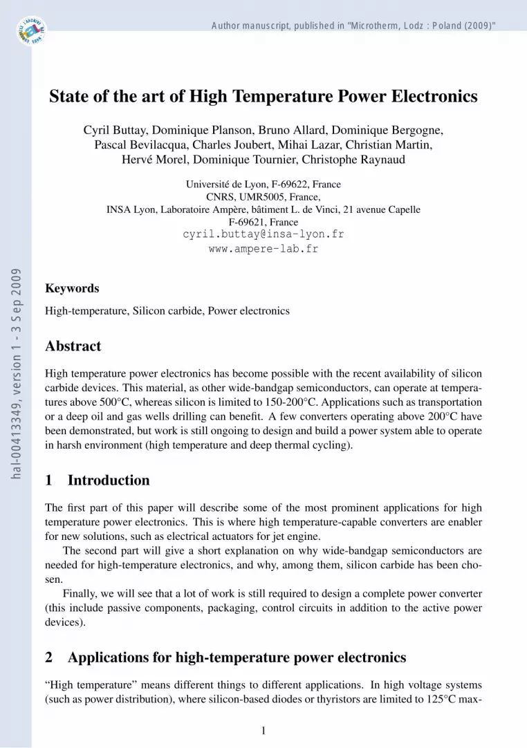
Figure 2: Static characteristic of a 1200V – 15A – 200 mΩ JFET (third generation) from SiCeD, fortwo ambiant temperatures: (a) 25°C and (b) 225°C. Curves where acquired using a Tektronix 371 curvetracer in pulse mode. Please note that both curves have a different y-scale for the sake of readability.
Regarding controlled switches, MOSFET have not reached yet maturity: their oxide layerhas poor reliability under high temperature and high voltage; the carrier mobility in their chan-nel is low, and charge trapping in the gate oxide causes threshold voltage instability [11]. Ap-parently, some of these limitations have been overcome recently, as SiC MOSFETs operatingabove 200°C have been demonstrated [12], but without any information about reliability andageing.
Currently, JFETs are considered good candidates as the “general purpose” SiC controlledswitch. They are available as engineering samples (for example from SiCeD, see figure 2), andshould be commercially available soon. Their main drawback is that they are “normally on”,i.e. they conduct current when no voltage is applied between their gate and source terminals.This requires special care when designing a converter to ensure that a fault in the control circuitwon’t result in a short-circuit in the power side. Furthermore, it can be seen in figure 2 thatJFETs require a negative voltage on the gate, whereas Si MOSFET require a positive voltage toturn on.
A SiC JFET/Low-voltage Si MOSFET hybrid has been presented to create a “normally-off”switch. This component is called a Baliga-pair [8] or a cascode. The presence of a Si-MOSFET,however, makes it ill-suited to high temperature.
3.2.2 Bipolar devices
As unipolar devices have quite good performances up to a few kilovolts, most of the workon bipolar devices is towards very high voltage (tens of kilovolts), for energy distribution ap-plications (PiN diodes, BJT, thyristors). However, bipolar devices can be interesting for hightemperature, even at low voltage, as their losses tend to reduce as temperature increases [13].Furthermore, Bipolar Junction Transistors (BJTs) are normally-off devices, which could makedesigning a converter easier (although they require fairly high current to drive them). Transic2
is an example of a company which sells BJTs for 600 V applicationsBipolar devices have long been crippled by defects in the base material (stacking faults).
2http://www.transic.com/
5
hal-0
0413
349,
ver
sion
1 -
3 Se
p 20
09

Figure 3: A JFET-based, 540 V, 15 A, 3-phase inverter (6 JFETs) in a single package with an externalDC capacitor. This system has been successfully tested at 200°C.
Their performances used to drop rapidly during operation. This is apparently getting better, andsome bipolar devices have been found to be stable for long periods (although the quality of thebase material still has a lot of influence) [14]
3.3 High temperature converters
Now that some SiC components have become available, some of the research work has shiftedto high-temperature converters. As we will see below, active devices are just one of the manyparts required to build a converter (high temperature passive, packaging, control circuits arealso required).
As long as the ambient temperature remains under 150°C, classical silicon control circuitscan be used. This is the case with inverters designed for automotive hybrids, which make useof the ICE cooling loop (120°C) [15]. In this case, it is possible to use Si IGBTs together withSiC SBDs, providing the thermal resistance of the package is low enough to keep the junctiontemperature of the IGBT below 175°C.
In [16], an inverter operating at 150°C ambient temperature is presented. Here, the idea isto take advantage of SiC devices to allow the junction temperature to reach 250°C. The 100°Ctemperature gradient allows to use a less efficient (and therefore much smaller) heatsink
At a even higher temperature (200°C), a SiC MOSFET-based, 2-kW boost converter isdemonstrated [12] . In [17], authors have designed all the basic building blocks for a JFETdriver, to be built in SOI. These blocks (in discrete form) have been used to drive a JFET-basedinverter operating at 200°C ambient temperature [18]. A picture of the inverter can be seen infigure 3
Finally, in [19], a buck converter (SiC JFET and SBD) is tested at 400°C. However, due tothe very high leakage current in the SBD at high temperature, the converter is derated to 200 Vinstead of 600V. Moreover, the saturation current in the JFET drops from 3.5 A to 0.7 A at hightemperature. Also, some components, such as the control circuits and the input capacitor arekept at ambient.
4 Remaining issues
As we have seen, some of the basic building block for high temperature power converters havebecome available in recent years. Although the first demonstrators have been presented, re-
6
hal-0
0413
349,
ver
sion
1 -
3 Se
p 20
09

0°C
50°C
100°C
150°C
200°C
250°C
300°C
100 V 1 kV 10 kV
Junc
tion
tem
pera
ture
Breakdown voltage
Safe Operating Area
Case limit
Silicon limit
Figure 4: For low-voltage silicon devices, the maximum operating temperature is limited by the materialsof the case. For higher voltage devices, the limit is the silicon.
search is still ongoing to provide systems with better performances, and more important yet,better reliability.
4.1 Better SiC devices
At the moment, only SiC SBD have reached maturity.MOSFETs have only been demonstrated by a few research laboratory, with little informa-
tion about their reliability.JFETs are getting better, but some of their parameters (such as the threshold voltage) are
not fully controlled yet. Because of this, drivers must be individually matched to the transistors(the gate breakdown voltage is only a few volts away from the threshold voltage). This shouldimprove soon.
The gain of BJTs is still relatively low (in the order of 30). This puts a lot of constraints onthe driver, which has a lot of current to source. Darlington pairs or more advanced combinationshould improve this issue.
4.2 high temperature/reliability packaging
As can be seen in figure 4, even for silicon devices, the maximum operating temperature issometimes limited by the packaging. Most packaging solutions have indeed been developed formild ambient [20], and require a complete redesign to cope with high temperature environments.
An example of this is the die-attach solution: in classical power modules, it is made usingthe so-called “high temperature” lead-rich solder alloy [20], which melts at 312°C, or with otheralloys which have an even lower melting point [21]. Although the melting point is higher thanmost high temperature environments, a wide safety margin must be ensured between the max-imum operating temperature and the melting point: the closer you are to the melting point, theworse the mechanical properties of the solder alloy. In most cases, the homologous temperature(ratio of the melting point over the operating temperature, both expressed in Kelvin) should notexceed 0.67 (although values as high as 0.85 are not uncommon in electronics).
To avoid the use of very high-melting point solder alloys, which would put a lot of stresson semiconductor dice during assembly, different die-attach solutions have been explored. Sin-tering of micrometre-sized silver powder has been developed by Semikron [22]. With this
7
hal-0
0413
349,
ver
sion
1 -
3 Se
p 20
09

Figure 5: Cross section of a power module (with its associated heatsink), which shows the many layersand interfaces it contains. When this structure is submitted to power cycling, heavy mechanical stressesare generated and can eventually yield to fatigue and faillure of the assembly.
technique, a joint is obtained by applying pressure (40 MPa) and temperature (about 250°C).As the die-attach material is pure silver, its melting point is expected to be 961°C, and there-fore will operate at very low homologous temperature. To avoid the use of pressure (whichrequires dedicated tooling), researchers at the Virginia Tech. have presented a silver sinteringsolution using nanometre-sized powder [23],[24]. This solution gives good results compared toEpoxy-based die attach or Au-Ge solders [25].
Another approach is the Transient Liquid Phase Bonding (TLP)[26]. With this technique, alow-melting point metal (or alloy) will diffuse into a solid phase. Once it is completely dilutedinto the solid phase, the melting point of the newly formed alloy will be much higher thanthe process temperature. Such techniques have been applied to Au/Sn alloys [27], In/Ag [28],among others. Finally, more exotic solutions have been explored to create a very localisedheating (hence avoiding stressing the dice) by using “explosive” reactive die attach [29].
In addition to the temperature-limitation of many parts of a classical packaging such asdepicted in figure 5 (solders, wirebonds, silicone encapsulant, thermal paste. . . ), it must benoted that power modules are very sensitive to thermal cycling. As we can see in figure 5,a power module is a stack of many materials, creating many interfaces. When such stack issubmitted to thermal cycling, all parts tends to expand differently (as they all have differentcoefficients of thermal expansion), creating stresses at the interfaces. During the life of thepower module, part of these stresses accumulates, creating fatigue and eventually failure. Thisphenomenon is already present with standard, silicon-based components, but becomes evenmore visible with high-temperature applications.
4.3 High temperature control circuits
Most high temperature converter use control circuits made with Silicon-On-Insulateor (SOI)substrate. Many circuits have been developed by Honeywell for oil well applications [7]. InEurope, the company Cissoid3 also designs SOI circuits for high temperature, including MOS-FET drivers [30].
Recently, the first SiC-based integrated circuit has been announced [11]. It should eventu-ally allow very high temperature drivers, or monolithic integration of drivers and power. How-ever, a lot of work is still needed to produce a driver complete with power supply and device
3http://www.cissoid.com/
8
hal-0
0413
349,
ver
sion
1 -
3 Se
p 20
09

protections.
4.4 High temperature passives
Magnetic material can be found for ambient temperature up to 450°C [19]. Capacitors are muchof an issue, as most dielectric material cannot be used above 200 to 250°C. For example, micacan be used up to 260°C, TFE up to 200°C [31]. A common dielectric in ceramic capacitors(X7R) can also be used at 200 °C, but at the expense of a strongly reduced capacitance (around50%). For all these technologies, the dissipation factor is high (1%), as well as the cost forcapacitors rated at a few hundred volts.
5 Conclusion
Silicon carbide allows power devices operating at very high temperature (in theory more than1000°C). As we have seen, research is still needed to take fully advantage of this material.Packaging, passive components and control circuits are currently restricted to much lower tem-peratures. Research is also needed to produce better power devices, eventually using alternativewide-bandgap semiconductors, such as GaN or diamond.
The first demonstrators of high temperature converters have been presented recently. Theyprove the feasibility and the advantages of systems that can operate in harsh environments.
References[1] M. Consortium, “Project year 1 executive summary,” report, MOET FP6, sep 2007.
[2] I. S. Mehdi, A. E. Brockschmidt, and K. K. J., “A case for high temperature electronics for aerospace,” inProceedings of the High Temperature Electronics Conference (HiTEC), (Santa Fe, NM), IMAPS, may 2006.
[3] J. G. Kassakian and D. J. Perreault, “The future of electronics in automobiles,” in Proceedings of the Interna-tional Symposium on Power Semiconductor Devices and ICs (ISPSD), (Osaka, Japan), pp. 15–19, 2001.
[4] L. D. Marlino, “High temperature & thermal management needs for the freedomcar program,” in Proceedingsof the High Temperature Electronics Conference (HiTEC), (Santa Fe, NM), IMAPS, may 2006.
[5] E. Kolawa, M. Mojarradi, and T. Balint, “Applications of high temperature electronics in space exploration,”in Proceedings of the High Temperature Electronics Conference (HiTEC), IMAPS, may 2006.
[6] “Downhole gas compression,” product brochure, Corac Group plc, 2005.
[7] B. W. Ohme, M. R. Larson, J. Riekels, S. Schlesinger, K. Vignarajah, and E. M. Nance, “Progress update onhoneywell’s deep trek high temperature electronics project,” in Proceedings of the High Temperature Electron-ics Conference (HiTEC), (Santa Fe), p. 9, IMAPS, may 2006.
[8] B. J. Baliga, “The future of power semiconductor device technology,” Proceedings of the IEEE, vol. 89,pp. 822–832, jun 2001.
[9] T. Funaki, J. C. Balda, J. Junghans, A. Jangwanitlert, S. Mounce, F. D. Barlow, H. A. Mantooth, T. Kimoto,and T. Hikihara, “Switching characteristics of sic jfet and schottky diode in high-temperature dc-dc powerconverters,” IEICE Electronics Express, vol. 2, pp. 97–102, feb 2005.
[10] A. Ward, “Sic power diode reliability,” application note, CREE, 4600, Silicon Drive, Durham, NC, oct 2008.
[11] K. Sheng, Y. Zhang, M. Su, J. H. Zhao, X. Li, P. Alexandrov, and L. Fursin, “Demonstration of the first sicpower integrated circuit,” Solid State Electronics, vol. 52, pp. 1636–1646, 2008.
[12] B. Ray, J. D. Scofield, R. L. Spyker, B. Jordan, and S.-H. Ryu, “High temperature operation of a dc-dcpower converter utilizing sic power devices,” in Proceedings of the 20th Applied Power Electronics Conference(APEC), (Austin, TX), pp. 315–321, IEEE, mar 2005.
9
hal-0
0413
349,
ver
sion
1 -
3 Se
p 20
09

[13] P. Borthen and G. Wachutka, “Testing semiconductor devices at extremely high operating temperatures,” Mi-croelectronics Reliability, vol. 48, pp. 1440–1443, aug 2008. 19th European Symposium on Reliability ofElectron Devices, Failure Physics and Analysis (ESREF 2008).
[14] P. G. Muzykov, R. M. Kennedy, Q. J. Zhang, C. Capell, A. Burk, A. Agarwal, and T. S. Sudarshan, “Physi-cal phenomena affecting performance and reliability of 4h–sic bipolar junction transistors,” MicroelectronicsReliability, vol. In Press, Corrected Proof, pp. –, 2008.
[15] C. Buttay, J. Rashid, C. Mark Johnson, P. Ireland, F. Udrea, G. Amaratunga, and R. Malhan, “High perfor-mance cooling system for automotive inverters,” in Proc. European Conference on Power Electronics andApplications, (Aalborg, Denmark), pp. 1–9, EPE, sep 2007.
[16] J. M. Hornberger, E. Cilio, R. M. Schupbach, A. B. Lostetter, and H. A. Mantooth, “A high-temperature mul-tichip power module (mcpm) inverter utilizing silicon carbide (sic) and silicon on insulator (soi) electronics,”in Proceedings of the 37th Power Electronics Specialists Conference (PESC), (Jeju, Korea), pp. 9–15, IEEE,June 2006.
[17] D. Bergogne, H. Morel, D. Tournier, B. Allard, D. Planson, C. Raynaud, and M. Lazar, “Normally-on de-vices and circuits, sic and high temperature : using sic jfets in power converters,” in Proceedings of the 5th
Conference on Integrated Power Systems (CIPS), 2008.
[18] D. Bergogne, H. Morel, D. Planson, D. Tournier, P. Bevilacqua, B. Allard, R. Meuret, S. Vieillard, S. Raël,and F. Meibody Tabar, “Towards an airborne high temperature sic inverter,” in Proceedings of the PowerElectronics Specialists Conference (PESC), IEEE, 2008.
[19] T. Funaki, J. C. Balda, J. Junghans, A. S. Kashyap, H. A. Mantooth, F. Barlow, T. Kimoto, and H. Takashi,“Power conversion with sic devices at extremely high ambient temperatures,” IEEE Transactions on PowerElectronics, vol. 22, pp. 1321–1329, jul 2007.
[20] W. W. Sheng and R. P. Colino, Power Electronic Modules: Design and Manufacture. CRC, 1st ed., jun 2004.
[21] I. Corp, “Alloy sorted by temperature,” datasheet, Indium Corp.
[22] C. Göbl, P. Beckedahl, and H. Braml, “Low temperature sinter technology die attachment for automotive powerelectronic applications,” in Automotive Power Electronics, (Paris), p. 5, 21–22 jun 2006.
[23] G. Bai, Low-Temperature Sintering of Nanoscale Silver Paste for Semiconductor Device Interconnection. PhDthesis, Virginia Polytechnic Institute and State University, Blacksburg, Virginia, oct 2005.
[24] J. G. Bai, J. Yin, Z. Zhang, G.-Q. Lu, and van Wyk Jacobus Daniel, “High-temperature operation of sicpower devices by low-temperature sintered silver die-attachment,” IEEE Transactions on Advanced Packaging,vol. 30, pp. 506–510, aug 2007.
[25] R. Kisiel and S. Z., “Die-attachment solutions for sic power devices,” Microelectronics Reliability, vol. InPress, Corrected Proof, 2009.
[26] J. Roman and T. Eagar, “Low stress die attach by low temperature transient liquid phase bonding,” in 1992 In-ternational Symposium on Microelectronics (I. International Society for Hybrid Microelectronics, ed.), no. 52,(San Fransisco, California), 1992.
[27] R. W. Johnson, C. Wang, Y. Liu, and J. D. Scofield, “Power device packaging technologies for extreme envi-ronments,” IEEE Transactions on Electronics Packaging Manufacturing, vol. 30, pp. 182–193, jul 2007.
[28] T. Quintero, Pedro O. andy Oberc and F. P. McCluskey, “High temperature die attach by transient liquid phasesintering,” in HiTEC 2008, (Albuquerque), pp. 207–212, IMAPS, may 2008.
[29] A. McClure, P. McCluskey, and A. J. Clark, “Rapid thermal processed attachment materials,” in HiTEC 2008,(Albuquerque), pp. 273–278, IMAPS, May 2008.
[30] CISSOID, “High-temperature, bootstrapped full-bridge mosfet driver,” datasheet, CISSOID, sep 2008.
[31] J. S. Bowers, “Comparative characterization of capacitors used in high temperature electronics applications,”in Proceedings of the 4th High Temperature Electronics Conference (HiTEC), pp. 184–190, IMAPS, 1998.
10
hal-0
0413
349,
ver
sion
1 -
3 Se
p 20
09