Embed Size (px)
Citation preview

Т 4 -S S 9 а .

MODELING AND CHARACTERIZATION OF CAPACITIVE MICROMACHINED ULTRASONIC TRANSDUCERS
A DISSERTATION
SUBMITTED TO THE DEPARTMENT OF ELECTRICAL AND ELECTRONICS
ENGINEERING
AND THE INSTITUTE OF ENGINEERING AND SCIENCES
OF BILKENT UNIVERSITY
IN PARTIAL FULFILLMENT OF THE REQUIREMENTS
FOR THE DEGREE OF
DOCTOR OF PHILOSOPHY
ByAyhan Bozkurt
January 5, 2000

Ί к
l lo o a
4 2

I certify that I have read this thesis and that in my opin
ion it is fully adequate, in scope and in quality, as a thesis
for the degree of Doctor of Philosophy.
/··■///'/b k l la h Atalar, Ph. D. (Supervisor)
I certify that I have read this thesis and that in my opin
ion it is fully adequate, in scope and in quality, as a thesis
for the degree of Doctor of Philosophy.
f Hayrettin Köyjıen, Ph. D.
I certify that I have read this thesis and that in my opin
ion it is fully adequate, in scope and in quality, as a thesis
for the degree of Doctor of Philosophз^
Orhan Aytiir, Ph. D.

11
I certify that I have read this thesis and that in my opin
ion it is fully adequate, in scope and in quality, as a thesis
for the degree of Doctor of Philosophy.
I certify that I have read this thesis and that in my opin
ion it is fully adequate, in scope and in quality, as a thesis
for the degree of Doctor of Philosophy.
Tayfun Akin, Ph. D.
Approved for the Institute of Engineering and Sciences:
Prof. Dr. Mehmet^^;i№ay Director of Institute of Engineering and Sciences

in loving memory of my father

ABSTRACT
MODELING AND CHARACTERIZATION OF CAPACITIVE MICROMACHINED ULTRASONIC TRANSDUCERS
Ayhan BozkurtPh. D. in Electrical and Electronics Engineering
Supervisor: Prof. Abdullah Atalar January 5, 2000
The Capacitive Micromachined Ultrasonic Transducer (cMUT) is a device used for the
generation and detection of ultrasonic sound waves. The device is constructed on a sil
icon substrate using a microfabrication process. Individual cells constituting the device
are membranes which have dimensions in the order of tens of microns, and are made up
of a mechanicalh^ strong compound of silicon. The transducer itself has dimensions mea
sured in centimeters, thus the total number of cells that make up a transducer is in the
order of thousands. The excitation/detection of acoustic waves relies on the capacitance
between the substrate and membrane: The presence of acoustic waves induces a small
-AlC variation on the DC bias on the device, which can be used for detection, while a
small -A.C component added to the DC bias by the drive circuit changes the electro-static
attraction force on the membrane causing it to vibrate, producing acoustic waves. Basic
advantages of cMUT devices include easy patterning of array structures, integration of
drive/detection electronics with mechanical structures, and low cost.
In this study, basic theory describing the characteristics of cMUT devices were de
veloped. The analytic formulation was used to test the validity of a Finite Element

Method (FEM) model. The FEM model, then, was emplo3'ed in the analysis of struc
tures for which no analytical models are present. Specific problems solved using the
FEM model included the characterization of cMUT devices with judiciously patterned
electrodes. A more specific study showed that the bandwidth of an immersion device
with an active area of radius 25 /¿m can be increased by 100% by simply setting the
electrode radius to 10 /rm. The FEM analysis was, then, extended to handle the effects
of substrate loss, which required the incorporation of an Absorbing Boundary Condition
(ABC) into the model. A Normal Mode Theory analysis was conducted to give better
insight to the physical nature of the effect of substrate loss to device characteristics. The
dominant wavemode for a transducer of central frequency 2.5 MHz was found to be the
lowest order anti-symmetric lamb wave mode (AO), for a silicon substrate of thickness
500 //m. A microfabrication process was developed for the production of cMUT devices.
Hexagonally shaped transducers of radius 40 p.m were fabrictated on a conducting sili
con substrated with silicon nitride as the sacrificial la.j'er and amorphous silicon as the
membrane material. Both the gap and membrane thicknesses are set to 0.5 //m. 8, 16,
and 24 /im gold plates were deposited as top eletrodes. The total number of active cells
were 24 thousand for a substrate size of 0.7x0.7 cm . Some experimental results were
obtained from the fabricated transducers to support the analytical cMUT model. The
device is found to have a central frequency of 2 MHz.
Keywords : Capacitive Micromachined Ultrasonic Transducer (cMUT), Finite Ele
ment Method (FEM) Modeling, Absorbing Boundary Condition (ABC), Normal Mode
Theory, Microfabrication Process.

ÖZET
KAPASİTİF MİKRO-İŞLENMİŞ ULTRASONİK ÇEVİRİCİLERİN MODELLENMESİ VE KARAKTERİZASYONU
Ayhan BozkurtElektrik ve Elektronik Mühendisliği Doktora Tez Yöneticisi: Prof. Dr. Abdullah Atalar
5 Ocak 2000
Kapasitif Mikro-işlenmiş Ultrasonik Çevirici (kMUÇ), ultrasonik ses dalgalarının üre
tilmesi ve algılanması için kullanılan bir cihazdır. Cihaz, silikon bir taban üzerinde
mikro-fabrikasyon yöntemiyle üretilir. Cihazı oluşturan hücreler, boyutları on mikro
nlar mertebesinde olan ve silikonun mekanik olarak sağlam bir bileşiğinden yapılan
zarlardır. Çeviricinin kendisi santimetre cinsinden ölçülebilen boyutlara sahip olduğu
için bir çeviriciyi oluşturan toplam hücre sayısı binlerle ifade edilir. Akustik dalgaların
uyarılması/algılanması, zar ile taban arasındaki kapasitansa dayanır: Akustik dalgaların
varlığı, cihaz üzerindeki DC öngeriliminde algılama için kullanılabilecek küçük bir AC
dalgalanmaya j’ol açarken, sürücü devre tarafından DC öngerilime eklenen küçük bir AC
bileşen zar üzerindeki elektrostatik çekim kuvvetini değiştirerek zarı titreştirip akustik
dalgalar üretir. Dizilim (array) yapılarının kolay biçimlendirilmesi, mekanik yapıların
sürücü/algılama devreleriyle entegras}'onu ve düşük maliyet kMUÇ cihazlarının temel
a^·antajları arasında yer almaktadır.
Bu çalışmada, kMUÇ cihazlarını karakterize etmekte kullanılan temel teoriler gelişti
rilmiştir. Analitik formulasyon, bir Sonlu Eleman Metodu (SE.M) modelinin doğruluğunu

sınamak için kullanımıştır. SEM modeli, daha sonra analitik modeli bulunmayan yapıların
analizinde kullanılmıştır. Elektrotları belli amaçlar için biçimlendirilmiş kMUÇ’larm
analizi, SEM modeli kullanılarak çözülen özel problemler arasında yer almaktadır. Daha
özel bir çalışma, sualtı uygulamaları için kullanılan 25 fim yarıçaph bir cihazın elek
trot yarıçapının 10 fim yapılmasıyla cihazın bant genişliğinin % 100 arttırılabileceğini
göstermiştir. SEM analizi, daha sonra taban kayıplarını da içerecek şeklide genişletilmiştir.
Bu, SEM modeline Emici Sınır Koşulları’nm (ESK) eklenmesini gerektirmiştir. Ajaıca
bir Normal Mod Teorisi analiziyle problemin fiziksel temelinin daha iyi anlaşılabilmesi
sağlanmıştır. Bu analizle, merkez frekansı 2.5 MHz ve taban kalınlığı 500 fim olan bir
çevirici için hakim dalga modunun en düşük sıralı anti-simetrik Lamb dalgası modu
olduğu tespit edilmiştir. Bu çalışmada ayrıca kMUÇ cihazlarının üretimi için bir mikro-
fabrikasyon yöntemi geliştirilmiştir. Bu yöntemle, zar malzemesi olarak amorf silikop,
kalıp malzemesi olarak da silikon nitrat kullanılarak 40 fim çaplı altıgen biçimli çeviriciler
üretilmiştir. Zar ve hava boşluğu kalınlıklarının her ikisi de 0.5 fim olarak seçilmiştir.
Zarlar, elektrot olarak kullanılmak üzere 8, 16 veya 24 fim çaplı altın plakalarla kaplan
mışlardır. 0.7x0.7 cm^’lik bir çevirici alanı üzerinde 24 bin aktif hücre inşaa edilmiştir.
Merkez frekansı 2 MHz olarak ölçülen çeviricilerden analitik kMUÇ modelini destekleyen
ölçüm sonuçları alınmıştır.
Anahtar Sözcükler: Kapasitif Mikro-işlenmiş Ultrasonik Çevirici (kMUÇ), Sonlu
Eleman Metodu (SEM), Emici Sınır Koşulları (ESK), Normal Mod Teorisi, Mikro-
fabrikasvon Yöntemi.

ACKNOWLEDGMENTS
I would like to express my sincere gratitude to Dr. Abdullah Atalar for his supervision,
guidance, suggestions and encouragement through the development of this thesis.’I
I would like to thank to the members of my dissertation jury for reading the manuscript
and commenting on the thesis.
I am indebted to Dr. Khuri-Yakub of the Ginzton Laboratory at Stanford University
for providing the means for a summer internship. Many thanks are due to Dr. Degertekin
and Dr. Ladabaum for their cooperation during my studies at the Ginzton Laboratory.
I would also like to thank to Dr. Ekmel Ozbay for his support during the experimental
work at the Physics Department. Special thanks go to Erhan Ata, Murat Güre, and
Burak Temelkuran who have been my teachers in the clean room.
Endless thanks to Sanlı! Not only an excellent colleague, he has always been my
most supporting friend.
And I would like to express my sincere gratitude to the following people: Güçlü,
Bacar, Tolga, Gürkan, Uğur Oğuz, Gün, Lütfİ3'e, for being my friends; Beygo, for giving
life; Tünay, Hayri, Melis, for being there whenever I needed them; and Gülbin, for
her endless support. Finally, like to thank to my parents, brother and Ebru, whose
understanding made this study possible.
Contents
1 INTRODUCTION
1.1 Analysis
1.2 Experiment . .
3
1
2 ULTRASONIC TRANSDUCERS
2.1 The Micromachined Ultrasonic Transducer
2.2 Operational Principles and Parameters
3 ANALYTIC MODEL for cMUTs
3.1 Mason's Equivalent Circuit
3.2 cM UT Parameters; Collapse Voltage
3.3 cM UT Parameters: Bandwidth of Immersion cM UT
4 FEM MODELING OF cMUTs
4.1 Thermal and Electrostatic Analyses
4.2 Calculation of Electrostatic Pressure
6
6
9
10
10
12
13
15
16
17
4.3 A N SYS Modeling of cM UT 18
5 STATIC and DYNAMIC SIMULATION 20
5.1 Static A n a ly s is ........................................................................................................... 21
5.1.1 First Order Iteration (Small D eflection).................................................. 22
5.1.2 Static Analysis - Membrane Collapse V o lta g e ........................................... 23
5.1.3 Static Analysis - Input C apacitan ce............................................................ 25
5.2 Dynamic Analysis 26
5.2.1 Dynamic Analysis - Membrane Impedance 26
5.2.2 Dynamic Analysis - Electro-mechanical Transformer Ratio 26
'/
6 OPTIMUM IMMERSION cMUT 29
6.1 Partially Metalized cM UT - Membrane Sh ap e..................................................... 31
6.2 Partially Metalized cM UT - Transformer Ratio 31
6.3 Partially Metalized cM UT - Simulation R e s u lts ..................................................... 34
6.3.1 Bandwidth of cM UT - Constant B i a s ........................................................ 34
6.3.2 Bandwidth of cM UT - Variable B ia s ............................................................ 35
7 cMUT LOSS MODELING 38
7.1 FEM Model for Substrate C o u p lin g ...................................................................... 39
7.2 Acoustic Impedance of cM UT with Loss 42
7.3 cM UT Loss vs. Model Dimensions 46
11
Ill
7.4 Normal Mode Theory A n alysis................................................................................ 47
8 DEVICE FABRICATION 54
8.1 An Introduction to Microfabrication...................................................................... 54
8.2 cM UT Fab ricatio n ................................................................................................... 55
8.3 Device D im ensions................................................................................................... 63
8.4 SEM Im a g e s .............................................................................................................. 65
8.5 Experimental Setup 67
8.6 Measurement Results 70
8.7 Discussion and Further Work 72
9 CONCLUSION 73
A A MICROMACHINING GLOSSARY 76
B MATERIAL PARAMETERS 78
List of Figures
2.1 Schematic views of two silicon cMUT structures.
2.2 3D visualizations for various cMUT structures.
3.1 Equivalent electrical circuit for the cMUT membrane.
4.1 Metal object surrounded by medium of dielectric constant e.
4.2 ANSYS Model of Circular MUT.
4.3 Finite element mesh of the model geometry.
5.1 Application of temperature on model geometry.
5.2 Structural loads on model geometry.
5.5 Steps of iterative electrostatic-structural solution.
5.6 Iteration results for a stable and a collapsing membrane.
5.7 Acoustic impedance of membrane with zero residual stress.
11
18
19
19
21
22
225.3 Clamped MUT membrane model......................................................................
5.4 E-filed intensity (left) and membrane deflection (right) for V=100 Volts. 23
24
25
27
IV

6.1 Reduced electrical circuit for the cMUT membrane......................................... 29
6.2 Electro-mechanical transformer ratio, capacitance and bandwidth of cMUT
transducer for electrode radius ranging from 2 to 24 /rm. 34
6.3 Butterworth network for electrical matching..................................................... 35
6.4 Normalized transducer bandwidth for two electrode sizes.............................. 36
6.5 Collapse voltage values for varying electrode sizes........................................... 36
6.6 Transducer bandwidth for DC bias equal to the collapse voltage.................. 37
7.1 Cross-sectional view of cMUT structure. 39
7.2 Finite-element model of the cMUT...................................................................... 40
7.3 Magnitude of nodal displacement on substrate (Left 1.0, Right 3.0 Mhz). 41
7.4 Fitted curve on ANSYS damp parameter determined by trial-and-error. . 42
7.5 Impedance of cMUT with substrate loss (real and imaginary parts) 42
7.6 Real impedance for a point contact........................................................■. . . . 43
7.7 Submodeling I : Substrate impedance. 43
7.8 Real substrate impedance for circular excitation.............................................. 44
7.9 Two-port representation for the cMUT membrane.......................................... 44
7.10 Submodeling II : Membrane as a two-port......................................................... 45
7.11 Forces at the rim of the membrane...................................................................... 45
7.12 cMUT Impedance: unified and two-part m o d e ls ........................................... 46
7.13 Real part of cMUT impedance for various substrate thicknesses. 47

7.14 Lowest (0th) order symmetric and antisymmetric plate modes (SO and AO). 47
7.15 Dispersion curves for AO and SO modes in the frequency range 1.0-3.0 MHz 49
7.16 Particle velocity field distribution (Aq and FEA) at 1 MHz (ri=29.9 mm). 50
7.17 Total power coupled to the substrate and powers for Aq and Sq modes. 51
7.18 Equivalent circuit model which includes cMUT substrate lo.ss. 51
7.19 Total loss resistance of cMUT and resistances of Aq and So modes........... 52
7.20 Equivalent circuit model revisited: modal loss accounts for total loss. 53
8.1 Process steps 1, 2a, 2b, 2c, 2d and 3. 58'/
8.2 Process steps 4a, 4b, 4c, 4d, 4e and 5a................................................................ 59
8.3 Process steps 5b and 5c........................................................................................... 60
8.4 Top view of cMUT structure for various fabrication steps.............................. 60
8.5 Zoomed view of mask (active membrane area 500x250 /xm approx.). 63
8.6 Basic building block used in drawing the cMUT mask. 64
8.7 SEM images of fabricated cMUT devices........................................................... 66
8.8 Experimental setup for cMUT characterization. 67
8.9 Detection circuit for cMUT. 68
8.10 Ginzton detection circuit for cMUT. (courtesy Dr. Sanlı Ergun) 69
8.11 Real and imaginary parts of cMUT impedance for various bias voltages. . 70
8.12 Simplified model for cMUT with ohmic losses.................................................. 71
8.13 Experimental results and model data.................................................................. 71
VI
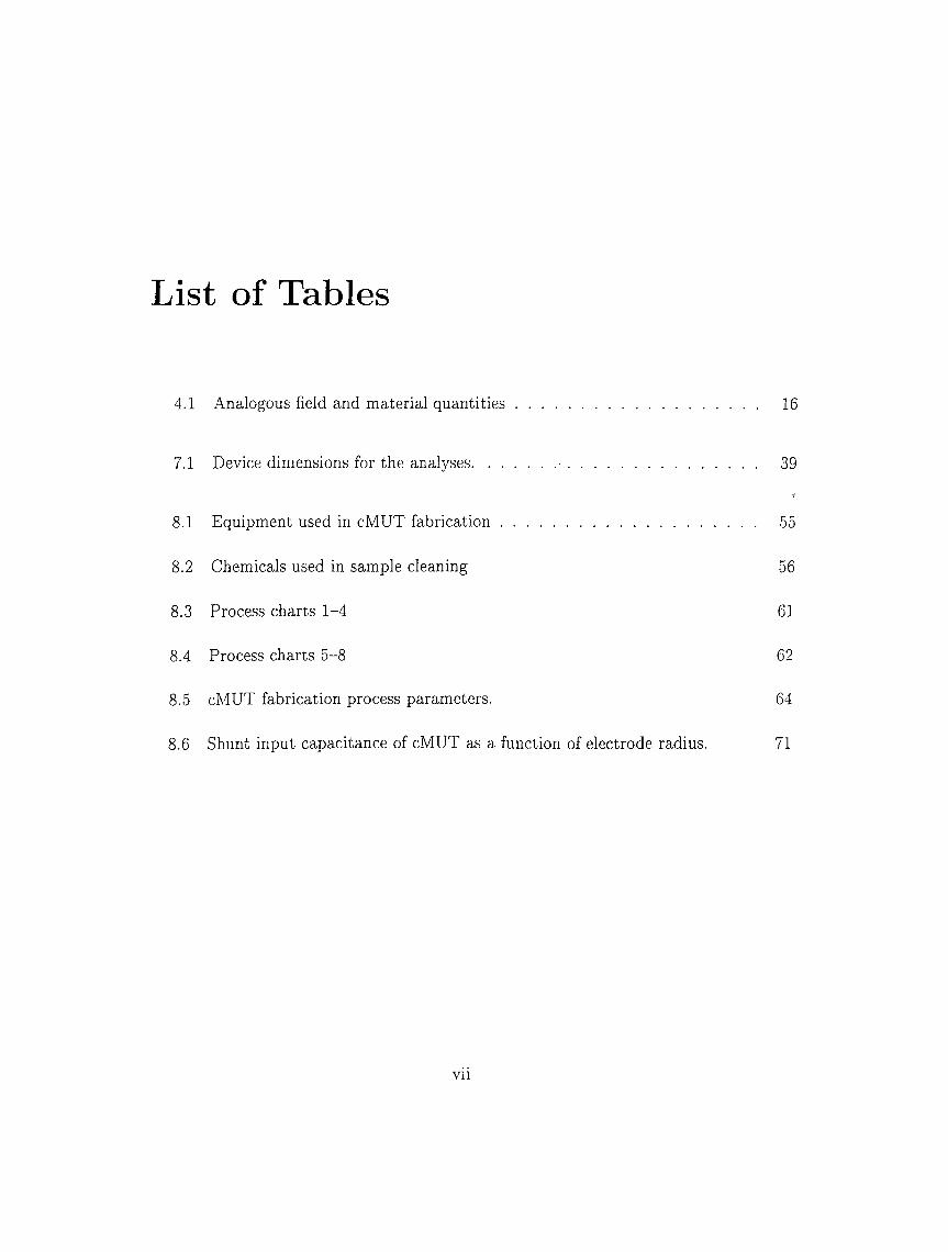
List of Tables
4.1 Analogous field and material quantities............................................................ 16
7.1 Device dimensions for the anatyses.................... .................................................. 39
■/
8.1 Equipment used in cMUT fabrication............................................................... 55
8.2 Chemicals used in sample cleaning 56
8.3 Process charts 1-4 61
8.4 Process charts 5-8 62
8.5 cMUT fabrication process parameters. 64
8.6 Shunt input capacitance of cMUT as a function of electrode radius. 71
Vll

Chapter 1
INTRODUCTION
The generation and detection of ultrasonic waves has long been a concern in many fields of
technology which include imaging, a general name for applications ranging from medical
ultrasound to underwater acoustics; and nondestructive evaluation (NDE), which covers
a huge set applications such as fiow measurement, material characterization, detection
of holes/cracks/fractures, assessment of bonding quality of layered material, etc. In
almost all applications, piezo-electric transducers were the unique choice, as alternatives
such as capacitive transducers did not perform well when compared to their ultrasonic
counterparts. Air-coupled and immersion capacitive ultrasonic transducers had long
existed [1-3] and their characteristics and performance had been exhaustively evaluated.
However, until recent developments in micromachining techniques which have led to
the design of new versions of the devices [4-10], those were not considered as serious
alternatives for piezo-electric transducers.
Piezo-electric transducers exploit a physical phenomenon called “piezoelectricity”:
an electric field causes a crystal structure to change its shape, or reversely, a crystal
produces an E-filed when it’s shape is changed. Capacitive ultrasonic transducers, on
the other hand, use electrostatic forces: changing the charge on the plates of a capacitor

changes the mutual attraction force, causing the plates to displace. Likewise, a change in
the plate displacement, when the voltage is held constant, causes a current to flow either
out from, or in to the capacitor. A capacitive Micromachined Ultrasonic Transducer,
is a collection of thousands of small capacitors with one plate being in the form of a
free-to-vibrate membrane, each cell having dimensions in the order of tens of microns.
Capacitive Micromachined Ultrasonic Transducers (cMUT), have the same qualities
of the piezo-electric transducers, when power output, dynamic range and operation fre
quency are concerned. However, there are three basic advantages associated with cMUTs
which deserve mentioning; First, they perform better in air. Materials used in the fab
rication of piezo-electric transducers usually have acoustic impedances in the order of
30x10® kg/m^s, 5 orders of magnitude higher than that of air (400 kg/m^s). There has
been a great effort in the development of matching layers, but these did not produce sat
isfactory results as either materials with desired acoustic impedances were not available,
or the matching layer was required to be impractically thin, or the matched transducer
turned out to have a a very narrow band. However, proper adjustment of design pa
rameters for cMUTs result in transducers that perform quite well even at frequencies
as high as 11.4 MHz [6]. A second advantage is about the convenience in fabrication of
complicated structures, such as array transducers. Piezo-electric array transducer pro
duction requires the use of fine mechanical processing tools, and employs a cumbersome
wiring step to connect the transducer to drive/detection electronics. For cMUTs, how
ever, structures are pattered using standard lithography, which makes the fabrication
of fancy structures quite convenient, and the drive electronics can be even constructed
on the same substrate, removing the necessity for wiring. Third, silicon processing is a
widely available well-established method. Therefore, cMUT devices are fabricated very
cheapljc
Theories explaining the electro-mechanical properties of piezo-electric transducers
have been well established, and the behavior of fabricated transducers can be precisely
predicted. Unfortunately, the same does not apply to cMUTs. Some theory and analysis
methods explaining their operation have been proposed [4,7,11-13]. Still, the behavior
of these devices require comprehensive analysis and design parameters must be well eval
uated. As main motivational forces behind transducer development include applications
in air-coupled NDE, new structures for efficient ultrasonic transmission into air need to
be developed. Likewise, designs for 3-D immersion imaging using 2-D transducer ma
trices require a good understanding of coupling between array elements. Furthermore,
for all applications, sources of mechanical loss need to be evaluated, as the spectral
characteristics of the device are greatly affected by loss.
This study has two focus points: the development of analysis tools for the evaluation
of cMUT characteristics, and the experimental verification of proposed analysis meth
ods. For the first objective, a lumped circuit representation for the cMUT device was
developed by the help of numerical analysis tools. For the second, a microfabrication
process was developed and implemented in a clean room environment. We now discuss
both parts of the thesis in more detail:
1.1 Analysis
The basic analysis method to evaluate the performance of micromachined structures is
to use an electrical equivalent circuit and express evaluation criteria in electrical terms
such as insertion loss, or electrical bandwidth. Mason proposed an lumped electrical
equivalent circuit for capacitive transducers [14]. This model has been extensively used
in our analj' ses to verify numerical results. Chapter 3 describes Mason’s model in detail.
Mason’s model describing cMUT characteristics only applies to particular device
structure. Real-life structures, however, usually do not satisfy conditions to make the
Mason’s model valid. As there are no closed form expression describing the behavior of
those devices, numerical methods need to be employed. Chapter 4 describes how the

cMUT device is modeled using the Finite Element Model (FEM) and how eletrostatic
and mechanical FEM probems can be coupled.
The FEM model proposed in Chapter 4 is first used to regenerate the results of
Mason, and was found to produce correct results, as described in Chapter 5. Simulation
for real-life structures are run and results are assessed bj comparing them to heuristic
expectations. Simulations are then extended to accuratel}' work out device parameters
(e.g., the collapse voltage) which are just estimated by Mason’s model.
One parameter of significance is the bandwidth of the transducer which, basically,
determines the pulse response of the device. Part of this study focuses on the bandwidth
optimization of immersion transducers, using anatysis, tools developed in Chapter 5.
Although electrode patterning has been used for selective mode excitation of resonators,
[15] and in the optimization of capacitive pressure transducers and microphones [16],
there is no comprehensive study in the literature on the performance optimization of
capacitive micromachined ultrasonic transducers (cMUTs) using electrode patterning. In
Chapter 6 we present optimization criteria, analyses, and simulations which demonstrate
that electrode patterning can be used to significantly enhance the performance of cMUTs.
Power coupled to anywhere other than the loading medium is considered as a loss
term for a transducer.The basic loss mechanism for capacitive micromachined ultrasonic
transducers is the power coupled to the substrate. Surface wave modes on solid half
spaces and acoustic waveguides have been extensively studied [17]. The power coupled
to these nodes can be determined by matching the stress amplitude at the membrane rirn
to the wave amplitudes of these nodes. Consequently, loss can be incorporated into the
lumped model of the cMUT. The same analysis can be used to determine cross-coupling
to neighboring transducer elements. The amount of loss and cross-coupling is significant
in the determination of transducer bandwidth and array performance. Chapter 7 finds
out values for loss terms to be incorporated in Mason’s model. A modal theory analysis is
included to give better insight to the physical nature of coupling to surface wave modes.
1.2 Experiment
Chapter 8 discusses a microfabrication process developed for the production of ch-IUT
devices. There are well established fabrication processes reported in literature [4,6,18-
20]. Here, we mimic the Stanford fabrication process described in [20], but we use our
own mask design and process sequencing, and make use of equipment available in the
Advanced Research Laboratory of the Physics Department of Bilkent University. The
fabricated devices are found to have reasonable electrical performance, despite their
low reliability. Although the experiments do not provide full support to the anal3Tic
results, they still provide good insight to the fabrication techniques, and their electrical
characteristics are well explained by a very basic model which is the starting point of
the entire modeling work.'I
All of the analyses described in Chapters 5 and 6 assume a transducer of circular
shape, as an FEM model for a circular structure is easily generated. However, the
fabricated transducers are of hexagonal shape to allow close packing. This will have an
insignificant effect on device characteristics, and the analysis for a circular transducer
will apply to the hexagonal structure.
To summarize, research work described in this thesis includes:
• Electrical Modeling of Capacitive Micromachined Ultrasonic transducers
• Optimization of device characteristics using electrode patterning.
• Modeling of mechanical losses using both FEM anal}^sis results and mode theory.
• Development of a microfabrication process for the production of cMUT devices.

Chapter 2
ULTRASONIC TRANSDUCERS
Ultrasonic transducers are devices capable of converting electrical signals into ultrasound
and vice versa. They find wide application in the fields of non-destructive evaluation
and medical imaging. Advances in microfabrication techniques enabled the construction
of micromachined versions of these devices with significant advantages described in this
chapter.
2.1 The Micromachined Ultrasonic Transducer
The almost universally used transducer type is that constructed using piezoelectric ma
terials [17]. Though being very commonly used, piezoelectric transducers have low con
version efficiency and their operation is limited to relatively low frequencies, because of
mechanical limitations on the production of small devices. For improved system per
formance and high resolution imaging, efficient high frequency transducers are required.
Capacitive Micromachined Ultrasonic Transducers (cMUTs), perform much better than
their piezoelectric counterparts in terms of the mentioned figures of merit. Microma
chined ultrasonic tran.sducers [8,11,12,21], are produced using standard silicon processes
6
and are distinguished with their efficiency, strength and reliability.
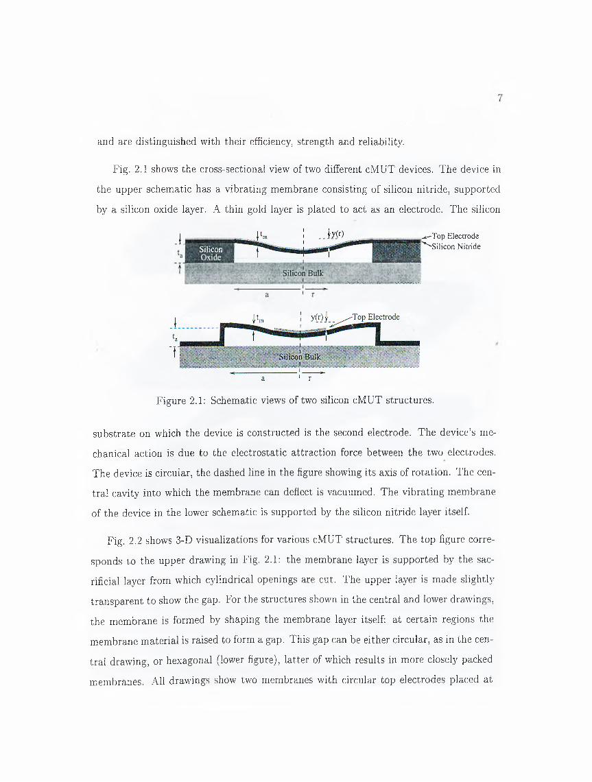
Fig. 2.1 shows the cross-sectional view of two different cMUT devices. The device in
the upper schematic has a vibrating membrane consisting of silicon nitride, supported
by a silicon oxide layer. A thin gold layer is plated to act as an electrode. The silicon
i .J y wJ .Silicon;·.,
^ T op Electrode ^Silicon Nitride
. Í M x,iw iw ir>v t i> <t»Ílíí5wMéííV;*^
Figure 2.1: Schematic views of two silicon cMUT structures.
substrate on which the device is constructed is the second electrode. The device’s me
chanical action is due to the electrostatic attraction force between the two electrodes.
The device is circular, the dashed line in the figure showing its axis of rotation. The cen
tral cavity into which the membrane can deflect is vacuumed. The vibrating membrane
of the device in the lower schematic is supported by the silicon nitride layer itself.
Fig. 2.2 shows 3-D visualizations for various cMUT structures. The top figure corre
sponds to the upper drawing in Fig. 2.1: the membrane layer is supported by the sac
rificial layer from which cylindrical openings are cut. The upper layer is made slightly
transparent to show the gap. For the structures shown in the central and lower drawings,
the membrane is formed by shaping the membrane layer itself: at certain regions the
membrane material is raised to form a gap. This gap can be either circular, as in the cen
tral drawing, or hexagonal (lower figure), latter of which results in more closely packed
membranes. All drawings show two membranes with circular top electrodes placed at

their centers and interconnected with metallic stripes.
Figure 2.2: 3D visualizations for various cMUT structures.
The production technique involved in the fabrication of the latter structure will be
described in Chapter 8.
One obvious advantage of capacitive transducers constructed using a rnicromachining
process is that the accompanying electronics can be constructed on the same substrate
on which the device resides. This results in noise immunity (as the cabling between the
transducer and driving/receiving electronics is eliminated) and ease of production (e.g.,
no flat parallel cables are required to be connected to array elements). Many foundries

now offer mixed micromachining/electronics processes for which the micromachining part
is done as a step of the standard device production process.
2.2 Operational Principles and Parameters
As mentioned, the cMUT’s activation is due to electrostatic attraction. An important
point to note is that electrostatic attraction is always positive. Thus, for harmonic
operation, a DC bias should be applied to make sure that the voltage on the cMUT is
always positive. In other words, the voltage to be applied in between the top electrode
and substrate should be of the form
V{t) - Vd c + VAcsin{uit) (2.1)
with u being the excitation frequency. As it will be further analyzed, the applied DC bias
is an important parameter which determines the device’s efficiency. The effect is positive,
i.e., efficiency increases with increasing DC bias. Therefore, the maximum allowed DC
bias which does not causes the membrane to collapse down to the substrate (which we
will call Vcoiiapse) is of importance. On the other hand, the inherent capacitance of the
device is another design consideration. Patterning the top electrode can reduce the device
capacitance, but this reduces the device efficiencjc However, capacitance and efficiency
have complex dependencies on electrode shape. Thus, an optimum point for device
performance can be found by judiciously patterning the top electrode. Simulation results
showing the validity of the last argument will be presented in the following chapters.

Chapter 3
ANALYTIC MODEL for cMUTs
In this chapter, we describe the model used in the anal3 sis of capacitive micromachined"
ultrasonic transducers (cMUT) and present some theoretically derived parameters of the
device. The theoretical derivations are verified by simulations which will be described in
subsequent chapters.
3.1 Mason's Equivalent Circuit
The anah'sis of the cMUT structure is based on the equivalent circuit approach of Ma
son [14] as adapted in [4]. The model, as seen in Fig.3.1, consists of a shunt input
capacitance Co at the electrical port and an electro-mechanical transformer with turns
ratio 1 : n. is the lumped acoustic impedance of the membrane and Z[ is the acoustic
load, which is just the acoustic impedance of the medium Zmedium. multiplied by the
membrane area Smembrane- V and i show the input voltage and current, respective!}'. F
is the total electrostatic force on the membrane under the assumption that electrostatic
pressure is uniform at all points. For the lumped model, the measure for the membrane
movement is its average velocity v.
10

11
+ o ^A
V
o -
f o
O - - - '
Electrical Port Acoustic Port
Figure 3.1; Equivalent electrical circuit for the cMUT membrane.
According to Mason [14], the membrane deflection is described bj'· the diff'erential
equation(r„ + T)t d'^x
(3.1)
where is the membrane thickness, T is the residual stress in the membrane material,
Yq is the Young’s modulus, S is the Poisson’s ration, p is density and P is the applied
pressure. For harmonic excitation, we have
(Yo + T )tn V y - t n T - P -o j tn p x = 012(1 - ¿2)
where w is the frequency. Boundary conditions for a clamped diaphragm are
ddy
(3.2)
y(^) |r=0 — 0) ddr = 0. (3.3)
Solving eqn. 3.2 with the above boundary conditions we get
y{r) = (^2û)^o(^P’) "b k\J\{ki(i)Ii){k2T) ^^ptn _k2Jo{k\(i)Ji(k2Q·) + k\J\{k-[(x)lQ{k2(i)
with
where
, \/d'^ + 4co;2 — d , \/^~+4cuP + dki = \ l ---------^ --------- ; k2 = V —2c
A {Yo + T)tl
2c
(3.4)
(3.6)
(3.6)12(1 - <S2) ’ -
This solution assumes that pressure P has constant amplitude for all r. The equation for
y{r) will be used to justify simulation results. The average velocity v{u) of the membrane

12
ISra
v{üj) = juj27r / r y{r) dr. Jo (3.7)
Substituting the above expression for y(r), the membrane impedance Za = {'Ka?)P/v{w)
is found as
3< ptnZa = 'Ka
f e # 4 + A:i74Hl k\ k 2 d 2 { k ' i - k k l )
7 J o ( k i a ) 1 7 I o { k 2 a ) r ' ^ J x i k i a )
k\k2CL 12 { k \ + k l )
(3.8)
This expression for Za will be used to check the membrane impedance found b} simula
tions. Furthermore, equation Za yields an analytic expression for the resonance frequency
of the cMUT membrane.
3.2 cM UT Parameters: Collapse Voltage
When the DC bias voltage applied to the membrane exceeds a critical value, the mem
brane collapses over the silicon membrane. This critical voltage {VcoUa.pse) be found
by modeling the membrane as a parallel plate capacitor suspended above a fixed ground
plate with a linear spring. The spring constant (k) can be found as the ratio of pressure
to volume displacement; [14]
T AtaK —
where
c =
(3,9)
12p(l — a^) ’ ^ p(3.10)
with T, p and a being the residual stress, density and Poisson’s ratio of the membrane
material, and A being the area of the membrane. If x denotes the membrane displace
ment, the total restoring string force is
Fs = fix (3.11)

13
The electrostatic force on the membrane is given by
Ae^V^F, (3.12)
2co {tn -\r x)'j
The voltage to keep the membrane at a certain deflection x can be found by equating
to Fs and solving for V. The critical voltage at which the membrane becomes unstable
can be determined by finding the displacement for which dVjdx — 0. Solving yields
a; = ^ (¿a +
and the corresponding collapse voltage is found as
(3.13)
Kcollapse1
8k (ta +
2TÁ7a(3.14)
3.3 cM UT Parameters: Bandwidth of Immersion cMUT
If the cMUT transducer is assumed to be a parallel plate capacitor, its capacitance is
e ACa =
For small deflections of the membrane,
(tn +(3.15)
E{r,t) = Vit)/itn + - Q0
(3.16)
Thus,
T{r, t) = —(U^c(^) + 2 VDc{r)VAcir) SixiLOt)/{tn + —ta) (3.17)1 ............................. , . . .s e
2 €o ' . . .
and the electro-mechanical transformer ratio n (which is the time varying part of T(r,t)
times the membrane area divided by the AC voltage) is
,2. T/ ^
^ ^ /, , N20 [tn T ta)(3.18)

14
Consequents^ the RC time constant r of the transducer (which is given as r = CoZil-n?)
is
r = £ s J _v ia \ to
in -i---- in ) ^l- (3.19)
Eq. 3.14 contains the spring constant k of the membrane as a term, which is has an
approximate expression [14] _ 16 7T Yq tl
(1 - ’
Substituting this into the collapse voltage expression of Eq. 3.14, we get
(3.20)
collapse12S Y o tl (i„ + J i „ ) ’
(3,21)2 7 eo (l-i)2 )tt·'
Combining Equations 3.19 and 3.21 }delds the expression for the time constant
_ 2 7 0 ^ / ) ^
128 Eo tl
where Zu, is the acoustic impedance of the loading medium. This equation shows that
the bandwidth of the cMUT does not depend on the air gap thickness when Vdc is at
(3.22)
collapse-
The resonance frequency fc of the cMUT membrane is [14]
(2.4)2 If c =
tn (3.23)2tt Y 12p(l — 6 ) a~
If a cMUT is to operate at a certain frequenc.y, tn/a^ has to be constant when adjusting
device dimensions to increase bandwidth. This condition, when combined with Eq. 3.22
implies that the device bandwidth linearly increases with increasing membrane thickness

Chapter 4
FEM MODELING OF cMUTs
Usually, complex mechanical structures cannot be analyzed using analytic models. In·/
those cases, the Finite Element Method (FEM) can be employed to obtain numerical
solutions to problems. Theoretical derivations for the behavior of clamped circular mem
branes [14] allow the evaluation of a single type of transducer geometry. For different
geometries and boundary conditions simulations are run using ANSYS Rev.5 .2 [22-25].
The FEM software package ANSYS is unable to handle static electrical problems.
However, many commercially available FEM packages (including ANSYS) are able to
solve field problems of the Laplace and Poisson type, which include heat conduction
problems. Although, not usually stated in software references, these programs are able to
solve electrostatic field problems, as well. The analogy between the governing differential
equations of these two types of problems enables a direct substitution of corresponding
field and material quantities [26].
We first present the theoretical tools employed in the simulations and then explain
how the cMUT was modelled using ANSYS.
15

16
4.1 Thermal and Electrostatic Analyses
In heat conduction, Poisson’s equation describes a problem in which the temperature
distribution r is to be solved from a known heat generation g in a medium of known
heat conduction /c, which turns out to be
v^ r = -(ilk (4.1)
for an isotropic medium. The electrostatic counterpart of this equation, the field quantity
to be determined is the scalar potential (j) given the charge distribution p in a region of
permittivity e, which, in turn, is
V V = -p /e (4.2)
again for an isotropic medium. An immediate observation of Eqns. 4.1 and 4.2, and ■,
further noting that the scalar potential is related to the electric field intensity E by
E = suggest the following table for analogous field and material quantities (viz.
table 4.1). The only consideration when making substitutions for the listed field and
Thermal Electricalk (conductivity) r (temperature) q (heat generation)V r (temperature gradient)
e (permittivity)(p (scalar potential) p (charge density)—E (electric field intensity)
Table 4.1; Analogous field and material quantities
material quantities is that corresponding quantities for the thermal and electrical prob
lems should be in the same system of units. The solution data should be interpreted
accordingly, as well.
17
4.2 Calculation of Electrostatic Pressure
The total force acting on a volume charge distribution p due to an external electric field
E is given by
F = y Y^dV (4.3)
where F„ is the volume density of force, defined as
Ft, = pE (4.4)
The force expression given in Eqn. 4.3 is a function of both field and charge. According
to the Faraday-Maxwell field theory, force can be expressed as a function of the field
only, as force is transmitted by means of the field. This suggests the existence of a force•I
function T on the surface enclosing the volume in consideration such that
f F y d V = [ T d SJv Js
(4.5)
where T is called the Maxwell Stress Tensor. After some vector manipulation, the
expression for T is found as
T = eo (n ■ E)E - (4.6)
where n is the surface normal. For a rigorous derivation, the reader is advised to refer
to [27], pp.112-113. Consider now that we have a metallic object of arbitrar}' shape,
placed in a non-conducting medium with electric permittivity e. We would like to find
an expression for T , noting that this problem requires additional treatment as Fqn. 4.6
is for a non-dielectric medium. Before proceeding, we observe that E is perpendicular
to the object surface (i.e., E = En), so that n · E = E. Hence, if the metal object were
in vacuum, the expression for T would be
E 2r = (4.7)
However, the object is surrounded by a medium of permittivity e. Consider that we
have an infinitesimally thin layer of vacuum between the object surface and the enclosing

18
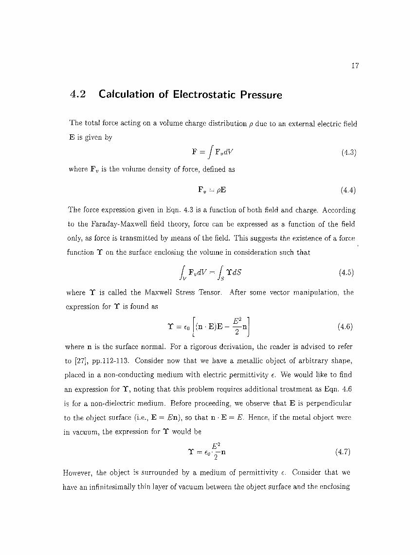
Ô-^O
. '_^d·
Figure 4.1; Metal object surrounded medium of dielectric constant e.
medium, as depicted in Fig. 4.1. From the Gauss’ flux theorem, E = (e/eo)Ed, where E
and Ed are electric field vectors in vacuum and dielectric, respectively. Combining this
with Eqn. 4.7 results in^2 p2
T = - ^ n (4.8)
which is the desired stress expression for the metal object in dielectric.
4.3 AN SYS Modeling of cMUT
ANSYS supports the modeling of T herm al and Structural elements. One ANSYS
element type of this category is SOLID13 which can be used individually as an element
having thermal or structural degrees of freedom, or it can be employed in an anal}' sis
where the effects of both are coupled. Throughout the work presented, the former anal
ysis type is used as the thermal model is employed just to work out the solution of the
electrical problem, and thermo-structural effects, such as thermal expansion, have noth
ing to do with the problem in hand. Hence, the structural and thermal (i.e., electrical)
problems are handled separately and their coupling is provided by “artificial” means,
which will be the discussed in the following sections.
The MUT whose static and dynamic electro-mechanical properties are to be investi
gated is modeled as a two dimensional axisymmetric solid. Elements of this type basically
define a volume of rotation around the y-axis. Thus, rectangles with one edge aligned
with the y-axis model cylinders, and the view on the computer screen turns out to be a
19
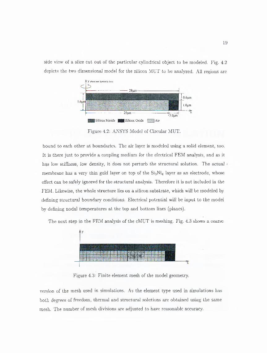
side view of a slice cut out of the particular cylindrical object to be modeled. Fig. 4.2
depicts the two dimensional model for the silicon MUT to be analyzed. All regions are
\ y (Roimional Syinmciiy Axis)
--------------------- 28pin--------------------------
25|jm-
l.Ojum
'S.Opin·Silicon Nitride |B I Silicon Oxide [, ■ j Air
Figure 4.2: ANSYS Model of Circular MUT.
bound to each other at boundaries. The air layer is modeled using a solid element, too.
It is there just to provide a coupling medium for the electrical FEM analysis, and as it
has low stiffness, low density, it does not perturb the structural solution. The actual
membrane has a very thin gold layer on top of the Si3Ni4 layer as an electrode, whose
effect can be safely ignored for the structural analysis. Therefore it is not included in the
FEM. Likewise, the whole structure lies on a silicon substrate, which will be modeled by
defining structural boundary conditions. Electrical potential will be input to the model
by defining nodal temperatures at the top and bottom lines (planes).
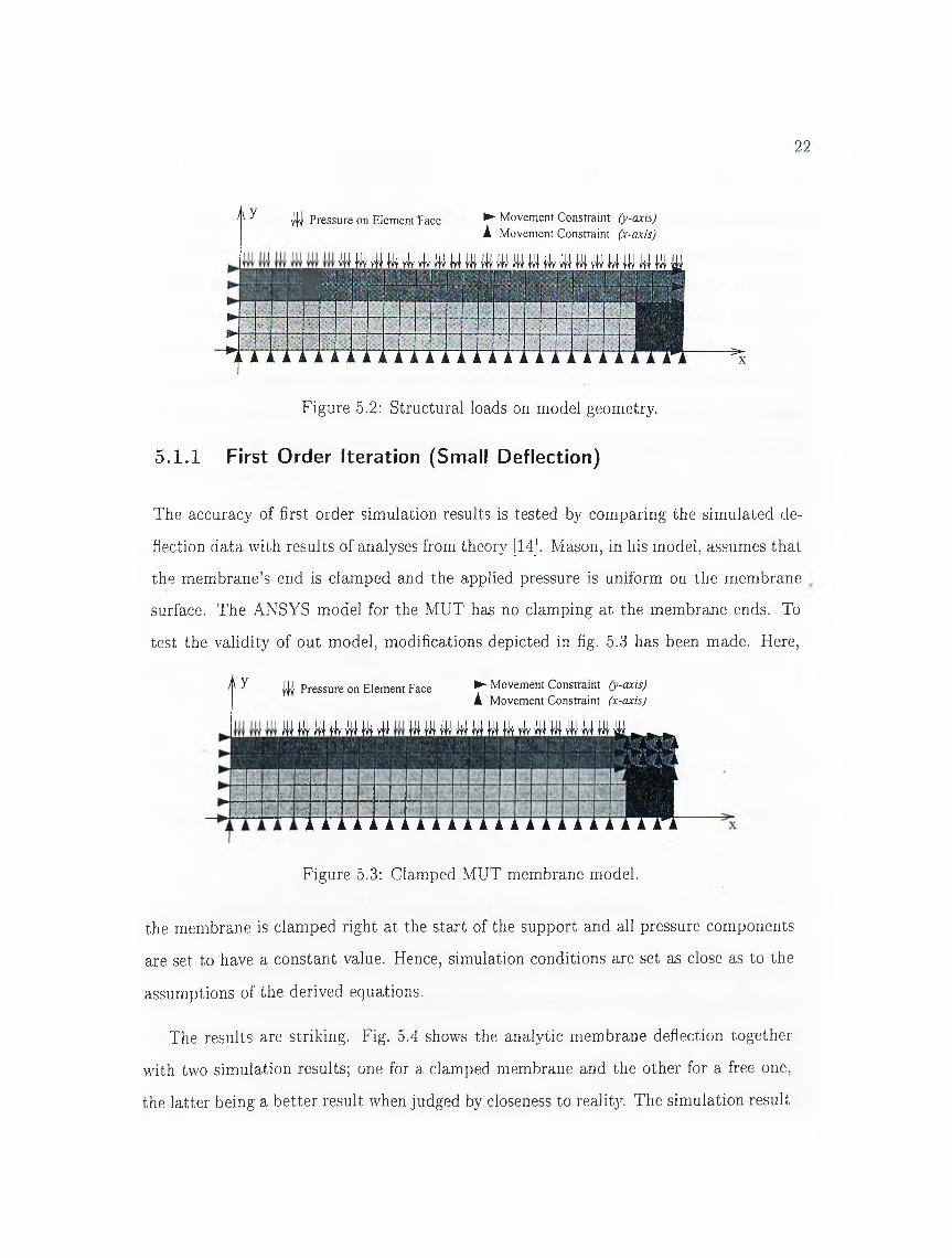
The next step in the FEM analysis of the cMUT is meshing. Fig. 4.3 shows a coarse
i m n iEEEEEBKBiiBi!;
Figure 4.3: Finite element mesh of the model geometry.
version of the mesh used in simulations. As the element type used in simulations has
both degrees of freedom, thermal and structural solutions are obtained using the same
mesh. The number of mesh divisions are adjusted to have reasonable accuracy.

Chapter 5
STATIC and DYNAMIC SIMULATION
The static (DC) and dj^namic (harmonic) simulations of the cMUT are done separatel}'
as ANSYS does not support a combined structural analysis. The static analysis of the
cMUT membrane 3uelds
- The shape and capacitance of the device for an applied DC bias,
- The collapse voltage (KoHapse),
- E-filed values to be used in the djmamic analysis.
The dynamic analysis, using results of the DC solution, provides
- The mechanical impedance of the membrane,
- The electro-mechanical conversion efficiency (transformer ratio).
Results of both analyses are then used to determine “component values” of the equivalent
circuit. In the following sections we present simulation results together w'ith analytic
figures to show the accuracy of the FEM model.
20

21
5.1 Static Analysis
The static displacement of the membrane is of interest in the determination of the shunt
input capacitance, the collapse voltage and field quantities for the harmonic analysis.
All of these require the determination of the membrane shape for an applied DC voltage.
The static analysis of the membrane deflection is done by first solving the electrostatic
problem, then computing the resulting pressure and finally performing a structural anal
ysis to find the effect of electrostatic forces on the structure. It is apparent that once
structural deformation occurs, the electrostatic solution is altered, which is the source
of the deformation. Therefore, the problem is non-linear in nature which calls for an
iterative solution. Once the structural deformation is found, the electrostatic problem
should be solved once again, followed by another structural analysis, and so on. In
each analysis step, the Thermal package of ANSYS is used to find the electrostatic field "
for a certain metalization size. Fig. 5.1 shows the application of thermal loads to the
undeflected model geometry. E-field intensity at the electrode-membrane boundary is
h y y Nodes @ 1 °C ^ Nodes @ 0°C
V V V V V V V V V V V V V y y V V V V V V V V V V 5 7 0
. . ■ ' ' ' A,g.·
Sf:llii'Aqni;'»V-'v mw 1 ; X· ia" '"A >1Si 'h' ‘ 3Fii 3 2 , "iA3
immmrrmmnm nnmrmm i l lFigure 5.1: Application of temperature on model geometry.
found by computing the thermal gradient. Then, we employ the Maxwell Stress Tensor
equation (5 .1 ) to find the electrostatic pre.ssure on the membrane:
T ocir) = n — Elc{r).¿Co
(5.1)
The computed pressure values are, then, applied as structural loads to the model geom
etry as depicted in Fig. 5.2.
22
i\y ► Movement Constraint (y -a x is)
À Movement Constraint (x -ax is)III Pressure on Element Face
iiiiiiiiiiiiiiiiiiiiiiiiiiiiiiiiiiiiiiiiiiiiiiiiiii III III III III Uj,
I
Figure 5 .2 : Structural loads on model geometry.
5.1.1 First Order Iteration (Small Deflection)
The accuracy of first order simulation results is tested by comparing the simulated de
flection data with results of analyses from theory [14]. Mason, in his model, assumes that
the membrane’s end is clamped and the applied pressure is uniform on the membrane
surface. The ANSYS model for the MUT has no clamping at the membrane ends. To
test the validity of out model, modifications depicted in fig. 5.3 has been made. Here,
AY ► Movement Constraint (y -ax is)
k Movement Constraint (x -ax is)III Pressure on Element Face
- IWIW Wl Wl IW W W III Wl W W WIWWIW W WUW m HI tii·» s m 0 , r£ % Ç& ÎK m m m % w : : m v> .-i··M ^ ^ SUf
Figure 5.3: Clamped MUT membrane model.
the membrane is clamped right at the start of the support and all pressure components
are set to have a constant ,value. Hence, simulation conditions are set as close as to the
assumptions of the derived equations.
The results are striking. Fig. 5.4 shows the analytic membrane deflection together
with two simulation results; one for a clamped membrane and the other for a free one,
the latter being a better result when judged by closeness to reality. The simulation result
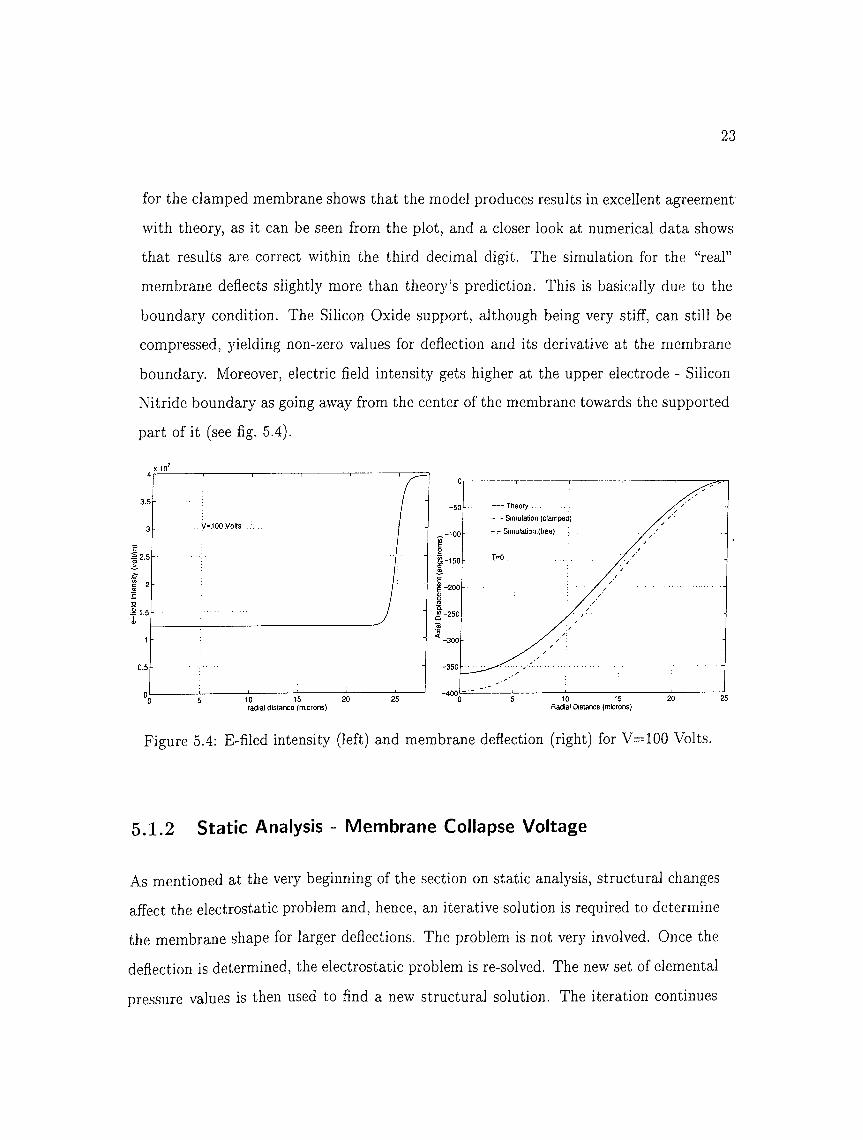
23
for the clamped membrane shows that the model produces results in excellent agreement
with theory, as it can be seen from the plot, and a closer look at numerical data shows
that results are correct within the third decimal digit. The simulation for the “real”
membrane deflects slightly more than theory’s prediction. This is basically due to the
boundary condition. The Silicon Oxide support, although being very stiff, can still be
compressed, 5delding non-zero values for deflection and its derivative at the membrane
boundary. Moreover, electric field intensity gets higher at the upper electrode - Silicon
Nitride boundary as going away from the center of the membrane towards the supported
part of it (see fig. 5.4).
Figure 5 .4 ; E-filed intensity (left) and membrane deflection (right) for V=100 Volts.
5.1.2 Static Analysis - Membrane Collapse Voltage
As mentioned at the very beginning of the section on static analysis, structural changes
aflPect the electrostatic problem and, hence, an iterative solution is required to determine
the membrane shape for larger deflections. The problem is not very involved. Once the
deflection is determined, the electrostatic problem is re-solved. The new set of elemental
pressure values is then used to find a new structural solution. The iteration continues

24
until either an infinitesimal change occurs in shape or the membrane collapses. Fig. 5.5
shows a fiow-chart describing the iteration, where e is the stopping criteria, d is the
height of the.air gap and y(r) is the membrane deflection at a radial distance r. The
Figure 5.5: Steps of iterative electrostatic-structural solution.
iteration to determine the membrane shape is terminated either when the membrane
shape stabilizes or when the membrane collapses onto the substrate. For the former case
the applied voltage is lower than the collapse voltage, while for the latter case the applied
voltage is above the collapse voltage. The collapse voltage is the value of the DC bias
at which the membrane is infinitesimally close to collapse. Figure 5.6 shows iteration
results for a stable and collapsing membrane, respectively. The applied voltages are 230
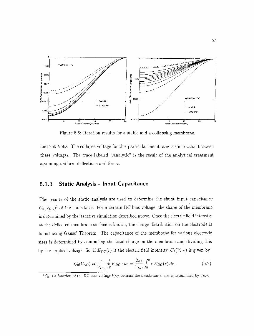
25
Figure 5.6: Iteration results for a stable and a collapsing membrane.
and 250 Volts. The collapse voltage for this particular membrane is some value between
these voltages. The trace labeled “Analytic” is the result of the analytical treatment
assuming uniform deflections and forces.
5.1.3 Static Analysis - Input Capacitance
The results of the static analysis are used to determine the shunt input capacitance
C'o(Vdc ) of the transducer. For a certain DC bias voltage, the shape of the membrane
is determined by the iterative simulation described above. Once the electric field intensity
at the deflected membrane surface is known, the charge distribution on the electrode is
found using Gauss’ Theorem. The capacitance of the membrane for various electrode
sizes is determined by computing the total charge on the membrane and dividing this
by the applied voltage. So, if Eocir) is the electric field intensit}', Со(Уос) is given by
27Гб
'DC6 f 2 тгб
Co(Vdc) = 7 ^ f Edc · ds = — / r Eocir) VDC Js Vdc Jo
dr. {5.2}
Co is a function o f the D C bias vo ltage V^c because the m em brane shape is d eterm ined b}' Voc-

26
5.2 Dynamic Analysis
The aim of the dynamic (harmonic) analysis is the determination of additional model
parameters of the equivalent electrical circuit: the lumped acoustic impedance of the
membrane Z«, and the electro-mechanical transformer ratio n.
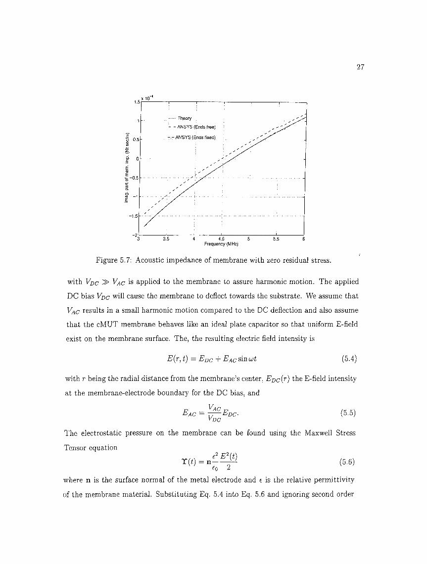
5.2.1 Dynamic Analysis - Membrane Impedance
The acoustic impedance Za of the membrane is found by first finding v(u)) for zero
acoustic load (i.e., the cMUT in vacuum) and a uniform excitation pressure at the set
of frequencies of interest, and then dividing the total force on the membrane by these■/velocity values. The accuracy of the analysis is tested by comparing the simulated
impedance values to analytical results. Mason [14], in his formulation of the membrane’s
mechanical behavior, assumes that the membrane ends are clamped. The same boundary
conditions are imposed during simulations for test purposes. For the stated boundary
conditions, there is a remarkable match between the analytical and numerical results.
The actual membrane’s ends are not clamped; rather, they rest on the sacrificial oxide
layer. Simulation results for this case show that the resonance frequency of the actual
membrane is slightly less than that of the clamped membrane. Fig. 5.7 shows the two
simulation results together with the analytic impedance curve.
5.2.2 Dynamic Analysis - Electro-mechanical Transformer Ratio
As previously stated,electrostatic forces generated by a voltage are always attractive,
regardless of the polarity of the applied voltage. Hence, a voltage of the form
V (t) — Voc + sill (5.3)
27
Figure 5.7: Acoustic impedance of membrane with zero residual stress.
with Vdc > Vac is applied to the membrane to assure harmonic motion. The applied
DC bias Vdc will cause the membrane to deflect towards the substrate. We assume that
Vac results in a small harmonic motion compared to the DC deflection and also assume
that the cMUT membrane behaves like an ideal plate capacitor so that uniform E-field
exist on the membrane surface. The, the resulting electric field intensity is
t) — Edc + Eac sin U)t (5.4)
with r being the radial distance from the membrane’s center, Er,c{‘>') the E-field intensity
at the membrane-electrode boundary for the DC bias, and
17 _ Vac jp^AC — 77— ^DC-F,D C(5.5)
The electrostatic pressure on the membrane can be found using the Maxwell Stress
Tensor equation
T(i) = n6o 2
(5.6)
where n is the surface normal of the metal electrode and e is the relative permittivity
of the membrane material. Substituting Eq. 5.4 into Eq. 5.6 and ignoring second order

28
terms gives the temporal and spacial variation of electrostatic pressure on the cMUT
surface:f V2= ^TT'^DC + n —£ ’£,c-£ .4CSinwi
The total AC force Fac oii the membrane is
FaC = (tTU ) —EdcEaC = A — FdcVaC { tn d-----ta€q 0 V Co
and consequently the electro-mechanical transformer ratio is
6 f e ^^ = FacI'^AC — -A —VDcftnd----¿a
Co V eo
- 2
(5.7)
(5.8)
(5.9)
The electro-mechanical transformer ratio, n, determines by how much the effect of the
mechanical properties of the membrane are reflected to the electrical port, as shown in'
Fig. 3.1.

Chapter 6
OPTIMUM IMMERSION cMUT
When the cMUT is used as an immersion device (i.e., loaded with a relatively high
acoustic impedance liquid such as water) the acoustic impedance of the cMUT membrane
Za and the load Zi form a low quality factor circuit. In such cases, the membrane
impedance can be neglected for frequencies near the mechanical resonance of the device.
The equivalent circuit, then, reduces to a simpler network containing Z/, Co and the
electro-mechanical transformer. Fig. 6.1 shows the reduced model for the cMUT used as
Z/ =t CoV
- o ---- ___ IElectrical Port Acoustic Port Equivalent Circuit
Figure 6.1: Reduced electrical circuit for the cMUT membrane.
an immersion device. Here, we limit our discussion to the effect of the shunt capacitance
Co on the efficiency and bandwidth of the device. If bandwidth were not a concern, one
could simply tune out Co with an inductor to achieve zero insertion loss. But bandwidth
is indeed a concern, ,so a more complete formulation of the optimization objective is to
29
30
minimize the time constant, r, of the first order network formed by the shunt input
capacitance and the transformed radiation impedance, where t = Cq Zi j n?. One might
suggest that decreasing the metalization for the top electrode can help to reduce the
capacitance without any sacrifice from electromechanical properties, i.e., by reducing the
top electrode size, Co can be reduced without reducing the electromechanical conversion
efficiency, n. This argument is based on the idea that how much the membrane deflects
depends not only on how much force is applied, but also on where this force is applied.
It seems that pushing the membrane at parts close to its boundary does not help much
as it its supported there by a relatively stiff layer. The point is to apply force to that
part by which the membrane can be more easily deflected, which, by common sense, is
its center. As it will be justified by simulation results, this argument is valid, and a
smaller electrode result in a cMUT with higher bandwidth.
In order to find the bandwidth of the transducer for a certain electrode size, we need
to compute the electro-mechanical transformer ratio n, and the input capacitance Cq.
The following is a step-by-step task list describing the computation of n and Co-
1 . Find out the membrane shape for the applied DC bias.
2 . Find Edc for the membrane under DC deflection, and
2 .1 . Integrate Eqc over the electrode to find Co-
2 .2 . Compute Eac by scaling Edc-
3. Compute T ac from Eac and perform a harmonic analysis.
4. Find average membrane velocity.
5 . Find AC force by multiplying average velocity and membrane impedance.
6 . The fraction of the AC force and applied AC voltage will yield n.

6.1 Partially Metalized cMUT - Membrane Shape
Determining the membrane shape is done by making use of the iterative method de
scribed in the chapter on simulations. The only difference is that for the partially
metalized membrane, force appears on only a fraction of the membrane, not on its whole
surface as it used to be. Cq is to be found as in the static analysis section.
6.2 Partially Metalized cMUT - Transformer Ratio
31
Qualitative!}', the transformer ratio relates the current and voltage at the electrical port
to the velocity and force at the acoustic port, and that its value depends on the elec-'
trode pattern. The subtlety lies in the fact that the velocity and force of the acoustic
ports are lumped parameters of a system which is in reality distributed. The force, as
defined in the derivation of the equivalent circuit [4,14], is a uniform force over the entire
membrane, and the velocity is defined as the average of the velocities on the contour of
the membrane. Given that the electrostatic force is not uniform, especially in the case
of partially metalized electrodes, consistency with the equivalent circuit model requires
that the lumped electrostatic force {F in Fig. 3.1) be interpreted as an effective force.
This effective force {F ffecUve) is the force which, if applied uniformly over the entire
membrane, would give the same peak membrane displacement that the patterned elec
trode gives. To find the electro-mechanical transformer ratio n in a d}'namic analysis,
one needs to compute the average membrane velocity corresponding to an applied volt
age Vac with no acoustic load, multiply that with Za to find Fe/fectwe and then divide
Fe f f e c i iv e by the applied voltage:
‘ partial —F,e f f e c i iv e
VA C
vZo.Vac
So, again, we assume that a voltage of the form
V(t) = Vdc + VAcViXiojt
(6 .1)
(6.2)

32
with Vdc ^ Vac is applied to the membrane to assure harmonic motion. The applied
DC bias Vdc will cause the membrane to deflect towards the substrate. We assume
that Vac results in a small harmonic motion compared to the DC deflection so that the
resulting electric field intensity is
E{r, t) = Eocir) + EAc(r) sinu)t (6.3)
with r being the radial distance from the membrane’s center, Eocii') the E-field intensity
at the membrane-electrode boundary for the DC bias, and
EAcir) = ^ ^ E o c ir ) .'DC
Again, we employ the Maxwell Stress Tensor equation, which is
T (r ,i) = n- ^
(6.4)
(6.5)Cq 2
Substituting Eq. 6.3 into Eq. 6.5 and ignoring second order terms gives the electrostatic
pressure on the cMUT surface:
2 2= n -^ E lc { r ) + n —EDc{r)EAc{'r) sin Lot
-¿to 0( 6.6)
Combining Eq. 6.4 and Eq. 6 .6 , the AC pressure on the cMUT T ^ c(c t) surface is found
as
T A c ( r ) =Vac .2
eo D>'DCE U r ) (6.7)
Thus, if Edc is known, this can be used to compute the AC excitation for the harmonic
analysis. The harmonic analysis will yield nodal displacement (or equivalently velocity)
values for the membrane surface. This can be used to compute the average velocity of
the membrane, namely
/ 27rr W .T4c(r) (ir. (6.8)A Jo
Multiptying v{co) with Za(io) yields the effective total force Fe/fectivei'^) on the cMUT
membrane. The electromechanical transformer ratio n is, then, given by
_ E e f f e c t i v e (^ )Tl — ~^AC
(6.9)

33
It should be pointed out that n has a negligible frequency dependence as long as only
the primary vibration mode of the membrane is possible. For verification, simulations
were run at two frequencies (one being smaller than u>c and the other greater), and the
same values for n were found.
An important point to note here is that Za is a mechanical property associated with
the cMUT membrane; it is not altered with changing electrode size or with loading. Thus,
we first find Za for particular device dimensions, and use this value for all subsequent
analyses of varying electrode sizes. The electro-mechanical transformer ratio, n, is a
function of metalization radius and thus has to be calculated for each individual electrode
size. It is also important to note that for the analyses herein presented, the actual value of
Za is not very significant because it is dwarfed by the magnitude of Zi] rather, the value-
of Upartiai, fo a given Za, due to electrode minimization is important. The following-
section presents more detail about the finite element simulations and quantitatively
demonstrates that electrode patterning can indeed improve cMUT performance in the
specific case of circular membranes.

34
6.3 Partially Metalized cMUT - Simulation Results
Two sets of simulations for the bandwidth of the cMUT are run; First, a constant DC
bias voltage is assumed. Secondly, the DC bias is set close to the collapse voltage, which
is a function of electrode size.
6.3.1 Bandwidth of cMUT - Constant Bias
Figure 6.2; Electro-mechanical transformer ratio, capacitance and bandwidth of cMUT transducer for electrode radius ranging from 2 to 24 /j,m.
The electro-mechanical transformer ratios for various electrode sizes are determined

35
by running structural simulations and computing the average membrane velocity under
harmonic excitation. These results are used to find the effective force on the membrane
and, consequently, the electro-mechanical transformer ratios. In Fig. 6 .2 , plots of n,
l/n^, Co and the bandwidth of the resulting RC network (which is 1/TparUai) are given.
The last graph indicates that with the proposed criteria, a transducer of dimensions
shown in Fig. 4.2, is optimized by an electrode of 11 p.m radius.
Figure 6.3: Butterworth network for electrical matching.
For the purpose of electrical matching we select a lossless matching network topolog}··
to tune out the parasitic element (Co) of the transducer equivalent circuit [28,29]. The
sixth order maximally flat (Butterworth) network [30] shown in Fig. 6.3 is used for the
electrical matching. Co is set equal to the shunt input capacitance of the transducer,
the source resistance is chosen as equal to the radiation resistance of the transducer,
and the center frequency of the network is set to the mechanical resonance frequency
of the membrane. The remaining component values are computed by properly scaling
the values in the prototype network of [30], which are also found in various Butterworth
tables of radio handbooks. The resulting bandwidth of the transducer for two different
metal electrode sizes is depicted in Fig. 6.4. For both electrode sizes, the DC bias voltage
is assumed to be 200 Volts. This is less than the voltage that causes the fully metalized
membrane to collapse, which is found as 240 Volts by simulations.
6.3.2 Bandwidth of cMUT - Variable Bias
The analysis method described in the static analysis of the cMUT has been used to
determine the collapse voltage for varying electrode sizes. Figure 6.5 shows the simulation

36
Figure 6.4: Normalized transducer bandwidth for two electrode sizes,
results for the de\dce of figure 4 .2 . Because the total force on the membrane scales with
Figure 6.5: Collapse voltage values for varjdng electrode sizes.
electrode area, a higher voltage is required for the collapse of a membrane with a smaller
electrode. Thus, for a smaller electrode a larger bias can be applied. From Eq. 6.7 we see
that AC stress on the membrane increases with increasing DC bias’. If the membrane
is modeled as a linear spring, we expect the AC deflection to be linearly dependent to
T^Q. Thus, for increasing DC bias, the effective force on the membrane increases. This
results in a larger value for n and, consequent!}^, a larger bandwidth. So if the DC bias is
set to the collapse voltage, the bandwidth of the transducer further increases for smaller
^The dependency is close to linear for sm all deflections as E q c linearly sca les w ith V d c - H ow ever, for larger deflections, E qc increases faster as the m em brane gets closer to the su bstra te .

37
electrodes. Fig. 6 .6 shows the bandwidth of the transducer of Fig. 4 .2 as a function of
electrode radius when the bias is set to the collapse voltages shown in Fig. 6 .5 . According
Figure 6 .6 : Transducer bandwidth for DC bias equal to the collapse voltage.
to this result, the transducer with maximum bandwidth should have a top electrode as
small as possible. Interconnections to the top electrode will set a limit on how small it
can get, as will breakdown mechanisms.
Chapter 7
cMUT LOSS MODELING
The main breakthrough brought about by cMUT devices is due to the inherent advan
tages of the technology used in the production: silicon processing enables convenient
integration between the mechanics and electronics, and provides the designer with tools
for easily patterning mechanical structures - quite important for the production of array
transducers. At the same time, the method of production brings about an important
issue regarding the performance of cMUT devices: the cMUT consists of cells that have
dimensions in the order of tens of microns [9], and as a transducer of reasonable size has
dimensions expressed in millimeters, thousands of individual devices need to be placed
on the same substrate [18]. Consequently, an individual transducer cell, instead of being
clamped at its ends, resides on a large substrate and couples power to radially outward
wa\-e modes. Furthermore, this power is received by the neighboring transducer ele
ments creating cross-coupling between individual cells of the transducer. Although a
model explaining the behavior of a single cell has been proposed, the above mentioned
power loss and cross-coupling effects still remain unexplained. As main motivational
forces behind transducer development include applications in air-coupled nondestruc
tive evaluation (NDE), analysis methods that include the loss mechanisms in cMUTs
need to be developed for the design of efficient transducers for ultrasonic transmission
38
39
into air. Likewise, designs for 3-D immersion imaging using 2 -D transducer matrices
require a good understanding of coupling between array elements. All of these call for
the development of models close to reality; models that incorporate power coupled to
the substrate.
In this chapter, we develop a simulation model to determine the mechanical impedance
of a cMUT device that includes the effect of power coupled to the substrate. Finite El
ement Method models are used in conjunction with absorbing boundary conditions.
7.1 FEM Model for Substrate Coupling
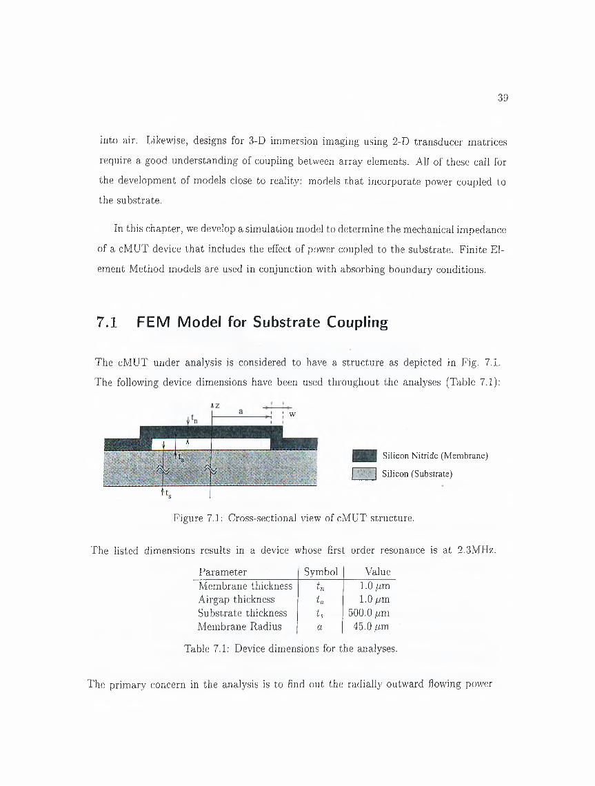
The cMUT under analysis is considered to have a structure as depicted in Fig. 7.L
The following device dimensions have been used throughout the analyses (Table 7.1):
: w
’■Af
Silicon N itride (M em brane)
Silicon (Substrate)
Figure 7.1: Cross-sectional view of cMUT structure.
The listed dimensions results in a device whose first order resonance is at 2 .3 MHz.
Parameter Symbol ValueMembrane thickness tn 1 .0 /j,mAirgap thickness ta 1 .0 /jmSubstrate thickness t.s 500.0 fxmMembrane Radius a 45.0 /j,m
Table 7.1: Device dimensions for the analyses.
The primary concern in the analysis is to find out the radially outward flowing power

40
coupled by the membrane into the substrate. For this, we need to have an absorbing-
boundary at the radial edges of our model. Levander [31] and Cerjan et al. [32] have
used lossy material boundaries to absorb waves incident on model boundaries. Later,
Berenger’s [33] Perfectly Matched Layer (PML) for electromagnetic waves was shown to
be applicable to elastic wave propagation problems by Chew et al. [3 4 ] and was used in
a number of applications [35-37]. In this study, we use a lossy medium of considerable
length to absorb the outward propagating waves. Fig. 7.2 depicts the finite element
model involved in the analysis. The attenuation in the lossy part of the model has to
Lossless
Lossy
i i Pressure Load
^ Displacement Constraint
Figure 7 .2 : Finite-element model of the cMUT.
be kept small to minimize the impedance mismatch at the boundary of the lossless and
lossy regions. On the other hand, the lossy region should provide enough attenuation so
that incident waves at the model boundary should be well attenuated and the reflected
waves at that end should not result in a significant standing wave pattern. This can be
achieved by having a very long attenuating region as compared to the largest wavelength.
The structure of Fig. 7,2 is used to run harmonic analyses using ANSYS 5.5 to test
the validity of our method. The indicated pressure loads are applied together with the
displacement constraints. ANSYS enables the use of an axisymmetric model, therefore
we were able to model the cMUT as the 2 -D structure of Fig. 7.2. As a first check, we
look at the particle displacement at the surface of the substrate as a function of radial
i©SAS IP, Inc.

41
distance. Displacement is expected to decay rnonotonically with y/r [38]. Fig. 7.3 shows
a plot of nodal displacement magnitude as a function of radial distance at excitation
frequencies 1.0 MHz. (left) and 3.0 MHz. (right). The radial distances up to 30rnm
Figure 7.3: Magnitude of nodal displacement on substrate (Left 1.0, Right 3.0 Mhz).
are in the lossless region of the model and, as expected, there is a good agreement
between the magnitude and the l/y /r curve shown with the dashed line. For radial
distances from 30 mm. to 60 mm. wave magnitude dies away and, as the plot has
reasonable smoothness, there is no significant reflection at either boundary. As the
attenuation encountered by the radial wave modes was a function of frequency, the
attenuation constants used in the simulations had to be adjusted for each frequencj' step
to get the above results. In order to run harmonic analyses conveniently for a large
range of frequencies (without the need to adjust attenuation for each frequency step), a
general expression for the attenuation parameter of the analysis was developed. Fig. 7.4
shows how a general expression was found for the ANSYS dump parameter by fitting
an analytically obtained curve to the attenuation values determined by trial-and-error
(i.e., running simulations for each frequency step to have reasonable reflection at model
boundaries). The expression for the analytic material dumping constant C curve turns
out to have the form C — Cof P with Cq being a constant and / the frequency.

42
Figure 7.4: Fitted curve on ANSYS damp parameter determined trial-and-error.
7.2 Acoustic Impedance of cMUT with Loss
Fig. 7.5 shows a typical simulation result for a cMUT with substrate loss. The device
Figure 7.5: Impedance of cMUT with substrate loss (real and imaginary parts)
dimensions used in the simulations are around 1 / 1 0 of the wavelengths of plate modes
present in the substrate [39], therefore they are expected to show the characteristics of
point sources, for which the real impedance is a decreasing function of frequency. The

43
real impedance for a point contact is depicted in Fig. 7.6. However, the real part of
Figure 7.6: Real impedance for a point contact.
the membrane impedance found from the simulations exhibits a completely unexpected
behavior: the impedance increases with frequency. To justify our simulation results,
we divide the model into two parts, for which the individual results can be verified by
comparing them with analytic quantities. Then, we combine the two analysis results to
see whether they reveal the original simulation outcome.
The first subdivision of the EM model consists of the substrate alone.' We remove
the membrane from the model, and apply a force to the nodes which were in touch with
the rim of the membrane (Fig.7.7). The simulation yields the nodal velocity values at
OIISISEiBEnmmmmmu№Kf»fllESR»»Biais
I Lossless H ||| Lossy
' 'I' i Pressure Load ^ Displacement Constraint
Figure 7.7: Submodeling I : Substrate impedance,
the excitation point, and those are used to compute the substrate impedance for circular

44
excitation. The measured substrate impedance Zsub has a real part depicted in Fig 7.8.
As expected from the case of point excitation, we get a curve decreasing with frequency.
Figure 7.8: Real substrate impedance for circular excitation.
The second part of the analysis, drops out the substrate, and finds a two-port rep
resentation for the cMUT membrane, with the ports being the center of the membrane
(where electro-static forces are applied) and the membrane rim (Fig.7.9). Device parame-
Figure 7.9: Two-port representation for the cMUT membrane.
ters Zi, Zi and .^3 are found by running simulations on the clamped membrane (Fig.7.10).
Clamping nodes at the rim is equivalent to setting of Fig. 7.9 to zero, or equivalently,
making Port-2 open. Measuring the velocity at the excitation point yields the input
impedance at Port-1 . Meanwhile, we record the reactive force at the clamped nodes,
which is F . These two reveal values of Z\ and Z^· To find Z3 we run another simulation

45
►
r
J ; :
_____________________________n i
Figure 7.10: Submodeling II : Membrane as a two-port,
to find Zin when nodes at the rim are set free to move, i.e., Port- 2 is shorted. Hence,
~ ■^¿n,open(l ~ F'2,open)
^2 — Zifi open p2 open
and we can solve for Z-i from
Zin,short — Z \ -|- Z ^ j jZ ' i
Figure 7.11: Forces at the rim of the membrane.
The simulation results for the membrane are in complete agreement with Mason’s
model [14] as depicted in Fig.7.11 where theoretical and simulated values for the force
on the membrane rim are shown.
The membrane impedance Zmem can, then, be found by combining the results of the

46
two analyses, i.e.,
^mem — Z\ + Z2j ¡{Z' + Zsub)
Fig. 7 .1 2 shows the membrane impedance from the original model together with the
combined result of the two independent analyses. The results of the combined anal}^sis
Figure 7 .1 2 : cMUT Impedance: unified and two-part models
yield the same impedance values with the overall model, out of which we conclude that
the FEM data are reliable.
7.3 cM UT Loss vs. Model Dimensions
The developed analysis method can now be emplo3 ed to observe the eff'ects of model
dimensions on the cMUT impedance. Here, we discuss two of them: substrate thickness,
and the rim width (parameters tg and w of Fig.7.1, respectively).
Simulations for various substrate thicknesses revealed that the real part of the cMUT
impedance increases with decreasing substrate thickness (viz. Fig.7.13). This is a reason
able result, as one might say that the thinner the substrate, the easier it can be vibrated.
As the dimensions and driving forces of the cMUT itself do not change, we might expect

47
that more power goes into plate modes that the substrate supports. On the other hand,
the rim width w did not have a significant effect on the cMUT impedance, seen from the
simulation results.
Figure 7.13: Real part of cMUT impedance for various substrate thicknesses.
7.4 Normal Mode Theory Analysis
The power coupled into the cMUT substrate goes into the plate modes {Lamé waves) [39]
supported by the silicon wafer over which the device is constructed. Analytic formulation
Symmetric (Dilatational)
Antisymmetric (Flexural)
Figure 7.14: Lowest (0th) order symmetric and antisymmetric plate modes (SO and AO).
of the wave equation reveals that the supported orthogonal wave modes divide into
two groups, namel}', symmetric and antisymmetric. Fig. 7.14 shows two of the lowest
plate modes. The names symmetric and antisymmetric reflect the nature of particle
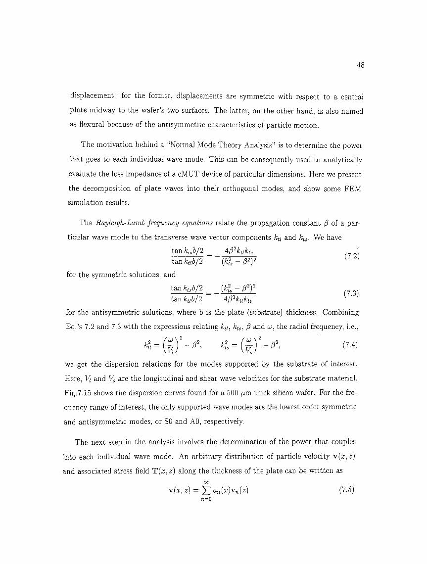
48
displacement: for the former, displacements are symmetric with respect to a central
plate midway to the wafer’s two surfaces. The latter, on the other hand, is also named
as flexural because of the antisymmetric characteristics of particle motion.
The motivation behind a “Normal Mode Theory Analysis” is to determine the power
that goes to each individual wave mode. This can be consequently used to analytically
evaluate the loss impedance of a cMUT device of particular dimensions. Here we present
the decomposition of plate M'aves into their orthogonal modes, and show some FEM
simulation results.
The Rayleigh-Lamb frequency equations relate the propagation constant /? of a par
ticular wave mode to the transverse wave vector components ku and kts. We have
tan ktsb/2 ^ iP'^ktikts .tmkub/2 { k l - p ^ Y
for the symmetric solutions, and
tan ktsb/2 ^ {kl - /? )tanA:i/V2 ^P^kuks
for the antisymmetric solutions, where b is the plate (substrate) thickness. Combining
Eq.’s 7.2 and 7.3 with the expressions relating ku, kts, and u>, the radial frequency, i.e..
k^ - - - - ~ I k(7.4)
we get the dispersion relations for the modes supported by the substrate of interest.
Here, Vi and K are the longitudinal and shear wave velocities for the substrate material.
Fig. 7.15 shows the dispersion curves found for a 500 yum thick silicon wafer. For the fre
quency range of interest, the only supported wave modes are the lowest order symmetric
and antisymmetric modes, or SO and AO, respectively.
The next step in the analysis involves the determination of the power that couples
into each individual wave mode. An arbitrary distribution of particle velocity v{x, z)
and associated stress field T{x, z) along the thickness of the plate can be written asCXD
v(x, z) = an(x)vn(z) (7.5)n=0

49
Figure 7.15; Dispersion curves for AO and SO modes in the frequency range 1.0-3.0 MHz
OO
T{x,z) = Y^an{x)Tn{z)-X (7.6)7 1 =0
where the orthogonal field distributions Vn{^) and T„(z) · x are in fact the field distri
butions of the propagating Lamb waves in the free silicon plate. The solution of the
boundary value problem to determine expressions for the supported wave modes reveal
that particle velocities along the thickness are
Vx — cos ktiz cos ktsb/2 —/^2 _ ^2
COS ktib/2 cos ktsZ2/?2
Vz — —kti sin ktiz cos ktsb/2 —^2 _ 2
cos ktib/2 sin kisZ2kts
for symmetric modes, and
Vx — 4-2/? sin ktiz sin ktsb/2 4-
Vx = T ip -kti sin ktiz cos ktsb/2 -
_ f 2sin ktib/2 sin ktsZ
/?2 _cos ktib/2 sin ktsZ
2kis
,TiPx
(7.7)
(7.8)
(7.9)
(7.10)
for antisymmetric modes. The mode amplitude an can be found by substituting the
corresponding orthogonal mode expansions for the arbitrary fields in Eq. 7.5 and 7.6 in
the orthogonality relation
1 roO'TL --
4P. '-is( - v ; (z ) . T(z) - v ( z ) . T-Jz)) ■ X dz. (7.11)
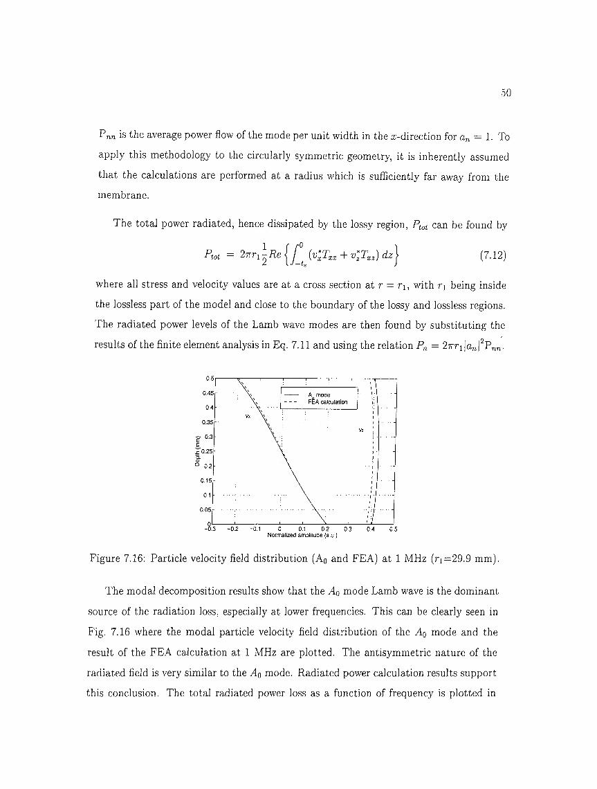
50
Pnn is the average power flow of the mode per unit width in the .x-direction for a„ = 1. To
apply this methodology to the circularly symmetric geometry, it is inherently assumed
that the calculations are performed at a radius which is sufficiently far awa}' from the
membrane.
The total power radiated, hence dissipated by the lossy region, Pjoi can be found by
Pm = 2Trn\Pe dz^ (7.12)
where all stress and velocity values are at a cross section at r = rj, with rj being inside
the lossless part of the model and close to the boundary of the lossy and lossless regions.
The radiated power levels of the Lamb wave modes are then found by substituting the
results of the finite element analysis in Eq. 7.11 and using the relation = 27rri |a„fP„n.
Figure 7.16: Particle velocity field distribution (Aq and FEA) at 1 MHz (ri=29.9 mm).
The modal decomposition results show that the Aq mode Lamb wave is the dominant
source of the radiation loss, especially at lower frequencies. This can be clearly seen in
Fig. 7.16 where the modal particle velocity field distribution of the Aq mode and the
result of the FEA calculation at 1 MHz are plotted. The antisymmetric nature of the
radiated field is very similar to the Aq mode. Radiated power calculation results support
this conclusion. The total radiated power loss as a function of frequency is plotted in

51
Figure 7.17: Total power coupled to the substrate and powers for Aq and So modes.
Fig. 7.17 as the solid line. As expected, the radiated power is maximum at the resonance
frequenc}cThe power radiated by the Aq and So modes are also depicted in the same
figure. It is evident that the Ao mode carries nearly 100% of the total radiated power,
whereas the So mode is becomes a more important source of loss at higher frequencies.
These results enable us to derive an equivalent circuit model of the membrane with
physically based loss terms as described below.
’ Z,.О
■ loss
V,Ю
avgIdeal Lossless Membrane
Figure 7.18: Equivalent circuit model which includes cMUT substrate loss.
Equivalent Circuit Model
The ideal lossless membrane is modeled as a capacitor and an inductor in series rep
resenting its compliance and mass, respectively. Substrate loss can be included to the
model as a series frequency dependent resistor (Fig. 7.18). The value of this resistor can
be found by finding the acoustic impedance Za of the membrane from FEM results: If
the applied pressure on element faces is P , the the total force on the membrane surface

52
is Ftot — Tio?· P. The average velocity of the membrane, Vavg is given by
Vavg = 2'Kru{r)dr (7-13)
where u{r) is the membrane displacement found from the FEM analysis. The acoustic
impedance of the membrane is, then, given by Za = FtotlVavg· As we claim that the real
part of Za accounts for the substrate loss, the resistance found by computing the power
propagating out from the membrane, should be identical to R e {Z a ) · The loss resistance is
then given by 0.5Pioi/|Ki;sP, where Ptot is calculated using Eq. 7.12. Fig. 7.19 shows that
Figure 7.19: Total loss resistance of cMUT and resistances of Aq and So modes.
the real part of the membrane impedances computed using the two suggested methods
are indeed in agreement. The value of loss resistance is about 1/100 of the impedance of
air as the loading medium, hence, power loss will be — 20dB with respect to the radiated
power of an air transducer.
The loss resistance can be further divided into terms each representing the loss due
to a different propagating mode in the silicon substrate giving more insight into the
ph}'sical loss mechanism. The result of this calculation for the Aq and So modes are
also depicted in Fig. 7.19. This results suggests a revised model for the membrane with
substrate loss: Loss term associated with each possible wave mode appear as distinct

53
"AO "SOo -o
V.avgIdeal Lossless Membrane
Figure 7.20: Equivalent circuit model revisited: modal loss accounts for total loss.
loss components in the equivalent circuit, as depicted in Fig. 7.20. The analysis can be
extended to a generalized model that includes components with analytically computed
values, which requires the knowledge of the surface impedance of each mode, so that the
loss computation method described in Sec. 7.2 can be employed.

Chapter 8
DEVICE FABRICATION
Micromachining, or the “art” of micron-sized mechanical structures is a natural conse
quence of silicon processing techniques mainly intended for the production of integrated
circuits. We will start out with a brief introduction on micromachining terminolog}'·,
and this will be followed by the fabrication method that we have developed at the
“Advanced Research Laboratories” (ARL) of the the Physics Department of Bilkent
University. Measurement results will be presented at the end of this chapter.·
8.1 An Introduction to Microfabrication
Each step of a micromachining process involves the following substeps:
1. Deposition of a certain layer, either metal or a silicon compound.
2. Patterning of a certain structure using lithography.3. Removal of the unwanted regions using either wet or dry etch.
A quartz plate of size 10x10 cm bearing the shapes to be carved on the structure is
used as a mask in the lithography step. After depositing the material of choice, the
sample is coated with a light-sensitive paint known as the photoresist. The mask is then
54

55
placed on the sample and the sample is exposed to light. This transfers the structure on
the mask to the photoresist, and the exposed parts are chemically altered so that they
are “washed-away” by the developer, a chemical that attacks exposed photoresist. At
this stage the regions of the deposited layer that we want to keep are protected by a
photoresist film. Etching, or the process of exposing the sample either to a chemical or
a mechanical corrosive able to act upon it, removes the uncovered regions of the layer,
but, does not have an effect on the photoresist and, consequently the sample under it.
Thus, at the end of etching, the deposited layer is patterned. Consecutive application of
the above procedure eventually results in the desired micro-structure. App.A presents a
small glossary of micromachining terms.
8.2 cMUT Fabrication
cMUT devices were fabricated at ART using standard deposition, lithography and wet/dry
etch techniques. The following set of equipment were involved in the fabrication carried
out in the Class-100 Clean Room:
Equipment
Conventional Lithography
Plasma Deposition (PECVD)
Reactive Ion-Etching
Metalization
Bonding
Vendor and Type
Karl-Suss MJB3
PlasmaLab 85IOC
Ley bold LE-301
Leybold LE-560
Westbond 7400 A
Table 8.1: Equipment used in cMUT fabrication
The fabrication involves a 3-mask process whose steps are described below:
STEP#1 : Cleaning
Cleaved doped silicon samples of size 12 x 12 mm^ are first cleaned using three solvents.

56
namely ТСА (trichloro-ethane), АСЕ (acetone) and ISO (iso-propyl alcohol). Table 8.2
lists the time durations for each individual chemical bath and the temperature setting.
The sample is then rinsed thoroughly under continuously flowing DI water for about a
Soh^ent
TCA (tri-chloro ethane)
ACE (acetone)
ISO (iso-propyl alcohol)
Duration
2 min.
5 min.
2 min.
Temperature
BOILING
ROOM (21°C)
BOILING
Table 8.2: Chemicals used in sample cleaning
couple of minutes, and dried using a N2 gun. To assure complete dryness before further
processing, the sample is held on a 120°C hot-plate for 2 minutes.
STEP9(¿2 ; Sacrificial Layer Deposition L· Patterning
The first lithography step of the process involves the deposition and patterning of the
sacrificial layer, which will determine the membrane shape and air-gap thickness. After
numerous trials, the most vulnerable material to HE (hydrofluoric acid) was found too
be Silicon-rich Nitride (Si^Nj,). A layer of 5000A thick Nitride is deposited onto the
silicon substrate. The following lithography step patterns the hexagonal shaped mem
branes. RIE (Reactive Ion Etch) is employed to etch away the non-active regions of the
membrane. Tri-solvent cleaning is applied again before the next deposition step.
STEP#3 ; Membrane Deposition
Tests to find two materials which have significant difference between their HE etch times
revealed that amorphous Silicon (a-Si) was almost insensitive to HE when compared
to Sij-Nj , the sacrificial layer material. This was necessary to be able to etch away
the sacrificial layer without any harm to the membrane itself, and is termed as “selec
tive etch”. Having chosen the membrane material, we coat the sample with a-Si and
bury the already-patterned sacrificial layer under this new layer.

57
STEP#4: Metalization (Electrode Deposition)
Before we go to the underetch of the sacrificial layer, we deposit the top electrode utilizing
a metalization process. The metalization does not cover the whole membrane, but is a
small area at the center of the membrane due to bandwidth optimization criteria [40].
The so-called “image-reversal” technique is applied for metalization because it provides a
better profile of the photoresist edges that make the lift-off much easier. The metalization
pattern is provided by a positive mask. After lithography, the sample is placed on
a 120°C hot-plate for 2 minutes. Then, a blank exposure of uV light is made. This
“reverses” the chemical properties of the photoresist, so that the initially exposed regions
of resist become defiant towards the developer. Then, the whole sample is coated witho
a 3000A thick gold layer. The regions determined by the mask get covered with the
gold layer, while resist blocks gold to reach the sample at regions to remain uncovered.
During lift-off, acetone removes remaining resist together with the gold layer on top of
it.
STEP#5; Underetch
The last step of the process involves the removal of the sacrificial layer that still remains
buried under the membrane. Another lithography step is involved to “drillf 2 yum wide
holes at the corners of the hexagonal membrane structure defined by the sacrificial la} er.
The etchant used for the underetch is 1:40 HF:H20 made from a 50% HF solution, and
the etch time is about 10 minutes.
Figures 8.1, 8.2 and 8.3 provide a pictorial representation of the fabrication, while in
Fig. 8.4 we depict the top view of the sample for various intermediate steps of the fabri
cation. Tables 8.3 and 8.4, on the other hand, are process charts showing useful timing
and set-up information for the particular instruments used in the Advanced Research
Laboratories.
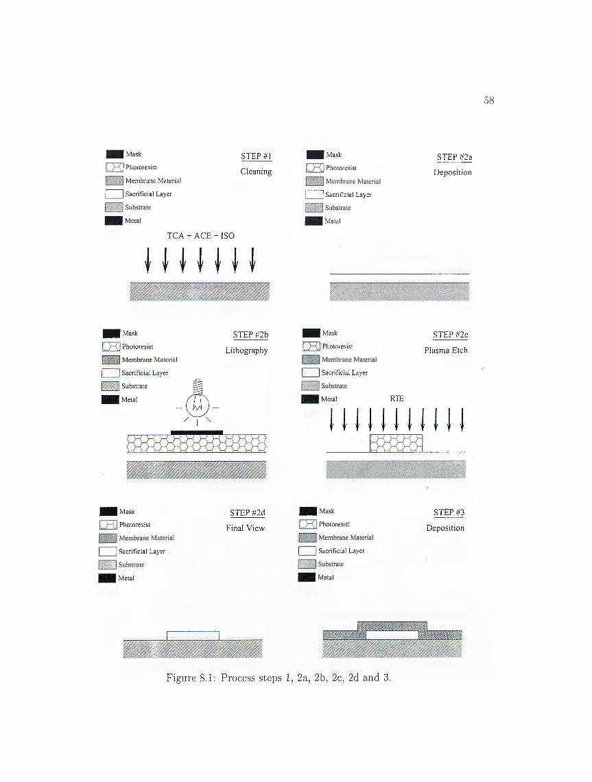
58
H H I Mask
J Photoresist
M embrane Materi
I I Sacrificial Layer
STEP#1
Cleaning
M etal
TCA + ACE + ISO
|| || || ||[ | M ask
Photoresist
I I Sacrificial Layer
M etal
STEP #2a
Deposition
|| |[ | || || Mask
Photoresist
STEP #2b
Lithography
IHliK_7~(J Photoresist
I I Sacrificial Layer
M etal RIE
STEP #2c
Plasma Etch
i m i M ask
Photoresist
I I Sacrificial Layer
M etal
STEP #2d
Final View
H liPhotoresist
I I Sacrificial Layer
Metal
STEP #3
Deposition
Figure 8.1; Process steps 1, 2a, 2b, 2c, 2d and 3.

59
I M ask
] Photoresist
M embrane Material
I I Sacrificial Layer
Substrate
H H M etal
STEP #4a
Lithography
I B0 ~ ~ ( J Photoresist
M embrane Material
I I Sacrificial Layer
Substrate
H | Metal
STEP #4b
Bake
1 1 ^ 1 M ask
Q —(J Photoresist
M embrane Material
I I Sacrificial Layer
Substrate
H I M etal
STEP #4c
Image Reversal
HHQ - Q Photoresist
Membrane Material
I I Sacrificial Layer
Substrate
I ^ H Metal
STEP #4d
Metalization
H M ask
Photoresist
M embrane Material
I I Sacrificial Layer
W W A Substrate
H I M etal
STEP #4e
Lift-off
H I M ask
Photoresist
M embrane Material
I I Sacrificial Layer
Substrate
H Metal
STEP #5a
Lithography
Figure 8.2: Process steps 4a, 4b, 4c, 4d, 4e and 5a.

m m M ask
Photoresist
] Sacrificial Layer
STEP #5b
Plasma Etch
M etal RIE
Mask
Photoresist
r I Sacrificial Layer
Metal
Figure 8.3: Process steps 5b and 5c.
60
STEP #5c
Under-etch
I t
I Hf t
...... ...I,...-·: .J...__L.
Figure 8.4: Top view of cMUT structure for various fabrication steps.

61
Table 8.3: Process charts 1-4

62
Table 8.4: Process charts 5-8

8.3 Device Dimensions
63
Figure 8.5: Zoomed \dew of mask (active membrane area 500x250 /rm approx.).
Fig. 8.5 shows part of the mask used in device fabrication with all la}' ers overlapped
on a single figure. Active membrane area is to the upper right corner of the figure while
features on the sides are alignment marks, corner marks, and information marks on
structure dimensions. Fig. 8.6 shows the basic building block used in the drawing of the
cMUT mask. The hexagonal membrane mask determines the shape of the air gap. Holes
are centered to the corner of the membrane, which are used during the underetch phase of
the process. The membrane electrode is placed to the center of the hexagonal structure,
and is tied to the next electrode with an additional stripe of metal. The GND electrode
layer can be used to construct cMUT structures on an insulating substrate. The use
of the GND electrode can further decrease the input capacitance of the device as the
stripes interconnecting the membrane electrodes will not be on a grounded conducting
substrate. On the complete mask, GND and membrane electrodes are combined at pads
at the two opposite sides of the substrate to form bound points to the drive circuit.
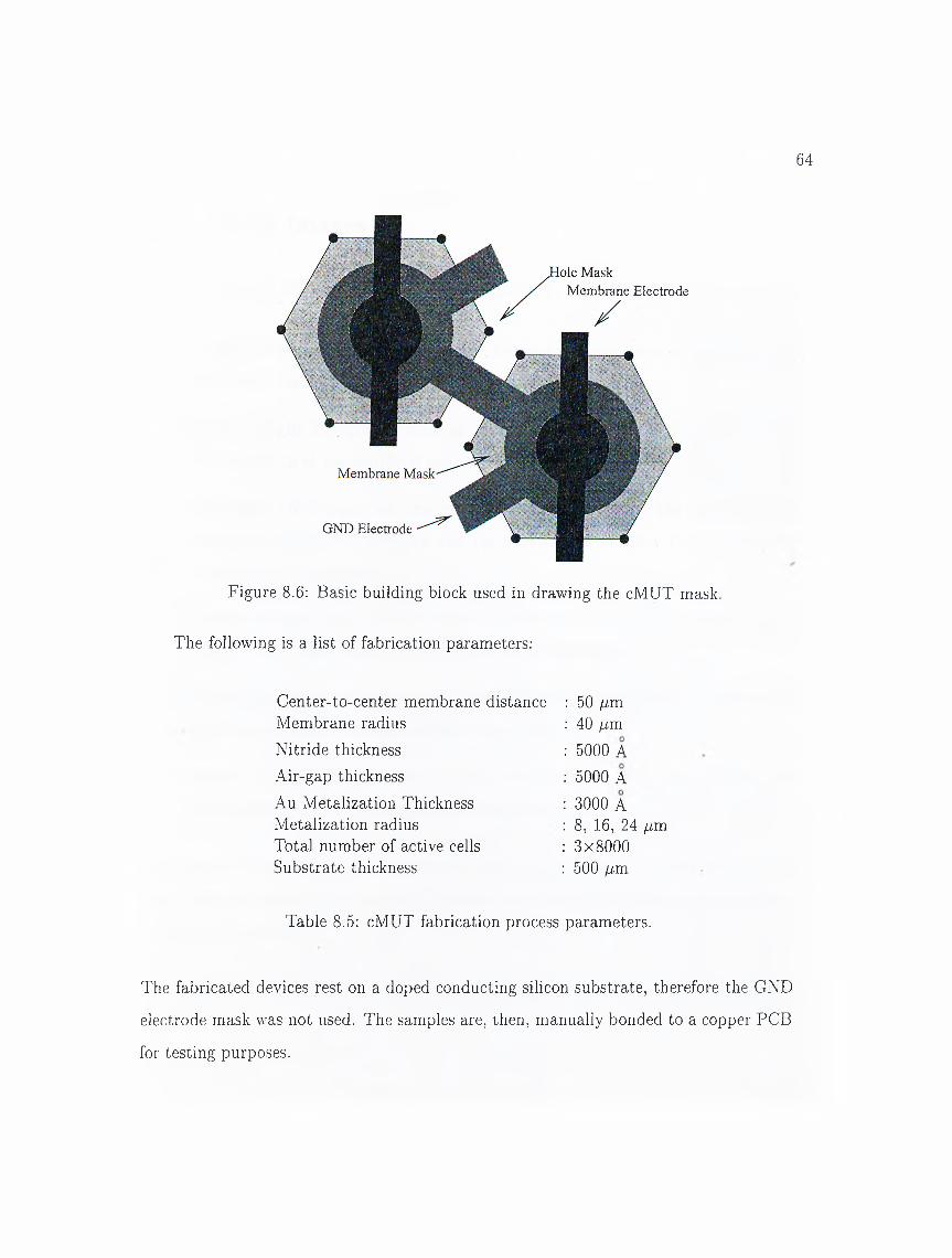
64
ole MaskMembrane Electrode
GND Electrode
Figure 8.6: Basic building block used in drawing the cA4UT mask.
The following is a list of fabrication parameters;
Center-to-center membrane distance Membrane radiusNitride thickness Air-gap thickness
Au Metalization Thickness Metalization radius Total number of active cells Substrate thickness
: 50 iJ,m 40 [im.5000 A 5000 A
3000 A 8, 16, 24 ¡jLva 3x8000 500 //m
Table 8.5: cMUT fabrication process parameters.
The fabricated devices rest on a doped conducting silicon substrate, therefore the GND
electrode mask was not used. The samples are, then, manually bonded to a copper PCB
for testing purposes.

65
8.4 SEM Images
Fig. 8.7 shows 6 SEM images of the fabricated cMUT devices:
• U pp er Left Top view of cMUT. The hexagonal active areas of the membranes
are visible together with the circularly shaped top electrode.
• U pp er R igh t Topographic close-up view of single cMUT cell. The holes used for
the underetch of the sacrificial layer are clearly visible.
• C entral Left Perspective view of a group of cMUT cells. The level difference
between active membrane area and the substrate is visible. The Au electrode
traces the level difference.
• C entral R igh t Cross sectional view of single cMUT cell. This picture clearly
shows the air gap between the membrane and the substrate.
• B o tto m Left Cross sectional view of cMUT cell. In this picture complete cells
interconnected with the sliced cell are also visible.
• B o tto m R ight Close-up view of cMUT cross-section. This picture shows the
membrane profile at the membrane-substrate interface.
All pictures are taken using a JEOL Electron Microscope operated at 17 kV, located in
the Advanced Research Laboratories (Class-100 clean-room) of the Physics Department
of Bilkent University.

66
Figure 8.7: SEM images of fabricated cMUT devices.
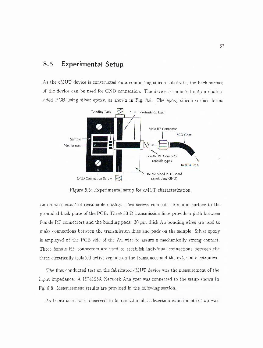
67
8.5 Experimental Setup
As the cMUT device is constructed on a conducting silicon substrate, the back surface
of the device can be used for GND connection. The device is mounted onto a double
sided PCB using silver epoxy, as shown in Fig. 8.8. The epoxy-silicon surface forms
Bonding Pads 50Q Transmission Line
Sample
Membranes
Male RF Connector
GND Connection Screw
XFemale RF Connector
(chassis type)
Double Sided PCB Board (Back plate GND)
Figure 8.8: Experimental setup for cMUT characterization.
an ohmic contact of reasonable quality. Two screws connect the mount surface to the
grounded back plate of the PCB. Three 50 transmission lines provide a path between
female RF connectors and the bonding pads. 30 pm thick Au bonding wires are used to
make connections between the transmission lines and pads on the sample. Silver epoxy
is employed at the PCB side of the Au wire to assure a mechanically strong contact.
Three female RF connectors are used to establish individual connections between the
three electrically isolated active regions on the transducer and the external electronics.
The first conducted test on the fabricated cMUT device was the measurement of the
input impedance. A HP4195A Network Analyzer was connected to the setup shown in
Fg. 8.8. Measurement results are provided in the following section.
As transducers were observed to be operational, a detection experiment set-up was

68
designed. The detection circuit employs a bias circuit followed by a low-noise transcon
ductance amplifier [6,41], as shown in Fig. 8.9. The RF-choke inductor provides the
Q +RF-ChokeDC D ecoupling Cap.
cM U T 9 Read-Out
. Transconductance Amp. .
Figure 8.9; Detection circuit for cMUT.
necessary bias for transducer operation. Incident acoustic waves cause the membrane
to vibrate, changing its capacitance. This causes an AC current to be generated by the
transducer having the same frequency that of the acoustic excitation. The RF-choke is
chosen to have a high enough value to block the generated AC current to leak into the DC
supply. Having no other path, the transducer current flows into the transconductance
amplifier, which outputs a voltage proportional to the input current, thus proportional
to transducer displacement. Usually, the required inductor value for the choke is very
large when the acoustic frequency range is considered. As realizing high-valued induc
tors requires bulky components, an inductive bias circuit is not quite suitable for devices
with integrated electronics. This problem can be solved by emplojdng resistive bias. The
RF-choke is to be replaced by a resistor with value much larger than the input impedance
of the amplifier. As the leak impedance of the cMUT itself is very large, it seems that
an arbitrarily large resistor value can be chosen. However, a larger resistor value implies
a larger amount of noise. Thus a compromise is to be made between output amplitude
and noise.
The circuit model described in Fig. 8.10 is employed by the cMUT research group

69
at Ginzton Laboratory, Stanford University. The following rules apply for the choice of
Figure 8.10: Ginzton detection circuit for cMUT. (courtesy Dr. Sanlı Ergun)
component values (by courtesy of Dr. Sanlı Ergun of Ginzton Laboratory);
• For air applications Zn is a high-Q RLC circuit. For immersion applications
is a low-Q RLC circuit. Therefore air applications are narrow band, immersion
applications are wide band.
• It is possible to put an inductor between the amplifier and the transducer to elim
inate the imaginary part of Ztransducer· However this makes the receiver circuitry
resonant. For immersion applications it is something you do not want.
• The SNR at the output of the amplifier does not depend on the input impedance of
the amplifier for it is the same impedance that the input referred noise sources of
the amplifier see. Thus, making Ramp higher does not make SNR better, although
it increases the signal level at the output.
• The SNR at the output is maximum when the impedance seen by the amplifier
\Ztransducer\ ÏS equal to < Bn > / < in > ratio. You can put a transformer between
the amplifier and the transducer to achieve this noise matching condition. You can
have a wide-band transformer, but still it is something you cannot do in integrated
circuits if your goal is to make an integrated system.

70
8.6 Measurement Results
The input impedance of the fabricated cMUT devices are measured using a HP4195A
Network Analyzer. Fig. 8.11 shows the real and imaginary parts of the membrane
Figure 8.11: Real and imaginary parts of cMUT impedance for various bias voltages.
impedance as the bias voltage is changed. This behavior is predicted by the model
circuit in Fig. 8.12. Without any bias, the electro-mechanical transformer of the model
has zero transfer ratio, i.e., the effect of the acoustic port is not reflected to the electrical
port. Hence, the frequency response that we see is that of a capacitor with a shunt
ohmic loss. As the bias rises, the transformer ratio assumes a non-zero value, and this
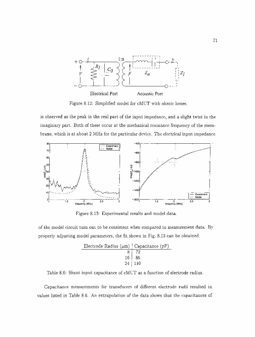
71
O - - .
Electrical Port Acoustic Port
Figure 8.12; Simplified model for cMUT with ohmic losses.
is observed as the peak in the real part of the input impedance, and a slight twist in the
imaginary part. Both of these occur at the mechanical resonance frequency of the mem
brane, which is at about 2 MHz for the particular device. The electrical input impedance
Figure 8.13: Experimental results and model data.
of the model circuit turn out to be consistent when compared to measurement data. By
properly adjusting model parameters, the fit shown in Fig. 8.13 can be obtained.
Electrode Radius (/im) Capacitance (pF)8 72
16 8624 no
Table 8.6: Shunt input capacitance of cMUT as a function of electrode radius.
Capacitance measurements for transducers of different electrode radii resulted in
values listed in Table 8.6. An extrapolation of the data shows that the capacitances of

72
the interconnections and pads account for a value of about 67 pF, and the total value
increased with increasing electrode area.
8.7 Discussion and Further Work
The material used for the membranes was low-temperature amorphous silicon which has
finite resistivity. This accounts in the leakage term seen in the equivalent circuit repre
sentation. No measurement results were obtained from the detection experiment as all
of the devices were shorted during experimentation. The possible cause is breakdowns
occuring in the membrane material which is also used as an insulating la}'er between-
the bonding pads and the conducting substrate. The shorted device exhibits the electri
cal characteristics of two back-to-back diodes with reverse breakdown voltages at about
3 Volts. These are most probably the metal-semiconductor contact diodes formed by the
silver epoxy GND connection and the gold electrode layer over the membrane material.
There are two possible ways to solve this problem. First, the membrane material might
be changed with some other silicon compound with higher resistivit}'. Second, an insu
lating substrate can be used. The latter requires the deposition of a ground electrode as
the first step of the production process. The cost of an additional fabrication step can
be compensated by the reduced input capacitance of the device, as none of the intercon
nections and bonding pads will be over ground planes, thus those will not contribute to
the capacitance.
Another concern about the fabricated devices was about the holes etched for under
etching the sacrificial layer. Those should be sealed if the device is to be used as an
immersion transducer. As the development of a working air transducer took a consid
erably long time with quite low yield, the sealing step was not implemented, and the
devices were tested onlv in air.
Chapter 9
CONCLUSION
The entire work on the modeling of Capacitive Micromachined Ultrasonic Transducers
(cMUTs) yielded tools for the following analyses;
1. Static Analysis The behavior of the cMUT structure under the application of
a DC bias voltage was analyzed. The shape of the membrane was determined
for a small applied voltage for which the static electric field is assumed to remain
unchanged with the changing shape of the membrane. The result of the small
defiection problem was found to be consistent with existing theory. Being convinced
about the accuracy of the FEM model, an iterative analysis was performed to
determine the membrane shape when higher bias voltages were applied. This
analjcsis revealed answers to questions like “what is the maximum bias voltage
that can be applied without causing the membrane to collapse?” or “What is the
DC capacitance of the deflected membrane?”.
2. Dynamic Analysis cMUT dynamic parameters such as the acoustic impedance
of the membrane and the electro-mechanical conversion efficiency were determined
using a harmonic analysis. Again, results were justified with existing theory. The
developed method was then emplo_yed in a optimization problem in which the best
73

74
top electrode size was determined. When bandwidth was chosen as the optimiza
tion criteria, the analysis result suggested an electrode which is as small as possible.
3. Loss A nalysis The developed tools for the static and dynamic analyses were ex
tended to handle an “infinite boundary value” problem. With the use of absorbing
boundary conditions, an FEM model to analyze the behavior of a cMUT struc
ture placed on a substrate of infinite radial dimensions was developed. This model
was used to determine the effect of substrate loss to the electro-acoustic charac
teristics of the cMUT device. Normal mode theory was employed to give a better
understanding of the nature of this loss mechanism.
All of the above mentioned tools can be used to design cMUT devices to meet certain
design criteria, test the device characteristics prior to fabrication and predict the be
havior of more complicated structures such as array transducers. As applications for
the developed anal}'sis tools, the electrode size for an immersion cMUT of radius 25 /rm
was optimized as bandwidth chosen as the optimization criteria. The optimum electrode
radius was found to be 10 /im, using which the transducer bandwidth is almost doubled
when compared to the fully metalized version. As a further study, the effect of substrate
thickness on loss impedance was analyzed. Using the developed normal mode theory
analysis, the dominant wave mode for a 500 //m thick silicon substrate was found to be
the lowest order antisymmetric mode (AO).
Experimental results obtained from the fabricated devices support the basic model
used in the whole study, but are yet insufficient to provide evidence for the correctness of
the developed analysis tools. The fabricated cMUT devices are found to have a resonance
frequency of 2 MHz. Due to problems resulting from the choice of the membrane material,
detection experiments were not possible.
75
The analysis part can be further extended to include the loading effects of the sur
rounding medium. A 3-D model incorporating a load halfspace will even handle cross
coupling over the loading medium, which is suspected to be a significant source of cross
talk among array elements.
As described at the end of the experimentation part, further research directions for
cMUT fabrication include the use of a insulating substrate for the fabrication of low
input impedance transducers with increased electrical reliability. Finally, sealing the
underetch holes will enable the cMUT devices to be used as immersion transducers.

Appendix A
A MICROMACHINING GLOSSARY
developer Chemical able to act on exposed photoresist. Exposed photoresist is “washed
awaj ” by the developer, which provides a mens to transfer the structure on the
mask onto the structure.
d irectional etch Etch in which the etchant is unable to act evenly on the material.
Directional etch can be achieved by either exploiting the crystal nature of the
the material, or applying a mechanical etchant with particles moving in a certain
direction (as in the case of reactive ion etch).
etch Removal of a material by either chemical or mechanical means. Micromachining
basically relies on the selective nature of the etchant’s corrosive effect on materials.
etchant Chemical or mechanical means used in etching.
exposure The application of uV light to photoresist. The presence of the mask between
the light source and the sample coated with photoresist transfers the patterns on
the mask onto the sample.
lithography Basic method used in carving the structures determined by the mask
76

77
onto the sample. Lithography starts with the coating of the sample with photore
sist, continues with exposure and the application of the developer, and ends with
etching.
m ask A quartz plate on which the shape of the structures to be constructed in each
step of the micromachining process are “drawn”. The number of masks involved
in the complete process determine the depth level of the fabrication.
p lasm a enhanced chem ical vapor deposition Basic method involved in the de
position of materials onto the sample surface. The gases involved in the process
determine which material is deposited, while the RF power used to create plasma,
flow rate of gases and temperature affect the mechanical and chemical properties
of the deposited layer. Done in a vacuum chamber.
p h otoresist A light sensitive “paint”. The photoresist is the essential chemical involved
in lithography. Known to be highly carcinogen.
reactive ion etch Mechanical etch in which the sample is placed under the bombard
ment of chemicals accelerated in RF plasma. While the used chemicals provide
a selectivity, the direction in which the chemicals are accelerated determines the
directivity of the etch. Done in a vacuum chamber.
selective etch Etch in which the etchant is inactive on the materials constituting the
structure, but a single one. Selective etch is the most important tool used in the
construction of micro-mechanical structures.
underetch A selective etch in which a material is removed from beneath another ma
terial. Underetch is the basic technique involved in the construction of suspended
mechanical structures.
Appendix B
MATERIAL PARAMETERS
The following material praramteres have been used througout all simulations:
Material
E
(kg/m-s^)
PmO(kg/m°)
a
(unitless)
e / e o
(unitless)
Air 1.00x10°° 1.29 0.499 1.00
Silicon Nitride 3.22x10^1 3270 0.260 7.50
Silicon Oxide 8.57x10^° 2651 0.075 3.90
Silicon 13.0x10^° 2332 0.278 11.8
E Young’s Modulus
Pmo Mass Density
G Poisson’s Ratio
e/ eq Relative Permittivity (Dielectric Constant)
78
Bibliography
[1] Khul, W., Schodder, G. R., and Schodder, F. K., “Condenser transmitters and
microphones with solid dielectric for airborne ultrasonics,” Acústica, vol. 4, pp.
520-532, 1954.
[2] K. Matzuwa, “Capacitive ultrasonic transducer,” J. Phys. Soc. Japan, vol. 13, pp.
1533-43, 1958.
[3] Cantrell, John H. and Heyman, Joseph S., “Broadband electrostatic acoustic trans
ducer for ultrasonic measurements in liquids,” Review of Scientific Instruments,
vol. 50, no. 1, pp. 31-33, January 1979.
[4] I. Ladabaum, X. C. Jin, H. T. Soh, A. Atalar, and B. T. Khuri-Yakub, “Surface
micromachined capacitive ultrasonic transducers,” IEEE Trans, on Ultrasonics,
Ferroelectrics and Frequency Control, vol. 45, no. 3, pp. 678-690, May 1998.
[5] Soh, Hyongsok. T., Ladabaum, Igal, Atalar, Abdullah, Quate, Calvin F., and Khuri-
Yakub, Butrus T., “Silicon micromachined ultrasonic immersion transducers,” Ap
plied Physics Letters, vol. 69, no. 24, pp. 3674-3676, December 1996.
[6] Ladabaum, Igal, Khuri-Yakub, Butrus T., and Spoliansky, Dimitri, “Micromachined
ultrasonic transducers: 11.4 MHz transmission in air and more,” Applied Physics
Letters, vol. 68, no. 1, pp. 7-9, January 1996.
79
80
[7] Matthew I. Haller, Micromachined Ultrasonic Devices and Materials, Ph.D. thesis,
Stanford University, 1997.
[8] Schindel, David W., Hutchins, David A., Zou, Lichun, and Say er, Michael, “The
design and characterization of micromachined air-coupled capacitance transducers,”
IEEE Transactions on Ultrasonics, Ferroelectrics, and Frequency Control, vol. 42,
no. 1, pp. 42-50, January 1995.
[9] P. Eccardt, K. Niederer, T. Scheiter, and C. Hierold, “Surface micromachined ultra
sound transducers in CMOS technology,” in Ultrasonics Symposium, San Antonio,
Texas, November 1996, IEEE Ultrasonics, Ferroelectrics, and Frequency Control
Society, pp. 959-962.
[10] Suzuki, K., Higuchi, K., and Tanigawa, H, “A silicon electrostatic ultrasonic trans
ducer,” IEEE Transactions on Ultrasonics, Ferroelectrics, and Frequency Control,
vol. 36, no. 6, pp. 620-627, November 1989.
[11] Rafiq, M. and W3' kes, C., “The performance of capacitive ultrasonic transducers
using V-grooved backplates,” Measurement Science and Technology, vol. 2, no. 2,
pp. 168-174, February 1991.
[12] Pentti, Mattila, Tsuzuki, Fabio, Vaataja, Heli, and Sasaki, Ken, “Electroacoustic
model for electrostatic ultrasonic transducers with V-grooved backplates,” IEEE
Transactions on Ultrasonics, Ferroelectrics, and Frequency Control, vol. 42, no. 1,
pp. 1-7, January 1995.
[13] Anderson, Michael J., Hill, James A., Fortunko, Christopher M., Dogan, Numan
S., and Moore, Russell D., “Broadband electrostatic transducers: Modeling and
experiments,” Journal of the Acoustical Society of America, vol. 97, no. 1, pp.
262-272, January 1995.

81
[14] Warren P. Mason, Electromechanical Transducers and Wave Filters, Van Nostrand,
1942.
[15] Prak, Albert, Elwenspoek, Miko, and Fluitman, Jan H., “Selective mode excitation
and detection of micromachined resonators,” in Micro Electro Mechanical Systems
Workshop, Travemünde, Germany, 1992, IEEE Robotics and Automation Society,
pp. 220-225.
[16] Voorthuyzen, J. A., Sprenkels, A. J., Van Der Onk, A. G. H., Scheeper, P. R.,
and Bergveld, P., “Optimization of capacitive microphone and pressure sensor
performance by capacitor-electrode shaping,” Sensors and Actuators A (Physical),
vol. 25-27, pp. 331-336, 1991.
[17] Gordon S. Kino, Acoustic Waves: Devices, Imaging, and Analog Signal Processing,
Prentice-Hall, Inc., 1987.
[18] I. Ladabaum, X. G. Jin, H. T. Soh, A. Atalar, and B. T. Khuri-Yakub, “Surface
micromachined capacitive ultrasonic transducers,” IEEE Trans, on Ultrasonics,
Ferroelectrics and Frequency Control, vol. 45, no. 3, pp. 678-690, May 1998.
[19] Ladabaum, I., Jin, X. G., Soh, H. T., Pierre, F., Atalar, A., and Khüri-Yakub, B.
T., “Micromachined ultrasonic transducers: towards robust models and immersion
devices,” in Ultrasonics Symposium, Levy, M., Schneider, S. G., and McAvoy, B.
R., Eds., San Antonio, USA, November 1996, IEEE Ultrasonics, Ferroelectrics, and
Frequency Gontrol Society, pp. 335-338.
Jin, Xuecheng, Ladabaum, Igal, and Khuri-Yakub, Butrus T., “The microfabrica
tion of capacitive ultrasonic transducers,” in Transducers 97, Ghicago, 1997, IEEE
Electron Devices Society, pp. 437-440.

82
[21] Hohm, D. and Hess, G., “A subminiature condenser microphone with silicon-nitride
membrane and silicon backplate,” Journal of the Acoustical Society of America, vol.
85, no. 1, pp. 476-480, January 1989.
[22] ANSYS User Manual, Volume I Procedures, (c)SAS IP, 1995.
[23] ANSYS User Manual, Volume II Commands, ©SAS IP, 1995.
[24] ANSYS User Manual, Volume III Elements, ©SAS IP, 1995.
[25] ANSYS User Manual, Volume IV Theory, ©SAS IP, 1995.
[26] Dale F. Ostergaard, “Adapting available finite element heat transfer problems to
solve 2-d and 3-d electrostatic field problems,” Journal of Electrostatics, vol. 19,
pp. 151-164, 1987.
[27] R. Plonsey and R. E. Collin, Principles and Applications of Electromagnetic Fields,
McGraw-Hill Book Company, Inc., New York, 1961.
[28] Tuttle,Jr. David F., Electric Networks, McGraw-Hill Book Company, 1965.
[29] R. M. Fano, “Theoretical limitations on the broadband matching of arbitrary
impedances,” J. Franklin Inst., , no. 249, pp. 57-83, 139-154, January and February
1950.
[30] George L. Matthaei, Microwave Filters, Impedance Matching Networks, and Cou
pling Structures, Artech House, Dedham, MA, 1980.
[31] A. R. Levander, “Use of telegraphy equation to improve absorbing boundary effi
ciency for fourthorder acoustic wave finite difference schemes,” Bull. Seismil. Soc.
Am., , no. 75, pp. 1847-1852, June 1985.
[32] C. Cerjan, D. Kosloff, R. Kosloff, and M. Reshef, “A nonreflecting boundary con
dition for discrete acoustic and elastic wave equations,” Geophysics, , no. 50, pp.
705-708, April 1985.
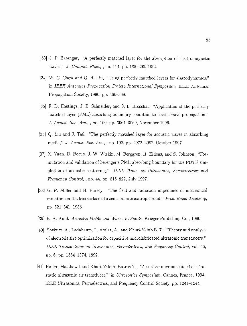
83
[33] J. P. Berenger, “A perfectly matched layer for the absorption of electromagnetic
waves,” J. Comput. Phys., , no. 114, pp. 185-200, 1994.
[34] W. C. Chew and Q. H. Liu, “Using perfectly matched layers for elastodynamics,”
in IEEE Antennas Propagation Society International Symposium. IEEE Antennas
Propagation Society, 1996, pp. 366-369.
[35] F. D. Hastings, J. B. Schneider, and S. L. Broschat, “Application of the perfectly
matched layer (PML) absorbing boundary condition to elastic wave propagation,”
J. Acoust. Soc. Am., , no. 100, pp. 3061-3069, November 1996.
[36] Q. Liu and J. TaO, “The perfectly matched layer for acoustic waves in absorbing
media,” J. Acoust. Soc. Am., , no. 102, pp. 2072-2082, October 1997.
[37] X. Yuan, D. Borup, J. W. Wiskin, M. Berggren, R. Eidens, and S. Johnson, “For
mulation and validation of berenger’s PML absorbing boundary for the FDTF sim-*
ulation of acoustic scattering,” IEEE Trans, on Ultrasonics, Ferroelectrics and
Frequency Control, , no. 44, pp. 816-822, July 1997.
[38] G. F. Miller and H. Pursey, “The field and radiation impedance of mechanical
radiators on the free surface of a semi-infinite isotropic solid,” Proc. Royal Academy,
pp. 521-541, 1953.
[39] B. A. Auld, Acoustic Fields and Waves in Solids, Krieger Publishing Co., 1990.
[40] Bozkurt, A., Ladabaum, I., Atalar, A., and Khuri-Yalub B. T., “Theory and analysis
of electrode size optimization for capacitive microfabricated ultrasonic transducers,”
IEEE Transactions on Ultrasonics, Ferroelectrics, and Frequency Control, vol. 46,
no. 6, pp. 1364-1374, 1999.
[41] Haller, Matthew Land Khuri-Yakub, Butrus T., “A surface micromachined electro
static ultrasonic air transducer,” in Ultrasonics Symposium, Cannes, France, 1994,
IEEE Ultrasonics, Ferroelectrics, and Frequency Control Society, pp. 1241-1244.


