Embed Size (px)
Citation preview

84
C H A P T E R 3
Review of Essential Electricaland Mechanical Concepts
3.0 PREVIEW
The MEMS research field crosses several disciplines, including electrical engineering, mechan-
ical engineering, material processing, and microfabrication. The successful design of a MEMS
device must take into consideration of many intersecting points.
For example, when developing a micromachined sensor such as the ADXL accelerome-
ter, a designer must consider both electrical and mechanical aspects. Electrical design aspects
include the capacitance value and signal processing circuits (e.g., analog to digital conversion).
Mechanical design aspects include the flexibility of the support beams, dynamic characteristics,
and intrinsic stresses in the beam. These issues are intricately connected and are relevant to
process, yield, and cost.
This chapter covers some of the most essential concepts and analytical skills for MEMS.
In order to maintain brevity and balance, only the most important and frequently encountered
concepts are reviewed.
Section 3.1 introduces the concept of semiconductor crystal and doping process, which
lead to discussion of the fundamental procedure for determining the conductivity of semi-
conductors based on doping concentrations;
Section 3.2 discusses conventions for naming crystal planes and directions;
Section 3.3 covers basic relations between stress and strain for various materials;
Section 3.4 reviews procedures for calculating the bending of flexural beams under simple
loading conditions;
Section 3.5 is dedicated to discussing the deformation of torsional bars under simple load-
ing conditions;
Section 3.6 explains the origin of intrinsic stresses and methods for characterization, con-
trol, and compensation;
M03_CHAN2240_02_PIE_C03.qxd 2/25/11 3:44 PM Page 84

3.1 Conductivity of Semiconductors 85
Section 3.7 discusses the mechanical behavior of micro structures under periodic loading
conditions;
Section 3.8 introduces methods for actively tuning the force constant and resonant fre-
quency of beams.
This chapter contains materials heavily condensed from several subject areas and courses.
For in-depth studies of these and other related topics, a reader is encouraged to refer to the list
of suggested reading materials outlined in Section 3.9.
3.1 CONDUCTIVITY OF SEMICONDUCTORS
Silicon, an element commonly found on sandy beaches and in window glasses, is the substrate
of choice for building integrated circuits. Silicon belongs to a class of materials called semicon-
ductors, which offers remarkable electrical characteristics and controllability for electronics cir-
cuits. Semiconductor silicon is the most common material in the MEMS field. Naturally, the
electrical and mechanical properties of silicon are of great interest.
A semiconductor is fundamentally different from conductors (e.g., metals) and insulators
(e.g., glass or rubber). As its name suggest, a semiconductor is a material whose conductivity
lies between that of a perfect insulator and a perfect conductor. However, this only tells half of
the story about why semiconductors are used heavily for modern electronics. More importantly,
the conductivity of a semiconductor material can be controlled by a variety of means, such as
intentionally introduced impurities, externally applied electric field, charge injection, ambient
light, and temperature variations. These control “levers” lead to many uses of the semiconduc-
tor materials, including bipolar junction transistors, field effect transistors, solar cells, diodes,
and sensors for temperature, force, and concentrations of chemical species (e.g., chemical field
effect transistors, or ChemFET).
Certainly, the value of conductivity of a semiconductor piece is of tremendous interest.
The macroscopic resistance and conductance are related to the microscopic conductivity. One
of the most basic exercises in MEMS is to find the conductivity value of a semiconductor silicon
piece based on its doping concentrations. This constitutes the major focus of this section.
I assume a reader is familiar with basic knowledge of charge, voltage, electric field, current,
and the Ohm’s law. A review of these topics can be found in textbooks and courses outlined in
Section 3.9.
3.1.1 Semiconductor Materials
The unique electrical properties of semiconductors stem from their atomic structures. In this
section, let us look at how conductivity of semiconductor silicon is originated.
Silicon is a Group IV element in the periodic table. Each silicon atom has four electrons
in its outermost orbit. As a consequence, each silicon atom in the crystal lattice shares four co-
valent bonds with four neighboring atoms.
Silicon atoms reside in a crystal lattice. The inter-atomic spacing between atoms is deter-
mined by the balance of atomic attraction and repulsive forces. The density of silicon atoms in
a solid is at 300 K.
Electrons that covalently bond to the orbits of silicon atoms cannot conduct current and
do not contribute to bulk conductivity. The conductivity of a semiconductor material is only
5 * 1022 atoms/cm3
M03_CHAN2240_02_PIE_C03.qxd 2/25/11 3:44 PM Page 85

86 Chapter 3 Review of Essential Electrical and Mechanical Concepts
related to the concentration of electrons that can freely move in the bulk. An electron bond to a
silicon atom must be excited with enough energy to escape the outermost orbit of the atom for
it to participate in bulk current conduction.
The statistically minimal energy needed to excite a covalently bonded electron to become
a free charge carrier is called the bandgap of the semiconductor material. It corresponds to the
energy necessary to break a single covalent bond between two atoms. The bandgap of silicon at
room temperature is approximately 1.11 eV, or . For more detailed information,
refer to classic textbooks on solid-state electronics devices ([1, 2]).
Electrons can receive energy and be liberated from its host atoms by a number of means,
including lattice vibration (e.g., temperature rise) and absorption of electromagnetic radiation
(e.g., light absorption). Temperature plays an important role in determining the concentration
of free electrons in a bulk. In fact, semiconductor silicon is insulating at absolute zero tempera-
ture (0 K), when no free-electrons are available to conduct current. Higher temperatures lead
to greater concentrations of free charge carriers and better conductivity.
A metal conductor, in contrast, consists of metal atoms that are linked to one another
with metallic bonds, which are generally weaker than covalent bonds. Electrons can readily
break free and participate in current conduction. The equivalent bandgap associated with met-
als is zero. Hence the conductivity of a metal conductor is always high and not sensitive to
changes of temperature and light conditions.
An insulator, on the other hand, involves atomic bonding that is much stronger than that
of a semiconductor material, such as ionic bonds. In other words, the bandgap of insulators is
much greater compared with that of semiconductors. Since it is difficult for electrons to break
loose from the atom orbits, the concentration of free charge carriers and the conductivity of in-
sulator materials are very low.
Silicon is not the only semiconductor material used for MEMS. Other semiconductor ma-
terials, such as germanium, polycrystalline germanium, silicon germanium, gallium arsenide
(GaAs), gallium nitride (GaN), and silicon carbide (SiC), have also been used.The bandgaps of
these materials are different from that of silicon [3, 4].
Certain organic materials also exhibit semiconductor characteristics. Organic semicon-
ductors are being investigated for flexible circuits and displays. These generally involve differ-
ent device architecture and fabrication methods compared with inorganic semiconductors. This
topic is beyond the scope of this text; however, interested readers can read the following refer-
enced papers to get acquainted on this emerging research topic [5–8].
3.1.2 Calculation of Charge Carrier Concentration
The electrical conductivity of a semiconductor material is determined by the number of free charge
particles in a bulk and their agility under the influence of electric field. In this section,we will discuss
basic formulation for determining the number (or volumetric concentration) of free charge carriers.
There are two types of free charge carriers—electrons and holes. Electrons that are freed
by breaking covalent bonds are not the only participants in bulk current conduction. The bond
vacancy left by an escaped electron, called a hole, can facilitate bulk current movement as a site
for successive electron hopping. A hole carries a positive charge. In a given material, the abili-
ties of the electrons and holes to conduct electricity are different, but they are often in the same
order of magnitude.
1.776 * 10-19 J
M03_CHAN2240_02_PIE_C03.qxd 2/25/11 3:44 PM Page 86

3.1 Conductivity of Semiconductors 87
The electron concentration in a semiconductor is denoted as n (units in or
), while the hole concentration is denoted as p The concentrations of electrons
and holes under steady state, thermal equilibrium conditions (i.e., no external current and no
ambient light) are commonly referred as and respectively. The subscript 0 indicates
values under thermal equilibrium.
There are two categories of semiconductor bulk—intrinsic and extrinsic. I will discuss the
intrinsic semiconductor material first, since it is the simplest form. I will then review extrinsic
materials, which are encountered more often in MEMS and microelectronics.
A perfect semiconductor crystal has no impurities and lattice defects in its crystal struc-
ture. It is called an intrinsic semiconductor material. In this type of material, electrons and holes
are created through thermal or optical excitation.When a valence electron receives enough en-
ergy, either thermally or optically, it is freed from the silicon atom and leaves a hole behind.
This event is called electron–hole pair generation.
The number and concentrations of electrons and holes, however, do not increase without
limit over time. Free electrons and holes can recombine and give up energy along the way. This
process, called recombination, competes with the generation process. Under steady state condi-
tions, the generation and recombination rates are identical.
Since the electrons and holes are created in pairs, the electron concentration (n) is equal
to the concentration of holes (p). For intrinsic materials, their common value is further denoted
as with the subscript i standing for the word intrinsic. The relation is summarized as
(3.1)
The magnitude of is a function of the bandgap and temperature, according to
(3.2)
where and are the effective mass of electrons, effective mass of holes, the Boltz-
mann’s constant, absolute temperature (in degree Kelvin), and the bandgap. The term h is the
Planck’s constant. For example, the value of for Si at room temperature is only
much smaller compared to the silicon atom density of approximately
The SI unit of the carrier concentrations is Due to historical reasons, the CGS unit
system for carrier concentration is prevalently used.
Most semiconductor pieces are not perfect intrinsic material, however. They often have
impurities atoms in them—by accident or by design. The impurity atoms contribute additional
electrons or holes, generally in an unbalanced manner. The intentional introduction of impuri-
ties, called doping, would turn an intrinsic material into an extrinsic semiconductor material.Impurities can be introduced in a number of ways, most notably through diffusion and ion im-
plantation. They can also be incorporated into semiconductor lattice during the growth of the
material as well. This process is called in situ doping.
Unregulated introduction of metal ions, such as sodium ions from human sweat, can cause
dramatic degradation of transistor performance. Hence the presence of metal ions is heavily
regulated in cleanrooms.
A dopant atom generally displaces a host atom when introduced into the crystal lattice.A
dopant atom with more electrons in its outmost shell than a host atom is able to introduce, or
“donate” its extra electrons to the bulk. This step, called ionization, occurs readily under room
(cm-3)
m-3.
5 * 1022/cm3.
1.5 * 1010/cm3,ni
Egm*n, m*p, k, T,
ni2
= 4a4p2 mn
* mp
* k2 T2
h2b
3>2
e-E
g
kT ,
ni
n = p K ni.
ni,
p0,n0
(cm-3).cm-3electrons/cm3,
M03_CHAN2240_02_PIE_C03.qxd 2/25/11 3:44 PM Page 87

88 Chapter 3 Review of Essential Electrical and Mechanical Concepts
temperature. This type of dopant is called a donor. For example, a phosphorus (P) atom intro-
duced into silicon bulk is a donor, because phosphorus is a Group V element with five electrons
in the outermost shell while needing only four atoms to form covalent bonds with four neigh-
boring silicon atoms. A phosphorus-doped silicon generally has more free electrons than holes
at room temperature. When the electron concentration is greater than the hole con-
centration, the electron is called the majority carrier and the semiconductor material is called
an n type material. An easy way to memorize this naming convention is to remember that the
letter n stands for negative (as in negative charges), and corresponds to the symbol for the con-
centration of electrons, the majority carrier in this case.
A dopant atom with fewer electrons in its outmost shell than a host atom has will “accept”
electrons from the bulk.This type of dopant is called an acceptor. For example, a boron (B) atom
in a silicon bulk is an acceptor, because boron is a Group III element with three electrons in the
outer shell. A boron-doped silicon generally has more free holes than electrons
When the hole concentration is greater than that of electrons, the hole is the majority carrier
and the semiconductor material is called p type. The letter p stands for positive (as in positive
charges) and corresponds to the symbol for the concentration of holes, the majority carrier in
this case.
For a doped semiconductor piece, the concentrations of carriers ( and ) are different
from However, it can be proven that the concentration of electrons and holes under thermal
equilibrium follows a simple relation,
(3.3)
In MEMS and microelectronics, doped extrinsic semiconductors are used prevalently.
One of the most important exercises is to find the free carrier concentrations from known dop-
ing levels. I will review the procedure for a general case below.
For an extrinsic material with a donor concentration of and an acceptor concentration
of the concentrations of electrons and holes can be determined by following the procedure
below. ( and are generally unequal.) Since the doping process involves injecting neutral
atoms into a neutral bulk, charge neutrality of the bulk is always maintained.The concentration
of negative charges in a bulk is made up of that of electrons and ionized acceptor atoms ( ).
The concentration of positive charges in a bulk consists of that of holes and ionized donor
atoms ( ). The condition of charge neutrality gives
(3.4)
In order to calculate the concentration of electrons, we replace with and rearrange
terms, to yield
(3.5)
or
(3.6)
An alternative expression in terms of is
(3.7)p20 - (N -
a - N +
d )p0 - n2i = 0.
p0
n20 - (N+
d - N -
a )n0 - n2i = 0.
n0 -
n2i
n0= N +
d - N -
a
n2i >n0p0
p0 + N +
d = n0 + N -
a .
N +
d
N-
a
NaNd
Na,
Nd
n0p0 = n2i .
ni.
p0n0
(n0 6 p0).
(n0 7 p0)
M03_CHAN2240_02_PIE_C03.qxd 2/25/11 3:44 PM Page 88

3.1 Conductivity of Semiconductors 89
Under common operation temperatures of semiconductors, donors and acceptors are as-
sumed to be fully ionized, i.e., and
The magnitude of and can be found by solving these second order quadratic equa-
tions, once the concentration of dopants are known. Two solutions can be found; the one that
makes physical sense should be accepted.
The left hand side of Equation 3.6 can be simplified if the magnitude of is much
greater than —the term can be ignored. In this case, one can approximate the concentra-
tion of electrons by
(3.8)
Subsequently, the concentration of holes can be found by solving Equation 3.3.
On the other hand, if the acceptor concentration far outweighs that of donor concentra-
tion and is much greater than the concentration of holes can be approximated by
(3.9)
using Equation 3.7. The concentration of electrons are found by solving Equation 3.3
Example 3.1 Calculation of Carrier Concentrations
Consider a piece of silicon under room temperature and thermal equilibrium. The silicon is
doped with boron with a doping concentration of Find the electron and hole
concentrations.
Solution. We assume that under the room temperature, the boron dopant atoms are all ion-
ized Since the concentration of ionized acceptor atoms is six orders
of magnitude greater than which is ( ), we have according to Equation 3.9,
Therefore, the magnitude of electron concentration is
Note the concentration of dopants is much smaller compared to the density of lattice atoms.
3.1.3 Conductivity and Resistivity
The conductivity of a bulk semiconductor is a measure of its ability to conduct electric cur-
rent. In this section, I will discuss formula for calculating electrical conductivity when carrier
concentrations of both types ( electrons and holes) are known. The overall conductivity of a
semiconductor is the sum of conductivities contributed by these two types individually.
Free charge carriers move under the influence of an electric field. This mode of carrier
transport is called drift. The agility of charge carriers drifting under the influence of a given
field affects the conductivity of the bulk. How fast can a free charge carrier move then?
A free charge carrier in a crystal lattice does not reach arbitrarily high speed over time
when it is placed in an uniform and constant electric field. Rather, it is frequently slowed or halted
n0 L
n2i
p0= 2.25 * 104>cm3.
p0 = 1016/cm3.
1.5 * 1010/cm3ni,
(Na-
= 1016/cm3)(Na = Na-).
1016 atoms/cm3.
p0 = N -
a - N +
d
ni,Na - Nd
n0p0 = n2i
n0 = N +
d - N -
a .
n2ini
Nd - Na
p0n0
N +
d = Nd.N -
a = Na
M03_CHAN2240_02_PIE_C03.qxd 2/25/11 3:44 PM Page 89

90 Chapter 3 Review of Essential Electrical and Mechanical Concepts
when it collides with lattice atoms and other free charge carriers. A charge carrier reaches a sta-
tistical average velocity ( ) between collision events.The magnitude of the velocity is the mathe-
matical product of the magnitude of the local electric field (E) and the agility of the carrier,
usually represented by a term called the carrier mobility, The mobility is defined as
(3.10)
with the unit being
The values of the mobility are influenced by the doping concentration, temperature, and
crystal-orientation, in a complex manner [1]. Certain materials (such as GaAs) offer higher
electron and hole mobilities than silicon and are used in high-speed electronic circuits.
The statistical average distance a charge carrier travels between two successive collision
events is called its mean free path, . The average time between two successive collision events
is the mean free time, . The average velocity, mean free path and mean free time are linked by
the relation
(3.11)
Armed with knowledge about carrier concentration and their speed, we are set to derive
the expression for the conductivity of a bulk semiconductor.
We start from the familiar Ohm’s law, which states that the bulk resistivity ( ) associated
with a material is the proportionality constant between an applied electric field and the resul-
tant current density J,
(3.12)
The current density equals current divided by the cross-sectional area.The conductivity is
the reciprocal of the resistivity The relationship between the current density and the
applied electric field can be rewritten as
(3.13)
The conductivity is explicitly defined as
(3.14)
The relation between J and E can be found by using a model depicted in Figure 3.1. A
macroscopic resistor made of doped semiconductor carries current I under applied voltage V.
First, a box volume is isolated from the bulk semiconductor resistor.The length of the box is par-
allel to the direction of charge movement and that of the external electric field.The length of the
box is intentionally chosen to be the mean free path of electrons in the bulk ( ).The current den-
sities of the box and the bulk resistor are identical, since the box is a sampling of a resistor bulk.
The current density associated with the box is the total charge passing through the section
in a given period of time, divided by the cross-sectional area (A). The total amount of charges
within the volume at any given instant, Q, equals the product of the carrier concentration, the
volume of the imaginary box, and the charge of unit charged particles, q. Since the length of the
box is set as the mean free path, these charged particles are bound to pass through the section
d
s =
JE
.
s
J = sE.
(s = 1>r).
E = rJ.
r
d = V # t.
td
(m/s)>(V/m) = m2/V # s.
m =
VE
m.
V
M03_CHAN2240_02_PIE_C03.qxd 2/25/11 3:44 PM Page 90

3.1 Conductivity of Semiconductors 91
hole
electron
A
d
IE
E
L
I
w
t
��
FIGURE 3.1
A semiconductor
resistor.
within the mean free time.The total electric current associated with section A � is simply the
ratio of Q and the mean free time.
The conductivity contributed by electrons is derived
(3.15)
where A, Q, and q are the current, sample cross section, total charge in a volume defined as
the product of the A and , and charge of a unit carrier ( ), respectively. The
term is the mobility of electrons.
The conductivity associated with holes is
(3.16)
The term is the mobility of holes.
The total conductivity equals the summation of conductivities contributed by electrons
and holes. The overall resistivity can be expressed as the functions of the mobility and the car-
rier concentrations,
(3.17)
While the resistivity is a material- and doping dependant value for semiconductor silicon,
the resistance of a resistor element is related to its dimensions. Once the resistivity and dimen-
sions of a resistor are known, the total resistance can be calculated.
The resistance is defined by the ratio of voltage drop and current load. The total voltage
drop is the product of the electric field and length. Meanwhile, the current is the product of the
current density and the cross section The expression of resistance is
(3.18)R =
VI
=
ELJA
= r
Lwt
=
r
t Lw
= rs
Lw
.
(A = w * t).
r K
1
s=
1
sn + sp=
1
q(mnn + mpp).
mp
sp = pmpq.
mn
q = 1.6 * 10-19CdIA,
sn =
JE
=
IA
AE
=
Q
AtE
=
(nAdq)
AtE
=
nVq
E= nmnq
IA
M03_CHAN2240_02_PIE_C03.qxd 2/25/11 3:44 PM Page 91

92 Chapter 3 Review of Essential Electrical and Mechanical Concepts
The terms is the sheet resistivity, which equals resistivity divided by the thickness of the
resistor or, in the case of a doped semiconductor resistor, the thickness of the doped region.The
unit of sheet resistivity of or The term is called a square. If you imagine the pattern
of a resistor viewed from the top as being formed with square tiles with the size of the tile
equaling to the width of the resistor, the number of square tiles needed to layout the entire re-
sistor pattern equals the ratio between the length and width. Each imaginary tile corresponds
to a square. The notation of square was invented in the integrated circuit industry, as a way of
simplifying communication between circuit designers and circuit manufacturers. The sheet re-
sistivity encapsulates information of doping concentration and depth, letting designers focusing
on geometric layout rather than process details (such as depth).
Example 3.2 Calculation of Conductivity and Resistivity
The intrinsic carrier concentration of silicon under room temperature is A
silicon piece is doped with phosphorus to a concentration of The mobility of elec-
trons and holes in the silicon are approximately and respectively.
Find the resistivity of the doped bulk silicon.
Solution. Following the same procedure as in Example 3.1, one can easily identify the con-
centration of electrons and holes as
The resistivity of the doped silicon is calculated by plugging in the following formula
Example 3.3 Sheet Resistivity
Continue with Example 3.2. If the doped layer is thick and has uniform doping thickness
within the layer, find the sheet resistivity of the doped layer. A resistor is defined using the
doped layer with geometries shown in Figure 3.2(a).What is the resistance of the resistor? How
much heat would be generated by the resistor when a 1 mA current is passed through it? What
is the resistance of the resistor shown in Figure 3.2(b)?
Solution. The sheet resistivity is
rs =
r
t=
0.0046(Æcm)
10-4(cm)= 46 Æ>n
1 mm
= 0.0046
V # s # cm
C= 0.0046
V # cm
A= 0.0046Æ
# cm
=
1
1.6 * 10-19* (1350 * 1018
+ 480 * 225)
r =
1
s=
1
q(mnn0 + mpp0)
p0 =
n2i
n0= 225 cm-3
n0 = 1018 cm-3
480 cm2/V-s,1350 cm2/V-s
1018 cm-3.
1.5 * 1010/cm3.(ni)
nÆ/n.Æ,
rs
M03_CHAN2240_02_PIE_C03.qxd 2/25/11 3:44 PM Page 92

3.2 Crystal Planes and Orientations 93
20 mm
8 mm
W
(a) (b)
FIGURE 3.3
Lattice cross section of silicon crystal along representative directions.
The resistance can be calculated in two ways. First, resistance is equal to resistivity multiplied
by the length and divided by the cross-sectional area, namely,
The second method is simpler in this case. The resistance is equal to sheet resistivity multiplied
by the number of squares. Ignoring the corners, there are 15 squares within the resistor. The
total resistance is
When the bias current is 1 mA, the ohmic heating power is
Recognizing the fact that the resistor in (b) has the same number of squares as the one in (a),
they must have the same resistance value,
3.2 CRYSTAL PLANES AND ORIENTATIONS
Silicon atoms in a crystal lattice are regularly arranged in a lattice structure. Materials proper-
ties (such as the Young’s modulus of elasticity, mobility, and piezoresistivity) and chemical etch
rates of silicon bulk often exhibit orientation dependency. The cross-sectional views of the sili-
con crystal lattice from several distinct orientations are shown in Figure 3.3. Obviously, the
atom packing density is different according to different planes, giving rise to crystal anisotropy
of electrical and mechanical properties and etching characteristics.
690 Æ.
P = I2R = 0.69 mW.
R = rs
lw
L 46 * 15 = 690 Æ.
R = r
lwt
.
FIGURE 3.2
Layout of two resistors
made of doped semi-
conductor.
Lattice topview
Waferorientation
{100} {110} {111}
yxz
yxz
yxz
M03_CHAN2240_02_PIE_C03.qxd 2/25/11 3:44 PM Page 93

94 Chapter 3 Review of Essential Electrical and Mechanical Concepts
a
a
ax
z
y
FIGURE 3.4
Cubic lattice.
(a, 0, 0)x
z
y
FIGURE 3.5
(100) plane.
A set of common notations, called Miller Indexes, has been developed for identifying and
visualizing planes and directions in a crystal lattice.
Let us first discuss the procedure for naming planes. A crystal plane may be defined by
considering how the plane intersects the main crystallographic axes of the solid. A rectangular
coordinate system is shown in Figure 3.4 with the lattice constant identified as a.
The procedures are most easily illustrated using a rudimentary example. We will first
consider the highlighted surface/plane filled with a solid color (Figure 3.5). Two major steps
are involved.
Step 1. Identify the intercepts of the plane with the and axes. In this case the intercept
on the x-axis is at i.e., at the point with coordinates (a, 0, 0). Since the surface is par-
allel to the y- and z-axes, there are no intercepts on these two axes. We shall consider the
intercept to be infinity for a case when a plane is parallel to an axis.The intercepts on
the x-, y-, and z-axes are thus a, .
Step 2. Take the reciprocals of the three numbers found in Step 1 and reduce them to the
smallest set of integers h, k, and l. For the example at hand, the reciprocals of three inter-
cepts are 1/a, and We reduce these three values to the smallest set of
integers. In this case, the task is achieved by multiplying these numbers with a. The set of
integers, enclosed in parenthesis according to the form (hkl), constitute the Miller Index
for the plane. The Miller Index of the highlighted plane in Figure 3.5 is (100).
From a crystallographic point of view, many planes in a lattice are equivalent. For exam-
ple, any plane parallel to the shaded plane in Figure 3.5 would also be (100). Three parallel
planes in Figure 3.6 are all (100) planes.
Silicon lattice belongs to the cubic lattice family. In a cubic lattice, materials properties
exhibit rotational symmetry. Hence (010) and (001) planes in the lattice (Figure 3.6) are
equivalent to (100) plane in terms of material properties. To represent a family of such
equivalent planes, a set of integers are enclosed in braces { } instead of parentheses ( ). For
example, crystal planes (100), (010), and (001) are said to belong to the same {100} family
(Figure 3.6).
1>q(=0).1>q(=0),
q , q(q)
x = a,
zx, y,
z
y
x (100)
(010)
(001)
FIGURE 3.6
Equivalent planes.
M03_CHAN2240_02_PIE_C03.qxd 2/25/11 3:44 PM Page 94

3.2 Crystal Planes and Orientations 95
The Miller Index is also used to denote directions in a crystal lattice. The Miller Index of
the direction of a vector consists of a set of three integers as well, determined by following a
two- step process outlined below:
Step 1. In many cases a vector of interest does not intercept with the origin of the coor-
dinate system. If this is the case, find a parallel vector that start at the origin. The Miller
Indexes of parallel vectors are identical.
Step 2. The three coordinate components of the vector intercepting with the origin are
reduced to the smallest set of integers while retaining the relationship among them. For ex-
ample, the body diagonal of the cube in Figure 3.4 extending from point (0,0,0) to point
(1a, 1a, 1a) consists of three X, Y, and Z components, all being 1a. Therefore, the Miller
Index of the body diagonal consists of three integers, 1, 1, and 1, enclosed in a bracket [111].
In a cubic lattice a vector with Miller Index [hkl] is always perpendicular to a plane (hkl).
Vectors that are rotationally symmetric belong to a family of vectors. The notation of a
family of vectors consists of three integers enclosed in
The most frequently encountered silicon crystal planes in MEMS are illustrated in the di-
agram below. Note the positions of the {100}, {110} and {111} families of surfaces, along with the
corresponding crystal directions, and Any surface in the {111} surface
family intercepts the (100) surface at an inclination angle of A (110) plane intercepts a
(100) plane at an angel of 45°.
54.75°.
61117 .61007 , 61107 ,
6 7 .
TABLE 3.1 Summary of notation for planes, directions, and their families.
Single element notation Family notation
Directions [hkl] <hkl>
Planes (hkl) {hkl}
<100>
<100>
<100>
<100>
{100}{100}
{100}
{111}
{100}
FIGURE 3.7
Identification of impor-
tant surfaces in silicon.
M03_CHAN2240_02_PIE_C03.qxd 2/25/11 3:44 PM Page 95

96 Chapter 3 Review of Essential Electrical and Mechanical Concepts
Commercial silicon wafers can be purchased with different front surface “cuts”. -
oriented wafers are used for metal-oxide-semiconductor (MOS) electronics devices for its low
density of interface states. wafers are also prevalently used for bulk silicon micromachin-
ing of MEMS devices. -oriented wafers, on the other hand, are commonly used for bipolar
junction transistors because of high mobility of charge carriers in the direction.They have
been used for MEMS applications occasionally (see Chapter 10). Surface micromachined mi-
crostructures without circuit integration can be performed on wafers of any orientation.
3.3 STRESS AND STRAIN
In this section, I will discuss the basic concepts of stress and strain, and their relations. It is as-
sumed that a reader is familiar with the general concepts of force and torque.
3.3.1 Internal Force Analysis: Newton’s Laws of Motion
Stress is developed in response to mechanical loading. Therefore, methods for analyzing inter-
nal forces inside a micromechanical element based on loading conditions will be discussed first.
Newton’s three laws of motion is the foundation for analyzing the static and dynamic be-
haviors of MEMS devices under loading. Here, these three laws are briefly reviewed.
Newton’s laws Statement
Newton’s First Law of Motion Every object in a state of uniform motion tends to remain in
(The Law of Inertia) the state of motion unless an external force is applied to it.
Newton’s Second Law of Motion The relationship between an object’s mass m, its accelera-
tion a, and the applied force F is Acceleration
and forces are vectors. The direction of the force vector is
the same as the direction of the acceleration vector.
Newton’s Third Law of Motion For every action there is an equal and opposite reaction.
One of the most frequently encountered consequences of the Newton’s Laws is that, for
any stationary object, the vector sum of forces and moment (torque) on the object and on any
part of it must be zero.
These laws are used to analyze force distribution inside a material, which gives rise to
stress and strain. I will illustrate the procedures for force analysis using the following examples.
Consider a bar firmly embedded in a brick wall with an axial force F applied at the end
(Figure 3.8). Since the force is transmitted through the bar to the wall, the wall must produce a re-
action according to the Newton’s Third Law.The wall would act on the left end of the bar with an
unknown force. To expose and quantify this force, we imaginarily remove the wall, and replace it
with the actions it imparts on the bar. This free-body diagram of the bar clearly reveals that the
wall must provide an axial force with equal magnitude but opposite direction to the applied force,
so that the total force on the bar is zero to maintain its stationary status (Newton’s First Law).
We can use this technique to expose and quantify hidden forces and stresses at any section.
Since the bar is in equilibrium, any part of it must be in equilibrium as well.We can pick an arbi-
trary section of interest, and imaginarily cut the bar into two halves. (If this section is cut per-
pendicular to the longitudinal direction of the bar, it is called a cross section.) The convenient
way to analyze the force on each of the two pieces is to start from the right-hand piece, since the
loading condition on one of its ends is explicitly known.
F = ma.
61117
61117
61007
61007
M03_CHAN2240_02_PIE_C03.qxd 2/25/11 3:44 PM Page 96

3.3 Stress and Strain 97
Since a force is applied at the free end of the bar, an equal but opposite force must de-
velop at the cross section. The two opposite faces at the cut sections must have matched force
and moment with opposite signs, as dictated by the Newton’s Third Law. Hence a force of mag-
nitude F is believed to act on the right end of the left-hand piece, even if we have no way of
measuring it experimentally since the surface is actually hidden.
Now let us consider the same bar under a force acting in the transverse direction (Figure 3.9).
Again, we isolate the bar by imaginarily removing the wall. The sum of forces and moments act-
ing on the isolated bar must be zero. For the net force to be zero, a force of same magnitude but
opposite sign must act on the end of the bar attached to the wall. The pair of force, however, cre-
ates a torque (also referred to as a couple or a moment in mechanics) with the magnitude being Ftimes L, the length of the bar. A reactive torque, with the magnitude of F times L but opposite
sign, must act on the end of the bar attached to the wall.
To calculate the reactive force and torque at an imaginarily cut section, we can start from
the piece to the right, since the loading on one of its ends is known.The face at the cross section
would experience an opposite force and a torque to balance the one created by the pair of
force, separated by an arm of L�.The imaginarily cut section on the piece to the left would have exactly opposite force and
torque as the opposing surface (according Newton’s Third Law). The magnitude of the sum of
torques on the left-hand piece is equal to , which equals the force
multiplied by the length of the left-hand piece The net force and torque acting on the left-
hand piece are both zero.
(L–).
(F)gM = FL - FL¿ = FL–
Wall
F
FF
L
free-body diagram
FF
F
F
FIGURE 3.8
Force balance analysis
M03_CHAN2240_02_PIE_C03.qxd 2/25/11 3:44 PM Page 97

98 Chapter 3 Review of Essential Electrical and Mechanical Concepts
3.3.2 Definitions of Stress and Strain
Mechanical stresses fall into two categories—normal stress and shear stress.We will first review
the definition of these two stresses using simple cases depicted in Figure 3.10.
For the simplest case of normal stress analysis, let us consider a rod with uniform cross-
sectional area subjected to axial loading. If we pull on the rod in its longitudinal direction, it will
experience tension and the length of the rod will increase (Figure 3.10).
The internal stress in the rod is exposed if we make an imaginary cut through the rod at
a section.
At any chosen cross section, a continuously distributed force is found acting over the
entire area of the section. The intensity of this force is called the stress. If the stress acts in a
direction perpendicular to the cross section, it is called a normal stress. The normal stress,
commonly denoted as is defined as the force applied on a given area (A),
(3.19)
The SI unit of stress is or Pa.N/m2,
s =
FA
.
(F)s,
L�
L
M � FL�
M � FL�
Wall
L�
free-body diagram
F
F
F
F
F
M � FL
M � FL
F
F
FIGURE 3.9
Force and moment
balance analysis.
M03_CHAN2240_02_PIE_C03.qxd 2/25/11 3:44 PM Page 98

3.3 Stress and Strain 99
A normal stress can be tensile (as in the case of pulling along the rod) or compressive (as
in the case of pushing along the rod). The polarity of normal stress can also be determined by
isolating an infinitesimally small volume inside the bar. If the volume is pulled in one particular
axis, the stress is tensile; if the volume is pushed, the stress is compressive.
The unit elongation of the rod represents the strain. In this case, it is called normal strainsince the direction of the strain is perpendicular to the cross section of the beam. Suppose the
steel bar has an original length denoted Under a given normal stress the rod is extended to
a length of L. The resultant strain in the bar is defined as
(3.20)
The strain is commonly denoted as in mechanics. However, it could easily be mistaken
with the notation reserved for electrical permitivity (dielectric constant) of a material. In most
cases, this is very clear based on the context of the discussion. In others, such as the discussion
of piezoelectricity where the constitutive equations involve both strain and permitivity, the
strain and permitivity terms must be assigned different notations to avoid confusion. In this
textbook, the strain is always denoted as s to prevent any possible confusion.
In reality, the applied longitudinal stress along the x-axis not only produces a longitudinal
elongation in the direction of the stress, but a reduction of cross-sectional area as well (Figure 3.11).
This can be explained by the argument that the material must strive to maintain constant
e
s =
L - L0
L0
=
¢LL0
.
L0.
unloaded
loaded
normal stress/strain shear stress/strain
a rod under no applied force
LA
A
F
F
F
F
dx
l
L � �L
FIGURE 3.10
Normal stress and shear
stress.
L
L � �L
F Fx
z
y
sxcrosssection
FIGURE 3.11
Longitudinal elongation
of a bar under an
applied normal stress.
M03_CHAN2240_02_PIE_C03.qxd 2/25/11 3:44 PM Page 99

100 Chapter 3 Review of Essential Electrical and Mechanical Concepts
atomic spacing and bulk volume. The relative dimensional change in the y and z directions can
be expressed as and This general material characteristic is captured by a term called the
Poisson’s ratio, which is defined as the ratio between transverse and longitudinal elongations:
(3.21)
Stress and strain are closely related. Under small deformation, the stress and the strain
terms are proportional to each other according to the Hooke’s law, i.e.,
(3.22)
The proportion constant, E, is called the modulus of elasticity. The general relation be-
tween stress and strain over a wider range of deformation, however, is much more complicated.
More in-depth discussion is found in section 3.3.3.
The modulus of elasticity, often called the Young’s modulus, is an intrinsic property of a
material. It is a constant for a given material, irrespective of the shape and dimensions of the
mechanical element. Atoms are held together with atomic forces. If one imagines inter-atomic
force acting as springs to provide restoring force when atoms are pulled apart or pushed to-
gether, the modulus of elasticity is the measure of the stiffness of the inter-atomic spring near
the equilibrium point.
Example 3.4 Longitudinal Stress and Strain
A cylindrical silicon rod is pulled on both ends with a force of 10 mN. The rod is 1 mm long and
in diameter. Find the stress and strain in the longitudinal direction of the rod.
Solution. The stress is calculated by dividing the force by the cross-sectional area,
The strain equals the stress divided by the strain,
Shear stresses can be developed under different force loading conditions. One of the simplest
ways to generate a pure shear loading is illustrated in Figure 3.10, with a pair of forces acting on
opposite faces of a cube. In this case, the magnitude of the shear stress is defined as
(3.23)
The unit of is Shear stress has no tendency to elongate or shorten the element in the
x, y, and z directions. Instead, the shear stresses produce a change in the shape of the element.The
N/m2.t
t =
FA
.
s =
s
E=
3.18 * 105
130 * 109= 2.4 * 10-6
s =
FA
=
10 * 10-3
pa100 * 10-6
2b
2= 3.18 * 105 N/m2
100-mm
s = Es.
n = 2 sy
sx
2 = 2 sz
sx
2 .n,
ey.ex
M03_CHAN2240_02_PIE_C03.qxd 2/25/11 3:44 PM Page 100

3.3 Stress and Strain 101
original element shown here, which is a rectangular parallelepiped, is deformed into an oblique
parallelepiped. Shear strain, defined as the extent of rotational displacement, is
(3.24)
The shear stress is unit less; in fact, it represents the angular displacement expressed in the
unit of radians. The shear stress and strain are also related to each other by a proportional con-
stant, called the shear modulus of elasticity, G. The expression of G is simply the ratio of and
(3.25)
The unit of G is The value of G depends on the material, not the shape and dimen-
sions of an object.
For a given materials, E, G, and the Poisson’s ratio are linked through the relationship
(3.26)
3.3.3 General Scalar Relation Between Tensile Stress and Strain
The relationship between tensile stress and strain has been studied both theoretically and ex-
perimentally for many materials, especially metals. The relation between normal stress and
strain expressed by Equation 3.22 is only applicable over a narrow range of deformation. Their
relationship over a wider range of deformation is discussed in this section.
In order to determine the stress–strain relation, a tensile test is commonly used. A rod
with precise dimensions, calibrated crystalline orientation and smooth surface finish is sub-
jected to a tension force applied in the longitudinal direction. The amount of relative displace-
ment and the applied stress are plotted on a stress-strain curve until the beam breaks.
A generic stress-strain curve is illustrated in Figure 3.12. At low levels of applied stress
and strain, the stress value increases proportionally with respect to the developed strain, with
the proportional constant being the Young’s modulus. This segment of the stress-strain curve is
called the elastic deformation regime. If the stress is removed, the material will return to its
original shape. This force loading can be repeated for many times.
As the stress exceeds a certain level, the material enters the plastic deformation regime.
In this regime, the amount of stress and strain does not follow a linear relationship anymore.
Furthermore, deformation cannot be fully recovered after the external loading is removed.
Bend a metal paper clip wire slightly, it will always return to its original shape. If the wire
is bent beyond a certain angle, the clip will never return to original shapes again. Plastic defor-
mation is said to have occurred.
Stress-strain curves for materials in compression differ from those in tension [9].
The stress-strain curve has two noticeable points—yield point and fracture point. Before
the yield point is reached, the material remains elastic. Between the yield point and the fracture
point, the specimen undergoes plastic deformation. At the fracture point, the specimen suffers
from irreversible failure. The y-coordinate of the yield point is the yield strength of the mater-
ial. The y-coordinate of the fracture point is designated the ultimate strength (or the fracture
strength) of the material.
G =
E2(1 + n)
.
N/m2.
G =
t
g.
g,t
g =
¢XL
.
g,
M03_CHAN2240_02_PIE_C03.qxd 2/25/11 3:44 PM Page 101

102 Chapter 3 Review of Essential Electrical and Mechanical Concepts
For many metals the generic relationship depicted in Figure 3.12 is true. However, not all
materials exhibit this generic stress–strain relationship. Some representative curves for differ-
ent classes of materials are shown in Figure 3.13, including brittle materials (such as silicon) and
soft rubber, both are used extensively in MEMS.
stress
plasticregimeyield stress
(sy)
proportionallimit
yieldpoint
fracturepoint
strain
neckingstrainhardening
perfectplasticityor yielding
elasticregime
FIGURE 3.12
Broad relation between
tensile stress and strain.
stress brittlematerial
generalelasticmaterial
softrubber
strainFIGURE 3.13
Stress-strain relations.
M03_CHAN2240_02_PIE_C03.qxd 2/25/11 3:44 PM Page 102

3.3 Stress and Strain 103
There are several common qualitative phrases used to describe materials—strong, ductile,
resilient, and tough. These terms can be explained much more clearly by relating to the stress-
strain curves.
A material is strong if it has high yield strength or ultimate strength. By this account, sili-
con is even stronger than stainless steel.
Ductility is an important mechanical property. It is a measure of the degree of plastic de-
formation that has been sustained at the point of fracture. A material that experiences very lit-
tle or no plastic deformation upon fracture is termed brittle. Silicon is a brittle material, which
fails in tension with only little elongation after the proportional limit is exceeded. Ductility may
be expressed quantitatively as either percent elongation or percent reduction in area.
Toughness is a mechanical measure of the ability of a material to absorb energy up to
fracture. For a static situation, toughness may be ascertained from the result of the tensile
stress-strain test. It is the area under the stress-strain curve up to the point of fracture. For a ma-
terial to be tough, it must display both strength and ductility.
Resilience is the capacity of a material to absorb energy when it is deformed elastically
and then, upon unloading, to have this energy recovered.
3.3.4 Mechanical Properties of Silicon and Related Thin Films
For brittle material like silicon, polysilicon, and silicon nitride, the values of the fracture stress
and fracture strain are very important for reliability [10, 11]. However, experimental values of
fracture stress, Young’s modulus, and fracture strain of single crystalline silicon, polycrystalline
silicon, and silicon are relatively scarce and scattered. It is scarce because the accurate mea-
surement of miniature sample specimen is more challenging than for macroscopic samples. It is
scattered because the materials properties are affected by a variety of subtle factors that are
often unreported or not easily traceable, such as exact material growth conditions, surface fin-
ish, and thermal treatment history. For macroscopic samples, the variation is less obvious be-
cause of the average effect from a large specimen. Unfortunately, many experimental data
obtained from macroscopic samples do not apply to microscale samples.
Certain measured material properties, such as fracture strength, quality factor [12],
and fatigue lifetime, depend on the size of specimen [13, 14]. The size effects on certain
MEMS specimen, such as single crystal silicon and silicon compound thin films, have been
studied extensively [15–17]. For example, one study found that the fracture strength is size
dependant, being 23–38 times larger than that of a millimeter-scale sample [16]. The fracture
behavior of silicon, for example, is governed by the presence of flaws and preexisting cracks.
For small single crystal silicon structures, the devices may exhibit large elastic strength and
strain than what is predicted for bulk materials due to the lack of flaws in the small volume
of silicon involved.
For single crystal silicon, the Young’s modulus is a function of the crystal orientation [18, 19].
In the {100} plane, the Young’s modulus of silicon is the greatest in the [110] direction (168 GPa)
[17] and the smallest in the [100] direction (130 GPa). In the {110} plane, the Young’s modulus
of silicon is the greatest in the [111] direction (187 GPa).The shear modulus of silicon is a func-
tion of the crystal orientation as well [18]. The Poisson’s ratio of silicon has rather broad range,
form 0.055 to 0.36, depending on the orientation and measurement configuration [18]. Unfor-
tunately, there is significant data scattering.
M03_CHAN2240_02_PIE_C03.qxd 2/25/11 3:44 PM Page 103

104 Chapter 3 Review of Essential Electrical and Mechanical Concepts
For polysilicon thin films, the Young’s modulus depends on the exact process conditions of
the materials, which differs from laboratory to laboratory due to subtle changes of growth condi-
tions. Polysilicon grown by LPCVD exhibits a (100) texture and rather uniform columnar grains
[20]. In fact, the mechanical properties of LPCVD polysilicon exhibit angular dependence due to the
columnar structure.The value for Young’s modulus of polysilicon ranges from 120 GPa to 175 GPa,
with the average being approximately 160 GPa.The doping level seems to affect the Young’s mod-
ulus. A comprehensive summary can be found in [21, 22]. More importantly, it has been observed
that the modulus values may differ even if the measurements are conducted on the same material,
from the same run, in a same reactor, and in close physical proximity. It appears advisable for any
microfabrication facility not to use the properties cited in the literature but to identify the most
feasible measurement technique and conduct measurement for every fabrication run [22].
The reported Poisson’s ratio ranges from 0.15 to 0.36 [22]. The widely quoted value of the
Poisson’s ratio of polysilicon is 0.22.
Measured fracture strength of polysilicon ranges from 1.0 to 3.0 GPa, obtained on differ-
ent polysilicon samples and using different techniques (e.g., tension, flexural bending, and
nanoindentation) [23].The fracture strain of polysilicon is temperature related; it increases with
rising temperature to a certain point, being approximately 0.7% (at room temperature) and
1.6% at 670ºC.The Young’s modulus and fracture strength for polycrystalline materials depend
on the crystal microstructure and the size of devices [24]. Experimental studies have been per-
formed to find that the fracture strength of polycrystalline silicon increases as the total surface
area of the test section decreases [21].
For thin film silicon nitride, experimental results tend to deviate from each other and
from that of bulk silicon nitride [25]. One report shows that the Young’s modulus is 254 GPa
and the fracture strength is 6.4 GPa, indicating that the fracture strain is 2.5% [26].
The properties of thin films and microstructures are difficult to study directly due to their
small dimensions. A number of techniques and structures have been developed to increase the
accuracy and efficiency of measurement [13, 24, 27–30]. In some cases, material properties of
microscale structures are most efficiently and accurately studied using micro actuators and sen-
sors that are cofabricated with the specimen [13, 31].
Many MEMS applications are potentially subjected to shock loading that may occur during
fabrication, deployment, or operation. It is of interest to extract comprehensive guidelines, using
both experimental and analytical tools. The behavior of MEMS devices under shock loads has
been studied [32]. One strategy for increasing the shock tolerance is to use ductile materials such
as polymers.An example of optical scanning with polyimide based hinges is discussed in [33].
Microstructures may fail under repeated loading even if the magnitude of the stress is
below the fracture strength [34]. This phenomenon, called fatigue, can be experienced in every-
day life and affects the life of devices [35, 36]. For example, repeated small angle bending of a
paper clip may cause it to develop surface cracks and eventually break over certain number of
cycles. Single crystal silicon material and micro mechanical structures in general exhibit good
fatigue life because, as the size of device becomes smaller, the number of crack-initiating sites
on a given structure decreases. Fatigue of single crystal silicon and other materials have been
experimentally studied, often by artificially introducing mechanical defects with controlled di-
mensions [37]. One study shows specimen lives ranged from to cycles in single crystal
silicon [38]. The fatigue behavior of polysilicon structures has been studied as well [39]. Polysil-
icon structures can achieve fatigue life up to cycles. The same study found that fatigue life
of polysilicon structures decrease with increasing stress (uniform or concentrated).
1011
1011106
M03_CHAN2240_02_PIE_C03.qxd 2/25/11 3:44 PM Page 104

3.3 Stress and Strain 105
Comprehensive lifetime testing of MEMS devices are rarely done and even more rarely
published. Scattered data points do exist. For example, a gold cantilever acting as a MEMS RF
switch was able to perform 7 billion cycles of switching [40].
Appendix A contains a table that summarizes representative mechanical and electrical
properties of several important MEMS materials.
3.3.5 General Stress—Strain Relations
The formula given earlier in Section 2.3.2 treats stress and strain as scalars. In reality, stress and
strain are tensors. Their relationship can be conveniently expressed in matrix form in which
stress and strain are expressed as vectors. The general vector representation of stresses and
strains will be discussed in this section.
To visualize vector components of stress and strain, let us isolate a unit cube from inside a
material and consider stress components acting on it. The cube is placed in a rectangular coor-
dinate system with axes marked as x, y, and z. For reasons of convenience that will become ap-
parent later, the axes and z are also labeled as axes 1, 2, and 3, respectively.
A cube has six faces. Consequently, there are 12 possible shear force components—two
for each face. These are not all independent. For example, each pair of shear stress components
acting on parallel faces but along the same axis have equal magnitude and opposite directions
for force balance (Newton’s first law). This reduces the number of independent shear stress
components to six.These six shear stress components are graphically illustrated in Figure 3.13.
Each component is identified by two subscript letters. The first letter in the subscript indicates
the normal direction of the facet on which the stress is applied to, while the second letter indi-
cates the direction of the stress component.
Based on torque balance, two shear stress components acting on two facets but pointing
towards a common edge have the same magnitude. Specifically, and
In other words, equal shear stresses always exist on mutually perpendicular planes.
The independent number of shear stress components is reduced to three.
There are six possible normal stress components—one for each face of a cube. Under
equilibrium conditions, the normal stress components acting on opposite facets must have
tzy = tyz.
txy = tyx, txz = tzx,
(t)
x, y,
1
4
3
6
5
2
szz
tzy
tzx
txz
txy
sxx
z
y
x
tyz
syy
tyx
FIGURE 3.14
Principal stress
components.
M03_CHAN2240_02_PIE_C03.qxd 2/25/11 3:44 PM Page 105

106 Chapter 3 Review of Essential Electrical and Mechanical Concepts
the same magnitude and point to opposite directions. Therefore, there are three independent
normal stress components (Figure 3.13). Normal stress components are labeled with two
subscript letters.
Overall, in a rectangular coordinate system under motion equilibrium, there are three in-
dependent normal stresses and three shear ones.
It is quite tedious to write down two subscripts for each component. The notations of the
six independent components can be further simplified by using the scheme below:
1. Normal stress components and are simply noted as and respectively.
2. Shear stress components and are simply noted as and respectively.
Correspondingly, there are three independent strains ( through ) and three shear
strains ( through ). The general matrix equation between stress and strain, is
(3.27)
In short-hand form, the expression is
(3.28)
The coefficient matrix C is called the stiffness matrix.
The strain matrix is a product of the compliance matrix, S, and the stress tensor, according
to the following matrix expression,
(3.29)
The expression in short hand form is
(3.30)
The compliance matrix S is the inverse of the stiffness matrix. In short hand notation,
(3.31)
Note the stiffness matrix is denoted by the letter C, whereas the compliance matrix is de-
noted by the letter S. This is not a mistake. These symbols are commonly used in mechanics.
It is quite tedious to manipulate matrixes with 36 components. Fortunately, for many
materials of interest to MEMS, the stiffness and the compliance matrix can be simplified.
S = C -1
s = S T.
F
s1
s2
s3
s4
s5
s6
V = F
S11 S12 S13 S14 S15 S16
S21 S22 S23 S24 S25 S26
S31 S32 S33 S34 S35 S36
S41 S42 S43 S44 S45 S46
S51 S52 S53 S54 S55 S56
S61 S62 S63 S64 S65 S66
V F
T1
T2
T3
T4
T5
T6
V .
T = C s.
F
T1
T2
T3
T4
T5
T6
V = F
C11 C12 C13 C14 C15 C16
C21 C22 C23 C24 C25 C26
C31 C32 C33 C34 C35 C36
C41 C42 C43 C44 C45 C46
C51 C52 C53 C54 C55 C56
C61 C62 C63 C64 C65 C66
V F
s1
s2
s3
s4
s5
s6
V .
s6s4
s3s1
T6,T4, T5,txytyz, txz,
T3,T1, T2,szzsxx, syy,
s
M03_CHAN2240_02_PIE_C03.qxd 2/25/11 3:44 PM Page 106

3.4 Flexural Beam Bending Analysis Under Simple Loading Conditions 107
For single crystal silicon with the coordinate axes along directions, the stiffness
matrix is
(3.32)
Example 3.5 Use of Stiffness Matrix
The stiffness and the compliance matrix incorporate rich information about the Young’s modu-
lus and the Poisson’s ratio in three-dimensional space. Find the Young’s modulus of silicon in
[100] direction based on the stiffness matrix.
Solution. To solve for the Young’s modulus in the [100] direction, which is the x-direction
(axis 1), set all other stress components except that in axis 1 to zero, and solve for the strain ma-
trix that would produce only stress in that axis.
Solve these three equations simultaneously to find the relation between and We have
This agrees with experimental data found in [18].
3.4 FLEXURAL BEAM BENDING ANALYSIS UNDER SIMPLE LOADING CONDITIONS
Flexural beams are commonly encountered in MEMS as spring support elements. Essential skills
and common practices for a MEMS researcher include calculating the bending of a beam under
simple loading conditions, analyzing induced internal stress, and determining the resonant fre-
quency associated with the element.A reader will be exposed to the following topics in this section:
Subsection 3.4.1 discusses types of mechanical beams and boundary conditions associated
with supports;
Subsection 3.4.2 reviews the distribution of longitudinal stress and strain in a beam under
pure bending;
Subsection 3.4.3 and section 3.4.4 explain procedures for calculating the deflection and
spring constant of a beam, respectively.
E31004 =
T1
s1= 1.66 * 1011
- 2
0.64 * 1011
1.66 * 1011+ 0.64 * 1011
0.64 * 1011= 130 GPa.
s1.T1
T3 = 0 = 0.64 * 1011 s1 + 0.64 * 1011
s2 + 1.66 * 1011 s3.
T2 = 0 = 0.64 * 1011 s1 + 1.66 * 1011
s2 + 0.64 * 1011 s3.
T1 = 1.66 * 1011 s1 + 0.64 * 1011
s2 + 0.64 * 1011 s3.
CSi,61007= F
1.66 0.64 0.64 0 0 0
0.64 1.66 0.64 0 0 0
0.64 0.64 1.66 0 0 0
0 0 0 0.8 0 0
0 0 0 0 0.8 0
0 0 0 0 0 0.8
V1011Pa
61007
M03_CHAN2240_02_PIE_C03.qxd 2/25/11 3:44 PM Page 107

108 Chapter 3 Review of Essential Electrical and Mechanical Concepts
3.4.1 Types of Beams
A beam is a structure member subjected to lateral loads, that is, forces or moments having their
vectors perpendicular to the longitudinal axis. In this textbook, we focus on planar structures—
beams that lie in single planes. In addition, all loads act in that same plane and all deflections
occur in that plane.
Beams are usually described by the manner in which they are supported. Boundary condi-
tions pertain to the deflections and slopes at the supports of a beam. Consider a two-dimensional
beam with movement confined in one plane. Each point along the length of the beam can have a
maximum of two linear degrees of freedom (DOF) and one rotational degree of freedom.Three
possible boundary conditions are summarized below according to their restrictions on DOFs:
1. The fixed boundary condition restricts both linear DOFs and the rotational DOF. No
movement is allowed at the support. At the fixed support, a beam can neither translate
nor rotate. Representative examples include the anchored end of a diving board or the
ground end of a flagpole.
2. The guided boundary conditions allow two linear DOFs but restrict the rotational DOF.
3. The free boundary conditions provide for both linear DOFS and rotation. At a free end,
a point on beam may translate and rotate. A representative example is the free end of a
diving board.
These three distinct types of boundary conditions are graphically represented in Table 3.2.
TABLE 3.2 Possible boundary conditions.
Boundary
Conditions
Number of
Linear DOF
Number of
Angular DOF Example
Fixed (clamped) 0 0
fixed B.C.
Guided 2 0
guided B.C.
Free 2 1
free B.C.
M03_CHAN2240_02_PIE_C03.qxd 2/25/11 3:44 PM Page 108
3.4 Flexural Beam Bending Analysis Under Simple Loading Conditions 109
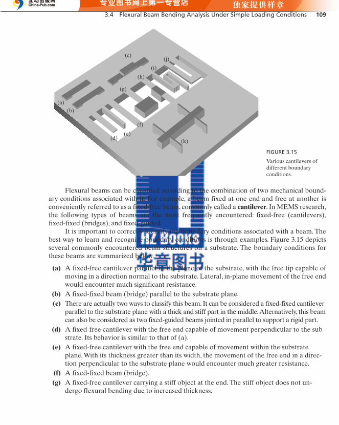
Flexural beams can be classified according to the combination of two mechanical bound-
ary conditions associated with it. For example, a beam fixed at one end and free at another is
conveniently referred to as a fixed-free beam, commonly called a cantilever. In MEMS research,
the following types of beams are the most frequently encountered: fixed-free (cantilevers),
fixed-fixed (bridges), and fixed-guided.
It is important to correctly identify the boundary conditions associated with a beam. The
best way to learn and recognize boundary conditions is through examples. Figure 3.15 depicts
several commonly encountered beam structures on a substrate. The boundary conditions for
these beams are summarized below.
(a) A fixed-free cantilever parallel to the plane of the substrate, with the free tip capable of
moving in a direction normal to the substrate. Lateral, in-plane movement of the free end
would encounter much significant resistance.
(b) A fixed-fixed beam (bridge) parallel to the substrate plane.
(c) There are actually two ways to classify this beam. It can be considered a fixed-fixed cantilever
parallel to the substrate plane with a thick and stiff part in the middle.Alternatively, this beam
can also be considered as two fixed-guided beams jointed in parallel to support a rigid part.
(d) A fixed-free cantilever with the free end capable of movement perpendicular to the sub-
strate. Its behavior is similar to that of (a).
(e) A fixed-free cantilever with the free end capable of movement within the substrate
plane. With its thickness greater than its width, the movement of the free end in a direc-
tion perpendicular to the substrate plane would encounter much greater resistance.
(f) A fixed-fixed beam (bridge).
(g) A fixed-free cantilever carrying a stiff object at the end. The stiff object does not un-
dergo flexural bending due to increased thickness.
(a)
(b)
(c)
(g)
(d)(e)
(f)
(h)
(i)
(j)
(k)
FIGURE 3.15
Various cantilevers of
different boundary
conditions.
M03_CHAN2240_02_PIE_C03.qxd 2/25/11 3:44 PM Page 109

110 Chapter 3 Review of Essential Electrical and Mechanical Concepts
(h) This beam is very similar to case (c) except for the fabrication method.
(i) A fixed-free cantilever with folded length. It consists of several fixed-free beam seg-
ments connected in series. The free end of the folded cantilever is capable of movement
in a direction parallel to the substrate surface. Movement of the free end perpendicular
to the substrate would encounter much greater resistance.
(j) Two fixed-free cantilever connected in parallel. The combined spring is stiffer than any
single arm.
(k) Four fixed-guided beam connect to a rigid shuttle, which is allowed to move in the sub-
strate plane but with restricted out-of-plane translational movement.
The most commonly encountered beam structures in MEMS are double-clamped suspen-
sion structures and single-clamped cantilevers.
3.4.2 Longitudinal Strain Under Pure Bending
The analysis of static deflection and stress in a beam under stress is a key element of MEMS
design. The first-order analysis model for beams under loading is discussed here. When a beam is
loaded by force or couples, stresses and strains are created throughout the interior of the beam.
Loads may be applied at a concentrated location (concentrated load), or distributed over a length
or region (distributed load).To determine the magnitude of these stresses and strains, we first must
find the internal forces and internal couples that act on cross sections of the beam (see 2.3.1.).
The loads (either concentrated or distributed) acting on a beam cause the beam to bend
(or flex), deforming its axis into a curve. The longitudinal strains in a beam can be found by an-
alyzing the curvature of the beam and the associated deformations. For this purpose, let us con-
sider a portion of a beam (A-B) in pure bending (i.e., the moment is constant throughout the
beam) (Figure 3.16).We assume that the beam initially has a straight longitudinal axis (the x axis
in the figure). The cross-sectional of the beam is symmetric about the y axis.
A m
m p
m
n
p
n
n
q
q
B
x
y
neutral plane
s t
t
M
u MM
M
FIGURE 3.16
Bending of a segment
of a beam under pure
bending.
M03_CHAN2240_02_PIE_C03.qxd 2/25/11 3:44 PM Page 110

3.4 Flexural Beam Bending Analysis Under Simple Loading Conditions 111
It is assumed that cross sections of the beam, such as sections mn and pq, remain plane and
normal to the longitudinal axis. Because of the bending deformations, cross sections mn and pqrotate with respect to each other about axes perpendicular to the xy plane. Longitudinal lines in
the convex (lower) part of the beam are elongated, whereas those on the concave (upper) side are
shortened. Thus, the lower part of the beam is in tension and the upper part is in compression.
Somewhere between the top and bottom of the beam is a surface in which longitudinal lines do
not change in length. This surface, indicated by the dashed line st, is called the neutral surface of
the beam.The intersection between the neutral surface with any cross-sectional plane, e.g., line tu,
is called the neutral axis of the cross section. If the cantilever is made of a homogeneous material
with a uniform, symmetric cross section, the neutral plane lies in the middle of the cantilever.
For a beam with symmetry and material homogeneity, the distribution of the stress and
strain is observed to follow a number of guidelines:
1. The magnitude of stress and strain at any interior point is linearly proportional to the dis-
tance between this point and the neutral axis;
2. On a given cross section, the maximum tensile stress and compressive stress occur at the
top and bottom surfaces of the cantilever;
3. The maximum tensile stress and the maximum compressive stress have the same magnitude;
4. Under pure bending, the magnitude of the maximum stress is constant through the length
of the beam.
The magnitude of stresses at any location in the beam under pure bending mode can be
calculated by following the procedure discussed here.At any section, the distributed stress con-
tributes to distributed force, which subsequently gives rise a reaction moment (with respect to
the neutral axis). The magnitude of the normal stress at a distance h to the neutral plane is de-
noted The normal forces acting on any given area dA is denoted The force con-
tributes to a moment with respect to the neutral axis. The moment equals the force,
multiplied by the arm between the force and the neutral plane.The area integral of the moment
equals the applied bending moment, according to
(3.33)
Under the assumption that the magnitude of stress is linearly related to h and is the high-
est at the surface (denoted ), one can rewrite the above equation to yield
(3.34)
The term I is called the moments of inertia associated with a particular cross section. The
maximum longitudinal strain is expressed as a function of the total torque M according to
(3.35)emax =
Mt2EI
.
M =
3w3
t2
h= -t2
£smax
h
at2b
dA≥h =
smax
at2b
3
w3
t2
h= - t2
h2dA =
smax
at2b
I.
smax
M =
OA
dF(h)h =
3w3
t2
h= -t2
(s(h)dA)h.
dF(h)
dF(h).s(h).
M03_CHAN2240_02_PIE_C03.qxd 2/25/11 3:44 PM Page 111

112 Chapter 3 Review of Essential Electrical and Mechanical Concepts
Practical cases are often more complex. For a simple loading condition depicted in
Figure 3.17, the moment along the beam is not constant. Shear stress components are also
present. In this case, Equation 3.35 can be applied to each individual cross section. For more
details, see Section 6.3.1.
3.4.3 Deflection of Beams
This section will cover methods for analyzing the deflection of beams under simple loading
conditions.
The general method for calculating the curvature of beam under small displacement is to
solve a second order differential equation of a beam:
(3.36)
where represents the bending moment at the cross section at location x and y the displace-
ment at location x.The x axis runs along the longitudinal direction of the cantilever (Figure 3.17).
The relationship between y and x can be found by solving the second order differential
equation. To solve this equation require three preparatory steps:
1. Find the moment of inertia with respect to the neutral axis;
2. Find the state of force and torque along the length of a beam;
3. Identify boundary conditions.Two boundary conditions are necessary to deterministically
find a solution.
The most commonly encountered cross section of a cantilever is a rectangle. Suppose the
width and thickness of a rectangle are denoted as w and t, the moments of inertia with respect
to the neutral axis is (provided that the cantilever bend in the direction of the thickness).
If the cross section of a beam is a circle with radius R, the moment of inertia is The
torque at any arbitrary location x can be calculated using procedures discussed in Section 3.3.1.
I =
pR4
4.
I =
wt3
12
M(x)
EI d2y
dx2= M(x),
y
x
F
FIGURE 3.17
Coordinate system for
describing bending of
cantilever beams.
M03_CHAN2240_02_PIE_C03.qxd 2/25/11 3:44 PM Page 112

3.4 Flexural Beam Bending Analysis Under Simple Loading Conditions 113
In fact, in many routine MEMS design cases, the interest is to find the maximum displace-
ment associated with a microstructure rather than the deformation profile. The solutions for
maximum angular and transverse displacement for common cases under simple point loading
conditions are summarized in Appendix B.
3.4.4 Finding the Spring Constants
Coiled springs are most commonly found in daily lives and macroscale engineering systems. For
microscale devices, it is difficult to fabricate and integrate coiled springs. Beams are the most
frequently encountered spring element in MEMS. These micro beams serve as mechanical
springs for sensing and actuation. The stiffness of these beams is a frequently encountered
design concern.
The stiffness is characterized by a term called the spring constant (or force constant).
Here I will discuss the procedures for calculating the spring constant of various types of beams.
It is necessary to first define the term spring constant. We define it here by using familiar
coiled springs (Figure 3.18). A coiled spring will extend by an amount x under a pointed load-
ing force F. The displacement and the applied force follow a familiar linear relationship em-
bodied in the Hooke’s law. The mechanical spring constant is the ratio of the applied force and
the resultant displacement,
(3.37)
For a cantilever spring, the general expression of a force constant is the force divided by
the displacement at a point of interest, commonly the point where the force is applied.
For a cantilever with point loading on the free end, the maximum deflection occurs at the
free end. For a fixed-fixed bridge with a loading force in the center of the span, the center has
the largest deflection.
Let us first focus on analyzing the force constant of a fixed-free beam with a rectangu-
lar cross section, one of the most common scenarios encountered in MEMS. The cantilever is
km =
Fx
.
F
F � 0 parallelconnectedspringsK � K1 � K2
seriallyconnectedsprings
at rest
K � F/x
k1 k2
x
1/K � 1/K1 � 1/K2
FIGURE 3.18
The mechanical defor-
mation of a coil spring
under a point loading
force.
M03_CHAN2240_02_PIE_C03.qxd 2/25/11 3:45 PM Page 113

114 Chapter 3 Review of Essential Electrical and Mechanical Concepts
diagramed in Figure 3.19, with the length, width and thickness of the cantilever beam denoted
l, w, and t, respectively. The Young’s modulus of the beam material along the longitudinal axis
is E.
In the case shown in Figure 3.19, the force is applied on the broad surface.The formula for
calculating the displacement can be found from Appendix B. The free end of the beam will
reach a certain bent angle, with the relationship between and F given by
(3.38)
The resulted vertical displacement equals
(3.39)
The spring constant of the cantilever is therefore
(3.40)
Apparently, the force constant decreases with increasing length. It is proportional to
the width and is strongly influenced by the change in thickness due to the presence of the
term
The stiffness of a cantilever depends on the direction of the bending. If the force is ap-
plied longitudinally, the spring constant would be very different. The beam is said to provide
compliance in one direction and resistance to movement in another.
Example 3.6 Moments of Inertia of Two Beams
Two cantilever beams of the same length and material, one with a cross section of by
and a second one with by Which one is more resistant to flexural bending
(i.e., stiffer?)
8 mm.50 mm5 mm,
100 mm
t3.
k =
Fx
=
3EI
l3=
Ewt3
4l3
x =
Fl3
3EI
u =
Fl2
2EI
uu,
F
F
l
t
w
y
x
dx
FIGURE 3.19
Schematic diagram of a
fixed-free cantilever
beam spring.
M03_CHAN2240_02_PIE_C03.qxd 2/25/11 3:45 PM Page 114

3.4 Flexural Beam Bending Analysis Under Simple Loading Conditions 115
Solution. The moment of inertia of the first beam is
For the second beam, we have
Since the second beam is stiffer judging by Equation 3.40.
Example 3.7
Find the force constant associated with cases a and b depicted in Figure 3.20.
Solution. Case (a) is a fixed-free cantilever beam with in-plane transverse loading. The perti-
nent moment of inertia and spring constant are
k =
Fx
=
3EI
l3=
Ew3t
4l3
I =
w3t12
I2 7 I1,
I1 =
wt3
12=
50 * 10-6* (8 * 10-6)3
12= 2.13 * 10-21 m4
I1 =
wt3
12=
100 * 10-6* (5 * 10-6)3
12= 1.04 * 10-21 m4.
verticalside wall
(a)
(b)
(d)
(e)
(g)
( f )
(c)
F
F
F
F
substrateplane
F
F
F
l
l
w
w w
w1
w1
t
t
t1
w2l2
l1
FIGURE 3.20
Calculate spring
constant for cases
(a) through (g).
M03_CHAN2240_02_PIE_C03.qxd 2/25/11 3:45 PM Page 115

116 Chapter 3 Review of Essential Electrical and Mechanical Concepts
Case (b) is a fixed-free cantilever beam with loading force normal to the substrate. The perti-
nent moment of inertia and spring constant are
In many applications, two or more springs may be connected to form a spring system. Two
springs can be connected in two ways—parallel or serial. If multiple springs are connected in
parallel, the total spring constant is the summation of spring constants of all springs in the system
(see Figure 3.18). If multiple coiled springs are connected in series, the inverse of the total spring
constant is the summation of the inverse of spring constants of constitutive spring elements.
Example 3.8 Cantilevers with Parallel Arms
Find the force constant associated with the case g depicted in Figure 3.20.
Solution. Case (g) consists of two fixed-free cantilever connected in parallel. The pertinent
moment of inertia of each arm is
The overall force constant is
Example 3.9 Vertical Translational Plates
Fixed-guided springs are often used to support rigid plates and facilitate their translation.
Often, a plate is supported by two or more such beams (Figure 3.21a,b). In these cases, one end
of the beam is fixed, with all degrees of freedom limited.Another end of the spring can move in
the vertical direction but no angular displacement is allowed because it is connected to the stiff
translational plate, which remains parallel to the substrate under allowable plate movement
(Figure 3.21c). Find the expression of the force constant associated with the plate.
Solution. Let us examine the basic formula for the spring constant of a single fixed-guided
beam under a transverse force loading F. Once again, the length, width and thickness of the
support beam are l, w and t, respectively. From Appendix B, the maximum displacement x oc-
curs at the guided end and is related to F by
(3.41)x =
Fl3
12EI
k = 2aFxb = 2
3EI
l23
=
Ew2t3
2l23
I =
w2t3
12
k =
Fx
=
3EI
l3=
Ewt3
4l3
I =
wt3
12
M03_CHAN2240_02_PIE_C03.qxd 2/25/11 3:45 PM Page 116

3.4 Flexural Beam Bending Analysis Under Simple Loading Conditions 117
fixed–guidedbeam
fixed–guidedbeam
guided
stiff plate
anchor
anchor anchor
anch
or
anch
or
stiff plate
anchor
l l
l
fixed guided guided
fixed
fixed
width: wthickness: t
F
width: wthickness: t
(a) (b)
(c)
stiff plate
FIGURE 3.21
Commonly encountered plate support configurations.
The expression for the force constant of each single fixed-guided beam is
(3.42)
By comparing with Equation 3.39, it is obvious that for a beam with equal dimensions, the
fixed-guided beam would be stiffer than a fixed-free cantilever.
If a force is applied to a plate supported by n cantilevers with equal dimensions and force
constants, each spring shared 1/nth of the total force load. The total force constant experienced
by the spring is nk.
The force constant associated with each fixed-guided beam is
For the plate supported by two fixed-guided beams, the equivalent force constant is
For the plate supported by four fixed guided beams, the equivalent force constant is
k = 4aEwt3
l3b .
k = 2aEwt3
l3b .
k =
Fx
=
12EI
l3=
Ewt3
l3 .
k =
12EI
l3 .
M03_CHAN2240_02_PIE_C03.qxd 2/25/11 3:45 PM Page 117

118 Chapter 3 Review of Essential Electrical and Mechanical Concepts
3.5 TORSIONAL DEFLECTIONS
Whereas beams, especially cantilevers, are frequently used in MEMS for producing linear dis-
placements and small angular rotations, torsional beams are often used to create large angular
displacement.A case in mind is the digital micro mirror device.The mirror plate is supported by
torsional bars to facilitate rotation.
We begin our discussion of torsion by considering a prismatic bar of circular cross section
twisted by torques T acting at the ends. Since every cross section of the bar is identical, and
since every cross section is subjected to the same internal torque T, the bar is said to be in pure
torsion. It may be proved that cross sections of the bar do not change shape as they rotate about
the longitudinal axis. In other words, all cross sections remain plane and circular and all radii re-
main straight. Furthermore, if the angle of rotation between one end of the bar and the other is
small, neither the length of the bar nor its radius will change.
To aid in visualizing the deformation of the bar, imagine that the left-hand end of the bar
is fixed in position. Then, under the action of a torque T, the right-hand end will rotate through
a small angle known as the angle of twist.
Because of this rotation, a straight longitudinal line on the surface of the bar will become
a helical curve. The angle of twist changes along the axis of the bar, and at intermediate cross
sections it will have a value that is between zero at the left-hand end and at the right-
hand end.The angle will vary linearly between the ends. Point a on the right-hand side will
move by a distance d to a new location,
The torsion induces shear stress throughout the bar. Stress distribution shows radial sym-
metry. The magnitude of the shear stress is zero in the center of the cross section and reaches
maximum at the outer surface of the bar. The maximum stress in the bar is denoted The
expression of the maximum shear strain is
(3.43)
Further, the magnitude of the stress is linearly proportional to the radial distance to the
center. The distribution of shear stress along the radial direction is superimposed on the cross-
sectional view of the bar in Figure 3.22.
g max =
dL
.
tmax.
a¿.
f(x)
ff(x)
f,
T
T
B
d
a�
a
A
L
u
�
tmax
tmax
r0
FIGURE 3.22
Torsional bending of a cylinder with circular cross section.
M03_CHAN2240_02_PIE_C03.qxd 2/25/11 3:45 PM Page 118

3.5 Torsional Deflections 119
The relationship between a torque and the maximum shear stress is found by torque
balance at any given section,
(3.44)
The surface integral is called the torsional moment of inertia, denoted J. For a
circular beam, therefore,
(3.45)
The magnitude of the maximum shear stress is
(3.46)
The torsional moment of inertia of a circle with a radius of is
(3.47)
The total angular displacement subtended by the torsional bar segment AB is calculated
according to the following:
(3.48)
For micromachined devices, torsional bars with rectangular cross sections are often en-
countered. The moment of inertial for such a torsional bar (with width and thickness being
and ) is
(3.49)
The moment of inertia of a beam with a square cross section with the length of each side
being 2a is
(3.50)
Example 3.10 Deformation of Torsional Bars
A suspended beam shown in the diagram below is under a force Find the verti-
cal displacement at the end of the beam, assuming the flexural bending of the cantilever beam
is negligible. The dimensions of the beam are
The Young’s Modulus of the beam material is The Poisson’s ratio of the beam
material is 0.3.
E = 150 GPa.
L = 40 mm, l = 200 mm, w = 5 mm, t = 2 mm.
F (F = 10 mN).
J = 2.25a4.
J = wt3 c16
3- 3.36
tw
a1 -
t4
12w4b d for w Ú t.
2t2w
£ =
dr0
=
Lur0
=
Lr0
tmax
G=
LTr0
r0GJ= TL>JG.
J =
pr40
2 .
r0
tmax =
Tr0
J .
T =
tmax
r0 L2pr3dr =
pr40
2 tmax
r0 .
dA = 2prdr,1r2dA
T =
La
rr0
tmaxbdA # r =
tmax
r0 Lr2dA.
M03_CHAN2240_02_PIE_C03.qxd 2/25/11 3:45 PM Page 119

120 Chapter 3 Review of Essential Electrical and Mechanical Concepts
l
L
FFIGURE 3.23
A torsional supported
cantilever.
Solution. First find the shear modulus of elasticity and the torsional moment of inertia of the
beam. The process is rather straightforward.
Plug in the expression for torque, , into the expression for the bending angle, we get
Plug in the numbers and we have
The vertical displacement at the free end of the cantilever is equal to the product of the angu-
lar displacement and the length of the cantilever. Namely,
3.6 INTRINSIC STRESS
Many thin film materials experience internal stress even when they are under room tempera-
ture and zero external loading conditions. This phenomenon is called the intrinsic stress. Thin
film materials associated with MEMS, such as polysilicon, silicon nitride, and many metal thin
films, exhibit intrinsic stresses [41]. The magnitude of the intrinsic stress may be identical or
nonuniform throughout the thickness of the thin film. If the stress distribution is nonuniform, a
stress gradient is said to be present.
dtorsional = fL =
TlL2JG
=
FL2l2JG
£ = 1.13 rad = 65
f =
Tl2JG
=
FLl2JG
T = FL
J = 6.2 * 10-25 m4
G = E>2(1 + 0.3) = 57.7 GPa
M03_CHAN2240_02_PIE_C03.qxd 2/25/11 3:45 PM Page 120

3.6 Intrinsic Stress 121
FIGURE 3.24
Microscale devices
bent under intrinsic
stress.
film under tensile stress
flat
film under compressive stress
wrinkled
substrate
FIGURE 3.25
Cross section of a taunt
membrane under
tensile stress and a
warped membrane
under compressive
stress. An optical
micrograph of a warped
membrane is shown.
The intrinsic stress is important for MEMS devices because it can cause deformation—
damages in excessive cases, affect surface planarity, or change the stiffness of a mechanical ele-
ment. For example, in micro optics applications, flat mirror surfaces are required for achieving
desired optical performances. Intrinsic stress may warp the mirror surface and change optical
properties.Bent cantilever structures due to the presence of intrinsic stress are shown in Figure 3.24.
Intrinsic stress may affect the mechanical behavior of membranes as well. For a thin film
diaphragm such as the one illustrated in Figure 3.25, the flatness of the membrane is guaranteed
M03_CHAN2240_02_PIE_C03.qxd 2/25/11 3:45 PM Page 121

122 Chapter 3 Review of Essential Electrical and Mechanical Concepts
when the membrane material is under tensile stress. Excessive tensile stresses in a clamped
membrane can cause the membrane to fracture. On the other hand, a film would buckle if a
compressive stress were present.
The origin and behavior of intrinsic stress have been widely studied [42, 43]. In many cases
related to MEMS structures, the intrinsic stress results from the temperature difference during de-
position and use.Thin film materials are often deposited on a substrate under an elevated temper-
ature. During the deposition, molecules are incorporated into a thin film with certain equilibrium
spacing. However, when the MEMS device is removed from the deposition chamber, the tempera-
ture change causes the material to contract, at a rate faster or slower than the substrate. As a rule
of thumb, the intrinsic stress in a thin film is tensile when a film wants to become “smaller” than the
substrate. Compressive stress results when a film wants to become “larger” than the substrate.
Intrinsic stress can also result from microstructure of the deposited film. The incorpora-
tion of oxygen atoms into silicon lattice during a thermal oxidation process, for example, cre-
ates compressive intrinsic stress in the oxide film.
Apart from the above-mentioned common source of intrinsic stress, other mechanisms
are possible, including phase change of materials and incorporation of impurity atoms (such as
dopant atoms).
In certain cases, the bending is desired and intentional. There are a number of application
scenarios in which the intrinsic stress can be used to induce out of plane deformation to realize
unique device architecture.
A common scenario of intrinsic stress induced beam bending involves a microstructure with
two or more structural layers (Figure 3.26). Consider a cantilever consisting of two layers, with the
intrinsic stress in Layer 1 being zero. If the Layer 2 is under a tensile stress, the beam would bend
towards the direction of Layer 2 (Figure 3.26b). On the other hand, if Layer 2 is under a com-
pressive intrinsic stress, the beam would bend towards the direction of Layer 1 (Figure 3.26c).
deposited material
substrate material
tensile stress
zero stress
compressive stress
zero stress
(a)
(b)
(c)
FIGURE 3.26
Beam bending due to intrinsic mechanical stress.
M03_CHAN2240_02_PIE_C03.qxd 2/25/11 3:45 PM Page 122

3.6 Intrinsic Stress 123
I will discuss the formulation used to calculate the bending of a two-layer cantilever beam
under difference of intrinsic stress. For simplicity, we assume that the two layers have the same
length and width Their thickness, intrinsic hydrostatic stress, and Young’s modulus are
denoted as and ( or 2).The subscript letters correspond to layers 1 or 2, with Layer 2
on the bottom.
First, the position of the neutral axis is found by
(3.51)
The distance is measured from the bottom of the bottom layer. An effective flexural stiff-
ness is calculated by using
(3.52)
The bending moment acting on the cantilever is
(3.53)
The radius of curvature of the beam bending, R, is given by
(3.54)
One would imagine that if a fixed-free cantilever is made of a single homogeneous mate-
rial, there would be no intrinsic stress nor intrinsic-stress induced bending. This assumption is
only true if the intrinsic stress is uniformly distributed throughout the thickness. A gradient of
intrinsic stress may cause a cantilever made of a single material to bend, as if the cantilever is
made of a large number of thin layers stacked together.
There are three strategies for minimizing undesirable intrinsic bending: (1) use materials
that inherently have zero or very low intrinsic stress; (2) for materials whose intrinsic stress de-
pends on material processing parameters, fine tune the stress by calibrating and controlling de-
position conditions; (3) use multiple layered structures to compensate stress-induced bending.
One of the materials in MEMS that has zero stress is single crystal bulk silicon. The SCS
is a homogenous material with perfect lattice spacing distribution. Polymer materials are
known to have relatively smaller intrinsic stresses than inorganic thin films. Secondly, the de-
position temperature of polymer materials is typically low. Parylene, a polymer material that
can be deposited by chemical vapor deposition method under room temperature, has virtually
zero stress in it [44].
In many surface micromachining materials such as polysilicon and silicon nitride, the in-
trinsic stress is unavoidable (Chapter 10). Although techniques exist to produce stress-free ma-
terials, the process is usually delicate, machine specific, and subjected to complex process
control. The best practice is to minimize the intrinsic-stress induced bending to an acceptable
R =
IeffE0
M .
+ w c at22 + t1t2
2b a as2(1 - n2) - E2
t1s1(1 - n1) + t2s2(1 - n2)
E1t1 + E2t2b d .
M = w c at21
2b a as1(1 - n1) - E1
t1s1(1 - n1) + t2s2(1 - n2)
E1t1 + E2t2b d
IeffE0 = waE1t1at21
12+ a
t12
- yb2
b + E2t2at22
12+ a
t22
+ t1 - yb2
b b .
y =
1
2 1E1t2
1 + E2t222 + E2t1t2
E1t1 + E2t2.
i = 1Eiti, si,
(w).(l)
M03_CHAN2240_02_PIE_C03.qxd 2/25/11 3:45 PM Page 123

124 Chapter 3 Review of Essential Electrical and Mechanical Concepts
level. Generally, intrinsic stress in silicon nitride or polycrystalline silicon can be minimized by
controlling the pressure, gas mixture, and growth rate (e.g., [45]).
Often the intrinsic stress of layers cannot be fully cancelled by material processing. It is
still possible to produce microstructures free of intrinsic-stress induced bending, by adding
stress compensation layers with carefully selected material, stress, and thickness. For example,
in the two-layer beam shown in Figure 3.27, the tensile-stressed upper layer and the compress-
stressed lower layer contribute to a finite amount of beam bending. The overall deformation
can be reduced to zero in theory by adding another layer of compress-stressed material on top.
The intrinsic stress of a material depends strongly on material deposition conditions. The
exact magnitude of intrinsic stress in a given process flow can be experimentally measured by
using specially designed testing structures and test protocols [46, 47]. A common technique for
measuring the stress is to use a circular plate (such as a wafer) bearing the thin film of interest
on one side (Figure 3.28) [48]. The stress in the thin film can be derived from the curvature
(bowing) of the plate. A classic formula (called the Stoney’s formula) has been derived under
the conditions that the substrate is thin, elastically isotropic, and flat when bare [48]. For a sin-
gle film case, the curvature of the substrate, C, is expressed as
(3.55)
where R is the radius of curvature, the Poisson’s ratio of the substrate, the in—plane
stress of the thin film, t the substrate thickness, and h the thickness of the thin film. The thin
sn
C =
1
R=
6(1 - n)sh
Et2,
tensile
compressive
tensile
compressive
compressive
FIGURE 3.27
Method of stress
compensation.
wafer
thin film
refle
cted
ligh
t
angular bending
stress
stress
inco
min
g lig
ht
FIGURE 3.28
Experimental methods for measuring intrinsic stress.
M03_CHAN2240_02_PIE_C03.qxd 2/25/11 3:45 PM Page 124

3.7 Dynamic System, Resonant Frequency, and Quality Factor 125
film material should be present on only one side. If the deposition process dictates double
side coating, then the material on one side should be carefully removed.
The method discussed above only measured the overall averaged stress level over the en-
tire wafer area. In most cases, the distribution of stress over the wafer is not uniform. The stress
within local regions of the wafers is needed for precise control of process. Surface and bulk mi-
cromachined test structures called process monitors are often used. One of the monitoring de-
vices is illustrated in Figure 3.28. It consists of a suspended thin film dial that is attached to the
substrate through two offset pulling beams. The two horizontal pulling beams, when under in-
trinsic stress, develop a torque that causes the dial to rotate for a certain amount.
3.7 DYNAMIC SYSTEM, RESONANT FREQUENCY, AND QUALITY FACTOR
A MEMS system, including sensors and actuators, invariably consists of mass and supporting struc-
tures.The supporting mechanical elements (membranes, cantilever, or suspensions) provide elastic
restoring spring constants. Movement of the mass is impeded by collision with air molecules sur-
rounding the mass.This constitutes damping, which is a velocity-dependant resistance force.
As such, a MEMS system can always be simplified into a classic mass-spring-damper sys-
tem. It is almost always subject to time varying input, dynamic input (pulses or shocks) and sinu-
soidal (resonant) input signals. The understanding of MEMS system dynamics is crucial for
predicting performance characteristics of sensors and actuators. Dynamic analysis is discussed in
many books. In this section, only the most essential elements of dynamic system behavior are
discussed.
3.7.1 Dynamic System and Governing Equation
The governing equation of a mass-spring-damper system shown in Figure 3.29 is
(3.56)
where the term c is the damping coefficient, k is the force constant (spring constant), and is
the forcing function. Dividing both sides with the mass m, we arrive at a canonic expression
(3.57)
where the term
(3.58)vn =
A
km
x$
+ 2jvnx#
+ vn2
= a(t),
f (t)
mx$
+ cx#
+ kx = f (t)
capacitor
K cP
m T
packagespring damper
xf(t) FIGURE 3.29
A mass-spring-damper
system.
M03_CHAN2240_02_PIE_C03.qxd 2/25/11 3:45 PM Page 125

126 Chapter 3 Review of Essential Electrical and Mechanical Concepts
is the natural resonant frequency and the term
(3.59)
is the damping ratio.
The term
(3.60)
is called the critical damping coefficient.
The solution method for the governing differential equation would be different for dif-
ferent input:
• If the solution is called the free system solution.
• If is an arbitraty forcing function, the solution may contain both transient and steady
state terms.
• If , the system is said to be under sinusoidal or resonant forcing.
In this section, we only focus on reviewing the response of the system under sinusoidal
input. Readers who wish to become familiar with dynamic system responses can refer to text-
books on this subjects and Appendix 3.
3.7.2 Response Under Sinusoidal Resonant Input
For sinusoidal forcing, the system will be forced to oscillate with the forcing frequency. The
steady-state response is the focus of analysis. Under a sinusoidal input,
(3.61)
the steady-state system output will be a sinusoidal signal with the same frequency as the driving
frequency, namely
(3.62)
Therefore, transient response and any initial conditions don’t matter anymore.The output
can be analyzed using the transfer function method. In this case, the transfer function between
x and f is
(3.63)
Dividing the numerator and the denominator with m, we have
(3.64)
If one replaces s with , the spectral response of T is
(3.65)ƒ T(v) ƒ = 2 1>m
v2n - v2
+ j2jvvn
2 =
1>m
2(v2n - v2)2
+ 4j2v2v2n
.
jv
T =
XF
=
1>m
s2+
Cm
s +
km
=
1>m
s2+ 2jvns + v2
n.
T =
XF
=
1
ms2+ Cs + k
.
x = A sin (vt + w).
f (t) = F sin (vt) = ma sin (vt),
f (t) = A sin vt
f (t)f (t) = 0,
cr = 22Km
j =
c
22Km= c>cr
M03_CHAN2240_02_PIE_C03.qxd 2/25/11 3:45 PM Page 126

3.7 Dynamic System, Resonant Frequency, and Quality Factor 127
The magnitude A is therefore
(3.66)
The term is the would-be amplitude under DC forcing conditions. The magnitude Ais a function of both the frequency and damping ratio .
A second order system responds differently to stimulus depending on if the system damp-
ing is large or small:
for large damping c, the system is said to be over damped;
the system is said to be critically damped if or ;
when the damping is between critical damping and zero, the system is said to be under
damped.
If we fix and change we can plot a typical frequency spectrum of the response. The
displacement of an underdamped mechanical structure under a periodic loading condition is
shown in Figure 3.30. At low frequencies, the displacement remains constant. This represents
the low-frequency behavior that applies to the steady loading case. At or near the resonant fre-quency ( with ), the mechanical vibration amplitude sharply increases. The sharp-
ness of the resonant peak is characterized by a term called the quality factor (Q). The sharper
the resonance peak, the higher the quality factor.
The amplitude magnification at the resonant frequency can be beneficial. By operating a
micro sensor or actuator at the resonant frequency may increase the sensitivity or range of ac-
tuation. However, resonance may also lead to self-destruction of mechanical elements.
At frequencies beyond the resonant frequency, the vibration amplitude decreases
(called roll off). A simple physical explanation is that the mechanical structures, with its
built-in inertia, cannot follow the driving input anymore at frequencies significantly above
the fr.
fr = vn>2pfr,
v,j
j = 1c = 22km
zv
F>m
A = ƒ T ƒ F =
F>m
2(v2n - v2)2
+ 4j2v2v2n
.
FWHM
100%
77%
static andlow-frequencydisplacement
resonantfrequency ( fr)
vibrationamplitude
drivingfrequency
�f FIGURE 3.30
A typical response
spectrum showing the
relationship of the
amplitude of vibration
as a function of the
input frequency.
M03_CHAN2240_02_PIE_C03.qxd 2/25/11 3:45 PM Page 127

128 Chapter 3 Review of Essential Electrical and Mechanical Concepts
3.7.3 Damping and Quality Factor
MEMS moving masses encounter damping invariably. Damping may be derived from both
viscously fluid interaction [49] (such as squeeze film damping [49–53] and collision with gas
particles [54]) and structural damping (internal friction) [55]. The damping factors are there-
fore subjected to temperature, pressure, types of gas molecule, and other environmental fac-
tors [56–58].
The quality factor, representing the sharpness of resonance peaks, can be defined in sev-
eral ways. Mathematically, the quality factor is related to the full width at half maximum
(FWHM), which is the spacing of two frequencies at half power (or 77% amplitude). The ratio
of the resonant frequency and the FWHM gives the quality factor.
(3.67)
From the energy point of view, Q is the ratio of the total stored energy in a system over
the energy lost over each cycle of oscillation.The lower the energy loss per cycle, the greater the
quality factor.
Mathematically, the quality factor is related to the damping factor, by
(3.68)
Hence the quality factor is inversely proportional to the damping.A small value of damp-
ing coefficient c translates into lower energy loss, smaller damping ratio, and hence higher Q.
As such, the quality factor of a micro device can be improved by reducing the operating
pressure [12, 59], by altering the operating temperature [12], by improving surface roughness [60],
by thermal annealing (up to 600% improvement demonstrated in [61]), or by modifying the
boundary conditions [62, 63]. Q value for micromechanical devices ranging from several hundred
[64] to up to 10,000 [63–65] have been demonstrated in micro- or nano mechanical resonators.
3.7.4 Resonant Frequency and Bandwidth
The resonant frequency determines the ultimately achievable bandwidth of a device. Hence
for many devices, a greater resonant frequency is desired. Formula for calculating the reso-
nant frequency of cantilevers under various boundary and loading conditions can be found in
Appendix B.
The resonant frequency of mechanical elements generally increases when scaled down, as
the value of m decreases rapidly. By down-scaling resonator device dimensions, resonant fre-
quency ranging form several MHz [65], tens of MHz [63], and even to the GHz range [60] has
been demonstrated successfully.
Because the resonance frequency is a function of device dimensions, it is susceptible to
changes in temperature.Temperature stabilization is critical for resonators requiring stable fre-
quency. For commercial devices, temperature stability must be achieved by temperature com-
pensation [66].
Additionally, the resonant frequency of micro resonators can be precisely tuned by trim-
ming materials (using laser or focused ion beam etching), or by locally depositing materials [67].
Q =
1
2j.
Q =
fr
¢f
M03_CHAN2240_02_PIE_C03.qxd 2/25/11 3:45 PM Page 128

3.8 Active Tuning of Spring Constant and Resonant Frequency 129
Example 3.11 Resonant Frequency
A mechanical resonator (fixed-fixed, or double clamped) has been demonstrated using SiC thin
film material. The length (L), width (W), and thickness (T) of the resonator are
and 75 nm, respectively. Knowing the resonant frequency found experimentally was 1.014 GHz,
and assuming a Young’s modulus of 700 GPa, find the density of the SiC material used for the
resonator.
Solution. The formula for the resonant frequency according to the table in Appendix B is
The distributed force w is given by
Plug into the formula for resonant frequency
we find the value of is
3.8 ACTIVE TUNING OF SPRING CONSTANT AND RESONANT FREQUENCY
Mechanical characteristics such as spring constants and resonant frequencies of beams and
membranes can be changed by introducing strain. In this section, we focus on discussing meth-
ods for tuning characteristics of cantilever beams to exemplify the methodology.
For cantilevers, longitudinal strain can be introduced by axial or transverse loading forces.
We will discuss these two cases separately below.
First, an axial tension can alter the spring constant and resonant frequency.This is analogous
to a violinist tuning the sound of a string by adjusting its tension.The longitudinal tuning force can
be introduced by lateral electrostatic force, or thermal expansion. (In the same token, the shift of
resonance frequency can be used to characterize intrinsic stress of fixed-fixed beams [68].) The
resonant frequency of a cantilever under a longitudinal strain is
(3.69)
where and L are the untuned resonant frequency, and the thickness and length of the beam.
The force constant and resonance frequency of a cantilever can be tuned by transverse
forces.To illustrate this case, think about a child standing at the end of a diving board and bouncing
w0, h
w = w0
A1 +
2L2
7h2 es,
es
r = a8.6 * 105
fn
T
L2b
2
= 52.662= 2773 kg/m3.
r
fn =
22.4
2p
A
EIg
rgWTL4=
22.4
2p
A
EWT3g
12rgWTL4=
22.4
2p
A
ET2
12rL4= 8.6 * 105
T
2rL2,
w =
r(WLT)g
L= rgWT.
fn =
22.4
2p
A
EIg
wL4.
1.1 mm, 120 nm,
M03_CHAN2240_02_PIE_C03.qxd 2/25/11 3:45 PM Page 129

130 Chapter 3 Review of Essential Electrical and Mechanical Concepts
lightly. Let us assume that the board dips below the horizontal level. The child feels the board has
a certain mechanical stiffness.
Now, imaging an adult pulling down at the same end of the diving board. The child will
feel that the diving board becomes softer (more displacement under a given weight) when
there is an active pulling force. In other words, the diving board appears to be softer to the
child. Beam softening results whenever the bias force point in the opposite direction of the can-
tilever restoring force. The apparent force constant changes from k to The transverse load-
ing force may be applied electrostatically [69, 70], thermally [71], or magnetically.
3.9 A LIST OF SUGGESTED COURSES AND BOOKS
The MEMS field is defined by its cross-disciplinary and multiphysics flavor. A person in the
MEMS field is expected to have knowledge in materials, processing technology, semiconductor
devices, circuit analysis and design, mechanics, and machine design. To successfully generate a
MEMS design often calls for strong fundamental knowledge such as electrostatics, electromag-
netics, solid-state physics, system dynamics, heat transfer, thermal dynamics, fluid dynamics, and
chemistry. A MEMS engineer is often faced with the challenge of using and understanding
many new tools, such as process equipment, computer simulation, data acquisition, etc. Further,
any brave innovator in the MEMS area must become familiar with deep domain knowledge in
the field (such as biology, medicine, communication, etc) very quickly, and must be prepared to
learn about competing technologies. Since the technology and application areas are often fast
moving, deep and broad knowledge of current research literature is also needed. As such, the
field is intellectually demanding and exciting.
The investigation of coupled electrical and mechanical behavior in a system is not unique
to the MEMS field or the microscale. At the macroscopic scale, two subject areas—mechatron-
ics and electromechanics have been studied for decades. They provide relevant background for
MEMS research as well.
The cross-disciplinary material required for success in MEMS is often beyond what is
being taught in undergraduate curriculum in a single undergraduate department. For readers
who wish to build a more comprehensive foundation of knowledge for pursuing future studies,
research, and development in the field of MEMS, I am providing a list of classic fundamental
books or thesis closely related to the field of MEMS.
Mechanical Engineering
1. Mechanics of materials [9].
2. Theory of elasticity [72].
3. Vibration analysis [73].
4. Thermal transfer [74].
5. Fluid mechanics [75].
6. Dynamic systems and analysis [76].
Electrical Engineering
1. Fundamentals of electrical and electronics circuits [77].
2. Field and waves [78].
3. General electronics circuit design.
keff.
M03_CHAN2240_02_PIE_C03.qxd 2/25/11 3:45 PM Page 130

Summary 131
4. Physics of semiconductor and solid-state devices [2].
5. Integrated circuit design [79].
6. Electromechanics [80].
7. Sensors: jargons, principles, and signal-conditioning electronics [81].
Microfabrication and Manufacturing
1. Integrated circuit fabrication [82, 83].
2. In depth discussion of MEMS fabrication [84, 85].
3. MEMS systems design and formulation [86].
4. State of the art of automated electronics product manufacturing [87–89].
Material Science
1. Broad and comprehensive discussion of different classes of engineering materials, prop-
erties, and processing techniques [90].
2. Material properties of polycrystalline silicon [20].
Business and Innovation
1. The rules of innovation [91].
2. Case studies of MEMS business development [92].
SUMMARY
This chapter provides a general overview of major electrical and mechanical aspects that are
used most frequently in the development of MEMS devices. The goal of this chapter is bring
readers from different backgrounds to reach a common level rapidly, at least to be aware of
major issues and major analytical procedures. A reader is encouraged to read in-depth text-
books on each individual topic to obtain a more complete understanding.
The following is a list of major concepts, facts, and skills associated with this chapter. A
reader can use this list to test related understanding.
Qualitative understanding and concepts:
• The origin of two types of charge carriers in a semiconductor.
• The difference and relation between resistivity and sheet resistivity.
• The naming conventions of crystal planes and directions.
• The concepts of normal stress and strain
• The concepts of shear stress and strain.
• The relationship between normal stress and strain and the various regimes of interest.
• The origin of intrinsic stress.
• Methods for reducing bending induced by intrinsic stress.
Quantitative understanding and skills:
• Procedures for calculating the concentrations of electrons and holes in an extrinsic material
when the doping concentrations are known.
M03_CHAN2240_02_PIE_C03.qxd 2/25/11 3:45 PM Page 131

132 Chapter 3 Review of Essential Electrical and Mechanical Concepts
• Procedures for finding the conductivity and resistivity of a semiconductor piece.
• Ability to identify boundary conditions associated with a beam or membrane.
• Procedures for calculating the end deflection of a cantilever under a given force.
• Procedures for calculating the force constant associated with a mechanical beam.
• Procedures for calculating the torsional bending of a torsion bar.
• Formula for calculating the resonant frequency of beams under certain boundary conditions.
PROBLEMS
SECTION 3.1
Problem 1: Review
Calculate the volumetric concentration of atoms and specific mass (density) of single crystal
silicon given the lattice constant of silicon (5.43 Å).
Problem 2: Design
Find the intrinsic concentration of electrons in a semiconductor at a temperature of 35�C.You can look up
the required data (effective masses of n, p, Boltzmann constant, bandgap energy, Planck’s constant) in lit-
erature or handbooks, and reference the source of information. Hint: Use the equation given
Problem 3: Design
A phosphorous-doped silicon resistor is long, wide, and thick.The doping concentra-
tion is The electron mobility which is a function of the doping concentration, is ap-
proximately The hole mobility is approximately What are the concentrations
of electrons and holes under thermal equilibrium at room temperature? Find the resistivity of the mater-
ial and the total resistance.
Problem 4: Design
Repeat Problem 3 assuming the resistor is doped with boron. In this case, holes will be the majority carrier.
Problem 5: Design
Repeat Problem 3 assuming the doping concentration of phosphorous is
Problem 6: Design
A phosphorous-doped silicon resistor has a sheet resistivity of The length and width of the resis-
tor is and , respectively. Find the total resistance of the resistor. If the thickness of the re-
sistor is known to be , what is the resistivity and the phosphorous doping concentration? What are
the concentrations of the majority carriers under thermal equilibrium at room temperature?
Problem 7: Design
A boron-doped silicon bar is long, wide, and thick. The doping concentration is
1016 atoms/cm3. The electron mobility , which is a function of the doping concentration, is approximately
1335 cm2/(Vs).The hole mobility is approximately 470 cm2/(Vs).What are the concentrations of electrons and
holes under thermal equilibrium at room temperature? Find the resistivity of the bar and the total resistance.
(mn)
0.4 mm3 mm90 mm
0.3 mm
0.25 mm15 mm
50Æ>n.
1011 atoms/cm3.
480 cm2/(Vs).1350 cm2/(Vs).
(mn),1017 atoms/cm3.
0.5 mm2 mm100 mm
ni2
= 4a4p2 mn
* mp
* k2 T2
h2b
3>2
e-E
g
kT
(atoms/cm3)
M03_CHAN2240_02_PIE_C03.qxd 3/4/11 3:42 PM Page 132

Problems 133
SECTION 3.2
Problem 8: Design
Discuss detailed steps to name the following shaded planes ( and )?
Problem 9: Design
Consider two parallel planes that are both parallel to the plane formed by the x & z axes. Prove that their
Miller Indexes are both (010).
Problem 10: Design
Prove that the (111) surface intercepts the (100) surface at an inclination angle of approximately
SECTION 3.3
Problem 11: Design
A silicon wafer is doped by boron ion implantation with a dose of 1012 atoms/cm2. The depth of the doped
region from the surface of the silicon wafer (junction depth) is determined by the original depth of high-
energy ion penetration and thermal diffusion during the activation step. Assume the junction depth is
and the concentration is uniform through the depth of the doped layer. What is the doping concen-
tration? (The projected range and straggle for the 100 keV energy level of ion implantation can be found in
literature or handbooks.)
Problem 12: Review
Find Poisson’s ratio of silicon in the [100] direction based on the stiffness matrix.
Problem 13: Design
An axial force with magnitude of U is applied at the end of a bar attached to a wall. Find the reactive force
and torque (if any) at the anchored end of the bar and at section A.
AU
L
L/2
1.5 mm
54.75.
z
y(0, a, 0)
(a, 0, 0)
x
z
y(0, a, 0)
( a, 0, 0)
x
z
y(0, a, 0)
(a, 0, 0)
(0, 0, a)
x
{210}{110}, {111},
M03_CHAN2240_02_PIE_C03.qxd 2/25/11 3:45 PM Page 133

134 Chapter 3 Review of Essential Electrical and Mechanical Concepts
Problem 14: Design
Two independent axial forces with magnitude of U and F are applied at the end of a bar attached to a
wall. Find the reactive force and torque (if any) at the anchored end of the bar and at section A.
Assume the overall reaction under a combined force is the linear sum of reactions under two forces
acting individually.
Problem 15: Design
An axial torque with magnitude of M is applied at the end of a bar attached to a wall. Find the reactive
force and torque (if any) at the anchored end of the bar and at section A.
Problem 16: Design
A slender silicon beam is under a longitudinal tensile stress.The force is 1 mN, and the cross-sectional area
is by The Young’s modulus in the longitudinal direction is 120 GPa. Find the relative elonga-
tion of the beam (percentage).What is the force necessary to fracture the beam if the fracture strain of sil-
icon is 0.3%?
Problem 17: Design
A polysilicon cuboid with dimensions is placed on a surface.A force of 1 mN is ap-
plied on the top surface. Find (1) the type of stress and (2) the magnitude of stress induced in the direction
of the applied force.
Problem 18: Design
For the previous problem, determine the amount of change in dimensions in X, Y and Z directions, given
the Young’s Modulus, E of polysilicon as 160 GPa, and Poisson’s ratio of polysilicon as 0.22.
1 cm * 1 cm * 1.5 cm
1 mm.20 mm
AM
L
L/2
AU
F
L
L/2
M03_CHAN2240_02_PIE_C03.qxd 2/25/11 3:45 PM Page 134

Problems 135
SECTION 3.4
Problem 19: Design
Find the moment of inertia of the cantilever beams shown below.The material is made of single crystal sil-
icon. The Young’s modulus in the longitudinal direction of the cantilever is 140 GPa.
Problem 20: Design
Prove that the spring constant of a centrally loaded fixed-fixed beam is equal to twice that of a fixed-
guided beam which is half as long as the fixed-fixed beam, with all other dimensions being equal.
Problem 21: Design
A single crystal silicon bar is long, wide, and thick at room temperature.The bar is doped
to a uniform P concentration of Find (a) the moment of inertia and (2) the electrical resis-
tance of the silicon bar.
Problem 22: Design
What is the scaling law for the moment of inertia of a flexural beam? What is the implication for MEMS
sensors? What is the implication for MEMS actuators?
Problem 23: Design
Find the analytical expression of the spring constant associated with Case (c) of Example 3.7.
Problem 24: Design
A fixed-fixed beam using polysilicon as structural material has length , width and
thickness . Find its resonant frequency if and density . If the reso-
nant frequency is required to be increased by 0.5 MHz, identify at least two parameters which you would
choose to trim. Only one parameter at a time may be trimmed. Compute the values of the parameters cho-
sen after trimming.
s = 2330 Kg/m3E = 160 GPat = 2 mm
W = 8 mmL = 40 mm
1016 atoms/cm3.
1 mm5 mm100 mm
Force(a)
t � 40 mm
w � 20 mm
cross sectionof a cantilever
Force
(b)
t � 40 mm
w � 20 mm
cross sectionof a cantilever
M03_CHAN2240_02_PIE_C03.qxd 2/25/11 3:45 PM Page 135

136 Chapter 3 Review of Essential Electrical and Mechanical Concepts
SECTION 3.5
Problem 25: Design
A torsional bar is anchored on two ends, with a lever attached in the middle of the bar.A force,
is applied to the end of the lever. Determine the degree of angular bending due to the rotation of the tor-
sional bars. Do not consider the bending of the flexural lever segment.The values of L, w, and t are 1000, 10,
and respectively. The beam is made of polycrystalline silicon. (Hint: find Young’s modulus and Pois-
son’s ratio from the literature and handbook, and cite the source of information (other than this textbook))
SECTION 3.7
Problem 26: Design
To build a wide fixed-free cantilever beam with a force constant of 10 N/m and a resonant fre-
quency of 10 kHz out of single crystal silicon, find the desired length and thickness of the cantilever beam.
The Young’s modulus of silicon is 120 GPa. The density of the silicon material is Selected the
correct answer from choice below and explain the reasoning behind your choice.
(3) and
(4) and
(3) and
(4) None of the above.
REFERENCES
1. Streetman, B.G., Solid state electronic devices. 4th ed. Prentice Hall Series in Solid State Physical
Electronics, ed. J. Nick Holonyak. 1995, Englewood Cliffs, NJ: Prentice Hall.
2. Muller, R.S., T.I. Kamins, and M. Chan, Device electronics for integrated circuits. 3rd ed. 2003: John
Wiley and Sons.
3. Mehregany, M., et al., Silicon carbide MEMS for harsh environments. Proceedings of the IEEE,
1998. 86(8): p. 1594–1609.
4. Stoldt, C.R., et al., A low-temperature CVD process for silicon carbide MEMS. Sensors and Actua-
tors A: Physical, 2002. 97–98: p. 410–415.
5. Rogers, J.A., ELECTRONICS: Toward paperlike displays. Science, 2001. 291(5508): p. 1502–1503.
thickness = 3.65 mm.Length = 143 mm
thickness = 75.7 mm.Length = 2.9 mm
thickness = 351 mm.Length = 6.4 mm
2330 Kg/m3.
20-mm
F
L
L
L
w � t
anchor
anchor
torsionbar
torsionbar
10 mm,
F = 0.01 mN,
M03_CHAN2240_02_PIE_C03.qxd 2/25/11 3:45 PM Page 136
References 137
6. Blanchet, G.B., et al., Large area, high resolution, dry printing of conducting polymers for organicelectronics. Applied Physics Letters, 2003. 82(3): p. 463–465.
7. Sundar, V.C., et al., Elastomeric transistor stamps: Reversible probing of charge transport in organiccrystals. Science, 2004. 303(5664): p. 1644–1646.
8. Mantooth, B.A. and P.S. Weiss, Fabrication, assembly, and characterization of molecular electroniccomponents. Proceedings of the IEEE, 2003. 91(11): p. 1785–1802.
9. Gere, J.M. and S.P. Timoshenko, Mechanics of materials. 4th ed. 1997, New York: PWS Publishing
Company.
10. Fitzgerald, A.M., et al., A general methodology to predict the reliability of single-crystal silicon MEMSdevices. IEEE/ASME Journal of Microelectromechanical Systems (JMEMS), 2009. 18(4): p. 962–970.
11. Yang, J., J. Gaspar, and O. Paul, Fracture properties of LPCVD silicon nitride and thermally grownsilicon oxide thin films from the load-deflection of long Si3N4 and SiO2/Si3N4 diaphragms.IEEE/ASME Journal of Microelectromechanical Systems (JMEMS), 2008. 17(5): p. 1120–1134.
12. Yasumura, K.Y., et al., Quality factors in micron- and submicron-thick cantilevers. Microelectro-
mechanical Systems, Journal of, 2000. 9(1): p. 117–125.
13. Van Arsdell, W.W. and S.B. Brown, Subcritical crack growth in silicon MEMS. Microelectromechan-
ical Systems, Journal of, 1999. 8(3): p. 319–327.
14. Hatty,V., H. Kahn, and A.H. Heuer, Fracture toughness, fracture strength, and stress corrosion crackingof silicon dioxide thin films. IEEE/ASME Journal of Microelectromechanical Systems (JMEMS),
2008. 17(4): p. 943–942.
15. Wilson, C.J. and P.A. Beck, Fracture testing of bulk silicon microcantilever beams subjected to a sideload. Microelectromechanical Systems, Journal of, 1996. 5(3): p. 142–150.
16. Namazu, T., Y. Isono, and T. Tanaka, Evaluation of size effect on mechanical properties of singlecrystal silicon by nanoscale bending test using AFM. Microelectromechanical Systems, Journal of,
2000. 9(4): p. 450–459.
17. Yi, T., L. Li, and C.-J. Kim, Microscale material testing of single crystalline silicon: Process effects onsurface morphology and tensile strength. Sensors and Actuators A: Physical, 2000. 83(1–3): p. 172–178.
18. Wortman, J.J. and R.A. Evans, Young’s modulus, shear modulus, and Poisson’s ratio in silicon andgermanium. Journal of Applied Physics, 1965. 36(1): p. 153–156.
19. Hopcroft, M.A., W.D. Nix, and T.W. Kenny, What is the Young’s modulus of silicon. IEEE/ASME
Journal of Microelectromechanical Systems (JMEMS), 2010. 19(2): p. 229.
20. Kamins, T., Polycrystalline silicon for integrated circuits and displays. Second ed. 1998: Kluwer
Academic Publishers.
21. Sharpe,W.N., Jr., et al., Effect of specimen size on Young’s modulus and fracture strength of polysilicon.Microelectromechanical Systems, Journal of, 2001. 10(3): p. 317–326.
22. Chasiotis, I. and W.G. Knauss, Experimentation at the micron and submicron scale, in Interfacial andNanoscale Fracture, W. Gerberich and W. Yang, Editors. 2003, Elsevier. p. 41–87.
23. Bagdahn, J., W.N. Sharpe, Jr., and O. Jadaan, Fracture strength of polysilicon at stress concentrations.Microelectromechanical Systems, Journal of, 2003. 12(3): p. 302–312.
24. Tsuchiya, T., et al., Specimen size effect on tensile strength of surface-micromachined polycrystallinesilicon thin films. Microelectromechanical Systems, Journal of, 1998. 7(1): p. 106–113.
25. Walmsley, B.A., et al., Poisson’s ratio of low-temperature PECVD silicon nitride thin films.IEEE/ASME Journal of Microelectromechanical Systems (JMEMS), 2007. 16(3): p. 622–627.
26. Sharpe, W.N., Tensile testing at the micrometer scale (opportunities in experimental mechanics). Ex-
perimental Mechanics, 2003. 43: p. 228–237.
M03_CHAN2240_02_PIE_C03.qxd 2/25/11 3:45 PM Page 137

138 Chapter 3 Review of Essential Electrical and Mechanical Concepts
27. Johansson, S., et al., Fracture testing of silicon microelements in situ in a scanning electron micro-scope. Journal of Applied Physics, 1988. 63(10): p. 4799–4803.
28. Pan, C.S. and W. Hsu, A microstructure for in situ determination of residual strain. Microelectro-
mechanical Systems, Journal of, 1999. 8(2): p. 200–207.
29. Sharpe, W.N., Jr., B. Yuan, and R.L. Edwards, A new technique for measuring the mechanical proper-ties of thin films. Microelectromechanical Systems, Journal of, 1997. 6(3): p. 193–199.
30. Reddy,A., H. Kahn, and A.H. Heuer, A MEMS-based evaluation of the mechanical properties of metallicthin films. IEEE/ASME Journal of Microelectromechanical Systems (JMEMS), 2007. 16(3): p. 650–658.
31. Haque, M.A. and M.T.A. Saif, Microscale materials testing using MEMS actuators. Microelectro-
mechanical Systems, Journal of, 2001. 10(1): p. 146–152.
32. Srikar, V.T. and S.D. Senturia, The reliability of microelectromechanical systems (MEMS) in shockenvironments. Microelectromechanical Systems, Journal of, 2002. 11(3): p. 206–214.
33. Miyajima, H., et al., A durable, shock-resistant electromagnetic optical scanner with polyimide-basedhinges. Microelectromechanical Systems, Journal of, 2001. 10(3): p. 418–424.
34. Ritchie, R.O., Mechanism of fatigue-crack propagation in ductile and brittle solids. International
Journal of Fracture, 1999. 100: p. 55–83.
35. Jalalahmadi, B., F. Sadeghi, and D. Peroulis, A numerical fatigue damage model for life scatter of MEMSdevices. IEEE/ASME Journal of Microelectromechanical Systems (JMEMS), 2009. 18(5): p. 1016–31.
36. Namazu,T. and Y. Isono, Fatigue life prediction criterion for micro-nanoscale single-crystal silicon struc-tures. IEEE/ASME Journal of Microelectromechanical Systems (JMEMS), 2009. 18(1): p. 129–137.
37. Somà, A. and G.D. Pasquale, MEMS mechanical fatigue: Experimental results on gold microbeams.IEEE/ASME Journal of Microelectromechanical Systems (JMEMS), 2009. 18(4): p. 828–835.
38. Muhlstein, C.L., S.B. Brown, and R.O. Ritchie, High-cycle fatigue of single-crystal silicon thin films.Microelectromechanical Systems, Journal of, 2001. 10(4): p. 593–600.
39. Sharpe,W.N. and J. Bagdahn, Fatigue testing of polysilicon—a review. Mechanics and Materials, 2004.
36(1–2): p. 3–11.
40. Chan, R., et al., Low-actuation voltage RF MEMS shunt switch with cold switching lifetime ofseven billion cycles. IEEE/ASME Journal of Microelectromechanical Systems (JMEMS), 2003.
12(5): p. 713–719.
41. Hu, S.M., Stress-related problems in silicon technology. Journal of Applied Physics, 1991. 70(6):
p. R53–R80.
42. Doerner, M. and W. Nix, Stresses and deformation processes in thin films on substrates. CRC Critical
Review Solid States Materials Science, 1988. 14(3): p. 225–268.
43. Nix, W.D., Elastic and plastic properties of thin films on substrates: nanoindentation techniques. Ma-
terials Science and Engineering A, 1997. 234–236: p. 37–44.
44. Harder, T.A., et al. Residual stress in thin film parylene-C. in The sixteens annual international con-
ference on micro electro mechanical systems. 2002. Las Vegas, NV.
45. Mastrangelo, C.H., Y.-C. Tai, and R.S. Muller, Thermophysical properties of low-residual stress, sili-con-rich, LPCVD silicon nitride films. Sensors and Actuators A: Physical, 1990. 23(1–3): p. 856–860.
46. Askraba, S., L.D. Cussen, and J. Szajman, A novel technique for the measurement of stress in thinmetallic films. Measurement Science and Technology, 1996. 7: p. 939–943.
47. Chen, S., et al., A new in situ residual stress measurement method for a MEMS thin fixed-fixed beamstructure. Microelectromechanical Systems, Journal of, 2002. 11(4): p. 309–316.
48. Preissig, F.J.v., Applicability of the classical curvature-stress relation for thin films on plate substrates.Journal of Applied Physics, 1989. 66(9): p. 4262–4268.
M03_CHAN2240_02_PIE_C03.qxd 2/25/11 3:45 PM Page 138

References 139
49. Kwok, P.Y., M.S. Weinberg, and K.S. Breuer, Fluid effects in vibrating micromachined structures.IEEE/ASME Journal of Microelectromechanical Systems (JMEMS), 2005. 14(4): p. 770–.
50. Mohite, S.S., V.R. Sonti, and R. Pratap, A compact squeeze-film model including inertia, compress-ibility, and rarefaction effects for perforated 3-D MEMS structures. IEEE/ASME Journal of Micro-
electromechanical Systems (JMEMS), 2008. 17(3): p. 709–723.
51. Luttge, R., et al., Integrated lithographic molding for microneedle-based devices. IEEE/ASME Journal
of Microelectromechanical Systems (JMEMS), 2007. 16(4): p. 872–884.
52. Pandey, A.K., R. Pratap, and F.S. Chau, Influence of boundary conditions on the dynamic character-istics of squeeze films in MEMS devices. IEEE/ASME Journal of Microelectromechanical Systems
(JMEMS), 2007. 16(4): p. 893–903.
53. Yang, Y.-J.J. and P.-C. Yen, An efficient macromodeling methodololgy for lateral air damping effects.IEEE/ASME Journal of Microelectromechanical Systems (JMEMS), 2005. 14(4): p. 812–828.
54. Martin, M.J., et al., Damping models for microcantilevers, bridges, and torsional resonators in thefree-molecular-flow regime. IEEE/ASME Journal of Microelectromechanical Systems (JMEMS),
2008. 17(2): p. 503–511.
55. Prabhakar, S. and S. Vengallatore, Theory of thermoelastic damping in micromechanical resonatorswith two-dimensional heat conduction. IEEE/ASME Journal of Microelectromechanical Systems
(JMEMS), 2008. 17(2): p. 494–502.
56. Kim, B., et al., Temperature dependence of quality factor in MEMS resonators. IEEE/ASME Journal
of Microelectromechanical Systems (JMEMS), 2008. 17(3): p. 755–766.
57. Duwel, A., et al., Engineering MEMS resonators with low thermoelastic damping. IEEE/ASME
Journal of Microelectromechanical Systems (JMEMS), 2006. 15(6): p. 1437–45.
58. Nielson, G.N. and G. Barbastathis, Dynamic pull-In of parallel-plate and torsional electrostaticMEMS actuators. IEEE/ASME Journal of Microelectromechanical Systems (JMEMS), 2006. 15(4):
p. 811–821.
59. Cheng,Y.-T., et al., Vacuum packaging technology using localized aluminum/silicon-to-glass bonding.Microelectromechanical Systems, Journal of, 2002. 11(5): p. 556–565.
60. Huang, X.M.H., et al., Nanoelectromechanical systems: Nanodevice motion at microwave frequencies.Nature, 2003. 421: p. 496.
61. Wang, K., et al. Frequency trimming and Q-factor enhancement of micromechanical resonators vialocalized filament annealing. in Solid State Sensors and Actuators, 1997. TRANSDUCERS ’97Chicago., 1997 International Conference on. 1997.
62. Wang, K., et al. Q-enhancement of microelectromechanical filters via low-velocity spring coupling. in
Ultrasonics Symposium, 1997. Proceedings., 1997 IEEE. 1997.
63. Wang, K.,A.-C.Wong, and C.T.-C. Nguyen, VHF free-free beam high-Q micromechanical resonators.Microelectromechanical Systems, Journal of, 2000. 9(3): p. 347–360.
64. Bannon, F.D., J.R. Clark, and C.T.-C. Nguyen, High-Q HF microelectromechanical filters. Solid-State
Circuits, IEEE Journal of, 2000. 35(4): p. 512–526.
65. Cleland, A.N. and M.L. Roukes, External control of dissipation in a nanometer-scale radiofrequencymechanical resonator. Sensors and Actuators A: Physical, 1999. 72(3): p. 256–261.
66. Hsu, W.-T., J.R. Clark, and C.T.-C. Nguyen. Mechanically temperature-compensated flexural-modemicromechanical resonators. in Electron Devices Meeting, 2000. IEDM Technical Digest. Interna-tional. 2000.
67. Joachim, D. and L. Lin, Characterization of selective polysilicon deposition for MEMS resonatortuning. Journal of Microelectromechanical Systems, 2003. 12(2): p. 193–200.
M03_CHAN2240_02_PIE_C03.qxd 2/25/11 3:45 PM Page 139

140 Chapter 3 Review of Essential Electrical and Mechanical Concepts
68. Chen, S., et al., A new in situ residual stress measurement method for a MEMS thin fixed-fixedbeam structure. IEEE/ASME Journal of Microelectromechanical Systems (JMEMS), 2003. 11(4):
p. 309–316.
69. Yao, J.J. and N.C. MacDonald, A micromachined, single-crystal silicon, tunable resonator. Journal of
Micromechanics and Microengineering, 1995. 6(3): p. 257–264.
70. Adams, S.G., et al., Independent tuning of linear and nonlinear stiffness coefficients [actuators].Microelectromechanical Systems, Journal of, 1998. 7(2): p. 172–180.
71. Syms, R.R.A., Electrothermal frequency tuning of folded and coupled vibrating micromechanicalresonators. Microelectromechanical Systems, Journal of, 1998. 7(2): p. 164–171.
72. Timoshenko, S. and J. Goodier, Theory of elasticity. 3rd ed. 1970, New York: McGraw-Hill.
73. Meirovitch, L., Elements of vibration analysis. 1986: McGraw-Hill.
74. Incropera, F.P. and D.P. DeWitt, Fundamentals of heat and mass transfer. 5th ed. 2002, New York:Wiley.
75. White, F.M., Fluid mechanics. 4th ed. 1999, New York: McGraw-Hill.
76. Palm, W.J., System dynamics. 2010, New York: McGraw Hill.
77. Irwin, J.D. and D.V. Kerns, Introduction to electrical engineering. 1995: Prentice Hall.
78. Rao, N.N., Elements of engineering electromagnetics. 6th ed. Illinois ECE Series. 2004: Prentice Hall.
79. Gray, P.R., et al., Analysis and design of analog integrated circuits. 4th ed. 2001: John Wiley and Sons.
80. Woodson, H.H. and J.R. Melchier, Electromechanical dynamics Part I: Discrete systems. 1968: John
Wiley and Sons.
81. Pallas-Areny, R. and J.G. Webster, Sensors and signal conditioning. 2001: Wiley-Interscience.
82. Jaeger, R.C., Introduction to microelectronic fabrication. 2nd ed. Modular series on solid-state de-
vices, ed. G.W. Neudeck and R.F. Pierret. Vol. V. 2002, Upper Saddle River, NJ: Prentice Hall.
83. Sze, S.M., VLSI technology. 1988, New York: McGraw-Hill.
84. Kovacs, G.T.A., Micromachined transducers sourcebook. 1998, New York: McGraw-Hill.
85. Madou, M.J., Fundamentals of microfabrication: The science of miniaturization, 2nd ed. 2002: CRC
Press.
86. Senturia, S.D., Microsystem design. 2001: Kluwer Academic Publishers.
87. Groover, M.P., Fundamentals of modern manufacturing: Materials, processes, and systems. 4th ed.
2010: Wiley.
88. Stillwell, R., Electronic product design for automated manufacturing. 1988: CRC Press.
89. Shina, S., Green electronics design and manufacturing: Implementing lead-free and RoHS compliantglobal products. 2008: McGraw-Hill Professional.
90. Callister, W.D., Materials science and engineering, an introduction. 4th ed. 1997, New York: John
Wiley and Sons.
91. Rogers, E.M., Diffusion of innovations. 5th ed. 2003: Free Press.
92. Govindarajan, V. and C. Trimble, Ten rules for strategic innovators. 2005, Boston: Harvard Business
School Press.
M03_CHAN2240_02_PIE_C03.qxd 2/25/11 3:45 PM Page 140