Embed Size (px)
Citation preview
Technical manual for user's reference
PRODUCT SPECIFICATION
PRODUCT
LCD module, 128 x 64 dots,
Transflective, white led FSTN,
wide temp , negative voltage
generator
PART NUMBER LWM12864B-BW-WNF
DENSITRON TECHNOLOGIES 24, rue de l’Atlantique ZA Pôle Sud - 44115 Basse Goulaine
DENSITRON TECHNOLOGIES 24, rue de l’Atlantique ZA Pôle Sud - 44115 Basse Goulaine
Contents 1.Module Classification Information
2.Precautions in use of LCD Modules
3.General Specification
4.Absolute Maximum Ratings
5.Electrical Characteristics
6.Optical Characteristics
7.Power Supply for LCD Module and Contrast Adjust
8.Counter Drawing & Block Diagram
9.Interface Pin Function
10.Display control instruction
11.Timing Characteristics
12.Quality Assurance
13.Reliability
14.Backlight Information
DENSITRON TECHNOLOGIES 24, rue de l’Atlantique ZA Pôle Sud - 44115 Basse Goulaine
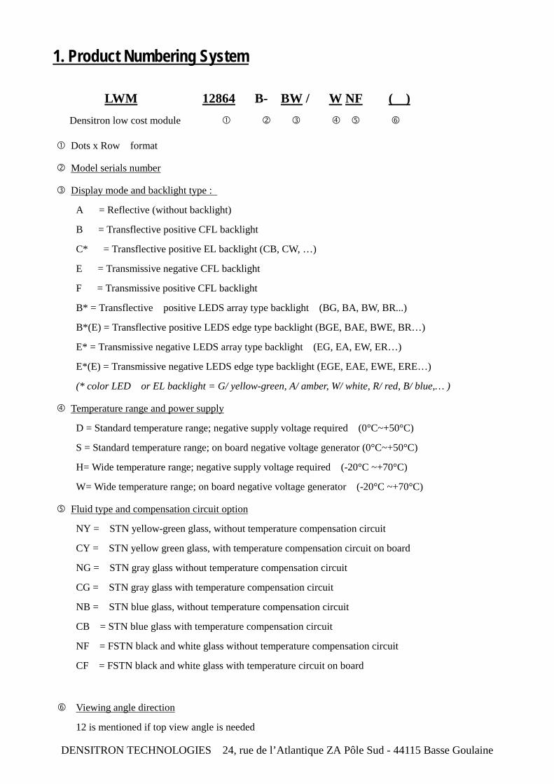
1. Product Numbering System
LWM 12864 B- BW / W NF ( ) Densitron low cost module
Dots x Row format
Model serials number
Display mode and backlight type :
A = Reflective (without backlight)
B = Transflective positive CFL backlight
C* = Transflective positive EL backlight (CB, CW, …)
E = Transmissive negative CFL backlight
F = Transmissive positive CFL backlight
B* = Transflective positive LEDS array type backlight (BG, BA, BW, BR...)
B*(E) = Transflective positive LEDS edge type backlight (BGE, BAE, BWE, BR…)
E* = Transmissive negative LEDS array type backlight (EG, EA, EW, ER…)
E*(E) = Transmissive negative LEDS edge type backlight (EGE, EAE, EWE, ERE…)
(* color LED or EL backlight = G/ yellow-green, A/ amber, W/ white, R/ red, B/ blue,… )
Temperature range and power supply
D = Standard temperature range; negative supply voltage required (0°C~+50°C)
S = Standard temperature range; on board negative voltage generator (0°C~+50°C)
H= Wide temperature range; negative supply voltage required (-20°C ~+70°C)
W= Wide temperature range; on board negative voltage generator (-20°C ~+70°C)
Fluid type and compensation circuit option
NY = STN yellow-green glass, without temperature compensation circuit
CY = STN yellow green glass, with temperature compensation circuit on board
NG = STN gray glass without temperature compensation circuit
CG = STN gray glass with temperature compensation circuit
NB = STN blue glass, without temperature compensation circuit
CB = STN blue glass with temperature compensation circuit
NF = FSTN black and white glass without temperature compensation circuit
CF = FSTN black and white glass with temperature circuit on board
Viewing angle direction
12 is mentioned if top view angle is needed
DENSITRON TECHNOLOGIES 24, rue de l’Atlantique ZA Pôle Sud - 44115 Basse Goulaine
Remarks and definitions : 1°) Display mode and backlight type :
- Reflective polarizer, None backlight, usable only in good ambient light conditions.
- Transflective polarizer, used a background backlight and a mirror reflector, usable in all lighting conditions.
- Transmissive polarizer need that the backlight is switch on continuously, usable mostly in low ambient light conditions
- EL (electro-luminescent), uniform brightness, short life time (8000 hours max), need EL inverter, low current consumption, low thickness.
- LED (light emitted diode), uniform brightness, long lifetime (100 000 hours), no need inverter, reliable in vibration and shock environment, different colors available.
Array version is a direct lighting type, available in standard, uniform and good brightness on all the active area.
Edge version is an edge lighting type providing a low consumption backlight, has a low thickness and brightness.
Positive mode has dark pixels on a light background
- Negative mode has light pixels in a dark background and is normally used only with a transmissive polarizer as it needs a backlight on to be visible.
2°) Fluid type :
- STN yellow green or gray LCD has a yellow green or gray background with dark blue pixels and offers a good contrast.
- FSTN LCD is to produce very high contrast with black and white pixels using a film polarizer
DENSITRON TECHNOLOGIES 24, rue de l’Atlantique ZA Pôle Sud - 44115 Basse Goulaine
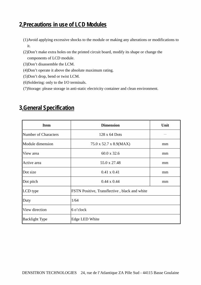
2.Precautions in use of LCD Modules
(1)Avoid applying excessive shocks to the module or making any alterations or modifications to it.
(2)Don’t make extra holes on the printed circuit board, modify its shape or change the components of LCD module.
(3)Don’t disassemble the LCM. (4)Don’t operate it above the absolute maximum rating. (5)Don’t drop, bend or twist LCM. (6)Soldering: only to the I/O terminals. (7)Storage: please storage in anti-static electricity container and clean environment.
3.General Specification
Item Dimension Unit
Number of Characters 128 x 64 Dots -
Module dimension 75.0 x 52.7 x 8.9(MAX) mm
View area 60.0 x 32.6 mm
Active area 55.0 x 27.48 mm
Dot size 0.41 x 0.41 mm
Dot pitch 0.44 x 0.44 mm
LCD type FSTN Positive, Transflective , black and white
Duty 1/64
View direction 6 o’clock
Backlight Type Edge LED White
DENSITRON TECHNOLOGIES 24, rue de l’Atlantique ZA Pôle Sud - 44115 Basse Goulaine
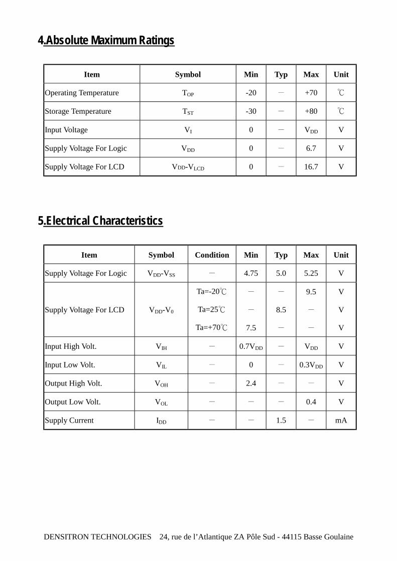
4.Absolute Maximum Ratings
Item Symbol Min Typ Max Unit
Operating Temperature TOP -20 - +70 ℃
Storage Temperature TST -30 - +80 ℃
Input Voltage VI 0 - VDD V
Supply Voltage For Logic VDD 0 - 6.7 V
Supply Voltage For LCD VDD-VLCD 0 - 16.7 V
5.Electrical Characteristics
Item Symbol Condition Min Typ Max Unit
Supply Voltage For Logic VDD-VSS - 4.75 5.0 5.25 V
Supply Voltage For LCD VDD-V0
Ta=-20℃
Ta=25℃
Ta=+70℃
-
-
7.5
-
8.5
-
9.5
-
-
V
V
V
Input High Volt. VIH - 0.7VDD - VDD V
Input Low Volt. VIL - 0 - 0.3VDD V
Output High Volt. VOH - 2.4 - - V
Output Low Volt. VOL - - - 0.4 V
Supply Current IDD - - 1.5 - mA
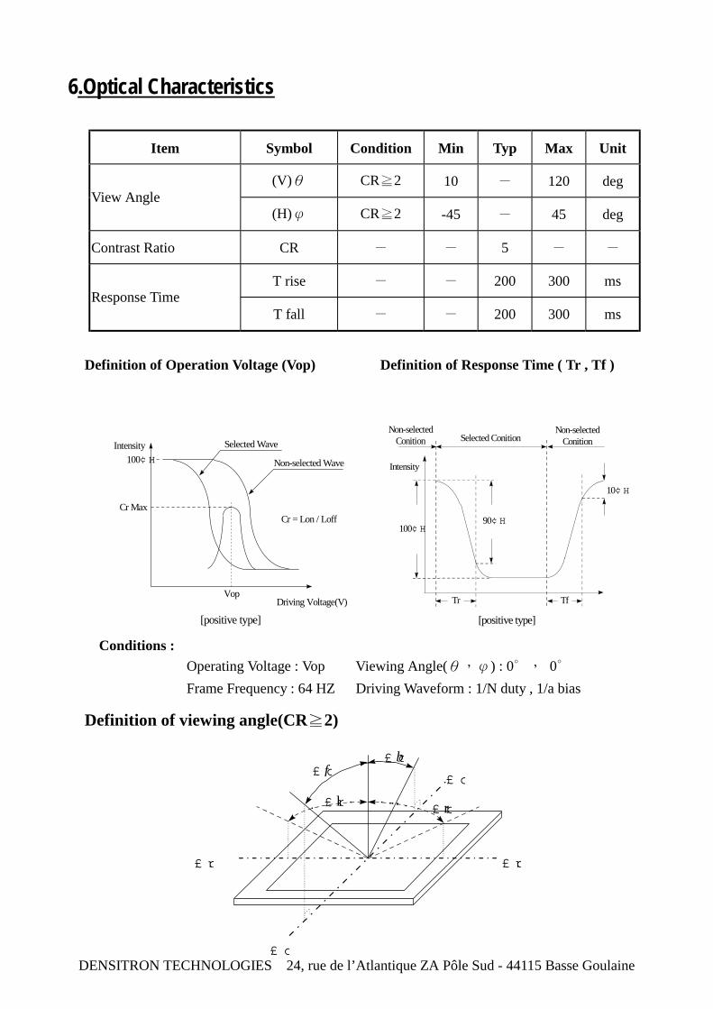
6.Optical Characteristics
Item Symbol Condition Min Typ Max Unit
(V)θ CR≧2 10 - 120 deg View Angle
(H)φ CR≧2 -45 - 45 deg
Contrast Ratio CR - - 5 - -
T rise - - 200 300 ms Response Time
T fall - - 200 300 ms
Definition of Operation Voltage (Vop) Definition of Response Time ( Tr , Tf )
Driving Voltage(V)
Intensity
Cr Max
100¢ H
Vop
Selected Wave
Non-selected Wave
[positive type]
Cr = Lon / Loff
Intensity
90¢ H100¢ H
Tr
10¢ H
Tf
Non-selectedConition
Non-selectedConitionSelected Conition
[positive type] Conditions : Operating Voltage : Vop Viewing Angle(θ,φ) : 0∘, 0∘ Frame Frequency : 64 HZ Driving Waveform : 1/N duty , 1/a bias
Definition of viewing angle(CR≧2)
DENSITRON TECHNOLOGIES 24, rue de l’Atlantique ZA Pôle Sud - 44115 Basse Goulaine
£ c f
£ c
£ p
£ c
£ p
£ c b
£ p r £ p l
DENSITRON TECHNOLOGIES 24, rue de l’Atlantique ZA Pôle Sud - 44115 Basse Goulaine
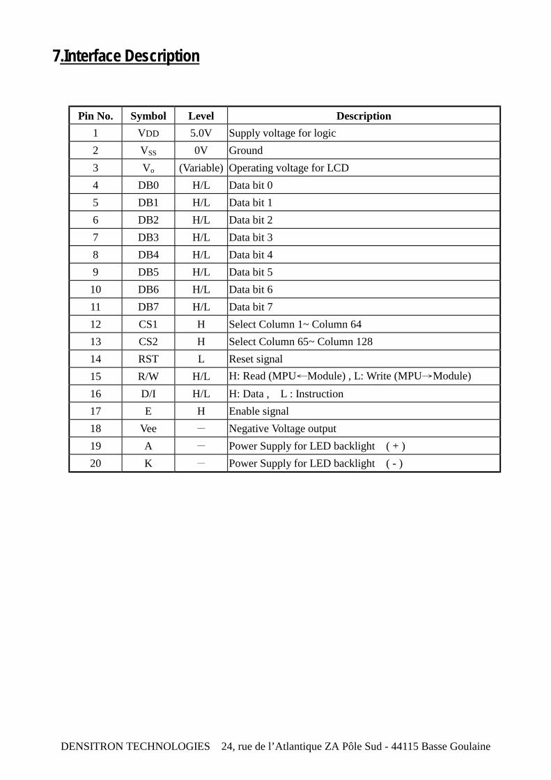
7.Interface Description
Pin No. Symbol Level Description 1 VDD 5.0V Supply voltage for logic 2 VSS 0V Ground 3 Vo (Variable) Operating voltage for LCD 4 DB0 H/L Data bit 0 5 DB1 H/L Data bit 1 6 DB2 H/L Data bit 2 7 DB3 H/L Data bit 3 8 DB4 H/L Data bit 4 9 DB5 H/L Data bit 5 10 DB6 H/L Data bit 6 11 DB7 H/L Data bit 7 12 CS1 H Select Column 1~ Column 64 13 CS2 H Select Column 65~ Column 128 14 RST L Reset signal 15 R/W H/L H: Read (MPU←Module) , L: Write (MPU→Module) 16 D/I H/L H: Data , L : Instruction 17 E H Enable signal 18 Vee - Negative Voltage output 19 A - Power Supply for LED backlight ( + ) 20 K - Power Supply for LED backlight ( - )
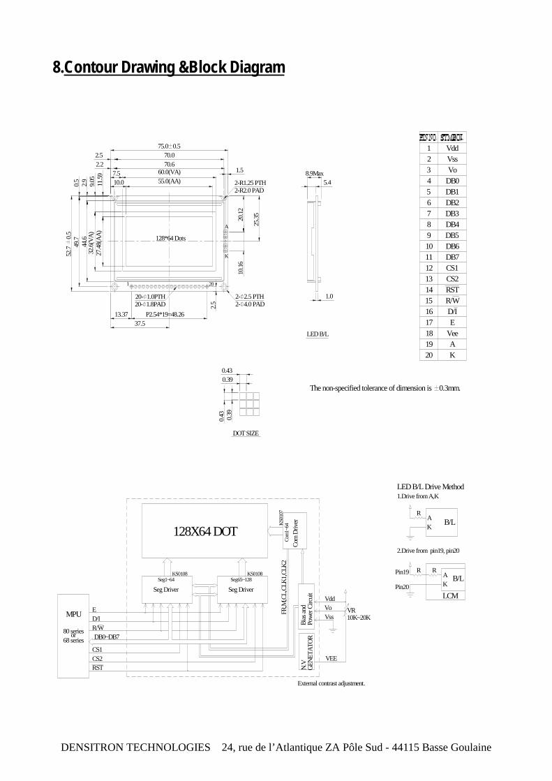
8.Contour Drawing &Block Diagram
MPU
80 series
ED/IR/WDB0~DB7or
68 series
128X64 DOT
Seg Driver Seg DriverSeg1~64 Seg65~128
FR,M
,CL,
CLK1
,CLK
2
Bias
and
Powe
r Circ
uit
External contrast adjustment.
KS0108 KS0108
Com
Driv
erCo
m1~
64KS01
07
CS1CS2
10K~20KVRVo
Vss
Vdd
RST
2.Drive from pin19, pin20
R
R
1.Drive from A,K LED B/L Drive Method
A
B/LA
LCMK
B/L
R
K
Pin19
Pin20
DB712
1413 CS2
CS1
Vdd1
DB27
1110
89
DB6DB5DB4DB3
4
65
32
DB1DB0VoVss
DOT SIZE
LED B/L
RSTR/W15
0.390.43
0.39
0.43
EVee
D/I161718
1 20
2.944
.60.5
49.7
52.7
0.5
10.0 55.0(AA)7.5 60.0(VA)
70.61.5
2.5 70.075.0 0.5
13.37 P2.54*19=48.26
20- 1.0PTH20- 1.8PAD
37.5
2.5
20.12
10.16
2- 2.5 PTH2- 4.0 PAD
2-R1.25 PTH2-R2.0 PAD
5.4
1.0
2.28.9Max
KA19
20
128*64 Dots
25.35
32.6(
VA)
27.48
(AA)
9.05
11.59
K
A
The non-specified tolerance of dimension is 0.3mm.
N.V
GENE
TATO
R
VEE
DENSITRON TECHNOLOGIES 24, rue de l’Atlantique ZA Pôle Sud - 44115 Basse Goulaine
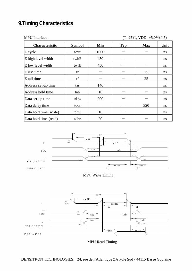
9.Timing Characteristics
MPU Interface (T=25℃, VDD=+5.0V±0.5)
Characteristic Symbol Min Typ Max Unit
E cycle tcyc 1000 - - ns
E high level width twhE 450 - - ns
E low level width twlE 450 - - ns
E rise time tr - - 25 ns
E tall time tf - - 25 ns
Address set-up time tas 140 - - ns
Address hold time tah 10 - - ns
Data set-up time tdsw 200 - - ns
Data delay time tddr - - 320 ns
Data hold time (write) tdhw 10 - - ns
Data hold time (read) tdhr 20 - - ns
E
R / W
C S 1 ,C S 2 ,D /I
D B 0 t o D B 7
2 .0 V
0 .8 V t w h Et r t f
t a h
t a s t a h2 .0 V0 .8 V
t d s w t d h w
t c y c
t w I E
t a s
MPU Write Timing
E
R /W
C S 1 ,C S 2 ,D /I
D B 0 to D B 7
2 .0 V
0 .8 V
2 .0 V
0 .8 V
td d r td h r
tw h Etr tf
tahta s
ta s tah2 .0 V0 .8 V
tcy c
tw IE
MPU Read Timing
DENSITRON TECHNOLOGIES 24, rue de l’Atlantique ZA Pôle Sud - 44115 Basse Goulaine
DENSITRON TECHNOLOGIES 24, rue de l’Atlantique ZA Pôle Sud - 44115 Basse Goulaine
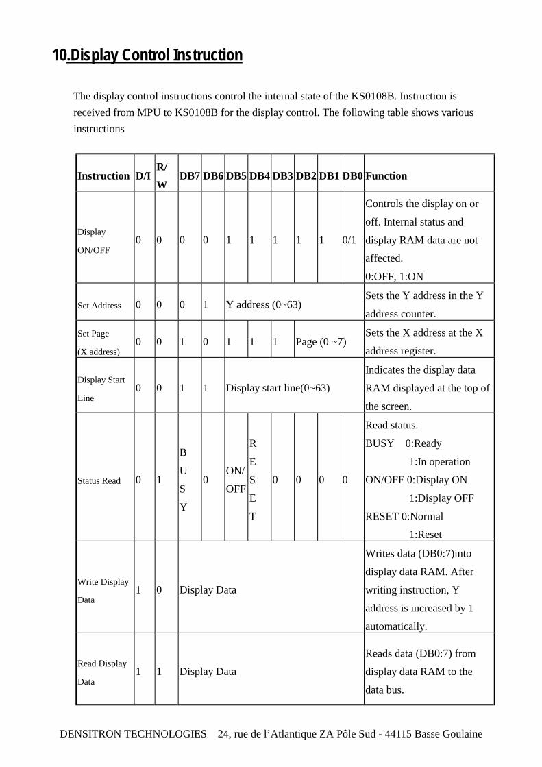
10.Display Control Instruction
The display control instructions control the internal state of the KS0108B. Instruction is received from MPU to KS0108B for the display control. The following table shows various instructions
Instruction D/I R/
W DB7 DB6 DB5 DB4 DB3 DB2 DB1 DB0 Function
Display
ON/OFF 0 0 0 0 1 1 1 1 1 0/1
Controls the display on or
off. Internal status and
display RAM data are not
affected.
0:OFF, 1:ON
Set Address 0 0 0 1 Y address (0~63) Sets the Y address in the Y
address counter.
Set Page
(X address) 0 0 1 0 1 1 1 Page (0 ~7)
Sets the X address at the X
address register.
Display Start
Line 0 0 1 1 Display start line(0~63)
Indicates the display data
RAM displayed at the top of
the screen.
Status Read 0 1
B
U
S
Y
0 ON/
OFF
R
E
S
E
T
0 0 0 0
Read status.
BUSY 0:Ready
1:In operation
ON/OFF 0:Display ON
1:Display OFF
RESET 0:Normal
1:Reset
Write Display
Data 1 0 Display Data
Writes data (DB0:7)into
display data RAM. After
writing instruction, Y
address is increased by 1
automatically.
Read Display
Data 1 1 Display Data
Reads data (DB0:7) from
display data RAM to the
data bus.
11.Detailed Explanation
Display On/Off
R/W D/I DB7 DB6 DB5 DB4 DB3 DB2 DB1 DB0
0 0 0 0 1 1 1 1 1 D
The display data appears when D is and disappears when D is 0. Though the data is not on the screen with D = 0, it remains in the display data RAM. Therefore, you can make it appear by changing D = 0 into D = 1.
Display Start Line
R/W D/I DB7 DB6 DB5 DB4 DB3 DB2 DB1 DB0
0 0 1 1 A A A A A A
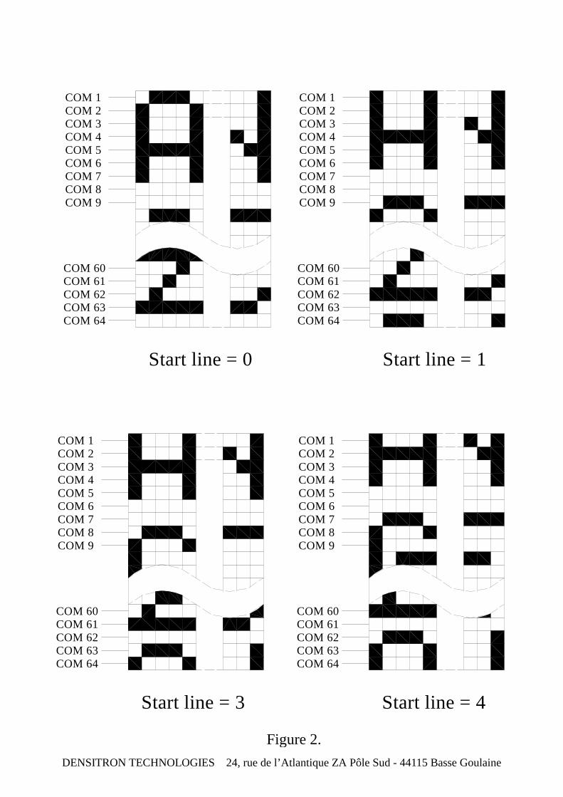
Z address AAAAAA ( binary ) of the display data RAM is set in the display start line register and displayed at the top of the screen. Figure 2. shows examples of display ( 1/64 duty cycle ) when the start line = 0-3. When the display duty cycle is 1/64 or more ( ex. 1/32, 1/24 etc. ), the data of total line number of LCD screen, from the line specified by display start line instruction, is displayed
Set Page ( X Address )
R/W D/I DB7 DB6 DB5 DB4 DB3 DB2 DB1 DB0
0 0 1 0 1 1 1 A A A
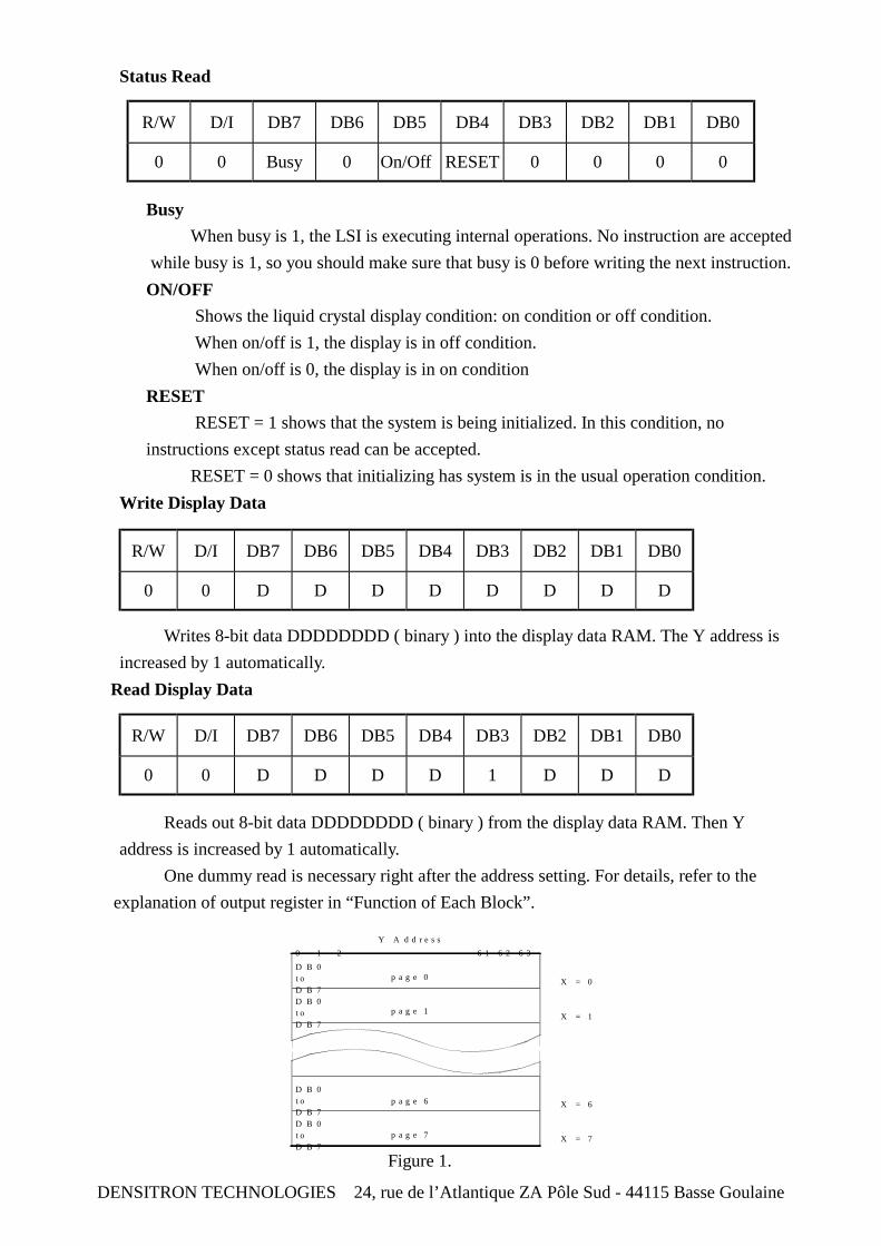
X address AAA ( binary ) of the display data RAM is set in the X address register. After that, writing or reading to or from MPU is executed in this specified page until the next page is set. See Figure 1.
Set Y Address
R/W D/I DB7 DB6 DB5 DB4 DB3 DB2 DB1 DB0
0 0 0 1 A A A A A A
Y address AAAAAA ( binary ) of the display data RAM is set in the Y address counter. After that, Y address counter is increased by 1 every time the data is written or read to or from MPU.
DENSITRON TECHNOLOGIES 24, rue de l’Atlantique ZA Pôle Sud - 44115 Basse Goulaine
Status Read
R/W D/I DB7 DB6 DB5 DB4 DB3 DB2 DB1 DB0
0 0 Busy 0 On/Off RESET 0 0 0 0
Busy When busy is 1, the LSI is executing internal operations. No instruction are accepted
while busy is 1, so you should make sure that busy is 0 before writing the next instruction. ON/OFF
Shows the liquid crystal display condition: on condition or off condition. When on/off is 1, the display is in off condition. When on/off is 0, the display is in on condition
RESET RESET = 1 shows that the system is being initialized. In this condition, no
instructions except status read can be accepted. RESET = 0 shows that initializing has system is in the usual operation condition.
Write Display Data
R/W D/I DB7 DB6 DB5 DB4 DB3 DB2 DB1 DB0
0 0 D D D D D D D D
Writes 8-bit data DDDDDDDD ( binary ) into the display data RAM. The Y address is increased by 1 automatically.
Read Display Data
R/W D/I DB7 DB6 DB5 DB4 DB3 DB2 DB1 DB0
0 0 D D D D 1 D D D
Reads out 8-bit data DDDDDDDD ( binary ) from the display data RAM. Then Y address is increased by 1 automatically.
One dummy read is necessary right after the address setting. For details, refer to the
DENSITRON TECHNOLOGIES 24, rue de l’Atlantique ZA Pôle Sud - 44115 Basse Goulaine
explanation of output register in “Function of Each Block”.
0 1 2 6 1 6 2 6 3D B 0t oD B 7
t oD B 7
D B 0
D B 7
D B 0t o
t oD B 7
D B 0
X = 0
X = 1
X = 6
X = 7
Y A d d r e s s
p a g e 0
p a g e 1
p a g e 6
p a g e 7
Figure 1.
DENSITRON TECHNOLOGIES 24, rue de
Start line = 0
COM 6
COM 64
COM 61COM 62COM 63
COM 60
COM 9COM 8COM 7
COM 2
COM 5COM 4COM 3
COM 1
COM 6
Start line = 1
COM 64
COM 61COM 62COM 63
COM 60
COM 9COM 8COM 7
COM 2
COM 5COM 4COM 3
COM 1
COM 6
Start line = 3
COM 64
COM 61COM 62COM 63
COM 60
COM 9COM 8COM 7
COM 2
COM 5COM 4COM 3
COM 1 COM 1
COM 3COM 4COM 5
COM 2
COM 7COM 8COM 9
COM 60
COM 63COM 62COM 61
COM 64
COM 6
Start line = 4
F
l’Atlantique ZA Pôle Sud - 44115 Basse Goulaineigure 2.
DENSITRON TECHNOLOGIES 24, rue de l’Atlantique ZA Pôle Sud - 44115 Basse Goulaine
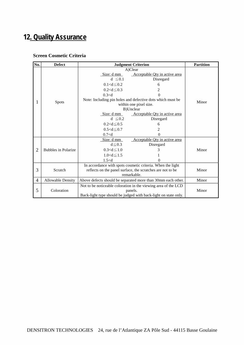
12. Quality Assurance
Screen Cosmetic Criteria
Judgment Criterion Partition
No. Defect
1 Spots
Size: dA)Clear
mm eptable Acc Qty in active area
Note: Includ h must be
Size: d m
d ≦0.1 Disregard 0.1<d≦0.2 6 0.2<d≦0.3 2 0.3<d 0 ing pin holes and defective dots whic
within one pixel size. B)Unclear
m Acceptable Qty in active area
Minor
d ≦0.2 Disregard 00.2<d≦ .5 6
0.5<d≦0.7 2 0.7<d 0
2 Bubbles in Polarize
Size: d mm Acceptable Qty in active area
Minor d≦0.3 Disregard
0.3<d≦1.0 3 1.0<d≦1.5 1 1.5<d 0
3 Scratch In accordan the light
Minor ce with spots cosmetic criteria. When
reflects on the panel surface, the scratches are not to be remarkable.
4 Allow sity Abo er. able Den ve defects should be separated more than 30mm each oth Minor
5 Coloration Not to be noticeable coloration in the viewing area of the LCD
panels. Back-light type should be judged with back-light on state only.
Minor
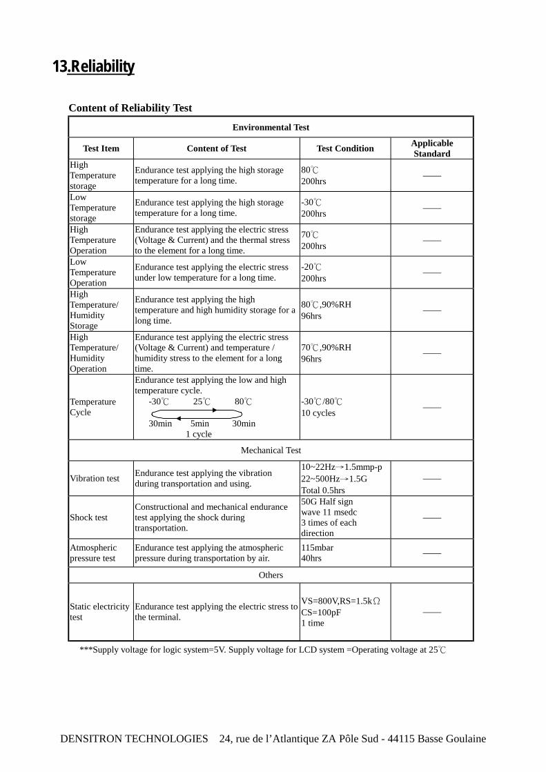
13.Reliability Content of Reliability Test
Environmental Test
Test Item Content of Test Test Condition Applicable Standard
High Temperature storage
Endurance test applying the high storage temperature for a long time.
80℃ 200hrs ——
Low Temperature storage
Endurance test applying the high storage temperature for a long time.
-30℃ 200hrs ——
High Temperature Operation
Endurance test applying the electric stress (Voltage & Current) and the thermal stress to the element for a long time.
70℃ 200hrs ——
Low Temperature Operation
Endurance test applying the electric stress under low temperature for a long time.
-20℃ 200hrs
——
High Temperature/ Humidity Storage
Endurance test applying the high temperature and high humidity storage for a long time.
80℃,90%RH 96hrs ——
High Temperature/ Humidity Operation
Endurance test applying the electric stress (Voltage & Current) and temperature / humidity stress to the element for a long time.
70℃,90%RH 96hrs ——
Temperature Cycle
Endurance test applying the low and high temperature cycle. -30℃ 25℃ 80℃ 30min 5min 30min 1 cycle
-30℃/80℃ 10 cycles ——
Mechanical Test
Vibration test Endurance test applying the vibration during transportation and using.
10~22Hz→1.5mmp-p 22~500Hz→1.5G Total 0.5hrs
——
Shock test Constructional and mechanical endurance test applying the shock during transportation.
50G Half sign wave 11 msedc 3 times of each direction
——
Atmospheric pressure test
Endurance test applying the atmospheric pressure during transportation by air.
115mbar 40hrs ——
Others
Static electricity test
Endurance test applying the electric stress to the terminal.
VS=800V,RS=1.5kΩ CS=100pF 1 time
——
***Supply voltage for logic system=5V. Supply voltage for LCD system =Operating voltage at 25℃
DENSITRON TECHNOLOGIES 24, rue de l’Atlantique ZA Pôle Sud - 44115 Basse Goulaine
DENSITRON TECHNOLOGIES 24, rue de l’Atlantique ZA Pôle Sud - 44115 Basse Goulaine
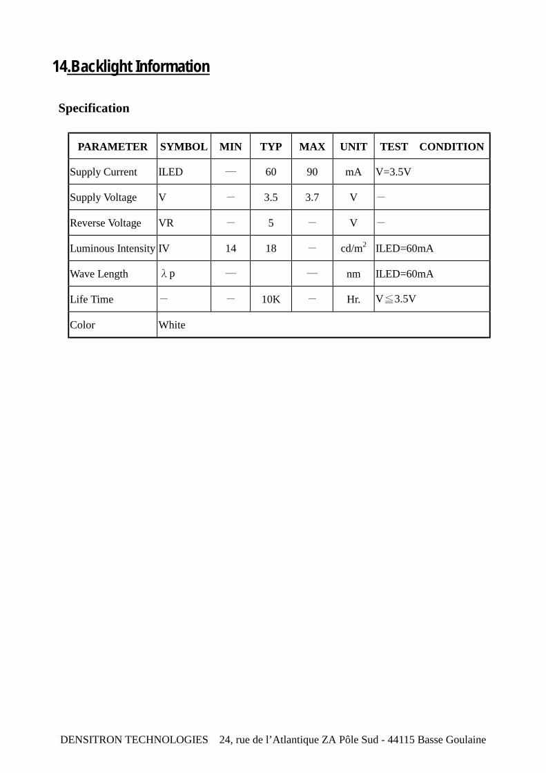
14.Backlight Information
Specification
PARAMETER SYMBOL MIN TYP MAX UNIT TEST CONDITION
Supply Current ILED ─ 60 90 mA V=3.5V
Supply Voltage V - 3.5 3.7 V -
Reverse Voltage VR - 5 - V -
Luminous Intensity IV 14 18 - cd/m2 ILED=60mA
Wave Length λp ─ ─ nm ILED=60mA
Life Time - - 10K - Hr. V≦3.5V
Color White


