Embed Size (px)
Citation preview

RSC Advances
PAPER
aDepartment of Materials Science and Eng
Display Institute, National Chiao Tung Un
E-mail: [email protected] of Electronics Engineering, N
30010, ROC, TaiwancDepartment of Electronics Engineering, Na
Taichung 41170, ROC, Taiwan
† Electronic supplementary informa10.1039/c4ra01517g
Cite this: RSC Adv., 2014, 4, 18493
Received 21st February 2014Accepted 2nd April 2014
DOI: 10.1039/c4ra01517g
www.rsc.org/advances
This journal is © The Royal Society of C
Polystyrene-block-poly(methylmethacrylate)composite material film as a gate dielectric forplastic thin-film transistor applications†
Jagan Singh Meena,ab Min-Ching Chu,a Ranjodh Singh,a Chung-Shu Wu,a
Umesh Chand,b Hsin-Chiang You,c Po-Tsun Liu,a Han-Ping D. Shieha
and Fu-Hsiang Ko*a
We report a simple approach to fabricate an organic–inorganic hybrid gate insulator based n-type thin-film
transistor (TFT) on a plastic polyimide (PI) sheet at room temperature using an appropriate composition of
commercially available polymers and block copolymer surfactant. The composite material film namely;
polystyrene-block-poly(methylmethacrylate) (PS-b-PMMA) is readily deposited as a gate dielectric with
zinc oxide (ZnO) as a semiconductor layer. This new dielectric material film exhibits high surface energy,
high air stability, very low leakage current density and better dielectric constant as compared to the
conventional polymer dielectrics. This plastic ZnO–TFT combines the advantages of a high-mobility
transparent inorganic semiconductor with an ultrathin high-capacitance and low-leakage PS-b-PMMA
composite gate dielectric. Fourier transform infrared (FT-IR) spectrum analysis is used for the PS-b-
PMMA film to confirm the presence of functional components in this composite material film. The
contact angle measurements for three test liquids (e.g., distilled water, ethylene glycol and
diiodomethane) reveal that the composite dielectric materials film is nearly hydrophobic and the
calculated surface energy is 35.05 mJ m�2. The resulting TFT exhibits excellent operating characteristics
at VDS ¼ 10 V with a drain–source current on/off modulation ratio (Ion/Ioff) of 3.12 � 106 and a carrier
mobility of 2.48 cm2 V�1 s�1. Moreover in the bending mode and in a normal environment, the device
remained undistorted and shows better reliability and performance, while the thickness of PS-b-PMMA is
about 28 nm. The results have suggested a new and easy approach for achieving transparent and
functionally bendable optoelectronics devices.
1. Introduction
The transistor is the most important invention of the 20th
century and from the day of its invention it has spread into ourdaily lives as an invaluable element in innumerable electronicproducts. The future demand for next-generation mobilecomputing, communication and identication devices hasincreased markedly throughout the past decades and is expec-ted to continue to increase throughout coming of the century.For diverse multiple functionalities, the electronics of idealmobile devices must achieve light weight, low powerconsumption, low operating voltages (powered by household
ineering, Department of Photonics and
iversity, Hsinchu 30010, ROC, Taiwan.
ational Chiao Tung University, Hsinchu
tional Chin-Yi University of Technology,
tion (ESI) available. See DOI:
hemistry 2014
batteries) and compatibility with various substrates.1 In addi-tion the desired features of optical transparency, mechanicalruggedness, environmental stability, eco-friendly and inexpen-sive room temperature (RT) as well large area fabrication mustbematched to customers' needs.2 Silicon and other II/VI and III/V compound semiconductors based TFTs exhibit necessaryfeatures such as high carrier mobility and high breakdowneld.3 But these TFTs are limited by relating to high tempera-ture processing (>400 �C) and mechanical exibility.2 Whileamorphous silicon TFTs have been fabricated on exible plasticsubstrates at temperatures as low as <150 �C, reported carriermobilities are modest in the range of 0.03–1.00 cm2 V�1 s�1 oninorganic insulators and the material is optically opaque.4 Thetransistors have scaled down in size colloquially referred to asextending Moore's law5 Now the insulating dielectrics havethinned to the point where charge build-up and crosstalkadversely affect the performance of the device. It is this reduc-tion in scale which drives the need for insulating materials needto be replaced by the lower dielectric constant materials.6
Whereas a low-kmaterial is one with a small value for dielectricconstant relative to silicon dioxide (SiO2) a former choice of the
RSC Adv., 2014, 4, 18493–18502 | 18493

RSC Advances Paper
dielectric. Replacing the silicon dioxide with a low-k dielectric ofthe same thickness reduces parasitic capacitance, enablingfaster switching speeds and lower heat dissipation. Apart fromthe above, low-k materials have been considered to decreaselower cross-talk noise, power dissipation, and, when incorpo-rated in device systems, can dramatically decrease resistance–capacitance (R–C) delays.7 For now most of the low-k materialsare organic and polymer materials which provide low dielectricloss, positive effect to the hot carrier degradation effect and lowshi of the threshold-voltage caused by mobile charges, lowleakage current, low power consumption. Recently, variouspolymers like polyvinyl chloride (PVC), polymethyl methacrylate(PMMA), polystyrene (PS), polyethylene (PE), polytetrauoro-ethylene (PTFE) or Teon, polyvinylidene uoride (PVDF),polypropylene (PP), uorinated polyimide (PI) and many othershave been considered as a gate insulator materials to be usedinto electronic devices.8 These polymer materials are compat-ible with substrate exibility and substantially thinner andlighter in weight. Although these polymer dielectrics have theirvarious advantages but still shows some poor sides. Most of thenative polymer materials are organic material so the thermalstability is a big problem and not able to match the performancewith former dielectrics. In particular, to achieve uniformpinhole-defects free polymer thin lm by solution processes isnot easy. The solution processed polymer thin lms suffer bypinhole-defects when the thickness is less than 100 nm.8d,9
Although several groups have achieved pinhole-defects freelms using cross-linked polymers or polymer blends.
The need for low power dissipation storage systems withhigh energy density could lead to the advancement of polymercomposite systems that combine the processability and break-down eld strength of the polymer with the high dielectricconstant.10 The key points of increasing the composite's effec-tive dielectric constant and the role of the interface (organic–inorganic) with semiconductor layer is very important in orderto makes it very appealing to introduce them into transistordevices. Which generally possess dielectric constants more thantheir native polymers. Moreover, the signicant advance in theeld of organic and polymer dielectrics meet all the aforemen-tioned requirements have proved elusive and probably require anew direction in choice of materials and processing strategies.Expectantly, it will result in the development of the necessaryimplementation for tuning device properties on a nanoscopiclevel. Likewise, various concerns persist relating to choice ofdielectric material and corresponding fabrication technique,such concerns as can relate to choice and incorporation of anyone particular semiconductor material. Such complexities andcompeting issues illustrate an on-going concern in the art. Thesearch continues for a comprehensive approach to TFT fabri-cation, one available at low process temperatures and/orcompatible with exible plastic substrates. Several studies haverecently probed the inuence of ZnO as semiconductingtransparent and position on the properties of transparentoptoelectronic devices.11 It was noted that the ZnO have uniqueproperties like wide band-gap (3.4 eV, II–VI group) and stablewurtzite structure with lattice parameter (a ¼ 0.325 nm, c ¼0.521 nm).12 In addition to controlling factors such as solubility
18494 | RSC Adv., 2014, 4, 18493–18502
and therefore ease of processing, can strongly inuence theelectronic properties of the ZnO while dispersed on polymersurface to be used into electronic and optoelectronic devices.
To address such limitations, in present study, we introduce asimple and easy to follow solution-processed approach whichrealized the high-quality bendable ZnO–TFT using polymercomposite materials lm (PS-b-PMMA) as a gate dielectric fromstraightforward polymer/copolymer precursors. Additionally,we varied the nature of the substrate, the molecular weight ofthe PS and PMMA biopolymer and the morphological behaviorof these lms. This was investigated by AFM, FT-IR, surfaceenergy and insulator characteristics into MIM structureddevices. It was observed from the results that polymercomposite PS-b-PMMA lm of the P123 copolymer compart-ment enhances the thin-lm stability further to be used intoZnO–TFT application. Moreover, we showed here that thiscomposite dielectric layer is uniform, pinhole defects freesurface and electrically functioned over large area plastic PIsubstrate. This also compatible with both bottom and topcontact device geometries, could be used to fabricate exibleelectronic devices, and the deposition approach is applicable todiverse gate and semiconductor materials. The strategic aim ofthis work is to explore the potential of the fabrication ofcomposite materials from the block-copolymer thin lms onexible substrate to use in current electronics devices.
2. Results and discussion2.1 PS-b-PMMA lm surface roughness and FT-IR analysis
Common materials used in this work and their schematicrepresentation of molecular structure of PS, PMMA and copol-ymer P123 precursors mixed into toluene are shown in Scheme1. Sol–gel solution was employed for fabricating the polymer PS-b-PMMA composite thin lm on a exible PI substrate using thespin-coating process for device applications are also shown inScheme 1. Further, to evaluate the nature of the PS-b-PMMA lmsurface, the AFM data was observed to provide the importantinformation about the surface roughness and further charac-terizations to use into device application. For the AFM imagewith a scan size of 2 mm � 2 mm, as shown in Fig. 1(a), a samplewas prepared using a spin-coating process coated onto exibleAu/Cr/PI substrate and cured at 100 �C. The morphology of thelm shows the uniformity and crack free surface was observedon exible PI substrate. The average root-mean square (rms)roughness evaluated from the AFM image of the PS-b-PMMAwas approximately 0.84 nm. In the case, the possible reason forthe better surface roughness in the PS-b-PMMA lm, this couldbe due to the presence of P123 functions as a uniform structure-directing agent.7 In a ternary system, the P123 block copolymermakes easy the deposition of a uniform lm through organic–organic cooperative assembly. Moreover, the presence ofsurfactant plays an important role in the morphology of solu-tion grown polymer composite lm. For example, adding blockcopolymer as a surfactant during the growth of thin lm directlyaffects the aspects ratio of the resulting lm. The thickness ofthe lm was measured both to an ellipsometry techniques and2-D AFM image cross section line analyses. The average gate
This journal is © The Royal Society of Chemistry 2014

Scheme 1 Common materials used in this work with their molecularstructures, and the representation of the copolymer P123, PS andPMMA precursors mixed in toluene in fabrication steps for fabricatingthe polymer PS-b-PMMA composite film on a flexible PI substrateusing the spin-coating process for characterizations and deviceapplications.
Paper RSC Advances
dielectric PS-b-PMMA lm thickness was 14 nm, which analyzedby an ellipsometry techniques. We further conrm the thick-ness by 2-D AFM image cross section line analyses as shown ininset of Fig. 1(a), which is close to 14 nm. The 2-D as well as 3-DAFM images on PI substrate are shown and the correspondingline analyses is also shown to conrm the lm thickness. Weput a very thin sellotape to cover the substrate and aer depo-sition of the lm, we removed the sellotape. Then the subse-quent scan the small part of the surface with a scanning-probeAFM and height prole through the cross-section line. Thethickness was extracted from the cross-section prole bycalculating the height difference of the higher and lower areas.We refer the method of thickness measurement with a AFMsection line analyses given by C. Uzum et al.13
The FT-IR spectroscopy was used to examine the functionalgroups of PS-b-PMMA composite thin lm surface. The spectrafor the PS-b-PMMA lm deposited with an organic additive thinlm shows a sharper spectral curve, which indicates that thelm have a less disordered structure as shown in Fig. 1(b). Thepeaks at 1726 and 1153 cm�1 in all the blends representsthe C]O and –OCH3 stretching of PMMA. The peaks at 1600and 698 cm�1 in all the blends represents the C–C stretchingand ring deformation of PS. The two peaks at 2929 and3030 cm�1 are due to the methylene group in PS. The bandsbetween 2877 and 2960 cm�1 are believed to be due to CH3,CH2, and CH stretching, which can be detected from the P123copolymer, whereas the sharp peak at 1170 cm�1 for the C–O–C
This journal is © The Royal Society of Chemistry 2014
bending mode likely resulted from the P123. It is difficult todetermine the origin of the 1720, 1735, and 1780 cm�1 peaks,which appeared from C–O group of the organic PI surface. Athorough analysis of IR spectra of these blends show thatdecrease in transmittance of carbonyl and methoxyl stretchingwith an increase of PS content and increase in transmittance ofthese peaks with an increase of PMMA content. These dataclearly indicates the formation polymer blends. The IR spec-trum of our PS-b-PMMA composite thin lm coating over PIsubstrate is more consistent for PS and P123 and PMMA sepa-rately over silicon for the functional group, which reportedpreviously.14 From the FT-IR spectrum, it can be concluded thattoluene as well other organic impurities were successfullyremoved when the sample was baked at 100 �C. These dataclearly indicates the formation of polymer PS-b-PMMA blendswhich can be further used in device application. Finally, weconcluded from the results that the sample consisted of PS,P123, PMMA and a trace amount of contaminating carbon; noother impurities.
2.2 Water contact angle test for the PS-b-PMMA lm
The total surface energy is another decisive scale parameter thataffects the pattern formation of polymeric lm on a plasticsubstrate. Surface free energy of the PS-b-PMMA lm surfacewas calculated using the contact angles for three test liquids e.g.distilled water, ethylene glycol and diiodomethane. Sincedistilled water (DW), ethylene glycol (EG), and diiodomethane(DM) have different level of polarity. The contact angles of theseliquids on the PS-b-PMMA layer were directly measured with thedrop prole at the point of contact with the surface to estimatethe surface free energy variation of these three different polarlevel liquids to the lm. Fig. 2(a–c) shows the contact angles forDW, EG and DMmeasured on PS-b-PMMA surface on exible PIsubstrate were 82.8�, 101.4�, and 79.2� respectively. Thismeasurement technique is based on the Young–Dupre equa-tion, as formulated by van Oss et al.15 which expresses thecondition for equilibrium at a solid–liquid interface. To calcu-late the surface energy we design a simplied model as shownin Fig. 2(d) to describe the interfacial tension between the liquid(L) and the polymeric lm surface (S).
The surface free energy was evaluated using van Oss andGood's three-liquid test method in together with the Lifshitz–van der Waals (LW) and Lewis acid-base (AB) theories,16 and thedetailed energy contributions from the polymeric apolar andpolar terms can be extracted individually. The total surfaceenergy gs can be calculated from the combination of these threefactors by using equation
gs ¼ gLWs + gAB
s ¼ gLWs + 2(g+
s )1/2(g�
s )1/2 (1)
where gLWs is the Lifshitz–van der Waals component (apolar),
gABs is the Lewis acid-base component (polar), g+
s is the Lewisacid and g�
s is the Lewis base component. Further, the values ofgLWs , g+
s and g�s were calculated from eqn (2)–(4) aer measuring
the liquid–solid contact angle (q) for these three characterizingliquids
RSC Adv., 2014, 4, 18493–18502 | 18495
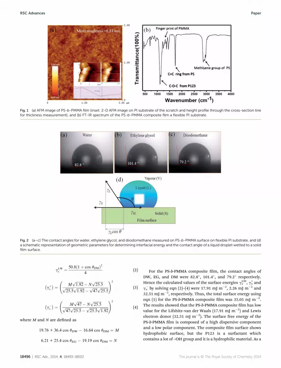
Fig. 1 (a) AFM image of PS-b-PMMA film (inset: 2-D AFM image on PI substrate of the scratch and height profile through the cross-section linefor thickness measurement), and (b) FT-IR spectrum of the PS-b-PMMA composite film a flexible PI substrate.
Fig. 2 (a–c) The contact angles for water, ethylene glycol, and diiodomethane measured on PS-b-PMMA surface on flexible PI substrate, and (d)a schematic representation of geometric parameters for determining interfacial energy and the contact angle of a liquid droplet wetted to a solidfilm surface.
RSC Advances Paper
gLWs ¼ 50:8ð1þ cos qDMÞ2
4(2)
�gþs
� ¼
Mffiffiffiffiffiffiffiffiffi1:92
p �Nffiffiffiffiffiffiffiffiffi25:5
pffiffiffiffiffiffiffiffiffi25:5
p ffiffiffiffiffiffiffiffiffi1:92
p � ffiffiffiffiffi47
p ffiffiffiffiffiffiffiffiffi25:5
p!2
(3)
�g�s
� ¼
Mffiffiffiffiffi47
p �Nffiffiffiffiffiffiffiffiffi25:5
pffiffiffiffiffi47
p ffiffiffiffiffiffiffiffiffi25:5
p � ffiffiffiffiffiffiffiffiffi25:5
p ffiffiffiffiffiffiffiffiffi1:92
p!2
(4)
where M and N are dened as
19.76 + 36.4 cos qDW � 16.64 cos qDM ¼ M
6.21 + 25.4 cos qEG � 19.19 cos qDM ¼ N
18496 | RSC Adv., 2014, 4, 18493–18502
For the PS-b-PMMA composite lm, the contact angles ofDW, EG, and DM were 82.8�, 101.4�, and 79.2� respectively.Hence the calculated values of the surface energies gLW
s , g+s and
g�s by solving eqn (2)–(4) were 17.91 mJ m�2, 2.26 mJ m�2 and
32.51 mJ m�2, respectively. Thus, the total surface energy usingeqn (1) for the PS-b-PMMA composite lm was 35.05 mJ m�2.The results showed that the PS-b-PMMA composite lm has lowvalue for the Lifshitz–van der Waals (17.91 mJ m�2) and Lewiselectron donor (32.51 mJ m�2). The surface free energy of thePS-b-PMMA lm is composed of a high dispersive componentand a low polar component. The composite lm surface showshydrophobic surface, but the P123 is a surfactant whichcontains a lot of –OH group and it is a hydrophilic material. As a
This journal is © The Royal Society of Chemistry 2014

Paper RSC Advances
result, removing the P123 causing the lm has lower surfaceenergy. In addition, in ZnO–TFT, the surface of the dielectriclayer is important for effective performance because it allows fora conducting channel in the interface between the dielectriclayer and the semiconductors.
2.3 Leakage current and capacitance tests of the PS-b-PMMAlm into MIM capacitor device
Leakage current is a very important parameter to evaluate thedielectric behavior of the PS-b-PMMA lm. For low-voltageoperated electronic devices, leakage current should be low forimproving switching speed of transistors and reduced theenergy consumption. We measured leakage current by fabricatea MIM structured device by applying voltage to the PS-b-PMMA/Au/Cr contact to the bottom PI substrate and the Al top elec-trode (inset: Fig. 3(a)). As shown in Fig. 3(a), the leakage currentdensity for the PS-b-PMMA was measured of 7.46 � 10�10 Acm�2. The result shows the dielectric performance of our sol–gel spin-coated polymeric PS-b-PMMA composite lm iscomparable to other various polymer as well as high-k dielec-trics.17 This result is an average and based on the measurementof 20 devices on PI substrate for PS-b-PMMA gate dielectric.
Further, we investigate the capacitance for our compositethin lm to calculate the dielectric constant (k) value. Fig. 3(b)
Fig. 3 (a) J–V plot (inset: MIM device configuration and a sampleimage), and (b) C–V plot for PS-b-PMMA film at frequency 100 kHz(inset: C–V plot for PS-b-PMMA film at frequency 1 kHz).
This journal is © The Royal Society of Chemistry 2014
shows the capacitance–voltage (C–V) measurement of the PS-b-PMMA lm in MIM capacitor device. The good capacitance(5.40 fF) was achieved at high frequency (100 kHz). We calcu-lated the k-value of the PS-b-PMMA lm using the followingequation18
C
A¼ k3o
t; or k ¼ Ct
A3o(5)
where k is the dielectric constant of the dielectric layer, 3o� 8.85� 10�12 F m�1 and is the permittivity of vacuum, A is the area ofthe capacitor (2.0 mm2), and t is the thickness of the PS-b-PMMAlm (14 nm). The calculated k-value of the PS-b-PMMA lm was4.2 at high frequency (100 kHz). We have pointed out from thisresult that the dielectric constant of PS-b-PMAA at 100 kHz washigh than its original k-value between 2–2.7. We have thenmeasured the capacitance (3.2 fF) at low frequency (1 kHz) asshown in inset of Fig. 3(b), and the calculated dielectricconstant is 2.5. This value is lies between its original dielectricconstant. We have some discussion over this variation indielectric constants. Since, the dielectric constant of any givenmaterial varies with temperature, and for polymers a rapidincrease begins near their glass transition temperature.Dielectric constants also vary as a function of frequency, andthis aspect will be important when we look at high frequencydesigns. Ideally, the dielectric constant should be constant withregard to frequency, temperature, voltage, and time. However,each polarization mechanism has a characteristic relaxationfrequency. Therefore, k values of most of the materials show adependence on the frequency because slower mechanisms failto respond and contribute to the dielectric storage when thefrequency becomes large.19 Moreover, polystyrene is non-polarand PMMA is polar, thus at high frequency due to polarizationmechanism effect of PMMA work and this increase the dielec-tric constant of our lm. It is also explained by D. Wei that thematerials heterogeneity of a microphase-separated copolymerhas an associated spatial variation in the dielectric constant.20
We can drawn some conclusion here from these results that theleakage current density and the dielectric strength of the PS-b-PMMA thin lm are much better than those of the commonlyused solution-processable polymer gate insulators. Theobtained results indicate that the PS-b-PMMA polymericcomposite lm as dielectric is a potential candidate to replaceSiO2 or other polymeric intermetal dielectric materials and thatit could be an ideal alternative for exible devices.
2.4 Reliability and air-stability test for the PS-b-PMMAcomposite dielectric lm
In order to realize the reliability and the stability of the PS-b-PMMA composite dielectric lm, we measured electrical prop-erties for the waiting period of time in air. The integrated MIMdevice on a PI cleaned Petridish at room temperature exposure toatmosphere and using four-point probe system, the leakagecurrent densities were measured from day 1 to weeks 4 to checkthe device functionally working or damaged for this long dura-tion of time. The results are shown in Fig. 4(a–d) for leakagecurrent density measurements from day 1 to weeks 4 for the PS-b-
RSC Adv., 2014, 4, 18493–18502 | 18497

Fig. 4 (a–d) Leakage current density measurements test for 1 day to 4weeks for the PS-b-PMMA film as gate dielectric layer.
RSC Advances Paper
PMMA lm as gate dielectric layer. In the beginning of thestability test, the leakage current density of the newly made MIMcapacitor was of 8.05 � 10�10 A cm�2. The leakage currentdensity gradually increases to higher value aer the waitingperiod for 1 week to 4 weeks. But aer 2 weeks, theMIM capacitordevice still shows a promising dielectric property, the leakagecurrent density was about 7.73 � 10�9 A cm�2. Further, aer 4weeks or more the device properties go down to very high leakagecurrent density i.e., 5.74 � 10�8 A cm�2. At this moment, thedevice properties hardly considered as an ideal device functioned
Fig. 5 (a) Photograph of the ZnO–TFT devices on a 5 cm � 5 cm areadevice that features PS-b-PMMA as a gate dielectric and ZnO as a semicooutput characteristic (IDS–VDS), where VGS ranges from 0 to 10.0 at 2 V
18498 | RSC Adv., 2014, 4, 18493–18502
well worth to be further use into transistor application. Weconclude that the composite dielectric material deposit on a PIsubstrate showed good time stability. This result emphasized theimportance of these tests in future to open up the way to furthermodication to be used for the long stability of time.
We have found the PS-b-PMMA composite lm has highleakage current aer 4 weeks. Because of the direct exposition ofthe device to air environment could be the cause of long-termstability of polymer based devices are affected by oxidativedecomposition in air. In addition, the lm at low thicknesscould suffers by deep-level defects due to long term explosion inair. If deep-level defects possibly touch each other and form acontact line but otherwise still can grow in all other directions,then the material of the contact line is drained. By this processtwo deep-level defects merge and form a single one and that isexpected reason of high leakage current aer 4 weeks. AlthoughPS-b-PMMA is an organic composite materials lm and oxida-tion in air might be expected, the device characteristics wereessentially unchanged aer 1 month; longer term stability hasnot been investigated. Further, we took double layer (thickness28 nm) J–V measurement for PS-b-PMMA lm and the deviceproperties were found very stable and leakage current not evenfurther changed while we put the sample in air-ambientcondition for more than 1month. The J–V results in air-ambientcondition from day 1 to weeks 4 are shown in ESI Fig. S1.†
2.5 Performance of TFT with PS-b-PMMA as gate dielectric asZnO as channel layer
To investigate the potential of the PS-b-PMMA lm as a gatedielectric and ZnO was used as a semiconductor channel layer
on flexible PI substrate, (b) schematic representation of the ZnO–TFTnductor layer, (c) transfer characteristic (IDS–VGS), when VDS ¼ 10 V, (d)step.
This journal is © The Royal Society of Chemistry 2014

Fig. 6 Extraction of the PS-b-PMMA gate dielectric ZnO–TFT fromtransfer characteristics (a) plot for hysteresis, (b) plot for deducing VT,and (c) plot for deducing subthreshold slope.
Paper RSC Advances
for TFT on a plastic PI substrate with the sample photographicimage is shown in Fig. 5(a) and the device geometry shown inFig. 5(b). Fig. 1(c) show representative transfer characteristics(IDS–VGS), at VDS ¼ 10 V, of our ZnO–TFT with the PS-b-PMMAlm as a gate dielectric, respectively. As gate voltage increased,the increased drain current showed a good t to the squarerelation in the saturation drain current equation;21
IDS ¼ msatCiW
2LðVGS � VthÞ2 (6)
where ID,sat is drain current in the saturation regime; W/L is thewidth to length ratio; msat is mobility in the saturation regime; Ci
is dielectric capacitance per unit area, VGS is gate voltage; andVth is threshold voltage, which is estimated of 2.6 V. The highestsaturation-region eld-effect mobility obtained was about2.48 cm2 V�1 s�1, which compared to maximum mobilities of1 cm2 V�1 s�1 for a-Si:H TFTs as well more or less with thesaturation-region eld-effect mobility of TFTs reported by othergroups.22 The Output characteristics of PS-b-PMMA as gatedielectric with ZnO as semiconductor were measured at 0–10 Vwith step of 2 V as shown in Fig. 5(d). Which showed the draincurrent saturated at a very low voltage, showing effective pinchoff behavior. Our results suggest that deposition of thecomposite ternary system interlayer could be a simple andefficient surface-treatment of polymeric gate insulators for high-performance ZnO–TFTs.
We have also characterized the hysteresis, threshold voltage(Vth), on/off current ratio (Ion/Ioff) and subthreshold slope (SS)for our PS-b-PMMA dielectric based ZnO–TFT. Fig. 6(a) showsthe hysteresis in the transfer characteristics. The hysteresis (e.g.,voltage shi (DV) between forward and reverse sweep) is relatedto charge (electron) trapping within the dielectric layer. Thedata showed almost negligible hysteresis (DV � 0.12 V) for PS-b-PMMA lm, suggesting a decrease in charge trapping for PS-b-PMMA–ZnO interface. The negligible hysteresis could be due tolow thickness of PS-b-PMMA gate dielectric lm. But there is anobvious trend of hysteresis as a function of the gate dielectric isobserved. It can be attributed to the PS-b-PMMA layer, whichfails to attain the charge injection from the gate electrode to thedielectric-semiconductor interface. When a negative sweep isapplied to the gate electrode, then electrons are easily injectedinto the gate dielectric. Occurring at the same time, holes in thesemiconductor layer are easily retained in the hole-traps. Thisveries the hysteresis reduction effect of the composite (orhybrid) gate dielectric for wide range of channel lengths.Further, we have deducted Vth, and SS by using Fig. 6(b and c)respectively.
The threshold voltage (Vth) is estimated by the extrapolationof the linear portion of the transfer characteristic graph to theVGS axis as shown in Fig. 6(b). The estimated value of Vth fromthis graph is 2.6 V. Further, to analyze the subthresholdbehavior of the device, the switch-on voltage (Vso) and inversesubthreshold slope (SS, V dec�1) are studied. The Vso is denedas the gate voltage where the current starts to increase in thesemi-logarithmic IDS–VGS plot. The SS-value is calculated about1.12 V dec�1 from the graph shown in Fig. 6(c) using therelation;23
This journal is © The Royal Society of Chemistry 2014
SS ¼�dðlog IDSÞ
dVGS
��1
(7)
The result obtained here, 1.12 V per decade, is larger thanthat typically observed for a-Si:H devices, but it is considerableenough to allow plastic ZnO–TFT use in many applications. Inaddition, we have also estimated the Ion/Ioff current ratio forZnO–TFT device by using Fig. 6(c). The estimated Ion/Ioff currentratio is 3.12 � 106 at VDS ¼ 10 V. These device parameters forour organic composite dielectric and ZnO semiconductor basedTFT device are comparable to results typically obtained for a-Si:H based TFT devices.
2.6 Environment-stability and bendability test for ZnO–TFT
For practical applications, bending test in tensile as wellcompressive mode and environment-stability test of our exible
RSC Adv., 2014, 4, 18493–18502 | 18499

RSC Advances Paper
TFT is a matter of concern due to oxygen and moisture trappingcharge in degradation of the device properties. The environ-ment-stability test of the ZnO based TFT on PS-b-PMMAdielectric, was monitored by measuring their mobility, and on/off current ratio as a function of time from day 1 to week 4 asshown in Fig. 7. The ZnO–TFT performance on PS-b-PMMAdielectric exhibited good ambient stability on a exible PIsubstrate. However, aer exposure in the air for more than 4week, the ZnO–TFT on the PS-b-PMMA dielectric exhibitedslight changes inmobility from 2.48 cm2 V�1 s�1 to 1.76 cm2 V�1
s�1, and on-off current ratio from 3.12 � 106 to 8.40 � 104. Thischange could be considered due to the changes in relativehumidity for organic dielectric materials in the ambientcondition, which has also been reported for other organicdielectric materials.24 All measurements reported here weremade in room air with no precautions taken to prevent degra-dation of the TFT device. Although our organic compositematerials lm is a fairly sensitive material and oxidation in airmight be expected, the device characteristics were essentiallychanged for low thickness of PS-b-PMAA aer 1 month and nolonger has term stability been investigated. Since, ambient airstability is very important for current organic materials basedelectronic devices, thus we tried passivation layer (double layer
Fig. 7 The performance changes in terms of mobility and on/offcurrent ratio of PS-b-PMMA film as gate dielectric and ZnO as semi-conductor and while the ZnO–TFT device was bended in tensile andcompressive mode (inset: bended graphic sample images) exposed inthe ambient condition for day 1 to week 4 under bending test. (Insets:their corresponding characteristics for double layer PS-b-PMMA filmunder similar bending mode and exposed in the ambient condition upto 4 weeks.)
18500 | RSC Adv., 2014, 4, 18493–18502
of PS-b-PMMA with thickness about 28 nm) to get long termstability in TFT device characteristics. Then, no appreciablechanges in the transfer characteristics were observed for ZnO–TFT measured in air and stored under ambient conditions forone month (ESI, Fig. S2†). We have added these double layersPS-b-PMMA based ZnO–TFT results of mobility and on/offcurrent ratio changes shown in inset of Fig. 7 to compare withsingle layer PS-b-PMMA based ZnO–TFT performance for day1 to 4 weeks. Finally, it can be concluded from these results thatthe interface between polymer composite materials lm as agate dielectric layer and inorganic materials lm as semi-conductor layer is good and stable combination for futurecheap plastic electronics.
3. Conclusion
We have demonstrated here the composition of appropriatecommercially available polymers and surfactant cross-linkingagents affords robust, smooth, adherent, high surface energy,pinhole free, ultrathin (e.g., 14 nm) lm showed low leakagecurrent and good capacitance as a composite dielectric mate-rials. The PS-b-PMMA lm was readily deposited from sol–gelsolution, which adheres strongly on a exible PI substrate andcompatible with ZnO semiconductor to be used into TFTapplication. The resulting ZnO–TFT and complementary MIMcapacitor devices function at unprecedentedly low operatingvoltages for a polymer-based gate dielectric for single layer(14 nm thick) showed short term stability and for double layer(28 nm thick) showed good and long term stability. In thiscondition device performed functionally well even aer waitingperiod of more than a month in air-ambient condition intogether bending the sample in compressive and tensile mode.These results clearly shows that implementing the polymerternary dielectric system using solution-processing methodol-ogies offers low voltage, low power operation to be used intoelectronic applications.
4. Experimental section4.1 Reagents and materials
Polyimide: DuPont™ Kapton® polyimide tape (abbreviated asPI) 38 mm in thickness a polymer of imidemonomers was used aexible substrate to characterize the surface and electricalproperties of the PS-b-PMMA composite thin-lm. The thermalstability of Kapton PI tape is excellent and allows processingtemperature in excess of nearly 400 �C. Ethanol (C2H5OH), 95%solution purchase from Sigma Aldrich and used as solvent andcleanser. Deionized (DI) and distilled water: the water used waspuried with lters, reverse osmosis, and de ionized systemuntil the resistance was more than 18 MU cm�1. DI water wasused to clean, wash, and be a solvent. Pluronic® P123 BlockCopolymer Surfactant: Pluronic P123 triblock copolymer,HO(CH2CH2O)20(CH2CH(CH3)O)70(CH2CH2O)20H, (abbreviatedas P123 or EO20PO70EO20, MW ¼ 5800, BASF Corporation). Ingeneral, water-soluble triblock copolymers of poly(ethyleneoxide) (PEO) and poly(propylene oxide) (PPO), as oen denotedPEO–PPO–PEO, are commercially available nonionic
This journal is © The Royal Society of Chemistry 2014

Paper RSC Advances
macromolecular surface active agents. Primary hydroxyl groupsa nonionic surfactant that is 100% active and relativelynontoxic. Polystyrene (PS): ((C8H8)n, Mw ¼ 54 000, Aldrich),poly(methyl methacrylate) (PMMA): ((C5O2H8)n, Mw ¼ 54 000,Aldrich) is a strong and lightweight material. PMMA ignites at460 �C (860 �F) and burns, forming carbon dioxide, water,carbon monoxide and low-molecular-weight compounds,including formaldehyde. Toluene (C6H5CH3, Tedia Co. Inc.) wasused as a solvent. The 50 nm thick ZnO layers were deposited atroom temperature by radio-frequency (RF) magnetron sputter-ing with different Ar and O2 mixed gas ratios (pure Ar ow,Ar : O2 ¼ 3 : 1, and 2 : 1). Chromium (Cr) shots, 99.999%,ADMAT Inc., size: 3–5 mm, aluminum (Al) shots, 99.999%,ADMAT Inc., size: 3–5 mm, gold (Au) shots, 98.999%, ADMATInc., size: 1–2 mm. The Cr, Al and Au lms to be used as anelectrode were deposited over PI substrate by a thermal coaterevaporation system which Cr, Al and Au shots and tungstenboat were used during deposition process. All of the reagentsand precursors were used without the further purication. Notethat all of the experiments were performed in air or in a stan-dard fume hood.
4.2 Precursor preparation of the PS-b-PMMA layer solution
In a typical synthesis experiment, PMMA (0.15 g) and PS (0.05 g)was added to a mixture of P123 (1.0 g) into toluene (15 mL)under static conditions. The reaction mixture is then stirred for12 h using a magnetic stirrer at room temperature. Aer PMMAand PS were completely dissolved into toluene, the solution wasused to prepare the PS-b-PMMA composite thin lm. The mixedsolution was then applied by spin-coating onto a exible PIsubstrate in two steps (2000 rpm 20 s and 3000 rpm 30 s). Beforethin lm deposition, the PI tape was pasted onto glass substratethen dipped into alcohol and later into DI water for 5–10 s andthen withdrawn for cleaning. Second, the substrate was cured ina vacuum oven at 100 �C for 10 min. Then, further surfacecharacterizations and applications in electronic devices (MIMand TFT) were investigated.
4.3 Fabrication of the MIM and ZnO–TFT devices
DuPont Kapton plastic PI substrate with a thickness of 38 mmwas used as the exible substrate for fabricating the MIM andZnO–TFT devices. The PI substrate was ultrasonically cleanedusing ethanol (Fluka; water content: <0.1%) for 30 min and thenrinsed with DI water. A high-pressure stream of N2 gas was thenused to remove the water and any remaining particles from thePI surface. Aer being cleaned, the PI substrate was annealed at200 �C for 1 h under vacuum to achieve relative thermal stabilityand to enhance the adhesion strength. Next, Cr (20 nm thick)and Au (80 nm thick) were sequentially deposited onto the PIsubstrate using a thermal coater. Au was deposited as a gateelectrode over the Cr layer on the PI substrate. The PS-b-PMMAlm, which functioned as the dielectric layer, was depositedusing spin-coating and then cured it in a vacuum oven at 100 �Cfor 5 min. At the end of the experiments, Al lms with a thick-ness of 300 nm were pattered as the top electrode using ashadow mask and a thermal coater. The electrical insulating
This journal is © The Royal Society of Chemistry 2014
properties of the PS-b-PMMA composite lm have been opti-mized for MIM device on the PI substrate, which makes themsuitable candidates for use as a stable intermetal dielectric inadvanced exible electronic devices. Further for ZnO–TFTdevice fabrication, Cr and Au, which had thickness of 20 nmand 80 nm, respectively, were sequentially deposited through ashadow mask using a thermal coater to function as gate elec-trodes. Then, PS-b-PMMA lm was deposited using the solutionspin-coating process as described in the previous section tofunction as an insulator layer. ZnO lm was then deposited onthe PS-b-PMMA/Au/Cr/PI substrate by RF magnetron sputteringas a channel layer with the substrate temperature maintained atroom temperature. Finally, source (S) and drain (D) Au elec-trodes with a thickness of 100 nm were deposited which yieldedthe top-contact electrode ZnO–TFT. The channel length (L) andwidth (W) were 70 and 1500 mm, respectively.
4.4 The PS-b-PMMA thin-lm characterizations and deviceperformance analysis
The surface morphology of the PS-b-PMMA lm that coated on aPI substrate was evaluated using atomic force microscopy (AFM,Digital Instruments Nanoscope, D-5000) with a scan size of 2 mm� 2 mm and a scan rate of 1 Hz. Two methods were used todetermine the lm thickness. We used ellipsometry techniquesand 2-D AFM image cross section line analyses to measure thethickness of the thin lm. The FT-IR spectrum was recordedwith the samples in KBr pellets (2 mg per 300 mg KBr) on an FT-IR spectrometer (model 580, Perkin-Elmer) with a resolution of4.00 cm�1. An infrared spectrum was recorded in the range of500–4000 cm�1 to determine the functional groups in themolecular structure. The FT-IR measurement was performed atroom temperature. The water contact angle on the lm surfacewas measured using a commercial contact angle meter.Distilled water, ethylene glycol and diiodomethane were used asthe test liquids during the contact angle experiment to calculatethe surface energy. The contact angles were measured using aFTA program aer the drop made contact with the lm surfaceduring testing of the exible PI substrate. The leakage currentsand capacitances in the MIM structured device with thecomposite lm were measured using an Agilent-4156 probestation and an HP-4284A capacitance–voltage analyzer, respec-tively. The output and transfer characteristics of the OTFT weremeasured using an Agilent-4156 probe station under ambientconditions.
Acknowledgements
We gratefully acknowledge the National Nano Device Labora-tories (NDL) and the National Science Council (NSC) of Taiwanfor nancial support this research under the contract NSC 101-2113-M-009-007-MY3.
Notes and references
1 K. Nomura, H. Ohta, A. Takagi, T. Kamiya, M. Hirano andH. Hosono, Nature, 2004, 432, 488.
RSC Adv., 2014, 4, 18493–18502 | 18501

RSC Advances Paper
2 L. Wang, M.-H. Yoon, G. Lu, Y. Yang, A. Facchetti andT. J. Marks, Nat. Mater., 2006, 5, 893.
3 M. Roschke and F. Schwierz, IEEE Trans. Electron Devices,2001, 48(7), 1442.
4 (a) S.-H. Lee, W.-S. Hong, J.-M. Kim, H. Lim, K.-B. Park,C.-L. Cho, K.-E. Lee, D.-Y. Kim, J.-S. Jung, J.-Y. Kwon andT. Noguchi, Jpn. J. Appl. Phys., 2006, 2(45), L227; (b)A. Sazonov, M. Meitine, D. Stryakhilev and A. Nathan,Semiconductors, 2006, 40, 959.
5 E. M. Vogel, K. Z. Ahmed, B. Hornung, W. K. Henson,P. K. McLarty, G. Lucovsky, J. R. Hauser and J. Wortman,IEEE Trans. Electron Devices, 1998, 45, 1350.
6 C.-H. Ting and T. E. Seidel, Method and Needs for Low kMaterials Research, Low Dielectric Constant Materials-Synthesis and Applications in Microelectronics, PA MaterialsResearch Soc., Pittsburgh, 1995, vol. 381, p. 3.
7 J. N. Tiwari, J. S. Meena, C.-S. Wu, R. N. Tiwari, M.-C. Chu,F.-C. Chang and F.-H. Ko, ChemSusChem, 2010, 3, 1051.
8 (a) C. Kim, A. Facchetti and T. J. Marks, Science, 2007, 318,76; (b) Z. Ahmad, Polymeric Dielectric Materials, licenseeInTech, 2012; (c) T.-S. Huang, Y.-K. Su and P.-C. Wang,Appl. Phys. Lett., 2007, 91, 092116; (d) M.-H. Yoon, H. Yan,A. Facchetti and T. J. J. Marks, J. Am. Chem. Soc., 2005, 127,10388.
9 (a) Y.-Y. Noh andH. Sirringhaus, Org. Electron., 2009, 10, 174;(b) J. S. Meena, M.-C. Chu, Y.-C. Chang, C.-S. Wu,C.-C. Cheng, F.-C. Chang and F.-H. Ko, ACS Appl. Mater.Interfaces, 2012, 4, 3261.
10 P. Barber, S. Balasubramanian, Y. Anguchamy, S. Gong,A. Wibowo, H. Gao, H. J. Ploehn and H.-C. Z. Loye,Materials, 2009, 2, 1697.
11 K.-S. Jang, D. Wee, Y. H. Kim, J. Kim, T. Ahn, J.-W. Ka andM. H. Yi, Langmuir, 2013, 29, 7143.
12 (a) M.-C. Chu, J. S. Meena, P.-T. Liu, H.-P. D. Shieh,H.-C. You, Y.-W. Tu, F.-C. Chang and F.-H. Ko, Appl. Phys.Express, 2013, 6, 076501; (b) J. S. Meena, M.-C. Chu,Y.-C. Chang, H.-C. You, R. Singh, P.-T. Liu, H.-P. D. Shieh,F.-C. Chang and F.-H. Ko, J. Mater. Chem. C, 2013, 1, 6613.
13 C. Uzum, J. Hellwig, N. Madaboosi, D. Volodkin and R. vonKlitzing, Beilstein J. Nanotechnol., 2012, 3, 778.
18502 | RSC Adv., 2014, 4, 18493–18502
14 K. Kaniappan and S. Latha, Int. J. ChemTech Res., 2011, 3(2),708.
15 C. J. van Oss, M. K. Chaudhary and R. J. Good, Chem. Rev.,1988, 88, 927.
16 (a) H. Chen, L. Li, P. M. Jones, Y.-T. Hsia andM. S. Jhon, IEEETrans. Magn., 2007, 43(6), 2226; (b) F.-H. Ko, C.-T. Wu andT.-C. Chu, Appl. Phys. Lett., 2007, 90, 191901.
17 (a) J. Rudd, Physical Constants of Poly(styrene), in PolymerHandbook, ed. J. Brandrup and E. Immergut, John Wiley &Sons, New York, 3rd edn, 1989; (b) W. Wunderlich,Physical Constants of Poly(methyl methacrylate), inPolymer Handbook, ed. J. Brandrup and E. Immergut, JohnWiley & Sons, New York, 3rd edn, 1989; (c) N. Kameda,T. Nishiguchi, Y. Morikawa, M. Kekura, H. Nonaka andS. Ichimura, J. Electrochem. Soc., 2007, 154, H769; (d)M.-H. Yoon, H. Yan, A. Facchetti and T. J. Marks, J. Am.Chem. Soc., 2005, 127, 10388; (e) Y. Q. Wu, H. C. Lin,P. D. Ye and G. D. Wilk, Appl. Phys. Lett., 2007, 90, 072105;(f) J. S. Meena, M.-C. Chu, C.-S. Wu, S. Ravipati andF.-H. Ko, J. Nanosci. Nanotechnol., 2011, 11, 6858; (g)J. S. Meena, M.-C. Chu, S.-W. Kuo, F.-C. Chang andF.-H. Ko, Phys. Chem. Chem. Phys., 2010, 12, 2582.
18 (a) A. Facchetti, M.-H. Yoon and T. J. Marks, Adv. Mater.,2005, 17, 1705; (b) C. Wang, W.-Y. Lee, R. Nakajima, J. Mei,D. H. Kim and Z. Bao, Chem. Mater., 2013, 25, 4806.
19 A. R. Blythe, Electrical Properties of Polymers, CambridgeUniversity Press, Cambridge, 1979.
20 D. Wei, Electrochemical Nanofabrication: Principles andApplications, Pan Stanford Publishing Pte. Ltd, 2012.
21 R. Hofmockel, U. Zschieschang, U. Kra, R. Rodel,N. H. Hansen, M. Stolte, F. Wurthner, K. Takimiya,K. Kern, J. Paum and H. Klauk, Org. Electron., 2013, 14,3213.
22 (a) R. A. Street, Technology and Applications of AmorphousSilicon, Springer-Verlag, Berlin Heildlberg, Germany, 2000;(b) J.-S. Seo, J.-H. Jeon, Y. H. Hwang, H. Park, M. Ryu,S.-H. K. Park and B.-S. Bae, Sci. Rep., 2013, 3, 2085.
23 J. H. Seo, J.-H. Kwon, S.-I. Shin, K.-S. Suh and B.-K. Ju,Semicond. Sci. Technol., 2007, 22, 1039.
24 D. Li, E.-J. Borkent, R. Nortrup, H. Moon, H. Katz and Z. Bao,Appl. Phys. Lett., 2005, 86(4), 042105.
This journal is © The Royal Society of Chemistry 2014


