Embed Size (px)
Citation preview
THIN FILM ENGINEERING FOR
TRANSPARENT THIN FILM
TRANSISTORS
Khairi Muftah Abusabee
A thesis submitted in partial fulfilment of the requirements of
Nottingham Trent University for the degree of Doctor of Philosophy
School of Science and Technology
Nottingham Trent University
January 2014
ii
Copyright Statement
This work is the intellectual property of the author, and may also be owned by the
research sponsor and/or Nottingham Trent University. You may copy up to 5% of this
work for private study, or personal, non-commercial research. Any re-use of the
information contained within this document should be fully referenced, quoting the
author, title, university, degree level and pagination. Queries or requests for any other
use, or if a more substantial copy if required, should be directed in the first instance
to the author.
iii
Abstract
Zinc oxide (ZnO) and Indium Gallium Zinc Oxide (IGZO) thin films are of interest as
oxide semiconductors in thin film transistor (TFT) applications, due to visible light
transparency, and low deposition temperature. There is particular interest in ZnO and
IGZO based transparent TFT devices fabricated at low temperature on low cost flexible
substrates. However, thermal annealing processes are typically required to ensure a
good performance, suitable long term stability, and to control the point defects which
affect the electrical characteristics. Hence there is interest in post deposition
processing techniques, particularly where alternatives to high temperature thermal
treatments can be utilised in combination with low temperature substrates. This thesis
presents the results of a series of experimental studies as an investigation into
photonic (excimer laser) processing of low temperature ZnO and IGZO thin films
deposited by RF magnetron sputtering and/or by high target utilisation sputtering
(HiTUS), to optimise the microstructure and electrical properties for potential use in
thin film electronic applications.
ZnO thin films were grown at various deposition parameters by varying oxygen flow
rates, RF power, oxygen concentration, and growth temperatures. Subsequently, the
films were subjected to three different annealing processes: (i) Thermal Annealing
(furnace): samples were thermally annealed in air at temperatures ranging from 300
°C to 880 °C for 1 hour. (ii) Rapid Thermal Annealing: samples were annealed in
nitrogen and oxygen environment at temperatures of 600 °C, 740 °C, 880 °C, and
1000 °C, and dwell times of 1-16 s. (iii) Excimer laser annealing: samples were
annealed at ambient conditions using a Lambda Physik 305i 284 nm, 20 ns pulse KrF
excimer laser with a beam delivery system providing a homogenised 10 mm x 10 mm
uniform irradiation at the sample plane. Processing was undertaken at fluences in the
range of 0 to 350 mJ/cm2 at single and multiple pulses.
iv
IGZO thin films were also investigated following RF magnetron deposition without
intentional substrate heating and at various other deposition conditions, followed by
laser processing in air at laser energy densities in the range of 0 to 175 mJ/cm2 with
single pulse.
Processed ZnO films were characterised by room temperature photoluminescence
excitation which exhibited that laser annealing at high fluences resulted in suppression
of the observed visible deep level emission (DLE) with evolution of a strong UV near
band emission (NBE) peak, indicating a reduction of intrinsic defects without film
degradation or materials loss that occurred by thermal and rapid thermal annealing.
Also the intensity of the NBE peak was strongly influenced by the films growth
temperature, with the results showing that as the growth temperature increased
beyond ambient; the intensity of the resultant NBE peak decreased as a function of
laser energy. TEM studies demonstrate that laser processing provides a controlled in-
depth crystallisation and modification of ZnO films. Therefore, laser processing is
shown to be a suitable technique to control the crystal microstructure and defect
properties as a function of two lasers processing parameters (fluence, number of
pulses) – realising optimised film properties as a localised region isolated from the
substrate or sensitive underlying layers. In terms of electrical properties, the results
indicated a significant drop in sheet resistance as a function of laser anneal from
highly resistive (>5 MΩ/sq.) to about 860 Ω/sq.
To produce IGZO thin films without intentional substrate heating with lowest sheet
resistance as a function of laser processing, low deposition pressure, low oxygen
concentration, and high RF power are required. Room temperature Hall effect mobility
of 50 nm thick IGZO increased significantly as the laser energy density increased from
75 mJ/cm2 to 100 mJ/cm2 at single pulse reaching values of 11.1 cm2/Vs and 13.9
cm2/Vs respectively.

v
Acknowledgements
All praise and thanks to Allah the Almighty, for giving me strength and ability to
complete this study.
I would like to express my heartfelt appreciation and gratitude towards my Director of
Studies Prof. Wayne Cranton, for providing me this great opportunity to undertake
this project. None of this work would have been possible without his support and
guidance. I am deeply grateful to him for taking so much care of his student‘s
personal career and promoting their results. It was a great pleasure and a humbling
experience to have Dr. Demosthenes Koutsogeorgis in the supervision team of my
project. I am deeply grateful to him for his availability and help, not only in the
research, but also in all other aspects of the PhD. Next, special thanks for Dr. Robert
Ranson for his supervision, guidance and encouragement throughout my work.
I would like to thank Dr. Costas Tsakonas who helped me to carry out my work in the
lab successfully, and trained me to use the lab equipment. I am also very grateful to
him for his support and invaluable knowledge throughout my work.
Many thanks to the nice people I worked in collaboration with for this researcher
project: Dr. Catherine Ramsdale, and Dr. Peter Downs (from PragmatIC Printing Ltd)
for their support and for providing samples, TFT devices, and helping with the
characterisation. Also would like to acknowledge Dr. Flora Li (from Cambridge
University) for providing samples.
I sincerely thank my extended friends and research colleagues: Dr. Gabriel Boutaud,
Dr.Nikolaos Kalfagiannis, Dr Neranga Abeywickrama, and Mr Salem EL Hamali, for
their assistance and helpful discussions during the course of my work.
Finally, and most importantly I would like to express my deep gratitude to my family
(brothers, and sisters), all my relatives and friends, for their endless encouragement,
and for supporting me whenever fear or discouragement where looming over me.
vi
List of Publications
C. Tsakonas, W. Cranton, F. Li, K. Abusabee, A. Flewitt, D. Koutsogeorgis and R.
Ranson, "Intrinsic photoluminescence from low temperature deposited zinc oxide thin
films as a function of laser and thermal annealing," J. Phys. D, vol. 46, pp. 095305,
2013.
K. Abusabee, W. Cranton, C. Tsakonas, S. El-hamali, D. Koutsogeorgis, and R.
Ranson, ―The effect of laser annealing on photoluminescence of ZnO deposited by RF
magnetron sputtering at various rf power and substrate temperatures‖. To be
submitted to Journal of physics D: Applied Physics.
Conferences:
Abusabee K., Cranton WM., Tsakonas C., Koutsogeorgis D.C., Ranson R., Down P.F.,
Ramsdale C.M., Price R.D, Photonic processing of RF magnetron sputtered indium
gallium zinc oxide thin films, TCM 2012, 4th International Symposium on Transparent
Conductive Materials, Crete, Oct. 2012.
K. Abusabee, WM. Cranton, C. Tsakonas, F. Li, A. Flewitt, D. Koutsogeorgis, R.
Ranson, Thin Film Device Engineering for Transparent Thin Film Transistors, Electronic
Display Conference, Nuremberg, Germany, March 2012 [ awarded 3rd place in Robert
Bosch Student Paper Competition].
vii
List of Abbreviations
a-Si Amorphous silicon
a-Si:H Amorphous silicon hydrogenated
Al2O3 Aluminium oxide
Ar Argon
AMLCD Active matrix liquid crystal display
ALD Atomic layer deposition
AOS Amorphous oxide semiconductor
Au Gold
au Arbitrary unit
BCE Back channel-etch
BE Binding energy
CB Conduction Band
CBM Conduction band minimum
CdSe Cadmium sulphide
CCS Constant current stress
COMS Complementary metal oxide semiconductor
Cr Chromium
DLE Deep level emission
DOS Density of states
Dt Dwell time
ELA Excimer laser anneal
Eg Energy gap
ES Etch stopper
FWHM Full width at half maximum
FPD Flat panel display
GCA Gradual channel approximation
Ge Germanium
Hz Hertz
viii
HiTUS High target utilisation system
He:Cd Helium cadmium
IGZO Indium gallium zinc oxide
IGO Indium gallium oxide
InO3 Indium oxide
KE Kinetic energy
KrF Krypton fluoride
LCD Liquid crystal display
MOSFET Metal oxide semiconductor field effect transistor
MFC Mass flow controller
NBE Near band edge emission
NTU Nottingham Trent University
n-type Negative type semiconductor
Nd:YAG Neodymium : yttrium aluminium garnet Nd:Y3Al5O12
n Refractive index
O2 Oxygen
OLED Organic light emitting diode
Oi Oxygen interstitial
PL photoluminescence
Poly-Si Ploy silicon
PLS Plasma launch system
PLD Pulsed laser deposition
PECVD Plasma enhanced chemical vapour deposition
RF Radio frequency
RTA Rapid thermal anneal
RT Room temperature
Si Silicon
SiO2 Silicon dioxide
SnO2 Tin oxide
ix
SiN Silicon nitride
sccm Standard cubic per centimetre
s Second
TA Thermal anneal
TCOs Transparent conducting oxide
TFT Thin film transistor
TEM Transmission electron microscopy
UV Ultraviolet
V Voltage
VB Valance band
Vzn Zinc Vacancy
VO Oxygen vacancy
W Watt
XRD X-ray diffraction
XPS X-ray photoelectron spectrometry
XeCl Xenon chloride
Y2O3 Yttrium oxide
ZnO Zinc oxide
ZTO Zinc tin oxide
ZIO Zinc indium oxide
Zni Zinc interstitial

x
List of Symbols
Å Angstrom (1X10⁻¹⁰ metres)
Co Capacitance per unit area of dielectric layer
°C Degree Celsius
D Drain
eV Electron volt
J Joule
mTorr MilliTorr
nm Nanometer
Qi Induced charge
S Source
S Sub-threshold swing
VD Drain voltage
VG Gate voltage
VGS Gate-source voltage
VDS Drain-source voltage
VD Drain voltage
VG Gate voltage
IDS Drain current
Vth Threshold voltage
W Width
L Length
λ Wavelength
μ Mobility
θ Angle
Ω/sq Ohms/square
φ Spectrometer work function
xi
List of Contents
Copyright Statement ···································································································· ii
Abstract ······················································································································ iii
Acknowledgements ······································································································ v
List of Publications······································································································· vi
List of Abbreviations ··································································································· vii
List of Symbols·············································································································· x
List of Contents ············································································································ xi
List of Figures ············································································································· xv
List of Tables ············································································································· xxii
Chapter 1 ····················································································································· 1
Introduction ················································································································· 1
Introduction ··············································································································· 1 1.1
Problem definition ····································································································· 3 1.2
Project Aim ················································································································ 4 1.3
Project Objectives ······································································································ 4 1.4
Structure of the Thesis ······························································································· 4 1.5
Chapter 2 ····················································································································· 7
Background and Literature Review ··············································································· 7
Introduction ··············································································································· 7 2.1
The basic structure of TFTs and operation theory ························································ 8 2.2
2.2.1 Overview of TFT principles of operation ··················································································· 8
2.2.2 Basic structure of TFTs ··············································································································· 8
2.2.3 Types of thin film transistors TFTs ····························································································· 9
2.2.4 The operation theory of TFTs ·································································································· 12
Materials used in TFT devices ··················································································· 16 2.3
Density of states (DOS) ····························································································· 18 2.4
xii
2.4.1 Density of states of amorphous silicon hydrogenated a-Si:H ·················································· 18
2.4.2 Density of states of amorphous indium gallium zinc oxide a-IGZO ········································· 19
Oxide thin film properties ························································································· 20 2.5
2.5.1 ZnO crystal structure ··············································································································· 20
2.5.2 Amorphous structure of IGZO ································································································· 21
ZnO and IGZO layer based TFTs ················································································· 23 2.6
2.6.1 Zinc oxide (ZnO) layers based TFTs ·························································································· 23
2.6.2 Multicomponent amorphous oxides of indium gallium zinc oxide (IGZO) based TFTs ··········· 29
Sputtering ················································································································ 34 2.7
2.7.1 RF magnetron sputtering ········································································································· 36
Conclusions ·············································································································· 38 2.8
Chapter 3 ··················································································································· 39
Experimental Techniques ···························································································· 39
3.1 Introduction ············································································································· 39
Thin film deposition ································································································· 39 3.2
3.2.1 High target utilisation sputtering HiTUS ·················································································· 40
3.2.2 RF magnetron sputtering ········································································································· 42
Excimer laser annealing (ELA) ··················································································· 46 3.3
IGZO-TFT fabrication on silicon ················································································· 48 3.4
Thin film characterisation and analytical techniques ················································· 50 3.5
3.5.1 Photoluminescence (PL) ·········································································································· 50
3.5.2 Transmission electron microscopy (TEM) ················································································ 53
3.5.3 X- ray diffraction (XRD) ············································································································ 54
3.5.4 X-ray photoelectron spectroscopy (XPS) ················································································· 58
3.5.5 Four point probe (4PP) measurements ··················································································· 58
3.5.6 Hall Effect measurements ······································································································· 61
Conclusion ··············································································································· 62 3.6
Chapter 4 ··················································································································· 63
ZnO Thin Films by HiTUS ····························································································· 63
Introduction ············································································································· 63 4.1
Photoluminescence characterisation ········································································ 63 4.2
xiii
4.2.1 Photoluminescence of thermally annealed HiTUS ZnO films ·················································· 64
4.2.2 Photoluminescence of rapidly thermal annealed ZnO films ··················································· 68
4.2.3 Photoluminescence of laser annealed HiTUS ZnO films ·························································· 72
Transmission electron microscopy (TEM) study ························································· 78 4.3
4.3.1 Transmission electron microscopy (TEM) of laser annealed HiTUS ZnO 41 sccm films ·········· 78
4.3.2 Transmission electron microscopy (TEM) of laser annealed HiTUS ZnO films (41 sccm 200 nm)
……………………………………………………………………………………………………………………………………………81
4.3.3 Transmission electron microscopy (TEM) of HiTUS ZnO films (41 sccm) thermally annealed at
880 °C for 1 hour ······················································································································ 83
X- ray diffraction characterisation ············································································· 84 4.4
Discussion ················································································································ 87 4.5
Chapter 5 ··················································································································· 89
ZnO Thin Films by RF Magnetron Sputtering ······························································· 89
Introduction ············································································································· 89 5.1
Laser anneal of films deposited at various RF power ················································· 90 5.2
PL of thermal annealed ZnO films deposited at various substrate temperatures ········ 97 5.3
PL of laser annealed ZnO films deposited at various substrate temperatures ············· 99 5.4
XRD characterisation of laser annealed ZnO films deposited at various substrate 5.5
temperatures ·········································································································· 101
Transmission electron microscopy (TEM) characterisation ······································· 106 5.6
5.6.1 Transmission electron microscopy (TEM) of ZnO films grown at room temperature ··········· 107
5.6.2 Transmission electron microscopy (TEM) of ZnO films grown at 300 °C ······························· 110
Discussion ·············································································································· 113 5.7
Chapter 6 ················································································································· 116
Electrical Characterisation of ZnO and IGZO ······························································ 116
Introduction ··········································································································· 116 6.1
Microstructure and electrical properties characterisation of ZnO films deposited on 6.2
silicon dioxide substrates ························································································· 117
6.2.1 PL characterisation of thermal annealed ZnO films deposited at RT and 400 °C. ················· 117
6.2.2 PL characterisation of laser annealed ZnO films deposited at RT, and 400 °C ······················ 118
xiv
6.2.3 X- ray diffraction (XRD) characterisation ··············································································· 119
6.2.4 Four point probe measurements (4PP) ················································································· 123
Electrical properties of laser annealed IGZO thin films ············································· 124 6.3
6.3.1 Electrical properties of laser annealed IGZO (2:2:1) and (1:1:1) films ··································· 124
6.3.2 Hall Effect characterisation···································································································· 129
Electrical properties of thermal and laser annealed IGZO–TFTs ································ 131 6.4
6.4.1 Thermal annealed IGZO–TFTs ································································································ 134
6.4.2 Laser annealed IGZO –TFTs ···································································································· 136
Discussion ·············································································································· 139 6.5
Chapter 7 ················································································································· 141
Conclusion and Future Work ····················································································· 141
Introduction ··········································································································· 141 7.1
Key Outcomes ········································································································ 142 7.2
Future work ··········································································································· 146 7.3
List of references ······································································································ 148
Appendices ··············································································································· 160
Appendix A: Derivation of TFT drain current at linear regime …………………………………………………………………..160
Appendix B: PL spectra of ZnO deposited at 20% O2 in Ar, RT, 2 mTorr at various RF powers ……………………………………………………………………………………………………………………...............................................162
xv
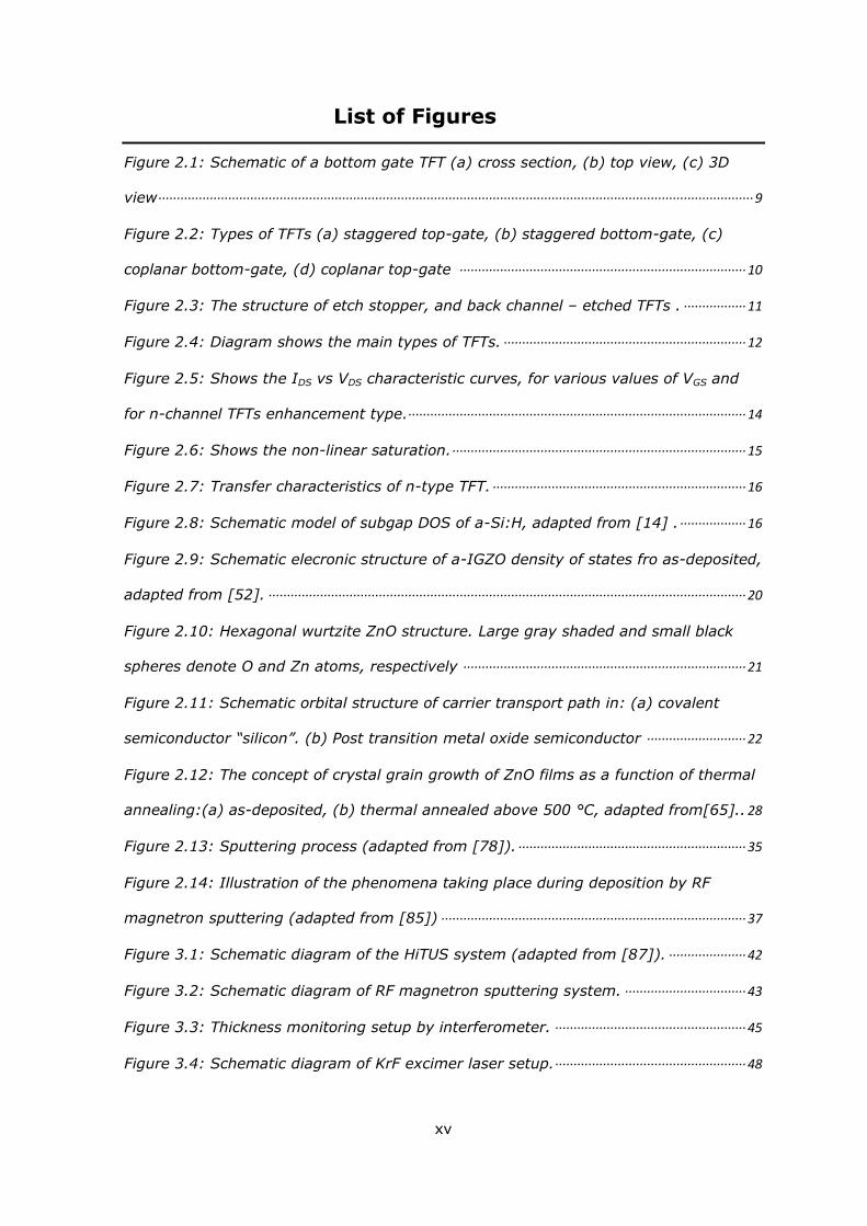
List of Figures
Figure 2.1: Schematic of a bottom gate TFT (a) cross section, (b) top view, (c) 3D
view ·································································································································································· 9
Figure 2.2: Types of TFTs (a) staggered top-gate, (b) staggered bottom-gate, (c)
coplanar bottom-gate, (d) coplanar top-gate ·············································································· 10
Figure 2.3: The structure of etch stopper, and back channel – etched TFTs . ················· 11
Figure 2.4: Diagram shows the main types of TFTs. ·································································· 12
Figure 2.5: Shows the IDS vs VDS characteristic curves, for various values of VGS and
for n-channel TFTs enhancement type.···························································································· 14
Figure 2.6: Shows the non-linear saturation. ················································································ 15
Figure 2.7: Transfer characteristics of n-type TFT. ····································································· 16
Figure 2.8: Schematic model of subgap DOS of a-Si:H, adapted from [14] . ·················· 16
Figure 2.9: Schematic elecronic structure of a-IGZO density of states fro as-deposited,
adapted from [52]. ·································································································································· 20
Figure 2.10: Hexagonal wurtzite ZnO structure. Large gray shaded and small black
spheres denote O and Zn atoms, respectively ············································································· 21
Figure 2.11: Schematic orbital structure of carrier transport path in: (a) covalent
semiconductor “silicon”. (b) Post transition metal oxide semiconductor ··························· 22
Figure 2.12: The concept of crystal grain growth of ZnO films as a function of thermal
annealing:(a) as-deposited, (b) thermal annealed above 500 °C, adapted from[65].. 28
Figure 2.13: Sputtering process (adapted from [78]). ······························································ 35
Figure 2.14: Illustration of the phenomena taking place during deposition by RF
magnetron sputtering (adapted from [85]) ··················································································· 37
Figure 3.1: Schematic diagram of the HiTUS system (adapted from [87]). ····················· 42
Figure 3.2: Schematic diagram of RF magnetron sputtering system. ································· 43
Figure 3.3: Thickness monitoring setup by interferometer. ···················································· 45
Figure 3.4: Schematic diagram of KrF excimer laser setup. ···················································· 48
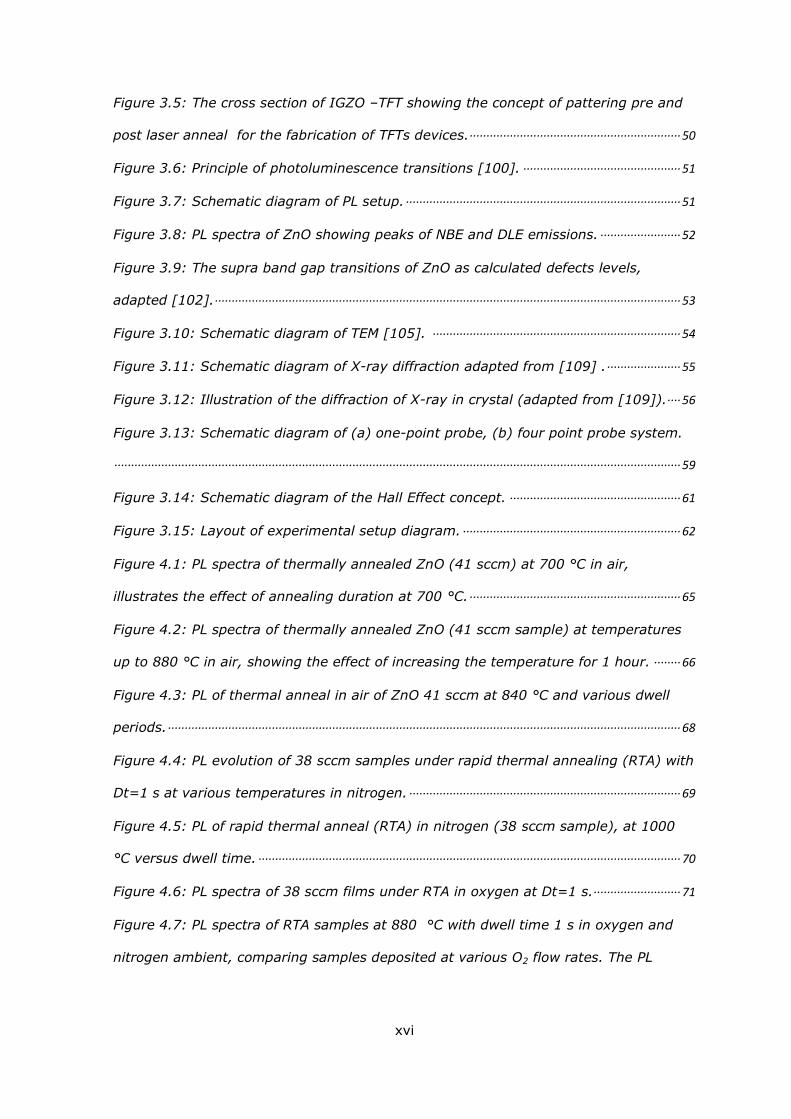
xvi
Figure 3.5: The cross section of IGZO –TFT showing the concept of pattering pre and
post laser anneal for the fabrication of TFTs devices. ······························································· 50
Figure 3.6: Principle of photoluminescence transitions [100]. ··············································· 51
Figure 3.7: Schematic diagram of PL setup. ·················································································· 51
Figure 3.8: PL spectra of ZnO showing peaks of NBE and DLE emissions. ························ 52
Figure 3.9: The supra band gap transitions of ZnO as calculated defects levels,
adapted [102]. ··········································································································································· 53
Figure 3.10: Schematic diagram of TEM [105]. ·········································································· 54
Figure 3.11: Schematic diagram of X-ray diffraction adapted from [109] . ······················ 55
Figure 3.12: Illustration of the diffraction of X-ray in crystal (adapted from [109]). ···· 56
Figure 3.13: Schematic diagram of (a) one-point probe, (b) four point probe system.
········································································································································································· 59
Figure 3.14: Schematic diagram of the Hall Effect concept. ··················································· 61
Figure 3.15: Layout of experimental setup diagram. ································································· 62
Figure 4.1: PL spectra of thermally annealed ZnO (41 sccm) at 700 °C in air,
illustrates the effect of annealing duration at 700 °C. ······························································· 65
Figure 4.2: PL spectra of thermally annealed ZnO (41 sccm sample) at temperatures
up to 880 °C in air, showing the effect of increasing the temperature for 1 hour. ········ 66
Figure 4.3: PL of thermal anneal in air of ZnO 41 sccm at 840 °C and various dwell
periods. ························································································································································· 68
Figure 4.4: PL evolution of 38 sccm samples under rapid thermal annealing (RTA) with
Dt=1 s at various temperatures in nitrogen. ················································································· 69
Figure 4.5: PL of rapid thermal anneal (RTA) in nitrogen (38 sccm sample), at 1000
°C versus dwell time. ······························································································································ 70
Figure 4.6: PL spectra of 38 sccm films under RTA in oxygen at Dt=1 s. ·························· 71
Figure 4.7: PL spectra of RTA samples at 880 °C with dwell time 1 s in oxygen and
nitrogen ambient, comparing samples deposited at various O2 flow rates. The PL
xvii
spectra of all the as-deposited films did not show any significant PL (they have been
omitted from the graph for clarity purpose). ················································································· 72
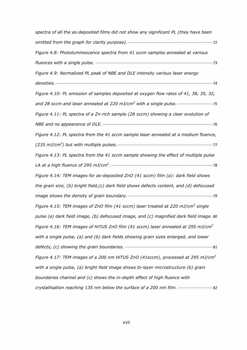
Figure 4.8: Photoluminescence spectra from 41 sccm samples annealed at various
fluences with a single pulse. ················································································································ 73
Figure 4.9: Normalized PL peak of NBE and DLE intensity various laser energy
densities. ······················································································································································ 74
Figure 4.10: PL emission of samples deposited at oxygen flow rates of 41, 38, 35, 32,
and 28 sccm and laser annealed at 220 mJ/cm2 with a single pulse. ·································· 75
Figure 4.11: PL spectra of a Zn-rich sample (28 sccm) showing a clear evolution of
NBE and no appearance of DLE. ········································································································· 76
Figure 4.12: PL spectra from the 41 sccm sample laser annealed at a medium fluence,
(235 mJ/cm2) but with multiple pulses. ··························································································· 77
Figure 4.13: PL spectra from the 41 sccm sample showing the effect of multiple pulse
LA at a high fluence of 295 mJ/cm2. ································································································· 78
Figure 4.14: TEM images for as-deposited ZnO (41 sccm) film (a): dark field shows
the grain size, (b) bright field,(c) dark field shows defects content, and (d) defocused
image shows the density of grain boundary. ················································································· 79
Figure 4.15: TEM images of ZnO film (41 sccm) laser treated at 220 mJ/cm2 single
pulse (a) dark field image, (b) defocused image, and (c) magnified dark field image. 80
Figure 4.16: TEM images of HiTUS ZnO film (41 sccm) laser annealed at 295 mJ/cm2
with a single pulse, (a) and (b) dark fields showing grain sizes enlarged, and lower
defects, (c) showing the grain boundaries. ···················································································· 81
Figure 4.17: TEM images of a 200 nm HiTUS ZnO (41sccm), processed at 295 mJ/cm2
with a single pulse, (a) bright field image shows bi-layer microstructure (b) grain
boundaries channel and (c) shows the in-depth effect of high fluence with
crystallisation reaching 135 nm below the surface of a 200 nm film. ································· 82
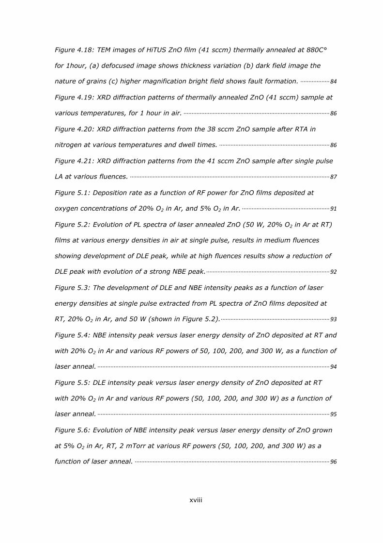
xviii
Figure 4.18: TEM images of HiTUS ZnO film (41 sccm) thermally annealed at 880C°
for 1hour, (a) defocused image shows thickness variation (b) dark field image the
nature of grains (c) higher magnification bright field shows fault formation. ·················· 84
Figure 4.19: XRD diffraction patterns of thermally annealed ZnO (41 sccm) sample at
various temperatures, for 1 hour in air. ·························································································· 86
Figure 4.20: XRD diffraction patterns from the 38 sccm ZnO sample after RTA in
nitrogen at various temperatures and dwell times. ···································································· 86
Figure 4.21: XRD diffraction patterns from the 41 sccm ZnO sample after single pulse
LA at various fluences. ··························································································································· 87
Figure 5.1: Deposition rate as a function of RF power for ZnO films deposited at
oxygen concentrations of 20% O2 in Ar, and 5% O2 in Ar. ······················································ 91
Figure 5.2: Evolution of PL spectra of laser annealed ZnO (50 W, 20% O2 in Ar at RT)
films at various energy densities in air at single pulse, results in medium fluences
showing development of DLE peak, while at high fluences results show a reduction of
DLE peak with evolution of a strong NBE peak.············································································ 92
Figure 5.3: The development of DLE and NBE intensity peaks as a function of laser
energy densities at single pulse extracted from PL spectra of ZnO films deposited at
RT, 20% O2 in Ar, and 50 W (shown in Figure 5.2). ··································································· 93
Figure 5.4: NBE intensity peak versus laser energy density of ZnO deposited at RT and
with 20% O2 in Ar and various RF powers of 50, 100, 200, and 300 W, as a function of
laser anneal. ··············································································································································· 94
Figure 5.5: DLE intensity peak versus laser energy density of ZnO deposited at RT
with 20% O2 in Ar and various RF powers (50, 100, 200, and 300 W) as a function of
laser anneal. ··············································································································································· 95
Figure 5.6: Evolution of NBE intensity peak versus laser energy density of ZnO grown
at 5% O2 in Ar, RT, 2 mTorr at various RF powers (50, 100, 200, and 300 W) as a
function of laser anneal. ························································································································ 96
xix
Figure 5.7: Evolution of DLE intensity peak versus laser energy density of ZnO grown
at 5% O2 in Ar, RT, 2 mTorr at various RF powers (50, 100, 200, and 300 W) as a
function of laser anneal. ························································································································ 97
Figure 5.8: PL spectra of ZnO films deposited at various temperatures of RT, 100 °C,
200 °C, 300 °C, and 400 °C. ··············································································································· 98
Figure 5.9: PL spectra of thermal annealed (at 700 °C, dwell time 1hour) ZnO films
grown at various temperatures. The inset shows the evolution of NBE peak at about
381nm. ························································································································································· 99
Figure 5.10: NBE peak intensity of laser annealed ZnO films deposited at various
substrate temperatures (RT, 100, 200, 300, and 400 °C). As the deposition
temperature increased, the NBE peak decreased. ····································································· 100
Figure 5.11: DLE peak intensity of laser annealed ZnO films deposited at various
substrate temperatures (RT, 100, 200, 300, and 400 °C). ··················································· 101
Figure 5.12: XRD patterns of ZnO deposited at room temperature following to laser
anneal versus laser energy density at single pulse. ································································· 102
Figure 5.13: XRD spectra of ZnO films deposited at 300 °C following by laser anneal
at various fluences. ································································································································ 104
Figure 5.14: XRD patterns (thermal annealed at 700 °C for an hour) of ZnO films
deposited at various substrate temperatures. The inset shows XRD patterns of films
grown at RT, and 100 °C.···················································································································· 105
Figure 5.15: TEM images for as-deposited ZnO deposited at room temperature, (a)
bright field image, (b) bright field image with higher magnification, (c) dark field
image. ························································································································································· 107
Figure 5.16: TEM images of ZnO film deposited at room temperature and laser
annealed at 270 mJ/cm2. (a) image of bright field, (b) an image with higher
magnification defocus, (c) image of dark field. ··········································································· 108
xx
Figure 5.17: TEM images of laser annealed ZnO deposited at room temperature and
laser annealed at 315 mJ/cm2, (a) high magnification defocus image, (b) dark field
image showing the effect of high fluence on grain size. ························································· 109
Figure 5.18: TEM images of thermal annealed ZnO at 700 °C for 1 hour in air, (a)
defocused image with appearance of pores (b) bright field image (c) dark field image
showing the nature of grain size. ····································································································· 110
Figure 5.19: TEM images of as-grown ZnO film at substrate temperature 300 °C, (a)
defocused image (b) bright field image, (c) dark field image. ············································· 111
Figure 5.20: TEM images of ZnO deposited at a substrate temperature of 300 °C and
after laser annealing at fluence 335 mJ/cm2 with a single pulse, (a) defocused image
(b) defocused image at high magnification (c) dark field image. ········································ 112
Figure 6.1: PL spectra of thermal annealed (700 °C for 1 hour in air) ZnO films grown
onto silicon dioxide substrates at RT and 400 °C. ····································································· 117
Figure 6.2: Evolution of NBE and DLE peaks of Laser annealed ZnO deposited on SiO2
substrate at 400 °C. ······························································································································ 119
Figure 6.3: XRD patterns of as deposited and thermal annealed ZnO deposited on
silicon dioxide substrates at RT and 400 °C. ··············································································· 120
Figure 6.4: XRD patterns of laser annealed ZnO films deposited on silicon dioxide
substrate at RT. The inset shows XRD spectra of as-deposited film. ································· 121
Figure 6.5: XRD patterns of laser annealed ZnO film deposited on SiO2 substrate at
400°C. ························································································································································· 122
Figure 6.6: Sheet resistance of laser annealed IGZO (2:2:1) films deposited at 50 W,
5 %, O2 in Ar, 50 nm, at various deposition pressures (2, 5 and 10 mTorr). ················ 126
Figure 6.7: Sheet resistance of laser annealed IGZO (2:2:1) films deposited at 100 W,
2 mTorr, 50 nm, at various oxygen deposition concentrations of 2, 5, 10% O2 in Ar.127
Figure 6.8: Sheet resistance of laser annealed IGZO (2:2:1) films deposited at 2, and
5% O2 in Ar, 2 mTorr, 50 nm, at various RF powers (50 W and 100 W). ························ 128
xxi
Figure 6.9: Sheet resistance of laser annealed IGZO (2:2:1), and (1:1:1) grown at
2% O2 in Ar, 50 W and 50 nm. ········································································································· 129
Figure 6.10: Hall mobilities, carrier concentrations, and resistivities of 50nm thick
IGZO (1:1:1) thin films film as a function of laser fluence. ··················································· 130
Figure 6.11: Cross section diagram of IGZO TFTs used for thermal and laser annealing
(W/L= 1000 μm/5 μm). ······················································································································· 132
Figure 6.12: Schematic diagram showing the process sequence of top gate–bottom
contacts IGZO-TFT fabrication and the concept of laser annealing pre and post IGZO
channel patterning. ································································································································ 133
Figure 6.13: Transfer characteristics ON sweep of IGZO-TFTs (W/L= 1000 μm/5 μm)
VDS =1 V, IGZO 30 nm, pre and post IGZO pattern thermal annealed at 150°C in air
for 1 hour. ················································································································································· 135
Figure 6.14: Transfer characteristics ON sweep IGZO-TFTs (W/L= 1000 μm/5 μm) VDS
=1, IGZO 30 nm, laser annealed at laser energy density of 75 mJ/cm2 with a single
pulse, pre and post IGZO patterning. ····························································································· 136
Figure 6.15: Transfer characteristics of ON sweep IGZO-TFTs (W/L= 1500 μm/5 μm)
VDS =1 V at laser energy density 75 mJ/cm2 single pulse post IGZO pattern. ··············· 138
Figure 6.16: Transfer characteristics of ON sweep IGZO-TFTs (W/L= 1500 μm/5 μm)
VDS =1 V pre and post IGZO pattern laser at laser energy density 75 mJ/cm2 single
pulse. ··························································································································································· 139
Figure A-1: Cross-sectional view of the channel region of a TFT used to drive gradual
channel approximation [7]. ················································································································ 160
Figure B-1: Evolution of PL spectra of laser annealed ZnO deposited at 100 W, 20%
O2 in Ar at RT. ·········································································································································· 162
Figure B-2: Evolution of PL spectra of laser annealed ZnO deposited at 200 W, 20%
O2 in Ar at RT. ·········································································································································· 163
Figure B-3: Evolution of PL spectra of laser annealed ZnO deposited at 300 W, 20% O2
in Ar at RT. ················································································································································ 164
xxii
List of Tables
Table 2.1: Summary of previous work on ZnO-TFTs. TA stands for thermal annealing
and LA for laser annealing. ................................................................................................................... 27
Table 2.2: Summary of the IGZO-TFTs work presented previously in the literature. TA
stands for thermal annealing and LA for laser annealing. ........................................................ 33
Table 4.1: XPS showing Zn:O ratio for films deposited at various oxygen flow rates. . 66
Table 4.2: XPS showing Zn:O ratio for films as a function of annealing temperatures.
......................................................................................................................................................................... 67
Table 5.1: Data from XRD patterns of ZnO films deposited at room temperature (RT)
following laser anneal at various energy densities with single pulse irradiation. .......... 103
Table 5.2: Data from XRD patterns of ZnO films deposited at 300 °C following laser
anneal at various energy density at single pulse. ...................................................................... 103
Table 5.3: Average grain size calculated from XRD patterns of ZnO films deposited at
various substrate temperatures following laser anneal at various energy densities with
single pulse irradiation, and also following thermal anneal at 700 °C for 1 hour. Films
processed with medium and high fluences exhibit the highest peak of DLE and NBE
peaks respectively. ................................................................................................................................ 106
Table 6.1: Comparison of average grain size calculated from XRD patterns of ZnO
films deposited on Si and SiO2 substrates at RT and 400 °C, following laser anneal at
various energy densities with single pulse irradiation, and thermal anneal at 700 °C
for 1 hour. ................................................................................................................................................. 123
Table 6.2: Sheet resistance of laser annealed 60 nm thick of ZnO films deposited at
50 W, 20% O2 in Ar, 2 mTorr on SiO2 substrates at RT and 400 °C.. ............................... 135
Table 6.3: Properties of IGZO –TFTs thermally annealed pre and post pattering of the
active layer 30 nm thick. ..................................................................................................................... 135
Table 6.4: Properties of IGZO –TFTs annealed with different laser annealing
conditions. ................................................................................................................................................. 137

xxiii
Table 6.5: Electrical properties of IGZO –TFTs laser annealed pre and post patterning
of the active layer 50 nm thick, at 75 mJ/cm2 with a single pulse in air. ........................ 138
Chapter 1 Introduction
Chapter 1
Introduction
Introduction 1.1
In recent years, there has been a significant research interest in the development of
materials fabrication and processing to realise flexible display technologies [1]. High
performance thin film transistors (TFTs) are one of the most significant technologies
required in active matrix flat panel displays, including active matrix liquid crystal
displays (AMLCD) [2], and active matrix organic light emitting diode (AMOLED)
displays, to switch the pixels ON and OFF. Transparent thin film transistors (TTFTs)
made of transparent oxide semiconductors (TOSs) have attracted considerable
attention due to their potential for use in display devices, because the use of
transparent active matrix circuits increases the aperture opening ratio (i.e. increases
the light emitting area per pixel, and hence pixel brightness) [2].
Amorphous silicon (a-Si) TFTs have been successfully employed in large area display
technology, but the major shortcoming is low mobility (~1 cm2/Vs) which limits the
device switching speed and ultimate refresh frequency [3]. Alternatively, poly silicon
(poly-Si) TFTs demonstrate higher mobility (>50 cm2/Vs), and are used in smaller area
AMLCDs [4]. However, the need for processing at high temperatures makes poly-Si
TFTs incompatible with flexible substrates, and it is difficult to grow uniform layers over
large areas, hence affecting display sizes attainable [5]. Furthermore, both a-Si and
poly-Si are opaque materials with a narrow band gap of 1.1 eV for crystalline silicon or
1.6 eV for a-Si [6], hence their use results in limitations to the pixel aperture ratios,
which affects the pixel brightness [7].
Chapter 1 Introduction
2
There is consequently a significant interest in developing materials technology that
offers alternatives to a-Si and poly-Si in order to achieve optimised performance in
future displays, and to also offer the potential for new design innovation through the
realisation of flexible, and ideally transparent displays and TFT materials. Several metal
oxide semiconductor materials have been studied over recent years, both as
transparent conducting oxides (TCOs) and as transparent semiconducting oxides
(TSOs) for application to electronic devices such as displays. One such oxide material is
Zinc oxide (ZnO) which is a material of interest for TFTs because of its wide and direct
band gap (3.36 eV) [8]. High processing temperature (deposition or annealing) is
typically required to achieve good properties such as to enhance the film crystallinity,
reduce the defects, reduce grain boundaries, and control conductivity. Hence deposition
and processing of ZnO at low temperatures with good microstructure and electrical
properties, to be compatible with flexible substrate is one of the most challenging tasks.
Another material of interest for display applications is amorphous indium gallium zinc
oxide, for use in transistor devices a-IGZO TFTs. These devices have attracted
considerable attention [9, 10], and have been demonstrated as switching devices in
active matrix liquid crystal displays (AMLCD), and organic light emitting diode based
displays (OLED) [11, 12]. The a-IGZO based TFTs reported in 2004 by Nomura et al,
were fabricated on flexible substrates via pulsed laser deposition (PLD). These devices
were investigated as an alternative to a-Si and poly-Si TFTs, because of the high field
effect mobility that was demonstrated in the amorphous state (>10 cm2/Vs) [9], which
was attributed to the heavy metal cations with (n - 1) d10 ns0 n≥5 electron
configuration [13]. In the past ten years, there has been much work on IGZO devices,
with commercial displays now using this material [14-16]. However, there is still a need
to optimise low temperature deposition and processing of IGZO for flexible applications,
ideally utilising a deposition and processing technique that is suitable for large area at
low cost.
Chapter 1 Introduction
3
For the research presented in this thesis, the combination of low temperature
deposition by sputtering (a technique well suited to scale up to large areas) and post
deposition by laser annealing has been investigated in order to study the potential for
application to the processing of ZnO and IGZO and TSOs. The use of laser processing
provides the potential to localise the modification induced by annealing in order to
minimise energy deposited into the substrate, hence can be a method suitable for low
temperature substrates. The work presented here uses RF magnetron sputtering and
High Target Utilisation Sputtering (HiTUS) in combination with subsequent pulsed UV
excimer laser treatment, to examine the effect on the thin film structure and
properties.
One of the main experimental tools used to investigate the effect of deposition and
annealing for this work is photoluminescence (PL). Typical PL emission from ZnO
exhibits two significant peaks: a strong narrow ultraviolet (UV) centred at around (381
nm) from near band emission (NBE) associated with free exciton recombination, and a
broad visible peak (from 450-750 nm) associated with deep level emission (DLE) [17,
18]. The DLE is attributed to intrinsic or extrinsic defects [18], and to produce ZnO
films with good microstructure and electrical properties, the related defects (DLE peak)
should be supressed with a pronounced evolution of NBE intensity. It has been reported
that an improvement of NBE intensity is clearly observed after thermal annealing [19].
Hence, for this work, the effect on PL of ZnO thin films processed by low temperature
laser annealing is compared with the effect of thermal and rapid thermal annealing.
Work on IGZO thin films is also presented, in which the electrical properties of devices
utilising IGZO semiconductor layers are studied following laser annealing.
Problem definition 1.2
There is a difficulty in fabricating good quality TFTs materials that are transparent and
at the same time fabricated at low temperatures. Also stability of performance is an
issue with the channel materials. Laser processing is a technique that has promise for
Chapter 1 Introduction
4
highly localised film modification. This project consequently addresses this area of
materials and device research to investigate the use of laser processing for the
optimisation of transparent semiconducting thin films suitable for use in TFTs.
Project Aim 1.3
The project aims to investigate the deposition and processing of oxide semiconductors
of zinc oxide (ZnO) and indium gallium zinc oxide (IGZO) in order to understand how to
modify and optimise the properties of these transparent semiconducting oxide thin films
for use in electronic device applications.
Project Objectives 1.4
The specific objectives of this work are to:
Undertake background study of TFT devices, ZnO and IGZO thin film deposition
and fabrication and characterisation of TCOs in electronic devices.
Experimental design to investigate the optimisation of TCOs: ZnO and IGZO.
Investigate the deposition and post processing of ZnO thin films though
characterisation of the resultant structural, electrical and defect properties.
Investigate the deposition and post processing of IGZO thin films though
characterisation of the resultant structural, electrical and defect properties.
Evaluate the effect of excimer laser processing on ZnO and IGZO.
Investigate the performance of TFT devices comprising IGZO produced in
pervious objectives.
Structure of the Thesis 1.5
This thesis consists of the following chapters:
Chapter 1 Introduction
5
Chapter 2: Background and Literature Review
This chapter presents background knowledge and a literature review related to the
structure, principle, and theory of the operation of thin film transistors (TFTs). This is
followed by a review of semiconductor materials in thin film transistors (TFTs) based on
polycrystalline zinc oxide and amorphous IGZO electrical properties, including a
discussion of the deposition methods used.
Chapter 3: Experimental Procedures and Techniques
The third chapter provides a description of the experimental systems utilised
throughout this research, comprising a description of the two deposition techniques of
HiTUS and RF-magnetron sputtering, and of the excimer laser processing system. Also
discussed are the characterisation techniques applied to the films following deposition
and processing: photoluminescence (PL), X-ray diffraction (XRD), Transmission Electron
Microscopy (TEM), Four Point Probe (4PP), and Hall Effect.
Chapter 4: ZnO Thin Films by HiTUS
This chapter presents the results obtained from a study of the photoluminescence of
ZnO films deposited at low temperature by the HiTUS technique and followed by
different annealing processes: laser, thermal, rapid thermal annealing. The structure of
the processed ZnO films is also examined and analysed using Transmission Electron
Microscopy (TEM) and X - ray Diffraction (XRD) and their results are correlated to the
PL properties.
Chapter 5: ZnO Thin Films by RF Magnetron Sputtering
In this chapter, the effect of laser annealing on PL spectra of ZnO films deposited by RF
magnetron sputtering at various RF powers and oxygen concentrations without
intentional substrate heating are reported. The effect of varying deposition parameters
is compared with the HiTUS results presented in chapter 4, with the PL spectra of laser
and thermal annealed ZnO films grown at various substrate temperatures presented.
Chapter 1 Introduction
6
Further confirmation of film structure as a function of annealing process is examined by
cross sectional TEM, and XRD pattern.
Chapter 6: Electrical Characterisation of ZnO and IGZO.
This chapter presents a study of the electrical properties of the investigated oxide
semiconductor materials and devices. The electrical properties of laser annealed ZnO
thin films and IGZO thin films deposited at various deposition parameters from targets
with different compositions are discussed, and an evaluation of test TFT devices
fabricated with the optimised IGZO thin films is presented.
Chapter 7: Conclusion and Further Work
The conclusion chapter provides a combinatorial summary of the research carried out,
and the achievements of the work performed, with some possible suggestions for
further work.
Chapter 2 Background and Literature Review
7
Chapter 2
Background and Literature Review
Introduction 2.1
Metal – oxide semiconductor devices, for example thin film transistors (TFTs) play an
important role in electronics applications. TFTs are one of the key components in
electronics displays in which they are used as switching elements (addressing) for
active matrix liquid displays (AMLCD) [20], and as a driver/address device in organic
light emitting diode (OLED) displays [11]. In recent years, transparent oxide
semiconductors (TOSs) are of interest for application to TFT technology for displays,
because of the transparency in the visible part of the spectrum, due to the wide band
gap, and due to the potential for low processing temperature, which facilitates
processing on substrates such as glass and flexible materials. For example in 2011,
Samsung introduced the first commercial 2-inch transparent display using transparent
TFTs [21]. Zinc oxide ZnO–TFTs and amorphous indium gallium zinc oxide a-IGZO-TFTs
have attracted much attention for the next generation large–area, transparent, and
flexible flat panel displays. These semiconducting thin films exhibit various advantages
over conventional Si–TFTs, such as high mobility and transparency [9, 22].
ZnO presents a wide band gap of 3.36 eV [23], and IGZO a band gap of ~3 eV [9],
hence, when used as channel layers in TFTs, exposure to light will not affect the device
performance. Hence, employing ZnO or IGZO TFTs in AMLCDs for switching the pixel
display can improve the brightness of pixels.
These features make zinc oxide (ZnO) and amorphous indium gallium zinc oxide (a-
IGZO) thin film transistors (TFTs) the subject of vibrant research and devices using
these materials have been demonstrated for display technologies such as liquid crystal
displays (LCD) and organic light emitting diodes (OLED) displays [24, 25].
Chapter 2 Background and Literature Review
8
The basic structure of TFTs and operation theory 2.2
2.2.1 Overview of TFT principles of operation
The main role of TFT devices is to control the current that passes between source and
drain via the medium of a semiconductor thin film layer. This is achieved by an induced
accumulation layer in the active layer/dielectric interface as a function of applied
voltage on insulated electrodes (gate/drain). TFTs can be classified into two categories:
enhancement mode ―normally off‖, and depletion mode ―normally on‖. For example, for
n-channel TFTs, a positive threshold voltage (Vth) is required to turn on an
enhancement mode device, while in depletion mode device a negative threshold voltage
is required. However, in a depletion mode ―normally on‖ device a voltage on the gate
terminal is required to switch off the device, hence enhancement mode is superior in
terms of minimizing the power dissipation as no voltage is needed to switch off the
device [26].
2.2.2 Basic structure of TFTs
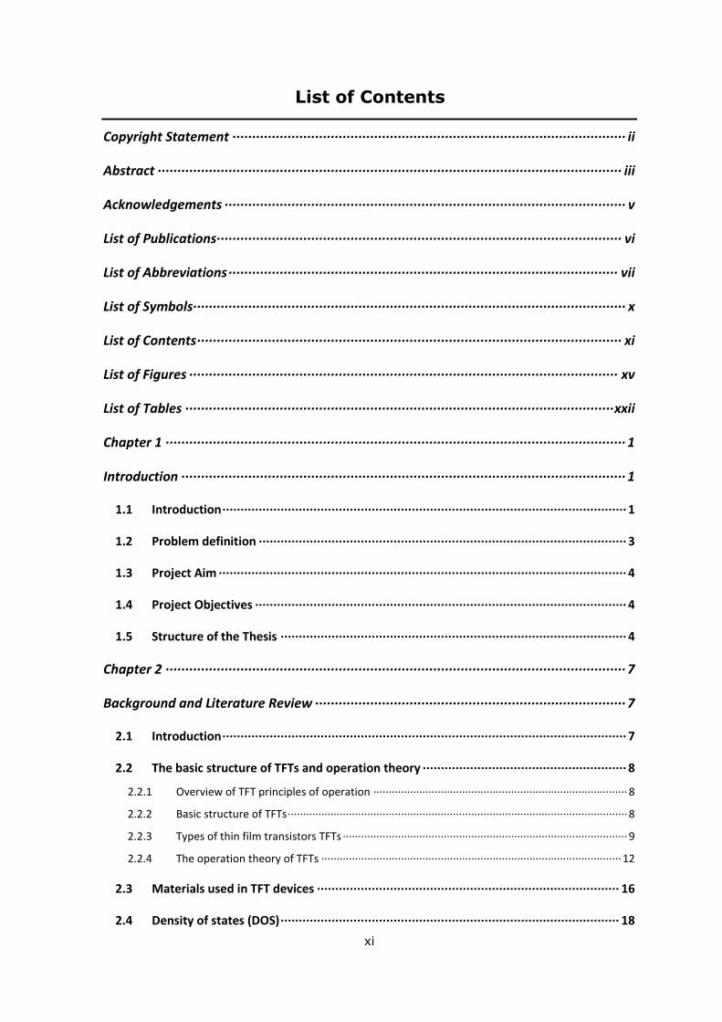
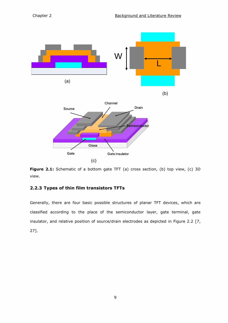
Figure 2.1, shows the simple bottom gate (inverted) structure of TFTs, which consists
of three electrodes terminals: source, drain, and gate. The gate is isolated from the
semiconductor layer by an insulating material (gate insulator), whereas the source and
the drain are in direct contact with the semiconductor film.
Figure 2.1 (a), shows the cross section of a TFT, while Figure 2.1(b), illustrates the top
view, with the dimensions W and L representing the width and length of the channel
layer respectively.
Chapter 2 Background and Literature Review
9
Figure 2.1: Schematic of a bottom gate TFT (a) cross section, (b) top view, (c) 3D
view.
2.2.3 Types of thin film transistors TFTs
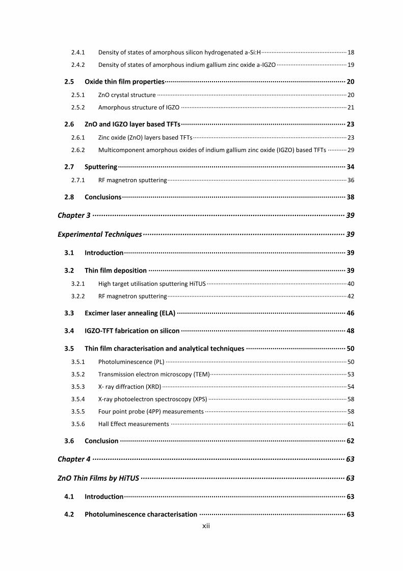
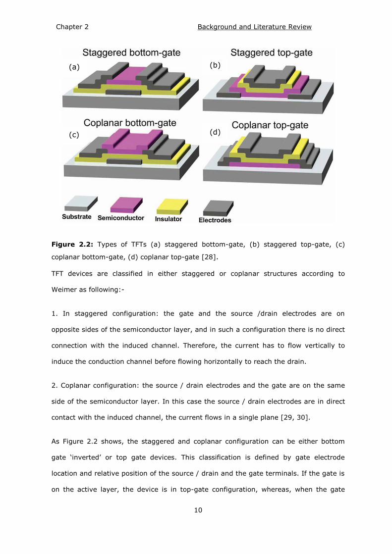
Generally, there are four basic possible structures of planar TFT devices, which are
classified according to the place of the semiconductor layer, gate terminal, gate
insulator, and relative position of source/drain electrodes as depicted in Figure 2.2 [7,
27].
(a)
W L
(b)
(c)
Chapter 2 Background and Literature Review
10
Figure 2.2: Types of TFTs (a) staggered bottom-gate, (b) staggered top-gate, (c)
coplanar bottom-gate, (d) coplanar top-gate [28].
TFT devices are classified in either staggered or coplanar structures according to
Weimer as following:-
1. In staggered configuration: the gate and the source /drain electrodes are on
opposite sides of the semiconductor layer, and in such a configuration there is no direct
connection with the induced channel. Therefore, the current has to flow vertically to
induce the conduction channel before flowing horizontally to reach the drain.
2. Coplanar configuration: the source / drain electrodes and the gate are on the same
side of the semiconductor layer. In this case the source / drain electrodes are in direct
contact with the induced channel, the current flows in a single plane [29, 30].
As Figure 2.2 shows, the staggered and coplanar configuration can be either bottom
gate ‗inverted‘ or top gate devices. This classification is defined by gate electrode
location and relative position of the source / drain and the gate terminals. If the gate is
on the active layer, the device is in top-gate configuration, whereas, when the gate
(a) (b)
(c) (d)
Chapter 2 Background and Literature Review
11
electrode is below the active layer, the device is in bottom-gate (inverted) configuration
[31].
Finally, the inverted–staggered "bottom gate" a-Si:H TFTs have better device
characteristics than the staggered ―top gate‖ structure because in the former the
insulator layer is deposited before the active layer, which leads to lower interface
density of states [32]. However, inverted staggered TFTs suffer from some drawbacks
that may affect TFTs performance such as; the back channel layer being exposed to
atmospheric gases, and back channel could be damage from subsequent process
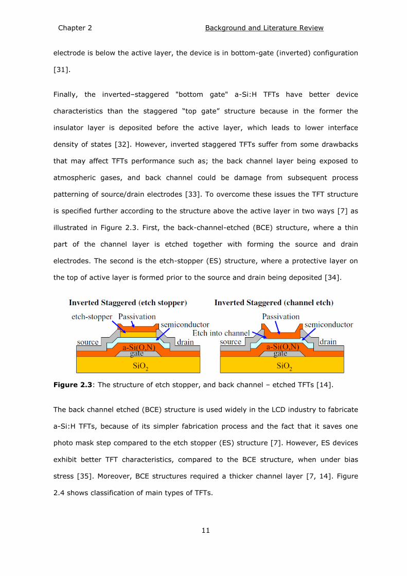
patterning of source/drain electrodes [33]. To overcome these issues the TFT structure
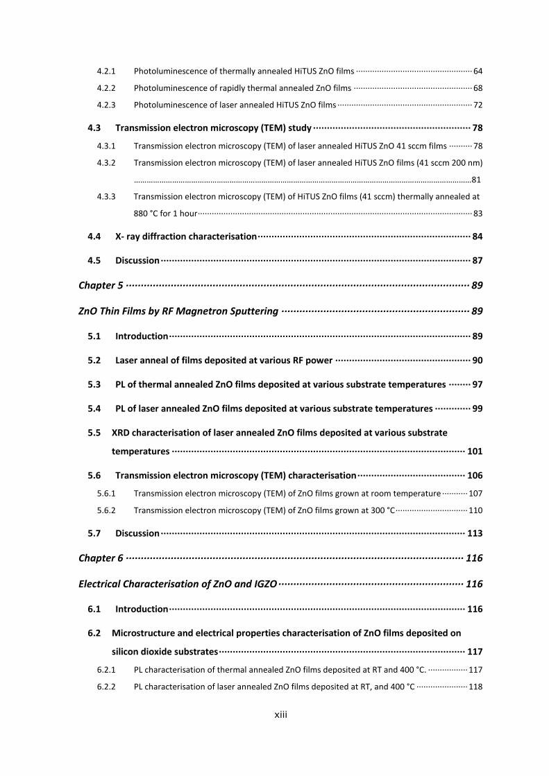
is specified further according to the structure above the active layer in two ways [7] as
illustrated in Figure 2.3. First, the back-channel-etched (BCE) structure, where a thin
part of the channel layer is etched together with forming the source and drain
electrodes. The second is the etch-stopper (ES) structure, where a protective layer on
the top of active layer is formed prior to the source and drain being deposited [34].
Figure 2.3: The structure of etch stopper, and back channel – etched TFTs [14].
The back channel etched (BCE) structure is used widely in the LCD industry to fabricate
a-Si:H TFTs, because of its simpler fabrication process and the fact that it saves one
photo mask step compared to the etch stopper (ES) structure [7]. However, ES devices
exhibit better TFT characteristics, compared to the BCE structure, when under bias
stress [35]. Moreover, BCE structures required a thicker channel layer [7, 14]. Figure
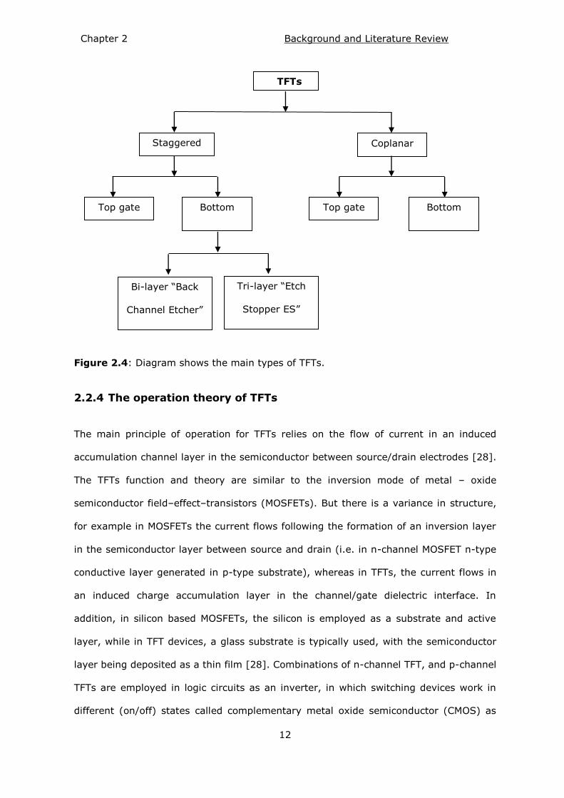
2.4 shows classification of main types of TFTs.
Chapter 2 Background and Literature Review
12
Figure 2.4: Diagram shows the main types of TFTs.
2.2.4 The operation theory of TFTs
The main principle of operation for TFTs relies on the flow of current in an induced
accumulation channel layer in the semiconductor between source/drain electrodes [28].
The TFTs function and theory are similar to the inversion mode of metal – oxide
semiconductor field–effect–transistors (MOSFETs). But there is a variance in structure,
for example in MOSFETs the current flows following the formation of an inversion layer
in the semiconductor layer between source and drain (i.e. in n-channel MOSFET n-type
conductive layer generated in p-type substrate), whereas in TFTs, the current flows in
an induced charge accumulation layer in the channel/gate dielectric interface. In
addition, in silicon based MOSFETs, the silicon is employed as a substrate and active
layer, while in TFT devices, a glass substrate is typically used, with the semiconductor
layer being deposited as a thin film [28]. Combinations of n-channel TFT, and p-channel
TFTs are employed in logic circuits as an inverter, in which switching devices work in
different (on/off) states called complementary metal oxide semiconductor (CMOS) as
Tri-layer ―Etch
Stopper ES‖
Coplanar Staggered
TFTs
Top gate Bottom
gate
Top gate Bottom
gate
Bi-layer ―Back
Channel Etcher‖
BCE‖
Chapter 2 Background and Literature Review
13
used in integrated circuits. Oxide CMOS devices have been demonstrated [36], for
example in transparent inverter using IGZO TFTs employed in ring oscillator circuits
[37].
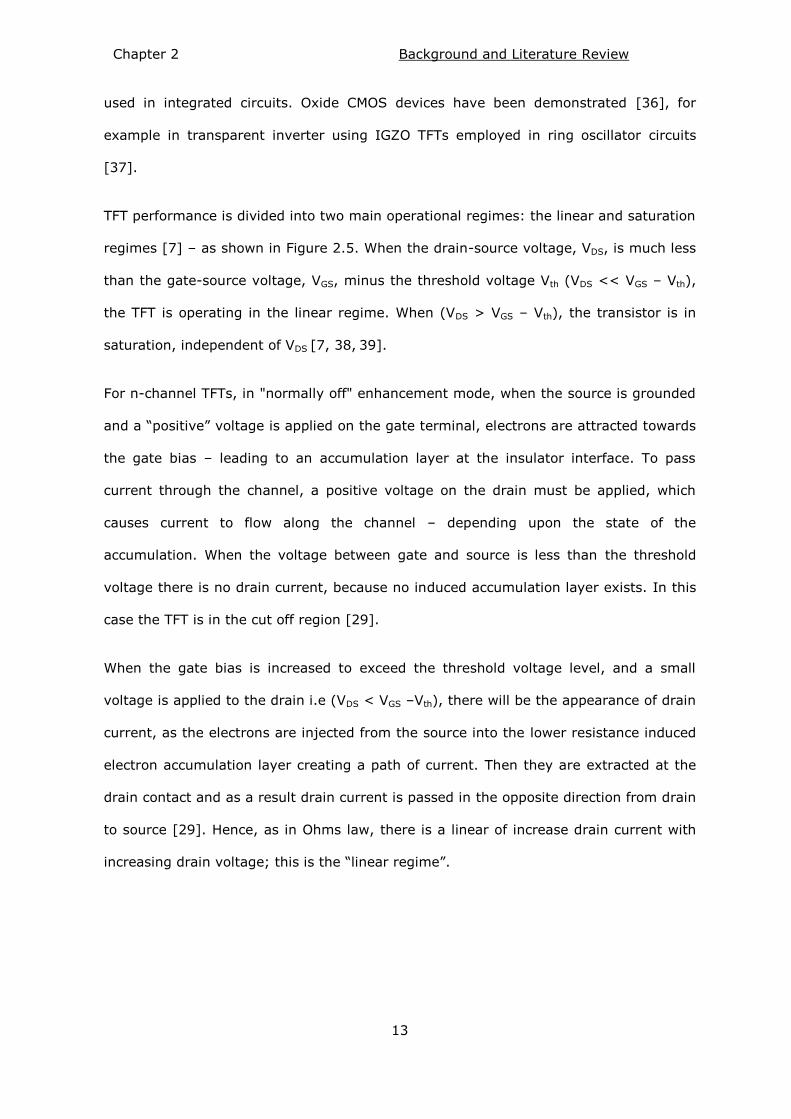
TFT performance is divided into two main operational regimes: the linear and saturation
regimes [7] – as shown in Figure 2.5. When the drain-source voltage, VDS, is much less
than the gate-source voltage, VGS, minus the threshold voltage Vth (VDS << VGS – Vth),
the TFT is operating in the linear regime. When (VDS > VGS – Vth), the transistor is in
saturation, independent of VDS [7, 38, 39].
For n-channel TFTs, in "normally off" enhancement mode, when the source is grounded
and a ―positive‖ voltage is applied on the gate terminal, electrons are attracted towards
the gate bias – leading to an accumulation layer at the insulator interface. To pass
current through the channel, a positive voltage on the drain must be applied, which
causes current to flow along the channel – depending upon the state of the
accumulation. When the voltage between gate and source is less than the threshold
voltage there is no drain current, because no induced accumulation layer exists. In this
case the TFT is in the cut off region [29].
When the gate bias is increased to exceed the threshold voltage level, and a small
voltage is applied to the drain i.e (VDS < VGS –Vth), there will be the appearance of drain
current, as the electrons are injected from the source into the lower resistance induced
electron accumulation layer creating a path of current. Then they are extracted at the
drain contact and as a result drain current is passed in the opposite direction from drain
to source [29]. Hence, as in Ohms law, there is a linear of increase drain current with
increasing drain voltage; this is the ―linear regime‖.
Chapter 2 Background and Literature Review
14
Figure 2.5: Shows the IDS vs VDS characteristic curves, for various values of VGS and for
n-channel TFTs enhancement type [28].
In linear regime by applying the Gradual Channel Approximation (GCA), the drain
current (IDS) with respect to gate voltage VGs given as:
*( )
)+ (2.1)
where W and L width and the length of the channel layer respectively.
When VDS << VGS then the drain current can be written as:
[( ) ] (2.2)
Further details of deriving equation (2.2) can be found in appendix A, at the end of this
thesis
VDS<<VGS - Vth
linear region
increasing VGS
VDS>VGS - Vth
I DS
VDS
Chapter 2 Background and Literature Review
15
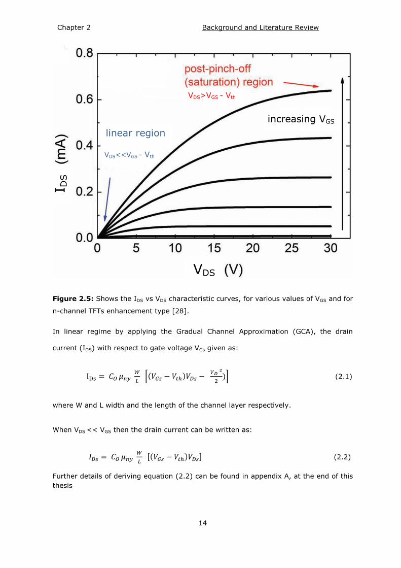
As the applied positive drain voltage increases, the induced carrier density near drain
terminal disappears when VDs = (VGs –Vth), resulting in the electron channel becoming
pinched off at the drain end, as illustrated in Figure 2.6. The drain current saturates
and is no longer Ohmic when VDS exceed the (VGS –Vth) [7, 29].
[( )
] (2.3)
Figure 2.6: Shows the non-linear saturation [29].
From equations (2.2),(2.3) we can find the important parameters defining and affecting
the TFTs operation, such as the capacitance of the dielectric layer (Co), mobility (μ),
threshold voltage (Vth), and the ratio of width over the length of the semiconductor
channel layer. All of these factors must be considered, and this study will be concerned
with optimising the mobility of ZnO, and IGZO thin films deposited at low temperature.
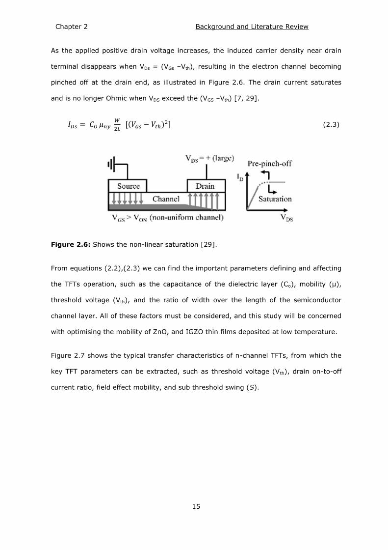
Figure 2.7 shows the typical transfer characteristics of n-channel TFTs, from which the
key TFT parameters can be extracted, such as threshold voltage (Vth), drain on-to-off
current ratio, field effect mobility, and sub threshold swing (S).
Chapter 2 Background and Literature Review
16
Figure 2.7: Transfer characteristics of n-type TFT [28].
The electrical characteristics of TFTs are highly influenced by the materials used in their
structure (such as the channel layer material), the deposition techniques, and the
parameters employed.
Materials used in TFT devices 2.3
The first functional thin film transistor (TFT) was reported in 1962, by P.K.Weimer [7,
40]. They employed a polycrystalline cadmium sulfide (CdS) semiconductor as the
active layer and fabrication via vacuum evaporation [40]. In the early 1980s TFTs were
fabricated from other semiconductor materials such as CdSe, Te, InSb and Ge [3, 41].
Cadmium sulfide CdSe TFTs were first employed as a switching element in the active
matrix liquid crystal display (AMLCD) industry [20]. However, CdSe TFT creates some
issues such as large density of interface states in CdSe [3], traps in the CdSe layer or
Vth
S
VGS
I DS
I DS
Chapter 2 Background and Literature Review
17
insulator interface affecting the frequency response of TFTs [42], and traps in the gate
insulator leading to instability [43].
An improvement in the LCDs industry was reported by LeComber [44] who employed
hydrogenated amorphous silicon (a-Si:H) as a channel layer in TFTs, which achieved
good performance in terms of uniformity, low temperature, and capability of fabrication
over large area. This was a good fit to the requirements of flat panel display (FPD)
addressing [44].
However, the use of conventional amorphous silicon (a-Si) – based TFTs for LCDs
displays create some disadvantages. The a-Si opacity leads to blocking the backlight in
a FPD, which restricts the pixel brightness (aperture ratio) [7, 45]. Other negative
factors are light sensitivity [3, 7], and low mobility (~1 cm2/Vs) which limits the
frequency of operation. Hence, alternatives with high mobility are desired in LCDs and
OLED displays in order to charge the storage capacitor in less time [28]. An additional
factor which must be considered is instability under bias stress which influences the
lifetime of the devices [7, 29].
In 1980 Depp et .al. reported poly- silicon TFTs with dramatic increase in mobility (50
cm2/Vs), fabricated at growth temperatures of 625 °C and 1050 °C for the poly-Si and
gate the insulator respectively [4]. However, poly-Si has some drawbacks associated
with the high processing temperature, which makes it unsuitable for flexible substrates.
Moreover, poly-Si is difficult to fabricated over large areas [46].
Hence, great interest is shown in replacing the conventional Si TFTs with transparent
semiconducting oxide (TSOs) in order to fabricate transparent display devices [22]. The
starting of transparent electronics evolution dates to early 2003, with the report of Zinc
Oxide (ZnO) thin films in transparent thin film transistors (TTFTs) [22, 26, 47]. Since
then, several reports have emerged describing a diversity of TFT channel materials such
as: indium gallium zinc oxide (IGZO), tin oxide (SnO2), indium oxide (In2O3), and zinc
tin oxide (ZTO) [48].
Chapter 2 Background and Literature Review
18
These transparent conducting oxides (TCOs) present a combination of two physical
properties: good electrical conductivity and high transparency [29]. Transparent
semiconducting oxides (TSOs), such as zinc oxide ZnO, are a promising material for the
channel layer in TFTs, because they can be grown at room temperature with high
electron mobility [49] and exhibit optical transparency in the visible spectrum [47].
In particular, amorphous indium gallium zinc oxide based thin film transistors (a-IGZO
TFTs) have attracted considerable attention [9, 10] and have been demonstrated as
switching devices in active matrix liquid crystal displays (AMLCD) and light emitting
diode based devices (OLED) [11, 12]. Hence, ZnO and a-IGZO thin films are the major
interest of this study, which is concerned with the low temperature deposition and the
subsequent photonic processing of these materials.
Density of states (DOS) 2.4
2.4.1 Density of states of amorphous silicon hydrogenated a-Si:H
The electronic characteristics of amorphous thin films are strongly dependant on the
density of state distribution. Amorphous silicon hydrogenated a-Si:H have no long-
range order, the atoms are not periodically located over large distance, but retain short
order of Si lattice. Figure 2.8 shows a typical density of states of a-Si:H, the density of
states distribution contain the following major parts:
Band tails (tail states): The band tails are due to bonding disorder in amorphous
structure, the disorder-induced localisation of states extended near the band edge and
decaying exponentially, arising from deviations in length and angle of particular bonds
originated from long range structural disorder [3]. The band states below the
conduction band minimum (CBM) and above the valence band maximum (VBM), Eu is
the Urbach energy typically Eu ~ 25 meV for conduction band tail and Eu ~ 50 meV for
the valence band tail [14].
Chapter 2 Background and Literature Review
19
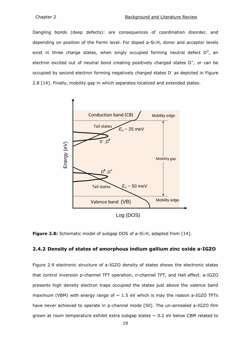
Dangling bonds (deep defects): are consequences of coordination disorder, and
depending on position of the Fermi level. For doped a-Si:H, donor and acceptor levels
exist in three charge states, when singly occupied forming neutral defect D0, an
electron excited out of neutral bond creating positively charged states D+, or can be
occupied by second electron forming negatively charged states D- as depicted in Figure
2.8 [14]. Finally, mobility gap in which separates localized and extended states.
Mobility edge (VB)
Log (DOS)
En
erg
y (
eV
)
Valence band
Conduction band (CB) Mobility edge
Mobility gap
D- ,D0
D0 ,D+
Tail states
Tail states Eu ~ 25 meV
Eu ~ 50 meV
Figure 2.8: Schematic model of subgap DOS of a-Si:H, adapted from [14].
2.4.2 Density of states of amorphous indium gallium zinc oxide a-IGZO
Figure 2.9 electronic structure of a-IGZO density of states shows the electronic states
that control inversion p-channel TFT operation, n-channel TFT, and Hall effect. a-IGZO
presents high density electron traps occupied the states just above the valence band
maximum (VBM) with energy range of ~ 1.5 eV which is may the reason a-IGZO TFTs
have never achieved to operate in p-channel mode [50]. The un-annealed a-IGZO film
grown at room temperature exhibit extra subgap states ~ 0.2 eV below CBM related to
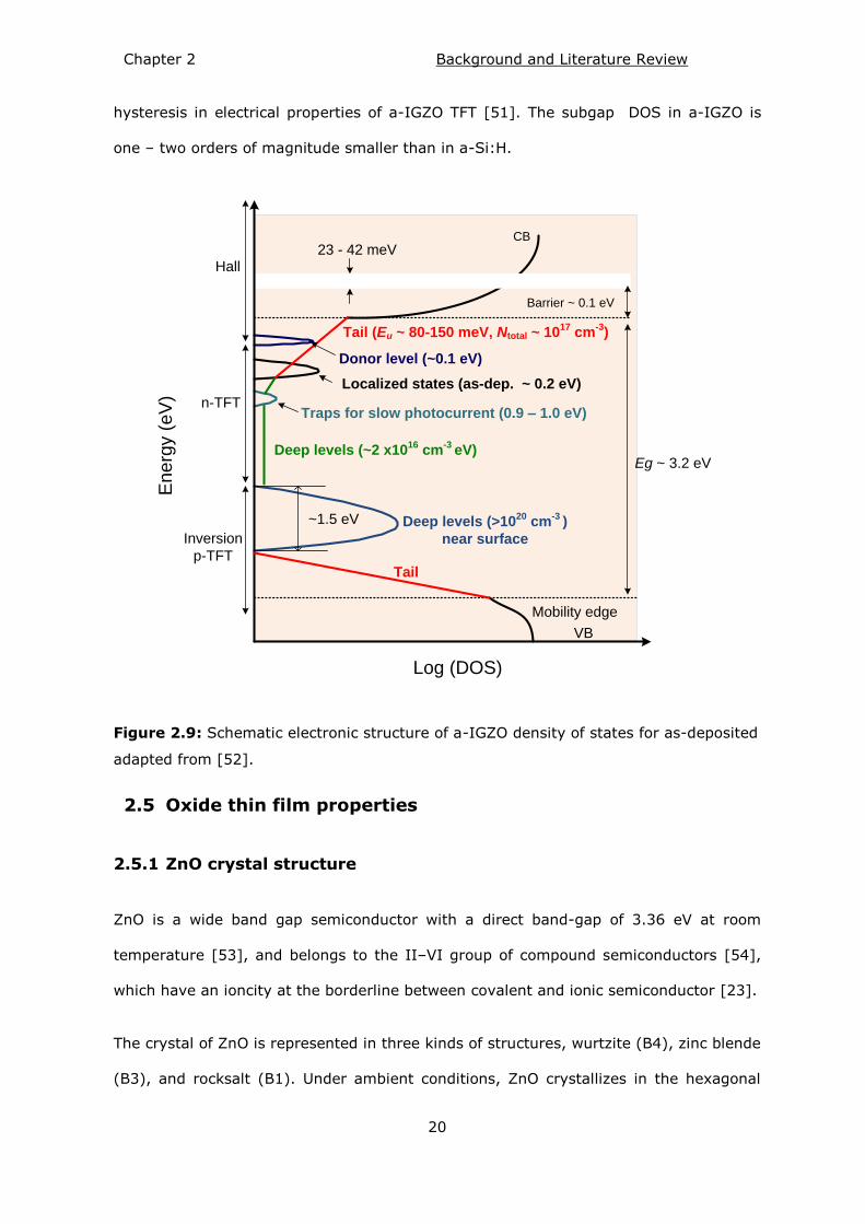
Chapter 2 Background and Literature Review
20
hysteresis in electrical properties of a-IGZO TFT [51]. The subgap DOS in a-IGZO is
one – two orders of magnitude smaller than in a-Si:H.
23 - 42 meV
Barrier ~ 0.1 eV
CB
Eg ~ 3.2 eV
~1.5 eV
Mobility edge
VB
Log (DOS)
Deep levels (>1020
cm-3
)
near surface
Tail
Deep levels (~2 x10¹⁶
cm-3
eV)
Traps for slow photocurrent (0.9 – 1.0 eV)
Localized states (as-dep. ~ 0.2 eV)
Donor level (~0.1 eV)
Tail (Eu ~ 80-150 meV, Ntotal ~ 1017
cm-3
)
En
erg
y (
eV
) n-TFT
Inversion
p-TFT
Hall
Figure 2.9: Schematic electronic structure of a-IGZO density of states for as-deposited
adapted from [52].
Oxide thin film properties 2.5
2.5.1 ZnO crystal structure
ZnO is a wide band gap semiconductor with a direct band-gap of 3.36 eV at room
temperature [53], and belongs to the II–VI group of compound semiconductors [54],
which have an ioncity at the borderline between covalent and ionic semiconductor [23].
The crystal of ZnO is represented in three kinds of structures, wurtzite (B4), zinc blende
(B3), and rocksalt (B1). Under ambient conditions, ZnO crystallizes in the hexagonal
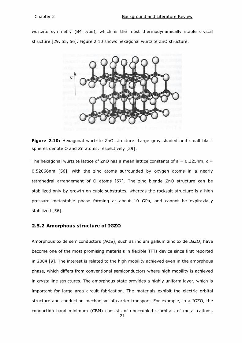
Chapter 2 Background and Literature Review
21
wurtzite symmetry (B4 type), which is the most thermodynamically stable crystal
structure [29, 55, 56]. Figure 2.10 shows hexagonal wurtzite ZnO structure.
Figure 2.10: Hexagonal wurtzite ZnO structure. Large gray shaded and small black
spheres denote O and Zn atoms, respectively [29].
The hexagonal wurtzite lattice of ZnO has a mean lattice constants of a = 0.325nm, c =
0.52066nm [56], with the zinc atoms surrounded by oxygen atoms in a nearly
tetrahedral arrangement of O atoms [57]. The zinc blende ZnO structure can be
stabilized only by growth on cubic substrates, whereas the rocksalt structure is a high
pressure metastable phase forming at about 10 GPa, and cannot be expitaxially
stabilized [56].
2.5.2 Amorphous structure of IGZO
Amorphous oxide semiconductors (AOS), such as indium gallium zinc oxide IGZO, have
become one of the most promising materials in flexible TFTs device since first reported
in 2004 [9]. The interest is related to the high mobility achieved even in the amorphous
phase, which differs from conventional semiconductors where high mobility is achieved
in crystalline structures. The amorphous state provides a highly uniform layer, which is
important for large area circuit fabrication. The materials exhibit the electric orbital
structure and conduction mechanism of carrier transport. For example, in a-IGZO, the
conduction band minimum (CBM) consists of unoccupied s-orbitals of metal cations,
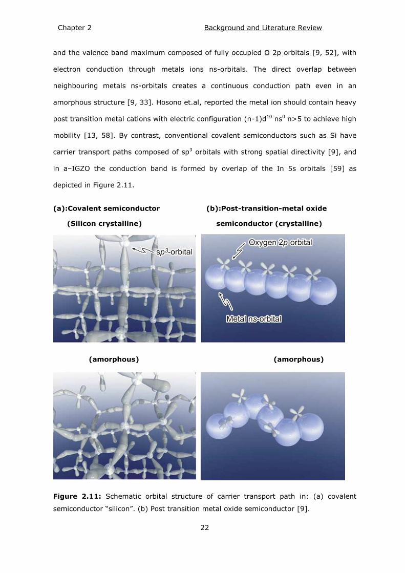
Chapter 2 Background and Literature Review
22
and the valence band maximum composed of fully occupied O 2p orbitals [9, 52], with
electron conduction through metals ions ns-orbitals. The direct overlap between
neighbouring metals ns-orbitals creates a continuous conduction path even in an
amorphous structure [9, 33]. Hosono et.al, reported the metal ion should contain heavy
post transition metal cations with electric configuration (n-1)d10 ns0 n>5 to achieve high
mobility [13, 58]. By contrast, conventional covalent semiconductors such as Si have
carrier transport paths composed of sp3 orbitals with strong spatial directivity [9], and
in a–IGZO the conduction band is formed by overlap of the In 5s orbitals [59] as
depicted in Figure 2.11.
(a):Covalent semiconductor (b):Post-transition-metal oxide
(Silicon crystalline) semiconductor (crystalline)
(amorphous) (amorphous)
Figure 2.11: Schematic orbital structure of carrier transport path in: (a) covalent
semiconductor ―silicon‖. (b) Post transition metal oxide semiconductor [9].
Chapter 2 Background and Literature Review
23
ZnO and IGZO layer based TFTs 2.6
2.6.1 Zinc oxide (ZnO) layers based TFTs
The first devices employing fully transparent ZnO-based TFTs were reported in 2003 by
three groups: Masuda et. al. Hoffman et. al. and Carcia et. al. [22, 26, 47].
Masuda et.al studied the effect of the double gate insulator layer, with a high carrier
concentration layer between the channel layer and source/drain contacts of bottom-
gate ZnO-TFTs. Three types of TFTs were investigated: the first devices were fabricated
with dual layer gate insulator of SiO2 and SiNx, the second devices were fabricated in
the same manner but with high carrier concentration layer between the ZnO layer and
source/drain electrodes, and the third set of devices were fabricated with transparent
materials. The resultant devices with the high carrier concentration layer presented a
high field effect mobility of about 0.97 cm2/Vs, and a threshold voltage of -1 V.
Conversely, the TFTs without the high carrier concentration layer exhibited a mobility of
0.031 cm2/Vs, which was lower than the Hall mobility of the ZnO thin films - at about
0.70 cm2/Vs .This reduction was attributed to a reduction in drain current caused by
contact resistance between the S/D electrodes and the ZnO layer. TFT devices
fabricated on glass substrates demonstrated optical transmittance > 80% in the visible
range [22].
Hoffman et.al fabricated bottom–gate highly transparent ZnO–TFTs on glass, with the
active layer deposited via ion beam sputtering at room temperature. To functionalise
the ZnO film, rapid thermal annealing (RTA) in the range 600-800 °C in oxygen
ambient was used. Following the subsequent deposition of the source and drain
electrode, RTA was carried out again at 300 °C in an O2 atmosphere. The devices
exhibited channel mobility in the range 0.3 to 2.5 cm2/Vs, a threshold voltage of
between 10 to 20 V, and a drain current on-to-off ratio ~107 [26].
Chapter 2 Background and Literature Review
24
Carcia et. al. demonstrated transparent ZnO–TFTs without post deposition annealing,
grown using low temperature processing (~120 °C) via RF magnetron sputtering. The
TFTs exhibited a channel mobility of more than 2 cm2/Vs, a threshold voltage ~0V,
drain current on-to-off ratio of >106, and transparency >80% [47].
More recently, Nishii et. al. reported ZnO-TFTs with improved field effect mobility to 7
cm2/Vs. These devices were fabricated by pulsed laser deposition (PLD) at a substrate
temperature in the range of 150-300 °C, and employed a CaHfOx layer between a ZnO
active layer and silicon nitride gate insulator [60].
Carcia et. al. studied the influence of different gate dielectric insulators on the
performance of ZnO–TFTs. The insulating thin films studied were HfO2, HfSiOx, SiO2,
and Al2O3 deposited via atomic layer deposition (ALD) at temperatures 300 °C, 400 °C,
~100 °C, and (450 °C, 200 °C, 150 °C) respectively. The TFT devices with an alumina
dielectric grown at 125 °C and 200 °C resulted in combination of lower threshold
voltage (1.1 V), and the highest mobility at 17.6 cm2/Vs [49].
Navamathavan et. al. reported an improvement of ZnO–TFTs characteristics using
bottom-gate top-contacts TFTs fabricated with silicon nitride (SiNx) as the gate
dielectric layer grown by plasma enhanced chemical vapour deposition (PECVD) at
300 °C, and the active layer grown by RF magnetron sputtering at 300 °C. The
resultant devices showed field effect mobility at 31 cm2/Vs, a threshold voltage of 9 V,
and drain current on/off ratio more than 105 [61].
Cross et. al. examined the stability of inverted–staggered ZnO-TFTs devices under bias
stress. Comparisons were made between the stability of devices fabricated using silicon
dioxide (SiO2) and silicon nitride (SiN) as the gate insulator, deposited via low pressure
chemical vapour deposition followed by annealing at 1000 °C, with the active layer in
both cases grown by RF magnetron sputtering at room temperature. The results
demonstrated devices with silicon nitride as gate insulator have slightly better
performance than TFTs with silicon dioxide gate dielectric. However, the TFT
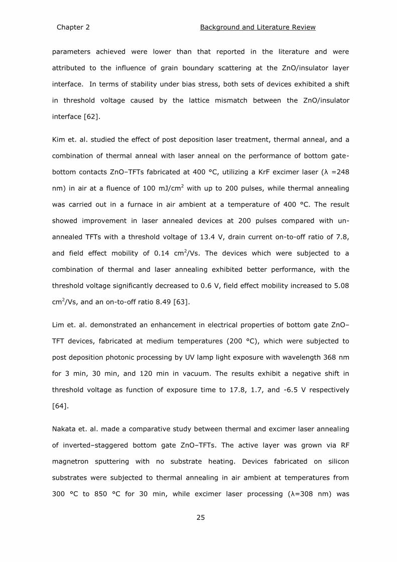
Chapter 2 Background and Literature Review
25
parameters achieved were lower than that reported in the literature and were
attributed to the influence of grain boundary scattering at the ZnO/insulator layer
interface. In terms of stability under bias stress, both sets of devices exhibited a shift
in threshold voltage caused by the lattice mismatch between the ZnO/insulator
interface [62].
Kim et. al. studied the effect of post deposition laser treatment, thermal anneal, and a
combination of thermal anneal with laser anneal on the performance of bottom gate-
bottom contacts ZnO–TFTs fabricated at 400 °C, utilizing a KrF excimer laser (λ =248
nm) in air at a fluence of 100 mJ/cm2 with up to 200 pulses, while thermal annealing
was carried out in a furnace in air ambient at a temperature of 400 °C. The result
showed improvement in laser annealed devices at 200 pulses compared with un-
annealed TFTs with a threshold voltage of 13.4 V, drain current on-to-off ratio of 7.8,
and field effect mobility of 0.14 cm2/Vs. The devices which were subjected to a
combination of thermal and laser annealing exhibited better performance, with the
threshold voltage significantly decreased to 0.6 V, field effect mobility increased to 5.08
cm2/Vs, and an on-to-off ratio 8.49 [63].
Lim et. al. demonstrated an enhancement in electrical properties of bottom gate ZnO–
TFT devices, fabricated at medium temperatures (200 °C), which were subjected to
post deposition photonic processing by UV lamp light exposure with wavelength 368 nm
for 3 min, 30 min, and 120 min in vacuum. The results exhibit a negative shift in
threshold voltage as function of exposure time to 17.8, 1.7, and -6.5 V respectively
[64].
Nakata et. al. made a comparative study between thermal and excimer laser annealing
of inverted–staggered bottom gate ZnO–TFTs. The active layer was grown via RF
magnetron sputtering with no substrate heating. Devices fabricated on silicon
substrates were subjected to thermal annealing in air ambient at temperatures from
300 °C to 850 °C for 30 min, while excimer laser processing (λ=308 nm) was
Chapter 2 Background and Literature Review
26
conducted for devices on plastic substrates at fluences ranging from 250-450 mJ/cm2 in
air. Results showed that laser annealing was more effective than thermal anneal, with a
field effect mobility of 12 cm2/Vs achieved at a laser energy density of 350 mJ/cm2
compared with thermal annealed devices where the equivalent field effect mobility was
6.4 cm2/Vs at annealing temperature 850 °C [65].
Ya-Hui yang et. al. reported the influence of laser annealing on solution based ZnO–
TFTs with the bottom-gate coplanar structure. The ZnO active layer was deposited by
spin-coating and post baked at 95 °C. Subsequently the devices were irradiated by 3rd
harmonic Nd:YAG laser 355 nm. The resultant as deposited devices demonstrated field
effect mobility, threshold voltage; drain current on to off ratio of 0.19 cm2/Vs, 3.4 V,
and 5.38x10⁵ respectively. However, laser irradiated devices show a pronounced
improvement in performance, where for example devices processed at a laser dosage
of 740mJ (spot size of 2.5x10⁻² cm2) exhibited a field effect mobility of 0.49 cm2/Vs and
drain current on to off ratio 3.19x10⁶ [66].
The main results of these studies are presented in Table 2.1. From all reports
summarized above we can conclude the electrical characteristics of ZnO TFTs are highly
dependent on the deposition techniques employed, and that high deposition
temperature or thermal annealing is required to improve the electrical properties of
ZnO-TFTs. However, the laser annealing process is a powerful technique to enhance
and improve the properties of ZnO-TFTs fabricated at low substrate temperature
(<120 °C) compatible with flexible substrates.
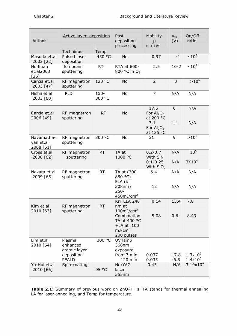
Chapter 2 Background and Literature Review
27
Author
Active layer deposition
Post
deposition
processing
Mobility
μ
cm2/Vs
Vth
(V)
On/Off
ratio
Technique
Temp
Masuda et.al
2003 [22]
Pulsed laser
deposition
450 °C No 0.97 -1 ~105
Hoffman
et.al2003
[26]
Ion beam
sputtering
RT RTA at 600-
800 °C in O2
2.5 10-2 ~107
Carcia et.al
2003 [47]
RF magnetron
sputtering
120 °C No 2 0 >106
Nishii et.al
2003 [60]
PLD
150-
300 °C
No 7
N/A
N/A
Carcia et.al
2006 [49]
RF magnetron
sputtering
RT
No
17.6
For Al2O3
at 200 °C
3.1
For Al2O3
at 125 °C
6
1.1
N/A
N/A
Navamatha-
van et.al
2008 [61]
RF magnetron
sputtering
300 °C No 31 9 >105
Cross et.al
2008 [62]
RF magnetron
sputtering
RT TA at
1000 °C
0.2-0.7
With SiN
0.1-0.25
With SiO2
N/A
N/A
105
3X10⁴
Nakata et.al
2009 [65]
RF magnetron
sputtering
RT TA at (300-
850 °C)
ELA (λ
308nm)
250-
450mJ/cm2
6.4
12
N/A
N/A
N/A
N/A
Kim et.al
2010 [63]
RF magnetron
sputtering
RT
KrF ELA 248
nm at
100mJ/cm2
Combination
TA at 400 °C
+LA at 100
mJ/cm2
200 pulses
0.14
5.08
13.4
0.6
7.8
8.49
Lim et.al
2010 [64]
Plasma
enhanced
atomic layer
deposition
PEALD
200 °C UV lamp
368nm
exposure
from 3 min
120 min
0.037
0.035
17.8
-6.5
1.3x10⁵
1.4x10⁵
Ya-Hui et.al
2010 [66]
Spin-coating
95 °C
Nd:YAG
laser
355nm
0.45 N/A 3.19x10⁶
Table 2.1: Summary of previous work on ZnO-TFTs. TA stands for thermal annealing
LA for laser annealing, and Temp for temperature.
Chapter 2 Background and Literature Review
28
Post-deposition processing improved the transfer characteristics of ZnO-TFTs devices
by phenomena which occurred when the ZnO films were heated up, indicating possible
enhancement mechanisms such as: crystal grain growth caused by Zn atoms gaining
higher energy, making Zinc and oxygen atoms well bonded by filling the entire volume
within a grain creating a path for current to flow as shown in Figure 2.12 [65, 67].
Hence electrical current increased, and there could be an increase in the carrier
concentration by generation of oxygen vacancies or Zn interstitials [64], and a
reduction of the concentration of point defects.
Free electron Current path
ZnO crystal Low crystallinity region
(a) (b)
Figure 2.12: The concept of crystal grain growth of ZnO films as a function of thermal
annealing: (a) as-deposited, (b) thermal annealed above 500 °C, adapted from [65]
To investigate this in detail, the research presented here investigates the effect of laser
annealing on the microstructure properties of ZnO thin films grown by two different
techniques; high target utilisation system (HiTUS) without intentional substrate heating
at various oxygen flow rates to identify the influences of three annealing methods
(furnace, rapid thermal, and laser annealing), and RF magnetron sputtering deposition
Chapter 2 Background and Literature Review
29
at various temperatures (from RT to 400 °C) to investigate and compare the effect of a
laser and thermal anneal of ZnO grown at various substrate temperatures, and to
investigate the nature of point defects developed or supressed by the annealing
processes.
2.6.2 Multicomponent amorphous oxides of indium gallium zinc oxide
(IGZO) based TFTs
In 2003 Nomura et. al. reported transparent single crystalline IGZO thin film transistors
using the top gate structure, with all TFT layers deposited via pulsed laser deposition
(PLD) at room temperature: 120 nm of InGaO3(ZnO)5 (as the active layer) deposited on
yttria-stabilized zirconia (YSZ) substrate, followed by thermal annealing at 1400 °C for
30 min, ITO source and drain electrodes grown and patterned on the channel layer,
amorphous HfO2 80 nm thick deposited as the gate insulator, and finally, an ITO gate
electrode on the top. As a result of the high annealing temperature, the devices
exhibited high field effect mobility ~80 cm2/Vs, a drain current on-to-off ratio ~106,
threshold voltage of 3 V, and an optical transmittance >80% at wavelengths between
390 nm-3200 nm [68].
Amorphous oxide semiconductor (AOS) of indium gallium zinc oxide (IGZO)-based
transparent and flexible TFTs was first reported in 2004 by Nomura et. al. who
demonstrated a-IGZO based TFTs, coplanar top-gate structure on polyethyhere
terephthalan (PEN) flexible substrates at room temperature, with all layers grown by
pulsed laser deposition (PLD). Yttrium oxide, Y2O3, was employed as the gate insulator.
The resultant devices exhibited a field effect mobility of ~8.3 cm2/Vs, drain current on-
to-off ratio ~106, and threshold voltage of 1.6 V [9].
In early 2006, Yabuta et. al. fabricated staggered top-gate type a-IGZO TFTs, where RF
magnetron sputtering was used to deposit the channel layer and gate insulator layers
on glass substrates. The electrical properties showed channel mobility, threshold
voltage, drain current on-to-off ratio of 12 cm2/Vs, 1.4 V, and ~108 respectively [10].
Chapter 2 Background and Literature Review
30
Since the first reports on IGZO TFTs research, there has been interest in studying the
effect of post deposition annealing as a mechanism to improve performance and
stability of the devices.
Kikunhi et. al. studied the effect of post deposition processing of IGZO–TFTs at
temperatures up to 400 °C. Two IGZO films were deposited via pulsed laser deposition
(PLD) and RF magnetron sputtering at room temperature. Prior to fabrication, the top-
contact bottom-gate TFTs structured a-IGZO films were subjected to a thermal anneal
in wet oxygen and dry oxygen atmosphere of 1 atm at various annealing temperatures
up to 200 °C. The RF sputtered TFTs annealed in dry oxygen at 150-200 °C exhibited
enhanced and improved characteristics, whereas wet annealing enhanced device
performance, but caused a large negative shift in threshold voltage. In contrast, PLD
devices with wet annealing at 200 °C exhibited improved characteristics with a small
negative shift in threshold voltage [69].
Ide et. al. examined the effect of the ozone (O3) annealing technique at temperature
<250 °C, on top-contact bottom-gate TFTs with a-IGZO films via RF magnetron
sputtering and ozone (O3) annealing. The O3 annealing improved the performance of
TFTs properties, and was more effective than conventional thermal annealing in oxygen
or air. The devices exhibited a channel mobility of ~ 11.4 cm2/Vs, threshold voltage 0.1
V, and sub threshold swing of 217 mV/decade [70, 71].
Nomura et. al. studied the stability of passivated a-IGZO TFTs against negative bias
light illumination stress (NBLS), and constant current stress (CCS). Bottom – gate top
contact TFTs were fabricated on Si substrates at room temperature, with the active
layer grown via pulsed laser deposition (PLD), and prior to the source and drain
contacts formation thermal annealing at 400 °C in wet oxygen with H2O vapour was
conducted. Then the Y2O3 passivation layer was deposited, and the devices were
annealed at 350 °C in air for 30 min. The resultant passivated TFTs exhibited a channel
mobility ~12.14 cm2/Vs, threshold voltage ~-1 V, and sub threshold swing ~0.14
Chapter 2 Background and Literature Review
31
V/decade with improvement of the stability against constant current stress, and
negative bias light illumination stress compared to un-passivated TFTs [72].
However, post thermal annealing at temperatures higher than the maximum allowable
temperature for heat resistance of plastic substrates (~150 °C) is undesirable when
considering low cost and flexible substrate applications. So, as an alternative to thermal
annealing, photonic processing using UV lamps or laser irradiation is a method of
interest for a range of applications where highly localised annealing and surface
modification is required [73, 74].
For example, Nakata et. al. reported utilizing excimer laser annealing (ELA) to process
20 nm IGZO thin films for inverted-staggered bottom gate a-IGZO-TFTs deposited via
RF magnetron sputtering at room temperature, using a XeCl excimer laser (λ=308 nm)
at 25 ns, for 2 pulses. The IGZO-TFTs irradiated at laser fluences of 130 mJ/cm2
exhibited ON current more than one order of magnitude higher than that of un-
annealed devices with a field effect mobility of 14 cm2/Vs [73].
Subsequently, many researchers have extensively focused on enhancing and improving
the properties of a-IGZO – TFTs using different kinds of post deposition photonic
processing.
Ahn et. al. fabricated bottom gate a-IGZO-TFTs, using a 50 nm thick channel layer
grown by RF magnetron sputtering without intentional substrate heating. The IGZO
films were selectively laser processed via a projection mask using a XeCl (λ=308 nm)
excimer laser in air ambient at ten pulses with a range of laser energy densities from 0
to 250 mJ/cm2. The electrical properties of the devices treated with laser energy
density 130 mJ/cm2 exhibited a channel mobility of 21.79 cm2/Vs, on/off ratio of 1.2
x108, and threshold voltage ~ -0.15 V. As the laser fluences increased to 130 mJ/cm2
the resistivity of IGZO film decreased from 104 Ω cm to 3.2x10⁻³ Ω cm with carrier
concentration 1.3x1020 cm-3, and hall mobility 15 cm2/Vs [74].
Chapter 2 Background and Literature Review
32
It has also been reported by Zan et. al. that the 4th harmonic of an Nd:YAG laser (266
nm) or UV lamp irradiation (172 nm) light exposure supressed the instability of a-IGZO
TFTs, and reduced the defects in IGZO film. Tests used a stable bottom–gate top
contact a-IGZO-TFT where the active layer was deposited by RF magnetron sputtering
and was subjected to the low temperature annealing methods of solid-state Nd:YAG
laser processing at 266 nm or UV lamp irradiation (172 nm). The TFT devices annealed
by Nd:YAG laser at energy density 10.7 mJ/cm2 exhibited an improvement in stability
with channel mobility of 8 cm2/Vs, threshold voltage 0 V, an on/off current ratio larger
than 7 order of magnitude, while devices subjected to UV lamp irradiation for 30 min
showed a channel mobility of 3 cm2/Vs, a threshold voltage 0 V, and on/off current
ratio larger than 6 order magnitude [75].
Ya-Hui Yang et. al. studied the effect of the 3rd harmonic of the Nd:YAG laser (λ=355
nm) on the performance of solution based IGZO-TFTs. 200 nm thick IGZO was the
active layer grown by spin-coating, and baked at 95 °C, with the devices subjected to
Nd:YAG laser annealing at various energy densities in air. Results demonstrate a clear
improvement in device properties as a function of laser processing, with field effect
mobility of 7.65 cm2/Vs, and drain current on to off ratio 2.88x10⁷ [76, 77].
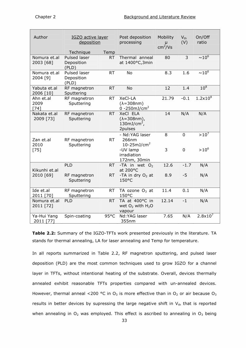
Chapter 2 Background and Literature Review
33
Author
IGZO active layer
deposition
Technique Temp
Post deposition
processing
Mobility
μ
cm2/Vs
Vth
(V)
On/Off
ratio
Nomura et.al
2003 [68]
Pulsed laser
Deposition
(PLD)
RT Thermal anneal
at 1400°C,3min
80 3 ~106
Nomura et.al
2004 [9]
Pulsed laser
Deposition
(PLD)
RT No 8.3 1.6 ~106
Yabuta et.al
2006 [10]
RF magnetron
Sputtering
RT No 12 1.4 108
Ahn et.al
2009
[74]
RF magnetron
Sputtering
RT XeCl-LA
(λ=308nm)
0 -250mJ/cm2
21.79 -0.1 1.2x10⁸
Nakata et.al
2009 [73]
RF magnetron
Sputtering
RT XeCl ELA
(λ=308nm),
130mJ/cm2,
2pulses
14 N/A N/A
Zan et.al
2010
[75]
RF magnetron
Sputtering
RT
- Nd:YAG laser
266nm
10-25mJ/cm2
-UV lamp
irradiation
172nm, 30min
8
3
0
0
>107
>106
Kikunhi et.al
2010 [69]
PLD
RF magnetron
Sputtering
RT
RT
-TA in wet O2
at 200°C
-TA in dry O2 at
150°C
12.6
8.9
-1.7
-5
N/A
N/A
Ide et.al
2011 [70]
RF magnetron
Sputtering
RT TA ozone O3 at
150°C
11.4 0.1 N/A
Nomura et.al
2011 [72]
PLD RT TA at 400°C in
wet O2 with H2O
vapour
12.14 -1 N/A
Ya-Hui Yang
2011 [77]
Spin-coating 95°C Nd:YAG laser
355nm
7.65 N/A 2.8x10⁷
Table 2.2: Summary of the IGZO-TFTs work presented previously in the literature. TA
stands for thermal annealing, LA for laser annealing and Temp for temperature.
In all reports summarized in Table 2.2, RF magnetron sputtering, and pulsed laser
deposition (PLD) are the most common techniques used to grow IGZO for a channel
layer in TFTs, without intentional heating of the substrate. Overall, devices thermally
annealed exhibit reasonable TFTs properties compared with un-annealed devices.
However, thermal anneal <200 °C in O3 is more effective than in O2 or air because O3
results in better devices by supressing the large negative shift in Vth that is reported
when annealing in O2 was employed. This effect is ascribed to annealing in O3 being
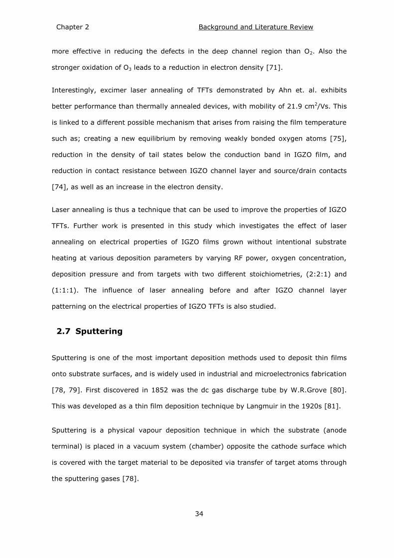
Chapter 2 Background and Literature Review
34
more effective in reducing the defects in the deep channel region than O2. Also the
stronger oxidation of O3 leads to a reduction in electron density [71].
Interestingly, excimer laser annealing of TFTs demonstrated by Ahn et. al. exhibits
better performance than thermally annealed devices, with mobility of 21.9 cm2/Vs. This
is linked to a different possible mechanism that arises from raising the film temperature
such as; creating a new equilibrium by removing weakly bonded oxygen atoms [75],
reduction in the density of tail states below the conduction band in IGZO film, and
reduction in contact resistance between IGZO channel layer and source/drain contacts
[74], as well as an increase in the electron density.
Laser annealing is thus a technique that can be used to improve the properties of IGZO
TFTs. Further work is presented in this study which investigates the effect of laser
annealing on electrical properties of IGZO films grown without intentional substrate
heating at various deposition parameters by varying RF power, oxygen concentration,
deposition pressure and from targets with two different stoichiometries, (2:2:1) and
(1:1:1). The influence of laser annealing before and after IGZO channel layer
patterning on the electrical properties of IGZO TFTs is also studied.
Sputtering 2.7
Sputtering is one of the most important deposition methods used to deposit thin films
onto substrate surfaces, and is widely used in industrial and microelectronics fabrication
[78, 79]. First discovered in 1852 was the dc gas discharge tube by W.R.Grove [80].
This was developed as a thin film deposition technique by Langmuir in the 1920s [81].
Sputtering is a physical vapour deposition technique in which the substrate (anode
terminal) is placed in a vacuum system (chamber) opposite the cathode surface which
is covered with the target material to be deposited via transfer of target atoms through
the sputtering gases [78].
Chapter 2 Background and Literature Review
35
The basic concept of sputtering is that when the gas, typically argon, is introduced to
the evacuated chamber, a voltage is applied between the electrodes to create a
discharge. Ar+ ions are created in the resultant glow discharge phenomenon (plasma),
and are accelerated towards the cathode and sputter the target via transfer of kinetic
energy, resulting in coating the thin film on the substrate surface [78] as shown in
Figure 2.13.
Incident ion
Target surface
Target atom
Sputter atom
Ion implantation
Figure 2.13: Sputtering process (adapted from [78]).
However, this technique has some shortcomings which relate to the quality and film
properties, such as low deposition rate [57]. In 1970s, Chapin had developed a
sputtering system to achieve large area high-rate deposition by inserting a strong
magnet below the target in order to generate a magnetic field perpendicular to the
electric field between the target and the substrate [82]. This forced the electrons to
move close to the target in circular path of the magnetic field lines. Therefore electron
motion increases the probability that they will collide with neutral gaseous molecules to
generate ions, hence increase the rate of ion bombardment of the target, and prevent
ion bombardment occurring at the substrate surface [83].
However, when dc sputtering is used to deposit insulating materials such as silicon
dioxide SiO2 or yttrium oxide Y2O3, the glow discharge phenomenon cannot be
sustained because of the build up of a surface charge of positive ions in front of the
Chapter 2 Background and Literature Review
36
target surface leading to the cessation of the sputtering process. For this reason,
magnetron sputtering supplied by a radio frequency voltage (13.56 MHz) is used to
prevent charge build up on the target [78].
2.7.1 RF magnetron sputtering
A simple RF magnetron sputtering system consists of three main parts; the main
sputtering chamber with a substrate holder (anode) and sputtering electrode/ target
assembly (cathode), diffusion and rotary pumps, and load lock chamber. For the work
presented here, RF magnetron sputtering deposition was undertaken in the system
described in detail in Chapter 3. In general, when undertaking RF magnetron
sputtering, the substrate and the target are closely placed, often about less than 10 cm
[83]. The substrate is ideally inserted inside the chamber from a clean area via a load
lock chamber equipped with a transfer arm used to load several substrates without
opening the chamber to the atmosphere. The chamber is connected to a pumping
system which can also pump down the load lock before the substrate is loaded to the
main chamber. The substrate holder can be rotated during sputtering to achieve a
uniform deposition over a large area. Inert and/or reactive gases are passed through
mass flow controllers (MFC) to allow a certain value of gas flow introduced to the
chamber. The gases are usually O2 / Ar + O2 with ratio from 0 to 1 at pressure 10-3 –
10-2 Torr, with O2 acting as the gas, while Ar is used to enhance the sputtering process
[83, 84]. Shutters can be used to shield the substrate during pre-sputtering, or to block
other electrodes in a multi electrode system. During the sputtering processing the
target electrode (cathode) will become hot from the plasma mechanisms; hence, to
avoid excessive heating up of the cathode, the electrode assembly is supplied with
cooling water.
Figure 2.14 shows the plasma mechanisms during deposition, with the electric field
applied cross the area between target (cathode) and substrate (anode). As the argon
gas is introduced to the vacuum chamber, argon atoms will get ionized creating a
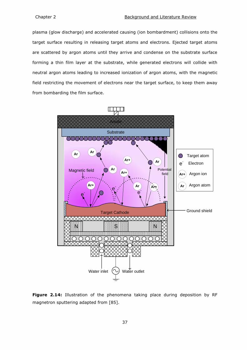
Chapter 2 Background and Literature Review
37
plasma (glow discharge) and accelerated causing (ion bombardment) collisions onto the
target surface resulting in releasing target atoms and electrons. Ejected target atoms
are scattered by argon atoms until they arrive and condense on the substrate surface
forming a thin film layer at the substrate, while generated electrons will collide with
neutral argon atoms leading to increased ionization of argon atoms, with the magnetic
field restricting the movement of electrons near the target surface, to keep them away
from bombarding the film surface.
Anode
Substrate
Ar
NN S
Ar+
Ar+
Ar+
Ar+
Ar
Ar
Ar
Ar
Water outlet Water inlet
e-
e- Electron
Ar+ Argon ion
Ar Argon atom
e-e
-
Target atom
Target Cathode Ground shield
Magnetic field Potential
field
Figure 2.14: Illustration of the phenomena taking place during deposition by RF
magnetron sputtering adapted from [85].
Chapter 2 Background and Literature Review
38
Conclusions 2.8
High performance TFTs for full active matrix display (LCD or OLED) applications should
demonstrate the following criteria: low threshold voltage (Vth), high electron mobility
(μ), high current on/off ratio, processing at low temperature to become compatible with
plastic substrates, good stability [86], and ideally be transparent. In this study all the
above important aspects must be considered for investigating ZnO and a-IGZO thin
films, and ZnO, a-IGZO based TFTs. This includes microstructure characterisation of
ZnO and a-IGZO to examine the defects, grain size, and crystal structure which
influences the electron mobility and the surface uniformity of the film, which is
important for channel interface considerations. This work was devoted to investigate
the effect of laser processing on microstructure and electrical properties of two oxide
semiconductor materials of ZnO and IGZO. The ZnO was deposited using two sputtering
techniques HiTUS, and RF magnetron sputtering. HiTUS films were deposited at room
temperature with different oxygen flow rates, RF magnetron sputtering films were
deposited at various RF power, oxygen concentration and substrate temperatures.
IGZO films were also deposited by RF magnetron sputtering, using two targets with two
stoichiometries (2:2:1) and (1:1:1), at various conditions to investigate the optimal
conditions in terms of conductivity and Hall mobility. IGZO-TFTs were fabricated and
subjected to laser and thermal processing to study the effect annealing process on TFT
performance.
Chapter 3 Experimental Techniques
39
Chapter 3
Experimental Techniques
3.1 Introduction
The initial phase of the work was concerned with the deposition of ZnO thin films by
using two sputtering deposition techniques: High Target Utilisation Sputtering (HiTUS),
and RF magnetron sputtering. A comparative study of post deposition processing was
then investigated using three annealing techniques, excimer laser annealing (ELA),
rapid thermal anneal (RTA), and thermal anneal (TA). Laser processing of IGZO thin
films deposited by RF magnetron sputtering was also investigated for optimization
studies. Finally, photoluminescence (PL), X-ray diffraction (XRD), transmission electron
microscopy (TEM), four point probe (4PP), and Hall Effect as thin film characterisation
techniques have been utilised to investigate the microstructure and electrical properties
of processed ZnO and IGZO thin films.
Thin film deposition 3.2
The first phase of this work was undertaken in collaboration with Cambridge University.
A series of initial trials involved a study of ZnO films and ZnO TFT devices based on the
bottom gate structure. These initial films were deposited at Cambridge University using
the High Target Utilisation sputtering (HiTUS) method, which is a technique previously
utilised by our group for luminescent materials and which offers high quality thin films
deposited at low temperature [87]. To investigate the properties of ZnO grown at room
temperature, the first stage of experimental work was the optimisation of the ZnO thin
films layer by a comparative study between three annealing techniques: thermal anneal
(TA), rapid thermal anneal (RTA), excimer laser anneal (ELA).
Chapter 3 Experimental Techniques
40
The second phase of this work involved ZnO thin films deposited on silicon, and silicon
dioxide covered silicon (SiO2/Si) substrates, by RF magnetron sputtering at various
substrate temperatures up to 400 °C. Following deposition at NTU, ZnO films were
subjected to laser annealing in order to study its effect on structure and semiconducting
properties.
The third phase of this work was devoted to studying the electrical properties of IGZO
thin films deposited by RF magnetron sputtering under various conditions. The optimal
conditions of film deposition and laser anneal were determined after electrical
characterisation of IGZO layers, and these conditions were used to fabricate test IGZO-
TFTs.
There are various techniques employed to grow transparent conducting oxides thin
films such as: molecular beam epitaxy [88], chemical vapour deposition [89], pulsed
laser deposition [90], atomic layer deposition [91], and RF magnetron sputtering [17].
Among these methods RF magnetron sputtering is the most commonly used technique,
and has been used extensively during the last decade, because of advantages such as
low operating temperature, uniformity, and reasonable quality of film at low cost [92].
For the research presented here, two sputtering techniques were used – High Target
Utilisation Sputtering (HiTUS) and RF-magnetron sputtering, with HiTUS depositions
being undertaken via collaboration with Cambridge University, and the RF-magnetron
sputtering undertaken at NTU.
3.2.1 High target utilisation sputtering HiTUS
High target utilisation sputtering (HiTUS) is a technique developed by a UK technology
company, Plasma Quest Ltd. [93] as an advanced RF sputtering technology, in which a
high density plasma is created in a remote chamber, to allow high deposition rates of ~
50 nm/min while maintaining excellent material properties [94]. Figure 3.1 shows a
schematic diagram of the employed HiTUS system. The system consists of a side arm
plasma launch system (PLS) connected to the main sputtering chamber. The PLS
Chapter 3 Experimental Techniques
41
contains a quartz tube surrounded by a copper antenna coil. 13.56 MHz RF power is
supplied to the side arm to generate highly intense plasma (1013 ions cm−3) away from
the substrate. Argon and oxygen are injected into the chamber separately using gas
distribution rings, with the argon next to the target for sputtering (of metallic target)
and oxygen in close proximity to the substrate for deposition of metal oxide thin films
[94]. The electromagnets at the exit of the PLS enhance and steer the plasma onto the
target resulting in a high density plasma over the full surface area of the target [87].
The HiTUS technique has been previously reported for the deposition of low
temperature metal oxides for transparent conducting electrodes [87, 95], light emitting
devices [96], thin film transistors [94], and electroluminescent devices [97].
For this work, several samples of ZnO films were deposited onto 100 mm silicon
substrates by using reactive sputtering from a 99.99% purity metallic zinc target.
Argon and oxygen were used as sputtering and reactive gases respectively, argon flow
rate of 55 sccm, at different oxygen flow rates of 28, 32, 35, 38, and 41 sccm. With RF
launch power of 1000 W and target bias power was 800 W. The films were deposited to
a thickness of 60 nm, and 200 nm, with no intentional substrate heating (maximum
achievable temperature during sputtering about 70 °C). Samples were received from
Cambridge University, following deposition by HiTUS in a system as shown in Figure
3.1.
Chapter 3 Experimental Techniques
42
PLASMA
Target Holder
RF
Power
Input
Side Arm Plasma
Source
Launch magnet
Steering magnet
Water cooling and DC bias
Substrate holder
Reactive Gas Feed
Substrate
Shutter
Pump
Systems
Ar Gas Inlet
Figure 3.1: Schematic diagram of the HiTUS system (adapted from [87]).
3.2.2 RF magnetron sputtering
All films deposited by RF magnetron sputtering were grown by the author using the
facilities at NTU. Initially, three ceramic targets (purity 99.99%) at 76.2 mm diameter
(5 mm thick) of transparent semiconductor oxides materials of zinc oxide (ZnO) and
indium gallium zinc oxide (IGZO) with two different stoichiometries (2:2:1) (1:1:1),
were loaded in the sputtering system. Figure 3.2 shows a schematic diagram of the RF
magnetron sputtering system used in this work.
Chapter 3 Experimental Techniques
43
O2
Interferometer
Load Lock
Rotary pump
Shutter
Substrate
Target
electrode
RF power
MFC
Heater
Controller
Matching Unit
RF power
13.56MHz
Loading arm
Diffusion pump
Liquid nitrogen
Cold trap
Baffle
valve
Cooling
Water
Ar
Knife valve
Figure 3.2: Schematic diagram of RF magnetron sputtering system.
Before sputtering took place, the deposition chamber was baked at 500 °C for about
one hour, in order to remove moisture that comes from the atmosphere following
loading the targets. After the chamber had cooled down, its base pressure reduced to
1.2 x 10⁻⁷ mbar. To start the deposition, a gas mixture of argon (sputtering) and
oxygen (reactive) was introduced to the chamber (at various oxygen concentrations)
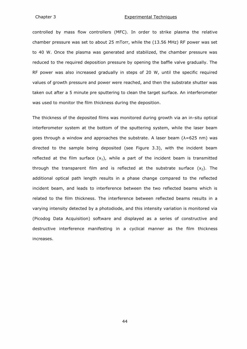
Chapter 3 Experimental Techniques
44
controlled by mass flow controllers (MFC). In order to strike plasma the relative
chamber pressure was set to about 25 mTorr, while the (13.56 MHz) RF power was set
to 40 W. Once the plasma was generated and stabilized, the chamber pressure was
reduced to the required deposition pressure by opening the baffle valve gradually. The
RF power was also increased gradually in steps of 20 W, until the specific required
values of growth pressure and power were reached, and then the substrate shutter was
taken out after a 5 minute pre sputtering to clean the target surface. An interferometer
was used to monitor the film thickness during the deposition.
The thickness of the deposited films was monitored during growth via an in-situ optical
interferometer system at the bottom of the sputtering system, while the laser beam
goes through a window and approaches the substrate. A laser beam (λ=625 nm) was
directed to the sample being deposited (see Figure 3.3), with the incident beam
reflected at the film surface (x1), while a part of the incident beam is transmitted
through the transparent film and is reflected at the substrate surface (x2). The
additional optical path length results in a phase change compared to the reflected
incident beam, and leads to interference between the two reflected beams which is
related to the film thickness. The interference between reflected beams results in a
varying intensity detected by a photodiode, and this intensity variation is monitored via
(Picodog Data Acquisition) software and displayed as a series of constructive and
destructive interference manifesting in a cyclical manner as the film thickness
increases.
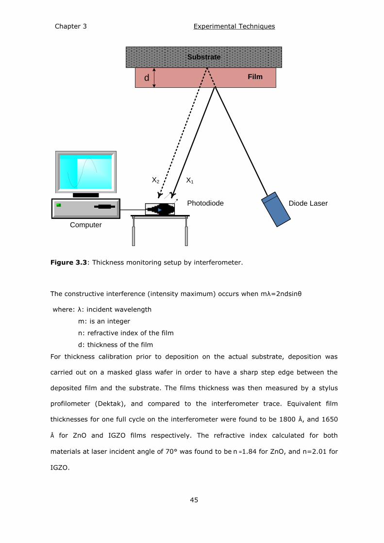
Chapter 3 Experimental Techniques
45
Diode Laser
Substrate
Computer
d
Photodiode
Film
X1X2
Figure 3.3: Thickness monitoring setup by interferometer.
The constructive interference (intensity maximum) occurs when mλ=2ndsinθ
where: λ: incident wavelength
m: is an integer
n: refractive index of the film
d: thickness of the film
For thickness calibration prior to deposition on the actual substrate, deposition was
carried out on a masked glass wafer in order to have a sharp step edge between the
deposited film and the substrate. The films thickness was then measured by a stylus
profilometer (Dektak), and compared to the interferometer trace. Equivalent film
thicknesses for one full cycle on the interferometer were found to be 1800 Å, and 1650
Å for ZnO and IGZO films respectively. The refractive index calculated for both
materials at laser incident angle of 70° was found to be n =1.84 for ZnO, and n=2.01 for
IGZO.
Chapter 3 Experimental Techniques
46
A series of depositions were carried out by RF magnetron sputtering as follows:
1- Samples of ZnO films of 60nm thickness, were deposited onto 100 mm silicon
(100) substrates at ambient temperatures (with no intentional substrate
heating) by varying oxygen concentrations (5% O2 in Ar-20% O2 in Ar), and RF
power (50, 100, 200, and 300 W) target diameter 76.2 nm with deposition
pressure set at 2 mTorr.
2- Samples of ZnO films (60 nm thick) were deposited onto silicon (100)
substrates, and (111) silicon dioxide coated silicon (SiO2/Si) substrates across a
range of substrate temperatures (RT, 100 °C, 200 °C, 300 °C, and 400 °C),
with oxygen concentrations of 20% O2 in Ar, RF power 50 W, and deposition
pressure of 2 mTorr.
3- Samples of IGZO thin films of 30 nm and 50 nm thickness were deposited by RF
magnetron sputtering from In2O3:Ga2O3:ZnO targets with two different
stoichiometries ratios of (2:2:1), and (1:1:1) onto (111) silicon dioxide coated
silicon substrates. Deposition was performed at ambient temperature (with no
intentional substrate heating) across a range of sputtering conditions by varying
oxygen concentrations (2% O2 in Ar, 5% O2 in Ar, and 10% O2 in Ar), and RF
power (50 W, 100 W) with target diameter 76.2nm at deposition pressure 2
mTorr to optimise the films for use in TFT device testing.
Excimer laser annealing (ELA) 3.3
The laser annealing process is a highly localised heat treatment technique to modify
and improve the properties of transparent conducting thin films. All of ZnO films, IGZO
films, and IGZO channel layers for TFTs that were deposited by both HiTUS and RF
magnetron sputtering with different growth conditions, were subjected to laser
treatment using a KrF excimer laser at NTU. Various fluences (energy density in units of
Joules per square centimetre – J/cm2) were applied via single or multiple pulses to
investigate the optimal conditions.
Chapter 3 Experimental Techniques
47
Laser processing was performed using a Lambda Physic LPX 305i excimer laser with an
operating wavelength 248 nm (KrF), at 20 ns pulse width. The pulse frequency varied
from 1 to 25 Hz, while a discharge voltage ranging from 14 to 24 kV was used to
provide course adjustment of the energy density. The ZnO and IGZO thin films were
diced onto 11 mm x 11 mm pieces, and processed using a homogenised laser beam
spot with an area of 10 mm x 10 mm. Various fluences were used in the range of 0
mJ/cm2 to 340 mJ/cm2 (±2%), using single pulse, and multiple pulse irradiation with
fine adjustment of fluence provided by a variable attenuator.
Figure 3.4 shows a schematic diagram of the laser beam plan view setup. Initially, the
raw beam is directed to a variable attenuator to control the energy density of the beam
by tilting the optics, and a UV lens is used to reduce the spot size in order to increase
the energy density. The main principle of the beam homogenizer is to divide the laser
beam into small sections (beamlets), and recombine them by over lapping in order to
produce a highly uniform energy profile over a predefined cross section size at the
mask location. This is achieved using two lens arrays and a condenser lens [98]. A
mask stage is used to pattern the beam spot to particular features, then the projection
lens is used to image the mask features onto the work piece. The distance from
projection lens to the sample cell was varied to control the laser spot size at the sample
position. Sample positioning was achieved utilising a computer controlled x-y–z
translation stage.
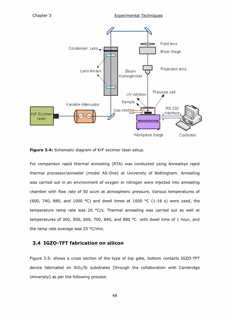
Chapter 3 Experimental Techniques
48
Figure 3.4: Schematic diagram of KrF excimer laser setup.
For comparison rapid thermal annealing (RTA) was conducted using Annealsys rapid
thermal processor/annealer (model AS-One) at University of Nottingham. Annealing
was carried out in an environment of oxygen or nitrogen were injected into annealing
chamber with flow rate of 50 sccm at atmospheric pressure, Various temperatures of
(600, 740, 880, and 1000 °C) and dwell times at 1000 °C (1-16 s) were used, the
temperature ramp rate was 20 °C/s. Thermal annealing was carried out as well at
temperatures of 300, 500, 600, 700, 840, and 880 °C with dwell time of 1 hour, and
the ramp rate average was 25 °C/min.
IGZO-TFT fabrication on silicon 3.4
Figure 3.5: shows a cross section of the type of top gate, bottom contacts IGZO-TFT
device fabricated on SiO2/Si substrates [through the collaboration with Cambridge
University] as per the following process:
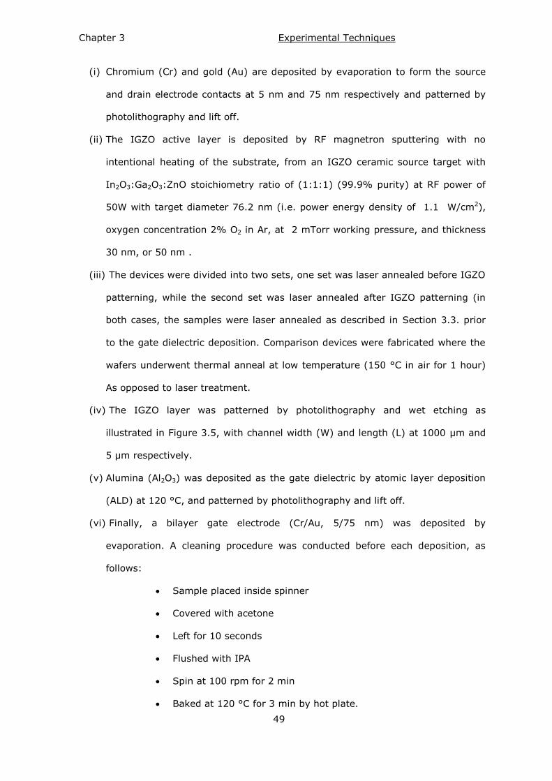
Chapter 3 Experimental Techniques
49
(i) Chromium (Cr) and gold (Au) are deposited by evaporation to form the source
and drain electrode contacts at 5 nm and 75 nm respectively and patterned by
photolithography and lift off.
(ii) The IGZO active layer is deposited by RF magnetron sputtering with no
intentional heating of the substrate, from an IGZO ceramic source target with
In2O3:Ga2O3:ZnO stoichiometry ratio of (1:1:1) (99.9% purity) at RF power of
50W with target diameter 76.2 nm (i.e. power energy density of 1.1 W/cm2),
oxygen concentration 2% O2 in Ar, at 2 mTorr working pressure, and thickness
30 nm, or 50 nm .
(iii) The devices were divided into two sets, one set was laser annealed before IGZO
patterning, while the second set was laser annealed after IGZO patterning (in
both cases, the samples were laser annealed as described in Section 3.3. prior
to the gate dielectric deposition. Comparison devices were fabricated where the
wafers underwent thermal anneal at low temperature (150 °C in air for 1 hour)
As opposed to laser treatment.
(iv) The IGZO layer was patterned by photolithography and wet etching as
illustrated in Figure 3.5, with channel width (W) and length (L) at 1000 μm and
5 μm respectively.
(v) Alumina (Al2O3) was deposited as the gate dielectric by atomic layer deposition
(ALD) at 120 °C, and patterned by photolithography and lift off.
(vi) Finally, a bilayer gate electrode (Cr/Au, 5/75 nm) was deposited by
evaporation. A cleaning procedure was conducted before each deposition, as
follows:
Sample placed inside spinner
Covered with acetone
Left for 10 seconds
Flushed with IPA
Spin at 100 rpm for 2 min
Baked at 120 °C for 3 min by hot plate.
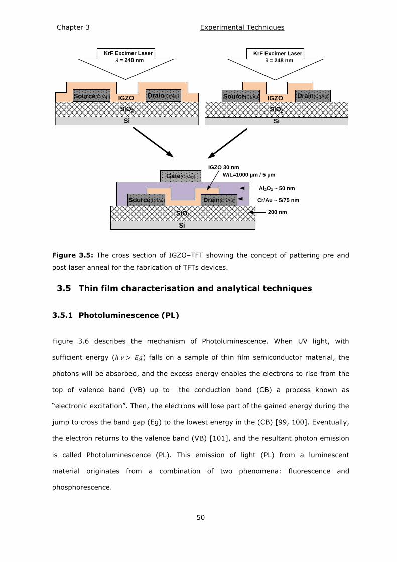
Chapter 3 Experimental Techniques
50
Si
SiO2
KrF Excimer Laser
λ= 248 nm
Drain(Cr/Au) Source(Cr/Au) IGZO
KrF Excimer Laser
λ= 248 nm
Si
SiO2
Drain(Cr/Au) Source(Cr/Au) IGZO
Cr/Au ~ 5/75 nm
SiO2
Gate(Cr/Au)
Drain(Cr/Au) Source(Cr/Au)
Si
IGZO 30 nm
Al2O3 ~ 50 nm
W/L=1000 µm / 5 µm
200 nm
Figure 3.5: The cross section of IGZO–TFT showing the concept of pattering pre and
post laser anneal for the fabrication of TFTs devices.
Thin film characterisation and analytical techniques 3.5
3.5.1 Photoluminescence (PL)
Figure 3.6 describes the mechanism of Photoluminescence. When UV light, with
sufficient energy ( ) falls on a sample of thin film semiconductor material, the
photons will be absorbed, and the excess energy enables the electrons to rise from the
top of valence band (VB) up to the conduction band (CB) a process known as
―electronic excitation‖. Then, the electrons will lose part of the gained energy during the
jump to cross the band gap (Eg) to the lowest energy in the (CB) [99, 100]. Eventually,
the electron returns to the valence band (VB) [101], and the resultant photon emission
is called Photoluminescence (PL). This emission of light (PL) from a luminescent
material originates from a combination of two phenomena: fluorescence and
phosphorescence.
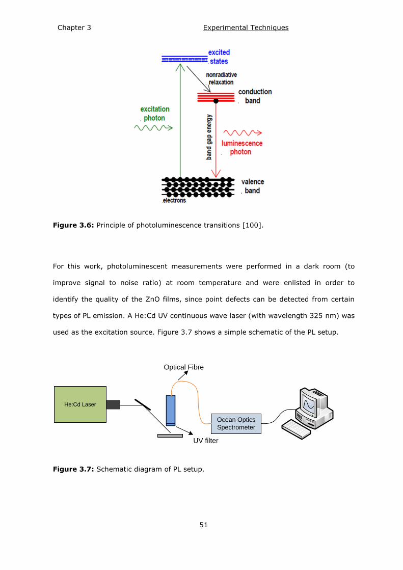
Chapter 3 Experimental Techniques
51
Figure 3.6: Principle of photoluminescence transitions [100].
For this work, photoluminescent measurements were performed in a dark room (to
improve signal to noise ratio) at room temperature and were enlisted in order to
identify the quality of the ZnO films, since point defects can be detected from certain
types of PL emission. A He:Cd UV continuous wave laser (with wavelength 325 nm) was
used as the excitation source. Figure 3.7 shows a simple schematic of the PL setup.
He:Cd Laser
Ocean Optics
Spectrometer
Optical Fibre
UV filter
Figure 3.7: Schematic diagram of PL setup.
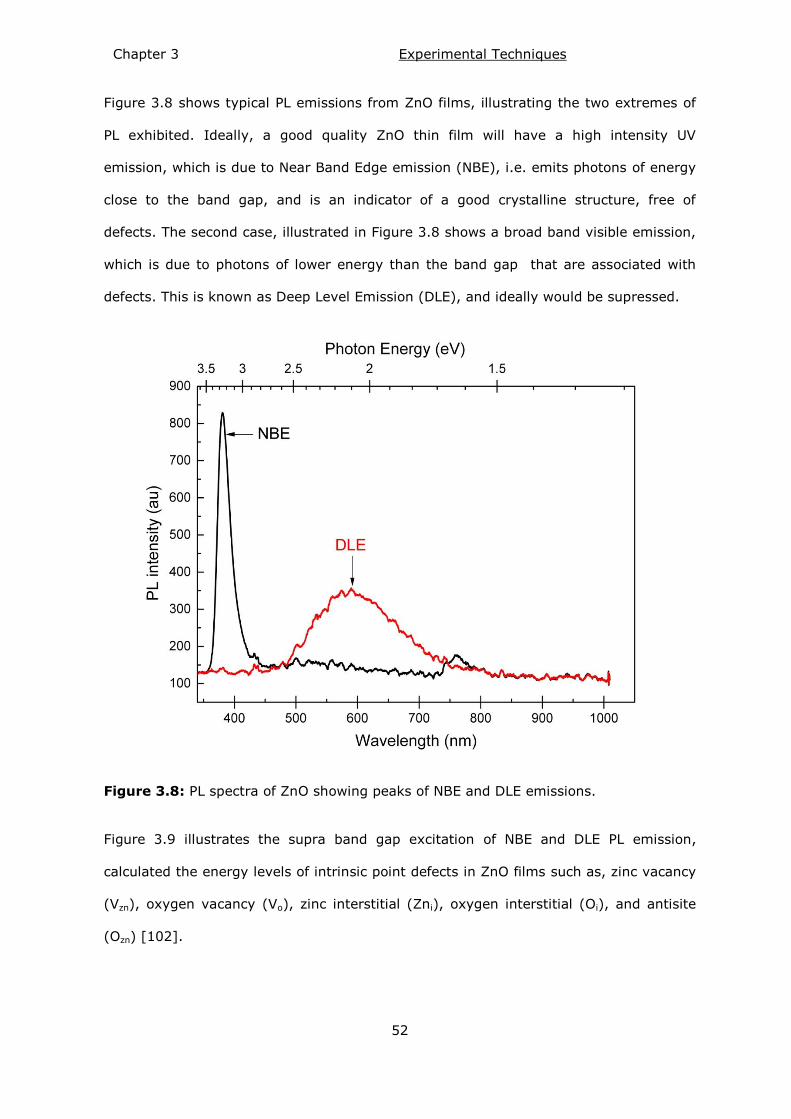
Chapter 3 Experimental Techniques
52
Figure 3.8 shows typical PL emissions from ZnO films, illustrating the two extremes of
PL exhibited. Ideally, a good quality ZnO thin film will have a high intensity UV
emission, which is due to Near Band Edge emission (NBE), i.e. emits photons of energy
close to the band gap, and is an indicator of a good crystalline structure, free of
defects. The second case, illustrated in Figure 3.8 shows a broad band visible emission,
which is due to photons of lower energy than the band gap that are associated with
defects. This is known as Deep Level Emission (DLE), and ideally would be supressed.
Figure 3.8: PL spectra of ZnO showing peaks of NBE and DLE emissions.
Figure 3.9 illustrates the supra band gap excitation of NBE and DLE PL emission,
calculated the energy levels of intrinsic point defects in ZnO films such as, zinc vacancy
(Vzn), oxygen vacancy (Vo), zinc interstitial (Zni), oxygen interstitial (Oi), and antisite
(Ozn) [102].
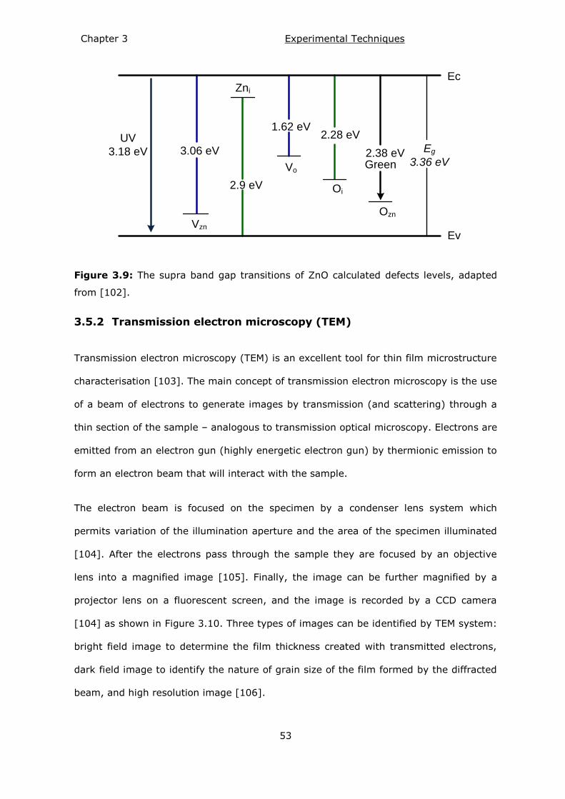
Chapter 3 Experimental Techniques
53
UV
3.18 eV
Zni
Vzn
3.06 eV
2.9 eV
1.62 eV
Vo
2.28 eV
Oi
2.38 eV
Ozn
Eg
3.36 eV
Ec
Ev
Green
Figure 3.9: The supra band gap transitions of ZnO calculated defects levels, adapted
from [102].
3.5.2 Transmission electron microscopy (TEM)
Transmission electron microscopy (TEM) is an excellent tool for thin film microstructure
characterisation [103]. The main concept of transmission electron microscopy is the use
of a beam of electrons to generate images by transmission (and scattering) through a
thin section of the sample – analogous to transmission optical microscopy. Electrons are
emitted from an electron gun (highly energetic electron gun) by thermionic emission to
form an electron beam that will interact with the sample.
The electron beam is focused on the specimen by a condenser lens system which
permits variation of the illumination aperture and the area of the specimen illuminated
[104]. After the electrons pass through the sample they are focused by an objective
lens into a magnified image [105]. Finally, the image can be further magnified by a
projector lens on a fluorescent screen, and the image is recorded by a CCD camera
[104] as shown in Figure 3.10. Three types of images can be identified by TEM system:
bright field image to determine the film thickness created with transmitted electrons,
dark field image to identify the nature of grain size of the film formed by the diffracted
beam, and high resolution image [106].
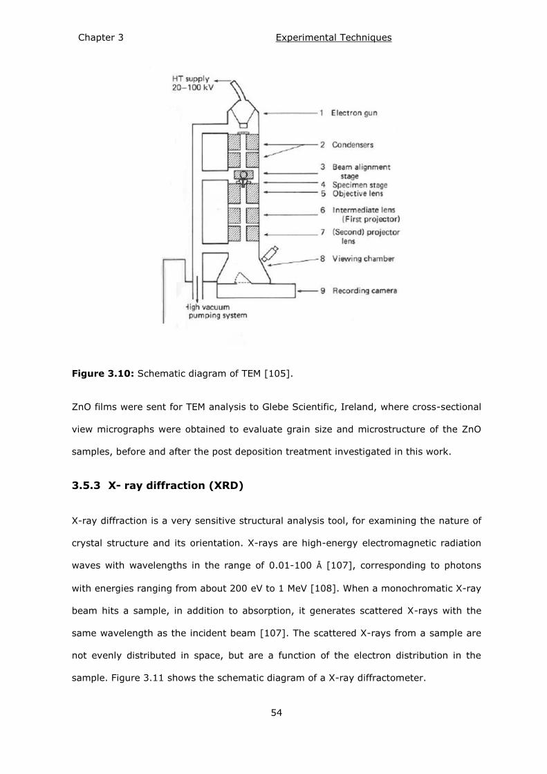
Chapter 3 Experimental Techniques
54
Figure 3.10: Schematic diagram of TEM [105].
ZnO films were sent for TEM analysis to Glebe Scientific, Ireland, where cross-sectional
view micrographs were obtained to evaluate grain size and microstructure of the ZnO
samples, before and after the post deposition treatment investigated in this work.
3.5.3 X- ray diffraction (XRD)
X-ray diffraction is a very sensitive structural analysis tool, for examining the nature of
crystal structure and its orientation. X-rays are high-energy electromagnetic radiation
waves with wavelengths in the range of 0.01-100 Å [107], corresponding to photons
with energies ranging from about 200 eV to 1 MeV [108]. When a monochromatic X-ray
beam hits a sample, in addition to absorption, it generates scattered X-rays with the
same wavelength as the incident beam [107]. The scattered X-rays from a sample are
not evenly distributed in space, but are a function of the electron distribution in the
sample. Figure 3.11 shows the schematic diagram of a X-ray diffractometer.
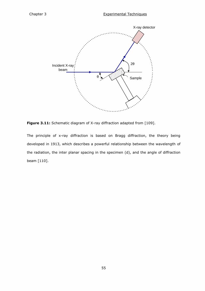
Chapter 3 Experimental Techniques
55
Incident X-ray
beam
2θ
θ
X-ray detector
Sample
Figure 3.11: Schematic diagram of X-ray diffraction adapted from [109].
The principle of x-ray diffraction is based on Bragg diffraction, the theory being
developed in 1913, which describes a powerful relationship between the wavelength of
the radiation, the inter planar spacing in the specimen (d), and the angle of diffraction
beam [110].
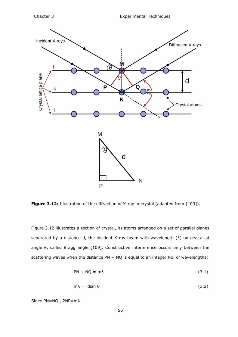
Chapter 3 Experimental Techniques
56
Incident X-rays
d
Diffracted X-rays
θ
θ
2θ
Crystal atoms
M
N
P Q
Cry
sta
l la
ttic
e p
lan
e
h
k
I
θ
NP
M
d
Figure 3.12: Illustration of the diffraction of X-ray in crystal (adapted from [109]).
Figure 3.12 illustrates a section of crystal, its atoms arranged on a set of parallel planes
separated by a distance d, the incident X-ray beam with wavelength (λ) on crystal at
angle θ, called Bragg angle [109]. Constructive interference occurs only between the
scattering waves when the distance PN + NQ is equal to an integer No. of wavelengths;
PN + NQ = mλ (3.1)
mλ = dsin θ (3.2)
Since PN=NQ , 2NP=mλ
Chapter 3 Experimental Techniques
57
NP=dsin θ (3.3)
2NP=2dsin θ (3.4)
mλ=2dsin θ (3.5)
where: λ: is the wavelength of the incident x-ray beam
θ: Bragg‘s angle
d: the distance between adjacent crystallographic planes in specimen.
m: is an integer.
The Scherrer formula was used in this work to estimate crystal domain size of the
materials:
D=
(3.6)
where, D: Crystallite size of materials
K: constant
λ: X-ray wavelength
B: full width at half maximum (FWHM) of the peak being investigated
θ: Bragg diffraction angle
For this work, X- ray diffraction measurements were performed for ZnO, and IGZO films
on silicon substrates using a Phillips PANalytical X-Pert PRO system operated in Bragg-
Brentano configuration with a monochromated Cu-Kd1 radiation source (λ =1.54056 Å)
-to identify the crystalline changes induced by excimer laser annealing (ELA), and
thermal annealing. A bracket flat stage was used to hold the films, and the scanning
parameters were controlled via X-Pert Data Collector software.
Chapter 3 Experimental Techniques
58
3.5.4 X-ray photoelectron spectroscopy (XPS)
X-ray photoelectron spectroscopy (XPS) is known as Electron Spectroscopy for
Chemical Analysis (ESCA). XPS is a surface analytical techniques in which identifying
the elemental and chemical species information arising from the top surface of the
sample. XPS is a photoelectron effect was observed in 1887 by Hertz [106]. The basic
principle of XPS is when a monochromatic X-ray emitted from X-ray source and directed
to the sample placed in high vacuum environment to achieve the analysis without
interference from gas phase collisions, as the photons hit the sample cause direct
transfer of energy from photon to core–level electron and photoelectrons are ejected
from irradiated atoms [111]. The energy of ejected electron measured by a
spectrometer, in which related to the binding energy of atom from which electron is
ejected. The basic of this process can be stated as
BE= –KE–φ (3.7)
where, BE is the binding energy of the electron in the atom, is the photon energy of
X-ray source, KE is the kinetic energy of the emitted electron, and φ is the
spectrometer work function.
For this research work XPS measurements were carried out at University of
Nottingham, to investigate the stoichiometry of as-deposited and thermally annealed
HiTUS ZnO films deposited at various oxygen flow rates.
3.5.5 Four point probe (4PP) measurements
A four point probe measurements system was used in order to determine the sheet
resistance (and resistivity) of the thin film [112]. The main concept of the in-line four
point probe is having four equally spaced probes placed on the semiconductor film
(sample under test) and applying a current through the outer two probes in order to
measure a potential drop (voltage) between the two inner probes as shown in Figure
3.13. In a four point probe measurement, the impact of resistance in the voltage
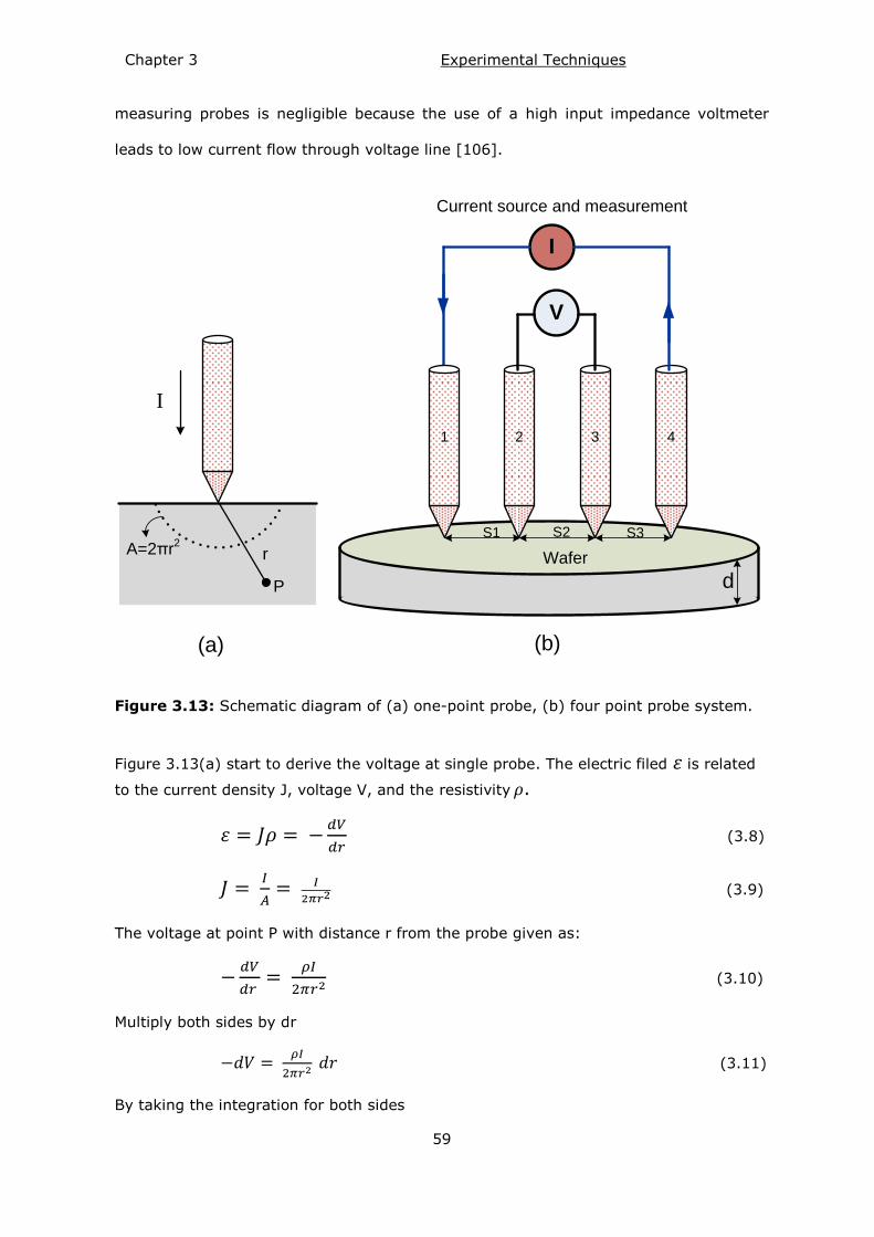
Chapter 3 Experimental Techniques
59
measuring probes is negligible because the use of a high input impedance voltmeter
leads to low current flow through voltage line [106].
(a) (b)
431 2
V
I
Wafer
S2 S3S1
d
Current source and measurement
P
A=2πr2
r
I
Figure 3.13: Schematic diagram of (a) one-point probe, (b) four point probe system.
Figure 3.13(a) start to derive the voltage at single probe. The electric filed is related
to the current density J, voltage V, and the resistivity .
(3.8)
(3.9)
The voltage at point P with distance r from the probe given as:
(3.10)
Multiply both sides by dr
(3.11)
By taking the integration for both sides
Chapter 3 Experimental Techniques
60
∫
∫
(3.12)
∫
(3.13)
*
+
(3.14)
As depicted in Figure 3.13(b), four point probe placed on a semi-infinite film the cross
voltage measured between two inner probes ―probes 2 and 3‖, so the voltage at probe
2 (V2) and probe 3 (V3) with S1, S2, and S3 the distance between the probes given as:
(
) (3.15)
(
) (3.16)
The total voltage between probe 2 and 3 V= V2 – V3 given as:
(
( )
) (3.17)
Then the resistivity ρ is given by
(
)*
(3.18)
When the probe spacing S1=S2=S3=S
( ) (3.19)
For infinite thin film equation (3.19) becomes
(3.20)
Sheet resistance Rsh = ρ/t , where t: is the film thickness
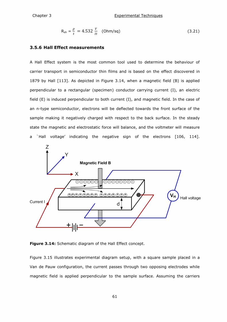
Chapter 3 Experimental Techniques
61
Rsh =
(Ohm/sq) (3.21)
3.5.6 Hall Effect measurements
A Hall Effect system is the most common tool used to determine the behaviour of
carrier transport in semiconductor thin films and is based on the effect discovered in
1879 by Hall [113]. As depicted in Figure 3.14, when a magnetic field (B) is applied
perpendicular to a rectangular (specimen) conductor carrying current (I), an electric
field (E) is induced perpendicular to both current (I), and magnetic field. In the case of
an n-type semiconductor, electrons will be deflected towards the front surface of the
sample making it negatively charged with respect to the back surface. In the steady
state the magnetic and electrostatic force will balance, and the voltmeter will measure
a `Hall voltage‘ indicating the negative sign of the electrons [106, 114].
Figure 3.14: Schematic diagram of the Hall Effect concept.
Figure 3.15 illustrates experimental diagram setup, with a square sample placed in a
Van de Pauw configuration, the current passes through two opposing electrodes while
magnetic field is applied perpendicular to the sample surface. Assuming the carriers
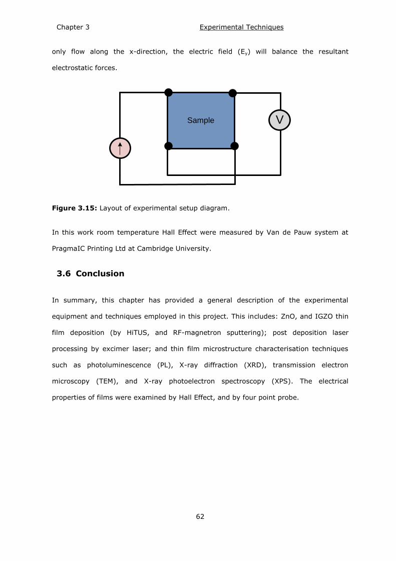
Chapter 3 Experimental Techniques
62
only flow along the x-direction, the electric field (Ey) will balance the resultant
electrostatic forces.
Sample V
Figure 3.15: Layout of experimental setup diagram.
In this work room temperature Hall Effect were measured by Van de Pauw system at
PragmaIC Printing Ltd at Cambridge University.
Conclusion 3.6
In summary, this chapter has provided a general description of the experimental
equipment and techniques employed in this project. This includes: ZnO, and IGZO thin
film deposition (by HiTUS, and RF-magnetron sputtering); post deposition laser
processing by excimer laser; and thin film microstructure characterisation techniques
such as photoluminescence (PL), X-ray diffraction (XRD), transmission electron
microscopy (TEM), and X-ray photoelectron spectroscopy (XPS). The electrical
properties of films were examined by Hall Effect, and by four point probe.
Chapter 4 ZnO Thin Films by HiTUS
63
Chapter 4
ZnO Thin Films by HiTUS
Introduction 4.1
This chapter presents the results from a microstructure characterisation of the ZnO thin
films deposited at room temperature by the HiTUS method followed by post deposition
annealing studies which were undertaken by the author using thermal annealing (TA),
rapid thermal annealing (RTA), and laser annealing (LA). Five 60 nm thick HiTUS ZnO
samples deposited on Si at various oxygen flow rates: 41, 38, 35, 32 and 28 sccm.
Section 4.2 presents room temperature photoluminescence characterisation results for
the thermally annealed, rapid thermal anneal, excimer laser annealed films
respectively. Section 4.3 presents the corresponding cross sectional of TEM images of
the films, and section 4.4 presents XRD structure patterns of the films following the
three annealing methods investigated. Finally, section 4.5 summaries the finding
related to HiTUS grown ZnO.
Photoluminescence characterisation 4.2
Photoluminescence (PL) spectrometry is a powerful tool for characterizing the optical
quality of semiconductor materials such as the metal oxide thin films investigated here.
The PL intensity is related directly to the defect densities in materials [115], and so is a
useful indicator of film quality. Specifically for the films studied here, it is well known
that the PL characteristics of ZnO are generally influenced by the deposition method
and preparation conditions [116], and are representative of film quality [67]. This work
is focused on two different deposition techniques: HiTUS and RF magnetron sputtering,
hence comparison of the resultant film quality via these two techniques is of interest. In
particular, the PL properties of ZnO films in the UV and visible part of the spectrum are
known to be closely related to microstructure [117, 118]. In undoped ZnO (intrinsic)
Chapter 4 ZnO Thin Films by HiTUS
64
films the UV ―Near Band emission‖(NBE) at around 380nm (3.2 eV) is attributed to
excitonic recombination, and the broad visible peak known as ―Deep Level
Emission‖(DLE) which ranges from 450 nm to 750 nm (2.7 eV to 1.65 eV) is correlated
directly with the intrinsic defects and defect complexes in the materials [84, 115, 119].
It has been reported that an improvement of NBE intensity is clearly observed after
thermal annealing with increase annealing temperatures [19, 115, 116]. Hence, the
intensity ratio of NBE over DLE is usually taken as an indication of the degree of
crystallinity improvement [120].
For the work presented in this chapter, the main objective is to investigate the
deposition and to perform a comparative study of the effect of post processing
techniques on ZnO thin films thermal annealing TA, rapid thermal annealing RTA, and
laser annealing LA. Hence a study of the resultant film properties has been undertaken
using PL spectrometry, where a particular interest is directed at how the NBE and DLE
are affected.
4.2.1 Photoluminescence of thermally annealed HiTUS ZnO films
Figure 4.1 illustrates the room temperature photoluminescence spectra of the 41 sccm
ZnO thin films, following an annealing process in a furnace at temperatures up to 700
°C and at various dwell times up to 2 hours. The PL spectra shows a strong broad
visible emission peak, associated with deep level emission (DLE), consisting of
orange/red emissions which has been shown to be attributed to radiative transitions
from defect sites associated with excess oxygen [121]. As shown in Figure 4.2 the DLE
PL increases significantly with increasing temperature up to 840 °C, whereas there is
negligible appearance of ultra-violet near band edge emission (NBE), even at high
temperatures. In this case, the dwell time is kept constant at 1 hour and the
temperature reaches 880 °C. The 840 °C were clearly producing the highest DLE
emission, however processing at longer periods results in film ablation, since
temperature at 700 °C was investigated by means of dwell time (Figure 4.1). It is
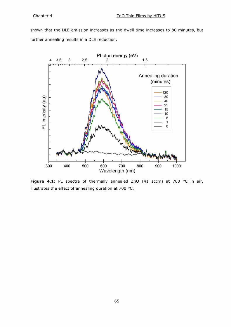
Chapter 4 ZnO Thin Films by HiTUS
65
shown that the DLE emission increases as the dwell time increases to 80 minutes, but
further annealing results in a DLE reduction.
Figure 4.1: PL spectra of thermally annealed ZnO (41 sccm) at 700 °C in air,
illustrates the effect of annealing duration at 700 °C.
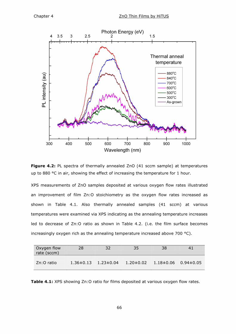
Chapter 4 ZnO Thin Films by HiTUS
66
Figure 4.2: PL spectra of thermally annealed ZnO (41 sccm sample) at temperatures
up to 880 °C in air, showing the effect of increasing the temperature for 1 hour.
XPS measurements of ZnO samples deposited at various oxygen flow rates illustrated
an improvement of film Zn:O stoichiometry as the oxygen flow rates increased as
shown in Table 4.1. Also thermally annealed samples (41 sccm) at various
temperatures were examined via XPS indicating as the annealing temperature increases
led to decrease of Zn:O ratio as shown in Table 4.2. (i.e. the film surface becomes
increasingly oxygen rich as the annealing temperature increased above 700 °C).
Oxygen flow
rate (sccm)
28 32 35 38 41
Zn:O ratio
1.36±0.13
1.23±0.04
1.20±0.02
1.18±0.06
0.94±0.05
Table 4.1: XPS showing Zn:O ratio for films deposited at various oxygen flow rates.
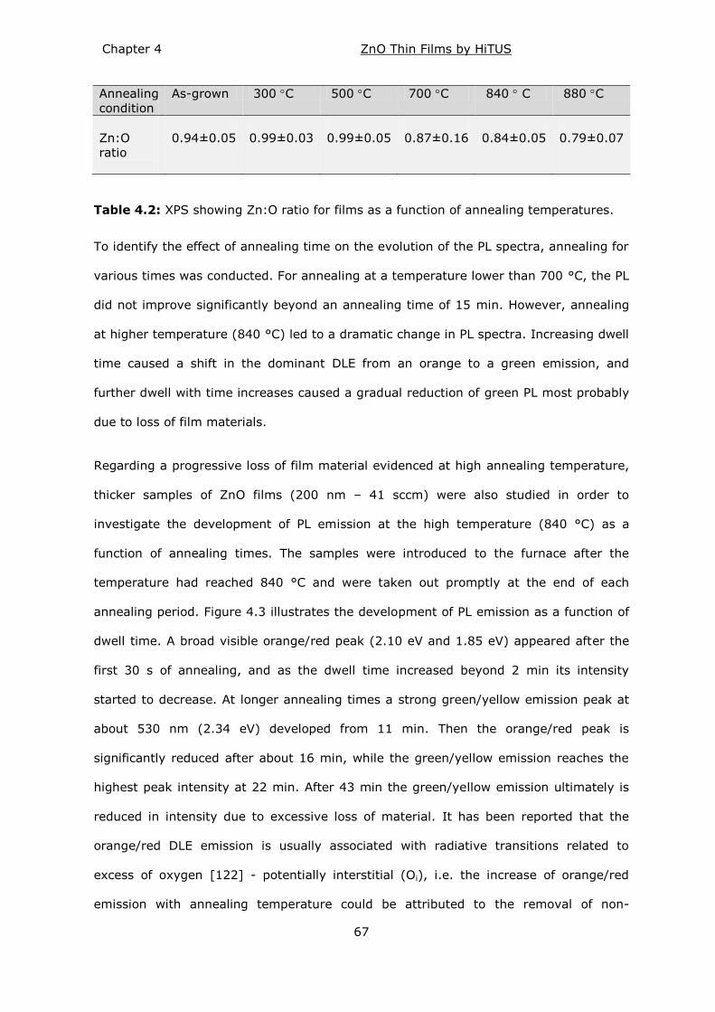
Chapter 4 ZnO Thin Films by HiTUS
67
Annealing
condition
As-grown 300 C 500 C 700 C 840 C 880 C
Zn:O
ratio
0.94±0.05
0.99±0.03
0.99±0.05
0.87±0.16
0.84±0.05
0.79±0.07
Table 4.2: XPS showing Zn:O ratio for films as a function of annealing temperatures.
To identify the effect of annealing time on the evolution of the PL spectra, annealing for
various times was conducted. For annealing at a temperature lower than 700 °C, the PL
did not improve significantly beyond an annealing time of 15 min. However, annealing
at higher temperature (840 °C) led to a dramatic change in PL spectra. Increasing dwell
time caused a shift in the dominant DLE from an orange to a green emission, and
further dwell with time increases caused a gradual reduction of green PL most probably
due to loss of film materials.
Regarding a progressive loss of film material evidenced at high annealing temperature,
thicker samples of ZnO films (200 nm – 41 sccm) were also studied in order to
investigate the development of PL emission at the high temperature (840 °C) as a
function of annealing times. The samples were introduced to the furnace after the
temperature had reached 840 °C and were taken out promptly at the end of each
annealing period. Figure 4.3 illustrates the development of PL emission as a function of
dwell time. A broad visible orange/red peak (2.10 eV and 1.85 eV) appeared after the
first 30 s of annealing, and as the dwell time increased beyond 2 min its intensity
started to decrease. At longer annealing times a strong green/yellow emission peak at
about 530 nm (2.34 eV) developed from 11 min. Then the orange/red peak is
significantly reduced after about 16 min, while the green/yellow emission reaches the
highest peak intensity at 22 min. After 43 min the green/yellow emission ultimately is
reduced in intensity due to excessive loss of material. It has been reported that the
orange/red DLE emission is usually associated with radiative transitions related to
excess of oxygen [122] - potentially interstitial (Oi), i.e. the increase of orange/red
emission with annealing temperature could be attributed to the removal of non-
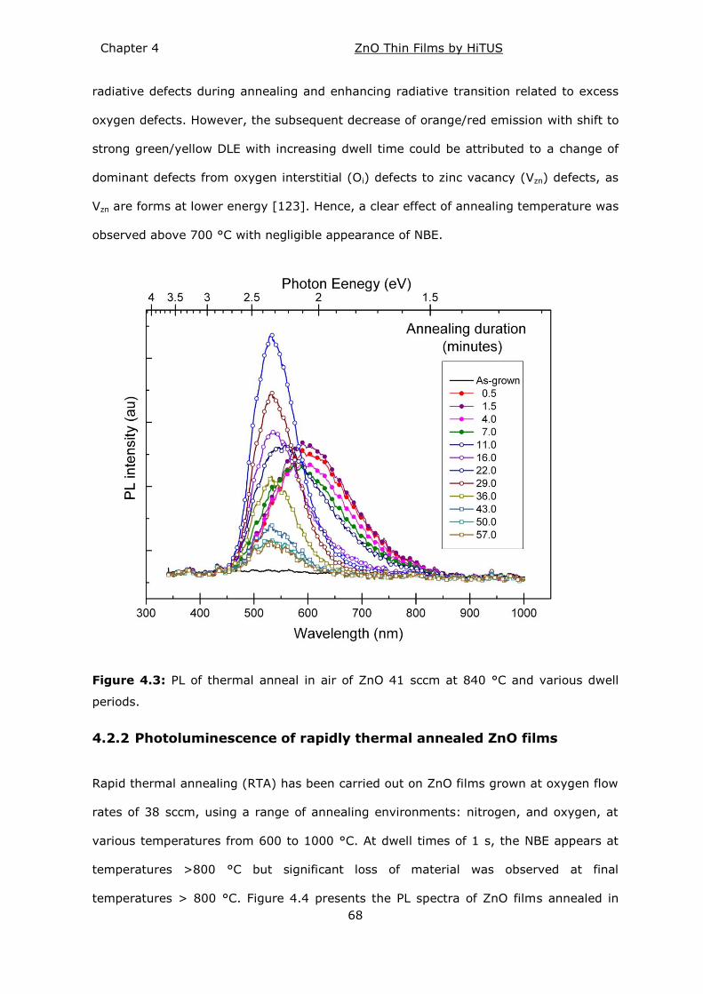
Chapter 4 ZnO Thin Films by HiTUS
68
radiative defects during annealing and enhancing radiative transition related to excess
oxygen defects. However, the subsequent decrease of orange/red emission with shift to
strong green/yellow DLE with increasing dwell time could be attributed to a change of
dominant defects from oxygen interstitial (Oi) defects to zinc vacancy (Vzn) defects, as
Vzn are forms at lower energy [123]. Hence, a clear effect of annealing temperature was
observed above 700 °C with negligible appearance of NBE.
Figure 4.3: PL of thermal anneal in air of ZnO 41 sccm at 840 °C and various dwell
periods.
4.2.2 Photoluminescence of rapidly thermal annealed ZnO films
Rapid thermal annealing (RTA) has been carried out on ZnO films grown at oxygen flow
rates of 38 sccm, using a range of annealing environments: nitrogen, and oxygen, at
various temperatures from 600 to 1000 °C. At dwell times of 1 s, the NBE appears at
temperatures >800 °C but significant loss of material was observed at final
temperatures > 800 °C. Figure 4.4 presents the PL spectra of ZnO films annealed in
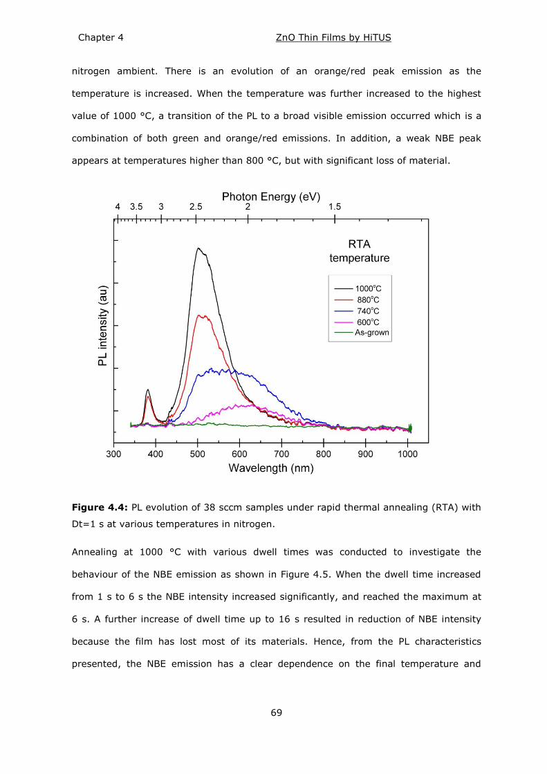
Chapter 4 ZnO Thin Films by HiTUS
69
nitrogen ambient. There is an evolution of an orange/red peak emission as the
temperature is increased. When the temperature was further increased to the highest
value of 1000 °C, a transition of the PL to a broad visible emission occurred which is a
combination of both green and orange/red emissions. In addition, a weak NBE peak
appears at temperatures higher than 800 °C, but with significant loss of material.
Figure 4.4: PL evolution of 38 sccm samples under rapid thermal annealing (RTA) with
Dt=1 s at various temperatures in nitrogen.
Annealing at 1000 °C with various dwell times was conducted to investigate the
behaviour of the NBE emission as shown in Figure 4.5. When the dwell time increased
from 1 s to 6 s the NBE intensity increased significantly, and reached the maximum at
6 s. A further increase of dwell time up to 16 s resulted in reduction of NBE intensity
because the film has lost most of its materials. Hence, from the PL characteristics
presented, the NBE emission has a clear dependence on the final temperature and
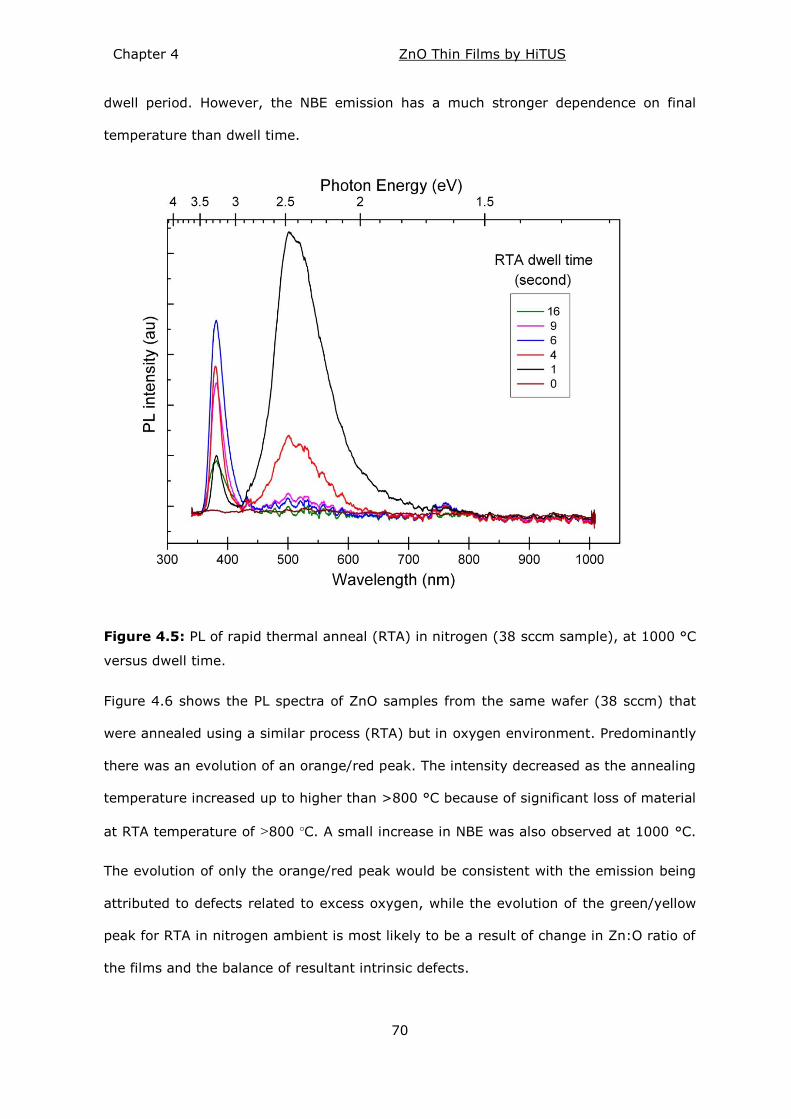
Chapter 4 ZnO Thin Films by HiTUS
70
dwell period. However, the NBE emission has a much stronger dependence on final
temperature than dwell time.
Figure 4.5: PL of rapid thermal anneal (RTA) in nitrogen (38 sccm sample), at 1000 °C
versus dwell time.
Figure 4.6 shows the PL spectra of ZnO samples from the same wafer (38 sccm) that
were annealed using a similar process (RTA) but in oxygen environment. Predominantly
there was an evolution of an orange/red peak. The intensity decreased as the annealing
temperature increased up to higher than >800 °C because of significant loss of material
at RTA temperature of >800 °C. A small increase in NBE was also observed at 1000 °C.
The evolution of only the orange/red peak would be consistent with the emission being
attributed to defects related to excess oxygen, while the evolution of the green/yellow
peak for RTA in nitrogen ambient is most likely to be a result of change in Zn:O ratio of
the films and the balance of resultant intrinsic defects.
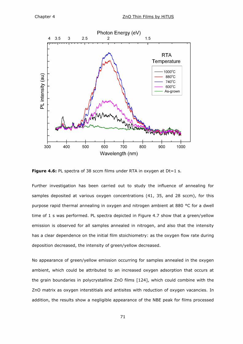
Chapter 4 ZnO Thin Films by HiTUS
71
Figure 4.6: PL spectra of 38 sccm films under RTA in oxygen at Dt=1 s.
Further investigation has been carried out to study the influence of annealing for
samples deposited at various oxygen concentrations (41, 35, and 28 sccm), for this
purpose rapid thermal annealing in oxygen and nitrogen ambient at 880 °C for a dwell
time of 1 s was performed. PL spectra depicted in Figure 4.7 show that a green/yellow
emission is observed for all samples annealed in nitrogen, and also that the intensity
has a clear dependence on the initial film stoichiometry: as the oxygen flow rate during
deposition decreased, the intensity of green/yellow decreased.
No appearance of green/yellow emission occurring for samples annealed in the oxygen
ambient, which could be attributed to an increased oxygen adsorption that occurs at
the grain boundaries in polycrystalline ZnO films [124], which could combine with the
ZnO matrix as oxygen interstitials and antisites with reduction of oxygen vacancies. In
addition, the results show a negligible appearance of the NBE peak for films processed
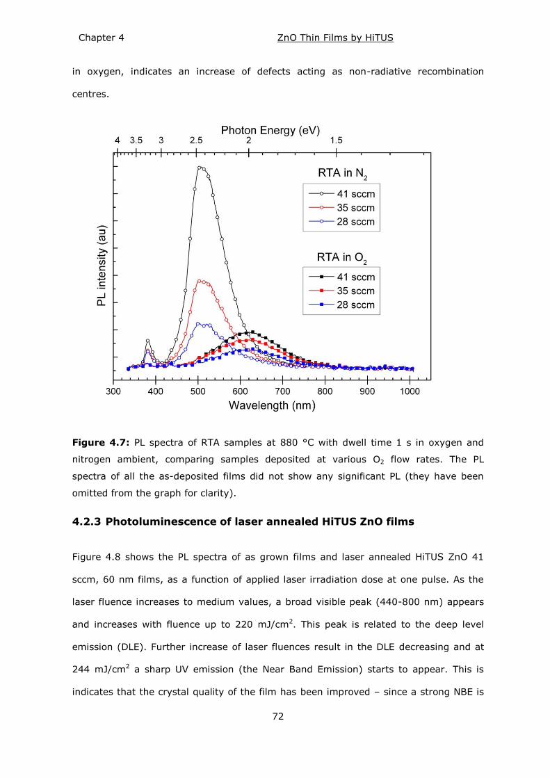
Chapter 4 ZnO Thin Films by HiTUS
72
in oxygen, indicates an increase of defects acting as non-radiative recombination
centres.
Figure 4.7: PL spectra of RTA samples at 880 °C with dwell time 1 s in oxygen and
nitrogen ambient, comparing samples deposited at various O2 flow rates. The PL
spectra of all the as-deposited films did not show any significant PL (they have been
omitted from the graph for clarity).
4.2.3 Photoluminescence of laser annealed HiTUS ZnO films
Figure 4.8 shows the PL spectra of as grown films and laser annealed HiTUS ZnO 41
sccm, 60 nm films, as a function of applied laser irradiation dose at one pulse. As the
laser fluence increases to medium values, a broad visible peak (440-800 nm) appears
and increases with fluence up to 220 mJ/cm2. This peak is related to the deep level
emission (DLE). Further increase of laser fluences result in the DLE decreasing and at
244 mJ/cm2 a sharp UV emission (the Near Band Emission) starts to appear. This is
indicates that the crystal quality of the film has been improved – since a strong NBE is
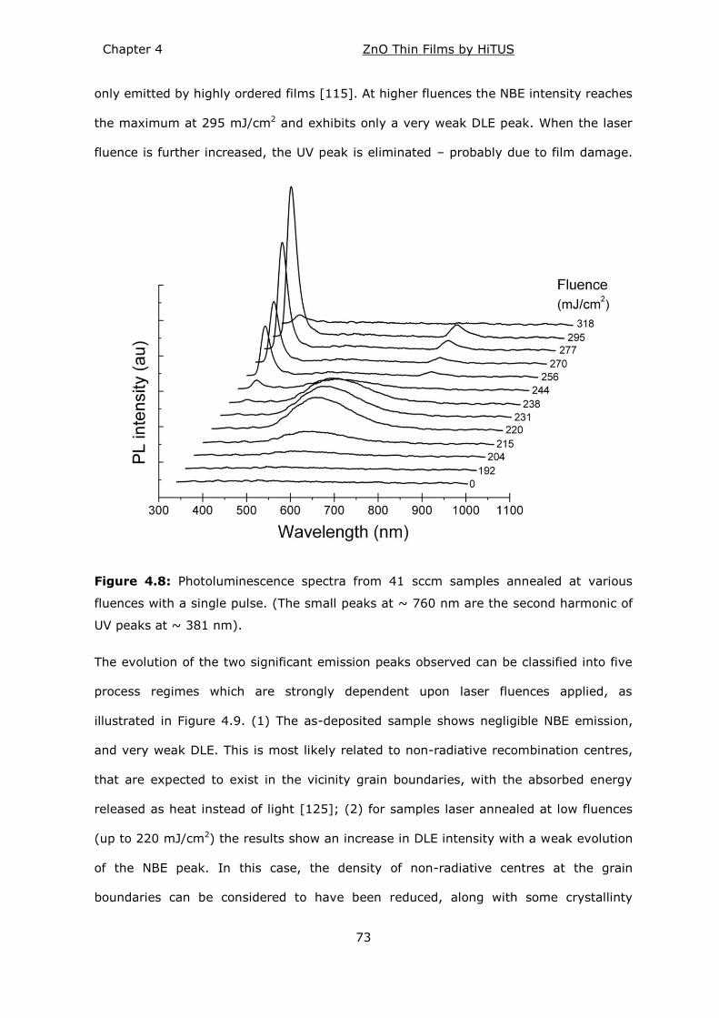
Chapter 4 ZnO Thin Films by HiTUS
73
only emitted by highly ordered films [115]. At higher fluences the NBE intensity reaches
the maximum at 295 mJ/cm2 and exhibits only a very weak DLE peak. When the laser
fluence is further increased, the UV peak is eliminated – probably due to film damage.
Figure 4.8: Photoluminescence spectra from 41 sccm samples annealed at various
fluences with a single pulse. (The small peaks at ~ 760 nm are the second harmonic of
UV peaks at ~ 381 nm).
The evolution of the two significant emission peaks observed can be classified into five
process regimes which are strongly dependent upon laser fluences applied, as
illustrated in Figure 4.9. (1) The as-deposited sample shows negligible NBE emission,
and very weak DLE. This is most likely related to non-radiative recombination centres,
that are expected to exist in the vicinity grain boundaries, with the absorbed energy
released as heat instead of light [125]; (2) for samples laser annealed at low fluences
(up to 220 mJ/cm2) the results show an increase in DLE intensity with a weak evolution
of the NBE peak. In this case, the density of non-radiative centres at the grain
boundaries can be considered to have been reduced, along with some crystallinty
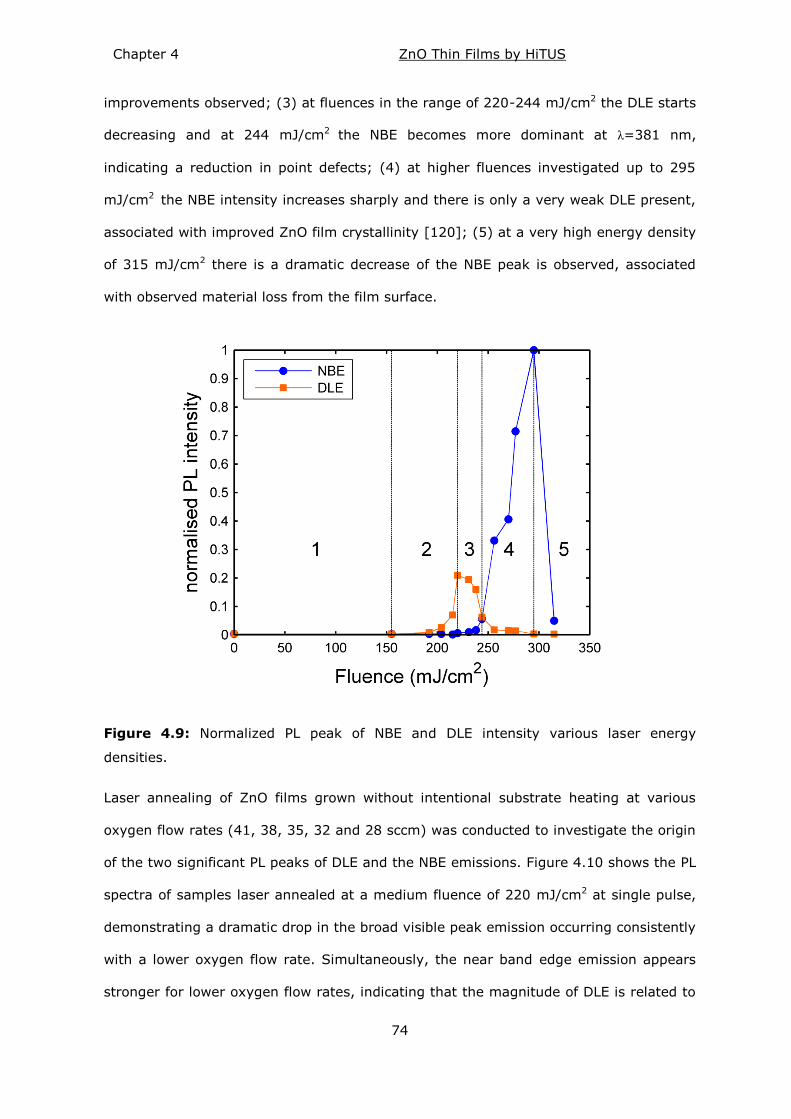
Chapter 4 ZnO Thin Films by HiTUS
74
improvements observed; (3) at fluences in the range of 220-244 mJ/cm2 the DLE starts
decreasing and at 244 mJ/cm2 the NBE becomes more dominant at λ=381 nm,
indicating a reduction in point defects; (4) at higher fluences investigated up to 295
mJ/cm2 the NBE intensity increases sharply and there is only a very weak DLE present,
associated with improved ZnO film crystallinity [120]; (5) at a very high energy density
of 315 mJ/cm2 there is a dramatic decrease of the NBE peak is observed, associated
with observed material loss from the film surface.
Figure 4.9: Normalized PL peak of NBE and DLE intensity various laser energy
densities.
Laser annealing of ZnO films grown without intentional substrate heating at various
oxygen flow rates (41, 38, 35, 32 and 28 sccm) was conducted to investigate the origin
of the two significant PL peaks of DLE and the NBE emissions. Figure 4.10 shows the PL
spectra of samples laser annealed at a medium fluence of 220 mJ/cm2 at single pulse,
demonstrating a dramatic drop in the broad visible peak emission occurring consistently
with a lower oxygen flow rate. Simultaneously, the near band edge emission appears
stronger for lower oxygen flow rates, indicating that the magnitude of DLE is related to
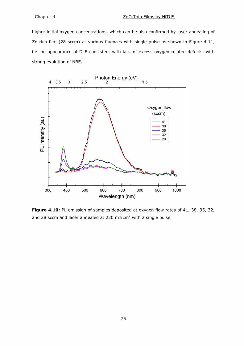
Chapter 4 ZnO Thin Films by HiTUS
75
higher initial oxygen concentrations, which can be also confirmed by laser annealing of
Zn-rich film (28 sccm) at various fluences with single pulse as shown in Figure 4.11,
i.e. no appearance of DLE consistent with lack of excess oxygen related defects, with
strong evolution of NBE.
Figure 4.10: PL emission of samples deposited at oxygen flow rates of 41, 38, 35, 32,
and 28 sccm and laser annealed at 220 mJ/cm2 with a single pulse.
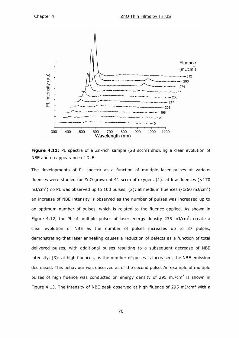
Chapter 4 ZnO Thin Films by HiTUS
76
Figure 4.11: PL spectra of a Zn-rich sample (28 sccm) showing a clear evolution of
NBE and no appearance of DLE.
The developments of PL spectra as a function of multiple laser pulses at various
fluences were studied for ZnO grown at 41 sccm of oxygen. (1): at low fluences (<170
mJ/cm2) no PL was observed up to 100 pulses, (2): at medium fluences (<260 mJ/cm2)
an increase of NBE intensity is observed as the number of pulses was increased up to
an optimum number of pulses, which is related to the fluence applied. As shown in
Figure 4.12, the PL of multiple pulses of laser energy density 235 mJ/cm2, create a
clear evolution of NBE as the number of pulses increases up to 37 pulses,
demonstrating that laser annealing causes a reduction of defects as a function of total
delivered pulses, with additional pulses resulting to a subsequent decrease of NBE
intensity. (3): at high fluences, as the number of pulses is increased, the NBE emission
decreased. This behaviour was observed as of the second pulse. An example of multiple
pulses of high fluence was conducted on energy density of 295 mJ/cm2 is shown in
Figure 4.13. The intensity of NBE peak observed at high fluence of 295 mJ/cm2 with a
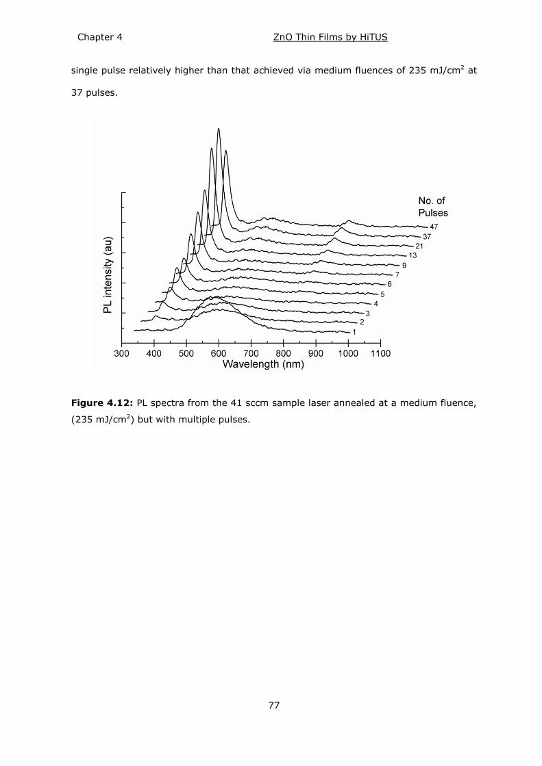
Chapter 4 ZnO Thin Films by HiTUS
77
single pulse relatively higher than that achieved via medium fluences of 235 mJ/cm2 at
37 pulses.
Figure 4.12: PL spectra from the 41 sccm sample laser annealed at a medium fluence,
(235 mJ/cm2) but with multiple pulses.
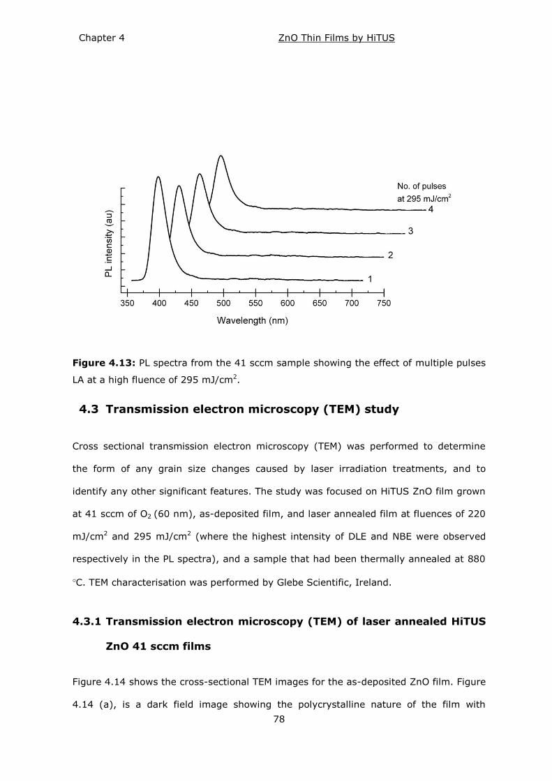
Chapter 4 ZnO Thin Films by HiTUS
78
Figure 4.13: PL spectra from the 41 sccm sample showing the effect of multiple pulses
LA at a high fluence of 295 mJ/cm2.
Transmission electron microscopy (TEM) study 4.3
Cross sectional transmission electron microscopy (TEM) was performed to determine
the form of any grain size changes caused by laser irradiation treatments, and to
identify any other significant features. The study was focused on HiTUS ZnO film grown
at 41 sccm of O2 (60 nm), as-deposited film, and laser annealed film at fluences of 220
mJ/cm2 and 295 mJ/cm2 (where the highest intensity of DLE and NBE were observed
respectively in the PL spectra), and a sample that had been thermally annealed at 880
°C. TEM characterisation was performed by Glebe Scientific, Ireland.
4.3.1 Transmission electron microscopy (TEM) of laser annealed HiTUS
ZnO 41 sccm films
Figure 4.14 shows the cross-sectional TEM images for the as-deposited ZnO film. Figure
4.14 (a), is a dark field image showing the polycrystalline nature of the film with
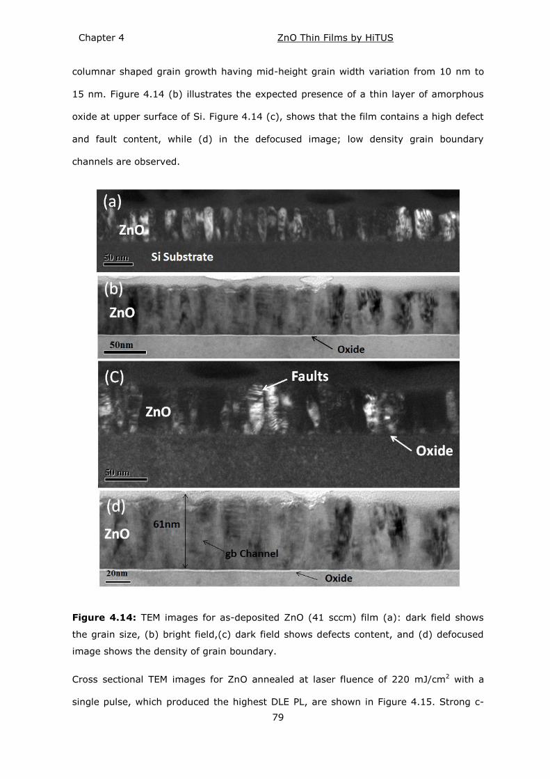
Chapter 4 ZnO Thin Films by HiTUS
79
columnar shaped grain growth having mid-height grain width variation from 10 nm to
15 nm. Figure 4.14 (b) illustrates the expected presence of a thin layer of amorphous
oxide at upper surface of Si. Figure 4.14 (c), shows that the film contains a high defect
and fault content, while (d) in the defocused image; low density grain boundary
channels are observed.
Figure 4.14: TEM images for as-deposited ZnO (41 sccm) film (a): dark field shows
the grain size, (b) bright field,(c) dark field shows defects content, and (d) defocused
image shows the density of grain boundary.
Cross sectional TEM images for ZnO annealed at laser fluence of 220 mJ/cm2 with a
single pulse, which produced the highest DLE PL, are shown in Figure 4.15. Strong c-
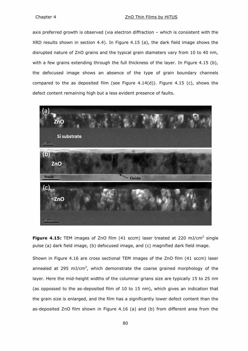
Chapter 4 ZnO Thin Films by HiTUS
80
axis preferred growth is observed (via electron diffraction – which is consistent with the
XRD results shown in section 4.4). In Figure 4.15 (a), the dark field image shows the
disrupted nature of ZnO grains and the typical grain diameters vary from 10 to 40 nm,
with a few grains extending through the full thickness of the layer. In Figure 4.15 (b),
the defocused image shows an absence of the type of grain boundary channels
compared to the as deposited film (see Figure 4.14(d)). Figure 4.15 (c), shows the
defect content remaining high but a less evident presence of faults.
Figure 4.15: TEM images of ZnO film (41 sccm) laser treated at 220 mJ/cm2 single
pulse (a) dark field image, (b) defocused image, and (c) magnified dark field image.
Shown in Figure 4.16 are cross sectional TEM images of the ZnO film (41 sccm) laser
annealed at 295 mJ/cm2, which demonstrate the coarse grained morphology of the
layer. Here the mid-height widths of the columnar grians size are typically 15 to 25 nm
(as oppossed to the as-deposited film of 10 to 15 nm), which gives an indication that
the grain size is enlarged, and the film has a significantly lower defect content than the
as-deposited ZnO film shown in Figure 4.16 (a) and (b) from different area from the
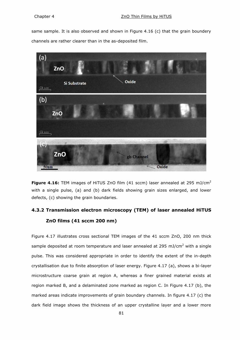
Chapter 4 ZnO Thin Films by HiTUS
81
same sample. It is also observed and shown in Figure 4.16 (c) that the grain boundery
channels are rather clearer than in the as-deposited film.
Figure 4.16: TEM images of HiTUS ZnO film (41 sccm) laser annealed at 295 mJ/cm2
with a single pulse, (a) and (b) dark fields showing grain sizes enlarged, and lower
defects, (c) showing the grain boundaries.
4.3.2 Transmission electron microscopy (TEM) of laser annealed HiTUS
ZnO films (41 sccm 200 nm)
Figure 4.17 illustrates cross sectional TEM images of the 41 sccm ZnO, 200 nm thick
sample deposited at room temperature and laser annealed at 295 mJ/cm2 with a single
pulse. This was considered appropriate in order to identify the extent of the in-depth
crystallisation due to finite absorption of laser energy. Figure 4.17 (a), shows a bi-layer
microstructure coarse grain at region A, whereas a finer grained material exists at
region marked B, and a delaminated zone marked as region C. In Figure 4.17 (b), the
marked areas indicate improvements of grain boundary channels. In figure 4.17 (c) the
dark field image shows the thickness of an upper crystalline layer and a lower more
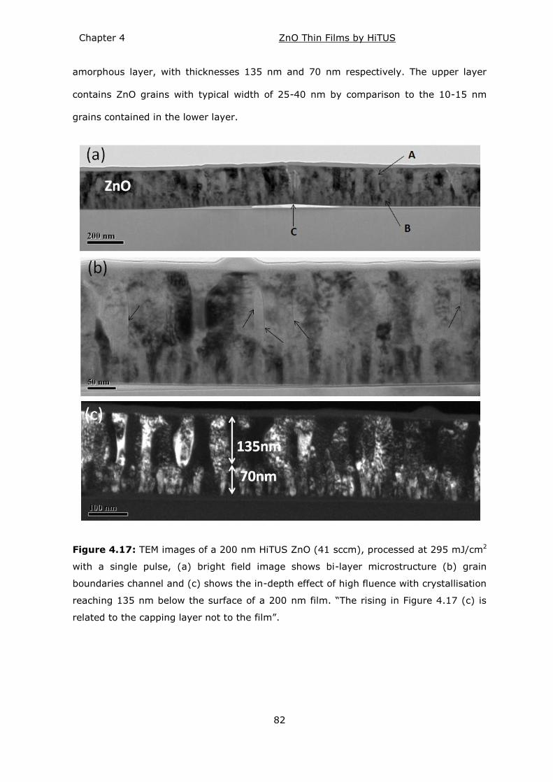
Chapter 4 ZnO Thin Films by HiTUS
82
amorphous layer, with thicknesses 135 nm and 70 nm respectively. The upper layer
contains ZnO grains with typical width of 25-40 nm by comparison to the 10-15 nm
grains contained in the lower layer.
Figure 4.17: TEM images of a 200 nm HiTUS ZnO (41 sccm), processed at 295 mJ/cm2
with a single pulse, (a) bright field image shows bi-layer microstructure (b) grain
boundaries channel and (c) shows the in-depth effect of high fluence with crystallisation
reaching 135 nm below the surface of a 200 nm film. ―The rising in Figure 4.17 (c) is
related to the capping layer not to the film‖.
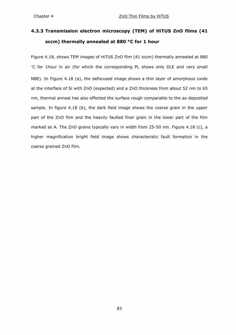
Chapter 4 ZnO Thin Films by HiTUS
83
4.3.3 Transmission electron microscopy (TEM) of HiTUS ZnO films (41
sccm) thermally annealed at 880 °C for 1 hour
Figure 4.18, shows TEM images of HiTUS ZnO film (41 sccm) thermally annealed at 880
°C for 1hour in air (for which the corresponding PL shows only DLE and very small
NBE). In Figure 4.18 (a), the defocused image shows a thin layer of amorphous oxide
at the interface of Si with ZnO (expected) and a ZnO thickness from about 52 nm to 65
nm, thermal anneal has also effected the surface rough comparable to the as-deposited
sample. In figure 4.18 (b), the dark field image shows the coarse grain in the upper
part of the ZnO film and the heavily faulted finer grain in the lower part of the film
marked as A. The ZnO grains typically vary in width from 25-50 nm. Figure 4.18 (c), a
higher magnification bright field image shows characteristic fault formation in the
coarse grained ZnO film.
Chapter 4 ZnO Thin Films by HiTUS
84
Figure 4.18: TEM images of HiTUS ZnO film (41 sccm) thermally annealed at 880 C°
for 1 hour, (a) defocused image shows thickness variation (b) dark field image the
nature of grains (c) higher magnification bright field shows fault formation.
X- ray diffraction characterisation 4.4
The crystalline characteristics of selected ZnO samples, for the three annealing
methods used, were investigated by XRD using the X-Pert Panalytical system operated
in Bragg- Brentano mode. The results indicate that the as-deposited films are under
compressive stress with a polycrystalline structure. However, the annealing processes
resulted in a shift of the (002) peak to higher diffraction angles, consistent with a
modification of the films stress as a function of annealing, leading to improved crystal
structure, and causing modification of the films stress to tensile. In all cases samples
exhibited c-axis preferred orientation as represented by the (002) diffraction peak, and
stress changed from compressive to tensile stress.
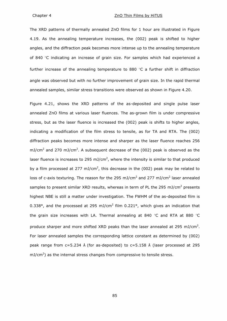
Chapter 4 ZnO Thin Films by HiTUS
85
The XRD patterns of thermally annealed ZnO films for 1 hour are illustrated in Figure
4.19. As the annealing temperature increases, the (002) peak is shifted to higher
angles, and the diffraction peak becomes more intense up to the annealing temperature
of 840 °C indicating an increase of grain size. For samples which had experienced a
further increase of the annealing temperature to 880 °C a further shift in diffraction
angle was observed but with no further improvement of grain size. In the rapid thermal
annealed samples, similar stress transitions were observed as shown in Figure 4.20.
Figure 4.21, shows the XRD patterns of the as-deposited and single pulse laser
annealed ZnO films at various laser fluences. The as-grown film is under compressive
stress, but as the laser fluence is increased the (002) peak is shifts to higher angles,
indicating a modification of the film stress to tensile, as for TA and RTA. The (002)
diffraction peaks becomes more intense and sharper as the laser fluence reaches 256
mJ/cm2 and 270 mJ/cm2. A subsequent decrease of the (002) peak is observed as the
laser fluence is increases to 295 mJ/cm2, where the intensity is similar to that produced
by a film processed at 277 mJ/cm2, this decrease in the (002) peak may be related to
loss of c-axis texturing. The reason for the 295 mJ/cm2 and 277 mJ/cm2 laser annealed
samples to present similar XRD results, whereas in term of PL the 295 mJ/cm2 presents
highest NBE is still a matter under investigation. The FWHM of the as-deposited film is
0.338°, and the processed at 295 mJ/cm2 film 0.221°, which gives an indication that
the grain size increases with LA. Thermal annealing at 840 °C and RTA at 880 °C
produce sharper and more shifted XRD peaks than the laser annealed at 295 mJ/cm2.
For laser annealed samples the corresponding lattice constant as determined by (002)
peak range from c=5.234 Å (for as-deposited) to c=5.158 Å (laser processed at 295
mJ/cm2) as the internal stress changes from compressive to tensile stress.
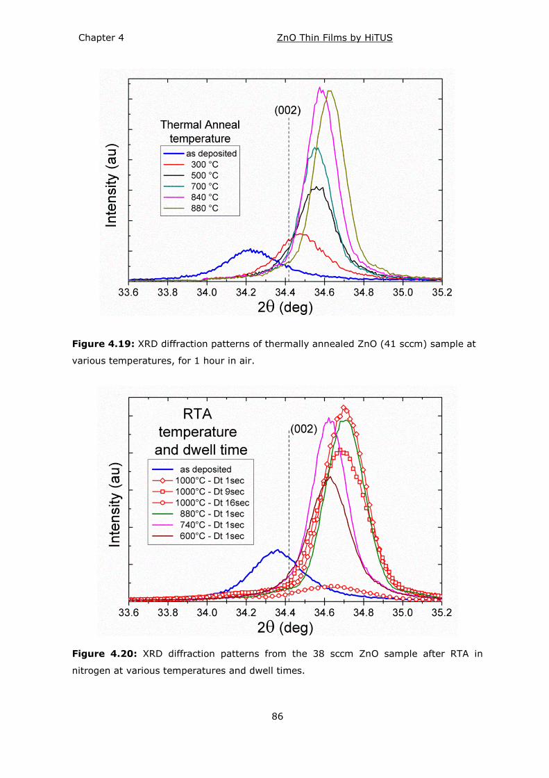
Chapter 4 ZnO Thin Films by HiTUS
86
Figure 4.19: XRD diffraction patterns of thermally annealed ZnO (41 sccm) sample at
various temperatures, for 1 hour in air.
Figure 4.20: XRD diffraction patterns from the 38 sccm ZnO sample after RTA in
nitrogen at various temperatures and dwell times.
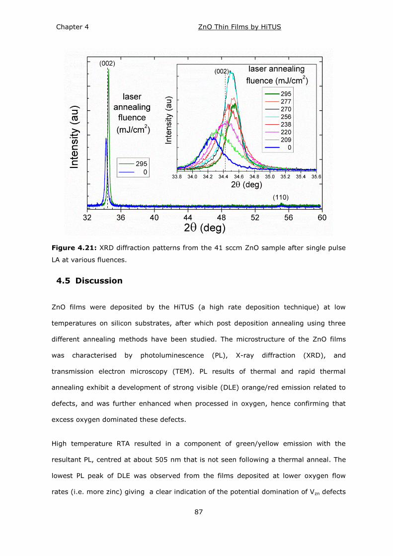
Chapter 4 ZnO Thin Films by HiTUS
87
Figure 4.21: XRD diffraction patterns from the 41 sccm ZnO sample after single pulse
LA at various fluences.
Discussion 4.5
ZnO films were deposited by the HiTUS (a high rate deposition technique) at low
temperatures on silicon substrates, after which post deposition annealing using three
different annealing methods have been studied. The microstructure of the ZnO films
was characterised by photoluminescence (PL), X-ray diffraction (XRD), and
transmission electron microscopy (TEM). PL results of thermal and rapid thermal
annealing exhibit a development of strong visible (DLE) orange/red emission related to
defects, and was further enhanced when processed in oxygen, hence confirming that
excess oxygen dominated these defects.
High temperature RTA resulted in a component of green/yellow emission with the
resultant PL, centred at about 505 nm that is not seen following a thermal anneal. The
lowest PL peak of DLE was observed from the films deposited at lower oxygen flow
rates (i.e. more zinc) giving a clear indication of the potential domination of Vzn defects
Chapter 4 ZnO Thin Films by HiTUS
88
rather than VO, which would be consistent with the lower energy formation of Vzn
defects [123]. RTA at even higher temperature demonstrates a significant development
of the NBE peak (crystallinity related PL). This is potentially indicating a reduction of
defects at grain boundaries. However, higher temperatures cause film degradation and
material loss for both TA and RTA.
Important results were demonstrated by laser annealing, where it was proven possible
to modify the internal properties of the ZnO films with a grain re-growth, crystallinity
improvement, and a dramatic reduction of point defect density (as indicated by the NBE
to DLE ratio [120] ), and without any film degradation or material loss that occurs in
high temperature thermal and rapid thermal annealing. Laser annealing is a highly
localised technique with a controlled in-depth crystallisation and modification of the
films was demonstrated by cross sectional TEM images (as shown in Figure 4.15 (c)).
At the same time it was clearly shown that LA offers an enlargement of grain size, with
XRD analysis giving further confirmation evidence for crystal structure improvement
with increasing laser fluence. This demonstrates that laser processing is a useful
method to control the in-depth modification of the thin film sample, gaining a benefit
from isolating the processed region from the substrate, and hence being compatible of
processing films on flexible substrates without any damage to the film or the substrate.
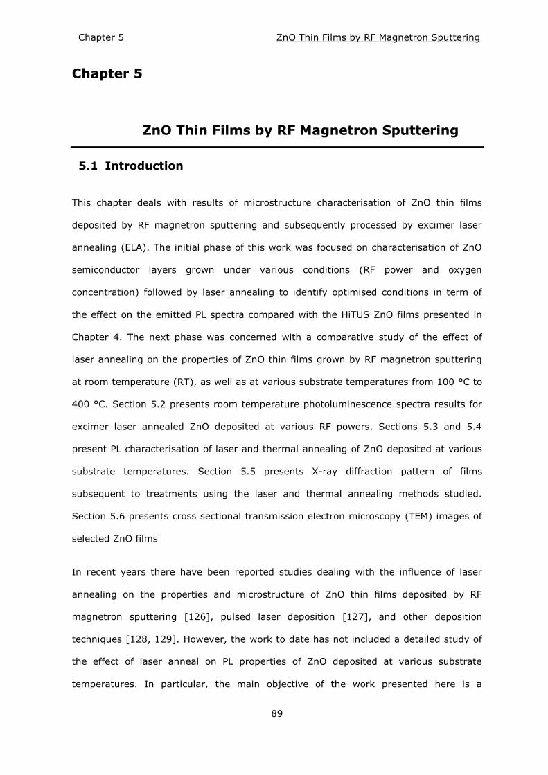
Chapter 5 ZnO Thin Films by RF Magnetron Sputtering
89
Chapter 5
ZnO Thin Films by RF Magnetron Sputtering
Introduction 5.1
This chapter deals with results of microstructure characterisation of ZnO thin films
deposited by RF magnetron sputtering and subsequently processed by excimer laser
annealing (ELA). The initial phase of this work was focused on characterisation of ZnO
semiconductor layers grown under various conditions (RF power and oxygen
concentration) followed by laser annealing to identify optimised conditions in term of
the effect on the emitted PL spectra compared with the HiTUS ZnO films presented in
Chapter 4. The next phase was concerned with a comparative study of the effect of
laser annealing on the properties of ZnO thin films grown by RF magnetron sputtering
at room temperature (RT), as well as at various substrate temperatures from 100 °C to
400 °C. Section 5.2 presents room temperature photoluminescence spectra results for
excimer laser annealed ZnO deposited at various RF powers. Sections 5.3 and 5.4
present PL characterisation of laser and thermal annealing of ZnO deposited at various
substrate temperatures. Section 5.5 presents X-ray diffraction pattern of films
subsequent to treatments using the laser and thermal annealing methods studied.
Section 5.6 presents cross sectional transmission electron microscopy (TEM) images of
selected ZnO films
In recent years there have been reported studies dealing with the influence of laser
annealing on the properties and microstructure of ZnO thin films deposited by RF
magnetron sputtering [126], pulsed laser deposition [127], and other deposition
techniques [128, 129]. However, the work to date has not included a detailed study of
the effect of laser anneal on PL properties of ZnO deposited at various substrate
temperatures. In particular, the main objective of the work presented here is a
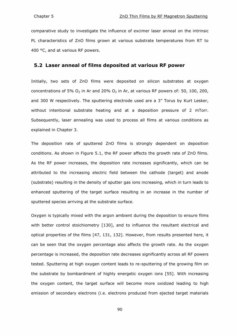
Chapter 5 ZnO Thin Films by RF Magnetron Sputtering
90
comparative study to investigate the influence of excimer laser anneal on the intrinsic
PL characteristics of ZnO films grown at various substrate temperatures from RT to
400 °C, and at various RF powers.
Laser anneal of films deposited at various RF power 5.2
Initially, two sets of ZnO films were deposited on silicon substrates at oxygen
concentrations of 5% O2 in Ar and 20% O2 in Ar, at various RF powers of: 50, 100, 200,
and 300 W respectively. The sputtering electrode used are a 3‖ Torus by Kurt Lesker,
without intentional substrate heating and at a deposition pressure of 2 mTorr.
Subsequently, laser annealing was used to process all films at various conditions as
explained in Chapter 3.
The deposition rate of sputtered ZnO films is strongly dependent on deposition
conditions. As shown in Figure 5.1, the RF power affects the growth rate of ZnO films.
As the RF power increases, the deposition rate increases significantly, which can be
attributed to the increasing electric field between the cathode (target) and anode
(substrate) resulting in the density of sputter gas ions increasing, which in turn leads to
enhanced sputtering of the target surface resulting in an increase in the number of
sputtered species arriving at the substrate surface.
Oxygen is typically mixed with the argon ambient during the deposition to ensure films
with better control stoichiometry [130], and to influence the resultant electrical and
optical properties of the films [47, 131, 132]. However, from results presented here, it
can be seen that the oxygen percentage also affects the growth rate. As the oxygen
percentage is increased, the deposition rate decreases significantly across all RF powers
tested. Sputtering at high oxygen content leads to re-sputtering of the growing film on
the substrate by bombardment of highly energetic oxygen ions [55]. With increasing
the oxygen content, the target surface will become more oxidized leading to high
emission of secondary electrons (i.e. electrons produced from ejected target materials
Chapter 5 ZnO Thin Films by RF Magnetron Sputtering
91
when argon ions hit the target) resulting in a decrease of growth rate [92]. Increasing
oxygen content at low RF power showed negligible influences on deposition rate.
Figure 5.1: Deposition rate as a function of RF power for ZnO films deposited at
oxygen concentrations of 20% O2 in Ar, and 5% O2 in Ar.
Figure 5.2 shows the room temperature PL spectra evolution of ZnO films deposited (to
60 nm thickness) with 20% O2 in Ar, RT, at RF power of 50 W, as a function of laser
annealing in air ambient with single pulses. No luminescence peak was observed for as
deposited films and films irradiated at low fluences (<244 mJ/cm2), which is likely to be
due to the dominance of non-radiative recombination centres created by lattice and
surface defects in sputtered ZnO films [133]. As the laser energy density of the laser
treatment is increased up to medium fuences (244 – 256 mJ/cm2), a deep level
emission peak (DLE) ranging from 450 nm-750 nm starts developing as a function of
fluence and reaches the highest intensity (correlating with a very weak appearance of
an NBE peak at around 381 nm) at fluence of 256 mJ/cm2.
Chapter 5 ZnO Thin Films by RF Magnetron Sputtering
92
Further increase in fluences (270 – 295 mJ/cm2) causes an increase in the NBE intensity
with a gradual decrease in DLE intensity until the DLE emission disappears at higher
fluences. A reduction in the DLE peak with increasing NBE peak is usually associated with
an increase of the grain size [134, 135]. Similar PL spectra trends were observed for
films deposited at RF power of 100, 200, and 300 W but with a significant drop in NBE
peak as the sputtering RF power increased, as a function of laser processing (PL spectra
of these films are shown in appendix B).
Figure 5.2: Evolution of PL spectra of laser annealed ZnO (50 W, 20% O2 in Ar at RT)
films at various energy densities in air at single pulse, results in medium fluences
showing development of DLE peak, while at high fluences results show a reduction of
DLE peak with evolution of a strong NBE peak. (The small peaks at ~ 760nm are the
second harmonic of the UV peaks at ~381nm).
Figure 5.3 shows the development of the NBE and DLE peaks intensity at about 381 nm
(NBE) and 450 to 750 nm (DLE) as a function of laser fluence. These data were
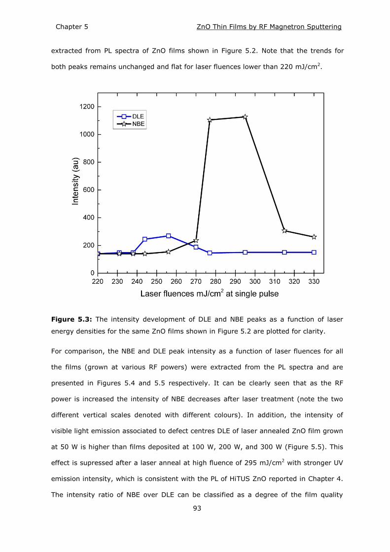
Chapter 5 ZnO Thin Films by RF Magnetron Sputtering
93
extracted from PL spectra of ZnO films shown in Figure 5.2. Note that the trends for
both peaks remains unchanged and flat for laser fluences lower than 220 mJ/cm2.
Figure 5.3: The intensity development of DLE and NBE peaks as a function of laser
energy densities for the same ZnO films shown in Figure 5.2 are plotted for clarity.
For comparison, the NBE and DLE peak intensity as a function of laser fluences for all
the films (grown at various RF powers) were extracted from the PL spectra and are
presented in Figures 5.4 and 5.5 respectively. It can be clearly seen that as the RF
power is increased the intensity of NBE decreases after laser treatment (note the two
different vertical scales denoted with different colours). In addition, the intensity of
visible light emission associated to defect centres DLE of laser annealed ZnO film grown
at 50 W is higher than films deposited at 100 W, 200 W, and 300 W (Figure 5.5). This
effect is supressed after a laser anneal at high fluence of 295 mJ/cm2 with stronger UV
emission intensity, which is consistent with the PL of HiTUS ZnO reported in Chapter 4.
The intensity ratio of NBE over DLE can be classified as a degree of the film quality
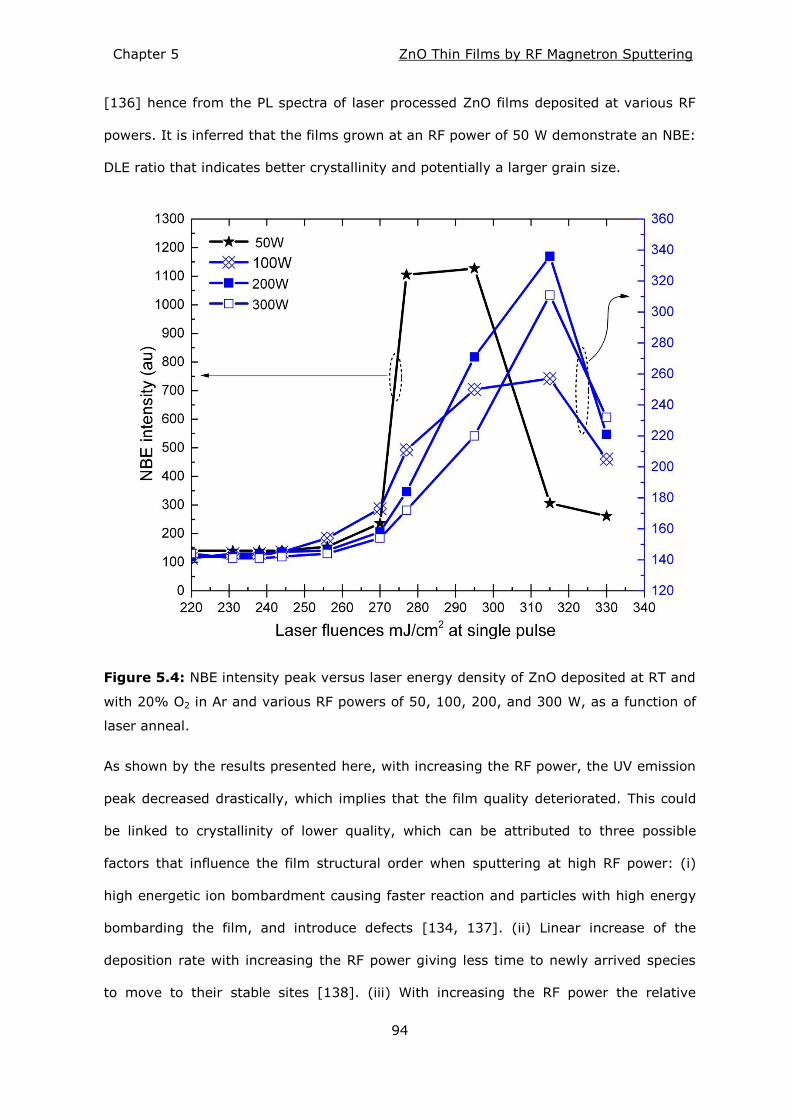
Chapter 5 ZnO Thin Films by RF Magnetron Sputtering
94
[136] hence from the PL spectra of laser processed ZnO films deposited at various RF
powers. It is inferred that the films grown at an RF power of 50 W demonstrate an NBE:
DLE ratio that indicates better crystallinity and potentially a larger grain size.
Figure 5.4: NBE intensity peak versus laser energy density of ZnO deposited at RT and
with 20% O2 in Ar and various RF powers of 50, 100, 200, and 300 W, as a function of
laser anneal.
As shown by the results presented here, with increasing the RF power, the UV emission
peak decreased drastically, which implies that the film quality deteriorated. This could
be linked to crystallinity of lower quality, which can be attributed to three possible
factors that influence the film structural order when sputtering at high RF power: (i)
high energetic ion bombardment causing faster reaction and particles with high energy
bombarding the film, and introduce defects [134, 137]. (ii) Linear increase of the
deposition rate with increasing the RF power giving less time to newly arrived species
to move to their stable sites [138]. (iii) With increasing the RF power the relative
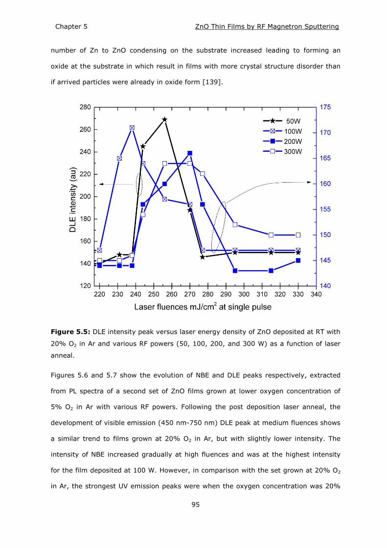
Chapter 5 ZnO Thin Films by RF Magnetron Sputtering
95
number of Zn to ZnO condensing on the substrate increased leading to forming an
oxide at the substrate in which result in films with more crystal structure disorder than
if arrived particles were already in oxide form [139].
Figure 5.5: DLE intensity peak versus laser energy density of ZnO deposited at RT with
20% O2 in Ar and various RF powers (50, 100, 200, and 300 W) as a function of laser
anneal.
Figures 5.6 and 5.7 show the evolution of NBE and DLE peaks respectively, extracted
from PL spectra of a second set of ZnO films grown at lower oxygen concentration of
5% O2 in Ar with various RF powers. Following the post deposition laser anneal, the
development of visible emission (450 nm-750 nm) DLE peak at medium fluences shows
a similar trend to films grown at 20% O2 in Ar, but with slightly lower intensity. The
intensity of NBE increased gradually at high fluences and was at the highest intensity
for the film deposited at 100 W. However, in comparison with the set grown at 20% O2
in Ar, the strongest UV emission peaks were when the oxygen concentration was 20%
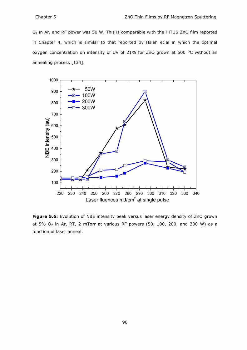
Chapter 5 ZnO Thin Films by RF Magnetron Sputtering
96
O2 in Ar, and RF power was 50 W. This is comparable with the HiTUS ZnO film reported
in Chapter 4, which is similar to that reported by Hsieh et.al in which the optimal
oxygen concentration on intensity of UV of 21% for ZnO grown at 500 °C without an
annealing process [134].
Figure 5.6: Evolution of NBE intensity peak versus laser energy density of ZnO grown
at 5% O2 in Ar, RT, 2 mTorr at various RF powers (50, 100, 200, and 300 W) as a
function of laser anneal.
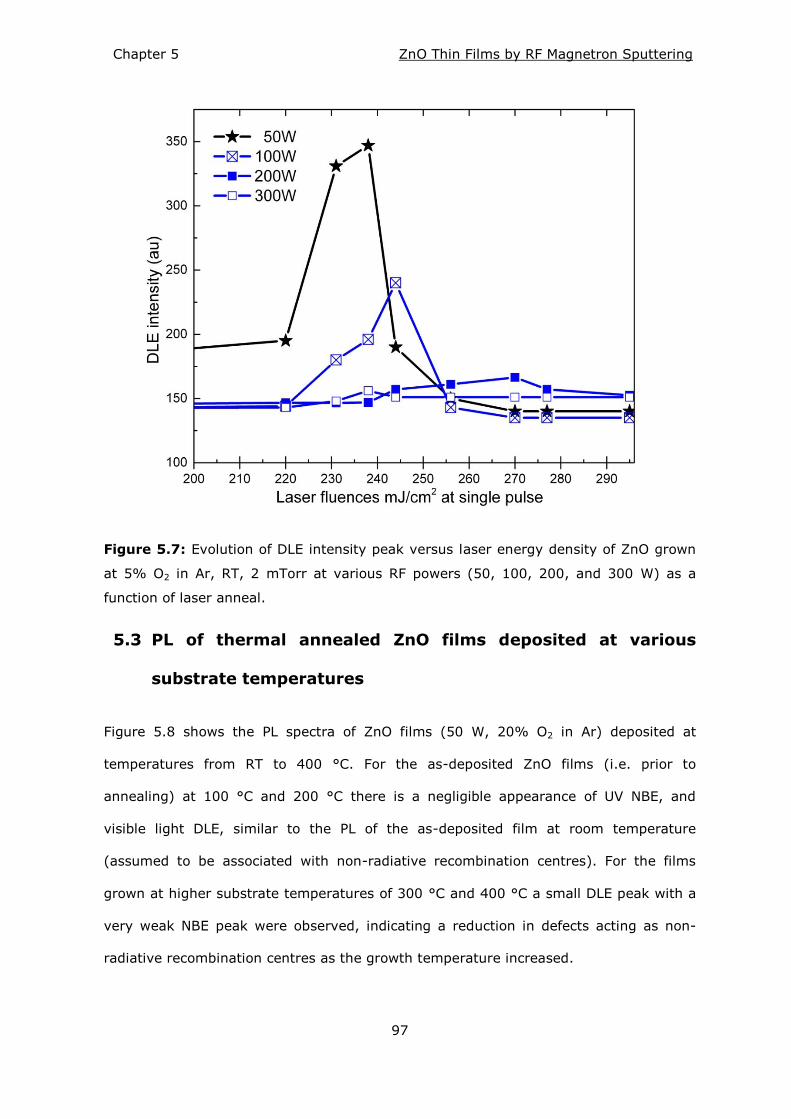
Chapter 5 ZnO Thin Films by RF Magnetron Sputtering
97
Figure 5.7: Evolution of DLE intensity peak versus laser energy density of ZnO grown
at 5% O2 in Ar, RT, 2 mTorr at various RF powers (50, 100, 200, and 300 W) as a
function of laser anneal.
PL of thermal annealed ZnO films deposited at various 5.3
substrate temperatures
Figure 5.8 shows the PL spectra of ZnO films (50 W, 20% O2 in Ar) deposited at
temperatures from RT to 400 °C. For the as-deposited ZnO films (i.e. prior to
annealing) at 100 °C and 200 °C there is a negligible appearance of UV NBE, and
visible light DLE, similar to the PL of the as-deposited film at room temperature
(assumed to be associated with non-radiative recombination centres). For the films
grown at higher substrate temperatures of 300 °C and 400 °C a small DLE peak with a
very weak NBE peak were observed, indicating a reduction in defects acting as non-
radiative recombination centres as the growth temperature increased.
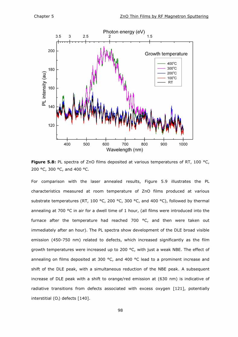
Chapter 5 ZnO Thin Films by RF Magnetron Sputtering
98
Figure 5.8: PL spectra of ZnO films deposited at various temperatures of RT, 100 °C,
200 °C, 300 °C, and 400 °C.
For comparison with the laser annealed results, Figure 5.9 illustrates the PL
characteristics measured at room temperature of ZnO films produced at various
substrate temperatures (RT, 100 °C, 200 °C, 300 °C, and 400 °C), followed by thermal
annealing at 700 °C in air for a dwell time of 1 hour, (all films were introduced into the
furnace after the temperature had reached 700 °C, and then were taken out
immediately after an hour). The PL spectra show development of the DLE broad visible
emission (450-750 nm) related to defects, which increased significantly as the film
growth temperatures were increased up to 200 °C, with just a weak NBE. The effect of
annealing on films deposited at 300 °C, and 400 °C lead to a prominent increase and
shift of the DLE peak, with a simultaneous reduction of the NBE peak. A subsequent
increase of DLE peak with a shift to orange/red emission at (630 nm) is indicative of
radiative transitions from defects associated with excess oxygen [121], potentially
interstitial (Oi) defects [140].
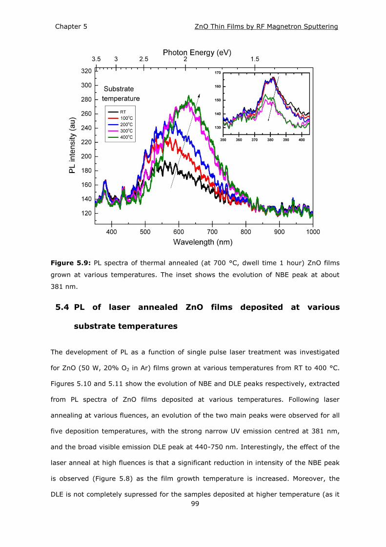
Chapter 5 ZnO Thin Films by RF Magnetron Sputtering
99
Figure 5.9: PL spectra of thermal annealed (at 700 °C, dwell time 1 hour) ZnO films
grown at various temperatures. The inset shows the evolution of NBE peak at about
381 nm.
PL of laser annealed ZnO films deposited at various 5.4
substrate temperatures
The development of PL as a function of single pulse laser treatment was investigated
for ZnO (50 W, 20% O2 in Ar) films grown at various temperatures from RT to 400 °C.
Figures 5.10 and 5.11 show the evolution of NBE and DLE peaks respectively, extracted
from PL spectra of ZnO films deposited at various temperatures. Following laser
annealing at various fluences, an evolution of the two main peaks were observed for all
five deposition temperatures, with the strong narrow UV emission centred at 381 nm,
and the broad visible emission DLE peak at 440-750 nm. Interestingly, the effect of the
laser anneal at high fluences is that a significant reduction in intensity of the NBE peak
is observed (Figure 5.8) as the film growth temperature is increased. Moreover, the
DLE is not completely supressed for the samples deposited at higher temperature (as it
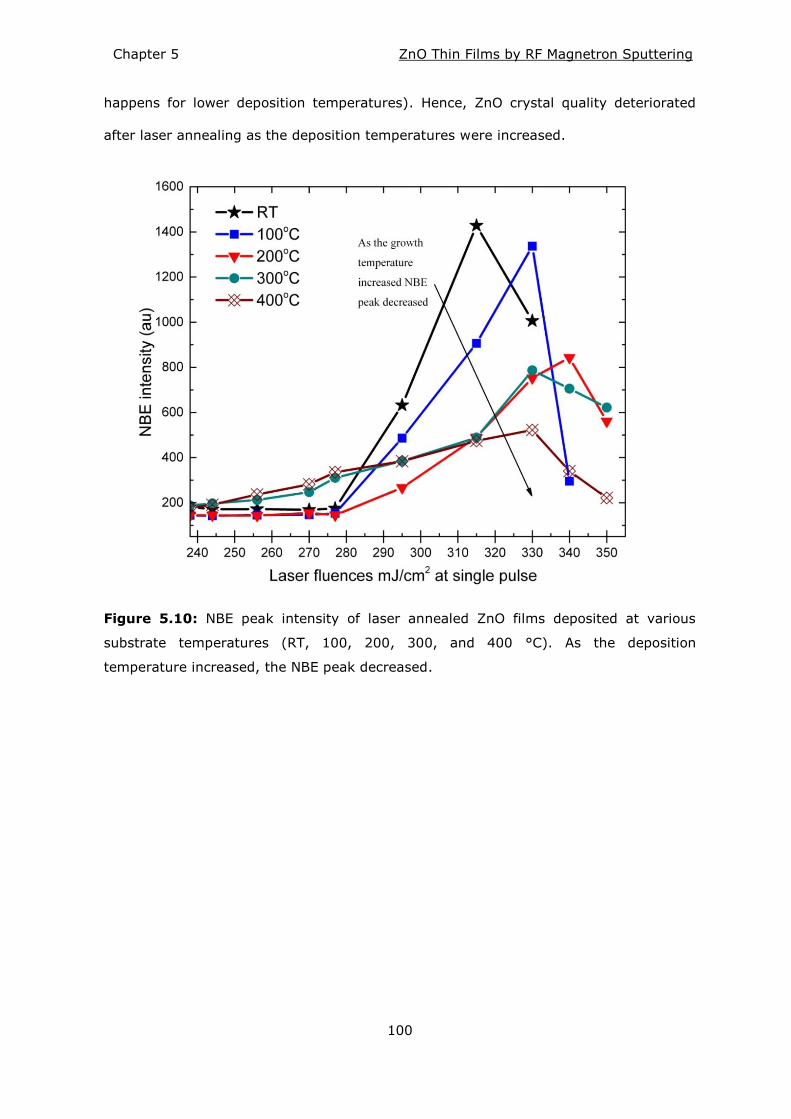
Chapter 5 ZnO Thin Films by RF Magnetron Sputtering
100
happens for lower deposition temperatures). Hence, ZnO crystal quality deteriorated
after laser annealing as the deposition temperatures were increased.
Figure 5.10: NBE peak intensity of laser annealed ZnO films deposited at various
substrate temperatures (RT, 100, 200, 300, and 400 °C). As the deposition
temperature increased, the NBE peak decreased.
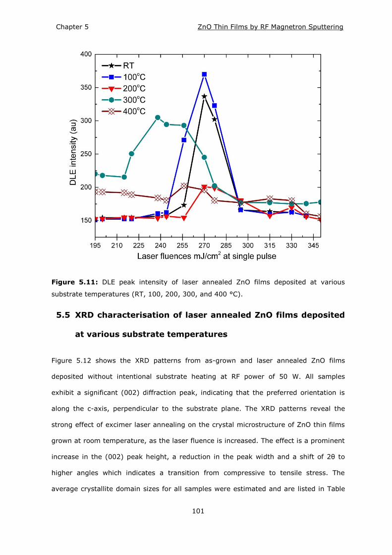
Chapter 5 ZnO Thin Films by RF Magnetron Sputtering
101
Figure 5.11: DLE peak intensity of laser annealed ZnO films deposited at various
substrate temperatures (RT, 100, 200, 300, and 400 °C).
XRD characterisation of laser annealed ZnO films deposited 5.5
at various substrate temperatures
Figure 5.12 shows the XRD patterns from as-grown and laser annealed ZnO films
deposited without intentional substrate heating at RF power of 50 W. All samples
exhibit a significant (002) diffraction peak, indicating that the preferred orientation is
along the c-axis, perpendicular to the substrate plane. The XRD patterns reveal the
strong effect of excimer laser annealing on the crystal microstructure of ZnO thin films
grown at room temperature, as the laser fluence is increased. The effect is a prominent
increase in the (002) peak height, a reduction in the peak width and a shift of 2θ to
higher angles which indicates a transition from compressive to tensile stress. The
average crystallite domain sizes for all samples were estimated and are listed in Table
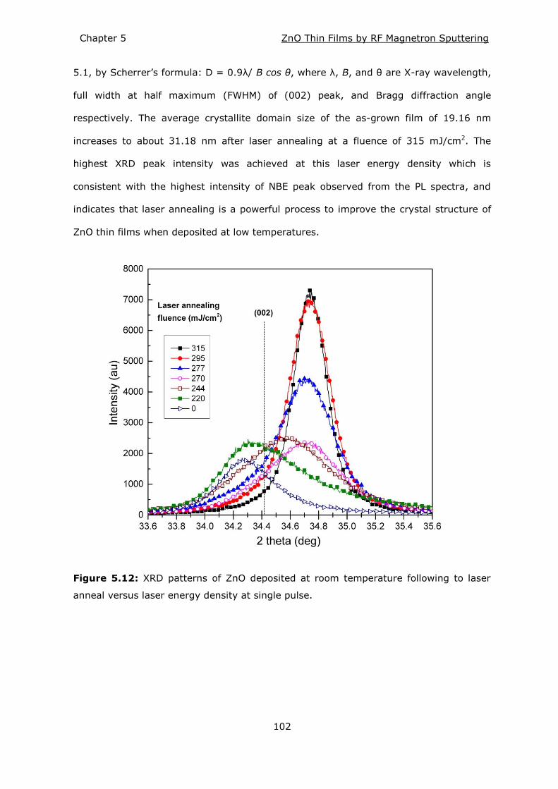
Chapter 5 ZnO Thin Films by RF Magnetron Sputtering
102
5.1, by Scherrer‘s formula: D = 0.9λ/ B cos θ, where λ, B, and θ are X-ray wavelength,
full width at half maximum (FWHM) of (002) peak, and Bragg diffraction angle
respectively. The average crystallite domain size of the as-grown film of 19.16 nm
increases to about 31.18 nm after laser annealing at a fluence of 315 mJ/cm2. The
highest XRD peak intensity was achieved at this laser energy density which is
consistent with the highest intensity of NBE peak observed from the PL spectra, and
indicates that laser annealing is a powerful process to improve the crystal structure of
ZnO thin films when deposited at low temperatures.
Figure 5.12: XRD patterns of ZnO deposited at room temperature following to laser
anneal versus laser energy density at single pulse.
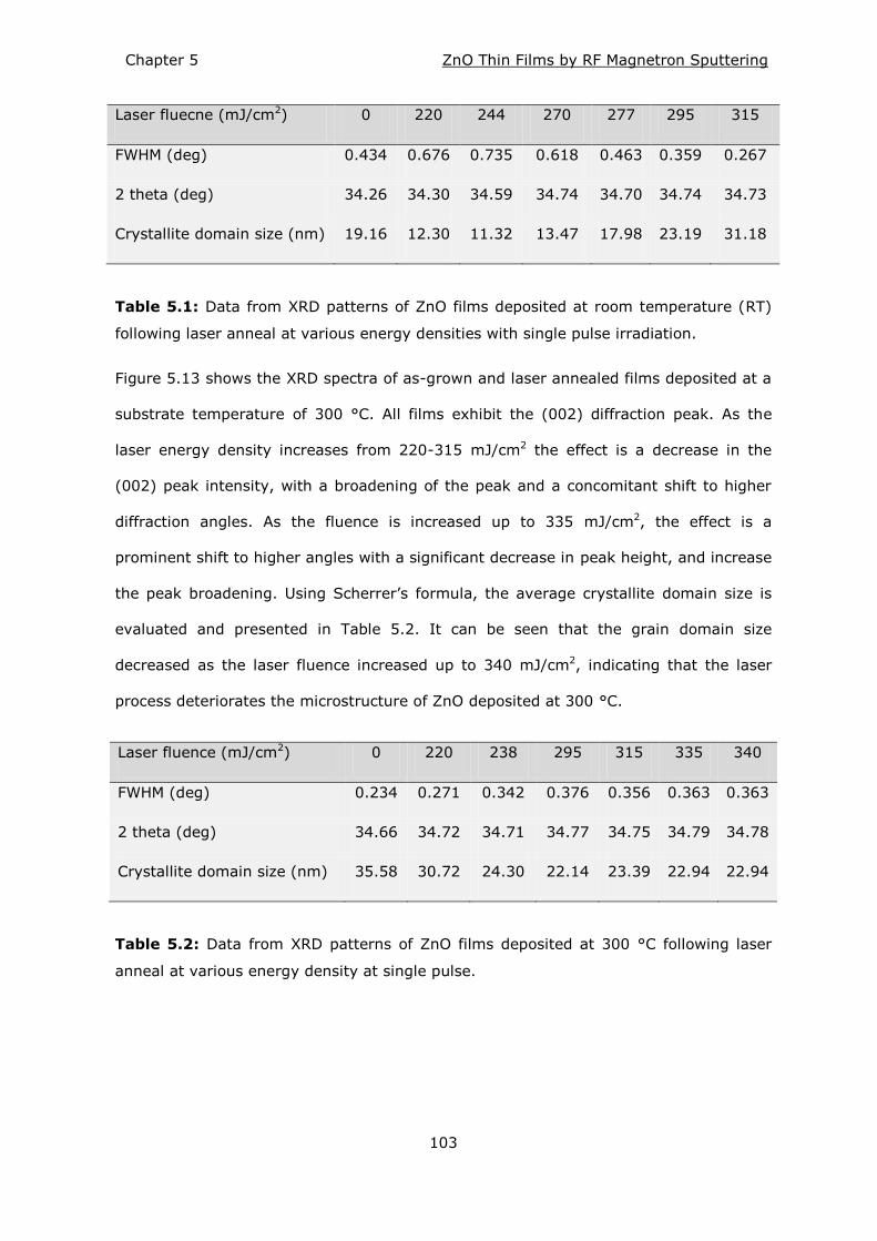
Chapter 5 ZnO Thin Films by RF Magnetron Sputtering
103
Laser fluecne (mJ/cm2) 0 220 244 270 277 295 315
FWHM (deg) 0.434 0.676 0.735 0.618 0.463 0.359 0.267
2 theta (deg) 34.26 34.30 34.59 34.74 34.70 34.74 34.73
Crystallite domain size (nm) 19.16 12.30 11.32 13.47 17.98 23.19 31.18
Table 5.1: Data from XRD patterns of ZnO films deposited at room temperature (RT)
following laser anneal at various energy densities with single pulse irradiation.
Figure 5.13 shows the XRD spectra of as-grown and laser annealed films deposited at a
substrate temperature of 300 °C. All films exhibit the (002) diffraction peak. As the
laser energy density increases from 220-315 mJ/cm2 the effect is a decrease in the
(002) peak intensity, with a broadening of the peak and a concomitant shift to higher
diffraction angles. As the fluence is increased up to 335 mJ/cm2, the effect is a
prominent shift to higher angles with a significant decrease in peak height, and increase
the peak broadening. Using Scherrer‘s formula, the average crystallite domain size is
evaluated and presented in Table 5.2. It can be seen that the grain domain size
decreased as the laser fluence increased up to 340 mJ/cm2, indicating that the laser
process deteriorates the microstructure of ZnO deposited at 300 °C.
Laser fluence (mJ/cm2) 0 220 238 295 315 335 340
FWHM (deg) 0.234 0.271 0.342 0.376 0.356 0.363 0.363
2 theta (deg) 34.66 34.72 34.71 34.77 34.75 34.79 34.78
Crystallite domain size (nm) 35.58 30.72 24.30 22.14 23.39 22.94 22.94
Table 5.2: Data from XRD patterns of ZnO films deposited at 300 °C following laser
anneal at various energy density at single pulse.
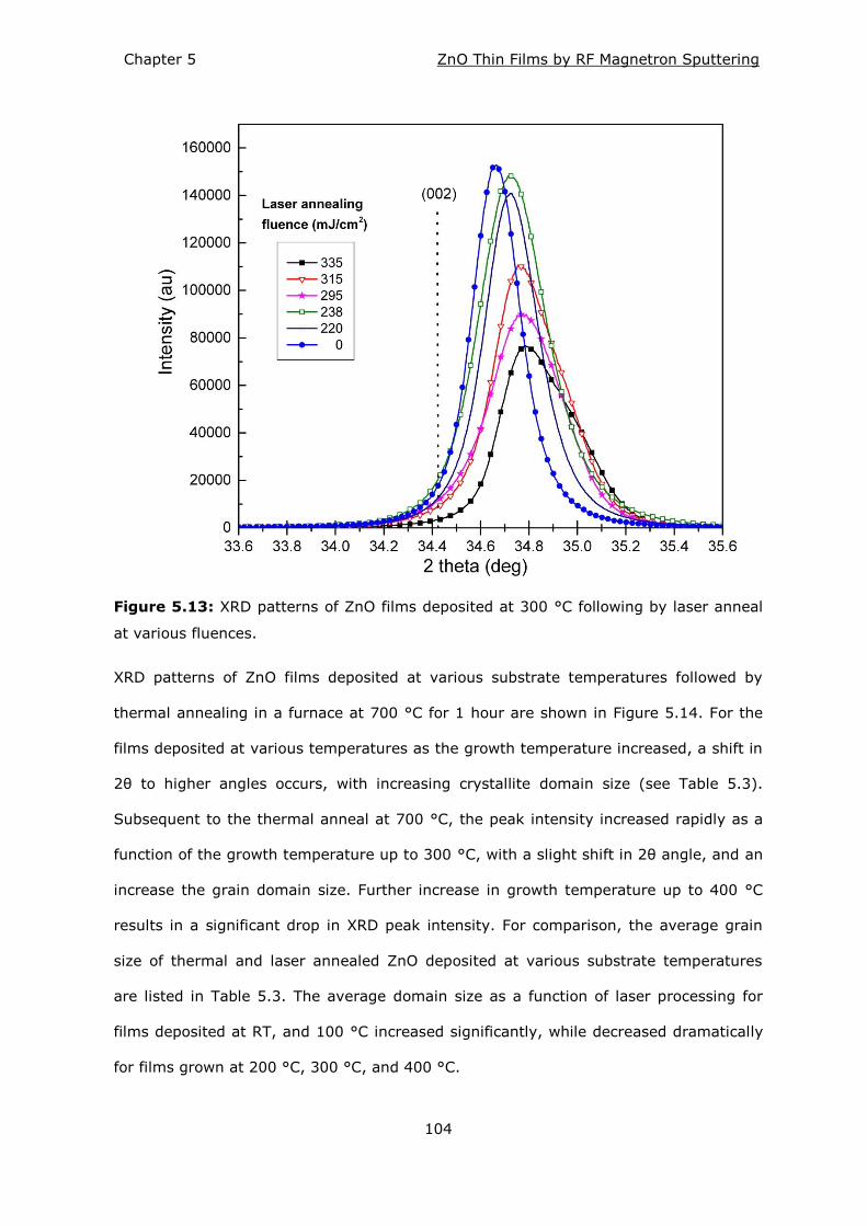
Chapter 5 ZnO Thin Films by RF Magnetron Sputtering
104
Figure 5.13: XRD patterns of ZnO films deposited at 300 °C following by laser anneal
at various fluences.
XRD patterns of ZnO films deposited at various substrate temperatures followed by
thermal annealing in a furnace at 700 °C for 1 hour are shown in Figure 5.14. For the
films deposited at various temperatures as the growth temperature increased, a shift in
2θ to higher angles occurs, with increasing crystallite domain size (see Table 5.3).
Subsequent to the thermal anneal at 700 °C, the peak intensity increased rapidly as a
function of the growth temperature up to 300 °C, with a slight shift in 2θ angle, and an
increase the grain domain size. Further increase in growth temperature up to 400 °C
results in a significant drop in XRD peak intensity. For comparison, the average grain
size of thermal and laser annealed ZnO deposited at various substrate temperatures
are listed in Table 5.3. The average domain size as a function of laser processing for
films deposited at RT, and 100 °C increased significantly, while decreased dramatically
for films grown at 200 °C, 300 °C, and 400 °C.
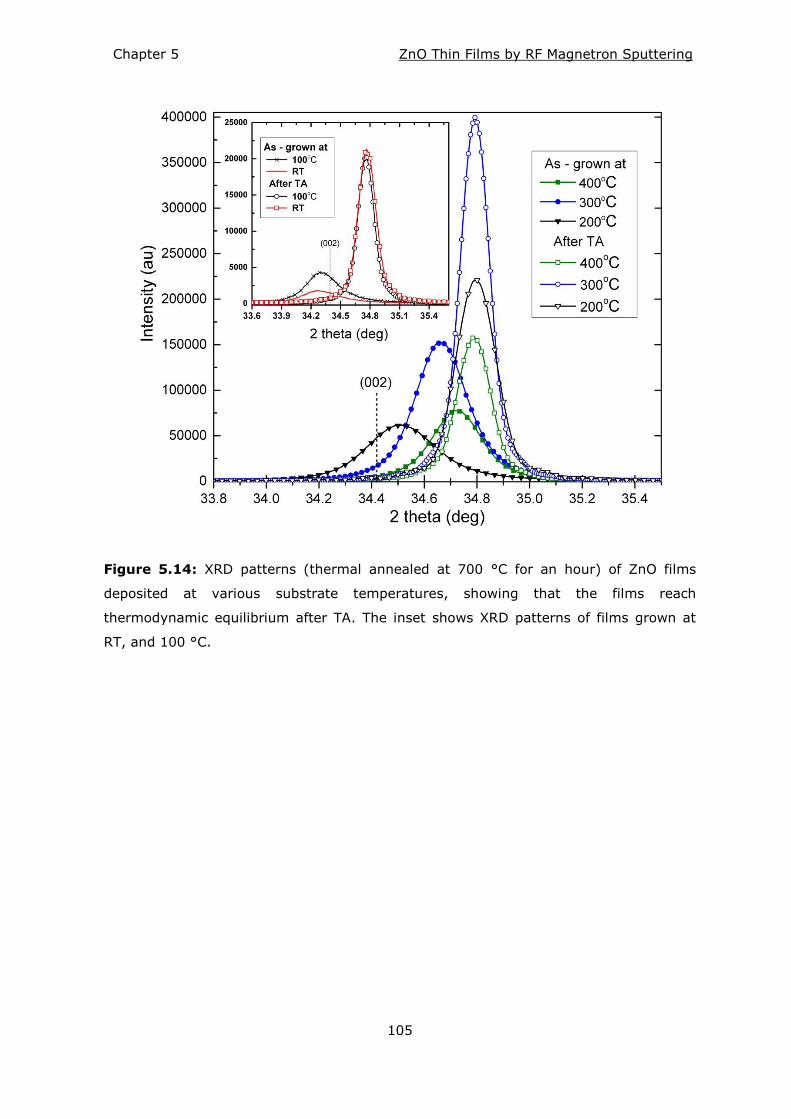
Chapter 5 ZnO Thin Films by RF Magnetron Sputtering
105
Figure 5.14: XRD patterns (thermal annealed at 700 °C for an hour) of ZnO films
deposited at various substrate temperatures, showing that the films reach
thermodynamic equilibrium after TA. The inset shows XRD patterns of films grown at
RT, and 100 °C.
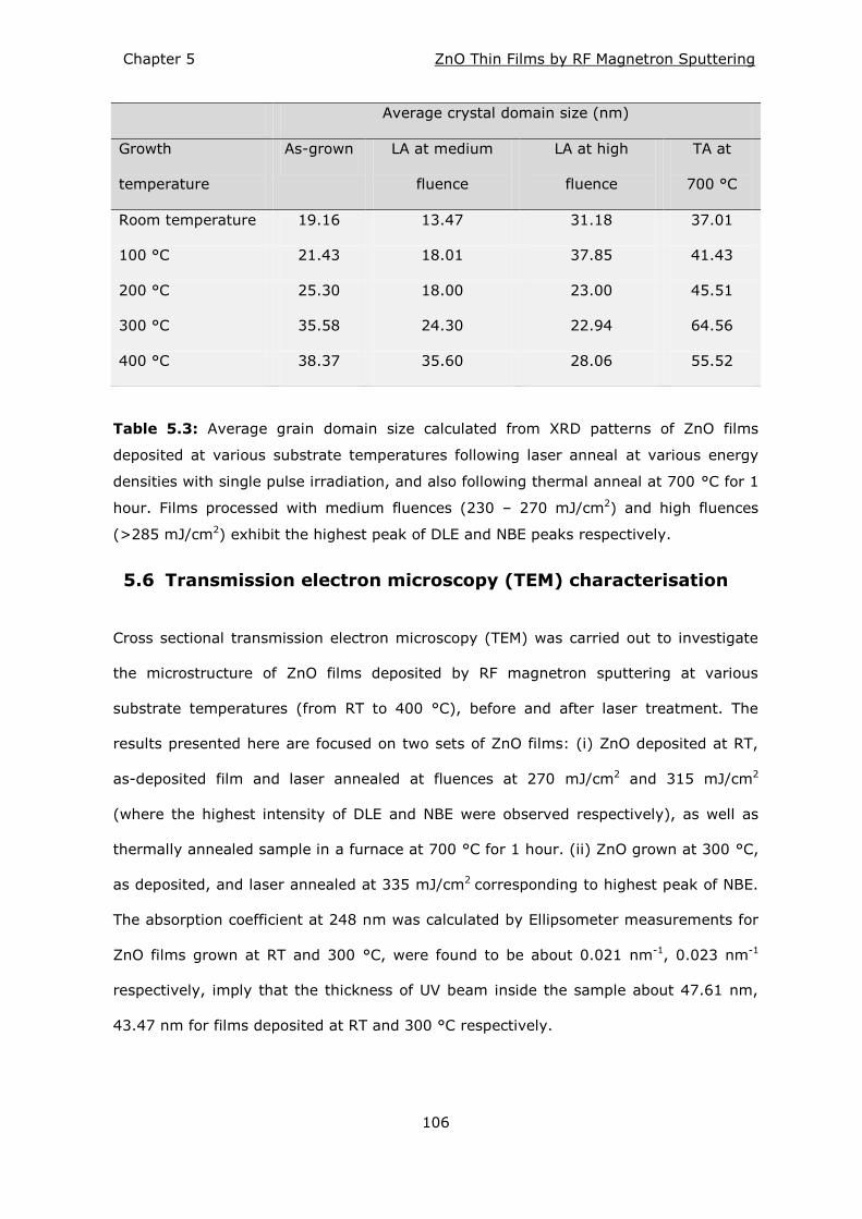
Chapter 5 ZnO Thin Films by RF Magnetron Sputtering
106
Table 5.3: Average grain domain size calculated from XRD patterns of ZnO films
deposited at various substrate temperatures following laser anneal at various energy
densities with single pulse irradiation, and also following thermal anneal at 700 °C for 1
hour. Films processed with medium fluences (230 – 270 mJ/cm2) and high fluences
(>285 mJ/cm2) exhibit the highest peak of DLE and NBE peaks respectively.
Transmission electron microscopy (TEM) characterisation 5.6
Cross sectional transmission electron microscopy (TEM) was carried out to investigate
the microstructure of ZnO films deposited by RF magnetron sputtering at various
substrate temperatures (from RT to 400 °C), before and after laser treatment. The
results presented here are focused on two sets of ZnO films: (i) ZnO deposited at RT,
as-deposited film and laser annealed at fluences at 270 mJ/cm2 and 315 mJ/cm2
(where the highest intensity of DLE and NBE were observed respectively), as well as
thermally annealed sample in a furnace at 700 °C for 1 hour. (ii) ZnO grown at 300 °C,
as deposited, and laser annealed at 335 mJ/cm2 corresponding to highest peak of NBE.
The absorption coefficient at 248 nm was calculated by Ellipsometer measurements for
ZnO films grown at RT and 300 °C, were found to be about 0.021 nm-1, 0.023 nm-1
respectively, imply that the thickness of UV beam inside the sample about 47.61 nm,
43.47 nm for films deposited at RT and 300 °C respectively.
Average crystal domain size (nm)
Growth
temperature
As-grown LA at medium
fluence
LA at high
fluence
TA at
700 °C
Room temperature 19.16 13.47 31.18 37.01
100 °C 21.43 18.01 37.85 41.43
200 °C 25.30 18.00 23.00 45.51
300 °C 35.58 24.30 22.94 64.56
400 °C 38.37 35.60 28.06 55.52
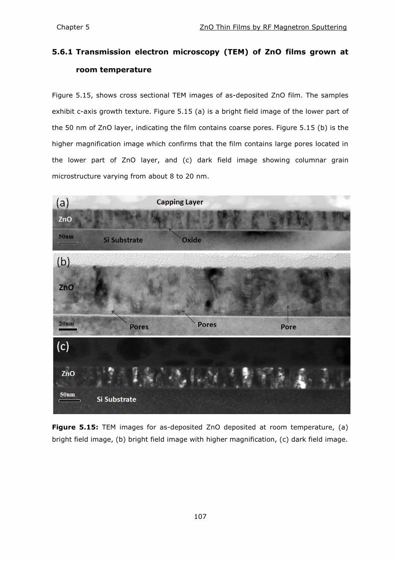
Chapter 5 ZnO Thin Films by RF Magnetron Sputtering
107
5.6.1 Transmission electron microscopy (TEM) of ZnO films grown at
room temperature
Figure 5.15, shows cross sectional TEM images of as-deposited ZnO film. The samples
exhibit c-axis growth texture. Figure 5.15 (a) is a bright field image of the lower part of
the 50 nm of ZnO layer, indicating the film contains coarse pores. Figure 5.15 (b) is the
higher magnification image which confirms that the film contains large pores located in
the lower part of ZnO layer, and (c) dark field image showing columnar grain
microstructure varying from about 8 to 20 nm.
Figure 5.15: TEM images for as-deposited ZnO deposited at room temperature, (a)
bright field image, (b) bright field image with higher magnification, (c) dark field image.
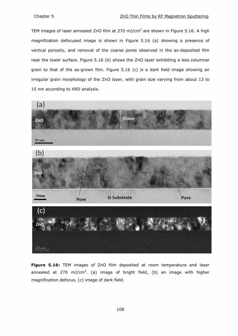
Chapter 5 ZnO Thin Films by RF Magnetron Sputtering
108
TEM images of laser annealed ZnO film at 270 mJ/cm2 are shown in Figure 5.16. A high
magnification defocused image is shown in Figure 5.16 (a) showing a presence of
vertical porosity, and removal of the coarse pores observed in the as-deposited film
near the lower surface. Figure 5.16 (b) shows the ZnO layer exhibiting a less columnar
grain to that of the as-grown film. Figure 5.16 (c) is a dark field image showing an
irregular grain morphology of the ZnO layer, with grain size varying from about 13 to
15 nm according to XRD analysis.
Figure 5.16: TEM images of ZnO film deposited at room temperature and laser
annealed at 270 mJ/cm2. (a) image of bright field, (b) an image with higher
magnification defocus, (c) image of dark field.
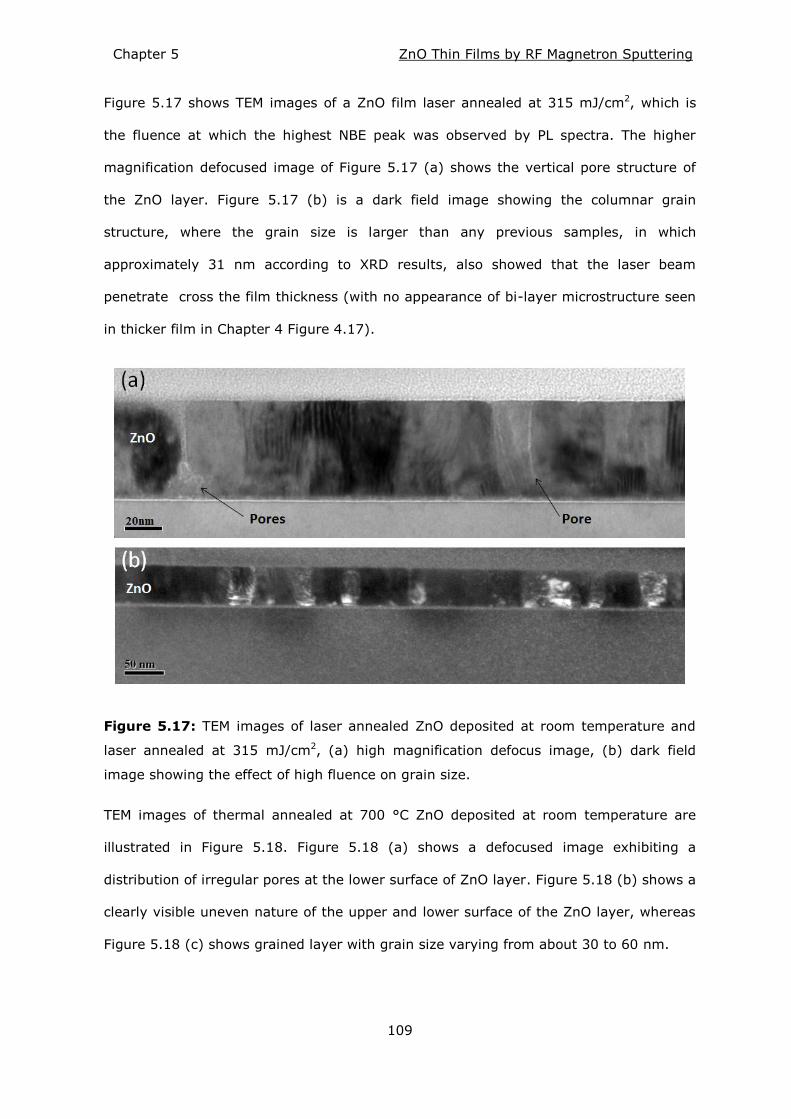
Chapter 5 ZnO Thin Films by RF Magnetron Sputtering
109
Figure 5.17 shows TEM images of a ZnO film laser annealed at 315 mJ/cm2, which is
the fluence at which the highest NBE peak was observed by PL spectra. The higher
magnification defocused image of Figure 5.17 (a) shows the vertical pore structure of
the ZnO layer. Figure 5.17 (b) is a dark field image showing the columnar grain
structure, where the grain size is larger than any previous samples, in which
approximately 31 nm according to XRD results, also showed that the laser beam
penetrate cross the film thickness (with no appearance of bi-layer microstructure seen
in thicker film in Chapter 4 Figure 4.17).
Figure 5.17: TEM images of laser annealed ZnO deposited at room temperature and
laser annealed at 315 mJ/cm2, (a) high magnification defocus image, (b) dark field
image showing the effect of high fluence on grain size.
TEM images of thermal annealed at 700 °C ZnO deposited at room temperature are
illustrated in Figure 5.18. Figure 5.18 (a) shows a defocused image exhibiting a
distribution of irregular pores at the lower surface of ZnO layer. Figure 5.18 (b) shows a
clearly visible uneven nature of the upper and lower surface of the ZnO layer, whereas
Figure 5.18 (c) shows grained layer with grain size varying from about 30 to 60 nm.
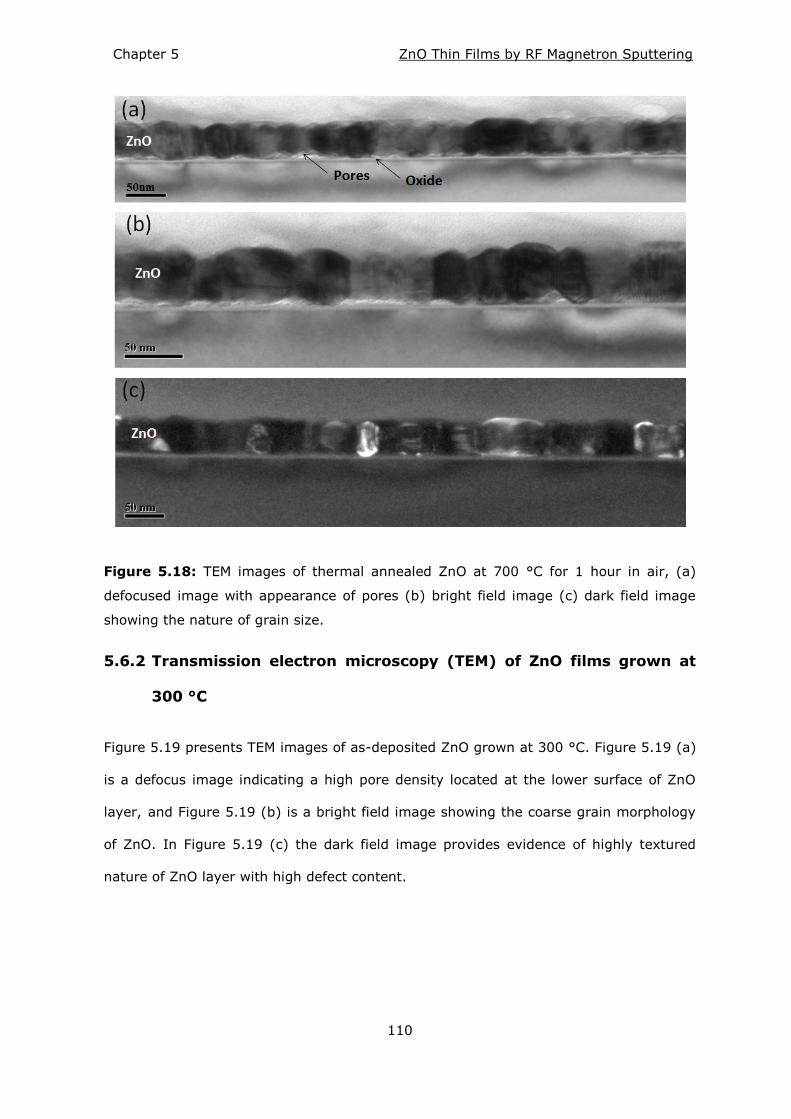
Chapter 5 ZnO Thin Films by RF Magnetron Sputtering
110
Figure 5.18: TEM images of thermal annealed ZnO at 700 °C for 1 hour in air, (a)
defocused image with appearance of pores (b) bright field image (c) dark field image
showing the nature of grain size.
5.6.2 Transmission electron microscopy (TEM) of ZnO films grown at
300 °C
Figure 5.19 presents TEM images of as-deposited ZnO grown at 300 °C. Figure 5.19 (a)
is a defocus image indicating a high pore density located at the lower surface of ZnO
layer, and Figure 5.19 (b) is a bright field image showing the coarse grain morphology
of ZnO. In Figure 5.19 (c) the dark field image provides evidence of highly textured
nature of ZnO layer with high defect content.
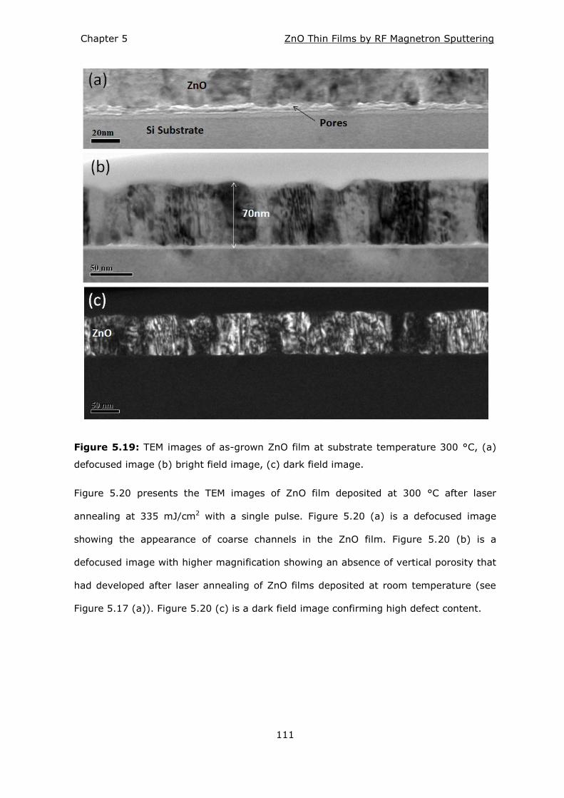
Chapter 5 ZnO Thin Films by RF Magnetron Sputtering
111
Figure 5.19: TEM images of as-grown ZnO film at substrate temperature 300 °C, (a)
defocused image (b) bright field image, (c) dark field image.
Figure 5.20 presents the TEM images of ZnO film deposited at 300 °C after laser
annealing at 335 mJ/cm2 with a single pulse. Figure 5.20 (a) is a defocused image
showing the appearance of coarse channels in the ZnO film. Figure 5.20 (b) is a
defocused image with higher magnification showing an absence of vertical porosity that
had developed after laser annealing of ZnO films deposited at room temperature (see
Figure 5.17 (a)). Figure 5.20 (c) is a dark field image confirming high defect content.
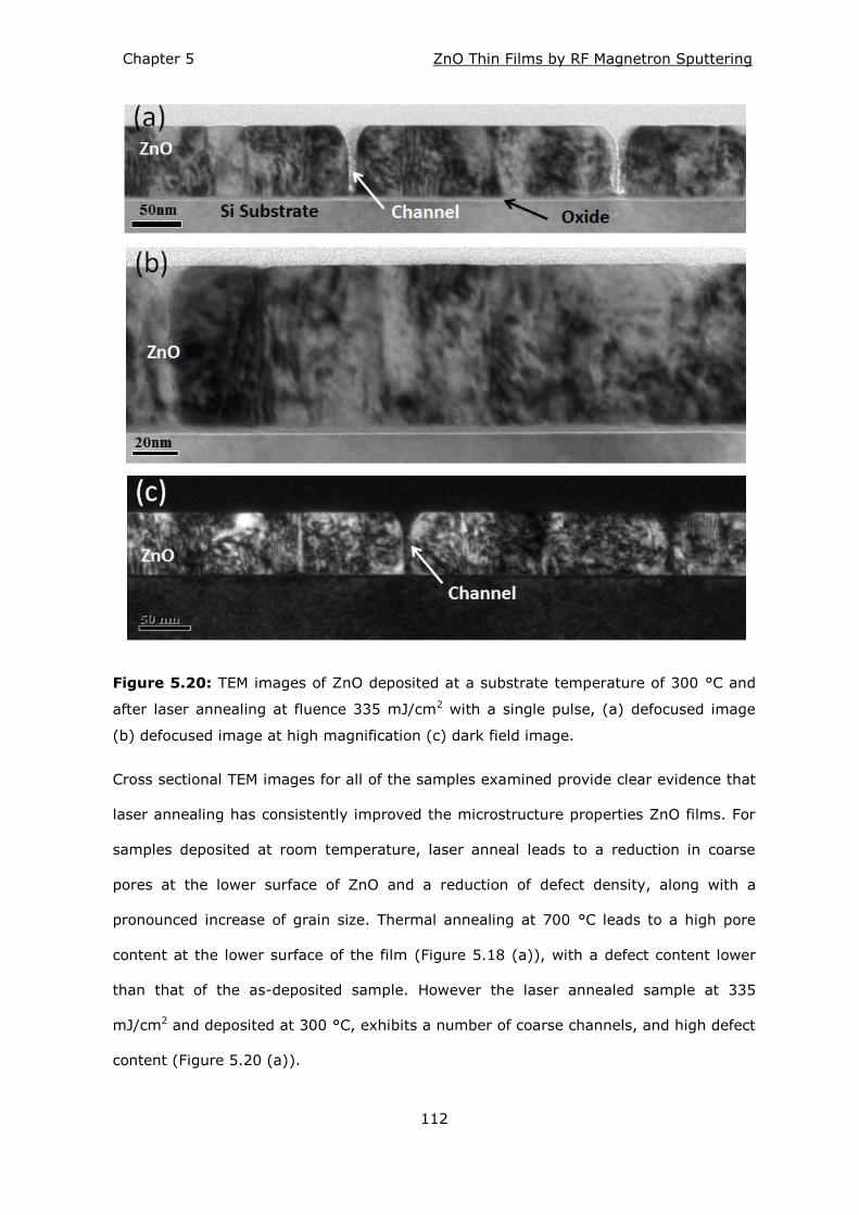
Chapter 5 ZnO Thin Films by RF Magnetron Sputtering
112
Figure 5.20: TEM images of ZnO deposited at a substrate temperature of 300 °C and
after laser annealing at fluence 335 mJ/cm2 with a single pulse, (a) defocused image
(b) defocused image at high magnification (c) dark field image.
Cross sectional TEM images for all of the samples examined provide clear evidence that
laser annealing has consistently improved the microstructure properties ZnO films. For
samples deposited at room temperature, laser anneal leads to a reduction in coarse
pores at the lower surface of ZnO and a reduction of defect density, along with a
pronounced increase of grain size. Thermal annealing at 700 °C leads to a high pore
content at the lower surface of the film (Figure 5.18 (a)), with a defect content lower
than that of the as-deposited sample. However the laser annealed sample at 335
mJ/cm2 and deposited at 300 °C, exhibits a number of coarse channels, and high defect
content (Figure 5.20 (a)).
Chapter 5 ZnO Thin Films by RF Magnetron Sputtering
113
Discussion 5.7
The effect of post-deposition annealing on the PL performance as well as on the
microstructure properties of RF magnetron sputtered ZnO films grown at various RF
powers and various substrate temperatures was studied. In terms of ZnO films grown
at various RF powers using PL results as a measure of film quality, after employing
laser processing of ZnO films deposited at room temperature demonstrate that the RF
power affected the film structure. As the RF power was increased, the film quality
deteriorated. Hence low RF power and laser annealing is required to produce higher
quality ZnO films when deposited without any intentional substrate heating an
excessive RF power leads to faster sputter causing severe surface damage [141, 142].
PL of laser annealed films deposited at lower oxygen concentration (5% O2 in Ar)
showed the DLE peak at medium fluences. For comparison, the DLE peak was not
observed for films deposited at an oxygen flow rate of 28 sccm by high target utilisation
sputtering (HiTUS) as we reported in Chapter 4 which is consistent with the lack of
excess oxygen related defects, while laser annealing at high fluence results in evolution
of a strong NBE peak, which decreased as the RF power increased.
For films deposited at different substrate temperatures (20% O2 in Ar, 50 W), the as-
deposited samples show an increase of average grain domain size from 19.16 nm to
38.37 nm as the growth temperature is increased from RT to 400 °C, which is similar to
that reported in reference [143]. Also, the (002) peak height increased and shifted to
higher diffraction angles as the substrate temperature increased up to 300 °C. A further
increase of growth temperature resulted in a decrease of the (002) peak, which is
attributed to the high temperature breaking the bonding of Zn-O and re-evaporating
the deposited film, instead of allowing the atoms to move to their stable sites [138].
This can be linked to the result that shows the average grain domain size after thermal
annealing at 700 °C increasing to 64.56 nm as the growth temperature is increased up
to 300 °C while for films deposited at 400 °C, the grain domain size increase is less
Chapter 5 ZnO Thin Films by RF Magnetron Sputtering
114
significant, to 55.52 nm, as shown in Table 5.3. Also, in terms of PL characterisation,
the thermally annealed samples at 700 °C deposited at substrate temperature of
300 °C and 400 °C exhibit a subsequent increase of DLE peak with a significant shift to
orange/red emission, and a slight reduction of NBE peak. The increase of green/yellow
DLE emission (peaking at about 570 nm) following thermal annealing for samples with
growth temperatures up to 200 °C indicates an increase of radiative defects as the film
growth temperature is increased, which is likely to be related to Vzn defects, because Zn
vacancies are formed at a lower energy [123]. With increasing the film growth
temperature, up to 400 °C, there is a shift to orange/red DLE emission centred at about
640 nm. This indicates a change of the dominant nature of point defects from Vzn to
excess oxygen related defects.
PL from the laser annealed samples demonstrates encouraging results in terms of the
effect of laser processing of films deposited at low temperatures. Samples deposited on
an unheated substrates show the development of a strong UV NBE emission peak at
high laser fluences, with the defect related DLE completely supressed. The NBE
intensity was greatly influenced by the substrate temperature at deposition. As the
growth temperature was increased beyond ambient, the intensity of the resultant NBE
peak following laser annealing, decreased as a function laser fluence. This reduction in
NBE emission can be attributed to effects related to improved films fabricated at higher
deposition temperatures – resulting in denser films [144]. Also, at higher deposition
temperature the defective layer between the film and the substrate becomes slightly
thicker. This affects subsequent structural and morphology changes as a result of the
laser processing. A decrease in deposition rate as the substrate temperature increased
was observed, from 8.4 Å min-1 to 6.7 Å min-1 at substrate temperatures 100 °C and
300 °C respectively. This is attributed to the vapour pressure of Zn increasing with
increasing temperature, leading to re-evaporation of zinc atoms before oxidation [55].
Further structural investigation confirmed deterioration of the ZnO structure deposited
at a substrate temperature of 300 °C as a function of laser processing, as observed by
Chapter 5 ZnO Thin Films by RF Magnetron Sputtering
115
XRD and TEM studies, in which the grain domain size was found to decrease from about
35.58 nm to 22.94 nm for as-grown and laser annealed samples at high fluences
(335mJ/cm2) respectively. Dark field TEM images demonstrate a high content of defects
for both samples, with coarse channels across the film surface affecting surface
morphology. In contrast, laser annealed ZnO films grown at room temperature showed
a pronounced grain re-growth with a reduction of defect content, and an improved film
quality. Moreover, XRD showed that in RF magnetron sputtered films the development
of the (002) peak develops as the laser fluence is increased, (similar to the thermal
annealed samples). In contrast, the HiTUS films demonstrated a concurrent shift
together with a development of the (002) peak, as the laser fluence increased,
potentially indicating a slight tilt of the crystal orientation. However, room temperature
HiTUS ZnO films showed slightly larger grain domain size pre and post laser processing
(24.60 nm and 37.56 nm respectively) compared to RF sputtered ZnO film grown at RT.
Results give a clear indication that laser processing is a powerful tool to improve the
microstructure properties of ZnO film grown on unheated substrates rather than
deposited at high temperatures.
Chapter 6 Electrical Characterisation of ZnO and IGZO
116
Chapter 6
Electrical Characterisation of ZnO and IGZO
Introduction 6.1
The work presented in this chapter concerns the influence of laser processing on the
microstructure and electrical properties of ZnO and IGZO films deposited on top of
200nm thick dielectric layers of silicon dioxide on silicon substrates. The aim of this
work was to investigate the optimal conditions of deposition and annealing for
semiconductor layers in TFTs. The use of SiO2/Si substrates allows for comparative
thermal and laser treatments to be studied (as well as comparing with the films
deposited onto Si), and also the measurement of electrical conductivity of the films.
The effect of laser and thermal annealing on the electrical properties of ZnO layers and
on IGZO–TFTs was studied. Section 6.2 presents the microstructure and electrical
characterisation of ZnO films grown at room temperature and at 400 °C, with the same
deposition conditions used in Chapter 5 (50 W, 20% O2 in Ar, 2 mTorr, 60 nm), and the
results are compared with the microstructure properties of ZnO deposited on silicon
substrates. Section 6.3 presents electrical characterisation of laser annealed IGZO thin
films deposited at various conditions from targets with two different stoichiometries
(2:2:1), and (1:1:1). Section 6.4 presents results of laser and thermal annealing of
IGZO films used as the channel layers in TFT test devices, including an examination of
the effect of processing pre and post IGZO layer patterning.
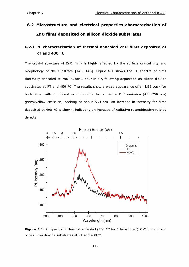
Chapter 6 Electrical Characterisation of ZnO and IGZO
117
Microstructure and electrical properties characterisation of 6.2
ZnO films deposited on silicon dioxide substrates
6.2.1 PL characterisation of thermal annealed ZnO films deposited at
RT and 400 °C.
The crystal structure of ZnO films is highly affected by the surface crystallinity and
morphology of the substrate [145, 146]. Figure 6.1 shows the PL spectra of films
thermally annealed at 700 °C for 1 hour in air, following deposition on silicon dioxide
substrates at RT and 400 °C. The results show a weak appearance of an NBE peak for
both films, with significant evolution of a broad visible DLE emission (450-750 nm)
green/yellow emission, peaking at about 560 nm. An increase in intensity for films
deposited at 400 °C is shown, indicating an increase of radiative recombination related
defects.
Figure 6.1: PL spectra of thermal annealed (700 °C for 1 hour in air) ZnO films grown
onto silicon dioxide substrates at RT and 400 °C.
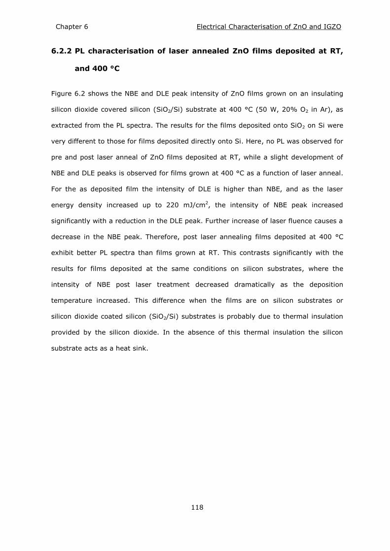
Chapter 6 Electrical Characterisation of ZnO and IGZO
118
6.2.2 PL characterisation of laser annealed ZnO films deposited at RT,
and 400 °C
Figure 6.2 shows the NBE and DLE peak intensity of ZnO films grown on an insulating
silicon dioxide covered silicon (SiO2/Si) substrate at 400 °C (50 W, 20% O2 in Ar), as
extracted from the PL spectra. The results for the films deposited onto SiO2 on Si were
very different to those for films deposited directly onto Si. Here, no PL was observed for
pre and post laser anneal of ZnO films deposited at RT, while a slight development of
NBE and DLE peaks is observed for films grown at 400 °C as a function of laser anneal.
For the as deposited film the intensity of DLE is higher than NBE, and as the laser
energy density increased up to 220 mJ/cm2, the intensity of NBE peak increased
significantly with a reduction in the DLE peak. Further increase of laser fluence causes a
decrease in the NBE peak. Therefore, post laser annealing films deposited at 400 °C
exhibit better PL spectra than films grown at RT. This contrasts significantly with the
results for films deposited at the same conditions on silicon substrates, where the
intensity of NBE post laser treatment decreased dramatically as the deposition
temperature increased. This difference when the films are on silicon substrates or
silicon dioxide coated silicon (SiO2/Si) substrates is probably due to thermal insulation
provided by the silicon dioxide. In the absence of this thermal insulation the silicon
substrate acts as a heat sink.
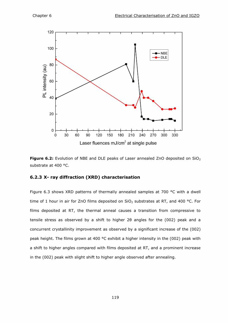
Chapter 6 Electrical Characterisation of ZnO and IGZO
119
Figure 6.2: Evolution of NBE and DLE peaks of Laser annealed ZnO deposited on SiO2
substrate at 400 °C.
6.2.3 X- ray diffraction (XRD) characterisation
Figure 6.3 shows XRD patterns of thermally annealed samples at 700 °C with a dwell
time of 1 hour in air for ZnO films deposited on SiO2 substrates at RT, and 400 °C. For
films deposited at RT, the thermal anneal causes a transition from compressive to
tensile stress as observed by a shift to higher 2θ angles for the (002) peak and a
concurrent crystallinity improvement as observed by a significant increase of the (002)
peak height. The films grown at 400 °C exhibit a higher intensity in the (002) peak with
a shift to higher angles compared with films deposited at RT, and a prominent increase
in the (002) peak with slight shift to higher angle observed after annealing.
Chapter 6 Electrical Characterisation of ZnO and IGZO
120
Figure 6.3: XRD patterns of as deposited and thermal annealed ZnO deposited on
silicon dioxide substrates at RT and 400 °C.
Figures 6.4 and 6.5 show XRD patterns of laser annealed samples at various fluences
with a single pulse for ZnO deposited on silicon dioxide at RT and 400 °C respectively.
Laser processing leads to a shift of the c-axis (002) peak to the higher angles as the
fluence is increased up to medium fluence (195 – 220 mJ/cm2) as well as an increase of
peak intensity. Further increase of the laser fluence up to high fluences (270 – 330
mJ/cm2) causes a decrease of the peak intensity. Although no PL spectra was observed
for films grown at RT, the XRD spectra indicate that laser annealing influences the
microstructure of the ZnO films, and enlarges the crystal size.
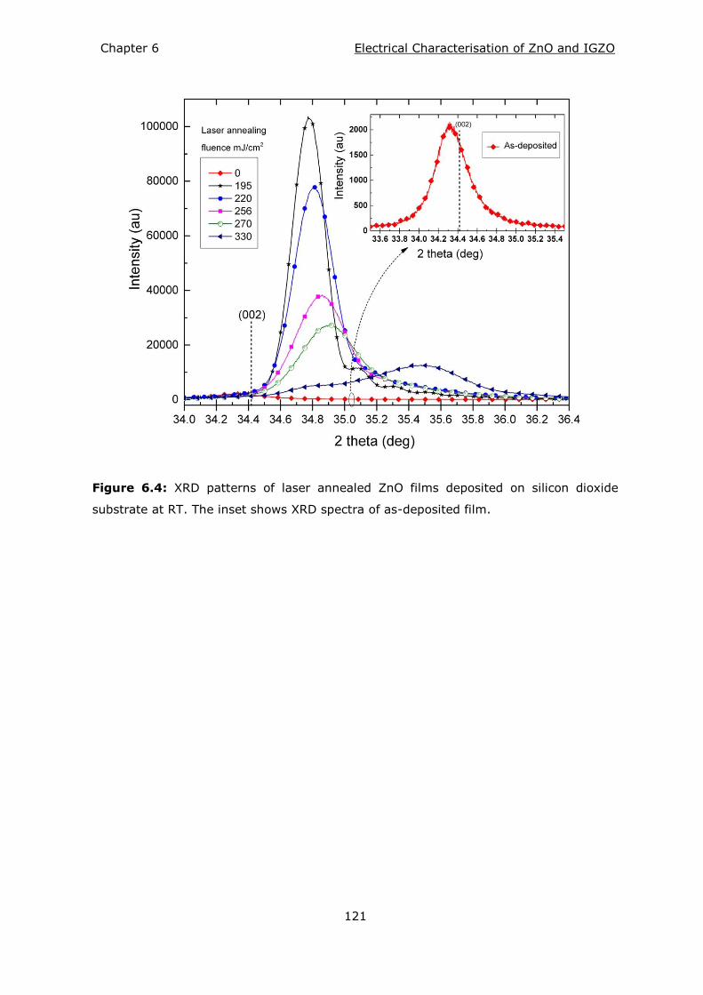
Chapter 6 Electrical Characterisation of ZnO and IGZO
121
Figure 6.4: XRD patterns of laser annealed ZnO films deposited on silicon dioxide
substrate at RT. The inset shows XRD spectra of as-deposited film.
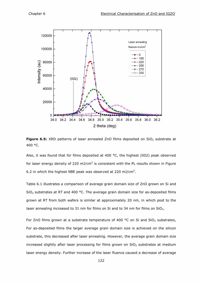
Chapter 6 Electrical Characterisation of ZnO and IGZO
122
Figure 6.5: XRD patterns of laser annealed ZnO films deposited on SiO2 substrate at
400 °C.
Also, it was found that for films deposited at 400 °C, the highest (002) peak observed
for laser energy density of 220 mJ/cm2 is consistent with the PL results shown in Figure
6.2 in which the highest NBE peak was observed at 220 mJ/cm2.
Table 6.1 illustrates a comparison of average grain domain size of ZnO grown on Si and
SiO2 substrates at RT and 400 °C. The average grain domain size for as-deposited films
grown at RT from both wafers is similar at approximately 20 nm, in which post to the
laser annealing increased to 31 nm for films on Si and to 34 nm for films on SiO2.
For ZnO films grown at a substrate temperature of 400 °C on Si and SiO2 substrates,
For as-deposited films the larger average grain domain size is achieved on the silicon
substrate, this decreased after laser annealing. However, the average grain domain size
increased slightly after laser processing for films grown on SiO2 substrates at medium
laser energy density. Further increase of the laser fluence caused a decrease of average
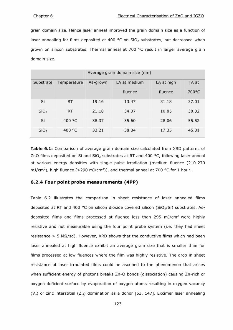
Chapter 6 Electrical Characterisation of ZnO and IGZO
123
grain domain size. Hence laser anneal improved the grain domain size as a function of
laser annealing for films deposited at 400 °C on SiO2 substrates, but decreased when
grown on silicon substrates. Thermal anneal at 700 °C result in larger average grain
domain size.
Table 6.1: Comparison of average grain domain size calculated from XRD patterns of
ZnO films deposited on Si and SiO2 substrates at RT and 400 °C, following laser anneal
at various energy densities with single pulse irradiation (medium fluence (210-270
mJ/cm2), high fluence (>290 mJ/cm2)), and thermal anneal at 700 °C for 1 hour.
6.2.4 Four point probe measurements (4PP)
Table 6.2 illustrates the comparison in sheet resistance of laser annealed films
deposited at RT and 400 °C on silicon dioxide covered silicon (SiO2/Si) substrates. As-
deposited films and films processed at fluence less than 295 mJ/cm2 were highly
resistive and not measurable using the four point probe system (i.e. they had sheet
resistance > 5 MΩ/sq). However, XRD shows that the conductive films which had been
laser annealed at high fluence exhibit an average grain size that is smaller than for
films processed at low fluences where the film was highly resistive. The drop in sheet
resistance of laser irradiated films could be ascribed to the phenomenon that arises
when sufficient energy of photons breaks Zn-O bonds (dissociation) causing Zn-rich or
oxygen deficient surface by evaporation of oxygen atoms resulting in oxygen vacancy
(Vo) or zinc interstitial (Zni) domination as a donor [53, 147]. Excimer laser annealing
Average grain domain size (nm)
Substrate Temperature As-grown LA at medium
fluence
LA at high
fluence
TA at
700°C
Si RT 19.16 13.47 31.18 37.01
SiO2 RT 21.18 34.37 10.85 38.32
Si 400 °C 38.37 35.60 28.06 55.52
SiO2 400 °C 33.21 38.34 17.35 45.31
Chapter 6 Electrical Characterisation of ZnO and IGZO
124
contributes to an increase in the carrier density of the film [73]. Sheet resistance as a
function of thermal anneal at 700 °C for 1 hour for films deposited at RT was found to
be less than that grown at 400 °C, with values being 5976±150 Ω/sq and 276241±200
Ω/sq respectively.
Table 6.2: Sheet resistance of laser annealed 60nm thick of ZnO films deposited at 50
W, 20% O2 in Ar, 2 mTorr, on SiO2 substrate at RT and 400 °C.
Electrical properties of laser annealed IGZO thin films 6.3
The main purpose of this section is to study the effect of laser annealing on electrical
properties of multicomponent oxide semiconductor IGZO thin films, deposited under
various conditions without intentional substrate heating, for application as an active
layer in TFTs. When sputtering IGZO, deposition conditions influence the deposition rate
which reflects the nature of the sputtering mechanism of material particles and plasma
arrivals on the substrate surface creating a thin film. For example, in sputtered IGZO, a
high deposition rate results in a lack of zinc content [148], because ZnO has a low
deposition rate, while gallium and indium have high deposition rates, hence the latter
cations will compensate the zinc deficiency [149].
6.3.1 Electrical properties of laser annealed IGZO (2:2:1) and (1:1:1)
films
Initially, three wafers of IGZO were deposited on silicon dioxide covered silicon
(SiO2/Si) at RF power 50 W, oxygen concentration 5% O2 in Ar, 50 nm thick, and
various deposition pressures (2, 5, 10 mTorr) without intentional substrate heating. The
Sheet resistance Ω/sq
Growth temperature 295 mJ/cm2 315 mJ/cm2 295 mJ/cm2
RT 943±100 864±80 1744±90
400 °C 492±90 860±75 595±100
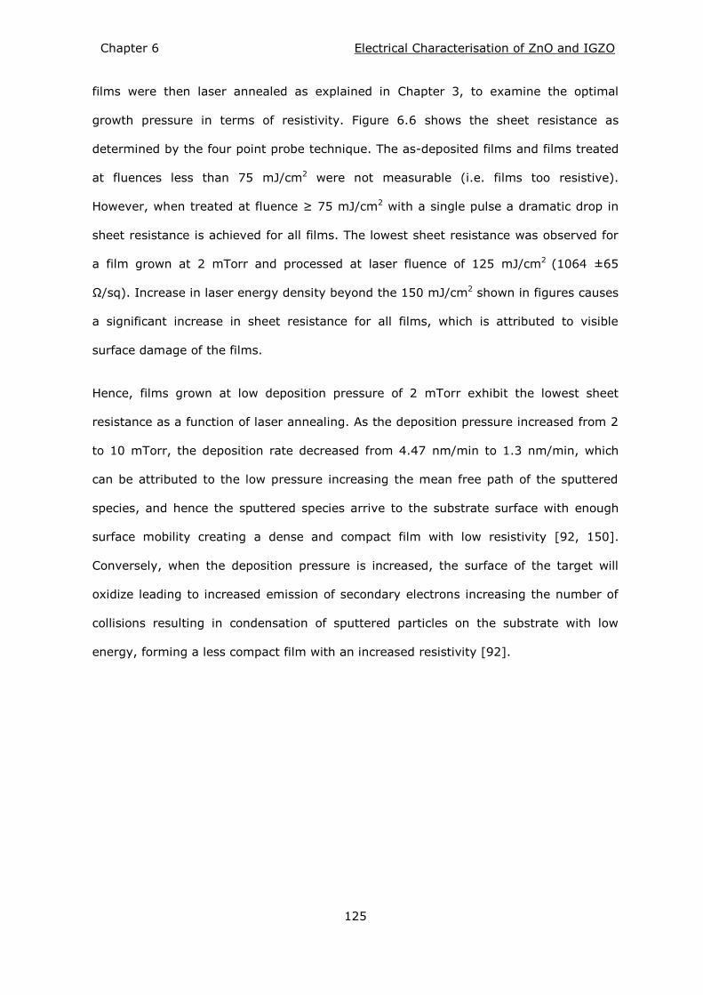
Chapter 6 Electrical Characterisation of ZnO and IGZO
125
films were then laser annealed as explained in Chapter 3, to examine the optimal
growth pressure in terms of resistivity. Figure 6.6 shows the sheet resistance as
determined by the four point probe technique. The as-deposited films and films treated
at fluences less than 75 mJ/cm2 were not measurable (i.e. films too resistive).
However, when treated at fluence ≥ 75 mJ/cm2 with a single pulse a dramatic drop in
sheet resistance is achieved for all films. The lowest sheet resistance was observed for
a film grown at 2 mTorr and processed at laser fluence of 125 mJ/cm2 (1064 ±65
Ω/sq). Increase in laser energy density beyond the 150 mJ/cm2 shown in figures causes
a significant increase in sheet resistance for all films, which is attributed to visible
surface damage of the films.
Hence, films grown at low deposition pressure of 2 mTorr exhibit the lowest sheet
resistance as a function of laser annealing. As the deposition pressure increased from 2
to 10 mTorr, the deposition rate decreased from 4.47 nm/min to 1.3 nm/min, which
can be attributed to the low pressure increasing the mean free path of the sputtered
species, and hence the sputtered species arrive to the substrate surface with enough
surface mobility creating a dense and compact film with low resistivity [92, 150].
Conversely, when the deposition pressure is increased, the surface of the target will
oxidize leading to increased emission of secondary electrons increasing the number of
collisions resulting in condensation of sputtered particles on the substrate with low
energy, forming a less compact film with an increased resistivity [92].
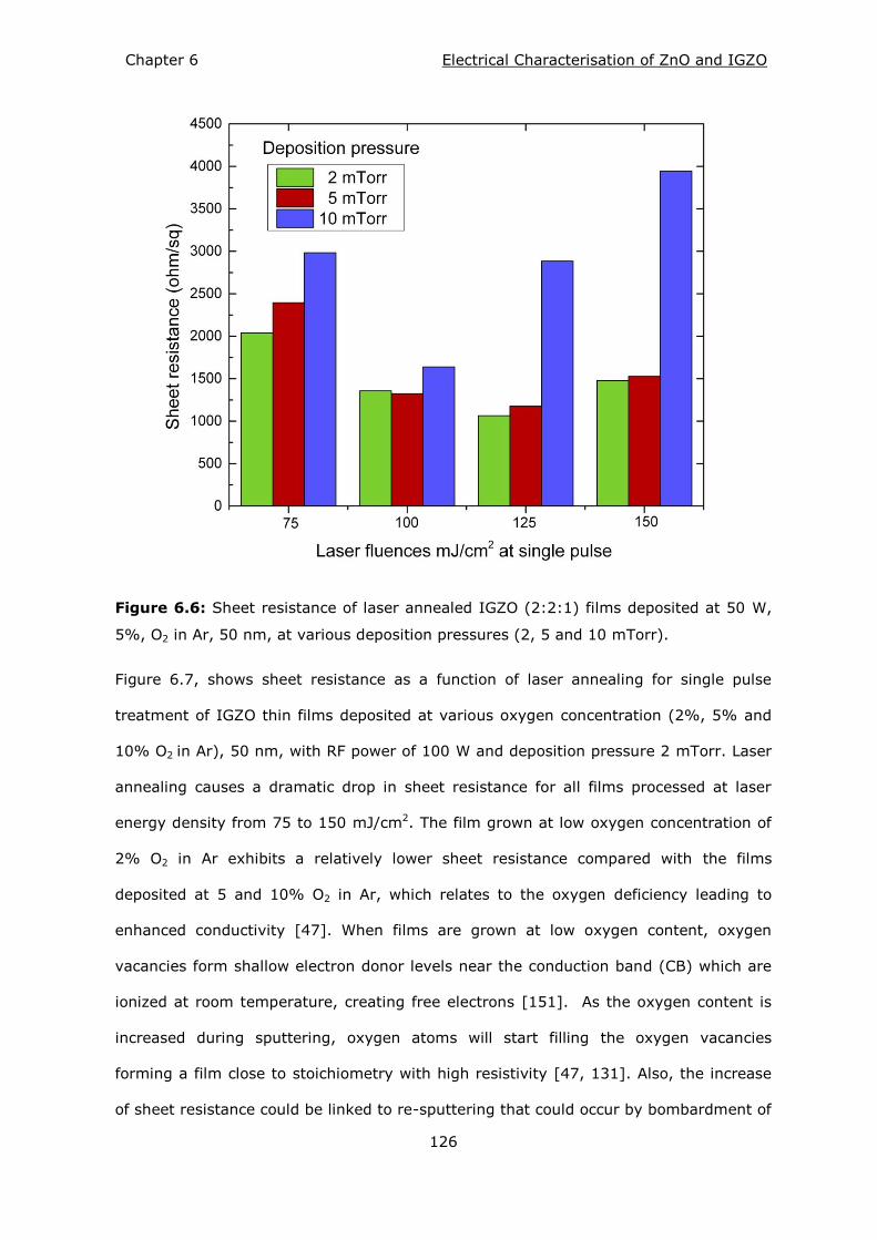
Chapter 6 Electrical Characterisation of ZnO and IGZO
126
Figure 6.6: Sheet resistance of laser annealed IGZO (2:2:1) films deposited at 50 W,
5%, O2 in Ar, 50 nm, at various deposition pressures (2, 5 and 10 mTorr).
Figure 6.7, shows sheet resistance as a function of laser annealing for single pulse
treatment of IGZO thin films deposited at various oxygen concentration (2%, 5% and
10% O2 in Ar), 50 nm, with RF power of 100 W and deposition pressure 2 mTorr. Laser
annealing causes a dramatic drop in sheet resistance for all films processed at laser
energy density from 75 to 150 mJ/cm2. The film grown at low oxygen concentration of
2% O2 in Ar exhibits a relatively lower sheet resistance compared with the films
deposited at 5 and 10% O2 in Ar, which relates to the oxygen deficiency leading to
enhanced conductivity [47]. When films are grown at low oxygen content, oxygen
vacancies form shallow electron donor levels near the conduction band (CB) which are
ionized at room temperature, creating free electrons [151]. As the oxygen content is
increased during sputtering, oxygen atoms will start filling the oxygen vacancies
forming a film close to stoichiometry with high resistivity [47, 131]. Also, the increase
of sheet resistance could be linked to re-sputtering that could occur by bombardment of
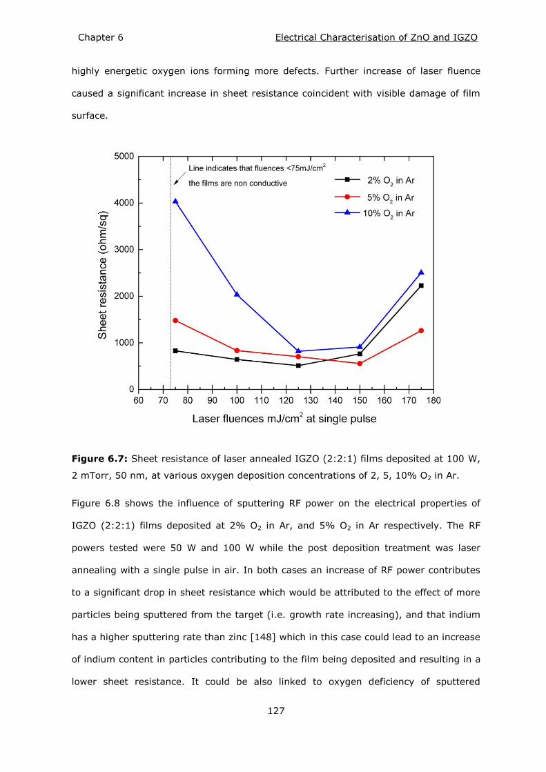
Chapter 6 Electrical Characterisation of ZnO and IGZO
127
highly energetic oxygen ions forming more defects. Further increase of laser fluence
caused a significant increase in sheet resistance coincident with visible damage of film
surface.
Figure 6.7: Sheet resistance of laser annealed IGZO (2:2:1) films deposited at 100 W,
2 mTorr, 50 nm, at various oxygen deposition concentrations of 2, 5, 10% O2 in Ar.
Figure 6.8 shows the influence of sputtering RF power on the electrical properties of
IGZO (2:2:1) films deposited at 2% O2 in Ar, and 5% O2 in Ar respectively. The RF
powers tested were 50 W and 100 W while the post deposition treatment was laser
annealing with a single pulse in air. In both cases an increase of RF power contributes
to a significant drop in sheet resistance which would be attributed to the effect of more
particles being sputtered from the target (i.e. growth rate increasing), and that indium
has a higher sputtering rate than zinc [148] which in this case could lead to an increase
of indium content in particles contributing to the film being deposited and resulting in a
lower sheet resistance. It could be also linked to oxygen deficiency of sputtered
Chapter 6 Electrical Characterisation of ZnO and IGZO
128
particles contributing to the film being deposited, where at high RF powers more
sputtered species are struck away from the target, leading to insufficient amount of
oxygen used to oxidize particles and the target [152].
Figure 6.8: Sheet resistance of laser annealed IGZO (2:2:1) films deposited at 2, and
5% O2 in Ar, 2 mTorr, 50 nm, at various RF powers (50 W and 100 W).
A similar trend was observed for laser processed films deposited from a target with a
stoichiometry of (1:1:1) at various RF powers and oxygen concentrations.
Figures 6.9 illustrates sheet resistance comparison between films grown from two
different stoichiometries of (2:2:1) and (1:1:1) deposited under the same growth
conditions of 2% O2 in Ar, 2 mTorr, RT, and at 50 or 100 W RF power. Results show
that films deposited from the (1:1:1) target demonstrate higher sheet resistance than
films from (2:2:1) target, which is associated with higher indium content.
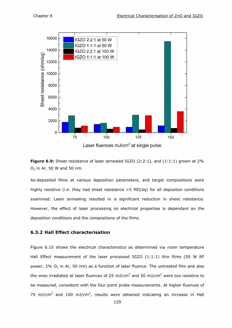
Chapter 6 Electrical Characterisation of ZnO and IGZO
129
Figure 6.9: Sheet resistance of laser annealed IGZO (2:2:1), and (1:1:1) grown at 2%
O2 in Ar, 50 W and 50 nm.
As-deposited films at various deposition parameters, and target compositions were
highly resistive (i.e. they had sheet resistance >5 MΩ/sq) for all depositon conditions
examined. Laser annealing resulted in a significant reduction in sheet resistance.
However, the effect of laser processing on electrical properties is dependant on the
deposition conditions and the compositions of the films.
6.3.2 Hall Effect characterisation
Figure 6.10 shows the electrical characteristics as determined via room temperature
Hall Effect measurement of the laser processed IGZO (1:1:1) thin films (50 W RF
power, 2% O2 in Ar, 50 nm) as a function of laser fluence. The untreated film and also
the ones irradiated at laser fluences of 25 mJ/cm2 and 50 mJ/cm2 were too resistive to
be measured, consistent with the four point probe measurements. At higher fluences of
75 mJ/cm2 and 100 mJ/cm2, results were obtained indicating an increase in Hall
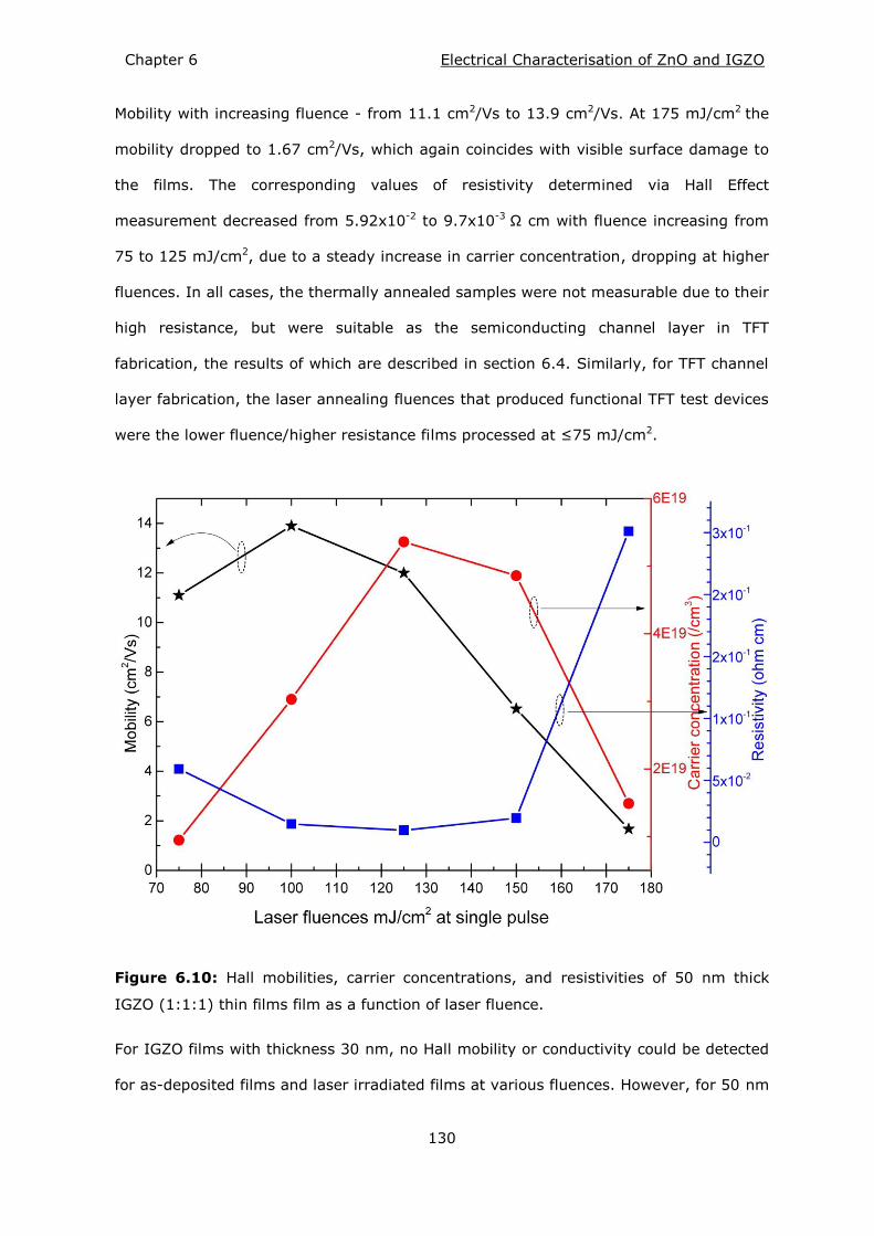
Chapter 6 Electrical Characterisation of ZnO and IGZO
130
Mobility with increasing fluence - from 11.1 cm2/Vs to 13.9 cm2/Vs. At 175 mJ/cm2 the
mobility dropped to 1.67 cm2/Vs, which again coincides with visible surface damage to
the films. The corresponding values of resistivity determined via Hall Effect
measurement decreased from 5.92x10⁻² to 9.7x10⁻³ Ω cm with fluence increasing from
75 to 125 mJ/cm2, due to a steady increase in carrier concentration, dropping at higher
fluences. In all cases, the thermally annealed samples were not measurable due to their
high resistance, but were suitable as the semiconducting channel layer in TFT
fabrication, the results of which are described in section 6.4. Similarly, for TFT channel
layer fabrication, the laser annealing fluences that produced functional TFT test devices
were the lower fluence/higher resistance films processed at ≤75 mJ/cm2.
Figure 6.10: Hall mobilities, carrier concentrations, and resistivities of 50 nm thick
IGZO (1:1:1) thin films film as a function of laser fluence.
For IGZO films with thickness 30 nm, no Hall mobility or conductivity could be detected
for as-deposited films and laser irradiated films at various fluences. However, for 50 nm
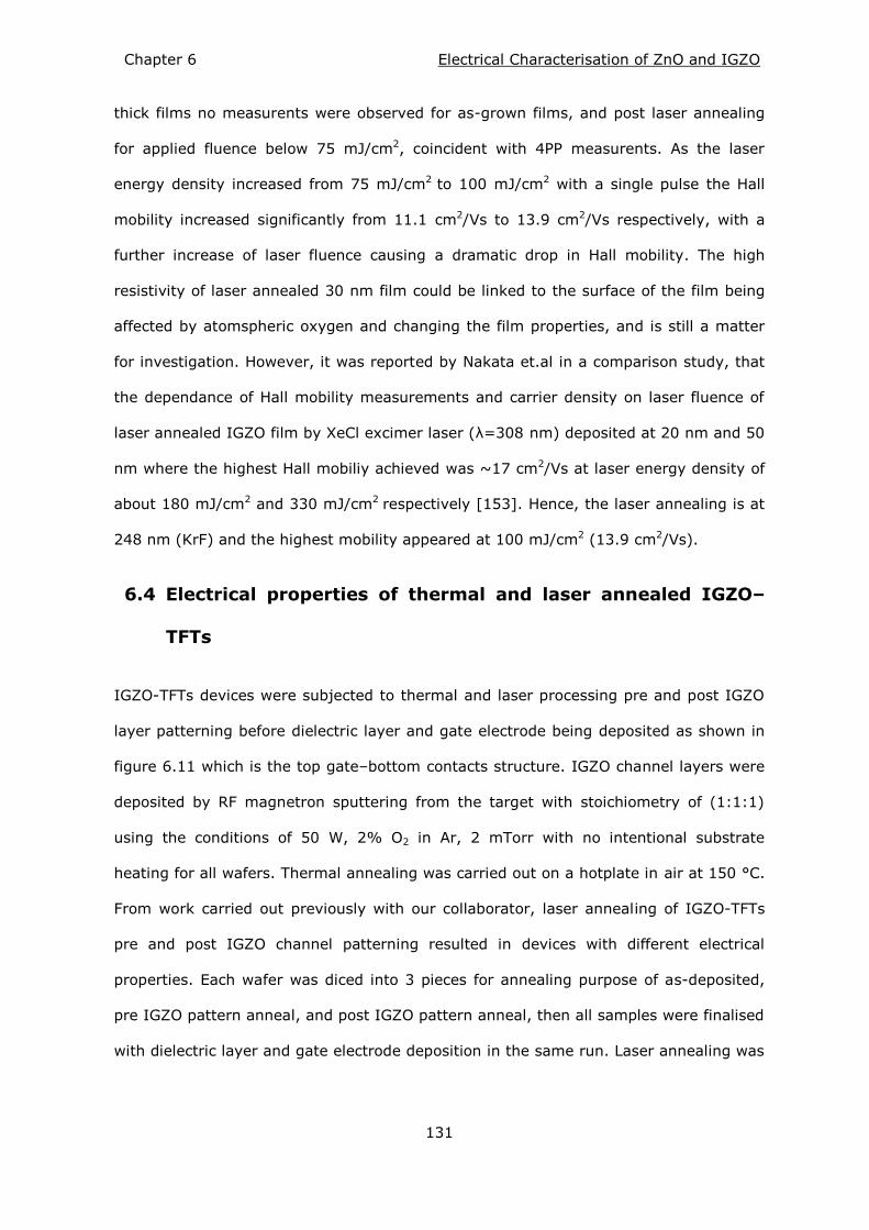
Chapter 6 Electrical Characterisation of ZnO and IGZO
131
thick films no measurents were observed for as-grown films, and post laser annealing
for applied fluence below 75 mJ/cm2, coincident with 4PP measurents. As the laser
energy density increased from 75 mJ/cm2 to 100 mJ/cm2 with a single pulse the Hall
mobility increased significantly from 11.1 cm2/Vs to 13.9 cm2/Vs respectively, with a
further increase of laser fluence causing a dramatic drop in Hall mobility. The high
resistivity of laser annealed 30 nm film could be linked to the surface of the film being
affected by atomspheric oxygen and changing the film properties, and is still a matter
for investigation. However, it was reported by Nakata et.al in a comparison study, that
the dependance of Hall mobility measurements and carrier density on laser fluence of
laser annealed IGZO film by XeCl excimer laser (λ=308 nm) deposited at 20 nm and 50
nm where the highest Hall mobiliy achieved was ~17 cm2/Vs at laser energy density of
about 180 mJ/cm2 and 330 mJ/cm2 respectively [153]. Hence, the laser annealing is at
248 nm (KrF) and the highest mobility appeared at 100 mJ/cm2 (13.9 cm2/Vs).
Electrical properties of thermal and laser annealed IGZO–6.4
TFTs
IGZO-TFTs devices were subjected to thermal and laser processing pre and post IGZO
layer patterning before dielectric layer and gate electrode being deposited as shown in
figure 6.11 which is the top gate–bottom contacts structure. IGZO channel layers were
deposited by RF magnetron sputtering from the target with stoichiometry of (1:1:1)
using the conditions of 50 W, 2% O2 in Ar, 2 mTorr with no intentional substrate
heating for all wafers. Thermal annealing was carried out on a hotplate in air at 150 °C.
From work carried out previously with our collaborator, laser annealing of IGZO-TFTs
pre and post IGZO channel patterning resulted in devices with different electrical
properties. Each wafer was diced into 3 pieces for annealing purpose of as-deposited,
pre IGZO pattern anneal, and post IGZO pattern anneal, then all samples were finalised
with dielectric layer and gate electrode deposition in the same run. Laser annealing was
Chapter 6 Electrical Characterisation of ZnO and IGZO
132
conducted selectively on the wafer at fluences from 0 to 75 mJ/cm2 for both pre-and
post-IGZO pattern.
Cr/Au ~ 5/75 nm
SiO2
Gate(Cr/Au)
Drain(Cr/Au) Source(Cr/Au)
Si
IGZO 30 nm
Al2O3 ~ 50 nm
W/L=1000 µm / 5 µm
200 nm
Figure 6.11: Cross section diagram of IGZO TFTs used for thermal and laser annealing
(W/L= 1000 μm/5 μm).
Figure 6.12 shows the process sequence of top gate-bottom contacts IGZO-TFT
fabrication undertaken via collabration with Cambridge University, with the IGZO
channel deposition, and laser processing carried out at NTU.
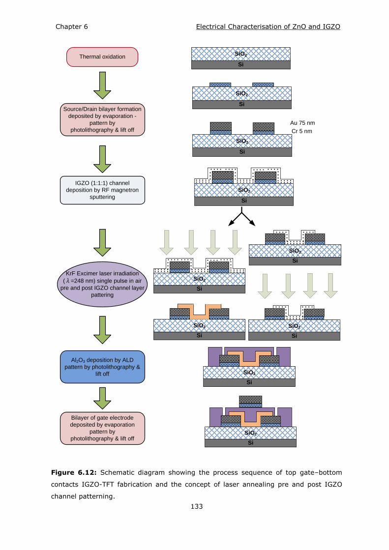
Chapter 6 Electrical Characterisation of ZnO and IGZO
133
KrF Excimer laser irradiation
(λ=248 nm) single pulse in air
pre and post IGZO channel layer
pattering
Thermal oxidation
Source/Drain bilayer formation
deposited by evaporation -
pattern by
photolithography & lift off Cr 5 nm
Au 75 nm
IGZO (1:1:1) channel
deposition by RF magnetron
sputtering
Al2O3 deposition by ALD
pattern by photolithography &
lift off
Bilayer of gate electrode
deposited by evaporation
pattern by
photolithography & lift off
Si
SiO2
Si
SiO2
Si
SiO2
Si
SiO2
Si
SiO2
Si
SiO2
Si
SiO2
Si
SiO2
Si
SiO2
Si
SiO2
Figure 6.12: Schematic diagram showing the process sequence of top gate–bottom
contacts IGZO-TFT fabrication and the concept of laser annealing pre and post IGZO
channel patterning.
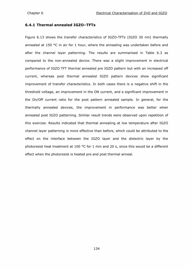
Chapter 6 Electrical Characterisation of ZnO and IGZO
134
6.4.1 Thermal annealed IGZO–TFTs
Figure 6.13 shows the transfer characteristics of IGZO-TFTs (IGZO 30 nm) thermally
annealed at 150 °C in air for 1 hour, where the annealing was undertaken before and
after the channel layer patterning. The results are summarised in Table 6.3 as
compared to the non-annealed device. There was a slight improvement in electrical
performance of IGZO TFT thermal annealed pre IGZO pattern but with an increased off
current, whereas post thermal annealed IGZO pattern devices show significant
improvement of transfer characteristics. In both cases there is a negative shift in the
threshold voltage, an improvement in the ON current, and a significant improvement in
the On/Off current ratio for the post pattern annealed sample. In general, for the
thermally annealed devices, the improvement in performance was better when
annealed post IGZO patterning. Similar result trends were observed upon repetition of
this exercise. Results indicated that thermal annealing at low temperature after IGZO
channel layer patterning is more effective than before, which could be attributed to the
effect on the interface between the IGZO layer and the dielectric layer by the
photoresist heat treatment at 100 °C for 1 min and 20 s, since this would be a different
effect when the photoresist is heated pre and post thermal anneal.
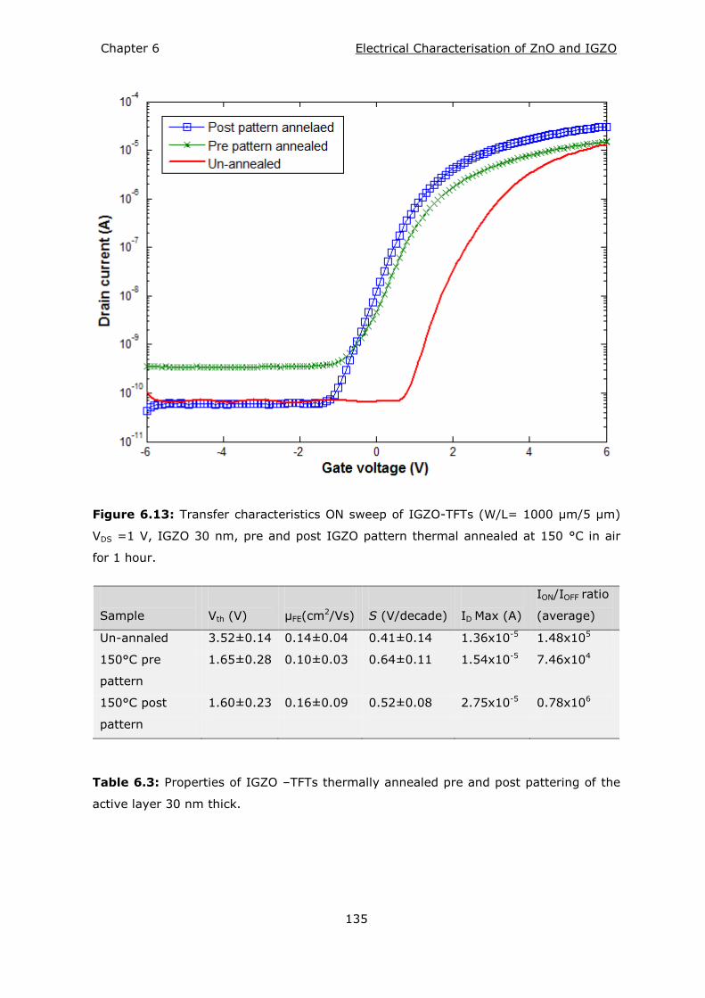
Chapter 6 Electrical Characterisation of ZnO and IGZO
135
Figure 6.13: Transfer characteristics ON sweep of IGZO-TFTs (W/L= 1000 μm/5 μm)
VDS =1 V, IGZO 30 nm, pre and post IGZO pattern thermal annealed at 150 °C in air
for 1 hour.
Sample
Vth (V)
μFE(cm2/Vs)
S (V/decade)
ID Max (A)
ION/IOFF ratio
(average)
Un-annaled 3.52±0.14 0.14±0.04 0.41±0.14 1.36x10⁻⁵ 1.48x10⁵
150°C pre
pattern
1.65±0.28 0.10±0.03 0.64±0.11 1.54x10⁻⁵ 7.46x10⁴
150°C post
pattern
1.60±0.23 0.16±0.09 0.52±0.08 2.75x10⁻⁵ 0.78x10⁶
Table 6.3: Properties of IGZO –TFTs thermally annealed pre and post pattering of the
active layer 30 nm thick.
Chapter 6 Electrical Characterisation of ZnO and IGZO
136
6.4.2 Laser annealed IGZO –TFTs
The TFT results for the laser processed samples are shown in Figure 6.14 which
represents the characteristics from devices fabricated on the same substrate. As with
the thermally annealed samples, the laser treated films at laser energy density of 75
mJ/cm2 with single pulse show a negative shift in threshold voltage and an increase of
ON current. However, devices laser annealed pre IGZO pattern demonstrate higher ON
and OFF current than the devices processed post to IGZO pattern. The electrical
properties of these devices are summarized in Table 6.4.
Figure 6.14: Transfer characteristics ON sweep IGZO-TFTs (W/L= 1000 μm/5 μm) VDS
=1 V, IGZO 30 nm, laser annealed at laser energy density of 75 mJ/cm2 with a single
pulse, pre and post IGZO patterning.
Laser annealed IGZO-TFT devices with a channel layer 30nm thick demonstrating very
low field effect mobility, as well as no Hall Effect was observed for 30 nm thick films as
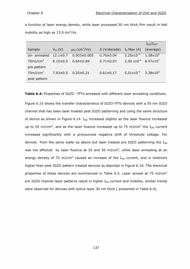
Chapter 6 Electrical Characterisation of ZnO and IGZO
137
a function of laser energy density, while laser processed 50 nm thick film result in Hall
mobility as high as 13.9 cm2/Vs.
Sample
Vth (V)
μFE (cm2/Vs)
S (V/decade)
ID Max (A)
ION/IOFF
(average)
Un- annealed 12.1±0.7 0.003±0.005 0.70±0.04 3.25x10⁻⁵ 1.58x10⁵
75mJ/cm2
pre pattern
8.15±0.5 0.64±0.69 0.71±0.07 2.00 x10⁻⁴ 8.47x10⁷
75mJ/cm2
post pattern
7.93±0.5 0.25±0.21 0.61±0.17 5.01x10⁻⁵ 3.38x10⁶
Table 6.4: Properties of IGZO –TFTs annealed with different laser annealing conditions.
Figure 6.15 shows the transfer characteristics of IGZO-TFTs devices with a 50 nm IGZO
channel that has been laser treated post IGZO patterning and using the same structure
of device as shown in Figure 6.14. ION increased slightly as the laser fluence increased
up to 25 mJ/cm2, and as the laser fluence increased up to 75 mJ/cm2 the ION current
increased significantly with a pronounced negative shift of threshold voltage. For
devices from the same wafer as above but laser treated pre IGZO patterning the ION
was not affected by laser fluence at 25 and 50 mJ/cm2, while laser annealing at an
energy density of 75 mJ/cm2 caused an increase of the ION current, and is relatively
higher than post IGZO pattern treated devices as depicted in Figure 6.16. The electrical
properties of these devices are summarized in Table 6.5. Laser anneal at 75 mJ/cm2
pre IGZO channel layer patterns result in higher ION current and mobility, similar trends
were observed for devices with active layer 30 nm thick ( presented in Table 6.4).
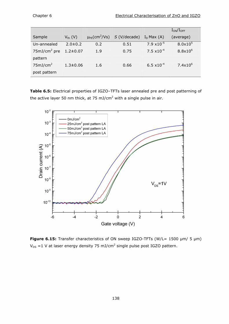
Chapter 6 Electrical Characterisation of ZnO and IGZO
138
Sample
Vth (V)
μFE(cm2/Vs)
S (V/decade)
ID Max (A)
ION/IOFF
(average)
Un-annealed 2.0±0.2 0.2 0.51 7.9 x10⁻⁵ 8.0x10⁵
75mJ/cm2 pre
pattern
1.2±0.07 1.9 0.75 7.5 x10⁻⁴ 8.8x10⁶
75mJ/cm2
post pattern
1.3±0.06 1.6 0.66 6.5 x10⁻⁴ 7.4x10⁶
Table 6.5: Electrical properties of IGZO–TFTs laser annealed pre and post patterning of
the active layer 50 nm thick, at 75 mJ/cm2 with a single pulse in air.
Figure 6.15: Transfer characteristics of ON sweep IGZO-TFTs (W/L= 1500 μm/ 5 μm)
VDS =1 V at laser energy density 75 mJ/cm2 single pulse post IGZO pattern.
Chapter 6 Electrical Characterisation of ZnO and IGZO
139
Figure 6.16: Transfer characteristics of ON sweep IGZO-TFTs (W/L= 1500 μm/ 5 μm)
VDS =1 V pre and post IGZO pattern laser at laser energy density 75 mJ/cm2 single
pulse.
Discussion 6.5
In oxide semiconductors, the electrical conduction arises by intrinsic defects (that
donate free electrons) such as interstitials or oxygen vacancies. It is shown in this
chapter that Laser annealing by KrF excimer laser (λ=248 nm) at single pulse in air
results in a significant reduction in resistivity of ZnO and IGZO thin films.
For ZnO films, laser irradiation causes a breaking of the Zn-O bond which results in
oxygen vacancies (Vo) or zinc interstitial (Zni) predominantly contributing as a donor. A
dramatic reduction in sheet resistance of laser processed ZnO films was observed at
high fluences, dropping to about 864 Ω/sq at 315 mJ/cm2 for films deposited at RT and
400 °C. No PL was observed as a function of laser anneal for films deposited on SiO2 at
RT. However, the influence on the microstructure of ZnO films was demonstrated by
Chapter 6 Electrical Characterisation of ZnO and IGZO
140
XRD patterns which shows a shift of the preferred (002) peak as a function of laser
fluence. The reason behind no PL being observed for ZnO on SiO2 grown at RT is still a
matter of investigation.
Post deposition annealing of IGZO films leads to removal of weakly bonded oxygen
atoms or oxygen combination contributing to a new equilibrium changing the electrical
properties of IGZO films [75, 132]. A significant drop in sheet resistance of IGZO thin
films deposited without intentional substrate heating as a function of laser energy
density for a single pulse is observed with a strong dependence on deposition
parameters. The lowest sheet resistance post laser processing was observed at
deposition conditions of low deposition pressure, low oxygen concentration, and high RF
power. In addition the Hall Effect mobility increased as a function of laser fluence to
13.9 cm2/Vs.
For IGZO-TFT devices, thermal and laser annealing pre and post IGZO channel layer
patterns result in negative shift in threshold voltage which could be attributed to the
high defects density in the subgap density of states (DOS) pins the Fermi level, so no
mobile holes. TFTs devices demonstrate high values of sub-threshold swing S in which
related to trap density in the subgap. High sub-threshold swing S result in poor
electrical properties such as, low speed and higher power consumption. Laser annealed
devices was unstable under bias stress in which demonstrate positive shift in threshold
voltage. laser irradiation is expected to reduce the contact resistance between the IGZO
channel layer and the source/drain electrodes by increasing the carrier concentration
[74].
Chapter 7 Conclusion and Future Work
141
Chapter 7
Conclusion and Future Work
Introduction 7.1
The main aim of this project was to investigate the feasibility of using excimer laser
processing as an alternative technique to conventional thermal annealing to improve
the microstructure and electrical properties of sputtered ZnO and IGZO thin films for
use in electronic devices. Initially, a comparative study was conducted into the effect of
post deposition processing using thermal annealing, rapid thermal annealing, and laser
annealing on the microstructure properties of ZnO thin films. The films were deposited
(via collaboration with Cambridge University) without intentional substrate heating
using the HiTUS technique. Oxygen flow rates of 28, 32, 35, 38, and 41 sccm were
used to produce films of varying stoichiometry in order to examine the effect of post
deposition processing on the properties, and to help in the study of intrinsic defects and
the modification of defect type and density as a function of the annealing process used.
The effect of post deposition processing was also investigated for ZnO films deposited
by RF magnetron sputtering at NTU, as a function of varying deposition conditions: RF
power, oxygen content in the sputtering gas, and substrate temperature from RT to
400 °C. Finally, the feasibility of using laser annealing to improve the electrical
properties of IGZO films grown via RF magnetron sputtering at room temperature was
investigated. IGZO thin films were deposited at various conditions to study the effect of
growth and post deposition annealing on the properties, with the optimised films used
in TFT test devices. This chapter presents an overview of the major outcomes from this
work and discusses aspects that would be suitable for further investigation.
Chapter 7 Conclusion and Future Work
142
Key Outcomes 7.2
The results from this research demonstrate that laser processing is a technique that can
be used for controlled modification of the internal properties of low temperature
deposited ZnO films. Optimised processing leads to grain re-growth, crystallinity
improvement and a dramatic reduction of point defects, without the associated film
degradation or loss that occurs when using high temperature thermal and rapid thermal
annealing. The results consequently provide evidence for the potential of this technique
to be used with the application of ZnO films for use on flexible substrates. The main
research findings are summarised as the following:
A comparative study has been presented into the effect of three annealing
methods using a comprehensive range of processing parameters applied to ZnO
thin films. The results demonstrate that laser annealing is a powerful technique
to control the modification of sputtered ZnO thin films grown at low
temperature. The effect is a reduction of intrinsic defects without film
degradation or materials loss that is observed for thermal and rapid thermal
annealing at high temperatures concomitantly with generation of new defects.
The resultant PL spectra exhibit the development of two main peaks: a strong
narrow NBE peak centred at 381 nm, and a broad visible emission DLE (440-800
nm). The evolution of these peaks is strongly dependent on the laser energy
density applied, with five process regimes observed for various fluence ranges
applied at single or multiples pulses. In intrinsic ZnO the nature of point defects
considered to be responsible for typical DLE is still a matter of debate [84].
However, the results presented here demonstrate that the DLE peak is related to
excess oxygen defects. This is evidenced by the fact that no appearance of a
DLE peak was observed as a function of laser fluence for films grown at an
oxygen flow rate of 28 sccm (Zn-rich), but there is a pronounced development
of NBE peak with fluence increase, indicating that the DLE observed for films
Chapter 7 Conclusion and Future Work
143
deposited at oxygen flow rate > 28 sccm is related to excess oxygen defects.
This is further evidenced when the effect of laser anneal as a function of as-
grown stoichiometry is examined; indicating that as the growth oxygen flow rate
is increased, the intensity of the DLE is increased consistent with excess oxygen
concentration, similar to the trend also observed for the RTA samples.
The research presents more detailed analyses of point defects generated
(defects related to the DLE) by TA and RTA than previously reported. Rapid
thermal annealing of low temperature deposited HiTUS ZnO films demonstrate
the development of a strong deep level emission (DLE), classified as an
orange/red emission, which is further enhanced when annealing is carried out in
an oxygen containing environment. This gives the indication that excess oxygen
dominates defect activation, which is likely to be through the mechanism of
oxygen absorption as oxygen interstitials and antisites. In comparison, thermal
annealing in air at high temperature as a function of annealing time
demonstrates a reduction in the orange/red emission peak with shift to a
sharper green/yellow emission. This could be ascribed to a change in the nature
of activated dominant DLE defects from oxygen interstitial (Oi) defects to zinc
vacancies (Vzn). This shift is confirmed via XPS characterisation in which the
corresponding deviation of film stoichiometry is observed as the temperature is
increased up to 700 °C. The effect of film stoichiometry is also presented by the
results of the RTA processing, with the films exhibiting a green/yellow DLE for all
samples annealed in nitrogen ambient, which is not observed for samples
processed in oxygen. The intensity of DLE for all samples has a dependence on
the film stoichiometry, with a higher DLE intensity consistent with samples
grown at higher oxygen flow rates.
In terms of the deposition parameters, the research has demonstrated that as a
function of laser annealing, a low sputtering RF power is required to produce
better quality ZnO films when grown at room temperature. From the resultant
PL, the results show that as the growth RF power is increased, the intensity of
Chapter 7 Conclusion and Future Work
144
the NBE peak is decreased significantly. This could be linked to the fact that at
the higher RF powers used for deposition, highly energetic ion bombardment
leads to surface damage, and defects are introduced to the film [116]. However,
it has been reported elsewhere that for as-deposited films without intentional
substrate heating, the grain size increased as the RF power increased [142],
while for the as-deposited films investigated here there is an observed reduction
in the average grain size as the RF power is increased. This discrepancy could be
ascribed to the films being deposited at different parameters, therefore the
actual threshold of RF power may differ.
The intensity of the NBE peak is shown to be strongly influenced by the film
growth temperature, with encouraging PL results demonstrated by samples
deposited on unheated substrates showing subsequent evolution of strong NBE
emission peak at high laser energy density, whilst eliminating the defects related
to the DLE peak. As the growth temperature is increased beyond ambient, the
NBE intensity peak following laser processing decreased as a function of laser
fluence. This effect could be attributed to improved film quality when deposited
at higher temperatures, or it might be related to the thickness of the defective
layer between the substrate and the film being increased as the growth
temperature is increased. However, the exact reason stills a matter of
investigation.
XRD characterisation shows that the average grain domain size for as-grown
films is increased as the growth temperature is increased, and following laser
processing, the average grain domain size increased significantly for films grown
at RT, and 100 °C, whereas this dramatically decreased for films deposited at
200 °C, 300 °C, and 400 °C. Following thermal annealing at 700 °C, XRD
demonstrates that for samples where the growth temperature was increased up
to 300 °C, there is a significant increase in the (002) peak intensity, compared
to the effect on films deposited at 400 °C where there was a dramatic decrease
in (002) peak following annealing, similar to results reported previously [138].
Chapter 7 Conclusion and Future Work
145
Further confirmation of the effect on crystal structure is evidenced by TEM
images, where dark field images of laser annealed ZnO films grown on un-
heated substrates exhibit a pronounced substantial grain growth and crystal
improvement.
One of the most significant results of this work is that laser processing is shown
to produce a controlled in-depth crystallisation and modification of ZnO films,
which would facilitate the use of the technique to isolate the modified region
from the substrate, or any sensitive underlying layers.
Additional output from this research relates to investigations into the deposition
and processing of IGZO for potential use in electronic devices. The results show
that to produce IGZO thin films without intentional substrate heating with lowest
ultimate sheet resistance as a function of post deposition laser processing the
parameters of choice should be low deposition pressure, low oxygen
concentration, and high RF power. Similar conditions were observed elsewhere
as a function of thermal annealing [154] which could be attributed to deposition
mechanisms which affect the sputtered particles arriving on substrate with
surface mobility resulting in dense and compact films with low resistivity [92].
The electrical characteristics of laser annealed IGZO thin films deposited at
various depositions parameters on unheated substrate demonstrate a significant
drop in sheet resistance as a function of laser fluence applied. The as-deposited
films were highly resistive (i.e. they had sheet resistance > 5 MΩ/sq) which
dropped to about 500±10% Ω/sq post laser anneal which can be used as metal
oxide for electroluminescence devices application. The electrical properties of
IGZO films are shown to be strongly dependent on the film growth conditions
and target stoichiometry. The sheet resistance of laser processed IGZO films
deposited from a target with the stoichiometry of (1:1:1) is relatively higher
than films from a (2:2:1) target, which would be attributed to a higher indium
content. It was suggested that annealing processes contribute to the removal of
weak bonded oxygen atoms or oxygen incorporation which leads to a new
Chapter 7 Conclusion and Future Work
146
equilibrium resulting in increased film conductivity [75]. For the results
presented here, the room temperature Hall Effect mobility of IGZO (50 nm thick)
increased significantly as the laser fluence was increased from 75 mJ/cm2 to 100
mJ/cm2 (single pulse) reaching values of 11.1 cm2/Vs and 13.9 cm2/Vs
respectively. Hence, results demonstrate that laser annealing is a powerful
techniques to modify the electrical properties of IGZO films grown at room
temperature.
Laser annealing of IGZO-TFT pre IGZO channel patterns result in relatively
higher ON current than post pattern while thermally annealing post IGZO
pattern demonstrate higher ON current. Laser and thermal annealing result in
negative shift in threshold voltage, the trap density in the subgap DOS cause
high sub-threshold swing in which affect the speed of the devices and increase
the power consumption.
Future work 7.3
Following the outcomes of this research project, it is suggested that further work would
be beneficial in terms of investigating the microstructure and electrical properties of
oxide semiconductors studied here, and into the processing of IGZO-TFTs devices as
described below:
The electrical properties of HiTUS ZnO films, and ZnO grown by RF magnetron
sputtering, as a function of laser processing to be characterised via Hall Effect,
and then the optimised functional films to be used as a channel layer for ZnO-
TFTs fabrication. Another interesting study would be to investigate the effect
laser and thermal anneal of ZnO channel layers as a function of pre and post
channel layer patterning, since the results with the IGZO devices showed that
the sequence is important.
More microstructure investigation via PL of the effect of laser processing of ZnO
deposited by RF magnetron sputtering at higher oxygen concentrations by
Chapter 7 Conclusion and Future Work
147
varying RF power, and substrate temperature – to further study the nature of
defects.
Temperature dependant PL of laser and thermal annealed ZnO films deposited
by HiTUS and RF magnetron sputtering.
Fabrication of IGZO-TFT devices on flexible substrates to study the effect of ON
current as a function of laser fluence, and to deposit alumina layer (Al2O3) on
the top of IGZO layer before laser processing as a protection layer from
atmospheric contamination during laser processing and before the source/drain
has been deposited.
Study of the effect of a combination of laser annealing and thermal annealing
onto microstructure and electrical properties of both ZnO and IGZO thin films.
List of references
148
List of references
[1] G. P. Crawford, Flexible Flat Panel Displays, John Wiley and Sons Ltd , pp. 1-9,
2005.
[2] T. Hirao, M. Furuta, H. Furuta, T. Matsuda, T. Hiramatsu, H. Hokari, M. Yoshida,
H. Ishii and M. Kakegawa, "Novel top‐gate zinc oxide thin‐film transistors (ZnO
TFTs) for AMLCDs," Journal of the Society for Information Display, vol. 15, pp.
17-22, 2007.
[3] Y. Kuo, Thin Film Transistors: Materials and Processes, Amorphous Silicon Thin
Film Transistors, Vol. 1. Boston, Mass. ; London: Kluwer Academic Publishers,
2004.
[4] S. Depp, A. Juliana and B. Huth, "Polysilicon FET devices for large area
input/output applications," in Electron Devices Meeting, 1980 International,
1980, pp. 703-706.
[5] T. Sameshima, "Status of Si thin film transistors," J. Non Cryst. Solids, vol. 227,
pp. 1196-1201, 1998.
[6] N. Park, T. Kim and S. Park, "Band gap engineering of amorphous silicon
quantum dots for light-emitting diodes," Appl. Phys. Lett., vol. 78, pp. 2575-
2577, 2001.
[7] C. R. Kagan and P. Andry, Thin-Film Transistors. New York: Marcel Dekker, 2003.
[8] U. Ozgur, Y. I. Alivov, C. Liu, A. Teke, M. Reshchikov, S. Dogan, V. Avrutin, S.
Cho and H. Morkoc, "A comprehensive review of ZnO materials and devices," J.
Appl. Phys., vol. 98, pp. 041301-041301-103, 2005.
[9] K. Nomura, H. Ohta, A. Takagi, T. Kamiya, M. Hirano and H. Hosono, "Room-
temperature fabrication of transparent flexible thin-film transistors using
amorphous oxide semiconductors," Nature, vol. 432, pp. 488-492, 2004.
[10] H. Yabuta, M. Sano, K. Abe, T. Aiba, T. Den, H. Kumomi, K. Nomura, T. Kamiya
and H. Hosono, "High-mobility thin-film transistor with amorphous InGaZnO
channel fabricated by room temperature rf-magnetron sputtering," Appl. Phys.
Lett., vol. 89, pp. 112123, 2006.
[11] J. Y. Kwon, K. S. Son, J. S. Jung, T. S. Kim, M. K. Ryu, K. B. Park, B. W. Yoo, J.
W. Kim, Y. G. Lee and K. C. Park, "Bottom-gate gallium indium zinc oxide thin-
film transistor array for high-resolution AMOLED display," Electron Device
Letters, IEEE, vol. 29, pp. 1309-1311, 2008.
[12] C. J. Kim, D. Kang, I. Song, J. C. Park, H. Lim, S. Kim, E. Lee, R. Chung, J. C.
Lee and Y. Park, "Highly stable Ga2O3-In2O3-ZnO TFT for active-matrix organic
light-emitting diode display application," in Electron Devices Meeting, 2006.
IEDM'06. International, 2006, pp. 1-4.
List of references
149
[13] H. Hosono, K. Nomura, Y. Ogo, T. Uruga and T. Kamiya, "Factors controlling
electron transport properties in transparent amorphous oxide semiconductors,"
J. Non Cryst. Solids, vol. 354, pp. 2796-2800, 5/1, 2008.
[14] T. Kamiya, K. Nomura and H. Hosono, "Present status of amorphous In–Ga–Zn–
O thin-film transistors," Science and Technology of Advanced Materials, vol. 11,
pp. 044305, 2010.
[15] H. Hsieh, T. Tsai, C. Chang, S. Hsu, C. Chuang and Y. Lin, "Active‐matrix organic
light‐emitting diode displays with indium gallium zinc oxide thin‐film transistors
and normal, inverted, and transparent organic light‐emitting diodes," Journal of
the Society for Information Display, vol. 19, pp. 323-328, 2011.
[16] T. Arai, "Oxide‐TFT technologies for next‐generation AMOLED displays," Journal of
the Society for Information Display, vol. 20, pp. 156-161, 2012.
[17] S. Jeong, B. Kim and B. Lee, "Photoluminescence dependence of ZnO films grown
on Si (100) by radio-frequency magnetron sputtering on the growth ambient,"
Appl. Phys. Lett., vol. 82, pp. 2625-2627, 2003.
[18] A. Djurišić, W. C. Choy, V. A. L. Roy, Y. H. Leung, C. Y. Kwong, K. W. Cheah, T.
Gundu Rao, W. K. Chan, H. Fei Lui and C. Surya, "Photoluminescence and
electron paramagnetic resonance of ZnO tetrapod structures," Advanced
Functional Materials, vol. 14, pp. 856-864, 2004.
[19] P. T. Hsieh, Y. C. Chen, C. M. Wang, Y. Z. Tsai and C. C. Hu, "Structural and
photoluminescence characteristics of ZnO films by room temperature sputtering
and rapid thermal annealing process," Appl. Phys. A, vol. 84, pp. 345-349, 2006.
[20] T. Brody, J. A. Asars and G. D. Dixon, "A 6× 6 inch 20 lines-per-inch liquid-
crystal display panel," Electron Devices, IEEE Transactions on, vol. 20, pp. 995-
1001, 1973.
[21] http://www.gizmag.com/samsungs-transparent-lcd-display/18283/.
[22] S. Masuda, K. Kitamura, Y. Okumura, S. Miyatake, H. Tabata and T. Kawai,
"Transparent thin film transistors using ZnO as an active channel layer and their
electrical properties," J. Appl. Phys., vol. 93, pp. 1624, 2003.
[23] Ü. Özgür, Y. I. Alivov, C. Liu, A. Teke, M. Reshchikov, S. Doğan, V. Avrutin, S. J.
Cho and H. Morkoc, "A comprehensive review of ZnO materials and devices," J.
Appl. Phys., vol. 98, pp. 041301, 2005.
[24] J. K. Jeong, J. H. Jeong, J. H. Choi, J. S. Im, S. H. Kim, H. W. Yang, K. N. Kang,
K. S. Kim, T. K. Ahn and H. Chung, "3.1: Distinguished paper: 12.1‐Inch WXGA
AMOLED display driven by Indium‐Gallium‐Zinc oxide TFTs array," in SID
Symposium Digest of Technical Papers, 2008, pp. 1-4.
[25] M. Ito, M. Kon, C. Miyazaki, N. Ikeda, M. Ishizaki, Y. Ugajin and N. Sekine, ""
Front Drive" Display Structure for Color Electronic Paper Using Fully Transparent
Amorphous Oxide TFT Array," IEICE Trans. Electron., vol. 90, pp. 2105-2111,
2007.
List of references
150
[26] R. Hoffman, B. J. Norris and J. Wager, "ZnO-based transparent thin-film
transistors," Appl. Phys. Lett., vol. 82, pp. 733-735, 2003.
[27] J. T. Wallmark and H. Johnson, Field-Effect Transistors: Physics, Technology and
Applications. Prentice-Hall, 1966.
[28] E. Fortunato, P. Barquinha and R. Martins, "Oxide Semiconductor Thin‐Film
Transistors: A Review of Recent Advances," Adv Mater, 2012.
[29] J. F. Wager, Transparent Electronics. New York ; London: Springer, 2008.
[30] D. Hong, G. Yerubandi, H. Chiang, M. Spiegelberg and J. Wager, "Electrical
modeling of thin-film transistors," Critical Reviews in Solid State and Material
Sciences, vol. 33, pp. 101-132, 2008.
[31] K. Hoshino, "Instability and temperature-dependence assessment of IGZO TFTs,"
2008.
[32] T. Hirao, M. Furuta, H. Furuta, T. Matsuda, T. Hiramatsu, H. Hokari and M.
Yoshida, "4.1: Distinguished paper: High mobility Top‐Gate zinc oxide Thin‐Film
transistors (ZnO‐TFTs) for Active‐Matrix liquid crystal displays," in SID
Symposium Digest of Technical Papers, 2006, pp. 18-20.
[33] J. S. Park, W. J. Maeng, H. S. Kim and J. S. Park, "Review of recent
developments in amorphous oxide semiconductor thin-film transistor devices,"
Thin Solid Films, vol. 520, pp. 1679-1693, 2012.
[34] M. Kim, J. H. Jeong, H. J. Lee, T. K. Ahn, H. S. Shin, J. S. Park, J. K. Jeong, Y. G.
Mo and H. D. Kim, "High mobility bottom gate InGaZnO thin film transistors with
SiOx etch stopper," Appl. Phys. Lett., vol. 90, pp. 212114-212114-3, 2007.
[35] J. Y. Kwon, K. S. Son, J. S. Jung, K. H. Lee, J. S. Park, T. S. Kim, K. H. Ji, R.
Choi, J. K. Jeong and B. Koo, "The impact of device configuration on the photon-
enhanced negative bias thermal instability of GaInZnO thin film transistors,"
Electrochemical and Solid-State Letters, vol. 13, pp. H213-H215, 2010.
[36] D. P. Heineck, B. R. McFarlane and J. F. Wager, "Zinc tin oxide thin-film-
transistor enhancement/depletion inverter," Electron Device Letters, IEEE, vol.
30, pp. 514-516, 2009.
[37] R. Presley, D. Hong, H. Chiang, C. Hung, R. Hoffman and J. Wager, "Transparent
ring oscillator based on indium gallium oxide thin-film transistors," Solid-State
Electronics, vol. 50, pp. 500-503, 2006.
[38] A. C. Tickle, Thin-Film Transistors. John Wiley, 1969.
[39] K. H. Cherenack, "Fabricating silicon thin-film transistors on plastic at 300 °C"
Princeton University 2009.
[40] P. K. Weimer, "The TFT a new thin-film transistor," Proceedings of the IRE, vol.
50, pp. 1462-1469, 1962.
List of references
151
[41] E. Lueder, "Processing of thin-film transistors with photolithography and
application for displays," in Digest 1980 SID Intl. Symp.(Soc. for Information
Displays), 1980, pp. 118-122.
[42] R. Haering, "Theory of thin film transistor operation," Solid-State Electronics, vol.
7, pp. 31-38, 1964.
[43] H. Koelmans and H. De Graaff, "Drift phenomena in CdSe thin film FET's," Solid-
State Electronics, vol. 10, pp. 997-1005, 1967.
[44] P. Le Comber, W. Spear and A. Ghaith, "Amorphous-silicon field-effect device
and possible application," Electron. Lett., vol. 15, pp. 179-181, 1979.
[45] R. Navamathavan, J. Lim, D. Hwang, B. Kim, J. Oh, J. Yang, H. Kim, S. Park and
J. Jang, "Thin-Film Transistors Based on ZnO Fabricated by Using Radio-
Frequency Magnetron Sputtering," JOURNAL-KOREAN PHYSICAL SOCIETY, vol.
48, pp. 271, 2006.
[46] R. Cross and M. De Souza, "Investigating the stability of zinc oxide thin film
transistors," Appl. Phys. Lett., vol. 89, pp. 263513, 2006.
[47] P. Carcia, R. McLean, M. Reilly and G. Nunes, "Transparent ZnO thin-film
transistor fabricated by rf magnetron sputtering," Appl. Phys. Lett., vol. 82, pp.
1117-1119, 2003.
[48] J. F. Wager, "68.1: Invited paper: Transparent Electronics—Display applications"
in 2007.
[49] P. Carcia, R. McLean and M. Reilly, "High-performance ZnO thin-film transistors
on gate dielectrics grown by atomic layer deposition," Appl. Phys. Lett., vol. 88,
pp. 123509-123509-3, 2006.
[50] K. Nomura, T. Kamiya, H. Yanagi, E. Ikenaga, K. Yang, K. Kobayashi, M. Hirano
and H. Hosono, "Subgap states in transparent amorphous oxide semiconductor,
In–Ga–Zn–O, observed by bulk sensitive X-ray photoelectron spectroscopy,"
Appl. Phys. Lett., vol. 92, pp. 202117, 2008.
[51] M. Kimura, T. Nakanishi, K. Nomura, T. Kamiya and H. Hosono, "Trap densities in
amorphous-InGaZnO4 thin-film transistors," Appl. Phys. Lett., vol. 92, pp.
133512, 2008.
[52] T. Kamiya, K. Nomura and H. Hosono, "Origins of High Mobility and Low
Operation Voltage of Amorphous Oxide TFTs: Electronic Structure, Electron
Transport, Defects and Doping*," Journal of Display Technology, vol. 5, pp. 468-
483, 2009.
[53] Y. Zhao and Y. Jiang, "Investigation of room temperature UV emission of ZnO
films with different defect densities induced by laser irradiation," Spectrochimica
Acta Part A: Molecular and Biomolecular Spectroscopy, vol. 76, pp. 336-340,
2010.
List of references
152
[54] H. Lu, Y. Tu, X. Lin, B. Fang, D. Luo and A. Laaksonen, "Effects of laser
irradiation on the structure and optical properties of ZnO thin films," Mater Lett,
2010.
[55] H. Hartnagel, A. Dawar, A. Jain and C. Jagadish, Semiconducting Transparent
Thin Films. Institute of Physics Pub. Bristol [England], 1995.
[56] C. Jagadish, and S. J. Pearton, Zinc Oxide Bulk, Thin Films and Nanostructures
Electronic Resource : Processing, Properties and Applications. Amsterdam ;
London: Elsevier, 2006.
[57] K. Ellmer, A. Klein Dr., B. Rech, Transparent Conductive Zinc Oxide : Basics and
Applications in Thin Film Solar Cells. Berlin: Springer, 2008.
[58] H. Hosono, "Ionic amorphous oxide semiconductors: Material design, carrier
transport, and device application," J. Non Cryst. Solids, vol. 352, pp. 851-858,
2006.
[59] K. Nomura, T. Kamiya, H. Ohta, T. Uruga, M. Hirano and H. Hosono, "Local
coordination structure and electronic structure of the large electron mobility
amorphous oxide semiconductor In-Ga-Zn-O: Experiment and ab initio
calculations," Physical Review B, vol. 75, pp. 035212, 2007.
[60] J. Nishii, F. M. Hossain, S. Takagi, T. Aita, K. Saikusa, Y. Ohmaki, I. Ohkubo, S.
KSISHIMOTO, A. Ohtomo and T. Fukumura, "High mobility thin film transistors
with transparent ZnO channels," Japanese Journal of Applied Physics, vol. 42,
pp. L347-L349, 2003.
[61] R. Navamathavan, C. Choi, E. Yang, J. Lim, D. Hwang, and S. Park "Fabrication
and characterizations of ZnO thin film transistors prepared by using radio
frequency magnetron sputtering," Solid-State Electronics, vol. 52, pp. 813-816,
2008.
[62] R. Cross, M. M. De Souza, S. C. Deane and N. D. Young, "A comparison of the
performance and stability of ZnO-TFTs with silicon dioxide and nitride as gate
insulators," Electron Devices, IEEE Transactions on, vol. 55, pp. 1109-1115,
2008.
[63] J. J. Kim, J. Y. Bak, J. H. Lee, H. S. Kim, N. W. Jang, Y. Yun and W. J. Lee,
"Characteristics of laser-annealed ZnO thin film transistors," Thin Solid Films,
vol. 518, pp. 3022-3025, 2010.
[64] S. Lim, J. M. Kim, D. Kim, C. Lee, J. S. Park and H. Kim, "The Effects of UV
Exposure on Plasma-Enhanced Atomic Layer Deposition ZnO Thin Film
Transistor," Electrochemical and Solid-State Letters, vol. 13, pp. H151-H154,
2010.
[65] M. Nakata, K. Takechi, T. Eguchi, E. Tokumitsu, H. Yamaguchi and S. Kaneko,
"Effects of thermal annealing on ZnO thin-film transistor characteristics and the
application of excimer laser annealing in plastic-based ZnO thin-film transistors,"
Japanese Journal of Applied Physics, vol. 48, pp. 1608, 2009.
List of references
153
[66] Y. Yang, S. S. Yang and K. Chou, "Laser‐irradiated zinc oxide thin‐film transistors
fabricated by solution processing," Journal of the Society for Information
Display, vol. 18, pp. 745-748, 2010.
[67] P. T. Hsieh, Y. C. Chen, K. S. Kao and C. M. Wang, "Structural and luminescent
characteristics of non-stoichiometric ZnO films by various sputtering and
annealing temperatures," Physica B: Condensed Matter, vol. 403, pp. 178-183,
2008.
[68] K. Nomura, H. Ohta, K. Ueda, T. Kamiya, M. Hirano and H. Hosono, "Thin-film
transistor fabricated in single-crystalline transparent oxide semiconductor,"
Science, vol. 300, pp. 1269-1272, 2003.
[69] Y. Kikuchi, K. Nomura, H. Yanagi, T. Kamiya, M. Hirano and H. Hosono, "Device
characteristics improvement of a-In–Ga–Zn–O TFTs by low-temperature
annealing," Thin Solid Films, vol. 518, pp. 3017-3021, 2010.
[70] K. Ide, Y. Kikuchi, K. Nomura, M. Kimura, T. Kamiya and H. Hosono, "Effects of
excess oxygen on operation characteristics of amorphous In-Ga-Zn-O thin-film
transistors," Appl. Phys. Lett., vol. 99, pp. 093507-093507-3, 2011.
[71] K. Ide, Y. Kikuchi, K. Nomura and T. K. Hosono, "Effects of low-temperature
ozone annealing on operation characteristics of amorphous In-Ga-Zn-O thin-film
transistors," Thin Solid Films, 2012.
[72] K. Nomura, T. Kamiya and H. Hosono, "Highly stable amorphous In-Ga-Zn-O
thin-film transistors produced by eliminating deep subgap defects," Appl. Phys.
Lett., vol. 99, pp. 053505-053505-3, 2011.
[73] M. Nakata, K. Takechi, K. Azuma, E. Tokumitsu, H. Yamaguchi and S. Kaneko,
"Improvement of InGaZnO4 thin film transistors characteristics utilizing excimer
laser annealing," Applied Physics Express, vol. 2, pp. 1102, 2009.
[74] B. Du Ahn, W. H. Jeong, H. S. Shin, D. L. Kim, H. J. Kim, J. K. Jeong, S. H. Choi
and M. K. Han, "Effect of excimer laser annealing on the performance of
amorphous indium gallium zinc oxide thin-film transistors," Electrochemical and
Solid-State Letters, vol. 12, pp. H430-H432, 2009.
[75] H. W. Zan, W. T. Chen, C. W. Chou, C. C. Tsai, C. N. Huang and H. W. Hsueh,
"Low temperature annealing with solid-state laser or UV lamp irradiation on
amorphous IGZO thin-film transistors," Electrochemical and Solid-State Letters,
vol. 13, pp. H144-H146, 2010.
[76] Y. Yang, S. S. Yang and K. Chou, "Characteristic Enhancement of Solution-
Processed In–Ga–Zn Oxide Thin-Film Transistors by Laser Annealing," Electron
Device Letters, IEEE, vol. 31, pp. 969-971, 2010.
[77] Y. Yang, S. S. Yang and K. Chou, "Performance improvements of IGZO and ZnO
thin‐film transistors by laser‐irradiation treatment," Journal of the Society for
Information Display, vol. 19, pp. 247-252, 2011.
[78] K. Wasa, M. Kitabatake and H. Adachi, Thin Film Materials Technology:
Sputtering of Compound Materials. William Andrew, 2004.
List of references
154
[79] M. Maqbool. Growth, characterization and luminescence and optical properties of
rare-earth elements and transition metals doped in wide bandgap nitride
semiconductors. Ohio University, 2005.
[80] W. R. Grove, "On the electro-chemical polarity of gases," Philosophical
Transactions of the Royal Society of London, vol. 142, pp. 87-101, 1852.
[81] I. Langmuir, "The mechanism of the surface phenomena of flotation,"
Transactions of the Faraday Society, vol. 15, pp. 62-74, 1920.
[82] J. S. Chapin, "PLANAR MAGNETRON," Research-Development, vol. 25, pp. 37,
1974.
[83] S. Campbell, "The Science Engineering of Microelectronic Fabrication". Oxford
University press, 2001.
[84] H. Morkoç and Ü. Özgür, Zinc Oxide: Fundamentals, Materials and Device
Technology. Vch Verlagsgesellschaft Mbh, 2009.
[85] D. Song, "Effects of rf power on surface-morphological, structural and electrical
properties of aluminium-doped zinc oxide films by magnetron sputtering," Appl.
Surf. Sci., vol. 254, pp. 4171-4178, 2008.
[86] E. Fortunato, P. Barquinha, A. Pimentel, L. Pereira, G. Goncalves and R. Martins,
"Amorphous IZO TTFTs with saturation mobilities exceeding 100 cm2/Vs,"
Physica Status Solidi (RRL)–Rapid Research Letters, vol. 1, pp. R34-R36, 2007.
[87] S. Wakeham, M. Thwaites, B. Holton, C. Tsakonas, W. Cranton, D. Koutsogeorgis
and R. Ranson, "Low temperature remote plasma sputtering of indium tin oxide
for flexible display applications," Thin Solid Films, vol. 518, pp. 1355-1358,
2009.
[88] D. C. Look, D. Reynolds, C. Litton, R. Jones, D. Eason and G. Cantwell,
"Characterization of homoepitaxial p-type ZnO grown by molecular beam
epitaxy," Appl. Phys. Lett., vol. 81, pp. 1830, 2002.
[89] M. Purica, E. Budianu, E. Rusu, M. Danila and R. Gavrila, "Optical and structural
investigation of ZnO thin films prepared by chemical vapor deposition (CVD),"
Thin Solid Films, vol. 403, pp. 485-488, 2002.
[90] X. Sun and H. Kwok, "Optical properties of epitaxially grown zinc oxide films on
sapphire by pulsed laser deposition," J. Appl. Phys., vol. 86, pp. 408-411, 1999.
[91] E. Przeździecka, W. Paszkowicz, E. Łusakowska, T. Krajewski, G. Łuka, E.
Guziewicz and M. Godlewski, "Photoluminescence, electrical and structural
properties of ZnO films, grown by ALD at low temperature," Semiconductor
Science and Technology, vol. 24, pp. 105014, 2009.
[92] K. Ellmer, "Magnetron sputtering of transparent conductive zinc oxide: relation
between the sputtering parameters and the electronic properties," J. Phys. D,
vol. 33, pp. R17, 2000.
[93] E. Valeron, "Sputtering Advance Reaches the Target," Vacuum Solutions (IOP
Publishing Ltd., 2000), pp. 23, 2000.
List of references
155
[94] A. Flewitt, J. Dutson, P. Beecher, D. Paul, S. Wakeham, M. Vickers, C. Ducati, S.
Speakman, W. Milne and M. Thwaites, "Stability of thin film transistors
incorporating a zinc oxide or indium zinc oxide channel deposited by a high rate
sputtering process," Semiconductor Science and Technology, vol. 24, pp.
085002, 2009.
[95] A. Yeadon, S. Wakeham, H. Brown, M. Thwaites, M. Whiting and M. Baker,
"Remote plasma sputtering of indium tin oxide thin films for large area flexible
electronics," Thin Solid Films, vol. 520, pp. 1207-1211, 2011.
[96] S. Wakeham, M. Thwaites, C. Tsakonas, W. Cranton, R. Ranson, G. Boutaud and
D. Koutsogeorgis, "A new reactive sputtering technique for the low temperature
deposition of transparent light emitting ZnS: Mn thin films," Physica Status Solidi
(a), vol. 207, pp. 1614-1618, 2010.
[97] S. Wakeham, C. Tsakonas, W. Cranton, M. Thwaites, G. Boutaud and D.
Koutsogeorgis, "Laser annealing of thin film electroluminescent devices
deposited at a high rate using high target utilization sputtering," Semiconductor
Science and Technology, vol. 26, pp. 045016, 2011.
[98] D. Basting and G. Marowsky, Excimer Laser Technology. Berlin ; London:
Springer/Praxis, 2005.
[99] R. M. Ranson, Investigation into Thermographic Phosphors. Nottingham Trent
University, 1999.
[100] D. Heiman, "Photoluminescence spectroscopy," Northeastern University, 2004.
[101] T. H. Gfroerer, "Photoluminescence in analysis of surfaces and interfaces," 2006.
[102] B. Lin, Z. Fu and Y. Jia, "Green luminescent center in undoped zinc oxide films
deposited on silicon substrates," Appl. Phys. Lett., vol. 79, pp. 943-945, 2001.
[103] B. Fultz and J. M. Howe, Transmission Electron Microscopy and Diffractometry of
Materials. Springer Verlag, 2007.
[104] L. Reimer and H. Kohl, Transmission Electron Microscopy: Physics of Image
Formation. Springer Verlag, 2008.
[105] I. M. Watt, The Principles and Practice of Electron Microscopy. Cambridge. A:
Cambridge Univ. Press, 1989.
[106] D. K. Schroder, Semiconductor Material and Device Characterization. John Wiley
& Sons, 2006.
[107] B. B. He, Two-Dimensional X-Ray Diffraction. John Wiley & Sons Inc, 2009.
[108] C. Suryanarayana and M. G. Norton, "X-ray diffraction: a practical approach,"
Microscopy and Microanalysis, vol. 4, pp. 513-515, 1998.
[109] B. D. Cullity and S. Stock, Elements of X-Ray Diffraction. Prentice Hall, 2002.
[110] C. HAMMOND, "The basics of crystallography & diffraction (Paper)," 2009.
List of references
156
[111] J. C. Vickerman and I. S. Gilmore, Surface Analysis: The Principal Techniques.
Wiley Online Library, 2009.
[112] L. B. Valdes, "Resistivity measurements on germanium for transistors,"
Proceedings of the IRE, vol. 42, pp. 420-427, 1954.
[113] E. H. Hall, "On a new action of the magnet on electric currents," American
Journal of Mathematics, vol. 2, pp. 287-292, 1879.
[114] D. S. Ginley, Handbook of Transparent Conductors. Springer, 2010.
[115] Y. Wang, S. Lau, X. Zhang, H. Hng, H. Lee, S. Yu and B. Tay, "Enhancement of
near-band-edge photoluminescence from ZnO films by face-to-face annealing,"
J. Cryst. Growth, vol. 259, pp. 335-342, 2003.
[116] P. Hsieh, Y. Chen, K. Kao and C. Wang, "Structural effect on UV emission
properties of high-quality ZnO thin films deposited by RF magnetron sputtering,"
Physica B: Condensed Matter, vol. 392, pp. 332-336, 2007.
[117] K. K. Kim, J. H. Song, H. J. Jung, W. K. Choib, S. J. Park and J. H. Song, "The
grain size effects on the photoluminescence of ZnOÕ-Al2O3 grown by radio-
frequency magnetron sputtering," J. Appl. Phys., vol. 87, 2000.
[118] T. Matsumoto, H. Kato, K. Miyamoto, M. Sano, E. A. Zhukov and T. Yao,
"Correlation between grain size and optical properties in zinc oxide thin films,"
Appl. Phys. Lett., vol. 81, pp. 1231, 2002.
[119] H. Ong, A. Li and G. Du, "Depth profiling of ZnO thin films by
cathodoluminescence," Appl. Phys. Lett., vol. 78, pp. 2667, 2001.
[120] V. Roy, A. Djurišić, W. Chan, J. Gao, H. Lui and C. Surya, "Luminescent and
structural properties of ZnO nanorods prepared under different conditions," Appl.
Phys. Lett., vol. 83, pp. 141, 2003.
[121] C. H. Ahn, Y. Y. Kim, D. C. Kim, S. K. Mohanta and H. K. Cho, "A comparative
analysis of deep level emission in ZnO layers deposited by various methods," J.
Appl. Phys., vol. 105, pp. 013502-013502-5, 2009.
[122] L. Wu, Y. Wu, X. Pan and F. Kong, "Synthesis of ZnO nanorod and the annealing
effect on its photoluminescence property," Optical Materials, vol. 28, pp. 418-
422, 2006.
[123] A. Janotti and Van de Walle, Chris G, "Native point defects in ZnO," Physical
Review B, vol. 76, pp. 165202, 2007.
[124] H. Haneda, I. Sakaguchi, A. Watanabe, T. Ishigaki and J. Tanaka, "Oxygen
diffusion in single-and poly-crystalline zinc oxides," Journal of Electroceramics,
vol. 4, pp. 41-48, 1999.
[125] H. Ong, J. Dai, K. Hung, Y. Chan, R. Chang and S. Ho, "Electronic structures of
polycrystalline ZnO thin films probed by electron energy loss spectroscopy,"
Appl. Phys. Lett., vol. 77, pp. 1484-1486, 2000.
List of references
157
[126] T. Yen, D. Strome, S. J. Kim, A. N. Cartwright and W. A. Anderson, "Annealing
studies on zinc oxide thin films deposited by magnetron sputtering," J Electron
Mater, vol. 37, pp. 764-769, 2008.
[127] Y. Zhao and Y. Jiang, "Effect of KrF excimer laser irradiation on the properties of
ZnO thin films," J. Appl. Phys., vol. 103, pp. 114903-114903-4, 2008.
[128] H. Lu, Y. Tu, X. Lin, B. Fang, D. Luo and A. Laaksonen, "Effects of laser
irradiation on the structure and optical properties of ZnO thin films," Mater Lett,
vol. 64, pp. 2072-2075, 2010.
[129] K. Kim, S. Kim and S. Y. Lee, "Effect of excimer laser annealing on the
properties of ZnO thin film prepared by sol-gel method," Current Applied
Physics, vol. 12, pp. 585-588, 2012.
[130] J. O. Barnes, D. J. Leary and A. Jordan, "Relationship between deposition
conditions and physical properties of sputtered ZnO," J. Electrochem. Soc., vol.
127, pp. 1636-1640, 1980.
[131] P. Carcia, R. McLean and M. Reilly, "Oxide engineering of ZnO thin‐film
transistors for flexible electronics," Journal of the Society for Information
Display, vol. 13, pp. 547-554, 2005.
[132] A. Suresh, P. Gollakota, P. Wellenius, A. Dhawan and J. F. Muth, "Transparent,
high mobility InGaZnO thin films deposited by PLD," Thin Solid Films, vol. 516,
pp. 1326-1329, 2008.
[133] O. Agyeman, C. Xu, W. Shi, X. Zheng and M. Suzuki, "Strong ultraviolet and
green emissions at room temperature from annealed ZnO thin films," Japanese
Journal of Applied Physics, vol. 41, pp. 666-669, 2002.
[134] P. Hsieh, Y. Chen, K. Kao and C. Wang, "Structural effect on UV emission
properties of high-quality ZnO thin films deposited by RF magnetron sputtering,"
Physica B: Condensed Matter, vol. 392, pp. 332-336, 2007.
[135] A. Chatterjee, C. Shen, A. Ganguly, L. Chen, C. Hsu, J. Hwang and K. Chen,
"Strong room-temperature UV emission of nanocrystalline ZnO films derived
from a polymeric solution," Chemical Physics Letters, vol. 391, pp. 278-282,
2004.
[136] Y. R. Jang, K. Yoo and S. M. Park, "Rapid thermal annealing of ZnO thin films
grown at room temperature," Journal of Vacuum Science & Technology A, vol.
28, pp. 216-219, 2010.
[137] B. Li, Y. Liu, D. Shen, J. Zhang, Y. Lu and X. Fan, "Effects of RF power on
properties of ZnO thin films grown on Si (001) substrate by plasma enhanced
chemical vapor deposition," J. Cryst. Growth, vol. 249, pp. 179-185, 2003.
[138] Y. J. Kim, Y. T. Kim, H. K. Yang, J. C. Park, J. I. Han, Y. E. Lee and H. J. Kim,
"Epitaxial growth of ZnO thin films on R-plane sapphire substrate by radio
frequency magnetron sputtering," Journal of Vacuum Science & Technology A:
Vacuum, Surfaces, and Films, vol. 15, pp. 1103-1107, 1997.
List of references
158
[139] C. Aita, R. Lad and T. Tisone, "The effect of rf power on reactively sputtered zinc
oxide," J. Appl. Phys., vol. 51, pp. 6405-6410, 1980.
[140] L. Wu, Y. Wu, X. Pan and F. Kong, "Synthesis of ZnO nanorod and the annealing
effect on its photoluminescence property," Optical Materials, vol. 28, pp. 418-
422, 2006.
[141] J. Lee, D. Lee, D. Lim and K. Yang, "Structural, electrical and optical properties
of ZnO: Al films deposited on flexible organic substrates for solar cell
applications," Thin Solid Films, vol. 515, pp. 6094-6098, 2007.
[142] J. Hoon, K. Chan and T. Tou, "Zinc oxide films deposited by radio frequency
plasma magnetron sputtering technique," Ceram. Int., 2012.
[143] G. A. Kumar, M. R. Reddy and K. N. Reddy, "Effect of substrate temperature on
structural and optical properties of nanostructured ZnO thin films grown by RF
magnetron sputtering," in Nanoscience, Engineering and Technology (ICONSET),
2011 International Conference on, 2011, pp. 56-60.
[144] H. Chang, K. Huang, C. Chu, S. Chen, T. H. Huang and M. Wu, "Low-resistivity
and high-transmittance indium gallium zinc oxide films prepared by co-
sputtering In2Ga2ZnO7 and In2O3 targets," ECS Transactions, vol. 28, pp. 137-
148, 2010.
[145] Y. Yoshino, K. Inoue, M. Takeuchi and K. Ohwada, "Effects of interface micro
structure in crystallization of ZnO thin films prepared by radio frequency
sputtering," Vacuum, vol. 51, pp. 601-607, 1998.
[146] P. Prepelita, R. Medianu, B. Sbarcea, F. Garoi and M. Filipescu, "The influence of
using different substrates on the structural and optical characteristics of ZnO
thin films," Appl. Surf. Sci., vol. 256, pp. 1807-1811, 2010.
[147] M. Oh, S. Kim, D. Hwang, S. Park and T. Seong, "Formation of Low Resistance
Nonalloyed Ti∕ Au Ohmic Contacts to n-Type ZnO by KrF Excimer Laser
Irradiation," Electrochemical and Solid-State Letters, vol. 8, pp. G317-G319,
2005.
[148] A. Takagi, K. Nomura, H. Ohta, H. Yanagi, T. Kamiya, M. Hirano and H. Hosono,
"Carrier transport and electronic structure in amorphous oxide semiconductor, a-
InGaZnO4," Thin Solid Films, vol. 486, pp. 38-41, 2005.
[149] R. Martins, E. Fortunato, P. Barquinha and L. Pereira, Transparent Oxide
Electronics: From Materials to Devices. Wiley, 2012.
[150] V. Assuncao, E. Fortunato, A. Marques, H. Aguas, I. Ferreira, M. Costa and R.
Martins, "Influence of the deposition pressure on the properties of transparent
and conductive ZnO: Ga thin-film produced by rf sputtering at room
temperature," Thin Solid Films, vol. 427, pp. 401-405, 2003.
[151] P. Carcia, R. McLean and M. Reilly, "Oxide engineering of ZnO thin‐film
transistors for flexible electronics," Journal of the Society for Information
Display, vol. 13, pp. 547-554, 2005.
List of references
159
[152] J. Chang, H. Wang and M. Hon, "Studying of transparent conductive ZnO: Al thin
films by RF reactive magnetron sputtering," J. Cryst. Growth, vol. 211, pp. 93-
97, 2000.
[153] M. Nakata, K. Takechi, S. Yamaguchi, E. Tokumitsu, H. Yamaguchi and S.
Kaneko, "Effects of excimer laser annealing on InGaZnO4 thin-film transistors
having different active-layer thicknesses compared with those on polycrystalline
silicon," Jpn J Appl Phys, vol. 48, pp. 115505-115505-6, 2009.
[154] P. M. C. Barquinha, "Transparent oxide thin-film transistors: production,
characterization and integration," University of Lisbon 2010.
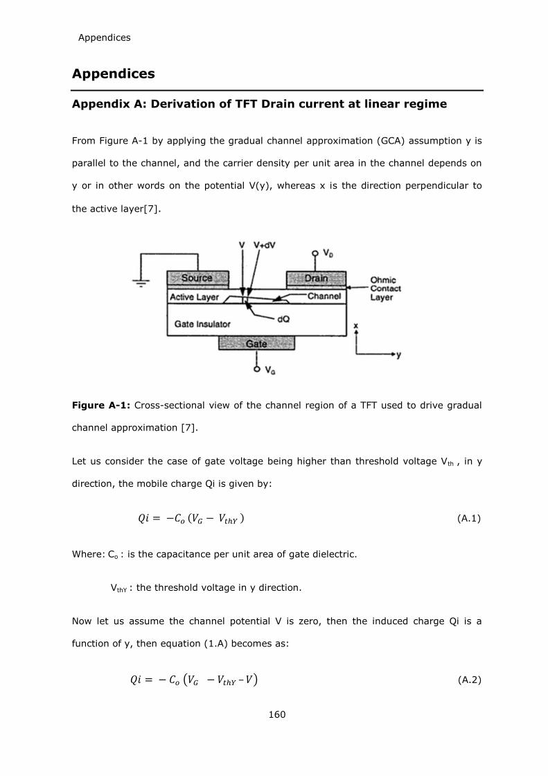
Appendices
160
Appendices
Appendix A: Derivation of TFT Drain current at linear regime
From Figure A-1 by applying the gradual channel approximation (GCA) assumption y is
parallel to the channel, and the carrier density per unit area in the channel depends on
y or in other words on the potential V(y), whereas x is the direction perpendicular to
the active layer[7].
Figure A-1: Cross-sectional view of the channel region of a TFT used to drive gradual
channel approximation [7].
Let us consider the case of gate voltage being higher than threshold voltage Vth , in y
direction, the mobile charge Qi is given by:
( ) (A.1)
Where: Co : is the capacitance per unit area of gate dielectric.
VthY : the threshold voltage in y direction.
Now let us assume the channel potential V is zero, then the induced charge Qi is a
function of y, then equation (1.A) becomes as:
( – ) (A.2)
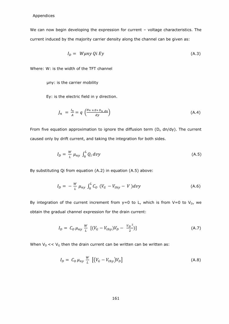
Appendices
161
We can now begin developing the expression for current – voltage characteristics. The
current induced by the majority carrier density along the channel can be given as:
(A.3)
Where: W: is the width of the TFT channel
μny: is the carrier mobility
Ey: is the electric field in y direction.
(
) (A.4)
From five equation approximation to ignore the diffusion term (Dn dn/dy). The current
caused only by drift current, and taking the integration for both sides.
∫
(A.5)
By substituting Qi from equation (A.2) in equation (A.5) above:
∫ (
) (A.6)
By integration of the current increment from y=0 to L, which is from V=0 to VD, we
obtain the gradual channel expression for the drain current:
[( )
)] (A.7)
When VD << VG then the drain current can be written can be written as:
[( ) ] (A.8)
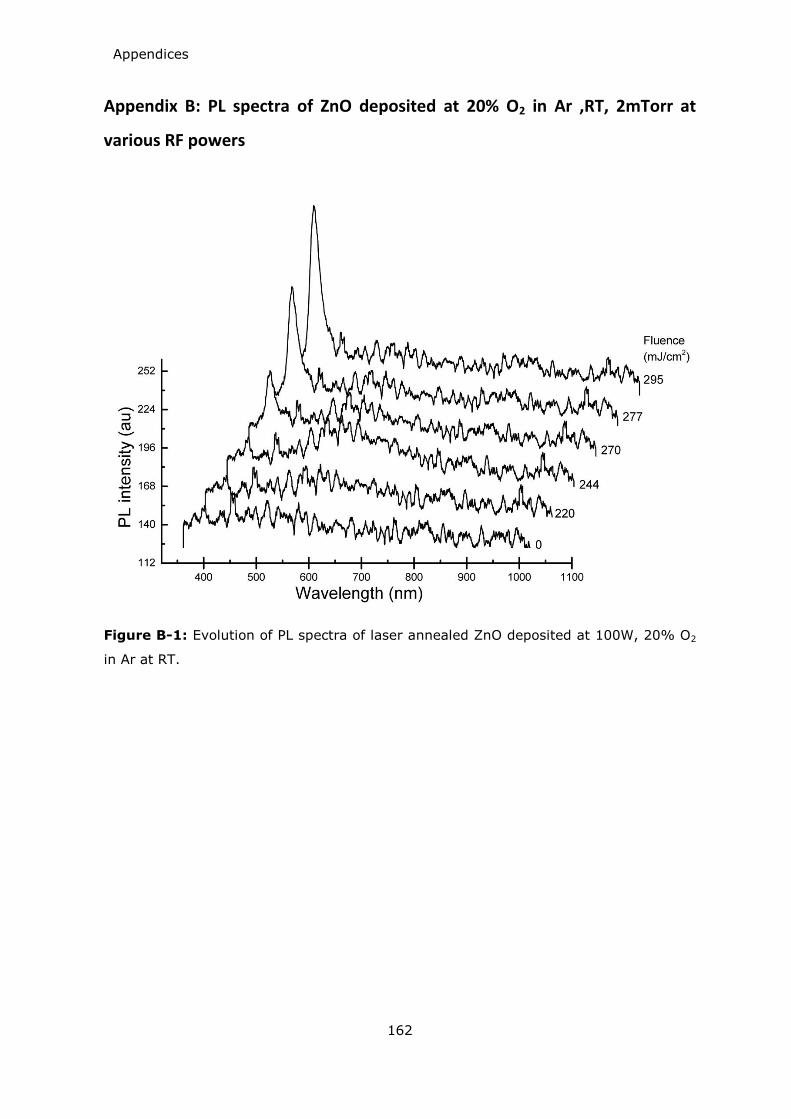
Appendices
162
Appendix B: PL spectra of ZnO deposited at 20% O2 in Ar ,RT, 2mTorr at
various RF powers
Figure B-1: Evolution of PL spectra of laser annealed ZnO deposited at 100W, 20% O2
in Ar at RT.
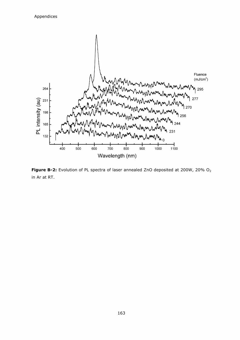
Appendices
163
Figure B-2: Evolution of PL spectra of laser annealed ZnO deposited at 200W, 20% O2
in Ar at RT.
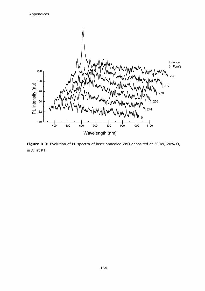
Appendices
164
Figure B-3: Evolution of PL spectra of laser annealed ZnO deposited at 300W, 20% O2
in Ar at RT.


