Embed Size (px)
Citation preview
(NASA-Case-MFS-2B764-1) MULTILAYER
THIN FILM HALL EFFECT DEVICE Patent
App|ication (NASA. Marshal] Space
Flight Center) 26 p
N95-14137
Unclas
G3/70 0029847
/ '
¸••4¸ ,. : •'
NASA CASE NO. MFS-28764-I
PRINT FIG. #i
NOTICE
The invention disclosed in this document resulted from
research in aeronautical and space activities performed under
programs of the National Aeronautics and Space
Administration. The invention is owned by NASA and is,
therefore, available for licensing in accordance with the!
NASA Patent Licensing Regulation (14 Code of Federal
Regulations 1245.2).
To encourage commercial utilization of NASA-owned inventions,
it is NASA policy to grant licenses to commercial concerns.
Although NASA encourages nonexclusive licensing to promote
competition and achieve the widest possible utilization, NASA
will consider the granting of a limited exclusive license,
pursuant to the NASA Patent Licensing Regulations, when such
a license will provide the necessary incentive to the
licensee to achieve early practical application of the
invention.
Address inquiries and all applications for license for this
invention to NASA/Marshall Space Flight Center, Patent
Counsel, Mail Code CC01, Marshall Space Flight Center, AL
35812. Approved NASA forms for application for nonexclusive
or exclusive license are available from the above address.
Serial Number
Filing Date
NASA/MSFC
08/317,071
September 30, 1994
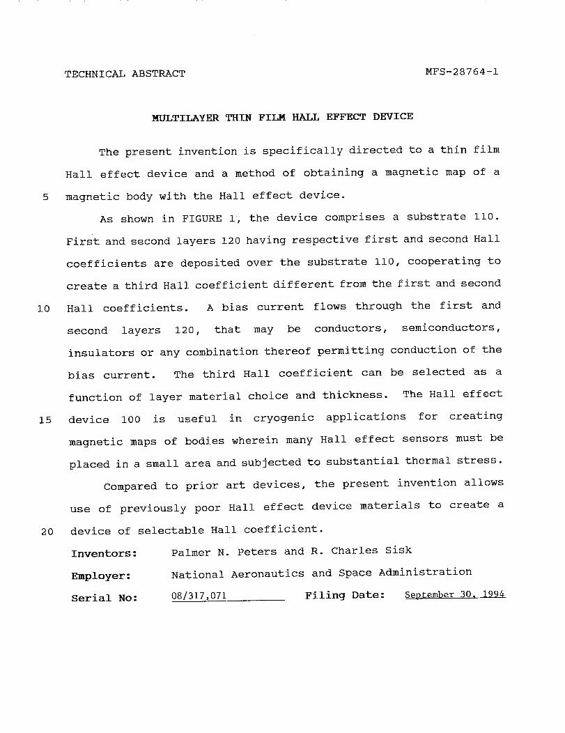
TECHNICAL ABSTRACT MFS-28764-I
i0
15
20
MULTILAYER THIN FILM HALL EFFECT DEVICE
The present invention is specifically directed to a thin film
Hall effect device and a method of obtaining a magnetic map of a
magnetic body with the Hall effect device.
As shown in FIGURE i, the device comprises a substrate Ii0.
First and second layers 120 having respective first and second Hall
coefficients are deposited over the substrate ii0, cooperating to
create a third Hall coefficient different from the first and second
Hall coefficients. A bias current flows through the first and
second layers 120, that may be conductors, semiconductors,
insulators or any combination thereof permitting conduction of the
bias current. The third Hall coefficient can be selected as a
function of layer material choice and thickness. The Hall effect
device i00 is useful in cryogenic applications for creating
magnetic maps of bodies wherein many Hall effect sensors must be
placed in a small area and subjected to substantial thermal stress.
Compared to prior art devices, the present invention allows
use of previously poor Hall effect device materials to create a
device of selectable Hall coefficient.
Inventors:
Employer:
Serial No:
Palmer N. Peters and R. Charles Sisk
National Aeronautics and Space Administration
08/317,071 Filing Date: September 30, 1994
Serial No. 317,071
Filing Date: Aug. 24, 1994
MFS-28764-IPATENT APPLICATION
MULTILAYER THIN FILM HALL EFFECT DEVICE
ORIGIN OF THE INVENTION
5
This invention was made by an employee of the
United States Government and may be manufactured and
used by or for the Government for governmental purposes
without the payment of any royalties.
1
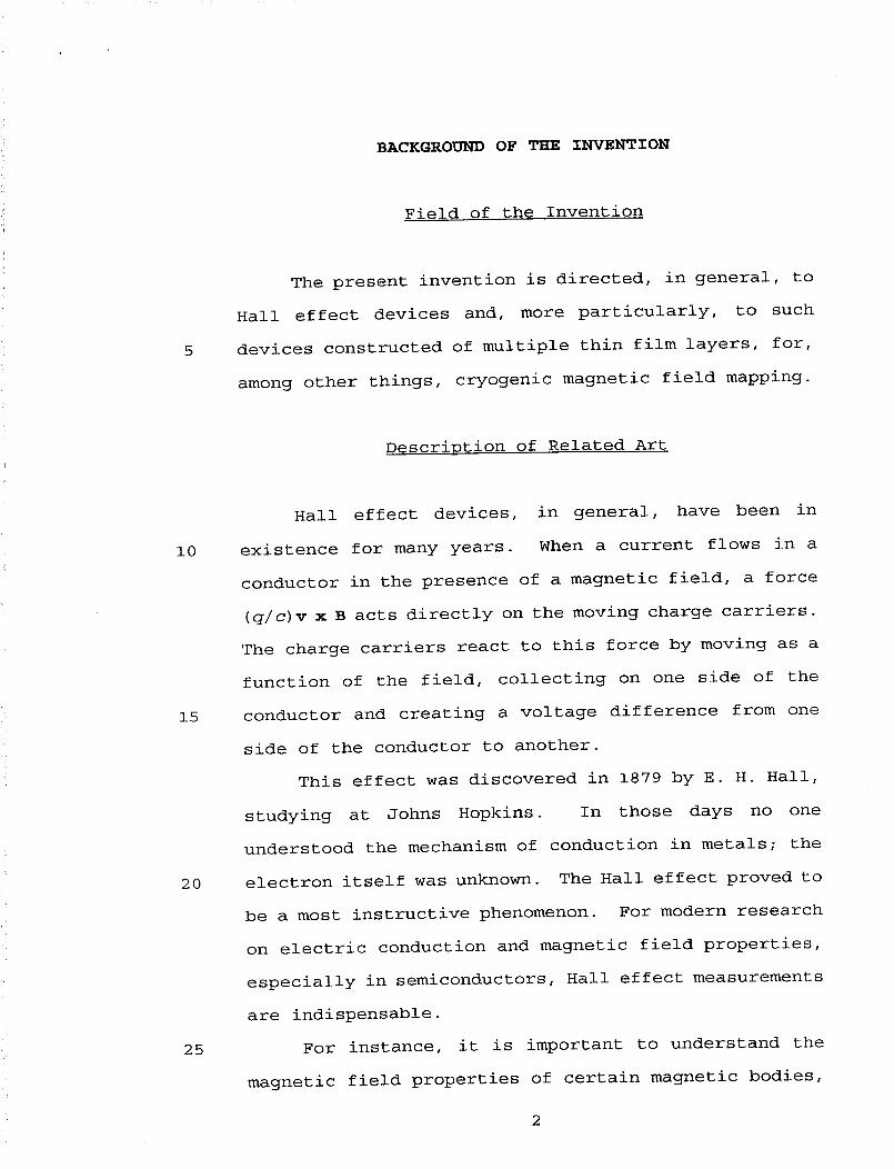
BACKGROUND OF THE INVENTION
Field of the Invention
The present invention is directed, in general, to
Hall effect devices and, more particularly, to such
devices constructed of multiple thin film layers, for,
among other things, cryogenic magnetic field mapping.
Description of Related Art
i0
15
20
25
Hall effect devices, in general, have been in
existence for many years. When a current flows in a
conductor in the presence of a magnetic field, a force
(q/c)v x B acts directly on the moving charge carriers.
The charge carriers react to this force by moving as a
function of the field, collecting on one side of the
conductor and creating a voltage difference from one
side of the conductor to another.
This effect was discovered in 1879 by E. H. Hall,
studying at Johns Hopkins. In those days no one
understood the mechanism of conduction in metals; the
electron itself was unknown. The Hall effect proved to
be a most instructive phenomenon. For modern research
on electric conduction and magnetic field properties,
especially in semiconductors, Hall effect measurements
are indispensable.
For instance, it is important to understand the
magnetic field properties of certain magnetic bodies,
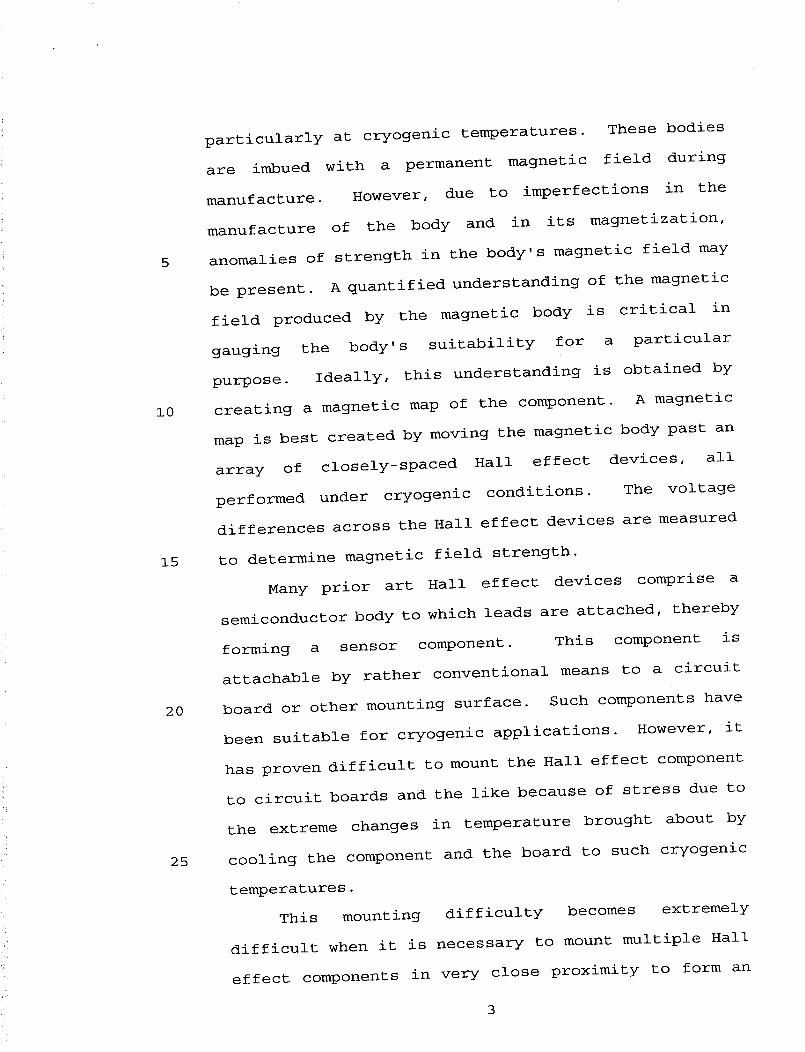
5
i0
15
2O
25
particularly at cryogenic temperatures. These bodies
are imbued with a permanent magnetic field during
manufacture. However, due to imperfections in the
manufacture of the body and in its magnetization,
anomalies of strength in the body's magnetic field may
be present. A quantified understanding of the magnetic
field produced by the magnetic body is critical in
gauging the body's suitability for a particular
purpose. Ideally, this understanding is obtained by
creating a magnetic map of the component. A magnetic
map is best created by moving the magnetic body past an
array of closely-spaced Hall effect devices, all
performed under cryogenic conditions. The voltage
differences across the Hall effect devices are measured
to determine magnetic field strength.
Many prior art Hall effect devices comprise a
semiconductor body to which leads are attached, thereby
forming a sensor component. This component is
attachable by rather conventional means to a circuit
board or other mounting surface. Such components have
been suitable for cryogenic applications. However, it
has proven difficult to mount the Hall effect component
to circuit boards and the like because of stress due to
the extreme changes in temperature brought about by
cooling the component and the board to such cryogenic
temperatures.
This mounting difficulty becomes extremely
difficult when it is necessary to mount multiple Hall
effect components in very close proximity to form an
:!I
i! •
i0
15
20
25
array for cryogenic magnetic mapping, as described
above.
One solution to the above problem is to dispense
with separate semiconductor components and to deposit
a thin film of a material that displays a suitably high
Hall coefficient directly on a substrate. However, to
this day, the only known materials suitable for
conventional thin film deposition techniques (such as
sputtering) that also exhibit a sufficient Hall
coefficient are bismuth and some recently discovered
high Tc superconductors that have naturally layered
structures (see, Chaban, Transport of High-Temperature
Superconductors in the Normal State, Journal of
Superconductivity, vol. 6, no. 6, December, 1993) .
Bismuth suffers from two notable disadvantages.
First, similar to lead, it is somewhat toxic, requiring
careful handling and manufacturing techniques to avoid
adverse health effects. Second, while bismuth displays
a suitable Hall coefficient, its Hall coefficient is
not adjustable. Because voltages across the Hall
effect devices vary as a function of, among other
things, the Hall coefficient of the devices, it is
advantageous to be able to adjust the Hall coefficient
to yield a device that has been tuned for a particular
application. With prior art bismuth thin film Hall
effect devices, one was not availed of that option.
While some high Tc materials exhibit variable Hall
effects, the naturally-fixed spacings of the layers of
the materials do not permit a wide range of adjustment
in layer separation.
Accordingly, what is needed in the art is a thin
film Hall effect device that eliminates a need for use
of toxic bismuth and that can be manufactured to have
a desired Hall coefficient, allowing each device to be
tuned to a desired sensitivity and response.
5
SUMMARY OF THE INVENTION
5
i0
15
20
25
It is therefore a primary object of the present
invention to provide a thin film Hall effect device
that allows use of materials as alternatives to
bismuth. It is a further primary object of the present
invention to Provide a Hall effect device that has a
selectable Hall coefficient, thereby creating a family
of thin film Hall effect devices that can be configured
for a desired sensitivity or response.
Accordingly, to address the above-noted primary
object, the present invention provides a Hall effect
device and a method of obtaining a magnetic field map
of a magnetic body with the Hall effect device. The
device comprises: (i) a substrate, (2) a first layer
having a first Hall coefficient deposited over the
substrate and (3) a second layer having a second Hall
coefficient deposited over the first layer, the first
and second layers cooperating to create, in the Hall
effect device, a third Hall coefficient different from
the first and second Hall coefficients.
The present invention is the first to deposit a
duality of materials in thin films, one over the other,
to produce a thin film Hall effect device having a
tunable Hall coefficient (the "third Hall
coefficient"). Creation of the third Hall coefficient
by cooperation of the first and second layers allows
use of materials for the first and second layers that
were previously unavailable for Hall effect devices due
6
5
i0
15
2O
25
to their relatively weak Hall coefficient. As will be
explained in more detail, it is postulated that the
confluence and cooperation of the first and second
layers cause a reflection or scattering of electron
wave functions by the first and second layers,
producing a transitional material between the first and
second layers that has superior Hall effect properties
that are adjustable as a function of the materials
chosen for the first and second layers and of the
thickness at which they are deposited. Therefore, in
a preferred embodiment of the present invention, the
first and second layers cooperate at an interface
thereof to create a material having the third Hall
coefficient.
High Hall coefficients are associated with
materials having low charge carrier density. In
bismuth, that has been described as a semimetal, a
filled-energy band associated with the electrons weakly
overlaps an empty band, permitting excitation of a few
electrons into a conducting band and leaving a
corresponding few holes in the previously-filled energy
band. Either the low concentration of electrons or
holes can provide high Hall coefficients, but of
different sign.
In a preferred embodiment of the present
invention, the first layer comprises a material
selected from the group consisting of: (i) a conductor,
(2) a semiconductor and (3) an insulator. Likewise,
the second layer comprises a material selected from the
i0
15
20
25
group consisting of: (i) a conductor, (2) a
semiconductor and (3) an insulator. Therefore, the
Hall effect device of the present invention is not
limited to bismuth or any other conductor, for that
matter.
In one embodiment of the present invention, the
third Hall coefficient is positive. Most metals have
a weak negative Hall coefficient. However, some have
a positive coefficient. This remained a baffling
paradox until it was explained by the quantum theory of
electrons in metals, providing a theoretical basis for
holes in metal, as described above. The Hall effect
device of the present invention can create either
positive or negative Hall coefficients and thus take
advantage of quantum effects.
In a preferred embodiment of the present
invention, the first and second conductive layers are
deposited in an elongated strip on the substrate, the
elongated strip having a plurality of voltage taps at
points along a length thereof. The first and second
layers are deposited in desired thicknesses to yield a
device of a desired third Hall coefficient.
In a preferred embodiment of the present
invention, there are a plurality of interdigitated
first and second conductive layers. Thus, the layers
are stacked in an alternate fashion to amplify the Hall
effect. The plurality of interdigitated layers are
believed to provide a large periodic superlattice
spacing, contributing to creation of structures
i0
15
2O
25
providing the above-described low carrier density
properties, yielding a material having a band structure
similar to bismuth, impurities in the superlattice
contribute to scattering and other effects that
complicate the analysis of the band structure.
Of course, it is desirable to obtain voltage
measurements from the Hall effect device of the present
invention. Accordingly, in a preferred embodiment of
the present invention, the Hall effect device further
comprises a duality of voltage detection conductors
coupled to predetermined points orthogonal to the
direction of the bias current on the first and second
conductive layers, the duality allowing a measuring of
the voltage between the predetermined points of the
first and second conductive layers.
In a preferred embodiment of the present
invention, the first and second conductive layers are
deposited in an elongated strip on the substrate, the
elongated strip having a plurality of voltage taps at
points along a length thereof and wherein the Hall
effect device further comprises voltage detection
conductors coupled to each of the voltage taps, the
voltage detection conductors allowing a measuring of
the voltage across the elongated strip. Thus, while
the central elongated strip is deposited, voltage taps
of the same material are also deposited. In a more
preferred embodiment, the voltage taps are derived from
the top and bottom elongated strips in the device
i0
15
20
25
comprising the plurality of interdigitated first and
second conductive layers.
In a preferred embodiment of the present
invention, the first and second conductive layers are
deposited in a pattern comprising a bias current
conductor and a plurality of probe conductors oriented
transversely to the bias current conductor and coupled
to the bias current conductor at points along a length
thereof and wherein the Hall effect device further
comprises voltage detection conductors coupled to ends
of the probe conductors distal to the bias current
conductor, the voltage detection conductors allowing a
measuring of the voltage across the bias current
conductor. In the illustrated embodiment, these probe
conductors take the form of strips running
substantially transverse to the length of the central
elongated strip to measure voltages edge-to-edge of the
elongated strip for a magnetic field having a flux
passing through the surface of the elongated strip.
The present invention further encompasses a method
of obtaining a magnetic field map of a magnetic body.
The method comprises the steps of: (i) providing a Hall
effect device comprising (a) a substrate, (b) a first
layer having a first Hall coefficient deposited over
the substrate in an elongated strip and (c) a second
layer having a second Hall coefficient deposited over
the first layer in an elongated strip, the first and
second layers cooperating to create, in the Hall effect
device, a third Hall coefficient different from the
I0
i0
15
2O
first and second Hall coefficients, (2) causing a bias
current to flow in the first and second layers, (3)
moving the magnetic body in a direction substantially
transverse to a length of the elongated strip of the
first and second layers and (4) measuring a voltage
between predetermined points of the first and second
conductive layers, the voltage indicative of a strength
of the magnetic field, to thereby produce the magnetic
map of the magnetic body.
The foregoing has outlined rather broadly the
features and technical advantages of the present
invention so that the detailed description of the
invention that follows may be better understood.
Additional features and advantages of the invention
will be described hereinafter which form the subject of
the claims of the invention. Those skilled in the art
should appreciate that the conception and the specific
embodiment disclosed may be readily utilized as a basis
for modifying or designing other structures for
carrying out the same purposes of the present
invention. Those skilled in the art should also
realize that such equivalent constructions do not
depart from the spirit and scope of the invention as
set forth in the appended claims.
ii
BRIEF DESCRIPTION OF TEE DRAWINGS
i0
For a more complete understanding of the present
invention, and the advantages thereof, reference is now
made to the following descriptions taken in conjunction
with the accompanying drawings, in which:
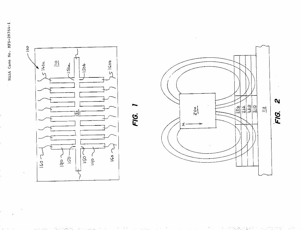
FIGURE 1 illustrates a plan view of a thin film
Hall effect device of the present invention;
FIGURE 2 illustrates an elevational view of the
Hall effect device of FIGURE 1 and a magnetic body
moving with respect to the Hall effect device to create
a map of the magnetic field of the magnetic body;
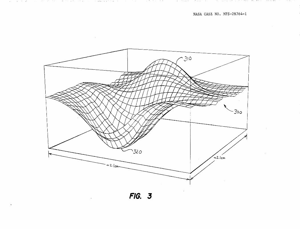
FIGURE 3 illustrates a view of a three dimensional
map of a magnetic field produced by the method of the
present invention.
12
DESCRIPTION OF THE PREFERRED EMBODIMENT
i0
15
20
25
Referring initially to FIGURE i, illustrated is a
plan view of a thin film Hall effect device of the
present invention. The Hall effect device, generally
designated i00, comprises a substrate ii0 and first
layer and second layers, jointly referenced as 120,
deposited over one another and the substrate Ii0. The
first layer has a first Hall coefficient and the second
layer has a second Hall coefficient, that may be
different in absolute value and sign from the first
Hall coefficient. The first and second layers 120
cooperate to create, in the Hall effect device, a third
Hall coefficient different from the first and second
Hall coefficients. The third Hall coefficient is
selectable, depending upon the materials and dimensions
selected for the first and second layers 120, but is
advantageously far in excess of the first and second
Hall coefficients to increase the sensitivity of the
device i00 to magnetic fields.
The first and second conductive layers 120 are
deposited in a pattern comprising a bias current
conductor 130 and a plurality of probe conductors 140
oriented substantially transversely to the bias current
conductor 130 and coupled to the bias current conductor
130 at points 150 along a length thereof. Voltage
detection conductors 160 coupled to ends of the probe
conductors 140 distal to the bias current conductor
130. The voltage detection conductors 160 allow a
13
5
i0
15
2O
25
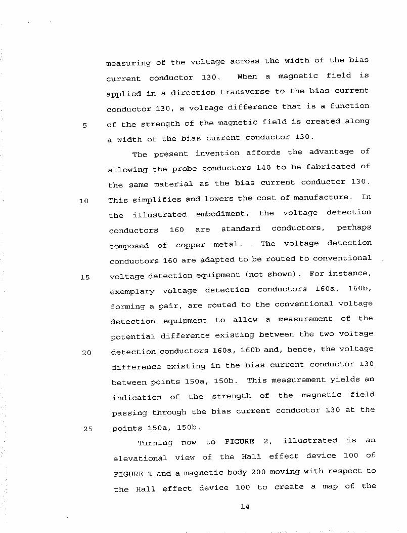
measuring of the voltage across the width of the bias
current conductor 130. When a magnetic field is
applied in a direction transverse to the bias current
conductor 130, a voltage difference that is a function
of the strength of the magnetic field is created along
a width of the bias current conductor 130.
The present invention affords the advantage of
allowing the probe conductors 140 to be fabricated of
the same material as the bias current conductor 130.
This simplifies and lowers the cost of manufacture. In
the illustrated embodiment, the voltage detection
conductors 160 are standard conductors, perhaps
composed of copper metal. The voltage detection
conductors 160 are adapted to be routed to conventional
voltage detection equipment (not shown). For instance,
exemplary voltage detection conductors 160a, 160b,
forming a pair, are routed to the conventional voltage
detection equipment to allow a measurement of the
potential difference existing between the two voltage
detection conductors 160a, 160b and, hence, the voltage
difference existing in the bias current conductor 130
between points 150a, 150b. This measurement yields an
indication of the strength of the magnetic field
passing through the bias current conductor 130 at the
points 150a, 150b.
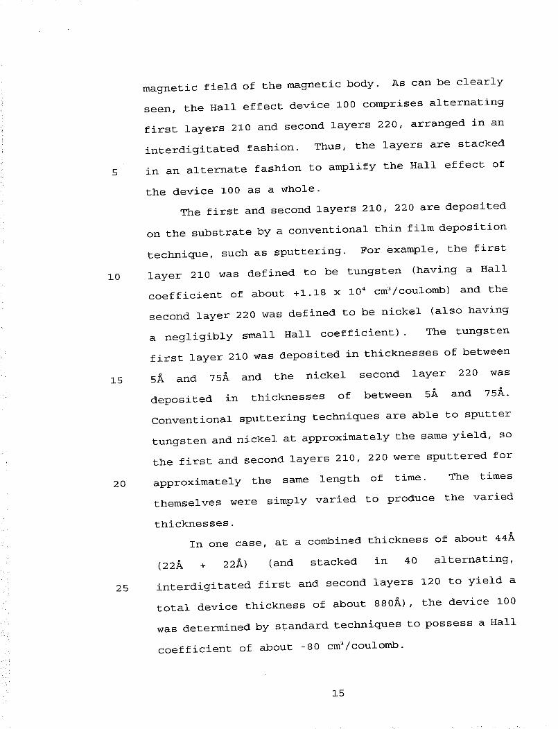
Turning now to FIGURE 2, illustrated is an
elevational view of the Hall effect device i00 of
FIGURE 1 and a magnetic body 200 moving with respect to
the Hall effect device i00 to create a map of the
14
5
i0
15
2O
25
magnetic field of the magnetic body. As can be clearly
seen, the Hall effect device i00 comprises alternating
first layers 210 and second layers 220, arranged in an
interdigitated fashion. Thus, the layers are stacked
in an alternate fashion to amplify the Hall effect of
the device i00 as a whole.
The first and second layers 210, 220 are deposited
on the substrate by a conventional thin film deposition
technique, such as sputtering. For example, the first
layer 210 was defined to be tungsten (having a Hall
coefficient of about +1.18 x 104 cm3/cou lomb) and the
second layer 220 was defined to be nickel (also having
a negligibly small Hall coefficient). The tungsten
first layer 210 was deposited in thicknesses of between
5A and 75A and the nickel second layer 220 was
deposited in thicknesses of between 5A and 75A.
Conventional sputtering techniques are able to sputter
tungsten and nickel at approximately the same yield, so
the first and second layers 210, 220 were sputtered for
approximately the same length of time. The times
themselves were simply varied to produce the varied
thicknesses.
In one case, at a combined thickness of about 44A
(22A + 22A) (and stacked in 40 alternating,
interdigitated first and second layers 120 to yield a
total device thickness of about 880A), the device i00
was determined by standard techniques to possess a Hall
coefficient of about -80 cm3/coulo mb.
15
5
i0
15
20
25
In another case, at a combined thickness of about
28A (14A + 14A) (and again stacked in 40 alternating,
interdigitated first and second layers 120 to yield a
total device thickness of about 560A), the device i00
was determined to possess a positive Hall coefficient,
yielding a positive Hall effect of about +.5 mV/kG for
a I00 mA bias current.
In still another case, at a combined thickness of
about 34A (17A + 17A) (and yet again stacked in 40
alternating, interdigitated first and second layers 120
to yield a total device thickness of about 680A), the
device i00 was determined to possess negligibly small
Hall coefficient. In two of the above cases, the third
Hall coefficient is substantially different from the
first and second Hall coefficients of the individual
first and second layers 210, 220, varying from high
positive to high negative to negligible values,
depending upon deposition thickness. Thus, in the
examples detailed above, multilayering of the two
layers 210, 220 cooperated to create a selectable,
different and useful third Hall coefficient.
Creation of the third Hall coefficient by
cooperation (achieved through multilayering) of the
first and second layers 210, 220 allows use of
materials for the first and second layers 210, 220 (in
this one case, tungsten and nickel) that were
previously unavailable for use in Hall effect devices
due to their relatively weak Hall coefficient. In a
preferred embodiment of the present invention, tungsten
16
5
i0
15
20
25
and nickel make up the first and second layers 210,
220, respectively.
Those skilled in the art will recognize that
useful Hall effect devices may also be constructed
using three or more alternating layers of differing
materials. The present invention is therefore not
limited to the use of only two alternating materials to
achieve a selectable Hall coefficient.
As previously mentioned, it is postulated that the
confluence and cooperation of the first and second
layers 210, 220 produces a transitional material
therebetween that has superior Hall effect properties
that are adjustable as a function of the materials
chosen for the first and second layers 210, 220 and of
the thickness at which they are deposited. In fact,
the first and second layers 210, 220 apparently
cooperate at an interface thereof to create a material
having the third Hall coefficient. It is postulated
that interdigitated multilayering of the first and
second layers 210, 220 enhances the Hall effect of the
device i00 as a whole. It is further postulated that
this material (a combination of the individual
materials of the first and second layers 210, 220)
produces a superlattice structure, causing a reflection
or scattering of electron wave functions by the first
and second layers 210, 220 and yielding a structure
having electrical properties that are amenable to the
Hall effect. This superlattice may affect the band
structure of the interstitial material to reduce charge
17
5
I0
15
20
25
carrier density to a level acceptable to obtain a
relatively high Hall coefficient in a manner similar to
the naturally-occurring structure of bismuth as
described previously. For a discussion of superlattice
structures in general and metallic magnetic
superlattices in particular, see, Falicov, Metallic
Magnetic Superlattices, Physics Today, October, 1992.
In the above example, the first and second layers
210, 220 are tungsten and nickel, respectively.
However, other conductors are within the scope of the
invention. The present invention also contemplates
that the first and second layers 210, 220 could be
semiconductors or insulators. One of the first and
second layers 210, 220 must be suited to carry the
required bias current.
The individual electrical properties of the
materials making up the first and second layers 210,
220 may not be determinative. Rather, it is more the
interaction and cooperation of the materials that
determine their suitability for application in the
present invention.
The magnetic body 200 is shown as moving
transverse to the bias current conductor 130. As the
magnetic body is moved from left to right as shown, for /_--_/
instance, each longitudinal portion of the bias current
conductor 130 is exposed to a -subztantially l:n_&r _ .
section of a magnetic field 230 (represented _7_'_
schematically by field lines) of the magnetic body 200. _/2_/_
When a bias current is passed through the bias current
18
5
i0
15
2O
25
conductor 130 via conventional means and as each
longitudinal portion comes under the influence of the
magnetic field 230, each portion responds by creating
a measurable voltage potential. This voltage
potential, that changes over time as the magnetic body
200 passes over the bias current conductor 130 and that
may vary as a function of the particular longitudinal
portion measured, is used to create a magnetic map of
the magnetic body.
Turning now to FIGURE 3, illustrated is a view of
the magnetic map produced by the method of the present
invention. The map, generally designated 300, contains
a three-dimensional indication of magnetic field
strength of the magnetic body 200 and a second magnetic
body as a function of location near the magnetic
bodies. It is apparent from the map 300 that opposite
poles of the magnetic bodies are proximate the Hall
effect sensors. The map 300 gives an indication of
voltage proportional to the field on the vertical axis
as a function of position in the plane scanned.
More specifically, FIGURE 3 is a computer-
generated representation of raw data taken with a
single scan of a linear array of thirty vertically-
oriented Hall effect sensors fabricated of a multilayer
film in accordance with the present invention and
separated a distance of 3mm from the magnetic bodies.
The magnetic bodies were moved, in this case, in 0.7mm
increments. Each sensor scans a path 0.7mm wide.
Therefore, each sensor produces a pixel area of
19
5
i0
15
2O
25
approximately 0.7mm x 0.7mm for a given period of time,
yielding a total side-to-side scan area for the map 300
of approximately 2.1cm x 2.1cm. The data have not been
smoothed to eliminate jagged edges arising from
discrete values. Nor have the data been scaled for
varying Hall coefficients among the thirty sensors.
For practical purposes, the thirty sensors may be
regarded as having substantially the same Hall
coefficient.
The magnetic body 200 is a magnetized disk 3mm
thick and 8mm in diameter and is represented as a hill
310 in the map 300. The second magnetic body is 3mm
thick and 10mm in diameter and is represented as a
valley 320 in the map 300.
The map 300 represents peak magnetic fields of
appoximately 1200 gauss. Those of skill in the art
will recognize minor artifacts in the map 300. These
artifacts are largely due to magnetic hysteresis and
should be removable as material, electronic circuit and
scanning techniques improve.
From the above, it is apparent that the present
invention provides a Hall effect device and a method of
obtaining a magnetic field map of a magnetic body with
the Hall effect device. The device comprises: (i) a
substrate, (2) a first layer having a first Hall
coefficient deposited over the substrate and (3) a
second layer having a second Hall coefficient deposited
over the first layer, the first and second layers
cooperating to create, in the Hall effect device, a
20
5
third Hall coefficient different from the first and
second Hall coefficients.
Although the present invention and its advantages
have been described in detail, it should be understood
that various changes, substitutions and alterations can
be made herein without departing from the spirit and
scope of the invention as defined by the appended
claims.
21
ABSTRACT OF THE DISCLOSURE
i0
15
A Hall effect device and a method of obtaining a
magnetic field map of a magnetic body with the Hall
effect device. The device comprises: (i) a substrate,
(2) a first layer having a first Hall coefficient
deposited over the substrate and (3) a second layer
having a second Hall coefficient deposited over the
first layer, the first and second layers cooperating to
create, in the Hall effect device, a third Hall
coefficient different from the first and second Hall
coefficients. Creation of the third Hall coefficient
by cooperation of the first and second layers allows
use of materials for the first and second layers that
were previously unavailable for Hall effect devices due
to their relatively weak Hall coefficient.
I
oo
I
Z \C,,.
L_
Y
IE
d_-JJ
I
G _ _9
IpIIIID
)
NASA CASE NO. MFS-28764-I
FIG. 3


