Embed Size (px)
Citation preview

INTRODUCTION TO NANOSCIENCE
AND NANOTECHNOLOGY
PHYS.472
Prof. Ali S. Hennache
Al-Imam Muhammad Ibn Saud Islamic University
Faculty of Sciences
Department of Physics
ASH/AIMISIU/CS/DP/RUH/05.06.2015/3.15PM/KSA

The course content has been structured to help the
student achieve the following objectives:
1. To gain an understanding of the principles of
nanotechnology; characterization of nano structured
materials; and tools and equipment for producing
and assembling at the nano scale.
2. To acquire experience in the use of equipment used in
nanotechnology .
3. To cultivate interest in the research and development
of nanotechnology for future advancement of the
career.
4. Discuss nanomaterials effects on medicine ,
environmental ,renewable energy, electronics etc....
Course Objectives /Outcomes

Reference Materials
1. Ratner, D. & Ratner, M. (2003). Nanotechnology: A
gentle introduction to the next big idea. New
Jersey: Pearson Education Inc, ISBN: 0131014005.
2. Charles P. Poole Jr. and Frank J. Owens (2003).
Introduction to Nanotechnology, Wiley-
Interscience , 1 st edition, ISBN-10: 0471079359
3. John F Mongillo (2007), Nanotechnology 101,
Greenwood Press, Westport, CT, ISBN: 0313338809.
4. Gabor L. Hornyak, H.F. Tibbals, Joydeep Dutta, and
John J. Moore (2009). Introduction to Nanoscience
and Nanotechnology, CRC Press, Boca Raton, ISBN
10: 1420047795.

Grading Policies
Course grade will be based on the following
components:
•Midterm Examinations (2): 2x 20 = 40%
•Home assignments – Quizzes = 15%
•Class participation = 5%
•Final Examination = 40%
ASH/AIMISIU/CS/DP/RUH/09.06.2015/KSA.6.44PM

The Exam Schedule for the
Summer 2015 Term
• Midterm Examination No.01 (20 marks)
MONDAY 22nd June 2015 @ 10.00AM
• Midterm Examination No.02 (20marks)
THURSDAY 02nd July 2015 @ 10.00AM
ASH/AIMISIU/CS/DP/RUH/09.06.2015/KSA.6.44PM
• QUIZ No.01 (5 marks)
TUESDAY 16th June 2015 @ 11.00AM

PHYS. 472
INTRODUCTION
TO
NANOTECHNOLOGY
Prof. Dr. Ali S. Hennache Department of Physics
College of Sciences
ASH/AIMISIU/CS/DP/RUH/05.06.2015/3.15PM/KSA

Content
Chapter 1- Introduction to nanoscience and nanotechnologies
Chapter 2- Principal synthesis techniques of nanosystems
Chapter 3- Quantification
Chapter 4- Porosity and texture of materials
Chapter 5- Nanomaterials and devices
Chapter 6- Deposition and etching of thin films
Chapter 7- Characterization techniques
Chapter 8- Devices based on thin films

Nanomaterials characterization
* What SEM and AFM are good for?
* What is the Atomic Force Microscopes Contribution
to Nanotechnology?
* What is Spectroscopy?

Background and History
The Scanning Tunneling Microscope (STM) was invented by G. Binnig and H. Rohrer, for which they were awarded the Nobel Prize in 1984
A few years later, the first Atomic Force Microscope (AFM) was developed by G. Binnig, Ch. Gerber, and C. Quate at Stanford University by gluing a tiny shard of diamond onto one end of a tiny strip of gold foil
Currently AFM is the most common form of scanning probe microscopy
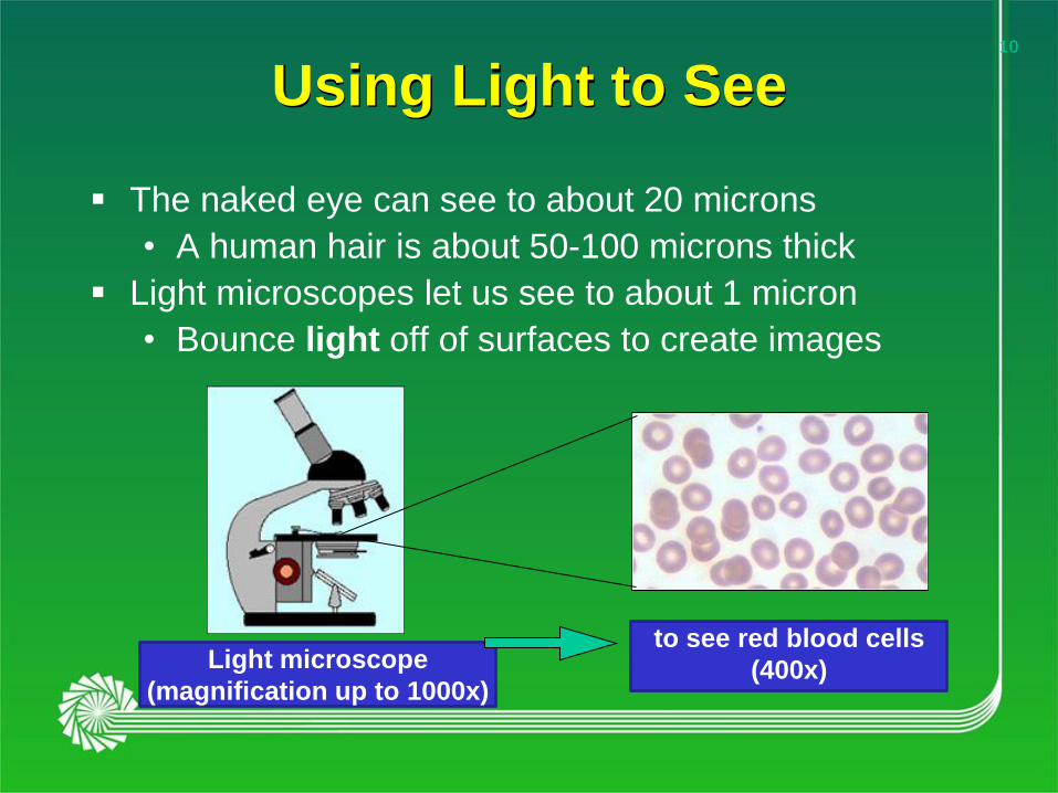
Light microscope
(magnification up to 1000x)
to see red blood cells
(400x)
Using Light to See
The naked eye can see to about 20 microns
• A human hair is about 50-100 microns thick
Light microscopes let us see to about 1 micron
• Bounce light off of surfaces to create images
10

Scanning Probe Microscopes
Atomic Force Microscope (AFM)
A tiny tip moves up and down in response to the
electromagnetic forces between the atoms of the
surface and the tip
The motion is recorded and used to create an
image of the atomic surface
Scanning Tunneling Microscope (STM)
A flow of electrical current occurs between the tip
and the surface
The strength of this current is used to create an
image of the atomic surface
11

Atomic Force Microscopes
(AFM)
The Atomic Force Microscope
was developed to overcome a
basic drawback with STM -
that it can only image
conducting or semiconducting
surfaces. The AFM, however,
has the advantage of imaging
almost any type of surface,
including polymers, ceramics,
composites, glass, and
biological samples.

1. Laser – deflected off cantilever
2. Mirror –reflects laser beam to photo detector
3. Photo detector –dual element photodiode that measures differences in light intensity and converts to voltage
4. Amplifier
5. Register
6. Sample
7. Probe –tip that scans sample made of Si
8. Cantilever –moves as scanned over sample and deflects laser beam
Parts of AFM

• Conductive AFM (c-AFM)
• Photo-conductive AFM (pc-AFM)
• Kelvin Probe Force Microscopy (KPFM)
• Piezoresponse Force Microscopy (PFM)
• AFM Nanoindentation
• AFM surface manipulation
Atomic Force Microscopy (AFM)
A

Schematic of the AFM operation
A sharp tip at the end of a micro-cantilever is scanned over the surface
Mode Topography Information/ Feedback
contact Deflection
intermittent contact (tapping mode) Amplitude
non-contact Frequency
Laser
sample Cantilever with tip
Split
photodiode
Feedback
Z- piezo,
Piezo
drive
Usually optical feedback
but also
other feedback types
e.g. tuning fork FB

Because the atomic force
microscope relies on the
forces between the tip and
sample, knowing these forces
is important for proper
imaging. The force is not
measured directly, but
calculated by measuring the
deflection of the lever, and
knowing the stiffness of the
cantilever. Hook’s law gives F
= - kz, where F is the force, k
is the stiffness of the lever,
and z is the distance the 5
lever is bent.
Schematic of the AFM operation

Scanning Tunneling Microscope
(STM)
x
feedback
regulator
high voltage
amplifier
z
y
I
Negative feedback keeps the current constant (pA – nA ) by moving the tip up and down.
Contours of constant current are recorded which correspond to constant charge density.
probing tip
sample
xyz- Piezo -Scanner

Atomic Force Microscopy (AFM)
AFM STM
no requirements sufficiently conductive sample
atomic resolution possible atomic resolution standard
but hard to get
local electrical information local electrical information and
independent of topography topography not separable
Contact not well defined defined tunneling via single atom
Also mechanical information xxx

• Monitors the forces of
attraction and repulsion
between a probe and a
sample surface
• The tip is attached to a
cantilever which moves up
and down in response to
forces of attraction or STM
repulsion with the sample
surface
– Movement of the cantilever
is detected by a laser and
photo detector
Atomic Force Microscopes
Shading shows
interaction
strength
AFM tips and cantilevers are microfabricated
from Si or Si 3N 4. Typical tip radius is from a
few to 10s of nm.

An atomic force microscope (AFM) creates a
highly magnified three dimensional image of
a surface. The magnified image is generated
by monitoring the motion of an atomically
sharp probe as it is scanned across a
surface. With the AFM it is possible to
directly view features on a surface having a
few nanometer-sized dimensions including
single atoms and molecules on a surface.
This gives scientists and engineers an ability
to directly visualize nanometer-sized objects
and to measure the dimensions of the
surface features.
Why AFM?

MBE Ge on p Si(001) substrate
strain induced dewetting of surface
SiGe layer forms domes
1.5x1.5 µm AFM topography , z= 60 nm
Topography and electrical
conductivity Probed by AFM

The fundamental interaction at short
distances is the van der Waals
interactions, which are responsible for
the formation of solids, wetting, etc. At
distances of a few nm, van der Waals
forces are sufficiently strong to move
macroscopic objects such as AFM
cantilevers. Van der Waals interactions
consist of three components:
polarization, induction, and dispersion.
Polarization refers to permanent dipole
moments such as exist in water
molecules. Induction refers to the
contribution of induced dipoles.
Dispersion is due to instantaneous
fluctuations of electrons, which occur
at the frequency of light.
Measuring forces

- Used for Contact Mode, Non-contact and Tapping Mode AFM
- Laser light from a solid state diode is reflected off the back of the
cantilever and collected by a position sensitive detector (PSD). This
consists of two closely spaced photodiodes. The output is then
collected by a differential amplifier
- Angular displacement of the cantilever results in one photodiode
collecting more light than the other. The resulting output signal is
proportional to the deflection of the cantilever.
- Detects cantilever deflection <1A
Modes of operation

Modes of operation
Repulsive (contact)
At short probe-sample
distances, the forces are
repulsive
Attractive Force (non-
contact)
At large probe-sample
distances, the forces are
attractive
The AFM cantelever can be
used to measure both
attractive force mode and
repulsive forces.

Constant force is applied to the surface while scanning
Contact mode
Potential diagram showing the region
of the probe while scanning in
contact mode.
In contact mode the probe
glides over the surface.
Contact mode is typically used for scanning hard samples and when a
resolution of greater than 50 nanometers is required. The cantilevers
used for contact mode may be constructed from silicon or silicon
nitride. Resonant frequencies of contact mode cantilevers are typically
around 50 KHz and the force constants 8 are below 1 N/m.

Left: Bits on a compact disk.
Center: Image of a metal surface.
Right: Nano-particles on a surface
Contact mode images

The probe is vibrated in and out of surface potential. The modulated
signal can then be processed with a phase or amplitude demodulator.
Tapping mode • A cantilever with attached tip is oscillated at its resonant frequency
and scanned across the sample surface.
• A constant oscillation amplitude (and thus a constant tip-sample
interaction) are maintained during scanning. Typical amplitudes are
20- 100nm.
• Forces can be 200 piconewton (pN) or less .
• The amplitude of the oscillations changes when the tip scans over
bumps or depressions on a surface.

Vibrating mode AFM images.
Left: Silicon wafer.
Center: Cancer cells.
Right: Proteins.
Tapping mode images

Contact Mode Contact (DC and AC)
Force Modulation
Non-Contact Mode Non-Contact (AC)
Tapping (Intermittent contact)
Mode Tapping (AC)
Modes of AFM
AC=dynamic(tip is driven to oscillate), DC=static(no external oscillation on tip)
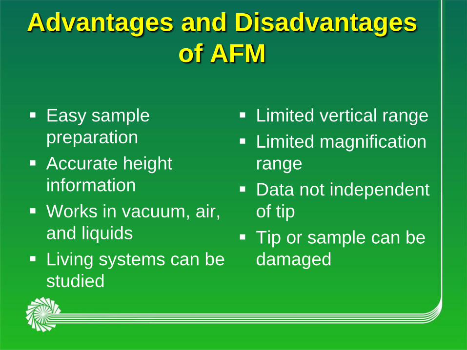
Easy sample
preparation
Accurate height
information
Works in vacuum, air,
and liquids
Living systems can be
studied
Limited vertical range
Limited magnification
range
Data not independent
of tip
Tip or sample can be
damaged
Advantages and Disadvantages
of AFM
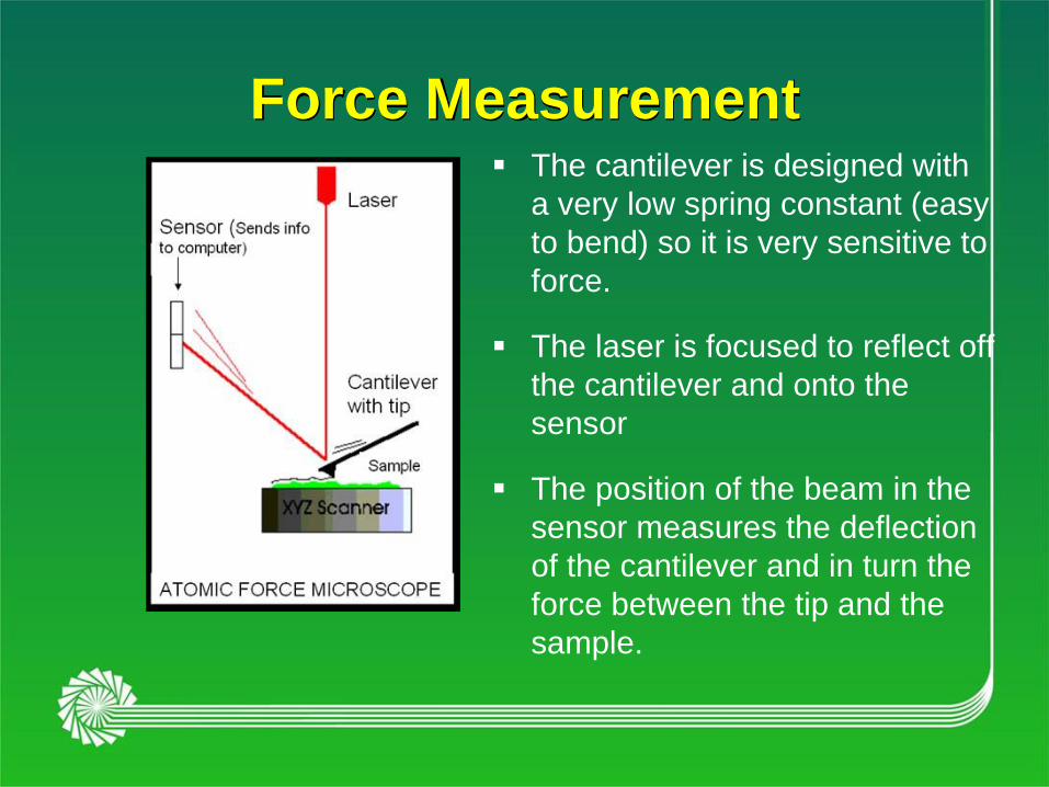
Force Measurement The cantilever is designed with
a very low spring constant (easy
to bend) so it is very sensitive to
force.
The laser is focused to reflect off
the cantilever and onto the
sensor
The position of the beam in the
sensor measures the deflection
of the cantilever and in turn the
force between the tip and the
sample.

Other Types of Scanning Probe
Microscopy (SPM) Techniques Lateral Force Microscopy (LFM)
Frictional forces measured by twisting or “sideways” forces on cantilever.
Magnetic Force Microscopy (MFM) Magnetic tip detects magnetic fields/measures magnetic properties of
the sample.
Electrostatic Force Microscopy (EFM) Electrically charged Pt tip detects electric fields/measures dielectric
and electrostatic properties of the sample
Chemical Force Microscopy (CFM) Chemically functionalized tip can interact with molecules on the
surface – giving info on bond strengths, etc.
Near Field Scanning Optical Microscopy (NSOM) Optical technique in which a very small aperture is scanned very close
to sample Probe is a quartz fiber pulled to a sharp point and coated with
aluminum to give a sub-wavelength aperture (~100 nm)


![[Nanotechnology--possibilities and hazards]](https://img.dokumen.tips/doc/110x75/634d2bd5024fe175900ac942/nanotechnology-possibilities-and-hazards.jpg)