Embed Size (px)
Citation preview

This content has been downloaded from IOPscience. Please scroll down to see the full text.
Download details:
This content was downloaded by: ghk
IP Address: 115.145.155.188
This content was downloaded on 27/06/2014 at 08:48
Please note that terms and conditions apply.
Unravelling the switching mechanisms in electric field induced insulator–metal transitions in
VO2 nanobeams
View the table of contents for this issue, or go to the journal homepage for more
2014 J. Phys. D: Appl. Phys. 47 295101
(http://iopscience.iop.org/0022-3727/47/29/295101)
Home Search Collections Journals About Contact us My IOPscience

Journal of Physics D: Applied Physics
J. Phys. D: Appl. Phys. 47 (2014) 295101 (8pp) doi:10.1088/0022-3727/47/29/295101
Unravelling the switching mechanisms inelectric field induced insulator–metaltransitions in VO2 nanobeams
Servin Rathi1, Jin-Hyung Park1, In-yeal Lee1, Jeong Min Baik2,Kyung Soo Yi3 and Gil-Ho Kim1
1 School of Electronic and Electrical Engineering and Sungkyunkwan Advanced Institute ofNanotechnology (SAINT), Sungkyunkwan University, Suwon 440-746, Korea2 School of Mechanical and Advanced Materials Engineering, Ulsan National Institute of Science andTechnology (UNIST), Ulsan 689-805, Korea3 Department of Physics, Pusan National University, Busan 609-735, Korea
E-mail: [email protected]
Received 6 February 2014, revised 14 May 2014Accepted for publication 28 May 2014Published 25 June 2014
AbstractWe studied insulator–metal transitions in VO2 nanobeams for both abrupt and gradual changesin applied electric fields. Based on the observations, the Poole–Frenkel effect explained theabrupt transition, while the gradual case is found to be dominated by the Joule heatingphenomenon. We also carried out power model and finite element method based simulationswhich supported the Joule heating phenomena for gradual transition. An in-principledemonstration of the Poole–Frenkel effect, performed using a square voltage pulse of 1 µsduration, further confirms the proposed insulator–metal transition mechanism with a switchingtime in the order of 100 ns. Finally, conductivity variations introduced via rapid thermalannealing at various temperatures validate the roles of both Joule heating and Poole–Frenkelmechanisms in the transitions.
Keywords: vanadium dioxide nanobeams, Joule heating, Poole–Frenkel effect,insulator–metal transitions
(Some figures may appear in colour only in the online journal)
1. Introduction
Despite having half-filled 3d shells, electron localizationresulting from strong electron–electron interactions makesvanadium dioxide (VO2) an insulator at room temperature [1].However, this behaviour can be overcome by the applicationof external stimuli like heat, dopants, electric fields, strain andlight, which leads to a transition from an insulating to a metallicstate [2, 3]. Below the transition temperature (TC), the atomicarrangement in VO2 is monoclinic (M1), and the pairing andtilting of V4+ ions results in the localization of the outer 3delectrons. Coulombic repulsion at the localization sites opensup an energy gap of 0.6 eV via the splitting of the d orbitals,which produces a highly resistive insulating state. However,for temperatures above TC, dissociation and reorientation of
the vanadium pairs into periodic chains parallel to the c-axisresults in the release of one electron per vanadium ion; thisleads to an abrupt jump in conductivity and the relaxation ofthe lattice to a tetragonal (rutile) structure [4–6].
These simultaneous electronic and first-order structuralphase transitions (SPTs) have long been a hot topic of scientificdebate, and competing theories attribute these changes to thePeierls lattice instability (a critical phonon density) and/or acritical carrier-density-dependent Mott transition [6, 7]. Inaddition to these pure aspects of VO2 research, applied researchindicates great potential in devices such as memristors,switches and sensors [8–12]. In switching and sensingapplications, electric field-induced transitions (EFITs) offer aconvenient method for instigating insulator to metal transitions(IMTs) [8–13]. Although EFITs have been widely studied in
0022-3727/14/295101+08$33.00 1 © 2014 IOP Publishing Ltd Printed in the UK
J. Phys. D: Appl. Phys. 47 (2014) 295101 S Rathi et al
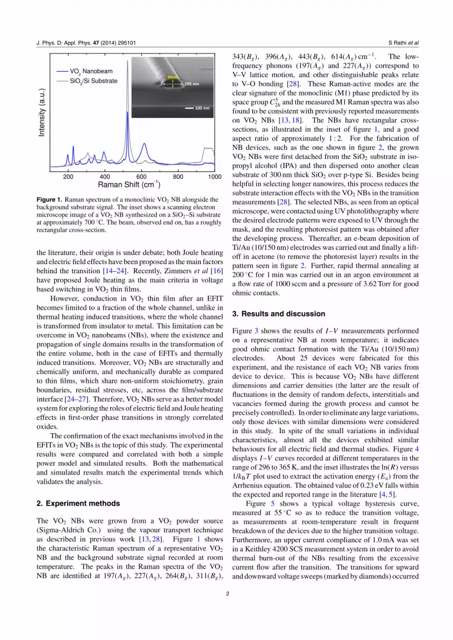
Figure 1. Raman spectrum of a monoclinic VO2 NB alongside thebackground substrate signal. The inset shows a scanning electronmicroscope image of a VO2 NB synthesized on a SiO2–Si substrateat approximately 700 C. The beam, observed end on, has a roughlyrectangular cross-section.
the literature, their origin is under debate; both Joule heatingand electric field effects have been proposed as the main factorsbehind the transition [14–24]. Recently, Zimmers et al [16]have proposed Joule heating as the main criteria in voltagebased switching in VO2 thin films.
However, conduction in VO2 thin film after an EFITbecomes limited to a fraction of the whole channel, unlike inthermal heating induced transitions, where the whole channelis transformed from insulator to metal. This limitation can beovercome in VO2 nanobeams (NBs), where the existence andpropagation of single domains results in the transformation ofthe entire volume, both in the case of EFITs and thermallyinduced transitions. Moreover, VO2 NBs are structurally andchemically uniform, and mechanically durable as comparedto thin films, which share non-uniform stoichiometry, grainboundaries, residual stresses, etc, across the film/substrateinterface [24–27]. Therefore, VO2 NBs serve as a better modelsystem for exploring the roles of electric field and Joule heatingeffects in first-order phase transitions in strongly correlatedoxides.
The confirmation of the exact mechanisms involved in theEFITs in VO2 NBs is the topic of this study. The experimentalresults were compared and correlated with both a simplepower model and simulated results. Both the mathematicaland simulated results match the experimental trends whichvalidates the analysis.
2. Experiment methods
The VO2 NBs were grown from a VO2 powder source(Sigma-Aldrich Co.) using the vapour transport techniqueas described in previous work [13, 28]. Figure 1 showsthe characteristic Raman spectrum of a representative VO2
NB and the background substrate signal recorded at roomtemperature. The peaks in the Raman spectra of the VO2
NB are identified at 197(Ag), 227(Ag), 264(Bg), 311(Bg),
343(Bg), 396(Ag), 443(Bg), 614(Ag) cm−1. The low-frequency phonons (197(Ag) and 227(Ag)) correspond toV–V lattice motion, and other distinguishable peaks relateto V–O bonding [28]. These Raman-active modes are theclear signature of the monoclinic (M1) phase predicted by itsspace group C5
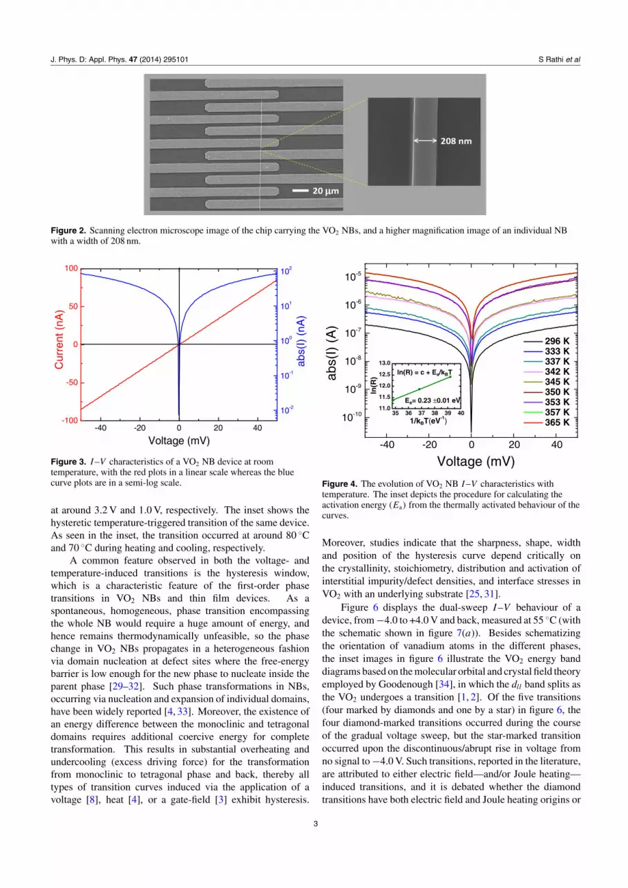
2h and the measured M1 Raman spectra was alsofound to be consistent with previously reported measurementson VO2 NBs [13, 18]. The NBs have rectangular cross-sections, as illustrated in the inset of figure 1, and a goodaspect ratio of approximately 1 : 2. For the fabrication ofNB devices, such as the one shown in figure 2, the grownVO2 NBs were first detached from the SiO2 substrate in iso-propyl alcohol (IPA) and then dispersed onto another cleansubstrate of 300 nm thick SiO2 over p-type Si. Besides beinghelpful in selecting longer nanowires, this process reduces thesubstrate interaction effects with the VO2 NBs in the transitionmeasurements [28]. The selected NBs, as seen from an opticalmicroscope, were contacted using UV photolithography wherethe desired electrode patterns were exposed to UV through themask, and the resulting photoresist pattern was obtained afterthe developing process. Thereafter, an e-beam deposition ofTi/Au (10/150 nm) electrodes was carried out and finally a lift-off in acetone (to remove the photoresist layer) results in thepattern seen in figure 2. Further, rapid thermal annealing at200 C for 1 min was carried out in an argon environment ata flow rate of 1000 sccm and a pressure of 3.62 Torr for goodohmic contacts.
3. Results and discussion
Figure 3 shows the results of I–V measurements performedon a representative NB at room temperature; it indicatesgood ohmic contact formation with the Ti/Au (10/150 nm)electrodes. About 25 devices were fabricated for thisexperiment, and the resistance of each VO2 NB varies fromdevice to device. This is because VO2 NBs have differentdimensions and carrier densities (the latter are the result offluctuations in the density of random defects, interstitials andvacancies formed during the growth process and cannot beprecisely controlled). In order to eliminate any large variations,only those devices with similar dimensions were consideredin this study. In spite of the small variations in individualcharacteristics, almost all the devices exhibited similarbehaviours for all electric field and thermal studies. Figure 4displays I–V curves recorded at different temperatures in therange of 296 to 365 K, and the inset illustrates the ln(R) versus1/kBT plot used to extract the activation energy (Ea) from theArrhenius equation. The obtained value of 0.23 eV falls withinthe expected and reported range in the literature [4, 5].
Figure 5 shows a typical voltage hysteresis curve,measured at 55 C so as to reduce the transition voltage,as measurements at room-temperature result in frequentbreakdown of the devices due to the higher transition voltage.Furthermore, an upper current compliance of 1.0 mA was setin a Keithley 4200 SCS measurement system in order to avoidthermal burn-out of the NBs resulting from the excessivecurrent flow after the transition. The transitions for upwardand downward voltage sweeps (marked by diamonds) occurred
2
J. Phys. D: Appl. Phys. 47 (2014) 295101 S Rathi et al
Figure 2. Scanning electron microscope image of the chip carrying the VO2 NBs, and a higher magnification image of an individual NBwith a width of 208 nm.
-40 -20 0 20 40-100
-50
0
50
100
Cur
rent
(nA
)
Voltage (mV)
10-2
10-1
100
101
102
abs(
I) (
nA)
Figure 3. I–V characteristics of a VO2 NB device at roomtemperature, with the red plots in a linear scale whereas the bluecurve plots are in a semi-log scale.
at around 3.2 V and 1.0 V, respectively. The inset shows thehysteretic temperature-triggered transition of the same device.As seen in the inset, the transition occurred at around 80 Cand 70 C during heating and cooling, respectively.
A common feature observed in both the voltage- andtemperature-induced transitions is the hysteresis window,which is a characteristic feature of the first-order phasetransitions in VO2 NBs and thin film devices. As aspontaneous, homogeneous, phase transition encompassingthe whole NB would require a huge amount of energy, andhence remains thermodynamically unfeasible, so the phasechange in VO2 NBs propagates in a heterogeneous fashionvia domain nucleation at defect sites where the free-energybarrier is low enough for the new phase to nucleate inside theparent phase [29–32]. Such phase transformations in NBs,occurring via nucleation and expansion of individual domains,have been widely reported [4, 33]. Moreover, the existence ofan energy difference between the monoclinic and tetragonaldomains requires additional coercive energy for completetransformation. This results in substantial overheating andundercooling (excess driving force) for the transformationfrom monoclinic to tetragonal phase and back, thereby alltypes of transition curves induced via the application of avoltage [8], heat [4], or a gate-field [3] exhibit hysteresis.
-40 -20 0 20 40
10-10
10-9
10-8
10-7
10-6
10-5
35 36 37 38 39 4011.0
11.5
12.0
12.5
13.0
296 K 333 K 337 K 342 K 345 K 350 K 353 K 357 K 365 K
abs(
I) (
A)
Voltage (mV)
ln(R
)
1/kBT(eV-1)
Ea= 0.23 ±0.01 eV
ln(R) = c + Ea/kBT
Figure 4. The evolution of VO2 NB I–V characteristics withtemperature. The inset depicts the procedure for calculating theactivation energy (Ea) from the thermally activated behaviour of thecurves.
Moreover, studies indicate that the sharpness, shape, widthand position of the hysteresis curve depend critically onthe crystallinity, stoichiometry, distribution and activation ofinterstitial impurity/defect densities, and interface stresses inVO2 with an underlying substrate [25, 31].
Figure 6 displays the dual-sweep I–V behaviour of adevice, from −4.0 to +4.0 V and back, measured at 55 C (withthe schematic shown in figure 7(a)). Besides schematizingthe orientation of vanadium atoms in the different phases,the inset images in figure 6 illustrate the VO2 energy banddiagrams based on the molecular orbital and crystal field theoryemployed by Goodenough [34], in which the dll band splits asthe VO2 undergoes a transition [1, 2]. Of the five transitions(four marked by diamonds and one by a star) in figure 6, thefour diamond-marked transitions occurred during the courseof the gradual voltage sweep, but the star-marked transitionoccurred upon the discontinuous/abrupt rise in voltage fromno signal to −4.0 V. Such transitions, reported in the literature,are attributed to either electric field—and/or Joule heating—induced transitions, and it is debated whether the diamondtransitions have both electric field and Joule heating origins or
3

J. Phys. D: Appl. Phys. 47 (2014) 295101 S Rathi et al
0 1 2 3 40.0
0.2
0.4
0.6
0.8
1.0
30 40 50 60 70 80 90 100
101
102
Cur
rent
(m
A)
Voltage (V)
HeatingCooling
Res
ista
nce
(k ΩΩ ΩΩ
)
Temperature (oC)
Figure 5. I–V curve indicating metal–insulator transitions in a VO2
NB with an applied voltage measured at 55 C. The inset showsthermally induced transition for both heating and cooling conditions.
Figure 6. Dual-sweep I–V curve, measured at 55 C, from negativeto positive voltage. The star symbol (at T1) indicates theabrupt/instantaneous transition with the application of the signal.The diamond symbols (at T2, T3, T4, T5) represent transitions forincreasing and decreasing voltage. The schematics in the insetillustrate the energy band diagram and vanadium atoms orientationin the insulating (green) and metallic (red) states.
result from Joule heating exclusively [16, 19, 35, 36]. We havestudied these transitions, and our analysis indicates that Jouleheating alone can produce the diamond transitions, while thestar transition was initiated by the electric field-induced Poole–Frenkel (PF) effect, subsequently supported by Joule heating.We would describe the Joule heating transitions first and thenanalyse the PF transition behaviour.
3.1. Joule heating induced transitions
A simple power dissipation model is employed to examineJoule heating in a NB, which is counterbalanced by conductivelosses to the atmosphere, metal electrodes, and the substrate.
In this model, the power dissipation can be expressed as [13]
dQ/dt = V 2c /Rc − k (T − T0) , (1)
where k is a collection of thermal parameters, includingthe thermal coefficient and heat capacity of the NB and theunderlying substrate surface, Vc and Rc are the voltage andresistance across the NB, respectively, and T and T0 are thetemperature of NB and ambient environment, respectively.At equilibrium and for negligible ohmic contact resistance,equation (1) can be rearranged as
VT = [k (TT − T0) RA]1/2 , (2)
where RA is the NB resistance before the transition, and VT andTT are the transition voltage and temperature, respectively. Ananalogous expression for V ′
T, the voltage at which the reversetransition occurs when voltage is swept from high to low, canalso be deduced. This is
V ′T = [
k′ (T ′T − T0
)RB
]1/2, (3)
where k′ is the collection of thermal coefficients in the metallicphase at high temperature and RB is the NB resistance in themetallic (rutile) phase.
Using equations (2) and (3), along with the derivedconstants k and k′, VT and V ′
T were found to be in agreementwith the observed values (in figure 6, the diamond symbols atT3 and T5, and T2 and T4 indicate VT and V ′
T, respectively). Tofurther confirm the nature of the transitions, the conductanceand resistance below the transition point, i.e. for V < 3.2 V,are plotted in figure 7(b). From the figure, it can be observedthat the variation is small at low V and increases rapidly after2.0 V, until it results in a steep variation in the conductance nearthe transition point. Furthermore, if we compare the resistancevariation trend in figure 7(b) to that of the inset in figure 5, theyappear to be similar. To make this comparison between the twovariations more clear, we solve equation (1) by assuming aninstantaneous equilibrium with the environment, i.e.
T = T0 + V 2/kR (4a)
orT = T0 + IV/k. (4b)
The above expressions are similar to the one used by Zimmerset al [16], which was fitted to the observed local temperatureevolution in the VO2 thin film channel. Using equations (4a)and (4b) and taking k as 4.6×10⁻⁶ W K−1, we plot both thermalresistance and Joule heating induced resistance variation infigure 7(c). The excellent agreement of the two curvesconfirms that the voltage-induced transition in the VO2 NBsis thermal in nature. On the other hand, according to Mott’stheory, the transition occurs at a critical density of electrons,nc, which is related to the screening due to electron–electroninteractions and is given by [19, 20]
(nc)1/3 αH
∼= 0.25, (5)
where αH(= (ε0εr/m∗)(/e)2 (where m∗ is the electroneffective mass, ε0εr is the permittivity of VO2, and e is the
4

J. Phys. D: Appl. Phys. 47 (2014) 295101 S Rathi et al
0
10
20
30
40
50
60
70
Voltage (V)
Con
duct
ance
(µS
)
0
20
40
60
80
100
120
140
Res
ista
nce
(kΩ
)
101
102
Res
ista
nce
(kΩ
)
Temperature (oC)
Joule-HeatingThermal
(a) (b)
(c) (d)0 1 2 3
30 40 50 60 70 80 90 100 0 1 2 30
2
4
6
8
10
Simulated Temp
kI = 0.4 Wm
-1K
-1
kI = 4.0 Wm
-1K
-1
Voltage (V)
e-de
nsity
(10
20 c
m-3)
50
55
60
65
70
75
80
85
90
Tem
pera
ture
(0 C)
Figure 7. (a) Schematic of the measurement setup, carried out at 55 C with the Keithley measurement unit. (b) Variation in conductanceand resistance with applied voltage below the transition point (V < VT = 3.2 V). (c) Thermal transition behaviour superimposed on thatestimated for Joule heating using equations (4a) and (4b). (d) Variation in electron density and temperature with the applied voltageV < VT, obtained from equations (4a) and (4b). The open and cross triangular symbols indicate the simulated temperature for two differentthermal conductivities i.e. 0.4 and 4.0 W m−1 K−1.
electron charge) is the localization radius of electrons in theinsulating phase known as the Bohr radius. The criticaldensity of electrons, nc, is calculated as ≈1021 cm−3, usingεr and m∗ as 28 and 7me, respectively [37, 38, 43]. Theelectron density in the insulating state is also calculated fromthe measured conductivity by considering the carrier mobilityas 0.5 cm2 V−1 s−1 which is within the range of reportedvalues i.e. 0.1–1.0 cm2 V−1 s−1 [37, 38]. It can be seen fromfigure 7(d) that, as the transition point is approached, theJoule heating induced temperature rises steeply along with theelectron density in the voltage-induced transition.
To further validate this thermal behaviour, a finite elementmethod (FEM) simulation was carried out [39]. Variousmodels for Joule heating, heat transfer, convective cooling, andheat loss via radiations have been incorporated for a realisticsimulation, along with the relevant material parameters.The variation in the conductivity at different voltages isalso considered in the simulations. Other VO2 materialparameters considered in the simulations are specific heat,C = 690 J kg−1 K−1, mass density, ρ = 4340 kg m−3,relative permittivity, εr = 24, Young’s Modulus, E =120×109 Pa, thermal conductivity, k1 = 0.4 W m−1 K−1,Poisson’s ratio = 0.2, and coefficient of thermal expansion,α = 23.2 × 10⁻⁶ K−1. These values have been widelyreported [2, 3, 6, 13, 19] for VO2 except the considered thermalconductivity. The thermal conductivity for VO2 thin films [40]has been reported as ≈4 W m−1 K−1 but in the absence ofany reported values for VO2 NBs in the literature, we found0.4 W m−1 K−1matches well with our experimental resultsas illustrated in figure 7(d). Similar reductions in thermal
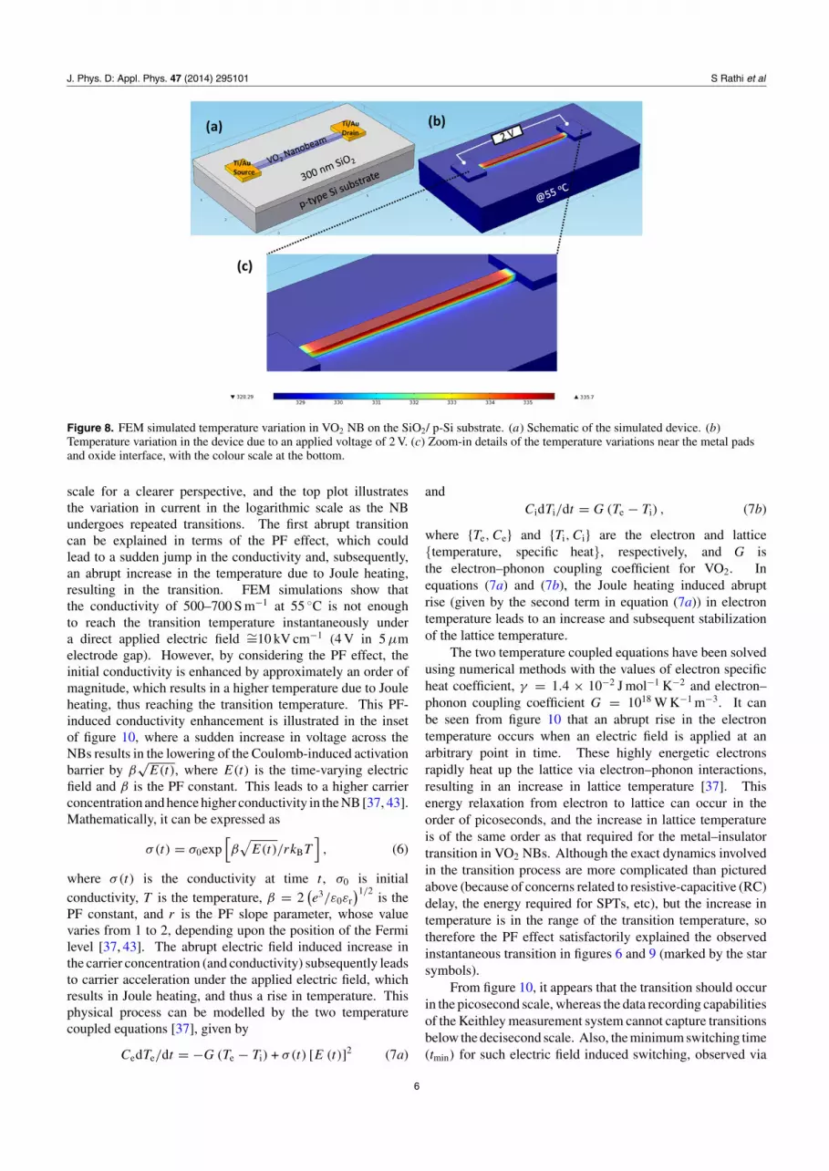
conductivity from bulk to nanowire have been widely reportedfor other nanowires [41, 42] like silicon, InAs, etc, where thishas been mainly attributed to the higher phonon boundaryscattering on the nanowire surface due to the higher surface tovolume ratio in low-dimensional materials. Figures 8(a)–(c)illustrate the device geometry considered for the simulation,and a representative case when a voltage of 2 V is appliedacross the NB along with the zoom-in detail of the metal-NBregion. It can be seen that the temperature across the NB is ata maximum in the middle, while it falls near the electrode dueto the better thermal conductivity of metal electrodes whichwork as effective heat sinks.
The matching of the simulated results with the modelledone is another indication of the accuracy of the modelemployed for Joule heating, although the simulated valuesshow considerable differences as the transition point isapproached. This can possibly be the result of the static valuesof the material properties used in the simulation, as the materialproperties such as thermal conductivity, lattice constant, etc,start varying near the transition point [39].
3.2. PF effect induced transition
Using this elaboration on the gradual transitions, marked bydiamonds (figure 6), we can now focus on the first transition,marked by the star in figure 6. For clarity, figure 9 re-plotsthe data used in figure 6 in the time domain, where it canbe seen that the first transition occurs almost instantaneouslywith the applied voltage. Further, both absolute currentand voltage are plotted in figure 9 on the common time
5
J. Phys. D: Appl. Phys. 47 (2014) 295101 S Rathi et al
Figure 8. FEM simulated temperature variation in VO2 NB on the SiO2/ p-Si substrate. (a) Schematic of the simulated device. (b)Temperature variation in the device due to an applied voltage of 2 V. (c) Zoom-in details of the temperature variations near the metal padsand oxide interface, with the colour scale at the bottom.
scale for a clearer perspective, and the top plot illustratesthe variation in current in the logarithmic scale as the NBundergoes repeated transitions. The first abrupt transitioncan be explained in terms of the PF effect, which couldlead to a sudden jump in the conductivity and, subsequently,an abrupt increase in the temperature due to Joule heating,resulting in the transition. FEM simulations show thatthe conductivity of 500–700 S m−1 at 55 C is not enoughto reach the transition temperature instantaneously undera direct applied electric field ∼=10 kV cm−1 (4 V in 5 µmelectrode gap). However, by considering the PF effect, theinitial conductivity is enhanced by approximately an order ofmagnitude, which results in a higher temperature due to Jouleheating, thus reaching the transition temperature. This PF-induced conductivity enhancement is illustrated in the insetof figure 10, where a sudden increase in voltage across theNBs results in the lowering of the Coulomb-induced activationbarrier by β
√E(t), where E(t) is the time-varying electric
field and β is the PF constant. This leads to a higher carrierconcentration and hence higher conductivity in the NB [37, 43].Mathematically, it can be expressed as
σ(t) = σ0exp[β√
E(t)/rkBT], (6)
where σ(t) is the conductivity at time t , σ0 is initialconductivity, T is the temperature, β = 2
(e3/ε0εr
)1/2is the
PF constant, and r is the PF slope parameter, whose valuevaries from 1 to 2, depending upon the position of the Fermilevel [37, 43]. The abrupt electric field induced increase inthe carrier concentration (and conductivity) subsequently leadsto carrier acceleration under the applied electric field, whichresults in Joule heating, and thus a rise in temperature. Thisphysical process can be modelled by the two temperaturecoupled equations [37], given by
CedTe/dt = −G (Te − Ti) + σ(t) [E (t)]2 (7a)
andCidTi/dt = G (Te − Ti) , (7b)
where Te, Ce and Ti, Ci are the electron and latticetemperature, specific heat, respectively, and G isthe electron–phonon coupling coefficient for VO2. Inequations (7a) and (7b), the Joule heating induced abruptrise (given by the second term in equation (7a)) in electrontemperature leads to an increase and subsequent stabilizationof the lattice temperature.
The two temperature coupled equations have been solvedusing numerical methods with the values of electron specificheat coefficient, γ = 1.4 × 10⁻² J mol−1 K−2 and electron–phonon coupling coefficient G = 1018 W K−1 m−3. It canbe seen from figure 10 that an abrupt rise in the electrontemperature occurs when an electric field is applied at anarbitrary point in time. These highly energetic electronsrapidly heat up the lattice via electron–phonon interactions,resulting in an increase in lattice temperature [37]. Thisenergy relaxation from electron to lattice can occur in theorder of picoseconds, and the increase in lattice temperatureis of the same order as that required for the metal–insulatortransition in VO2 NBs. Although the exact dynamics involvedin the transition process are more complicated than picturedabove (because of concerns related to resistive-capacitive (RC)delay, the energy required for SPTs, etc), but the increase intemperature is in the range of the transition temperature, sotherefore the PF effect satisfactorily explained the observedinstantaneous transition in figures 6 and 9 (marked by the starsymbols).
From figure 10, it appears that the transition should occurin the picosecond scale, whereas the data recording capabilitiesof the Keithley measurement system cannot capture transitionsbelow the decisecond scale. Also, the minimum switching time(tmin) for such electric field induced switching, observed via
6

J. Phys. D: Appl. Phys. 47 (2014) 295101 S Rathi et al
Figure 9. Time evolution plot of the I–V data in figure 6. The redcurve indicates voltage, the orange curve indicates the absolutevoltage, the green curve shows current variation, and the blue curveshows the absolute current. The pink curve shows the currentvariation in a semi-log scale.
I–V measurement, can be calculated [19, 35] by consideringthe thermal parameters of VO2 NBs only for the constant k inequation (2) as
tmin = (CρVch) (TT − T0) R/V 2, (8)
where C is specific heat, ρ is mass density, and Vch is theNB channel volume. Considering a NB of dimension Vch =length × width × height = 5 µm × 300 nm × 150 nm, witha given resistance R, under an applied voltage V , near thetransition point, tmin is in the order of 10 nanoseconds (ns). Thistimescale is further confirmed by the comparison of the valueof the term CρVch/tmin with that of the experimentally obtainedk. Therefore, in order to resolve the observed transition timefurther, an oscilloscope measurement with a square pulse of1 µs duration was carried out, and it can be seen in the inset offigure 11 that the transition time is in the order of 100 ns. Aninitial delay in onset time can still be seen in the oscilloscopemeasurement; this may be due to the intrinsic RC factorassociated with the NB and the external resistance and henceis difficult to remove completely [23, 24, 44]. However, thisRC delay can be overcome using ultrafast time-resolved THzspectroscopy/pump-probe techniques, where the transitionstime in the VO2 material is in the order of the picosecond scale[6, 37]. Further, Treadway et al [24] have demonstrated that
Figure 10. Illustration of electron and lattice temperature variationswith the application of a high-voltage signal at t ≈ 58 ps. Theschematic in the inset illustrates the lowering of barrier height on theapplication of the abrupt voltage signal, and the symbols q, and drepresent fundamental charge, initial barrier for no field, anddistance between two consecutive electrodes, respectively.
-3 -2 -1 0 1 2 3-0.6
-0.4
-0.2
0.0
0.2
0.4
0.6
300 oC 400 oC
Cur
rent
(m
A)
Voltage (V)
0.0 0.5 1.0 1.5 2.00.0
0.5
1.0
1.5
2.0
2.5
Time (µµµµs)
Vo
ltag
e P
uls
e (V
)
0.0
0.5
1.0
1.5
Cu
rren
t P
uls
e (m
A)
Figure 11. I–V curve measured at 55 C for VO2 NBs annealed at300 and 400 C in an argon ambient for 1 min. The top left insetillustrates the arrangement for the oscilloscope measurement,plotted in the bottom right inset. A square input pulse was applied tothe device annealed at 300 C, and the voltage drop was recordedusing an oscilloscope across an external resistance, which was thenconverted and plotted as current.
radio frequency (RF) power also contributes to the dc voltage-induced switching in the VO2 thin-film-based coplanar wave-guides, and the RF based steady-state switching time is of thesame order as tmin. This also indicates toward the two process-based mechanism where field-induced carrier injection resultsin an initial current jump, followed by the temperature rise dueto Joule heating [24].
Furthermore, the I–V curves in figure 11 show thetransition characteristics of NBs annealed at 300 and 400 Cin an argon ambient for 1 min. It can be seen from thefigure that the annealing results in the lowering of thetransition voltage for both abrupt and gradual transitions.
7

J. Phys. D: Appl. Phys. 47 (2014) 295101 S Rathi et al
This fits the Joule heating and PF effect based transitionpictures as annealing in the reducing environment decreasesthe NB’s resistance from 500 k (standard device annealed at200 C) to 250 k and 42 k for devices annealed at 300 Cand 400 C, respectively, which results in reduced thresholdvoltages to achieve the transition. The decrease in NBresistance is due to oxygen deficiency induced lattice defects,like interstitials and vacancies, along with the formationof various Magneli phases (VnO2n−1 = V2O3 + (n − 2) VO2)
which result in higher electron concentrations [28, 45, 46].Moreover, according to the Drude model of conductivity(σ = neµ, where n is carrier concentration, e is chargeand µ is mobility), the decrease in the NB’s resistance alsoindicates higher electron concentrations, as annealing inducedimperfections and defects in the crystal lattice would result inmobility degradation rather than enhancement. The loweringof the transition voltage in figure 11 is also consistent withMott’s transition theory, in which the transition is dependent onthe critical strength of electron-density dependent screening.
4. Conclusion
In conclusion, both abrupt and gradual transitions have beenobserved in VO2 nanobeam devices upon the application ofa dual-sweep voltage signal. The gradual transitions agreewith the Joule heating picture, while the Poole–Frenkel effectfits for the abrupt transition. Although an intrinsic RC delaylimits the abrupt transition time in electrical switching, itcan still be utilized for switching and fail-safe applications.Furthermore, this study can also serve as a comprehensiveguide for understanding the electrical response of vanadiumdioxide nanobeams for device applications.
Acknowledgments
This research was supported by Basic Science ResearchProgram through the National Research Foundation of Korea(NRF) funded by the Ministry of Education, Science andTechnology (2013R1A2A2A01069023 and 20130633002).
References
[1] Imada M, Fujimori A and Tokura Y 1998 Rev. Mod. Phys. 70 4[2] Yang Z, Ko C and Ramanathan S 2011 Annu. Rev. Mater.
Res. 41 337[3] Nakano M, Shibuya K, Okuyama D, Hatano T, Ono S,
Kawasaki M, Iwasa Y and Tokura Y 2012 Nature 487 459[4] Wei J, Wang Z, Chen W and Cobden D H 2009 Nature
Nanotechnol. 4 420[5] Wei J, Ji H, Guo W, Nevidomskyy A H and Natelson D 2012
Nature Nanotechnol. 7 357[6] Cocker T L, Titova L V, Fourmaux S, Holloway G,
Bandulet H C, Brassard D, Kieffer J C, Khakani M A E andHegmann F A 2012 Phys. Rev. B 85 155120
[7] Eyert V 2011 Phys. Rev. Lett. 107 016401[8] Baik J M, Kim M H, Larson C, Yavuz C T, Stucky G D,
Wodtke A M and Moskovits M 2009 Nano Lett. 9 3980[9] Strelcov E, Lilach Y and Kolmakov A 2009 Nano Lett. 9 2322
[10] Sengupta S, Wang K, Liu K, Bhat A K, Dhara S, Wu J andDeshmukh M M 2011 Appl. Phys. Lett. 99 062114
[11] Pellegrino L, Manca N, Kanki T, Tanaka H, Biasotti M,Bellingeri E, Siri A S and Marre D 2012 Adv. Mater.24 2929
[12] Manca N, Pellegrino L, Kanki T, Yamasaki S, Tanaka H,Siri A S and Marre D 2013 Adv. Mater. 25 6430
[13] Baik J M, Kim M H, Larson C, Wodtke A M and Moskovits M2008 J. Phys. Chem. C 112 13328
[14] Yang Z, Hart S, Ko C, Yacoby A and Ramanathan S 2011J. Appl. Phys. 110 033725
[15] Fu D, Liu K, Tao T, Lo K, Cheng C, Liu B, Zhang R,Bechtel H A and Wu J 2013 J. Appl. Phys. 113 043707
[16] Zimmers A, Aigouy L, Mortier M, Sharoni A, Wang S,West K G, Ramirez J G and Schuller I K 2013 Phys. Rev.Lett. 110 056601
[17] Ko C and Ramanathan S 2008 Appl. Phys. Lett. 93 252101[18] Kim H T, Chae B G, Youn D H, Kim G, Kang K Y, Lee S J,
Kim K and Lim Y S 2005 Appl. Phys. Lett. 86 242101[19] Stefanovich G, Pergament A and Stefanovich D 2000 J. Phys.:
Condens. Matter 12 8837[20] Hormoz S and Ramanathan S 2010 Solid-State Electron.
54 654[21] Lee S B, Kim K, Oh J S, Kahng B and Lee J S 2013 Appl.
Phys. Lett. 102 063501[22] Zhou Y, Chen X, Ko C, Yang Z, Mouli C and Ramanathan S
2013 IEEE Electron Device Lett. 34 2[23] Kar A, Shukla N, Freeman E, Paik H, Liu H, Herbert R E,
Bharadwaja S S N, Schlom D G and Datta S 2013 Appl.Phys. Lett. 102 072106
[24] Ha S D, Zhou Y, Fisher C J, Ramanathan S and Treadway J P2013 J. Appl. Phys. 113 184501
[25] Yang Z, Ko C and Ramanathan S 2010 J. Appl. Phys.108 073708
[26] Ruzmetov D, Senanayake S D and Ramanathan S 2007 Phys.Rev. B 75 195102
[27] Ruzmetov D, Senanayake S D, Narayanamurti V andRamanathan S 2008 Phys. Rev. B 77 195442
[28] Rathi S, Park J H, Lee I Y, Kim M J, Baik J M and Kim G H2013 Appl. Phys. Lett. 103 203114
[29] Atkin J M, Berweger S, Chavez E K, Raschke M B, Cao J,Fan W and Wu J 2012 Phys. Rev. B 85 020101
[30] Lopez R, Haynes T E, Boatner L A, Feldman L C andHaglund R F 2002 Phys. Rev. B 65 224113
[31] Donev E U, Lopez R, Feldman L C and Haglund R F 2009Nano Lett. 9 702
[32] Appavoo K, Lei D Y, Sonnefraud Y, Wang B, Pantelides S T,Maier S A and Haglund R F 2012 Nano Lett. 12 780
[33] Sohn J I, Joo H J, Ahn D, Lee H H, Porter A E, Kim K,Kang D J and Welland M E 2009 Nano Lett. 9 3392
[34] Goodenough J B 1971 J. Solid State Chem. 3 490[35] Gopalakrishnan G, Ruzmetov D and Ramanathan S 2009
J. Mater. Sci. 44 5345[36] Zhao Y, Hao J, Chen C and Fan Z 2012 J. Phys.: Condens.
Matter 24 035601[37] Liu M et al 2012 Nature 487 345[38] Yang Z, Ko C, Balakrishnan V, Gopalakrishnan G and
Ramanathan S 2010 Phys. Rev. B 82 205101[39] COMSOL Multiphysics Package (www.comsol.com/)[40] Oh D W, Ko C, Ramanathan S and Cahill D G 2010 Appl.
Phys. Lett. 96 151906[41] Li D, Wu Y, Kim P, Shi L, Yang P and Majumdar A 2003 Appl.
Phys. Lett. 83 14[42] He Y and Galli G 2012 Phys. Rev. Lett. 108 215901[43] Hormoz S and Ramanathan S 2010 Solid-State Electron.
54 654[44] Zhou Y, Chen X, Ko C, Yang Z, Mouli C and Ramanathan S
2013 IEEE Electron Device Lett. 34 220[45] Zhang S, Kim I S and Lauhon L J 2011 Nano Lett. 11 1443[46] Hong W K et al 2013 Nano Lett. 13 1822
8