Embed Size (px)
Citation preview
Peak Detector and/or Envelope Detector— A Detailed Analysis —
Predrag Pejović
April 7, 2018
AbstractIn this document, a simple circuit constructed using a diode, a resistor, and a capacitor, utilizedas a peak detector and/or as an envelope detector is analyzed. The analysis is approached byapplying approximate methods and by a mix of exact and numerical methods, aiming designguidelines and understanding of the circuit operation. Approximate and exact approaches arecompared, and a region where the approximate analysis provides adequate answers is identified.Ability of the circuit to track the envelope variations is analyzed, and it is shown to depend bothon the circuit time constant and the output voltage value, i.e. the modulation signal frequencyand the modulation index. Relevant relations are derived and presented. Finally, distortionof the output voltage caused by the output voltage ripple is addressed, and averaged model ofthe circuit is derived. It is shown that average of the output voltage over the carrier period isincreased about three times when filtering of the output voltage is applied. Transfer functionfor averaged waveforms of the envelope detector is derived, containing slight attenuation and areal pole at the double of the carrier frequency.
c© 2018 Predrag Pejović,This work is licensed under a Creative Commons Attribution-ShareAlike 4.0 International License.
1 IntroductionPeak detector and/or envelope detector, built as a circuit of Fig. 1 is frequent in electricalengineering curricula and usually the first circuit built by enthusiasts in amateur radio clubs.The author of this document is no exception: still remembers his joy after this simple circuitdemonstrated its operation. Analysis of the circuit could be found in many places, like [1] or[2], to mention a few. However, the author never found all the answers he asked himself inavailable literature, at least not arranged in the way he would like it to be. After student MilošNenadović asked a question during lab exercise, as stated in the Acknowledgement, the authorrealized that there are other people being bothered by the same questions, which initiatedwriting of this document. Peak and/or envelope detector is an old circuit, not being in thefocus of leading edge research in electronics. However, it is a nice circuit, which might be usedas an example to illustrate many complex circuit analysis techniques on a circuit containingonly three elements: one linear resistive, one nonlinear resistive, and one accumulating. Insuch an example, the essence could be demonstrated without unnecessary burden of irrelevantdetails.
At this point, difference between the peak detector and the envelope detector should beclarified, since the circuit performing the tasks is the same. In both of the cases considered inthis document, we would assume the same general form of the input voltage
vIN(t) = vA(t) cos (ω0 t) (1)
where vA(t) is considered the signal envelope. In the case of a peak detector application, weassume constant envelope, vA(t) = VC , and the goal is to reconstruct the value of VC . In thecase of envelope detector, vA(t) is assumed as a variable signal, and reconstructing its waveformis the goal.
It is worth to mention that notion of a signal envelope [3] is much more complex thanshown here. However, our aim is to construct a simple circuit for asynchronous demodulationof signals provided by standard amplitude modulation [4], and the definition applied here issufficient for such application.
Aim of the analysis presented in this document is to obtain reasonably accurate and reason-ably simple equations that model the output voltage, both in the sense of the output voltageripple [5] and in the sense of the circuit ability to track the envelope variations. One of the goalswas to provide a rule of thumb for choosing R and C. This task is essentially one parameteroptimization problem, since R and C appear in equations merged in the time constant RC.The optimization could be experimentally performed just in a few steps, and requirement forsuch analysis did not emerge from practice. However, it might be nice to understand the circuitoperation, modeling, and optimization from a theoretical viewpoint, also.
+
−vIN
D
C R
vOUT
Figure 1: Peak detector and/or envelope detector, circuit diagram.
2
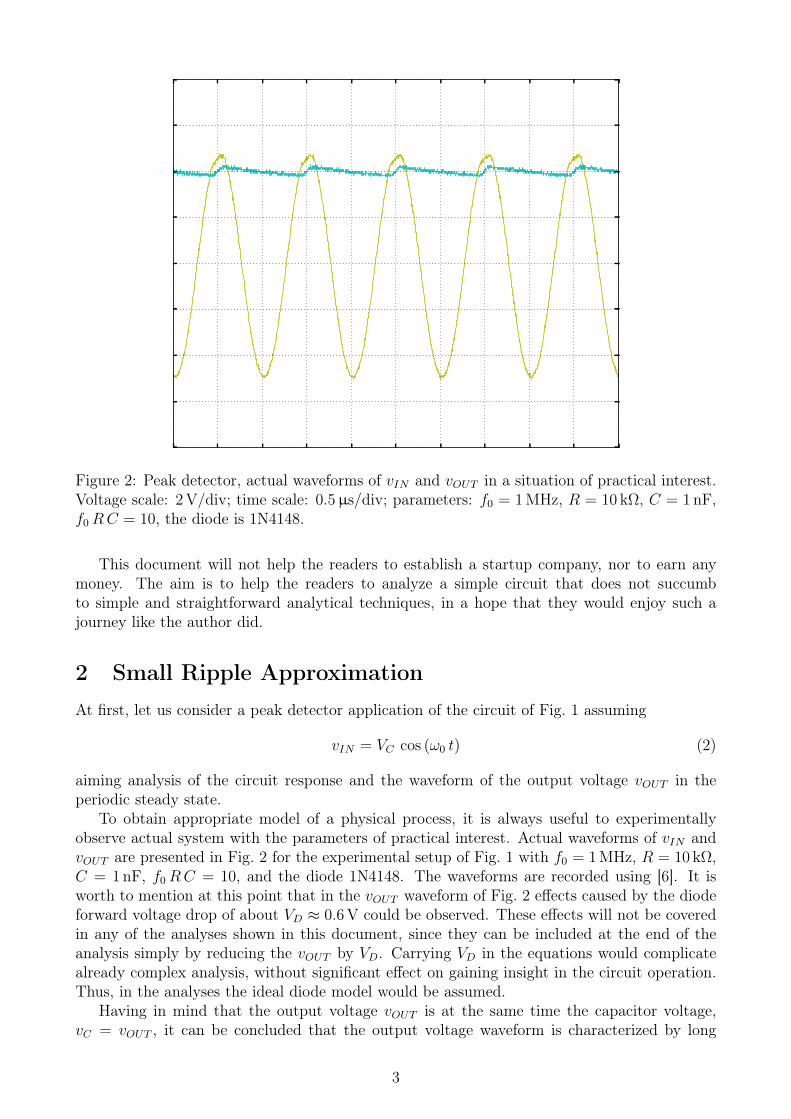
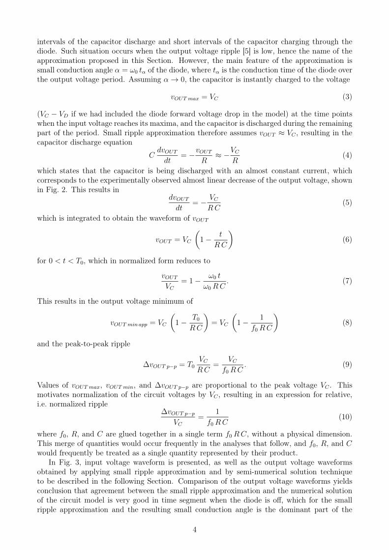
Figure 2: Peak detector, actual waveforms of vIN and vOUT in a situation of practical interest.Voltage scale: 2V/div; time scale: 0.5µs/div; parameters: f0 = 1MHz, R = 10 kΩ, C = 1 nF,f0RC = 10, the diode is 1N4148.
This document will not help the readers to establish a startup company, nor to earn anymoney. The aim is to help the readers to analyze a simple circuit that does not succumbto simple and straightforward analytical techniques, in a hope that they would enjoy such ajourney like the author did.
2 Small Ripple ApproximationAt first, let us consider a peak detector application of the circuit of Fig. 1 assuming
vIN = VC cos (ω0 t) (2)
aiming analysis of the circuit response and the waveform of the output voltage vOUT in theperiodic steady state.
To obtain appropriate model of a physical process, it is always useful to experimentallyobserve actual system with the parameters of practical interest. Actual waveforms of vIN andvOUT are presented in Fig. 2 for the experimental setup of Fig. 1 with f0 = 1MHz, R = 10 kΩ,C = 1 nF, f0RC = 10, and the diode 1N4148. The waveforms are recorded using [6]. It isworth to mention at this point that in the vOUT waveform of Fig. 2 effects caused by the diodeforward voltage drop of about VD ≈ 0.6V could be observed. These effects will not be coveredin any of the analyses shown in this document, since they can be included at the end of theanalysis simply by reducing the vOUT by VD. Carrying VD in the equations would complicatealready complex analysis, without significant effect on gaining insight in the circuit operation.Thus, in the analyses the ideal diode model would be assumed.
Having in mind that the output voltage vOUT is at the same time the capacitor voltage,vC = vOUT , it can be concluded that the output voltage waveform is characterized by long
3
intervals of the capacitor discharge and short intervals of the capacitor charging through thediode. Such situation occurs when the output voltage ripple [5] is low, hence the name of theapproximation proposed in this Section. However, the main feature of the approximation issmall conduction angle α = ω0 tα of the diode, where tα is the conduction time of the diode overthe output voltage period. Assuming α→ 0, the capacitor is instantly charged to the voltage
vOUT max = VC (3)
(VC − VD if we had included the diode forward voltage drop in the model) at the time pointswhen the input voltage reaches its maxima, and the capacitor is discharged during the remainingpart of the period. Small ripple approximation therefore assumes vOUT ≈ VC , resulting in thecapacitor discharge equation
CdvOUTdt
= −vOUTR≈ −VC
R(4)
which states that the capacitor is being discharged with an almost constant current, whichcorresponds to the experimentally observed almost linear decrease of the output voltage, shownin Fig. 2. This results in
dvOUTdt
= − VCRC
(5)
which is integrated to obtain the waveform of vOUT
vOUT = VC
(1− t
RC
)(6)
for 0 < t < T0, which in normalized form reduces to
vOUTVC
= 1− ω0 t
ω0RC. (7)
This results in the output voltage minimum of
vOUT minapp = VC
(1− T0
RC
)= VC
(1− 1
f0RC
)(8)
and the peak-to-peak ripple
∆vOUT p−p = T0VCRC
=VC
f0RC. (9)
Values of vOUT max, vOUT min, and ∆vOUT p−p are proportional to the peak voltage VC . Thismotivates normalization of the circuit voltages by VC , resulting in an expression for relative,i.e. normalized ripple
∆vOUT p−pVC
=1
f0RC(10)
where f0, R, and C are glued together in a single term f0RC, without a physical dimension.This merge of quantities would occur frequently in the analyses that follow, and f0, R, and Cwould frequently be treated as a single quantity represented by their product.
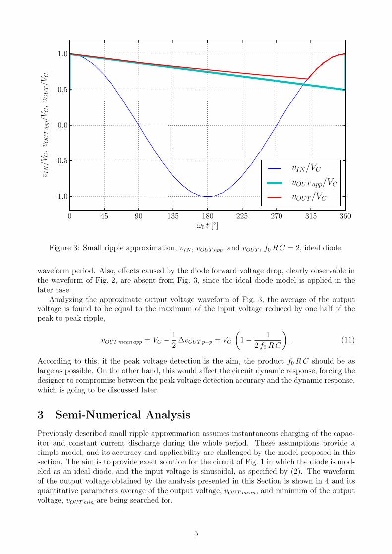
In Fig. 3, input voltage waveform is presented, as well as the output voltage waveformsobtained by applying small ripple approximation and by semi-numerical solution techniqueto be described in the following Section. Comparison of the output voltage waveforms yieldsconclusion that agreement between the small ripple approximation and the numerical solutionof the circuit model is very good in time segment when the diode is off, which for the smallripple approximation and the resulting small conduction angle is the dominant part of the
4
0 45 90 135 180 225 270 315 360ω0 t []
−1.0
−0.5
0.0
0.5
1.0
v IN/V
C,v O
UTapp/V
C,v O
UT/V
C
vIN/VC
vOUT app/VC
vOUT/VC
Figure 3: Small ripple approximation, vIN , vOUT app, and vOUT , f0RC = 2, ideal diode.
waveform period. Also, effects caused by the diode forward voltage drop, clearly observable inthe waveform of Fig. 2, are absent from Fig. 3, since the ideal diode model is applied in thelater case.
Analyzing the approximate output voltage waveform of Fig. 3, the average of the outputvoltage is found to be equal to the maximum of the input voltage reduced by one half of thepeak-to-peak ripple,
vOUT meanapp = VC −1
2∆vOUT p−p = VC
(1− 1
2 f0RC
). (11)
According to this, if the peak voltage detection is the aim, the product f0RC should be aslarge as possible. On the other hand, this would affect the circuit dynamic response, forcing thedesigner to compromise between the peak voltage detection accuracy and the dynamic response,which is going to be discussed later.
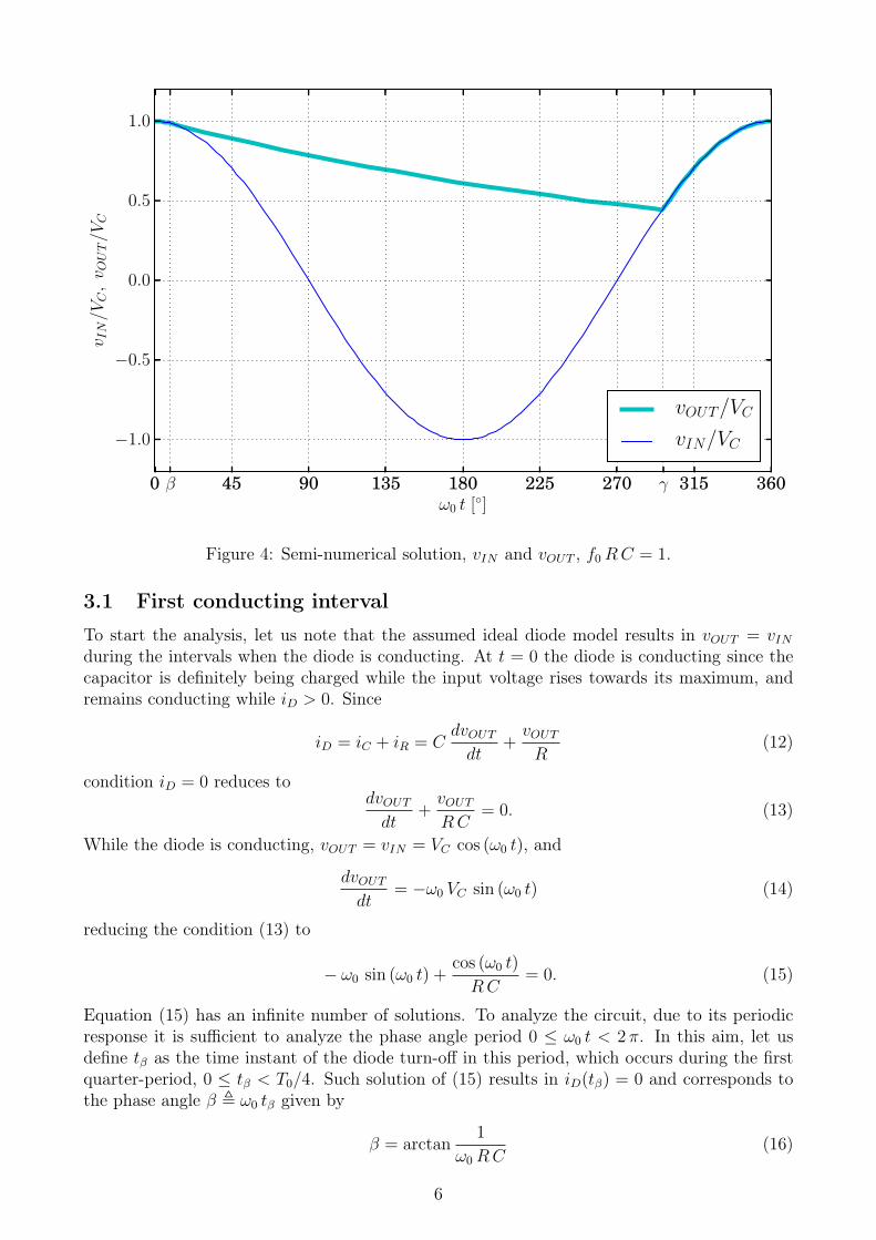
3 Semi-Numerical AnalysisPreviously described small ripple approximation assumes instantaneous charging of the capac-itor and constant current discharge during the whole period. These assumptions provide asimple model, and its accuracy and applicability are challenged by the model proposed in thissection. The aim is to provide exact solution for the circuit of Fig. 1 in which the diode is mod-eled as an ideal diode, and the input voltage is sinusoidal, as specified by (2). The waveformof the output voltage obtained by the analysis presented in this Section is shown in 4 and itsquantitative parameters average of the output voltage, vOUT mean, and minimum of the outputvoltage, vOUT min are being searched for.
5
0 β 45 90 135 180 225 270 γ 315 360ω0 t []
−1.0
−0.5
0.0
0.5
1.0
v IN/V
C,v O
UT/V
C
vOUT/VC
vIN/VC
Figure 4: Semi-numerical solution, vIN and vOUT , f0RC = 1.
3.1 First conducting interval
To start the analysis, let us note that the assumed ideal diode model results in vOUT = vINduring the intervals when the diode is conducting. At t = 0 the diode is conducting since thecapacitor is definitely being charged while the input voltage rises towards its maximum, andremains conducting while iD > 0. Since
iD = iC + iR = CdvOUTdt
+vOUTR
(12)
condition iD = 0 reduces todvOUTdt
+vOUTRC
= 0. (13)
While the diode is conducting, vOUT = vIN = VC cos (ω0 t), and
dvOUTdt
= −ω0 VC sin (ω0 t) (14)
reducing the condition (13) to
− ω0 sin (ω0 t) +cos (ω0 t)
RC= 0. (15)
Equation (15) has an infinite number of solutions. To analyze the circuit, due to its periodicresponse it is sufficient to analyze the phase angle period 0 ≤ ω0 t < 2π. In this aim, let usdefine tβ as the time instant of the diode turn-off in this period, which occurs during the firstquarter-period, 0 ≤ tβ < T0/4. Such solution of (15) results in iD(tβ) = 0 and corresponds tothe phase angle β , ω0 tβ given by
β = arctan1
ω0RC(16)
6
which satisfies the condition to be in the first quarter-period since 0 < β < π/2 for positiveω0RC. In this manner, the first time segment of the circuit operation over considered periodis determined by 0 ≤ ω0 t < β, where vOUT = vIN .
3.2 Nonconducting interval
The second segment of the circuit operation starts with the diode turn off at tβ, and lasts fortβ ≤ t < tγ, where tγ is the time instant when the diode turns on again, which corresponds tothe phase angle γ , ω0 tγ. Within the considered phase angle scope, γ is located in the range3π/2 ≤ γ < 2 π.
While the diode is off, the output voltage is
vOUT (t) = vOUT (tβ) e−t−tβRC (17)
wherevOUT (tβ) = VC cos β =
ω0RC√1 + (ω0RC)2
VC . (18)
In terms of the phase angle, which is normalized time, normalized output voltage during theinterval when the diode is off is
vOUT (ω0 t)
VC=
ω0RC√1 + (ω0RC)2
e−ω0 t−βω0 RC (19)
The diode nonconducting interval ends at tγ = γ/ω0 when vOUT given by (19) and vIN meetagain, vOUT (γ) = vIN(γ), which in expanded form results in
vOUT (γ) = VC cos γ =ω0RC√
1 + (ω0RC)2VC e
− γ−βω0 RC . (20)
After cancellation of VC , determining γ reduces to solving
cos γ =ω0RC√
1 + (ω0RC)2e− γ−βω0 RC (21)
which is a transcendental equation [7] over γ. The equation does not have a closed form solution,and requires a numerical solution over γ. This requirement makes the analysis semi-numerical,since a closed form expression for γ would provide purely analytical solution.
To solve for γ numerically, a linear iterration proces is applied, designed to search a solutionfor γ in the range 3 π/2 ≤ γ < 2π using the following iterration rule
γk+1 = 2π − arccos
ω0RC√1 + (ω0RC)2
e− γk−βω0 RC
. (22)
To design the iteration rule, special care is taken in inverting the cosine function, to providesolution in the desired range. This is the most delicate part of the analysis. The iteration isperformed until the criterion
|γk+1 − γk| < ε (23)
is met. The results presented in this document are obtained with the exit parameter valueε = 10−6.
7
10−3 10−2 10−1 100 101 102 103 104
f0RC
0
90
180
270
360β,γ,α
[] α
β
γ
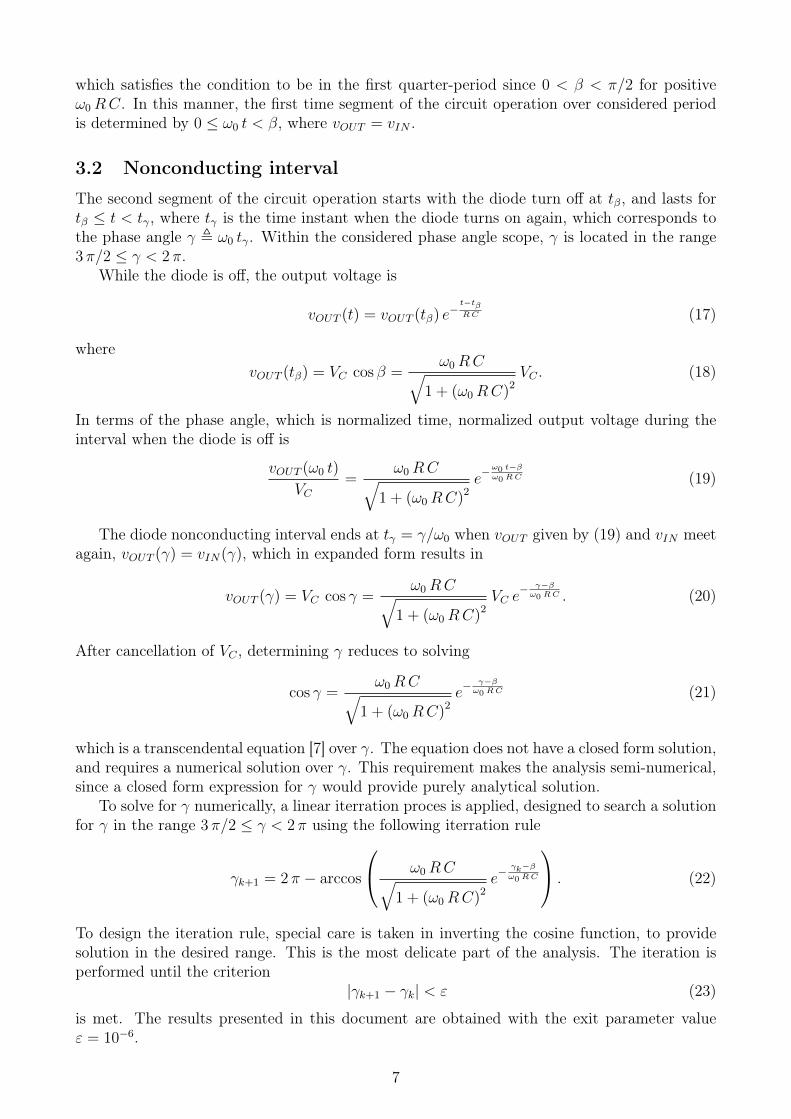
Figure 5: Angles: β, γ, and α.
3.3 Second conducting interval
The second conducting interval of the diode during the switching period occurs for γ ≤ ω0 t <2π, which closes the period.
After angles β and γ are determined, the diode conduction angle is obtained as
α = 2π − (γ − β) (24)
and in the case of the small ripple approximation is considered to be negligibly small. Values ofβ, γ, and consequently α, according to (16), (21), and (24) depend on the combined parameterf0RC only. Dependence of α, β, and γ on f0RC is given in Fig. 5 in logarithmic scale overf0RC. The figure illustrates that effects of filtering by the capacitor C are noticeable forf0RC > 10−2, when α starts to decrease from 180. For f0RC > 102 the filtering is perfect,and the conduction angle α approaches zero.
3.4 Parameters of the output voltage
Purpose of determining β analytically and γ numerically was to determine mean value of theoutput voltage
vOUT mean =1
2π
∫ 2π
0
vOUT (ω0 t) d(ω0 t) (25)
and its minimal value, vOUT min. Both quantities are convenient to represent in normalizedform, obtained by dividing with VC , providing the result in VC independent form. Average ofthe output voltage is after some symbolic computation obtained as
vOUT meanVC
=1
2 π
(sin β − sin γ + ω0RC
(1− e
β−γω0 RC
)cos β
)(26)
8
10−3 10−2 10−1 100 101 102 103 104
f0RC
0.0
0.2
0.4
0.6
0.8
1.0v O
UTmax/V
C,v
OUTmin/V
C,v
OUTmean/V
C
vOUT max/VC
vOUT min/VC
vOUT mean/VC
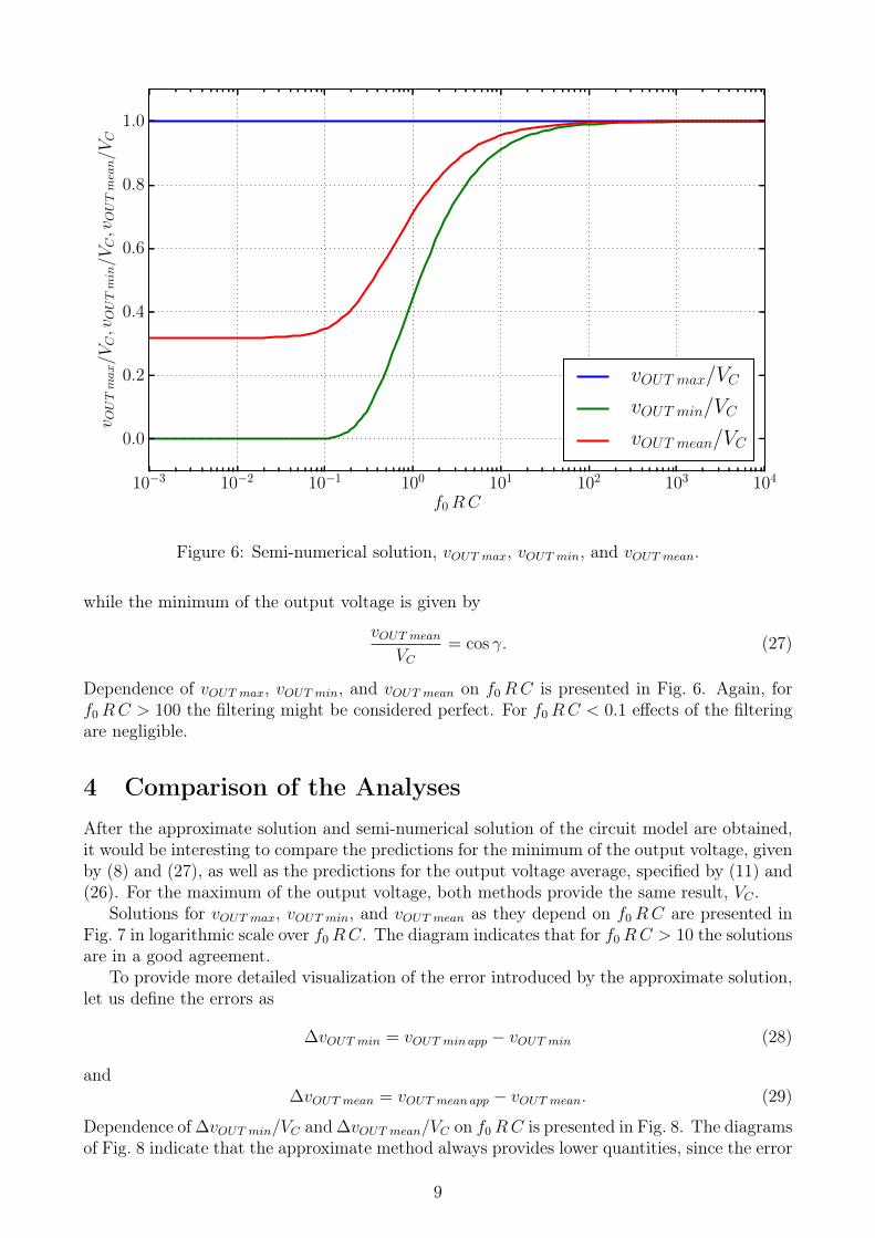
Figure 6: Semi-numerical solution, vOUT max, vOUT min, and vOUT mean.
while the minimum of the output voltage is given by
vOUT meanVC
= cos γ. (27)
Dependence of vOUT max, vOUT min, and vOUT mean on f0RC is presented in Fig. 6. Again, forf0RC > 100 the filtering might be considered perfect. For f0RC < 0.1 effects of the filteringare negligible.
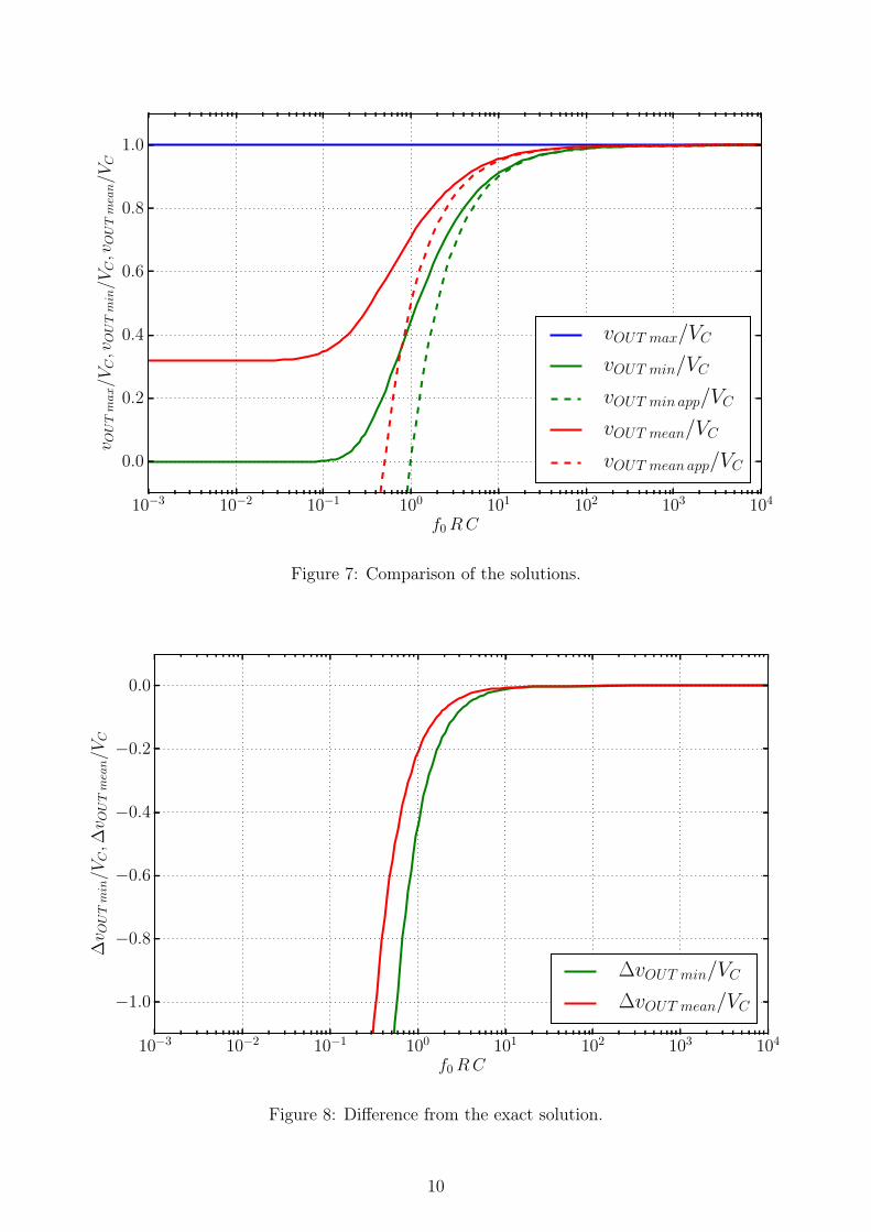
4 Comparison of the AnalysesAfter the approximate solution and semi-numerical solution of the circuit model are obtained,it would be interesting to compare the predictions for the minimum of the output voltage, givenby (8) and (27), as well as the predictions for the output voltage average, specified by (11) and(26). For the maximum of the output voltage, both methods provide the same result, VC .
Solutions for vOUT max, vOUT min, and vOUT mean as they depend on f0RC are presented inFig. 7 in logarithmic scale over f0RC. The diagram indicates that for f0RC > 10 the solutionsare in a good agreement.
To provide more detailed visualization of the error introduced by the approximate solution,let us define the errors as
∆vOUT min = vOUT minapp − vOUT min (28)
and∆vOUT mean = vOUT meanapp − vOUT mean. (29)
Dependence of ∆vOUT min/VC and ∆vOUT mean/VC on f0RC is presented in Fig. 8. The diagramsof Fig. 8 indicate that the approximate method always provides lower quantities, since the error
9
10−3 10−2 10−1 100 101 102 103 104
f0RC
0.0
0.2
0.4
0.6
0.8
1.0
v OUTmax/V
C,v
OUTmin/V
C,v
OUTmean/V
C
vOUT max/VC
vOUT min/VC
vOUT min app/VC
vOUT mean/VC
vOUT mean app/VC
Figure 7: Comparison of the solutions.
10−3 10−2 10−1 100 101 102 103 104
f0RC
−1.0
−0.8
−0.6
−0.4
−0.2
0.0
∆v O
UTmin/V
C,∆v O
UTmean/V
C
∆vOUT min/VC
∆vOUT mean/VC
Figure 8: Difference from the exact solution.
10
10−3 10−2 10−1 100 101 102 103 104
f0RC
10−5
10−4
10−3
10−2
10−1
100
101
102
103
104
105(|∆
v OUTmin|/V
C,|∆
v OUTmean|/V
C)×
100%
∆vOUT min/VC
∆vOUT mean/VC
Figure 9: Difference from the exact solution, logarithmic scale.
is negative. Above 10 f0RC the error seems negligible, but seems to grow rapidly in magnitudebelow this value, in an exponential-like fashion.
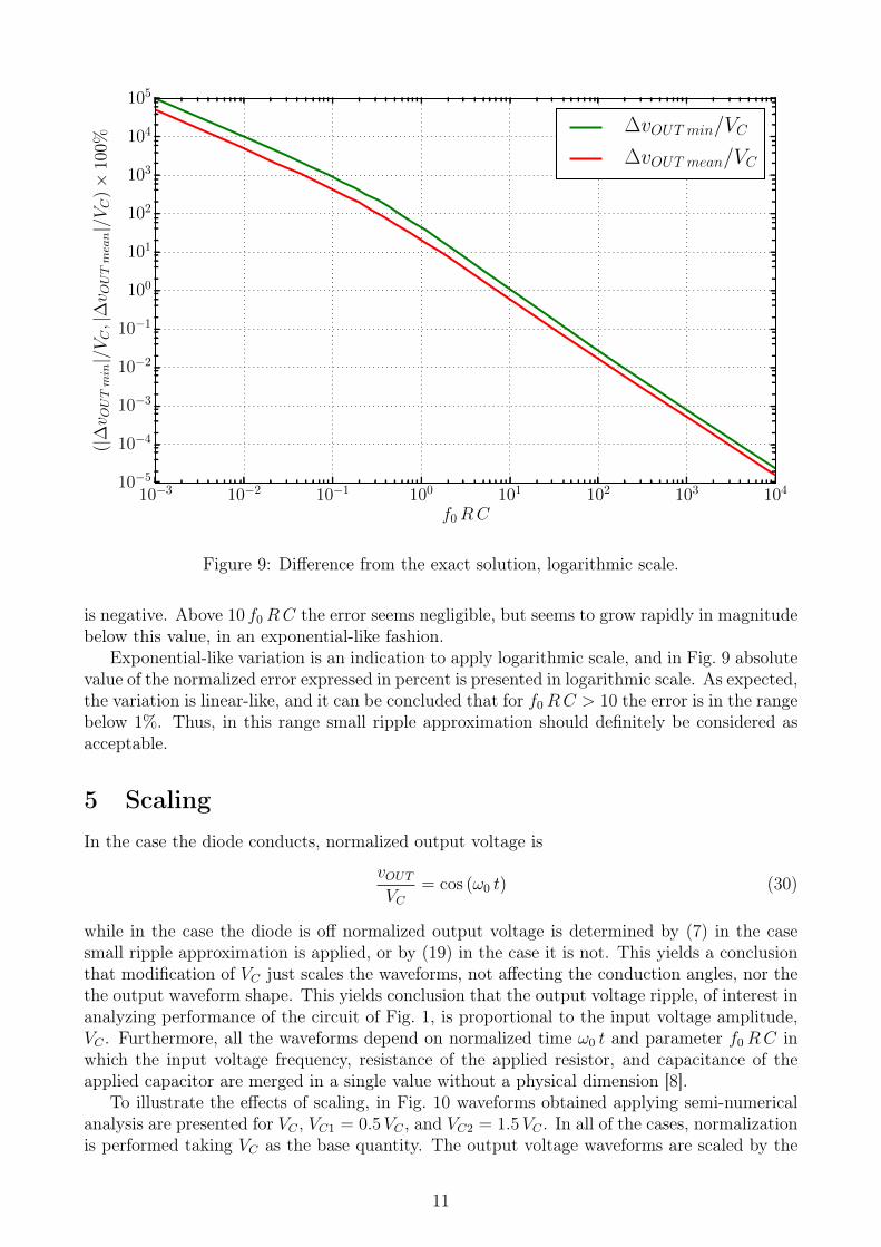
Exponential-like variation is an indication to apply logarithmic scale, and in Fig. 9 absolutevalue of the normalized error expressed in percent is presented in logarithmic scale. As expected,the variation is linear-like, and it can be concluded that for f0RC > 10 the error is in the rangebelow 1%. Thus, in this range small ripple approximation should definitely be considered asacceptable.
5 ScalingIn the case the diode conducts, normalized output voltage is
vOUTVC
= cos (ω0 t) (30)
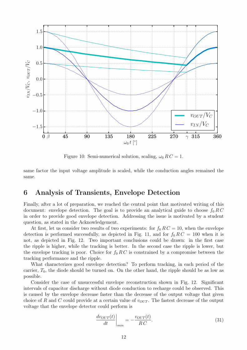
while in the case the diode is off normalized output voltage is determined by (7) in the casesmall ripple approximation is applied, or by (19) in the case it is not. This yields a conclusionthat modification of VC just scales the waveforms, not affecting the conduction angles, nor thethe output waveform shape. This yields conclusion that the output voltage ripple, of interest inanalyzing performance of the circuit of Fig. 1, is proportional to the input voltage amplitude,VC . Furthermore, all the waveforms depend on normalized time ω0 t and parameter f0RC inwhich the input voltage frequency, resistance of the applied resistor, and capacitance of theapplied capacitor are merged in a single value without a physical dimension [8].
To illustrate the effects of scaling, in Fig. 10 waveforms obtained applying semi-numericalanalysis are presented for VC , VC1 = 0.5VC , and VC2 = 1.5VC . In all of the cases, normalizationis performed taking VC as the base quantity. The output voltage waveforms are scaled by the
11
0 β 45 90 135 180 225 270 γ 315 360ω0 t []
−1.5
−1.0
−0.5
0.0
0.5
1.0
1.5v IN/V
C,v O
UT/V
C
vOUT/VC
vIN/VC
Figure 10: Semi-numerical solution, scaling, ω0RC = 1.
same factor the input voltage amplitude is scaled, while the conduction angles remained thesame.
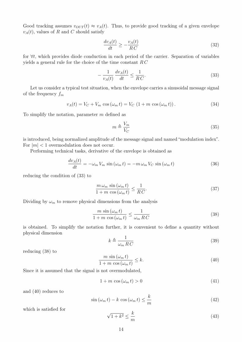
6 Analysis of Transients, Envelope DetectionFinally, after a lot of preparation, we reached the central point that motivated writing of thisdocument: envelope detection. The goal is to provide an analytical guide to choose f0RCin order to provide good envelope detection. Addressing the issue is motivated by a studentquestion, as stated in the Acknowledgement.
At first, let us consider two results of two experiments: for f0RC = 10, when the envelopedetection is performed successfully, as depicted in Fig. 11, and for f0RC = 100 when it isnot, as depicted in Fig. 12. Two important conclusions could be drawn: in the first casethe ripple is higher, while the tracking is better. In the second case the ripple is lower, butthe envelope tracking is poor. Choice for f0RC is constrained by a compromise between thetracking performance and the ripple.
What characterizes good envelope detection? To perform tracking, in each period of thecarrier, T0, the diode should be turned on. On the other hand, the ripple should be as low aspossible.
Consider the case of unsuccessful envelope reconstruction shown in Fig. 12. Significantintervals of capacitor discharge without diode conduction to recharge could be observed. Thisis caused by the envelope decrease faster than the decrease of the output voltage that givenchoice of R and C could provide at a certain value of vOUT . The fastest decrease of the outputvoltage that the envelope detector could perform is
dvOUT (t)
dt
∣∣∣∣min
= −vOUT (t)
RC. (31)
12
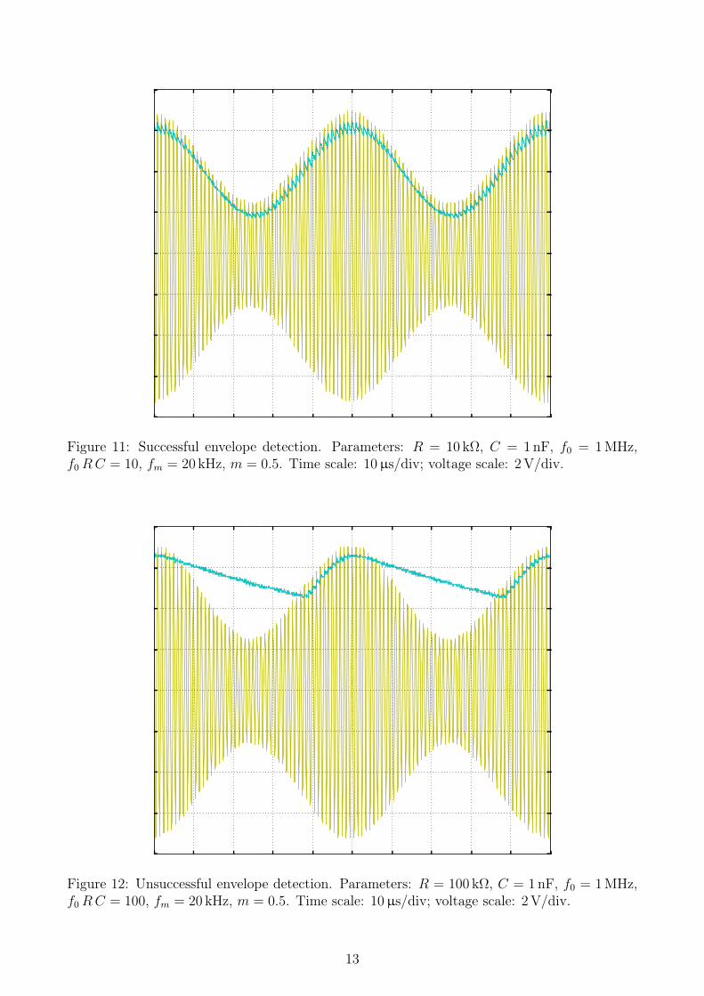
Figure 11: Successful envelope detection. Parameters: R = 10 kΩ, C = 1 nF, f0 = 1MHz,f0RC = 10, fm = 20 kHz, m = 0.5. Time scale: 10µs/div; voltage scale: 2V/div.
Figure 12: Unsuccessful envelope detection. Parameters: R = 100 kΩ, C = 1 nF, f0 = 1MHz,f0RC = 100, fm = 20 kHz, m = 0.5. Time scale: 10µs/div; voltage scale: 2V/div.
13
Good tracking assumes vOUT (t) ≈ vA(t). Thus, to provide good tracking of a given envelopevA(t), values of R and C should satisfy
dvA(t)
dt≥ −vA(t)
RC(32)
for ∀t, which provides diode conduction in each period of the carrier. Separation of variablesyields a general rule for the choice of the time constant RC
− 1
vA(t)
dvA(t)
dt≤ 1
RC. (33)
Let us consider a typical test situation, when the envelope carries a sinusoidal message signalof the frequency fm
vA(t) = VC + Vm cos (ωm t) = VC (1 +m cos (ωm t)) . (34)
To simplify the notation, parameter m defined as
m ,VmVC
(35)
is introduced, being normalized amplitude of the message signal and named “modulation index”.For |m| < 1 overmodulation does not occur.
Performing technical tasks, derivative of the envelope is obtained as
dvA(t)
dt= −ωm Vm sin (ωm t) = −mωm VC sin (ωm t) (36)
reducing the condition of (33) to
mωm sin (ωm t)
1 +m cos (ωm t)≤ 1
RC. (37)
Dividing by ωm to remove physical dimensions from the analysis
m sin (ωm t)
1 +m cos (ωm t)≤ 1
ωmRC(38)
is obtained. To simplify the notation further, it is convenient to define a quantity withoutphysical dimension
k ,1
ωmRC(39)
reducing (38) tom sin (ωm t)
1 +m cos (ωm t)≤ k. (40)
Since it is assumed that the signal is not overmodulated,
1 +m cos (ωm t) > 0 (41)
and (40) reduces to
sin (ωm t)− k cos (ωm t) ≤k
m(42)
which is satisfied for √1 + k2 ≤ k
m(43)
14
0.0 0.2 0.4 0.6 0.8 1.0m
0
10
20
30
40
502π
m√
1−m
2
Figure 13: Relative ripple versus m.
or1
k≤√
1−m2
m. (44)
Restoring (39), choice of the time constant RC is reduced to
RC ≤ 1
ωm
√1−m2
m(45)
in order to provide the envelope recovery.Analysis of the envelope tracking up to this point did not involve carrier frequency, since the
carrier frequency is related only to the output voltage ripple, the higher the carrier frequencythe lower the ripple. However, there is a relation between the output voltage ripple and theenvelope tracking capability, which is going to be derived here. First, consider a result fromsmall ripple approximation analysis that relates the output voltage ripple and the time constantRC, derived from (10)
RC =2π
ω0
vOUT∆vOUT p−p
. (46)
Substituting in (45) yields2 π
ω0
vOUT∆vOUT p−p
≤ 1
ωm
√1−m2
m(47)
which can be transformed to
∆vOUT p−pvOUT
≥ 2 πωmω0
m√1−m2
(48)
or∆vOUT p−pvOUT
≥ 2 πfmf0
m√1−m2
. (49)
15
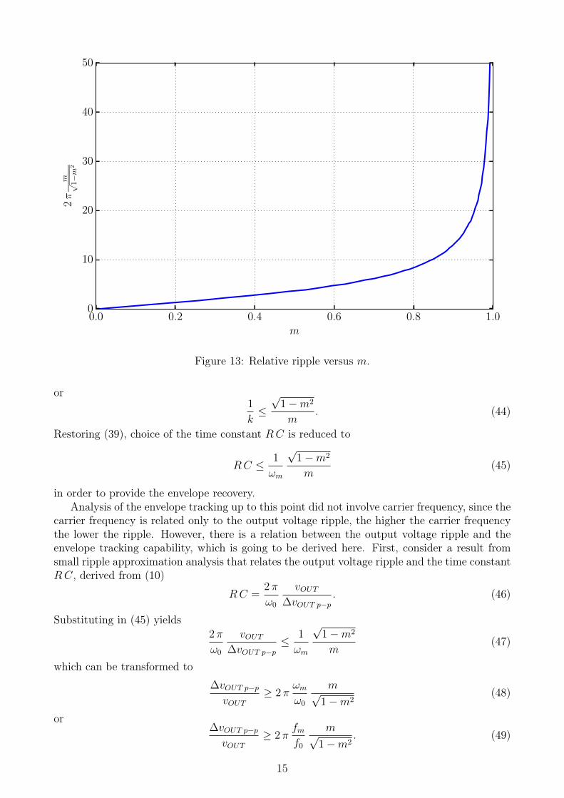
Relations (48) and (49) present fundamental relation between the normalized output voltageripple, ratio of the modulation frequency and the carrier frequency, and the modulation indexm, since the normalized output voltage ripple is greater or equal to the product of fm/f0 anda function of m, 2 πm/
√1−m2, depicted in Fig. 13. The relations indicate that the ripple
is lower for higher ratios of f0/fm, and that for high values of the modulation index, whenm approaches 1, the envelope tracking could be provided only at the expense of high outputvoltage ripple. The later is caused by low values of vOUT , insufficient to provide requireddecrease rate of the output voltage.
7 DistortionAC component of the envelope detector output voltage should reconstruct the message sent ap-plying standard amplitude modulation [4]. However, the output voltage ac component containssome distortion even if the requirements of Section 6 are met. The cause of distortion is incom-plete reduction of the output voltage ripple, the more present the lower f0/fm ratio is. As anexample, consider an experimental result for the output voltage AC component correspondingto the case of Fig. 11, presented in Fig. 14. In Fig. 14 reconstructed sinusoidal message signalcould be observed, as well as a superimposed sawtooth signal. To measure distortion of a signalx(t), total harmonic distortion defined as
THD ,
√XRMS
X1RMS
− 1 (50)
is used, where XRMS is the signal root-mean-square value, and X1RMS is the root-mean-squarevalue of its first harmonic. This definition is slightly computationally more convenient than theone of [9]. After five repeated waveform captures, by digital signal post-processing the meanvalue of THDexp = 6.13% is obtained, with the standard deviation estimated as σTHD exp = 0.05.
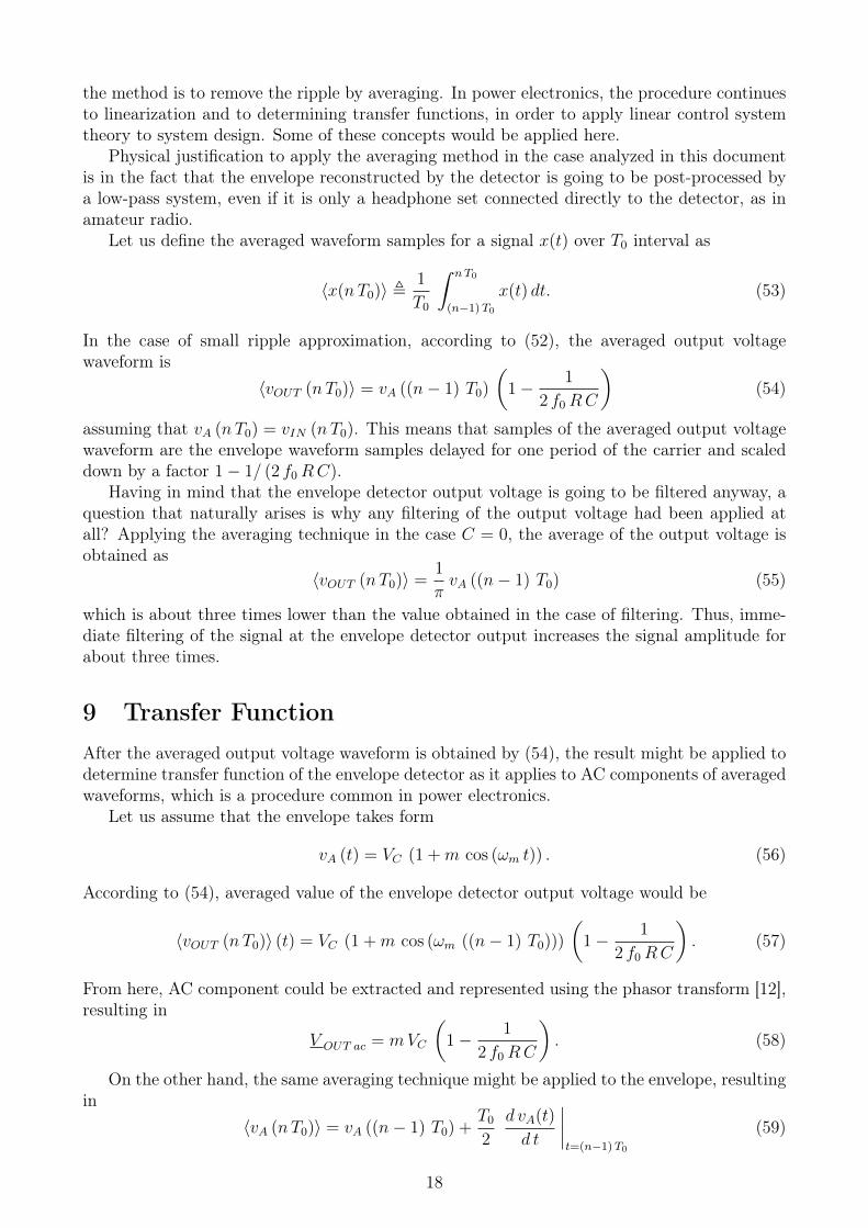
Extending the ideas of small ripple approximation, derived in Section 2, from the constantenvelope to the modulated envelope case, the approximate model could be designed such thatat t = nT0, n ∈ N
vOUT (nT0) = vIN(nT0) (51)
and that for nT0 ≤ t < (n+ 1)T0
vOUT (t) = vIN(nT0)−vIN(nT0)
RC(t− nT0) . (52)
This is nothing more than superimposing the sawtooth waveform with proper amplitude andfrequency to the envelope. Such waveform is computationally obtained, and presented in Fig.15 in the same scale and for the same parameter values as the waveform of Fig. 14. Thewaveforms agree to a great extent, and the main difference are pronounced discontinuities inthe waveform of Fig. 15, caused by neglected intervals of diode conduction. Total harmonicdistortion of the waveform of Fig. 15 is THDsim = 6.44% which is in pretty good agreementwith the experimental result.
To conclude, the ripple caused distortion could be reduced by increasing f0RC parameter.This can either be done by increasing f0, which is rarely a parameter available to play with, orby increasing the time constant RC, but this would decrease the envelope tracking capability.
8 Averaged ModelThe material presented in this section is inspired by the method of averaging, frequently usedin power electronics, as pioneered in [10], and described in a tutorial fashion in [11]. Essence of
16
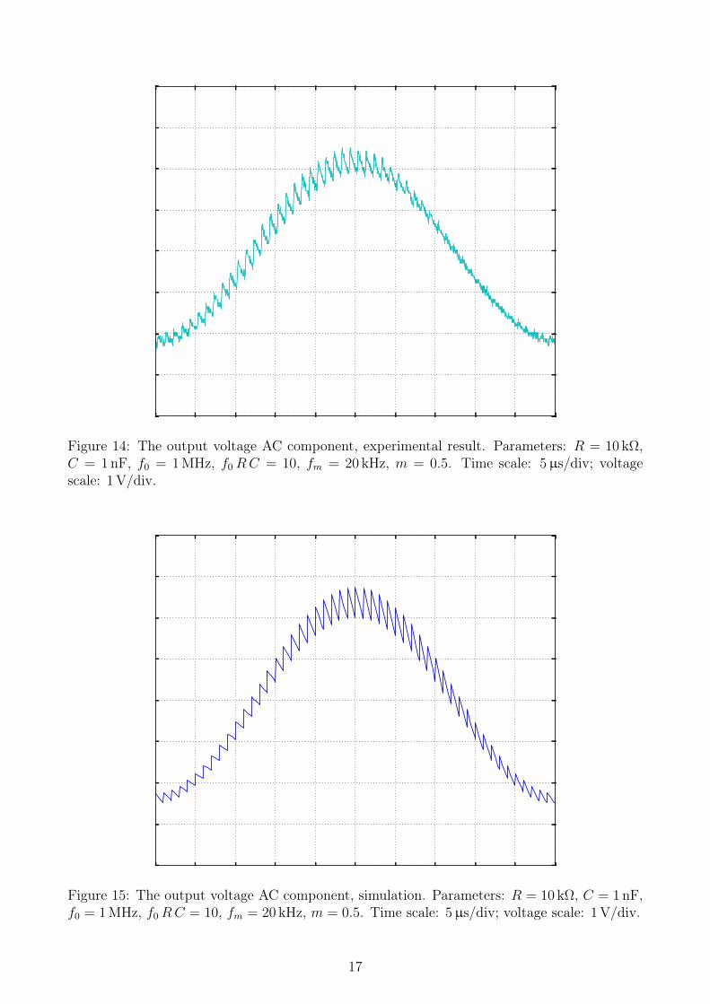
Figure 14: The output voltage AC component, experimental result. Parameters: R = 10 kΩ,C = 1 nF, f0 = 1MHz, f0RC = 10, fm = 20 kHz, m = 0.5. Time scale: 5µs/div; voltagescale: 1V/div.
Figure 15: The output voltage AC component, simulation. Parameters: R = 10 kΩ, C = 1 nF,f0 = 1MHz, f0RC = 10, fm = 20 kHz, m = 0.5. Time scale: 5µs/div; voltage scale: 1V/div.
17
the method is to remove the ripple by averaging. In power electronics, the procedure continuesto linearization and to determining transfer functions, in order to apply linear control systemtheory to system design. Some of these concepts would be applied here.
Physical justification to apply the averaging method in the case analyzed in this documentis in the fact that the envelope reconstructed by the detector is going to be post-processed bya low-pass system, even if it is only a headphone set connected directly to the detector, as inamateur radio.
Let us define the averaged waveform samples for a signal x(t) over T0 interval as
〈x(nT0)〉 ,1
T0
∫ nT0
(n−1)T0
x(t) dt. (53)
In the case of small ripple approximation, according to (52), the averaged output voltagewaveform is
〈vOUT (nT0)〉 = vA ((n− 1) T0)
(1− 1
2 f0RC
)(54)
assuming that vA (nT0) = vIN (nT0). This means that samples of the averaged output voltagewaveform are the envelope waveform samples delayed for one period of the carrier and scaleddown by a factor 1− 1/ (2 f0RC).
Having in mind that the envelope detector output voltage is going to be filtered anyway, aquestion that naturally arises is why any filtering of the output voltage had been applied atall? Applying the averaging technique in the case C = 0, the average of the output voltage isobtained as
〈vOUT (nT0)〉 =1
πvA ((n− 1) T0) (55)
which is about three times lower than the value obtained in the case of filtering. Thus, imme-diate filtering of the signal at the envelope detector output increases the signal amplitude forabout three times.
9 Transfer FunctionAfter the averaged output voltage waveform is obtained by (54), the result might be applied todetermine transfer function of the envelope detector as it applies to AC components of averagedwaveforms, which is a procedure common in power electronics.
Let us assume that the envelope takes form
vA (t) = VC (1 +m cos (ωm t)) . (56)
According to (54), averaged value of the envelope detector output voltage would be
〈vOUT (nT0)〉 (t) = VC (1 +m cos (ωm ((n− 1) T0)))
(1− 1
2 f0RC
). (57)
From here, AC component could be extracted and represented using the phasor transform [12],resulting in
V OUT ac = mVC
(1− 1
2 f0RC
). (58)
On the other hand, the same averaging technique might be applied to the envelope, resultingin
〈vA (nT0)〉 = vA ((n− 1) T0) +T02
d vA(t)
d t
∣∣∣∣t=(n−1)T0
(59)
18
which for the assumed envelope waveform reduces to
〈vA (nT0)〉 = VC
(1 +m
(cos (ωm (n− 1) T0)− π
fmf0
sin (ωm (n− 1) T0)
)). (60)
Extracting the AC component and performing the phasor transform [12],
V Aac = mVC
(1 + j π
fmf0
)= mVC
(1 + j π
ωmω0
)= mVC
(1 + j
ωm2 f0
)(61)
is obtained.Defining the transfer function of the envelope detector as
H (jωm) ,V OUT ac
V Aac
(62)
the transfer function is obtained as
H (jωm) =1− 1
2 f0RC
1 + j ωm2 f0
. (63)
Obtained transfer function consists of a scaling factor 1 − 12 f0RC
and a single real pole atωp = 2 f0, which should be a pretty high frequency to provide significant effects on the outputvoltage waveform.
10 ConclusionsIn this document, a thorough analysis of the peak and/or envelope detector circuit is performed.The analysis is first approached using a small ripple or small conduction angle approximation,and relevant equations are derived for this simplified model. To validate the results obtainedusing the approximate techniques, a semi-numerical analysis of the circuit model is performed,aiming exact analysis wherever possible and resorting to numerical techniques only where tran-scendental equations prohibited closed form solution. The results of the two approaches arecompared, and it is shown that for f0RC > 10 the small ripple approximation provides theresults with an error bellow 1%. Next, an application related topic of scaling is covered, in-dicating that the output voltage ripple, the output voltage average, and the output voltagewaveform are proportional to the input voltage amplitude for a given value of f0RC, while theconduction angles are not affected by the input voltage amplitude variations.
Main issue discussed in the paper is the ability of the circuit to accurately track the envelopevariations, which was the essence of the question posed by a curious student, which initiatedpublishing of this document. After the analysis, it is shown that ability of the envelope detectorto follow the envelope variations depends both on the circuit time constant RC, as well as theoutput voltage itself. Author of the document is not aware of such a conclusion clearly statedin available literature. In the case of sinusoidal modulating signal, this reduces to a conclusionthat ability of the circuit to track variations of the envelope depend both on the modulatingsignal frequency and the modulation index. This is the main result presented in the document,and the dependence is analyzed in detail, relating the envelope tracking ability to the outputvoltage ripple, indicating that there is a trade-off between the two.
Finally, the distortion caused by the output voltage ripple is analyzed, and the experimentalresults are compared to the low ripple approximation model, showing good agreement. Averagedmodel of the envelope detector is derived, showing that average of the output voltage duringthe carrier period follows the envelope with a delay of one carrier period and with some linear
19
downscaling caused by the output voltage ripple. A case when filtering of the output voltagehas not been applied is addressed, showing that in that case the averaged output voltage wouldbe about three times lower than in the case filtering is applied. Transfer function of the envelopedetector defined on the level of averaged waveforms of the output voltage and the envelope isderived, containing scaling factor 1 − 1
2 f0RCand a single real pole at ωp = 2 f0, which should
be a frequency high enough not to cause significant effects on the output voltage waveform.
AcknowledgementAppearance of this document is initiated by a student question asked by Miloš Nenadovićduring the class of Electrical Measurements, Lab Execise 7, on December 7, 2017.
References[1] Wikipedia, The Free Encyclopedia, “Envelope detector” [Online]. Available:
https://en.wikipedia.org/wiki/Envelope_detector [Accessed: February 15, 2018]
[2] Anant Agarwal, Jeffrey H. Lang, Foundations of Analog and Digital ElectronicCircuits, Morgan Kaufmann Publishers is an imprint of Elsevier. San Francisco, CA,2005.
[3] Wikipedia, The Free Encyclopedia, “Envelope (mathematics)” [Online]. Available:https://en.wikipedia.org/wiki/Envelope_(mathematics) [Accessed: February 15, 2018]
[4] Wikipedia, The Free Encyclopedia, “Amplitude modulation” [Online]. Available:https://en.wikipedia.org/wiki/Amplitude_modulation [Accessed: February 15, 2018]
[5] Wikipedia, The Free Encyclopedia, “Ripple (electrical)” [Online]. Available:https://en.wikipedia.org/wiki/Ripple_(electrical) [Accessed: February 15, 2018]
[6] Predrag Pejović, “oscusb.py, A Class for USB Communication, Supports TektronixTBS 1052B-EDU” [Online]. Available: http://tnt.etf.bg.ac.rs/ oe2em/oscusb.py[Accessed: February 15, 2018]
[7] Wikipedia, The Free Encyclopedia, “Transcendental equation” [Online]. Available:https://en.wikipedia.org/wiki/Transcendental_equation [Accessed: February 15, 2018]
[8] Wikipedia, The Free Encyclopedia, “Dimensional analysis” [Online]. Available:https://en.wikipedia.org/wiki/Dimensional_analysis [Accessed: February 15, 2018]
[9] D. Shmilovitz, “On the definition of total harmonic distortion and its effect onmeasurement interpretation,” IEEE Transactions on Power Delivery, vol. 20, no. 1,pp. 526–528, Jan. 2005. doi: 10.1109/TPWRD.2004.839744
[10] Slobodan Ćuk, Modelling, analysis, and design of switching converters. Dissertation(Ph.D.), California Institute of Technology, 1977. [Online]. Available:http://resolver.caltech.edu/CaltechETD:etd-03262008-110336 [Accessed: February 15,2018]
[11] Robert W. Erickson, Dragan Maksimović, Fundamentals of power electronics. SpringerScience & Business Media, 2007.
[12] Predrag Pejović, “Phasor Transform” [Online]. Available: http://tnt.etf.bg.ac.rs/~oe3ee/phasor-transform.pdf, [Accessed: February 25, 2018]
20

Appendixfrom pylab import *
f0RC = logspace(-3, 4, 701)w0RC = 2 * pi * f0RC
n = len(w0RC)beta = empty(n)gamma = empty(n)alpha = empty(n)
def f(gamma):f = k * exp(- gamma / w0RC) - cos(gamma)
for i in range(n):
beta[i] = arctan(1.0 / w0RC[i])k = cos(beta[i]) * exp(beta[i] / w0RC[i])
b0 = 7 * pi / 4cmax = 1e5c = 0eps = 1e-6while c < cmax:
b1 = 2 * pi - arccos(k * exp(-b0 / w0RC[i]))if abs(b1 - b0) < eps:
breakb0 = b1
gamma[i] = b1alpha[i] = 2 * pi - (gamma[i] - beta[i])
close(’all’)
rc(’text’, usetex = True)rc(’font’, family = ’serif’)rc(’font’, size = 16)rcParams[’text.latex.preamble’] = [r’\usepackageamsmath’]
figure(1, figsize = (10, 6))semilogx(f0RC, degrees(alpha), ’m’, label = r’$\alpha$’, linewidth = 2)semilogx(f0RC, degrees(beta), ’b’, label = r’$\beta$’, linewidth = 2)semilogx(f0RC, degrees(gamma), ’g’, label = r’$\gamma$’, linewidth = 2)ylim(-30, 390)yticks([0, 90, 180, 270, 360])xlabel(r’$f_0 \, R \, C$’)ylabel(r’$\beta, \, \gamma, \, \alpha \; [^\circ]$’)legend(loc = ’center right’)grid()savefig(’fbetagammaalpha.pdf’, bbox_inches = ’tight’)
data = array([w0RC / 2.0 / pi, beta, gamma, alpha]).transpose()np.save(’fbetagammaalphadata.npy’, data)
voutmean = (sin(beta) - sin(gamma) +cos(beta) * (w0RC * (1 - exp((beta - gamma) / w0RC)))) / (2 * pi)
voutmin = cos(gamma)
21

voutmax = ones(n)
figure(2, figsize = (10, 6))semilogx(f0RC, voutmax, ’b’, label = r’$v_OUT\,max / V_C$’, linewidth = 2)semilogx(f0RC, voutmin, ’g’, label = r’$v_OUT\,min / V_C$’, linewidth = 2)semilogx(f0RC, voutmean, ’r’, label = r’$v_OUT\,mean / V_C$’, linewidth = 2)ylim(-0.1, 1.1)xlabel(r’$f_0 \, R \, C$’)ylabel(r’$v_OUT\,max / V_C, v_OUT\,min / V_C, v_OUT\,mean / V_C$’)legend(loc = ’lower right’)grid()savefig(’fmaxminmean.pdf’, bbox_inches = ’tight’)
22