Embed Size (px)
Citation preview
ABSTRACT
Intelligent Energy Saving System can be used in
places like where lighting is very important. The
libraries will be well illuminated with many lamps. When
people are not present at a reading place the lighting
can be made OFF and when they are present, the lighting
made ON. All these can be done through by Dimming circuit
and PIR sensor.
If a person entering to the monitored area, the PIR
sensors activates and sense the person, gives to the
micro controller. The Infrared energy emitted from the
living body is focused by a Fresnel lens segment. Then
only the PIR sensor activates. After sensing the person
LDR checks the light intensity of the monitored area,
whether it is bright or dark. Depending on the LDR
output, the lamp may be ON / OFF by using Dimmer circuit.
By using this system we can adjust the speed of Fan
according to the room temperature measured by Thermostat,
which is connected to the micro controller.
To display the room temperature of PIR mode
operation we are using the LCD display.
- 1 -
INDEX PAGE NO
1. INTRODUCTION 9
1.1 Objective of the Project
10
1.2 Block Diagram
11
1.3 Pinciple Of Operation
12
1.4 System Features
13
1.5 Equipments 15
2. DESCRIPTION OF THE PROJECT 6
2.1 Block Diagram Description
2.2 Schematic Diagrams
2.3 Schematic Explanation
3. HARDWARE DESCRIPTION
10
3.1 Microcontroller (PIC16F72)
3.2 Passive Infrared Sensor
3.3 Light Dependent Resistor
3.4 Thermostat (DS1621)
3.5 Zero Crossing Detector
3.6 Power Supply
3.7 Liquid Crystal Display
3.8 Dimmer
- 2 -
3.9 Optocoupler
3.10 Loads
4. SOWFTWARE DESCRIPTION 64
4.1 Flow Chart
4.2 Source Code
5. RESULT
6. CONCLUSION AND FUTURE DIRECTIONS
BIBLIOGRAPHY
LIST OF FIGURES
1. Block Diagram
2. Schematic Diagram
3. Architecture of PIC16F72
4. Pin Diagram of PIC 16F72
5. Operation of PIR Diagram
6. Operation of LDR Diagram
7. LDR Circuit Diagram
8. Pin Diagram of DS1621
9. Functional Block Diagram of DS1621
- 3 -

10. ZCD Circuit Diagram
11. ZCD Output waveform
12. Power Circuit Diagram
13. Pin Diagram of LCD
14. Dimmer Circuit Diagram
15. Pin Diagram of OptoCoupler
- 4 -

CHAPTER 1 INTRODUCTION
1. INTRODUCTION
- 5 -
Intelligent Energy Saving System, the aim of
the project is to save the energy. In this project we are
using various sensors, controlling and display.
However, in this project work the basic signal
processing of various parameters which are temperature,
LDR, Smoke sensor. For measuring various parameters
values, various sensors are used and the output of these
sensors are converted to control the parameters. The
control circuit is designed using micro-controller. The
outputs of all the three parameters are fed to micro-
controller. The output of the micro-controller is used to
drive the LCD display, so that the value of each
parameter can be displayed. In addition to the LCD
display micro-controller outputs are also used to driver
a relay independently. This relay energizes and de-
energizes automatically according to the condition of the
parameter.
1.1 OBJECTIVE OF THE PROJECT: -
The aim of the project is to save the energy or
power, used in places like libraries where lighting is
very important for the people who come to read books. So,
the libraries will be well illuminated with many lamps.
At the same time when people are not present at a
particular reading place the lighting can be made off by
- 6 -
using Dimmer and when people come to that area, according
to the LDR lighting can be made sufficiently brighter.
By using this system, we can also adjust
the speed of the Fan according to the room temperature
using Thermostat and Dimmer.
1.2 PRINCIPLE OF OPERATION
Consider a particular table in the library, which is
connected with our experimental kit .When a person
entering into that place the PIR sensor absorbs the black
body radiation emitted by that person and activates it.
The LCD display will displays the “PIR ON”.
After some time delay the light will glows for some
time by using the Dimmer circuit and with the help of LDR
sensor it checks the room lightening , and it takes the
condition when the light is sufficient the lamp will be
in OFF state and when light is insufficient the lamp will
be in ON state.
With the help of Thermostat sensor the room
temperature is measured and the speed of the Fan varies
- 7 -
according to the temperature of Thermostat. The LCD
display will displays the room “temperature in degree
centigrade”.
When a person is leaving that place, the PIR sensor
will activate again and firstly the Fan will be OFF and
after some time delay the lamp also will be OFF. Now the
LCD display is in stand by mode state. And the main
supply power will be switched OFF.
1.3 BLOCK DIAGRAM:
- 8 -
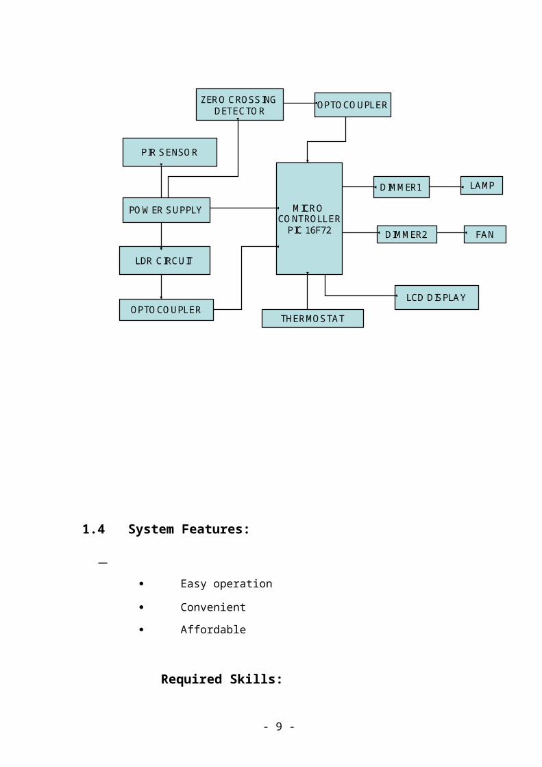
PIR SENSO R
ZERO CROSSING DETECTO R
LDR CIRCUIT
OPTO CO UPLER
OPTO CO UPLER
DIM M ER1
DIM M ER2
LAMP
FAN
M ICRO CO NTROLLERPIC 16F72
LCD DISPLAY
THERMOSTAT
PO W ER SUPPLY
1.4 System Features:
Easy operation
Convenient
Affordable
Required Skills:
- 9 -

Understanding of Micro controller
Embedded C Programming
Understanding Interfacing Techniques
Knowledge on Sensors
Design and Fabrication of PCB
Project phase: -
Schematic design and drawing of PCB
Design and Interfacing Circuits for Micro
controller
Preparation of PCB
Assembling and Testing of Interfacing
Circuits
Code for the Application
Debugging and Testing
Project Report
1.4 EQUIPMENTS: -
- 10 -
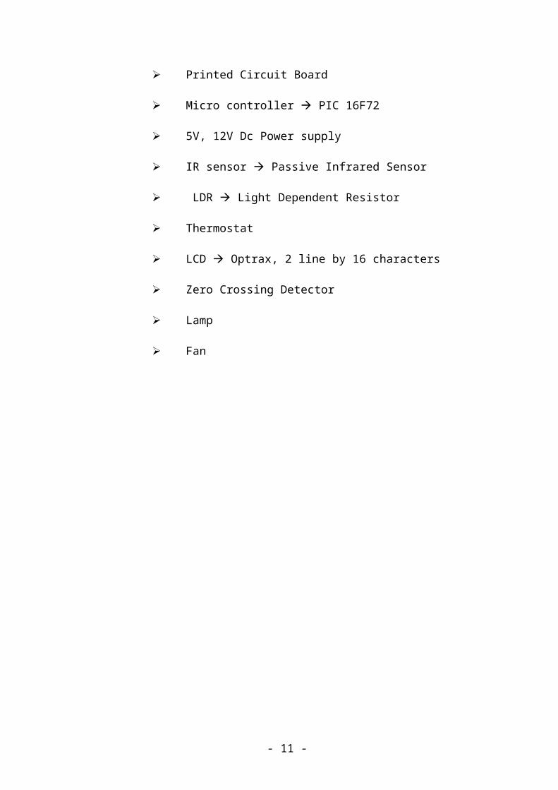
Printed Circuit Board
Micro controller à PIC 16F72
5V, 12V Dc Power supply
IR sensor à Passive Infrared Sensor
LDR à Light Dependent Resistor
Thermostat
LCD à Optrax, 2 line by 16 characters
Zero Crossing Detector
Lamp
Fan
- 11 -

CHAPTER 2.
DESCRIPTION OF THE PROJECT
- 12 -
2. DESCRIPTION OF THE PROJECT: -2.1 BLOCK DIAGRAM EXPLANATION: -
PIR SENSOR: - A PIR detector is a motion detector that
senses the heat emitted by a living body. These are often
fitted to security lights so that they will switch on
automatically if approached. They are very effective in
enhancing home security systems.
The sensor is passive because,
instead of emitting a beam of light or microwave energy
that must be interrupted by a passing person in order to
- 13 -
“sense” that person, the PIR is simply sensitive to the
infrared energy emitted by every living thing. When an
intruder walks into the detector’s field of vision, the
detector “sees” a sharp increase in infrared energy.
LDR: - LDR’s or Light Dependent Resistors are
very useful especially in light/dark sensor circuits.
These help in automatically switching ON /OFF the street
lights and etc., normally the resistance of an LDR is
very high, sometimes as very high as 1000000 ohms, but
when they are illuminated with light, resistance drop
dramatically. Electronic opto sensors are the devices
that alter their electrical characteristics, in the
presence of visible or invisible light. The best-known
devices of these types are the light dependent resistor
(LDR), the photo diode and the phototransistors.
ZCD: - A zero crossing detectorliterally detects the transition of a signal waveform
from positive and negative, ideally providing a narrow
pulse that coincides exactly with the zero voltage
condition.
THERMOSTAT: - In this project we are making use DS
1621 thermostat, it’s a non-contact digital type
temperature transducer suitable for measuring room
- 14 -
temperature. The word ‘thermistor’ is an acronym for
thermal resistor, i.e., a temperature sensitive resistor.
It is used to detect very small changes in temperature.
The variation in temperature is reflected through
appreciable variation of the resistance of the device.
LCD DISPLAY: - A liquid crystal is a material (normally
organic for LCD’s) that will flow like a liquid but whose
molecular structure has some properties normally
associated with solids. The Liquid Crystal Display (LCD)
is a low power device. The power requirement is typically
in the order of microwatts for the LCD. However, an LCD
requires an external or internal light source. We are
making use of LCD in our project to display the PIR mode
and room temperature.
OPTOCOUPLER: - Optocoupler is a device that uses a short
optical transmission path to transfer a signal between
elements of a circuit, typically a transmitter and a
receiver, while keeping them electrically isolated. A
common implementation involves a LED and a
phototransistor, separated so that light may travel
across a barrier but electrical current may not.
DIMMER: -
- 15 -
Dimmers are devices used to vary the brightness
of a light. By decreasing or increasing the RMS voltage
and hence the mean power to the lamp it is possible to
vary the intensity of the light output. Although
variable-voltage devices are used for various purposes,
the term dimmer is generally reserved for those intended
to control lighting.
2.2 SCHEMATIC DIAGRAM: -
- 16 -
- 17 -
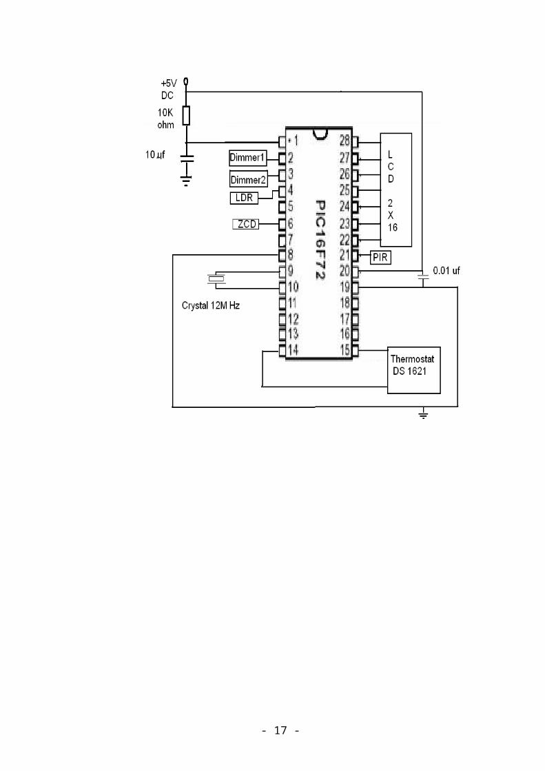
2.3 SCHEMATIC EXPLANATION: -
PORT A: -
Port A can acts as a both input as well as
output port. It is having 6 pins (A0-A5). In these A0 is
connected to Dimmer1, A1 is connected to Dimmer2 and A4
is connected to ZCD output.
PORT B: -
Port B can acts as a both input as well as
output port. It is having 8 pins (B0-B7). In these B1
connected to register selection pin(R/S), B2 is connected
to read/write(R/W) and B3 pin is connected to enable pin.
PORT C: -
Port C can acts as a both input as well as
output port. It is having 8 pins (C0-C7).
In these RC3 and RC4 connected to the
thermostat pins.
12M Hz Crystal Oscillator is connected in
between 9th and 10th pins of micro
controller.
- 18 -

Reset pin is connected to the pin number1
i.e., MCLR/VPP.
8th and 19th pins are connected to ground
(Vss).
CHAPTER 3.- 19 -
HARDWARE DESCRIPTION
3. HARDWARE DESCRIPTION: -
3.1 MICRO CONTROLLER: -
INTRODUCTION: -
Microcontrollers these days are silent workers
in many apparatus, ranging from the washing machine to
the video recorder. Nearly all of these controllers are
mask programmed and therefore are of very little use for
applications that require the programs to be changed
during the course of execution.
- 20 -
Even if the programs could be altered, the
information necessary to do so an instruction set, an
assembler language and description for the basic hardware
is either very difficult to obtain or are in adequate
when it came to the issue of accessibility.
A marked exception to the above category is the
PICI6F72 micro controller belonging to the PIC family.
This microcontroller has features that seem to make it
more accessible than any other single chip
microcontroller with a reasonable price tag.
The PICI6F72, an 8-bit single chip
microcontroller has got a powerful CPU optimized for
control applications. The PICI6F72 is an 8 – bit single
chip microcontroller. The 16f7877A provides a
significantly more powerful architecture, a more powerful
instruction set and a full serial port.
The PICI6F72 is a complete micro controller.
There are 40 pins needed by the five-bidirectional ports.
Pins provide power, allow you to connect a crystal clock
and provide a few timing and control signals.
The architecture includes the ALU, W register,
the stack; a block of registers. All these devices are
connected to via internal 8-bit data bus.
- 21 -
Each I/O port is also connected to the 8-bit
internal data bus through a series of registers. These
registers hold data during I/O transfers and control the
I/O ports. The architectural block diagram also shows
the PICI6F72 ROM and RAM
Comparison of microprocessor and microcontroller:
The difference between Microprocessor and Micro
controller is Microprocessor can only process with the
data, Micro controller can control external device. That
is if you want switch “ON” or “OFF” a device, you need
peripheral ICs to do this work with Micro controller you
can directly control the device.
Like Microprocessor, Micro controller is
available with different features. It is available with
inbuilt memory, I/O lines, timer and ADC. The micro
controller, which we are going to use.
Advantages of Microcontrollers:
1. If a system is developed with a microprocessor, the
designer has to go for external memory such as RAM, ROM
or EPROM and peripherals and hence the size of the PCB
will be large enough to hold all the required
peripherals.
2. But the microcontroller has got all these peripheral
facilities on a single chip so development of a similar
system with a microcontroller reduces PCB size and cost
of the design.
- 22 -
3. One of the major difference between a
microcontroller and a microprocessor is that a controller
often deals with bits, not bytes as in the real world
application, for example switch contacts can only be open
or close, indicators should be lit or dark and motors can
be either turned on or off and so forth.
4. The Microcontroller has two 8-bit timers/ counters
built within it, which makes it more suitable to this
application since we need to produce some accurate timer
delays. It is even more advantageous that the timers
also act as interrupt.
ABOUT PICI6F72:
The PICI6F72 is a low-power, high-performance
CMOS 8-bit microcomputer with 2K bytes Flash programmable
and erasable read only memory (PEROM). PICI 6F72 is a
powerful microcomputer, which provides a highly flexible
and cost-effective solution to many embedded control
application.
FEATURES OF PIC 16F72: -
High performance RISC CPU:
Only 35 single word instructions to learn All single cycle instructions except for program branches, which are two-cycle.
- 23 -
Operating speed: DC-20 MHZ clock input DC-200 ns instruction cycle Up to 2k x 14 words of program Memory, Up to 128 x 8 bytes of Data Memory (RAM)
Pinout compatible to PIC 16C72/72A and PIC 16F872. Interrupt capability. Eight- level deep hard ware stack. Direct, Indirect and Relative Addressing modes.
Peripheral Features: High Sink/Source Current: 25 mA
Timer0: 8-bit timer/counter with 8-bit prescaler
Timer1: 16-bit timer/counter with prescaler, can be
incremented during
Via External crystal/clock.
Timer2: 8-bit timer/counter with 8-bit period
register, prescaler and
postscaler
Capture, Compare, PWM (CCP) module
- Capture is 16-bit, max. resolution is
12.5 ns
Compare is 16-bit, max. resolution is 200 ns
PWM max. resolution is 10-bit
8-bit, 5-channel analog-to-digital converter
Synchronous Serial Port (SSP) with SPI™
(Master/Slave) and I2C™ (Slave)
- 24 -

Brown-out detection circuitry for Brown-out Reset
(BOR)
CMOS Technology: Low power, high speed CMOS FLASH technology
Fully static design
Wide operating voltage range: 2.0V to 5.5V
Industrial temperature range
Low power consumption:< 0.6 mA typical @ 3V, 4 MHz
20 µA typical @ 3V, 32 kHz
< 1 µA typical standby current
Special Microcontroller Features:
1,000 erase/write cycle FLASH program memory typical
Power- on Reset (POR)
Power-up Timer (PWRT)
Oscillator Start –up Timer (OST)
Watchdog Timer (WDT) with its own on-chip RC
oscillator for reliable operation.
RC oscillator for reliable operation
Programmable code protection
Power saving SLEEP mode
Selectable oscillator options
In-Circuit Serial Programming™ (ICSP™) via 2
pins
Processor read access to program memory
- 25 -
ARCHITECTURE OF PIC 16F72 MICRO CONTROLLER: -
The PIC16F72 belongs to the Mid-Range family of
the PIC micro devices. The program memory contains 2K
words, which translate to 2048 instructions, since each
14-bit program memory word is the same width as each
device instruction. The data memory (RAM) contains 128
bytes. There are 22 I/O pins that are user configurable
on a pin-to-pin basis. Some pins are multiplexed with
other device functions.
These functions include: -
External interrupt
Change on PORTB interrupts
Timer0 clock input
Timer1 clock/oscillator
Capture/Compare/PWM
A/D converter
SPI/I2C
Low Voltage Programming
- 26 -
Incircuit Debuuger
ARCHITECTURE DIAGRAM OF PIC 16F72:
- 27 -
PIN DIGRAM OF PIC 16F72:
- 28 -
- 29 -
PIN DESCRIPTION:
MCLR/VPP:
Master Clear (Reset) input or programming voltage
input. This pin is an active low RESET to the device.
RA0 - RA5:
These are the bi-directional Input / output PORTA
pins.
RA1, RA2, are the analog inputs 1, analog input2.
RA3 can also be analog input3 or analog reference
voltage.
RA4 can also be the clock input to the Timer0 module.
Output is open drain type.
RA5 can also be analog input4 or the slave select
for the synchronous serial port.
VSS:
Ground reference for logic and I/O pins.
OSC1/CLK1:
Oscillator crystal input / External clock source
input.
OSC2/CLKO:
Oscillator crystal output. Connects to crystal or
resonator in Crystal Oscillator mode. In RC mode, the OSC2
pin outputs CLKO, which has 1/4 the frequency of OSC1, and
denotes the instruction cycle rate.
RC0 – RC7:
- 30 -
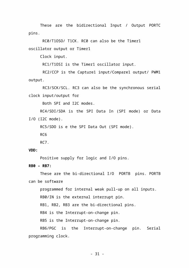
These are the bidirectional Input / Output PORTC
pins.
RC0/T1OSO/ T1CK. RC0 can also be the Timer1
oscillator output or Timer1
Clock input.
RC1/T1OSI is the Timer1 oscillator input.
RC2/CCP is the Capture1 input/Compare1 output/ PWM1
output.
RC3/SCK/SCL. RC3 can also be the synchronous serial
clock input/output for
Both SPI and I2C modes.
RC4/SDI/SDA is the SPI Data In (SPI mode) or Data
I/O (I2C mode).
RC5/SDO is e the SPI Data Out (SPI mode).
RC6
RC7.
VDD:
Positive supply for logic and I/O pins.
RB0 – RB7:
These are the bi-directional I/O PORTB pins. PORTB
can be software
programmed for internal weak pull-up on all inputs.
RB0/IN is the external interrupt pin.
RB1, RB2, RB3 are the bi-directional pins.
RB4 is the Interrupt-on-change pin.
RB5 is the Interrupt-on-change pin.
RB6/PGC is the Interrupt-on-change pin. Serial
programming clock.
- 31 -
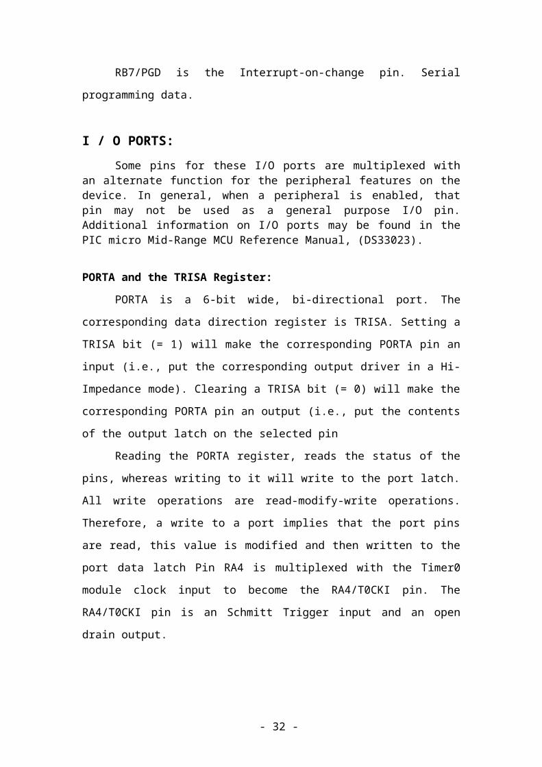
RB7/PGD is the Interrupt-on-change pin. Serial
programming data.
I / O PORTS:Some pins for these I/O ports are multiplexed with
an alternate function for the peripheral features on thedevice. In general, when a peripheral is enabled, thatpin may not be used as a general purpose I/O pin.Additional information on I/O ports may be found in thePIC micro Mid-Range MCU Reference Manual, (DS33023).
PORTA and the TRISA Register:
PORTA is a 6-bit wide, bi-directional port. The
corresponding data direction register is TRISA. Setting a
TRISA bit (= 1) will make the corresponding PORTA pin an
input (i.e., put the corresponding output driver in a Hi-
Impedance mode). Clearing a TRISA bit (= 0) will make the
corresponding PORTA pin an output (i.e., put the contents
of the output latch on the selected pin
Reading the PORTA register, reads the status of the
pins, whereas writing to it will write to the port latch.
All write operations are read-modify-write operations.
Therefore, a write to a port implies that the port pins
are read, this value is modified and then written to the
port data latch Pin RA4 is multiplexed with the Timer0
module clock input to become the RA4/T0CKI pin. The
RA4/T0CKI pin is an Schmitt Trigger input and an open
drain output.
- 32 -
All other RA port pins have TTL input levels and
full CMOS output drivers. Other PORTA pins are
multiplexed with analog inputs and analog VREF input. The
operation of each pin is selected by clearing/setting the
control bits in the ADCON1 register (A/D Control
Register1).
Other PORTA pins are multiplexed with analog inputs
and analog VREF input. The operation of each pin is
selected by clearing/setting the control bits in the
ADCON1 register (A/D Control Register1). Other PORTA pins
are multiplexed with analog inputs and analog VREF input.
The operation of each pin is selected by clearing/setting
the control bits in the ADCON1 register (A/D Control
Register1).
The TRISA register controls the direction of the RA
pins, even when they are being used as analog inputs. The
user must ensure the bits in the TRISA register are
maintained set when using them as analog inputs.
PORTB and the TRISB Register:PORTB is an 8-bit wide, bi-directional port. The
corresponding data direction register is TRISB. Setting a
TRISB bit (= 1) will make the corresponding PORTB pin an
input (i.e., put the corresponding output driver in a Hi-
Impedance mode). Clearing a TRISB bit (= 0) will make the
- 33 -
corresponding PORTB pin an output (i.e., put the contents
of the output latch on the selected pin).
Each of the PORTB pins has a weak internal pull-up.
A single control bit can turn on all the pull-ups. This
is performed by clearing bit RBPU (OPTION<7>). The weak
pull-up is automatically turned off when the port pin is
configured as an output. The pull-ups are disabled on a
Power-on Reset.
Four of PORTB’s pins, RB7:RB4, have an interrupt-on-
change feature. Only pins configured as inputs can cause
this interrupt to occur (i.e., any RB7:RB4 pin
configured as an output is excluded from the interrupt on
change comparison). The input pins (of RB7:RB4) are
compared with the old value latched on the last read of
PORTB. The “mismatch” outputs of RB7:RB4 are OR’d
together to generate the RB Port Change Interrupt with
flag bit RBIF (INTCON<0>).
PORTC and the TRISC Register:
PORTC is an 8-bit wide, bi-directional port. The
corresponding data direction register is TRISC. Setting a
TRISC bit (= 1) will make the corresponding PORTC pin an
input (i.e., put the corresponding output driver in a Hi-
Impedance mode). Clearing a TRISC bit (= 0) will make the
corresponding PORTC pin an output (i.e., put the contents
of the output latch on the selected pin). PORTC is
- 34 -
multiplexed with several peripheral functions. PORTC pins
have Schmitt Trigger input buffers.
When enabling peripheral functions, care should be
taken in defining TRIS bits for each PORTC pin. Some
peripherals override the TRIS bit to make a pin an out-
put, while other peripherals override the TRIS bit to
make a pin an input. Since the TRIS bit override is in
effect while the peripheral is enabled, read-modify-write
instructions (BSF, BCF, XORWF) with TRISC as destination
should be avoided. The user should refer to the
corresponding peripheral section for the correct
TRIS bit settings.
Capture Mode:In Capture mode, CCPR1H: CCPR1L captures the 16-bit
value of the TMR1 register when an event occurs on pinRC2/CCP1. An event is defined as:
• Every falling edge
• Every rising edge
• Every 4th rising edge
• Every 16th rising edge
An event is selected by control bits CCP1M3:CCP1M0
(CCP1CON<3:0>). When a capture is made, the interrupt
request flag bit CCP1IF (PIR1<2>) is set. It must be
cleared in software. If another capture occurs before the
value in register CCPR1 is read, the old captured value
is overwritten by the new captured value.
Compare Mode:
- 35 -
In Compare mode, the 16-bit CCPR1 register value is
constantly compared against the TMR1 register pair value.
When a match occurs, the RC2/CCP1 pin is:
• Driven High
• Driven Low
• Remains Unchanged
The action on the pin is based on the value of
control bits CCP1M3: CCP1M0 (CCP1CON<3:0>). At the same
time, interrupt flag bit CCP1IF is set. The output may
become inverted when the mode of the module is
changed from Compare/Clear on Match (CCPxM<3:0> =
‘1001’) to Compare/Set on Match (CCPxM<3:0> = ‘1000’).
This may occur as a result of any operation that
selectively clears bit CCPxM0, such as a BCF instruction.
When this condition occurs, the output becomes inverted
when the instruction is executed. It will remain inverted
for all following Compare operations, until the module is
reset.
ANALOG-TO-DIGITAL CONVERTER (A/D) MODULE:The analog-to-digital (A/D) converter module has
five inputs for the PIC16F72. The A/D allows conversion
of an analog input signal to a corresponding 8-bit
digital number. The output of the sample and hold is
the input into the converter, which generates the result
via successive approximation. The analog reference
voltage is software selectable to either the device’s
positive supply voltage (VDD) or the voltage level on the
RA3/AN3/VREF pin.
- 36 -
The A/D converter has a unique feature of being able
to operate while the device is in SLEEP mode. To operate
in SLEEP, the A/D conversion clock must be derived from
the A/D’s internal RC oscillator.
The A/D module has three registers:
• A/D Result Register ADRES
• A/D Control Register 0 ADCON0
• A/D Control Register 1 ADCON1
A device RESET forces all registers to their RESET
state. This forces the A/D module to be turned off and
any conversion is aborted. The ADCON0 register, shown in
Register 10-1, controls the operation of the A/D
module. The ADCON1 register, shown in Register 10-2,
configures the functions of the port pins. The port pins
can be configured as analog inputs (RA3 can also be a
voltage reference) or a digital I/O.
OSCILLATOR CONFIGURATIONS:
The PIC16F72 can be operated in four different
Oscillator modes. The user can program two configuration
bits (FOSC1 and FOSC0) to select one of these four Modes:
• LP Low Power Crystal
• XT Crystal/Resonator
• HS High Speed Crystal/Resonator
• RC Resistor/Capacitor
RESET:
- 37 -
The PIC16F72 differentiates between various kinds of
RESET:
• Power-on Reset (POR)
• MCLR Reset during normal operation
• MCLR Reset during SLEEP
• WDT Reset (during normal operation)
• WDT Wake-up (during SLEEP)
• Brown-out Reset (BOR)
Some registers are not affected in any RESET
condition. Their status is unknown on POR and unchanged
in any other RESET. Most other registers are reset to a
“RESET state” on Power-on Reset (POR), on the MCLR and
WDT Reset, on MCLR Reset during SLEEP, and Brown-out
Reset (BOR). They are not affected by a WDT Wake-up,
which is viewed as the resumption of normal operation.
The TO and PD bits are set or cleared differently in
different RESET situations, as indicated in Table 11-4.
These bits are used in software to determine the nature
of the RESET.
Power-on Reset (POR):A Power-on Reset pulse is generated on-chip when VDD
rise is detected (in the range of 1.2V - 1.7V). To take
advantage of the POR, tie the MCLR pin to VDD, A maximum
rise time for VDD is specified. When the device starts
normal operation (exits the RESET condition), device-
operating parameters (volt-age, frequency, temperature,)
must be met to ensure operation. If these conditions are
- 38 -
not met, the device must be held in RESET until the
operating conditions are met.
Power-up Timer (PWRT):The Power-up Timer provides a fixed 72 ms nominal
time-out on power-up only
From the POR. The Power-up Timer operates on an internalRC oscillator. The chip is kept in RESET as long as thePWRT is active. The PWRT’s time delay allows VDD to riseto an acceptable level.
A configuration bit is provided to enable/ disable
the PWRT. The power-up time delay will vary from chip to
chip due to VDD, temperature and process variation.
Oscillator Start-up Timer (OST):
The Oscillator Start-up Timer (OST) provides 1024
oscillator cycles (from OSC1 input) delay after the PWRT
delay is over (if enabled). This helps to ensure that the
crystal oscillator or resonator has started and
stabilized. The OST time-out is invoked only for XT, LP
and HS modes and only on Power-on Reset or wake-up from
SLEEP.
Brown-out Reset (BOR):The configuration bit, BOREN, can enable or disable
the Brown-out Reset circuit. If VDD falls below VBOR
(parameter D005, about 4V) for longer than TBOR
(parameter #35, about 100 µs), the brown-out situation
will reset the device. If VDD falls below VBOR for less
- 39 -
than TBOR, a RESET may not occur. Once the brown-out
occurs, the device will remain in Brown-out Reset until
VDD rises above VBOR. The Power-up Timer then keeps the
device in RESET for TPWRT (parameter #33, about 72 ms).
If VDD should fall below VBOR during TPWRT, the Brown-out
Reset process will restart when VDD rises above VBOR,
with the Power-up Timer Reset. The Power-up Timer is
always enabled when the Brown-out Reset circuit is
enabled, regardless of the state of the PWRT
configuration bit.
Power Control/Status Register (PCON):The Power Control/Status Register, PCON, has two
bits to indicate the type of RESET that last occurred.
Bit0 is Brown-out Reset Status bit, BOR. Bit BOR is
unknown on a Power-on Reset. It must then be set by the
user and checked on subsequent RESETS to see if bit BOR
cleared, indicating a Brown-out Reset occurred. When the
Brown-out Reset is disabled, the state of the BOR bit is
unpredictable.
Bit1 is POR (Power-on Reset Status bit). It is
cleared on a Power-on Reset and unaffected otherwise. The
user must set this bit following a Power-on Reset.
- 40 -
Watchdog Timer (WDT):The Watchdog Timer is a free running, on-chip RC
oscillator that does not require any external components.
This RC oscillator is separate from the RC oscillator of
the SC1/CLKI pin. That means that the WDT will run, even
if the clock on the OSC1/CLKI and OSC2/ CLKO pins of the
device has been stopped, for example, by execution of a
SLEEP instruction.
During normal operation, a WDT time-out generates a
device RESET (Watchdog Timer Reset). If the device is in
SLEEP mode, a WDT time-out causes the device to wake-up
and continue with normal operation (Watchdog Timer Wake-
up). The TO bit in the STATUS register will be cleared
upon a Watchdog Timer time-out.
Program Verification/Code Protection:If the code protection bit(s) have not been
programmed, the on-chip program memory can be read out
for verification purposes.
ID Locations:
Four memory locations (2000h - 2003h) are designated
as ID locations, where the user can store checksum or
other code identification numbers. These locations are
not accessible during normal execution, but are
readable and writable during program/verify. It is
recommended that only the four Least Significant bits of
the ID location are used.
- 41 -
In-Circuit Serial Programming:PIC16F72 microcontrollers can be serially programmed
while in the end application circuit. This is simply done
with two lines for clock and data and three other lines
for power, ground, and the programming voltage. This
allows customers to manufacture boards with unprogrammed
devices, and then program the micro controller just
before shipping the product. This also allows the most
recent firmware or a custom firmware to be programmed.
INSTRUCTION SET SUMMARY:Each PIC16F72 instruction is a 14-bit word divided
into an OPCODE that specifies the instruction type and
one or more operands that further specify the operation
of the instruction. The PIC16F72 instruction set summary
in Table 12-2 lists byte-oriented, bit-oriented, and
literal and control operations. Table 12-1 shows the
opcode field descriptions. For byte-oriented
instructions, ‘f’ represents a file register
designator and ‘d’ represents a destination designator.
The file register designator specifies which file
register is to be used by the instruction.
The destination designator specifies where the
result of the operation is to be placed. If ‘d’ is
zero, the result is placed in the W register. If ‘d’ is
- 42 -
one, the result is placed in the file register specified
in the instruction.
For bit-oriented instructions, ‘b’ represents a bit
field designator which selects the number of the bit
affected by the operation, while ‘f’ represents the
number of the file in which the bit is located. For
literal and control operations, ‘k’ represents an eight
or eleven-bit constant or literal value.
The instruction set is highly orthogonal and is
grouped into three basic categories:
• Byte-oriented operations
• Bit-oriented operations
• Literal and control operations
All instructions are executed within one single
instruction cycle, unless a conditional test is true or
the program counter is changed as a result of an
instruction. In this case, the execution takes two
instruction cycles, with the second cycle executed as a
NOP. One instruction cycle consists of four oscillator
periods. Thus, for an oscillator frequency of 4 MHz, the
normal instruction execution time is 1 µs. If a
conditional test is true, or the program counter is
changed as a result of an instruction, the instruction
execution time is 2 µs.
- 43 -
I2C PROTOCOL
HISTORY OF THE I2C BUS
The I2C bus was developed in the early 1980's by
Philips Semiconductors. Its original purpose was to
provide an easy way to connect a CPU to peripheral chips
in a TV-set. I²C is a multi-master serial computer bus used
to attach low-speed peripherals to a motherboard,
embedded system, or cell phone. The name stands for
Inter-Integrated Circuit and is pronounced I-squared-C and
also, I-two-C.
THE I2C BUS PROTOCOL
The I2C bus physically consists of 2 active wires
and a ground connection. The active wires, called SDA and
SCL, are both bi-directional. SDA is the Serial data
line, and SCL is the Serial clock line.
Every device hooked up to the bus has its own unique
address, no matter whether it is an MCU, LCD driver,
memory, or ASIC. Each of these chips can act as a
receiver and/or transmitter, depending on the
functionality. Obviously, an LCD driver is only a
receiver, while a memory or I/O chip can be both
transmitter and receiver.
- 44 -
The I2C bus is a multi-master bus. This means that
more than one IC capable of initiating a data transfer
can be connected to it. The I2C protocol specification
states that the IC that initiates a data transfer on the
bus is considered the Bus Master. Consequently, at that
time, all the other ICs are regarded to be Bus Slaves.
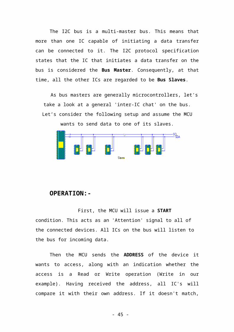
As bus masters are generally microcontrollers, let's
take a look at a general 'inter-IC chat' on the bus.
Let’s consider the following setup and assume the MCU
wants to send data to one of its slaves.
OPERATION:-
First, the MCU will issue a START
condition. This acts as an 'Attention' signal to all of
the connected devices. All ICs on the bus will listen to
the bus for incoming data.
Then the MCU sends the ADDRESS of the device it
wants to access, along with an indication whether the
access is a Read or Write operation (Write in our
example). Having received the address, all IC's will
compare it with their own address. If it doesn't match,
- 45 -
they simply wait until the bus is released by the stop
condition (see below). If the address matches, however,
the chip will produce a response called the
ACKNOWLEDGEMENT signal.
Once the MCU receives the acknowledge, it can start
transmitting or receiving DATA. In our case, the MCU will
transmit data. When all is done, the MCU will issue the
STOP condition. This is a signal that the bus has been
released and that the connected ICs may expect another
transmission to start any moment.
We have had several states on the bus in our
example: START, ADDRSS, ACKNOWLEDGEMENT, DATA and STOP.
These are all unique conditions on the bus. Before we
take a closer look at these bus conditions we need to
understand a bit about the physical structure and
hardware of the bus
THE I2C BUS HARDWARE STRUCTURE
As explained earlier, the bus physically consists of
2 active wires called SDA (data) and SCL (clock), and a
ground connection.
Both SDA and SCL are initially bi-directional. This
means that in a particular device, these lines can be
driven by the IC itself or from an external device. In
order to achieve this functionality, these signals use
- 46 -
open collector or open drain outputs (depending on the
technology).
The bus interface is built around an input buffer
and an open drain or open collector transistor. When the
bus is IDLE, the bus lines are in the logic HIGH state
(note that external pull-up resistors are necessary for
this which is easily forgotten). To put a signal on the
bus, the chip drives its output transistor, thus pulling
the bus to a LOW level. The "pull-up resistor" in the
devices as seen in the figure is actually a small current
source or even non-existent.
I2C Bus Events: The START and STOP conditions:
Prior to any transaction on the bus, a START
condition needs to be issued on the bus. The start
condition acts as a signal to all connected IC's that
something is about to be transmitted on the bus. As a
result, all connected chips will listen to the bus.
After a message has been completed, a STOP condition
is sent. This is the signal for all devices on the bus
that the bus is available again (idle). If a chip was
- 47 -
accessed and has received data during the last
transaction, it will now process this information (if not
already processed during the reception of the message).
START: The chip issuing the Start condition first pulls
the SDA (data) line low, and next pulls the SCL (clock)
line low.
STOP: The Bus Master first releases the SCL and then
the SDA line.
A single message can contain multiple Start
conditions. The use of this so- called "repeated
start" is common in I2C.
A Stop condition always denotes the END of a
transmission. Even if it is issued in the middle
- 48 -
of a transaction or in the middle of a byte. It is
"good behavior" for a chip that, in this case, it
disregards the information sent and resumes the
"listening state", waiting for a new start
condition.
I2C BUS EVENTS: TRANSMITTING A BYTE TO A SLAVE:
Once the start condition has been sent, a byte can
be transmitted by the MASTER to the SLAVE.
This first byte after a start condition will
identify the slave on the bus (address) and will select
the mode of operation. The meaning of all following bytes
depends on the slave.
As the I2C bus gained popularity, it was soon
discovered that the number of available addresses was too
small. Therefore, one of the reserved addresses has been
allocated to a new task to switch to 10-bit addressing
mode. If a standard slave (not able to resolve extended
addressing) receives this address, it won't do anything
(since it's not its address).
- 49 -
If there are slaves on the bus that can operate in
the extended 10-bit addressing mode, they will ALL
respond to the ACK cycle issued by the master. The second
byte that gets transmitted by the master will then be
taken in and evaluated against their address.
I2C BUS EVENTS: RECEIVING A BYTE FROM A SLAVE:
Once the slave has been addressed and the slave has
acknowledged this, a byte can be received from the slave
if the R/W bit in the address was set to READ (set to
'1').
The protocol syntax is the same as in transmitting a
byte to a slave, except that now the master is not
allowed to touch the SDA line. Prior to sending the 8
clock pulses needed to clock in a byte on the SCL line,
the master releases the SDA line. The slave will now take
control of this line. The line will then go high if it
wants to transmit a '1' or, if the slave wants to send a
'0', remain low.
All the master has to do is generate a rising edge
on the SCL line (2), read the level on SDA (3) and
generate a falling edge on the SCL line (4). The slave
- 50 -
will not change the data during the time that SCL is
high. (Otherwise a Start or Stop condition might
inadvertently be generated.)
During (1) and (5), the slave may change the stateof the SDA line.
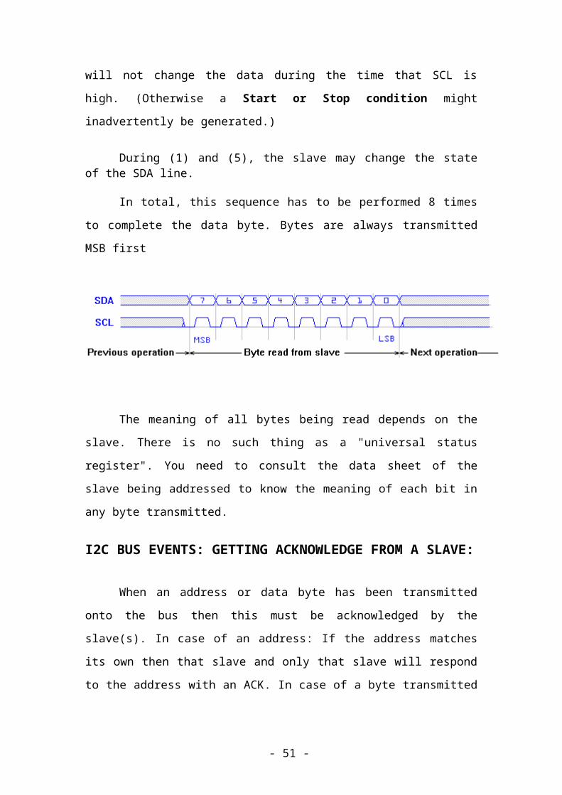
In total, this sequence has to be performed 8 times
to complete the data byte. Bytes are always transmitted
MSB first
The meaning of all bytes being read depends on the
slave. There is no such thing as a "universal status
register". You need to consult the data sheet of the
slave being addressed to know the meaning of each bit in
any byte transmitted.
I2C BUS EVENTS: GETTING ACKNOWLEDGE FROM A SLAVE:
When an address or data byte has been transmitted
onto the bus then this must be acknowledged by the
slave(s). In case of an address: If the address matches
its own then that slave and only that slave will respond
to the address with an ACK. In case of a byte transmitted
- 51 -
to an already addressed slave then that slave will
respond with an ACK as well.
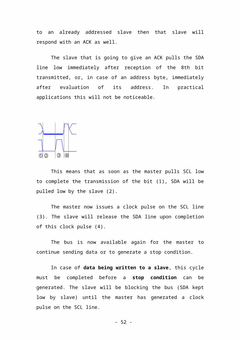
The slave that is going to give an ACK pulls the SDA
line low immediately after reception of the 8th bit
transmitted, or, in case of an address byte, immediately
after evaluation of its address. In practical
applications this will not be noticeable.
This means that as soon as the master pulls SCL low
to complete the transmission of the bit (1), SDA will be
pulled low by the slave (2).
The master now issues a clock pulse on the SCL line
(3). The slave will release the SDA line upon completion
of this clock pulse (4).
The bus is now available again for the master to
continue sending data or to generate a stop condition.
In case of data being written to a slave, this cycle
must be completed before a stop condition can be
generated. The slave will be blocking the bus (SDA kept
low by slave) until the master has generated a clock
pulse on the SCL line.
- 52 -

I2C BUS EVENTS: GIVING ACKNOWLEDGE TO A SLAVE:
Upon reception of a byte from a slave, the master
must acknowledge this to the slave device.
The master is in full control of the SDA and the SCLline.
After transmission of the last bit to the master (1)
the slave will release the SDA line. The SDA line should
then go high (2). The Master will now pull the SDA line
low (3) .
Next, the master will put a clock pulse on the SCL
line (4). After completion of this clock pulse, the
master will again release the SDA line (5).The slave will
now regain control of the SDA line (6).
If the master wants to stop receiving data from the
slave, it must be able to send a stop condition.
- 53 -

Since the slave regains control of the SDA line
after the ACK cycle issued by the master, this could lead
to problems.
Let's assume the next bit ready to be sent to the
master is a 0. The SDA line would be pulled low by the
slave immediately after the master takes the SCL line
low. The master now attempts to generate a Stop condition
on the bus. It releases the SCL line first and then tries
to release the SDA line - which is held low by the slave.
Conclusion: No Stop condition has been generated on the
bus.
This condition is called a NACK: Not acknowledge.
I2C BUS EVENTS: NO ACKNOWLEDGE (FROM SLAVE
TO MASTER):
This is not exactly a condition. It is merely a
state in the data flow between master and slave.
If, after transmission of the 8th bit from the
master to the slave the slave does not pull the SDA line
low, then this is considered a No ACK condition.
This means that either:
The slave is not there (in case of an address)
The slave missed a pulse and got out of sync with
the SCL line of the master.
- 54 -
The bus is "stuck". One of the lines could be held
low permanently.
In any case the master should abort by attempting to send
a stop condition on the bus.
APPLICATIONS
I²C is appropriate for peripherals where simplicity and
low manufacturing cost are more important than speed.
Common applications of the I²C bus are:
Reading configuration data from SPD EPROM’s on
SDRAM, DDR SDRAM, DDR2 SDRAM memory sticks (DIMM)
and other stacked PC boards
Supporting systems management for PCI cards, through
a SMBus 2.0 connection.
Accessing NVRAM chips that keep user settings.
Accessing low speed DACs.
Accessing low speed ADCs.
Changing contrast, hue, and color balance settings
in monitors (Display Data Channel).
- 55 -
Changing sound volume in intelligent speakers.
Controlling OLED/LCD displays, like in a cell phone.
Reading hardware monitors and diagnostic sensors,
like a CPU thermostat and fan speed.
Reading real time clocks.
Turning on and turning off the power supply of
system components.
A particular strength of I²C is that a microcontroller
can control a network of device chips with just two
general-purpose I/O pins and software.
Peripherals can also be added to or removed from the I²Cbus while the system is running, which makes it ideal forapplications that require hot swapping of components.
3.2 PASSIVE INFRARED SENSOR (PIR): -
A PIR detector is a motion detector that senses the
heat emitted by a living body. These are often fitted to
security lights so that they will switch on automatically
if approached. They are very effective in enhancing home
security systems.
- 56 -

The sensor is passive because, instead of emitting a
beam of light or microwave energy that must be
interrupted by a passing person in order to “sense” that
person, the PIR is simply sensitive to the infrared
energy emitted by every living thing. When an intruder
walks into the detector’s field of vision, the detector
“sees” a sharp increase in infrared energy.
A PIR sensor light is designed to turn on when a
person approaches, but will not react to a person
standing still. The lights are designed this way. A
moving person exhibits a sudden change in infrared
energy, but a slower change is emitted by a motionless
body. Slower changes are also caused by gradual
fluctuations in the temperature of the environment. If
the light were sensitive to these slower changes, it
would react to the sidewalk cooling off at night, instead
of the motion of a burglar.
If you have a PIR light, you may notice that it is
more sensitive on cold days than on warm days. This is
because the difference in temperature between the ambient
air and the human body is greater on cold days, making
the rise in temperature easier for the sensor to detect.
This has drawbacks, though; if the sensor is too
sensitive, it will pick up things you don’t want it to
such as the movement of small animals.
- 57 -
Passive infrared sensor is an electronic device,
which measures infrared light radiating from objects in
its field of view. PIRs are often used in the
construction of PIR-based motion detectors. Apparent
motion is detected when an infrared source with one
temperature, such as a human, passes in front of an
infrared source with another temperature, such as a wall.
All objects emit what is known as black body
radiation. This energy is invisible to the human eye but
can be detected by electronic devices designed for such a
purpose. The term 'Passive' in this instance means the
PIR does not emit energy of any type but merely accepts
incoming infrared radiation.
Infrared radiation enters through the front of the
sensor, known as the sensor face. At the core of a PIR is
a solid state sensor or set of sensors, made from
approximately 1/4 inches square of natural or artificial
pyroelectric materials, usually in the form of a thin
film, out of gallium nitride (GaN), caesium nitrate
(CsNO3), polyvinyl fluorides, derivatives of
phenylpyrazine, and cobalt phthalocyanine. (See
pyroelectric crystals.) Lithium tantalate (LiTaO3) is a
crystal exhibiting both piezoelectric and pyroelectric
properties.
The sensor is often manufactured as part of an
integrated circuit and may consist of one (1), two (2) or
- 58 -
four (4) 'pixels' of equal areas of the pyroelectric
material. Pairs of the sensor pixels may be wired as
opposite inputs to a differential amplifier. In such a
configuration, the PIR measurements cancel each other so
that the average temperature of the field of view is
removed from the electrical signal; an increase of IR
energy across the entire sensor is self-cancelling and
will not trigger the device. This allows the device to
resist false indications of change in the event of being
exposed to flashes of light or field-wide illumination.
(Continuous bright light could still saturate the sensor
materials and render the sensor unable to register
further information.)
At the same time, this differential arrangement
minimizes common-mode interference; this allows the
device to resist triggering due to nearby electric
fields. However, a differential pair of sensors cannot
measure temperature in that configuration and therefore
this configuration is specialized for motion detectors.
In a PIR-based motion detector, the PIR sensor is
typically mounted on a printed circuit board, which also
contains the necessary electronics required to interpret
the signals from the chip. The complete circuit is
contained in a housing, which is then mounted in a
location where the sensor can view the area to be
- 59 -
monitored. Infrared energy is able to reach the sensor
through the window because the plastic used is
transparent to infrared radiation (but only translucent
to visible light). This plastic sheet prevents the
introduction of dust and insects, which could obscure the
sensor's field of view.
OPERATION OF PIR SENSOR:
A few mechanisms have been used to focus the distant
infrared energy onto the sensor surface. The window may
have Fresnel lenses molded into it. Alternatively,
sometimes PIR sensors are used with plastic segmented
parabolic mirrors to focus the infrared energy; when
mirrors are used, the plastic window cover has no Fresnel
lenses molded into it. A filtering window (or lens) may
be used to limit the wavelengths to 8-14 micrometers,
which is most sensitive to human infrared radiation (9.4
micrometers being the strongest).
The PIR device can be thought of as a kind of
infrared ‘camera’, which remembers the amount of infrared
energy focused on its surface. Once power is applied to
the PIR the electronics in the PIR shortly settle into a
quiescent state and energize a small relay. This relay
controls a set of electrical contacts, which are usually
connected to the detection input of an alarm control
panel. If the amount of infrared energy focused on the
sensor changes within a configured time period, the
- 60 -
device will switch the state of the alarm output relay.
The alarm output relay is typically a "normally closed
(NC)" relay; also know as a "Form B" relay.
A person entering the monitored area is detected
when the infrared energy emitted from the intruder's body
is focused by a Fresnel lens or a mirror segment and
overlaps a section on the chip, which had previously been
looking at some much cooler part of the protected area.
That portion of the chip is now much warmer than when the
intruder wasn't there. As the intruder moves, so does the
hot spot on the surface of the chip. This moving hot spot
causes the electronics connected to the chip to de-
energize the relay, operating its contacts, thereby
activating the detection input on the alarm control
panel. Conversely, if an intruder were to try to defeat a
PIR perhaps
- 61 -
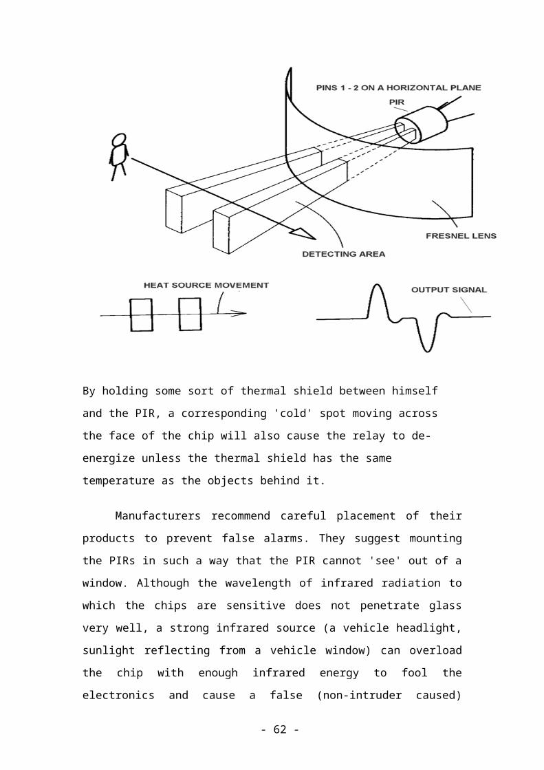
By holding some sort of thermal shield between himself
and the PIR, a corresponding 'cold' spot moving across
the face of the chip will also cause the relay to de-
energize unless the thermal shield has the same
temperature as the objects behind it.
Manufacturers recommend careful placement of their
products to prevent false alarms. They suggest mounting
the PIRs in such a way that the PIR cannot 'see' out of a
window. Although the wavelength of infrared radiation to
which the chips are sensitive does not penetrate glass
very well, a strong infrared source (a vehicle headlight,
sunlight reflecting from a vehicle window) can overload
the chip with enough infrared energy to fool the
electronics and cause a false (non-intruder caused)
- 62 -
alarm. A person moving on the other side of the glass
however would not be 'seen' by the PIR.
They also recommended that the PIR not be placed in
such a position that an HVAC vent would blow hot or cold
air onto the surface of the plastic, which covers the
housing's window. Although air has very low emissivity
(emits very small amounts of infrared energy), the air
blowing on the plastic window cover could change the
plastic's temperature enough to, once again, fool the
electronics.
PIRs come in many configurations for a wide variety
of applications. The most common used in home security
systems has numerous Fresnel lenses or mirror segments
and has an effective range of about thirty feet. Some
larger PIRs are made with single segment mirrors and can
sense changes in infrared energy over one hundred feet
away from the PIR. There are also PIRs designed with
reversible orientation mirrors, which allow either broad
coverage (110° wide) or very narrow 'curtain' coverage.
PIRs can have more than one internal sensing element
so that, with the appropriate electronics and Fresnel
lens, it can detect direction. Left to right, right to
left, up or down and provide an appropriate output
signal.
- 63 -
3.3LIGHT DEPENDENT RESISTOR: -
LDRs or Light Dependent Resistors are very useful
especially in light/dark sensor circuits. Normally the
resistance of an LDR is very high, sometimes as high as
1000 000 ohms, but when they are illuminated with light
resistance drops dramatically.
Electronic opto sensors are the devices that alter
their electrical characteristics, in the presences of
visible or invisible light. The best-known devices of
this type are the light dependent resistor (LDR), the
photo diode and the phototransistors.
Light dependent resistor as the name suggests
depends on light for the variation of resistance.
LDR are made by depositing a film of cadmium
sulphide or cadmium selenide on a substrate of ceramic
containing no or very few free electrons when not
illuminated. The film is deposited in a zig zag fashion
in the form of a strip. The longer the strip the more the
value of resistance.
When light falls on the strip, the resistance
decreases. In the absence of light the resistance can be
in the order of 10K ohm to 15K ohm and is called the dark
resistance.
Depending on the exposure of light the resistance
can fall down to value of 500 ohms. The power ratings are
- 64 -
usually smaller and are in the range 50mw to .5w. Though
very sensitive to light, the switching time is very high
and hence cannot be used for high frequency applications.
They are used in chopper amplifiers.
Light dependent resistors are available as discs
0.5cm to 2.5cm. The resistance rises to several Mega ohms
under dark conditions.
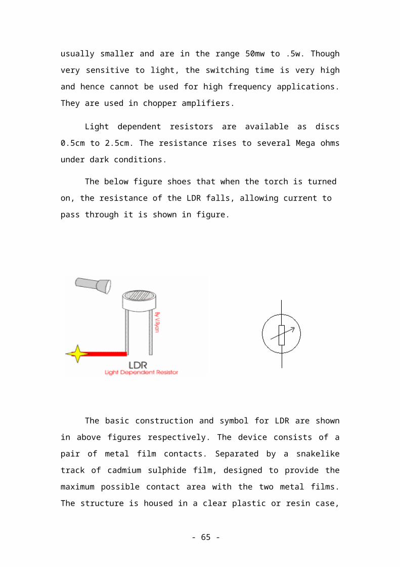
The below figure shoes that when the torch is turned
on, the resistance of the LDR falls, allowing current to
pass through it is shown in figure.
The basic construction and symbol for LDR are shown
in above figures respectively. The device consists of a
pair of metal film contacts. Separated by a snakelike
track of cadmium sulphide film, designed to provide the
maximum possible contact area with the two metal films.
The structure is housed in a clear plastic or resin case,
- 65 -
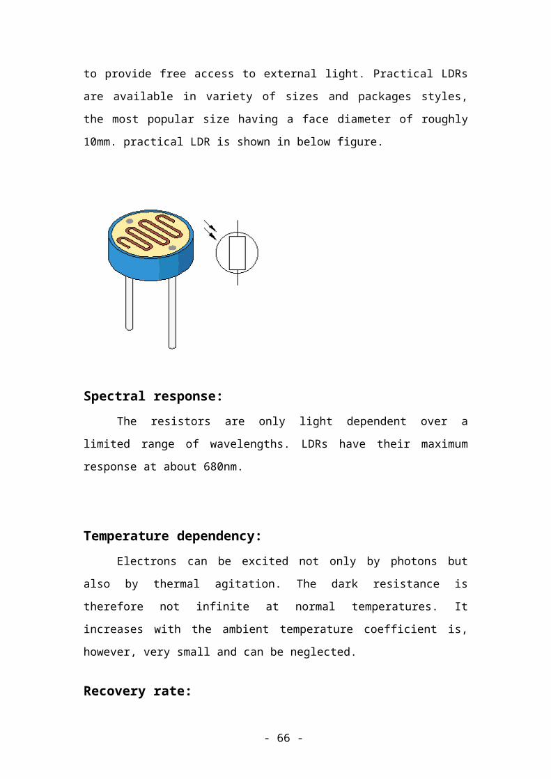
to provide free access to external light. Practical LDRs
are available in variety of sizes and packages styles,
the most popular size having a face diameter of roughly
10mm. practical LDR is shown in below figure.
Spectral response:The resistors are only light dependent over a
limited range of wavelengths. LDRs have their maximum
response at about 680nm.
Temperature dependency:Electrons can be excited not only by photons but
also by thermal agitation. The dark resistance is
therefore not infinite at normal temperatures. It
increases with the ambient temperature coefficient is,
however, very small and can be neglected.
Recovery rate:
- 66 -
When an LDR is brought from a certain illuminating
level into total darkness, the resistance does not
increase immediately to the dark value. The recovery rate
is specified in k ohm/second and for current LDR types it
is more than 200k ohm/second. The recovery rate is much
greater in the reverse direction, e.g. going from
darkness to illumination level of 300 lux, it takes less
than 10ms to reach a resistance which corresponds with
a light level of 400 lux.
LDRs are sensitive, inexpensive, and readily
available devices. They have good power and voltage
handling capabilities, similar to those of a conventional
resistor. Their only siginificant defect is that they arefairly low acting, taking tens or hundreds of LDR include
light and dark-activated switches and alarms, light beam
alarms and reflective smoke alarms etc. A LDR may be
connected either way round and no special precautions are
required when soldering.
Darkness: Maximum resistance, about 1Mohm.
Very bright light: Minimum resistance, about
100 ohm.
The LDR is a variable resistor whose resistance
decreases with the increase in light intensity. Two
cadmium sulphide (cds) photoconductive cells with
spectral response similar to that of the human eye. The
cell resistance falls with increasing light intensity.
- 67 -
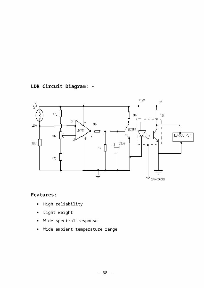
LDR Circuit Diagram: -
Features: High reliability
Light weight
Wide spectral response
Wide ambient temperature range
- 68 -
Applications:
Smoke detection
Automatic lighting control
Burglar alarm systems
Camera (electronic shutter)
Strobe (color temperature reading)
3.4 Digital Thermometer and Thermostat
(DS1621): -
FEATURES: -
Temperature measurements require no external
components
Measures temperatures from -55°C to +125°C in 0.5°C
increments. Fahrenheit equivalent is -67°F to 257°F in
0.9°F increments
Temperature is read as a 9-bit value (2-byte
transfer)
Wide power supply range (2.7V to 5.5V)
Converts temperature to digital word in less than 1
second
- 69 -
Thermostatic settings are user definable and
nonvolatile
Data is read from/written via a 2-wire serial
interface (open drain I/O lines)
Applications include thermostatic controls,
industrial systems, consumer
products, Thermometers, or any thermal sensitive
system
8-pin DIP or SO package (150mil and 208mil)
ABSOLUTE MAXIMUM RATINGS:
Voltage on Any Pin Relative to Ground -
0.5V to +6.0V
Operating Temperature Range
-55_C to +125_C
Storage Temperature Range
-55_C to +125_C
DESCRIPTION:
The DS1621 Digital Thermometer and Thermostat
provides 9-bit temperature readings, which indicate the
temperature of the device. The thermal alarm output,
TOUT, is active when the temperature of the device
exceeds a user-defined temperature TH:- The output
remains active until the temperature drops below user
defined temperature TL, allowing for any hysteresis
necessary.
- 70 -
User-defined temperature settings are stored in
nonvolatile memory so parts may be programmed prior to
insertion in a system. Temperature settings and
temperature readings are all communicated to/from the
DS1621 over a simple 2-wire serial interface.
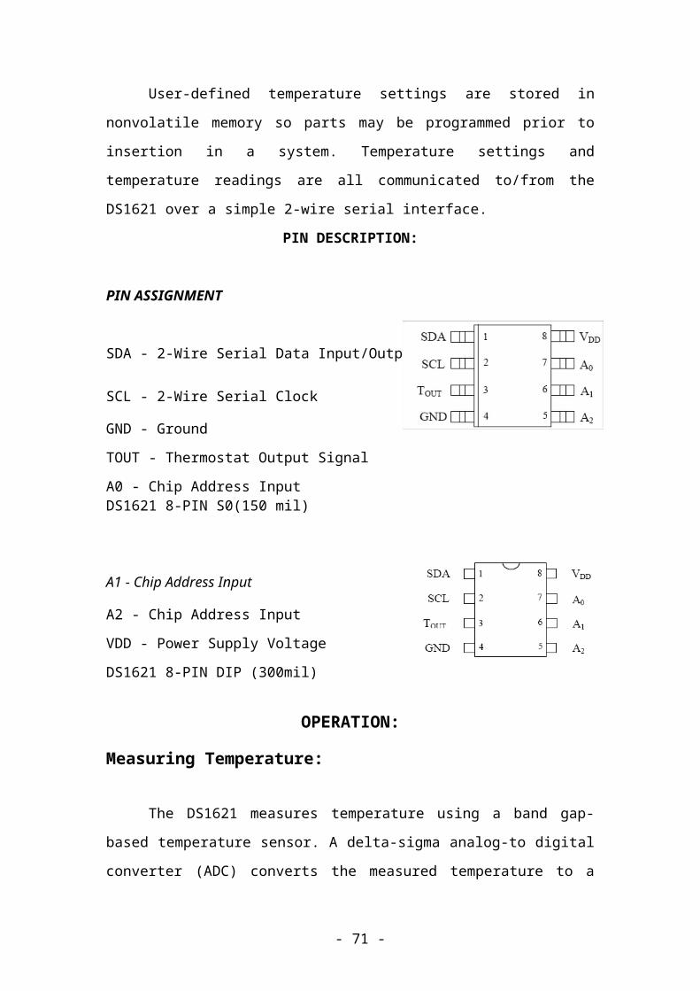
PIN DESCRIPTION:
PIN ASSIGNMENT
SDA - 2-Wire Serial Data Input/Output.
SCL - 2-Wire Serial Clock
GND - Ground
TOUT - Thermostat Output Signal
A0 - Chip Address Input DS1621 8-PIN S0(150 mil)
A1 - Chip Address Input
A2 - Chip Address Input
VDD - Power Supply Voltage
DS1621 8-PIN DIP (300mil)
OPERATION:
Measuring Temperature:
The DS1621 measures temperature using a band gap-
based temperature sensor. A delta-sigma analog-to digital
converter (ADC) converts the measured temperature to a
- 71 -
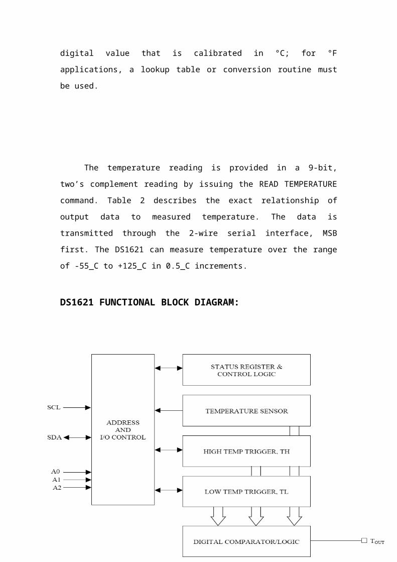
digital value that is calibrated in °C; for °F
applications, a lookup table or conversion routine must
be used.
The temperature reading is provided in a 9-bit,
two’s complement reading by issuing the READ TEMPERATURE
command. Table 2 describes the exact relationship of
output data to measured temperature. The data is
transmitted through the 2-wire serial interface, MSB
first. The DS1621 can measure temperature over the range
of -55_C to +125_C in 0.5_C increments.
DS1621 FUNCTIONAL BLOCK DIAGRAM:
- 72 -
Thermostat Control: -In its operating mode, the DS1621 functions as a
thermostat with programmable hysteresis as shown in
Figure 3. The thermostat output updates as soon as a
temperature conversion is complete.
When the DS1621’s temperature meets or exceeds the
value stored in the high temperature trip register (TH),
the output becomes active and will stay active until the
temperature falls below the temperature stored in the low
temperature trigger register (TL). In this way, any
amount of hysteresis may be obtained.
The active state for the output is programmable by
the user so that an active state may either be a logic
"1" (VDD) or a logic "0" (0V). This is done using the POL
bit in the configuration register as explained in the
Operation and Control section of this datasheet.
- 73 -
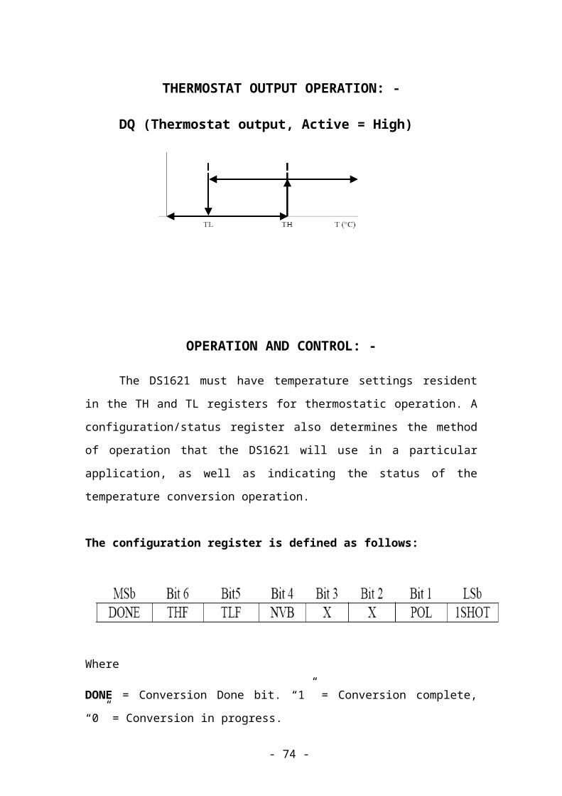
THERMOSTAT OUTPUT OPERATION: -
DQ (Thermostat output, Active = High)
OPERATION AND CONTROL: -
The DS1621 must have temperature settings resident
in the TH and TL registers for thermostatic operation. A
configuration/status register also determines the method
of operation that the DS1621 will use in a particular
application, as well as indicating the status of the
temperature conversion operation.
The configuration register is defined as follows:
Where
DONE = Conversion Done bit. “1” = Conversion complete,
“0” = Conversion in progress.
- 74 -
THF = Temperature High Flag. This bit will be set to “1”
when the temperature is greater than or equal to the
value of TH. It will remain “1” until reset by writing
“0” into this location or removing power from the device.
This feature provides a method of determining if the
DS1621 has ever been subjected to temperatures above TH
while power has been applied.
TLF = Temperature Low Flag. This bit will be set to “1”
when the temperature is less than or equal to the value
of TL. It will remain “1” until reset by writing “0” into
this location or removing power from the device. This
feature provides a method of determining if the DS1621
has ever been subjected to temperatures below TL while
power has been applied.
NVB = Nonvolatile Memory Busy flag. “1” = Write to an E2
memory cell in progress, “0” =nonvolatile memory is not
busy. A copy to E2 may take up to 10 ms.
POL = Output Polarity Bit. “1” = active high, “0” = active low. This bit is nonvolatile.
1SHOT = One Shot Mode. If 1SHOT is “1”, the DS1621 will
perform one temperature conversion upon receipt of the
Start Convert T protocol. If 1SHOT is “0”, the DS1621
will continuously perform temperature conversions. This
bit is nonvolatile.
- 75 -
X = Reserved.
For typical thermostat operation the DS1621 will
operate in continuous mode. However, for applications
where only one reading is needed at certain times or to
conserve power, the one-shot mode may be used. Note that
the thermostat output (TOUT) will remain in the state it
was in after the last valid temperature conversion cycle
when operating in one-shot mode.
The DS1621 may operate in the following two modes:
1. Slave receiver mode: Serial data and clock are
received through SDA and SCL. After each byte is received
an acknowledge bit is transmitted. START and STOP
conditions are recognized as the beginning and end of a
serial transfer. Address recognition is performed by
hardware after reception of the slave address and
direction bit.
2. Slave transmitter mode: The first byte is received
and handled as in the slave receiver mode. However, in
this mode the direction bit will indicate that the
transfer direction is reversed. Serial data is
transmitted on SDA by the DS1621 while the serial clock
is input on SCL. START and STOP conditions are recognized
as the beginning and end of a serial transfer.
- 76 -
COMMAND SET: To write to the DS1621, the master will issue the slave
address of the DS1621 and the R/W bit will be set to “0”. After
receiving an acknowledge, the bus master provides a command
protocol. After receiving this protocol, the DS1621 will issue
an acknowledge and then the master may send data to the DS1621.
If the DS1621 is to be read, the master must send the command
protocol as before and then issue a repeated
START condition and the control byte again, this time with the
R/W bit set to “1” to allow reading of the data from the DS1621.
The command set for the DS1621 as shown in Table 3 is as follows:
Read Temperature [AAh]: - This command reads the last temperature conversion
result. The DS1621 will send 2 bytes, in the format described
earlier, which are the contents of this register.
Access TH [A1h]: - If R/W is “0” this command writes to the TH (HIGH
TEMPERATURE) register. After issuing this command, the next 2
bytes written to the DS1621, in the same format as described
for reading temperature, will set the high temperature
threshold for operation of the TOUT output. If R/W is “1” the
value stored in this register is read back.
Access TL [A2h]: - If R/W is “0” this command writes to the TL (LOW
TEMPERATURE) register. After issuing this command, the next 2
bytes written to the DS1621, in the same format as described
- 77 -
for reading temperature, will set the high temperature
threshold for
operation of the TOUT output. If R/W is “1” the value
stored in this register is read back.
Access Config [ACh]: -
If R/W is “0” this command writes to the configuration
register. After issuing this command, the next data byte is the
value to be written into the configuration register. If R/W is
“1” the next data byte read is the value stored in the
configuration register.
Read Counter [A8h]: -
This command reads the value Count_Remain. This command is valid only if R/W is “1”.
Read Slope [A9h]: -
This command reads the value Count_Per_C. This command is valid only if R/W is “1”.
Start Convert T [EEh]: -
This command begins a temperature conversion. No further
data is required. In one-shot mode the temperature conversion
will be performed and then the DS1621 will remain idle. In
- 78 -
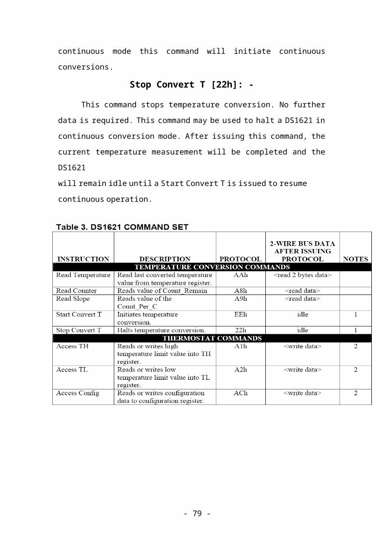
continuous mode this command will initiate continuous
conversions.
Stop Convert T [22h]: -
This command stops temperature conversion. No further
data is required. This command may be used to halt a DS1621 in
continuous conversion mode. After issuing this command, the
current temperature measurement will be completed and the
DS1621
will remain idle until a Start Convert T is issued to resume
continuous operation.
- 79 -
3.5 ZERO CROSSING DETECTOR (ZCD): -
Zero crossing detectors as a group are not a well-
understood application, although they are essential
elements in a wide range of products. It has probably
escaped the notice of readers who have looked at the
lighting controller and the Linkwitz Cosine Burst
Generator, but both of these rely on a zero crossing
detector for their operation.
A zero crossing detector literally detects the
transition of a signal waveform from positive and
negative, ideally providing a narrow pulse that coincides
exactly with the zero voltage condition. At first glance,
this would appear to be an easy enough task, but in fact
it is quite complex, especially where high frequencies
are involved. In this instance, even 1 kHz starts to
present a real challenge if extreme accuracy is needed.
The not so humble comparator plays a vital role -
without it, most precision zero crossing detectors would
not work, and we'd be without digital audio, PWM and a
multitude of other applications taken for granted.
- 80 -

Basic low frequency: -
The zero crossing detector as used for the dimmer
ramp generator. Although it has almost zero phase
inaccuracy, that is largely because the pulse is so broad
that any inaccuracy is completely swamped. The comparator
function is handled by transistor Q1 - very basic, but
adequate for the job.
The circuit is also sensitive to level, and for
acceptable performance the AC waveform needs to be of
reasonably high amplitude. 12-15V AC is typical. If the
voltage is too low, the pulse width will increase. R1 is
there to ensure that the voltage falls to zero - stray
capacitance is sufficient to stop the circuit from
working without it.
- 81 -
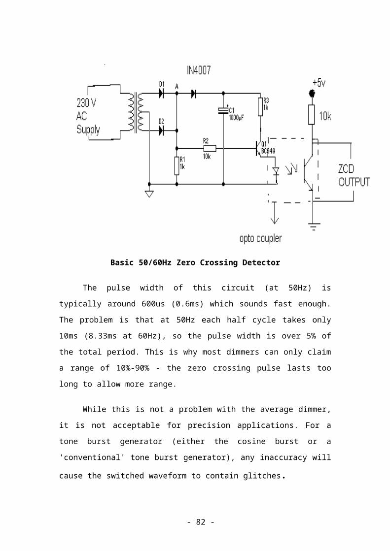
Basic 50/60Hz Zero Crossing Detector
The pulse width of this circuit (at 50Hz) is
typically around 600us (0.6ms) which sounds fast enough.
The problem is that at 50Hz each half cycle takes only
10ms (8.33ms at 60Hz), so the pulse width is over 5% of
the total period. This is why most dimmers can only claim
a range of 10%-90% - the zero crossing pulse lasts too
long to allow more range.
While this is not a problem with the average dimmer,
it is not acceptable for precision applications. For a
tone burst generator (either the cosine burst or a
'conventional' tone burst generator), any inaccuracy will
cause the switched waveform to contain glitches.
- 82 -
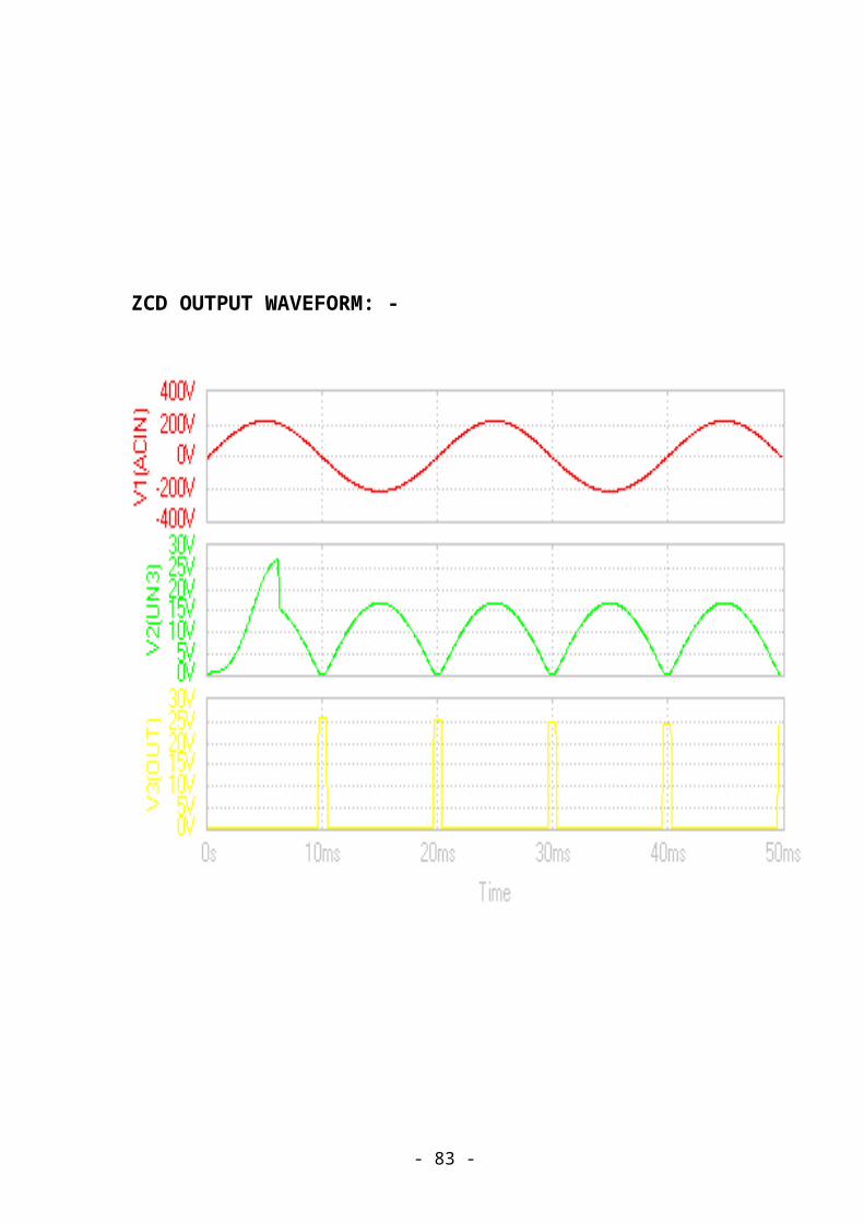
ZCD OUTPUT WAVEFORM: -
- 83 -

3.6 POWER SUPPLY:Power supply block consists of following units:
Step down transformer.
Bridge rectifier circuit.
Input filter.
Voltage regulators.
Output filter.
Indicator unit.
Step down transformer:The step-down transformer is used to step down the
supply voltage of 230v ac from mains to lower values, asthe various IC’s used in this project require reducedvoltages. The transformer consists of primary andsecondary coils. To reduce or step down the voltage, thetransformer is designed to contain less number of turnsin its secondary core. The outputs from the secondarycoil which is center tapped are the ac values of 0v, 15vand 15v. The conversion of these ac values to dc valuesto dc values is done using the full wave rectifier unit.
Rectifier Unit:
- 84 -
A diode bridge is an arrangement of four diodes
connected in a bridge circuit. That provides the polarity
of output voltage of any polarity of the input voltage.
When used in its most common application, for conversion
of alternating current (A.C) input into direct current
(D.C) output, it is known as a bridge rectifier. The
diagram describes a diode-bridge design known as a full
wave rectifier. This design can be used to rectify single
phase A.C. when no transformer center tap is available. A
bridge rectifier makes use of four diodes in a bridge
arrangement to achieve full wave rectification. This is a
Widely used configuration, both with individual diodes
wired as shown and with single component bridges where
the diode bridge is wired internally.
For both positive and negative swings of the
transformer, there is a forward path through the diode
bridge. Both conduction paths cause current to flow in
the same direction through the load resister,
accomplishing full-wave rectification. While one set of
diodes is forward biased, the other set is reverse biased
and effectively eliminated from the circuit.
Input Filter: -
Capacitors are used as filters. The ripples fromthe dc voltages are removed and pure dc voltage isobtained. The primary action performed by capacitor ischarging and discharging. It charges in positive halfcycle of the ac voltage and it will discharge in negativehalf cycle. So it allows only ac voltage and does not
- 85 -
allow the dc voltage. This filter is fixed before theregulator. Capacitors used here are of the value 1000uF
Regulator unit: -Regulator regulates the output voltage to a specific
value. The output voltage is maintained irrespective of
the fluctuations in the input dc voltage. Whenever there
are any ac voltage fluctuations, the dc voltage also
changes, and to avoid this regulators are used.
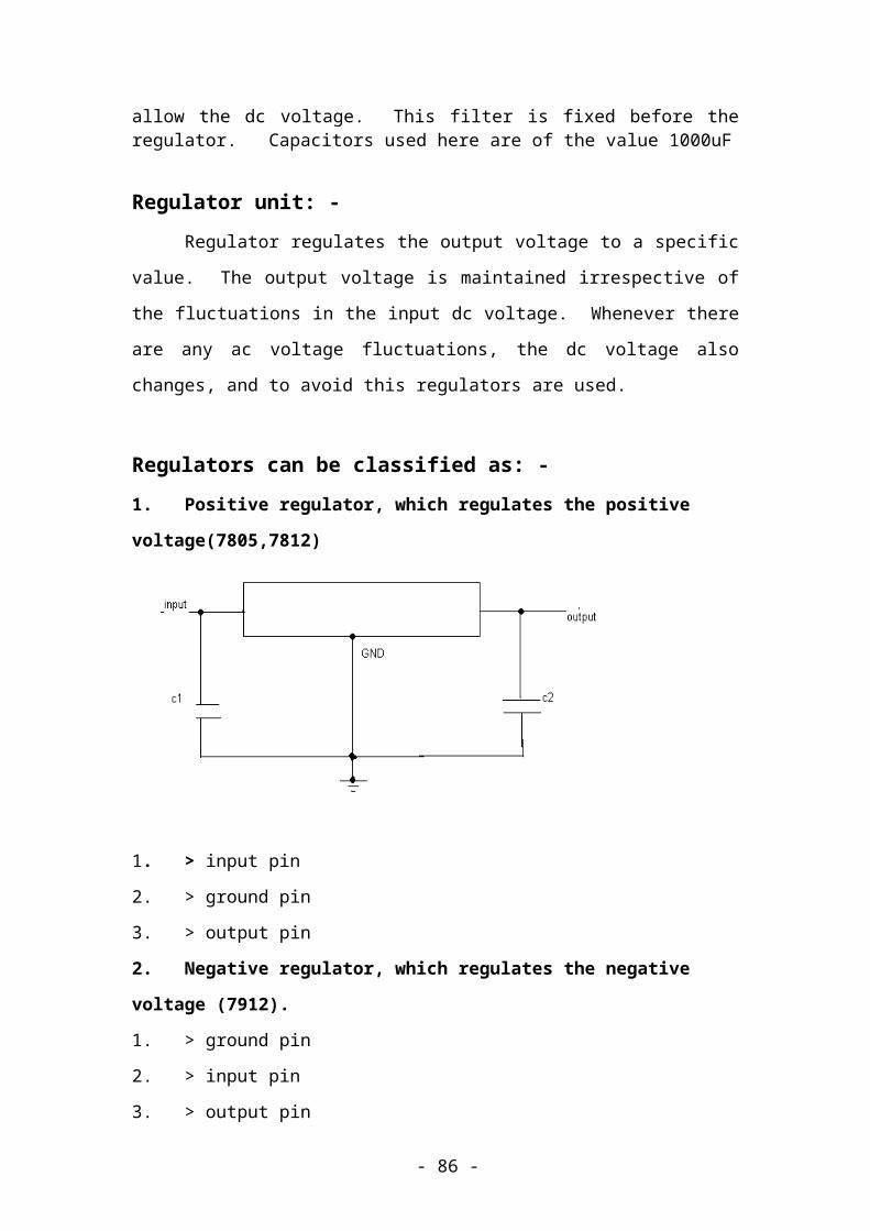
Regulators can be classified as: -1. Positive regulator, which regulates the positive
voltage(7805,7812)
1. > input pin
2. > ground pin
3. > output pin
2. Negative regulator, which regulates the negative
voltage (7912).
1. > ground pin
2. > input pin
3. > output pin
- 86 -
Regulators used in this application are: -7805 which provides 5v dc
7812 which provides 12v dc
7912 which provides -121v dc
Out put Filter: -This filter is fixed after the Regulator circuit to
filter any of the possibly found ripples in the output
received finally. Capacitors used here are of value 10F.
Power Supply Circuit Diagram:
- 87 -
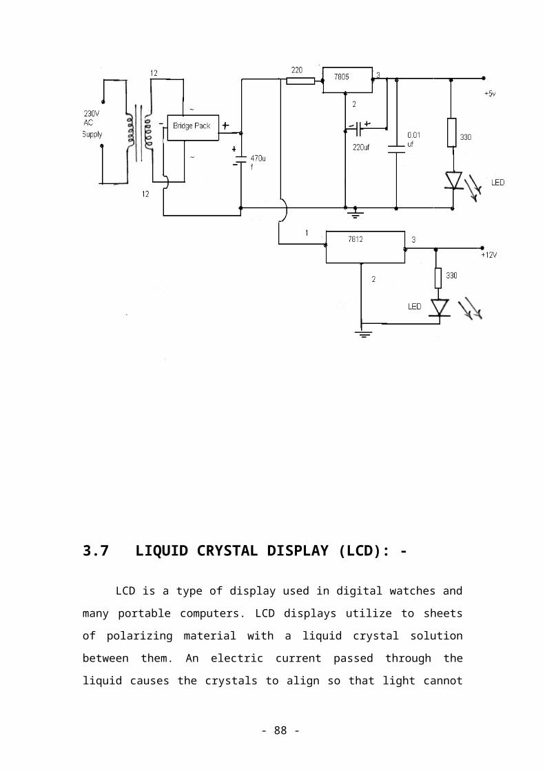
3.7 LIQUID CRYSTAL DISPLAY (LCD): -
LCD is a type of display used in digital watches and
many portable computers. LCD displays utilize to sheets
of polarizing material with a liquid crystal solution
between them. An electric current passed through the
liquid causes the crystals to align so that light cannot
- 88 -
pass through them. LCD technology has advanced very
rapidly since its initial inception over a decade ago for
use in lap top computers. Technical achievements has
resulted in brighter displace, higher resolutions, reduce
response times and cheaper manufacturing process.
The liquid crystals can be manipulated through an
applied electric voltage so that light is allowed to pass
or is blocked. By carefully controlling where and what
wavelength (color) of light is allowed to pass, the LCD
monitor is able to display images. A backlight provides
LCD monitor’s brightness.
Over the years many improvements have been made to
LCD to help enhance resolution, image, sharpness and
response times.
One of the latest such advancement is applied to
glass during acts as switch allowing control of light at
the pixel level, greatly improving LCD’s ability to
display small-sized fonts and image clearly.
Other advances have allowed LCD’s to greatly reduce
liquid crystal cell response times. Response time is
basically the amount of time it takes for a pixel to
“change colors”, in reality response time is the amount
of time it takes a liquid crystal cell to go from being
active to inactive.
This is due to following reasons:
- 89 -
The declining prices of LCDs.
The ability to display numbers, characters and
graphics. This is in contrast to LEDs, which
are limited to numbers and a few characters.
An intelligent LCD display of two lines, 20
characters per line that is interfaced to the pic16f72
microcontroller.
Incorporation of a refreshing controller into the
LCD, thereby relieving the CPU to keep displaying the
data. Ease of programming for characters and graphics.
Most of the LCD modules conform to a standard
interface specification. A 14-pin access is provided
having eight data lines, three control lines and three
power lines. The connections are laid out in one of the
two common configurations, either two rows of seven pins,
or a single row of 14 pins.
One of these pins is numbered on the LCD’s printed
circuit board (PCB), but if not, it is quite easy to
locate pin1. Since this pin is connected to ground, it
often has a thicker PCB track, connected to it, and it is
generally connected to metal work at same point.
PIN DIAGRAM OF LCD: -
- 90 -
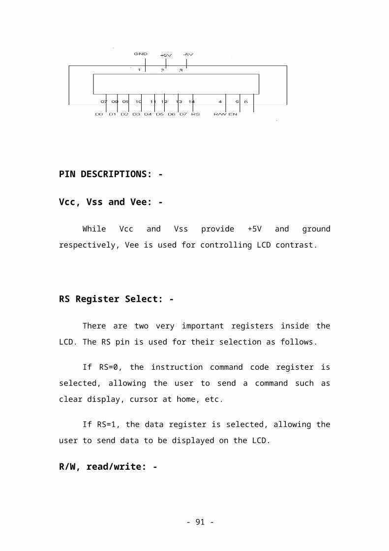
PIN DESCRIPTIONS: -
Vcc, Vss and Vee: -
While Vcc and Vss provide +5V and ground
respectively, Vee is used for controlling LCD contrast.
RS Register Select: -
There are two very important registers inside the
LCD. The RS pin is used for their selection as follows.
If RS=0, the instruction command code register is
selected, allowing the user to send a command such as
clear display, cursor at home, etc.
If RS=1, the data register is selected, allowing the
user to send data to be displayed on the LCD.
R/W, read/write: -
- 91 -
R/W input allows the user to write information to
the LCD or read information from it.
R/W = 1 for reading.
R/W= 0 for writing.
EN, enable: -
The LCD to latch information presented to its data
pins uses the enable pin. When data is supplied to data
pins, a high–to-low pulse must be applied to this pin in
order for the LCD to latch in the data present at the
data pins. This pulse must be a minimum of 450 ns wide.
D0 – D7: -
The 8–bit data pins, DO – D7, are used to send
information to the LCD or read the contents of the LCD’s
internal registers.
To display letters and numbers, we send ASCII codes
for the letters A–Z, a-z numbers 0-9 to these pins while
making RS=1.
There are also instruction command codes that can be
sent to the LCD to clear the display or force the cursor
to home position or blink the instruction command codes.
We also use RS = 0 to check the busy flag bit to see
if the LCD is ready to receive information. The busy flag
is D7 and can be read when R/W=1 and RS=0, as follows: if
- 92 -
R/W = 1, RS = 0. When D7= 1 (busy flag = 1), the LCD is
busy taking care of internal operations and will not
accept any information.
Prototype circuit: -
For a LCD module to be used effectively in any piece
of equipment, a Microprocessor or Micro controller is
usually, required to drive it. However, before attempting
a series of switches to the pins of the module. This can
be a quite benefical step, if even you are thoroughly
conversant with the workings of microprocessors.
3.8 DIMMER: -Dimmers are devices used to vary the brightness of a
light. By decreasing or increasing the RMS voltage and
hence the mean power to the lamp it is possible to vary
the intensity of the light output. Although variable-
voltage devices are used for various purposes, the term
dimmer is generally reserved for those intended to
control lighting.
Modern dimmers are built from silicon-controlled
rectifiers (SCR) instead of potentiometers or variable
resistors because they have higher efficiency. A variable
resistor would dissipate power by heat (efficiency as low
as 0.5). By switching on and off, theoretically a dimmer
does not heat up (efficiency close to 1.0).
- 93 -

Thyristor (and briefly, thyratrom) dimmers were
introduced to solve some of these problems. Because they
use switching techniques instead of potential division
there is almost no wasted power, dimming can be almost
instantaneous and is easily controlled by remote
electronics.
Triacs are used instead of SCR thyristors in lower
cost designs, but do not have the surge handling capacity
of back-to-back SCR's, and are only suitable for loads
less than about 20 Amps. The switches generate some heat
during switching, and can cause interference. Large
inducors are used as part of the circuitry to suppress
this interference. When the dimmer is at 50% power the
switches are switching their highest voltage (>300 V in
Europe) and the sudden surge of power causes the coils on
the inductor to move, creating buzzing sound associated
with some types of dimmer; this same effect can be heard
in the filaments of the incandescent lamps as "singing".
The suppression circuitry adds a lot of weight to the
dimmer, and is often insufficient to prevent buzzing to
be heard on audio systems that share the mains supply
with the lighting loads. This development also made it
possible to make dimmers small enough to be used in place
of normal domestic light switches.
CIRCUIT DIAGRAM: -
- 94 -
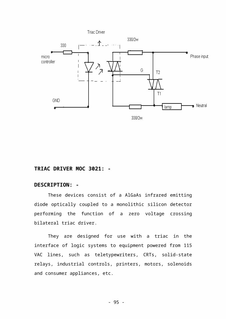
TRIAC DRIVER MOC 3021: -
DESCRIPTION: -These devices consist of a AlGaAs infrared emitting
diode optically coupled to a monolithic silicon detector
performing the function of a zero voltage crossing
bilateral triac driver.
They are designed for use with a triac in the
interface of logic systems to equipment powered from 115
VAC lines, such as teletypewriters, CRTs, solid-state
relays, industrial controls, printers, motors, solenoids
and consumer appliances, etc.
- 95 -
APPLICATIONS: -
• Solenoid/valve controls
• Lighting controls
• Static power switches
• AC motor drives
• Temperature controls
• E.M. contactors
• AC motor starters
• Solid-state relays
FEATURES: -• Simplifies logic control of 115 VAC power
• Zero voltage crossing
• dv/dt of 2000 V/s typical, 1000 V/s guaranteed
3.9 OPTOCOUPLER: -Opto coupler is a device that uses a short optical
transmission path to transfer a signal between elements
of a circuit, typically a transmitter and a receiver,
while keeping them electrically isolated — since the
- 96 -
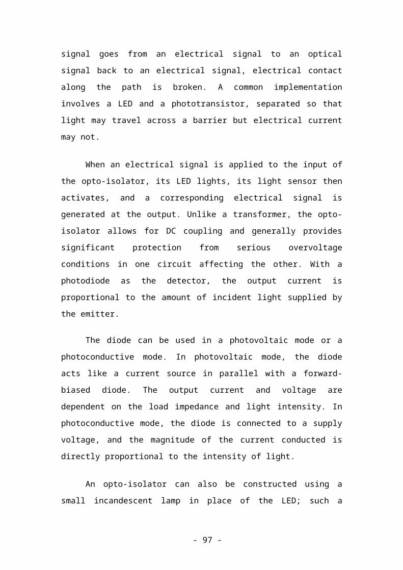
signal goes from an electrical signal to an optical
signal back to an electrical signal, electrical contact
along the path is broken. A common implementation
involves a LED and a phototransistor, separated so that
light may travel across a barrier but electrical current
may not.
When an electrical signal is applied to the input of
the opto-isolator, its LED lights, its light sensor then
activates, and a corresponding electrical signal is
generated at the output. Unlike a transformer, the opto-
isolator allows for DC coupling and generally provides
significant protection from serious overvoltage
conditions in one circuit affecting the other. With a
photodiode as the detector, the output current is
proportional to the amount of incident light supplied by
the emitter.
The diode can be used in a photovoltaic mode or a
photoconductive mode. In photovoltaic mode, the diode
acts like a current source in parallel with a forward-
biased diode. The output current and voltage are
dependent on the load impedance and light intensity. In
photoconductive mode, the diode is connected to a supply
voltage, and the magnitude of the current conducted is
directly proportional to the intensity of light.
An opto-isolator can also be constructed using a
small incandescent lamp in place of the LED; such a
- 97 -
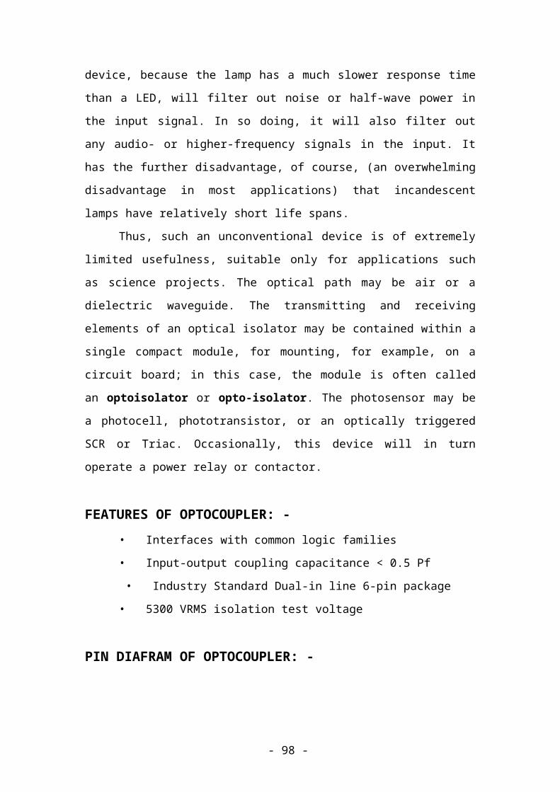
device, because the lamp has a much slower response time
than a LED, will filter out noise or half-wave power in
the input signal. In so doing, it will also filter out
any audio- or higher-frequency signals in the input. It
has the further disadvantage, of course, (an overwhelming
disadvantage in most applications) that incandescent
lamps have relatively short life spans.
Thus, such an unconventional device is of extremely
limited usefulness, suitable only for applications such
as science projects. The optical path may be air or a
dielectric waveguide. The transmitting and receiving
elements of an optical isolator may be contained within a
single compact module, for mounting, for example, on a
circuit board; in this case, the module is often called
an optoisolator or opto-isolator. The photosensor may be
a photocell, phototransistor, or an optically triggered
SCR or Triac. Occasionally, this device will in turn
operate a power relay or contactor.
FEATURES OF OPTOCOUPLER: -• Interfaces with common logic families
• Input-output coupling capacitance < 0.5 Pf
• Industry Standard Dual-in line 6-pin package
• 5300 VRMS isolation test voltage
PIN DIAFRAM OF OPTOCOUPLER: -
- 98 -
Applications: AC mains detection
Reed relay driving
Switch mode power supply feedback
Telephone ring detection
Logic ground isolation
Logic coupling with high frequency noise rejection
3.10 LOADS: -In this intelligent energy saving system we are
using two loads, lamp and Fan. According to the light
intensity of the particular room or cabin the LDR will
senses, depending on the LDR output the lamp will be
ON/OFF. This system is only applicable for lamps and not
- 99 -

applicable for tube lights, because the starting voltage
of the tube lights is high compared to lamps.
By using Thermostat and Dimmer we can adjust the
speed of the Fan according to the changes of the room
temperature.
- 100 -
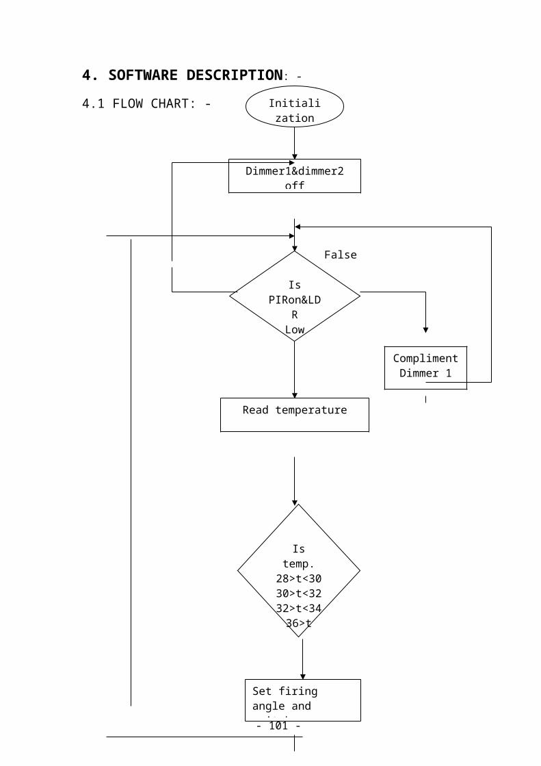
4. SOFTWARE DESCRIPTION: -4.1 FLOW CHART: -
False
- 101 -
Initialization
Dimmer1&dimmer2off
Is PIRon&LD
RLow
ComplimentDimmer 1
onRead temperature
Is temp.
28>t<3030>t<3232>t<3436>t
Set firing angle and switch on
4.2 SOURCE CODE: -
Program for PIC16F72: -
# include<16f72.h>
# use delay (clock=12000000)
# fuses hs , nowdt , protect
# use i2c(master, sda=PIN_c4 , scl=PIN_c3)
# include <lcdb.c>
int temph , templ ;
int1 x=0 , y=0 ;
int m ;
# define zcd PIN_a4
# define pir PIN_B0
# define ldr PIN_a2
# define dim1 PIN_a0
# define dim2 PIN_a1
# include <temperature.c>
# include <dimmer1.c>
# include <dimmer2.c>
# INT_EXT
Void main( )
{
Output_low(dim1) ;
Output_low(dim2) ;
- 102 -
X=0; Y=0;
Setup_adc_ports( NO_ANALOGS ) ;// All are
digital only
temp_intit( ) ;
lcd_intit( ) ;
LCD_PUTC(“\f POWER SAVER”) ;
delay_ms(2000) ;
While(1)
{
If (! input(pir) )
{
output_high(dim1) ;
While(! input(pir) ){}
X=~x ;
LCD_PUTC(“\n PIR ON “) ;
Delay_ms(5000) ;
}
if(x= =0)
{
- 103 -
If(y= =1)
{
delay_ms(20000) ;
Y=0 ;
}
output_low(dim1) ;
output_low(dim2);
LCD_PUTC(“\n STAND BY “) ;
delay_ms (300);
}
if(x= =1)
{
y=1;
temp_read ( );
if (templ= =0x80) templ=5;
else templ=0;
printf(lcd_putc, ”\nTEMP: %02d.%d dc”,
temph,templ) ;
if(temph>=27 && temph<=28 )
- 104 -
{
back25: if( ! input(zcd))goto back25;
/ /waiting to get zero start
delay_ms(5);
output_high(dim2);
back26: if( ! input(zcd))goto back26;
/ /waiting to get zero start
output_low(dim2);
delay_ms(5);
output_high(dim2);
back27: if( ! input(zcd))goto back27;
output_low(dim2);
}
if (temph>=29 && temph<=31
)
{
- 105 -

back20: if( ! input(zcd))goto back20;
/ /waiting to get zero start
delay_ms(5); / / 161
output_high(dim2);
back30: if( ! input(zcd))goto back30;
/ /waiting to get zero start
output_low(dim2);
delay_ms(5);
output_high(dim2);
back32: if( ! input(zcd))goto back32;
output_low(dim2);
}
if (temph>31 &&
temph<=33 )
{
back9: if( ! input(zcd))goto back9;
/ /waiting to get zero start
delay_ms(5); / / 161
output_high(dim2);
- 106 -
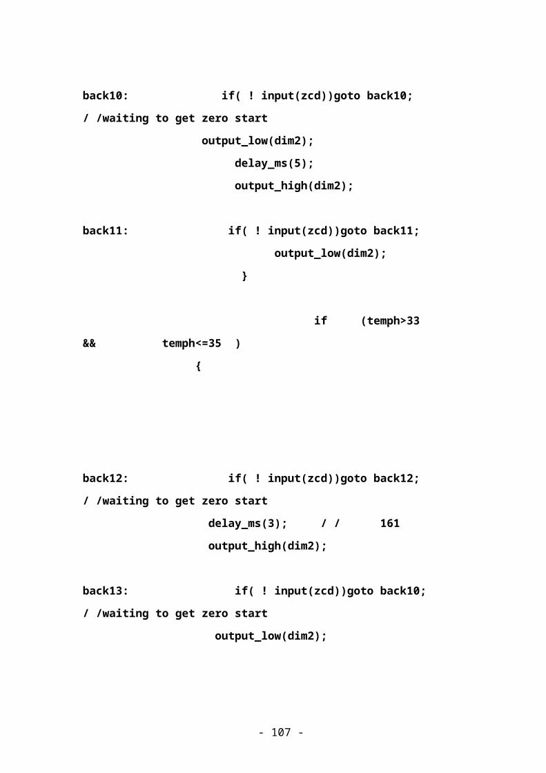
back10: if( ! input(zcd))goto back10;
/ /waiting to get zero start
output_low(dim2);
delay_ms(5);
output_high(dim2);
back11: if( ! input(zcd))goto back11;
output_low(dim2);
}
if (temph>33
&& temph<=35 )
{
back12: if( ! input(zcd))goto back12;
/ /waiting to get zero start
delay_ms(3); / / 161
output_high(dim2);
back13: if( ! input(zcd))goto back10;
/ /waiting to get zero start
output_low(dim2);
- 107 -
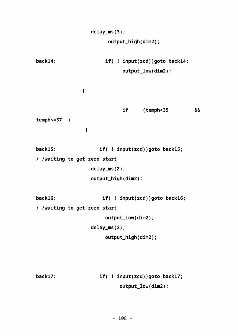
delay_ms(3);
output_high(dim2);
back14: if( ! input(zcd))goto back14;
output_low(dim2);
}
if (temph>35 &&
temph<=37 )
{
back15: if( ! input(zcd))goto back15;
/ /waiting to get zero start
delay_ms(2);
output_high(dim2);
back16: if( ! input(zcd))goto back16;
/ /waiting to get zero start
output_low(dim2);
delay_ms(2);
output_high(dim2);
back17: if( ! input(zcd))goto back17;
output_low(dim2);
- 108 -

}
if (temph>37)
output_high(dim2) ;
if
(input(ldr) )output_high(dim1) ;
if (!
Input(ldr) )out_low(dim1) ;
}
}
}
- 109 -
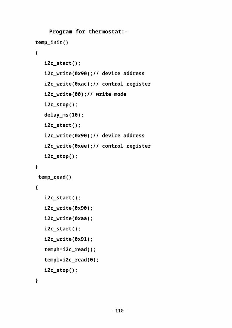
Program for thermostat:-temp_init()
{
i2c_start();
i2c_write(0x90);// device address
i2c_write(0xac);// control register
i2c_write(00);// write mode
i2c_stop();
delay_ms(10);
i2c_start();
i2c_write(0x90);// device address
i2c_write(0xee);// control register
i2c_stop();
}
temp_read()
{
i2c_start();
i2c_write(0x90);
i2c_write(0xaa);
i2c_start();
i2c_write(0x91);
temph=i2c_read();
templ=i2c_read(0);
i2c_stop();
}
- 110 -

CHAPTER 6.
CONCLUSION & FUTURE DIRECTIONS
- 111 -
CONCLUSION:
Intelligent Energy Saving System is not limited for
any particular application, it can be used any where in a
process industries with little modifications in software
coding according to the requirements. This concept not
only ensures that our work will be usable in the future
but also provides the flexibility to adapt and extend, as
needs change.
In this project work we have studied and implemented
a complete working model using a PIC microcontroller. The
programming and interfering of PIC microcontroller has
been mastered during the implementation. This work
includes the study of energy saving system in many
applications
FUTURE DIRECTIONS:
- 112 -
We except that our next generation will develop this
energy saving system with wire less network.
In our project we connected all the sensors to micro
controller with the wires. This can be developed with
wire less such that we can place different sensors in
different places. This sensor will activate the micro
controller with the signals instead of using wires.
This system can also be applicable to various loads
like pressure, force and etc. by increasing the number of
ports of the micro controller.
- 113 -

BIBLIOGRAPHY
- 114 -
BIBLIOGRAPHY
BOOKS REFERRED:
1) Adler, R. B., A. C. Smith, and R. L. Longani: “Introduction to Semiconductor Physics,” vol. 1, p. 78, Semiconductor Electronics Education Comitee, John Wiley & Sons, Inc., New York ,1964.
2) Schade, O. H.: “Analysis of Rectifier Operation”, proc. IRE, vol.31, pp. 341-361, July, 1943.
3) Stout, M. B.: “Analysis of Rectifier Circuits”, Elec. Eng., vol. 54, September, 1935.
4) Jacob Millman Christos C. Halkias.: “Electronic Devices And Circuits”, Tata McGraw-Hill Publishing Company Ltd.Sep, 2003.
5) Fair, Z. E.: “Piezoelectric Crystals in Oscillator Circuits”, Bell System Tech. J., vol.24, April, 1945.
6) Hakim, S. s.:”Open and Closed Loop Response of Feedback Amplifiers”, Electron. Eng., October, 1962
7) Bode, H. W.: “Negative Feedback in Current Amplifier Design,” D. Van Nostrand Company, Inc., Princeton, N.J., 1945.
8) Sawhney, A.K.: “Electrical and Electronic Measurements and Instruments”, Dhanpat Rai & Co. 2003.
9) Yang, E.S: “Fundamentals of Semiconductor Devices”, chap. 1McGraw Hill Book Company, New York, 1978.
10) Shive, J.N.: “Semiconductor Devices”, chaps 8&9, D.Van Nostrand Inc. Princeton, N.J., 1959.
11) Millman, J.: “Microelectronics: Digital and Analog Circuits and Systems”, McGraw Hill Book Company, New York, 1979.
- 115 -
12) Roger L Stevens : “Serial Communications”, Dontrics, 1997
13) Robert Terusalim: “Programming in Luo” 2-nd edition, D. Van Nostrand Company, Inc., Princeton, N.J., 1987.
- 116 -
14) Jan Axelson: “Parallel Port Complete”, McGraw Hill Book Company, New York, 1989.
15) Peter H.Anderson, “PIC C Routines copyright”, Baltimore, MD, Nov,’99
16) Bahadur, B.: “Liquid Crystals- Applications and Uses”, Litton Systems Canada, 1992.
17) Myke Predko: “Programming and Customizing PIC Microcontrollers”, Amazon, 1998.
18) Myke Predko: “Handbook of Microcontrollers”, Amazon, 1887.
Journals Referred
1) Innovation: Magazine of Research & Technology,2000
2) International Journal of Reliability, Quality and Safety Engineering(IJRQSE)Editor-in-chiefHoang PhamDept. of Industrial Eng
3) Journal of Electronics Manufacturing (JEM) Editor-in-Chief Paul P. Conway Wolfson School of Mechanical & Manufacturing Engineering 4) Foundations and Trends in Electronic Design
Automation (FTEDA)Editor –in-chiefSharad Malik,Dept.of Electrical Eng.,Princeton University.
5) Printed Circuit Design Online (Magazine).
- 117 -

6) Design Magazine.
7) Journal of Instrumentation (JNIST).
8) Microcontroller solutions.
- 118 -

DATA SHEETS:
1) pic16f72 datasheets.
2) Optrex LCD data sheet
3) I2C_BUS_SPECIFICATION_1995.pdf
- 119 -


