Embed Size (px)
Citation preview
P89LPC9328-bit microcontroller with accelerated two-clock 80C51 core8 kB Flash with 512-byte data EEPROM and 768-byte RAMRev. 04 — 06 January 2004 Product data
1. General description
The P89LPC932 is a single-chip microcontroller, available in low cost packages,based on a high performance processor architecture that executes instructions in twoto four clocks, six times the rate of standard 80C51 devices. Many system-levelfunctions have been incorporated into the P89LPC932 in order to reduce componentcount, board space, and system cost.
2. Features
n A high performance 80C51 CPU provides instruction cycle times of 167-333 ns forall instructions except multiply and divide when executing at 12 MHz. This is6 times the performance of the standard 80C51 running at the same clockfrequency. A lower clock frequency for the same performance results in powersavings and reduced EMI.
n 2.4 V to 3.6 V VDD operating range. I/O pins are 5 V tolerant (may be pulled up ordriven to 5.5 V).
n 8 kB Flash code memory with 1 kB erasable sectors, 64-byte erasable page size.
n 256-byte RAM data memory. 512-byte auxiliary on-chip RAM.
n 512-byte customer Data EEPROM on chip allows serialization of devices, storageof set-up parameters, etc.
n Two 16-bit counter/timers. Each timer may be configured to toggle a port outputupon timer overflow or to become a PWM output.
n Real-Time clock that can also be used as a system timer.
n Capture/Compare Unit (CCU) provides PWM, input capture, and output comparefunctions.
n Two analog comparators with selectable inputs and reference source.
n Enhanced UART with fractional baud rate generator, break detect, framing errordetection, automatic address detection and versatile interrupt capabilities.
n 400 kHz byte-wide I2C-bus communication port.
n SPI communication port.
n Eight keypad interrupt inputs, plus two additional external interrupt inputs.
n Four interrupt priority levels.
n Watchdog timer with separate on-chip oscillator, requiring no externalcomponents. The watchdog prescaler is selectable from 8 values.
n Active-LOW reset. On-chip power-on reset allows operation without external resetcomponents. A reset counter and reset glitch suppression circuitry preventspurious and incomplete resets. A software reset function is also available.
n Low voltage reset (Brownout detect) allows a graceful system shutdown whenpower fails. May optionally be configured as an interrupt.
Philips Semiconductors P89LPC9328-bit microcontroller with accelerated two-clock 80C51 core
n Oscillator Fail Detect. The Watchdog timer has a separate fully on-chip oscillatorallowing it to perform an oscillator fail detect function.
n Configurable on-chip oscillator with frequency range and RC oscillator options(selected by user programmed Flash configuration bits). The RC oscillator optionallows operation without external oscillator components. Oscillator optionssupport frequencies from 20 kHz to the maximum operating frequency of 12 MHz.The RC oscillator option is selectable and fine tunable.
n Programmable port output configuration options:
u quasi-bidirectional,
u open drain,
u push-pull,
u input-only.
n Port ‘input pattern match’ detect. Port 0 may generate an interrupt when the valueof the pins match or do not match a programmable pattern.
n Second data pointer.
n Schmitt trigger port inputs.
n LED drive capability (20 mA) on all port pins. A maximum limit is specified for theentire chip.
n Controlled slew rate port outputs to reduce EMI. Outputs have approximately10 ns minimum ramp times.
n 23 I/O pins minimum (28-pin package). Up to 26 I/O pins while using on-chiposcillator and reset options.
n Only power and ground connections are required to operate the P89LPC932when on-chip oscillator and reset options are selected.
n Serial Flash programming allows simple in-circuit production coding. Flashsecurity bits prevent reading of sensitive application programs.
n In-Application Programming of the Flash code memory. This allows changing thecode in a running application.
n Idle and two different Power-down reduced power modes. Improved wake-up fromPower-down mode (a low interrupt input starts execution). Typical Power-downcurrent is 1 m A (total Power-down with voltage comparators disabled).
n 28-pin PLCC, TSSOP, and HVQFN packages.
n Emulation support.
Product data Rev. 04 — 06 January 2004 2 of 60
9397 750 12379 © Koninklijke Philips Electronics N.V. 2004. All rights reserved.
Philips Semiconductors P89LPC9328-bit microcontroller with accelerated two-clock 80C51 core
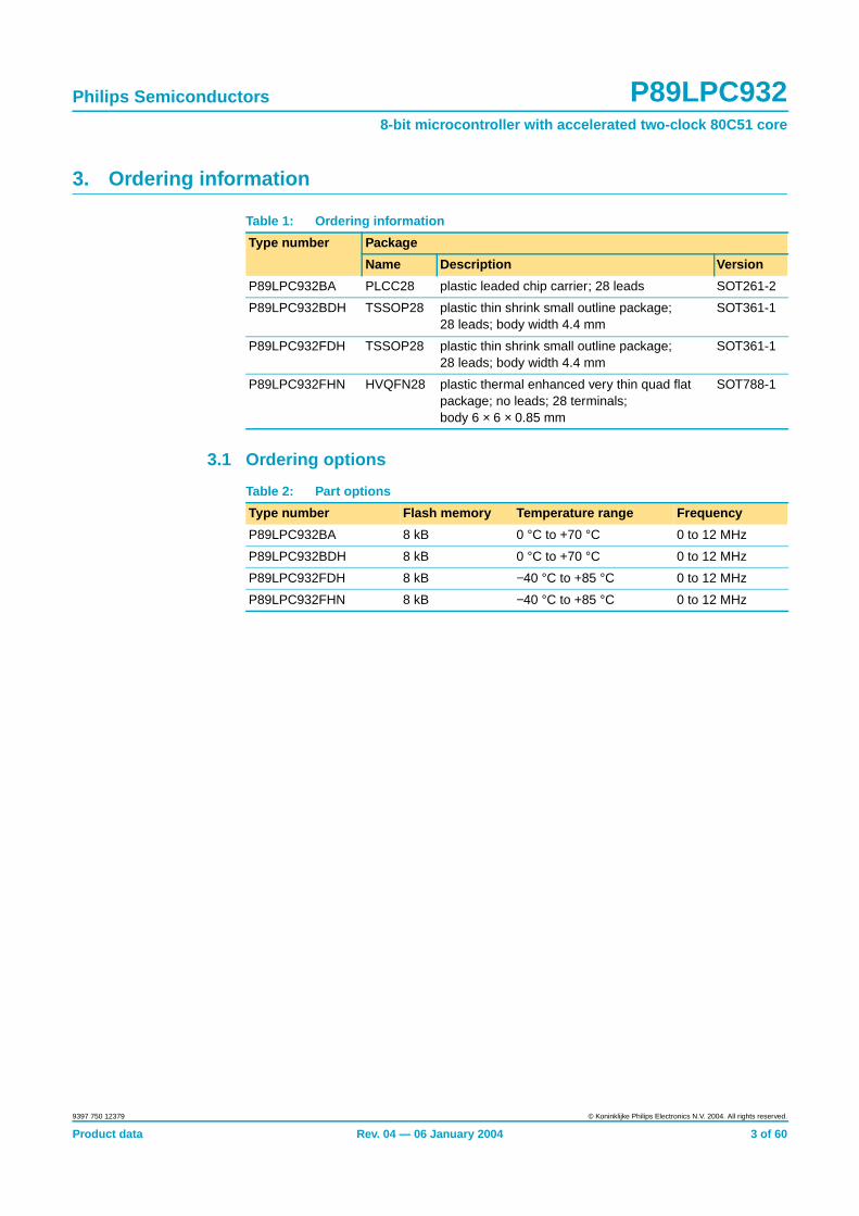
3. Ordering information
3.1 Ordering options
Table 1: Ordering information
Type number Package
Name Description Version
P89LPC932BA PLCC28 plastic leaded chip carrier; 28 leads SOT261-2
P89LPC932BDH TSSOP28 plastic thin shrink small outline package;28 leads; body width 4.4 mm
SOT361-1
P89LPC932FDH TSSOP28 plastic thin shrink small outline package;28 leads; body width 4.4 mm
SOT361-1
P89LPC932FHN HVQFN28 plastic thermal enhanced very thin quad flatpackage; no leads; 28 terminals;body 6 ´ 6 ´ 0.85 mm
SOT788-1
Table 2: Part options
Type number Flash memory Temperature range Frequency
P89LPC932BA 8 kB 0 °C to +70 °C 0 to 12 MHz
P89LPC932BDH 8 kB 0 °C to +70 °C 0 to 12 MHz
P89LPC932FDH 8 kB - 40 °C to +85 °C 0 to 12 MHz
P89LPC932FHN 8 kB - 40 °C to +85 °C 0 to 12 MHz
Product data Rev. 04 — 06 January 2004 3 of 60
9397 750 12379 © Koninklijke Philips Electronics N.V. 2004. All rights reserved.
Philips Semiconductors P89LPC9328-bit microcontroller with accelerated two-clock 80C51 core
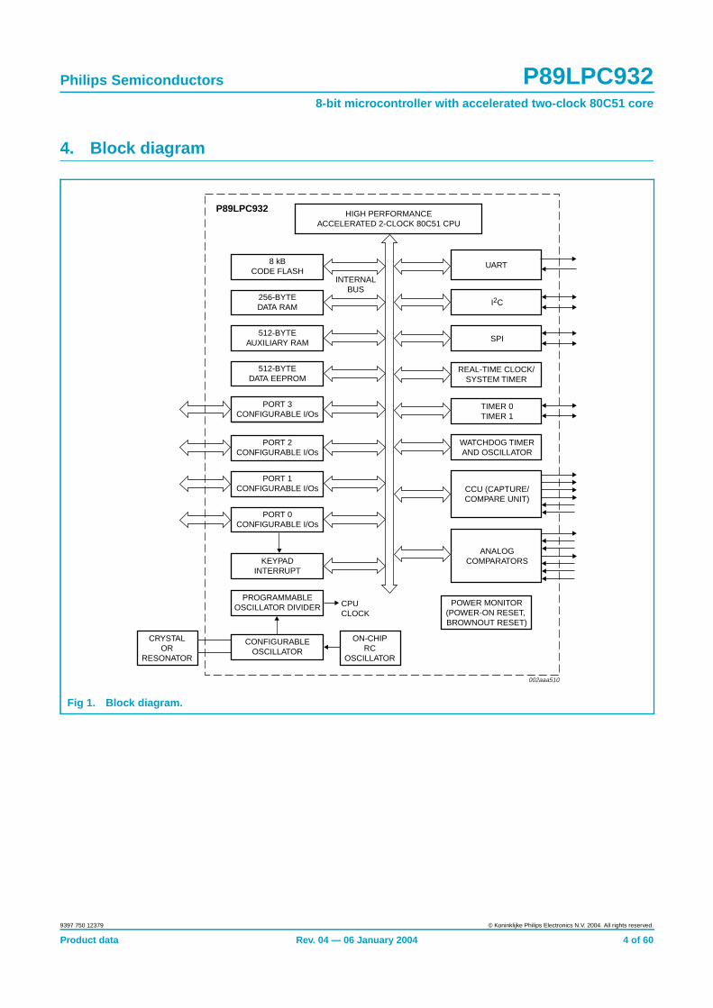
4. Block diagram
Fig 1. Block diagram.
HIGH PERFORMANCEACCELERATED 2-CLOCK 80C51 CPU
8 kBCODE FLASH
256-BYTEDATA RAM
PORT 2CONFIGURABLE I/Os
PORT 1CONFIGURABLE I/Os
PORT 0CONFIGURABLE I/Os
KEYPADINTERRUPT
PROGRAMMABLEOSCILLATOR DIVIDER CPU
CLOCK
CONFIGURABLEOSCILLATOR
ON-CHIPRC
OSCILLATOR
INTERNALBUS
CRYSTALOR
RESONATOR
POWER MONITOR(POWER-ON RESET, BROWNOUT RESET)
002aaa510
UART
REAL-TIME CLOCK/SYSTEM TIMER
SPI
TIMER 0TIMER 1
WATCHDOG TIMERAND OSCILLATOR
ANALOGCOMPARATORS
512-BYTEAUXILIARY RAM
I2C
512-BYTEDATA EEPROM
PORT 3CONFIGURABLE I/Os
CCU (CAPTURE/COMPARE UNIT)
P89LPC932
Product data Rev. 04 — 06 January 2004 4 of 60
9397 750 12379 © Koninklijke Philips Electronics N.V. 2004. All rights reserved.
Philips Semiconductors P89LPC9328-bit microcontroller with accelerated two-clock 80C51 core
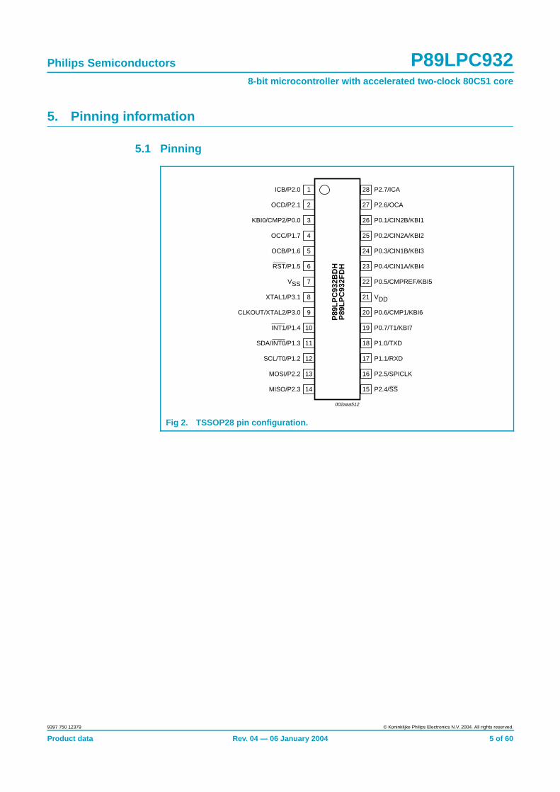
5. Pinning information
5.1 Pinning
Fig 2. TSSOP28 pin configuration.
handbook, halfpage
P89
LPC
932B
DH
P89
LPC
932F
DH
002aaa512
1
2
3
4
5
6
7
8
9
10
11
12
13
14
ICB/P2.0
OCD/P2.1
KBI0/CMP2/P0.0
OCC/P1.7
OCB/P1.6
RST/P1.5
VSS
XTAL1/P3.1
CLKOUT/XTAL2/P3.0
INT1/P1.4
SDA/INT0/P1.3
SCL/T0/P1.2
MOSI/P2.2
MISO/P2.3
P2.7/ICA
P2.6/OCA
P0.1/CIN2B/KBI1
P0.2/CIN2A/KBI2
P0.3/CIN1B/KBI3
P0.4/CIN1A/KBI4
P0.5/CMPREF/KBI5
VDD
P0.6/CMP1/KBI6
P0.7/T1/KBI7
P1.0/TXD
P1.1/RXD
P2.5/SPICLK
P2.4/SS
28
27
26
25
24
23
22
21
20
19
18
17
16
15
Product data Rev. 04 — 06 January 2004 5 of 60
9397 750 12379 © Koninklijke Philips Electronics N.V. 2004. All rights reserved.

Philips Semiconductors P89LPC9328-bit microcontroller with accelerated two-clock 80C51 core
Fig 3. PLCC28 pin configuration.
Fig 4. HVQFN28 pin configuration.
idth
P89LPC932BA
002aaa513
5
6
7
8
9
10
11
25
24
23
22
21
20
19
12 13 14 15 16 17 18
4 3 2 1 28 27 26
P1.
7/O
CC
P0.
0/C
MP
2/K
BI0
P2.
1/O
CD
P2.
0/IC
B
P2.
7/IC
A
P2.
6/O
CA
P0.
1/C
IN2B
/KB
I1
SC
L/T
0/P
1.2
MO
SI/P
2.2
MIS
O/P
2.3
SS
/P2.
4
SP
ICLK
/P2.
5
RX
D/P
1.1
TX
D/P
1.0
OCB/P1.6
RST/P1.5
VSS
XTAL1/P3.1
CLKOUT/XTAL2/P3.0
INT1/P1.4
SDA/INT0/P1.3
P0.2/CIN2A/KBI2
P0.3/CIN1B/KBI3
P0.4/CIN1A/KBI4
P0.5/CMPREF/KBI5
VDD
P0.6/CMP1/KBI6
P0.7/T1/KBI7
P89LPC932FHN
002aaa514
INT1/P1.4
SDA/INT0/P1.3
CLKOUT/XTAL2/P3.0
XTAL1/P3.1
VSS
RST/P1.5
OCB/P1.6
2
1
3
4
5
6
7
P1.
2/T
0/S
CL
P2.
5/S
PIC
LK
P2.
3/M
ISO
P2.
4/S
S
P2.
2/M
OS
I
P1.
1/R
XD
P1.
0/T
XD
1311 14121098
ICB
/P2.
0
KB
I0/C
MP
2/P
0.0
OC
D/P
2.1
OC
C/P
1.7
ICA
/P2.
7
KB
I1/C
IN2B
/P0.
1
OC
A/P
2.6
2225 2324262728
P0.6/CMP1/KBI6
P0.7/T1/KBI7
P0.5/CMPREF/KBI5
VDD
P0.4/CIN1A/KBI4
P0.3/CIN1B/KBI3
P0.2/CIN2A/KBI221
19
20
18
17
16
15
Product data Rev. 04 — 06 January 2004 6 of 60
9397 750 12379 © Koninklijke Philips Electronics N.V. 2004. All rights reserved.
Philips Semiconductors P89LPC9328-bit microcontroller with accelerated two-clock 80C51 core
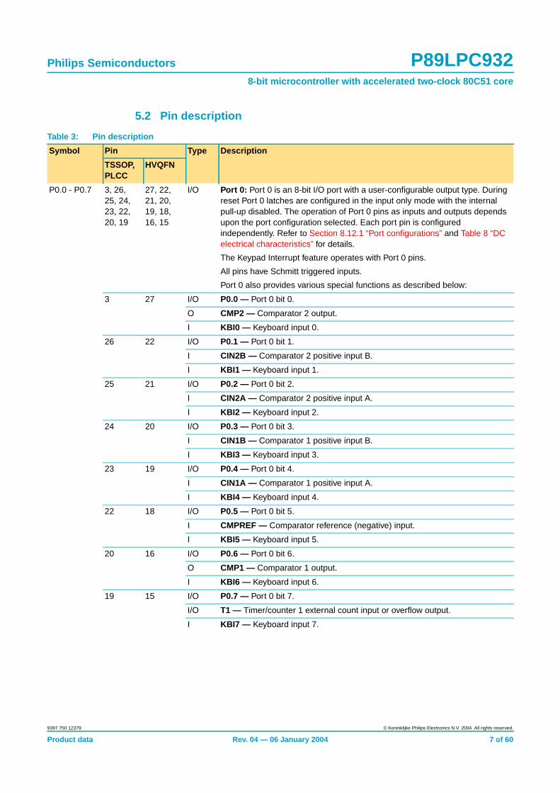
5.2 Pin description
Table 3: Pin description
Symbol Pin Type Description
TSSOP,PLCC
HVQFN
P0.0 - P0.7 3, 26,25, 24,23, 22,20, 19
27, 22,21, 20,19, 18,16, 15
I/O Port 0: Port 0 is an 8-bit I/O port with a user-configurable output type. Duringreset Port 0 latches are configured in the input only mode with the internalpull-up disabled. The operation of Port 0 pins as inputs and outputs dependsupon the port configuration selected. Each port pin is configuredindependently. Refer to Section 8.12.1 “Port configurations” and Table 8 “DCelectrical characteristics” for details.
The Keypad Interrupt feature operates with Port 0 pins.
All pins have Schmitt triggered inputs.
Port 0 also provides various special functions as described below:
3 27 I/O P0.0 — Port 0 bit 0.
O CMP2 — Comparator 2 output.
I KBI0 — Keyboard input 0.
26 22 I/O P0.1 — Port 0 bit 1.
I CIN2B — Comparator 2 positive input B.
I KBI1 — Keyboard input 1.
25 21 I/O P0.2 — Port 0 bit 2.
I CIN2A — Comparator 2 positive input A.
I KBI2 — Keyboard input 2.
24 20 I/O P0.3 — Port 0 bit 3.
I CIN1B — Comparator 1 positive input B.
I KBI3 — Keyboard input 3.
23 19 I/O P0.4 — Port 0 bit 4.
I CIN1A — Comparator 1 positive input A.
I KBI4 — Keyboard input 4.
22 18 I/O P0.5 — Port 0 bit 5.
I CMPREF — Comparator reference (negative) input.
I KBI5 — Keyboard input 5.
20 16 I/O P0.6 — Port 0 bit 6.
O CMP1 — Comparator 1 output.
I KBI6 — Keyboard input 6.
19 15 I/O P0.7 — Port 0 bit 7.
I/O T1 — Timer/counter 1 external count input or overflow output.
I KBI7 — Keyboard input 7.
Product data Rev. 04 — 06 January 2004 7 of 60
9397 750 12379 © Koninklijke Philips Electronics N.V. 2004. All rights reserved.
Philips Semiconductors P89LPC9328-bit microcontroller with accelerated two-clock 80C51 core
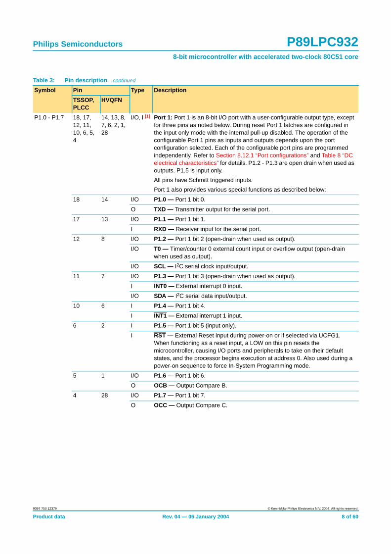
P1.0 - P1.7 18, 17,12, 11,10, 6, 5,4
14, 13, 8,7, 6, 2, 1,28
I/O, I [1] Port 1: Port 1 is an 8-bit I/O port with a user-configurable output type, exceptfor three pins as noted below. During reset Port 1 latches are configured inthe input only mode with the internal pull-up disabled. The operation of theconfigurable Port 1 pins as inputs and outputs depends upon the portconfiguration selected. Each of the configurable port pins are programmedindependently. Refer to Section 8.12.1 “Port configurations” and Table 8 “DCelectrical characteristics” for details. P1.2 - P1.3 are open drain when used asoutputs. P1.5 is input only.
All pins have Schmitt triggered inputs.
Port 1 also provides various special functions as described below:
18 14 I/O P1.0 — Port 1 bit 0.
O TXD — Transmitter output for the serial port.
17 13 I/O P1.1 — Port 1 bit 1.
I RXD — Receiver input for the serial port.
12 8 I/O P1.2 — Port 1 bit 2 (open-drain when used as output).
I/O T0 — Timer/counter 0 external count input or overflow output (open-drainwhen used as output).
I/O SCL — I2C serial clock input/output.
11 7 I/O P1.3 — Port 1 bit 3 (open-drain when used as output).
I INT0 — External interrupt 0 input.
I/O SDA — I2C serial data input/output.
10 6 I P1.4 — Port 1 bit 4.
I INT1 — External interrupt 1 input.
6 2 I P1.5 — Port 1 bit 5 (input only).
I RST — External Reset input during power-on or if selected via UCFG1.When functioning as a reset input, a LOW on this pin resets themicrocontroller, causing I/O ports and peripherals to take on their defaultstates, and the processor begins execution at address 0. Also used during apower-on sequence to force In-System Programming mode.
5 1 I/O P1.6 — Port 1 bit 6.
O OCB — Output Compare B.
4 28 I/O P1.7 — Port 1 bit 7.
O OCC — Output Compare C.
Table 3: Pin description …continued
Symbol Pin Type Description
TSSOP,PLCC
HVQFN
Product data Rev. 04 — 06 January 2004 8 of 60
9397 750 12379 © Koninklijke Philips Electronics N.V. 2004. All rights reserved.

Philips Semiconductors P89LPC9328-bit microcontroller with accelerated two-clock 80C51 core
P2.0 - P2.7 1, 2, 13,14, 15,16, 27,28
25, 26, 9,10, 11,12, 23,24
I/O Port 2: Port 2 is an 8-bit I/O port with a user-configurable output type. Duringreset Port 2 latches are configured in the input only mode with the internalpull-up disabled. The operation of Port 2 pins as inputs and outputs dependsupon the port configuration selected. Each port pin is configuredindependently. Refer to Section 8.12.1 “Port configurations” and Table 8 “DCelectrical characteristics” for details.
All pins have Schmitt triggered inputs.
Port 2 also provides various special functions as described below:
1 25 I/O P2.0 — Port 2 bit 0.
I ICB — Input Capture B.
2 26 I/O P2.1 — Port 2 bit 1.
O OCD — Output Compare D.
13 9 I/O P2.2 — Port 2 bit 2.
I/O MOSI — SPI master out slave in. When configured as master, this pin isoutput; when configured as slave, this pin is input.
14 10 I/O P2.3 — Port 2 bit 3.
I/O MISO — When configured as master, this pin is input, when configured asslave, this pin is output.
15 11 I/O P2.4 — Port 2 bit 4.
I SS — SPI Slave select.
16 12 I/O P2.5 — Port 2 bit 5.
I/O SPICLK — SPI clock. When configured as master, this pin is output; whenconfigured as slave, this pin is input.
27 23 I/O P2.6 — Port 2 bit 6.
O OCA — Output Compare A.
28 24 I/O P2.7 — Port 2 bit 7.
I ICA — Input Capture A.
Table 3: Pin description …continued
Symbol Pin Type Description
TSSOP,PLCC
HVQFN
Product data Rev. 04 — 06 January 2004 9 of 60
9397 750 12379 © Koninklijke Philips Electronics N.V. 2004. All rights reserved.

Philips Semiconductors P89LPC9328-bit microcontroller with accelerated two-clock 80C51 core
[1] Input/Output for P1.0-P1.4, P1.6, P1.7. Input for P1.5.
P3.0 - P3.1 9, 8 5, 4 I/O Port 3: Port 3 is a 2-bit I/O port with a user-configurable output type. Duringreset Port 3 latches are configured in the input only mode with the internalpull-up disabled. The operation of Port 3 pins as inputs and outputs dependsupon the port configuration selected. Each port pin is configuredindependently. Refer to Section 8.12.1 “Port configurations” and Table 8 “DCelectrical characteristics” for details.
All pins have Schmitt triggered inputs.
Port 3 also provides various special functions as described below:
9 5 I/O P3.0 — Port 3 bit 0.
O XTAL2 — Output from the oscillator amplifier (when a crystal oscillator optionis selected via the FLASH configuration.
O CLKOUT — CPU clock divided by 2 when enabled via SFR bit (ENCLK -TRIM.6). It can be used if the CPU clock is the internal RC oscillator,watchdog oscillator or external clock input, except when XTAL1/XTAL2 areused to generate clock source for the Real-Time clock/system timer.
8 4 I/O P3.1 — Port 3 bit 1.
I XTAL1 — Input to the oscillator circuit and internal clock generator circuits(when selected via the FLASH configuration). It can be a port pin if internalRC oscillator or watchdog oscillator is used as the CPU clock source, and ifXTAL1/XTAL2 are not used to generate the clock for the Real-Timeclock/system timer.
VSS 7 3 I Ground: 0 V reference.
VDD 21 17 I Power Supply: This is the power supply voltage for normal operation as wellas Idle and Power-Down modes.
Table 3: Pin description …continued
Symbol Pin Type Description
TSSOP,PLCC
HVQFN
Product data Rev. 04 — 06 January 2004 10 of 60
9397 750 12379 © Koninklijke Philips Electronics N.V. 2004. All rights reserved.
Philips Semiconductors P89LPC9328-bit microcontroller with accelerated two-clock 80C51 core
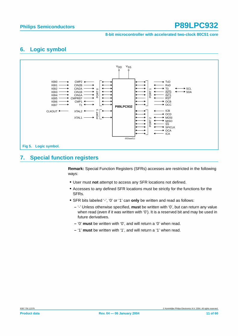
6. Logic symbol
7. Special function registers
Remark: Special Function Registers (SFRs) accesses are restricted in the followingways:
• User must not attempt to access any SFR locations not defined.
• Accesses to any defined SFR locations must be strictly for the functions for theSFRs.
• SFR bits labeled ‘-’, ‘0’ or ‘1’ can only be written and read as follows:
– ‘-’ Unless otherwise specified, must be written with ‘0’, but can return any valuewhen read (even if it was written with ‘0’). It is a reserved bit and may be used infuture derivatives.
– ‘0’ must be written with ‘0’, and will return a ‘0’ when read.
– ‘1’ must be written with ‘1’, and will return a ‘1’ when read.
Fig 5. Logic symbol.
VDD VSS
P89LPC932
PO
RT
0P
OR
T 3
PO
RT
1
TxDRxDT0INT0INT1RST
SCLSDA
002aaa511
CMP2CIN2BCIN2ACIN1BCIN1A
CMPREFCMP1
T1
XTAL2
XTAL1
KBI0KBI1KBI2KBI3KBI4KBI5KBI6KBI7
CLKOUT
OCBOCC
PO
RT
2
ICBOCDMOSIMISOSSSPICLKOCAICA
Product data Rev. 04 — 06 January 2004 11 of 60
9397 750 12379 © Koninklijke Philips Electronics N.V. 2004. All rights reserved.
xxxxxxxxxxxxxxxxxxxxx xxxxxxxxxxxxxxxxxxxxxxxxxx xxxxxxx x x x xxxxxxxxxxxxxxxxxxxxxxxxxxxxxx xxxxxxxxxxxxxxxxxxx xx xxxxxxx xxxxxxxxxxxxxxxxxxxxxxxxxxx xxxxxxxxxxxxxxxxxxx xxxxxx xxxxxxxxxxxxxxxxxxxxxxxxxxxxxxxxxxx xxxxxxxxxxxx x xxxxxxxxxxxxxxxxxxxxxx xxxxxxxxxxxxxxxxxxxxxxxxxxxxxx xxxxx xxxxxxxxxxxxxxxxxxxxxxxxxxxxxxxxxxxxxxxxxxxxxxxxxx xxxxxxxxxxxxxxxxxxxxxxxxxxxxxxxxx xxxxxxxxxxxxxxxxxxxx xxx P
hilips Sem
iconductorsP
89LPC
9328-bit m
icrocontroller with accelerated tw
o-clock 80C51 core
9397 750 12379
Product data
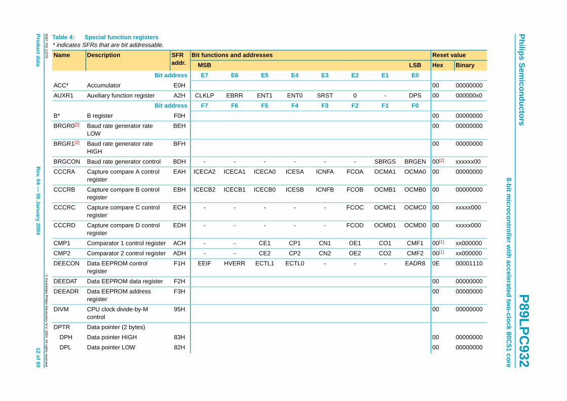
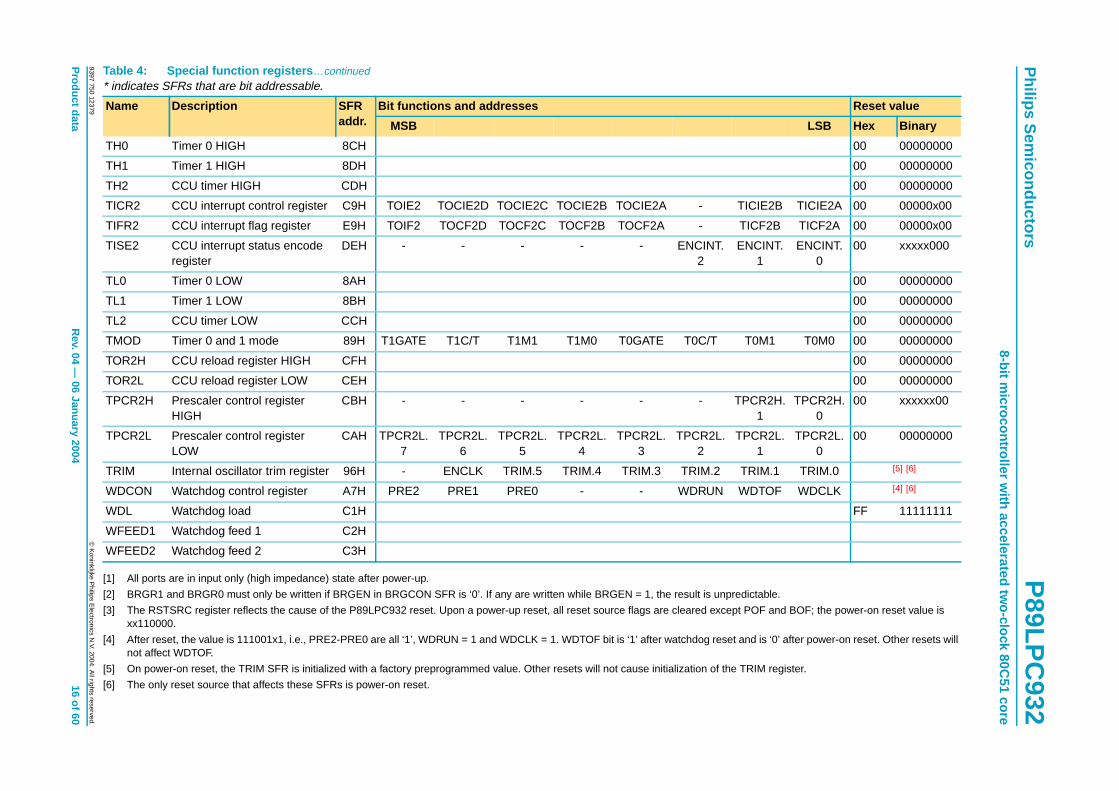
Table 4: Special function registers* indicates SFRs that are bit addressable.
Name Description SFRaddr.
Bit functions and addresses Reset value
MSB LSB Hex Binary
E1 E0
00 00000000
- DPS 00 000000x0
F1 F0
00 00000000
00 00000000
00 00000000
SBRGS BRGEN 00[2] xxxxxx00
OCMA1 OCMA0 00 00000000
OCMB1 OCMB0 00 00000000
OCMC1 OCMC0 00 xxxxx000
OCMD1 OCMD0 00 xxxxx000
CO1 CMF1 00[1] xx000000
CO2 CMF2 00[1] xx000000
- EADR8 0E 00001110
00 00000000
00 00000000
00 00000000
00 00000000
00 00000000
© K
oninklijke Philips E
lectronics N.V. 2004. A
ll rights reserved.
Rev. 04 —
06 January 200412 of 60
Bit address E7 E6 E5 E4 E3 E2
ACC* Accumulator E0H
AUXR1 Auxiliary function register A2H CLKLP EBRR ENT1 ENT0 SRST 0
Bit address F7 F6 F5 F4 F3 F2
B* B register F0H
BRGR0[2] Baud rate generator rateLOW
BEH
BRGR1[2] Baud rate generator rateHIGH
BFH
BRGCON Baud rate generator control BDH - - - - - -
CCCRA Capture compare A controlregister
EAH ICECA2 ICECA1 ICECA0 ICESA ICNFA FCOA
CCCRB Capture compare B controlregister
EBH ICECB2 ICECB1 ICECB0 ICESB ICNFB FCOB
CCCRC Capture compare C controlregister
ECH - - - - - FCOC
CCCRD Capture compare D controlregister
EDH - - - - - FCOD
CMP1 Comparator 1 control register ACH - - CE1 CP1 CN1 OE1
CMP2 Comparator 2 control register ADH - - CE2 CP2 CN2 OE2
DEECON Data EEPROM controlregister
F1H EEIF HVERR ECTL1 ECTL0 - -
DEEDAT Data EEPROM data register F2H
DEEADR Data EEPROM addressregister
F3H
DIVM CPU clock divide-by-Mcontrol
95H
DPTR Data pointer (2 bytes)
DPH Data pointer HIGH 83H
DPL Data pointer LOW 82H

xxxxxxxxxxxxxxxxxxxxx xxxxxxxxxxxxxxxxxxxxxxxxxx xxxxxxx x x x xxxxxxxxxxxxxxxxxxxxxxxxxxxxxx xxxxxxxxxxxxxxxxxxx xx xxxxxxx xxxxxxxxxxxxxxxxxxxxxxxxxxx xxxxxxxxxxxxxxxxxxx xxxxxx xxxxxxxxxxxxxxxxxxxxxxxxxxxxxxxxxxx xxxxxxxxxxxx x xxxxxxxxxxxxxxxxxxxxxx xxxxxxxxxxxxxxxxxxxxxxxxxxxxxx xxxxx xxxxxxxxxxxxxxxxxxxxxxxxxxxxxxxxxxxxxxxxxxxxxxxxxx xxxxxxxxxxxxxxxxxxxxxxxxxxxxxxxxx xxxxxxxxxxxxxxxxxxxx xxx P
hilips Sem
iconductorsP
89LPC
9328-bit m
icrocontroller with accelerated tw
o-clock 80C51 core
9397 750 12379
Product data
2 I2ADR.0 GC 00 00000000
D9 D8
- CRSEL 00 x00000x0
00 00000000
00 00000000
0 0 F8 11111000
00 00000000
00 00000000
00 00000000
00 00000000
A9 A8
ET0 EX0 00 00000000
E9 E8
EKBI EI2C 00[1] 00x00000
B9 B8
PT0 PX0 00[1] x0000000
PT0H PX0H 00[1] x0000000
F9 F8
PKBI PI2C 00[1] 00x00000
PKBIH PI2CH 00[1] 00x00000
PATN_SEL
KBIF 00[1] xxxxxx00
00 00000000
FF 11111111
Table 4: Special function registers …continued* indicates SFRs that are bit addressable.
Name Description SFRaddr.
Bit functions and addresses Reset value
MSB LSB Hex Binary
© K
oninklijke Philips E
lectronics N.V. 2004. A
ll rights reserved.
Rev. 04 —
06 January 200413 of 60
I2ADR I C slave address register DBH I2ADR.6 I2ADR.5 I2ADR.4 I2ADR.3 I2ADR.2 I2ADR.1
Bit address DF DE DD DC DB DA
I2CON* I2C control register D8H - I2EN STA STO SI AA
I2DAT I2C data register DAH
I2SCLH Serial clock generator/SCLduty cycle register HIGH
DDH
I2SCLL Serial clock generator/SCLduty cycle register LOW
DCH
I2STAT I2C status register D9H STA.4 STA.3 STA.2 STA.1 STA.0 0
ICRAH Input capture A register HIGH ABH
ICRAL Input capture A register LOW AAH
ICRBH Input capture B register HIGH AFH
ICRBL Input capture B register LOW AEH
Bit address AF AE AD AC AB AA
IEN0* Interrupt enable 0 A8H EA EWDRT EBO ES/ESR ET1 EX1
Bit address EF EE ED EC EB EA
IEN1* Interrupt enable 1 E8H EIEE EST - ECCU ESPI EC
Bit address BF BE BD BC BB BA
IP0* Interrupt priority 0 B8H - PWDRT PBO PS/PSR PT1 PX1
IP0H Interrupt priority 0 HIGH B7H - PWDRTH
PBOH PSH/PSRH
PT1H PX1H
Bit address FF FE FD FC FB FA
IP1* Interrupt priority 1 F8H PIEE PST - PCCU PSPI PC
IP1H Interrupt priority 1 HIGH F7H PIEEH PSTH - PCCUH PSPIH PCH
KBCON Keypad control register 94H - - - - - -
KBMASK Keypad interrupt maskregister
86H
KBPATN Keypad pattern register 93H
xxxxxxxxxxxxxxxxxxxxx xxxxxxxxxxxxxxxxxxxxxxxxxx xxxxxxx x x x xxxxxxxxxxxxxxxxxxxxxxxxxxxxxx xxxxxxxxxxxxxxxxxxx xx xxxxxxx xxxxxxxxxxxxxxxxxxxxxxxxxxx xxxxxxxxxxxxxxxxxxx xxxxxx xxxxxxxxxxxxxxxxxxxxxxxxxxxxxxxxxxx xxxxxxxxxxxx x xxxxxxxxxxxxxxxxxxxxxx xxxxxxxxxxxxxxxxxxxxxxxxxxxxxx xxxxx xxxxxxxxxxxxxxxxxxxxxxxxxxxxxxxxxxxxxxxxxxxxxxxxxx xxxxxxxxxxxxxxxxxxxxxxxxxxxxxxxxx xxxxxxxxxxxxxxxxxxxx xxx P
hilips Sem
iconductorsP
89LPC
9328-bit m
icrocontroller with accelerated tw
o-clock 80C51 core
9397 750 12379
Product data
00 00000000
00 00000000
00 00000000
00 00000000
00 00000000
00 00000000
00 00000000
00 00000000
81 80
CIN2B/KB1
CMP2/KB0
[1]
91 90
RXD TXD [1]
91 90
OCD ICB [1]
B1 B0
XTAL1 XTAL2 [1]
P0M1.1) (P0M1.0) FF[1] 11111111
P0M2.1) (P0M2.0) 00[1] 00000000
P1M1.1) (P1M1.0) D3[1] 11x1xx11
P1M2.1) (P1M2.0) 00[1] 00x0xx00
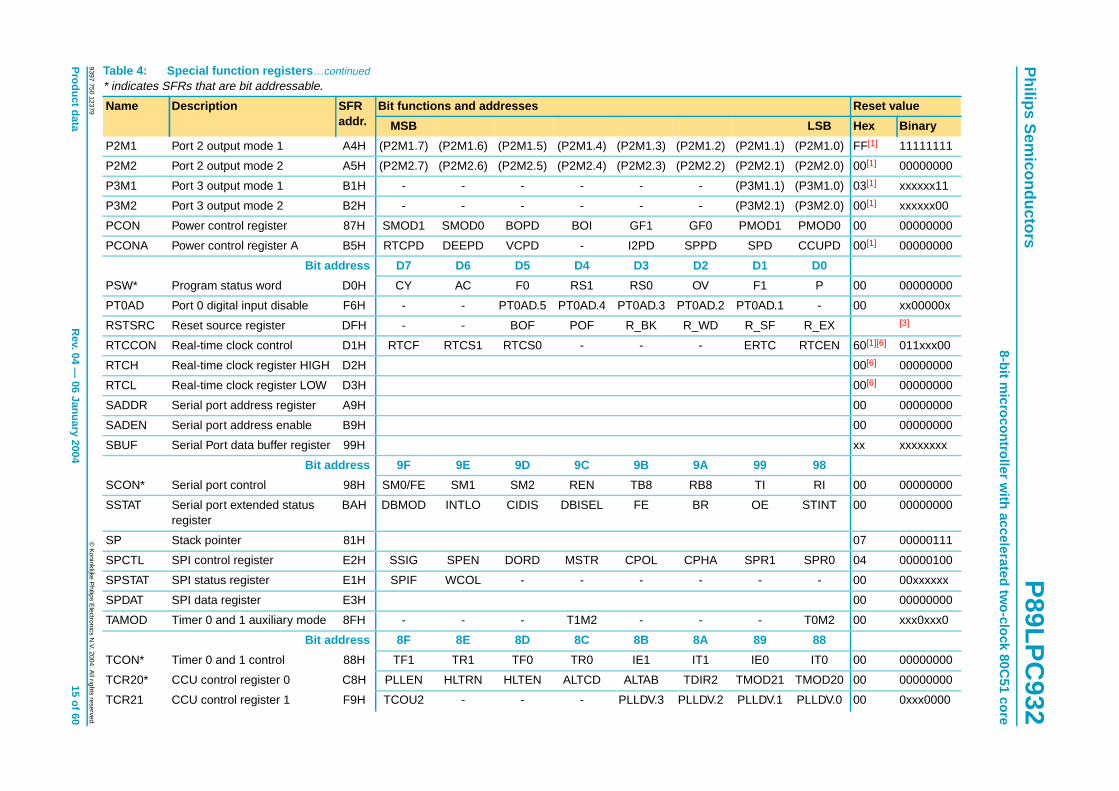
Table 4: Special function registers …continued* indicates SFRs that are bit addressable.
Name Description SFRaddr.
Bit functions and addresses Reset value
MSB LSB Hex Binary
© K
oninklijke Philips E
lectronics N.V. 2004. A
ll rights reserved.
Rev. 04 —
06 January 200414 of 60
OCRAH Output compare A registerHIGH
EFH
OCRAL Output compare A registerLOW
EEH
OCRBH Output compare B registerHIGH
FBH
OCRBL Output compare B registerLOW
FAH
OCRCH Output compare C registerHIGH
FDH
OCRCL Output compare C registerLOW
FCH
OCRDH Output compare D registerHIGH
FFH
OCRDL Output compare D registerLOW
FEH
Bit address 87 86 85 84 83 82
P0* Port 0 80H T1/KB7 CMP1/KB6
CMPREF/KB5
CIN1A/KB4
CIN1B/KB3
CIN2A/KB2
Bit address 97 96 95 94 93 92
P1* Port 1 90H OCC OCB RST INT1 INT0/SDA
T0/SCL
Bit address 97 96 95 94 93 92
P2* Port 2 A0H ICA OCA SPICLK SS MISO MOSI
Bit address B7 B6 B5 B4 B3 B2
P3* Port 3 B0H - - - - - -
P0M1 Port 0 output mode 1 84H (P0M1.7) (P0M1.6) (P0M1.5) (P0M1.4) (P0M1.3) (P0M1.2) (
P0M2 Port 0 output mode 2 85H (P0M2.7) (P0M2.6) (P0M2.5) (P0M2.4) (P0M2.3) (P0M2.2) (
P1M1 Port 1 output mode 1 91H (P1M1.7) (P1M1.6) - (P1M1.4) (P1M1.3) (P1M1.2) (
P1M2 Port 1 output mode 2 92H (P1M2.7) (P1M2.6) - (P1M2.4) (P1M2.3) (P1M2.2) (
xxxxxxxxxxxxxxxxxxxxx xxxxxxxxxxxxxxxxxxxxxxxxxx xxxxxxx x x x xxxxxxxxxxxxxxxxxxxxxxxxxxxxxx xxxxxxxxxxxxxxxxxxx xx xxxxxxx xxxxxxxxxxxxxxxxxxxxxxxxxxx xxxxxxxxxxxxxxxxxxx xxxxxx xxxxxxxxxxxxxxxxxxxxxxxxxxxxxxxxxxx xxxxxxxxxxxx x xxxxxxxxxxxxxxxxxxxxxx xxxxxxxxxxxxxxxxxxxxxxxxxxxxxx xxxxx xxxxxxxxxxxxxxxxxxxxxxxxxxxxxxxxxxxxxxxxxxxxxxxxxx xxxxxxxxxxxxxxxxxxxxxxxxxxxxxxxxx xxxxxxxxxxxxxxxxxxxx xxx P
hilips Sem
iconductorsP
89LPC
9328-bit m
icrocontroller with accelerated tw
o-clock 80C51 core
9397 750 12379
Product data
P2M1.1) (P2M1.0) FF[1] 11111111
P2M2.1) (P2M2.0) 00[1] 00000000
P3M1.1) (P3M1.0) 03[1] xxxxxx11
P3M2.1) (P3M2.0) 00[1] xxxxxx00
PMOD1 PMOD0 00 00000000
SPD CCUPD 00[1] 00000000
D1 D0
F1 P 00 00000000
T0AD.1 - 00 xx00000x
R_SF R_EX [3]
ERTC RTCEN 60[1][6] 011xxx00
00[6] 00000000
00[6] 00000000
00 00000000
00 00000000
xx xxxxxxxx
99 98
TI RI 00 00000000
OE STINT 00 00000000
07 00000111
SPR1 SPR0 04 00000100
- - 00 00xxxxxx
00 00000000
- T0M2 00 xxx0xxx0
89 88
IE0 IT0 00 00000000
MOD21 TMOD20 00 00000000
PLLDV.1 PLLDV.0 00 0xxx0000
Table 4: Special function registers …continued* indicates SFRs that are bit addressable.
Name Description SFRaddr.
Bit functions and addresses Reset value
MSB LSB Hex Binary
© K
oninklijke Philips E
lectronics N.V. 2004. A
ll rights reserved.
Rev. 04 —
06 January 200415 of 60
P2M1 Port 2 output mode 1 A4H (P2M1.7) (P2M1.6) (P2M1.5) (P2M1.4) (P2M1.3) (P2M1.2) (
P2M2 Port 2 output mode 2 A5H (P2M2.7) (P2M2.6) (P2M2.5) (P2M2.4) (P2M2.3) (P2M2.2) (
P3M1 Port 3 output mode 1 B1H - - - - - - (
P3M2 Port 3 output mode 2 B2H - - - - - - (
PCON Power control register 87H SMOD1 SMOD0 BOPD BOI GF1 GF0
PCONA Power control register A B5H RTCPD DEEPD VCPD - I2PD SPPD
Bit address D7 D6 D5 D4 D3 D2
PSW* Program status word D0H CY AC F0 RS1 RS0 OV
PT0AD Port 0 digital input disable F6H - - PT0AD.5 PT0AD.4 PT0AD.3 PT0AD.2 P
RSTSRC Reset source register DFH - - BOF POF R_BK R_WD
RTCCON Real-time clock control D1H RTCF RTCS1 RTCS0 - - -
RTCH Real-time clock register HIGH D2H
RTCL Real-time clock register LOW D3H
SADDR Serial port address register A9H
SADEN Serial port address enable B9H
SBUF Serial Port data buffer register 99H
Bit address 9F 9E 9D 9C 9B 9A
SCON* Serial port control 98H SM0/FE SM1 SM2 REN TB8 RB8
SSTAT Serial port extended statusregister
BAH DBMOD INTLO CIDIS DBISEL FE BR
SP Stack pointer 81H
SPCTL SPI control register E2H SSIG SPEN DORD MSTR CPOL CPHA
SPSTAT SPI status register E1H SPIF WCOL - - - -
SPDAT SPI data register E3H
TAMOD Timer 0 and 1 auxiliary mode 8FH - - - T1M2 - -
Bit address 8F 8E 8D 8C 8B 8A
TCON* Timer 0 and 1 control 88H TF1 TR1 TF0 TR0 IE1 IT1
TCR20* CCU control register 0 C8H PLLEN HLTRN HLTEN ALTCD ALTAB TDIR2 T
TCR21 CCU control register 1 F9H TCOU2 - - - PLLDV.3 PLLDV.2
xxxxxxxxxxxxxxxxxxxxx xxxxxxxxxxxxxxxxxxxxxxxxxx xxxxxxx x x x xxxxxxxxxxxxxxxxxxxxxxxxxxxxxx xxxxxxxxxxxxxxxxxxx xx xxxxxxx xxxxxxxxxxxxxxxxxxxxxxxxxxx xxxxxxxxxxxxxxxxxxx xxxxxx xxxxxxxxxxxxxxxxxxxxxxxxxxxxxxxxxxx xxxxxxxxxxxx x xxxxxxxxxxxxxxxxxxxxxx xxxxxxxxxxxxxxxxxxxxxxxxxxxxxx xxxxx xxxxxxxxxxxxxxxxxxxxxxxxxxxxxxxxxxxxxxxxxxxxxxxxxx xxxxxxxxxxxxxxxxxxxxxxxxxxxxxxxxx xxxxxxxxxxxxxxxxxxxx xxx P
hilips Sem
iconductorsP
89LPC
9328-bit m
icrocontroller with accelerated tw
o-clock 80C51 core
9397 750 12379
Product data
dictable.
t POF and BOF; the power-on reset value is
and is ‘0’ after power-on reset. Other resets will
TRIM register.
00 00000000
00 00000000
00 00000000
TICIE2B TICIE2A 00 00000x00
TICF2B TICF2A 00 00000x00
ENCINT.1
ENCINT.0
00 xxxxx000
00 00000000
00 00000000
00 00000000
T0M1 T0M0 00 00000000
00 00000000
00 00000000
PCR2H.1
TPCR2H.0
00 xxxxxx00
PCR2L.1
TPCR2L.0
00 00000000
TRIM.1 TRIM.0 [5] [6]
WDTOF WDCLK [4] [6]
FF 11111111
Table 4: Special function registers …continued* indicates SFRs that are bit addressable.
Name Description SFRaddr.
Bit functions and addresses Reset value
MSB LSB Hex Binary
© K
oninklijke Philips E
lectronics N.V. 2004. A
ll rights reserved.
Rev. 04 —
06 January 200416 of 60
[1] All ports are in input only (high impedance) state after power-up.
[2] BRGR1 and BRGR0 must only be written if BRGEN in BRGCON SFR is ‘0’. If any are written while BRGEN = 1, the result is unpre
[3] The RSTSRC register reflects the cause of the P89LPC932 reset. Upon a power-up reset, all reset source flags are cleared excepxx110000.
[4] After reset, the value is 111001x1, i.e., PRE2-PRE0 are all ‘1’, WDRUN = 1 and WDCLK = 1. WDTOF bit is ‘1’ after watchdog resetnot affect WDTOF.
[5] On power-on reset, the TRIM SFR is initialized with a factory preprogrammed value. Other resets will not cause initialization of the
[6] The only reset source that affects these SFRs is power-on reset.
TH0 Timer 0 HIGH 8CH
TH1 Timer 1 HIGH 8DH
TH2 CCU timer HIGH CDH
TICR2 CCU interrupt control register C9H TOIE2 TOCIE2D TOCIE2C TOCIE2B TOCIE2A -
TIFR2 CCU interrupt flag register E9H TOIF2 TOCF2D TOCF2C TOCF2B TOCF2A -
TISE2 CCU interrupt status encoderegister
DEH - - - - - ENCINT.2
TL0 Timer 0 LOW 8AH
TL1 Timer 1 LOW 8BH
TL2 CCU timer LOW CCH
TMOD Timer 0 and 1 mode 89H T1GATE T1C/T T1M1 T1M0 T0GATE T0C/T
TOR2H CCU reload register HIGH CFH
TOR2L CCU reload register LOW CEH
TPCR2H Prescaler control registerHIGH
CBH - - - - - - T
TPCR2L Prescaler control registerLOW
CAH TPCR2L.7
TPCR2L.6
TPCR2L.5
TPCR2L.4
TPCR2L.3
TPCR2L.2
T
TRIM Internal oscillator trim register 96H - ENCLK TRIM.5 TRIM.4 TRIM.3 TRIM.2
WDCON Watchdog control register A7H PRE2 PRE1 PRE0 - - WDRUN
WDL Watchdog load C1H
WFEED1 Watchdog feed 1 C2H
WFEED2 Watchdog feed 2 C3H
Philips Semiconductors P89LPC9328-bit microcontroller with accelerated two-clock 80C51 core
8. Functional description
Remark: Please refer to the P89LPC932 User’s Manual for a more detailedfunctional description.
8.1 Enhanced CPUThe P89LPC932 uses an enhanced 80C51 CPU which runs at 6 times the speed ofstandard 80C51 devices. A machine cycle consists of two CPU clock cycles, andmost instructions execute in one or two machine cycles.
8.2 Clocks
8.2.1 Clock definitions
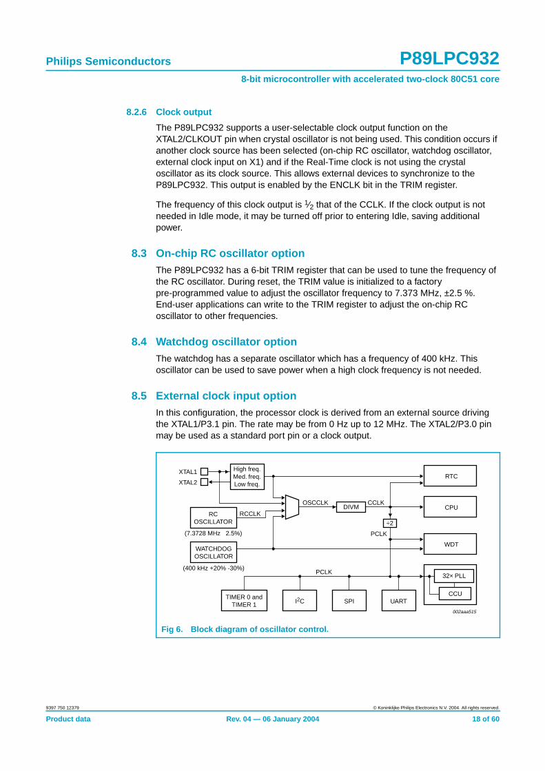
The P89LPC932 device has several internal clocks as defined below:
OSCCLK — Input to the DIVM clock divider. OSCCLK is selected from one of fourclock sources (see Figure 6) and can also be optionally divided to a slower frequency(see Section 8.7 “CPU Clock (CCLK) modification: DIVM register”).
Note: fOSC is defined as the OSCCLK frequency.
CCLK — CPU clock; output of the clock divider. There are two CCLK cycles permachine cycle, and most instructions are executed in one to two machine cycles (twoor four CCLK cycles).
RCCLK — The internal 7.373 MHz RC oscillator output.
PCLK — Clock for the various peripheral devices and is CCLK¤ 2.
8.2.2 CPU clock (OSCCLK)
The P89LPC932 provides several user-selectable oscillator options in generating theCPU clock. This allows optimization for a range of needs from high precision to lowestpossible cost. These options are configured when the FLASH is programmed andinclude an on-chip watchdog oscillator, an on-chip RC oscillator, an oscillator usingan external crystal, or an external clock source. The crystal oscillator can beoptimized for low, medium, or high frequency crystals covering a range from 20 kHzto 12 MHz.
8.2.3 Low speed oscillator option
This option supports an external crystal in the range of 20 kHz to 100 kHz. Ceramicresonators are also supported in this configuration.
8.2.4 Medium speed oscillator option
This option supports an external crystal in the range of 100 kHz to 4 MHz. Ceramicresonators are also supported in this configuration.
8.2.5 High speed oscillator option
This option supports an external crystal in the range of 4 MHz to 12 MHz. Ceramicresonators are also supported in this configuration.
Product data Rev. 04 — 06 January 2004 17 of 60
9397 750 12379 © Koninklijke Philips Electronics N.V. 2004. All rights reserved.
Philips Semiconductors P89LPC9328-bit microcontroller with accelerated two-clock 80C51 core
8.2.6 Clock output
The P89LPC932 supports a user-selectable clock output function on theXTAL2/CLKOUT pin when crystal oscillator is not being used. This condition occurs ifanother clock source has been selected (on-chip RC oscillator, watchdog oscillator,external clock input on X1) and if the Real-Time clock is not using the crystaloscillator as its clock source. This allows external devices to synchronize to theP89LPC932. This output is enabled by the ENCLK bit in the TRIM register.
The frequency of this clock output is 1¤ 2 that of the CCLK. If the clock output is notneeded in Idle mode, it may be turned off prior to entering Idle, saving additionalpower.
8.3 On-chip RC oscillator optionThe P89LPC932 has a 6-bit TRIM register that can be used to tune the frequency ofthe RC oscillator. During reset, the TRIM value is initialized to a factorypre-programmed value to adjust the oscillator frequency to 7.373 MHz, ±2.5 %.End-user applications can write to the TRIM register to adjust the on-chip RCoscillator to other frequencies.
8.4 Watchdog oscillator optionThe watchdog has a separate oscillator which has a frequency of 400 kHz. Thisoscillator can be used to save power when a high clock frequency is not needed.
8.5 External clock input optionIn this configuration, the processor clock is derived from an external source drivingthe XTAL1/P3.1 pin. The rate may be from 0 Hz up to 12 MHz. The XTAL2/P3.0 pinmay be used as a standard port pin or a clock output.
Fig 6. Block diagram of oscillator control.
¸ 2
002aaa515
RTC
CPU
WDT
DIVMCCLK
UART
OSCCLK
I2C
PCLK
TIMER 0 andTIMER 1
High freq.Med. freq.Low freq.
XTAL1
XTAL2
RCOSCILLATOR
WATCHDOGOSCILLATOR
(7.3728 MHz ±2.5%)
(400 kHz +20% -30%)
PCLK
RCCLK
SPICCU
32́ PLL
Product data Rev. 04 — 06 January 2004 18 of 60
9397 750 12379 © Koninklijke Philips Electronics N.V. 2004. All rights reserved.
Philips Semiconductors P89LPC9328-bit microcontroller with accelerated two-clock 80C51 core
8.6 CPU Clock (CCLK) wake-up delayThe P89LPC932 has an internal wake-up timer that delays the clock until it stabilizesdepending on the clock source used. If the clock source is any of the three crystalselections (low, medium and high frequencies) the delay is 992 OSCCLK cycles plus60 to 100 m s. If the clock source is either the internal RC oscillator, watchdogoscillator, or external clock, the delay is 224 OSCCLK cycles plus 60 to 100 m s.
8.7 CPU Clock (CCLK) modification: DIVM registerThe OSCCLK frequency can be divided down up to 510 times by configuring adividing register, DIVM, to generate CCLK. This feature makes it possible totemporarily run the CPU at a lower rate, reducing power consumption. By dividing theclock, the CPU can retain the ability to respond to events that would not exit Idlemode by executing its normal program at a lower rate. This can also allow bypassingthe oscillator start-up time in cases where Power-down mode would otherwise beused. The value of DIVM may be changed by the program at any time withoutinterrupting code execution.
8.8 Low power selectThe P89LPC932 is designed to run at 12 MHz (CCLK) maximum. However, if CCLKis 8 MHz or slower, the CLKLP SFR bit (AUXR1.7) can be set to ‘1’ to lower the powerconsumption further. On any reset, CLKLP is ‘0’ allowing highest performanceaccess. This bit can then be set in software if CCLK is running at 8 MHz or slower.
8.9 Memory organizationThe various P89LPC932 memory spaces are as follows:
• DATA
128 bytes of internal data memory space (00h:7Fh) accessed via direct or indirectaddressing, using instructions other than MOVX and MOVC. All or part of theStack may be in this area.
• IDATA
Indirect Data. 256 bytes of internal data memory space (00h:FFh) accessed viaindirect addressing using instructions other than MOVX and MOVC. All or part ofthe Stack may be in this area. This area includes the DATA area and the 128 bytesimmediately above it.
• SFR
Special Function Registers. Selected CPU registers and peripheral control andstatus registers, accessible only via direct addressing.
• XDATA
‘External’ Data or Auxiliary RAM. Duplicates the classic 80C51 64 kB memoryspace addressed via the MOVX instruction using the SPTR, R0, or R1. All or partof this space could be implemented on-chip. The P89LPC932 has 512 bytes ofon-chip XDATA memory.
• CODE
64 kB of Code memory space, accessed as part of program execution and via theMOVC instruction. The P89LPC932 has 8 kB of on-chip Code memory.
Product data Rev. 04 — 06 January 2004 19 of 60
9397 750 12379 © Koninklijke Philips Electronics N.V. 2004. All rights reserved.
Philips Semiconductors P89LPC9328-bit microcontroller with accelerated two-clock 80C51 core
The P89LPC932 also has 512 bytes of on-chip Data EEPROM that is accessed viaSFRs (see Section 8.26 “Data EEPROM”).
8.10 Data RAM arrangementThe 768 bytes of on-chip RAM are organized as shown in Table 5.
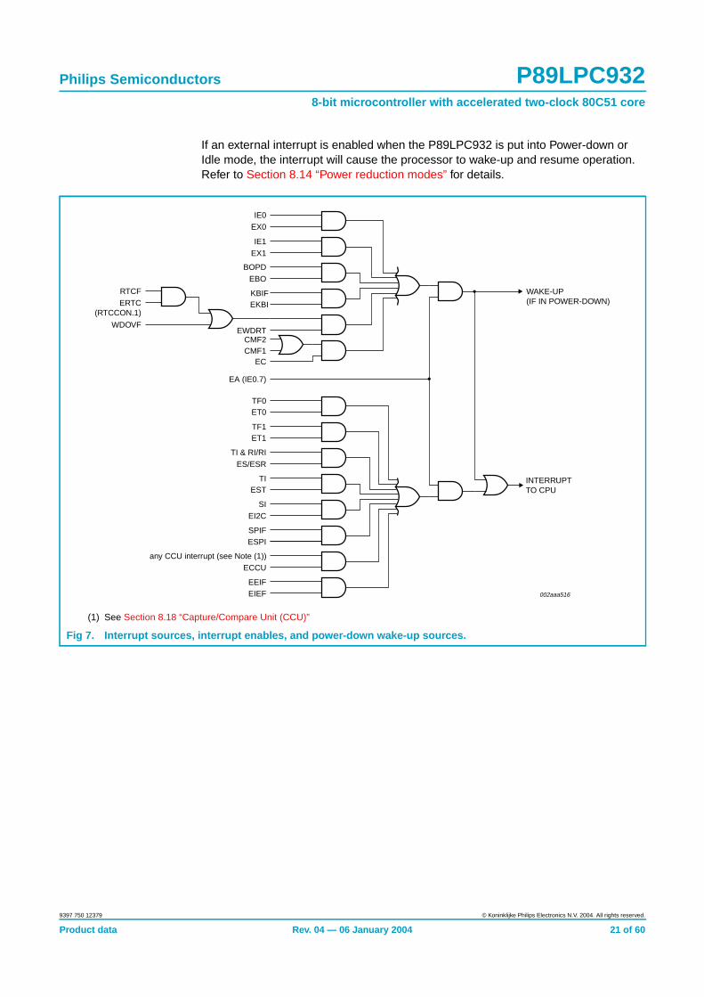
8.11 InterruptsThe P89LPC932 uses a four priority level interrupt structure. This allows greatflexibility in controlling the handling of the many interrupt sources. The P89LPC932supports 15 interrupt sources: external interrupts 0 and 1, timers 0 and 1, serial portTx, serial port Rx, combined serial port Rx/Tx, brownout detect, watchdog/Real-Timeclock, I2C, keyboard, comparators 1 and 2, SPI, CCU, data EEPROM writecompletion.
Each interrupt source can be individually enabled or disabled by setting or clearing abit in the interrupt enable registers IEN0 or IEN1. The IEN0 register also contains aglobal disable bit, EA, which disables all interrupts.
Each interrupt source can be individually programmed to one of four priority levels bysetting or clearing bits in the interrupt priority registers IP0, IP0H, IP1, and IP1H. Aninterrupt service routine in progress can be interrupted by a higher priority interrupt,but not by another interrupt of the same or lower priority. The highest priority interruptservice cannot be interrupted by any other interrupt source. If two requests ofdifferent priority levels are pending at the start of an instruction, the request of higherpriority level is serviced.
If requests of the same priority level are pending at the start of an instruction, aninternal polling sequence determines which request is serviced. This is called thearbitration ranking. Note that the arbitration ranking is only used to resolve pendingrequests of the same priority level.
8.11.1 External interrupt inputs
The P89LPC932 has two external interrupt inputs as well as the Keypad Interruptfunction. The two interrupt inputs are identical to those present on the standard80C51 microcontrollers.
These external interrupts can be programmed to be level-triggered or edge-triggeredby setting or clearing bit IT1 or IT0 in Register TCON.
In edge-triggered mode, if successive samples of the INTn pin show a HIGH in onecycle and a LOW in the next cycle, the interrupt request flag IEn in TCON is set,causing an interrupt request.
Table 5: On-chip data memory usages
Type Data RAM Size (bytes)
DATA Memory that can be addressed directly and indirectly 128
IDATA Memory that can be addressed indirectly 256
XDATA Auxiliary (‘External Data’) on-chip memory that is accessedusing the MOVX instructions
512
Product data Rev. 04 — 06 January 2004 20 of 60
9397 750 12379 © Koninklijke Philips Electronics N.V. 2004. All rights reserved.
Philips Semiconductors P89LPC9328-bit microcontroller with accelerated two-clock 80C51 core
If an external interrupt is enabled when the P89LPC932 is put into Power-down orIdle mode, the interrupt will cause the processor to wake-up and resume operation.Refer to Section 8.14 “Power reduction modes” for details.
(1) See Section 8.18 “Capture/Compare Unit (CCU)”
Fig 7. Interrupt sources, interrupt enables, and power-down wake-up sources.
002aaa516
IE0EX0
IE1EX1
BOPDEBO
KBIFEKBI
INTERRUPT TO CPU
WAKE-UP(IF IN POWER-DOWN)
EWDRTCMF2CMF1
EC
EA (IE0.7)
TF1ET1
TI & RI/RIES/ESR
TIEST
SIEI2C
SPIFESPI
RTCFERTC
(RTCCON.1)
WDOVF
TF0ET0
any CCU interrupt (see Note (1))ECCU
EEIFEIEF
Product data Rev. 04 — 06 January 2004 21 of 60
9397 750 12379 © Koninklijke Philips Electronics N.V. 2004. All rights reserved.
Philips Semiconductors P89LPC9328-bit microcontroller with accelerated two-clock 80C51 core
8.12 I/O portsThe P89LPC932 has four I/O ports: Port 0, Port 1, Port 2, and Port 3. Ports 0, 1and 2are 8-bit ports, and Port 3 is a 2-bit port. The exact number of I/O pins availabledepends upon the clock and reset options chosen, as shown in Table 6.
8.12.1 Port configurations
All but three I/O port pins on the P89LPC932 may be configured by software to one offour types on a bit-by-bit basis. These are: quasi-bidirectional (standard 80C51 portoutputs), push-pull, open drain, and input-only. Two configuration registers for eachport select the output type for each port pin.
P1.5 (RST) can only be an input and cannot be configured.
P1.2 (SCL/T0) and P1.3 (SDA/INT0) may only be configured to be either input-only oropen-drain.
8.12.2 Quasi-bidirectional output configuration
Quasi-bidirectional output type can be used as both an input and output without theneed to reconfigure the port. This is possible because when the port outputs a logicHIGH, it is weakly driven, allowing an external device to pull the pin LOW. When thepin is driven LOW, it is driven strongly and able to sink a fairly large current. Thesefeatures are somewhat similar to an open-drain output except that there are threepull-up transistors in the quasi-bidirectional output that serve different purposes.
The P89LPC932 is a 3 V device, but the pins are 5 V-tolerant. In quasi-bidirectionalmode, if a user applies 5 V on the pin, there will be a current flowing from the pin toVDD, causing extra power consumption. Therefore, applying 5 V in quasi-bidirectionalmode is discouraged.
A quasi-bidirectional port pin has a Schmitt-triggered input that also has a glitchsuppression circuit.
8.12.3 Open-drain output configuration
The open-drain output configuration turns off all pull-ups and only drives thepull-down transistor of the port driver when the port latch contains a logic ‘0’. To beused as a logic output, a port configured in this manner must have an externalpull-up, typically a resistor tied to VDD.
An open-drain port pin has a Schmitt-triggered input that also has a glitchsuppression circuit.
Table 6: Number of I/O pins available
Clock source Reset option Number of I/O pins(28-pin package)
On-chip oscillator or watchdog oscillator No external reset (except during power-up) 26
External RST pin supported 25
External clock input No external reset (except during power-up) 25
External RST pin supported 24
Low/medium/high speed oscillator(external crystal or resonator)
No external reset (except during power-up) 24
External RST pin supported 23
Product data Rev. 04 — 06 January 2004 22 of 60
9397 750 12379 © Koninklijke Philips Electronics N.V. 2004. All rights reserved.
Philips Semiconductors P89LPC9328-bit microcontroller with accelerated two-clock 80C51 core
8.12.4 Input-only configuration
The input-only port configuration has no output drivers. It is a Schmitt-triggered inputthat also has a glitch suppression circuit.
8.12.5 Push-pull output configuration
The push-pull output configuration has the same pull-down structure as both theopen-drain and the quasi-bidirectional output modes, but provides a continuousstrong pull-up when the port latch contains a logic ‘1’. The push-pull mode may beused when more source current is needed from a port output. A push-pull port pinhas a Schmitt-triggered input that also has a glitch suppression circuit.
8.12.6 Port 0 analog functions
The P89LPC932 incorporates two Analog Comparators. In order to give the bestanalog function performance and to minimize power consumption, pins that are beingused for analog functions must have the digital outputs and digital inputs disabled.
Digital outputs are disabled by putting the port output into the Input-Only (highimpedance) mode.
Digital inputs on Port 0 may be disabled through the use of the PT0AD register,bits 1:5. On any reset, PT0AD[1:5] defaults to ‘0’s to enable digital functions.
8.12.7 Additional port features
After power-up, all pins are in Input-Only mode. Please note that this is differentfrom the LPC76x series of devices.
• After power-up, all I/O pins except P1.5, may be configured by software.
• Pin P1.5 is input only. Pins P1.2 and P1.3 and are configurable for either input-onlyor open-drain.
Every output on the P89LPC932 has been designed to sink typical LED drive current.However, there is a maximum total output current for all ports which must not beexceeded. Please refer to Table 8 “DC electrical characteristics” for detailedspecifications.
All ports pins that can function as an output have slew rate controlled outputs to limitnoise generated by quickly switching output signals. The slew rate is factory-set toapproximately 10 ns rise and fall times.
8.13 Power monitoring functionsThe P89LPC932 incorporates power monitoring functions designed to preventincorrect operation during initial power-up and power loss or reduction duringoperation. This is accomplished with two hardware functions: Power-on Detect andBrownout detect.
8.13.1 Brownout detection
The Brownout detect function determines if the power supply voltage drops below acertain level. The default operation is for a Brownout detection to cause a processorreset, however it may alternatively be configured to generate an interrupt.
Brownout detection may be enabled or disabled in software.
Product data Rev. 04 — 06 January 2004 23 of 60
9397 750 12379 © Koninklijke Philips Electronics N.V. 2004. All rights reserved.

Philips Semiconductors P89LPC9328-bit microcontroller with accelerated two-clock 80C51 core
If Brownout detection is enabled, the operating voltage range for VDD is 2.7 V to 3.6 V,and the brownout condition occurs when VDD falls below the brownout trip voltage,VBO (see Table 8 “DC electrical characteristics”), and is negated when VDD risesabove VBO. If brownout detection is disabled, the operating voltage range for VDD is2.4 V to 3.6 V. If the P89LPC932 device is to operate with a power supply that can bebelow 2.7 V, BOE should be left in the unprogrammed state so that the device canoperate at 2.4 V, otherwise continuous brownout reset may prevent the device fromoperating.
For correct activation of Brownout detect, the VDD rise and fall times must beobserved. Please see Table 8 “DC electrical characteristics” for specifications.
8.13.2 Power-on detection
The Power-on Detect has a function similar to the Brownout detect, but is designed towork as power comes up initially, before the power supply voltage reaches a levelwhere Brownout detect can work. The POF flag in the RSTSRC register is set toindicate an initial power-up condition. The POF flag will remain set until cleared bysoftware.
8.14 Power reduction modesThe P89LPC932 supports three different power reduction modes. These modes areIdle mode, Power-down mode, and total Power-down mode.
8.14.1 Idle mode
Idle mode leaves peripherals running in order to allow them to activate the processorwhen an interrupt is generated. Any enabled interrupt source or reset may terminateIdle mode.
8.14.2 Power-down mode
The Power-down mode stops the oscillator in order to minimize power consumption.The P89LPC932 exits Power-down mode via any reset, or certain interrupts. InPower-down mode, the power supply voltage may be reduced to the RAM keep-alivevoltage VRAM. This retains the RAM contents at the point where Power-down modewas entered. SFR contents are not guaranteed after VDD has been lowered to VRAM,therefore it is highly recommended to wake up the processor via reset in this case.VDD must be raised to within the operating range before the Power-down mode isexited.
Some chip functions continue to operate and draw power during Power-down mode,increasing the total power used during Power-down. These include: Brownout detect,Watchdog Timer, Comparators (note that Comparators can be powered-downseparately), and Real-Time Clock (RTC)/System Timer. The internal RC oscillator isdisabled unless both the RC oscillator has been selected as the system clock and theRTC is enabled.
8.14.3 Total Power-down mode
This is the same as Power-down mode except that the brownout detection circuitryand the voltage comparators are also disabled to conserve additional power. Theinternal RC oscillator is disabled unless both the RC oscillator has been selected asthe system clock and the RTC is enabled. If the internal RC oscillator is used to clock
Product data Rev. 04 — 06 January 2004 24 of 60
9397 750 12379 © Koninklijke Philips Electronics N.V. 2004. All rights reserved.

Philips Semiconductors P89LPC9328-bit microcontroller with accelerated two-clock 80C51 core
the RTC during Power-down, there will be high power consumption. Please use anexternal low frequency clock to achieve low power with the Real-Time Clock runningduring Power-down.
8.15 ResetThe P1.5/RST pin can function as either an active-LOW reset input or as a digitalinput, P1.5. The RPE (Reset Pin Enable) bit in UCFG1, when set to ‘1’, enables theexternal reset input function on P1.5. When cleared, P1.5 may be used as an inputpin.
Remark: During a power-up sequence, the RPE selection is overridden and this pinwill always function as a reset input. An external circuit connected to this pinshould not hold this pin LOW during a power-on sequence as this will keep thedevice in reset. After power-up this input will function either as an external resetinput or as a digital input as defined by the RPE bit. Only a power-up reset willtemporarily override the selection defined by RPE bit. Other sources of reset will notoverride the RPE bit.
Remark: During a power cycle, VDD must fall below VPOR (see Table 8 “DC electricalcharacteristics” on page 45) before power is reapplied, in order to ensure a power-onreset.
Reset can be triggered from the following sources:
• External reset pin (during power-up or if user configured via UCFG1);
• Power-on detect;
• Brownout detect;
• Watchdog Timer;
• Software reset;
• UART break character detect reset.
For every reset source, there is a flag in the Reset Register, RSTSRC. The user canread this register to determine the most recent reset source. These flag bits can becleared in software by writing a ‘0’ to the corresponding bit. More than one flag bitmay be set:
• During a power-on reset, both POF and BOF are set but the other flag bits arecleared.
• For any other reset, previously set flag bits that have not been cleared will remainset.
8.15.1 Reset vector
Following reset, the P89LPC932 will fetch instructions from either address 0000h orthe Boot address. The Boot address is formed by using the Boot Vector as the highbyte of the address and the low byte of the address = 00h.
The Boot address will be used if a UART break reset occurs, or the non-volatile BootStatus bit (BOOTSTAT.0) = 1, or the device is forced into ISP mode during power-on(see P89LPC932 User’s Manual). Otherwise, instructions will be fetched fromaddress 0000H.
Product data Rev. 04 — 06 January 2004 25 of 60
9397 750 12379 © Koninklijke Philips Electronics N.V. 2004. All rights reserved.

Philips Semiconductors P89LPC9328-bit microcontroller with accelerated two-clock 80C51 core
8.16 Timers/counters 0 and 1The P89LPC932 has two general purpose counter/timers which are upwardcompatible with the standard 80C51 Timer 0 and Timer 1. Both can be configured tooperate either as timers or event counter. An option to automatically toggle the T0and/or T1 pins upon timer overflow has been added.
In the ‘Timer’ function, the register is incremented every machine cycle.
In the ‘Counter’ function, the register is incremented in response to a 1-to-0 transitionat its corresponding external input pin, T0 or T1. In this function, the external input issampled once during every machine cycle.
Timer 0 and Timer 1 have five operating modes (modes 0, 1, 2, 3 and 6). Modes 0, 1,2 and 6 are the same for both Timers/Counters. Mode 3 is different.
8.16.1 Mode 0
Putting either Timer into Mode 0 makes it look like an 8048 Timer, which is an 8-bitCounter with a divide-by-32 prescaler. In this mode, the Timer register is configuredas a 13-bit register. Mode 0 operation is the same for Timer 0 and Timer 1.
8.16.2 Mode 1
Mode 1 is the same as Mode 0, except that all 16 bits of the timer register are used.
8.16.3 Mode 2
Mode 2 configures the Timer register as an 8-bit Counter with automatic reload.Mode 2 operation is the same for Timer 0 and Timer 1.
8.16.4 Mode 3
When Timer 1 is in Mode 3 it is stopped. Timer 0 in Mode 3 forms two separate 8-bitcounters and is provided for applications that require an extra 8-bit timer. WhenTimer 1 is in Mode 3 it can still be used by the serial port as a baud rate generator.
8.16.5 Mode 6
In this mode, the corresponding timer can be changed to a PWM with a full period of256 timer clocks.
8.16.6 Timer overflow toggle output
Timers 0 and 1 can be configured to automatically toggle a port output whenever atimer overflow occurs. The same device pins that are used for the T0 and T1 countinputs are also used for the timer toggle outputs. The port outputs will be a logic 1prior to the first timer overflow when this mode is turned on.
Product data Rev. 04 — 06 January 2004 26 of 60
9397 750 12379 © Koninklijke Philips Electronics N.V. 2004. All rights reserved.
Philips Semiconductors P89LPC9328-bit microcontroller with accelerated two-clock 80C51 core
8.17 Real-Time clock/system timerThe P89LPC932 has a simple Real-Time clock that allows a user to continue runningan accurate timer while the rest of the device is powered-down. The Real-Time clockcan be a wake-up or an interrupt source. The Real-Time clock is a 23-bit downcounter comprised of a 7-bit prescaler and a 16-bit loadable down counter. When itreaches all ‘0’s, the counter will be reloaded again and the RTCF flag will be set. Theclock source for this counter can be either the CPU clock (CCLK) or the XTALoscillator, provided that the XTAL oscillator is not being used as the CPU clock. If theXTAL oscillator is used as the CPU clock, then the RTC will use CCLK as its clocksource. Only power-on reset will reset the Real-Time clock and its associated SFRsto the default state.
8.18 Capture/Compare Unit (CCU)This unit features:
• A 16-bit timer with 16-bit reload on overflow.
• Selectable clock, with prescaler to divide clock source by any integral numberbetween 1 and 1024.
• 4 Compare/PWM outputs with selectable polarity
• Symmetrical/Asymmetrical PWM selection
• 2 Capture inputs with event counter and digital noise rejection filter
• 7 interrupts with common interrupt vector (one Overflow, 2 Capture, 4 Compare)
• Safe 16-bit read/write via shadow registers.
8.18.1 CCU clock (CCUCLK)
The CCU runs on the CCUCLK, which is either PCLK in basic timer mode, or theoutput of a PLL. The PLL is designed to use a clock source between 0.5 MHz to1 MHz that is multiplied by 32 to produce a CCUCLK between 16 MHz and 32 MHz inPWM mode (asymmetrical or symmetrical). The PLL contains a 4-bit divider to helpdivide PCLK into a frequency between 0.5 MHz and 1 MHz.
8.18.2 CCU clock prescaling
This CCUCLK can further be divided down by a prescaler. The prescaler isimplemented as a 10-bit free-running counter with programmable reload at overflow.
8.18.3 Basic timer operation
The Timer is a free-running up/down counter with a direction control bit. If the timercounting direction is changed while the counter is running, the count sequence will bereversed. The timer can be written or read at any time.
When a reload occurs, the CCU Timer Overflow Interrupt Flag will be set, and aninterrupt generated if enabled. The 16-bit CCU Timer may also be used as an 8-bitup/down timer.
Product data Rev. 04 — 06 January 2004 27 of 60
9397 750 12379 © Koninklijke Philips Electronics N.V. 2004. All rights reserved.
Philips Semiconductors P89LPC9328-bit microcontroller with accelerated two-clock 80C51 core
8.18.4 Output compare
There are four output compare channels A, B, C and D. Each output comparechannel needs to be enabled in order to operate and the user will have to set theassociated I/O pin to the desired output mode to connect the pin. When the contentsof the timer matches that of a capture compare control register, the Timer OutputCompare Interrupt Flag (TOCFx) becomes set. An interrupt will occur if enabled.
8.18.5 Input capture
Input capture is always enabled. Each time a capture event occurs on one of the twoinput capture pins, the contents of the timer is transferred to the corresponding 16-bitinput capture register. The capture event can be programmed to be either rising orfalling edge triggered. A simple noise filter can be enabled on the input capture byenabling the Input Capture Noise Filter bit. If set, the capture logic needs to see fourconsecutive samples of the same value in order to recognize an edge as a captureevent. An event counter can be set to delay a capture by a number of capture events.
8.18.6 PWM operation
PWM operation has two main modes, symmetrical and asymmetrical.
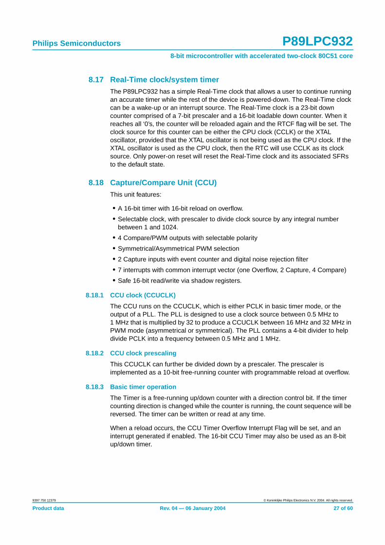
In asymmetrical PWM operation the CCU Timer operates in downcounting moderegardless of the direction control bit.
In symmetrical mode, the timer counts up/down alternately. The main difference frombasic timer operation is the operation of the compare module, which in PWM mode isused for PWM waveform generation.
As with basic timer operation, when the PWM (compare) pins are connected to thecompare logic, their logic state remains unchanged. However, since bit FCO is usedto hold the halt value, only a compare event can change the state of the pin.
Fig 8. Asymmetrical PWM, downcounting.
TOR2
COMPARE VALUE
TIMER VALUE
NON-INVERTED
INVERTED
0x0000
002aaa534
Product data Rev. 04 — 06 January 2004 28 of 60
9397 750 12379 © Koninklijke Philips Electronics N.V. 2004. All rights reserved.
Philips Semiconductors P89LPC9328-bit microcontroller with accelerated two-clock 80C51 core
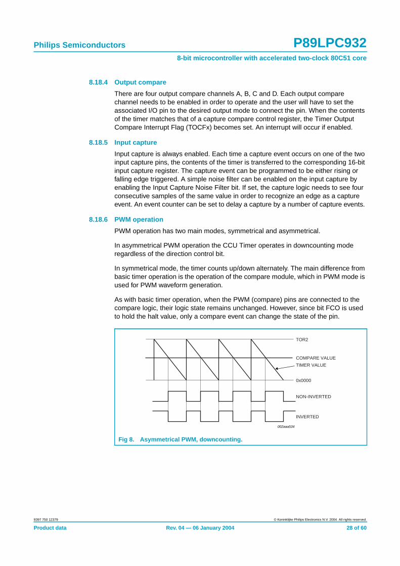
8.18.7 Alternating output mode
In asymmetrical mode, the user can set up PWM channels A/B and C/D asalternating pairs for bridge drive control. In this mode the output of these PWMchannels are alternately gated on every counter cycle.
8.18.8 PLL operation
The PWM module features a Phase Locked Loop that can be used to generate aCCUCLK frequency between 16 MHz and 32 MHz. At this frequency the PWMmodule provides ultrasonic PWM frequency with 10-bit resolution provided that thecrystal frequency is 1 MHz or higher. The PLL is fed an input signal of 0.5 - 1 MHzand generates an output signal of 32 times the input frequency. This signal is used toclock the timer. The user will have to set a divider that scales PCLK by a factor of1-16. This divider is found in the SFR register TCR21. The PLL frequency can beexpressed as shown in Equation 1.
(1)
Where: N is the value of PLLDV3:0.
Since N ranges in 0 - 15, the CCLK frequency can be in the range of PCLK to PCLK¤ 16.
Fig 9. Symmetrical PWM.
TOR2
COMPARE VALUE
TIMER VALUE
NON-INVERTED
INVERTED
002aaa535
0
Fig 10. Alternate output mode.
TIMER VALUE
002aaa536
0
TOR2
COMPARE VALUE A (or C)
COMPARE VALUE B (or D)
PWM OUTPUT A (or C) (P2.6)
PWM OUTPUT B (or D) (P1.6)
PLL frequency PLCKN 1+( )------------------=
Product data Rev. 04 — 06 January 2004 29 of 60
9397 750 12379 © Koninklijke Philips Electronics N.V. 2004. All rights reserved.
Philips Semiconductors P89LPC9328-bit microcontroller with accelerated two-clock 80C51 core
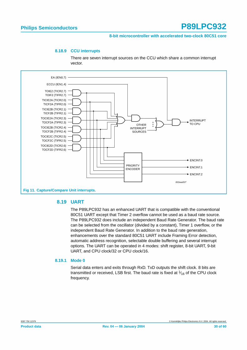
8.18.9 CCU interrupts
There are seven interrupt sources on the CCU which share a common interruptvector.
8.19 UARTThe P89LPC932 has an enhanced UART that is compatible with the conventional80C51 UART except that Timer 2 overflow cannot be used as a baud rate source.The P89LPC932 does include an independent Baud Rate Generator. The baud ratecan be selected from the oscillator (divided by a constant), Timer 1 overflow, or theindependent Baud Rate Generator. In addition to the baud rate generation,enhancements over the standard 80C51 UART include Framing Error detection,automatic address recognition, selectable double buffering and several interruptoptions. The UART can be operated in 4 modes: shift register, 8-bit UART, 9-bitUART, and CPU clock/32 or CPU clock/16.
8.19.1 Mode 0
Serial data enters and exits through RxD. TxD outputs the shift clock. 8 bits aretransmitted or received, LSB first. The baud rate is fixed at 1¤ 16 of the CPU clockfrequency.
Fig 11. Capture/Compare Unit interrupts.
002aaa537
INTERRUPT TO CPU
TOIE2 (TICR2.7)TOIF2 (TIFR2.7)
TICIE2A (TICR2.0)TICF2A (TIFR2.0)
TICIE2B (TICR2.1)TICF2B (TIFR2.1)
TOCIE2A (TICR2.3)TOCF2A (TIFR2.3)
TOCIE2B (TICR2.4)TOCF2B (TIFR2.4)
TOCIE2C (TICR2.5)TOCF2C (TIFR2.5)
TOCIE2D (TICR2.6)TOCF2D (TIFR2.6)
EA (IEN0.7)
ECCU (IEN1.4)
PRIORITYENCODER
OTHERINTERRUPT
SOURCES
ENCINT.0
ENCINT.1
ENCINT.2
Product data Rev. 04 — 06 January 2004 30 of 60
9397 750 12379 © Koninklijke Philips Electronics N.V. 2004. All rights reserved.
Philips Semiconductors P89LPC9328-bit microcontroller with accelerated two-clock 80C51 core
8.19.2 Mode 1
10 bits are transmitted (through TxD) or received (through RxD): a start bit(logical ‘0’), 8 data bits (LSB first), and a stop bit (logical ‘1’). When data is received,the stop bit is stored in RB8 in Special Function Register SCON. The baud rate isvariable and is determined by the Timer 1 overflow rate or the Baud Rate Generator(described in Section 8.19.5 “Baud rate generator and selection”).
8.19.3 Mode 2
11 bits are transmitted (through TxD) or received (through RxD): start bit (logical ‘0’),8 data bits (LSB first), a programmable 9th data bit, and a stop bit (logical ‘1’). Whendata is transmitted, the 9th data bit (TB8 in SCON) can be assigned the value of ‘0’ or‘1’. Or, for example, the parity bit (P, in the PSW) could be moved into TB8. Whendata is received, the 9th data bit goes into RB8 in Special Function Register SCON,while the stop bit is not saved. The baud rate is programmable to either 1¤ 16 or 1¤ 32 ofthe CPU clock frequency, as determined by the SMOD1 bit in PCON.
8.19.4 Mode 3
11 bits are transmitted (through TxD) or received (through RxD): a start bit(logical ‘0’), 8 data bits (LSB first), a programmable 9th data bit, and a stop bit(logical ‘1’). In fact, Mode 3 is the same as Mode 2 in all respects except baud rate.The baud rate in Mode 3 is variable and is determined by the Timer 1 overflow rate orthe Baud Rate Generator (described in Section 8.19.5 “Baud rate generator andselection”).
8.19.5 Baud rate generator and selection
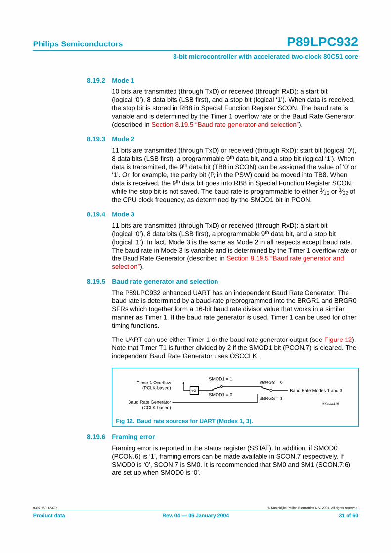
The P89LPC932 enhanced UART has an independent Baud Rate Generator. Thebaud rate is determined by a baud-rate preprogrammed into the BRGR1 and BRGR0SFRs which together form a 16-bit baud rate divisor value that works in a similarmanner as Timer 1. If the baud rate generator is used, Timer 1 can be used for othertiming functions.
The UART can use either Timer 1 or the baud rate generator output (see Figure 12).Note that Timer T1 is further divided by 2 if the SMOD1 bit (PCON.7) is cleared. Theindependent Baud Rate Generator uses OSCCLK.
8.19.6 Framing error
Framing error is reported in the status register (SSTAT). In addition, if SMOD0(PCON.6) is ‘1’, framing errors can be made available in SCON.7 respectively. IfSMOD0 is ‘0’, SCON.7 is SM0. It is recommended that SM0 and SM1 (SCON.7:6)are set up when SMOD0 is ‘0’.
Fig 12. Baud rate sources for UART (Modes 1, 3).
Baud Rate Modes 1 and 3
SBRGS = 1
SBRGS = 0
SMOD1 = 0
SMOD1 = 1
¸2
Timer 1 Overflow(PCLK-based)
Baud Rate Generator(CCLK-based)
002aaa419
Product data Rev. 04 — 06 January 2004 31 of 60
9397 750 12379 © Koninklijke Philips Electronics N.V. 2004. All rights reserved.
Philips Semiconductors P89LPC9328-bit microcontroller with accelerated two-clock 80C51 core
8.19.7 Break detect
Break detect is reported in the status register (SSTAT). A break is detected when11 consecutive bits are sensed LOW. The break detect can be used to reset thedevice and force the device into ISP mode.
8.19.8 Double buffering
The UART has a transmit double buffer that allows buffering of the next character tobe written to SBUF while the first character is being transmitted. Double bufferingallows transmission of a string of characters with only one stop bit between any twocharacters, as long as the next character is written between the start bit and the stopbit of the previous character.
Double buffering can be disabled. If disabled (DBMOD, i.e., SSTAT.7 = ‘0’), the UARTis compatible with the conventional 80C51 UART. If enabled, the UART allows writingto SnBUF while the previous data is being shifted out. Double buffering is onlyallowed in Modes 1, 2 and 3. When operated in Mode 0, double buffering must bedisabled (DBMOD = ‘0’).
8.19.9 Transmit interrupts with double buffering enabled (Modes 1, 2 and 3)
Unlike the conventional UART, in double buffering mode, the Tx interrupt is generatedwhen the double buffer is ready to receive new data.
8.19.10 The 9th bit (bit 8) in double buffering (Modes 1, 2 and 3)
If double buffering is disabled TB8 can be written before or after SBUF is written, aslong as TB8 is updated some time before that bit is shifted out. TB8 must not bechanged until the bit is shifted out, as indicated by the Tx interrupt.
If double buffering is enabled, TB8 must be updated before SBUF is written, as TB8will be double-buffered together with SBUF data.
Product data Rev. 04 — 06 January 2004 32 of 60
9397 750 12379 © Koninklijke Philips Electronics N.V. 2004. All rights reserved.

Philips Semiconductors P89LPC9328-bit microcontroller with accelerated two-clock 80C51 core
8.20 I2C-bus serial interfaceI2C-bus uses two wires (SDA and SCL) to transfer information between devicesconnected to the bus, and it has the following features:
• Bi-directional data transfer between masters and slaves
• Multimaster bus (no central master)
• Arbitration between simultaneously transmitting masters without corruption ofserial data on the bus
• Serial clock synchronization allows devices with different bit rates to communicatevia one serial bus
• Serial clock synchronization can be used as a handshake mechanism to suspendand resume serial transfer
• The I2C-bus may be used for test and diagnostic purposes.
A typical I2C-bus configuration is shown in Figure 13. The P89LPC932 deviceprovides a byte-oriented I2C-bus interface that supports data transfers up to 400 kHz.
Fig 13. I2C-bus configuration.
OTHER DEVICEWITH I2C-BUS
INTERFACE
SDA
SCL
RPRP
OTHER DEVICEWITH I2C-BUS
INTERFACE
P1.3/SDA P1.2/SCL
P89LPC932
I2C-BUS
002aaa559
Product data Rev. 04 — 06 January 2004 33 of 60
9397 750 12379 © Koninklijke Philips Electronics N.V. 2004. All rights reserved.

Philips Semiconductors P89LPC9328-bit microcontroller with accelerated two-clock 80C51 core
Fig 14. I2C-bus serial interface block diagram.
INT
ER
NA
L B
US
002aaa421
ADDRESS REGISTER
COMPARATOR
SHIFT REGISTER
8
I2ADR
ACK
BIT COUNTER /ARBITRATION &
SYNC LOGIC
8 I2DAT
TIMING&
CONTROLLOGIC
SERIAL CLOCKGENERATOR
CCLK
INTERRUPT
INPUTFILTER
OUTPUTSTAGE
INPUTFILTER
OUTPUTSTAGE
P1.3
P1.3/SDA
P1.2/SCL
P1.2
TIMER 1OVERFLOW
CONTROL REGISTERS &SCL DUTY CYCLE REGISTERS
I2CONI2SCLHI2SCLL
8
STATUSDECODERSTATUS BUS
STATUS REGISTER
8
I2STAT
Product data Rev. 04 — 06 January 2004 34 of 60
9397 750 12379 © Koninklijke Philips Electronics N.V. 2004. All rights reserved.
Philips Semiconductors P89LPC9328-bit microcontroller with accelerated two-clock 80C51 core
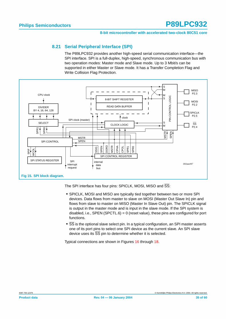
8.21 Serial Peripheral Interface (SPI)The P89LPC932 provides another high-speed serial communication interface—theSPI interface. SPI is a full-duplex, high-speed, synchronous communication bus withtwo operation modes: Master mode and Slave mode. Up to 3 Mbit/s can besupported in either Master or Slave mode. It has a Transfer Completion Flag andWrite Collision Flag Protection.
The SPI interface has four pins: SPICLK, MOSI, MISO and SS:
• SPICLK, MOSI and MISO are typically tied together between two or more SPIdevices. Data flows from master to slave on MOSI (Master Out Slave In) pin andflows from slave to master on MISO (Master In Slave Out) pin. The SPICLK signalis output in the master mode and is input in the slave mode. If the SPI system isdisabled, i.e., SPEN (SPCTL.6) = 0 (reset value), these pins are configured for portfunctions.
• SS is the optional slave select pin. In a typical configuration, an SPI master assertsone of its port pins to select one SPI device as the current slave. An SPI slavedevice uses its SS pin to determine whether it is selected.
Typical connections are shown in Figures 16 through 18.
Fig 15. SPI block diagram.
002aaa497
CPU clock
DIVIDERBY 4, 16, 64, 128
SELECTCLOCK LOGIC
SPI CONTROL REGISTER
READ DATA BUFFER
8-BIT SHIFT REGISTER
SPI CONTROL
SPI STATUS REGISTER
SP
R1
SP
IF
WC
OL
SP
R0
SPI clock (master) PIN
CO
NT
RO
L LO
GIC
SM
SM
MS
MISOP2.3
MOSIP2.2
SPICLKP2.5
SSP2.4
SPIinterruptrequest
internaldatabus
SS
IG
SP
EN
SP
EN
MS
TR
DO
RD
MS
TR
CP
HA
CP
OL
SP
R1
SP
R0
MSTRSPEN
clock
Product data Rev. 04 — 06 January 2004 35 of 60
9397 750 12379 © Koninklijke Philips Electronics N.V. 2004. All rights reserved.

Philips Semiconductors P89LPC9328-bit microcontroller with accelerated two-clock 80C51 core
8.21.1 Typical SPI configurations
Fig 16. SPI single master single slave configuration.
Fig 17. SPI dual device configuration, where either can be a master or a slave.
002aaa435
Master Slave
8-BIT SHIFTREGISTER
SPI CLOCKGENERATOR
8-BIT SHIFTREGISTER
MISO
MOSI
SPICLK
PORT
MISO
MOSI
SPICLK
SS
002aaa499
Master Slave
8-BIT SHIFTREGISTER
SPI CLOCKGENERATOR
SPI CLOCKGENERATOR
8-BIT SHIFTREGISTER
MISO
MOSI
SPICLK
MISO
MOSI
SPICLK
SSSS
Product data Rev. 04 — 06 January 2004 36 of 60
9397 750 12379 © Koninklijke Philips Electronics N.V. 2004. All rights reserved.

Philips Semiconductors P89LPC9328-bit microcontroller with accelerated two-clock 80C51 core
Fig 18. SPI single master multiple slaves configuration.
002aaa437
Master Slave
8-BIT SHIFTREGISTER
SPI CLOCKGENERATOR
8-BIT SHIFTREGISTER
MISO
MOSI
SPICLK
port
port
MISO
MOSI
SPICLK
SS
Slave
8-BIT SHIFTREGISTER
MISO
MOSI
SPICLK
SS
Product data Rev. 04 — 06 January 2004 37 of 60
9397 750 12379 © Koninklijke Philips Electronics N.V. 2004. All rights reserved.

Philips Semiconductors P89LPC9328-bit microcontroller with accelerated two-clock 80C51 core
8.22 Analog comparatorsTwo analog comparators are provided on the P89LPC932. Input and output optionsallow use of the comparators in a number of different configurations. Comparatoroperation is such that the output is a logical one (which may be read in a registerand/or routed to a pin) when the positive input (one of two selectable pins) is greaterthan the negative input (selectable from a pin or an internal reference voltage).Otherwise the output is a zero. Each comparator may be configured to cause aninterrupt when the output value changes.
The overall connections to both comparators are shown in Figure 19. Thecomparators function to VDD = 2.4 V.
When each comparator is first enabled, the comparator output and interrupt flag arenot guaranteed to be stable for 10 microseconds. The corresponding comparatorinterrupt should not be enabled during that time, and the comparator interrupt flagmust be cleared before the interrupt is enabled in order to prevent an immediateinterrupt service.
When a comparator is disabled the comparator’s output, COx, goes HIGH. If thecomparator output was LOW and then is disabled, the resulting transition of thecomparator output from a LOW to HIGH state will set the comparator flag, CMFx.This will cause an interrupt if the comparator interrupt is enabled. The user shouldtherefore disable the comparator interrupt prior to disabling the comparator.Additionally, the user should clear the comparator flag, CMFx, after disabling thecomparator.
8.22.1 Internal reference voltage
An internal reference voltage generator may supply a default reference when a singlecomparator input pin is used. The value of the internal reference voltage, referred toas VREF, is 1.23 V ±10%.
Fig 19. Comparator input and output connections.
Comparator 1CP1
CN1
(P0.4) CIN1A
(P0.3) CIN1B
(P0.5) CMPREF
VREF
OE1
Change Detect
CO1
CMF1
Interrupt
002aaa422
CMP1 (P0.6)
ECChange Detect
CMF2Comparator 2
OE2
CO2CMP2 (P0.0)
CP2
CN2
(P0.2) CIN2A
(P0.1) CIN2B
Product data Rev. 04 — 06 January 2004 38 of 60
9397 750 12379 © Koninklijke Philips Electronics N.V. 2004. All rights reserved.
Philips Semiconductors P89LPC9328-bit microcontroller with accelerated two-clock 80C51 core
8.22.2 Comparator interrupt
Each comparator has an interrupt flag contained in its configuration register. This flagis set whenever the comparator output changes state. The flag may be polled bysoftware or may be used to generate an interrupt. The two comparators use onecommon interrupt vector. If both comparators enable interrupts, after entering theinterrupt service routine, the user needs to read the flags to determine whichcomparator caused the interrupt.
8.22.3 Comparators and power reduction modes
Either or both comparators may remain enabled when Power-down or Idle mode isactivated, but both comparators are disabled automatically in Total Power-downmode.
If a comparator interrupt is enabled (except in Total Power-down mode), a change ofthe comparator output state will generate an interrupt and wake up the processor. Ifthe comparator output to a pin is enabled, the pin should be configured in thepush-pull mode in order to obtain fast switching times while in Power-down mode.The reason is that with the oscillator stopped, the temporary strong pull-up thatnormally occurs during switching on a quasi-bidirectional port pin does not takeplace.
Comparators consume power in Power-down and Idle modes, as well as in thenormal operating mode. This fact should be taken into account when system powerconsumption is an issue. To minimize power consumption, the user can disable thecomparators via PCONA.5, or put the device in Total Power-down mode.
8.23 Keypad interrupt (KBI)The Keypad Interrupt function is intended primarily to allow a single interrupt to begenerated when Port 0 is equal to or not equal to a certain pattern. This function canbe used for bus address recognition or keypad recognition. The user can configurethe port via SFRs for different tasks.
The Keypad Interrupt Mask Register (KBMASK) is used to define which input pinsconnected to Port 0 can trigger the interrupt. The Keypad Pattern Register (KBPATN)is used to define a pattern that is compared to the value of Port 0. The KeypadInterrupt Flag (KBIF) in the Keypad Interrupt Control Register (KBCON) is set whenthe condition is matched while the Keypad Interrupt function is active. An interrupt willbe generated if enabled. The PATN_SEL bit in the Keypad Interrupt Control Register(KBCON) is used to define equal or not-equal for the comparison.
In order to use the Keypad Interrupt as an original KBI function like in 87LPC76xseries, the user needs to set KBPATN = 0FFH and PATN_SEL = 1 (not equal), thenany key connected to Port 0 which is enabled by the KBMASK register will cause thehardware to set KBIF and generate an interrupt if it has been enabled. The interruptmay be used to wake up the CPU from Idle or Power-down modes. This feature isparticularly useful in handheld, battery-powered systems that need to carefullymanage power consumption yet also need to be convenient to use.
In order to set the flag and cause an interrupt, the pattern on Port 0 must be heldlonger than 6 CCLKs.
Product data Rev. 04 — 06 January 2004 39 of 60
9397 750 12379 © Koninklijke Philips Electronics N.V. 2004. All rights reserved.
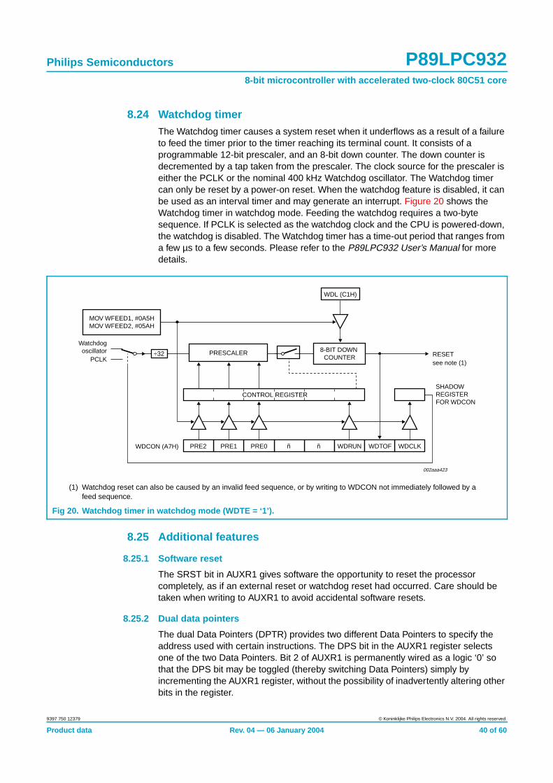
Philips Semiconductors P89LPC9328-bit microcontroller with accelerated two-clock 80C51 core
8.24 Watchdog timerThe Watchdog timer causes a system reset when it underflows as a result of a failureto feed the timer prior to the timer reaching its terminal count. It consists of aprogrammable 12-bit prescaler, and an 8-bit down counter. The down counter isdecremented by a tap taken from the prescaler. The clock source for the prescaler iseither the PCLK or the nominal 400 kHz Watchdog oscillator. The Watchdog timercan only be reset by a power-on reset. When the watchdog feature is disabled, it canbe used as an interval timer and may generate an interrupt. Figure 20 shows theWatchdog timer in watchdog mode. Feeding the watchdog requires a two-bytesequence. If PCLK is selected as the watchdog clock and the CPU is powered-down,the watchdog is disabled. The Watchdog timer has a time-out period that ranges froma few m s to a few seconds. Please refer to the P89LPC932 User’s Manual for moredetails.
8.25 Additional features
8.25.1 Software reset
The SRST bit in AUXR1 gives software the opportunity to reset the processorcompletely, as if an external reset or watchdog reset had occurred. Care should betaken when writing to AUXR1 to avoid accidental software resets.
8.25.2 Dual data pointers
The dual Data Pointers (DPTR) provides two different Data Pointers to specify theaddress used with certain instructions. The DPS bit in the AUXR1 register selectsone of the two Data Pointers. Bit 2 of AUXR1 is permanently wired as a logic ‘0’ sothat the DPS bit may be toggled (thereby switching Data Pointers) simply byincrementing the AUXR1 register, without the possibility of inadvertently altering otherbits in the register.
(1) Watchdog reset can also be caused by an invalid feed sequence, or by writing to WDCON not immediately followed by afeed sequence.
Fig 20. Watchdog timer in watchdog mode (WDTE = ‘1’).
PRE2 PRE1 PRE0 ñ ñ WDRUN WDTOF WDCLKWDCON (A7H)
CONTROL REGISTER
PRESCALER
002aaa423
SHADOW REGISTERFOR WDCON
8-BIT DOWN COUNTER
WDL (C1H)
Watchdogoscillator
PCLK¸ 32
MOV WFEED1, #0A5HMOV WFEED2, #05AH
RESETsee note (1)
Product data Rev. 04 — 06 January 2004 40 of 60
9397 750 12379 © Koninklijke Philips Electronics N.V. 2004. All rights reserved.

Philips Semiconductors P89LPC9328-bit microcontroller with accelerated two-clock 80C51 core
8.26 Data EEPROMThe P89LPC932 has 512 bytes of on-chip Data EEPROM. The Data EEPROM isSFR based, byte readable, byte writable, and erasable (via row fill and sector fill). Theuser can read, write and fill the memory via SFRs and one interrupt. This DataEEPROM provides 100,000 minimum erase/program cycles for each byte.
• Byte Mode: In this mode, data can be read and written one byte at a time.
• Row Fill: In this mode, the addressed row (64 bytes) is filled with a single value.The entire row can be erased by writing 00h.
• Sector Fill: In this mode, all 512 bytes are filled with a single value. The entiresector can be erased by writing 00h.
After the operation finishes, the hardware will set the EEIF bit, which if enabled willgenerate an interrupt. The flag is cleared by software.
8.27 Flash program memory
8.27.1 General description
The P89LPC932 Flash memory provides in-circuit electrical erasure andprogramming. The Flash can be read, erased, or written as bytes. The Sector andPage Erase functions can erase any Flash sector (1 kB) or page (64 bytes). The ChipErase operation will erase the entire program memory. In-System Programming andstandard parallel programming are both available. On-chip erase and write timinggeneration contribute to a user-friendly programming interface. The P89LPC932Flash reliably stores memory contents even after 10,000 erase and program cycles.The cell is designed to optimize the erase and programming mechanisms. TheP89LPC932 uses VDD as the supply voltage to perform the Program/Erasealgorithms.
8.27.2 Features
• Internal fixed boot ROM, containing low-level In-Application Programming (IAP)routines
• User programs can call these routines to perform In-Application Programming(IAP).
• Default loader providing In-System Programming via the serial port, located inupper end of user program memory.
• Boot vector allows user-provided Flash loader code to reside anywhere in theFlash memory space, providing flexibility to the user.
• Programming and erase over the full operating voltage range.
• Read/Programming/Erase using ISP/IAP.
• Any flash program/erase operation in 2 ms.
• Parallel programming with industry-standard commercial programmers.
• Programmable security for the code in the Flash for each sector.
• 100,000 typical erase/program cycles for each byte.
• 10 year minimum data retention.
Product data Rev. 04 — 06 January 2004 41 of 60
9397 750 12379 © Koninklijke Philips Electronics N.V. 2004. All rights reserved.

Philips Semiconductors P89LPC9328-bit microcontroller with accelerated two-clock 80C51 core
8.27.3 ISP and IAP capabilities of the P89LPC932
Flash organization: The P89LPC932 program memory consists of eight 1 kBsectors. Each sector can be further divided into 64-byte pages. In addition to sectorerase and page erase, a 64-byte page register is included which allows from1 to 64 bytes of a given page to be programmed at the same time, substantiallyreducing overall programming time. An In-Application Programming (IAP) interface isprovided to allow the end user’s application to erase and reprogram the user codememory. In addition, erasing and reprogramming of user-programmable bytesincluding UCFG1, the Boot Status Bit and the Boot Vector are supported. As shippedfrom the factory, the upper 512 bytes of user code space contains a serial In-SystemProgramming (ISP) routine allowing for the device to be programmed in circuitthrough the serial port.
Flash programming and erasing: There are three methods of erasing orprogramming of the Flash memory that may be used. First, the Flash may beprogrammed or erased in the end-user application by calling low-level routinesthrough a common entry point. Second, the on-chip ISP boot loader may be invoked.This ISP boot loader will, in turn, call low-level routines through the same commonentry point that can be used by the end-user application. Third, the Flash may beprogrammed or erased using the parallel method by using a commercially availableEPROM programmer which supports this device. This device does not provide fordirect verification of code memory contents. Instead, this device provides a 32-bitCRC result on either a sector or the entire 8 kB of user code space.
Boot ROM: When the microcontroller programs its own Flash memory, all of thelow-level details are handled by code that is contained in a Boot ROM that is separatefrom the Flash memory. A user program simply calls the common entry point in theBoot ROM with appropriate parameters to accomplish the desired operation. TheBoot ROM include operations such as erase sector, erase page, program page, CRC,program security bit, etc. The Boot ROM occupies the program memory space at thetop of the address space from FF00 to FEFF hex, thereby not conflicting with the userprogram memory space.
Power-on reset code execution: The P89LPC932 contains two special Flashelements: the Boot Vector and the Boot Status Bit. Following reset, the P89LPC932examines the contents of the Boot Status Bit. If the Boot Status Bit is set to zero,power-up execution starts at location 0000H, which is the normal start address of theuser’s application code. When the Boot Status Bit is set to a value other than zero, thecontents of the Boot Vector is used as the high byte of the execution address and thelow byte is set to 00H. The factory default setting is 01EH and corresponds to theaddress 1E00H for the default ISP boot loader. This boot loader is pre-programmedat the factory into this address space and can be erased by the user. Users whowish to use this loader should take precautions to avoid erasing the 1 kBsector from 1C00H to 1FFFH. Instead, the page erase function can be used toerase the eight 64-byte pages located from 1C00H to 1DFFH. A custom bootloader can be written with the Boot Vector set to the custom boot loader, if desired.
Hardware activation of the boot loader: The boot loader can also be executed byforcing the device into ISP mode during a power-on sequence (see the P89LPC932User’s Manual for specific information). This has the same effect as having anon-zero status byte. This allows an application to be built that will normally executeuser code but can be manually forced into ISP operation. If the factory default setting
Product data Rev. 04 — 06 January 2004 42 of 60
9397 750 12379 © Koninklijke Philips Electronics N.V. 2004. All rights reserved.
Philips Semiconductors P89LPC9328-bit microcontroller with accelerated two-clock 80C51 core
for the Boot Vector (1EH) is changed, it will no longer point to the factorypre-programmed ISP boot loader code. If this happens, the only way it is possible tochange the contents of the Boot Vector is through the parallel programming method,provided that the end user application does not contain a customized loader thatprovides for erasing and reprogramming of the Boot Vector and Boot Status Bit. Afterprogramming the Flash, the status byte should be programmed to zero in order toallow execution of the user’s application code beginning at address 0000H.
In-System Programming (ISP): In-System Programming is performed withoutremoving the microcontroller from the system. The In-System Programming facilityconsists of a series of internal hardware resources coupled with internal firmware tofacilitate remote programming of the P89LPC932 through the serial port. Thisfirmware is provided by Philips and embedded within each P89LPC932 device. ThePhilips In-System Programming facility has made in-system programming in anembedded application possible with a minimum of additional expense in componentsand circuit board area. The ISP function uses five pins (VDD, VSS, TXD, RXD, andRST). Only a small connector needs to be available to interface your application to anexternal circuit in order to use this feature.
In-Application Programming (IAP): Several In-Application Programming (IAP) callsare available for use by an application program to permit selective erasing andprogramming of Flash sectors, pages, security bits, configuration bytes, and deviceidentification. All calls are made through a common interface, PGM_MTP. Theprogramming functions are selected by setting up the microcontroller’s registersbefore making a call to PGM_MTP at FF00H.
8.28 User configuration bytesA number of user-configurable features of the P89LPC932 must be defined atpower-up and therefore cannot be set by the program after start of execution. Thesefeatures are configured through the use of the Flash byte UCFG1. Please see theP89LPC932 User’s Manual for additional details.
8.29 User sector security bytesThere are eight User Sector Security Bytes, each corresponding to one sector.Please see the P89LPC932 User’s Manual for additional details.
Product data Rev. 04 — 06 January 2004 43 of 60
9397 750 12379 © Koninklijke Philips Electronics N.V. 2004. All rights reserved.

Philips Semiconductors P89LPC9328-bit microcontroller with accelerated two-clock 80C51 core
9. Limiting values
[1] Stresses above those listed under Table 7 “Limiting values” may cause permanent damage to the device. This is a stress rating only andfunctional operation of the device at these or any conditions other than those described in Table 8 “DC electrical characteristics” andTable 9 “AC characteristics” of this specification are not implied.
[2] This product includes circuitry specifically designed for the protection of its internal devices from the damaging effects of excessivestatic charge. Nonetheless, it is suggested that conventional precautions be taken to avoid applying greater than the rated maximum.
[3] Parameters are valid over operating temperature range unless otherwise specified. All voltages are with respect to VSS unless otherwisenoted.
Table 7: Limiting valuesIn accordance with the Absolute Maximum Rating System (IEC 60134).
Symbol Parameter Conditions Min Max Unit
Tamb(bias) operating bias ambient temperature - 55 +125 °C
Tstg storage temperature range - 65 +150 °C
Vxtal voltage on XTAL1, XTAL2 pin to VSS - VDD + 0.5 V
Vn voltage on any other pin (exceptXTAL1, XTAL2) to VSS
- 0.5 +5.5 V
IOH(I/O) HIGH-level output current per I/O pin - 20 mA
IOL(I/O) LOW-level output current per I/O pin - 20 mA
II/O(tot)(max) maximum total I/O current - 100 mA
Ptot(pack) total power dissipation per package based on package heattransfer, not device powerconsumption
- 1.5 W
Product data Rev. 04 — 06 January 2004 44 of 60
9397 750 12379 © Koninklijke Philips Electronics N.V. 2004. All rights reserved.
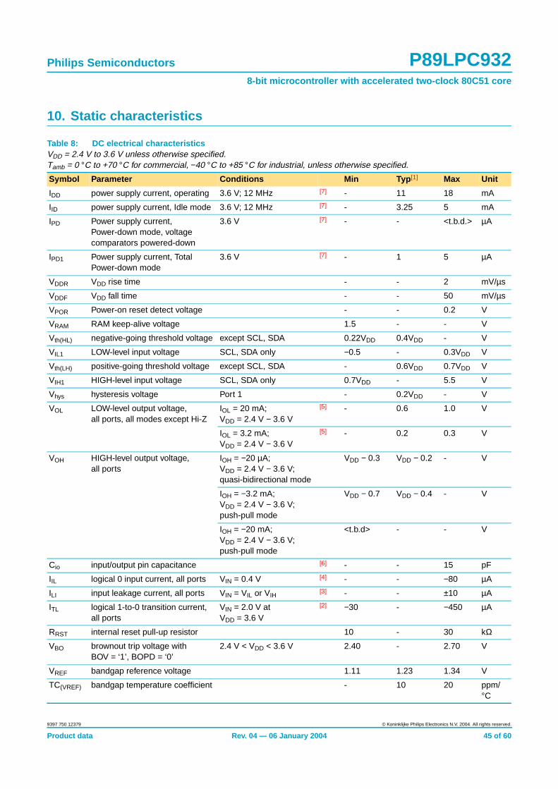
Philips Semiconductors P89LPC9328-bit microcontroller with accelerated two-clock 80C51 core
10. Static characteristics
Table 8: DC electrical characteristicsVDD = 2.4 V to 3.6 V unless otherwise specified.Tamb = 0 °C to +70 °C for commercial, - 40 °C to +85 °C for industrial, unless otherwise specified.
Symbol Parameter Conditions Min Typ [1] Max Unit
IDD power supply current, operating 3.6 V; 12 MHz [7] - 11 18 mA
IID power supply current, Idle mode 3.6 V; 12 MHz [7] - 3.25 5 mA
IPD Power supply current,Power-down mode, voltagecomparators powered-down
3.6 V [7] - - <t.b.d.> m A
IPD1 Power supply current, TotalPower-down mode
3.6 V [7] - 1 5 m A
VDDR VDD rise time - - 2 mV/m s
VDDF VDD fall time - - 50 mV/m s
VPOR Power-on reset detect voltage - - 0.2 V
VRAM RAM keep-alive voltage 1.5 - - V
Vth(HL) negative-going threshold voltage except SCL, SDA 0.22VDD 0.4VDD - V
VIL1 LOW-level input voltage SCL, SDA only - 0.5 - 0.3VDD V
Vth(LH) positive-going threshold voltage except SCL, SDA - 0.6VDD 0.7VDD V
VIH1 HIGH-level input voltage SCL, SDA only 0.7VDD - 5.5 V
Vhys hysteresis voltage Port 1 - 0.2VDD - V
VOL LOW-level output voltage,all ports, all modes except Hi-Z
IOL = 20 mA;VDD = 2.4 V - 3.6 V
[5] - 0.6 1.0 V
IOL = 3.2 mA;VDD = 2.4 V - 3.6 V
[5] - 0.2 0.3 V
VOH HIGH-level output voltage,all ports
IOH = - 20 m A;VDD = 2.4 V - 3.6 V;quasi-bidirectional mode
VDD - 0.3 VDD - 0.2 - V
IOH = - 3.2 mA;VDD = 2.4 V - 3.6 V;push-pull mode
VDD - 0.7 VDD - 0.4 - V
IOH = - 20 mA;VDD = 2.4 V - 3.6 V;push-pull mode
<t.b.d> - - V
Cio input/output pin capacitance [6] - - 15 pF
IIL logical 0 input current, all ports VIN = 0.4 V [4] - - - 80 m A
ILI input leakage current, all ports VIN = VIL or VIH[3] - - ±10 m A
ITL logical 1-to-0 transition current,all ports
VIN = 2.0 V atVDD = 3.6 V
[2] - 30 - - 450 m A
RRST internal reset pull-up resistor 10 - 30 kW
VBO brownout trip voltage withBOV = ‘1’, BOPD = ‘0’
2.4 V < VDD < 3.6 V 2.40 - 2.70 V
VREF bandgap reference voltage 1.11 1.23 1.34 V
TC(VREF) bandgap temperature coefficient - 10 20 ppm/°C
Product data Rev. 04 — 06 January 2004 45 of 60
9397 750 12379 © Koninklijke Philips Electronics N.V. 2004. All rights reserved.
Philips Semiconductors P89LPC9328-bit microcontroller with accelerated two-clock 80C51 core
[1] Typical ratings are not guaranteed. The values listed are at room temperature, 3 V.
[2] Port pins source a transition current when used in quasi-bidirectional mode and externally driven from ‘1’ to ‘0’. This current is highestwhen VIN is approximately 2 V.
[3] Measured with port in high-impedance mode.
[4] Measured with port in quasi-bidirectional mode.
[5] See Section 9 “Limiting values” on page 44 for steady state (non-transient) limits on IOL or IOH. If IOL/IOH exceeds the test condition,VOL/VOH may exceed the related specification.
[6] Pin capacitance is characterized but not tested.
[7] The IDD, IID, and IPD specifications are measured using an external clock with the following functions disabled: comparators, brownoutdetect, and Watchdog timer.
Product data Rev. 04 — 06 January 2004 46 of 60
9397 750 12379 © Koninklijke Philips Electronics N.V. 2004. All rights reserved.

Philips Semiconductors P89LPC9328-bit microcontroller with accelerated two-clock 80C51 core
11. Dynamic characteristics
Table 9: AC characteristicsTamb = 0 °C to +70 °C for commercial, - 40 °C to +85 °C for industrial, unless otherwise specified.[1]
Symbol Parameter Conditions Variable clock fOSC = 12 MHz Unit
Min Max Min Max
fRCOSC internal RC oscillator frequency 7.189 7.557 7.189 7.557 MHz
fWDOSC internal Watchdog oscillatorfrequency
280 480 280 480 kHz
fOSC oscillator frequency 0 12 - - MHz
tCLCL clock cycle see Figure 22 83 - - - ns
fCLKLP CLKLP active frequency 0 8 - - MHz
Glitch filter
glitch rejection, P1.5/RST pin - 50 - 50 ns
signal acceptance, P1.5/RST pin 125 - 125 - ns
glitch rejection, any pin exceptP1.5/RST
- 15 - 15 ns
signal acceptance, any pin exceptP1.5/RST
50 - 50 - ns
External clock
tCHCX HIGH time see Figure 22 33 tCLCL - tCLCX 33 - ns
tCLCX LOW time see Figure 22 33 tCLCL - tCHCX 33 - ns
tCLCH rise time see Figure 22 - 8 - 8 ns
tCHCL fall time see Figure 22 - 8 - 8 ns
Shift register (UART mode 0)
tXLXL serial port clock cycle time see Figure 21 16 tCLCL - 1333 - ns
tQVXH output data set-up to clock rising edge see Figure 21 13 tCLCL - 1083 - ns
tXHQX output data hold after clock risingedge
see Figure 21 - tCLCL + 20 - 103 ns
tXHDX input data hold after clock rising edge see Figure 21 - 0 - 0 ns
tDVXH input data valid to clock rising edge see Figure 21 150 - 150 - ns
SPI interface
fSPI operating frequency
2.0 MHz (master) - - - - MHz
2.0 MHz (slave) 0 2.0 0 2.0 MHz
3.0 MHz (master) - - - - MHz
3.0 MHz (slave) 0 3.0 0 3.0 MHz
tSPICYC cycle time see Figures23, 24, 25, 262.0 MHz (master) - - - - ns
2.0 MHz (slave) 500 - 500 - ns
3.0 MHz (master) - - - - ns
3.0 MHz (slave) 333 - 333 - ns
Product data Rev. 04 — 06 January 2004 47 of 60
9397 750 12379 © Koninklijke Philips Electronics N.V. 2004. All rights reserved.

Philips Semiconductors P89LPC9328-bit microcontroller with accelerated two-clock 80C51 core
[1] Parameters are valid over operating temperature range unless otherwise specified.
[2] Parts are tested to 2 MHz, but are guaranteed to operate down to 0 Hz.
tSPILEAD enable lead time (slave) see Figures25, 262.0 MHz 250 - 250 - ns
3.0 MHz 240 - 240 - ns
tSPILAG enable lag time (slave) see Figures25, 262.0 MHz 250 - 250 - ns
3.0 MHz 240 - 240 - ns
tSPICLKH SPICLK HIGH time see Figures23, 24, 25, 26master 340 - 340 - ns
slave 190 - 190 - ns
tSPICLKL SPICLK LOW time see Figures23, 24, 25, 26master 340 - 340 - ns
slave 190 - 190 - ns
tSPIDSU data set-up time (master or slave) see Figures23, 24, 25, 26
100 - 100 - ns
tSPIDH data hold time (master or slave) see Figures23, 24, 25, 26
100 - 100 - ns
tSPIA access time (slave) see Figures25, 26
0 120 0 120 ns
tSPIDIS disable time (slave) see Figures25, 262.0 MHz 0 240 - 240 ns
3.0 MHz 0 167 - 167 ns
tSPIDV enable to output data valid see Figures23, 24, 25, 262.0 MHz - 240 - 240 ns
3.0 MHz - 167 - 167 ns
tSPIOH output data hold time see Figures23, 24, 25, 26
0 - 0 - ns
tSPIR rise time see Figures23, 24, 25, 26SPI outputs
(SPICLK, MOSI, MISO)- 100 - 100 ns
SPI inputs(SPICLK, MOSI, MISO, SS)
- 2000 - 2000 ns
tSPIF fall time see Figures23, 24, 25, 26SPI outputs
(SPICLK, MOSI, MISO)- 100 - 100 ns
SPI inputs(SPICLK, MOSI, MISO, SS)
- 2000 - 2000 ns
Table 9: AC characteristics …continuedTamb = 0 °C to +70 °C for commercial, - 40 °C to +85 °C for industrial, unless otherwise specified.[1]
Symbol Parameter Conditions Variable clock fOSC = 12 MHz Unit
Min Max Min Max
Product data Rev. 04 — 06 January 2004 48 of 60
9397 750 12379 © Koninklijke Philips Electronics N.V. 2004. All rights reserved.

Philips Semiconductors P89LPC9328-bit microcontroller with accelerated two-clock 80C51 core
Fig 21. Shift register mode timing.
0 1 2 3 4 5 6 7
Valid Valid Valid Valid Valid Valid Valid Valid
tXLXL
002aaa425
Set TI
Set RI
tXHQXtQVXH
tXHDV
tXHDX
Clock
Output Data
Write to SBUF
Input Data
Clear RI
Fig 22. External clock timing.
tCHCL tCLCX
tCHCX
tC
tCLCH
002aaa416
0.2 VDD + 0.9
0.2 VDD - 0.1 V
VDD - 0.5 V
0.45 V
Fig 23. SPI master timing (CPHA = ‘0’)
tCLCL
tSPICLKHtSPICLKL
Master LSB/MSB outMaster MSB/LSB out
tSPIDHtSPIDSU
tSPICLKLtSPICLKH
tSPIF
tSPIOH tSPIDV tSPIRtSPIDV
tSPIF
tSPIF
tSPIR
tSPIR
SS
SPICLK(CPOL = 0)
(output)
002aaa156
SPICLK(CPOL = 1)
(output)
MISO(input)
MOSI(output)
LSB/MSB inMSB/LSB in
Product data Rev. 04 — 06 January 2004 49 of 60
9397 750 12379 © Koninklijke Philips Electronics N.V. 2004. All rights reserved.
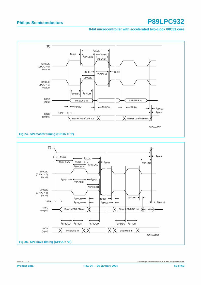
Philips Semiconductors P89LPC9328-bit microcontroller with accelerated two-clock 80C51 core
Fig 24. SPI master timing (CPHA = ‘1’)
tCLCL
tSPICLKLtSPICLKH
Master LSB/MSB outMaster MSB/LSB out
tSPIDHtSPIDSU
tSPICLKH
tSPICLKL
tSPIF
tSPIOH tSPIDV tSPIDVtSPIR
tSPIDV
tSPIF
tSPIRtSPIF
tSPIR
SS
SPICLK(CPOL = 0)
(output)
002aaa157
SPICLK(CPOL = 1)
(output)
MISO(input)
MOSI(output)
LSB/MSB inMSB/LSB in
Fig 25. SPI slave timing (CPHA = ‘0’)
tCLCL
tSPICLKHtSPICLKL
tSPILEAD
tSPICLKH
tSPICLKL
tSPILAG
tSPIDSU tSPIDH tSPIDHtSPIDSU tSPIDSU
tSPIR
tSPIAtSPIOH
tSPIOH
tSPIDIS
tSPIR
Slave MSB/LSB out
MSB/LSB in LSB/MSB in
Slave LSB/MSB out
tSPIDV
tSPIOHtSPIDV
tSPIRtSPIF
tSPIRtSPIF
SS
SPICLK(CPOL = 0)
(input)
002aaa158
SPICLK(CPOL = 1)
(input)
MISO(output)
MOSI(input)
Not defined
Product data Rev. 04 — 06 January 2004 50 of 60
9397 750 12379 © Koninklijke Philips Electronics N.V. 2004. All rights reserved.
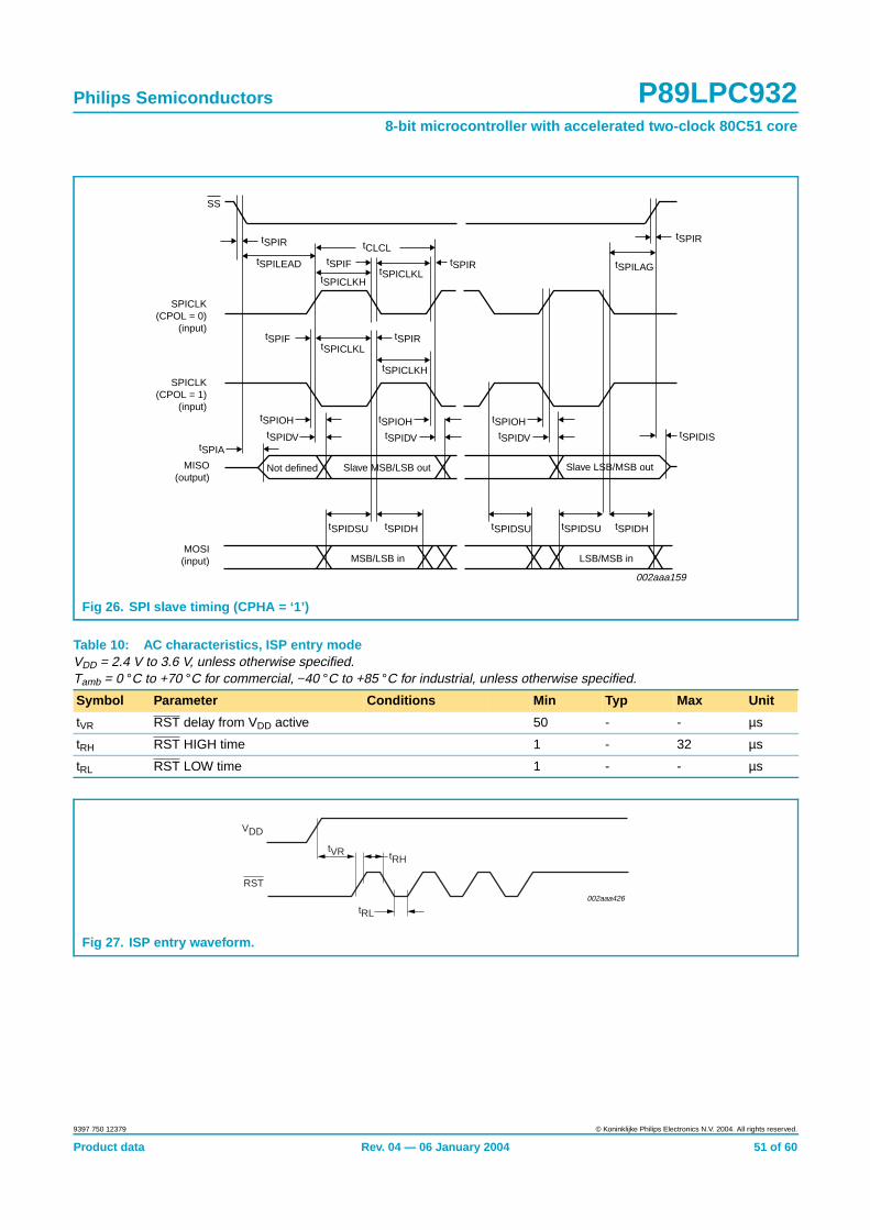
Philips Semiconductors P89LPC9328-bit microcontroller with accelerated two-clock 80C51 core
Fig 26. SPI slave timing (CPHA = ‘1’)
tCLCL
tSPICLKHtSPICLKL
tSPILEAD
tSPICLKH
tSPICLKL
tSPILAG
tSPIDSU tSPIDH tSPIDHtSPIDSU
tSPIR
tSPIA
tSPIOHtSPIDIS
tSPIR
Slave MSB/LSB outNot defined
MSB/LSB in LSB/MSB in
Slave LSB/MSB out
tSPIDV
tSPIOHtSPIDV
tSPIOHtSPIDV
tSPIRtSPIF
tSPIRtSPIF
SS
SPICLK(CPOL = 0)
(input)
002aaa159
SPICLK(CPOL = 1)
(input)
MISO(output)
MOSI(input)
tSPIDSU
Table 10: AC characteristics, ISP entry modeVDD = 2.4 V to 3.6 V, unless otherwise specified.Tamb = 0 °C to +70 °C for commercial, - 40 °C to +85 °C for industrial, unless otherwise specified.
Symbol Parameter Conditions Min Typ Max Unit
tVR RST delay from VDD active 50 - - m s
tRH RST HIGH time 1 - 32 m s
tRL RST LOW time 1 - - m s
Fig 27. ISP entry waveform.
002aaa426
VDD
RST
tRL
tVR tRH
Product data Rev. 04 — 06 January 2004 51 of 60
9397 750 12379 © Koninklijke Philips Electronics N.V. 2004. All rights reserved.

Philips Semiconductors P89LPC9328-bit microcontroller with accelerated two-clock 80C51 core
12. Comparator electrical characteristics
[1] This parameter is characterized, but not tested in production.
Table 11: Comparator electrical characteristicsVDD = 2.4 V to 3.6 V, unless otherwise specified.Tamb = 0 °C to +70 °C for commercial, - 40 °C to +85 °C for industrial, unless otherwise specified.
Symbol Parameter Conditions Min Typ Max Unit
VIO offset voltage comparator inputs - - ±20 mV
VCR common mode range comparator inputs 0 - VDD - 0.3 V
CMRR common mode rejection ratio [1] - - - 50 dB
response time - 250 500 ns
comparator enable to output valid - - 10 m s
IIL input leakage current, comparator 0 < VIN < VDD - - ±10 m A
Product data Rev. 04 — 06 January 2004 52 of 60
9397 750 12379 © Koninklijke Philips Electronics N.V. 2004. All rights reserved.
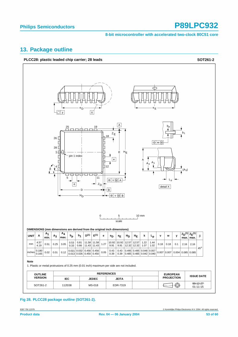
Philips Semiconductors P89LPC9328-bit microcontroller with accelerated two-clock 80C51 core
13. Package outline
Fig 28. PLCC28 package outline (SOT261-2).
REFERENCESOUTLINEVERSION
EUROPEANPROJECTION ISSUE DATE
IEC JEDEC JEITA
Note
1. Plastic or metal protrusions of 0.25 mm (0.01 inch) maximum per side are not included.
SOT261-2 112E08 MS-018 EDR-7319
1925
28
1
4
5 11
18
12
26
detail X
(A )3
bp
w M
A1A
A4
Lp
b1
βk
Xy
e
E
B
DH
EH
v M B
D
ZD
A
ZE
e
v M A
0 5 10 mm
scale
99-12-2701-11-15
pin 1 index
PLCC28: plastic leaded chip carrier; 28 leads SOT261-2
UNIT β
mm 4.574.19 0.51 3.05
0.530.33
0.0210.013
1.27 2.16
45o0.18 0.10.18
DIMENSIONS (mm dimensions are derived from the original inch dimensions)
11.5811.43
12.5712.32 2.16
0.810.66
1.221.07
0.1800.165 0.02 0.12
0.25
0.01 0.05 0.0850.007 0.0040.007
1.441.02
0.0570.040
0.4560.450
11.5811.43
0.4560.450
0.4950.485
12.5712.32
0.4950.485
10.929.91
0.430.39
10.929.91
0.430.39 0.085
0.0320.026
0.0480.042
Ee
inches
De
AA1
min.
A4max.
bp e ywvD(1) E(1) HD HEZD
(1)
max.ZE
(1)
max.b1 kA3 LpeD eE
Product data Rev. 04 — 06 January 2004 53 of 60
9397 750 12379 © Koninklijke Philips Electronics N.V. 2004. All rights reserved.
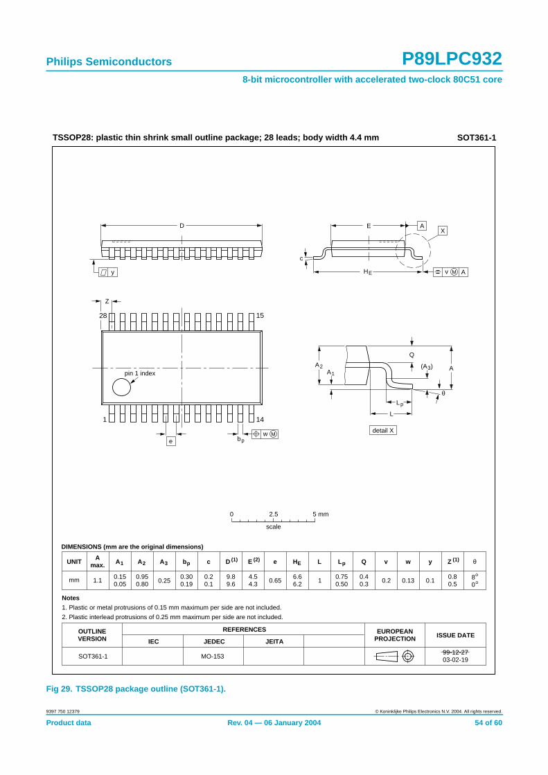
Philips Semiconductors P89LPC9328-bit microcontroller with accelerated two-clock 80C51 core
Fig 29. TSSOP28 package outline (SOT361-1).
UNIT A1 A2 A3 bp c D (1) E (2) (1)e HE L L p Q Zywv q
REFERENCESOUTLINEVERSION
EUROPEANPROJECTION ISSUE DATE
IEC JEDEC JEITA
mm 0.150.05
0.950.80
0.300.19
0.20.1
9.89.6
4.54.3 0.65
6.66.2
0.40.3
0.80.5
80
o
o0.13 0.10.21
DIMENSIONS (mm are the original dimensions)
Notes
1. Plastic or metal protrusions of 0.15 mm maximum per side are not included.
2. Plastic interlead protrusions of 0.25 mm maximum per side are not included.
0.750.50
SOT361-1 MO-15399-12-2703-02-19
0.25
w Mbp
Z
e
1 14
28 15
pin 1 index
q
AA1
A2
Lp
Q
detail X
L
(A )3
HE
E
c
v M A
XAD
y
0 2.5 5 mm
scale
TSSOP28: plastic thin shrink small outline package; 28 leads; body width 4.4 mm SOT361-1
Amax.
1.1
Product data Rev. 04 — 06 January 2004 54 of 60
9397 750 12379 © Koninklijke Philips Electronics N.V. 2004. All rights reserved.
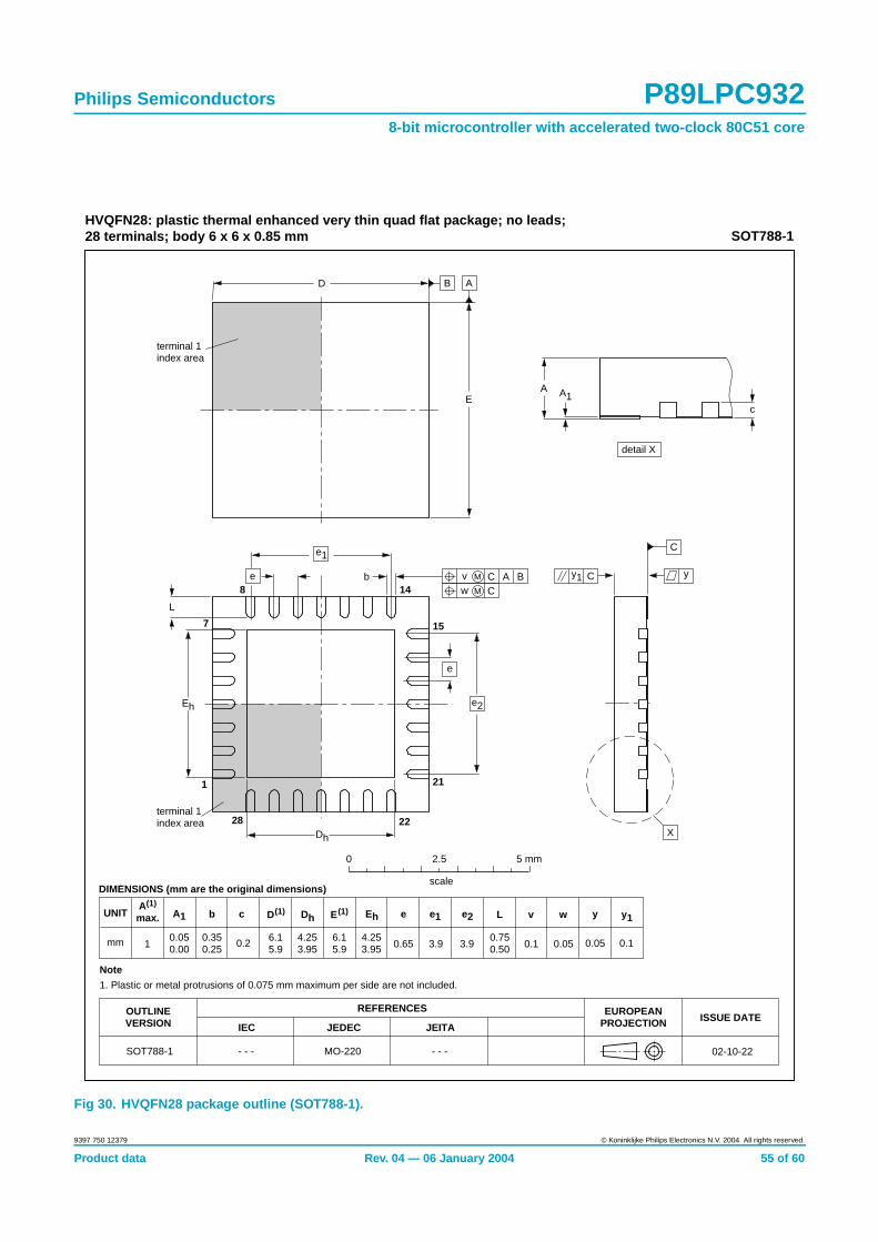
Philips Semiconductors P89LPC9328-bit microcontroller with accelerated two-clock 80C51 core
Fig 30. HVQFN28 package outline (SOT788-1).
0.651
A1 Ehb cUNIT ye
REFERENCESOUTLINEVERSION
EUROPEANPROJECTION ISSUE DATE
IEC JEDEC JEITA
mm 6.15.9
6.15.9
Dh
4.253.95
y1
4.253.95
e1
3.9
e2
3.90.350.25
0.050.00
0.2 0.05 0.1
DIMENSIONS (mm are the original dimensions)
SOT788-1 MO-220- - - - - -
0.750.50
L
0.1
v
0.05
w
0 2.5 5 mm
scale
SOT788-1HVQFN28: plastic thermal enhanced very thin quad flat package; no leads;28 terminals; body 6 x 6 x 0.85 mm
A(1)
max.
A A1c
detail X
yy1 Ce
L
Eh
Dh
e
e1
b8 14
28 22
21
157
1
X
D
E
C
B A
e2
02-10-22
terminal 1index area
terminal 1index area
ACC
Bv M
w M
Note
1. Plastic or metal protrusions of 0.075 mm maximum per side are not included.
D(1) E(1)
Product data Rev. 04 — 06 January 2004 55 of 60
9397 750 12379 © Koninklijke Philips Electronics N.V. 2004. All rights reserved.
Philips Semiconductors P89LPC9328-bit microcontroller with accelerated two-clock 80C51 core
14. Soldering
14.1 Introduction to soldering surface mount packagesThis text gives a very brief insight to a complex technology. A more in-depth accountof soldering ICs can be found in our Data Handbook IC26; Integrated CircuitPackages (document order number 9398 652 90011).
There is no soldering method that is ideal for all IC packages. Wave soldering can stillbe used for certain surface mount ICs, but it is not suitable for fine pitch SMDs. Inthese situations reflow soldering is recommended. In these situations reflowsoldering is recommended.
14.2 Reflow solderingReflow soldering requires solder paste (a suspension of fine solder particles, flux andbinding agent) to be applied to the printed-circuit board by screen printing, stencillingor pressure-syringe dispensing before package placement. Driven by legislation andenvironmental forces the worldwide use of lead-free solder pastes is increasing.
Several methods exist for reflowing; for example, convection or convection/infraredheating in a conveyor type oven. Throughput times (preheating, soldering andcooling) vary between 100 and 200 seconds depending on heating method.
Typical reflow peak temperatures range from 215 to 270 °C depending on solderpaste material. The top-surface temperature of the packages should preferably bekept:
• below 225 °C (SnPb process) or below 245 °C (Pb-free process)
– for all BGA, HTSSON..T and SSOP..T packages
– for packages with a thickness ³ 2.5 mm
– for packages with a thickness < 2.5 mm and a volume ³ 350 mm3 so calledthick/large packages.
• below 240 °C (SnPb process) or below 260 °C (Pb-free process) for packages witha thickness < 2.5 mm and a volume < 350 mm3 so called small/thin packages.
Moisture sensitivity precautions, as indicated on packing, must be respected at alltimes.
14.3 Wave solderingConventional single wave soldering is not recommended for surface mount devices(SMDs) or printed-circuit boards with a high component density, as solder bridgingand non-wetting can present major problems.
To overcome these problems the double-wave soldering method was specificallydeveloped.
If wave soldering is used the following conditions must be observed for optimalresults:
• Use a double-wave soldering method comprising a turbulent wave with highupward pressure followed by a smooth laminar wave.
Product data Rev. 04 — 06 January 2004 56 of 60
9397 750 12379 © Koninklijke Philips Electronics N.V. 2004. All rights reserved.
Philips Semiconductors P89LPC9328-bit microcontroller with accelerated two-clock 80C51 core
• For packages with leads on two sides and a pitch (e):
– larger than or equal to 1.27 mm, the footprint longitudinal axis is preferred to beparallel to the transport direction of the printed-circuit board;
– smaller than 1.27 mm, the footprint longitudinal axis must be parallel to thetransport direction of the printed-circuit board.
The footprint must incorporate solder thieves at the downstream end.
• For packages with leads on four sides, the footprint must be placed at a 45° angleto the transport direction of the printed-circuit board. The footprint mustincorporate solder thieves downstream and at the side corners.
During placement and before soldering, the package must be fixed with a droplet ofadhesive. The adhesive can be applied by screen printing, pin transfer or syringedispensing. The package can be soldered after the adhesive is cured.
Typical dwell time of the leads in the wave ranges from 3 to 4 seconds at 250 °C or265 °C, depending on solder material applied, SnPb or Pb-free respectively.
A mildly-activated flux will eliminate the need for removal of corrosive residues inmost applications.
14.4 Manual solderingFix the component by first soldering two diagonally-opposite end leads. Use a lowvoltage (24 V or less) soldering iron applied to the flat part of the lead. Contact timemust be limited to 10 seconds at up to 300 °C.
When using a dedicated tool, all other leads can be soldered in one operation within2 to 5 seconds between 270 and 320 °C.
14.5 Package related soldering information
[1] For more detailed information on the BGA packages refer to the (LF)BGA Application Note(AN01026); order a copy from your Philips Semiconductors sales office.
[2] All surface mount (SMD) packages are moisture sensitive. Depending upon the moisture content, themaximum temperature (with respect to time) and body size of the package, there is a risk that internalor external package cracks may occur due to vaporization of the moisture in them (the so calledpopcorn effect). For details, refer to the Drypack information in the Data Handbook IC26; IntegratedCircuit Packages; Section: Packing Methods.
Table 12: Suitability of surface mount IC packages for wave and reflow solderingmethods
Package [1] Soldering method
Wave Reflow [2]
BGA, HTSSON..T[3], LBGA, LFBGA, SQFP,SSOP..T[3], TFBGA, USON, VFBGA
not suitable suitable
DHVQFN, HBCC, HBGA, HLQFP, HSO, HSOP,HSQFP, HSSON, HTQFP, HTSSOP, HVQFN,HVSON, SMS
not suitable[4] suitable
PLCC[5], SO, SOJ suitable suitable
LQFP, QFP, TQFP not recommended[5][6] suitable
SSOP, TSSOP, VSO, VSSOP not recommended[7] suitable
CWQCCN..L[8], PMFP[9], WQCCN..L[8] not suitable not suitable
Product data Rev. 04 — 06 January 2004 57 of 60
9397 750 12379 © Koninklijke Philips Electronics N.V. 2004. All rights reserved.

Philips Semiconductors P89LPC9328-bit microcontroller with accelerated two-clock 80C51 core
[3] These transparent plastic packages are extremely sensitive to reflow soldering conditions and muston no account be processed through more than one soldering cycle or subjected to infrared reflowsoldering with peak temperature exceeding 217 °C ± 10 °C measured in the atmosphere of the reflowoven. The package body peak temperature must be kept as low as possible.
[4] These packages are not suitable for wave soldering. On versions with the heatsink on the bottomside, the solder cannot penetrate between the printed-circuit board and the heatsink. On versions withthe heatsink on the top side, the solder might be deposited on the heatsink surface.
[5] If wave soldering is considered, then the package must be placed at a 45° angle to the solder wavedirection. The package footprint must incorporate solder thieves downstream and at the side corners.
[6] Wave soldering is suitable for LQFP, QFP and TQFP packages with a pitch (e) larger than 0.8 mm; itis definitely not suitable for packages with a pitch (e) equal to or smaller than 0.65 mm.
[7] Wave soldering is suitable for SSOP and TSSOP packages with a pitch (e) equal to or larger than0.65 mm; it is definitely not suitable for packages with a pitch (e) equal to or smaller than 0.5 mm.
[8] Image sensor packages in principle should not be soldered. They are mounted in sockets or deliveredpre-mounted on flex foil. However, the image sensor package can be mounted by the client on a flexfoil by using a hot bar soldering process. The appropriate soldering profile can be provided onrequest.
[9] Hot bar soldering or manual soldering is suitable for PMFP packages.
15. Revision history
Table 13: Revision history
Rev Date CPCN Description
04 20040106 - Product data (9397 750 12379); ECN 853-2433 01-A15016 dated 16 December 2003
Modifications:
• Table 4 “Special function registers”: changed PLEEN to PLLEN.
• Section 8.27.2 “Features” on page 41: adjusted bullet for erase/program cycles
• Table 8 “DC electrical characteristics” on page 45: adjusted value for ITL VIN.
03 20031007 - Product data (9397 750 12119); ECN 853-2433 30392 dated 30 September 2003
02 20030725 - Product data (9397 750 11712); ECN 853-2433 30141 dated 23 July 2003.Supersedes Preliminary data P89LPC932_1 of 21 October 2002 (9397 750 10475)
Product data Rev. 04 — 06 January 2004 58 of 60
9397 750 12379 © Koninklijke Philips Electronics N.V. 2004. All rights reserved.
Philips Semiconductors P89LPC9328-bit microcontroller with accelerated two-clock 80C51 core
16. Data sheet status
[1] Please consult the most recently issued data sheet before initiating or completing a design.
[2] The product status of the device(s) described in this data sheet may have changed since this data sheet was published. The latest information is available on the Internet atURL http://www.semiconductors.philips.com.
[3] For data sheets describing multiple type numbers, the highest-level product status determines the data sheet status.
17. Definitions
Short-form specification — The data in a short-form specification isextracted from a full data sheet with the same type number and title. Fordetailed information see the relevant data sheet or data handbook.
Limiting values definition — Limiting values given are in accordance withthe Absolute Maximum Rating System (IEC 60134). Stress above one ormore of the limiting values may cause permanent damage to the device.These are stress ratings only and operation of the device at these or at anyother conditions above those given in the Characteristics sections of thespecification is not implied. Exposure to limiting values for extended periodsmay affect device reliability.
Application information — Applications that are described herein for anyof these products are for illustrative purposes only. Philips Semiconductorsmake no representation or warranty that such applications will be suitable forthe specified use without further testing or modification.
18. Disclaimers
Life support — These products are not designed for use in life supportappliances, devices, or systems where malfunction of these products canreasonably be expected to result in personal injury. Philips Semiconductors
customers using or selling these products for use in such applications do soat their own risk and agree to fully indemnify Philips Semiconductors for anydamages resulting from such application.
Right to make changes — Philips Semiconductors reserves the right tomake changes in the products - including circuits, standard cells, and/orsoftware - described or contained herein in order to improve design and/orperformance. When the product is in full production (status ‘Production’),relevant changes will be communicated via a Customer Product/ProcessChange Notification (CPCN). Philips Semiconductors assumes noresponsibility or liability for the use of any of these products, conveys nolicence or title under any patent, copyright, or mask work right to theseproducts, and makes no representations or warranties that these products arefree from patent, copyright, or mask work right infringement, unless otherwisespecified.
19. Licenses
Level Data sheet status [1] Product status [2][3] Definition
I Objective data Development This data sheet contains data from the objective specification for product development. PhilipsSemiconductors reserves the right to change the specification in any manner without notice.
II Preliminary data Qualification This data sheet contains data from the preliminary specification. Supplementary data will be publishedat a later date. Philips Semiconductors reserves the right to change the specification without notice, inorder to improve the design and supply the best possible product.
III Product data Production This data sheet contains data from the product specification. Philips Semiconductors reserves theright to make changes at any time in order to improve the design, manufacturing and supply. Relevantchanges will be communicated via a Customer Product/Process Change Notification (CPCN).
Purchase of Philips I 2C components
Purchase of Philips I2C components conveys a licenseunder the Philips’ I2C patent to use the components in theI2C system provided the system conforms to the I2Cspecification defined by Philips. This specification can beordered using the code 9398 393 40011.
9397 750 12379 © Koninklijke Philips Electronics N.V. 2004. All rights reserved.
Product data Rev. 04 — 06 January 2004 59 of 60
Contact informationFor additional information, please visit http://www.semiconductors.philips.com .For sales office addresses, send e-mail to: [email protected] . Fax: +31 40 27 24825

© Koninklijke Philips Electronics N.V. 2004.Printed in the U.S.A.
All rights are reserved. Reproduction in whole or in part is prohibited without the priorwritten consent of the copyright owner.
The information presented in this document does not form part of any quotation orcontract, is believed to be accurate and reliable and may be changed without notice. Noliability will be accepted by the publisher for any consequence of its use. Publicationthereof does not convey nor imply any license under patent- or other industrial orintellectual property rights.
Date of release: 06 January 2004 Document order number: 9397 750 12379
Contents
Philips Semiconductors P89LPC9328-bit microcontroller with accelerated two-clock 80C51 core
1 General description . . . . . . . . . . . . . . . . . . . . . . 12 Features . . . . . . . . . . . . . . . . . . . . . . . . . . . . . . . 13 Ordering information . . . . . . . . . . . . . . . . . . . . . 33.1 Ordering options . . . . . . . . . . . . . . . . . . . . . . . . 34 Block diagram . . . . . . . . . . . . . . . . . . . . . . . . . . 45 Pinning information . . . . . . . . . . . . . . . . . . . . . . 55.1 Pinning . . . . . . . . . . . . . . . . . . . . . . . . . . . . . . . 55.2 Pin description . . . . . . . . . . . . . . . . . . . . . . . . . 76 Logic symbol . . . . . . . . . . . . . . . . . . . . . . . . . . 117 Special function registers . . . . . . . . . . . . . . . . 118 Functional description . . . . . . . . . . . . . . . . . . 178.1 Enhanced CPU. . . . . . . . . . . . . . . . . . . . . . . . 178.2 Clocks . . . . . . . . . . . . . . . . . . . . . . . . . . . . . . . 178.3 On-chip RC oscillator option . . . . . . . . . . . . . . 188.4 Watchdog oscillator option . . . . . . . . . . . . . . . 188.5 External clock input option . . . . . . . . . . . . . . . 188.6 CPU Clock (CCLK) wake-up delay . . . . . . . . . 198.7 CPU Clock (CCLK) modification: DIVM
register. . . . . . . . . . . . . . . . . . . . . . . . . . . . . . 198.8 Low power select . . . . . . . . . . . . . . . . . . . . . . 198.9 Memory organization . . . . . . . . . . . . . . . . . . . 198.10 Data RAM arrangement . . . . . . . . . . . . . . . . . 208.11 Interrupts . . . . . . . . . . . . . . . . . . . . . . . . . . . . 208.12 I/O ports . . . . . . . . . . . . . . . . . . . . . . . . . . . . . 228.13 Power monitoring functions. . . . . . . . . . . . . . . 238.14 Power reduction modes . . . . . . . . . . . . . . . . . 248.15 Reset . . . . . . . . . . . . . . . . . . . . . . . . . . . . . . . 258.16 Timers/counters 0 and 1 . . . . . . . . . . . . . . . . . 268.17 Real-Time clock/system timer. . . . . . . . . . . . . 278.18 Capture/Compare Unit (CCU). . . . . . . . . . . . . 278.19 UART . . . . . . . . . . . . . . . . . . . . . . . . . . . . . . . 308.20 I2C-bus serial interface . . . . . . . . . . . . . . . . . . 338.21 Serial Peripheral Interface (SPI) . . . . . . . . . . . 358.22 Analog comparators . . . . . . . . . . . . . . . . . . . . 388.23 Keypad interrupt (KBI) . . . . . . . . . . . . . . . . . . 398.24 Watchdog timer. . . . . . . . . . . . . . . . . . . . . . . . 408.25 Additional features . . . . . . . . . . . . . . . . . . . . . 408.26 Data EEPROM . . . . . . . . . . . . . . . . . . . . . . . . 418.27 Flash program memory. . . . . . . . . . . . . . . . . . 418.28 User configuration bytes . . . . . . . . . . . . . . . . . 438.29 User sector security bytes . . . . . . . . . . . . . . . 439 Limiting values. . . . . . . . . . . . . . . . . . . . . . . . . 4410 Static characteristics. . . . . . . . . . . . . . . . . . . . 4511 Dynamic characteristics . . . . . . . . . . . . . . . . . 4712 Comparator electrical characteristics . . . . . . 5213 Package outline . . . . . . . . . . . . . . . . . . . . . . . . 5314 Soldering . . . . . . . . . . . . . . . . . . . . . . . . . . . . . 56
14.1 Introduction to soldering surface mount packages. . . . . . . . . . . . . . . . . . . . . . . . . . . . 56
14.2 Reflow soldering. . . . . . . . . . . . . . . . . . . . . . . 5614.3 Wave soldering. . . . . . . . . . . . . . . . . . . . . . . . 5614.4 Manual soldering . . . . . . . . . . . . . . . . . . . . . . 5714.5 Package related soldering information . . . . . . 5715 Revision history . . . . . . . . . . . . . . . . . . . . . . . 5816 Data sheet status. . . . . . . . . . . . . . . . . . . . . . . 5917 Definitions . . . . . . . . . . . . . . . . . . . . . . . . . . . . 5918 Disclaimers . . . . . . . . . . . . . . . . . . . . . . . . . . . 5919 Licenses . . . . . . . . . . . . . . . . . . . . . . . . . . . . . . 59