Embed Size (px)
Citation preview
Nonlinear Dyn (2006) 46:239–257DOI 10.1007/s11071-006-9046-8
O R I G I NA L A RT I C L E
Nonlinear and nonsmooth dynamics in a DC–DC Buckconverter: Two experimental set-ups
Fabiola Angulo · Carlos Ocampo · Gerard Olivar ·Rafael Ramos
Received: 4 May 2005 / Accepted: 5 September 2005 / Published online: 5 July 2006C© Springer Science + Business Media B.V. 2006
Abstract It is well known that many nonlinear phe-nomena such as bifurcations and chaotic behavior occurin DC–DC converters mainly due to the switching ac-tion among all the different topologies of the circuit.Such behavior has been described with detail numer-ically, and also mathematical reasoning has been pro-vided. In this paper we focuss on the experimentalside of a DC–DC Buck converter controlled with twodifferent strategies: classical Pulse Width Modulation(PWM) with a ramp and a more recently described ZeroAverage Dynamics (ZAD). We show some nonsmoothevents and we explain with detail the experimental set-ups. In one of them, we use a FPGA card to obtainon-line results. In the other we use Virtual Instrumen-
Partially funded by SICONOS.
F. Angulo · G. Olivar (�)Departamento de Ingenieria Electrıca, Electronica yComputacion, Universidad Nacional de Colombia, sedeManizales, Campus La Nubia, Manizales, Colombia, SouthAmericae-mail: [email protected]
C. OcampoDepartament d’Enginyeria de Sistemes, Automatica eInformatica Industrial, Universitat Politecnica deCatalunya, Campus de Terrassa, C. Colom, 1, 08222Terrassa, Spain
R. RamosDepartament d’Enginyeria Electronica, UniversitatPolitecnica de Catalunya, Campus de Vilanova i la Geltru,Av. Victor Balaguer, S/N, 08800 Vilanova i la Geltru, Spain
tation to generate an experimental two-dimensional bi-furcation diagram, which will be compared to the nu-merical data. After the data acquisition of the systemstate variables some elaborated post-processing mustbe made. This is done through LabView. Although themain application of these results is centered in avoidingnon-periodic or high-amplitude periodic behavior, theycan also be applied to reducing the generated electro-magnetic interference and to the information transmis-sion.
Keywords Bifurcations . Chaos . DC–DCconverters . Nonlinear . Nonsmooth . Virtualinstrumentation
1. Introduction
Most branches of electronics are concerned with pro-cessing information or signals; in contrast power elec-tronics deals with the processing of electrical energy,being an intermediary between an energy producer andan energy consumer. Power electronics is a green tech-nology, converting electrical energy from one formto another, achieving high conversion efficiency andtherefore low waste heat. Intelligent use of power elec-tronics allows consumption of electricity to be reduced.There are two reasons for studying nonlinear dynamicsin power electronics: on one hand, to allow convertersto be engineered to take advantage of nonlinear ef-fects, and on the other hand, to better understand the
Springer
240 Nonlinear Dyn (2006) 46:239–257
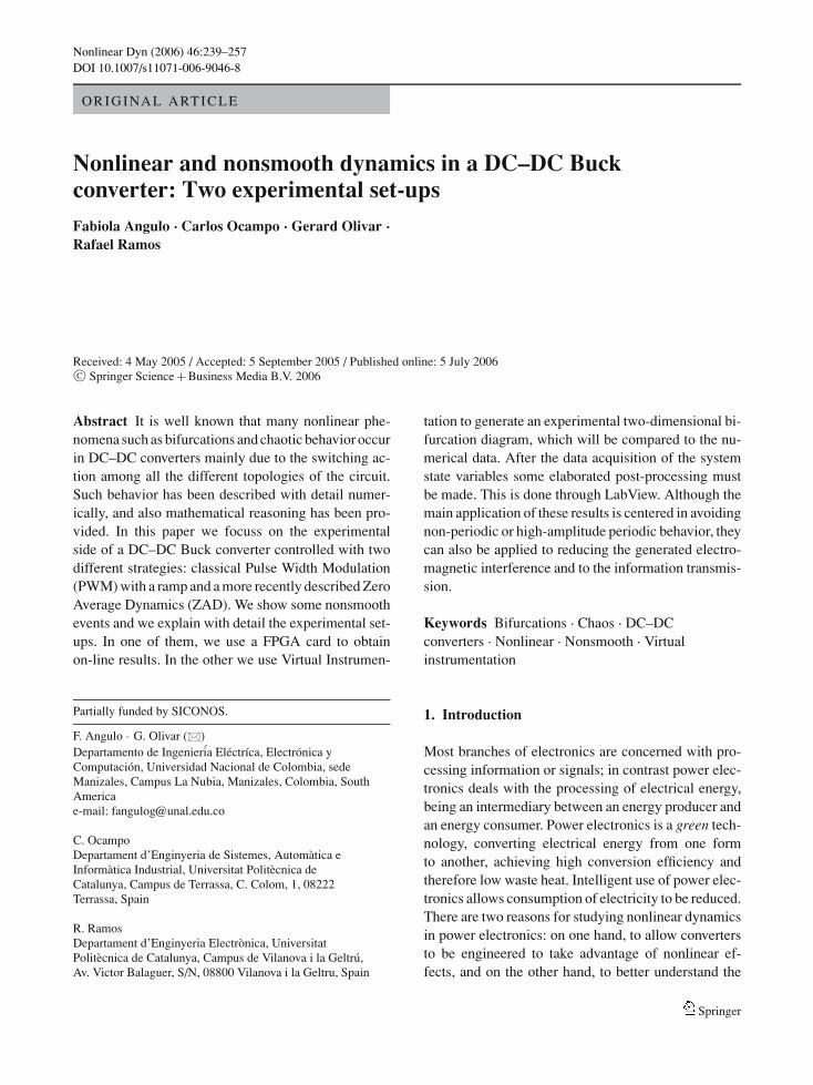
Fig. 1 Scheme of a BuckDC–DC convertercontrolled with a ramp
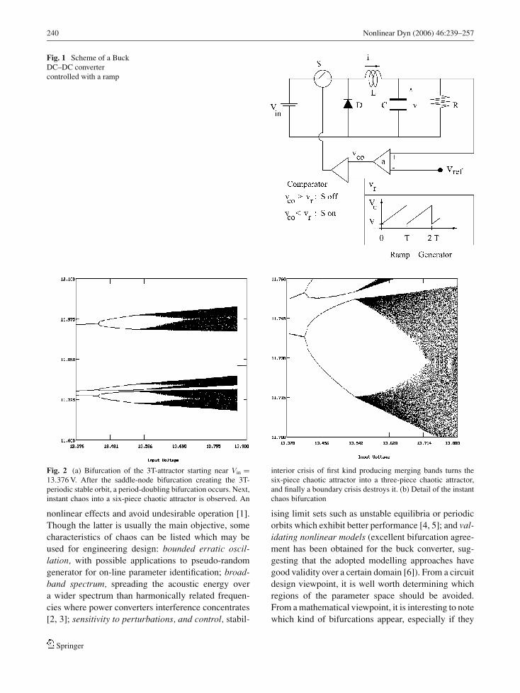
Fig. 2 (a) Bifurcation of the 3T-attractor starting near Vin =13.376 V. After the saddle-node bifurcation creating the 3T-periodic stable orbit, a period-doubling bifurcation occurs. Next,instant chaos into a six-piece chaotic attractor is observed. An
interior crisis of first kind producing merging bands turns thesix-piece chaotic attractor into a three-piece chaotic attractor,and finally a boundary crisis destroys it. (b) Detail of the instantchaos bifurcation
nonlinear effects and avoid undesirable operation [1].Though the latter is usually the main objective, somecharacteristics of chaos can be listed which may beused for engineering design: bounded erratic oscil-lation, with possible applications to pseudo-randomgenerator for on-line parameter identification; broad-band spectrum, spreading the acoustic energy overa wider spectrum than harmonically related frequen-cies where power converters interference concentrates[2, 3]; sensitivity to perturbations, and control, stabil-
ising limit sets such as unstable equilibria or periodicorbits which exhibit better performance [4, 5]; and val-idating nonlinear models (excellent bifurcation agree-ment has been obtained for the buck converter, sug-gesting that the adopted modelling approaches havegood validity over a certain domain [6]). From a circuitdesign viewpoint, it is well worth determining whichregions of the parameter space should be avoided.From a mathematical viewpoint, it is interesting to notewhich kind of bifurcations appear, especially if they
Springer
Nonlinear Dyn (2006) 46:239–257 241
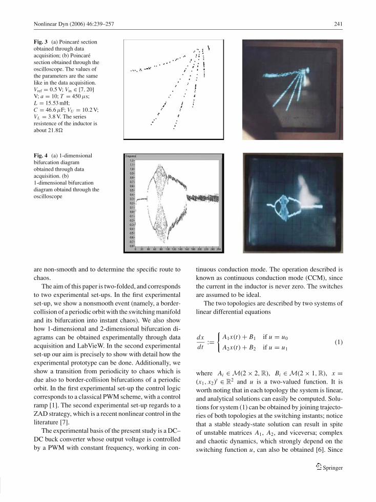
Fig. 3 (a) Poincare sectionobtained through dataacquisition; (b) Poincaresection obtained through theoscilloscope. The values ofthe parameters are the samelike in the data acquisition.Vref = 0.5 V; Vin ∈ [7, 20]V; a = 10; T = 450 μs;L = 15.53 mH;C = 46.6 μF; VU = 10.2 V;VL = 3.8 V. The seriesresistence of the inductor isabout 21.8�
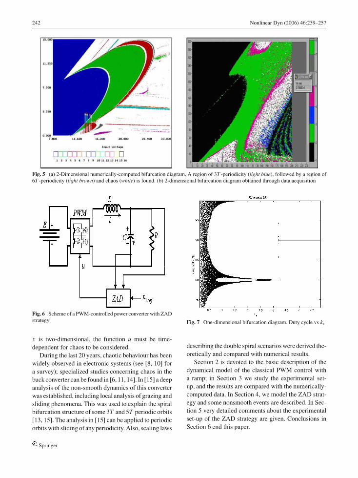
Fig. 4 (a) 1-dimensionalbifurcation diagramobtained through dataacquisition. (b)1-dimensional bifurcationdiagram obtaind through theoscilloscope
are non-smooth and to determine the specific route tochaos.
The aim of this paper is two-folded, and correspondsto two experimental set-ups. In the first experimentalset-up, we show a nonsmooth event (namely, a border-collision of a periodic orbit with the switching manifoldand its bifurcation into instant chaos). We also showhow 1-dimensional and 2-dimensional bifurcation di-agrams can be obtained experimentally through dataacquisition and LabVieW. In the second experimentalset-up our aim is precisely to show with detail how theexperimental prototype can be done. Additionally, weshow a transition from periodicity to chaos which isdue also to border-collision bifurcations of a periodicorbit. In the first experimental set-up the control logiccorresponds to a classical PWM scheme, with a controlramp [1]. The second experimental set-up regards to aZAD strategy, which is a recent nonlinear control in theliterature [7].
The experimental basis of the present study is a DC–DC buck converter whose output voltage is controlledby a PWM with constant frequency, working in con-
tinuous conduction mode. The operation described isknown as continuous conduction mode (CCM), sincethe current in the inductor is never zero. The switchesare assumed to be ideal.
The two topologies are described by two systems oflinear differential equations
dxdt
:={
A1x(t) + B1 if u = u0
A2x(t) + B2 if u = u1(1)
where Ai ∈ M(2 × 2, R), Bi ∈ M(2 × 1, R), x =(x1, x2)t ∈ R2 and u is a two-valued function. It isworth noting that in each topology the system is linear,and analytical solutions can easily be computed. Solu-tions for system (1) can be obtained by joining trajecto-ries of both topologies at the switching instants; noticethat a stable steady-state solution can result in spiteof unstable matrices A1, A2, and viceversa; complexand chaotic dynamics, which strongly depend on theswitching function u, can also be obtained [6]. Since
Springer
242 Nonlinear Dyn (2006) 46:239–257
Fig. 5 (a) 2-Dimensional numerically-computed bifurcation diagram. A region of 3T -periodicity (light blue), followed by a region of6T -periodicity (light brown) and chaos (white) is found. (b) 2-dimensional bifurcation diagram obtained through data acquisition
Fig. 6 Scheme of a PWM-controlled power converter with ZADstrategy
x is two-dimensional, the function u must be time-dependent for chaos to be considered.
During the last 20 years, chaotic behaviour has beenwidely observed in electronic systems (see [8, 10] fora survey); specialized studies concerning chaos in thebuck converter can be found in [6, 11, 14]. In [15] a deepanalysis of the non-smooth dynamics of this converterwas established, including local analysis of grazing andsliding phenomena. This was used to explain the spiralbifurcation structure of some 3T and 5T periodic orbits[13, 15]. The analysis in [15] can be applied to periodicorbits with sliding of any periodicity. Also, scaling laws
Fig. 7 One-dimensional bifurcation diagram. Duty cycle vs ks
describing the double spiral scenarios were derived the-oretically and compared with numerical results.
Section 2 is devoted to the basic description of thedynamical model of the classical PWM control witha ramp; in Section 3 we study the experimental set-up, and the results are compared with the numerically-computed data. In Section 4, we model the ZAD strat-egy and some nonsmooth events are described. In Sec-tion 5 very detailed comments about the experimentalset-up of the ZAD strategy are given. Conclusions inSection 6 end this paper.
Springer

Nonlinear Dyn (2006) 46:239–257 243
Fig. 8 Detailed scheme of implemented system. It shows the DSCB (Drivers and Switching Circuit), the CMB ( Conversion andMultiplexing Board) and the SCAB (Analog Board)
Fig. 9 Analog circuit to generate s(t)
Springer
244 Nonlinear Dyn (2006) 46:239–257
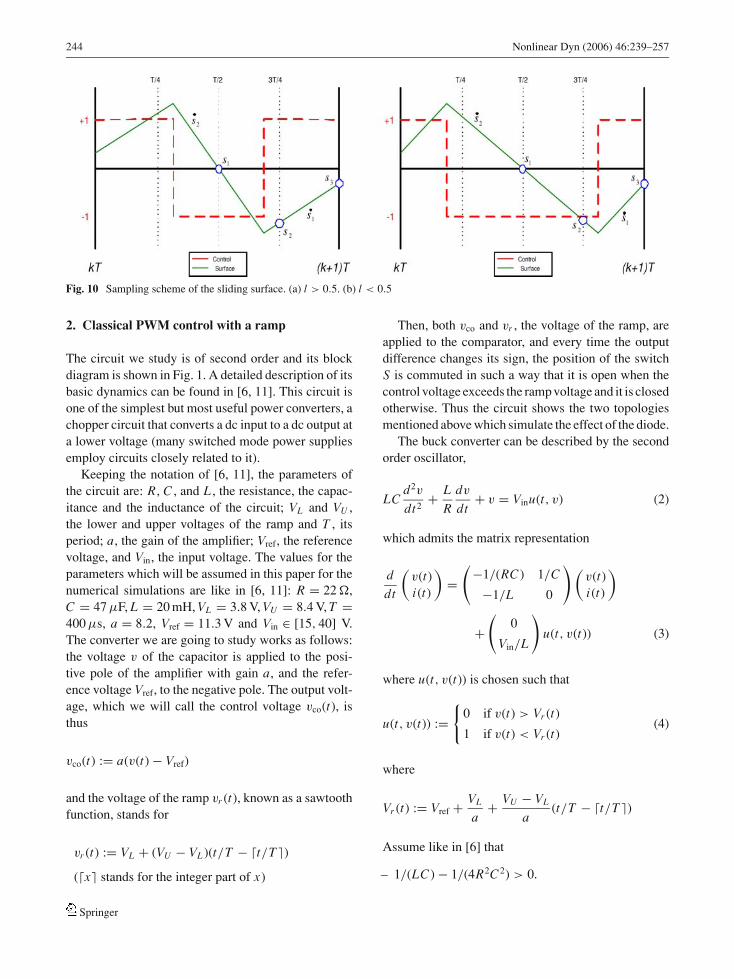
Fig. 10 Sampling scheme of the sliding surface. (a) l > 0.5. (b) l < 0.5
2. Classical PWM control with a ramp
The circuit we study is of second order and its blockdiagram is shown in Fig. 1. A detailed description of itsbasic dynamics can be found in [6, 11]. This circuit isone of the simplest but most useful power converters, achopper circuit that converts a dc input to a dc output ata lower voltage (many switched mode power suppliesemploy circuits closely related to it).
Keeping the notation of [6, 11], the parameters ofthe circuit are: R, C , and L , the resistance, the capac-itance and the inductance of the circuit; VL and VU ,the lower and upper voltages of the ramp and T , itsperiod; a, the gain of the amplifier; Vref, the referencevoltage, and Vin, the input voltage. The values for theparameters which will be assumed in this paper for thenumerical simulations are like in [6, 11]: R = 22 �,C = 47 μF, L = 20 mH, VL = 3.8 V, VU = 8.4 V, T =400 μs, a = 8.2, Vref = 11.3 V and Vin ∈ [15, 40] V.The converter we are going to study works as follows:the voltage v of the capacitor is applied to the posi-tive pole of the amplifier with gain a, and the refer-ence voltage Vref, to the negative pole. The output volt-age, which we will call the control voltage vco(t), isthus
vco(t) := a(v(t) − Vref)
and the voltage of the ramp vr (t), known as a sawtoothfunction, stands for
vr (t) := VL + (VU − VL )(t/T − �t/T �)
(�x� stands for the integer part of x)
Then, both vco and vr , the voltage of the ramp, areapplied to the comparator, and every time the outputdifference changes its sign, the position of the switchS is commuted in such a way that it is open when thecontrol voltage exceeds the ramp voltage and it is closedotherwise. Thus the circuit shows the two topologiesmentioned above which simulate the effect of the diode.
The buck converter can be described by the secondorder oscillator,
LCd2v
dt2+ L
Rdv
dt+ v = Vinu(t, v) (2)
which admits the matrix representation
ddt
(v(t)i(t)
)=
(−1/(RC) 1/C
−1/L 0
) (v(t)i(t)
)
+(
0
Vin/L
)u(t, v(t)) (3)
where u(t, v(t)) is chosen such that
u(t, v(t)) :={
0 if v(t) > Vr (t)
1 if v(t) < Vr (t)(4)
where
Vr (t) := Vref + VL
a+ VU − VL
a(t/T − �t/T �)
Assume like in [6] that
– 1/(LC) − 1/(4R2C2) > 0.
Springer
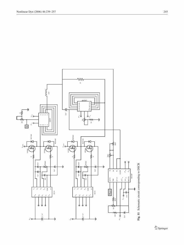
Nonlinear Dyn (2006) 46:239–257 245
Fig
.1
1Sc
hem
atic
circ
uitc
orre
spon
ding
toD
SCB
Springer
246 Nonlinear Dyn (2006) 46:239–257
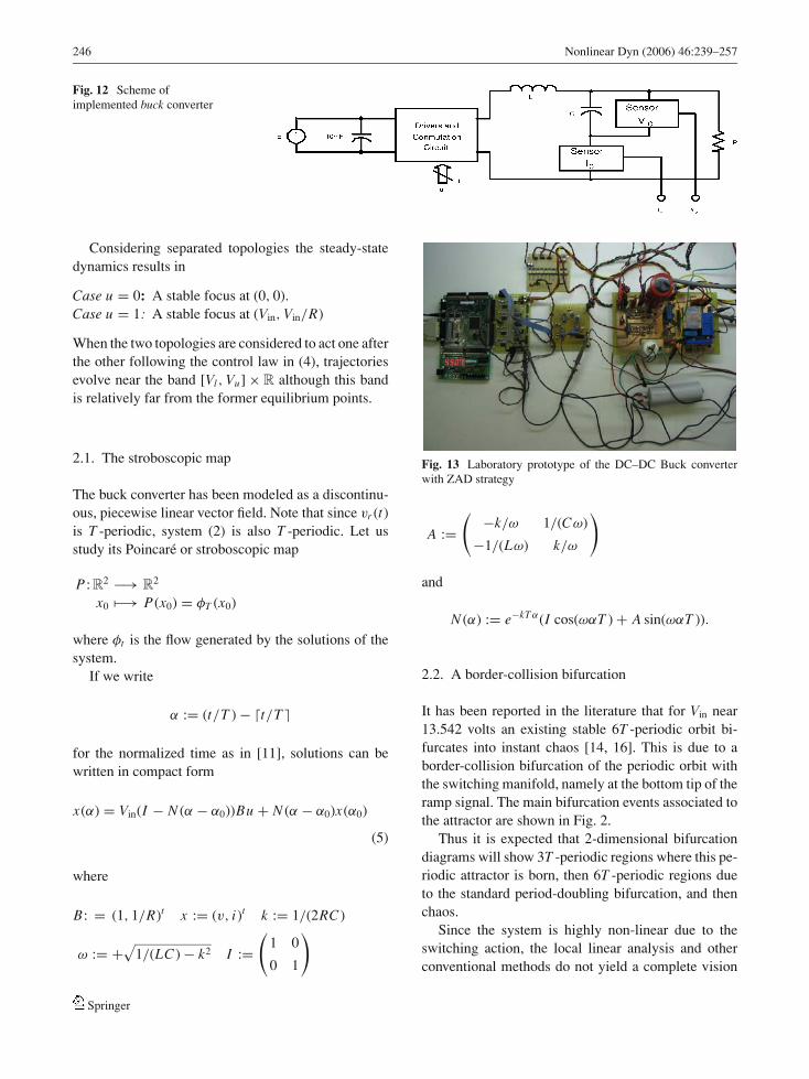
Fig. 12 Scheme ofimplemented buck converter
Considering separated topologies the steady-statedynamics results in
Case u = 0: A stable focus at (0, 0).Case u = 1: A stable focus at (Vin, Vin/R)
When the two topologies are considered to act one afterthe other following the control law in (4), trajectoriesevolve near the band [Vl , Vu] × R although this bandis relatively far from the former equilibrium points.
2.1. The stroboscopic map
The buck converter has been modeled as a discontinu-ous, piecewise linear vector field. Note that since vr (t)is T -periodic, system (2) is also T -periodic. Let usstudy its Poincare or stroboscopic map
P: R2 −→ R2
x0 �−→ P(x0) = φT (x0)
where φt is the flow generated by the solutions of thesystem.
If we write
α := (t/T ) − �t/T �
for the normalized time as in [11], solutions can bewritten in compact form
x(α) = Vin(I − N (α − α0))Bu + N (α − α0)x(α0)
(5)
where
B: = (1, 1/R)t x := (v, i)t k := 1/(2RC)
ω := +√
1/(LC) − k2 I :=(
1 0
0 1
)
Fig. 13 Laboratory prototype of the DC–DC Buck converterwith ZAD strategy
A :=(
−k/ω 1/(Cω)
−1/(Lω) k/ω
)
and
N (α) := e−kT α(I cos(ωαT ) + A sin(ωαT )).
2.2. A border-collision bifurcation
It has been reported in the literature that for Vin near13.542 volts an existing stable 6T -periodic orbit bi-furcates into instant chaos [14, 16]. This is due to aborder-collision bifurcation of the periodic orbit withthe switching manifold, namely at the bottom tip of theramp signal. The main bifurcation events associated tothe attractor are shown in Fig. 2.
Thus it is expected that 2-dimensional bifurcationdiagrams will show 3T -periodic regions where this pe-riodic attractor is born, then 6T -periodic regions dueto the standard period-doubling bifurcation, and thenchaos.
Since the system is highly non-linear due to theswitching action, the local linear analysis and otherconventional methods do not yield a complete vision
Springer
Nonlinear Dyn (2006) 46:239–257 247
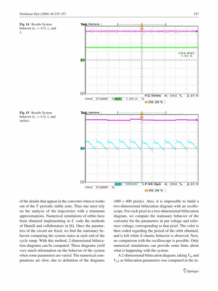
Fig. 14 Results Systembehavior (ks = 4.5). iL andln
Fig. 15 Results Systembehavior (ks = 4.5). ln andsurface
of the details that appear in the converter when it worksout of the T -periodic stable zone. Thus one must relyon the analysis of the trajectories with a minimumapproximations. Numerical simulations of orbits havebeen obtained implementing in C code the methodsof Hamill and collaborators in [6]. Once the parame-ters of the circuit are fixed, we find the stationary be-havior comparing the system states at each end of thecycle ramp. With this method, 2-dimensional bifurca-tion diagrams can be computed. These diagrams yieldvery much information on the behavior of the systemwhen some parameters are varied. The numerical com-putations are slow, due to definition of the diagrams
(400 × 400 pixels). Also, it is impossible to build atwo-dimensional bifurcation diagram with an oscillo-scope. For each pixel in a two-dimensional bifurcationdiagram, we compute the stationary behavior of theconverter for the parameters in put voltage and refer-ence voltage, corresponding to that pixel. The color isthen coded regarding the period of the orbit obtained,and is left white if chaotic behavior is observed. Now,no comparison with the oscilloscope is possible. Onlynumerical simulations can provide some hints aboutwhat is happening with the system.
A 2-dimensional bifurcation diagram, taking Vin andVref as bifurcation parameters was computed in the in-
Springer
248 Nonlinear Dyn (2006) 46:239–257
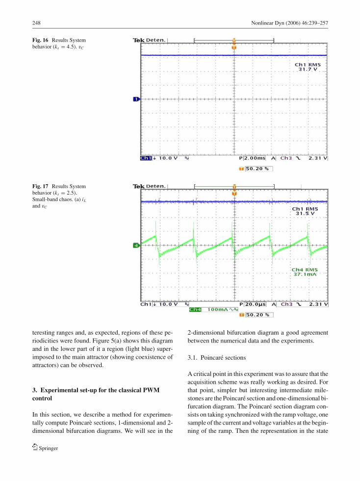
Fig. 16 Results Systembehavior (ks = 4.5). vC
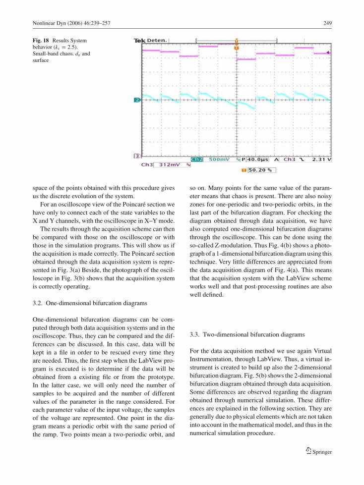
Fig. 17 Results Systembehavior (ks = 2.5).Small-band chaos. (a) iLand vC
teresting ranges and, as expected, regions of these pe-riodicities were found. Figure 5(a) shows this diagramand in the lower part of it a region (light blue) super-imposed to the main attractor (showing coexistence ofattractors) can be observed.
3. Experimental set-up for the classical PWM
control
In this section, we describe a method for experimen-tally compute Poincare sections, 1-dimensional and 2-dimensional bifurcation diagrams. We will see in the
2-dimensional bifurcation diagram a good agreementbetween the numerical data and the experiments.
3.1. Poincare sections
A critical point in this experiment was to assure that theacquisition scheme was really working as desired. Forthat point, simpler but interesting intermediate mile-stones are the Poincare section and one-dimensional bi-furcation diagram. The Poincare section diagram con-sists on taking synchronized with the ramp voltage, onesample of the current and voltage variables at the begin-ning of the ramp. Then the representation in the state
Springer
Nonlinear Dyn (2006) 46:239–257 249
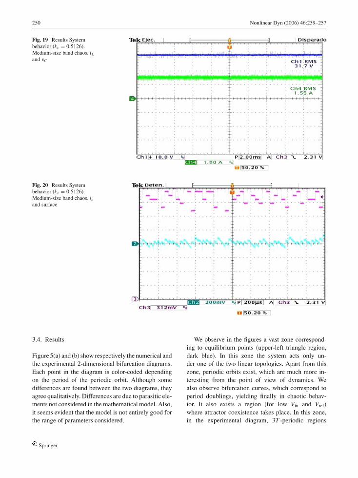
Fig. 18 Results Systembehavior (ks = 2.5).Small-band chaos. dn andsurface
space of the points obtained with this procedure givesus the discrete evolution of the system.
For an oscilloscope view of the Poincare section wehave only to connect each of the state variables to theX and Y channels, with the oscilloscope in X–Y mode.
The results through the acquisition scheme can thenbe compared with those on the oscilloscope or withthose in the simulation programs. This will show us ifthe acquisition is made correctly. The Poincare sectionobtained through the data acquisition system is repre-sented in Fig. 3(a) Beside, the photograph of the oscil-loscope in Fig. 3(b) shows that the acquisition systemis correctly operating.
3.2. One-dimensional bifurcation diagrams
One-dimensional bifurcation diagrams can be com-puted through both data acquisition systems and in theoscilloscope. Thus, they can be compared and the dif-ferences can be discussed. In this case, data will bekept in a file in order to be rescued every time theyare needed. Thus, the first step when the LabView pro-gram is executed is to determine if the data will beobtained from a existing file or from the prototype.In the latter case, we will only need the number ofsamples to be acquired and the number of differentvalues of the parameter in the range considered. Foreach parameter value of the input voltage, the samplesof the voltage are represented. One point in the dia-gram means a periodic orbit with the same period ofthe ramp. Two points mean a two-periodic orbit, and
so on. Many points for the same value of the param-eter means that chaos is present. There are also noisyzones for one-periodic and two-periodic orbits, in thelast part of the bifurcation diagram. For checking thediagram obtained through data acquisition, we havealso computed one-dimensional bifurcation diagramsthrough the oscilloscope. This can be done using theso-called Z-modulation. Thus Fig. 4(b) shows a photo-graph of a 1-dimensional bifurcation diagram using thistechnique. Very little differences are appreciated fromthe data acquisition diagram of Fig. 4(a). This meansthat the acquisition system with the LabView schemeworks well and that post-processing routines are alsowell defined.
3.3. Two-dimensional bifurcation diagrams
For the data acquisition method we use again VirtualInstrumentation, through LabView. Thus, a virtual in-strument is created to build up also the 2-dimensionalbifurcation diagram. Fig. 5(b) shows the 2-dimensionalbifurcation diagram obtained through data acquisition.Some differences are observed regarding the diagramobtained through numerical simulation. These differ-ences are explained in the following section. They aregenerally due to physical elements which are not takeninto account in the mathematical model, and thus in thenumerical simulation procedure.
Springer
250 Nonlinear Dyn (2006) 46:239–257
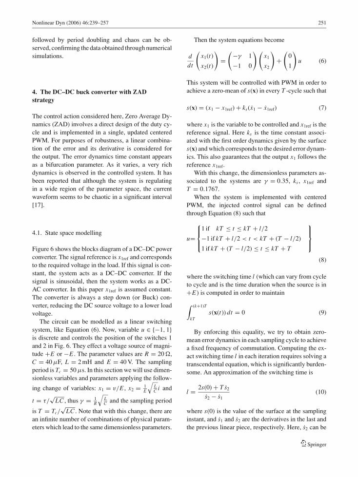
Fig. 19 Results Systembehavior (ks = 0.5126).Medium-size band chaos. iLand vC
Fig. 20 Results Systembehavior (ks = 0.5126).Medium-size band chaos. lnand surface
3.4. Results
Figure 5(a) and (b) show respectively the numerical andthe experimental 2-dimensional bifurcation diagrams.Each point in the diagram is color-coded dependingon the period of the periodic orbit. Although somedifferences are found between the two diagrams, theyagree qualitatively. Differences are due to parasitic ele-ments not considered in the mathematical model. Also,it seems evident that the model is not entirely good forthe range of parameters considered.
We observe in the figures a vast zone correspond-ing to equilibrium points (upper-left triangle region,dark blue). In this zone the system acts only un-der one of the two linear topologies. Apart from thiszone, periodic orbits exist, which are much more in-teresting from the point of view of dynamics. Wealso observe bifurcation curves, which correspond toperiod doublings, yielding finally in chaotic behav-ior. It also exists a region (for low Vin and Vref)where attractor coexistence takes place. In this zone,in the experimental diagram, 3T -periodic regions
Springer
Nonlinear Dyn (2006) 46:239–257 251
followed by period doubling and chaos can be ob-served, confirming the data obtained through numericalsimulations.
4. The DC–DC buck converter with ZAD
strategy
The control action considered here, Zero Average Dy-namics (ZAD) involves a direct design of the duty cy-cle and is implemented in a single, updated centeredPWM. For purposes of robustness, a linear combina-tion of the error and its derivative is considered forthe output. The error dynamics time constant appearsas a bifurcation parameter. As it varies, a very richdynamics is observed in the controlled system. It hasbeen reported that although the system is regulatingin a wide region of the parameter space, the currentwaveform seems to be chaotic in a significant interval[17].
4.1. State space modelling
Figure 6 shows the blocks diagram of a DC–DC powerconverter. The signal reference is x1ref and correspondsto the required voltage in the load. If this signal is con-stant, the system acts as a DC–DC converter. If thesignal is sinusoidal, then the system works as a DC-AC converter. In this paper x1ref is assumed constant.The converter is always a step down (or Buck) con-verter, reducing the DC source voltage to a lower loadvoltage.
The circuit can be modelled as a linear switchingsystem, like Equation (6). Now, variable u ∈ {−1, 1}is discrete and controls the position of the switches 1and 2 in Fig. 6. They effect a voltage source of magni-tude +E or −E . The parameter values are R = 20 �,C = 40 μF, L = 2 mH and E = 40 V. The samplingperiod is Tc = 50 μs. In this section we will use dimen-sionless variables and parameters applying the follow-
ing change of variables: x1 = v/E , x2 = 1E
√LC i and
t = τ/√
LC , thus γ = 1R
√LC and the sampling period
is T = Tc/√
LC . Note that with this change, there arean infinite number of combinations of physical param-eters which lead to the same dimensionless parameters.
Then the system equations become
ddt
(x1(t)
x2(t)
)=
(−γ 1
−1 0
) (x1
x2
)+
(0
1
)u (6)
This system will be controlled with PWM in order toachieve a zero-mean of s(x) in every T -cycle such that
s(x) = (x1 − x1ref) + ks(x1 − x1ref) (7)
where x1 is the variable to be controlled and x1ref is thereference signal. Here ks is the time constant associ-ated with the first order dynamics given by the surfaces(x) and which corresponds to the desired error dynam-ics. This also guarantees that the output x1 follows thereference x1ref.
With this change, the dimensionless parameters as-sociated to the systems are γ = 0.35, ks , x1ref andT = 0.1767.
When the system is implemented with centeredPWM, the injected control signal can be definedthrough Equation (8) such that
u=
⎧⎪⎨⎪⎩1 if kT ≤ t ≤ kT + l/2
−1 if kT + l/2 < t < kT + (T − l/2)
1 if kT + (T − l/2) ≤ t ≤ kT + T
⎫⎪⎬⎪⎭(8)
where the switching time l (which can vary from cycleto cycle and is the time duration when the source is in+E) is computed in order to maintain∫ (k+1)T
kTs(x(t)) dt = 0 (9)
By enforcing this equality, we try to obtain zero-mean error dynamics in each sampling cycle to achievea fixed frequency of commutation. Computing the ex-act switching time l in each iteration requires solving atranscendental equation, which is significantly burden-some. An approximation of the switching time is
l = 2s(0) + T s2
s2 − s1(10)
where s(0) is the value of the surface at the samplinginstant, and s1 and s2 are the derivatives in the last andthe previous linear piece, respectively. Here, s2 can be
Springer
252 Nonlinear Dyn (2006) 46:239–257
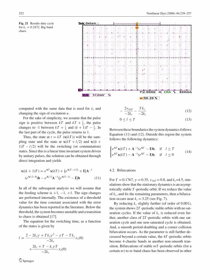
Fig. 21 Results duty cyclefor ks = 0.2472. Big-bandchaos
computed with the same data that is used for s1 andchanging the sign of excitation u.
For the sake of simplicity, we assume that the pulsesign is positive between kT and kT + l
2 , the pulsechanges to -1 between kT + l
2 and (k + 1)T − l2 . In
the last part of the cycle, the pulse returns to 1.Thus, the state at t = kT (x(kT )) will be the sam-
pling state and the state at x(kT + l/2) and x((k +1)T − l/2) will be the switching (or commutation)states. Since this is a linear time invariant system drivenby unitary pulses, the solution can be obtained throughdirect integration and yields
x((k + 1)T ) = eAT x(kT ) + (eA(T −l/2) + I
)A−1
(eAl/2−I)b − eAl/2A−1(eA(T −l) − I)b (11)
In all of the subsequent analysis we will assume thatthe feeding scheme is +1, −1, +1. The sign changesare performed internally. The existence of a thresholdvalue for the time constant associated with the errordynamics has been reported in the literature. Below thethreshold, the system becomes unstable and a transitionto chaos is obtained [17].
The equation for the switching time, as a functionof the states is given by
l = 2 − 2ksγ + T ksγ2 − γ T − T ks
−2ksx1(0)
+2ks + T − ksγ T−2ks
x2(0)
− 2x1ref
−2ks− T ks
−2ks(12)
0 ≤ l ≤ T (13)
Between these boundaries the system dynamics followsEquation (11) and (12). Outside this region the systemfollows the following dynamics:{
eAT x(kT ) + A−1(eAT − I)b, if l ≥ T
eAT x(kT ) − A−1(eAT − I)b, if l ≤ 0(14)
4.2. Bifurcations
For T = 0.1767, γ = 0.35, x1ref = 0.8, and ks=4.5, sim-ulations show that the stationary dynamics is an asymp-totically stable T -periodic orbit. If we reduce the valueof ks , and fix the remaining parameters, then a bifurca-tion occurs near ks = 3.25 (see Fig. 7).
By reducing ks slightly further (of order of 0.001),the system shows 2T -periodic stable orbits with no sat-uration cycles. If the value of ks is reduced even fur-ther, another class of 2T -periodic orbits with one sat-uration cycle and one non-saturated cycle is obtained.And, a smooth period-doubling and a corner collisionbifurcation occurs. As the parameter is still further de-creased beyond a certain value, the 4T -periodic orbitsbecome 4-chaotic bands in another non-smooth tran-sition. Bifurcations of stable mT -periodic orbits (for acertain m) to m-band chaos has been observed in other
Springer
Nonlinear Dyn (2006) 46:239–257 253
systems and specifically in other DC–DC converters,and are also predicted by the existing bifurcation the-ory of non-smooth systems. Finally, the sequence ofmerging bands crises ends in a chaotic 1-band attractor[17, 18].
In the following, we design an experimental setupand some laboratory experiments are performed,which shows the agreement with the numericalsimulations.
5. System design characteristics for the ZAD
strategy
In this section the composition and functionality of eachpart of the design is exposed according to distributionshowed in Fig. 8.
Acquisition and analog processing stage is done bySurface Conformation Analog Board; analog-digitalconversion is done by Conversion and MultiplexingBoard. FPGA board calculates duty cycle and con-trol signal; some design parameters can be varied andshown through Variation and Visualization Board. Fi-nally, Drivers and Switching Circuit Board applies thecalculated control signal over the power electronic con-verter.
5.1. Surface conformation analog board
In the Surface ConformationAnalog Board (SCAB) the reference signal, the orig-
inating signal of the load voltage sensor (vC ) and theproportional voltage to the capacitor current (iC ) origi-nating at the current sensor located in the power circuitare introduced. Note that ic = C vC . With these inputswe obtain the sliding surface. That circuit is shown inFig. 9.
The expression for the generated surface is writtenas
s(t) = G2
[G1(vC − vref) + G3G4
256N
(dvC
dt− dvref
dt
)](15)
where vref corresponds to the reference voltage, Gi isthe i-th operational amplifier gain and N is a 8-bitssequence by means of which derivative error gain is
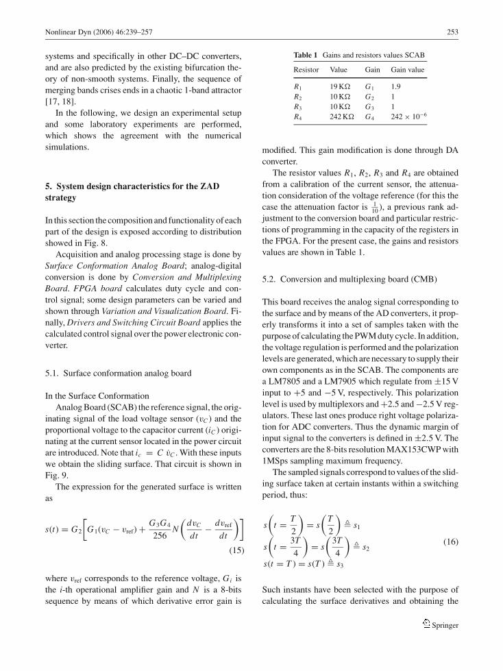
Table 1 Gains and resistors values SCAB
Resistor Value Gain Gain value
R1 19 K� G1 1.9R2 10 K� G2 1R3 10 K� G3 1R4 242 K� G4 242 × 10−6
modified. This gain modification is done through DAconverter.
The resistor values R1, R2, R3 and R4 are obtainedfrom a calibration of the current sensor, the attenua-tion consideration of the voltage reference (for this thecase the attenuation factor is 1
10 ), a previous rank ad-justment to the conversion board and particular restric-tions of programming in the capacity of the registers inthe FPGA. For the present case, the gains and resistorsvalues are shown in Table 1.
5.2. Conversion and multiplexing board (CMB)
This board receives the analog signal corresponding tothe surface and by means of the AD converters, it prop-erly transforms it into a set of samples taken with thepurpose of calculating the PWM duty cycle. In addition,the voltage regulation is performed and the polarizationlevels are generated, which are necessary to supply theirown components as in the SCAB. The components area LM7805 and a LM7905 which regulate from ±15 Vinput to +5 and −5 V, respectively. This polarizationlevel is used by multiplexors and +2.5 and −2.5 V reg-ulators. These last ones produce right voltage polariza-tion for ADC converters. Thus the dynamic margin ofinput signal to the converters is defined in ±2.5 V. Theconverters are the 8-bits resolution MAX153CWP with1MSps sampling maximum frequency.
The sampled signals correspond to values of the slid-ing surface taken at certain instants within a switchingperiod, thus:
s(
t = T2
)= s
(T2
)� s1
s(
t = 3T4
)= s
(3T4
)� s2
s(t = T ) = s(T ) � s3
(16)
Such instants have been selected with the purpose ofcalculating the surface derivatives and obtaining the
Springer
254 Nonlinear Dyn (2006) 46:239–257
duty cycle. The considerations made for the calculationof these derivatives are:
– Duty cycle denominator s2 − s1, is considered as aconstant K , due to previous reported results [19]where such consideration presents better results re-ducing calculation complexity. Such constant K isexpressed by
K = −2 T E G2 G3 G4 GDAC FADC
LC(17)
where GDAC is the DA converter gain that is locatedin SCAB, which for this case, is equal to N
256 . FADC
corresponds to the ratio of the AD converter dynam-ical rank to the maximum polarization voltage (forthis case 51.2).
– The expression for the duty cycle has been standard-ized to work in the rank between 0 and 1 (or 0 and 255after the quantization). Thus, dividing by the switch-ing period, and considering the samples taken fromthe surface and duty cycle denominator consideredas a constant, results in
ln(k) = 2s3 + ( s2T
)K
(18)
– From K and the surface samples, s1, s2 and s3, thederivatives s1 and s2 are computed. If the duty cyclevalue in the previous switching period ln(k − 1) isbigger than 0.5, the derivative expressions will be(Fig. 10(a))
s1 = (s3 − s2)
4(19)
s2 = s1 + K (20)
On the other hand, if the duty cycle value in the pre-vious switching period ln(k − 1) is lower than 0.5,we shall have (Fig. 10(b))
s1 = s2 − K (21)
s2 = (s2 − s1)
4(22)
5.3. FPGA development board
For the control part of the system and the calcula-tions of the duty cycle, signals to drivers and others,
a development board Digilab 2 (D2) has been used.This board is produced and distributed by Digilent Inc.and consists of a FPGA Xilinx Spartan 2 XC2S200-PQ208. In addition, this board includes other bene-fits like voltage regulators, slots for clock crystal in-corporation and OTP memories (One Time Program-ming) [20]. The elaboration of the algorithms for theFPGA has been made using Foundation 3.1, whichis a tool developed for such aim by Xilinx, Inc. andhas been adapted for the assembly starting of exist-ing algorithms for previous related implementations[7, 19, 21, 22].
At this board the surface samples arrive with thepurpose of computing the duty cycle and thus the cal-culation of control signals. The FPGA has a clock sig-nal of 50 MHz, with which, making internal routinesof frequency division, the synchronization signals areobtained and are sent to AD converters to obtain s1, s2
and s3. Once the value of duty cycle is obtained, it iscompared with a double ramp generated by means ofan internal up-down counter, and the resulting signal isintroduced in a sign block to get the signals that com-mand each one of the power transistors of H bridge.For this implementation, these signals are conduced bymeans of a port destined for such aim, being taken tothe DSCB. To avoid a short circuit at the switching timein the power transistors, the set of control signals foreach branch of H bridge has a delay time with respect tothe other two FPGA clock periods, which is equivalentto 166 ns.
Additionally, the external variation of the surfaceconstant is made, a term that is part of the calculationof the duty cycle and that is present analogically inthe construction of the sliding surface. For this tablesof discrete values of ks variation have been generatedand they have been stored in blocks of memories withinthe programming algorithm of the FPGA. The physicalvariation (carried out through the Variation and Visu-alization Board) implies that the algorithm consults inthe block of memories the selected value of ks and ituses it to obtain the corresponding duty cycle. Also,this value of ks is associated with a value of N to de-termine the DA converter gain in the SCAB and thusto assure that ks is the same in the digital part (Al-gorithm within the FPGA) and in the analogical part(surface construction). Therefore, the value N gets outfrom the FPGA development board to the SCAB to dothe corresponding adjustment in the surface constantgain.
Springer
Nonlinear Dyn (2006) 46:239–257 255
5.4. Drivers and switching circuit board (DSCB)
This stage isolates the control and power parts, whichavoids serious failures and damages in the electronicstage due to a possible failure in the switching circuit.This isolation is made by means of two integrated cir-cuits IR2110, which are drivers designed to supportvoltages up until 600 V. Each integrated circuit drivesa branch of H bridge of IRFP450 power transistors,which are feeded by source E . Fig. 11 shows a dia-gram of the DSCB. In this scheme the implementedelements of the power electronic converter Circuit andsensors to take the necessary measures in the algorithmfrom control also appear. We will go back on them later.
5.5. Electronic power converter circuit
The last part of the implementation consists of the sys-tem in study and the sensors for the acquisition of in-teresting signals. Figure 12 shows the correspondingscheme.
First, a 10 mF capacitor is in parallel with the powersupply. The purpose of this element consists of avoid-ing problems in the feeding of the circuit due to thecharacteristics of the source signal or to the pulsatingnature of the system. After, there is the LC filter which,for this case, is composed of a 2 mH inductance coil anda 40 μF capacitor. The current sensor is in series withthe capacitor, whose sensitivity is S = 5 mA/A. Thegain of this branch must be fitted in such a way that it isequal to G4. This is obtained with a Raj potentiometer.Thus, this gain will be
G I c = S C Raj (23)
from where it results that Raj = 1210 �.There is a AD215BYI voltage sensor in parallel to
the capacitor, which takes the value from the vC voltageand isolates it from the following stage of processing.Note in Fig. 12 that although the interest of the controllaw is to manipulate the output voltage, the capacitorvoltage is measured. This is so because the voltage istaken only from the capacitor to avoid the loss in theresistance of the current sensor. Nevertheless, this volt-age in the sensor is so small that, for practical effects,the signals vC and the load voltage are approximatelythe same ones. Table 2 presents characteristics of the
Table 2 Characteristics of the sensors used
Reference Element Description
LA25NP Current sensor Sensibility: 5 mA/AAD215BY Voltage sensor/insolator Gain: −1/10
sensors used. Figure 13 shows the implemented hard-ware for the experiments.
5.6. Results
In this section the results obtained in laboratory with thedescribed system are presented. The duty cycle displayis done by fitting to the saturation in the top of the figure,and zero at the bottom. The top corresponds to the uppervoltage of the reference in DA converter that allowsthe cycle analog measurement. This adjustment is donewith the purpose of calibrating in the most precise waythe measurement of the duty cycle.
Sets of figures and their corresponding observationsin agreement with the value of ks will appear next, fixedby the user by means of the Variation and VisualizationBoard.
Figure 14 shows the behavior of system variables,sliding surface and duty cycle when ks = 4.5. The ref-erence voltage is 32 V and the output voltage is 31.7 V,which originates a 0.94% regulation error. The slidingsurface has the form of the capacitor current, oscillatingaround a DC level. The current stays close to desiredvalue of stationary state (approximately 1.6 A).
Figure 17 shows the behavior of the system whenks = 2.5. The output voltage decreases to 31.5 V, whichentails to an error of 1.56%. The inductor current forthis case appears without its DC component, with thepurpose of visualizing a more visible oscillation withrespect to the previous value of ks . Within this oscilla-tion, at the switching instants, there are peaks, whichare reflected in the output voltage signal. Duty cycleoscillates within a band, causing the sliding surface tohave an irregular behavior, losing the uniform behaviorobserved for greater values of ks . This variation of thecycle is approximately ±6.88% and in some periodssaturation appears.
When kS decreases to 0.5126 the system still regu-lates. However, the inductor current changes very muchcompared with the earlier case. Duty cycle increases therange of band values and now it saturates constantly.The sliding surface has a similar behavior as it was
Springer
256 Nonlinear Dyn (2006) 46:239–257
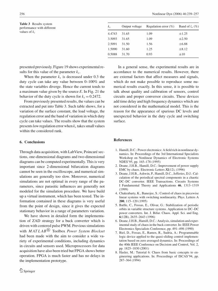
Table 3 Results systemperformance with differentvalues of ks
ks Output voltage Regulation error (%) Band of ln (%)
4.4743 31.65 1.09 ±1.25
3.5093 31.65 1.09 ±2.50
2.5091 31.50 1.56 ±6.88
1.5090 31.60 1.25 ±8.12
0.5088 31.70 0.93 ±10
presented previously. Figure 19 shows experimental re-sults for this value of the parameter ks .
When the parameter ks is decreased under 0.3 theduty cycle can take any value between 0–100% andthe state variables diverge. Hence the current tends toa maximum value given by the source E. In Fig. 21 thebehavior of the duty cycle is shown for ks = 0.2472.
From previously presented results, the values can beextracted and put into Table 3. Such table shows, for avariation of the surface constant, the load voltage, theregulation error and the band of variation in which dutycycle can take values. The results show that the systempresents low regulation error when ks takes small valueswithin the considered rank.
6. Conclusions
Through data acquisition, with LabView, Poincare sec-tions, one-dimensional diagrams and two-dimensionaldiagrams can be computed experimentally. This is veryimportant since 2-dimensional bifurcation diagramscannot be seen in the oscilloscope, and numerical sim-ulations are generally too slow. Moreover, numericalsimulations are not optimal in every range of the pa-rameters, since parasitic influences are generally notmodeled for the simulation procedure. We have buildup a virtual instrument, which has been tested. The in-formation contained in these diagrams is very usefulfrom the point of design, since it gives the expectedstationary behavior in a range of parameters variation.
We have shown in detailed form the implementa-tion of ZAD strategy for a buck converter which isdriven with centered pulse PWM. Previous simulationswith M AT L AB� Toolbox Power System Blocksethad been made with the aim to consider a wide va-riety of experimental conditions, including dynamicsin circuits and sensors used. Microprocessors for dataacquisition have also been tried but FPGA shows betteroperation. FPGA is much faster and has no delays inthe implementation prototype.
In a general sense, the experimental results are inaccordance to the numerical results. However, thereare external factors that affect measures and signals,which do not make possible to reproduce some nu-merical results exactly. In this sense, it is possible totalk about quality and calibration of sensors, controlcircuits and proper conversor circuits. These devicesadd time delay and high frequency dynamics which arenot considered in the mathematical model. This is thereason for the appearance of spurious DC levels andunexpected behavior in the duty cycle and switchingsurface.
References
1. Hamill, D.C.: Power electronics: A field rich in nonlinear dy-namics. In: Proceedings of the 3rd International SpecialistsWorkshop on Nonlinear Dynamics of Electronic SystemsNDES’95, pp. 165–178 (1995)
2. Deane, J.H.B., Hamill, D.C.: Improvement of power supplyEMC by chaos. Electronic Letters 32(12), (1996)
3. Deane, J.H.B., Ashwin, P., Hamill, D.C., Jefferies, D.J.: Cal-culation of the periodical spectral components in a chaoticDC–DC converter. IEEE Transactions. Circuits SystemsI Fundamental Theory and Applications 46, 1313–1319(1999)
4. Chakrabarty, K., Banerjee, S.: Control of chaos in piecewiselinear systems with switching nonlinearity. Phys. Letters A200, 115–120 (1995)
5. Batlle, C., Fossas, E., Olivar, G.: Stabilization of periodicorbits in variable structure systems. Application to DC–DCpower converters. Int. J. Bifur. Chaos. Appl. Sci. and Eng.6(12B), 2635–2643 (1996)
6. Deane, J.H.B., Hamill, D.C.: Analysis, simulation and exper-imental study of chaos in the buck converter. In: IEEE PowerElectronics Specialists Conference, pp. 491–498 (1990)
7. Biel, D., Fossas, E., Ramos, R., Sudria, A.: Programmablelogic device applied to the quasi-sliding control implemen-tation based on zero averaged dynamics. In: Proceedings ofthe 40th IEEE Conference on Decision and Control, Vol. 2,pp. 1825–1830 (2001)
8. Hasler, M.: Tutorial 6: Chaos from basic concepts to en-gineering applications. In: Proceedings of ISCAS’94, pp.287–364 (1994)
Springer

Nonlinear Dyn (2006) 46:239–257 257
9. Carroll, T.L., Peccora, L.M. (eds.): Nonlinear Dynamics inCircuits, World Scientific, Singapore (1995)
10. Verghese, G., Banerjee, S. (eds.): Nonlinear Phenomena inPower Electronics, IEEE Press, Piscataway, NJ (2001)
11. Fossas, E., Olivar, G.: Study of Chaos in the Buck Converter.IEEE Transactions on Circuits Systems I Fundamental The-ory and Applications 43(1), 13–25 (1996)
12. Chakrabarty, K., Poddar, G., Banerjee, S.: Bifurcation be-havior of the buck converter. IEEE Transactions on PowerElectronics 11(3), 439–447 (1996)
13. di Bernardo, M., Fossas, E., Olivar, G., Vasca, F.: Secondarybifurcations and high periodic orbits in voltage controlledbuck converter. Int. J. Bifur. Chaos Appl. Sci. Engrg. 7(12),2755–2771 (1997)
14. Olivar, G.: Chaos in the Buck Converter. Ph. D. Thesis, Tech-nical University of Catalonia, Barcelona (1997)
15. di Bernardo, M., Budd, C., Champneys, A.: Grazing, skip-ping and sliding: Analysis of the non-smooth dynamics ofthe DC–DC buck converter. Nonlinearity 11(4), 858–890(1998)
16. Banerjee, S.: Coexisting attractors, chaotic saddles, and frac-tal basins in a power electronic circuit. IEEE Transactionson Circuits Systems I Fund. Theory Appl. 44(9), 847–849(1997)
17. Angulo, F.: Dynamical analysis of PWM-controlled powerelectronic converters based on the zero average dynamics(ZAD) strategy. (in Spanish)’, Ph. D. Thesis, Technical Uni-versity of Catalonia, Barcelone (2004)
18. Angulo, F., Fossas, E., Olivar, G.: Transition from periodicityto Chaos in a PWM-controlled buck converter with ZADstrategy. Int. J. of Bifur. Chaos (accepted for publication inOctober 2005)
19. Ramos, R., Biel, D., Fossas, E., Guinjoan, F.: A fixed-frequency quasi-sliding control algorithm: Application topower inverters design by means of FPGA implementa-tion. Power IEEE Trans. on Power Electron. 18(1), 344–355(2003)
20. Digilent Inc. Digilab 2 reference manual and digilab DIO1reference manual. www.digilentinc.com. May 7 (2002)
21. Ramos, R., Biel, D., Guinjoan, F., Fossas, E.: Distributedcontrol strategy for parallel-connected inverters. slidingmode control approach and FPGA-based implementation.IEEE 2002 28th Annual Conference of the IECON 2002(Industrial Electronics Society) 1, 111–116 (2002)
22. Ramos, R., Biel, D., Guinjoan, F., Fossas, E.: Design con-siderations in sliding-mode controlled parallel-connected in-verters. IEEE International Symposium on Circuits and Sys-tems, 2002. ISCAS 2002, 4, IV-357–IV-360 (2002)
Springer


