Embed Size (px)
Citation preview

energies
Article
A New Buck-Boost AC/DC Converter withTwo-Terminal Output Voltage for DC Nano-Grid
Xiangkun Li 1, Weimin Wu 1,*, Houqing Wang 1, Ning Gao 1, Henry Shu-hung Chung 2 andFrede Blaabjerg 3
1 Department of Electronic Engineering, Shanghai Maritime University, Shanghai 201306, China;[email protected] (X.L.); [email protected] (H.W.); [email protected] (N.G.)
2 Department of Electronic Engineering, City University of Hong Kong, Hong Kong 999077, China;[email protected]
3 Department of Energy Technology, Aalborg University, Aalborg DK-9220, Denmark; [email protected]* Correspondence: [email protected]
Received: 7 August 2019; Accepted: 30 September 2019; Published: 9 October 2019
Abstract: Due to the development and deployment of renewable DC power sources and their inherentadvantages for DC loads in applications, the DC nano-grid has attracted more and more researchattentions; especially the topologies of AC/DC converters are increasingly studied. When designingan AC to DC converter for a DC nano-grid system, the grounding configuration, which determinesthe costs, the efficiency as well as the safety, plays an important role. A three-terminal output ACto DC converter based on united grounding configuration has been presented for DC nano-grid.However, it has to be pointed out that the three-terminal output DC nano-grid is not as popularas the two-terminal DC output one, due to the infrastructure consideration. This paper proposesa new Buck-Boost AC to DC converter with two-terminal output voltage for DC nano-grid. Theoperating principle, the steady-state analysis, and the small signal modelling for the proposedconverter working in continuous conduction mode are presented in detail. A 220 V/50 Hz/800 Wprototype was fabricated to verify the effectiveness of the proposed converter.
Keywords: buck-boost; converter; dc nano-grid; single inductor
1. Introduction
Due to the energy crisis and the environmental issues caused by the consumption of traditionalfossil fuels, a large number of renewable power conversion systems are connected to low voltage ACdistribution systems as distributed generators. Note that many renewable power sources generateDC energies, while more and more power loads show DC characteristics. Therefore, the DCnano-grids are put forward to be instead of the conventional AC microgrid due to the energyefficiency consideration [1,2], and become more and more attentions [3–13].
In order to flexibly utilize the DC power generated by the renewable energy sources, a bi-directionalAC/DC converter is generally adopted as the interface between the DC nano-grid and the AC powersystem. However, in some places, due to a large number of dc loads, the power generated by thelocal renewable energy sources cannot meet the consumption of local DC loads, so the traditional ACgrid needs to provide power to DC nano-grid and the interface works like a power factor correctionrectifier [10].
Generally, for safety, household appliances need to be connected with ground line, whether in aDC nano-grid or a low-voltage AC grid [12–15]. When selecting the power converter between the DCnano-grid and the low-voltage AC grid, the grounding should be first addressed. Three basic types
Energies 2019, 12, 3808; doi:10.3390/en12203808 www.mdpi.com/journal/energies

Energies 2019, 12, 3808 2 of 18
of the grounding configurations for the DC nano-grid have been summarized in [10], including theunited grounding, the virtual isolated grounding and the unidirectional grounding.
In [15–20], various AC to DC converters were reviewed and compared, but the suitable AC toDC converters based on the united grounding configuration for DC nano-grid application were notintroduced. Thus, [10] introduced a dual Buck-Boost AC to DC converter for DC nano-grid based onthe principle of Two-Switch Buck-Boost (TSBB) converter, which is a simplified cascade connection ofthe Buck and Boost converter. This transformerless Buck-Boost AC to DC converter has three-terminalDC outputs and the AC system is common-ground with the DC system. Due to the applicationof MOSFET switching devices, only one switch operates in the high frequency state at any time,the switching losses of this converter can be reduced a lot. In order to solve the imbalance of thethree-terminal output voltages of the converter in [10], which may be due to the unbalanced loads, acoupled-inductor-based Buck-Boost AC to DC converter was proposed in [12]. And to further improvethe efficiency of the converter in [12], a modified dual buck–boost AC/DC converter with self-balancedDC output voltages in [13] was proposed. All these techniques have accelerated the application of DCnano-grid. However, it has to be pointed out that the three-terminal output DC nano-grid is not aspopular as the two-terminal DC output one, due to the infrastructure consideration. Hence, exploringa new topology of Buck–Boost AC to DC converter with only two-terminal DC output in DC nano-gridapplications is very important and valuable.
In this study, as shown in Figure 1, a new transformerless Buck–Boost AC to DC converter isproposed by inserting an additional switched network into a TSBB converter. During the positive ACgrid voltage, the proposed AC to DC converter operates like a TSBB converter. During the negativeAC grid voltage, the proposed AC to DC converter operates like a single-switch Buck-Boost converter.The main merit of the proposed Buck–Boost AC to DC converter is that two-terminal DC output can besuccessfully achieved, while only a single DC inductor is required and its utilization factor is 100%,resulting in the reduction of size and cost.
Energies 2019, 12, x FOR PEER REVIEW 2 of 18
In [15–20], various AC to DC converters were reviewed and compared, but the suitable AC to DC converters based on the united grounding configuration for DC nano-grid application were not introduced. Thus, [10] introduced a dual Buck-Boost AC to DC converter for DC nano-grid based on the principle of Two-Switch Buck-Boost (TSBB) converter, which is a simplified cascade connection of the Buck and Boost converter. This transformerless Buck-Boost AC to DC converter has three-terminal DC outputs and the AC system is common-ground with the DC system. Due to the application of MOSFET switching devices, only one switch operates in the high frequency state at any time, the switching losses of this converter can be reduced a lot. In order to solve the imbalance of the three-terminal output voltages of the converter in [10], which may be due to the unbalanced loads, a coupled-inductor-based Buck-Boost AC to DC converter was proposed in [12]. And to further improve the efficiency of the converter in [12], a modified dual buck–boost AC/DC converter with self-balanced DC output voltages in [13] was proposed. All these techniques have accelerated the application of DC nano-grid. However, it has to be pointed out that the three-terminal output DC nano-grid is not as popular as the two-terminal DC output one, due to the infrastructure consideration. Hence, exploring a new topology of Buck–Boost AC to DC converter with only two-terminal DC output in DC nano-grid applications is very important and valuable.
In this study, as shown in Figure 1, a new transformerless Buck–Boost AC to DC converter is proposed by inserting an additional switched network into a TSBB converter. During the positive AC grid voltage, the proposed AC to DC converter operates like a TSBB converter. During the negative AC grid voltage, the proposed AC to DC converter operates like a single-switch Buck-Boost converter. The main merit of the proposed Buck–Boost AC to DC converter is that two-terminal DC output can be successfully achieved, while only a single DC inductor is required and its utilization factor is 100%, resulting in the reduction of size and cost.
LRVoVg
D3Lg D5
S3
D1
S1S2
D4
D2
Cf
C
Figure 1. Proposed AC to DC converter with an inductor.
The rest of this paper is organized as follows. In Section 2, the structure of the new transformerless Buck–Boost AC to DC converter is proposed, while its operating principle is illustrated via the equivalent circuits in three working states. The steady-state characteristics of the converter are analyzed in Section 3. The small-signal model is derived, and control strategy of the proposed converter is introduced in Section 4. In order to confirm the theoretical analysis as well as the operating modes, an experimental prototype is developed, and the results are provided in Section 5. Finally, the conclusions are given in Section 6.
2. Proposed AC to DC Converter
2.1. Proposed Topology
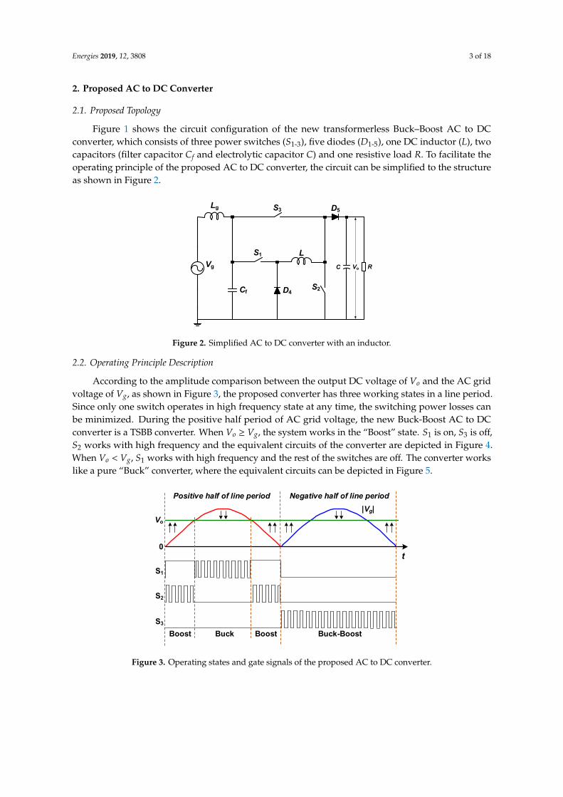
Figure 1 shows the circuit configuration of the new transformerless Buck–Boost AC to DC converter, which consists of three power switches (S1-3), five diodes (D1-5), one DC inductor (L), two capacitors (filter capacitor Cf and electrolytic capacitor C) and one resistive load R. To facilitate the
Figure 1. Proposed AC to DC converter with an inductor.
The rest of this paper is organized as follows. In Section 2, the structure of the new transformerlessBuck–Boost AC to DC converter is proposed, while its operating principle is illustrated via theequivalent circuits in three working states. The steady-state characteristics of the converter areanalyzed in Section 3. The small-signal model is derived, and control strategy of the proposedconverter is introduced in Section 4. In order to confirm the theoretical analysis as well as the operatingmodes, an experimental prototype is developed, and the results are provided in Section 5. Finally, theconclusions are given in Section 6.
Energies 2019, 12, 3808 3 of 18
2. Proposed AC to DC Converter
2.1. Proposed Topology
Figure 1 shows the circuit configuration of the new transformerless Buck–Boost AC to DCconverter, which consists of three power switches (S1-3), five diodes (D1-5), one DC inductor (L), twocapacitors (filter capacitor Cf and electrolytic capacitor C) and one resistive load R. To facilitate theoperating principle of the proposed AC to DC converter, the circuit can be simplified to the structureas shown in Figure 2.
Energies 2019, 12, x FOR PEER REVIEW 3 of 18
operating principle of the proposed AC to DC converter, the circuit can be simplified to the structure as shown in Figure 2.
LRVoVg
Lg D5S3
S2D4Cf
C
S1
Figure 2. Simplified AC to DC converter with an inductor.
2.2. Operating Principle Description
According to the amplitude comparison between the output DC voltage of Vo and the AC grid voltage of Vg, as shown in Figure 3, the proposed converter has three working states in a line period. Since only one switch operates in high frequency state at any time, the switching power losses can be minimized. During the positive half period of AC grid voltage, the new Buck-Boost AC to DC converter is a TSBB converter. When Vo ≥ Vg, the system works in the “Boost” state. S1 is on, S3 is off, S2 works with high frequency and the equivalent circuits of the converter are depicted in Figure 4. When Vo < Vg, S1 works with high frequency and the rest of the switches are off. The converter works like a pure “Buck” converter, where the equivalent circuits can be depicted in Figure 5.
0t
|Vg|Vo
S1
S2
S3
Boost Buck-Boost Buck Boost
Positive half of line period Negative half of line period
Figure 3. Operating states and gate signals of the proposed AC to DC converter.
LRVoVg
Lg D5S3
S2D4Cf
C
S1
LRVoVg
Lg D5S3
S2D4Cf
C
S1
(a) (b)
Figure 4. Equivalent circuits of the “Boost” state in the positive AC grid voltage: (a) Energy storing; (b) Energy releasing.
Figure 2. Simplified AC to DC converter with an inductor.
2.2. Operating Principle Description
According to the amplitude comparison between the output DC voltage of Vo and the AC gridvoltage of Vg, as shown in Figure 3, the proposed converter has three working states in a line period.Since only one switch operates in high frequency state at any time, the switching power losses canbe minimized. During the positive half period of AC grid voltage, the new Buck-Boost AC to DCconverter is a TSBB converter. When Vo ≥ Vg, the system works in the “Boost” state. S1 is on, S3 is off,S2 works with high frequency and the equivalent circuits of the converter are depicted in Figure 4.When Vo < Vg, S1 works with high frequency and the rest of the switches are off. The converter workslike a pure “Buck” converter, where the equivalent circuits can be depicted in Figure 5.
Energies 2019, 12, x FOR PEER REVIEW 3 of 18
operating principle of the proposed AC to DC converter, the circuit can be simplified to the structure as shown in Figure 2.
LRVoVg
Lg D5S3
S2D4Cf
C
S1
Figure 2. Simplified AC to DC converter with an inductor.
2.2. Operating Principle Description
According to the amplitude comparison between the output DC voltage of Vo and the AC grid voltage of Vg, as shown in Figure 3, the proposed converter has three working states in a line period. Since only one switch operates in high frequency state at any time, the switching power losses can be minimized. During the positive half period of AC grid voltage, the new Buck-Boost AC to DC converter is a TSBB converter. When Vo ≥ Vg, the system works in the “Boost” state. S1 is on, S3 is off, S2 works with high frequency and the equivalent circuits of the converter are depicted in Figure 4. When Vo < Vg, S1 works with high frequency and the rest of the switches are off. The converter works like a pure “Buck” converter, where the equivalent circuits can be depicted in Figure 5.
0t
|Vg|Vo
S1
S2
S3
Boost Buck-Boost Buck Boost
Positive half of line period Negative half of line period
Figure 3. Operating states and gate signals of the proposed AC to DC converter.
LRVoVg
Lg D5S3
S2D4Cf
C
S1
LRVoVg
Lg D5S3
S2D4Cf
C
S1
(a) (b)
Figure 4. Equivalent circuits of the “Boost” state in the positive AC grid voltage: (a) Energy storing; (b) Energy releasing.
Figure 3. Operating states and gate signals of the proposed AC to DC converter.

Energies 2019, 12, 3808 4 of 18
Energies 2019, 12, x FOR PEER REVIEW 3 of 18
operating principle of the proposed AC to DC converter, the circuit can be simplified to the structure as shown in Figure 2.
LRVoVg
Lg D5S3
S2D4Cf
C
S1
Figure 2. Simplified AC to DC converter with an inductor.
2.2. Operating Principle Description
According to the amplitude comparison between the output DC voltage of Vo and the AC grid voltage of Vg, as shown in Figure 3, the proposed converter has three working states in a line period. Since only one switch operates in high frequency state at any time, the switching power losses can be minimized. During the positive half period of AC grid voltage, the new Buck-Boost AC to DC converter is a TSBB converter. When Vo ≥ Vg, the system works in the “Boost” state. S1 is on, S3 is off, S2 works with high frequency and the equivalent circuits of the converter are depicted in Figure 4. When Vo < Vg, S1 works with high frequency and the rest of the switches are off. The converter works like a pure “Buck” converter, where the equivalent circuits can be depicted in Figure 5.
0t
|Vg|Vo
S1
S2
S3
Boost Buck-Boost Buck Boost
Positive half of line period Negative half of line period
Figure 3. Operating states and gate signals of the proposed AC to DC converter.
LRVoVg
Lg D5S3
S2D4Cf
C
S1
LRVoVg
Lg D5S3
S2D4Cf
C
S1
(a) (b)
Figure 4. Equivalent circuits of the “Boost” state in the positive AC grid voltage: (a) Energy storing; (b) Energy releasing. Figure 4. Equivalent circuits of the “Boost” state in the positive AC grid voltage: (a) Energy storing; (b)Energy releasing.Energies 2019, 12, x FOR PEER REVIEW 4 of 18
LRVoVg
Lg D5S3
S2D4Cf
C
S1
LRVoVg
Lg D5S3
S2D4Cf
C
S1
(a) (b)
Figure 5. Equivalent circuits of the “Buck” state in the positive AC grid voltage: (a) Energy storing; (b) Energy releasing.
During the negative AC grid voltage, the proposed Buck-Boost AC to DC converter is a single-switch Buck-Boost converter. S1 and S2 are off, S3 operates in high frequency state and the operating states are shown in Figure 6. When S3 is on, the AC Source supplies the power to the DC inductor. When S3 is off, the power stored in the inductor will be released to R, where the whole system works in the “Buck-Boost” state.
LRVoVg
Lg D5S3
S2D4Cf
C
S1
LRVoVg
Lg D5S3
S2D4Cf
C
S1
(a) (b)
Figure 6. Equivalent circuits of the “Buck-Boost” state in the negative AC grid voltage: (a) Energy storing; (b) Energy releasing.
3. Steady-State Characteristics
3.1. Grid Current
The proposed converter works like a power factor correction circuit and the objective of the converter is to transfer the AC power to the DC load while synchronizing the input AC current with the AC grid voltage in phase. Therefore, the grid current can be expressed as:
_(t) sin( t)g g peaki I ω= (1)
where Ig_peak is the peak amplitude of grid current.
3.2. Low Frequency Voltage of the Filter Capacitor
Since the inductance of the grid inductor is very small (micro-henry scale), the voltage drop and phase angle caused by the grid inductor are so small that they can be ignored. The voltage across the filter capacitor VC_f is approximately equal to the grid voltage. It can be determined as:
_ _(t) (t) sin( t)C f g g peakv v V ω≈ = (2)
Figure 5. Equivalent circuits of the “Buck” state in the positive AC grid voltage: (a) Energy storing; (b)Energy releasing.
During the negative AC grid voltage, the proposed Buck-Boost AC to DC converter is asingle-switch Buck-Boost converter. S1 and S2 are off, S3 operates in high frequency state andthe operating states are shown in Figure 6. When S3 is on, the AC Source supplies the power to theDC inductor. When S3 is off, the power stored in the inductor will be released to R, where the wholesystem works in the “Buck-Boost” state.
Energies 2019, 12, x FOR PEER REVIEW 4 of 18
LRVoVg
Lg D5S3
S2D4Cf
C
S1
LRVoVg
Lg D5S3
S2D4Cf
C
S1
(a) (b)
Figure 5. Equivalent circuits of the “Buck” state in the positive AC grid voltage: (a) Energy storing; (b) Energy releasing.
During the negative AC grid voltage, the proposed Buck-Boost AC to DC converter is a single-switch Buck-Boost converter. S1 and S2 are off, S3 operates in high frequency state and the operating states are shown in Figure 6. When S3 is on, the AC Source supplies the power to the DC inductor. When S3 is off, the power stored in the inductor will be released to R, where the whole system works in the “Buck-Boost” state.
LRVoVg
Lg D5S3
S2D4Cf
C
S1
LRVoVg
Lg D5S3
S2D4Cf
C
S1
(a) (b)
Figure 6. Equivalent circuits of the “Buck-Boost” state in the negative AC grid voltage: (a) Energy storing; (b) Energy releasing.
3. Steady-State Characteristics
3.1. Grid Current
The proposed converter works like a power factor correction circuit and the objective of the converter is to transfer the AC power to the DC load while synchronizing the input AC current with the AC grid voltage in phase. Therefore, the grid current can be expressed as:
_(t) sin( t)g g peaki I ω= (1)
where Ig_peak is the peak amplitude of grid current.
3.2. Low Frequency Voltage of the Filter Capacitor
Since the inductance of the grid inductor is very small (micro-henry scale), the voltage drop and phase angle caused by the grid inductor are so small that they can be ignored. The voltage across the filter capacitor VC_f is approximately equal to the grid voltage. It can be determined as:
_ _(t) (t) sin( t)C f g g peakv v V ω≈ = (2)
Figure 6. Equivalent circuits of the “Buck-Boost” state in the negative AC grid voltage: (a) Energystoring; (b) Energy releasing.

Energies 2019, 12, 3808 5 of 18
3. Steady-State Characteristics
3.1. Grid Current
The proposed converter works like a power factor correction circuit and the objective of theconverter is to transfer the AC power to the DC load while synchronizing the input AC current withthe AC grid voltage in phase. Therefore, the grid current can be expressed as:
ig(t) = Ig_peak sin(ωt) (1)
where Ig_peak is the peak amplitude of grid current.
3.2. Low Frequency Voltage of the Filter Capacitor
Since the inductance of the grid inductor is very small (micro-henry scale), the voltage drop andphase angle caused by the grid inductor are so small that they can be ignored. The voltage across thefilter capacitor VC_f is approximately equal to the grid voltage. It can be determined as:
vC_ f (t) ≈ vg(t) = Vg_peak sin(ωt) (2)
where Vg_peak is the peak amplitude of grid voltage,ω is the angular frequency of grid voltage.
3.3. Duty Ratio
Figures 4–6 show the operating principle of the proposed converter via the equivalent circuits.The converter operates in “Boost” state, “Buck” state, and “Buck-Boost” state respectively. Thus, theduty ratio D can be expressed by:
DBoost(t) =vo−
∣∣∣vg(t)∣∣∣
vo(3)
DBuck(t) =vo∣∣∣vg(t)
∣∣∣ (4)
DBuck−Boost(t) =vo
vo+∣∣∣vg(t)
∣∣∣ (5)
It can be seen that when the DC output voltage is constant, the duty cycle varies with thegrid voltage.
3.4. Low Frequency Current of the DC Inductor
When the converter works in “Boost” state, from Figure 4, it can be seen that the low frequencyDC inductor current is the same as the grid current. Thus, the low frequency DC inductor current canbe determined as:
iL(t) = ig(t) (6)
When the converter operates in “Buck” state, the low frequency DC inductor current can bederived through the energy balance equation as:
iL(t) =vg(t) · ig(t)
vo(7)
When the converter operates in “Buck-Boost” state, as shown in Figure 6b, the energy stored inthe DC inductor is transferred to the DC loads during the energy-releasing period. Assuming thatthe devices used in the converter are ideal, the relative power losses can be neglected. According tothe energy balance equation, the output power is equal to the input power in a switching cycle when

Energies 2019, 12, 3808 6 of 18
the converter is operating in the steady state. Thus, the low frequency DC inductor current can bederived as:
iL(t) =vg(t) · ig(t)
vo(1−DBuck−Boost(t))(8)
3.5. High Frequency Current Ripple of the DC Inductor
Assume that the converter works in continuous conduction mode (CCM), during the energy-storingperiod, the current ripple of the DC inductor can be derived through the state equation, which can beexpressed as:
vL(t) = L∆iLTON
(9)
where vL(t) is the voltage across the DC inductor and TON is the turn-on time in a switching period.Thus, the high frequency current ripple of the DC inductor can be expressed as:
∆iL(t) =vL(t) ·D(t)
L · fSW(10)
where D is the duty ratio, f SW is the switching frequency.As shown in Figure 4a, when the AC to DC converter works in “Boost” state, vL(t) and vg(t) are
equal during the energy-storing period. The high frequency current ripple of the DC inductor can beexpressed as:
∆iL_Boost(t) =vg(t)D_Boost(t)
L · fSW(11)
According to the Equations (3) and (11), the DC inductor current ripple ∆iL_Boost(t) can beachieved as:
∆iL_Boost(t) =vg(t) · (vo−
∣∣∣vg(t)∣∣∣)
L · fSW · vo(12)
Similarly, when the proposed converter works in “Buck” and “Buck-Boost” state, the DC inductorcurrent ripple can be obtained as:
∆iL_Buck(t) =(∣∣∣vg(t)
∣∣∣−vo) · vo
L · fSW ·∣∣∣vg(t)
∣∣∣ (13)
∆iL_Buck−Boost(t) =
∣∣∣vg(t)∣∣∣·vo
L · fSW · (vo+∣∣∣vg(t)
∣∣∣) (14)
It can be observed from Equations (12)–(14) that the amplitude of DC inductor current ripple istime varying with the grid voltage.
3.6. High Frequency Voltage Ripple of the Filter Capacitor
When the converter works in “Boost” state, the high frequency voltage ripple of filter capacitorcan be neglected since the filter capacitor current is very small. When the converter works in “Buck”state and “Buck-Boost” state, the voltage ripple of filter capacitor is caused by discharge from the gridinductor. During the energy-releasing period, the current of the filter capacitor is equal to the gridinductor current. In a short switching cycle, the grid current can be regarded as a constant current.Therefore, the voltage ripple peak to peak value of the filter capacitor ∆vC_f(t) can be defined as:
iC_f(t) = C f∆vC_f(t)
TOFF(15)

Energies 2019, 12, 3808 7 of 18
where iC_f is the current of filter capacitor.
∆vC_f(t) =ig(t) · (1−D(t))
C f · fSW(16)
By putting Equations (4) and (5) into Equation (16) respectively, the voltage ripple of the filtercapacitor can be obtained when the converter operates in “Buck” state and “Buck-Boost” state as:
∆vC_f_Buck(t) =ig(t) · (
∣∣∣vg(t)∣∣∣−vo)
C f · fSW ·∣∣∣vg(t)
∣∣∣ (17)
∆vC_f_Buck−Boost(t) =ig(t)·
∣∣∣vg(t)∣∣∣
C f · fSW · (vo+∣∣∣vg(t)
∣∣∣) (18)
From Equations (17) and (18), it can be seen that the value of high frequency voltage ripple of thefilter capacitor is time varying with the grid voltage and grid current.
4. Small Signal Modelling and Controller Design
According to the circuit analysis in Section 2, the working states of proposed AC to DC converterinclude “Boost”, “Buck” and “Buck-Boost”. When the converter operates in “Boost” and “Buck” state,the small signal modeling had been presented and analyzed in [12,21], and the control versus thegrid current transfer functions of “Boost”, and “Buck” stages are deduced as Equations (19) and (20)respectively as:
iLg(s)
d(s)
∣∣∣∣∣∣∣ ∧vg(s) = 0∧vo(s) = 0
=Vo
s3LgLC f + s(Lg + L)(19)
iLg(s)
d(s)
∣∣∣∣∣∣∣ vg(s) = 0∧vo(s) = 0
=sLIL + DVC_ f
s3LgLC f + s(DS12Lg + L)
(20)
where, DS1 is the duty cycle of the switch S1.Thus, in this paper, the control analysis in the “Buck-Boost” stage will be focused on.During the “Buck-Boost” state, the equivalent circuits have been depicted in Figure 6. To simplify
the analysis, the effects of the semiconductors have been ignored. Figure 6a,b show the equivalentcircuits when S3 is on during [t, t + DTs] and off during [t + DTs, t + Ts], respectively. The state equationcan be deduced as followings:
L 0 00 Lg 00 0 C f
ddt
iL(t)ig(t)
vC_f(t)
= Aon
iL(t)ig(t)
vC_f(t)
+ Bon
vo(t)vg(t)
0
(21)
where, Aon =
0 0 10 0 −1−1 1 0
, Bon =
0 0 00 1 00 0 0
.
L 0 00 Lg 00 0 C f
ddt
iL(t)ig(t)
vC_f(t)
= Ao f f
iL(t)ig(t)
vC_f(t)
+ Bo f f
vo(t)vg(t)
0
(22)

Energies 2019, 12, 3808 8 of 18
where, Ao f f =
0 0 00 0 −10 1 0
, Bo f f =
−1 0 00 1 00 0 0
.Using the average state small signal modeling method and assuming that the AC grid source
brings no disturbance and the electrolytic capacitor C is large enough that the output voltage rippleand fluctuation can be ignored during one switching period, the control versus grid current transferfunction can be derived as:
iLg(s)
d(s)
∣∣∣∣∣∣∣ vg(s) = 0∧vo(s) = 0
=sLIL −DS3(VC_f + Vo)
s3LgLC f + s(DS32Lg + L)
(23)
where, DS3 is the duty cycle of the switch S3.The control to grid current transfer functions in three operating states indicate that the proposed
converter is a typical third order system. The controller design of typical third order system has beenfully analyzed in [22–26], so more detailed control design will not be given in this paper.
Figure 7 depicts the whole control block diagram of proposed AC to DC converter, where the ADsampling signals include the output DC voltage of Vo, the grid voltage of Vg and the grid current ig.Double control loops with Proportional Integral (PI) controllers are adopted in the system, where theouter loop is to control the output DC voltage and the inner loop is to make the grid inductor currentto track the sinusoidal waveform and synchronize with the AC grid voltage. Besides, the gate signalsof switches are obtained by comparison of modulated signals and carrier signal.
Energies 2019, 12, x FOR PEER REVIEW 8 of 18
Figure 7 depicts the whole control block diagram of proposed AC to DC converter, where the AD sampling signals include the output DC voltage of Vo, the grid voltage of Vg and the grid current ig. Double control loops with Proportional Integral (PI) controllers are adopted in the system, where the outer loop is to control the output DC voltage and the inner loop is to make the grid inductor current to track the sinusoidal waveform and synchronize with the AC grid voltage. Besides, the gate signals of switches are obtained by comparison of modulated signals and carrier signal.
AD Sampling and Processing
LR
Vg
Lg D5S3
S2D4Cf
C
S1
PI Vref
Vo
Outer LoopInner Loop
DC loadAC grid Proposed Topology
Vo
Vo Vg
sin(ωt )Buck_PI
Buck-Boost_PI
Boost_PI
> Vg Vo
Yes No
< 0Vg Yes No
PLL
ig
igVg
PWM
PWM
PWM
Switch Selection
Switch Selection
Switch Selection
Driver S3
Driver S1
Driver S2
Figure 7. Controller block diagram.
5. Experimental Results
Experiments based a 220 V/800 W/50 Hz prototype have been carried out in the laboratory to validate the effectiveness and performance of the proposed topology. The photograph of the prototype is shown in Figure 8. The AC grid voltage is generated by a programmable AC source (Chroma 6530). The efficiency of the converter is measured by a digital power meter. Table 1 shows the specification and key parameters of the prototype. The selected devices used in the prototype are listed in Table 2. Limited by the laboratory hardware resources, the core EE110 is adopted in DC inductor and grid inductor. And the core material used in inductors is PC40.
Figure 8. Photograph of the experimental setup.
Figure 7. Controller block diagram.
5. Experimental Results
Experiments based a 220 V/800 W/50 Hz prototype have been carried out in the laboratory tovalidate the effectiveness and performance of the proposed topology. The photograph of the prototypeis shown in Figure 8. The AC grid voltage is generated by a programmable AC source (Chroma 6530).The efficiency of the converter is measured by a digital power meter. Table 1 shows the specificationand key parameters of the prototype. The selected devices used in the prototype are listed in Table 2.Limited by the laboratory hardware resources, the core EE110 is adopted in DC inductor and gridinductor. And the core material used in inductors is PC40.

Energies 2019, 12, 3808 9 of 18
Energies 2019, 12, x FOR PEER REVIEW 8 of 18
Figure 7 depicts the whole control block diagram of proposed AC to DC converter, where the AD sampling signals include the output DC voltage of Vo, the grid voltage of Vg and the grid current ig. Double control loops with Proportional Integral (PI) controllers are adopted in the system, where the outer loop is to control the output DC voltage and the inner loop is to make the grid inductor current to track the sinusoidal waveform and synchronize with the AC grid voltage. Besides, the gate signals of switches are obtained by comparison of modulated signals and carrier signal.
AD Sampling and Processing
LR
Vg
Lg D5S3
S2D4Cf
C
S1
PI Vref
Vo
Outer LoopInner Loop
DC loadAC grid Proposed Topology
Vo
Vo Vg
sin(ωt )Buck_PI
Buck-Boost_PI
Boost_PI
> Vg Vo
Yes No
< 0Vg Yes No
PLL
ig
igVg
PWM
PWM
PWM
Switch Selection
Switch Selection
Switch Selection
Driver S3
Driver S1
Driver S2
Figure 7. Controller block diagram.
5. Experimental Results
Experiments based a 220 V/800 W/50 Hz prototype have been carried out in the laboratory to validate the effectiveness and performance of the proposed topology. The photograph of the prototype is shown in Figure 8. The AC grid voltage is generated by a programmable AC source (Chroma 6530). The efficiency of the converter is measured by a digital power meter. Table 1 shows the specification and key parameters of the prototype. The selected devices used in the prototype are listed in Table 2. Limited by the laboratory hardware resources, the core EE110 is adopted in DC inductor and grid inductor. And the core material used in inductors is PC40.
Figure 8. Photograph of the experimental setup.
Figure 8. Photograph of the experimental setup.
Table 1. Parameters of the proposed converter.
Parameters Value
Grid inductance Lg 0.6 mHFilter capacitance Cf 2 µF
DC inductance L 1.2 mHDC output capacitor C 5600 µF
Grid voltage Vg 220 VGrid frequency f 0 50 Hz
DC output voltage Vo 200 VInput power Pin 750 W
Switching frequency fsw 40 kHz
Table 2. Selected devices in the prototype.
Devices Type
Switches S1–S3 IPW65R041CFDDiodes D1–D5 IDW30G65C5Capacitor Cf IKC CBB22
Core of the inductors EE110
Figure 9 shows the gate signals of switches when the reference value of the DC output voltage(Vo) is set to 200 V and the AC input grid voltage (Vg) is set to 220 V/50 Hz (Vg_peak = 311 V). When theproposed converter works in “Boost”, “Buck” and “Buck-Boost” states, the gate signals of switches inhigh frequency are shown in Figure 10 respectively. It can be seen that the states of switches meet withthe principle analyzed in Section 2.
Energies 2019, 12, x FOR PEER REVIEW 9 of 18
Table 1. Parameters of the proposed converter.
Parameters Value Grid inductance Lg 0.6 mH
Filter capacitance Cf 2 µF DC inductance L 1.2 mH
DC output capacitor C 5600 µF Grid voltage Vg 220 V
Grid frequency f0 50 Hz DC output voltage Vo 200 V
Input power Pin 750 W Switching frequency fsw 40 kHz
Table 2. Selected devices in the prototype.
Devices Type
Switches S1–S3 IPW65R041CFD
Diodes D1–D5 IDW30G65C5
Capacitor Cf IKC CBB22
Core of the inductors EE110
Figure 9 shows the gate signals of switches when the reference value of the DC output voltage (Vo) is set to 200 V and the AC input grid voltage (Vg) is set to 220 V/50 Hz (Vg_peak = 311 V). When the proposed converter works in “Boost”, “Buck” and “Buck-Boost” states, the gate signals of switches in high frequency are shown in Figure 10 respectively. It can be seen that the states of switches meet with the principle analyzed in Section 2.
VG_S1
VG_S2
VG_S3
Buck Boost Buck-Boost
Figure 9. Measured Gate signals of MOSFETS when Vo = 200 V, and Vg_peak = 311 V. Figure 9. Measured Gate signals of MOSFETS when Vo = 200 V, and Vg_peak = 311 V.

Energies 2019, 12, 3808 10 of 18
Energies 2019, 12, x FOR PEER REVIEW 10 of 18
VG_S1
VG_S2
VG_S3
Boost State
(a)
VG_S1
VG_S2
VG_S3
Buck State
(b)
VG_S1
VG_S2
VG_S3
Buck-Boost State
(c)
Figure 10. Measured Gate signals of MOSFETS when the proposed converter works in (a) Boost state; (b) Buck state; (c) Buck-Boost state.
Figures 11 and 12 show the experimental results when the AC input peak voltage (Vg_peak) is smaller than the DC output voltage (Vo), where the grid AC voltage is set to 110 V/50 Hz (Vg_peak = 155 V) and the reference value of the DC output voltage Vo is set to 200 V. Figure 11 shows the measured AC grid voltage (Vg(t)), the output DC voltage (Vo), and the grid inductor current (ig(t)). Figure 12 shows the filter capacitor voltage (VC_f(t)) and the DC inductor current (iL(t)). During “Buck-Boost” operation, the maximum filter capacitor voltage ripple is about 28 V, which is consistent with Equation (18).
Figure 10. Measured Gate signals of MOSFETS when the proposed converter works in (a) Boost state;(b) Buck state; (c) Buck-Boost state.
Figures 11 and 12 show the experimental results when the AC input peak voltage (Vg_peak) issmaller than the DC output voltage (Vo), where the grid AC voltage is set to 110 V/50 Hz (Vg_peak = 155 V)and the reference value of the DC output voltage Vo is set to 200 V. Figure 11 shows the measured ACgrid voltage (Vg(t)), the output DC voltage (Vo), and the grid inductor current (ig(t)). Figure 12 showsthe filter capacitor voltage (VC_f(t)) and the DC inductor current (iL(t)). During “Buck-Boost” operation,the maximum filter capacitor voltage ripple is about 28 V, which is consistent with Equation (18).

Energies 2019, 12, 3808 11 of 18
Energies 2019, 12, x FOR PEER REVIEW 11 of 18
V o
Vg
ig
Figure 11. Measured input AC voltage (Vg(t)), the output DC voltage (Vo), and the input grid current ig, when Vo = 200 V, Vg = 110 V, R = 110 Ω.
VC_f
iL
2ΔVC_f = 56V
Figure 12. Measured capacitor voltage (VC_f (t)) and the dc inductor current iL, when Vo = 200 V, Vg = 110 V, R = 110 Ω.
Figures 13 and 14 show the experimental results when the grid voltage is set to 220 V/50 Hz (Vg_peak = 311 V) and the reference value of the DC output voltage Vo is set to 200 V. According to Figure 14, when the proposed converter operates in “Buck” state and the “Buck-Boost” state, the maximum filter capacitor voltage ripple is about 22 V and 37 V respectively, which is consistent with Equations (17) and (18). Figure 15 shows the measured grid voltage (Vg(t)) and grid-injected current (ig(t)) when the DC load changes from 154 Ω to 82 Ω. Figure 16 shows the dynamic response of Vo when the grid voltage are increased from 130 V to 220 V. It can be observed that the DC output voltage has a voltage fluctuation and the maximum DC voltage is about 210 V, which means that the dynamic response of Vo can be further optimized by using a lower time constant PI compensator in each controller.
Figure 11. Measured input AC voltage (Vg(t)), the output DC voltage (Vo), and the input grid currentig, when Vo = 200 V, Vg = 110 V, R = 110 Ω.
Energies 2019, 12, x FOR PEER REVIEW 11 of 18
V o
Vg
ig
Figure 11. Measured input AC voltage (Vg(t)), the output DC voltage (Vo), and the input grid current ig, when Vo = 200 V, Vg = 110 V, R = 110 Ω.
VC_f
iL
2ΔVC_f = 56V
Figure 12. Measured capacitor voltage (VC_f (t)) and the dc inductor current iL, when Vo = 200 V, Vg = 110 V, R = 110 Ω.
Figures 13 and 14 show the experimental results when the grid voltage is set to 220 V/50 Hz (Vg_peak = 311 V) and the reference value of the DC output voltage Vo is set to 200 V. According to Figure 14, when the proposed converter operates in “Buck” state and the “Buck-Boost” state, the maximum filter capacitor voltage ripple is about 22 V and 37 V respectively, which is consistent with Equations (17) and (18). Figure 15 shows the measured grid voltage (Vg(t)) and grid-injected current (ig(t)) when the DC load changes from 154 Ω to 82 Ω. Figure 16 shows the dynamic response of Vo when the grid voltage are increased from 130 V to 220 V. It can be observed that the DC output voltage has a voltage fluctuation and the maximum DC voltage is about 210 V, which means that the dynamic response of Vo can be further optimized by using a lower time constant PI compensator in each controller.
Figure 12. Measured capacitor voltage (VC_f (t)) and the dc inductor current iL, when Vo = 200 V,Vg = 110 V, R = 110 Ω.
Figures 13 and 14 show the experimental results when the grid voltage is set to 220 V/50 Hz(Vg_peak = 311 V) and the reference value of the DC output voltage Vo is set to 200 V. According toFigure 14, when the proposed converter operates in “Buck” state and the “Buck-Boost” state, themaximum filter capacitor voltage ripple is about 22 V and 37 V respectively, which is consistent withEquations (17) and (18). Figure 15 shows the measured grid voltage (Vg(t)) and grid-injected current(ig(t)) when the DC load changes from 154 Ω to 82 Ω. Figure 16 shows the dynamic response ofVo when the grid voltage are increased from 130 V to 220 V. It can be observed that the DC outputvoltage has a voltage fluctuation and the maximum DC voltage is about 210 V, which means that thedynamic response of Vo can be further optimized by using a lower time constant PI compensator ineach controller.

Energies 2019, 12, 3808 12 of 18
Energies 2019, 12, x FOR PEER REVIEW 12 of 18
V o
Vg
ig
Figure 13. Measured AC grid voltage (Vg(t)), the DC voltage (Vo), and the input grid current ig, when Vo = 200 V, Vg = 220 V, R = 60 Ω.
VC_f
iL
2ΔVC_f = 44V
2ΔVC_f = 74V
Figure 14. Measured capacitor voltage (VC_f(t)) and the dc inductor current iL, when Vo = 200 V, Vg = 220 V, R = 60 Ω.
R=154Ω R=82Ω
Steady state
Steady state
Dynamic state
Figure 15. Measured AC grid voltage (Vg(t)), the DC voltage (Vo), and the input grid current ig, when Vo = 200 V, Vgm = 220 V.
Figure 13. Measured AC grid voltage (Vg(t)), the DC voltage (Vo), and the input grid current ig, whenVo = 200 V, Vg = 220 V, R = 60 Ω.
Energies 2019, 12, x FOR PEER REVIEW 12 of 18
V o
Vg
ig
Figure 13. Measured AC grid voltage (Vg(t)), the DC voltage (Vo), and the input grid current ig, when Vo = 200 V, Vg = 220 V, R = 60 Ω.
VC_f
iL
2ΔVC_f = 44V
2ΔVC_f = 74V
Figure 14. Measured capacitor voltage (VC_f(t)) and the dc inductor current iL, when Vo = 200 V, Vg = 220 V, R = 60 Ω.
R=154Ω R=82Ω
Steady state
Steady state
Dynamic state
Figure 15. Measured AC grid voltage (Vg(t)), the DC voltage (Vo), and the input grid current ig, when Vo = 200 V, Vgm = 220 V.
Figure 14. Measured capacitor voltage (VC_f(t)) and the dc inductor current iL, when Vo = 200 V,Vg = 220 V, R = 60 Ω.
Energies 2019, 12, x FOR PEER REVIEW 12 of 18
V o
Vg
ig
Figure 13. Measured AC grid voltage (Vg(t)), the DC voltage (Vo), and the input grid current ig, when Vo = 200 V, Vg = 220 V, R = 60 Ω.
VC_f
iL
2ΔVC_f = 44V
2ΔVC_f = 74V
Figure 14. Measured capacitor voltage (VC_f(t)) and the dc inductor current iL, when Vo = 200 V, Vg = 220 V, R = 60 Ω.
R=154Ω R=82Ω
Steady state
Steady state
Dynamic state
Figure 15. Measured AC grid voltage (Vg(t)), the DC voltage (Vo), and the input grid current ig, when Vo = 200 V, Vgm = 220 V. Figure 15. Measured AC grid voltage (Vg(t)), the DC voltage (Vo), and the input grid current ig, whenVo = 200 V, Vgm = 220 V.

Energies 2019, 12, 3808 13 of 18
Energies 2019, 12, x FOR PEER REVIEW 13 of 18
Vg=130V Vg=220V
Steady state
Steady state
Dynamic state Figure 16. Measured AC grid voltage (Vg(t)), the DC voltage (Vo), and the input grid current ig, when Vo = 200 V, Vgm = 220 V, R = 60 Ω.
Figures 17 and 18 show the measured efficiency of the converter, when the AC grid voltages are 110 V and 220 V, respectively. In addition, the measured and calculated efficiency curves versus input power of the proposed converter are plotted in Figure 19, under that the AC grid voltage is 220 V. It can be seen that the measured efficiency curve and the calculated efficiency curve have the same trend of change. Because of the additional decentralized power losses in the experiment, the calculated efficiency is higher than the measured efficiency. Figure 20 shows the calculated power losses of main devices, while Pin is 745 W versus the different output DC voltage Vo. It can be seen that the power losses of S3 are larger than those of S1 or S2. Moreover, although DC inductor and grid inductor use the same core EE110 and core material, the DC inductor operates at 40 kHz and the grid inductor operates at 50 Hz. The core loss increases with increasing frequency under the same core, so, the core power loss of grid inductor is much smaller than the DC inductor. In addition, there is little difference in copper loss between the two inductors at the same power. So, as shown in Figure 20, the total power losses of DC inductor are much higher than the total power losses of grid inductor and account for a large proportion of the total proposed converter power losses. Figure 21 shows the power losses distribution of semiconductor devices in “Boost”, “Buck” and “Buck-Boost” working states respectively when Vg = 220 V, Vo = 200 V and Pin = 745 W. According to Equations (6)–(8), when the proposed converter is operated in the Buck–Boost state with the same specification, the average DC inductor current of the Buck–Boost state is larger than that of the Boost state or Buck state. Therefore, in the “Buck–Boost”’ state, the conduction and switching losses are higher compared to the “Buck” or “Boost” states.
Figure 17. The measured efficiency of the proposed converter when Vg = 110 V, E = 200 V, R = 110 Ω.
Figure 16. Measured AC grid voltage (Vg(t)), the DC voltage (Vo), and the input grid current ig, whenVo = 200 V, Vgm = 220 V, R = 60 Ω.
Figures 17 and 18 show the measured efficiency of the converter, when the AC grid voltages are110 V and 220 V, respectively. In addition, the measured and calculated efficiency curves versus inputpower of the proposed converter are plotted in Figure 19, under that the AC grid voltage is 220 V.It can be seen that the measured efficiency curve and the calculated efficiency curve have the sametrend of change. Because of the additional decentralized power losses in the experiment, the calculatedefficiency is higher than the measured efficiency. Figure 20 shows the calculated power losses of maindevices, while Pin is 745 W versus the different output DC voltage Vo. It can be seen that the powerlosses of S3 are larger than those of S1 or S2. Moreover, although DC inductor and grid inductor use thesame core EE110 and core material, the DC inductor operates at 40 kHz and the grid inductor operatesat 50 Hz. The core loss increases with increasing frequency under the same core, so, the core power lossof grid inductor is much smaller than the DC inductor. In addition, there is little difference in copperloss between the two inductors at the same power. So, as shown in Figure 20, the total power lossesof DC inductor are much higher than the total power losses of grid inductor and account for a largeproportion of the total proposed converter power losses. Figure 21 shows the power losses distributionof semiconductor devices in “Boost”, “Buck” and “Buck-Boost” working states respectively whenVg = 220 V, Vo = 200 V and Pin = 745 W. According to Equations (6)–(8), when the proposed converteris operated in the Buck–Boost state with the same specification, the average DC inductor current of theBuck–Boost state is larger than that of the Boost state or Buck state. Therefore, in the “Buck–Boost”’state, the conduction and switching losses are higher compared to the “Buck” or “Boost” states.
Energies 2019, 12, x FOR PEER REVIEW 13 of 18
Vg=130V Vg=220V
Steady state
Steady state
Dynamic state Figure 16. Measured AC grid voltage (Vg(t)), the DC voltage (Vo), and the input grid current ig, when Vo = 200 V, Vgm = 220 V, R = 60 Ω.
Figures 17 and 18 show the measured efficiency of the converter, when the AC grid voltages are 110 V and 220 V, respectively. In addition, the measured and calculated efficiency curves versus input power of the proposed converter are plotted in Figure 19, under that the AC grid voltage is 220 V. It can be seen that the measured efficiency curve and the calculated efficiency curve have the same trend of change. Because of the additional decentralized power losses in the experiment, the calculated efficiency is higher than the measured efficiency. Figure 20 shows the calculated power losses of main devices, while Pin is 745 W versus the different output DC voltage Vo. It can be seen that the power losses of S3 are larger than those of S1 or S2. Moreover, although DC inductor and grid inductor use the same core EE110 and core material, the DC inductor operates at 40 kHz and the grid inductor operates at 50 Hz. The core loss increases with increasing frequency under the same core, so, the core power loss of grid inductor is much smaller than the DC inductor. In addition, there is little difference in copper loss between the two inductors at the same power. So, as shown in Figure 20, the total power losses of DC inductor are much higher than the total power losses of grid inductor and account for a large proportion of the total proposed converter power losses. Figure 21 shows the power losses distribution of semiconductor devices in “Boost”, “Buck” and “Buck-Boost” working states respectively when Vg = 220 V, Vo = 200 V and Pin = 745 W. According to Equations (6)–(8), when the proposed converter is operated in the Buck–Boost state with the same specification, the average DC inductor current of the Buck–Boost state is larger than that of the Boost state or Buck state. Therefore, in the “Buck–Boost”’ state, the conduction and switching losses are higher compared to the “Buck” or “Boost” states.
Figure 17. The measured efficiency of the proposed converter when Vg = 110 V, E = 200 V, R = 110 Ω. Figure 17. The measured efficiency of the proposed converter when Vg = 110 V, E = 200 V, R = 110 Ω.

Energies 2019, 12, 3808 14 of 18
Energies 2019, 12, x FOR PEER REVIEW 14 of 18
Figure 18. The measured efficiency of the proposed converter when Vg = 220 V, E = 200 V, R = 60 Ω.
Figure 19. Calculated and measured efficiency curve of proposed converter versus the different input power when Vg = 220 V, Vo = 200 V.
Figure 20. Power losses distribution of main devices versus the different output DC voltages when Vg = 220 V, Pin = 745 W.
Figure 18. The measured efficiency of the proposed converter when Vg = 220 V, E = 200 V, R = 60 Ω.
Energies 2019, 12, x FOR PEER REVIEW 14 of 18
Figure 18. The measured efficiency of the proposed converter when Vg = 220 V, E = 200 V, R = 60 Ω.
Figure 19. Calculated and measured efficiency curve of proposed converter versus the different input power when Vg = 220 V, Vo = 200 V.
Figure 20. Power losses distribution of main devices versus the different output DC voltages when Vg = 220 V, Pin = 745 W.
Figure 19. Calculated and measured efficiency curve of proposed converter versus the different inputpower when Vg = 220 V, Vo = 200 V.
Energies 2019, 12, x FOR PEER REVIEW 14 of 18
Figure 18. The measured efficiency of the proposed converter when Vg = 220 V, E = 200 V, R = 60 Ω.
Figure 19. Calculated and measured efficiency curve of proposed converter versus the different input power when Vg = 220 V, Vo = 200 V.
Figure 20. Power losses distribution of main devices versus the different output DC voltages when Vg = 220 V, Pin = 745 W.
Figure 20. Power losses distribution of main devices versus the different output DC voltages whenVg = 220 V, Pin = 745 W.

Energies 2019, 12, 3808 15 of 18
Energies 2019, 12, x FOR PEER REVIEW 15 of 18
Figure 21. Power losses distribution of semiconductor devices in different working states when Vg = 220 V, Vo = 200 V, Pin = 745 W.
6. Discussion
A comparison of various features of the proposed scheme with existing Buck-Boost AC to DC converters based on united grounding configuration has been performed and presented in Table 3. It can be seen that the proposed Buck-Boost AC to DC converter has the advantage of low number of passive elements and high utilization factor of DC inductor. Compared to the converter proposed in [10], there is no problem of output-DC-voltage unbalance in the proposed AC to DC converter. Compared to the converter proposed in [12,13], the proposed Buck-Boost AC to DC converter has acceptable operating states and control strategy. Since the new AC to DC converter operates in Buck-Boost state during the negative AC grid voltage, the efficiency of the whole system is lower than the converters presented in [10,12,13]. Limited by the laboratory hardware resources, the core EE110 is adopted in DC inductor. This is another factor that affects the efficiency of the proposed converter. Using lower power losses semiconductor devices and using inductors with small core size and low core losses can improve the efficiency of the whole system. Thus, when prioritizing the low cost and small volume of the system, the proposed AC to DC converter is an optional interface device between the AC low voltage grid and the DC nano-grid.
Table 3. Comparison table of various Buck-Boost AC to DC converters based on united grounding configuration.
Topology Converter
in [10] Converter in [12] Converter in [13] Proposed Converter
Switches 4 6 4 3 Diodes 6 6 6 5
Capacitor 3 3 3 2 DC inductors 2 2 2 1
Operating states Buck, Boost Buck, Boost,
Flybuck, Flyback Buck, Boost,
Flybuck, Flyback Buck, Boost, Buck-Boost
Utilization factor of DC inductor 50% 50–100% 50–100% 100% Complexity of small-signal models Three-order
Reference DC output voltage Vo_ref = 400 V Vo_ref = 200 V
Vg = 110V.
Loads RL1 = 144 Ω, RL2 = 94 Ω R = 110 Ω Vo1 223.67 V 200.86 V 200.90 V
Vo = 200 V Vo2 −176.43 V −198.69 V −198.61 V
Efficiency 95.45% 92.96% 93.37% 90.53%
Vg = 220V.
Loads RL1 = 72 Ω, RL2 = 52 Ω. R = 60 Ω Vo1 221.08 V 203.33 V 202.94 V
Vo = 200 V Vo2 −179.37 V −196.14 V −197.35 V
Efficiency 96.24% 96.22% 96.33% 92.15%
Figure 21. Power losses distribution of semiconductor devices in different working states whenVg = 220 V, Vo = 200 V, Pin = 745 W.
6. Discussion
A comparison of various features of the proposed scheme with existing Buck-Boost AC to DCconverters based on united grounding configuration has been performed and presented in Table 3.It can be seen that the proposed Buck-Boost AC to DC converter has the advantage of low numberof passive elements and high utilization factor of DC inductor. Compared to the converter proposedin [10], there is no problem of output-DC-voltage unbalance in the proposed AC to DC converter.Compared to the converter proposed in [12,13], the proposed Buck-Boost AC to DC converter hasacceptable operating states and control strategy. Since the new AC to DC converter operates inBuck-Boost state during the negative AC grid voltage, the efficiency of the whole system is lower thanthe converters presented in [10,12,13]. Limited by the laboratory hardware resources, the core EE110 isadopted in DC inductor. This is another factor that affects the efficiency of the proposed converter.Using lower power losses semiconductor devices and using inductors with small core size and lowcore losses can improve the efficiency of the whole system. Thus, when prioritizing the low cost andsmall volume of the system, the proposed AC to DC converter is an optional interface device betweenthe AC low voltage grid and the DC nano-grid.
Table 3. Comparison table of various Buck-Boost AC to DC converters based on united groundingconfiguration.
Topology Converter in[10]
Converter in[12]
Converter in[13]
ProposedConverter
Switches 4 6 4 3
Diodes 6 6 6 5
Capacitor 3 3 3 2
DC inductors 2 2 2 1
Operating states Buck, BoostBuck, Boost,
Flybuck,Flyback
Buck, Boost,Flybuck,Flyback
Buck, Boost,Buck-Boost
Utilization factor of DC inductor 50% 50–100% 50–100% 100%
Complexity of small-signal models Three-order
Reference DC output voltage Vo_ref = 400 V Vo_ref = 200 V

Energies 2019, 12, 3808 16 of 18
Table 3. Cont.
Topology Converter in[10]
Converter in[12]
Converter in[13]
ProposedConverter
Vg = 110V.
Loads RL1 = 144 Ω, RL2 = 94 Ω R = 110 Ω
Vo1 223.67 V 200.86 V 200.90 VVo = 200 V
Vo2 −176.43 V −198.69 V −198.61 V
Efficiency 95.45% 92.96% 93.37% 90.53%
Vg = 220V.
Loads RL1 = 72 Ω, RL2 = 52 Ω. R = 60 Ω
Vo1 221.08 V 203.33 V 202.94 VVo = 200 V
Vo2 −179.37 V −196.14 V −197.35 V
Efficiency 96.24% 96.22% 96.33% 92.15%
7. Conclusions
A new transformerless Buck-Boost AC to DC converter is adopted as an interface between theAC low voltage grid and the DC nano-grid. The characteristics of this converter can be summarizedas following:
1. Similar to the Buck-Boost AC to DC converter presented in [10,12,13], the same ground line canbe used by the AC grid and DC nano-grid without any transformer isolation, which ensures theearth-fault protection for a hybrid power system.
2. Different from the Buck-Boost AC to DC converter presented in [10,12,13], only a single DCinductor and fewer switching devices are adopted, which can reduce the costs and volume of thesystem. The utilization factor of DC inductor is 100%, but it should be noted that the efficiency ofthe new AC to DC converter has been affected, since the new converter operates in Buck-Booststate during the negative AC grid voltage.
The principle of proposed converter has been described through the equivalent circuits.Experimental results obtained from a 220 V/50 Hz/800 W prototype have verified the feasibilityand effectiveness of the proposed AC to DC converter.
How to improve the efficiency of this converter should be focused on for next step research, forexample, replacing the diodes with the MOSFETs to reduce the conduction power losses or replacingthe material of the inductor core with low power loss to reduce the inductor power losses.
Author Contributions: Conceptualization, X.L., W.W. and H.W.; methodology, X.L., W.W. and N.G.; software,X.L. and H.W.; validation, X.L., and N.G.; formal analysis, H.W. and W.W.; investigation, X.L. and H.W.; resources,W.W.; data curation, X.L.; writing—original draft preparation, X.L., W.W., H.W., H.S.-h.C. and F.B.; writing—reviewand editing, X.L., W.W., H.W., H.S.-h.C. and F.B.; visualization, X.L.; supervision, W.W.; project administration,W.W.; funding acquisition, W.W.
Funding: This work was supported in part by NSFC under Grant 51577114, in part by Shanghai MunicipalEducation Committee under Grant 14SG43, and in part by the Shanghai Science and Technology Commissionunder Grant 17040501500.
Conflicts of Interest: The authors declare no conflict of interest.
Nomenclature
ig Grid currentIg_peak Peak amplitude of grid currentvg Grid voltageVg_peak Peak amplitude of grid voltageω Angular frequency of gridvC_ f Voltage across the filter capacitor

Energies 2019, 12, 3808 17 of 18
vo DC output voltageDBoost Duty ratio in “Boost” stateDBuck Duty ratio in “Buck” stateDBuck−Boost Duty ratio in “Buck-Boost” stateiL Low frequency DC inductor currentvL Voltage across the DC inductorL Value of DC inductor∆iL Current ripple of the DC inductorTON Turn-on time in a switching periodTOFF Turn-off time in a switching periodfSW Switching frequency∆iL_Boost DC inductor current ripple in “Buck” state∆iL_Buck DC inductor current ripple in “Boost” state∆iL_Buck−Boost DC inductor current ripple in “Buck-Boost” stateiC_f Current of filter capacitorC f Value of filter capacitor∆vC_f Voltage ripple peak to peak value of the filter capacitor∆vC_f_Buck Voltage ripple peak to peak value of the filter capacitor in “Buck” state∆vC_f_Buck−Boost Voltage ripple peak to peak value of the filter capacitor in “Buck-Boost” stateDS1 Duty cycle of the switch S1DS3 Duty cycle of the switch S3
References
1. Sannino, A.; Postiglione, G.; Bollen, M.H.J. Feasibility of a DC network for commercial facilities. IEEE Trans.Ind. Appl. 2003, 39, 1499–1507. [CrossRef]
2. Salomonsson, D.; Sannino, A. Low-voltage DC distribution system for commercial power systems withsensitive electronic loads. IEEE Trans. Power Deliv. 2007, 22, 1620–1627. [CrossRef]
3. Sathyan, S.; Suryawanshi, H.M.; Shitole, A.B.; Ballal, M.S.; Borghate, V.B. Soft Switched Interleaved DC/DCConverter as front-end of Multi Inverter Structure for Micro Grid Applications. IEEE Trans. Power Electron.2018, 33, 7645–7655. [CrossRef]
4. Kinhekar, N.; Padhy, N.P.; Li, F.; Gupta, H.O. Utility Oriented Demand Side Management Using Smart ACand Micro DC Grid Cooperative. IEEE Trans. Power Syst. 2016, 31, 1151–1160. [CrossRef]
5. Prabhakaran, P.; Goyal, Y.; Agarwal, V. Novel Nonlinear Droop Control Techniques to Overcome the LoadSharing and Voltage Regulation Issues in DC Microgrid. IEEE Trans. Power Electron. 2018, 33, 4477–4487.[CrossRef]
6. Xu, Q.; Hu, X.; Wang, P.; Xiao, J.; Tu, P.; Wen, C.; Lee, M. A Decentralized Dynamic Power Sharing Strategy forHybrid Energy Storage System in Autonomous DC Microgrid. IEEE Trans. Ind. Electron. 2017, 64, 5930–5941.[CrossRef]
7. Yue, X.; Boroyevich, D.; Lee, F.C.; Chen, F.; Burgos, R.; Zhuo, F. Beat Frequency Oscillation Analysis forPower Electronic Converters in DC Nanogrid Based on Crossed Frequency Output Impedance Matrix Model.IEEE Trans. Power Electron. 2018, 33, 3052–3064. [CrossRef]
8. Yang, Q.; Jiang, L.; Zhao, H.; Zeng, H. Autonomous Voltage Regulation and Current Sharing in IslandedMulti-inverter DC Microgrid. IEEE Trans. Smart Grid 2018, 9, 6429–6437. [CrossRef]
9. Cai, W.; Jiang, L.; Liu, B.; Duan, S.; Zou, C. A Power Decoupled Method Based on Four-Switch Three-PortDC/DC/AC Converter in DC Microgrid. IEEE Trans. Ind. Appl. 2015, 51, 336–343. [CrossRef]
10. Wu, W.; Wang, H.; Liu, Y.; Huang, M.; Blaabjerg, F. A Dual-Buck–Boost AC/DC Converter for DC Nanogridwith Three-Terminal Outputs. IEEE Trans. Ind. Electron. 2017, 64, 295–299. [CrossRef]
11. Rivera, S.; Wu, B.; Kouro, S.; Yaramasu, V.; Wang, J. Electric Vehicle Charging Station Using a Neutral PointClamped Converter With Bipolar DC Bus. IEEE Trans. Ind. Electron. 2015, 62, 1999–2009. [CrossRef]
12. Wang, H.; Wu, W.; Li, Y.W.; Blaabjerg, F. A Coupled-Inductor-Based Buck-Boost AC/DC Converter withBalanced DC Output Voltages. IEEE Trans. Power Electron. 2019, 34, 151–159. [CrossRef]
13. Wang, H.; Wu, W.; Gao, N.; He, Y.; Chung, H.S.; Blaabjerg, F. Modified dual buck–boost AC/DC converterwith self-balanced DC output voltages. IET Power Electron. 2019, 12, 1170–1178. [CrossRef]

Energies 2019, 12, 3808 18 of 18
14. Park, J.D.; Candelaria, J. Fault Detection and Isolation in Low-Voltage DC-Bus Microgrid System. IEEE Trans.Power Deliv. 2013, 28, 779–787. [CrossRef]
15. Salomonsson, D.; Soder, L.; Sannino, A. Protection of Low-Voltage DC Microgrids. IEEE Trans. Power Deliv.2009, 24, 1045–1053. [CrossRef]
16. Singh, B.; Singh, B.N.; Chandra, A.; Al-Haddad, K.; Pandey, A.; Kothari, D.P. A review of single-phaseimproved power quality AC-DC converters. IEEE Trans. Ind. Electron. 2003, 50, 962–981. [CrossRef]
17. Singh, B.; Singh, B.N.; Chandra, A.; Al-Haddad, K.; Pandey, A.; Kothari, D.P. A review of three-phaseimproved power quality AC-DC converters. IEEE Trans. Ind. Electron. 2004, 51, 641–660. [CrossRef]
18. Jovanovic, M.M.; Jang, Y. State-of-the-art, single-phase, active power-factor-correction techniques forhigh-power applications—An overview. IEEE Trans. Ind. Electron. 2005, 52, 701–708. [CrossRef]
19. Kolar, J.W.; Friedli, T. The Essence of Three-Phase PFC Rectifier Systems—Part I. IEEE Trans. Power Electron.2013, 28, 176–198. [CrossRef]
20. Friedli, T.; Hartmann, M.; Kolar, J.W. The Essence of Three-Phase PFC Rectifier Systems—Part II. IEEE Trans.Power Electron. 2014, 29, 543–560. [CrossRef]
21. Wu, W.; Liu, Y.; Wang, H.; Huang, M.; Blaabjerg, F. Modelling and control design of a dual Buck-BoostAC/DC converter used in the DC Nano-grid. In Proceedings of the IEEE 8th International Power Electronicsand Motion Control Conference (IPEMC-ECCE Asia), Hefei, China, 22–26 May 2016; pp. 2187–2192.
22. Liu, Y.; Wu, W.; He, Y.; Lin, Z.; Blaabjerg, F.; Chung, H.S. An Efficient and Robust Hybrid Damper for LCL-or LLCL-based Grid-Tied Inverter with Strong Grid-side Harmonic Voltage Effect Rejection. IEEE Trans. Ind.Electron. 2016, 63, 926–936. [CrossRef]
23. Wang, J.; Yan, J.D.; Jiang, L.; Zou, J. Delay-Dependent Stability of Single-Loop Controlled Grid-ConnectedInverters with LCL Filters. IEEE Trans. Power Electron. 2016, 31, 743–757. [CrossRef]
24. Wang, H.; Wu, W.; Zhang, S.; He, Y.; Chung, H.S.; Blaabjerg, F. A modified Aalborg inverter extractingmaximum power from one PV array source. CPSS Trans. Power Electron. Appl. 2019, 4, 109–118. [CrossRef]
25. Fang, J.; Li, X.; Yang, X.; Tang, Y. An Integrated Trap-LCL Filter with Reduced Current Harmonics forGrid-Connected Converters Under Weak Grid Conditions. IEEE Trans. Power Electron. 2017, 32, 8446–8457.[CrossRef]
26. Wu, W.; Liu, Y.; He, Y.; Chung, H.S.; Liserre, M.; Blaabjerg, F. Damping Methods of Resonances Caused byLCL-Filter-Based Current-Controlled Grid-tied Power Inverters: An Overview. IEEE Trans. Ind. Electron.2017, 64, 7402–7413. [CrossRef]
© 2019 by the authors. Licensee MDPI, Basel, Switzerland. This article is an open accessarticle distributed under the terms and conditions of the Creative Commons Attribution(CC BY) license (http://creativecommons.org/licenses/by/4.0/).


