Embed Size (px)
Citation preview
Sensors and Actuators B 49 (1998) 73–80
Nanoscaled interdigitated electrode arrays for biochemical sensors
Peter Van Gerwen a,*, Wim Laureyn a, Wim Laureys a, Guido Huyberechts a,Maaike Op De Beeck a, Kris Baert a, Jan Suls b, Willy Sansen b, P. Jacobs c,
Lou Hermans a, Robert Mertens a
a IMEC, Kapeldreef 75, B-3001 Leu6en, Belgiumb Department ESAT MICAS, Katholieke Uni6ersiteit Leu6en, K. Mercierlaan 94, B-3001 Leu6en, Belgium
c Innogenetics NV, Industriepark Zwijnaarde 7, Box 4, B-9052 Ghent, Belgium
Received 29 September 1997; received in revised form 2 March 1998; accepted 3 March 1998
Abstract
Nanoscaled interdigitated electrode arrays were made with deep UV lithography. Electrode widths and spacings from 500 downto 250 nm were achieved on large active areas (0.5×1 mm). These electrodes allow for the detection of affinity binding ofbiomolecular structures (e.g. antigens, DNA) by impedimetric measurements. Such a sensor with Pd electrodes on SiO2 isdeveloped and theoretically analysed. It was experimentally characterised in KCl solutions demonstrating its bulk-insensitivebehaviour and the immobilisation of glucose oxidase (GOD) could be monitored by measuring the double layer impedance.© 1998 Elsevier Science S.A. All rights reserved.
Keywords: Nanoscaled; Interdigitated electrode; Biochemical sensors
1. Introduction
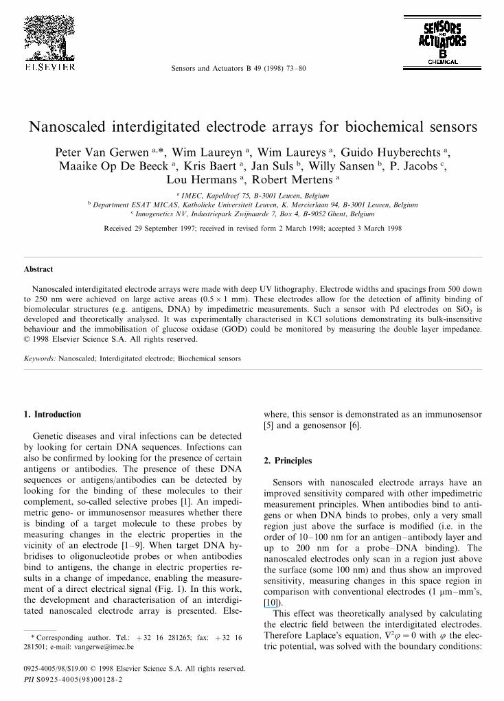
Genetic diseases and viral infections can be detectedby looking for certain DNA sequences. Infections canalso be confirmed by looking for the presence of certainantigens or antibodies. The presence of these DNAsequences or antigens/antibodies can be detected bylooking for the binding of these molecules to theircomplement, so-called selective probes [1]. An impedi-metric geno- or immunosensor measures whether thereis binding of a target molecule to these probes bymeasuring changes in the electric properties in thevicinity of an electrode [1–9]. When target DNA hy-bridises to oligonucleotide probes or when antibodiesbind to antigens, the change in electric properties re-sults in a change of impedance, enabling the measure-ment of a direct electrical signal (Fig. 1). In this work,the development and characterisation of an interdigi-tated nanoscaled electrode array is presented. Else-
where, this sensor is demonstrated as an immunosensor[5] and a genosensor [6].
2. Principles
Sensors with nanoscaled electrode arrays have animproved sensitivity compared with other impedimetricmeasurement principles. When antibodies bind to anti-gens or when DNA binds to probes, only a very smallregion just above the surface is modified (i.e. in theorder of 10–100 nm for an antigen–antibody layer andup to 200 nm for a probe–DNA binding). Thenanoscaled electrodes only scan in a region just abovethe surface (some 100 nm) and thus show an improvedsensitivity, measuring changes in this space region incomparison with conventional electrodes (1 mm–mm’s,[10]).
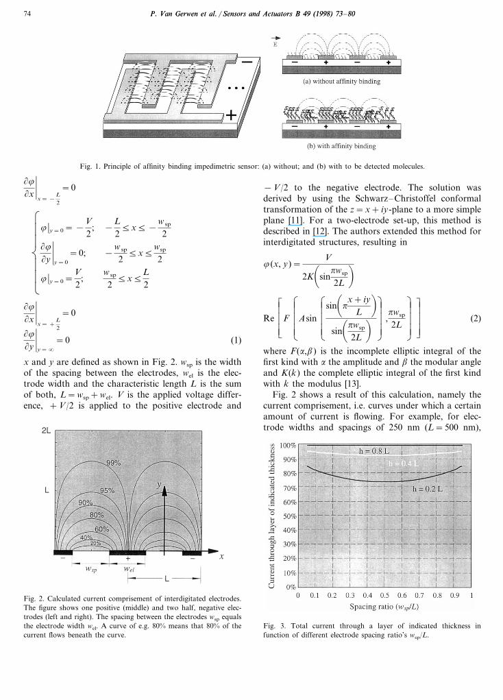
This effect was theoretically analysed by calculatingthe electric field between the interdigitated electrodes.Therefore Laplace’s equation, 928=0 with 8 the elec-tric potential, was solved with the boundary conditions:
* Corresponding author. Tel.: +32 16 281265; fax: +32 16281501; e-mail: [email protected]
0925-4005/98/$19.00 © 1998 Elsevier Science S.A. All rights reserved.
PII S0925-4005(98)00128-2
P. Van Gerwen et al. / Sensors and Actuators B 49 (1998) 73–80P. Van Gerwen et al. / Sensors and Actuators B 49 (1998) 73–8074
Fig. 1. Principle of affinity binding impedimetric sensor: (a) without; and (b) with to be detected molecules.
(8
(x)x= −
L
2
=0
ÍÃ
Ã
Ã
Ã
Á
Ä
8 �y=0= −V2
;
(8
(y)y=0
=0;
8 �y=0=V2
;
−L25x5−
w sp
2
−w sp
25x5
wsp
2w sp
25x5
L2
(8
(x)x= +
L
2
=0
(8
(y)y=�
=0 (1)
x and y are defined as shown in Fig. 2. wsp is the widthof the spacing between the electrodes, wel is the elec-trode width and the characteristic length L is the sumof both, L=wsp+wel. V is the applied voltage differ-ence, +V/2 is applied to the positive electrode and
−V/2 to the negative electrode. The solution wasderived by using the Schwarz–Christoffel conformaltransformation of the z=x+ iy-plane to a more simpleplane [11]. For a two-electrode set-up, this method isdescribed in [12]. The authors extended this method forinterdigitated structures, resulting in
8(x, y)=V
2K�
sinpwsp
2L�
ReÃÃ
Ã
Æ
ÈFÃÃ
Ã
Á
Ä
AsinÃÃ
Ã
Á
Ä
sin�
px+ iy
L�
sin�pwsp
2L� Ã
Ã
Ã
Â
Å
,pwsp
2LÃÃ
Ã
Â
Å
ÃÃ
Ã
Ç
É(2)
where F(a,b) is the incomplete elliptic integral of thefirst kind with a the amplitude and b the modular angleand K(k) the complete elliptic integral of the first kindwith k the modulus [13].
Fig. 2 shows a result of this calculation, namely thecurrent comprisement, i.e. curves under which a certainamount of current is flowing. For example, for elec-trode widths and spacings of 250 nm (L=500 nm),
Fig. 2. Calculated current comprisement of interdigitated electrodes.The figure shows one positive (middle) and two half, negative elec-trodes (left and right). The spacing between the electrodes wsp equalsthe electrode width wel. A curve of e.g. 80% means that 80% of thecurrent flows beneath the curve.
Fig. 3. Total current through a layer of indicated thickness infunction of different electrode spacing ratio’s wsp/L.
P. Van Gerwen et al. / Sensors and Actuators B 49 (1998) 73–80P. Van Gerwen et al. / Sensors and Actuators B 49 (1998) 73–80 75
80% of the current flows in a layer not higher than 250nm above the surface.
This model points to the advantages of nanoscaledelectrodes and also permits deduction of the optimalgeometry for maximal percentage of current through alayer of a certain thickness. It is expected that thistranslates to maximal sensor sensitivity. Fig. 3 shows theamount of current flowing in a layer of indicatedthickness. For example, with a spacing ratio of wsp/L=0.5, the layer with thickness 0.4×L carries 92% of thecurrent. One can see that equal electrode width andspacing (ratio=0.5) gives a minimum, however it is veryflat and it is still a good compromise. If the spacing istoo small, there are very high electric fields at the cornersof the wide electrodes and the signal is less influenced bywhat is happening in the middle of the electrode.
The model also allows for the calculation of theresistance of the solution between the electrodes and ofthe parasitic capacitance through the dielectric under theelectrodes. The resistance of the solution Rsol is given by
Rsol=1nl
1k
2K�
sinpwsp
2L�
K�
cospwsp
2L� (3)
where k is the conductivity of the solution and n thenumber and l the length of the fingers of the interdigi-tated electrodes. The parasitic capacitance Cpar throughthe oxide is given by
Cpar=nloK�
cospwsp
2L�
2K�
sinpwsp
2L� (4)
where o is the permittivity of the dielectric. The interpre-tation of these formulas is given in the paragraph dealingwith the results.
The interdigitated electrode arrays are fabricated withdeep UV lithography. Deep UV lithography allowsstructuring of the electrodes in a very defined andaccurate way. A better reproducibility is therefore to beexpected in comparison with ‘island’-like electrode struc-tures [8]. Another advantage is that large active areas arestructured at once and many sensors can be put in anarray. This offers advantages over e-beam patterning (asin e.g. [2,4,14]) while still achieving submicron struc-tures.
3. Realisation
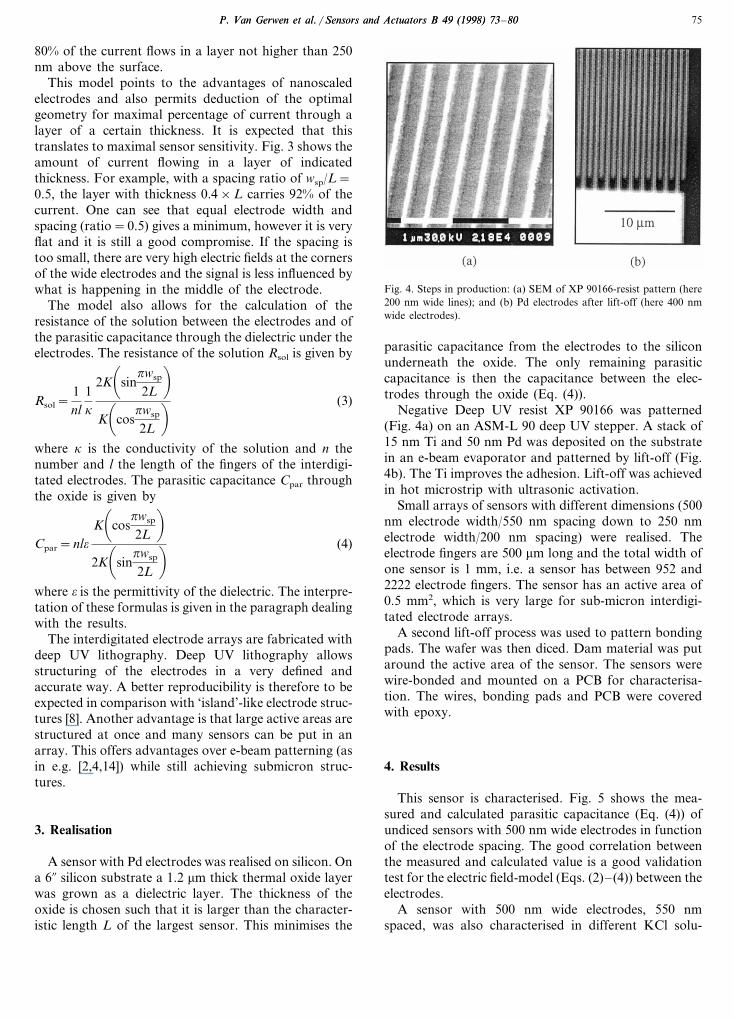
A sensor with Pd electrodes was realised on silicon. Ona 6¦ silicon substrate a 1.2 mm thick thermal oxide layerwas grown as a dielectric layer. The thickness of theoxide is chosen such that it is larger than the character-istic length L of the largest sensor. This minimises the
Fig. 4. Steps in production: (a) SEM of XP 90166-resist pattern (here200 nm wide lines); and (b) Pd electrodes after lift-off (here 400 nmwide electrodes).
parasitic capacitance from the electrodes to the siliconunderneath the oxide. The only remaining parasiticcapacitance is then the capacitance between the elec-trodes through the oxide (Eq. (4)).
Negative Deep UV resist XP 90166 was patterned(Fig. 4a) on an ASM-L 90 deep UV stepper. A stack of15 nm Ti and 50 nm Pd was deposited on the substratein an e-beam evaporator and patterned by lift-off (Fig.4b). The Ti improves the adhesion. Lift-off was achievedin hot microstrip with ultrasonic activation.
Small arrays of sensors with different dimensions (500nm electrode width/550 nm spacing down to 250 nmelectrode width/200 nm spacing) were realised. Theelectrode fingers are 500 mm long and the total width ofone sensor is 1 mm, i.e. a sensor has between 952 and2222 electrode fingers. The sensor has an active area of0.5 mm2, which is very large for sub-micron interdigi-tated electrode arrays.
A second lift-off process was used to pattern bondingpads. The wafer was then diced. Dam material was putaround the active area of the sensor. The sensors werewire-bonded and mounted on a PCB for characterisa-tion. The wires, bonding pads and PCB were coveredwith epoxy.
4. Results
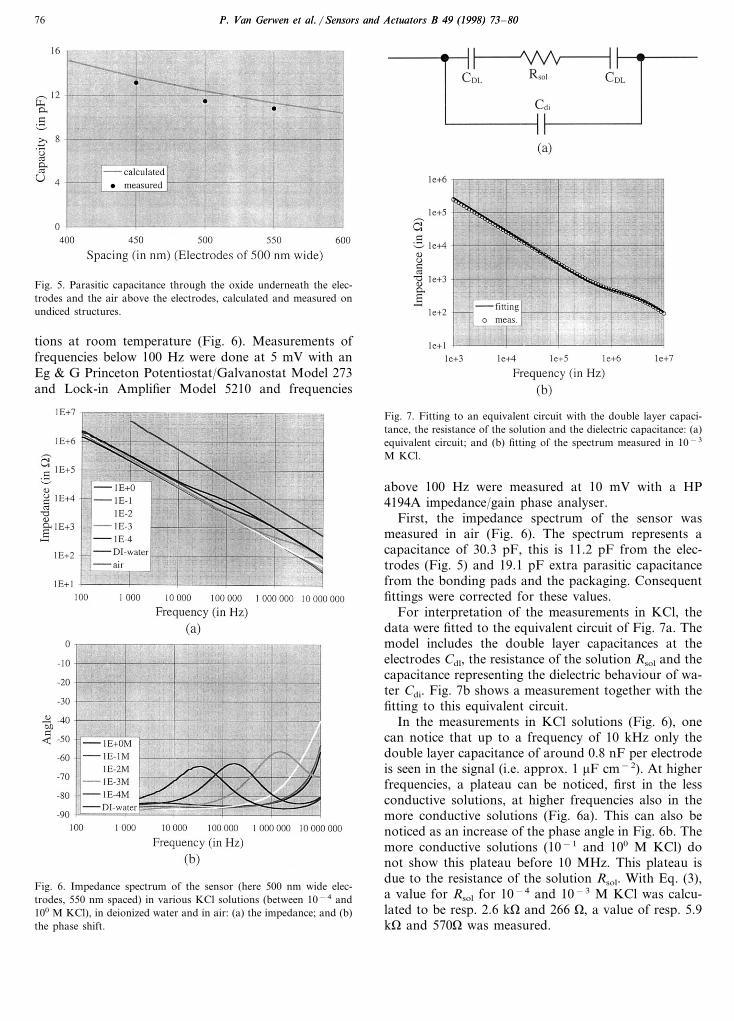
This sensor is characterised. Fig. 5 shows the mea-sured and calculated parasitic capacitance (Eq. (4)) ofundiced sensors with 500 nm wide electrodes in functionof the electrode spacing. The good correlation betweenthe measured and calculated value is a good validationtest for the electric field-model (Eqs. (2)–(4)) between theelectrodes.
A sensor with 500 nm wide electrodes, 550 nmspaced, was also characterised in different KCl solu-
P. Van Gerwen et al. / Sensors and Actuators B 49 (1998) 73–80P. Van Gerwen et al. / Sensors and Actuators B 49 (1998) 73–8076
Fig. 5. Parasitic capacitance through the oxide underneath the elec-trodes and the air above the electrodes, calculated and measured onundiced structures.
Fig. 7. Fitting to an equivalent circuit with the double layer capaci-tance, the resistance of the solution and the dielectric capacitance: (a)equivalent circuit; and (b) fitting of the spectrum measured in 10−3
M KCl.
tions at room temperature (Fig. 6). Measurements offrequencies below 100 Hz were done at 5 mV with anEg & G Princeton Potentiostat/Galvanostat Model 273and Lock-in Amplifier Model 5210 and frequencies
Fig. 6. Impedance spectrum of the sensor (here 500 nm wide elec-trodes, 550 nm spaced) in various KCl solutions (between 10−4 and100 M KCl), in deionized water and in air: (a) the impedance; and (b)the phase shift.
above 100 Hz were measured at 10 mV with a HP4194A impedance/gain phase analyser.
First, the impedance spectrum of the sensor wasmeasured in air (Fig. 6). The spectrum represents acapacitance of 30.3 pF, this is 11.2 pF from the elec-trodes (Fig. 5) and 19.1 pF extra parasitic capacitancefrom the bonding pads and the packaging. Consequentfittings were corrected for these values.
For interpretation of the measurements in KCl, thedata were fitted to the equivalent circuit of Fig. 7a. Themodel includes the double layer capacitances at theelectrodes Cdl, the resistance of the solution Rsol and thecapacitance representing the dielectric behaviour of wa-ter Cdi. Fig. 7b shows a measurement together with thefitting to this equivalent circuit.
In the measurements in KCl solutions (Fig. 6), onecan notice that up to a frequency of 10 kHz only thedouble layer capacitance of around 0.8 nF per electrodeis seen in the signal (i.e. approx. 1 mF cm−2). At higherfrequencies, a plateau can be noticed, first in the lessconductive solutions, at higher frequencies also in themore conductive solutions (Fig. 6a). This can also benoticed as an increase of the phase angle in Fig. 6b. Themore conductive solutions (10−1 and 100 M KCl) donot show this plateau before 10 MHz. This plateau isdue to the resistance of the solution Rsol. With Eq. (3),a value for Rsol for 10−4 and 10−3 M KCl was calcu-lated to be resp. 2.6 kV and 266 V, a value of resp. 5.9kV and 570V was measured.
P. Van Gerwen et al. / Sensors and Actuators B 49 (1998) 73–80P. Van Gerwen et al. / Sensors and Actuators B 49 (1998) 73–80 77
At even higher frequencies this plateau again disap-pears and a capacitance can be noticed. This capaci-tance of approx. 130 pF is not the parasitic capacitance,but it corresponds to the dielectric behaviour of water(or=78). With Eq. (4), a value of 177 pF wascalculated.
In physiological solution1, the resistance of the solu-tion (below 10 V) can not be resolved from the spec-trum anymore. The behaviour of the sensor iscapacitive up to very high frequencies, at least up to 10MHz. This capacitance is then the parallel capacitanceof the double layer and the dielectric. They can not bedistinguished anymore in fittings.
One can also notice that between 1 kHz and 1 MHz,the impedance ranges between 200 kV and 300 V, avery practical and workable range.
At frequencies below 100 Hz, the impedance is notpurely capacitive anymore and changes in function oftime. Fig. 8 shows a sensor in the same solution,measured immediately, after 2, 4 and 24 h. At frequen-cies higher than 1 kHz, absolutely no difference couldbe noticed, but at lower frequencies the signal changessignificantly. This drifting is due to the appearance of aparallel resistance, e.g. a swelling behaviour of theepoxy. This range is not stable and therefore not suit-able for the biosensor.
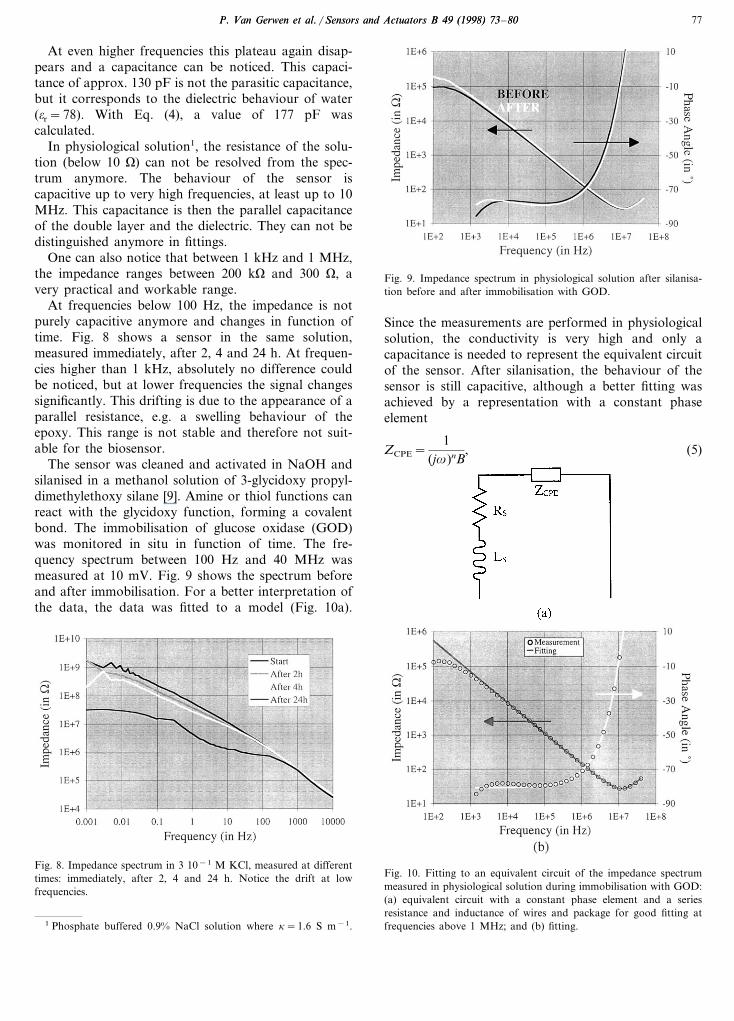
The sensor was cleaned and activated in NaOH andsilanised in a methanol solution of 3-glycidoxy propyl-dimethylethoxy silane [9]. Amine or thiol functions canreact with the glycidoxy function, forming a covalentbond. The immobilisation of glucose oxidase (GOD)was monitored in situ in function of time. The fre-quency spectrum between 100 Hz and 40 MHz wasmeasured at 10 mV. Fig. 9 shows the spectrum beforeand after immobilisation. For a better interpretation ofthe data, the data was fitted to a model (Fig. 10a).
Fig. 9. Impedance spectrum in physiological solution after silanisa-tion before and after immobilisation with GOD.
Since the measurements are performed in physiologicalsolution, the conductivity is very high and only acapacitance is needed to represent the equivalent circuitof the sensor. After silanisation, the behaviour of thesensor is still capacitive, although a better fitting wasachieved by a representation with a constant phaseelement
ZCPE=1
(jv)nB, (5)
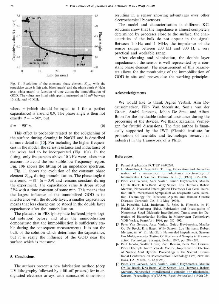
Fig. 10. Fitting to an equivalent circuit of the impedance spectrummeasured in physiological solution during immobilisation with GOD:(a) equivalent circuit with a constant phase element and a seriesresistance and inductance of wires and package for good fitting atfrequencies above 1 MHz; and (b) fitting.
Fig. 8. Impedance spectrum in 3 10−1 M KCl, measured at differenttimes: immediately, after 2, 4 and 24 h. Notice the drift at lowfrequencies.
1 Phosphate buffered 0.9% NaCl solution where k=1.6 S m−1.
P. Van Gerwen et al. / Sensors and Actuators B 49 (1998) 73–80P. Van Gerwen et al. / Sensors and Actuators B 49 (1998) 73–8078
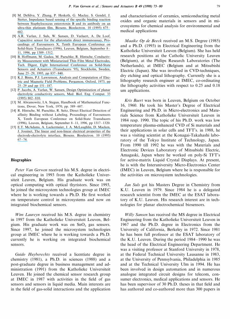
Fig. 11. Evolution of the constant phase element ZCPE with thecapacitive value B (left axis, black graph) and the phase angle u (rightaxis, white graph) in function of time during the immobilisation ofGOD. The values are fitted with spectra measured at 10 mV between10 kHz and 40 MHz.
resulting in a sensor showing advantages over otherelectrochemical biosensors.
The model and characterisation in different KClsolutions show that the impedance is almost completelydetermined by processes close to the surface, the char-acteristics of the bulk do not appear in the signal.Between 1 kHz and 1 MHz, the impedance of thesensor ranges between 200 kV and 300 V, a verypractical and workable range.
After cleaning and silanisation, the double layerimpedance of the sensor is well represented by a con-stant phase element. The measurement of this parame-ter allows for the monitoring of the immobilisation ofGOD in situ and proves also the working principles.
Acknowledgements
We would like to thank Agnes Verbist, Ann De-caussemaeker, Filip Van Steenkiste, Sonja van derGroen, Andre Janssens, Johan De Smet and AlbertBoon for the invaluable technical assistance during theprocessing of the devices. We thank Katarina Verhae-gen for fruitful discussions. The first author is finan-cially supported by the IWT (Flemish institute forpromotion of scientific and technologic research inindustry) in the framework of a Ph.D.
References
[1] Patent Application PCT/EP 96/05290.[2] L. Montelius, J. Tegenfeldt, T. Ling, Fabrication and character-
ization of a nanosensor for admittance spectroscopy ofbiomolecules, J. Vac. Sci. Technol. A 13 (3) (1995) 1755–1760.
[3] Peter Van Gerwen, Anca Varlan, Guido Huyberechts, MaaikeOp De Beeck, Kris Baert, Willy Sansen, Lou Hermans, RobertMertens, Nanoscaled Interdigitated Electrodes For Gene Detec-tion IBC’s International Symposium on Diagnostic Gene Detec-tion Technology for Infectious Agents and Human GeneticDiseases, Coronado CA, 2–3 May (1996).
[4] M. Paeschke, L.M. Buchman, R. Seitz, R. Hintsche, in: H.Reichl, A. Heuberger (Eds.), Fabrication and Investigation ofNanometer Sized Dielectric Interdigitated Transducers for De-tection of Biomolecular Binding in Microsystem Technology,VDE-Verlag, Frankfurt, 1996, pp. 687–692.
[5] Peter Van Gerwen, Anca Varlan, Guido Huyberechts, MaaikeOp De Beeck, Kris Baert, Willy Sansen, Lou Hermans, RobertMertens, in: W. Ehrfeld (Ed.), Nanoscaled Impedimetric SensorsFor Multiparameter Testing Of Biochemical Samples in Microre-action Technology, Springer, Berlin, 1997, pp. 289–293.
[6] Paul Jacobs, Walter Hofer, Rudi Rossau, Peter Van Gerwen,Peter Detemple Andre Van de Voorde, Impedimetric Detectionof Nucleic Acid Hybrids, Proceedings of the Second Interna-tional Conference on Microreaction Technology 1998, New Or-leans, LA, March, 8–12 (1998).
[7] Peter Van Gerwen, Anca Varlan, Guido Huyberechts, MaaikeOp De Beeck, Kris Baert, Willy Sansen, Lou Hermans, RobertMertens, Nanoscaled Interdigitated Electrodes For BiochemicalSensors. Proceedings of mTAS’96, Basel, Switzerland (1996) 254.
where n (which should be equal to 1 for a perfectcapacitance) is around 0.9. The phase angle is then notexactly u= −90°, but
u= −90° n. (6)
This effect is probably related to the roughening ofthe surface during cleaning in NaOH and is describedin more detail in [15]. For including the higher frequen-cies in the model, the series resistance and inductance ofthe wires had to be incorporated (Fig. 10a). In thefitting, only frequencies above 10 kHz were taken intoaccount to avoid the less stable low frequency region.Fig. 10b shows the fitting of an impedance spectrum.
Fig. 11 shows the evolution of the constant phaseelement ZCPE during immobilisation. The phase angle u
is around −81° (n=0.9) and remains constant duringthe experiment. The capacitance value B drops about23% with a time constant of some min. This means thatthe largest influence of the immobilised GOD is itsinterference with the double layer, a smaller capacitancemeans that less charge can be stored in the double layercapacitance after the immobilisation.
The plateaux in PBS (phosphate buffered physiologi-cal solution) before and after the immobilisationdemonstrate that the immobilisation is sufficiently sta-ble during the consequent measurements. It is not thebulk of the solution which determines the capacitance,but it is really the influence of the GOD near thesurface which is measured.
5. Conclusions
The authors present a new fabrication method (deepUV lithography followed by a lift-off process) for inter-digitated electrode arrays with nanoscaled dimensions
P. Van Gerwen et al. / Sensors and Actuators B 49 (1998) 73–80P. Van Gerwen et al. / Sensors and Actuators B 49 (1998) 73–80 79
[8] M. DeSilva, Y. Zhang, P. Hesketh, G. Maclay, S. Gendel, J.Stetter, Impedance based sensing of the specific binding reactionbetween Staphylococcus enterotoxin B and its antibody on anultra-thin platinum film, Biosens. Bioelectron. 10 (1995) 675–682.
[9] A.R. Varlan, J. Suls, W. Sansen, D. Veelaert, A. De Loof,Capacitive sensor for the allatostatin direct immunoassay, Pro-ceedings of Eurosensors X, Tenth European Conference onSolid-State Transducers (1996), Leuven, Belgium, September 8–11, 1996, pp 1309–1312.
[10] B. Hoffmann, M. Gadau, M. Paeschke, R. Hintsche, Conductiv-ity Measurement with Miniaturized Thin Film Metal Electrodes,Tech. Digest, Eight International Conference on Solid-StateSensors and Actuators (Transducers ‘95), Stockholm, Sweden,June 25–29, 1995, pp 837–840.
[11] K.J. Binns, P.J. Lawrenson, Analysis and Computation of Elec-tric and Magnetic Field Problems, Pergamon, Oxford, 1973, pp25–29 and pp 151–187.
[12] P. Jacobs, A. Varlan, W. Sansen, Design Optimization of planarelectrolytic conductivity sensors, Med. Biol. Eng. Comput. 33(1995) 802–810.
[13] M. Abramowitz, I.A. Stegun, Handbook of Mathematical Func-tions, Dover, New York, 1970, pp. 589–607.
[14] R. Hintsche, M. Paeschke, R. Seitz, Direct Electical Detection ofaffinity Binding without Labeling, Proceedings of EurosensorsX, Tenth European Conference on Solid-State Transducers(1996), Leuven, Belgium, September 8–11, 1996, pp 1317–1320.
[15] E.T. McAdams, A. Lackermeier, J. A. McLaughlin, D. Macken,J. Jossinet, The linear and non-linear electrical properties of theelectrode-electrolyte interface, Biosens. Bioelectron. 10 (1995)67–74.
Biographies
Peter Van Gerwen received his M.S. degree in electri-cal engineering in 1993 from the Katholieke Univer-siteit Leuven, Belgium. His graduate work was onoptical computing with optical thyristors. Since 1993,he joined the microsystem technologies group at IMECwhere he is working towards a Ph.D. He first workedon temperature control in microsystems and now onintegrated biochemical sensors.
Wim Laureyn received his M.S. degree in chemistryin 1997 from the Katholieke Universiteit Leuven, Bel-gium. His graduate work was on SnO2 gas sensors.Since 1997, he joined the microsystem technologiesgroup at IMEC where he is working towards a Ph.D.currently he is working on integrated biochemicalsensors.
Guido Huyberechts received a licentiate degree inchemistry (1981), a Ph.D. in sciences (1988) and apost-graduate degree in business management and ad-ministration (1991) from the Katholieke UniversiteitLeuven. He joined the chemical sensor research groupat IMEC in 1987 with activities in the field of gassensors and sensors in liquid media. Main interests arein the field of gas-solid interactions and the application
and characterisation of ceramics, semiconducting metaloxides and organic materials in sensors and in mi-crosystems for chemical analysis for environmental andmedical applications
Maaike Op de Beeck received an M.S. Degree (1985)and a Ph.D. (1993) in Electrical Engineering from theKatholieke Universiteit Leuven (Belgium). She has heldresearch positions at the Catholic University Leuven(Belgium), at the Philips Research Laboratories (TheNetherlands), at IMEC (Belgium and at MitsubishiElectric (Japan). She was involved in CVD-techniques,dry etching and optical lithography. Currently she is alithography research engineer at IMEC, co-ordinatingthe lithography activities with respect to 0.25 and 0.18um applications.
Kris Baert was born in Leuven, Belgium on October16, 1960. He took his Master’s Degree of ElectricalEngineering and Ph.D. in Micro-electronics and Mate-rials Science from Katholieke Universiteit Leuven in1984 resp. 1990. The topic of his Ph.D. work was lowtemperature plasma-enhanced CVD of Si materials andtheir applications in solar cells and TFT’s. in 1988, hewas a visiting scientist at the Konagai-Takahashi labo-ratory of the Tokyo Institute of Technology, Japan.From 1990 till 1992 he was with the Materials andElectronic Devices Laboratory of Mitsubishi Electric,Amagaski, Japan where he worked on poly-Si TFT’sfor active-matrix Liquid Crystal Displays. At present,he is with the Interuniversity Micro-Electronics Center(IMEC) in Leuven, Belgium where he is responsible forthe activities on microsystem technologies.
Jan Suls got his Masters Degree in Chemistry fromK.U. Leuven in 1979. Since 1984 he is a delegatedresearch scientist from the IMEC at the ESAT labora-tory of K.U. Leuven. His research interest are in tech-nologies for planar electrochemical biosensors.
Willy Sansen has received the MS degree in ElectricalEngineering from the Katholieke Universiteit Leuven in1967 and the Ph.D. degree in Electronics from theUniversity of California, Berkeley in 1972. Since 1981he has been full professor at the ESAT laboratory ofthe K.U. Leuven. During the period 1984–1990 he wasthe head of the Electrical Engineering Department. Hewas a visiting professor at Stanford University in 1978,at the Federal Technical University Lausanne in 1983,at the University of Pennsylvania, Philadelphia in 1985and at the Technical University Ulm in 1994. He hasbeen involved in design automation and in numerousanalogue integrated circuit designs for telecom, con-sumer electronics, medical applications and sensors. Hehas been supervisor of 30 Ph.D. theses in that field andhas authored and co-authored more than 300 papers in
P. Van Gerwen et al. / Sensors and Actuators B 49 (1998) 73–80P. Van Gerwen et al. / Sensors and Actuators B 49 (1998) 73–8080
international journals and conference proceedings andsix books, among which the textbook (with K. Laker)on ‘Design of Analog Integrated Circuits and Systems’.
Paul Jacobs was born in Lokeren, Belgium in 1962.He received his Master’s in Electrical Engineering fromthe Rijksuniversiteit Gent in 1987 and in BiomedicalEngineering from K.U. Leuven in 1989. He received hisPh.D. in Applied Sciences from the K.U. Leuven in1996. From 1988 to 1995 he was employed as a re-search assistant in the ESAT-MICAS Laboratory at theK.U. Leuven where his research was focusing on theemployed as a Research Engineer at Heraeus Electro-Nite in Houthalen Belgium where he was active in thedevelopment of gas sensors. Since May 1997 he isemployed at Innogenetics, N.V., Gent, Belgium wherehe is responsible for the development of new technolo-gies for diagnostic purposes.
Lou Hermans was born in Belgium on March 19,1956. He received an M.S. Degree in Physics (1978) anda Ph.D. in Physics (1983) from the Katholieke Univer-siteit Leuven. Since 1992, he is Head of the Microsys-
tems group which covers activities such as developmentof imaging devices, IR detectors, micromachining,chemical sensors and packaging technologies such asMCM. In that function he is also acting as projectmanager.
Robert Mertens received the Ph.D. degree from theKatholieke Universiteit of Leuven, Belgium in 1972. Hewas a visiting scientist at the University of Florida in1973. After his return to Belgium in 1974 he became asenior research associate of the National Foundationfor Scientific Research of Belgium. In 1984 he joinedthe Interuniversity Microelectronics Center (IMEC) asvice-president, responsible for research on Materialsand Packaging. These activities include also research onmicro-systems, photovoltaics and on solid-state sensors.Since 1984 he is also a professor at the University ofLeuven where he is teaching a course on technology ofelectronic systems and a course on advanced mi-crodevices. He was elected Fellow of the IEEE forcontributions to heavily doped semiconductors, bipolartransistors and silicon solar cells.
.


