Embed Size (px)
Citation preview
XiR M3688XiR M3688
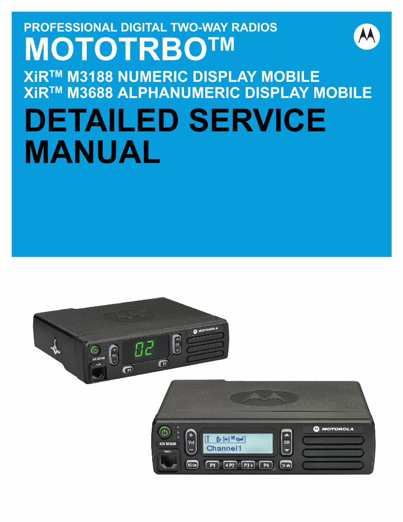
PROFESSIONAL DIGITAL TWO-WAY RADIOS
MOTOTRBOTM XiRTM M3188 NUMERIC DISPLAY MOBILEXiRTM M3688 ALPHANUMERIC DISPLAY MOBILE
DETAILED SERVICE MANUAL

i
ForewordThis manual covers all XiR™ M3000 Series Mobiles, unless otherwise specified. This manual provides sufficient information to enable qualified service technicians to troubleshoot and repair XiR™ M3000 Series Mobiles to the component level.
For details on radio operation or basic troubleshooting, refer to the applicable manuals available separately.
Product Safety and RF Exposure Compliance
ATTENTION!
Before using the mobile two-way product, XiR™ M3000 Series Mobiles, read the RF Energy Exposure and Safety guide that ships with the radio which contains important operating instructions for safe usage and RF energy awareness and control for Compliance with applicable Standards and Regulations.
Computer Software CopyrightsThe Motorola products described in this manual may include copyrighted Motorola computer programs stored in semiconductor memories or other media. Laws in the United States and other countries preserve for Motorola certain exclusive rights for copyrighted computer programs, including, but not limited to, the exclusive right to copy or reproduce in any form the copyrighted computer program. Accordingly, any copyrighted Motorola computer programs contained in the Motorola products described in this manual may not be copied, reproduced, modified, reverse-engineered, or distributed in any manner without the express written permission of Motorola. Furthermore, the purchase of Motorola products shall not be deemed to grant either directly or by implication, estoppel, or otherwise, any license under the copyrights, patents or patent applications of Motorola, except for the normal non-exclusive license to use that arises by operation of law in the sale of a product.
Document CopyrightsNo duplication or distribution of this document or any portion thereof shall take place without the express written permission of Motorola. No part of this manual may be reproduced, distributed, or transmitted in any form or by any means, electronic or mechanical, for any purpose without the express written permission of Motorola.
DisclaimerThe information in this document is carefully examined, and is believed to be entirely reliable. However, no responsibility is assumed for inaccuracies. Furthermore, Motorola reserves the right to make changes to any products herein to improve readability, function, or design. Motorola does not assume any liability arising out of the applications or use of any product or circuit described herein; nor does it cover any license under its patent rights nor the rights of others.
TrademarksMOTOROLA, MOTO, MOTOROLA SOLUTIONS and the Stylized M logo are trademarks or registered trademarks of Motorola Trademark Holdings, LLC and are used under license. All other trademarks are the property of their respective owners.
© 2013 Motorola Solutions, Inc. All rights reserved.
These servicing instructions are for use by qualified personnel only. To reduce the risk of electric shock, do not perform any servicing other than that contained in the Operating Instructions unless you are qualified to do so. Refer all servicing to qualified service personnel.
!C a u t i o n

ii
Notes
iii
Document History
The following major changes have been implemented in this manual since the previous edition:
Edition Description Date
68012008035-A Initial Release. June 2013

iv
Notes
Warranty and Service Support v
Warranty and Service Support
Motorola offers long term support for its products. This support includes full exchange and/or repair of the product during the warranty period, and service/ repair or spare parts support out of warranty.
Warranty Period and Return Instructions
The terms and conditions of warranty are defined fully in the Motorola Dealer or Distributor or Reseller contract. These conditions may change from time to time and the following notes are for guidance purposes only. In instances where the product is covered under a "return for replacement" or "return for repair" warranty, a check of the product should be performed prior to shipping the unit back to Motorola. This is to ensure that the product has been correctly programmed or has not been subjected to damage outside the terms of the warranty.
Prior to shipping any radio back to the appropriate Motorola warranty depot, please contact Customer Resources or your Motorola dealer, distributor or reseller. All returns must be accompanied by a Warranty Claim Form, available from your Customer Service representative or Motorola Online Extranet (MOL) or your Motorola dealer, distributor or reseller. Products should be shipped back in the original packaging, or correctly packaged to ensure no damage occurs in transit.
After Warranty Period
After the Warranty period, Motorola continues to support its products in two ways.
1. Motorola's Managed Technical Services (MTS) offers a repair service to both end users and dealers at competitive prices.
2. MTS supplies individual parts and modules that can be purchased by dealers who are technically capable of performing fault analysis and repair.
XiR M3188/XiR M3688 Mobile Radios Two (2) Years
Product Accessories One (1) Year

vi
Notes
June, 2013
XiR™ M3188/XiR™ M3688Mobile Radios
Detailed Service Manual
Contents
Chapter 1 Service Maintainability
Chapter 2 MOTOTRBO XiR M3188/XiR M3688 Mobile Radio Block Diagram
Chapter 3 Control Head Service Information
Chapter 4 Controller Service Information
Chapter 5 VHF Low Power (1–25 W) Service Information
Chapter 6 VHF High Power (25–45 W) Service Information
Appendix A Replacement Parts and Kits
Glossary

viii
Notes
ix
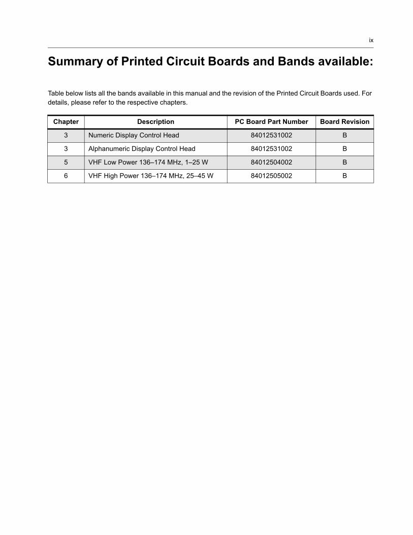
Summary of Printed Circuit Boards and Bands available:
Table below lists all the bands available in this manual and the revision of the Printed Circuit Boards used. For details, please refer to the respective chapters.
Chapter Description PC Board Part Number Board Revision
3 Numeric Display Control Head 84012531002 B
3 Alphanumeric Display Control Head 84012531002 B
5 VHF Low Power 136–174 MHz, 1–25 W 84012504002 B
6 VHF High Power 136–174 MHz, 25–45 W 84012505002 B

x
Notes
XiR™ M3188/XiR™ M3688Mobile Radios
Chapter 1
Service Maintainability
M
Issue: June, 2013

Computer Software CopyrightsThe Motorola products described in this manual may include copyrighted Motorola computer programs stored in semiconductor memories or other media. Laws in the United States and other countries preserve for Motorola certain exclusive rights for copyrighted computer programs, including, but not limited to, the exclusive right to copy or reproduce in any form the copyrighted computer program. Accordingly, any copyrighted Motorola computer programs contained in the Motorola products described in this manual may not be copied, reproduced, modified, reverse-engineered, or distributed in any manner without the express written permission of Motorola. Furthermore, the purchase of Motorola products shall not be deemed to grant either directly or by implication, estoppel, or otherwise, any license under the copyrights, patents or patent applications of Motorola, except for the normal non-exclusive license to use that arises by operation of law in the sale of a product.
i
Chapter 1 – Service Maintainability
Table of Contents
Section 1 Introduction
1.0 Notations Used in This Manual............................................................................ 1-12.0 Radio Description ................................................................................................ 1-1
Section 2 Maintenance
1.0 Introduction .......................................................................................................... 2-12.0 Preventive Maintenance ...................................................................................... 2-1
2.1 Inspection ....................................................................................................... 2-12.2 Cleaning Procedures...................................................................................... 2-1
3.0 Safe Handling of CMOS and LDMOS Devices.................................................... 2-24.0 Repair Procedures and Techniques – General ................................................... 2-45.0 Pre-baking of Integrated Circuits ......................................................................... 2-5
5.1 IPC/JEDEC J-STD-020D.1 (March 2008) Chart ............................................ 2-7
Section 3 Test Equipment and Service Aids
1.0 Recommended Test Equipment .......................................................................... 3-12.0 Service Aids......................................................................................................... 3-23.0 Programming Cables ........................................................................................... 3-34.0 Test Cable ........................................................................................................... 3-35.0 Accessory Cable.................................................................................................. 3-4
Section 4 Power-Up Self Test
1.0 Power-Up Error Codes ........................................................................................ 4-1

ii
Notes
1-1
Section 1
INTRODUCTION
1.0 Notations Used in This Manual
Throughout the text in this publication, you will notice the use of note and caution notations. These notations are used to emphasize that safety hazards exist, and due care must be taken and observed.
NOTE: An operational procedure, practice, or condition that is essential to emphasize.
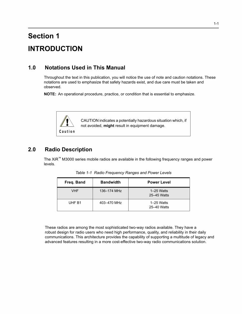
2.0 Radio Description
The XiR™ M3000 series mobile radios are available in the following frequency ranges and power levels.
These radios are among the most sophisticated two-way radios available. They have arobust design for radio users who need high performance, quality, and reliability in their daily communications. This architecture provides the capability of supporting a multitude of legacy and advanced features resulting in a more cost-effective two-way radio communications solution.
CAUTION indicates a potentially hazardous situation which, if not avoided, might result in equipment damage.
Table 1-1 Radio Frequency Ranges and Power Levels
Freq. Band Bandwidth Power Level
VHF 136–174 MHz 1–25 Watts25–45 Watts
UHF B1 403–470 MHz 1–25 Watts25–40 Watts
!C a u t i o n

1-2
Notes

2-1
Section 2
MAINTENANCE
1.0 Introduction
This chapter provides details about the following:
• Preventive maintenance (inspection and cleaning)
• Safe handling of CMOS and LDMOS devices
• Repair procedures and techniques
• Pre-baking of Integrated Circuits
2.0 Preventive Maintenance
Periodic visual inspection and cleaning is recommended.
2.1 Inspection
Check that the external surfaces of the radio are clean, and that all external controls and switches are functional. It is not recommended to inspect the interior electronic circuitry.
2.2 Cleaning Procedures
The following procedures describe the recommended cleaning agents and the methods to be used when cleaning the external and internal surfaces of the radio. External surfaces include the control head and housing assembly. These surfaces should be cleaned whenever a periodic visual inspection reveals the presence of smudges, grease, and/or grime.
NOTE: Internal surfaces should be cleaned only when the radio is disassembled for service or repair.
The only recommended agent for cleaning the external radio surfaces is a 0.5% solution of a mild dishwashing detergent in water. The only factory recommended liquid for cleaning the printed circuit boards and their components is isopropyl alcohol (100% by volume).
Use all chemicals as prescribed by the manufacturer. Be sure to follow all safety precautions as defined on the label or material safety data sheet.
The effects of certain chemicals and their vapors can have harmful results on certain plastics. Avoid using aerosol sprays, tuner cleaners and other chemicals.
!C a u t i o n
2-2 Safe Handling of CMOS and LDMOS Devices
Cleaning External Plastic Surfaces
Apply the 0.5% detergent-water solution sparingly with a stiff, non-metallic, short-bristled brush to work all loose dirt away from the radio. Use a soft, absorbent, lintless cloth or tissue to remove the solution and dry the radio. Make sure that no water remains entrapped near the connectors, cracks, or crevices.
Cleaning Internal Circuit Boards and Components
Isopropyl alcohol (100%) may be applied with a stiff, non-metallic, short-bristled brush to dislodge embedded or caked materials located in hard-to-reach areas. The brush stroke should direct the dislodged material out and away from the inside of the radio. Make sure that controls or tunable components are not soaked with alcohol. Do not use high-pressure air to hasten the drying process since this could cause the liquid to collect in unwanted places. Once the cleaning process is complete, use a soft, absorbent, lintless cloth to dry the area. Do not brush or apply any isopropyl alcohol to the frame, control head and housing assembly.
NOTE: Always use a fresh supply of alcohol and a clean container to prevent contamination by dissolved material (from previous usage).
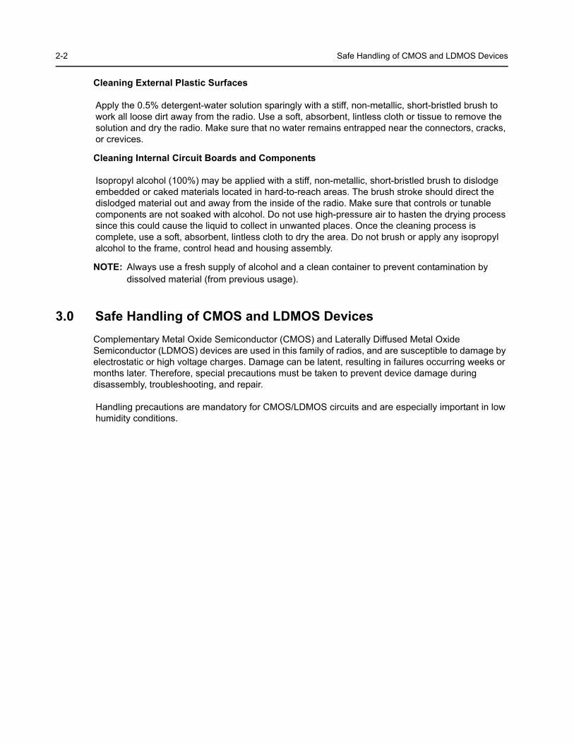
3.0 Safe Handling of CMOS and LDMOS Devices
Complementary Metal Oxide Semiconductor (CMOS) and Laterally Diffused Metal Oxide Semiconductor (LDMOS) devices are used in this family of radios, and are susceptible to damage by electrostatic or high voltage charges. Damage can be latent, resulting in failures occurring weeks or months later. Therefore, special precautions must be taken to prevent device damage during disassembly, troubleshooting, and repair.
Handling precautions are mandatory for CMOS/LDMOS circuits and are especially important in low humidity conditions.
Safe Handling of CMOS and LDMOS Devices 2-3
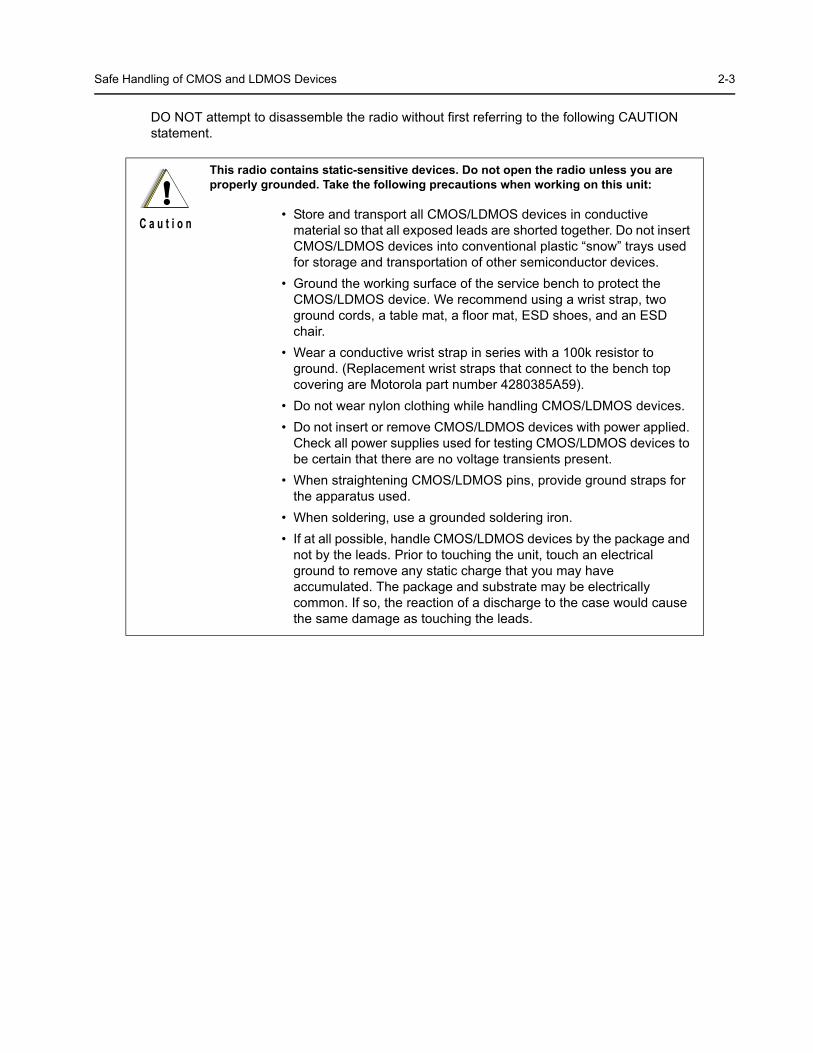
DO NOT attempt to disassemble the radio without first referring to the following CAUTION statement.
This radio contains static-sensitive devices. Do not open the radio unless you are properly grounded. Take the following precautions when working on this unit:
• Store and transport all CMOS/LDMOS devices in conductive material so that all exposed leads are shorted together. Do not insert CMOS/LDMOS devices into conventional plastic “snow” trays used for storage and transportation of other semiconductor devices.
• Ground the working surface of the service bench to protect the CMOS/LDMOS device. We recommend using a wrist strap, two ground cords, a table mat, a floor mat, ESD shoes, and an ESD chair.
• Wear a conductive wrist strap in series with a 100k resistor to ground. (Replacement wrist straps that connect to the bench top covering are Motorola part number 4280385A59).
• Do not wear nylon clothing while handling CMOS/LDMOS devices.
• Do not insert or remove CMOS/LDMOS devices with power applied. Check all power supplies used for testing CMOS/LDMOS devices to be certain that there are no voltage transients present.
• When straightening CMOS/LDMOS pins, provide ground straps for the apparatus used.
• When soldering, use a grounded soldering iron.
• If at all possible, handle CMOS/LDMOS devices by the package and not by the leads. Prior to touching the unit, touch an electrical ground to remove any static charge that you may have accumulated. The package and substrate may be electrically common. If so, the reaction of a discharge to the case would cause the same damage as touching the leads.
!C a u t i o n
2-4 Repair Procedures and Techniques – General
4.0 Repair Procedures and Techniques – General
Any rework or repair on Environmentally Preferred Products must be done using the appropriate lead-free solder wire and lead-free solder paste as stated in the following table:
Parts Replacement and Substitution
Check the parts list for the proper Motorola part number and order the part from the nearest Motorola Radio Products and Solutions Organization listed in Appendix A of this manual.
Rigid Circuit Boards
This family of radios uses bonded, multi-layer, printed circuit boards. Since the inner layers are not accessible, some special considerations are required when soldering and unsoldering components. The printed through holes may interconnect multiple layers of the printed circuit. Therefore, exercise care to avoid pulling the plated circuit out of the hole.
When soldering near a connector:
• Avoid accidentally getting solder in the connector
• Be careful not to form solder bridges between the connector pins
• Examine your work closely for shorts due to solder bridges
For soldering components with Hot-Air or infra red solder systems, please check your user guide of the solder system to get information on solder temperature and time for the different housings of the integrated circuits and other components.
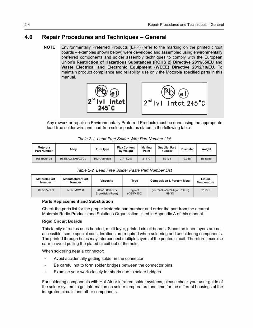
NOTE Environmentally Preferred Products (EPP) (refer to the marking on the printed circuitboards – examples shown below) were developed and assembled using environmentallypreferred components and solder assembly techniques to comply with the EuropeanUnion’s Restriction of Hazardous Substances (ROHS 2) Directive 2011/65/EU andWaste Electrical and Electronic Equipment (WEEE) Directive 2012/19/EU. Tomaintain product compliance and reliability, use only the Motorola specified parts in thismanual.
Table 2-1 Lead Free Solder Wire Part Number List
Motorola Part Number
Alloy Flux TypeFlux Content
by WeightMelting Point
Supplier Part number
Diameter Weight
1088929Y01 95.5Sn/3.8Ag/0.7Cu RMA Version 2.7–3.2% 217°C 52171 0.015” 1lb spool
Table 2-2 Lead Free Solder Paste Part Number List
Motorola Part Number
Manufacturer Part Number
Viscosity Type Composition & Percent MetalLiquid
Temperature
1085674C03 NC-SMQ230 900–1000KCPs Brookfield (5rpm)
Type 3 (-325/+500)
(95.5%Sn–3.8%Ag–0.7%Cu) 89.3%
217°C
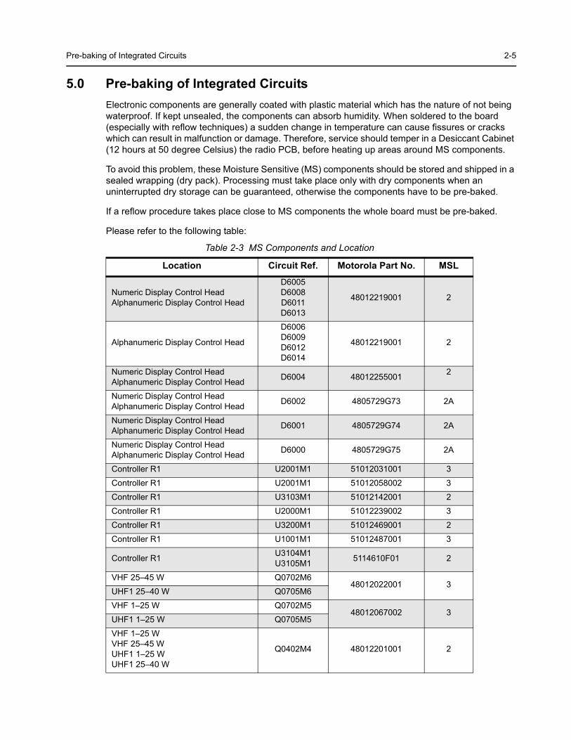
Pre-baking of Integrated Circuits 2-5
5.0 Pre-baking of Integrated Circuits
Electronic components are generally coated with plastic material which has the nature of not being waterproof. If kept unsealed, the components can absorb humidity. When soldered to the board (especially with reflow techniques) a sudden change in temperature can cause fissures or cracks which can result in malfunction or damage. Therefore, service should temper in a Desiccant Cabinet (12 hours at 50 degree Celsius) the radio PCB, before heating up areas around MS components.
To avoid this problem, these Moisture Sensitive (MS) components should be stored and shipped in a sealed wrapping (dry pack). Processing must take place only with dry components when an uninterrupted dry storage can be guaranteed, otherwise the components have to be pre-baked.
If a reflow procedure takes place close to MS components the whole board must be pre-baked.
Please refer to the following table:
Table 2-3 MS Components and Location
Location Circuit Ref. Motorola Part No. MSL
Numeric Display Control HeadAlphanumeric Display Control Head
D6005D6008D6011D6013
48012219001 2
Alphanumeric Display Control Head
D6006 D6009D6012D6014
48012219001 2
Numeric Display Control HeadAlphanumeric Display Control Head
D6004 480122550012
Numeric Display Control HeadAlphanumeric Display Control Head
D6002 4805729G73 2A
Numeric Display Control HeadAlphanumeric Display Control Head
D6001 4805729G74 2A
Numeric Display Control HeadAlphanumeric Display Control Head
D6000 4805729G75 2A
Controller R1 U2001M1 51012031001 3
Controller R1 U2001M1 51012058002 3
Controller R1 U3103M1 51012142001 2
Controller R1 U2000M1 51012239002 3
Controller R1 U3200M1 51012469001 2
Controller R1 U1001M1 51012487001 3
Controller R1U3104M1U3105M1
5114610F01 2
VHF 25–45 W Q0702M648012022001 3
UHF1 25–40 W Q0705M6
VHF 1–25 W Q0702M548012067002 3
UHF1 1–25 W Q0705M5
VHF 1–25 WVHF 25–45 WUHF1 1–25 WUHF1 25–40 W
Q0402M4 48012201001 2
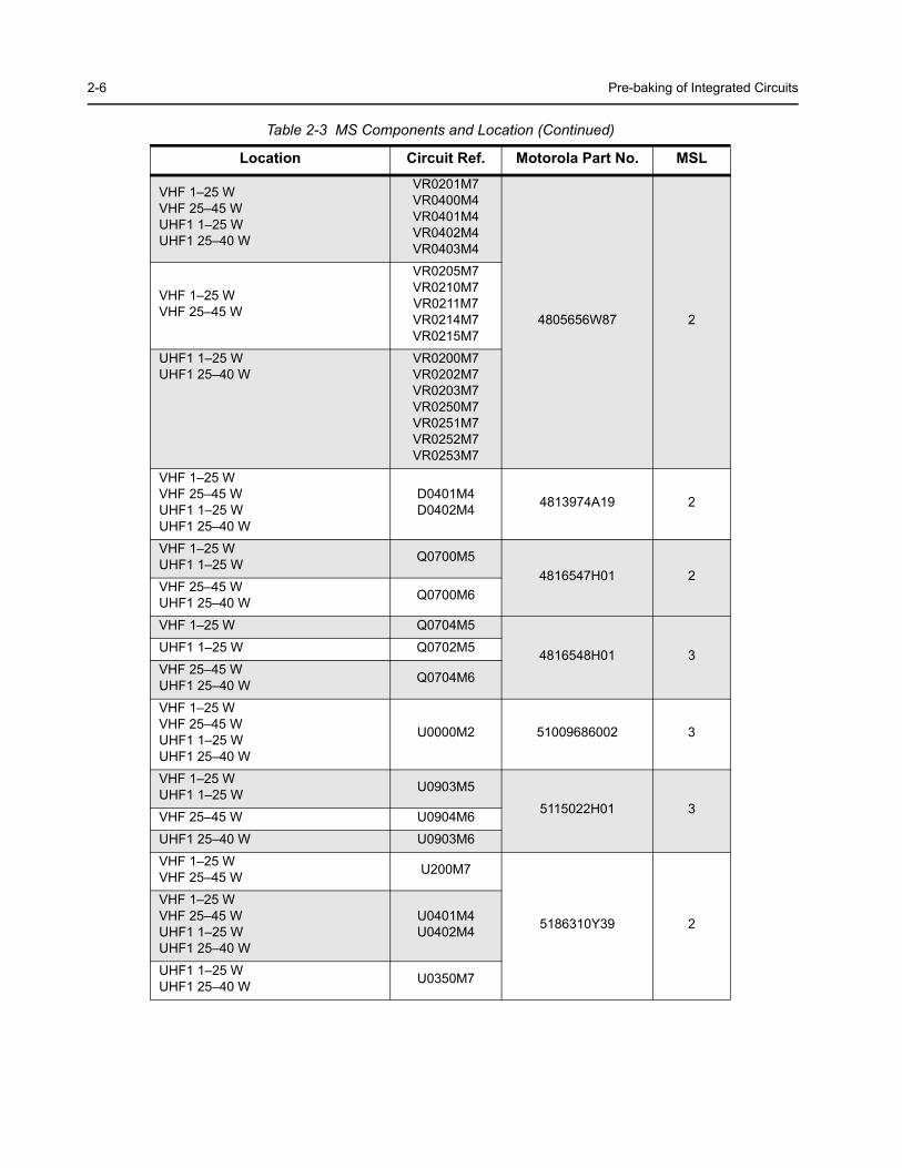
2-6 Pre-baking of Integrated Circuits
VHF 1–25 WVHF 25–45 WUHF1 1–25 WUHF1 25–40 W
VR0201M7VR0400M4VR0401M4VR0402M4VR0403M4
4805656W87 2
VHF 1–25 WVHF 25–45 W
VR0205M7VR0210M7VR0211M7VR0214M7VR0215M7
UHF1 1–25 WUHF1 25–40 W
VR0200M7VR0202M7VR0203M7VR0250M7VR0251M7VR0252M7VR0253M7
VHF 1–25 WVHF 25–45 WUHF1 1–25 WUHF1 25–40 W
D0401M4D0402M4
4813974A19 2
VHF 1–25 WUHF1 1–25 W
Q0700M5
4816547H01 2VHF 25–45 WUHF1 25–40 W
Q0700M6
VHF 1–25 W Q0704M5
4816548H01 3UHF1 1–25 W Q0702M5
VHF 25–45 WUHF1 25–40 W
Q0704M6
VHF 1–25 WVHF 25–45 WUHF1 1–25 WUHF1 25–40 W
U0000M2 51009686002 3
VHF 1–25 WUHF1 1–25 W
U0903M5
5115022H01 3VHF 25–45 W U0904M6
UHF1 25–40 W U0903M6
VHF 1–25 WVHF 25–45 W
U200M7
5186310Y39 2
VHF 1–25 WVHF 25–45 WUHF1 1–25 WUHF1 25–40 W
U0401M4U0402M4
UHF1 1–25 WUHF1 25–40 W
U0350M7
Table 2-3 MS Components and Location (Continued)
Location Circuit Ref. Motorola Part No. MSL
Pre-baking of Integrated Circuits 2-7
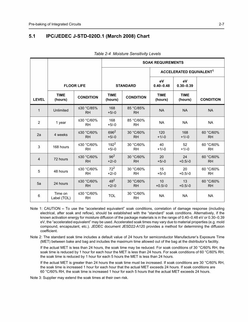
5.1 IPC/JEDEC J-STD-020D.1 (March 2008) Chart
Table 2-4 Moisture Sensitivity Levels
LEVEL
FLOOR LIFE
SOAK REQUIREMENTS
STANDARD
ACCELERATED EQUIVALENT1
Note 1: CAUTION – To use the “accelerated equivalent” soak conditions, correlation of damage response (includingelectrical, after soak and reflow), should be established with the “standard” soak conditions. Alternatively, if theknown activation energy for moisture diffusion of the package materials is in the range of 0.40–0.48 eV or 0.30–0.39eV, the “accelerated equivalent” may be used. Accelerated soak times may vary due to material properties (e.g. moldcompound, encapsulant, etc.). JEDEC document JESD22-A120 provides a method for determining the diffusioncoefficient.
eV0.40–0.48
eV0.30–0.39
CONDITIONTIME
(hours)CONDITION
TIME (hours)
CONDITIONTIME
(hours)TIME
(hours)
1 Unlimited≤30 °C/85%
RH168
+5/-085 °C/85%
RHNA NA NA
2 1 year≤30 °C/60%
RH168
+5/-085 °C/60%
RHNA NA NA
2a 4 weeks≤30 °C/60%
RH6962
+5/-0
Note 2: The standard soak time includes a default value of 24 hours for semiconductor Manufacturer’s Exposure Time(MET) between bake and bag and includes the maximum time allowed out of the bag at the distributor’s facility.
If the actual MET is less than 24 hours, the soak time may be reduced. For soak conditions of 30 °C/60% RH, thesoak time is reduced by 1 hour for each hour the MET is less than 24 hours. For soak conditions of 60 °C/60% RH,the soak time is reduced by 1 hour for each 5 hours the MET is less than 24 hours.
If the actual MET is greater than 24 hours the soak time must be increased. If soak conditions are 30 °C/60% RH,the soak time is increased 1 hour for each hour that the actual MET exceeds 24 hours. If soak conditions are 60 °C/60% RH, the soak time is increased 1 hour for each 5 hours that the actual MET exceeds 24 hours.
Note 3: Supplier may extend the soak times at their own risk.
30 °C/60%RH
120+1/-0
168+1/-0
60 °C/60%RH
3 168 hours≤30 °C/60%
RH1922
+5/-030 °C/60%
RH40
+1/-052
+1/-060 °C/60%
RH
4 72 hours≤30 °C/60%
RH962
+2/-030 °C/60%
RH20
+5/-024
+0.5/-060 °C/60%
RH
5 48 hours≤30 °C/60%
RH722
+2/-030 °C/60%
RH15
+5/-020
+0.5/-060 °C/60%
RH
5a 24 hours≤30 °C/60%
RH482
+2/-030 °C/60%
RH10
+0.5/-013
+0.5/-060 °C/60%
RH
6Time on
Label (TOL)≤30 °C/60%
RHTOL
30 °C/60%RH
NA NA NA

2-8 Pre-baking of Integrated Circuits
Notes
Recommended Test Equipment 3-1
Section 3
TEST EQUIPMENT AND SERVICE AIDS
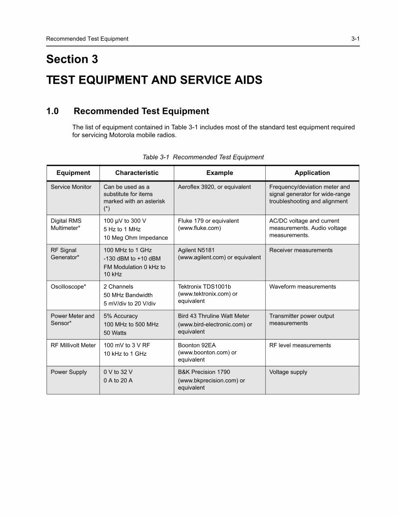
1.0 Recommended Test Equipment
The list of equipment contained in Table 3-1 includes most of the standard test equipment required for servicing Motorola mobile radios.
Table 3-1 Recommended Test Equipment
Equipment Characteristic Example Application
Service Monitor Can be used as a substitute for items marked with an asterisk (*)
Aeroflex 3920, or equivalent Frequency/deviation meter and signal generator for wide-range troubleshooting and alignment
Digital RMS Multimeter*
100 µV to 300 V
5 Hz to 1 MHz
10 Meg Ohm Impedance
Fluke 179 or equivalent (www.fluke.com)
AC/DC voltage and current measurements. Audio voltage measurements.
RF Signal Generator*
100 MHz to 1 GHz
-130 dBM to +10 dBM
FM Modulation 0 kHz to 10 kHz
Agilent N5181 (www.agilent.com) or equivalent
Receiver measurements
Oscilloscope* 2 Channels
50 MHz Bandwidth
5 mV/div to 20 V/div
Tektronix TDS1001b (www.tektronix.com) or equivalent
Waveform measurements
Power Meter and Sensor*
5% Accuracy
100 MHz to 500 MHz
50 Watts
Bird 43 Thruline Watt Meter
(www.bird-electronic.com) or equivalent
Transmitter power output measurements
RF Millivolt Meter 100 mV to 3 V RF
10 kHz to 1 GHz
Boonton 92EA (www.boonton.com) or equivalent
RF level measurements
Power Supply 0 V to 32 V
0 A to 20 A
B&K Precision 1790
(www.bkprecision.com) or equivalent
Voltage supply
3-2 Service Aids
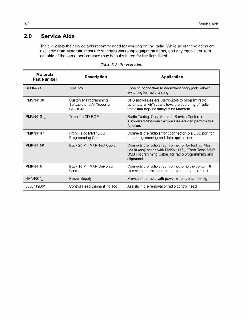
2.0 Service Aids
Table 3-2 lists the service aids recommended for working on the radio. While all of these items are available from Motorola, most are standard workshop equipment items, and any equivalent item capable of the same performance may be substituted for the item listed.
Table 3-2 Service Aids
MotorolaPart Number
Description Application
RLN4460_ Test Box Enables connection to audio/accessory jack. Allows switching for radio testing.
PMVN4130_ Customer Programming Software and AirTracer on CD-ROM
CPS allows Dealers/Distributors to program radio parameters. AirTracer allows the capturing of radio traffic into logs for analysis by Motorola.
PMVN4131_ Tuner on CD-ROM Radio Tuning. Only Motorola Service Centers or Authorized Motorola Service Dealers can perform this function.
PMKN4147_ Front Telco MMP USBProgramming Cable
Connects the radio’s front connector to a USB port for radio programming and data applications.
PMKN4150_ Back 20 Pin MAP Test Cable Connects the radio’s rear connector for testing. Must use in conjunction with PMKN4147_ (Front Telco MMP USB Programming Cable) for radio programming and alignment.
PMKN4151_ Back 16 Pin MAP Universal Cable
Connects the radio’s rear connector to the center 16 pins with unterminated connectors at the user end.
HPN4007_ Power Supply Provides the radio with power when bench testing.
6686119B01 Control Head Dismantling Tool Assists in the removal of radio control head.
Programming Cables 3-3
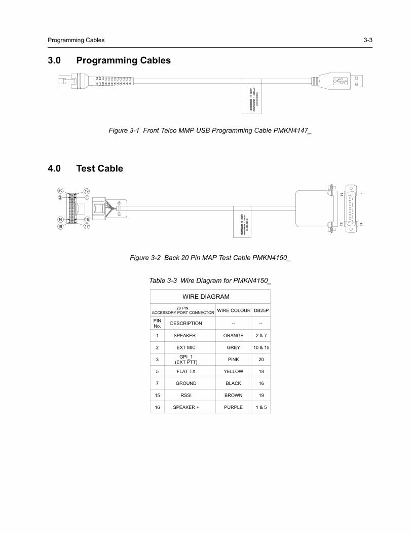
3.0 Programming Cables
Figure 3-1 Front Telco MMP USB Programming Cable PMKN4147_
4.0 Test Cable
Figure 3-2 Back 20 Pin MAP Test Cable PMKN4150_
Table 3-3 Wire Diagram for PMKN4150_
20
2
19
1
15
17
16
18
11425 13
1
1425 13
WIRE DIAGRAM
20 PIN ACCESSORY PORT CONNECTOR WIRE COLOUR DB25P
PINNo. DESCRIPTION
1 SPEAKER - 2 & 7
2 EXT MIC 10 & 15
3 GPI_1(EXT PTT) 20
5 FLAT TX 18
16 SPEAKER + 1 & 5
-- --
ORANGE
GREY
PINK
YELLOW
7 GROUND BLACK 16
15 RSSI BROWN 19
PURPLE
3-4 Accessory Cable
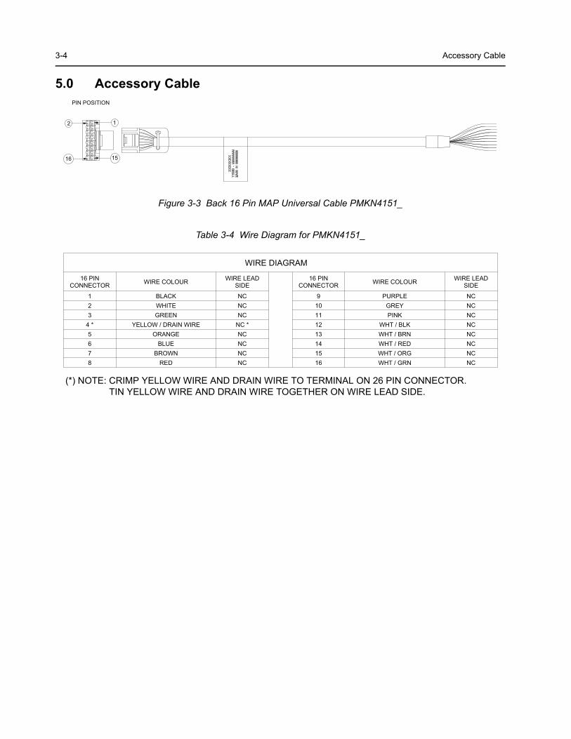
5.0 Accessory Cable
Figure 3-3 Back 16 Pin MAP Universal Cable PMKN4151_
Table 3-4 Wire Diagram for PMKN4151_
(*) NOTE: CRIMP YELLOW WIRE AND DRAIN WIRE TO TERMINAL ON 26 PIN CONNECTOR.TIN YELLOW WIRE AND DRAIN WIRE TOGETHER ON WIRE LEAD SIDE.
PIN POSITION
1
1516
2
WIRE DIAGRAM
16 PINCONNECTOR WIRE COLOUR WIRE LEAD
SIDE16 PIN
CONNECTOR WIRE COLOUR WIRE LEADSIDE
1 BLACK NC 9 PURPLE NC2 WHITE NC 10 GREY NC3 GREEN NC 11 PINK NC
4 * YELLOW / DRAIN WIRE NC * 12 WHT / BLK NC5 ORANGE NC 13 WHT / BRN NC6 BLUE NC 14 WHT / RED NC7 BROWN NC 15 WHT / ORG NC8 RED NC 16 WHT / GRN NC
4-1
Section 4
POWER-UP SELF TEST
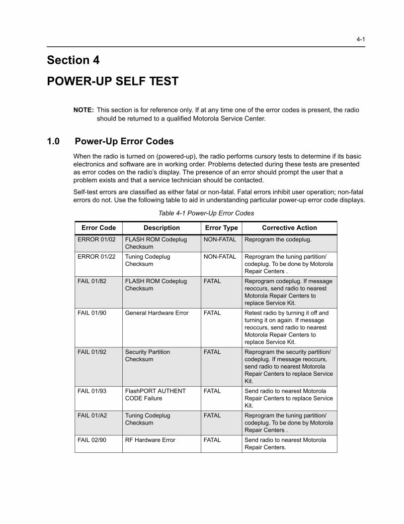
NOTE: This section is for reference only. If at any time one of the error codes is present, the radio should be returned to a qualified Motorola Service Center.
1.0 Power-Up Error Codes
When the radio is turned on (powered-up), the radio performs cursory tests to determine if its basic electronics and software are in working order. Problems detected during these tests are presented as error codes on the radio’s display. The presence of an error should prompt the user that a problem exists and that a service technician should be contacted.
Self-test errors are classified as either fatal or non-fatal. Fatal errors inhibit user operation; non-fatal errors do not. Use the following table to aid in understanding particular power-up error code displays.
Table 4-1 Power-Up Error Codes
Error Code Description Error Type Corrective Action
ERROR 01/02 FLASH ROM Codeplug Checksum
NON-FATAL Reprogram the codeplug.
ERROR 01/22 Tuning Codeplug Checksum
NON-FATAL Reprogram the tuning partition/codeplug. To be done by Motorola Repair Centers .
FAIL 01/82 FLASH ROM Codeplug Checksum
FATAL Reprogram codeplug. If message reoccurs, send radio to nearest Motorola Repair Centers to replace Service Kit.
FAIL 01/90 General Hardware Error FATAL Retest radio by turning it off and turning it on again. If message reoccurs, send radio to nearest Motorola Repair Centers to replace Service Kit.
FAIL 01/92 Security Partition Checksum
FATAL Reprogram the security partition/codeplug. If message reoccurs, send radio to nearest Motorola Repair Centers to replace Service Kit.
FAIL 01/93 FlashPORT AUTHENT CODE Failure
FATAL Send radio to nearest Motorola Repair Centers to replace Service Kit.
FAIL 01/A2 Tuning Codeplug Checksum
FATAL Reprogram the tuning partition/codeplug. To be done by Motorola Repair Centers .
FAIL 02/90 RF Hardware Error FATAL Send radio to nearest Motorola Repair Centers.

4-2 Power-Up Error Codes
Notes
XiR™ M3188/XiR™ M3688Mobile Radios
Chapter 2
Mobile Radio Block Diagram
M
Issue: June, 2013

Computer Software CopyrightsThe Motorola products described in this manual may include copyrighted Motorola computer programs stored in semiconductor memories or other media. Laws in the United States and other countries preserve for Motorola certain exclusive rights for copyrighted computer programs, including, but not limited to, the exclusive right to copy or reproduce in any form the copyrighted computer program. Accordingly, any copyrighted Motorola computer programs contained in the Motorola products described in this manual may not be copied, reproduced, modified, reverse-engineered, or distributed in any manner without the express written permission of Motorola. Furthermore, the purchase of Motorola products shall not be deemed to grant either directly or by implication, estoppel, or otherwise, any license under the copyrights, patents or patent applications of Motorola, except for the normal non-exclusive license to use that arises by operation of law in the sale of a product.
i
Chapter 2 – MOTOTRBO XiR M3188/XiR M3688 Mobile Radio Block Diagram
Table of Contents
Section 1
1.0 MOTOTRBO XiR M3188/XiR M3688 Mobile Radio Block Diagram .................... 1-1

ii
Notes
M 1-1
S
1
ll subsequent chapters.
Audio Buffers and Switches
MAP Port- 20 pin conn
EXT_MIC+
UART
EXT_SPKR
MAP SWB+
2
RX_AUDIO
GPIOs
9V3
SPEAKER
Battery
3.6V Buck Reg.1.5A
ON_OFFIGNITION
EMERGENCY
9.3V LDO @ 200mA
SWB+ @ 1500mA
9.3V LDO @ 3A
1.2V LDO500mA
5.0V LDO @0.3A
IGN_SENSE_DETECT
EMERG_SENSE_DETECT
ON_OFF_CNTRL
eset1.8V / 2.8V Dual LDO
@150mA1.8V_ANA
1.8V_DIG
1.2V_DIG
3.6V
FET SW
5V
9R1
9V3_PA
Batt+
MAP SWB+
3.3V LDO200mA
Vout
Delay SD
Vin
Error
ON_OFF
IGN_IN
Emerg_IN
SWITCHESLOW_BAT_DET
BATT_SENSE
1.8V LDO200mA
Vout
Delay SDError
Vin
9V3
5V LDO @ 25mA5V_UNSW
5.0V LDO @ 50mA(Optional)5V_PC
1.8V / 2.8V Dual LDO @150mA
2.8V_RX
1.8V_SYNTH2.8V_SYNTH
Buffer RSSIRSSI_OUT
TX DataMUX
Pin # MAP CONNECTOR
REARVIEW
20 2 4 6 8 10 12 14 16 18
19 1 3 5 7 9 11 13 15 17
2 EXT_MIC_AUDIO11 FLAT_FILTERED_RX AUDIO5 FLAT_TX_AUDIO7 GROUND
20 GROUND8 GPIO_4 -Monitor
12 GPIO_7 -Channel Activity14 GPIO_8 OR TTR6 UART-CTS9 EMERGENCY
10 IGNITION SENSE3 GPI_1 -PTT4 GPO_2 -External Alarm
15 RSSI18 UART-RXD17 UART-TXD19 UART-RTS1 SPKR-16 SPKR+13 SWB+
Transorb27V
Pin # Pin Name1 D+2 HANDSET_AUDIO3 KEY_ROW/cable_detect4 PTT5 MIC+6 MIC_GROUND7 HOOK/VBUS_detect8 KEY_COL/cable_detect9 5V_SW10 D-
ON_OFF_DETECT
PCB
OTOTRBO XiR M3188/XiR M3688 Mobile Radio Block Diagram
ection 1
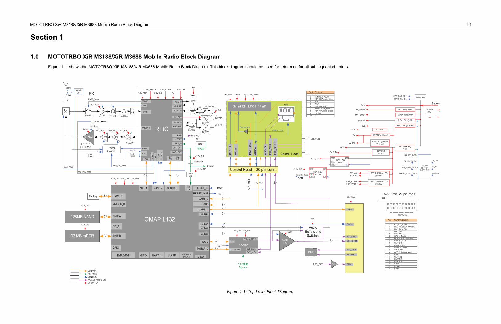
.0 MOTOTRBO XiR M3188/XiR M3688 Mobile Radio Block Diagram
Figure 1-1: shows the MOTOTRBO XiR M3188/XiR M3688 Mobile Radio Block Diagram. This block diagram should be used for reference for a
Figure 1-1: Top Level Block Diagram
1 2 3 4 5 6 7 8 9 10
SPI_1 McBSP_1 REFCLKGPIOs
EMIF A
UART_0
MMCSD_0
Factory 2
RESET_IN POR
RST
OMAP L132128MB NAND
32 MB mDDR EMIF B
1.8V_DIG
1.8V_DIG
45
43
UART_1 McASPGPIOs MMCSD_1 [WLAN]EMAC/RMII
GPIO
GPIOs
McBSP_0CODEC
4
I2C 0 2
Codec SSI
I2C
19.2MHzSquare
3.3V_DIG
AUDIO (HPR)
EXT_MIC+INT_MIC+
AudioPA
USB0
UART_1
UART_2
GPIOs
GPIOs
2
6SPI_0
3.6V 5V_UNSW3.3V_DIG
Control Head – 20 pin conn.
Smart CH: LPC1114 uP
RE
SE
T
2
INT
_MIC
+
MM
P_U
SB
2
4
GPIOs
GPIOs
UA
RT
CH
_RS
T
3
INT_
SP
KR
+
GP
IOs
Batt+
2 2
RST
AU
DIO
ComparatorVBUS / Hook
MMP
RESET_OUT
Control Head
2
Power_On_R
3.3V_DIG
POR1.2V_DIG 1.8V_DIG 3.3V_DIG
RX
TR
4 3 3Step DN
1.2V_DIGCodec
RFIC
LTD
TX SSI
LNAPre-SEL Post-SEL
SPI
RX
AC
Q
1.8V_ANA
1.8V_SYNTH
2.8V_RX
2.8V_SYNTH
5V
1.8V_DIG
VoltageMultiplier
VDD_CP
VMULT
5V
MC PUMP
VCO1_IN
LOOP FILTER
HP MOD
GPDAC_1
PA_Bias
19.2MHz
TCXO
Squarer
1.8V_DIG
REF_IN
RXSSI
CLK_OUT
LOCK DET
TTR
GP
Os
RSSI RSSI_OUTRSTRESET
RAMP
ADC
FINAL
TX
Pre-AMP
Batt+
ADA4743RD01RD07
9V3_PA 9V3_PA 9V3_PA
HP: RD70LP: RD35
Batt+Temp
VSWRPower Control
GPDAC_2
RF Step
VCO’sRX_VCO
TX_VCO
BUFFER
RF SWITCH
Pwr_Ctrl_Atten
5V
1.8V_DIG
REF FREQCONTROLANALOG AUDIO_DC
SSI/DATA
DC SUPPLY
RX
TXGPO9V1_RX
ANT_Atten
RXFE_Tune
OCD
DM
CS
WB_AGC_Flag
SF_OUT
9V3
REV
FWD
VSWRDET
7
1-2
Notes
XiR™ M3188/XiR™ M3688Mobile Radios
Chapter 3
Control Head
Service Information
M
Issue: June, 2013

Computer Software CopyrightsThe Motorola products described in this manual may include copyrighted Motorola computer programs stored in semiconductor memories or other media. Laws in the United States and other countries preserve for Motorola certain exclusive rights for copyrighted computer programs, including, but not limited to, the exclusive right to copy or reproduce in any form the copyrighted computer program. Accordingly, any copyrighted Motorola computer programs contained in the Motorola products described in this manual may not be copied, reproduced, modified, reverse-engineered, or distributed in any manner without the express written permission of Motorola. Furthermore, the purchase of Motorola products shall not be deemed to grant either directly or by implication, estoppel, or otherwise, any license under the copyrights, patents or patent applications of Motorola, except for the normal non-exclusive license to use that arises by operation of law in the sale of a product.
i
Chapter 3 – Control Head Service Information
Table of Contents
Section 1 Overview
1.0 Numeric Display Model........................................................................................ 1-12.0 Alphanumeric Display Model ............................................................................... 1-2
Section 2 Troubleshooting Charts
1.0 Numeric Display Model Control Head Troubleshooting Flow Chart .................... 2-11.1 On/Off ............................................................................................................ 2-11.2 Numeric Display ............................................................................................. 2-21.3 Speaker Audio................................................................................................ 2-31.4 Front MMP USB ............................................................................................. 2-4
2.0 Alphanumeric Display Model Control Head Troubleshooting Flow Chart............ 2-52.1 On/Off............................................................................................................. 2-52.2 Alphanumeric Display..................................................................................... 2-62.3 Speaker Audio................................................................................................ 2-72.4 Front MMP USB ............................................................................................. 2-8
Section 3 Control Head PCBs/Schematics/Parts lists
1.0 Allocation of Schematics and Circuit Boards ....................................................... 3-12.0 Numeric Display and Alphanumeric Display Control Head –
PCB 84012531002-B........................................................................................... 3-3Numeric Display and Alphanumeric Display Control Head PCB Diagram –
84012531002-B.............................................................................................. 3-33.0 Numeric Display Control Head Schematic........................................................... 3-4
Numeric Display Control Head Schematic Diagram............................................... 3-44.0 Numeric Display Control Head Parts List ............................................................ 3-55.0 Alphanumeric Display Control Head Schematic .................................................. 3-7
Alphanumeric Display Control Head Schematic Diagram ...................................... 3-76.0 Alphanumeric Display Control Head Parts List .................................................. 3-8

ii
Notes
1-1
Section 1
OVERVIEW
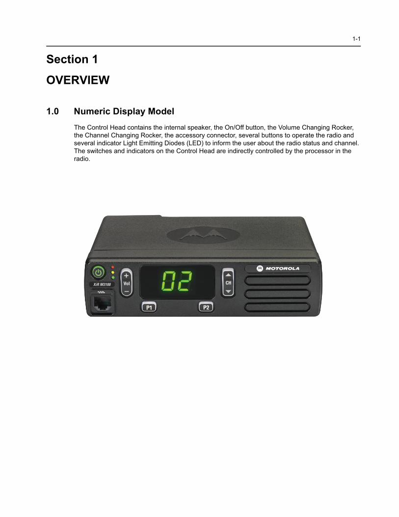
1.0 Numeric Display Model
The Control Head contains the internal speaker, the On/Off button, the Volume Changing Rocker, the Channel Changing Rocker, the accessory connector, several buttons to operate the radio and several indicator Light Emitting Diodes (LED) to inform the user about the radio status and channel. The switches and indicators on the Control Head are indirectly controlled by the processor in the radio.
XiR M3188
1-2 Alphanumeric Display Model
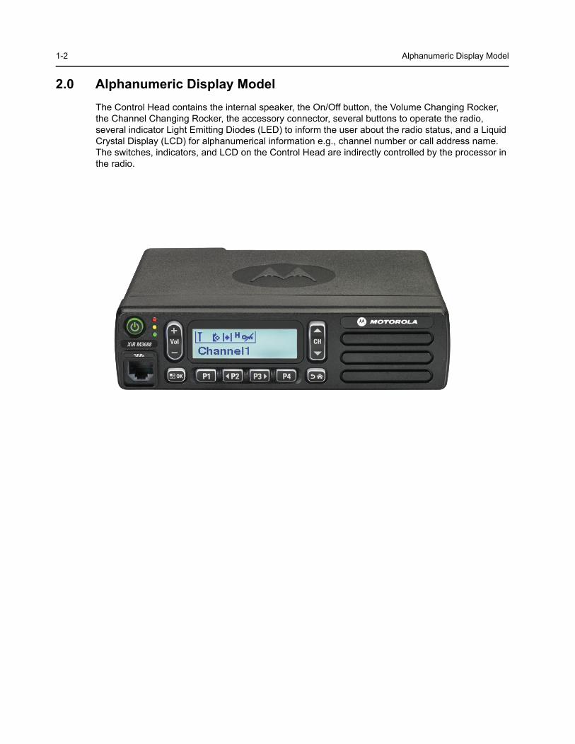
2.0 Alphanumeric Display Model
The Control Head contains the internal speaker, the On/Off button, the Volume Changing Rocker, the Channel Changing Rocker, the accessory connector, several buttons to operate the radio, several indicator Light Emitting Diodes (LED) to inform the user about the radio status, and a Liquid Crystal Display (LCD) for alphanumerical information e.g., channel number or call address name. The switches, indicators, and LCD on the Control Head are indirectly controlled by the processor in the radio.
XiR M3688
2-1
Section 2
TROUBLESHOOTING CHARTS
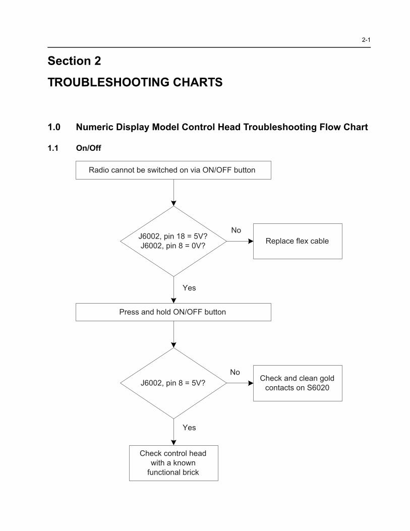
1.0 Numeric Display Model Control Head Troubleshooting Flow Chart
1.1 On/Off
Radio cannot be switched on via ON/OFF button
J6002, pin 18 = 5V?J6002, pin 8 = 0V? Replace flex cable
Press and hold ON/OFF button
J6002, pin 8 = 5V? Check and clean gold contacts on S6020
Check control head with a known
functional brick
No
No
Yes
Yes
2-2 Numeric Display Model Control Head Troubleshooting Flow Chart
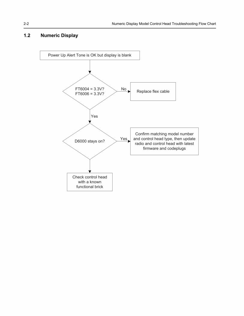
1.2 Numeric Display
Power Up Alert Tone is OK but display is blank
Check control head with a known
functional brick
FT6004 = 3.3V?FT6006 = 3.3V? Replace flex cableNo
Yes
D6000 stays on?
Confirm matching model number and control head type, then update radio and control head with latest
firmware and codeplugs
Yes
Numeric Display Model Control Head Troubleshooting Flow Chart 2-3
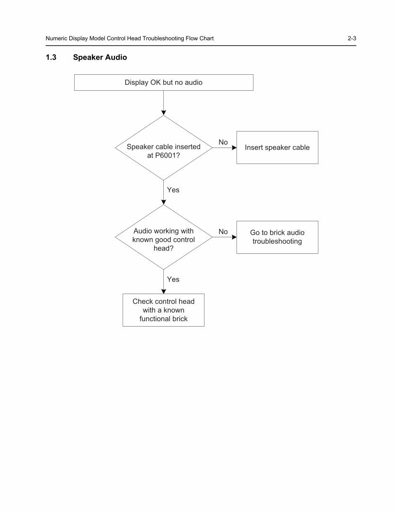
1.3 Speaker Audio
Display OK but no audio
Speaker cable inserted at P6001?
Audio working with known good control
head?
Yes
Check control head with a known
functional brick
Yes
Go to brick audio troubleshooting
No
Insert speaker cableNo
2-4 Numeric Display Model Control Head Troubleshooting Flow Chart
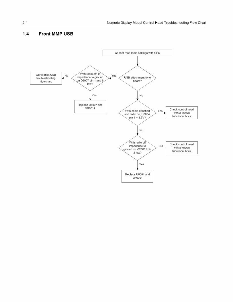
1.4 Front MMP USB
Cannot read radio settings with CPS
USB attachment tone heard?
With cable attachedand radio on, U6004,
pin 1 = 3.3V?
Yes
No
No
With radio off, is impedance to ground on D6007 pin 1 and 6
low?
Replace D6007 and VR6014
Yes
Go to brick USB troubleshooting
flowchart
No Yes
Replace U6004 and VR6001
With radio off impedance to
ground on VR6001 pin 2 low?
Yes
Check control head with a known
functional brick
No
Check control head with a known
functional brick
Alphanumeric Display Model Control Head Troubleshooting Flow Chart 2-5
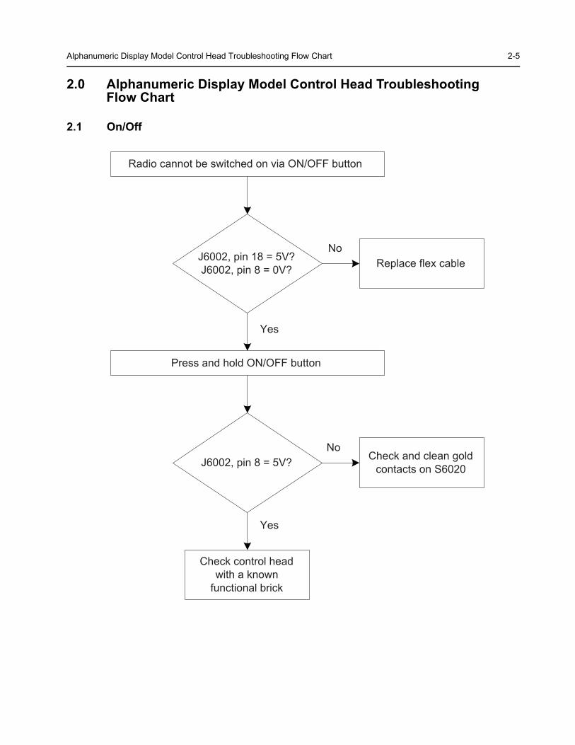
2.0 Alphanumeric Display Model Control Head Troubleshooting Flow Chart
2.1 On/Off
Radio cannot be switched on via ON/OFF button
J6002, pin 18 = 5V?J6002, pin 8 = 0V? Replace flex cable
Press and hold ON/OFF button
J6002, pin 8 = 5V? Check and clean gold contacts on S6020
Check control head with a known
functional brick
No
No
Yes
Yes
2-6 Alphanumeric Display Model Control Head Troubleshooting Flow Chart
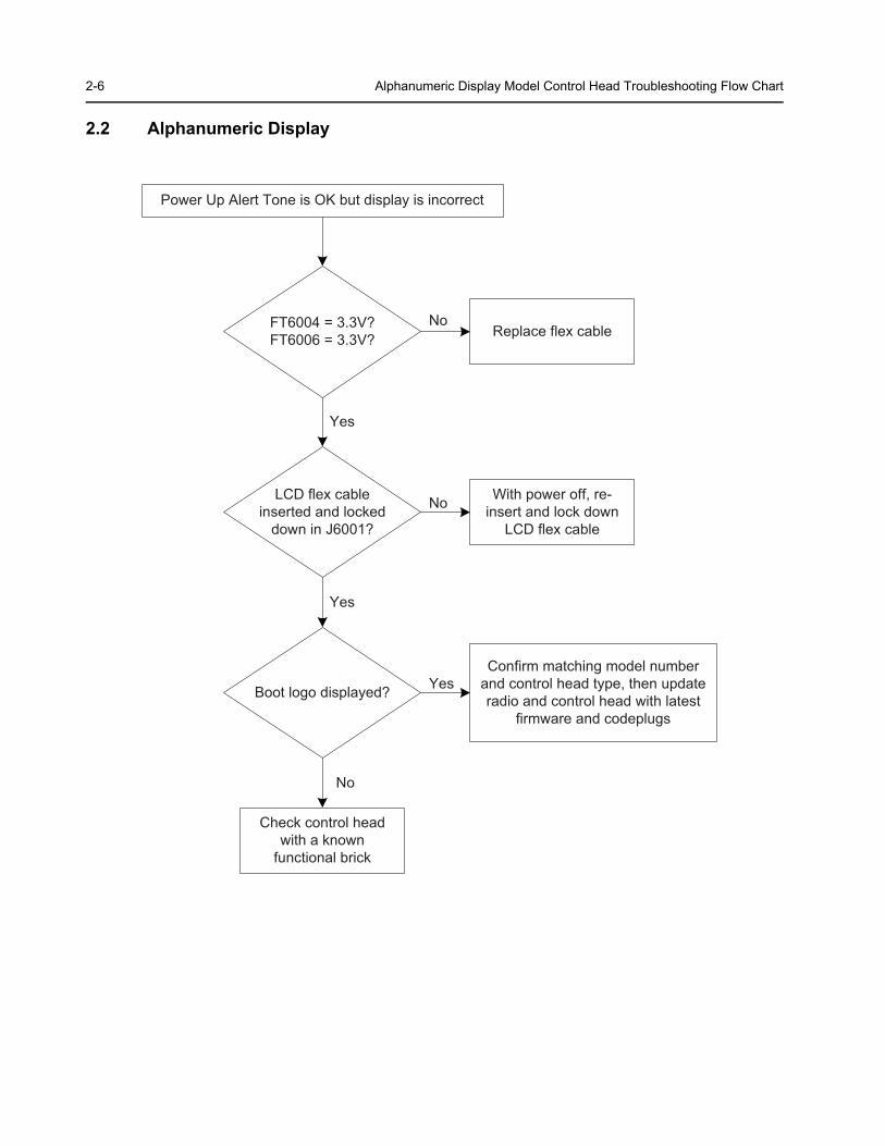
2.2 Alphanumeric Display
Power Up Alert Tone is OK but display is incorrect
LCD flex cableinserted and locked
down in J6001?
With power off, re-insert and lock down
LCD flex cable
Boot logo displayed?
Check control head with a known
functional brick
Confirm matching model number and control head type, then update radio and control head with latest
firmware and codeplugs
No
Yes
Yes
No
FT6004 = 3.3V?FT6006 = 3.3V? Replace flex cable
No
Yes
Alphanumeric Display Model Control Head Troubleshooting Flow Chart 2-7
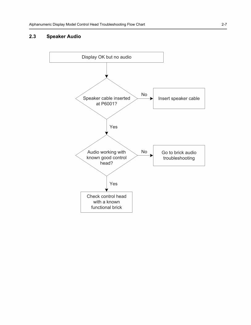
2.3 Speaker Audio
Display OK but no audio
Speaker cable inserted at P6001?
Audio working with known good control
head?
Yes
Check control head with a known
functional brick
Yes
Go to brick audio troubleshooting
No
Insert speaker cableNo
2-8 Alphanumeric Display Model Control Head Troubleshooting Flow Chart
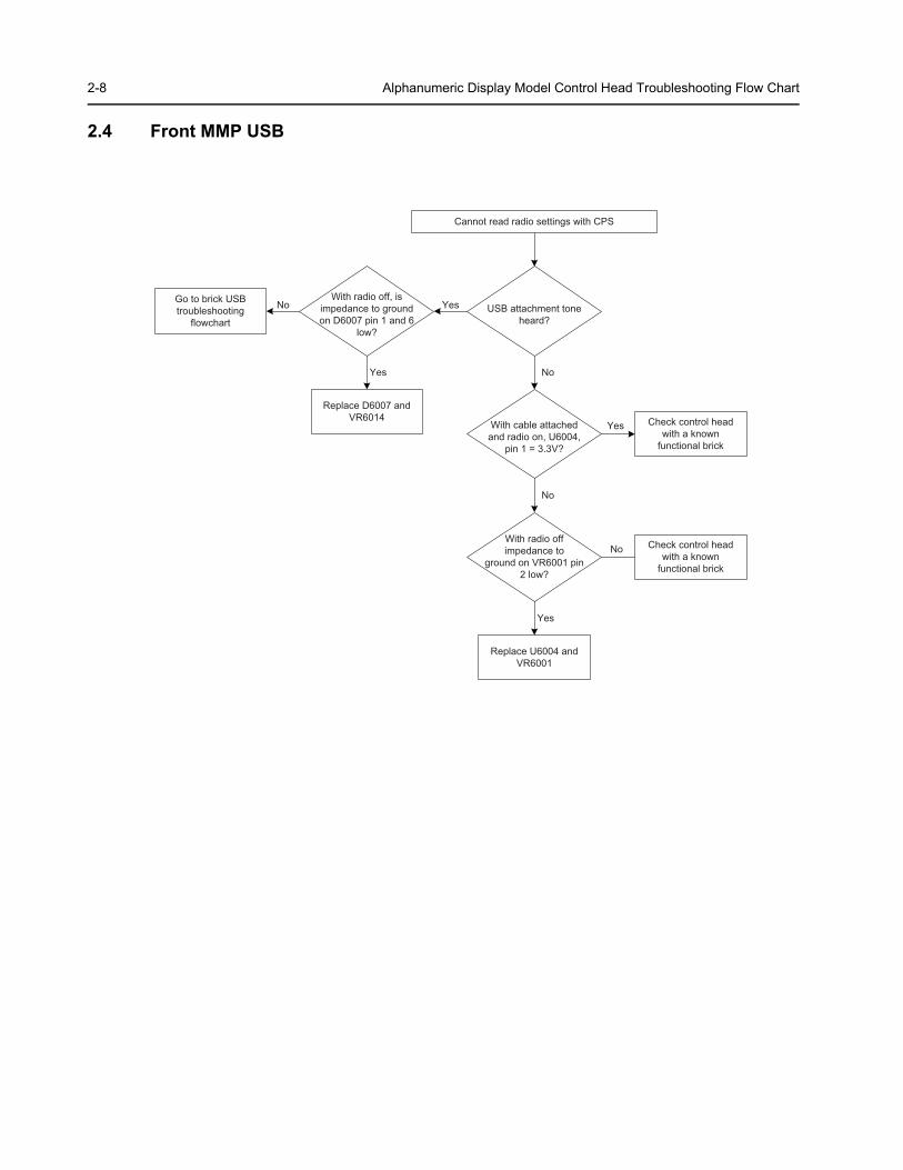
2.4 Front MMP USB
Cannot read radio settings with CPS
USB attachment tone heard?
With cable attachedand radio on, U6004,
pin 1 = 3.3V?
Yes
No
No
With radio off, is impedance to ground on D6007 pin 1 and 6
low?
Replace D6007 and VR6014
Yes
Go to brick USB troubleshooting
flowchart
No Yes
Replace U6004 and VR6001
With radio off impedance to
ground on VR6001 pin 2 low?
Yes
Check control head with a known
functional brick
No
Check control head with a known
functional brick
3-1
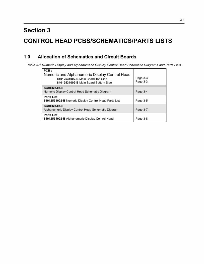
Section 3
CONTROL HEAD PCBS/SCHEMATICS/PARTS LISTS
1.0 Allocation of Schematics and Circuit Boards
Table 3-1 Numeric Display and Alphanumeric Display Control Head Schematic Diagrams and Parts Lists
PCB :
Numeric and Alphanumeric Display Control Head 84012531002-B Main Board Top Side84012531002-B Main Board Bottom Side
Page 3-3Page 3-3
SCHEMATICSNumeric Display Control Head Schematic Diagram Page 3-4
Parts List84012531002-B Numeric Display Control Head Parts List Page 3-5
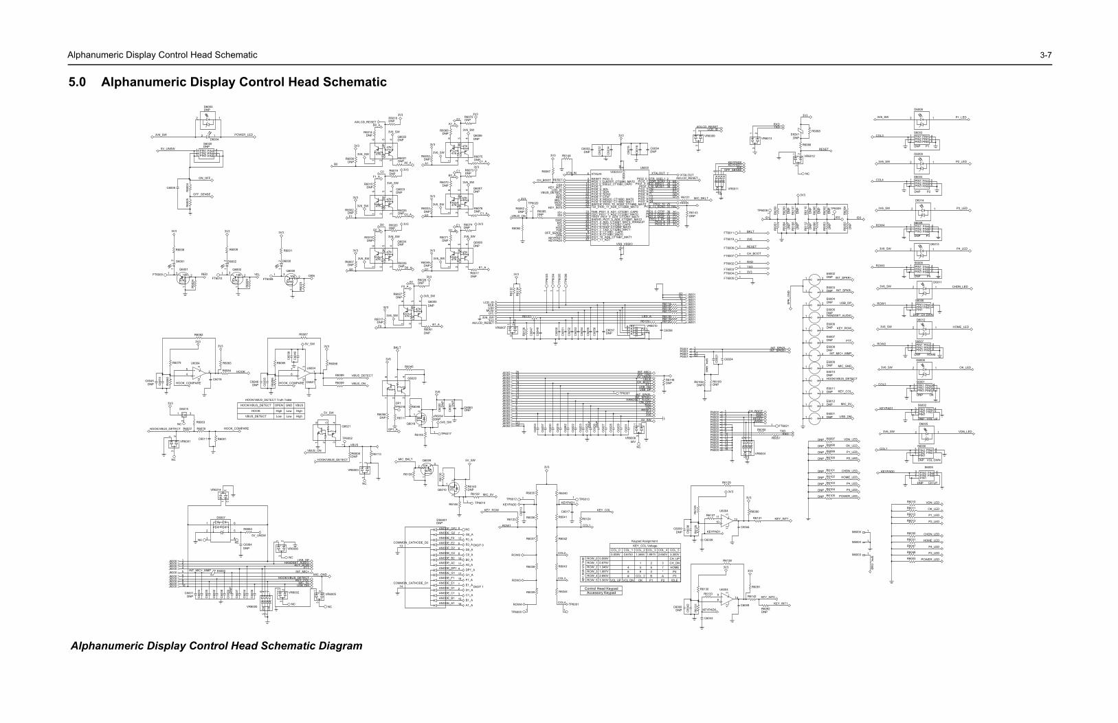
SCHEMATICSAlphanumeric Display Control Head Schematic Diagram Page 3-7
Parts List84012531002-B Alphanumeric Display Control Head Page 3-8

3-2
Notes
N 3-3
2
3
4
6D6013
S6008
3
4
6D6012
S6007
S6006
345 2
D60
11
32 54
S6005
R6148
C6037
TP6002
C6030
C6019
TP6007
C6022
C6062
C6033
C6027
C6026
C6025
C6023
D6007
VR6014
R6064
VR
6008
M6004
C6008
R6003
C6012
VR
6005
R6105
R6001
R6009
R6006
FT6005FT6021FT6004FT6002FT6019
FT6010FT6008FT6011FT6003 FT6009
R6068
R6066
R6010
R6097
6
E6004
E6007
E6005
E6008
E6006
E6012
E6011
E6009
E6010
C6006 C6002
R6122
VR
6002E
6001
Q6001
R6086
R6087
R6085
C6046
C6042
R6131C6060
VR
6001
R6130
R6091
Q6002
C6036
C6059
R6138
R6126
Q6000
R6141
R6090
R6125
C6044
R6129
E6241
C6035
C6064C6004
C6003
E6000
R6008
R6113
C6001
VR6003
C6009
7
814
VR
6006
M6005
R6146
R6140
VR6000
C6000
C6007
R6135
TP6010
Q6010
R6123
R6124
Q6009R6022
C6011
R6081
U6004C6038
C6049
R6079
018
R6084
R6083
R6142
R6092
6133
R6011 R6063
R6078
C6045
C6010
R6080
D6015
3
R6082
R6098
20
J6002
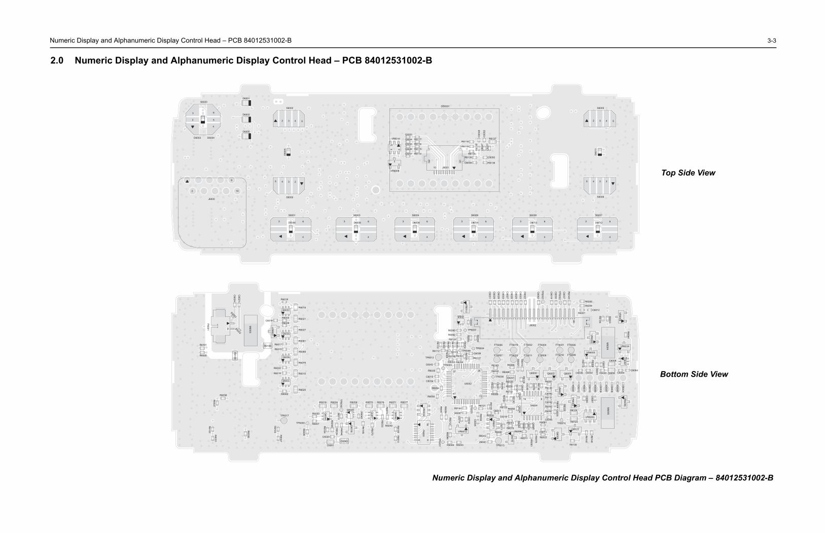
nd Alphanumeric Display Control Head PCB Diagram – 84012531002-B
Top Side View
Bottom Side View
umeric Display and Alphanumeric Display Control Head – PCB 84012531002-B
.0 Numeric Display and Alphanumeric Display Control Head – PCB 84012531002-B
3
2
4
5
6
D6004D6003
S6020
D6000
D6002
D6001
2 543
S6002
D60
05
45 3 2
S6000
3
4
6D6006
S6001
2 10
9
J6000
3
4
6 3
4
6 3
4
6D6008
S6003
D6009
S6004
D6014
S6009
DS6001
32
643
VR6009
VR6010
C6057
C6056
C6055
C6054
C6053
R6114
R6117
R6116
R6115
10
G2
G1
J6001
R6139R6120
R6119
R6118
R61
32
C60
47
C6058
C60
48
C60
51
C6050
C60
52
R6137
R6136
R6002
R6025
R6015
R6075
R6069
Q6005R6027
R6061
R6028
R6000
R6014
R6021
R6018
Q6003
R6032
R6019
R6072
Q6006
R6017
Q6022
C6016
R6106
VR
6007
2
M6003
R6109
E6002C
6021
C6024
E6003
R6030
R6101
P6001
R6038R
6031R
6037
R6036
R6102
C6063
Q6018
C6061
R6048
C6020
R6034
R6046
Q6004
R6111
TP6018
R6026
R6104
R6007
R6020
R6016
R6039
TP6000
TP6017
R6047
R6103
916
8
P6000
VR
6004
R6013
R6100
R6049Q
6008
R6074
R6071 R6077
R6033
R6073
Q6007
R6070 R6076
R6145
R6045
Q6020
R6058
C6031
C6029
C6028
FT6006
FT6007
47
37
13
25
TP6004
U6002
TP6008C6039
R6127R
6029
TP6020
R6134
R6065
R6059
VR
6013
C6040
TP6003
R6096
R6053
R6095
R6107
R6093
R6050
R6051
R6094
R6108
TP6009
R6062
R6060
Q6021
R6054
R6035
C6034
C6015
R6110
R6052
R6112
TP6012
C6043
VR
6011
R6041
R6042
R6121
R6043
VR6012
C6005
TP6005
R6004
C6032
R6044
R6099
C6014
R6067
R6144
R6012
R6056
TP6001
R6057
R6055R6089
TP600
R6023
R6024
R6143
R6088
C6041
C6017
R6040
C6
R6128 R
R6005
C6013
TP601
Numeric Display a
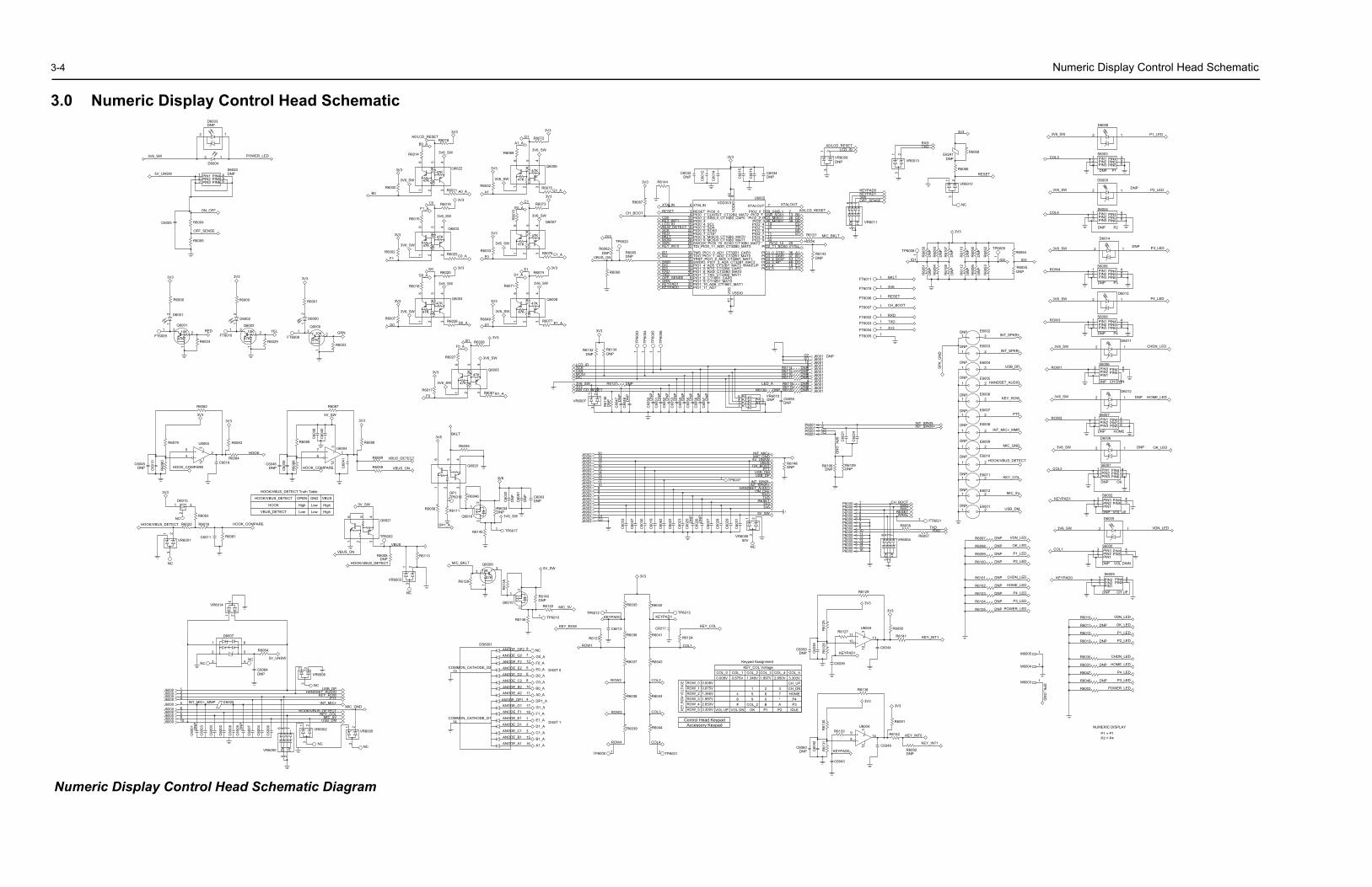
3-4 Numeric Display Control Head Schematic
3.0
DNPVR6009
213
VR6013
LCD_IDD_RESET
A2
A1
K4
K3
K2
K1
6 4 3 1
5 2
VR6011
KEYPAD1
OFF_SENSE3V6
KEYPAD0
RXDTXD
R6068E6241
R6066
213
VR6012
DNP
3V3
RESET
NC
FT6005
1FT6019
1FT6011
1FT6006
FT6007
FT60021FT60031FT6004
RXD
RESET
3V3
BKLT
TXD
CH_BOOT
3V6
1
1
1
LT
DNP
DN
P
DN
PD
NP
DN
P
DN
P
DN
P
DN
P
DN
P
DN
P
R61
12R
6110
R61
08R
6107
R60
94
R60
96R
6095
R60
93
R6055
1
TP6009
1
TP6008 R6054
R60
52R
6053
R60
50R
6051
3V3
ID3ID2ID1
DNP
1
DNP
DNP
DNP
DNP
DNP
E6008DNP
DNP
DNP
DNP
DNP
DNP
E6002
E6003
E6004
E6005
INT_SPKR+
INT_SPKR-
1
21
21
2
2
21E6006
21E6007
21
21E6009
21
E6010
21E6011
21
21E6001
INT_SPKR+
USB_DP
INT_MIC+_MMP
USB_DM
PTT
HANDSET_AUDIO
SP
K_G
ND
KEY_COL
MIC_GND
INT_SPKR-
KEY_ROW
MIC_5V
HOOK/VBUS_DETECT
E6012A
2
A1
K4
K3
K2
K1
R6057
FT60211
R6056
6 4 3 1
5 2
CH_BOOT
WAKERESET
SWCSWD
TXDRXD
VR6004
16P600015P6000
13P6000 14P6000
12P600011P6000
9P6000 10P6000
8P60007P6000
5P6000 6P6000
4P60003P60002P60001P6000
DNPR6109
C60
24
C60
21SP
K_G
ND
U6004 R6090
123
1310
R6141
6039
R6127
C6044
3V3
KEYPAD1
KEY_INT1
R6129
3V3
11
8
123
9
U60046133
R6138
3V3
DNPR6092
R6091
14 R6142
6043
C6049
KEY_INT0
3V3
KEY_INT1
EYPAD0
NUMERIC DISPLAY
P1 = P1P2 = P4
DNP
DNP
DNP
DNP
R6003
R6011
R6048
R6047
R6031
R6030
R6013
R6012
P3_LED
HOME_LED
OK_LED
P1_LED
VDN_LED
POWER_LED
P4_LED
CHDN_LED
P2_LED
R6010
1
1M6005
M6003
1M6004
SP
K_G
ND
P3_LED
DNP
DNP
DNP
DNP
DNP
DNP
DNP
DNP
DNP
R6105
R6104
R6103
R6102
R6101
R6100
R6099
R6098
R6097
OK_LED
P4_LED
VDN_LED
CHDN_LED
P2_LED
P1_LED
HOME_LED
POWER_LED
COL1
KEYPAD0
3V6_SW
3V6_SW
KEYPAD1
COL2
3V6_SW
ROW1
ROW2
3V6_SW
3V6_SW
ROW3
3V6_SW
ROW4
COL4
3V6_SW
3V6_SW
COL3
P2
P1
PIN5PIN2PIN1 PIN4
PIN6PIN3
PIN5PIN2PIN1 PIN4
PIN6PIN3
2 1
D6009
654
321
S6004
2 1
D6008
654
321
S6003
P1_LED
DNP P2_LED
DNP
DNP
P3
PIN5PIN2PIN1 PIN4
PIN6PIN3
2 1
D6014
654
321
S6009
DNP P3_LED
DNP
2 1
D6013P4_LED
P4
PIN5PIN2PIN1 PIN4
PIN6PIN3 654
321
S6008
DNP
2 1
D6011CHDN_LED
CH DWN
PIN2PIN3
PIN1PIN5PIN4 5
4321
S6006
DNP
2 1 DNP HOME_LEDD6012
HOME
PIN5PIN2PIN1 PIN4
PIN6PIN3 654
321
S6007
D6006
DNP
1 OK_LEDDNP2
OK
PIN5PIN2PIN1 PIN4
PIN6PIN3 654
321
S6001
DNP
VOL UP
PIN2PIN3
PIN1PIN5PIN4
D6005
543
21
S6002
DNP
PIN2PIN3
PIN1PIN5PIN43
1
S6000
2
VOL DWNDNP
12 VDN_LED
54
CH UP
PIN2PIN3
PIN1PIN5PIN4 5
4321
S6005
DNP
Nume
Numeric Display Control Head Schematic
C1
DNP
D6004
D6003
POWER_LED2 1
2 1
5V_UNSW
3V6_SW
PIN5PIN2PIN1 PIN4
PIN6PIN3
S6020DNP
654
321
R6004
R6005
C6005
ON_OFF
OFF_SENSE
10K
47KFT6008
21
D6000
1
R6023
1
32
Q6000
R6001
GRN
3V3
10K
47K
YEL
21
D6002
R6029
1
32
Q6002
R6009
3V3
10K
47KFT6010FT6009
21
D6001
1 1
R6024
1
32
Q6001
R6006
3V3
RED
47K10K
47K
10K
3
R6019
R6002
4
16 5
2
Q6003
R6025
R60211 32
3V6_SW
C0_A
A0_A
3V6_SW
F1
C0
3V3
3V3
F1_A
47K10K
47K
10K
R6018
R6015
R6014
R6000
46 5
Q6022
A0/LCD_RESET
B0_A
B0
3V3
3V6_SW
3V6_SW
3V3
47K10K
47K
10K
Q6006
R6072
4
1 3
6 52
R6069
R6075G1_A
A1_A
G1
3V3
3V6_SW
3V6_SW
3V3
R6032
A1
47K10K
47K
10K
R6033
E0
R6073
4
1 3
6 52
Q6007
R60
70
R6076 C1_A
E0_A
3V6_SW
3V6_SW
3V3
3V3
47K10K
47K
10K
R6028
R6017R6061
R6027
4
1 3
6 52
Q6005
3V6_SW
B1_AF0
3V3
3V6_SW
B1F0_A
3V3
47K10K
47K
10K3V6_SW
R6074
R6049
4
1 3
6 52
Q6008
R6071
R6077
3V3
E1_A
D1_A
3V3E1
D1
3V6_SW
47K10K
47K
10K
R6007
1 32 R6026 D0_A
3V3
G0
3V6_SW
R6020
46 5
Q6004
R6016
3V3
G0_A
D0
3V6_SW
DNPDNP
R6062
R6060
1
TP6020
R6065
3V3
VBUS_ON
213
A0/LC
XTALOUTPIO2_0_DTR_SSEL1
PIO2_2_DCD_MISO1PIO2_3_RI_MOSI1
PIO2_1_DSR_SCK1
PIO2_4PIO2_5
PIO2_8
PIO2_6PIO2_7
PIO2_9
VD
DIO
PIO2_11_SCK0
PIO3_0_DTR*PIO3_1_DSR*PIO3_2_DCD*
VSSIO
VDD3V3XTALIN
RESET_PIO0_0PIO0_1_CLKOUT_CT32B0_MAT2
PIO0_5_SDAPIO0_4_SCL
PIO0_2_SSEL0_CT16B0_CAP0PIO0_3
PIO0_8_MISO0_CT16B0_MAT0
PIO0_6_SCK0
SWCLK_PIO0_10_SCK0_CT16B0_MAT2
PIO0_7_CTS*
PIO0_9_MOSI0_CT16B0_MAT1
VS
S
TDI_PIO0_11_AD0_CT32B0_MAT3
TDO_PIO1_1_AD2_CT32B1_MAT0TMS_PIO1_0_AD1_CT32B1_CAP0
TRST_PIO1_2_AD3_CT32B1_MAT1SWDIO_PIO1_3_AD4_CT32B1_MAT2PIO1_4_AD5_CT32B1_MAT3_WAKEUP
PIO1_7_TXD_CT32B0_MAT1
PIO1_5_RTS_CT32B0_CAP0PIO1_6_RXD_CT32B0_MAT0
PIO1_8_CT16B1_CAP0
PIO1_11_AD7PIO1_10_AD6_CT16B1_MAT1PIO1_9_CT16B1_MAT0
KEYPAD1
R6144
R60676
35
3334
32
39
29
3
423017
947464540
2827232216151410
4
ID3
LCD_IDVBUS_DETECT
SWC
SWD
BKLT
SCKRED
CS0KEY_INT1
KEY_INT0
ID1
MOSI
TXDRXD
ID2
D/C
GRN
KEYPAD0
OFF_SENSE
3V3
CH_BOOT RESET
XTALIN
541844
DNPDNPC6034C6032
C60
16
C60
15
C60
14
C60
12
U6002
3V3
PIO2_10
PIO3_3_RI*
PIO3_5PIO3_4
DNP
R6121
R6143
7
211848433736
3125
24121112019
3826132
F1
C1
E1
HOOK
XTALOUTA0/LCD_RESET
D0E0F0G0G1
C0B0
D1
B1A1
YEL
MIC_BK
DNPR6106
G2P6001
2P6001 G1P6001
1P6001
RXD
DNP
1 TP6007
R6148
VR6008
CH_BOOT
3V6
TXD
PTT
3V3
MIC_GNDINT_MIC+
RESET
VBUS
HANDSET_AUDIOINT_SPKR+
5V_UNSW
ON_OFF
INT_SPKR-
USB_DMUSB_DP
5V_SW
13
2
NC
C60
28DN
P
DN
P
C60
62
C60
30
C60
37
C60
33
C60
31
C60
29
C60
27
C60
26
C60
25
C60
23
C60
22
20J6002 19J6002 18J6002 17J6002 16J6002 15J6002 14J6002 13J6002 12J6002 11J6002 10J6002 9J6002 8J6002 7J6002 6J6002 5J6002 4J6002
C60
19
3J6002 2J6002 1J6002 G1J6002 G2J6002
50V
DNPC6046
R60
86
C60
35 123
7
6HOOK
HOOK_COMPARE VBUS_ONR6059
R6088
C60
40
C60
38
R6085
1U6004
R6087
C60
41
R6089 VBUS_DETECT
5V_SW3V3
HOOK/VBUS_DETECT Truth Table
HOOK/VBUS_DETECT
HOOK
VBUS_DETECT
OPEN
High
Low
GND
Low
Low
VBUS
High
High
HOOK_COMPARE
12
R60
80
C60
10
3
25
4
3V3
DNPC6045
R6083R6079 U6004
R6082
C6018R6084
3V3
D6015
HOOK_COMPARENC
VR6001
R6022
1 3
2
R6081
R6078
C6011
R6063
HOOK/VBUS_DETECT
3V3
213
NC
DNPC6064
52
43
1
D6007
5V_UNSW
R6064
6
NCNC
VR6014
321
NC
VR6005
MIC_5V
213
HANDSET_AUDIOKEY_ROW
PTT
KEY_COL
INT_MIC+
USB_DM
HOOK/VBUS_DETECTMIC_GND
USB_DP
NC
VR6002
213
A2
A1
K4
K3
K2
K1
VR6000
6 4 3 1
5 2
NC
213
VR6006
DN
P
DN
P
1J6000 2J6000 3J6000 4J60005J60006J6000 7J6000 8J6000 9J6000 10J6000
E6000
C60
09
C60
03
C60
08
C60
01
C60
07
C60
06
C60
04
C60
02
C60
00
INT_MIC+_MMP
VR6003
2
R6113
2
R6008
TP6002
4
1 3
6 5
Q6021
5V_SW
VBUS_ON
VBUS
HOOK/VBUS_DETECT
1
DNP
1
3
NC
10K
47K
1
32
Q6009MIC_BKLT
R6128
DNPR6122
R6140
R61
35
2
1
5V_SW
R6146
Q6010
3
TP6010
MIC_5V
1
KEY_ROW
R6043
COL3
R6041
KEYPAD0
R6038
R6124
R6044
1TP6012 1 TP6013
1 TP6001
R6040R6035
R6036
R6037
R6039
ROW3
ROW2
KEYPAD1
COL4
3V3
COL1
KEY_COL
ROW4
1TP6000
C6017
R6042
ROW1
R6123
COL2
C6013
DIGIT 1
DIGIT 0
B0_A
ANODE_DP2
ANODE_G2
ANODE_F2
ANODE_D2
ANODE_E2
ANODE_B2
ANODE_C2
ANODE_A2
ANODE_DP1ANODE_G1
ANODE_F1
ANODE_D1
ANODE_E1
ANODE_C1
ANODE_B1
ANODE_A1
COMMON_CATHODE_D2
COMMON_CATHODE_D1
NC
DS6001
13
14
7
17
12
5
1
9
4
6
2
8
3
10
15
11
16
F0_A
G0_A
D0_A
B1_A
A1_A
C1_A
F1_A
G1_A
DP1_A
A0_A
C0_A
E0_A
D1_A
E1_A
18
Control Head KeypadAccessory Keypad
KEY_
ROW
VOL
TAGE ROW_0
ROW_1ROW_2ROW_3ROW_4ROW_5
0.008V0.675V1.346V1.997V2.650V3.300V
COL_00.008V
VOL UP
COL_10.675V
48#
VOL DN
COL_21.346V
159
COL_2OK
COL_31.997V
260BP1
COL_42.650V
37*AP2
COL_53.300VCH_UPCH_DNHOME
P4P3
IDLE
KEY_COL VoltageKeypad Assignment
DNP
R6145
R6058 R6111
1
1 TP6017
R6045
R6046
4
1 3
6 52
Q6020
R6034
2
1
3
Q6018
DP1
3V6BKLT
3V6_SW
DP1_A
TP6018
C60
20
DN
P
DN
P
DNPC6063
C60
61
3V6
1TP
6006
1TP
6005
1TP
6004
1TP
6003
C60
57
C60
54
C60
53
DN
P DN
P
DN
P
DN
P
DN
P
DN
P
DN
P
DN
P
DN
P
DN
P
DN
P
DNP DNP
C60
51
213
VR6007
R6134R6132
R6137
R61
36
C60
47
C60
48
C60
50
C60
56
C60
55
C60
52
LCD_ID
DNP
A0/LCD_RESET
D/C
SCK
MOSICS0
3V33V6_SW
3V3
J6001
DNP
6 J60017 J600189 J6001
10 J6001G1 J6001
1 J60012 J60013 J60014 J60015 J6001
G2 J6001
A2A1
K4K3K2K1
DNPDNP
R6120R6119R6118
R6117R6116R6115R6114
6431
52
VR6010
R6139
C6058
DNP
DNPDNPDNPDNP
DNPDNPDNP
LED_A
C6059
C
C60
36
R61
26
DNP
R61
25
R
DNPC6060
C60
42
R61
31
C
R61
30
K
ric Display Control Head Schematic Diagram
N 3-5
4
1
1
D
D
D
a.
R6031 NOT PLACED
R6032 0613952R01
R6033 0613952R01
R6034 NOT PLACED
R6035 0613952R18
R6036 0613952R04
R6037 0613952R09
R6038 0613952R16
R6039 0613952R28
R6040 0613952R18
R6041 0613952R04
R6042 0613952R09
R6043 0613952R16
R6044 0613952R28
R6045 0613952Q89
R6046 0613952Q89
R6047 0613952Q71
R6048 NOT PLACED
R6049 0613952R01
R6050 NOT PLACED
R6051 NOT PLACED
R6052 0613952N15
R6053 0613952M01
R6054 0613952R66
R6055 NOT PLACED
R6056 0613952R66
R6057 0613952R66
R6058 0613952H63
R6059 0613952R66
R6060 0613952R01
R6061 0613952H57
R6062 NOT PLACED
R6063 0613952Q66
R6064 0613952R01
R6065 NOT PLACED
R6066 0613952Q73
R6067 0613952R17
R6068 0613952R66
Circuit Ref.
MotorolaPart No.
R6069 0613952H57
R6070 0613952H57
R6071 0613952H57
R6072 0613952R01
R6073 0613952R01
R6074 0613952R01
R6075 0613952H57
R6076 0613952H57
R6077 0613952H57
R6078 0613952R04
R6079 0613952R33
R6080 0613952R33
R6081 0613952R16
R6082 0613952R49
R6083 0613952Q73
R6084 0613952Q53
R6085 0613952R33
R6086 0613952R35
R6087 0613952R49
R6088 0613952Q73
R6089 0613952Q53
R6090 0613952Q73
R6091 0613952Q73
R6092 NOT PLACED
R6093 NOT PLACED
R6094 0613952R66
R6095 NOT PLACED
R6096 NOT PLACED
R6097 NOT PLACED
R6098 NOT PLACED
R6099 NOT PLACED
R6100 NOT PLACED
R6101 NOT PLACED
R6102 NOT PLACED
R6103 NOT PLACED
R6104 NOT PLACED
R6105 NOT PLACED
R6106 NOT PLACED
Circuit Ref.
MotorolaPart No.
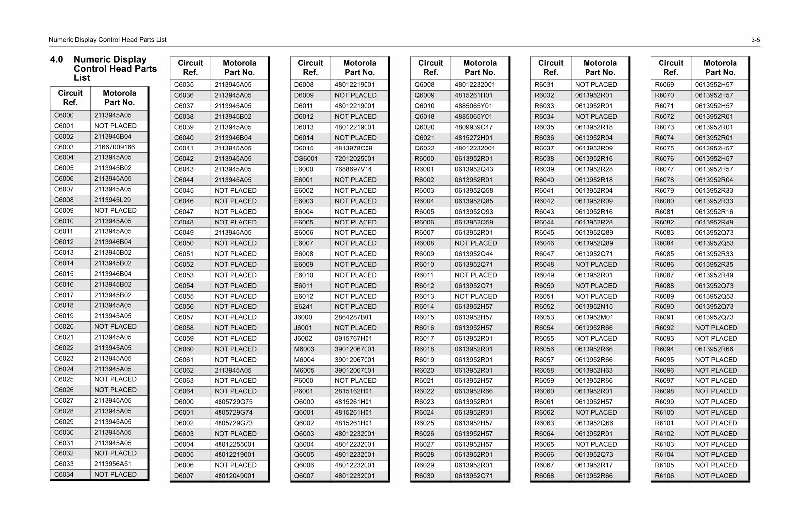
umeric Display Control Head Parts List
.0 Numeric Display Control Head Parts List
Circuit Ref.
MotorolaPart No.
C6000 2113945A05
C6001 NOT PLACED
C6002 2113946B04
C6003 21667009166
C6004 2113945A05
C6005 2113945B02
C6006 2113945A05
C6007 2113945A05
C6008 2113945L29
C6009 NOT PLACED
C6010 2113945A05
C6011 2113945A05
C6012 2113946B04
C6013 2113945B02
C6014 2113945B02
C6015 2113946B04
C6016 2113945B02
C6017 2113945B02
C6018 2113945A05
C6019 2113945A05
C6020 NOT PLACED
C6021 2113945A05
C6022 2113945A05
C6023 2113945A05
C6024 2113945A05
C6025 NOT PLACED
C6026 NOT PLACED
C6027 2113945A05
C6028 2113945A05
C6029 2113945A05
C6030 2113945A05
C6031 2113945A05
C6032 NOT PLACED
C6033 2113956A51
C6034 NOT PLACED
C6035 2113945A05
C6036 2113945A05
C6037 2113945A05
C6038 2113945B02
C6039 2113945A05
C6040 2113946B04
C6041 2113945A05
C6042 2113945A05
C6043 2113945A05
C6044 2113945A05
C6045 NOT PLACED
C6046 NOT PLACED
C6047 NOT PLACED
C6048 NOT PLACED
C6049 2113945A05
C6050 NOT PLACED
C6051 NOT PLACED
C6052 NOT PLACED
C6053 NOT PLACED
C6054 NOT PLACED
C6055 NOT PLACED
C6056 NOT PLACED
C6057 NOT PLACED
C6058 NOT PLACED
C6059 NOT PLACED
C6060 NOT PLACED
C6061 NOT PLACED
C6062 2113945A05
C6063 NOT PLACED
C6064 NOT PLACED
D6000 4805729G75
D6001 4805729G74
D6002 4805729G73
D6003 NOT PLACED
D6004 48012255001
D6005 48012219001
D6006 NOT PLACED
D6007 48012049001
Circuit Ref.
MotorolaPart No.
D6008 48012219001
D6009 NOT PLACED
D6011 48012219001
D6012 NOT PLACED
D6013 48012219001
D6014 NOT PLACED
D6015 4813978C09
DS6001 72012025001
E6000 7688697V14
E6001 NOT PLACED
E6002 NOT PLACED
E6003 NOT PLACED
E6004 NOT PLACED
E6005 NOT PLACED
E6006 NOT PLACED
E6007 NOT PLACED
E6008 NOT PLACED
E6009 NOT PLACED
E6010 NOT PLACED
E6011 NOT PLACED
E6012 NOT PLACED
E6241 NOT PLACED
J6000 2864287B01
J6001 NOT PLACED
J6002 0915767H01
M6003 39012067001
M6004 39012067001
M6005 39012067001
P6000 NOT PLACED
P6001 2815162H01
Q6000 4815261H01
Q6001 4815261H01
Q6002 4815261H01
Q6003 48012232001
Q6004 48012232001
Q6005 48012232001
Q6006 48012232001
Q6007 48012232001
Circuit Ref.
MotorolaPart No.
Q6008 4801223200
Q6009 4815261H01
Q6010 4885065Y01
Q6018 4885065Y01
Q6020 4809939C47
Q6021 4815272H01
Q6022 4801223200
R6000 0613952R01
R6001 0613952Q43
R6002 0613952R01
R6003 0613952Q58
R6004 0613952Q85
R6005 0613952Q93
R6006 0613952Q59
R6007 0613952R01
R6008 NOT PLACE
R6009 0613952Q44
R6010 0613952Q71
R6011 NOT PLACE
R6012 0613952Q71
R6013 NOT PLACE
R6014 0613952H57
R6015 0613952H57
R6016 0613952H57
R6017 0613952R01
R6018 0613952R01
R6019 0613952R01
R6020 0613952R01
R6021 0613952H57
R6022 0613952R66
R6023 0613952R01
R6024 0613952R01
R6025 0613952H57
R6026 0613952H57
R6027 0613952H57
R6028 0613952R01
R6029 0613952R01
R6030 0613952Q71
Circuit Ref.
MotorolPart No
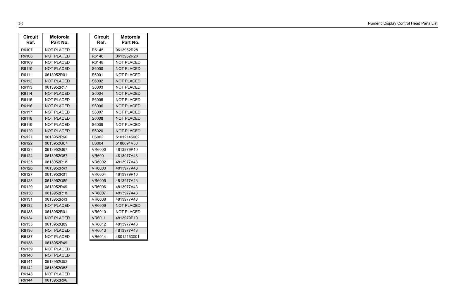
3-6 Numeric Display Control Head Parts List
R610
R610
R610
R611
R611
R611
R611
R611
R611
R611
R611
R611
R611
R612
R612
R612
R612
R612
R612
R612
R612
R612
R612
R613
R613
R613
R613
R613
R613
R613
R613
R613
R613
R614
R614
R614
R614
R614
CirR
7 NOT PLACED
8 NOT PLACED
9 NOT PLACED
0 NOT PLACED
1 0613952R01
2 NOT PLACED
3 0613952R17
4 NOT PLACED
5 NOT PLACED
6 NOT PLACED
7 NOT PLACED
8 NOT PLACED
9 NOT PLACED
0 NOT PLACED
1 0613952R66
2 0613952G67
3 0613952G67
4 0613952G67
5 0613952R18
6 0613952R43
7 0613952R01
8 0613952Q89
9 0613952R49
0 0613952R18
1 0613952R43
2 NOT PLACED
3 0613952R01
4 NOT PLACED
5 0613952Q89
6 NOT PLACED
7 NOT PLACED
8 0613952R49
9 NOT PLACED
0 NOT PLACED
1 0613952Q53
2 0613952Q53
3 NOT PLACED
4 0613952R66
cuit ef.
MotorolaPart No.
R6145 0613952R28
R6146 0613952R28
R6148 NOT PLACED
S6000 NOT PLACED
S6001 NOT PLACED
S6002 NOT PLACED
S6003 NOT PLACED
S6004 NOT PLACED
S6005 NOT PLACED
S6006 NOT PLACED
S6007 NOT PLACED
S6008 NOT PLACED
S6009 NOT PLACED
S6020 NOT PLACED
U6002 51012145002
U6004 5188691V50
VR6000 4813979P10
VR6001 4813977A43
VR6002 4813977A43
VR6003 4813977A43
VR6004 4813979P10
VR6005 4813977A43
VR6006 4813977A43
VR6007 4813977A43
VR6008 4813977A43
VR6009 NOT PLACED
VR6010 NOT PLACED
VR6011 4813979P10
VR6012 4813977A43
VR6013 4813977A43
VR6014 48012153001
Circuit Ref.
MotorolaPart No.
A 3-7
5
KEYPAD0
KEY_INT1
3V3
KEY_INT0
C6049
R6130
R61
31
U6004
9
312
R60920
DNPC60
42
R6091
R6142R6133
8
C6043
3V3
14
R6138
KEYPAD1
3V3
3V3
C6044
R6129
R6127
R61
26
C60
36
R6141
U6004
10
1113
312
R6090
9P
KEY_INT1
C6039
R61
25
P6000 1P6000 2P6000 3P6000 4
P6000 6P6000 5
P6000 7P6000 8
P6000 10P6000 9
P6000 11P6000 12
P6000 14P6000 13
P6000 15P6000 16
RXDTXD
SWDSWC
RESETWAKE
CH_BOOT
R6056
R6057
FT60211
VR6004
25
1346 K1
K2
K3
K4
A1
A2
SP
K_G
ND
P6001 1
P6001 G1P6001 2
P6001 G2
C60
21
C6024
R6106 R6109DNP DNP
J60012
J60015J60014J60013J60012J60011
J60011J60010J60019J60018J60017J60016
MIC_BKLTHOOK
LCD_RESET
R6143DNP
R6121
XTALOUT
KEYPAD0
3V6OFF_SENSE
KEYPAD1
VR6011
251346
K1
K2
K3
K4
A1
A2
TXDRXD
VR6013
31 2
A0/LCD_RESETLCD_ID
VR6009
31 2
RESET
3V3
DNP
VR6012
31 2
R6066
E6241R6068
NC
3V3
ID1 ID2
R60
51R
6050
R60
52
R60
54TP6008
1
TP6009
1R60
93
R60
95
R61
10
DN
P
DN
P
DN
P
DN
P
DN
P
R61
07
ID3
R60
53
R60
55
R60
96
R60
94
R61
12
DN
P
DN
P
DN
P
DN
P
DN
PR
6108
COL3
COL4
3V6_SW
3V6_SW
P1DNP
S6003123
456
D6009
12
PIN3 PIN6
PIN4PIN1PIN2 PIN5
P2_LED
P1_LED
D6008
12
P2DNP
S6004123
456PIN3 PIN6
PIN4PIN1PIN2 PIN5
P3_LED3V6_SW
D6014
12
P3DNP
ROW4S6009
123
456PIN3 PIN6
PIN4PIN1PIN2 PIN5
ROW3
3V6_SW
P4DNP
S6008123
D6013
12
PIN3 PIN6
PIN4PIN1PIN2 PIN5
ROW1
3V6_SW
ROW2
3V6_SW
P4_LED
CHDN_LED
456
1
D6011
CH DWNDNP
S6006
123
2
PIN4PIN5
PIN1
PIN3PIN2
45
D6012
HOME_LED12
HOMEDNP
S6007123
456PIN3 PIN6
PIN4PIN1PIN2 PIN5
D6006
12
COL2
KEYPAD1
3V6_SW
OKDNP
S6001123
456PIN3 PIN6
PIN4PIN1PIN2 PIN5
VOL UPDNP
S6002
123 4
5
D6005
PIN4PIN5
PIN1
PIN3PIN2
VOL DWNDNP
S6000
123 4
5PIN4PIN5
PIN1
PIN3PIN2
12
KEYPAD0
3V6_SW
COL1
VDN_LED
CH UPDNP
S6005
123 4
5PIN4PIN5
PIN1
PIN3PIN2
P2_LED
CHDN_LED
P4_LED
POWER_LED
VDN_LED
P1_LED
OK_LED
P3_LED
HOME_LED
R6012
R6013
R6030
R6031
R6047
R6048
R6011
R6010
R6003
SP
K_G
ND
M6004 1
M6003 1
M6005 1
R6097
R6098
R6099
R6100
R6101
R6102
R6103
R6104
R6105
DNP
DNP
DNP
DNP
DNP
DNP
DNP
DNP
DNP
POWER_LED
P3_LED
HOME_LED
OK_LED
P1_LED
P2_LED
CHDN_LED
VDN_LED
P4_LED
INT_SPKR-INT_SPKR+
SP
K_G
ND
TXD
BKLT
3V3
CH_BOOT
RESET
3V6
RXD
FT6004 1
1
FT60031
FT6002 1
FT6007 1
FT6006 1
FT6011 1
FT6019 1
FT6005
OK_LED
HOOK/VBUS_DETECT
MIC_5V
KEY_ROW
MIC_GND
KEY_COL
INT_SPKR-
INT_SPKR+
HANDSET_AUDIO
PTT
USB_DM
DNP
DNP
DNP
DNP
DNP
DNP
DNP
DNP
DNP
DNP
DNP
INT_MIC+_MMP
USB_DP
DNP
E60011 2
E60121 2
E60111 2
E6010
1 2
E60091 2
E6008
1 2
E60071 2
E60061 2
E6005
1 2
E60041 2
E60031 2
E60021 2
lphanumeric Display Control Head Schematic
.0 Alphanumeric Display Control Head Schematic
3V6_SW
5V_UNSW
POWER_LED
DNPS6020
123
456
12
12D6004
D6003DNP
PIN3 PIN6
PIN4PIN1PIN2 PIN5
OFF_SENSE
ON_OFF
C6005R
6005
R60
04
RED
3V3 3V3
YEL
R6006
Q6001
23
1
R6009
Q6002
23
R60
29
R60
24
FT6010FT6009 1
D6001
12 D6002
12
47K
10K
47K
10K
3V3
GRN
R6001
Q6000
23
1
1
R60
23
1
FT6008
D6000
12
47K
10K1
3V3
3V6_SW
3V6_SW
3V3
B0
B0_AA0/LCD_RESET
A0_A
Q6022
256
31
4
R6000 R6021
R6014
DNP
DNP
DNP
DNP
DNPR6018
10K47K
10K
47K3V3
3V6_SW
3V3
G1A1_A
G1_AA1
3V6_SWR6075
R6069
Q6006
256
31
4
R6032DNP
DNP
R6072DNP
DNP
DNP
10K47K
10K
47K
3V3
E0
C1
3V6_SW
E0_A
C1_A
R6076
R6070
Q6007
256
31
4
R6033
DNPR6073
DNP
DNP
DNPDNP
3V6_SW
3V3
10K47K
10K
47K
F1_A
3V3
3V3
C0
F1 C0_A
3V6_SW
R6015
Q6003
256
31
4
R6002DNPDNP
DNP
DNPR6019
R6025
DNP
3V6_SW
10K47K
10K
47K
3V6_SW
G0
3V3
D0
D0_A
G0_A
3V3
R6016Q6004
256
31
4
R6007
3V6_SW
DNP
DNP
DNPR6026
DNPR6020
DNP
10K47K
10K
47K
3V6_SW
E1 3V3
D1_A
R6071
Q6008
256
31
4
R6074
DNP
DNP
DNP
10K47K
10K
47K
3V6_SW
D1E1_A
3V3
R6077
R6049
DNP
DNP
3V3
3V6_SW
F0 B1_A2 31
R6017DNP
DNPR6061
10K47K
10K
47K
F0_AB1
3V3
3V6_SW
Q600556 4
R6027
R6028
DNP
DNP
DNP
3V3
HOOK_COMPARE
5V_SW
C6041
R6087
U6004
6
71
312
C60
35
R6085
R60
86
C60
38
C60
40
R6088
C6046DNP VBUS_ON
VBUS_DETECTR6089
R6059
HOOK/VBUS_DETECT Truth Table
HOOK/VBUS_DETECT
HOOK
VBUS_DETECT
OPEN
High
Low
GND
Low
Low
VBUS
High
High
HOOK_COMPAREC60
10
R60
80C6045DNP
C6018
U6004
4
52
312
R6079
3V3
HOOK
3V3
R6084
R6082
R6083
HOOK/VBUS_DETECT
3V3
C6011
D6015
2
31
VR6001
31 2
NC
NCHOOK_COMPARER6022
R6063
R6078
R6081
VR6014
1 23
25V_UNSW
1 6
3 4
5 R6064
C6064
D6007
DNP
NCNC
VR6006
31 2
NC
HOOK/VBUS_DETECT
USB_DM
MIC_GND
MIC_5V
INT_MIC+
KEY_COL
PTTKEY_ROW
USB_DPHANDSET_AUDIO
VR6002
31 2
VR6005
31 2
NCNC
VR6000
25
1346
K1
K2
K3
K4
A1
A2
INT_MIC+_MMP
C60
00
C60
02
C60
04
C60
06
C60
07C6001
C60
08
C60
03
C60
09
E6000
J6000 10J6000 9J6000 8J6000 7J6000 6J6000 5J6000 4J6000 3J6000 2J6000 1
DN
P
DNP
HOOK/VBUS_DETECT
VBUS
VBUS_ON
5V_SW
Q6021
256
31
4
TP6002
1
R6008
31 2
VR6003
DNPR6113
NC
MIC_BKLT
R6128
23
1
Q6009
47K
10K
5V_SW
MIC_5VQ6010
3
1
2R61
35
R6140
TP60101
R6122
R6146
DNP
DIGIT 0
DIGIT 1
8 C0_A
14
KEY_COL
COL1
KEYPAD0
ROW1
KEY_ROW
E0_A
A0_A
DP1_A
G1_A
F1_A
D1_A
E1_A
C1_A
A1_A
B1_A
D0_A
G0_A
B0_A
F0_A
DNPC
6013
R6035
R6041
R6040
C6017
TP60131TP6012 1
R6124R6123
16
11
15
10
3
2
6
4
9
1
5
18
12
17
7
13
DS6001
3V3
R6036
KEYPAD1
NC
COMMON_CATHODE_D1
COMMON_CATHODE_D2
ANODE_A1
ANODE_B1
ANODE_C1
ANODE_E1
ANODE_D1
ANODE_F1
ANODE_G1ANODE_DP1
ANODE_A2
ANODE_C2
ANODE_B2
ANODE_E2
ANODE_D2
ANODE_F2
ANODE_G2ANODE_DP2
ROW3
R6039
COL4
COL3
ROW2 COL2
ROW4
TP60001
R6044
R6038 R6043
R6042
TP6001
1
R6037
Control Head KeypadAccessory Keypad
KEY_
ROW
VOL
TAGE ROW_0
ROW_1ROW_2ROW_3ROW_4ROW_5
0.008V0.675V1.346V1.997V2.650V3.300V
COL_00.008V
VOL UP
COL_10.675V
48#
VOL DN
COL_21.346V
159
COL_2OK
COL_31.997V
260BP1
COL_42.650V
37*A
P2
COL_53.300VCH_UPCH_DNHOME
P4P3
IDLE
KEY_COL VoltageKeypad Assignment
DNPC606
C605DN
50V
C60
19
C60
22
C60
23
C60
26
C60
27
C60
28
C60
29
C60
31
VR6008
31 2
C60
33
C60
37
C60
30
C60
62
C60
25 DN
P
DN
P
NC
RXD
5V_SW
USB_DPUSB_DM
INT_SPKR-
ON_OFF
5V_UNSW
INT_SPKR+HANDSET_AUDIO
VBUS
RESET
INT_MIC+MIC_GND
3V3
PTT
TXD
3V6
CH_BOOT
TP60071
R6148DNP
GG1
LED_A
C6058
R6139VR6010
25
1346
R6114R6115R6116R6117
R6118R6119R6120
K1K2K3K4
A1
A2
3V3
3V3
C60
12
C60
14
C60
15
C60
16C6032 C6034
R6067
R6144DNP DNP
XTALIN
RESET
VBUS_ON
KEYPAD1GRN
D/C
ID2
RXDTXD
3V3MOSI
KEY_INT0
CS0
REDSCK
SWD
SWC
VBUS_DETECTLCD_ID
ID3
CH_BOOT
OFF_SENSE
KEYPAD0
R6065
TP6020
1
R6062ID1DNP
DNP
KEY_INT1
BKLT
R6060
3V3
R61
32
R61
34
TP60
031
TP60
041
TP60
051
TP60
061
LCD_ID
3V6_SW3V3
CS0MOSI
SCK
D/C
A0/LCD_RESET
C60
52
C60
53
C60
54
C60
55
C60
56 C6057
C60
50
C60
48
C60
47
R61
36
R6137
VR6007
31 2
C60
51
DNP
4
14151622232728
40454647
9173042
3
29
39
32
3433
35
5
6
41
10
PIO1_9_CT16B1_MAT0PIO1_10_AD6_CT16B1_MAT1PIO1_11_AD7
PIO1_8_CT16B1_CAP0
PIO1_6_RXD_CT32B0_MAT0PIO1_5_RTS_CT32B0_CAP0
PIO1_7_TXD_CT32B0_MAT1
PIO1_4_AD5_CT32B1_MAT3_WAKEUPSWDIO_PIO1_3_AD4_CT32B1_MAT2TRST_PIO1_2_AD3_CT32B1_MAT1
TMS_PIO1_0_AD1_CT32B1_CAP0TDO_PIO1_1_AD2_CT32B1_MAT0
TDI_PIO0_11_AD0_CT32B0_MAT3
VSS
PIO0_9_MOSI0_CT16B0_MAT1
PIO0_7_CTS*
SWCLK_PIO0_10_SCK0_CT16B0_MAT2
PIO0_6_SCK0
PIO0_8_MISO0_CT16B0_MAT0
PIO0_3PIO0_2_SSEL0_CT16B0_CAP0
PIO0_4_SCLPIO0_5_SDA
PIO0_1_CLKOUT_CT32B0_MAT2RESET_PIO0_0
XTALINVDD3V3
VSSIO
PIO2_11_SCK0
VD
DIO
PIO2_9
PIO2_7PIO2_6
PIO2_8
PIO2_5PIO2_4
PIO2_1_DSR_SCK1
PIO2_3_RI_MOSI1PIO2_2_DCD_MISO1
PIO2_0_DTR_SSEL1
YEL
A1B1
D1
B0C0
G1G0
E0D0
E1
C1
F1
A0/
U6002
2132638
19201111224
2531
363743481821
44 8
7
F0
PIO3_4PIO3_5
PIO3_3_RI*PIO3_2_DCD*PIO3_1_DSR*PIO3_0_DTR*
PIO2_10
XTALOUT
DP1_A
3V6_SW
3V6
BKLT
3V6
DP1
DNP
Q60183
12
R6034
Q6020
256
31
4R6046
R6045
TP60171
TP60181
R6111R6058
C60
20
C60
61 C6063
R6145
DNP
DN
P
DNP
DN
P
J6002 G2J6002 G1J6002 1J6002 2J6002 3J6002 4J6002 5J6002 6J6002 7J6002 8J6002 9J6002 10J6002 11J6002 12J6002 13J6002 14J6002 15J6002 16J6002 17J6002 18J6002 19J6002 20
Alphanumeric Display Control Head Schematic Diagram
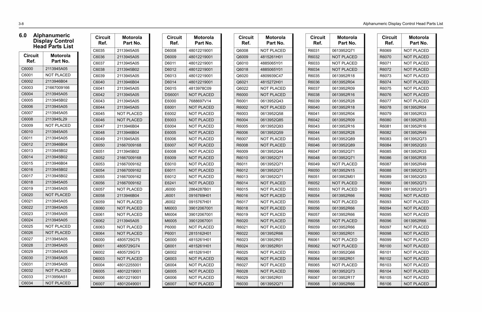
3-8 Alphanumeric Display Control Head Parts List
6.0
CirR
C600
C600
C600
C600
C600
C600
C600
C600
C600
C600
C601
C601
C601
C601
C601
C601
C601
C601
C601
C601
C602
C602
C602
C602
C602
C602
C602
C602
C602
C602
C603
C603
C603
C603
C603
R6031 0613952Q71
R6032 NOT PLACED
R6033 NOT PLACED
R6034 NOT PLACED
R6035 0613952R18
R6036 0613952R04
R6037 0613952R09
R6038 0613952R16
R6039 0613952R28
R6040 0613952R18
R6041 0613952R04
R6042 0613952R09
R6043 0613952R16
R6044 0613952R28
R6045 0613952Q89
R6046 0613952Q89
R6047 0613952Q71
R6048 0613952Q71
R6049 NOT PLACED
R6050 0613952N15
R6051 0613952M01
R6052 NOT PLACED
R6053 NOT PLACED
R6054 0613952R66
R6055 NOT PLACED
R6056 0613952R66
R6057 0613952R66
R6058 NOT PLACED
R6059 0613952R66
R6060 0613952R01
R6061 NOT PLACED
R6062 NOT PLACED
R6063 0613952Q66
R6064 0613952R01
R6065 NOT PLACED
R6066 0613952Q73
R6067 0613952R17
R6068 0613952R66
Circuit Ref.
MotorolaPart No.
R6069 NOT PLACED
R6070 NOT PLACED
R6071 NOT PLACED
R6072 NOT PLACED
R6073 NOT PLACED
R6074 NOT PLACED
R6075 NOT PLACED
R6076 NOT PLACED
R6077 NOT PLACED
R6078 0613952R04
R6079 0613952R33
R6080 0613952R33
R6081 0613952R16
R6082 0613952R49
R6083 0613952Q73
R6084 0613952Q53
R6085 0613952R33
R6086 0613952R35
R6087 0613952R49
R6088 0613952Q73
R6089 0613952Q53
R6090 0613952Q73
R6091 0613952Q73
R6092 NOT PLACED
R6093 NOT PLACED
R6094 NOT PLACED
R6095 NOT PLACED
R6096 0613952R66
R6097 NOT PLACED
R6098 NOT PLACED
R6099 NOT PLACED
R6100 NOT PLACED
R6101 NOT PLACED
R6102 NOT PLACED
R6103 NOT PLACED
R6104 NOT PLACED
R6105 NOT PLACED
R6106 NOT PLACED
Circuit Ref.
MotorolaPart No.
Alphanumeric Display Control Head Parts List
cuit ef.
MotorolaPart No.
0 2113945A05
1 NOT PLACED
2 2113946B04
3 21667009166
4 2113945A05
5 2113945B02
6 2113945A05
7 2113945A05
8 2113945L29
9 NOT PLACED
0 2113945A05
1 2113945A05
2 2113946B04
3 2113945B02
4 2113945B02
5 2113946B04
6 2113945B02
7 2113945B02
8 2113945A05
9 2113945A05
0 NOT PLACED
1 2113945A05
2 2113945A05
3 2113945A05
4 2113945A05
5 NOT PLACED
6 NOT PLACED
7 2113945A05
8 2113945A05
9 2113945A05
0 2113945A05
1 2113945A05
2 NOT PLACED
3 2113956A51
4 NOT PLACED
C6035 2113945A05
C6036 2113945A05
C6037 2113945A05
C6038 2113945B02
C6039 2113945A05
C6040 2113946B04
C6041 2113945A05
C6042 2113945A05
C6043 2113945A05
C6044 2113945A05
C6045 NOT PLACED
C6046 NOT PLACED
C6047 2113946B04
C6048 2113946B04
C6049 2113945A05
C6050 21667009168
C6051 2113945B02
C6052 21667009168
C6053 21667009162
C6054 21667009162
C6055 21667009162
C6056 21667009162
C6057 NOT PLACED
C6058 2113946B04
C6059 NOT PLACED
C6060 NOT PLACED
C6061 NOT PLACED
C6062 2113945A05
C6063 NOT PLACED
C6064 NOT PLACED
D6000 4805729G75
D6001 4805729G74
D6002 4805729G73
D6003 NOT PLACED
D6004 48012255001
D6005 48012219001
D6006 48012219001
D6007 48012049001
Circuit Ref.
MotorolaPart No.
D6008 48012219001
D6009 48012219001
D6011 48012219001
D6012 48012219001
D6013 48012219001
D6014 48012219001
D6015 4813978C09
DS6001 NOT PLACED
E6000 7688697V14
E6001 NOT PLACED
E6002 NOT PLACED
E6003 NOT PLACED
E6004 NOT PLACED
E6005 NOT PLACED
E6006 NOT PLACED
E6007 NOT PLACED
E6008 NOT PLACED
E6009 NOT PLACED
E6010 NOT PLACED
E6011 NOT PLACED
E6012 NOT PLACED
E6241 NOT PLACED
J6000 2864287B01
J6001 0916769H01
J6002 0915767H01
M6003 39012067001
M6004 39012067001
M6005 39012067001
P6000 NOT PLACED
P6001 2815162H01
Q6000 4815261H01
Q6001 4815261H01
Q6002 4815261H01
Q6003 NOT PLACED
Q6004 NOT PLACED
Q6005 NOT PLACED
Q6006 NOT PLACED
Q6007 NOT PLACED
Circuit Ref.
MotorolaPart No.
Q6008 NOT PLACED
Q6009 4815261H01
Q6010 4885065Y01
Q6018 4885065Y01
Q6020 4809939C47
Q6021 4815272H01
Q6022 NOT PLACED
R6000 NOT PLACED
R6001 0613952Q43
R6002 NOT PLACED
R6003 0613952Q58
R6004 0613952Q85
R6005 0613952Q93
R6006 0613952Q59
R6007 NOT PLACED
R6008 NOT PLACED
R6009 0613952Q44
R6010 0613952Q71
R6011 0613952Q71
R6012 0613952Q71
R6013 0613952Q71
R6014 NOT PLACED
R6015 NOT PLACED
R6016 NOT PLACED
R6017 NOT PLACED
R6018 NOT PLACED
R6019 NOT PLACED
R6020 NOT PLACED
R6021 NOT PLACED
R6022 0613952R66
R6023 0613952R01
R6024 0613952R01
R6025 NOT PLACED
R6026 NOT PLACED
R6027 NOT PLACED
R6028 NOT PLACED
R6029 0613952R01
R6030 0613952Q71
Circuit Ref.
MotorolaPart No.
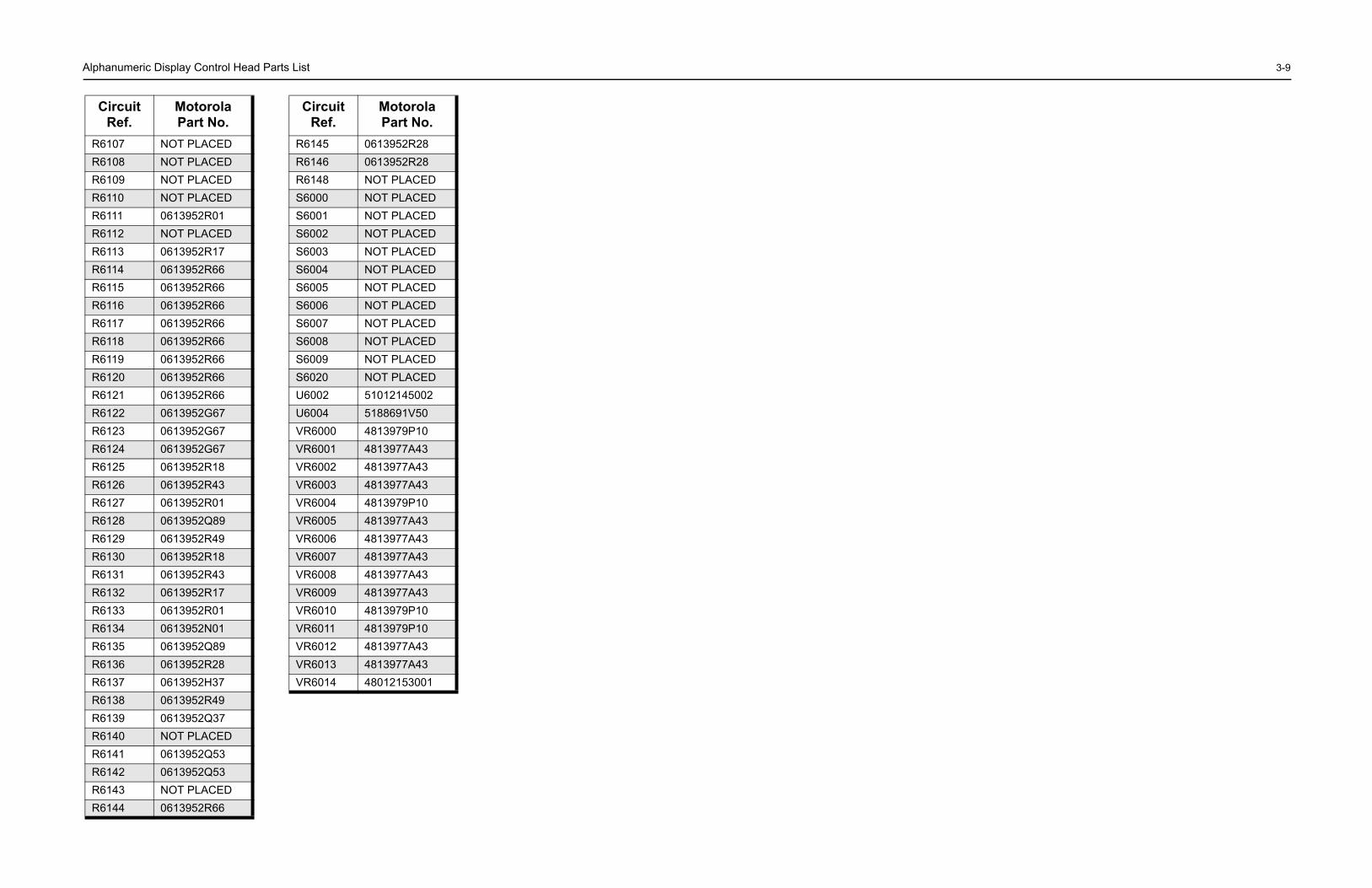
A 3-9
lphanumeric Display Control Head Parts ListR6107 NOT PLACED
R6108 NOT PLACED
R6109 NOT PLACED
R6110 NOT PLACED
R6111 0613952R01
R6112 NOT PLACED
R6113 0613952R17
R6114 0613952R66
R6115 0613952R66
R6116 0613952R66
R6117 0613952R66
R6118 0613952R66
R6119 0613952R66
R6120 0613952R66
R6121 0613952R66
R6122 0613952G67
R6123 0613952G67
R6124 0613952G67
R6125 0613952R18
R6126 0613952R43
R6127 0613952R01
R6128 0613952Q89
R6129 0613952R49
R6130 0613952R18
R6131 0613952R43
R6132 0613952R17
R6133 0613952R01
R6134 0613952N01
R6135 0613952Q89
R6136 0613952R28
R6137 0613952H37
R6138 0613952R49
R6139 0613952Q37
R6140 NOT PLACED
R6141 0613952Q53
R6142 0613952Q53
R6143 NOT PLACED
R6144 0613952R66
Circuit Ref.
MotorolaPart No.
R6145 0613952R28
R6146 0613952R28
R6148 NOT PLACED
S6000 NOT PLACED
S6001 NOT PLACED
S6002 NOT PLACED
S6003 NOT PLACED
S6004 NOT PLACED
S6005 NOT PLACED
S6006 NOT PLACED
S6007 NOT PLACED
S6008 NOT PLACED
S6009 NOT PLACED
S6020 NOT PLACED
U6002 51012145002
U6004 5188691V50
VR6000 4813979P10
VR6001 4813977A43
VR6002 4813977A43
VR6003 4813977A43
VR6004 4813979P10
VR6005 4813977A43
VR6006 4813977A43
VR6007 4813977A43
VR6008 4813977A43
VR6009 4813977A43
VR6010 4813979P10
VR6011 4813979P10
VR6012 4813977A43
VR6013 4813977A43
VR6014 48012153001
Circuit Ref.
MotorolaPart No.
3-10 Alphanumeric Display Control Head Parts List
Notes
XiR™ M3188/XiR™ M3688Mobile Radios
Chapter 4
Controller
Service Information
M
Issue: June, 2013

Computer Software CopyrightsThe Motorola products described in this manual may include copyrighted Motorola computer programs stored in semiconductor memories or other media. Laws in the United States and other countries preserve for Motorola certain exclusive rights for copyrighted computer programs, including, but not limited to, the exclusive right to copy or reproduce in any form the copyrighted computer program. Accordingly, any copyrighted Motorola computer programs contained in the Motorola products described in this manual may not be copied, reproduced, modified, reverse-engineered, or distributed in any manner without the express written permission of Motorola. Furthermore, the purchase of Motorola products shall not be deemed to grant either directly or by implication, estoppel, or otherwise, any license under the copyrights, patents or patent applications of Motorola, except for the normal non-exclusive license to use that arises by operation of law in the sale of a product.
i
Chapter 4 – Controller Service Information
Table of Contents
Section 1 Troubleshooting Charts
1.0 Controller Troubleshooting Chart......................................................................... 1-12.0 Power-Up Troubleshooting Chart ........................................................................ 1-23.0 MMP USB (Radio is in Device Mode) Troubleshooting Chart ............................. 1-34.0 Audio Troubleshooting Chart ............................................................................... 1-4
Section 2 Controller Schematics/Parts Lists
1.0 Allocation of Schematics and Parts Lists............................................................. 2-11.1 Controller Circuits........................................................................................... 2-1
2.0 Controller R1 Schematic Diagrams ..................................................................... 2-3Controller – Top Level Schematic Diagram............................................................ 2-3Controller DC Supply Schematic Diagram ............................................................. 2-4Controller Audio Schematic Diagram ..................................................................... 2-5Controller Peripheral Schematic Diagram (sheet 1 of 2) ........................................ 2-6Controller Peripheral Schematic Diagram (sheet 2 of 2) ........................................ 2-7Controller Microprocessor Schematic Diagram...................................................... 2-8Controller Memories Schematic Diagram............................................................... 2-9
3.0 Controller R1 Parts List...................................................................................... 2-10

ii
Notes
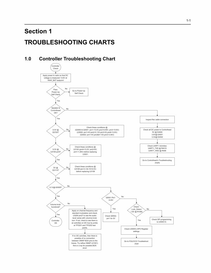
1-1
Section 1
TROUBLESHOOTING CHARTS
1.0 Controller Troubleshooting Chart
Pass Power-UpSelf Check
Controller Check
Speaker &Controlhead
OK?
9.3V @U3100-pin5?
5V @E3113?
Controller OK
9.1V@ E0009?
Q0001 Pin1 =2.8V
Check Q0002-pin1 for 0V
Volume knob funcitonal?
Go to Power-Up Self Check
No
Yes
Yes
No
Go to Controlhead’s Troubleshooting charts
Check these conditions @ U3100 (pin4=13.2V; pin2=0V; pin1=1.26V) before replacing
U3001.
Yes
No
Check these conditions @ U3108 (pin 8, 9 & 10=9.3V)
before replacing U3108
No
Yes
Yes
No
Yes
Apply on channel frequency and standard modulation and check U3200 pin27 to see the audio level varies with volumne knob
turn. If not, check to see there is an activities on I2C bus by probe
at TP3201 and TP3202 test points.
No
Yes
If no I2C activities, then there is possible of no connection
between OMAP BGA pins to the traces. Try reflow OMAP (U1001)
first or x-ray for possible BGA short.
No
Check SPI programming to U0000 IC.
Check Lock_Detect
1.8V @ R1065No
Check U0000's GPO Register settings.
Yes
9.3V @E0700?
Check these conditions @(Q3000 & Q3001: pin1=13.0V,pin2=9.45V, pin3=13.6V)
(U3000: pin1=4V,pin2=5.13V,pin3=5V,pin8=13.6V)(Q3002: pin1=4V,pin2&4=13V,pin3=3.35V)
No
Apply power to radio so that DC voltage is measured 13.6V at
RAW_BAT testpoint
Check all DC power to Controlhead5V @ E40003.6V@ E40013.3V@ E4002
Go to FGU/VCO Troubleshoot chart
Inspect flex cable connection
Check UART1 Activities:UART1_TXD @ R4015UART1_RXD @ R406
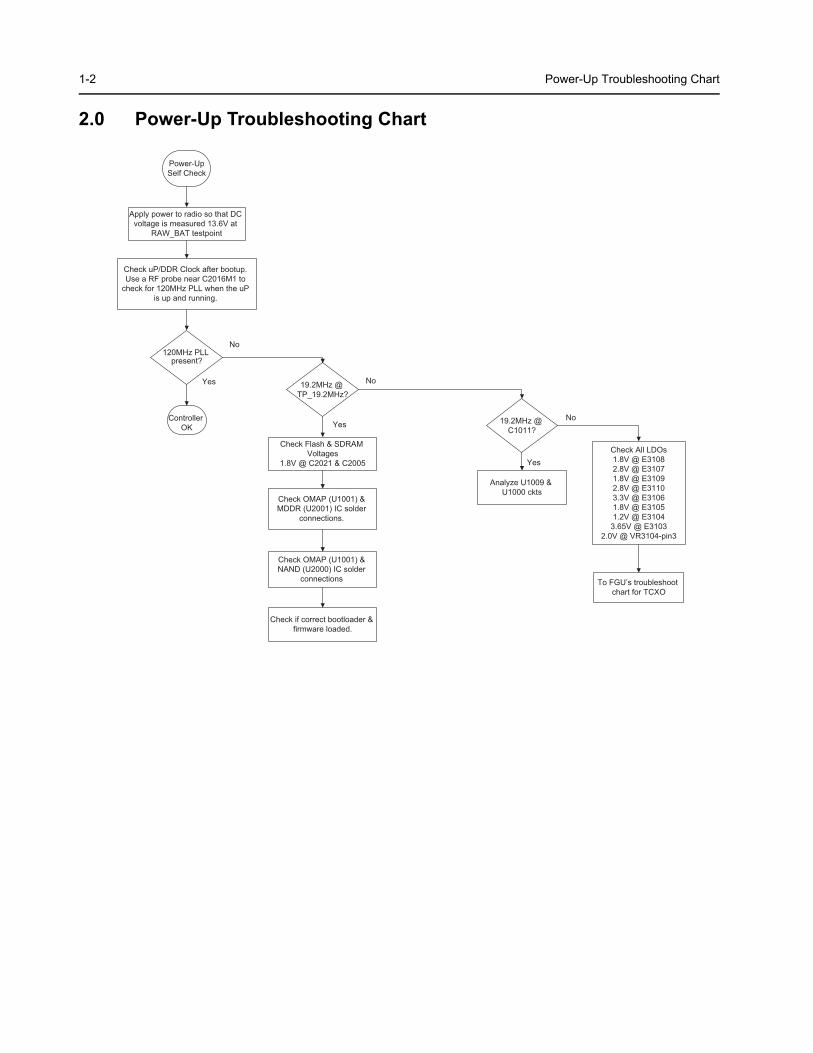
1-2 Power-Up Troubleshooting Chart
2.0 Power-Up Troubleshooting Chart
19.2MHz @ TP_19.2MHz?
120MHz PLL present?
Power-UpSelf Check
To FGU’s troubleshoot chart for TCXO
NoYes
No
No
Check All LDOs1.8V @ E31082.8V @ E31071.8V @ E31092.8V @ E31103.3V @ E31061.8V @ E31051.2V @ E31043.65V @ E3103
2.0V @ VR3104-pin3
Analyze U1009 & U1000 ckts
Check OMAP (U1001) & MDDR (U2001) IC solder
connections.
Yes
Check Flash & SDRAM Voltages
1.8V @ C2021 & C2005
Check OMAP (U1001) & NAND (U2000) IC solder
connections
Yes
Apply power to radio so that DC voltage is measured 13.6V at
RAW_BAT testpoint
19.2MHz @ C1011?
Check if correct bootloader & firmware loaded.
Controller OK
Check uP/DDR Clock after bootup. Use a RF probe near C2016M1 to
check for 120MHz PLL when the uP is up and running.
MMP USB (Radio is in Device Mode) Troubleshooting Chart 1-3
3.0 MMP USB (Radio is in Device Mode) Troubleshooting Chart
Yes
PC or Host does not recognize radio through
MMP USB port
NoDose USB work in FlashZap mode?
With radio is Off and disconnected from PC or Host, Ohm out D+ and D-to ground on the brick side. Typical
resistance on these signals are open load or OL. If not, then check
VR4002M1 pin 6 &1 and U1004M1 pin 1 & 2 for possible damage or
manufacturing related.
After connecting USB cable to the PC or Host, 5V should be present at TP4011M1 testpoint as well as at
D1005M1 pin2. If not, analyze VR44002M1 and D1005M1 ckts.
Once 5V is detected by Processor, the radio’s software will automatically pull
D+ to 3.3V @ FL_D+_M1 or CH_D+M1 followed by the enumeration process. If
not, then inspect or X-Ray U1001 for possible open or short connections on
the BGA pins.
May not loaded in the correct firmware. Try reflashing in the proper
firmware.
Attached/De-attached Tone present?
Verify that controlhead’s flex is inserted properly
No Yes
Verify that U6004 Comparator circuits in controlhead are behaved
correctly per Truth Table.
Check to see a constant 5V is present at TP6002 when a USB programming cable is attached.
With radio is Off and disconnected from PC or Host, Ohm out D+ and D-to ground on the controlhead side.
Typical resistance on these signals are open load or OL. If not, then check
D6007 pin6, VR6014 pin2, D6007 pin1, and VR6014 pin1 for possible damage
or manufacturing related.
1-4 Audio Troubleshooting Chart
4.0 Audio Troubleshooting Chart
Audio Self-Check
YesIs Audio present at speaker outputs?
Does adjustingthe volume knob
fix problem?
This test assumes standard RF input: 60% full deviation 1kHz audio tone
Does adjustingthe volume knob work properly?
Go to A
+ Self-check completed
Is audio present atTP3206?
Verify active data on
CODEC SSI input
U3200: CODEC SSIPin 7: Probe SSI CLK
Pin 6: Probe SSI FSYNCPin 5: Probe SSI DATA_IN
Is there active data on the CODEC
SSI bus?
Go to RX troubleshooting
chart.
Is there active data on the RFIC
SSI bus?
Verify U3200 connections
before replacing
Do diagnostics on U1001 before
replacing.
U3200: CODECPin 2, 3: +1.8V
Pin 17, 28, 21, 24: +3.3VPin 1,16,18,20,25,29,33: GND
Pin 10: Probe I2C CLKPin 9: Probe I2C DATA
Pin 23: AUDIO OUT (+1.6V BIAS)
Is audio present at pin 12 of U3204?
A
Yes
Yes
Yes
Yes Yes
No No
No
No
No
No No
Verify C3217, R3229, C3240, R3286, C3233, and C3232 connections before
replacing
Verify U3204 connections before
replacing
U3204: Audio Amplifier Pin 5, 16: VBAT+
Pin 1, 10, 11, 12, 20: GNDPin 4: 9.3V (when enabled)
U0000: RFIC SSIProbe SSI CLK @ R1004
Probe SSI FSYNC @ R1003Probe SSI DATA_IN @ R1002
2-1
Section 2
CONTROLLER SCHEMATICS/PARTS LISTS
1.0 Allocation of Schematics and Parts Lists
1.1 Controller Circuits
This Chapter shows the Schematics and the Parts List for the Controller circuits.
Table 2-1 Controller R1 Schematic Diagrams and Parts List
Controller R1 used on PCB:84012504002_B VHF (136–174 MHz), 1–25 W84012505002_B VHF (136–174 MHz), 25–45 W84012591001_A UHF1 (403–470 MHz), 1–25 W 84012592001_A UHF1 (403–470 MHz), 25–40 W
SCHEMATICSController Top LevelController DC SupplyController AudioController Peripheral (sheet 1 of 2)Controller Peripheral (sheet 2 of 2)Controller MicroprocessorController Memories
Page 2-3Page 2-4Page 2-5Page 2-6Page 2-7Page 2-8Page 2-9
Parts ListsController R1 Page 2-10

2-2
Notes
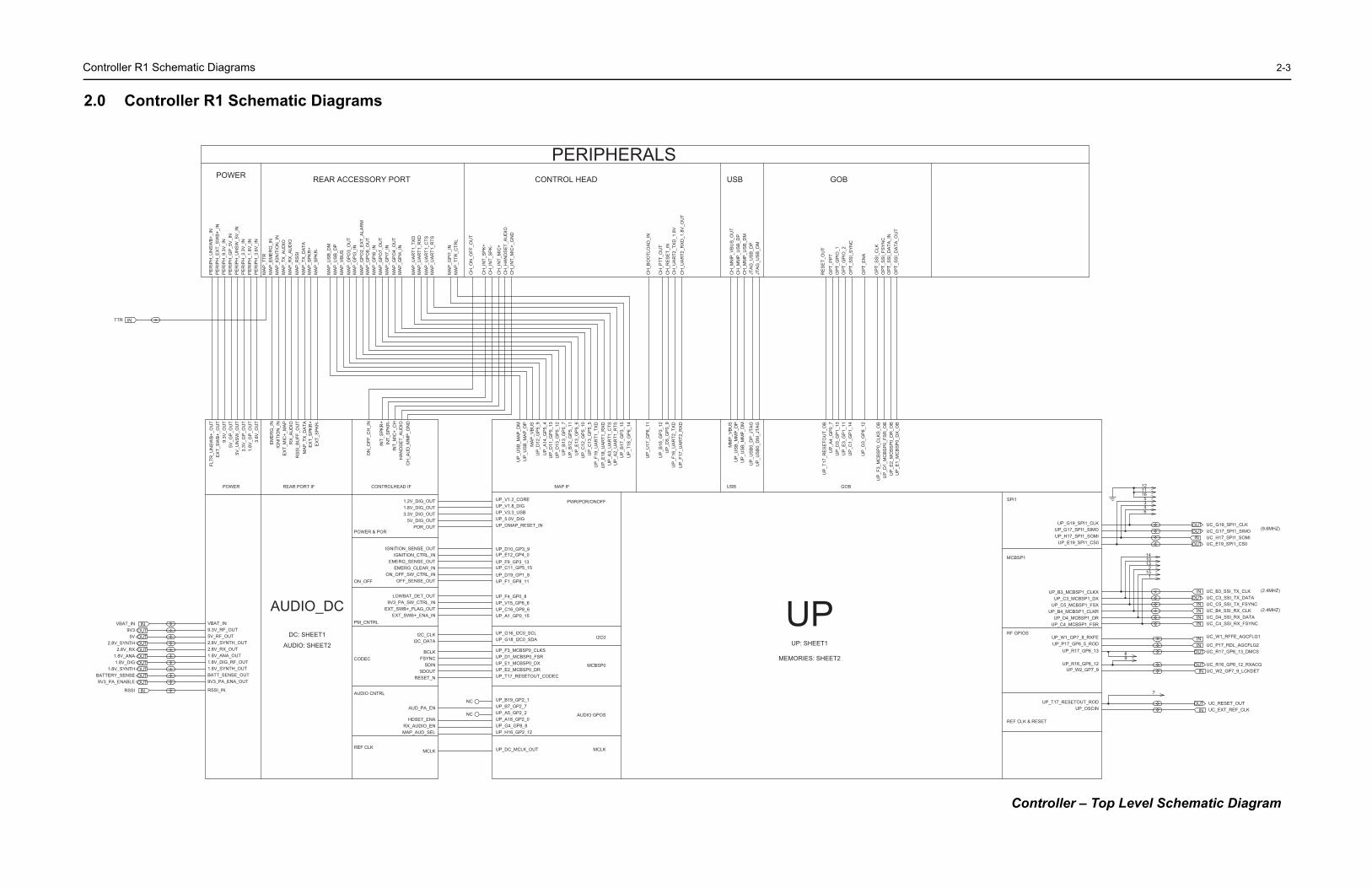
C 2-3
2
UP_G19_SPI1_CLK
UP_H17_SPI1_SOMIUP_E19_SPI1_CS0
UP_G17_SPI1_SIMO
UP_D4_MCBSP1_DRUP_B4_MCBSP1_CLKR
UP_C5_MCBSP1_FSXUP_C3_MCBSP1_DX
UP_B3_MCBSP1_CLKX
UP_W2_GP7_9
UP_T17_RESETOUT_ROD
UP_C4_MCBSP1_FSR
UP_W1_GP7_8_RXFEUP_P17_GP6_5_ROD
UP_R17_GP6_13
UP_R16_GP6_12
UP_OSCIN
REF CLK & RESET
SPI1
RF GPIOS
MCBSP1
2
UP
_G3_
GP
8_12
UP
_E2_
MC
BS
P0_
DR
_OB
UP
_D1_
MC
BS
P0_
FSR
_OB
UP
_F3_
MC
BS
P0_
CLK
S_O
B
UP
_C1_
GP
1_14
UP
_E3_
GP
1_11
UP
_D3_
GP
1_13
UP
_E1_
MC
BS
P0_
DX
_OB
GOB
OP
T_G
PIO
_2
OP
T_S
SI_
DA
TA_I
NO
PT_
SS
I_FS
YN
CO
PT_
SS
I_C
LK
OP
T_E
NA
OP
T_S
SI_
SY
NC
OP
T_G
PIO
_1
OP
T_S
SI_
DA
TA_O
UT
OB
(9.6MHZ)
(2.4MHZ)
(2.4MHZ)UC_C5_SSI_TX_FSYNC
UC_B3_SSI_TX_CLKUC_C3_SSI_TX_DATA
UC_G19_SPI1_CLKUC_G17_SPI1_SIMOUC_H17_SPI1_SOMI
UC_B4_SSI_RX_CLKUC_D4_SSI_RX_DATAUC_C4_SSI_RX_FSYNC
UC_W1_RFFE_AGCFLG1
UC_E19_SPI1_CS0
UC_R16_GP6_12_RXACQ
UC_R17_GP6_13_DMCS
UC_W2_GP7_9_LCKDET
UC_P17_RDL_AGCFLG2OUT
INININ
OUTIN
IN
OUTIN
OUT
OUT
ININ
INOUT
14
9
2
115
8
1013
7
UC_EXT_REF_CLKUC_RESET_OUTOUT
IN
12
34
5
6
1611
Controller – Top Level Schematic Diagram
ontroller R1 Schematic Diagrams
.0 Controller R1 Schematic Diagrams
9V3_PA_ENABLEBATTERY_SENSE
1.8V_SYNTH1.8V_DIG
1.8V_ANA
RSSI
2.8V_SYNTH2.8V_RX
5V9V3
VBAT_IN
OUTOUTOUT
OUT
OUT
OUT
OUT
IN
OUT
OUTIN UP
UP: SHEET1
MEMORIES: SHEET
UP
_US
B0_
DP
_JTA
G
UP
_F17
_UA
RT2
_RX
D
UP
_D5_
GP
0_9
MM
P_V
BU
S
UP
_US
B0_
DM
_JTA
G
UP
_US
B_M
MP
_DP
UP
_B12
_GP
5_11
UP
_US
B_M
AP
_DM
MA
P_V
BU
S
UP
_E13
_GP
5_6
UP
_A4_
GP
0_7
UP
_F16
_UA
RT2
_TX
D
UP
_A2_
UA
RT1
_RTS
UP
_A3_
UA
RT1
_CTS
UP
_E18
_UA
RT1
_RX
DU
P_F
19_U
AR
T1_T
XD
UP
_C13
_GP
5_5
UP
_C12
_GP
5_10
UP
_B13
_GP
5_7
UP
_D13
_GP
5_12
UP
_D11
_GP
5_13
UP
_A14
_GP
5_4
UP
_D12
_GP
5_9
UP
_US
B_M
AP
_DP
UP
_T17
_RE
SE
TOU
T_O
B
UP
_US
B_M
MP
_DM
UP
_B16
_GP
3_12
UP
_U17
_GP
6_11
UP
_T18
_GP
6_14
UP
_B17
_GP
3_15
USBMAP IF
UP_F3_MCBSP0_CLKSUP_D1_MCBSP0_FSR
UP_C16_GP8_6
UP_E2_MCBSP0_DR
UP_A5_GP2_2UP_B7_GP2_7UP_B19_GP2_1
UP_DC_MCLK_OUT
UP_H16_GP2_12UP_G4_GP8_8UP_A18_GP2_0
UP_T17_RESETOUT_CODEC
UP_E1_MCBSP0_DX
UP_V15_GP6_6
UP_C11_GP5_15UP_F9_GP3_13UP_E12_GP4_0UP_D10_GP3_9
UP_F1_GP8_11UP_D19_GP1_8
UP_F4_GP0_8
UP_A1_GP0_15
UP_G18_I2C0_SDAUP_G16_I2C0_SCL
UP_OMAP_RESET_INUP_5.0V_DIGUP_V3.3_USBUP_V1.8_DIGUP_V1.2_CORE
I2C0
AUDIO GPOS
MCBSP0
MCLK
PWR/POR/ONOFF
NC
NC
ON
_OFF
_CH
_IN
EX
T_S
PK
R+
HA
ND
SE
T_A
UD
IOIN
T_M
IC+_
CH
INT_
SP
KR
-
RS
SI_
BU
FF_O
UT
BATT_SENSE_OUT1.8V_SYNTH_OUT
EX
T_S
PK
R-
RX
_AU
DIO
EX
T_M
IC+_
MA
P
FSYNCBCLK
IGNITION_CTRL_INEMERG_SENSE_OUT
EMERG_CLEAR_IN
OFF_SENSE_OUTON_OFF_SW_CTRL_IN
SDIN
VBAT_IN
1.8V_ANA_OUT2.8V_RX_OUT2.8V_SYNTH_OUT
9.3V_RF_OUT
RESET_N
RSSI_IN
9V3_PA_ENA_OUT
5V_RF_OUT
1.8V_DIG_RF_OUT
I2C_DATA
EXT_SWB+_FLAG_OUT9V3_PA_SW_CTRL_IN
LOWBAT_DET_OUT
I2C_CLK
IGNITION_SENSE_OUT
MA
P_T
X_D
ATA
SDOUT
AUD_PA_EN
HDSET_ENA
MCLK
RX_AUDIO_ENMAP_AUD_SEL
IGN
ITIO
N_I
NE
ME
RG
_IN
5V_U
NS
W_O
UT
INT_
SP
KR
+
CH
_AU
D_M
MP
_GN
D
3.6V
_OU
T1.
8V_G
P_O
UT
3.3V
_GP
_OU
T
5V_G
P_O
UT
9.3V
_OU
TE
XT_
SW
B+_
OU
TFL
TR_U
NS
WB
+_O
UT
1.2V_DIG_OUT
POR_OUT5V_DIG_OUT
3.3V_DIG_OUT1.8V_DIG_OUT
EXT_SWB+_ENA_IN
POWER
AUDIO: SHEET2
DC: SHEET1
REF CLK
REAR PORT IF
ON_OFF
CODEC
PM_CNTRL
POWER & POR
AUDIO_DC
AUDIO CNTRL
CONTROLHEAD IF
TTR IN
MA
P_R
X_A
UD
IOM
AP
_RS
SI
PE
RIP
H_9
.3V
_IN
MA
P_S
PK
R+
MA
P_T
TR
MA
P_G
PO
7_O
UT
MA
P_V
BU
S
MA
P_G
PO
2_E
XT_
ALA
RM
MA
P_U
SB
_DM
MA
P_G
PO
3_O
UT
MA
P_G
PI7
_IN
MA
P_U
AR
T1_T
XD
MA
P_U
AR
T1_R
XD
CH
_UA
RT2
_RX
D_1
.8V
_OU
T
JTA
G_U
SB
_DM
JTA
G_U
SB
_DP
CH
_MM
P_U
SB
_DM
CH
_MM
P_U
SB
_DP
CH
_MM
P_V
BU
S_O
UT
MA
P_G
PO
4_O
UT
MA
P_G
PO
8_O
UT
MA
P_T
X_D
ATA
MA
P_T
X_A
UD
IOM
AP
_IG
NIT
ION
_IN
PE
RIP
H_U
NS
W_5
V_I
NP
ER
IPH
_GP
_5V
_IN
MA
P_E
ME
RG
_IN
PE
RIP
H_3
.6V
_IN
PE
RIP
H_1
.8V
_IN
PE
RIP
H_3
.3V
_IN
PE
RIP
H_U
NS
WB
+_IN
CH
_IN
T_S
PK
-C
H_I
NT_
SP
K+
MA
P_T
TR_C
TRL
CH
_ON
_OFF
_OU
T
CH
_HA
ND
SE
T_A
UD
IO
MA
P_S
PK
R-
MA
P_U
SB
_DP
MA
P_G
PI3
_IN
MA
P_G
PI8
_IN
MA
P_G
PI4
_IN
CH
_IN
T_M
IC+
CH
_IN
T_M
IC+_
GN
D
PE
RIP
H_E
XT_
SW
B+_
IN
MA
P_U
AR
T1_C
TSM
AP
_UA
RT1
_RTS
MA
P_G
PI1
_IN
CH
_BO
OTL
OA
D_I
N
CH
_PTT
_OU
TC
H_R
ES
ET_
INC
H_U
AR
T2_T
XD
_1.8
V
OP
T_P
PT
RE
SE
T_O
UT
USB GREAR ACCESSORY PORTPOWER CONTROL HEAD
PERIPHERALS
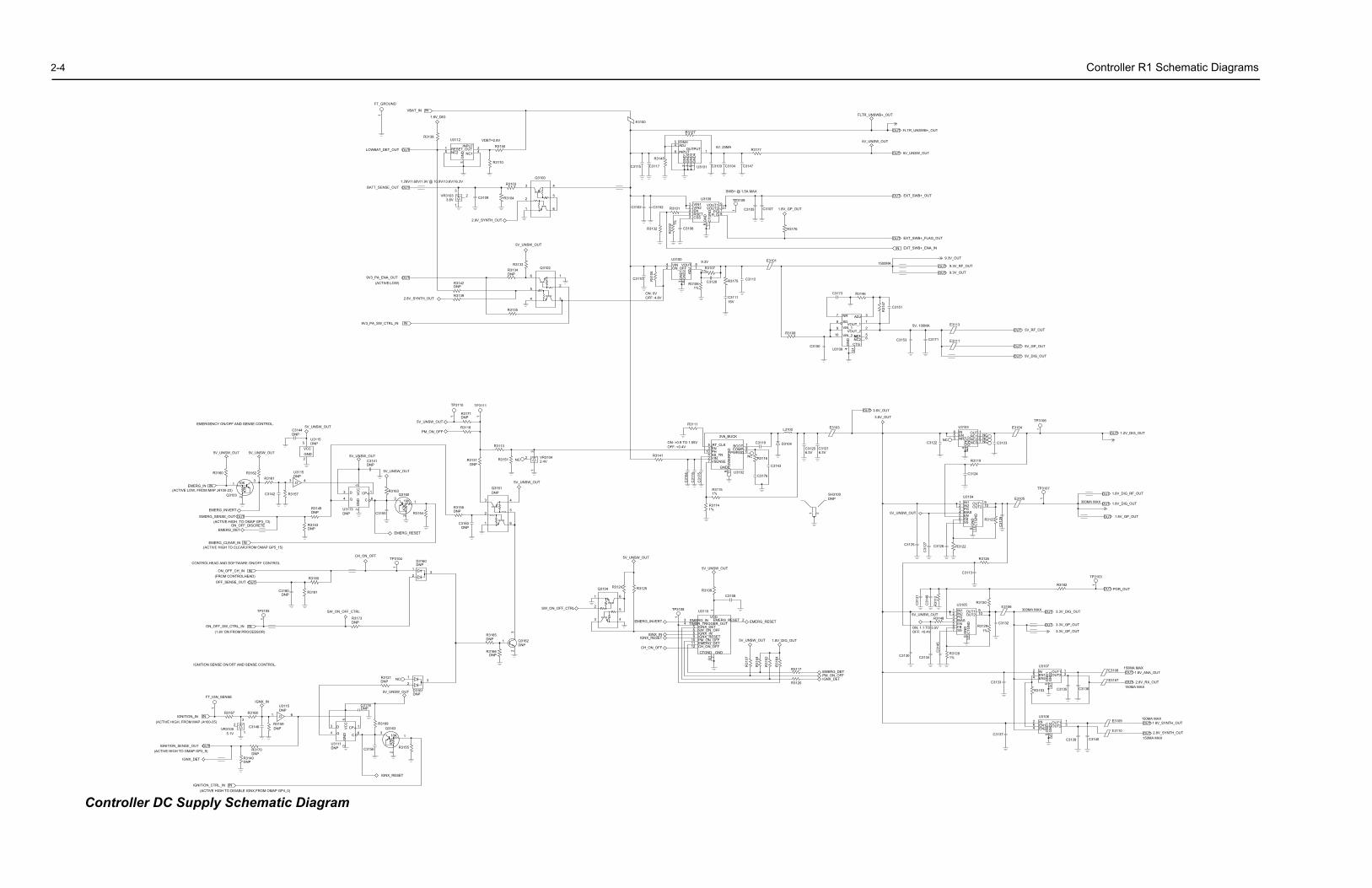
2-4 Controller R1 Schematic Diagrams
CTGNC2NC1
GN
D
NR ADJ
VOUT_1VIN_1
VIN_2VOUT_2
SD
C3151
R31
47
R31463173
2
1
10
9
8
7
65
4
G1
3
3108
NC1
5V, 100MA
E3111
E3113
C3171C3153
5V_RF_OUT
5V_GP_OUT
5V_DIG_OUTOUT
OUT
OUT
9.3V_OUT
9.3V_RF_OUT
9.3V_OUT
OUT
OUT
1500MA
EXT_SWB+_FLAG_OUT
EXT_SWB+_ENA_ININ
OUT
5V_UNSW_OUT
5V_UNSW_OUT
EXT_SWB+_OUT
FLTR_UNSWB+_OUT
FLTR_UNSWB+_OUTOUT
OUT
OUT
ET_OFF_DET
03
3.6V_OUT
3.6V_OUTOUT
100
NC
OUTNC1NC2NC3G
ND
2
IN
GN
D1NR
EN
NCNCNC
E3104
C3123
1
3762
8
G14
5
U3103
C3122
R3119
C3124
R3122C3126
C31
27C3125
R3126
C3113
5V_UNSW_OUT
OUT1OUT2IN2
PGBIASENFBSS
CTG
ND
GN
D
IN1E3105
C31
28R31237
3109
21
6
85
11
4
U3104 1
TP3107
300MA MAX
1.8V_GP_OUT
1.8V_DIG_OUT
1.8V_DIG_RF_OUT
OUT
OUT
OUT
1
TP3106
1.2V_DIG_OUTOUT
1
TP3103
R3182POR_OUTOUT
300MA MAX 3.3V_DIG_OUT
3.3V_GP_OUT
3.3V_GP_OUT
OUT
OUTON: 1.1 TO 5.5VOFF: <0.4V
OUT1OUT2IN2
PGBIASENFBSS
CTG
ND
GN
D
IN1
C31
45
1%
R31
12
R3148
R3130C31
49
C31
31
R31297
3109
21
6
85
11
4
U3105
R3128C3134C3130
1%
5V_UNSW_OUT
E3106
C3132
C3133
C3137
EN1EN2
IN
GN
D12
5
46
U3107
R3153
150MA MAX
150MA MAX
150MA MAX
150MA MAX
EN1EN2
IN
GN
D2
GN
D1
OUT2OUT1
GN
D2
OUT2OUT1
E3109
E3110
C3140
C3136C3135
C3139
31
G1
312
G15
46
U3106
2.8V_RX_OUT
1.8V_ANA_OUT
1.8V_SYNTH_OUT
2.8V_SYNTH_OUT
OUT
OUT
OUT
OUT
E3107
E3108
C
1
FT_GROUND
VBAT_IN IN
1.28V/1.60V/1.9V @ 10.9V/13.6V/16.3V
VDET=2.8V
RESET_OUTNC1
INPUT
NC2
GN
D
R3138U3112
5
1.8V_DIG
R3150
R3110
142
3
BATT_SENSE_OUT
LOWBAT_DET_OUT OUT
OUT
R3104VR3103 2 C31093.6V
1
R3103
3
2.8V_SYNTH_OUT
Q3100
3 4
1 6
52
(ACTIVE:LOW)
DNP
R3133
4
1
3
6
52
Q3102R3134
R3135
R3142
R3139
5V_UNSW_OUT
DNP
2.8V_SYNTH_OUT
9V3_PA_SW_CTRL_IN
9V3_PA_ENA_OUT OUT
IN
5V, 25MA
GN
D3
GN
D2INPUT
GN
D4
GN
D1
ADJOINH
OUTPUT
R3127
R3145
U3101 C3147
R3177
C3104C3103
1
5
8
7632
4
C3117
E3100
C3115
SWB+ @ 1.5A MAX
VOUT1
PGVOUT2
FLG
CTG
ND
VIN1VIN2ENRSET
GN
DCSS
U3109
R3132
1
TP3109
R3101
R31
02
C3106
109
21
57
6
84
11
3
C3152C3102
1%
C3107
R3176
C3105 1.8V_GP_OUT
9.3V
OFF: 4.8VON: 0V
VOUT
GN
D2
VIN
GN
D1 1%
C3129
1%
C3112R3175
16VC3111
R310754
2
63
1
U3100
R31
05
R3106C3110
AD
JON_OFF
E3101
R3108
C3150
C
U
EMERGENCY ON/OFF AND SENSE CONTROL.
VCCGND
DNP
DNP
C3144
5
2
U3115
5V_UNSW_OUT
(FROM CONTROLHEAD)
(1.8V ON FROM PROCESSOR)
(ACTIVE LOW, FROM MAP J4100-23)
CONTROLHEAD AND SOFTWARE ON/OFF CONTROL
(ACTIVE HIGH TO CLEAR,FROM OMAP GP5_15)
(ACTIVE:HIGH, TO OMAP GP3_13)
47K
10K
EMERG_SENSE_OUT
EMERG_INVERT
ON_OFF_DISCRETE
R3157
U3115DNP
DNPC3180 R3181
R3180
43
R3162R3161
C3142
1
TP3105
31
2Q3103
R3160
EMERG_IN
ON_OFF_CH_IN
5V_UNSW_OUT5V_UNSW_OUT
EMERG_CLEAR_IN
OFF_SENSE_OUT
ON_OFF_SW_CTRL_IN
EMERG_DET
IN
IN
IN
OUT
OUT
IN
R3149DNP
DNPR3143
NCDNP
R3131
13
2 VR3104R3151
R3113
2.4V
5V_UNSW_OUT
Q3161DNP
DNPR3158
C3160DNP
4
1
3
6
52
GN
DQ
D VC
C
CP
C
47K
10K
C3141DNP
DNPU3113
R3154
31
2
Q3160R3163
C3155
4
2
3 1
6
5V_UNSW_OUT
5V_UNSW_OUT
EMERG_RESET
5
DNPD3160
DNP
32
11
TP3104
R3173
CH_ON_OFF
SW_ON_OFF_CTRL
DNP 11
TP3110
R3171
R3118PM_ON_OFF
5V_UNSW_OUT
TP3111
(ACTIVE HIGH, FROM MAP J4100-25)
(ACTIVE HIGH TO OMAP GP3_9)IGNITION_SENSE_OUT
1
FT_IGN_SENSE
R3168R3167
IGNX_DET
IGNX_IN
IGNITION_IN IN
OUT
U3115DNP
DNPR3159
61
C31461
32
VR31055.1V
(ACTIVE HIGH TO DISABLE IGNX,FROM OMAP GP4_0)
DNP
R3170DNP
R3140
IGNITION_CTRL_IN IN
GN
DQ
D VC
C
CP
C
47K
10K
DNPR3121
DNPD3161
C3118DNP
DNPU3111
32
1
R3155
R3169
31
2
Q3163
C3156
4
2
3 1
6
5V_UNSW_OUT
IGNX_RESET
NC
5
IGNITION SENSE ON/OFF AND SENSE CONTROL.
DNP
R3166
DNP
23
1 Q3162R3165
DNP
SW_ON_OFF_CTRL
Q3104 R3125R3124
4
1
3
6
52
5V_UNSW_OUT
SW_ON_OFFIGNX_DET
TIMER_TRIGGER_OUTEMERG_IN
IGNX_IN
CH_ON_OFFEMERG_DETPM_ON_OFFIGNX_RESET
CTGND
VDD
GND
EMERG_RESET
U3110
CH_ON_OFF
1
4
6
1098
5
7
23
11
G1
12
1
TP3108
EMERG_RESET
IGNX_RESET
EMERG_INVERT
IGNX_IN
R3109C3108
5V_UNSW_OUT
R3120
R3117
R31
64
R31
52
R31
44
R31
37
1.8V_DIG_OUT5V_UNSW_OUT
IGNX_DPM_ONEMERG
E31
C3121C31206.3V 6.3V
21
SH3DNP
OFF: <0.4V
3V6_BUCK
ON: >0.9 TO 1.55V
PWRGD
BOOTCOMP
PO
WE
RP
AD
RT_CLKENPH
GND
SS_TRVINVSENSE
NC
L3100
D3104C3119
C3143
R3116
C3176
R3111
724
5
6
11
10
9
3 81
U3102
C31
75
C31
16
C31
54
R3141
R3115
R3114
1%
1%
ontroller DC Supply Schematic Diagram
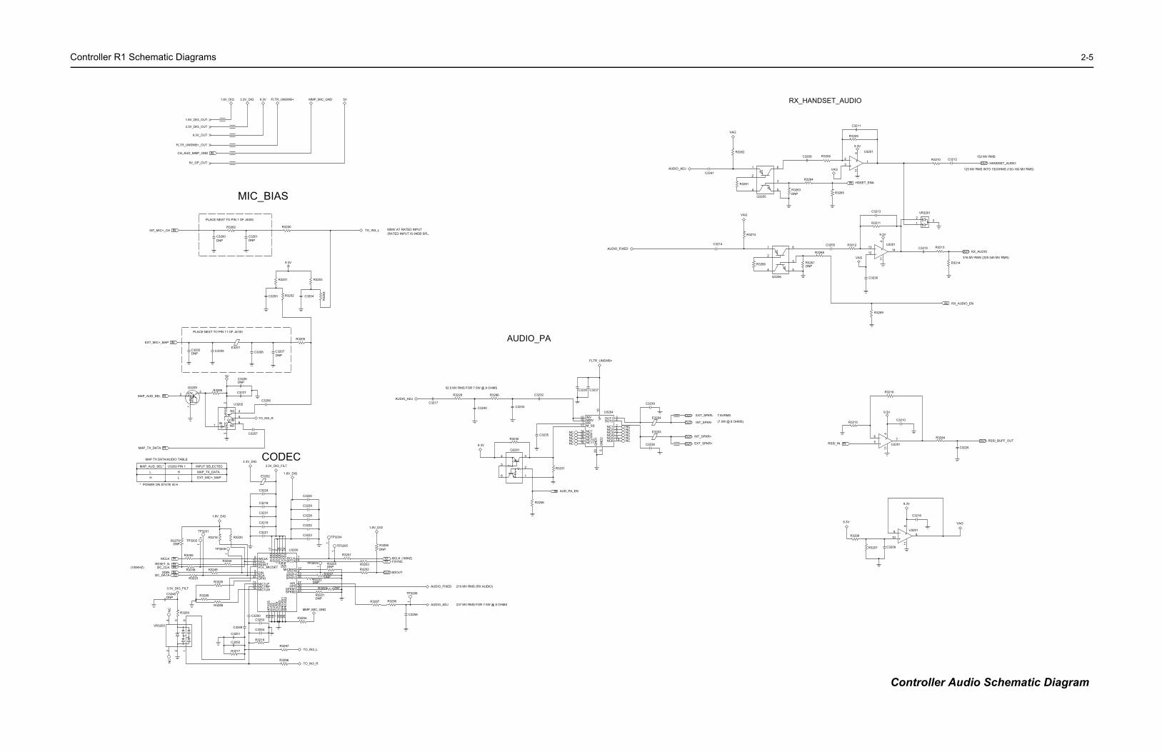
C 2-5
R3262
3241
VAG
RX_HANDSET_AUDIO
2
3
R3263
VAG
R3265
R3264R3261
5
1
4
6
Q3205
C3211
R3209
114
13
2
U3201R3208C3209
9.3V
DNP
HDSET_ENAIN
R3274
C3214
VAG
C3255
R3268
R3267
5
1
4
6
3
2
Q3206
R3266 DNP
R3212
C3230
R3269
VAG
R3211
C3213
114
1412
13U3201
9.3V
2
13
VR3201
316 MV RMS (225-345 MV RMS)
R3213C3215
R3214
RX_AUDIOOUT
RX_AUDIO_ENIN
125 MV RMS INTO 150OHMS (100-160 MV RMS)
152 MV RMS
HANDSET_AUDIOC3212R3210
OUT
7.8VRMS
(7.5W @ 8 OHMS)
R+
R+
KR-
KR-
6
4
C3225RSSI_IN U3201
57
11
R3215
R3216
R3284
C3210
9.3V
OUTIN
C3216
114
810
9 U3201
C3208
R3206
R3207
9.3V VAG
9.3V
RSSI_BUFF_OUT
Controller Audio Schematic Diagram
ontroller R1 Schematic Diagrams
3.3V_DIG_OUT
1.8V_DIG_OUT
9.3V_OUT
FLTR_UNSWB+_OUT
CH_AUD_MMP_GND
5V_GP_OUT
IN
5VFLTR_UNSWB+ MMP_MIC_GND3.3V_DIG1.8V_DIG 9.3V
MIC_BIAS
PLACE NEXT TO PIN 1 OF J4000
R3200
C3201
R3282
C3200
INT_MIC+_CH
DNPDNP
IN
R32
04
R3203
C3204
R3201
R3202C3203
9.3V
PLACE NEXT TO PIN 11 OF J4100
R3205
C3207C3206E3201
C3205C3202
EXT_MIC+_MAP
DNP DNP
IN
GN
DV
PO
S
NO
COM
NC
IN
47K
47K
DNP
C3227
C3226
R328532
1
Q3209
C3257
C3256
2
6
4
1
3
5
U3202
TO_IN3_R
MAP_AUD_SEL
5V
IN
* POWER ON STATE IS H
MAP TX DATA/AUDIO TABLE
INPUT SELECTED
EXT_MIC+_MAP
U3202 PIN 1
L
H
H
L
MAP_AUD_SEL*
MAP_TX_DATA
MAP_TX_DATA IN
CODEC
C3220
E3202
C3224
C3229
C3228
C3222
C3223
C3218
C3219
C3231
C3221
3.3V_DIG_FILT
1.8V_DIG
3.3V_DIG
(1MHZ)
R3253
R3251
TP3204
DNP
BCLK
R3280TP3205
1
1
R3252
1.8V_DIG
FSYNC
SDOUT
IOIO
OUT
C3250
R3219
R32542520129 18 3316
C3253
R3297
C3254
R3296
TO_IN3_L
TO_IN3_R
MMP_MIC_GND
IOV
DD
HP
VD
D
BCLKWCLK
SPKP2
DOUTSPKP1
MICBIAS
SPKM2
HPLHPR
SPKM1
IOV
SS
CTG
ND
AV
DD
DV
DD
MCLKSCL
RESETVOL_MICDET
DINSDA
SP
KV
DD
2S
PK
VD
D1
GPIO
MIC1LPMIC1RPMIC1LM
AV
SS
DV
SS
SP
KV
SS
1S
PK
VS
S2
HP
VS
S
DNP
2226
R3225
28
TP3203
U3200
DNPR3257
R3222DNP
DNPR3224
R3221DNP
1
6
11
2421
2319
9
1031
12
1413
15
8
2
3027
32
3
45
7
17
R3290
TP3206
R3287 1
210 MV RMS (RX AUDIO)
237 MV RMS FOR 7.5W @ 8 OHMS
AUDIO_FIXED
C3258
AUDIO_ADJ
NC
3.3V_DIG_FILT
VR3200
DNP
R3283
54 6
C3248
23 1
NC
(100KHZ)
I2C_DATA
I2C_CLK
R3218
C3249
TP3200
TP3202
TP3201
DNPR3279
MCLK
R3248 R3249
R3220
R3217
1
R3250
R3226
R3288
C3251
C3252
11
R3255
R3223
R3289
RESET_N
SDIN
1.8V_DIG
IN
ININ
INIO
(RATED INPUT IS 94DB SPL,80MV AT RATED INPUTTO_IN3_L
AUDIO_ADJ
AUDIO_FIXED
C
AUDIO_PA
52.5 MV RMS FOR 7.5W @ 8 OHMS
C3240
R3286 C3232
C3233
R3229
C3217AUDIO_ADJ
NC1
OUT2OUT1
NC2NC3NC4NC5NC6
GN
D2
VPINV
NINVRRM_SS
GN
D1
NC7NC8NC9NC10NC11
NCNCNC
NCNCNC
NCNCNCNCNC
10
183
19
1817161514
139764211
12
520
U3204
C3235
R3231
R3256
4
1
3
6
52
Q3201
R3230
9.3V
AUD_PA_ENIN
C3237C3236
FLTR_UNSWB+
E3204
E3203
C3239
C3238 EXT_SPK
INT_SPK
EXT_SP
INT_SPOUT
OUT
OUT
OUT
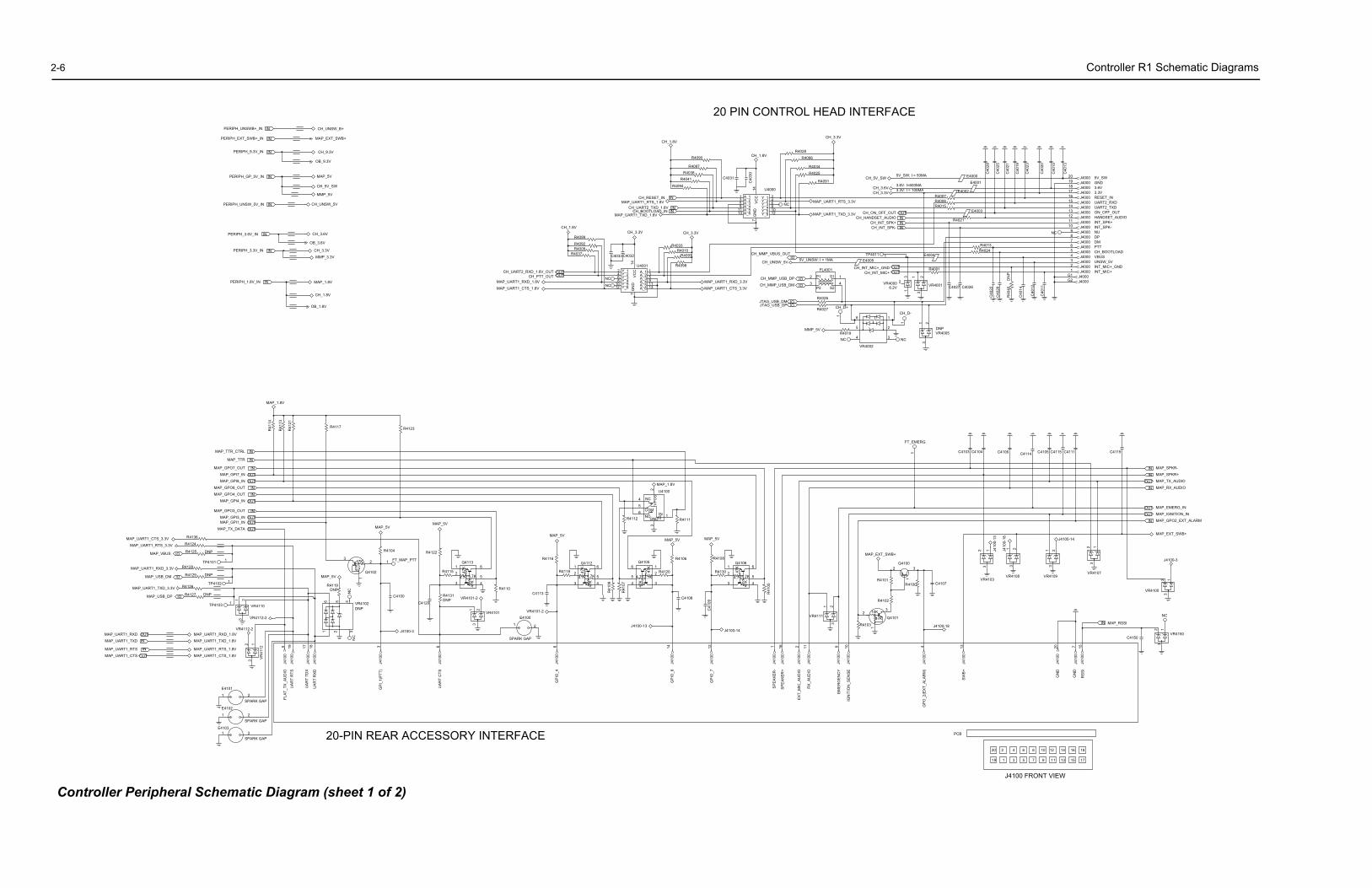
2-6 Controller R1 Schematic Diagrams
1
CH_D+
4
1
5
4
6
R4019NC
CH_D-
1
2
3
1
VR4002
NC
23
1
VR4005DNP
.3V
D INTERFACE
_RTS_3.3V
_TXD_3.3V
CH_INT_SPK+CH_INT_SPK-
CH_ON_OFF_OUTCH_HANDSET_AUDIO IN
OUT
ININ
5V_SW: I = 50MA
3.3V: I = 100MA3.6V: I=600MA
CH_5V_SW
CH_3.6VCH_3.3V
E4000
E4002
E4001
R4021
E4003R4015
R4007R4006
C40
13
C40
15
C40
20
C40
23
C40
21
C40
25
C40
28
C40
19
NC
INT_SPK+INT_SPK-
INT_MIC+_GND
3.3V3.6V
UART2_TXD
NUDPDMPTTCH_BOOTLOAD
HANDSET_AUDIOON_OFF_OUT
UNSW_5V
INT_MIC+
UART2_RXDRESET_IN
GND5V_SW
VBUS
78
J4000J400019
17 J4000
20 J4000
18
15 J4000
16 J4000
14 J4000
11 J4000
12 J4000
13 J4000
10 J4000
J4000
9 J4000
J40006 J40005 J40004 J4000
2 J40001 J4000
G1 J4000
3 J4000
G2 J4000
C40
22
C40
29
DN
PR
4040
C40
11
C40
12
C40
14C4026C4027
R4024R4013
1
6.2V
1
1TP4011E4005
3
2VR4000
23
VR4001
CH_INT_MIC+CH_INT_MIC+_GND OUT
OUT
E4004
R4001
1
FT_EMERG
C4111C4115C4114C4106 C4105C4104C4103 C4119
MAP_RX_AUDIO
MAP_EMERG_IN
MAP_EXT_SWB+
MAP_TX_AUDIO
MAP_SPKR+
MAP_SPKR-
MAP_IGNITION_IN
MAP_GPO2_EXT_ALARM
IN
IN
OUT
IN
OUT
OUT
IN
J4100-3
2 13
VR4100
NC
VR4150
2 13
C4150
MAP_RSSIIN
20 1513109 74
GN
D
RS
SI
GN
D
GP
O_2
(EX
T_A
LAR
M)
SW
B+
J410
0
J410
0
J410
0
J410
0
J410
0
J410
0
J410
0
EM
ER
GE
NC
Y
IGN
ITIO
N_S
EN
SE
10K
47K
1
R4103
R4102
32
Q4101
C4107R4100
2 3
1
Q4100
R4101
J4100-18
MAP_EXT_SWB+
1J410
0-18
22 1 J410
0-13 J4100-14
33
2 13
3
21
VR4109VR4108VR4107
VR4103
PCB
20 2
91 1
4
3
J4100 FRONT VIEW
6
5
8
7
10 12
9 11
14
13
16
15
18
17
Cont
PERIPH_1.8V_IN
PERIPH_3.3V_IN
PERIPH_3.6V_IN
PERIPH_UNSW_5V_IN
PERIPH_GP_5V_IN
PERIPH_9.3V_IN
PERIPH_UNSWB+_IN
PERIPH_EXT_SWB+_IN
IN
IN
IN
IN
IN
IN
IN
IN
MAP_EXT_SWB+
CH_UNSW_B+
MMP_5V
CH_5V_SW
MAP_5V
CH_9.3V
OB_9.3V
CH_UNSW_5V
MMP_3.3V
CH_3.3V
OB_3.6V
CH_3.6V
OB_1.8V
CH_1.8V
MAP_1.8VMAP_UART1_CTS_1.8V
MAP_UART1_RXD_1.8VCH_PTT_OUT
CH_UART2_RXD_1.8V_OUTOUTOUT Y_1
Y_2Y_3Y_4Y_5Y_6
VC
C A_1A_2A_3
GN
D
A_6
A_4A_5
NC
NC
1
1210
8642
147
1311953
U4001
R4099
R4092R4008
R4037 C4033 C4032
CH_3.3VCH_1.8V
R4098
R4093
R4033R4010
CH_3.3V
MAP_UART1_CTS_3.3V
MAP_UART1_RXD_3.3V
5V_UNSW: I = 1MA
JTAG_USB_DPJTAG_USB_DM
CH_MMP_VBUS_OUT
CH_UNSW_5V
CH_MMP_USB_DM
CH_MMP_USB_DP
IO
IO
IO
IOIO
P1
P2
S1
S2
R4026
R4027
3
2
FL4001
MMP_5V
R4028
R4096
R4025
R4091
R4034
CH_1.8V
CH_3
Y_1Y_2Y_3Y_4Y_5Y_6
VC
CA_1A_2A_3
GN
D
A_6
A_4A_5
NC
C40
30
C4031
12108642
147
13119531
U4000
R4041
R4097
R4094
R4038
R4090
CH_1.8V
CH_RESET_INMAP_UART1_RTS_1.8V
MAP_UART1_TXD_1.8VCH_BOOTLOAD_IN
CH_UART2_TXD_1.8V ININ
IN
20 PIN CONTROL HEA
MAP_UART1
MAP_UART1
319 1817 1614 12 11865 21
GP
I_1(
PTT
)
UA
RT
RX
D
UA
RT
TDX
FLA
T_TX
_AU
DIO
UA
RT
CTS
20-PIN REAR ACCESSORY INTERFACE
GP
IO_4
SP
EA
KE
R-
GP
IO_7
SP
EA
KE
R+
EX
T_M
IC_A
UD
IO
RX
_AU
DIO
GP
IO_8
J410
0
J410
0
J410
0
J410
0
J410
0
J410
0
J410
0
J410
0
J410
0
J410
0
J410
0
J410
0
J410
0
UA
RT
RTS
R41
14
MAP_1.8V
R4123R4117
R41
21
R41
13
MAP_TX_DATA
MAP_GPI1_INMAP_GPI3_IN
MAP_GPO3_OUT
MAP_GPO7_OUT
MAP_TTR_CTRL
MAP_TTR
MAP_GPI7_IN
MAP_GPI8_IN
MAP_GPO4_OUT
MAP_GPI4_IN
MAP_GPO8_OUT
IN
IN
IN
OUT
OUT
IN
IN
OUT
OUT
OUT
IN
OUT
TP4103
VR4112-23
DNPR4127
DNPR4129
DNP
MAP_USB_DM
MAP_UART1_TXD_3.3V
TP4101
R4125
R4124MAP_UART1_CTS_3.3V
MAP_UART1_RTS_3.3V
TP4102
MAP_UART1_RXD_3.3V
R4126
1VR4110
R4128
R4136
1
1
21
MAP_VBUS
MAP_USB_DP
IO
IO
IO
VR4112-2
VR
4112
2
MAP_UART1_RXD_1.8V
3
MAP_UART1_CTS_1.8V
1
MAP_UART1_TXD_1.8V
MAP_UART1_RTS_1.8V
MAP_UART1_CTS
MAP_UART1_RXD
MAP_UART1_TXD
MAP_UART1_RTS
OUT
IN
OUTIN
SPARK GAP
E4101
E4102
E4103
1
1
SPARK GAP
SPARK GAP
1
2
2
2
NC
NC
R4119
6 VR4102DNP
MAP_5V
25 4
31
DNP
47K
47K
C4100
J4100-3
C4120
Q4102
1
R4104
FT_MAP_PTT32
1
MAP_5V
4.7K
47K
47K
4.7KR4115
DNPR4131
4
1
3
6
52
Q4113
R4110
R4122
213
VR4101
VR4101-2
MAP_5V
E4100
SPARK GAP
VR4101-2
21
4.7K
47K
47K
4.7K 4.7K
47K
47K
4.7K4
1
3
6
52
Q4105
4
1
3
6
52
Q4112
R4120R4118
R41
09
R41
07
R4106R4116
C4108C4113
MAP_5V
J4100-13
MAP_5V
GND
VP
OS
NO
COM
NC
IN
5
R4112 R4111
2
6
4
1
3
U4100
MAP_1.8V
1
3
2R4130
R4108
C41
09
J4100-14
MAP_5V
4.7K
47K
47K
4.7K4
6
5
Q4106
R41
05
21
3
VR4111
roller Peripheral Schematic Diagram (sheet 1 of 2)
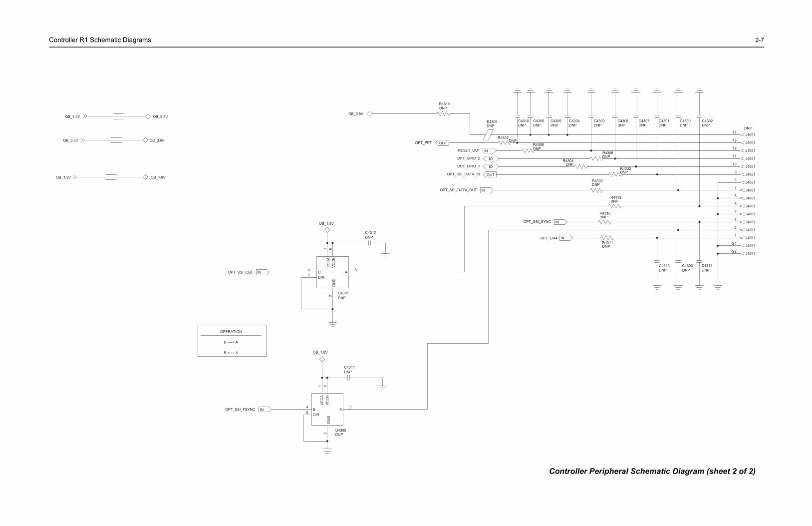
C 2-7
R4306DNP
DNP
R4307
0 C4305DNPDNP DNPDNP DNPDNPDNPDNPDNPDNP
C4302C4300C4301C4307C4308C4309C4304C4306C4310
DNP
DNP
R4312DNP
R4304
DNP
OPT_ENA
OPT_SSI_SYNC
R4303
DNPR4302
DNP
DNP
R4305
R4310
R4311IN
IN
DNPC4313 C4303 C4314
DNPDNP
4
J4001
J4001
J4001
J4001
10J4001
J4001
11
9
8
13J4001
DNP
J4001
J4001
J4001
J4001
14
12
J4001
7
3 J4001
6
5
J4001
G1
1 J4001
2 J4001
G2
Controller Peripheral Schematic Diagram (sheet 2 of 2)
ontroller R1 Schematic Diagrams
OB_3.6V
OB_9.3V
OB_1.8VOB_1.8V
OB_3.6V
OB_9.3V
RESET_OUT
OPT_SSI_DATA_IN
OPT_SSI_DATA_OUT
DNP
DNP
R4314
E430
OPT_PPT
OPT_GPIO_2
OPT_GPIO_1
IN
IO
IO
OUT
OUT
IN
OB_3.6V
BDIR
VC
CA
VC
CB
GN
D
A
DNP
3
DNP
1
OPT_SSI_CLK
U4301
C4312
62
54
OB_1.8V
IN
B ----> A
B <---- A
OPERATION
BDIR
VC
CA
VC
CB
GN
D
A
DNPU4300
DNP
OB_1.8V
3
1
C4311
62
54OPT_SSI_FSYNC IN
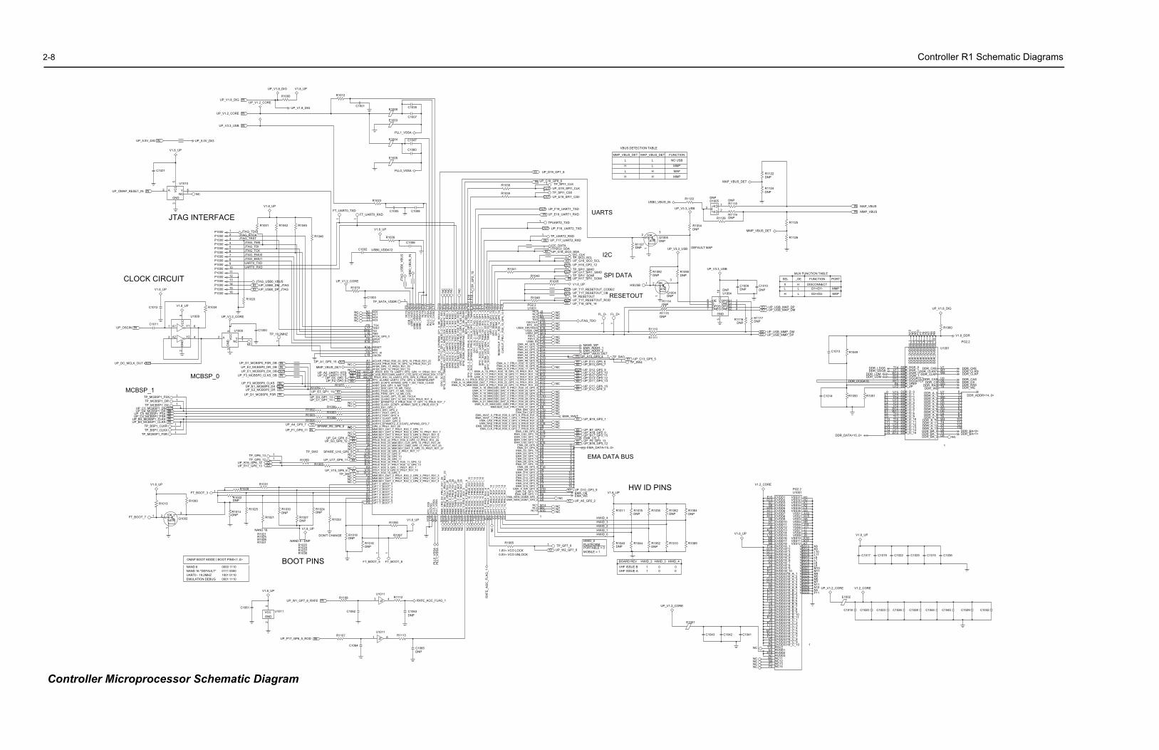
2-8 Controller R1 Schematic Diagrams
DDR_DATA<15..0>
C1013
DDR_DQGATEDDR_UDM
DDR_UDQSDDR_LDQS
C1014 R1050 R1051
R1049
DDR_LDM
PG2.2
NC
DD
R_D
VD
D18
_10
DD
R_D
VD
D18
_9D
DR
_DV
DD
18_8
DD
R_D
VD
D18
_6D
DR
_DV
DD
18_7
DDR_CKEDDR_CLKN*DDR_CLKP
DDR_CASDDR_CS
DDR_RASDDR_WEDDR_A_0DDR_A_1DDR_A_2
DDR_A_4DDR_A_3
DDR_A_5DDR_A_6DDR_A_7
DDR_A_9DDR_A_8
DDR_A_10DDR_A_11DDR_A_12
DDR_BA_1DDR_BA_0DDR_A_13
DDR_BA_2
DD
R_D
VD
D18
_5D
DR
_DV
DD
18_4
DD
R_D
VD
D18
_3D
DR
_DV
DD
18_2
DD
R_D
VD
D18
_1
DDR_DQS_0DDR_DQS_1DDR_DQM_0DDR_DQM_1DDR_DQGATE1
DDR_VREFDDR_DQGATE0
DDR_ZP
DDR_D_0DDR_D_1DDR_D_2DDR_D_3DDR_D_4DDR_D_5DDR_D_6DDR_D_7
DDR_D_9DDR_D_8
DDR_D_10
DDR_D_12DDR_D_11
DDR_D_13DDR_D_14DDR_D_15
DDR_ADDR<14..0>
DDR_BA<0>DDR_BA<1>
DDR_WEDDR_RAS
DDR_CAS
DDR_CLKP
DDR_CKE
0
15
13
10
2
14
11
987
5
3
1
12
910
67
43
12
6
0
12
5
8
4
11
DDR_CS
13
1
U7
W6V6U5V5W5U6U4T6W4T4V4T5V8T9U8
U9
V7W7W8
V9
U15U14V14U13V13V12W12W11T13T11T10T12U10V10U11W10
R11R12
W13R10
T14V11
N10
N6
N9
P10
P7
P8
P9
R7
R8
R9
W9R6T8U12
U1001
V1.8_DDR
R1060
DDR_CLKN
T7
UP_V1.8_DIG
H
LX
SEL _OE
L
LH
MUX FUNCTION TABLE
FUNCTION
D2+/D2-
D1+/D1-DISCONNECT
MMP
PORT
MAP
MMP_VBUS_DET
R1125
R1126
MAP_VBUS_DET
R1124
R1122
DNP
DNP
MAP
3
D10051 R1118
DNP
2R1119
R1128 DNP
DNP
MAP_VBUS
MMP_VBUS
IN
IN
R1116 R1117
UP_USB_MMP_DP
UP_USB_MAP_DP
UP_USB_MMP_DM
DNPDNP
UP_USB_MAP_DMIOIO
IOIO
GND
VC
C
DNEG1DPOS2
DPOS1
DPOSSOE
C1010
U1004DNP
7
28
1
5
69
10
C1009
34
DNP DNP
UP_V3.3_USB
DNEG2DNEG
V1.8_UP
PG2.2
VSS13VSS14VSS15VSS16VSS17VSS18VSS19VSS20
VSS23
VSS21VSS22
VSS24VSS25VSS26VSS27VSS28
VSS30VSS29
V1.2_CORE
U1001
G13G7G8
H10H11H12H13
H6H7
J12J6
K12K6
L12M8M9N8
F14G10G11G12
G6J13K5L6
P13R13F15
F5G14G15
G5H5
E14F10F11F12F13
F6F7F8G9
J14K15
J5K13L13
L4M13N13P12
P5P6R4
M2N4P1P2
T19E5
H14N7
A19H15H8H9J10J11J7J8J9K10K11K7
H1H2K1K2L3M1
E15 VSS31
VSS33VSS32
VSS34VSS35VSS36
VSS2VSS1
VSS3VSS4VSS5
VSS7VSS6
VSS8VSS9
VSS10
VSS12VSS11
CVDD1CVDD2CVDD3CVDD4CVDD5CVDD6
CVDD8CVDD7
CVDD9
CVDD11CVDD10
CVDD12CVDD13CVDD14CVDD15CVDD16
CVDD18CVDD17
DVDD18_1DVDD18_2DVDD18_3DVDD18_4DVDD18_5DVDD18_6
DVDD18_8DVDD18_7
DVDD3318_A_1DVDD18_10DVDD18_9
DVDD3318_A_3DVDD3318_A_2
DVDD3318_A_6
DVDD3318_A_4DVDD3318_A_5
DVDD3318_B_1DVDD3318_B_2DVDD3318_B_3
DVDD3318_B_5DVDD3318_B_4
DVDD3318_B_7DVDD3318_B_6
DVDD3318_B_8DVDD3318_B_9DVDD3318_B_10
DVDD3318_C_1DVDD3318_B_11
DVDD3318_C_2
DVDD3318_C_4DVDD3318_C_3
DVDD3318_C_6DVDD3318_C_7
DVDD3318_C_5
DVDD3318_C_8DVDD3318_C_9DVDD3318_C_10RSV2RVDD1
RVDD3RVDD2
NC11NC12NC13NC14
UP_V1.2_CORE
1
K8K9L10L11L5L7L8L9M10M11M4M5M6M7N11N12N5P11
NC
NCNCNCNC
C1043 C1042 C1041
V1.2_CORE
E1002
C1018 C1020 C1023 C1026 C1028 C1044 C1045 C1029 C1032
V1.8_UP
C1017 C1019 C1022 C1025 C1015 C1036
Cont
UP_C16_GP8_6
UP_D19_GP1_8
TP_SPI1_CLK1IN
IO
UARTS
UP_G19_SPI1_CLK
UP_F19_UART1_TXD
UP_G18_I2C0_SDA
I2C_DATA
UP_F16_UART2_TXD
UP_E18_UART1_RXD
UP_E19_SPI1_CS0
UP_F17_UART2_RXD
TPI2C0_SDA1
TP_SPI1_CS01
TP_UART2_RXD1
TPUART2_TXD
IN
OUT
OUT
IN
OUT
OUT
IO
UP_T17_RESETOUT_OB
UP_H17_SPI1_SOMI
UP_T17_RESETOUT_CODEC
UP_T17_RESETOUT_ROD
V1.8_UP
I2C_CLK
UP_G16_I2C0_SCLUP_H16_GP2_12
UP_G17_SPI1_SIMO
UP_T18_GP6_14
R1041
R1039
R1038
R1043
R1005
TP_RESETOUT1
TP_SPI1_SOMI1
TP_SPI1_SIMO1
TP_I2C0_SCL1
1
OUT
OUT
IN
IO
OUT
OUT
OUTIO
R1048
I2C
SPI DATA
RESETOUT
NC
NCNC
NC
NC
NCNC
NCNC
JTAG_TDO
FL_D-
1
FL_D+
1
HSUSB
DEFAULT
10K
47K
USB0_VBUS_IN
UP_V3.3_USB
UP_V3.3_USB
23
1
R1054
R1120
Q1005DNP
DNP
DNPR1127
MMP
FUNCTION
MMP
H
L
H H
MAP
L
MMP_VBUS_DET
L NO USB
H
L
MAP_VBUS_DET
VBUS DETECTION TABLE
10K
47K
DNPQ1004
23
1
1
R1092DNP DNP
R1090
R1115
R1114
R1110
R1111
DNP
DNP
NAND_WP
UP_A14_GP5_4
EMA_ADDR_2MAP_VBUS_DET
EMA_ADDR_1
UP_C13_GP5_5TP_SW41
TP_SW31INIO
UP_E13_GP5_6
UP_C12_GP5_10
UP_E12_GP4_0UP_C11_GP5_15
UP_D11_GP5_13UP_D13_GP5_12
UP_B13_GP5_7
UP_D12_GP5_9
UP_B12_GP5_11
UP_B19_GP2_1IO
EMA DATA BUS
UP_B17_GP3_15UP_A18_GP2_0UP_B7_GP2_7
EMA_DATA<15..0>
UP_F9_GP3_13UP_B16_GP3_12
EMA_CS_3
IOIOIO
IOIO
15
2
5
0
6
1112
10
1413
1
8
3
7
9
4
UP_A5_GP2_2
EMA_OEUP_D10_GP3_9
EMA_WEV1.8_UP
IO
IO
NCNCNC
NC
UP_V1.2_CORE
E1001
0 0
BOARD REV
VHF ISSUE BUHF ISSUE A
HWID_4
1001
HWID_3HWID_2
R1040 R1044 R1069DNP DNP
R1052 R1010
HW ID PINS
DNP DNPDNPR1011 R1035 R1062 R1064R1036
HWID_1HWID_0
HWID_2HWID_3HWID_4
PLATFORMPORTABLE = 0MOBILE = 1
HWID_0
UP_W2_GP7_9TP_GP7_91
IO
VCCGND
V1.8_UP
C1061
UP_W1_GP7_8_RXFE
UP_P17_GP6_5_ROD
U1011
25
IN
IN
RXFE_AGC_FLAG_1
U1011
1
C1064
U1011
DNP
DNP
R1107
R1108 3 4
6
C1062 C1063
R1113
C1065
R1112
1.8V= VCO LOCK0.0V= VCO UNLOCK
R1065
RX
FE_A
GC
_FLA
G_1
NC
NC
NC
NC
NC
NC
NC
NC
NC
NC
NC
NC
NC
NC
NC
NC
PLL
1_V
SS
AP
LL0_
VS
SA
W18
W17
V17
W16
R14
V16
U18
P17
R15
U19
V19 W
1
V1
W19 W2
V2
U1
H18 W
3
V3
U2
L18
M17
M15
R19
R18 T1
6
V18
FT_BOOT_5 FT_BOOT_6
DNP
R1057
1 1
R1016
V1.8_UPR1056
BOOT PINS
NAND 8 - DNPR1022R1024R1027
DON'T CHANGE
R1030
R1027
R1018DNP
DNP
V1.8_UP
DNP R1033
R1024
R1031R1028R1025R1021
NAND 16
DNPR1030
R1021
R1025
DNP
DNP
FT_BOOT_3 1
R1022
R1028R1031
R101410K
47K
R1013
FT_BOOT_7 1Q1002
23
1
R1093
V1.8_UP
OMAP BOOT MODE BOOT PINS<7..0>
NAND 8 NAND 16 *DEFAULT*UART0 - 19.2MHZEMULATION DEBUG
0000 11100111 00001001 01100001 1110
MCBSP_1
UP_C4_MCBSP1_FSRUP_B3_MCBSP1_CLKXUP_B4_MCBSP1_CLKR
UP_C3_MCBSP1_DXUP_D4_MCBSP1_DR
UP_C5_MCBSP1_FSX
TP_BSP1_CLKR 1
TP_BSP1_CLKX 1
TP_MCBSP1_FSR 1
TP_MCBSP1_FSX 1
TP_MCBSP1_DR 1
TP_MCBSP1_DX 1OUT
ININ
INININ
MCBSP_0
CLOCK CIRCUIT
C1012
UP_DC_MCLK_OUT
UP_OSCIN
V1.8_UP
OUT
IN A1
A2
VC
CG
ND
Y1
Y2 4
V1.8_UP
C10111
3
25
6
R1034
U1009
YNC
VC
C
A
GN
D
NC
UP_V1.2_CORE
U1000
2
3
1
5
4TP_19.2MHZ
1
C1000
UP_F3_MCBSP0_CLKS_OBUP_E1_MCBSP0_DX_OBUP_E2_MCBSP0_DR_OB
UP_D1_MCBSP0_FSR
UP_E1_MCBSP0_DXUP_F3_MCBSP0_CLKS
UP_E2_MCBSP0_DR
UP_D1_MCBSP0_FSR_OB ININ
OUTIN
INOUTIN
IN
NCNC
UP_A2_UART1_RTS
UP_A1_GP0_15
UP_A3_UART1_CTSUP_D5_GP0_9UP_F4_GP0_8
UP_E3_GP1_11
UP_D3_GP1_13
MMP_VBUS_DET
R1076
UP_C1_GP1_14
NC
INOUT
OUT
IOIO
IO
IO
NC
IOR1077
SPARE_U16_GP6_9
SPARE_R5_GP6_0 NC
NCNCNC
NCNC
NCNC
UP_F1_GP8_11
UP_A4_GP0_7
UP_R17_GP6_13UP_R16_GP6_12
TP_GP6_12 1TP_GP6_13 1
1
R1004
R1003
R1002R1007
R1008
R1006
IOIO
IO
IN
IO
NC
IOIO
NCNCNC
NC
UP_U17_GP6_11
UP_G3_GP8_12
UP_V15_GP6_6
UP_G4_GP8_8
R1059R1009
TP_SW1 1
TP_SW2
IO
JTAG INTERFACE
YNC
VC
C
A
GND
UP_5.0V_DIG
P1000
V1.8_UP
UP_5.0V_DIG
UP_OMAP_RESET_IN
P1000 13
P1000 14
P1000 12
16P1000 15
P1000 4P1000 3P1000 2P1000 1
P1000 10P1000 9P1000 8
P1000 5
P1000 6
P1000 7
P1000 11
U1010
2
3
1
5
4
C1021
IN
INNC
UP_V3.3_USB
UP_V1.2_CORE
UP_V1.2_CORE
UP_V1.8_DIG V1.8_UP
UP_V1.8_DIG IN
IN
IN
UP_V1.8_DIG
R1000
E1004
PLL1_VSSA
R1012
C1001E1000
C1007
C1035
E1003
PLL0_VSSA
E1005
C1047
C1060
C1008FT_UART0_TXD
1
FT_UART0_RXD
1
R1023
C1005
C1006
USB0_VDDA12
V1.8_UP
V1.8_UPR1001 R1042 R1045
R1046 R1026
C1002
UP_V1.2_CORE JTA
G_U
SB
0_V
BU
S
US
B0_
VB
US
_IN
NCNCNCNC
C1
TP_SATA_VDDR
K16
C1003
R1019
1
A1B1C2B2
A2A3D5
F3E1E2E3D1D3
D2E4C3D4C5C4B3B4A4
J16
R5
U3T1T2T3R1R2R3P4
J3K3
H3
G4H4F2F1
N1N2L2L1
J17
L19
G3
J4G2
G1T15U16W15U17R16R17
K4V15W14
K14
F4
J19
K17
J15
M16L16
L17
NC
NC
NC
NC
NC
TP_G
P2_
151
PG2.2U1001
A7
B8
D9
D13
B6
1
C14D15B14D14A14C13E13B13A13D12C12B12
D11A12C11E12B11E11C10A11B10A10
C15A15
A9
B7A18B17A17F9B16C9A8
E8B5E7C6D7
D6A6
C7
B15
A16D8
B18B19
B9C8A5
E9
M14M3
J2J1N3
N16
K19
P18P19
H19
J18
M18M19
K18
P16
E10
D10E6
EMA_WAIT
OUT
IOIO
IOIO
IOIOIOIO
NCNCNCNC
NCNC
NC
NC
NCNC
NC
NC
NC
NC
JTAG_USB0_VBUSUP_USB0_DM_JTAGUP_USB0_DP_JTAG
JTAG_EMU1JTAG_EMU0
JTAG_TDI
JTAG_TRSTJTAG_TMS
UART0_RXD
JTAG_TCK
JTAG_RTCKJTAG_TDO
UART0_TXD
R1020
IOIO
P3
P15
G17
F17
F16
T18
P14
L15
N15
T17
L14
D19
C17
D17
E16
D16
E17
D18
C19
C18
C16
G19
H16
G18
G16
E19
F18
F19
E18
H17
N19
N17
N14
N18
M12
NC3NC4NC5TDO
RTC_XOOSCOUT
USB0_DRVVBUSUSB0_DMUSB0_DP
RSV3_2RSV3_1
EMA_A0_GP5_0USB0_ID
EMA_A1_GP5_1
EMA_A3_GP5_3EMA_A2_GP5_2
EMA_A4_GP5_4EMA_A5_GP5_5EMA_A6_GP5_6
EMA_A_8_PRU1_R30_16_GP5_8EMA_A_7_PRU1_R30_15_GP5_7
EMA_A_9_PRU1_R30_17_GP5_9EMA_A_10_PRU1_R30_18_GP5_10_PRU1_R31_18EMA_A_11_PRU1_R30_19_GP5_11_PRU1_R31_19
EMA_A_13_PRU0_R30_21_PRU1_R30_21_GP5_13_PRU1_R31_21EMA_A_12_PRU1_R30_20_GP5_12_PRU1_R31_20
EMA_A_14_MMCSD0_DAT_7_PRU1_R30_22_GP5_14_PRU1_R31_22
EMA_A_16_MMCSD0_DAT_5_PRU1_R30_24_GP4_0EMA_A_15_MMCSD0_DAT_6_PRU1_R30_23_GP5_15_PRU1_R31_23
EMA_A_18_MMCSD0_DAT_3_PRU1_R30_26_GP4_2EMA_A_17_MMCSD0_DAT_4_PRU1_R30_25_GP4_1
EMA_A_19_MMCSD0_DAT_2_PRU1_R30_27_GP4_3EMA_A_20_MMCSD0_DAT_0_PRU1_R30_28_GP4_4EMA_A_21_MMCSD0_DAT_0_PRU1_R30_29_GP4_5
MMCSD0_CLK_PRU1_R30_31_GP4_7EMA_A_22_MMCSD0_CMD_PRU1_R30_30_GP4_6
CLK
OU
T_P
RU
1_R
30_1
3_G
P6_
14R
ES
ETO
UT_
PR
U1_
R30
_14_
GP
6_15
SP
I1_S
OM
I_G
P2_
11S
PI1
_SIM
O_G
P2_
10S
PI1
_EN
A_G
P2_
12S
PI1
_SC
S7_
I2C
0_S
CL_
TM64
P2_
OU
T12_
GP
1_5
SP
I1_S
CS
5_U
AR
T2_R
XD
_I2C
1_S
CL_
GP
1_3
SP
I1_S
CS
6_I2
C0_
SD
A_T
M64
P3_
OU
T12_
GP
1_4
SP
I1_S
CS
4_U
AR
T2_T
XD
_I2C
1_S
DA
_GP
1_2
SP
I1_S
CS
_3_U
AR
T1_R
XD
_GP
1_1
SP
I1_S
CS
_2_U
AR
T1_T
XD
_GP
1_0
SP
I1_S
CS
_0_E
PW
M1B
_PR
U0_
R30
_7_G
P2_
14_T
M64
P3_
IN12
SP
I1_S
CS
_1_E
PW
M1A
_PR
U0_
R30
_8_G
P2_
15_T
M64
P2_
IN12
SP
I1_C
LK_G
P2_
13S
PI0
_SO
MI_
EP
WM
SY
NC
I_G
P8_
6_M
II_R
XE
RS
PI0
_SIM
O_E
PW
MS
YN
CO
_GP
8_5_
MII_
CR
S
SP
I0_S
CS
_5_U
AR
T0_R
XD
_GP
8_4_
MII_
RX
D_3
SP
I0_E
NA
_EP
WM
0B_P
RU
0_R
30_6
_MII_
RX
DV
EMA_BA0_GP2_8EMA_BA1_GP2_9
EMA_WAIT_0_PRU0_R30_0_GP3_8_PRU0_R31_0EMA_WAIT_1_PRU0_R30_1_GP2_1_PRU0_R31_1
EMA_CAS_PRU0_R30_2_GP2_4_PRU0_R31_2EMA_RAS_PRU0_R30_3_GP2_5_PRU0_R31_3
EMA_CLK_PRU0_R30_5_GP2_7_PRU0_R31_5EMA_SDCKE_PRU0_R30_4_GP2_6_PRU0_R31_4
EMA_CS0_GP2_0EMA_CS2_GP3_15EMA_CS3_GP3_14
EMA_CS5_GP3_12EMA_CS4_GP3_13
EMA_D0_GP4_8
EMA_D2_GP4_10EMA_D1_GP4_9
EMA_D4_GP4_12EMA_D3_GP4_11
EMA_D5_GP4_13
EMA_D7_GP4_15EMA_D6_GP4_14
EMA_D8_GP3_0EMA_D9_GP3_1
EMA_D10_GP3_2
EMA_D12_GP3_4EMA_D11_GP3_3
EMA_D13_GP3_5EMA_D14_GP3_6EMA_D15_GP3_7
EMA_OE_GP3_10EMA_A_RW_GP3_9
EMA_WE_GP3_11
EMA_WEN_DQM1_GP2_2EMA_WEN_DQM0_GP2_3
NC1
NC10NC2
GP
7_15
_PR
U1_
R31
_15
GP
7_14
_PR
U1_
R31
_14
GP
7_12
_PR
U1_
R31
_12
GP
7_13
_PR
U1_
R31
_13
GP
7_10
_PR
U1_
R31
_10
GP
7_11
_PR
U1_
R31
_11
GP
7_9_
PR
U1_
R31
_9
PR
U0_
R30
_15_
PR
U0_
R31
_15
GP
7_8_
PR
U1_
R31
_8
PR
U0_
R30
_14_
PR
U0_
R31
_14
PR
U0_
R30
_13_
PR
U0_
R31
_13
PR
U0_
R30
_12_
PR
U0_
R31
_12
PR
U0_
R30
_10_
PR
U0_
R31
_10
PR
U0_
R30
_11_
PR
U0_
R31
_11
GP
6_5_
PR
U1_
R31
_0P
RU
0_R
30_9
_PR
U0_
R31
_9
RM
II_TX
D_1
_PR
U0_
R31
_29
RM
II_TX
D_0
_PR
U0_
R31
_28
RM
II_TX
EN
_PR
U0_
R31
_27
SP
I0_S
CS
_4_U
AR
T0_T
XD
_GP
8_3_
MII_
RX
D_2
SP
I0_S
CS
_3_U
AR
T0_C
TS_G
P8_
2_M
II_R
XD
_1S
PI0
_SC
S_2
_UA
RT0
_RTS
_GP
8_1_
MII_
RX
D_0
SP
I0_S
CS
1_TM
64P
0_O
UT1
2_G
P1_
7_M
DIO
_CLK
_TM
64P
0_IN
12S
PI0
_SC
S0_
TM64
P1_
OU
T12_
GP
1_6_
MD
IO_D
_TM
64P
1_IN
12S
PI0
_CLK
_EP
WM
0A_G
P1_
8_M
II_R
XC
LK
RTC
_CV
DD
PLL
1_V
DD
AP
LL0_
VD
DA
NC
17N
C16
US
B0_
VD
DA
33U
SB
0_V
DD
A18
US
B0_
VD
DA
12U
SB
0_V
BU
SU
SB
_CV
DD
NC
15NC6
NC8NC7
NC9
TCKTRSTTDITMSRTCK_GP8_0EMU0EMU1
NMIRESET
RTC_XIOSCIN
ACLKR_PRU0_R30_20_GP0_15_PRU0_R31_22ACLKX_PRU0_R30_19_GP0_14_PRU0_R31_21AFSR_GP0_13_PRU0_R31_20
AHCLKR_PRU0_R30_18_UART1_RTS_GP0_11_PRU0_R31_18AFSX_GP0_12_PRU0_R31_19
AHCLKX_USB_REFCLKIN_UART1_CTS_GP0_10_PRU0_R31_17
RTC_ALARM_UART2_CTS_GP0_8_NDEEPSLEEPAMUTE_PRU0_R30_16_UART2_RTS_GP0_9_PRU0_R31_16
AXR1_DX0_GP1_9_MII_TXD1AXR2_DR0_GP1_10_MII_TXD2
AXR0_ECAP0_APWM0_GP8_7_MII_TXD0_CLKS0
AXR4_FSR0_GP1_12_MII_COLAXR3_FSX0_GP1_11_MII_TXD3
AXR7_EPWM1TZ_0_PRU0_R30_17_GP1_15_PRU0_R31_7AXR6_CLKR0_GP1_14_MII_TXEN_PRU0_R31_6AXR5_CLKX0_GP1_13_MII_TXCLK
AXR9_DX1_GP0_1AXR8_CLKS1_ECAP1_APWM1_GP0_0_PRU0_R31_8
RM
II_R
XD
_0_P
RU
0_R
31_2
5R
MII_
RX
D_1
_PR
U0_
R31
_26
RM
II_R
XE
R_P
RU
0_R
31_2
4R
MII_
MH
Z_50
_CLK
_PR
U0_
R31
_23
RM
II_C
RS
_DV
_PR
U1_
R31
_29
PLL
1_V
SS
AP
LL0_
VS
SA
RTC
_VS
SO
SC
VS
S
AXR10_DR1_GP0_2AXR11_FSX1_GP0_3AXR12_FSR1_GP0_4AXR13_CLKX1_GP0_5AXR14_CLKR1_GP0_6AXR15_EPWM0TZ_0_ECAP2_APWM2_GP0_7
MMCSD1_DAT_7_PRU1_R30_7_GP8_11GP6_0_PRU1_R31_28
MMCSD1_DAT_5_PRU1_R30_5_GP8_9_PRU1_R31_6MMCSD1_DAT_6_PRU1_R30_6_GP8_10_PRU1_R31_7
MMCSD1_DAT_4_PRU1_R30_4_GP8_8_PRU1_R31_5
PRU0_R30_24_MMCSD1_CLK_GP8_14_PRU1_R31_26PRU0_R30_22_PRU1_R30_8_GP8_12_PRU1_R31_24
PRU0_R30_26_GP6_8_PRU1_R31_17
PRU0_R30_23_MMCSD1_CMD_GP8_13_PRU1_R31_25PRU0_R30_25_MMCSD1_DAT_0_GP8_15_PRU1_R31_27
PRU0_R30_28_GP6_10PRU0_R30_27_GP6_9
PRU0_R30_30_PRU1_R30_11_GP6_12PRU0_R30_31_PRU1_R30_12_GP6_13
PRU0_R30_29_GP6_11
PRU1_R30_0_GP6_1_PRU1_R31_1PRU1_R30_9_GP6_6_PRU1_R31_16PRU1_R30_10_GP6_7MMCSD1_DAT_2_PRU1_R30_2_GP6_3_PRU1_R31_3MMCSD1_DAT_1_PRU1_R30_1_GP6_2_PRU1_R31_2
GP7_0_BOOT_0MMCSD1_DAT_3_PRU1_R30_3_GP6_4_PRU1_R31_4
GP7_1_BOOT_1
GP7_3_BOOT_3GP7_2_BOOT_2
GP7_5_BOOT_5GP7_4_BOOT_4
GP7_6_BOOT_6GP7_7_BOOT_7
roller Microprocessor Schematic Diagram
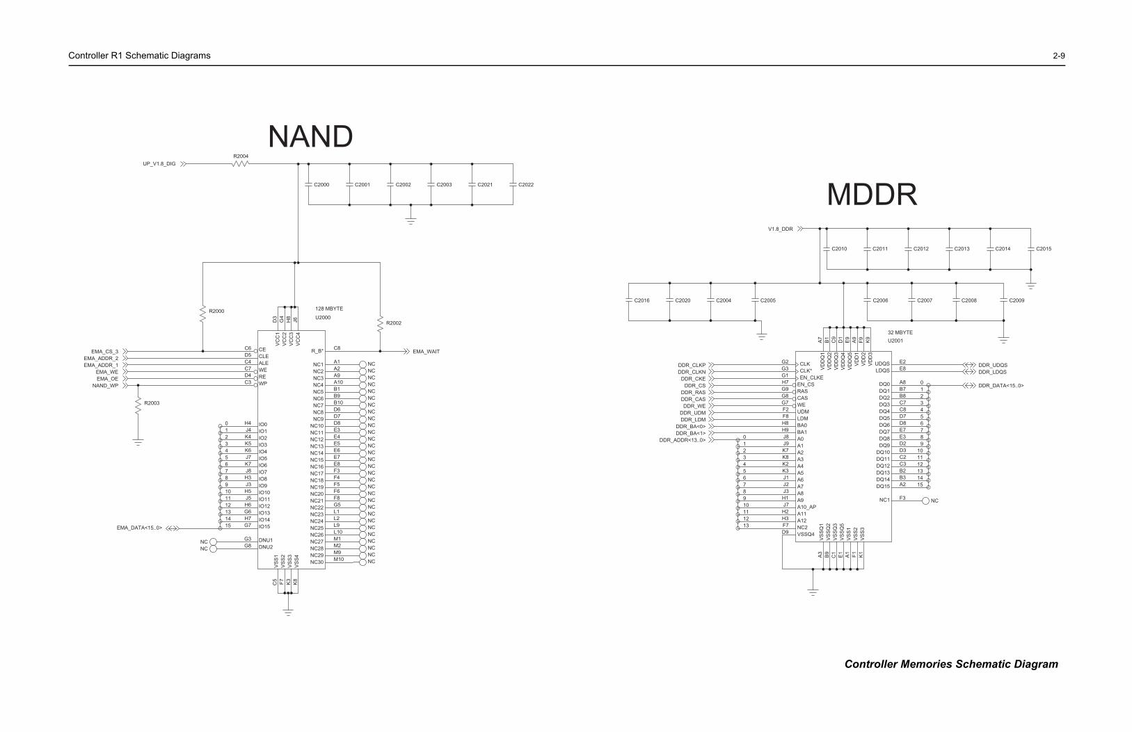
C 2-9
MDDRV1.8_DDR
C2010 C2011 C2012 C2013 C2014 C2015
C2004 C2009C2005 C2006 C2007 C2008
DDR_DATA<15..0>
DDR_LDQSDDR_UDQS
NC
LDQSUDQS
DQ1DQ0
DQ2DQ3
DQ5DQ4
DQ6
DQ8DQ7
VD
D2
VD
D3
DQ9
DQ11DQ10
DQ13DQ12
DQ14DQ15
NC1
VS
S3
VS
S2
VS
S1
VS
SQ
5
VD
DQ
2
WE
A0
CLK*CLK
EN_CLKE
RASEN_CS
CAS
LDMUDM
BA0BA1
A1
A3A2
A4A5A6A7A8A9
VS
SQ
3V
SS
Q2
VS
SQ
1
A10_APA11A12NC2VSSQ4
VD
D1
VD
DQ
5V
DD
Q4
VD
DQ
3
VD
DQ
1
U2001
F3
E9
B8B7
13
15
21
0
11
11109
543
8
6
45
7
1
0
12
7
12
109
2
8
3
6
14
J8J9K7K8K2K3
J2J3H1J7H2H3
H8H9
G8
G2G3
A8
C7C8D7D8E7E3D2D3C2C3B2B3A2
G1H7
F8
E8
F7
G9
F2
E2
A9
F9 K9
A7
B1
C9
D1
A1 F1 K1
A3
B9
C1
D9
E1
G7
J1
13
32 MBYTE
_CLKP
13..0>
R_WE
_CLKNR_CKE
R_RASR_CS
R_CAS
_LDM_UDM
BA<0>BA<1>
Controller Memories Schematic Diagram
ontroller R1 Schematic Diagrams
NANDC2022C2000 C2002C2001 C2003 C2021
UP_V1.8_DIGR2004
128 MBYTE
EMA_WAIT
R2002U2000
R2000
NCNC
1K4
7
15
12
14
1098
65432
0
13
11
C4
C6
G3G8
H4J4
K5K6J7K7J8H3J3H5J5H6G6H7G7
D4C7
C3
D5
EMA_DATA<15..0>
EMA_ADDR_2EMA_ADDR_1
EMA_WEEMA_OE
NAND_WP
EMA_CS_3
R2003
NCNCNCNCNCNCNCNCNCNCNCNCNCNCNCNCNCNCNCNC
NCNCNCNCNCNCNCNCNCNC
NC2NC1
R_B*
VC
C4
VC
C3
NC3NC4NC5NC6NC7
NC10NC9NC8
NC11NC12NC13NC14NC15NC16NC17NC18
NC20NC19
NC21NC22NC23NC24NC25NC26NC27NC28
NC30NC29
VS
S4
VC
C2
VC
C1
CECLEALEWEREWP
DNU2
IO0IO1IO2IO3
IO5IO4
IO7IO6
IO8
IO10IO9
IO12IO11
IO13
VS
S3
VS
S2
VS
S1
IO14IO15
DNU1
A1A2A9A10B1B9B10D6D7D8E3E4E5E6E7E8F3F4F5F6F8G5L1L2L9L10M1M2M9M10
C8
D3
G4
H8
J6
C5 F7 K3
K8
C2016 C2020
DDR
DDR_ADDR<
DD
DDRDD
DDDD
DD
DDRDDR
DDR_DDR_
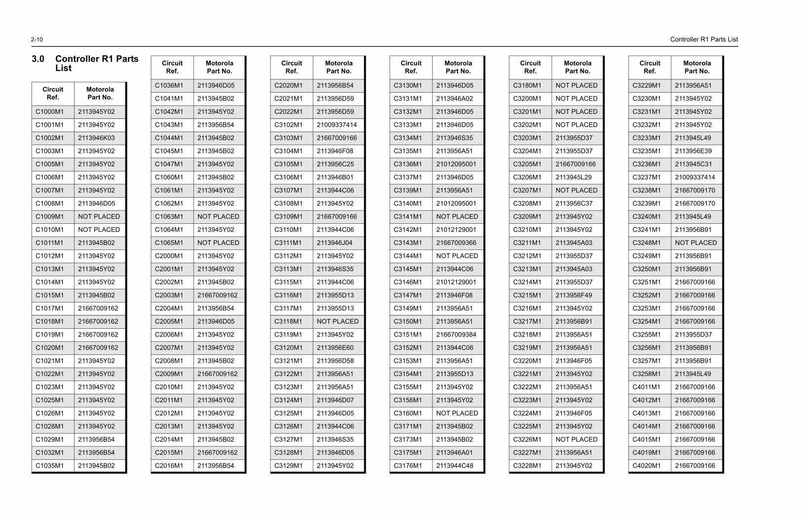
2-10 Controller R1 Parts List
3.0
CirR
C100
C100
C100
C100
C100
C100
C100
C100
C100
C101
C101
C101
C101
C101
C101
C101
C101
C101
C102
C102
C102
C102
C102
C102
C102
C102
C103
C103
C3180M1 NOT PLACED
C3200M1 NOT PLACED
C3201M1 NOT PLACED
C3202M1 NOT PLACED
C3203M1 2113955D37
C3204M1 2113955D37
C3205M1 21667009166
C3206M1 2113945L29
C3207M1 NOT PLACED
C3208M1 2113956C37
C3209M1 2113945Y02
C3210M1 2113945Y02
C3211M1 2113945A03
C3212M1 2113955D37
C3213M1 2113945A03
C3214M1 2113955D37
C3215M1 2113956F49
C3216M1 2113945Y02
C3217M1 2113956B91
C3218M1 2113956A51
C3219M1 2113956A51
C3220M1 2113946F05
C3221M1 2113945Y02
C3222M1 2113956A51
C3223M1 2113945Y02
C3224M1 2113946F05
C3225M1 2113945Y02
C3226M1 NOT PLACED
C3227M1 2113956A51
C3228M1 2113945Y02
Circuit Ref.
MotorolaPart No.
C3229M1 2113956A51
C3230M1 2113945Y02
C3231M1 2113945Y02
C3232M1 2113945Y02
C3233M1 2113945L49
C3235M1 2113956E39
C3236M1 2113945C31
C3237M1 21009337414
C3238M1 21667009170
C3239M1 21667009170
C3240M1 2113945L49
C3241M1 2113956B91
C3248M1 NOT PLACED
C3249M1 2113956B91
C3250M1 2113956B91
C3251M1 21667009166
C3252M1 21667009166
C3253M1 21667009166
C3254M1 21667009166
C3255M1 2113955D37
C3256M1 2113956B91
C3257M1 2113956B91
C3258M1 2113945L49
C4011M1 21667009166
C4012M1 21667009166
C4013M1 21667009166
C4014M1 21667009166
C4015M1 21667009166
C4019M1 21667009166
C4020M1 21667009166
Circuit Ref.
MotorolaPart No.
Controller R1 Parts List
cuit ef.
MotorolaPart No.
0M1 2113945Y02
1M1 2113945Y02
2M1 2113946K03
3M1 2113945Y02
5M1 2113945Y02
6M1 2113945Y02
7M1 2113945Y02
8M1 2113946D05
9M1 NOT PLACED
0M1 NOT PLACED
1M1 2113945B02
2M1 2113945Y02
3M1 2113945Y02
4M1 2113945Y02
5M1 2113945B02
7M1 21667009162
8M1 21667009162
9M1 21667009162
0M1 21667009162
1M1 2113945Y02
2M1 2113945Y02
3M1 2113945Y02
5M1 2113945Y02
6M1 2113945Y02
8M1 2113945Y02
9M1 2113956B54
2M1 2113956B54
5M1 2113945B02
C1036M1 2113946D05
C1041M1 2113945B02
C1042M1 2113945Y02
C1043M1 2113956B54
C1044M1 2113945B02
C1045M1 2113945B02
C1047M1 2113945Y02
C1060M1 2113945B02
C1061M1 2113945Y02
C1062M1 2113945Y02
C1063M1 NOT PLACED
C1064M1 2113945Y02
C1065M1 NOT PLACED
C2000M1 2113945Y02
C2001M1 2113945Y02
C2002M1 2113945B02
C2003M1 21667009162
C2004M1 2113956B54
C2005M1 2113946D05
C2006M1 2113945Y02
C2007M1 2113945Y02
C2008M1 2113945B02
C2009M1 21667009162
C2010M1 2113945Y02
C2011M1 2113945Y02
C2012M1 2113945Y02
C2013M1 2113945Y02
C2014M1 2113945B02
C2015M1 21667009162
C2016M1 2113956B54
Circuit Ref.
MotorolaPart No.
C2020M1 2113956B54
C2021M1 2113956D59
C2022M1 2113956D59
C3102M1 21009337414
C3103M1 21667009166
C3104M1 2113946F08
C3105M1 2113956C25
C3106M1 2113946B01
C3107M1 2113944C06
C3108M1 2113945Y02
C3109M1 21667009166
C3110M1 2113944C06
C3111M1 2113946J04
C3112M1 2113945Y02
C3113M1 2113946S35
C3115M1 2113944C06
C3116M1 2113955D13
C3117M1 2113955D13
C3118M1 NOT PLACED
C3119M1 2113945Y02
C3120M1 2113956E60
C3121M1 2113956D58
C3122M1 2113956A51
C3123M1 2113956A51
C3124M1 2113946D07
C3125M1 2113946D05
C3126M1 2113944C06
C3127M1 2113946S35
C3128M1 2113946D05
C3129M1 2113945Y02
Circuit Ref.
MotorolaPart No.
C3130M1 2113946D05
C3131M1 2113946A02
C3132M1 2113946D05
C3133M1 2113946D05
C3134M1 2113946S35
C3135M1 2113956A51
C3136M1 21012095001
C3137M1 2113946D05
C3139M1 2113956A51
C3140M1 21012095001
C3141M1 NOT PLACED
C3142M1 21012129001
C3143M1 21667009366
C3144M1 NOT PLACED
C3145M1 2113944C06
C3146M1 21012129001
C3147M1 2113946F08
C3149M1 2113956A51
C3150M1 2113956A51
C3151M1 21667009384
C3152M1 2113944C06
C3153M1 2113956A51
C3154M1 2113955D13
C3155M1 2113945Y02
C3156M1 2113945Y02
C3160M1 NOT PLACED
C3171M1 2113945B02
C3173M1 2113945B02
C3175M1 2113946A01
C3176M1 2113944C48
Circuit Ref.
MotorolaPart No.
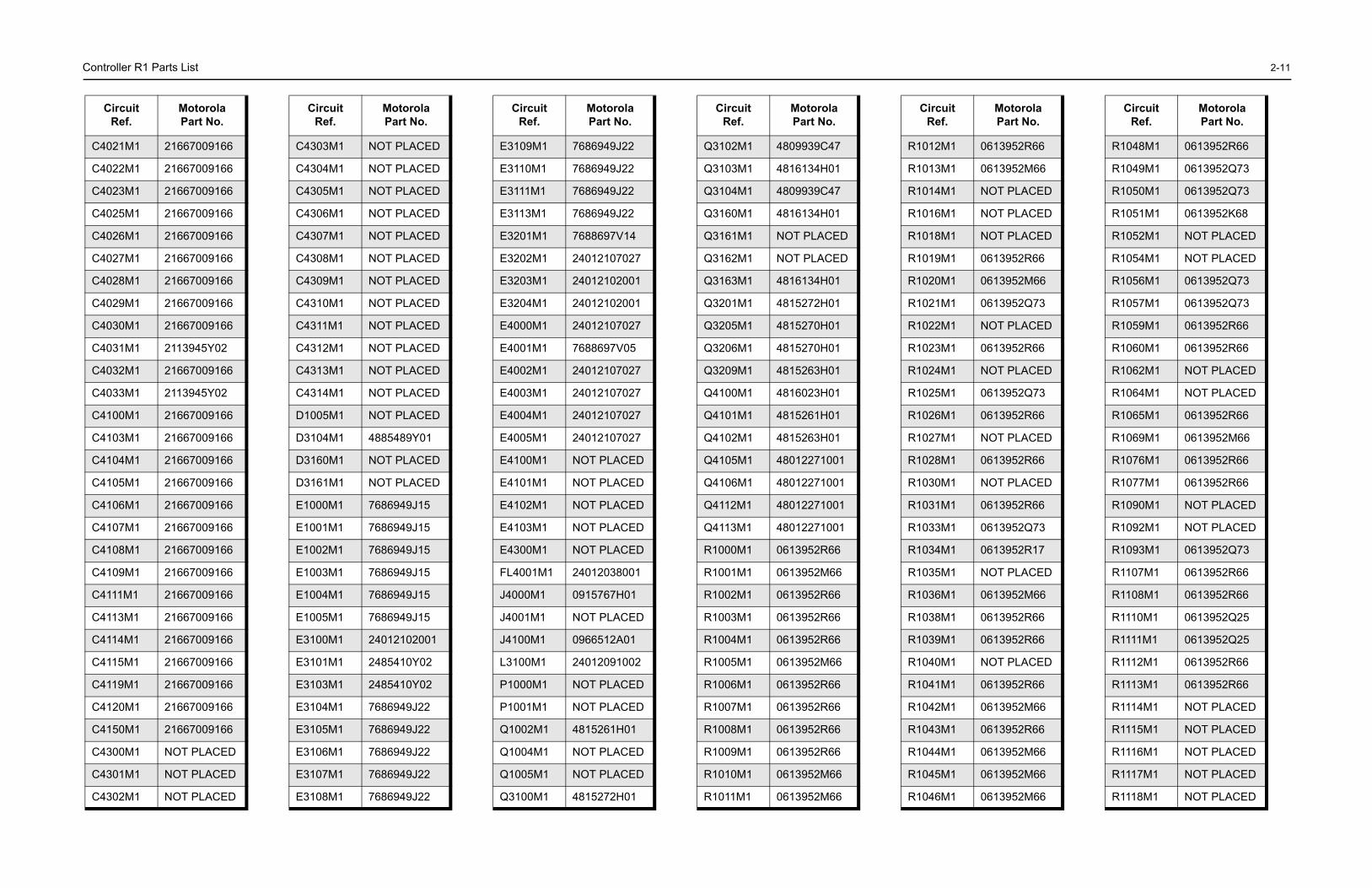
C 2-11
1
1
D
D
1
1
1
1
1
1
1
1
6
6
6
6
6
6
6
R1012M1 0613952R66
R1013M1 0613952M66
R1014M1 NOT PLACED
R1016M1 NOT PLACED
R1018M1 NOT PLACED
R1019M1 0613952R66
R1020M1 0613952M66
R1021M1 0613952Q73
R1022M1 NOT PLACED
R1023M1 0613952R66
R1024M1 NOT PLACED
R1025M1 0613952Q73
R1026M1 0613952R66
R1027M1 NOT PLACED
R1028M1 0613952R66
R1030M1 NOT PLACED
R1031M1 0613952R66
R1033M1 0613952Q73
R1034M1 0613952R17
R1035M1 NOT PLACED
R1036M1 0613952M66
R1038M1 0613952R66
R1039M1 0613952R66
R1040M1 NOT PLACED
R1041M1 0613952R66
R1042M1 0613952M66
R1043M1 0613952R66
R1044M1 0613952M66
R1045M1 0613952M66
R1046M1 0613952M66
Circuit Ref.
MotorolaPart No.
R1048M1 0613952R66
R1049M1 0613952Q73
R1050M1 0613952Q73
R1051M1 0613952K68
R1052M1 NOT PLACED
R1054M1 NOT PLACED
R1056M1 0613952Q73
R1057M1 0613952Q73
R1059M1 0613952R66
R1060M1 0613952R66
R1062M1 NOT PLACED
R1064M1 NOT PLACED
R1065M1 0613952R66
R1069M1 0613952M66
R1076M1 0613952R66
R1077M1 0613952R66
R1090M1 NOT PLACED
R1092M1 NOT PLACED
R1093M1 0613952Q73
R1107M1 0613952R66
R1108M1 0613952R66
R1110M1 0613952Q25
R1111M1 0613952Q25
R1112M1 0613952R66
R1113M1 0613952R66
R1114M1 NOT PLACED
R1115M1 NOT PLACED
R1116M1 NOT PLACED
R1117M1 NOT PLACED
R1118M1 NOT PLACED
Circuit Ref.
MotorolaPart No.
ontroller R1 Parts List
C4021M1 21667009166
C4022M1 21667009166
C4023M1 21667009166
C4025M1 21667009166
C4026M1 21667009166
C4027M1 21667009166
C4028M1 21667009166
C4029M1 21667009166
C4030M1 21667009166
C4031M1 2113945Y02
C4032M1 21667009166
C4033M1 2113945Y02
C4100M1 21667009166
C4103M1 21667009166
C4104M1 21667009166
C4105M1 21667009166
C4106M1 21667009166
C4107M1 21667009166
C4108M1 21667009166
C4109M1 21667009166
C4111M1 21667009166
C4113M1 21667009166
C4114M1 21667009166
C4115M1 21667009166
C4119M1 21667009166
C4120M1 21667009166
C4150M1 21667009166
C4300M1 NOT PLACED
C4301M1 NOT PLACED
C4302M1 NOT PLACED
Circuit Ref.
MotorolaPart No.
C4303M1 NOT PLACED
C4304M1 NOT PLACED
C4305M1 NOT PLACED
C4306M1 NOT PLACED
C4307M1 NOT PLACED
C4308M1 NOT PLACED
C4309M1 NOT PLACED
C4310M1 NOT PLACED
C4311M1 NOT PLACED
C4312M1 NOT PLACED
C4313M1 NOT PLACED
C4314M1 NOT PLACED
D1005M1 NOT PLACED
D3104M1 4885489Y01
D3160M1 NOT PLACED
D3161M1 NOT PLACED
E1000M1 7686949J15
E1001M1 7686949J15
E1002M1 7686949J15
E1003M1 7686949J15
E1004M1 7686949J15
E1005M1 7686949J15
E3100M1 24012102001
E3101M1 2485410Y02
E3103M1 2485410Y02
E3104M1 7686949J22
E3105M1 7686949J22
E3106M1 7686949J22
E3107M1 7686949J22
E3108M1 7686949J22
Circuit Ref.
MotorolaPart No.
E3109M1 7686949J22
E3110M1 7686949J22
E3111M1 7686949J22
E3113M1 7686949J22
E3201M1 7688697V14
E3202M1 24012107027
E3203M1 24012102001
E3204M1 24012102001
E4000M1 24012107027
E4001M1 7688697V05
E4002M1 24012107027
E4003M1 24012107027
E4004M1 24012107027
E4005M1 24012107027
E4100M1 NOT PLACED
E4101M1 NOT PLACED
E4102M1 NOT PLACED
E4103M1 NOT PLACED
E4300M1 NOT PLACED
FL4001M1 24012038001
J4000M1 0915767H01
J4001M1 NOT PLACED
J4100M1 0966512A01
L3100M1 24012091002
P1000M1 NOT PLACED
P1001M1 NOT PLACED
Q1002M1 4815261H01
Q1004M1 NOT PLACED
Q1005M1 NOT PLACED
Q3100M1 4815272H01
Circuit Ref.
MotorolaPart No.
Q3102M1 4809939C47
Q3103M1 4816134H0
Q3104M1 4809939C47
Q3160M1 4816134H0
Q3161M1 NOT PLACE
Q3162M1 NOT PLACE
Q3163M1 4816134H01
Q3201M1 4815272H0
Q3205M1 4815270H01
Q3206M1 4815270H0
Q3209M1 4815263H01
Q4100M1 4816023H0
Q4101M1 4815261H01
Q4102M1 4815263H0
Q4105M1 4801227100
Q4106M1 4801227100
Q4112M1 4801227100
Q4113M1 4801227100
R1000M1 0613952R66
R1001M1 0613952M6
R1002M1 0613952R66
R1003M1 0613952R6
R1004M1 0613952R66
R1005M1 0613952M6
R1006M1 0613952R66
R1007M1 0613952R6
R1008M1 0613952R66
R1009M1 0613952R6
R1010M1 0613952M6
R1011M1 0613952M6
Circuit Ref.
MotorolaPart No.
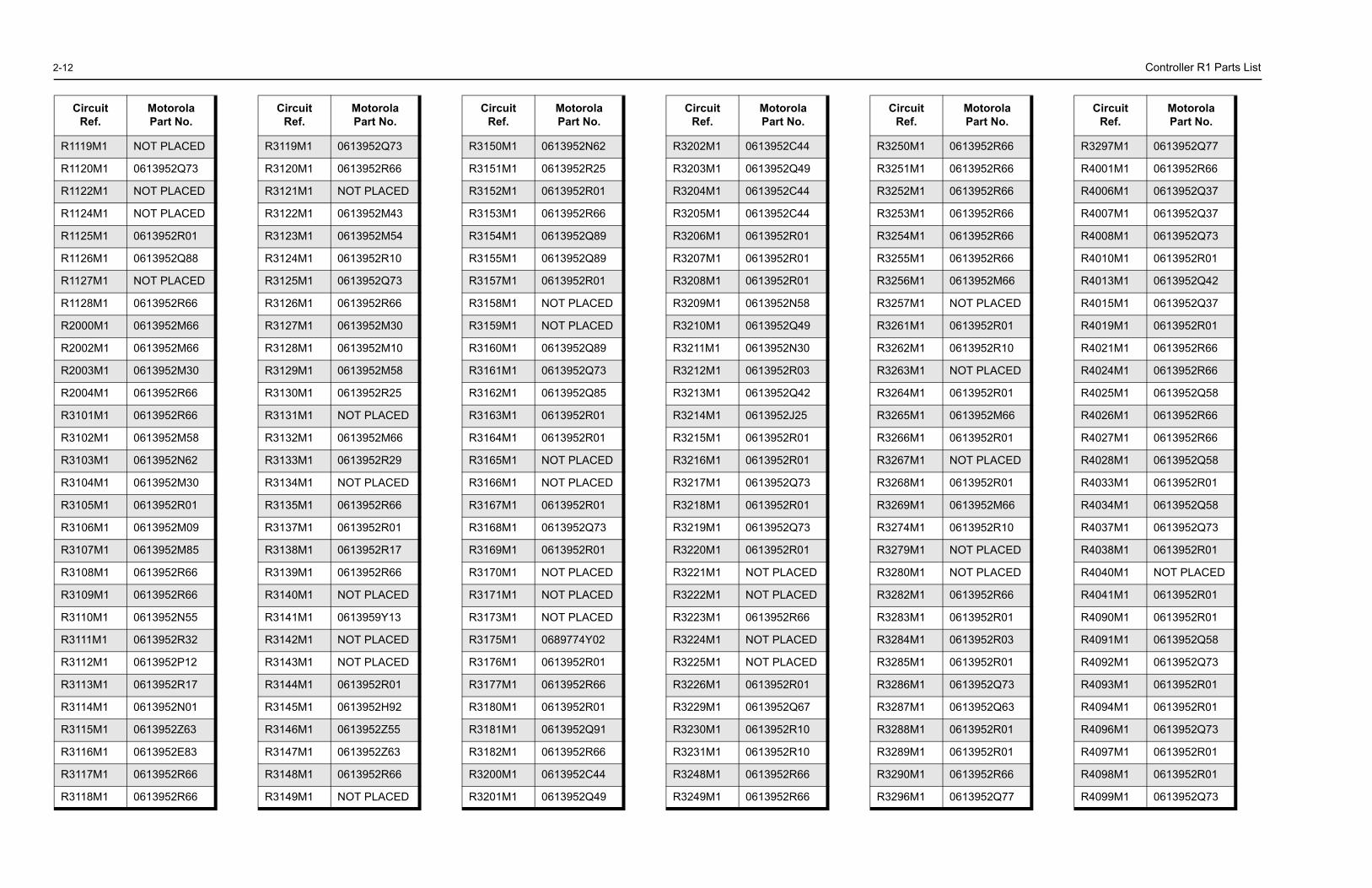
2-12 Controller R1 Parts List
R111
R112
R112
R112
R112
R112
R112
R112
R200
R200
R200
R200
R310
R310
R310
R310
R310
R310
R310
R310
R310
R311
R311
R311
R311
R311
R311
R311
R311
R311
CirR
R3250M1 0613952R66
R3251M1 0613952R66
R3252M1 0613952R66
R3253M1 0613952R66
R3254M1 0613952R66
R3255M1 0613952R66
R3256M1 0613952M66
R3257M1 NOT PLACED
R3261M1 0613952R01
R3262M1 0613952R10
R3263M1 NOT PLACED
R3264M1 0613952R01
R3265M1 0613952M66
R3266M1 0613952R01
R3267M1 NOT PLACED
R3268M1 0613952R01
R3269M1 0613952M66
R3274M1 0613952R10
R3279M1 NOT PLACED
R3280M1 NOT PLACED
R3282M1 0613952R66
R3283M1 0613952R01
R3284M1 0613952R03
R3285M1 0613952R01
R3286M1 0613952Q73
R3287M1 0613952Q63
R3288M1 0613952R01
R3289M1 0613952R01
R3290M1 0613952R66
R3296M1 0613952Q77
Circuit Ref.
MotorolaPart No.
R3297M1 0613952Q77
R4001M1 0613952R66
R4006M1 0613952Q37
R4007M1 0613952Q37
R4008M1 0613952Q73
R4010M1 0613952R01
R4013M1 0613952Q42
R4015M1 0613952Q37
R4019M1 0613952R01
R4021M1 0613952R66
R4024M1 0613952R66
R4025M1 0613952Q58
R4026M1 0613952R66
R4027M1 0613952R66
R4028M1 0613952Q58
R4033M1 0613952R01
R4034M1 0613952Q58
R4037M1 0613952Q73
R4038M1 0613952R01
R4040M1 NOT PLACED
R4041M1 0613952R01
R4090M1 0613952R01
R4091M1 0613952Q58
R4092M1 0613952Q73
R4093M1 0613952R01
R4094M1 0613952R01
R4096M1 0613952Q73
R4097M1 0613952R01
R4098M1 0613952R01
R4099M1 0613952Q73
Circuit Ref.
MotorolaPart No.
9M1 NOT PLACED
0M1 0613952Q73
2M1 NOT PLACED
4M1 NOT PLACED
5M1 0613952R01
6M1 0613952Q88
7M1 NOT PLACED
8M1 0613952R66
0M1 0613952M66
2M1 0613952M66
3M1 0613952M30
4M1 0613952R66
1M1 0613952R66
2M1 0613952M58
3M1 0613952N62
4M1 0613952M30
5M1 0613952R01
6M1 0613952M09
7M1 0613952M85
8M1 0613952R66
9M1 0613952R66
0M1 0613952N55
1M1 0613952R32
2M1 0613952P12
3M1 0613952R17
4M1 0613952N01
5M1 0613952Z63
6M1 0613952E83
7M1 0613952R66
8M1 0613952R66
cuit ef.
MotorolaPart No.
R3119M1 0613952Q73
R3120M1 0613952R66
R3121M1 NOT PLACED
R3122M1 0613952M43
R3123M1 0613952M54
R3124M1 0613952R10
R3125M1 0613952Q73
R3126M1 0613952R66
R3127M1 0613952M30
R3128M1 0613952M10
R3129M1 0613952M58
R3130M1 0613952R25
R3131M1 NOT PLACED
R3132M1 0613952M66
R3133M1 0613952R29
R3134M1 NOT PLACED
R3135M1 0613952R66
R3137M1 0613952R01
R3138M1 0613952R17
R3139M1 0613952R66
R3140M1 NOT PLACED
R3141M1 0613959Y13
R3142M1 NOT PLACED
R3143M1 NOT PLACED
R3144M1 0613952R01
R3145M1 0613952H92
R3146M1 0613952Z55
R3147M1 0613952Z63
R3148M1 0613952R66
R3149M1 NOT PLACED
Circuit Ref.
MotorolaPart No.
R3150M1 0613952N62
R3151M1 0613952R25
R3152M1 0613952R01
R3153M1 0613952R66
R3154M1 0613952Q89
R3155M1 0613952Q89
R3157M1 0613952R01
R3158M1 NOT PLACED
R3159M1 NOT PLACED
R3160M1 0613952Q89
R3161M1 0613952Q73
R3162M1 0613952Q85
R3163M1 0613952R01
R3164M1 0613952R01
R3165M1 NOT PLACED
R3166M1 NOT PLACED
R3167M1 0613952R01
R3168M1 0613952Q73
R3169M1 0613952R01
R3170M1 NOT PLACED
R3171M1 NOT PLACED
R3173M1 NOT PLACED
R3175M1 0689774Y02
R3176M1 0613952R01
R3177M1 0613952R66
R3180M1 0613952R01
R3181M1 0613952Q91
R3182M1 0613952R66
R3200M1 0613952C44
R3201M1 0613952Q49
Circuit Ref.
MotorolaPart No.
R3202M1 0613952C44
R3203M1 0613952Q49
R3204M1 0613952C44
R3205M1 0613952C44
R3206M1 0613952R01
R3207M1 0613952R01
R3208M1 0613952R01
R3209M1 0613952N58
R3210M1 0613952Q49
R3211M1 0613952N30
R3212M1 0613952R03
R3213M1 0613952Q42
R3214M1 0613952J25
R3215M1 0613952R01
R3216M1 0613952R01
R3217M1 0613952Q73
R3218M1 0613952R01
R3219M1 0613952Q73
R3220M1 0613952R01
R3221M1 NOT PLACED
R3222M1 NOT PLACED
R3223M1 0613952R66
R3224M1 NOT PLACED
R3225M1 NOT PLACED
R3226M1 0613952R01
R3229M1 0613952Q67
R3230M1 0613952R10
R3231M1 0613952R10
R3248M1 0613952R66
R3249M1 0613952R66
Circuit Ref.
MotorolaPart No.
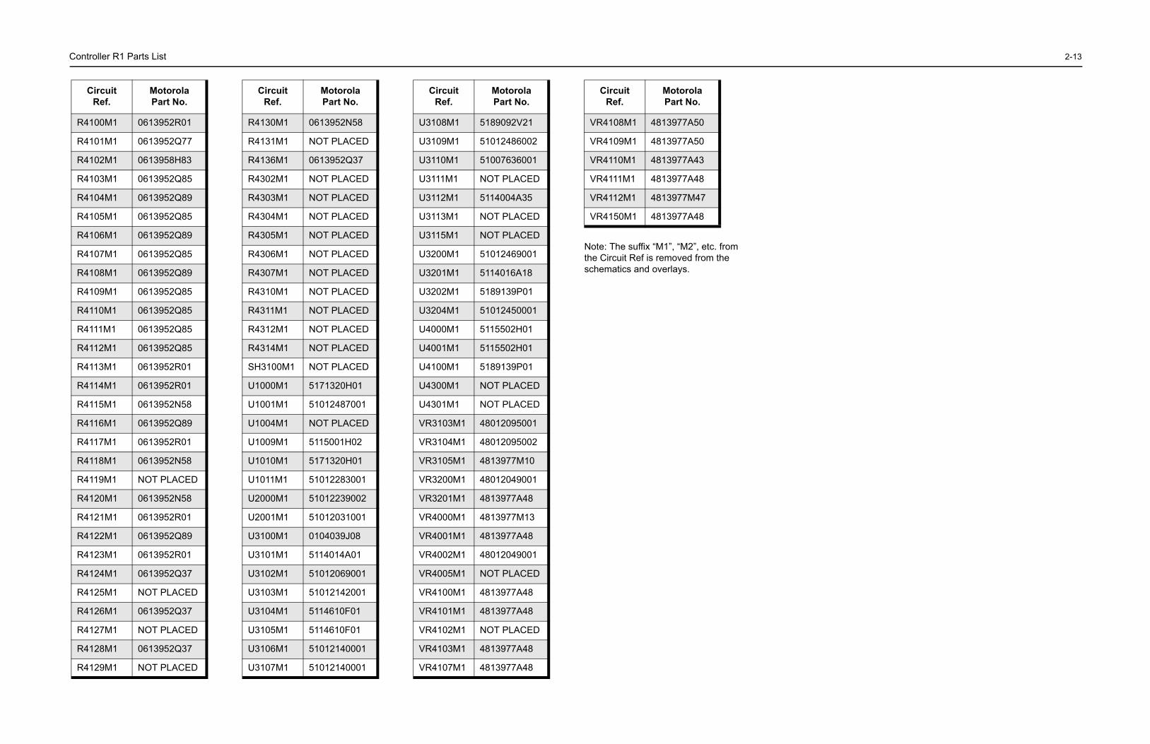
C 2-13
etc. from om the
7
ontroller R1 Parts List
Note: The suffix “M1”, “M2”, the Circuit Ref is removed frschematics and overlays.
R4100M1 0613952R01
R4101M1 0613952Q77
R4102M1 0613958H83
R4103M1 0613952Q85
R4104M1 0613952Q89
R4105M1 0613952Q85
R4106M1 0613952Q89
R4107M1 0613952Q85
R4108M1 0613952Q89
R4109M1 0613952Q85
R4110M1 0613952Q85
R4111M1 0613952Q85
R4112M1 0613952Q85
R4113M1 0613952R01
R4114M1 0613952R01
R4115M1 0613952N58
R4116M1 0613952Q89
R4117M1 0613952R01
R4118M1 0613952N58
R4119M1 NOT PLACED
R4120M1 0613952N58
R4121M1 0613952R01
R4122M1 0613952Q89
R4123M1 0613952R01
R4124M1 0613952Q37
R4125M1 NOT PLACED
R4126M1 0613952Q37
R4127M1 NOT PLACED
R4128M1 0613952Q37
R4129M1 NOT PLACED
Circuit Ref.
MotorolaPart No.
R4130M1 0613952N58
R4131M1 NOT PLACED
R4136M1 0613952Q37
R4302M1 NOT PLACED
R4303M1 NOT PLACED
R4304M1 NOT PLACED
R4305M1 NOT PLACED
R4306M1 NOT PLACED
R4307M1 NOT PLACED
R4310M1 NOT PLACED
R4311M1 NOT PLACED
R4312M1 NOT PLACED
R4314M1 NOT PLACED
SH3100M1 NOT PLACED
U1000M1 5171320H01
U1001M1 51012487001
U1004M1 NOT PLACED
U1009M1 5115001H02
U1010M1 5171320H01
U1011M1 51012283001
U2000M1 51012239002
U2001M1 51012031001
U3100M1 0104039J08
U3101M1 5114014A01
U3102M1 51012069001
U3103M1 51012142001
U3104M1 5114610F01
U3105M1 5114610F01
U3106M1 51012140001
U3107M1 51012140001
Circuit Ref.
MotorolaPart No.
U3108M1 5189092V21
U3109M1 51012486002
U3110M1 51007636001
U3111M1 NOT PLACED
U3112M1 5114004A35
U3113M1 NOT PLACED
U3115M1 NOT PLACED
U3200M1 51012469001
U3201M1 5114016A18
U3202M1 5189139P01
U3204M1 51012450001
U4000M1 5115502H01
U4001M1 5115502H01
U4100M1 5189139P01
U4300M1 NOT PLACED
U4301M1 NOT PLACED
VR3103M1 48012095001
VR3104M1 48012095002
VR3105M1 4813977M10
VR3200M1 48012049001
VR3201M1 4813977A48
VR4000M1 4813977M13
VR4001M1 4813977A48
VR4002M1 48012049001
VR4005M1 NOT PLACED
VR4100M1 4813977A48
VR4101M1 4813977A48
VR4102M1 NOT PLACED
VR4103M1 4813977A48
VR4107M1 4813977A48
Circuit Ref.
MotorolaPart No.
VR4108M1 4813977A50
VR4109M1 4813977A50
VR4110M1 4813977A43
VR4111M1 4813977A48
VR4112M1 4813977M4
VR4150M1 4813977A48
Circuit Ref.
MotorolaPart No.
2-14 Controller R1 Parts List
Notes

XiR™ M3188/XiR™ M3688Mobile Radios
Chapter 5
VHF (136–174 MHz)
1–25W
Service Information
M
Issue: June, 2013

Computer Software CopyrightsThe Motorola products described in this manual may include copyrighted Motorola computer programs stored in semiconductor memories or other media. Laws in the United States and other countries preserve for Motorola certain exclusive rights for copyrighted computer programs, including, but not limited to, the exclusive right to copy or reproduce in any form the copyrighted computer program. Accordingly, any copyrighted Motorola computer programs contained in the Motorola products described in this manual may not be copied, reproduced, modified, reverse-engineered, or distributed in any manner without the express written permission of Motorola. Furthermore, the purchase of Motorola products shall not be deemed to grant either directly or by implication, estoppel, or otherwise, any license under the copyrights, patents or patent applications of Motorola, except for the normal non-exclusive license to use that arises by operation of law in the sale of a product.
i
Chapter 5 – VHF Low Power Service Information
Table of Contents
Section 1 Troubleshooting Charts
1.0 Troubleshooting Flow Chart for Receiver ............................................................ 1-12.0 Troubleshooting Flow Chart for 25W Transmitter................................................ 1-53.0 Troubleshooting Flow Chart for RFIC .................................................................. 1-64.0 Troubleshooting Flow Chart for Rx VCO ........................................................... 1-115.0 Troubleshooting Flow Chart for Tx VCO............................................................ 1-13
Section 2 VHF PCB/Schematics/Parts List
1.0 Allocation of Schematics and Circuit Boards ....................................................... 2-11.1 VHF 25W Circuits........................................................................................... 2-1
2.0 VHF (136–174 MHz) 1–25W PCB/Schematics/Parts List ................................... 2-3VHF (136–174 MHz) 1–25W 84012504002-B Top Side ........................................ 2-3VHF (136–174 MHz) 1–25W 84012504002-B Bottom Side................................... 2-4VHF (136–174 MHz) 1–25W Overall Schematic Diagram ..................................... 2-5VHF (136–174 MHz) 1–25W Receiver Front-End Schematic Diagram.................. 2-6VHF (136–174 MHz) 1–25W Transmitter Power Amplifier Schematic Diagram
(sheet 1 of 2) .................................................................................................. 2-7VHF (136–174 MHz) 1–25W Transmitter Power Amplifier Schematic Diagram
(sheet 2 of 2) .................................................................................................. 2-8VHF (136–174 MHz) 1–25W Transmit/Receive Switch and Harmonic Filter
Schematic Diagram........................................................................................ 2-9VHF (136–174 MHz) 1–25W Power Control Schematic Diagram........................ 2-10VHF (136–174 MHz) 1–25W Transmitter Power Amplifier DC Distribution
Schematic Diagram...................................................................................... 2-11VHF (136–174 MHz) 1–25W RFIC Schematic Diagram ...................................... 2-12VHF (136–174 MHz) 1–25W Transmitter VCO Schematic Diagram.................... 2-13VHF (136–174 MHz) 1–25W Receiver VCO Schematic Diagram........................ 2-14VHF (136–174 MHz) 1–25W VCO Buffer Schematic Diagram ............................ 2-15VHF PCB 84012504002-B Parts List 1–25W....................................................... 2-16

ii
Notes
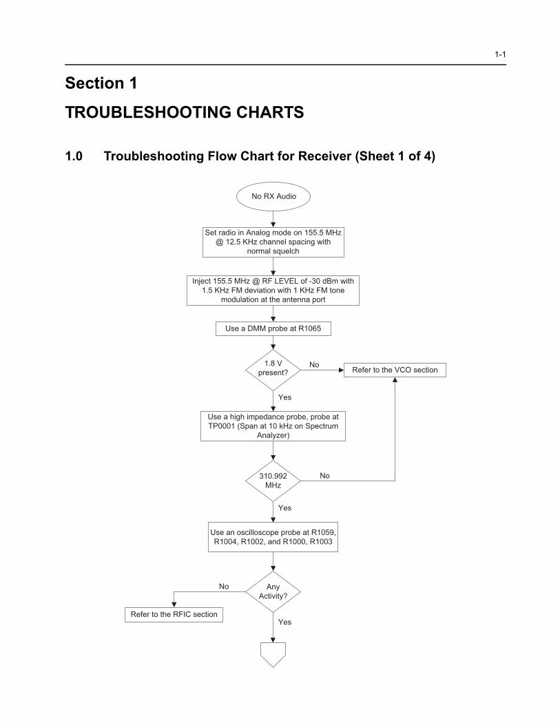
1-1
Section 1
TROUBLESHOOTING CHARTS
1.0 Troubleshooting Flow Chart for Receiver (Sheet 1 of 4)
Set radio in Analog mode on 155.5 MHz @ 12.5 KHz channel spacing with
normal squelch
Inject 155.5 MHz @ RF LEVEL of -30 dBm with 1.5 KHz FM deviation with 1 KHz FM tone
modulation at the antenna port
1.8 V present?
310.992MHz
Any Activity?
Use a high impedance probe, probe at TP0001 (Span at 10 kHz on Spectrum
Analyzer)
Use an oscilloscope probe at R1059, R1004, R1002, and R1000, R1003
Refer to the RFIC section
Yes
Use a DMM probe at R1065
Yes
No
Yes
Refer to the VCO sectionNo
No
No RX Audio
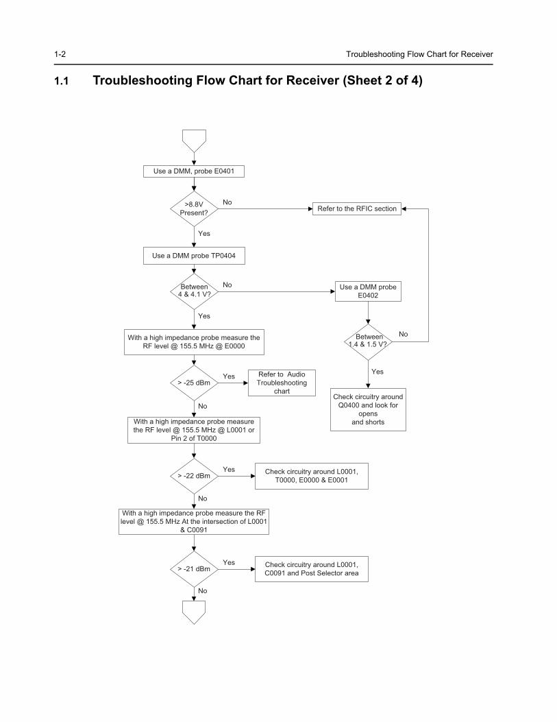
1-2 Troubleshooting Flow Chart for Receiver
1.1 Troubleshooting Flow Chart for Receiver (Sheet 2 of 4)
Use a DMM probe TP0404
Between 4 & 4.1 V?
> -25 dBm
> -22 dBm
With a high impedance probe measure the RF level @ 155.5 MHz @ E0000
With a high impedance probe measure the RF level @ 155.5 MHz @ L0001 or
Pin 2 of T0000
Yes
No
Use a DMM, probe E0401
Use a DMM probe E0402
No
>8.8VPresent?
Yes
> -21 dBm
No
With a high impedance probe measure the RF level @ 155.5 MHz At the intersection of L0001
& C0091
No
Refer to the RFIC sectionNo
Between 1.4 & 1.5 V?
Check circuitry around Q0400 and look for
opens and shorts
Refer to Audio Troubleshooting
chart
Check circuitry around L0001, C0091 and Post Selector area
Check circuitry around L0001, T0000, E0000 & E0001
YesYes
Yes
Yes
No

Troubleshooting Flow Chart for Receiver 1-3
1.2 Troubleshooting Flow Chart for Receiver (Sheet 3 of 4)
> -18 dBm
With a high impedance probe measure the RF level @ 155.5 MHz @ the intersection of C0420 and C0460
With a high impedance probe measure the RF level @ 155.5 MHz @ the Intersection of C0431 & C0443 & R0443
& R0442
Check Circuitry Around Post
Selector Area
> -17 dBm Use a DMM probe E0404 & E0405
With a high impedance probe measure the RF level @ 155.5 MHz @ the Intersection of R0448,
C0401,R0440, & R0442E0404=2.5VE0405=28mV
Check Circuitry Around Step
Atten
Make sure C0427 is properly placed. If
Placement is OK, replace U0401 & U0402.
> -15 dBm
With a high impedance probe measure the RF level @ 155.5 MHz
@ R0429
> -33 dBmUsing a DMM, probe
Q0402 Pin 4 and Pin 2
No
Yes
No
Yes
No
Yes
No
Yes
No
Check Circuitry Around R0442, R0440 & R0443
Yes
Pin 4 = 2.4VPin 2 = 0.8V
No
Check Circuitry Around Q0401
Check circuitry around C0411, R0445, D0402, L0402, C0415, C0418, R0448, R0442, R0440,
R0443
Yes
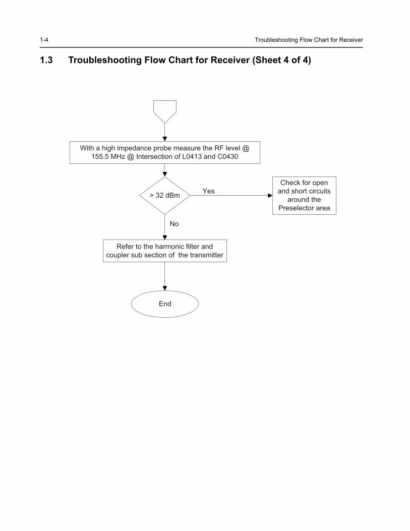
1-4 Troubleshooting Flow Chart for Receiver
1.3 Troubleshooting Flow Chart for Receiver (Sheet 4 of 4)
> 32 dBm
With a high impedance probe measure the RF level @ 155.5 MHz @ Intersection of L0413 and C0430
Refer to the harmonic filter and coupler sub section of the transmitter
Check for open and short circuits
around the Preselector area
No
Yes
End
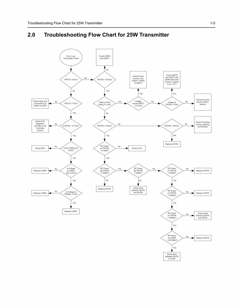
Troubleshooting Flow Chart for 25W Transmitter 1-5
2.0 Troubleshooting Flow Chart for 25W Transmitter
TP0710 >4Vdc? TP0705 ~9.3Vdc?
Voltageacross R0877
~3.7Vdc?
TP0706 ~2.6Vdc?
RF Power @ TP0704 ~+15dBm?
Is R0745 ~9.1Vdc?
Check 9.3V Regulator
(U3108) in the Controller Section
Volt at U0904 pin1 >3Vdc?
Check RFIC
Is Voltageat U0902
pin3 >3Vdc?
Is Voltage atTP0900 >1Vdc?
Replace U0904
Replace U0902
Replace U0901
RF Power @ TP0700 ~+9dBm?
TP0710 <1Vdc?Check setup and connections at C0870 & J0700
RF Power at TP0703 ~+0 dBm?
Check Final Bias tuning codeplug
and Rodinia
Check D0875and D0877 with DMM diode test function, replace
if not ~0.7V
Voltage atTP0709 >1Vdc?
Radio currentduring Tx >2A?
Check Ant_Enb line from MCU
Section
Check Power Control Loop
(D0951, D0900 & U0901)
TP0708 ~3.8Vdc?
Replace Q0702
RF Power at TP0702 ~+22dBm?
RF Power at TP0705 ~+33dBm?
RF Power at TP0706 ~+33dBm?
RF Power at C0758
~+45.5dBm?
Check VCO
Replace Q0703 Check parts between Q0703
and Q0700
Replace Q0700
Replace Q0704
Check parts between Q0704
and Q0702
Replace Q0702
Check parts between Q0702
& J0700
Check Q3000 and Q3001
No
No
Yes
Yes
Yes
Yes
Yes
No
Yes
Yes
Yes Yes
No No
No No
No
No
Yes Yes
Yes
Yes Yes
No No
No
Yes
Yes
No
No
No
Yes
Yes
No or Low Transmitter Power
No
Yes
No
No
No
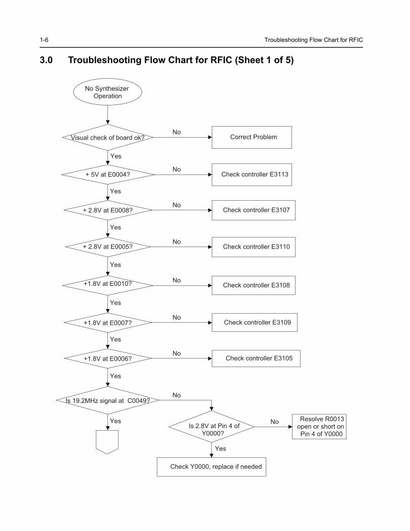
1-6 Troubleshooting Flow Chart for RFIC
3.0 Troubleshooting Flow Chart for RFIC (Sheet 1 of 5)
Visual check of board ok?
+ 5V at E0004?
+ 2.8V at E0008?
+ 2.8V at E0005?
+1.8V at E0010?
+1.8V at E0007?
+1.8V at E0006?
Is 19.2MHz signal at C0049?
Is 2.8V at Pin 4 of Y0000?
Correct Problem
Check controller E3105
Check controller E3113
Check controller E3107
Check controller E3110
Check controller E3108
Check controller E3109
Check Y0000, replace if needed
Yes
No
Yes
Yes
Yes
Yes
Yes
Yes
Yes
No
Yes
No
No
No
No
No
No
No
No Synthesizer Operation
Resolve R0013 open or short on Pin 4 of Y0000
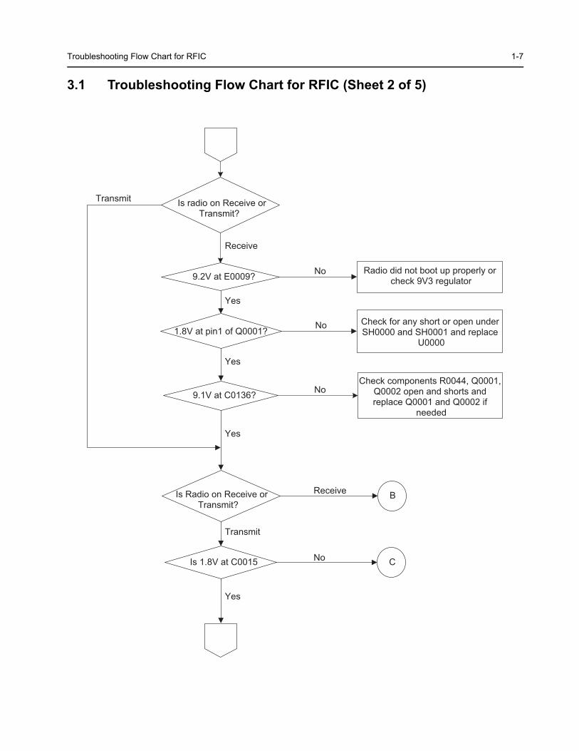
Troubleshooting Flow Chart for RFIC 1-7
3.1 Troubleshooting Flow Chart for RFIC (Sheet 2 of 5)
Is radio on Receive or Transmit?
9.2V at E0009?
1.8V at pin1 of Q0001?
9.1V at C0136?
Is Radio on Receive or Transmit?
Is 1.8V at C0015
Radio did not boot up properly or check 9V3 regulator
Check for any short or open under SH0000 and SH0001 and replace
U0000
Check components R0044, Q0001, Q0002 open and shorts and replace Q0001 and Q0002 if
needed
No
No
BReceive
C
Receive
No
Yes
Yes
Yes
Transmit
Yes
No
Transmit
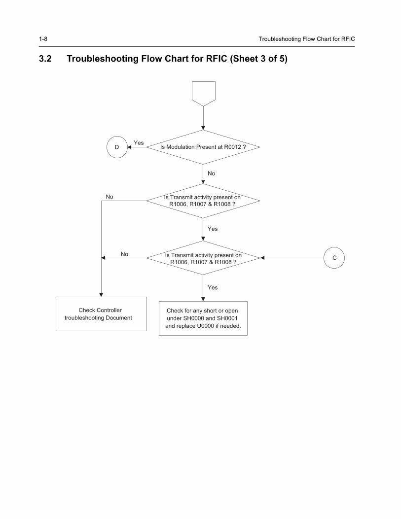
1-8 Troubleshooting Flow Chart for RFIC
3.2 Troubleshooting Flow Chart for RFIC (Sheet 3 of 5)
Is Modulation Present at R0012 ?DYes
Is Transmit activity present on R1006, R1007 & R1008 ?
Is Transmit activity present on R1006, R1007 & R1008 ?
Yes
No
Check Controller troubleshooting Document
Yes
Check for any short or open under SH0000 and SH0001
and replace U0000 if needed.
C
No
No
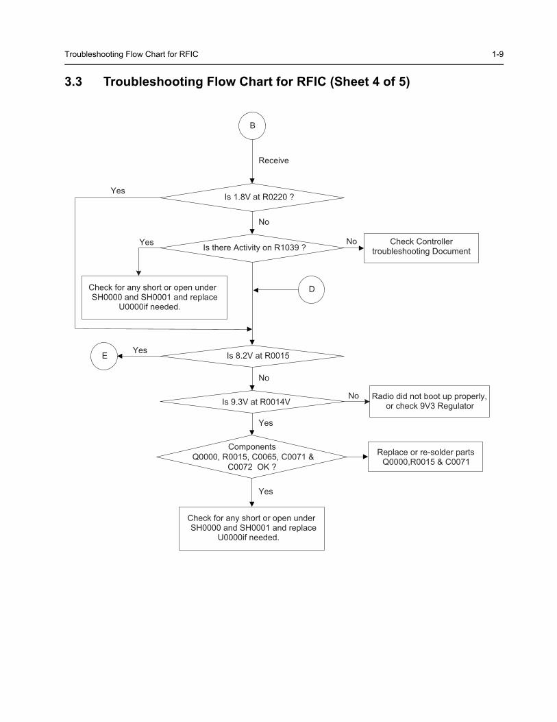
Troubleshooting Flow Chart for RFIC 1-9
3.3 Troubleshooting Flow Chart for RFIC (Sheet 4 of 5)
B
Receive
Is there Activity on R1039 ?Check Controller
troubleshooting DocumentNo
Check for any short or open under SH0000 and SH0001 and replace
U0000if needed.
Is 1.8V at R0220 ?
No
D
Is 8.2V at R0015
Yes
Is 9.3V at R0014V
No
Radio did not boot up properly, or check 9V3 Regulator
Replace or re-solder parts Q0000,R0015 & C0071
Components Q0000, R0015, C0065, C0071 &
C0072 OK ?
Yes
Yes
Check for any short or open under SH0000 and SH0001 and replace
U0000if needed.
E Yes
Yes
No
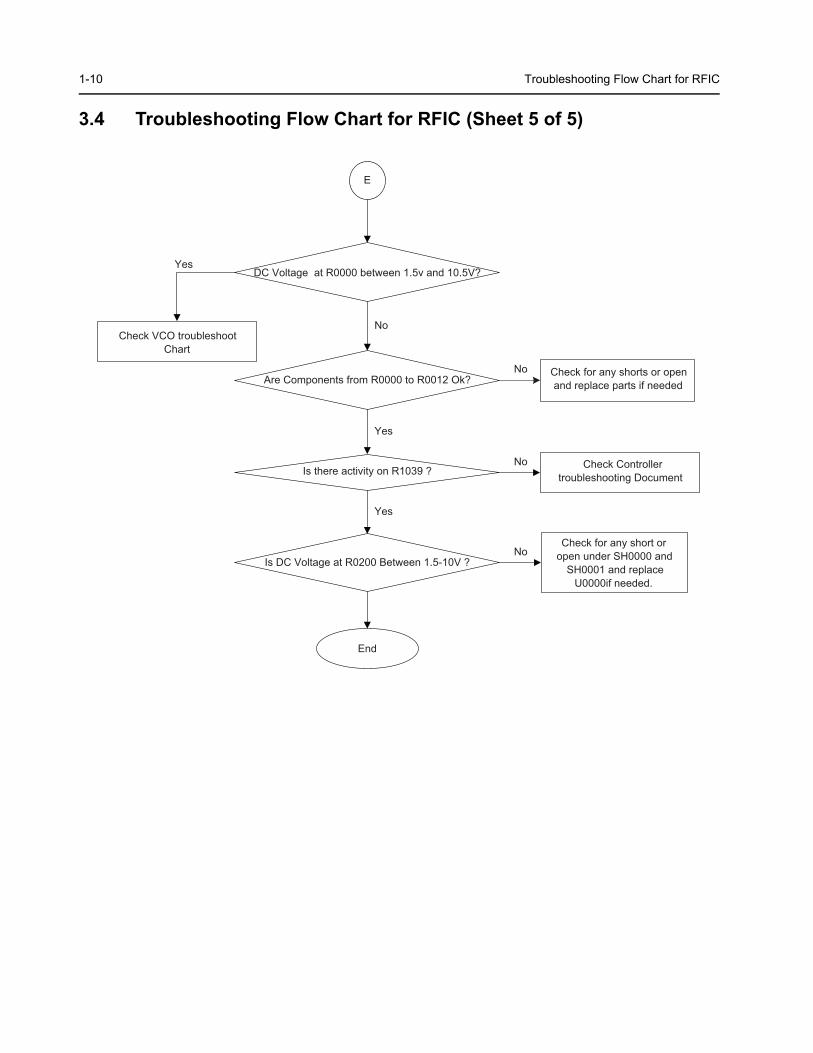
1-10 Troubleshooting Flow Chart for RFIC
3.4 Troubleshooting Flow Chart for RFIC (Sheet 5 of 5)
E
DC Voltage at R0000 between 1.5v and 10.5V?
Check VCO troubleshoot Chart
No
Are Components from R0000 to R0012 Ok?Check for any shorts or open and replace parts if needed
Is there activity on R1039 ?
Yes
Check Controller troubleshooting Document
No
Check for any short or open under SH0000 and
SH0001 and replace U0000if needed.
Is DC Voltage at R0200 Between 1.5-10V ?No
End
No
Yes
Yes
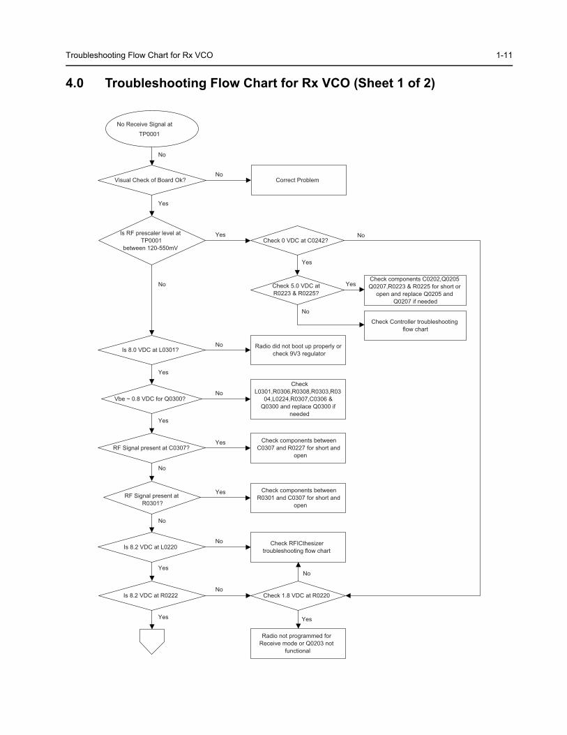
Troubleshooting Flow Chart for Rx VCO 1-11
4.0 Troubleshooting Flow Chart for Rx VCO (Sheet 1 of 2)
Visual Check of Board Ok?
No
NoCorrect Problem
Yes
Is 8.0 VDC at L0301?No Radio did not boot up properly or
check 9V3 regulator
Yes
Vbe ~ 0.8 VDC for Q0300?No
Check L0301,R0306,R0308,R0303,R03
04,L0224,R0307,C0306 & Q0300 and replace Q0300 if
neededYes
RF Signal present at C0307?Yes Check components between
C0307 and R0227 for short and open
Is RF prescaler level at TP0001
between 120-550mV
Yes
No
No
RF Signal present at R0301?
Yes Check components between R0301 and C0307 for short and
open
No
Is 8.2 VDC at L0220No Check RFICthesizer
troubleshooting flow chart
Yes
Is 8.2 VDC at R0222 Check 1.8 VDC at R0220No
No
Yes
Radio not programmed for Receive mode or Q0203 not
functional
Yes
Yes
Check 0 VDC at C0242?No
Check 5.0 VDC at R0223 & R0225?
YesCheck components C0202,Q0205 Q0207,R0223 & R0225 for short or
open and replace Q0205 and Q0207 if needed
No
Check Controller troubleshooting flow chart
No Receive Signal at TP0001
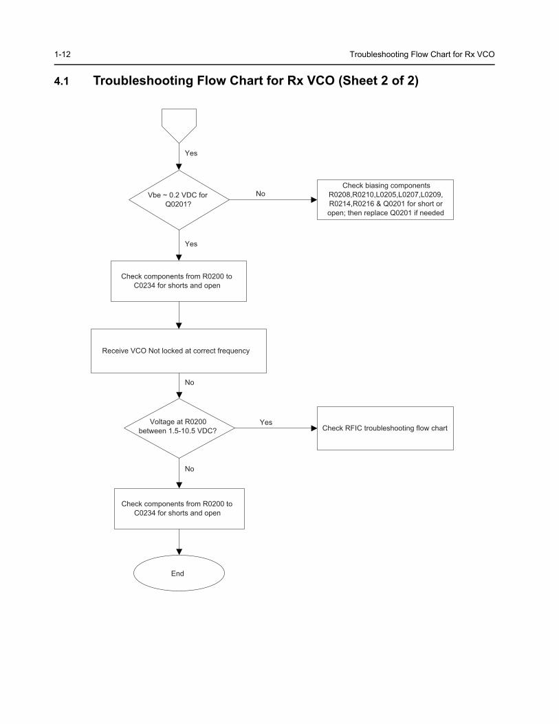
1-12 Troubleshooting Flow Chart for Rx VCO
4.1 Troubleshooting Flow Chart for Rx VCO (Sheet 2 of 2)
Yes
Vbe ~ 0.2 VDC for Q0201?
NoCheck biasing components
R0208,R0210,L0205,L0207,L0209, R0214,R0216 & Q0201 for short or open; then replace Q0201 if needed
Yes
Check components from R0200 to C0234 for shorts and open
Receive VCO Not locked at correct frequency
Voltage at R0200 between 1.5-10.5 VDC?
No
YesCheck RFIC troubleshooting flow chart
No
Check components from R0200 to C0234 for shorts and open
End
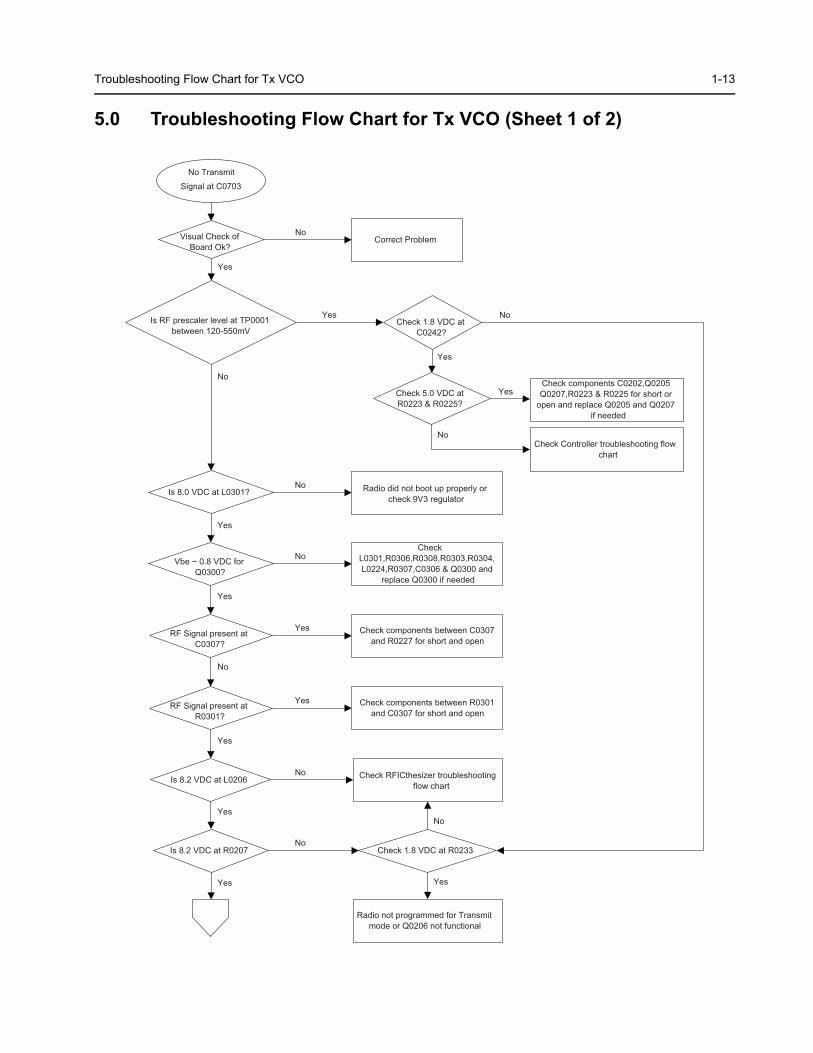
Troubleshooting Flow Chart for Tx VCO 1-13
5.0 Troubleshooting Flow Chart for Tx VCO (Sheet 1 of 2)
Visual Check of Board Ok?
NoCorrect Problem
Yes
Is 8.0 VDC at L0301?No Radio did not boot up properly or
check 9V3 regulator
Yes
Vbe ~ 0.8 VDC for Q0300?
NoCheck
L0301,R0306,R0308,R0303,R0304,L0224,R0307,C0306 & Q0300 and
replace Q0300 if needed
Yes
RF Signal present at C0307?
Yes Check components between C0307 and R0227 for short and open
Is RF prescaler level at TP0001 between 120-550mV
Yes
No
No
RF Signal present at R0301?
Yes Check components between R0301 and C0307 for short and open
Yes
Is 8.2 VDC at L0206 No Check RFICthesizer troubleshooting
flow chart
Yes
Is 8.2 VDC at R0207 Check 1.8 VDC at R0233No
No
Yes
Radio not programmed for Transmit mode or Q0206 not functional
Yes
Yes
Check 1.8 VDC at C0242?
No
Check 5.0 VDC at R0223 & R0225?
YesCheck components C0202,Q0205 Q0207,R0223 & R0225 for short or
open and replace Q0205 and Q0207 if needed
NoCheck Controller troubleshooting flow
chart
No Transmit Signal at C0703
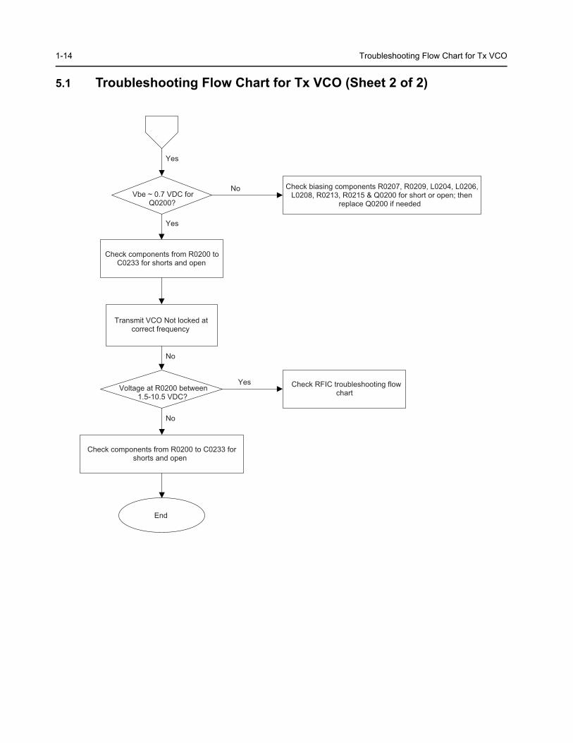
1-14 Troubleshooting Flow Chart for Tx VCO
5.1 Troubleshooting Flow Chart for Tx VCO (Sheet 2 of 2)
Yes
Vbe ~ 0.7 VDC for Q0200?
No Check biasing components R0207, R0209, L0204, L0206, L0208, R0213, R0215 & Q0200 for short or open; then
replace Q0200 if needed
Yes
Check components from R0200 to C0233 for shorts and open
Transmit VCO Not locked at correct frequency
Voltage at R0200 between 1.5-10.5 VDC?
No
Yes Check RFIC troubleshooting flow chart
No
Check components from R0200 to C0233 for shorts and open
End
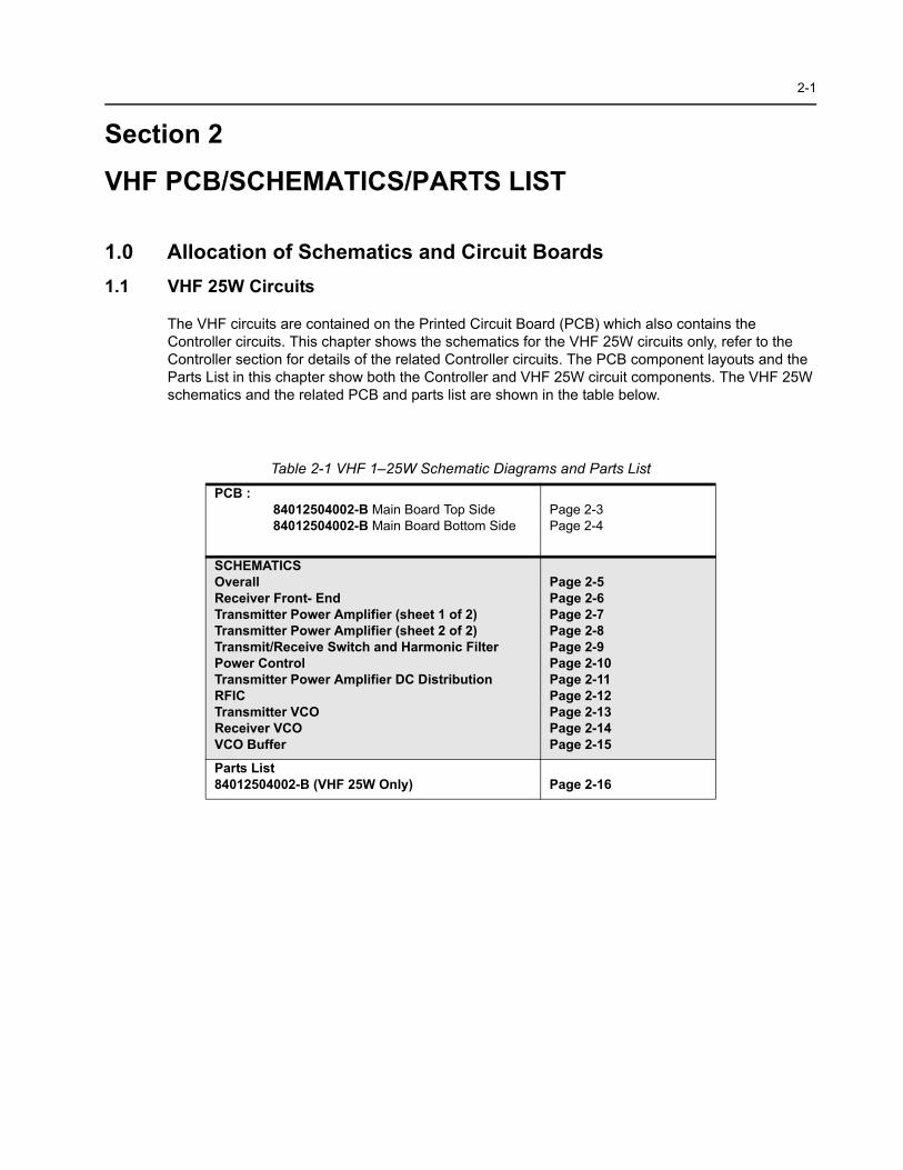
2-1
Section 2
VHF PCB/SCHEMATICS/PARTS LIST
1.0 Allocation of Schematics and Circuit Boards
1.1 VHF 25W Circuits
The VHF circuits are contained on the Printed Circuit Board (PCB) which also contains the Controller circuits. This chapter shows the schematics for the VHF 25W circuits only, refer to the Controller section for details of the related Controller circuits. The PCB component layouts and the Parts List in this chapter show both the Controller and VHF 25W circuit components. The VHF 25W schematics and the related PCB and parts list are shown in the table below.
Table 2-1 VHF 1–25W Schematic Diagrams and Parts List
PCB :84012504002-B Main Board Top Side84012504002-B Main Board Bottom Side
Page 2-3Page 2-4
SCHEMATICSOverall Receiver Front- EndTransmitter Power Amplifier (sheet 1 of 2)Transmitter Power Amplifier (sheet 2 of 2)Transmit/Receive Switch and Harmonic FilterPower ControlTransmitter Power Amplifier DC DistributionRFICTransmitter VCOReceiver VCOVCO Buffer
Page 2-5Page 2-6Page 2-7Page 2-8Page 2-9Page 2-10Page 2-11Page 2-12Page 2-13Page 2-14Page 2-15
Parts List84012504002-B (VHF 25W Only) Page 2-16

2-2
Notes
V 2-3
2
3 45
E3100
C30
21
C30
46
U31
12
R31
10R
3150
C3050
C3051 22019
1817
E41
00
E41
01
E4103
E4102
J4100
23
VR
4110TP
4102
TP41
03
TP31
09TP
4101
5
C31
12C
3129
R31
07R
3175
C3111
R3106
101120
U3204
10
5 6
R31
32
U31
09
R31
02
R31
01
C3106
C31
52
C31
02
5
106
32
32
G214G1
J4001
C3201
R40
40C
4011
C32
00
R4001
R32
82
C40
29C
4022
C40
14C
4012VR4005
C40
19C
4021
C40
23
C40
25C
4028
C40
13C
4015
C40
20
VR
4001
VR4000
C31
21C
3120
L3100R3115
C31
76R
3114
C31
19
R3116
C3143
SH3100
U31
02
R3141
D3104
C3175
R31
11
C3116
C3154
4 3
3
23
2
2
53
32 E40
05
E40
04R
4024
R40
13
R40
27
FL40
01
R11
24
R40
06R
4007
E40
03R
4015
R40
21
E40
00E
4001
E40
02
R40
26R
4010
R40
25
R11
22
R1118R1128
R4093 R4091
R4028 R4034
R40
33C20
00
R2003
R11
26
R11
25
Q10
05D
1005R1119
R1120
R40
38
R2004
R2002
R2000
R40
37
D3160
C20
21
U10
10
C1021
R1020
R1001R1045
R10
42
R31
73
23
43
6
3
6 43
2
36
4
C2020R1035R1036
3
24
C2016
C20
09
C20
22C
2002
U31
07
C31
35
R3153
R31
04
C31
37
C31
33
C20
03
E31
08
C31
36
C2001
Q3100
C31
09
R31
03
E31
10
VR
3103
C31
40
U31
06139
C31
80R
1077
R31
81R
3180109
R1021864
2
R1050C1014
R1011
R1062R1064
R1024R1030R1027
5
9
1
0
0
8
6
4 5
8
5 610
R3108C31
71C
3153
C32
23
U31
00R3280C32
22C
3228R32
54
C3221
C32
24
R3290
C3144E3104
C3150C3173
U31
08
C31
51
R31
47
R3146E3113
E31
11
C3122U3103C3123
C31
24
C1029
R31
19
C1032
E10
02E
1004
C3118
6 49
C1010C1009
U10
04
R10
46
C10
44
C1023
C10
28C
1036
C1017
R1023
C10
08
E1003
C10
05C1002
C10
06C
1007
R10
26C
1025
C20
07
C1003
C10
45C
2006
C10
41
C10
15
E1001
C1001
R10
12
C10
42C
1019
C10
26
C10
22 C10
18
C1020
C1035
R10
19
6 43
436
23
E32
02
R32
00
Q3209
R32
04C3204
C20
15
C20
13
R32
03
C32
19
C3231
C3218
U3202
R1060
C3229
C32
26R
3285 C3227
C20
14
C20
11
C20
10C20
08
56
R3287
C32
57
C2012
R3138
R3176C3214
C2005
R32
08 C323001
R32
31R
3230 R3142
C10
47
C3248 C10
60
R1051
C1013R1049
63
C2004
R32
64
R3265
R3262
R3263
Q32
05
R3261
C32
09
C32
25
VHF (136–174 MHz) 1–25W 84012504002-B Top Side
HF (136–174 MHz) 1–25W PCB/Schematics/Parts List
.0 VHF (136–174 MHz) 1–25W PCB/Schematics/Parts List
G2
G1
23
J070
0
R09
57
R09
58
R0956
L0952
23R
0950
C09
50
C09
51C0952
D09
50
32
R09
55
R09
54
C0955
D09
51
C09
54
C09
53
R09
53
C0871
C0870
C0869
R09
51R
0949
R09
52L0
951
2
R09
13
R09
61C
0957
R09
62
C09
02
C0916
C09
11
R0940R0939
R0914R0915R0744
RT0900TP09
00R
0904
R09
60
1
458
3
R09
59
C0901
R09
22C0900R09
21
R0920R0917R0916U
0902
TP0902C0918
4 5
R09
65
C09
25C
0917
TP09
04R
0928
R0924
SH0900
R0929
R09
19
R0923C0926
R07
35R
0727
C0700C0722
U09
04
R0933
R09
32
TP0903
R0931
C0956
C0919R0930
63
48
45
Q0400
R0411
C0463
C0410
C04
64
E04
00
C04
08
C04
67
TP0404C0469
SH0400
R0423
C0422R0428
R0425U0400
R04
24
R04
31
Q0406
R04
30R
0427
C04
66
R04
33R
0436
R0437
TP04
03
R0438
R04
39
E04
01
23
36
R0403 C04
65
E0402
C04
13R
0410
R0413 R04
17 R04
15L0401
R04
16
L0406
L0413
C0430
C04
04
C0452VR0401
D0401
R0402
VR0400L0405
R0404
C0402
C04
07C0406C0453
VR0403VR0402
C04
35
C04
03L041
4C
0438
C04
05C0423
R0429
C03
06
R03
07C03
04R
0304C
0302
SH0200
VR0215
VR
0210
VR
0214
VR
0211
L0212
C02
41
R03
09C
0307C0301
L0224
R0305
Q0300
R03
03
L0226
C0276
L030
0
R03
00R
0302
C03
00
R02
24R
0222C0252
C0256 Q02
04
L0218
C0245C02
44
C0248
C0257
L0214
L030
2C
0309
C03
10
L0304
C02
02
L030
1
L030
3R0306R0308
C0308
C03
05
L0220
R0301
C02
65R
0232
R02
28R
0230
L022
2
R0203
L0216
C02
63
C02
59
E0300
C02
67
C0004
C0034
R0011R0006
C0007
C0012
R0012
C0043
R00
07
C00
06C
0003C0002
C00053
2C0120
C00
74C
0145
C00
55R0015
R0014C0061C0059C0065C0072
R0001
C0011R0009
R0010
R00
00
C00
54
C0075C0024
C0101
C01
38
C01
41
C00
13
C00
22C
0015
C00
26C
0035
C0018C0014C0030C0031C0029
C00
53
Q00
00
C00
36
C00
98
SH0001
C0056
C0144
C0143C0124
E0007C01
40
C00
16C
0105
C00
64
C00
60
C0019
C01
50C
0149
C0001
C0039
C0146C0147
C00
17
C0135
E00
09C0009C0102
E0008
C0100
C0076
C0093C0033
C01
39C
0071
C0032
C0037
C00
83
C0068C0066
R0019C0067
R0030
C0070
46
3
43
6
L0000
C00
86
C0080
D00
00
R0029C00
85SH0003
C0082C0081
D00
01
C00
78
R0022R0025
C0860
L085
2
C0868
L085
8
C0858
C0857
C0859
C0856
SH0850
L0854
C0862C0861
C0863
C0866
L0850
L087
9
C08
50
C08
51
C08
52
C08
53
L087
5
C0893
L0857
C0875
L088
5
D08
77
C0891
L087
8
C0880
L087
7D0875
C08
78
C08
88
C08
90
4
32
C0876
D08
76
C0762
C0759C0758
C0753
L0710
C07
52
C07
65
C0767
C07
50
C07
28
C0774
C0768
C0751
C0718
C0771
L070
6
C0773
C0824
C07
70
C07
36
C07
35
C0723
C07
16C
0712
C07
07C
3003
C0740
C0733
C0742
C0721
C30
02
C0755
C0739
C0730C0748
C0737C0726
R3006
R07
36 R3005E0701
E07
03
G1
32
C30
12
Q30
00
C30
13
R30
15
C30
14
C07
45
C08
18C
0714
2 3R
3004
R30
02
R30
03
R30
01
C30
20C3042
C3044C3047
M30
00
R103
R105R104
C3
E3
Q10
02
R101R101R101
R102
R102
R106
R103
R104
R101
R102
R32
Q32
C0094
5
67
8
23
4
Q07
02
M07
00
R07
25
R07
13
R0739TP07
08
R07
46C0761R0743C0764
R07
42
R0710
R07
34
R07
32
R07
26
36
G1
32
C0706
R09
34
R0935
C09
21U0903
R08
83
C07
75
R0712
Q07
01
Q30
01
C07
32
R0711
R0704
R0723
C0710
R07
00C07
01
C0727
R07
18TP
0710
R0720
C07
31
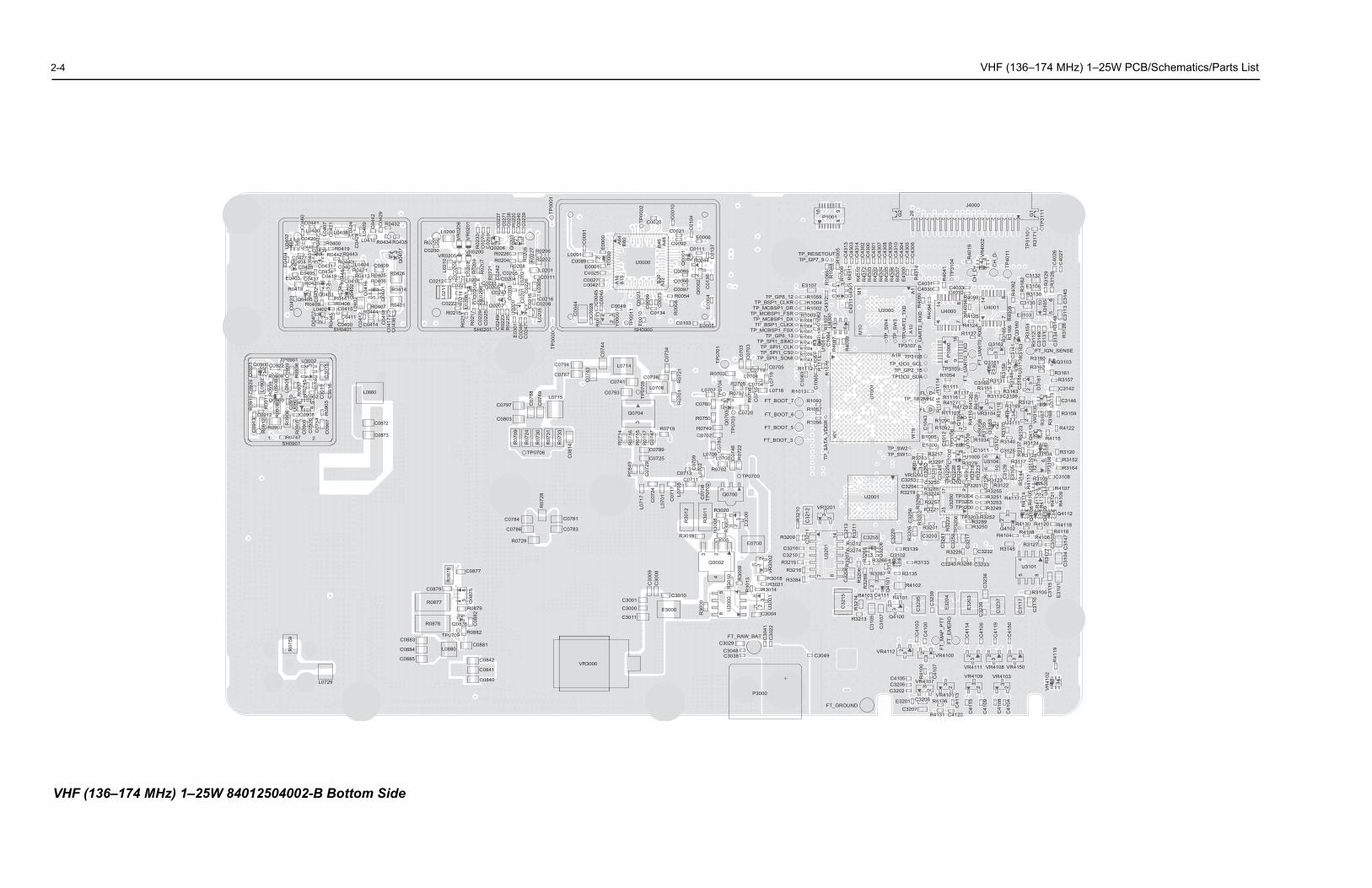
2-4 VHF (136–174 MHz) 1–25W PCB/Schematics/Parts List
14W
1
6
34
346
R43
14
E43
00
R43
02
R43
07R
4306
R43
05R
4304
R10
00R
4311
R43
12R
4310
R43
03
R10
05
C43
11U
4301
R40
99
R40
97
C43
04C
4305
C43
06
C43
01C
4307
C43
08C
4309
C43
10
C43
14C
4303
C43
13
C43
02C
4300
89
G2
20
J4000
G1
R31
71TP
3111
TP31
10
46
3
C40
27C
4026VR
4002
R40
19
R40
41TP
3104 CH
_D-
TP40
11
C4030C4031
R40
90
R40
94
TP_U
AR
T2_R
XD
7
A10
M10
814
A1
M1
U2000 U4000
TP_I2C0_SCLTP3105
TPU
AR
T2_T
XD
TP3107
TP_S
W3
TP_S
W4
TPI2C0_SDATP_GP2_15
U10
01
A19
C32
37
C31
17
C32
38E32
03
E32
04
C32
36
C32
35
C32
39
32
8
45
6
4366 436 43
43 R4107
C3108
R41
11
U41
00
R3109R3122
R3123
R31
44
C31
28E
3105
C31
26
R41
21
R41
09
Q4112
Q41
05
R41
05R
4113
R41
12
Q41
06R
4114
R3252
R3249R3253R3251R3255
C31
47
C31
03
R4116R4118
R31
77
R4106R3127
R4108
R4130 R4120
R3145
R4104Q4102
E31
01C
3104
C31
15
U3101
R3105
C31
10
6712
6 43
64 3
R3164
R3152
TP31
08
U31
10R3117
Q3103
FT_IGN_SENSE
C3146
C3142
R3157R3161
R4122
R3159
R31
68R
3167
R31
70
VR
3105
R3120
R4115
Q3104R3125
R3124
R41
23
Q41
13
R31
37
C3125
R3140
23
6
6 43
1698
4 3
23
5
7
2
32
6
10
8
14
R31
28C3132
R31
29
CH
_D+
C31
45
U31
05C3130
R3130
E3106
R40
08
R31
82
R40
96
R4098C4032C4033
U4001
C31
13R
3126
R31
54
C31
34R
3148
C31
31C
3149
R31
12
E3103
R1127
R4124
R4125
R3162
R3160
Q3162
FT_U
AR
T0_R
XD
FT_U
AR
T0_T
XD
P10
00
U31
15
D31
61
C3160R1054TP3103
R3121
U3111
R3169
R40
92
6 34
2634
Q31
60
R31
65R
3166
R31
63C
3141
U31
13Q3161
R3131
R3113R3143
C31
55R31
58R
3149
C3156
R3151
R31
18106
52
2
3
U3104
R1117
R41
26R
4128
R1111
R11
14
R1116TP_19.2MHZFL_D+
VR3104
R41
10
HS
US
BR
3155
Q31
63
R4129FL_D- R11
15 R4127
R1034
C1011 C31
27
32
32
3232 23
2323
23
23
C41
50
C41
19
C41
06
C41
14
FT_M
AP
_PTT
FT_E
ME
RG
C41
00
C41
03
VR4150VR4108VR4111
R41
00
VR4100VR4112
VR4103
C41
04
C41
08
C41
09
C41
15
VR4109
VR4101
C41
07
C41
13
C3202C3205C4105
E3201
VR4107
C4120
R4136
R4131
C3206GROUND
C3207
6 43R
4119
VR
4102
9
2517
C3250C3254C3253
VR3200
TP3203
TP3200TP3205TP3204
R3289
U32
00
R3288R3224
R3257R3221
R32
02
C32
56R
3296
R3219
C3232
R3250
TP32
06
R3229
C32
17
C32
58
C32
41R
3222
C3233R3286C324036 4
3
2
23
3
6
R3201
C3203
R32
05
C32
20
C3255
Q32
06R3212
R32
11
C32
13
R3133
R3135
R3139Q3102
R31
34R3266
R3267
R32
69R
3206
R32
68
R32
07C
3208
R3274
Q4100
R4101
R4102
C31
07
C4111
R32
14
C31
05
Q41
01
C32
15
R3213
R4103
U2001
5
6 43
33
44
6
W19
23
TP3201TP3202
R32
23R
3218
R32
20
R3279
R32
48R
3226
C32
49R
3225
C32
51
R3297
C32
52
Q10
04
R1092
R1110R1090
TP31
06
C10
43
C10
00R3217
E1000 C10
12
U1000
E1005
U10
09
TP_SW1TP_SW2
R3283
R4117
VHF (
21
8 54
5
346
4 3
C09
07
R0747SH0901
U3002
R09
36
C09
09C0922TP0901
Q0900
C30
16
C30
19C
3015
R0902
R07
08
R07
45R
0937
C09
10L0
901
L090
0
R0909
R09
38
L090
2R
0911
R09
10C
0924
C09
23
R09
03
C07
54
U09
01
R0907
R09
08
D0960
C09
05R
0905
C0908
C09
06R09
06C0912
R09
12
C09
13
C0873
L0860
C0872
634
436
R0432
R0435
C04
29C
0442
L0410 R0434
L040
9
C04
24C
0428C
0421
L0408
R0419
L040
7
C0439R0400
R04
22
L0400C0441
C04
60
C0420
U04
02
Q04
07
L0404C0401R0440
R0443R0442
C0440
2
3 46
2
R0426
C0409
R0405R0421
R04
48C0419C0434C0431
E0405
U04
01
C0427
C0425
E0403
Q0404
E04
04R0406
R0412C0418C0437
R0420
Q0405
R0418C
0433
23
63
32 4
234
R0401
R0414
Q04
01
R0407
C04
16
L040
3Q04
02
C0415L0402R0408R0441
Q0403
R0409
C04
32
C04
36C
0417C04
58R0444
C0414C04
12C0411C0400R
0445
SH0401
D04
02
C02
25C
0229
C0222 R02
11
C02
47C
0246
E03
01R02
25R
0223
C02
49
SH0201
R02
17
R02
13
R0215
3
36 43 4
C02
39C
0240
R02
20Q
0203
C02
70
C02
38C
0271
C02
37
Q0206C02
69
R02
33VR
0201
VR
0206
L0200
R0200
R02
21
R0204R0226
R02
07
C0217
R02
09C
0207
C02
06
VR0200VR0205
C0212
L021
0
C0200
Q0205C0233
L020
6
C0231
L020
8
L0204
Q02
00C0221
L021
1
C0311
R0202
R0206
L020
2C
0226
C0204C0205
R0208L0201
R02
27R
0205
C02
42
L030
5
C0243
4
C0216
U02
00 C0208C02
15C02
03
C02
01
Q0207
L020
5
C08
14
R07
33
R07
31
R07
30
TP0706
R07
24
R07
09
L0715
C07
49
C07
88
C0803
C0797
TP00
00
C07
34
L0714
C07
44
C0794
L0708
R07
21
C0738
TP07
05
C0741
C0793
C07
43
C0787
C30
22C
3041
C3049C3038C3048
C3029
P3000
C0879
R0878
R0877
C0883
C0884
C0885
4 5
8
C0877
R08
76
Q08
75
R0879
C08
822
Q0876
R0882TP0709
C0881
C0842
L0880
C0840
C0841
8
45
C30
08C
3009
U30
00
R30
00
C3010
C3000
C3001
FT_RAW_BAT
E3000C3011
VR3000
32
4
3 2
23
23
D30
00
R3020
R30
11
R30
12
E0700
R30
07
C3005
R30
08
R3019
VR
3002
R3018
R30
10
Q3002
R3021R3014
U30
01
R30
13R30
09
C3004
873 2
VR3201
C32
12
C3216
C32
11
R3209
R32
10
U32
01
R3284
R3216
R3215C3210
3
3
C0702R0719
C0725
C0789
C07
47R
0717
R07
15R
0716
R07
14
C07
08TP
0702
L070
5C
0717
L070
1
L071
7
C07
24C
0729
R08
49
Q0700
L0707
R07
01
R0749
R0750
C0760
Q0704
C07
46R
0722
L0700
C07
09
L0709 C07
80
TP0700R0702
C0711
L070
2
C0713
FT_BOOT_3
R1013
R1056
R1057
R1093
TP_S
ATA
_VD
DR
FT_BOOT_5
FT_BOOT_6
FT_BOOT_7432
C0705C0719
L070
3C
0703
TP07
01
C07
15 L0718
L0704
C0704 L071
9
TP07
04 R0705
R07
06
R0703
TP07
03Q
0703
R0707
C0720
R07
28
C0783
C0781
R0729
C0786
C0784
L0729
R07
59
TP00
01
B30
A32B15
A16
42
B45 A48A64
B60C00
91
U0000
C0025E0001
E00
00T0
000
C0089L0001
C00
46C
0045
C0042C0027
R00
13C00
28
C00
44
4 32
23
2
C0020
SH0000
E0006
C00
10
C01
04
C0092
C0021
TP00
02
R0044
C0111
C01
37
Q00
02
C01
36
Q00
01
C0095
E00
04
C0096
C0097
R00
08
R0054
C00
73
C00
99
C00
23
C0049
C0103 E0005E00
10 C0134
TP00
11
Y00
00
R1004R1059TP_GP6_12
TP_BSP1_CLKRTP_MCBSP1_DR
R1009
R1002R1003R1006
R1007R1008
TP_GP6_13
TP_BSP1_CLKXTP_MCBSP1_DX
TP_MCBSP1_FSR
TP_MCBSP1_FSX
R10
76R
1113
C10
61C
1065
R1112
R1043
R1041
R1039R1038
TP_SPI1_SOMITP_SPI1_CS0TP_SPI1_CLK
TP_SPI1_SIMO
C10
63
643
TP_GP7_9TP_RESETOUT
R10
48R
1065
E3107
C43
12R
1108
C10
62R
1107
C10
64U
4300
U10
1116
P1001
FT_
136–174 MHz) 1–25W 84012504002-B Bottom Side
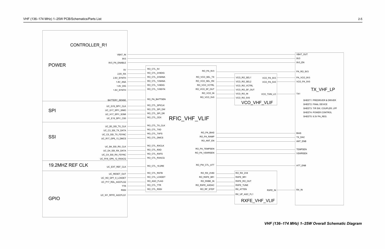
V 2-5
RX_UP_AGC_FL1
RXFE_IN
RXFE_RO_OUT
RXFE_TUNE
RX_ATTEN
RXFE_9R1
RO_RX_2V8
VCO_PA_5V0
VCO_RO_VCTRL
VCO_RO_SF_OUT
VCO_PA_9V3
VCO_RO_IN
VCO_RO_SEL2
VCO_RO_SEL1
VCO_RO_5V0
VCO_TXIN_LO
ANT_ENB
TEMPSEN
VSWRSEN
VCO_PA_5V0
TX1
PA_RO_9V3
9V3_EN
9V3
VBAT_OUT
RX_IN
ATT_ENB
TX_DAC
BIAS
PA_VCO_9V3
RXFE_VHF_VLIF
TX_VHF_LP
SHEET3: T/R SW, COUPLER, LPF
SHEET4: POWER CONTROL
SHEET5: 9.3V PA_REG.
SHEET2: FINAL DEVICE
SHEET1: PREDRIVER & DRIVERVCO_VHF_VLIF
VHF (136–174 MHz) 1–25W Overall Schematic Diagram
HF (136–174 MHz) 1–25W PCB/Schematics/Parts List
UC_C4_SSI_RX_FSYNC
UC_B4_SSI_RX_CLK
UC_D4_SSI_RX_DATA
UC_W2_GP7_9_LCKDET
9V3
9V3_PA_ENABLE
5V
2.8V_RX
2.8V_SYNTH
UC_P17_RDL_AGCFLG2
UC_W1_RFFE_AGCFLG1
RSSI
TTR
UC_R17_GP6_13_DMCS
UC_H17_SPI1_SOMI
1.8V_ANA
1.8V_DIG
VBAT_IN
1.8V_SYNTH
UC_G17_SPI1_SIMO
UC_RESET_OUT
UC_EXT_REF_CLK
UC_R16_GP6_12_RXACQ
UC_E19_SPI1_CS0
UC_B3_SSI_TX_CLK
UC_C3_SSI_TX_DATA
UC_C5_SSI_TX_FSYNC
UC_G19_SPI1_CLK
BATTERY_SENSE
RO_CTL_DMCS RO_PA_RAMP
RO_PA_BIAS
RO_RXBE_IN
RO_RXFE_AXDAC
RO_CTL_RXACQ
RO_CTL_RXFS
RO_CTL_1V8SYN
RO_CTL_1V8DIG
RO_PA_9V3
RO_VCO_SEL_TX
RO_VCO_SEL_RX
RO_ANT_EN
RO_PA_TEMPSEN
RO_PA_VSWRSEN
RO_PA_BATTSEN
RO_CTL_SPI_DR
RO_CTL_RXCLK
RO_CTL_RXD
RO_CTL_19.2RE
RO_CTL_LCKDET
RO_CTL_TTR
RO_CTL_RSSI
RO_CTL_2V8DIG
RO_CTL_1V8ANA
RO_CTL_CEX
RO_CTL_5V
RO_RX_2V80
RO_RXFE_9R1
RO_RF_STEP
RO_AGC_FLAG
RO_CTL_RSTB
RO_PW_CTL_ATT
RO_CTL_SPICLK
RO_CTL_SPI_DW
RO_CTL_TX_CLK
RO_CTL_TXD
RO_CTL_TXFS
RO_VCO_VCTRL
RO_VCO_SF_OUT
RO_VCO_IN
RO_VCO_5V0
RO_CTL_2V8ANA
19.2MHZ REF CLK
SPI
POWER
SSI
GPIO
CONTROLLER_R1
RFIC_VHF_VLIF
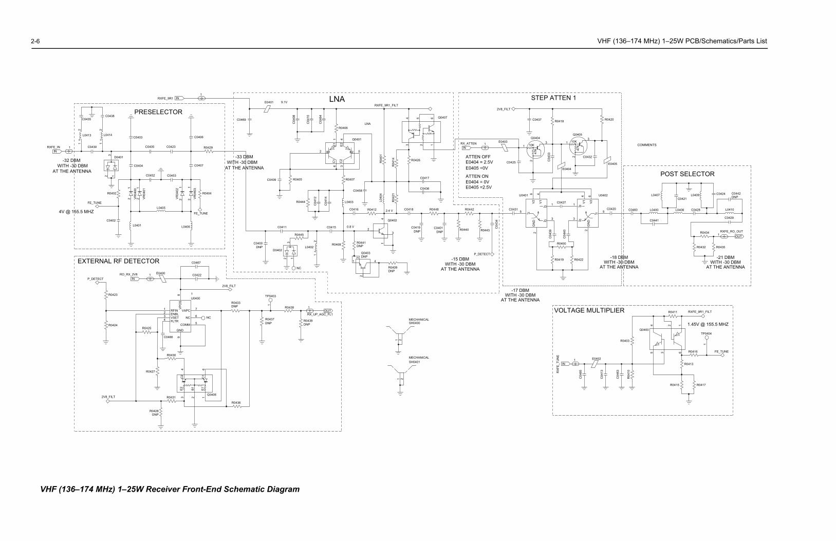
2-6 VHF (136–174 MHz) 1–25W PCB/Schematics/Parts List
RXF
0425
STEP ATTEN 1
47K
10K
47K
10K
C0437
E0404
E0405
R0420
Q0405Q0404
R0418
C04
33 C0432
31
2
31
2
T
COMMENTS
POST SELECTOR
AT THE ANTENNAWITH -30 DBM
-21 DBM
L0400
R0434
R0435
C0442
C0441
R0432
C0429
L0410
C0424L0409
C0428L0408
C0421L0407
C0460
1
DNP
RXFE_RO_OUTOUT
AT THE ANTENNAWITH -30 DBM
-18 DBM
J1
V2
V1
GN
DJ2
J3
U0402
C0420
64
1
3
5
2
J1
V2
V1
GN
D J2
J35
U0401
C0431
C0427
C04
40
C04
39
R0400
R0422R0419
6 4
1
3
2
HE ANTENNAITH -30 DBM-17 DBM
VOLTAGE MULTIPLIER
1.45V @ 155.5 MHZ
TP0404
RXFE_9R1_FILT
1
Q0400
FE_TUNE
2
R0413
R0417
R0411
R0416
R0415
R0403
5
14
63
R04
10
C04
63
C04
13
E0402
C04
65
1
RX
FE_T
UN
E
IN
VHF
PRESELECTOR
R0429
C0406
AT THE ANTENNAWITH -30 DBM
-32 DBM
RXFE_9R1
1
C0452
L0414
1
E_IN C0423C0405
C0453
C0403
C0404
D0401
C0430
C0438C0435
L0413
1
2 21
23
1
IN
IN
4V @ 155.5 MHZ
VR
0402
1
C0407
R0404
C0402
FE_TUNE
R0402
VR
0400
1
VR
0403
L0406
VR
0401
L0405
L0401
2
1222
1
FE_TUNE
AT THE ANTENNAWITH -30 DBM
-33 DBM
R0444
C0409 R0405
C04
14
C04
12
LNA
E2
B2
C2
E1
C1
B1
R0406
Q0401
R0407
41
36
52
LNA
C0469
C04
10
C04
64
9.1V
C04
08
E0401RXFE_9R1_FILT
Q04074
13
652
R0426
C0436
R04
14
R04
01
C0417
2.4 V
L0403 L040
4
C0458
R04
21
R0412C0416 R0442
R0443
P_DETECT
R0440DNPC0401
R0448
C0419
C0418
Q0402
C04
34
DNP
AT THE ANTENNA
-15 DBMWITH -30 DBM
E0404 = 2.5VE0405 =0V
ATTEN ON
E0405 =2.5VE0404 = 0V
ATTEN OFF
RX_ATTEN 1E0403
C
IN
2V8_FIL
AT TW
MECHANICALSH0400
SH0401
21
21
MECHANICAL
2
DNP L0402D0402
C0411
C0400
R0445
1
23
1
NC
0.8 V
R0409
C0415
R0408
Q0403
R0441
3
14
2
3
1 4
2
DNP
DNP
DNP
EXTERNAL RF DETECTOR
RFINENBLVSETFLTR
VP
OS
COMM
NC
VAPC
GND
NC
DNPR0439
R0438
TP0403
R0437
C0467
R0433
C0422E0400
U0400
C0466
R0425
R0423
R0424
2V8_FILT
1
1
1
3
8
71
6
9
4
2
5
RX_UP_AGC_FL1
RO_RX_2V8
DNP
1
P_DETECT
DNPOUT
IN
R0430
R0427
R0431
R0428DNP
2V8_FILT
C1
C2
E1
B1
E2
R0436
Q0406
3 1
4 6
2
(136–174 MHz) 1–25W Receiver Front-End Schematic Diagram
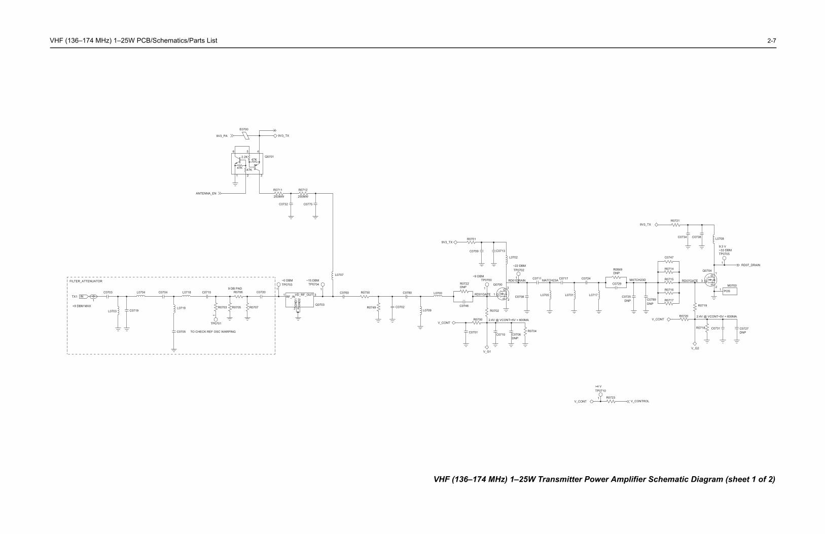
V 2-7
ONT=5V = 600MA
~22 DBM
SD
L0701
C0717
TP0702
C0706
L0717L0705C0708
C07241
L0702
C0711
R07040
3
2
3
DNP
RD01DRAIN MATCH23A
2.4V @ VCONT=5V = 600MA
C0747
R0716
V_CONT
R0849
V_G2
R0719
DNPC0731
C0725
C0729
C0727R0718
R0714
R0715
R0720
R0717C0789
DNP
DNP
RD07GATE
DNP
MATCH23D
~33 DBM9.3 V
POS
G
SD
L0708
TP0705
R0721
C0738C0734
1
2
3
1Q0704
1M0700
9V3_TX
RD07_DRAIN
>4 VTP0710
R0723V_CONTROL
1V_CONT
) 1–25W Transmitter Power Amplifier Schematic Diagram (sheet 1 of 2)
HF (136–174 MHz) 1–25W PCB/Schematics/Parts List
+9 DBM MAX
FILTER_ATTENUATOR
C0703 L0718
L0703
C0715C0704L0704
C0719
1TX1 IN
9 DB PAD
TO CHECK REF OSC WARPING
C0720
TP0701
R0707R0705
R0706
1
R0703L0719
C0705
~0 DBM ~15 DBM
VD_RF_OUTG
ND
2G
ND
1RF_IN
TP0704TP0703
R07501
3
Q0703
C0760
L0707
2
1
1
4 R0749L0709
L0700
C0702
C0780
2.4V @ VC
~9 DBM
G
R0701
Q0700
C0746
9V3_TX
C0709
C0701
V_CONT
DNP
RD01GATE
R0700
C071
C071
1
1
TP0700
R0702
R0722
V_G1
E0700
9V3_PA 9V3_TX
47K 47K
2.2K47K
1
46
32
5
Q0701
ANTENNA_EN250MW
R0712
250MW
R0711
C0732 C0775
VHF (136–174 MHz
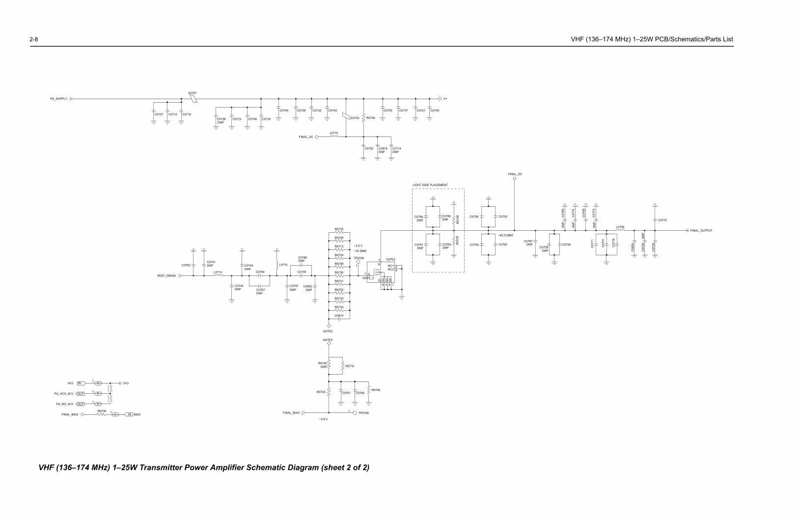
2-8 VHF (136–174 MHz) 1–25W PCB/Schematics/Parts List
~45.5 DBM
C0753
C0762 C0750C0728
C0767
DNP
DNP
C07
35C07
51
C07
18
C0770
C07
73
L0706
C07
68
C07
74
C07
36
C08
24C07
71
C07
65
DN
P
DN
P
DN
P
DN
P
FINAL_DC
FINAL_OUTPUT
VHF
PA_SUPPLY
E0701
C0730C0748C0723C0739C0716C0712C0707
DNP
FINAL_DC
C0742C0733C0726C0745
L0710
C0740C0721C0737C0755
R0736E0703
A+
C0714C0818C0752DNPDNP
LIGHT SIDE PLACEMENT
BIAS1R0739
1
1
1PA_RO_9V3
9V39V3
FINAL_BIAS
PA_VCO_9V3
IN
IN
OUT
OUT
~3.8 V
1
R0746
TP0708
C0761
R0710R0742
C0764R0743
GATE2
DNP
GATE2
FINAL_BIAS
~2.6 V
~33 DBM
R0733
R0732
R0730
R0709 1
TP0706
R0725
R0726
R0713
R0724
R0731
R0734
C0814
C0788
C0787C0803
C0794
C0743
C0744
L0714
C0793C0741
C0749
C0797
L0715
DNP
DNP
DNP
DNP
DNP
DNP
DNP
RD07_DRAIN
NC1NC2
S4
S3
S2
DS
1
G
8 5 4 1
62
7
3 Q0702
GATE_2
R07
29
DNP
C0786DNP
C0784
C0783C0781
R07
28
DNP
DNP
C0759
C0758
(136–174 MHz) 1–25W Transmitter Power Amplifier Schematic Diagram (sheet 2 of 2)
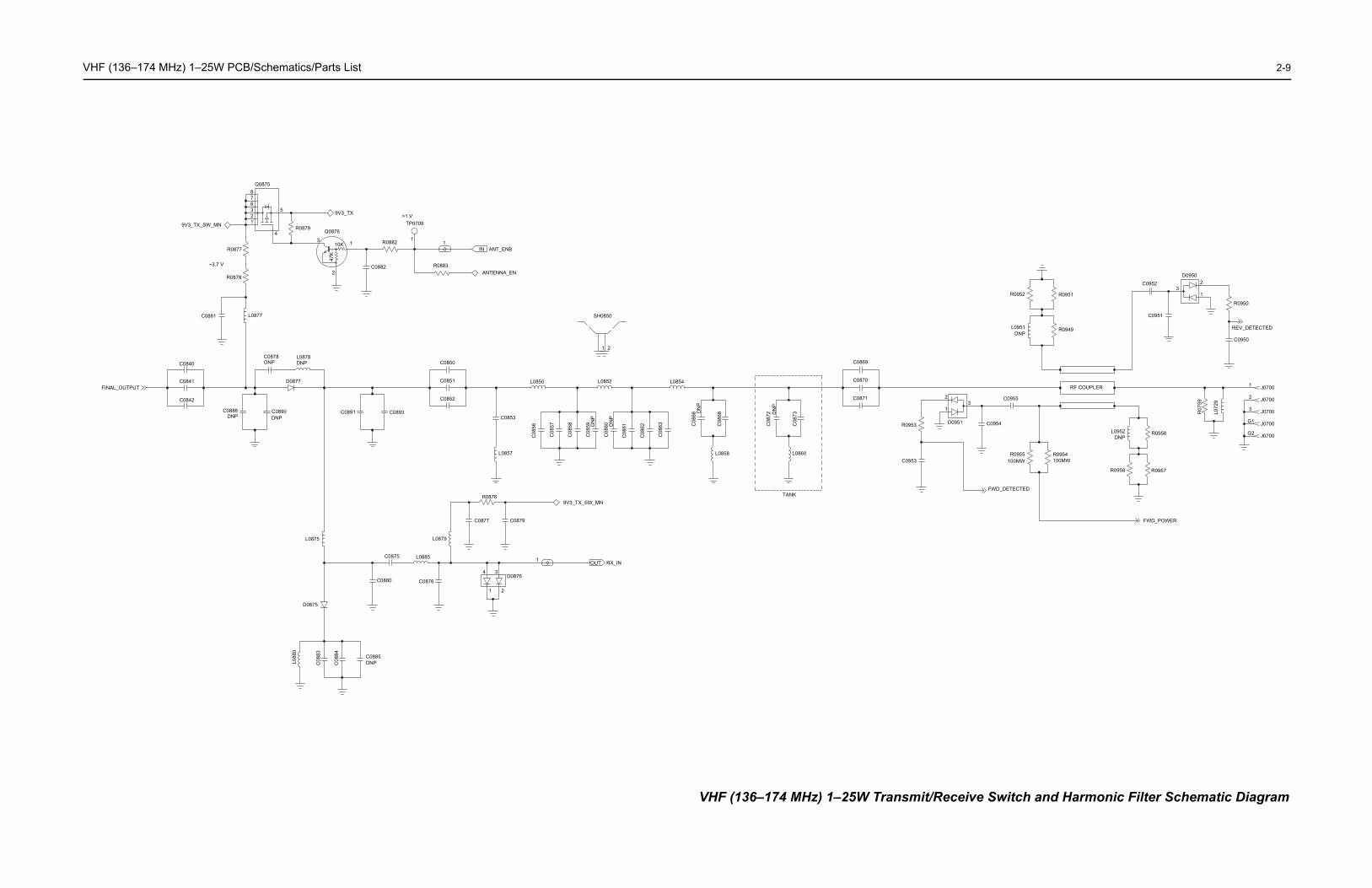
V 2-9
C0869
C0871
C0870
C0955
C0954
23
1
D0951R0953
C0953R0954R0955
100MW 100MW
FWD_DETECTED
RF COUPLER
R0951R0952
R0949L0951DNP
J0700G2
J0700
R0950
2 J0700
1 J0700
C0950
3 J0700
G1
23
1
D0950
C0951
C0952
REV_DETECTED
L072
9
R07
59
R0957
DNPL0952
R0958
FWD_POWER
R0956
25W Transmit/Receive Switch and Harmonic Filter Schematic Diagram
HF (136–174 MHz) 1–25W PCB/Schematics/Parts List
47K
10K
Q0876R0879
1
9V3_TX
R08823
2C0882
5
4
876321
Q0875
~3.7 V
R0878
9V3_TX_SW_MN
C0881
R0877
L0877
C0840
C0842
C0841FINAL_OUTPUT
C0890C0888
L0878C0878
D0877
DNP DNP
DNP DNPC0893C0891
C0852
C0850
C0851 L0854
21
SH0850
L0852L0850
C08
56
C08
61
C08
59
C08
60
C08
58
C08
63
C08
62
C08
57
C0853
L0857
DN
P
DN
P
TANK
L0858
C08
73
C08
72
L0860
C08
68
C08
66 DN
P
DN
P
>1 VTP0709
ANTENNA_EN
ANT_ENB
R0883
11
IN
C0885
L0885
C0876
C0875
C0880
C08
84
L0875
D0875
C08
83
L088
0
DNP
3D0876
RX_IN
C0879C0877
1
R0876
L0879
1 2
4
9V3_TX_SW_MN
OUT
VHF (136–174 MHz) 1–
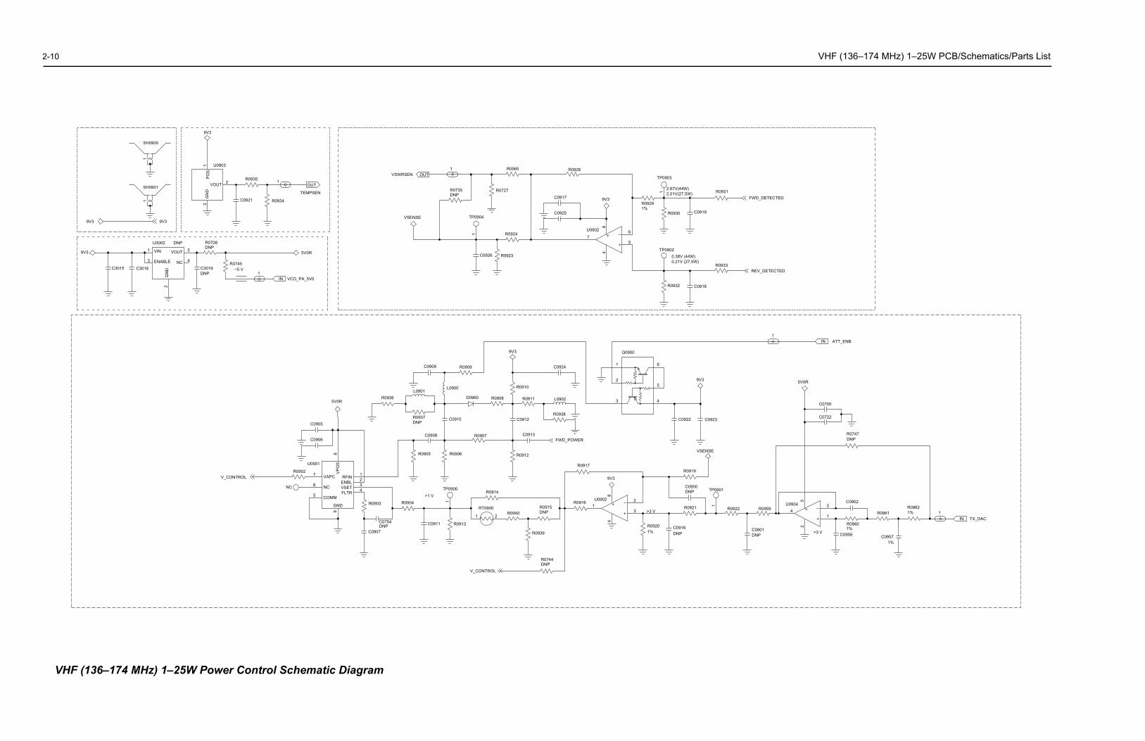
2-10 VHF (136–174 MHz) 1–25W PCB/Schematics/Parts List
0919
R0931FWD_DETECTED
)
0918
R0933REV_DETECTED
VSENSE
R0922
TP0901
1
R0959
>3 VDNPC0901
14
52
3U0904
1%
TX_DAC1%
R0960
C0902
R0961
C0957
R09621
1%C0956
IN
5V0R
DNP
1
R0747
C0722
ATT_ENB
C0700
IN
9V3
C0923
VHF
9V3
SH0901
1 21 2
SH0900
9V3
PO
SG
ND
VOUT
9V3
TEMPSEN
U0903
3
2
C0921
R0935 1
R09341
OUT
~5 V
5V0R
VCO_PA_5V0
R0745
1IN
VOUT
ENABLE
GN
D
VIN
NC
9V3
DNP
DNPDNP
C3015
3
2
1 5
4
U3002 R0708
C3019C3016
DNP
TP0904
R0735
VSWRSEN
VSENSE
R0965
C0926 R0923
1
R0928
R0727
R0924
1OUT
C0925
C0917
U0902
57
84
9V3
6
2.67V(44W)2.01V(27.5W)
1%R0929
1
C
TP0903
R0930
0.21V (27.5W0.38V (44W)
C
TP0902
R0932
RFINENBLVSETFLTR
VP
OS
COMM
NC
VAPC
GND
5V0R
V_CONTROL
U0901
5
2
46
17
8
3
R0902
C0906
C0905
NC
L0901
C0909 R0909
R0936
L0900
R0908D0960
9V3
FWD_POWER
R0905 R0906
R0937
R0907
R0912
C0913
R0910
R0911
R0938
C0908
DNPC0910 C0912
L0902
C0924
>1 V
DNP
9
C0907
R0903 R0904
C0911 R0913
TP0900
C0754
1
>3 V
DNPV_CONTROL
9V3
RT0900
21
R0915R0916
U0902 2
31
84
R0917
R0744
DNPR0940
R0914
R0939 1% DNP
DNP
R0920 C0916
R0921
C0900
R0919
C0922
Q0900
1 6
5
3 4
2
(136–174 MHz) 1–25W Power Control Schematic Diagram
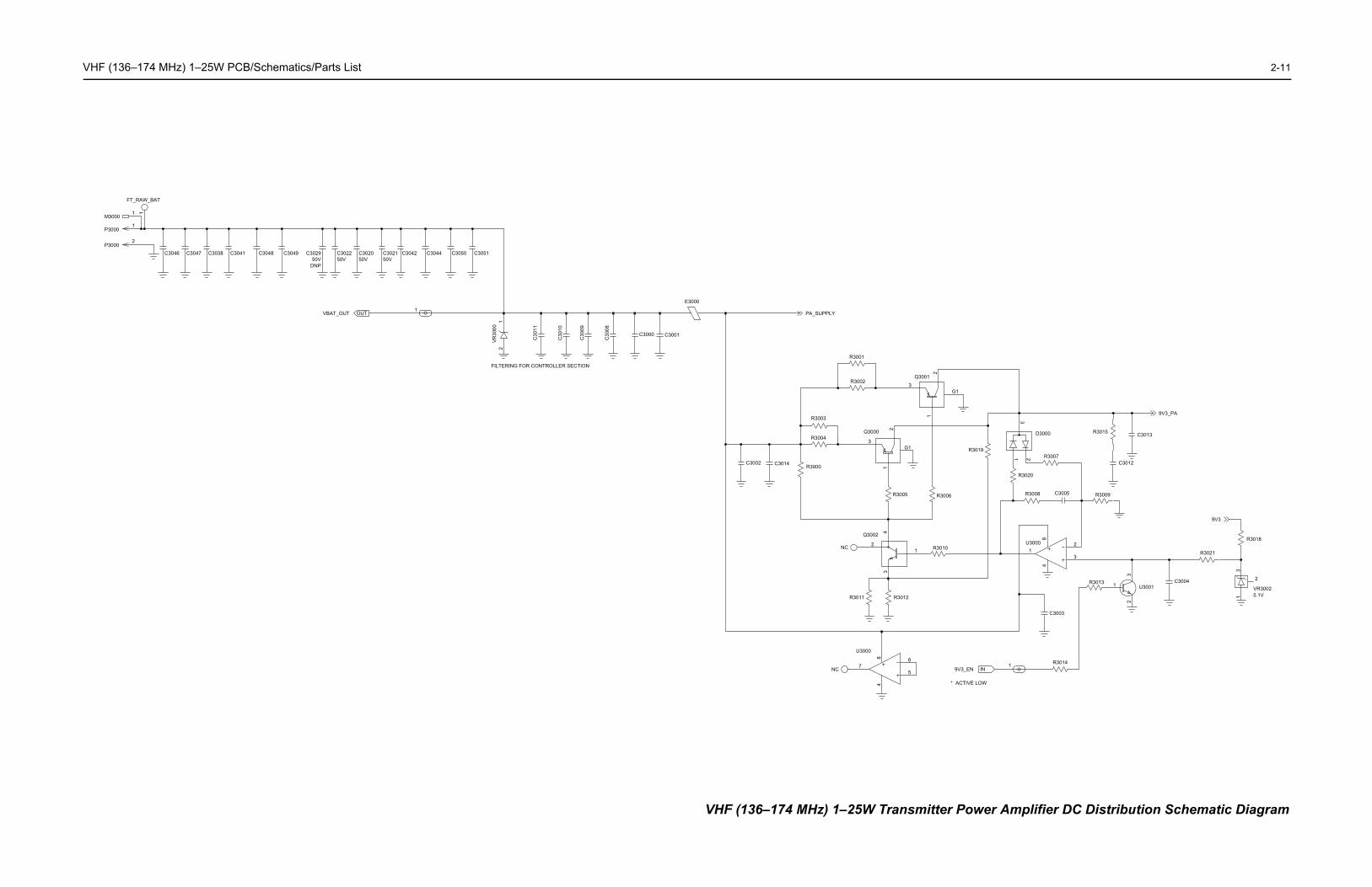
V 2-11
1
R3001
R3002
G13
21
Q3001
G13
21
Q3000
R3019
R3006R3005
R3010
34
21
Q3002
NC
R3012R3011
48
75
6
U3000
C
* ACTIVE LOW
9V3_EN IN
R3013 C3004
23
1 U3001
C3003
R30141
48
3
2U3000
R3009
23
1
D3000
R3007
C3005R3008
R3020
R3015 C3013
C3012
9V3_PA
R3018
R3021
13
2
VR3002
9V3
5.1V
–25W Transmitter Power Amplifier DC Distribution Schematic Diagram
HF (136–174 MHz) 1–25W PCB/Schematics/Parts List
C3051C3050
1M3000
C3044C3042C3021C3020C3022C3029C3049C3048C3041C3038C3047C3046
1
FT_RAW_BAT
1P3000
2P3000
50VDNP50V 50V50V
1VBAT_OUT OUT
FILTERING FOR CONTROLLER SECTION
C3001C3000
C30
08
C30
09
C30
10
C30
11
21
VR
3000
E3000
PA_SUPPLY
R3003
R3004
R3000C3014C3002
N
VHF (136–174 MHz) 1
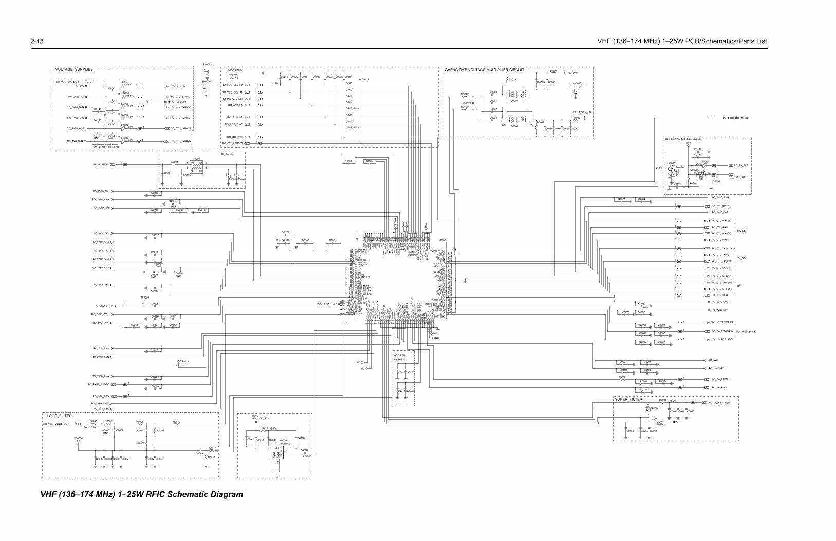
2-12 VHF (136–174 MHz) 1–25W PCB/Schematics/Parts List
LOO
RO_VCO
CIRCUIT L0000
C0086C0085R0029
RO_5V0
21
SH0003
R0019
R0030
VDD14_SYN_CP
K2K3
A1A2A3
K1
K2K3
A1A2A3
K1 3
C0070C0068C0067C0066
12
654
D0000
123
654
D0001 NC
1 RO_CTL_19.2REOUT
+9.3V
+9.1V
9R1 SWITCH FOR FRONT-END
C01361
C0137
3
1
C0135
E0009
12Q0002
R0044
RO_RXFE_9R1
RO_PA_9V3
9V3
IN
OUT
+1.8V
47K
10K
2
C0111
31
Q0001
C0092C0021
1
1
1
1
1
1
1
1
1
1
1
1
1
TX_SSI
SPI
RX_SSI
RO_2V80_SYN
RO_2V80_RX
RO_CTL_CEX
RO_CTL_RSTB
RO_1V80_DIG
RO_CTL_RXCLK
RO_CTL_SPICLK
RO_CTL_SPI_DW
RO_CTL_SPI_DR
RO_CTL_DMCS
RO_CTL_TX_CLK
RO_CTL_TXFS
RO_CTL_TXD
RO_CTL_RXFS
RO_CTL_RXD
RO_CTL_RXACQ
RO_1V80_DIG
IN
OUT
OUT
IN
OUT
IN
OUT
OUT
IN
IN
IN
OUT
IN
ALC_FEEDBACK
RO_PA_VSWRSEN
RO_PA_BATTSEN
RO_PA_TEMPSEN
IN
IN
IN
RO_5V0
RO_2V80_RX
RO_PA_BIAS
RO_PA_RAMP
RO_VCO_SF_OUT
OUT
OUT
OUT1
1
1
C0099
C0120
C0100
R0008
C0024
C0150
C0134
R0054
+8.2V
+9.3V
SUPER_FILTER
C0065Q0000
C0072C0071
R0015
R0014
C0061
23
1
C0059C0055
9V3
1C0037
C0032
C00091
1
C0093
C0094
C0095
C0096
C0097
C0149
DNP
VHF
VOLTAGE SUPPLIES
1
RO_2V80_RX
RO_VCO_5V0
RO_1V8_SYN
RO_1V80_DIG
RO_1V80_ANA
RO_5V0
RO_2V80_SYN
OUT
C0141
C0101
C0102
C0138
DNPC0105
C0103
C0104
C0140
C0143
C0144
DNP
+5V
+2.8V
+2.8V
+1.8V
+1.8V
+1.8V
1E0006
1
E0007
E0005
1
E0004
1
1
1
1
E0008
E0010
RO_CTL_5V
RO_CTL_2V8DIG
RO_RX_2V80
RO_CTL_2V8ANA
RO_CTL_1V8DIG
RO_CTL_1V8ANA
RO_CTL_1V8SYN
OUT
IN
IN
IN
IN
IN
IN
RO_RXBE_IN
RO_2V80_RX
RO_1V80_ANA
RO_2V80_RX
IN 1 P1
P2
S1
S2
L0001
4
1
3
2
T0000
C0091C0089
DNP
C0016
C0018
C0013
C0039 C0035
RO_2V80_RX
RO_1V80_ANA
RO_2V80_RX
RO_1V80_ANA
RO_1V80_ANA
1RO_VCO_IN
RO_1V8_SYN
RO_2V80_SYN
RO_1V8_SYN
IN
RO_2V80_SYN
RO_1V8_SYN
RO_2V80_SYN
RO_CTL_RSSI
RO_1V8_SYN
RO_RXFE_AXDAC
RO_1V80_ANA
OUT
OUT
1
1
1
TP0011
C0023
C0029
C0056
1
TP0001
C0053 C0042
C0025
C0026
C0027
C0030
C0031
DNPC0022
C0014
C0017
C0019
C0139 DNPDNP
FE_BALUN
E0000E0001
2121
SH0000
SH0001
LOW:0VHI:1.8V
GPO_LINES
1
RO_ANT_EN
1
1
1
1
1
1
1
RO_AGC_FLAG
RO_VCO_SEL_RX
RO_VCO_SEL_TX
RO_CTL_LCKDET
RO_PW_CTL_ATT
RO_RF_STEP
RO_CTL_TTR
OUT
OUT
OUT
OUT
OUT
OUT
OUT
OUT
+1.8V
C0015 C0010C0036C0033C0020C0124
C0098C0054
GPO6
GPO8 (NC)
GPO7
GPO5 (NC)
GPO3
GPO1
GPO2
GPO4
C0064C0060
C0001C0147
C0145
C0146
VDD14_SYN_CP B13
B12
A1
A4
A14
B3
B9A10
B11
B4
B10
A12
A16
A15
B5
B2
A6
A5
A3
A2
A7
A8
A13
B7
B15
B14
A11
A9B8
B6
B1
A38
A46
A47
B42
A48
B33
B34
A40B38
B37
B31
B35
B36
B32
B44
B40
A44
A45
B41A43
B43
A36
B45
B39A41
A39
A42
A37
A35
A34
A33
U0000
A21
A28
B21
B16
B26
A25
B18
B17
A18
A24
B23
B19
A22
B20
A19
A31
B29
B27
A30
A27
A26
B25
B24
B30
A32
B22
A23
A20
A17 G
1
A29
B28
NC
NC
BYPASS
ADC REF
C0073 C0075
C0076C0074
NC
NC
NCN
CN
C
1TP
0002
VDD28_VMULTIGPO9
VMULT1SCAN_EN
VMULT2RSTB
RXCLK_IO
RXDVDD33_DIG
RXACQRX_EN_OUT
RXFS
GND12CLK_OUT
GP
O8
TES
T2_C
HR
PS
W
TES
T1_L
CK
DE
TD
CC
AL_
GP
O5
AG
C_F
LG_G
PO
7R
FSTE
PA
_GP
O6
GP
O4_
TES
T4
GP
O2_
TES
T2G
PO
3_TE
ST3
GP
O1_
TES
T1M
IC_I
NM
IC_I
NB
GN
D13
GN
D14
GND11TXD
TXFSTXCLK
DMCSSPI_CLK
SPI_DRSPI_DW
CEXVDD18_DIG_2
NC7VDD28_DAC_ADC_2
ALC_VSWRSENSSCAN_IN
ALC_PATEMPTM
ALC_BATTSENS
CTG
ND
GP
AD
C_I
N_4
GP
AD
C_I
N_5
RA
MP
NC
16N
C6
AD
C_R
EF1
_BY
PA
DC
_RE
F2_B
YP
NC
15
VD
D28
_DA
C_A
DC
_1V
DD
HV
5_D
AC
NC
5G
PD
AC
_OU
T_2
HP
_MO
D_O
UT
VD
D18
_TX
RF
GP
DA
C_O
UT_
1
VD
D28
_PM
AV
DD
18_P
MA
AG
C_D
AC
AG
C_R
EF
MIX
OU
T_I
MIX
OU
T_IX
MIX
OU
T_Q
XM
IXO
UT_
Q
NC
8N
C17
NC
9N
C18
NC
10G
ND
15N
C11
GN
D16
NC
12
VDD28_MIXBYP_TO_2P7
NC13NC1
VDD28_LNA_1
NC2VDD18_QG
VDD18_LNANC3
NC4NC14
GND2LTD_INBGND_LNA_LTD
TX1_
OU
TS
PK
R_D
AC
_OU
T
GN
D10
GN
D9
VD
D28
_SF
SF_
OU
T
VD
DH
V10
_SF
SF_
BY
P
SF_
SE
NS
GN
D8
VD
D18
_RE
F_C
LK
VD
D18
_FG
U2_
PS
RE
F_IN
VC
O2_
INV
DD
28_F
GU
2_C
PFG
U2_
CP
_OU
T
LTD_INGND3GND4
VDD18_LO_DIVVDD18_MIX_1
VDD18_DIV_PSGND5VDD18_LO_DCA
VDD28_SYNVCO1_IN
GND_LO_DCAVDDHV14_SYN_CPVDD18_SYN
GND7SYN_ACPUMP
GND6
SYN_MCPUMP
B47
A56
B53
B46
B48
B58
B57
A64
A63
A62
A61
A60
B56
A59
B55
A58
B51
A54
A49
A52
B49
A53
B50B
60
B59
B52
A55
A50
B54
A51
A57
1.5V - 10.5V
P_FILTER
_VCTRL 1 R0000
TP0000
C0006
C0007C0005C0002
1
R0001
C0003
C0034C0012C0004
DNP
OUTR0010
R0009C0011
R0006
R0007
R0012
C0043R0011 19.2MHZ
+2.8V
TCXO
GN
D1
VCC
GN
D2
OU
T
4
Y0000
RO_2V80_SYN
R0013
C0045
C00493
C0028 C0046
21
C004419.2MHZ
CAPACITIVE VOLTAGE MULTIPLIER
NC
C0080
C0081
C0083
C0082
C0078
R0022
R0025
(136–174 MHz) 1–25W RFIC Schematic Diagram
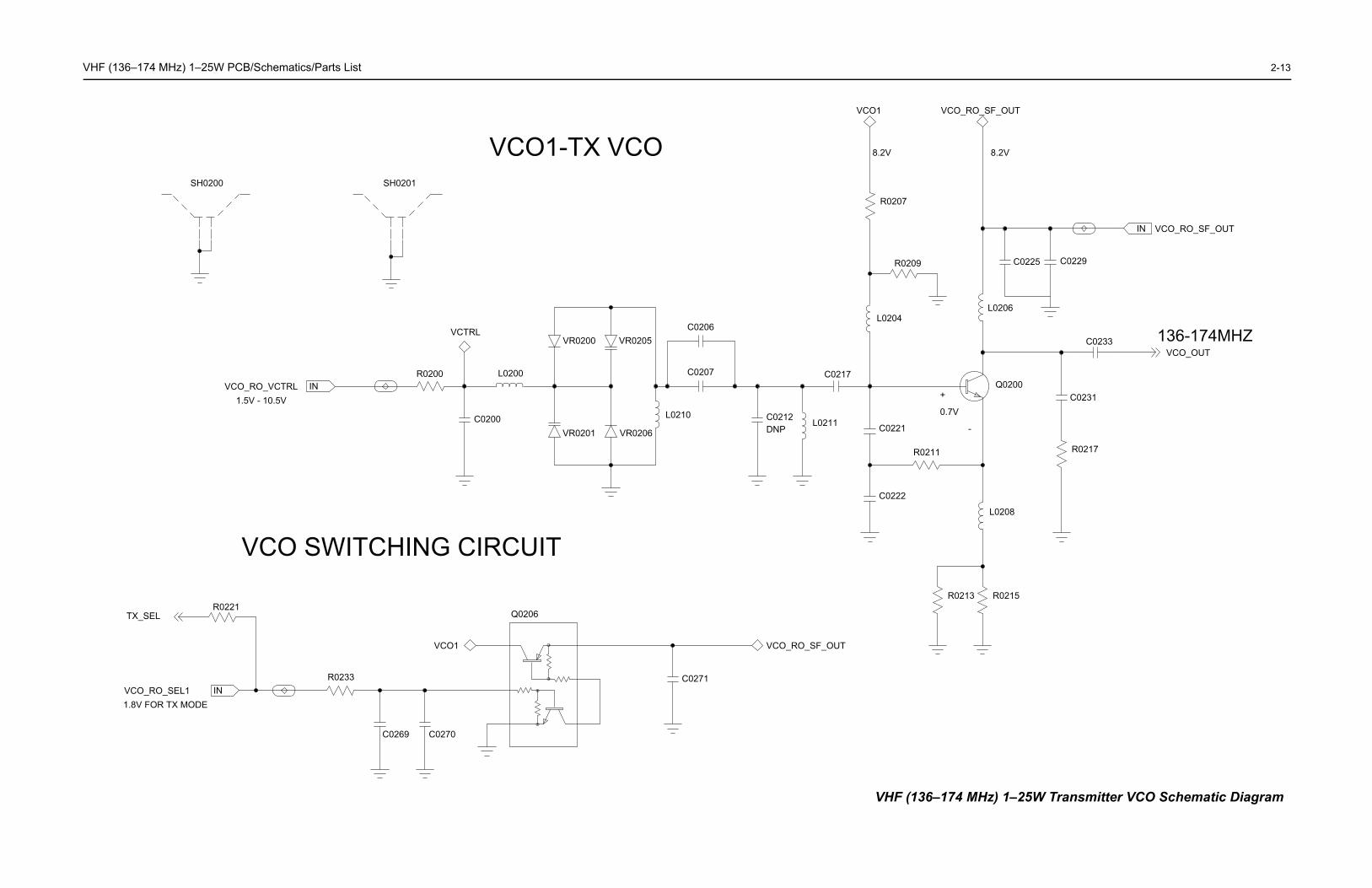
V 2-13
0.7V
+
-
Q0200C0231
C0233
C0221
R0217
C0222
R0211
L0208
R0213 R0215
T
8.2V
R0209
L0204
R0207
217
8.2V
VCO_RO_SF_OUT
VCO_RO_SF_OUTVCO1
IN
136-174MHZVCO_OUT
C0225
L0206
C0229
VHF (136–174 MHz) 1–25W Transmitter VCO Schematic Diagram
HF (136–174 MHz) 1–25W PCB/Schematics/Parts List
VCO1-TX VCOSH0200 SH0201
1.5V - 10.5V
C0200
VCTRL
VCO_RO_VCTRLR0200 L0200
IN
VR0200
VR0201
VR0205
C0207
C0206
L0210
VR0206
VCO SWITCHING CIRCUIT
VCO_RO_SF_OU
C0271
1.8V FOR TX MODEVCO_RO_SEL1
VCO1
R0221TX_SEL
R0233
C0269
Q0206
IN
C0270
DNPC0212 L0211
C0
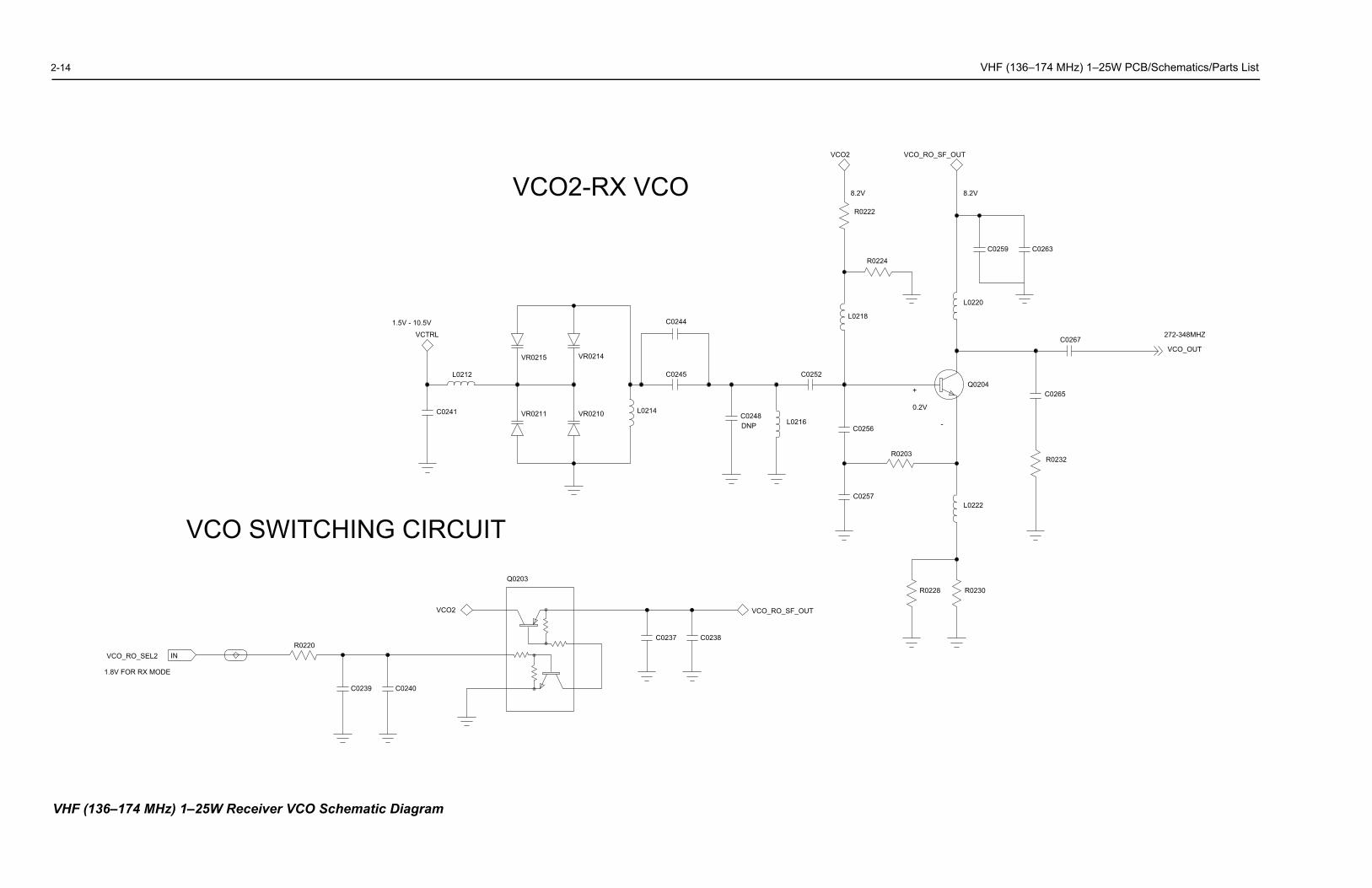
2-14 VHF (136–174 MHz) 1–25W PCB/Schematics/Parts List
C0256
0.2V
-
+
C0267
R0232
C0265Q0204
L0220
C0259 C0263
8.2V8.2V
VCO_RO_SF_OUTCO2
R0222
R0224
L0218
L0222
R0203
C0257
R0228 R0230
272-348MHZ
VCO_OUT
VHF (
VCO2-RX VCO
1.5V - 10.5V
VR0215
VR0211
VCTRL
L0212
VR0214
VR0210C0241
DNP
C0244
C0248L0216
C0252
L0214
C0245
V
VCO_RO_SF_OUT
C0237 C0238
VCO SWITCHING CIRCUIT
VCO2
Q0203
R0220
C0239 C0240
1.8V FOR RX MODE
VCO_RO_SEL2 IN
136–174 MHz) 1–25W Receiver VCO Schematic Diagram
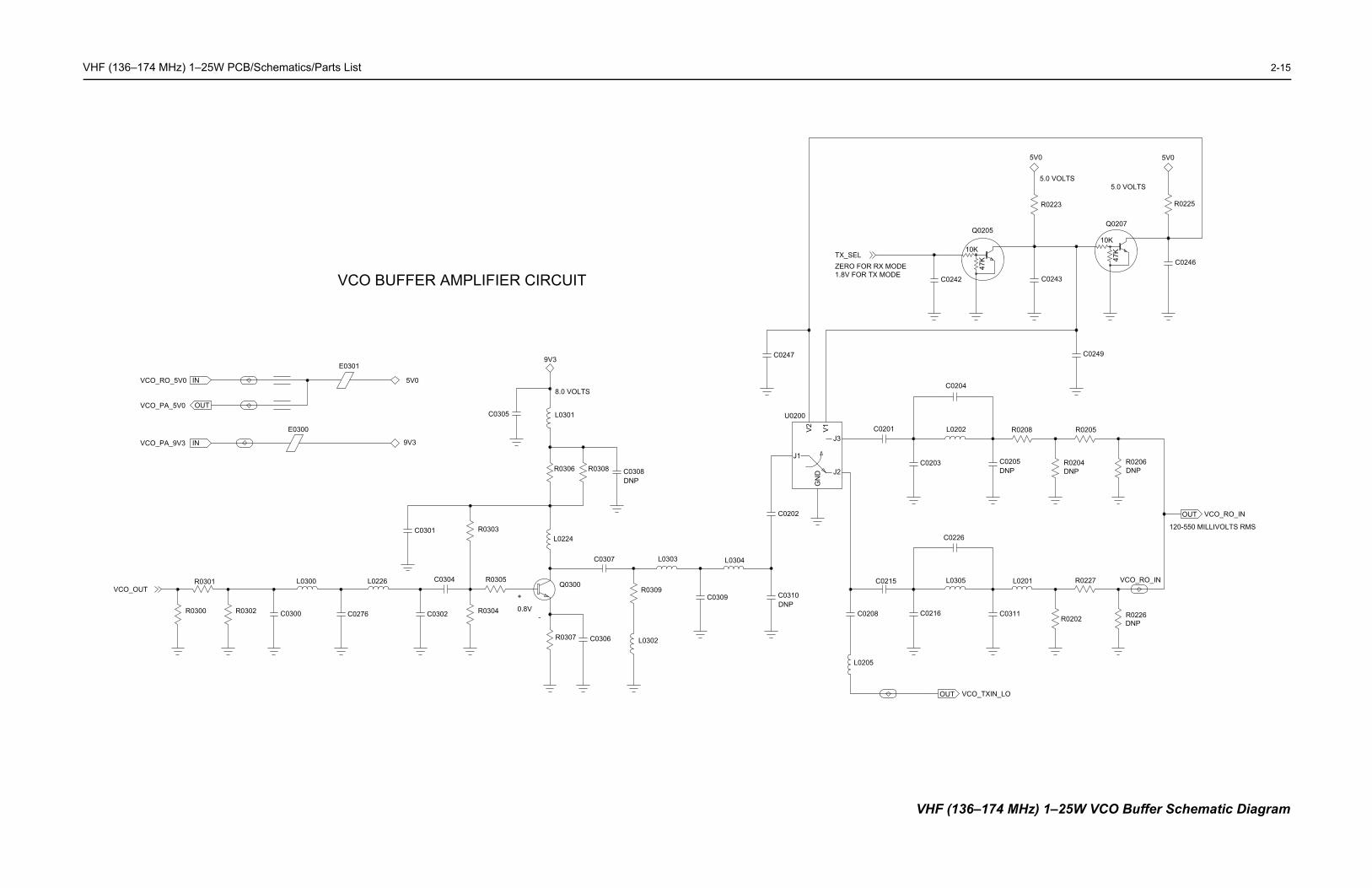
V 2-15
1.8V FOR TX MODEZERO FOR RX MODE 47
K
10K
Q0205
C0242
TX_SEL
5.0 VOLTS
C0243
R0223
5V0
5.0 VOLTS
47K
10K
Q0207
C0246
R0225
5V0
C0249
DNP
R0208
R0204C0205
R0205
R0206DNP DNP
C0201
C0203
L0202
C0204
2
3
C0216
VCO_TXIN_LO
C0215
DNP
L0205
C0208R0202
L0201 R0227
R0226
VCO_RO_IN
C0311
C0226
L0305
OUT
120-550 MILLIVOLTS RMS
VCO_RO_INOUT
VHF (136–174 MHz) 1–25W VCO Buffer Schematic Diagram
HF (136–174 MHz) 1–25W PCB/Schematics/Parts List
VCO BUFFER AMPLIFIER CIRCUIT
VCO_PA_9V3
VCO_RO_5V0
VCO_PA_5V0
E0300
E0301
IN
OUT
IN
9V3
5V0
C0300
C0304L0226
C0302C0276
L0300R0301
R0302R0300
VCO_OUT
0.8V-
+
R0307
Q0300
R0304
L0304
C0310C0309
L0303C0307
L0224
R0309
L0302C0306
R0303
R0305
C0301
DNP
C0308R0306 R0308
DNP
8.0 VOLTS
9V3
L0301C0305
J1
V2
V1
GN
D J
J
U0200
C0202
C0247
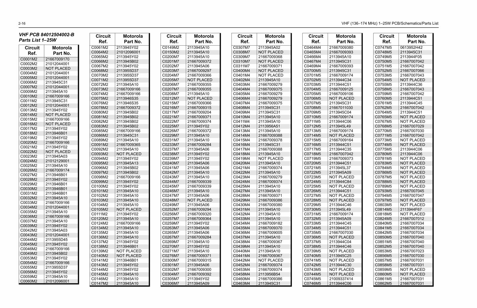
2-16 VHF (136–174 MHz) 1–25W PCB/Schematics/Parts List
VHF PParts
CirR
C000C000C000C000C000C000C000C000C001C0011C001C001C001C001C001C001C001C001C002C002C002C002C002C002C002C002C002C002C003C003C003C003C003C003C003C003C003C004C004C004C004C004C004C005C005C005C005C005C006
C0464M4 21667009380C0465M4 21667009393C0466M4 2113945A10C0467M4 2113945C31C0469M4 21667009393C0700M5 2113945C31C0701M5 21667009174C0702M5 2113944C34C0703M5 2113944C51C0704M5 21667009125C0705M5 21667009106C0706M5 NOT PLACEDC0707M5 2113945C31C0708M5 21667011030C0709M5 2113945C04C0710M5 21667009174C0711M5 2113944C06C0712M5 2113945L49C0713M5 21667009174C0714M5 NOT PLACEDC0715M5 21667009164C0716M5 2113944C51C0717M5 2113944C35C0718M5 21667007042C0719M5 21667009373C0720M5 2113944C51C0721M5 2113945L37C0722M5 2113945A09C0723M5 NOT PLACEDC0724M5 2113944C84C0725M5 NOT PLACEDC0726M5 2113944C51C0727M5 NOT PLACEDC0728M5 NOT PLACEDC0729M5 2113944C46C0730M5 2113945L49C0731M5 21667009174C0732M5 2113945A09C0733M5 2113944C45C0734M5 2113944C51C0735M5 21667007030C0736M5 NOT PLACEDC0737M5 2113944C04C0738M5 2113944C46C0739M5 NOT PLACEDC0740M5 2113945C25C0741M5 NOT PLACEDC0742M5 2113944C30C0743M5 NOT PLACEDC0744M5 NOT PLACEDC0745M5 21009337414C0746M5 2113944C06
CircuitRef.
MotorolaPart No.
C0747M5 0613952H42C0748M5 2113945C31C0749M5 2113944F05C0750M5 21667007042C0751M5 21667007042C0752M5 21667007066C0753M5 21667007043C0754M5 NOT PLACEDC0755M5 2113944C36C0758M5 21667007043C0759M5 21667007042C0760M5 2113944C51C0761M5 2113944C45C0762M5 21667007042C0764M5 2113944C51C0765M5 NOT PLACEDC0767M5 NOT PLACEDC0768M5 21667007029C0770M5 21667007030C0771M5 21667007042C0773M5 NOT PLACEDC0774M5 NOT PLACEDC0775M5 2113944C06C0780M5 2113944C06C0781M5 NOT PLACEDC0783M5 NOT PLACEDC0784M5 NOT PLACEDC0786M5 NOT PLACEDC0787M5 NOT PLACEDC0788M5 NOT PLACEDC0789M5 NOT PLACEDC0793M5 21667007045C0794M5 21667007047C0797M5 NOT PLACEDC0803M5 NOT PLACEDC0814M5 2113944F67C0818M5 NOT PLACEDC0824M5 21667007012C0840M5 21667007034C0841M5 21667007034C0842M5 21667007034C0850M5 21667007040C0851M5 21667007040C0852M5 21667007040C0853M5 21667007023C0856M5 21667007030C0857M5 21667007031C0858M5 21667007031C0859M5 NOT PLACEDC0860M5 NOT PLACEDC0861M5 21667007031C0862M5 21667007031
CircuitRef.
MotorolaPart No.
CB 84012504002-B List 1–25Wcuitef.
MotorolaPart No.
1M2 216670091702M2 210120440013M2 NOT PLACED4M2 210120440015M2 210120440016M2 2113945C317M2 210120440019M2 2113945A100M2 21667009166M2 2113945C31
2M2 210120440013M2 2113945Y024M2 NOT PLACED5M2 216670091666M2 NOT PLACED7M2 2113945Y028M2 2113946B019M2 2113945Y020M2 216670091661M2 2113945Y022M2 NOT PLACED3M2 2113945A034M2 210121290015M2 2113945A106M2 216670091747M2 2113946B018M2 2113945Y029M2 2113946B010M2 2113946B011M2 2113946B012M2 2113945A103M2 216670091664M2 210120440015M2 2113945A106M2 216670091667M2 2113945A109M2 2113945Y022M2 2113945A033M2 210120440014M2 2113955D455M2 2113945Y026M2 216670091669M2 2113945B023M2 2113945Y024M2 216670091665M2 2113955D376M2 2113945Y029M2 2113945A100M2 21012096001
C0061M2 2113945Y02C0064M2 21012096001C0065M2 2113945Y02C0066M2 2113945B02C0067M2 2113945Y02C0068M2 2113955D37C0070M2 2113955D37C0071M2 2113955D37C0072M2 2113945A10C0073M2 21667009166C0074M2 21667009166C0075M2 2113946S35C0076M2 2113946S35C0078M2 21667009372C0080M2 2113945B02C0081M2 2113945B02C0082M2 2113945B02C0083M2 2113945B02C0085M2 21667009166C0086M2 2113945C31C0089M2 2113945A10C0091M2 21667009365C0092M2 2113945A10C0093M2 NOT PLACEDC0094M2 2113945Y02C0095M2 2113945A13C0096M2 2113945B02C0097M2 2113945B02C0098M2 21667009166C0099M2 2113945Y02C0100M2 2113945Y02C0101M2 2113945A10C0102M2 2113945A10C0103M2 2113945A10C0104M2 2113945A10C0105M2 NOT PLACEDC0111M2 2113945Y02C0120M2 2113945A10C0124M2 21667009166C0134M2 2113945A10C0135M2 2113945A10C0136M2 2113945A10C0137M2 2113945Y02C0138M2 2113946B01C0139M2 NOT PLACEDC0140M2 NOT PLACEDC0141M2 2113946B01C0143M2 2113945Y02C0144M2 2113945Y02C0145M2 2113945A10C0146M2 2113945A10C0147M2 2113945A10
CircuitRef.
MotorolaPart No.
C0149M2 2113945A10C0150M2 2113945A10C0200M7 2113945A10C0201M7 21667009372C0202M7 2113945A06C0203M7 21667009297C0204M7 21667009366C0205M7 NOT PLACEDC0206M7 21667009355C0207M7 21667009355C0208M7 2113945A10C0212M7 NOT PLACEDC0215M7 21667009366C0216M7 21667009315C0217M7 21667009204C0221M7 21667009371C0222M7 21667009374C0225M7 2113945Y02C0226M7 21667009372C0229M7 2113945A10C0231M7 2113945A10C0233M7 21667009284C0237M7 2113945A06C0238M7 2113945Y02C0239M7 2113945Y02C0240M7 2113945A06C0241M7 2113945A06C0242M7 2113945A10C0243M7 2113945A10C0244M7 21667009339C0245M7 21667009339C0246M7 2113945A10C0247M7 2113945A06C0248M7 NOT PLACEDC0249M7 2113945A06C0252M7 21667009294C0256M7 21667009320C0257M7 21667009364C0259M7 2113945Y02C0263M7 2113945A06C0265M7 2113945A06C0267M7 21667009284C0269M7 2113945A10C0270M7 2113945Y02C0271M7 2113945A10C0276M7 21667009371C0300M7 21667009315C0301M7 2113945A06C0302M7 21667009300C0304M7 21667009392C0305M7 2113945Y02C0306M7 2113945A09
CircuitRef.
MotorolaPart No.
C0307M7 2113945A02C0308M7 NOT PLACEDC0309M7 21667009368C0310M7 NOT PLACEDC0311M7 21667009371C0400M4 NOT PLACEDC0401M4 NOT PLACEDC0402M4 2113945A10C0403M4 21667009279C0404M4 21667009375C0405M4 21667009279C0406M4 21667009279C0407M4 21667009375C0408M4 2113945C31C0409M4 2113945C31C0410M4 2113945A10C0411M4 2113945A10C0412M4 2113956A51C0413M4 2113945A10C0414M4 21667009388C0415M4 21667009378C0416M4 2113945C31C0417M4 21667009388C0418M4 2113945A10C0419M4 NOT PLACEDC0420M4 2113945A10C0421M4 21667009374C0422M4 2113945A10C0423M4 21667009279C0424M4 21667009374C0425M4 2113945A10C0427M4 2113945A10C0428M4 21667009371C0429M4 21667009386C0430M4 21667009380C0431M4 2113945A10C0432M4 2113945A10C0433M4 2113945A10C0434M4 21667009182C0435M4 21667009370C0436M4 21667009005C0437M4 2113945A10C0438M4 21667009367C0439M4 2113945A10C0440M4 2113945A10C0441M4 21667009367C0442M4 NOT PLACEDC0452M4 21667009374C0453M4 21667009374C0458M4 2113956B54C0460M4 21667009386C0463M4 2113945C31
CircuitRef.
MotorolaPart No.
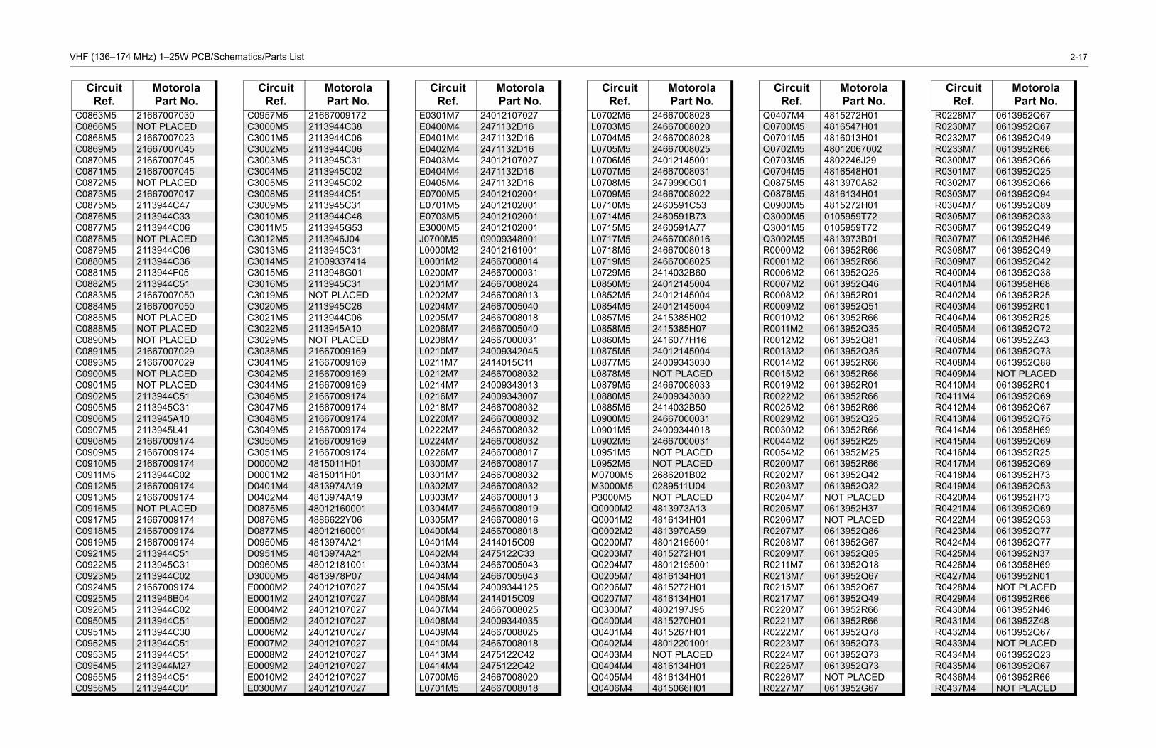
V 2-17
808511
2
685
444
40D30
181DD
D
1
1
1D
lao.
Q0407M4 4815272H01Q0700M5 4816547H01Q0701M5 4816013H01Q0702M5 48012067002Q0703M5 4802246J29Q0704M5 4816548H01Q0875M5 4813970A62Q0876M5 4816134H01Q0900M5 4815272H01Q3000M5 0105959T72Q3001M5 0105959T72Q3002M5 4813973B01R0000M2 0613952R66R0001M2 0613952R66R0006M2 0613952Q25R0007M2 0613952Q46R0008M2 0613952R01R0009M2 0613952Q51R0010M2 0613952R66R0011M2 0613952Q35R0012M2 0613952Q81R0013M2 0613952Q35R0014M2 0613952R66R0015M2 0613952R66R0019M2 0613952R01R0022M2 0613952R66R0025M2 0613952R66R0029M2 0613952Q25R0030M2 0613952R66R0044M2 0613952R25R0054M2 0613952M25R0200M7 0613952R66R0202M7 0613952Q42R0203M7 0613952Q32R0204M7 NOT PLACEDR0205M7 0613952H37R0206M7 NOT PLACEDR0207M7 0613952Q86R0208M7 0613952G67R0209M7 0613952Q85R0211M7 0613952Q18R0213M7 0613952Q67R0215M7 0613952Q67R0217M7 0613952Q49R0220M7 0613952R66R0221M7 0613952R66R0222M7 0613952Q78R0223M7 0613952Q73R0224M7 0613952Q73R0225M7 0613952Q73R0226M7 NOT PLACEDR0227M7 0613952G67
CircuitRef.
MotorolaPart No.
R0228M7 0613952Q67R0230M7 0613952Q67R0232M7 0613952Q49R0233M7 0613952R66R0300M7 0613952Q66R0301M7 0613952Q25R0302M7 0613952Q66R0303M7 0613952Q94R0304M7 0613952Q89R0305M7 0613952Q33R0306M7 0613952Q49R0307M7 0613952H46R0308M7 0613952Q49R0309M7 0613952Q42R0400M4 0613952Q38R0401M4 0613958H68R0402M4 0613952R25R0403M4 0613952R01R0404M4 0613952R25R0405M4 0613952Q72R0406M4 0613952Z43R0407M4 0613952Q73R0408M4 0613952Q88R0409M4 NOT PLACEDR0410M4 0613952R01R0411M4 0613952Q69R0412M4 0613952Q67R0413M4 0613952Q75R0414M4 0613958H69R0415M4 0613952Q69R0416M4 0613952R25R0417M4 0613952Q69R0418M4 0613952H73R0419M4 0613952Q53R0420M4 0613952H73R0421M4 0613952Q69R0422M4 0613952Q53R0423M4 0613952Q77R0424M4 0613952Q77R0425M4 0613952N37R0426M4 0613958H69R0427M4 0613952N01R0428M4 NOT PLACEDR0429M4 0613952R66R0430M4 0613952N46R0431M4 0613952Z48R0432M4 0613952Q67R0433M4 NOT PLACEDR0434M4 0613952Q23R0435M4 0613952Q67R0436M4 0613952R66R0437M4 NOT PLACED
CircuitRef.
MotorolaPart No.
HF (136–174 MHz) 1–25W PCB/Schematics/Parts List
C0863M5 21667007030C0866M5 NOT PLACEDC0868M5 21667007023C0869M5 21667007045C0870M5 21667007045C0871M5 21667007045C0872M5 NOT PLACEDC0873M5 21667007017C0875M5 2113944C47C0876M5 2113944C33C0877M5 2113944C06C0878M5 NOT PLACEDC0879M5 2113944C06C0880M5 2113944C36C0881M5 2113944F05C0882M5 2113944C51C0883M5 21667007050C0884M5 21667007050C0885M5 NOT PLACEDC0888M5 NOT PLACEDC0890M5 NOT PLACEDC0891M5 21667007029C0893M5 21667007029C0900M5 NOT PLACEDC0901M5 NOT PLACEDC0902M5 2113944C51C0905M5 2113945C31C0906M5 2113945A10C0907M5 2113945L41C0908M5 21667009174C0909M5 21667009174C0910M5 21667009174C0911M5 2113944C02C0912M5 21667009174C0913M5 21667009174C0916M5 NOT PLACEDC0917M5 21667009174C0918M5 21667009174C0919M5 21667009174C0921M5 2113944C51C0922M5 2113945C31C0923M5 2113944C02C0924M5 21667009174C0925M5 2113946B04C0926M5 2113944C02C0950M5 2113944C51C0951M5 2113944C30C0952M5 2113944C51C0953M5 2113944C51C0954M5 2113944M27C0955M5 2113944C51C0956M5 2113944C01
CircuitRef.
MotorolaPart No.
C0957M5 21667009172C3000M5 2113944C38C3001M5 2113944C06C3002M5 2113944C06C3003M5 2113945C31C3004M5 2113945C02C3005M5 2113945C02C3008M5 2113944C51C3009M5 2113945C31C3010M5 2113944C46C3011M5 2113945G53C3012M5 2113946J04C3013M5 2113945C31C3014M5 21009337414C3015M5 2113946G01C3016M5 2113945C31C3019M5 NOT PLACEDC3020M5 2113945C26C3021M5 2113944C06C3022M5 2113945A10C3029M5 NOT PLACEDC3038M5 21667009169C3041M5 21667009169C3042M5 21667009169C3044M5 21667009169C3046M5 21667009174C3047M5 21667009174C3048M5 21667009174C3049M5 21667009174C3050M5 21667009169C3051M5 21667009174D0000M2 4815011H01D0001M2 4815011H01D0401M4 4813974A19D0402M4 4813974A19D0875M5 48012160001D0876M5 4886622Y06D0877M5 48012160001D0950M5 4813974A21D0951M5 4813974A21D0960M5 48012181001D3000M5 4813978P07E0000M2 24012107027E0001M2 24012107027E0004M2 24012107027E0005M2 24012107027E0006M2 24012107027E0007M2 24012107027E0008M2 24012107027E0009M2 24012107027E0010M2 24012107027E0300M7 24012107027
CircuitRef.
MotorolaPart No.
E0301M7 24012107027E0400M4 2471132D16E0401M4 2471132D16E0402M4 2471132D16E0403M4 24012107027E0404M4 2471132D16E0405M4 2471132D16E0700M5 24012102001E0701M5 24012102001E0703M5 24012102001E3000M5 24012102001J0700M5 09009348001L0000M2 24012161001L0001M2 24667008014L0200M7 24667000031L0201M7 24667008024L0202M7 24667008013L0204M7 24667005040L0205M7 24667008018L0206M7 24667005040L0208M7 24667000031L0210M7 24009342045L0211M7 2414015C11L0212M7 24667008032L0214M7 24009343013L0216M7 24009343007L0218M7 24667008032L0220M7 24667008032L0222M7 24667008032L0224M7 24667008032L0226M7 24667008017L0300M7 24667008017L0301M7 24667008032L0302M7 24667008032L0303M7 24667008013L0304M7 24667008019L0305M7 24667008016L0400M4 24667008018L0401M4 2414015C09L0402M4 2475122C33L0403M4 24667005043L0404M4 24667005043L0405M4 24009344125L0406M4 2414015C09L0407M4 24667008025L0408M4 24009344035L0409M4 24667008025L0410M4 24667008018L0413M4 2475122C42L0414M4 2475122C42L0700M5 24667008020L0701M5 24667008018
CircuitRef.
MotorolaPart No.
L0702M5 2466700802L0703M5 2466700802L0704M5 2466700802L0705M5 2466700802L0706M5 2401214500L0707M5 2466700803L0708M5 2479990G01L0709M5 2466700802L0710M5 2460591C53L0714M5 2460591B73L0715M5 2460591A77L0717M5 2466700801L0718M5 2466700801L0719M5 2466700802L0729M5 2414032B60L0850M5 2401214500L0852M5 2401214500L0854M5 2401214500L0857M5 2415385H02L0858M5 2415385H07L0860M5 2416077H16L0875M5 2401214500L0877M5 2400934303L0878M5 NOT PLACEL0879M5 2466700803L0880M5 2400934303L0885M5 2414032B50L0900M5 2466700003L0901M5 2400934401L0902M5 2466700003L0951M5 NOT PLACEL0952M5 NOT PLACEM0700M5 2686201B02M3000M5 0289511U04P3000M5 NOT PLACEQ0000M2 4813973A13Q0001M2 4816134H01Q0002M2 4813970A59Q0200M7 4801219500Q0203M7 4815272H01Q0204M7 4801219500Q0205M7 4816134H01Q0206M7 4815272H01Q0207M7 4816134H01Q0300M7 4802197J95Q0400M4 4815270H01Q0401M4 4815267H01Q0402M4 4801220100Q0403M4 NOT PLACEQ0404M4 4816134H01Q0405M4 4816134H01Q0406M4 4815066H01
CircuitRef.
MotoroPart N
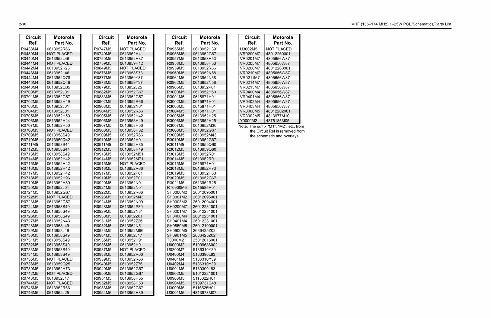
2-18 VHF (136–174 MHz) 1–25W PCB/Schematics/Parts List
m om
R043R043R044R044R044R044R044R044R044R070R070R070R070R070R070R070R070R070R070R071R0711R071R071R071R071R071R071R071R071R072R072R072R072R072R072R072R072R072R072R073R073R073R073R073R073R073R073R074R074R074R074R074
CirR
Note: The suffix “M1”, “M2”, etc. frothe Circuit Ref is removed frthe schematic and overlays.
8M4 0613952R669M4 NOT PLACED0M4 0613952L461M4 NOT PLACED2M4 0613952K253M4 0613952L464M4 0613952Q785M4 0613952Q468M4 0613952Q350M5 0613952J011M5 0613952G672M5 0613952H493M5 0613952J014M5 0613952J015M5 0613952H506M5 0613952H447M5 0613952H508M5 NOT PLACED9M5 0613958S490M5 0613959Q42M5 0613958S44
2M5 0613958S443M5 0613958S494M5 0613952H425M5 0613952H426M5 0613952H427M5 0613952H428M5 0613952H969M5 0613952H890M5 0613952J011M5 0613952G672M5 NOT PLACED3M5 0613952G674M5 0613958S495M5 0613958S496M5 0613958S497M5 0613952N438M5 0613958J499M5 0613958J490M5 0613958S491M5 0613958S492M5 0613958S493M5 0613958S494M5 0613958S495M5 NOT PLACED6M5 0613959Q259M5 0613952H732M5 NOT PLACED3M5 0613952J174M5 NOT PLACED5M5 0613952R666M5 0613952J25
cuitef.
MotorolaPart No.
R0747M5 NOT PLACEDR0749M5 0613952H41R0750M5 0613952H37R0759M5 0613959H12R0849M5 NOT PLACEDR0876M5 0613958S73R0877M5 0613959Y37R0878M5 0613959Y37R0879M5 0613952J25R0882M5 0613952G67R0883M5 0613952G67R0902M5 0613952R66R0903M5 0613952N01R0904M5 0613952R66R0905M5 0613952H42R0906M5 0613958H49R0907M5 0613958H56R0908M5 0613958H32R0909M5 0613952R66R0910M5 0613952H91R0911M5 0613952H85R0912M5 0613958H49R0913M5 0613952M51R0914M5 0613952M71R0915M5 NOT PLACEDR0916M5 0613952R66R0917M5 0613952P01R0919M5 0613952P01R0920M5 0613952N01R0921M5 0613952N01R0922M5 0613952R66R0923M5 0613952M43R0924M5 0613952N09R0928M5 0613952P30R0929M5 0613952N81R0930M5 0613952Z61R0931M5 0613952Z26R0932M5 0613952N51R0933M5 0613952M66R0934M5 0613952J17R0935M5 0613952H91R0936M5 0613952H91R0937M5 NOT PLACEDR0938M5 0613952R66R0939M5 0613952R66R0940M5 0613952Z76R0949M5 0613952G67R0950M5 0613952G67R0951M5 0613958H55R0952M5 0613958H53R0953M5 0613952G67R0954M5 0613952H39
CircuitRef.
MotorolaPart No.
R0955M5 0613952H39R0956M5 0613952G67R0957M5 0613958H53R0958M5 0613958H53R0959M5 0613952R66R0960M5 0613952N58R0961M5 0613952N58R0962M5 0613952N58R0965M5 0613952P01R3000M5 0613952H60R3001M5 0615871H01R3002M5 0615871H01R3003M5 0615871H01R3004M5 0615871H01R3005M5 0613952H25R3006M5 0613952H25R3007M5 0613952M30R3008M5 0613952G67R3009M5 0613952M43R3010M5 0613952G67R3011M5 0613959Q60R3012M5 0613959Q60R3013M5 0613952R01R3014M5 0613952R01R3015M5 0615871H01R3018M5 0613952H73R3019M5 0613952H60R3020M5 0613952G67R3021M5 0613952R25RT0900M5 0615585H01SH0000M2 26012095001SH0001M2 26012095001SH0003M2 26012094001SH0200M7 26012231001SH0201M7 26012231001SH0400M4 26012231001SH0401M4 26012231001SH0850M5 26012100001SH0900M5 2686425Z02SH0901M5 2686425Z02T0000M2 25012016001U0000M2 51009686002U0200M7 5186310Y39U0400M4 5180390L83U0401M4 5186310Y39U0402M4 5186310Y39U0901M5 5180390L83U0902M5 51012221001U0903M5 5115022H01U0904M5 5109731C48U3000M5 5116525H01U3001M5 4813973M07
CircuitRef.
MotorolaPart No.
U3002M5 NOT PLACEDVR0200M7 48012260001VR0201M7 4805656W87VR0205M7 4805656W87VR0206M7 48012260001VR0210M7 4805656W87VR0211M7 4805656W87VR0214M7 4805656W87VR0215M7 4805656W87VR0400M4 4805656W87VR0401M4 4805656W87VR0402M4 4805656W87VR0403M4 4805656W87VR3000M5 48012202001VR3002M5 4813977M10Y0000M2 4875185M05
CircuitRef.
MotorolaPart No.
XiR™ M3188/XiR™ M3688Mobile Radios
Chapter 6
VHF (136–174 MHz)
25–45W
Service Information
M
Issue: June, 2013

Computer Software CopyrightsThe Motorola products described in this manual may include copyrighted Motorola computer programs stored in semiconductor memories or other media. Laws in the United States and other countries preserve for Motorola certain exclusive rights for copyrighted computer programs, including, but not limited to, the exclusive right to copy or reproduce in any form the copyrighted computer program. Accordingly, any copyrighted Motorola computer programs contained in the Motorola products described in this manual may not be copied, reproduced, modified, reverse-engineered, or distributed in any manner without the express written permission of Motorola. Furthermore, the purchase of Motorola products shall not be deemed to grant either directly or by implication, estoppel, or otherwise, any license under the copyrights, patents or patent applications of Motorola, except for the normal non-exclusive license to use that arises by operation of law in the sale of a product.
i
Chapter 6 – VHF High Power Service Information
Table of Contents
Section 1 Troubleshooting Charts
1.0 Troubleshooting Flow Chart for Receiver ............................................................ 1-12.0 Troubleshooting Flow Chart for 45W Transmitter................................................ 1-53.0 Troubleshooting Flow Chart for RFIC .................................................................. 1-64.0 Troubleshooting Flow Chart for Rx VCO ........................................................... 1-115.0 Troubleshooting Flow Chart for Tx VCO............................................................ 1-13
Section 2 VHF PCB/Schematics/Parts Lists
1.0 Allocation of Schematics and Circuit Boards ....................................................... 2-11.1 VHF 45W Circuits........................................................................................... 2-1
2.0 VHF (136–174 MHz) 25–45W PCB/Schematics/Parts List ................................. 2-3VHF (136–174 MHz) 25–45W 84012505002-B Top Side ...................................... 2-3VHF (136–174 MHz) 25–45W 84012505002-B Bottom Side................................. 2-4VHF (136–174 MHz) 25–45W Overall Schematic Diagram ................................... 2-5VHF (136–174 MHz) 25–45W Receiver Front-End Schematic Diagram................ 2-6VHF (136–174 MHz) 25–45W Transmitter Power Amplifier Schematic Diagram
(sheet 1 of 2) .................................................................................................. 2-7VHF (136–174 MHz) 25–45W Transmitter Power Amplifier Schematic Diagram
(sheet 2 of 2) .................................................................................................. 2-8VHF (136–174 MHz) 25–45W Transmit/Receive Switch and Harmonic Filter
Schematic Diagram........................................................................................ 2-9VHF (136–174 MHz) 25–45W Power Control Schematic Diagram...................... 2-10VHF (136–174 MHz) 25–45W Transmitter Power Amplifier DC Distribution
Schematic Diagram...................................................................................... 2-11VHF (136–174 MHz) 25–45W RFIC Schematic Diagram .................................... 2-12VHF (136–174 MHz) 25–45W Transmitter VCO Schematic Diagram.................. 2-13VHF (136–174 MHz) 25–45W Receiver VCO Schematic Diagram...................... 2-14VHF (136–174 MHz) 25–45W VCO Buffer Schematic Diagram .......................... 2-15VHF PCB 84012505002-B Parts List 25–45W..................................................... 2-16

ii
Notes
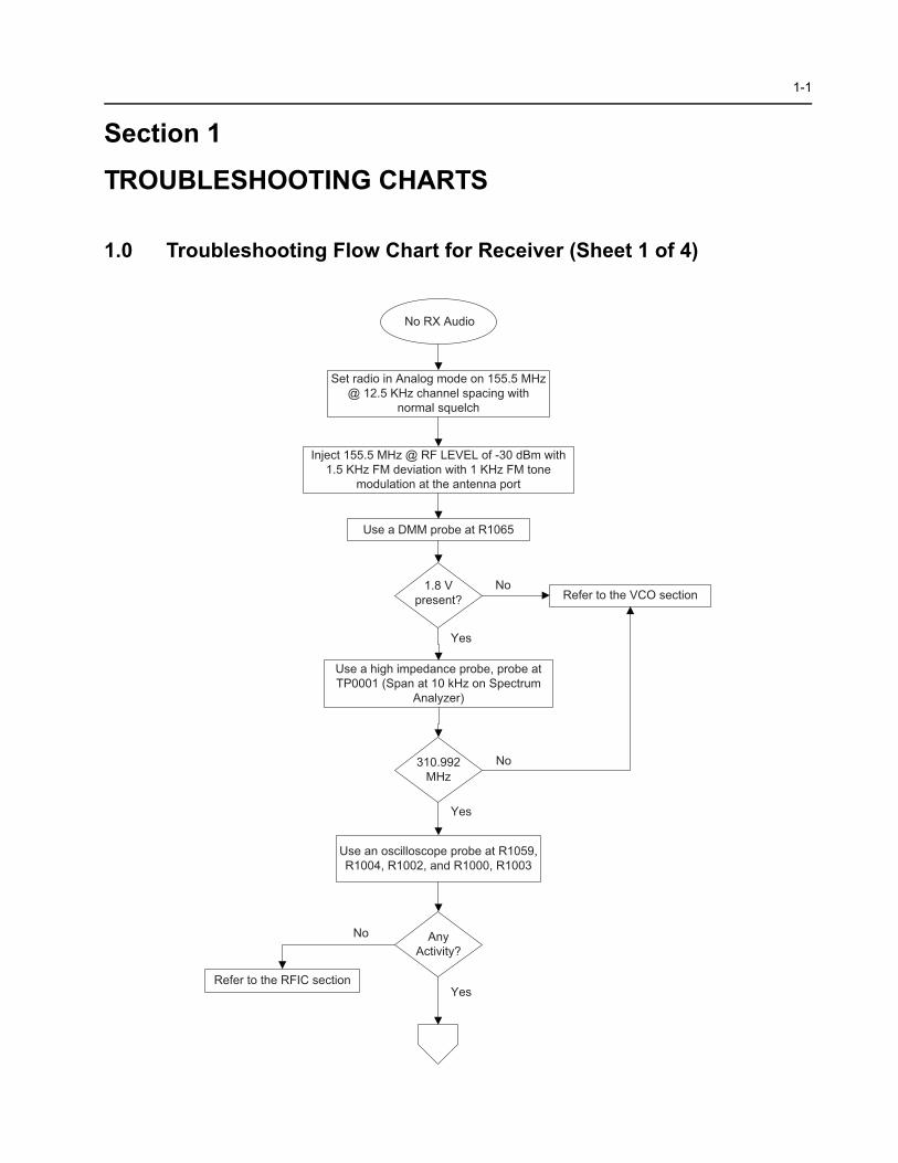
1-1
Section 1
TROUBLESHOOTING CHARTS
1.0 Troubleshooting Flow Chart for Receiver (Sheet 1 of 4)
Set radio in Analog mode on 155.5 MHz @ 12.5 KHz channel spacing with
normal squelch
Inject 155.5 MHz @ RF LEVEL of -30 dBm with 1.5 KHz FM deviation with 1 KHz FM tone
modulation at the antenna port
1.8 V present?
310.992MHz
Any Activity?
Use a high impedance probe, probe at TP0001 (Span at 10 kHz on Spectrum
Analyzer)
Use an oscilloscope probe at R1059, R1004, R1002, and R1000, R1003
Refer to the RFIC section
Yes
Use a DMM probe at R1065
Yes
No
Yes
Refer to the VCO sectionNo
No
No RX Audio
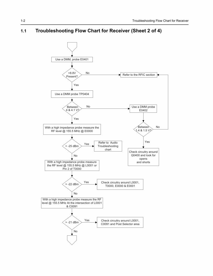
1-2 Troubleshooting Flow Chart for Receiver
1.1 Troubleshooting Flow Chart for Receiver (Sheet 2 of 4)
Use a DMM probe TP0404
Between 4 & 4.1 V?
> -25 dBm
> -22 dBm
With a high impedance probe measure the RF level @ 155.5 MHz @ E0000
With a high impedance probe measure the RF level @ 155.5 MHz @ L0001 or
Pin 2 of T0000
Yes
No
Use a DMM, probe E0401
Use a DMM probe E0402
No
>8.8VPresent?
Yes
> -21 dBm
No
With a high impedance probe measure the RF level @ 155.5 MHz At the intersection of L0001
& C0091
No
Refer to the RFIC sectionNo
Between1.4 & 1.5 V?
Check circuitry around Q0400 and look for
opens and shorts
Refer to Audio Troubleshooting
chart
Check circuitry around L0001, C0091 and Post Selector area
Check circuitry around L0001, T0000, E0000 & E0001
YesYes
Yes
Yes
No
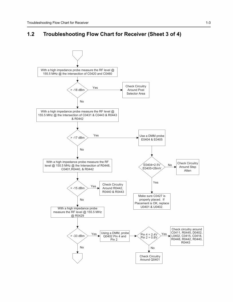
Troubleshooting Flow Chart for Receiver 1-3
1.2 Troubleshooting Flow Chart for Receiver (Sheet 3 of 4)
> -18 dBm
With a high impedance probe measure the RF level @ 155.5 MHz @ the intersection of C0420 and C0460
With a high impedance probe measure the RF level @ 155.5 MHz @ the Intersection of C0431 & C0443 & R0443
& R0442
Check Circuitry Around Post
Selector Area
> -17 dBm Use a DMM probe E0404 & E0405
With a high impedance probe measure the RF level @ 155.5 MHz @ the Intersection of R0448,
C0401,R0440, & R0442E0404=2.5VE0405=28mV
Check Circuitry Around Step
Atten
Make sure C0427 is properly placed. If
Placement is OK, replace U0401 & U0402.
> -15 dBm
With a high impedance probe measure the RF level @ 155.5 MHz
@ R0429
> -33 dBmUsing a DMM, probe
Q0402 Pin 4 and Pin 2
No
Yes
No
Yes
No
Yes
No
Yes
No
Check Circuitry Around R0442, R0440 & R0443
Yes
Pin 4 = 2.4VPin 2 = 0.8V
No
Check Circuitry Around Q0401
Check circuitry around C0411, R0445, D0402, L0402, C0415, C0418, R0448, R0442, R0440,
R0443
Yes
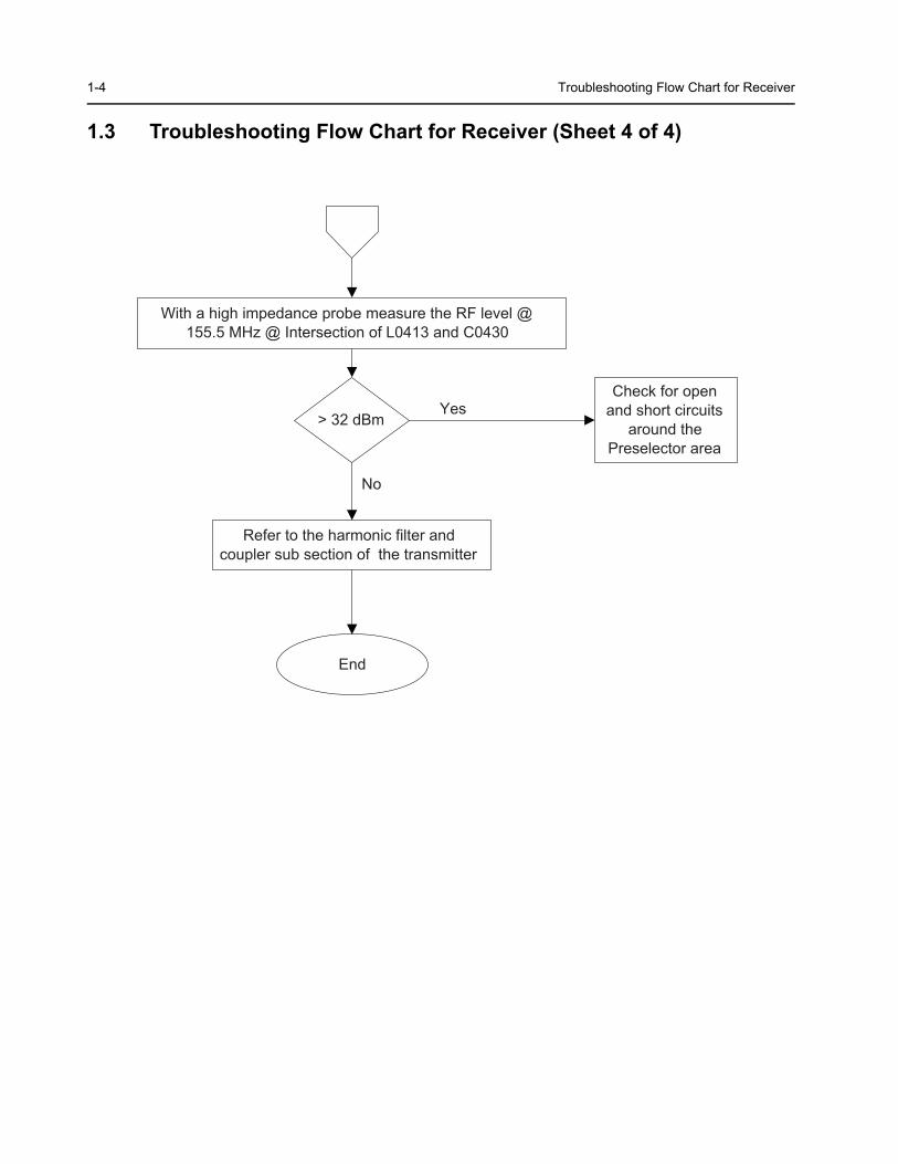
1-4 Troubleshooting Flow Chart for Receiver
1.3 Troubleshooting Flow Chart for Receiver (Sheet 4 of 4)
> 32 dBm
With a high impedance probe measure the RF level @ 155.5 MHz @ Intersection of L0413 and C0430
Refer to the harmonic filter and coupler sub section of the transmitter
Check for open and short circuits
around the Preselector area
No
Yes
End
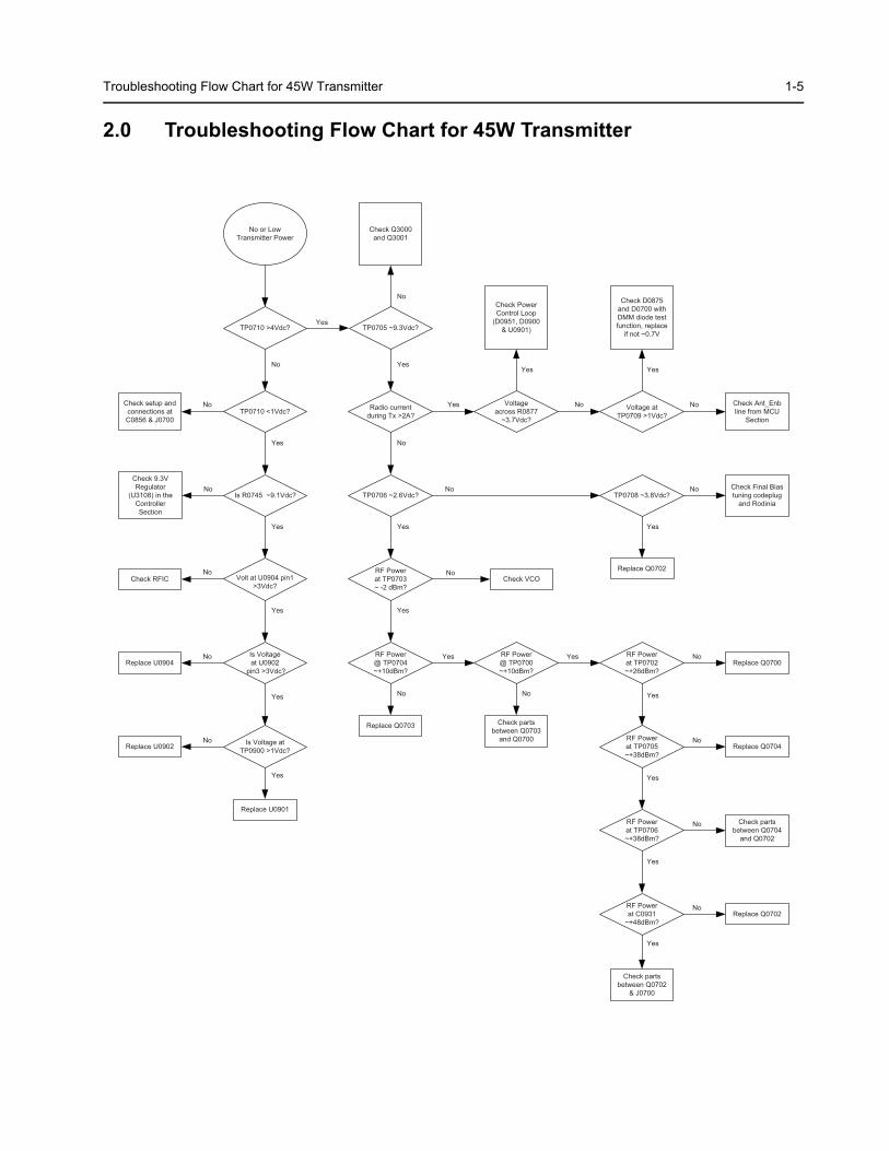
Troubleshooting Flow Chart for 45W Transmitter 1-5
2.0 Troubleshooting Flow Chart for 45W Transmitter
TP0710 >4Vdc? TP0705 ~9.3Vdc?
Voltageacross R0877
~3.7Vdc?
TP0706 ~2.6Vdc?
RF Power @ TP0704 ~+10dBm?
Is R0745 ~9.1Vdc?
Check 9.3V Regulator
(U3108) in the Controller Section
Volt at U0904 pin1 >3Vdc?
Check RFIC
Is Voltageat U0902
pin3 >3Vdc?
Is Voltage atTP0900 >1Vdc?
Replace U0904
Replace U0902
Replace U0901
RF Power @ TP0700 ~+10dBm?
TP0710 <1Vdc?Check setup and connections at C0856 & J0700
RF Power at TP0703 ~ -2 dBm?
Check Final Bias tuning codeplug
and Rodinia
Check D0875and D0700 with DMM diode test function, replace
if not ~0.7V
Voltage atTP0709 >1Vdc?
Radio currentduring Tx >2A?
Check Ant_Enb line from MCU
Section
Check Power Control Loop
(D0951, D0900 & U0901)
TP0708 ~3.8Vdc?
Replace Q0702
RF Power at TP0702 ~+26dBm?
RF Power at TP0705 ~+38dBm?
RF Power at TP0706 ~+38dBm?
RF Power at C0931
~+48dBm?
Check VCO
Replace Q0703 Check parts between Q0703
and Q0700
Replace Q0700
Replace Q0704
Check parts between Q0704
and Q0702
Replace Q0702
Check parts between Q0702
& J0700
Check Q3000 and Q3001
No
Yes
Yes
Yes
Yes
Yes
No
Yes
Yes
Yes Yes
No No
No No
No
No
Yes Yes
Yes
Yes Yes
No No Yes
Yes
Yes
Yes
No or Low Transmitter Power
No
Yes
No
No
No
No
No
No
No
No

1-6 Troubleshooting Flow Chart for RFIC
3.0 Troubleshooting Flow Chart for RFIC (Sheet 1 of 5)
Visual check of board ok?
+ 5V at E0004?
+ 2.8V at E0008?
+ 2.8V at E0005?
+1.8V at E0010?
+1.8V at E0007?
+1.8V at E0006?
Is 19.2MHz signal at C0049?
Is 2.8V at Pin 4 of Y0000?
Correct Problem
Check controller E3105
Check controller E3113
Check controller E3107
Check controller E3110
Check controller E3108
Check controller E3109
Check Y0000, replace if needed
Yes
No
Yes
Yes
Yes
Yes
Yes
Yes
Yes
No
Yes
No
No
No
No
No
No
No
No Synthesizer Operation
Resolve R0013 open or short on Pin 4 of Y0000
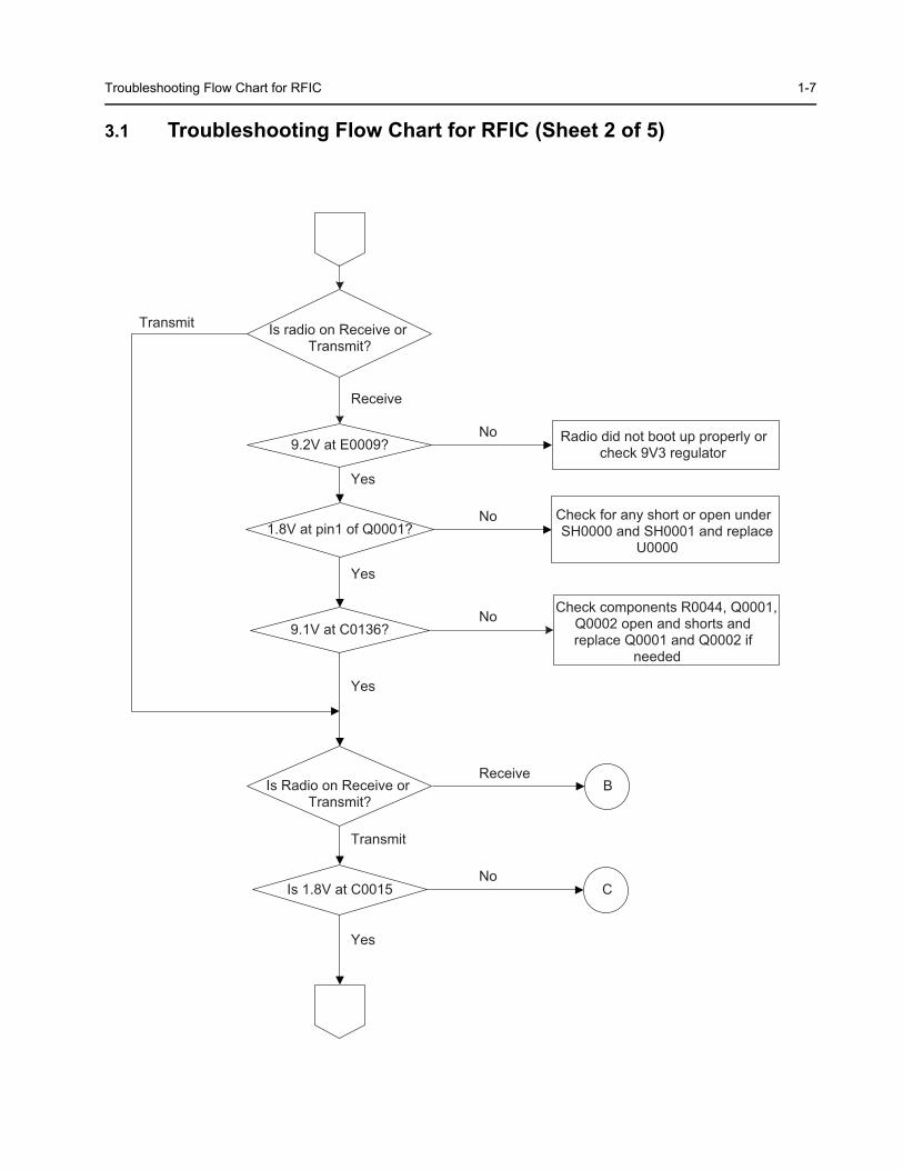
Troubleshooting Flow Chart for RFIC 1-7
3.1 Troubleshooting Flow Chart for RFIC (Sheet 2 of 5)
Is radio on Receive or Transmit?
9.2V at E0009?
1.8V at pin1 of Q0001?
9.1V at C0136?
Is Radio on Receive or Transmit?
Is 1.8V at C0015
Radio did not boot up properly or check 9V3 regulator
Check for any short or open under SH0000 and SH0001 and replace
U0000
Check components R0044, Q0001, Q0002 open and shorts and replace Q0001 and Q0002 if
needed
No
No
BReceive
C
Receive
No
Yes
Yes
Yes
Transmit
Yes
No
Transmit
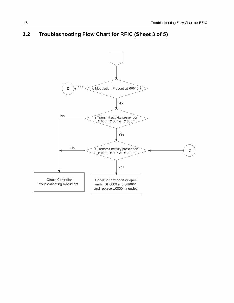
1-8 Troubleshooting Flow Chart for RFIC
3.2 Troubleshooting Flow Chart for RFIC (Sheet 3 of 5)
Is Modulation Present at R0012 ?DYes
Is Transmit activity present on R1006, R1007 & R1008 ?
Is Transmit activity present on R1006, R1007 & R1008 ?
Yes
No
Check Controller troubleshooting Document
Yes
Check for any short or open under SH0000 and SH0001
and replace U0000 if needed.
C
No
No
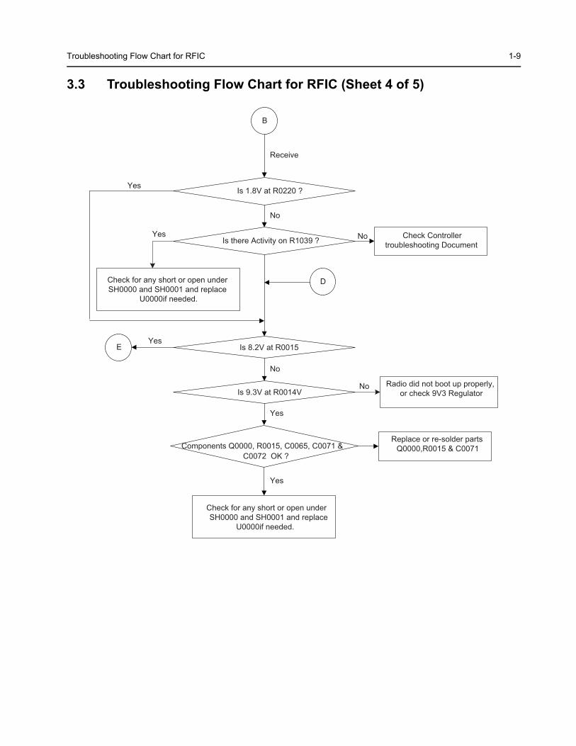
Troubleshooting Flow Chart for RFIC 1-9
3.3 Troubleshooting Flow Chart for RFIC (Sheet 4 of 5)
B
Receive
Is there Activity on R1039 ? Check Controller troubleshooting Document
No
Check for any short or open under SH0000 and SH0001 and replace
U0000if needed.
Is 1.8V at R0220 ?
No
D
Is 8.2V at R0015
Yes
Is 9.3V at R0014V
No
Radio did not boot up properly, or check 9V3 Regulator
Replace or re-solder parts Q0000,R0015 & C0071Components Q0000, R0015, C0065, C0071 &
C0072 OK ?
Yes
Yes
Check for any short or open under SH0000 and SH0001 and replace
U0000if needed.
EYes
Yes
No
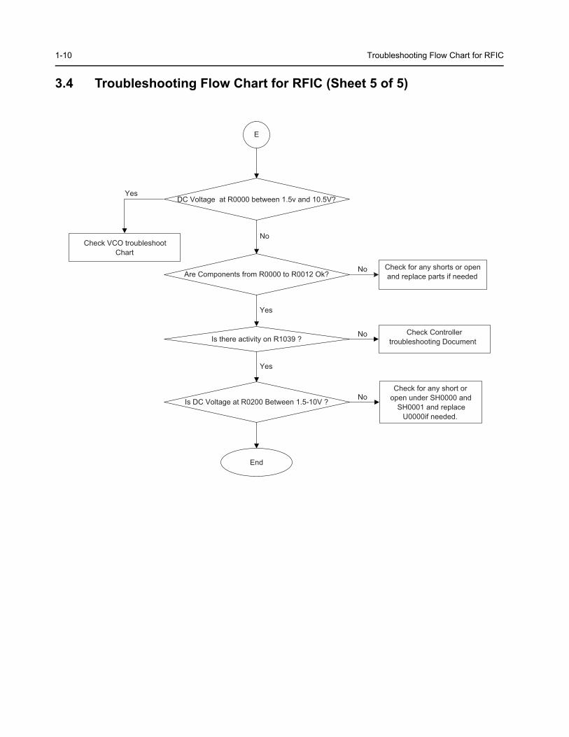
1-10 Troubleshooting Flow Chart for RFIC
3.4 Troubleshooting Flow Chart for RFIC (Sheet 5 of 5)
E
DC Voltage at R0000 between 1.5v and 10.5V?
Check VCO troubleshoot Chart
No
Are Components from R0000 to R0012 Ok?Check for any shorts or open and replace parts if needed
Is there activity on R1039 ?
Yes
Check Controller troubleshooting Document
No
Check for any short or open under SH0000 and
SH0001 and replace U0000if needed.
Is DC Voltage at R0200 Between 1.5-10V ? No
End
No
Yes
Yes
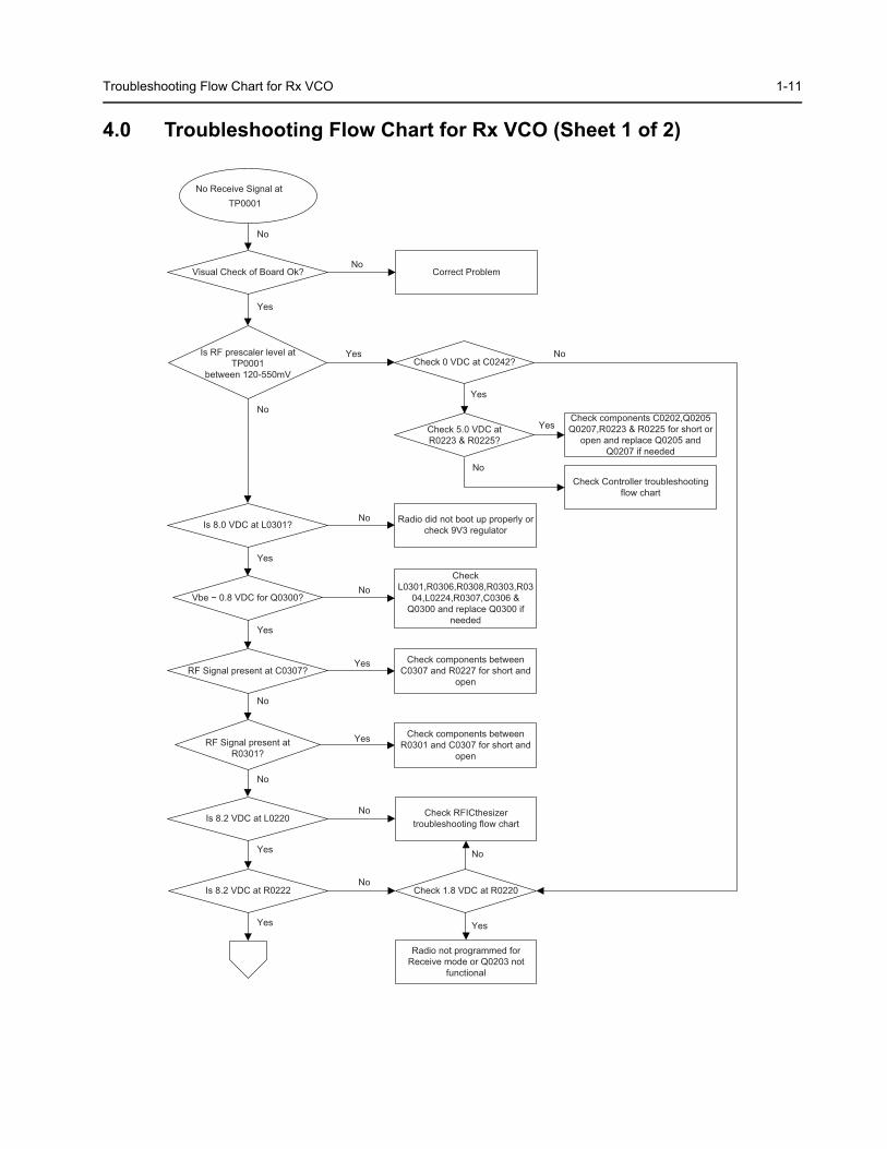
Troubleshooting Flow Chart for Rx VCO 1-11
4.0 Troubleshooting Flow Chart for Rx VCO (Sheet 1 of 2)
Visual Check of Board Ok?
No
NoCorrect Problem
Yes
Is 8.0 VDC at L0301?No Radio did not boot up properly or
check 9V3 regulator
Yes
Vbe ~ 0.8 VDC for Q0300?No
Check L0301,R0306,R0308,R0303,R03
04,L0224,R0307,C0306 & Q0300 and replace Q0300 if
neededYes
RF Signal present at C0307?Yes Check components between
C0307 and R0227 for short and open
Is RF prescaler level at TP0001
between 120-550mV
Yes
No
No
RF Signal present at R0301?
Yes Check components between R0301 and C0307 for short and
open
No
Is 8.2 VDC at L0220No Check RFICthesizer
troubleshooting flow chart
Yes
Is 8.2 VDC at R0222 Check 1.8 VDC at R0220No
No
Yes
Radio not programmed for Receive mode or Q0203 not
functional
Yes
Yes
Check 0 VDC at C0242?No
Check 5.0 VDC at R0223 & R0225?
YesCheck components C0202,Q0205 Q0207,R0223 & R0225 for short or
open and replace Q0205 and Q0207 if needed
NoCheck Controller troubleshooting
flow chart
No Receive Signal at TP0001
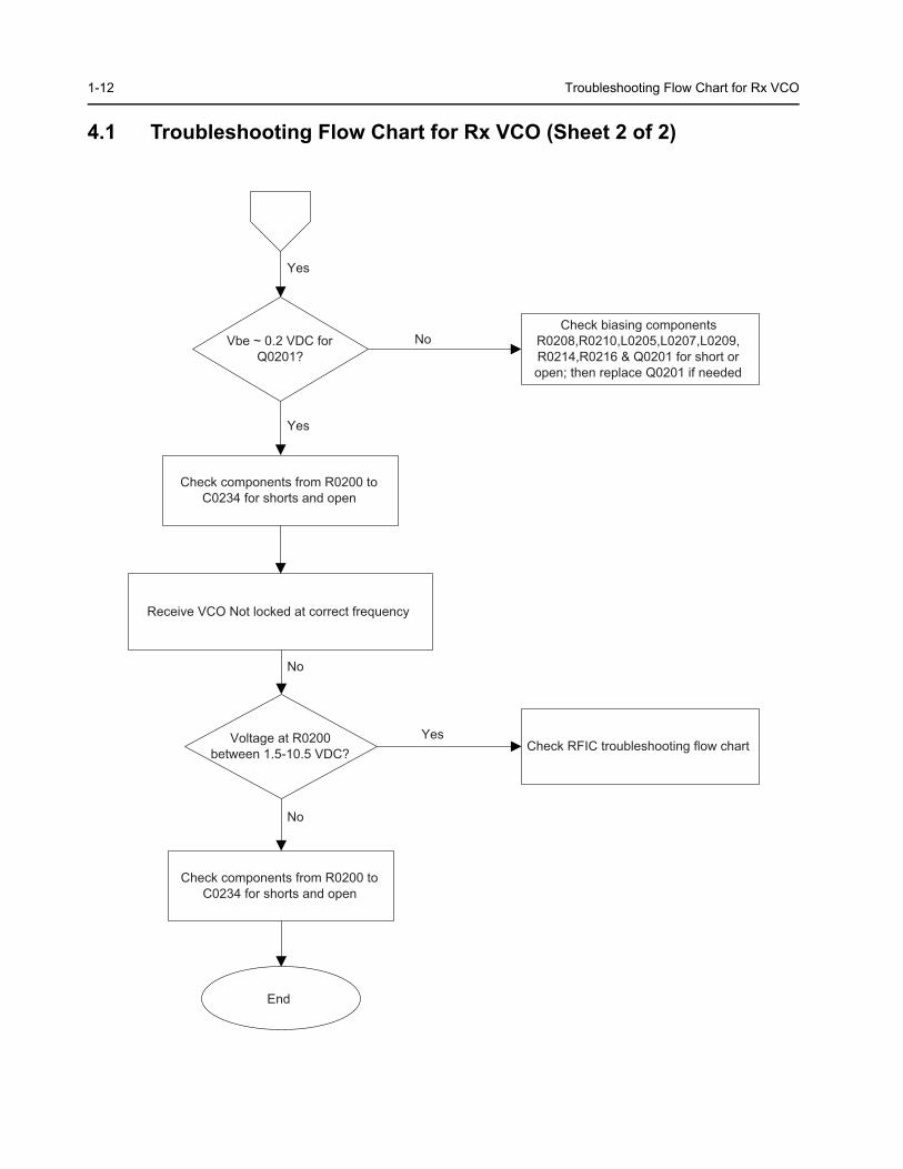
1-12 Troubleshooting Flow Chart for Rx VCO
4.1 Troubleshooting Flow Chart for Rx VCO (Sheet 2 of 2)
Yes
Vbe ~ 0.2 VDC for Q0201?
NoCheck biasing components
R0208,R0210,L0205,L0207,L0209, R0214,R0216 & Q0201 for short or open; then replace Q0201 if needed
Yes
Check components from R0200 to C0234 for shorts and open
Receive VCO Not locked at correct frequency
Voltage at R0200 between 1.5-10.5 VDC?
No
YesCheck RFIC troubleshooting flow chart
No
Check components from R0200 to C0234 for shorts and open
End

Troubleshooting Flow Chart for Tx VCO 1-13
5.0 Troubleshooting Flow Chart for Tx VCO (Sheet 1 of 2)
Visual Check of Board Ok?
NoCorrect Problem
Yes
Is 8.0 VDC at L0301?No Radio did not boot up properly or
check 9V3 regulator
Yes
Vbe ~ 0.8 VDC for Q0300?
NoCheck
L0301,R0306,R0308,R0303,R0304,L0224,R0307,C0306 & Q0300 and
replace Q0300 if needed
Yes
RF Signal present at C0307?
Yes Check components between C0307 and R0227 for short and open
Is RF prescaler level at TP0001 between 120-550mV
Yes
No
No
RF Signal present at R0301?
Yes Check components between R0301 and C0307 for short and open
Yes
Is 8.2 VDC at L0206 No Check RFICthesiz er troubleshooting
flow chart
Yes
Is 8.2 VDC at R0207 Check 1.8 VDC at R0233No
No
Yes
Radio not programmed for Transmit mode or Q0206 not functional
Yes
Yes
Check 1.8 VDC at C0242?
No
Check 5.0 VDC at R0223 & R0225?
YesCheck components C0202,Q0205 Q0207,R0223 & R0225 for short or
open and replace Q0205 and Q0207 if needed
NoCheck Controller troubleshooting flow
chart
No Transmit Signal at C0703
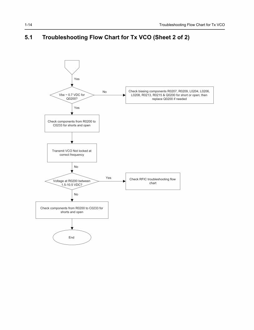
1-14 Troubleshooting Flow Chart for Tx VCO
5.1 Troubleshooting Flow Chart for Tx VCO (Sheet 2 of 2)
Yes
Vbe ~ 0.7 VDC for Q0200?
No Check biasing components R0207, R0209, L0204, L0206, L0208, R0213, R0215 & Q0200 for short or open; then
replace Q0200 if needed
Yes
Check components from R0200 to C0233 for shorts and open
Transmit VCO Not locked at correct frequency
Voltage at R0200 between 1.5-10.5 VDC?
No
Yes Check RFIC troubleshooting flow chart
No
Check components from R0200 to C0233 for shorts and open
End
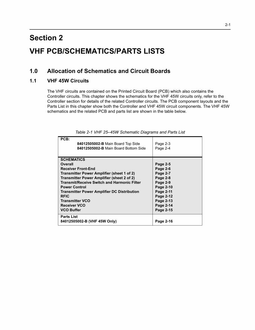
2-1
Section 2
VHF PCB/SCHEMATICS/PARTS LISTS
1.0 Allocation of Schematics and Circuit Boards
1.1 VHF 45W Circuits
The VHF circuits are contained on the Printed Circuit Board (PCB) which also contains the Controller circuits. This chapter shows the schematics for the VHF 45W circuits only, refer to the Controller section for details of the related Controller circuits. The PCB component layouts and the Parts List in this chapter show both the Controller and VHF 45W circuit components. The VHF 45W schematics and the related PCB and parts list are shown in the table below.
Table 2-1 VHF 25–45W Schematic Diagrams and Parts List
PCB:84012505002-B Main Board Top Side84012505002-B Main Board Bottom Side
Page 2-3Page 2-4
SCHEMATICSOverall Receiver Front-EndTransmitter Power Amplifier (sheet 1 of 2)Transmitter Power Amplifier (sheet 2 of 2)Transmit/Receive Switch and Harmonic FilterPower ControlTransmitter Power Amplifier DC DistributionRFICTransmitter VCOReceiver VCOVCO Buffer
Page 2-5Page 2-6Page 2-7Page 2-8Page 2-9Page 2-10Page 2-11Page 2-12Page 2-13Page 2-14Page 2-15
Parts List84012505002-B (VHF 45W Only) Page 2-16

2-2
Notes
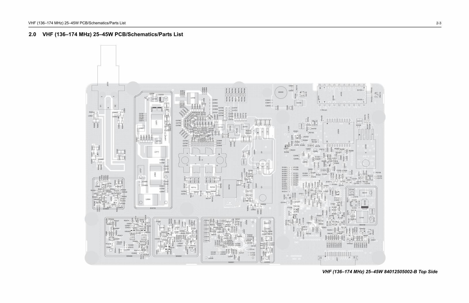
V 2-3
2
23
18220
1719
E4102
TP41
03
E41
00
E41
01 VR
4110
E4103
TP41
02
J410
0
5
C31
12C
3129
R31
07R
3175
C3111
R3106
101120
U32
04
5
106
C31
21L3100R3115
R31
14
C31
20
D31
04
C31
19
C3143
R3116
U31
02
C31
76
C3116C3175
R31
11
R3141
C3154
1065
C3144C3118
R3108
C3150C3173
R3146
C31
53C
3151
U31
08
C3122
E3113
E31
11
R3147
C31
71
63
5 610
6 43
C2004
C2016
C20
10C20
11
C2009
C3214
R3138
R3176
C2005
R3264
R3265R32
08 R3262
C3230
201
3256
R32
30
R3231
R3142
R3263
R3132
C32
09
R3261
Q32
05
C32
25
TP31
09
U31
09C31
52
C3106
R3102
R31
01C31
02
C2008 6 433
2
R32
00
E3202
Q32
09
C3204
R32
04
C20
15
C20
13
R3280
C32
28
R32
54
C32
22
C3221
C32
24
C3218
C3231
C32
19
R32
03
C3227U3202
C32
26
R3285
R1060C3229
C20
14
R3290R3287
C32
57C2012
854
C32
23
E3104
C1029
R31
19
C3123U3103
C31
24C1032
E10
02
6U
3100
3 45
TP4101C30
21
E3100
C30
46
C3050
U31
12
R31
10R
3150
C3051
233
G2
14G1
2 3
J400
1
C3201
R32
82
R4001
C32
00C
4011
R40
40C
4012
C40
14C
4029
C40
22R
4024
R40
13
E40
04
E40
05
R40
26
R40
27
FL40
01
VR4005
C40
19C
4021
C40
23
C40
25C
4028
C40
13C
4015
C40
20
VR
4001
VR4000
R40
25R
4010
SH3100
23
23
2
R11
24
E40
03
R40
06R
4007
R40
15
R40
21
E40
00
E40
02E
4001
R1118
R1122
R40
91
R4093
R4028 R4034
R40
33
D10
05Q
1005
R1120
R1119
469
4 3
32
5
R1128R11
26
R11
25
R2003
C20
22
C20
02
C20
00
D3160
R40
37
R40
38
R2004
R2002
R2000
C20
21C20
03
C2001
U10
10R
1042
C1021
R1045
R1001
R1020
R31
73
U10
04
C1010C1009
R1023
C10
08
E1003
C1002
C10
05
C10
47
E10
04
E1001
C10
60
C2020
C20
07
C10
25R
1026 C10
06C
1007
C10
15
C20
06
C10
41
C3248R1049
R1051R1050
C1013C1014
R10362R10354
3
C10
01
R10
46
C10
19
C1020
C10
44
R10
12C
1042
C10
26C10
18C
1022
C1017 C10
28C
1036
C10
23
C1003
R10
19
C1035
C10
45
R1027R1021
8
468
R1062R1064R1011
R1024R1030
0
0
1
9
5
2
32
643
3 46
32
63 4U31
07
R3153
C31
35
R31
04
C31
37
C31
33E
3108
C31
36
Q3100
R31
03
C31
09
E31
10
VR
3103
C3140C3139
U31
06
R1077
R31
80
C31
80R
3181
VHF (136–174 MHz) 25–45W 84012505002-B Top Side
HF (136–174 MHz) 25–45W PCB/Schematics/Parts List
.0 VHF (136–174 MHz) 25–45W PCB/Schematics/Parts List
G2
G1
23
J070
0
23
R09
50
C09
50
R09
57
R09
58
C09
51
C0952
D0950L0952
R0956
23
R09
55
R09
54
C0955
D09
51C
0954
R09
53
C09
53
R09
51L0
950
R09
52L0
951
1
458
2543
R09
13
R09
62C
0957
R09
61C
0902
R0959
C0901
R09
22
C0900
R0921R09
65
C09
25C
0917
R0920
R0916
C09
16
R0917
U09
02
TP0902R0933
R0929
TP09
04R
0928
R0924
TP0903
C0926R0923
R09
19
R0745
R07
49
C09
11
R0939
TP09
00
RT0900
R0940R0914R0904
R0915
SH0900
C0772
C0776
C0918
R09
32R0931
U09
04
R09
60
C0956
R0930
C0919 R0744
234
C0929
L085
2L072
7
C0855
C0788
C0822C0718
C0928
SH0700
C0853
L0711C
0815
C08
19C
0807
C08
51
C08
20
L087
6
L0712C08
52
C0876
D08
76
L087
5C0816
L0857
C0880
C0875
L088
5
D08
75
C0787C0785C0786C0850
D07
00 L087
7
D0877
C0777
C0766C0722
L0708
L0854
C0750C0823C0789
C0854
C0825
23
643
6
8
45
3
R0403
E0402
C04
65
C0463
R0411
R04
10C
0413
Q0400
C0464C0410
C04
08
E04
00
C0467
R0413
R04
17R
0415
L0401
TP0404
R04
16
L0406
SH0400
C0469
R0423
C0422R0428
R0425
U0400
C04
52C
0404
VR0401
R0402
L0413
L0405VR0400
D0401
R0404C0402
C0407C0406C0453
VR0403VR0402
R04
24
R04
31
Q0406
R04
30R
0427
C04
66
C04
35
C04
03
C04
38 L041
4
C0405C0423
R0429
R04
33R
0436
R0437TP0403
R04
39
R0438
E04
01
C0430
C03
06
R0307
R03
04
VR
0210
VR
0211
VR0215VR
0214
L0212
C02
41
R03
09
C03
01 C0307
L0224Q0300
R03
03
R0305L0226
C0302
C0276
L030
0C
0300
R03
02R
0300
R02
24
SH0200
C02
45
Q02
04
L0218
R02
22
C0256
C0252
C02
44
C02
57
C0248
L021
4
L030
2
L0304
C03
09C
0310
C02
02
L030
1R
0306
R0308 L030
3C0308
C03
05
R0301C0267
L0220
C02
65
L022
2
R02
28R
0230
R0203
L0216
C02
63
C02
59E0300
C03
04
R02
32
C08
46C
0809
C08
24
Q3
R
C3042
C3044C3047
C30
20
M3000
5
67
8
2
9
3
4
C08
12
R07
25
R07
35
R07
27
Q07
02
M07
00
R07
38
R07
32
R07
34
C08
14
C0753
R07
37
R0741
R0739TP
0708
R07
46C0761
R07
40
C0754
R0709
R0743
R0710R07
42
C0764
32G
1
C30
12
Q30
00
C30
13
R30
15
R3006
C30
14
C07
45
R3005
E0701
32
R30
04
R30
03
R30
02
R30
01
C0857C0848
R07
36
C08
28
C07
52
C08
18
C07
14C09
34
C0858
E07
03L0710
36
G1
32
C0710
R07
00
R0704
R0723
C07
01
TP0710
C07
31
R0720
R0935
R09
34
U0903
C09
21R08
83
R0712
C07
75
Q07
01
Q30
01
R0711
R07
18C0727
C07
32
C0706
R105R104R103
R102
R101R101R101
R101
R104
R103
R106
R102
R102
Q10
02
E3109
C00
36
C00
98
C0056
C0124C0143
C0144
E0007
C0094
C00
60
C01
05C
0016
C01
40
C00
64
C0146 C0001C0039C0147
C0135
E00
09
C0100E0008C0102C0009
SH0001
C0004
C0034
C0032
C00
37
C01
20
C0075R0011R0014
R0012
C0072
C0065C0059
C0061
R0009
R0010
C0011R0006
R00
00C0007
C0012
C00
54
C0101C0024C
0138
C0141C0043
R00
07
R0001
C00
06C
0003C0002
32
C0019
C00
35C
0022
C00
15
C0033C01
50C
0149
C00
17
C0018C0014
C0030C0031C0029
C00
13
C00
26
C0093C0139
C00
71C00
53 C0076C
0074
C01
45C
0055
Q00
00
R0015
C0005
643
346
L000
0
C00
86
C0080
D00
00
R00
29C
0085
C0081C0082
SH0003
C00
78
D00
01
C00
83
R0022R0025
C0068C0066R0019
R0030
C0067
C0070
C09
32C
0867
C30
03
C07
07C
0712
C07
16
C0721
C0740C0742
C0733
C30
02
C0755C0730C0748
C0723
C0800
C0751
C0737
C0941
C0942
C0940C0726
R07
75R
0784
R07
86R
0785
R07
74R
0776
R07
79R
0778
R07
82R
0781
R07
83R
0777
R07
58R
0780
C0763C0806
C08
11C
0758
C07
36
C07
59C
0810
C07
70
L0706
C07
91C
0859
C07
90C
0803
C0780C0781
C0860C0861
R0771C0843C0782C
0821
C0774C0801
C0769
C0792C0804
C0795C0779C0768
C0930C0939
C08
42C08
41C
0840
C08
08
C07
46
C0773
C0802
C09
38
C0872
C07
67
C08
44
R0789R0788
C08
73
C09
33
R0787R0770
R0772R0773
R07
69R
0766
R07
67
R07
68
R0795R0794
C08
68C
0847
C08
64
C08
62
R0790
C08
69C
0874
C08
70
R0797
R07
92R
0793
R07
99
C0728
C08
45
C0756C0757
R08
10R
0804
R08
11R
0803 R0802R0801 R0796
R0800
C07
71C
0805
C08
63C
0865
R0798 R0760R0763
R0807
R0808R0812R0809
R0805R0806
R0791
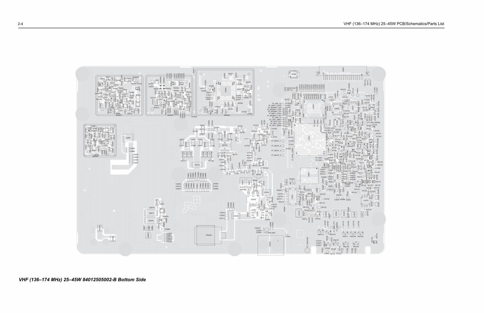
2-4 VHF (136–174 MHz) 25–45W PCB/Schematics/Parts List
8
634
G1
20G2 J4
000
01
TP31
11
TP31
10R
3171
C40
27C
4026
TP40
11
CH
_D-
R4019 VR
4002
CH_D+TP31
04
C4033
R40
41
C4031
C4030
A10
M10
A1
M1
T
R43
14
E43
00
C43
06C
4305
C43
04R
4307
R43
06R
4305
R43
04R
4302
C43
08C
4309
C43
10
C43
07C
4301
R43
12R
4303
R43
10
R43
11
C43
00C
4302
C43
14C
4303
C43
13R
1000
R10
05R
1048
U20
00
643
346
C43
11U4301
R40
99
R40
97
U4300
W19
W1
A19
TPU
AR
T2_T
XD
TP_S
W3
TP_S
W4
U10
01
33
2
2
46
5
7
7
2
634
14814
610
8
C3132
C31
45
R31
28
C3130
R31
29
U3105
E3106
R3130
R31
82
R40
08
R4098C4032
R40
96
U40
01
U4000
R40
94R
4090
R31
26C
3113
C31
34R
3148
C31
31C
3149
R31
12R31
54
E3103
R31
65
R31
66Q
3160
R4125
R4124
TP_U
AR
T2_R
XD
Q3103FT_IGN_SENSE
R3162
R3160R31
63
U3113
C31
41
Q31
62
Q3161
TP31
07
R3157
C3142
R3161
R31
58
R40
926
3 4
23
98
16
R1127
FT_U
AR
T0_R
XD
FT_U
AR
T0_T
XD
P10
00
TP31
05
TP_I2C0_SCLTP_GP2_15
TPI2C0_SDAR3131 R
3149
R3113
C31
55
R3143
R11
17 C3160
R41
28
R41
26 R3151
TP3103
R1111R11
14 R1054
TP_1
9.2M
HZ
FL_D+ R3121
R3169
R31
18
U3111
C3156R4127
R4129
R1116
R41
10
VR3104R1110R11
15
FL_D-
6
32
34
32
C31
46
U31
15
D31
61
R31
59R
4122
R31
67
R31
68
VR
3105
R41
15
53
33
64
42
C10
11U
1009
C10
12C
1000R3217
E1005
E1000
U10
00
TP_SW2TP_SW1
R3283
HS
US
BQ10
04
TP31
06
R1092
R1090
C10
43
R10
34
127 6
106
43634
6
5
2C
3127
R3152
R3164
C3108
TP31
08
R3117
U31
10
R3123
U31
04
R3170
R31
55
Q3163
R31
20
R41
23
R3125
R3124 Q3104
Q4113
R31
37
C3125
R3140
3 4
6346
3 46
91725
6
63
4
34
R3109
U41
00
R41
11R31
44
R3122
C31
28E
3105
TP3202 TP3201
R32
23
R3279
R32
20R
3218
R3255
C31
26R32
26R
3248
R32
25
C32
51
R3297
C32
49
C3250
VR3200 C32
52
C3253
R41
21
R4107
R41
09
R41
13R
4112
R41
05
Q4112
Q41
05
R4114
Q41
06
TP3205TP3204
TP3200R3253R3251
R3249
R3288
R3224R3257
R3221
U32
00
C3254R3219
R3296
R32
02C32
56
U20
01
R3201
C3203R32
05
854
32
Q4102
R3252R3289
C3103
R4118R4116
C31
47
R31
77
R4120
R4106R4108
R31
27
R4104
R3145
R3250
C32
32
R3229
C32
17
E31
01C
3104
C31
15
U3101C3233R3286
R3105
C31
10
C31
17
C32
38C
3236
C32
37
E32
03
E32
04
R4130TP3203
TP32
06R
3222
C32
58
C32
41
C3240
6 34R
4119
VR
4102
32
32
C41
04
C41
08
C41
09
C41
15
VR4109
32
32
32
C41
50
C41
19
C41
06
C41
14
FT_E
ME
RG
VR4150VR4108VR4111
32
3
323
2
32
4362
32
R3139
R3135
R3133R31
34 Q3102
C32
39
R4101
C32
35
R4102
C4111
C31
07 Q4100
R4103
Q4101
R32
14
C31
05
C32
15
C41
03C
4100
FT_M
AP
_PTT
R3213
R41
00
VR4100VR4112
C41
13
VR4101
C41
07
C3205C4105
C3202
E32
01V
R41
07
FT_G
RO
UN
D
R4131 C4120C3207
C32
20
36
C3255C32
13
R32
11
R3212
Q32
06R
3266
R32
67
R32
68R
3269
R32
06
R32
07
R3274
C32
08
82
14
VR4103C3206 R4136
R4117
9
VHF (
63 4
6 3 4
C04
21
C0441
C0439
C04
20
C0460
R04
22 R0400
L040
7
L0400
U04
02
R0442
C0431
R0419
U04
01
C0427 C04
40
E04
04
43
2
63
23
243
2
4 36
2
R0432
R0434 R0435
C04
29C0442
L040
9
L0410
C04
24C
0428
L0408
SH0401
C0409R0421R0412
Q04
07
L0404R0443
R0440C0401
C0434
R04
48
E0403C0425
E04
05Q0404
R0414
R0426
R0401
R0406R0405
R04
07
L040
3 Q04
01
R0441
C04
18
C0419
C0415
C04
16
R0408
Q04
02
C04
32
C0437
R04
09
Q04
05
R0418 R0420
Q04
03
C04
33
C04
36
C0414C04
12
C04
17R04
44C
0458
C0400
C0411
R04
45
L0402D
0402
TP0000
TP00
01
R02
20C
0240
C02
39
Q02
03
C02
69
C02
38
C02
37C
0271
C02
70R
0233
4
3
4 3643
Q02
06VR
0201
VR
0206
L0200
R0200
C0311
R02
06
R0202C0205
R0226R0204
L020
2 L0201
R02
05
R02
27
R0208
R02
21
C02
42
R02
07
C0212
C02
06
C0217
C02
07
R02
09
VR0205 VR0200C0200
L021
0
C02
16
U02
00
C02
26
C0204
C02
01C0203
C0208
C0215
L030
5C0233
C0243
C02
25
Q0205
Q02
07
L020
6
C0221
C0222
C02
31
C02
29R
0217
R02
11
L0204
L020
8
Q02
00
L021
1
L020
5
E03
01C
0246
C02
47C02
49R
0223
R02
25
SH0201
R0215
R02
13 4 32
B30
A32B15
A16
32
242
B45 A48
A64
B60
E0006
C00
10
C01
04
C0021
C0092
C0020
TP00
02
C00
91
C01
37C0111
C01
36
R0044
Q0002C0095
Q0001
U00
00
E0001
E0000
C0025
T000
0
C0089L0001
SH0000
E00
04
R0054
R00
08
C0096C0097
C00
73
C00
23
C00
99
C0049C00
46
C0027C0042
C00
45
E0005C0103
E00
10
C0134
TP00
11
Y00
00
C00
28
R00
13C00
44
C0899
C0784
C0838C0856
C0827
C0826
L0899
5
436
4 3
U30
02Q0900
R09
36
TP0901
R09
37R
0813
R07
08
R0909 C09
09C0922
L090
1
C09
23
21
8 54
C09
05
R0748 R09
05
C30
15C
3016
SH0901
R0902 C30
19
R09
38
C09
10
L090
0
C09
24R
0910
R09
11L0
902
R09
03
C09
06
C0908
C09
07
C09
36
R09
08
R0907 R09
06
D0960
U09
01
C0912
C09
13
R09
12
R07
59
L072
9
854
2
C0877R08
76
C0879
R0879
Q08
75
R0877
C08
85
Q08
76
R08
82
TP07
09
C08
82
C08
83
R0878
C08
17
C0839C0881C0717
C0884
L088
0
C0813C0762C0765
VR3000C
3010
E3000
C30
09C
3008
C3000C3001
C3011
C08
89C
0888
C08
66
C08
87C
0886
C08
92
C08
78C
0891
C0927C0920
C0903
C09
15
C08
98C
0897
C08
96
C09
31
C08
95C
0894C0904
C08
93C0914C0937
C08
90
TP0706
R07
28
R07
29
R07
26
R07
30
TP0707
R07
33
R07
31
R0724
C08
33
C07
44
C0837
C07
43
C08
30
C0798
C0734C0831
C0738R07
21R
0701
C0829
C0739C0793
TP07
05C0741
R0755
C0832
C0794C0749
3
R0719
C0729 C07
47
L0849
R07
17R07
16R
0715
R07
14
C07
13
C07
08
C0724
C07
11
L0709
L0705L0716
C0836C0834C0835
C0799C0797 Q0704C0796 R07
65
R07
64
8
32
23
4
32
5 4
3
32
C07
83
R07
22
TP0700
C07
09
C0725
L070
2
L0717
R0702
TP07
02
D30
00
R3020
Q0700
R30
11
R30
12
E0700C3005
R30
07R
3008
R3019
VR
3002
R3018
R30
10
Q3002
R3014R3021
R30
09R
3013
U30
01
R30
00
U30
00
C30
22C
3049
C3004
FT_RAW_BAT
C3041
C3048C3038
C3029
P30
00
16 P10
TP_RESETOUTP_GP7_9
R10
656
34
C43
12
E3107
TP_BSP1_CLKRTP_GP6_12
TP_MCBSP1_DR
R1059R1004R1002
R11
07
R1108
C10
62
C10
64
TP_MCBSP1_FSR
TP_MCBSP1_FSX
TP_MCBSP1_DXTP_BSP1_CLKX
TP_GP6_13
R1003R1006R1008R1007
R1009
R11
13R
1076
R1112
C10
61C
1065
U1011TP_SPI1_CLKTP_SPI1_CS0
TP_SPI1_SIMO
TP_SPI1_SOMI
R1038R1041
R1039R1043
C10
63
432
FT_BOOT_3
L0700
C0702
C0700L0701R0713
C07
19
C0705
C07
03L0
703
TP0701
TP_S
ATA
_VD
DR
R1013
C07
15
C0704
L0704
L071
9
L0718R0705
R07
06
R0703
TP07
04
L0707
R1056
R1057
R1093
FT_BOOT_6
FT_BOOT_7
FT_BOOT_5
C0720
R0707
TP07
03
Q07
03
C07
60
C07
35
L0730
73
VR3201
C32
12C
3211
C3216
R32
10
R3209
R3215
R3216
C3210
R32
84
U32
01
136–174 MHz) 25–45W 84012505002-B Bottom Side
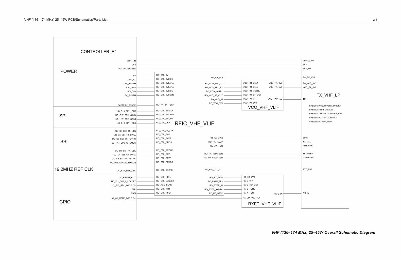
V 2-5
X_UP_AGC_FL1
RXFE_IN
XFE_RO_OUT
XFE_TUNE
X_ATTEN
XFE_9R1
O_RX_2V8
VCO_PA_5V0
CO_RO_VCTRL
CO_RO_SF_OUT
VCO_PA_9V3
CO_RO_IN
CO_RO_SEL2
CO_RO_SEL1
CO_RO_5V0
VCO_TXIN_LO
ANT_ENB
TEMPSEN
VSWRSEN
VCO_PA_5V0
TX1
PA_RO_9V3
9V3_EN
9V3
VBAT_OUT
RX_IN
ATT_ENB
TX_DAC
BIAS
PA_VCO_9V3
RXFE_VHF_VLIF
TX_VHF_LP
SHEET3: T/R SW, COUPLER, LPF
SHEET4: POWER CONTROL
SHEET5: 9.3V PA_REG.
SHEET2: FINAL DEVICE
SHEET1: PREDRIVER & DRIVERVCO_VHF_VLIF
VHF (136–174 MHz) 25–45W Overall Schematic Diagram
HF (136–174 MHz) 25–45W PCB/Schematics/Parts List
UC_C4_SSI_RX_FSYNC
UC_B4_SSI_RX_CLK
UC_D4_SSI_RX_DATA
UC_W2_GP7_9_LCKDET
9V3
9V3_PA_ENABLE
5V
2.8V_RX
2.8V_SYNTH
UC_P17_RDL_AGCFLG2
UC_W1_RFFE_AGCFLG1
RSSI
TTR
UC_R17_GP6_13_DMCS
UC_H17_SPI1_SOMI
1.8V_ANA
1.8V_DIG
VBAT_IN
1.8V_SYNTH
UC_G17_SPI1_SIMO
UC_RESET_OUT
UC_EXT_REF_CLK
UC_R16_GP6_12_RXACQ
UC_E19_SPI1_CS0
UC_B3_SSI_TX_CLK
UC_C3_SSI_TX_DATA
UC_C5_SSI_TX_FSYNC
UC_G19_SPI1_CLK
BATTERY_SENSE
RO_CTL_DMCS RO_PA_RAMP
RO_PA_BIAS
RO_RXBE_IN
RO_RXFE_AXDAC
RO_CTL_RXACQ
RO_CTL_RXFS
RO_CTL_1V8SYN
RO_CTL_1V8DIG
RO_PA_9V3
RO_VCO_SEL_TX
RO_VCO_SEL_RX
RO_ANT_EN
RO_PA_TEMPSEN
RO_PA_VSWRSEN
RO_PA_BATTSEN
RO_CTL_SPI_DR
RO_CTL_RXCLK
RO_CTL_RXD
RO_CTL_19.2RE
RO_CTL_LCKDET
RO_CTL_TTR
RO_CTL_RSSI
RO_CTL_2V8DIG
RO_CTL_1V8ANA
RO_CTL_CEX
RO_CTL_5V
RO_RX_2V80
RO_RXFE_9R1
RO_RF_STEP
RO_AGC_FLAG
RO_CTL_RSTB
RO_PW_CTL_ATT
RO_CTL_SPICLK
RO_CTL_SPI_DW
RO_CTL_TX_CLK
RO_CTL_TXD
RO_CTL_TXFS
RO_VCO_VCTRL
RO_VCO_SF_OUT
RO_VCO_IN
RO_VCO_5V0
RO_CTL_2V8ANA
R
R
R
R
R
R
V
V
V
V
V
V
19.2MHZ REF CLK
SPI
POWER
SSI
GPIO
CONTROLLER_R1
RFIC_VHF_VLIF
2-6 VHF (136–174 MHz) 25–45W PCB/Schematics/Parts List
RXF
STEP ATTEN 1
C0437 R0420
Q0405
R0418
47K
10K
47K
10K
E0404
E0405
Q0404
C0433425
C0432
31
2
31
2
J1
V2
V1
GN
D J2
J3
5
U0401
0431
6 4
1
3
2
J1
V2
V1
GN
DJ2
J3L0400
C0427
C0441
C0440C0439
U0402
C0460C0420
R0400
R0422R0419
64
1
3
5
2
VOLTAGE MULTIPLIERHE ANTENNA
ITH -30 DBM-17 DBM
AT THE ANTENNAWITH -30 DBM
-18 DBM
POST SELECTOR
C0442
C0429
L0410
C0424L0409C0421L0407
DNP
AT THE ANTENNAWITH -30 DBM
-21 DBM
R0434
R04
35
R04
32
C0428L0408
1RXFE_RO_OUT
OUT
COMMENTS
1.45V @ 155.5 MHZ
TP0404
RXFE_9R1_FILT
1
Q0400
FE_TUNE
2
R0413
R0417
R0411
R0416
R0415
R0403
5
14
63
R0410C0463C0413
E0402
C0465
1
RX
FE_T
UN
E
IN
VHF
PRESELECTOR
RXFE_9R1 1IN
4V @ 155.5 MHZ
AT THE ANTENNAWITH -30 DBM
-32 DBM
C0402
FE_TUNE
R0402
D0401
23
1
1
L041
4
1
E_IN C0423C0405
C0403
C0430
C04
38
C04
35L0
413
2 21
INR0429
C0406
C0407
C0452 C0453
C0404V
R04
021
R0404
VR
0400
1
VR
0403
L0406
VR
0401
L0405
L0401
21
2221
FE_TUNE
LNA
C0469
C04
10
C04
64
9.1V
C04
08
E0401RXFE_9R1_FILT
LNA
E2
B2
C2
E1
C1
B1
R0406
Q040141
36
52
R0426
2.4 V
L0404
C0458C0436
R0414R0401
R0421
C0418R0412C0416
Q0407
C0417R0407
4
13
652
AT THE ANTENNAWITH -30 DBM
-33 DBM
R04
44
L040
3
C0409 R0405
C04
14
C04
12
AT THE ANTENNA
-15 DBMWITH -30 DBM
R0442
R0443
P_DETECT
R0440DNP
C0401
R0448
C0419Q0402
R0409
Q0403
R0441
C0434
3
14
2
3
1 4
2
DNP
DNP
DNP
DNP
E0404 = 2.5VE0405 =0V
ATTEN ON
E0405 =2.5VE0404 = 0V
ATTEN OFF
RX_ATTEN 1 E0403
IN
2V8_FILT
C0
C
AT TW
0.8 V
NC
2
DNP
C0415
R0408L0402
C0411
C0400
R0445
1
23
1
DNPR0439
R0438
TP0403
R0437
11
RX_UP_AGC_FL1
DNP
OUT
R0433
2V8_FILT
DNP
EXTERNAL RF DETECTOR C0467
C0422E0400
R0423
R0424
1RO_RX_2V8
P_DETECT IN
RFINENBLVSETFLTR
VPOS
COMM
NC
VAPC
GND
NC
U0400
C0466
R0425
3
8
71
6
9
4
2
5
1
R0430
R0427
R0431
R0428DNP
2V8_FILT
C1
C2
E1
B1
E2
Q0406
3 1
4 6
2
R0436
D0402
MECHANICALSH0400
SH0401
21
21
MECHANICAL
(136–174 MHz) 25–45W Receiver Front-End Schematic Diagram
V 2-7
C0724
L0709
C0729
L0849
L0716
C0711
~2.6V
~38 DBM~38 DBM
~2.6V
GATE_2TP0706
1 1
TP0707GATE_1
R0710
1%R0746R0737
1%
R0709
1%C0754 R0741 C0764
R0742R0740
R0743C07531%
DNP
GATE2GATE1
C0761
DNP
~3.8V
PA_CTL_9V3
19V3
PA_VCO_9V3
TP0708FINAL_BIAS 1
9V3
PA_RO_9V3
PA_VCO_9V3
PA_RO_9V3
1
1
V_CONT
IN
OUT
OUT>4V
V_CONTROL
1
PA_RO_BIAS
R0723
TP0710
BIASFINAL_BIASR0739
1 IN
ANTENNA_EN
11
INBLOCK
47K47K
2.2K47K
9V3_TX
Q0701
1
4 6
3 25
9.3V
~+38 DBM
POS
C0738
TP0705
RD07_DRAIN
1
C0734
M0700
R0721
1
PA
9V3_TX
G
SD
R0716
C0747
RD07GATE
1
2
R0719
3
Q0704
R0714
R0715
DNP
100MW
100MW
100MW
100MW
R0717
2.4V @ VCONT=5V = 600MA BIAS
C0727C0731R0718
V_G2
DNP
R0720
V_CONT
5–45W Transmitter Power Amplifier Schematic Diagram (sheet 1 of 2)
HF (136–174 MHz) 25–45W PCB/Schematics/Parts List
+6 DBM MAX
12DB
FILTER_ATTENUATOR
TO CHECK REF OSC WARPING
C0720C0715L0718
1
TP0701
R0703
L0719
C0705
C0704L0704C0703
C0719L0703
1
PA_RO_TX1
TX1
R0705
R0706
R0707
IN
~+26 DBM
L0705
L0702
L0717 C0725
TP0702
RD01DRAIN
1
C0708
2.5V @ VCONT=5V = 75MA BIAS
~+10 DBM
G
SD
TP0700
Q0700RD01GATE
1
C0783
3
DNP
R0722
C0701
R0700V_CONT
2
1
R0702
R0704C0706C0710DNP
V_G1
C0713
9V3_TXR0701
C0709
~-2 DBM~+10 DBM
VD_RF_OUT
GN
D2
GN
D1
RF_IN
TP0704
3
2
GAINBLOCKDRAINQ0703
1
4
1
1
TP0703
C0732
R07R0712
C0775
L0707 SWITCHED9V3TOGA
E0700
9V3_PA
L0701 C0760L0700 C0735MATCH12A
L0730C0702C0700 R0713
DNP
VHF (136–174 MHz) 2
2-8 VHF (136–174 MHz) 25–45W PCB/Schematics/Parts List
C0757 C0756
C0728
C0795C0768 C0779
C0865
C0863
C0771
C0805 DNP
DNP
C0746
C0773
C0802
C0763
C0841
C0840
C0842
C0806
C0808
DNP
C0939
C0930DNP
DNP
C09
42
C09
41
C09
40
C0872
C08
00
C07
51
DNP
DN
P
DN
P
DN
P
DN
P
DN
P
C0759C0758
C0938
C0811
C0736
L0706
C0770
C0810
C0824
C0809
DNP
C0762
C0765
C0717
C0839
C0881
C0813FINAL_OUTPUT
C0846
RD
VHF
PA_SUPPLY
E0701
C0716C0712C0707
50V 50V50V
C0748
C0742C0733C0726C0745
C0730C072350V50V
50V50V
50V
50VC0740C0721C0737C0755
R0736E070350V50V50V
A+
50V
C0828
C0752 DNP
DNP
C0714C0818C0774
C0792
C0804
C0801
C0821
C0782
C0861 C0860
C0843
L0710
C0934
C0933
C0873
DNP
DNP
DNP
C0847
C0845
C0932
C0870
C0869
C0867
C0868
C0864
C0862
C0874
DNP
DNP
DNP
C0831
C0832
C08
33
C0794
C07
43
R0755
C08
29
C07
39C
0793
C07
41
C08
30
C07
44
07_DRAIN
C0797
C0749
C0835
R0764
C0796
R0765
C0837
C0836C0834
C0798
C0799
DNP
D1
CE
D2
G1
S1
S2
S4
S3
G2 3
GATE_2
2DRAIN
R0729
R0735
GATE1
R0728
R0727R0726R0725
R0724
C0812
Q0702
750MW
85417
69
GATE_1
DNP
GATE2
R0730
C0814
R0738
R0731
R0732
R0733
R0734
DNPC0857 C0858C0848
~+48 DBM
C0803
C0767
C0844
C0859
C0791
C0790
DNP
DNP
C07
81
C07
69
C07
80
~+48 DBM
C09
37
C09
14
C09
04
~+48 DBMC0895
C0931
C0890
C0915
C0898
C0897
C0896
C0894
C0893
C0891
C0878
C0866
C0892
C0889
C0888
C0887
C0886
C09
27
C09
20
C09
03
R0777
R0794
R0812
R0811
R0810
R0809
R0808
R0807
R0806
R0805
R0804
R0803
R0801R0783
R0792 R0797
R0796
R0800
R0799
R0798
R0802
R0795
R0793
R0791
R0790
R0789
R0788
R0787
R0786
R0785
R0784
R0773
R0776
R0775
R0774
R0782
R0781
R0780
R0779
R0778
R0772
R0771
R0770
R0769
R0768
R0767
R0766
R0763
R0760
R0758
DNP
DNP
DNP
DNP
DNP
DNP
DNP
DNP
DNP
DNP
(136–174 MHz) 25–45W Transmitter Power Amplifier Schematic Diagram (sheet 2 of 2)
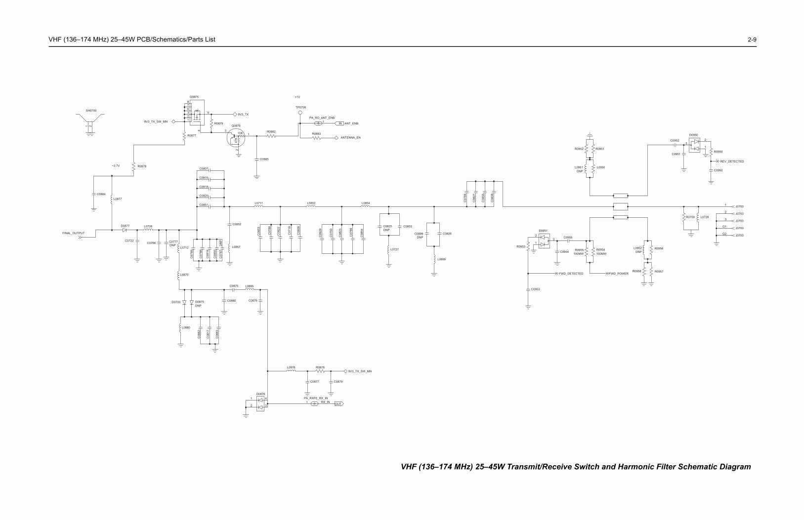
V 2-9
C08
38
R0951R0952
L0950L0951DNP
R0950
23
1
D0950
C0951
C0950
C0952
REV_DETECTED
1 J0700
2 J0700
3 J0700
G1 J0700
G2 J0700
L0729R0759
R0956L0952
R0957R0958
DNP
FWD_POWER
R0954
C0955
R0955C0954
23
1
D0951
R0953
100MW100MW
C0953
FWD_DETECTED
5W Transmit/Receive Switch and Harmonic Filter Schematic Diagram
HF (136–174 MHz) 25–45W PCB/Schematics/Parts List
SH0700
21
47K
10K
R0879
3
Q0876
5 9V3_TX
1
2
76
Q0875
4
8
321
R0877
9V3_TX_SW_MN
>1V
TP0709
R0883
PA_RO_ANT_ENB
R0882
C0885
1
ANTENNA_EN
ANT_ENBIN
C0807
C0815
C0819
C0820
C0851 L0852L0711 L0854 C07
84
C08
27
C08
56
C0826
C0825
C0899
L0899
C0855
L0727
DNP
DNP
C07
18
C09
28
C07
89
C07
88
C09
29
C08
23
C08
22
C08
54
C07
50
C08
53
C07
87
C07
85
C07
86
C08
16
C0852
L0857
C08
50
DN
P
L0877C0884
L0712C0766
C0722
L0708D0877
C0777DNP
FINAL_OUTPUT
D0700
L0885
C0876
C0875
L0875
C0880D0875DNP
C08
83
C08
17
C08
82
L0880
1
2
4
3
D0876
C0879
R0876L0876
C0877
9V3_TX_SW_MN
1PA_RXFE_RX_IN
RX_IN OUT
~3.7V R0878
VHF (136–174 MHz) 25–4
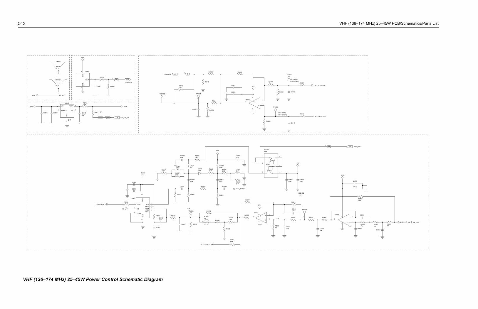
2-10 VHF (136–174 MHz) 25–45W PCB/Schematics/Parts List
.01V(27.5W)
.67V(44W)
C0919
R0931
3
FWD_DETECTED
C0918
R0933
REV_DETECTED
9V3
C092322DNP
1
TP0901C0900
R0919
R0959
C0901
R0922
DNP
DNP
VSENSE
R0921
1ATT_ENBIN
C0776
C0772
5V0R
1%R0960 R0961
C0956
R0748
C0957
1
R0962
C0902
DNP
1% 1%
TX_DACIN
>3V
25
41
3U0904
VHF
21
SH0900
21
SH0901
9V3 9V3
PO
SG
ND
VOUT
U0903
2 1
R0934
R0935
C0921
13
TEMPSEN
9V3
OUT
VOUT
ENABLE
GN
D
VIN
NC
51
4
2
3
U3002
C3016C3015
9V3
DNP
5V
R0708
1
R0813
DNPC3019
VCO_PA_5V0
5V0RDNP
IN
R0749
TP0904
R0923
R0924
R0745
R0928
1
C0926
R09651
DNP
VSENSE
VSWRSEN OUT
U0902
48
75
6
C0917
C0925
221
TP090
R0930
R09291%
0.38V (44W)0.21V (27.5W)
R0932
TP0902
5
4
6
Q0900DNP
3
2
1
C09DNP
>3V
R0920 C09161% DNP
2
R0917
48
13
U0902R0916
9V3
RT0900
R0914
R0744
R0915
1 2
R0939
R0940 DNP
DNP
47K
V_CONTROL
R0907C0908
R0905 R0906
DNPC0910
R0936DNP
DNPC0909
DNP
R0909
R0908D0960
L0901 L0900
R0937
DNP
DNP
5V0RDNPDNP
DNP
R0912
C0924DNP
FWD_POWER
L0902
R0938
R0911
R0910
C0913
C0912DNP
DNP
DNP
DNPDNP
9V3
NC
RFINENBLVSETFLTR
VP
OS
COMM
NC
VAPC
GN
D
C0906
C0905
R0902
3
8
7 1
6
9
4
2
5
U0901
V_CONTROL
>1V
TP0900
1R0904
R0913
C0936
C0911
R0903
C0907
DNP
9V3
(136–174 MHz) 25–45W Power Control Schematic Diagram
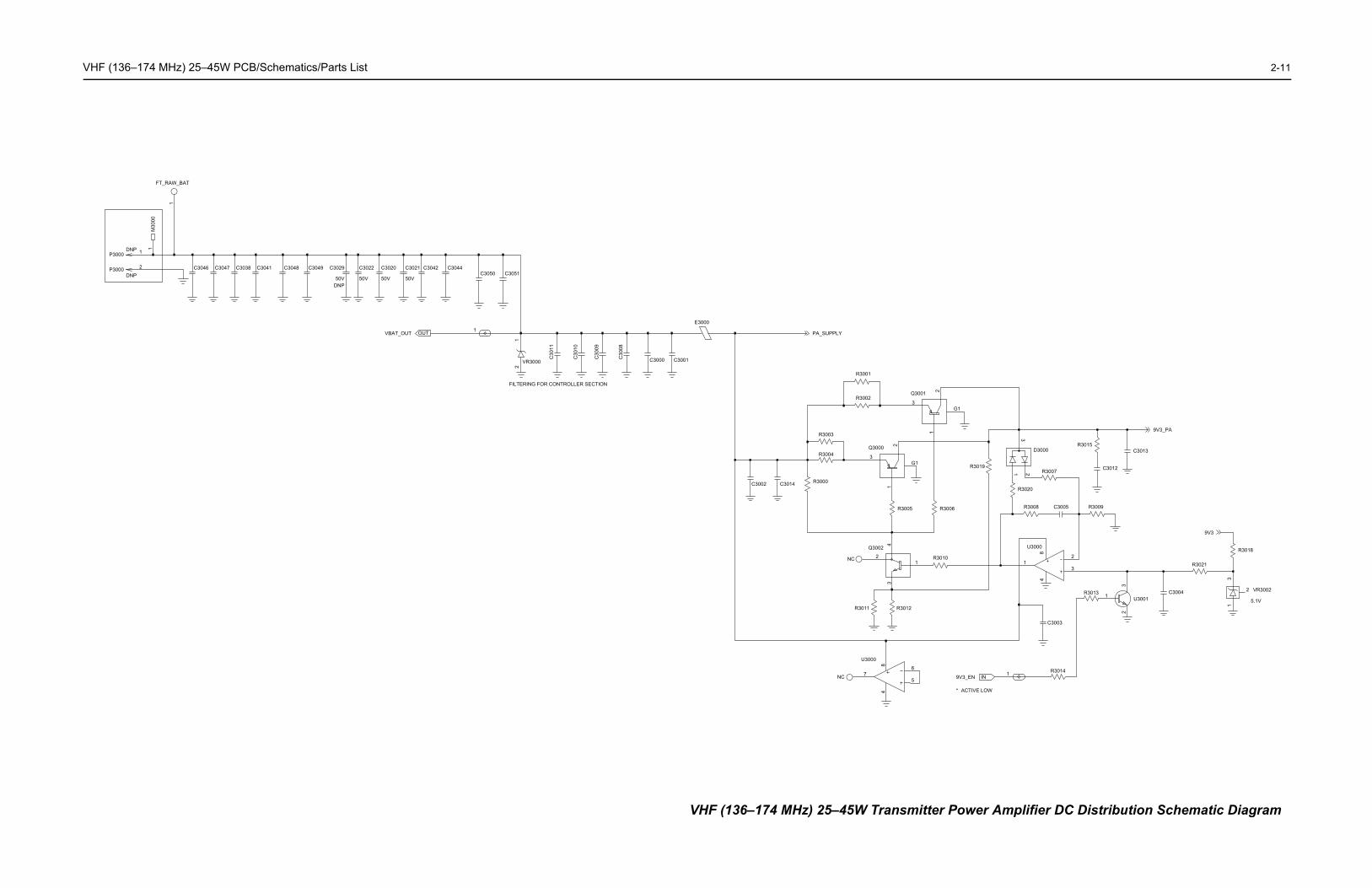
V 2-11
LY
G13
21
Q3001
R3001
R3002
G13
21
Q3000
R3019
R3006R3005
NC R3010
34
21
Q3002
R3012R3011
48
75
6
U3000
NC
* ACTIVE LOW
R301419V3_EN IN
48
13
2
U3000
C3004
23
1 U3001R3013
C3003
R3018
R3021
13
2 VR3002
9V3
5.1V
R3009
R3007
C3005
23
1
D3000
R3020
R3008
R3015C3013
C3012
9V3_PA
45W Transmitter Power Amplifier DC Distribution Schematic Diagram
HF (136–174 MHz) 25–45W PCB/Schematics/Parts List
1M
3000
1
FT_RAW_BAT
1P3000
2P3000DNP
DNP
C3051C3050
1
C3044C3042C3021C3020C3022C3029C3049C3048C3041C3038C3047C3046
50V50V50V
VBAT_OUT
50VDNP
OUT
FILTERING FOR CONTROLLER SECTION
E3000
C3001C3000C30
08
C30
09
C30
10
C30
11
21
VR3000
PA_SUPP
R3003
R3004
R3000C3014C3002
VHF (136–174 MHz) 25–
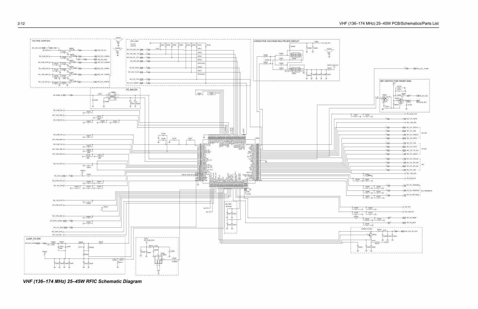
2-12 VHF (136–174 MHz) 25–45W PCB/Schematics/Parts List
LOO
RO_VC
IRCUIT L0000
C0086C0085R0029
RO_5V0
21
SH0003
R0030
VDD14_SYN_CP
K2K3
A1A2A3
K1
123
654
D0001
K2K3
A1A2A3
K1
NC
3
12
654
D0000
C0070C0068C0067C0066R0019
1RO_CTL_19.2REOUT
+9.3V
9R1 SWITCH FOR FRONT-END
C0137
1
C0135
E0009
RO_RXFE_9R1
RO_PA_9V3
9V3
IN
OUT+9.1V
C01361
3 12Q0002
R0044
+1.8V
47K
10K
2
31
Q0001
C0111
TX_SSI
SPI
RX_SSI
RO_2V80_SYN
RO_2V80_RX
RO_CTL_CEX
RO_CTL_RSTB
RO_1V80_DIG
RO_CTL_RXCLK
RO_CTL_SPICLK
RO_CTL_SPI_DW
RO_CTL_SPI_DR
RO_CTL_DMCS
RO_CTL_TX_CLK
RO_CTL_TXFS
RO_CTL_TXD
RO_CTL_RXFS
RO_CTL_RXD
RO_CTL_RXACQ
RO_1V80_DIG
IN
OUT
OUT
IN
OUT
IN
OUT
OUT
IN
IN
IN
OUT
IN
1
1
1
1
1
1
1
1
1
1
1
1
1
C0092C0021
ALC_FEEDBACK
RO_PA_VSWRSEN
RO_PA_BATTSEN
RO_PA_TEMPSEN
IN
IN
IN
1C0037
C0032
C00091
1
C0093
C0094
C0095
C0096
C0097
C0149
DNP
C0099
C0120
C0100
R0008
C0024
C0150
C0134
R0054 1
1
RO_5V0
RO_2V80_RX
RO_PA_BIAS
RO_PA_RAMPOUT
OUT
+9.3V
R0014
C0061
1
C0059C0055
SUPER_FILTER
C0065Q0000
C0072C0071
23
9V3
+8.2V 1R0015RO_VCO_SF_OUTOUT
VHF
RO_CTL_5V
RO_CTL_2V8DIG
RO_RX_2V80
RO_CTL_2V8ANA
RO_CTL_1V8DIG
RO_CTL_1V8ANA
RO_CTL_1V8SYN
OUT
IN
IN
IN
IN
IN
IN
1
1
1
1
1
1
1
+5V
+2.8V
+2.8V
+1.8V
+1.8V
+1.8V
E0006
E0007
E0005
E0004
E0008
E0010
VOLTAGE SUPPLIES
1
RO_2V80_RX
RO_VCO_5V0
RO_1V80_DIG
RO_1V80_ANA
RO_5V0
RO_2V80_SYN
OUT
C0141
C0140
C0143
C0144
RO_1V8_SYN
DNP
C0101
C0102
C0138
DNP
C0105
C0103
C0104
RO_RXBE_IN 1IN
RO_2V80_RX
RO_2V80_RX
RO_1V80_ANA
RO_1V80_ANA
RO_2V80_RX
RO_2V80_RX
RO_1V80_ANA
RO_1V80_ANA
DNP
C0016
C0018
C0013
C0039 C0035
DNP
C0022
C0017
C0019
C0139
DNP
C0014
C0030
DNP
1RO_VCO_IN
RO_2V80_SYN
RO_1V8_SYN
IN
1
TP0001
C0025
RO_1V8_SYN
C0053 C0042
C0026
C0027
C0031
RO_2V80_SYN
RO_CTL_RSSI
RO_1V8_SYN
RO_RXFE_AXDAC
RO_1V80_ANA
1
1
TP0011
C0023
C0029
C00561
RO_2V80_SYN
RO_1V8_SYN
OUT
OUT
1.5V - 10.5V
P_FILTER
O_VCTRL 1 R0000
C0006
R0001
C0003DNP
OUT
TP0000
C0007C0005C0002
1
C0004
R0010
R0009C0011
R0006
R0007
C0034C0012
R0012C0043R0011
P1
P2
S1
S2
L0001
4
1
3
2
T0000
C0091C0089
FE_BALUN
E0000E0001
21
SH0000
21
SH0001
LOW:0VHI:1.8V
GPO_LINES
1
RO_ANT_EN
1
1
1
1
1
1
1
RO_AGC_FLAG
RO_VCO_SEL_RX
RO_VCO_SEL_TX
RO_CTL_LCKDET
RO_PW_CTL_ATT
RO_RF_STEP
RO_CTL_TTR
OUT
OUT
OUT
OUT
OUT
OUT
OUT
OUT
+1.8V
GPO6
GPO8 (NC)
GPO7
GPO5 (NC)
GPO3
GPO1
GPO2
GPO4
C0015 C0010C0036C0033C0020 C0124C0098C0054
C0064C0060
CAPACITIVE VOLTAGE MULTIPLIER C
NC
C0080
C0081C0078
C0083
C0082
R0022
R0025
+2.8V
TCXO
Y0000
RO_2V80_SYN
R0013
19.2MHZ
19.2MHZ
GN
D1 V
CC
GN
D2
OU
T
4
C0045
C00493
C0028 C0046
21
C0044
BYPASS
ADC REF
C0073 C0075
C0076C0074
NC
NC
NC
NC
A21
A28
B21
B16
B26
A25
B18
B17
A18
A24
B23
B19
A22
B20
A19
A31
B29
B27
A30
A27
A26
B25
B24
B30
A32
B22
A23
A20
A17 G1
A29
B28
NCN
CN
C
1TP
0002
VDD28_MIXBYP_TO_2P7
NC13NC1
VDD28_LNA_1
NC2VDD18_QG
VDD18_LNANC3
NC4NC14
GND2LTD_INBGND_LNA_LTDLTD_INGND3GND4
VDD18_LO_DIVVDD18_MIX_1
VDD18_DIV_PSGND5VDD18_LO_DCA
VDD28_SYNVCO1_IN
GND_LO_DCAVDDHV14_SYN_CPVDD18_SYN
GND7SYN_ACPUMP
GND6
SYN_MCPUMP
B13
B12
A1
A4
A14
B3
B9A10
B11
B4
B10
A12
A16
A15
B5
B2
A6
A5
A3
A2
A7
A8
A13
B7
B15
B14
A11
A9B8
B6
B1
VDD14_SYN_CP
C0001C0147
C0145
C0146
VDD28_VMULTIGPO9
VMULT1SCAN_EN
VMULT2RSTB
RXCLK_IO
RXDVDD33_DIG
RXACQRX_EN_OUT
RXFS
GND12CLK_OUT
GP
O8
TES
T2_C
HR
PS
W
TES
T1_L
CK
DE
TD
CC
AL_
GP
O5
AG
C_F
LG_G
PO
7R
FSTE
PA
_GP
O6
GP
O4_
TES
T4
GP
O2_
TES
T2G
PO
3_TE
ST3
GP
O1_
TES
T1M
IC_I
NM
IC_I
NB
GN
D13
GN
D14
GND11TXD
TXFSTXCLKDMCS
SPI_CLK
SPI_DRSPI_DW
CEXVDD18_DIG_2
NC7VDD28_DAC_ADC_2
ALC_VSWRSENSSCAN_IN
ALC_PATEMPTM
ALC_BATTSENS
CTG
ND
GP
AD
C_I
N_4
GP
AD
C_I
N_5
RA
MP
NC
16N
C6
AD
C_R
EF1
_BY
PA
DC
_RE
F2_B
YP
NC
15
VD
D28
_DA
C_A
DC
_1V
DD
HV
5_D
AC
NC
5G
PD
AC
_OU
T_2
HP
_MO
D_O
UT
VD
D18
_TX
RF
GP
DA
C_O
UT_
1V
DD
28_P
MA
VD
D18
_PM
AA
GC
_DA
CA
GC
_RE
FM
IXO
UT_
IM
IXO
UT_
IX
MIX
OU
T_Q
XM
IXO
UT_
Q
NC
8N
C17
NC
9N
C18
NC
10G
ND
15N
C11
GN
D16
NC
12
TX1_
OU
TS
PK
R_D
AC
_OU
T
GN
D10
GN
D9
VD
D28
_SF
SF_
OU
T
VD
DH
V10
_SF
SF_
BY
P
SF_
SE
NS
GN
D8
VD
D18
_RE
F_C
LK
VD
D18
_FG
U2_
PS
RE
F_IN
VC
O2_
INV
DD
28_F
GU
2_C
PFG
U2_
CP_
OU
T
A38
B47
A46
A47
B42
A48
A56
B33
B53
B34
A40B38
B37
B31
B46
B35
B36
B32
B44
B40
A44
A45
B41A43
B43
B48
B58
B57
A64
A63
A62
A61
A60
A36
B56
A59
B55
A58
B51
A54
B45
A49
A52
B49
A53
B50
B60
B59
B52
A55
B39A41
A39
A50
A42
A37
A35
A34
A33
B54
A51
A57 U0000
(136–174 MHz) 25–45W RFIC Schematic Diagram
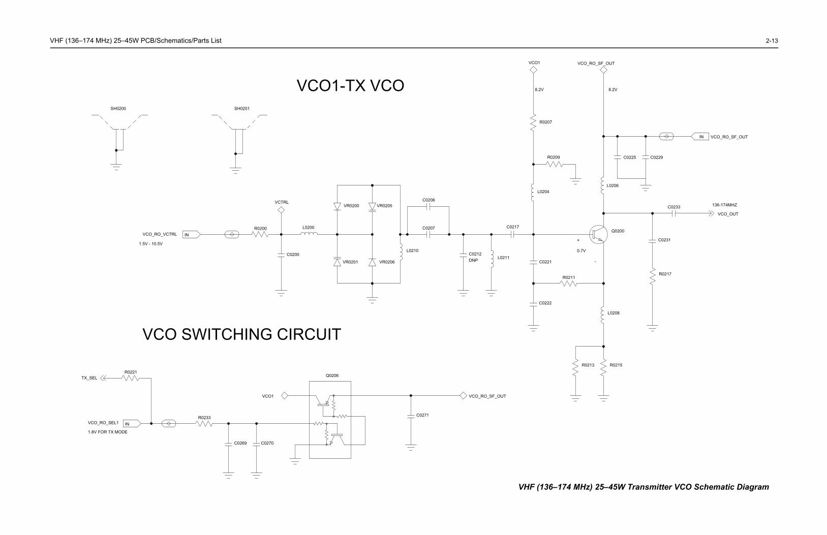
V 2-13
0.7V
+
-
R0209
11
R0211
L0204
Q0200
C0221
C0217
8.2V8.2V
C0225 C0229
VCO_RO_SF_OUT
VCO_RO_SF_OUTVCO1
R0207
IN
136-174MHZ
T
VCO_OUT
R0213
C0222
R0215
L0208
C0231
L0206
C0233
R0217
VHF (136–174 MHz) 25–45W Transmitter VCO Schematic Diagram
HF (136–174 MHz) 25–45W PCB/Schematics/Parts List
VCO SWITCHING CIRCUIT
VCO1-TX VCOSH0200 SH0201
1.5V - 10.5V
VCO_RO_VCTRL IN
VR0200
C0200
VCTRL
R0200 L0200
VR0201
VR0205
C0207
C0206
L0210
VR0206 DNPC0212
L02
VCO_RO_SF_OU
Q0206
C0271
VCO1
R0233
C0269 C0270
1.8V FOR TX MODE
VCO_RO_SEL1
R0221TX_SEL
IN
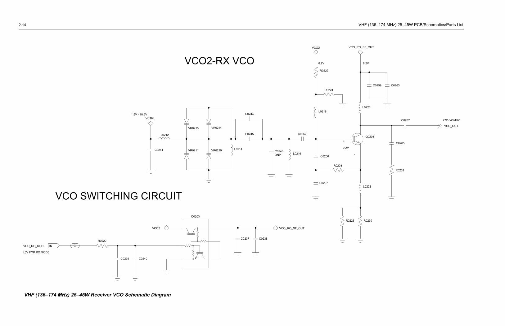
2-14 VHF (136–174 MHz) 25–45W PCB/Schematics/Parts List
0.2V
-
+
272-348MHZ
VCO_OUT
L0222
C0267
R0203
C0257
C0256
R0232
C0265
Q0204
8.2V8.2V
VCO_RO_SF_OUTVCO2
R0222
L0220
C0259 C0263R0224
L0218
1.8V FO
VCO_R
R0228 R0230
VHF
1.5V - 10.5V
VR0215
VR0211
VCTRL
L0212
VR0214
VR0210C0241
DNP
C0244
C0248L0216
C0252
L0214
C0245
VCO2-RX VCO
VCO_RO_SF_OUT
C0237 C0238
VCO SWITCHING CIRCUIT
VCO2
Q0203
R RX MODE
O_SEL2
R0220
C0239 C0240
IN
(136–174 MHz) 25–45W Receiver VCO Schematic Diagram
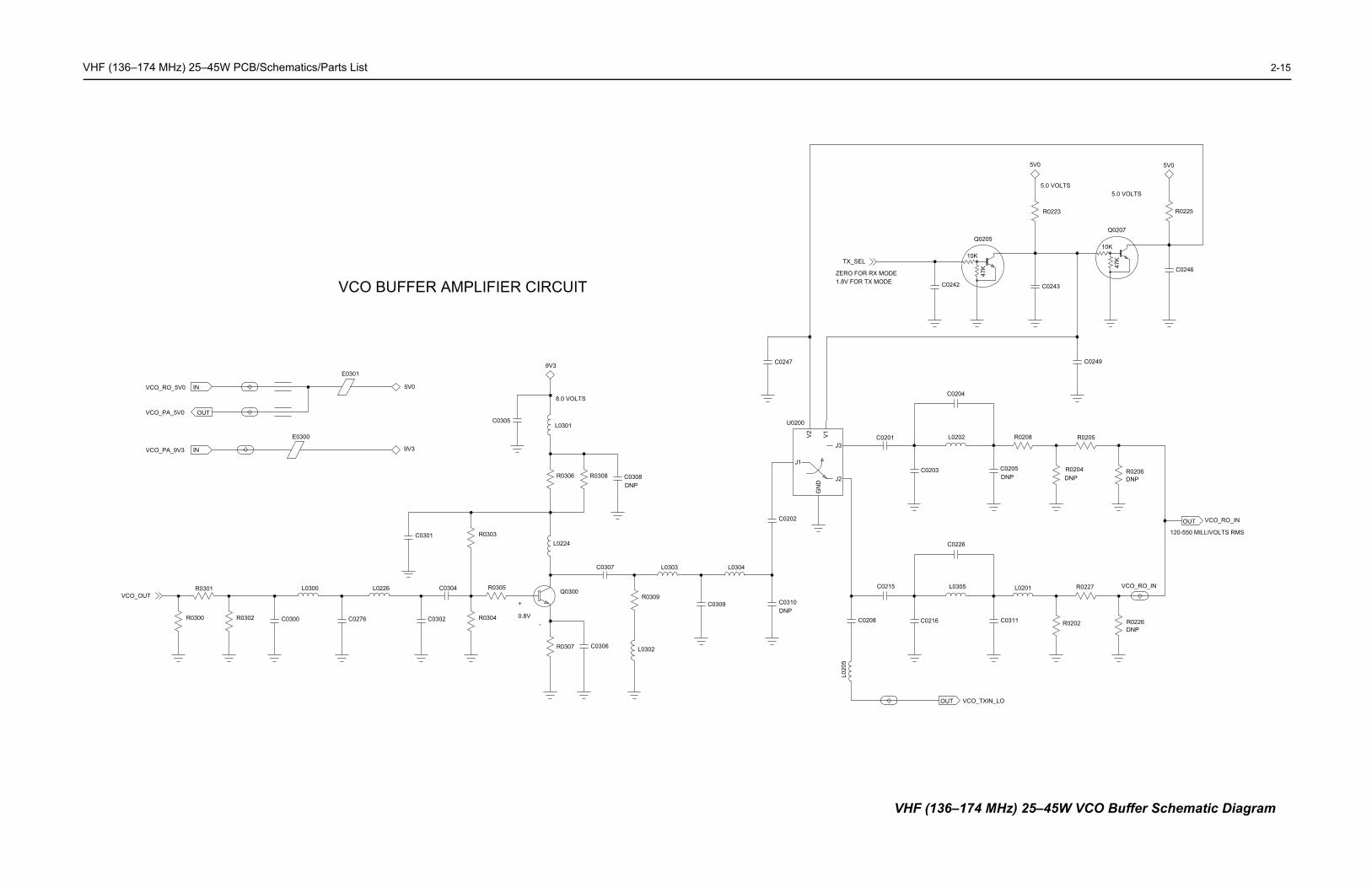
V 2-15
J2
J3C0201
DNP
R0208
C0203
L0202
C0204
R0204C0205
R0205
DNP
120-550 MILLIVOLTS RMS
VCO_RO_IN
R0206
VCO_RO_IN
DNP
OUT
C0216
C0215
DNPC0208 R0202
L0201 R0227
R0226C0311
L0305
VCO_TXIN_LO
L020
5
OUT
C0226
1.8V FOR TX MODEZERO FOR RX MODE
TX_SEL
47K
10K
Q0205
C0242
5.0 VOLTS5.0 VOLTS
47K
10K
Q0207
C0249
C0246
R0225
C0243
R0223
5V05V0
VHF (136–174 MHz) 25–45W VCO Buffer Schematic Diagram
HF (136–174 MHz) 25–45W PCB/Schematics/Parts List
VCO BUFFER AMPLIFIER CIRCUIT
VCO_PA_9V3
VCO_RO_5V0
VCO_PA_5V0
9V3
5V0
E0300
E0301
IN
OUT
IN
8.0 VOLTS
9V3
L0301C0305
C0308R0306 R0308DNP
L0303C0307
L0224R0303C0301
0.8V-
+
Q0300
R0304C0300
R0305C0304L0226
C0302C0276
L0300R0301
R0302R0300
VCO_OUT
R0307
C0202
L0304
C0310C0309R0309
L0302C0306
DNP
J1
V2
V1
GN
D
U0200
C0247
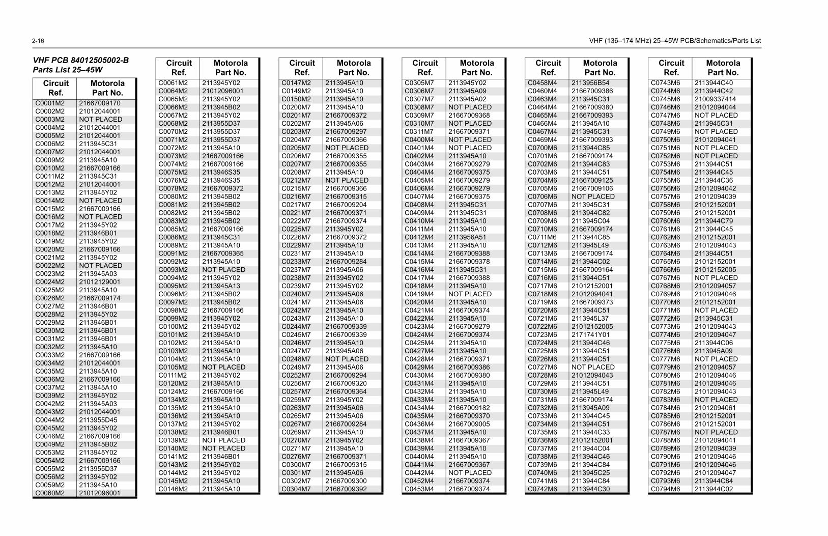
2-16 VHF (136–174 MHz) 25–45W PCB/Schematics/Parts List
VHF PParts
CirR
C000C000C000C000C000C000C000C000C001C0011C001C001C001C001C001C001C001C001C002C002C002C002C002C002C002C002C002C002C003C003C003C003C003C003C003C003C003C004C004C004C004C004C004C005C005C005C005C005C006
C0458M4 2113956B54C0460M4 21667009386C0463M4 2113945C31C0464M4 21667009380C0465M4 21667009393C0466M4 2113945A10C0467M4 2113945C31C0469M4 21667009393C0700M6 2113944C85C0701M6 21667009174C0702M6 2113944C83C0703M6 2113944C51C0704M6 21667009125C0705M6 21667009106C0706M6 NOT PLACEDC0707M6 2113945C31C0708M6 2113944C82C0709M6 2113945C04C0710M6 21667009174C0711M6 2113944C85C0712M6 2113945L49C0713M6 21667009174C0714M6 2113944C02C0715M6 21667009164C0716M6 2113944C51C0717M6 21012152001C0718M6 21012094041C0719M6 21667009373C0720M6 2113944C51C0721M6 2113945L37C0722M6 21012152005C0723M6 2171741Y01C0724M6 2113944C46C0725M6 2113944C51C0726M6 2113944C51C0727M6 NOT PLACEDC0728M6 21012094043C0729M6 2113944C51C0730M6 2113945L49C0731M6 21667009174C0732M6 2113945A09C0733M6 2113944C45C0734M6 2113944C51C0735M6 2113944C33C0736M6 21012152001C0737M6 2113944C04C0738M6 2113944C46C0739M6 2113944C84C0740M6 2113945C25C0741M6 2113944C84C0742M6 2113944C30
Circuit Ref.
MotorolaPart No.
C0743M6 2113944C40C0744M6 2113944C42C0745M6 21009337414C0746M6 21012094044C0747M6 NOT PLACEDC0748M6 2113945C31C0749M6 NOT PLACEDC0750M6 21012094041C0751M6 NOT PLACEDC0752M6 NOT PLACEDC0753M6 2113944C51C0754M6 2113944C45C0755M6 2113944C36C0756M6 21012094042C0757M6 21012094039C0758M6 21012152001C0759M6 21012152001C0760M6 2113944C79C0761M6 2113944C45C0762M6 21012152001C0763M6 21012094043C0764M6 2113944C51C0765M6 21012152001C0766M6 21012152005C0767M6 NOT PLACEDC0768M6 21012094057C0769M6 21012094046C0770M6 21012152001C0771M6 NOT PLACEDC0772M6 2113945C31C0773M6 21012094043C0774M6 21012094047C0775M6 2113944C06C0776M6 2113945A09C0777M6 NOT PLACEDC0779M6 21012094057C0780M6 21012094046C0781M6 21012094046C0782M6 21012094043C0783M6 NOT PLACEDC0784M6 21012094061C0785M6 21012152001C0786M6 21012152001C0787M6 NOT PLACEDC0788M6 21012094041C0789M6 21012094039C0790M6 21012094046C0791M6 21012094046C0792M6 21012094047C0793M6 2113944C84C0794M6 2113944C02
Circuit Ref.
MotorolaPart No.
CB 84012505002-B List 25–45Wcuit ef.
MotorolaPart No.
1M2 216670091702M2 210120440013M2 NOT PLACED4M2 210120440015M2 210120440016M2 2113945C317M2 210120440019M2 2113945A100M2 21667009166M2 2113945C31
2M2 210120440013M2 2113945Y024M2 NOT PLACED5M2 216670091666M2 NOT PLACED7M2 2113945Y028M2 2113946B019M2 2113945Y020M2 216670091661M2 2113945Y022M2 NOT PLACED3M2 2113945A034M2 210121290015M2 2113945A106M2 216670091747M2 2113946B018M2 2113945Y029M2 2113946B010M2 2113946B011M2 2113946B012M2 2113945A103M2 216670091664M2 210120440015M2 2113945A106M2 216670091667M2 2113945A109M2 2113945Y022M2 2113945A033M2 210120440014M2 2113955D455M2 2113945Y026M2 216670091669M2 2113945B023M2 2113945Y024M2 216670091665M2 2113955D376M2 2113945Y029M2 2113945A100M2 21012096001
C0061M2 2113945Y02C0064M2 21012096001C0065M2 2113945Y02C0066M2 2113945B02C0067M2 2113945Y02C0068M2 2113955D37C0070M2 2113955D37C0071M2 2113955D37C0072M2 2113945A10C0073M2 21667009166C0074M2 21667009166C0075M2 2113946S35C0076M2 2113946S35C0078M2 21667009372C0080M2 2113945B02C0081M2 2113945B02C0082M2 2113945B02C0083M2 2113945B02C0085M2 21667009166C0086M2 2113945C31C0089M2 2113945A10C0091M2 21667009365C0092M2 2113945A10C0093M2 NOT PLACEDC0094M2 2113945Y02C0095M2 2113945A13C0096M2 2113945B02C0097M2 2113945B02C0098M2 21667009166C0099M2 2113945Y02C0100M2 2113945Y02C0101M2 2113945A10C0102M2 2113945A10C0103M2 2113945A10C0104M2 2113945A10C0105M2 NOT PLACEDC0111M2 2113945Y02C0120M2 2113945A10C0124M2 21667009166C0134M2 2113945A10C0135M2 2113945A10C0136M2 2113945A10C0137M2 2113945Y02C0138M2 2113946B01C0139M2 NOT PLACEDC0140M2 NOT PLACEDC0141M2 2113946B01C0143M2 2113945Y02C0144M2 2113945Y02C0145M2 2113945A10C0146M2 2113945A10
Circuit Ref.
MotorolaPart No.
C0147M2 2113945A10C0149M2 2113945A10C0150M2 2113945A10C0200M7 2113945A10C0201M7 21667009372C0202M7 2113945A06C0203M7 21667009297C0204M7 21667009366C0205M7 NOT PLACEDC0206M7 21667009355C0207M7 21667009355C0208M7 2113945A10C0212M7 NOT PLACEDC0215M7 21667009366C0216M7 21667009315C0217M7 21667009204C0221M7 21667009371C0222M7 21667009374C0225M7 2113945Y02C0226M7 21667009372C0229M7 2113945A10C0231M7 2113945A10C0233M7 21667009284C0237M7 2113945A06C0238M7 2113945Y02C0239M7 2113945Y02C0240M7 2113945A06C0241M7 2113945A06C0242M7 2113945A10C0243M7 2113945A10C0244M7 21667009339C0245M7 21667009339C0246M7 2113945A10C0247M7 2113945A06C0248M7 NOT PLACEDC0249M7 2113945A06C0252M7 21667009294C0256M7 21667009320C0257M7 21667009364C0259M7 2113945Y02C0263M7 2113945A06C0265M7 2113945A06C0267M7 21667009284C0269M7 2113945A10C0270M7 2113945Y02C0271M7 2113945A10C0276M7 21667009371C0300M7 21667009315C0301M7 2113945A06C0302M7 21667009300C0304M7 21667009392
Circuit Ref.
MotorolaPart No.
C0305M7 2113945Y02C0306M7 2113945A09C0307M7 2113945A02C0308M7 NOT PLACEDC0309M7 21667009368C0310M7 NOT PLACEDC0311M7 21667009371C0400M4 NOT PLACEDC0401M4 NOT PLACEDC0402M4 2113945A10C0403M4 21667009279C0404M4 21667009375C0405M4 21667009279C0406M4 21667009279C0407M4 21667009375C0408M4 2113945C31C0409M4 2113945C31C0410M4 2113945A10C0411M4 2113945A10C0412M4 2113956A51C0413M4 2113945A10C0414M4 21667009388C0415M4 21667009378C0416M4 2113945C31C0417M4 21667009388C0418M4 2113945A10C0419M4 NOT PLACEDC0420M4 2113945A10C0421M4 21667009374C0422M4 2113945A10C0423M4 21667009279C0424M4 21667009374C0425M4 2113945A10C0427M4 2113945A10C0428M4 21667009371C0429M4 21667009386C0430M4 21667009380C0431M4 2113945A10C0432M4 2113945A10C0433M4 2113945A10C0434M4 21667009182C0435M4 21667009370C0436M4 21667009005C0437M4 2113945A10C0438M4 21667009367C0439M4 2113945A10C0440M4 2113945A10C0441M4 21667009367C0442M4 NOT PLACEDC0452M4 21667009374C0453M4 21667009374
Circuit Ref.
MotorolaPart No.
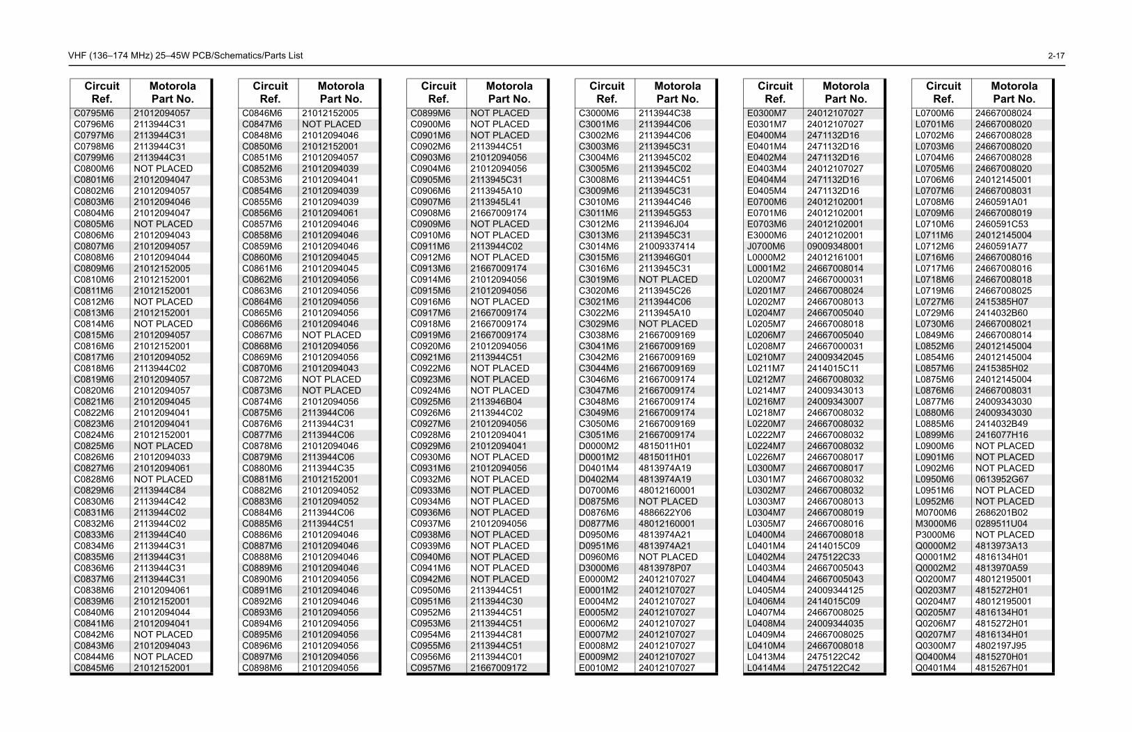
V 2-17
4
D
D9999444494
1D
1
D
777777777
lao.
E0300M7 24012107027E0301M7 24012107027E0400M4 2471132D16E0401M4 2471132D16E0402M4 2471132D16E0403M4 24012107027E0404M4 2471132D16E0405M4 2471132D16E0700M6 24012102001E0701M6 24012102001E0703M6 24012102001E3000M6 24012102001J0700M6 09009348001L0000M2 24012161001L0001M2 24667008014L0200M7 24667000031L0201M7 24667008024L0202M7 24667008013L0204M7 24667005040L0205M7 24667008018L0206M7 24667005040L0208M7 24667000031L0210M7 24009342045L0211M7 2414015C11L0212M7 24667008032L0214M7 24009343013L0216M7 24009343007L0218M7 24667008032L0220M7 24667008032L0222M7 24667008032L0224M7 24667008032L0226M7 24667008017L0300M7 24667008017L0301M7 24667008032L0302M7 24667008032L0303M7 24667008013L0304M7 24667008019L0305M7 24667008016L0400M4 24667008018L0401M4 2414015C09L0402M4 2475122C33L0403M4 24667005043L0404M4 24667005043L0405M4 24009344125L0406M4 2414015C09L0407M4 24667008025L0408M4 24009344035L0409M4 24667008025L0410M4 24667008018L0413M4 2475122C42L0414M4 2475122C42
Circuit Ref.
MotorolaPart No.
L0700M6 24667008024L0701M6 24667008020L0702M6 24667008028L0703M6 24667008020L0704M6 24667008028L0705M6 24667008020L0706M6 24012145001L0707M6 24667008031L0708M6 2460591A01L0709M6 24667008019L0710M6 2460591C53L0711M6 24012145004L0712M6 2460591A77L0716M6 24667008016L0717M6 24667008016L0718M6 24667008018L0719M6 24667008025L0727M6 2415385H07L0729M6 2414032B60L0730M6 24667008021L0849M6 24667008014L0852M6 24012145004L0854M6 24012145004L0857M6 2415385H02L0875M6 24012145004L0876M6 24667008031L0877M6 24009343030L0880M6 24009343030L0885M6 2414032B49L0899M6 2416077H16L0900M6 NOT PLACEDL0901M6 NOT PLACEDL0902M6 NOT PLACEDL0950M6 0613952G67L0951M6 NOT PLACEDL0952M6 NOT PLACEDM0700M6 2686201B02M3000M6 0289511U04P3000M6 NOT PLACEDQ0000M2 4813973A13Q0001M2 4816134H01Q0002M2 4813970A59Q0200M7 48012195001Q0203M7 4815272H01Q0204M7 48012195001Q0205M7 4816134H01Q0206M7 4815272H01Q0207M7 4816134H01Q0300M7 4802197J95Q0400M4 4815270H01Q0401M4 4815267H01
Circuit Ref.
MotorolaPart No.
HF (136–174 MHz) 25–45W PCB/Schematics/Parts List
C0795M6 21012094057C0796M6 2113944C31C0797M6 2113944C31C0798M6 2113944C31C0799M6 2113944C31C0800M6 NOT PLACEDC0801M6 21012094047C0802M6 21012094057C0803M6 21012094046C0804M6 21012094047C0805M6 NOT PLACEDC0806M6 21012094043C0807M6 21012094057C0808M6 21012094044C0809M6 21012152005C0810M6 21012152001C0811M6 21012152001C0812M6 NOT PLACEDC0813M6 21012152001C0814M6 NOT PLACEDC0815M6 21012094057C0816M6 21012152001C0817M6 21012094052C0818M6 2113944C02C0819M6 21012094057C0820M6 21012094057C0821M6 21012094045C0822M6 21012094041C0823M6 21012094041C0824M6 21012152001C0825M6 NOT PLACEDC0826M6 21012094033C0827M6 21012094061C0828M6 NOT PLACEDC0829M6 2113944C84C0830M6 2113944C42C0831M6 2113944C02C0832M6 2113944C02C0833M6 2113944C40C0834M6 2113944C31C0835M6 2113944C31C0836M6 2113944C31C0837M6 2113944C31C0838M6 21012094061C0839M6 21012152001C0840M6 21012094044C0841M6 21012094041C0842M6 NOT PLACEDC0843M6 21012094043C0844M6 NOT PLACEDC0845M6 21012152001
Circuit Ref.
MotorolaPart No.
C0846M6 21012152005C0847M6 NOT PLACEDC0848M6 21012094046C0850M6 21012152001C0851M6 21012094057C0852M6 21012094039C0853M6 21012094041C0854M6 21012094039C0855M6 21012094039C0856M6 21012094061C0857M6 21012094046C0858M6 21012094046C0859M6 21012094046C0860M6 21012094045C0861M6 21012094045C0862M6 21012094056C0863M6 21012094056C0864M6 21012094056C0865M6 21012094056C0866M6 21012094046C0867M6 NOT PLACEDC0868M6 21012094056C0869M6 21012094056C0870M6 21012094043C0872M6 NOT PLACEDC0873M6 NOT PLACEDC0874M6 21012094056C0875M6 2113944C06C0876M6 2113944C31C0877M6 2113944C06C0878M6 21012094046C0879M6 2113944C06C0880M6 2113944C35C0881M6 21012152001C0882M6 21012094052C0883M6 21012094052C0884M6 2113944C06C0885M6 2113944C51C0886M6 21012094046C0887M6 21012094046C0888M6 21012094046C0889M6 21012094046C0890M6 21012094056C0891M6 21012094046C0892M6 21012094046C0893M6 21012094056C0894M6 21012094056C0895M6 21012094056C0896M6 21012094056C0897M6 21012094056C0898M6 21012094056
Circuit Ref.
MotorolaPart No.
C0899M6 NOT PLACEDC0900M6 NOT PLACEDC0901M6 NOT PLACEDC0902M6 2113944C51C0903M6 21012094056C0904M6 21012094056C0905M6 2113945C31C0906M6 2113945A10C0907M6 2113945L41C0908M6 21667009174C0909M6 NOT PLACEDC0910M6 NOT PLACEDC0911M6 2113944C02C0912M6 NOT PLACEDC0913M6 21667009174C0914M6 21012094056C0915M6 21012094056C0916M6 NOT PLACEDC0917M6 21667009174C0918M6 21667009174C0919M6 21667009174C0920M6 21012094056C0921M6 2113944C51C0922M6 NOT PLACEDC0923M6 NOT PLACEDC0924M6 NOT PLACEDC0925M6 2113946B04C0926M6 2113944C02C0927M6 21012094056C0928M6 21012094041C0929M6 21012094041C0930M6 NOT PLACEDC0931M6 21012094056C0932M6 NOT PLACEDC0933M6 NOT PLACEDC0934M6 NOT PLACEDC0936M6 NOT PLACEDC0937M6 21012094056C0938M6 NOT PLACEDC0939M6 NOT PLACEDC0940M6 NOT PLACEDC0941M6 NOT PLACEDC0942M6 NOT PLACEDC0950M6 2113944C51C0951M6 2113944C30C0952M6 2113944C51C0953M6 2113944C51C0954M6 2113944C81C0955M6 2113944C51C0956M6 2113944C01C0957M6 21667009172
Circuit Ref.
MotorolaPart No.
C3000M6 2113944C38C3001M6 2113944C06C3002M6 2113944C06C3003M6 2113945C31C3004M6 2113945C02C3005M6 2113945C02C3008M6 2113944C51C3009M6 2113945C31C3010M6 2113944C46C3011M6 2113945G53C3012M6 2113946J04C3013M6 2113945C31C3014M6 2100933741C3015M6 2113946G01C3016M6 2113945C31C3019M6 NOT PLACEC3020M6 2113945C26C3021M6 2113944C06C3022M6 2113945A10C3029M6 NOT PLACEC3038M6 2166700916C3041M6 2166700916C3042M6 2166700916C3044M6 2166700916C3046M6 2166700917C3047M6 2166700917C3048M6 2166700917C3049M6 2166700917C3050M6 2166700916C3051M6 2166700917D0000M2 4815011H01D0001M2 4815011H01D0401M4 4813974A19D0402M4 4813974A19D0700M6 4801216000D0875M6 NOT PLACED0876M6 4886622Y06D0877M6 4801216000D0950M6 4813974A21D0951M6 4813974A21D0960M6 NOT PLACED3000M6 4813978P07E0000M2 2401210702E0001M2 2401210702E0004M2 2401210702E0005M2 2401210702E0006M2 2401210702E0007M2 2401210702E0008M2 2401210702E0009M2 2401210702E0010M2 2401210702
Circuit Ref.
MotoroPart N
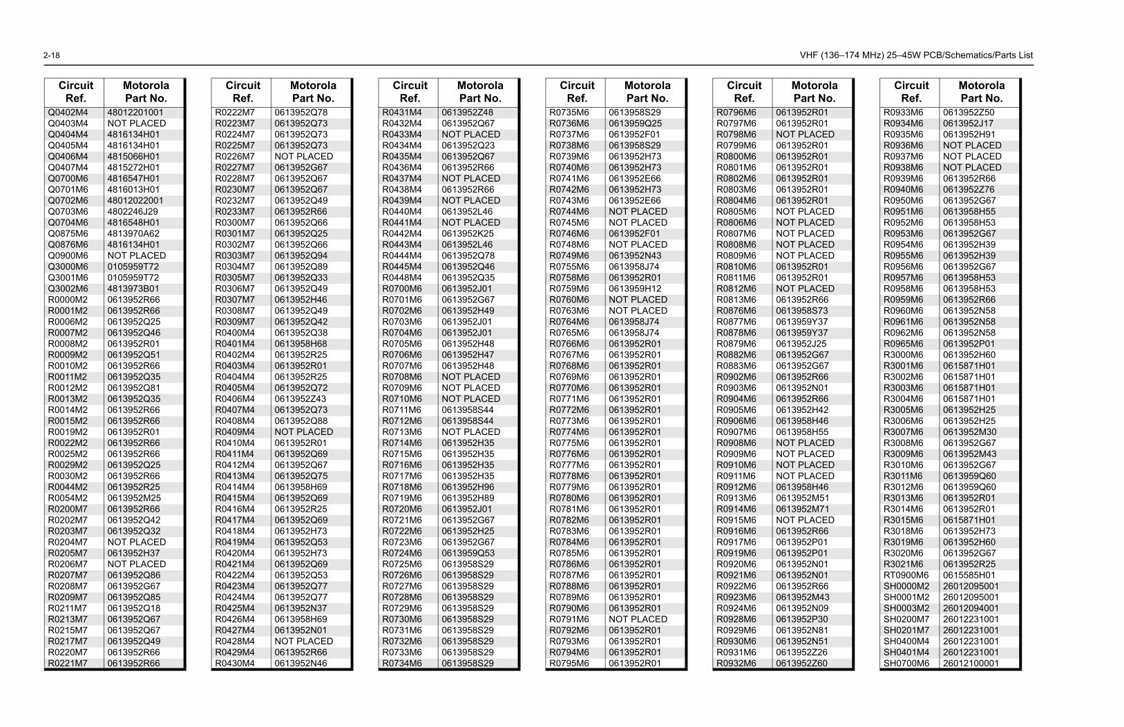
2-18 VHF (136–174 MHz) 25–45W PCB/Schematics/Parts List
Q040Q040Q040Q040Q040Q040Q070Q070Q070Q070Q070Q087Q087Q090Q300Q300Q300R000R000R000R000R000R000R001R0011R001R001R001R001R001R002R002R002R003R004R005R020R020R020R020R020R020R020R020R020R0211R021R021R021R022R022
CirR
R0796M6 0613952R01R0797M6 0613952R01R0798M6 NOT PLACEDR0799M6 0613952R01R0800M6 0613952R01R0801M6 0613952R01R0802M6 0613952R01R0803M6 0613952R01R0804M6 0613952R01R0805M6 NOT PLACEDR0806M6 NOT PLACEDR0807M6 NOT PLACEDR0808M6 NOT PLACEDR0809M6 NOT PLACEDR0810M6 0613952R01R0811M6 0613952R01R0812M6 NOT PLACEDR0813M6 0613952R66R0876M6 0613958S73R0877M6 0613959Y37R0878M6 0613959Y37R0879M6 0613952J25R0882M6 0613952G67R0883M6 0613952G67R0902M6 0613952R66R0903M6 0613952N01R0904M6 0613952R66R0905M6 0613952H42R0906M6 0613958H46R0907M6 0613958H55R0908M6 NOT PLACEDR0909M6 NOT PLACEDR0910M6 NOT PLACEDR0911M6 NOT PLACEDR0912M6 0613958H46R0913M6 0613952M51R0914M6 0613952M71R0915M6 NOT PLACEDR0916M6 0613952R66R0917M6 0613952P01R0919M6 0613952P01R0920M6 0613952N01R0921M6 0613952N01R0922M6 0613952R66R0923M6 0613952M43R0924M6 0613952N09R0928M6 0613952P30R0929M6 0613952N81R0930M6 0613952N51R0931M6 0613952Z26R0932M6 0613952Z60
Circuit Ref.
MotorolaPart No.
R0933M6 0613952Z50R0934M6 0613952J17R0935M6 0613952H91R0936M6 NOT PLACEDR0937M6 NOT PLACEDR0938M6 NOT PLACEDR0939M6 0613952R66R0940M6 0613952Z76R0950M6 0613952G67R0951M6 0613958H55R0952M6 0613958H53R0953M6 0613952G67R0954M6 0613952H39R0955M6 0613952H39R0956M6 0613952G67R0957M6 0613958H53R0958M6 0613958H53R0959M6 0613952R66R0960M6 0613952N58R0961M6 0613952N58R0962M6 0613952N58R0965M6 0613952P01R3000M6 0613952H60R3001M6 0615871H01R3002M6 0615871H01R3003M6 0615871H01R3004M6 0615871H01R3005M6 0613952H25R3006M6 0613952H25R3007M6 0613952M30R3008M6 0613952G67R3009M6 0613952M43R3010M6 0613952G67R3011M6 0613959Q60R3012M6 0613959Q60R3013M6 0613952R01R3014M6 0613952R01R3015M6 0615871H01R3018M6 0613952H73R3019M6 0613952H60R3020M6 0613952G67R3021M6 0613952R25RT0900M6 0615585H01SH0000M2 26012095001SH0001M2 26012095001SH0003M2 26012094001SH0200M7 26012231001SH0201M7 26012231001SH0400M4 26012231001SH0401M4 26012231001SH0700M6 26012100001
Circuit Ref.
MotorolaPart No.
2M4 480122010013M4 NOT PLACED4M4 4816134H015M4 4816134H016M4 4815066H017M4 4815272H010M6 4816547H011M6 4816013H012M6 480120220013M6 4802246J294M6 4816548H015M6 4813970A626M6 4816134H010M6 NOT PLACED0M6 0105959T721M6 0105959T722M6 4813973B010M2 0613952R661M2 0613952R666M2 0613952Q257M2 0613952Q468M2 0613952R019M2 0613952Q510M2 0613952R66M2 0613952Q35
2M2 0613952Q813M2 0613952Q354M2 0613952R665M2 0613952R669M2 0613952R012M2 0613952R665M2 0613952R669M2 0613952Q250M2 0613952R664M2 0613952R254M2 0613952M250M7 0613952R662M7 0613952Q423M7 0613952Q324M7 NOT PLACED5M7 0613952H376M7 NOT PLACED7M7 0613952Q868M7 0613952G679M7 0613952Q85M7 0613952Q18
3M7 0613952Q675M7 0613952Q677M7 0613952Q490M7 0613952R661M7 0613952R66
cuit ef.
MotorolaPart No.
R0222M7 0613952Q78R0223M7 0613952Q73R0224M7 0613952Q73R0225M7 0613952Q73R0226M7 NOT PLACEDR0227M7 0613952G67R0228M7 0613952Q67R0230M7 0613952Q67R0232M7 0613952Q49R0233M7 0613952R66R0300M7 0613952Q66R0301M7 0613952Q25R0302M7 0613952Q66R0303M7 0613952Q94R0304M7 0613952Q89R0305M7 0613952Q33R0306M7 0613952Q49R0307M7 0613952H46R0308M7 0613952Q49R0309M7 0613952Q42R0400M4 0613952Q38R0401M4 0613958H68R0402M4 0613952R25R0403M4 0613952R01R0404M4 0613952R25R0405M4 0613952Q72R0406M4 0613952Z43R0407M4 0613952Q73R0408M4 0613952Q88R0409M4 NOT PLACEDR0410M4 0613952R01R0411M4 0613952Q69R0412M4 0613952Q67R0413M4 0613952Q75R0414M4 0613958H69R0415M4 0613952Q69R0416M4 0613952R25R0417M4 0613952Q69R0418M4 0613952H73R0419M4 0613952Q53R0420M4 0613952H73R0421M4 0613952Q69R0422M4 0613952Q53R0423M4 0613952Q77R0424M4 0613952Q77R0425M4 0613952N37R0426M4 0613958H69R0427M4 0613952N01R0428M4 NOT PLACEDR0429M4 0613952R66R0430M4 0613952N46
Circuit Ref.
MotorolaPart No.
R0431M4 0613952Z48R0432M4 0613952Q67R0433M4 NOT PLACEDR0434M4 0613952Q23R0435M4 0613952Q67R0436M4 0613952R66R0437M4 NOT PLACEDR0438M4 0613952R66R0439M4 NOT PLACEDR0440M4 0613952L46R0441M4 NOT PLACEDR0442M4 0613952K25R0443M4 0613952L46R0444M4 0613952Q78R0445M4 0613952Q46R0448M4 0613952Q35R0700M6 0613952J01R0701M6 0613952G67R0702M6 0613952H49R0703M6 0613952J01R0704M6 0613952J01R0705M6 0613952H48R0706M6 0613952H47R0707M6 0613952H48R0708M6 NOT PLACEDR0709M6 NOT PLACEDR0710M6 NOT PLACEDR0711M6 0613958S44R0712M6 0613958S44R0713M6 NOT PLACEDR0714M6 0613952H35R0715M6 0613952H35R0716M6 0613952H35R0717M6 0613952H35R0718M6 0613952H96R0719M6 0613952H89R0720M6 0613952J01R0721M6 0613952G67R0722M6 0613952H25R0723M6 0613952G67R0724M6 0613959Q53R0725M6 0613958S29R0726M6 0613958S29R0727M6 0613958S29R0728M6 0613958S29R0729M6 0613958S29R0730M6 0613958S29R0731M6 0613958S29R0732M6 0613958S29R0733M6 0613958S29R0734M6 0613958S29
Circuit Ref.
MotorolaPart No.
R0735M6 0613958S29R0736M6 0613959Q25R0737M6 0613952F01R0738M6 0613958S29R0739M6 0613952H73R0740M6 0613952H73R0741M6 0613952E66R0742M6 0613952H73R0743M6 0613952E66R0744M6 NOT PLACEDR0745M6 NOT PLACEDR0746M6 0613952F01R0748M6 NOT PLACEDR0749M6 0613952N43R0755M6 0613958J74R0758M6 0613952R01R0759M6 0613959H12R0760M6 NOT PLACEDR0763M6 NOT PLACEDR0764M6 0613958J74R0765M6 0613958J74R0766M6 0613952R01R0767M6 0613952R01R0768M6 0613952R01R0769M6 0613952R01R0770M6 0613952R01R0771M6 0613952R01R0772M6 0613952R01R0773M6 0613952R01R0774M6 0613952R01R0775M6 0613952R01R0776M6 0613952R01R0777M6 0613952R01R0778M6 0613952R01R0779M6 0613952R01R0780M6 0613952R01R0781M6 0613952R01R0782M6 0613952R01R0783M6 0613952R01R0784M6 0613952R01R0785M6 0613952R01R0786M6 0613952R01R0787M6 0613952R01R0788M6 0613952R01R0789M6 0613952R01R0790M6 0613952R01R0791M6 NOT PLACEDR0792M6 0613952R01R0793M6 0613952R01R0794M6 0613952R01R0795M6 0613952R01
Circuit Ref.
MotorolaPart No.
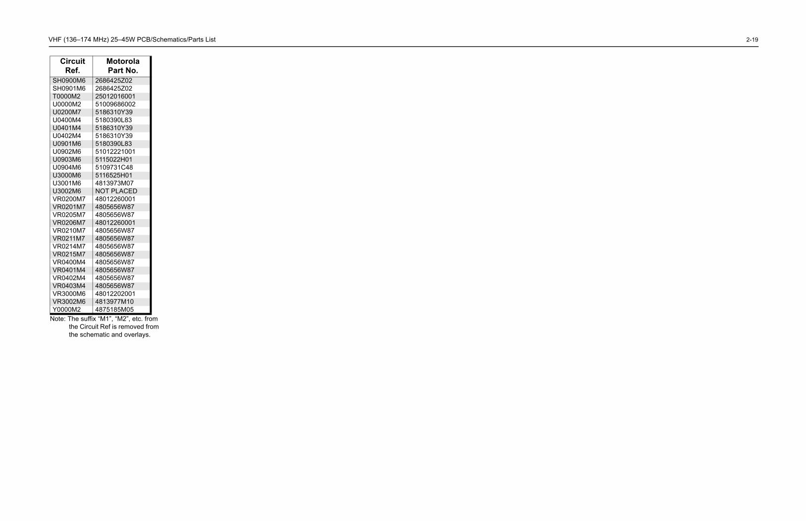
V 2-19
N
HF (136–174 MHz) 25–45W PCB/Schematics/Parts List
ote: The suffix “M1”, “M2”, etc. from the Circuit Ref is removed from the schematic and overlays.
SH0900M6 2686425Z02SH0901M6 2686425Z02T0000M2 25012016001U0000M2 51009686002U0200M7 5186310Y39U0400M4 5180390L83U0401M4 5186310Y39U0402M4 5186310Y39U0901M6 5180390L83U0902M6 51012221001U0903M6 5115022H01U0904M6 5109731C48U3000M6 5116525H01U3001M6 4813973M07U3002M6 NOT PLACEDVR0200M7 48012260001VR0201M7 4805656W87VR0205M7 4805656W87VR0206M7 48012260001VR0210M7 4805656W87VR0211M7 4805656W87VR0214M7 4805656W87VR0215M7 4805656W87VR0400M4 4805656W87VR0401M4 4805656W87VR0402M4 4805656W87VR0403M4 4805656W87VR3000M6 48012202001VR3002M6 4813977M10Y0000M2 4875185M05
Circuit Ref.
MotorolaPart No.

2-20 VHF (136–174 MHz) 25–45W PCB/Schematics/Parts List
Notes
A-1
Appendix A Replacement Parts and Kits
A.1 Level 1 and 2 Maintenance
This manual covers Level 1 and 2 Maintenance:
Level 1 maintenance is the assessment and/or repair of fault in terms of faulty accessory or physical aspect of product; not including opening of the unit. Limited to replacement of antenna, battery, handset, external microphones, external knobs, all related frequency programming to customers’ and in some cases alignment/tuning, by Customer Programming software (CPS).
Level 2 maintenance includes all Level I activities plus: Assessment that require opening the Subscriber Product and rectifying a fault by replacement of a board or module, or replacement of major mechanical parts (like Front Housing Kit or Control Head Board), followed by alignment/tuning to ensure the replacement of board/module/major mechanical parts are within Subscriber Product’s specifications as per the service manual. It does not incorporate discrete component replacement.
A.1.1 Replacement Parts Ordering
Some replacement parts, spare parts, and/or product information can be ordered directly. While parts may be assigned with a Motorola part number, this does not guarantee that they are available from Motorola Radio Products and Solutions Organization (RPSO). If no Motorola part number is assigned, the part is normally not available from Motorola, or is not a user-serviceable part. Part numbers appended with an asterisk are serviceable by Motorola Depot only.
Orders for replacement parts, kits, and assemblies should be placed directly on Motorola’s local distribution organization or via Motorola Online. For Level 2 maintenance, only Motorola Service Centers or Authorized Motorola Service Dealers can perform these functions. Any tampering by non-authorized Motorola Service Centers voids the warranty of your radio. To find out more about Motorola Service Centers, please visit http://www.motorolasolutions.com
A.2 Level 3 MaintenanceThe Level 3 Maintenance can only be done at the Motorola Service Center/Depot since it can deeply affect the performance of the radio. To find out more about Motorola Service Center, please visithttp://www.motorolasolutions.com

A-2 Replacement Parts and Kits: Level 3 Maintenance
Notes
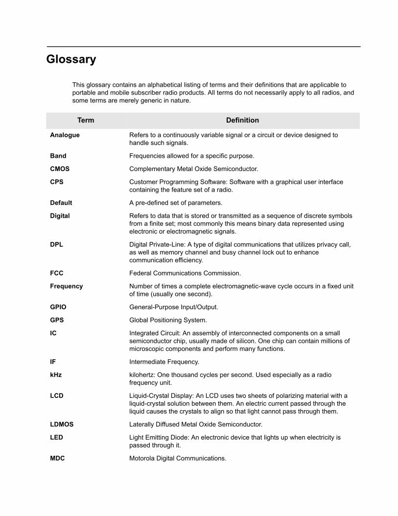
Glossary Glossary
This glossary contains an alphabetical listing of terms and their definitions that are applicable to portable and mobile subscriber radio products. All terms do not necessarily apply to all radios, and some terms are merely generic in nature.
Term Definition
Analogue Refers to a continuously variable signal or a circuit or device designed to handle such signals.
Band Frequencies allowed for a specific purpose.
CMOS Complementary Metal Oxide Semiconductor.
CPS Customer Programming Software: Software with a graphical user interface containing the feature set of a radio.
Default A pre-defined set of parameters.
Digital Refers to data that is stored or transmitted as a sequence of discrete symbols from a finite set; most commonly this means binary data represented using electronic or electromagnetic signals.
DPL Digital Private-Line: A type of digital communications that utilizes privacy call, as well as memory channel and busy channel lock out to enhance communication efficiency.
FCC Federal Communications Commission.
Frequency Number of times a complete electromagnetic-wave cycle occurs in a fixed unit of time (usually one second).
GPIO General-Purpose Input/Output.
GPS Global Positioning System.
IC Integrated Circuit: An assembly of interconnected components on a small semiconductor chip, usually made of silicon. One chip can contain millions of microscopic components and perform many functions.
IF Intermediate Frequency.
kHz kilohertz: One thousand cycles per second. Used especially as a radio frequency unit.
LCD Liquid-Crystal Display: An LCD uses two sheets of polarizing material with a liquid-crystal solution between them. An electric current passed through the liquid causes the crystals to align so that light cannot pass through them.
LDMOS Laterally Diffused Metal Oxide Semiconductor.
LED Light Emitting Diode: An electronic device that lights up when electricity is passed through it.
MDC Motorola Digital Communications.
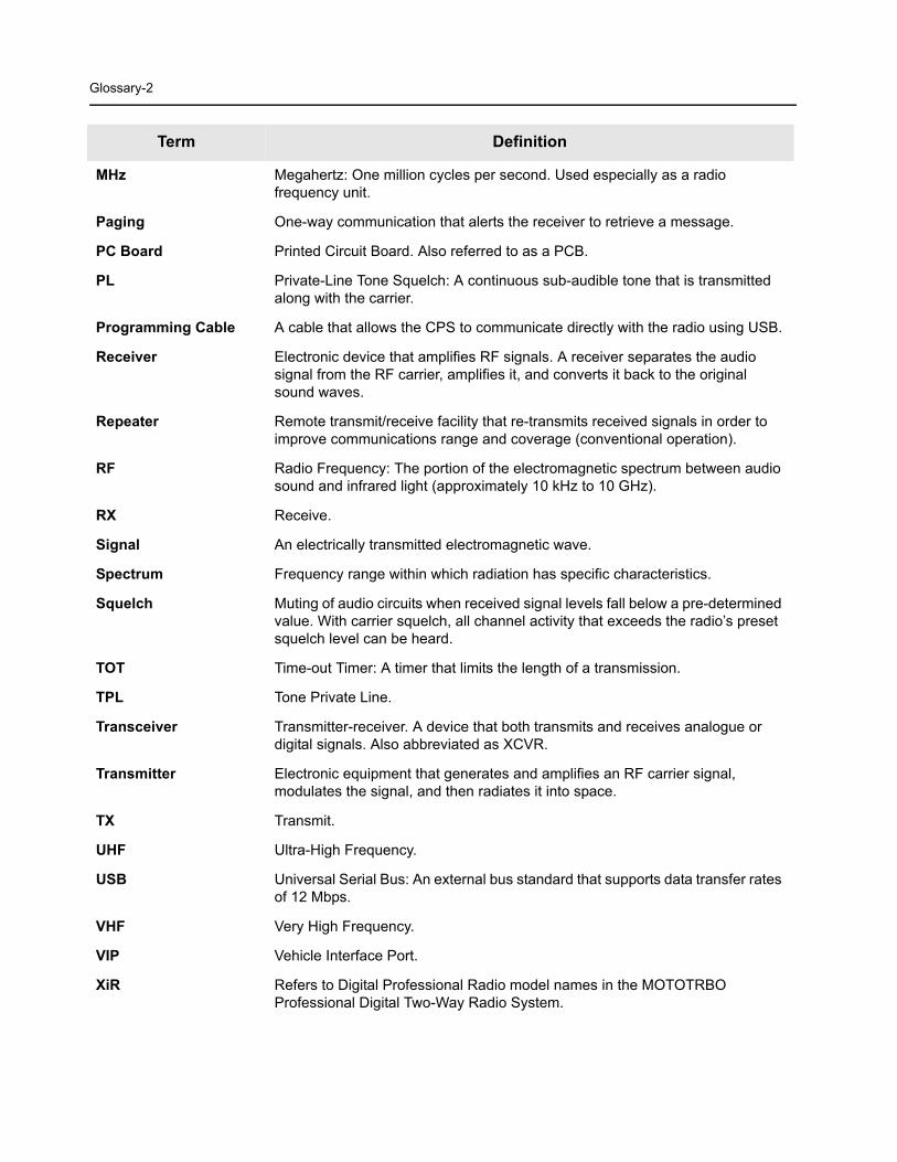
Glossary-2
MHz Megahertz: One million cycles per second. Used especially as a radio frequency unit.
Paging One-way communication that alerts the receiver to retrieve a message.
PC Board Printed Circuit Board. Also referred to as a PCB.
PL Private-Line Tone Squelch: A continuous sub-audible tone that is transmitted along with the carrier.
Programming Cable A cable that allows the CPS to communicate directly with the radio using USB.
Receiver Electronic device that amplifies RF signals. A receiver separates the audio signal from the RF carrier, amplifies it, and converts it back to the original sound waves.
Repeater Remote transmit/receive facility that re-transmits received signals in order to improve communications range and coverage (conventional operation).
RF Radio Frequency: The portion of the electromagnetic spectrum between audio sound and infrared light (approximately 10 kHz to 10 GHz).
RX Receive.
Signal An electrically transmitted electromagnetic wave.
Spectrum Frequency range within which radiation has specific characteristics.
Squelch Muting of audio circuits when received signal levels fall below a pre-determined value. With carrier squelch, all channel activity that exceeds the radio’s preset squelch level can be heard.
TOT Time-out Timer: A timer that limits the length of a transmission.
TPL Tone Private Line.
Transceiver Transmitter-receiver. A device that both transmits and receives analogue or digital signals. Also abbreviated as XCVR.
Transmitter Electronic equipment that generates and amplifies an RF carrier signal, modulates the signal, and then radiates it into space.
TX Transmit.
UHF Ultra-High Frequency.
USB Universal Serial Bus: An external bus standard that supports data transfer rates of 12 Mbps.
VHF Very High Frequency.
VIP Vehicle Interface Port.
XiR Refers to Digital Professional Radio model names in the MOTOTRBO Professional Digital Two-Way Radio System.
Term Definition

Motorola Solutions Malaysia Sdn Bhd (Co. No. 455657-H)Plot 2 Bayan Lepas Technoplex Industrial ParkMukim 12 S.W.D11900 Penang, Malaysia
MOTOROLA, MOTO, MOTOROLA SOLUTIONS and the Stylized M logo are trademarks or registered trademarks of Motorola Trademark Holdings, LLC and are used under license.All other trademarks are the property of their respective owners. © 2013 Motorola Solutions, Inc. All rights reserved.June 2013.
www.motorolasolutions.com/mototrbo
*68012008035*68012008035-A


