Embed Size (px)
Citation preview
INVESTIGATION OF THE EFFECTS OF SWITCHING TECHNIQUE AND GAN
DEVICE ON THE PERFORMANCE OF BIDIRECTIONAL BUCK-BOOST
DC/DC CONVERTER
A THESIS SUBMITTED TO
THE GRADUATE SCHOOL OF NATURAL AND APPLIED SCIENCES
OF
MIDDLE EAST TECHNICAL UNIVERSITY
BY
İBRAHİM KOÇAK
IN PARTIAL FULFILLMENT OF THE REQUIREMENTS
FOR
THE DEGREE OF MASTER OF SCIENCE
IN
ELECTRICAL AND ELECTRONICS ENGINEERING
AUGUST 2019


Approval of the thesis:
INVESTIGATION OF THE EFFECTS OF SWITCHING TECHNIQUE AND
GAN DEVICE ON THE PERFORMANCE OF BIDIRECTIONAL BUCK-
BOOST DC/DC CONVERTER
submitted by İBRAHİM KOÇAK in partial fulfillment of the requirements for the
degree of Master of Science in Electrical and Electronics Engineering
Department, Middle East Technical University by,
Prof. Dr. Halil Kalıpçılar
Dean, Graduate School of Natural and Applied Sciences
Prof. Dr. İlkay Ulusoy
Head of Department, Electrical and Electronics Engineering
Prof. Dr. Hulusi Bülent Ertan
Supervisor, Electrical and Electronics Eng. Dept., METU
Examining Committee Members:
Assist. Prof. Dr. Ozan Keysan
Electrical and Electronics Engineering Dept., METU
Prof. Dr. Hulusi Bülent Ertan
Electrical and Electronics Engineering Dept., METU
Prof. Dr. Barış Bayram
Electrical and Electronics Engineering Dept., METU
Assist. Prof. Dr. Emine Bostancı
Electrical and Electronics Engineering Dept., METU
Prof. Dr. Güngör Bal
Electrical and Electronics Engineering Dept., Gazi University
Date: 22.08.2019

iv
I hereby declare that all information in this document has been obtained and
presented in accordance with academic rules and ethical conduct. I also declare
that, as required by these rules and conduct, I have fully cited and referenced all
material and results that are not original to this work.
Name, Surname:
Signature:
İbrahim Koçak
v
ABSTRACT
INVESTIGATION OF THE EFFECTS OF SWITCHING TECHNIQUE AND
GAN DEVICE ON THE PERFORMANCE OF BIDIRECTIONAL BUCK-
BOOST DC/DC CONVERTER
Koçak, İbrahim
Master of Science, Electrical and Electronics Engineering
Supervisor: Prof. Dr. Hulusi Bülent Ertan
August 2019, 128 pages
In general, a DC/DC converter provides energy transfer from a source to a load in one
direction. However, today, bidirectional power transfer is needed for most of the
system that includes battery based energy storage, such as solar or wind power plant,
uninterruptible power supplies, automotive industry, smart grid applications,
telecommunication and space technology. Serving a compact solution for this need is
crucial in order to reduce the total size of the system especially where the physical size
is a critical subject. Various types of bidirectional DC/DC converter topologies and
control methods are implemented for this purpose. In this study, a bidirectional
DC/DC converter topology and a modulation method are selected, developed and
implemented for the power train of a double battery suited car. The effect of new
generation GaN devices on the efficiency of the converter is also covered. With the
results of this study, it is seen that the selected topology is suitable for bidirectional
power flow and the power density can be increased throughout whole load range with
a software based control method and selecting proper switching device.
Keywords: Buck-Boost Converter, Bidirectional Converter, Phase Shifted Operation
vi
ÖZ
ANAHTARLAMA TEKNİĞİNİN VE GAN MALZEMELERİN ÇİFT YÖNLÜ
AZALTAN-ARTIRAN DA/DA ÇEVİRİCİLERİN PERFORMANSINA
ETKİLERİNİN ARAŞTIRILMASI
Koçak, İbrahim
Yüksek Lisans, Elektrik ve Elektronik Mühendisliği
Tez Danışmanı: Prof. Dr. Hulusi Bülent Ertan
Ağustos 2019, 128 sayfa
DA/DA çeviriciler, enerji transferini genellikle kaynaktan yüke doğru tek yönlü olarak
gerçekleştirirler. Günümüzde, güneş veya rüzgar kaynaklı santraller, kesintisiz güç
kaynakları, otomotiv endüstrisi, akıllı şebeke ve uzay teknolojileri gibi batarya temelli
enerji depolama kullanılan sistemlerde çift yönlü enerji transferinin sağlanması
gerekmektedir. Özellikle fiziksel boyutların önemli olduğu sistemlerde, bu ihtiyaca
kompakt bir çözüm sunmak tüm sitem boyutunu azaltma açısından önem arz
etmektedir. Bu amaçla, çeşitli çift yönlü DA/DA çevirici topolojileri ve kontrol
metotları uygulanmaktadır. Bu çalışmada, iki batarya içeren bir aracın çift yönlü güç
aktarımı için uygun bir topoloji ve modülasyon metodu seçilmiş, geliştirilmiş,
uygulanmış ve test edilmiştir. Aynı zamanda, GaN malzemelerin tasarlanan
çeviricilerin verimliliğine etkileri de incelenmiştir. Bu çalışmanın sonucunda, seçilen
topolojinin çift yönlü enerji aktarımı için uygun olduğu ve önerilen yazılım temelli
kontrol metodunun ve seçilen uygun anahtarlama malzemesinin çevirici verimliliğini
tüm yük şartlarında yükselterek güç yoğunluğunu artırdığı gözlemlenmiştir.
Anahtar Kelimeler: Azaltan-Artıran Çevirici, Çift Yönlü Çevirici, Faz Kaydırmalı
Çalışma

vii
To my wife and lovely son

viii
ACKNOWLEDGEMENTS
I would like to express my thankful to my supervisor Prof. Dr. Hulusi Bülent Ertan
for his great effort, supervision, guidance, advice and discussions throughout this
study.
I wish to thank my examining committee members Prof. Dr. Barış Bayram, Doç. Dr.
Ozan Keysan, Doç. Dr. Emine Bostancı and Prof. Dr. Güngör Bal for their comments
and advices.
I also want to thank my family and especially my love Burcu Koçak for their endless
understanding, support and patience.
I am grateful to my colleagues at ASELSAN, Çağdaş Pekuz, Engin Çağlav, Kaan
Kütaruk and Erdem Karadağ for their help and encouragement.
I am appreciated ASELSAN MGEO Division for the usage of laboratory equipments
and funds.

ix
TABLE OF CONTENTS
ABSTRACT ................................................................................................................. v
ÖZ ............................................................................................................................. vi
ACKNOWLEDGEMENTS ..................................................................................... viii
TABLE OF CONTENTS ............................................................................................ ix
LIST OF TABLES ................................................................................................... xiii
LIST OF FIGURES ................................................................................................... xv
CHAPTERS
1. INTRODUCTION ................................................................................................ 1
1.1. General .............................................................................................................. 1
1.2. Application Areas of Bidirectional DC/DC Converters .................................... 2
1.2.1. Solar Power Plant ....................................................................................... 2
1.2.2. Wind Power Plant ....................................................................................... 3
1.2.3. Uninterruptible Power Supply .................................................................... 4
1.2.4. Electric Vehicle Technology ...................................................................... 5
1.2.4.1. Micro Hybrid Vehicles ......................................................................... 6
1.2.4.2. Mild Hybrid Vehicles ........................................................................... 7
1.2.4.3. Full Hybrid Vehicles ............................................................................ 8
1.2.4.4. Electric Vehicles .................................................................................. 9
1.3. Aim of Thesis .................................................................................................. 11
1.4. Thesis Structure ............................................................................................... 12
2. BIDIRECTIONAL DC/DC CONVERTERS .................................................... 15
2.1. Non-Isolated Topologies ................................................................................. 16

x
2.1.1. Single Phase Type .................................................................................... 17
2.1.2. Single Phase with Auxiliary ZVS and ZCS circuitry ............................... 19
2.1.3. Multiphase Type ....................................................................................... 22
2.2. Isolated Topologies ......................................................................................... 24
2.2.1. Dual Active Bridge (DAB) ....................................................................... 25
2.2.2. Dual Half Bridge (DHB) .......................................................................... 29
2.2.3. Full Bridge – Push Pull ............................................................................ 31
2.3. Comparison of Topologies .............................................................................. 35
3. OPERATION PRINCIPLE AND DESIGN STEPS OF SELECTED
TOPOLOGY ............................................................................................................. 39
3.1. Operation Principles of Selected Topology .................................................... 40
3.1.1. Conventional Operation ........................................................................... 41
3.1.2. Phase Shifted Operation ........................................................................... 42
3.1.2.1. Buck Mode Operation ........................................................................ 44
3.1.2.2. Boost Mode Operation ....................................................................... 49
3.2. Evaluation of Operation Principles ................................................................. 50
3.3. Switching Techniques to Improve Efficiency ................................................. 51
3.3.1. Zero Voltage Switching Operation ........................................................... 52
3.3.2. Adaptive Phase Shifted Operation ........................................................... 53
3.4. Mathematical Analysis of Phase Shifted Operation ....................................... 57
3.4.1. Voltage Conversion Ratio ........................................................................ 57
3.4.2. Inductor Current Ripple Calculation ........................................................ 59
3.4.3. Capacitor Voltage Ripple Calculation ...................................................... 61
3.5. Feasibility of the Selected Converter for a Special Vehicle Application ....... 63

xi
3.6. Evaluation of the Phase Shifted Method for Selected Topology .................... 64
3.7. Power Stage and Control Design ..................................................................... 67
3.7.1. Switching Device Selection ...................................................................... 67
3.7.1.1. Switching Device Losses ................................................................... 68
3.7.1.2. Selection of Switching Devices from Market .................................... 70
3.7.2. Switching Frequency Selection ................................................................ 75
3.7.3. Inductor Selection ..................................................................................... 75
3.7.4. Capacitance Selection ............................................................................... 77
3.7.5. Gate Drive Selection ................................................................................. 79
3.7.6. Microcontroller Selection ......................................................................... 79
4. SIMULATION AND TEST RESULTS ............................................................. 83
4.1. Test Equipment ................................................................................................ 83
4.2. Forward Mode of Operation (Energy Transfer is from V1 to V2) ................... 84
4.2.1. Phase Shifted Method for Forward Mode of Operation ........................... 84
4.2.2. Conventional Method for Forward Mode of Operation ........................... 90
4.2.3. Comparison of Methods while Energy Transfer is from V1 to V2 ........... 93
4.3. Backup Mode of Operation (Energy Transfer is from V2 to V1) .................... 96
4.3.1. Phase Shifted Method for Backup Mode of Operation ............................ 96
4.3.2. Conventional Method for Backup Mode of Operation ........................... 100
4.3.3. Comparison of Methods while Energy Transfer from V2 to V1 ............. 103
5. GAN DEVICE APPLICATION ....................................................................... 109
5.1. Implementation of GaN Device .................................................................... 111
5.2. Phase Shifted Method with GaN Based Converter ....................................... 112
5.3. Comparison of Test Results of GaN and MOSFET Based Converters ......... 114

xii
5.4. Evaluation of the Test Results of Si and GaN Applications ......................... 115
5.5. Effects of Switching Frequency on Losses ................................................... 115
5.6. Evaluation of the Phase Shifted Method for Selected Topology Using GaN
.............................................................................................................................. 118
6. CONCLUSION and FUTURE WORK ........................................................... 119
6.1. Conclusion .................................................................................................... 119
6.2. Future Work .................................................................................................. 121
REFERENCES ........................................................................................................ 123
xiii
LIST OF TABLES
TABLES
Table 1.1. Design specifications of the prototype ...................................................... 12
Table 2.1. Comparison of Non-Isolated Topologies .................................................. 36
Table 2.2. Comparison of Isolated Topologies .......................................................... 37
Table 3.1. State of switches and inductor voltage at different time intervals within a
period of buck mode from V1 to V2 ........................................................................... 49
Table 3.2. Comparison of Switching Devices for Second Battery Side (12V-28V) . 73
Table 3.3. Comparison of Switching Devices for First Battery Side (24V-56V) ...... 74
Table 4.1. Measurements of Inductor Current Ripple while V1=56V, V2=28V and
P=250W for phase shifted operation of forward mode .............................................. 88
Table 4.2. Test and simulation data of conventional method during forward mode of
operation when V1 = 56V ........................................................................................... 93
Table 4.3. Test and simulation data of phase shifted method during forward mode of
operation when V1 = 56V ........................................................................................... 94
Table 4.4. Measurements of Inductor Current Ripple while V2=28V, V1=56V and
P=250W for phase shifted operation of backup mode ............................................. 100
Table 4.5. Test and simulation data of conventional method during backward mode of
operation when V2 = 28V ......................................................................................... 104
Table 4.6. Test and simulation data of phase shifted method during backward mode of
operation when V2 = 28V ......................................................................................... 105
Table 5.1. Material Properties of Si, SiC and GaN .................................................. 110
Table 5.2. Measurements of Inductor Current Ripple while V1=56V, V2=28V and
P=250W for phase shifted operation of forward mode with GaN ........................... 114
Table 5.3. Test data of GaN and MOSFET based converters during forward mode of
operation when V1 = 56V using phase shifted method ............................................ 114

xiv
Table 5.4. Measurements at various switching frequencies for MOSFET based setup
................................................................................................................................. 116
Table 5.5. Measurements at various switching frequencies for GaN based setup .. 117

xv
LIST OF FIGURES
FIGURES
Figure 1.1. Bidirectional Power Flow Using Two Separate Power Stage ................... 1
Figure 1.2. Bidirectional Power Flow Using Same Power Stage ................................ 2
Figure 1.3. Solar Power Plant Block Diagram ............................................................. 3
Figure 1.4. Wind Power Plant Block Diagram [14] ..................................................... 4
Figure 1.5. Block Diagram of Interactive UPS system [2] .......................................... 4
Figure 1.6. Power train in hybrid electric vehicle [4] .................................................. 5
Figure 1.7. Mild Hybrid Power Train [9] ..................................................................... 8
Figure 1.8. Block Diagram of an Electric Vehicle Power Train [16] ........................ 10
Figure 1.9. Block diagram of double battery fitted system ........................................ 11
Figure 2.1. General Representation of Bidirectional Power Flow [20] ..................... 15
Figure 2.2. Derivation of Bidirectional Buck Converter from a Unidirectional One 16
Figure 2.3. Circuit Diagram of Boost Type and Buck Type BDC [19] ..................... 17
Figure 2.4. Circuit Diagram of Buck-Boost Type BDC ............................................ 18
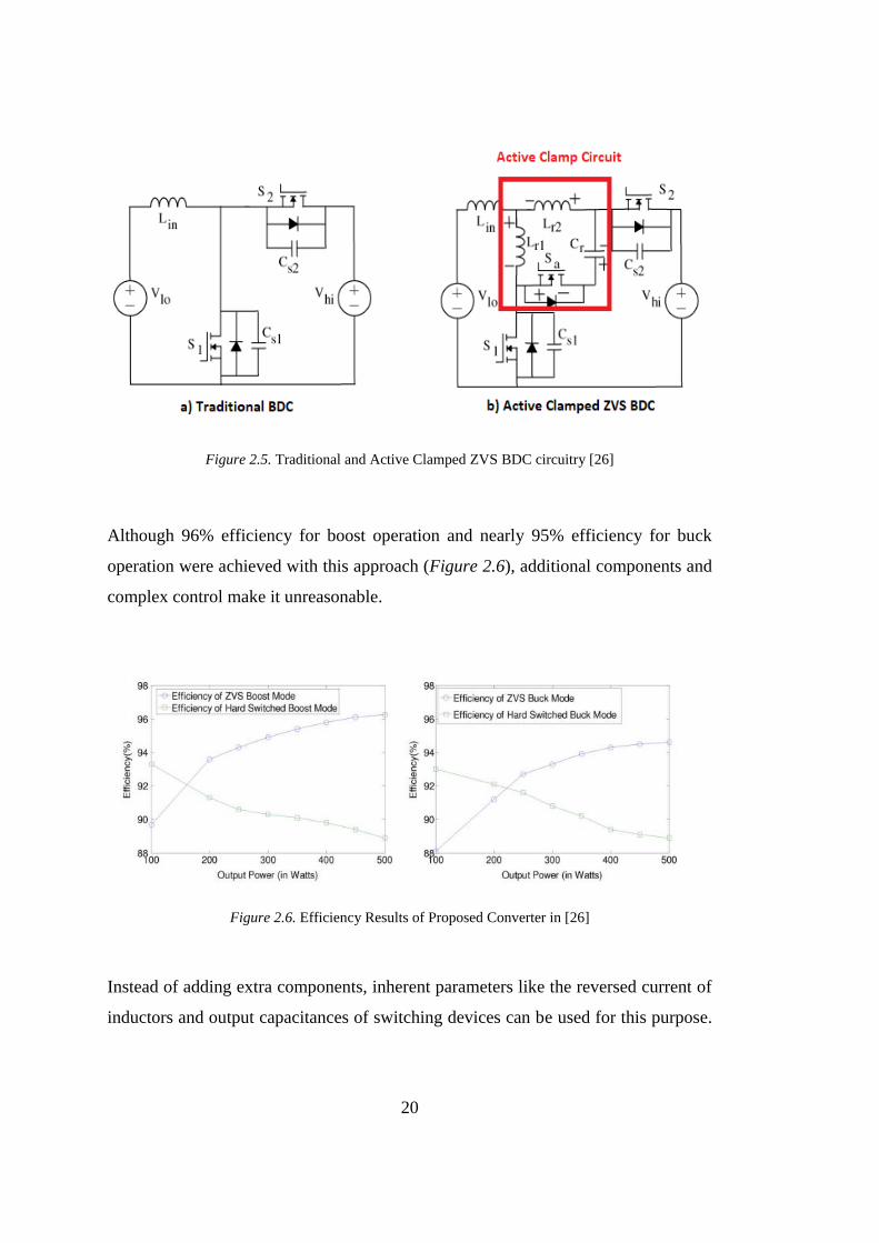
Figure 2.5. Traditional and Active Clamped ZVS BDC circuitry [26] ...................... 20
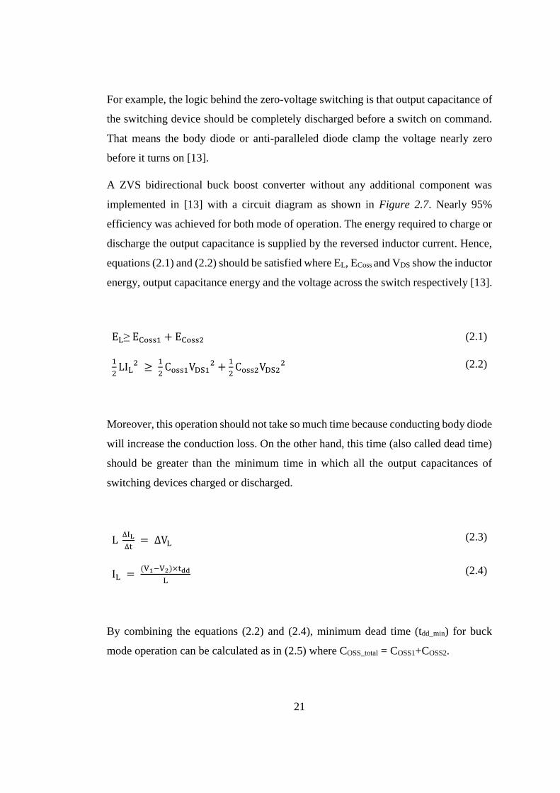
Figure 2.6. Efficiency Results of Proposed Converter in [26] ................................... 20
Figure 2.7. Buck-Boost Type BDC and ZVS Commutation during Buck Mode [13]
.................................................................................................................................... 22
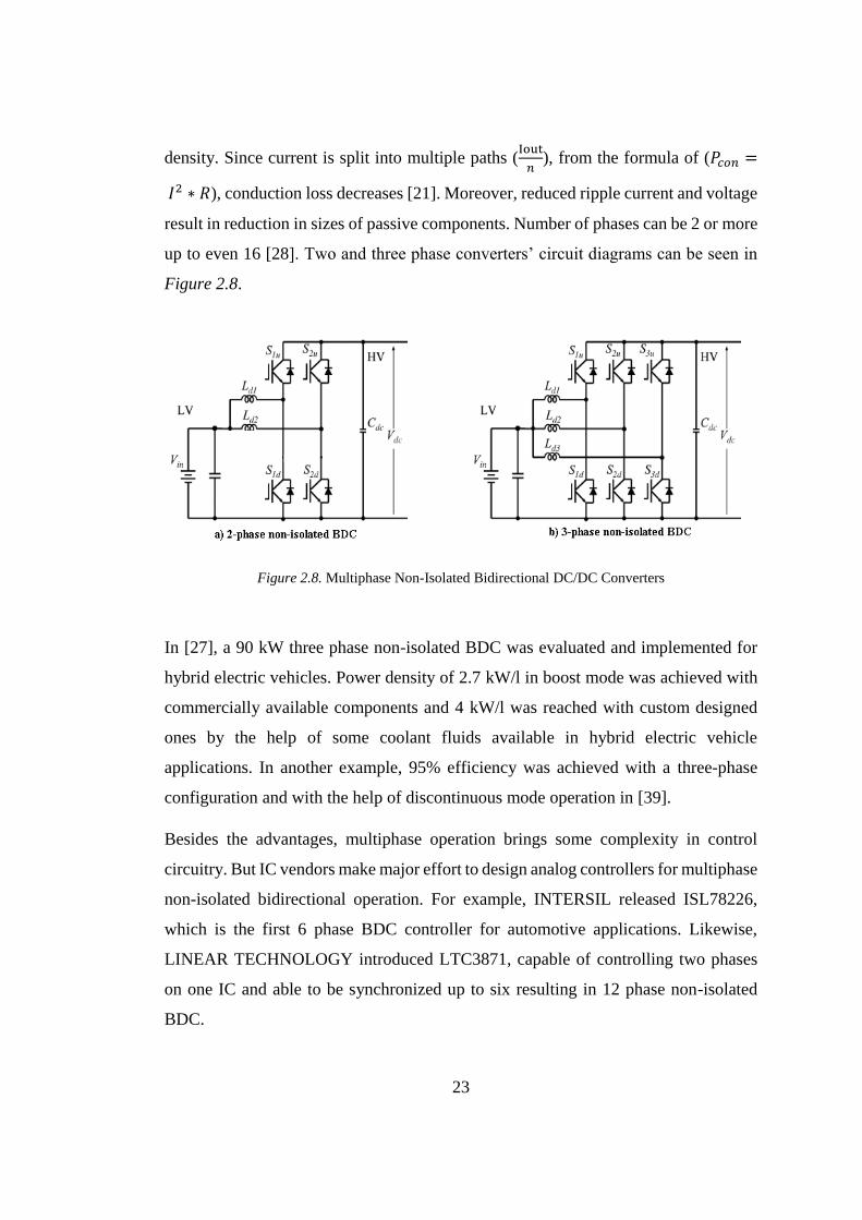
Figure 2.8. Multiphase Non-Isolated Bidirectional DC/DC Converters .................... 23
Figure 2.9. General Representation of Isolated Bidirectional DC/DC Converters [29]
.................................................................................................................................... 25
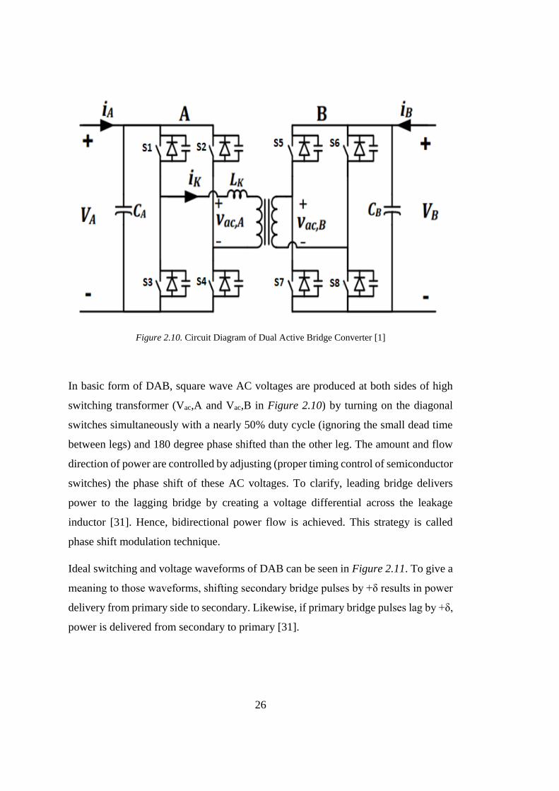
Figure 2.10. Circuit Diagram of Dual Active Bridge Converter [1] .......................... 26
Figure 2.11. Dual Active Bridge Waveforms [31] ..................................................... 27
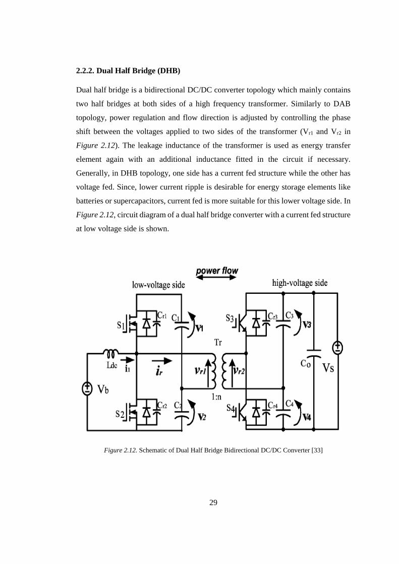
Figure 2.12. Schematic of Dual Half Bridge Bidirectional DC/DC Converter [33] .. 29
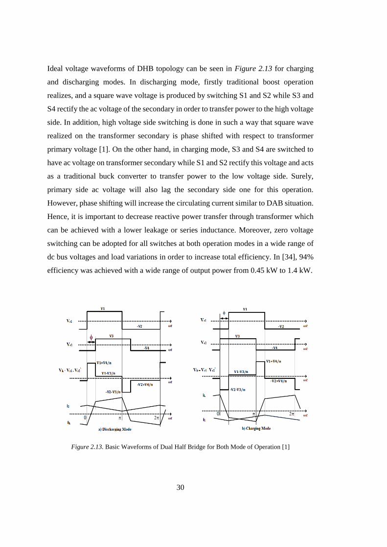
Figure 2.13. Basic Waveforms of Dual Half Bridge for Both Mode of Operation [1]
.................................................................................................................................... 30

xvi
Figure 2.14. Schematic of Full Bridge – Push Pull Bidirectional Converter ............ 31
Figure 2.15. Simplified Circuit Diagram of Charging and Discharging Modes [35] 32
Figure 2.16. Waveforms of Discharging Mode ......................................................... 33
Figure 2.17. Half Bridge and Current Fed Push Pull Topology for Bidirectional Power
Transfer [36] .............................................................................................................. 34
Figure 2.18. Soft Switched Full Bridge-Push Pull Bidirectional DC/DC Converter
with an Extra Switch [37] .......................................................................................... 34
Figure 3.1. Topology of (a) unidirectional and (b) bidirectional buck-boost converter
................................................................................................................................... 40
Figure 3.2. Equivalent circuits in buck (a) and boost mode (b) from V1 to V2 ......... 41
Figure 3.3. Required gating signals and inductor current waveforms during (a) Buck
Mode from V1 to V2 (b) Boost Mode from V1 to V2 [42] ......................................... 43
Figure 3.4. Required gating signals and inductor current waveforms during (a) Buck
Mode from V2 to V1 (b) Boost Mode from V2 to V1 [42] ......................................... 43
Figure 3.5. Equivalent circuit of buck mode from V1 to V2 at t=t0 ........................... 44
Figure 3.6. Equivalent circuit of buck mode from V1 to V2 at time interval of t0<t<t1
................................................................................................................................... 45
Figure 3.7. Equivalent circuit of buck mode from V1 to V2 at time interval of t1<t<t2
................................................................................................................................... 45
Figure 3.8. Equivalent circuit of buck mode from V1 to V2 at time interval of t2<t<t3
................................................................................................................................... 46
Figure 3.9. Equivalent circuit of buck mode from V1 to V2 at t=t3 ........................... 47
Figure 3.10. Equivalent circuit of buck mode from V1 to V2 at time interval of t3<t<T
................................................................................................................................... 48
Figure 3.11. Efficiency comparison of fixed (blue) and adaptive phase shift operation
(red) [42] .................................................................................................................... 51
Figure 3.12. Inductor current waveform under different load conditions if the
switching times are kept constant [42] (green line refers to light load condition while
red shows higher one) ................................................................................................ 56
Figure 3.13. Different approaches while optimizing the switching times [41] ......... 57

xvii
Figure 3.14. Voltage and current waveforms of inductor, output capacitor and S3 .. 61
Figure 3.15. Rise and fall times of a MOSFET.......................................................... 63
Figure 3.16. Variation of inductance value according to input/output voltage levels
(Base values are V1=48V, V2=24V and L=896nH) ................................................... 66
Figure 3.17. Variation of Coss value of switching device according to input/output
voltage levels (Base values are V1=48V, V2=24V and Coss =2.78nF) ....................... 66
Figure 3.18. Parasitic capacitances of a MOSFET [44] ............................................. 69
Figure 3.19. Switching waveform of a MOSFET [43] .............................................. 70
Figure 3.20. VDS and gate voltages of switches S1, S3 (V1=56V, V2=28V at P=500W)
.................................................................................................................................... 72
Figure 3.21. Inductor current at full load condition (V1=56V, V2=28V at P=500W)77
Figure 3.22. Output capacitance ripple voltage at half load (V1=56V, V2=28V at
P=500W) .................................................................................................................... 78
Figure 3.23. Block diagram of prototype board ......................................................... 80
Figure 3.24. Picture of the prototype board (Component side).................................. 80
Figure 3.25. Picture of the prototype board (Solder Side) ......................................... 81
Figure 4.1. Simulated bidirectional DC/DC converter circuit while V1=56V, V2=28V
and P=250W for phase shifted operation ................................................................... 85
Figure 4.2. Gating signal waveforms (GateSW1: blue, GateSW2: red, GateSW3: brown,
GateSW4: turquoise) for switching devices while V1=56V, V2=28V and P=250W for
phase shifted operation (Simulation) ......................................................................... 86
Figure 4.3. Gating signal waveforms (GateSW1: yellow, GateSW2: blue, GateSW3: pink,
GateSW4: green) for switching devices while V1=56V, V2=28V and P=250W for phase
shifted operation obtained (Test) ............................................................................... 86
Figure 4.4. Inductor voltage (blue), current (red), switching device S3 current (brown)
and output capacitance current (turquoise) waveforms while V1=56V, V2=28V and
P=250W for phase shifted operation (Simulation) .................................................... 87
Figure 4.5. Inductor voltage (yellow) and current (green) waveforms while V1=56V,
V2=28V and P=250W for phase shifted operation (Test) .......................................... 87
xviii
Figure 4.6. Switching device S1 gate (blue) and Vds (red) voltage, switching device
S3 gate (turquoise) and Vds (brown) voltage waveforms while V1=56V, V2=28V and
P=250W for phase shifted operation (Simulation) .................................................... 89
Figure 4.7. Switching device S1 gate (yellow) and Vds (blue) voltage, switching
device S3 gate (purple) and Vds (green) voltage waveforms while V1=56V, V2=28V
and P=250W for phase shifted operation (Test) ........................................................ 89
Figure 4.8. Simulated bidirectional DC/DC converter circuit while V1=56V, V2=28V
and P=250W for conventional operation ................................................................... 90
Figure 4.9. Gating signal waveforms (GateSW1: red, GateSW2: blue, GateSW3: turquoise,
GateSW4: brown) for switching devices while V1=56V, V2=28V and P=250W for
conventional operation (Simulation) ......................................................................... 91
Figure 4.10. Gating signal waveforms (GateSW1: yellow, GateSW2: blue, GateSW3: pink,
GateSW4: green) for switching devices while V1=56V, V2=28V and P=250W for
conventional operation (Test) .................................................................................... 91
Figure 4.11. Inductor current (blue) and output current (red) waveforms while
V1=56V, V2=28V and P=250W for conventional operation (Simulation) ................ 92
Figure 4.12. Inductor current, inductor voltage and output current waveforms while
V1=56V, V2=28V and P=250W for conventional operation (Test) ........................... 92
Figure 4.13. Efficiency comparison of phase shifted and conventional approaches
while Vin=56V at various output voltages and load conditions (Simulation)............ 95
Figure 4.14. Efficiency comparison of phase shifted and conventional approaches
while Vin=56V at various output voltages and load conditions (Test) ...................... 95
Figure 4.15. Simulated bidirectional DC/DC converter circuit while V2=28V, V1=56V
and P=250W for phase shifted operation................................................................... 97
Figure 4.16. Gating signal waveforms (GateSW3: blue, GateSW4: red, GateSW1: brown,
GateSW2: turquoise) for switching devices while V2=28V, V1=56V and P=250W for
phase shifted operation (Simulation) ......................................................................... 98
Figure 4.17. Gating signal waveforms (GateSW3: yellow, GateSW4: blue, GateSW1: pink,
GateSW2: green) for switching devices while V2=28V, V1=56V and P=250W for phase
shifted operation (Test) .............................................................................................. 98
xix
Figure 4.18. Inductor voltage (red) and current (blue) waveforms while V2=28V,
V1=56V and P=250W for phase shifted operation (Simulation) ............................... 99
Figure 4.19. Inductor voltage (yellow) and current (green) waveforms while V2=28V,
V1=56V and P=250W for phase shifted operation (Test) .......................................... 99
Figure 4.20. Simulated bidirectional DC/DC converter circuit while V2=28V, V1=56V
and P=250W for conventional operation ................................................................. 100
Figure 4.21. Gating signal waveforms (GateSW1: red, GateSW2: blue, GateSW3:
turquoise, GateSW4: brown) for switching devices while V2=28V, V1=56V and
P=250W for conventional operation (Simulation) ................................................... 101
Figure 4.22. Gating signal waveforms (GateSW1: yellow, GateSW2: blue, GateSW3: pink,
GateSW4: green) for switching devices while V2=28V, V1=56V and P=250W for
conventional operation (Test) .................................................................................. 101
Figure 4.23. Inductor voltage (red) and current (blue) waveforms while V2=28V,
V1=56V and P=250W for conventional operation (Simulation) .............................. 102
Figure 4.24. Input current waveform while V2=28V, V1=56V and P=250W for
conventional operation (Simulation) ........................................................................ 102
Figure 4.25. Inductor voltage (up-yellow), current (up-green) and input current
(bottom) waveforms while V2=28V, V1=56V and P=250W for conventional operation
(Test) ........................................................................................................................ 103
Figure 4.26. Efficiency comparison of phase shifted and conventional approaches
while Vin=28V at various output voltages and load conditions (Simulation) .......... 106
Figure 4.27. Efficiency comparison of phase shifted and conventional approaches
while Vin=28V at various output voltages and load conditions (Test) ..................... 106
Figure 5.1. Converting the demo boards to four switch buck boost converter ........ 111
Figure 5.2. Whole setup for GaN tests ..................................................................... 112
Figure 5.3. Gating signal waveforms (GateSW1: yellow, GateSW2: blue, GateSW3: pink,
GateSW4: green) for switching devices while V1=56V, V2=28V and P=112W for phase
shifted operation ....................................................................................................... 113
Figure 5.4. Inductor voltage (yellow) and current (blue) waveforms while V1=56V,
V2=28V and P=112W for phase shifted operation with GaN .................................. 113

xx
Figure 5.5. Efficiency comparison of GaN and MOSFET based four switch buck boost
converter during forward mode of operation when V1 = 56V using phase shifted
method ..................................................................................................................... 115
Figure 5.6. Variation of total loss with change in frequency in MOSFET based setup
................................................................................................................................. 117
Figure 5.7. Variation of total loss with change in frequency for GaN based setup . 117
Figure 5.8. Variation of inductance and Coss values in the case of GaN device (Base
values are V1=48V, V2=24V, L=89nH and Coss =278pF) ....................................... 118
1
CHAPTER 1
1. INTRODUCTION
1.1. General
Nowadays, the storage of electrical power has become an important issue because of
many reasons such as; the problem of environment pollution, increase utilization of
Uninterruptible Power Supply (UPS), renewable energy systems, requirements of
Hybrid Electric Vehicle (HEV) or Electric Vehicle (EV) etc.[1]. In many cases, the
storage elements for that purposes are batteries and supercapacitors. Moreover, it is
required to put into use of this stored energy in the case of an extra power demand,
failure or supply fluctuation. Storage and backup of electrical power in such a case
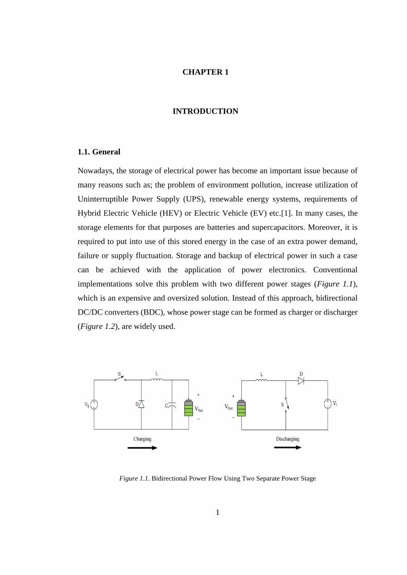
can be achieved with the application of power electronics. Conventional
implementations solve this problem with two different power stages (Figure 1.1),
which is an expensive and oversized solution. Instead of this approach, bidirectional
DC/DC converters (BDC), whose power stage can be formed as charger or discharger
(Figure 1.2), are widely used.
Figure 1.1. Bidirectional Power Flow Using Two Separate Power Stage

2
Figure 1.2. Bidirectional Power Flow Using Same Power Stage
1.2. Application Areas of Bidirectional DC/DC Converters
In this section, systems, that need bidirectional energy transfer, are stated briefly to
realize and explain the motivation of this study.
1.2.1. Solar Power Plant
Today, the most interesting and attractive renewable energy systems are solar power
plant systems. Sunlight of nature is converted to electricity with the help of these
plants. Since the natural supply is unstable throughout a day, solar power plant cannot
be the only source of electricity power. It is necessary to regulate and make the output
continuous in order not to disturb load. The output of solar array is stored at batteries
with a high voltage DC bus to reuse in the case of solar source insufficiency.
Bidirectional DC/DC converters realize the process of charging and discharging of
batteries with the help of a power control unit, the most common type of which is
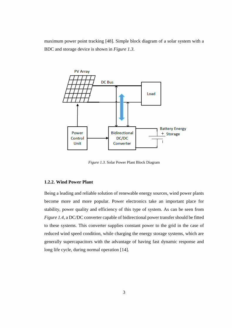
3
maximum power point tracking [48]. Simple block diagram of a solar system with a
BDC and storage device is shown in Figure 1.3.
Figure 1.3. Solar Power Plant Block Diagram
1.2.2. Wind Power Plant
Being a leading and reliable solution of renewable energy sources, wind power plants
become more and more popular. Power electronics take an important place for
stability, power quality and efficiency of this type of system. As can be seen from
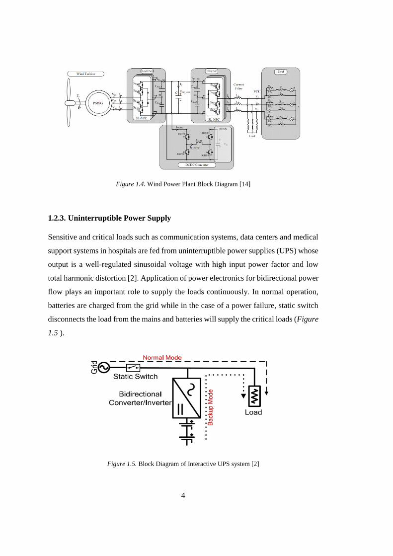
Figure 1.4, a DC/DC converter capable of bidirectional power transfer should be fitted
to these systems. This converter supplies constant power to the grid in the case of
reduced wind speed condition, while charging the energy storage systems, which are
generally supercapacitors with the advantage of having fast dynamic response and
long life cycle, during normal operation [14].
4
Figure 1.4. Wind Power Plant Block Diagram [14]
1.2.3. Uninterruptible Power Supply
Sensitive and critical loads such as communication systems, data centers and medical
support systems in hospitals are fed from uninterruptible power supplies (UPS) whose
output is a well-regulated sinusoidal voltage with high input power factor and low
total harmonic distortion [2]. Application of power electronics for bidirectional power
flow plays an important role to supply the loads continuously. In normal operation,
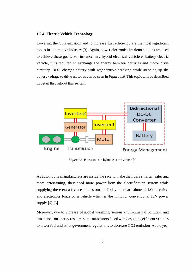
batteries are charged from the grid while in the case of a power failure, static switch
disconnects the load from the mains and batteries will supply the critical loads (Figure
1.5 ).
Figure 1.5. Block Diagram of Interactive UPS system [2]
5
1.2.4. Electric Vehicle Technology
Lowering the CO2 emission and to increase fuel efficiency are the most significant
topics in automotive industry [3]. Again, power electronics implementations are used
to achieve these goals. For instance, in a hybrid electrical vehicle or battery electric
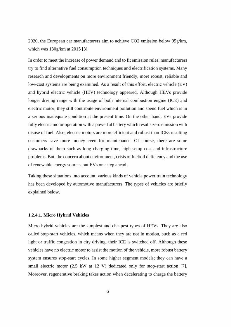
vehicle, it is required to exchange the energy between batteries and motor drive
circuitry. BDC charges battery with regenerative breaking while stepping up the
battery voltage to drive motor as can be seen in Figure 1.6. This topic will be described
in detail throughout this section.
Figure 1.6. Power train in hybrid electric vehicle [4]
As automobile manufacturers are inside the race to make their cars smarter, safer and
more entertaining, they need more power from the electrification system while
supplying these extra features to customers. Today, there are almost 2 kW electrical
and electronics loads on a vehicle which is the limit for conventional 12V power
supply [5] [6].
Moreover, due to increase of global warming, serious environmental pollution and
limitations on energy resources, manufacturers faced with designing efficient vehicles
to lower fuel and strict government regulations to decrease CO2 emission. At the year
6
2020, the European car manufacturers aim to achieve CO2 emission below 95g/km,
which was 130g/km at 2015 [3].
In order to meet the increase of power demand and to fit emission rules, manufacturers
try to find alternative fuel consumption techniques and electrification systems. Many
research and developments on more environment friendly, more robust, reliable and
low-cost systems are being examined. As a result of this effort, electric vehicle (EV)
and hybrid electric vehicle (HEV) technology appeared. Although HEVs provide
longer driving range with the usage of both internal combustion engine (ICE) and
electric motor; they still contribute environment pollution and spend fuel which is in
a serious inadequate condition at the present time. On the other hand, EVs provide
fully electric motor operation with a powerful battery which results zero emission with
disuse of fuel. Also, electric motors are more efficient and robust than ICEs resulting
customers save more money even for maintenance. Of course, there are some
drawbacks of them such as long charging time, high setup cost and infrastructure
problems. But, the concern about environment, crisis of fuel/oil deficiency and the use
of renewable energy sources put EVs one step ahead.
Taking these situations into account, various kinds of vehicle power train technology
has been developed by automotive manufacturers. The types of vehicles are briefly
explained below.
1.2.4.1. Micro Hybrid Vehicles
Micro hybrid vehicles are the simplest and cheapest types of HEVs. They are also
called stop-start vehicles, which means when they are not in motion, such as a red
light or traffic congestion in city driving, their ICE is switched off. Although these
vehicles have no electric motor to assist the motion of the vehicle, more robust battery
system ensures stop-start cycles. In some higher segment models; they can have a
small electric motor (2.5 kW at 12 V) dedicated only for stop-start action [7].
Moreover, regenerative braking takes action when decelerating to charge the battery
7
by the help of an alternator. However, this system has some restrictions. For example,
air conditioning system which is powered from the ICE can restart the engine when
the cabin temperature exceeds the set point [8]. Even so, being a low-cost solution
with a %5-%10 fuel saving, micro hybrid vehicles spread rapidly in the market.
1.2.4.2. Mild Hybrid Vehicles
Mild hybrid vehicles, also known as power assist [6], have an electric motor which
cannot drive the vehicle on its own. Instead, this motor can start the ICE quickly and
assist it in the case of high acceleration and torque. Moreover, it recharges the battery
during deceleration similar to the alternator of a conventional ICE powered vehicle.
Therefore, this more powerful electric motor eliminates the need for starting motor
and alternator. On the other hand, these vehicles also have stop-start property and
regenerative braking like micro hybrid ones. In other words, they turn off the ICE
during when the vehicle is immobile or a in a deceleration mode, retrieve the energy
while braking and use it to rerun the vehicle or to assist the ICE in the case of high-
power demand in a sudden acceleration. Furthermore, they make the engine to operate
at a more efficient operating point by adding extra load and storing the residuary
energy into the battery [8]. These properties and the usage of the stored energy during
braking to support extra power to the engine result in a decrease at fuel consumption
approximately %20-%30 [7].
From the perspective of electrical view; since the traditional 12 V battery became
inadequate for increasing power demand of high technology vehicles, new voltage
levels were introduced for HEVs. In recent years, the voltage level for mild hybrid
vehicles was proposed as 48 V which is below the electric shock limit of 60 V. With
this 48 V voltage level also called dual voltage system; four times more power can be
produced than 12 V systems with more efficiency while adding no cost for additional
safety requirements [8].This does not mean that the traditional 12 V system had gone
away completely. It is still fitted for light loads such as entertainment, safety, security
8
and lighting [6]. Since the voltage level (48 V) is not high enough to decrease current
level, electric unit is bulkier and heavier compared to full hybrid ones. Due to the
existing two voltage level network at mild hybrid vehicles; some power electronics
take place to achieve bidirectional energy transfer between these voltage levels. Power
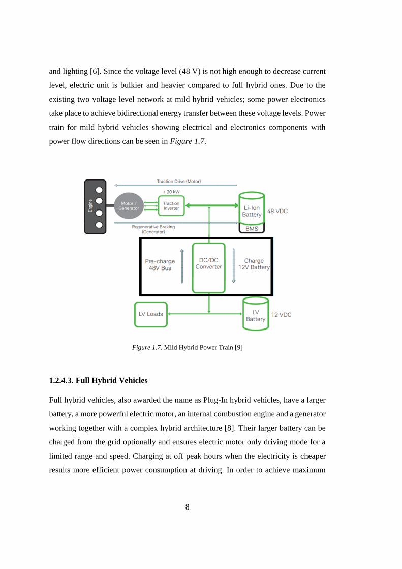
train for mild hybrid vehicles showing electrical and electronics components with
power flow directions can be seen in Figure 1.7.
Figure 1.7. Mild Hybrid Power Train [9]
1.2.4.3. Full Hybrid Vehicles
Full hybrid vehicles, also awarded the name as Plug-In hybrid vehicles, have a larger
battery, a more powerful electric motor, an internal combustion engine and a generator
working together with a complex hybrid architecture [8]. Their larger battery can be
charged from the grid optionally and ensures electric motor only driving mode for a
limited range and speed. Charging at off peak hours when the electricity is cheaper
results more efficient power consumption at driving. In order to achieve maximum
9
energy efficiency and minimum emission, the power flow is designed such that it is
flexible between engine, motor, alternator and the battery. For example, engine will
deliver more power than the required while propulsion or a high acceleration in order
to work at optimum operating range. The excess energy will be captured by the battery
and used by the electric motor to support engine or to use at electric motor driving
mode, with a result of energy saving up to %30-%50 [7]. The voltage of the batteries
in a full hybrid vehicle is at the level of 200 V to achieve low current density at electric
unit. Unfortunately, it decreases the safety level and more precautions must be applied
to the power train. Furthermore, limited speed and range of electric motor only
operation makes these types of vehicles no suitable for interurban driving. On the other
hand, high cost of installed electric power makes full hybrid systems more expensive
in comparison with other hybrid systems [3]. Besides these properties, even full hybrid
vehicles still contribute to air pollution and consume large amount of fuel. These kinds
of reasons lead automotive manufacturers to search for alternative solutions resulting
fully electric vehicles to be introduced to the market.
1.2.4.4. Electric Vehicles
In fact, interest in electric vehicle had been started at the beginning of 20th century.
However, as the vehicles with internal combustion engines showed fast development
at that era, the industry of EVs almost disappeared. In addition to environmental
concerns, with the great development in power electronics, microelectronics, material
and battery technologies, EV power train again came into issue at 1970s [15]. And
now, both the serious lack of fuel source and the invention of renewable energy
sources for electricity, EVs have become one of the most attractive and challenging
issues of automotive industry inevitably.
Unlike HEVs, battery electric vehicles do not have any internal combustion engine
concluding a simpler structure. All the power needed for propulsion and traction
system is supplied from more efficient pure electric power train. That makes them

10
more silent and cheaper to run. With this property, EVs also contribute to reduce air
pollution from CO2 emission and the reduction level can be increased by using a
renewable energy such as solar photovoltaic system for charging the batteries.
Furthermore, EVs have fewer moving parts than ICEs and don’t have any expensive
exhaust system, fuel injection systems or starter motors. These features with the
inherent robustness of electric motors make EVs require less maintenance.
EVs will also be able to use as an electric energy storage device in near future. Energy
can be stored from the grid during off peak hours at which many of vehicles are
remained as parked and will be returned to grid at times of increased energy demand.
This idea which is called vehicle to grid (V2G) will smooth the load curve and improve
the power system reliability [17].
Due to their high energy density, compact size and reliability, batteries are commonly
used as energy storage system in electric vehicles. This stored energy is used for both
to drive motor by the help of an inverter and to supply other electronic loads generally
using a step-down DC/DC converter. Moreover, as can be seen from Figure 1.8, power
electronic applications take place to charge the batteries from mains or via
regenerative braking process.
Figure 1.8. Block Diagram of an Electric Vehicle Power Train [16]
11
Because of these mentioned leading features and with the great incentives of
governments, electric vehicle technology and power electronics applications for these
vehicles will seem to gain great attention in both industry and academia.
1.3. Aim of Thesis
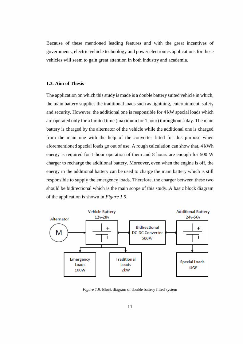
The application on which this study is made is a double battery suited vehicle in which,
the main battery supplies the traditional loads such as lightning, entertainment, safety
and security. However, the additional one is responsible for 4 kW special loads which
are operated only for a limited time (maximum for 1 hour) throughout a day. The main
battery is charged by the alternator of the vehicle while the additional one is charged
from the main one with the help of the converter fitted for this purpose when
aforementioned special loads go out of use. A rough calculation can show that, 4 kWh
energy is required for 1-hour operation of them and 8 hours are enough for 500 W
charger to recharge the additional battery. Moreover, even when the engine is off, the
energy in the additional battery can be used to charge the main battery which is still
responsible to supply the emergency loads. Therefore, the charger between these two
should be bidirectional which is the main scope of this study. A basic block diagram
of the application is shown in Figure 1.9.
Figure 1.9. Block diagram of double battery fitted system
12
Taking into account the necessities of this vehicle, the aim of this research is to design
and implement a compact and highly efficient power supply for bidirectional power
flow between batteries. For this purpose, various bidirectional DC/DC converter
topologies, which are too many in the literature, are searched and compared according
to their efficiency, cost, size and ease of control. A topology is selected, analyzed,
designed and implemented. Two different modulation techniques are applied to this
topology to compare the performances of these techniques. Moreover, in order to
observe the contribution of GaN devices; which are introduced as one of the new
generation wide bandgap switching devices in literature, to the performance of the
converter, they are implemented in a different setup and various tests are performed
as in the case of silicon ones. The control of power stage and the PWM drive of
switching devices are implemented using a microcontroller in a digital manner. Design
specifications for the prototype of selected topology are presented at Table 1.1.
Table 1.1. Design specifications of the prototype
First Battery Voltage 24V - 56V
Second Battery Voltage 12V - 28V
Rated Power 500 W
Switching Frequency 100 kHz
1.4. Thesis Structure
The thesis is organized into 6 chapters.
First chapter gives information about the need for bidirectional power flow in multiple
application areas, electrification of vehicles with different types and the aim of this
study.
Chapter 2 includes classification of bidirectional DC/DC converter topologies with
their basic operating principles. Various topologies are investigated and compared in

13
this section referring to their advantages and disadvantages in terms of their size, cost,
efficiency and simplicity.
Chapter 3 describes the operating principle and two different approaches to selected
bidirectional DC/DC converter topology with all analytical and design calculations in
detail. Evaluation of these approaches is done and one of them is selected. Component
selection is pointed out with loss analysis of each one and their compatibility with
theoretical calculations.
In Chapter 4, the implementation of selected topology on a printed circuit board,
simulation and experimental results for charging and discharging modes are covered.
Both phase shifted and conventional approaches for switching purpose are analyzed
in terms of their efficiency.
Chapter 5 mentions the theoretical advantages of GaN power semiconductors.
Implementation of GaN device and its effect on the performance of designed converter
in comparison with its silicon competitor are presented. Furthermore, the effect of
switching frequency on the design parameters, component selection, total size and
losses of the converter is evaluated.
Last chapter is for the conclusion and future work of this topic.

15
CHAPTER 2
2. BIDIRECTIONAL DC/DC CONVERTERS
As introduced in Chapter 1, batteries, which are fitted as the energy storage devices
are used to store the excessive energy supplied by different sources in many
applications. On the other hand, they also supply energy in the case of an extra demand
or source deficiency. Having the ability to transfer current in two ways, and thereby
power, implementation of bidirectional DC/DC converters is gaining more and more
interest by power electronics engineers. Power or current flow of a bidirectional
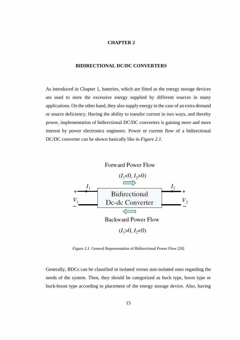
DC/DC converter can be shown basically like in Figure 2.1.
Figure 2.1. General Representation of Bidirectional Power Flow [20]
Generally, BDCs can be classified in isolated versus non-isolated ones regarding the
needs of the system. Then, they should be categorized as buck type, boost type or
buck-boost type according to placement of the energy storage device. Also, having
16
voltage source or current source structure can be a classification criterion [19]. By
considering these properties, several topologies have been proposed in literature for
bidirectional power flow. In this chapter; these topologies are analyzed and evaluated
according to their component count, efficiency, semiconductor voltage and current
stresses, simplicity, power density (W/kg), cost and feasibility of input/output voltage
ratings for the application mentioned in Section 1.3.
2.1. Non-Isolated Topologies
Bidirectional DC/DC converters (BDCs) generally derived from traditional
unidirectional converters by replacing diodes with switching semiconductor devices
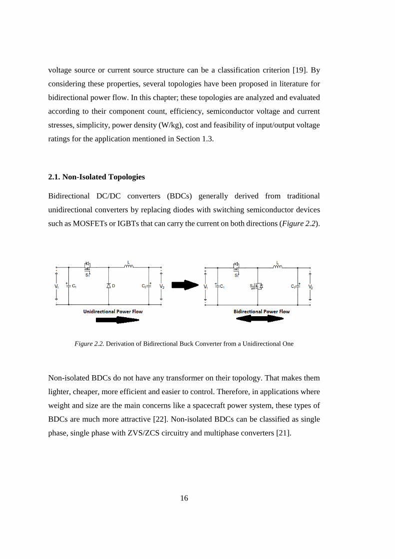
such as MOSFETs or IGBTs that can carry the current on both directions (Figure 2.2).
Figure 2.2. Derivation of Bidirectional Buck Converter from a Unidirectional One
Non-isolated BDCs do not have any transformer on their topology. That makes them
lighter, cheaper, more efficient and easier to control. Therefore, in applications where
weight and size are the main concerns like a spacecraft power system, these types of
BDCs are much more attractive [22]. Non-isolated BDCs can be classified as single
phase, single phase with ZVS/ZCS circuitry and multiphase converters [21].
17
2.1.1. Single Phase Type
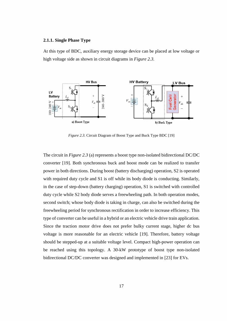
At this type of BDC, auxiliary energy storage device can be placed at low voltage or
high voltage side as shown in circuit diagrams in Figure 2.3.
Figure 2.3. Circuit Diagram of Boost Type and Buck Type BDC [19]
The circuit in Figure 2.3 (a) represents a boost type non-isolated bidirectional DC/DC
converter [19]. Both synchronous buck and boost mode can be realized to transfer
power in both directions. During boost (battery discharging) operation, S2 is operated
with required duty cycle and S1 is off while its body diode is conducting. Similarly,
in the case of step-down (battery charging) operation, S1 is switched with controlled
duty cycle while S2 body diode serves a freewheeling path. In both operation modes,
second switch; whose body diode is taking in charge, can also be switched during the
freewheeling period for synchronous rectification in order to increase efficiency. This
type of converter can be useful in a hybrid or an electric vehicle drive train application.
Since the traction motor drive does not prefer bulky current stage, higher dc bus
voltage is more reasonable for an electric vehicle [19]. Therefore, battery voltage
should be stepped-up at a suitable voltage level. Compact high-power operation can
be reached using this topology. A 30-kW prototype of boost type non-isolated
bidirectional DC/DC converter was designed and implemented in [23] for EVs.
18
The circuit becomes a buck type BDC as shown in Figure 2.3 (b) by placing the battery
on high voltage side. Operation principle is similar to boost type ones with a difference
only in operation modes (step-down for discharging and step-up for charging).
In some applications, at one time; battery voltages can be at the same level with output
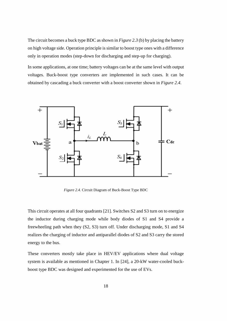
voltages. Buck-boost type converters are implemented in such cases. It can be
obtained by cascading a buck converter with a boost converter shown in Figure 2.4.
Figure 2.4. Circuit Diagram of Buck-Boost Type BDC
This circuit operates at all four quadrants [21]. Switches S2 and S3 turn on to energize
the inductor during charging mode while body diodes of S1 and S4 provide a
freewheeling path when they (S2, S3) turn off. Under discharging mode, S1 and S4
realizes the charging of inductor and antiparallel diodes of S2 and S3 carry the stored
energy to the bus.
These converters mostly take place in HEV/EV applications where dual voltage
system is available as mentioned in Chapter 1. In [24], a 20-kW water-cooled buck-
boost type BDC was designed and experimented for the use of EVs.

19
Although buck-boost type BDCs are the most flexible ones of non-isolated
bidirectional converters, since the number of switches is increased, they are more
costly and have more complex control system and circuitry. Furthermore, hard
switching of the switching devices can cause severe EMI issues which cause the need
for large filters. This also makes the converter bulkier and less efficient [13]. However,
when battery voltage is very close the voltage level of dc bus voltage, usage of buck-
boost type bidirectional converter is a necessity.
2.1.2. Single Phase with Auxiliary ZVS and ZCS circuitry
In single phase topologies, since the converter operates in continuous conduction
mode (CCM) at both buck and boost mode, switching losses due to hard switching are
increased. Moreover, CCM operation results in the phenomenon of reverse recovery
of body diodes of switches [25] while resulting in a low current ripple.
Alternative techniques are applied to non-isolated BDCs to increase the efficiency.
Zero voltage switching can be achieved by using a smaller inductance providing the
inductor current flowing in both directions at the end of each switching period.
However, this technique increases the current and voltage ripple, shortening the
lifetime of the batteries which is not an acceptable situation [25]. Interleaving can be
another solution both to increase the efficiency and to decrease the ripple current, but
the number of components increases, and the control of converter become more
complicated.
In order to overcome these problems, soft switching techniques called zero voltage
switching (ZVS) and zero current switching (ZCS) become more popular. These
techniques can be achieved by using extra switches as active clamps or resonant
circuits. But, doing so will again increase the component count and complexity of the
circuit. In [26], zero voltage switching was reached by using an active clamped with
a resonant circuit shown in Figure 2.5.
20
Figure 2.5. Traditional and Active Clamped ZVS BDC circuitry [26]
Although 96% efficiency for boost operation and nearly 95% efficiency for buck
operation were achieved with this approach (Figure 2.6), additional components and
complex control make it unreasonable.
Figure 2.6. Efficiency Results of Proposed Converter in [26]
Instead of adding extra components, inherent parameters like the reversed current of
inductors and output capacitances of switching devices can be used for this purpose.
21
For example, the logic behind the zero-voltage switching is that output capacitance of
the switching device should be completely discharged before a switch on command.
That means the body diode or anti-paralleled diode clamp the voltage nearly zero
before it turns on [13].
A ZVS bidirectional buck boost converter without any additional component was
implemented in [13] with a circuit diagram as shown in Figure 2.7. Nearly 95%
efficiency was achieved for both mode of operation. The energy required to charge or
discharge the output capacitance is supplied by the reversed inductor current. Hence,
equations (2.1) and (2.2) should be satisfied where EL, ECoss and VDS show the inductor
energy, output capacitance energy and the voltage across the switch respectively [13].
EL≥ ECoss1 + ECoss2 (2.1)
1
2LIL
2 ≥ 1
2Coss1VDS1
2 +1
2Coss2VDS2
2 (2.2)
Moreover, this operation should not take so much time because conducting body diode
will increase the conduction loss. On the other hand, this time (also called dead time)
should be greater than the minimum time in which all the output capacitances of
switching devices charged or discharged.
L ∆IL
∆t = ∆VL (2.3)
IL = (V1−V2)×tdd
L (2.4)
By combining the equations (2.2) and (2.4), minimum dead time (tdd_min) for buck
mode operation can be calculated as in (2.5) where COSS_total = COSS1+COSS2.
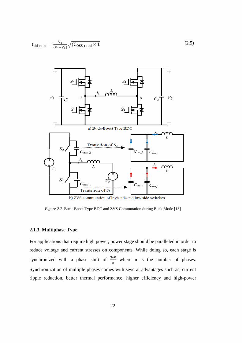
22
tdd_min =V1
(V1−V2)√(COSS_total × L (2.5)
Figure 2.7. Buck-Boost Type BDC and ZVS Commutation during Buck Mode [13]
2.1.3. Multiphase Type
For applications that require high power, power stage should be paralleled in order to
reduce voltage and current stresses on components. While doing so, each stage is
synchronized with a phase shift of 360
𝑛 where n is the number of phases.
Synchronization of multiple phases comes with several advantages such as, current
ripple reduction, better thermal performance, higher efficiency and high-power
23
density. Since current is split into multiple paths (Iout
𝑛), from the formula of (𝑃𝑐𝑜𝑛 =
𝐼2 ∗ 𝑅), conduction loss decreases [21]. Moreover, reduced ripple current and voltage
result in reduction in sizes of passive components. Number of phases can be 2 or more
up to even 16 [28]. Two and three phase converters’ circuit diagrams can be seen in
Figure 2.8.
Figure 2.8. Multiphase Non-Isolated Bidirectional DC/DC Converters
In [27], a 90 kW three phase non-isolated BDC was evaluated and implemented for
hybrid electric vehicles. Power density of 2.7 kW/l in boost mode was achieved with
commercially available components and 4 kW/l was reached with custom designed
ones by the help of some coolant fluids available in hybrid electric vehicle
applications. In another example, 95% efficiency was achieved with a three-phase
configuration and with the help of discontinuous mode operation in [39].
Besides the advantages, multiphase operation brings some complexity in control
circuitry. But IC vendors make major effort to design analog controllers for multiphase
non-isolated bidirectional operation. For example, INTERSIL released ISL78226,
which is the first 6 phase BDC controller for automotive applications. Likewise,
LINEAR TECHNOLOGY introduced LTC3871, capable of controlling two phases
on one IC and able to be synchronized up to six resulting in 12 phase non-isolated
BDC.

24
2.2. Isolated Topologies
As mentioned in Chapter 2.1 non-isolated bidirectional converters are easy to
implement for two-way power flow. However, they can only operate buck or boost
mode only in one direction which is determined by the arrangement of switching and
filter devices [29]. Furthermore, due to limited control of duty cycle, they are
impractical to use when the voltage ratio of input and output is very large.
When galvanic isolation is needed for an application, high frequency magnetic
transformers become a reasonable solution. Reasons for galvanic isolation can be
stated as; human safety, noise reduction and correct operation of protection circuits
[1]. In other words, one of the stages is protected from an undesirable situation such
as a short circuit taking place at the other stage. Turns ratio of transformers can also
be used for voltage matching in order to optimize the voltage ratings of input and
output stages when the conversion ratio is high. Although transformers make the
topology more complex, large and expensive, implementation of them is inevitable in
such cases.
Most of isolated BDCs have a block diagram shown in Figure 2.9 [29]. There are one
rectifier and one inverter stage which have bidirectional energy transfer on each side.
Hence, DC buses should be able to provide or absorb energy. According to
application, these buses can be a high voltage DC bus or can be connected to batteries,
supercapacitor or capacitor banks as storage devices. Moreover, requirements of the
application specify the fed type of the converter. For example, since batteries show
higher performance with a low ripple current, current-fed type converter is more
reasonable at battery side. Because, they have an inductor at its terminals like a
traditional boost converter and have strict current characteristic.

25
Figure 2.9. General Representation of Isolated Bidirectional DC/DC Converters [29]
There are lots of topologies introduced in the literature for isolated BDCs. In fact,
most of them are derived from three major topologies which are introduced in this
chapter. Operating principles and fundamental characteristics with advantages and
disadvantages of them are described.
2.2.1. Dual Active Bridge (DAB)
The dual active bridge is a bidirectional DC/DC converter topology which has full
bridge converters at both sides with voltage fed or current fed configurations. It
consists of a high frequency transformer, eight switching semiconductors, dc link
capacitors and sometimes energy transfer inductor in addition to leakage inductance
of transformer.
26
Figure 2.10. Circuit Diagram of Dual Active Bridge Converter [1]
In basic form of DAB, square wave AC voltages are produced at both sides of high
switching transformer (Vac,A and Vac,B in Figure 2.10) by turning on the diagonal
switches simultaneously with a nearly 50% duty cycle (ignoring the small dead time
between legs) and 180 degree phase shifted than the other leg. The amount and flow
direction of power are controlled by adjusting (proper timing control of semiconductor
switches) the phase shift of these AC voltages. To clarify, leading bridge delivers
power to the lagging bridge by creating a voltage differential across the leakage
inductor [31]. Hence, bidirectional power flow is achieved. This strategy is called
phase shift modulation technique.
Ideal switching and voltage waveforms of DAB can be seen in Figure 2.11. To give a
meaning to those waveforms, shifting secondary bridge pulses by +δ results in power
delivery from primary side to secondary. Likewise, if primary bridge pulses lag by +δ,
power is delivered from secondary to primary [31].
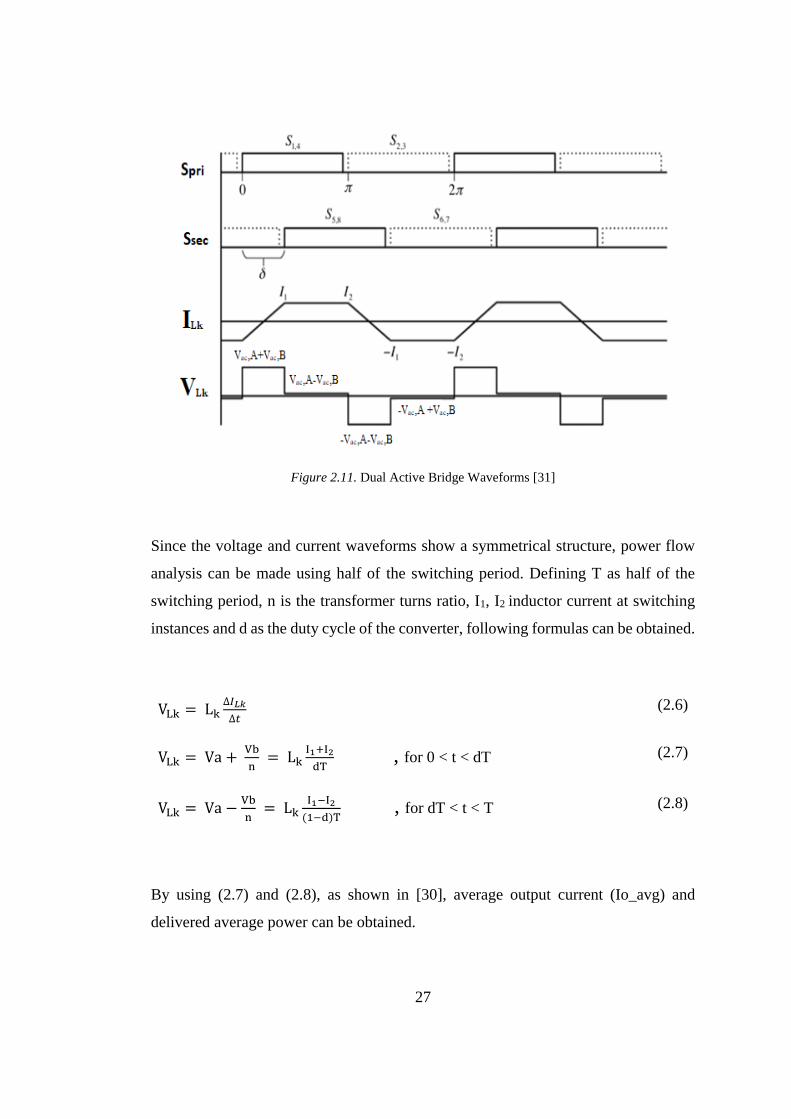
27
Figure 2.11. Dual Active Bridge Waveforms [31]
Since the voltage and current waveforms show a symmetrical structure, power flow
analysis can be made using half of the switching period. Defining T as half of the
switching period, n is the transformer turns ratio, I1, I2 inductor current at switching
instances and d as the duty cycle of the converter, following formulas can be obtained.
VLk = Lk∆𝐼𝐿𝑘
∆𝑡 (2.6)
VLk = Va + Vb
n = Lk
I1+I2
dT , for 0 < t < dT (2.7)
VLk = Va −Vb
n = Lk
I1−I2
(1−d)T , for dT < t < T (2.8)
By using (2.7) and (2.8), as shown in [30], average output current (Io_avg) and
delivered average power can be obtained.

28
IO_avg = (1−|d|)×d×T×Va
n×Lk (2.9)
PO_avg = (1−|d|)×d×T×Va×Vb
n×Lk (2.10)
The expression (2.10) shows that delivered power is a function of phase shift between
two bridges, energy transfer inductance, switching period and number of turns of high
frequency transformer. Moreover, a negative phase shift results in that power flow
direction is reversed and maximum output power is achieved at 50% phase shift [30].
In addition, DAB converters are able to adapt for soft switching commutations without
any extra active or passive component. Since this topology is a phase shift converter,
it has higher circulating currents resulting higher conduction losses than traditional
hard switching converters [1]. However, as the switching frequency increases, the
reduction of loss with soft switching implementation (as in the case mentioned in
Chapter 2.1.2) overrides the increased conduction losses and thus efficiency will
increase. Peak efficiency of 97.4% was achieved in [32] in a 2kW design with the help
of complete zero voltage switching. The most remarkable result of this design is that
even at 12.5% of rated load, soft switching is continued, and 90.9% efficiency is
reached showing the success of zero voltage switching at wide load range.
To sum up, DAB topology is an applicable topology for bidirectional power flow due
to having high efficiency, not having any additional component for soft switching,
compatibility with average or peak current mode control techniques and the simple
structure of its transformer. On the other hand, relatively high component count, high
ripple current values due to phase shifting and the sensitivity of phase shift control
especially at high bus voltages can be regarded as its drawbacks [1].
29
2.2.2. Dual Half Bridge (DHB)
Dual half bridge is a bidirectional DC/DC converter topology which mainly contains
two half bridges at both sides of a high frequency transformer. Similarly to DAB
topology, power regulation and flow direction is adjusted by controlling the phase
shift between the voltages applied to two sides of the transformer (Vr1 and Vr2 in
Figure 2.12). The leakage inductance of the transformer is used as energy transfer
element again with an additional inductance fitted in the circuit if necessary.
Generally, in DHB topology, one side has a current fed structure while the other has
voltage fed. Since, lower current ripple is desirable for energy storage elements like
batteries or supercapacitors, current fed is more suitable for this lower voltage side. In
Figure 2.12, circuit diagram of a dual half bridge converter with a current fed structure
at low voltage side is shown.
Figure 2.12. Schematic of Dual Half Bridge Bidirectional DC/DC Converter [33]
30
Ideal voltage waveforms of DHB topology can be seen in Figure 2.13 for charging
and discharging modes. In discharging mode, firstly traditional boost operation
realizes, and a square wave voltage is produced by switching S1 and S2 while S3 and
S4 rectify the ac voltage of the secondary in order to transfer power to the high voltage
side. In addition, high voltage side switching is done in such a way that square wave
realized on the transformer secondary is phase shifted with respect to transformer
primary voltage [1]. On the other hand, in charging mode, S3 and S4 are switched to
have ac voltage on transformer secondary while S1 and S2 rectify this voltage and acts
as a traditional buck converter to transfer power to the low voltage side. Surely,
primary side ac voltage will also lag the secondary side one for this operation.
However, phase shifting will increase the circulating current similar to DAB situation.
Hence, it is important to decrease reactive power transfer through transformer which
can be achieved with a lower leakage or series inductance. Moreover, zero voltage
switching can be adopted for all switches at both operation modes in a wide range of
dc bus voltages and load variations in order to increase total efficiency. In [34], 94%
efficiency was achieved with a wide range of output power from 0.45 kW to 1.4 kW.
Figure 2.13. Basic Waveforms of Dual Half Bridge for Both Mode of Operation [1]

31
As mentioned in this section, DHB bidirectional converters have the advantages of
decreased number of switching devices, lower cost and soft switching techniques can
be implemented easily in either side without any additional component. Lower ripple
current level at the current fed side also makes them desirable for battery applications.
With compared to DAB bidirectional converters, they have half component count with
the same total device rating for the same power level. On the other hand, high ripple
current on the split dc capacitors and unbalanced current stress on low voltage
switches can be the major drawbacks of this topology [34].
2.2.3. Full Bridge – Push Pull
This topology consists of a voltage fed full bridge stage on the high voltage side and
a current fed push pull stage on the low voltage side as shown in Figure 2.14. This
topology lets all switching devices to be switched with zero voltage switching for both
charging and discharging modes. In addition, synchronous switching can be
implemented to avoid diode rectification losses. By considering these properties,
highly efficient bidirectional power transfer is reached with proper switching schemes.
Figure 2.14. Schematic of Full Bridge – Push Pull Bidirectional Converter
32
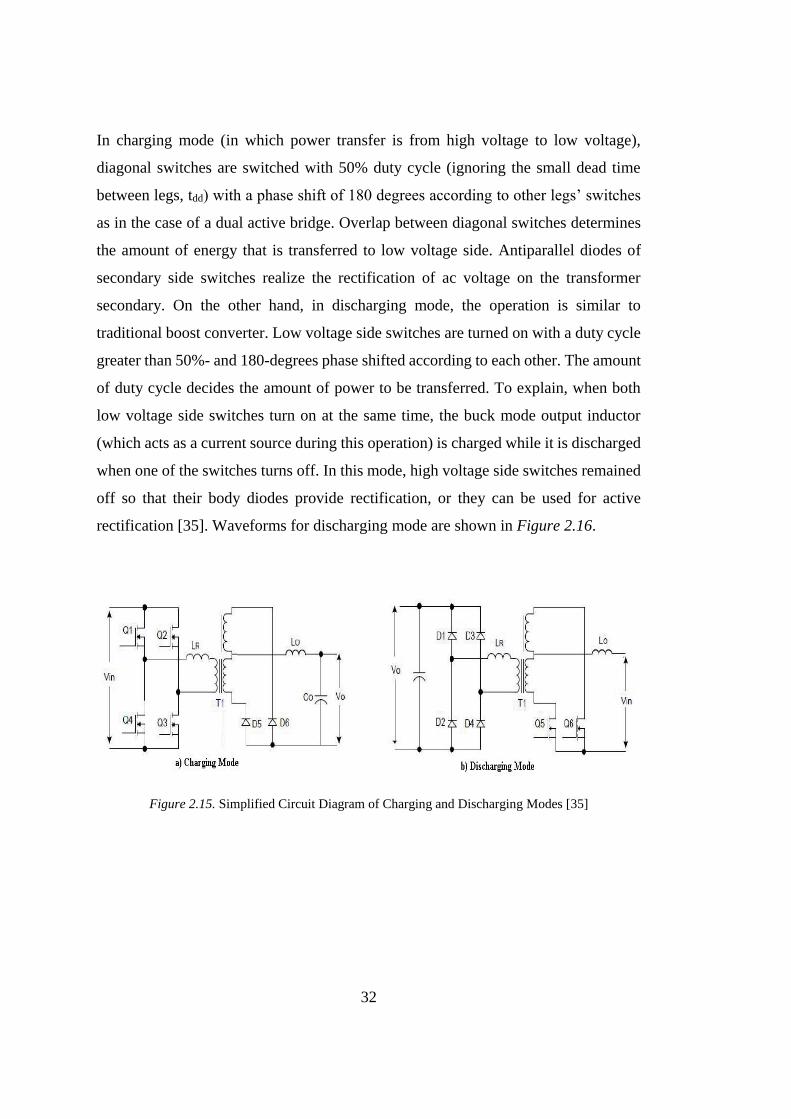
In charging mode (in which power transfer is from high voltage to low voltage),
diagonal switches are switched with 50% duty cycle (ignoring the small dead time
between legs, tdd) with a phase shift of 180 degrees according to other legs’ switches
as in the case of a dual active bridge. Overlap between diagonal switches determines
the amount of energy that is transferred to low voltage side. Antiparallel diodes of
secondary side switches realize the rectification of ac voltage on the transformer
secondary. On the other hand, in discharging mode, the operation is similar to
traditional boost converter. Low voltage side switches are turned on with a duty cycle
greater than 50%- and 180-degrees phase shifted according to each other. The amount
of duty cycle decides the amount of power to be transferred. To explain, when both
low voltage side switches turn on at the same time, the buck mode output inductor
(which acts as a current source during this operation) is charged while it is discharged
when one of the switches turns off. In this mode, high voltage side switches remained
off so that their body diodes provide rectification, or they can be used for active
rectification [35]. Waveforms for discharging mode are shown in Figure 2.16.
Figure 2.15. Simplified Circuit Diagram of Charging and Discharging Modes [35]
33
Figure 2.16. Waveforms of Discharging Mode
Compared to DAB converter, this topology has less switching device due to push pull
configuration at the secondary. Also, since the discharging mode is a current fed
converter thanks to output filter inductor of charging operation, the topology
inherently limits the current provided by the battery [36]. The use of overlapping
conduction times of switches during step-up operation reduces their average and rms
currents so as transformer windings. However, the voltage stresses of the switching
devices are doubled at the current fed push pull stage which is a serious problem for
high voltage applications. Furthermore, since it works under hard switching at push
pull side, low efficiency and voltage spikes can occur needing active clamp circuitry
or resonant structures to improve the efficiency and reliability [37].
In order to decrease component count further, another topology was introduced from
this structure in [36]. As shown from circuit schematic in Figure 2.17, full bridge stage
replaced with a half bridge stage. Although lower parts count compared to others is
achieved, the topology has the drawbacks of both half bridge structure like high ripple
currents on dc split capacitors and push pull structure as doubled voltage stresses on
switches. Even so, it can be suitable for low voltage and low power applications.

34
Figure 2.17. Half Bridge and Current Fed Push Pull Topology for Bidirectional Power Transfer [36]
Soft switching techniques or multiphase operation can be applied isolation ones as
well as non-isolated ones. However, it should be taken into account that; complexity
of the circuit and the control tend to be more when these techniques are to be applied.
For example, one more switch was added at push pull stage resulting a topology
consisting of three switches at this side in [37]. 96% efficiency was achieved at 500
W load while increasing the switch count one as shown in Figure 2.18.
Figure 2.18. Soft Switched Full Bridge-Push Pull Bidirectional DC/DC Converter with an Extra
Switch [37]

35
2.3. Comparison of Topologies
A brief summary of bidirectional DC/DC converters was given in this chapter. Their
operation principles were mentioned. Also, design difficulty and feasibility for
specific applications of topologies in the literature were evaluated. It is concluded that,
topology will differ according to requirements of the application. Basically, a suitable
topology can be chosen after the need for galvanic isolation is determined. In order to
be a reference for power electronic designers, Table 2.1 and Table 2.2 are given as a
short comparison of them. In this thesis study, giving the reasons for decision in next
chapter, a non-isolated topology is selected, analyzed, implemented and
experimented.

36
Tab
le 2
.1. C
om
pari
son o
f N
on
-Iso
late
d T
opolo
gie
s
Dis
ad
va
nta
ges
- N
ot
app
lica
ble
if
input
and o
utp
ut
volt
age
level
s ar
e
sam
e
- N
eed f
or
larg
e fi
lter
s
due
to h
ard s
wit
chin
g
- S
ever
e E
MI
issu
es
- H
igh c
om
ponen
t
cou
nt
- C
om
ple
x c
ontr
ol
- C
om
ple
x C
ontr
ol
- H
igh c
om
ponen
t
cou
nt
- C
om
ple
x c
ontr
ol
Ad
va
nta
ges
- S
impli
city
- L
ow
com
ponen
t
cou
nt
- A
pp
lica
ble
if
inp
ut
and
outp
ut
volt
age
level
s
are
sam
e
- F
lexib
le s
truct
ure
- H
igh e
ffic
iency
- In
her
ent
ZV
S
oper
atio
n
- H
igh e
ffic
iency
- L
ow
curr
ent
stre
ss
on c
om
ponen
ts
Eff
icie
ncy
in
Ref
. N
o
91%
in R
ef.
[40]
92%
in R
ef.
[24]
96%
at
Boost
oper
atio
n
95%
at
Buck
oper
atio
n
in R
ef.
[26]
94%
at
Boost
oper
atio
n
95%
at
Buck
oper
atio
n
in R
ef.
[13]
95%
in R
ef.
[39]
Vo
lta
ge
Str
ess
of
Sw
itch
es
Max
imum
of
DC
Bus
or
Bat
tery
Volt
age
Max
imum
of
DC
Bus
or
Bat
tery
Volt
age
Max
imum
of
DC
Bus
or
Bat
tery
Volt
age
Max
imum
of
DC
Bus
or
Bat
tery
Volt
age
Max
imum
of
DC
Bus
or
Bat
tery
Volt
age
Basi
c C
om
pon
ent
Cou
nt
- 2 s
wit
chin
g d
evic
es
- 1 i
nduct
or
for
ener
gy t
ransf
er
- 2 D
C l
ink c
apac
itors
-2 s
wit
chin
g d
evic
es
- 1 i
nduct
or
for
ener
gy t
ransf
er
- 2 D
C l
ink c
apac
itors
- 2 s
wit
chin
g d
evic
es
- 1 i
nduct
or
for
ener
gy t
ransf
er
- 2 D
C l
ink c
apac
itors
- 1 a
uxil
iary
sw
itch
for
acti
ve
clam
p
- 2 i
nduct
ors
and 1
cap
acit
or
for
ZV
S
- 4 s
wit
chin
g d
evic
es
- 1 i
nduct
or
for
ener
gy t
ransf
er
- 2 D
C l
ink c
apac
itors
- 6 s
wit
chin
g d
evic
es
- 3 i
nduct
ors
for
ener
gy t
ransf
er
- 2 D
C l
ink c
apac
itors
Top
olo
gy (
Ch
ap
ter N
o)
- N
on-i
sola
ted B
oost
- N
on-i
sola
ted B
uck
(Ch
apte
r 2
.1.1
.)
- N
on-i
sola
ted B
uck
-Boost
(Ch
apte
r 2
.1.1
.)
- N
on-i
sola
ted B
uck
wit
h A
ctiv
e C
lam
p f
or
ZV
S
(Ch
apte
r 2
.1.2
.)
- Z
VS
Non
-iso
late
d B
uck
-
Boost
wit
hout
any e
xtr
a
com
po
nen
t (C
hap
ter
2.1
.2.)
- T
hre
e phas
e non
-iso
late
d
(Ch
apte
r 2
.1.3
.)

37
Tab
le 2
.2. C
om
pari
son o
f Is
ola
ted T
opolo
gie
s
Dis
ad
va
nta
ges
- H
igh r
ipple
curr
ent
due
to
phas
e sh
ifte
d o
per
atio
n
- H
igh c
om
ponen
t co
unt
- S
ensi
tivit
y o
f phas
e sh
ift
con
tro
l at
hig
h v
olt
ages
- U
nb
alan
ced
curr
ent
stre
ss o
n
low
volt
age
swit
ches
- H
igh r
ipple
curr
ent
on D
C
spli
t ca
pac
itors
- V
olt
age
spik
es a
t p
ush
pu
ll
side
due
to h
ard s
wit
chin
g
- N
eed o
f ac
tive
clam
p o
r
reso
nan
t ci
rcu
it f
or
soft
swit
chin
g
- H
igh v
olt
age
stre
ss a
t push
pull
sta
ge
- C
om
ple
x c
ontr
ol
due
to
acti
ve
clam
p c
ircu
itry
- U
nb
alan
ced
cu
rren
t st
ress
on
low
volt
age
swit
ches
- H
igh v
olt
age
stre
ss a
t push
pull
sta
ge
Ad
va
nta
ges
- S
imple
tran
sform
er
stru
cture
- In
her
ent
ZV
S
oper
atio
n
- G
ood E
MI
- L
ow
com
ponen
t
cou
nt
- L
ow
rip
ple
curr
ent
lev
el a
t
curr
ent
fed
sid
e
- L
ow
sw
itch
cou
nt
- S
ynch
ronous
rect
ific
atio
n a
nd
low
rip
ple
curr
ent
level
at
curr
ent-
fed p
ush
pull
sid
e
- H
igh e
ffic
iency
- L
ow
com
ponen
t
cou
nt
Eff
icie
ncy
in
Ref
. N
o
97.4
% i
n R
ef.
[32
]
94%
in R
ef.
[34
]
91%
in R
ef.
[38
]
96%
in R
ef.
[37
]
90%
in R
ef.
[36
]
Vo
lta
ge
Str
ess
of
Sw
itch
es
DC
Bus
Volt
age
2 *
DC
Bus
Volt
age
of
LV
sid
e
2 *
DC
Bus
Volt
age
of
LV
sid
e
2 *
DC
Bus
Volt
age
of
LV
sid
e
2 *
DC
Bus
Volt
age
of
push
pull
sta
ge
Basi
c C
om
pon
ent
Cou
nt
- 8
sw
itch
ing
dev
ices
- 1
hig
h f
req
uen
cy t
ran
sfo
rmer
-
2 D
C li
nk
cap
acit
ors
- 1
ind
uct
or
for
ene
rgy
tran
sfer
- 4
sw
itch
ing
dev
ices
- 1
hig
h f
req
uen
cy t
ran
sfo
rmer
- 2
DC
lin
k ca
pac
ito
rs
- 1
ind
uct
or
for
ene
rgy
tran
sfer
- 6
sw
itch
ing
dev
ices
-
1 h
igh
fre
qu
ency
tra
nsf
orm
er
- 2
DC
lin
k ca
pac
ito
rs
- 1
ind
uct
or
for
ene
rgy
tran
sfer
- 7
sw
itch
ing
dev
ices
-
1 h
igh
fre
qu
ency
tra
nsf
orm
er
- 2
DC
lin
k ca
pac
ito
rs
- 1
ind
uct
or
for
ene
rgy
tran
sfer
- 4
sw
itch
ing
dev
ices
- 1
hig
h f
req
uen
cy t
ran
sfo
rmer
- 2
DC
lin
k ca
pac
ito
rs
- 1
ind
uct
or
for
ene
rgy
tran
sfer
Top
olo
gy
(C
ha
pte
r N
o)
Du
al A
ctiv
e B
rid
ge
(Ch
apte
r 2
.2.1
.)
Du
al H
alf
Bri
dge
(Ch
apte
r 2
.2.2
.)
Full
Bri
dge
–
Pu
sh P
ull
(Ch
apte
r 2
.2.3
.)
ZVS
Full
Bri
dge
– P
ush
Pu
ll
(Ch
apte
r 2
.2.3
.)
Hal
f B
rid
ge –
Pu
sh P
ull
(Ch
apte
r 2
.2.3
.)

39
CHAPTER 3
3. OPERATION PRINCIPLE AND DESIGN STEPS OF SELECTED
TOPOLOGY
As discussed in Chapter 2, various bidirectional DC/DC converter topologies have
been proposed in the literature. Among these, non-isolated ones will be more preferred
than the others where the main interest is to have more power density and isolation
requirement between source and the load is not a necessity (especially when the
voltage gain can be achieved with solely duty cycle control). Since they have fewer
parts; i.e. decreased number of power switches and passive components as compared
at Table 2.1 and Table 2.2, and do not have any large transformer on their structure,
they are also easier to control and implement. Moreover, less parts count results a
decrease in cost and losses, increasing efficiency in a dedicated area.
In this study, four switched non-isolated buck-boost converter is selected for specified
application. Although switch count is much more than the other non-isolated ones,
this topology brings the advantage of both buck and boost operation at each side which
is useful when input and output voltage levels are close to each other. Furthermore,
this topology is flexible to implement zero voltage switching (ZVS) without any extra
components unlike the resonant or active clamped converters which require additional
LLC circuits or active switches [26] for zero voltage switching operation respectively.
Also, the disadvantages of resonant converters, which are limited operating voltage
and load conditions, higher ratings of switches [36], complicated EMI filter design
due to variable switching frequency [41], are eliminated with this topology. ZVS can
be achieved just by controlled phase shift with the control of gating signals of each
switching device in a wide range and with a decrease in components’ stress.
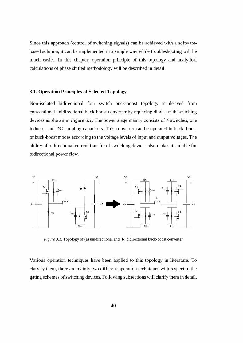
40
Since this approach (control of switching signals) can be achieved with a software-
based solution, it can be implemented in a simple way while troubleshooting will be
much easier. In this chapter; operation principle of this topology and analytical
calculations of phase shifted methodology will be described in detail.
3.1. Operation Principles of Selected Topology
Non-isolated bidirectional four switch buck-boost topology is derived from
conventional unidirectional buck-boost converter by replacing diodes with switching
devices as shown in Figure 3.1. The power stage mainly consists of 4 switches, one
inductor and DC coupling capacitors. This converter can be operated in buck, boost
or buck-boost modes according to the voltage levels of input and output voltages. The
ability of bidirectional current transfer of switching devices also makes it suitable for
bidirectional power flow.
Figure 3.1. Topology of (a) unidirectional and (b) bidirectional buck-boost converter
Various operation techniques have been applied to this topology in literature. To
classify them, there are mainly two different operation techniques with respect to the
gating schemes of switching devices. Following subsections will clarify them in detail.
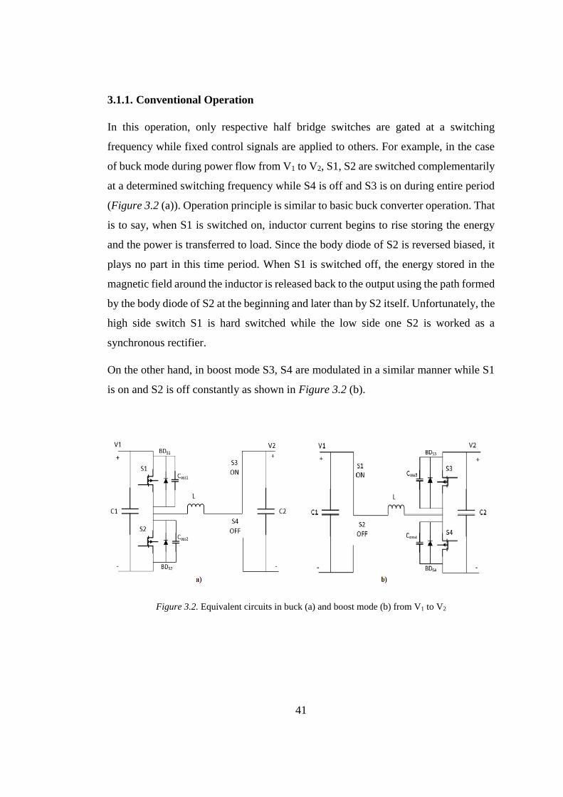
41
3.1.1. Conventional Operation
In this operation, only respective half bridge switches are gated at a switching
frequency while fixed control signals are applied to others. For example, in the case
of buck mode during power flow from V1 to V2, S1, S2 are switched complementarily
at a determined switching frequency while S4 is off and S3 is on during entire period
(Figure 3.2 (a)). Operation principle is similar to basic buck converter operation. That
is to say, when S1 is switched on, inductor current begins to rise storing the energy
and the power is transferred to load. Since the body diode of S2 is reversed biased, it
plays no part in this time period. When S1 is switched off, the energy stored in the
magnetic field around the inductor is released back to the output using the path formed
by the body diode of S2 at the beginning and later than by S2 itself. Unfortunately, the
high side switch S1 is hard switched while the low side one S2 is worked as a
synchronous rectifier.
On the other hand, in boost mode S3, S4 are modulated in a similar manner while S1
is on and S2 is off constantly as shown in Figure 3.2 (b).
Figure 3.2. Equivalent circuits in buck (a) and boost mode (b) from V1 to V2

42
With this conventional method, desired voltage levels can be reached by adjusting the
duty cycles of switched devices. However, it is important to note that there should be
a dead time between the same leg switches (i.e. complementary switches) in order to
avoid shoot through operation. Moreover, zero voltage switching can be achieved with
such a switching pattern by verifying the equations (2.1) to (2.5) resulting in a high
efficient converter. To give an example, in [13], 94% efficiency is obtained with this
topology and operation principle.
3.1.2. Phase Shifted Operation
Unlike the conventional one, all four switching devices at both legs (S1 to S4 in Figure
3.1 (b)) are switched on and off during a period in this operation. Phase shift means
that with such a gating pattern there will be a phase difference between bridge legs
shown in Figure 3.3 as θ. Input-output voltage conversion ratio and direction of power
flow is determined by the duty ratio of corresponding switches and phase shift angle
between them. For instance, the leading gating scheme of S1 over S3 makes power
flow from V1 to V2 and conversion ratio (V2/ V1) will be equal to ratio of duty cycles
of S1 (t2/T) and S3 ((t3-t1)/T). Steps of ratio calculation are given in Section 3.4.
Required gating signals for all possible modes can be analyzed in Figure 3.3 and
Figure 3.4 [42]. As it is seen from these figures, operating principles for different
modes are similar to each other. Hence, detailed circuit operation of buck and boost
modes in the case of transferring power from V1 to V2 will be examined in detail
throughout this section.
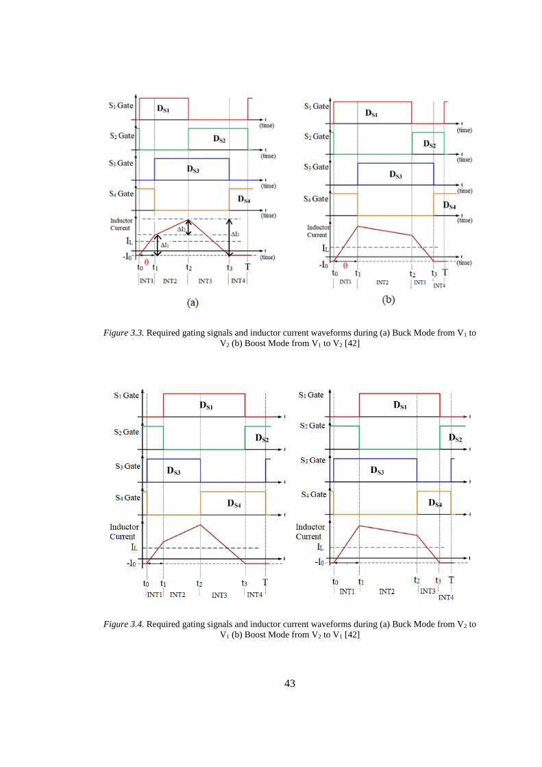
43
Figure 3.3. Required gating signals and inductor current waveforms during (a) Buck Mode from V1 to
V2 (b) Boost Mode from V1 to V2 [42]
Figure 3.4. Required gating signals and inductor current waveforms during (a) Buck Mode from V2 to
V1 (b) Boost Mode from V2 to V1 [42]
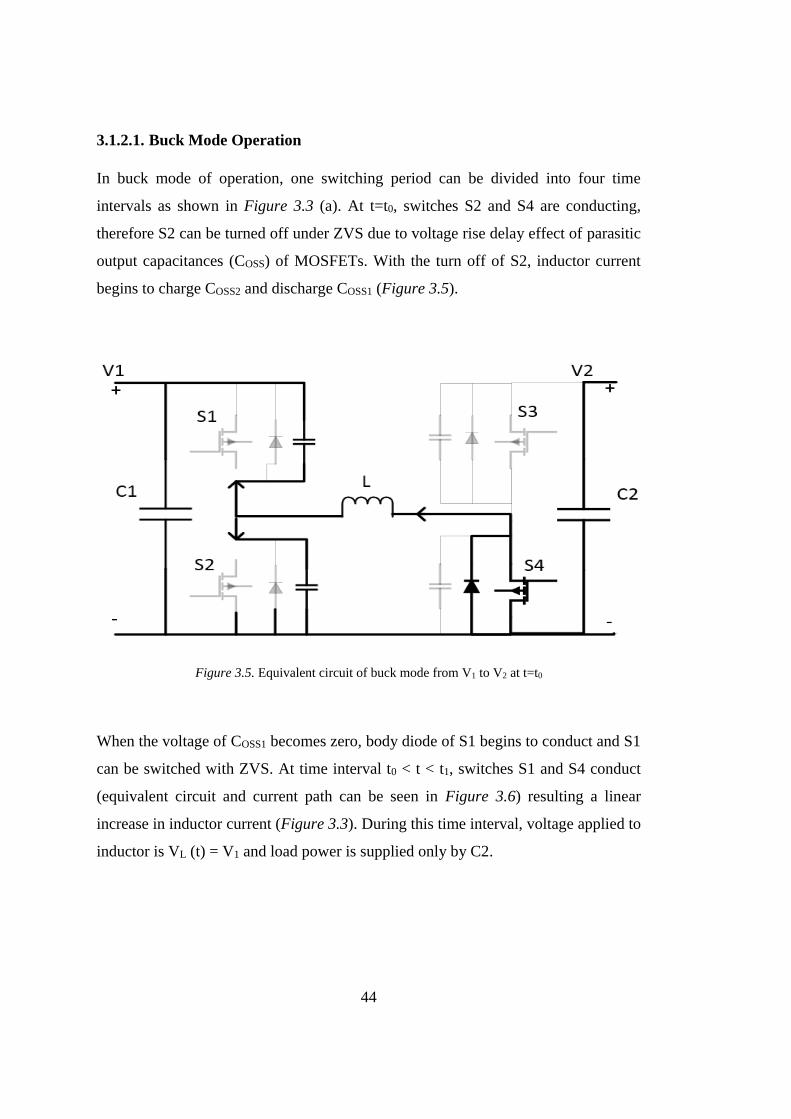
44
3.1.2.1. Buck Mode Operation
In buck mode of operation, one switching period can be divided into four time
intervals as shown in Figure 3.3 (a). At t=t0, switches S2 and S4 are conducting,
therefore S2 can be turned off under ZVS due to voltage rise delay effect of parasitic
output capacitances (COSS) of MOSFETs. With the turn off of S2, inductor current
begins to charge COSS2 and discharge COSS1 (Figure 3.5).
Figure 3.5. Equivalent circuit of buck mode from V1 to V2 at t=t0
When the voltage of COSS1 becomes zero, body diode of S1 begins to conduct and S1
can be switched with ZVS. At time interval t0 < t < t1, switches S1 and S4 conduct
(equivalent circuit and current path can be seen in Figure 3.6) resulting a linear
increase in inductor current (Figure 3.3). During this time interval, voltage applied to
inductor is VL (t) = V1 and load power is supplied only by C2.
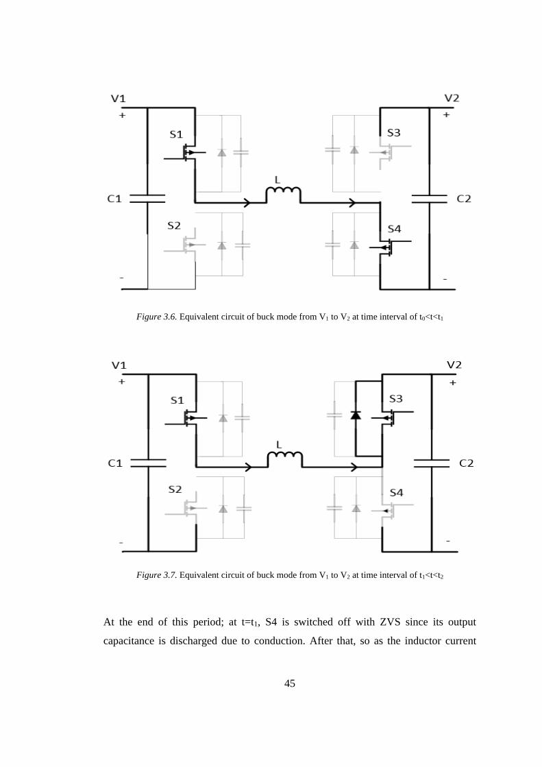
45
Figure 3.6. Equivalent circuit of buck mode from V1 to V2 at time interval of t0<t<t1
Figure 3.7. Equivalent circuit of buck mode from V1 to V2 at time interval of t1<t<t2
At the end of this period; at t=t1, S4 is switched off with ZVS since its output
capacitance is discharged due to conduction. After that, so as the inductor current
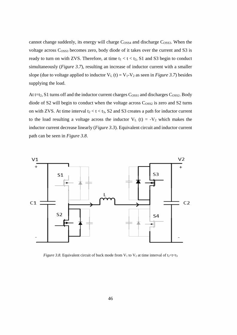
46
cannot change suddenly, its energy will charge COSS4 and discharge COSS3. When the
voltage across COSS3 becomes zero, body diode of it takes over the current and S3 is
ready to turn on with ZVS. Therefore, at time t1 < t < t2, S1 and S3 begin to conduct
simultaneously (Figure 3.7), resulting an increase of inductor current with a smaller
slope (due to voltage applied to inductor VL (t) = V1-V2 as seen in Figure 3.7) besides
supplying the load.
At t=t2, S1 turns off and the inductor current charges COSS1 and discharges COSS2. Body
diode of S2 will begin to conduct when the voltage across COSS2 is zero and S2 turns
on with ZVS. At time interval t2 < t < t3, S2 and S3 creates a path for inductor current
to the load resulting a voltage across the inductor VL (t) = -V2 which makes the
inductor current decrease linearly (Figure 3.3). Equivalent circuit and inductor current
path can be seen in Figure 3.8.
Figure 3.8. Equivalent circuit of buck mode from V1 to V2 at time interval of t2<t<t3
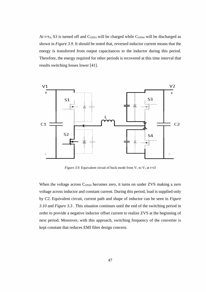
47
At t=t3, S3 is turned off and COSS3 will be charged while COSS4 will be discharged as
shown in Figure 3.9. It should be noted that, reversed inductor current means that the
energy is transferred from output capacitances to the inductor during this period.
Therefore, the energy required for other periods is recovered at this time interval that
results switching losses lower [41].
Figure 3.9. Equivalent circuit of buck mode from V1 to V2 at t=t3
When the voltage across COSS4 becomes zero, it turns on under ZVS making a zero
voltage across inductor and constant current. During this period, load is supplied only
by C2. Equivalent circuit, current path and shape of inductor can be seen in Figure
3.10 and Figure 3.3 . This situation continues until the end of the switching period in
order to provide a negative inductor offset current to realize ZVS at the beginning of
next period. Moreover, with this approach, switching frequency of the converter is
kept constant that reduces EMI filter design concern.
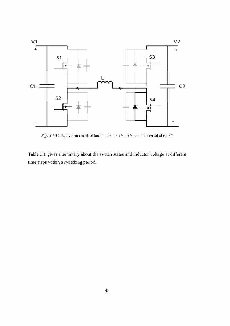
48
Figure 3.10. Equivalent circuit of buck mode from V1 to V2 at time interval of t3<t<T
Table 3.1 gives a summary about the switch states and inductor voltage at different
time steps within a switching period.

49
Table 3.1. State of switches and inductor voltage at different time intervals within a period of buck
mode from V1 to V2
3.1.2.2. Boost Mode Operation
Similar to buck mode, one complete switching cycle can be divided into four time-
intervals during boost operation as can be seen from the inductor current waveform in
Figure 3.3 (b). Conducting switches are completely same in corresponding time
intervals as in the case of buck mode. The only difference of this operation is that;
since the output voltage level will be higher than the input voltage, at time interval t1
< t < t2, inductor current has a negative slope (Figure 3.3 (b)). All equivalent circuit
configurations for buck mode shown in Figure 3.5 to Figure 3.10 are valid for boost
mode of operation too.
Time
interval
S1
Vcoss1
S2
Vcoss2
S3
Vcoss3
S4
Vcoss4
Inductor
Voltage
State or
Eq.
t0< t < t1 On
0v
Off
V1
Off
V2
On
0 V1 Eq. 3.4
t1< t < t1ı On
0v
Off
V1
Off
Discharging
to 0v
Off
Charging to
V2
V1 –
Vcoss4
Dead
Time
t1ı< t < t2
On
0v
Off
V1
On
0v
Off
V2 V1 - V2 Eq. 3.5
t2< t < t2ı
Off
Charging to
V1
Off
Discharging
to 0v
On
0v
Off
V2
Vcoss2 -
V2
Dead
Time
t2ı< t < t3
Off
V1
On
0v
On
0v
Off
V2 - V2 Eq. 3.6
t3< t < t3ı Off
V1
On
0v
Off
Charging to
V2
Off
Discharging
to 0v
– Vcoss4 Dead
Time
t3ı< t < ts
Off
V1
On
0v
Off
V2
On
0v 0 Eq. 3.7
ts< t < t0ı
Off
Discharging
to 0v
Off
Charging to
V1
Off
V2
On
0v Vcoss2
Dead
Time

50
3.2. Evaluation of Operation Principles
As described at the previous section, there are mainly two different approaches while
gating the switching devices; namely, conventional and phase shifted operation. Both
methods mainly consist of the same number of components including four switching
devices, one inductor to store the energy and DC link capacitors at the input and output
stages. Hence, hardware costs and sizes are similar to each other. However, only two
switches are turned on and off in the former one while all the switches are gated in a
period in the latter. By applying phase shifted operation, turn on of all switches can be
achieved with ZVS by adopting the switching times which does not require any extra
active or passive components. It also helps to improve EMI performance of the
converter and to decrease the components’ voltage or current stresses. Moreover, since
the body diode of the complementary switch in a half bridge is blocked, there will be
no reverse recovery losses. Additionally, turn off under ZVS is realized due to the
inherent output capacitance parameter of the switches and can be improved with a
minimum resistance in the turn off path of the gate driver [41]. This methodology will
be described analytically in detail at the following chapter. Although switching pattern
and control scheme are more complicated, efficiency will be higher with such a gating
configuration. For example, improvement in efficiency is observed in [42] at whole
load range as can be seen in Figure 3.11.
In this study, phase shifted operation is selected as the modulation technique by
considering mentioned benefits and drawbacks. Comparison of these two approaches
will be done by simulation and experimental measurements in order to verify
theoretical analysis.
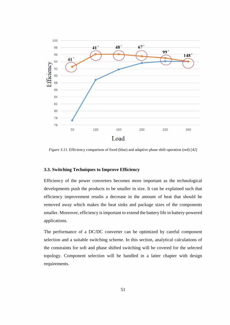
51
Figure 3.11. Efficiency comparison of fixed (blue) and adaptive phase shift operation (red) [42]
3.3. Switching Techniques to Improve Efficiency
Efficiency of the power converters becomes more important as the technological
developments push the products to be smaller in size. It can be explained such that
efficiency improvement results a decrease in the amount of heat that should be
removed away which makes the heat sinks and package sizes of the components
smaller. Moreover, efficiency is important to extend the battery life in battery-powered
applications.
The performance of a DC/DC converter can be optimized by careful component
selection and a suitable switching scheme. In this section, analytical calculations of
the constraints for soft and phase shifted switching will be covered for the selected
topology. Component selection will be handled in a latter chapter with design
requirements.
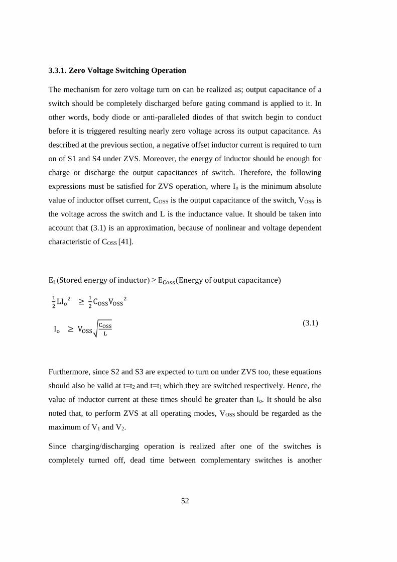
52
3.3.1. Zero Voltage Switching Operation
The mechanism for zero voltage turn on can be realized as; output capacitance of a
switch should be completely discharged before gating command is applied to it. In
other words, body diode or anti-paralleled diodes of that switch begin to conduct
before it is triggered resulting nearly zero voltage across its output capacitance. As
described at the previous section, a negative offset inductor current is required to turn
on of S1 and S4 under ZVS. Moreover, the energy of inductor should be enough for
charge or discharge the output capacitances of switch. Therefore, the following
expressions must be satisfied for ZVS operation, where Io is the minimum absolute
value of inductor offset current, COSS is the output capacitance of the switch, VOSS is
the voltage across the switch and L is the inductance value. It should be taken into
account that (3.1) is an approximation, because of nonlinear and voltage dependent
characteristic of COSS [41].
EL(Stored energy of inductor) ≥ ECoss(Energy of output capacitance)
1
2LIo
2 ≥ 1
2COSSVOSS
2
Io ≥ VOSS√COSS
L
(3.1)
Furthermore, since S2 and S3 are expected to turn on under ZVS too, these equations
should also be valid at t=t2 and t=t1 which they are switched respectively. Hence, the
value of inductor current at these times should be greater than Io. It should be also
noted that, to perform ZVS at all operating modes, VOSS should be regarded as the
maximum of V1 and V2.
Since charging/discharging operation is realized after one of the switches is
completely turned off, dead time between complementary switches is another

53
important parameter for ZVS operation. Minimum value of it (tdd) can be expressed
as (3.2) using (3.1) and (3.3).
tdd,min ≥ V1
V1 − V2√L ∗ Coss
(3.2)
3.3.2. Adaptive Phase Shifted Operation
From the operation principle and circuit analysis of the selected topology stated in
previous sections, it can be observed that the turn on/off times of switching devices
are important to improve efficiency and reliability of the converter. Furthermore, since
the transferred power is directly proportional to inductor current, time function of it
should be obtained in order to calculate the whole transferred power. By using
equation (3.3) and inductor current waveform depicted in Figure 3.3 (a), the time
function of inductor current can be obtained as in equations (3.4) to (3.7).
𝑉L(t) = L ∗𝑑
dtiL(𝑡) (3.3)
𝑖L(t) = −𝐼𝑜 +𝑉1
L𝑡 for t0 ≤ t < t1 (3.4)
𝑖L(t) = −𝐼𝑜 +𝑉2
L𝑡1 +
𝑉1−𝑉2
L𝑡 for t1 ≤ t < t2
(3.5)
𝑖L(t) = −𝐼𝑜 +𝑉2
L𝑡1 +
𝑉1
L𝑡2 +
−𝑉2
L𝑡 for t2 ≤ t < t3 (3.6)
𝑖L(t) = −𝐼𝑜 for t3≤ t <ts (3.7)

54
Next, from the formula of; 𝑃average = 1
T∫ 𝑣(𝑡) ∗ 𝑖(𝑡)
𝑇
0 following equations can be
derived for PIN and POUT. It should be noted that power is provided by the input at t0 ≤
t ≤ t2 and transferred to output at t1 ≤ t ≤ t3 as can be seen from the current flow in
Figure 3.5 to Figure 3.10.
𝑃IN = 𝑉1
𝑡𝑠∫ 𝑖𝐿(𝑡)𝑑(𝑡)
𝑡2
𝑡0
= 𝑉1
𝑡𝑠(∫ (−𝐼𝑜 +
𝑉1
L𝑡) 𝑑(𝑡) +
𝑡1
𝑡0
∫ (−𝐼𝑜 +𝑉2
L𝑡1 +
𝑉1 − 𝑉2
L𝑡) 𝑑(𝑡)
𝑡2
𝑡1
)
= 𝑉1
2𝑡𝑠𝐿(2𝑉2𝑡1𝑡2 + 𝑉1t2
2 − 𝑉2t22 − 𝑉2t1
2) − 𝑉1∗ 𝐼0∗ 𝑡2
𝑡𝑠
(3.8)
𝑃OUT = 𝑉2
𝑡𝑠∫ 𝑖𝐿(𝑡)𝑑(𝑡)
𝑡3
𝑡1
= 𝑉2
𝑡𝑠(∫ (−𝐼𝑜 +
𝑉2
L𝑡1 +
𝑉1−𝑉2
L𝑡) 𝑑(𝑡) +
𝑡2
𝑡1∫ (−𝐼𝑜 +
𝑉2
L𝑡1 +
𝑉1
L𝑡2 +
𝑡3
𝑡2
−𝑉2
L𝑡) 𝑑(𝑡))
= −𝑉2𝐼0
𝑡𝑠(𝑡3 − 𝑡1 )
+ 𝑉2
2𝑡𝑠𝐿(−𝑉2t3
2 − 𝑉1t22 − (𝑉1 + 𝑉2)t1
2 + 𝑉2𝑡1𝑡3 + 2𝑉1𝑡2𝑡3)
(3.9)
Input and output power directly depend on switching times (t1, t2 and t3) as can be seen
from (3.8) and (3.9). Therefore, in order to obtain maximum power, an optimization
process (introduced in [41]) should be applied while determining these times. Firstly,
assuming the components are ideal and when the losses are neglected, output power
has to be equal to the input power giving the equation (3.10). Then, as stated before,
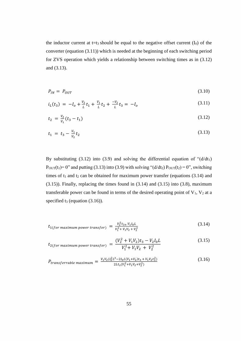
55
the inductor current at t=t3 should be equal to the negative offset current (I0) of the
converter (equation (3.11)) which is needed at the beginning of each switching period
for ZVS operation which yields a relationship between switching times as in (3.12)
and (3.13).
𝑃𝐼𝑁 = 𝑃𝑂𝑈𝑇 (3.10)
𝑖𝐿(𝑡3) = −𝐼𝑜 +𝑉2
𝐿𝑡1 +
𝑉1
𝐿𝑡2 +
−𝑉2
𝐿𝑡3 = −𝐼𝑜 (3.11)
𝑡2 = 𝑉2
𝑉1(𝑡3 − 𝑡1) (3.12)
𝑡1 = 𝑡3 − 𝑉1
𝑉2𝑡2 (3.13)
By substituting (3.12) into (3.9) and solving the differential equation of “(d/dt1)
POUT(t1)= 0” and putting (3.13) into (3.9) with solving “(d/dt2) POUT(t2) = 0”, switching
times of t1 and t2 can be obtained for maximum power transfer (equations (3.14) and
(3.15)). Finally, replacing the times found in (3.14) and (3.15) into (3.8), maximum
transferable power can be found in terms of the desired operating point of V1, V2 at a
specified t3 (equation (3.16)).
𝑡1(𝑓𝑜𝑟 𝑚𝑎𝑥𝑖𝑚𝑢𝑚 𝑝𝑜𝑤𝑒𝑟 𝑡𝑟𝑎𝑛𝑠𝑓𝑒𝑟) = 𝑉2
2𝑡3+ 𝑉1𝐼0𝐿
𝑉12+ 𝑉1𝑉2 + 𝑉2
2 (3.14)
𝑡2(𝑓𝑜𝑟 𝑚𝑎𝑥𝑖𝑚𝑢𝑚 𝑝𝑜𝑤𝑒𝑟 𝑡𝑟𝑎𝑛𝑠𝑓𝑒𝑟) = (𝑉2
2 + 𝑉1𝑉2)𝑡3 − 𝑉2𝐼0𝐿
𝑉12+ 𝑉1𝑉2 + 𝑉2
2 (3.15)
𝑃𝑡𝑟𝑎𝑛𝑠𝑓𝑒𝑟𝑟𝑎𝑏𝑙𝑒 𝑚𝑎𝑥𝑖𝑚𝑢𝑚 = 𝑉1𝑉2(𝐼0
2𝐿2−2𝐼0𝐿(𝑉1+𝑉2)𝑡3 + 𝑉1𝑉2𝑡32)
2𝐿𝑡𝑠(𝑉12+𝑉1𝑉2+𝑉2
2) (3.16)
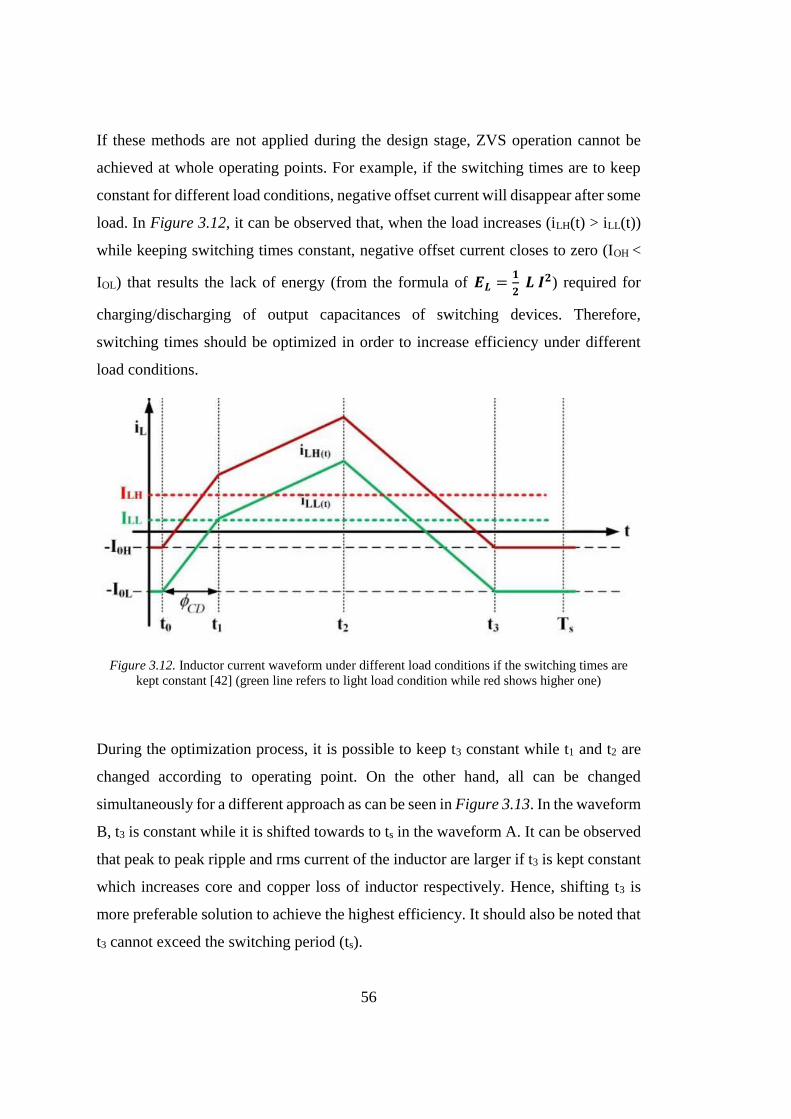
56
If these methods are not applied during the design stage, ZVS operation cannot be
achieved at whole operating points. For example, if the switching times are to keep
constant for different load conditions, negative offset current will disappear after some
load. In Figure 3.12, it can be observed that, when the load increases (iLH(t) > iLL(t))
while keeping switching times constant, negative offset current closes to zero (IOH <
IOL) that results the lack of energy (from the formula of 𝑬𝑳 =𝟏
𝟐 𝑳 𝑰𝟐) required for
charging/discharging of output capacitances of switching devices. Therefore,
switching times should be optimized in order to increase efficiency under different
load conditions.
Figure 3.12. Inductor current waveform under different load conditions if the switching times are
kept constant [42] (green line refers to light load condition while red shows higher one)
During the optimization process, it is possible to keep t3 constant while t1 and t2 are
changed according to operating point. On the other hand, all can be changed
simultaneously for a different approach as can be seen in Figure 3.13. In the waveform
B, t3 is constant while it is shifted towards to ts in the waveform A. It can be observed
that peak to peak ripple and rms current of the inductor are larger if t3 is kept constant
which increases core and copper loss of inductor respectively. Hence, shifting t3 is
more preferable solution to achieve the highest efficiency. It should also be noted that
t3 cannot exceed the switching period (ts).

57
Figure 3.13. Different approaches while optimizing the switching times [41]
3.4. Mathematical Analysis of Phase Shifted Operation
In this section, the analysis of input-output voltage conversion ratio in terms of circuit
parameters and switching times of phase shifted operation is described. In addition,
peak values of inductor current and the ripple voltage of output capacitor is calculated.
3.4.1. Voltage Conversion Ratio
Using the voltage drop formula across the inductor (3.17) and respective equations of
different time intervals (3.18) to (3.20), voltage conversion ratio of phase shifted
operation can be expressed as follows.
𝑉L(t) = L ∗𝑑
dtiL(𝑡) (3.17)
𝑉1 = L ∗𝛥𝐼1
𝑑𝑡 ; t0 ≤ t < t1
(3.18)
𝑉1 − 𝑉2 = L ∗𝛥𝐼2
𝑑𝑡 ; t1 ≤ t < t2
(3.19)
−𝑉2 = L ∗𝛥𝐼3
𝑑𝑡 ; t2 ≤ t < t3
(3.20)

58
Since energy stored in the inductor at the end of each switching period is equal to that
of at the beginning, (3.21) and by reorganizing (3.18) to (3.20), equations for ΔIs are
obtained as (3.22) to (3.24).
𝛥𝐼1 + 𝛥𝐼2 = 𝛥𝐼3 (3.21)
𝛥𝐼1 = 𝑉1 ∗t1
𝐿 (3.22)
𝛥𝐼2 = (𝑉1 − 𝑉2) ∗𝑡2−𝑡1
𝐿 (3.23)
𝛥𝐼3 = −𝑉2 ∗𝑡3−𝑡2
𝐿 (3.24)
Using (3.21) to (3.24); relationship between input (V1) and output (V2) is expressed
as;
𝑉1 ∗t1
𝐿+ (𝑉1 − 𝑉2) ∗
𝑡2−𝑡1
𝐿 = −𝑉2 ∗
𝑡3−𝑡2
𝐿 (3.25)
Simplifying (3.25) gives;
𝑉1
𝑉2 =
𝑡2
𝑡3−𝑡1 (3.26)
In (3.26), nominator term (t2) is equal to product of duty cycle of switch S1 with
switching period and denominator term (t3 - t1) is obtained with the multiplication of
duty cycle of switch S3 with switching period. Hence, conversion ratio can also be
submitted as (3.27) where DS1 is duty cycle of S1 and DS2 is duty cycle of S3.

59
𝑉1
𝑉2 =
DS1
DS3 (3.27)
3.4.2. Inductor Current Ripple Calculation
As it is seen at Figure 3.3 (a), inductor current shows a waveform like a kind of
trapezoidal throughout one switching period. It has different slope values at different
intervals due to applied voltage. Defining the current value at t = t0 as I0, at t = t1 as Ip1
and at t = t2 as Ip2, equations (3.28) and (3.29) are obtained.
𝑉1 = L ∗𝐼p1− 𝐼0
𝑡1 » 𝐼p1 − 𝐼0 =
𝑉1𝑡1
L
(3.28)
𝑉1 − 𝑉2 = L ∗𝐼p2− 𝐼p1
𝑡2−𝑡1 » -𝐼p1 + 𝐼P2 =
( 𝑉1 − 𝑉2 )(𝑡2−𝑡1)
L (3.29)
Due to charge-second balance principle the net current into and out of the output
capacitor should be zero. Moreover, due to Kirchhoff’s current law; switch S3 current
must be equal to sum of output capacitor current and load current. Therefore, load
current is equal to average value of switch S3 current (Figure 3.14) yielding;
𝐼LOAD =1
T∫ 𝑖𝑆3(𝑡)𝑑(𝑡)
T
0
(3.30)
𝐼LOAD ∗ T = ∫ 𝑖𝑆3(𝑡)𝑑(𝑡)𝑡2
𝑡1
+ ∫ 𝑖𝑆3(𝑡)𝑑(𝑡)𝑡3
𝑡2
(3.31)
𝐼LOAD ∗ T =( 𝐼p1 + 𝐼p2 )(𝑡2−𝑡1)
2 +
( 𝐼0 + 𝐼p2 )(𝑡3−𝑡2)
2 (3.32)

60
Reorganizing (3.32) gives;
𝐼p1(𝑡2−𝑡1) + 𝐼p2(𝑡3−𝑡1) + 𝐼0(𝑡3−𝑡2)
T = 2𝐼LOAD (3.33)
Rewriting (3.28), (3.29) and (3.33) in matrix form, I0, Ip1 and Ip2 can be found in terms
of V1, V2 , ILOAD and timings as follows.
[
( 𝑡3 – 𝑡2 )/𝑇 ( 𝑡2 – 𝑡1 )/𝑇 ( 𝑡3 – 𝑡1 )/𝑇−𝐿 /𝑡1 𝐿 /𝑡1 0
0 −𝐿 /(𝑡2 − 𝑡1) 𝐿 /(𝑡2 − 𝑡1)
] [
𝐼0
𝐼P1
𝐼P2
]= [2 0 00 1 00 1 −1
] [
𝐼LOAD
𝑉1
𝑉2
] (3.34)
Defining the matrix of left-hand side of the equation as A, and the right-hand side of
the equation as B gives;
[ 𝐼0
𝐼P1
𝐼P2
] = 𝐴−1 ∗ 𝐵 ∗ [ 𝐼LOAD
𝑉1
𝑉2
]
(3.35)
resulting;
[
𝐼0
𝐼P1
𝐼P2
] =
[ −𝑇/(𝑡1– 𝑡3 )
( 𝑡1 – 𝑡2 )
2𝐿 +
𝑡1 (𝑡2 −2𝑡1+𝑡3 )
2𝐿(𝑡1– 𝑡3 ) −
( 𝑡1 – 𝑡2 )
2𝐿
−𝑇/(𝑡1– 𝑡3 )( 𝑡1 – 𝑡2 )
2𝐿 +
𝑡1 (𝑡2 −𝑡3 )
2𝐿(𝑡1– 𝑡3 ) −
( 𝑡1 – 𝑡2 )
2𝐿
−𝑇/(𝑡1– 𝑡3 ) −( 𝑡1 – 𝑡2 )
2𝐿 +
𝑡1 (𝑡2 −𝑡3 )
2𝐿(𝑡1– 𝑡3 )
( 𝑡1 – 𝑡2 )
2𝐿 ]
[
𝐼LOAD
𝑉1
𝑉2
]
(3.36)
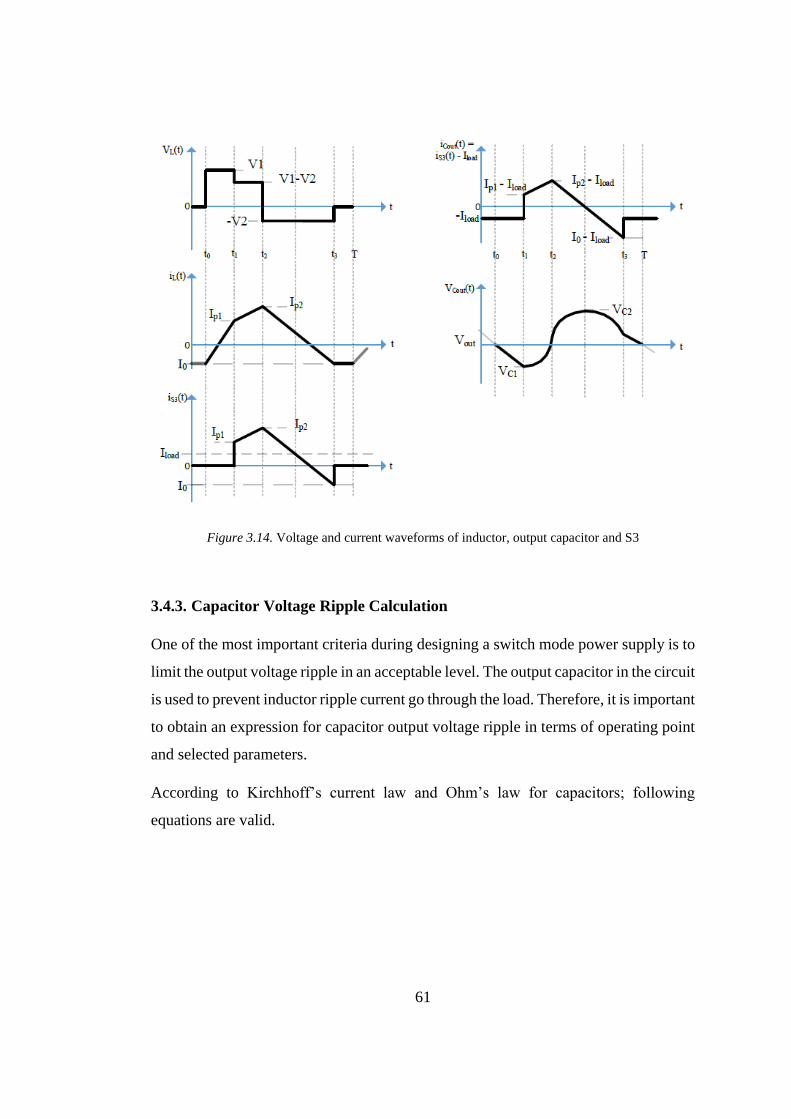
61
Figure 3.14. Voltage and current waveforms of inductor, output capacitor and S3
3.4.3. Capacitor Voltage Ripple Calculation
One of the most important criteria during designing a switch mode power supply is to
limit the output voltage ripple in an acceptable level. The output capacitor in the circuit
is used to prevent inductor ripple current go through the load. Therefore, it is important
to obtain an expression for capacitor output voltage ripple in terms of operating point
and selected parameters.
According to Kirchhoff’s current law and Ohm’s law for capacitors; following
equations are valid.

62
𝑖Cout(t) = 𝑖S3(t) − 𝑖LOAD (3.37)
iCout(t) = 𝐶OUT ∗ 𝑑𝑉Cout(t)
𝑑𝑡
» 𝛥𝑉Cout(t) =1
𝐶OUT∫ 𝑖𝐶𝑜𝑢𝑡(𝑡)𝑑(𝑡)
𝑇
0
(3.38)
As can be inferred from equation (3.38) and can be seen in Figure 3.14, area under
“iCout vs t” graph between t1 and tx gives peak to peak ripple voltage expression. Thus;
𝛥𝑉Cout(t) =1
𝐶OUT∫ 𝑖𝐶𝑜𝑢𝑡(𝑡)𝑑(𝑡)
𝑡x
𝑡1
(3.39)
𝛥𝑉Cout(t) =1
𝐶OUT [(I𝑃1 + I𝑃2 − 2I𝐿𝑂𝐴𝐷) (
𝑡2 – 𝑡1
2) + (I𝑃2 − I𝐿𝑂𝐴𝐷) (
𝑡x – 𝑡2
2)] (3.40)
For tx, from the graph of “iCout vs t”;
( 𝐼p2 − 𝐼LOAD )
(𝑡x−𝑡2) =
( 𝐼LOAD − 𝐼0 )
(𝑡3−𝑡x) (3.41)
tx =𝑡3( 𝐼p2 − 𝐼LOAD ) −𝑡2( 𝐼0 − 𝐼LOAD )
𝐼p2 − 𝐼0
(3.42)
Substituting (3.42) into (3.40) gives;
𝛥𝑉Cout(t) =1
2𝐶OUT [(−I𝑃1 − I𝑃2 + 2I𝐿𝑂𝐴𝐷) 𝑡1 −
[(−I𝑃1 − I𝑃2 + 2I𝐿𝑂𝐴𝐷) +(𝐼LOAD− 𝐼p2)
2
𝐼P2− 𝐼0] 𝑡2 +
(𝐼LOAD− 𝐼p2)2
𝐼P2− 𝐼0 𝑡3 ]
(3.43)
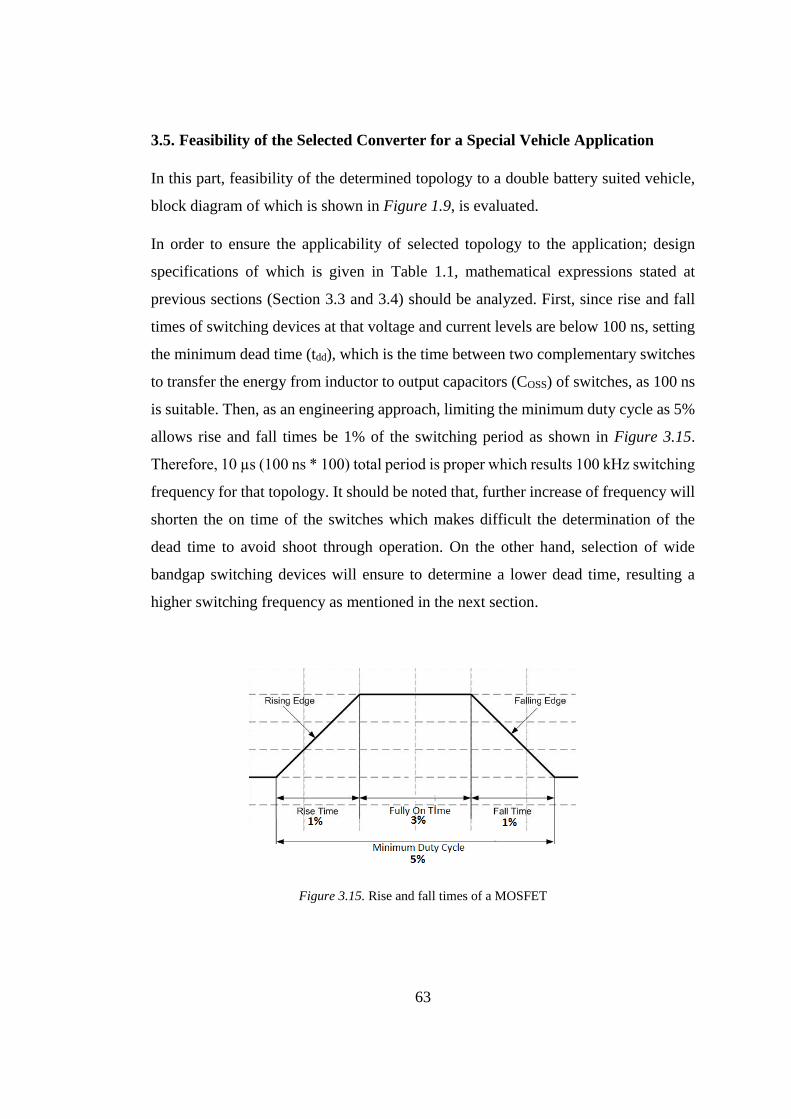
63
3.5. Feasibility of the Selected Converter for a Special Vehicle Application
In this part, feasibility of the determined topology to a double battery suited vehicle,
block diagram of which is shown in Figure 1.9, is evaluated.
In order to ensure the applicability of selected topology to the application; design
specifications of which is given in Table 1.1, mathematical expressions stated at
previous sections (Section 3.3 and 3.4) should be analyzed. First, since rise and fall
times of switching devices at that voltage and current levels are below 100 ns, setting
the minimum dead time (tdd), which is the time between two complementary switches
to transfer the energy from inductor to output capacitors (COSS) of switches, as 100 ns
is suitable. Then, as an engineering approach, limiting the minimum duty cycle as 5%
allows rise and fall times be 1% of the switching period as shown in Figure 3.15.
Therefore, 10 µs (100 ns * 100) total period is proper which results 100 kHz switching
frequency for that topology. It should be noted that, further increase of frequency will
shorten the on time of the switches which makes difficult the determination of the
dead time to avoid shoot through operation. On the other hand, selection of wide
bandgap switching devices will ensure to determine a lower dead time, resulting a
higher switching frequency as mentioned in the next section.
Figure 3.15. Rise and fall times of a MOSFET
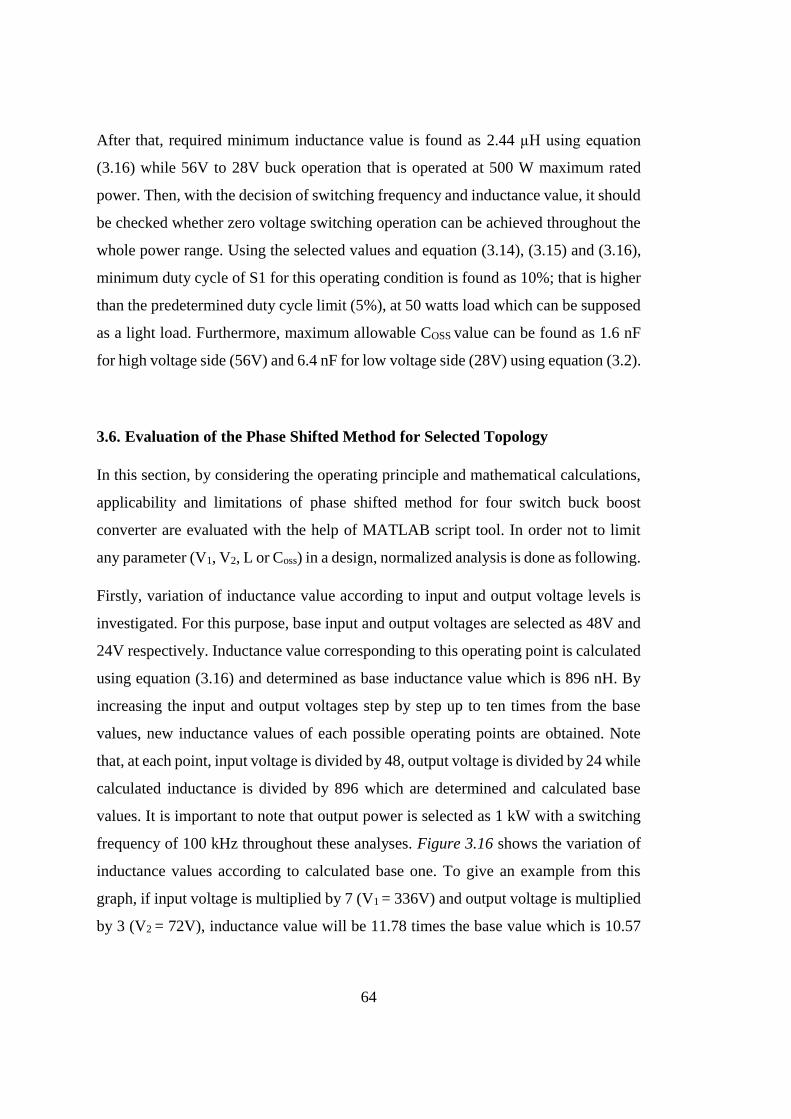
64
After that, required minimum inductance value is found as 2.44 µH using equation
(3.16) while 56V to 28V buck operation that is operated at 500 W maximum rated
power. Then, with the decision of switching frequency and inductance value, it should
be checked whether zero voltage switching operation can be achieved throughout the
whole power range. Using the selected values and equation (3.14), (3.15) and (3.16),
minimum duty cycle of S1 for this operating condition is found as 10%; that is higher
than the predetermined duty cycle limit (5%), at 50 watts load which can be supposed
as a light load. Furthermore, maximum allowable COSS value can be found as 1.6 nF
for high voltage side (56V) and 6.4 nF for low voltage side (28V) using equation (3.2).
3.6. Evaluation of the Phase Shifted Method for Selected Topology
In this section, by considering the operating principle and mathematical calculations,
applicability and limitations of phase shifted method for four switch buck boost
converter are evaluated with the help of MATLAB script tool. In order not to limit
any parameter (V1, V2, L or Coss) in a design, normalized analysis is done as following.
Firstly, variation of inductance value according to input and output voltage levels is
investigated. For this purpose, base input and output voltages are selected as 48V and
24V respectively. Inductance value corresponding to this operating point is calculated
using equation (3.16) and determined as base inductance value which is 896 nH. By
increasing the input and output voltages step by step up to ten times from the base
values, new inductance values of each possible operating points are obtained. Note
that, at each point, input voltage is divided by 48, output voltage is divided by 24 while
calculated inductance is divided by 896 which are determined and calculated base
values. It is important to note that output power is selected as 1 kW with a switching
frequency of 100 kHz throughout these analyses. Figure 3.16 shows the variation of
inductance values according to calculated base one. To give an example from this
graph, if input voltage is multiplied by 7 (V1 = 336V) and output voltage is multiplied
by 3 (V2 = 72V), inductance value will be 11.78 times the base value which is 10.57

65
µH. It can also be inferred from Figure 3.16, inductance value goes unobtainable rates
(approximately 100 times the base value shown with red color in Figure 3.16 which
is a redundant inductance value for such an application) at some operating conditions
while the input and output voltages have higher values. Moreover, as inductance value
increases, DC resistance value of inductor increases with higher number of turns,
resulting more resistive loss of inductor.
Next, allowable maximum output capacitance (Coss) value of switching device; to
perform zero voltage switching operation is evaluated with the same method as in the
case of inductance value observation. That is, a base value of Coss is calculated as 2.78
nF using equation (3.2) for base voltage levels of input (48V), output (24V) with their
corresponding inductance base value (896 nH). Then, various Coss values are
calculated for multiple operating points while updating the inductance value as well.
Variation of them according to input/output base values is shown in Figure 3.17. One
example from this figure shows; for 6 times higher input voltage (V1 = 288V) and 2
times higher output voltage (V2 = 48V), maximum Coss value is half of the base one
which is 1.39 nF. Figure 3.17 also tells that, operating points shown in red color
(especially as output voltage level goes higher) limit the Coss at very low values which
is unreachable todays’ silicon technology. It should be noted that, at these analyses,
switching frequency is set to 100 kHz and dead time between complementary switches
is taken as 100ns which is compatible with MOSFETs when they are used for
switching purposes.
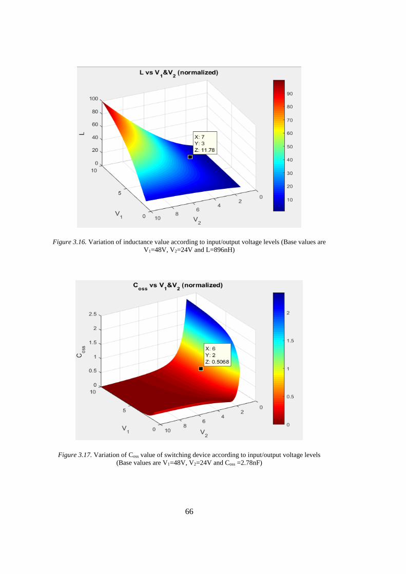
66
Figure 3.16. Variation of inductance value according to input/output voltage levels (Base values are
V1=48V, V2=24V and L=896nH)
Figure 3.17. Variation of Coss value of switching device according to input/output voltage levels
(Base values are V1=48V, V2=24V and Coss =2.78nF)

67
In conclusion, these analyses give an idea for the applicable region of phase shifted
method to selected topology by examining the inductance value and output
capacitance value of switching devices.
Considering the evaluations, calculations and constraints mentioned in this section and
previous sections, detailed description of component selection and design parameters
will be explained at the next stage (Section 3.7).
3.7. Power Stage and Control Design
In this section, from the mentioned analytical expressions and discussions about the
operating principle of the converter until here, a design procedure is derived and
applied. For this purpose, firstly; t3 will be taken as equal to ts for a desired V1, V2 and
maximum power rating which are 56V maximum for V1, 28V maximum for V2 and
500W respectively. Then, the inductance value is going to be calculated from (3.16)
after calculating the value of Io with the selection of switching devices. After that, new
t3 values for different power ratings will be found using (3.16). Finally, t1 and t2 values
are calculated from (3.14) and (3.15) and these values will be tabulated to operate in
case of different load conditions. Furthermore, in order to ensure ZVS operation, half
bridge voltages are also going to be monitored via ADC ports of microcontroller.
3.7.1. Switching Device Selection
The output regulation of a DC/DC converter is achieved by pulse width modulation
of switching devices such as thyristors, BJTs, IGBTs and FETs. Fast development of
silicon semiconductor technology made the latter ones, FETs and IGBTs, become
more dominant than the formers in the market. Although there is not any universal
standard to determine which device is better than the other for an application,
generally; low voltage-high switching frequency applications prefer FETs while high
voltage-low switching frequency applications favor IGBTs. Since the power density

68
is another important criterion for power converters, a higher switching frequency,
greater than that of maximum operating of IGBTs, is selected to decrease the
components’ size. Therefore, it is decided to use FET type switching devices. In the
next subsections, types of FETs; that can be classified according to their production
technology (i.e. Si, SiC or GaN), are compared and evaluated in terms of their basic
parameters which affect the performance of the converter, their sizes, accessibility and
suitability for a prototype board. After the analytical analysis in the next section,
selection of switching device is going to be explained.
3.7.1.1. Switching Device Losses
After deciding switching devices type as FETs, it is required to express the losses
originated from them. In general, power FET losses can be divided into three groups
such that conduction (PCOND), switching (PSW) and gate drive (PGATE) losses. It is
important to note that, synchronous rectifiers (low side switches in a half bridge
configuration) do not have any switching loss part as they are switched with zero
voltage inherently.
Conduction loss is related with both the current and the internal resistance of the
MOSFET. It can be expressed as in (3.44) where RDSon is the on state resistance of the
MOSFET (given at the datasheets by the manufacturers) and Irms is the rms value of
the current directly dependent on the current shape of the inductor which is related
with the switching times as stated in chapter 3.3.2. Furthermore, temperature
dependence of the RDSon should be considered to calculate the exact loss value.
PCond = Irms2 ∗ RDSon (3.44)
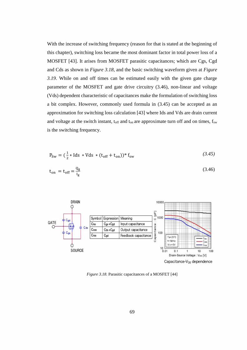
69
With the increase of switching frequency (reason for that is stated at the beginning of
this chapter), switching loss became the most dominant factor in total power loss of a
MOSFET [43]. It arises from MOSFET parasitic capacitances; which are Cgs, Cgd
and Cds as shown in Figure 3.18, and the basic switching waveform given at Figure
3.19. While on and off times can be estimated easily with the given gate charge
parameter of the MOSFET and gate drive circuitry (3.46), non-linear and voltage
(Vds) dependent characteristic of capacitances make the formulation of switching loss
a bit complex. However, commonly used formula in (3.45) can be accepted as an
approximation for switching loss calculation [43] where Ids and Vds are drain current
and voltage at the switch instant, toff and ton are approximate turn off and on times, fsw
is the switching frequency.
PSw = ( 1
2∗ Ids ∗ Vds ∗ (toff + ton))* fsw (3.45)
ton = toff = Qg
Ig (3.46)
Figure 3.18. Parasitic capacitances of a MOSFET [44]
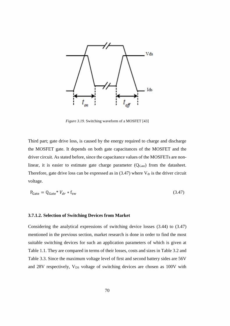
70
Figure 3.19. Switching waveform of a MOSFET [43]
Third part; gate drive loss, is caused by the energy required to charge and discharge
the MOSFET gate. It depends on both gate capacitances of the MOSFET and the
driver circuit. As stated before, since the capacitance values of the MOSFETs are non-
linear, it is easier to estimate gate charge parameter (QGate) from the datasheet.
Therefore, gate drive loss can be expressed as in (3.47) where Vdr is the driver circuit
voltage.
PGate = QGate* 𝑉𝑑𝑟 ∗ fsw (3.47)
3.7.1.2. Selection of Switching Devices from Market
Considering the analytical expressions of switching device losses (3.44) to (3.47)
mentioned in the previous section, market research is done in order to find the most
suitable switching devices for such an application parameters of which is given at
Table 1.1. They are compared in terms of their losses, costs and sizes in Table 3.2 and
Table 3.3. Since the maximum voltage level of first and second battery sides are 56V
and 28V respectively, VDS voltage of switching devices are chosen as 100V with

71
considering the effects of parasitic elements in board layout. After a fast glance in
products of manufacturers, it is seen that SiC is not suitable at these voltage levels.
Hence, silicon and GaN power semiconductors are assigned to be the candidates. By
the help of given loss formulas ((3.44) to (3.47)) in preceding section and the
parameters of devices in their datasheets, expected losses are calculated. It should be
noted that, in the expression of switching loss (3.45), VD is taken as 5V since adaptive
phase shifted operation will ensure zero voltage switching.
As compatible with introduced benefits of GaN devices in literature and Chapter 5,
they (EPC2022) are more efficient than their silicon competitors in even smaller sizes
as can be seen in Table 3.2 and Table 3.3. However, their costs are still higher, and
they are hard to procure since they have fewer manufacturers in the market. On the
other hand, IRFP100P219 is the most efficient one of 3 candidates but the size of this
MOSFET is too large than the others. As a result of these reasons, IRFS4010PbF from
International Rectifier is decided to be used as an optimal solution. This MOSFET is
also compatible with the selected dead time which is 100 ns as stated before (Section
3.5) since its rise and fall times are about 90ns. Furthermore, the output capacitance
value is in the range of zero voltage switching operation calculated section 3.5 (COSS
= 660pF < 1.6nF).
In this study, also a GaN application is implemented and tested in order to observe the
effect of switching device on the performance of the converter. This application is
explained in Chapter 5.
The simulation results, which are done with the parameters of selected MOSFETs,
show VDS voltage values of S1 and S3 at switch instant. It is observed that when gate
commands are applied to switches, their VDS voltages are nearly zero volt satisfying
ZVS operation (Figure 3.20).
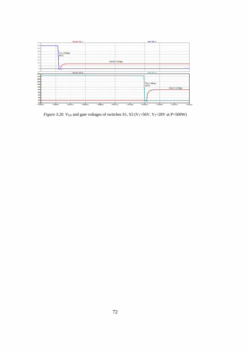
72
Figure 3.20. VDS and gate voltages of switches S1, S3 (V1=56V, V2=28V at P=500W)
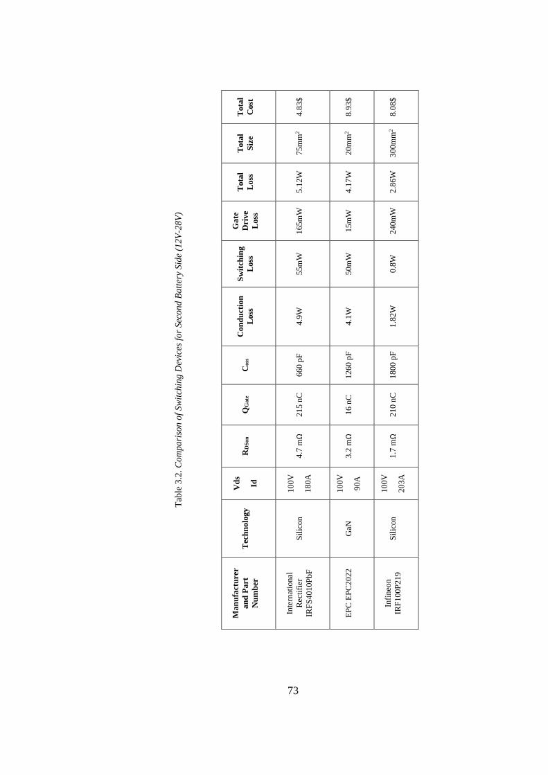
73
Tab
le 3
.2. C
om
pari
son o
f Sw
itch
ing D
evic
es f
or
Sec
ond B
att
ery
Sid
e (1
2V
-28V
)
Tota
l
Co
st
4.8
3$
8.9
3$
8.0
8$
Tota
l
Siz
e
75m
m2
20m
m2
300m
m2
Tota
l
Loss
5.1
2W
4.1
7W
2.8
6W
Gate
Dri
ve
Loss
165m
W
15m
W
240m
W
Sw
itch
ing
Loss
55m
W
50m
W
0.8
W
Co
nd
uct
ion
Loss
4.9
W
4.1
W
1.8
2W
Coss
660 p
F
1260 p
F
1800 p
F
QG
ate
215 n
C
16 n
C
210 n
C
RD
Son
4.7
mΩ
3.2
mΩ
1.7
mΩ
Vd
s
Id
100V
180A
100V
90A
100V
203A
Tec
hn
olo
gy
Sil
icon
GaN
Sil
icon
Ma
nu
fact
ure
r
an
d P
art
Nu
mb
er
Inte
rnat
ion
al
Rec
tifi
er
IRF
S4
010
Pb
F
EP
C E
PC
20
22
Infi
neo
n
IRF
10
0P
21
9

74
Tab
le 3
.3. C
om
pari
son o
f Sw
itch
ing D
evic
es f
or
Fir
st B
att
ery
Sid
e (2
4V
-56
V)
Tota
l
Co
st
4.8
3$
8.9
3$
8.0
8$
Tota
l
Siz
e
75m
m2
20m
m2
300m
m2
Tota
l
Loss
7.8
W
5.7
3W
3.8
4W
Gate
Dri
ve
Loss
165m
W
15m
W
240m
W
Sw
itch
ing
Loss
0.7
5W
68m
W
1.1
W
Co
nd
uct
ion
Loss
6.8
8W
5.6
5W
2.5
W
Coss
660 p
F
1260 p
F
1800 p
F
QG
ate
215 n
C
16 n
C
210 n
C
RD
Son
4.7
mΩ
3.2
mΩ
1.7
mΩ
Vd
s
Id
100V
180A
100V
90A
100V
203A
Tec
hn
olo
gy
Sil
icon
GaN
Sil
icon
Ma
nu
fact
ure
r
an
d P
art
Nu
mb
er
Inte
rnat
ion
al
Rec
tifi
er
IRF
S4
010
Pb
F
EP
C
EP
C2
02
2
Infi
neo
n
IRF
10
0P
21
9

75
3.7.2. Switching Frequency Selection
As mentioned in previous section, switching frequency should be increased in order
to get more power density. That is; converter size will be smaller, and light weighted
as a result of a decrease in the volume of passive components. High frequency
operation also allows the converter to operate with greater bandwidth which increase
its transient response [46]. However, greater switching frequency can make the
converter efficiency decrease with the increase in switching losses formulated at
(3.45) to (3.47). Besides, EMI problems will be tougher which needs more
complicated filter design. Furthermore, maximum applicable frequency is limited by
available switching devices [45].
Therefore, there is a challenge while determining the switching frequency. 100 kHz is
selected as the switching frequency for this study; which is compatible with rise and
fall times of selected switching devices, dead time to be applied and adaptive phase
shifted operation.
3.7.3. Inductor Selection
Inductor is used as an energy storage element in a switching regulator. Selection of it
is another important step of design stage. It effects both loss and ripple performances
of the converter.
An inductance value is obtained according to analytical expressions in section 3.3.2.
As an approach similar to Waffler’s and Kolar’s in [41], t3 is taken as ts which is 10µs
in the formula of (3.16). In the extreme case situation; in which V1 is equal to 56V and
V2 is 28V, equation (3.16) gives an inductance value of 2.44uH. Since maximum
power is expected as 500 W, saturation current of inductor should be greater than 50A
with a permitted current ripple of %40.
Inductor loss mainly consists of copper and core losses which are related to DC and
AC components of the inductor current. Calculation of DC loss is straightforward with

76
the given parameter of RDC (DC resistance of the inductor obtained from the datasheet)
as in equation (3.48). On the other hand, since AC components of an inductor change
with the conditions like frequency or ripple, the latter one is difficult to calculate. In
general, Steinmetz power equation is used to estimate the core loss (3.49) where f is
the frequency, Bpk is peak flux density and K, α and β are the constants given by the
core manufacturers [47].
PDC = Irms2 ∗ RDC (3.48)
PAC = K ∗ fα ∗ Bpkβ
(3.49)
By considering inductance value and loss calculations, IHXL-2000VZ-5A (Vishay)
with 2.2 µH inductance value is chosen as the energy storage device. In simulation
results (Figure 3.21), peak current of inductor is observed as 50A which is below the
saturation current level of selected inductor.
It is also important to note that waveform of inductor current seen in Figure 3.21
exactly match with the theoretically expected one shown in Figure 3.3. Moreover,
peak and valley current values of inductor are found as I0 = -17.9 A, Ip1 = 26.4A and
Ip2 = 52.7A using (3.36) at given operating point which are close to the values in Figure
3.21 verifying the formulation of inductor current ripple given in section 3.4.2.
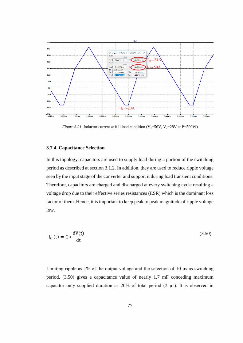
77
Figure 3.21. Inductor current at full load condition (V1=56V, V2=28V at P=500W)
3.7.4. Capacitance Selection
In this topology, capacitors are used to supply load during a portion of the switching
period as described at section 3.1.2. In addition, they are used to reduce ripple voltage
seen by the input stage of the converter and support it during load transient conditions.
Therefore, capacitors are charged and discharged at every switching cycle resulting a
voltage drop due to their effective series resistances (ESR) which is the dominant loss
factor of them. Hence, it is important to keep peak to peak magnitude of ripple voltage
low.
IC (t) = C ∗dV(t)
dt
(3.50)
Limiting ripple as 1% of the output voltage and the selection of 10 µs as switching
period, (3.50) gives a capacitance value of nearly 1.7 mF conceding maximum
capacitor only supplied duration as 20% of total period (2 µs). It is observed in
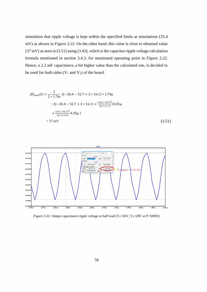
78
simulation that ripple voltage is kept within the specified limits at simulations (35.4
mV) as shown in Figure 3.22. On the other hand, this value is close to obtained value
(37 mV) as seen in (3.51) using (3.43), which is the capacitor ripple voltage calculation
formula mentioned in section 3.4.3, for mentioned operating point in Figure 3.22.
Hence, a 2.2 mF capacitance, a bit higher value than the calculated one, is decided to
be used for both sides (V1 and V2) of the board.
𝛥𝑉Cout(t) =1
2 ∗ 1.7m [(−26.4 − 52.7 + 2 ∗ 16.1) ∗ 1.74µ
−[(−26.4 − 52.7 + 2 ∗ 16.1) +(16.1−52.7)2
52.7+17.9]3.81µ
+(16.1−52.7)2
52.7+17.99.35µ ]
= 37 mV
(3.51)
Figure 3.22. Output capacitance ripple voltage at half load (V1=56V, V2=28V at P=500W)

79
3.7.5. Gate Drive Selection
A gate drive circuit is designed to drive selected switching devices properly. One
common driver is used for high and low side MOSFETs of each half bridge in order
to minimize the difference of propagation delay effect caused by the layout of the
board. Texas Instruments (TI) UCC27211 is selected as it has a maximum boot voltage
of 120V, 4A current sink and source capability and suitable rise/fall times with
selected MOSFETs.
3.7.6. Microcontroller Selection
In order to produce four PWM signals (two of each is complementary) for switching
devices at calculated and tabulated timings (t1 t2, t3 - mentioned in detail in section
3.3.2) for different operating points, a microcontroller is required. TI’s
TMS320F28027 Piccolo series which has four different high resolution PWM
channels (HRPWM) is utilized in the design.
In addition, ADC channels of microcontroller are used to sense input and output
voltage and current values as well as inductor current and voltage in order to protect
the circuit in the case of undesired conditions. Bidirectional current sense IC (INA240
which has 80 V common mode voltage range) is used for bidirectional current sensing
purpose.
Block diagram of the whole design is shown in Figure 3.23. Laboratory prototype
printed circuit board pictures are also given in Figure 3.24 and Figure 3.25.
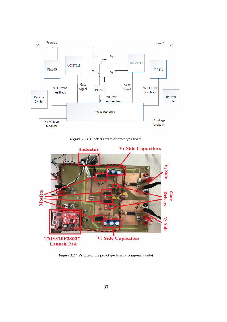
80
Figure 3.23. Block diagram of prototype board
Figure 3.24. Picture of the prototype board (Component side)

81
Figure 3.25. Picture of the prototype board (Solder Side)


83
CHAPTER 4
4. SIMULATION AND TEST RESULTS
Operating principle and design steps of selected converter are described in preceding
section. In this chapter, in order to verify the validity of these analyses and to assess
the performance of the phase shifted method with the conventional one; with respect
to efficiency under different input, output and load conditions, realized simulations
and experimental tests are explained.
As it is mentioned in section 3.3.2, optimized switching times (t1, t2 and t3) depend on
the circuit parameters V1, V2, output power, inductance value and switching frequency
for phase shifted technique. Hence, they are calculated separately with the selected
parameters for corresponding operating condition using (3.14) to (3.16) and embedded
into simulation and the microcontroller of the prototype to decrease the time spent.
The simulations are conducted by using LTSPICE software package from LINEAR
Technologies. Simulations and tests are performed at various operating points
covering the design requirements shown in Table 1.1 using both conventional and
phase shifted methods. In order to compare the methods, one of the variables is held
constant while the others are changeable. Moreover, voltage/current waveforms and
analytical calculations explained in Chapter 3 are verified with the results.
4.1. Test Equipment
TTI CPX400D Dual Power Supply: This device is used to supply the input side of the
converter.
PRODIGIT 3332F Dual DC Electronic Load: This equipment is used to load the
output side of the converter.

84
TEKTRONIX TPS2024B Oscilloscope: It is used to obtain gate and switch node
voltages, inductor current and voltage waveforms. Up to four voltage probes or one
current probe are attached for these purposes.
TEKTRONIX TCP303 Current Clamp: This device is used to get inductor, input and
output current waveforms.
TEKTRONIX TCPA300 Amplifier: It is used to make connection between current
clamp and oscilloscope.
FLUKE 179 Multimeter: This equipment is used to measure levels of input and output
voltages.
4.2. Forward Mode of Operation (Energy Transfer is from V1 to V2)
In this mode of operation, power flow is produced from V1 to V2 by connecting a
power supply to V1 side and an electronic load, which can be set as constant power or
constant current mode, to other side. Output voltage and load are varied to observe
their effect on efficiency; while keeping constant the input voltage, in both phase
shifted and conventional methods for comparison purposes. Tests and simulation
results are combined and shown graphically in order to analyze the effect of these
alterations in detail. In addition, detailed explanations of waveforms and
measurements of buck mode of operation (boost mode is mentioned in the following
section 4.3) is given to verify the operation with theoretical analysis.
4.2.1. Phase Shifted Method for Forward Mode of Operation
For phase shifted method, by changing the output voltage from 28V to 12V at various
load power levels, all switching times (t1, t2 and t3) are calculated and applied to the
circuit correspondingly. In this section; the measurements of simulations and tests
while V2=28V and P=250W (half load) are presented in detail as an example of buck
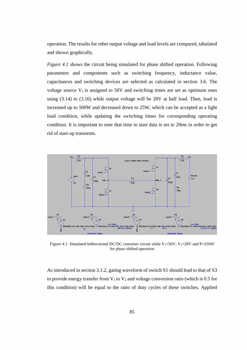
85
operation. The results for other output voltage and load levels are compared, tabulated
and shown graphically.
Figure 4.1 shows the circuit being simulated for phase shifted operation. Following
parameters and components such as switching frequency, inductance value,
capacitances and switching devices are selected as calculated in section 3.6. The
voltage source V1 is assigned to 56V and switching times are set as optimum ones
using (3.14) to (3.16) while output voltage will be 28V at half load. Then, load is
increased up to 500W and decreased down to 25W, which can be accepted as a light
load condition, while updating the switching times for corresponding operating
condition. It is important to note that time to start data is set to 20ms in order to get
rid of start-up transients.
Figure 4.1. Simulated bidirectional DC/DC converter circuit while V1=56V, V2=28V and P=250W
for phase shifted operation
As introduced in section 3.1.2, gating waveform of switch S1 should lead to that of S3
to provide energy transfer from V1 to V2 and voltage conversion ratio (which is 0.5 for
this condition) will be equal to the ratio of duty cycles of these switches. Applied
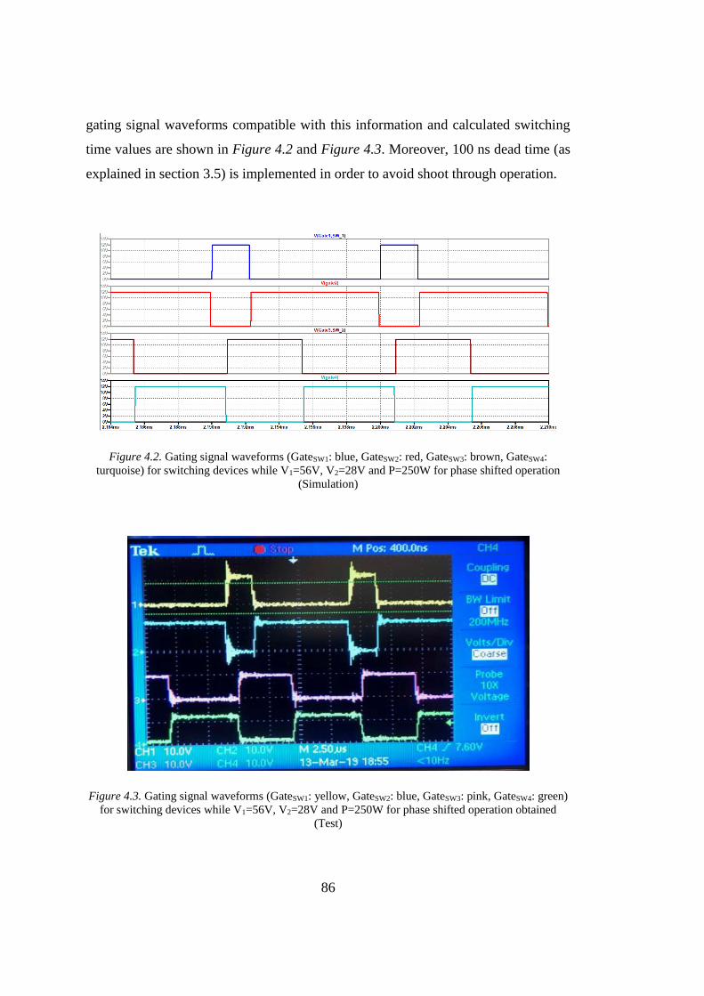
86
gating signal waveforms compatible with this information and calculated switching
time values are shown in Figure 4.2 and Figure 4.3. Moreover, 100 ns dead time (as
explained in section 3.5) is implemented in order to avoid shoot through operation.
Figure 4.2. Gating signal waveforms (GateSW1: blue, GateSW2: red, GateSW3: brown, GateSW4:
turquoise) for switching devices while V1=56V, V2=28V and P=250W for phase shifted operation
(Simulation)
Figure 4.3. Gating signal waveforms (GateSW1: yellow, GateSW2: blue, GateSW3: pink, GateSW4: green)
for switching devices while V1=56V, V2=28V and P=250W for phase shifted operation obtained
(Test)
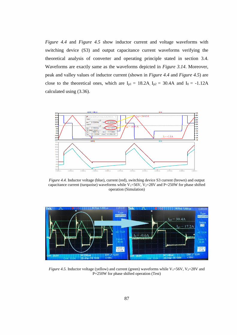
87
Figure 4.4 and Figure 4.5 show inductor current and voltage waveforms with
switching device (S3) and output capacitance current waveforms verifying the
theoretical analysis of converter and operating principle stated in section 3.4.
Waveforms are exactly same as the waveforms depicted in Figure 3.14. Moreover,
peak and valley values of inductor current (shown in Figure 4.4 and Figure 4.5) are
close to the theoretical ones, which are Ip1 = 18.2A, Ip2 = 30.4A and I0 = -1.12A
calculated using (3.36).
Figure 4.4. Inductor voltage (blue), current (red), switching device S3 current (brown) and output
capacitance current (turquoise) waveforms while V1=56V, V2=28V and P=250W for phase shifted
operation (Simulation)
Figure 4.5. Inductor voltage (yellow) and current (green) waveforms while V1=56V, V2=28V and
P=250W for phase shifted operation (Test)

88
All measurements and calculations about inductor current ripple are combined in
Table 4.1. There are slight differences between the measurements which are due to
non-ideal characteristics of inductor and switching devices.
Table 4.1. Measurements of Inductor Current Ripple while V1=56V, V2=28V and P=250W for phase
shifted operation of forward mode
Method Ip1 (A) Ip2 (A) I0 (A)
Analytical 18.20 30.40 -1.12
Simulation 16.31 30.03 -1.10
Measurement 17.20 30.40 -0.60
Figure 4.6 and Figure 4.7 show the measurements; which are taken in order to verify
ZVS operation of switching devices at input and output side (S1 and S3). Waveforms
are exactly match with expected ones that is gate voltages are applied when their drain
source (Vds) voltages are nearly at zero volts. Furthermore, simulation and test results
are consistent with each other.
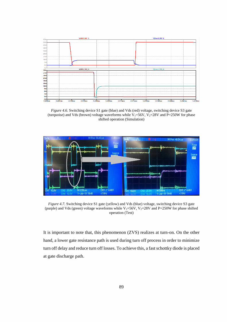
89
Figure 4.6. Switching device S1 gate (blue) and Vds (red) voltage, switching device S3 gate
(turquoise) and Vds (brown) voltage waveforms while V1=56V, V2=28V and P=250W for phase
shifted operation (Simulation)
Figure 4.7. Switching device S1 gate (yellow) and Vds (blue) voltage, switching device S3 gate
(purple) and Vds (green) voltage waveforms while V1=56V, V2=28V and P=250W for phase shifted
operation (Test)
It is important to note that, this phenomenon (ZVS) realizes at turn-on. On the other
hand, a lower gate resistance path is used during turn off process in order to minimize
turn off delay and reduce turn off losses. To achieve this, a fast schottky diode is placed
at gate discharge path.
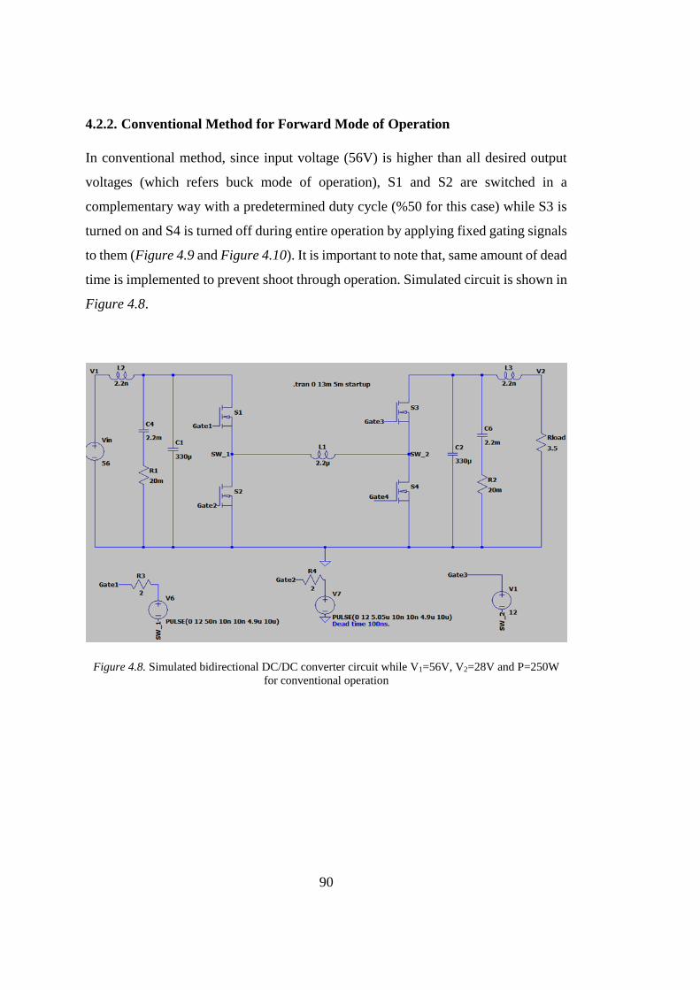
90
4.2.2. Conventional Method for Forward Mode of Operation
In conventional method, since input voltage (56V) is higher than all desired output
voltages (which refers buck mode of operation), S1 and S2 are switched in a
complementary way with a predetermined duty cycle (%50 for this case) while S3 is
turned on and S4 is turned off during entire operation by applying fixed gating signals
to them (Figure 4.9 and Figure 4.10). It is important to note that, same amount of dead
time is implemented to prevent shoot through operation. Simulated circuit is shown in
Figure 4.8.
Figure 4.8. Simulated bidirectional DC/DC converter circuit while V1=56V, V2=28V and P=250W
for conventional operation
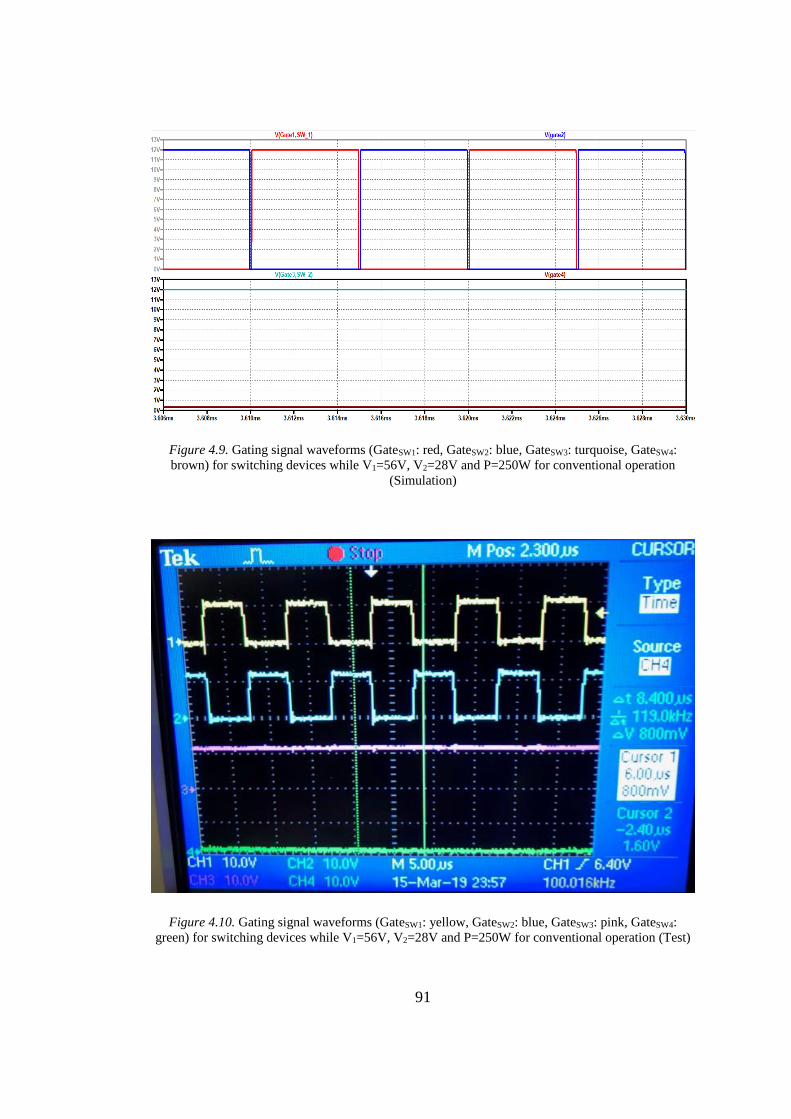
91
Figure 4.9. Gating signal waveforms (GateSW1: red, GateSW2: blue, GateSW3: turquoise, GateSW4:
brown) for switching devices while V1=56V, V2=28V and P=250W for conventional operation
(Simulation)
Figure 4.10. Gating signal waveforms (GateSW1: yellow, GateSW2: blue, GateSW3: pink, GateSW4:
green) for switching devices while V1=56V, V2=28V and P=250W for conventional operation (Test)
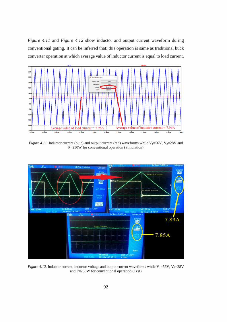
92
Figure 4.11 and Figure 4.12 show inductor and output current waveform during
conventional gating. It can be inferred that; this operation is same as traditional buck
converter operation at which average value of inductor current is equal to load current.
Figure 4.11. Inductor current (blue) and output current (red) waveforms while V1=56V, V2=28V and
P=250W for conventional operation (Simulation)
Figure 4.12. Inductor current, inductor voltage and output current waveforms while V1=56V, V2=28V
and P=250W for conventional operation (Test)
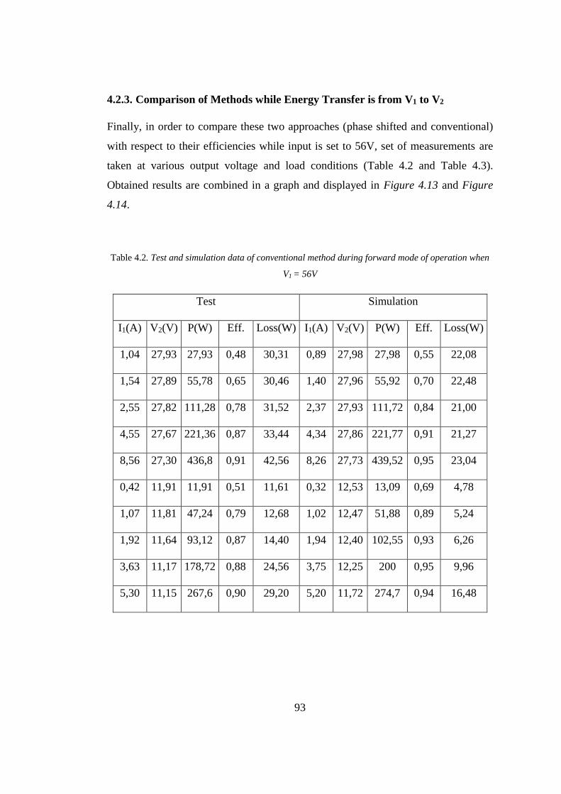
93
4.2.3. Comparison of Methods while Energy Transfer is from V1 to V2
Finally, in order to compare these two approaches (phase shifted and conventional)
with respect to their efficiencies while input is set to 56V, set of measurements are
taken at various output voltage and load conditions (Table 4.2 and Table 4.3).
Obtained results are combined in a graph and displayed in Figure 4.13 and Figure
4.14.
Table 4.2. Test and simulation data of conventional method during forward mode of operation when
V1 = 56V
Test Simulation
I1(A) V2(V) P(W) Eff. Loss(W) I1(A) V2(V) P(W) Eff. Loss(W)
1,04 27,93 27,93 0,48 30,31 0,89 27,98 27,98 0,55 22,08
1,54 27,89 55,78 0,65 30,46 1,40 27,96 55,92 0,70 22,48
2,55 27,82 111,28 0,78 31,52 2,37 27,93 111,72 0,84 21,00
4,55 27,67 221,36 0,87 33,44 4,34 27,86 221,77 0,91 21,27
8,56 27,30 436,8 0,91 42,56 8,26 27,73 439,52 0,95 23,04
0,42 11,91 11,91 0,51 11,61 0,32 12,53 13,09 0,69 4,78
1,07 11,81 47,24 0,79 12,68 1,02 12,47 51,88 0,89 5,24
1,92 11,64 93,12 0,87 14,40 1,94 12,40 102,55 0,93 6,26
3,63 11,17 178,72 0,88 24,56 3,75 12,25 200 0,95 9,96
5,30 11,15 267,6 0,90 29,20 5,20 11,72 274,7 0,94 16,48

94
Table 4.3. Test and simulation data of phase shifted method during forward mode of operation when
V1 = 56V
Test Simulation
I1(A) V2(V) P(W) Eff. Loss(W) I1(A) V2(V) P(W) Eff. Loss(W)
0,51 26,24 26,24 0,92 2,32 0,59 29,73 31,51 0,92 1,75
1,04 26,92 53,84 0,92 4,40 1 27,6 54,37 0,95 1,63
2,14 27,52 110,08 0,92 9,76 2,1 28,1 112,8 0,95 4,8
4,20 27,10 216,8 0,92 18,40 4,2 28,22 227,5 0,96 7,75
8,40 26,89 430,24 0,91 40,16 8,4 28,04 449,3 0,95 21,06
0,28 12,11 12,11 0,77 3,57 0,28 13,08 14,26 0,86 1,31
0,88 10,83 43,32 0,88 5,96 0,98 12,62 53,05 0,95 1,83
1,83 11,24 89,92 0,88 12,56 1,94 12,42 102,8 0,94 5,63
3,56 11,20 179,2 0,90 20,16 3,35 11,55 178,5 0,95 9,15
5,34 11,16 268 0,90 31,2 4,91 11,35 258,4 0,94 16,74
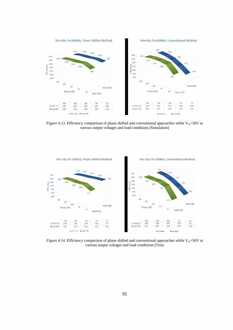
95
Figure 4.13. Efficiency comparison of phase shifted and conventional approaches while Vin=56V at
various output voltages and load conditions (Simulation)
Figure 4.14. Efficiency comparison of phase shifted and conventional approaches while Vin=56V at
various output voltages and load conditions (Test)
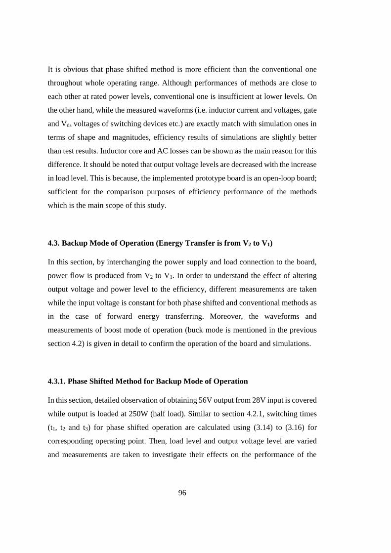
96
It is obvious that phase shifted method is more efficient than the conventional one
throughout whole operating range. Although performances of methods are close to
each other at rated power levels, conventional one is insufficient at lower levels. On
the other hand, while the measured waveforms (i.e. inductor current and voltages, gate
and Vds voltages of switching devices etc.) are exactly match with simulation ones in
terms of shape and magnitudes, efficiency results of simulations are slightly better
than test results. Inductor core and AC losses can be shown as the main reason for this
difference. It should be noted that output voltage levels are decreased with the increase
in load level. This is because, the implemented prototype board is an open-loop board;
sufficient for the comparison purposes of efficiency performance of the methods
which is the main scope of this study.
4.3. Backup Mode of Operation (Energy Transfer is from V2 to V1)
In this section, by interchanging the power supply and load connection to the board,
power flow is produced from V2 to V1. In order to understand the effect of altering
output voltage and power level to the efficiency, different measurements are taken
while the input voltage is constant for both phase shifted and conventional methods as
in the case of forward energy transferring. Moreover, the waveforms and
measurements of boost mode of operation (buck mode is mentioned in the previous
section 4.2) is given in detail to confirm the operation of the board and simulations.
4.3.1. Phase Shifted Method for Backup Mode of Operation
In this section, detailed observation of obtaining 56V output from 28V input is covered
while output is loaded at 250W (half load). Similar to section 4.2.1, switching times
(t1, t2 and t3) for phase shifted operation are calculated using (3.14) to (3.16) for
corresponding operating point. Then, load level and output voltage level are varied
and measurements are taken to investigate their effects on the performance of the
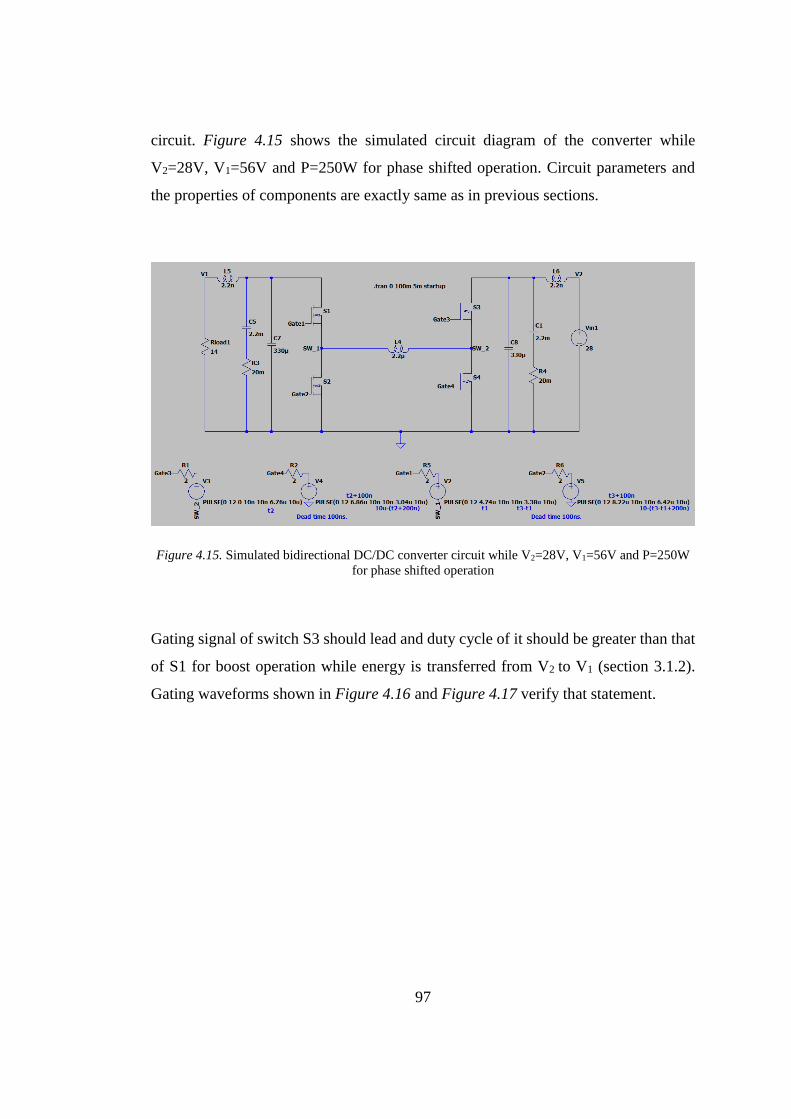
97
circuit. Figure 4.15 shows the simulated circuit diagram of the converter while
V2=28V, V1=56V and P=250W for phase shifted operation. Circuit parameters and
the properties of components are exactly same as in previous sections.
Figure 4.15. Simulated bidirectional DC/DC converter circuit while V2=28V, V1=56V and P=250W
for phase shifted operation
Gating signal of switch S3 should lead and duty cycle of it should be greater than that
of S1 for boost operation while energy is transferred from V2 to V1 (section 3.1.2).
Gating waveforms shown in Figure 4.16 and Figure 4.17 verify that statement.
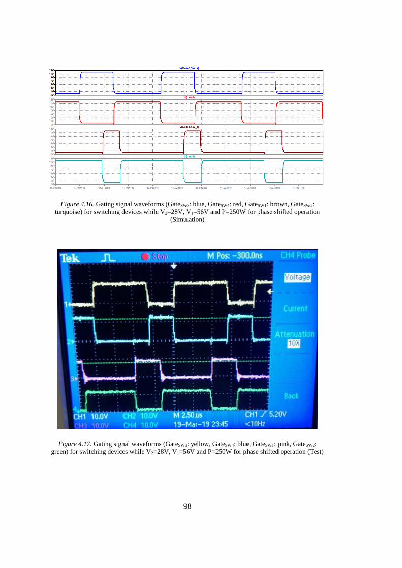
98
Figure 4.16. Gating signal waveforms (GateSW3: blue, GateSW4: red, GateSW1: brown, GateSW2:
turquoise) for switching devices while V2=28V, V1=56V and P=250W for phase shifted operation
(Simulation)
Figure 4.17. Gating signal waveforms (GateSW3: yellow, GateSW4: blue, GateSW1: pink, GateSW2:
green) for switching devices while V2=28V, V1=56V and P=250W for phase shifted operation (Test)
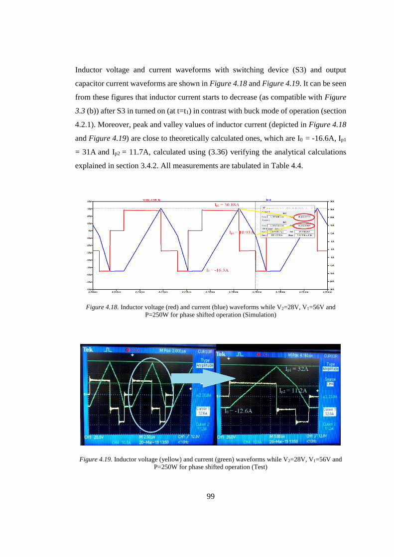
99
Inductor voltage and current waveforms with switching device (S3) and output
capacitor current waveforms are shown in Figure 4.18 and Figure 4.19. It can be seen
from these figures that inductor current starts to decrease (as compatible with Figure
3.3 (b)) after S3 in turned on (at t=t1) in contrast with buck mode of operation (section
4.2.1). Moreover, peak and valley values of inductor current (depicted in Figure 4.18
and Figure 4.19) are close to theoretically calculated ones, which are I0 = -16.6A, Ip1
= 31A and Ip2 = 11.7A, calculated using (3.36) verifying the analytical calculations
explained in section 3.4.2. All measurements are tabulated in Table 4.4.
Figure 4.18. Inductor voltage (red) and current (blue) waveforms while V2=28V, V1=56V and
P=250W for phase shifted operation (Simulation)
Figure 4.19. Inductor voltage (yellow) and current (green) waveforms while V2=28V, V1=56V and
P=250W for phase shifted operation (Test)
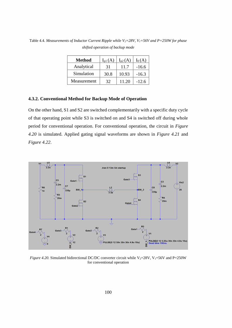
100
Table 4.4. Measurements of Inductor Current Ripple while V2=28V, V1=56V and P=250W for phase
shifted operation of backup mode
Method Ip1 (A) Ip2 (A) I0 (A)
Analytical 31 11.7 -16.6
Simulation 30.8 10.93 -16.3
Measurement 32 11.20 -12.6
4.3.2. Conventional Method for Backup Mode of Operation
On the other hand, S1 and S2 are switched complementarily with a specific duty cycle
of that operating point while S3 is switched on and S4 is switched off during whole
period for conventional operation. For conventional operation, the circuit in Figure
4.20 is simulated. Applied gating signal waveforms are shown in Figure 4.21 and
Figure 4.22.
Figure 4.20. Simulated bidirectional DC/DC converter circuit while V2=28V, V1=56V and P=250W
for conventional operation
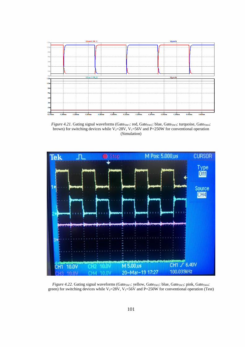
101
Figure 4.21. Gating signal waveforms (GateSW1: red, GateSW2: blue, GateSW3: turquoise, GateSW4:
brown) for switching devices while V2=28V, V1=56V and P=250W for conventional operation
(Simulation)
Figure 4.22. Gating signal waveforms (GateSW1: yellow, GateSW2: blue, GateSW3: pink, GateSW4:
green) for switching devices while V2=28V, V1=56V and P=250W for conventional operation (Test)
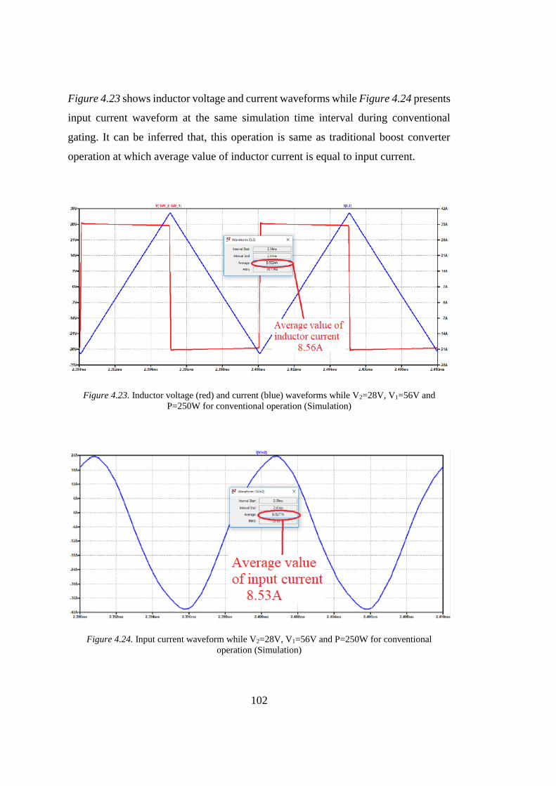
102
Figure 4.23 shows inductor voltage and current waveforms while Figure 4.24 presents
input current waveform at the same simulation time interval during conventional
gating. It can be inferred that, this operation is same as traditional boost converter
operation at which average value of inductor current is equal to input current.
Figure 4.23. Inductor voltage (red) and current (blue) waveforms while V2=28V, V1=56V and
P=250W for conventional operation (Simulation)
Figure 4.24. Input current waveform while V2=28V, V1=56V and P=250W for conventional
operation (Simulation)
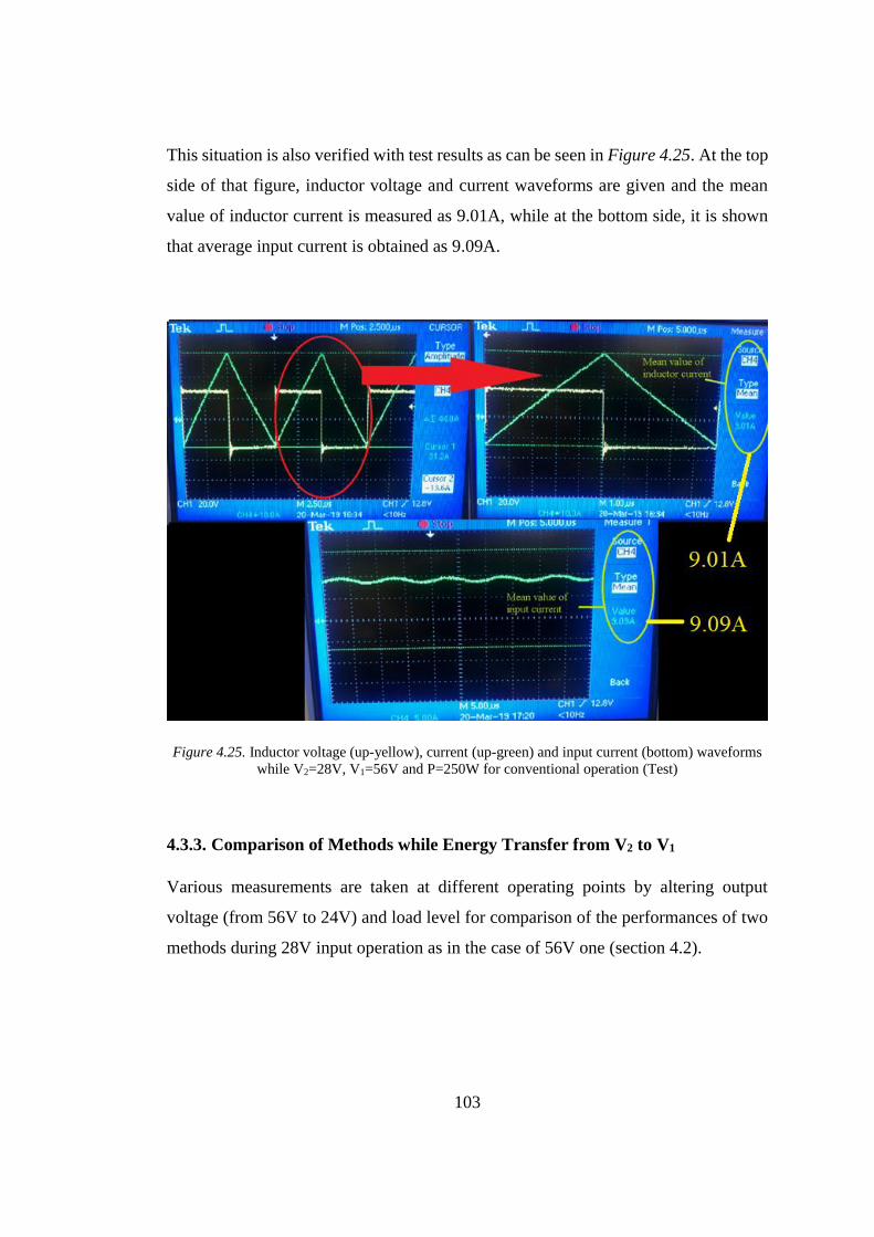
103
This situation is also verified with test results as can be seen in Figure 4.25. At the top
side of that figure, inductor voltage and current waveforms are given and the mean
value of inductor current is measured as 9.01A, while at the bottom side, it is shown
that average input current is obtained as 9.09A.
Figure 4.25. Inductor voltage (up-yellow), current (up-green) and input current (bottom) waveforms
while V2=28V, V1=56V and P=250W for conventional operation (Test)
4.3.3. Comparison of Methods while Energy Transfer from V2 to V1
Various measurements are taken at different operating points by altering output
voltage (from 56V to 24V) and load level for comparison of the performances of two
methods during 28V input operation as in the case of 56V one (section 4.2).

104
Table 4.5. Test and simulation data of conventional method during backward mode of operation when
V2 = 28V
Test Simulation
I2(A) V1(V) P(W) Eff. Loss(W) I2(A) V1(V) P(W) Eff. Loss(W)
1,58 56,20 28,10 0,64 16.14 1,31 55,92 27,9 0,74 8,78
3,07 55,76 55,76 0,65 30.2 2,3 55,88 55,71 0,85 8,69
5,09 55,57 111,14 0,78 31.38 4,27 55,82 111,08 0,92 8,59
9,08 55,18 220,72 0,87 33.52 8,21 55,69 221,65 0,96 8,12
13,10 54,74 328,44 0,90 38.36 12,18 55,56 331,9 0,97 9,14
0,97 23,70 23,70 0,87 3.46 0,92 24,06 24,06 0,90 1,62
1,85 23,62 47,24 0,91 4.56 1,77 24,04 48,09 0,95 1,58
3,67 23,45 93,80 0,91 8.96 3,49 24,00 95,99 0,97 1,59
7,10 23,20 185,6 0,93 13.2 6,93 23,79 188,65 0,97 5,39
14,15 22,84 365,44 0,92 30.76 13,7 23,66 373,12 0,97 10,48
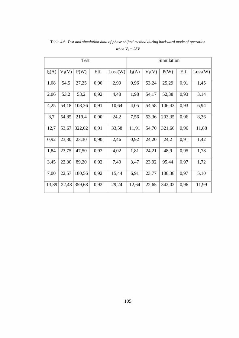
105
Table 4.6. Test and simulation data of phase shifted method during backward mode of operation
when V2 = 28V
Test Simulation
I2(A) V1(V) P(W) Eff. Loss(W) I2(A) V1(V) P(W) Eff. Loss(W)
1,08 54,5 27,25 0,90 2,99 0,96 53,24 25,29 0,91 1,45
2,06 53,2 53,2 0,92 4,48 1,98 54,17 52,38 0,93 3,14
4,25 54,18 108,36 0,91 10,64 4,05 54,58 106,43 0,93 6,94
8,7 54,85 219,4 0,90 24,2 7,56 53,36 203,35 0,96 8,36
12,7 53,67 322,02 0,91 33,58 11,91 54,70 321,66 0,96 11,88
0,92 23,30 23,30 0,90 2,46 0,92 24,20 24,2 0,91 1,42
1,84 23,75 47,50 0,92 4,02 1,81 24,21 48,9 0,95 1,78
3,45 22,30 89,20 0,92 7,40 3,47 23,92 95,44 0,97 1,72
7,00 22,57 180,56 0,92 15,44 6,91 23,77 188,38 0,97 5,10
13,89 22,48 359,68 0,92 29,24 12,64 22,65 342,02 0,96 11,99
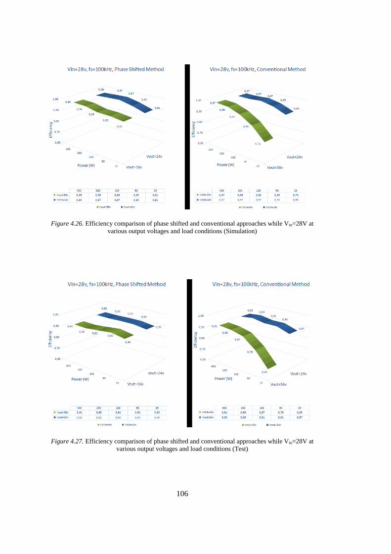
106
Figure 4.26. Efficiency comparison of phase shifted and conventional approaches while Vin=28V at
various output voltages and load conditions (Simulation)
Figure 4.27. Efficiency comparison of phase shifted and conventional approaches while Vin=28V at
various output voltages and load conditions (Test)

107
The results (Figure 4.26, Figure 4.27, Table 4.5 and Table 4.6) show that phase shifted
method is much more efficient than the conventional one regardless of the mode of
operation or direction of energy transfer, i.e. at both buck mode from V1 to V2 (section
4.2) and boost mode from V2 to V1 (section 4.3). Their performances are again close
to each other at rated power levels but phase shifted one surpasses the other especially
at light loads. It is also important to note that conventional method operates more
efficient than the other conditions when input and output voltage levels are close to
each other (for example 28V to 24V conversion results of which can be seen in Table
4.5 and Table 4.6). This is because, even conventional method can achieve zero
voltage switching in the case of lower operating voltages. In other words, sufficient
energy in order to charge or discharge the output capacitances of switching devices
can be stored by the inductor at these voltage and current levels (section 3.3.1).

109
CHAPTER 5
5. GAN DEVICE APPLICATION
Nowadays, with the advance in production process of semiconductors, wide bandgap
devices (WBGs) such as silicon carbide (SiC) and gallium nitride (GaN) replace
silicon (Si) ones by having superior material properties. The term “wide band-gap”
means that their crystal bonds are stronger, and more energy is required to make an
electron cross the band gap compared to the situation at silicon devices [12]. This
higher energy decreases the intrinsic carrier concentration and since leakage current
is proportional with this concentration, wide band gap devices have very smaller
leakage current than the silicon ones [12]. High band gap energy also makes the
material to be preferred for high temperature operation [10]. Moreover, this energy
results in higher breakdown voltage proportional to the critical electric field
breakdown (Ecrt) of the device which is necessary to produce carrier avalanche at the
junction [11]. Equation (5.1) points out that semiconductors having high critical field
breakdown have less on resistance [12], concluding lower conduction losses; where µ
refers to electron mobility. Table 5.1 shows various material properties of silicon and
wide bandgap devices [12].
Ron ∝1
µ×Ecrt3 (5.1)
Furthermore, wide bandgap devices have much smaller gate charge and parasitic
input/output capacitance that enables the designers increase the switching frequency
and have extended zero voltage switching range resulting in a decrease of gate drive
and switching losses.

110
Table 5.1. Material Properties of Si, SiC and GaN
Material Property Si SiC GaN
Band-gap Energy (ev) Eg 1.12 3.25 3.44
Critical Electric Breakdown (MV/cm) Ecrt 0.23 2.2 3.3
Intrinsic Carrier Concentration (cm-3) ni 1.4*1010 8.2*10-9 1.9*10-10
Electron mobility (cm2/Vs) µ 1400 950 1500
Thermal Conductivity (W/cmK) λ 1.5 3.8 1.3
To sum up, wide bandgap devices have high frequency and high temperature
operation, lower on resistance, lower gate and output charge as can be seen in
comparison tables (Table 3.2 and Table 3.3). These properties contribute to improve
the efficiency of a power supply in terms of switching and conduction losses.
Moreover, high frequency operation will make the passive components of supply and
their cooling requirements smaller, concluding the supply more compact. For
example, a 10 MHz zero voltage switched non-inverting buck-boost converter is
designed in [13] with a power density of 6.25W/cm3. Its efficiency is almost %95
with the usage of a GaN power transistor.
On the other hand, although wide bandgap have superior performance that directly
affects the efficiency of the converter, they also bring serious difficulties such as they
are more sensitive to layout, cause worse electromagnetic interference due to fast
switching and more stress (high overvoltage) on the components as a result of the
parasitic inductance [13]. Furthermore, as they do not have intrinsic body diodes,
forward voltage drop during reverse conduction will be higher [49]. Hence, dead time
should be minimized to reduce undesirable losses. Additionally, they are still more
expensive and less in number at the market than their silicon competitors which makes
the designer to think twice.
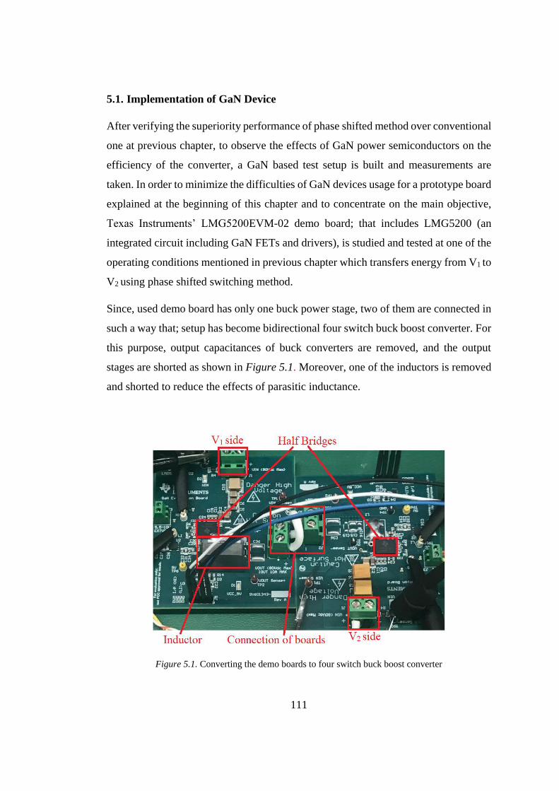
111
5.1. Implementation of GaN Device
After verifying the superiority performance of phase shifted method over conventional
one at previous chapter, to observe the effects of GaN power semiconductors on the
efficiency of the converter, a GaN based test setup is built and measurements are
taken. In order to minimize the difficulties of GaN devices usage for a prototype board
explained at the beginning of this chapter and to concentrate on the main objective,
Texas Instruments’ LMG5200EVM-02 demo board; that includes LMG5200 (an
integrated circuit including GaN FETs and drivers), is studied and tested at one of the
operating conditions mentioned in previous chapter which transfers energy from V1 to
V2 using phase shifted switching method.
Since, used demo board has only one buck power stage, two of them are connected in
such a way that; setup has become bidirectional four switch buck boost converter. For
this purpose, output capacitances of buck converters are removed, and the output
stages are shorted as shown in Figure 5.1. Moreover, one of the inductors is removed
and shorted to reduce the effects of parasitic inductance.
Figure 5.1. Converting the demo boards to four switch buck boost converter

112
Figure 5.2. Whole setup for GaN tests
5.2. Phase Shifted Method with GaN Based Converter
Firstly, operating principles of phase shifted method is verified as in the case of
MOSFET based converter in section 4.2.
Switching frequency and dead time are selected as 1MHz and 10ns respectively;
which are compatible with rise and fall times of GaNFETs used in demo boards, as
introduced in section 3.5 and 3.6. Required inductance value is calculated again using
equation (3.16) with these new parameters as 220nH and is replaced with the
remaining inductor on the demo board. Furthermore, timings for each operating point
are calculated as in the case of previous situation (using (3.14) to (3.16)) and
embedded into the software in the same microcontroller. Whole test setup is shown in
Figure 5.2. Again, as introduced in section 3.1.2, gating waveform of switch S1 should
lead to that of S3 to provide energy transfer from V1 to V2 and voltage conversion
ratio (which is 0.5 for this condition) will be equal to the ratio of duty cycles of these
switches. Gating signal waveforms of switches are shown in Figure 5.3.
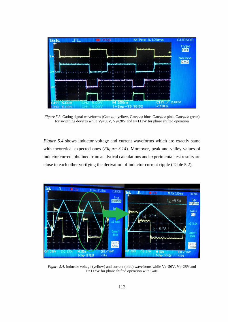
113
Figure 5.3. Gating signal waveforms (GateSW1: yellow, GateSW2: blue, GateSW3: pink, GateSW4: green)
for switching devices while V1=56V, V2=28V and P=112W for phase shifted operation
Figure 5.4 shows inductor voltage and current waveforms which are exactly same
with theoretical expected ones (Figure 3.14). Moreover, peak and valley values of
inductor current obtained from analytical calculations and experimental test results are
close to each other verifying the derivation of inductor current ripple (Table 5.2).
Figure 5.4. Inductor voltage (yellow) and current (blue) waveforms while V1=56V, V2=28V and
P=112W for phase shifted operation with GaN

114
Table 5.2. Measurements of Inductor Current Ripple while V1=56V, V2=28V and P=250W for phase
shifted operation of forward mode with GaN
Method Ip1 (A) Ip2 (A) I0 (A)
Analytical 9.54 5.62 -0.9
Measurement 9.5 5.5 -0.7
5.3. Comparison of Test Results of GaN and MOSFET Based Converters
After verifying operating principle of the GaN based converter, tests are performed
while power is transferred from V1 to V2 at different load levels when V1 is equal to
56V and V2 is 28V that is the same case in section 4.2 for comparison with MOSFET
based one in terms of their efficiency values. It is important to note that, since used
GaN devices have a maximum current rating of 10 amps, tests can be realized up to
210 watts. Test data and comparison of these results and their comparison are
presented in Table 5.3 and Figure 5.5 respectively.
Table 5.3. Test data of GaN and MOSFET based converters during forward mode of operation when
V1 = 56V using phase shifted method
GaNFET Tests MOSFET Tests
I1(A) V2(V) P(W) Eff. Loss(W) I1(A) V2(V) P(W) Eff. Loss(W)
0,53 27,88 27,88 0,94 1,80 0,51 26,24 26,24 0,92 2,32
1,04 27,78 55,56 0,95 2,68 1,04 26,92 53,84 0,92 4,40
2,02 27,06 108,24 0,96 4,88 2,14 27,52 110,08 0,92 9,76
3,00 26,50 159,0 0,95 9,00 3,15 27,10 162,6 0,92 13,8
3,96 26,20 209,6 0,95 12,16 4,20 27,10 216,8 0,92 18,4

115
Figure 5.5. Efficiency comparison of GaN and MOSFET based four switch buck boost converter
during forward mode of operation when V1 = 56V using phase shifted method
5.4. Evaluation of the Test Results of Si and GaN Applications
As can be seen from the measurements (Table 5.3) and comparison graph (Figure 5.5),
approximately 3% efficiency improvement is obtained using GaN devices which
support the analytical analysis done in switching device selection section. In addition,
since switching frequency is increased up to ten times, values and sizes of components
are reduced significantly.
5.5. Effects of Switching Frequency on Losses
As the end for this chapter, some measurements are taken to observe the influence of
the switching frequency on the efficiency of the converter. For this purpose, both
setups in sections 4.2 (Si) and 5.1 (GaN) are tested again by changing the frequency
at the same operating condition that is while energy is transferred from V1 to V2 at 110
watts loads with phase shifted method.
Table 5.4 and Figure 5.6 show the variation of total loss for Si based setup while Table
5.5 and Figure 5.7 are for GaN. It can be inferred from these data that, increasing

116
switching frequency reduces the amount of loss in the converter which verifies the
switching losses are not the dominant portion of total losses. This also supports the
calculations of design parameters such as determining switching times, dead time and
frequency which are done during the design stage. On the other hand, since inductor
ripple current and capacitor ripple voltage decreases with higher switching
frequencies, core loss of inductor and AC loss components of both will decrease which
can be shown as the main reason for the reduction of losses. It should also be noted
that, further increase of switching frequency can deteriorate the operation of the
converter as it will shorten the dead time between complementary switches. If the dead
time gets a value smaller than the rise and fall times of the switching devices, shoot
through operation realizes and the board will be damaged due to high currents passing
through switches.
Table 5.4. Measurements at various switching frequencies for MOSFET based setup
fsw (kHz) 50 100 150
V1 (V) 56,00 56,00 56,00
I1 (A) 2,15 2,14 2,11
V2 (V) 27,38 27,52 27,07
I2 (A) 4,00 4,00 4,00
P (W) 109,52 110,08 108,28
Efficiency 0,91 0,92 0,92
Total Loss (W) 10,88 9,76 9,88
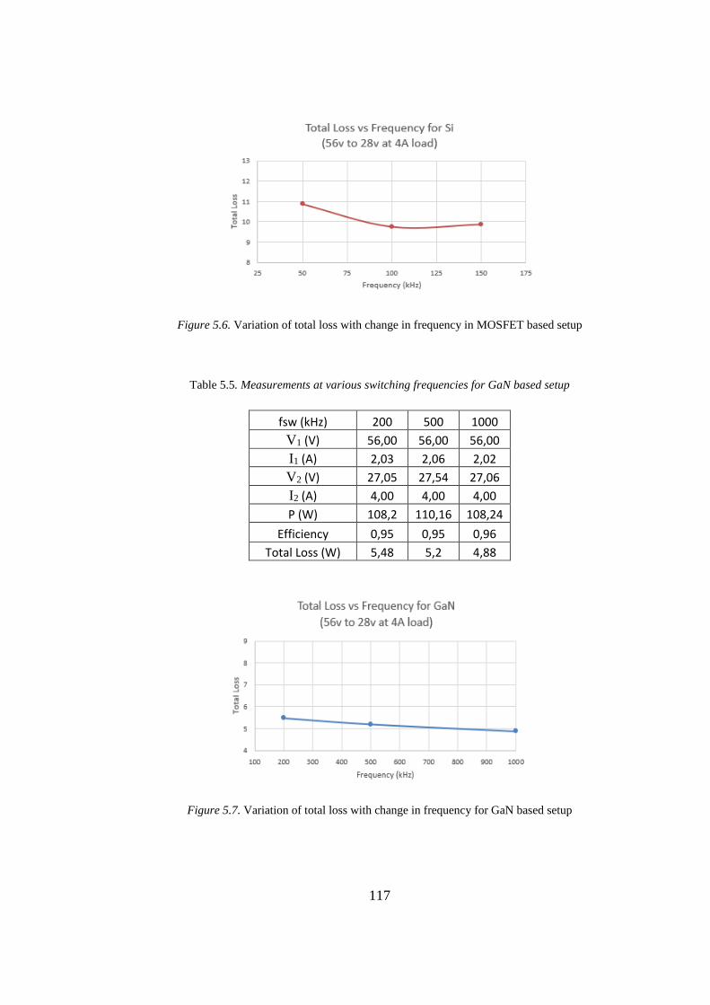
117
Figure 5.6. Variation of total loss with change in frequency in MOSFET based setup
Table 5.5. Measurements at various switching frequencies for GaN based setup
fsw (kHz) 200 500 1000
V1 (V) 56,00 56,00 56,00
I1 (A) 2,03 2,06 2,02
V2 (V) 27,05 27,54 27,06
I2 (A) 4,00 4,00 4,00
P (W) 108,2 110,16 108,24
Efficiency 0,95 0,95 0,96
Total Loss (W) 5,48 5,2 4,88
Figure 5.7. Variation of total loss with change in frequency for GaN based setup
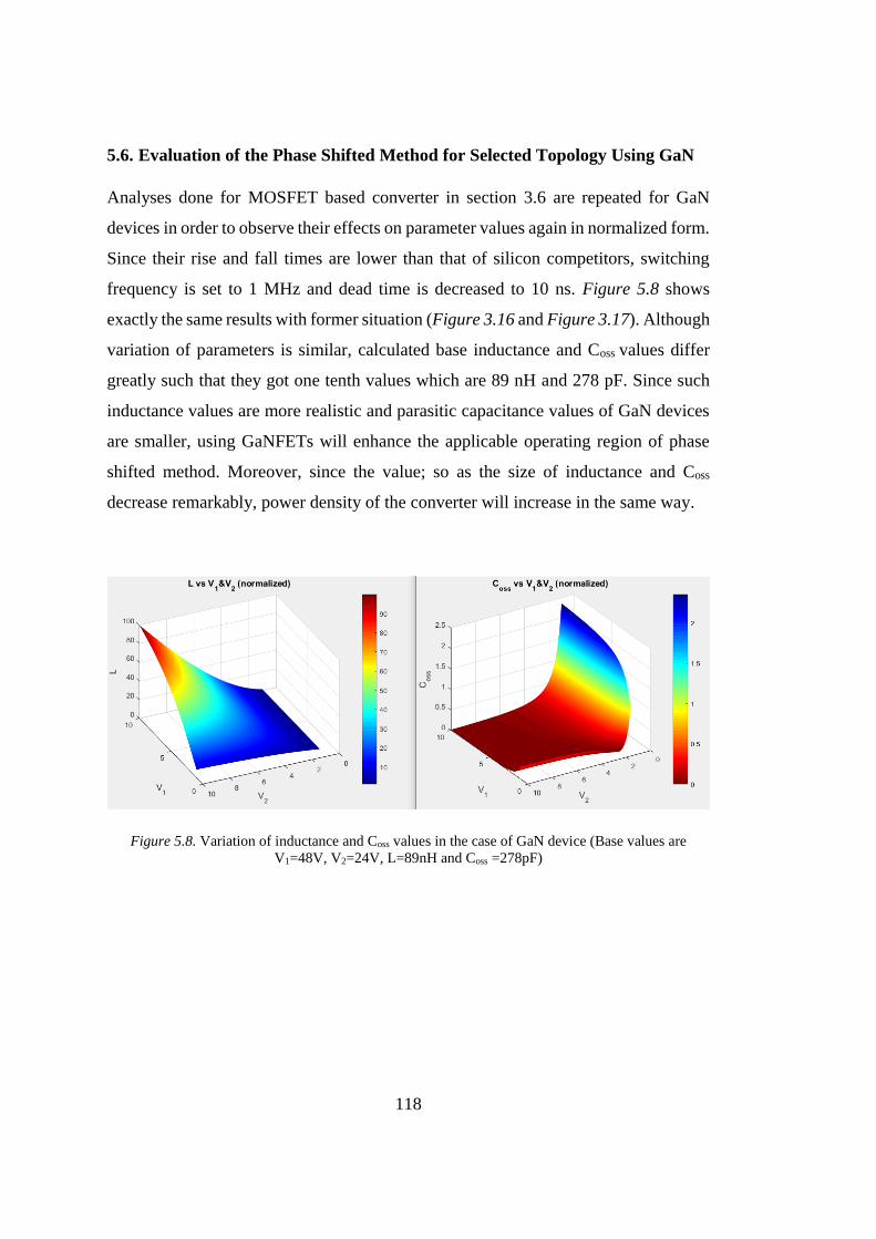
118
5.6. Evaluation of the Phase Shifted Method for Selected Topology Using GaN
Analyses done for MOSFET based converter in section 3.6 are repeated for GaN
devices in order to observe their effects on parameter values again in normalized form.
Since their rise and fall times are lower than that of silicon competitors, switching
frequency is set to 1 MHz and dead time is decreased to 10 ns. Figure 5.8 shows
exactly the same results with former situation (Figure 3.16 and Figure 3.17). Although
variation of parameters is similar, calculated base inductance and Coss values differ
greatly such that they got one tenth values which are 89 nH and 278 pF. Since such
inductance values are more realistic and parasitic capacitance values of GaN devices
are smaller, using GaNFETs will enhance the applicable operating region of phase
shifted method. Moreover, since the value; so as the size of inductance and Coss
decrease remarkably, power density of the converter will increase in the same way.
Figure 5.8. Variation of inductance and Coss values in the case of GaN device (Base values are
V1=48V, V2=24V, L=89nH and Coss =278pF)

119
CHAPTER 6
6. CONCLUSION AND FUTURE WORK
6.1. Conclusion
In this study, it is aimed to design and implement a DC/DC converter which is capable
of bidirectional energy transfer. Firstly, the importance and need for bidirectional
power flow in different application areas; in which storage of electrical energy is
required due to source deficiency or fluctuation, are mentioned in Chapter 1.
Although this kind of power transfer can be achieved with two separate power stages,
it is important to solve this problem with a compact solution; that can be operated for
both forward and backward mode when it is necessary, where the size of the total
system is critical. Topologies in the literature are examined, classified and compared
according to their size, cost, efficiency values and ease of implementation in Chapter
2. They are categorized into two main groups regarding their possessing galvanic
isolation between input and output. Then, they are evaluated according to ability to
reduce or boost the input voltage. Table 2.1 and Table 2.2 are given as a summary of
this chapter.
In Chapter 3, highlighting the reasons for the decision, one of the topologies
mentioned in previous chapter; which is four switch buck-boost converter, is selected
for the application described in Chapter 1. Two different modulation techniques to this
topology namely conventional and phase shifted operation are clarified. Detailed
operating principle with the circuit analysis of each time interval in a switching period
is given in this chapter to understand the whole operation. Voltage and current
waveforms of components at these intervals are presented. Moreover, switching
techniques to improve the efficiency of the converter are covered. Mathematical
analysis (input output voltage conversion ratio, inductor current or capacitor voltage
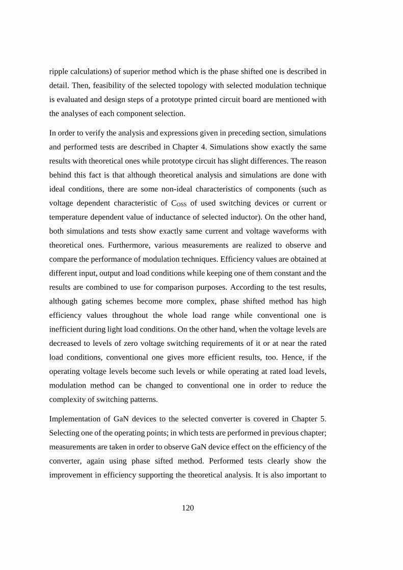
120
ripple calculations) of superior method which is the phase shifted one is described in
detail. Then, feasibility of the selected topology with selected modulation technique
is evaluated and design steps of a prototype printed circuit board are mentioned with
the analyses of each component selection.
In order to verify the analysis and expressions given in preceding section, simulations
and performed tests are described in Chapter 4. Simulations show exactly the same
results with theoretical ones while prototype circuit has slight differences. The reason
behind this fact is that although theoretical analysis and simulations are done with
ideal conditions, there are some non-ideal characteristics of components (such as
voltage dependent characteristic of COSS of used switching devices or current or
temperature dependent value of inductance of selected inductor). On the other hand,
both simulations and tests show exactly same current and voltage waveforms with
theoretical ones. Furthermore, various measurements are realized to observe and
compare the performance of modulation techniques. Efficiency values are obtained at
different input, output and load conditions while keeping one of them constant and the
results are combined to use for comparison purposes. According to the test results,
although gating schemes become more complex, phase shifted method has high
efficiency values throughout the whole load range while conventional one is
inefficient during light load conditions. On the other hand, when the voltage levels are
decreased to levels of zero voltage switching requirements of it or at near the rated
load conditions, conventional one gives more efficient results, too. Hence, if the
operating voltage levels become such levels or while operating at rated load levels,
modulation method can be changed to conventional one in order to reduce the
complexity of switching patterns.
Implementation of GaN devices to the selected converter is covered in Chapter 5.
Selecting one of the operating points; in which tests are performed in previous chapter;
measurements are taken in order to observe GaN device effect on the efficiency of the
converter, again using phase sifted method. Performed tests clearly show the
improvement in efficiency supporting the theoretical analysis. It is also important to

121
say that, as the switching frequency is increased greatly with GaN implementation,
especially total size of the passive components of the converter is reduced
dramatically. That increase in efficiency and decrease in size of the components will
enhance the power density of whole system including such a converter with a
reduction in cooling requirements and so on total cost. However, limitations of the
components, design and the topology; such as rise and fall times of switching devices
or dead time which is expressed in (3.2), should also be considered carefully as a
tradeoff while increasing switching frequency as mentioned in section 5.5.
With the results of this study, it is understood that, four switch buck boost converter
topology is feasible for bidirectional power flow in an efficient way with different
modulation techniques; which can be interchanged according to the need of the system
during run time with a compatible software. On the other hand, selecting right
switching device with a suitable switching frequency for it will make further
contribution to the performance of the converter and enhance the applicable region.
6.2. Future Work
Designed, simulated and implemented prototype is observed as suitable for the
purpose of this study, which is bidirectional energy transfer with a single power stage.
Since the aim of this study is to investigate the improvement in efficiency of the
converter, tests are realized at open loop. However, the circuit can be operated with a
closed loop feedback system in order to observe steady state and transient performance
of the design. For this purpose, small signal analysis can be done and transfer functions
of the topology in different operating modes should be derived with introducing a
voltage feedback from the output.

123
REFERENCES
[1]Hamid R. Karshenas; Hamid Daneshpajooh; Alireza Safaee; Praveen Jain; Alireza
Bakhshai, “Bidirectional DC - DC Converters for Energy Storage Systems, Energy
Storage in the Emerging Era of Smart Grids”, Prof. Rosario Carbone (Ed.), ISBN:
978-953-307-269-2, InTech, 2011
[2]Muhammad Aamir; Kafeel Ahmed Kalwar; Saad Mekhilef, “Review:
Uninterruptible Power Supply (UPS) system”, in Renewable and Sustainable Energy
Reviews 58 (2016) 1395–1410, 2016
[3]Jacek Junak, “Development of vehicle drivetrain and its components solutions for
CO2 reduction”, in International Conference on Sustainable Mobility Applications,
Renewables and Technology (SMART), 2015
[4]Di Han; Jukkrit Noppakunkajorn; Bulent Sarlioglu, “Comprehensive Efficiency,
Weight, and Volume Comparison of SiC- and Si-Based Bidirectional DC–DC
Converters for Hybrid Electric Vehicles” in IEEE transactions on vehicular
technology, vol. 63, no. 7, Sep. 2014
[5]Chenhao Nan; Raja Ayyanar, “A 1 MHz Bi-directional Soft-switching DC-DC
Converter with Planar Coupled Inductor for Dual Voltage Automotive Systems”, in
Applied Power Electronics Conference and Exposition (APEC),2016
[6] Murat Senol; Rik W. De Doncker, “Drivetrain Integrated Dc-Dc Converter
utilizing the Zero Sequence Current of the Starter-Generator in 48 V Network
Vehicles”, in Intl Aegean Conference on Electrical Machines & Power Electronics
(ACEMP), 2015
[7]C. C. Chan, “The State of the Art of Electric, Hybrid, and Fuel Cell Vehicles”, in
Proceedings of the IEEE 95(4):704–718, May 2007

124
[8]Dr Peter Miller, “xEV market trend and prospect”, in IEEE Vehicle Power and
Propulsion Conference, Oct. 2012
[9] Mike Hawes, “Emerging Solutions to Hybrid & Electric Vehicle DC:DC
Converter Design and Test”, White Paper
[10]Lionel Hoffmann; Cyrille Gautier; Stephane Lefebvre; François Costa,
“Optimization of the Driver of GaN Power Transistors Through Measurement of Their
Thermal Behavior”, in IEEE transactions on power electronics, vol. 29, no. 5, May
2014
[11] Jerry L. Hudgins; Grigory S. Simin; Enrico Santi; M. Asif Khan, “An Assessment
of Wide Bandgap Semiconductors for Power Devices”, in IEEE transactions on power
electronics, vol. 18, no. 3, May 2003
[12]Nando Kaminski, “State of the Art and the Future of Wide Band-Gap Devices”,
in Conference: Power Electronics and Applications, 2009
[13]Kristian Kruse, “GaN-based High Efficiency Bidirectional DC-DC Converter
with 10 MHz Switching Frequency”, in Applied Power Electronics Conference and
Exposition (APEC), 2017
[14]Shafquat Ullah Khan; Ali I. Maswood; Hossein Dehghani Tafti; Muhammad M.
Roomi; Mohd Tariq, “Control of Bidirectional DC/DC Converter for Back to Back
NPC-based Wind Turbine System under Grid Faults”, in 4th International Conference
on the Development in the in Renewable Energy Technology (ICDRET), 2016
[15]Kaushik Rajashekara, “Present Status and Future Trends in Electric Vehicle
Propulsion Technologies”, in IEEE journal of emerging and selected topics in power
electronics, vol. 1, no. 1, March 2013
[16] INPEL, “http://inpel.ulsan.ac.kr/battery-charger-technologies-for-electric-
vehicle/”
125
[17]https://ieeexplore.ieee.org/stamp/stamp.jsp?tp=&arnumber=5747986Tuyiyun; Li
Can; Cheng Lin; Le Lin2, “Research on Vehicle-to-grid Technology”, in International
Conference on Computer Distributed Control and Intelligent Environmental
Monitoring, 2011
[18]Dr. Peter Harrop, “Integrating charging and traction systems in electric vehicles:
Part1”, in Chalmers University of Technology, July 2016
[19]Jih-Sheng Lai; Douglas J. Nelson, “Energy Management Power Converters in
Hybrid Electric and Fuel Cell Vehicles”, in Proceedings of the IEEE Vol. 95, No. 4,
April 2007
[20]Junhong Zhang, “Bidirectional DC-DC Power Converter Design Optimization,
Modeling and Control” in Virginia Tech, Jan. 2008
[21]Kostiantyn; Tytelmaier; Oleksandr Husev; Oleksandr Veligorskyi and Roman
Yershov, “A review of non-isolated bidirectional dc-dc converters for energy storage
systems”, in International Young Scientists Forum on Applied Physics and
Engineering, Oct. 2016
[22]Gabriel Renan Broady, “Bidirectional dc-dc converters for hybrid energy storage
systems in electric vehicle applications”, in Federal University of technology of
Parana, 2016
[23]F. Caricchi; F. Crescimbini; G. Noia and D. Pirolo, “Experimental study of a
bidirectional dc-dc converter for the dc link voltage control and the regenerative
braking in pm motor drives devoted to electrical vehicles”, in Applied Power
Electronics Conference and Exposition, 1994
[24]F. Caricchi; F. Crescimbirii; A. Di Napoli, “20 kW Water-cooled Prototype of a
Buck-Boost Bidirectional DC-DC Converter Topology for Electrical Vehicle Motor
Drives”, in Applied Power Electronics Conference and Exposition, 1995
[25]Hyun-Lark Do, “Nonisolated Bidirectional Zero-Voltage-Switching DC–DC
Converter”, in IEEE Transactions on Power Electronics (Vol. 26, Issue: 9), Sept. 2011
126
[26]Pritam Das; Brian Laan; Seyed Ahmad Mousavi and Gerry Moschopoulos, “A
Nonisolated Bidirectional ZVS-PWM Active Clamped DC–DC Converter”, in IEEE
Transactions on Power Electronics (Vol.24, No.2), Feb. 2009
[27]D. P. Urciuoli and C. W. Tipton, “Development of a 90 kW Bi-Directional DC-
DC Converter for Power Dense Applications” in Applied Power Electronics
Conference and Exposition, 2006
[28]Liqin Ni; Dean J. Patterson and Jerry L. Hudgins, “High Power Current Sensorless
Bidirectional 16-Phase Interleaved DC-DC Converter for Hybrid Vehicle
Application”, in IEEE Transactions on Power Electronics (Vol. 27, Issue. 3), March
2012
[29]Welday Gebremedihn Gerekial, “Bi-directional power converters for smart
grids”, in Norwegian University of Science and Technology, June 2014
[30]Alberto Rodriguez Alonso; Javier Sebastian; Diego G. Lamar; Marta M.
Hernando; Aitor Vazquez, “An overall study of a Dual Active Bridge for bidirectional
DC/DC conversion”, Energy Conversion Congress and Exposition (ECCE), 2010
[31]Kenny George, “Design and Control of a Bidirectional Dual Active Bridge DC-
DC Converter to Interface Solar, Battery Storage, and Grid-Tied Inverters”,
University of Arkansas, Fayetteville, Dec. 2015
[32]Giuseppe Guidi; Atsuo Kawamura; Yuji Sasaki and Tomofumi Imakubo, “Dual
Active Bridge Modulation with Complete Zero Voltage Switching Taking Resonant
Transitions into Account”, Proceedings of the European Conference on Power
Electronics and Applications, Sept. 2011
[33]Hui Li; Fang Z. Peng, “Modeling of a New ZVS Bi-directional DC-DC
Converter”, IEEE Transactions on Aerospace and Electronic
Systems (Vol.40, Issue.1), Jan 2004

127
[34]Fang Z. Peng; Hui Li; Gui-Jia Su and Jack S. Lawler, “A New ZVS Bidirectional
DC–DC Converter for Fuel Cell and Battery Application”, IEEE Transactions on
power electronics(Vol. 19, No. 1), Jan. 2004
[35]Mofakkharul Islam; Masuma Nasrin; Abul Bashar Sarkar, “An Isolated
Bidirectional DC-DC Converter for Energy Storage Systems”, PCIM Europe, May
2017
[36]Manu Jain, “A Bidirectional DC–DC Converter Topology for Low Power
Application”, IEEE transactions on power electronics, (Vol. 15, No. 4), July 2000
[37]Yiran Lu; Qunfang Wu; Qin Wang; Dan Liu and Lan Xiao, “Analysis of a Novel
Zero-Voltage-Switching Bidirectional DC/DC Converter for Energy Storage
System”, IEEE transactions on power electronics, (Vol. 33, No. 4), April 2018
[38]Texas Instruments, “http://www.ti.com/lit/ug/tiduai7/tiduai7.pdf”
[39]Praful V Nandankar; Dr. (Mrs.) Jyoti P Rothe, “Highly efficient discontinuous
mode interleaved dc-dc converter”, in International Conference on Electrical,
Electronics, and Optimization Techniques, 2016
[40]Kong Zhiguo; Zhu Chunbo; Yang Shiyan; Cheng Shukang, “Study of
Bidirectional DC-DC Converter for Power Management in Electric Bus with
Supercapacitors”, in Vehicle Power and Propulsion Conference, in 2006
[41]Stefan Waffler; Johann W. Kolar, “A Novel Low-Loss Modulation Strategy for
High-Power Bidirectional Buck+Boost Converters”, IEEE transactions on power
electronics, (Vol. 24, No. 6), June 2009
[42]Kou-Bin Liu; Chen-Yao Liu; Yi-Hua Liu; Yuan-Chen Chien; Bao-Sheng Wang;
Yong-Seng Wong, “Analysis and Controller Design of A Universal Bidirectional DC-
DC Converter”, in National Synchrotron Radiation Research Center, June 2016
[43]Z. John Shen; Yali Xiong; Xu Cheng1; Yue Fu and Pavan Kumar, “Power
MOSFET Switching Loss Analysis: A New Insight”, in Conference Record of the

128
2006 IEEE Industry Applications Conference Forty-First IAS Annual Meeting,
October 2006
[44]ROHM, “http://micro.rohm.com/en/techweb/knowledge/si/s-si/03-s-si/4873”
[45]J. Biela; S. Waffler and J. W. Kolar, “Mission Profile Optimized Modularization
of Hybrid Vehicle DC/DC Converter Systems”, in IEEE 6th International Power
Electronics and Motion Control Conference, May 2009
[46]Texas Instruments, “http://www.ti.com/lit/an/snva399a/snva399a.pdf”
[47]Ranjith Bramanpalli, “Accurate Calculation of AC Losses of Inductors in Power
Electronic Applications”, in PCIM Europe International Exhibition and Conference
for Power Electronics, Intelligent Motion, Renewable Energy and Energy
Management, May 2016
[48]Zhan Wang; Hui Li, "Integrated MPPT and bidirectional battery charger for PV
application using one multiphase interleaved three-port dc-dc converter", in APEC,
March 2011
[49]Fei Xue; Ruiyang Yu; Suxuan Guo; Wensong Yu; Alex Q. Huang, “Loss Analysis
of GaN Devices in an Isolated Bidirectional DC-DC Converter”, in WiPDA,
November 2015


