Embed Size (px)
Citation preview
IPASJ International Journal of Electronics & Communication (IIJEC) Web Site: http://www.ipasj.org/IIJEC/IIJEC.htm
A Publisher for Research Motivatin........ Email: [email protected] Volume 2, Issue 7, July 2014 ISSN 2321-5984
Volume 2, Issue 7, July 2014 Page 27
ABSTRACT Analog to digital converters are crucial components in many communication, signal processing systems and image capturing systems. The goal of this project was to design a high speed, low power 12-bit, analog-to-digital converter in CMOS 0.18micron technology that makes it suitable for video application. For designing the particular ADC a bottom up hierarchical method is adopted. First according to the specification, the design of aspect ratio of the transistors used in our design is done. There were many challenges throughout the design process, including determining the matching requirements of the devices, investigating what percentage of segmentation to be used to design the whole system. For checking the functionality of the whole system a spice code is written using H-SPICE by defining all blocks in the circuit as sub circuits. Then a schematic capture is done using schematic composer from CADENCE virtuoso stating from bottom level to top level. Finally the layout for the complete ADC is done using CADENCE Virtuoso Layout editor. This thesis addresses these challenges using the pipeline ADC as a demonstration platform. Specific new design techniques/algorithms include (1) a power-efficient, capacitor ratio-independent conversion scheme, (2) a pipeline stage-scaling algorithm, (3) a nested CMOS gain-boosting technique, (4) an amplifier and comparator sharing technique, and the use of minimum channel-length, thin oxide transistors with clock bootstrapping and in-line switch techniques Keywords: Pipeline ADC, Sampling, Cadence, Bootstrapping, Sample and hold 1. INTRODUCTION Many of the communication systems today utilize digital signal processing (DSP) to resolve the transmitted information. Therefore, between the received analog signal and DSP system, an analog-to-digital interface is necessary. This interface achieves the digitization of received waveform subject to a sampling rate requirement of the system. Being a part of communication system, the low power constraint, mentioned above, the A/D interface also needs to address to the low power constraint. To achieve the goals mentioned above (i.e. low power, low voltage and high speed), CMOS technology is very attractive for several reasons. First, the low cost and high integration level have made the CMOS technology superior over bipolar technology. Because of that, several low power CMOS design techniques have been developed. And with the scaled CMOS technology, it can achieve the high speed which was once reserved for bipolar or other fast processes. 2. INTRODUCTION TO PIPELINED ADC ARCHITECTURE To characterize the converters a detailed study of different architectures used to design the ADC is to be decided. A literature survey was done on various existing ADC to find its various pros and cons. S. H. Lewis and P. R. Gray [1] describes an experimental CMOS 3.3V 9-bit 1.5-bit-per-stage pipeline analog-to-digital converter (ADC) using a feed forward sample-and-hold amplifier (SHA) in a 5V 0.8um Bi-CMOS process. Test results show that it achieves up to 8 bits of resolution. The chip consumes a power of 35mW at a maximum conversion rate of 10MS/s. The modified SHA offers several advantages such as relaxed gain requirement, lower power consumption and smaller area. Boris Murmann, Student Member, IEEE, and Bernhard E. Boser, Fellow, IEEE [2] Precision amplifiers dominate the power dissipation in most high-speed pipelined analog-to-digital converters (ADCs). We propose a digital background calibration technique as an enabling element to replace precision amplifiers by simple power efficient open-loop stages. In the multi-bit first stage of a 12-bit 75-MSamples/s proof-of-concept prototype, we achieve more than 60% residue amplifier power savings over a conventional implementation. The ADC has been fabricated in a 0.35µm double-poly quadruple-metal CMOS technology Arash Loloee, Alfio Zanchi, Huawen Jin, Shereef Shehata, Eduardo Bartolome [3] demonstrates the efficiency of the straight 1.5 bit-per-stage pipelined approach up to 12b resolution and 80MSps speed. Performance of 66Db SNR and 75dB SFDR at 80MSps/31MHz input is obtained without calibration, drawing 192mW
Implementation of Pipelined ADC Using Open-Loop Residue Amplification
V.Kamalakannan1, S.Tamilselvan2
1Research Scholar, Department of Electronics and Communication, Pondicherry Engineering College, Puducherry-605014 2 Assistant Professor, Department of Electronics and Communication, Pondicherry Engineering College, Puducherry-605014
IPASJ International Journal of Electronics & Communication (IIJEC) Web Site: http://www.ipasj.org/IIJEC/IIJEC.htm
A Publisher for Research Motivatin........ Email: [email protected] Volume 2, Issue 7, July 2014 ISSN 2321-5984
Volume 2, Issue 7, July 2014 Page 28
in the analog core (259mW total) from 3V supply. Same values are achieved at 100MSps when the power is increased to 391mW. The ADC has been fabricated in a purely digital 0.18μm CMOS process, in order to allowing for integration with advanced DSP cores. Still, the popular figure of merit considering power-effective resolution speed, rates this converter’s performance among the best in its class.J. Arias, V. Boccuzzi, L. Quintanilla, L. Enríquez, D. Bisbal, M. Banu, and J. Barbolla, [4] attempts to theoretically determine the optimal number of bit-per-stage required for the CMOS low-voltage (Vsupply < 2.5Vth) radix-2 pipeline ADC architecture, with minimization of power dissipation and analog complexity as the overall goal. The design of a 1.5 V, 21mW, 25 MS/s, 10-bit pipeline ADC is employed as reference. The results of the optimization analysis show that 2.5 bit-per-stage is the optimum for the 10-bit ADC design with digital error correction. This can also be generalized for any n-bit low-voltage pipeline ADC.J. Ming and S. H. Lewis [5] Design and performance of an ultrafast 8bit 0.25um CMOS flash ADC based on the thresholding inverter comparator are presented. Mark Ferriss, Joshua Kang [6] describes a 10 bit, 1.5 bit per stage pipeline ADC. The ADC has a max sampling rate of 100 MHz, and has been designed on a 0.25μ, 2.5V CMOS process. Several novel design techniques have been introduced in order to address some of the limiting factors in a state of the art ADC design. These techniques have been verified in simulation, and an ENOB of 9.01 has been achieved.Wesley O Jin, Varun Aggarwal [7] states In this project, we were asked to create a 12-bit ADC that would be accurate to +/- 1LSB of INL and +-1/2LSB of DNL. Our primary concern was to find ways of dealing with errors resulting from capacitor mismatch and comparator offset. Using an op-amp with a gain of more than 19,500 and ideal switches, problems resulting from finite gain and charge injection were of secondary importance. Maysam Ghovanloo [8] A CMOS wide band operational amplifier is designed based on the classical two stage differential input criteria and simulated using Mentor Graphics tools. A set of design specifications has been taken into account as a benchmark, but it is tried to extend them further where ever possible.Ali TANGEL, Kyusun CHOI [9] This paper introduces a single-ended non-offset cancelled flash ADC architecture, the "Threshold Inverter Quantizer (TIQ). The TIQ is based on a CMOS inverter cell, in which the voltage transfer characteristics (VTC) are changed by systematic transistor sizing. As a result, a significant improvement of speed and reduction of area and power consumption is achieved. H. A. Aslanzadeh, s. Mehrmanesh, M . B. Vahidfar, a. Q. Safari [10] A 12-bit 25MS/S pipelined analog-to-digital (ADC) converter was designed and simulated using 0.35 um CMOS technology. The proposed new high speed class AB opamp makes it possible to achieve requirement of 12-bit resolution and settling in 20ns within O.O.F% accuracy. However Pipeline ADCs are tolerant to Comparator’s offset, but using dynamic comparators, power dissipation can be reduced. So a dynamic Comparator is designed which is more power efficient. Total Power dissipation is about 76mw from a single 3v supply, where INL and DNL are 0.8 LSB a d 0.6 LSB respectively. SNDR oJ70.1 dB is achieved. Among many types of CMOS A/D converter architectures, a pipeline architecture can achieve good high input frequency dynamic performances and as a high throughput as the flash ADC due to a S/H circuit in each stage of the pipeline for concurrent processing. In this dissertation, both fundamental and practical limitations to the power dissipation in CMOS A/D converters are examined, and techniques to allow low power and low voltage operation of the pipeline architecture are described
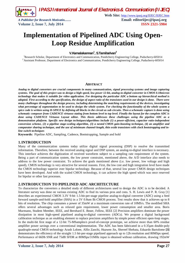
Figure 1. Block digram of Pipelined ADC
The pipeline ADC shown in figure 1 is the extension of the two-step structure. The conversion is divided into several stages with each stage generating a certain number of digital bits. The general block diagram is shown in Fig. There are 12 stages and the ith stage generates mi digits. If no redundancy is used, the sum of mi equals to 12, the resolution of ADC. The stages perform the following functions: the sample-hold circuits sample the output from the previous stage; the sub-ADC converts the analog signal into mi digital bits; the sub-DAC generates the estimated analog input signal; the subtraction and multiplication circuits generate the error signal between the input and the estimated signal and multiply it into the full scale.This residue signal goes to the next stage. All stages operate concurrently. When a stage works on the current sample, the next stage processes the previous one. The nature of concurrence makes the throughput of the converter independent of its resolution, and the same as for a flash ADC.
IPASJ International Journal of Electronics & Communication (IIJEC) Web Site: http://www.ipasj.org/IIJEC/IIJEC.htm
A Publisher for Research Motivatin........ Email: [email protected] Volume 2, Issue 7, July 2014 ISSN 2321-5984
Volume 2, Issue 7, July 2014 Page 29
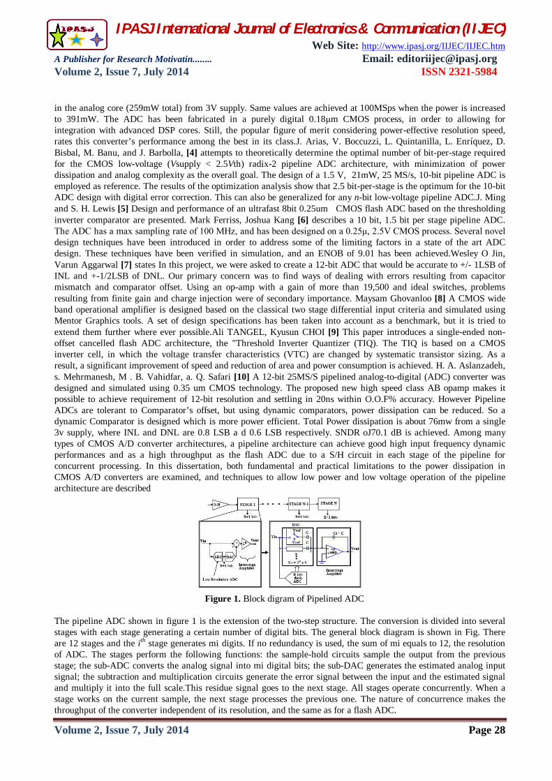
3. BEHAVIOURAL SIMULATION OF 12-BIT PIPELINED ADC The functional block diagram of the pipelined ADC is simulated using SIMULINK in MATLAB. The 1-bit single stage converter behavioral block shown in figure 2 has been designed and simulated. The behavior of the block has been developed using the equations given below. If Vin > Vmid Vresidue=2 (Vin-Vref) (1) If Vin < Vmid Vresidue=2 (Vin) (2) Using a reference value this single stage block would act as a comparator and gives a bit as output. Again that bit will be converted in to analog value, that value again compared with the actual input signal and the difference signal will be produced. The difference signal will be in the range of half of the actual input range. Since the total pipelined architecture has been developed using these similar type of 1-bit single stage blocks, should give the same input rage to all stages. To get that voltage rage we should multiply the error signal with 2, then we can give output of one stage to input of next stage. Every stage has its own sample and hold circuit, operating at 75 MS/s. the output of the sample and hold stage will be considered as the input to the 1-bit converter.
Figure 2. MATLAB SIMULINK model for the 1-bit conversion stage
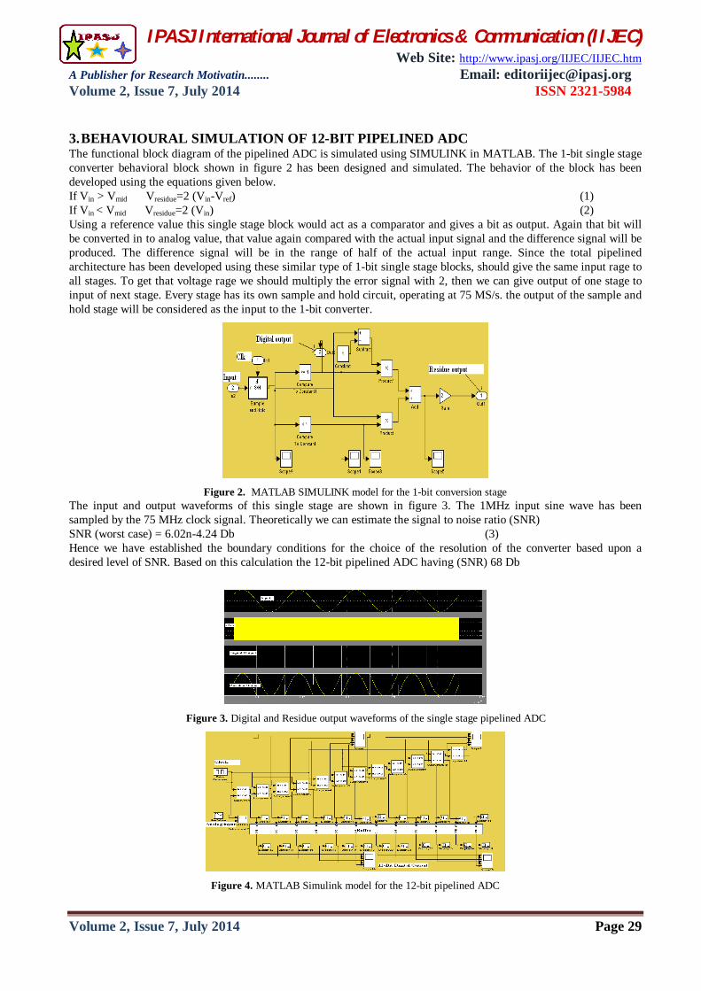
The input and output waveforms of this single stage are shown in figure 3. The 1MHz input sine wave has been sampled by the 75 MHz clock signal. Theoretically we can estimate the signal to noise ratio (SNR) SNR (worst case) = 6.02n-4.24 Db (3) Hence we have established the boundary conditions for the choice of the resolution of the converter based upon a desired level of SNR. Based on this calculation the 12-bit pipelined ADC having (SNR) 68 Db
Figure 3. Digital and Residue output waveforms of the single stage pipelined ADC
Figure 4. MATLAB Simulink model for the 12-bit pipelined ADC
IPASJ International Journal of Electronics & Communication (IIJEC) Web Site: http://www.ipasj.org/IIJEC/IIJEC.htm
A Publisher for Research Motivatin........ Email: [email protected] Volume 2, Issue 7, July 2014 ISSN 2321-5984
Volume 2, Issue 7, July 2014 Page 30
Figure 5. Digital output from the 12-bit pipelined ADC for sine wave
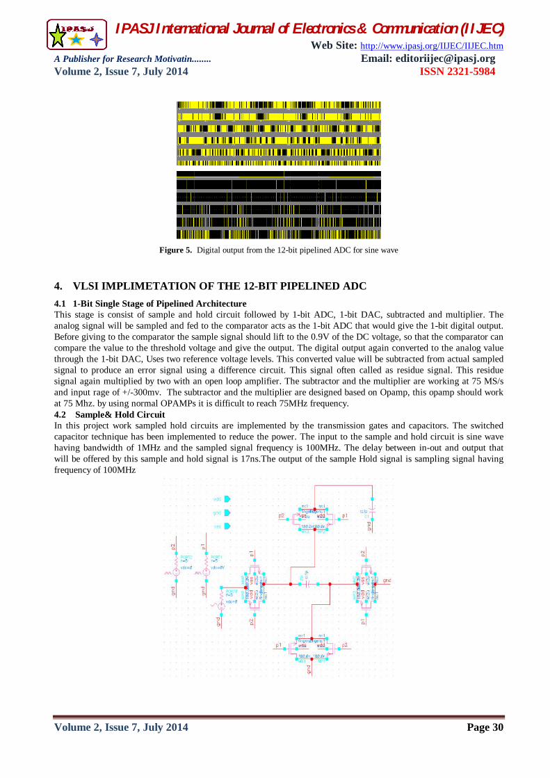
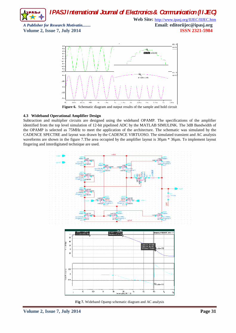
4. VLSI IMPLIMETATION OF THE 12-BIT PIPELINED ADC 4.1 1-Bit Single Stage of Pipelined Architecture This stage is consist of sample and hold circuit followed by 1-bit ADC, 1-bit DAC, subtracted and multiplier. The analog signal will be sampled and fed to the comparator acts as the 1-bit ADC that would give the 1-bit digital output. Before giving to the comparator the sample signal should lift to the 0.9V of the DC voltage, so that the comparator can compare the value to the threshold voltage and give the output. The digital output again converted to the analog value through the 1-bit DAC, Uses two reference voltage levels. This converted value will be subtracted from actual sampled signal to produce an error signal using a difference circuit. This signal often called as residue signal. This residue signal again multiplied by two with an open loop amplifier. The subtractor and the multiplier are working at 75 MS/s and input rage of +/-300mv. The subtractor and the multiplier are designed based on Opamp, this opamp should work at 75 Mhz. by using normal OPAMPs it is difficult to reach 75MHz frequency. 4.2 Sample& Hold Circuit In this project work sampled hold circuits are implemented by the transmission gates and capacitors. The switched capacitor technique has been implemented to reduce the power. The input to the sample and hold circuit is sine wave having bandwidth of 1MHz and the sampled signal frequency is 100MHz. The delay between in-out and output that will be offered by this sample and hold signal is 17ns.The output of the sample Hold signal is sampling signal having frequency of 100MHz
IPASJ International Journal of Electronics & Communication (IIJEC) Web Site: http://www.ipasj.org/IIJEC/IIJEC.htm
A Publisher for Research Motivatin........ Email: [email protected] Volume 2, Issue 7, July 2014 ISSN 2321-5984
Volume 2, Issue 7, July 2014 Page 31
Figure 6. Schematic diagram and output results of the sample and hold circuit
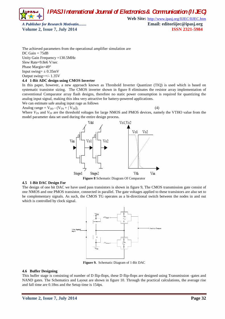
4.3 Wideband Operational Amplifier Design Subtraction and multiplier circuits are designed using the wideband OPAMP. The specifications of the amplifier identified from the top level simulation of 12-bit pipelined ADC by the MATLAB SIMULINK. The 3dB Bandwidth of the OPAMP is selected as 75MHz to meet the application of the architecture. The schematic was simulated by the CADENCE SPECTRE and layout was drawn by the CADENCE VIRTUOSO. The simulated transient and AC analysis waveforms are shown in the figure 7.The area occupied by the amplifier layout is 30µm * 36µm. To implement layout fingering and interdigitated technique are used.
Fig 7. Wideband Opamp schematic diagram and AC analysis
IPASJ International Journal of Electronics & Communication (IIJEC) Web Site: http://www.ipasj.org/IIJEC/IIJEC.htm
A Publisher for Research Motivatin........ Email: [email protected] Volume 2, Issue 7, July 2014 ISSN 2321-5984
Volume 2, Issue 7, July 2014 Page 32
The achieved parameters from the operational amplifier simulation are DC Gain = 75dB Unity Gain Frequency =130.5MHz Slew Rate=9.8e6 V/sec Phase Margin=49° Input swing= ± 0.35mV Output swing=+/- 1.35V 4.4 1-Bit ADC design using CMOS Inverter In this paper, however, a new approach known as Threshold Inverter Quantizer (TIQ) is used which is based on systematic transistor sizing. The CMOS inverter shown in figure 8 eliminates the resistor array implementation of conventional Comparator array flash designs, therefore no static power consumption is required for quantizing the analog input signal, making this idea very attractive for battery-powered applications. We can estimate safe analog input rage as follows Analog range = VDD - (VTN + | VTP|), (4) Where VTN and VTP are the threshold voltages for large NMOS and PMOS devices, namely the VTHO value from the model parameter data set used during the entire design process.
Figure 8 Schematic Diagram Of Comparator
4.5 1-Bit DAC Design For The design of one bit DAC we have used pass transistors is shown in figure 9, The CMOS transmission gate consist of one NMOS and one PMOS transistor, connected in parallel. The gate voltages applied to these transistors are also set to be complementary signals. As such, the CMOS TG operates as a bi-directional switch between the nodes in and out which is controlled by clock signal.
Figure 9. Schematic Diagram of 1-Bit DAC
4.6 Buffer Designing This buffer stage is consisting of number of D flip-flops, these D flip-flops are designed using Transmission -gates and NAND gates. The Schematics and Layout are shown in figure 10. Through the practical calculations, the average rise and fall time are 0.18ns and the Setup time is 154ps.
IPASJ International Journal of Electronics & Communication (IIJEC) Web Site: http://www.ipasj.org/IIJEC/IIJEC.htm
A Publisher for Research Motivatin........ Email: [email protected] Volume 2, Issue 7, July 2014 ISSN 2321-5984
Volume 2, Issue 7, July 2014 Page 33
Figure 10. Schematic Diagram of 12-Bit Buffer
The digital outputs for a given input analog sample are not generated at the same time. MSB comes first and LSB last. The time delay between adjacent bits is one half clock cycle. All bits need to be synchronized. The 1-bit digital output from the first stage is delayed by 12 half cycles and the output from the second stage is delayed by 11 half cycles, and so on. The output from the last stage is delayed by a half cycle. The delay block is made of D flip-flops (DFF) implemented with transmission gate and static NAND gates. Since sampling rate is only 100 MS/s and the word length is 12 bits, the carry ripple is not an issue under 0.18m process. 4.7 1-Bit Single stage of Pipelined Architecture This stage is consist of sample and hold circuit followed by 1-bit ADC, 1-bit DAC, subtracted and multiplier as shown in figure 11. The analog signal will be sampled and fed to the comparator acts as the 1-bit ADC, which would give the 1-bit digital output. Before giving to the comparator the sample signal should lift to the 0.9V of the DC voltage, so that the comparator can compare the value to the threshold voltage and give the output.
Figure 11. Schematic Diagram of 1-Bit Conversion Stage
The digital output again converted to the analog value through the 1-bit DAC, Uses two reference voltage levels. This converted value will be subtracted from actual sampled signal to produce an error signal using a difference circuit, this signal often called as residue signal. This residue signal again multiplied by two with an open loop amplifier. The difference and the multiplier are working at 75 MS/s and input rage of ±300mvwhich is shown in figure 12.
IPASJ International Journal of Electronics & Communication (IIJEC) Web Site: http://www.ipasj.org/IIJEC/IIJEC.htm
A Publisher for Research Motivatin........ Email: [email protected] Volume 2, Issue 7, July 2014 ISSN 2321-5984
Volume 2, Issue 7, July 2014 Page 34
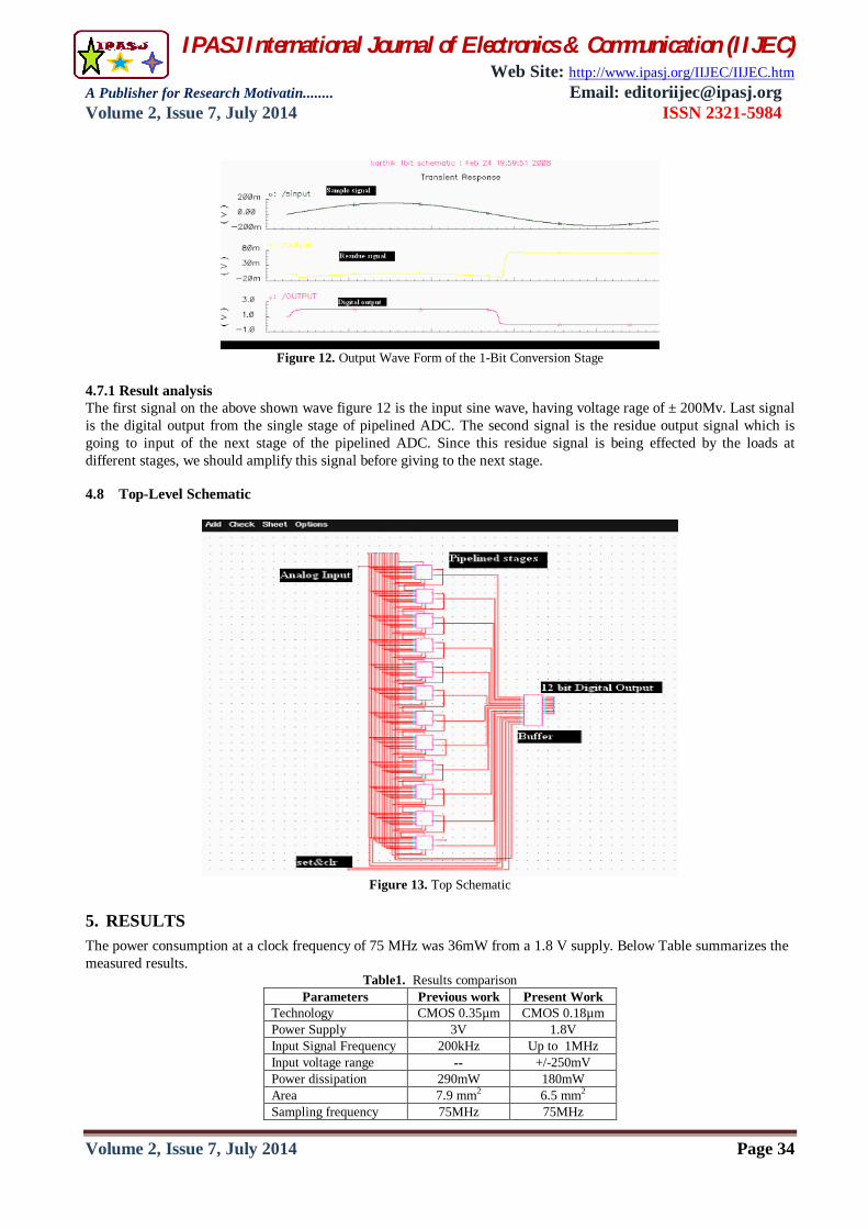
Figure 12. Output Wave Form of the 1-Bit Conversion Stage
4.7.1 Result analysis The first signal on the above shown wave figure 12 is the input sine wave, having voltage rage of ± 200Mv. Last signal is the digital output from the single stage of pipelined ADC. The second signal is the residue output signal which is going to input of the next stage of the pipelined ADC. Since this residue signal is being effected by the loads at different stages, we should amplify this signal before giving to the next stage.
4.8 Top-Level Schematic
Figure 13. Top Schematic
5. RESULTS The power consumption at a clock frequency of 75 MHz was 36mW from a 1.8 V supply. Below Table summarizes the measured results.
Table1. Results comparison Parameters Previous work Present Work
Technology CMOS 0.35µm CMOS 0.18µm Power Supply 3V 1.8V Input Signal Frequency 200kHz Up to 1MHz Input voltage range -- +/-250mV Power dissipation 290mW 180mW Area 7.9 mm2 6.5 mm2 Sampling frequency 75MHz 75MHz
IPASJ International Journal of Electronics & Communication (IIJEC) Web Site: http://www.ipasj.org/IIJEC/IIJEC.htm
A Publisher for Research Motivatin........ Email: [email protected] Volume 2, Issue 7, July 2014 ISSN 2321-5984
Volume 2, Issue 7, July 2014 Page 35
6. CONCLUSIONS The different ADC architectures were analyzed to determine the optimal topology for the given performance specifications with minimum power consumption. Second, the exact implementation of the chosen architecture was investigated in an effort to use the minimum amount of power. Due to some limitations the SNR of the designed 12-bit ADC cannot able to be measured. After a complete analysis, the block was simulated for functionality verification. Once confirmation of correct operation was achieved, a complete layout has been designed. This project involved designing an integrated CMOS Analog-to-Digital converter for communication and video applications in 0.18µm technology at an operating voltage of ±1.8 V. Low-voltage design techniques for the switched-capacitor building blocks have been demonstrated enabling the implementation of larger applications such as sample-and-holds, filters, and data converters. The behavioral simulation of pipelined ADC has been done using MATLAB SIMULINK. Final results from MATLAB SIMULINK and results from H-SPICE were verified. Both simulations and analytical results have been used to establish design criteria. 7. RECOMMENDATIONS FOR FURTHER WORK The designed 12-bit pipelined ADC has ±300mv input voltage range. This input voltage range is limited by the input voltage swing of the OPAMP and the voltage follower circuits which are commonly used, to avoid the loading effect. We can use the rail to rail OPAMP to increase the input voltage rage of the ADC, but by increasing the input voltage swing the resolution will be affected. By using the OPAMPs at the output of the voltage followers we can maintain the signal strength without affecting much. We can reduce the latency of the Pipelined ADC greatly by making the adjacent stages of the ADC are working at opposite phase. References
[1] S. H. Lewis and P. R. Gray, “A pipelined 5-MS/s 9-bit analog-to-digital converter”, IEEE Journal of Solid-State Circuits, vol. 22, pp. 954-961, Dec. 1987.
[2] Boris Murmann and Bernhard E. Boser, “A 12-Bit 75-MS/s Pipelined ADC Using Open-loop Residue Amplification”, IEEE Journal of Solid-State Circuits, vol. 38, no. 12, pp. 1-4, Dec. 2003.
[3] A. Varzaghani and C. K. K. Yang, “A 600 MS/s 5-bit pipelined analog-to-digital converter using Digital reference Calibration”, IEEE Journal of Solid-State Circuits, vol. 41, no. 2, pp. 1-4, Feb. 2006.
[4] J. Arias, V. Boccuzzi, L. Quintanilla, L. Enríquez, D. Bisbal, M. Banu, and J. Barbolla, “Low-Power Pipeline ADC for Wireless LANs”, IEEE Journal of Solid-State Circuits, vol. 39, no. 8, pp. 1-3, Aug. 2004.
[5] J. Ming and S. H. Lewis, “An 8 b 80 MSample/s pipelined ADC with background calibration”, in IEEE Int. Solid-State Circuits Conference, pp. 42-43, Feb. 2000.
[6] Ali TANGEL and Kyusun CHOI, “The CMOS Inverter as a comparator in ADC designs”, The Pennsylvania State University, University Park, PA16802 USA.
[7] Maysam Ghovanloo, “A Classic Wide Band Operational Amplifier Design”, University of Michigan, Ann Arbor, MI, 48109-2122.
[8] Arash Loloee, Alfio Zanchi, Huawen jin, Shereef Shehata, Eduardo Bartolome,” A 12 bit 80 Msps Pipelined ADC Core with 190mw consumption from 3v in 0.18um Digital CMOS”, Texas Instruments, Inc.-Wireless Infrastructure Data Converters 12500 TI Boulevard, MS8755-75243 Dallas, TX(U.S.A), 2002.
[9] J. M. Rabaey, “Digital Integrated Circuits- A design Perspective”, Prentice Hall India, 1996. [10] D. Johns and K. Martin, “Analog Integrated Circuit Design”, John Wiley, New York, 1997. [11] Phillip E.Allen &Holberg, “CMOS Analog Circuit Design”, Oxford University Press, Second edition, 2002 [12] R.Jacob Baker, “CMOS Mixed Signal Circuit Design”, IEEE Series on Microelectronic systems, NJ, 2002 AUTHOR V.Kamalakannan has received the B.E. in Electronics and Communications Engineering from Bangalore University in 2001 and M.Tech. In VLSI Design and Embedded System from Visvesvaraya Technological University in 2009, respectively. Currently pursuing as Ph.D. Research Scholar, in Pondicherry Engineering College, Pondicherry University. His research area is VLSI Design, Image Processing, Signal Processing, Digital Electronics, Reversible logic gates, HDL Coding (VHDL and Verilog HDL). S.Tamilselvan received B.E degree in Electronics and Communication Engineering from Madras University in 1999 and M.Tech degree in Electronics and Communication Engineering from Pondicherry Engineering College,

IPASJ International Journal of Electronics & Communication (IIJEC) Web Site: http://www.ipasj.org/IIJEC/IIJEC.htm
A Publisher for Research Motivatin........ Email: [email protected] Volume 2, Issue 7, July 2014 ISSN 2321-5984
Volume 2, Issue 7, July 2014 Page 36
Pondicherry, India. He completed his Ph.D degree in 2011 from Pondicherry University. His current research interests are in signal processing, wireless communication systems, Mobile and Distributed Computing. Currently he is working as an Assistant Professor in the department of ECE, Pondicherry Engineering College, Pondicherry, India.


