Embed Size (px)
Citation preview
Available online at www.sciencedirect.com
www.elsevier.com/locate/micpro
Microprocessors and Microsystems 31 (2007) 487–497
Multiplierless and fully pipelined JPEG compressionsoft IP targeting FPGAs
Luciano Volcan Agostini a,c,*, Ivan Saraiva Silva b, Sergio Bampi c
a Group of Architectures and Integrated Circuits, DInfo, UFPel, Pelotas, Brazilb DIMAp, UFRN, Natal, Brazil
c Microelectronics Group II, UFRGS, Porto Alegre, Brazil
Available online 28 February 2006
Abstract
This paper presents the design of a soft IP for JPEG compression targeted for high performance in a FPGA device. The JPEG com-pressor architecture achieves high throughput with a deep and optimized pipeline and with a multiplierless datapath architecture. TheJPEG compressor architecture was designed in a hierarchical and modular fashion and the details of the global architecture and of itsmodules are presented in this paper. A modular and strictly structural VHDL design is followed to develop the JPEG compressor soft IP.The VHDL codes were synthesized to Altera and Xilinx FPGAs. Synthesis results and relevant performance comparisons with relatedworks are presented. Our high throughput compressor is able to compress 39.8 millions of pixels per second when mapped onto an AlteraFLEX 10KE FPGA. Our JPEG soft IP mapped to FLEX 10KE low cost FPGA is able to compress 115 images per second in SDTVresolution (720 · 480 pixels). Considering this SDTV resolution our design is worthy as a core of an M-JPEG video compressor, reachinga real time processing rate of 30 fps, once mapped to the FLEX 10KE FPGA device.� 2006 Elsevier B.V. All rights reserved.
Keywords: FPGA based design; JPEG compression; Soft IP design; VLSI architecture
1. Introduction
The Joint Photographic Experts Group [1] proposed theJPEG compression standard [2] in 1987 and, since then,this is the most used lossy compression standard for stillphotographic images.
The JPEG standard is very complex and allows severaloperation modes [2,3], using different compression tech-niques [3]. The mode called baseline is the mode widelyused in both software and hardware implementations ofJPEG compression [4]. The baseline mode will be used asreference for the architecture proposed in this paper.
JPEG compression in software is widely used, but theprocessing time and power restrictions for real-time embed-ded hardware applications make it unfeasible to use a soft-ware solution in a general purpose processor. Power
0141-9331/$ - see front matter � 2006 Elsevier B.V. All rights reserved.
doi:10.1016/j.micpro.2006.02.002
* Corresponding author.E-mail address: [email protected] (L.V. Agostini).
efficiency and fast compression are often a performancecritical factor. Software implementation may not be appli-cable in embedded systems like digital cameras, DVD play-ers and so on. To satisfy the requirements of theseapplications a dedicated hardware design of a JPEG com-pressor is important. As the JPEG compression process isvery complex, its design in hardware is very demanding.
This paper presents a soft IP for high throughput JPEGcompression in hardware. An IP (intellectual property) is areusable hardware block that can be used in many differentdesigns. Hardware IP blocks can be classified according totheir level of commitments to a given hardware technology:hard IP, firm IP and soft IP. The hard IP is supplied as aGDSII that was physically designed by the IP provider,including the place-and-route. The firm IP is an intermedi-ate level of abstraction and it can be supplied as a RTL or anetlist with some type of information that is taken fromlower levels of abstraction, closer to the physical design.The soft IP is supplied as a synthesizable RTL descriptionof the reusable hardware block, without considering
488 L.V. Agostini et al. / Microprocessors and Microsystems 31 (2007) 487–497
restrictions of the physical design. Soft IPs are very flexible,making it easier to modify them to adapt to different tech-nology targets and physical design methods [5].
The JPEG architecture was planned to reach high per-formance running in FPGAs. The architectural detailsand some synthesis results are presented in the next sec-tions. The designed soft IP is able to process 115720 · 480 pixels images (SDTV) in 1 s when mapped toan Altera FLEX 10KE FPGA. This processing rate isenough to use this compressor as the core of an M-JPEG[6] video compressor in real time (30 fps).
Our design strategy was to optimize each module corre-sponding to each of the operations demanded by the JPEGstandard, considering an 8-bit input stream of gray scalepixels. All modules were designed, optimized and describedin VHDL. Full synthesis and simulation were done withthe Altera Quartus II tool [7] and with Xilinx ISE tool[8]. Further validation was done with a comparison ofthe compressed bit-stream with the results obtained froma software compression.
Except for the case of the 2-D DCT architecture, whichhas a top-level block design based on previous work [9], allother architectural solutions have been completely pro-posed for this design. The 2-D DCT algorithm has beenmodified to correct a less than optimum solution that hasbeen previously published [9]. The proposition of thisJPEG design and some initial architectures are presentedin [10], but the complete and final results of this designare presented in this paper. This paper presents unpub-lished information about this JPEG IP design, includingdetails of the global and optimized architecture, the archi-tecture validation and the numerical error evaluationdescriptions, the final synthesis results and the performancecomparisons with related works.
This paper is divided in five main sections. Section 2introduces the JPEG standard. Section 3 presents the archi-tecture designed for the JPEG compressor hardware. Theapproach used to validate the architecture and the resultsof the numerical error evaluation are presented in Section4. Section 5 presents the synthesis results and the perfor-mance comparisons with related works. Finally, the con-clusions of this work are presented in Section 6.
2. JPEG image compression
The core of the JPEG compression is the two-dimen-sional discrete cosine transform (2-D DCT) that, togetherwith quantization and lossless compression techniques,makes possible a significant reduction in the amount ofdata required to represent an image. JPEG 2000 standard[11] allows the wavelet discrete transform to be usedinstead of the DCT, which increases the compression rates
Fig. 1. Top-level view of the pipelined m
and the quality of the compressed image. This workaddressed the JPEG compression based on the DCT, sincemost of the current JPEG compressors still use DCT.
The JPEG compression for gray scale images, whenoperating in the baseline mode, is formed by three mainoperations: the two-dimensional discrete cosine transform(DCT 2-D), quantization and entropy coding [2,4].
There are losses of information in the baseline JPEGcompression and this is the basis of the high compressionrates reached for this compression standard. Losses aredue, essentially, to the quantization operation. These lossescan be controlled to have an almost imperceptible influenceto the human visual system [4].
The input image for the JPEG compression is divided in8 · 8 matrixes of pixels [2,3], that are the basic units offrame processing in JPEG compression.
3. Designed architecture for the JPEG compressor
This section focuses in the architecture designed for theJPEG compressor soft IP. The input image considered iscomposed by pixels represented in an unsigned, eight bitgray representation [0, . . . ,255].
Before the calculation of 2-D DCT, the input pixel goesthrough a level-shifting operation. This shift moves theaverage value of the input elements to zero (in a two’s com-plement signed representation), resulting in better unifor-mity for the image representation in the spatial domain [4].
The datapath and control blocks were designed in a stricthierarchical design. This design discipline speeded up theoverall design, increasing its performance. Besides provid-ing clarity in the design, it facilitates the reuse of modulesor parts of this architecture by other hardware projects.
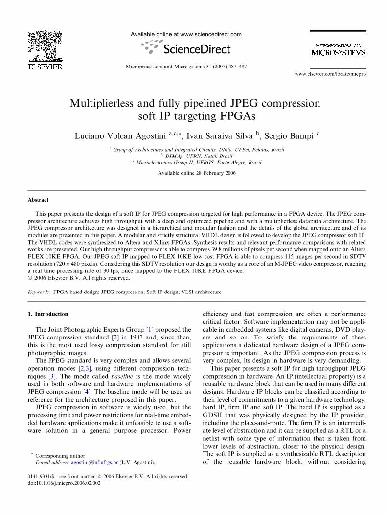
The most abstract hierarchical level is presented inFig. 1. It has just four macro pipeline stages: a 2-D DCT,a quantization block, a zigzag buffer and an entropy coder.Each macro stage is designed to contain several pipelinestages, in order to balance the overall pipeline and to guar-antee the high throughput desired.
The input data are consumed at a rate of one 8-bit pixelat each clock cycle. The output JPEG word is 32-bit wideand is presented at the output in an asynchronous way.This asynchronism will be detailed in the next sections.Due to this asynchronism, the output of the JPEG com-pressor flags the bit ‘‘OK’’ in Fig. 1, to indicate that anew and valid JPEG 4-byte word is ready at the outputstream.
The global latency is also dependent on the asynchro-nism generated in the compressor output, but the minimumcompressor latency is 238 clock cycles. This highlatency stems from the deep pipeline design used in ourarchitecture. This deep and optimized pipeline was
acro-blocks in the JPEG compressor.
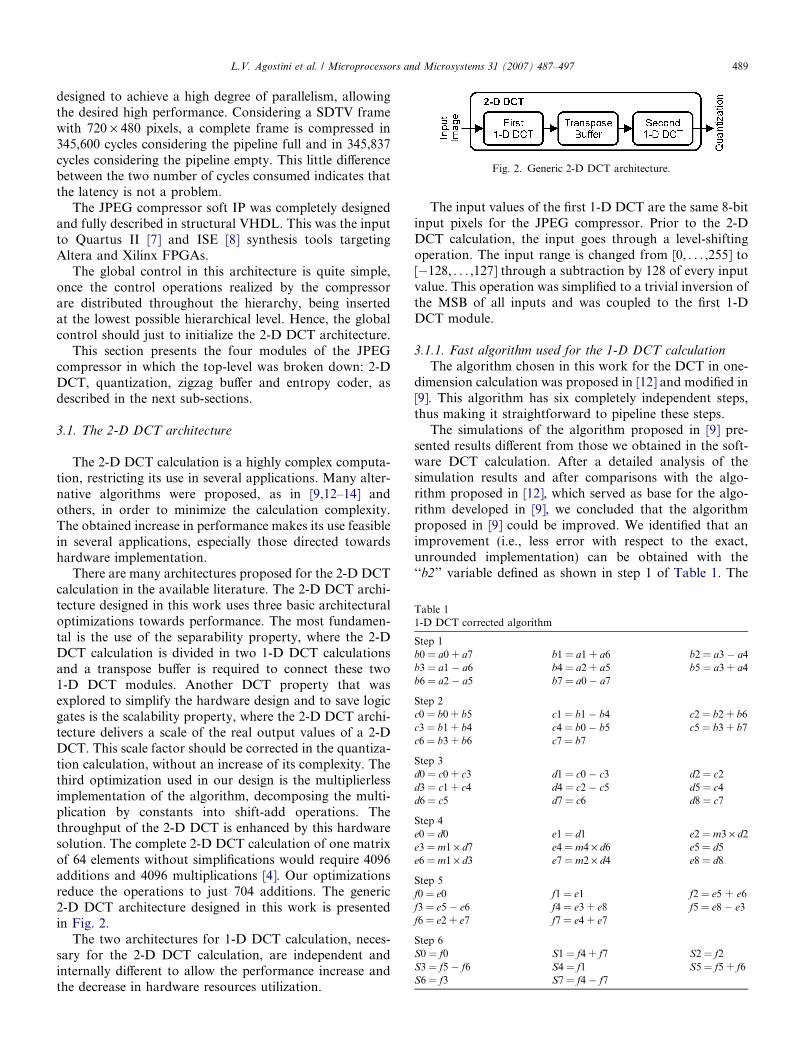
Fig. 2. Generic 2-D DCT architecture.
Table 11-D DCT corrected algorithm
Step 1b0 = a0 + a7 b1 = a1 + a6 b2 = a3 � a4b3 = a1 � a6 b4 = a2 + a5 b5 = a3 + a4b6 = a2 � a5 b7 = a0 � a7
Step 2c0 = b0 + b5 c1 = b1 � b4 c2 = b2 + b6c3 = b1 + b4 c4 = b0 � b5 c5 = b3 + b7c6 = b3 + b6 c7 = b7
Step 3d0 = c0 + c3 d1 = c0 � c3 d2 = c2d3 = c1 + c4 d4 = c2 � c5 d5 = c4d6 = c5 d7 = c6 d8 = c7
Step 4e0 = d0 e1 = d1 e2 = m3 · d2e3 = m1 · d7 e4 = m4 · d6 e5 = d5e6 = m1 · d3 e7 = m2 · d4 e8 = d8
Step 5f0 = e0 f1 = e1 f2 = e5 + e6f3 = e5 � e6 f4 = e3 + e8 f5 = e8 � e3f6 = e2 + e7 f7 = e4 + e7
Step 6S0 = f0 S1 = f4 + f7 S2 = f2S3 = f5 � f6 S4 = f1 S5 = f5 + f6S6 = f3 S7 = f4 � f7
L.V. Agostini et al. / Microprocessors and Microsystems 31 (2007) 487–497 489
designed to achieve a high degree of parallelism, allowingthe desired high performance. Considering a SDTV framewith 720 · 480 pixels, a complete frame is compressed in345,600 cycles considering the pipeline full and in 345,837cycles considering the pipeline empty. This little differencebetween the two number of cycles consumed indicates thatthe latency is not a problem.
The JPEG compressor soft IP was completely designedand fully described in structural VHDL. This was the inputto Quartus II [7] and ISE [8] synthesis tools targetingAltera and Xilinx FPGAs.
The global control in this architecture is quite simple,once the control operations realized by the compressorare distributed throughout the hierarchy, being insertedat the lowest possible hierarchical level. Hence, the globalcontrol should just to initialize the 2-D DCT architecture.
This section presents the four modules of the JPEGcompressor in which the top-level was broken down: 2-DDCT, quantization, zigzag buffer and entropy coder, asdescribed in the next sub-sections.
3.1. The 2-D DCT architecture
The 2-D DCT calculation is a highly complex computa-tion, restricting its use in several applications. Many alter-native algorithms were proposed, as in [9,12–14] andothers, in order to minimize the calculation complexity.The obtained increase in performance makes its use feasiblein several applications, especially those directed towardshardware implementation.
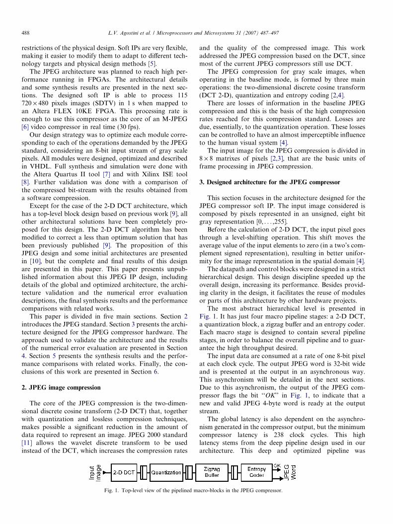
There are many architectures proposed for the 2-D DCTcalculation in the available literature. The 2-D DCT archi-tecture designed in this work uses three basic architecturaloptimizations towards performance. The most fundamen-tal is the use of the separability property, where the 2-DDCT calculation is divided in two 1-D DCT calculationsand a transpose buffer is required to connect these two1-D DCT modules. Another DCT property that wasexplored to simplify the hardware design and to save logicgates is the scalability property, where the 2-D DCT archi-tecture delivers a scale of the real output values of a 2-DDCT. This scale factor should be corrected in the quantiza-tion calculation, without an increase of its complexity. Thethird optimization used in our design is the multiplierlessimplementation of the algorithm, decomposing the multi-plication by constants into shift-add operations. Thethroughput of the 2-D DCT is enhanced by this hardwaresolution. The complete 2-D DCT calculation of one matrixof 64 elements without simplifications would require 4096additions and 4096 multiplications [4]. Our optimizationsreduce the operations to just 704 additions. The generic2-D DCT architecture designed in this work is presentedin Fig. 2.
The two architectures for 1-D DCT calculation, neces-sary for the 2-D DCT calculation, are independent andinternally different to allow the performance increase andthe decrease in hardware resources utilization.
The input values of the first 1-D DCT are the same 8-bitinput pixels for the JPEG compressor. Prior to the 2-DDCT calculation, the input goes through a level-shiftingoperation. The input range is changed from [0, . . . ,255] to[�128, . . . ,127] through a subtraction by 128 of every inputvalue. This operation was simplified to a trivial inversion ofthe MSB of all inputs and was coupled to the first 1-DDCT module.
3.1.1. Fast algorithm used for the 1-D DCT calculation
The algorithm chosen in this work for the DCT in one-dimension calculation was proposed in [12] and modified in[9]. This algorithm has six completely independent steps,thus making it straightforward to pipeline these steps.
The simulations of the algorithm proposed in [9] pre-sented results different from those we obtained in the soft-ware DCT calculation. After a detailed analysis of thesimulation results and after comparisons with the algo-rithm proposed in [12], which served as base for the algo-rithm developed in [9], we concluded that the algorithmproposed in [9] could be improved. We identified that animprovement (i.e., less error with respect to the exact,unrounded implementation) can be obtained with the‘‘b2’’ variable defined as shown in step 1 of Table 1. The
490 L.V. Agostini et al. / Microprocessors and Microsystems 31 (2007) 487–497
authors of the original paper defined it as ‘‘a2–a4’’, whilewe used ‘‘a3–a4’’. The complete and corrected algorithmimplemented in the 1-D DCT hardware we designed is pre-sented in Table 1, for which the following constants aredefined and later implemented in an optimized roundedfix point representation:
m1 ¼ cosð4p=16Þ; m3 ¼ cosð2p=16Þ � cosð6p=16Þ;m2 ¼ cosð6p=16Þ; m4 ¼ cosð2p=16Þ þ cosð6p=16Þ.
3.1.2. 1-D DCT architectures
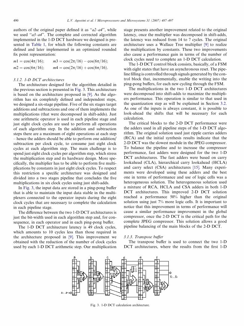
The architecture designed for the algorithm detailed inthe previous section is presented in Fig. 3. This architectureis based on the architecture proposed in [9]. As the algo-rithm has six completely defined and independent steps,we designed a six-stage pipeline. Five of the six stages targetadditions and subtractions and one of them implements themultiplications (that were decomposed in shift-adds). Justone arithmetic operator is used in each pipeline stage andjust eight clock cycles are used to perform all operationsof each algorithm step. In the addition and subtractionsteps there are a maximum of eight operations at each step– hence the adders should be able to perform one addition/subtraction per clock cycle, to consume just eight clockcycles at each algorithm step. The main challenge is tospend just eight clock cycles per algorithm step, which stressthe multiplication step and its hardware design. More spe-cifically, the multiplier has to be able to perform five multi-plications by constants in just eight clock cycles. To respectthis restriction a specific architecture was designed anddivided into a two stages pipeline that concludes the fivemultiplications in six clock cycles using just shift-adds.
In Fig. 3, the input data are stored in a ping-pong bufferthat is able to maintain the input data stable in the multi-plexers connected to the operator inputs during the eightclock cycles that are necessary to complete the calculationin each pipeline stage.
The difference between the two 1-D DCT architectures isjust the bit-width used in each algorithm step and, for con-sequence, in each operator and in each ping-pong buffer.
The 1-D DCT architecture latency is 49 clock cycles,which amounts to 10 cycles less than those required inthe architecture proposed in [9]. This improvement weobtained with the reduction of the number of clock cyclesused by each 1-D DCT arithmetic step. Our multiplication
Fig. 3. 1-D DCT calcu
stage presents another improvement related to the originallatency, once the multiplier was decomposed in shift-adds,the latency was reduced from 14 to 7 cycles. The originalarchitecture uses a Wallace Tree multiplier [9] to realizethe multiplication by constants. These two improvementsalso cause a performance gain in terms of the number ofclock cycles need to complete an 1-D DCT calculation.
The 1-D DCT control block consists, basically, of a FSMwith eight states that have an asynchronous reset. The pipe-line filling is controlled through signals generated by the con-trol block that, incrementally, enable the writing into theping-pong buffers, for each new cycling through the FSM.
The multiplications in the two 1-D DCT architectureswere decomposed into shift-adds to maximize the multipli-ers performance. This operation is similar to that used inthe quantization step as will be explained in Section 3.2.As one of the inputs is always constant, it is possible tolook-ahead the shifts that will be necessary for eachcalculation.
The critical blocks to the 2-D DCT performance werethe adders used in all pipeline steps of the 1-D DCT algo-rithm. The original solution used just ripple carries adders(RCA) and the initial synthesis results indicate that the2-D DCT was the slowest module in the JPEG compressor.To balance the pipeline and to increase the compressorperformance, fast adders were designed for the two 1-DDCT architectures. The fast adders were based on carrylookahead (CLA), hierarchical carry lookahead (HCLA)and carry select (CSA) architectures [15]. Many experi-ments were developed using these adders and the bestone in terms of performance and use of logic cells was aheterogeneous solution. The heterogeneous solution useda mixture of RCA, HCLA and CSA adders in both 1-DDCT architectures. This improved 2-D DCT solutionreached a performance 50% higher than the originalsolution using just 7% more logic cells. It is important tonotice that this improvement in terms of performance willcause a similar performance improvement in the globalcompressor, once the 2-D DCT is the critical path for thecomplete JPEG compressor. This solution allows a goodpipeline balancing of the main blocks of the 2-D DCT.
3.1.3. Transpose buffer
The transpose buffer is used to connect the two 1-DDCT architectures, where the results from the first 1-D
lation architecture.
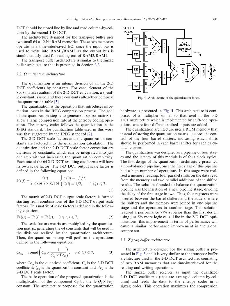
Fig. 4. Architecture of the quantization block.
L.V. Agostini et al. / Microprocessors and Microsystems 31 (2007) 487–497 491
DCT should be stored line by line and read column-by-col-umn by the second 1-D DCT.
The architecture designed for the transpose buffer usestwo small 64 · 12-bit RAM memories. These two memoriesoperate in a time-interleaved I/O, since the input bus isused to write into RAM1/RAM2 as the output bus issimultaneously used for reading out of RAM2/RAM1.
The transpose buffer architecture is similar to the zigzagbuffer architecture that is presented in Section 3.3.
3.2. Quantization architecture
The quantization is an integer division of all the 2-DDCT coefficients by constants. For each element of the8 · 8 matrix resultant of the 2-D DCT calculation, a specif-ic constant is used and these constants altogether comprisethe quantization table [3].
The quantization is the operation that introduces infor-mation losses in the JPEG compression process. The goalof the quantization step is to generate a sparse matrix toallow a large compression rate at the entropy coding oper-ation. The entropy coder follows the quantization in theJPEG standard. The quantization table used in this workwas that suggested by the JPEG standard [2].
The 2-D DCT scale factors and the quantization con-stants are factored into the quantization calculation. Thequantization and the 2-D DCT scale factor correction aredivisions by constants, which can be integrated into justone step without increasing the quantization complexity.Each one of the 64 2-D DCT resulting coefficients will haveits own scale factor. The 1-D DCT output scale factor isdefined in the following equation:
FeðiÞ ¼ CðiÞ2� cosði� p=16Þ
Cð0Þ ¼ 1=ffiffiffi2p
;
CðiÞ ¼ 1=2; 1 6 i 6 7.
(
ð1ÞThe matrix of 2-D DCT output scale factors is formed
starting from combinations of the 1-D DCT output scalefactors. This matrix of scale factors is defined in the follow-ing equation:
FeðijÞ ¼ FeðiÞ � FeðjÞ; 0 6 i; j 6 7. ð2ÞThe scale factors matrix are multiplied by the quantiza-
tion matrix, generating the 64 constants that will be used inthe divisions realized by the quantization architecture.Then, the quantization step will perform the operationsdefined in the following equation:
Cqij ¼ round Cij �1
Qij � Feij
!; 0 6 i; j 6 7; ð3Þ
where Cqij is the quantized coefficient; Cij is the 2-D DCTcoefficient; Qij is the quantization constant and Feij is the2-D DCT scale factor.
The basic operation of the proposed quantization is themultiplication of the component Cij by the 1/(Qij · Feij)constant. The architecture proposed for the quantization
hardware is presented in Fig. 4. This architecture is com-prised of a multiplier similar to that used in the 1-DDCT architecture which is implemented by shift-add oper-ations, where four different shifted inputs are added.
The quantization architecture uses a ROM memory thatinstead of storing the quantization matrix, it stores the con-trol of the four barrel shifters, indicating which shiftsshould be performed in each barrel shifter for each calcu-lated element.
The quantization was designed as a pipeline of four stag-es and the latency of this module is of four clock cycles.The first design of the quantization architecture presenteda non-balanced pipeline, once the first stage of this pipelinehad a high number of operations. In this stage were real-ized a memory reading, four parallel shifts on the data readfrom the memory and two parallel additions of the shiftedresults. The solution founded to balance the quantizationpipeline was the insertion of a new pipeline stage, dividingthe delay of the first stage in two. Thus, four registers wereinserted between the barrel shifters and the adders, wherethe shifters and the memory were joined in one pipelinestage and the operators in another stage. This solutionreached a performance 77% superior than the first designusing just 5% more logic cells. Like in the 2-D DCT opti-mizations, this improvement in terms of performance willcause a similar performance improvement in the globalcompressor.
3.3. Zigzag buffer architecture
The architecture designed for the zigzag buffer is pre-sented in Fig. 5 and it is very similar to the transpose bufferarchitecture used in the 2-D DCT architecture, consistingof two RAM memories that are time-interleaved for thereading and writing operations.
The zigzag buffer receives as input the quantized2-D DCT coefficients (that are arranged column-by-col-umn) and feeds the data to the entropy coder in azigzag order. This operation maximizes the compression
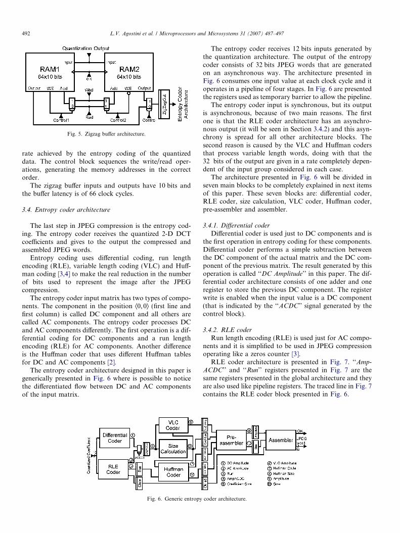
Fig. 5. Zigzag buffer architecture.
492 L.V. Agostini et al. / Microprocessors and Microsystems 31 (2007) 487–497
rate achieved by the entropy coding of the quantizeddata. The control block sequences the write/read oper-ations, generating the memory addresses in the correctorder.
The zigzag buffer inputs and outputs have 10 bits andthe buffer latency is of 66 clock cycles.
3.4. Entropy coder architecture
The last step in JPEG compression is the entropy cod-ing. The entropy coder receives the quantized 2-D DCTcoefficients and gives to the output the compressed andassembled JPEG words.
Entropy coding uses differential coding, run lengthencoding (RLE), variable length coding (VLC) and Huff-man coding [3,4] to make the real reduction in the numberof bits used to represent the image after the JPEGcompression.
The entropy coder input matrix has two types of compo-nents. The component in the position Æ0,0æ (first line andfirst column) is called DC component and all others arecalled AC components. The entropy coder processes DCand AC components differently. The first operation is a dif-ferential coding for DC components and a run lengthencoding (RLE) for AC components. Another differenceis the Huffman coder that uses different Huffman tablesfor DC and AC components [2].
The entropy coder architecture designed in this paper isgenerically presented in Fig. 6 where is possible to noticethe differentiated flow between DC and AC componentsof the input matrix.
Fig. 6. Generic entropy
The entropy coder receives 12 bits inputs generated bythe quantization architecture. The output of the entropycoder consists of 32 bits JPEG words that are generatedon an asynchronous way. The architecture presented inFig. 6 consumes one input value at each clock cycle and itoperates in a pipeline of four stages. In Fig. 6 are presentedthe registers used as temporary barrier to allow the pipeline.
The entropy coder input is synchronous, but its outputis asynchronous, because of two main reasons. The firstone is that the RLE coder architecture has an asynchro-nous output (it will be seen in Section 3.4.2) and this asyn-chrony is spread for all other architecture blocks. Thesecond reason is caused by the VLC and Huffman codersthat process variable length words, doing with that the32 bits of the output are given in a rate completely depen-dent of the input group considered in each case.
The architecture presented in Fig. 6 will be divided inseven main blocks to be completely explained in next itemsof this paper. These seven blocks are: differential coder,RLE coder, size calculation, VLC coder, Huffman coder,pre-assembler and assembler.
3.4.1. Differential coder
Differential coder is used just to DC components and isthe first operation in entropy coding for these components.Differential coder performs a simple subtraction betweenthe DC component of the actual matrix and the DC com-ponent of the previous matrix. The result generated by thisoperation is called ‘‘DC Amplitude’’ in this paper. The dif-ferential coder architecture consists of one adder and oneregister to store the previous DC component. The registerwrite is enabled when the input value is a DC component(that is indicated by the ‘‘ACDC’’ signal generated by thecontrol block).
3.4.2. RLE coder
Run length encoding (RLE) is used just for AC compo-nents and it is simplified to be used in JPEG compressionoperating like a zeros counter [3].
RLE coder architecture is presented in Fig. 7. ‘‘Amp-
ACDC’’ and ‘‘Run’’ registers presented in Fig. 7 are thesame registers presented in the global architecture and theyare also used like pipeline registers. The traced line in Fig. 7contains the RLE coder block presented in Fig. 6.
coder architecture.
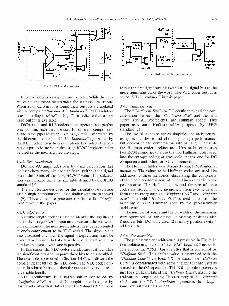
Fig. 8. Huffman coder architecture.
Fig. 7. RLE coder architecture.
L.V. Agostini et al. / Microprocessors and Microsystems 31 (2007) 487–497 493
Entropy coder is an asynchronous coder. While the cod-er counts the zeros occurrences the outputs are frozen.When a non-zero input is found these outputs are updatedwith a new pair ‘‘Run and AC Amplitude’’. RLE architec-ture has a flag (‘‘Okrle’’ in Fig. 7) to indicate that a newvalid output is available.
Differential and RLE coders must operate in a perfectsynchronism, such they are used for different componentsat the same pipeline stage. ‘‘DC Amplitude’’ (generated bythe differential coder) and ‘‘AC Amplitude’’ (generated bythe RLE coder), pass by a multiplexer that selects the cor-rect output to be stored in the ‘‘AmpACDC’’ register and tobe used in the next architecture steps.
3.4.3. Size calculation
DC and AC amplitudes pass by a size calculation thatindicates how many bits are significant (without the signalbit) in the 10 bits of the ‘‘AmpACDC’’ value. This calcula-tion was designed using the size table defined by the JPEGstandard [2].
The architecture designed for this calculation was madewith a single combinational logic similar with the proposedin [9]. This architecture generates the field called ‘‘Coeffi-
cient Size’’ in this paper.
3.4.4. VLC coder
Variable length coder is used to identify the significantbits in the ‘‘AmpACDC’’ input and to discard the bits with-out significance. The negative numbers must be representedin one’s complement to be VLC coded. The signal bit isalso discarded and then the signal interpretation must beinverted: a number that starts with zero is negative and anumber that starts with one is positive.
In this paper, the VLC coder architecture just identifiesthe significant bits and prepares these bits to be assembled.The assembler (presented in Section 3.4.6) will discard thenon-significant bits of the VLC code. The VLC coder out-put values have 9 bits and then the outputs have not a real-ly variable length.
VLC architecture is a barrel shifter controlled by‘‘Coefficient Size’’. AC and DC amplitude values pass bythis barrel shifter that shifts to left the ‘‘AmpACDC’’ value
to put the first significant bit (without the signal bit) as themore significant bit of the word. The VLC coder output iscalled ‘‘VLC Amplitude’’ in this paper.
3.4.5. Huffman coder
The ‘‘Coefficient Size’’ (to DC coefficients) and the con-catenation between the ‘‘Coefficient Size’’ and the field‘‘Run’’ (to AC coefficients) are Huffman coded. Thispaper uses static Huffman tables proposed by JPEGstandard [2].
The use of standard tables simplifies the architecture,using less hardware and obtaining a high performance,but decreasing the compression rate [4]. Fig. 8 presentsthe Huffman coder architecture. This architecture usestwo ROM memories to store the two Huffman tables usedinto the entropy coding of gray scale images: one for DCcomponents and other for AC components.
The Huffman tables were designed using FPGA internalmemories. The values to be Huffman coded are used likeaddresses to these memories, eliminating the complexityof the memory address generation and increasing the blockperformance. The Huffman codes and the size of thesecodes are stored in these memories. Then two fields willform the memory outputs: ‘‘Huffman Code’’ and ‘‘Huffman
Size’’. The field ‘‘Huffman Size’’ is used to control theassembly of each Huffman code by the pre-assemblerarchitecture.
The number of words and the bit width of the memorieswere optimized. AC table used 176 memory positions with8 address bits. DC table used 12 memory positions with 4address bits.
3.4.6. Pre-assemblerThe pre-assembler architecture is presented in Fig. 9. In
this architecture, the bits of the ‘‘VLC Amplitude’’ are shift-ed right for the ‘‘BSA’’ barrel shifter that is controlled by‘‘Huffman Size’’. This shifted value is assembled with the‘‘Huffman Code’’ by a logic OR operation. The ‘‘Huffman
Code’’ is concatenated with zeros at right that are used asa mask to the OR operation. This OR operation preservesjust the significant bits of the ‘‘Huffman Code’’, making thereal variable length coding. This assembly of the ‘‘Huffman
Code’’ and the ‘‘VLC Amplitude’’ generates the ‘‘Ampli-
tude’’ output that uses 28 bits.
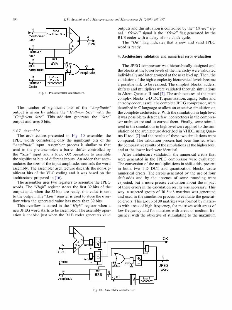
Fig. 9. Pre-assembler architecture.
494 L.V. Agostini et al. / Microprocessors and Microsystems 31 (2007) 487–497
The number of significant bits of the ‘‘Amplitude’’output is given by adding the ‘‘Huffman Size’’ with the‘‘Coefficient Size’’. This addition generates the ‘‘Size’’output and uses 5 bits.
3.4.7. Assembler
The architecture presented in Fig. 10 assembles theJPEG words considering only the significant bits of the‘‘Amplitude’’ input. Assembler process is similar to thatused in the pre-assembler: a barrel shifter controlled bythe ‘‘Size’’ input and a logic OR operation to assemblethe significant bits of different inputs. An adder that accu-mulates the sizes of the input amplitudes controls the wordassembly. The assembler architecture discards the non-sig-nificant bits of the VLC coding and it was based on thearchitecture proposed in [16].
The assembler uses two registers to assemble the JPEGwords. The ‘‘High’’ register stores the first 32 bits of theoutput and, when the 32 bits are ready, this value is sentto the output. The ‘‘Low’’ register is used to store the over-flow when the generated value has more than 32 bits.
This overflow is stored in the ‘‘High’’ register when anew JPEG word starts to be assembled. The assembly oper-ation is enabled just when the RLE coder generates valid
Fig. 10. Assemble
outputs and this situation is controlled by the ‘‘Okrle1’’ sig-nal. ‘‘Okrle1’’ signal is the ‘‘Okrle’’ flag generated by theRLE coder with a delay of one clock cycle.
The ‘‘OK’’ flag indicates that a new and valid JPEGword is ready.
4. Architecture validation and numerical error evaluation
The JPEG compressor was hierarchically designed andthe blocks at the lower levels of the hierarchy were validatedindividually and later grouped at the next level up. Then, thevalidation of the high complexity hierarchical levels becamea possible task to be realized. The simplest blocks: adders,shifters and multipliers were validated through simulationsin Altera Quartus II tool [7]. The architectures of the mostcomplex blocks: 2-D DCT, quantization, zigzag buffer andentropy coder, as well the complete JPEG compressor, weredescribed in C language to allow an extensive simulation onthe complete architecture. With the simulation in high levelit was possible to detect a few incorrectness in the compres-sor architecture and to correct them. Finally, some stimuliused in the simulations in high level were applied to the sim-ulation of the architecture described in VHDL using Quar-tus II tool [7] and the results of these two simulations werecompared. The validation process had been finished whenthe comparative results of the simulations at the higher leveland at the lower level were identical.
After architecture validation, the numerical errors thatwere generated in the JPEG compressor were evaluated.The conversion of the multiplications in shift-adds, presentin both, two 1-D DCT and quantization blocks, causenumerical errors. The errors generated by the use of fourshift-adds and by the absence of some rounding wereexpected, but a more precise evaluation about the impactof these errors in the calculation results was necessary. Thisway, a selected group of 30 8 · 8 matrixes was generatedand used in the simulation process to evaluate the generat-ed errors. This group of 30 matrixes was formed by matrix-es with areas of high frequency, for matrixes with areas oflow frequency and for matrixes with areas of medium fre-quency, with the objective of stimulating to the maximum
r architecture.
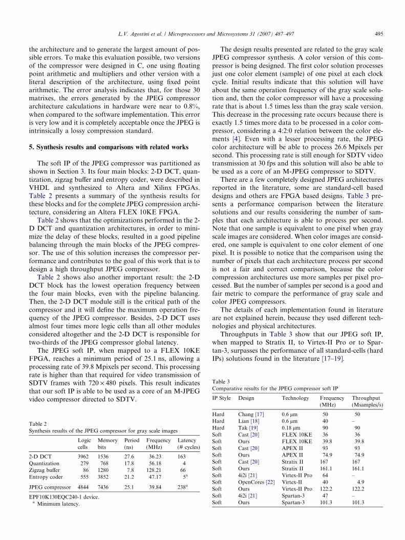
Table 3Comparative results for the JPEG compressor soft IP
IP Style Design Technology Frequency Throughput
L.V. Agostini et al. / Microprocessors and Microsystems 31 (2007) 487–497 495
the architecture and to generate the largest amount of pos-sible errors. To make this evaluation possible, two versionsof the compressor were designed in C, one using floatingpoint arithmetic and multipliers and other version with aliteral description of the architecture, using fixed pointarithmetic. The error analysis indicates that, for those 30matrixes, the errors generated by the JPEG compressorarchitecture calculations in hardware were near to 0.8%,when compared to the software implementation. This erroris very low and it is completely acceptable once the JPEG isintrinsically a lossy compression standard.
5. Synthesis results and comparisons with related works
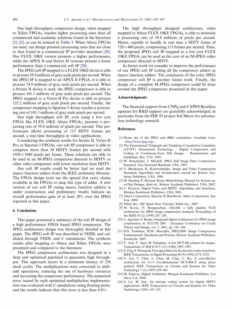
The soft IP of the JPEG compressor was partitioned asshown in Section 3. Its four main blocks: 2-D DCT, quan-tization, zigzag buffer and entropy coder, were described inVHDL and synthesized to Altera and Xilinx FPGAs.Table 2 presents a summary of the synthesis results forthese blocks and for the complete JPEG compression archi-tecture, considering an Altera FLEX 10KE FPGA.
Table 2 shows that the optimizations performed in the 2-D DCT and quantization architectures, in order to mini-mize the delay of these blocks, resulted in a good pipelinebalancing through the main blocks of the JPEG compres-sor. The use of this solution increases the compressor per-formance and contributes to the goal of this work that is todesign a high throughput JPEG compressor.
Table 2 shows also another important result: the 2-DDCT block has the lowest operation frequency betweenthe four main blocks, even with the pipeline balancing.Then, the 2-D DCT module still is the critical path of thecompressor and it will define the maximum operation fre-quency of the JPEG compressor. Besides, 2-D DCT usesalmost four times more logic cells than all other modulesconsidered altogether and the 2-D DCT is responsible fortwo-thirds of the JPEG compressor global latency.
The JPEG soft IP, when mapped to a FLEX 10KEFPGA, reaches a minimum period of 25.1 ns, allowing aprocessing rate of 39.8 Mpixels per second. This processingrate is higher than that required for video transmission ofSDTV frames with 720 · 480 pixels. This result indicatesthat our soft IP is able to be used as a core of an M-JPEGvideo compressor directed to SDTV.
Table 2Synthesis results of the JPEG compressor for gray scale images
Logiccells
Memorybits
Period(ns)
Frequency(MHz)
Latency(# cycles)
2-D DCT 3962 1536 27.6 36.23 163Quantization 279 768 17.8 56.18 4Zigzag buffer 86 1280 7.8 128.21 66Entropy coder 555 3852 21.2 47.17 5a
JPEG compressor 4844 7436 25.1 39.84 238a
EPF10K130EQC240-1 device.a Minimum latency.
The design results presented are related to the gray scaleJPEG compressor synthesis. A color version of this com-pressor is being designed. The first color solution processesjust one color element (sample) of one pixel at each clockcycle. Initial results indicate that this solution will haveabout the same operation frequency of the gray scale solu-tion and, then the color compressor will have a processingrate that is about 1.5 times less than the gray scale version.This decrease in the processing rate occurs because there isexactly 1.5 times more data to be processed in a color com-pressor, considering a 4:2:0 relation between the color ele-ments [4]. Even with a lesser processing rate, the JPEGcolor architecture will be able to process 26.6 Mpixels persecond. This processing rate is still enough for SDTV videotransmission at 30 fps and this solution will also be able tobe used as a core of an M-JPEG compressor to SDTV.
There are a few completely designed JPEG architecturesreported in the literature, some are standard-cell baseddesigns and others are FPGA based designs. Table 3 pre-sents a performance comparison between the literaturesolutions and our results considering the number of sam-ples that each architecture is able to process per second.Note that one sample is equivalent to one pixel when grayscale images are considered. When color images are consid-ered, one sample is equivalent to one color element of onepixel. It is possible to notice that the comparison using thenumber of pixels that each architecture process per secondis not a fair and correct comparison, because the colorcompression architectures use more samples per pixel pro-cessed. But the number of samples per second is a good andfair metric to compare the performance of gray scale andcolor JPEG compressors.
The details of each implementation found in literatureare not explained herein, because they used different tech-nologies and physical architectures.
Throughputs in Table 3 show that our JPEG soft IP,when mapped to Stratix II, to Virtex-II Pro or to Spar-tan-3, surpasses the performance of all standard-cells (hardIPs) solutions found in the literature [17–19].
(MHz) (Msamples/s)
Hard Chang [17] 0.6 lm 50 50Hard Lian [18] 0.6 lm 40 –Hard Tak [19] 0.18 lm 90 90Soft Cast [20] FLEX 10KE 36 36Soft Ours FLEX 10KE 39.8 39.8Soft Cast [20] APEX II 93 93Soft Ours APEX II 74.9 74.9Soft Cast [20] Stratix II 167 167Soft Ours Stratix II 161.1 161.1Soft 4i2i [21] Virtex-II Pro 64 –Soft OpenCores [22] Virtex-II 40 4.9Soft Ours Virtex-II Pro 122.2 122.2Soft 4i2i [21] Spartan-3 47 –Soft Ours Spartan-3 101.3 101.3
496 L.V. Agostini et al. / Microprocessors and Microsystems 31 (2007) 487–497
Our high throughput compressor design, when mappedto Xilinx FPGAs, reaches higher processing rates than allcommercial and academic solutions found in the literature[21,22], as can be noticed in Table 3. When Altera FPGAsare used, our design presents processing rates that are closeto that found in a commercial IP provider datasheet [20].Our FLEX 10KE version presents a higher performance,while the APEX II and Stratix II versions present a lowerperformance than a commercial soft IP [20].
The JPEG soft IP mapped to a FLEX 10KE device is ableto process 39.8 millions of gray scale pixels per second. Whenthe JPEG IP is mapped to an APEX II FPGA, it is able toprocess 74.9 millions of gray scale pixels per second. Whena Stratix II device is used, the JPEG compressor is able toprocess 161.1 millions of gray scale pixels per second. TheJPEG mapped to a Virtex-II Pro device is able to process122.2 millions of gray scale pixels per second. Finally, thecompressor mapping to Spartan-3 device reaches a process-ing rate of 101.3 millions of gray scale pixels per second.
Our high throughput soft IP, even using a low costFPGA like FLEX 10KE Altera FPGAs, presents a pro-cessing rate of 39.8 millions of pixels per second. This per-formance allows processing of 115 SDTV frames persecond, a real time throughput in video applications.
Considering the synthesis results for Stratix II, Virtex-IIPro or Spartan-3 FPGAs, our soft IP compressor is able tocompress more than 30 HDTV frames per second with1920 · 1080 pixels per frame. These solutions are able tobe used in an M-JPEG compressor directed to HDTV orother video compressor with lower resolution than HDTV.
Our soft IP results could be better had we used themacro function adders from the IEEE arithmetic libraries.The FPGA design tools use the special fast carry chainsavailable in the FPGAs to map this type of adder. A newversion of our soft IP (using macro function adders) isunder construction and preliminary results indicate anoverall performance gain of at least 20% over the JPEGreported in this paper.
6. Conclusions
This paper presented a summary of the soft IP design ofa high performance FPGA based JPEG compressor. TheJPEG architecture design was thoroughly detailed in thispaper. The JPEG soft IP was described in VHDL and val-idated through VHDL and C simulations. The synthesisresults after mapping to Altera and Xilinx FPGAs werepresented and compared to the literature.
The JPEG compressor architecture was designed in adeep and optimized pipelined to guarantee high through-put. This approach incurs in a minimum latency of 238clock cycles. The multiplications were converted to shift-add operations, reducing the use of hardware resourcesand increasing the compressor performance. The numericalerror caused by such optimized multiplierless implementa-tion was evaluated with C simulations using floating point,and the results indicate that this error is less than 0.8%.
The high throughput designed architecture, whenmapped to Altera FLEX 10KE FPGAs, is able to maintaina processing rate of 39.8 millions of pixels per second.Hence, capable to handle in real time a SDTV frame of720 · 480 pixels, compressing 115 frames per second. Then,the proposed JPEG soft IP mapped to a low cost FLEX10KE FPGA can be used as the core of an M-JPEG videocompressor directed to SDTV.
As future work we consider to improve the performanceof our JPEG soft IP coding all the compressor adders asmacro function adders. The conclusion of the color JPEGcompressor soft IP is another future work. Finally, thedesign of a complete M-JPEG compressor could be donearound the JPEG compressor presented in this paper.
Acknowledgments
The financial support from CNPq and CAPES Brazilianagencies for R&D support are gratefully acknowledged, inparticular from the PDI-TI project SoCMicro for informa-tion technology research.
References
[1] Home site of the JPEG and JBIG committees. Available from:<http://www.jpeg.org>.
[2] The International Telegraph and Telephone Consultative Committee(CCITT). Information Technology – Digital Compression andCoding of Continuous-Tone Still Images – Requirements andGuidelines. Rec. T.81, 1992.
[3] W. Pennebaker, J. Mitchell, JPEG Still Image Data CompressionStandard, Van Nostrand Reinhold, USA, 1992.
[4] V. Bhaskaran, K. Konstantinides, Image and Video CompressionStandards Algorithms and Architectures, second ed., Kluwer Aca-demic Publishers, USA, 1999.
[5] M. Keating, P. Bricaud, Reuse Methodology Manual for System-on-a-Chip Designs, third ed., Kluwer Academic Publishers, USA, 2002.
[6] C. Poynton, Digital Video and HDTV: Algorithms and Interfaces,Morgan Kaufmann Publishers, USA, 2003.
[7] Altera Corporation, Quartus II Handbook, Altera Corporation, SanJose, 2004.
[8] Xilinx Inc., ISE Quick Start Tutorial, Xilinx Inc., 2005.[9] M. Kovac, N. Ranganathan, JAGAR: a fully pipeline VLSI
architecture for JPEG image compression standard, Proceedings ofthe IEEE 83 (2) (1995) 247–258.
[10] L. Agostini, S. Bampi, Integrated digital architecture for JPEG imagecompression, in: ECCTD 2001 – European Conference on CircuitTheory and Design, vol. 3, 2001, pp. 181–184.
[11] D.S. Taubman, M.W. Marcellin, JPEG2000: Image CompressionFundamentals, Standards and Practice, Kluwer Academic Publishers,Dordrecht, 2002.
[12] Y. Arai, T. Agui, M. Nakajima, A fast DCT-SQ scheme for images,Transactions of IEICE E71 (11) (1988) 1095–1097.
[13] E. Feig, S. Winograd, Fast algorithms for the discrete cosine transform,IEEE Transactions on Signal Processing 40 (9) (1992) 2174–2193.
[14] Y. Lee, T. Chen, L. Chen, M. Chen, C. Ku, A cost-effectivearchitecture for 8 · 8 two-dimensional DCT/IDCT using directmethod, IEEE Transactions on Circuits and Systems for VideoTechnology 7 (3) (1997) 459–467.
[15] M. Ergovac, Digital Arithmetic, Morgan Kaufmann Publishers, LosAltos, CA, 2004.
[16] S. Lei, M. Sun, An entropy coding system for digital HDTVapplications, IEEE Transactions on Circuits and Systems for VideoTechnology (1991) 147–155.
Ivan Saraiva Silva received the Electrical Engineer
degree and the M.Sc. in Electrical Engineering
degree from Federal University of Paraıba, Brazil.
Received the Ph.D. in Informatics from Universite
Pierre et Marie Curie – Paris VI, France. Actually he
is professor at Federal University of Rio Grande do
Norte, Brazil.
L.V. Agostini et al. / Microprocessors and Microsystems 31 (2007) 487–497 497
[17] H. Chang, L. Chen, C. Lian, Y. Chang, L. Chen, IP design of areconfigurable baseline JPEG coding, in: AP-ASIC 1999. IEEE AsiaPacific Conference on ASICS, 1999, pp. 143–146.
[18] C. Lian, L. Chen, H. Chang, Y. Chang, Embedded JPEG encoder IPcore and memory efficient preprocessing architecture for scanner, in:APCCAS 2000 – IEEE Asia-Pacific Conference on Circuits andSystems, 2000, pp. 686–689.
[19] Tak’ASICS, JPEG IP. Available from: <http://www.takasic.com/prod_vdev_jpeg.php>, 2005.
[20] Cast Inc., JPEG-E: baseline JPEG encoder megafunction. Availablefrom: <http://www.cast-inc.com/cores/jpeg-e/cast_jpeg-e.pdf>, 2005.
[21] 4i2i Communications Ltd, JPEG encoder. Available from: <http://www.4i2i.com/downloads/AllianceCoreMJPEGencoder.pdf>, 2005.
[22] OpenCores.org, JPEG Hardware compressor: overview. Availablefrom: <http://www.opencores.org/projects.cgi/web/jpeg/overview>,2005.
Luciano Volcan Agostini received the B.S. degree in
computer science from Federal University of Pelo-
tas, Brazil, and the M.S. degree from Federal
University of Rio Grande do Sul, Brazil. He is
currently pursuing a Ph.D. degree at UFRGS.
Since August 2002 he is professor at Federal
University of Pelotas.
Sergio Bampi received the Electronics Engineer and
the Physicist degrees from Federal University of
Rio Grande do Sul. He received the MSEE and
Ph.D. in Electrical Engineering degrees from Stan-
ford University. He is professor since 1981 at the
Informatics Institute at the Federal University of
Rio Grande do Sul, Brazil.


