Embed Size (px)
Citation preview
International Journal of Application or Innovation in Engineering & Management (IJAIEM) Web Site: www.ijaiem.org Email: [email protected]
Volume 3, Issue 5, May 2014 ISSN 2319 - 4847
Volume 3, Issue 5, May 2014 Page 315
Abstract
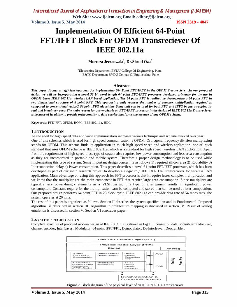
This paper discuss an efficient approach for implementing 64- Point FFT/IFFT in the OFDM Transreciever .In our proposed design we will be incorporating a novel 32 bit word length 64 point FFT/IFFT processor developed primarily for the use in OFDM bases IEEE 802.11a wireless LAN based application. The 64 point FFT is realized by decomposing a 64 point FFT in two dimensional structure of 8 point FFT. This approach greatly reduces the number of complex multiplication required as compared to conventional radix-2 64 point FFT algorithm. Same unit can be used for both FFT and IFFT by just swapping its real and imaginary parts The main reason for our emphasis on FFT/IFFT processor in the design of IEEE 802.11a Transreciever is because of its ability to provide orthogonality to data carrier that forms the essence of any OFDM scheme. Keywords: FFT/IFFT, OFDM, ROM, IEEE 802.11a, HDL. 1. INTRODUCTION As the need for high speed data and voice communication increases various technique and scheme evolved over year. One of this schemes which is used for high speed communication is OFDM. Orthogonal frequency division multiplexing stands for OFDM. This scheme finds its application in much high speed wired and wireless application. one of such standard that uses OFDM scheme is IEEE 802.11a, which is a standard for high speed wireless LAN application. Apart from the requirement of high speed these type of system also requires low power consumption and less area consumption as they are incorporated in portable and mobile system. Therefore a proper design methodology is to be used while implementing this type of system. Some important design concern is as follows 1) required silicon area 2) Routability 3) Interconnection delay 4) Power consumption. This paper describes a novel 64-point FFT/IFFT processor, which has been developed as part of our main research project to develop a single chip IEEE 802.11a Transreciever for wireless LAN application. Main advantage of using this approach for FFT processor is that it require lesser complex multiplication and we know that the multiplier are the main component in FFT that require large area consumption. Since multipliers are typically very power-hungry elements in a VLSI design, this type of arrangement results in significant power consumption. Constant require for the multiplication cam be computed and stored that can be used at later computation. Our proposed design performs 64 point FFT in 23 clock cycle. IEEE 802.11a can provide data rate of 54 mbps max. the system operates at 20 mhz. The rest of this paper is organized as follows. Section II describes the system specification and its Fundamental. Proposed algorithm is described in section III. Algorithm to architecture mapping is discussed in section IV. Result of verilog emulation is discussed in section V. Section VI concludes paper. 2. SYSTEM SPECIFICATION Complete structure of proposed modem design of IEEE 802.11a is shown in Fig.1. It consist of data scrambler/randomizer, channel encoder, Interleaver , Modulator, 64-point IFFT/FFT, Demodulator, De-Interleaver, Descrambler.
Figure 7 Block diagram of the physical layer of an IEEE 802.11a Transreciever
Implementation Of Efficient 64-Point FFT/IFFT Block For OFDM Transreciever Of
IEEE 802.11a
Murtuza Jeeranwala1, Dr.Shruti Oza2
1Electronics Department BVDU College Of Engineering, Pune. 2E&TC Department BVDU College Of Engineering, Pune
International Journal of Application or Innovation in Engineering & Management (IJAIEM) Web Site: www.ijaiem.org Email: [email protected]
Volume 3, Issue 5, May 2014 ISSN 2319 - 4847
Volume 3, Issue 5, May 2014 Page 316
The standard specification of our system specifies the data rate of 6-54 Mbps depending upon type of modulation technique used viz. BPSK,QPSK,16-QAM,64-QAM.we will be using 64-QAM for our design. Encoding rate supported are ½, 2/3, ¾. Bandwidth of transmitted signal is 20 Mhz and the OFDM symbol time duration is 4µs which comprises of 0.8µs of guard interval. Thus for implementation our FFT/IFFT should be calculated within 4µs. Generally there are two ways of implementing FFT transform 1) Direct Fourier Transform implementation 2) Direct hardware implementation based on FFT signal flow graph. Main disadvantage of using this technique is excessive wring requirement, high timing delay and high power and area consumption. Conventional Cooley and Tuckey radix-2 FFT algorithm requires 192 complex butterfly to be calculated . Considering our requirement of one FFT to be computed within 4µs, one butterfly unit must be calculated in 48Mhz clock cycle that is 20.8ns for each butterfly. In order to satisfy the timing requirement one has to implement multiple butterfly computation using parallel implementation. Main motivation our works come from the fact that the IEEE 802.11a design must meet the standard specification by satisfying the timing constraints and requiring moderate silicon area and low power consumption. One of the main advantage of our implementation is that complex multiplier required for calculating the complex term that is referred in later section can be implemented using shift and add operation only. Since multiplier are very power hungry and area consuming.
Table 3 IEEE 802.11a SPECIFICATION
Bandwidth 20MHz Operational Bandwidth 16.MHz Subcarrier spacing 312.5KHz(20/64 point FFT) Information Rate 6-54Mbps Modulation BPSK,QPSK,16-QAM,64-QAM Coding Rate ½ Total subcarrier 52(-26 to +26) Total data carrier 48
3. ALGORITHM FORMULATION DFT(Discrete Fourier Transform) A(r) of a complex set of data sequence B(k) of length N where r, k is{0 to N-1} is described by following equation
(1) Where if we make N=MT,r=s+T t and K=r+Mm where s,l is {0,1....7} and m,t is {0,1...T-1} , Applying these values in (1) we get
(2) Eq(2) means that it is possible to realize the FFT of length N by decomposing it into M and T point FFT N=MT, and then combining them. This result in a two dimensional structure. If we take M=8 and T=8 it is possible to formulate 64 Point FFT as
(3) From eq(3) it is quite evident that it is possible to decompose a 64 point FFT into two 8-point FFT of length 8 plus 64 complex intermediate complex multiplication given by though there are 64 constant multiplication needed but he number of non trivial complex multiplication are only 49. From incoming data every 8-data point are selected and undergoes 8-point FFT computation followed by multiplication with complex constant term. These complex constants are also termed as twiddle factors . Eight such computations is needed to produce 64 intermediate term which again undergoes through second 8-point FFT unit. Proper reshuffling of data output coming from second FFT unit results in final output of 64-point FFT. Another important fact regarding this algorithm is that 8-point FFT block stated here doesn’t require any explicit complex twiddle factor for calculations. The only required constant are 1, j, (0.707+0.707j). first two are mere multiplication of 1 with real and complex term last term can be obtained by shift and add operation . Thus it doesn’t requires any extra digital multiplier and hence provide an effective way of implementing 64-point FFT with minimal hardware requirement. So if we compare our algorithm with conventional radix-2 64 point FFT , proposed model requires only 49 complex nontrivial multiplication with input data stream on the other hand conventional approach requires 66 nontrivial calculation so there is reduction of 26% of complex multiplication Both FFT and IFFT part requires same approach the only difference is that for IFFT calculation we first swap both real and imaginary terms at input and again swap them at output. This method allows us to perform both IFFT/FFT using same architecture without need of any change in internal coefficient. Although on comparing the proposed method with radix 4 FFT in terms of arithmetic complexity we found that there is not much reduction in complex multiplication i.e radix 4 FFT requires only 5 more complex multiplication as compared to 49 of proposed method 4. ARCHITECTURE FOR 64-POINT IFFT/FFT BLOCK

International Journal of Application or Innovation in Engineering & Management (IJAIEM) Web Site: www.ijaiem.org Email: [email protected]
Volume 3, Issue 5, May 2014 ISSN 2319 - 4847
Volume 3, Issue 5, May 2014 Page 317
Block diagram for 64-point FFT /IFFT block is shown in figure-3. Main units in this block are as follows 1) input unit 2) Two 8-point FFT block 3) A complex multiplier block 4) Intermediate memory register block (CB) 5) Output unit. To achieve efficient algorithm to architecture mapping several special strategies are adopted that will be discussed in later section.
Figure 8 Block Diagram of internal architecture of proposed 64-point IFFT/FFT block
Input unit The input unit consist of an register bank (reg(0 to 56)) having 32 bit word length i.e 16 bit real and 16 bit complex bit that can store 57 complex data. Three additional registers are also provide in order to maintain the timing specification required for each block. The input unit have to single bit input signal Data_start, Mode signal. Assertion of data_start signal indicates valid input stream and Mode signal is used in order to switch between FFT/IFFT operation. Downward shifting of data in input register is synchronized by master clock
Eight point FFT unit Radix -2 DIT FFT technique is chosen to construct a 8-Point FFT unit. This algorithm is selected due to the fact that this approach requires simple addition and subtraction and a single complex constant or Twiddle factor that can be obtained by simple shift and add operation only. Full computation of 8-point FFT is carried out in single clock cycle.
Multiplier unit Multiplier unit is a tricky structure in our proposed design from eq (3) it is evident that we need 49 non-trivial complex multiplications constant ( . Further examination of these constant shows that there are only nine set of these constant that are unique. They are They are (1,0), (0.995178, 0.097961), (0.980773,0.195068), (0.956909, 0.290283), (0.923828, 0.382629), (0.881896, 0.471374), (0.831420, 0.555541), (0.773010, 0.634338), (0.707092, 0.707092),. In each of this constant the first part represents cosine term and last part represents the sine term. Entire constant multiplication operation can be carried out using only these nine constant by appropriate swapping of there real and imaginary term. This implies that one just need to store this eight constant only, there by greatly reducing the memory storage requirement. The fact that the multipliers constant are known in advance greatly reduce our burden of calculating each of these constant using shift and add operation. Input set of data coming from 8-point FFT block is rearranged such that each constant is multiplied accordingly to the input set, condition may arise that certain set of constant are used more than one time in the calculation of output. The reuse leads to increase in clock cycle but it is unavoidable. Block diagram of multiplier unit is shown in fig (3).
Figure 9 Block diagram of complete multiplier unit
Data shuffle network at input and output side performs the function of aligning the input data set coming to multiplier box and output going towards toward the internal storage register (CB). Using this arrangement whole computation can be performed in 12 clock cycle instead of spending 49 clock cycle which is required for conventional computation. As we
International Journal of Application or Innovation in Engineering & Management (IJAIEM) Web Site: www.ijaiem.org Email: [email protected]
Volume 3, Issue 5, May 2014 ISSN 2319 - 4847
Volume 3, Issue 5, May 2014 Page 318
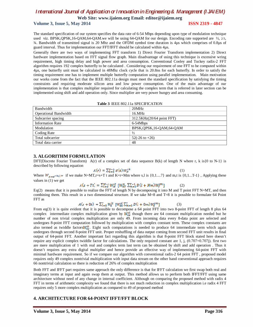
know from above discussion that FFT computation is performed in one clock cycle and multiplier block requires more time so the data coming out from the FFT unit has to be kept until multiplication of full set is completed. this is achieved by suspending the downward shifting of data in input register for this clock cycle and once the multiplication of first set is completed the downward shifting can again be resumed. Internal Register Bank (CB) As compared to Input unit the only difference between CB and Input unit is that for internal register bank no separate register are required and no swapping unit is required as in the case of Input unit. The internal register bank is a 32 bit word length register used to store 64 output coming from multiplier block. It has eight hardwired output positioned at 8j where j is {0,1..,7}. These outputs are directly connected to the input of second 8-point FFT unit. As soon as the register bank gets full the data start to shift down means data at i position goes to (i-1) position. Downward shifting takes one clock cycle for each shift and continue for 8 clock cycle. Output unit Output unit follows same mechanism as input unit but its complementary in nature. Output from second 8-point FFT unit is directly mapped into 8i position where i is{0,1,...,7}. The final output is taken serially from the 0th position . as the next set of 8 input arrives at 8i previous data gets downshifted to i-1 position. A data_out signal is generated by control logic which implies that the valid data will available at 0th position on next clock cycle. This signal remain asserted for next 64 clock cycles. Control logic Entire unit is controlled by a 5-bit binary counter that starts counting from zero. start_count signal is asserted when 56th position of Input register bank is filled. First output data at 0th position of output register is available at count number 16. Complete set of output data are stored in output register at count 23. At this point data_start signal is asserted and remain high for next 64 clock cycle. 5. RESULTS & DISCUSSIONS Complete hardware is described in verilog HDL and it is simulated & verified to check its functionality in Mentor Graphic’s Modelsim 6.3f simulator Xilinx Isim simulator. In the below figures we will be showing the simulation result for 64-point FFT/IFFT.
Figure 10 Simulation result of first 8-point FFT block
Figure 11 Results of multiplier unit
International Journal of Application or Innovation in Engineering & Management (IJAIEM) Web Site: www.ijaiem.org Email: [email protected]
Volume 3, Issue 5, May 2014 ISSN 2319 - 4847
Volume 3, Issue 5, May 2014 Page 319
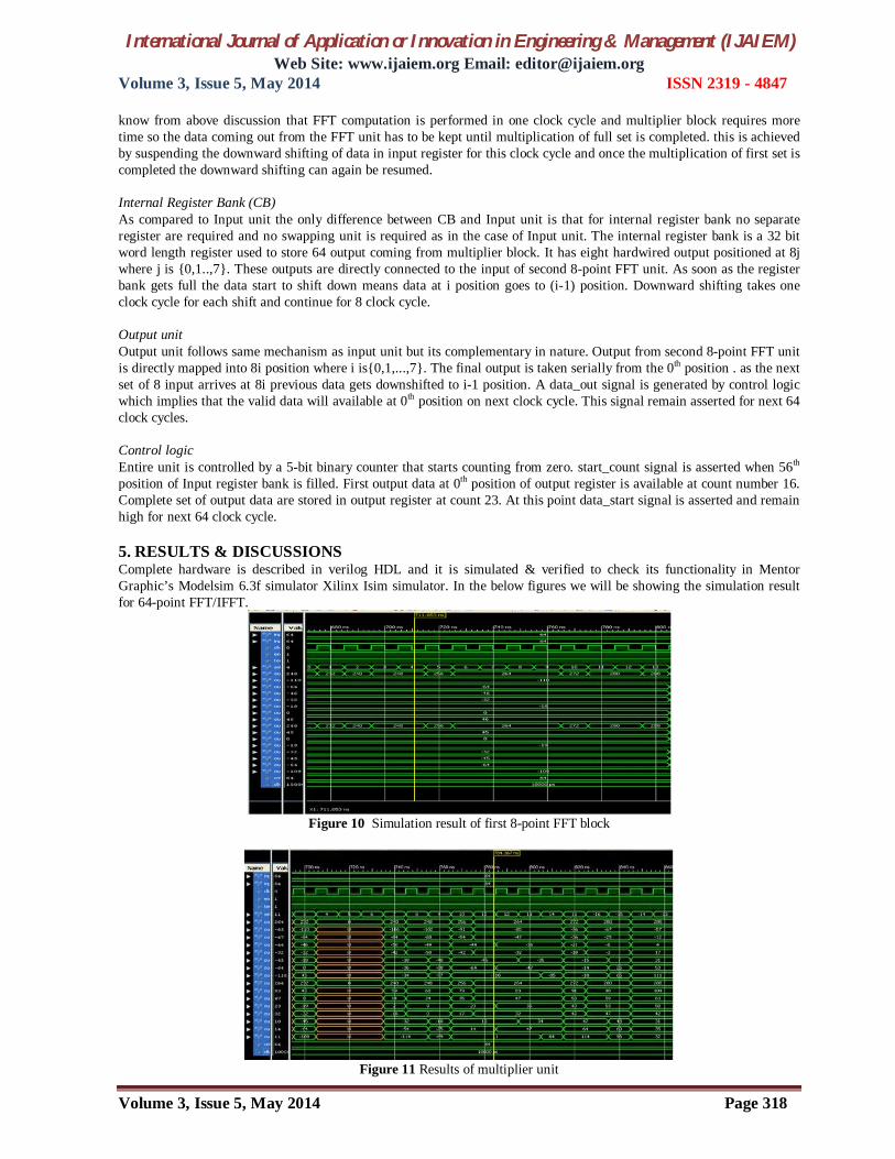
Figure 12 Result of Internal Register Bank
Figure 13 Simulation result for second 8-point FFT block
6 . CONCLUSION Proposed method describes a novel 64-point IFFT/FFT architecture to be used in high speed WLAN system based on OFDM transmission. The architecture is based on the technique of decomposing a 64-point FFT into two 8-point FFT. Proposed technique exhibits attractive features like modularity, regularity, simple wiring and high throughput. This architecture consumes less silicon area and results in considerable reduction in cost. Both IFFT/FFT can be realized by same architecture we just have to swap real and imaginary part. Number of non-trivial complex multiplication are 49 that is 26% less than required by radix-2 64 point FFT. For computation of IFFT/FFT full parallel scheme is adopted there by making it very fast. Complex multiplication constant are calculated using shift and add operation there by reducing area and power consumption as compared to multiplier. With proposed design full parallel 64 point FFT/IFFT can be computed in 23 clock cycles.
References [1] JOAQUIN GARCIA, RENE CUMPLIDO “ON THE DESIGN OF AN FPGA-BASED OFDM MODULATOR FOR IEEE 80211A. “ 2ND
INTERNATIONAL CONFERENCE ON ELECTRICAL AND ELECTRONICS ENGINEERING (ICEEE) AND XI CONFERENCE ON ELECTRICAL ENGINEERING (CIE 2005)
[2] Magis Networks, Inc. “Orthogonal Frequency Division Multiplexing (OFDM) Explained” February 8, 2001. [3] Manjunath Lakkannavar, Ashwini Desai “Design and Implementation of OFDM (Orthogonal Frequency Division
Multiplexing) using VHDL and FPGA”. ISSN: 2249 – 8958, Volume-1, Issue-6, August 2012 [4] International Engineering Consortium “An Introduction to OFDM”, [5] Loo Kah Cheng “Design of an OFDM Transmitter and Receiver using FPGA” UTM, 2004. [6] Ahmed Saeed, M. Elbably, G. Abdelfadeel, and M. I. Eladawy “Efficient FPGA implementation of FFT/IFFT”. [7] Koushik Maharatna, Eckhard Grass, and Ulrich Jagdhold ”A 64-Point Fourier Transform Chip for High-Speed
Wireless LAN Application Using OFDM” IEEE JOURNAL OF SOLID-STATE CIRCUITS, VOL. 39, NO. 3, MARCH 2004
International Journal of Application or Innovation in Engineering & Management (IJAIEM) Web Site: www.ijaiem.org Email: [email protected]
Volume 3, Issue 5, May 2014 ISSN 2319 - 4847
Volume 3, Issue 5, May 2014 Page 320
[8] (2002) The IEEE website. [Online]. Available: http://www.ieee.org/. [9] http://wireless.agilent.com/wireless/helpfiles/89600B/WebHelp/Subsystems/wlan-ofdm/Content/ofdm_80211-
overview.htm/ [10] Zafar Iqbal, Saeid Nooshabadi, Heung-No Lee “ Analysis and design of coding and interleaving in MIMO-OFDM
system” IEEE TRANSACTION ON CONSUMER ELECTRONICS VOL.58,NO..3AUGUST2012.


