Embed Size (px)
Citation preview
PR
OD
UC
T P
RE
VIE
W
UCD3138
www.ti.com SLUSAP2 –JANUARY 2012
Highly Integrated Digital Controller for Isolated PowerCheck for Samples: UCD3138
1 Introduction
1.1 Features1
– Synchronous Rectifier Soft On/Off• Digital Control of up to 3 IndependentFeedback Loops – Low IC Standby Power– Dedicated PID based hardware • Soft Start / Stop with and without Pre-bias– 2-pole/2-zero configurable • Fast Input Voltage Feed Forward Hardware– Programmable • Primary Side Voltage Sensing– Non-Linear Control • Copper Trace Current Sensing
• Up to 16MHz Error Analog to Digital Converter • Flux and Phase Current Balancing for(EADC) Non-Peak Current Mode Control Applications– Configurable Resolution as Small as • Current Share Bus Support
1mV/LSB – Analog Average– Automatic Resolution Selection – Master/Slave– Up to 8x Oversampling • Feature Rich Fault Protection Options– Hardware Based Averaging ( up to 8x) – 7 High Speed Analog Comparators– 14 bit Effective DAC – Cycle-by-Cycle Current Limiting
• Up to 8 High Resolution Digital Pulse Width – Programmable Fault CountingModulated (DPWM) Outputs – External Fault Inputs– 250ps Pulse Width Resolution – 4–10 Digital Comparators– 4ns Frequency Resolution – Programmable blanking time– 4ns Phase Resolution • Synchronization of DPWM waveforms between– Adjustable Phase Shift Between Outputs multiple UCD313x devices– Adjustable Dead-band Between Pairs • 14 channel, 12 bit, 265 ksps General Purpose– Up to 2MHz Switching Frequency ADC with integrated
• Configurable PWM Edge Movement – Programmable averaging filters– Trailing Modulation – Dual sample and hold– Leading Modulation • Internal Temperature Sensor– Dual Edge Modulation • Fully Programmable High-Performance
31.25MHz, 32-bit ARM7TDMI-S Processor• Configurable Feedback Control– 32 kByte (kB) Program Flash– Voltage Mode– 2 kB Data Flash with ECC– Average Current Mode– 4 kB Data RAM– Peak Current Mode Control– 4 kB Boot ROM Enables Firmware Boot-Load– Constant Current
in the Field via I2C or UART– Constant Power• Communication Peripherals• Configurable Modulation Methods
– I2C/PMBus– Frequency Modulation– 2 UARTs– Phase Shift Modulation
• JTAG Debug Port– Pulse Width Modulation• Timer capture with selectable input pins• Fast, Automatic and Smooth Mode Switching• Up to 5 Additional General Purpose Timers– Frequency Modulation and PWM• Built In Watchdog: BOD and POR– Phase Shift Modulation and PWM• 64-pin QFN and 40-pin QFN packages• High Efficiency and Light Load Management• Operating Temperature: –40°C to 125°C– Burst Mode• Fusion Digital Power GUI Support– Ideal Diode Emulation
1
Please be aware that an important notice concerning availability, standard warranty, and use in critical applications of TexasInstruments semiconductor products and disclaimers thereto appears at the end of this data sheet.
PRODUCT PREVIEW information concerns products in the formative or design phase of Copyright © 2012, Texas Instruments Incorporateddevelopment. Characteristic data and other specifications are design goals. TexasInstruments reserves the right to change or discontinue these products without notice.
PR
OD
UC
T P
RE
VIE
W
UCD3138
SLUSAP2 –JANUARY 2012 www.ti.com
1.2 Applications• Power Supplies and Telecom Rectifiers• Power Factor Correction• Isolated dc-dc Modules
2 Overview
2.1 Description
The UCD3138 is a digital power supply controller from Texas Instruments offering superior levels ofintegration and performance in a single chip solution. The flexible nature of the UCD3138 makes itsuitable for a wide variety of power conversion applications. In addition, multiple peripherals inside thedevice have been specifically optimized to enhance the performance of ac/dc and isolated dc/dcapplications and reduce the solution component count in the IT and network infrastructure space.
The UCD3138 is a fully programmable solution offering customers complete control of their application,along with ample ability to differentiate their solution. At the same time, TI is committed to simplifying ourcustomer’s development effort through offering best in class development tools, including applicationfirmware, Code Composer Studio™ software development environment, and TI’s Fusion PowerDevelopment GUI which enables customers to configure and monitor key system parameters.
At the core of the UCD3138 controller are the digital control loop peripherals, also known as Fusion DigitalPower Peripherals (FDPP). Each FDPP implements a high speed digital control loop consisting of adedicated Error Analog to Digital Converter (EADC), a PID based 2 pole–2 zero digital compensator andDPWM outputs with 250 ps pulse width resolution. The device also contains a 12-bit, 265ksps generalpurpose ADC with up to 14 channels, timers, interrupt control, JTAG debug and PMBus and UARTcommunications ports. The device is based on a 32-bit ARM7TDMI-S RISC microcontroller that performsreal-time monitoring, configures peripherals and manages communications. The ARM microcontrollerexecutes its program out of programmable flash memory as well as on-chip RAM and ROM.
In addition to the FDPP, specific power management peripherals have been added to enable highefficiency across the entire operating range, high integration for increased power density, reliability, andlowest overall system cost and high flexibility with support for the widest number of control schemes andtopologies. Such peripherals include: light load burst mode, synchronous rectification, LLC and phaseshifted full bridge mode switching, input voltage feed forward, copper trace current sense, ideal diodeemulation, constant current constant power control, synchronous rectification soft on and off, peak currentmode control, flux balancing, secondary side input voltage sensing, high resolution current sharing,hardware configurable soft start with pre bias, as well as several other features. Topology support hasbeen optimized for voltage mode and peak current mode controlled phase shifted full bridge, single anddual phase PFC, bridgeless PFC, hard switched full bridge and half bridge, and LLC half bridge and fullbridge.
2 Overview Copyright © 2012, Texas Instruments Incorporated
Submit Documentation FeedbackProduct Folder Link(s): UCD3138
PR
OD
UC
T P
RE
VIE
W
UCD3138
www.ti.com SLUSAP2 –JANUARY 2012
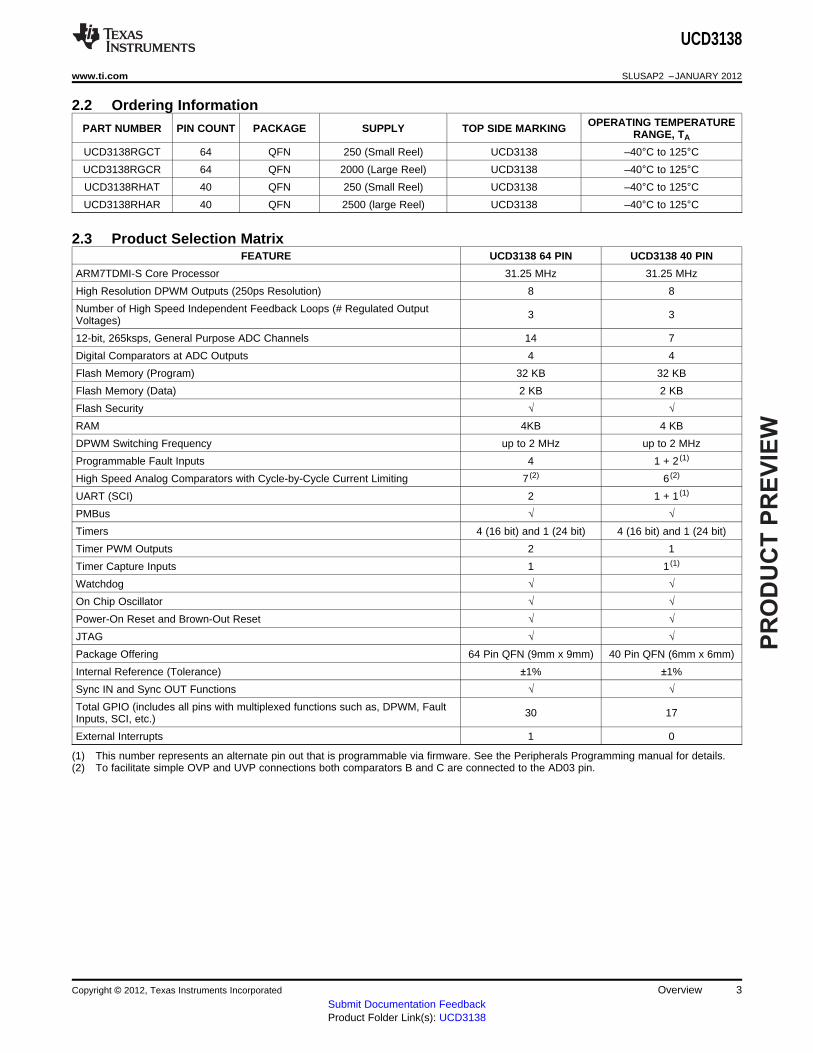
2.2 Ordering InformationOPERATING TEMPERATUREPART NUMBER PIN COUNT PACKAGE SUPPLY TOP SIDE MARKING RANGE, TA
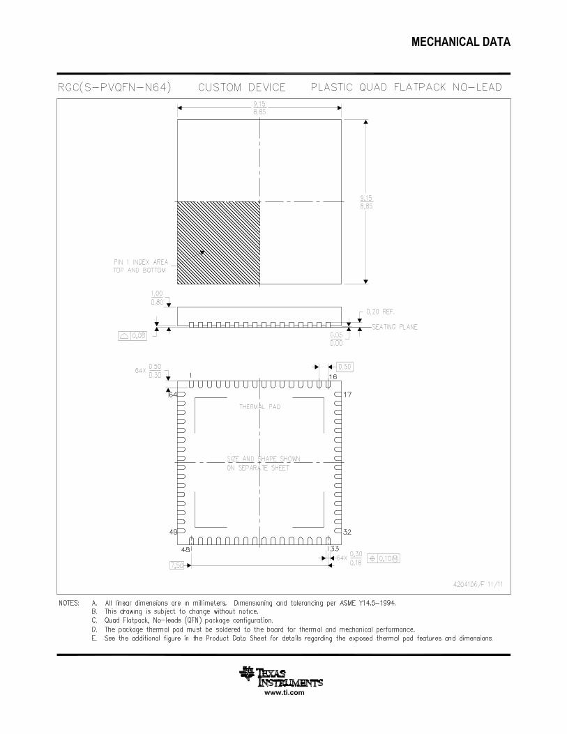
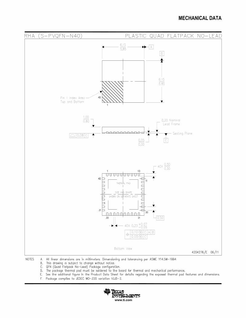
UCD3138RGCT 64 QFN 250 (Small Reel) UCD3138 –40°C to 125°CUCD3138RGCR 64 QFN 2000 (Large Reel) UCD3138 –40°C to 125°CUCD3138RHAT 40 QFN 250 (Small Reel) UCD3138 –40°C to 125°CUCD3138RHAR 40 QFN 2500 (large Reel) UCD3138 –40°C to 125°C
2.3 Product Selection MatrixFEATURE UCD3138 64 PIN UCD3138 40 PIN
ARM7TDMI-S Core Processor 31.25 MHz 31.25 MHz
High Resolution DPWM Outputs (250ps Resolution) 8 8
Number of High Speed Independent Feedback Loops (# Regulated Output 3 3Voltages)
12-bit, 265ksps, General Purpose ADC Channels 14 7
Digital Comparators at ADC Outputs 4 4
Flash Memory (Program) 32 KB 32 KB
Flash Memory (Data) 2 KB 2 KB
Flash Security √ √RAM 4KB 4 KB
DPWM Switching Frequency up to 2 MHz up to 2 MHz
Programmable Fault Inputs 4 1 + 2 (1)
High Speed Analog Comparators with Cycle-by-Cycle Current Limiting 7 (2) 6 (2)
UART (SCI) 2 1 + 1 (1)
PMBus √ √Timers 4 (16 bit) and 1 (24 bit) 4 (16 bit) and 1 (24 bit)
Timer PWM Outputs 2 1
Timer Capture Inputs 1 1 (1)
Watchdog √ √On Chip Oscillator √ √Power-On Reset and Brown-Out Reset √ √JTAG √ √Package Offering 64 Pin QFN (9mm x 9mm) 40 Pin QFN (6mm x 6mm)
Internal Reference (Tolerance) ±1% ±1%
Sync IN and Sync OUT Functions √ √Total GPIO (includes all pins with multiplexed functions such as, DPWM, Fault 30 17Inputs, SCI, etc.)
External Interrupts 1 0
(1) This number represents an alternate pin out that is programmable via firmware. See the Peripherals Programming manual for details.(2) To facilitate simple OVP and UVP connections both comparators B and C are connected to the AD03 pin.
Copyright © 2012, Texas Instruments Incorporated Overview 3Submit Documentation FeedbackProduct Folder Link(s): UCD3138
PR
OD
UC
T P
RE
VIE
W
UCD3138
(64 QFN)
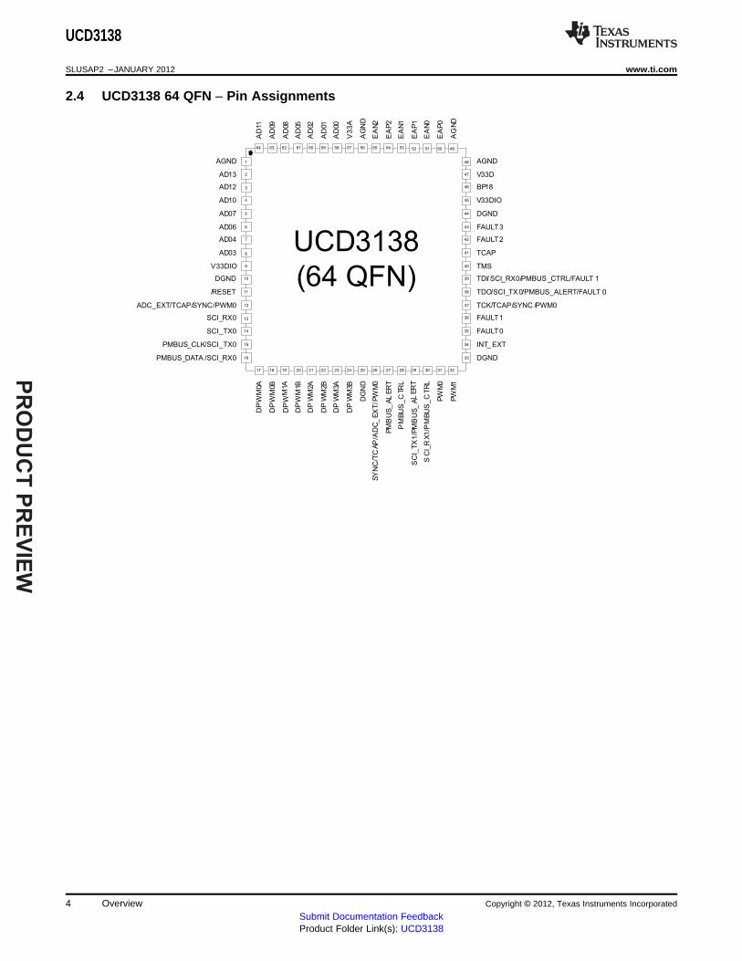
1AGND
2AD13
3AD12
4AD10
5AD07
6AD06
7AD04
8AD03
9V33DIO
10
/RESET 11
ADC_EXT/TCAP/SYNC/PWM0 12
SCI_RX0 13
SCI_TX0 14
DGND
15PMBUS_CLK/SCI_TX0
16PMBUS_DATA /SCI_RX0
48 AGND
47 V33D
46 BP18
45 V33DIO
44 DGND
43 FAULT3
42 FAULT2
41 TCAP
40 TMS
39 TDI/ SCI_RX0/PMBUS _CTRL/FAULT 1
38 TDO/SCI_TX 0/PMBUS_ALERT/FAULT 0
37 TCK/TCAP/SYNC /PWM0
36 FAULT1
35 FAULT0
34 INT_ EXT
33 DGND
32
PW
M1
31
PW
M0
30
SC
I_R
X1
/PM
BU
S_
CT
RL
29
SC
I_T
X1
/PM
BU
S_
AL
ER
T
28
PM
BU
S_
CTR
L
27
PM
BU
S_
AL
ER
T
26
SY
NC
/TC
AP
/AD
C_
EX
T/P
WM
025
DG
ND
24
DP
WM
3B
23
DP
WM
3A
22
DP
WM
2B
21
DP
WM
2A
20
DP
WM
1B
19
DP
WM
1A
18
DP
WM
0B
17
DP
WM
0A
64
AG
ND
63
EA
P0
62
EA
N0
61
EA
P1
60
EA
N1
59
EA
P2
58
EA
N2
57
AG
ND
56
V3
3A
55
AD
00
54
AD
01
53
AD
02
52
AD
05
51
AD
08
50
AD
09
49
AD
11
UCD3138
SLUSAP2 –JANUARY 2012 www.ti.com
2.4 UCD3138 64 QFN – Pin Assignments
4 Overview Copyright © 2012, Texas Instruments Incorporated
Submit Documentation FeedbackProduct Folder Link(s): UCD3138
PR
OD
UC
T P
RE
VIE
W
UCD3138
(40 QFN)
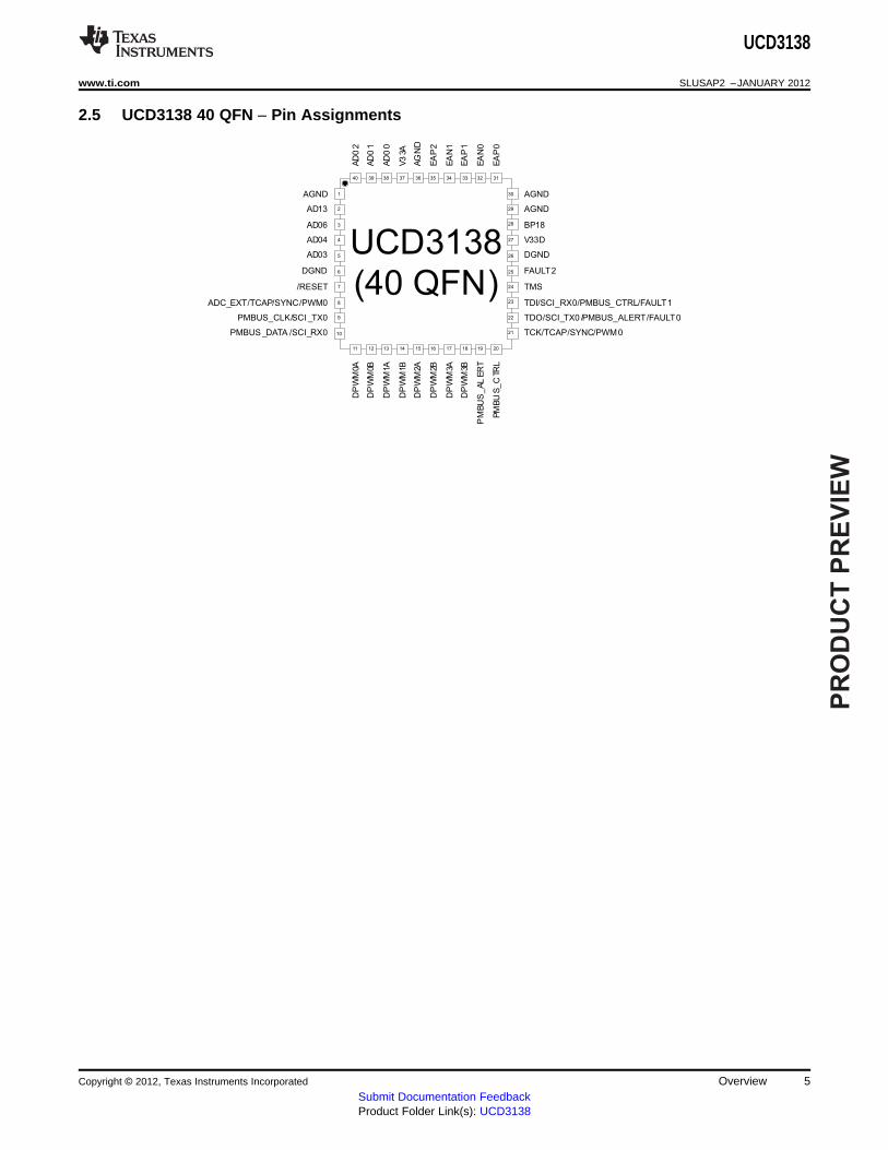
1AGND
2
3
4
5
AD13
6
AD06
7
AD04
8
AD03
9
DGND
10
/RESET
11
ADC_EXT/TCAP/SYNC/PWM0
12 13 14 15
PMBUS_CLK/SCI _TX0
16
PMBUS _DATA /SCI_RX0
AGND
BP18
DGND
V33D
40 39
TMS
38
TDI/SCI_RX0/PMBUS_ CTRL/FAULT1
37
TDO/SCI_TX0 /PMBUS_ALERT/FAULT0
36
TCK/TCAP/SYNC/PWM0
35 34 33
FAULT2
32 31
AGND
30
29
28
27
26
DP
WM
3B
25
DP
WM
3A
24
PM
BU
S_
CTR
L
23
PM
BU
S_
AL
ER
T
22
DP
WM
2B
21
DP
WM
2A
20
DP
WM
1B
19
DP
WM
1A
18
DP
WM
0B
17
DP
WM
0A
EA
P0
EA
N0
EA
P1
EA
N1
EA
P2
AG
ND
V3
3A
AD
00
AD
01
AD
02
UCD3138
www.ti.com SLUSAP2 –JANUARY 2012
2.5 UCD3138 40 QFN – Pin Assignments
Copyright © 2012, Texas Instruments Incorporated Overview 5Submit Documentation FeedbackProduct Folder Link(s): UCD3138
PACKAGE OPTION ADDENDUM
www.ti.com 7-Feb-2012
Addendum-Page 1
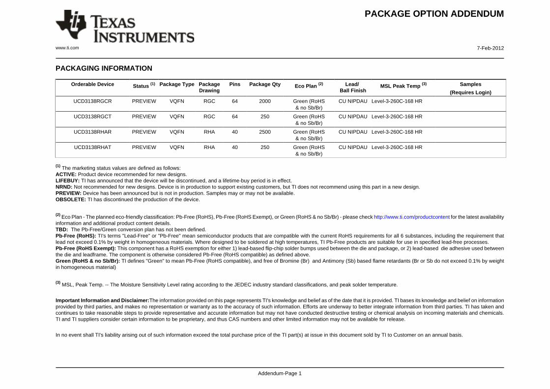
PACKAGING INFORMATION
Orderable Device Status (1) Package Type PackageDrawing
Pins Package Qty Eco Plan (2) Lead/Ball Finish
MSL Peak Temp (3) Samples
(Requires Login)
UCD3138RGCR PREVIEW VQFN RGC 64 2000 Green (RoHS& no Sb/Br)
CU NIPDAU Level-3-260C-168 HR
UCD3138RGCT PREVIEW VQFN RGC 64 250 Green (RoHS& no Sb/Br)
CU NIPDAU Level-3-260C-168 HR
UCD3138RHAR PREVIEW VQFN RHA 40 2500 Green (RoHS& no Sb/Br)
CU NIPDAU Level-3-260C-168 HR
UCD3138RHAT PREVIEW VQFN RHA 40 250 Green (RoHS& no Sb/Br)
CU NIPDAU Level-3-260C-168 HR
(1) The marketing status values are defined as follows:ACTIVE: Product device recommended for new designs.LIFEBUY: TI has announced that the device will be discontinued, and a lifetime-buy period is in effect.NRND: Not recommended for new designs. Device is in production to support existing customers, but TI does not recommend using this part in a new design.PREVIEW: Device has been announced but is not in production. Samples may or may not be available.OBSOLETE: TI has discontinued the production of the device.
(2) Eco Plan - The planned eco-friendly classification: Pb-Free (RoHS), Pb-Free (RoHS Exempt), or Green (RoHS & no Sb/Br) - please check http://www.ti.com/productcontent for the latest availabilityinformation and additional product content details.TBD: The Pb-Free/Green conversion plan has not been defined.Pb-Free (RoHS): TI's terms "Lead-Free" or "Pb-Free" mean semiconductor products that are compatible with the current RoHS requirements for all 6 substances, including the requirement thatlead not exceed 0.1% by weight in homogeneous materials. Where designed to be soldered at high temperatures, TI Pb-Free products are suitable for use in specified lead-free processes.Pb-Free (RoHS Exempt): This component has a RoHS exemption for either 1) lead-based flip-chip solder bumps used between the die and package, or 2) lead-based die adhesive used betweenthe die and leadframe. The component is otherwise considered Pb-Free (RoHS compatible) as defined above.Green (RoHS & no Sb/Br): TI defines "Green" to mean Pb-Free (RoHS compatible), and free of Bromine (Br) and Antimony (Sb) based flame retardants (Br or Sb do not exceed 0.1% by weightin homogeneous material)
(3) MSL, Peak Temp. -- The Moisture Sensitivity Level rating according to the JEDEC industry standard classifications, and peak solder temperature.
Important Information and Disclaimer:The information provided on this page represents TI's knowledge and belief as of the date that it is provided. TI bases its knowledge and belief on informationprovided by third parties, and makes no representation or warranty as to the accuracy of such information. Efforts are underway to better integrate information from third parties. TI has taken andcontinues to take reasonable steps to provide representative and accurate information but may not have conducted destructive testing or chemical analysis on incoming materials and chemicals.TI and TI suppliers consider certain information to be proprietary, and thus CAS numbers and other limited information may not be available for release.
In no event shall TI's liability arising out of such information exceed the total purchase price of the TI part(s) at issue in this document sold by TI to Customer on an annual basis.
IMPORTANT NOTICE
Texas Instruments Incorporated and its subsidiaries (TI) reserve the right to make corrections, modifications, enhancements, improvements,and other changes to its products and services at any time and to discontinue any product or service without notice. Customers shouldobtain the latest relevant information before placing orders and should verify that such information is current and complete. All products aresold subject to TI’s terms and conditions of sale supplied at the time of order acknowledgment.
TI warrants performance of its hardware products to the specifications applicable at the time of sale in accordance with TI’s standardwarranty. Testing and other quality control techniques are used to the extent TI deems necessary to support this warranty. Except wheremandated by government requirements, testing of all parameters of each product is not necessarily performed.
TI assumes no liability for applications assistance or customer product design. Customers are responsible for their products andapplications using TI components. To minimize the risks associated with customer products and applications, customers should provideadequate design and operating safeguards.
TI does not warrant or represent that any license, either express or implied, is granted under any TI patent right, copyright, mask work right,or other TI intellectual property right relating to any combination, machine, or process in which TI products or services are used. Informationpublished by TI regarding third-party products or services does not constitute a license from TI to use such products or services or awarranty or endorsement thereof. Use of such information may require a license from a third party under the patents or other intellectualproperty of the third party, or a license from TI under the patents or other intellectual property of TI.
Reproduction of TI information in TI data books or data sheets is permissible only if reproduction is without alteration and is accompaniedby all associated warranties, conditions, limitations, and notices. Reproduction of this information with alteration is an unfair and deceptivebusiness practice. TI is not responsible or liable for such altered documentation. Information of third parties may be subject to additionalrestrictions.
Resale of TI products or services with statements different from or beyond the parameters stated by TI for that product or service voids allexpress and any implied warranties for the associated TI product or service and is an unfair and deceptive business practice. TI is notresponsible or liable for any such statements.
TI products are not authorized for use in safety-critical applications (such as life support) where a failure of the TI product would reasonablybe expected to cause severe personal injury or death, unless officers of the parties have executed an agreement specifically governingsuch use. Buyers represent that they have all necessary expertise in the safety and regulatory ramifications of their applications, andacknowledge and agree that they are solely responsible for all legal, regulatory and safety-related requirements concerning their productsand any use of TI products in such safety-critical applications, notwithstanding any applications-related information or support that may beprovided by TI. Further, Buyers must fully indemnify TI and its representatives against any damages arising out of the use of TI products insuch safety-critical applications.
TI products are neither designed nor intended for use in military/aerospace applications or environments unless the TI products arespecifically designated by TI as military-grade or "enhanced plastic." Only products designated by TI as military-grade meet militaryspecifications. Buyers acknowledge and agree that any such use of TI products which TI has not designated as military-grade is solely atthe Buyer's risk, and that they are solely responsible for compliance with all legal and regulatory requirements in connection with such use.
TI products are neither designed nor intended for use in automotive applications or environments unless the specific TI products aredesignated by TI as compliant with ISO/TS 16949 requirements. Buyers acknowledge and agree that, if they use any non-designatedproducts in automotive applications, TI will not be responsible for any failure to meet such requirements.
Following are URLs where you can obtain information on other Texas Instruments products and application solutions:
Products Applications
Audio www.ti.com/audio Automotive and Transportation www.ti.com/automotive
Amplifiers amplifier.ti.com Communications and Telecom www.ti.com/communications
Data Converters dataconverter.ti.com Computers and Peripherals www.ti.com/computers
DLP® Products www.dlp.com Consumer Electronics www.ti.com/consumer-apps
DSP dsp.ti.com Energy and Lighting www.ti.com/energy
Clocks and Timers www.ti.com/clocks Industrial www.ti.com/industrial
Interface interface.ti.com Medical www.ti.com/medical
Logic logic.ti.com Security www.ti.com/security
Power Mgmt power.ti.com Space, Avionics and Defense www.ti.com/space-avionics-defense
Microcontrollers microcontroller.ti.com Video and Imaging www.ti.com/video
RFID www.ti-rfid.com
OMAP Mobile Processors www.ti.com/omap
Wireless Connectivity www.ti.com/wirelessconnectivity
TI E2E Community Home Page e2e.ti.com
Mailing Address: Texas Instruments, Post Office Box 655303, Dallas, Texas 75265Copyright © 2012, Texas Instruments Incorporated