Embed Size (px)
Citation preview

University of South FloridaScholar Commons
Graduate School Theses and Dissertations USF Graduate School
1-1-2011
Growth and Characterization of ThermoelectricBa8Ga16Ge30 Type-I Clathrate Thin-FilmsDeposited by Pulsed Dual-Laser AblationRobert Harry HydeUniversity of South Florida, [email protected]
Follow this and additional works at: http://scholarcommons.usf.edu/etdPart of the American Studies Commons, Materials Science and Engineering Commons, and the
Physics Commons
This Dissertation is brought to you for free and open access by the USF Graduate School at Scholar Commons. It has been accepted for inclusion inGraduate School Theses and Dissertations by an authorized administrator of Scholar Commons. For more information, please [email protected].
Scholar Commons CitationHyde, Robert Harry, "Growth and Characterization of Thermoelectric Ba8Ga16Ge30 Type-I Clathrate Thin-Films Deposited by PulsedDual-Laser Ablation" (2011). Graduate School Theses and Dissertations.http://scholarcommons.usf.edu/etd/3162

Growth and Characterization of Thermoelectric Ba8Ga16Ge30 Type-I Clathrate
Thin-Films Deposited by Pulsed Dual-Laser Ablation
by
Robert H. Hyde
A dissertation submitted in partial fulfillment of the requirements for the degree of
Doctor of Philosophy Department of Physics
College of Arts and Sciences University of South Florida
Co-Major Professor: Pritish Mukherjee, Ph.D. Co-Major Professor: Sarath Witanachchi, Ph.D.
Xiaomei Jiang, Ph.D. Dale Johnson, Ph.D.
George S. Nolas, Ph.D.
Date of Approval: April 20, 2011
Keywords: hydrodynamic modeling, ICCD imaging, in-situ growth, optical emission spectroscopy, PLD, polycrystalline, power factor, Seebeck coefficient, stoichiometric
Copyright © 2011, Robert H. Hyde

DEDICATION
I dedicate this work to my parents, Mrs. Kay A. Hyde and the late Mr. Harry W.
Hyde, who inspired and encouraged the completion of this doctorial degree.

ACKNOWLEDGEMENTS
I would like to express my gratitude and appreciation to my advisors, Dr. Sarath
Witanachchi and Dr. Pritish Mukherjee, for their support, guidance, encouragement, and
interest in my academic and personal life throughout the years of my graduate work.
I would like to acknowledge and thank the faculty members serving on my
dissertation committee for their time and participation; Dr. Xiaomei Jiang, Dr. Dale
Johnson, and Dr. George S. Nolas.
I am thankful to my colleagues Devajyoti Mukherjee and Marek Merlak for their
valuable assistance and perspective during our time in the laboratory. I would also like to
acknowledge the other current and past members of LAMSAT; Ted Wangensteen, Jason
Rejman, Dr. Tara Dhakal, Dr. Gayan Dedigamuwa, Dr. James Winslow, and Dr.
Houssam Abou Mourad, for the friendship and comradery we have shared, both in and
out of the lab. I also thank my friend Diana Nesbitt for her unique contribution to my life
and efforts toward fabrication of the new multi-technique deposition system.
I would also like to thank all the past and present Physics Department staff for
their invaluable assistance through the years; Mary Ann Prowant, Daisy Matos, Bob
Harrington, Phil Bergeron, Kimberly Carter, Evelyn Keeton-Williams, and Sue Wolfe.
This project was partially supported by the US Department of Energy under grant
number DE-FG02-04ER46145 and the National Science Foundation under grant number
DMI-0217939.

i
TABLE OF CONTENTS LIST OF TABLES iii LIST OF FIGURES v LIST OF ABBREVIATIONS xiv ABSTRACT xvii CHAPTER 1: INTRODUCTION 1
1.1. Thermoelectrics 2 1.1.1. Basic Review 2 1.1.2. Current Thermoelectric Materials Research 9 1.1.3. Clathrates 13 1.1.4. Thin-Film Thermoelectric Structures 16 1.1.5. Thin-Film Deposition Techniques 17 1.2. Pulsed-Laser Vaporization and Deposition 18
1.3. Summary 25 1.4. Outline of Dissertation 25 CHAPTER 2: DUAL-LASER ABLATION 27 2.1. Description of the Pulsed Dual-Laser Ablation System 32 2.1.1. Dual-Laser System Parameters 33 2.1.2. CO2 Laser Parameters 37 2.1.3. Excimer Laser Parameters 38 2.2. Summary 39 CHAPTER 3: INVESTIGATION OF TARGET SURFACE MODIFICATION
BY PULSED LASER ABLATION 40 3.1. Ba8Ga16Ge30 Target Properties 44 3.2. Experimental Details 47 3.3. Investigation of the Excimer Laser - Target Interaction 50 3.4. Investigation of the CO2 Laser - Target Interaction 54 3.5. Investigation of the Dual-Laser - Target Interaction 61 3.6. Summary 64 CHAPTER 4: IN-SITU OPTICAL DIAGNOSTICS 66 4.1. Experimental Setup 68 4.2. ICCD Imaging 75 4.2.1. Dual-Laser Synchronization by In-Situ Optical Diagnostics 75

ii
4.2.2. Elemental Expansion Profiles 80 4.3. Optical Emission Spectroscopy 84 4.4. Summary 91 CHAPTER 5: HYDRODYNAMIC MODELING OF PLASMA EXPANSION 93 5.1. Isothermal and Adiabatic Expansion Model 95 5.2. Application of the Theoretical Model 100 5.3. Summary 104 CHAPTER 6: CHARACTERIZATION OF THE Ba8Ga16Ge30 THIN FILMS 106 6.1. Film Deposition Profile 106 6.2. Thin Film Surface Morphology 110 6.3. Thin Film Crystallinity 116 6.4. Thin Film Composition 120 6.5. Electric Transport Properties 122 6.5.1. Temperature Dependent Resistivity 123 6.5.2. Van der Pauw - Hall Measurement 129 6.5.3. Seebeck Coefficient 131 6.5.3.1. Seebeck Apparatus 137 6.5.3.2. Seebeck Apparatus Characterization 141 6.6. Summary 146 CHAPTER 7: CONCLUSIONS 148 REFERENCES 152 APPENDICIES 165 Appendix A: Wyckoff Positions 166 Appendix B: Grit Designation Table 167 Appendix C: Properties of Ba8Ga16Ge30 Target Components 168 Appendix D: ICCD Camera System Specifications 169 Appendix E: Spectrometer Specifications 170 Appendix F: Fiber Optic Bundles 172 Appendix G: OES and ICCD Procedure 174 Appendix H: Hydrodynamic Plasma Model Maple Program 176 Appendix I: PLD Procedure 179 Appendix J: Electron Binding Energies 182 Appendix K: CO2 Output Couplers 183 Appendix L: Publications and Presentations 184 ABOUT THE AUTHOR End Page

iii
LIST OF TABLES
Table 1.1. Properties of pulsed laser evaporation and deposition. 19 Table 2.1. Properties of the excimer and CO2 lasers and resulting effect on
laser output. Laser properties include the high-voltage of the discharge capacitor (HV), gas mixture ratio, reflection of the CO2 laser output coupler (OC), and cavity length of the CO2 laser. 36
Table 2.2. The CO2 laser gas premix used during dual-laser ablation. 38 Table 3.1. Crystallographic and transport properties for single crystal type-I
clathrate Ba8Ga16Ge30 at room temperature. 41 Table 3.2. Parameters for the KrF excimer and CO2 lasers. 42 Table 3.3. The powder XRD indices for the cold-pressed Ba8Ga16Ge30 type-I
clathrate target. The XRD source is Cu Kα. 46 Table 3.4. Composition and Ga/Ge atomic ratio of the Ba8Ga16Ge30 type-I
clathrate cold-pressed target determined by EDS analysis. 46 Table 3.5. Laser-target interaction site composition by EDS for excimer laser
fluences 1 to 5 J/cm2 after 1000 pulses. The intrinsic and un-ablated target values are listed also. The Ga/Ge ratio is calculated for each. 53
Table 3.6. Laser-target interaction site composition by EDS for CO2 laser
fluences 0.6 to 2.4 J/cm2 after 1000 pulses. The intrinsic balanced and un-ablated target values are listed also. The Ga/Ge ratio is calculated for each. 56
Table 3.7. The actual composition and Ga/Ge ratio of the un-ablated target
and laser-target interaction sites after 1000 pulses per site for dual-laser 1 J/cm2 UV coupled with 2 J/cm2 IR with 100 – 110 ns p-p delay. The results for excimer-only single-laser 3 J/cm2 (S3) and 1 J/cm2 (S1) are included for comparison. 64

iv
Table 4.1. The full width at half maximum (FWHM) of the OES cross-section profile of ablated plumes 5 mm from the target for (a) 1 J/cm2 and (b) 3 J/cm2 single-laser, and (c) dual-laser ablation. (± 1.5 degree) 83
Table 5.1. Velocity, coefficient gamma, plasma thickness, and plasma
temperature. for 1 J/cm2 and (b) 3 J/cm2 single-laser and (c) dual-laser. 105
Table 6.1. The n factor of the cosnθ fit for the y- and z-axis thickness profiles
for single and dual-laser depositions at a target-substrate distance of 4 cm. 110
Table 6.2. Stoichiometry of thin films deposited by single-laser (SL) and dual-
laser (DL) ablation. 121 Table 6.3. Barium, gallium, and germanium composition of thin-films
deposited a various dual-laser peak-to-peak delays of 175 ns, 100 ns and -25 ns. The substrate temperature during deposition was room temperature. The thickness of the resultant films is given. 122
Table 6.4. The room temperature electric transport properties of various Ag
doped Ba8Ga16Ge30 thin films deposited on quartz substrates deposited by single-laser (SL) and dual-laser (DL) ablation. 128
Table A.1. The Wyckoff positions for the crystallographic cubic space group
Pm-3n, applicable to the type-I clathrate Ba8Ga16Ge30 [102]. 166 Table B.1. ISO grit designation and average grit diameter. 167 Table C.1. Properties of the target components; barium, gallium, and
germanium. 168 Table J.1. The electron binding energy for oxygen (O), silicon (SI), gallium
(Ga), germanium (Ge), strontium (Sr), and barium (Ba). 182 Table K.1. The output energy and delay for the CO2 laser germanium output
couplers. 183

v
LIST OF FIGURES
Figure 1.1. The Seebeck effect for an isolated conductor in a uniform temperature gradient (ΔT). The Fermi-Dirac diagrams indicate the energy states for a hot and a cold temperature. The higher energy carriers diffuse from the hot side to the cold side generating a voltage potential (ΔV). 2
Figure 1.2. Schematic diagram of the open circuit Seebeck effect for two
dissimilar conductors a and b with junctions a positions 1 and 2, held at temperatures T1 > T2, respectively. 3
Figure 1.3. Arrangement of thermoelectric modules for (a) power generation
by the Seebeck effect and (b) refrigeration by the Peltier effect. 4 Figure 1.4. The energy band diagrams for ideal ohmic metal-semiconductor
junctions at thermal equilibrium for a TE refrigeration device. The thermal energy absorption and emission as the carriers (electrons and holes) cross the junctions between the semiconductor material and metal contacts. 5
Figure 1.5. The figure-of-merit (ZT) of state-of-the-art commercial materials
for thermoelectric power generation, (a) n-type and (b) p-type. 10 Figure 1.6. A comparison of the Seebeck coefficient (α), power factor (α2σ),
and conductivity (σ) as a function of the carrier concentration (10x). 11
Figure 1.7. The type-I clathrate composed of the (a) face-sharing pentagonal
dodecahedron and tetrakaidecahedron, and the (b) cubic unit cell with the polyhedra outlined in red. The Wyckoff positions of the guest and framework atoms are indicated. 14
Figure 1.8. Components of the type-I clathrate structure with (a) guest atoms
on the corners, center, and faces of the cubic unit cell, and the host atom (b) dodecahedron cages (9), (c) the tetrakaidecahedron cages (12), and (d) the complete host-guest schematic. 15

vi
Figure 1.9. Diagram of the pulsed laser deposition process depicting the pulsed beam (i) vaporization of the target surface, (ii) transport of the vapor plume, and (iii) growth of the film on the substrate. 18
Figure 1.10. A diagram of the excimer laser energy (i) absorption by the target
material and initiation of ablation and (ii) continued target ablation and fractional plasma absorption of the laser pulse. 21
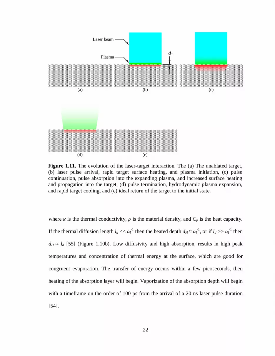
Figure 1.11. The evolution of the laser-target interaction. The (a) The unablated
target, (b) laser pulse arrival, rapid target surface heating, and plasma initiation, (c) pulse continuation, pulse absorption into the expanding plasma, and increased surface heating and propagation into the target, (d) pulse termination, hydrodynamic plasma expansion, and rapid target cooling, and (e) ideal return of the target to the initial state. 22
Figure 2.1. A diagram of the pulsed dual-laser ablation system. The system
can be operated in either excimer-only single-laser or dual-laser mode. 28
Figure 2.2. Oscilloscope traces of the temporal synchronization of the (UV)
excimer laser pulse and the (IR) CO2 laser pulse. The p-p delay (peak-to-peak) is shown relative to the peak of the excimer laser pulse. 29
Figure 2.3. Evolution of the laser-target interaction for dual-laser ablation. (a)
CO2 laser pulse arrival and on-set of surface melt, (b) synchronized arrival of the excimer laser pulse to interact with the pre-melt zone, initiate evaporation and plasma formation, and dual-laser plasma absorption, and (c) termination of the excimer pulse, and continued plasma absorption of the CO2 laser pulse, increasing plasma temperature and expansion. 30
Figure 2.4. The time-line of component synchronization for the dual-laser
ablation system. The t0 trigger to initiate the dual-laser pulse cycle is the (a) CO2 laser internal trigger, followed by the (b) CO2 laser capacitor discharge, which triggers the (c) digital delay generator (DDG) t0 signal to trigger the excimer laser, followed by the (d) excimer laser output pulse, and (e) the CO2 laser output pulse. 34
Figure 2.5. Detail of the cumulative oscilloscope traces of the excimer and
CO2 laser pulses to illustrate the 16 ns jitter of the CO2 laser pulses relative to the excimer laser pulses. The jitter is measured between the minimum and maximum occurrence of the full-width at half-maximum (FWHM) of the laser pulses. 35

vii
Figure 2.6. Schematic diagram of the CO2 laser with the ZnSe Brewster window extension tube and Ge output coupler. 37
Figure 2.7. Output characteristics of the excimer laser after a new fill, the (a)
output delay and (b) pulse jitter relative to the trigger pulse, as a function of the output energy. 39
Figure 3.1. The normalized, indexed, powder XRD pattern for the cold-
pressed Ba8Ga16Ge30 type-I clathrate target. 45 Figure 3.2. SEM image of the coarse polished (529 nm rms) Ba8Ga16Ge30
type-I clathrate cold-pressed target. Approximately 315×315 µm viewing area. 47
Figure 3.3. Diagram of the laser spot size at the laser-target interaction site. 48 Figure 3.4. Photograph of the Ba8Ga16Ge30 target with various laser interaction
sites at fluences of 1 to 5 J/cm2 and repetitions of 1, 10, 100, and 1000 pulses. 49
Figure 3.5. Diagram of SEM and EDS analysis locations for the laser-target
interaction study on the Ba8Ga16Ge30 target. 50 Figure 3.6a. SEM images of the UV KrF excimer only, laser-target interaction
sites for fluences of 1, 2, and 3 J/cm2, and cumulative laser pulses per site of 10, 100, and 1000. 51
Figure 3.6b. SEM images of the UV KrF excimer only, laser-target interaction
sites for fluences of 4 and 5 J/cm2, and cumulative laser pulses per site of 10, 100, and 1000. 52
Figure 3.7. SEM images of the IR CO2 laser only, laser-target interaction sites
at 1000 pulses per site for fluences of 0.6 J/cm2, 1.3 J/cm2, 1.8 J/cm2, 2.0 J/cm2, and 2.4 J/cm2. 55
Figure 3.8. The schematic diagram of the experiment setup for the single beam
transient reflectivity measurements. 57 Figure 3.9. The monitor pulse before target interaction and reflection pulse
after target interaction. The 0.6 J/cm2 CO2 laser fluence was used for alignment and calibration. 58
Figure 3.10. Representation of IR reflection pulse showing features: on-set of
melt, on-set of ablation, and peak of the monitor pulse. 58

viii
Figure 3.11. Single-beam reflectivity for CO2 laser fluences of (a) 1.8 J/cm2, (b) 2.0 J/cm2, and (c) 2.4 J/cm2, before (Monitor) and after Reflection from the Ba8Ga16Ge30 target, displaying on-set of melt. 60
Figure 3.12. The monitor oscilloscope traces of the UV excimer laser pulse and
the IR CO2 laser pulse with a 100 -110 ns p-p delay. The on-set of the melt is indicated at τm. 61
Figure 3.13. Images of the laser-target interaction sites for 10, 100, and 1000
pulses/site using dual-laser fluences of 1 J/cm2 UV and 2 J/cm2 IR with 100 - 110 ns p-p delay. 62
Figure 3.14. SEM images of dual-laser ablation of an unpolished target. A
region of un-ablated target surface is shown and the laser-target interaction sites for 10, 100, and 1000 pulses/site using dual-laser fluences of 1 J/cm2 UV and 2 J/cm2 IR with 100 ns p-p delay. 63
Figure 4.1. Diagram of the imaging system identifying the coordinate system,
object plane, image plane, and an example light collecting device (optical fiber). The magnification is -½ for this configuration. 68
Figure 4.2. The schematic diagrams of the dual-laser deposition system with
the (a) optical emission spectroscopy (OES), and (b) intensified charge-coupled device (ICCD) imaging system included. 69
Figure 4.3. Specification of the wavelength sensitivity of the ICCD camera.
The wavelength cut-off due to the imaging window is shown at 350 nm. 70
Figure 4.4. Photographs of the alignment and calibration procedure using a 4
cm long helium lamp as the object (not shown) placed along the plume axis of propagation and imaged at the light collection plane. Photograph (a) is an example of proper object/lens alignment and (b) is misaligned displaying distortion of the image. 72
Figure 4.5. Schematic diagram of the imaging system alignment and
calibration layout using a helium lamp masked for 4 cm length. The diagram is drawn to scale. 73
Figure 4.6. Intensity of the He lamp (587.6 nm wavelength) as the optical fiber
position was varied along the x-axis (horizontal) and y-axis (vertical) of the image plane. 74
Figure 4.7. The (a) back-lit scale card used to determine image magnification
and orientation for the optical diagnostics system(s), and (b) a photograph of the imaged card. 74

ix
Figure 4.8. Time-integrated ICCD images of CO2 laser-target interactions with laser fluences of (a) 1.8 J/cm2, (b) 2.0 J/cm2, and (c) 2.4 J/cm2. Images are normalized with respect to image (c). 76
Figure 4.9. The normalized time-resolved total emission intensity of the CO2
laser-target interactions for 1.8 J/cm2, 2.0 J/cm2, and 2.4 J/cm2. The emission was imaged at the target surface (0 mm position). 76
Figure 4.10. ICCD imaging of total emission of ablated plumes from the target
for (a) 1 J/cm2 and (b) dual-laser ablation. 77 Figure 4.11. Overlapped oscilloscope traces for the excimer laser pulse (UV)
and CO2 laser pulses (IR) for peak-to-peak delays of -25 ns, +100 ns, and +175 ns, relative to the UV pulse at 0 ns. 78
Figure 4.12. Dual-laser synchronization parameters as a function of the dual-
laser pulse peak-to-peak delays obtained by total emission ICCD imaging of the laser induced plasma expansion. The (a) normalized peak intensity and (b) normalized FWHM are shown. 79
Figure 4.13. ICCD imaging of the time-integrated laser generated plume
emission for excimer only 1 J/cm2 (S1), high fluence single-laser 3 J/cm2 (S3), and dual-laser ablation. For each laser configuration the unfiltered total emission, Ba+ 455 nm, Ga+ 426 nm, and Ge+ 481 nm are shown. 81
Figure 4.14. OES cross-section of ablated plumes 5 mm from the target for (a) 1
J/cm2 and (b) 3 J/cm2 single-laser, and (c) dual-laser ablation. The emission shown is for Ba+ 455 nm, Ga+ 426 nm and Ge+ 481 nm. 82
Figure 4.15. The time-integrated spectra for (a) single-laser 1 J/cm2 fluence and
(b) dual-lasers ablated plumes. The neutral (I) and singly ionized (II) species of Ba, Ga, and Ge are indicated. 85
Figure 4.16. The total intensity of the time-integrated optical emission obtained
2 cm from the target surface for cumulative laser pulse for single and dual-laser ablation. 86
Figure 4.17. An example of a time-of-flight (TOF) profile positioned at 2 mm
from the target surface. 88

x
Figure 4.18. The normalized intensity, time-resolved, total emission time-of-flight profiles for positions 0 mm, 1 mm, 2 mm, 4 mm, and 6 mm from the target surface. The profiles were imaged along the plume axis for single-laser (a) 1 J/cm2, and (b) 3 J/cm2 and (c) dual-laser ablation configurations. The dual-laser p-p delay was 100 ns. 89
Figure 4.19. The distance-time plot of the TOF peak arrival time at various
distances from the target surface, for single-laser 1 J/cm2 and 3 J/cm2, and dual-laser 1 J/cm2 UV + 2 J/cm2 IR. The slopes were velocity determination. 90
Figure 4.20. The temporal FWHM of the TOF profiles for single laser 1 J/cm2
and 3 J/cm2 , and for the dual-laser 1 J/cm2 UV + 2 J/cm2 IR. 90 Figure 4.21. The time-resolved elemental TOF profiles for the ions Ba+ 455 nm,
Ga+ 426 nm, and Ge+ 481 nm at 4 mm from the target surface. 91 Figure 5.1. Schematic diagrams showing the three regimes during the pulsed
laser irradiation of a bulk target: the (a) evaporation regime (0 < t < 100’s ps), (b) isothermal regime (100’s ps < t ≤ τ), and (c) the adiabatic regime (t > τ). 94
Figure 5.2. Schematic diagram of the (a) laser spot size at the target surface
and (b) the plasma volume with the orthogonal edges (Xo,Yo,Zo) indicated. 97
Figure 5.3. TOF profiles and theoretical model fit for single-laser ablation (a)
1 J/cm2, (b) 3 J/cm2, and (c) dual-laser 1 J/cm2 UV + 2 J/cm2 IR. 103 Figure 6.1. The dependence of the on-axis film deposition rate per laser pulse
on the excimer laser fluence. The substrate temperature was room-temperature. 107
Figure 6.2. Profile film thickness along the (a) y-axis and (b) z-axis for
Ba8Ga16Ge30 deposited on quartz substrates. The target to substrate distance was 4 cm. The solid lines indicate the theoretical fit cosnθ. 108
Figure 6.3. A SEM at 3000 times magnification which shows examples of the
various types of particulates found on the thin films. 109 Figure 6.4. SEM at 300 times magnification at (a) 1 J/cm2 (b) 2 J/cm2 (c) 3
J/cm2 (d) 4 J/cm2 and (e) 5 J/cm2. 111 Figure 6.5. SEM images of thin films deposited by single-laser PLD with
fluences of (a) 1 J/cm2 and (b) 3 J/cm2, and dual-laser fluences of (c) 1 J/cm2 UV and 2 J/cm2 IR. 112

xi
Figure 6.6. Overlapped oscilloscope traces for the excimer laser pulse (UV) and CO2 laser pulses (IR) for peak-to-peak delays of -25 ns, +100 ns, and +175 ns, relative to the UV pulse at 0 ns. 113
Figure 6.7. Scanning electron micrographs of films deposited at various dual-
laser peak-to-peak delays with 1 J/cm2 UV and 2 J/cm2 IR laser fluences. The CO2 laser pulse peak is delayed by (a) -25 ns, (b) 100 ns, and (c) 175 ns, relative to the excimer laser pulse peak. The film deposited at 100 ns delay resulted in reduced particulate generation. 115
Figure 6.8. The XRD dependence on the substrate temperature. The excimer
laser fluence was 1 J/cm2. 116 Figure 6.9. XRD intensity of the peak 31.2° (321) as a function of
temperature. 117 Figure 6.10. The XRD patterns dependence on the excimer laser fluence. The
substrate temperature was 400 °C. 118 Figure 6.11. XRD intensity of the peak 31.2° (321) as a function of the excimer
laser fluence. 118 Figure 6.12. X-ray diffraction patterns for single-laser 1 J/cm2 UV (SL1) and 3
J/cm2 UV (SL3), and dual-laser (DL1+2) 1J/cm2 UV + 2 J/cm2 IR. The film thickness was 267 ± 30 nm. The type-I clathrate XRD peaks are identified to a cubic unit cell structure with space group Pm-3n. 119
Figure 6.13. EDS quantification of the films deposited as a function of the
excimer laser fluence. 120 Figure 6.14. The temperature dependent resistivity of a Ba8Ga16Ge30 thin film
sample at various applied injection currents, demonstrating the semiconducting behavior. 123
Figure 6.15. Temperature dependent resistivity of the Ba8Ga16Ge30 thin films
deposited by single and dual-laser ablation for various thicknesses. 125 Figure 6.16. A scanning electron micrograph image of a film deposited by
single-laser PLD with a fluence of 3 J/cm2. The average film thickness is 623 nm. The micro-cracks are visible on the film. 125

xii
Figure 6.17a. Schematic diagram of progressive film nucleation for single-laser deposition, (a) sparse nucleation, (b) increased coalescence growth, (c) final, discontinuous crystal growth within an amorphous fill and or channels and holes, and (d) an SEM image of a Ba8Ga16Ge30 film grown with 3 J/cm2 single-laser ablation. Note the 50-150 nm ‘crystallites’ encased within the film growth. 127
Figure 6.17b. Schematic diagram of progressive film nucleation for dual-laser
deposition, (a) high energy, ion bombardment promoting increased nucleation, (b) increased, dense crystal growth, (c) final, uniform continuous growth, and (d) an SEM image of a Ba8Ga16Ge30 film grown from 1 J/cm2 UV and 2 J/cm2 IR dual-laser ablation. Note the smooth film growth as compared to the image in Figure 6.20a. 127
Figure 6.18. The schematic diagram of the Van der Pauw technique for
determination of resistivity and Hall values for thin film samples. 125 Figure 6.19. A schematic diagram of a basic thermocouple arrangement (a-b)
between hot (TH) and cold (TL) sources. 132 Figure 6.20. Schematic arrangement of thermocouples on the sample surface for
determination of the thermopower by the differential method. 135 Figure 6.21. A schematic wiring diagram of the apparatus used to measure the
temperature gradient and Seebeck voltage, used to determine the Seebeck coefficient. 140
Figure 6.22. Diagram of the Seebeck coefficient measurement apparatus. 141 Figure 6.23. Photographs of the (a) Seebeck apparatus and DAQ board and (b)
detail of the sample and thermocouple placement. 141 Figure 6.24. Arrangement of the T-type thermocouples on the surface of the
hater block for characterization of the thermocouples. 142 Figure 6.25. Time required for the heater block temperature to stabilize with 15
V AC applied to the heater. 142 Figure 6.26. The stabilized temperature recorded by the thermocouples at
various heater voltages. 143 Figure 6.27. The voltage potential as a function of the temperature difference at
various average temperatures. 145 Figure 6.28. The thermopower (αb) of the Cu lead of the thermocouples used in
the Seebeck apparatus. 145

xiii
Figure E.1. Spectrograph optical layout. 171 Figure F.1. 10 mm diameter ferrule on spectrograph end for (a) two-leg fiber
bundle and (b) four-leg fiber bundle. 172 Figure F.2. The three fiber configuration on the source end of the four-leg
fiber bundle. An approximate 528 µm diameter fiber bundle zone (including cladding), an approximate 483 µm diameter light collection zone (not including cladding at outer edge). 173
Figure I.1. Substrate heater cool-down time from 300 °C to room temperature
with 1 V AC reduction every 2.5 minutes until 0 V AC is reached. 181

xiv
LIST OF ABBREVIATIONS Å angstrom ArF argon fluorine Ba8Ga16Ge30 Barium Gallium Germanium C heat capacity CA clear aperture CCD charge coupled device CJC cold-junction compensation CO2 carbon dioxide CWL center wavelength DC direct current ΔT change in temperature
ΔV change in voltage
e electron charge EF Fermi energy f Ladenurg’s oscillator strength v1 laser frequency vp plasma resonant frequency g upper level statistical weight Hz hertz IR infrared

xv
ICCD intensified charge coupled device I current J Joule K Kelvin KrF krypton fluorine kB Boltzmann constant κ thermal conductivity λ wavelength MOCVD metal organic chemical vapor deposition μm micrometer μV microvolt μ(E) mobility mJ millijoules ne electron number density nm nanometer ns nanosecond OES Optical Emission Spectroscopy
OMA optical multi-channel analyzer n(E) density of states PGEC phonon glass electron crystal α2σ Power Factor PLD Pulsed Laser Deposition q carrier charge

xvi
s second S Seebeck coefficient SiO2 silicon dioxide σ electrical conductivity T temperature TH high temperature TL low temperature T/C thermal couple TE thermoelectric TISR-LIPS time-integrate space-resolved laser-induced plasma spectroscopy TEA transversely-excited atmospheric-pressure UV ultra-violet V voltage VH high voltage VL low voltage XeCl xenon chloride YSZ yttrium stabilized zirconium ZT figure-of-merit

xvii
ABSTRACT
The on-going interest in thermoelectric (TE) materials, in the form of bulk and
films, motivates investigation of materials that exhibit low thermal conductivity and good
electrical conductivity. Such materials are phonon-glass electron-crystals (PGEC), and
the multi-component type-I clathrate Ba8Ga16Ge30 is in this category. This work reports
the first investigation of Ba8Ga16Ge30 films grown by pulsed laser deposition (PLD).
This dissertation details the in-situ growth of polycrystalline type-I clathrate
Ba8Ga16Ge30 thin-films by pulsed laser ablation. Films deposited using conventional laser
ablation produced films that contained a high density of particulates and exhibited weak
crystallinity. In order to produce high quality, polycrystalline, particulate-free films, a
dual-laser ablation process was used that combines the pulses of (UV) KrF excimer and
(IR) CO2 lasers that are temporally synchronized and spatially overlapped on the target
surface. The effect of the laser energy on stoichiometric removal of material and
morphology of the target has been investigated. In addition, in-situ time-gated emission
spectroscopy and imaging techniques were used to monitor expansion of components in
the ablated plumes. Through these investigations, the growth parameters were optimized
not only to significantly reduce the particulate density but also to produce large area
stoichiometric films. Structure and electrical transport properties of the resultant films
were also evaluated. This work provides new insight toward the in-situ growth of
complex multi-component structures in thin-film form for potential TE applications.

1
CHAPTER 1:
INTRODUCTION
The increasing need for energy production and conservation has motivated
interest in technologies that address energy harvesting [1]. Waste-heat recovery through
the application of thermoelectric materials (TE) can play a major role in this area [2-5].
The impact that TE materials will have on the energy crisis is a matter of debate [6],
however, niche military, space [7], and commercial products have shown promise over
the past decade. Small scale thermo-generators for low power consumption in high-
volume commercial applications are the most promising [8]. Vehicle exhaust heat
recovery has considerable potential benefit and along with a U.S. Department of Energy
(DOE) goal of ~10% improved fuel economy is stimulating on-going research [7-9]. TE
materials have found applications as self-powered monitors, transponders, and
temperature warning systems [9]. Other viable applications include localized active
cooling or heating of devices such as micro-processors, laser diodes, detectors, and
biological specimens [10-12]. However, the main shortcoming with current
thermoelectric materials is their poor efficiency [3]. From the experimental point of view,
one of the motivations is to have the ability to grow TE materials in thin-film form for
devices with improved efficiencies.

2
This chapter describes the physical properties that contribute to the TE conversion
efficiency, and material systems and structures used in TE devices. Commonly used film
fabrication techniques will be discussed, as well as the PLD that was utilized.
1.1. Thermoelectrics
A basic review of thermoelectrics (TE) is presented as well as the current focus
for improving TE materials being researched. The novel materials known as clathrates
will be discussed, and thin-film TE structures and their deposition techniques will be
reviewed.
1.1.1. Basic Review
In a conductor or semiconductor the free carriers (electrons and holes) carry both
charge and heat and can be induced to diffuse through the material (Figure 1.1) [13, 14].
The diffusing carriers are scattered by impurities, imperfections, and lattice vibrations
(phonons) and these hot and cold carriers diffuse at different rates. The Fermi-Dirac
distribution for a hot and cold temperature is depicted in Figure 1.1 [15, 16]. Within the
εF(0)
ε
f(ε) 0 1 ½
T=0 εF(0)
ε
f(ε) 0 1 ½
T=0 Hot Cold + + + +
- - - -
ΔT
ΔV
Figure 1.1. The Seebeck effect for an isolated conductor in a uniform temperature gradient (ΔT). The Fermi-Dirac diagrams indicate the energy states for a hot and a cold temperature. The higher energy carriers diffuse from the hot side to the cold side generating a voltage potential (ΔV).

3
temperature gradient (ΔT) the average energy per electron in an isolated conductor is
greater in the hot end. Consequently, the more energetic electrons diffuse toward the cold
region until a potential difference (ΔV) is built up which prevents further diffusion.
The basis of this process is called the Seebeck or thermoelectric effect, discovered
in 1821. Thomas Seebeck observed when two dissimilar conductors, a and b, are joined
(Figure 1.2) and the junctions are held at two different temperatures, T1 > T2, a voltage
difference (ΔV) develops that is proportional to the temperature difference (ΔT). The ΔV
and ΔT are related by an intrinsic property of the materials called the Seebeck coefficient
or thermopower (α) where αab is defined as the differential Seebeck coefficient between
materials a and b such that:
TV
ab ∆∆
=α (1.1)
for small ΔT as 0→T .
A reversal of this process is known as the Peltier effect, discovered in 1834. It
was observed when an electric current flows through the junction of two dissimilar
metals, heat is exchanged [17, 14]. If a current source is applied across the points 3 and 4
(Figure 1.2), then heat is either absorbed or rejected depending on the direction of the
a
b b V
3 4
Cold (T2)
2
Hot (T1)
1
Figure 1.2. Schematic diagram of the open circuit Seebeck effect for two dissimilar conductors a and b with junctions at positions 1 and 2, held at temperatures T1 > T2, respectively.

4
current. The Seebeck coefficient (α) and the Peltier effect are related to each other in the
definition of the Peltier coefficient (Π) where:
Tabα=Π (1.2)
where T is the temperature of the junction. The rate of heating (Q) or cooling is given by:
ITQ abα= (1.3)
where I is the current through the junction.
The Seebeck effect and Peltier effect are the foundation for solid state TE devices
that can be used to directly convert heat into electricity for power generation, or for
refrigeration, depending the configuration (Figure 1.3) [2, 3]. A TE couple, is made up of
two types of semiconductor materials, an n-type (electron majority carriers) and a p-type
(hole majority carriers). The two branches of the device are connected by a metallic
contact to form an electrical series, but thermally parallel circuit [13, 14]. The Seebeck
effect is temperature-gradient driven; a heat source applied to one side will drive the
Figure 1.3. Arrangement of thermoelectric modules for (a) power generation by the Seebeck effect and (b) refrigeration by the Peltier effect.
(a) (b)
I
p-type n-type
Heat Rejection (TH)
Cooling (TC)
+
+ -
RL I
Heat Sink (TC)
p-type n-type
Heat Input (TH)
V
+ -

5
majority carriers toward the cooler region (Figure 1.3a). This type of TE configuration
will produce a voltage that can be utilized drive a current through a load resistance (RL)
for power-generation.
The Peltier effect is current driven; an electric current applied to the material
system diffuses the hot carriers through the circuit (Figure 1.3b). The electrons in n-type
material will flow against the direction of the current and holes in p-type material will
flow with the current direction. Since ideal ohmic metal/semiconductor contacts at
thermal equilibrium share Fermi levels (Ef), heat will be absorbed or emitted as carriers
(electrons and holes) cross the junctions [18, 19]. For example, as current passes through
the metal/n-type semiconductor junction an electron acquires energy (cooling) as it enters
the conduction band. Energy is released (heating) as an electron passes through an n-type
semiconductor/metal junction (Figure 1.4). Thus, this TE configuration provides
Figure 1.4. The energy band diagrams for ideal ohmic metal-semiconductor junctions at thermal equilibrium for a TE refrigeration device. The thermal energy absorption and emission as the carriers (electrons and holes) cross the junctions between the semiconductor material and metal contacts.
p-type n-type
Heat Released (TH)
Cooling (TC)
+ -
Ev
Ec Ef
Metal p-type
p-type Metal
Ev
Ec
Ef
Ev
Ec Ef
Metal n-type
Ef Ev
Ec Metal n-type
_ +
Heat Released Heat Released
Heat Absorbed Heat Absorbed
Heat Absorbed

6
refrigeration capability with no moving parts.
A TE couple is consists of TE material segments a and b, which are p-type and n-
type, respectively. The efficiency (η) of a TE power generation couple is measured as the
ratio of electrical power (PL) delivered through the load resistance (RL), relative to the
heat flow (QH) into the hot side of the TE couple. The electrical power is given by PL =
I2RL where I is the current through RL.
H
L
QP
=η (1.4)
The QH input is comprised of three terms. The heat flow through the TE couple due to the
thermal conductance (KΔT); the heat absorbed at the hot junction due to the Peltier
coefficient (Q = αabITH), equation (1.3); and the heat due to Joule heating (½I2R) of the
TE couple with the assumption that it is divided between the hot and cold sides. K is the
total thermal conductance of materials a and b in parallel, and R is the series resistance of
a and b. Therefore, QH is given by:
RIITTKQ HabH2
21
−+∆= α (1.5)
then the power generation efficiency (η) is given by:
RIITTK
IR
Hab
L
2
21
−+∆=
αη (1.6)
where ΔT = TH – TC, and αab = αp – αn where αp and αn are the Seebeck coefficients of the
p-type and n-type materials, respectively.
The efficiency (ϕ) of TE refrigeration is measured by the coefficient of
performance (COP), defined as the ratio of the heat absorbed (QC) to the electrical power
input. The rate of the heat absorbed is given by:

7
TKRIITQ CabC ∆−−= 2
21α (1.7)
The power input (P) is given by:
RITIP ab2+∆= α (1.8)
where the applied voltage to the TE couple is balanced between the resistance (R) of the
TE segments and the Seebeck voltage due to the ΔT between the junctions. The efficiency
(ϕC) of refrigeration is then given by:
( )( ) RITI
TKRIIT
PQ
np
Cnp
C
CC
2
2
21
+∆−
∆−−−=
=
αα
ααφ
φ
(1.9)
The efficiency (ϕH) of the heat released by the hot side for TE heating is obtained by
substitution of TH for TC in equation (1.9).
The performance of a TE couple can be evaluated at a specified temperature by
the figure-of-merit (Z) where:
RK
Z ab2α
= (1.10)
If the geometries of the segments a and b are matched to minimize heat absorption, then
the segment cross-sectional area (A) and length (L), can optimize the Z of a TE couple.
An optimization of Z occurs if the product RK is minimized, such that when:
21
=
pn
np
np
pn
ALAL
κρκρ
(1.11)
The figure-of-merit for the couple can then be rewritten in terms of the two materials, an
n-type and a p-type, where:

8
( )
( ) ( )
+
−=
21
21
2
nnpp
npZκρκρ
αα (1.12)
or as the dimensionless figure-of-merit (ZT):
+
−=
2/12/1
2)(
n
n
p
p
np TZT
σκ
σκ
αα (1.13)
The performance of an individual TE material segment relies directly on the ZT [14]. The
parameter ZT is then given by:
κσα TZT
2
= (1.14)
where α is the Seebeck coefficient, σ is the electrical conductivity, T is the temperature of
interest, and κ is the total thermal conductivity. The κ is approximately described as:
eL κκκ += (1.15)
where κL is the lattice thermal conductivity and is the heat conducted by phonons (lattice
vibrations). The electronic thermal conductivity (κe) is the heat conducted by mobile
electrons. Since the κe for TE materials is proportional to σ via the Wiedemann-Franz law
[5] given by:
LTe σκ = (1.16)
where L is the Lorentz number (2.45 × 10⁻⁸ V2K-2 for free electrons). The product α2σ is
referred to as the electrical power factor and is a value commonly reported as an indicator
of TE performance.
The early application of the TE effect was metal thermocouples which are still
widely used today. During the 1950s and 1960s extensive research was conducted on

9
materials such as alloys of Bi2Te3 and Si1-xGex for thermoelectric applications. These
materials remain state-of-the-art for their specific temperature use. In the 1990s,
resurgence in the field began with advances in novel processes for producing bulk
materials and progress in thin-film growth techniques [11].
1.1.2. Current Thermoelectric Materials Research
At room temperature, T = 300 K, desired values for the thermoelectric parameters
are α = 225 µV/K [20], σ = 105 Ω-1m-1, and κ = 1.5 W/m·K, which results in a ZT ≈ 1.
These values are typical for the best TE materials such as Bi2Te3 and Sb2Te3 alloys,
which are presently used by industry in devices that operate near room temperature and
are well investigated [2, 21]. Current TE devices operate at an efficiency of about 5-6 %.
By increasing ZT by a factor of 4 predicted efficiencies can increase to 30 % [3].
A comparison of various n-type and p-type TE materials is shown in Figure 1.5
where the ZT peaks for each material such that each material has an optimal operating
temperature range [5]. CsBi4Te6 (p-type) has shown promise for low temperature
applications (100 - 200 K) [22, 23]. Mid-temperature range (500-900 K) power
generation materials have been based on tellurides like LAST (Lead-Antimony-Silver-
Telluride, n-type) and TAGS (Te-Ag-Ge-Sb, p-type) such as (AgSbTe2)0.15(GeTe)0.85.
TAGS has been shown to be more efficient than PbTe but is very expensive. High
temperature TE generators (>900K) have used Si-Ge alloys (n-type and p-types) as well
as La2Te3 (n-type) and Yb14MnSb11 (p-type). Lower thermal conductivity has been
achieved with materials such as β-Zn4Sb3 (0.9 W/m·K) [24], n-type PbTe (0.15 W/m·K)
[24], and inhomogeneous nano-structured materials such as SALT (Sodium-Antimony-

10
Lead-Telluride) and LASTT (Lead-Antimony-Sodium-Tin-Telluride) [3, 5].
Current research is aimed at increasing the ZT by maximizing the power factor (α
2σ) and/or minimizing the thermal conductivity (κ), or finding materials capable of
operating in new or broader temperature ranges [20]. A maximized power factor implies
that a high voltage and current are generated, and a low κ allows a larger ΔT to be created
across the material [2-5].
Increasing the power factor (α2σ) involves increasing α and σ together. In reality,
it is difficult to enhance α without lowering σ. Since α is the energy transported per
carrier
qC
≈α (1.17)
where C is the specific heat and q is the charge of the carrier, a low σ gives rise to high α.
Figure 1.5. The figure-of-merit (ZT) of state-of-the-art commercial materials for thermoelectric power generation, (a) n-type and (b) p-type [3, 5, 22-25].
(a) (b)
0.0
0.2
0.4
0.6
0.8
1.0
1.2
1.4
1.6
1.8
100 300 500 700 900 1100 1300Temperature (K)
ZT Bi2Te3
SiGeCoSb3
LAST
PbTe
La2Te3
n -type0.0
0.2
0.4
0.6
0.8
1.0
1.2
1.4
1.6
1.8
100 300 500 700 900 1100 1300Temperature (K)
ZT
Yb14MnSb11
SiGe
Zn4Sb3
Sb2Te3
PbTe
TAGS
CsBi4Te6
SALT
p -type

11
The α and σ can be adjusted through doping that changes the free carrier concentration.
Since these two parameters typically change in opposite directions, a compromised set of
values needs to be achieved such that there is a peak power factor through optimization
of the carrier concentration (n) [5]. Depending on the material system, the optimum
carrier concentration typically occurs at 1019 to 1021 cm-3, a concentration found in
heavily-doped semiconductors (Figure 1.6). To effectively minimize minority carrier
contributions, leading high-mobility carriers, the direct band-gap needs to be large
enough, on the order of ≈ 10kBT, where kB is the Boltzmann constant (1.381 × 10⁻²³ J/K)
[25]. For semiconductors, the carriers must be thermally excited across the band-gap for
conduction to occur, and the temperature-dependence of the electrical conductivity is
approximated by;
TkE
ob
g
e−
≈ σσ (1.18)
0
200
400
600
800
1000
1200
1400
17 18 19 20 21 22Carrier Concentration (log)
Seeb
eck
Coe
ffici
ent (
µV/K
)
0
2000
4000
6000
8000
10000
Con
duct
ivity
(Ω
Seebeck (α)
Power Factor (α2/ρ = α2σ )
Conductivity (σ = 1/ρ)
Semiconductor Heavily Doped Semiconductor
Metal
Figure 1.6. A comparison of the Seebeck coefficient (α), power factor (α2σ), and conductivity (σ) as a function of the carrier concentration (10x) [5].

12
There are two primary ways to achieve a high conductivity, by having a very small band-
gap to excite across (Eg ≈ 10kbT, 0.25 eV at 300 K), or by having very high-mobility
carriers (µ ≈ 2000 cm2/V·s) [20]. Optimizing the power factor of a material or system
would have to be based on band-gap size, shape and width of the bands near the Fermi
level (EF), and the carrier effective masses and mobilities [25].
A common characteristic of recently developed thermoelectrics with ZT > 1 is that
most have lattice thermal conductivities (κL) that are lower than the current commercial
materials. The lattice thermal conductivity (κL) component of the total thermal
conductivity is the only parameter not determined by the electronic structure [2, 3].
Lowering κe would come at the cost of lowering σ which is not desirable in a TE material.
A reduced lattice thermal conductivity directly improves the TE efficiency, and allows re-
optimization of the carrier concentration for additional ZT improvement.
Productive strategies to improve the ZT related to minimizing the thermal
conductivity are the use of materials with intrinsically low κL, and to scatter phonons
within the unit cell or structure. Materials with intrinsically low κL follow the phonon-
glass electron-crystal (PGEC) approach. The PGEC approach is a concept introduced by
Slack (1995) as a guide for new TE materials with improved properties [26]. An ideal
PGEC material would have the thermal conductivity associated with amorphous materials
(“phonon-glass”), and the electronic properties associated with good semiconductor
single crystals (“electron-crystal”). Scattering phonons can be accomplished by (i)
creating rattling structures or point defects such as interstitials, vacancies or by alloying,
(ii) the use of complex crystal structures, (iii) increasing the lattice period, and (iv) by
scattering phonons at interfaces utilizing boundary scattering.

13
1.1.3. Clathrates
PGEC materials that can satisfy these strategies include the class of novel
materials known as clathrates [27, 28]. Inorganic clathrates were first systematically
investigated in the 1960s with Na8Si46 (Kasper et al., 1965), Si and Ge (Cros et al., 1968),
and Sn clathrates (Gallmeier et al., 1969) [29]. Type-I inorganic clathrates are
characterized by a framework of ‘host’ atoms which occupy sites at the vertices of face-
sharing polyhedral ‘cages’ which enclose loosely bond ‘guest’ atoms. A general chemical
formula for type-I clathrates can be written as A8ByY46-y, where A represents the guest
atom (Group IIA, alkaline-earth metal, Sr, Ba, or Eu), and B framework substituting atom
(Group IIIB, Ga or In), and Y (Group IVB, Si, Ge, or Sn) represent the framework atoms.
The host atom cages form two pentagonal dodecahedrons and six tetrakaidecahedrons
(hexagonal truncated trapezohedron) per cubic unit cell [29, 30]. The 12 sided (12
pentagons), 20 atom dodecahedron and the 14 sided (12 pentagons and 2 hexagons), 24
atom tetrakaidecahedron cages with the enclosed guest atom are shown in Figure 1.7a.
The unit cell crystal structure highlighting the dodecahedra outlined at the center of
Figure 1.7b, and the tetrakaidecahedron is outlined at the right of the figure. The green
shaded spheres represent atoms forming the host framework, and the guest atoms inside
the polyhedra are represented in shades of blue. Type-I clathrate belongs to the
crystallographic cubic space group Pm-3n, and in the Wyckoff position notation the host
atoms are found at three different sites, 6c, 16i, and 24k (see Appendix A) and the centers
of the cages are denoted 2a and 6d for the dodecahedron and tetrakaidecahedron cages,
respectively.

14
The fully occupied (A8ByY46-y) host-atom framework of the type-I clathrate
contains 46 tetrahedrally coordinated host atoms in the unit cell. The geometrical
arrangement of the 46 host atoms leaves 8 voids per unit cell for the guest atoms to
occupy. An illustrative description of the three dimensional structure is shown in Figure
1.8a-d, where depth perspective has been added for clarity. The one guest atom is located
at each corner (2a) and two on each face (6d) of the cubic unit cell (Figure 1.8a). Part of
the structure can be envisioned where a dodecahedron cage encloses the guest atom at
each 2a site (Figure 1.8b). Each tetrakaidecahedron cage encloses a 6d site guest atom
where these cages are joined by their hexagonal faces (Figure 1.8c). The complete
structure with the unit cell outlined is illustrated in Figure 1.8d, which can be visualized
as the dodecahedron cages joined through the 16i sites with vacancies at the 6c sites. The
dodecahedron cage is a subunit present in all inorganic clathrates and filling the 6c sites
form the outline of the tetrakaidecahedron cages. Describing the type-I clathrate with this
Figure 1.7. The type-I clathrate composed of the (a) face-sharing pentagonal dodecahedron and tetrakaidecahedron, and the (b) cubic unit cell with the polyhedra outlined in red. The Wyckoff positions of the guest and framework atoms are indicated.
x
y
z
24k 16i 6c
6d
2a
(a) (b)

15
manner has been used to help explain the preference for vacancies and lower valence host
elements on the 6c site [124].
The loosely bound guests, or ‘rattlers’, in these crystalline materials can undergo
(a)
Figure 1.8. Components of the type-I clathrate structure with (a) eight guest atoms on the corners, one on center, and twelve on the faces of the cubic unit cell, and the (b) nine dodecahedron cages, (c) the twelve tetrakaidecahedron cages, and (d) the complete host-guest schematic.
(b)
(c) (d)

16
large, localized low-frequency vibrations, which in turn can scatter the heat-carrying
acoustic phonons resulting in thermal conductivities with magnitudes similar to
amorphous materials. The guest-host interaction in clathrates continues to be of scientific
interest. It has also been demonstrated that the transport properties can be optimized
through Si substitution within the Ga-Ge framework [31-33] and manipulation of the
carrier concentration [34].
The type-I class of clathrates meet desired features for possible ZT improvement
with their intrinsically low κ, complex crystal structure with the phonon scattering rattler.
As a result of the interesting properties and technological promise of type-I clathrates, the
bulk properties of these materials have been studied extensively using a wide range of
experimental and theoretical techniques [34].
1.1.4. Thin-Film Thermoelectric Structures
Phonon scattering at interfaces leads to the use of multiphase composites mixed
on the nanometer scale. These nanostructured materials can be formed as thin-film
hetero-structures and superlattices, or as intimately mixed composite structures. TE
materials in thin-film form offer promise for ZT enhancement [35]. Three thin-film
approaches have been suggested. The first approach uses quantum-confinement effects to
obtain an enhanced density of states near the Fermi level. The second approach employs
phonon-blocking/electron-transmitting superlattices. These structures utilize the acoustic
mismatch between the superlattice components to reduce κL, rather than using the
conventional alloying approach, thereby potentially eliminating alloy scattering of
carriers. The third thin-film approach is based on thermionic effects in heterostructures

17
[36]. Thin-film heterostructures, or superlattices, consist of alternating thin layers (2-10
nm each) of different materials stacked periodically (~100 µm total thickness). The lattice
mismatch and electronic potential differences at the interfaces, and resulting phonon and
electron interface scattering and band structure modifications can be exploited to reduce
phonon heat conduction, i.e. κL, while maintaining or enhancing the electron transport.
This in turn, improves the thermoelectric figure of merit [35].
1.1.5. Thin-Film Deposition Techniques
Films of TE materials have been deposited by a variety of fabrication techniques.
Research-based thin-film deposition techniques include molecular beam epitaxy (MBE)
[37] and low-pressure chemical vapor deposition (CVD) [38] of Si-Ge alloys; low
temperature metal organic chemical vapor deposition (MOCVD) [39, 40], flash
evaporation [41, 42], MBE [43], sputtering [44], and pulsed laser ablation (PLA) [45] of
Bi2Te3 and Sb2Te3 alloys.
The method of PLA profitably differs from the thermal methods of continuous
deposition of thin semiconductor films. The presence of a large fraction of excited atoms
and ions allows lower growth temperatures, and a high nucleation rate allows the
deposition of thin continuous films, on the order of several nanometers. In addition, since
an insignificant mass of the target material evaporates for one pulse, the film thickness
can be precisely controlled by the number of laser pulses. In some cases, the quality of
the films obtained by laser ablation is comparable with the quality of films grown by
MBE [46]. One of the main advantages of laser ablation for film growth is the ability of
this process to closely reproduce the target stoichiometry in the deposited film [47-49].

18
For a target that contains elements with a wide variation of physical properties, pulsed
laser ablation is uniquely suited for the growth of complex structured, multi-component
films from a single composite target such as Ba8Ga16Ge30.
1.2. Pulsed Laser Vaporization and Deposition
Pulsed laser deposition (PLD) is often described as a three-step process consisting
of (i) vaporization of a target material, (ii) transport of the vapor plume, and (iii) film
growth on a substrate (Figure 1.9) [50, 51]. During the first step, a pulsed laser beam
strikes the surface of the source material, a rotating target, and the energy from the laser
rapidly evaporates the target’s surface. In most materials, the radiation is absorbed by
only the outermost layers of the target, to a depth on the order of fractions of a
micrometer. The short laser pulses, lasting less than 50 ns, cause the temperature of the
surface to rise rapidly to thousands of degrees Celsius, but the temperature of the target
(iii) Film Growth
(i) Vaporization
(ii) Transport of Vapor Plume
Rotating Target
Pulsed Beam
Substrate
Figure 1.9. Diagram of the pulsed laser deposition process depicting the pulsed beam (i) vaporization of the target surface, (ii) transport of the vapor plume, and (iii) growth of the film on the substrate.

19
bulk remains unchanged. The rapid, non-equilibrium heating produces evaporants along
with the characteristic luminous plasma that expand and propagate, as the second step.
This vaporized material then deposits on the substrate, the third step, producing a film
with composition typically identical to that of the target surface. The ability to reproduce
the composition of the target in the film may be the highest benefit of PLD [52].
This technique has many unique advantages for thin-film deposition (Table 1.1).
An energy source (laser) outside of the deposition chamber produces a highly forward-
directed and confined plume of materials, which can be deposited with less
contamination than the unconfined plasma in a sputter process. In complex multi-
component material deposition with conventional evaporation methods, the various
cations come from different sources. To produce the right mixture in the deposited film,
the rate of arrival of each species must be monitored and controlled. PLD does not
require such monitoring, because the composition of the film typically replicates the
composition of the target, referred to as congruent evaporation and stoichiometric
deposition. Producing multilayer materials can also be accomplished rather easily with
PLD, because different targets can be alternately positioned in the path of the laser beam
which is done with a controlled target carousel. PLD is a good technique for depositing
Property Effect on film properties
Congruent evaporation Stoichiometry
High kinetic energy of species Crystalline structure. Sputtering of light atoms
High instantaeous evaporation rates Low background gas incorporation. Crystalline structure
Low power input Low thermal radiation
Local evaporation Preservation of source purity
Particulate ejection Degradation of optical, electrical properties
Table 1.1. Properties of pulsed laser evaporation and deposition.

20
extremely pure films. In most processes the film includes contaminants. For example, in
thermal and electron-beam evaporation a container is used to hold the source material,
and the high temperatures needed to evaporate the source materials can also evaporate
parts of the container thereby contaminating the deposition process. In metal organic
chemical vapor deposition (MOCVD), volatile organic molecules transport the desired
cations from the source to the film, and fragments of the organics can end up in the film
[52].
It is desirable to have the photon energy of the laser greater than the band gap of
the material which is being ablated, thus giving lower densities required for ablation. The
photon energy, Eλ, is given by;
λλhcE = (1.19)
where h is Plank’s constant (6.626 × 10⁻³⁴ J·s), c is the speed of light (2.998 × 10⁸ m/s),
and λ is the laser wavelength.
The laser power density at the target surface can be divided as low (< 106 W/cm2),
intermediate (> 106 W/cm2 and < 108 W/cm2), and high (>108 W/cm2). The intermediate
to high power density regimes correspond to typical PLD laser fluences of 1 to 6 J/cm2
with laser pulse widths of 20 to 60 ns. An advantage of laser evaporation is the small heat
content of the evaporation target due to the small size of the evaporating volume and
shorter radiation time of the pulsed laser. The small volume of heated material is defined
by the area of the laser spot size at the target surface and its absorption heated depth (dH).
This volume is quickly brought to boiling temperature which then rapidly cools, by
conduction into the bulk of the target, upon termination of the laser pulse. These cycle
times are on the order of milliseconds and are conducive for congruent evaporation [53].

21
This process is depicted in Figures 1.10 and 1.11. The dominant mechanisms involved in
this process are found to depend on laser parameters such as the energy density (fluence),
pulse duration (τp), wavelength, polarization, laser repetition rate [54]. The material
properties that affect the surface temperature and nature of evaporation are the thermal
diffusivity (Dt) and optical absorption coefficient (αl) at the laser wavelength. During
initial stages of the laser-target interaction, thermal energy is absorbed into a thin layer on
the surface of the target, and then diffuses into the target during the laser pulse duration.
The depth of the heated volume of material is given by the thermal diffusion length (ld)
[55]:
pTd Dl τ2= (1.20)
where the thermal diffusivity (DT) of the material is given by:
p
T CD
ρκ
= (1.21)
0.0
0.1
0.2
0.3
0.4
0.5
0.6
0.7
0.8
0.9
1.0
1.1
-100 -50 0 50 100 150 200Time (ns)
Nor
mal
ized
Vol
tage
Energy absorption and initiation of ablation
40 ns
Continued ablation and plasma absorption
Figure 1.10. A diagram of the excimer laser energy (i) absorption by the target material and initiation of ablation and (ii) continued target ablation and fractional plasma absorption of the laser pulse.
22
where κ is the thermal conductivity, ρ is the material density, and Cp is the heat capacity.
If the thermal diffusion length ld << αl-1 then the heated depth dH ≈ αl
-1, or if ld >> αl-1 then
dH ≈ ld [55] (Figure 1.10b). Low diffusivity and high absorption, results in high peak
temperatures and concentration of thermal energy at the surface, which are good for
congruent evaporation. The transfer of energy occurs within a few picoseconds, then
heating of the absorption layer will begin. Vaporization of the absorption depth will begin
with a timeframe on the order of 100 ps from the arrival of a 20 ns laser pulse duration
[54].
Figure 1.11. The evolution of the laser-target interaction. The (a) The unablated target, (b) laser pulse arrival, rapid target surface heating, and plasma initiation, (c) pulse continuation, pulse absorption into the expanding plasma, and increased surface heating and propagation into the target, (d) pulse termination, hydrodynamic plasma expansion, and rapid target cooling, and (e) ideal return of the target to the initial state.
(d)
(a) (c)
(e)
(b)
Plasma
Laser beam
dT

23
At sufficiently high laser fluence, a plasma is formed in the vapor over the target
area irradiated by the incident laser pulse. The interaction of this plasma with the
remainder of the laser pulse and evaporation source, strongly affects the nature of the
evaporation and energy coupling to the target surface. A general feature of pulsed laser
ablation plasmas, or plumes, is the high ion and electron temperatures on the order of
several thousand Kelvin, and the high degree of ionization [54]. When this plasma is
dense enough it will absorb laser radiation directly by inverse Bremsstrahlung process
[56] and the plasma absorption coefficient (αν) is given by:
−
×=
−
Tkh
ic BeT
nZν
νν
α 11069.332
1
238 (1.22)
where Zc is the average charge in the plasma of ion density ni, at temperature T, and laser
frequency ν. Also, ne, q, me, are the electron density, electronic charge, and electron mass,
respectively. This absorption increases the plasma temperature and shields the
evaporating surface from laser radiation so that the evaporation enters a self-regulating
regime. Radiant heating from the plasma, and plasma impingement, further heats the
surface, increasing the energy coupling efficiency to the material (Figure 1.10c).
In instances where a plasma is produced, the wavelength of irradiation determines
the fractional absorption of the beam by the plasma. The plasma resonant frequency (vp)
is given by:
( ) 2/13
2/12
109.8
4
ep
e
ep
nv
mqn
v
×=
=
π (1.23)

24
A ratio of v1/vp ≈ 1 is necessary in order for substantial absorption to occur in the plasma,
where v1 is the laser frequency [56, 57]. A laser pulse optical frequency greater than the
plasma frequency, νl > νp, results in the laser energy predominately penetrating the
plasma and continuing to interact with the target surface. If νp > νl then proportionally
more of the laser energy will be reflected from the plasma. The number and density of the
excited and ionized atoms is a strong function of laser fluence for evaporation. Typical
values of the charge density are ne = 1019 – 1020 cm-3 for plasmas generated by PLA. This
will lead to critical plasma frequency values in the range of 3 × 10¹³ to 9 × 10¹³ s-1.
Formation of the plasma and its subsequent hydrodynamic expansion are the
origin of the high kinetic energy, and ionized and excited neutral species, and their
impingment on the film growth surface, which play important roles in the nucleation,
structure, and growth of thin-films [58]. The plasma will produce species with high
kinetic energies ranging between 1 eV and more than 100 eV [59, 60]. Particle energies
in the 10 to 1000 eV range are sufficient to break atomic bonds, cause thermal spikes,
generate subsurface vacancies and displacement of atoms, and enhance surface
diffusivity of the adsorbed atoms. These mechanisms generally improve the film
microstructure and morphology in a manner similar to ion-assisted deposition [61]. They
can also cause damage to the substrate and film as with ion etching [62]. Lower substrate
temperatures can be used in pulsed laser deposition due to enhanced surface mobility
caused by energetic bombardment during deposition [54]. For example, epitaxial
germanium film growth was possible at 300 °C using PLD while for molecular-beam
epitaxy (MBE), temperature in excess of 700 °C are required [51].

25
PLD stands out as perhaps the most promising deposition choice for a broad range
of materials. Reliable congruent transfer of material from bulk to film is possible, the
energy range of the impinging particles promotes surface diffusion while avoiding bulk
damage, the species are often activated either as ions or excited neutrals which facilitate
associative chemistry on the growing film, and virtually all materials can be ablated [54].
1.3. Summary
The pursuit of improved performance of TE materials is motivated by energy
production and conservation issues. TE materials with complex structures and
intrinsically low thermal conductivity such as type-I clathrates are promising candidates
for investigation. In addition, the enhanced performance of TE structures composed of
thin-films is of interest. TE devices composed of thin-films may be appropriate for small-
scale electronic and optoelectronic applications where small heat loads or low level of
power generation are more appropriate [71]. The advantages of PLD are ideal for in-situ
growth of such complex multi-component materials such as type-I clathrate. Based on the
results obtained, this will help establish a basic understanding of film growth of complex
structures, and to date the quantity of reports on the production and characterization of
any type-I clathrate thin-films are extremely limited [72].
1.4. Outline of Dissertation
The thin-film growth and characterization of the novel thermoelectric material
type-I clathrate Ba8Ga16Ge30 deposited by pulsed dual-laser ablation was studied through
the following investigations. The surface modification of the polycrystalline target by

26
pulsed laser ablation techniques was investigated through surface morphology and
composition studies (Chapter 3). The optical emission and expansion of the vaporized
material plume in transit to the substrate was studied by in-situ optical diagnostics
(Chapter 4), and a hydrodynamic model of the plasma expansion was investigated
(Chapter 5) to determine plasma temperatures of the ablated material. The resultant films
were studied for the structure and electric transport properties (Chapter 6). A
comprehensive summary of these results and a brief discussion of future directions will
be presented (Chapter 7).

27
CHAPTER 2:
DUAL-LASER ABLATION
For certain applications, there remains an obstacle with PLD despite its
advantages. Some materials when used with PLD produces fine particulates, ranging in
size from microns down to submicron dimensions. Particulates generated by pulsed laser
ablation can be distinguished by whether the original material when ejected from the
target is in the solid, liquid, or vapor state [55]. The size of particulates formed from the
vapor state tends to be in the nanometer range and may be spherical or polyhedral in
shape. The shape of particulates formed from liquid ejecta tend to be spherical and in the
sub-micron to micron size range. Particulates formed from solid ejecta are also in the
micron size range and tend to be irregularly shaped. There are multiple sources of
particulate generation: (1) dislodged fragments from pits and micro-cracks due to laser-
induced thermal and mechanical shock; (2) rapid expansion of trapped gas beneath the
target surface during laser irradiation causing forcible ejection of material; (3) splashing
of the molten layer caused by the presence of a subsurface superheated layer or from
laser-induced rapid surface evaporation; and (4) condensation from vapor species due to
supersaturation observed with high ambient gas pressure [55, 53]. Particulates
incorporated into the film degrade its properties and the tolerance for particulates is
application specific as well as dependent on their size and density. Considering an
electronic thin-film component with a typical width of 10 µm, a particulate density of less

28
that 1 per 100 µm2 may be desirable [55].
A number of techniques exist to eliminate particulates. A high-quality, high-
density target can minimizes the problem for some materials, and other active and passive
techniques have been developed to filter out the heavy particulates [52]. A simple
approach to reduce the number of particulates is to reduce the laser power density to
below the threshold level that causes the splashing of the molten layer, also by increasing
the spot size [63, 55]. Rotating vane velocity filters can be used to stop the slow moving
massive particles (~1-10 cm/ms), but let the fast atomic and molecular evaporants
through (~1 cm/µs) [64, 55]. Other techniques involve gas-dynamic separation [62], “off-
axis” deposition [65], and substrate biasing [66] to separate massive particles from the
vapor plume [55].
UV Detector
Excimer Laser
CO2 Laser
Delay Generator
IR Detector
Oscilloscope
Rotating Target
Vacuum Chamber
Energy Monitor
Substrate Heater
Figure 2.1. A diagram of the pulsed dual-laser ablation system. The system can be operated in either excimer-only single-laser or dual-laser mode.

29
A modified approach for particulate reduction is employing a second pulsed laser
to control particulate production (Figure 2.1). The plume absorption of the second laser
pulse, to heat the plume formed by the first laser, evaporates the ejected matter in the
plume. This pulsed dual-laser ablation technique utilizes spatial overlap of two laser
pulses of different wavelengths on the target surface. The ejection of particulates is
essentially eliminated with use of a suitable temporal delay between the two laser pulses
(Figure 2.2). Additionally, this technique enhances the evaporated species kinetic energy
and ionization in the laser-ablated plume by enhanced plume excitation. This allows the
reduction of the substrate temperature for epitaxial film growth as a result of the
increased mobility on the substrate due to enhanced plume excitation.
Figure 2.2. Oscilloscope traces of the temporal synchronization of the (UV) excimer laser pulse and the (IR) CO2 laser pulse. The p-p delay (peak-to-peak) is shown relative to the peak of the excimer laser pulse.
0.0
0.1
0.2
0.3
0.4
0.5
0.6
0.7
0.8
0.9
1.0
1.1
0 100 200 300 400 500 600 700 800 900Time (ns)
Nor
mal
ized
Vol
tage
.
UVIR
p-p delay

30
Figure 2.3. Evolution of the laser-target interaction for dual-laser ablation. (a) CO2 laser pulse arrival and on-set of surface melt, (b) synchronized arrival of the excimer laser pulse to interact with the pre-melt zone, initiate evaporation and plasma formation, and dual-laser plasma absorption, and (c) termination of the excimer pulse, and continued plasma absorption of the CO2 laser pulse, increasing plasma temperature and expansion.
(a)
Surface pre-melt
0.0
0.2
0.4
0.6
0.8
1.0
-100 0 100 200 300 400 500 600 700 800Time (ns)
Nor
mal
ized
Vol
tage
IR
Pre-melt
(b)
0.0
0.2
0.4
0.6
0.8
1.0
-100 0 100 200 300 400 500 600 700 800Time (ns)
Nor
mal
ized
Vol
tage
UV
IR
Evaporation and plasma absorption
(c)
0.0
0.2
0.4
0.6
0.8
1.0
-100 0 100 200 300 400 500 600 700 800Time (ns)
Nor
mal
ized
Vol
tage
IR
UV
Plasma absorption

31
During ablation (Figure 2.3) using the dual-laser process the IR CO2 laser pulse
arrives at the target first and begins to heat up the material (Figure 2.3a). When the UV
excimer laser (KrF) pulse arrives at the same spot on the target that has been heated just
above the melting point by the CO2 laser pulse, it interacts with a smooth molten layer of
the material (Figure 2.3b). The molten material lacks any cracks and loose particles that
could produce particulate ejection [53]. The plasma plume formed at the target surface
will interact with the remaining part of the CO2 laser pulse to heat the plume to a higher
temperature, through the inverse Bremsstrahlung process (eq. 1.22) that would re-
evaporate any submicron particles remaining in the plume (Figure 2.3c). This dual-laser
deposition process reduces the particulates without losing any of the basic advantages
that makes pulsed laser deposition appealing for thin film deposition [47-49, 67-69].
Material ablation by synchronized dual-lasers is a promising technique to simultaneously
minimize both particulates and the narrow angular distribution problem of standard
single-laser PLD [70]. This dual-laser ablation technique has been successfully employed
in the control of Pb depletion in PZT (PbZr1-xTixO3) films [125], and film growth of Y2O3
[126, 132], Zn [127], ZnO [126, 128, 130, 131], diamond-like carbon [129], multi-
component films of CuIn0.75Ga0.25Se2 [131], and Er-doped Y2O3 [133]
The implementation of the dual-laser system ultimately involves the relationship
between the two laser pulses at the target surface and the qualities of the material. The
effect of laser-target interactions of each laser individually will guide selection of
promising fluences for each laser when used in combination. Generally, the applicable
fluence of the excimer laser is greater than the threshold fluence but less than the
optimum fluence required during the standard single-laser ablation method. The choice of

32
the CO2 laser energy for a particular material is a fluence that produces surface melting
without causing significant material removal through ablation. The two lasers then
require temporal synchronization such that the CO2 laser pulse arrives at the target first to
initiate surface melting, followed by the arrival of the excimer laser pulse at on-set of the
melt, see Figure 2.2. The proper coupling of the infrared (IR) CO2 laser energy with the
ultraviolet (UV) excimer laser generated plasma results in ionic enhancement and
increased kinetic energy of the evaporated material may allow even lower substrate
temperatures to be used as compared to standard single-laser PLD due to the enhanced
surface mobility caused by energetic bombardment during deposition [68].
2.1. Description of the Pulsed Dual-Laser Ablation System
The concept of single-laser PLA, or PLD, was introduced Chapter 1.2. The dual-
laser ablation system, shown in Figure 2.1, can be operated in either single-laser or dual-
laser modes of operation. The evacuation of deposition chamber is performed by a
roughing pump and turbo molecular pump in series, to the upper micro-torr range, then
by a closed cycle cryo-pump, to the 10-7 torr range. The substrate heater is a stainless
steel block internally heated by a 600 watt halogen bulb, with a temperature range of
room temperature (26 °C) to 700 °C. The substrate temperature is monitored by a K-type
thermocouple with the tip in thermal contact by conductive silver paste to the face of the
heater block. The substrates are located adjacent to the thermocouple tip and fixed to the
heater block with conductive silver paint to improve thermal contact. The substrate
temperature was referred to, and recorded as, the surface temperature of the heater block.
The target-to-substrate distance was typically maintained at 4 cm on-axis to the laser-

33
target interaction site. The laser utilized during single-laser ablation is a UV KrF excimer
laser with a pulse full-width-half-maximum (FWHM) duration of 28 - 56 ns, emitting a
wavelength of 248 nm. During experiments using dual-laser ablation the second laser is a
far IR CO2 laser with a pulse FWHM of 250 ns, emitting a wavelength of 10.6 μm. The
pulses from the two lasers are synchronized through the use of delayed triggering from an
inductive-pickup of the CO2 laser discharge. The reported laser fluences are measured at
the target surface, accounting for losses through the optical path(s) of the laser pulse.
Losses occur at optical elements such as the mirrors, lenses, and chamber windows; there
was 70.3 % transmission of the excimer laser pulse, and 86.9 % transmission of the CO2
laser pulse, to the target.
2.1.1. Dual –Laser System Parameters
The dual-laser system described in Figure 2.1 is initiated by the internal trigger of
the CO2 laser (Figure 2.4a). An inductive-pickup of the CO2 laser capacitor discharge
(Figure 2.4b) is used to trigger the digital delay generator (DDG) t0 signal (Figure 2.4c)
to trigger the excimer laser. The temporal delay between the excimer laser output pulse
(Figure 2.4d) and the CO2 laser output pulse (Figure 2.4e) is detected by the UV and IR
detectors (Figure 2.1) and monitored on a fast oscilloscope, 1 gigi-samples per second,
and regulated by the excimer laser triggering delay set by the DDG.
There are innate properties of the lasers that affect the internal delay between their
trigger and output. These properties include the level of the high-voltage (HV) applied to
the discharge capacitors, the ratio of the gas mixtures, and for the CO2 laser specifically,
the output coupler reflection (OC) and laser cavity geometry. Typically, it is desired to

34
have the excimer laser output occur as early as possible, and the CO2 laser pulse to occur
as late as possible, while still maintaining the quality of the laser pulse. This allows the p-
p delay to be controlled over a large range by the DDG. The temporal delay is referenced
relative to the peak of the excimer laser pulse (0 ns), called the peak-to-peak delay (p-p
0 500 1000 1500 2000 2500 3000Time (ns)
(a)
(e)
(d)
(c)
(b)
Nor
mal
ized
Vol
tage
Figure 2.4. The time-line of component synchronization for the dual-laser ablation system. The t0 trigger to initiate the dual-laser pulse cycle is the (a) CO2 laser internal trigger, followed by the (b) CO2 laser capacitor discharge, which triggers the (c) digital delay generator (DDG) t0 signal to trigger the excimer laser, followed by the (d) excimer laser output pulse, and (e) the CO2 laser output pulse.

35
delay). If the peak of the CO2 laser pulse occurs after the peak of the excimer laser pulse,
the p-p delay is positive (+), and a CO2 laser peak before the excimer pulse would be
negative (-). The typical p-p delay range is limited to approximately +250 ns by the CO2
laser gain build-up time, and is essentially unlimited in the negative p-p direction. For
practical purposes, a negative p-p delay greater than -50 ns would cause undesired
ablation by the CO2 laser pulse energy, and not allow enough remaining energy in the
CO2 laser pulse to interact with the excimer laser-generated plasma. Laser pulse quality is
evaluated by uniformity of the energy distribution across the laser spot area, and the jitter.
Energy distribution becomes less uniform at low laser energy. Jitter is a measure of the
fluctuations of the temporal positions of pulses, as illustrated in Figure 2.5. Previous
experiment reports have demonstrated that precise synchronization of the two laser pulses
0.0
0.1
0.2
0.3
0.4
0.5
0.6
0.7
0.8
0.9
1.0
1.1
0 25 50 75 100 125 150 175 200 225 250Time (ns)
Nor
mal
ized
Vol
tage
16 ns jitter
Figure 2.5. Detail of the cumulative oscilloscope traces of the excimer and CO2 laser pulses to illustrate the 16 ns jitter of the CO2 laser pulses relative to the excimer laser pulses. The jitter is measured between the minimum and maximum occurrence of the full-width at half-maximum (FWHM) of the laser pulses.

36
to within tens of nanoseconds is crucially important for the particulate-free deposition of
thin films [67, 69] and excessive jitter will adversely affect pulse-to-pulse
synchronization. Laser pulse jitter is affected by the HV, gas mixture, OC, and CO2 laser
cavity geometry. Greater levels of HV will reduce jitter, depleted gas mixture will
increase jitter, high OC reflection decreases jitter, and longer laser cavity length increases
jitter. A summary of the laser parameters effect on the laser output is given in Table 2.1.
The listed parameters are the high-voltage applied to the discharge capacitors (HV), the
gas mixture ratio, the reflection of the CO2 laser output coupler (OC), and the cavity
length of the CO2 laser. The effects on the laser output by changing these parameters are
evaluated by the pulse energy, delay, jitter, and duration (τp). Adjusting one parameter to
achieve a desired output effect generally requires compensation by other parameters.
Therefore, a compromise of the parameters is established to have control over the range
of values desired.
Energy Delay Jitter Duration
High Increase Decrease Decrease Increase
Low Decrease Increase Increase Decrease
Optimum Increase Decrease Decrease Negligible
Depleted Decrease Increase Increase Slight Increase
High Increase Decrease Decrease Negligible
Low Decrease Increase Increase Negligible
High Negligible Increase Increase Negligible
Low Negligible Decrease Decrease Negligible
Effect on laser outputProperty Value
HV
OC Reflection
Cavity Length
Gas Mixture
Table 2.1. Properties of the excimer and CO2 lasers and resulting effect on laser output. Laser properties include the high-voltage of the discharge capacitor (HV), gas mixture ratio, reflection of the CO2 laser output coupler (OC), and cavity length of the CO2 laser.

37
2.1.2. CO2 Laser Parameters
It was found that configuring the CO2 laser with a ZeSe Brewster window
attached to an extension tube yielded the best results for achieving a consistent and
uniform laser pulse with a practical energy density range required for experimental
purposes. Placing the window as far or farther (20.75 inches, on center) from the end of
the electrodes as the gold back mirror’s distance (12 inches), kept the ZnSe window from
becoming damaged due to sputtering from ionized gas within the laser gas cavity (Figure
2.6). The final cavity length was 161.8 cm, which was the longest length which could be
accommodated to maximize the delay and also allow ample working space for
adjustments and maintenance. An 80% reflectivity and 20 meter curvature germanium
output coupler was chosen which produced approximately 550 mJ of energy at a HV of
36.5 kV, while providing a delay of 975-1310 ns (Appendix K). The spatial filter was
completely opened for maximum power output and the output coupler was adjusted for 6-
2 multi-mode. A standard gas premix was used for the CO2 laser, see Table 2.2, and was
Cavity Length
Back Mirror
ZnSe Brewster Window
Output Coupler
Spatial Filter
Electrodes
Cu Mirror
Figure 2.6. Schematic diagram of the CO2 laser with the ZnSe Brewster window extension tube and Ge output coupler.

38
flowed constantly in order to maintain consistent energy output. The laser applied HV
was maintained at 30 kV or greater to minimize the jitter.
2.1.3. Excimer Laser Parameters
The cavity length and output coupler of the excimer laser were not modified from
the original manufactures configuration. As shown in Figure 2.7a-b, as the HV is
increased the output energy increases, and as the energy is increased, the delay and jitter
decrease. These are desirable characteristics; however, the output energy is too high for
the required dual-laser conditions. The gas mixture was then intentionally depleted by
manually injecting the neon buffer gas into the laser cavity while maintaining required
3000 mbar cavity pressure. This buffer injection results in decreased energy output at
elevated HV settings without significantly increasing the jitter or delay.
Table 2.2. The CO2 laser gas premix used during dual-laser ablation.
Gas Mix Percent (%)CO 1N 4
CO2 12He Balance

39
2.2. Summary
Through proper configuration of the dual-laser system it was possible to achieve
the desired output conditions. CO2 and excimer laser fluences as high as 3 J/cm2 for each
laser could be achieved, with a p-p delay range of -50 to 200 ns, and typical dual-laser
jitter of 16 ns with 8 ns capability. This degree of flexibility provides a versatile system
for experimental investigations of pulsed laser ablation.
1050
1100
1150
1200
1250
1300
25 75 125 175 225 275 325 375Energy (mJ)
Del
ay (n
s)
16
18
20
22
24
26
28
30
32
34
25 75 125 175 225 275 325 375Energy (mJ)
Jitte
r (n
s)
(a)
(b)
Figure. 2.7. Output characteristics of the excimer laser after a new fill, the (a) output delay and (b) pulse jitter relative to the trigger pulse, as a function of the output energy.

40
CHAPTER 3:
INVESTIGATION OF TARGET SURFACE MODIFICATION
BY PULSED LASER ABLATION
In order to produce high quality thin films by PLD with basic properties such as
broad area, smooth topography, uniform distribution, and stoichiometric deposition, it is
essential to gain an understanding of the interaction between the focused laser pulse and
the target surface. Insight into this laser-target interaction can be gained through
investigations of the target surface modification by the high power, pulsed laser ablation
of the material of interest. Stoichiometric deposition is dependent on congruent
evaporation of the laser irradiated target, and to achieve this, the entire heated volume
(the laser irradiated spot area and heated depth) must be vaporized during each laser
pulse. However, if a high percentage of the molten material is left behind, phase
segregation and re-crystallization will take place [50]. Factors relevant to surface
modification follows: (i) the maximum temperature reached in the solid and the melt
depth, increase with laser fluence, (ii) the thermal pulse penetrates deeper into solids with
low absorption coefficients and high thermal conductivities, and (iii) shorter pulse lengths
produce higher melting and solidification velocities [50, 73]. The more intrinsic aspects
of the laser/solid interaction are dependent on the important laser parameters; pulse
width, wavelength, and fluence (energy density). It is typically desirable to have the pulse
width on the order of nanoseconds or shorter, for longer pulse widths, the energy

41
delivered by the laser is carried away by thermal conduction to a significant extent. Use
of a KrF excimer laser (248 nm) as the primary laser for ablation, results in pulse widths
in the range of 20 to 60 ns. There are few restrictions placed on the targets used in a
pulsed laser deposition (PLD) system. Successful deposition can be made from pressed
powders, sintered pellets, cast material, single crystals, and metal foils. The main
differences between these different target morphologies are in the nature of the target
erosion, and the generation of particulates. A general guide is that high-density and
highly homogenous targets yield the best films [74].
Parameter Symbol Units Value Ref.
Formula B8Ga16Ge30
Temperature T K 295
Formula Weight (g/mol) 4391.94 15
Space Group Pm-3n 15
Lattice Parameter a Å 10.767(10) 15
Volume V Å3 1248.2(2) 15
Atoms/Unit Cell Z 1 15
Density ρ calc g/cm3 5.843 15
Linear Absorption Coefficient αl mm-1 32.383 15
Melting Point °C 963 ± 5 18
Seebeck Coefficient α µV/K 50 18
Carrier Concentration n cm-3 ~1021 18
Mobility µ cm2/V•s 10-15 18
Band gap E g eV 0.89 19
Heat Capacity C p J/g•K 0.3065 4
Lattice Thermal Conductivity κ L W/m•K 1.9-2.1 4
Table 3.1. Crystallographic and transport properties for single crystal type-I clathrate Ba8Ga16Ge30 at room temperature.

42
Reported values for properties of single-crystal type-I clathrate Ba8Ga16Ge30 are
given in Table 3.1. The band gap of Ba8Ga16Ge30 is 0.89 eV, and since it is desirable to
have the photon energy (Eλ) of the laser greater than the band gap of the material being
ablated (equation 1.19), then the KrF excimer laser (5.00 eV) will satisfy this parameter
(Table 3.2). This will allow lower energy densities for ablation. Whereas, the CO2 laser
with 10.6 µm wavelength (Eλ = 0.117 eV) would not be an appropriate ablation source.
Based on the material properties values (Table 3.1) for the thermal conductivity
(κL), density (ρ), and heat capacity (Cp), the calculated thermal diffusivity (DT) is 1.06 –
1.17 mm2/s. From previously reported excimer laser ablation of Ba8Ga16Ge30 using
fluences of 1 – 3 J/cm2 [6], the laser pulse duration (τp) is 30 – 43 ns. The calculated
thermal diffusion length (ld) is then 0.25 – 0.32 µm. The linear absorption coefficient (αl)
of Ba8Ga16Ge30 is 32.383 mm-1 [76] and since ld << αl-1 where αl
-1 = 30.88 µm then the
Excimer CO2
Type KrF CO2
Spectrum Range Ultraviolet (UV) Far Infrared (IR)
Wavelength nm 248 10.6 × 10³
Photon Energy E λ eV 5.000 0.117
Optical Frequency ν l s-1 1.2 × 10¹⁵ 2.8 × 10¹³
High-Voltage HV kV 16 -24 30 - 40
Delay ns 1076 - 1264 975-1395
Fluence F l J/cm2 0.5 - 6 0.3 - 3.5
Duration (FWHM) τ p ns 25-56 261 ± 6
Rise-Time ns 6.4 ± 0.4 98 ± 6
Jitter ns ± 6.6 (S.D.)
LaserParameter Symbol Units
Table 3.2. Parameters for the KrF excimer and CO2 lasers

43
heated depth is dH ≈ αl-1 30.88 µm [55]. Since ad >> ld, the complete volume is vaporized
during a high energy laser pulse, preventing any phase segregation. This leads to
congruent evaporation; however, at low laser pulse energies the entire volume does not
reach the boiling point of the material and this leaves the low volatile material behind
leading to non-stoichiometric evaporation [50].
During dual-laser ablation, the majority of the IR CO2 laser pulse is absorbed into
the excimer laser-generated plasma since the absorption coefficient (αν), equation 1.22, is
proportional to ν-3 or λ3, where the absorption is much stronger for the longer wavelength
CO2 laser than the excimer laser radiation. Then, by the inverse Bremsstrahlung process
[56], the target is screened from further ablation by the relatively long CO2 laser pulse. In
addition, the absorbed CO2 laser energy causes intense heating of the plasma and can
evaporate the submicron particulates passing through the plasma and at the same time
enhance the kinetic energies of the plume species [47]. Also, since the wavelength of
irradiation determines the fractional absorption of the beam by the plasma, as compared
to the plasma frequency (vp), equation 1.23. When v1/vp ≈ 1, substantial absorption to the
plasma occurs, and given typical values of the charge density are n = 1019 – 1020 cm-3 for
plasmas generated by PLA, then the critical plasma frequency values will be in the range
of 3×10¹³ to 9×10¹³ s-1. As compared to the optical frequency of the KrF excimer laser,
νUV = 1.2×10¹⁵ s-1, and the CO2 laser, νIR = 2.8×10¹³ s-1, the CO2 laser frequency is near
ideal for absorption into the plasma.
Due to the low thermal conductivity and thermal diffusion length, the heated
volume of Ba8Ga16Ge30 will be small. These results, combined with the short KrF
excimer laser pulse duration, are good conditions for congruent evaporation at relatively

44
moderate ablation fluences. Under dual-laser ablation, absorption of CO2 laser pulse
energy into the excimer laser-generated plasma will contribute to increased plasma
temperatures, leading to enhanced kinetic energy and ionization. Investigation of the
Ba8Ga16Ge30 target surface modification by pulsed laser ablation will lead to
understanding of conditions which are conducive to congruent evaporation and contribute
to growth of high-quality thin films.
3.1. Ba8Ga16Ge30 Target Properties
The Ba8Ga16Ge30 type I clathrate material used for the packed-powder laser
ablation target was synthesized at the Novel Materials Laboratory at the University of
South Florida, Physics Department [77]. The material was prepared by mixing
stoichiometric quantities of the high purity elements Ba (99%, Aldrich), Ga (99.9999%,
Chameleon), and Ge (99.99%, Alfa Aesar). The powder mixture was placed in a
pyrolytic boron nitride crucible, and sealed in a fused quartz ampoule under high purity
nitrogen gas at a pressure of 2/3 atmosphere. To form Ba8Ga16Ge30, the mixture was
heated at 1 °C/min, held at 1000 °C for 24 hours, and then cooled at a rate of 2 °C/min;
the total synthesis time was approximately 48 hours. The resulting product consisted of
ingots possessing a metallic luster, which was then ground to 325 mesh, approximately
45 µm. The density of the material was higher than 95 % of the theoretical X-ray density
(5.843 g/cm3 [78]), as analyzed by powder X-ray diffraction (XRD). The clathrate
powder was uni-axial cold die pressed in a 1.25 inch diameter die with a load of 27.4 ×
103 lb/in2 and maintained for six hours. The compacted bulk density of the final target
was 4.19 ± 0.07 g/cm3, which is 71.8 % ± 1.1 % of the theoretical density.

45
The indexed powder XRD pattern of the cold-pressed target is shown in Figure
3.1, and the corresponding indices are given in Table 3.3. The XRD pattern was indexed
to a cubic unit cell structure with space group Pm-3n. The diffraction pattern displays
peaks which are characteristic of type-I clathrates and are in good agreement with those
reported for Ba8Ga16Ge30 [78, 79]. The XRD spectrum indicates trace amounts of the
impurity phase diamond structured germanium found at 27.3° 2Θ, which has been
observed in other work [34, 80, 81].
0.0
0.2
0.4
0.6
0.8
1.0
1.2
20 25 30 35 40 45 50 55 602θ (degree)
Nor
mal
ized
Inte
nsity
(arb
.)
Ge
(222
) (320
)(3
21)
(400
)(4
10)
(411
)(4
20)
Ge
+ (5
20)
(440
)(5
30)
(531
)(6
00)
(611
)G
e +
(620
)(5
40)
Figure 3.1. The normalized, indexed, powder XRD pattern for the cold-pressed Ba8Ga16Ge30 type-I clathrate target.

46
The samples of the cold-pressed target were flat-polished to a surface roughness
of 10.1 ± 9.6 nm (RMS 13.9 nm) and the chemical composition was analyzed by energy
dispersive x-ray spectroscopy (EDS) (JEOL) at 20 keV, as given in Table 3.4. The results
Table 3.4. Composition and Ga/Ge atomic ratio of the Ba8Ga16Ge30 type-I clathrate cold-pressed target determined by EDS analysis.
Ba Ga Ge Ga/Ge
Stoichiometic 8.0 16.0 30.0 0.533
Target 8.5 ± 0.2 15.6 ± 0.6 30.0 ± 0.6 0.53 ± 0.03
Atomic %
Table 3.3. The powder XRD indices for the cold-pressed Ba8Ga16Ge30 type-I clathrate target. The XRD source is Cu Kα.
2Θ (deg) Intensity (%) (hkl) d (Å) Note
27.27 13.1 3.268 Ge
28.66 26.0 (222) 3.112
29.85 35.8 (320) 2.991
30.99 100.0 (321) 2.883
33.21 15.6 (400) 2.696
34.27 15.4 (410) 2.615
35.25 7.5 (411) 2.544
37.26 8.9 (420) 2.411
45.28 15.4 (520) 2.001 Ge + Ba8Ga16Ge30
47.66 7.3 (440) 1.907
49.17 29.3 (530) 1.851
49.99 13.4 (531) 1.823
50.73 17.9 (600) 1.798
52.24 38.0 (611) 1.750
53.68 10.1 (620) 1.706 Ge + Ba8Ga16Ge30
54.45 6.4 (540) 1.684

47
were normalized to the average Ge30 atomic percent (at.%) composition. The target
material was found to appear slightly Ba rich, as compared to the stoichiometric 8:16:30
ratio. However, the Ga/Ge ratio of 0.53 ± 0.03 is consistent with the intrinsic material.
3.2. Experimental Details
In order to study the effect of the surface modification at the laser-target
interaction site by the pulsed-laser ablation processes, the Ba8Ga16Ge30 packed-powder
target was re-surfaced and polished with super-fine ISO P1200 grit (15.3 µm average
particle diameter) sand paper (see Appendix B) to provide a smooth target surface which
has not been processed by laser ablation (Figure 3.2). The target was then sprayed with
pressurized dry nitrogen gas to remove loose particles. The target was mounted in the
appropriate target-holder and installed in the vacuum chamber.
The target was kept stationary during each trial so the laser pulse could interact
with the same region for a given laser fluence and number of pulses. This reduced the
Figure 3.2. SEM image of the coarse polished (529 nm rms) Ba8Ga16Ge30 type-I clathrate cold-pressed target. Approximately 315×315 µm viewing area.
50 µm

48
experiment duration and more importantly, the overall erosion of the target. For
subsequent trials, the next laser-impingement site was changed to a clean, un-ablated
location either by moving the laser spot location by vertical translation of the focusing, or
rotating the target. The process was repeated for the next number of repetitions or laser
fluence. The focused laser spot size at the target surface (Figure 3.3), was maintained at
2.0 mm wide by 3.0 mm high for each laser fluence, by adjusting the laser focusing
lens(es).
The vacuum chamber was evacuated to 10-6 Torr for this investigation. The
focused laser pulse was impinged onto target surface locations for 1, 10, 100, and 1000
counts. The UV KrF excimer laser fluence was varied to 1, 2, 3, 4, and 5 J/cm2. The IR
CO2 laser fluence was varied to 0.3, 0.6, 1.3, 1.8, 2.0, and 2.4 J/cm2. The surface
morphology and composition of the laser-target interaction sites were then examined for
2 mm
3 mm
Target Laser-Target Interaction Site
Figure 3.3. Diagram of the laser spot size at the laser-target interaction site.

49
morphological and compositional changes by scanning electron microscopy (SEM) and
energy dispersive spectroscopy (EDS), respectively.
A photograph of the Ba8Ga16Ge30 target after various UV laser fluences and
repetitions (Figure 3.4), displays the result of the accumulated laser impingement. Figure
3.5 shows the typical layout of the SEM and EDS analysis sites. SEM observations were
conducted at 30X to 30000X magnifications to determine appropriate representation of
the morphology of the surface. It was concluded that 300X magnification (approximate
scan area of 315 × 315 µm) is representative of the laser-target interaction area. EDS was
performed and at four adjacent locations at each site, the average and standard deviation
these locations were reported. Each interaction site was compared to a bare, un-ablated
region of the target surface for surface morphology and stoichiometry.
The results of the single-laser, excimer only and CO2 only, laser-target
interactions will determine the laser fluence combination to be used for the dual-laser
ablation investigations.
1 J/cm2
2 J/cm2
3 J/cm2
4 J/cm2
5 J/cm2
1000 pulses
100 pulses
10 pulses
1 pulse
Figure 3.4. Photograph of the Ba8Ga16Ge30 target with various laser interaction sites at fluences of 1 to 5 J/cm2 and repetitions of 1, 10, 100, and 1000 pulses.

50
3.3. Investigation of the Excimer Laser - Target Interaction
SEM images are shown for UV KrF excimer only, laser-target interaction sites for
fluences of 1, 2, 3, 4, and 5 J/cm2 at cumulative pulses or 10, 100, and 1000 pulses per
site, respectively (Figure 3.6a and b). The surface modification can be compared to the
un-ablated target region shown in Figure 3.2. It was observed that practical ablation did
not occur with an excimer laser fluence of 0.5 J/cm2. This establishes that the ablation
threshold (FT) is approximately 0.5 J/cm2. Ablation at a low fluence of 1 J/cm2 eventually
produces defined “cones” as the laser pulses progress from 10 to 100 pulses/site, and
become more defined as the pulses reach 1000 pulses/site. The cones are directed toward
Target
Laser-Target Interaction Site
Laser-Target Interaction Site, 30X SEM-EDS Site (4)
SEM-EDS Site, 300X
Figure 3.5. Diagram of SEM and EDS analysis locations for the laser-target interaction study on the Ba8Ga16Ge30 target.

51
the incident laser beam, and are the result of cumulative shadowing caused by ripples in
the incomplete melt zone of the interaction site. Typically, the formation of cones is and
indication of non-congruent evaporation. At 2 J/cm2 the result was eventual partial cone
and molten zone formation as 1000 pulses/site is achieved. At fluences of 3, 4, and 5
J/cm2, a smooth melt zone is produced quickly, and produced increasing degrees of a re-
Figure 3.6a. SEM images of the UV KrF excimer only, laser-target interaction sites for fluences of 1, 2, and 3 J/cm2, and cumulative laser pulses per site of 10, 100, and 1000.
50 µm
50 µm 50 µm 50 µm
50 µm 50 µm 50 µm
50 µm 50 µm 50 µm
1 J/cm2 10 pulse 2 J/cm2 10 pulse 3 J/cm2 10 pulse
1 J/cm2 100 pulse 2 J/cm2 100 pulse 3 J/cm2 100 pulse
1 J/cm2 1000 pulse 2 J/cm2 1000 pulse 3 J/cm2 1000 pulse

52
solidified molten zone. It can be seen that 1000 pulses/site long order ripples or waves
have started to form.
50 µm
50 µm
50 µm
50 µm
50 µm
50 µm
4 J/cm2 10 pulse 5 J/cm2 10 pulse
4 J/cm2 100 pulse 5 J/cm2 100 pulse
4 J/cm2 1000 pulse 5 J/cm2 1000 pulse
Figure 3.6b. SEM images of the UV KrF excimer only, laser-target interaction sites for fluences of 4 and 5 J/cm2, and cumulative laser pulses per site of 10, 100, and 1000.

53
The effect of the cumulative laser ablation on the target composition was
investigated by EDS after 1000 pulses for the different laser fluences. The results were
normalized to germanium with an atomic percentage of 30% (Ge30), to be compared to
the intrinsic Ba8Ga16Ge30 clathrate (Table 3.5). The results for the un-ablated target are
given as reference. It can be seen that at low fluences, 1 and 2 J/cm2, there is a significant
deficiency of barium and slight excess gallium, relative to germanium and as compared to
the original target and higher fluences. This is due to the incomplete melt of the target at
low fluences, allowing the lower boiling point barium (2171 K) to be evaporated at a
higher rate than the other components (Ga 2478 K, Ge 3107 K). Properties of the target
components, barium, gallium, and germanium are listed in Appendix C. This non-
uniformity in evaporation can cause non-congruent expansion in the ablated plume and/or
non-stoichiometric deposition on the film.
The presence of the molten zone produced with higher laser fluences is more
conducive for stoichiometric evaporation and this conclusion is supported by the energy
dispersive spectroscopy (EDS) scans of the ablated spots on the target, which is presented
Table 3.5. Laser-target interaction site composition by EDS for excimer laser fluences 1 to 5 J/cm2 after 1000 pulses. The intrinsic and un-ablated target values are listed also. The Ga/Ge ratio is calculated for each.
Ba Ga Ge
Intrinsic 8.0 16.0 30.0 0.533
Target 8.8 ± 0.4 15.8 ± 0.7 30.0 ± 0.9 0.53 ± 0.04
1 J/cm2 6.4 ± 0.4 17.5 ± 0.4 30.0 ± 0.7 0.58 ± 0.01
2 J/cm2 7.0 ± 0.2 16.6 ± 0.6 30.0 ± 0.6 0.55 ± 0.01
3 J/cm2 7.3 ± 0.1 16.2 ± 0.5 30.0 ± 0.7 0.54 ± 0.01
4 J/cm2 7.3 ± 0.2 16.1 ± 0.5 30.0 ± 0.8 0.54 ± 0.01
5 J/cm2 7.7 ± 0.5 16.0 ± 0.6 30.0 ± 0.7 0.53 ± 0.01
Atomic %Sample Ga/Ge

54
in Table 3.5. At a 1 J/cm2 excimer laser fluence, as the ablation continues, the target had
greater deficiency of the more volatile barium, signifying germanium enrichment.
3.4. Investigation of the CO2 Laser - Target Interaction
The laser - target interaction was further studied by the CO2 laser - target
interaction and the single-beam transient reflectivity. The results presented here will be
combined with the results of the excimer laser – target interaction investigation (Chapter
3.3) for the investigation of the dual-laser - target interaction.
Long wavelength, 10.6 μm, CO2 laser pulses usually induce a “thermal”
evaporation process [82], which can lead to non-congruent evaporation. Evaporation of
the target material is not the goal of this investigation, whereas the purpose is to
determine conditions to provide surface melting with minimal ablation. The SEM images
(Figure 3.7) of the CO2 laser-target interaction site for an un-ablated target, and at 1000
pulses each for fluences of 0.6, 1.3, 1.8, 2.0 and 2.4 J/cm2, are shown in Figure 3.7. A
fluence of 0.6 J/cm2 produced slightly detectable melt of the smallest particles on the
target surface, even after 1000 pulses. Increasing fluence through 2.4 J/cm2 resulted in an
increasingly partial melt of the target surface. The higher fluences produced a partial melt
that re-solidified into larger feature than the original target granule sizes. The laser
fluences from 0.6 to 1.8 J/cm2 did not produce detectable plasma generation nor ablation
of the target. The higher fluence of 2.4 J/cm2 was observed to produce strong plume
production and emission, which is undesirable for use during dual-laser ablation.
The effect on the target composition was investigated by EDS after 1000 pulses
for the different IR laser fluences, as with the UV irradiation, shown in Table 3.6. It can

55
be seen that there is no significant change in the percentage of the elemental composition
of the target. There is a slight non-significant increase in the barium content as the
fluences increases, as compared to the bare target, possibly due to a higher absorption of
far IR irradiation by the germanium.
The appropriate CO2 laser energy to be utilized for dual-laser ablation is
determined by the amount of surface melt and ablation. The surface morphology
investigation allows for the observation of a cumulative effect. However, the effect is not
conveyed as a temporal evolution. Temporal synchronization is determined by the on-set
of the target surface melt measured by single-beam transient reflectivity observations.
The single-beam transient target reflectivity method [49] is used to obtain
information about target surface modifications by observing the temporal profile of the
Figure 3.7. SEM images of the IR CO2 laser only, laser-target interaction sites at 1000 pulses per site for fluences of 0.6 J/cm2, 1.3 J/cm2, 1.8 J/cm2, 2.0 J/cm2, and 2.4 J/cm2.

56
reflected laser pulse as it interacts with the target. As the target melts, it become smoother
and the surface is expected to result in the enhancement of the reflection, followed by a
decrease due to absorption of the remainder of the pulse into the self-ablated plume. This
single beam configuration provides a simple way of monitoring the plume cutoff so that
the time for the melting (τm) can be observed directly.
Figure 3.8 illustrates the CO2 laser single-beam transient reflectivity
configuration. The target surface was polished to aid in the detector alignment since the
intensity of the reflected portion of the beam is significantly weaker than the monitor
pulse. IR detector 1 was used to monitor the initial laser pulse shape directly, so that the
scattered pulse collected by IR Detector 2 could be compared to the actual laser pulse
directly for each individual laser pulse. Both of the detectors were high sensitivity
HgCdTe infrared detectors to permit single shot detection for very weak probe levels.
Table 3.6. Laser-target interaction site composition by EDS for CO2 laser fluences 0.6 to 2.4 J/cm2 after 1000 pulses. The intrinsic balanced and un-ablated target values are listed also. The Ga/Ge ratio is calculated for each.
Ba Ga Ge
Balanced 8.0 16.0 30.0 0.533
Target 8.8±0.4 15.8±0.7 30.0±0.9 0.53±0.04
0.6 J/cm2 8.8±0.4 15.7±0.9 30.0±0.9 0.52±0.04
1.3 J/cm2 8.8±0.5 15.7±0.7 30.0±1.1 0.52±0.04
1.8 J/cm2 8.8±0.2 15.7±0.6 30.0±0.9 0.52±0.04
2.0 J/cm2 8.8±0.6 15.7±0.9 30.0±0.8 0.52±0.04
2.4 J/cm2 9.1±0.1 16±0.9 30.0±1.1 0.53±0.05
SampleAtomic %
Ga/Ge

57
Consistent with results of the CO2 laser-target interaction investigation, a CO2
laser fluence of 0.6 J/cm2 did not result in appreciable melting of the target surface. This
fluence was then chosen for alignment and calibration of the single-beam transient
measurements, which involves a degree of difficulty due to the low light level that
reaches the reflection detector. The properly aligned and calibrated monitor and reflection
pulses (Figure 3.9) will over-lap one another well with proper alignment, with only a
Oscilloscope
IR Detector 2
IR Detector 1
Target
Vacuum Chamber
CO2 Laser
B.S.
Mirror
ZnSe Lens
ZnSe Lens
Figure 3.8. The schematic diagram of the experiment setup for the single-beam transient target reflectivity measurements.

58
0.0
0.1
0.2
0.3
0.4
0.5
0.6
0.7
0.8
0.9
1.0
0 100 200 300 400 500 600 700 800 900 1000Time (ns)
Nor
mal
ized
Vol
tage
MonitorReflection
Figure 3.9. The monitor pulse before target interaction and reflection pulse after target interaction. The 0.6 J/cm2 CO2 laser fluence was used for alignment and calibration.
Figure 3.10. Representation of IR reflection pulse showing features: on-set of melt, on-set of ablation, and peak of the monitor pulse.
0.0
0.1
0.2
0.3
0.4
0.5
0.6
0.7
0.8
0.9
1.0
0 100 200 300 400 500 600 700 800 900 1000Time (ns)
Nor
mal
ized
Vol
tage
MonitorReflection
on-set of melton-set of ablationpeak of monitor pulse
τm

59
reduced change in magnitude for the reflected pulse. Figure 3.10 schematically
demonstrates the features of the reflected pulse that are noted; (i) on-set of the target
surface melt (τm), (ii) onset of ablation/evaporation of the molten material, in reference to
(iii) the peak of the monitor pulse.
The target was impinged by CO2 laser pulses of 1.8, 2.0, and 2.4 J/cm2 and the
reflection pulses were recorded concurrently with the monitor pulse (Figure 3.11a-c)
respectively. Each recorded pulse is for a single pulse per target location. Each
subsequent pulse was on an un-ablated region of the target as to not record a cumulative
effect. The results of 1.8 J/cm2 (Figure 3.11a) show a late arrival and low onset of melt
increase 115 ns before the peak, with little to no ablation contribution. The late onset of
melt may not allow sufficient CO2 laser energy remaining to interact with the excimer
laser generated plasma. The 2.0 J/cm2 fluence (Figure 3.11b) had a 145 ns time span
before the pulse peak and weak ablation. The 2.4 J/cm2 fluence (Figure 3.11c) had a 180
ns time difference, causing melting at the onset of the pulse and significant ablation, not
desired in this process. The transient reflectivity results combined with the surface
morphology and compositional results lead to 2.0 J/cm2 CO2 laser fluence being the most
promising candidate for use with dual-laser ablation. When the excimer laser pulse is
synchronized with the CO2 laser pulse during dual-laser ablation, based on the above
results the on-set of the excimer laser pulse should occur at the same time as the on-set of
the melt (τm).

60
Figure 3.11. Single-beam reflectivity for CO2 laser fluences of (a) 1.8 J/cm2, (b) 2.0 J/cm2, and (c) 2.4 J/cm2, before (Monitor) and after Reflection from the Ba8Ga16Ge30 target, displaying on-set of melt.
0.0
0.1
0.2
0.3
0.4
0.5
0.6
0.7
0.8
0.9
1.0
0 100 200 300 400 500 600 700 800 900Time (ns)
Nor
mal
ized
Vol
tage
MonitorReflection
0.0
0.1
0.2
0.3
0.4
0.5
0.6
0.7
0.8
0.9
1.0
0 100 200 300 400 500 600 700 800 900Time (ns)
Nor
mal
ized
Vol
tage
MonitorReflection
0.0
0.1
0.2
0.3
0.4
0.5
0.6
0.7
0.8
0.9
1.0
0 100 200 300 400 500 600 700 800 900Time (ns)
Nor
mal
ized
Vol
tage
MonitorReflection
(a)
(b)
(c)
τm
τm
τm

61
3.5. Investigation of the Dual-Laser - Target Interaction
Based upon the results of the 3 investigation of excimer laser-target interaction
(Section 3) and the investigation of CO2 laser-target interaction (Section 3.4), moderate
laser fluences were combined for the dual-laser ablation technique. The low excimer laser
fluence of 1 J/cm2 was chosen as the excimer laser energy density. This investigation is to
determine if the cumulative surface features and non-congruent evaporation can be
controlled when coupled with the appropriate CO2 laser energy. Referring to Section 3.3
Figure 3.6a, after 10 laser pulses with 1 J/cm2, the laser-target interaction site had a
smooth melt zone. The goal is to maintain this when coupled with the CO2 laser pulse.
The results of the CO2 laser-target interaction and single-beam transient reflectivity
studies lead to the selection of 2.0 J/cm2 CO2 laser fluence, and a excimer laser pulse on-
set of approximately 60-80 ns (100-120 ns p-p delay) (Figure 3.12).
Figure 3.12. The monitor oscilloscope traces of the UV excimer laser pulse and the IR CO2 laser pulse with a 100 -110 ns p-p delay. The on-set of the melt is indicated at τm.
0.0
0.1
0.2
0.3
0.4
0.5
0.6
0.7
0.8
0.9
1.0
1.1
-100 0 100 200 300 400 500 600 700 800Time (ns)
Nor
mal
ized
Vol
tage
UVIR
100 -110 ns p-p delay
τ m

62
SEM images of the dual laser-target interaction sites for 10, 100, and 1000
pulses/site for laser fluences of 1 J/cm2 UV coupled with 2 J/cm2 IR and a 100-110 ns p-p
delay are shown in Figure 3.13. These parameters produced and maintained a smooth
melt zone through all laser pulse/site conditions. This is similar to the high fluence
single-laser ablation results, but without the long order surface waves (see Figure 3.6a
and b). These dual laser-target surface modification results are conducive for reduced
particulate generation.
It was observed that proper evaporation using the dual-laser technique with these
parameters is dependent on the target surface preparation. Polishing the target surface
prior to ablation controlled the formation of conical features on the surface. The dual-
laser ablation was able to maintain a smooth melt feature when starting from a smooth
target, but could not produce a smooth melt from a target surface that began with an un-
polished, granulated target surface (Figure 3.14). Rastering the laser spot location across
the rotating target during long deposition runs can be used to also minimize feature
formation. Spot rastering was performed to minimize the average laser pulses per site to
Figure 3.13. Images of the laser-target interaction sites for 10, 100, and 1000 pulses/site using dual-laser fluences of 1 J/cm2 UV and 2 J/cm2 IR with 100 - 110 ns p-p delay.
50 µm 50 µm 50 µm
Dual 100 pulse Dual 1000 pulse Dual 10 pulse

63
have a quantity of pulses/site which was comparable to other single-laser fluences during
film deposition investigations.
The effect on the target composition was investigated by EDS after 1000 pulses
per site for the different laser fluences, as shown in Table 3.7. The dual-laser results are
shown compared to the excimer-only laser fluence of 1 J/cm2. The dual-laser was also
compared to the excimer-only single-laser fluence of 3 J/cm2 since the melt zones had a
similar appearance. The results were normalized to germanium with an atomic percentage
of 30% (Ge30), to be standardized to the Ba8Ga16Ge30 clathrate. The result for the un-
ablated target was not irradiated by the pulsed laser. The dual-laser ablation resulted in
Figure 3.14. SEM images of dual-laser ablation of an unpolished target. A region of un-ablated target surface is shown and the laser-target interaction sites for 10, 100, and 1000 pulses/site using dual-laser fluences of 1 J/cm2 UV and 2 J/cm2 IR with 100 ns p-p delay.
50 µm
Un-ablated Target Dual 10 pulse
50 µm
Dual 100 pulse
50 µm
Dual 1000 pulse
50 µm

64
near-stoichiometric evaporation and a significant improvement as compared to the
excimer-only laser fluence of 1 J/cm2.
3.6. Summary
Based upon general qualities of type-I clathrate Ba8Ga16Ge30, high quality thin-
film deposition by PLD may incur some challenges. These qualities include the complex
clathrate crystal structure, multi-component material with widely varied physical
properties, and cold-pressed powder target as the source. Investigation of the target
surface modification by pulsed laser ablation was undertaken to gain understanding of the
parameters that can be controlled to provide ablation conditions that may be conducive
for quality thin film deposition.
The target surface irradiation using KrF excimer-only single-laser ablation
revealed that use of low fluences produced conical surface modifications and non-
congruent evaporation of the material. High fluence ablation produced near congruent
Table 3.7. The actual composition and Ga/Ge ratio of the un-ablated target and laser-target interaction sites after 1000 pulses per site for dual-laser 1 J/cm2 UV coupled with 2 J/cm2 IR with 100 – 110 ns p-p delay. The results for excimer-only single-laser 3 J/cm2 (S3) and 1 J/cm2 (S1) are included for comparison.
Ba Ga Ge
Balanced 8.0 16.0 30.0 0.533
Target 8.6±0.4 15.6±0.2 30.0±0.2 0.52±0.01
Dual 7.6±0.1 15.7±0.2 30.0±0.1 0.52±0.01
S3 7.3±0.1 15.9±0.5 30.0±0.7 0.53±0.01
S1 6.5±0.4 17.6±0.7 30.0±0.9 0.59±0.03
Atomic %Sample Ga/Ge

65
evaporation with smooth laser-target melt zone, which is conducive for good film
deposition. However, fluences greater than 3 J/cm2 do not appear to result in an increased
benefit. The laser-target interaction was also investigated using the dual-laser ablation
technique. Based on the excimer-only investigations and CO2 laser-only results, it was
found that conducive evaporation conditions could be achieved using low to moderate
laser fluences. Coupling 2 J/cm2 CO2 laser fluence with the 1 J/cm2 excimer laser
generated plasma produced results comparable to those of high fluence excimer-only
results.
The outcome of this surface modification investigation have provided the ablation
conditions that can now be used during in-situ optical emission studies of the laser
generated plasma. Optical diagnostic studies can further the understanding of the
evaporation processes that occur during pulsed laser ablation of this particular material.

66
CHAPTER 4:
IN-SITU OPTICAL DIAGOISTICS
During the laser-target interaction in pulsed laser ablation the evaporated material
forms a plasma whose ion density is determined by the laser parameters. The plasma
contains both multiply ionized species and highly excited species. Subsequent expansion
of the plasma and collisional excitation of the ionized and excited species extend the
visible emission in a plume of material traveling from the target to the substrate. In-situ
optical diagnostics provides a non-invasive probe to investigate atoms, ions, and
molecules within the laser-generated plasma without interfering with the ablation
process. It can yield information about properties such as excited state species densities,
collisional effects, and distribution of species to name a few. These details are utilized to
develop a physical understanding about the plasma dynamics that affect the growth of
stoichiometric Ba8Ga16Ge30 films.
A number of diagnostic techniques have been developed to assist in the
characterization of plume dynamics, such as spectroscopic analysis and time-gated
imaging. Optical emission spectroscopy (OES) is well suited to yield information about
PLD ablation plumes. Emission spectroscopy is used to identify the species in the laser
ablated plume from referenced atomic lines [83]. The emission intensity is very high
during the initial stages of plume expansion corresponding to a continuum of radiation
through the visible spectrum. The plasma appears white within the first millimeter of

67
expansion. After expansion to distances of a few millimeters, PLD plumes exhibit an
assortment of atomic and ionic lines. The spectral intensities change dramatically with
time as the atoms cool and de-excite.
Imaging techniques are extremely useful for studies of ablation plumes in vacuum
by providing two-dimensional snapshots of the three-dimensional plume propagation and
dynamics. This capability becomes essential for understanding of the plume propagation.
Intensified charge coupled device array (ICCD) cameras allow high-speed photography
with the use of electronic gates that can be used to dynamically image the plume
emission [84, 83]. The light emitted by the excited sample can be spectrally resolved
through the use of notch filters to yield qualitative and quantitative information on the
elemental constituents of the sample.
In a typical optical emission diagnostics system the plasma plume is imaged
outside of the vacuum chamber using relevant optical elements (Figure 4.1). A specific
object plane along the axis of the plume is imaged onto a plane which is incident to
optical fibers or directly onto the detector of the camera. This arrangement allows
collection of light from a specific position, a plane or points on that plane, within the
plasma while contributions from other positions are minimized, as shown in Figure 4.1.
Optical plasma emission measurements may be time-gated dependent upon the
information desired. Time-integrated data collection from the entire laser generated
plume volume is adequate for species identification or expansion profiles. This involves
gating on the order of micro-seconds or longer. However, spatially and temporally
resolved measurements are necessary to infer the time-of-flight (TOF) and local
populations. Time-resolved measurements require gating on the order of nano-seconds.

68
Key parameters for determining the quality of a growing film are the kinetic
energy of the species and the stoichiometry of the components [85]. Optical
determination of the time-of-flight (TOF), and in turn the velocity, is an attractive method
for estimating the energy of the species [86]. Insight into stoichiometric deposition is
examined by comparative species expansion profiles. The OES and ICCD imaging
techniques were utilized for characterization of the pulsed laser generated plasma.
4.1. Experimental Details
The experimental set-up consists of the dual-laser ablation system described in
Chapter 2.3 with the integration of the optical diagnostics system (Figure 4.2a-b). The
center piece of the in-situ optical diagnostics is the high speed ICCD camera. The ICCD
Figure 4.1. Diagram of the imaging system identifying the coordinate system, object plane, image plane, and an example light collecting device (optical fiber). The magnification is -½ for this configuration.
x
z y
x'
z' y'
Spectrometer
Object Plane
Vacuum Chamber Imaging Window
Lens System
Image Plane
S 3 J/cm2 G
Target
2 cm

69
Figure 4.2. The schematic diagrams of the dual-laser deposition system with the (a) optical emission spectroscopy (OES), and (b) intensified charge-coupled device (ICCD) imaging system included.
UV Detector Excimer Laser
CO2 Laser
IR Detector
Oscilloscope
Rotating Target
Vacuum Chamber Substrate
Heater
Lens System
Digital Delay Generator
ICCD
10.00ns
Sync Out
Trig In
Trig In ICCD Sync
Control PC
(b)
(a)
UV Detector
Excimer Laser
CO2 Laser
IR Detector
Oscilloscope
Rotating Target
Vacuum Chamber
Substrate Heater 10.00ns
OMA System
Lens System
Digital Delay Generator
0
500
1000
1500
2000
2500
3000
400 450 500 550 600 650 700 750 800Wavelength (nm)
Inte
nsit
y (a
rb)
Optical Fiber
Spectrograph ICCD
Sync Out
Trig In
Trig In

70
camera was interchangeable between the two configurations, OES (Figure 4.2a) and
ICCD imaging (Figure 4.2b). The camera was part of a PI Acton PI-MAX:512 UNIGEN
Digital ICCD Camera System, with 512 × 512 pixels (19 × 19 µm pixel active area), 12.4
× 12.4 mm image area, and < 5 ns gating capable (see Appendix D). The gating
capability allows for high speed, short time frame exposure to be used for laser generated
plume analysis. The spectral sensitivity of the camera ranges from 150 nm (UV) to 925
nm (Figure 4.3). The timing of the camera is controllable by the Programmable Timing
Generator (PTG).
The spectrometer (Appendix E) used in the OES experiments, was a 500 mm
focal length, Czerny-Turner type, with 1:1 magnification, and triple indexable gratings
(150, 600, and 1200 grooves/mm), adjustable entrance slit set to 10 µm, and resolution to
Figure 4.3. Specification of the wavelength sensitivity of the ICCD camera. The wavelength cut-off due to the imaging window is shown at 350 nm.
0
5
10
15
20
25
30
35
40
45
150 200 250 300 350 400 450 500 550 600 650 700 750 800 850 900 950Wavelength (nm)
Qua
ntum
Effi
ency
(%)
Imaging window wavelength cut-off

71
0.05 nm. The optical fiber bundle (Appendix F) was a three fiber bundle with 200 µm
diameter fibers (~245 µm dia. with cladding). The spectrometer was joined with the
ICCD camera to produce broad range wavelength spectrums of the emission, as in an
optical multi-channel analyzer (OMA) system, also referred to as time-integrate space-
resolved laser-induced plasma spectroscopy (TISR-LIPS) [87].
The camera, spectrometer, and PTG were controlled by the WinSpec/WinView
software (version 2.5.21.0,). The software is for real-time acquisition, display, and data
processing operated under Microsoft Windows 2000/XP. The OES and ICCD imaging
standard operating procedure for data collection and analysis is given in Appendix G.
The imaging system was a 10.5 cm focal length lens set, which was positioned
perpendicular to the plume axis. The optic axis of the lens system was centered 2 cm
from the face of the target, see Figure 4.1. The axis of the luminous laser-generated
plume (object) was imaged onto a plane outside the deposition chamber. A magnification
of –½ was produced for use during OES. The fiber was able to be translated in the x-y
plane of the image plane. During ICCD imaging, the lens position was adjusted to
produce a -1/4 magnification and the camera was positioned so that the image plane
formed on the front surface of the camera’s ICCD detector. The camera was mounted on
a stage with y-z axis adjustment to facilitate proper focus of the image and positioning of
the image on the detector of the camera. The entire target-substrate distance of 4 cm was
detectable without requiring movement of the camera.
The system is aligned and calibrated by placing a standard source (helium lamp)
on-axis in place of the target and substrate. The lamp was masked to simulate the 4 cm
target-substrate distance. This alignment was performed to minimize effects due to

72
distortion and aberration caused by the optical elements of the system such as windows,
lenses, filters, and fiber optics. The position of the lens was adjusted to minimize image
distortion losses, and position of the optical fiber or camera detector was defined relative
to the aligned image plane. Figure 4.4a shows an example of the properly aligned image
system and Figure 4.4b is an example of the distortion that can result due to
misalignment. The He lamp was translated vertically along the object plane (Figure 4.5)
and He spectrums were recorded by OES at various x-y positions. The optical fiber
position was translated horizontally (0 to 40 mm) and also vertically (-30 mm to 30 mm)
as the lamp was moved. The normalized intensity of the 587.6 nm wavelength line of He,
as a function of the x-y plane position of the optical fiber is shown in Figure 4.6. This
gives a representation of the field of view of the imaging system without resulting in
losses due to distortion. The alignment allows quality image rendition within the needed
Figure 4.4. Photographs of the alignment and calibration procedure using a 4 cm long helium lamp as the object (not shown) placed along the plume axis of propagation and imaged at the light collection plane. Photograph (a) is an example of proper object/lens alignment and (b) is misaligned displaying distortion of the image.
Optical Fiber
He Lamp Image
Distortion
(a) (b)

73
0 – 40 cm horizontal range from -20 to 20 cm vertically. The spectrometer and data
collection software were also calibrated in this fashion to account for contributions due to
the optical system components. The image magnification and orientation were
determined by placing a scale card between the target and substrate holder (Figure 4.7).
The scale card is aligned along the plume axis then back-lit and focused onto the image
Figure 4.5. Schematic diagram of the imaging system alignment and calibration layout using a helium lamp masked for 4 cm length. The diagram is drawn to scale.
Substrate Holder
He Lamp Position(s)
Target
Optic Fiber Position(s)
(0, 0)
Lens Dia.
Chamber Window
x
y

74
0.0
0.1
0.2
0.3
0.4
0.5
0.6
0.7
0.8
0.9
1.0
1.1
0 5 10 15 20 25 30 35 40 45Horizontal Position (mm)
Inte
nsity
(arb
.)-30mm-20mm-10mm0mm10mm20mm30mm
Figure 4.6. Intensity of the He lamp (587.6 nm wavelength) as the optical fiber position was varied along the x-axis (horizontal) and y-axis (vertical) of the image plane.
Figure 4.7. The (a) back-lit scale card used to determine image magnification and orientation for the optical diagnostics system(s), and (b) a photograph of the imaged card.
y
x
1 cm
0 1 2 3 4
Target Holder Image
1cm
x
y
(a) (b)

75
plane. The timing of the in-situ optical diagnostics system was triggered (t0)
simultaneously with the excimer laser via the digital delay generator. The camera delay
and gate-width were controlled by the t0 triggered PTG.
4.2. ICCD Imaging
4.2.1. Dual-Laser Synchronization by In-Situ Optical Diagnostics
The laser generated plume emission and expansion is observed to increase
dramatically when the excimer laser generated plasma is efficiently coupled with the CO2
laser energy. When the synchronization is optimized for given laser parameters the plume
ionization, plume expansion, and particle reduction are enhanced [48, 69]. The proper
temporal synchronization of the dual-laser inter-pulse delay can be determined by the
maximum expansion and emission of the plume when optimum energy coupling has
occurred.
To illustrate the CO2 laser-only interaction with the target, time-integrated ICCD
images of laser ablation at various CO2 laser fluences were recorded (Figure 4.8). A
fluence of 1.8 J/cm2 (Figure 4.8a) results in visible thermionic emission; however there is
no visible emission from a plasma or plume formation. 2.0 J/cm2 (Figure 4.8b) created
weak visible plume emission, while 2.4 J/cm2 (Figure 4.8c) produced strong plasma and
plume formation. The dramatic increase in the ablation with the 2.4 J/cm2 as compared to
the lower fluences is shown in Figure 4.9 by time-resolved emission imaged at the target
surface. These results support the on-set of the melt studies by single-beam transient
reflectivity in Chapter 3 Section 4. Although the CO2 laser fluence of 2.4 J/cm2
independently produces strong ablation and emission, but when coupled with the excimer

76
laser generated plasma it would result in excessive target surface temperatures causing
increasing evaporation and particulate production and would be counter-productive.
The ICCD imaging configuration, Figure 4.2b, of the in-situ optical diagnostics
system was utilized for the following results, as well as the object plane of the plume
0.0
0.1
0.2
0.3
0.4
0.5
0.6
0.7
0.8
0.9
1.0
1.1
0 50 100 150 200 250 300Time (ns)
Nor
mal
ized
Inte
nsity
(arb
)
2.4J2.0J1.8J
Figure 4.9. The normalized time-resolved total emission intensity of the CO2 laser-target interactions for 1.8 J/cm2, 2.0 J/cm2, and 2.4 J/cm2. The emission was imaged at the target surface (0 mm position).
(b)
5 mm
Figure 4.8. Time-integrated ICCD images of CO2 laser-target interactions with laser fluences of (a) 1.8 J/cm2, (b) 2.0 J/cm2, and (c) 2.4 J/cm2. Images are normalized with respect to image (c).
(a)
5 mm
(c)
5 mm

77
described in Figure 4.1. The length of the viewable area imaged in Figure 4.10 is
approximately 48 mm. The following results presented in this section utilized time-
integrated gating to capture all the light emitted during the ablation process.
The total intensity of the plume emission was recorded for the single-laser low
fluence of 1 J/cm2 and again when coupled with the addition of the 2 J/cm2 IR CO2 laser
pulse at various peak-to-peak (p-p) delays. Examples of single-laser and dual-laser
generated plasmas are shown is Figure 4.10a and b, respectively. Also, examples of the
in-situ monitored laser pulse delays for -25 ns, 100 ns, and 175 ns p-p delays are shown
in Figure 4.11. The ICCD camera system was synchronized to the triggering of the
excimer laser and recorded each event for 20 µs to ensure that the entire plume emission
was captured (time-integrated). The p-p delay was varied from -50 ns to 200 ns, relative
Figure 4.10. ICCD imaging of total emission of ablated plumes from the target for (a) 1 J/cm2 and (b) dual-laser ablation.
(a) Dual Ge+ 481 nm

78
to the peak of the excimer laser pulse at 0 ns. The on-axis intensity (Figure 4.12.a), and
cross-sectional FWHM (Figure 4.12.b) of the plume was measured 250 µm from the
target surface. This observation position is beyond the edge of the laser induced plasma,
within the 2 × 3 mm laser spot size, and before significant plume expansion and ion
recombination has occurred. The cross-sectional expansion profiles were compared
(Figure 4.12) and the on-axis intensity of the dual-laser induced plume was observed to
minimize as the FWHM maximized. Maximum plume expansion is indicative of
optimum energy coupling of the CO2 laser pulse into the excimer laser pulse generated
plasma as the plume becomes less forward-directed and broader expansion occurs due to
the higher temperatures of the plasma which can result in greater species ionization [48]..
The minimum on-axis intensity occurred when the p-p inter-pulse delay was between
105-125 ns, and the maximum cross-sectional FWHM occurred between 80-105 ns. It is
0.0
0.1
0.2
0.3
0.4
0.5
0.6
0.7
0.8
0.9
1.0
1.1
-200 -100 0 100 200 300 400 500 600Time (ns)
Nor
mal
ized
Vol
tage
UV 0nsIR -25nsIR 100nsIR 175ns
0-25 100 175
Figure 4.11. Overlapped oscilloscope traces for the excimer laser pulse (UV) and CO2 laser pulses (IR) for peak-to-peak delays of -25 ns, +100 ns, and +175 ns, relative to the UV pulse at 0 ns.

79
evident from Figure 4.10b, with the 100 ns delay, that the plume expansion is
dramatically greater for the dual-laser emission as compared to the excimer-only single-
laser expansion.
0.6
0.7
0.8
0.9
1.0
1.1
-75 -25 25 75 125 175 225Peak-To-Peak Delay (ns)
Nor
mal
ized
Inte
nsity
DualSingle
(b)
0.4
0.5
0.6
0.7
0.8
0.9
1.0
1.1
-75 -25 25 75 125 175 225Peak-to-Peak Delay (ns)
Nor
mal
ized
FW
HM
DualSingle
(a)
Figure 4.12. Dual-laser synchronization parameters as a function of the dual-laser pulse peak-to-peak delays obtained by total emission ICCD imaging of the laser induced plasma expansion. The (a) normalized peak intensity and (b) normalized FWHM are shown.

80
4.2.2. Elemental Expansion Profiles
To investigate the expansion and species ionization, the laser generated plumes
were imaged with the addition of notch filtering. Wavelength filters were individually
placed in the optical path before the detector of the ICCD camera. The optical filters were
chosen based on NIST emission spectra tables as strong lines and not overlapping or near
other emission lines. The filters for singly ionized barium (Ba+ 455 nm), gallium (Ga+
426 nm), and germanium (Ge+ 481 nm) were implemented in this study. The ICCD
images of the laser generated plumes for single-laser ablation low fluence (1 J/cm2 UV),
single-laser ablation high fluence (3 J/cm2 UV), and dual-laser ablation (1 J/cm2 UV + 2
J/cm2 IR), respectively, are shown in Figure 4.13. The results displayed also include
unfiltered emission (total emission of the plume), allowing the contribution from the
entire detectable spectrum to be recorded (350 nm – 925 nm). The pseudo-color intensity
of the images is normalized relative to each other.
The emission from the excimer-only low fluence configuration was very weak for
all three element wavelengths, as compared to the single-laser high fluence and dual-laser
ablation results. It results from coupling the CO2 laser energy into the low fluence
excimer laser generated plasma can be clearly seen. The emission is greatly increased, as
is the expansion. As a comparison, the dual-laser expansion is significantly greater than
the high fluence single laser ablation.
The angular distribution of the OES cross-section of ablated plumes 5 mm from
the target was derived from the wavelength filtered images (Figure 4.14). To compare all
three laser configurations, the 5 mm on-axis distance was chosen because beyond this
distance the emission from the low fluence single–laser ablation was depleted below

81
detectable values for the parameters utilized here. The emission shown is for Ba+ 455 nm,
Ga+ 426 nm and Ge+ 481 nm. The species dependent intensity profiles for (a) 1 J/cm2 and
(b) 3 J/cm2 single-laser, and (c) dual-laser ablation, are shown in Figure 4.14a-c. The
results of the full width at half maximum (FWHM) of the OES profiles are summarized
Figure 4.13. ICCD imaging of the time-integrated laser generated plume emission for excimer only 1 J/cm2 (S1), high fluence single-laser 3 J/cm2 (S3), and dual-laser ablation. For each laser configuration the unfiltered total emission, Ba+ 455 nm, Ga+ 426 nm, and Ge+ 481 nm are shown.
S 1J/cm2 Total S 3J/cm2 Total Dual Total
S 1 J/cm2 Ba+ 455 nm
S 1 J/cm2 Ga+ 426 nm
S 1 J/cm2 Ge+ 481 nm
S 3 J/cm2 Ga+ 426 nm
S 3 J/cm2 Ba+ 455 nm Dual Ba+ 455 nm
Dual Ga+ 426 nm
Dual Ge+ 481 nm S 3 J/cm2 Ge+ 481 nm

82
0.0
0.1
0.2
0.3
0.4
0.5
0.6
0.7
0.8
0.9
1.0
-80 -60 -40 -20 0 20 40 60 80Angle (deg)
Nor
m. I
nten
sity
(arb
.)
BaGaGe
0.0
0.1
0.2
0.3
0.4
0.5
0.6
0.7
0.8
0.9
1.0
-80 -60 -40 -20 0 20 40 60 80Angle (deg)
Nor
m. I
nten
sity
(arb
.)
BaGaGe
0.0
0.1
0.2
0.3
0.4
0.5
0.6
0.7
0.8
0.9
1.0
-80 -60 -40 -20 0 20 40 60 80Angle (deg)
Nor
m. I
nten
sity
(arb
.)
BaGaGe
Figure 4.14. OES cross-section of ablated plumes 5 mm from the target for (a) 1 J/cm2 and (b) 3 J/cm2 single-laser, and (c) dual-laser ablation. The emission shown is for Ba+ 455 nm, Ga+ 426 nm and Ge+ 481 nm.
(a)
(b)
(c)

83
in Table 4.1. The expansion for the dual-laser ablation generated plume is significantly
broader and more congruent, as compared to either single-laser configuration. The
average FWHM expansion of the dual-laser ablated plume is 1.7 to 3.1 times greater than
the single-laser plumes.
The optical emission from the Ba8Ga16Ge30 plume demonstrates that the coupling
of the CO2 laser into the excimer laser-generated plume causes both significant ionic
excitation in addition to lateral plume expansion, as previously demonstrated with other
materials [48, 68]. The highly ionized material and congruent expansion profiles of the
dual-laser process are desirable for quality film depositions, leading to stoichiometric
deposition of the material. Congruent evaporation is one of the important advantages of
pulsed laser evaporation (pulse widths < 1 µs) for deposition of multi-component
materials [53]. There are exceptions, however, where evaporation is incongruent even
under pulsed laser heating [90, 91], such as a volatile element component of the
compound causing preferential evaporation leading to non-stoichiometric depositions.
The lower boiling point of the barium has been found to be problematic for a laser energy
density (1 J/cm2) near the excimer laser ablation threshold for Ba8Ga16Ge30, however, this
is circumvented with the utilization of dual-laser ablation.
Ba Ga Ge
S1 29.4 29.4 22.3
S3 33.4 41.2 37.3
DL 67.4 66.5 69.6
FWHM (deg)
Table 4.1. The full width at half maximum (FWHM) of the OES cross-section profile of ablated plumes 5 mm from the target for (a) 1 J/cm2 and (b) 3 J/cm2 single-laser, and (c) dual-laser ablation. (± 1.5 degree)

84
4.3. Optical Emission Spectroscopy
OES is primarily used for identification of the species in the laser generated
plume from tabulated atomic lines and molecular bands [84]. Time-integrated spectra
from the entire plume volume are adequate for this task. However, spatially and
temporally resolved measurements are necessary to infer the time-of-flight (TOF) and
local populations. After expansion to distances of a few millimeters, PLD plumes
generally exhibit a rich assortment of atomic and ionic lines. Because the interpretation of
OES observations is dependent on the source of emission and the understanding of the
physical processes occurring within the source, care must be taken in the interpretation of
these observations [92].
The laser-generated plume was characterized by viewing the optical emission of
the plume perpendicular to the axis of propagation (Figure 4.1). The spectra of the plume
were obtained using the OES configuration of the in-situ optical diagnostics system,
Figure 4.2a. The optical fiber was positioned to collect light which was imaged 2 cm
away from the target surface, along the plume/optic axis. The spectrum was started at 400
nm due to the complete transmission cut-off at 350 nm from the deposition chamber
imaging window (Borofloat). The time-integrated spectra were collected for the excimer
only portion (1 J/cm2), and dual-laser 100 ns p-p delay (1 J/cm2 UV + 2 J/cm2 IR)
ablation, Figures 4.15a and b, respectively. The spectra have shown on the same scale for
comparison and show the relative emission of the excited species. The neutral (I) and
singly (II) ionized elements are identified for barium, gallium, and germanium [93]. The
increased singly ionized intensities of the dual-laser configuration can be clearly seen,
demonstrating the effect of coupling the energy of the CO2 laser pulse with the excimer

85
laser generated plasma. Under the optimum conditions, highly excited and ionized
plumes can be produced while using moderate laser fluences. The higher ionization leads
0
5000
10000
15000
20000
25000
30000
35000
400 420 440 460 480 500 520 540 560 580 600 620 640 660 680 700Wavelength (nm)
Inte
nsity
(arb
.)
Ba IBa IIGa IGa IIGe II
0
5000
10000
15000
20000
25000
30000
35000
400 420 440 460 480 500 520 540 560 580 600 620 640 660 680 700Wavelength (nm)
Inte
nsity
(arb
.)
Ba IBa IIGa IGa IIGe II
Figure 4.15. The time-integrated spectra for (a) single-laser 1 J/cm2 fluence and (b) dual-lasers ablated plumes. The neutral (I) and singly ionized (II) species of Ba, Ga, and Ge are indicated.

86
to generation of energetic species and their impingement on the film growth surface plays
an important role in the nucleation structure of high quality thin-film growth [53].
While ablating the rotating target with low excimer laser fluence, it was observed
that the optical emission intensity decreased as the total laser pulses accumulated. The
time-integrated intensity for the visible spectrum (400 nm to 715 nm) was recorded on-
axis, 2 cm from the target, as a function of cumulative laser pulses. The normalized
intensity for single and dual-laser PLD is shown in Figure 4.16. As the laser pulses
accumulate, the intensity decreases for the single-laser PLD process but remains constant
for the dual-laser PLD. This effect may be due to the changing target surface topography
from the impinging excimer laser pulses for low fluence ablation, as seen in Chapter 2,
causing reduced absorption of the laser energy into the target surface. As for the dual-
laser process, the target surface topography is smoother as a result of the more complete
melt zone, providing a more consistent plume as the ablation of the target progresses.
0.1
0.2
0.3
0.4
0.5
0.6
0.7
0.8
0.9
1.0
1.1
0 1000 2000 3000 4000 5000 6000Pulses
Nor
m. I
nten
sity
SingleDual
Figure 4.16. The total intensity of the time-integrated optical emission obtained 2 cm from the target surface for cumulative laser pulse for single and dual-laser ablation.

87
Spatially and temporally resolved measurements were utilized to measure time-
of-flight (TOF) of the transient plume for determination of the velocity of the ablated
material. This velocity is proportional to the kinetic energy of the emitting material. The
emission temporal profiles were recorded for the laser-generated transient plumes for 1
J/cm2 and 3 J/cm2 excimer single-laser ablation and dual-laser ablation. The optical fiber
was translated along the optical axis of the image plane a distances of 0 mm, 1, mm, 2
mm, 4 mm, and 6 mm, for each laser condition. The peak of the 0 mm position TOF data
is utilized as a reference point to calibrate the distance and time to equal to zero. The
smallest feasible camera time-gate was used for each condition in order to measure the
emission for only a small increment of time at a given distance from the target, while still
being able to measure appropriate emission intensity. This will aid increasing the signal-
to-noise ratio at larger distances from the target and lower ablation energies. Due to the
low intensity emission of the low fluence single-laser ablation, time-gates of 10 ns (at 0
mm) to 250 ns (at 6 mm) were required. The high fluence single-laser was gated at 10 ns
each, while the dual-laser was gated at 20 ns each. At each position, the delay of the time-
gate is increased from 0 to 1.5 µs in steps equal to the gate-width, in order to record the
complete time evolution of the population passing that particular point.
An example of a time-gated TOF profile for a plume pulse arriving at a point 2
mm on-axis from the target surface with a 10 ns gate is shown in Figure 4.17. The peak
of the intensity profile corresponds to the bulk of the light emitting material passing the
imaged position. In the given example the peak on material passes the 2 mm point of
interest, approximately 235 ns after the arrival of the laser pulse. This data is used to
determine the velocity of the bulk of material and is referred as the TOF. The TOF

88
profiles for the three laser configurations (Figure 4.18a-c) are intensity normalized for
each individual profile. The low fluence single laser TOF profiles (Figure 4.18a) occur
later in time and are significantly broader than the profiles for high fluence single-laser
and the dual-laser, Figure 4.18b and 4.18c, respectively. The time at which the peak
intensity occurs is used to determine the TOF of the emitting material. The distance as a
function of the peak time was plotted (Figure 4.19) and the slope was used to determine
the velocity of the emitted material for each laser configuration. The material accelerates
quickly in the initial stages of the plasma to a constant velocity. The low fluence single-
laser ablation resulted in the lowest velocity, 0.63 cm/µs, and the broadest temporal
FWHM (Figure 4.20). The high fluence single-laser and dual-laser ablation resulted in
higher velocities, 0.90 and 1.56 cm/µs, respectively. However, the temporal FWHM for
these two conditions were equal.
0.0
0.1
0.2
0.3
0.4
0.5
0.6
0.7
0.8
0.9
1.0
1.1
0 100 200 300 400 500 600 700 800 900 1000Delay (ns)
Nor
mal
ized
Inte
nsity
(arb
)
Figure 4.17. An example of a time-of-flight (TOF) profile positioned at 2 mm from the target surface.

89
0.00.10.20.30.40.50.60.70.80.91.01.1
0 250 500 750 1000 1250 1500Time (ns)
Nor
mal
ized
Inte
nsity
(arb
) 0mm
1mm2mm4mm6mm
0.00.10.20.30.40.50.60.70.80.91.01.1
0 250 500 750 1000 1250 1500Time (ns)
Nor
mal
ized
Inte
nsity
(arb
) 0mm
1mm2mm4mm6mm
0.00.10.20.30.40.50.60.70.80.91.01.1
0 250 500 750 1000 1250 1500Time (ns)
Nor
mal
ized
Inte
nsity
(arb
) 0mm
1mm2mm4mm6mm
Figure 4.18. The normalized intensity, time-resolved, total emission time-of-flight profiles for positions 0 mm, 1 mm, 2 mm, 4 mm, and 6 mm from the target surface. The profiles were imaged along the plume axis for single-laser (a) 1 J/cm2, and (b) 3 J/cm2 and (c) dual-laser ablation configurations. The dual-laser p-p delay was 100 ns.

90
Figure 4.19. The distance-time plot of the TOF peak arrival time at various distances from the target surface, for single-laser 1 J/cm2 and 3 J/cm2, and dual-laser 1 J/cm2 UV + 2 J/cm2 IR. The slopes were velocity determination.
y = 0.6335x - 0.0236R2 = 0.9896
y = 0.8958x - 0.0025R2 = 0.9946
y = 1.563x - 0.0276R2 = 0.989
0.0
0.1
0.2
0.3
0.4
0.5
0.6
0.7
0.0 0.2 0.4 0.6 0.8 1.0 1.2Time (μs)
Dis
tanc
e (c
m)
S 1JS 3JDual
Figure 4.20. The temporal FWHM of the TOF profiles for single-laser 1 J/cm2 and 3 J/cm2, and for the dual-laser 1 J/cm2 UV + 2 J/cm2 IR.
100200300400500600700800900
100011001200
0 0.1 0.2 0.3 0.4 0.5 0.6 0.7Distance (cm)
FWH
M (n
s)
S 1JS 3JDual

91
The velocities of the individual elements were investigated to determine the
difference between the velocities of the different species. Due to the low emission of Ga
and Ge, relative to that of Ba, these velocities could not be resolved with certain accuracy
(Figure 4.21). This has been observed elsewhere with other materials using laser ablation
in vacuum, where individual species velocities have been found to not to be as expected
[86].
4.4. Summary
Through the use of in-situ optical diagnostic techniques the time-gated and time-
integrated plasma emission was investigated as a technique to facilitate the
synchronization of the two lasers for dual-laser ablation. The optimum temporal p-p
0.0
0.1
0.2
0.3
0.4
0.5
0.6
0.7
0.8
0.9
1.0
1.1
200 300 400 500 600 700 800 900Time (ns)
Nor
mal
ized
Inte
nsity
(arb
)
Ba+ 455nmGa+ 426nmGe+ 481nm
Figure 4.21. The time-resolved elemental TOF profiles for the ions Ba+ 455 nm, Ga+ 426 nm, and Ge+ 481 nm at 4 mm from the target surface.

92
delay was able to be determined for the coupling of the 1 J/cm2 excimer laser-generated
plasma with the 2 J/cm2 CO2 laser energy. Similar results were obtained when
investigated by the laser-target interaction; however, the use of optical diagnostic
techniques is a desirable in-situ process.
Results of the optical emission studies, thought the use of both ICCD imaging and
OES, yielded insight into the nature of the ablated target material. The plasma expansion
profiles found that the dual-laser technique produced broader and congruent expansion of
the species which is conducive to improved film distribution and stoichiometric
deposition. The OES studies demonstrated the higher species ionization and TOF also for
the dual-laser technique. This is advantageous for producing high quality films with good
adhesion and crystal structure.

93
CHAPTER 5:
HYDRODYNAMIC MODELING OF PLASMA EXPANSION
Results of hydrodynamic modeling of the laser-generated plasma expansion due
to single-laser and dual-laser ablation of the Ba8Ga16Ge30 target were evaluated. The
interaction of the high-power laser pulses with bulk targets results in evaporation, plasma
formation, and deposition of films. The mechanisms involved in the plasma expansion
process were investigated by utilizing a theoretical model developed by Singh et al. [94]
for simulating laser-plasma-solid interactions.
The model is based on gas dynamic equations where the laser-generated plasma is
treated as an ideal gas at high pressure and temperature. This plasma volume is initially
confined to the small dimensions of the laser spot size and plasma thickness, and then is
suddenly allowed to expand in vacuum. The process can be classified into three regimes
(Figure 5.1) [95]: (i) interaction of the laser beam with the bulk material resulting in
evaporation of the surface layers (evaporation regime), (ii) interaction of the laser beam
with the evaporated material leading to formation of a high-temperature isothermal
expanding plasma consisting of positively charged and neutral particles, molecules, and
atoms (isothermal regime), and (iii) the anisotropic three-dimensional adiabatic
expansion of the laser-generated plasma and deposition of films (adiabatic regime). The
first two regimes occur during the laser pulse duration (t ≤ τ), while the last initiates after
the laser pulse terminates (t > τ). The evaporation of the target is assumed to be thermal

94
in nature under pulsed laser evaporation conditions, while the plasma expansion
dynamics is non-thermal as a result of interactions of the laser beam with the evaporated
material. The gas dynamic equations simulate the expansion of the plasma in the last two
regimes. The solution of the equations shows the expansion velocities of the plasma are
related to its initial dimensions and temperature, and the atomic weight of the species.
The model has been shown to predict characteristic features of pulse laser
evaporation and deposition of films [95]. The characteristics include (a) the pulse energy
density effect on atomic velocities, (b) the forward-directed nature of the plasma and its
dependence on energy density, (c) spatial compositional variations in multi-component
thin films as a function of energy density, (d) dependence of the atomic velocities with
atomic weights, (e) velocity distribution of the atomic and molecular species, and (f)
thickness and compositional variations as a function of substrate-target distance and
irradiated spot size.
Figure 5.1. Schematic diagrams showing the three regimes during the pulsed laser irradiation of a bulk target: the (a) evaporation regime (0 < t < 100’s ps), (b) isothermal regime (100’s ps < t ≤ τ), and (c) the adiabatic regime (t > τ).
(a) (c) (b)

95
The model was initially developed for simulation of single excimer-laser
evaporation [94] but was modified for the dual-laser ablation technique [68]. The
modified plasma model has been successfully used to simulate the film thickness profiles,
plasma thickness [97], and species expansion profiles of multi-component materials [98]
for single-laser and dual-laser techniques. Under dual-laser ablation, the addition of the
synchronized, but longer pulse duration, CO2 laser required the consideration of another
isothermal regime during the initial stages of the plasma generation. For the results
presented here, plasma model was applied to the time-of-flight (TOF) profiles of the
single and dual-laser ablated plasmas presented in Chapter 4. The model was fitted to the
experimental data through computation determination of plasma expansion parameters
such as initial plasma thickness, temperature, and the expansion velocities.
5.1. Isothermal and Adiabatic Expansion Model
The rapid expansion of the laser-generated plasma in vacuum results from large
density gradients. The plasma which is absorbing the laser energy can be simulated as a
high-temperature high-pressure gas. In the initial stages of the plasma expansion the
particle density is on the order of 1019-1020 cm-3, so the mean free path of the particles is
short and the plasma behaves as a fluid. The equations of gas dynamics can be applied to
simulate its expansion. In the theoretical model, the density and pressure profiles of the
plasma are assumed to show an exponential decrease with distance from the target
surface. The density (n) of the plasma at any given point (x,y,z) at time t can be expressed
by [94];

96
−−−
=
2
2
2
2
2
2
)(2)(2)(2
)()()(),,,( tZ
ztY
ytX
x
o etZtYtX
nttzyxnτ
(5.1)
Where no is the total number of evaporated particles at the end of the laser pulse (t = τ).
The pressure (P) at any point in the plasma is related to its density by the ideal gas
equation (PV=nkBTo) and can be expressed by [94];
−−−
=
2
2
2
2
2
2
)(2)(2)(2
)()()(),,,( tZ
ztY
ytX
x
oo etZtYtX
TnttzyxPτ
(5.2)
where T0 is the isothermal temperature of the plasma. The expression for the position and
time dependent velocity (v) of the plasma is given by [94];
^^^ )(
)()(
)()(
)(),,,( k
dttdZ
tZxj
dttdY
tYxi
dttdX
tXxtzyxv
+
+
= (5.3)
where dX/dt, dY/dt, and dZ/dt refer to the expansion velocities of the plasma edges X, Y,
and Z respectively. The equation of gas dynamics governing the expansion of the plasma
is the equation of continuity expressed as [94];
( )∫ ∫ ∂∂
−⋅=∂∂
−v S
otmnt
AdNvdVt τ
ρρ ˆ (5.4)
where there is an injection of particles into the plasma, and V denotes the volume, S is
the surface enclosing that volume, and N̂ is the unit normal vector. The density ρ of the
fluid and the mass m of the atomic species. This equation simple states the conservation
of mass for each atomic species. The last term shows the injection of atomic species into
the plasma.
The equation of the conservation of linear momentum or the equation of motion
can be expressed as [94];

97
( ) ( ) ( ) 0=
∇+⋅∇+∇⋅+∇⋅+
∂∂
+∂∂
∫ dVPvvPvvvvt
vtv
V
ρρρρ (5.5)
If the relations for the velocity, density, and pressure are substituted into the equation of
continuity and the equation of motion, the final solution is [94];
MTk
dttZd
dttdZ
ttZ
dttYd
dttdY
ttY
dttXd
dttdX
ttX oB=
+=
+=
+ 2
2
2
2
2
2 )()(1)()()(1)()()(1)(
where τ≤t (5.6)
where To is the initial plasma temperature, M is the atomic mass of the plume species, and
kB is the Boltsmann constant. This equation determines the initial expansion of the three
orthogonal plasma edges, see Figure 5.2. The initial dimensions of the plasma in the
transverse direction are determined by the irradiated area of the laser spot size and are on
the order of millimeters, whereas in the perpendicular direction the dimension is on the
order of microns. Since the velocities are controlled by the pressure gradients, the
Figure 5.2. Schematic diagram of the (a) laser spot size at the target surface and (b) the plasma volume with the orthogonal edges (Xo,Yo,Zo) indicated.
Zo
y
z x
Yo
Xo
10 – 100 µm
(b)
Zo
y
z
Yo
2.0 mm
3.0 mm
(a)

98
expansion is anisotropic in the direction perpendicular to the target.
The second phase of the process begins after the termination of the laser pulse (t >
τ), no particles are evaporated or injected into the plasma, also adiabatic expansion of the
plasma occurs. The temperature of the plasma can be related to the dimensions of the
plasma by the adiabatic thermodynamic equation given by [94];
[ ] consttZtYtXT =−1)()()( γ (5.7)
where γ is the ratio of the specific heat capacities at constant pressure and volume where;
V
P
CC
=γ (5.8)
The thermal energy is rapidly converted into kinetic energy with the plasma attaining
extremely high expansion velocities. Since there is no injection of particles into the
plasma in this regime, the density and pressure gradients can be expressed in a form
similar to equations (5.1) and (5.2) by neglecting the term (t/τ). The plasma density can
be then expressed as [94];
−−−
=
2
2
2
2
2
2
)(2)(2)(2
)()()(),,,( tZ
ztY
ytX
x
o etZtYtX
ntzyxn (5.9)
and the pressure as [94];
−−−
=
2
2
2
2
2
2
)(2)(2)(2
)()()(),,,( tZ
ztY
ytX
x
oo etZtYtX
TntzyxP (5.10)
for t > τ. The velocity expression remains similar to equation (5.3) as in the isothermal
regime. The adiabatic equation of state is given as [94];
01=
∇⋅+∂∂
−
∇⋅+∂∂ nv
tn
nPv
tP
P γ (5.11)
And the equation of temperature is given by [94];

99
( ) vTTvtT ⋅∇−=∇⋅+∂∂ γ1 (5.12)
The assumption is that there are no spatial variations in the plasma temperature,
( 0=∇T ). The equations for the velocity, density, and pressure are substituted into the
differential equations, Equations (5.4), (5.5), (5.11), and (5.12). The solution which
controls the expansion of the plasma in this regime is given by following set of similarity
equations [94];
)1(
2
2
2
2
2
2
)()()(6
)()()(−
=
=
=
γ
tZtYtXZYX
MTk
dtZdtZ
dtYdtY
dtXdtX ooooB (5.13)
These equations facilitate the three-dimensional expansion profile of the laser ablated
plume. Xo, Yo, and Zo are the three initial orthogonal plasma edges (Figure 5.2) after the
termination of the laser pulse (t = τ) ~ 30 ns FWHM at 1 J/cm2 with the center of the
laser-irradiated spot at spatial coordinates (0, 0, 0) at time t. The initial perpendicular
dimensions (x) are less than 10 - 100 μm. The expansion velocity and initial acceleration
are determined by the dimensions of the plasma. The x-coordinate is directed
perpendicular to the target surface. X(t), Y(t), Z(t) refer to the spatial coordinates of the
expanding plasma in the three orthogonal directions. To is the isothermal temperature of
the plasma, kB is the Boltsmann constant, M denotes the atomic mass of the plasma
species, and γ is the ratio of the specific heat capacity at constant pressure and volume.
This theoretical model for pulsed laser evaporation was applied to experimental
conditions by simultaneously solving the similarity Equations (5.6) and (5.7) in a
Maple© 9.50 program to compute the plume density profile as a function of time which
is TOF of the evaporated material. The program, Plasma Model.mw, is given in
Appendix H. For single laser ablation, which this model was originally designed for,

100
there is an isothermal regime, which lasts for the duration of the laser pulse (20 – 60 ns),
followed by the adiabatic regime. However, modeling the dual-laser ablated plume is
complicated by the arrival of the CO2 laser pulse [68]. There are two distinct stages to the
initial isothermal expansion in the dual-laser case. The first stage, during the excimer
laser pulse, is modeled similarly to the single laser expansion with a higher temperature
corresponding to increased absorption of CO2 laser energy. After the conclusion of the
excimer laser pulse, the continuing absorption of the CO2 laser by the plasma for
approximately 264 ns, due to the longer laser pulse width, without including additional
incorporation of material from the target into the plume.
5.2. Application of the Theoretical Model
The previously described model was used to fit the theoretical time and position
dependent density relation to the experimental temporal time-of-flight (TOF) profiles
obtained during in-situ optical diagnostics which were presented in Chapter 4. The
analysis was conducted on data for dual-laser ablation with the combined laser fluences
of 1 J/cm2 UV and 2 J/cm2 IR. The UV irradiation component of the dual-laser ablation,
low fluence excimer-only laser fluence of 1 J/cm2 was analyzed to determine the
enhancement provided by the addition of the CO2 laser energy. The high fluence
excimer-only laser ablation (3 J/cm2) was also calculated and compared due to its laser-
target interaction similarity to that of the dual-laser effect.
The input parameters used in the simulation were the; laser spot size, atomic
mass of the plasma species, delay time, time-gate, distance from the target surface,
plasma velocity components, specific heat ratio (gamma), plasma thickness, and plasma

101
temperature. The area irradiated by the incident laser pulse into the target surface kept
consistent and was measured to be 3 mm high × 2 mm wide, and since the orthogonal
egdes of the plasma volume are determined from the center of the laser spot then Y = 1.5
mm and Z = 1.0 mm. The atomic masses of the elements of the Ba8Ga16Ge30 compound
are Ba8 = 137.33, Ga16 = 69.72, Ge30 = 72.59, with a total atomic mass equal to 279.64,
so the average of the total atomic mass was used (M = 93.21) for the plasma species. The
laser pulse duration was used as the delay time. The time-gate was the same as the
experimental time-gate condition utilized during in-situ OES. The distance from the
target surface was the same on-axis position of the OES optical fiber used during data
collection, 0 – 6 mm. The perpendicular plasma velocity (vx) was determined for the TOF
values; however the were determined by successive iterations of the model to fit the data.
The remaining simulation parameters; gamma, plasma thickness, and plasma
temperature, were also determined by iterations of the computational model. For those
parameters which were not determined by direct experimental measurements, were varied
based on practical values reported for PLD and trends similar to physical expectations.
These values were in the range of 0.1 – 2.0 cm/µs for transverse velocities vy and vz, 1.1 –
1.67 for gamma, plasma thickness of 10 – 100 µm, and plasma temperatures of 2000 –
40000 K [84]. The transverse velocities are on the low end of the range for single-laser
ablation due to the highly-forward directed nature, and on the high end for dual-laser
ablation due to the much broader expansion profiles observed during in-situ optical
diagnostics, Chapter 4. Gamma is high for low energy, low emission PLD and decreases
for higher energy conditions. Low plasma thickness and temperature occur with low
energy PLE, and is counter for high energy PLE.

102
The model calculated the number density of a species passing a certain point in
space over a set time interval. This includes the emitting and non-emitting atoms or ions
of the species. Thus, the model predicts the total amount of material passing that point.
This is ideal for fitting film thickness profiles as previously done by Singh et al. and
Mukerjee et al. This makes the model a useful tool in predicting thickness profiles and
the degree of expansion, however, the calculated number density does not directly
correspond to the light emitted by the material at that point for the same time interval.
The agreement between the model and the data falls off as the angle from the optic axis
and distance from the source increases. The plasma expansion is thought of as a high-
pressure gas expanding into the vacuum. The sustained emission from the plume is a
result of collision between the constituents of the plume and the lower pressure gradient
of the plasma at the outer edges of the plume will result in fewer collisions resulting in
lower emission intensities. Due to this effect, the computational results and experimental
data were only compared on-axis and close to the target surface (0 – 6 mm) where the
emission is still intense and would have less inherent error as compared to longer
distances and far off-axis. The results were also computed for multiple points (2, 4, and 6
mm) for each experimental condition to further improve the output.
The corresponding best theoretical fit curves are shown in Figure 5.3 as the solid
black lines and overlaid with the experimental results for TOF from Chapter 4. The very
high intensity emission of the high fluence single-laser ablation aided in obtaining good
agreement between the experimental and computational results (Figure 5.3b). This helped
with determining the affect of adjusting parameters in the model which could be applied
when analyzing the results of lower emission data, such as for the single-laser 1 J/cm2

103
Figure 5.3. TOF profiles and theoretical model fit for single-laser ablation (a) 1 J/cm2, (b) 3 J/cm2, and (c) dual-laser 1 J/cm2 UV + 2 J/cm2 IR. The black line is the model fit.
0.0
0.2
0.4
0.6
0.8
1.0
0 250 500 750 1000 1250 1500Time (ns)
Nor
mal
ized
Inte
nsity
(arb
)
2mm4mm6mm
(a)
0.0
0.2
0.4
0.6
0.8
1.0
0 250 500 750 1000 1250 1500Time (ns)
Nor
mal
ized
Inte
nsity
(arb
) 2mm
4mm6mm
(b)
0.0
0.2
0.4
0.6
0.8
1.0
0 250 500 750 1000 1250 1500Time (ns)
Nor
mal
ized
Inte
nsity
(arb
) 2mm
4mm6mm
(c)

104
fluence. Adjustment of the parameters to have the peaks of the profiles occur at the
proper times determined accurate simulation of the on-axis velocity (vx), and the
broadening of the profile was found to be a factor of the initial transverse velocities (vy
and vz). The results for the velocity, plasma thickness, and plasma temperature, are given
in Table 5.1. The single-laser high fluence (3 J/cm2) had the greatest plasma thickness
which results in the highly forward directed plume, as discussed in the ICCD imaging
section. The dual-laser had a thinner plasma thickness, but a much higher plasma
temperature, the combination of which resulted in the highly ionized elemental species in
the plume and the broader plume expansion. The ionization of the laser-generated plasma
is strongly dependent on the surface and plasma temperature.
5.3. Summary
Application of the hydrodynamic modeling of the plasma expansion has
successful matched the experimentally obtained TOF profiles. This has allowed
determination of the laser-generated plasma thickness and temperature. The high initial
plasma temperature of the dual-laser technique was obtained while using modest laser
energy densities. This comparatively high plasma temperature is the origin of the higher
Sample v (cm/μs) γ t (μm) T (K)
S1 0.63 1.53 18 7600
S3 0.90 1.31 49 14700
DL 1.56 1.17 39 28400
Table 5.1. Velocity, coefficient gamma, plasma thickness, and plasma temperature. for 1 J/cm2 and (b) 3 J/cm2 single-laser and (c) dual-laser.

105
ionization which was observed during optical diagnostics, and the higher velocity which
leads to higher kinetic energy. These effects are conducive for deposition of high-quality
thin films.

106
CHAPTER 6:
CHARACTERIZATION OF THE Ba8Ga16Ge30 THIN FILMS
This is a properties characterization report of Ba8Ga16Ge30 type-I clathrate thin
films deposited by pulsed laser-ablation techniques. Electronic devices, coatings,
displays, sensors, optical equipment, and numerous other technologies all depend on the
deposition high quality thin films. The thin film growth was evaluated by deposition rate
and distribution, film structure which included crystallinity, surface morphology, and
composition, and the electric transport properties of the films. The electric transport
properties included temperature dependent resistivity, and room-temperature Seebeck
coefficient, carrier concentration, and mobility. The concept, parameters, and procedure
(Appendix I) of the pulsed dual-laser deposition system(s) utilized in the experiments was
described in Chapter 1.2 and Chapter 2, with a system diagram shown in Figure 2.1.
6.1. Film Deposition Profile
The dependence of the on-axis film deposition rate, on the laser fluence was
investigated. The deposited film thickness was obtained using a surface texture
profilometer (Dektak 3030 ST). The step height produced by the removable stainless
steel mask is measured by a stylus in contact with, and gently dragging along, the surface
of the substrate. For each trial, the target-substrate distance was maintained at 4 cm, and
the substrate heater-block was unheated, referred to as room-temperature. The on-axis

107
deposition rate for the laser ablation fluence was then calculated by dividing the on-axis
film thickness by the total number of laser pulses during the deposition. The single laser
deposition rate increases linearly for fluences from 0.6 to 3 J/cm2 at a rate of 0.55 Å/pulse
per J/cm2 (Figure 6.1). The ablation threshold occurred at fluences lower than 0.6 J/cm2
where no detectable deposition occurred. The ablation threshold occurs at the value
where the energy density is absorbed into the material but is not sufficient to raise the
temperature of the material enough to cause evaporation. Whereas on the other end of the
linear increase of the deposition rate (≥ 3 J/cm2), the laser ablation causes the plasma
density at the surface of the target to reach a point where higher laser fluences can not
penetrate the plasma, thereby shielding the target from further evaporation. At this point
the deposition rate saturates. At this high energy region, changes in the plasma may have
occurred such as plasma losses and reflectivity of the laser pulse. The on-axis deposition
Figure 6.1. The dependence of the on-axis film deposition rate per laser pulse on the excimer laser fluence. The substrate temperature was room-temperature.
0.0
0.2
0.4
0.6
0.8
1.0
1.2
1.4
1.6
0 1 2 3 4 5 6Fluence (J/cm2)
Rat
e (Å
/Pul
se)

108
rate of 0.14 ± 0.03 Å/pulse for preliminary dual-laser ablation conditions (1 J/cm2 UV
and 2 J/cm2 IR) was found to be significantly lower than the excimer-only depositions.
The relatively low deposition rate is a result of the combination of low laser fluences, and
other factors unique to dual-laser ablation such as the broader expansion profile which
was presented in Chapter 4.
Large area films depositions were performed for dual-laser (1 J/cm2 UV + 2 J/cm2
IR) (DL) and the excimer-only conditions of 1 J/cm2 (S1) and 3 J/cm2 (S3). The xyz axis
orientation of the irradiated laser spot on the target surface relative to the resulting film
deposition on the substrate is illustrated in the schematic diagram shown in Figure 6.2.
The x-axis refers to the central axis of the laser spot, the laser-generated plume of
material, and the peak of the film distribution profile. This x-axis is perpendicular to the
surface of the target and the substrate (Figure 6.2). The film thickness profiles of these
films (Figure 6.3) along the y-axis (vertical) and z-axis (horizontal) of the various laser
fluences illustrate the broader deposition profile achieved by the dual-laser configuration.
The solid line is the cosn(θ) fit for the profiles, where θ corresponds to the angle between
Figure 6.2. A schematic diagram illustrating the xyz axis orientation of the irradiated laser spot on the target surface relative to the resulting film deposition on the substrate.
z
y
y
z x
4 cm
Rotating Target
3×2 mm Laser Spot
½ × ½ in. Substrate

109
0.0
0.1
0.2
0.3
0.4
0.5
0.6
0.7
0.8
0.9
1.0
1.1
0 5 10 15 20 25 30 35 40Angle (deg)
Nor
mal
ized
Thi
ckne
ss
S1S3DL
(a)
0.0
0.1
0.2
0.3
0.4
0.5
0.6
0.7
0.8
0.9
1.0
1.1
0 5 10 15 20 25 30 35 40Angle (deg)
Nor
mal
ized
Thi
ckne
ss
S1S3DL
(a)
0.0
0.1
0.2
0.3
0.4
0.5
0.6
0.7
0.8
0.9
1.0
1.1
0 5 10 15 20 25 30 35 40Angle (deg.)
Nor
mal
ized
Thi
ckne
ss
S1S3DL
(b)
0.0
0.1
0.2
0.3
0.4
0.5
0.6
0.7
0.8
0.9
1.0
1.1
0 5 10 15 20 25 30 35 40Angle (deg.)
Nor
mal
ized
Thi
ckne
ss
S1S3DL
(b)
Figure 6.3. Profile film thickness along the (a) z-axis and (b) y-axis for Ba8Ga16Ge30 deposited on quartz substrates. The target to substrate distance was 4 cm. The solid lines indicate the theoretical fit cosnθ.

110
the radial vector and the target normal. Depending on the pulse energy density and other
parameters, the thickness variation across the films typically show a relationship where n
= 8-12 [94]. The cosn(θ) fit for the profiles is summarized in Table 6.1. The y/z ratio for
the cosn(θ) approaches unity for dual-laser indicating a broader and more uniform
distribution profile. This ratio progresses to a value of 2 as the single-laser fluence
increases, which is indicative a narrower, more forward directed deposition. The lower
on-axis deposition rate discussed earlier for the dual-laser deposition is a result of its
desirable broader deposition as compared to the single-laser conditions.
6.2. Thin Film Surface Morphology
The surface topography of the excimer laser deposited films was examined by
SEM. An example of the distribution of undesired particulates found on the films is
shown in the 3000X magnified SEM image (Figure 6.4). The films were deposited at
excimer-only laser fluences of 1 and 3 J/cm2 and dual-laser fluences of 1 J/cm2 UV +
2J/cm2 IR. The films deposited by excimer only single-laser ablation have an undesirable
range of particulates ranging from sub-micron droplets to macro molten droplets, with
Table 6.1. The n factor of the cosnθ fit for the y- and z-axis thickness profiles for single and dual-laser depositions at a target-substrate distance of 4 cm.
Sample z y y/zSingle 1 J/cm2 9.0 14.0 1.56Single 3 J/cm2 8.5 17.0 2.00
Dual-Laser 7.0 8.5 1.21
n factor for cosn(Θ)

111
sizes greater than 5 µm, and irregular shards, Figure 6.5a and b, as seen previously [75,
99, 100] and with other TE materials [45]. The macro droplets originate from splashing
of the irradiated target molten layer which results in particles which were molten in
transit but too massive to vaporize in the laser generated plasma, these features are
typical of high fluence ablation of materials composed of metallic elements. A common
and simple approach to reduce the quantity of particles is to decrease the laser fluence, so
films deposited with a fluence of 1 J/cm2 (Figure 6.5a) do not contain macro droplets but
the micron to submicron sized particles are still present. However, the film deposited by
dual-laser ablation resulted in a significant reduction in particulates (Figure 6.5c).
Figure 6.4. A SEM at 3000 times magnification which shows examples of the various types of particulates found on the thin films.

112
(a)
(b)
(c)
Figure 6.5. SEM images of thin films deposited by single-laser PLD with fluences of (a) 1 J/cm2 and (b) 3 J/cm2, and dual-laser fluences of (c) 1 J/cm2 UV and 2 J/cm2 IR.

113
Thin films were deposited at three distinct p-p delays of -25 ns, 100 ns, and 175 ns,
respectively, to investigate the effect on the morphology of the films. At -25 ns p-p delay,
a significant portion of the CO2 laser pulse arrives at the target surface before the arrival
of the excimer laser pulse (Figure 6.6) resulting in a condition referred to as pre-melt of
the laser-target interaction site. Based on the results presented in Chapter 4, 100 ns p-p
delay was a delay at which expansion of the plasma and plume are increased. When the
p-p delay is 175 ns, plasma and/or plume pumping occurs. Upon inspection of the
deposited films by SEM (Figure 6.7a and 6.7c) the films produced under the conditions
with the -25 ns and 175 ns p-p delays, respectively, have a large amount of molten
droplets, an undesirable quality for the deposition of thin films. However, the 100 ns p-p
delay film (Figure 6.7b) is smooth with few sub-micron sized particles. The particulates
in Figure 6.7a have been ejected from the target surface and only partially melted while
0.0
0.1
0.2
0.3
0.4
0.5
0.6
0.7
0.8
0.9
1.0
1.1
-200 -100 0 100 200 300 400 500 600Time (ns)
Nor
mal
ized
Vol
tage
UV 0nsIR -25nsIR 100nsIR 175ns
0-25 100 175
Figure 6.6. Overlapped oscilloscope traces for the excimer laser pulse (UV) and CO2 laser pulses (IR) for peak-to-peak delays of -25 ns, +100 ns, and +175 ns, relative to the UV pulse at 0 ns.

114
passing through the laser generated plasma. The particulates in Figure 6.7c are
characteristic of ejected material that has not reached a temperature to vaporize the
material but enough to liquefy the material resulting in molten droplets that splash when
deposited on the substrate.
Implementing the dual-laser technique has greatly reduced the quantity of
particulates on the film, as can be seen in Figure 6.7b. Dual-laser ablation has eliminated
the large macro droplets through laser-target interaction site pre-melt from the long
wavelength IR CO2 laser followed by UV laser ablation from pre-smoothed target zone,
then submicron sized particles are evaporated in the plasma which has been increased in
temperature due to absorption of the remainder of the long CO2 laser pulse.

115
(c)
(b)
(a)
Figure 6.7. Scanning electron micrographs of films deposited at various dual-laser peak-to-peak delays with 1 J/cm2 UV and 2 J/cm2 IR laser fluences. The CO2 laser pulse peak is delayed by (a) -25 ns, (b) 100 ns, and (c) 175 ns, relative to the excimer laser pulse peak. The film deposited at 100 ns delay resulted in reduced particulate generation.

116
6.3. Thin Film Crystallinity
The crystallinity of the deposited thin-films was examined by x-ray diffraction
(XRD). The XRD peak intensity dependence on the substrate temperature was
investigated over a range from room temperature to 500 °C as shown in Figure 6.8. The
excimer laser fluence was maintained at 1 J/cm2. The germanium impurity peak at 27.27°
only appears at 500 °C when the film quality appears to be affected by the deposition
temperature, and the deposition rate is reduced as the material is re-evaporated from the
heated substrate. The XRD intensity of the prominent peak at 31.2° (321) as a function of
temperature is shown in Figure 6.9 and a maximum occurs at a substrate temperature of
400 °C, and may be near an optimal deposition temperature for this laser fluence.
0
100
200
300
400
500
600
20 25 30 35 40 45 50 55 602Θ (degree)
Inte
nsity
(arb
.)
Target
RT
100°C
200°C
300°C
400°C
500°C
Figure 6.8. The XRD dependence on the substrate temperature. The excimer laser fluence was 1 J/cm2.

117
The XRD peak intensity dependence on the excimer laser fluence was
investigated over a range of 1 to 6 J/cm2, as shown in Figure 6.10. The substrate
temperature was maintained at 400 °C. The germanium impurity peak at 27.27° does not
appear in any of the films. The XRD pattern was indexed to a cubic unit cell structure
with space group Pm-3n. The diffraction pattern displays peaks which are characteristic
of type-I clathrates and are in good agreement those reported for Ba8Ga16Ge30 [76, 79]
and for the target as reported in Chapter 3. For each of the fluences, the peak that occurs
at 29.85° (320) is proportionately lower than that of the target. The XRD intensity of the
prominent peak at 31.2° (321) as a function of excimer laser fluence is shown in Figure
6.11. The peak intensity increases linearly from 1 to 3 J/cm2 and a maximum occurs at a
fluence of 4 J/cm2.
40
50
60
70
80
90
100
110
120
130
0 100 200 300 400 500 600Temperature (°C)
Inte
nsity
2Θ
=31.
2° (C
ount
s)
Figure 6.9. XRD intensity of the peak 31.2° (321) as a function of temperature.

118
0
1000
2000
3000
4000
5000
6000
25 30 35 40 45 50 55Scatering Angle 2θ (degree)
Inte
nsity
(arb
.)
Target
6 J/cm2
5 J/cm2
4 J/cm2
3 J/cm2
2 J/cm2
1 J/cm2
400 °C
Figure 6.10. The XRD patterns dependence on the excimer laser fluence. The substrate temperature was 400 °C.
0
100
200
300
400
500
600
700
800
900
0 1 2 3 4 5 6 7Fluence (J/cm2)
Inte
nsity
2Θ
=31.
2° (C
ount
s)
Figure 6.11. XRD intensity of the peak 31.2° (321) as a function of the excimer laser fluence.

119
A set of films were deposited by dual-laser ablation with matching thickness of
264 nm for single-laser films, Figure 6.12. It is evident that the low fluence deposited
film has a weak XRD peak intensity as compared to the other configurations (29% max.).
The XRD peak patterns of the films deposited by the high fluence single-laser and the
dual-laser configurations agree with that produced by the Ba8Ga16Ge30 target [79]. These
two films have similar XRD peak heights even though the films grown by the dual-laser
deposition technique only required a substrate temperature of 300 °C as compared to 400
°C for the single-laser deposited films. This is achieved by the increased ionization and
kinetic energy of the plume material provided by the dual-laser ablation leading to higher
mobility of the material arriving at the heated substrate.
25 30 35 40 45 50 552Θ (deg)
Inte
nsity
(arb
.)
- 87%
- 29%
- 100%
DL1+2
SL3
SL1
Figure 6.12. X-ray diffraction patterns for single-laser 1 J/cm2 UV (SL1) and 3 J/cm2 UV (SL3), and dual-laser (DL1+2) 1J/cm2 UV + 2 J/cm2 IR. The film thickness was 267 ± 30 nm. The type-I clathrate XRD peaks are identified to a cubic unit cell structure with space group Pm-3n.

120
6.4. Thin Film Composition
The composition of the deposited thin-films was analyzed by energy dispersive
X-ray spectroscopy (EDS), a standard procedure for identifying and quantifying the
elemental composition of sample volumes as small as a few cubic micrometers
(Appendix J). The dependence of the film stoichiometry on the excimer laser fluence was
examined. The quartz substrate temperature was maintained at 400 °C. The laser fluence
was varied from 1 to 6 J/cm2. The average film thickness was 5780 ± 780 Å. The atomic
percentage ratios normalized to Ba8 are shown in Figure 6.13. The deposition over the
fluence range of 1 to 6 J/cm2 produced the desired stoichiometry of Ba8Ga16Ge30.
5
10
15
20
25
30
35
0 1 2 3 4 5 6 7Fluence (J/cm2)
Ato
mic
%
BaGaGeBa8Ga16Ge30
Figure 6.13. EDS quantification of the films deposited as a function of the excimer laser fluence.

121
Films were deposited by the dual-laser ablation technique along with
comparative single-laser deposited films. The films presented had an average thickness of
267 ± 30 nm. The film deposited by the single-laser 1 J/cm2 fluence has slight Ba
enrichment as compared to the Ga and Ge content. This is a result of the preferential
evaporation of the more volatile Ba from the target, Table 6.2, leading to a greater
percentage of Ba arriving at the substrate. It is noted that the deviation in the low fluence
deposited film was much greater than the other two configurations. The on-axis
stoichiometry of films deposited by the single-laser 3 J/cm2 fluence and dual-laser are
with the proper range as the outcome of phase segregation during ablation from the
target. The Ga/Ge ratio of these two depositions resulted in an n-type composition ratios
(Ga/Ge < 0.533) with the high fluence single-laser closer to intrinsic [6].
The composition of the dual-laser deposited films with various p-p delays was
investigated and the elemental composition summary of these deposited films (Table 6.3)
reveals that the -25 ns and 175 ns films are far off the Ba:Ga:Ge 8:16:30 intrinsic ratio.
These films are rich in barium and gallium, the elements with the lowest boiling points of
the three. The film thicknesses are also increased as a result of increased material being
Table 6.2. Stoichiometry of thin films deposited by single-laser 1 J/cm2 (S1) and 3 J/cm2 (S3), and dual-laser (Dual) ablation.
Ba Ga Ge
Balanced 8.0 16.0 30.0 0.533
Dual 8.1±0.4 15.3±0.2 30.0±0.2 0.51±0.00
S3 8.1±0.4 15.7±0.6 30.0±0.5 0.53±0.03
S1 8.5±0.6 16.3±1.2 30.0±0.8 0.54±0.04
Atomic %Sample Ga/Ge

122
ejected from the target surface, in vapor and liquefied form. The slightly more forward
directed plume propagation, as indicated by the narrower and more intense plasma
expansion will also contribute to higher on-axis material deposition. Although this
experiment exaggerated non-optimum laser pulse synchronization by 75 ns and grater, it
demonstrates the need proper synchronization the dual-laser pulses for optimum energy
coupling of the CO2 laser pulse into the excimer laser generated plume. It also leads to
possibility of tailoring the elemental ratios through proper management laser energies and
the p-p delay. This could be a future investigation of this complex material for control of
the Ga:Ge ratio for p-type and n-type film growths.
6.5. Electric Transport Properties
The thin films were further characterized by their electric transport properties.
Samples deposited by single and dual-laser to various thicknesses of 200 to 650 nm were
evaluated. The electric transport properties of the films included temperature dependent
resistivity (ρ), carrier concentration (n), thermopower or Seebeck coefficient (S), and
thermoelectric power factor (S2/ρ).
Thickness
Ba Ga Ge (nm)
175 ns 17.5±1.4 22.2±4.7 30.0±8.3 93±2
100 ns 8.7±0.1 16.0±0.1 30.0±0.6 81±6
-25 ns 47.5±4.5 26.7±16.8 30.0±8.3 150±5
Atomic %Sample
Table 6.3. Barium, gallium, and germanium composition of thin-films deposited a various dual-laser peak-to-peak delays of 175 ns, 100 ns and -25 ns. The substrate temperature during deposition was room temperature. The thickness of the resultant films is given.

123
6.5.1. Temperature Dependant Resistivity
The temperature dependent resistivity of the films was measured using standard a
four-point probe technique. The film was mounted in a closed cycle refrigeration system
that controlled the temperature in the range starting at 320 K and was decreased to 20 K.
The resistance was typically measured across a 0.20 cm × 0.31 cm bridge that was
scribed on the film. Voltage measurements were taken for injected currents of 5 to 1000
μA, determined upon the response of the particular thin film sample. A sample
temperature dependent resistivity result for a random Ba8Ga16Ge30 thin film is shown in
Figure 6.14. The resistivity increases exponentially with decreasing temperature to
demonstrating the semiconducting characteristic of the deposited material. The resistivity
of this particular sample diverges as the temperature is decreased due to ohmic heating as
0
20000
40000
60000
80000
100000
120000
0 50 100 150 200 250 300 350Temperature (K)
Res
istiv
ity (m
Ω·c
m)
10nA505nA1000nA
Figure 6.14. The temperature dependent resistivity of a Ba8Ga16Ge30 thin film sample at various applied injection currents, demonstrating the semiconducting behavior.

124
a result of the high resistivity and applied current. This effect is avoided during final
sample measurements. During this investigation it was found that films deposited by the
excimer-only single-laser ablation fluence of 1 J/cm2 had excessively high resistivity,
beyond the limits of the available instrumentation, so this configuration was eliminated
from further electric transport characterization. Thin films deposited by high fluence
single-laser ablation (3 J/cm2) were also found to have high but measureable resistivity,
and were included in the following investigations as a comparison to the results of the
higher quality dual-laser deposited thin films. Although the high fluence single-laser
deposited films had high particulate concentrations as compared to the dual-laser
deposited films, the crystallinity results were comparable and of interest, as discussed in
Sections 6.3 and 6.4 of this chapter.
The temperature dependent resistivity was investigated for films of various
thicknesses to gain insight into the quality of the films. Films deposited to a thickness
range 200 to 650 nm are presented and the results are shown in Figure 6.15. As the
thickness of the film increased the resistivity decreased for the dual-laser deposited
samples. However the high fluence single-laser film at 300 nm thick show the highest
resistivity and thicker films resulted in increased resistivity counter-intuitive to typical
findings. These thicker single-laser deposited films were imaged by SEM and were found
to contain micro-cracks (Figure 6.16) causing discontinuity and increased resistance.
These micro-cracks are the result of stress in the film; however the film did not peel from
the substrate indicating adequate adhesion. These micro-cracks did not occur with the
dual-laser deposited thin-films, again demonstrating the benefit of the technique by
reducing the stress in the film through the highly energetic and ionized plume of material

125
created during ablation, as discussed in Chapters 4 and 5. In general, films are in a state
of stress, compressive or tensile stress. Compressively stressed films will expand parallel
Figure 6.16. A scanning electron micrograph image of a film deposited by single-laser PLD with a fluence of 3 J/cm2. The average film thickness is 623 nm. The micro-cracks are visible on the film.
1.E+01
1.E+02
1.E+03
1.E+04
1.E+05
1.E+06
1.E+07
0 50 100 150 200 250 300 350Temperature (K)
Res
istiv
ity (m
Ω·c
m)
S 300nmD 202nmD 269nmD 435nmD 632nm
Figure 6.15. Temperature dependent resistivity of the Ba8Ga16Ge30 thin films deposited by single and dual-laser ablation for various thicknesses.

126
to the substrate surface leading to peeling. Tensile stressed films want to contract and will
crack if the elastic limit of the material is surpassed. High stress in films is undesirable
for device applications because they (a) tend to have poor adhesion, (b) are susceptible to
corrosion, (c) tend to crack, and (d) have resistivity higher than ‘relaxed’ annealed films
[134].
During the SEM investigation of these films it was found that the highly resistive
films grown by single-laser deposition display the occurrence of ‘crystallites’ within the
films, as seen in Figure 6.17a (d). These ‘crystallites’ are 50 to 150 nm in diameter and
appear to not be in contact with one another. The films deposited by dual-laser ablation
do not show this effect, as see in the SEM image of Figure 6.17b (d). Thin films formed
by physical vapor deposition methods such as PLD grow by condensation of atoms or
molecules from the vapor phase. This condensation begins with the formation of small
clusters or nuclei through random agglomeration, as depicted in Figure 6.17a (a) and
Figure 6.17b (a). Atoms may continue to move along the surface into other positions as a
result of the kinetic energy associated with the material’s arrival velocity or by thermal
activation from the heated substrate. The dual-laser deposited material has a higher
velocity as discussed in Chapter 4, 0.90 and 1.56 cm/µs for high fluence single-laser and
dual-laser ablation, respectively. The dual-laser ablation results in higher surface mobility
possibly allowing increased migration, leading to smaller and more numerous initial
nucleation sites, resulting in a more uniform film growth as opposed to that of the single-
laser ablation results. As depicted in the progression of nucleation and growth, as shown
in Figures 6.17a (a-c) and 6.17b (a-c).

127
Figure 6.17a. Schematic diagram of progressive film nucleation for single-laser deposition, (a) sparse nucleation, (b) increased coalescence growth, (c) final, discontinuous crystal growth within an amorphous fill and or channels and holes, and (d) an SEM image of a Ba8Ga16Ge30 film grown with 3 J/cm2 single-laser ablation. Note the 50-150 nm ‘crystallites’ encased within the film growth.
(a)
(b)
(c) 500 nm
(d)
Figure 6.17b. Schematic diagram of progressive film nucleation for dual-laser deposition, (a) high energy, ion bombardment promoting increased nucleation, (b) increased, dense crystal growth, (c) final, uniform continuous growth, and (d) an SEM image of a Ba8Ga16Ge30 film grown from 1 J/cm2 UV and 2 J/cm2 IR dual-laser ablation. Note the smooth film growth as compared to the image in Figure 6.20a.
(a)
(b)
(c) 500 nm
(d)

128
The electrical conductivity of a material is due to the motion of charge carriers
through the lattice [135]. These carriers are affected by non-periodicity in the lattice,
resulting lattice vibrations, lattice defects, impurities, vacancies, interstitials, dislocations,
grain boundaries, and alloying. The resistivity of thin films is generally higher than that
of the same bulk material, resulting from the fact that films generally contain more
defects, dislocations, and grain boundaries [134]. The addition of even small amounts of
an impurity, such as oxygen, can cause very large changes in resistivity, on the order of
several orders of magnitude. Vacancies, interstitials, and dislocations are considered to
have a smaller effect on the resistivity of a material [136]. These issues may be factors in
the resistivity values obtained for high fluence single-laser deposited films as compared
to the dual-laser results. They may also become an increasing contribution to the dual-
laser deposited films as the films were made thinner. The room-temperature results
obtained by the temperature dependent resistivity investigation are summarized in Table
6.4
Fluence d ρ
(J/cm2) (nm) (mΩ·cm)
1 Single 3 UV 300 6.54×10⁴
2 Dual 1 UV + 2 IR 202 3.48×10³
3 Dual 1 UV + 2 IR 269 1.61×10³
4 Dual 1 UV + 2 IR 435 4.55×10²
5 Dual 1 UV + 2 IR 632 2.30×101
PLDSample
Table 6.4. Temperature dependent resistivity results of the Ba8Ga16Ge30 thin films deposited by single and dual-laser ablation for various thicknesses.

129
6.5.2. Van der Pauw - Hall Measurement
Electrical properties of the thin films were measured using the Van der Pauw
technique. Since the thickness of the films was much smaller than the length and width of
the sample and grown on symmetrical (½ × ½ inch) quartz substrates, the Van der Pauw
method could be successfully applied. The electrical contacts were made using silver
epoxy and thin, epoxy coated, copper wire. They were placed on the corners of the film
as shown in the schematic diagram (Figure 6.18). During the Hall measurements, the
magnetic field (B) was applied perpendicular to the film plane as shown in the schematic
diagram (Figure 6.18). The electromagnet utilized for the measurements provided a
maximum field of 0.5 Telsa.
The results were tabulated such that the sheet resistance (RS) was determined by:
( ) ( ) 1=+ −− SBSA RRRR ee ππ [6.1]
The resistivity (ρ) could then be calculated using the film thickness (d):
dRS=ρ [6.2]
The carrier concentration (n) could then be determined using:
B
1 4
3 2
Figure 6.18. The schematic diagram of the Van der Pauw technique for determination of resistivity and Hall values for thin film samples.

130
( )∑
−×=
iS Vq
IBn8108 [6.3]
dn
n S= [6.4]
The mobility (μH) was then calculated using the following:
SS
H Rqn1
=µ [6.5]
Results of investigating films of various thickness using the Van der Pauw
method for room temperature resistivity (ρ), carrier concentration (n), and mobility (μH)
are summarized in Table 6.5. Values of 1 to 52 mΩ·cm for bulk polycrystalline
Ba8Ga16Ge30 at room-temperature have been reported [101, 33]. The carrier
concentrations (n) are lower than that reported for the bulk Ba8Ga16Ge30 material, typical
for thin films. However, the thinner films resulted in excessively low calculation of
carrier concentration due to unaccounted thickness variations. Average film thickness
does not accurately correspond to calculations and further investigation is required.
Fluence d ρ n μ H
(J/cm2) (nm) (mΩ·cm) (cm-3) (cm2/V·s)
1 Single 3 UV 300 6.7×10⁴ 3.4×10¹⁶ 10.2
2 Dual 1 UV + 2 IR 202 3.58×10³ 9.9×10¹⁶ 17.7
3 Dual 1 UV + 2 IR 269 1.60×10³ 5.6×10¹⁶ 17.1
4 Dual 1 UV + 2 IR 435 4.31×10² 1.4×10¹⁸ 5.5
5 Dual 1 UV + 2 IR 632 2.10×101 1.1×10¹⁹ 7.7
Sample PLD
Table 6.5. Results of the Van der Pauw measurements for room temperature resistivity (ρ), carrier concentration (n), and mobility (μH).

131
6.5.3. Seebeck Coefficient
Thermoelectric energy conversion can be discussed with reference to the
schematic of a thermocouple configuration shown in Figure 6.19. It can be considered as
a circuit formed from two dissimilar conductors a and b which are connected electrically
in series but thermally in parallel. If junctions at 1 and 2 are maintained at different
temperatures TH and TL where TH > TL, an open circuit electromotive force (emf), V is
developed between 3 and 4 and given by V = α(TH – TL) or α = V/ΔT, which defines the
differential Seebeck coefficient αab between elements a and b. For small temperature
differences the relationship is linear. The sign of α is positive if the emf causes a current
to flow in a clockwise direction around the circuit and is measured in units of V/K, or
more often in µV/K [110]. The Seebeck coefficient or thermopower, α, is an intrinsic and
bulk property of a material related to the material’s electronic structure and is not
geometry specific [106, 107]. The thermopower yields information about the sign (+/-) of
the charge carrier and is essentially the entropy per carrier divided by the charge of the
carrier [106]. When a thermoelectric material is subjected to a small and constant
temperature difference, a thermoelectric potential difference is produced. The
thermopower of the material is defined as α = ΔV/ΔT as ΔT→0 [108] given by a
measurement of the ratio of the sample voltage (electric field) to the temperature
difference (temperature gradient) along the sample;

132
( ) ( )LHLHab TTVVTV −−=∆∆= //α [6.1]
where αab = αb – αa is the measured value of the thermopower which includes both the
sample contribution, αa, as well as the measurement lead contribution, αb. The lead
contribution, typically Au, Cu, or Chromel, must be known and subtracted from each data
point at each temperature [106] such that the thermopower of the sample αa = αb – αab and
equation 6.1 may be rewritten as;
( ) ( )LHLHba TTVV −−−= αα [6.2]
An essential requirement for accurate thermopower measurement but also a
source of error is the determination of the temperatures (TH and TL) and voltages (VH and
VL) at the same positions, respectively. This requires the contact junction of the
temperature probe to be located as close as possible to the voltage probe junction. A way
to minimize this error is to use one leg of each thermocouple as the sample voltage lead
itself, thus the thermocouples act both as voltage potential leads and for measuring the
thermo-voltage [106]. Another requirement is zero heat flow along the measuring leads
where the leads act as heat sinks [108]. This can be minimized by utilizing leads with as
small a diameter as practical.
Figure 6.19. A schematic diagram of a basic thermocouple arrangement (a-b) between hot (TH) and cold (TL) sources.
a
b b V
3 4 + -
p-type
n-type I Cold (TL)
2
Hot (TH)
1

133
The simplest technique of measuring the thermopower is the small ΔT method
[106]. Typically, the temperature difference should be as small as possible by definition
(α = ΔV/ΔT as ΔT→0), but in practice a compromise has to be met in achieving sufficient
measurement accuracy, thus ΔT is usually of the order of 1 to 5 K [108]. This method
involves sweeping the ΔT around a set temperature and measuring the resulting voltage of
the sample. The slope of ΔV as a function of ΔT is the measured thermopower αab. It is
required that ΔV is linear in ΔT and goes through ΔV = 0 at ΔT = 0 [106].
For accurate and reproducible determination of the thermopower, the temperature
difference should be relatively small, the specimen homogeneous, and spurious voltages
of thermal origin should be eliminated. When measuring at temperatures far from
ambient, spurious thermally induced voltages will become more significant in the
measuring circuit. It maybe also necessary to take into account the absolute thermopower
of the contact material used to thermally anchor the leads to the sample, especially if this
is comparable to that of the material being measured. To minimize such effects it is
recommended to measure the thermoelectric potential difference as a function of
temperature difference, the slope of the curve (dΔV/dΔT) thus giving the overall
thermopower [108].
Measurement of the thermopower of thin-film samples on substrates requires
special consideration. The thermal conductivity of the substrate is typically quite high
and can be a source of unwanted temperature gradients. Thermally anchoring the
thermocouple bead to the film surface presents sources of error since only a small
fraction of the bead surface can actually be placed in contact with the film surface. In
order to assure that the remainder of the bead is at the same temperature, solder or a

134
thermally conducting epoxy can be used to thermally anchor the entire bead to the film
[107].
It has been shown that there are a number of sources for error. It is quite easy to
get an erroneous sign (+/-) of the thermopower, it is essential to use consistency in
defining the direction of the temperature gradient with respect to the voltage
measurement, the sample will typically be opposite in sign from the measured
thermopower. This is due to the fact that one has to subtract out the lead contributions (αa
= αb – αab) which is usually small compared to the sample thermopower [107]. The
voltage leads must be in excellent thermal contact to the point at which the temperature is
measured [107]. High resistance contacts can exhibit ac pickup resulting in a rectified dc
offset voltage which can also lead to errors [106]. The temperature dependence of the
thermopower can be quite difficult to interpret, many contributions, such as phonon drag
can be involved in combination with simple diffusion thermopower (linear in T) which is
typical of metals [106].
To check the accuracy of a Seebeck measurement both a constant offset and
errors proportional to the Seebeck coefficient of the sample have to be excluded. Thus,
Seebeck calibration with reference materials should include a pure metal with low
Seebeck coefficient (few µV/K like Pt, Pd, Cu or others) as well as a reference material
with higher Seebeck coefficient (preferentially several 10 to 100 µV/K) this could be
CuNi (constantan) or NiCr (chromel) based on standardized thermocouples’ calibration
values [108].
A popular method to measure thermopower is the differential method, shown
schematically in Figure 6.16. In this method, the temperature difference ΔT between two

135
points of the sample and the potential difference ΔV between the same two points is
measured when the net current in the sample is zero, I = 0. Therefore, the electrical field
in the sample is due to the thermopower only, E = αΔT [109].
Figure 6.20 shows two thermocouples in contact with the surface of the solid
whose Seebeck coefficient is to be measured. The temperature of junction X is raised
above ambient temperature and is assumed that the sample immediately below the
junction is at the same temperature, namely TH. Likewise it is assumed that TL is the
temperature both of the junction Y and the solid immediately beneath it. The
thermoelectric potential measured between wires 1 and 3 or 2 and 4 will depend only
upon the nature of the wires (C or A), the nature of the sample, and the temperature
difference TH – TL: the potential is independent of the shape of the isotherms between X
and Y. If the potential difference is measured using the wire C (1 and 3), then the mean
Seebeck coefficient SSC of the sample over the small temperature interval TH to TL, is
given by where SC is the absolute mean Seebeck coefficient of material C between TH and
TL. The sign of V is given by the sign of the potential of the cold electrode, and the
V
V
TH TL
a a
b b
1 3
2 4
X Y
Figure 6.20. Schematic arrangement of thermocouples on the sample surface for determination of the thermopower by the differential method.

136
appropriate sign of the material C must be used for SC. For p-type material the Seebeck
coefficient is positive (+), and so V will be positive, even for very low values of SSC,
provided SC is chosen as positive [111].
In many applications an automatic ice bath with built-in reference thermocouples
(T/C’s) may not be practical. Automatic ice baths are expensive and do not operate
reliably in ambient temperatures below 0.0 °C or above 40.0 °C. Instruments available
today for T/C measurement provide and electronic circuit for determining the
temperature of the terminals to which the T/C’s are attached. An appropriate reference
voltage is added by the system to that produced by the external T/C. Such circuits are
referred to as compensators, because they compensated for the fact that the terminals to
which the T/C’s were connected were not at the ice-point temperature. The compensator
produces a voltage that is a function of the terminal temperature [112].
One of the main challenges is the measurement of true temperature gradient
across the sample. A true temperature gradient is measured only when good thermal
contact is made between the sample and the sensors. In case of poor thermal contact, the
temperature drop at the interface will underestimate α, due to overestimation of ΔT. The
only way to reduce this error is to reduce the heat flow that is necessary to develop the
required temperature gradient ΔT. In other words, one needs to use a long thin sample.
Alternatively, one can attach thin thermocouples directly on the sample. In this case,
finite area contact introduces error to that extent. In addition, samples that exhibit low
thermal conductivity tend to give more accurate values. However, it is not always
possible to obtain a sample of desired dimensions or thermal conductivity [113]. It has

137
been reported, that it is necessary to select the metal electrode fitted to the thermoelectric
material to make the thermoelectric conversion efficiency as high as possible [114].
It has been reported of the existence of a universal optimal reduced Fermi
potential (ηopt) and the corresponding optimal Seebeck coefficient, in the range of 103-
187 µV/K, where the power factor is maximized at any given temperature. These findings
help to dispel the notion that good thermoelectrics should have very large |S|. Instead, it
would help to refocus efforts on increasing the power factor (S2σ) through an increase in
the conductivity while maintaining |S|~ Sopt. Additionally, the identification of ηopt will
enable easy determination of the optimal carrier concentration [115].
Simple, rapid, versatile, accurate techniques for determining the Seebeck
coefficient of thermoelectric materials along with experimental difficulties have been
described in publications [111, 116-118]. The Seebeck coefficient data for materials,
especially semiconductors, are prone to variation because of their sensitivity to the exact
material composition. Also, the temperature dependency can be significant, for example a
5-10% increase for metals over a temperature rise of 30 °C [118]. A main problem in
surface temperature measurement is getting the thermocouple in good thermal contact at
the chosen location. Always use the smallest diameter thermocouple wire that can be
handled without too much breakage [120].
6.5.3.1. Seebeck Apparatus
A differential method was chosen for the determination of the Seebeck
coefficient. This method depends on the temperature difference, ΔT, and potential
difference, ΔV, measured between the same two points of the sample when the net

138
current in the sample is zero, I = 0. When the net current is zero, the electric field in the
sample is only due to the thermopower, E = αΔT [122]. In the apparatus shown in Figure
6.21, the heater blocks are 3.82 cm long × 8.82 cm wide × 1.33 cm high stainless steel
with a 6.14 mm diameter × 5.12 cm long, 250 watt stainless steel sheath cartridge heater
inserted into the block. The heating elements are secured into the blocks with silver ink to
improve thermal contact. The power to each heater block was adjusted by 0 - 120 V AC
Variac power supplies and the temperature is measured and monitored with
thermocouples. The sample is clamped between two stainless steel blocks with the block-
sample contact areas coated with silver ink to improve thermal contact. The temperature
probes are bare T-type, copper-constantan, 0.005 inch diameter, 12 inch long
thermocouples. The junctions of the thermocouples are adjusted as to maintain their
position under slight compression and then a small amount of silver ink, less than 1 mm
in diameter, is applied to ensure thermal contact while securing the position. A
thermocouple is affixed to each heater block and two on the sample. To minimize
temperature fluctuations the apparatus is screened from drafts by an enclosure. The
voltage difference is measured between the copper legs of the thermocouples and read by
a Keithley 182 Sensitive Digital Voltmeter and displayed on a National Instruments
LabVIEW 6.1 program which averages and displays the voltage. A simplified diagram of
the Seebeck Coefficient measurement apparatus is shown in Figure 6.22 and a
photograph of the apparatus is shown in Figure 6.23 with detail of the thermal couple
positioning.
The possible sources of error are compensation error, linearization error,
measurement error, thermocouple wire error, and noise error. To minimize errors, the

139
SCB-68 shielded desktop connector block has a temperature sensor for cold-junction
compensation (CJC). The temperature sensor is powered with switches S1, S2, and S3 set
for single-ended or differential mode. This configuration also powers the signal
conditioning area and circuitry. CJC is accurate only if the temperature sensor reading is
close to the actual temperature of the screw terminals. Therefore, when reading the
thermocouples, the SCB-68 is kept away from drafts or other temperature gradients, such
as those caused by heaters, radiators, fans, and warm equipment [123].

140
Figure 6.21. A schematic wiring diagram of the apparatus used to measure the temperature gradient and Seebeck voltage, used to determine the Seebeck coefficient.
TH TL
Voltage Data Collection Computer
Temperature Data
Collection Computer
Heater Block Heater/Heat Sink
Heater Elements T-Type Thermocouples Silver Ink Pads
Sample
Heater Power Supply
Heater Power Supply
Enclosure
VTHB VTLB VTH VTL
NI SCB-68 CJC Temperature Sensor S1 S2 S3
30 63 33 66 65 31 28 61
VS + _

141
6.5.3.2. Seebeck Apparatus Characterization
The T-type thermocouples utilized in the Seebeck apparatus were characterized to
determine the relative precision of the chosen sensors. A bead of silver ink was placed on
heater block 1 and the tips of the four thermocouples were placed in the silver bead to
VCu TH
TH TL
Constantan Constantan Cu Cu
Sample Heat Source Heat Sink
TL
Figure 6.22. Diagram of the Seebeck coefficient measurement apparatus.
Figure 6.23. Photographs of the (a) Seebeck apparatus and DAQ board and (b) detail of the sample and thermocouple placement.
(a) (b)

142
improve thermal anchoring (Figure 6.24). The temperature data was collected using the
Figure 6.24. Arrangement of the T-type thermocouples on the surface of the hater block for characterization of the thermocouples.
TC1 TC2 TC3
TC4
Silver Bead S.S. Heater Block Heater Element
44
46
48
50
52
54
56
58
0 10 20 30 40 50 60Time (min.)
Tem
pera
ture
(°C
)
TC1TC2TC3TC4
Figure 6.25. Time required for the heater block temperature to stabilize with 15 V AC applied to the heater.

143
National Instruments (NI) program Temperature.vi at a rate of 4 samples per second, 100
data points, and the average and standard deviation were calculated. The temperature was
recorded periodically over 60 minutes. The time required for the heater block temperature
to stabilize was investigated and a typical response of the various voltages is shown in
Figure 6.25, when 15 V AC was applied to the heater element. It can be seen that a
typical time for the temperature to stabilize was approximately 30 minutes, also that TC4
falls outside the typical response of the thermocouples, and based on the standard
deviation TC1 and TC2 are not significant different. The average stabilized temperature
measured by the probes was 54.74 ± 0.50 °C when the heater voltage was 15 V AC.
To determine a reasonable temperature achievable by the heater blocks, voltage
was applied to the heater element at approximate values of 0 (room temperature), 2.5, 5,
10, 15, 20 and 25 volts AC and the resultant temperature measured by the four probes
20
30
40
50
60
70
80
90
100
110
0 5 10 15 20 25 30Heater Voltage (V)
Tem
pera
ture
(°C
)
TC1TC2TC3TC4
Figure 6.26. The stabilized temperature recorded by the thermocouples at various heater voltages.

144
was recorded. The results are shown in Figure 6.26, and at a heater voltage of 25 V and
average temperature of 100.55 ± 0.71 °C was achieved. Again, based on the standard
deviation TC1 and TC2 are not significantly different, and exponential trend lines
determined that the R2 value for TC1 and TC2 were 0.9940 and 0.9941, respectively.
The efficacy of the apparatus enclosure to minimize temperature measurement
errors was investigated. As an example, when the heater block was adjusted to 25 V and
TC1 measured the temperature to be 99.18 ± 0.20 °C with the enclosure and 87.53 ± 2.05
°C without the enclosure in place.
Based on these results, using an apparatus enclosure assists in reducing and
temperature fluctuations and radiative loses. This will lead to reduction in measurement
errors that are reportedly problematic of Seebeck coefficient measurements. It was also
determined that TC1 and TC2 were to be used to measure the temperature of the sample,
TH and TL, respectively, while the lesser accurate TC3 and TC4 were used to monitor the
heater block and heat sink temperatures, respectively.
A random thin film sample on a quartz substrate was affixed in the apparatus and
the average temperature of the sample was adjusted for trials at approximately 27, 63, and
95 °C. The temperature of heater block 1 was then adjusted to vary the temperature
difference, ΔT = TH – TL, within 0 to 5 °C. As shown in Figure 6.27, at temperatures near
ambient the deviation in temperature is lowest, approximately 0.28 °C, resulting in low
deviation of the Seebeck voltage potential, ΔV. As the temperature is increased much
greater than ambient, approximately 95 °C, the deviation of ΔT and ΔV is strongly
significant. In order to minimize error, temperatures near ambient will be utilized in
determination of the Seebeck coefficient utilizing this particular apparatus.

145
y = 145.71x - 15.992R2 = 0.9995
y = 154.56x - 10.688R2 = 0.9895
y = 168.35x - 37.143R2 = 0.9974
0
100
200
300
400
500
600
700
800
900
0 1 2 3 4 5 6Δ Temperature (°C)
Δ V
olta
ge (µ
V)
27C63C95C
Figure 6.27. The voltage potential as a function of the temperature difference at various average temperatures.
Figure 6.28. The thermopower (αb) of the Cu lead of the thermocouples used in the Seebeck apparatus.
1.90
1.91
1.92
1.93
1.94
1.95
1.96
23 24 25 26 27 28 29 30Temperature (°C)
The
rmop
ower
(μV
/K

146
The thermocouple lead contribution (αb) to the thermopower (see equation 6.2)
was determined by affixing a sample of the Cu lead wire to the Seebeck apparatus and
measuring the resultant voltage potential as a function of the temperature differential and
calculating the thermopower (αb). The lead contribution must be known and subtracted
from each data point at each temperature. The results are shown in Figure 6.28 and are
consistent with references.
6.6. Summary
In conclusion, this chapter described the topography, structure, and electrical
transport properties of the thin films deposited by single and dual-laser ablation. The
Ba8Ga16Ge30 material was found produce undesirable particulates and molten droplets,
weak crystallinity, and excessively high resistivity when deposited by KrF single-laser
ablation. These poor thin film characteristics were circumvented by the use the dual-laser
ablation technique. Through proper coupling of the CO2 laser energy with the excimer
laser-generated plasma, control of particle reduction was demonstrated as well as high
Table 6.6. The results of the room temperature thermopower measurements (S) and power factor (S2/ρ) for thin films deposited by single and dual-laser ablation at various thicknesses (d). The resistivity determined by the Van der Pauw method (Table 6.2) are included for reference. p
Fluence d ρ S S 2/ρ
(J/cm2) (nm) (mΩ·cm) (µV/K) (µW/cm·K2)
1 Single 3 UV 300 6.7×10⁴ -864 1.1×10⁻²
2 Dual 1 UV + 2 IR 202 3.58×10³ -117 3.8×10⁻³
3 Dual 1 UV + 2 IR 269 1.60×10³ -119 8.9×10⁻³
4 Dual 1 UV + 2 IR 435 4.31×10² -112 2.9×10⁻²
5 Dual 1 UV + 2 IR 632 2.10×101 -105 5.3×10⁻¹
Sample PLD

147
crystallinity. These characteristics lead to decreased film resistivity and desirable
thermopower.
Thicker film depositions were performed to determine the effect on the electric
transport properties. However, but due to the development of micro-cracks in the high
fluence single laser thin-films with thickness greater than 300 nm, the resistivity
increased due to discontinuity of the film. This was not the case with dual-laser deposited
thin-films. High resistivity values may be due to vacancies on the framework sites [5].
Vacancies may introduce shallow defects near the conduction band, lowering the Hall
mobility and thus increasing the resistivities as compared to Ba8Ga16Ge30.
The resistivity (ρ, mΩ·cm) and majority carrier density (n) were determined using
the van der Pauw – Hall method. The thermopower, or Seebeck coeffiecient (S, µV/K),
was determined using a thermopower differential method with small ΔT. These results,
Table 6.4, were used to calculate the thermoelectric power factor, P = S2/ρ (µW/cm·K2),
for comparison. With increasing film thickness the resistivity decreased by approximately
two orders of magnitude, assumed to be due to reduced surface interface effects. The
carrier density increased from 1016 toward 1019 cm-3, a range approaching the optimum
value. The temperature gradient established for determination of the Seebeck coefficient
is driven predominately by the thermal conductivity (1.3 W/m·K) and mass of the
amorphous quartz substrate and film surface losses rather than the inherent characteristics
of the Ba8Ga16Ge30 clathrate material. Improvement of the power factor was shown with
increasing film thickness, with a maximum room temperature power factor of 0.53
µW/cm·K2 achieved which is comparable to reported values for the bulk material near
room temperature.

148
CHAPTER 7:
CONCLUSIONS
The aim of this work was to grow thin films of the type-I clathrate Ba8Ga16Ge30,
for thermoelectric applications by pulsed laser ablation. Type-I clathrates exhibit a multi-
component, complex structure composed of elements with a broad range of physical
properties. These characteristics can be challenging parameters for thin-film deposition
processes. Pulsed laser ablation/deposition is a technique which offers unique advantages
for successful deposition of complex multicomponent materials such as Ba8Ga16Ge30.
Under the proper choice of laser fluence films have the same composition as the target.
This sets PLD apart from incongruent-transfer methods such as thermal evaporation and
sputtering.
The source material was polycrystalline type-I Ba8Ga16Ge30 clathrate powder
synthesized by the Novel Materials Laboratory at the Department of Physics, University
of South Florida, under the supervision of Dr. George Nolas. The source material was
cold-pressed into a packed-powder target for pulsed laser ablation. This work was
divided into four main areas of study; (i) laser-target interaction to determine ablation
parameters that are conducive to stoichiometric evaporation, (ii) in-situ optical
diagnostics of the ablated material to investigate plume expansion dynamics, (iii)
deposition of thin-films, and (iv) investigation of their properties.

149
Ablation from a stoichiometric target leading to stoichiometric evaporation of the
target material, minimal ejection of particulates or droplets in the evaporated material
plume, and congruent expansion of the ablated elemental components is desirable. The
laser-target interaction studies involved impinging single-laser pulsed and dual-laser
pulses on the target surface at various laser fluences and total laser pulses per target site.
The surfaces of the ablated target regions were examined by scanning electron
microscopy (SEM) to determine the morphological changes of the target. It was found
that low fluence single-laser ablation, 1 J/cm2, of the target developed conical structures
that are about 50 µm wide, which is indicative non-stoichiometric evaporation of the
material. High fluence single-laser ablation, 3 J/cm2, resulted in a smooth laser-target
melt zone which is conducive for stoichiometric evaporation. Preliminary studies found
that single-laser ablation leads to varying degrees of particulate deposition while laser-
target studies for the dual-laser ablation technique showed a smooth laser-target melt
zone similar to 3 J/cm2 single-laser ablation. Compositional analysis of the laser-target
interaction sites by energy dispersive spectroscopy (EDS) found near-stoichiometric
removal of material by the properly synchronized dual-laser ablation as well as for high
fluence single-laser ablation. Ablation was not congruent for single laser deposition at
fluences near 1 J/cm2.
In-situ optical diagnostics was performed to investigate the ionic emission of the
ablated material, expansion profiles of the barium, gallium, and germanium components,
and to determine plasma temperatures of the various laser-ablation. The diagnostics
involved visible wavelength optical emission spectroscopy (OES), two-dimensional
ICCD imaging, time-gated imaging and time-of-flight spectroscopy. The dual-laser
ablation was found to ionize the elemental components in the plume to a greater degree,

150
as compared to its single-laser component (1 J/cm2). The dual-laser ablation conditions
produced broader expansion profiles and maintained congruent expansion profiles of the
components. On the other hand, expansion profiles of components produced by the single
laser ablation deviated from each other due to the small cone angle of expansion. A
mathematical model of the plasma expansion was employed to determine the plasma
temperature, with a comparison between single and dual-laser ablation. The low and high
fluence single-laser ablation produced plasma temperatures of 7600 K and 14700 K,
respectively. Dual-laser ablation plasma temperature was calculated to be 28400 K. The
high plasma temperature was the dual-laser ablation characteristic which contributed to
the high ionization, high velocity which leads to increased kinetic energy, and broader
expansion profiles. These are all factors which are necessary for high-quality thin-film
growth.
Thin films deposited were investigated by x-ray diffraction (XRD) to
determination crystallinity, scanning electron microscopy (SEM) to analyze the surface
morphology, energy dispersive spectroscopy (EDS) to determine the elemental
composition. It was found that deposition by the dual-laser technique with modest laser
energy densities produced thin-films with better structural properties such as increased
crystallinity, minimal density of particulates, and stoichiometric depositions. High-energy
single-laser depositions resulted in comparable crystallinity and stoichiometry, however,
the particulate density on the films was unacceptable.
The electric transport properties of films deposited by excimer-only single-laser
ablation had high resistivities which were beyond the instruments range. This was found
to be due to micro-cracks which developed in the films, most probably due to the
excessive strain in the deposited films. Dual-laser deposited films produced superior

151
electrical properties as compared to that if the single-laser deposited films. The room
temperature electric transport properties such as the Seebeck coefficient and power factor
(α2σ) were comparable to polycrystalline Ba8Ga16Ge30 bulk values.

152
REFERENCES
[1] J.C. Hemminger, G. Crabtree, A. Malozemoff, “Science for Energy Technology: Strengthening the Link Between Basic Research and Industry,” U.S. Department of Energy (2010); http://www.er.doe.gov/bes/reports/files/SETF_rpt_print.pdf
[2] B.C. Sales, “Critical Overview of Recent Approaches to Improved Thermoelectric
Materials,” International Journal of Applied Ceramic Technology, Vol. 4, No. 4, pg. 291-296 (2007).
[3] J.R. Sootsman, D.Y. Chung, and M.G. Kanatzidis, “New and Old Concepts in
Thermoelectric Materials,” Angewandte Chemi International Edition, Vol. 48, No. 46, pg. 8616-8639 (2009).
[4] J. Zheng, “Recent Advances on Thermoelectric Materials,” Frontiers of Physics in
China, Vol. 3 No. 3, pg. 269-279 (2008). [5] G.J. Snyder and E.S. Toberer, “Complex Thermoelectric Materials,” Nature
Materials, Vol. 7, pg. 105-114 (2008). [6] C.B. Vining, “An Inconvenient Truth About Thermoelectrics,” Nature Materials, Vol.
8, pg. 83-85 (2009). [7] J. Yang and T. Caillat, “Thermoelectric Materials for Space and Automotive Power
Generation,” MRS Bulletin, Vol. 31, pg. 224-229 (2006). [8] F.R. Stabler, “Commercialization of Thermoelectric Technology,” Materials
Research Symposium Proceedings, Vol. 886, 0886-F01-04.1 (2006). [9] H. Böttner, J. Nurmus, and A. Schubert, “Miniaturized Thermoelectric Converters,”
in Thermoelectrics Handbook – Macro to Nano, ed. D.M. Rowe, Chp. 46, pg. 1-18, CRC Press (2006).
[10] J. Cancheevaram, R. alley, E. Siivola, and R. Venkatasubramanian, “Performance of
Integrated Thin-Film Thermoelectrics in Cooling “Hot-Spots” on Microprocessors – Experimental Setup and Results,” Materials Research Society Symposium Proceedings, Vol. 793, S8.18.1 (2004).

153
[11] T.M. Tritt and V.M. Browning, “Overview of Measurement and Characterization Techniques for Thermoelectric Materials,” in Recent Trends in Thermoelectric Materials Research II - Semiconductors and Semimetals, ed T.M. Tritt, Vol. 70, pg. 25-49, Academic Press (2001).
[12] R. Venkatasubramanian, E. Siivola, and B. O’Quinn, “Superlattice Thin-Film
Thermoelectric Material and Device Technologies,” in Thermoelectrics Handbook – Macro to Nano, ed. D.M. Rowe, Chp. 49, pg. 1-15, CRC Press (2006).
[13] S.O. Kasap, “Thermoelectric Effects in Metals: Thermocouples,” Web-Materials, 3rd
ed., (November 6, 2001) http://materials.usask.ca/samples/Thermoelectric-Seebeck.pdf
[14] D.M. Rowe, “General Princiles and Basic Considerations,” in Thermoelectrics
Handbook – Macro to Nano, ed. D.M. Rowe, Chp. 1, pg. 1-14, CRC Press (2006). [15] J.P. McKelvey, “Statistical Mechanics,” in Solid State Physics for Engineering and
Material Science, Chp 5, pg. 187-229, Krieger Publishing, Malabar, FL (1993). [16] N.W. Ashcroft and N.D. Mermin, “The Sommerfeld Theory of Metals,” Solid State
Physics, Chp. 2, pg. 29-56, Saunders College Publishing, Fort Worth, TX (1976). [17] H.J. Goldsmid, “Introduction,” in Recent Trends in Thermoelectric Materials
Research I - Semiconductors and Semimetals, ed T.M. Tritt, V. 69, pg. 1-24, Academic Press (2001).
[18] R.S. Muller and T.I. Kamins, Device Electronics for Integrated Circuits, 3rd ed., pg
141-170, Wiley (2003). [19] S.M. Sze, “Metal-Semiconductor Contacts,” in Physics of Semiconductor Devices
2nd Ed., Chp. 5, pg. 245-311, Wiley, New York (1981). [20] T.M. Tritt and M.A. Subramanian, “Thermoelectric Materials, Phenomena, and
Applications: A Bird’s Eye View,” MRS Bulletin, Vol. 31, pg. 188-198 (2006). [21] O. Yamashita and S. Sugihara, "High Performance Bismuth-Telluride Compounds
with Highly Stable Thermoelectric Figure of Merit," Journal of Materials Science, Vol. 40, pp. 6439-6444 (2005).
[22] D.Y. Chung, T.P. Hogan, M.Rocci-Lane, P. Brazis, J.R. Ireland, C.R. Kannewurf,
M. Bastea, C. Uher, and M. G. Kanatzidis, "A New Thermoelectric Material:CsBi4Te6," Journal of the American Society of Chemistry, Vol. 126, pp. 6414-6428 (2004).

154
[23] D.Y. Chung, T. Hogan, P. Brazis, M. Rocci-Lane, C. Kannewurf, M. Bastea, C. Uher, and M. G. Kanatzidis, "CsBi4Te6: A High-Performance Thermoelectric Material for Low-Temperature Applications," Science, Vol. 287, pp. 1024-1027 (2000).
[24] T. Caillat, J.-P. Fleurial, and A. Borshchevsky, “Preparation and Thermoelectric
Properties of Semiconducting Zn4Sb3,” Journal of Physics and Chemistry of Solids, 58, (7), pp. 1119-1125, (1997).
[25] G. Mahan, B. Sales, J. Sharp, “Thermoelectric Materials: New Approaches to an Old
Problem,” Physics Today, Vol. 50, No. 3, pg. 42-47 (1997). [26] G.A. Slack, “New Materials and Performance Limits for Thermoelectric Cooling,”
in CRC Handbook of Thermoelectrics (D.M. Rowe, ed.) pg 407, CRC Press, Boca Raton, FL (1995).
[27] G.A. Slack, “Design Concepts for Improved Thermoelectric Materials,” Materials
Research Society Symposium Proceedings, Vol. 478, pg. 47-54 (1997). [28] G.S. Nolas, J.L. Cohn, G.A. Slack, and S.B. Schujman, “Semiconducting Ge
Clathrates: Promising Candidates for Thermoelectric Applications,” Applied Physics Letters, Vol. 73, No. 2, pg. 178-180 (1998).
[29] G.S. Nolas, G.A. Slack, and S.B. Schujman, “Semiconductor Clathrates: A Phonon
Glass Electron Crystal Material with Potential for Thermoelectric Applications,” in Recent Trends in Thermoelectric Materials Research I – Semiconductors and Semimetals (T.M. Tritt, ed.) Vol. 69, pg. 255-300, Academic Press, San Diego, CA (2001).
[30] G.S. Nolas, C.A. Kendziora, “Ramen Scattering Study of Ge and Sn Compounds
with Type-I Clathrate Hydrate Crystal Structure,” Physical Review B, Vol. 62, No. 11, pg. 7157 (2000).
[31] G.S. Nolas, X. Lin, J. Martin, M. Beekman, and H. Wang, “Open-Structured
Materials: Skutterudites and Clathrates,” Journal of Electronic Materials, Vol. 38, No. 7, pg. 1052-1055 (2009).
[32] G.S. Nolas, M. Beekman, J. Martin, D. Wang, and X. Lin, “Bulk Materials Research
for Thermoelectric Power Generation Applications,” Materials Research Society Symposium Proceedings, Vol. 044 (2008).
[33] J. Martin, S. Erickson, G.S. Nolas, P. Alboni, T. Tritt, and J. Yang, “Structural and
Transport Properties of Ba8Ga16SixGe30-x Clathrates,” Journal of Applied Physics, Vol. 99, No. 4, pg. 044903 (2006).

155
[34] G.S. Nolas, “Structure, Thermal Conductivity, and Thermoelectric Properties of Clathrate Compounds,” in Thermoelectrics Handbook – Macro to Nano, ed. D.M. Rowe, Chp. 33, pg. 1-8, CRC Press (2006).
[34] J. Martin, H. Wang, and G.S. Nolas, “Optimization of the Thermoelectric Properties
of Ba8Ga16Ge30,” Applied Physics Letters, Vol. 92, No. 22, pg 222110 (2008). [35] H. Böttner, G. Chen, and R. Venkatasubramanian, “Aspects of Thin-Film
Superlattice Thermoelectric Materials, Devices, and Applications,” MRS Bulletin, Vol. 31, pg. 211-217 (2006).
[36] R. Venkatasubramanian, E. Siivola, T. Colpitts, and B. O’Quinn, “Thin-Film
Thermoelctric Devices with High Room-Temperature Figures of Merit,” Nature, Vol. 413, pg. 597-602 (2001).
[37] J. Nurnus, H. Böttner, C. Künzel, U. Vetter, A. Lambrecht, J. Schumann, and F.
Völklein, “Thin Film Based Thermoelectric Energy Conversion Systems,” [38] M. Takashiri, T. Borca-Tasciuc, A. Jacquot, K. Miyazaki, and G. Chen, “Structure
and Thermoelectric Properties of Boron Doped Nanocrystalline Si0.8Ge0.2 Thin Films,” Journal of Applied Physics, Vol. 100, No. 5, pg. 054315 (2006).
[39] R. Venkatasubramanian, B. O’Quinn, E. Siivola, K. Coonley, P. Addepally, M.
Napier, and T. Colpitts, “Superlattice Thin-Film Thermoelectric Materials and Devices,” Materials Research Society Symposium Proceedings, Vol. 793, pg. S2.3.1 (2004).
[40] A. Giani, F. Pascal-Delannoy, A. Boyer, A. Foucaran, M. Gschwind, P. Ancey, Thin
Solid Films 303 (1997) 817. [41] J. Dheepa, R. Sathyamoorthy, and S. Velumani, “Characterization of Bismuth
Telluride thin Films – Flash Evaporation Method,” Materials Characterization, Vol. 58, pg. 782-785 (2007).
[42] F. Volklein, V. Baier, U. Dillner, E. Kessler, “Transport Properties of Flash
Evaporated (Bi1-xSbx)2Te3 Films 1. Optimization of Film Properties,” Thin Solid Films, Vol. 187, No. 2, pg. 253-262 (1990).
[43] A. Boyer, E. Cisse, “Properties of Thin-Film Thermoelectric-Materials – Application
to Sensors Using the Seebeck Effect,” Materials Science and Engineering B – Solid State Materials for Advanced Technology, Vol. 13, No. 2, pg. 103-111 (1992).
[44] H. Noro, K. Sato, H. Kagechika, “The Thermoelectric Properties and
Crystallography of Bi-Sb-Te-Se Thin-Films Grown by Ion Beam Sputtering,” Journal of Applied Physics, Vol. 73, No. 3, pf 1252-1260 (1993).

156
[45] I.S. Virt, T.P. Shkumbatyuk, I.V. Kurilo, I.O. Rudyi, T.Ye. Lopatinskyi, L.F. Linnik, V.V. Tetyorkin, and A.G. Phedorov, “Deposition of Thin Bi2Te3 and Sb2Te3 Films by Pulsed Laser Ablation,” Semiconductors, Vol. 44, No. 4, pg. 544-549 (2010).
[46] J.J. Dubowski, Chemotronics, Vol. 3, No. 7, pg. 66 (1988). [47] S. Witanachchi, K. Ahmed, P. Sakthivel and P. Mukherjee, “Dual-Laser Ablation for
particulate-Free Film Growth,” Applied Physics Letters, Vol. 66, No. 12, pg. 1469-1471 (1995).
[48] P. Mukherjee, J.B. Cuff, and S. Witanachchi, “Plume Expansion and Stoichiometry
in the Growth of Multi-Component Thin Films Using Dual-Laser Ablation,” Applied Surface Science, Vol. 127-129, pg. 620-625 (1998).
[48] P. Mukherjee, J.B. Cuff, and S. Witanachchi, “Plume Expansion and Stoichiometry
in the Growth of Multi-Component Thin Films Using Dual-Laser Ablation,” Applied Surface Science, Vol. 127-129, pg. 620-625 (1998).
[49] P. Mukherjee, S. Chen, J.B. Cuff, P. Sakthivel, S. Witanachchi, “Evidence for the
Physical Basis and Universality of the Elimination of Particulates Using Dual-Laser Ablation. I. Dynamic Time-Resolved Target Melt Studies, and Film Growth of Y2O3 and ZnO,” Journal of Applied Physics, Vol. 91, No. 4, pg. 1828-1836 (2002).
[50] S.R. Foltyn, “Surface Modification of Materials by Cumulative Laser Irradiation” in
Pulsed Laser Deposition of Thin Films (D.B. Chrisey and G.K. Hubler, eds.) Wiley, New York, pp. 89-113 (1994).
[51] H. Sankar, W.J. Gunning, J. DeNatale, and J.F. Flintoff, J. Applied Physics, Vol. 65,
2475 (1986). [52] T. Venkatesan and Steven M. Green, “Pulsed Laser Deposition: Thin Films in a
Flash” The Industrial Physicist, pp. 22 (1996). [53] H. Sankur and J.T. Cheung, “Formation of Dielectric and Semiconductor Thin Films
by Laser-Assisted Evaporation,” Applied Physics A: Solids and Surfaces, Vol. 47, pg 271-284 (1988).
[54] P.R. Willmott and J.R. Huber, “Pulsed Laser Vaporization and Deposition,” Review
of Modern Physics, Vol. 72, No. 1, pg. 315-328 (2000). [55] L.C. Chen, “Particulates Generated by Pulsed Laser Ablation” in Pulsed Laser
Deposition of Thin Films (D.B. Chrisey and G.K. Hubler, eds.) Wiley, New York, pp. 167-198 (1994).

157
[56] J.F. Ready, “Laser-Induced Particle Emission,” in Effect of High Power Laser Radiation, Chp. 4 (Academic, New York, 1971).
[57] A.D. Sappey and N.S. Nogar, “Diagnostic Studies of Laser Ablation for Chemical
Analysis”, in Laser Ablation Principles and Applications (J.C. Miller, ed.), Springer-Verlag, Berlin, pp. 159-160 (1994).
[58] T.P. Hughes, Plasma and Laser Light, Wiley, New York, (1975). [59] L. Wiedeman and H. Helvajian, “Laser Photodecomposition of Sintered
YBa2Cu3O6+x: Ejected Species Population Distributions and Initial Kinetic Energies for the Laser Ablation Wavelengths 351, 248, and 193 nm,” Journal of Applied Physics, Vol. 70, No. 8, pg. 4513-4523 (1991).
[60] R.W. Dreyfus, “Cu0, Cu+, and Cu2 from Excimer‐Ablated Copper,” Journal of
Applied Physics, Vol. 69, No.3, pg 1721-1729 (1991). [61] P.J. Martin, J. Material Science, Vol. 21, 1 (1983). [62] S.V. Gaponov, B.M. Luskin, B.A. Nesterov, N.N. Salashchenko, Sov. Phys. Solid.
State, Vol. 19, 1736 (1977). [63] D.H.A. Blank, R.P.J. Ijsselsteijn, P.G. Out, H.J.H. Kuiper, J. Floksura, and H.
Rogalla, Material Science Engineering, Vol. B13, 67 (1992). [64] W.P. Barr, “The Production of Low Scattering Dielectric Mirrors Using Rotating
Vane Particle Filtration,” Journal Physics E: Journal Sci. Instruments, Vol. 2, No. 2, pg. 1112-1114 (1969).
[65] R.J. Kennedy, Thin Solid Films, Vol. 214, 223 (1992). [66] D.S. Lubden, S.A. Barnett, K. Suzuki, S. Gorbatkin, and J.E. Greene,
“Laser‐Induced Plasmas for Primary Ion Deposition of Epitaxial Ge and Si Films,” Journal of Vacuum Science Technology, Vol. B3, pg. 968 (1992).
[67] A. Gupta, “Novel Pulsed Laser Deposition Approaches” in Pulsed Laser Deposition
of Thin Films (D. B. Chrisey and G. K. Hubler, eds.), Wiley, New York, pp. 285-287 (1994).
[68] P. Mukherjee, S. Chen, S. Witanachchi, “Effect of Initial Plasma Geometry and
Temperature on Dynamic Plume Expansion in Dual-Laser Ablation,” Applied Physics Letters, Vol. 74, No. 11, pg. 1546-1548 (1999).
[69] S. Witanachchi and P. Mukherjee, “Role of Temporal Delay in Dual-Laser Ablated
Plumes,” Journal of Vacuum Science and Technology A, Vol. 13, No. 3, pg. 1171-1174 (1995).

158
[70] D.H. Lowndes, D.B. Geohegan, A.A. Puretzky, D.P. Norton, and C.M. Rouleau, “Synthesis of Novel Thin-Film Materials by Pulsed Laser Deposition”, Science, Vol. 273, No. 5277, pg. 898-903 (1996).
[71] T.M. Tritt and M.A. Subramanian, “Thermoelectric Materials, Phenomena, and
Applications: A Bird’s Eye View,” MRS Bulletin, Vol. 31, pg. 188-198 (2006). [72] L.Miao, S. Tanemura, T. Watanabe, M. Tanemura, S. Toh, K. Kaneko, Y. Sugahara,
and T. Hirayama, “Epitaxial Growth of Ba8Ga16Ge30 Clathrate Films on Si Substrate by RF Helicon Magnetron Sputtering with Evaluation on Thermoelectric Properties,” Applied Surface Science, Vol. 254, pg. 167-172 (2007).
[73] R.K. Singh, D. Bhattacharya, and J. Narayan, “Laser-Target Interactions and its
Effect on Surface Morphology of Laser Deposited Thin Films” Material Research Society Symposium Proceedings, Vol. 201, pg. 427-432 (1991).
[74] S.M. Green, A. Pique, K.S. Harshavardhan, and J.S. Berstein, “Equipment” in
Pulsed Laser Deposition of Thin Films (D. B. Chrisey and G. K. Hubler, eds.), Wiley, New York, pp. 23-54 (1994).
[75] R. Hyde, M. Beekman, G.S. Nolas, P. Mukherjee, and S. Witanachchi, “Growth and
Characterization of Germanium-Based Type I Clathrate Thin Films Deposited by Pulsed Laser Ablation,” in Advances in Electronic Ceramics, Ceramic Engineering and Science Proceedings (C. Randal, Hua-Tay Lin, K. Koumoto, and P. Clem, eds.), 2007 Proceedings of the 31st International Conference on Advanced Ceramics and Composites, American Ceramics Society, Vol. 28, Issue 8, pg. 211, Wiley (2008).
[76] H.F. Wang, K.F. Cai, H. Li, D.H. Yu, X. Wang, C.W. Zhou, X.L. Li, Y.Y. Wang,
B.J. An, and Y. Du, “Synthesis and Thermoelectric Properties of Single Crystalline and Poly crystalline Ba8Ga16Ge30” Journal of Alloys and Compounds, Vol. 491, pg. 684-688 (2010).
[77] S. Witanachchi, R. Hyde, M. Beekman, D. Mukherjee, P. Mukherjee, and G.S.
Nolas, “Synthesis and Characterization of Bulk and Thin Film Clathrates for Solid State Power Conversion Applications” 25th International Conference on Thermoelectrics, pg. 44-47 (2006).
[78] H.F. Wan, K.F. Cai, H. Li, D.H. Yu, X. Wang, C.W. Zhou, X.L. Li, Y.Y. Wang, B.J.
An, and Y. Du, “Synthesis and Thermoelectric Properties of Single Crystalline and Poly crystalline Ba8Ga16Ge30” Journal of Alloys and Compounds, Vol. 491, pg. 684-688 (2010).
[79] J.D. Bryan, V.I Srdanov, G.D Stucky, D. Schmidt, “Superconductivity in
Germanium Clathrate Ba8Ga16Ge30” Physical Review B, Vol. 60, Number 5, pg. 3064-3067 (1999).

159
[80] Y. Yan, X. Tang, P. Li, and Q. Zhang, “Microstructure and Thermoelectric Transport Properties of Type I Clathrates Ba8Sb2Ga14Ge30 Prepared by Ultrarapid Solidification Process”, Journal of Electronic Materials, Vol. 38, No. 7, pg. 1278-1281 (2009).
[81] A. Saramat, E.S. Toberer, A.F. May, and G.J. Snyder, “Thermal Stability and Phase
Purity in Polycrystalline Ba8GaxGe46-x” Journal of Electronic Materials, Vol. 38, No. 7, pg 1423-1426 (2009).
[82] D.J. Burgess, P.C. Stair, E. Weitz. “Calculations of the Surface Temperature Rise
and Desorption Temperature in Laser-Induced Thermal Desorption”, Journal of Vacuum Science Technology, Vol. A4, No. 3, pg. 1362-1366 (1986).
[83] T. Hirata and Z. Miyazaki, “High-Speed Camera Imaging for Laser Ablation
Process: For Further Reliable elemental Analysis Using Inductivey Coupled Plasma-Mass Spectroscopy,” Analytical Chemistry, Vo. 79, No. 1, Pg 147-152 (2007).
[84] D.B. Geohegan, “Diagnostics and Characteristics of Pulsed Laser Deposition Laser
Plasmas,” in Pulsed Laser Deposition of Thin Films (D.B. Chrisey and G.K. Hubler, eds.) Wiley, New York, pp. 115-165 (1994).
[85] G. Dinescu, M.N. Oliveira, O. Conde, “Emission Characteristics of the Plasma
Plume Generated During KrF Laser Ablation of a Cr2O3 Target in Vacuum,” Applied Surface Science, Vol. 208-209, pg. 90-95 (2003).
[86] A. De Giacomo, “Experimental Characterization of Metalic Titanium-Laser Induced
Plasma by Time and Space resolved Optical Emission Spectroscopy,” Spectrochimica Acta Part B, Vol. 58, Pg. 71-83 (2003).
[87] M.A. Khater, P. van Kampen, J.T. Costello, J.P. Mosnier, and E.T. Kennedy, “Time-
integrated laser-induced plasma spectroscopy in the vacuum ultraviolet for the quantitative elemental characterization of steel alloys,” Journal of Physics D: Applied Physics, Vol. 33, pg. 2252–2262 (2000).
[90] D. Mukherjee, R. Hyde, T. Dhakal, H. Srikanth, P. Mukherjee and S. Witanachchi.
“Investigation of the Pb Depletion in Single and Dual Pulsed Laser Deposited Epitaxial PZT Thin Films and Their Structural Characterization”, in Multiferroic and Ferroelectric Materials (A. Gruverman, C.J. Fennie, I. Kunishima, B. Noheda, T.W. Noh, eds.) 2009 Materials Research Symposium Poceedings, Vol. 1199E, Vol. 1199E, pg. 1199-F03-37, Warrendale, PA (2010).
[91] P.K. Bhat, J.T. Dubowski, and D.F. Williams, “Detection of Optical Emission from
InSb Induced by Pulsed Laser Evaporation,” Applied Physics Letters, Vol. 47, No.10, pg. 1085-1087 (1985).

160
[92] J. R. Roberts, “Optical Emission Spectroscopy on the Gaseous Electronics Conference RF Reference Cell,” Journal of Research of the National Institute of Standards and Technology, Vol. 100, No. 4, pg. 353-371 (1995).
[93] NIST Physics Laboratory, “Handbook for Basic Atomic Spectroscopic Data,” [94] R.K. Singh and J. Narayan, “Pulsed-Laser Evaporation Technique for Deposition of
Thin Films: Physics and Theoretical Model,” Physical Review B, Vol. 41, No. 13, pg. 8843-8859 (1990).
[95] R.K. Singh, O.W. Holland, and J. Narayan, “Theoretical Model for Deposition of
Superconducting Thin Films Using Pulsed Laser Evaporation Technique,” Journal of Applied Physics, Vol. 68, No 1, gg. 233-247 (1990).
[96] C.L. Liu, J.N. Leboeuf, R.F. Wood, D.B. Geobegan, J.M. Donato, K.R. Chen, A.A.
Puretzky, “Computational Modeling of Physical Processes During Laser Ablation,” Materials Science and Engineering B, Vol. 47, pg. 70-77 (1997).
[97] S. Chen, CO2 Laser-Target Interaction and Plume Imaging in Dual-Laser Ablation,
Thesis, University of South Florida (1999). [98] J.B. Cuff, Plume Dynamics and Laser Pulse Synchronization in Dual Laser
Ablation, Thesis, University of South Florida (2000). [99] S. Witanachchi, R. Hyde, H. S. Nagaraja, M. Beekman, G. S. Nolas, and P.
Mukherjee, “Growth and Characterization of Germanium-Based Type I Clathrate Thin Films Deposited by Pulsed Laser Ablation,” in Materials and Technologies for Direct Thermal-to-Electric Energy Conversion (J. Yang, T.P. Hogan, R. Funahashi, G.S. Nolas, eds.) 2005 Materials Research Society Symposium Proceedings, Vol. 886, pg. 0886-F10-03, Warrendale, PA (2006).
[100] S. Witanachchi, R. Hyde, M. Beekman, D. Mukherjee, P. Mukherjee, and G. S.
Nolas, “Synthesis and Characterization of Bulk and Thin Film Clathrates for Solid State Power Conversion Applications,” IEEE Proceedings of the 25th International Conference on Thermoelectrics, Vienna, Austria, pg. 44-47 (2006).
[101] A.F. May, E.S. Toberer, A. Saramat, and G.J. Snyder, “Characterization and
Analysis of Thermoelectric Transport in n-Type Ba8Ga16-xGe30+x” Physical Review B, Vol 80, No. 12, pg. 125205 (2009).
[102] M.I. Aroyo, A. Kirov, C. Capillas, J.M. Perez-Mato, and H. Wondratschek. "Bilbao
Crystallographic Server II: Representations of crystallographic point groups and space groups". Acta Cryst., A62, 115-128 (2006).
[103] J.A. Bearden and A.F. Burr, "Reevaluation of X-Ray Atomic Energy Levels," Rev.
Mod. Phys. 39, pg. 125 (1967).

161
[104] M. Cardona and L. Ley, Eds., Photoemission in Solids I: General Principles (Springer-Verlag, Berlin, 1978).
[105] J.C. Fuggle and N. Mårtensson, "Core-Level Binding Energies in Metals," J.
Electron Spectrosc. Relat. Phenom. 21, pg. 275 (1980). [106] T.M. Tritt, “Measurement and Characterization Techniques for Thermoelectric
Materials,” Materials Research Society Symposium Proceedings, Vol. 478, pg. 25-36 (1997).
[107] T.M. Tritt, “Electrical and Thermal Transport Measurement Techniques for the
Evaluation of the Figure-of-Merit of Bulk Thermoelectric Materials,” in Thermoelectrics Handbook Macro to Nano (D. M. Rowe, ed.) CRC Press, Boca Raton, ch. 23 pg. 2–10 (2006).
[108] E. Müller, C. Stiewe, D.M. Rowe, and S.G.K. Williams, “Approaches to
Thermoelectric Standardization,” in Thermoelectrics Handbook Macro to Nano (D.M. Rowe, ed.) CRC Press, Boca Raton, ch. 26 pg. 4–6 (2006).
[109] A.T. Burkov, “Measurements of Resistivity and Thermopower: Principles and
Practical Realization,” in Thermoelectrics Handbook Macro to Nano (D.M. Rowe, ed.) CRC Press, Boca Raton, ch. 22 pp. 4–6 (2006).
[110] D.M. Rowe, “General Principles and Basic Considerations,” in Thermoelectrics
Handbook Macro to Nano (D.M. Rowe, ed.) CRC Press, Boca Raton, chp. 1, pg. 1-14 (2006).
[111] W. Gee and M. Green, “An Improved Hot-Probe Apparatus for the Measurement of
Seebeck Coefficient,” Journal of Physics E: Scientific Instruments, Vol. 3, pg. 135-136 (1970).
[112] C. Kemper and G. Bringert, “Temperature Measurements,” in Validation of
Pharmaceutical Processes 3rd ed. (J.P. Agalloco and F.J. Carleton, eds.) Informa Healthcare, ch. 8, pg. 109-128 (2007).
[113] V. Ponnambalam, S. Lindsey, N.S. Hickman, and T.M. Tritt, “Sample Probe to
Measure Resistivity and Thermopower in the Temperature Range of 300-1000 K,” Review of Scientific Instrunments, Vol. 77, pg. 073904 (2006).
[114] O. Yamashita, “Effect of Metal Electrode on Seebeck Coefficient of p- and n-Type
Si Thermoelectrics,” Journal of Applied Physics, Vol. 95, No. 1, pg. 178-183 (2004).
[115] P. Pichanusakorn and P.R. Bandaru, “The Optimal Seebeck Coefficient for
Obtaining the Maximum Power Factor in Thermoelectrics,” Applied Physics Letters, Vol. 94, No. 22, pg. 223108 (2009).

162
[116] H.J. Goldsmid, “A Simple Technique for Determining the Seebeck Coefficient of Thermoelectric Materials,” Journal of Physics E: Scientific Instruments, Vol. 19, pg. 921-922 (1986).
[117] M. Fraser, “Apparatus for the Rapid Measurement of Seebeck Coefficient,”
Journal of Scientific Instruments, Vol. 39, No. 5, pg. 227-228 (1962). [118] W.H. Kettler, R. Wernhardt, and M. Rosenberg, “Differential AC Method of
Thermopower Measurement,” Review of Scientific Instruments, Vol. 57, No. 12, pg. 3053-3058 (1986).
[119] C.J.M. Lasance, “The Seebeck Coefficient,” Electronics Cooling Magazine, Vol.
12, No. 4 (2006). [120] R.J. Moffat, “Notes on Using Thermocouples,” Electronics Cooling Magazine,
Vol. 3, No. 1, (1997). [121] H. Werheit, U. Kuhlmann, B. Herstell, and W. Winkelbauer, “Reliable
Measurement of Seebeck Coefficient in Semiconductors,” Journal of Physics: Conference Series, Vol. 176, pg. 012037 (2009).
[122] A.T. Burkov. “Measurements of Resistivity and Thermopower: Principles and
Practical Realization” in Thermoelectrics Handbook Macro to Nano. D. M. Rowe (ed.). CRC Press, Boca Raton, Chp. 22, pg. 4–6 (2006).
[123] “Temperature Sensor and Thermocouple”, in SCB-68 User Manual for Advanced
Functions, National Instruments Corporation, Chp. 2 (2009). [124] M. Christensen, S. Johnsen, and B.B. Iversen, “Thermoelectric Clathrates of Type
I,” Dalton Transactions, Vol. 30, No. 4, pg. 978-992 (2010). [125] D. Mukherjee, R. Hyde, T. Dhakal, H. Srikanth, P. Mukherjee, and S. Witanachchi.
“Investigation of the Pb Depletion in Single and Dual Pulsed Laser Deposited Epitaxial PZT Thin Films and Their Structural Characterization”, in Multiferroic and Ferroelectric Materials (A. Gruverman, C.J. Fennie, I. Kunishima, B. Noheda, T.W. Noh, eds.) 2009 Materials Research Society Symposium Proceedings, Vol. 1199E, pg. 1199-F03-37, Warrendale, PA (2010).
[126] P. Mukherjee, S. Chen, J.B. Cuff, P. Sakthivel, and S. Witanachchi, "Evidence for
the Physical Basis and Universality of the Elimination of Particulates using Dual-Laser Ablation. I. Dynamic Time-Resolved Target Melt Studies, and Film Growth of Y2O3 and ZnO", Journal of Applied Physics, Vol. 91, pg. 1828-1836 (2002).

163
[127] P. Mukherjee, S. Chen, J. B. Cuff, and S. Witanachchi, "Evidence for the Physical Basis and Universality of the Elimination of Particulates using Dual-Laser Ablation. II. Dynamic Time-Resolved Target Reflectivity and Film Growth of Zn", Journal of Applied Physics, Vol. 91, pg. 1837-1844 (2002).
[128] P. Mukherjee, J. B. Cuff, and S. Witanachchi, "A Novel Technique for Low-Jitter
Dual-Laser Synchronization in a Thin Film Deposition System", Review of Scientific Instruments, Vol. 72, pg. 2380-2386 (2001).
[129] S. Witanachchi, A. M. Miyawa, and P. Mukherjee, "Highly Ionized Carbon Plasma
Generation by Dual-Laser Ablation for Diamond-Like Carbon Film Growth", Laser-Solid Interactions for Materials Processing, Materials Research Society Symposium Proceedings, Vol. 616, pg. 235-240 (2000).
[130] P. Mukherjee, S. Chen, and S. Witanachchi, “Effect of Initial Plasma Geometry and
Temperature on Dynamic Plume Expansion in Dual-Laser Ablation”, Applied Physics Letters, Vol. 74, pg. 1546-1548 (1999).
[131] P. Mukherjee, J. B. Cuff, and S. Witanachchi, “Plume Expansion and
Stoichiometry in the Growth of Multi-Component Thin Films Using Dual-Laser Ablation”, Applied Surface Science, Vol. 127-129, pg. 620-625 (1998).
[132] S. Witanachchi, K. Ahmed, P. Sakthivel, and P. Mukherjee, "Dual-Laser Ablation
for Particulate-Free Film Growth", Applied Physics Letters, Vol. 66, pg. 1469 (1995).
[133] S. Witanachchi and P. Mukherjee, "Role of Temporal Delay in Dual-Laser Ablated
Plumes", Journal of Vacuum Science and Technology, Vol. A13, pg. 1171-1174 (1995).
[134] S. Wolf and R.N. Tauber, Silicon Processing for the VSLI Era, 2nd ed, Vol. 1, pg.
104-118, Lattice Press (2000). [135] L.B. Valdes, Procedings IRE, Vol 42, pg. 420 (1954). [136] L.I. Maissel and R. Glang, Handbok of thin Films, McGraw-Hill (1970). [137] H. Anno, M. Hokazono, M. Kawamura, and K. Matsubara, “Effect of Transition
Element Substitution on Thermoelectric Properties of Semiconductor Clathrate Compounds,” 22nd International Conference on Thermoelectrics (ICT 03) La Grande Motte, France, pg. 121-126 (2003).
[138] H. Anno, M. Hokazono, M. Kawamura, and K. Matsubara, “Effect of Transition
Element Substitution on Thermoelectric Properties of Semiconductor Clathrate Compounds,” 22nd International Conference on Thermoelectrics (ICT 03) La Grande Motte, France, pg. 121-126 (2003).

164
[139] E.S. Toberer, M. Christensen, B.B. Iversen, and G.J. Snyder, “High Temperature Thermoelectric Efficiency in Ba8Ga16Ge30,” Physical Review B, Vol. 77, No. 7, pg. 075203 (2008).

165
APPENDICES

166
Appendix A: Wyckoff Positions
Multiplicity Wyckoff letter
Site Symmetry
(0,y,z) (0,-y,z)(0,y,-z) (0,-y,-z)(z,0,y) (z,0,-y)(-z,0,y) (-z,0,-y)(y,z,0) (-y,z,0)(y,-z,0) (-y,-z,0)
(y+1/2,1/2,-z+1/2) (-y+1/2,1/2,-z+1/2)(y+1/2,1/2,z+1/2) (-y+1/2,1/2,z+1/2)(1/2,z+1/2,-y+1/2) (1/2,z+1/2,y+1/2)(1/2,-z+1/2,-y+1/2) (1/2,-z+1/2,y+1/2)(z+1/2,y+1/2,1/2) (z+1/2,-y+1/2,1/2)(-z+1/2,y+1/2,1/2) (-z+1/2,-y+1/2,1/2)
(1/4,0,1/2) (3/4,0,1/2)(1/2,1/4,0)(0,1/2,1/4) (0,1/2,3/4)(1/2,3/4,0)
(x,x,x) (-x,-x,x)(-x,x,-x) (x,-x,-x)
(x+1/2,x+1/2,-x+1/2) (-x+1/2,-x+1/2,-x+1/2)(x+1/2,-x+1/2,x+1/2) (-x+1/2,x+1/2,x+1/2)
(-x,-x,-x) (x,x,-x)(x,-x,x) (-x,x,x)
(-x+1/2,-x+1/2,x+1/2) (x+1/2,x+1/2,x+1/2)(-x+1/2,x+1/2,-x+1/2) (x+1/2,-x+1/2,-x+1/2)
2 a m-3. (0,0,0) (1/2,1/2,1/2)(1/4,1/2,0) (3/4,1/2,0)(0,1/4,1/2)(1/2,0,1/4) (1/2,0,3/4)(0,3/4,1/2)
m..
Coordinates
d -4m. 2
16 i .3.
6 c -4m. 2
24 k
6
Table A.1. The Wyckoff positions for the crystallographic cubic space group Pm-3n, applicable to the type-I clathrate Ba8Ga16Ge30 [102].

167
Appendix B: Grit Designation Table
ISO/FEPA Grit Designation
Average Particle Diameter (µm)
P12 1815P16 1324P20 1000P24 764P30 642P36 538P40 425P50 336P60 269P80 201
P100 162P120 125P150 100P180 82P220 68
P240 58.5P280 52.2P320 46.2P360 40.5P400 35P500 30.2P600 25.8P800 21.8
P1000 18.3P1200 15.3P1500 12.6P2000 10.3P2500 8.4
Extra Coarse (Very fast removal of material)
Coarse (Rapid removal of material)
Ultra fine (final sanding and polishing of thick finishes)
Grit Size Table
MACROGRITS
MICROGRITS
Medium (preparation for finishing, for gentle removal of varnish)
Extra fine (start polishing)
Super fine (final sanding of finishes)
Fine (preparation for finishing, not suitable for removing varnish or paint, use for cleaning)
Very Fine (sanding of bare material)
Very Fine (sanding finishes between coats)
Table B.1. ISO grit designation and average grit diameter.

168
Appendix C: Properties of Ba8Ga16Ge30 Target Components
Table C.1. Properties of the target components; barium, gallium, and germanium.
Units Barium Galium GermaniumSymbol Ba Ga Ge
Atomic Number 56 31 32
Atomic Weight 137.327 69.723 72.61
Density g/cm3 3.62 5.91 5.32Atomic Volume cm3/mol 39.24 11.8 13.6
Covalent Radius Å 1.98 1.26 1.22Atomic Radius Å 2.78 1.81 1.52
Oxidation States 2 3 4
Electron Configuration (Xe)6s2 (Ar)3d104s2p1 (Ar)3d104s2p2
Melting Point °C 727 29.8 937.2
Boiling Point °C 1640 2403 2830Acid-Base Properties basic weak amphoteric weak amphoteric
Thermal Conductivity (300K) [W/(cm·K)] 0.184 0.406 0.599
Specific Heat (300K) J/(g·K) 0.204 0.37 0.32
Heat of Fusion (melting pt.) kJ/mol 7.750 5.590 36.940
Heat of Vaporization (boiling pt.) kJ/mol 142.0 258.70 330.90
Latent Heat of Fusion k-cal/g·atom 111.5
Latent Heat of Vaporization cal/g 1100First Ionization Potential (300K) V 5.212 5.999 7.899
Electronegativity Pauling’s 0.9 1.6 1.8
Electrical Resistivity microOhms·cm 50 53.4 47 (27°C)Electrical Conductivity (293K) 106/(Ω·cm) 0.030 0.0678 1.45x10⁴
Crystal Structure bcc Orthorhombic Diamond
Work Function eV 2.5 4.5
Vapor Pressure mm Hg 760 (2400°C) 760 (27°C)
Vapor Pressure Temp. (10-6 Torr) °C 350 740 945
Cubic Coefficient of Expansion K-1 5.4x10⁻⁶ (20°C)
Linear Coefficient of Expansion K-1 6.1x10⁻⁸
Mohs Hardness 1.5-2.5 (20°C)
Magnetic Susceptibility emu/mole -22x106 (20°C)
Debye Temperature K 362

169
Appendix D: ICCD Camera System Specifications
PI Acton PI-MAX:512 UNIGEN Digital ICCD Camera System: Manufacturer: Princeton Instruments Acton Model: 7361-0017 Serial Number: 2911060001 Thompson TH7895M scientific grade 1, front-illuminated CCD, 512 x 512 pixels 1.27:1 fiber-optic bonded 18 mm grade 1, Gen III extended blue image intensifier
ideal for 350 nm to 900 nm range. Fiber-optic input, proprietary UV coating 19 x 19 µm pixels (12.4 x 12.4 mm image area) < 5 ns gating capable
ICCD USB2 Controller:
with 16-bit 100 kHz and 16-bit 1 Mhz digitizers ST-133 B/U-PTG-Dual Model 7513-0001 Serial Number: 2911060002
Programmable Timing Generator (PTG): Delay Range: ~0 ns to 20 ms Timing Resolution: 40 ps Timing Jitter: 40 ps rms Repetition Rate: 50 kHz sustained; 500 kHz burst Gate Width: 5 ns to 10 ms; 40 ps resolution Fast Gate: 2 ns; 5 kHz repetition rate Bracket Pulse: 5 kHz repetition rate; 500 ns lead time Insertion Delay: 15 ns

170
Appendix E: Spectrometer Specifications
Manufacturer: Acton Research Corporation Model: 1237 SpectraPro-500 Serial Number: 500173S Controller Serial Number: 100-240V 2A Focal Length: 500 mm Optical System: Czerny-Turner type with in-line (180°) optical path, and optical multi-port configuration featuring 90° and 180° optical path. Wavelength Scanning System: Direct Digital Scanning with exclusive AutotrackTM electronics. Scan Linearity: Scans linear with respect to wavelength. Triple Indexable Gratings: 150, 600, and 1200 grooves/mm. Wavelength Display: Automatically displays correct wavelength for gratings installed. Displays grating position, groove spacing and blaze wavelength for gratings. Resolution: 0.05 nm with standard 1200 g/mm grating, 10 μm wide x 4 mm high slits, measured at 435.8 nm. Reciprocal Linear Dispersion: 1.67 nm/mm with 1200 g/mm grating (nominal). Aperture Ratio: f/6.9 Wavelength Operating Range: Up to the far infrared with available gratings. 185 nm to 1.4 μm with 1200 g/mm grating. Wavelength Accuracy: ± 0.2 nm/500 nm with a 1200 g/mm grating. Wavelength Reproducibility: ± 0.5 nm with 1200 g/mm. Focal Plane Detector Compatibility: 25 mm focal plane extends 0.750 inch (19 mm) beyond housing for easy positioning of focal plane detectors. Provides nominal 280 nm coverage with 150 g/mm grating, 140 nm with 300 g/mm grating, 70 nm with 600 g/mm grating, and 35 nm with 1200 g/mm grating.

171
Slits: Standard slits are bilaterally adjustable from 10 μm to 3.0 mm, via external micrometer. Standard slit height is 4 mm. Other slit heights up to 20 mm can be supplied. Computer Compatibility: RS-232 port – 9600 baud, no parity, 8 data bits, 1 start bit, 1 stop bit; or optional IEEE 48 port.
Entrance Slit
Triple Grating Turret
End Port for Detector
Figure E.1: Spectrograph optical layout.

172
Appendix F: Fiber Optic Bundles
Standard bundles come with 200 µm diameter fibers in silica for UV-VIS. Fibers are arranged as a slit pattern (in a 10 mm diameter ferrule) on the spectrograph end, with a round configuration (in SMA 905 connectors) on the source end. Two-Leg Fiber Bundle Model BFB-455-7: a 1 m long UV_VIS fiberoptic bundle for 190 to 1100 nm. It contains two groups of 200 µm diameter fibers (~245 micron diameter with cladding), with seven fibers per group and ~1 mm spacing between groups. Four-Leg Fiber Bundle Model QFB-455-3: a 1 m long UV_VIS fiberoptic bundle for 190 to 1100 nm. It contains four groups of 200 µm diameter fibers (~245 micron diameter with cladding), with three fibers per group and ~1 mm spacing between groups.
~4.4 mm ~5.9 mm
Figure F.1. 10 mm diameter ferrule on spectrograph end for (a) two-leg fiber bundle and (b) four-leg fiber bundle.
(a) (b)

173
Figure F.2. The three fiber configuration on the source end of the four-leg fiber bundle. An approximate 528 µm diameter fiber bundle zone (including cladding), an approximate 483 µm diameter light collection zone (not including cladding at outer edge).
~528 µm dia.
1/8 inch dia. connector
(3) 200 μm dia. fibers, ~245 µm dia. including cladding

174
Appendix G: OES and ICCD Procedure
Imaging Data Collection Data Analysis Following is the procedure to extract the desired Region of Interest (ROI) (ex.: Fiber Bundle Leg 3) from the collected WinSpec Glue Files, and then convert the resulting ROI files to Text ASCII files for further analysis in a spreadsheet program such as Microsoft Excel. Create the following folders:
Step Files Original Glue Files Excel Files ROI Leg 3 with 2 sub folders of Text Files and WinSpec Files
Sort the Step Files and the Original Glue Files into their respective folders. Start the WinSpec/32 program. When using the program without the spectrometer and camera, a warning window will appear Camera not found…, click Cancel and a warning Error Communicating With Acton SP500 on Com1, click Cancel. Under the Process menu select Binning and Skipping
Under the Input tab: Select the Input Image (*.SPE file) from the Original Glue Files Frame is set at 1 to 1 X Range is set at 1 to 1294 Y Range is set at 271 to 310 from Leg 3
Following are the Regions of Interest (ROI) for each leg of the four-leg fiber bundle:
126 to 165 for Leg 1 199 to 238 for Leg 2 271 to 310 for Leg 3 342 to 381 for Leg 4
Datatype is shown as FLOAT, this parameter is set later Under the Parameters tab:
Binning is set at X Dimension 1 and Y Dimension, Average is not selected Under Skipping, X Dimension is set at 0 and Y Dimension is set at 0
Under the Output tab: for Output Image type the filename (usually the Input Image filename with 3 added to the end * 3.SPE) in folder ROI Leg 3 Display Result is selected

175
Datatype is set at FLOAT Click Apply button, the resulting region of interest (ROI) is displayed. Repeat the procedure for the remaining files. The previous settings remain except for Y Range.
To convert the ROI WinSpec Files to Text files:
In the WinSpec/32 program under the Tools menu select Convert to ASCII In the .SPE To ASCII Conversion window:
Click the Choose Files button, select all the (* 3.SPE) files from the WinSpec Files folder, all the filenames selected will be displayed in the File Name window Click the Choose Output Directory button and select the Text Files folder under the ROI Leg 3 folder Frame No.: set at 1 to 512 File Extension: set to txt Delimiter set to Tab X-Axis set to nm Output Oder set to Pixel, Intensity New Line Characters select both Carriage Return and Line Feed Output File Options select One File for all Frames and Single Column Pixel Format select Preserve CCD X/Y/Frame Dimension Value Click Convert to ASCII button. While the conversion is being performed, the Convert to ASCII button is dimmed, and depending on the number file files being converted and the destination, each file takes approximately 1 second to convert.
Click the Done button when finished. Exit the WinSpec program.

176
Appendix H: Hydrodynamic Plasma Model Maple Program
The plasma model was computed using Maple 9.50. Distances are entered as
centimeters (cm) and time as microseconds (�s). The program,Plasma Model.mw,is as
follows with Maple code (red print), and sample input data (blue print).
> restart; > > # Input Parameters > Sh := 1.0; # laser spot horizontal dimension from center (mm)
Sh := 1.0
> Sv := 1.5; # laser spot vertical dimension from center (mm)
Sv := 1.5
> Pt := 22.5; # plasma thickness (micrometer) Pt := 22.5
> Temp := 8000; # plasma temperature (K)
Temp := 8000
> aw := 81.33; # atomic weight aw := 81.33
> vx := 0.6335; # initial x-velocity (m/s)
vx := 0.6335
> vy := 0.1901; # initial y-velocity (m/s) vy := 0.1901
> vz := 0.1267; # initial z-velocity (m/s)
vz := 0.1267
> tid := 0; # initial delay time (ns) tid := 0
> tstart := 0; # start time (ns)
tstart := 0
> tend := 2000; # end time (ns)

177
tend := 2000
> tgate := 20; # gate time (ns) tgate := 20
> gama := 1.6; # exponent factor
gama := 1.6
> xd := 6; # on-axis distance for TOF (mm) xd := 6
> Digits := 5: # number of digits used for calculations > > # Conversions Constants and Calculations > a := Pt/(1*10^6): # plasma thickness unit conversion (m) > b := Sh/(1*10^(3)): # laser spot horizontal dimension unit conversion (m) > c := Sv/(1*10^(3)): # laser spot vertical dimension unit conversion (m) > ti := tid/(1*10^9): # initial delay time unit conversion (sec) > ts := tstart/(1*10^9): # start time unit conversion (sec) > tf := tend/(1*10^9): # end time unit conversion (sec) > DT := tgate/(1*10^9): # gate time step unit conversion (sec) > d := xd/(1*10^3): # on-axis distance unit conversion (m) > k := 1.3810*10^(-23): # Boltzmann constant (J/K) > eV := 1.60210*10^(-19): # Joules to eV conversion (eV) > u := 1.661*10^(-27): # unified atomic mass unit (kg) > Const := (6*k*Temp)/(aw*u); # constant
Const := 4.9069 106
> with(DEtools): > eqns := diff(x(t),t$2)*x(t)=Const*((a*b*c)/(x(t)*y(t)*z(t)))^(gama-1), diff(y(t),t$2)*y(t)=Const*((a*b*c)/(x(t)*y(t)*z(t)))^(gama-1), diff(z(t),t$2)*z(t)=Const*((a*b*c)/(x(t)*y(t)*z(t)))^(gama-1); # plasma expansion equations
eqns := d 2
dt 2 x t( )
����
����
x t( ) = 2.5572 1
x t( ) y t( ) z t( )���
���
0.6
, d 2
dt 2 y t( )
����
����
y t( ) = 2.5572 1
x t( ) y t( ) z t( )���
���
0.6
,
d 2
dt 2 z t( )
����
����
z t( ) = 2.5572 1
x t( ) y t( ) z t( )���
���
0.6

178
> initvals := x(ti)=a, y(ti)=b, z(ti)=c, D(x)(ti)=vx, D(y)(ti)=vy, D(z)(ti)=vz: # initial conditions for position and velocity > > L := dsolve({eqns, initvals}, {x(t),y(t),z(t)}, type=numeric, output=listprocedure); # solve ordinary differential equation with initial conditions
L := ��
t = proc t( ) ... end proc;, x t( ) = proc t( ) ... end proc;, d dt
x t( ) = proc t( ) ... end proc;,
y t( ) = proc t( ) ... end proc;, d dt
y t( ) = proc t( ) ... end proc;, z t( ) = proc t( ) ... end proc;,
d dt
z t( ) = proc t( ) ... end proc;��
> T := rhs(L[1]): # time > X := rhs(L[2]): # x-position > X1 := rhs(L[3]): # x-velocity > Y := rhs(L[4]): # y-position > Y1 := rhs(L[5]): # y-velocity > Z := rhs(L[6]): # z-position > Z1 := rhs(L[7]): # z-velocity > FLX := t->((X(t)^2*Y(t)*Z(t))^(-1))*d*X1(t)*exp(-(d^2/(2*(X(t)^2)))); # flux
FLX := t � d X1 t( ) e
- d2
2 X t( )2
����
����
X t( )2 Y t( ) Z t( )
> TOF := t->FLX(t)*DT; # time of flight TOF := t � FLX t( ) DT
> for t from ts by DT to tf do TOF(t) end do;
1.6822 10-15437
1.1677 10-2593
2.0780 10-596
1.0963 10-234
1.9759 10-119
4.5118 10-70

179
Appendix I: PLD Procedure
• Substrate Preparation o Standard clean
Cut substrate, typical substrate size is ½ × ½ inch square Sonic bath in acetone 15 minutes Sonic bath in methanol 15 minutes De-ionized water rinse Blow dry with nitrogen gas
o Mount substrate Adhere with conductive silver paint Cover edge strip with stainless steel step mask for thickness
measurement Dry silver paint by pre-heating heater block and substrate to
approximately 100 °C for 20 minutes, then allow to cool to touch o Mount substrate holder/ heater block
Secure the substrate holder at the predetermined target-substrate distance
Center the substrate on-axis with the target-laser spot center Rotate the substrate shield to block the plume from the substrate
o Check bulb heater and thermocouple connections
• Chamber Preparation o Clean laser windows
Polish laser windows with optical polishing powder Rinse with water Blow dry with nitrogen gas Wipe Viton o-ring and o-ring groove with methanol Reseat window Wipe chamber inside walls with acetone followed with methanol Wipe chamber lid o-ring with methanol and reseat o-ring
• Laser Preparation
o Turn on the laser(s) Adjust laser energy to achieve the predetermined laser fluence Adjust the laser focusing lens for proper laser spot size and
position
• Evacuate Chamber o Close chamber lid o Close pressure relief valve o Turn on roughing pump o Open gate valve o Open cryo-pump gate valve, if the pump is to be employed

180
o Pump chamber until pressure is less than 200 milli-torr, typically requires 3 minutes or less
o Turn on turbo molecular pump o Turn on substrate heater to assist in de-gassing and baking-out the
chamber o Evacuate chamber to less than 1×10⁻⁵ torr o If needed, close cryo-pump gate valve, turn on cryo-pump o Evacuate chamber to 1×10⁻⁶ torr or less o If needed, close the roughing/turbo pump gate valve, and open the cryo-
pump gate valve, the pressure should drop to low 10-7 torr
• Deposition o When the chamber pressure is in the 10-6 torr range, raise the substrate
heater temperature to the desired temperature o Allow the temperature to stabilize for at least 20 minutes o Start the target rotation o Turn on laser(s) o Laser-condition the target surface o Rotate the substrate shield from in front of the substrate o Reset the laser pulse counter o Start the laser ablation for the predetermined number of pulses o Stop laser pulses
• Substrate Cool-Down o Five minutes after the deposition was completed, reduce the heater voltage
by 1 volt AC every 2.5 minutes until 0 volts is reached. Sample cool-down rate is shown in Figure M.1.
o Allow the heater block to continue to cool to approximately room temperature

181
y = -2.6355x + 346.94R2 = 0.9995
20457095
120145170195220245270295320
0 15 30 45 60 75 90 105 120 135 150 165 180Time (min.)
Tem
pera
ture
(°C
)
Figure I.1. Substrate heater cool-down time from 300 °C to room temperature with 1 V AC reduction every 2.5 minutes until 0 V AC is reached.

182
Appendix J: Electron Binding Energies
The energies are given relative to the vacuum level for rare gases and H, N, O, F, and Cl diatomic molecules; relative to the Fermi level for metals; and relative to the top of the valence band for semiconductors. Values are taken from [103-105].
Table J.1. The electron binding energy for oxygen (O), silicon (SI), gallium (Ga), germanium (Ge), strontium (Sr), and barium (Ba).
8 14 31 32 38 56O Si Ga Ge Sr Ba
K 1s 0.543 1.839 10.367 11.103 16.105 37.441L-I 2s 0.042 0.150 1.299 1.415 2.216 5.989L-II 2p1/2 0.100 1.143 1.248 2.007 5.624L-III 2p3/2 0.099 1.116 1.217 1.94 5.247M-I 3s 0.160 0.180 0.3587 1.293M-II 3p1/2 0.104 0.125 0.2803 1.137M-III 3p3/2 0.100 0.121 0.27 1.063M-IV 3d3/2 0.019 0.030 0.136 0.796M-V 3d5/2 0.019 0.029 0.1342 0.781N-I 4s 0.0389 0.254N-II 4p1/2 0.0216 0.192N-III 4p3/2 0.0201 0.179N-IV 4d3/2 0.093N-V 4d5/2 0.090N-VI 4f5/2N-VII 4f7/2
O-I 5s 0.030O-II 5p1/2 0.017O-III 5p3/2 0.015O-IV 5d3/2O-V 5d5/2P-I 6sP-II 6p1/2P-III 6p3/2
Electron Binding Energy (keV)
Atomic NumberElement
Orbital

183
Appendix K: CO2 Laser Output Couplers
30kV 36.5kV1 80 20 553 1310 9752 50 300 2250 14603 90 10 400 1070 8654 70 350 1480 11105 99 7 140 1000 8256 93 10 524 1020 8657 85 40 564 1150 9158 99 3 220 992 8109 77 6 236 975 792
10 88 10 570 1130 88811 40 1160 87512 89 20 546 1125 89513 90 2 260 1060 85514 95 400 1100 87015 10 016 95 475 1080 86017 90 510 1150 91518 60 180 3980 180019 50 260 2430 149020 25 021 50 022 25 023 100 024 65 254 1980 134025 45 151 3070 187026 99 130 990 82027 90 390 1110 89028 75 525 1380 105029 63 290 2390 147030 95 37 1860 135031 5 032 87 545 1200 950
Delay (ns)Output Coupler Reflection (%) Curvature (m) Energy @
36.5KV
Table K.1. The output energy and delay for the CO2 laser germanium output couplers.

184
Appendix L: Publications and Presentations
Appendix L.1. Journal Publications [1] D. Mukherjee, T. Dhakal, R. Hyde, P. Muhkerjee, H. Srikanth, and S. Witanachchi,
“Role of Epitaxy in Controlling the Magnetic and Magnetostrictive Properties of Cobalt Ferrite–PZT Bilayers,” Journal of Physics D: Applied Physics, Vol. 43, pg. 485001 (2010).
[2] T. Dhakal, D. Mukherjee, R. Hyde, P. Mukherjee, M.H. Phan, H. Srikanth, and S. Witanachchi. “Magnetic Anisotropy and Field-Switching in Cobalt Ferrite Thin Films Deposited by Pulsed Laser Ablation”, Journal of Applied Physics, Vol. 107, pg., No. 5, 053914 1-6 (2010).
Appendix L.2. Published Conference Proceeings [5] D. Mukherjee, R. Hyde, T. Dhakal, H. Srikanth, P. Mukherjee and S. Witanachchi.
“Investigation of the Pb Depletion in Single and Dual Pulsed Laser Deposited Epitaxial PZT Thin Films and Their Structural Characterization”, in Multiferroic and Ferroelectric Materials (A. Gruverman, C.J. Fennie, I. Kunishima, B. Noheda, T.W. Noh, eds.) 2009 Materials Research Symposium Proceedings, Vol. 1199E, pg. 1199-F03-37, Warrendale, PA (2010).
[4] T. Dhakal, D. Mukherjee, R. Hyde, H. Srikanth, P. Mukherjee and S. Witanachchi. “Enhancement in Ferroelectricity in V-Doped ZnO Thin Film Grown Using Laser Ablation”, in Multiferroic and Ferroelectric Materials (A. Gruverman, C.J. Fennie, I. Kunishima, B. Noheda, T.W. Noh, ed.) 2009 Materials Research Symposium Proceedings, Vol. 1199E, pg. 1199-F03-44, Warrendale, PA (2010).
[3] R. Hyde, M. Beekman, G.S. Nolas, P. Mukherjee, and S. Witanachchi, “Growth and Characterization of Germanium-Based Type I Clathrate Thin Films Deposited by Pulsed Laser Ablation,” in Advances in Electronic Ceramics, Ceramic Engineering and Science Proceedings (C. Randal, Hua-Tay Lin, K. Koumoto, and P. Clem, eds.), 2007 Proceedings of the 31st International Conference on Advanced Ceramics and Composites, American Ceramics Society, Vol. 28, Issue 8, pg. 211, Wiley (2008).
[2] S. Witanachchi, R. Hyde, M. Beekman, D. Mukherjee, P. Mukherjee, and G. S. Nolas, “Synthesis and Characterization of Bulk and Thin Film Clathrates for Solid State Power Conversion Applications,” IEEE Proceedings of the 25th International Conference on Thermoelectrics, Vienna, Austria, pg. 44-47 (2006).
[1] S. Witanachchi, R. Hyde, H. S. Nagaraja, M. Beekman, G. S. Nolas, and P. Mukherjee, “Growth and Characterization of Germanium-Based Type I Clathrate Thin Films Deposited by Pulsed Laser Ablation,” in Materials and Technologies for Direct Thermal-to-Electric Energy Conversion (J. Yang, T.P. Hogan, R. Funahashi, G.S. Nolas, eds.) 2005 Materials Research Society Symposium Proceedings, Vol. 886, pg. 0886-F10-03, Warrendale, PA (2006).

185
Appendix L.3. Conference Presentations - Presentations
[11] D. Mukherjee T. Dhakal, R. Hyde, H. Srikanth, P. Mukherjee, and S. Witanachchi,
“Investigation of the Pb Depletion in Single and Dual Pulsed Laser Deposited Epitaxial PZT Thin Films and Their Ferroelectric Characterization”, Materials Research Society Fall Meeting, Boston, MA (Dec. 2009).
[10] D. Mukherjee, R. Hyde, T. Dhakal, H. Srikanth, P. Mukherjee, and S. Witanachchi, “Dual-Laser Deposition of Stoichiometric PZT/CoFe2O4 Epitaxial Heterostructures” Materials Research Society Spring Meeting, San Francisco, CA, (April 2010).
[9] R. Hyde, P. Mukherjee, M. Beekman, G. S. Nolas, and S. Witanachchi, “Growth and Characterization of Dual-Laser Deposited Films of Ba8Ga16Ge30 for Thermoelectric Applications,” 27th International Conference on Thermoelectrics, Corvallis OR (2008).
[8] R. Hyde, P. Mukherjee, M. Beekman, G. S. Nolas, and S. Witanachchi, “Growth of Stoichiometric Ba8Ga16Ge30 Films by Dual-Laser Ablation and Study of Growth Dynamics by Emission Spectroscopy,” Materials Research Society Fall Meeting, Boston MA (2007).
[7] R. Hyde, M. Beekman, G. S. Nolas, P. Mukherjee, and S. Witanachchi, “Growth and Characterization of Germanium-Based Type I Clathrate Thin Films Deposited by Pulsed Laser Ablation,” Univ. of South Florida CAS 6th Graduate Research Symposium, Tampa FL (2007).
[6] M. Beekman, R. Hyde, D. Mukherjee, S. Witanachchi, P. Mukherjee, and G. S. Nolas, “Preparation and Physical Properties of Group IV Clathrates,” 31st Int. Conf. on Advanced Ceramics and Composites, American Ceramic Society, Daytona Beach FL (2007).
[5] R. Hyde, M. Beekman, G. S. Nolas, P. Mukherjee, and S. Witanachchi, “Growth and Characterization of Germanium-Based Type I Clathrate Thin Films Deposited by Pulsed Laser Ablation,” 31st Int. Conf. on Advanced Ceramics and Composites, American Ceramic Society, Daytona Beach FL (2007).
[4] Sarath Witanachchi, R. Hyde, V. Vithianathan, M. Beekman, P. Mukherjee, and G. S. Nolas, “Synthesis and Characterization of Bulk and Thin Film Type I and Type II Clathrate Materials for Thermoelectric and Optoelectric Applications,” 25th Int. Conf. on Thermoelectrics, Vienna Austria (2006).
[3] M. Beekman, D. Wang, R. Hyde, H. S. Nagaraja, P. Mukherjee, S. Witanachchi, and G. S. Nolas, “Synthesis and Characterization of Bulk and Thin Film Silicon and Germanium Clathrate Materials,” Materials Research Society Spring Meeting, San Francisco CA (2006).
[2] Sarath Witanachchi, P. Mukherjee, H. S. Nagaraja, R. Hyde, M. Beekman, H. F. Rubin, and G. S. Nolas, “Dual-Laser Deposition of Type I Clathrate Films,” Materials Research Society Fall Meeting, Boston MA (2005).
[1] R. Hyde, P. Mukherjee, and S. Witanachchi, “Role of the Magnetic Field on Large-Area Carbon Film Growth on Silicon in a Hollow-Anode Arc Plasma Process”, Materials Research Society Spring Meeting, San Francisco CA (2002).

186
Appendix L.4. Conference Presentaions - Poster Presentations
[8] D. Mukherjee, R. Hyde, T. Dhakal, S. Hariharan, P. Mukherjee, and S. Witanachchi.
“Investigation of the Pb Depletion in Single and Dual Pulsed Laser Deposited Epitaxial PZT Thin Films and Their Structural Characterization.” Materials Research Society Fall Meeting, Boston MA (2009).
[7] T. Dhakal, D. Mukherjee, R. Hyde, H. Srikanth, P. Mukherjee, and S. Witanachchi. “Enhancement in Ferroelectricity in V-Doped ZnO Thin Film Grown Using Laser Ablation,” Materials Research Society Fall Meeting, Boston MA (2009).
[6] J. Rejman, T. Dhakal, R. Hyde, H. Srikanth, P. Mukherjee, and S. Withanachchi. “Pulsed Laser Deposition as a Novel Growth Technique for Thin Film LuFe2O4 and Related Multiferroic Nature,” Materials Research Society Fall Meeting, Boston MA (2009).
[5] D. Mukherjee, T. Dhakal, R. Hyde, P. Mukherjee, S. Hariharen, and S. Witanachchi. “Growth of Epitaxial CoFe2O4/PZT Heterostructures and Ferroelectric-Ferromagnetic Characterization,” Materials Research Society Fall Meeting, Boston MA (2008).
[4] D. Mukherjee, T. Dhakal, R. Hyde, P. Mukherjee, S. Hariharen, and S. Witanachchi. “Growth of Epitaxial CoFe2O4/PZT Heterostructures and Ferromagnetic Characterization” University of South Florida Poster Symposium & Competition, Tampa FL (2008).
[3] R. Hyde, P. Mukherjee, M. Beekman, G. S. Nolas, and S. Witanachchi, “Growth of Ba8Ga16Ge30 Films by Pulsed Laser Ablation and Study of Growth Dynamics by Optical Emission Spectroscopy,” Univ. of South Florida Poster Symposium & Competition, Tampa FL (2008).
[2] R. Hyde, M. Beekman, G. S. Nolas, P. Mukherjee, and S. Witanachchi, “Growth and Characterization of Germanium-Based Type I Clathrate Thin Films Deposited by Pulsed Laser Ablation,” Univ. of South Florida CAS 5th Graduate Research Symposium, Tampa FL (2006).
[1] R. Hyde, P. Mahawela, S. Witanachchi, and P. Mukherjee, “A Laser-Triggered, Pulsed Plasma Process for Large-Area Thin Film Growth,” Joint 29th Applied Vacuum Science and Technology Symposium and 19th Meeting of the Florida Society for Microscopy Surface Analysis.

ABOUT THE AUTHOR
Robert H. Hyde received his Bachelor’s of Science degree in Physics from Lock
Haven University of Pennsylvania in 1991. Prior to attending the University of South
Florida, he was employed in Research & Development with Wardley Corp./Hartz
Maountain, leading to co-inventor of three U.S. Patents. He completed the Dual Master’s
of Science program in Engineering Science and Physics from the University of South
Florida in 2006 and entered the Applied Physics Ph.D. program in 2007. He has been
awarded the University of South Florida Graduate Research Symposium Award, Frank E.
Duckwall Graduate Fellowship, and Fred L. & Helen M. Tharp Endowment Scholarship
during the course of his graduate work. The research conducted during his graduate
tenure at USF resulted in presentations at conferences and symposiums, multiple poster
and oral presentations. This work also lead to five published conferences proceedings and
two peer reviewed journal publications.


