Embed Size (px)
Citation preview
FPGA Implementations of Neural Networks
Edited by
AMOS R. OMONDIFlinders University, Adelaide,SA, Australia
and
JAGATH C. RAJAPAKSENanyang Tecnological University,Singapore
A C.I.P. Catalogue record for this book is available from the Library of Congress.
ISBN-10 0-387-28485-0 (HB)ISBN-13 978-0-387-28485-9 (HB)ISBN-10 0-387-28487-7 ( e-book)ISBN-13 978-0-387-28487-3 (e-book)
Published by Springer,P.O. Box 17, 3300 AA Dordrecht, The Netherlands.
Printed on acid-free paper
All Rights Reserved
No part of this work may be reproduced, stored in a retrieval system, or transmittedin any form or by any means, electronic, mechanical, photocopying, microfilming, recordingor otherwise, without written permission from the Publisher, with the exceptionof any material supplied specifically for the purpose of being enteredand executed on a computer system, for exclusive use by the purchaser of the work.
Printed in the Netherlands.
www.springer.com
© 200 Springer 6
Contents
Preface ix
1FPGA Neurocomputers 1Amos R. Omondi, Jagath C. Rajapakse and Mariusz Bajger
1.1. Introduction 11.2. Review of neural-network basics 31.3. ASIC vs. FPGA neurocomputers 91.4. Parallelism in neural networks 121.5. Xilinx Virtex-4 FPGA 131.6. Arithmetic 151.7. Activation-function implementation: unipolar sigmoid 211.8. Performance evaluation 321.9. Conclusions 34References 34
237
Medhat Moussa and Shawki Areibi and Kristian Nichols2.1. Introduction 372.2. Background 392.3. Architecture design and implementation 432.4. Experiments using logical-XOR problem 482.5. Results and discussion 502.6. Conclusions 55References 56
3FPNA: Concepts and properties 63Bernard Girau
3.1. Introduction 633.2. Choosing FPGAs 653.3. FPNAs, FPNNs 713.4. Correctness 863.5. Underparameterized convolutions by FPNNs 883.6. Conclusions 96References 97
Arithmetic precision for implementing BP networks on FPGA: A case study
v
vi
4FPNA: Applications and implementations 103Bernard Girau
4.1. Summary of Chapter 3 1044.2. Towards simplified architectures: symmetric boolean functions by
FPNAs 1054.3. Benchmark applications 1094.4. Other applications 1134.5. General FPGA implementation 1164.6. Synchronous FPNNs 1204.7. Implementations of synchronous FPNNs 1244.8. Implementation performances 1304.9. Conclusions 133References 134
5Back-Propagation Algorithm Achieving 5 GOPS on the Virtex-E 137Kolin Paul and Sanjay Rajopadhye
5.1. Introduction 1385.2. Problem specification 1395.3. Systolic implementation of matrix-vector multiply 1415.4. Pipelined back-propagation architecture 1425.5. Implementation 1445.6. MMAlpha design environment 1475.7. Architecture derivation 1495.8. Hardware generation 1555.9. Performance evaluation 1575.10. Related work 1595.11. Conclusion 160Appendix 161References 163
6FPGA Implementation of Very Large Associative Memories 167Dan Hammerstrom, Changjian Gao, Shaojuan Zhu, Mike Butts
6.1. Introduction 1676.2. Associative memory 1686.3. PC Performance Evaluation 1796.4. FPGA Implementation 1846.5. Performance comparisons 1906.6. Summary and conclusions 192References 193
7FPGA Implementations of Neocognitrons 197Alessandro Noriaki Ide and José Hiroki Saito
7.1. Introduction 1977.2. Neocognitron 1987.3. Alternative neocognitron 2017.4. Reconfigurable computer 2057.5. Reconfigurable orthogonal memory multiprocessor 206
FPGA Implementations of neural networks
Contents vii
7.6. Alternative neocognitron hardware implementation 2097.7. Performance analysis 2157.8. Applications 2187.9. Conclusions 221References 222
8Self Organizing Feature Map for Color Quantization on FPGA 225Chip-Hong Chang, Menon Shibu and Rui Xiao
8.1. Introduction 2258.2. Algorithmic adjustment 2288.3. Architecture 2318.4. Implementation 2358.5. Experimental results 2398.6. Conclusions 242References 242
9Implementation of Self-Organizing Feature Maps in Reconfigurable
Hardware247
Mario Porrmann, Ulf Witkowski, and Ulrich Rückert9.1. Introduction 2479.2. Using reconfigurable hardware for neural networks 2489.3. The dynamically reconfigurable rapid prototyping system
RAPTOR2000 2509.4. Implementing self-organizing feature maps on RAPTOR2000 2529.5. Conclusions 267References 267
10FPGA Implementation of a Fully and Partially Connected MLP 271
Antonio Canas, Eva M. Ortigosa, Eduardo Ros and Pilar M. Ortigosa10.1. Introduction 27110.2. MLP/XMLP and speech recognition 27310.3. Activation functions and discretization problem 27610.4. Hardware implementations of MLP 28410.5. Hardware implementations of XMLP 29110.6. Conclusions 293Acknowledgments 294References 295
11FPGA Implementation of Non-Linear Predictors 297Rafael Gadea-Girones and Agustn Ramrez-Agundis
11.1. Introduction 29811.2. Pipeline and back-propagation algorithm 29911.3. Synthesis and FPGAs 30411.4. Implementation on FPGA 31311.5. Conclusions 319References 321
viii
12The REMAP reconfigurable architecture: a retrospective 325Lars Bengtsson, Arne Linde, Tomas Nordstr-om, Bertil Svensson,and Mikael Taveniku
12.1. Introduction 32612.2. Target Application Area 32712.3. REMAP-β – design and implementation 33512.4. Neural networks mapped on REMAP-β 34612.5. REMAP- γ architecture 35312.6. Discussion 35412.7. Conclusions 357Acknowledgments 357References 357
FPGA Implementations of neural networks
Preface
During the 1980s and early 1990s there was significant work in the designand implementation of hardware neurocomputers. Nevertheless, most of theseefforts may be judged to have been unsuccessful: at no time have have hard-ware neurocomputers been in wide use. This lack of success may be largelyattributed to the fact that earlier work was almost entirely aimed at developingcustom neurocomputers, based on ASIC technology, but for such niche ar-eas this technology was never sufficiently developed or competitive enough tojustify large-scale adoption. On the other hand, gate-arrays of the period men-tioned were never large enough nor fast enough for serious artificial-neural-network (ANN) applications. But technology has now improved: the capacityand performance of current FPGAs are such that they present a much morerealistic alternative. Consequently neurocomputers based on FPGAs are nowa much more practical proposition than they have been in the past. This booksummarizes some work towards this goal and consists of 12 papers that wereselected, after review, from a number of submissions. The book is nominallydivided into three parts: Chapters 1 through 4 deal with foundational issues;Chapters 5 through 11 deal with a variety of implementations; and Chapter12 looks at the lessons learned from a large-scale project and also reconsidersdesign issues in light of current and future technology.
Chapter 1 reviews the basics of artificial-neural-network theory, discussesvarious aspects of the hardware implementation of neural networks (in bothASIC and FPGA technologies, with a focus on special features of artificialneural networks), and concludes with a brief note on performance-evaluation.Special points are the exploitation of the parallelism inherent in neural net-works and the appropriate implementation of arithmetic functions, especiallythe sigmoid function. With respect to the sigmoid function, the chapter in-cludes a significant contribution.
Certain sequences of arithmetic operations form the core of neural-networkcomputations, and the second chapter deals with a foundational issue: howto determine the numerical precision format that allows an optimum tradeoffbetween precision and implementation (cost and performance). Standard sin-gle or double precision floating-point representations minimize quantization
ix
x
errors while requiring significant hardware resources. Less precise fixed-pointrepresentation may require less hardware resources but add quantization errorsthat may prevent learning from taking place, especially in regression problems.Chapter 2 examines this issue and reports on a recent experiment where we im-plemented a multi-layer perceptron on an FPGA using both fixed and floatingpoint precision.
A basic problem in all forms of parallel computing is how best to map ap-plications onto hardware. In the case of FPGAs the difficulty is aggravatedby the relatively rigid interconnection structures of the basic computing cells.Chapters 3 and 4 consider this problem: an appropriate theoretical and prac-tical framework to reconcile simple hardware topologies with complex neuralarchitectures is discussed. The basic concept is that of Field ProgrammableNeural Arrays (FPNA) that lead to powerful neural architectures that are easyto map onto FPGAs, by means of a simplified topology and an original dataexchange scheme. Chapter 3 gives the basic definition and results of the theo-retical framework. And Chapter 4 shows how FPNAs lead to powerful neuralarchitectures that are easy to map onto digital hardware. applications and im-plementations are described, focusing on a class
Chapter 5 presents a systolic architecture for the complete back propagationalgorithm. This is the first such implementation of the back propagation algo-rithm which completely parallelizes the entire computation of learning phase.The array has been implemented on an Annapolis FPGA based coprocessorand it achieves very favorable performance with range of 5 GOPS. The pro-posed new design targets Virtex boards. A description is given of the process ofautomatically deriving these high performance architectures using the systolicarray design tool MMAlpha, facilitates system-specification This makes iteasy to specify the system in a very high level language (Alpha) and alsoallows perform design exploration to obtain architectures whose performanceis comparable to that obtained using hand optimized VHDL code.
Associative networks have a number of properties, including a rapid, com-pute efficient best-match and intrinsic fault tolerance, that make them ideal formany applications. However, large networks can be slow to emulate becauseof their storage and bandwidth requirements. Chapter 6 presents a simple buteffective model of association and then discusses a performance analysis of theimplementation this model on a single high-end PC workstation, a PC cluster,and FPGA hardware.
Chapter 7 describes the implementation of an artificial neural network in areconfigurable parallel computer architecture using FPGA’s, named Reconfig-urable Orthogonal Memory Multiprocessor (REOMP), which uses p2 memorymodules connected to p reconfigurable processors, in row access mode, andcolumn access mode. REOMP is considered as an alternative model of theneural network neocognitron. The chapter consists of a description of the RE-
FPGA Implementations of neural networks
xi
OMP architecture, a the case study of alternative neocognitron mapping, and aperformance performance analysis with systems systems consisting of 1 to 64processors.
Chapter 8 presents an efficient architecture of Kohonen Self-OrganizingFeature Map (SOFM) based on a new Frequency Adaptive Learning (FAL)algorithm which efficiently replaces the neighborhood adaptation function ofthe conventional SOFM. The proposed SOFM architecture is prototyped onXilinx Virtex FPGA using the prototyping environment provided by XESS.A robust functional verification environment is developed for rapid prototypedevelopment. Various experimental results are given for the quantization of a512 X 512 pixel color image.
Chapter 9 consists of another discussion of an implementation of SOFMsin reconfigurable hardware. Based on the universal rapid prototyping system,RAPTOR2000, a hardware accelerator for self-organizing feature maps hasbeen developed. Using Xilinx Virtex-E FPGAs, RAPTOR2000 is capable ofemulating hardware implementations with a complexity of more than 15 mil-lion system gates. RAPTOR2000 is linked to its host – a standard personalcomputer or workstation – via the PCI bus. A speed-up of up to 190 is achievedwith five FPGA modules on the RAPTOR2000 system compared to a softwareimplementation on a state of the art personal computer for typical applicationsof SOFMs.
Chapter 10 presents several hardware implementations of a standard Multi-Layer Perceptron (MLP) and a modified version called eXtended Multi-LayerPerceptron (XMLP). This extended version is an MLP-like feed-forward net-work with two-dimensional layers and configurable connection pathways. Thediscussion includes a description of hardware implementations have been de-veloped and tested on an FPGA prototyping board and includes systems spec-ifications using two different abstraction levels: register transfer level (VHDL)and a higher algorithmic-like level (Handel-C) as well as the exploitation ofvarying degrees of parallelism. The main test bed application is speech recog-nition.
Chapter 11 describes the implementation of a systolic array for a non-linearpredictor for image and video compression. The implementation is based on amultilayer perceptron with a hardware-friendly learning algorithm. It is shownthat even with relatively modest FPGA devices, the architecture attains thespeeds necessary for real-time training in video applications and enabling moretypical applications to be added to the image compression processing
The final chapter consists of a retrospective look at the REMAP project,which was the construction of design, implementation, and use of large-scaleparallel architectures for neural-network applications. The chapter gives anoverview of the computational requirements found in algorithms in general andmotivates the use of regular processor arrays for the efficient execution of such
Preface
xii
algorithms. The architecture, following the SIMD principle (Single Instruc-tion stream, Multiple Data streams), is described, as well as the mapping ofsome important and representative ANN algorithms. Implemented in FPGA,the system served as an architecture laboratory. Variations of the architectureare discussed, as well as scalability of fully synchronous SIMD architectures.The design principles of a VLSI-implemented successor of REMAP-β are de-scribed, and the paper concludes with a discussion of how the more powerfulFPGA circuits of today could be used in a similar architecture.
AMOS R. OMONDI AND JAGATH C. RAJAPAKSE
FPGA Implementations of neural networks
Chapter 1
FPGA NEUROCOMPUTERS
Amos R. OmondiSchool of Informatics and Engineering, Flinders University, Bedford Park, SA 5042, Australia
Jagath C. RajapakseSchool Computer Engineering, Nanyang Technogoical University, Singapore 639798
Mariusz BajgerSchool of Informatics and Engineering, Flinders University, Bedford Park, SA 5042, Australia
AbstractThis introductory chapter reviews the basics of artificial-neural-network the-
ory, discusses various aspects of the hardware implementation of neural net-works (in both ASIC and FPGA technologies, with a focus on special featuresof artificial neural networks), and concludes with a brief note on performance-evaluation. Special points are the exploitation of the parallelism inherent inneural networks and the appropriate implementation of arithmetic functions, es-pecially the sigmoid function. With respect to the sigmoid function, the chapterincludes a significant contribution.
Keywords: FPGAs, neurocomputers, neural-network arithmetic, sigmoid, performance-evaluation.
1.1 Introduction
In the 1980s and early 1990s, a great deal of research effort (both industrialand academic) was expended on the design and implementation of hardwareneurocomputers [5, 6, 7, 8]. But, on the whole, most efforts may be judged
1
A. R. Omondi and J. C. Rajapakse (eds.), FPGA Implementations of Neural Networks, 1–36. © 2006 Springer. Printed in the Netherlands.
2 FPGA Neurocomputers
to have been unsuccessful: at no time have have hardware neurocomputersbeen in wide use; indeed, the entire field was largely moribund by the end the1990s. This lack of success may be largely attributed to the fact that earlierwork was almost entirely based on ASIC technology but was never sufficientlydeveloped or competetive enough to justify large-scale adoption; gate-arraysof the period mentioned were never large enough nor fast enough for seriousneural-network applications.1 Nevertheless, the current literature shows thatASIC neurocomputers appear to be making some sort of a comeback [1, 2, 3];we shall argue below that these efforts are destined to fail for exactly the samereasons that earlier ones did. On the other hand, the capacity and performanceof current FPGAs are such that they present a much more realistic alternative.We shall in what follows give more detailed arguments to support these claims.
The chapter is organized as follows. Section 2 is a review of the fundamen-tals of neural networks; still, it is expected that most readers of the book will al-ready be familiar with these. Section 3 briefly contrasts ASIC-neurocomputerswith FPGA-neurocomputers, with the aim of presenting a clear case for theformer; a more significant aspects of this argument will be found in [18]. Oneof the most repeated arguments for implementing neural networks in hardwareis the parallelism that the underlying models possess. Section 4 is a short sec-tion that reviews this. In Section 5 we briefly describe the realization of astate-of-the art FPGA device. The objective there is to be able to put into aconcrete context certain following discussions and to be able to give groundeddiscussions of what can or cannot be achieved with current FPGAs. Section6 deals with certain aspects of computer arithmetic that are relevant to neural-network implementations. Much of this is straightforward, and our main aimis to highlight certain subtle aspects. Section 7 nominally deals with activa-tion functions, but is actually mostly devoted to the sigmoid function. Thereare two main reasons for this choice: first, the chapter contains a significantcontribution to the implementation of elementary or near-elementary activa-tion functions, the nature of which contribution is not limited to the sigmoidfunction; second, the sigmoid function is the most important activation func-tion for neural networks. In Section 8, we very briefly address an importantissue — performance evaluation. Our goal here is simple and can be statedquite succintly: as far as performance-evaluation goes, neurocomputer archi-tecture continues to languish in the “Dark Ages", and this needs to change. Afinal section summarises the main points made in chapter and also serves as abrief introduction to subsequent chapters in the book.
1Unless otherwise indicated, we shall use neural network to mean artificial neural network.
Review of neural-network basics 3
1.2 Review of neural-network basics
The human brain, which consists of approximately 100 billion neurons thatare connected by about 100 trillion connections, forms the most complex objectknown in the universe. Brain functions such as sensory information process-ing and cognition are the results of emergent computations carried out by thismassive neural network. Artificial neural networks are computational modelsthat are inspired by the principles of computations performed by the biolog-ical neural networks of the brain. Neural networks possess many attractivecharacteristics that may ultimately surpass some of the limitations in classicalcomputational systems. The processing in the brain is mainly parallel and dis-tributed: the information are stored in connections, mostly in myeline layersof axons of neurons, and, hence, distributed over the network and processed ina large number of neurons in parallel. The brain is adaptive from its birth to itscomplete death and learns from exemplars as they arise in the external world.Neural networks have the ability to learn the rules describing training data and,from previously learnt information, respond to novel patterns. Neural networksare fault-tolerant, in the sense that the loss of a few neurons or connections doesnot significantly affect their behavior, as the information processing involvesa large number of neurons and connections. Artificial neural networks havefound applications in many domains — for example, signal processing, imageanalysis, medical diagnosis systems, and financial forecasting.
The roles of neural networks in the afore-mentioned applications fallbroadly into two classes: pattern recognition and functional approximation.The fundamental objective of pattern recognition is to provide a meaningfulcategorization of input patterns. In functional approximation, given a set ofpatterns, the network finds a smooth function that approximates the actualmapping between the input and output.
A vast majority of neural networks are still implemented on software onsequential machines. Although this is not necessarily always a severe limita-tion, there is much to be gained from directly implementing neual networksin hardware, especially if such implementation exploits the parellelism inher-ent in the neural networks but without undue costs. In what follows, we shalldescribe a few neural network models — multi-layer perceptrons, Kohonen’sself-organizing feature map, and associative memory networks — whose im-plementations on FPGA are discussed in the other chapters of the book.
1.2.1 Artificial neuron
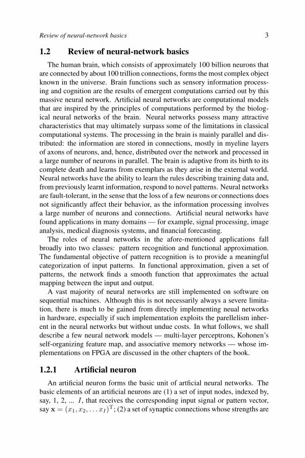
An artificial neuron forms the basic unit of artficial neural networks. Thebasic elements of an artificial neurons are (1) a set of input nodes, indexed by,say, 1, 2, ... I , that receives the corresponding input signal or pattern vector,say x = (x1, x2, . . . xI)T; (2) a set of synaptic connections whose strengths are
4 FPGA Neurocomputers
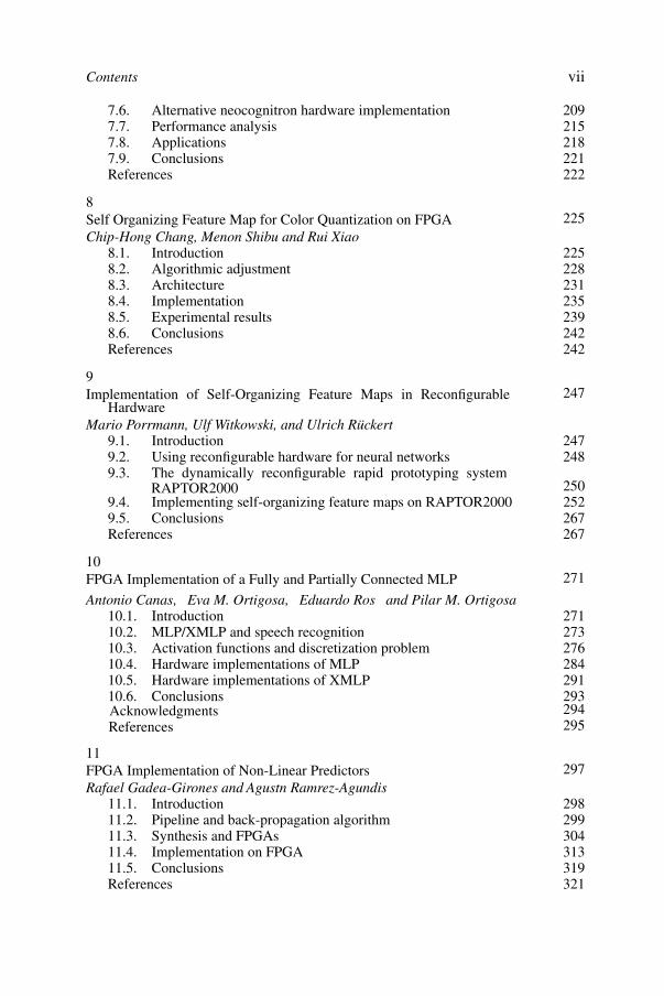
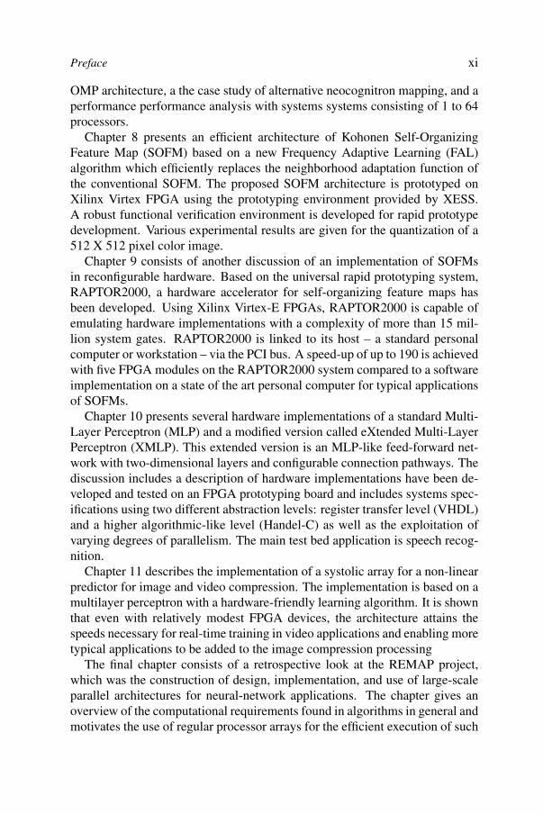
represented by a set of weights, here denoted by w = (w1, w2, . . . wI)T; and(3) an activation function Φ that relates the total synaptic input to the output(activation) of the neuron. The main components of an artificial neuron isillustrated in Figure 1.
Figure 1: The basic components of an artificial neuron
The total synaptic input, u, to the neuron is given by the inner product of theinput and weight vectors:
u =I∑
i=1
wixi (1.1)
where we assume that the threshold of the activation is incorporated in theweight vector. The output activation, y, is given by
y = Φ(u) (1.2)
where Φ denotes the activation function of the neuron. Consequently, the com-putation of the inner-products is one of the most important arithmetic opera-tions to be carried out for a hardware implementation of a neural network. Thismeans not just the individual multiplications and additions, but also the alterna-tion of successive multiplications and additions — in other words, a sequenceof multiply-add (also commonly known as multiply-accumulate or MAC) op-erations. We shall see that current FPGA devices are particularly well-suitedto such computations.
The total synaptic input is transformed to the output via the non-linear acti-vation function. Commonly employed activation functions for neurons are
Review of neural-network basics 5
the threshold activation function (unit step function or hard limiter):
Φ(u) ={
1.0, when u > 0,0.0, otherwise.
the ramp activation function:2
Φ(u) = max {0.0, min{1.0, u + 0.5}}
the sigmodal activation function, where the unipolar sigmoid function is
Φ(u) =a
1 + exp(−bu)
and the bipolar sigmoid is
Φ(u) = a
(1 − exp(−bu)1 + exp(−bu)
)where a and b represent, repectively, real constants the gain or amplitudeand the slope of the transfer function.
The second most important arithmetic operation required for neural networksis the computation of such activation functions. We shall see below that thestructure of FPGAs limits the ways in which these operations can be carriedout at reasonable cost, but current FPGAs are also equipped to enable high-speed implementations of these functions if the right choices are made.
A neuron with a threshold activation function is usually referred to as thediscrete perceptron, and with a continuous activation function, usually a sig-moidal function, such a neuron is referred to as continuous perceptron. Thesigmoidal is the most pervasive and biologically plausible activation function.
Neural networks attain their operating characteristics through learning ortraining. During training, the weights (or strengths) of connections are gradu-ally adjusted in either supervised or unsupervised manner. In supervised learn-ing, for each training input pattern, the network is presented with the desiredoutput (or a teacher), whereas in unsupervised learning, for each training inputpattern, the network adjusts the weights without knowing the correct target.The network self-organizes to classify similar input patterns into clusters inunsupervised learning. The learning of a continuous perceptron is by adjust-ment (using a gradient-descent procedure) of the weight vector, through theminimization of some error function, usually the square-error between the de-sired output and the output of the neuron. The resultant learning is known as
2In general, the slope of the ramp may be other than unity.
6 FPGA Neurocomputers
as delta learning: the new weight-vector, wnew, after presentation of an inputx and a desired output d is given by
wnew = wold + αδx
where wold refers to the weight vector before the presentation of the input andthe error term, δ, is (d − y)Φ′(u), where y is as defined in Equation 1.2 andΦ
′is the first derivative of Φ. The constant α, where 0 < α ≤ 1, denotes the
learning factor. Given a set of training data, Γ = {(xi, di); i = 1, . . . n}, thecomplete procedure of training a continuous perceptron is as follows:
begin: /* training a continuous perceptron */Initialize weights wnew
RepeatFor each pattern (xi, di) do
wold = wnew
wnew = wold + αδxi
until convergenceend
The weights of the perceptron are initialized to random values, and the conver-gence of the above algorithm is assumed to have been achieved when no moresignificant changes occur in the weight vector.
1.2.2 Multi-layer perceptron
The multi-layer perceptron (MLP) is a feedforward neural network consist-ing of an input layer of nodes, followed by two or more layers of perceptrons,the last of which is the output layer. The layers between the input layer andoutput layer are referred to as hidden layers. MLPs have been applied success-fully to many complex real-world problems consisting of non-linear decisionboundaries. Three-layer MLPs have been sufficient for most of these applica-tions. In what follows, we will briefly describe the architecture and learning ofan L-layer MLP.
Let 0-layer and L-layer represent the input and output layers, respectively;and let wl+1
kj denote the synaptic weight connected to the k-th neuron of thel + 1 layer from the j-th neuron of the l-th layer. If the number of perceptrons
in the l-th layer is Nl, then we shall let Wl�= {wl
kj}NlxNl−1denote the matrix
of weights connecting to l-th layer. The vector of synaptic inputs to the l-thlayer, ul = (ul
1, ul2, . . . u
lNl
)T is given by
ul = Wlyl−1,
where yl−1 = (yl−11 , yl−1
2 , . . . yl−1Nl−1
)T denotes the vector of outputs at the l−1layer. The generalized delta learning-rule for the layer l is, for perceptrons,
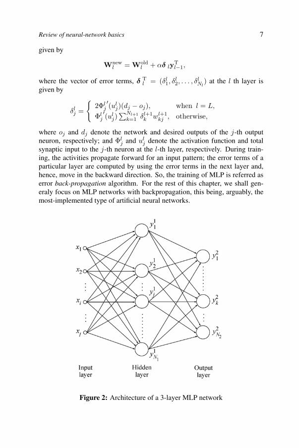
Review of neural-network basics 7
given by
Wnewl = Wold
l + αδ lyTl−1,
where the vector of error terms, δ Tl = (δl
1, δl2, . . . , δ
lNl
) at the l th layer isgiven by
δlj =
{2Φl
j′(ul
j)(dj − oj), when l = L,
Φlj′(ul
j)∑Nl+1
k=1 δl+1k wl+1
kj , otherwise,
where oj and dj denote the network and desired outputs of the j-th outputneuron, respectively; and Φl
j and ulj denote the activation function and total
synaptic input to the j-th neuron at the l-th layer, respectively. During train-ing, the activities propagate forward for an input pattern; the error terms of aparticular layer are computed by using the error terms in the next layer and,hence, move in the backward direction. So, the training of MLP is referred aserror back-propagation algorithm. For the rest of this chapter, we shall gen-eraly focus on MLP networks with backpropagation, this being, arguably, themost-implemented type of artificial neural networks.
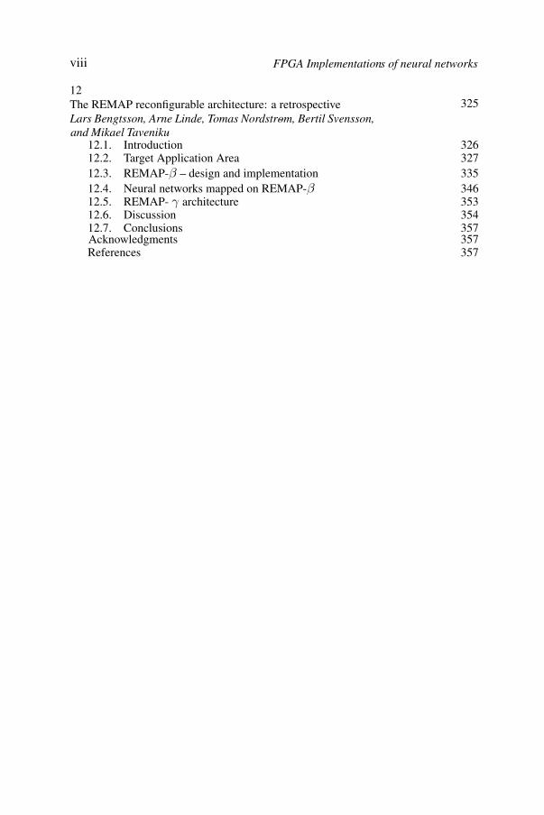
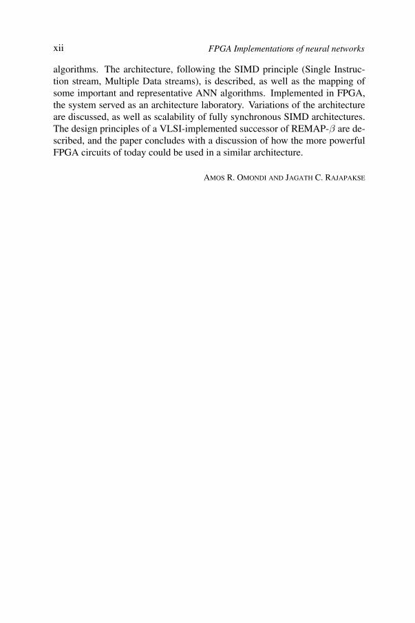
Figure 2: Architecture of a 3-layer MLP network
8 FPGA Neurocomputers
1.2.3 Self-organizing feature maps
Neurons in the cortex of the human brain are organized into layers of neu-rons. These neurons not only have bottom-up and top-down connections, butalso have lateral connections. A neuron in a layer excites its closest neigh-bors via lateral connections but inhibits the distant neighbors. Lateral inter-actions allow neighbors to partially learn the information learned by a winner(formally defined below), which gives neighbors responding to similar pat-terns after learning with the winner. This results in topological ordering offormed clusters. The self-organizing feature map (SOFM) is a two-layer self-organizing network which is capable of learning input patterns in a topolog-ically ordered manner at the output layer. The most significant concept in alearning SOFM is that of learning within a neighbourhood around a winningneuron. Therefore not only the weights of the winner but also those of theneighbors of the winner change.
The winning neuron, m, for an input pattern x is chosen according to thetotal synaptic input:
m = arg maxj
wTj x,
where wj denotes the weight-vector corresponding to the j-th output neuron.wT
mx determines the neuron with the shortest Euclidean distance between itsweight vector and the input vector when the input patterns are normalized tounity before training.
Let Nm(t) denote a set of indices corresponding to the neighbourhood sizeof the current winner m at the training time or iteration t. The radius of Nm isdecreased as the training progresses; that is, Nm(t1) > Nm(t2) > Nm(t3) . . . ,where t1 < t2 < t3 . . .. The radius Nm(t = 0) can be very large at thebeginning of learning because it is needed for initial global ordering of weights,but near the end of training, the neighbourhood may involve no neighbouringneurons other than the winning one. The weights associated with the winnerand its neighbouring neurons are updated by
∆wj = α(j, t) (x − wj) for all j ∈ Nm(t),
where the positive learning factor depends on both the training time and thesize of the neighbourhood. For example, a commonly used neighbourhoodfunction is the Gaussian function
α(Nm(t), t) = α(t) exp(−‖rj − rm‖2
2σ2(t)
),
where rm and rj denote the positions of the winning neuron m and of thewinning neighbourhood neurons j, respectively. α(t) is usually reduced at a
ASIC vs. FPGA neurocomputers 9
rate that is inversely proportional to t. The type of training described aboveis known as Kohonen’s algorithm (for SOFMs). The weights generated by theabove algorithms are arranged spatially in an ordering that is related to thefeatures of the trained patterns. Therefore, the algorithm produces topology-preserving maps. After learning, each input causes a localized response withpositions on the output layer that reflects dominant features of the input.
1.2.4 Associative-memory networks
Associative memory networks are two-layer networks in which weightsare determined in order to store a set of pattern associations, say,{(s1, t1), (s2, t2), . . . (sk, tk), . . . (sn, tn)}, where input pattern sk is associ-ated with output pattern tk. These networks not only learn to produce asso-ciative patterns, but also are able to recall the desired response patterns whena given pattern is similar to the stored pattern. Therefore they are referredto as content-addressible memory. For each association vector (sk, tk), ifsk = tk, the network is referred to as auto-associative; otherwise it is hetero-associative. The networks often provide input-output descriptions of the asso-ciative memory through a linear transformation (then known as linear associa-tive memory). The neurons in these networks have linear activation functions.If the linearity constant is unity, then the output layer activation is given by
y = Wx,
where W denotes the weight matrix connecting the input and output layers.These networks learn using the Hebb rule; the weight matrix to learn all theassociations is given by the batch learning rule:
W =n∑
k=1
tksTk .
If the stored patterns are orthogonal to each other, then it can be shown thatthe network recalls the stored associations perfectly. Otherwise, the recalledpatterns are distorted by cross-talk between patterns.
1.3 ASIC vs. FPGA neurocomputers
By far, the most often-stated reason for the development of custom (i.e.ASIC) neurocomputers is that conventional (i.e. sequential) general-purposeprocessors do not fully exploit the parallelism inherent in neural-network mod-els and that highly parallel architectures are required for that. That is true asfar as it goes, which is not very far, since it is mistaken on two counts [18]:The first is that it confuses the final goal, which is high performance — notmerely parallelism — with artifacts of the basic model. The strong focus on
10 FPGA Neurocomputers
parallelism can be justified only when high performance is attained at a rea-sonable cost. The second is that such claims ignore the fact that conventionalmicroprocessors, as well as other types of processors with a substantial user-base, improve at a much faster rate than (low-use) special-purpose ones, whichimplies that the performance (relative to cost or otherwise) of ASIC neurocom-puters will always lag behind that of mass-produced devices – even on specialapplications. As an example of this misdirection of effort, consider the latestin ASIC neurocomputers, as exemplified by, say, [3]. It is claimed that “withrelatively few neurons, this ANN-dedicated hardware chip [Neuricam Totem]outperformed the other two implementations [a Pentium-based PC and a TexasInstruments DSP]”. The actual results as presented and analysed are typicalof the poor benchmarking that afflicts the neural-network area. We shall havemore to say below on that point, but even if one accepts the claims as given,some remarks can be made immediately. The strongest performance-claimmade in [3], for example, is that the Totem neurochip outperformed, by a fac-tor of about 3, a PC (with a 400-MHz Pentium II processor, 128 Mbytes ofmain memory, and the neural netwoks implemented in Matlab). Two pointsare pertinent here:
In late-2001/early 2002, the latest Pentiums had clock rates that weremore than 3 times that of Pentium II above and with much more memory(cache, main, etc.) as well.
The PC implementation was done on top of a substantial software (base),instead of a direct low-level implementation, thus raising issues of “best-effort” with respect to the competitor machines.
A comparison of the NeuriCam Totems and Intel Pentiums, in the years 2002and 2004 will show the large basic differences have only got larger, primarilybecause, with the much large user-base, the Intel (x86) processors continue toimprove rapidly, whereas little is ever heard of about the neurocomputers asPCs go from one generation to another.
So, where then do FGPAs fit in? It is evident that in general FPGAs can-not match ASIC processors in performance, and in this regard FPGAs havealways lagged behind conventional microprocessors. Nevertheless, if oneconsiders FPGA structures as an alternative to software on, say, a general-purpose processor, then it is possible that FPGAs may be able to deliver bettercost:performance ratios on given applications.3 Moreover, the capacity forreconfiguration means that may be extended to a range of applications, e.g.several different types of neural networks. Thus the main advantage of theFPGA is that it may offer a better cost:performance ratio than either custom
3Note that the issue is cost:performance and not just performance
ASIC vs. FPGA neurocomputers 11
ASIC neurocomputers or state-of-the art general-purpose processors and withmore flexibility than the former. A comparison of the NeuriCam Totem, In-tel Pentiums, and M FPGAs will also show that improvements that show theadvantages of of the FPGAs, as a consequence of relatively rapid changes indensity and speed.
It is important to note here two critical points in relation to custom (ASIC)neurocomputers versus the FPGA structures that may be used to implement avariety of artificial neural networks. The first is that if one aims to realize a cus-tom neurocomputer that has a signficiant amount of flexibility, then one endsup with a structure that resembles an FPGA — that is, a small number of differ-ent types functional units that can be configured in different ways, according tothe neural network to be implemented — but which nonetheless does not havethe same flexibility. (A particular aspect to note here is that the large variety ofneural networks — usually geared towards different applications — gives risea requirement for flexibility, in the form of either programmability or recon-figurability.) The second point is that raw hardware-performance alone doesnot constitute the entirety of a typical computing structure: software is alsorequired; but the development of software for custom neurocomputers will,because of the limited user-base, always lag behind that of the more widelyused FPGAs. A final drawback of the custom-neurocomputer approach is thatmost designs and implementations tend to concentrate on just the high paral-lelism of the neural networks and generally ignore the implications of Am-dahl’s Law, which states that ultimately the speed-up will be limited by anyserial or lowly-parallel processing involved. (One rare exception is [8].)4 Thusnon-neural and other serial parts of processing tend to be given short shrift.Further, even where parallelism can be exploited, most neurocomputer-designseem to to take little account of the fact that the degrees of useful parallelismwill vary according to particular applications. (If parallelism is the main is-sue, then all this would suggest that the ideal building block for an appropri-ate parallel-processor machine is one that is less susceptible to these factors,and this argues for a relatively large-grain high-performance processor, used insmaller numbers, that can nevertheless exploit some of the parallelism inherentin neural networks [18].)
All of the above can be summed up quite succintly: despite all the claimsthat have been made and are still being made, to date there has not been acustom neurocomputer that, on artificial neural-network problems (or, for thatmatter, on any other type of problem), has outperformed the best conventionalcomputer of its time. Moreover, there is little chance of that happening. The
4Although not quite successful as a neurocomputer, this machine managed to survive longer than mostneurocomputers — because the flexibility inherent in its design meant that it could also be useful for non-neural applications.
12 FPGA Neurocomputers
promise of FPGAs is that they offer, in essence, the ability to realize “semi-custom” machines for neural networks; and, with continuing developments intechnology, they thus offer the best hope for changing the situation, as far aspossibly outperforming (relative to cost) conventional processors.
1.4 Parallelism in neural networks
Neural networks exhibit several types of parallelism, and a careful examina-tion of these is required in order to both determine the most suitable hardwarestructures as well as the best mappings from the neural-network structures ontogiven hardware structures. For example, parallelism can be of the SIMD typeor of the MIMD type, bit-parallel or word-parallel, and so forth [5]. In general,the only categorical statement that can be made is that, except for networks of atrivial size, fully parallel implementation in hardware is not feasible — virtualparallelism is necessary, and this, in turn, implies some sequential processing.In the context of FPGa, it might appear that reconfiguration is a silver bullet,but this is not so: the benefits of dynamic reconfigurability must be evaluatedrelative to the costs (especially in time) of reconfiguration. Nevertheless, thereis litle doubt that FPGAs are more promising that ASIC neurocomputers. Thespecific types of parallelism are as follows.
Training parallelism: Different training sessions can be run in parallel,e.g. on SIMD or MIMD processors. The level of parallelism at this levelis usually medium (i.e. in the hundreds), and hence can be nearly fullymapped onto current large FPGAs.
Layer parallelism: In a multilayer network, different layers can beprocessed in parallel. Parallelism at this level is typically low (in thetens), and therefore of limited value, but it can still be exploited throughpipelining.
Node parallelism: This level, which coresponds to individual neurons, isperhaps the most important level of parallelism, in that if fully exploited,then parallelism at all of the above higher levels is also fully exploited.But that may not be possible, since the number of neurons can be ashigh as in the millions. Nevertheless, node parallelism matches FPGAsvery well, since a typical FPGA basically consists of a large number of“cells” that can operate in parallel and, as we shall see below, onto whichneurons can readily be mapped.
Weight parallelism: In the computation of an output
y = Φ
(n∑
i=1
wixi
),
Xilinx Virtex-4 FPGA 13
where xi is an input and wi is a weight, the products xiwi can all becomputed in parallel, and the sum of these products can also be com-puted with high parallelism (e.g. by using an adder-tree of logarithmicdepth).
Bit-level parallelism: At the implementation level, a wide variety of par-allelism is available, depending on the design of individual functionalunits. For example, bit-serial, serial-parallel, word-parallel, etc.
From the above, three things are evident in the context of an implementation.First, the parallelism available at the different levels varies enormously. Sec-ond, different types of parallelism may be traded off against others, dependingon the desired cost:performance ratio (where for an FPGA cost may be mea-sured in, say, the number of CLBs etc.); for example, the slow speed of asingle functional unit may be balanced by having many such units operatingconcurrently. And third, not all types of parallelism are suitable for FPGAimplementation: for example, the required routing-interconnections may beproblematic, or the exploitation of bit-level parallelism may be constrained bythe design of the device, or bit-level parallelism may simply not be appropriate,and so forth. In the Xilinx Virtex-4, for example, we shall see that it is possibleto carry out many neural-network computations without using much of what isusually taken as FPGA fabric.5
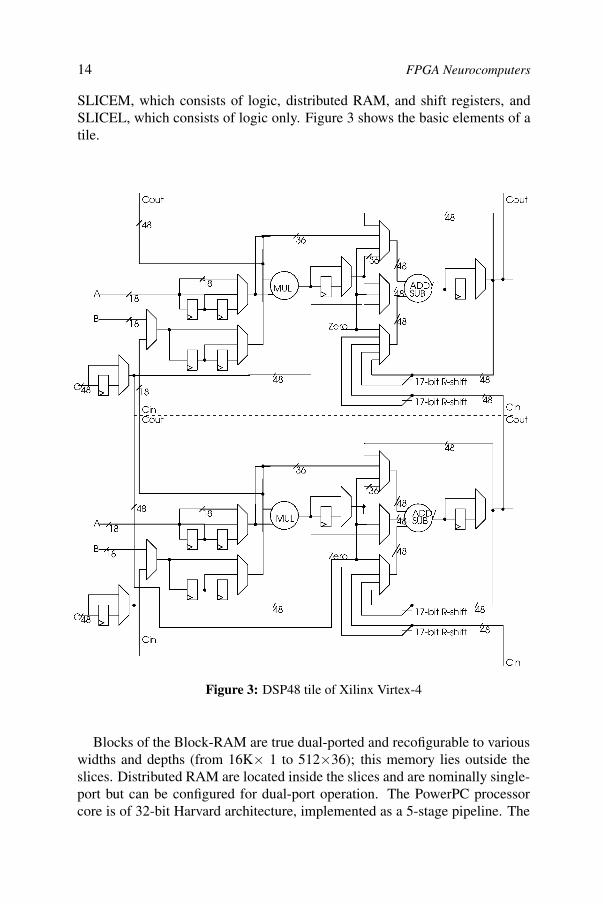
1.5 Xilinx Virtex-4 FPGA
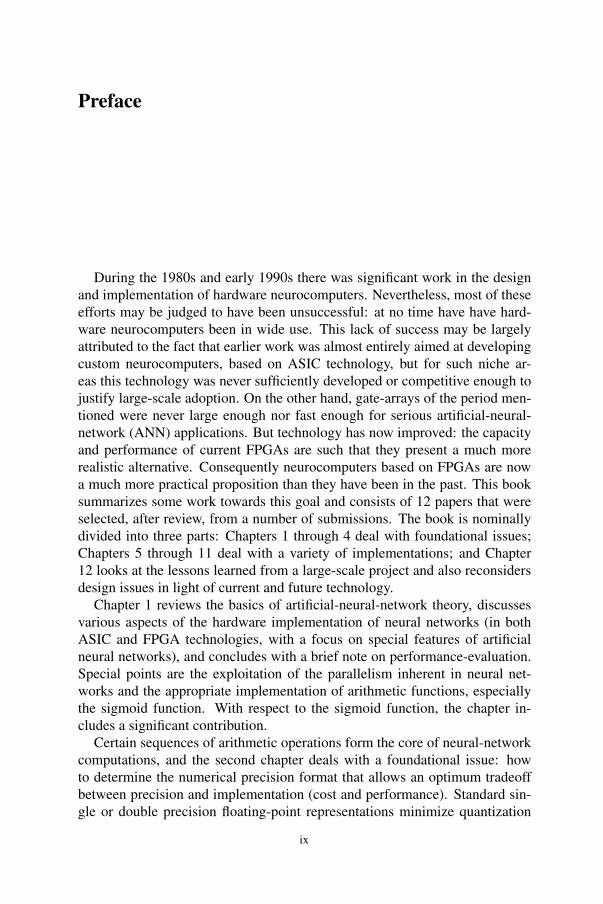
In this section, we shall briefly give the details an current FPGA device,the Xilinx Virtex-4, that is typical of state-of-the-art FPGA devices. We shallbelow use this device in several running examples, as these are easiest under-stood in the context of a concrete device. The Virtex-4 is actually a family ofdevices with many common features but varying in speed, logic-capacity, etc..The Virtex-E consists of an array of up to 192-by-116 tiles (in generic FPGAterms, configurable logic blocks or CLBs), up to 1392 Kb of Distributed-RAM,upto 9936 Kb of Block-RAM (arranged in 18-Kb blocks), up to 2 PowerPC 405processors, up to 512 Xtreme DSP slices for arithmetic, input/ouput blocks,and so forth.6
A tile is made of two DSP48 slices that together consist of eight function-generators (configured as 4-bit lookup tables capable of realizing any four-input boolean function), eight flip-flops, two fast carry-chains, 64 bits ofDistributed-RAM, and 64-bits of shift register. There are two types of slices:
5The definition here of FPGA fabric is, of course, subjective, and this reflects a need to deal with changes inFPGA realization. But the fundamental point remains valid: bit-level parallelism is not ideal for the givencomputations and the device in question.6Not all the stated maxima occur in any one device of the family.
14 FPGA Neurocomputers
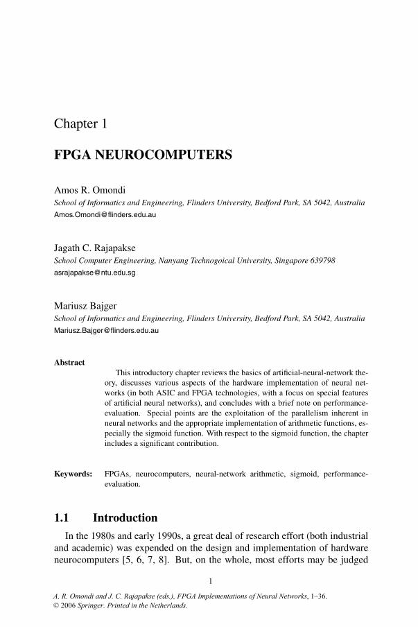
SLICEM, which consists of logic, distributed RAM, and shift registers, andSLICEL, which consists of logic only. Figure 3 shows the basic elements of atile.
Figure 3: DSP48 tile of Xilinx Virtex-4
Blocks of the Block-RAM are true dual-ported and recofigurable to variouswidths and depths (from 16K× 1 to 512×36); this memory lies outside theslices. Distributed RAM are located inside the slices and are nominally single-port but can be configured for dual-port operation. The PowerPC processorcore is of 32-bit Harvard architecture, implemented as a 5-stage pipeline. The
Arithmetic 15
significance of this last unit is in relation to the comment above on the serialparts of even highly parallel applications — one cannot live by parallelismalone. The maximum clock rate for all of the units above is 500 MHz.
Arithmetic functions in the Virtex-4 fall into one of two main categories:arithmetic within a tile and arithmetic within a collection of slices. All theslices together make up what is called the XtremeDSP [22]. DSP48 slicesare optimized for multipliy, add, and mutiply-add operations. There are 512DSP48 slices in the largest Virtex-4 device. Each slice has the organizationshown in Figure 3 and consists primarily of an 18-bit×18-bit multiplier, a 48-bit adder/subtractor, multiplexers, registers, and so forth. Given the importanceof inner-product computations, it is the XtremeDSP that is here most crucial forneural-network applications. With 512 DSP48 slices operating at a peak rate of500 MHz, a maximum performance of 256 Giga-MACs (multiply-accumlateoperations) per second is possible. Observe that this is well beyond anythingthat has so far been offered by way of a custom neurocomputer.
1.6 Arithmetic
There are several aspects of computer arithmetic that need to be consid-ered in the design of neurocomputers; these include data representation, inner-product computation, implementation of activation functions, storage and up-date of weights, and the nature of learning algorithms. Input/output, althoughnot an arithmetic problem, is also important to ensure that arithmetic units canbe supplied with inputs (and results sent out) at appropriate rates. Of these,the most important are the inner-product and the activation functions. Indeed,the latter is sufficiently significant and of such complexity that we shall devoteto it an entirely separate section. In what follows, we shall discuss the others,with a special emphasis on inner-products. Activation functions, which hereis restricted to the sigmoid (although the relevant techniques are not) are suf-ficiently complex that we have relegated them to seperate section: given theease with which multiplication and addition can be implemented, unless suffi-cient care is taken, it is the activation function that will be the limiting factorin performance.
Data representation: There is not much to be said here, especially since exist-ing devices restrict the choice; nevertheless, such restrictions are not absolute,and there is, in any case, room to reflect on alternatives to what may be onoffer. The standard representations are generally based on two’s complement.We do, however, wish to highlight the role that residue number systems (RNS)can play.
It is well-known that RNS, because of its carry-free properties, is particu-larly good for multiplication and addition [23]; and we have noted that inner-product is particularly important here. So there is a natural fit, it seems. Now,
16 FPGA Neurocomputers
to date RNS have not been particularly successful, primarily because of thedifficulties in converting between RNS representations and conventional ones.What must be borne in mind, however, is the old adage that computing is aboutinsight, not numbers; what that means in this context is that the issue of con-version need come up only if it is absolutely necessary. Consider, for example,a neural network that is used for classification. The final result for each input isbinary: either a classification is correct or it is not. So, the representation usedin the computations is a side-issue: conversion need not be carried out as longas an appropriate output can be obtained. (The same remark, of course, appliesto many other problems and not just neural networks.) As for the constraintsof off-the-shelf FPGA devices, two things may be observed: first, FPGA cellstypically perform operations on small slices (say, 4-bit or 8-bit) that are per-fectly adequate for RNS digit-slice arithmetic; and, second, below the levelof digit-slices, RNS arithmetic will in any case be realized in a conventionalnotation.
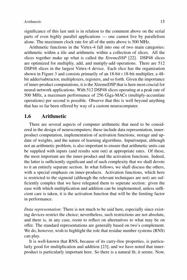
Figure 4: XtremeDSP chain-configuration for an inner-product
The other issue that is significant for representation is the precision used.There have now been sufficient studies (e.g. [17]) that have established 16bits for weights and 8 bits for activation-function inputs as good enough. With
Arithmetic 17
this knowledge, the critical aspect then is when, due to considerations of per-formance or cost, lower precision must be used. Then a careful process ofnumerical analysis is needed.
Figure 5: XtremeDSP tree-configuration for an inner-product
Sum-of-products computations: There are several ways to implement this, de-pending on the number of datasets. If there is just one dataset, then the opera-tion is
∑Ni=1 wiXi, where wi is a weight and Xi is an input. (In general, this
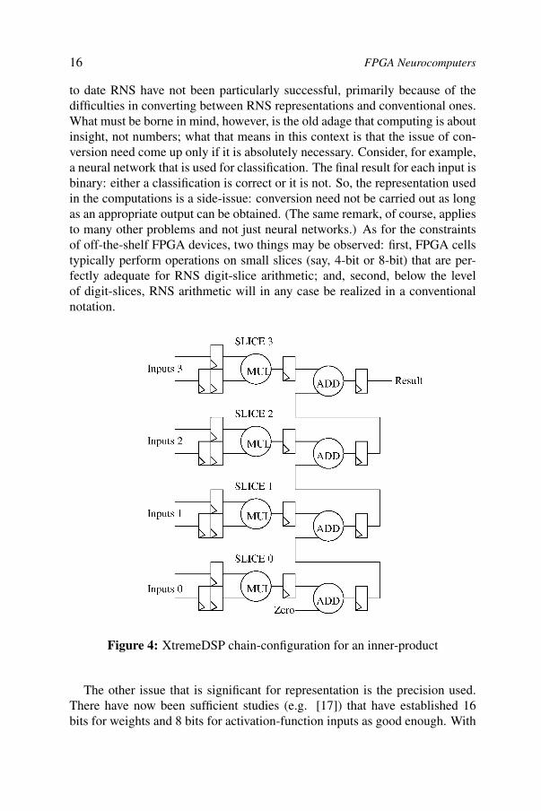
is the matrix-vector computation expressed by Equation 1.1.) In such a case,with a device such as the Xilinx Virtex-4, there are several possible implemen-tations, of which we now give a few sketches. If N is small enough, then twodirect implementations consist of either a chain (Figure 4) or a tree (Figure 5)of DSP48 slices. Evidently, the trade-off is one of latency versus effecient useof device logic: with a tree the use of tile logic is quite uneven and less efficientthan with a chain. If N is large, then an obvious way to proceed is to use acombination of these two approaches. That is, partition the computation intoseveral pieces, use a chain for each such piece, and then combine in a tree theresults of these chains, or the other way around. But there are other possibleapproaches: for example, instead of using chains, one DSP48 slice could beused (with a feedback loop) to comute the result of each nominal chain, withall such results then combined in a chain or a tree. Of course, the latency willnow be much higher.
18 FPGA Neurocomputers
With multiple datasets, any of the above approaches can be used, althoughsome are better than others — for example, tree structures are more amenableto pipelining. But there is now an additional issue: how to get data in andout at the appropriate rates. If the network is sufficiently large, then most ofthe inputs to the arithmetic units will be stored outside the device, and thenumber of device pins available for input/output becomes a minor issue. Inthis case, the organization of input/output is critical. So, in general, one needsto consider both large datasets as well as multiple data sets. The followingdiscussions cover both aspects.Storage and update of weights, input/output: For our purposes, Distributed-RAM is too small to hold most of the data that is to be processed, and therefore,in general Block-RAM will be used. Both weights and input values are storedin a single block and simualtaneously read out (as the RAM is dual-ported).Of course, for very small networks, it may be practical to use the Distributed-RAM, especially to store the weights; but we will in general assume networksof arbitrary size. (A more practical use for Distributed-RAM is the storage ofconstants used to implement activation functions.) Note that the disparity (dis-cussed below) between the rate of inner-product computations and activation-function computations means that there is more Distributed-RAM available forthis purpose than appears at first glance. For large networks, even the Block-RAM may not be sufficient, and data has to be periodically loaded into andretrieved from the FPGA device. Given pin-limitations, careful considerationmust be given to how this is done.
Let us suppose that we have multiple datasets and that each of these is verylarge. Then, the matrix-vector product of Equation 1.1, that is,
u = Wy
becomes a matrix-matrix product,
U = WY,
where each column of Y is associated with one input dataset. The mostcommon method used for matrix-matrix multiplication is the inner-productmethod; that is, each element of the output matrix is directly generated as aninner-product of two vectors of the input matrices. Once the basic method hasbeen selected, the data must be processed — in particular, for large datasets,this includes bringing data into, and retrieving data from, the FPGA — exactlyas indicated above. This is, of course, true for other methods as well.
Whether or not the inner-product method, which is a highly sequentialmethod, is satisfactory depends a great deal on the basic processor microar-chitecture, and there are at least two alternatives that should always be consid-
Arithmetic 19
ered: the outer-product and the middle-product methods.7 Consider a typical“naive” sequential implementation of matrix multiplication. The inner-productmethod would be encoded as three nested loops, the innermost of which com-putes the inner-product of a vector of one of the input matrices and a vector ofthe other input matrix:
for i:=1 to n dofor j:=1 to n do
for k:=1 to n doU[i,j]:=U[i,j]+W[i,k]*Y[k,j];
(where we assume that the elements of U [i, j] have all been initialized to zero.)Let us call this the ijk-method8, based on the ordering of the index-changes.The only parallelism here is in the multiplication of individual matrix elementand, to a much lesser extent (assuming the tree-method is used instead of thechain method) in the tree-summation of these products). That is, for n×n ma-trices, the required n2 inner-products are computed one at a time. The middle-product method is obtained by interchanging two of the loops so as to yieldthe jki-method. Now more parallelism is exposed, since n inner-products canbe computed concurrently; this is the middle-product method. And the outer-product method is the kij-method. Here all parallelism is now exposed: all n2
inner products can be computed concurrently. Nevertheless, it should be notedthat no one method may be categorically said to be better than another — it alldepends on the architecture, etc.
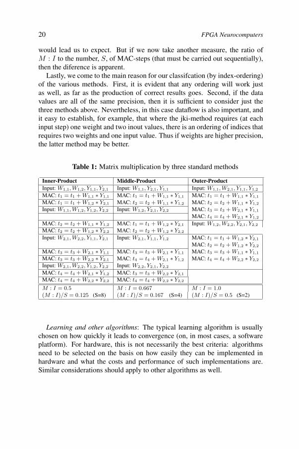
To put some meat to the bones above, let us consider a concrete example —the case of 2× 2 matrices. Further, let us assume that the multiply-accumulate(MAC) operations are carried out within the device but that all data has to bebrought into the device. Then the process with each of the three methods isshown in Table 1. (The horizontal lines delineate groups of actions that maytake place concurrently; that is within a column, actions separated by a linemust be performed sequentially.)
A somewhat rough way to compare the three methods is measure the ratio,M : I , of the number of MACs carried out per data value brought into thearray. This measure clearly ranks the three methods in the order one wouldexpect; also note that by this measure the kij-method is completely efficient(M : I = 1): every data value brought in is involved in a MAC. Nevertheless,it is not entirely satisfactory: for example, it shows that the kij-method to bebetter than the jki-method by factor, which is smaller that what our intuition
7The reader who is familiar with compiler technology will readily recognise these as vecorization (paral-lelization) by loop-interchange.8We have chosen this terminology to make it convenient to also include methods that have not yet been“named”.
20 FPGA Neurocomputers
would lead us to expect. But if we now take another measure, the ratio ofM : I to the number, S, of MAC-steps (that must be carried out sequentially),then the diference is apparent.
Lastly, we come to the main reason for our classifcation (by index-ordering)of the various methods. First, it is evident that any ordering will work justas well, as far as the production of correct results goes. Second, if the datavalues are all of the same precision, then it is sufficient to consider just thethree methods above. Nevertheless, in this case dataflow is also important, andit easy to establish, for example, that where the jki-method requires (at eachinput step) one weight and two inout values, there is an ordering of indices thatrequires two weights and one input value. Thus if weights are higher precision,the latter method may be better.
Inner-Product Middle-Product Outer-ProductInput: W1,1, W1,2, Y1,1, Y2,1 Input: W1,1, Y2,1, Y1,1 Input: W1,1, W2,1, Y1,1, Y1,2
MAC: t1 = t1 + W1,1 ∗ Y1,1 MAC: t1 = t1 + W1,1 ∗ Y1,1 MAC: t1 = t1 + W1,1 ∗ Y1,1
MAC: t1 = t1 + W1,2 ∗ Y2,1 MAC: t2 = t2 + W1,1 ∗ Y1,2 MAC: t2 = t2 + W1,1 ∗ Y1,2
Input: W1,1, W1,2, Y1,2, Y2,2 Input: W1,2, Y2,1, Y2,2 MAC: t3 = t3 + W2,1 ∗ Y1,1
MAC: t4 = t4 + W2,1 ∗ Y1,2
MAC: t2 = t2 + W1,1 ∗ Y1,2 MAC: t1 = t1 + W1,2 ∗ Y2,1 Input: W1,2, W2,2, Y2,1, Y2,2
MAC: t2 = t2 + W1,2 ∗ Y2,2 MAC: t2 = t2 + W1,2 ∗ Y2,2
Input: W2,1, W2,2, Y1,1, Y2,1 Input: W2,1, Y1,1, Y1,2 MAC: t1 = t1 + W1,2 ∗ Y2,1
MAC: t2 = t2 + W1,2 ∗ Y2,2
MAC: t3 = t3 + W2,1 ∗ Y1,1 MAC: t3 = t3 + W2,1 ∗ Y1,1 MAC: t3 = t3 + W1,1 ∗ Y1,1
MAC: t3 = t3 + W2,2 ∗ Y2,1 MAC: t4 = t4 + W2,1 ∗ Y1,2 MAC: t4 = t4 + W2,2 ∗ Y2,2
Input: W2,1, W2,2, Y1,2, Y2,2 Input: W2,2, Y2,1, Y2,2
MAC: t4 = t4 + W2,1 ∗ Y1,2 MAC: t3 = t3 + W2,2 ∗ Y2,1
MAC: t4 = t4 + W2,2 ∗ Y2,2 MAC: t4 = t4 + W2,2 ∗ Y2,2
M : I = 0.5 M : I = 0.667 M : I = 1.0(M : I)/S = 0.125 (S=8) (M : I)/S = 0.167 (S=4) (M : I)/S = 0.5 (S=2)
Table 1: Matrix multiplication by three standard methods
Learning and other algorithms: The typical learning algorithm is usuallychosen on how quickly it leads to convergence (on, in most cases, a softwareplatform). For hardware, this is not necessarily the best criteria: algorithmsneed to be selected on the basis on how easily they can be implemented inhardware and what the costs and performance of such implementations are.Similar considerations should apply to other algorithms as well.
Activation-function implementation: unipolar sigmoid 21
1.7 Activation-function implementation: unipolarsigmoid
For neural networks, the implementation of these functions is one of the twomost important arithmetic design-issues. Many techniques exist for evaluatingsuch elementary or nearly-elementary functions: polynomial approximations,CORDIC algorithms, rational approximations, table-driven methods, and soforth [4, 11]. For hardware implementation, accuracy, performance and costare all important. The latter two mean that many of the better techniques thathave been developed in numerical analysis (and which are easily implementedin software) are not suitable for hardware implementation. CORDIC is perhapsthe most studied technique for hardware implementation, but it is (relatively)rarely implemented: its advantage is that the same hardware can be used forseveral functions, but the resulting performance is usually rather poor. High-order polynomial approximations can give low-error implementations, but aregenerally not suitable for hardware implementation, because of the number ofarithmetic operations (multiplications and additions) that must be performedfor each value; either much hardware must be used, or performance be com-promised. And a similar remark applies to pure table-driven methods, unlessthe tables are quite small: large tables will be both slow and costly. The prac-tical implication of these constraints is as indicated above: the best techniquesfrom standard numerical analysis are of dubious worth.
Given trends in technology, it is apparent that at present the best techniquefor hardware function-evaluation is a combination of low-order polynomialsand small look-up tables. This is the case for both ASIC and FPGA technolo-gies, and especially for the latter, in which current devices are equipped withsubstantial amounts of memory, spread through the device, as well as manyarithmetic units (notably mulipliers and adders).9 The combination of low-order polynomials (primarily linear ones) is not new — the main challengeshas always been one of how to choose the best interpolation points and how toensure that look-up tables remain small. Low-order interpolation therefore hasthree main advantages. The first is that exactly the same hardware structurescan be used to realize different functions, since only polynomial coefficients(i.e. the contents of look-up tables) need be changed; such efficient reuse is notpossible with the other techniques mentioned above. The second is that it iswell-matched to current FPGA devices, which come with built-in multipliers,adders, and memory.
The next subsection outlines the basic of our approach to linear interpola-tion; the one after that discusses implementation issues; and the final subsec-tion goes into the details of the underlying theory.
9This is validated by a recent study of FPGA implementations of various techniques [16].
22 FPGA Neurocomputers
1.7.1 Basic concepts
On the basis of the considerations above, we have chosen piecewise linearinterpolation for the approximation of the sigmoid function.
For most functions, interpolation with uniformly-sized intervals (i.e.uniformly-spaced abscissae) is not ideal; in the case of the sigmoid, it is evidentthat, idealy, more intervals should be used as the magnitude of the argumentincreases. Nevertheless, for hardware implementation, the need to quicklymap arguments onto the appropriate intervals dictates the use of such inter-vals. With this choice and linear interpolation, the critical issue then becomesthat of what function-value to associate with each interval. The most commonchoice is to arbitrarily select the value at the midpoint of the interval — thatis, if x ∈ [L, U ], then f(x) = f(L/2 + U/2) — or to choose a value thatminimizes absolute errors. 10 Neither is particularly good. As we shall show,even with a fixed number of intervals, the best function-value for an interval isgenerally not the midpoint. And, depending on the “curvature” of the functionat hand, relative error may be more critical than absolute error. For example,for the sigmoid function, f(x) = 1/(1 + e−x), we have a function that is sym-metric (about the y-axis), but the relative error grows more rapidly on one sideof the axis than the other, and on both sides the growth depends on the interval.Thus, the effect of a given value of absolute error is not constant or even linear.
The general approach we take is as follows. Let I = [L, U ] be a real intervalwith L < U , and let f : I → R be a function to be approximated (where Rdenotes the set of real numbers). Suppose that f : I → R is a linear function— that is, f(x) = c1 + c2x, for some constants c1 and c2 — that approximatesf . Our objective is to investigate the relative-error function
ε(x) = f(x)−f(x)f(x) , x ∈ I, (Err)
and to find c1 and c2 such that ε(x) is small. One way to obtain reasonablygood values for c1, c2 is to impose the
f(L) = f(L), f(U) = f(U) (C)
and then compute values for c1 and c2. But a much better result can be obtainedusing the “improved” condition
|ε(L)| = |ε(U)| = |ε(xstat)|, (IC)
where xstat (stationary point) is the value of x for which ε(x) has a localextremum. An example of the use of this technique to approximate reciprocals
10Following [12], we use absolute error to refer to the difference between the exact value and its approxi-mation; that is, it is not the absolute value of that difference.
Activation-function implementation: unipolar sigmoid 23
can be found in [4, 10] for the approximation of divisor reciprocals and square-root reciprocals. It is worth noting, however, that in [10], ε(x) is taken to bethe absolute-error function. This choice simplifies the application of (IC), but,given the "curvature" of these functions, it is not as good as the relative-errorfunction above. We will show, in Section 7.3, that (IC) can be used successfullyfor sigmoid function, despite the fact that finding the exact value for xstat
may not be possible. We show that, compared with the results from using thecondition (C), the improved condition (IC) yields a massive 50% reduction inthe magnitude of the relative error. We shall also give the analytical formulaefor the constants c1 and c2. The general technique is easily extended to otherfunctions and with equal or less ease [13], but we shall here consider onlythe sigmoid function, which is probably the most important one for neuralnetworks.
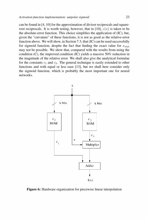
Figure 6: Hardware organization for piecewise linear interpolation
24 FPGA Neurocomputers
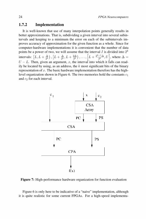
1.7.2 Implementation
It is well-known that use of many interpolation points generally results inbetter approximations. That is, subdividing a given interval into several subin-tervals and keeping to a minimum the error on each of the subintervals im-proves accuracy of approximation for the given function as a whole. Since forcomputer-hardware implementations it is convenient that the number of datapoints be a power of two, we will assume that the interval I is divided into 2k
intervals:[L, L + ∆
2k
),[L + ∆
2k , L + 2∆2k
), . . . ,
[L + 2k−1∆
2k , U], where ∆ =
U − L. Then, given an argument, x, the interval into which it falls can read-ily be located by using, as an address, the k most significant bits of the binaryrepresentation of x. The basic hardware implementation therefore has the high-level organization shown in Figure 6. The two memories hold the constants c1
and c2 for each interval.
Figure 7: High-performance hardware organization for function evaluation
Figure 6 is only here to be indicative of a “naive” implementation, althoughit is quite realistic for some current FPGAs. For a high-speed implementa-
Activation-function implementation: unipolar sigmoid 25
tion, the actual structure may differ in several ways. Consider for example themultiplier-adder pair. Taken individually, the adder must be a carry-propagateadder (CPA); and the multiplier, if it is of high performance will consist of anarray of carry-save adders (CSAs) with a final CPA to assimilate the partial-sum/partial-carry (PC/PS) output of the CSAs. But the multiplier-CPA may bereplaced with two CSAs, to yield much higher performance. Therefore, in ahigh speed implementation the actual structure would have the form shown inFigure 7.
Nevertheless, for FPGAs, the built-in structure will impose some con-straints, and the actual implementation will generally be device-dependent. Forexample, for a device such as the Xilinx Virtex-4, the design of Figure 6 maybe implemented more or less exactly as given: the DSP48 slice provides themultiply-add function, and the constants, c1 and c2, are stored in Block-RAM.They could also be stored in Distributed-RAM, as it is unlikely that there willbe many of them. Several slices would be required to store the constants at therequired precision, but this is not necessarily problematic: observe that eachinstance of activation-function computation corresponds to several MACs (bitslices).
All of the above is fairly straightforward, but there is one point that needs aparticular mention: Equations 1.1 and 1.2 taken together imply that there is aninevitable disparity between the rate of inner-product (MACs) computationsand activation-function computations. In custom design, this would not causeparticular concern: both the design and the placement of the relevant hard-ware units can be chosen so as to optimize cost, performance, etc. But withFPGAs, this luxury does not exist: the mapping of a network to a device, therouting requirements to get an inner-product value to the correct place for theactivation-function computation, the need to balance the disparate rates ... allthese mean that the best implementation will be anything but straightforward.
1.7.3 Theory
We shall illustrate our results with detailed numerical data obtained for afixed number of intervals. All numerical computations, were carried out inthe computer algebra system MAPLE [24] for the interval11 I = [0.5, 1] andk = 4; that is, I was divided into the 16 intervals:[
12,1732
,916
,1932
,58, . . . , 1
].
We have used MAPLE to perform many of complex symbolic computations.Floating-point calculations in MAPLE are carried out in finite precision, with
11Note that evaluation on any other interval can be transformed into evaluation on the interval [0.5, 1].
26 FPGA Neurocomputers
intermediate results rounded to a precision that is specified by MAPLE con-stant Digits. This constant controls the number of digits that MAPLE uses forcalculations. Thus, generally, the higher the Digits value is, the higher accu-racy of the obtainable results, with roundoff errors as small as possible. (Thishowever cannot be fully controlled in case of complex algebraic expressions).We set Digits value to 20 for numerical computations. Numerical results willbe presented using standard (decimal) scientific notation.
Applying condition (C), in Section 7.1, to the sigmoid function, we get⎧⎨⎩c1 + c2L = 1
1+e−U
c1 + c2U = 11+e−L .
For simplicity, we will use θ to denote the expression
UeL − LeU − Le(L+U) + Ue(L+U).
Then the solution of the above system may be expressed as
c1 = θθ+U−L+UeU−LeL
c2 = eU−eL
θ+U−L+UeU−LeL .
and the approximation function f(x) = c1 + c2x takes the form
f(x) =θ + x
(eU − eL
)θ + U − L + UeU + LeL
, x ∈ I.
The relative error is now
ε(x) =−LeL − L + UeU + U − e−xθ − xeU
θ + U − L + UeU + LeL
+−xeU−x + xeL + xe(L−x)
θ + U − L + UeU + LeL, x ∈ I.
Activation-function implementation: unipolar sigmoid 27
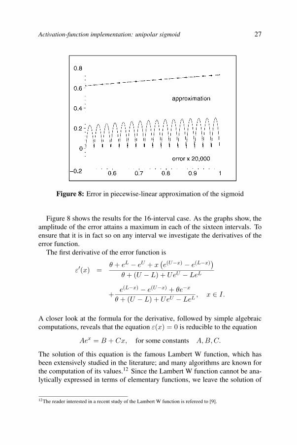
Figure 8: Error in piecewise-linear approximation of the sigmoid
Figure 8 shows the results for the 16-interval case. As the graphs show, theamplitude of the error attains a maximum in each of the sixteen intervals. Toensure that it is in fact so on any interval we investigate the derivatives of theerror function.
The first derivative of the error function is
ε′(x) =θ + eL − eU + x
(e(U−x) − e(L−x)
)θ + (U − L) + UeU − LeL
+e(L−x) − e(U−x) + θe−x
θ + (U − L) + UeU − LeL, x ∈ I.
A closer look at the formula for the derivative, followed by simple algebraiccomputations, reveals that the equation ε(x) = 0 is reducible to the equation
Aex = B + Cx, for some constants A, B, C.
The solution of this equation is the famous Lambert W function, which hasbeen extensively studied in the literature; and many algorithms are known forthe computation of its values.12 Since the Lambert W function cannot be ana-lytically expressed in terms of elementary functions, we leave the solution of
12The reader interested in a recent study of the Lambert W function is refereed to [9].
28 FPGA Neurocomputers
our equation in the form
xstat = eLLambertW
⎛⎜⎝−e
(U− θ+(eU−eL)(U−1)
eU−eL
)⎞⎟⎠+eULambertW
⎛⎜⎝−e
(U− θ+(eU−eL)(U−1)
eU−eL
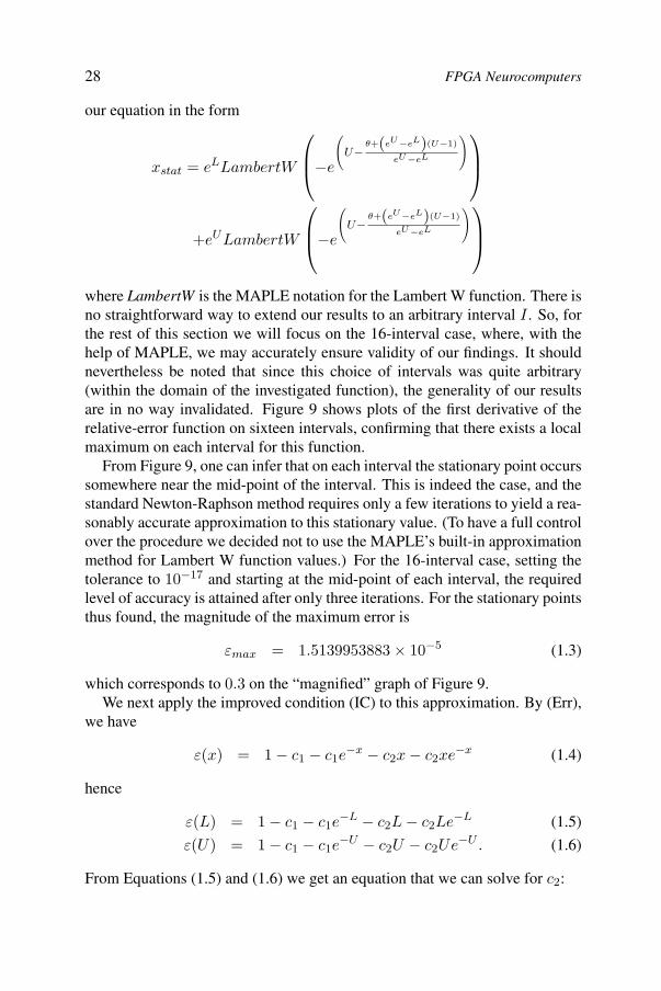
)⎞⎟⎠where LambertW is the MAPLE notation for the Lambert W function. There isno straightforward way to extend our results to an arbitrary interval I . So, forthe rest of this section we will focus on the 16-interval case, where, with thehelp of MAPLE, we may accurately ensure validity of our findings. It shouldnevertheless be noted that since this choice of intervals was quite arbitrary(within the domain of the investigated function), the generality of our resultsare in no way invalidated. Figure 9 shows plots of the first derivative of therelative-error function on sixteen intervals, confirming that there exists a localmaximum on each interval for this function.
From Figure 9, one can infer that on each interval the stationary point occurssomewhere near the mid-point of the interval. This is indeed the case, and thestandard Newton-Raphson method requires only a few iterations to yield a rea-sonably accurate approximation to this stationary value. (To have a full controlover the procedure we decided not to use the MAPLE’s built-in approximationmethod for Lambert W function values.) For the 16-interval case, setting thetolerance to 10−17 and starting at the mid-point of each interval, the requiredlevel of accuracy is attained after only three iterations. For the stationary pointsthus found, the magnitude of the maximum error is
εmax = 1.5139953883 × 10⁻⁵ (1.3)
which corresponds to 0.3 on the “magnified” graph of Figure 9.We next apply the improved condition (IC) to this approximation. By (Err),
we have
ε(x) = 1 − c1 − c1e−x − c2x − c2xe−x (1.4)
hence
ε(L) = 1 − c1 − c1e−L − c2L − c2Le−L (1.5)
ε(U) = 1 − c1 − c1e−U − c2U − c2Ue−U . (1.6)
From Equations (1.5) and (1.6) we get an equation that we can solve for c2:
Activation-function implementation: unipolar sigmoid 29
c2 =c1
(e−L − e−U
)U + Ue−U − L − Le−L
(1.7)
Substituting for c2 in Equation (1.4) yields the final formula for the relativeerror
ε(x) = 1 − c1 − c1e−x +
c1
(e−U − e−L
)x
U + Ue−U − L − Le−L
+c1
(e−U − e−L
)xe−x
U + Ue−U − L − Le−L, x ∈ I.
To study the error magnitude we investigate its first derivative for x ∈ I:
ε′(x) = c1e−xU + e(−x−U)U − e−xL − e(−x−L)L + e−U
U + Ue−U − L − Le−L
+c1−e−L + e(−x−U) + e(−x−L)
U + Ue−U − L − Le−L
+c1−xe(−x−U) + xe(−x−L)
U + Ue−U − L − Le−L.
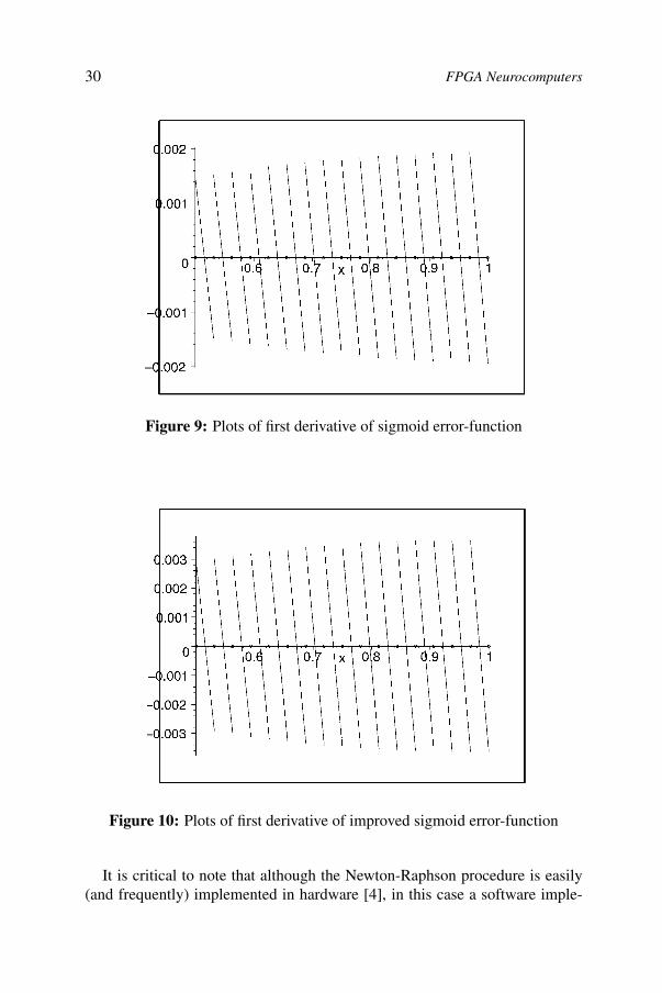
We may assume without loss of generality that c1 is positive: the graph ofthe sigmoid function indicates that this is a valid assumption. For simplicity,let us assume that c1 = 1 and see how the first derivative behaves on thesixteen intervals. Figure 10 shows the graphs of the first derivative of the newerror function. From these plots we see that within each interval the derivativechanges sign at a unique stationary point. Finding an exact analytical formulafor the values of these points is not possible, because, as above, the equationε(x) = 0, reduces to a Lambert-type of equation. So, once again, we applythe Newton-Raphson method to get some reasonably accurate estimate values.Starting the iteration from the mid-point we obtain good approximation afterjust a few iterations.
30 FPGA Neurocomputers
Figure 9: Plots of first derivative of sigmoid error-function
Figure 10: Plots of first derivative of improved sigmoid error-function
It is critical to note that although the Newton-Raphson procedure is easily(and frequently) implemented in hardware [4], in this case a software imple-
Activation-function implementation: unipolar sigmoid 31
mentation is sufficient. The procedure is required only to obtain c1 and c2, andonce these have been obtained off-line and stored in memory, the procedure isnot relevant.
Let by xa denote the approximate value at which the error has a local ex-tremum. Then, by the the final formula for the relative error, we have
ε(xa) = 1 − c1 − c1e−xa +
c1
(e−U − e−L
)xa
U + Ue−U − L − Le−L
+c1
(e−U − e−L
)xe−xa
U + Ue−U − L − Le−L
Since, by condition (IC), we must have ε(xa) = −ε(L), we end up with oneequation with one variable c1. Solving this equation gives us the required sec-ond parameter for our approximation function f(x) = c1 + c2x. We omittedious (but elementary) algebraic calculations, presenting only the final for-mula
c1 = −2(U + Ue−U − L − Le−L
)/
(−2U − 2Ue−U + 2L + 2Le−L − e−xaU(1 + U)
+e−xaL(1 + L) + xae−U − xae
−L + xae−xa−U
+xae−xa−L + xae
−xa−L − e−LU
−e−L−UU + Le−U + Le−L−U
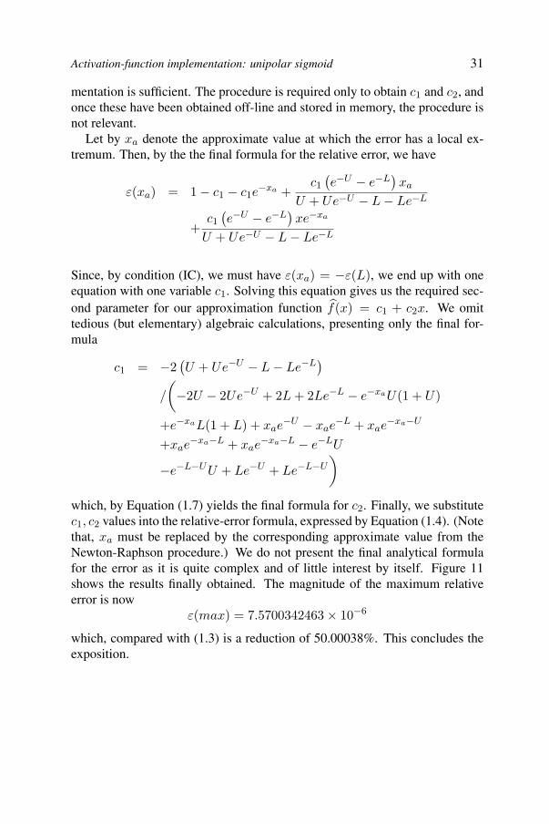
)which, by Equation (1.7) yields the final formula for c2. Finally, we substitutec1, c2 values into the relative-error formula, expressed by Equation (1.4). (Notethat, xa must be replaced by the corresponding approximate value from theNewton-Raphson procedure.) We do not present the final analytical formulafor the error as it is quite complex and of little interest by itself. Figure 11shows the results finally obtained. The magnitude of the maximum relativeerror is now
ε(max) = 7.5700342463 × 10⁻⁶
which, compared with (1.3) is a reduction of 50.00038%. This concludes theexposition.
32 FPGA Neurocomputers
Figure 11: Plots of improved sigmoid error-function
1.8 Performance evaluation
Having outlined above the promise of realizing neural networks in hard-ware, we now come to an especially delicate point — that of actually showingthat “semi-custom” (i.e. FPGA) or custom (i.e. ASIC) neurocomputers canactually deliver what is promised. In this respect, the neural-network commu-nity has not especially distinguished itself, which, in turn explains the dearthof many practical neurocomputers, despite the many years of research, the de-velopment of countless prototypes, and so forth. (This point can be readilyappreciated by comparing the status of performance-evaluation for nuerocom-puters with that for conventional computers.) We will not here aim to solvethe underlying problems or even suggest specific concrete solutions — eitherbeing an enormous task that is outside the scope of this work — but it is ourobjective to sharply highlight them and to indicate general directions for theirsolution.
At the very least there are two issues that must be considered for a properevaluation of performance: the metrics used and what benchmarks are used toobtain the measurements. (Both need to be such that they can, in the main,be easily agreed on and understood by most users.) The neural-network areais sorely lacking in both. The most commonly used metrics are connections-per-second (CPS), which is essentially the rate at which neuron multiply-addoperations are carried out, and connection-updates-per-second (CUPS), whichis essentialy the rate at which updates of weights are carried out. Speedup is
Performance evaluation 33
also sometimes used but is of even less value than CPS and CUPS; and evenworse is to rely on just time-complexity, e.g. [1]. The are three main problemswith these metrics:
MCPS and MCUPS are similar to, and suffer from the same drawbacksas, MIPS (Millions of Instructions Per Second) and MFLOPS (Mil-lions of Floating-point Operations Per Second) that were long used forgeneral-purpose computers and now largely discredited as useful mea-sures.
MCPS and MCUPS cannot always be meaningfully used with all typesof networks; for example, they are of little worth with radial-basis-function networks.
A large value of MCPS or MCUPS does not necessarily mean betterperformance (i.e. in the sense of a network being faster) when appliedto different algorithms. In other words, interpreting the numbers is notstraightforward.
As is the case for general-purpose computers, there is little doubt that ulti-mately the best measure of performance is actual execution-time [19].
As an example of the untidy state of affairs that curently exists, consider,for example [3], which has already been partially discussed above. In thatwork, execution-time is one of the main metrics used, which is acceptable asfar as it goes. But things quickly become problematic. First, although someneural-network applications have been chosen for use as benchmarks, no ba-sis is given for why and how they been chosen. Second, it is not quite thecase that exactly the same programs are being used for benchmarks: the au-thors compare a Reactive Tabu Search learning algorithm (on their machine)against Back-Propagation learning (on two other machines). Third, given thevariety and non-uniform use of various metrics, what the target is is far fromclear: Is it, say, the the proportion of patterns that are correcly classified? Ifso, then that should be fixed and measurements than made of the other metrics(error, execution-time, etc.) and the results then used to compare the differentmachines. The same remark applies to, say, fixing error limits and then mea-suring execution time, or number of iterations/epcohs, or patterns-classified,and so forth. As it is, the authors allow all parameters to simultaneously varyin a manner that practically renders meaningless the use of execution-time asa reasonable metric. Fourth, details of algorithm-implementations on the twoother machines are not given, which begs the question of whether they were thebest possible. Contrast this with the standards of SPEC [20], in which “own-ers” (usually the manufacturers) of given machines run (under highly regulatedconditions) specific programs, under tight constraints, and then publicly reportthe results, thus ensuring best-effort implementations.
34 FPGA Neurocomputers
In summary, the area of performance-evaluation — in particular the choiceperformance metrics and selection of benchmarks — is one that needs to beaddressed urgently for neurocomputers. Neurocomputers (whether in ASIC ofFPGA) will not achieve widespread use unless potential users can be convincedof their worth; given their history so far, it should now be clear that merelyextolling their virtues is insufficient.
1.9 Conclusions
This chapter covers a broad range of topics, many of which are discussedin more detail in following chapters. In the case of arithmetic, we have high-lighted inner-product and activation-function computations. We have advancedthe use of piecewise linear interpolation, but the story need not end there: al-though interpolations of a degree higher than three do do not appear to be ap-propriate for high-speed hardware implementations, there may be some profitin the search for second-order ones that are well-suited to FPGAs. Chapter 2discussed further aspects of arithmetic.
We have discussed the main types of parallelism that are to be found inneural networks, but little of that discussion has addressed the matter of map-pings. With very large networks, the mapping from network to FPGA is amajor factor in performance. Chapters 3 and 4 are devoted to a suitable the-oretical framework for the derivation of such mappings. Chapter 5 also dealswith mappings but is limited to back-propagation in the context of an actualdevice; Chapter 6 is similar in that it is limited to associative memories.
Chapters 7 through 11 cover the FPGA-implementation of neural networksfor several specific applications. The last chapter is a retrospective: it discussesvarious lessons learned from the realization of a custom neurocomputer andprojects these to current FPGAs.
References
[1] U. Ruckert. 2002. ULSI architectures for artificial neural networks. IEEEMicro (May–June): 10–19.
[2] J. Buddefeld and K. E. Grosspietsch. 2002. Intelligent-memory architec-tures for artificial neural networks. IEEE Micro (May–June): 32–40.
[3] G. Danese, F. Leoporati, and S. Ramat. 2002. A parallel neural processorfor real-time applications. IEEE Micro (May–June): 20–31.
[4] A. R. Omondi. Computer Arithmetic Systems: Algorithms, Architecture,and Implementations. Prentice-Hall, UK, 1994.
[5] T. Nordstrom and B. Svensson. 1991. Using and designing massively par-allel computers for artificial neural networks. Journal of Parallel and Dis-tributed Computing, 14:260–285.
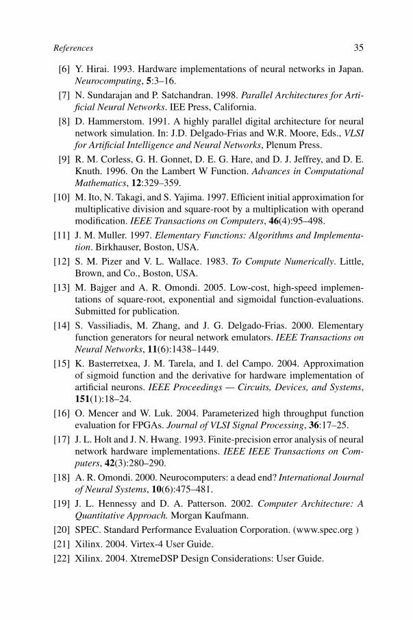
35
[6] Y. Hirai. 1993. Hardware implementations of neural networks in Japan.Neurocomputing, 5:3–16.
[7] N. Sundarajan and P. Satchandran. 1998. Parallel Architectures for Arti-ficial Neural Networks. IEE Press, California.
[8] D. Hammerstom. 1991. A highly parallel digital architecture for neuralnetwork simulation. In: J.D. Delgado-Frias and W.R. Moore, Eds., VLSIfor Artificial Intelligence and Neural Networks, Plenum Press.
[9] R. M. Corless, G. H. Gonnet, D. E. G. Hare, and D. J. Jeffrey, and D. E.Knuth. 1996. On the Lambert W Function. Advances in ComputationalMathematics, 12:329–359.
[10] M. Ito, N. Takagi, and S. Yajima. 1997. Efficient initial approximation formultiplicative division and square-root by a multiplication with operandmodification. IEEE Transactions on Computers, 46(4):95–498.
[11] J. M. Muller. 1997. Elementary Functions: Algorithms and Implementa-tion. Birkhauser, Boston, USA.
[12] S. M. Pizer and V. L. Wallace. 1983. To Compute Numerically. Little,Brown, and Co., Boston, USA.
[13] M. Bajger and A. R. Omondi. 2005. Low-cost, high-speed implemen-tations of square-root, exponential and sigmoidal function-evaluations.Submitted for publication.
[14] S. Vassiliadis, M. Zhang, and J. G. Delgado-Frias. 2000. Elementaryfunction generators for neural network emulators. IEEE Transactions onNeural Networks, 11(6):1438–1449.
[15] K. Basterretxea, J. M. Tarela, and I. del Campo. 2004. Approximationof sigmoid function and the derivative for hardware implementation ofartificial neurons. IEEE Proceedings — Circuits, Devices, and Systems,151(1):18–24.
[16] O. Mencer and W. Luk. 2004. Parameterized high throughput functionevaluation for FPGAs. Journal of VLSI Signal Processing, 36:17–25.
[17] J. L. Holt and J. N. Hwang. 1993. Finite-precision error analysis of neuralnetwork hardware implementations. IEEE IEEE Transactions on Com-puters, 42(3):280–290.
[18] A. R. Omondi. 2000. Neurocomputers: a dead end? International Journalof Neural Systems, 10(6):475–481.
[19] J. L. Hennessy and D. A. Patterson. 2002. Computer Architecture: AQuantitative Approach. Morgan Kaufmann.
[20] SPEC. Standard Performance Evaluation Corporation. (www.spec.org )
[21] Xilinx. 2004. Virtex-4 User Guide.
[22] Xilinx. 2004. XtremeDSP Design Considerations: User Guide.
References
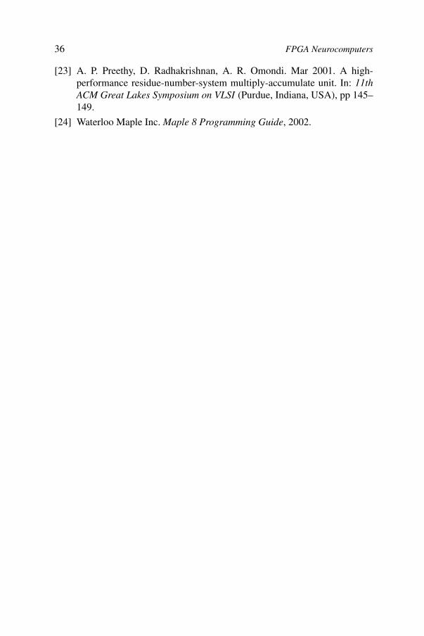
36 FPGA Neurocomputers
[23] A. P. Preethy, D. Radhakrishnan, A. R. Omondi. Mar 2001. A high-performance residue-number-system multiply-accumulate unit. In: 11thACM Great Lakes Symposium on VLSI (Purdue, Indiana, USA), pp 145–149.
[24] Waterloo Maple Inc. Maple 8 Programming Guide, 2002.
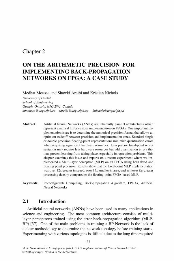
Chapter 2
ON THE ARITHMETIC PRECISION FORIMPLEMENTING BACK-PROPAGATIONNETWORKS ON FPGA: A CASE STUDY
Medhat Moussa and Shawki Areibi and Kristian NicholsUniversity of GuelphSchool of EngineeringGuelph, Ontario, N1G 2W1, [email protected] [email protected] [email protected]
Abstract Artificial Neural Networks (ANNs) are inherently parallel architectures whichrepresent a natural fit for custom implementation on FPGAs. One important im-plementation issue is to determine the numerical precision format that allows anoptimum tradeoff between precision and implementation areas. Standard singleor double precision floating-point representations minimize quantization errorswhile requiring significant hardware resources. Less precise fixed-point repre-sentation may require less hardware resources but add quantization errors thatmay prevent learning from taking place, especially in regression problems. Thischapter examines this issue and reports on a recent experiment where we im-plemented a Multi-layer perceptron (MLP) on an FPGA using both fixed andfloating point precision. Results show that the fixed-point MLP implementationwas over 12x greater in speed, over 13x smaller in area, and achieves far greaterprocessing density compared to the floating-point FPGA-based MLP.
Keywords: Reconfigurable Computing, Back-propagation Algorithm, FPGAs, ArtificialNeural Networks
2.1 Introduction
Artificial neural networks (ANNs) have been used in many applications inscience and engineering. The most common architecture consists of multi-layer perceptrons trained using the error back-propagation algorithm (MLP-BP) [37]. One of the main problems in training a BP Network is the lack ofa clear methodology to determine the network topology before training starts.Experimenting with various topologies is difficult due to the long time required
37
A. R. Omondi and J. C. Rajapakse (eds.), FPGA Implementations of Neural Networks, 37–61. © 2006 Springer. Printed in the Netherlands.
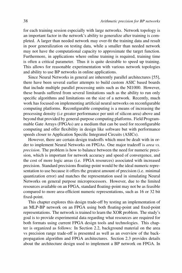
38 Arithmetic precision for BP networks
for each training session especially with large networks. Network topology isan important factor in the network’s ability to generalize after training is com-pleted. A larger than needed network may over-fit the training data and resultin poor generalization on testing data, while a smaller than needed networkmay not have the computational capacity to approximate the target function.Furthermore, in applications where online training is required, training timeis often a critical parameter. Thus it is quite desirable to speed up training.This allows for reasonable experimentation with various network topologiesand ability to use BP networks in online applications.
Since Neural Networks in general are inherently parallel architectures [55],there have been several earlier attempts to build custom ASIC based boardsthat include multiple parallel processing units such as the NI1000. However,these boards suffered from several limitations such as the ability to run onlyspecific algorithms and limitations on the size of a network. Recently, muchwork has focused on implementing artificial neural networks on reconfigurablecomputing platforms. Reconfigurable computing is a means of increasing theprocessing density (i.e greater performance per unit of silicon area) above andbeyond that provided by general-purpose computing platforms. Field Program-mable Gate Arrays (FPGAs) are a medium that can be used for reconfigurablecomputing and offer flexibility in design like software but with performancespeeds closer to Application Specific Integrated Circuits (ASICs).
However, there are certain design tradeoffs which must be dealt with in or-der to implement Neural Networks on FPGAs. One major tradeoff is area vs.precision. The problem is how to balance between the need for numeric preci-sion, which is important for network accuracy and speed of convergence, andthe cost of more logic areas (i.e. FPGA resources) associated with increasedprecision. Standard precisions floating-point would be the ideal numeric repre-sentation to use because it offers the greatest amount of precision (i.e. minimalquantization error) and matches the representation used in simulating NeuralNetworks on general purpose microprocessors. However, due to the limitedresources available on an FPGA, standard floating-point may not be as feasiblecompared to more area-efficient numeric representations, such as 16 or 32 bitfixed-point.
This chapter explores this design trade-off by testing an implementation ofan MLP-BP network on an FPGA using both floating-point and fixed-pointrepresentations. The network is trained to learn the XOR problem. The study’sgoal is to provide experimental data regarding what resources are required forboth formats using current FPGA design tools and technologies. This chap-ter is organized as follows: In Section 2.2, background material on the areavs precision range trade-off is presented as well as an overview of the back-propagation algorithm and FPGA architectures. Section 2.3 provides detailsabout the architecture design used to implement a BP network on FPGA. In
Background 39
section 2.4 the XOR problem is presented. Finally validation of the proposedimplementations, and benchmarked results of floating-point and fixed-pointarithmetic functions implemented on a FPGA are discussed in Section 2.5.
2.2 Background
One way to help achieve the density advantage of reconfigurable comput-ing over general-purpose computing is to make the most efficient use of thehardware area available. In terms of an optimal range-precision vs area trade-off, this can be achieved by determining the minimum allowable precision andminimum allowable range, where their criterion is to minimize hardware areausage without sacrificing quality of performance. These two concepts com-bined can also be referred to as the minimum allowable range-precision.
2.2.1 Range-Precision vs. Area Trade-off
A reduction in precision usually introduces many errors into the system.Determining the minimum allowable precision is actually a question of de-termining the maximum amount of uncertainty (i.e. quantization error due tolimited precision) an application can withstand before performance begins todegrade. It is often dependent upon the algorithm used and the application athand.
For MLP using the BP algorithm, Holt and Baker [41] showed using simu-lations and theoretical analysis that 16-bit fixed-point (1 bit sign, 3 bit left and12 bit right of the radix point) was the minimum allowable range-precisionfor the back-propagation algorithm assuming that both input and output werenormalized between [0,1] and a sigmoid transfer function was used.
Ligon III et al. [45] have also shown the density advantage of fixed-pointover floating-point for older generation Xilinx 4020E FPGAs, by showing thatthe space/time requirements for 32-bit fixed-point adders and multipliers wereless than that of their 32-bit floating-point equivalents.
Other efforts focused on developing a complete reconfigurable archi-tecture for implementing MLP. Eldredge [3] successfully implemented theback-propagation algorithm using a custom platform he built out of XilinxXC3090 FPGAs, called the Run-Time Reconfiguration Artificial Neural Net-work (RRANN). He showed that the RRANN architecture could learn howto approximate centroids of fuzzy sets. Heavily influenced by the Eldredge’sRRANN architecture, Beuchat et al. [13] developed a FPGA platform, calledRENCO–a REconfigurable Network COmputer. As it’s name implies, RENCOcontains four Altera FLEX 10K130 FPGAs that can be reconfigured and mon-itored over any LAN (i.e. Internet or other) via an on-board 10Base-T inter-face. RENCO’s intended application was hand-written character recognition.Ferrucci and Martin [14, 15] built a custom platform, called Adaptive Connec-
40 Arithmetic precision for BP networks
tionist Model Emulator (ACME) which consists of multiple Xilinx XC4010FPGAs. They validated ACME by successfully carrying out a 3-input, 3-hidden unit, 1-output network used to learn the 2-input XOR problem. Skr-bek’s FPGA platform [26], called the ECX card, could also implement RadialBasis Function (RBF) neural networks, and was validated using pattern recog-nition applications such as parity problem, digit recognition, inside-outsidetest, and sonar signal recognition.
Since the size of an FPGA-based MLP-BP is proportional to the multi-plier used, it is clear that given an FPGA’s finite resources, a 32-bit signed(2’s complement) fixed-point representation will allow larger [54] ANNs tobe implemented than could be accommodated when using a 32-bit IEEE (a32-bit floating point multiplier can be implemented on a Xilinx Virtex-II orSpartan-3 FPGA using four of the dedicated multiplier blocks and CLB re-sources) floating-point. However, while 32 fixed-point representation allowshigh processor density implementation, the quantization error of 32 floating-point representation is negligible. Validating an architecure on an FPGA using32-bit floating point arithmetic might be easier than fixed point arithmetic sincea software version of the architecture can be run on a Personal Computer with32-bit floating point arithmetic. As such its use is justifiable if the relative lossin processing density is negligible in comparison.
FPGA architectures and related development tools have become increas-ingly sophisticated in more recent years, including improvements in thespace/time optimization of arithmetic circuit designs. As such, the objectiveof this study is to determine the feasibility of floating-point arithmetic in im-plementing MLP-BP using today’s FPGA design tools and technologies. Bothfloating-point and fixed-point precision are considered for implementation andare classified as amplitude-based digital numeric representations. Other nu-meric representations, such as digital frequency-based [42] and analog werenot considered because they promote the use of low precision, which is oftenfound to be inadequate for minimum allowable range-precision.
2.2.2 Overview of Back-propagation Algorithm
It is helpful before proceeding to discuss architecture design to give a briefreview of MLP and the error Back-propagation algorithm. The general struc-ture of a Multi-layer perceptron (MLP) neural network is shown in Figure 2.1,where layers are numbered 0 to M , and neurons are numbered 1 to N .
A MLP using the back-propagation algorithm has five steps of execution:(1) Initialization
The following parameters must be initialized before training starts: (i)w
(s)kj (n) is defined as the synaptic weight that corresponds to the connection
from neuron unit j in the (s − 1)th layer, to k in the sth layer. This weight
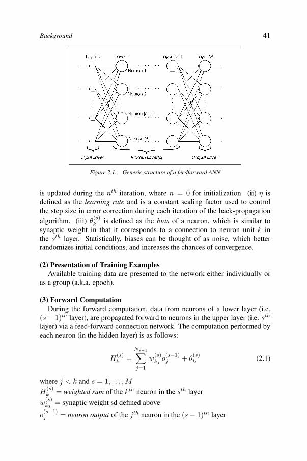
Background 41
Figure 2.1. Generic structure of a feedforward ANN
is updated during the nth iteration, where n = 0 for initialization. (ii) η isdefined as the learning rate and is a constant scaling factor used to controlthe step size in error correction during each iteration of the back-propagationalgorithm. (iii) θ
(s)k is defined as the bias of a neuron, which is similar to
synaptic weight in that it corresponds to a connection to neuron unit k inthe sth layer. Statistically, biases can be thought of as noise, which betterrandomizes initial conditions, and increases the chances of convergence.
(2) Presentation of Training ExamplesAvailable training data are presented to the network either individually or
as a group (a.k.a. epoch).
(3) Forward ComputationDuring the forward computation, data from neurons of a lower layer (i.e.
(s − 1)th layer), are propagated forward to neurons in the upper layer (i.e. sth
layer) via a feed-forward connection network. The computation performed byeach neuron (in the hidden layer) is as follows:
H(s)k =
Ns−1∑j=1
w(s)kj o
(s−1)j + θ
(s)k (2.1)
where j < k and s = 1, . . . , M
H(s)k = weighted sum of the kth neuron in the sth layer
w(s)kj = synaptic weight sd defined above
o(s−1)j = neuron output of the jth neuron in the (s − 1)th layer
42 Arithmetic precision for BP networks
θ(s)k = bias of the kth neuron in the sth layer.
On the other hand for the output layer neurons the computation is as follows:
o(s)k = f(H(s)
k ) (2.2)
where k = 1, . . . , N and s = 1, . . . , M
o(s)k = neuron output of the kth neuron in the sth layer
f(H(s)k ) = activation function computed on the weighted sum H
(s)k
Note that a unipolar sigmoid function is often used as the nonlinear activationfunction, such as the following logsig function:
f(x)logsig =1
1 + exp(−x)(2.3)
(4) Backward ComputationIn this step, the weights and biases are updated. The learning algorithm’s
goal is to minimize the error between the expected (or teacher) value and theactual output value that was determined in the Forward Computation. Thefollowing steps are performed:
1 Starting with the output layer, and moving back towards the input layer,calculate the local gradients, as follows:
ε(s)k =
{tk − o
(s)k s = M∑Ns+1
j=1 ws+1kj δ
(s+1)j s = 1, . . . , M − 1
(2.4)
whereε(s)k = error term for the kth neuron in the sth layer; the difference
between the teaching signal tk and the neuron output o(s)k
δ(s+1)j = local gradient for the jth neuron in the (s + 1)th layer.
δ(s)k = ε
(s)k f ′(H(s)
k ) s = 1, . . . , M (2.5)
where f ′(H(s)k ) is the derivative of the activation function.
2 Calculate the weight (and bias) changes for all the weights as follows:
∆w(s)kj = ηδ
(s)k o
(s−1)j k = 1, . . . , Ns
j = 1, . . . , Ns−1(2.6)
where ∆w(s)kj is the change in synaptic weight (or bias) corresponding to
the gradient of error for connection from neuron unit j in the (s − 1)th
layer, to neuron k in the sth layer.
Architecture design and implementation 43
3 Update all the weights (and biases) as follows:
wskj(n + 1) = ∆w
(s)kj (n) + w
(s)kj (n) (2.7)
where k = 1, . . . , Ns and j = 1, . . . , Ns−1
wskj(n+1) = updated synaptic weight (or bias) to be used in the (n+1)th
iteration of the Forward Computation∆w
(s)kj (n) = change in synaptic weight (or bias) calculated in the nth
iteration of the Backward Computation, where n = the current iterationw
(s)kj (n) = synaptic weight (or bias) to be used in the nth iteration of the
Forward and Backward Computations, where n = the current iteration.
(5) IterationReiterate the Forward and Backward Computations for each training exam-
ple in the epoch. The trainer can continue to train the MLP using one or moreepochs until some stopping criteria is met. Once training is complete, the MLPonly needs to carry out the Forward Computation when used in applications.
2.2.3 Field Programmable Gate Arrays
FPGAs are a form of programmable logic, which offer flexibility in designlike software, but with performance speeds closer to Application Specific Inte-grated Circuits (ASICs). With the ability to be reconfigured an endless numberof times after having been manufactured, FPGAs have traditionally been usedas a prototyping tool for hardware designers. However, as growing die capaci-ties of FPGAs have increased over the years, so has their use in reconfigurablecomputing applications too.
The fundamental architecture of Xilinx FPGAs consists of a two-dimensional array of programmable logic blocks, referred to as ConfigurableLogic Blocks (CLBs). Figure 2.2 shows the architecture of a CLB from theXilinx Virtex-E family of FPGAs, which contains four logic cells (LCs) andis organized in two similar slices. Each LC includes a 4-input look-up ta-ble (LUT), dedicated fast carry-lookahead logic for arithmetic functions, anda storage element (i.e. a flip-flop). A CLB from the Xilinx Virtex-II familyof FPGAs, on the other hand, contains eight 4-input LUTs, and is over twicethe amount of logic as a Virtex-E CLB. As we will see, the discrepancies inCLB architecture from one family to another is an important factor to take intoconsideration when comparing the spatial requirements (in terms of CLBs) forcircuit designs which have been implemented on different Xilinx FPGAs.
2.3 Architecture design and implementation
There has been a rich history of attempts at implementing ASIC-based ap-proaches for neural networks - traditionally referred to as neuroprocessors [29]
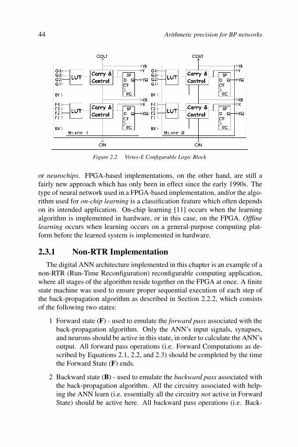
44 Arithmetic precision for BP networks
Figure 2.2. Virtex-E Configurable Logic Block
or neurochips. FPGA-based implementations, on the other hand, are still afairly new approach which has only been in effect since the early 1990s. Thetype of neural network used in a FPGA-based implementation, and/or the algo-rithm used for on-chip learning is a classification feature which often dependson its intended application. On-chip learning [11] occurs when the learningalgorithm is implemented in hardware, or in this case, on the FPGA. Offlinelearning occurs when learning occurs on a general-purpose computing plat-form before the learned system is implemented in hardware.
2.3.1 Non-RTR Implementation
The digital ANN architecture implemented in this chapter is an example of anon-RTR (Run-Time Reconfiguration) reconfigurable computing application,where all stages of the algorithm reside together on the FPGA at once. A finitestate machine was used to ensure proper sequential execution of each step ofthe back-propagation algorithm as described in Section 2.2.2, which consistsof the following two states:
1 Forward state (F) - used to emulate the forward pass associated with theback-propagation algorithm. Only the ANN’s input signals, synapses,and neurons should be active in this state, in order to calculate the ANN’soutput. All forward pass operations (i.e. Forward Computations as de-scribed by Equations 2.1, 2.2, and 2.3) should be completed by the timethe Forward State (F) ends.
2 Backward state (B) - used to emulate the backward pass associated withthe back-propagation algorithm. All the circuitry associated with help-ing the ANN learn (i.e. essentially all the circuitry not active in ForwardState) should be active here. All backward pass operations (i.e. Back-
Architecture design and implementation 45
ward Computations as described by Equations 2.4, 2.5, and 2.6) shouldbe completed by the time the Backward state ends.
It should be noted that both states of the finite state machine continually alter-nate, and synaptic weights are updated (as described in Equation 2.7) duringthe transition from Backward State to Forward State.
As far as the ANN’s components (eg. neurons, synapses) were concerned,the finite state machine is generally a means of synchronizing when varioussets of components should be active. The duration of each state depends onthe number of clock cycles required to complete calculations in each state,the length of the system’s clock period, and the propagation delay associatedwith each state(Note that propagation delay is platform dependent, and canonly be determined after the digital VLSI design has been synthesized on atargeted FPGA. The propagation delay is then determined through a timinganalysis/simulation using the platform’s EDA tools). The architecture of theactive ANN components associated with each state dictates the propagationdelay for that state.
Each of the ANN components implemented in hardware, such as thesynapse and neuron, housed a chip select input signal in their architecturewhich is driven by the finite state machine. This chip select feature ensuredthat only those components that were associated with a particular state wereenabled or active throughout that state’s duration. With regards to initializationof the circuit, a reset input signal was used which would fulfill two importantrequirements when activated:
Ensure the finite state machine initially starts in “Forward State”.
Initialize the synaptic weights of the ANN, to some default value.
Finally, the BP algorithm calculations, Equations 2.1–2.7, are realized usinga series of arithmetic components, including addition, subtraction, multiplica-tion, and division. Standardized high-description language (HDL) libraries fordigital hardware implementation can be used in synthesizing all the arithmeticcalculations involved with the back-propagation algorithm, in analogous fash-ion of how typical math general programming language (GPL) libraries areused in software implementations of ANNs. The architecture described hereis generic enough to support arithmetic HDL libraries of different amplitude-based precision, whether it be floating-point or fixed-point.
2.3.2 Arithmetic Library
The architecture was developed using VHDL. Unfortunately, there is cur-rently no explicit support for fixed- and floating-point arithmetic in VHDL(according to the IEEE Design Automation Standards Committee [43], an ex-tension of IEEE Std 1076.3 has been proposed to include support for fixed-
46 Arithmetic precision for BP networks
and floating-point numbers in VHDL, and is to be addressed in a future re-view of the standard). As a result, two separate arithmetic VHDL librarieswere custom designed for use with the FPGA-based ANN. One of the librariessupports the IEEE-754 standard for single-precision (i.e. 32-bit) floating-pointarithmetic, and is referred to as uog fp arith, which is an abbreviation forUniversity of Guelph Floating-Point Arithmetic. The other library supports 16-bit fixed-point arithmetic, and is referred to as uog fixed arith, which is anabbreviation for University of Guelph Fixed-Point Arithmetic. These two rep-resentations were chosen based on previous results from the literature [41] thatshowed that 16 bit fixed point representation is the minimum needed to allowthe BP algorithm to converge and the fact that 32 bit floating point precision isthe standard floating point representation. We could have used a custom float-ing point representation (maybe with less precision) but it is very likely that anyfuture VHDL floating point implementation will follow this standard represen-tation. As such we specifically wanted to test the tradeoff with this standardpresentation. This is also important for applications in Hardware/Software co-design using languages like SystemC and HandleC.
Fixed-point representation is signed 2’s complement binary representation,which is made rational with a virtual decimal point. The virtual radix pointlocation used in uog fixed arith is SIII.FFFFFFFFFFFF , where
S = sign bit
I = integer bit, as implied by location of binary point
F = fraction bit, as implied by location of binary point
The range for a 16-bit fixed-point representation of this configuration is [-8.0,8.0), with a quantization error of 2.44140625E-4. Description of the variousarithmetic VHDL design alternatives considered for use in the uog fp arithand uog fixed arith libraries are summarized in Table 2.1. All HDL de-signs with the word std in their name signify that one of the IEEE stan-dardized VHDL arithmetic libraries was used to create them. For example,uog std multiplier was easily created using the following VHDL syntax:z <= x ∗ y;where x and y are the input signals, and z the output signal of the circuit.Such a high level of abstract design is often associated with behavioral VHDLdesigns, where ease of design comes at the sacrifice of letting the FPGA’s syn-thesis tools dictate the fine-grain architecture of the circuit.
On the other hand, an engineer can explicitly define the fine-grain architec-ture of a circuit by means of structural VHDL and schematic-based designs, aswas done for uog ripple carry adder, uog c l adder (please refer to Fig-ure 2.4 for detailed implementation) and uog sch adder respectively. How-
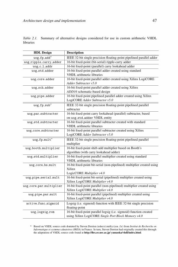
Architecture design and implementation 47
Table 2.1. Summary of alternative designs considered for use in custom arithmetic VHDLlibraries
HDL Design Description
uog fp add∗ IEEE 32-bit single precision floating-point pipelined parallel adderuog ripple carry adder 16-bit fixed-point (bit-serial) ripple-carry adder
uog c l addr 16-bit fixed-point (parallel) carry lookahead adderuog std adder 16-bit fixed-point parallel adder created using standard
VHDL arithmetic librariesuog core adder 16-bit fixed-point parallel adder created using Xilinx LogiCORE
Adder Subtracter v5.0uog sch adder 16-bit fixed-point parallel adder created using Xilinx
ADD16 schematic-based designuog pipe adder 16-bit fixed-point pipelined parallel adder created using Xilinx
LogiCORE Adder Subtractor v5.0
uog fp sub∗ IEEE 32-bit single precision floating-point pipelined parallelsubtracter
uog par subtracter 16-bit fixed-point carry lookahead (parallel) subtracter, basedon uog std adder VHDL entity
uog std subtracter 16-bit fixed-point parallel subtracter created with standardVHDL arithmetic libraries
uog core subtracter 16-bit fixed-point parallel subtracter created using XilinxLogiCORE Adder Subtracter v5.0
uog fp mult∗ IEEE 32-bit single precision floating-point pipelined parallelmultiplier
uog booth multiplier 16-bit fixed-point shift-add multiplier based on Booth’salgorithm (with carry lookahead adder)
uog std multiplier 16-bit fixed-point parallel multiplier created using standardVHDL arithmetic libraries
uog core bs mult 16-bit fixed-point bit-serial (non-pipelined) multiplier created usingXilinxLogicCORE Multiplier v4.0
uog pipe serial mult 16-bit fixed-point bit-serial (pipelined) multiplier created usingXilinx LogiCORE Multiplier v4.0
uog core par multiplier 16-bit fixed-point parallel (non-pipelined) multiplier created usingXilinx LogiCORE Multiplier v4.0
uog pipe par mult 16-bit fixed-point parallel (pipelined) multiplier created usingXilinx LogiCORE Multiplier v4.0
active func sigmoid Logsig (i.e. sigmoid) function with IEEE 32-bit single precisionfloating-point
uog logsig rom 16-bit fixed-point parallel logsig (i.e. sigmoid) function createdusing Xilinx LogiCORE Single Port Block Memory v4.0
* Based on VHDL source code dontated by Steven Derrien ([email protected]) from Institut de Recherche enInformatique et syst«emes al«eatoires (IRISA) in France. In turn, Steven Derrien had originally created this throughthe adaptation of VHDL source code found at http://flex.ee.uec.ac.jp/ yamaoka/vhdl/index.html.
48 Arithmetic precision for BP networks
ever, having complete control over the architecture’s fine-grain design comesat the cost of additional design overhead for the engineer.
Many of the candidate arithmetic HDL designs described in Table 2.1 werecreated by the Xilinx CORE Generator System. This EDA tool helps anengineer parameterize ready-made Xilinx intellectual property (ip) designs(i.e. LogiCOREs), which are optimized for Xilinx FPGAs. For example,uog core adder was created using the Xilinx proprietary LogiCORE for anadder design.
Approximation of the logsig function in both floating-point and fixed-pointprecision, were implemented in hardware using separate lookup-table archi-tectures. In particular, active func sigmoid was a modular HDL design,which encapsulated all the floating-point arithmetic units necessary to carryout calculation of logsig function. According to Equation 2.3, this wouldrequire the use of a multiplier, adder, divider, and exponential function. Asa result, active func sigmoid was realized in VHDL using uog fp mult,uog fp add, a custom floating-point divider called uog fp div, and a table-driven floating-point exponential function created by Bui et al [44]. While thisis not the most efficient implementation of the logsig, it allows implementingother transfer functions with min efforts (like Tan Hyperbolic) since it sharesthe basic functions with the Sigmoid. It is very common in training BP net-works to test different transfer functions.
The uog logsig rom HDL design utilized a Xilinx LogiCORE to imple-ment single port block memory. A lookup-table of 8192 entries was createdwith this memory, which was used to approximate the logsig function in fixed-point precision.
In order to maximize the processing density of the digital VLSI ANN de-sign proposed in Section 2.3.1, only the most area-optimized arithmetic HDLdesigns offered in Table 2.1 should become part of the uog fp arith anduog fixed arith VHDL libraries. However, the space-area requirements ofany VHDL design will vary from one FPGA architecture to the next. There-fore, all the HDL arithmetic designs found in Table 2.1 have to be implementedon the same FPGA as was targeted for implementation of the digital VLSIANN design, in order to determine the most area-efficient arithmetic candi-dates.
2.4 Experiments using logical-XOR problem
The logical-XOR problem is a classic toy problem used to benchmark thelearning ability of an ANN. It is a simple example of a non-linearly separableproblem.
The minimum ANN topology (a topology includes the number of neurons,number of layers, and the layer interconnections (i.e. synapses)) required to
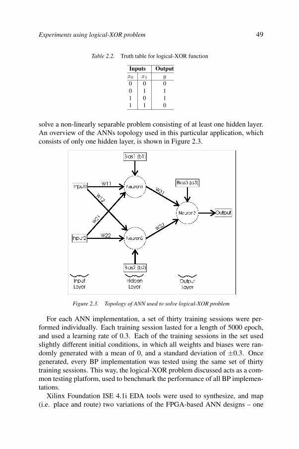
Experiments using logical-XOR problem 49
Table 2.2. Truth table for logical-XOR function
Inputs Outputx0 x1 y
0 0 00 1 11 0 11 1 0
solve a non-linearly separable problem consisting of at least one hidden layer.An overview of the ANNs topology used in this particular application, whichconsists of only one hidden layer, is shown in Figure 2.3.
Figure 2.3. Topology of ANN used to solve logical-XOR problem
For each ANN implementation, a set of thirty training sessions were per-formed individually. Each training session lasted for a length of 5000 epoch,and used a learning rate of 0.3. Each of the training sessions in the set usedslightly different initial conditions, in which all weights and biases were ran-domly generated with a mean of 0, and a standard deviation of ±0.3. Oncegenerated, every BP implementation was tested using the same set of thirtytraining sessions. This way, the logical-XOR problem discussed acts as a com-mon testing platform, used to benchmark the performance of all BP implemen-tations.
Xilinx Foundation ISE 4.1i EDA tools were used to synthesize, and map(i.e. place and route) two variations of the FPGA-based ANN designs – one
50 Arithmetic precision for BP networks
using uog fp arith library, and one using uog fixed arith library. Allexperiments and simulations were carried out on a PC workstation runningWindows NT (SP6) operating system, with 1 GB of memory and Intel PIII733MHz CPU.
These circuit designs were tested and validated in simulation only, usingModelTech’s ModelSim SE v5.5. Functional simulations were conducted totest the syntactical and semantical correctness of HDL designs, under idealFPGA conditions (i.e. where no propagation delay exists). Timing simulationswere carried out to validate the HDL design under non-ideal FPGA conditions,where propagation delays associated with the implementation as targeted on aparticular FPGA are taken into consideration.
Specific to VHDL designs, timing simulations are realized using an IEEEstandard called VITAL (VHDL Initiative Toward ASIC Libraries). VITAL li-braries contain information used for modeling accurate timing of a particularFPGA at the gate level, as determined a priori by the respective FPGA man-ufacturer. These VITAL libraries are then used by HDL simulators, such asModelSim SE, to validate designs during timing simulations.
A software implementation of a back-propagation algorithm was createdusing MS Visual C++ v6.0 IDE. The software simulator was set up to solve thelogical-XOR problems using the topology shown in Figure 2.3. The purposefor creating this software simulator was to generate expected results for testingand validating FPGA-based BP. To speed up development and testing, twoother software utilities were created to automate numeric format conversions–one for converting real decimal to/from IEEE-754 single precision floating-point hexadecimal format, and one for converting real decimal to/from 16-bitfixed-point binary format.
2.5 Results and discussion
We implemented the previous HDL designs on Xilinx FPGAs. The resultingspace-time requirements for each arithmetic HDL design are summarized inTable 2.3. In order to maximize the neuron density of the FPGA-based MLP,the area of the various arithmetic HDL designs that a neuron is comprised ofshould be minimized. As a result, the focus here is to determine the mostarea-optimized arithmetic HDL designs for use in the implementations.
2.5.1 Comparison of Digital Arithmetic Hardware
Comparison of the different adder results, shown in Table 2.3, reveals thatthe three carry lookahead adders (i.e. uog std adder, uog core adder, anduog sch adder) require the least amount of area and are the fastest among allnon-pipelined adders. Note that the sophistication of today’s EDA tools have
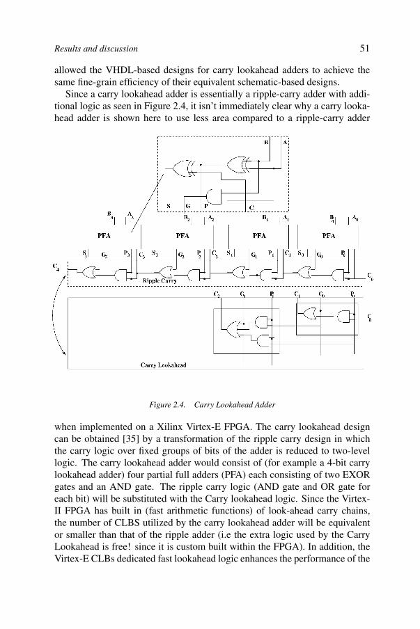
Results and discussion 51
allowed the VHDL-based designs for carry lookahead adders to achieve thesame fine-grain efficiency of their equivalent schematic-based designs.
Since a carry lookahead adder is essentially a ripple-carry adder with addi-tional logic as seen in Figure 2.4, it isn’t immediately clear why a carry looka-head adder is shown here to use less area compared to a ripple-carry adder
Figure 2.4. Carry Lookahead Adder
when implemented on a Xilinx Virtex-E FPGA. The carry lookahead designcan be obtained [35] by a transformation of the ripple carry design in whichthe carry logic over fixed groups of bits of the adder is reduced to two-levellogic. The carry lookahead adder would consist of (for example a 4-bit carrylookahead adder) four partial full adders (PFA) each consisting of two EXORgates and an AND gate. The ripple carry logic (AND gate and OR gate foreach bit) will be substituted with the Carry lookahead logic. Since the Virtex-II FPGA has built in (fast arithmetic functions) of look-ahead carry chains,the number of CLBS utilized by the carry lookahead adder will be equivalentor smaller than that of the ripple adder (i.e the extra logic used by the CarryLookahead is free! since it is custom built within the FPGA). In addition, theVirtex-E CLBs dedicated fast lookahead logic enhances the performance of the
52 Arithmetic precision for BP networks
adder. As a result, it’s best to use HDL adder designs which take advantage ofthe Virtex-E’s fast carry lookahead logic.
The Virtex-E’s fast carry-lookahead logic is again utilized to pro-duce the best area-optimized subtracters (i.e. uog std subtracter anduog core subtracter), as well as, the best area-optimized multiplier (i.e.uog booth multiplier).
Only the most area-optimized arithmetic HDL designs discussed here wereused in the construction of custom arithmetic HDL libraries, as listed in Ta-ble 2.4. In the case where there was more than one choice of best area-optimized arithmetic HDL design to choose from, behavioral VHDL designswere preferred because they promote high-level abstract designs and porta-bility. For example, such was the case in selecting a fixed-point adder andsubtracter for the uog fixed arith library.
Table 2.4 also reveals how much more area-optimized the individual fixed-point arithmetic HDL designs in uog fixed arith were compared to thefloating-point arithmetic HDL designs in uog fp arith. Since a floating-point adder is essentially a fixed-point adder plus additional logic, not to men-tion the fact that floating-point uses more precision than fixed-point arithmetic,it’s no surprise to find that the 16-bit fixed-point adder is much smaller than the32-bit floating-point adder. Similar in nature is the case for subtracter and mul-tiplier comparisons shown in Table 2.4.
The comparison of area-optimized logsig arithmetic HDL designs revealsthat the 32-bit floating-point version is over 250 times bigger than the 16-bitfixed-point version. Aside from the difference in amount of precision used, thesignificant size difference between logsig implementations is due to the factthat floating-point implementation encapsulates a table-lookup architecture inaddition to other area-expensive arithmetic units, while the fixed-point versiononly encapsulates a table-lookup via memory.
Uog fp arith and uog fixed arith have been clearly defined with onlythe best area-optimized components, as shown in Table 2.4. This will helpto ensure that 32-bit floating-point and 16-bit fixed-point FPGA-based MLPimplementations achieve a processing density advantage over the software-based MLP simulations. As was shown here, the larger area requirements offloating-point precision in FPGA-based ANNs makes it not nearly as feasibleas fixed-point precision.
2.5.2 Comparison of ANN Implementations
Table 2.5 summarizes logical-XOR benchmark results for each of the fol-lowing implementations with identical topology:
32-bit floating-point FPGA-based MLP, which utilizes uog fp arithlibrary.
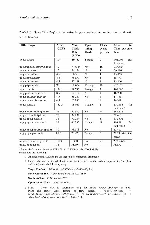
Results and discussion 53
Table 2.3. Space/Time Req’ts of alternative designs considered for use in custom arithmetic
HDL Design Area(CLB)s
Max.ClockRate(MHz)
Pipe-liningUsed?
Clockcyclesper calc.
Min. TotalTime per calc.(ns)
uog fp add 174 19.783 1-stage 2 101.096 (forfirst calc.)
uog ripple carry adder 12 67.600 No 16 236.688uog c l addr 12 34.134 No 1 29.296uog std adder 4.5 66.387 No 1 15.063uog core adder 4.5 65.863 No 1 15.183uog sch adder 4.5 72.119 No 1 13.866uog pipe adder 96 58.624 15-stage 16 272.928
uog fp sub 174 19.783 1-stage 2 101.096uog par subtracter 8.5 54.704 No 1 18.280uog std subtracter 4.5 56.281 No 1 17.768uog core subtracter 4.5 60.983 No 1 16.398
uog fp mult 183.5 18.069 1-stage 2 110.686 (forfirst calc.)
uog booth multiplier 28 50.992 No 34 668.474uog std multiplier 72 32.831 No 1 30.459uog core bs mult 34 72.254 No 20 276.800uog pipe serial mult 39 66.397 ?-stage 21 316.281 (for
first calc.)uog core par multiplier 80 33.913 No 1 29.487uog pipe par mult 87.5 73.970 ?-stage 2 27.038 (for first
calc.)
active func sigmoid∗ 3013 1.980 No 56 29282.634uog logsig rom 12 31.594 No 1 31.652
*Target platform used here was Xilinx Virtex-II FPGA (xc2v8000-5bf957)Please note the following:
1 All fixed-point HDL designs use signed 2’s complement arithmetic
2 Unless otherwise mentioned, all arithmetic functions were synthesized and implemented (i.e. placeand route) under the following setup:
Target Platform: Xilinx Virtex-E FPGA (xcv2000e–6bg560)
Development Tool: Xilinx Foundation ISE 4.1i (SP2)
Synthesis Tool: FPGA Express VHDL
Optimization Goal: Area (Low Effort)
3 Max. Clock Rate is determined usig the Xilinx Timing Analyzer on Post-Place and Route Static Timing of HDL design. Max.ClockRate =min{(Min.CombinationalPathDelay)−1, [(Min.InputArrivalT imeBeforeClk) +Max.OutputRequiredT imeBeforeClk)]−1}
VHDL libraries
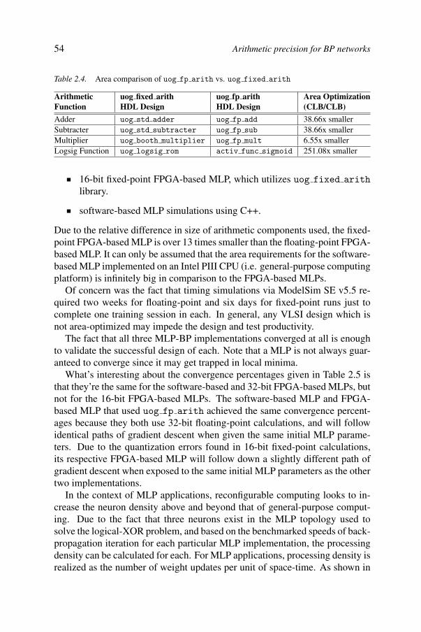
54 Arithmetic precision for BP networks
Table 2.4.
Arithmetic uog fixed arith uog fp arith Area OptimizationFunction HDL Design HDL Design (CLB/CLB)
Adder uog std adder uog fp add 38.66x smallerSubtracter uog std subtracter uog fp sub 38.66x smallerMultiplier uog booth multiplier uog fp mult 6.55x smallerLogsig Function uog logsig rom activ func sigmoid 251.08x smaller
16-bit fixed-point FPGA-based MLP, which utilizes uog fixed arithlibrary.
software-based MLP simulations using C++.
Due to the relative difference in size of arithmetic components used, the fixed-point FPGA-based MLP is over 13 times smaller than the floating-point FPGA-based MLP. It can only be assumed that the area requirements for the software-based MLP implemented on an Intel PIII CPU (i.e. general-purpose computingplatform) is infinitely big in comparison to the FPGA-based MLPs.
Of concern was the fact that timing simulations via ModelSim SE v5.5 re-quired two weeks for floating-point and six days for fixed-point runs just tocomplete one training session in each. In general, any VLSI design which isnot area-optimized may impede the design and test productivity.
The fact that all three MLP-BP implementations converged at all is enoughto validate the successful design of each. Note that a MLP is not always guar-anteed to converge since it may get trapped in local minima.
What’s interesting about the convergence percentages given in Table 2.5 isthat they’re the same for the software-based and 32-bit FPGA-based MLPs, butnot for the 16-bit FPGA-based MLPs. The software-based MLP and FPGA-based MLP that used uog fp arith achieved the same convergence percent-ages because they both use 32-bit floating-point calculations, and will followidentical paths of gradient descent when given the same initial MLP parame-ters. Due to the quantization errors found in 16-bit fixed-point calculations,its respective FPGA-based MLP will follow down a slightly different path ofgradient descent when exposed to the same initial MLP parameters as the othertwo implementations.
In the context of MLP applications, reconfigurable computing looks to in-crease the neuron density above and beyond that of general-purpose comput-ing. Due to the fact that three neurons exist in the MLP topology used tosolve the logical-XOR problem, and based on the benchmarked speeds of back-propagation iteration for each particular MLP implementation, the processingdensity can be calculated for each. For MLP applications, processing density isrealized as the number of weight updates per unit of space-time. As shown in
Area comparison of uog fp arith vs. uog fixed arith
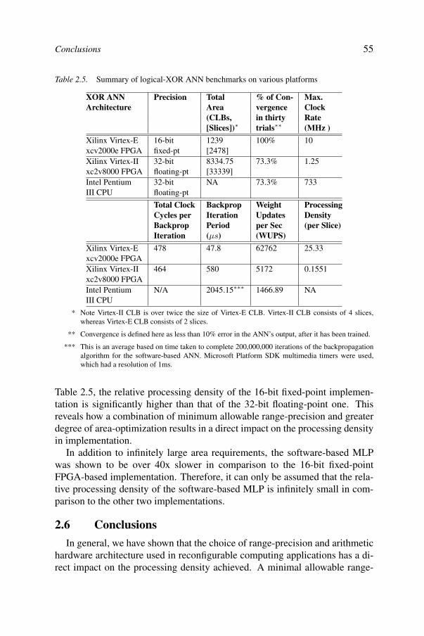
55
Table 2.5.
XOR ANN Precision Total % of Con- Max.Architecture Area vergence Clock
(CLBs, in thirty Rate[Slices])∗ trials∗∗ (MHz )
Xilinx Virtex-E 16-bit 1239 100% 10xcv2000e FPGA fixed-pt [2478]Xilinx Virtex-II 32-bit 8334.75 73.3% 1.25xc2v8000 FPGA floating-pt [33339]Intel Pentium 32-bit NA 73.3% 733III CPU floating-pt
Total Clock Backprop Weight ProcessingCycles per Iteration Updates DensityBackprop Period per Sec (per Slice)Iteration (µs) (WUPS)
Xilinx Virtex-E 478 47.8 62762 25.33xcv2000e FPGAXilinx Virtex-II 464 580 5172 0.1551xc2v8000 FPGAIntel Pentium N/A 2045.15∗∗∗ 1466.89 NAIII CPU
* Note Virtex-II CLB is over twice the size of Virtex-E CLB. Virtex-II CLB consists of 4 slices,whereas Virtex-E CLB consists of 2 slices.
** Convergence is defined here as less than 10% error in the ANN’s output, after it has been trained.
*** This is an average based on time taken to complete 200,000,000 iterations of the backpropagationalgorithm for the software-based ANN. Microsoft Platform SDK multimedia timers were used,which had a resolution of 1ms.
Table 2.5, the relative processing density of the 16-bit fixed-point implemen-tation is significantly higher than that of the 32-bit floating-point one. Thisreveals how a combination of minimum allowable range-precision and greaterdegree of area-optimization results in a direct impact on the processing densityin implementation.
In addition to infinitely large area requirements, the software-based MLPwas shown to be over 40x slower in comparison to the 16-bit fixed-pointFPGA-based implementation. Therefore, it can only be assumed that the rela-tive processing density of the software-based MLP is infinitely small in com-parison to the other two implementations.
2.6 Conclusions
In general, we have shown that the choice of range-precision and arithmetichardware architecture used in reconfigurable computing applications has a di-rect impact on the processing density achieved. A minimal allowable range-
Summary of logical-XOR ANN benchmarks on various platforms
Conclusions
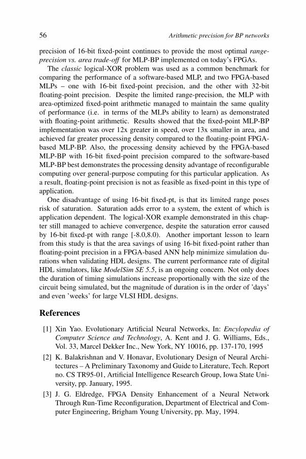
56 Arithmetic precision for BP networks
precision of 16-bit fixed-point continues to provide the most optimal range-precision vs. area trade-off for MLP-BP implemented on today’s FPGAs.
The classic logical-XOR problem was used as a common benchmark forcomparing the performance of a software-based MLP, and two FPGA-basedMLPs – one with 16-bit fixed-point precision, and the other with 32-bitfloating-point precision. Despite the limited range-precision, the MLP witharea-optimized fixed-point arithmetic managed to maintain the same qualityof performance (i.e. in terms of the MLPs ability to learn) as demonstratedwith floating-point arithmetic. Results showed that the fixed-point MLP-BPimplementation was over 12x greater in speed, over 13x smaller in area, andachieved far greater processing density compared to the floating-point FPGA-based MLP-BP. Also, the processing density achieved by the FPGA-basedMLP-BP with 16-bit fixed-point precision compared to the software-basedMLP-BP best demonstrates the processing density advantage of reconfigurablecomputing over general-purpose computing for this particular application. Asa result, floating-point precision is not as feasible as fixed-point in this type ofapplication.
One disadvantage of using 16-bit fixed-pt, is that its limited range posesrisk of saturation. Saturation adds error to a system, the extent of which isapplication dependent. The logical-XOR example demonstrated in this chap-ter still managed to achieve convergence, despite the saturation error causedby 16-bit fixed-pt with range [-8.0,8.0). Another important lesson to learnfrom this study is that the area savings of using 16-bit fixed-point rather thanfloating-point precision in a FPGA-based ANN help minimize simulation du-rations when validating HDL designs. The current performance rate of digitalHDL simulators, like ModelSim SE 5.5, is an ongoing concern. Not only doesthe duration of timing simulations increase proportionally with the size of thecircuit being simulated, but the magnitude of duration is in the order of ’days’and even ’weeks’ for large VLSI HDL designs.
References
[1] Xin Yao. Evolutionary Artificial Neural Networks, In: Encylopedia ofComputer Science and Technology, A. Kent and J. G. Williams, Eds.,Vol. 33, Marcel Dekker Inc., New York, NY 10016, pp. 137-170, 1995
[2] K. Balakrishnan and V. Honavar, Evolutionary Design of Neural Archi-tectures – A Preliminary Taxonomy and Guide to Literature, Tech. Reportno. CS TR95-01, Artificial Intelligence Research Group, Iowa State Uni-versity, pp. January, 1995.
[3] J. G. Eldredge, FPGA Density Enhancement of a Neural NetworkThrough Run-Time Reconfiguration, Department of Electrical and Com-puter Engineering, Brigham Young University, pp. May, 1994.
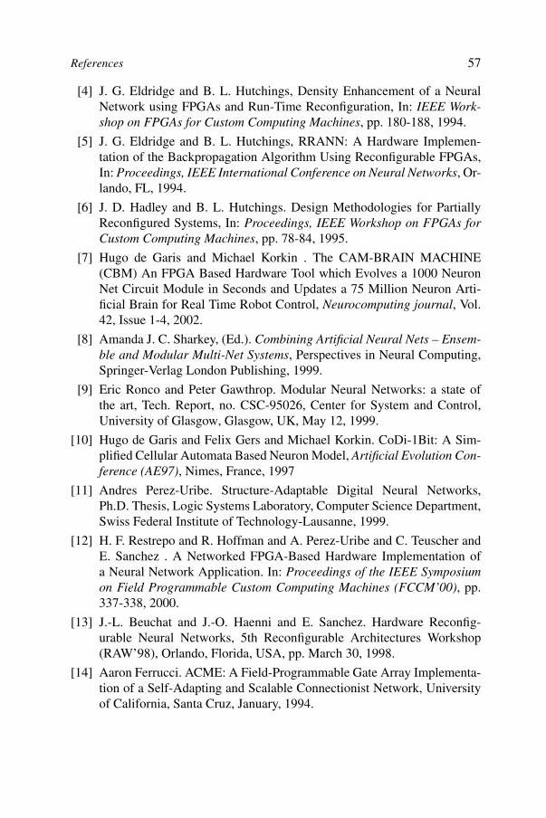
57
[4] J. G. Eldridge and B. L. Hutchings, Density Enhancement of a NeuralNetwork using FPGAs and Run-Time Reconfiguration, In: IEEE Work-shop on FPGAs for Custom Computing Machines, pp. 180-188, 1994.
[5] J. G. Eldridge and B. L. Hutchings, RRANN: A Hardware Implemen-tation of the Backpropagation Algorithm Using Reconfigurable FPGAs,In: Proceedings, IEEE International Conference on Neural Networks, Or-lando, FL, 1994.
[6] J. D. Hadley and B. L. Hutchings. Design Methodologies for PartiallyReconfigured Systems, In: Proceedings, IEEE Workshop on FPGAs forCustom Computing Machines, pp. 78-84, 1995.
[7] Hugo de Garis and Michael Korkin . The CAM-BRAIN MACHINE(CBM) An FPGA Based Hardware Tool which Evolves a 1000 NeuronNet Circuit Module in Seconds and Updates a 75 Million Neuron Arti-ficial Brain for Real Time Robot Control, Neurocomputing journal, Vol.42, Issue 1-4, 2002.
[8] Amanda J. C. Sharkey, (Ed.). Combining Artificial Neural Nets – Ensem-ble and Modular Multi-Net Systems, Perspectives in Neural Computing,Springer-Verlag London Publishing, 1999.
[9] Eric Ronco and Peter Gawthrop. Modular Neural Networks: a state ofthe art, Tech. Report, no. CSC-95026, Center for System and Control,University of Glasgow, Glasgow, UK, May 12, 1999.
[10] Hugo de Garis and Felix Gers and Michael Korkin. CoDi-1Bit: A Sim-plified Cellular Automata Based Neuron Model, Artificial Evolution Con-ference (AE97), Nimes, France, 1997
[11] Andres Perez-Uribe. Structure-Adaptable Digital Neural Networks,Ph.D. Thesis, Logic Systems Laboratory, Computer Science Department,Swiss Federal Institute of Technology-Lausanne, 1999.
[12] H. F. Restrepo and R. Hoffman and A. Perez-Uribe and C. Teuscher andE. Sanchez . A Networked FPGA-Based Hardware Implementation ofa Neural Network Application. In: Proceedings of the IEEE Symposiumon Field Programmable Custom Computing Machines (FCCM’00), pp.337-338, 2000.
[13] J.-L. Beuchat and J.-O. Haenni and E. Sanchez. Hardware Reconfig-urable Neural Networks, 5th Reconfigurable Architectures Workshop(RAW’98), Orlando, Florida, USA, pp. March 30, 1998.
[14] Aaron Ferrucci. ACME: A Field-Programmable Gate Array Implementa-tion of a Self-Adapting and Scalable Connectionist Network, Universityof California, Santa Cruz, January, 1994.
References
58 Arithmetic precision for BP networks
[15] Marcelo H. Martin. A Reconfigurable Hardware Accelerator for Back-Propagation Connectionist Classifiers, University of California, SantaCruz, 1994.
[16] Tomas Nordstrom. Highly Parallel Computers for Artificial Neural Net-works, Ph.D. Thesis,Division of Computer Science and Engineering,Lulea University of Technology, Sweden, 1995.
[17] T. Nordstrom and E. W. Davis and B. Svensson. Issues and Applica-tions Driving Research in Non-Conforming Massively Parallel Proces-sors, book. In: Proceedings of the New Frontiers, a Workshop of FutureDirection of Massively Parallel Processing, 1992
[18] T. Nordstrom and B. Svensson. Using and Designing Massively ParallelComputers for Artificial Neural Networks, Journal of Parallel and Dis-tributed Computing, Vol. 14, 1992.
[19] B. Svensson and T. Nordstrom and K. Nilsson and P.-A. Wiberg. TowardsModular, Massively Parallel Neural Computers, In: Connectionism in aBroad Perspective: Selected Papers from the Swedish Conference on Con-nectionism - 1992, L. F. Niklasson and M. B. Boden, Eds., Ellis Harwood,pp. 213-226, 1994.
[20] Arne Linde and Tomas Nordstrom and Mikael Taveniku. Using FP-GAs to implement a reconfigurable highly parallel computer. In: Field-Programmable Gate Arrays: Architectures and Tools for Rapid Prototyp-ing, Springer-Verlag, Berlin, 1992.
[21] T. Nordstrom. On-line Localized Learning Systems Part 1 - Model De-scription, Research Report, Division of Computer Science and Engineer-ing, Lulea University of Technology, Sweden, 1995.
[22] Tomas Nordstrom. On-line Localized Learning Systems Part II - ParallelComputer Implementation, Research Report, no. TULEA 1995:02, Divi-sion of Computer Science and Engineering, Lulea University of Technol-ogy, Sweden, 1995.
[23] Tomas Nordstrom. Sparse distributed memory simulation on REMAP3,Research Report, no. TULEA 1991:16, Division of Computer Scienceand Engineering, Lulea University of Technology, Sweden, 1991.
[24] T. Nordstrom. Designing Parallel Computers for Self Organizing Maps,In: Proceedings of the 4th Swedish Workshop on Computer System Archi-tecture (DSA-92), Linkoping, Sweden, January 13-15, 1992.
[25] B. Svensson and T. Nordstrom. Execution of neural network algorithmson an array of bit-serial processors. In: Proceedings, 10th InternationalConference on Pattern Recognition, Computer Architectures for Visionand Pattern Recognition, Vol. II, pp. 501-505, 1990.
59
[26] M. Skrbek. Fast Neural Network Implementation. In: Neural NetworkWorld, Elsevier, Vol. 9, no. No. 5, pp. 375-391, 1999.
[27] Introducing the XC6200 FPGA Architecture: The First FPGA Archi-tecture Optimized for Coprocessing in Embedded System Applications,Xcell, Xilinx Inc., No. 18 : Third Quarter, pp. 22-23, 1995, url =http://www.xilinx.com/apps/6200.htm.
[28] Xilinx. XC6200 Field Programmable Gate Arrays, Data Sheet, Version1.7, 1996.
[29] Mikael Taveniku and Arne Linde. A reconfigurable SIMD computer forartificial neural networks, Licentiate Thesis, Department of ComputerEngineering, Chalmers University of Technology, Goteborg, Sweden,1995.
[30] Gate Count Capacity Metrics for FPGAs, Application Note, no.XAPP 059 - Version 1.1, Xilinx, Inc., Feb. 1, 1997, URL =http://www.xilinx.com/xapp/xapp059.pdf.
[31] FLEX 10K Embedded Programmable Logic Device Family,Data Sheet, Version 4.1, Altera, Inc., March, 2001, URL =http://www.altera.com/literature/ds/dsf10k.pdf
[32] XC3000 Series Field Programmable Gate Arrays, Product De-scription, Version 3.1, Xilinx, Inc., November 9, 1998, URL =http://www.xilinx.com/partinfo/3000.pdf
[33] XC4000XLA/XV Field Programmable Gate Arrays, Product Specifica-tion, no. DS015 - Version 1.3, Xilinx, Inc., October 18, 1999, URL =http://www.xilinx.com/partinfo/ds015.pdf
[34] Andres Perez-Uribe and Eduardo Sanchez. Speeding-Up AdaptiveHeuristic Critic Learning with FPGA-Based Unsupervised Clustering,In: Proceedings of the IEEE International Conference on EvolutionaryComputation ICEC’97, pp. 685-689, 1997.
[35] M. Morris Mano and Charles R. Kime. Logic And Computer Design Fun-damentals, Prentice Hall Inc., New Jersey, USA, 2000.
[36] Andre Dehon. The Density Advantage of Configurable Computing, IEEEComputer, vol. 33, no. 5, pp. 41–49, 2000.
[37] David E Rumelhart and James L McClelland and PDP Research Group.Parallel Distrubuted Processing: Explorations in the Microstructure ofCognition, vol. Volume 1: Foundations, MIT Press, Cambridge, Massa-chusetts, 1986.
[38] Simon Haykin, Neural Networks: A Comprehensive Foundation,Prentice-Hall, Englewood Cliffs, New Jersey, 1999.
References
60 Arithmetic precision for BP networks
[39] Stephen D. Brown and Robert J. Francis and Jonathan Rose and ZvonkoG. Vranesic, Field-Programmable Gate Arrays, Kluwer Academic Pub-lishers, USA, 1992
[40] Virtex-E 1.8 V Field Programmable Gate Arrays, Perliminary ProductSpecification, no. DS022-2 (v2.3), Xilinx, Inc., November 9, 2001, URL= http://www.xilinx.com/partinfo/ds022-2.pdf
[41] Jordan L Holt and Thomas E Baker. Backpropagation simulations usinglimited precision calculations. In: Proceedings, International Joint Con-ference on Neural Networks (IJCNN-91), vol. 2, Seattle, WA, USA, pp.121 - 126, 1991.
[42] Hikawa Hiroomi. Frequency-Based Multilayer Neural Network with On-chip Learning and Enhanced Neuron Characterisitcs. IEEE Transactionson Neural Networks, vol. 10, no. 3, pp. 545-553, May, 1999.
[43] Peter J. Ashenden. VHDL Standards. IEEE Design & Test of Computers,vol. 18, no. 6, pp. 122-123, September–October, 2001.
[44] Hung Tien Bui and Bashar Khalaf and Sofi„ene Tahar. Table-DrivenFloating-Point Exponential Function, Technical Report, Concordia Uni-versity, Department of Computer Engineering, October, 1998, URL =http://www.ece.concordia.ca/ tahar/pub/FPE-TR98.ps
[45] W.B. Ligon III and S. McMillan and G. Monn and K. Schoonover andF. Stivers and K.D. Underwood. A Re-evaluation of the Practicality ofFloating Point Operations on FPGAs. In: Proceedings, IEEE Symposiumon FPGAs for Custom Computing Machines, pp. 206–215, 1998.
[46] Pete Hardee. System C: a realistic SoC debug strategy, EETimes, 2001.
[47] G.M. Amdahl. Validity of the single-processor approach to achievinglarge scale computing capabilities, In: AFIPS Conference Proceedings,vol. 30, AFIPS Press, Reston, Va., pp. 483–485, 1967.
[48] Stephen Chappell and Chris Sullivan, Celoxica Ltd. Oxford UK. Handel-C for co-processing & co-design of Field Programmable System on ChipFPSoC, 2002, url = www.celoxica.com/technical-library/
[49] Synopsys, Inc. Describing Synthesizable RTL in SystemC v1.1, Synop-sys, Inc., January, 2002.
[50] Martyn Edwards. Software Acceleration Using Coprocessors: Is it Worththe Effort?, In: Proceedings, 5th International Workshop on Hard-ware/Software Co-design Codes/CASHE’97, Braunschneig, Germany,pp. 135–139, March 24-26, 1997.
[51] Giovanni De Micheli and Rajesh K. Gupta. Hardware/Software Co-design. Proceedings of the IEEE, vol. 85, no. 3, pp. 349-365, March,1997.

61
[52] John Sanguinetti and David Pursley. High-Level Modeling and HardwareImplementation with General- Purpose Languages and High-level Syn-thesis, White Paper, Forte Design Systems, 2002.
[53] Don Davis. Architectural Synthesis: Unleasing the Power of FPGASystem-Level Design. Xcell Journal, Xilinx Inc., no. 44, vol. 2, pp. 30-34,pp. Winter, 2002.
[54] Xilinx, XAPP467 Using Embedded Multipliers in Spartan-3 FPGAs, Xil-inx Application Note, May 13, 2003, http://www.xilinx.com.
[55] Nestor Inc. Neural Network Chips, http://www.nestor.com.
References
Chapter 3
FPNA: CONCEPTS AND PROPERTIES
Bernard GirauLORIA INRIA-LorraineNancy France
Abstract Neural networks are usually considered as naturally parallel computing mod-els. But the number of operators and the complex connection graph of standardneural models can not be handled by digital hardware devices. Though pro-grammable digital hardware now stand as a real opportunity for flexible hard-ware implementations of neural networks, many area and topology problemsarise when standard neural models are implemented onto programmable circuitssuch as FPGAs, so that the fast FPGA technology improvements can not be fullyexploited. The theoretical and practical framework first introduced in [21] rec-onciles simple hardware topologies with complex neural architectures, thanksto some configurable hardware principles applied to neural computation: FieldProgrammable Neural Arrays (FPNA) lead to powerful neural architectures thatare easy to map onto FPGAs, by means of a simplified topology and an origi-nal data exchange scheme. This two-chapter study gathers the different resultsthat have been published about the FPNA concept, as well as some unpublishedones. This first part focuses on definitions and theoretical aspects. Starting froma general two-level definition of FPNAs, all proposed computation schemes aretogether described and compared. Their correctness and partial equivalence isjustified. The computational power of FPNA-based neural networks is charac-terized through the concept of underparameterized convolutions.
Keywords: neural networks, fine-grain parallelism, digital hardware, FPGA
3.1 Introduction
Various fast implementations of neural networks have been developed, be-cause of the huge amount of computations required by neural network appli-
63
A. R. Omondi and J. C. Rajapakse (eds.), FPGA Implementations of Neural Networks, 63–101. © 2006 Springer. Printed in the Netherlands.
64 FPNA: Concepts and properties
cations, especially during the learning phase.1 A broad introduction to parallelneural computing may be found in [50]. Several kinds of parallel devices havebeen used for these fast implementations, such as massively parallel comput-ers, neuro-computers, analog or digital ASICs (application specific integratedcircuits). Programmable digital circuits (such as FPGAs, field programmablegate arrays) mix the efficiency and parallelism grain of hardware devices withthe flexibility of software implementations, so that they appear as particularlywell-adapted to the usual needs of neural implementations (see [26]).
However, the 2D-topology of FPGAs is not able to handle the connectioncomplexity of standard neural models. What is more, FPGAs still implementa limited number of logic gates, whereas neural computations require area-greedy operators (multipliers, activation functions). Usual solutions handlesequentialized computations with an FPGA used as a small neuroprocessor,or they implement very small low-precision neural networks without on-chiplearning. Connectivity problems are not solved even by the use of several re-configurable FPGAs with a bit-serial arithmetic, or by the use of small-area op-erators (stochastic bit-stream or frequency-based). Subsection 3.2.3 preciselydescribes the specific problems raised by neural network implementations onFPGAs.
In [29], we propose an implementation method for multilayer perceptronsof any size on a single FPGA, with on-chip learning and adaptable precision.This work takes advantage of an area-saving on-line arithmetic that is well-adapted to neural computations. It also uses an original parallelization of theinternal computations of each neuron. Yet, this implementation method barelyexploits the massive fine-grain parallelism that is inherent to neural networkarchitectures.
In [21] and following publications, I have defined and studied a set of neuralmodels called FPNAs (Field Programmable Neural Arrays). These modelsshare a computation method whose local data processing is more complex thanin the standard neural computation scheme. It makes it possible to handle sim-plified neural network topologies, though such neural networks may be func-tionally equivalent to standard neural models (multilayer perceptron, Hopfieldnetwork, etc). Therefore, FPNAs lead to the definition of large and efficientneural networks that are adapted to hardware topological constraints. Theyreconcile the high connection density of neural architectures with the need ofa limited interconnection scheme in hardware implementations.
1A neural network has got some learnable parameters. The learning phase consists in determining parametervalues such that the neural network computes a function that performs an expected task (e.g. classificationof a set of patterns). When the parameters have been determined, the neural network is ready to be appliedto unknown patterns. This is the generalization phase.
Choosing FPGAs 65
FPNAs are based on an FPGA-like approach: a set of resources with freelyconfigurable interactions. These resources are defined to perform computa-tions of standard neurons, but they behave in an autonomous way. As a conse-quence, numerous virtual connections are achieved thanks to the application ofa simple protocol to the resources of a sparse neural network. A standard buttopologically complex neural network may be replaced by a simplified neuralnetwork that uses this new neural computation concept.
The aim of this two-chapter study is to gather the different results, publishedor unpublished, about the FPNA concept ([21, 20, 27, 25, 24, 22, 23, 28]), soas to give an exhaustive overview of this hardware-oriented neural paradigm.This first chapter focuses on definitions and theoretical aspects. Section 3.2first proposes a brief survey of the use of parallel devices for neural implemen-tations. Then it describes the specific advantages and problems of the use ofprogrammable hardware for such implementations. Section 3.3 starts from ageneral two-level definition of FPNAs. Then it describes and compares all pro-posed computation schemes for FPNA-based neural networks. Their correct-ness and partial equivalence is justified in section 3.4. Section 3.5 characterizesthe computational power of FPNA-based neural networks through the conceptof underparameterized convolutions. Chapter 4 focuses on implementationsand applications.
3.2 Choosing FPGAs
This section shows how FPGAs stand as appropriate hardware devices forneural implementations:
§3.2.1 is a rapid survey of existing devices for parallel implementationsof neural networks
§3.2.2 describes some specific advantages of the use of FPGAs to imple-ment neural applications
§3.2.3 points out the main issues of such implementations on FPGAs
§3.2.4 is a short survey of existing solutions, from the simplest to themost well-built
3.2.1 Parallel implementations of neural networks
Fast implementations of neural network applications are useful because ofthe very high number of required arithmetic operations. Such implementationsmight use massively parallel computers as well as digital or analog hardwaredesigns. This subsection rapidly discusses the use of the various possible par-allel devices.
66 FPNA: Concepts and properties
3.2.1.1 General purpose parallel computers. Fine-grain parallel im-plementations on massively parallel computers (either SIMD, as in [72, 64], orMIMD, as in [42, 55, 51, 7]) suffer from the connectivity of standard neuralmodels that results in costly information exchanges ([63, 51, 7, 62]). Coarse-grain parallel implementations are mainly applied to neural learning, so thattheir efficiency suffers from the sequentiality of standard learning algorithmssuch as stochastic gradient descent (see [53, 55, 14]). Furthermore, massivelyparallel computers are expensive resources and they cannot be used in em-bedded applications. Such solutions are usually preferable for huge neuralstructures and complex neural computations or learning methods ([45, 30, 7,62]).
3.2.1.2 Dedicated parallel computers. Neuro-computers are parallelsystems dedicated to neural computing. They are based on computing de-vices such as DSPs (digital signal processors) as in [39, 49, 46, 62], or neuro-processors ([3, 68, 62]). Their use suffers from their cost and their developmenttime: they rapidly become out-of-date, compared to the most recent sequentialprocessors. Most well-known neurocomputers are described in [50, 62].
3.2.1.3 Analog ASICs. Many analog hardware implementations havebeen realized. They are very fast, dense and low-power, but they introducespecific problems (see [41]), such as precision, data storage, robustness. On-chip learning is difficult ([9]). It is an expensive and not flexible solution, asany ASIC (even if some design methods tend to be flexible, [48]). And theirvery long development is very tricky for users who are not analog technologyexperts.
3.2.1.4 Digital ASICs. Many digital integrated circuits have also beendesigned for neural networks. Compared to analog chips, they provide moreaccuracy, they are more robust, and they can handle any standard neural com-putation. Yet their design requires a strong effort to obtain working chips andit is very expensive when only a few chips are needed (standard drawbacks ofASICs). They usually implement limited parts of neural networks, so as to beincluded in neuro- computer systems ([69, 13]). Sometimes they implementa whole specific neural network, nevertheless the architecture of this neuralnetwork is not directly mapped onto the chip (e.g. [38]).
3.2.1.5 The FPGA solution. To summarize the above survey, hard-ware implementations are more likely to fit the parallelism grain of neuralcomputations, and both digital and analog ASICs may efficiently implementregular structures, but they require important development times. This majordrawback may be avoided with the help of programmable integrated circuits
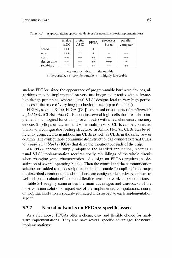
Choosing FPGAs 67
analogASIC
digitalASIC
FPGAprocessor
basedparallel
computerspeed +++ ++ + – +area +++ ++ + – – –cost – – – – ++ ++ – –design time – – – – ++ +++ +reliability – – + ++ ++ ++
– –: very unfavourable, –: unfavourable,+: favourable, ++: very favourable, +++: highly favourable
Table 3.1. Appropriate/inappropriate devices for neural network implementations
such as FPGAs: since the appearance of programmable hardware devices, al-gorithms may be implemented on very fast integrated circuits with software-like design principles, whereas usual VLSI designs lead to very high perfor-mances at the price of very long production times (up to 6 months).
FPGAs, such as Xilinx FPGA ([70]), are based on a matrix of configurablelogic blocks (CLBs). Each CLB contains several logic cells that are able to im-plement small logical functions (4 or 5 inputs) with a few elementary memorydevices (flip-flops or latches) and some multiplexors. CLBs can be connectedthanks to a configurable routing structure. In Xilinx FPGAs, CLBs can be ef-ficiently connected to neighbouring CLBs as well as CLBs in the same row orcolumn. The configurable communication structure can connect external CLBsto input/output blocks (IOBs) that drive the input/output pads of the chip.
An FPGA approach simply adapts to the handled application, whereas ausual VLSI implementation requires costly rebuildings of the whole circuitwhen changing some characteristics. A design on FPGAs requires the de-scription of several operating blocks. Then the control and the communicationschemes are added to the description, and an automatic “compiling” tool mapsthe described circuit onto the chip. Therefore configurable hardware appears aswell-adapted to obtain efficient and flexible neural network implementations.
Table 3.1 roughly summarizes the main advantages and drawbacks of themost common solutions (regardless of the implemented computations, neuralor not). Each solution is roughly estimated with respect to each implementationaspect.
3.2.2 Neural networks on FPGAs: specific assets
As stated above, FPGAs offer a cheap, easy and flexible choice for hard-ware implementations. They also have several specific advantages for neuralimplementations:
68 FPNA: Concepts and properties
Reprogrammable FPGAs permit prototyping: in most applications, sev-eral neural architectures must be tested so as to find the most efficientone. This may be directly performed with the hardware efficiency of anFPGA-based implementation, without any additional cost. Moreover agood architecture that has been designed and implemented may be re-placed later by a better one without having to design a new chip.
On-chip learning is often considered as difficult and useless. Indeed itis used very seldom. But on-chip learning usually results in a loss ofefficiency in a hardware implementation, since it requires some specificoperators, a higher precision, . . . etc. Therefore off-chip learning isnaturally chosen when no dynamic learning is necessary. In a recon-figurable FPGA, on-chip learning may be performed prior to a specificoptimized implementation of the learned neural network on the samechip.
FPGAs may be used for embedded applications, when the robustnessand the simplicity of neural computations is most needed, even for low-scale productions.
FPGA-based implementations may be mapped onto new improved FP-GAs, which is a major advantage, considering that FPGA speeds andareas approximately double each year. Even large neural networks maysoon be implemented on single FPGAs, provided that the implementa-tion method is scalable enough. The FPNA concept is a major advanceto ensure the scalability of direct hardware mappings of neural networks(the neural architecture itself is mapped by the compiler onto the FPGA).
3.2.3 Implementation issues
Neural network implementations on FPGAs have to deal with the usual is-sues of digital hardware implementations of neural network applications. Butthese issues become more acute because of the specific constraints of FPGAs:it is particularly obvious when it is a matter of area consumption. Even ifthe software-like use of FPGAs is simple, the user should not forget that thecompiler has to deal with these strong constraints.
3.2.3.1 Topology-related issues.
Hardware devices have 2-D topologies, that do not easily fit the regu-lar but complex connection graph of most standard neural models (e.g.multilayer ones). Furthermore, in the case of FPGAs, the user must dealwith an already specified connection frame, even if it is programmable.Routing problems may not be solved by means of a shrewd use of thedifferent metal layers.
Choosing FPGAs 69
Neurons have a large number of parallel input links in most neural mod-els, whereas hardware implementations of operators can handle only alimited fan-in. In the case of FPGAs, part of the available CLBs maybe used just to increase the routing capacities, which results in a loss ofcomputation resources.
3.2.3.2 Area-related issues.
Multipliers and elementary function operators (e.g. the sigmoidal acti-vation function tanh) are area-greedy. This problem strongly depends onthe required precision. Though neural networks do not usually requirevery precise computations, the required precision varies with the appli-cation ([2]). Moreover, learning is not as tolerant as generalization ([34,58, 47, 48]), so that on-chip learning does not only introduce algorithmicneeds, but also makes low-precision implementations impossible.
Weight storage can not be included in the FPGA for large neural net-works. When efficient implementations are obtained, a careful manage-ment of the memory accesses must be taken into account.
Neural network applications have a notable drawback: there is an imbal-ance between the overall computation time and the implementation areaof the different operators involved in neural computing. In most standardneural models, the main part of the computation time is due to matrix-vector products that require multipliers and adders. But other area-greedy operators, such as activation functions, must be implemented.The area of an FPGA is strictly bounded. A significant part of the avail-able area is required to implement these other operators, so that only areduced part of the whole FPGA is available to implement almost 100 %of the overall computation time of the neural application.
3.2.4 Existing solutions
The easiest way to bypass these issues is to consider very small neural net-works (as in [8, 54, 57, 44]). More generally, standard solutions include:
Implementation of the generalization phase only ([4, 8, 60, 10, 37, 66]).
Implementation of a small neuro-processor on the FPGA, and sequential(and therefore slower) use of this computing device ([10, 37, 15]).
Implementation of a small neuro-processor on each one of several FP-GAs with data communications ([11, 54–1, 33]) that raise bandwidthproblems and that need to minimize the number of required I/O pads,which is difficult when densely connected neural architectures are han-dled.
70 FPNA: Concepts and properties
Simplified computations, discretized activation function, very low pre-cision ([8, 10, 31]). Such solutions only adapt to specific applicationswith very weak precision requirements.
More advanced methods have been considered:
3.2.4.1 Area-saving solutions.
Optimized implementation of the activation function (e.g. cordic-likealgorithm in [2], or piecewise polynomial approximation controled bylook-up tables in [29]), or fast multipliers ([60]). Such solutions may becombined with other advanced method. Their choice depends on someapplication characteristics, such as required precision, or required on-chip learning.
Bit-serial arithmetic (standard: [11], or optimized: [66]) or on-line serialarithmetic ([29]). The choice of the best arithmetic for digital hardwareimplementations of neural networks is discussed in [61], but the speci-ficity of FPGAs is not taken into account, and on-line arithmetic is notconsidered. Any serial arithmetic requires more clock cycles, and shouldbe used with pipelined operators.
Pulse-based arithmetic (bit-stream neurons in [4, 59, 43, 67, 40, 56], orsome frequency-based solution in [32, 44]). It provides tiny operators,so that an average-sized neural network can be fully implemented on asingle FPGA, but the routing constraints of FPGAs still do not permitlarge neural networks to be implemented. What is more, such solutionsneed to be applied to the development of the neural application from thebeginning (arithmetical operations are not equivalent to standard ones).
3.2.4.2 Solutions to reduce CLB idleness.
Run-time reconfiguration of the FPGA ([11, 6]). Such methods stillclash with significant dynamic reconfiguration times.
Pipelined architecture (e.g. orthogonal systolic array, [17]). Strong con-straints are put on the kind of neural architectures to which such methodsapply.
Sub-neural parallelism level and computation overlappings ([29]): thiswork makes it possible to implement multilayer perceptrons of any sizeon a single FPGA, with on-chip learning and adaptable precision, but itoffers a limited parallelism level (this solution is a compromise betweena neuro-processor and a direct parallel mapping of neural operators).
FPNAs, FPNNs 71
3.2.4.3 Topologically hardware-friendly solutions.
Partition of the neural graph into equivalent subgraphs, so that a repeateduse of such a simple subgraph covers the whole graph ([31]).
Neural computation paradigm tolerant of constrained topologies: it cor-responds to the FPNA concept that is described in this paper.
3.2.4.4 Adapted frameworks of neural computation. As shownabove, many neural implementations on FPGAs handle simplified neural com-putations. Furthermore, many efficient implementation methods (on ASICs,neuro-computers, . . . etc) have to limit themselves to few well-fitted neuralarchitectures. An upstream work is preferable: neural computation paradigmsmay be defined to counterbalance the main implementation problems, and theuse of such paradigms naturally leads to neural models that are more toler-ant of hardware constraints, without any additional limitation. Since the mainimplementation issues are linked to area-greedy operators and complex topolo-gies, two kinds of (complementary) hardware-adapted neural computation par-adigms may appear: area-saving neural computation frameworks on one hand,and paradigms that may handle simplified topologies on the other hand. Thebit-stream technology mentioned above has led to an example of area-savingneural paradigm, while the definition of the FPNA framework makes it possi-ble to simplify the architectures of standard neural models without significantloss of approximation capability.
Next section introduces the FPNA concept, before §3.3.5 explains how itmakes it possible to overcome most implementation issues mentioned above.
3.3 FPNAs, FPNNs
This section describes the FPNA/FPNN concept. These models appear asparameterized task graphs that are specialized so as to perform neural computa-tions, but they differ from standard neural models that are graphs of non-linearregressors.
The description below directly illustrates the links of the FPNA concept withboth implementation choices and standard neural theory.
The distinction between FPNAs and FPNNs is mainly linked to implemen-tation properties. An FPNA is a given set of neural resources that are organizedaccording to specific neighbourhood relations. An FPNN is a way to use thisset of resources: it only requires local configuration choices. Therefore, theimplementations of two different FPNNs exactly require the same mapping onFPGA, as long as they are based on the same FPNA.
This section is organized as follows:
72 FPNA: Concepts and properties
§3.3.1 briefly describes where this concept comes from, then it definesan FPNA as a set of computing resources which architecture is fullyspecified, but in which local computations still need to be parameterized
§3.3.2 describes the parameterization step that is required to get to afunctional neural model, called FPNN,
§3.3.3 describes the basic computation algorithm that has been definedfor FPNNs, and that sequentially handles a list of tasks (node-level com-putation); an example is described in detail and it illustrates the mainproperties of FPNN computation, such as how virtual connections areobtained as composite links, §3.3.4 describes a parallel version of the above algorithm, in order to showthat it only requires local computations; this computation algorithm isthe basis of a direct parallel mapping onto FPGAs in 4.5; an example isdescribed in detail and it illustrates how virtual connections generate afunctional equivalence between an FPNN and a standard neural networkwith a completely different architecture,
§1.3.5 gets back to the discussion of §3.2.3 and it explains how mostneural implementation issues may be overcome by the use of FPNA ar-chitectures combined with the virtual connections that are created byFPNN computation.
3.3.1 FPNAs
3.3.1.1 From FPGAs to FPNAs. The first aim of the FPNA concept isto develop neural structures that are easy to map directly onto digital hardware,thanks to a simplified and flexible topology. The structure of an FPNA is basedon FPGA principles: complex functions realized by means of a set of simpleprogrammable resources. The nature and the relations of these FPNA resourcesare derived from the mathematical processing FPNAs have to perform.
To summarize, in a standard neural model, each neuron computes a functionapplied to a weighted sum of its inputs: if xi is the input vector of neuron i,and wi is its weight vector, it computes fi( wi.xi). See [18, 19] for a unifiedtheoretical approach of the computation of standard neural networks. The in-put vector xi may contain neural network inputs as well as outputs of otherneurons, depending of the connection graph of the neural network. In sucha standard model, each link is a connection between the output of a neuronand an input of another neuron. Therefore the number of inputs of each neu-ron is its fan-in in the connection graph. On the contrary, neural resourcesbecome autonomous in an FPNA: their dependencies are freely set, and theresulting processing is more complex than in standard neural models. As in
FPNAs, FPNNs 73
FPGAs, FPNA configuration handles both resource interconnections and re-source functionalities.
3.3.1.2 FPNA resources. An FPNA is a programmable set of neuralresources that are defined to compute partial convolutions for non-linear re-gression (see section 3.5), as standard multilayer neural networks do. Twokinds of autonomous FPNA resources naturally appear: activators that applystandard neural functions to a set of input values on one hand, and links thatbehave as independent affine operators on the other hand.
These resources might be handled in different ways. The easiest schemewould allocate any link to any activator, with the help of an underlying pro-grammable interconnection network. This would lead to massively prunedstandard neural networks, or to multiple weight sharing connections. Topo-logical problems would still appear (such as high fan-ins), and weight sharingwould lead to few different wi weight vectors. Therefore, another principlehas been chosen for FPNAs: any link may be connected to any local resource.The aim of locality is to reduce topological problems, whereas connected linksresult in more various weight vectors.
More precisely, the links connect the nodes of a directed graph, each nodecontains one activator. The specificity of FPNAs is that the relations betweenany local resources of each node may be freely set. A link may be connected ornot to the local activator and to other local links. Direct connections betweenaffine links appear, so that the FPNA computes numerous composite affinetransforms. These compositions create numerous virtual neural connections,so that different convolution terms may be obtained with a reduced number ofconnection weights.
3.3.1.3 Definition of FPNAs. The following definition specifies thestructure of an FPNA (directed graph), as well as the functional nature of eachindividual neural resource.
An FPNA is defined by means of:
A directed graph (N , E), where N is an ordered finite set of nodes, andE is a set of directed edges without loop. E may be seen as a subset ofN 2.
For each node n, the set of the direct predecessors (resp. succes-sors) of n is defined by Pred(n) = {p ∈ N | (p, n) ∈ E} (resp.Succ(n) = {s ∈ N | (n, s) ∈ E}). The set of the input nodes isNi = {n ∈ N | Pred(n) = ∅}.
A set of affine operators α(p,n) for each (p, n) in E .
74 FPNA: Concepts and properties
A set of activators (in, fn), for each n in N − Ni: in is an iterationoperator (a function from IR2 to IR), and fn is an activation function(from IR to IR).
To simplify, (p, n) and (n) now stand for the corresponding links and activa-tors.
3.3.1.4 Interpretation. Resources are associated with the nodes,whereas locality is defined by the edges. For each node n ∈ N , there isone activator and as many communication links as this node has got predeces-sors. Each link is associated with an affine operator. An activator is definedby (in, fn), since it will handle any neuron computation as in a sequential pro-gram. Indeed, any standard neuron computation may be performed by meansof a loop that updates a variable with respect to the neuron inputs, and a finalcomputation that maps this variable to the neuron output. The iteration func-tion in stands for the updating function inside the loop. The neuron output isfinally computed with fn. See [21] for the definition of (in, fn) so as to obtainmost standard neurons, e.g.:
A d-input sigmoidal neuron of a multilayer perceptron computes
σ
⎛⎝θ +d∑
j=1
wjxj
⎞⎠ (3.1)
where σ is a sigmoid function (bounded, monotonous), θ is a thresholdvalue.
A d-input radial basis function of a RBF network computes
γ
⎛⎝√√√√ d∑
j=1
(wj(xj − tj))2
⎞⎠where γ is a gaussian function and t is a translation vector.
A d-input wavelet neuron of a wavelet network ([71, 5]) computes
d∏j=1
ψ(wj(xj − tj))
where ψ is a wavelet function (localized in both space and frequencydomains).
When the FPNA graph and the different operators have been defined, ageneral implementation can be given: each resource corresponds to a basic
FPNAs, FPNNs 75
block, and these blocks are organized according to the graph. This imple-mentation may be used by any FPNN derived from this FPNA. Some of theseFPNNs compute very complex functions (equivalent to standard neural net-works), though the FPNA graph is made simple (reduced number of edges,limited node fan-ins and fan-outs, so that the FPNA is easily mapped by thecompiler onto the hardware device).
3.3.2 FPNNs
An FPNN (field programmed neural network) is a configured FPNA: anFPNA whose resources have been connected in a specific way (furthermore,some parameters must be given to specify the computation of each resource).
In other words, the underlying FPNA of an FPNN is a topologically fullyspecified architecture of neural resources, whereas this FPNN is a given wayto specify how these resources will interact to define a functional behaviour.
3.3.2.1 Definition of FPNNs. An FPNA configuration requires localconnections (from link to link, link to activator or activator to link) as wellas precisions about the iterative process performed by each activator (initialvalue, number of iterations). Therefore an FPNN is specified by:
an FPNA (available neural resources),
for each node n in N −Ni,
– a real value θn (initial value of the variable updated by iterationfunction in)
– a positive integer an (number of iterations before an activator ap-plies its activation function)
– for each p in Pred(n), two real value Wn(p) and Tn(p) (coeffi-cients of affine operator α(p,n)(x) = Wn(p)x + Tn(p)),
– for each p in Pred(n), a binary value rn(p) (set to 1 iff link (p, n)and activator (n) are connected),
– for each s in Succ(n), a binary value Sn(s) (set to 1 iff activator(n) and link (n, s) are connected),
– for each p in Pred(n) and each s in Succ(n), a binary valueRn(p, s) (set to 1 iff links (p, n) and (n, s) are connected),
for each input node n in Ni,
– a positive integer cn (number of inputs sent to this node),
– for each s in Succ(n), a binary value Sn(s) (see above).
76 FPNA: Concepts and properties
3.3.2.2 Computing in an FPNN. Several computation methods havebeen defined for the FPNNs in [21]. Their common principles may be de-scribed as follows:
All resources behave independently.
A resource receives values. For each value,
– the resource applies its local operator(s),
– the result is sent to all neighbouring resources to which the re-source is locally connected (an activator waits for an values beforesending any result to its neighbours).
The main differences with the standard neural computation are:
A resource may or may not be connected to a neighbouring resource.These local connections are set by the rn(p), Sn(s) and Rn(p, s) values.
A link may directly send values to other communication links.
A resource (even a link) may handle several values during a single FPNNcomputation process.
A sequential version of the most general FPNN computing method is firstdescribed below. This method clearly illustrates the above principles. More-over, it stands as a reference computation scheme when establishing theoreticalproperties.
Then a parallel version is described. This computation scheme is aimed atbeing directly implemented onto FPGAs.
3.3.3 Sequential computation
This computation method handles a list of tasks L that are processed ac-cording to a FIFO scheduling. Each task [(p, n), x] corresponds to a value xsent on a link (p, n). Task handling corresponds to the various steps that mustbe performed at node-level to deal with such an input:
Input nodes just have to send global input values to their connectedneighbours.
An incoming value is first processed in an affine way.
Then it is directly forwarded to neighbouring nodes when direct connec-tions exist between links.
It is also processed by the local activator when a connection exists be-tween the incoming link and this activator. The latter generates an output
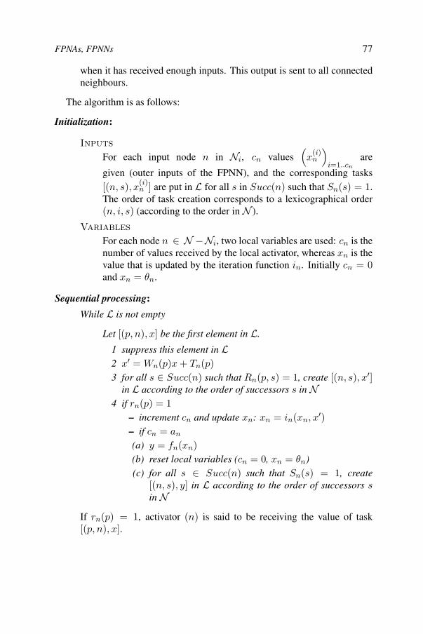
FPNAs, FPNNs 77
when it has received enough inputs. This output is sent to all connectedneighbours.
The algorithm is as follows:
Initialization:
Inputs
For each input node n in Ni, cn values(x
(i)n
)i=1..cn
are
given (outer inputs of the FPNN), and the corresponding tasks[(n, s), x(i)
n ] are put in L for all s in Succ(n) such that Sn(s) = 1.The order of task creation corresponds to a lexicographical order(n, i, s) (according to the order in N ).
Variables
For each node n ∈ N −Ni, two local variables are used: cn is thenumber of values received by the local activator, whereas xn is thevalue that is updated by the iteration function in. Initially cn = 0and xn = θn.
Sequential processing:
While L is not empty
Let [(p, n), x] be the first element in L.
1 suppress this element in L2 x′ = Wn(p)x + Tn(p)3 for all s ∈ Succ(n) such that Rn(p, s) = 1, create [(n, s), x′]
in L according to the order of successors s in N4 if rn(p) = 1
– increment cn and update xn: xn = in(xn, x′)– if cn = an
(a) y = fn(xn)(b) reset local variables (cn = 0, xn = θn)(c) for all s ∈ Succ(n) such that Sn(s) = 1, create
[(n, s), y] in L according to the order of successors sin N
If rn(p) = 1, activator (n) is said to be receiving the value of task[(p, n), x].
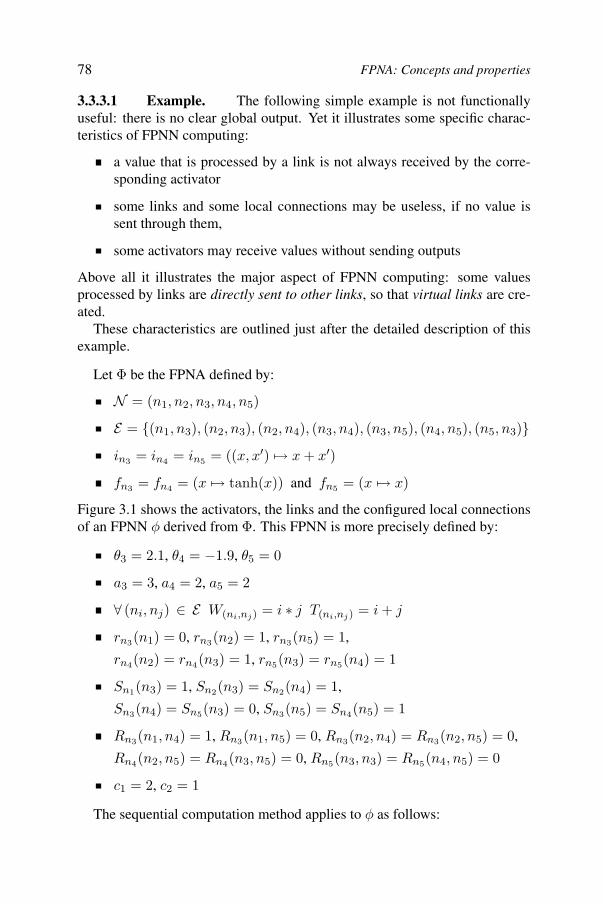
78 FPNA: Concepts and properties
3.3.3.1 Example. The following simple example is not functionallyuseful: there is no clear global output. Yet it illustrates some specific charac-teristics of FPNN computing:
a value that is processed by a link is not always received by the corre-sponding activator
some links and some local connections may be useless, if no value issent through them,
some activators may receive values without sending outputs
Above all it illustrates the major aspect of FPNN computing: some valuesprocessed by links are directly sent to other links, so that virtual links are cre-ated.
These characteristics are outlined just after the detailed description of thisexample.
Let Φ be the FPNA defined by:
N = (n1, n2, n3, n4, n5)
E = {(n1, n3), (n2, n3), (n2, n4), (n3, n4), (n3, n5), (n4, n5), (n5, n3)}in3 = in4 = in5 = ((x, x′) �→ x + x′)
fn3 = fn4 = (x �→ tanh(x)) and fn5 = (x �→ x)
Figure 3.1 shows the activators, the links and the configured local connectionsof an FPNN φ derived from Φ. This FPNN is more precisely defined by:
θ3 = 2.1, θ4 = −1.9, θ5 = 0
a3 = 3, a4 = 2, a5 = 2
∀ (ni, nj) ∈ E W(ni,nj) = i ∗ j T(ni,nj) = i + j
rn3(n1) = 0, rn3(n2) = 1, rn3(n5) = 1,
rn4(n2) = rn4(n3) = 1, rn5(n3) = rn5(n4) = 1
Sn1(n3) = 1, Sn2(n3) = Sn2(n4) = 1,
Sn3(n4) = Sn5(n3) = 0, Sn3(n5) = Sn4(n5) = 1
Rn3(n1, n4) = 1, Rn3(n1, n5) = 0, Rn3(n2, n4) = Rn3(n2, n5) = 0,
Rn4(n2, n5) = Rn4(n3, n5) = 0, Rn5(n3, n3) = Rn5(n4, n5) = 0
c1 = 2, c2 = 1
The sequential computation method applies to φ as follows:
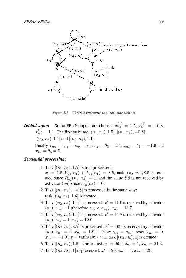
FPNAs, FPNNs 79
Figure 3.1. FPNN φ (resources and local connections)
Initialization: Some FPNN inputs are chosen: x(1)n1 = 1.5, x
(2)n1 = −0.8,
x(1)n2 = 1.1. The first tasks are [(n1, n3), 1.5], [(n1, n3),−0.8],
[(n2, n3), 1.1] and [(n2, n4), 1.1].Finally, cn3 = cn4 = cn5 = 0, xn3 = θ3 = 2.1, xn4 = θ4 = −1.9 andxn5 = θ5 = 0.
Sequential processing:
1 Task [(n1, n3), 1.5] is first processed:x′ = 1.5 Wn3(n1) + Tn3(n1) = 8.5, task [(n3, n4), 8.5] is cre-ated since Rn3(n1, n4) = 1, and the value 8.5 is not received byactivator (n3) since rn3(n1) = 0.
2 Task [(n1, n3),−0.8] is processed in the same way:task [(n3, n4), 1.6] is created.
3 Task [(n2, n3), 1.1] is processed: x′ = 11.6 is received by activator(n3), cn3 = 1 (therefore cn3 < an3), xn3 = 13.7.
4 Task [(n2, n4), 1.1] is processed: x′ = 14.8 is received by activator(n4), cn4 = 1, xn4 = 12.9.
5 Task [(n3, n4), 8.5] is processed: x′ = 109 is received by activator(n4), cn4 = 2, xn4 = 121.9. Now cn4 = an4 : reset (cn4 = 0,xn4 = −1.9), y = tanh(109) 1, task [(n4, n5), 1] is created.
6 Task [(n3, n4), 1.6] is processed: x′ = 26.2, cn4 = 1, xn4 = 24.3.
7 Task [(n4, n5), 1] is processed: x′ = 29, cn5 = 1, xn5 = 29.
80 FPNA: Concepts and properties
As mentioned above, this simple example is not functionally useful: onewould expect φ to map input values to some output values (for example com-puted by n5). Yet it illustrates the specific characteristics of FPNN computingthat have been mentioned: the values processed by the links towards n3 are notalways received by activator (n3), link (n5, n3) is not used, activators (n3) and(n5) receive values without sending outputs, . . . etc.
Most of all this example illustrates the creation of virtual links thanks todirect connections between links. In this simple example there is a directconnection from (n1, n3) towards (n3, n4), so that a virtual link (n1, n4) iscreated. Its virtual affine coefficients are Wn4(n1) = Wn4(n3)Wn3(n1) andTn4(n1) = Wn4(n3)Tn3(n1) + Tn4(n3). Of course far more complex virtuallinks are required to obtain significant topology simplifications (see section4.3).
3.3.4 Asynchronous parallel computation
The asynchronous parallel computation scheme illustrates best the resourceautonomy. It is based on an asynchronous local handling of requests: there isno global list of requests. A request req[�1, �2, x] is created when a value xis exchanged by two connected resources �1 and �2. Therefore, this parallelcomputation is performed at resource-level instead of node-level. The samelocal computations are performed as in the above sequential algorithm, exceptthat resources behave independantly, and this behaviour depends on the typeof resource (link or activator).
The corresponding algorithm is as follows:
Initialization:
For each input node n in Ni, cn values(x
(i)n
)i=1..cn
are given
(FPNN inputs), and the corresponding requests
req[(n), (n, s), x(i)n ] are created for all s in Succ(n) such that
Sn(s) = 1.
Each node n in N − Ni has got a local counter cn and a localvariable xn, initially set as cn = 0 and xn = θn.
Parallel processing:
All resources work concurrently. Each one of them sequentially handlesall requests it receives. Resource �2 chooses a request req[�1, �2, x]among the unprocessed requests that have already been received (with afair choice policy). This request is processed by �2 as follows:
1 an acknowledgement is sent to �1
2 if �2 is activator (n)
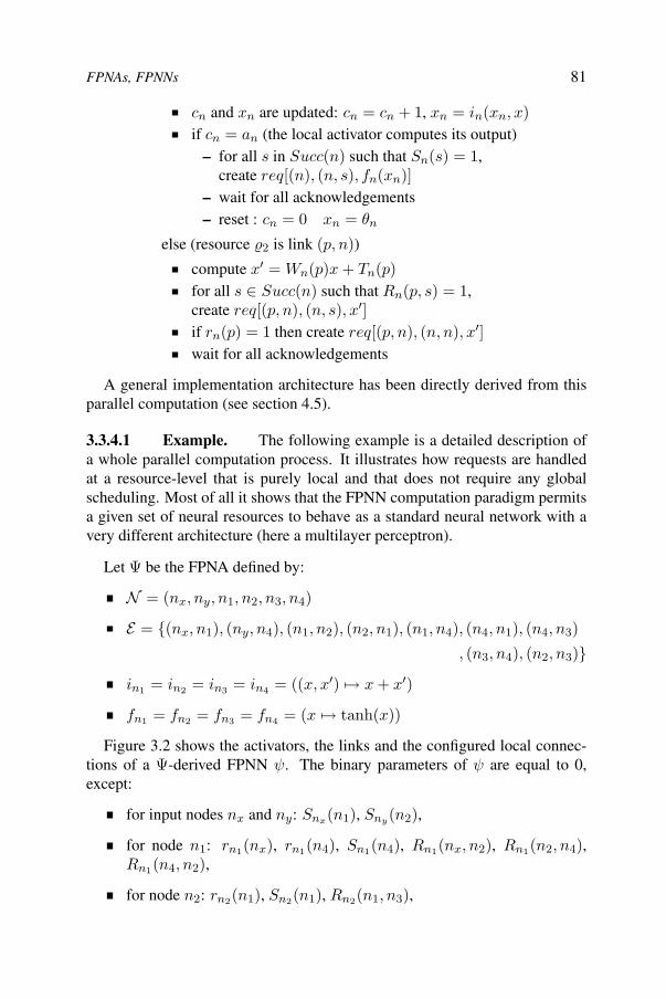
FPNAs, FPNNs 81
cn and xn are updated: cn = cn + 1, xn = in(xn, x)if cn = an (the local activator computes its output)
– for all s in Succ(n) such that Sn(s) = 1,create req[(n), (n, s), fn(xn)]
– wait for all acknowledgements– reset : cn = 0 xn = θn
else (resource �2 is link (p, n))
compute x′ = Wn(p)x + Tn(p)for all s ∈ Succ(n) such that Rn(p, s) = 1,create req[(p, n), (n, s), x′]if rn(p) = 1 then create req[(p, n), (n, n), x′]wait for all acknowledgements
A general implementation architecture has been directly derived from thisparallel computation (see section 4.5).
3.3.4.1 Example. The following example is a detailed description ofa whole parallel computation process. It illustrates how requests are handledat a resource-level that is purely local and that does not require any globalscheduling. Most of all it shows that the FPNN computation paradigm permitsa given set of neural resources to behave as a standard neural network with avery different architecture (here a multilayer perceptron).
Let Ψ be the FPNA defined by:
N = (nx, ny, n1, n2, n3, n4)
E = {(nx, n1), (ny, n4), (n1, n2), (n2, n1), (n1, n4), (n4, n1), (n4, n3)
, (n3, n4), (n2, n3)}in1 = in2 = in3 = in4 = ((x, x′) �→ x + x′)
fn1 = fn2 = fn3 = fn4 = (x �→ tanh(x))
Figure 3.2 shows the activators, the links and the configured local connec-tions of a Ψ-derived FPNN ψ. The binary parameters of ψ are equal to 0,except:
for input nodes nx and ny: Snx(n1), Sny(n2),
for node n1: rn1(nx), rn1(n4), Sn1(n4), Rn1(nx, n2), Rn1(n2, n4),Rn1(n4, n2),
for node n2: rn2(n1), Sn2(n1), Rn2(n1, n3),
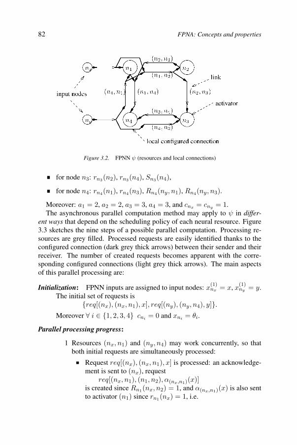
82 FPNA: Concepts and properties
Figure 3.2. FPNN ψ (resources and local connections)
for node n3: rn3(n2), rn3(n4), Sn3(n4),
for node n4: rn4(n1), rn4(n3), Rn4(ny, n1), Rn4(ny, n3).
Moreover: a1 = 2, a2 = 2, a3 = 3, a4 = 3, and cnx = cny = 1.The asynchronous parallel computation method may apply to ψ in differ-
ent ways that depend on the scheduling policy of each neural resource. Figure3.3 sketches the nine steps of a possible parallel computation. Processing re-sources are grey filled. Processed requests are easily identified thanks to theconfigured connection (dark grey thick arrows) between their sender and theirreceiver. The number of created requests becomes apparent with the corre-sponding configured connections (light grey thick arrows). The main aspectsof this parallel processing are:
Initialization: FPNN inputs are assigned to input nodes: x(1)nx = x, x
(1)ny = y.
The initial set of requests is{req[(nx), (nx, n1), x], req[(ny), (ny, n4), y]}.
Moreover ∀ i ∈ {1, 2, 3, 4} cni = 0 and xni = θi.
Parallel processing progress:
1 Resources (nx, n1) and (ny, n4) may work concurrently, so thatboth initial requests are simultaneously processed:
Request req[(nx), (nx, n1), x] is processed: an acknowledge-ment is sent to (nx), request
req[(nx, n1), (n1, n2), α(nx,n1)(x)]is created since Rn1(nx, n2) = 1, and α(nx,n1)(x) is also sentto activator (n1) since rn1(nx) = 1, i.e.
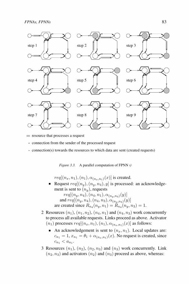
FPNAs, FPNNs 83
resource that processes a request
connection from the sender of the processed request
connection(s) towards the resources to which data are sent (created requests)
Figure 3.3. A parallel computation of FPNN ψ
req[(nx, n1), (n1), α(nx,n1)(x)] is created.Request req[(ny), (ny, n4), y] is processed: an acknowledge-ment is sent to (ny), requests
req[(ny, n4), (n4, n1), α(ny ,n4)(y)]and req[(ny, n4), (n4, n3), α(ny ,n4)(y)]
are created since Rn4(ny, n1) = Rn4(ny, n3) = 1.
2 Resources (n1), (n1, n2), (n4, n1) and (n4, n3) work concurrentlyto process all available requests. Links proceed as above. Activator(n1) processes req[(nx, n1), (n1), α(nx,n1)(x)] as follows:
An acknowledgement is sent to (nx, n1). Local updates are:cn1 = 1, xn1 = θ1 + α(nx,n1)(x). No request is created, sincecn1 < an1 .
3 Resources (n1), (n2), (n2, n3) and (n3) work concurrently. Link(n2, n3) and activators (n2) and (n3) proceed as above, whereas:
84 FPNA: Concepts and properties
req[(n4, n1), (n1), α(n4,n1)(α(ny ,n4)(y))] is processed: an ac-knowledgement is sent to (n4, n1). Local updates are: cn1 =2, xn1 = θ1 + α(nx,n1)(x) + α(n4,n1)(α(ny ,n4)(y)). Nowcn1 = an1 , so that req[(n1), (n1, n4), tanh(xn1)] is createdsince Sn1(n4) = 1. Then cn1 = 0 and xn1 = θ1.
req[(n4, n1), (n1, n2), α(n4,n1)(α(ny ,n4)(y))] is another availablerequest, but resource (n1, n2) still waits for the acknowledgementof the two requests that it created at step 2.
4 Resource (n1, n2) is now able to process its waiting request. Re-sources (n1, n4) and (n3) also work concurrently.
. . .
8. Activator (n4) chooses a request among the two ones it has re-ceived.
9. Activator (n4) processes the last request, so that cn4 = an4 . There-fore (n4) computes its output, but no request is created, since allSn4(.) binary values are ’0’. This output is
tanh(θ4 + α(n1,n4)(tanh(θ1 + α(nx,n1)(x) + α(n4,n1)(α(ny ,n4)(y))))
+ α(n1,n4)(α(n2,n1)(tanh(θ2 + α(n1,n2)(α(nx,n1)(x))+ α(n1,n2)(α(n4,n1)(α(ny ,n4)(y))))))
+ α(n3,n4)(tanh(θ3 + α(n2,n3)(α(n1,n2)(α(nx,n1)(x)))+ α(n2,n3)(α(n1,n2)(α(n4,n1)(α(ny ,n4)(y))))
+ α(n4,n3)(α(ny ,n4)(y)))))
The above result is exactly the same as with the MLP in Figure 3.4, providedthat:
all coefficients Tn(p) are equal to 0,
the compositions of link weights (virtual synaptic weights) are equalto the weights of Figure 3.4, which implies for example that w2,2 =Wn2(n1)Wn1(n4)Wn4(ny)
and w3,2 = (Wn3(n2)Wn2(n1)Wn1(n4) + Wn3(n4)) Wn4(ny).
As mentioned above, this example shows that the FPNA computation par-adigm permits a given set of neural resources to behave as a standard neuralnetwork with a very different architecture. Nevertheless, this FPNN is not use-ful: the architecture of Figure 3.2 does not simplify the MLP architecture ofFigure 3.4. Indeed, this MLP is so simple that it is neither possible nor nec-essary to expect any architecture simplification. Some examples of significantsimplifications of larger neural networks are described in 4.3.
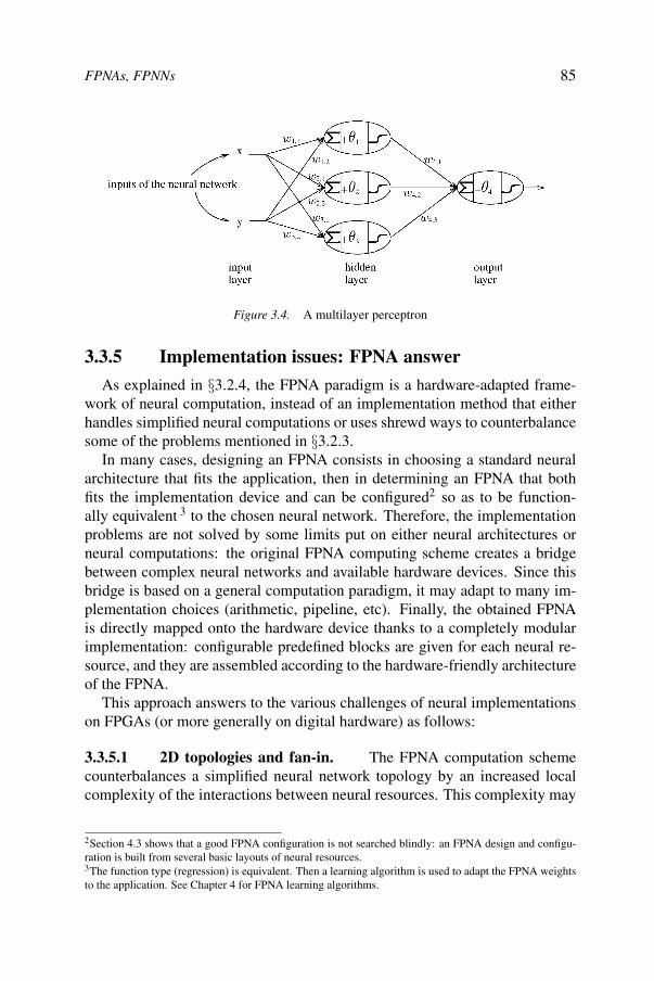
FPNAs, FPNNs 85
Figure 3.4. A multilayer perceptron
3.3.5 Implementation issues: FPNA answer
As explained in §3.2.4, the FPNA paradigm is a hardware-adapted frame-work of neural computation, instead of an implementation method that eitherhandles simplified neural computations or uses shrewd ways to counterbalancesome of the problems mentioned in §3.2.3.
In many cases, designing an FPNA consists in choosing a standard neuralarchitecture that fits the application, then in determining an FPNA that bothfits the implementation device and can be configured2 so as to be function-ally equivalent 3 to the chosen neural network. Therefore, the implementationproblems are not solved by some limits put on either neural architectures orneural computations: the original FPNA computing scheme creates a bridgebetween complex neural networks and available hardware devices. Since thisbridge is based on a general computation paradigm, it may adapt to many im-plementation choices (arithmetic, pipeline, etc). Finally, the obtained FPNAis directly mapped onto the hardware device thanks to a completely modularimplementation: configurable predefined blocks are given for each neural re-source, and they are assembled according to the hardware-friendly architectureof the FPNA.
This approach answers to the various challenges of neural implementationson FPGAs (or more generally on digital hardware) as follows:
3.3.5.1 2D topologies and fan-in. The FPNA computation schemecounterbalances a simplified neural network topology by an increased localcomplexity of the interactions between neural resources. This complexity may
2Section 4.3 shows that a good FPNA configuration is not searched blindly: an FPNA design and configu-ration is built from several basic layouts of neural resources.3The function type (regression) is equivalent. Then a learning algorithm is used to adapt the FPNA weightsto the application. See Chapter 4 for FPNA learning algorithms.
86 FPNA: Concepts and properties
be tuned so as to make the simplified topology fit the hardware: a compro-mise must be found, since FPNA learning becomes more difficult when thecomplexity of the local configured connections increases (see Chapter 4.
3.3.5.2 Area-greedy operators. FPNAs use the same operators asstandard neural networks, but a simplified topology is related to a reducednumber of such operators, so that area and interconnection problems are si-multaneously solved.
3.3.5.3 Weight storage and time/area imbalance. The FPNA compu-tation paradigm creates numerous virtual connections despite a reduced num-ber of links. Therefore, topology simplifications mostly result in less links, i.e.less weights and multipliers. Moreover each weight is simultaneously used indifferent ways to create the virtual connections, so that FPNA computationsresult in a reduced share of the overall computation time for the input-weightmultiplications.
3.4 Correctness
The aim of this section is to mention the various properties that have beenestablished about FPNN computations so as to justify their correctness.
3.4.1 Feedforward FPNNs
A FPNN is feedforward if the local configured connections between re-sources do not infer any cyclical dependency. Therefore an FPNN may befeedforward even if its underlying FPNA uses a cyclical graph. Two formal de-finitions express this. The fisrt one defines the dependency graph of an FPNN:the nodes are the neural resources (links and activators) and the edges corre-spond to the configured local connections.
Definition 1 Let φ ={N , E , (θn, in, fn, Wn, Tn, an, Rn, rn, Sn)n∈N
}be
an FPNN. Its dependency graph GD(φ) = (N ′, E ′) is defined by:
N ′ = E ∪ {(n) | n ∈ N}E ′ = {((p, n), (n, s)) | Rn(p, s) = 1} ∪ {((p, n), (n)) | rn(p) = 1}
∪ {((n), (n, s)) | Sn(s) = 1}Indeed, the computation scheme of an FPNN follows the oriented edges of
its dependency graph. Therefore:
Definition 2 Let φ be an FPNN. It is feedforward iff GD(φ) does not in-clude any cycle.
Correctness 87
3.4.1.1 Correctness of the asynchronous sequential computation.The above computation algorithms (sequential and parallel) appear as quitedifefrent, and they are based on local processings. The first question is whetherthey define a global behaviour for the whole FPNN. This correctness problemmay be expressed as follows: do the asynchronous sequential and parallel com-putations halt ?
A first simple result answers this question as far as the asynchronous se-quential computation is concerned:
Theorem 3.1 If φ is a feedforward FPNN, then its asynchronous sequentialcomputation halts.
The proof is straightforward, since the task generation process is locally finite,and follows the oriented edges of GD(φ). See [21] for more details.
3.4.1.2 Deadlock in the asynchronous parallel computation. Thecase of the asynchronous parallel computation is a bit more complicated. Itis linked with, but not equivalent to, the notion of deadlock. Though this no-tion is rather standard when studying distributed communication protocols, itmust be first defined for the above parallel algorithm. The following definitiondescribes a deadlock situation as a “cycle” of waiting requests.
Definition 3 A FPNN is said to be in deadlock conditions during its asyn-chronous parallel computation if there exist resources �0, . . . , �p such thateach �i is processing a request, and if this processing may not halt un-less �i+1 terminates the request processing it is performing (considering that�p+1 = �0).
Then a rather simple result ensures that the asynchronous parallel computa-tion applies to feedforward FPNNs without deadlock.
Theorem 3.2 If φ is a feedforward FPNN, then it may not be in deadlockconditions during its asynchronous parallel computation.
The proof is easy. It is based on an equivalence between deadlock condi-tions and the existence of a cycle in a subgraph of GD(φ) (graph inferred bysimultaneously processed requests). See [21] for more details.
3.4.1.3 Conditions of parallel non-termination. The main result isthe relation between deadlock conditions and non-termination. It ensures thatdeadlock is the only possible cause of non-termination.
Theorem 3.3 If φ is an FPNN whose asynchronous sequential computationhalts, then its asynchronous parallel computation does not halt if and only if itis in deadlock conditions.
88 FPNA: Concepts and properties
sufficient condition: obvious (see definition 3)necessary condition (proof outline, see [21] for full details):1. The set of requests may be partially ordered.2. The number of requests is finite (there exists an injection towards the set
of sequential tasks).3. There is a request whose processing does not halt.4. A deadlock cycle may be built in the set of direct and indirect successors
of a non-terminating request.
A straightforward consequence is that both asynchronous sequential andparallel computations of a feedforward FPNN halt. Moreover the study of [21]shows how simple conditions ensure that all defined computation methods areequivalent and deterministic (see Chapter 4).
3.4.2 Recurrent FPNNs: synchronized computations
The above computation schemes can not satisfactorily handle recurrentFPNNs. Nevertheles only slight changes are required. In a synchronized FPNNcomputation, synchronisation barriers are used in order to separate the strictsending of neural output values from the simple direct value transmissions be-tween connected links. It provides a correct recurrent computation, providedthat there is no loop in the direct connections between the links.
At a given moment, the requests are processed as above, except for anyvalue sent by an activator. Such a request is put in a waiting list, without beingprocessed. When a new synchronization barrier is raised, all waiting requestsare set active, so that their processing may start.
Similar correctness results are available (Theorem 3.2 may be extended torecurrent FPNNs under some obvious conditions).
3.5 Underparameterized convolutions by FPNNs
The aim of this section is to study the computational power of FPNNs.As shown in [21], it is always possible to define an FPNN that exactly com-
putes the same function as any standard neural network. But this FPNN may beas complex as the desired neural network. Therefore, it should be known whichfunctions may be computed by hardware-friendly FPNNs. This question leadsto the idea of underparameterized convolutions.
This section is organized as follows:
§3.5.1 is a necessary reminder of some links between neural computationand convolution,
§3.5.2 briefly explains how FPNN computation leads to underparame-terized convolutions,
Underparameterized convolutions by FPNNs 89
§3.5.3 gives two opposite examples to show that this underparameteri-zation may be fully overcome in some cases, whereas it is a strict theo-retical limit in some other cases; the special case of grid-based layeredFPNNs is studied, since underparameterization may be put in equationsin this case,
§3.5.4 briefly explains that the influence of underparameterization onFPNN practical utility deserves an experimental study (that is providedin sections §4.3 and §4.4),
§3.5.5 describes how the above study of the underparameterization con-volution that is performed by FPNNs leads to a theoretically justifiedmethod for FPNN weight initialization.
3.5.1 Partial convolutions by neural networks
Feedforward neural models are often justified by their approximation capa-bilities as non-linear regression tools, since [16, 36, 35]. This regression is per-formed by means of discrete frequential convolutions based on neuron transferfunctions. Such convolutions clearly appear in several works that study mod-els with localized neural functions: for example [52] for RBF networks (radialbasis function), or [71] for wavelet networks (which directly derive from thereversibility of convolution with wavelets). Convolution is more hidden for themost standard feedforward neural model, called multilayer perceptrons (MLP).Each neuron in a layer of a MLP applies a sigmoidal transfer function σ to aweighted sum of the outputs of all neurons in the previous layer:
In [16], the universal approximation property is built with two main ar-guments:
1 Let Ψ(x) = σ(
xδ + α
)− σ(
xδ − α
), where (δ, α) ∈ IR2. A func-
tion f may be approximated by the reverse transform of a discretefrequential convolution function, in which a vectorial form of Ψconvolutes Fourier transform f . This convolution function must beestimated at several convolution points, so as to build the reversetransform. And each estimation uses multiple convolution termsthat are computed at each point of a fine-grain covering of a com-pact frequency domain.
2 The hidden weights give a set of points that cover this frequencydomain, whereas the output weights are set by means of the valuesof f at each of these points.
The second argument directly derives from the multilayer architectureand its ability to map a fine n-dimensional mesh onto the frequency do-
90 FPNA: Concepts and properties
main. It explains why the work lies in the proof that a reversible trans-form may be built on a sigmoidal function.
The convolution is still more hidden in [36], which is often taken as thebasic reference for MLP universal approximation. The property is a con-sequence of the Stone-Weierstrass Theorem (sigmoid properties make itpossible to go without some of its hypotheses). Yet it may be noted thatthis standard theorem refers to a covering by low-diameter balls. And thestrong hypotheses of Stone-Weierstrass Theorem are bypassed thanks tothe approximation of trigonometric polynomials by sigmoids. Thereforediscrete frequential convolutions re-emerge.
To simplify, an expected function in a space domain is obtained thanks toa reverse transform of its frequential form. Neuron transfer functions create abase of localized functions in a compact frequency domain. Convolutions areperformed to get the projection. Let w and t be the multiplying parameters andthe additive parameters of a hidden neuron (in a MLP, w is the weight vector,whereas t is reduced to the threshold). Then w may be seen as a frequencyvector involved in one discrete frequential convolution, whereas t expressesthe corresponding convolution point (indirectly, since the convoluting functiondepends on the neural network input vector). The output weight that applies tothis neuron depends on both t and the frequential value of f at w.
Concrete neural applications only require a limited precision approximation,so that only few convolution terms are used (several ones instead of vd for eachconvolution point, where d is the input space dimension and v is inverselyproportional to the expected precision).
3.5.2 Underparameterized partial convolutions
FPNNs are also defined to compute such partial convolutions for non- lin-ear regression, though their architecture is simplified with respect to standardneural models. The FPNN definition permits to connect any link to any localresource. Locality permits simplified topologies, whereas connected links re-sult in more various frequency vectors: direct connections between affine linksappear, so that the FPNN may compute numerous composite affine transforms(virtual neural connections). Therefore different convolution terms may be ob-tained with a reduced number of connection weights (underparameterization).
Though various, the weights of the virtual connections are not independentof each other. The complex induced dependencies are studied in [21]. Theyimply that the computational power of an FPNN with k neural resources andK virtual connections is lying between the computational power of a standardneural network with k neural operators and the computational power of a stan-dard neural network with k + K neural operators. Next subsection illustratesthis intermediate situation through two opposite results: a first example shows
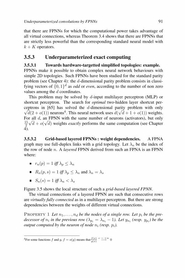
Underparameterized convolutions by FPNNs 91
that there are FPNNs for which the computational power takes advantage ofall virtual connections, whereas Theorem 3.4 shows that there are FPNNs thatare strictly less powerful than the corresponding standard neural model withk + K operators.
3.5.3 Underparameterized exact computing
3.5.3.1 Towards hardware-targetted simplified topologies: example.FPNNs make it possible to obtain complex neural network behaviours withsimple 2D topologies. Such FPNNs have been studied for the standard parityproblem (see Chapter 4): the d-dimensional parity problem consists in classi-fying vectors of {0, 1}d as odd or even, according to the number of non zerovalues among the d coordinates.
This problem may be solved by d-input multilayer perceptron (MLP) orshortcut perceptron. The search for optimal two-hidden layer shortcut per-ceptrons in [65] has solved the d-dimensional parity problem with only√
d(2 + o(1)) neurons4. This neural network uses d(√
d + 1 + o(1)) weights.For all d, an FPNN with the same number of neurons (activators), but only152
√d + o(
√d) weights exactly performs the same computation (see Chapter
4).
3.5.3.2 Grid-based layered FPNNs : weight dependencies. A FPNAgraph may use full-duplex links with a grid topology. Let λn be the index ofthe row of node n. A layered FPNN derived from such an FPNA is an FPNNwhere:
rn(p) = 1 iff λp ≤ λn
Rn(p, s) = 1 iff λp ≤ λn and λn = λs
Sn(s) = 1 iff λn < λs
Figure 3.5 shows the local structure of such a grid-based layered FPNN.The virtual connections of a layered FPNN are such that consecutive rows
are virtually fully connected as in a multilayer perceptron. But there are strongdependencies between the weights of different virtual connections.
Property 1 Let n1, . . . , nd be the nodes of a single row. Let pi be the pre-decessor of ni in the previous row (λpi = λni − 1). Let yni (resp. ypi) be theoutput computed by the neuron of node ni (resp. pi).
4For some functions f and g, f = o(g) means that f(x)g(x)
x → +∞−→ 0
92 FPNA: Concepts and properties
Figure 3.5. Node of a grid-based layered FPNN
Computing virtual connection weights shows that if 1 ≤ i < j < k ≤ dthen:
∂yni
∂ypk
=Wnk
(pk)Wnj (pj)
k−1∏k=j
Wnk(nk+1)
(∂yni
∂ypj
)Therefore, if all the FPNN weights are fixed, then for all i, 1 ≤ i < d andfor all real values yp1 , . . . , ypi , the function (ypi+1 , . . . , ypd
) �→ (yn1 , . . . , yni)defines an arc from IRd−i into IRi.
This result is an example of the strong dependencies that may exist betweenthe different points where an FPNN virtually estimates the terms of a partialconvolution (each yni is a convolution term computed at (yp1 , . . . , ypd
)). Sec-tion 4.3 shows in what way these dependencies influence FPNNs, and howthis unfavourable result has led to the definition of a specific way to set FPNNweights.
3.5.3.3 Shortcut FPNNs. Standard neural models may be used as FP-NAs (so that each neuron and its input and output connections become freelyconnectable). And any standard neural network can be exactly simulated byan FPNN based on the FPNA form of this neural network. For example, onecan use the multilayer topology of a one hidden-layer MLP to build an FPNA,and then set a derived FPNN that computes the same function as the originalMLP. To obtain this, there must be no direct configured connection betweentwo different links, that is Rn(p, s) = 0. If some Rn(p, s) values are set to 1,virtual shortcut connections are obtained between the input and output neurallayers. Such FPNNs may then be called one-hidden layer shortcut FPNNs.Examples can be given in which these FPNNs can solve specific tasks that noone-hidden layer MLP can solve with the same number of neurons. No con-clusive result has been obtained when comparing a one-hidden layer shortcut
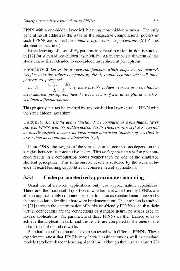
Underparameterized convolutions by FPNNs 93
FPNN with a one-hidden layer MLP having more hidden neurons. The onlygeneral result addresses the issue of the respective computational powers ofsuch FPNNs and of real one- hidden layer shortcut perceptrons (MLP plusshortcut connections).
Exact learning of a set of Np patterns in general position in IRdi is studiedin [12] for standard one-hidden layer MLPs. An intermediate theorem of thisstudy can be first extended to one-hidden layer shortcut perceptrons:
Property 2 Let F be a vectorial function which maps neural networkweights onto the values computed by the do output neurons when all inputpatterns are presented.
Let Nh =do(Np − di)
di + do. If there are Nh hidden neurons in a one-hidden
layer shortcut perceptron, then there is a vector of neural weights at which Fis a local diffeomorphism.
This property can not be reached by any one-hidden layer shortcut FPNN withthe same hidden layer size:
Theorem 3.4 Let the above function F be computed by a one-hidden layershortcut FPNN, with Nh hidden nodes. Sard’s Theorem proves that F can notbe locally surjective, since its input space dimension (number of weights) islower than its output space dimension Npdo.
In an FPNN, the weights of the virtual shortcut connections depend on theweights between its consecutive layers. This underparameterization phenom-enon results in a computation power weaker than the one of the simulatedshortcut perceptron. This unfavourable result is softened by the weak influ-ence of exact learning capabilities in concrete neural applications.
3.5.4 Underparameterized approximate computing
Usual neural network applications only use approximation capabilities.Therefore, the most useful question is whether hardware-friendly FPNNs areable to approximately compute the same function as standard neural networksthat are too large for direct hardware implementation. This problem is studiedin [21] through the determination of hardware-friendly FPNNs such that theirvirtual connections are the connections of standard neural networks used inseveral applications. The parameters of these FPNNs are then learned so as toachieve the application task, and the results are compared to the ones of theinitial standard neural networks.
Standard neural benchmarks have been tested with different FPNNs. Theseexperiments attest that FPNNs may learn classifications as well as standardmodels (gradient descent learning algorithm), although they use an almost 2D
94 FPNA: Concepts and properties
underlying topology and 4 to 10 times less resources than the equivalent stan-dard neural networks.
Chapter 4 will describe such experiments (for example based on the diabetesclassification problem). It will also show how the hardware-friendly architec-ture of the obtained FPNNs leads to efficient FPGA-based implementationsthat the equivalent standard neural models do not permit.
3.5.5 Weight initialization
As mentioned in §3.5.1, too many weights and neurons would be necessaryfor a neural network to perform full discrete convolutions. Choosing a goodscattering of weight vectors seems quite natural, when approximation must beperformed with a limited number of neurons. But such a good scattering is abasic property of the independent weights of standard neural models. There-fore evolved weight initialization methods focus on the adequacy of neuralnetwork parameters and input patterns (usual solutions listed in [5]). Additiveparameters are essential in such methods (biases, translation vectors, . . . etc),particularly when localized transfer functions are used (these parameters arescattered in a convex hull defined by expected inputs). FPNA constraints donot concern additive parameters, but only multiplying ones.
FPNN virtual weights can not be individually set. Weight dependenciesdescribed in §3.5.3 might lead to bad classification applications. To obtainlow precision approximations, FPNN should first be able to approximate thelow-band components of expected functions5. Convolution terms reduce to asatisfactory covering of a reduced frequency domain. This approach does notdepend on the input patterns. It simultaneously considers all weight vectors,so that it better adapts to FPNNs.
This subsection shows how weight vector scattering can be controlled, andwhat influence it has on concrete applications. The first question is to knowwhether FPNNs are able to obtain well scattered virtual convolution terms.
3.5.5.1 Convolution point scattering for FPNNs. In order to estimatethe scattering of the convolution terms that correspond to the virtual connec-tions of an FPNN, the frequency domain is partitioned into as many distinctzones as there are convolution terms, with a Voronoi partition based on theeuclidean distance. Scattering may be measured by the maximum zone diam-eter (other criteria have been studied with similar conclusions).
The special case of a grid-based layered FPNN (see §3.5.3) is studied withthis criterion. It corresponds to d convolution points in a d-dimensional space.
5Low-frequency components in a frequential decomposition give the main frame of a signal.
Underparameterized convolutions by FPNNs 95
The ratio of the number of virtual connections to the number of links used bysuch FPNNs is d
36.
An optimal scattering may be estimated as the expected mean value of thechosen criterion when using a random drawing of d points uniformly distrib-uted in the frequency domain: it corresponds to the independent weights of astandard neural network. A similar random drawing of FPNN weights leadsto a bad scattering. As mentioned in §3.5.3, virtual weight dependencies inFPNNs are mostly linked to multiplications of Wn(p) parameters. A randomvariable w is computed so that its distribution function is as stable as possiblewhen multiplication is applied. Let v1 and v2 be two uniformly distributedrandom variables. Then w is defined as
h
(12
+15
√−2 ln(v1) cos(2πv2)
)where h(x) = x+1
2−x . The probability density of w is
ρ(x)dx =∫ x+dx
x
[N (
12,15)]
(h−1(u))[h−1]′(u)du
15(1 + x)2
√2π
e− 1
2
(15(x−1)2(x+1)
)2
dx
so that
The fulfilled relation xρ(x) = 1xρ( 1
x) implies that the expected meanvalue of w keeps unchanged by random variable multiplication.
The use of the normal random variable ensures that the standard devia-tion of a product of w variables keeps reduced.
The FPNN weights are then set with a random drawing of w, to which an affinetransform is applied to fit the desired range. Figure 3.6 shows the ratio of thecriterion mean value in the optimal case to the mean value that is observed forFPNN virtual convolutions.
3.5.5.2 Scattering and learning. The above w-based method has beenused for random initialization of FPNN weights. It mostly improve conver-gence times, as illustrated in §4.3.1.
On the other hand, one can wonder whether the learning process increasesvirtual weight dependencies or not: the gradient computation in an FPNN de-pends on a much larger equivalent neural structure that widely uses weight
6d2 connections between two fully connected layers of d neurons, about 3d links in a grid-based layeredFPNA architecture.
96 FPNA: Concepts and properties
Figure 3.6. Convolution point scattering of grid-based layered FPNNs
sharing, so that the dependencies between the partial differentials appear evenstronger (dependencies are back-propagated through the layers). And yet§4.3.1 shows how scattering improves during learning. This improvement iseven greater with a w-based initialization method.
3.6 Conclusions
Connectionist models, such as neural networks, are the first models of paral-lel computing. This approach of neural computation has been penalized by itsunfitness for the characteristics of usual parallel devices. Neural network hard-ware implementations have to reconcile simple hardware topologies with oftencomplex neural architectures. Field Programmable Neural Arrays have beendefined for that. Their computation scheme creates numerous virtual neuralconnections by means of a limited set of links, whatever the device, the arith-metic, and the neural structure. The FPNA computation paradigm thus makesit possible to define neural models which performance is similar to standardneural models despite simplified architectures.
The FPNA framework is a neural computation paradigm that has been de-fined in order to fit direct digital hardware implementations. It has given riseto a complete theoretical model for topologically constrained neural computa-tion. In this Chapter, FPNAs and FPNNs have been formally defined. Theircomputation has been described and justified. Their main limitation has beenidentified as an underparameterization of the frequency vectors that are used
97
in approximate convolutions. Possible unfavourable theoretical consequenceshave been pointed out. They indicate that FPNA weights deserve a specific ap-proach. Applications take advantage of adequate FPNA weight distributions,especially in terms of convergence time. Such applications, as well as some oftheir implementations, are presented in Chapter 4.
References
[1] D. Abramson, K. Smith, P. Logothetis, and D. Duke. FPGA based imple-mentation of a hopfield neural network for solving constraint satisfactionproblems. In Proc. EuroMicro, 1998.
[2] D. Anguita, S. Bencetti, A. De Gloria, G. Parodi, D. Ricci, and S. Ridella.FPGA implementation of high precision feedforward networks. In Proc.MicroNeuro, pages 240–243, 1997.
[3] N. Avellana, A. Strey, R. Holgado, A. Fern„andez, R. Capillas, andE. Valderrama. Design of a low-cost and high-speed neurocomputer sys-tem. In Proc. MicroNeuro, pages 221–226, 1996.
[4] S.L. Bade and B.L. Hutchings. FPGA-based stochastic neural networks- implementation. In Proceedings of the IEEE Workshop on FPGAs forCustom Computing Machines, pages 189–198, 1994.
[5] R. Baron and B. Girau. Parameterized normalization : application towavelet networks. In Proc. IJCNN, volume 2, pages 1433–1437. IEEE,1998.
[6] J.-L. Beuchat. Conception d’un neuroprocesseur reconfigurable pro-posant des algorithmes d’apprentissage et d’«elagage: une premi„ere «etude.In Proc. NSI Neurosciences et Sciences de l’Ing«enieur, 1998.
[7] Y. Boniface. A parallel simulator to build distributed neural algorithms.In International Joint Conference on Neural Networks - IJCNN’01, Wash-ington, USA, 2001.
[8] N.M. Botros and M. Abdul-Aziz. Hardware implementation of an artifi-cial neural network. In Proc. ICNN, volume 3, pages 1252–1257, 1993.
[9] Y.K. Choi, K.H. Ahn, and S.-Y. Lee. Effects of multiplier output offsetson on-chip learning for analog neuro-chips. Neural Processing Letters,4:1–8, 1996.
[10] V.F. Cimpu. Hardware FPGA implementation of a neural network. InProc. Int. Conf. Technical Informatics, volume 2, pages 57–68, 1996.
[11] J.G. Eldredge and B.L. Hutchings. RRANN: a hardware implementationof the backpropagation algorithm using reconfigurable FPGAs. In Pro-ceedings of the IEEE World Conference on Computational Intelligence,1994.
References
98 FPNA: Concepts and properties
[12] A. Elisseeff and H. Paugam-Moisy. Size of multilayer networks for exactlearning: analytic approach. Technical Report 96-16, LIP-ENSL, 1996.
[13] W. Eppler, T. Fisher, H. Gemmeke, T. Becher, and G. Kock. High speedneural network chip on PCI-board. In Proc. MicroNeuro, pages 9–17,1997.
[14] S.K. Foo, P. Saratchandran, and N. Sundararajan. Parallel implemen-tation of backpropagation neural networks on a heterogeneous array oftransputers. IEEE Trans. on Systems, Man, and Cybernetics–Part B: Cy-bernetics, 27(1):118–126, 1997.
[15] D. Franco and L. Carro. FPGA architecture comparison for non-conventional signal processing. In Proc. IJCNN, 2000.
[16] K.-I. Funahashi. On the approximate realization of continuous mappingsby neural networks. Neural Networks, 2:183–192, 1989.
[17] R. Gadea, J. Cerda, F. Ballester, and A. Mocholi. Artificial neural net-work implementation on a single FPGA of a pipelined on-line backprop-agation. In Proc. ISSS, pages 225–230, 2000.
[18] C. G«egout, B. Girau, and F. Rossi. A general feedforward neural networkmodel. Technical report NC-TR-95-041, NeuroCOLT, Royal Holloway,University of London, 1995.
[19] C. G«egout, B. Girau, and F. Rossi. Generic back-propagation in arbi-trary feedforward neural networks. In Artificial Neural Nets and GeneticAlgorithms – Proc. of ICANNGA, pages 168–171. Springer-Verlag, 1995.
[20] B. Girau. Dependencies of composite connections in Field ProgrammableNeural Arrays. Research report NC-TR-99-047, NeuroCOLT, Royal Hol-loway, University of London, 1999.
[21] B. Girau. Du parall«elisme des mod„eles connexionnistes „a leur implanta-tion parall„ele. PhD thesis n◦ 99ENSL0116, ENS Lyon, 1999.
[22] B. Girau. Building a 2D-compatible multilayer neural network. In Proc.IJCNN. IEEE, 2000.
[23] B. Girau. Conciliating connectionism and parallel digital hardware. Par-allel and Distributed Computing Practices, special issue on Unconven-tional parallel architectures, 3(2):291–307, 2000.
[24] B. Girau. Digital hardware implementation of 2D compatible neural net-works. In Proc. IJCNN. IEEE, 2000.
[25] B. Girau. FPNA: interaction between FPGA and neural computation. Int.Journal on Neural Systems, 10(3):243–259, 2000.
[26] B. Girau. Neural networks on FPGAs: a survey. In Proc. Neural Compu-tation, 2000.
99
[27] B. Girau. Simplified neural architectures for symmetric boolean func-tions. In Proc. ESANN European Symposium on Artificial Neural Net-works, pages 383–388, 2000.
[28] B. Girau. On-chip learning of FPGA-inspired neural nets. In Proc.IJCNN. IEEE, 2001.
[29] B. Girau and A. Tisserand. MLP computing and learning on FPGA usingon-line arithmetic. Int. Journal on System Research and Information Sci-ence, special issue on Parallel and Distributed Systems for Neural Com-puting, 9(2-4), 2000.
[30] C. Grassmann and J.K. Anlauf. Fast digital simulation of spiking neuralnetworks and neuromorphic integration with spikelab. InternationalJournal of Neural Systems, 9(5):473–478, 1999.
[31] M. Gschwind, V. Salapura, and O. Maisch berger. A generic buildingblock for Hopfield neural networks with on-chip learning. In Proc. IS-CAS, 1996.
[32] H. Hikawa. Frequency-based multilayer neural network with on-chiplearning and enhanced neuron characteristics. IEEE Trans. on NeuralNetworks, 10(3):545–553, 1999.
[33] R. Hoffmann, H.F. Restrepo, A. Perez-Uribe, C. Teuscher, andE. Sanchez. Implémentation d’un réseau de neurones sur un réseau defpga. In Proc. Sympa’6, 2000.
[34] P.W. Hollis, J.S. Harper, and J.J. Paulos. The effects of precision con-straints in a backpropagation learning algorithm. Neural Computation,2:363–373, 1990.
[35] K. Hornik. Approximation capabilities of multilayer feedforward net-works. Neural Networks, 4:251–257, 1991.
[36] K. Hornik, M. Stinchcombe, and H. White. Multilayer feedforward net-works are universal approximators. Neural Networks, 2:359–366, 1989.
[37] N. Izeboudjen, A. Farah, S. Titri, and H. Boumeridja. Digital implemen-tation of artificial neural networks: From VHDL description to FPGAimplementation. In Proc. IWANN, 1999.
[38] A. Johannet, L. Personnaz, G. Dreyfus, J.D. Gascuel, and M. Weinfeld.Specification and implementation of a digital Hopfield-type associativememory with on-chip training. IEEE Trans. on Neural Networks, 3, 1992.
[39] J. Kennedy and J. Austin. A parallel architecture for binary neural net-works. In Proc. MicroNeuro, pages 225–231, 1997.
[40] K. Kollmann, K. Riemschneider, and H.C. Zeidler. On-chip backpropa-gation training using parallel stochastic bit streams. In Proc. MicroNeuro,pages 149–156, 1996.
References
100 FPNA: Concepts and properties
[41] A. Kramer. Array-based analog computation: principles, advantages andlimitations. In Proc. MicroNeuro, pages 68–79, 1996.
[42] V. Kumar, S. Shekhar, and M.B. Amin. A scalable parallel formulation ofthe back-propagation algorithm for hypercubes and related architectures.IEEE Transactions on Parallel and Distributed Systems, 5(10):1073–1090, October 1994.
[43] P. Lysaght, J. Stockwood, J. Law, and D. Girma. Artificial neural networkimplementation on a fine-grained FPGA. In Proc. FPL, pages 421–432,1994.
[44] Y. Maeda and T. Tada. FPGA implementation of a pulse density neuralnetwork using simultaneous perturbation. In Proc. IJCNN, 2000.
[45] S. McLoone and G.W. Irwin. Fast parallel off-line training of multilayerperceptrons. IEEE Trans. on Neural Networks, 8(3):646–653, 1997.
[46] I. Milosavlevich, B. Flower, and M. Jabri. PANNE: a parallel computingengine for connectionist simulation. In Proc. MicroNeuro, pages 363–368, 1996.
[47] P.D. Moerland and E. Fiesler. Hardware-friendly learning algorithms forneural networks: an overview. In Proc. MicroNeuro, 1996.
[48] A. Montalvo, R. Gyurcsik, and J. Paulos. Towards a general-purpose ana-log VLSI neural network with on-chip learning. IEEE Trans. on NeuralNetworks, 8(2):413–423, 1997.
[49] U.A. M-uller, A. Gunzinger, and W. Guggenb-uhl. Fast neural net sim-ulation with a DSP processor array. IEEE Trans. on Neural Networks,6(1):203–213, 1995.
[50] T. Nordstr-om and B. Svensson. Using and designing massively parallelcomputers for artificial neural networks. Journal of Parallel and Distrib-uted Computing, 14(3):260–285, 1992.
[51] R. -Ostermark. A flexible multicomputer algorithm for artificial neuralnetworks. Neural Networks, 9(1):169–178, 1996.
[52] J. Park and I.W. Sandberg. Universal approximation using radial-basis-function networks. Neural Computation, 3:246–257, 1991.
[53] H. Paugam-Moisy. Optimal speedup conditions for a parallel back-propagation algorithm. In CONPAR, pages 719–724, 1992.
[54] A. P«erez-Uribe and E. Sanchez. FPGA implementation of an adaptable-size neural network. In Proc. ICANN. Springer-Verlag, 1996.
[55] A. P«etrowski. Choosing among several parallel implementations of thebackpropagation algorithm. In Proc. ICNN, pages 1981–1986, 1994.
[56] M. Rossmann, A. B-uhlmeier, G. Manteuffel, and K. Goser. short- andlong-term dynamics in a stochastic pulse stream neuron implemented inFPGA. In Proc. ICANN, LNCS, 1997.
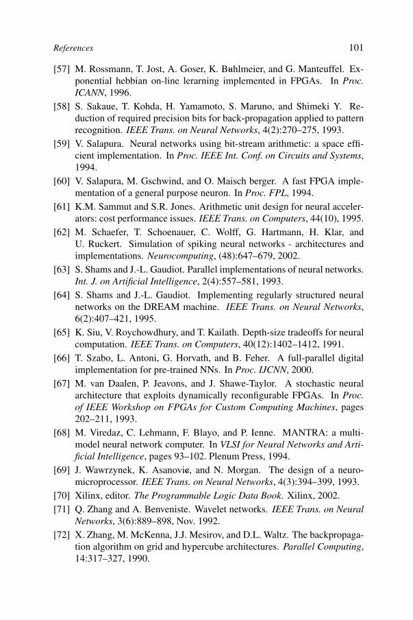
101
[57] M. Rossmann, T. Jost, A. Goser, K. B-uhlmeier, and G. Manteuffel. Ex-ponential hebbian on-line lerarning implemented in FPGAs. In Proc.ICANN, 1996.
[58] S. Sakaue, T. Kohda, H. Yamamoto, S. Maruno, and Shimeki Y. Re-duction of required precision bits for back-propagation applied to patternrecognition. IEEE Trans. on Neural Networks, 4(2):270–275, 1993.
[59] V. Salapura. Neural networks using bit-stream arithmetic: a space effi-cient implementation. In Proc. IEEE Int. Conf. on Circuits and Systems,1994.
[60] V. Salapura, M. Gschwind, and O. Maisch berger. A fast FPGA imple-mentation of a general purpose neuron. In Proc. FPL, 1994.
[61] K.M. Sammut and S.R. Jones. Arithmetic unit design for neural acceler-ators: cost performance issues. IEEE Trans. on Computers, 44(10), 1995.
[62] M. Schaefer, T. Schoenauer, C. Wolff, G. Hartmann, H. Klar, andU. Ruckert. Simulation of spiking neural networks - architectures andimplementations. Neurocomputing, (48):647–679, 2002.
[63] S. Shams and J.-L. Gaudiot. Parallel implementations of neural networks.Int. J. on Artificial Intelligence, 2(4):557–581, 1993.
[64] S. Shams and J.-L. Gaudiot. Implementing regularly structured neuralnetworks on the DREAM machine. IEEE Trans. on Neural Networks,6(2):407–421, 1995.
[65] K. Siu, V. Roychowdhury, and T. Kailath. Depth-size tradeoffs for neuralcomputation. IEEE Trans. on Computers, 40(12):1402–1412, 1991.
[66] T. Szabo, L. Antoni, G. Horvath, and B. Feher. A full-parallel digitalimplementation for pre-trained NNs. In Proc. IJCNN, 2000.
[67] M. van Daalen, P. Jeavons, and J. Shawe-Taylor. A stochastic neuralarchitecture that exploits dynamically reconfigurable FPGAs. In Proc.of IEEE Workshop on FPGAs for Custom Computing Machines, pages202–211, 1993.
[68] M. Viredaz, C. Lehmann, F. Blayo, and P. Ienne. MANTRA: a multi-model neural network computer. In VLSI for Neural Networks and Arti-ficial Intelligence, pages 93–102. Plenum Press, 1994.
[69] J. Wawrzynek, K. Asanovi«c, and N. Morgan. The design of a neuro-microprocessor. IEEE Trans. on Neural Networks, 4(3):394–399, 1993.
[70] Xilinx, editor. The Programmable Logic Data Book. Xilinx, 2002.[71] Q. Zhang and A. Benveniste. Wavelet networks. IEEE Trans. on Neural
Networks, 3(6):889–898, Nov. 1992.[72] X. Zhang, M. McKenna, J.J. Mesirov, and D.L. Waltz. The backpropaga-
tion algorithm on grid and hypercube architectures. Parallel Computing,14:317–327, 1990.
References
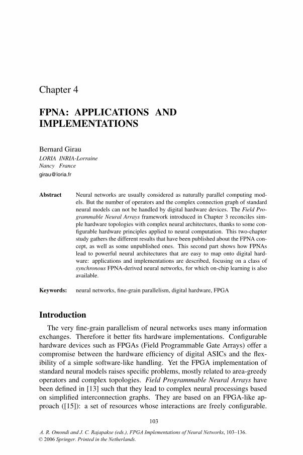
Chapter 4
FPNA: APPLICATIONS ANDIMPLEMENTATIONS
Bernard GirauLORIA INRIA-LorraineNancy France
Abstract Neural networks are usually considered as naturally parallel computing mod-els. But the number of operators and the complex connection graph of standardneural models can not be handled by digital hardware devices. The Field Pro-grammable Neural Arrays framework introduced in Chapter 3 reconciles sim-ple hardware topologies with complex neural architectures, thanks to some con-figurable hardware principles applied to neural computation. This two-chapterstudy gathers the different results that have been published about the FPNA con-cept, as well as some unpublished ones. This second part shows how FPNAslead to powerful neural architectures that are easy to map onto digital hard-ware: applications and implementations are described, focusing on a class ofsynchronous FPNA-derived neural networks, for which on-chip learning is alsoavailable.
Keywords: neural networks, fine-grain parallelism, digital hardware, FPGA
Introduction
The very fine-grain parallelism of neural networks uses many informationexchanges. Therefore it better fits hardware implementations. Configurablehardware devices such as FPGAs (Field Programmable Gate Arrays) offer acompromise between the hardware efficiency of digital ASICs and the flex-ibility of a simple software-like handling. Yet the FPGA implementation ofstandard neural models raises specific problems, mostly related to area-greedyoperators and complex topologies. Field Programmable Neural Arrays havebeen defined in [13] such that they lead to complex neural processings basedon simplified interconnection graphs. They are based on an FPGA-like ap-proach ([15]): a set of resources whose interactions are freely configurable.
103
A. R. Omondi and J. C. Rajapakse (eds.), FPGA Implementations of Neural Networks, 103–136. © 2006 Springer. Printed in the Netherlands.
104 FPNA: Applications and implementations
Several different neural networks may be configured from a given FPNA. Theyare called Field Programmed Neural Networks (FPNN). FPNA resources aredefined to perform computations of standard neurons, but they behave in anautonomous way. As a consequence, numerous virtual synaptic connectionsmay be created thanks to the application of a multicast data exchange protocolto the resources of a sparse neural network. This new neural computation con-cept makes it possible to replace a standard but topologically complex neuralarchitecture by a simplified one.
After a survey of parallel implementations of neural networks (particularlyon FPGAs), Chapter 3 has focused on the definitions, computations and theo-retical properties of FPNNs. Reading §3.3.1, §3.3.2 and §3.3.4 is required tohandle FPNA/FPNN notations and to understand FPNN computation. Never-theless, section 4.1 shortly recalls the main aspects of Chapter 3. This sec-ond chapter now describes how FPNNs may be used and implemented. Thenit focuses on a class of FPNNs that result in simple implementations withon-chip learning, as well as efficient pipelined implementations. Section 4.2shows how FPNNs may exactly perform the same computation as much morecomplex standard neural networks applied to boolean function computation,whereas sections 4.3 and 4.4 illustrate how they may approximately performthe same computation as much more complex standard neural networks appliedto more concrete applications (benchmark problems as well as real applica-tions). Their general implementation method is described in section 4.5. Thensection 4.6 defines and studies the case of simplifiable FPNNs: both computa-tion and learning of these synchronous FPNNs are described with a few equa-tions. Their specific implementations (with on-chip learning or pipeline) areoutlined in section 4.7. All implementation performances are finally discussedin section 4.8.
4.1 Summary of Chapter 3
Section 3.2 explains why FPGAs appear as a both flexible and rather ef-ficient device for neural applications. Implementation issues should not beneglected though. Defining hardware-adapted frameworks of neural computa-tion directly provides neural networks that are easy to map onto such deviceswithout a significant loss of computational power. The FPNA concept is such ahardware-adapted neural computation paradigm. It mainly leads to topologicalsimplifications of standard neural architectures.
A neural network may be seen as a graph of interconnected neural resources(neurons and weighting links). In a standard model, the number of inputsof each neuron is its fan-in in the connection graph. On the contrary, neuralresources (links and activators) become autonomous in an FPNA: their depen-dencies are freely set.
Towards simplified architectures:symmetric boolean functions by FPNAs 105
Activators apply standard neural functions to a set of input values on onehand, and links behave as independent affine operators on the other hand. TheFPNA concept permits to connect any link to any local resource (each node ofthe FPNA graph corresponds to an activator with incoming and outgoing links).Direct connections between affine links appear, so that the FPNA computesnumerous composite affine transforms. These compositions create numerousvirtual neural connections.
The activator of a node n performs any neuron computation by means ofa loop that updates a variable with respect to the neuron inputs (in denotesthe updating function), and a final computation (function fn) that maps thisvariable to the neuron output. A link between two nodes p and n performs anaffine transform Wn(p)x + Tn(p).
An FPNA is only an unconfigured set of such resources. An FPNN is anFPNA whose resources have been connected in a specific way. The mainconfiguration parameters are binary values: rn(p) = 1 to connect link (p, n)and activator (n), Sn(s) = 1 to connect activator (n) and link (n, s), andRn(p, s) = 1 to connect links (p, n) and (n, s): such direct connections be-tween links create virtual composite links.
During an FPNN computation, all resources (activators as well as links)behave independently. When a resource receives a value, it applies its localoperator(s), and then it sends the result to all neighbouring resources to whichit is locally connected.
Section 3.4 has shown that FPNN computation is coherent and well-defined,whereas section 3.5 has estimated the computational power of FPNNs. It islinked to complex dependency relations between the weights of the virtual con-nections that are created by direct local connections between links. A dedicatedweight initialization method has been derived so as to minimize the influenceof these complex dependencies.
4.2 Towards simplified architectures:symmetric boolean functions by FPNAs
This section shows how FPNAs may be used so as to replace standard neuralnetworks with simpler 2D-compatible architectures that exactly perform thesame computations. Nevertheless, this way of using FPNAs is limited to fewwell-identified applications. The case of symmetric boolean functions is dis-cussed here.
This section is organized as follows:
§4.2.1 describes the initial work of [24] to find an optimal multilayerneural network with shortcut links to compute symmetric boolean func-tions,
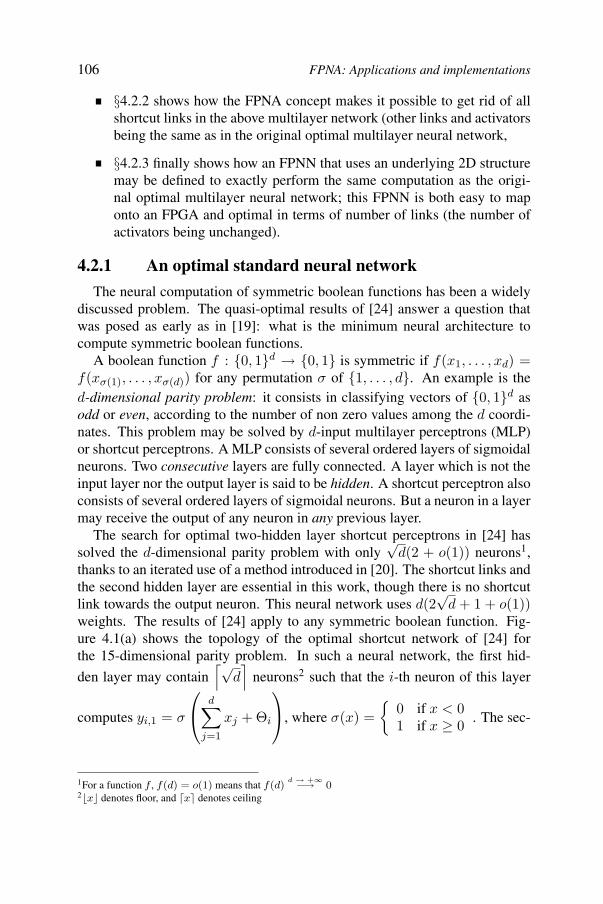
106 FPNA: Applications and implementations
§4.2.2 shows how the FPNA concept makes it possible to get rid of allshortcut links in the above multilayer network (other links and activatorsbeing the same as in the original optimal multilayer neural network,
§4.2.3 finally shows how an FPNN that uses an underlying 2D structuremay be defined to exactly perform the same computation as the origi-nal optimal multilayer neural network; this FPNN is both easy to maponto an FPGA and optimal in terms of number of links (the number ofactivators being unchanged).
4.2.1 An optimal standard neural network
The neural computation of symmetric boolean functions has been a widelydiscussed problem. The quasi-optimal results of [24] answer a question thatwas posed as early as in [19]: what is the minimum neural architecture tocompute symmetric boolean functions.
A boolean function f : {0, 1}d → {0, 1} is symmetric if f(x1, . . . , xd) =f(xσ(1), . . . , xσ(d)) for any permutation σ of {1, . . . , d}. An example is thed-dimensional parity problem: it consists in classifying vectors of {0, 1}d asodd or even, according to the number of non zero values among the d coordi-nates. This problem may be solved by d-input multilayer perceptrons (MLP)or shortcut perceptrons. A MLP consists of several ordered layers of sigmoidalneurons. Two consecutive layers are fully connected. A layer which is not theinput layer nor the output layer is said to be hidden. A shortcut perceptron alsoconsists of several ordered layers of sigmoidal neurons. But a neuron in a layermay receive the output of any neuron in any previous layer.
The search for optimal two-hidden layer shortcut perceptrons in [24] hassolved the d-dimensional parity problem with only
√d(2 + o(1)) neurons1,
thanks to an iterated use of a method introduced in [20]. The shortcut links andthe second hidden layer are essential in this work, though there is no shortcutlink towards the output neuron. This neural network uses d(2
√d + 1 + o(1))
weights. The results of [24] apply to any symmetric boolean function. Fig-ure 4.1(a) shows the topology of the optimal shortcut network of [24] forthe 15-dimensional parity problem. In such a neural network, the first hid-
den layer may contain⌈√
d⌉
neurons2 such that the i-th neuron of this layer
computes yi,1 = σ
⎛⎝ d∑j=1
xj + Θi
⎞⎠, where σ(x) ={
0 if x < 01 if x ≥ 0 . The sec-
1For a function f , f(d) = o(1) means that f(d)d → +∞−→ 0
2�x� denotes floor, and �x denotes ceiling
Towards simplified architectures:symmetric boolean functions by FPNAs 107
ond hidden layer contains at most
⌈d+1
√d�⌉
: its i-th neuron computes yi,2 =
σ
⎛⎜⎝�√d�∑j=1
wi,j,2yj,1 + (−1)id∑
j=1
xj
⎞⎟⎠. Then y = σ
⎛⎝ √d∑
j=1
wi,j,3yj,2 + Θ
⎞⎠ is
computed by the only output neuron.
4.2.2 FPNAs to remove shortcut links
The construction in [24] implies that for any (i, j), (−1)i and wi,j,2 haveopposite signs. This property may be used so that all shortcut links (betweenthe input and the second hidden layer) are virtually replaced by some directconnections between incoming and outgoing links in the first hidden layer ofan FPNA. This FPNA has got d
√d(1+o(1)) weights, instead of d
√d(2+o(1))
weights in [24].More precisely, the architecture of the FPNA is the same as the shortcut
perceptron of [24], without all shortcut links. The weights of the links betweenboth hidden layers are as in [24]. When configured as an FPNN, each neuronis fully connected to all incoming and outgoing links (∀ (p, n) rn(p) = 1 and∀ (n, s) Sn(s) = 1). If n is the i-th node of the first hidden layer, and if s isthe i-th node of the second hidden layer, then for any p ∈ Pred(n), there is adirect connection between (p, n) and (n, s) (i.e. Rn(p, s) = 1). If n is the i-thnode of the first hidden layer, then for any p ∈ Pred(n), Wn(p) = − 1
wi,i,2and
Tn(p) = 0. If n is the i-th node of the first hidden layer, then θn = − Θiwi,i,2
.Figure 4.1(b) sketches the architecture of such an FPNN for a 15-dimensionalsymmetric boolean function.
4.2.3 Towards a simplified 2D architecture
Even without shortcut links, the underlying FPNA of Figure 4.1(b) still doesnot have a hardware-friendly architecture. A more drastic simplification of thearchitecture is expected. The full connection between consecutive layers maybe virtually replaced by the use of sparse inter-layer and intra-layer FPNAlinks.
The construction of an FPNN in §4.2.2 does not depend on the symmetricboolean function. On the contrary, the determination of a hardware-friendlyFPNN for symmetric boolean functions takes advantage of several function-dependent weight similarities in [24]. Such successful determinations havebeen performed for various symmetric boolean functions and input dimen-sions: it appears that for any d and for any symmetric boolean function f ,an FPNN with the same number of neurons as in [24], but with only O(
√d)
108 FPNA: Applications and implementations
Figure 4.1. Neural architectures for the parity problem (d = 15)
weights3 computes f exactly as in [24]. The parity problem may be taken asan example: in [24], the weight of the link between the i-th neuron of the firsthidden layer and the j-th neuron of the second hidden layer only depends on(−1)j when i �= 1. This property may be used so as to build a hardware-friendly FPNN as follows.
Activators are globally unchanged. Therefore, the number of nodes ineach hidden layer is the same as the number of neurons in [24].
The inputs of the boolean function are gathered in groups so that theconnectivity from input nodes is simplified. Therefore the number ofinput nodes is the number of nodes in the first hidden layer. Each input
node sends up to⌈√
d⌉
inputs.
3i.e. at most proportional to√
d, indeed 152
√d + o(
√d) here
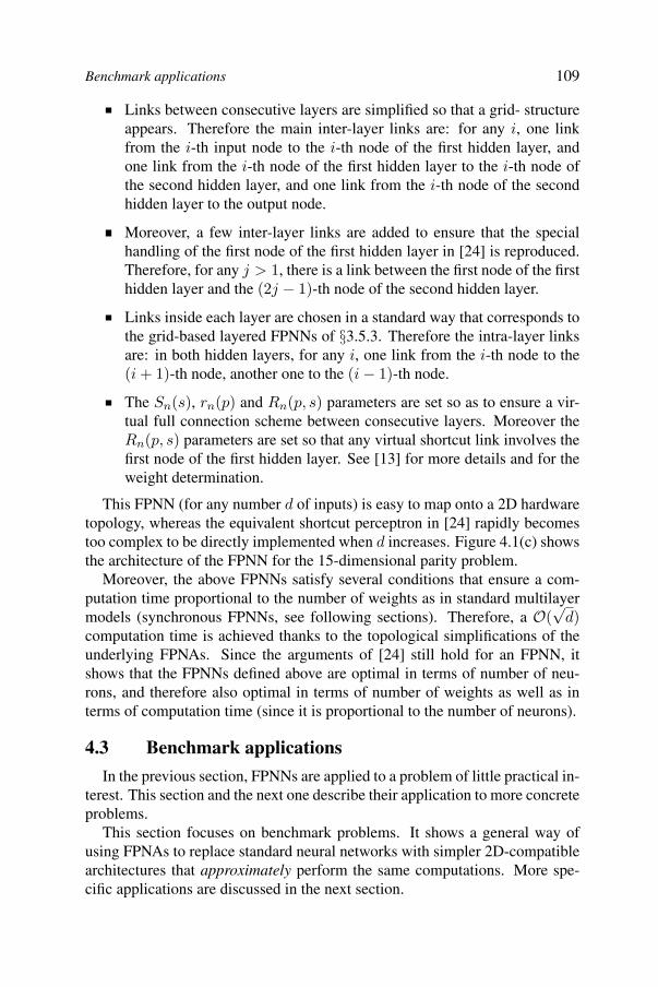
Benchmark applications 109
Links between consecutive layers are simplified so that a grid- structureappears. Therefore the main inter-layer links are: for any i, one linkfrom the i-th input node to the i-th node of the first hidden layer, andone link from the i-th node of the first hidden layer to the i-th node ofthe second hidden layer, and one link from the i-th node of the secondhidden layer to the output node.
Moreover, a few inter-layer links are added to ensure that the specialhandling of the first node of the first hidden layer in [24] is reproduced.Therefore, for any j > 1, there is a link between the first node of the firsthidden layer and the (2j − 1)-th node of the second hidden layer.
Links inside each layer are chosen in a standard way that corresponds tothe grid-based layered FPNNs of §3.5.3. Therefore the intra-layer linksare: in both hidden layers, for any i, one link from the i-th node to the(i + 1)-th node, another one to the (i − 1)-th node.
The Sn(s), rn(p) and Rn(p, s) parameters are set so as to ensure a vir-tual full connection scheme between consecutive layers. Moreover theRn(p, s) parameters are set so that any virtual shortcut link involves thefirst node of the first hidden layer. See [13] for more details and for theweight determination.
This FPNN (for any number d of inputs) is easy to map onto a 2D hardwaretopology, whereas the equivalent shortcut perceptron in [24] rapidly becomestoo complex to be directly implemented when d increases. Figure 4.1(c) showsthe architecture of the FPNN for the 15-dimensional parity problem.
Moreover, the above FPNNs satisfy several conditions that ensure a com-putation time proportional to the number of weights as in standard multilayermodels (synchronous FPNNs, see following sections). Therefore, a O(
√d)
computation time is achieved thanks to the topological simplifications of theunderlying FPNAs. Since the arguments of [24] still hold for an FPNN, itshows that the FPNNs defined above are optimal in terms of number of neu-rons, and therefore also optimal in terms of number of weights as well as interms of computation time (since it is proportional to the number of neurons).
4.3 Benchmark applications
In the previous section, FPNNs are applied to a problem of little practical in-terest. This section and the next one describe their application to more concreteproblems.
This section focuses on benchmark problems. It shows a general way ofusing FPNAs to replace standard neural networks with simpler 2D-compatiblearchitectures that approximately perform the same computations. More spe-cific applications are discussed in the next section.
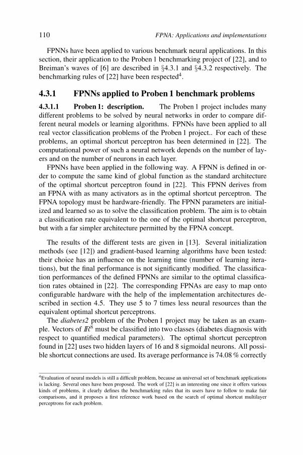
110 FPNA: Applications and implementations
FPNNs have been applied to various benchmark neural applications. In thissection, their application to the Proben 1 benchmarking project of [22], and toBreiman’s waves of [6] are described in §4.3.1 and §4.3.2 respectively. Thebenchmarking rules of [22] have been respected4.
4.3.1 FPNNs applied to Proben 1 benchmark problems
4.3.1.1 Proben 1: description. The Proben 1 project includes manydifferent problems to be solved by neural networks in order to compare dif-ferent neural models or learning algorithms. FPNNs have been applied to allreal vector classification problems of the Proben 1 project.. For each of theseproblems, an optimal shortcut perceptron has been determined in [22]. Thecomputational power of such a neural network depends on the number of lay-ers and on the number of neurons in each layer.
FPNNs have been applied in the following way. A FPNN is defined in or-der to compute the same kind of global function as the standard architectureof the optimal shortcut perceptron found in [22]. This FPNN derives froman FPNA with as many activators as in the optimal shortcut perceptron. TheFPNA topology must be hardware-friendly. The FPNN parameters are initial-ized and learned so as to solve the classification problem. The aim is to obtaina classification rate equivalent to the one of the optimal shortcut perceptron,but with a far simpler architecture permitted by the FPNA concept.
The results of the different tests are given in [13]. Several initializationmethods (see [12]) and gradient-based learning algorithms have been tested:their choice has an influence on the learning time (number of learning itera-tions), but the final performance is not significantly modified. The classifica-tion performances of the defined FPNNs are similar to the optimal classifica-tion rates obtained in [22]. The corresponding FPNAs are easy to map ontoconfigurable hardware with the help of the implementation architectures de-scribed in section 4.5. They use 5 to 7 times less neural resources than theequivalent optimal shortcut perceptrons.
The diabetes2 problem of the Proben 1 project may be taken as an exam-ple. Vectors of IR8 must be classified into two classes (diabetes diagnosis withrespect to quantified medical parameters). The optimal shortcut perceptronfound in [22] uses two hidden layers of 16 and 8 sigmoidal neurons. All possi-ble shortcut connections are used. Its average performance is 74.08 % correctly
4Evaluation of neural models is still a difficult problem, because an universal set of benchmark applicationsis lacking. Several ones have been proposed. The work of [22] is an interesting one since it offers variouskinds of problems, it clearly defines the benchmarking rules that its users have to follow to make faircomparisons, and it proposes a first reference work based on the search of optimal shortcut multilayerperceptrons for each problem.
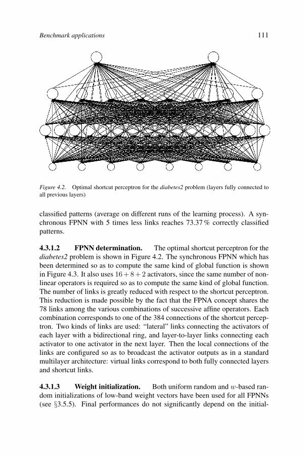
Benchmark applications 111
Figure 4.2. Optimal shortcut perceptron for the diabetes2 problem (layers fully connected toall previous layers)
classified patterns (average on different runs of the learning process). A syn-chronous FPNN with 5 times less links reaches 73.37 % correctly classifiedpatterns.
4.3.1.2 FPNN determination. The optimal shortcut perceptron for thediabetes2 problem is shown in Figure 4.2. The synchronous FPNN which hasbeen determined so as to compute the same kind of global function is shownin Figure 4.3. It also uses 16+8+2 activators, since the same number of non-linear operators is required so as to compute the same kind of global function.The number of links is greatly reduced with respect to the shortcut perceptron.This reduction is made possible by the fact that the FPNA concept shares the78 links among the various combinations of successive affine operators. Eachcombination corresponds to one of the 384 connections of the shortcut percep-tron. Two kinds of links are used: “lateral” links connecting the activators ofeach layer with a bidirectional ring, and layer-to-layer links connecting eachactivator to one activator in the next layer. Then the local connections of thelinks are configured so as to broadcast the activator outputs as in a standardmultilayer architecture: virtual links correspond to both fully connected layersand shortcut links.
4.3.1.3 Weight initialization. Both uniform random and w-based ran-dom initializations of low-band weight vectors have been used for all FPNNs(see §3.5.5). Final performances do not significantly depend on the initial-
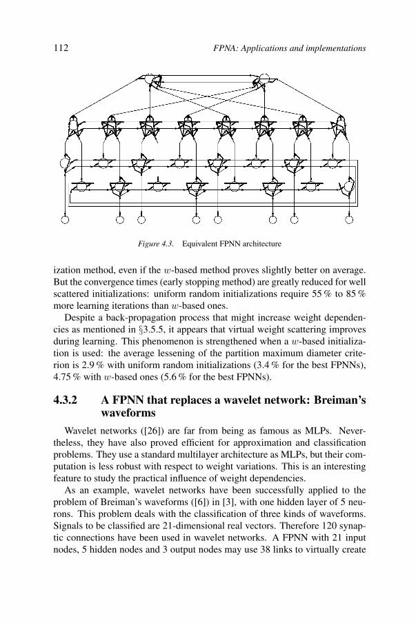
112 FPNA: Applications and implementations
Figure 4.3. Equivalent FPNN architecture
ization method, even if the w-based method proves slightly better on average.But the convergence times (early stopping method) are greatly reduced for wellscattered initializations: uniform random initializations require 55 % to 85 %more learning iterations than w-based ones.
Despite a back-propagation process that might increase weight dependen-cies as mentioned in §3.5.5, it appears that virtual weight scattering improvesduring learning. This phenomenon is strengthened when a w-based initializa-tion is used: the average lessening of the partition maximum diameter crite-rion is 2.9 % with uniform random initializations (3.4 % for the best FPNNs),4.75 % with w-based ones (5.6 % for the best FPNNs).
4.3.2 A FPNN that replaces a wavelet network: Breiman’swaveforms
Wavelet networks ([26]) are far from being as famous as MLPs. Never-theless, they have also proved efficient for approximation and classificationproblems. They use a standard multilayer architecture as MLPs, but their com-putation is less robust with respect to weight variations. This is an interestingfeature to study the practical influence of weight dependencies.
As an example, wavelet networks have been successfully applied to theproblem of Breiman’s waveforms ([6]) in [3], with one hidden layer of 5 neu-rons. This problem deals with the classification of three kinds of waveforms.Signals to be classified are 21-dimensional real vectors. Therefore 120 synap-tic connections have been used in wavelet networks. A FPNN with 21 inputnodes, 5 hidden nodes and 3 output nodes may use 38 links to virtually create
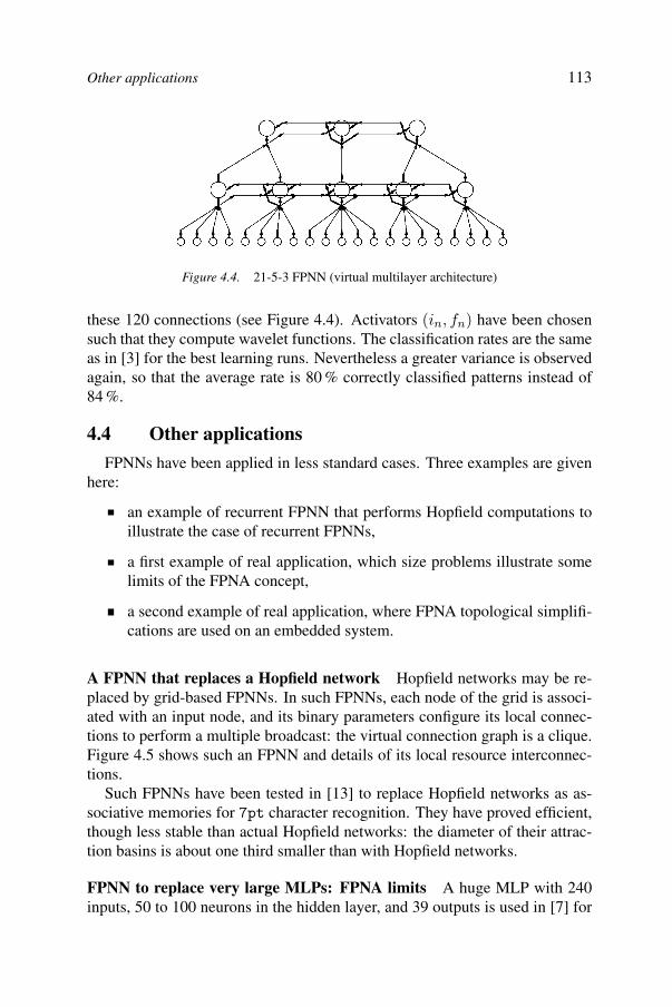
Other applications 113
Figure 4.4. 21-5-3 FPNN (virtual multilayer architecture)
these 120 connections (see Figure 4.4). Activators (in, fn) have been chosensuch that they compute wavelet functions. The classification rates are the sameas in [3] for the best learning runs. Nevertheless a greater variance is observedagain, so that the average rate is 80 % correctly classified patterns instead of84 %.
4.4 Other applications
FPNNs have been applied in less standard cases. Three examples are givenhere:
an example of recurrent FPNN that performs Hopfield computations toillustrate the case of recurrent FPNNs,
a first example of real application, which size problems illustrate somelimits of the FPNA concept,
a second example of real application, where FPNA topological simplifi-cations are used on an embedded system.
A FPNN that replaces a Hopfield network Hopfield networks may be re-placed by grid-based FPNNs. In such FPNNs, each node of the grid is associ-ated with an input node, and its binary parameters configure its local connec-tions to perform a multiple broadcast: the virtual connection graph is a clique.Figure 4.5 shows such an FPNN and details of its local resource interconnec-tions.
Such FPNNs have been tested in [13] to replace Hopfield networks as as-sociative memories for 7pt character recognition. They have proved efficient,though less stable than actual Hopfield networks: the diameter of their attrac-tion basins is about one third smaller than with Hopfield networks.
FPNN to replace very large MLPs: FPNA limits A huge MLP with 240inputs, 50 to 100 neurons in the hidden layer, and 39 outputs is used in [7] for
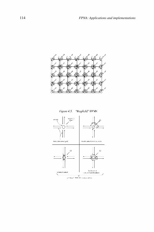
114 FPNA: Applications and implementations
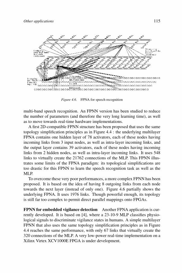
Other applications 115
Figure 4.6. FPNA for speech recognition
multi-band speech recognition. An FPNN version has been studied to reducethe number of parameters (and therefore the very long learning time), as wellas to move towards real-time hardware implementations.
A first 2D-compatible FPNN structure has been proposed that uses the sametopology simplification principles as in Figure 4.4 : the underlying multilayerFPNA contains one hidden layer of 78 activators, each of these nodes havingincoming links from 3 input nodes, as well as intra-layer incoming links, andthe output layer contains 39 activators, each of these nodes having incominglinks from 2 hidden nodes, as well as intra-layer incoming links. It uses 548links to virtually create the 21762 connections of the MLP. This FPNN illus-trates some limits of the FPNA paradigm: its topological simplifications aretoo drastic for this FPNN to learn the speech recognition task as well as theMLP.
To overcome these very poor performances, a more complex FPNN has beenproposed. It is based on the idea of having 8 outgoing links from each nodetowards the next layer (instead of only one). Figure 4.6 partially shows theunderlying FPNA. It uses 1976 links. Though powerful enough, its topologyis still far too complex to permit direct parallel mappings onto FPGAs.
FPNN for embedded vigilance detection Another FPNA application is cur-rently developed. It is based on [4], where a 23-10-9 MLP classifies physio-logical signals to discriminate vigilance states in humans. A simple multilayerFPNN that also uses the same topology simplification principles as in Figure4.4 reaches the same performance, with only 67 links that virtually create the320 connections of the MLP. A very low-power real-time implementation on aXilinx Virtex XCV1000E FPGA is under development.
116 FPNA: Applications and implementations
Previous sections have discussed the application of FPNNs to different prob-lems, they have focused on the topological simplifications, and they have stud-ied the obtained performances with respect to standard neural models. Nextsections focus on implementation methods. A general one is first described inSection 4.5. It may be used for any FPNN computation. Nevertheless, moreefficient solutions exist, but they only apply to specific FPNNs, called synchro-nous. This kind of FPNN is defined and studied in section 4.6, whereas Section4.7 describes their specific implementation methods: a pipelined version andan implementation with on-chip learning.
Several implementation results (mostly areas) are given in sections 4.5 and4.7. Nevertheless, technical details have to be found in Section 4.8.
4.5 General FPGA implementation
This Section describes a very general implementation method that is directlyderived from the asynchronous parallel computation scheme (see §3.3.2). It isorganized as follows:
§4.5.1 explains that this implementation only requires to define basicbuilding blocks since a modular assembling is made possible thanks toFPNA properties,
§4.5.2 describes the first building block: the implementation of a link,
§4.5.3 describes the second building block: the implementation of anactivator.
4.5.1 Modular implementation of FPNNs
An FPNN implementation only requires configurable predefined blocks thatare simply assembled as in the underlying FPNA architecture (direct parallelmapping of the neural architecture onto the FPGA). Its simplified topologymake it possible for the compiling tool to perform well.
The resources (links and activators) of the FPNA are implemented: eachresource corresponds to a predefined block that performs both resource com-putations and asynchronous protocol handling, and all blocks are assembledaccording to the FPNA graph. This implementation may be used by any FPNNderived from this FPNA: some elements just have to be correctly configured in-side each block, such as multiplexers, registers, etc. Such FPNNs may computecomplex functions as in Section 4.3, though their FPNA architecture is madesimple (reduced number of edges, limited fan-ins and fan-outs). Therefore,this implementation method is flexible, straightforward and compatible withhardware constraints. Moreover this implementation shows how time may beinherent to FPNN computations.
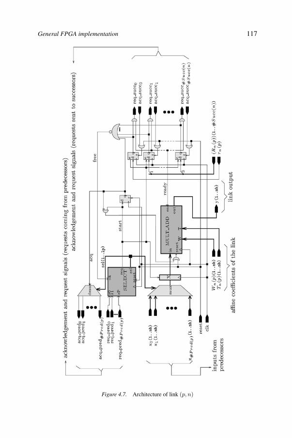
General FPGA implementation 117
Figure 4.7. Architecture of link (p, n)
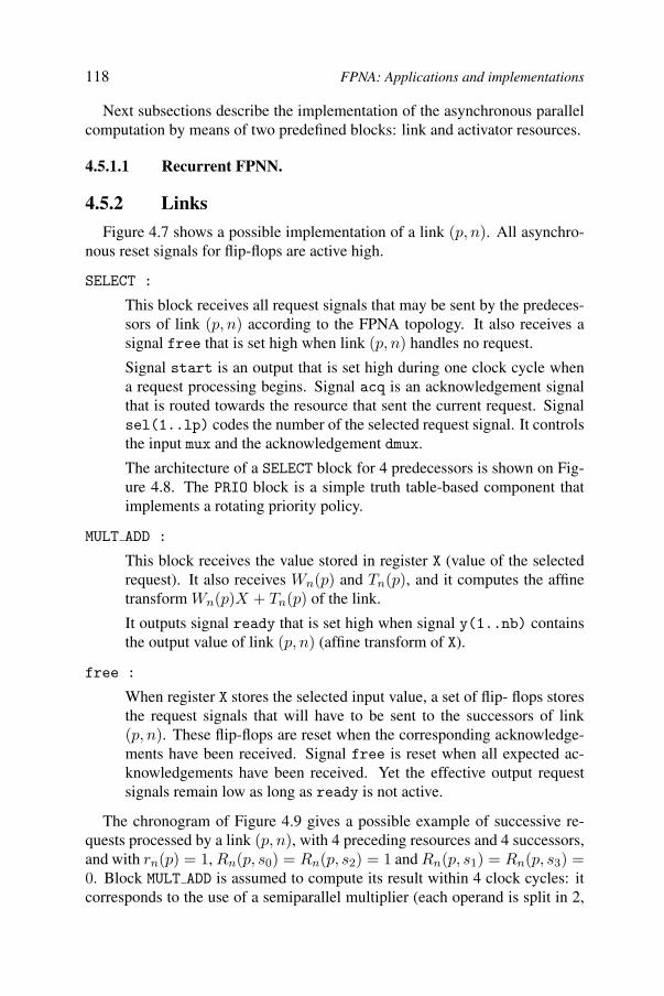
118 FPNA: Applications and implementations
Next subsections describe the implementation of the asynchronous parallelcomputation by means of two predefined blocks: link and activator resources.
4.5.1.1 Recurrent FPNN.
4.5.2 Links
Figure 4.7 shows a possible implementation of a link (p, n). All asynchro-nous reset signals for flip-flops are active high.
SELECT :
This block receives all request signals that may be sent by the predeces-sors of link (p, n) according to the FPNA topology. It also receives asignal free that is set high when link (p, n) handles no request.
Signal start is an output that is set high during one clock cycle whena request processing begins. Signal acq is an acknowledgement signalthat is routed towards the resource that sent the current request. Signalsel(1..lp) codes the number of the selected request signal. It controlsthe input mux and the acknowledgement dmux.
The architecture of a SELECT block for 4 predecessors is shown on Fig-ure 4.8. The PRIO block is a simple truth table-based component thatimplements a rotating priority policy.
MULT ADD :
This block receives the value stored in register X (value of the selectedrequest). It also receives Wn(p) and Tn(p), and it computes the affinetransform Wn(p)X + Tn(p) of the link.
It outputs signal ready that is set high when signal y(1..nb) containsthe output value of link (p, n) (affine transform of X).
free :
When register X stores the selected input value, a set of flip- flops storesthe request signals that will have to be sent to the successors of link(p, n). These flip-flops are reset when the corresponding acknowledge-ments have been received. Signal free is reset when all expected ac-knowledgements have been received. Yet the effective output requestsignals remain low as long as ready is not active.
The chronogram of Figure 4.9 gives a possible example of successive re-quests processed by a link (p, n), with 4 preceding resources and 4 successors,and with rn(p) = 1, Rn(p, s0) = Rn(p, s2) = 1 and Rn(p, s1) = Rn(p, s3) =0. Block MULT ADD is assumed to compute its result within 4 clock cycles: itcorresponds to the use of a semiparallel multiplier (each operand is split in 2,
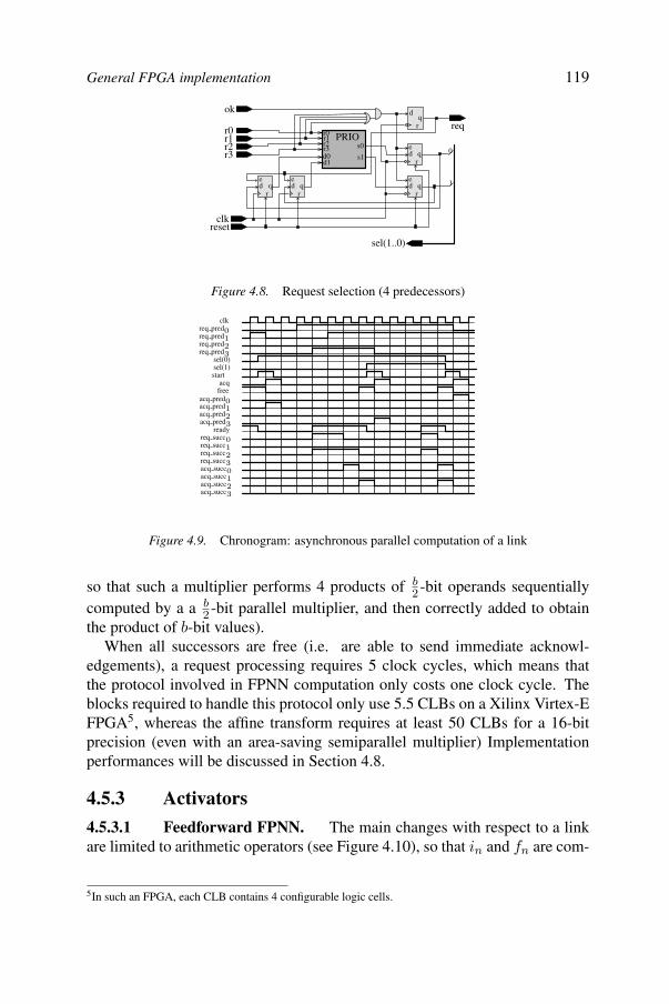
General FPGA implementation 119
req
clk
r0r1r2r3
reset
ok
qed
qed
r
r
qed
rq
ed
r
rq
d
r3r2r1r0
d1d0 s1
PRIOs0
0
1
sel(1..0)
Figure 4.8. Request selection (4 predecessors)
acq succ0acq succ1
acq succ3acq succ2
sel(0)sel(1)
acq
req pred0req pred1req pred2req pred3
acq pred0acq pred1acq pred2acq pred3
req succ0req succ1req succ2req succ3
start
free
ready
clk
Figure 4.9. Chronogram: asynchronous parallel computation of a link
so that such a multiplier performs 4 products of b2 -bit operands sequentially
computed by a a b2 -bit parallel multiplier, and then correctly added to obtain
the product of b-bit values).When all successors are free (i.e. are able to send immediate acknowl-
edgements), a request processing requires 5 clock cycles, which means thatthe protocol involved in FPNN computation only costs one clock cycle. Theblocks required to handle this protocol only use 5.5 CLBs on a Xilinx Virtex-EFPGA5, whereas the affine transform requires at least 50 CLBs for a 16-bitprecision (even with an area-saving semiparallel multiplier) Implementationperformances will be discussed in Section 4.8.
4.5.3 Activators
4.5.3.1 Feedforward FPNN. The main changes with respect to a linkare limited to arithmetic operators (see Figure 4.10), so that in and fn are com-
5In such an FPGA, each CLB contains 4 configurable logic cells.
120 FPNA: Applications and implementations
puted instead of the affine transform of a communication link. Operators ITERand OUTPUT are used instead of MULT ADD. These blocks perform the iteratedcomputation of the activator output (see §3.3.2). ITER is the in function thatis applied to the input and to the internal variable so as to update the latter.OUTPUT is the fn function that is applied to the final state of the internal vari-able so as to obtain the activator output. The computation of OUTPUT onlyoccurs when an values have been processed by ITER.
A linear feedback shift register is required for this arity handling, so that theFPNN asynchronous protocol requires 6 CLBs for an activator (if in ≤ 15)instead of 5.5 for a link. Once again, the cost of the FPNN asynchronousprotocol is negligible with respect to the arithmetic operators required by theactivator itself.
§3.4.2 explains that synchronization barriers must be introduced to handlerecurrent FPNNs: activator-generated requests are put in a waiting buffer untilthe next synchronization barrier.
Nevertheless, the theoretical study in [13] shows that an activator in a de-terministic recurrent FPNN sends at most one value after each synchronizationbarrier, so that no request buffering is needed. Therefore, the general paral-lel implementation of recurrent FPNNs is very close to the one of feedforwardFPNNs, except that a simple additional synchronization signal is received. Thissignal clocks a flip-flop with signal ready as input and ready sync as output.Then ready and ready sync replaces signal ready in the control of theoutput request signals. No other change is required.
4.6 Synchronous FPNNs
This Section focuses on a specific class of FPNNs, for which both descrip-tion and computation can be greatly simplified, so that an implementation withon-chip learning as well as an optimized pipelined implementation may be de-scribed (see Section 4.7). It is organized as follows:
§4.6.1 gives the definition of synchronous FPNNs,
§4.6.2 describes the main property of these FPNNs and it explains thatsuch FPNNs perform computations that appear similar to usual neuralcomputations,
these computation simplifications lead to a backpropagated methodto compute the gradient of synchronous FPNNs, so that their back-propagation-based learning is described in §4.6.3.
4.6.1 Definition of synchronous FPNNs
A synchronous FPNN is an FPNN in which any resource may simultane-ously process all its received values. In such an FPNN, any resource can “wait”
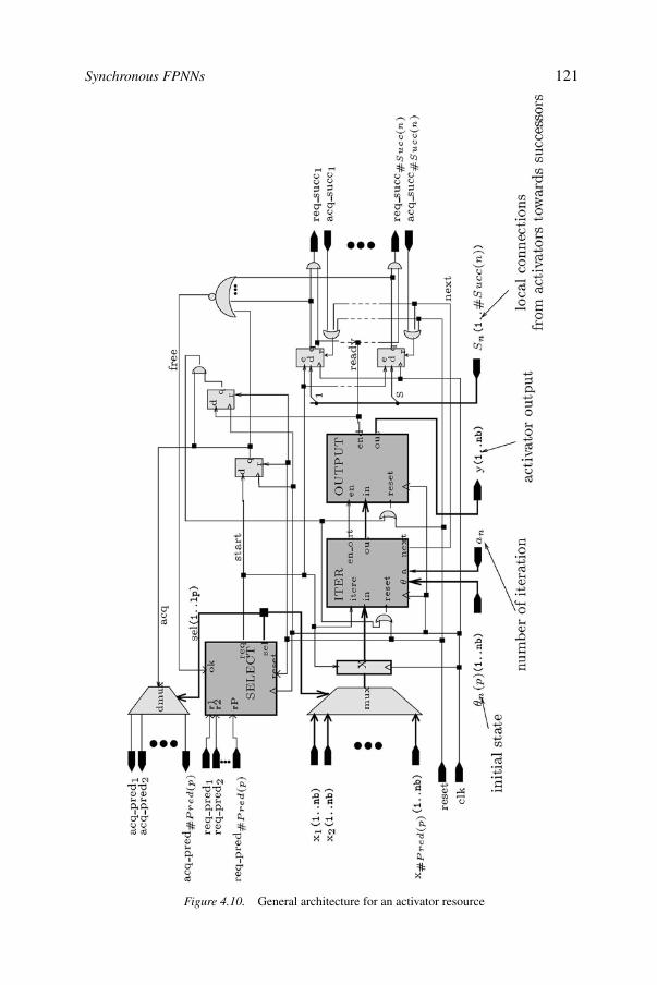
Synchronous FPNNs 121
Figure 4.10. General architecture for an activator resource
122 FPNA: Applications and implementations
for all its input values before it begins to process them, without modifying thecomputation of the whole FPNN.
The study of [13] defines three (rather tricky) conditions for an FPNN tobe considered as synchronous. Nevertheless, these conditions are satisfied bya set of easily identified FPNNs, for which all activators use simple additionsto update their variable state and for which all links apply linear functions.Therefore, only this set of synchronous FPNNs will be considered from nowon. This set includes the FPNNs defined such that their activators perform thecomputations of standard sigmoidal neurons.
More formally, a simple definition (close to standard feedforward neuralnetworks) may be given for synchronous FPNNs. Following the FPNA/FPNNdefinition given in Chapter 3, a FPNN must fulfill the following conditions tobe synchronous:
All iteration functions in are associative and commutative.
Whatever computation method is chosen, the activator in node n exactlyreceives an values. In the asynchronous parallel computation method,it means that for all n, there are exactly an requests req[(p, n), (n), x]where p ∈ Pred(n). Therefore an activator always sends an output(except if an = 0) and it does not receive any value after having sent thisoutput. This condition is fulfilled if the following recursive property issatisfied:
∀n an =∑
p∈Pred(n)
d(p,n)rn(p)
where d(p,n) = χIN�+(ap)Sp(n) +
∑q∈Pred(p)
d(q,p)Rp(q, n)
Links must be linear operators x �→ Wn(p)x (for each (p, n) in E),instead of affine ones.
4.6.2 Equivalent and simplified computations
In [13], synchronous FPNNs have been introduced when studying the deter-minism of both sequential and parallel computation schemes for feedforwardand recurrent FPNNs. The main result6 is:
Theorem 4.1 Feedforward synchronous FPNNs are deterministic: all neu-rons compute the same outputs with both sequential and parallel computations,and these outputs do not depend on any graph ordering nor request schedulingpolicy.
6Indeed, the last condition (linearity of links) is not required here.
Synchronous FPNNs 123
This is the fundamental property of synchronous FPNNs: the above conditionsensure that the order in which input requests are sent to any activator does nothave any influence on its computed output.
These equivalent results may be then expressed in a very simplified way.For each input node n in Ni, a value xn is given (outer inputs of the FPNN).Then, activators (n) and links (n, s) compute:
y(n) = fn
⎛⎝ ∑rn(p)=1
y(p,n) + θn
⎞⎠
y(n,s) = Ws(n)
⎛⎝ ∑Rn(p,s)=1
y(p,n) + Sn(s)y(n)
⎞⎠Similar results are available for recurrent synchronous FPNNs.
4.6.3 Learning of synchronous FPNNs
Both learning and generalization phases of synchronous FPNNs may be ef-ficiently implemented on configurable hardware. This key feature shows thatthis kind of neural models is particularly able to take advantage of the charac-teristics of reconfigurable computing systems: prototyping may be efficientlyperformed, and then the system may be reconfigured so as to implement thelearned FPNN with an outstanding generalization speed (see section 4.3).
The learning phase of many standard neural networks (such as MLPs) isoften performed thanks to what is called the back-propagation learning algo-rithm, where an error function Err estimates the distance between the neuralnetwork output and the expected output that corresponds to the given trainingpattern. A positive real value ε is given as learning rate. Each parameter p is
updated as follows: p ⇐ p − ε∂Err
∂p.
The generalized back-propagation algorithm of [10] may be applied to syn-chronous FPNNs (see [13]). It shows that the gradient of a synchronous FPNNmay be computed by means of simple formulae. Moreover, these computa-tions are performed by the resources with local data (provided by the neigh-bouring resources). It provides a simple hardware implementation that is basedon assembled predefined blocks (Section 4.5). The simplified architectures ofFPNAs ensure that this assembling is straightforward and hardware-friendly.
A node in a synchronous FPNN is an output node if its local activa-tor computes an output value without sending it to any other resource (i.e.Sn(s) = 0 for all s ∈ Succ(n)). Let Err be the quadratic distanceErr = 1
2
∑n output node(y(n) − en)2, where en is the corresponding expected
output. The following notations are also introduced:
124 FPNA: Applications and implementations
∂Err(p,n) is the differential of Err with respect to the output of link(p, n)
∂Err(n) is the differential of Err with respect to the output of activator(n)
Then the gradient of Err with respect to the FPNN learnable parametersWn(p) and θn is computed thanks to the following formulae, that are simi-lar to a standard back-propagation process in a multilayer neural network.
Three formulae express the back-propagation of differentials.
If n is an output node: ∂Err(n) = y(n) − en.
Else: ∂Err(n) =∑
Sn(s)=1
Ws(n)∂Err(n,s)
∂Err(p,n) = rn(p) f ′n
⎛⎝ ∑rn(p)=1
y(p,n) + θn
⎞⎠ ∂Err(n)
+∑
Rn(p,s)=1
Ws(n)∂Err(n,s)
Then the gradient values are locally computed.
Differential w.r.t. θn:
∂Err
∂θn= f ′
n
⎛⎝ ∑rn(p)=1
y(p,n) + θn
⎞⎠ ∂Err(n)
Differential w.r.t. Ws(n):
∂Err
∂Ws(n)=
⎛⎝ ∑Rn(p,s)=1
y(p,n) + Sn(s)yn
⎞⎠ ∂Err(n,s)
4.7 Implementations of synchronous FPNNs
The computational simplifications of synchronous FPNNs provide two spe-cific implementation methods: on-chip learning is possible, and a fast pipelineimplementation may be used (without learning). The general topological sim-plifications that are made possible by FPNAs are still available, so that theseimplementation methods still consist of an easy modular hardware mapping ofbasic building blocks.
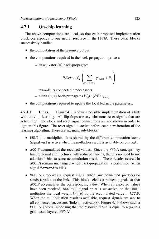
Implementations of synchronous FPNNs 125
4.7.1 On-chip learning
The above computations are local, so that each proposed implementationblock corresponds to one neural resource in the FPNA. These basic blockssuccessively handle:
the computation of the resource output
the computations required in the back-propagation process
– an activator (n) back-propagates
∂Err(n) f ′n
⎛⎝ ∑rn(p)=1
y(p,n) + θn
⎞⎠towards its connected predecessors
– a link (n, s) back-propagates Ws(n)∂Err(n,s)
the computations required to update the local learnable parameters.
4.7.1.1 Links. Figure 4.11 shows a possible implementation of a linkwith on-chip learning. All flip-flops use asynchronous reset signals that areactive high. The clock and reset signal connections are not shown in order tolighten this figure. The reset signal is active before each new iteration of thelearning algorithm. There are six main sub-blocks:
MULT is a multiplier. It is shared by the different computation steps.Signal end is active when the multiplier result is available on bus out.
ACC F accumulates the received values. Since the FPNA concept mayhandle neural architectures with reduced fan-ins, there is no need to useadditional bits to store accumulation results. These results (stored inACC F) remain unchanged when back-propagation is performed (whensignal forward is idle).
SEL FWD receives a request signal when any connected predecessorsends a value to the link. This block selects a request signal, so thatACC F accumulates the corresponding value. When all expected valueshave been received, SEL FWD, signal en m is set active, so that MULTmultiplies the local weight Wn(p) by the accumulated value in ACC F.When the multiplication result is available, request signals are sent toall connected successors (links or activators). Figure 4.13 shows such aSEL FWD block, supposing that the resource fan-in is equal to 4 (as in agrid-based layered FPNA).
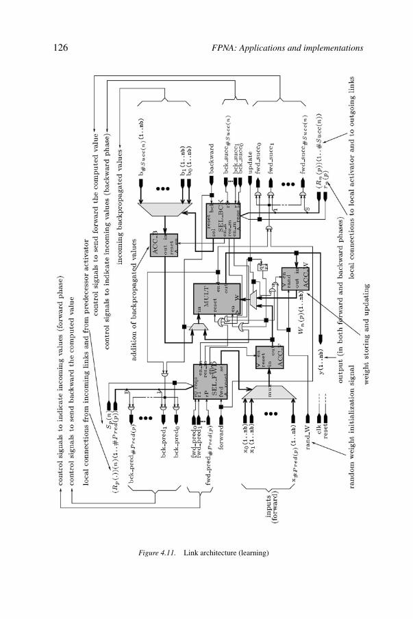
126 FPNA: Applications and implementations
Figure 4.11. Link architecture (learning)
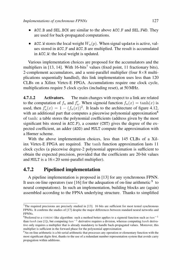
Implementations of synchronous FPNNs 127
ACC B and SEL BCK are similar to the above ACC F and SEL FWD. Theyare used for back-propagated computations.
ACC W stores the local weight Wn(p). When signal update is active, val-ues stored in ACC F and ACC B are multiplied. The result is accumulatedin ACC W: the local weight is updated.
Various implementation choices are proposed for the accumulators and themultipliers in [13, 14]. With 16-bits7 values (fixed point, 11 fractionary bits),2-complement accumulators, and a semi-parallel multiplier (four 8×8 multi-plications sequentially handled), this link implementation uses less than 120CLBs on a Xilinx Virtex-E FPGA. Accumulations require one clock cycle,multiplications require 5 clock cycles (including reset), at 50 MHz.
4.7.1.2 Activators. The main changes with respect to a link are relatedto the computation of fn and f ′
n. When sigmoid function fn(x) = tanh(x) isused, then f ′
n(x) = 1 − (fn(x))2. It leads to the architecture of figure 4.12,with an additional part that computes a piecewise polynomial approximation8
of tanh: a table stores the polynomial coefficients (address given by the mostsignificant bits stored in ACC F), a counter (CNT) gives the degree of the ex-pected coefficient, an adder (ADD) and MULT compute the approximation witha H-orner scheme.
With the above implementation choices, less than 145 CLBs of a Xil-inx Virtex-E FPGA are required. The tanh function approximation lasts 11clock cycles (a piecewise degree-2 polynomial approximation is sufficient toobtain the expected precision, provided that the coefficients are 20-bit valuesand MULT is a 16×20 semi-parallel multiplier).
4.7.2 Pipelined implementation
A pipeline implementation is proposed in [13] for any synchronous FPNN.It uses on-line operators (see [16] for the adequation of on-line arithmetic 9 toneural computations). In such an implementation, building blocks are (again)assembled according to the FPNA underlying structure. Thanks to simplified
7The required precisions are precisely studied in [13]. 16 bits are sufficient for most tested synchronousFPNNs. It confirms the studies of [17] despite the major differences between standard neural networks andFPNNs.8Preferred to a cordic-like algorithm: such a method better applies to a sigmoid function such as tan−1
than tanh (see [1]), but computing tan−1 derivative requires a division, whereas computing tanh deriva-tive only requires a multiplier that is already mandatory to handle back-propagated values. Moreover, thismultiplier is sufficient in the forward phase for the polynomial approximation9An on-line arithmetic is a bit-serial arithmetic that processes any operation or elementary function with themost significant digits first, thanks to the use of a redundant number representation system that avoids carrypropagation within additions.
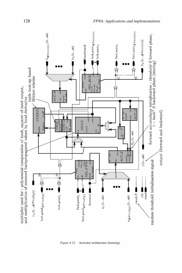
128 FPNA: Applications and implementations
Figure 4.12. Activator architecture (learning)
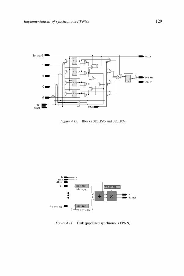
Implementations of synchronous FPNNs 129
clkreset
r3
r2
r1
r0
ed q
r
qed
r
qe
rq
d
dr
0
1
3
2
qed
r
reqs
en a
en m
res m
forward
Figure 4.13. Blocks SEL FWD and SEL BCK
clkreset
shift reg.
shift reg.(delay#P red(p))
yctl out
weight reg.x1
x#P red(p)
(delay1)
ctl in
Figure 4.14. Link (pipelined synchronous FPNN)
130 FPNA: Applications and implementations
computations (§4.6.2), these building blocks do not require any protocol han-dling. They handle data and computation in a serial way. Thanks to the useof on-line arithmetic, both activators and links handle data in the same way.Activators use elementary functions (sin, cos, tan, tanh, exp, log, arctan, . . .).The evaluation of these elementary functions can be performed using polyno-mial or rational approximations, shift and add algorithms or table-based algo-rithms. Those algorithms are presented in [21]. In this work, we have chosenthe evaluation of the tanh function using polynomial approximations with aH-orner scheme10. See [16, 13] for more details about on-line operators anddelay handling.
Figure 4.14 sketches a “link” building block. It uses 37 CLBs (170 for anactivator) of a Xilinx Virtex-E FPGA for a 16-bit precision. It may be clockedat 100 MHz.
4.8 Implementation performances
This section discusses the implementation performances (area and speed)of the various implementation methods that have been described in sections4.5 and 4.7 through several examples taken from sections 4.3 and 4.4. §4.8.1focuses on a typical synchronous FPNN, whereas §4.8.2 deals with the lesscommon case of non- synchronous FPNNs. Finally §4.8.3 (cautiously) com-pares the obtained implementation performances with other works.
Our implementations are based on a Celoxica RC1000PP board with a Xil-inx Virtex XCV1000E-BG560 FPGA. Xilinx FPGAs have been chosen be-cause the fine grain parallelism of neural computations requires many elemen-tary memory devices, and such FPGAs offer a high memory/logic ratio. We usethe Virtex-E FPGA family to illustrate FPNN implementation performances,indicating the smallest one that is sufficient to implement each FPNN. EachCLB in these FPGAs corresponds to 4 configurable logic cells.
It must be pointed out that current FPGAs already outperform the capacityof the Virtex XCV1000E: such an FPGA contains 27648 logic cells, to be com-pared with the 73008 ones of the largest Virtex-E, as well as with the 125136logic cells of the largest current Virtex-II Pro. Such improvements make thescalability of the FPNA concept even more useful: larger neural networks maybe implemented without routing bottlenecks, or spared CLBs may be used forother computations required by the application.
We currently use Xilinx ISE 4.2 as synthesis tool. The mapping of eachbuilding block is asked to optimize the implementation area. Modular mappingis priviledged for large FPNNs. Speeds are given according to both FPGA
10Again preferred to a cordic-like algorithm, that would require an iterated process unfitted for a pipelineimplementation
Implementation performances 131
synthesis indications and memory bandwidth limits in our board. It shouldbe pointed out that these performances have not been optimized by experts ofFPGA implementation, and that they might be also improved by a combineduse of area-saving neural operators (for example bit-stream neurons may beused in conjunction with the pipeline implementation of FPNNs).
4.8.1 Application to the FPNN of Figure 4.3
Several implementations are available for this FPNN.
The implementation of the learning phase of this FPNN requires 13250CLBs (16-bit precision, based on parallel 8 × 8 multipliers and a piece-wise polynomial approximation of tanh). It may use a single Xilinx Vir-tex XCV3200E (largest Virtex-E), or two Xilinx Virtex XCV1600E-BG560. In this case the small fan-ins of the FPNA resources make it pos-sible to exchange all required signals with the 404 available I/O ports ofthe FPGAs: at most 168 ports are required for each FPGA. The shortcutperceptron of Figure 4.2 could not be directly mapped onto any numberof FPGAs: these FPGAs would have to exchange too many signals, be-sides the topology and fan-in problems inside each FPGA. One learningiteration of the FPNN lasts 378 clock cycles, so that a 14 FPNN-MCUPSspeed is reached: 14.106 links are updated by the learning process persecond. It corresponds to 70 MCUPS (70.106 connections updated persecond) with the optimal shortcut perceptron which outputs the samefunction as the FPNN.
For the generalization phase, the asynchronous implementation of sub-sections 4.5.2 and 4.5.3 uses 7500 CLBs (a Xilinx XCV1600E is neces-sary). A 24 FPNN-MCPS speed is reached: 24.106 neural resources areprocessed per second. It corresponds to 120 MCPS with the equivalentoptimal shortcut perceptron.
An optimized pipeline implementation of the generalization phase of thisFPNN requires only one Xilinx XCV1000E (3820 CLBs). A 250 FPNN-MCPS speed is reached, with a sufficient 11-bit precision (according topreliminary tests). It corresponds to 1.25 GCPS (giga connections persecond) with the equivalent optimal shortcut perceptron.
Similar performances have been obtained for other Proben 1 applications(see [13]).
132 FPNA: Applications and implementations
4.8.2 “Wavelet” and “Hopfield” FPNNs
The above optimized pipeline implementation is not available for these non-synchronous FPNNs, so that they require an implementation based on theblocks of 4.5.2 and 4.5.311.
A 13 FPNN-MCPS speed is reached for the “wavelet” FPNN of Figure 4.4(equivalent to 42 MCPS for the corresponding wavelet network). It requires3150 CLBs of a single XCV600E FPGA. No other hardware implementationof wavelet networks has been found (most efficient implementations are basedon matrix–vector products that do not appear in such neural models). ThisFPNN implementation may be compared with the 5 MCPS of a sequentialimplementation of wavelet networks on a Intel PIII processor (800 MHz). Thecombined use of both FPNA paradigm and FPGA devices thus multiplies thespeed–power ratio by approximately 80.
A 90 FPNN-MCPS speed is reached for the “Hopfield” FPNN of §4.5. Itcorresponds to 940 MCPS for the corresponding Hopfield network. Thereforethis FPGA-based implementation reaches the same speed as the digital ASICof [18], though such a comparison must be very carefully made (different im-plemented models, different design choices, precisions, . . . etc), as explainedbelow.
4.8.3 Performance analysis
The above speeds must be compared with the different neural network im-plementations discussed in Section 3.2. Nevertheless, it is difficult to make afair comparison between the performances of the various FPGA-based meth-ods: they implement different neural architectures, with different implemen-tation choices (precision, on-chip learning, etc), the FPGA types vary, and apart of the performance differences may be attributed to FPGA technology im-provements.
Without on-chip learning, the speeds for the implementation of standardmultilayer architectures range from a few MCPS per FPGA (2 MCPS in [9], 4MCPS in [5]) to a few tens MCPS (18 MCPS in [16], 22 MCPS in [2]). Withon-chip learning, speeds range from 0.1 MCUPS in [9] to 8 MCUPS in [16].
Despite these heterogeneous previous results, it appears that the aboveFPNNs outperform the few previous FPGA-based implementations, with orwithout on-chip learning. The performances for the various FPNNs of [13] aremore similar to the ones of complex neuro-computers: 5 MCUPS to 1 GCUPSand 10 MCPS to 5 GCPS (neuro-computers CNAPS, RAP, etc). But only oneor a few FPGAs are required for FPNN implementations.
11Handling recurrent FPNNs just implies a few additional control signals.
Conclusions 133
Indeed, great implementation speeds are not the main advantage of theFPNA/FPNN concept: above all, this new neural framework defines neuralnetworks that are easy to map onto some configurable hardware by means ofa hardware-friendly assembling of predefined blocks, whereas such a straight-forward parallel implementation is impossible for equivalent standard neuralnetworks.12 As soon as a neural solution fits a chosen hardware device thanksto the FPNA paradigm, effort is put on the optimization of implementationchoices (arithmetic, precision, etc) so as to reach outstanding performances.
FPNAs make it possible for current and future neural implementations totake advantage of the rapid FPGA technology improvements, whereas the pre-vious advanced methods are limited by large neural architectures that do notfit hardware topologies.13 Moreover the FPNA paradigm may be used in con-junction with such advanced area-saving methods.
4.9 Conclusions
FPNAs have been defined to reconcile simple hardware topologies with of-ten complex neural architectures, thanks to a computation scheme that createsnumerous virtual neural connections by means of a reduced set of links, what-ever the device, the arithmetic, and the neural structure. This FPNA computa-tion paradigm thus leads to define neural models whose computational poweris similar to usual neural networks despite simplified architectures that are wellsuited for hardware implementations.
FPNAs and FPNNs are both a new theoretical framework for neural com-putation and an efficient tool to adapt most standard neural networks to digitalhardware. The implementation of FPNA-derived neural networks on FPGAshas proved far more efficient than previous FPGA-based implementations ofstandard neural models. Moreover, the main advantage of the FPNA conceptis to define neural networks that are easily mapped onto any configurable dig-ital hardware device by means of a simple assembling of predefined blocks.This assembling is permitted by hardware-compatible FPNA architectures (theneural architecture may be directly taken as the modular design that is handledby the compiler that maps the neural computations onto the FPGA), whereassuch immediate parallel implementations are impossible for equivalent stan-dard neural networks.
The main limitation of the topology simplifications appears in FPNN learn-ing: a too drastic reduction of the number of neural resources may result in asignificant loss of computational power despite numerous distinct virtual con-
12The shortcut perceptron of Figure 4.2 cannot be directly mapped onto FPGAs, even with the help of theadvanced methods of [1], [23], [9], [2], [25], or [27].13A bit-stream based method leads to very small implementation areas, but the limits of the FPGA connec-tivity are already reached for a rather small FPGA in [2].
134 FPNA: Applications and implementations
nection weights. Therefore topology simplifications stop when FPNN learn-ing fails in retrieving the classification performance of the standard neuralmodel that is functionally equivalent. Application of FPNNs to standard neuralbenchmarks has shown that topology may be sufficiently simplified before thislimitation appears. Nevertheless, this limitation may appear for some complexreal-world applications.
FPNAs still deserve further developments, such as pipeline implementationsin conjunction with the bit-stream technology, additional learning algorithms,or dynamic learning of FPNN architectures. They are to be included in a neuralnetwork compiler onto FPGAs that is developped in our team (it handles im-plementation choices and it generates vhdl code for standard neural networksaccording to the user description).
FPNAs appear as an asset for FPGAs : these cheap, flexible and rapidlyimproving digital circuits may take advantage of the FPNA concept to stand aspromising solutions for hardware neural implementations, despite their perfor-mances below ASIC speeds. Nevertheless, it is still difficult to see how FPNAswill interfere with new trends in FPGA development : mixed DSP-processor-FPGA approach of new powerful FPGAs, or routing problems in huge FPGAs([8]).
References
[1] D. Anguita, S. Bencetti, A. De Gloria, G. Parodi, D. Ricci, and S. Ridella.FPGA implementation of high precision feedforward networks. In Proc.MicroNeuro, pages 240–243, 1997.
[2] S.L. Bade and B.L. Hutchings. FPGA-based stochastic neural networks- implementation. In Proceedings of the IEEE Workshop on FPGAs forCustom Computing Machines, pages 189–198, 1994.
[3] R. Baron and B. GIRau. Parameterized normalization : application towavelet networks. In Proc. IJCNN, volume 2, pages 1433–1437. IEEE,1998.
[4] K. Ben Khalifa, M.H. Bedoui, L. Bougrain, R. Raychev, M. Dogui, andF. Alexandre. Analyse et classification des «etats de vigilance par r«eseauxde neurones. Technical Report RR-4714, INRIA, 2003.
[5] N.M. Botros and M. Abdul-Aziz. Hardware implementation of an artifi-cial neural network. In Proc. ICNN, volume 3, pages 1252–1257, 1993.
[6] L. Breiman, J.H. Friedman, R.A. Olshen, and C.J. Stone. Classificationand regression trees. 0-534-98054-6. Wadsworth Inc, Belmont Califor-nia, 1984.
[7] C. Cerisara and D. Fohr. Multi-band automatic speech recognition. Com-puter Speech and Language, 15(2):151–174, 2001.
135
[8] F. de Dinechin. The price of routing in fpgas. Journal of UniversalComputer Science, 6(2):227–239, 2000.
[9] J.G. Eldredge and B.L. Hutchings. RRANN: a hardware implementationof the backpropagation algorithm using reconfigurable FPGAs. In Pro-ceedings of the IEEE World Conference on Computational Intelligence,1994.
[10] C. G«egout, B. GIRau, and F. Rossi. Generic back-propagation in arbi-trary feedforward neural networks. In Artificial Neural Nets and GeneticAlgorithms – Proc. of ICANNGA, pages 168–171. Springer-Verlag, 1995.
[11] C. G«egout and F. Rossi. Geometrical initialization, parameterization andcontrol of multilayer perceptron: application to function approximation.In Proc. WCCI, 1994.
[12] B. GIRau. Dependencies of composite connections in Field Program-mable Neural Arrays. Research report NC-TR-99-047, NeuroCOLT,Royal Holloway, University of London, 1999.
[13] B. GIRau. Du parall«elisme des mod„eles connexionnistes „a leur implan-tation parall„ele. PhD thesis n◦ 99ENSL0116, ENS Lyon, 1999.
[14] B. GIRau. Digital hardware implementation of 2D compatible neuralnetworks. In Proc. IJCNN. IEEE, 2000.
[15] B. GIRau. FPNA: interaction between FPGA and neural computation.Int. Journal on Neural Systems, 10(3):243–259, 2000.
[16] B. GIRau and A. Tisserand. MLP computing and learning on FPGAusing on-line arithmetic. Int. Journal on System Research and Informa-tion Science, special issue on Parallel and Distributed Systems for NeuralComputing, 9(2-4), 2000.
[17] J.L. Holt and J.-N. Hwang. Finite precision error analysis of neuralnetwork hardware implementations. IEEE Transactions on Computers,42(3):281–290, March 1993.
[18] A. Johannet, L. Personnaz, G. Dreyfus, J.D. Gascuel, and M. Weinfeld.Specification and implementation of a digital Hopfield-type associativememory with on-chip training. IEEE Trans. on Neural Networks, 3, 1992.
[19] W. Kautz. The realization of symmetric switching functions with linear-input logical elements. IRE Trans. Electron. Comput., EC-10, 1961.
[20] R. Minnick. Linear-input logic. IEEE Trans. Electron. Comput., EC-10,1961.
[21] J.M. Muller. Elementary Functions, Algorithms and Implementation.Birkhauser, Boston, 1997.
[22] L. Prechelt. Proben1 - a set of neural network benchmark problems andbenchmarking rules. Technical Report 21/94, Fakult-at f-ur Informatik,Universit-at Karlsruhe, 1994.
References
136 FPNA: Applications and implementations
[23] V. Salapura, M. Gschwind, and O. Maisch berger. A fast FPGA imple-mentation of a general purpose neuron. In Proc. FPL, 1994.
[24] K. Siu, V. Roychowdhury, and T. Kailath. Depth-size tradeoffs for neuralcomputation. IEEE Trans. on Computers, 40(12):1402–1412, 1991.
[25] M. van Daalen, P. Jeavons, and J. Shawe-Taylor. A stochastic neuralarchitecture that exploits dynamically reconfigurable FPGAs. In Proc.of IEEE Workshop on FPGAs for Custom Computing Machines, pages202–211, 1993.
[26] Q. Zhang and A. Benveniste. Wavelet networks. IEEE Trans. on NeuralNetworks, 3(6):889–898, Nov. 1992.
[27] J. Zhao, J. Shawe-Taylor, and M. van Daalen. Learning in stochastic bitstream neural networks. Neural Networks, 9(6):991–998, 1996.
Chapter 5
BACK-PROPAGATION ALGORITHMACHIEVING 5 GOPS ON THE VIRTEX-E
Kolin PaulDepartment of Computer Science & EngineeringIndian Institute of Technology, DelhiNew Delhi, INDIA
Sanjay RajopadhyeDepartment of Computer ScienceColorado State UniversityFort Collins, Colorado,USA
AbstractBack propagation is a well known technique used in the implementation
of artificial neural networks. The algorithm can be described essentially as asequence of matrix vector multiplications and outer product operations inter-spersed with the application of a point wise non linear function. The algorithmis compute intensive and lends itself to a high degree of parallelism. Thesefeatures motivate a systolic design of hardware to implement the Back Prop-agation algorithm. We present in this chapter a new systolic architecture forthe complete back propagation algorithm. For a neural network with N inputneurons, P hidden layer neurons and M output neurons, the proposed architec-ture with P processors, has a running time of (2N + 2M + P + max(M, P ))for each training set vector. This is the first such implementation of the backpropagation algorithm which completely parallelizes the entire computation oflearning phase. The array has been implemented on an Annapolis FPGA basedcoprocessor and it achieves very favorable performance with range of 5 GOPS.The proposed new design targets Virtex boards.
We also describe the process of automatically deriving these high perfor-mance architectures using systolic array design tool MMAlpha. This allowsus to specify our system in a very high level language (Alpha) and perform
137
A. R. Omondi and J. C. Rajapakse (eds.), FPGA Implementations of Neural Networks, 137–165. © 2006 Springer. Printed in the Netherlands.
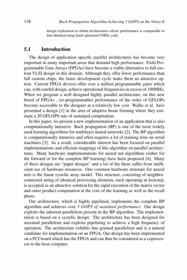
138 Back-Propagation Algorithm Achieving 5 GOPS on the Virtex-E
design exploration to obtain architectures whose performance is comparable tothat obtained using hand optimized VHDL code.
5.1 Introduction
The design of application specific parallel architectures has become veryimportant in many important areas that demand high performance. Field Pro-grammable Gate Arrays (FPGAs) have become a viable alternative to full cus-tom VLSI design in this domain. Although they offer lower performance thanfull custom chips, the faster development cycle make them an attractive op-tion. Current FPGA devices offer over a million programmable gates whichcan, with careful design, achieve operational frequencies in excess of 100MHz.When we program a well designed highly parallel architecture, on this newbreed of FPGAs , (re-programmable) performance of the order of GFLOPsbecome accessible to the designer at a relatively low cost. Walke et al. havepresented a design [1] in the area of adaptive beam forming where they esti-mate a 20 GFLOPS rate of sustained computation.
In this paper, we present a new implementation of an application that is alsocomputationally intensive. Back propagation (BP) is one of the most widelyused learning algorithms for multilayer neural networks [2]. The BP algorithmis computationally intensive and often requires a lot of training time on serialmachines [3]. As a result, considerable interest has been focused on parallelimplementations and efficient mappings of this algorithm on parallel architec-tures. Many hardware implementations for neural net algorithms (either forthe forward or for the complete BP learning) have been proposed [4]. Manyof these designs are “paper designs" and a lot of the them suffer from ineffi-cient use of hardware resources. One common hardware structure for neuralnets is the linear systolic array model. This structure, consisting of neighbor-connected string of identical processing elements, each operating in lockstep,is accepted as an attractive solution for the rapid execution of the matrix vectorand outer product computation at the core of the learning as well as the recallphase.
Our architecture, which is highly pipelined, implements the complete BPalgorithm and achieves over 5 GOPS of sustained performance. Our designexploits the inherent parallelism present in the BP algorithm. The implemen-tation is based on a systolic design. The architecture has been designed formaximal parallelism and exploits pipelining to achieve a high frequency ofoperation. The architecture exhibits fine grained parallelism and is a naturalcandidate for implementation on an FPGA. Our design has been implementedon a PCI board which has the FPGA and can thus be considered as a coproces-sor to the host computer.
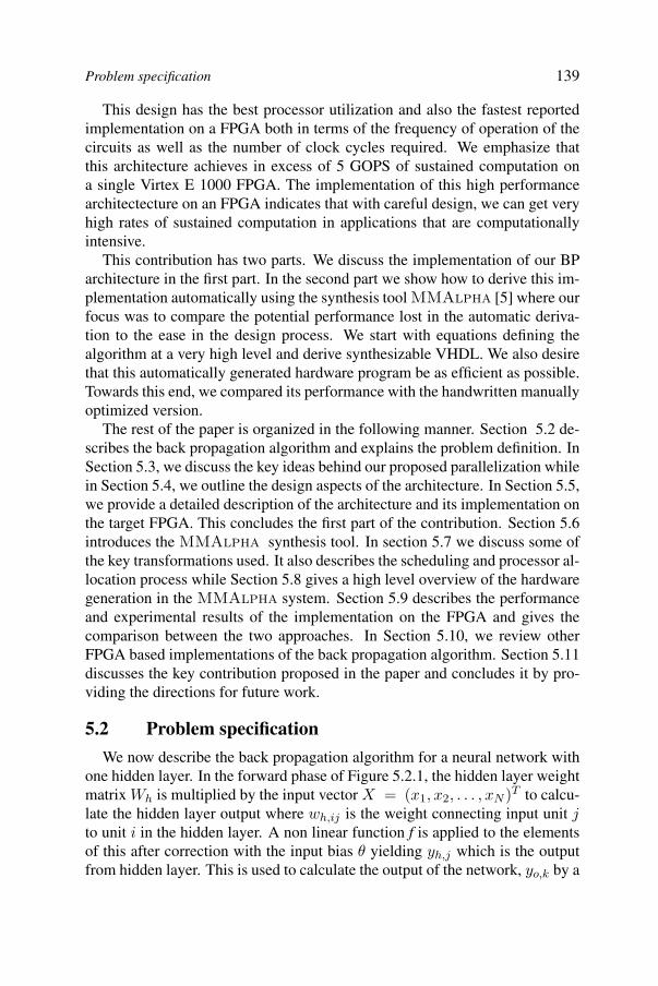
Problem specification 139
This design has the best processor utilization and also the fastest reportedimplementation on a FPGA both in terms of the frequency of operation of thecircuits as well as the number of clock cycles required. We emphasize thatthis architecture achieves in excess of 5 GOPS of sustained computation ona single Virtex E 1000 FPGA. The implementation of this high performancearchitectecture on an FPGA indicates that with careful design, we can get veryhigh rates of sustained computation in applications that are computationallyintensive.
This contribution has two parts. We discuss the implementation of our BParchitecture in the first part. In the second part we show how to derive this im-plementation automatically using the synthesis tool MMAlpha [5] where ourfocus was to compare the potential performance lost in the automatic deriva-tion to the ease in the design process. We start with equations defining thealgorithm at a very high level and derive synthesizable VHDL. We also desirethat this automatically generated hardware program be as efficient as possible.Towards this end, we compared its performance with the handwritten manuallyoptimized version.
The rest of the paper is organized in the following manner. Section 5.2 de-scribes the back propagation algorithm and explains the problem definition. InSection 5.3, we discuss the key ideas behind our proposed parallelization whilein Section 5.4, we outline the design aspects of the architecture. In Section 5.5,we provide a detailed description of the architecture and its implementation onthe target FPGA. This concludes the first part of the contribution. Section 5.6introduces the MMAlpha synthesis tool. In section 5.7 we discuss some ofthe key transformations used. It also describes the scheduling and processor al-location process while Section 5.8 gives a high level overview of the hardwaregeneration in the MMAlpha system. Section 5.9 describes the performanceand experimental results of the implementation on the FPGA and gives thecomparison between the two approaches. In Section 5.10, we review otherFPGA based implementations of the back propagation algorithm. Section 5.11discusses the key contribution proposed in the paper and concludes it by pro-viding the directions for future work.
5.2 Problem specification
We now describe the back propagation algorithm for a neural network withone hidden layer. In the forward phase of Figure 5.2.1, the hidden layer weightmatrix Wh is multiplied by the input vector X = (x1, x2, . . . , xN )T to calcu-late the hidden layer output where wh,ij is the weight connecting input unit jto unit i in the hidden layer. A non linear function f is applied to the elementsof this after correction with the input bias θ yielding yh,j which is the outputfrom hidden layer. This is used to calculate the output of the network, yo,k by a
140 Back-Propagation Algorithm Achieving 5 GOPS on the Virtex-E
Input
Output
Hidden Layer Forw
ard
BA
CK
PRO
P
III
IV
V
VI
II
I
Figure 5.2.1: The Backpropagation Algorithm
Section BPNEquations OurNotation EqNo
I yh,j = f(∑Ni
i=1 wh,jixi − θ)Y1 = W1XY2 = f(Y1)
AB
II yo,k = f(∑Nh
j=1 wo,kjyh,j − θ)Y3 = W2Y2Y4 = f(Y3)
CD
III δo,k = yo,k(1 − yo,k)(dk − yo,k)Y5 = Y4(1 − Y4)∗
(D − Y4)E
IV δh,j = yh,j(1 − yh,j)∑No
k=1 δo,kwo,kjY6 = W T
2 Y5Y7 = Y2(1 − Y2)Y6
FG
V∆wo,kj = ηδo,kyh,j
w′o,kj = wo,kj + ∆wo,kj
∆W2 = Y5 ⊗ Y2W ′
2 = W2 + ∆W2
IJ
V I∆wh,ji = ηδh,jxi
w′h,ji = wh,ji + ∆wh,ji
∆W1 = Y7 ⊗ XW ′
1 = W1 + ∆W1
KL
(5.1)
Table 5.1. Equations for The Back Propagation Algorithm. Capitals denote either thematrix of the values of the weights or vectors representing the inputs and outputs. Theouter product of two vectors is denoted by ⊗
similar process using a different weight matrix Wo. The expected output is dk
and it is used to update the weights. A vector δo is computed from yo and d (byelement wise operation) and the update to the Wo matrix is simply the outerproduct of δo and yh scaled by a learning parameter η. Similarly a vector δhk iscomputed by the element wise operation on yh and the matrix vector product ofW T
o and δo. The update to the Wh matrix is also computed as η times the outerproduct of δh and X . The flow of computation is illustrated in Figure 5.2.1where the roman numerals refer to the rows on Table 1. In our discussion, weignore the learning parameter and input bias to avoid clutter. Moreover, theyare scaling factors and may be trivially incorporated in the implementation.
The BP algorithm may be succinctly specified as a sequence of threeMatrix Vector Multiplications or MVMs (Equations A, C and F) ) and
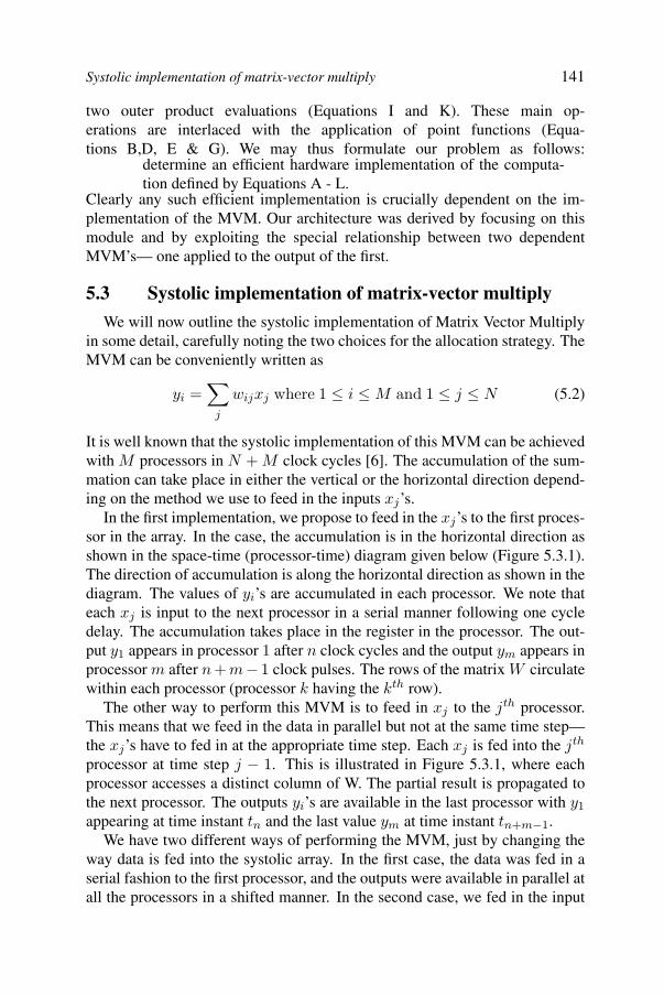
Systolic implementation of matrix-vector multiply 141
two outer product evaluations (Equations I and K). These main op-erations are interlaced with the application of point functions (Equa-tions B,D, E & G). We may thus formulate our problem as follows:
determine an efficient hardware implementation of the computa-tion defined by Equations A - L.
Clearly any such efficient implementation is crucially dependent on the im-plementation of the MVM. Our architecture was derived by focusing on thismodule and by exploiting the special relationship between two dependentMVM’s— one applied to the output of the first.
5.3 Systolic implementation of matrix-vector multiply
We will now outline the systolic implementation of Matrix Vector Multiplyin some detail, carefully noting the two choices for the allocation strategy. TheMVM can be conveniently written as
yi =∑
j
wijxj where 1 ≤ i ≤ M and 1 ≤ j ≤ N (5.2)
It is well known that the systolic implementation of this MVM can be achievedwith M processors in N + M clock cycles [6]. The accumulation of the sum-mation can take place in either the vertical or the horizontal direction depend-ing on the method we use to feed in the inputs xj’s.
In the first implementation, we propose to feed in the xj’s to the first proces-sor in the array. In the case, the accumulation is in the horizontal direction asshown in the space-time (processor-time) diagram given below (Figure 5.3.1).The direction of accumulation is along the horizontal direction as shown in thediagram. The values of yi’s are accumulated in each processor. We note thateach xj is input to the next processor in a serial manner following one cycledelay. The accumulation takes place in the register in the processor. The out-put y1 appears in processor 1 after n clock cycles and the output ym appears inprocessor m after n + m− 1 clock pulses. The rows of the matrix W circulatewithin each processor (processor k having the kth row).
The other way to perform this MVM is to feed in xj to the jth processor.This means that we feed in the data in parallel but not at the same time step—the xj’s have to fed in at the appropriate time step. Each xj is fed into the jth
processor at time step j − 1. This is illustrated in Figure 5.3.1, where eachprocessor accesses a distinct column of W. The partial result is propagated tothe next processor. The outputs yi’s are available in the last processor with y1
appearing at time instant tn and the last value ym at time instant tn+m−1.We have two different ways of performing the MVM, just by changing the
way data is fed into the systolic array. In the first case, the data was fed in aserial fashion to the first processor, and the outputs were available in parallel atall the processors in a shifted manner. In the second case, we fed in the input
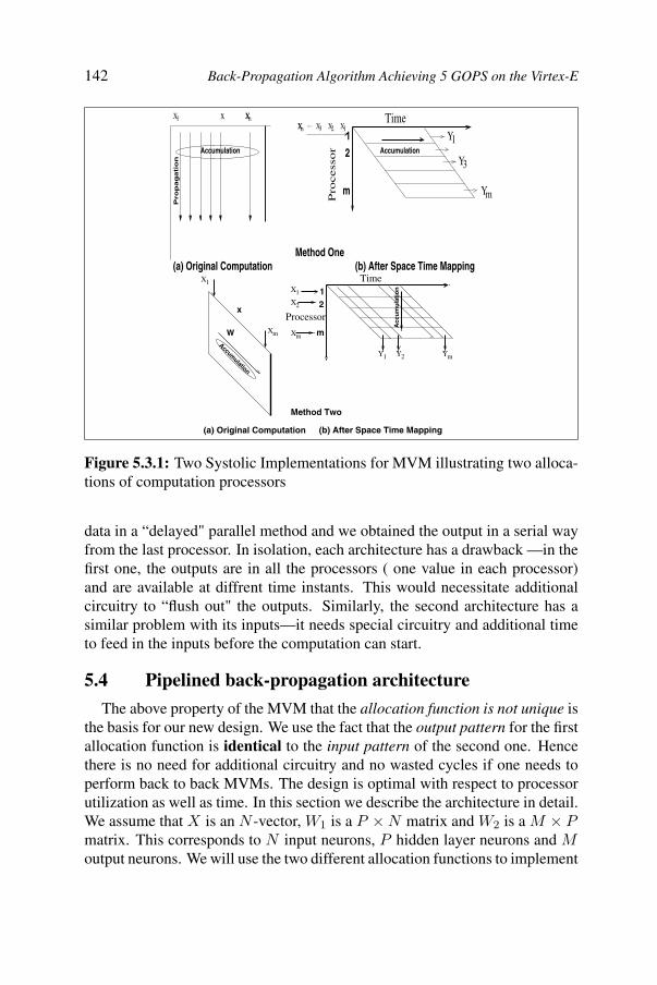
142 Back-Propagation Algorithm Achieving 5 GOPS on the Virtex-E
Y1
3Y
X1X2X3XnX ....
Ym
X1 XnXx
1
m
Pro
cess
or Accumulation2
Time
Accumulation
Pro
pa
ga
tio
n
(a) Original Computation (b) After Space Time MappingMethod One
Y2 Ym
X1
X2
Xm
Y1
X1
Xm
x
WAccum
ulation
(a) Original Computation
1
m
2Processor
Time
Acc
um
ula
tio
n
(b) After Space Time Mapping
Method Two
Figure 5.3.1: Two Systolic Implementations for MVM illustrating two alloca-tions of computation processors
data in a “delayed" parallel method and we obtained the output in a serial wayfrom the last processor. In isolation, each architecture has a drawback —in thefirst one, the outputs are in all the processors ( one value in each processor)and are available at diffrent time instants. This would necessitate additionalcircuitry to “flush out" the outputs. Similarly, the second architecture has asimilar problem with its inputs—it needs special circuitry and additional timeto feed in the inputs before the computation can start.
5.4 Pipelined back-propagation architecture
The above property of the MVM that the allocation function is not unique isthe basis for our new design. We use the fact that the output pattern for the firstallocation function is identical to the input pattern of the second one. Hencethere is no need for additional circuitry and no wasted cycles if one needs toperform back to back MVMs. The design is optimal with respect to processorutilization as well as time. In this section we describe the architecture in detail.We assume that X is an N -vector, W1 is a P × N matrix and W2 is a M × Pmatrix. This corresponds to N input neurons, P hidden layer neurons and Moutput neurons. We will use the two different allocation functions to implement
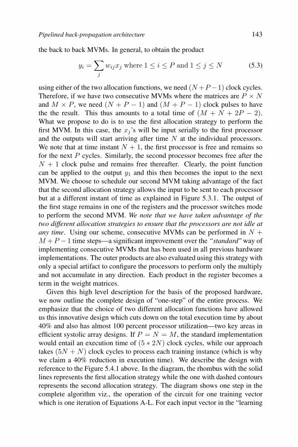
Pipelined back-propagation architecture 143
the back to back MVMs. In general, to obtain the product
yi =∑
j
wijxj where 1 ≤ i ≤ P and 1 ≤ j ≤ N (5.3)
using either of the two allocation functions, we need (N +P −1) clock cycles.Therefore, if we have two consecutive MVMs where the matrices are P × Nand M × P , we need (N + P − 1) and (M + P − 1) clock pulses to havethe the result. This thus amounts to a total time of (M + N + 2P − 2).What we propose to do is to use the first allocation strategy to perform thefirst MVM. In this case, the xj’s will be input serially to the first processorand the outputs will start arriving after time N at the individual processors.We note that at time instant N + 1, the first processor is free and remains sofor the next P cycles. Similarly, the second processor becomes free after theN + 1 clock pulse and remains free thereafter. Clearly, the point functioncan be applied to the output y1 and this then becomes the input to the nextMVM. We choose to schedule our second MVM taking advantage of the factthat the second allocation strategy allows the input to be sent to each processorbut at a different instant of time as explained in Figure 5.3.1. The output ofthe first stage remains in one of the registers and the processor switches modeto perform the second MVM. We note that we have taken advantage of thetwo different allocation strategies to ensure that the processors are not idle atany time. Using our scheme, consecutive MVMs can be performed in N +M +P −1 time steps—a significant improvement over the “standard" way ofimplementing consecutive MVMs that has been used in all previous hardwareimplementations. The outer products are also evaluated using this strategy withonly a special artifact to configure the processors to perform only the multiplyand not accumulate in any direction. Each product in the register becomes aterm in the weight matrices.
Given this high level description for the basis of the proposed hardware,we now outline the complete design of “one-step” of the entire process. Weemphasize that the choice of two different allocation functions have allowedus this innovative design which cuts down on the total execution time by about40% and also has almost 100 percent processor utilization—two key areas inefficient systolic array designs. If P = N = M , the standard implementationwould entail an execution time of (5 ∗ 2N) clock cycles, while our approachtakes (5N + N) clock cycles to process each training instance (which is whywe claim a 40% reduction in execution time). We describe the design withreference to the Figure 5.4.1 above. In the diagram, the rhombus with the solidlines represents the first allocation strategy while the one with dashed contoursrepresents the second allocation strategy. The diagram shows one step in thecomplete algorithm viz., the operation of the circuit for one training vectorwhich is one iteration of Equations A-L. For each input vector in the “learning
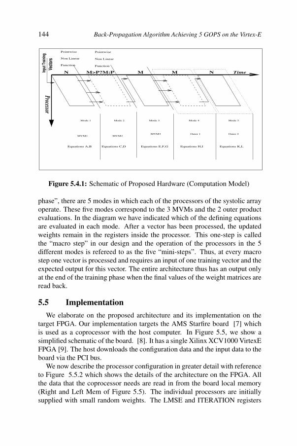
144 Back-Propagation Algorithm Achieving 5 GOPS on the Virtex-E
Non Linear
Pointwise
Function
Non Linear
Pointwise
Function
MVM3
Mode 1
MVM1 MVM2
Mode 2 Mode 4 Mode 5Mode 3
Outer 1 Outer 2
Input
Train
ing
Vecto
rs
Equations A,B Equations C,D Equations E,F,G Equations H,I Equations K,L
N NM>P?M:P M M
Processor
Time
Figure 5.4.1: Schematic of Proposed Hardware (Computation Model)
phase”, there are 5 modes in which each of the processors of the systolic arrayoperate. These five modes correspond to the 3 MVMs and the 2 outer productevaluations. In the diagram we have indicated which of the defining equationsare evaluated in each mode. After a vector has been processed, the updatedweights remain in the registers inside the processor. This one-step is calledthe “macro step” in our design and the operation of the processors in the 5different modes is refereed to as the five “mini-steps”. Thus, at every macrostep one vector is processed and requires an input of one training vector and theexpected output for this vector. The entire architecture thus has an output onlyat the end of the training phase when the final values of the weight matrices areread back.
5.5 Implementation
We elaborate on the proposed architecture and its implementation on thetarget FPGA. Our implementation targets the AMS Starfire board [7] whichis used as a coprocessor with the host computer. In Figure 5.5, we show asimplified schematic of the board. [8]. It has a single Xilinx XCV1000 VirtexEFPGA [9]. The host downloads the configuration data and the input data to theboard via the PCI bus.
We now describe the processor configuration in greater detail with referenceto Figure 5.5.2 which shows the details of the architecture on the FPGA. Allthe data that the coprocessor needs are read in from the board local memory(Right and Left Mem of Figure 5.5). The individual processors are initiallysupplied with small random weights. The LMSE and ITERATION registers
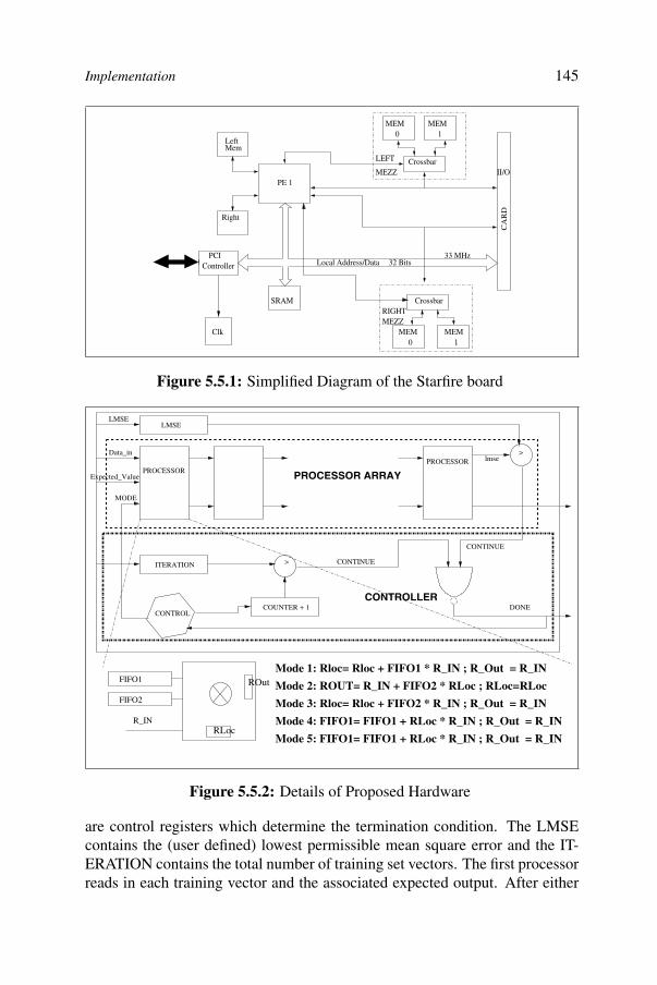
Implementation 145
PE 1
Left
Right
MEM
LEFT
MEZZ
0 1MEM
Crossbar
Mem
PCIController
SRAM
Local Address/Data 32 Bits33 MHz
Clk
II/O
CA
RD
MEM MEM 1
Crossbar
0
MEZZRIGHT
Figure 5.5.1: Simplified Diagram of the Starfire board
Mode 1: Rloc= Rloc + FIFO1 * R_IN ; R_Out = R_IN
Mode 2: ROUT= R_IN + FIFO2 * RLoc ; RLoc=RLoc
Mode 3: Rloc= Rloc + FIFO2 * R_IN ; R_Out = R_IN
Mode 4: FIFO1= FIFO1 + RLoc * R_IN ; R_Out = R_IN
Mode 5: FIFO1= FIFO1 + RLoc * R_IN ; R_Out = R_IN
FIFO1
FIFO2
R_INRLoc
ROut
LMSE
ITERATION
COUNTER + 1
PROCESSORPROCESSOR
CONTINUE
DONE
MODE
Expected_Value
Data_in
LMSE
>
>
CONTINUE
lmse
PROCESSOR ARRAY
CONTROLLERCONTROL
Figure 5.5.2: Details of Proposed Hardware
are control registers which determine the termination condition. The LMSEcontains the (user defined) lowest permissible mean square error and the IT-ERATION contains the total number of training set vectors. The first processorreads in each training vector and the associated expected output. After either
146 Back-Propagation Algorithm Achieving 5 GOPS on the Virtex-E
the least mean square error is lower than LMSE or the number of training setvectors are exhausted, the processor downloads the final weight vectors to thelocal memory and issues the ‘done’ signal to the host. The host then reads outthe final weight values. The entire operation is thus compute bound. In eachmacro step, only the first processor reads in a sequence of 2N vectors in onlyone of the five phases of “one-step" of the computation. The system has anoutput only once at the end of the entire training phase.
In Figure 5.4.1 we show the space time diagram of the computation ofone step in the entire computation. The one step of the computation takes ina n-size vector and does a MVM. This takes n clock ticks on a p processorsystolic array. We have a point wise function applied to the output of eachprocessor and this is then fed as input to the processor to perform the nextMVM. This second MVM continues for m or p cycles whichever is greater asindicated in the diagram. The outputs from the last processor are fed into thefirst processor after this time interval so that the third MVM can begin. In thefinal two modes, the processors actually evaluate the products and update theshift registers containing the weight values.
The operation of the processor in the five modes is described in Figure 5.5.2.We have shown the operations during each of the five modes of operation. Wehave abstracted away the portions of the circuit inside the processor which re-main inactive during a particular mode and only show the relevant sectionswhich are enabled. The mode signal controls this enabling/disabling of com-ponents inside the processors. For example, in mode 1 , the first shift registerbank which contains the row of W1 matrix, is enabled and the other similarbank being disabled are omitted from the diagram. Also in this mode, eachprocessor at the end of the accumulation phase needs to evaluate the non linearfunction f on the final value before switching modes. We have implementedthis function as a table lookup. In this mode, at any given time, one and onlyone of the processors will be accessing the LUT. Hence the LUT is designedas a shared resource between the individual processors of the array. We alsohave one additional processor following the “last” processor. This processor isactive only in mode 2 and evaluates equation 14. This enables us to decreasethe length of the critical path and improve the frequency of operation of theentire circuit. This is a design choice that we have made noting that the controlbecomes simpler if we use some of the registers to make an additional proces-sor instead of incorporating the functionality in the last processor. The resultof the multiply at each time step is added to the content of the appropriate shiftregister output to reflect the updated value of the weight matrices. We notein the figure, that except for mode 1, the multiply-accumulator unit in eachprocessor in all other modes takes its input either from the shift registers oran internal register. The register, in general, contains the value computed in
MMAlpha design environment 147
a previous mode. Thus in four out of five “mini steps” of each “macro step”,there is no IO involved.
We decided to see if it was possible to derive a similar architecture automat-ically starting with the equations describing the computation. There are a lotof systems which take a high level description of the system in C/Matlab andderive synthesizable RTL level descriptions [10, 11]. However, most of thesesystems require that we write the description making the parallelism explicit.The motivation for trying to see if we could get a high performance VHDLdescription of the network automatically starting from the equations was to re-duce the implementation time of the designing and coding in VHDL. We shallwalk through, in detail, the automatic derivation of this architecture using ourcodesign research prototype “MMAlpha".
5.6 MMAlpha design environment
We used the systolic design prototype tool MMAlpha to systematicallyderive the RTL description of the proposed implementation. In this section wedescribe briefly the characteristics of this design environment. We also give atop level overview of the design procedure.
5.6.1 The Alpha Language
We use Alpha [5] as the language to write our algorithm. The Alpha lan-guage was conceived in 1989 by Christophe Mauras as part of his PhD thesis.The MMAlpha system was initially developed at IRISA, and since 1995, itsfurther development is being done at IRISA in collaboration with BYU [12]and CSU [13].
Alpha is a single assignment, equational (functional), and inherently par-allel language, based on the formalism of systems of recurrence equations.Algorithms may be represented at a very high level in Alpha , similar to howone might specify them mathematically. The basic advantage of writing thealgorithm in this functional language is that it allows us the ability to reasonabout the system. The Alpha language is restrictive in the class of algorithmsit can easily represent (although the language is Turing complete), but is usefulfor programming algorithms which have a high degree of regularity and par-allelism such as those frequently occurring in linear algebra and digital signalprocessing applications.
Computational entities in Alpha are called systems [5], which are parallelfunctions relating the system outputs to system inputs. The Alpha systemdeclaration specifies the types and domains of system inputs and outputs. Thedefinition of the system function is given as a set of affine recurrence equationsinvolving input, outpu t, and local variables.
148 Back-Propagation Algorithm Achieving 5 GOPS on the Virtex-E
One of Alpha’s strengths is the fact that an Alpha program can be trans-formed by a series of rewriting rules into equivalent Alpha programs suitablefor:
implementation as a regular array circuit, or
execution on a sequential or parallel computer.
This capability is provided by the MMAlpha system. Alpha program trans-formations have been independently proved to preserve the semantics of theoriginal program, and thus derived programs are correct by construction (as-suming the specification was correct). Alpha also allows the analyzabilityneeded to help choose what transformations to perform.The MMAlpha SystemThe “transformation engine" interface for manipulating Alpha programs iswritten in C and Mathematica. The user interface is in Mathematica whichprovides an interpreted language with high level built in functions for symboliccomputations. MMAlpha uses these facilities for transforming Alpha pro-grams.
The internal representation of any Alpha program is stored as an AbstractSyntax Tree (AST). All computations and manipulations are performed on thisinternal representation. Typical commands include viewing an Alpha pro-gram, checking its correctness, generating C code to execute the program, etc.
Specific C functions are used for two purposes: various parsers and un-parsers, and computations on polyhedra. All the C functions are accessed viaMathematica and extensively use the polyhedral library [14] which is the com-putational kernel of the MMAlpha system.
The design flow with MMAlpha is illustrated in Figure 5.6.1. A compu-tation intensive part of a program (usually a loop) is rewritten in Alpha andis then transformed using MMAlpha into an implementation which consistsof three programs:
The hardware part (in VHDL) which represents the implementation ofthe loop on the FPGA.
The software part which replaces the loop in the original program.
The hardware/software interface part which handles the communicationof data betweeen the host and the FPGA.
MMAlpha is not a push button system, but requires the user to be “in theloop" as an “expert" who can take the initial specification of the program andapply the required transformations (intelligently) so that we get the three pro-grams as mentioned above. We shall go through a detailed walkthrough of theentire process in the derivation of synthesizable RTL from the Alpha speci-fication of “one step" of the computation of the back propagation network to
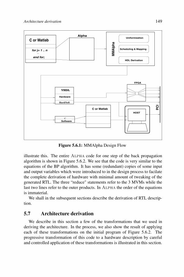
Architecture derivation 149
C
AlphaUniformization
Scheduling & Mapping
HDL Derivation
MM
Alp
ha
VHDL
Hardware
FPGA
C or Matlab
Software
PC
I
...for j= 1 .. n
end for;
C or Matlab
Hard/Soft
HOST
Figure 5.6.1: MMAlpha Design Flow
illustrate this. The entire Alpha code for one step of the back propagationalgorithm is shown in Figure 5.6.2. We see that the code is very similar to theequations of the BP algorithm. It has some (redundant) copies of some inputand output variables which were introduced to in the design process to facilatethe complete derivation of hardware with minimal amount of tweaking of thegenerated RTL. The three “reduce" statements refer to the 3 MVMs while thelast two lines refer to the outer products. In Alpha the order of the equationsis immaterial.
We shall in the subsequent sections describe the derivation of RTL descrip-tion.
5.7 Architecture derivation
We describe in this section a few of the transformations that we used inderiving the architecture. In the process, we also show the result of applyingeach of these transformations on the initial program of Figure 5.6.2. Theprogressive transformation of this code to a hardware description by carefuland controlled application of these transformations is illustrated in this section.
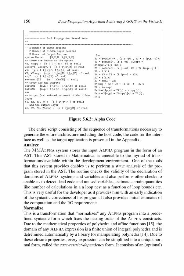
150 Back-Propagation Algorithm Achieving 5 GOPS on the Virtex-E
--======================================================================------------------ Back Propagation Neural Nets----======================================================================---- N Number of Input Neurons-- P Number of hidden layer neurons-- M Number of Output Neuronssystem Neural : {N,P,M |2≤M,N,P}-- these are inputs to the system(x, xcopy : {n | 1 ≤ n ≤ N} of real;Z4copy1, Z4copy2 : {m | 1≤m≤M} of real;W1: {p,n | 1≤p≤P; 1≤n≤N} of real;W2, W2copy: {m,p | 1≤m≤M; 1≤p≤P} of real;expZ : {m | 1≤m≤M} of real)returns (Z4 : {m | 1≤m≤M} of real;-- these are the outputsDeltaW1: {p,n | 1≤p≤P; 1≤n≤N} of real;DeltaW2: {m,p | 1≤m≤M; 1≤p≤P} of real);var-- output (and related vectors) of the hiddenlayerY1, Y2, Y3, Y4 : {p | 1≤p≤P } of real;-- and the output layerZ1, Z2, Z3, Z4comp : {m | 1≤m≤M} of real;
letY1 = reduce (+ , (p,n→p) , W1 * x.(p,n→n));Y3 = reduce(+, (m,p→p), W2copy *Z4copy1.(m,p→m));Z1 = reduce(+, (m,p→m), W2 * Y2.(m,p→p));Y2 = f(Y1);Y4 = Y3 * Y2 * (1.(p→) - Y2);Z2 = f(Z1);Z3 = expZ - Z2;Z4comp = Z3 * Z2 * (1.(m→) - Z2);Z4 = Z4comp;DeltaW1[p,n] = Y4[p] * xcopy[n];DeltaW2[m,p] = Z4copy2[m] * Y2[p];tel;
Figure 5.6.2: Alpha Code
The entire script consisting of the sequence of transformations necessary togenerate the entire architecture including the host code, the code for the inter-face as well as the target application is presented in the Appendix.AnalyzeThe MMAlpha system stores the input Alpha program in the form of anAST. This AST stored in Mathematica, is amenable to the myriad of trans-formations available within the development environment. One of the toolsthat this system provides enables us to perform a static analysis of the pro-gram stored in the AST. The routine checks the validity of the declaration ofdomains of Alpha systems and variables and also performs other checks toenable us to detect dead code and unused variables, estimate certain quantitieslike number of calculations in a a loop nest as a function of loop bounds etc.This is very useful for the developer as it provides him with an early indicationof the syntactic correctness of his program. It also provides initial estimates ofthe computation and the I/O requirements.NormalizeThis is a transformation that “normalizes" any Alpha program into a prede-fined syntactic form which fixes the nesting order of the Alpha constructs.Due to the mathematical properties of polyhedra and affine functions [15], thedomain of any Alpha expression is a finite union of integral polyhedra and isdetremined automatically by a library for manipulating polyhedra [14]. Due tothese closure properties, every expression can be simplified into a unique nor-mal form, called the case-restrict-dependency form. It consists of an (optional)
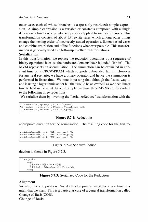
Architecture derivation 151
outer case, each of whose branches is a (possibly restricted) simple expres-sion. A simple expression is a variable or constants composed with a singledependency function or pointwise operators applied to such expressions. Thistransformation consists of about 35 rewrite rules which among other thingschange the nesting order of incorrectly nested operations, flatten nested casesand combine restriction and affine functions whenever possible. This transfor-mation is generally used as a followup to other transformations.SerializationIn this transformation, we replace the reduction operations by a sequence ofbinary operations because the hardware elements have bounded “fan in". TheMVM represents an accumulation. The summation can be evaluated in con-stant time on a CRCW-PRAM which supports unbounded fan in. Howeverfor any real scenario, we have a binary operator and hence the summation isperformed in linear time. We note in passing that although the fastest way toadd is using a logarithmic adder but that would be an overkill as we need lineartime to feed in the input. In our example, we have three MVMs correspondingto the following three reductions.We serialize them by invoking the “serializeReduce" transformation with the
Y1 = reduce (+ , (p,n→p) , W1 ∗ x.(p,n→n));Y3 = reduce (+ , (m,p→p) , W2copy ∗ Z4copy1.(m,p→m));Z1 = reduce (+ , (m,p→m) , W2 ∗ Y2.(m,p→p));
Figure 5.7.1: Reductions
appropriate direction for the serialization. The resulting code for the first re-
serializeReduce[6, 1, 2, "YY1.(p,n→p,n-1)"];serializeReduce[6, 3, 2, "YY3.(m,p→m-1,p)"];serializeReduce[6, 5, 2, "ZZ1.(m,p→m,p-1)"];
Figure 5.7.2: SerializeReduce
duction is shown in Figure 5.7.3.
YY1acc[p,n] =case
{ | n=1} : 0[] + W1 * x[1];{ | 2<=n} : YY1acc[p,n-1] + W1 * x[n];
esac;
Figure 5.7.3: Serialized Code for the Reduction
AlignmentWe align the computation. We do this keeping in mind the space time dia-gram that we want. This is a particular case of a general transformation calledChange of Basis(COB).Change of Basis
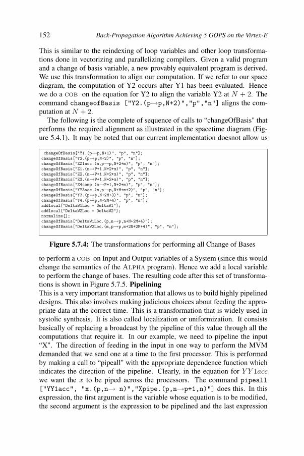
152 Back-Propagation Algorithm Achieving 5 GOPS on the Virtex-E
This is similar to the reindexing of loop variables and other loop transforma-tions done in vectorizing and parallelizing compilers. Given a valid programand a change of basis variable, a new provably equivalent program is derived.We use this transformation to align our computation. If we refer to our spacediagram, the computation of Y2 occurs after Y1 has been evaluated. Hencewe do a cob on the equation for Y2 to align the variable Y2 at N + 2. Thecommand changeofBasis ["Y2.(p→p,N+2)","p","n"] aligns the com-putation at N + 2.
The following is the complete of sequence of calls to “changeOfBasis" thatperforms the required alignment as illustrated in the spacetime diagram (Fig-ure 5.4.1). It may be noted that our current implementation doesnot allow us
changeOfBasis["Y1.(p→p,N+1)", "p", "n"];changeOfBasis["Y2.(p→p,N+2)", "p", "n"];changeOfBasis["ZZ1acc.(m,p→p,N+2+m)", "p", "n"];changeOfBasis["Z1.(m→P+1,N+2+m)", "p", "n"];changeOfBasis["Z2.(m→P+1,N+2+m)", "p", "n"];changeOfBasis["Z3.(m→P+1,N+2+m)", "p", "n"];changeOfBasis["Z4comp.(m→P+1,N+2+m)", "p", "n"];changeOfBasis["YY3acc.(m,p→p,N+M+m+2)", "p", "n"];changeOfBasis["Y3.(p→p,N+2M+3)", "p", "n"];changeOfBasis["Y4.(p→p,N+2M+4)", "p", "n"];addlocal["DeltaW1Loc = DeltaW1"];addlocal["DeltaW2Loc = DeltaW2"];normalize[];changeOfBasis["DeltaW1Loc.(p,n→p,n+N+2M+4)"];changeOfBasis["DeltaW2Loc.(m,p→p,m+2N+2M+4)", "p", "n"];
Figure 5.7.4: The transformations for performing all Change of Bases
to perform a cob on Input and Output variables of a System (since this wouldchange the semantics of the Alpha program). Hence we add a local variableto perform the change of bases. The resulting code after this set of transforma-tions is shown in Figure 5.7.5. PipeliningThis is a very important transformation that allows us to build highly pipelineddesigns. This also involves making judicious choices about feeding the appro-priate data at the correct time. This is a transformation that is widely used insystolic synthesis. It is also called localization or uniformization. It consistsbasically of replacing a broadcast by the pipeline of this value through all thecomputations that require it. In our example, we need to pipeline the input“X". The direction of feeding in the input in one way to perform the MVMdemanded that we send one at a time to the first processor. This is performedby making a call to “pipeall" with the appropriate dependence function whichindicates the direction of the pipeline. Clearly, in the equation for Y Y 1accwe want the x to be piped across the processors. The command pipeall["YY1acc", "x.(p,n→ n)","Xpipe.(p,n→p+1,n)"] does this. In thisexpression, the first argument is the variable whose equation is to be modified,the second argument is the expression to be pipelined and the last expression
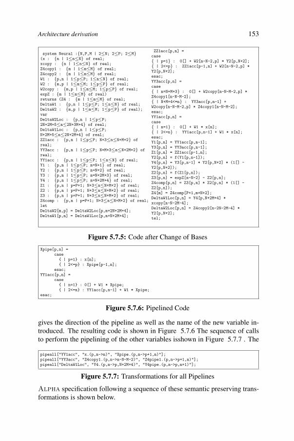
Architecture derivation 153
system Neural :{N,P,M | 2≤N; 2≤P; 2≤M}(x : {n | 1≤n≤N} of real;xcopy : {n | 1≤n≤N} of real;Z4copy1 : {m | 1≤m≤M} of real;Z4copy2 : {m | 1≤m≤M} of real;W1 : {p,n | 1≤p≤P; 1≤n≤N} of real;W2 : {m,p | 1≤m≤M; 1≤p≤P} of real;W2copy : {m,p | 1≤m≤M; 1≤p≤P} of real;expZ : {m | 1≤m≤M} of real)returns (Z4 : {m | 1≤m≤M} of real;DeltaW1 : {p,n | 1≤p≤P; 1≤n≤N} of real;DeltaW2 : {m,p | 1≤m≤M; 1≤p≤P} of real);varDeltaW2Loc : {p,n | 1≤p≤P;2N+2M+5≤n≤2N+3M+4} of real;DeltaW1Loc : {p,n | 1≤p≤P;N+2M+5≤n≤2N+2M+4} of real;ZZ1acc : {p,n | 1≤p≤P; N+3≤n≤N+M+2} ofreal;YY3acc : {p,n | 1≤p≤P; N+M+3≤n≤N+2M+2} ofreal;YY1acc : {p,n | 1≤p≤P; 1≤n≤N} of real;Y1 : {p,n | 1≤p≤P; n=N+1} of real;Y2 : {p,n | 1≤p≤P; n=N+2} of real;Y3 : {p,n | 1≤p≤P; n=N+2M+3} of real;Y4 : {p,n | 1≤p≤P; n=N+2M+4} of real;Z1 : {p,n | p=P+1; N+3≤n≤N+M+2} of real;Z2 : {p,n | p=P+1; N+3≤n≤N+M+2} of real;Z3 : {p,n | p=P+1; N+3≤n≤N+M+2} of real;Z4comp : {p,n | p=P+1; N+3≤n≤N+M+2} of real;letDeltaW2[m,p] = DeltaW2Loc[p,m+2N+2M+4];DeltaW1[p,n] = DeltaW1Loc[p,n+N+2M+4];
ZZ1acc[p,n] =case{ | p=1} : 0[] + W2[n-N-2,p] * Y2[p,N+2];{ | 2<=p} : ZZ1acc[p-1,n] + W2[n-N-2,p] *Y2[p,N+2];esac;YY3acc[p,n] =case{ | n=N+M+3} : 0[] + W2copy[n-N-M-2,p] *Z4copy1[n-N-M-2];{ | N+M+4<=n} : YY3acc[p,n-1] +W2copy[n-N-M-2,p] * Z4copy1[n-N-M-2];esac;YY1acc[p,n] =case{ | n=1} : 0[] + W1 * x[n];{ | 2<=n} : YY1acc[p,n-1] + W1 * x[n];esac;Y1[p,n] = YY1acc[p,n-1];Y3[p,n] = YY3acc[p,n-1];Z1[p,n] = ZZ1acc[p-1,n];Y2[p,n] = f(Y1[p,n-1]);Y4[p,n] = Y3[p,n-1] * Y2[p,N+2] * (1[] -Y2[p,N+2]);Z2[p,n] = f(Z1[p,n]);Z3[p,n] = expZ[n-N-2] - Z2[p,n];Z4comp[p,n] = Z3[p,n] * Z2[p,n] * (1[] -Z2[p,n]);Z4[m] = Z4comp[P+1,m+N+2];DeltaW1Loc[p,n] = Y4[p,N+2M+4] *xcopy[n-N-2M-4];DeltaW2Loc[p,n] = Z4copy2[n-2N-2M-4] *Y2[p,N+2];tel;
Figure 5.7.5: Code after Change of Bases
Xpipe[p,n] =case
{ | p=1} : x[n];{ | 2<=p} : Xpipe[p-1,n];
esac;YY1acc[p,n] =
case{ | n=1} : 0[] + W1 * Xpipe;{ | 2<=n} : YY1acc[p,n-1] + W1 * Xpipe;
esac;
Figure 5.7.6: Pipelined Code
gives the direction of the pipeline as well as the name of the new variable in-troduced. The resulting code is shown in Figure 5.7.6 The sequence of callsto perform the pipelining of the other variables isshown in Figure 5.7.7 . The
pipeall["YY1acc", "x.(p,n->n)", "Xpipe.(p,n->p+1,n)"];pipeall["YY3acc", "Z4copy1.(p,n->n-N-M-2)", "Z4pipe1.(p,n->p+1,n)"];pipeall["DeltaW1Loc", "Y4.(p,n->p,N+2M+4)", "Y4pipe.(p,n->p,n+1)"];
Figure 5.7.7: Transformations for all Pipelines
Alpha specification following a sequence of these semantic preserving trans-formations is shown below.
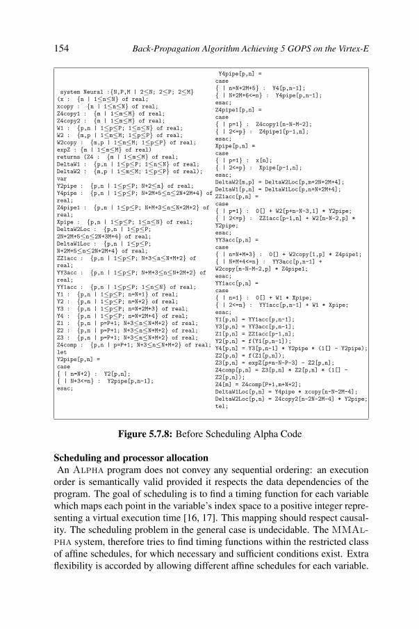
154 Back-Propagation Algorithm Achieving 5 GOPS on the Virtex-E
system Neural :{N,P,M | 2≤N; 2≤P; 2≤M}(x : {n | 1≤n≤N} of real;xcopy : {n | 1≤n≤N} of real;Z4copy1 : {m | 1≤m≤M} of real;Z4copy2 : {m | 1≤m≤M} of real;W1 : {p,n | 1≤p≤P; 1≤n≤N} of real;W2 : {m,p | 1≤m≤M; 1≤p≤P} of real;W2copy : {m,p | 1≤m≤M; 1≤p≤P} of real;expZ : {m | 1≤m≤M} of real)returns (Z4 : {m | 1≤m≤M} of real;DeltaW1 : {p,n | 1≤p≤P; 1≤n≤N} of real;DeltaW2 : {m,p | 1≤m≤M; 1≤p≤P} of real);varY2pipe : {p,n | 1≤p≤P; N+2≤n} of real;Y4pipe : {p,n | 1≤p≤P; N+2M+5≤n≤2N+2M+4} ofreal;Z4pipe1 : {p,n | 1≤p≤P; N+M+3≤n≤N+2M+2} ofreal;Xpipe : {p,n | 1≤p≤P; 1≤n≤N} of real;DeltaW2Loc : {p,n | 1≤p≤P;2N+2M+5≤n≤2N+3M+4} of real;DeltaW1Loc : {p,n | 1≤p≤P;N+2M+5≤n≤2N+2M+4} of real;ZZ1acc : {p,n | 1≤p≤P; N+3≤n≤N+M+2} ofreal;YY3acc : {p,n | 1≤p≤P; N+M+3≤n≤N+2M+2} ofreal;YY1acc : {p,n | 1≤p≤P; 1≤n≤N} of real;Y1 : {p,n | 1≤p≤P; n=N+1} of real;Y2 : {p,n | 1≤p≤P; n=N+2} of real;Y3 : {p,n | 1≤p≤P; n=N+2M+3} of real;Y4 : {p,n | 1≤p≤P; n=N+2M+4} of real;Z1 : {p,n | p=P+1; N+3≤n≤N+M+2} of real;Z2 : {p,n | p=P+1; N+3≤n≤N+M+2} of real;Z3 : {p,n | p=P+1; N+3≤n≤N+M+2} of real;Z4comp : {p,n | p=P+1; N+3≤n≤N+M+2} of real;letY2pipe[p,n] =case{ | n=N+2} : Y2[p,n];{ | N+3<=n} : Y2pipe[p,n-1];esac;
Y4pipe[p,n] =case{ | n=N+2M+5} : Y4[p,n-1];{ | N+2M+6<=n} : Y4pipe[p,n-1];esac;Z4pipe1[p,n] =case{ | p=1} : Z4copy1[n-N-M-2];{ | 2<=p} : Z4pipe1[p-1,n];esac;Xpipe[p,n] =case{ | p=1} : x[n];{ | 2<=p} : Xpipe[p-1,n];esac;DeltaW2[m,p] = DeltaW2Loc[p,m+2N+2M+4];DeltaW1[p,n] = DeltaW1Loc[p,n+N+2M+4];ZZ1acc[p,n] =case{ | p=1} : 0[] + W2[p+n-N-3,1] * Y2pipe;{ | 2<=p} : ZZ1acc[p-1,n] + W2[n-N-2,p] *Y2pipe;esac;YY3acc[p,n] =case{ | n=N+M+3} : 0[] + W2copy[1,p] * Z4pipe1;{ | N+M+4<=n} : YY3acc[p,n-1] +W2copy[n-N-M-2,p] * Z4pipe1;esac;YY1acc[p,n] =case{ | n=1} : 0[] + W1 * Xpipe;{ | 2<=n} : YY1acc[p,n-1] + W1 * Xpipe;esac;Y1[p,n] = YY1acc[p,n-1];Y3[p,n] = YY3acc[p,n-1];Z1[p,n] = ZZ1acc[p-1,n];Y2[p,n] = f(Y1[p,n-1]);Y4[p,n] = Y3[p,n-1] * Y2pipe * (1[] - Y2pipe);Z2[p,n] = f(Z1[p,n]);Z3[p,n] = expZ[p+n-N-P-3] - Z2[p,n];Z4comp[p,n] = Z3[p,n] * Z2[p,n] * (1[] -Z2[p,n]);Z4[m] = Z4comp[P+1,m+N+2];DeltaW1Loc[p,n] = Y4pipe * xcopy[n-N-2M-4];DeltaW2Loc[p,n] = Z4copy2[n-2N-2M-4] * Y2pipe;tel;
Figure 5.7.8: Before Scheduling Alpha Code
Scheduling and processor allocationAn Alpha program does not convey any sequential ordering: an execution
order is semantically valid provided it respects the data dependencies of theprogram. The goal of scheduling is to find a timing function for each variablewhich maps each point in the variable’s index space to a positive integer repre-senting a virtual execution time [16, 17]. This mapping should respect causal-ity. The scheduling problem in the general case is undecidable. The MMAl-pha system, therefore tries to find timing functions within the restricted classof affine schedules, for which necessary and sufficient conditions exist. Extraflexibility is accorded by allowing different affine schedules for each variable.
Hardware generation 155
The technique used for scheduling is to formulate the causality constraints aslinear integer programming program (LP) and to solve it using a software tool(like PIP [18]).
For the example of the neural nets, we required that the one step of thecomputation be completed in 2N + 2M + max(P, M) time (Figure 5.4.1).The scheduler in MMAlpha was able to compute this schedule. Also inthe general case, where N, M and P are not equal, the scheduler was able tocompute the optimum schedule (lowest processor idle time being the criterionfor optimality). We do a reindexing of the first dimension to represent the timeand the second processor. The resulting Alpha code is shown in Figure 5.7.9.In the next section, we describe the generation of the RTL description of thearchitecture.
5.8 Hardware generation
One of the motivating factors in this research was to derive the RTL de-scription of the high performance architecture implementing the back propa-gation algorithm. We have described the sequence of transformations whichtransformed the initial specification (Figure 5.6.2) into a form where an ex-ecution time and processor allocation has been assigned for each expression(Figure 5.7.9).
Control Signal GenerationTo realize a systolic array in hardware, control signals are necessary to
instruct each Processing Element (PE) of the array when to perform whatcomputation. MMAlpha allows us to automatically generate the controlflow information so that the right computations are done by the right PEs atthe right time steps.
Alpha0 FormatAfter the program has been uniformized and scheduled, MMAlpha translatesit to the Alpha0 format. After the program has been scheduled, the nextimportant step is the generation and pipelining of the control signal. Thereforecontrol signals are generated and multiplexors added to each processors. Thecontrols signal is then pipelined automatically by the system. The resultingAlpha0 program contains the precise information that appears on the lifetimeof each signal and on the input date of each data.Alphard FormatAlphard is a subset of the Alpha language and is used to describe regularcircuits with local interconnections and their control and is hierarchical. Atthe lowest level we have cells consisting of combinatorial circuits, registers,multiplexors, etc. A cell may also contain other cells. We also have controllers
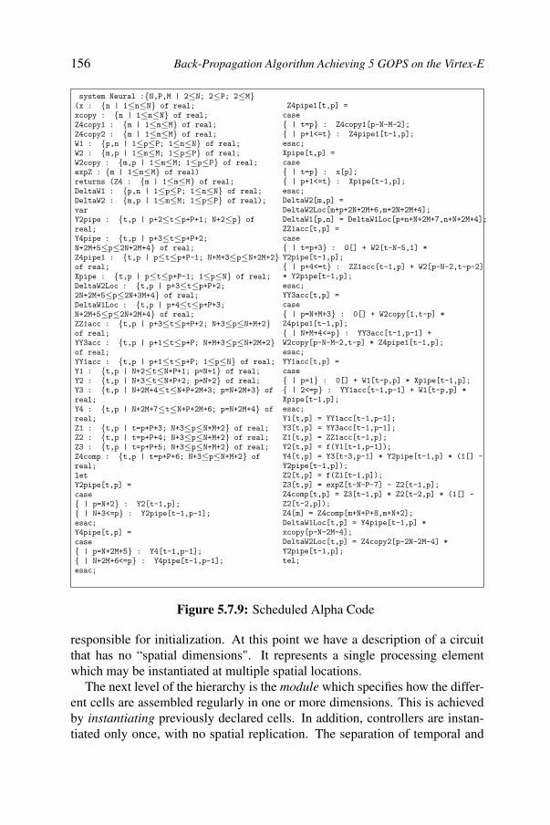
156 Back-Propagation Algorithm Achieving 5 GOPS on the Virtex-E
system Neural :{N,P,M | 2≤N; 2≤P; 2≤M}(x : {n | 1≤n≤N} of real;xcopy : {n | 1≤n≤N} of real;Z4copy1 : {m | 1≤m≤M} of real;Z4copy2 : {m | 1≤m≤M} of real;W1 : {p,n | 1≤p≤P; 1≤n≤N} of real;W2 : {m,p | 1≤m≤M; 1≤p≤P} of real;W2copy : {m,p | 1≤m≤M; 1≤p≤P} of real;expZ : {m | 1≤m≤M} of real)returns (Z4 : {m | 1≤m≤M} of real;DeltaW1 : {p,n | 1≤p≤P; 1≤n≤N} of real;DeltaW2 : {m,p | 1≤m≤M; 1≤p≤P} of real);varY2pipe : {t,p | p+2≤t≤p+P+1; N+2≤p} ofreal;Y4pipe : {t,p | p+3≤t≤p+P+2;N+2M+5≤p≤2N+2M+4} of real;Z4pipe1 : {t,p | p≤t≤p+P-1; N+M+3≤p≤N+2M+2}of real;Xpipe : {t,p | p≤t≤p+P-1; 1≤p≤N} of real;DeltaW2Loc : {t,p | p+3≤t≤p+P+2;2N+2M+5≤p≤2N+3M+4} of real;DeltaW1Loc : {t,p | p+4≤t≤p+P+3;N+2M+5≤p≤2N+2M+4} of real;ZZ1acc : {t,p | p+3≤t≤p+P+2; N+3≤p≤N+M+2}of real;YY3acc : {t,p | p+1≤t≤p+P; N+M+3≤p≤N+2M+2}of real;YY1acc : {t,p | p+1≤t≤p+P; 1≤p≤N} of real;Y1 : {t,p | N+2≤t≤N+P+1; p=N+1} of real;Y2 : {t,p | N+3≤t≤N+P+2; p=N+2} of real;Y3 : {t,p | N+2M+4≤t≤N+P+2M+3; p=N+2M+3} ofreal;Y4 : {t,p | N+2M+7≤t≤N+P+2M+6; p=N+2M+4} ofreal;Z1 : {t,p | t=p+P+3; N+3≤p≤N+M+2} of real;Z2 : {t,p | t=p+P+4; N+3≤p≤N+M+2} of real;Z3 : {t,p | t=p+P+5; N+3≤p≤N+M+2} of real;Z4comp : {t,p | t=p+P+6; N+3≤p≤N+M+2} ofreal;letY2pipe[t,p] =case{ | p=N+2} : Y2[t-1,p];{ | N+3<=p} : Y2pipe[t-1,p-1];esac;Y4pipe[t,p] =case{ | p=N+2M+5} : Y4[t-1,p-1];{ | N+2M+6<=p} : Y4pipe[t-1,p-1];esac;
Z4pipe1[t,p] =case{ | t=p} : Z4copy1[p-N-M-2];{ | p+1<=t} : Z4pipe1[t-1,p];esac;Xpipe[t,p] =case{ | t=p} : x[p];{ | p+1<=t} : Xpipe[t-1,p];esac;DeltaW2[m,p] =DeltaW2Loc[m+p+2N+2M+6,m+2N+2M+4];DeltaW1[p,n] = DeltaW1Loc[p+n+N+2M+7,n+N+2M+4];ZZ1acc[t,p] =case{ | t=p+3} : 0[] + W2[t-N-5,1] *Y2pipe[t-1,p];{ | p+4<=t} : ZZ1acc[t-1,p] + W2[p-N-2,t-p-2]* Y2pipe[t-1,p];esac;YY3acc[t,p] =case{ | p=N+M+3} : 0[] + W2copy[1,t-p] *Z4pipe1[t-1,p];{ | N+M+4<=p} : YY3acc[t-1,p-1] +W2copy[p-N-M-2,t-p] * Z4pipe1[t-1,p];esac;YY1acc[t,p] =case{ | p=1} : 0[] + W1[t-p,p] * Xpipe[t-1,p];{ | 2<=p} : YY1acc[t-1,p-1] + W1[t-p,p] *Xpipe[t-1,p];esac;Y1[t,p] = YY1acc[t-1,p-1];Y3[t,p] = YY3acc[t-1,p-1];Z1[t,p] = ZZ1acc[t-1,p];Y2[t,p] = f(Y1[t-1,p-1]);Y4[t,p] = Y3[t-3,p-1] * Y2pipe[t-1,p] * (1[] -Y2pipe[t-1,p]);Z2[t,p] = f(Z1[t-1,p]);Z3[t,p] = expZ[t-N-P-7] - Z2[t-1,p];Z4comp[t,p] = Z3[t-1,p] * Z2[t-2,p] * (1[] -Z2[t-2,p]);Z4[m] = Z4comp[m+N+P+8,m+N+2];DeltaW1Loc[t,p] = Y4pipe[t-1,p] *xcopy[p-N-2M-4];DeltaW2Loc[t,p] = Z4copy2[p-2N-2M-4] *Y2pipe[t-1,p];tel;
Figure 5.7.9: Scheduled Alpha Code
responsible for initialization. At this point we have a description of a circuitthat has no “spatial dimensions". It represents a single processing elementwhich may be instantiated at multiple spatial locations.
The next level of the hierarchy is the module which specifies how the differ-ent cells are assembled regularly in one or more dimensions. This is achievedby instantiating previously declared cells. In addition, controllers are instan-tiated only once, with no spatial replication. The separation of temporal and
Performance evaluation 157
spatial aspects is also reflected in the fact that the equations describing the be-havior of cells have only one local index variable (time) and in the equationsfor modules, the dependencies have only spatial components indicating pure(delayless) interconnections.
The architectural description given by Alphard provides
structuring, as complex designs must be hierarchical;
genericity to allow component reuse and
allows regularity to be described, in order to reuse hardware descriptionsand simplify the design process.
Synthesizable VHDLThe translation produces synthesizable VHDL (compliant with IEEE-1076standard [19] when the size parameters have been fixed. The hardware transla-tor is implemented using a syntax generated meta translator which allows fastretargeting of generator depending on the type of synthesis tools used.Interface GenerationThe MMAlpha system supports the automatic generation of interfaces be-tween the host program and the application running on the FPGA. The under-lying interface of the system consists of a bus and a FIFO that interconnectsthe bus with the application. The bus and the FIFO comprises the hardwareinterface. The FIFO allows the data to be buffered when an interruption occurson the bus. On top of the hardware interface, is built an application interfacewhose role is to rearrange as necessary, the data between the hardware interfaceand the application.
As described in the previous discussion on the hand derived code, we down-load the application data into the on board memories. This requires us to con-nect the FIFO to the onboard memories instead of the bus. This part of theinterface is dependent to a certain degree on the hardware board being used—nevertheless MMAlpha generates generic code that can be easily customizedfor the different boards. The data to be downloaded to the memory is the samereordered data that is automatically generated by the system.
5.9 Performance evaluation
In this section, we discuss the performance of our architecture for the back-propagation neural network. In the first part of this paper we described thedesign—the VHDL specification for the entire system was written and syn-thesized for the target application directed for implementation on the StarfireBoard. Subsequently we derived a VHDL description (automatically) of the ar-chitecture from a very high level specification using the MMAlpha researchtool. This gave us two circuits implemented on hardware and we present inthis section, their comparative performance figures.
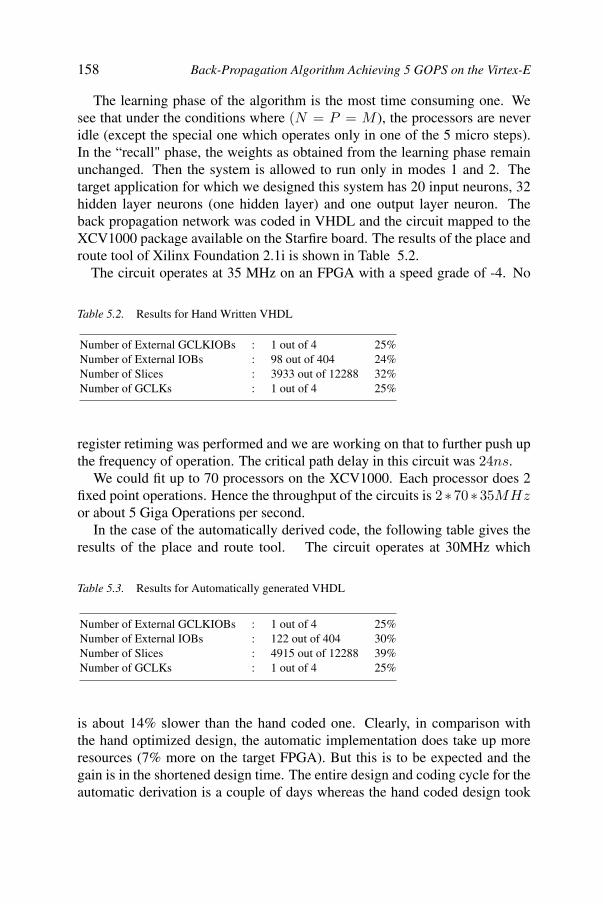
158 Back-Propagation Algorithm Achieving 5 GOPS on the Virtex-E
The learning phase of the algorithm is the most time consuming one. Wesee that under the conditions where (N = P = M ), the processors are neveridle (except the special one which operates only in one of the 5 micro steps).In the “recall" phase, the weights as obtained from the learning phase remainunchanged. Then the system is allowed to run only in modes 1 and 2. Thetarget application for which we designed this system has 20 input neurons, 32hidden layer neurons (one hidden layer) and one output layer neuron. Theback propagation network was coded in VHDL and the circuit mapped to theXCV1000 package available on the Starfire board. The results of the place androute tool of Xilinx Foundation 2.1i is shown in Table 5.2.
The circuit operates at 35 MHz on an FPGA with a speed grade of -4. No
Table 5.2. Results for Hand Written VHDL
Number of External GCLKIOBs : 1 out of 4 25%Number of External IOBs : 98 out of 404 24%Number of Slices : 3933 out of 12288 32%Number of GCLKs : 1 out of 4 25%
register retiming was performed and we are working on that to further push upthe frequency of operation. The critical path delay in this circuit was 24ns.
We could fit up to 70 processors on the XCV1000. Each processor does 2fixed point operations. Hence the throughput of the circuits is 2∗70∗35MHzor about 5 Giga Operations per second.
In the case of the automatically derived code, the following table gives theresults of the place and route tool. The circuit operates at 30MHz which
Table 5.3. Results for Automatically generated VHDL
Number of External GCLKIOBs : 1 out of 4 25%Number of External IOBs : 122 out of 404 30%Number of Slices : 4915 out of 12288 39%Number of GCLKs : 1 out of 4 25%
is about 14% slower than the hand coded one. Clearly, in comparison withthe hand optimized design, the automatic implementation does take up moreresources (7% more on the target FPGA). But this is to be expected and thegain is in the shortened design time. The entire design and coding cycle for theautomatic derivation is a couple of days whereas the hand coded design took
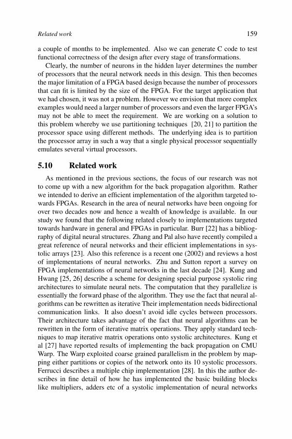
Related work 159
a couple of months to be implemented. Also we can generate C code to testfunctional correctness of the design after every stage of transformations.
Clearly, the number of neurons in the hidden layer determines the numberof processors that the neural network needs in this design. This then becomesthe major limitation of a FPGA based design because the number of processorsthat can fit is limited by the size of the FPGA. For the target application thatwe had chosen, it was not a problem. However we envision that more complexexamples would need a larger number of processors and even the larger FPGA’smay not be able to meet the requirement. We are working on a solution tothis problem whereby we use partitioning techniques [20, 21] to partition theprocessor space using different methods. The underlying idea is to partitionthe processor array in such a way that a single physical processor sequentiallyemulates several virtual processors.
5.10 Related work
As mentioned in the previous sections, the focus of our research was notto come up with a new algorithm for the back propagation algorithm. Ratherwe intended to derive an efficient implementation of the algorithm targeted to-wards FPGAs. Research in the area of neural networks have been ongoing forover two decades now and hence a wealth of knowledge is available. In ourstudy we found that the following related closely to implementations targetedtowards hardware in general and FPGAs in particular. Burr [22] has a bibliog-raphy of digital neural structures. Zhang and Pal also have recently compiled agreat reference of neural networks and their efficient implementations in sys-tolic arrays [23]. Also this reference is a recent one (2002) and reviews a hostof implementations of neural networks. Zhu and Sutton report a survey onFPGA implementations of neural networks in the last decade [24]. Kung andHwang [25, 26] describe a scheme for designing special purpose systolic ringarchitectures to simulate neural nets. The computation that they parallelize isessentially the forward phase of the algorithm. They use the fact that neural al-gorithms can be rewritten as iterative Their implementation needs bidirectionalcommunication links. It also doesn’t avoid idle cycles between processors.Their architecture takes advantage of the fact that neural algorithms can berewritten in the form of iterative matrix operations. They apply standard tech-niques to map iterative matrix operations onto systolic architectures. Kung etal [27] have reported results of implementing the back propagation on CMUWarp. The Warp exploited coarse grained parallelism in the problem by map-ping either partitions or copies of the network onto its 10 systolic processors.Ferrucci describes a multiple chip implementation [28]. In this the author de-scribes in fine detail of how he has implemented the basic building blockslike multipliers, adders etc of a systolic implementation of neural networks
160 Back-Propagation Algorithm Achieving 5 GOPS on the Virtex-E
in FPGA. This work concentrates more on extracting performance out of theFPGA architecture in terms of efficient low level implementations of the ele-ments that are used to build the neurons. The design also is reported to work at10MHz. Elredge and Hutchings report a novel way of improving the hardwaredensity of FPGAs using Runtime Reconfiguration(RTR) [29]. They divide theback propagation algorithm into three sequentially executed stages and con-figure the FPGA to execute only one stage at a time. They report significantdeterioration in performance but justify the use of RTR to get density enhance-ment. Bade and Hutchings [30] report an implementation of stochastic neuralnetworks based on FPGAs—their proof of concept circuit is implemented ona very small FPGA (100 CLBs). Their solution proposes the use of bit ser-ial stochastic techniques for implementing multiplications. Their implemen-tations achieve very high densities for stochastic neural networks. Zhang hasreported an efficient implementation of the BP algorithm on the connectionmachine [31]. This implements only the forward phase of the network. Theauthors describe how to implement a “multiply-accumulate-rotate" iterationfor a fully connected network using the 2D connections of CM-2.
Botros et al. [32], have presented a system for feed forward recall phase.Each node is implemented with two XC3042 FPGAs and a 1KX8 EPROM.Training is done offline on a PC. The whole system operated at 4MHz. Lindeet al [33] have described REMAP which is an experimental project of buildingan entire computer for neural computation using only FPGAs. The suggestedarchitecture incorporates highly parallel, communicating processing modules,each constructed as a linear SIMD (Single Instruction stream, Multiple Datastream) array, internally connected using a ring topology, but also supportingbroadcast and reduction operations.This gives high performance, up to 40-50MHz. The full scale prototype is reported to work at 10 MHz. Gadea et al. [34],report an implementation of a pipelined on-line back propagation network ona single XCV400 package. Also they have reported a maximum operatingfrequency of only 10MHz.
5.11 Conclusion
Our contribution in this paper is two fold. We have described a new systolicdesign for implementing the back propagation learning algorithm which lendsitself to efficient parallelization. Our algorithm is the fastest systolic designreported as yet since it avoids the inter phase idle time from which all previousdesigns suffer. Secondly, we have implemented the proposed algorithm onan FPGA. Here too, we believe that we have a higher operating frequency ascompared with other implementations. Although, this is an implementationissue and depends on the target boards, available memory and the FPGA itself,our operating frequency of about 35 MHz is based on the the XCV1000 FPGA
161
which is not the most recent technology. We expect to have a faster circuit onthe Virtex II FPGA. Our design is completely scalable and can accommodate alarge number of processors (limited only by the size of the FPGA). The designis also scalable in the number of hidden layers. The design has been targetedfor the Virtex based boards and good results have been obtained.
The main focus of this research endeavor has been two fold—one to desisgna high performance circuit for the BP algorithm and second to use automaticsynthesis of such a high performance architecture for FPGA. We implementeda new design and then used the tool to generate the RTL automatically. Wehave presented performance figures for both these designs. The automaticallygenerated hardware description obviously makes greater demands on hardwareresources but that is to be expected. We have been working on hardware opti-mizations that can be implemented in our tool so as to close the gap.
AppendixThe complete script which transforms the Alpha specification to synthesizable
VHDL.
load["NN.a"]; analyze[]; ashow[]serializeReduce[{6, 1, 2}, "YY1.(p,n->p,n-1)"];serializeReduce[{6, 3, 2}, "YY3.(m,p->m-1,p)"];serializeReduce[{6, 5, 2}, "ZZ1.(m,p->m,p-1)"];simplifySystem[]; ashow[]cut["ZZ1", "{m,p | p=0}", "ZZ10", "ZZ1acc"];cut["YY1", "{p,n | n=0}", "YY10", "YY1acc"];cut["YY3", "{m,p | m=0}", "YY30", "YY3acc"];Print["Simplifying, please wait"]simplifySystem[];substituteInDef[ZZ1acc, ZZ10];substituteInDef[YY1acc, YY10];substituteInDef[YY3acc, YY30];removeAllUnusedVars[];Print["I’m normalizing, please wait ..."]normalize[]; simplifySystem[]; ashow[]asave["NN-serial.a"]
load["NN-serial.a"];changeOfBasis["Y1.(p->p,N+1)", {"p", "n"}];changeOfBasis["Y2.(p->p,N+2)", {"p", "n"}];changeOfBasis["ZZ1acc.(m,p->p,N+2+m)", {"p", "n"}];changeOfBasis["Z1.(m->P+1,N+2+m)", {"p", "n"}];changeOfBasis["Z2.(m->P+1,N+2+m)", {"p", "n"}];changeOfBasis["Z3.(m->P+1,N+2+m)", {"p", "n"}];changeOfBasis["Z4comp.(m->P+1,N+2+m)", {"p", "n"}];changeOfBasis["YY3acc.(m,p->p,N+M+m+2)", {"p", "n"}];changeOfBasis["Y3.(p->p,N+2M+3)", {"p", "n"}];
Appendix
162 Back-Propagation Algorithm Achieving 5 GOPS on the Virtex-E
changeOfBasis["Y4.(p->p,N+2M+4)", {"p", "n"}];addlocal["DeltaW1Loc = DeltaW1"];addlocal["DeltaW2Loc = DeltaW2"];normalize[];changeOfBasis["DeltaW1Loc.(p,n->p,n+N+2M+4)"];changeOfBasis["DeltaW2Loc.(m,p->p,m+2N+2M+4)", {"p", "n"}];Print["and now ..."]normalize[]; simplifySystem[]; ashow[]asave["NN-aligned.a"]Print["Now we need to go into NN-aligned.a and uniformize some depencences --which are actually uniform-in-context by hand, and save the result inNN-aligned-hand.a"]Print["Actually, this has already been done"]InputString["So hit return to continue > "];
load["NN-aligned-hand.a"];pipeall["YY1acc", "x.(p,n->n)", "Xpipe.(p,n->p+1,n)"];pipeall["YY3acc", "Z4copy1.(p,n->n-N-M-2)", "Z4pipe1.(p,n->p+1,n)"];pipeall["DeltaW1Loc", "Y4.(p,n->p,N+2M+4)", "Y4pipe.(p,n->p,n+1)"];addlocal["temp", "Y2.(p,n->p,N+2)"];cut["temp", "{p,n|n>=N+2}", "Temp", "junk"];simplifySystem[]; removeAllUnusedVars[];pipeall["Temp", "Y2.(p,n->p,N+2)", "Y2pipe.(p,n->p,n+1)"];substituteInDef[DeltaW2Loc, Temp];substituteInDef[Y4, Temp];substituteInDef[ZZ1acc, Temp];simplifySystem[]; removeAllUnusedVars[];convexizeAll[]; ashow[]asave["NN-local1.a"];Print["Apparently, convexizeAll does not work as well as we hope, so you haveto do this by hand"]InputString["So hit return to continue > "];
load["NN-local1-hand.a"];schedule[scheduleType -> sameLinearPart]appSched[]; asave["NN-scheduled-app.a"];load["NN-local1-hand.a"];applySchedule[]; asave["NN-scheduled-apply.a"];load["NN-scheduled-apply.a"];toAlpha0v2[];simplifySystem[alphaFormat -> Alpha0];reuseCommonExpr[];simplifySystem[alphaFormat -> Alpha0];addAllParameterDomain[];convexizeAll[];simplifySystem[alphaFormat -> Alpha0];alpha0ToAlphard[]; asaveLib["NN_Hard"]load["NN_Hard"];analyze[];uniformQ[];fixParameter["N", 20];

163
fixParameter["P", 32];fixParameter["M", 10];$library = Drop[$library, -1];$library = $library /. (real -> integer);a2v[]
References
References
[1] R L Walke, R W M Smith, and G Lightbody. 2000. “20 GFLOPSQR processor on a Xilinx Virtex E FPGA,” in SPIE, Advanced SignalProcessing Algorithms, Architectures, and Implementations X.
[2] D. E. Rumelhart, G. E. Hinton, and R. J. Williams. 1986. “Learning In-ternal Representations by Error Propagation,” Nature, vol. 323, pp. 533–536.
[3] Y. L. Cun and et al., 1989. “Backpropagation applied to Handwritten ZipCode Generation,” Neural Computation, vol. 1, no. 4, pp. 541–551.
[4] N. Sundarajan and P. Saratchandran.1998. Parallel Architectures for Arti-ficial Neural Networks. IEEE Computer Society Press, California, USA,ISBN 0-8186-8399-6.
[5] “The Alpha Homepage,” Information available at http://www.irisa.fr/cosi/ALPHA.
[6] D. Lavenier, P. Quinton, and S. Rajopadhye. 1999. Digital SignalProcessing for Multimedia Systems, ch. 23. Parhi and Nishitani edi-tor, Marcel Dekker, New York.
[7] Annapolis Micro Systems Inc. STARFIRE Reference Manual, availableat www.annapolis.com.
[8] Annapolis Micro Systems Inc. at http://www.annapmicro.com.
[9] “Xilinx Inc. 2.5V Field Programmable Gate Arrays:Preliminary ProductDescription,” October 1999. www.xilinx.com.
[10] “Celoxica Inc,” Information available at http://www.celoxica.com.
[11] “Accel Inc,” Information available at http://www.accelchip.com.
[12] “The Alpha Homepage at Brigham Young University,” Information avail-able at http://www.ee.byu.edu:8080/~wilde/Alpha.

164 Back-Propagation Algorithm Achieving 5 GOPS on the Virtex-E
[13] “The Alpha Homepage at Colorado State University,” Information avail-able at http://www.cs.colostate.edu/~kolin/Alpha.
[14] “The polyhedral library,” Information available at http://icps.u-strasbg.fr/PolyLib/.
[15] C. Mauras. 1989. Alpha: un langage équationnel pour la conception et laprogrammation d’arctitectures parallèles synchrones . PhD thesis, Thèse,Université de Rennes 1, IFSIC .
[16] P. Feautrier. 1992. “Some efficient solutions to the affine scheduling prob-lem: I. one-dimensional time,” International Journal of Parallel Pro-gramming, vol. 21, no. 5, pp. 313–348.
[17] P. Feautrier. 1992. “Some efficient solutions to the affine scheduling prob-lem: part ii multidimensional time,” International Journal of ParallelProgramming, vol. 21, no. 6, pp. 389–420.
[18] “PIP/PipLib 1.2.1 ‘fusion’,” Information available athttp://www.prism.uvsq.fr/~cedb/bastools/piplib.html.
[19] “IEEE Standard VHDL Language Reference Manual,” 1994. ANSI/IEEEStd 1076-1993.
[20] S Derrien and S Rajopadhye. 1991. “Loop Tiling for Reconfigurable Ac-celerators,” in International Workshop on Field Programmable Logic andApplications (FPL’91).
[21] S Derrien and S Sur Kolay and S Rajopadhye. 2000. “Optimal partition-ing for FPGA Based Arrays Implementation,” in IEEE PARELEC’0.
[22] J. Burr. 1991. Digital Neural Network Implementations – Concepts, Ap-plications and Implementations, Vol III. Englewood Cliffs, New Jersey:Prentice Hall.
[23] D. Zhang and S. K. Pal. 2002. Neural Networks and Systolic Array De-sign. World Scientific Company.
[24] Jihan Zhu and Peter Sutton. 2003. “FPGA Implementation of Neural Net-works - A Survey of a Decade of Progress,” in 13th International Con-ference on Field-Programmable Logic and Applications (FPL 2003), Lis-bon, Portugal., pp. 1062–1066, Springer-Verlag.
[25] S Y Kung. 1988. “Parallel Achitectures for Artificial Neural Networks,”in International Conference on Systolic Arrays, pp. 163–174.

165References
[26] S Y Kung and J N Hwang. August 1989. “A Unified Systolic Architecturefor Artificial Neural Networks,” Journal of Parallel Distributed Comput-ing, vol. 6, pp. 358–387.
[27] H T Kung. 1988. “How We got 17 million connections per second,” inInternational Conference on Neural Networks, vol. 2, pp. 143–150.
[28] A T Ferrucci. 1994. A Field Programmable Gate Array Implementationof self adapting and Scalable Connectionist Network. PhD thesis, MasterThesis, University of California, Santa Cruz, California.
[29]ment of a Neural Network using FPGAs and Runtime Reconfiguration,”in IEEE Workshop on FPGAs for Custom Computing Machines, pp. 180–188, IEEE.
[30] Stephen L Bade and Brad L April 1994. “FPGA-BasedStochaistic Neural Networks,” in IEEE Workshop on FPGAs for CustomComputing Machines,, pp. 189–198, IEEE.
[31]propagation Algorithm on the Connection Machine,” Advances in NeuralInformation Processing Systems, vol. 2, pp. 801–809.
[32] N. M. Botros and M Abdul-Aziz. December 1994. “Hardware Implemen-tation of an Artificial Neural Network using Field Programmable Arrays,”IEEE Transactions on Industrial Electronics, vol. 41, pp. 665–667.
[33] A Linde, T Nordstrom, and M Taveniku, “Using FPGAs to implementa Reconfigurable Highly Parallel Computer” 1992. in Selected papersfrom: Second International Workshop on Field Programmable Logic andApplications (FPL’92), pp. 199–210, Springer-Verlag.
[34] Rafael Gadea, Franciso Ballester, Antonio Mocholí, and Joaquín Cerdá.2000. “Artificial Neural Network Implementation on a Single FPGA ofa Pipelined On-Line Backpropagation,” in Proceedings of the 13th Inter-national Symposium on System Synthesis, IEEE.
James G Elridge and Stephen L Bade. April 1994. “Density Enhance-
Hutchings.
X. Zhang and et al. 1990. “An Efficient Implementation of the Back-

Chapter 6
FPGA IMPLEMENTATION OF VERY LARGEASSOCIATIVE MEMORIES
Application to Automatic Speech Recognition
Dan Hammerstrom, Changjian Gao, Shaojuan Zhu, Mike Butts*OGI School of Science and Engineering, Oregon Health and Science University, *CadenceDesign Systems
Abstract Associative networks have a number of properties, including a rapid, computeefficient best-match and intrinsic fault tolerance, that make them ideal for manyapplications. However, large networks can be slow to emulate because of theirstorage and bandwidth requirements. In this chapter we present a simple buteffective model of association and then discuss a performance analysis we havedone in implementing this model on a single high-end PC workstation, a PCcluster, and FPGA hardware.
Keywords: Association networks, FPGA acceleration, Inner product operations, Memorybandwidth, Benchmarks
6.1 Introduction
The goal of the work described here was to assess the implementationoptions for very large associative networks. Association models have beenaround for many years, but lately there has been a renaissance in research intothese models, since they have characteristics that make them a promising solu-tion to a number of important problems.
The term Intelligent Signal Processing (ISP) is used to describe algorithmsand techniques that involve the creation, efficient representation, and effectiveutilization of complex models of semantic and syntactic relationships. In otherwords, ISP augments and enhances existing Digital Signal Processing (DSP)by incorporating contextual and higher level knowledge of the application do-main into the data transformation process. It is these complex, “higher-order”
167
A. R. Omondi and J. C. Rajapakse (eds.), FPGA Implementations of Neural Networks, 167–195. © 2006 Springer. Printed in the Netherlands.

168 FPGA Implementation of Very Large Associative Memories
relationships that are so difficult for us to communicate to existing computersand, subsequently, for them to utilize efficiently when processing signal data.
Associative networks are neural network structures that approximate thegeneral association areas seen in many biological neural circuits. In additionto having a strong grounding in computational neurobiology, they also showpromise as an approach to ISP. This is particularly true when used in multiplemodule configurations where connectivity, learning, and other parameters arevaried between modules, leading to complex data representations and systemfunctionality.
This chapter is divided into 4 major sections and a Summary and Conclu-sions section. Section 6.2 describes the basic association memory computa-tional model used for our analysis as well as examples of its use in real ap-plications. Section 6.3 presents a performance analysis of a single PC and PCcluster in executing this model. These systems represent the best alternativesto the FPGA solution proposed here and constitute a standard performancebenchmark for the model. Section 6.4 presents an analysis of the FPGA imple-mentation, using a memory intensive FPGA board. And, Section 6.5 comparesthe FPGA analysis to the PC performance results.
6.2 Associative memory
In this section we show the basic computational model that was imple-mented. Subsection 6.2.1 provides some historical background, while sub-section 6.2.2 presents the basic model. A theoretical model is briefly presentedin 6.2.3, and two example applications in subsection 6.2.4.
In traditional computing, data are stored in memory according to a directaddressing scheme. This approach requires that the computation engine be ableto provide the addresses for the data being accessed. For some applications,such as the storage of large numerical arrays, creating the necessary address isnot difficult, though a fair amount of effort is still involved. However, in someapplications the address is unknown, or some part of a particular set of datais known and the remaining data in the set are sought. To accomplish this, adifferent kind of memory function, content addressing, is used.
The most common kind of content addressing is exact match, where part ofthe data is known and is matched exactly to the contents of a location. Thereare a number of applications for exact match association, from addressing incache memory to routing tables. There have been a number of parallel, exactmatch, association engines [4] created over the years. Also, there are fairlyefficient algorithms for exact match association such as hash coding.
However, if the data we have are close but not exact to data stored in thememory, a best match content addressable memory would be useful. Thismemory would find the content that had the “closest” match according to some

Associative memory 169
metric. And it turns out that in many kinds of ISP this is exactly what we wantto do, that is, given noisy, corrupt input, we want to find the original contentthat is the “most likely” in some sense.
An exact match can be determined fairly easily, but a best match is a littlemore complicated. Unlike using hash based addressing for exact match asso-ciation, there is no short cut1 to finding the best match. For arbitrary searchesit requires that every item in memory be examined. This is one reason whybest match associative memory is not used extensively. However, by using dis-tributed data representation, efficient best match associative processing can berealized. Best-match association also seems to be something that is commonlyperformed by neural circuitry.
Best-match association finds the “closest” match according to some met-ric distance defined over the data space. A simple and often used metric isHamming distance, however more complex vector metrics can also be used.In some applications, for example, the distance between two vectors may havemore to do with the meaning assigned to the words represented by the vectorsthan the number of letters different or the distance the letters are from eachother.
A common example of best match processing is Vector Quantization, wherethe metric can be a Euclidean distance in a high dimensional vector space. Wecan be even more sophisticated and let our metric be based on probability esti-mates. Then under certain conditions our best match system returns the matchthat was the most likely to have been the source of the data being presented,based on data and error probabilities.
There is always the brute force approach which allocates a simple proces-sor per record (or per a small number of records), all computing the match inparallel with a competitive “run-off” to see who has the best score. Though in-efficient, this implementation of best-match guarantees the best results and caneasily be used to generate optimal performance criteria, but it is too computeintensive for most real applications.
6.2.1 Previous Work
We cannot do justice to the rich history of associative processing in thischapter, but it is important to mention some of the key developments. It is noteven clear who started using these techniques first, though Donald Hebb [10]used the term “association” in conjunction with arrays of neurons. Perhaps the
Stein-
1One of the best algorithms is the KD tree of [18]. Bumptrees for efficient function, constraint, and classifi-cation learning. Advances in Neural Information Processing Systems 3, Denver, Colorado, Morgan Kauff-mann., but even these have significant limitations in many applications, for example, such as dynamicallylearning new data during execution.
first visible development was the Lernmatrix of Karl Steinbuch [23].

170 FPGA Implementation of Very Large Associative Memories
buch’s model, and similar early models by Willshaw and his group [7] andKohonen [14], were based primarily on linear association. In linear associa-tion, the connection weight matrix is formed by summing the outer products(of the input vector with its output vector). Recall is done via a simple matrix/ vector multiplication. If a training vector is input, the output vector associ-ated with it will be output. If a noisy version of a training vector is input, theoutput will be a combination of the various training vectors that are present inthe noisy input vector. The components of the associated output vectors willbe proportional to the degree to which the training vectors are represented inthe noisy input, with the most prominent (usually the training vector before thenoise was added) input vector being the most prominent in the output. To beeffective, the trained vectors need to be linearly independent.
In the 80s a number of important, non-linear, variations of the linear asso-ciator were developed. Perhaps the most influential models were developedby Palm [20], Willshaw [24], and Hopfield [12]. The Hopfield model wasbased on the physics of spin glasses and consequently had an appealing the-oretical basis. In addition, the model required asynchronous operation. Foradditional models the interested reader is referred to the work of Amari [1],Hecht-Nielsen [11], Anderson [2, 3], and Lansner [15].
6.2.2 Sparse Association Networks with k-WTA Output
6.2.2.1 The Palm Model. A simple, but effective association algo-rithm was developed by G. Palm and his associates [20, 21]. A key aspect ofthis model is a very sparse data representation and k-WTA (K Winners TakeAll) output filtering. The k-WTA operation increases the effectiveness of thememory and also eliminates the need for the training vectors to be linearlyindependent.
Although non-binary Palm models are possible, for the sake of this discus-sion we will assume that all input and output vectors are binary as is the weightmatrix. In the Palm model there are certain vectors that are used to train thenetwork. Each vector has a sparse representation, which is enforced by limit-ing the number of 1s in each vector to a fixed value, k. This limited activationenforces a certain distribution of the data representations, where each nodemay participate in the representation of a number of different stored elements.Sparse, distributed representations are efficient, because of the combinatoriceffects of very large vector spaces. And they are massively parallel becauselarge numbers of processing nodes operate concurrently to compute the out-put. Distributed representations also enhance fault tolerance.
The algorithm uses here stores mappings of specific input representationsxi to specific output representations yi, such that xi → yi. The network isconstructed with an input-output training set (xi, yi), where F (xi) = yi. The
Associative memory 171
mapping F is approximative, or interpolative, in the sense that F (xi + ε) =yi + δ, where xi + ε is an input pattern that is close to input xµ being storedin the network, and |δ| � |ε| with δ → 0 , where δand ε represent noisevectors. This definition also requires a metric over both the input and outputspaces.
In Palm’s model, the input, X , and output, Y , vectors are binary valued (0or 1) and have equal dimensions, n, since we are using a feedback network(output to input) to implement auto-association. There is also a binary valuedn by n matrix, W , that contains the weights. Output computation is a two-step process, first an intermediate sum is computed for each node (there are nnodes) by thresholding
sj =∑
i
wjixi
where wji is the weight from input i to node j. The node outputs are thencomputed
yj = f(sj − θj)
The function, f(x), is a step function (“hard max”), it is 1 if x > 0 and 0 ifx ≤ 0, leading to a threshold function whose output yj is 1 or 0 depending onthe value of the node’s threshold, θj . The setting of the threshold is discussedbelow. In Palm’s basic model, there is one global threshold, but more complexnetwork models relax that assumption.
Programming these networks involves creating the appropriate weight ma-trix, W , which is developed from “training” vectors. In the case of auto-association these represent the association targets. In the Hopfield energy spinmodel case, for example, these are energy minima. There are m training pat-terns
S = {(Xµ, Y µ)|µ = 1, · · · , m}In auto-associative memories the output is fed back to the input so that X =
Y . The weights are set according to a “clipped” Hebbian rule. That is, aweight matrix is computed by taking the outer product of each training vectorwith itself, and then doing a bit-wise OR of each training vector’s matrix
wij =M⋃
µ=1
(xµi · (yµ
j )T )
An important characteristic is that only a constant number of nodes are ac-tive for any vector. The number of active nodes, k, is fixed and it is a relativelysmall number compared to the dimensions of the vector itself – Palm suggestsk = O(log(n)) . This is also true for network output, where a global thresholdvalue, θ, is adjusted to insure that only knodes are above threshold. Althoughreducing theoretical capacity somewhat, small values of k lead to very sparsely
172 FPGA Implementation of Very Large Associative Memories
activated networks and connectivity. It also creates a more effective computingstructure, since the k−Winners Take All (k-WTA) operation acts as a filter thattends to eliminate competing representations.
Although a Palm network is similar to a Hopfield network in function andstructure, the key differences of clipped Hebbian weight update and k-WTA ac-tivation rule make a big difference in the capability of the network. In theoret-ical studies of these networks, researchers have developed asymptotic boundsfor arbitrarily scalable nets. Palm has shown, for example, that in order to havemaximum memory capacity, the number of 1s and 0s in the weight matrixshould be balanced, that is p1 = p0 = 0.5, where p1 is the probability that abit is 1 and p0 the probability that a bit is 0. The memory capacity per synapsethen is − ln p0 ≤ ln 2. In order for this relationship to hold, the training vectorsneed to be sparsely coded with at most log2(n) bits set to 1, then the optimalcapacity of ln 2 = 0.69 bits per synapse is reached.
6.2.2.2 Other Model Variations. Palm networks are robust and scalereasonably well. However, there are still some limitations:
1 The model as currently defined does not allow for incremental, dynamiclearning.
2 Even though the vectors themselves are sparsely activated, as more in-formation is added to the network, the weight matrix approaches 50%non-zero entries, which is not very sparse. For a 1M network, that is500Gb with each node having a fan-in (convergence) of 500K connec-tions. Cortical pyramidal cells typically have a convergence of roughly10K.
3 Time is not factored into the model, so that temporal data is not cleanlyintegrated into the association process.
4 The network requires that input data be mapped into a sparse represen-tation, likewise output data must be mapped back to the original repre-sentation.
Concerning the last item, algorithms are available [8] for creating sparse rep-resentations (“sparsification”). Our experience has shown that for many ap-plications getting a sparse representation is straightforward. Once a sparserepresentation is determined, it has not been difficult to map from an externalrepresentation into the sparse representation and back again. This is important,since much of power of these nets is due to the sparse, distributed representa-tion of the data.
The Palm model is simple and easy to work with and it is a good startfor looking at the various performance issues concerning hardware imple-mentation of such models. However, it is likely that real applications will

Associative memory 173
use more complex models. One model that we are also working with is theBayesian Confidence Propagation Neural Network (BCPNN) developed byAnders Lansner and his group [15, 16] at the Royal Institute of Technologyin Stockholm, Sweden. BCPNN addresses several of these issues and demon-strates a number of useful behaviors. For example, in addition to capturinghigh order Bayesian statistics, they also demonstrate the Palimpsest property,where older information is forgotten first as the network approaches full capac-ity. Another key characteristic of BCPNN networks is its ability to do “secondmatch,” where, when the network is allowed to habituate to its first output, itwill then return the next best match, etc.
Lansner has likened a single node in the BCPNN as comparable to a corticalminicolumn and the Winner-Take-All group as a cortical hypercolumn. Themodel has its origin in neuroscience and the study of cortical circuits. Onedisadvantage of the model is the need for fairly high precision for the weightupdate computations. Both the Palm and BCPNN models can be reformulatedas pulse or spiking based models. Pulse models have certain implementationadvantages and handle the temporal dimension more efficiently [17].
It is also likely that real systems will use collections of models with differ-ent learning capabilities, thresholding systems, and connectivity. Examples ofsuch models can be found in O’Reilly [19].
6.2.2.3 Simulation. We have developed an association memory simu-lation environment, Csim (Connectionist SIMulator). Csim is object orientedand is written in C++. It uses objects that represent clusters, or “vectors” ofmodel nodes. It can operate in a parallel processing mode and uses the Mes-sage Passing Interface (MPI) to do interprocess communication over multipleprocessors. We have a small set of association network models operating onthe simulator. Because the simulator has a simple command line interface, andbecause C++ and MPI are standards, it operates under Windows 2K, Linux,and SGI Unix. We use the simulator on our Beowulf cluster (8 1GHz Pen-tium IIIs) and on NASA’s SGI supercomputers at the Ames Research Centerin Mountain View, California [25].
6.2.3 An Information Theoretic Model of Association
A communication channel is a useful way to conceptualize the operation ofa simple, auto-association network. For example, in speech recognition whenwe say a word, we have a specific word in mind. We then encode that word intoa form (speech) that is transmitted over a noisy channel (sound waves in air)to the computer, which then decodes the received wave back into the originalword. The channel, Figure 6.1, is our mouth, tongue, vocal chords, the physicalenvironment, as well as the computer’s microphone and signal processing.

174 FPGA Implementation of Very Large Associative Memories
Figure 6.1. The “Decoder” Model of Association
This channel is noisy because there is significant variation in the way theword is encoded – people say the same things differently from one instant tothe next, then add to that speaker variations, ambient noise in the environment,etc. The decoding process uses digital signal processing algorithms at the frontend and complex “intelligent signal processing” algorithms, such as HiddenMarkov Models, that model higher order dependencies at the high-end.
6.2.3.1 A Single Channel. An auto-associative memory can be mod-eled as the decoder in a simple communication channel, Figure 6.2. An inputgenerates a message y that is encoded by the transmitter as x. The message isthen sent over a noisy channel and x′ is received. The decoder decodes x′ into,y′, what is believed to be the most likely y to have been sent.
Messages are generated with probability p(y). The received message, x′, isthe transmitted message with errors. This message is sent to the decoder. Thedecoder has, via many examples, learned the probabilities p(y) and p(x’|y).The decoder uses these data to determine the most likely y given that it receivedx′ (based on what knowledge it has)2
p(y|x′) =p(x′|y)p(y)
p(x′)=
p(x′|y)p(y)∑x p(x′|x)p(x)
Message xi is transmitted, message x′ is received, for simplicity assumethat all vectors are N bits in length, so the Noisy Channel only inserts sub-stitution errors. The Hamming Distance between two bit vectors, xi and xj ,
2Note, the probability p(x’|y) reflects the channel error probabilities.

Associative memory 175
Figure 6.2. Communication Channel - The Decoder Is An Auto-Associative Memory
is HD(xi, xj). Assume that the Noisy Channel is binary symmetric with theprobability of a single bit error being ε, and the probability that a bit is trans-mitted intact is (1-ε). The error probabilities are independent and identicallydistributed and ε < 0.5. Under these circumstances it can be shown that thePalm memory approximates a Bayesian inference, that is, the Palm associativememory will generally recall the most likely original message, xi, from a noisyreceived message x′.
Our primary objective, therefore, is to develop an associative memory thatperforms such probabilistic inference in real-time over very large data sets withsophisticated metrics. We believe that a large capacity version of this memory,implemented in an inexpensive chip, has significant commercial value.
6.2.3.2 Scaling. Association networks have much promise as a com-ponent in building systems that perform ISP. There are a number of problemsthat need to be solved before distributed representation, best match associativememories can enjoy widespread usage. Perhaps the most serious concerns scal-ing to very large networks. Even though the vectors used by the Palm memoryare sparse, as you add training vectors to the memory, the Weight matrix be-comes decidedly non-sparse. Palm has shown that maximum capacity occurswhen there are an equal number of 1s and 0s. This is 50% connectivity. Thisis not very biological and it does not scale. This level of connectivity causessignificant implementation problems as we scale to relatively large networks.
If you randomly delete connections from a Palm network, performance de-grades gradually to a point where the network suddenly fails completely. There

176 FPGA Implementation of Very Large Associative Memories
is no sudden appearance of emergent functionality, yet cortex has roughly0.0001% connectivity. Clearly we’re doing something wrong.
The associative networks in the cortex seem to be fairly localized. Just as insilicon, connections are expensive to biology, they take space and metabolism,increase the probability of error, and they require genetic material to specifyconnectivity, [6], Cortex: Statistics and Geometry of Neuronal Connectivity[6].
"metric" (high density connections to physically local unit, based on ac-tual two-dimensional layout) and
"ametric" (low density point to point connections to densely connectedgroups throughout the array)
Braitenberg [5] used√
n hypercolumns each with√
n neurons. BCPNNuses 1-WTA per hypercolumn. Although beyond the scope of this chapter,it is possible to create a multiple channel model of associative memory thatmodels the hierarchical structure seen in primate neocortex. Here the memoryis modelled as parallel channels that have unique inputs with some overlap.Likewise, each channel uses inputs from other parallel channels to provideinformation in its own decoding process. Although not required for the currentmodels, reproducing more biological connectivity patterns will be required inthe long run.
6.2.4 Example Applications
To see how best match association memories can be used, we briefly de-scribe two applications we are working on at OGI, the first is for a sensorfusion system for the US Air Force, and the second, a robotic control systemfor NASA.
6.2.4.1 Enhanced Visual System for Pilot Assist. With Max-Viz,Inc., Portland, OR, we are developing an Enhanced Vision Systems (EVS) foraircraft [13]. This system is designed to aid the pilot during approach andlanding in extremely low visibility environments. The system will have visualsensors that operate at different frequencies and have different absorption spec-tra in natural phenomena such as fog. The EVS takes these various images andfuses them in a Bayesian most-likely manner into a single visual image that isprojected on a Head-Up Display (HUD) in front of the pilot.
Computing a Bayesian most likely fused image at the necessary resolutionand video rates is extremely computationally intensive. So we are developinga system that approximates Bayesian accuracy with far less computation byusing an association engine.

Associative memory 177
Figure 6.3. EVS Association Application
In this system basic visual-like image pre-processing is used on each imageto find key elements of the background, generally the edges of the runway.Since these features tend to be consistent across all images from the varioussensors, the feature vectors are just added together, then thresholding is per-formed to reduce the number of features, creating a sparse representation ofthe strongest features. This cumulative feature vector is then input to an as-sociative memory that returns the features of a stored image. These featuresare then used to do a hash (exact match association) to a database that containsthe real visual image that is then projected onto the HUD. An overview of theprocessing steps for each video frame is shown in Figure 6.3.
6.2.4.2 Reinforcement Based Learning for Robot Vision. We are de-veloping a robotics control system for NASA3 that uses biologically inspiredmodels for bottom-up/top-down sensorimotor control with sparse representa-tions. In this research we plan to demonstrate a system that performs a simplecognitive task, which is learned by the system via reinforcement, in much thesame way a monkey would learn the task. The selected task is block copywhere the animal copies a model of a block layout in one work area into an-other work area using a set of predefined blocks in a resource area. An exampleis shown in Figure 6.4. This task is known to illustrate important properties ofthe primate brain in terms of:
Visual processing and representation, and visual short term memory;
3“Biological computing for robot navigation and control,” NASA, March 1, 2001, Three years, $1,393K.PI: Marwan Jabri, Co-PIs: Chris Assad, Dan Hammerstrom, Misha Pavel, Terrence Sejnowski, and OlivierCoenen.

178 FPGA Implementation of Very Large Associative Memories
Sequencing and planning, and the requirements of short-term microplansand longer term plans;
Memory based processing, in particular, top-down information process-ing; and
Spatial Representations.
Data on human and monkey experiments on various block copying tasks areavailable. However to build a machine that performs such a task using a bi-ologically based model, one has to think how a monkey is trained to performsuch a task. We know that monkeys learn complex sequences by maintainingtheir attention and their rewards as they are proceeding. To build a machine tolearn to perform such a task, we need to define the set of sub-skills that the ma-chine must have the minimum hardware capabilities for such learning to takeplace.
Figure 6.4. Active Vision Block Copying Task
Our approach is to take preliminary information on the systems in the pri-mate brain that neuroscientists believe are used in solving this task and startwith highly simplified versions, but with all the required brain areas rep-resented. The architecture of our current system is shown in Figure 6.5.Although complex, each subcomponent is basically an associative memory,though different modules have slightly different learning rules and connectiv-ity patterns.

PC Performance Evaluation 179
6.3 PC Performance Evaluation
In this section we present results and analysis from the implementation ofthe basic Palm model on a PC Workstation, single processor, and a multi-processor PC cluster. As we move to larger, more complex cognitive systemsbuilt from diverse association modules, the ability to execute these large mod-els in close to real time, which would be required by most applications, be-comes a problem even for high end PC Workstations. The primary purpose ofthis chapter is to study the use of an FGPA based emulation system for asso-ciation networks. However, as part of any specialized hardware design, it isimportant to assess the cost performance of this hardware in comparison withhigh performance, commercial off-the-shelf hardware.
Figure 6.5. Architecture of Block Copy System
Thanks to Moore’s law, the performance-price of commercial hardware hasmade amazing improvements over the last 10 years. It is possible to have thesame performance in a desktop machine or notebook that was only availablein super computers 15 years ago. Consequently, any application that is a can-didate for special purpose hardware implementation must first be measured ongeneral-purpose hardware, since in many cases specialized hardware will notprovide a sufficient performance improvement to justify the cost of the extrahardware.
The Palm algorithm has two basic operations:
1 A matrix vector multiply of a very sparse binary vector by a very large,and, for the time being, not so sparse binary matrix.

180 FPGA Implementation of Very Large Associative Memories
2 A k-WTA function on the non-sparse, non-binary vector that is the prod-uct of the matrix vector multiply, the output being another very sparsebinary vector.
In our experience the matrix-vector multiply is the most time consuming andthe most memory intensive. For the real applications we are contemplating,the input and output vectors contain 10s to 100s of thousands of elements.What is clear is that we need to use large, commercial memory to get thenecessary capacity, density, bandwidth, and latency, which implies state ofthe art SDRAM. Since the matrices we use are very large and not sparse4,consequently the entire matrix cannot be stored in any reasonably sized cache.For the inner product operation every element fetched by the cache is onlyused once. Since, the entire matrix must be traversed for one operation, thecache provides no performance benefit. So the matrix-vector multiply requiresa long, continuous stream of data from memory with the memory bandwidthbeing the major factor in determining system performance. So in this situationa data caches does not contribute much performance. This is also true for theclock speed of the processor, which is mostly just waiting for data.
6.3.1 Single PC
For the single, high-end, PC experiments described here we used a DELLDimension 8100 with the following hardware and software:
CPU: Pentium 4 1.8GHz
Chipset: Intel R© 850
Memory: 1024MB RDRAM
System Bus: 400MHz
Microsoft Windows 2000 Professional
Microsoft Visual C++ 6.0
Intel VTune Performance Analyzer 6.1
Using the Csim version of the Palm algorithm, we ran several experimentsmeasuring average memory bandwidth and nodes updated per second. Thealgorithm that Csim implemented is not necessarily optimal. In this algorithm,both for the sparse and full representations, the weight matrix is stored by row.One row was read at a time and an inner product performed with the input
4A sparse matrix generally has fewer elements and a matrix with very large dimensions may still fit entirelyinto the cache.

PC Performance Evaluation 181
(test) vector, which, incidentally, is stored as a set of indices. This algorithmwas implemented in the same way by both the Csim and FPGA versions.
Another approach to the matrix vector inner product with very sparse datastructures is to store the weight matrix by columns and then only read thecolumns that correspond to a non-zero element in the input vector. We arestudying how best to do this in the FPGA implementation, which will be pre-sented in future papers. In Figure 6.6, the x-axis is the vector size, and they-axis is the inner-product memory bandwidth (MBytes/sec). The diamond-dotted curve is for the sparse weight matrix representation (where only theindices of the non-zero elements are stored) with the compiler set to maxi-mum speed optimization. The square-dotted curve is for the full binary weightmatrix (one bit per weight, 8 weights per byte, etc.) with the compiler set tomaximum speed. Note both representations are of the same matrix, this is truein Figure 6.7 as well.
Figure 6.6. he relationship between the number of network nodes (vector size in nodes) and
In Figure 6.7 we can see that as the vector size increases (the number oftraining vector numbers used is 0.69 of the vector size, n, and the number ofactive nodes, k, is approximately log2(vector size)), the inner-product memorybandwidth is reduced. For the sparse-matrix representation, the bandwidthgoes to 140MB/sec when the vector size, n, is about 32K. For the full-matrixrepresentation, the bandwidth decreases to 100MB/sec when the vector size is
the single PC inner-product memory bandwidth

182 FPGA Implementation of Very Large Associative Memories
about 32K. As the vector size increases, L1 cache misses increase, the averagememory access time increases, and the bandwidth decreases.
Figure 6.7. Vector size versus node update rate
Incidentally, with the current algorithm it is not necessary for the hardwareto read the entire weight matrix. If you assume that each test vector indexis in a different word, which is a worst case assumption, for each test vector,we will only need to read kn/32� words of weight matrix data, where forthese experiments k=log2(n). The FPGA implementation does this explicitly,the PC does it by virtue of the cache only fetching the block that contains aelement corresponding to a test vector index.
6.3.2 PC Cluster
One common approach to enhancing the performance of the basic PC plat-form is to use a parallel PC configuration, generally referred to as a PC cluster[22]. A common cluster configuration is to use Linux based PCs in what isreferred to as a “Beowulf cluster,” where a number of PCs are connected to acommon broadband network. Software is available that allows these PCs toshare tasks and communicate data and results.
In addition to systems support there are programming environments for sup-porting parallel programs for such clusters, the most commonly used is MPI(the Message Passing Interface) [9]. Csim has a parallel execution option thatis based on MPI. In this subsection, we present the results of executing Csim

PC Performance Evaluation 183
on a small Beowulf cluster, where a single association network is spread acrossthe processors as shown in Figure 6.8.
The purpose of this experiment was to understand the overhead required toexecute a single association network across multiple processors. However, realimplementations will probably use multiple association networks, with eachmodule assigned to a processing node (whether it be a PC or an FPGA).
There are two components to the Palm algorithm that require different ap-proaches to parallelization. The first is the matrix-vector multiplication. Herethe weight matrix is equally divided into p groups of r rows each (n = p× r) ,each processor is assigned a group of r rows. The entire input vector is broad-casted to all processors so that they can perform a matrix-vector inner-producton those rows of the weight matrix that are assigned that processor.
The second part of the algorithm involves the k-WTA. Each processor com-putes a k-WTA on the r node portion of the output vector that it has (thosek nodes allocated to it). These (p − 1) k−element vectors are then sent toprocessor 0 (the root process), which performs another k-WTA over the totalp×r elements. Since k is usually much smaller than the vector dimension, thisapproach is reasonably efficient and guarantees that the final k-WTA is correct.Also, the k-WTA is only performed after all the inner products are complete,which is generally the larger time component.
Figure 6.8. Weight Distribution (4 processor cluster)
The cluster gets its performance by dividing the computation into p equalparts that can be computed concurrently. This also increases the effective mem-ory bandwidth by p. Ideally the speed up would be p. Unfortunately, there isno free lunch, since there is some extra overhead that parallelism creates. Inour simulator this overhead has two components: 1) the broadcast of the inputvector to all the processes, and 2) The broadcast of the k local winners to theroot processor and the computation of the final k-WTA.

184 FPGA Implementation of Very Large Associative Memories
The important question then is, what is the relationship between speed upand the number of processors, p? For these experiments, we used a small PCcluster environment with 8 DELL Dimension L1000R computers. Each nodewas an Intel P3 1.0GHz CPU, 512MB PC133 memory. The OS is RedHatLinux 7.1. The compiler is G++ 2.96.
A summary of the results is shown in Table 6.1. The number of trainingvectors, m, was approximately 0.69 the vector size, n. The number of activenodes, k, was log2(n). The nodes per second per PC is smaller than for the8100 which is most likely due to the reduced memory bandwidth of the P3based Dimension L1000R.
The most important result is that for the larger network, going to more par-allelism does not add significant overhead. For the 64K node network, onlyabout 8% of the performance is lost in going from 2 PCs to 8 PCs, i.e., we areonly 8% short of a linear performance improvement of 4x.
Table 6.1. IPC cluster (8 processors) simulation results
Number Vector Knodes Normalize node rateof PCs Size, n per second by 2 PC Number
2 4096 410 1.004 4096 683 0.838 4096 1024 0.632 8192 390 1.004 8192 745 0.958 8192 1170 0.752 16384 356 1.004 16384 683 0.968 16384 1170 0.822 32768 312 1.004 32768 607 0.978 32768 1130 0.912 65536 289 1.004 65536 560 0.978 65536 1057 0.92
6.4 FPGA Implementation
In this section we first present the architecture of a memory intensive FPGAboard implementation and then second, an analysis of the performance of thatboard on our association memory implementation.
FPGAs are a remarkable technology, allowing a rapid, soft reconfigurationof on chip hardware to customize the hardware to a wide range of applications.As Moore’s law continues, FPGAs gain in density and speed at the same rate

FPGA Implementation 185
as state of the art microprocessors. And although FPGAs pay a price in speedand density for their flexibility, for certain applications with a sufficient num-ber of parallel operations they can offer better performance-price and powerdissipation than state of the art microprocessors or DSPs.
Because of this ability to leverage parallelism, FPGAs have been used exten-sively in image processing applications and are beginning to be used in neuralnetwork applications, where incremental learning by on-line weight modifica-tion can be implemented concurrently and with any precision. Most of thesebenefits assume that the network fits entirely on a single FPGA and that onchip RAM, typically on the order of a few megabits of SRAM, is used to storethe weights and other parameters. As discussed earlier in this Chapter, webelieve that the network models required for many applications will be quitelarge, easily outstripping the capacity of the on-chip memory in a state of theart FPGA. This raises an important question about whether the FPGA is stilla useful platform for the emulation of such networks. One possibility is tostore the network parameters in a state of the art memory connected directlyto the FPGA instead of inside the FPGA, but does this provide a sufficientperformance-price advantage? In this subsection we study this question forour model.
These programs do have a fair amount of opportunity for parallel computa-tion, especially where only a few bits of precision are required. If most of themodel state is stored in external DRAM, the memory bandwidth is the primarycontributor to systems performance, since, for our algorithms, even a modestsized FPGA can keep up with the memory access rate for even very fast stateof the art SDRAM. We believe that an FPGA connected directly to state of theart DRAM in this manner is a useful platform for a large range of image andpattern classification problems.
6.4.1 The Relogix Accelerator Board
The Relogix Mini-Mirax Memory-Intensive Reconfigurable AcceleratorCard is a stand-alone card containing one FPGA+SDRAM pair. Each accel-erator has 1.6 GByte/s of dedicated memory bandwidth available for memory-intensive applications. Each accelerator card is accessed by application soft-ware running on the Unix host via an IDE/FireWire bridge. The objective ofthis board is to take advantage of inexpensive SDRAM PC memory, FPGAsand high speed interfaces to maximize performance-price in a reconfigurableaccelerator. The Mini-Mirax is organized as an incremental brick, so that manyMinis can be connected together in a single system. The basic board layout isshown in Figure 6.9.
The PQ208 pinout accepts any size Spartan-IIE chip. Spartan-IIE,XC2S50E-100, 150, 200 or 300 FPGAs may be installed at assembly. They

186 FPGA Implementation of Very Large Associative Memories
all have the same pinout, 142 general-purpose I/Os, and four global clock in-puts, and differ in only the amount of logic and memory. By using smallerFPGAs, we can stay in a QFP (Quad Flat Pack) for the early boards, sinceit reduces costs. And because our algorithms make such extensive use of theSDRAM, there is a point of diminishing returns as one goes to larger FPGAs.
Figure 6.9. he basic FPGA card
Connected to each FPGA is a single DIMM socket, which supports a 10nsDDR (Double Data Rate) 64-bit pathway (two words are delivered in every10ns clock) into the FPGA. With today’s memory technology this allows up to512MB (soon to be 1GB) of memory to be directly connected to each FPGA.Finally there is an IDE to FireWire chip that creates the external FireWireinterface for the board. An external header uses 20 uncommitted FPGA I/Osthat can be connected to other Mini cards or external devices such as sensors.A JTAG daisy chain header connects the FPGA to a Xilinx interface cable forprogramming by Xilinx software. Many Minis can be used in one JTAG loop.One or more Mini cards are installed in one or more FireWire/IDE enclosures,which provide an IDE to FireWire bridge, power and cooling, and a connectionto a Linux, OS-X or Solaris host.
We are developing a set of IP that will be a more highly abstracted interfaceto the DRAM controller, the IDE controller and the header pins. The DRAMand IDE controllers are also IP that sits inside the FPGA. The user developstheir own IP for the FPGA in Verilog or VHDL and then connects it to theMini-Mirax “Operating System” IP and loads that into the FPGA. In addition,there is software on the PC Host that communicates with this “OS,” in startingthe user subsystem as well as providing debug services.
The primary reason for building this board is that we want to be able toplace state of the art SDRAM, in the form of a DIMM, immediately next to

FPGA Implementation 187
a state of the art, FPGA. The goal is to leverage the maximum bandwidth ofthe largest commercially available memory. At the writing of this Chapter weare not aware of any commercial FPGA boards that provide as much directlyaccessible SDRAM to each FPGA.
The system will obviously be most cost-effective with larger numbers ofparallel, low-precision operations, a configuration where typically there willbe more computation per bit fetched from the SDRAM. The board will trackthe latest memory density (commercial SDRAM) and bandwidth, followingMoore’s law at the same rate as a general purpose microprocessor.
We do not yet have a functioning board, so we cannot provide exact per-formance measurements. In the next subsection we present an analysis of theexpected performance of the Mini-Mirax board on the same association algo-rithm used throughout this paper.
6.4.2 Performance Analysis of Simulation on FPGA
A block diagram of the FPGA Palm implementation is shown in Figure 6.10.This implementation is quite similar to that of the PC, in the sense that theweight values are stored in the external SDRAM with the inner-product and k-WTA performed by the FPGA. Because the board implementation is simple andthere are no complex entities such as multi-level caches, the results presentedhere should be a reasonably accurate representation of the performance weexpect from the actual board. Also, we have implemented pieces of the Palmmodel and run them on other commercially available FPGA boards.
6.4.2.1 FPGA Functional Block Description. There are a numberof assumptions that were made about the Palm implementation on the Miraxboard:
A single FPGA / SDRAM board is used for analysis, even though theMini-Mirax system supports multiple FPGA configurations. Likewise,it is likely that the communication overhead for connecting multipleboards, as a percentage of the total computation time, will be muchsmaller than with multiple PCs in a cluster.
Only a full binary weight matrix implementation is assumed where eachbit is a binary weight. One 64-bit word at a time is fetched from theSDRAM. Only words that have at least one test vector index pointinginto them are fetched.
The input test vectors are sparsely encoded and the time transfer of datato and from the PC host is ignored. Each vector is assumed to havesingle bit precision and consists of a list of indices of the weight bits in

188 FPGA Implementation of Very Large Associative Memories
Figure 6.10. FPGA functional block diagram

FPGA Implementation 189
the matrix row. When a test vector is processed, this list of indices isbrought from the PC into the FPGA.
The inner-product produces a vector of sums. This vector is generallynot sparse. The bits required to represent each sum is log2 k� bits, andthere are k sums. The k-WTA is computed dynamically, that is, aftereach inner-product element is generated it is compared to the existingk largest sums, which, along with their indices, are stored in SRAMin the FPGA. The new index is then either inserted or discarded. Thisapproach eliminates the need to move the sums off chip and then backagain to form the k-WTA.
The final output vector is sparse and its indices are written to the PChost, thus completing the computation of a single vector. The time tomove the final result is also ignored.
There are a number of additional optimizations that are possible whichwe have ignored here in favor of keeping the PC and FPGA implemen-tation as close as possible. Future work will examine the effect of suchoptimizations for both platforms more closely.
Inner-product operation: The input vector Vin,i (represented by its ac-tive nodes’ indices) is transferred to the IDE Interface. The fetching of theweight matrix rows begins, with the weight matrix row addresses being gener-ated by the Address Translator. The SDRAM transfers the data requested bythe FPGA a single 64-bit word at a time through the SDRAM Memory Bus In-terface. There are a number of ways a binary inner product can be performed.But a simple look up and count is all that is required. Because of the sparserepresentation of the test vector, many words will not have a matching index,and those that do will generally only have one or two matches.
k-WTA operation: After executing the inner-product for each output vectorsum, the FPGA, which keeps a list of the k largest sums, checks to see if theresulting element is larger than the smallest of the current k largest sums, thisrequires a single comparison. If the new element is larger, then it needs to beinserted into the list of k largest in the proper, sorted, position.
6.4.2.2 Performance analysis. Inner Product Computation in theFPGA: Analysis indicates that, because of the very sparse input vectors, thissimple inner-product can easily be computed at a rate that matches the rateat which the weight matrix words are streaming into memory. So the inner-product time is determined exclusively by the memory bandwidth. For sequen-tial access the DDR memory interface in the Xilinx Sparten IIE approaches a1.6GB/sec. bandwidth. However, for non-sequential, random access, the timeis approximately about 6x slower or about 60ns to access two 64-bit words.

190 FPGA Implementation of Very Large Associative Memories
For the full matrix representation, there are n rows, but only k words are readper row and these are read in a non-sequential, random access mode:
Full Inner Product Memory Access Time (sec) = (nk) 3x10⁻⁸
The number of active nodes, k, is much smaller than the number of rows,n. So on average about k words will be read, since the odds of more than oneindex falling into the same word is quite low.
k-WTA: For each insertion into the sorted list of k sums, we will assumean average of k/2 comparisons are performed. Initially there will be manyinsertions, however, near the end of the inner product operation there will befew insertions, since the probability of any sum being in the k largest decreases.A pessimistic assumption is that for each item being sorted, the probability ofan insertion is 1/2. Since there are n items examined and if we can do onecomparison per 100 MHz clock (10ns), the time for k-WTA is:
Time for k-WTA (sec) = (nk/4) 10−8
Table 2 shows the execution times for the inner product and k-WTA op-erations. We can see that the inner product memory access time dominates.Overlapping the k-WTA operation with the inner product saves some time, butnot much.
Table 6.2. Memory Access Time (Inner Product Time) and k-WTA time per Network Size
Vector Full Access k-WTASize, n Time(usec) Time(usec)1024 307.2 25.62048 675.8 56.34096 1474.6 122.98192 3194.9 266.216384 6881.3 573.4
6.5 Performance comparisons
Figure 6.11 shows the node update rate for the P4 and the P3 cluster. Thex-axis is the node size. The y-axis is the node update rate (Knodes/sec). Thesquare-dotted curve is the cluster implementation. The diamond-dotted curveis the simulation result from the P4 for full-matrix vector.
Because the computers in the PC cluster are much slower than the P4, andPC133 memory in the PC cluster is much slower than the Rambus memory inP4, the entire PC cluster implementation did not do significantly better thanthe P4 implementation. This is an interesting result since the cluster machinesare only one generation older than the P4 system.

191
Figure 6.12 shows the expected node update rate comparisons for the P4and a single FPGA board (one FPGA/DIMM pair). The x-axis is the vec-tor size (number of nodes per vector), n. The y-axis is the node update rate(Knodes/sec). The square-dotted curve is the FPGA implementation. Thediamond-dotted curve is the simulation result from the P4 for the full-matrixvector. From Figure 6.12, we can see the FPGA implementation has a perfor-mance advantage over the P4 implementation, which increases as the networksize increases.
Figure 6.11. shows the node update rate, node outputs computed per second, for the P4 andthe P3 cluster vs. the vector dimension.
In Figure 6.13, we show the node update rate for the P4 and the FPGAnormalized by each implementation’s memory bandwidth. Though it is possi-ble for FPGA based solutions to approximate the memory bandwidth of largerPC workstations, there will be cost as well as power dissipation issues. Con-sequently, many real applications of computational neurobiological solutionsmay require less expensive, lower power consuming implementations. Wehave seen that memory bandwidth is the key factor in such systems, showingthe results relative to each system’s memory bandwidth gives a sense of thecomputational power of the system. The assumed bandwidth for each systemwas 3.2GB/sec for the P4 and 1.6GB/sec for the FPGA respectively.
Performance comparisons

192 FPGA Implementation of Very Large Associative Memories
Figure 6.12. Node update rate, node outputs computed per second, for P4 and FPGA vs. thevector dimension, n
6.6 Summary and conclusions
In this chapter we presented a fairly simple computational model thatperforms best-match association using distributed representations. We thenshowed the results of implementing this basic algorithm on three different plat-forms, a stand-alone high-end PC, an 8-node PC cluster, and an FPGA boardthat integrates state of the art SDRAM together with state of the art FPGAtechnology.
Although still preliminary, we believe that the results given here indicatethat an FPGA acceleration card based on the tight integration of an FPGA chipand commercial SDRAM creates an effective association network hardwareemulation system with a competitive performance-price. Although we havenot yet extended our results to include an analysis of multiple FPGA systems,we believe that such systems will have larger incremental performance thanPC clusters built from commercial boxes.Acknowledgements
This work was supported in part by the Research Institute for AdvancedComputer Science under Cooperative Agreement NCC 2-1006 between theUniversities Space Research Association and NASA Ames Research Center,the Office of Naval Research, Contract N00014-00-1-0257, and by NASAContracts NCC 2-1253 and NCC-2-1218. And part of this work is sponsored inpart by AFRL/SNHC, Hanscom AFB, MA, Contract No. F19628-02-C-0080.

193
Figure 6.13. Node update rate by memory bandwidth for P4 and FPGA
References
[1] Amari S., 1997. The neural Theory of Association and Concept Forma-tion, Biol. cyber. 26, pp. 175-185
[2] Anderson J. A. and others,1999. Radar Signal Categorization Using aNeural Network, Proceedings of the IEEE, 1990, August.
[3] Anderson J. A., 1995. Introduction to Neural Networks, MIT Press, Cam-bridge, MA.
[4] Batcher K. E., 1977. The Multi-dimensional access in STARAN, IEEETransactions on Computers, Special Issue on Parallel Processing, pp.174-177
[5] . Braitenberg V. , 2001. Brain Size and Number of Neurons: An Exercisein Synthetic Neuroanatomy, Journal of Computational Neuroscience, 10,pp. 71-77
[6] Braitenberg V. and A. Schuz, 1998. Cortex: Statistics and Geometry ofNeuronal Connectivity, Springer-Verlag.
[7] Buckingham J. T. and D. J. Willshaw, 1992. Performance characteristicsof the associative net, Network, 3, pp. 407-414
[8] Field D. J., 1999. What is the goal of sensory coding? UnsupervisedLearning, MIT Press, pp. 101-143.
References

194 FPGA Implementation of Very Large Associative Memories
[9] , Gropp W. E. Lusk et al., 1999. Using MPI Portable Parallel Program-ming with the Message Passing Interface, MIT Press, Cambridge, MA.
[10] Hebb D. O., 1999. The Organization of Behavior, Wiley, New York.
[11] Hecht-Nielsen R. Tutorial: Cortronic Neural Networks, 1999, Interna-tional Joint Conference on Neural Networks, Washington, DC.
[12] Hopfield J., 1982. Neural networks and physical systems with emergentcollective computational abilities, Proc. Natl. Acad. Sci. USA 79.
[13] Kerr J. R. C. H. Luk et al., 2003. Advanced integrated enhanced visionsystems, SPIE.
[14] Kohonen T., 1984. Self-Organization and Associative Memory,SpringerVerlag, Heidelberg
[15] Lansner A. and A. Holst, 1996. A Higher Order Bayesian Neural Net-work with Spiking Units, Int. J. Neural Systems, 7(2), pp. 115-128.
[16] Lansner A. and others, 1997. Detailed Simulation of Large Scale NeuralNetworks. Computational Neuroscience: Trends in Research 1997,Plenum Press, J. M. Bower. Boston, MA, pp. 931-935.
[17] Maass W. and C. M. Bishop, Pulsed Neural Networks, MIT Press, 1999,address=Cambridge MA
[18] Omohundro S. M., 1990. Bumptrees for efficient function, constraint,and classification learning, Advances in Neural Information ProcessingSystems, 3, Denver, Colorado, Morgan Kauffmann.
[19] O’Reilly R. and Y. Munakata, 2000. Computational Explorations in Cog-nitive Neuroscience - Understanding the Mind by Simulating the Brain,MIT Press., Cambridge, MA
[20] , Palm G., 1980. On Associative Memory, Biological Cybernetics , 36,pp. 19-31
[21] Palm G. F. Schwenker et al., 1997. Neural Associative Memories. Asso-ciative Processing and Processors, IEEE Computer Society, pp. 284-306,Los Alamitos, CA.
[22] Reschke C. T. Sterling et al. A Design Study of Alternative NetworkTopologies for the Beowulf Parallel Workstation, High Performance andDistributed Computing, 1996
[23] Steinbuch K., 1967. Die Lernmatrix., Kybernetik, 1.

195
[24] Willshaw D. and B. Graham, 1995. Improving Recall From An Associa-tive Memory, Biological Cybernetics , 72, pp. 337-346.
[25] Zhu S. and D. Hammerstrom, 2002. Simulation of Associative NeuralNetworks, ICONIP, Singapore.
References

Chapter 7
FPGA IMPLEMENTATIONS OFNEOCOGNITRONS
Alessandro Noriaki IdeUniversidade Federal de São CarlosDepartamento de ComputaçãoRodovia Washington Luis (SP-310), Km 235, 13565-905, São Carlos, SP, Brasil
José Hiroki SaitoUniversidade Federal de São CarlosDepartamento de ComputaçãoRodovia Washington Luis (SP-310), Km 235, 13565-905, São Carlos, SP, Brasil
Abstract In this chapter it is described the implementation of an artificial neural networkin a reconfigurable parallel computer architecture using FPGA’s, named Recon-figurable Orthogonal Memory Multiprocessor (REOMP), which uses p2 mem-ory modules connected to p reconfigurable processors, in row access mode, andcolumn access mode. It is described an alternative model of the neural net-work Neocognitron; the REOMP architecture, and the case study of alternativeNeocognitron mapping; the performance analysis considering the computer sys-tems varying the number of processors from 1 to 64; the applications; and theconclusions.
7.1 Introduction
This chapter describes the FPGA (Field Programmable Gate Array) imple-mentations of neural networks, using reconfigurable parallel computer archi-tecture. In spite of FPGA’s have been used to rapid prototyping of several kindsof circuits, it is of our special interest the reconfigurable implementation ofneural networks. There are several classes of artificial neural networks, whichwe would like to implement in different time, in analogy to several brain func-tions which are activated separately, and sequentially. We discuss a reconfig-
197
A. R. Omondi and J. C. Rajapakse (eds.), FPGA Implementations of Neural Networks, 197–224. © 2006 Springer. Printed in the Netherlands.

198 FPGA Implementations of Neocognitrons
urable architecture using FPGA’s which combines the conventional computerwith a reconfigurable one, using a software that can recognize and separatethe reconfiguration thread to be executed at the reconfigurable computer. Thisthread activates the reconfiguration of the arithmetic/logic data flow unit, andits control unit.
In the case of neural network implementation, an Orthogonal Memory Mul-tiprocessor (OMP) [15][19], is also of interest. OMP is a multiprocessor wherethe memory is organized in several modules connected to row access, and col-umn access. Each memory module may be accessed by row and by column,so that when rows are activated, all rows may be accessed, each one by anexclusive processor. Similarly, when columns are activated, all columns maybe accessed, each one by an exclusive processor. This kind of memory or-ganization allows a conflict free and efficient memory access in the case offeed-forward neural network implementation.
It is described the reconfiguration of an alternative of the biological visionbased neural network, Neocognitron, proposed by Fukushima [6] [7] [9] [8].Neocognitron is a feed-forward neural network, organized in a sequence ofSimple-cell (S-cell) layers, and Complex-cell (C-cell) layers. Each S-cell layeris composed by a number of S-cell planes, each one composed of a matrixof neurons, responsible by the feature extraction using convolution over thepreceding C-cell layer. Each C-cell layer is composed by a number of C-cellplanes, that is responsible by a shape tolerance using average operation over aregion of the preceding S-cell plane. The C-cell layer is also responsible by thereduction of the number of neuron cells at the succeeding layers, until the lastlayer, which corresponds to the output layer, where each class of recognizedobject is represented by an unique neuron, which corresponds to the grandmother cell, or "Gnostic" cell, in the human brain model.
In this chapter it is presented an overview of reconfigurable architecturesusing FPGA’s, and the hardware implementation of an alternative to the neuralnetwork Neocognitron, using a reconfigurable architecture, named Reconfig-urable Orthogonal Multiprocessor (REOMP) [16]. Finally it is presented theresults of the reconfiguration, the performance analysis of the resulted parallelcomputer architecture, its applications, and conclusions.
7.2 Neocognitron
Neocognitron is a massively parallel neural network, composed by severallayers of neuron cells, proposed by Fukushima, inspired on the Hubel andWiesel [14] researches in biological vision. The lowest stage of the network isthe input layer U0. Each of the succeeding i-th stages has a layer USi consistingof S-cells, followed by a layer UCi of C-cells. Each layer of S-cells or C-cells is composed by a number of two-dimensional arrays of cells, called cell-

Neocognitron 199
planes. Each S-cell-plane is able to recognize all the same features presentat the preceding C-cell-planes, at different positions, because all the S-cells,composing a cell-plane, have the same weight of input connections, limited toa small region corresponding to its receptive field. C-cells are responsible bythe distorted features correction, since they process the average of their inputconnections. Then the C-cell-planes are reduced, since the 8-neighbors of acell have close values after average. After the succeeding stages the outputlayer is reduced to a set of planes of only one C-cell. This cell correspondsto the gnostic cell found at the infero-temporal cortex of the brain. Algorithm1 is used to the computation of the activation of S-cells, and the Algorithm 2corresponds to the computation of the activation of the C-cells.
Algorithm 1: Computation of the activation of a cell-plane of S-cells
Procedure ComputeLayer US (l)begin
for k=1 to Kl dobegin
for n=1 to N dobegin
for K=1 to Kl−1 dobegin
for all v ∈ Sv dobegin
e(n, k) := e(n, k) + a(v, k, K).uCl−1(n + v, k)
h(n, k) := h(n, k + c(v).(uCl−1(k, n + v))2
end;V(n,k):=sqrt(h(n,k));uSl
(n, k) := (θ/(1 − θ).ϕ((1 + e(n, k))/(1 + θ.b(k).V (n, k)) − 1
end;end;
end;end;

200 FPGA Implementations of Neocognitrons
Figure 7.1 shows the interconnection environment to the activation of aS-cell. To obtain the S-cell value, uSl
(n, k), it is first computed the weightedsum, e(n, k) and h(n, k), of all inputs coming from all Kl−1 C-cell-planes ofthe preceding layer. Here, n is the index of a cell position at the cell-plane,and k is index of the cell-plane at the layer. The value a(v, k, K) and c(v) arethe connection weights, respectively, where v corresponds to the connectionarea, which surrounds the position n, of the preceding layer C-cell, and Kcorresponds to the index of the preceding layer cell-plane. The e(n, k) is thecomputation of the excitation input weighted sum, and h(n, k) is the compu-tation of the inhibition input weighted sum. If the V (n, k) = sqrt(h(n, k))is considered as the inhibition cell value, b(k), its input connection weight,and θ the threshold value of the neuron, the uSl
(n, k) value is obtained by theEquation 6.1:
uSl(n, k) = (θ/(1 − θ).ϕ((1 + e(n, k))/(1 + θ.b(k).V (n, k)) − 1 (7.1)
Figure 7.1.
To obtain the C-cell value, uCl(n, k), it is first computed the weighted sum
of all inputs corresponding to the previously obtained uSl(n, k), in a given
Interconnection environment to the activation of a S-cell

Alternative neocognitron 201
connection area Sv. It is used the connection weight d(v). where v correspondsto the connection area of the preceding S-cell layer. Then, a function ψ(x) =ϕ(x)/(1 + ϕ(x)), that limits C-cell output to the range [0,1) is computed.
Algorithm 2: Computation of activation of a cell-plane of C-cells
Procedure ComputeLayer UC(l)begin
for k = 1 to Kl dobegin
for n = 1 to N dobegin
for all v ∈ Sv dobegin
uCl(n, k) := uCl
(n, k) + d(v).uSl(n + v, k);
uCl(n, k) := ψ(uCl
(n, k))end;
end;end;
end;
Figure 7.2 shows a six-stage Neocognitron structure of S-cells and C-cells.All k cell planes from first stage take the input values from the input layer. Thefirst stage is related to the edge extraction. After the parallel processing of the kcell planes at the first stage, all results are used by all cell planes of the secondstage, which is related to the line extraction. The third stage may be processedafter the line extraction by the S-cell layer to the bend point extractions. TheC-cells of the line extraction stage and the bend point extraction stage are usedby the fourth stage to the complex features extraction. The fifth stage joins thecomplex features of the preceding stage and the sixth stage, which includes theoutput layer, corresponds to the gnostic cells, found at infero-temporal cortexof the brain.
In order to improve the Neocognitron learning phase it was implemented anAlternative Neocognitron, described as follows.
7.3 Alternative neocognitron
The following description is related to an Alternative Neocognitron [2] [1],which differs from the original one on the learning procedure. The AlternativeNeocognitron, which is able to manipulate characteristics including surfacecharacteristics, beyond the line segments, is shown at Figure 7.3 . At a first

202 FPGA Implementations of Neocognitrons
U0
US1UC1 US2
US3
UC3
UC2
US4 UC4
US5
UC5
US6
UC6
57X57input layer
57x57x16 57x57x16
57x57x16
57x57x8
21x21x16
21x21x8
21x21xKS4
13x13xKC4
13x13xKS5
7x7xKC5
3x3xKS6
1x1xKC6
edge extraction
line extraction
bend extraction
complex featuresextraction
output layer(gnostic unit)
FIRSTSTAGE
Figure 7.2. Neocognitron structure with six stages of S-cell layer (USi ) and C-cell layer (UCi
glance, the proposed network is very similar to the original Neocognitron, andin fact the network structure is the same except that the input to the fourthstage are the bend points, from the UC3 layer, and the reduced input layer.The difference is present at the network training phase, and at the recognitionphase. The network training uses Algorithm 3. Since one S-cell-plane is ableto recognize the same feature at all positions, all S-cells of the same cell-planehave the same input connection weights. So, the training of a cell-plane isreduced to the detection of a new feature, and to the extension of the featureto all positions. This is the same as the seed planting over the cell-plane, soit is used a special plane denoted seed-selection-plane, as the last cell-planeof the layer, during the training phase. So, in a moment of the training phase,there are Kl cell-planes at the layer, corresponding to the known features, and aseed-selection-plane (SSP). After a new feature detection, by the winner-take-all approach, the input connection weights of the winner, which is the seed cell,is reinforced, and the seed planting occurs to all over the cell-plane. Though,a new cell-plane of a new feature is added to the layer and so the number of
)

Alternative neocognitron 203
cell-planes at the layer increments by one. The training proceeds with a newSSP, until all new features are detected, using different input patterns.
U0
US1UC1 US2
US3
UC3
US4 UC4
US5
UC5
US6
UC6
21X21reduced
input layer
57x57x16 57x57x16
57x57x16
57x57x8
21x21x16
21x21xKS4
13x13xKC4
13x13xKS5
7x7xKC5
3x3xKS6
1x1xKC6
edgeextraction
line extraction
bend extraction
complex featuresextraction
output layer(gnostic unit)
57X57input layer
Figure 7.3. Alternative Neocognitron structure: the U0 layer values are reused, after the bendextraction, composing a reduced input layer
The described algorithm is used at the original Neocognitron, to the trainingof the layer US4 , US5 and US6 , since the layer US1 , US2 and US3 have fixedinput weights. The Alternative Neocognitron uses a little different approach,since it uses again the input layer, as the input to the layer US4 . This is becauseit is interested on the features like surface textures present at the input pattern,that is not considered in the original Neocognitron. So the bend points, indi-cates the position of the input pattern, where the corresponding surface textureis interested to be trained. By this way, a composition of features includingtextures and lines segments are considered during the training of the followingfifth and output stages. Another difference of the Alternative Neocognitronis that although we use the input layer, the first three stages, and the last threestages, during the training phase, at the recognition phase we use only the inputlayer and the last three stages, so that the network computation would be fasterthan the original Neocognitron computation. The Alternative Neocognitron is

204 FPGA Implementations of Neocognitrons
able to be used in patterns, where some line segments are present, and detectedby the first three layers, but a complex blending of lines and textures may bepresent. This is the case of a human face pattern. It may be observed that thethreshold associated to the individual neurons during the training phase con-trols the number of new features extracted. Considering all the modificationsin the original Neocognitron structure, the following sections will give a briefdescription of the main characteristics found in reconfigurable computers andthe proposal of a OMP architecture, adequate to the neural networks mapping.
Algorithm 3: Network Training
Procedure Training layer US(l)begin
repeatComputeLayer US(l)
selected := falserepeat
if US (next winner)> 0 thenbegin
winner : = next winner;selected : = true;for k = 1 to Kl do
beginif US (winner, k) > 0 thenselected := falseend
until (selected = true or next winner = ϕ ) ;if selected thenbegin
for k = 1 to Kl−1 dobegin
for all v ∈ US dobegin
a(v, k, K) := a(v, k, K)+q.c(v).uCl−1(winner+v, k);;
b(k) := b(k) + q. sqrt(h(winner,k));Kl := Kl + 1
end;until not(selected)
end

Reconfigurable computer 205
7.4 Reconfigurable computer
In this section, it is described an approach to the Alternative Neocognitronhardware implementation, that can be also applied to other neural networks. Areconfigurable computer provides the solution to the hardware implementationof neural networks using the current technology of FPGA’s. This approachassumes that not all the neural networks functions are active all the time, sothat only the active functions are configured in the computer during a snapshotof operation.
The reconfigurable computer has a reconfigurable unit, and a fixed unit. Ituses the components as FPGA’s to implement a special function in the recon-figurable unit. A FPGA is an array of processing elements whose function andinterconnection can be programmed after fabrication. Most traditional FPGA’suse small lookup tables to serve as programmable elements. The lookup tablesare wired together with a programmable interconnection, which accounts formost of the area in each FPGA cell. Several commercial devices use four in-put lookup tables (4-LUT’s) for the programmable elements. The commercialarchitectures have several special purpose features, as carry chains for adders,memory nodes, shared bus lines.
The configurable unit is efficient if it implements the processing elementsspatially distributed to exploit the streaming of the datapath [5], as in the neuralnetwork. Obviously, some functional systems of the neural networks are al-ways active, that can be implemented at the fixed unit of the computer.
A reconfigurable computer partitions computations between two maingroups: (1) reconfigurable units, or fabric; and (2) fixed units. The reconfig-urable units exploits the reconfigurable computations, which is efficient whenthe main computation is executed in a pipelined data path fashion. The fixedunits exploit system computations that controls the reconfigurable units. Thereconfigurable units are reconfigured to implement a customized circuit fora particular computation, which in a general purpose computer is cost pro-hibitive, to be implemented in hardware, because of its reduced use. Thecompiler embeds computations in a single static configuration rather than aninstruction sequence, reducing instruction bandwidth and control overhead.Function units are sized properly, and the system can realize all statically de-tectable parallelism, because the circuit is customized for the computation athand [16].
A reconfigurable unit can outperform a fixed unit processing in cases that:(a) operate on bit widths different from the processor’s basic word size, (b)have data dependencies that enable multiple function units operate in parallel,(c) contain a series of operations that can combine into a specialized opera-tion, (d) enable pipelining, (e) enable constant propagation to reduce operationcomplexity, or (f) reuse the input values several times [10].

206 FPGA Implementations of Neocognitrons
Reconfigurable units give the computational data path more flexibility.However, their utility and applicability depend on the interaction between re-configurable and fixed computations, the interface between the units, and theway a configuration loads.
It is possible to divide reconfigurable computations into two categories: (1)stream-based functions which corresponds to the processing of large, regulardata input streams, producing a large data output stream, and having little con-trol interaction with the rest of the computation; and (2) custom instructionswhich are characterized with a few inputs, producing a few outputs, executedintermittently, and having tight control interactions with the other processes.Stream-based functions are suitable for a system where the reconfigurableunit is not directly coupled to the processor, whereas custom instructions areusually beneficial only when the reconfigurable unit is closely coupled to theprocessor [10].
Some examples of reconfigurable architectures implemented using FPGA’sare: DISC [22], MATRIX [4] [18], GARP [13] [3], CHIMAERA [12],PIPERENCH [11] [10] and MorphoSys [20] [21] [17]. Next section will de-scribe the proposed reconfigurable computer, REOMP.
7.5 Reconfigurable orthogonal memory multiprocessor
The proposed Reconfigurable Orthogonal Memory Multiprocessor - RE-OMP, is a computer composed by: (1) a Control Unit that is connected to theHost Processor and the Reconfigurable Processors; (2) Reconfigurable Proces-sors (RP’s); and the Memory modules organized in two access modes, row andcolumn.
M00 M01M02 M03
M10 M11 M12 M13
M20M21 M22 M23
M30 M31 M32M33
RP0
RP1
RP2
RP3
ROW 0
ROW1
ROW2
ROW3
CO
LUM
N0
CO
LUM
N1
CO
LUM
N2
CO
LUM
N3
ControlUnit
HostProcessor
Figure 7.4. REOMP Architecture

Reconfigurable orthogonal memory multiprocessor 207
The overall system is an Orthogonal Multi-Processor, OMP, which is char-acterized by the parallel processing units, each one accessing their memorymodules in two ways, column, and row. Each row, and each column, is at-tributed to one exclusive processor. The row access and column access are per-formed exclusively, without time-sharing of the buses by the multiple proces-sors, eliminating the memory access conflicts.
The reconfigurable processors (RP’s) access the orthogonal memory mod-ules, to provide the input data to the weighted sum operations of the neuralnetwork. REOMP presents an interesting solution to the data exchange afterone layer processing of a neural network like Neocognitron. REOMP is anorthogonal multiprocessor, with p reconfigurable processors working synchro-nized, all of them connected to the orthogonal memory. Figure 7.4 showsa REOMP diagram, with four reconfigurable processors, and sixteen memorymodules. A control unit is used to interface REOMP with the host processor. Ifeach reconfigurable processor processes stream-based functions data, and eachprocessor must be synchronized with each other, the control unit provides thecorresponding control templates to each processor, synchronously. It seemsa microprogramming control, except that there is not any conventional levelinstruction to be executed. Each processing task corresponds to a special op-timized microprogram, which is loaded at the Control Unit, and executed tocontrol all the RP’s. After the processing of a task, another microprogram isloaded, and the RP’s are also reconfigured to the new task.
7.5.1 Reconfigurable Processor
The Reconfigurable Processor structure, Figure 7.5, is composed by (a)fixed units, such as memory address register (MAR), memory buffer register(MBR), set of general registers; and (b) a reconfigurable dataflow unit, imple-mented in FPGA’s, which enables the implementation of special reconfigura-tions.
In the fixed unit data are loaded/stored from/to memory like in a moderncomputer. The general registers are efficient when the same data are usedseveral times. So, it is necessary to load data from memory once, and thenreuse them from the registers. It becomes the computation faster and moreefficient, as a register-register processor.
The reconfigurable unit is composed by an array of arithmetic/logic units(ALU’s). The number of ALU’s can vary from application to application,using reconfiguration. The reconfigurable processors are fully controlled bycontrol signals, which are responsible by the control of all the arithmetic/logiccomputations, load and store, and branch conditions (the data passes throughan ALU, its computation is done, and a flag signal is sent to the control unit.

208 FPGA Implementations of Neocognitrons
Figure 7.5. Reconfigurable Processor Structure
7.5.2 Control Unit
The control unit is similar to a microprogramming control, Figure 7.6. It iscomposed basically by: a template memory, template counter (TC), a templateregister, and a timing unit. The dataflow is controlled by a set of templates,stored at the template memory, which is modified according to the application.The timing unit synchronizes the template application to the dataflow at RP’s.The template counter is responsible to address the next template, at the tem-plate memory. However, in some cases the program must branch to anothertemplate, and in this case a multiplex (mTC) is selected to branch address-ing, which is indicated by the current template. This synchronization enablesthe architecture to execute several different computations in sequence, paralleland pipeline, outperforming the conventional computer, in special computationapplications.
Each template cycle is divided into four sub-cycles. In the first sub-cycle,the control unit loads the template register with the next template; in the second
ALU1
datamemory
MAR
MBR
mMUX
bar A
bar B
bMUX
eMBR--
eMAR
bar C
bar R
controlunit
generalregisters
reco
nfig
urab
leda
taflo
w
latch latch
ALU2
latch latch
. . . . . . . .
bar D
ALUn
latch latch

Alternative neocognitron hardware implementation 209
templatememory
TC
template
+1
control signals
timming unit /sequence control
reconfigurabledataflow flags
mTC
sequ
ence
con
trol
bran
ch a
ddre
ss
Figure 7.6. Control Unit Structure
one, the data is loaded from the general registers into the ALU latches; in thethird one, MAR is loaded, and the ALU’s operations are executed; and in thelast one, data is loaded from memory to MBR, and are loaded the generalregisters. It is noticed that the number of sub-cycles does not depend on thenumber of pipeline stages. So, all operations in the RP’s dataflow will spendfour sub-cycles, independently of the number of pipeline stages or parallelcomputations. The increase in the number of ALU’s means an increase in thenumber of template bits.
7.6 Alternative neocognitron hardware implementation
By the analysis of the Alternative Neocognitron described at previous sec-tions it is extracted a set of concurrent computation modules. Five modules E,H, S, C, and ψ, correspond to the Neocognitron computing algorithm.
E-module computes to all N positions of the S-cell-plane, the weightedsum of the input uCl−1
(n + v, K), with the weight a(v, k, K), within the con-nection region Sv, which results in a partial value of e(n, k) , correspondingto the preceding plane. Each E-module issue repeats the processing N timesto compute all positions of the E-matrix. Its result is added to the E-matrixwhich will accumulate the weighted sum of all cell-planes, after K issues ofthe E-module function.

210 FPGA Implementations of Neocognitrons
H-module is similar to the E-module but the weight values are c(v) and theinput values are squared before weighted sum. It results in the H matrix, whichwill contain the weighted sum of all preceding layer cell-planes, after K issuesof the H-module function.
S-module computes uSl(n, k), to all N positions of the cell-plane, using the
results of the previously described E-module and H-module functions.C-module corresponds to the computation of the uCl
(n, k), to all N cells.It computes the weighted sum of uSl
(n + v, k) , by d(v).ψ-module computes the ψ(x), which limits C-cell output to the range [0,1).Figure 7.7 shows a two-stage dataflow of the proposed architecture, to the
Alternative Neocognitron implementation. This structure may be used to com-pute the E-module of the Alternative Neocognitron. Figure 7.8 shows thetemplate which controls the E-module. It is a 37-bit template with 12 fields;and two of these twelve fields are responsible by the reconfigurable dataflowcontrol. Tab. 7.1 shows a resumed description of the template fields.
Table 7.1. Description of the E-module control fields
field descriptioncond branch condition
00: no branch;01: conditional branch;10: unconditional branch;
branch next microinstruction addressmem memory read/write control
0: read;1: write;
eMAR load MAR control0: load;1: not load;
eMBR load MBR control0: load;1: not load;
mMUX multiplex data from memory or ALU0: memory;1: ALU;
barA, barB load data into latch A and Bf1/f2 00: A/C
01: B/D10: A+B / C+D;11: A-B / C-D;
As follows, it is showed the resumed algorithm to process the E-Module. Inthis case it was considered a 57x57 input matrix, a 3x3 connection area, and acircular buffer to store the uSl
(n + v, k) values. It is divided into five steps:

Alternative neocognitron hardware implementation 211
datamemory
MAR
MBR
mMUX
bar A
bar B
wc
a0-a8c0-c8
rwpendac
1-1
656-5657-57
bMUX
eMBR--
eMAR
bar C
bar R
0
3
58-58
sv
general registers
bar D
7
7
88
8
888
8
A B
C D
*
+
8
8 12
8
8
8
12
control unitflag
Figure 7.7. Reconfiguration of a RP to the E-module hardware implementation
microinstruction-E
37-bits
cond branch mem eMAR eMBR mMUX bMUX barA barB barC barR f1 f2
2 7 1 1 1 1 1 5 5 5 5 2 1
Figure 7.8. E-module template
load the weights a(v, k, K) from memory to the general registers;
load the uCl(n + v, k) values from memory to the general registers, ac-
cording to the connection area size; (it fills the full circular buffer)

212 FPGA Implementations of Neocognitrons
load some uCl(n+v, k) values and replace part of the data in the circular
buffer;
arithmetic processing; and
loop test.
The first step is related to the weights a(v, k, K) loading into the generalregisters (a0-a8). In this case MAR is loaded with the first weight address andthe address pointer is incremented; then it is waited for the memory reading;after that, the read value is loaded at the MBR; and finally the first weight isloaded in the general register a0. This operation is repeated to all the nineweights (a0-a8).
After the weights are loaded to the general registers, the same operation isrepeated to load the connection area C-cell values from memory to the registersuc0-uc8. But before this, it is necessary to start a counter (cont) and a circularbuffer pointer (wp). The counter restarts every time a full column is processed;and wp is restarted when the last position of the circular buffer is occupied.
The circular buffer is implemented via template. For each processed pointof the E-matrix, three new values are loaded into the circular buffer. So that,from the nine values, six of them keep unaltered. The substitution control isshowed in Figure 7.9, and it proceeds as follows:
replacereplacereplace
uc3uc4uc5uc6uc7uc8
wp = 0
replacereplacereplace
uc0uc1uc2
uc6uc7uc8
wp = 3
replacereplacereplace
uc3uc4uc5
wp = 6
uc0uc1uc2
Figure 7.9. Circular Buffer Control
if wp=0, replace the uc0-uc2 values;
if wp=3, replace the uc2-uc5 values; and
if wp=6, replace the uc5-uc8 values.
Once both the weights and the connection area C-cell values are loaded,the E-matrix processing is started. The data is processed and stored into thememory. In order to finalize the algorithm, there are a set of loop test andupdates to control the E-matrix processing.

Alternative neocognitron hardware implementation 213
Figure 7.10, Figure 7.11, and Figure 7.12, show the reconfigurabledataflow for the H-module, S-module, and C-module, respectively. It is notedthat the E, H and C-modules are similar; and the S-module is the biggest one,therefore it uses less general registers. Figure 7.13 corresponds to the calcula-tion of the ψ function of the C-module output.
datamemory
MAR
MBR
mMUX
A bar
B bar
wuc
c0-c8uc0-uc8
rwpfimac
1-1
656-5657-57
bMUX
eMBR--
eMAR
C bar
R bar
0
3
58-58
sv
general registers
D bar
7
7
88
8
888
8
l0 l1
l2 l3
SQR
*
f1 --
f2 --
control unitflag
4 8
l4 l5
f3 --
8
12
12
8
8
124
+/-
Figure 7.10.
Tab. 7.2 shows the hardware resources used in the implementation of the Al-ternative Neocognitron using the Altera’s Quartus II tool. The first line showsthe amount of templates necessary to control each module; the second lineshows the number of pipeline stages; the third line shows the template size;the fourth line shows the number of logic elements (term used to define the
H-module reconfiguration

214 FPGA Implementations of Neocognitrons
datamemory
MAR
MBR
mMUX
bar A
bar B
wewh
contfim
bMUX
eMBR--
eMAR
bar C
bar R
r
general registers
bar D
7
7
88
8
888
8
l0 l1
l2 l3
SQRT
*
f1 --
f2 --
4
l5 l6
+f4 --
8
5
8
l4
-
l7 l8
/
l9 l10
Fi
f5 --
f6 --
88
4
84
88
88
8
8
8 8
f3 --
control unitflag
Figure 7.11. S-module reconfiguration

Performance analysis 215
datamemory
MAR
MBR
mMUX
bar A
bar B
wus
d0-d8uc0-uc8
rwpendac
1-1
656-5657-57
bMUX
eMBR--
eMAR
bar C
bar R
0
3
58-58
sv
general registers
bar D
7
7
88
8
888
8
A B
C D
*
+
8
8 12
8
8
8
12
control unitflag
Figure 7.12.
sic logicb uilding blocks of Altera’s programmable logic devices (PLD)) usedto implement each reconfigurable dataflow unit; the fifth row shows the totalnumber of input and output pins; and the last two rows show the configurationtime and the processing time, respectively.
7.7 Performance analysis
As an example, the mapping of the Alternative Neocognitron to the pro-posed architecture may be resumed, as follows. The modules E, H, S, C, andψ, are processed at the RP’s, and the other functions at the host processor.
In a general version of REOMP we propose the use of the orthogonal mem-ory, as follows. When the processors are writing their results in the orthogonalmemory, preparing to the next phase of orthogonal access, they write simul-taneously, the same data to all accessible memory modules. After that, the
C-module reconfiguration
ba

216 FPGA Implementations of Neocognitrons
datamemory
MAR
MBR
mMUX
bar A
bar B
wus
end1
bMUX
eMBR--
eMAR
bar C
bar R
sv
general registers
bar D
7
7
88
8
888
8
l0 l1
l2 l3
Fi
+/-
f1 --
f2 --
8 8
l5
/f3 --
8
8
8
88
8
control unitflag
8
Figure 7.13.
processors wait for the next orthogonal access, which occurs automatically, af-ter the last processor finishes the processing. At the next orthogonal access,the access mode is changed, to row or column, depending on the last access.When the mode is changed, all the processors have the preceding processingresults of all the processors, because of the simultaneous writing of the samedata to all accessible modules, in the preceding access.
Figure 7.14 shows a typical data spreading operation using the REOMPmemory modules. At the left side we can see the diagonal memory moduleswhich correspond to local memory of the processors, with their respective data.
Ψ-module reconfiguration

Performance analysis 217
Table 7.2. Hardware resources used in the reconfigurable datapath implementation
Resources E H S C
Templates 90 92 16 90/12
Pipeline-stages 2 3 5 2/3
Template Size 37 44 32 37/31
Logic Elements 168 326 426 168/264
I/O Pins 37 43 57 37/37
Configuration Time(µs) 168 326 426 168/264
Processing Time (ms) 2.02 2.08 1.03 2.02/0.78
D0
D1
D2
Dp
D0
D1
D2
Dp
D0
D1
D2
Dp
D0
D1
D2
Dp
D0
D1
D2
Dp
Contents of data in thediagonal memory modules
Parallel write operation to all line modules
Figure 7.14.
With a row access, the processors connected to the exclusive rows spreads thedata to all row modules, simultaneously. At the right side, we see the result ofparallel data spreading operation, with all columns containing the same data,distributed in several memory modules. During the following column access,all processors may access their own column memory modules, which containthe spread data.
The computation of all described Alternative Neocognitron modules resultsin cell plane values. In a layer there are several cell planes, so that each RP isresponsible by the computation of a number of them, using the same previouslyprocessed, and spread data of the orthogonal memory.
A performance analysis of the REOMP architecture is done considering atypical implementation of the alternative Neocognitron, with an input matrixof size 57x57, a connection area of size 3x3, and a number of 64 cell planes.Tab. 7.3 shows the number of processors (p), varying in a range of 1 to 64reconfigurable processors; the number of cell planes (NCP) computed by each
A typical parallel data spreading at the REOMP memory modules

218 FPGA Implementations of Neocognitrons
processor; the reconfiguration time (RT); the orthogonal memory size (OMS);the spread time (ST); the total processing time(Proc.Time) ; and the speed-up.
Table 7.3. Performance Analysis
p NCP RT(µs) OMS ST(ms) Proc.Time(ms) Speed-up
1 64 86.5 220932 0 509 1
2 32 43.2 116964 14.5 (5.4%) 269 1.89
4 16 21.6 64980 21.8 (14.6%) 149 3.41
8 8 10.8 38988 25.4 (28.5%) 89.1 5.71
16 4 5.4 25992 27.2 (46.1%) 59.1 8.61
32 2 2.7 19494 28.2 (63.9%) 44.1 11.5
64 1 1.3 16245 28.6 (78.2%) 36.6 13.9
The distribution of the cell planes is done homogeneously to each reconfig-urable processor. When p=1 all the 64 cell planes are processed at one RP;otherwise, when the number of processors is 64, each RP processes one cellplane, reducing the reconfiguration time. On the other hand, when the num-ber of processors (p) increases, the number of orthogonal memory modulesincreases as p2 and consequently, the spread time also increases. From 16processors the spread time occupies 46.1% of the total processing time; andwith 64 processors, it is 78.2%. These percentages are obtained with the di-vision of the ST by the Proc.Time. It compromises the speed-up which variesfrom 1 to 13.9. Figure 7.17 shows the speed-up when the number of processorsvaries from 1 to 64.
7.8 Applications
The Neocognitron model has been originally developed to handwritten char-acters recognition and classification. It is based on the manipulation of lines,edges and bend points. One of the applications of the Alternative Neocog-nitron model is on the solution of biometric problems to individuals classifi-cation and recognition. Figure 7.18 shows some face images used as inputpatterns to the Alternative Neocognitron in human face recognition, and theFigure 7.19 shows the results after the edge processing, line segment process-ing, and the bend point processing. Figure 7.20a shows a fingerprint originalimage, and Figure 7.20b its enhanced image, used to the minutia detectionapplication. Figure 7.21 shows the 8 minutiae categories been consideredby the fingerprint recognition application of the Alternative Neocognitron, andFigure 7.22 illustrates the minutiae position in a fingerprint sample. The Alter-

Applications 219
0 10 20 30 40 50 60 70 80 90
1
2
4
8
16
32
64
Nu
mb
er o
f P
roce
sso
rs
Number of Cell Planes
Reconfiguration Time
Figure 7.15. Comparison between the number of cell-planes and the reconfiguration timewhen the number of processors increases
1 2 4 8 16 32 64
0
10
20
30
40
50
60
Number of Processors
Orthogonal Memory Size
Spread Time
Total Processing Time
Figure 7.16. Comparison between the orthogonal memory size, spread time and the totalprocessing time when the number of processors increases
native Neocognitron was fully implemented in simulation and it presented anacceptable recognition rate (86%), and rejection rate (14%), using 10 differentindividuals, in the face recognition, and a number of 10 test patterns [2]. In thefingerprint application, where the Alternative Neocognitron was applied sev-

220 FPGA Implementations of Neocognitrons
Figure 7.17. Speed-up x Number of processors
eral times over the full fingerprint image, the correct recognition rate was 96%,the error rate was 1%, and the rejection rate was 3%, using 479 test patterns[1].
Figure 7.18.
Figure 7.19. Bend points obtained by the first three stages of the Alternative Neocognitron, tothe face images of the Figure
Face images used to the Alternative Neocognitron face recognition
7.18, in the respective sequence

Conclusions 221
Figure 7.22.
7.9 Conclusions
This work describes an FPGA implementation of an Alternative Neocogni-tron, which is a neural network inspired on the biological brain. The proposedneural network was simulated and it was verified that its performance is sim-ilar to the original Neocognitron, manipulating other types of input images,than handwritten character recognition. It was also described the proposalof its hardware implementation in a reconfigurable computer. Although theneural networks corresponds to the human brain functions, the proposed
An example of the minutiae position in a fingerprint

222 FPGA Implementations of Neocognitrons
chitecture is completely different from the brain internal structure based onthe neural cells. The proposed RP’s are based on FPGA’s, which are pro-grammed with configuration data generated by an environment of hardwaredescription language, VHDL, and are reconfigured to execute the algorithmsby a microprogramming-like control unit. By the analysis of the orthogonalmemory performance, it is possible to conclude about the use of orthogonalmemory with reconfigurable components. A REOMP architecture is efficientfor a lot of scientific applications but the memory access principle disable thecolumn, and row, data access mix. It reduces the flexibility to those algorithmsthat do not necessity an orthogonal access. Fortunately, a neural network has alot of concurrent operations in the neuron processing, which facilitates its map-ping in a orthogonal architecture. Another problem in the REOMP architecturelaid in the number of memory modules, which grows according to the numberof processors (p) in a p2 rate. This is tolerable until a few number of proces-sors. The results obtained showed that until 8 processors a REOMP architec-ture is interesting; after that the data spread in the orthogonal memory becameto be critic. The algorithms are processed in the RP’s which are connectedto the orthogonal memory modules. As the brain alternates their functions,it is proposed a neural network hardware implementation which uses a smallnumber of FPGA’s simultaneously, each one processing a specific algorithm.If the processing is finished, all the RP’s and the Control Unit of the REOMParchitecture is reconfigured to another algorithm. As the brain, some algo-rithms or functions are constantly in operation, and others may be alternated.Several reconfigurable architectures have been proposed, to support demand-driven instruction set modification, most of them using partial reconfiguration,paging instruction modules in and out of an FPGA as demanded by the exe-cuting program. In the case, the functions constantly in operation may be atthe host processor, and the alternated functions in RP’s. The proposed architec-ture comports hardware implementation of the algorithms, which simulates thebrain functions, occupying physically restricted space. Future works are con-cerned in the REOMP implementation in a System-on-Chip (SoC) approachprovided this new technology enables the use of modular design concept.
References
[1] Arantes, M., Ide, A. N., and Saito, J. H. A System for FingerprintMinutiae Classification and Recognition. volume 5, pages 2474–2478.Proceedings of the 9th International Conference on Neural InformationProcessing - ICONIP’2002. Singapura, 2002.
[2] Bianchini, A. R. Arquitetura de Redes Neurais para o ReconhecimentoFacial Baseado no Neocognitron. Master’s thesis, Universidade Federalde São Carlos.
ar

223
[3] T. J. Callahan, J. R. Hauser, and J. Wawrzyneck. The Garp Architectureand C Compiler. volume 33, pages 62–69. IEEE Computer Society, Com-puter: Innovative Technology for Computer Professionals, April 2002.
[4] A. Dehon. Reconfigurable Architecture for General Purpose Computing.PhD thesis, Massachussets Institute of Technology (MIT), 1996.
[5] A. Dehon. The Density Advantage of Configurable Computing. vol-ume 33. IEEE Computer, 2000.
[6] K. Fukushima. Neural-Network Model for a Mechanism of PatternRecognition Unaffected by Shift in Position - Neocognitron. volume 62-A. Transactions of the IECE, 1979. Japan.
[7] K. Fukushima and S. Miyake. Neocognitron: A New Algorithm for Pat-tern Recognition Tolerant of Deformations and Shift in Position. vol-ume 15, pages 455–469. Pattern Recognition, 1982.
[8] K. Fukushima and M. Tanigawa. Use of Different Thresholds in Learningand Recognition. volume 11, pages 1–17. Neurocomputing, 1996.
[9] K. Fukushima and N. Wake. Improved Neocognitron with Bend-D de-tecting Cells. Proceedings of the IEEE - International Joint Conferenceon Neural Networks, 1992. Baltimore, Maryland.
[10] S. C. Goldstein, H. Schmit, M. Budiu, S. Cadambi, M. Moe, and R. R.Taylor. Piperench: A Reconfigurable Architecture and Compiler. vol-ume 33, pages 70–77, Issue 4. IEEE Computer, April 2000.
[11] S. C. Goldstein, H. Schmit, M. Moe, M. Budiu, S. Cadambi, R. R. Taylor,and R. Laufer. Piperench: A Coprocessor for Streaming Multimedia Ac-celeration. pages 28–39. Proceedings of the 26th. Annual InternationalSymposium on Computer Architecture (ISCA’99), 1999.
[12] S. Hauck, T. W. Fry, M. M. Hosler, and J. P. Kao. The Chimaera Recon-figurable Functional Unit. pages 87–96. Proceedings of the IEEE Sympo-sium on Field-Programmable Custom Computing Machines (FCCM’97),April 1997.
[13] J. R. Hauser and J. Wawrzynek. Garp: A MIPS Processor with a Recon-figurable Coprocessor. Proceedings of the IEEE Symposium on Field-Programmable Custom Computing Machines - FCCM ’97, April 1997.USA.
[14] D. H. Hubel and T. N. Wiesel. Receptive Fields and Functional Architec-ture of Monkey Striate Cortex. volume 165, pages 215–243. J. Physiol-ogy, 1968.
[15] K. Hwang, P. Tseng, and D. Kim. An Orthogonal Multiprocessor forParallel Scientific Computations. volume 38, Issue 1, pages 47–61. IEEETransactions On Computers, January, 1989.
References

224 FPGA Implementations of Neocognitrons
[16] A. N. Ide and J. H. Saito. A Reconfigurable Computer REOMP. vol-ume 13, pages 62–69. Proceedings of the 13th Symposium on ComputerArchitecture and High Performance Computing - SBAC-PAD’2001, Sep-tember 2001. Pirenópolis.
[17] G. Lu. Modeling, Implementation and Scalability of the MorphoSys Dy-namically Reconfigurable Computing Architecture. PhD thesis, Electricaland Computer Engineering Department, University of California, 2000.Irvine.
[18] E. A. Mirsky. Coarse-Grain Reconfigurable Computing. PhD thesis,Massachussetts Institute of Technology, June 1996.
[19] J. H. Saito. A Vector Orthogonal Multiprocessor NEOMP and Its Usein Neural Network Mapping. volume 11. Proceedings of the SBAC-PAD’99 - 11th Symposium on Computer Architecture and High Perfor-mance Computing, 1999. Natal, RN, Brazil.
[20] H. Singh. Reconfigurable Architectures for Multimedia and Parallel Ap-plication Domains. PhD thesis, Electrical and Computer EngineeringDepartment, University of California, 2000. Irvine.
[21] H. Singh, M. Lee, G. Lu, F. Kurdahi, N. Bagherzadeh, and E. M. C. Filho.Morphosys: An Integrated Reconfigurable System for Data-Parallel andComputation-Intensive Applications. volume 49, pages 465–481. IEEETransactions on Computers, May 2000.
[22] M. J. Wirthlin and B. I. Hutchings. A Dynamic Instruction Set Computer.Proceedings of the IEEE Symposium on FPGA’s for Custom ComputingMachines, April 1995.

Chapter 8
SELF ORGANIZING FEATURE MAP FORCOLOR QUANTIZATION ON FPGA
Chip-Hong Chang, Menon Shibu and Rui XiaoCentre for High Performance Embedded Systems,Nanyang Technological University
Abstract This chapter presents an efficient architecture of Kohonen Self-Organizing Fea-ture Map (SOFM) based on a new Frequency Adaptive Learning (FAL) algo-rithm which efficiently replaces the neighborhood adaptation function of theconventional SOFM. For scalability, a broadcast architecture is adopted withhomogenous synapses composed of shift register, counter, accumulator and aspecial SORTING UNIT. The SORTING UNIT speeds up the search for neu-rons with minimal attributes. Dead neurons are reinitialized at preset intervalsto improve their adaptation. The proposed SOFM architecture is prototyped onXilinx Virtex FPGA using the prototyping environment provided by XESS. Arobust functional verification environment is developed for rapid prototype de-velopment. Rapid prototyping using FPGAs allows us to develop networks ofdifferent sizes and compare the performance. Experimental results show thatit uses 12k slices and the maximum frequency of operation is 35.8MHz for a64-neuron network. A 512 X 512 pixel color image can be quantized in about1.003s at 35MHz clock rate without the use of subsampling. The Peak Signal toNoise Ratio (PSNR) of the quantized images is used as a measure of the qualityof the algorithm and the hardware implementation.
Keywords: Artificial Neural Networks, FPGA, Self Organizing Feature Maps, Color Quan-tization
8.1 Introduction
The color of a given pixel on the video display is determined by the amountof color provided by each of the respective R, G and B electron guns. Eachof the three basic colors of a 24-bit RGB formatted digitized color imagecan contribute to one of the 256 shades of that color. This relatively largenumber of possible color combinations produces a true-to-life color image on
225
A. R. Omondi and J. C. Rajapakse (eds.), FPGA Implementations of Neural Networks, 225–245. © 2006 Springer. Printed in the Netherlands.

226 Self Organizing Feature Map for Color Quantization on FPGA
the video display. However, problems arise when superior image quality isof a secondary concern than the scarce valuable memory in applications liketransparency displays, animation and displaying continuous tone color imageson monitors that lack full color frame buffers. The image size becomes moreimportant a concern for portable applications, where the available memoryfor storage of the image is less. This calls for a compression scheme whichachieves a good compression performance, while maintaining the best possibleimage quality.
One of the most common compression methods for color images involvestheir coding using Vector Quantization (VQ). Color Quantization (CQ) [1–7]is a subset of VQ that provides color reduction by selecting a small numberof code words (colors) from a universal set of available colors to represent ahigh color resolution image with minimum perceptual distortion. Reductionof the image colors is an important factor for compression of a color image.A global compression scheme utilizes the DCT transforms and a low passfilter to preprocess the image before being quantized [8]. Since humanvision has considerably less spatial acuity for chrominance than luminance[9], in addition to the standard lossy compression aiming at removing theunperceivable high frequency components, further compression is achievedwith Color Quantization (CQ) [5, 7, 9].
CQ can be considered as a two-step process involving “color palette design”and “quantizer mapping” [5]. The color palette design is to find a reducedset of pixel values called the codebook, which is most representative of theoriginal image. Let the set of all pixels of the image be I . The color valueof I is represented by I = (r, g, b), where r, g and b are the associated pixelcolor values. Thus, the color palette design is to partition the input colors intoM disjoint sets, Cs, (0 ≤ s ≤ M), where M is the number of colors in thequantized image, which is usually limited by the hardware. For every colorset Cs, there is a representative color qs, which constitutes the color palette.Thus, the main issue in colormap design is to select the best possible set ofrepresentative colors qs for the images, and partition the colors into M colorsets, Cs. Quantizer mapping, on the other hand, involves the mapping of eachpixel of the image to an entry in the codebook to produce the highest possiblequality image. Quantizer mapping, thus involves the association of each pixelof the image with a color from qs to yield the highest quality image. Byoptimizing the color palette design to choose a codebook using a finer scale onvectors occurring more frequently, the loss of precision due to the quantizationscheme is minimized.
A number of approaches have been suggested for the design of CQ includ-ing the LBG algorithm [10], popularity algorithm [11], variance-minimizationCQ algorithm [12] and the Octree algorithm [13]. However, the approach thathas the most potential in terms of the compression ratio, computational com-

Introduction 227
plexity and perceptual distortion is found to be the one using Neural Network(NN) algorithms [14, 29, 16, 17]. The frequently used clustering techniquesfor color quantization are the Kohonen Self-Organizing Feature Map (SOFM)[18], Fuzzy C-means [19], C-means [20] and K-means [21]. The use of NNfor CQ has a number of significant advantages. First, algorithms based on NNlend themselves to highly parallel digital implementation and offer the poten-tial for real time processing. Second, the large body of training techniques forNN can be adapted to yield new and better algorithm for codebook design.Finally most NN training algorithms are adaptive, thus NN based CQ designalgorithms can be used to build adaptive vector quantizers. One class of NNstructures, called self-organizing or competitive learning networks [29, 22,23], appears to be particularly suited for image clustering, and a number ofrelevant studies have been reported [24], [25, 26]. In comparison with otherneural networks, and especially with supervised learning, it is known thatcompetitive learning is highly suited to discovering a feature set and to createnew classes automatically [27]. Basically, there are two different models ofself-organizing neural networks originally proposed by Willshaw and VonDer Malsburg [28] and Kohonen [29], respectively. The model developedby Willshaw et al. is specialized to the types of mappings where the inputdimension is the same as the output dimension. However, Kohonen SOFM ismore general in the sense that it is capable of generating mappings from highdimensional signal spaces to lower dimensional topological structure.
Kohonen Self Organizing Feature Map (SOFM) [30–36], wherein asequence of inputs is presented to a network of neurons that self-organize toquantize the input space as optimally as possible has been reported to haveachieved phenomenal success in image color quantization [3–5, 8, 31, 35, 15].When used in color quantization, its advantages are manifested in the inherentmassively parallel computing structure and the ability to adapt to the inputdata through unsupervised learning.
The Kohonen SOFM adopts a massively parallel computing structure.This inherent parallelism arises out of the independent processing ability ofindividual neurons and is of immense benefit when a VLSI implementationof the network is considered. This structure is also ideally suited for buildinga scalable architecture. Another feature of the Kohonen SOFM that makesit attractive is that it is essentially an on-line algorithm where codebookupdating is done while the training vectors are being processed, thus needingvery minimal memory to store the data. These features along with anotherimportant characteristic of Kohonen SOFM, namely graceful degradationmakes it the algorithm of choice for most hardware implementation of featuremapped networks.
The traditional Von Neumann based architecture of the general-purposecomputers and high speed digital signal processors have been optimized to

228 Self Organizing Feature Map for Color Quantization on FPGA
process arbitrary code and in such application, the performance will be shortof the required speed by direct mapping of the algorithm of interest ontoprogrammable codes running on a generic computing architecture. Softwareimplementations of neural network algorithms suffer from the inherentweakness of being inefficient and hence time-consuming. Kohonen SOFMespecially is a highly parallel algorithm which needs large CPU times fortraining large data sets to the network [37]. Thus a need for specializedhardware systems dedicated to SOFM computations and which maximize theutilization of resources for exploiting the inherent parallelism in the algorithmis called for. Moreover, in portable applications, where the time taken forcompression is critical, a specialized hardware for speeding up the process ofquantization is justified.
Re-configurable devices such as FPGAs offer a low cost middle groundbetween the efficiency of VLSI ASIC implementations and the flexibility of asoftware solution. An FPGA approach allows fast time-to-market, customiz-ability and just-in-time production. Moreover, since different compressionrates can be obtained with different network sizes, FPGAs are a suitable way tostudy the comparative features of the different networks. An implementationon an FPGA also gives us the option of run time programmability in portableapplications to obtain different compression ratios.
In this chapter we propose a novel hardware implementation of the KohonenSOFM using Frequency Adaptive Learning (FAL) algorithm with frequencyreinitialization at set intervals. In such a scheme, the learning rate is localizedto each individual neuron and is dependent on the number of times the neuronhas won instead of the length of training. This change in the fundamentallearning equation improves the utilization of trained neurons in the mappingprocess and eliminates the dead neuron problems due to poor initialization.As a result, neighborhood updating can be ignored without severely affectingthe adaptation rate.
8.2 Algorithmic adjustment
In VLSI implementation of the Kohonen SOFM, each neuron is typicallyimplemented as a processing element. The more complex the neuron structureis, the lesser is the number of neurons that can be accommodated withinreasonable area constraints. Given the need for a decent number of neuronsin any application, a direct implementation of the Kohonen algorithm isimplausible as it requires an impractical number of multipliers and I/Opins per neuron [31, 32, 34]. This section discusses the modified Kohonenalgorithm and the novelties that we have implemented.

Algorithmic adjustment 229
8.2.1 Conventional algorithmic simplification
Most present digital implementations of the Kohonen network rely onmodifications to the original algorithm to simplify the hardware architecture[31, 32]. Past researches have focused on how to optimally implement theKohonen SOFM on a digital platform without overtly affecting the effective-ness of the algorithm [3]. The general trend has been towards simplifying thosestages of the Kohonen algorithm that involve digitally impractical calculations.The most common modifications involve the use of Manhattan distance forEuclidean distance [31, 34] and the use of simplified learning rate functions,both of which cut down on the usage of digital multipliers. Typical algorithmtailored for hardware implementation is presented here:
1 The neurons are initialized with random weights.
2 The topological distance between the neuron weight, W = {Wr, Wg,Wb} and the input pixel, X = {Xr, Xg, Xb} is calculated. Manhattandistance is used instead of the Euclidean distance to avoid the computa-tionally intensive square root and squaring functions.
3 The neuron with the least topological distance is deemed the winningneuron. The weights of the winning neuron are updated based on somelearning rule.
Ww(t + 1) = Ww(t) + α(t)(X(t) − Ww(t)) (8.1)
where α(t) is the learning rate function, Ww(t) and X(t) are respec-tively, the weight of the winning neuron and the input pixel presented attime t. For hardware simplicity, unit learning rate [31] or learning ratedecreasing as integer multiples of 1
2 [32] have been adopted.
4 The neighborhood neurons of the winning neuron are determined andtheir weights are updated according to a similar learning rule:
Wn(t + 1) = Wn(t) + β(t)(X(t) − Wn(t)) (8.2)
where β(t) is the learning rate function of the neighborhood, whichreduces with their topological distances from the winning neuron. Asβ(t) < α(t)∀t, a good neighborhood learning rate function is difficult toaccommodate in hardware without significantly degrading its area andtime performances. On the other hand, ignoring neighborhood learningleads to slow rate of adaptation.
8.2.2 Frequency Adaptive Learning Algorithm
In the conventional SOFM algorithm, the learning rate α(t) is set high ini-tially. As more input pixels are presented to the network, the learning rates α(t)

230 Self Organizing Feature Map for Color Quantization on FPGA
and β(t) are gradually reduced according to a linear or exponential function.This approach can however lead to the problem of over utilization of someand under utilization of other neurons in the pixel mapping process owing tothe localization of responses. The resulting visual artifacts are more severe inhardware than software due to the limited number of neurons imposed by thesize constraints. The situation is alleviated by randomizing the input presen-tation [5]. Again, the hardware cost required for the input randomization hasoften been overlooked.
We propose an implementation based on a novel Frequency Adaptive Learn-ing algorithm (FAL) [30]. This method requires each neuron to track the num-ber of times it has been updated with a winning frequency counter. The learn-ing rate of the winner is then a direct function of the frequency count. Atpredefined intervals in the training process, the “dead” neurons (as denoted byneurons with zero frequency count) are reinitialized with the weights of the“saturated” neuron (with maximum frequency count). To implement FAL, alocalized learning rate function α(F ) is proposed as follows:
α(F ) = K10·log(F ) (8.3)
where K is a constant value ranging from 0 to 1, and F is the local frequencycount normalized according to the network and image sizes. Figure 8.1 com-pares the proposed learning rate function with some popular learning functions[5, 35]. It is noticed that the proposed learning rates strive to drag the winningneuron towards the input cluster as quickly as possible within its first 10 to 50updates, thereafter the neuron is allowed to fine tune gradually in its later wins.For other learning rate functions, the neurons are almost frozen after 50 timesof winning.
Figure 8.1. Comparisons of Different Learning Rates
For ease of hardware implementation, learning rates as a function of the sumand difference of power-of-two terms were chosen. Instead of using the origi-nal continuous, complex learning rate function of (3), several discrete rates are

Architecture 231
selected for different ranges of normalized winning frequencies, F , as shownin Table 8.1. The lower limits for the normalized frequency ranges are chosensuch that various learning rates can be multiplexed with simple selector logicsformed by the bits of the frequency counter. When the normalized frequency isgreater than 2047, the neuron is inhibited from further updating to avoid unnec-essary oscillations around the cluster centroid. The advantages that this method
Table 8.1. Comparisons of Different Learning Rates
F 0 − 7 8 − 63 64 − 1023 1024 − 2047 > 2048
α 0.75 0.375 0.09 0.0156 0
offers are ample. Firstly, this implementation achieves a truly utilization de-pendent learning as opposed to unity learning rate [31] or a broadcast commonlearning rate [34]. Consequently, neurons that have been utilized quite heavilyundergo smaller change of magnitudes. This is equivalent to not disturbingthose neurons that are already representative of some majority colors. Sec-ondly, training can be divided into stages, so that dead neurons can be detectedat each stage and reinitialized towards the active neurons. Software simulationshows that adaptation can be sped up by eight times and utilization rate at thefinal pixel mapping process improved significantly [30]. It has also been shownthat one pass of all pixels of an image is sufficient to achieve a good reconstruc-tion quality. This deterministic convergence has eliminated substantial amountof hardware cost and computation time to evaluate termination criteria in con-ventional SOFM. Lastly, by decoupling learning rate function from the orderof presentation, input randomization can be foregone. Most VLSI implemen-tations ignore neighborhood function without compensating for their severedegradation on the adaptation results. With the rate of adaptation acceleratedby FAL, neighborhood updating can be ignored in our proposed implementa-tion. Re-initialization of dead or undertrained neurons achieves a similar effectas neighborhood updating to the clustering of neurons.
8.3 Architecture
This section deals with the architectural features of the implemented SOFM.The most critical aspect of any hardware design is the selection and design ofthe architecture that provides the most efficient and effective implementationof the algorithm available. It is a general requirement of neural nets that theneurons be richly interconnected for the purpose of inter-neuron communica-tion. In an ideal situation, any neuron must be able to communicate with anyother neuron. A direct digital implementation of this rich interconnection can

232 Self Organizing Feature Map for Color Quantization on FPGA
only be achieved at the cost of an impractical number of I/O and routing re-sources. An FPGA has only limited routing resources. Moreover, when therouting gets congested, long routing paths may be necessary to complete a sig-nal path. This could slow down the design and cause routing problems for thesignal that must travel across or around the congested areas.
An architecture that suits the need for interconnected networks admirablywithout taxing hardware needs very much is the broadcast architecture [31, 34].A broadcast architecture fully exploits the property of computational indepen-dence of neurons. A distinct advantage of such a network is the leeway pro-vided for scalability with respect to the network size. The network structure isillustrated in Figure 8.2.
The Control Unit is the backbone of the network and it controls the opera-tion of the network by broadcasting the control and data values on the controland data buses, respectively. The individual neurons are also capable of takingcontrol of the bi-directional data bus to broadcast their data values.
ENCODER
CONTROL UNIT
CO
NT
RO
L B
US
DA
TA
BU
S
Neuron 1 Neuron 2
Neuron 3
Neuron 5
Neuron 4
Neuron 6
Figure 8.2. Broadcast Architecture

Architecture 233
Each neuron in Figure 8.2 has a structure shown in Figure 8.3. The inter-nal arithmetic circuits are designed to allow each processing element to au-tonomously compute its distance to the input and update its weight. Anothersalient feature of this neuron architecture is that all the computations can becarried out with just a single adder module. The SORTING UNIT is used toallow the controller to read any bit of the internal register through the single bitfeedback line by placing the bit mask on the data-in lines. This unit is very use-ful for finding the neuron with the minimum Manhattan distance or minimumfrequency count. Using a down-counting frequency counter offers two distinctadvantages: The SORTING UNIT can be used to determine the neuron withthe maximum frequency and saturated neurons can be easily determined asthose with a frequency count of 0, thus cutting down on unnecessary compara-tors. With the SORTING UNIT, the number of cycles taken to find the neuronwith minimum attributes is almost half that of the binary search method. Thetradeoff is in terms of an increase in hardware resources used.
During the initialization phase, the Control Unit sends an n-bit address onthe data bus (for a network of N = 2n neurons) and asserts the add cycsignal. The addressed neuron acknowledged by setting its en neuron flag.In the next cycle, the Control Unit broadcasts the 8-bit data on the databus and deasserts the add cyc signal to initialize the addressed neuron withWr = Wg = Wb = 255 · A(N − 1) where A is the address of the neuron.This process is repeated with consecutive addresses until all neurons have beeninitialized. The frequency counters of all neurons can be initialized in a similarmanner by asserting the init freq signal on the control bus and putting theinitial frequency value on the data bus. The frequency counters are initializedto fmax instead of 0 so that the winning frequency, F = fmax − f , where fis the counter value. This arrangement allows the SORTING UNIT to searchfor the most active neuron during the reinitialization. In addition, saturatedneurons can be identified by zero frequency count so that they can be inhibitedfrom further updating.
After initialization, the system performs the following operations as the in-put pixels are presented:
Step 1: The Control Unit broadcasts the input pixel values: r(t), g(t)and b(t) on the data bus. The neurons calculate the metric |Xi − Wi|fori = r, g, b and store the three difference values in the D registers, DR,DG and DB .
Step 2: The Manhattan distance |(Xr −Wr)+(Xg −Wg)+(Xb−Wb)|is calculated and stored in the internal register of the SORTING UNIT.Through the SORTING UNIT, the neuron with the minimum Manhattandistance is found and its wnr flag is set.

234 Self Organizing Feature Map for Color Quantization on FPGA
GLOBAL
BUS
2'scomp
Flag registers
Shift_Circuit
Arithmetic Unit
mux02_sel
clkreset
start_calcp_load
mux01_sel [1:0]
mem_out [8:0]
b_bus[8:0]
shift
_out
[8:0
]
FrequencyCounter
b_bus[8:0]
init_freqclk
reset
dec_freq
Comparator
f>32 f>128 f>1024 f>16384
sr_en
shift_add
sr_en
7-word Memory
T2RCT2GCT2BC
add/sub'
flag_sel[1:0]
Buffer
mem
_out
Wnr
Wnr
calc_done
Nrn_cntrl
flag_write
c_add[1:0]
en_mem
buf_out[8:0]
Enable_Control
Decoder
en_neuron
b_bus
add-cyc
rd/wr'
data_en
MUX
diff_out[9:0]
a_out[9:0]
b_bus[8:0]
mux_cntrl[1:0]
WNR
s_bit
clk,reset
clk,reset
mem
_out
[8:0
]
s2
ram_address[2:0]
data
_in
[9:0
]
neg_out
select
cyc_cntrlcyc_cntrl
SORTING_UNIT
clk,reset
MUXa_out[9
:0]
freq_count [14:0]data_mux_min
b_bus[4]
b_bus[3:0]
reset_wnrwrite_wnr
gnt_out
write_winning_frequency
WNR
dec_assert
S1
S2
freq
_cou
nt [1
4:0]
Figure 8.3. Neuron Structure

Implementation 235
Step 3: The Control Unit asserts the dec freq signal to decrement thefrequency counter of the winning neuron, which is identified by the localwnr flag.
Step 4: The neuron with wnr asserted will be updated, i.e., Wc(t+1) =Wc(t)+γi((X(t)−Wc(t+1)) is executed with the shift-add operationsthrough the shift register and the Arithmetic unit. The amount of shiftsis determined by the range of frequency counter value, f .
Step 5: At this stage, the Control Unit checks if the predefined cycletime for re-initialization has reached. If the re-initialization cycle is notdue, it proceeds directly to Step 8. During re-initialization, the ControlUnit asserts the load frequency signal on the control bus to load thefrequency counter value to the internal register of the SORTING UNIT.By accessing the bits of this register, the neuron with the minimum fre-quency count (denoting maximum updates) is found and its wnr flag isasserted.
Step 6: The neuron whose wnr flag is set takes control of the data busand places its Wr, Wg and Wb values on the bus.
Step 7: The neurons with f = fmax have their no update flag set. Theno update flag enables the neurons to reinitialize their weights to theweights on the data bus.
Step 8: Steps 1 to 8 are repeated for the next input pixel.
After all the pixels of an image have been exhausted, the weights stored in theneurons form the entries of the LUT indexed by the addresses of the neurons.The quantizer mapping is done in a manner similar to the color palette design.
8.4 Implementation
The SOFM architecture discussed in earlier sections was implemented ona Xilinx FPGA (XCV1000-4bg560). The design and verification was accom-plished using Verilog HDL (Hardware Description Language). Verilog HDLis an all purpose language that affords the user the ability to design hardwareelements in abstract terms as well as the ability to design the verification en-vironment. Compilation and Simulation were achieved using MODELSIM.Synthesis, which is the stage where the abstract Verilog elements is translatedinto a gate-level net-list, was accomplished using Xilinx ISE and FPGA EX-PRESS.

236 Self Organizing Feature Map for Color Quantization on FPGA
MONITORSTIMULUS
GENERATOR
CHECKER
CONFIGURATIONFILE
DATA FILELOG FILE
CHECK TASKSCHECK TASKS
TOP DUT
LUT COLOR INDEX
DatabaseBit FilesConfiguration
RECONSTRUCTION
HARDWARERECONSTRUCTED IMAGE
SOFTWARERECONSTRUCTED IMAGE
FPGA
Figure 8.4. Complete Design and Verification Environment
8.4.1 Development Environment
Figure 8.4 shows the complete design and verification environment. TheTOP DUT (Device Under Test) is the synthesizable HDL description of thehardware. This module is functionally verified using a combination of a stimu-lus generator, which generates test stimuli and a checker module that comparesthe obtained response with the expected response. Pre-written check tasks pro-vide the checker module with the expected responses.
Functional simulation with actual images involves, firstly the software de-construction of an image into a configuration file and a data file. The config-uration file provides the stimulus generator with details such as the number ofneurons, the number of pixels in the image, the initialization values, etc. The

Implementation 237
data file, on the other hand contains the R, G and B values of all pixels ofthe image. The stimulus generator generates stimuli based on these two filesand the monitor generates the log file, which carries information regarding thequantization process. Information printed includes the weights of all neuronsafter every learning cycle. The output of the DUT, meanwhile is stored sepa-rately as the LUT values in one file and the color indices (weights) in the otherfile.
To compare the hardware and software encoding qualities, the color indicesare used to encode the data using a software implementation and this is usedto obtain a software reconstruction of the image. Similarly, the LUT generatedfor the hardware implementation is used to reconstruct the image. The imagequality is quantified using the PSNR.
8.4.2 Control Unit Description
The Control unit is described as a big Finite State Machine (FSM) that hasan almost one-to-one correspondence with the algorithm implemented. Figure8.5 shows the state diagram simplified for presentation. Each of the statesshown in this figure can be seen as a super state that has child states. As can beseen from this figure, the state machine closely follows the algorithmic steps.
All registers and sequential elements of the design are reset initially.This is represented by the RESET state. This state is followed by the LOADCONFIGURATION state where the configuration data is loaded. Configu-ration data includes such essential items as the number of neurons, numberof pixels and initial frequency. Once these data have been loaded as seen bythe setting of the flag load complete, the control unit goes about initializingfrequency counters of the neuron. This is followed by the INITIALIZEWEIGHT state where the neuron weights are initialized. When all the neuronshave been initialized, which is reflected in initialize count being equalto neuron count, the CALCULATE MANHATTAN DISTANCE state isarrived at. This state is responsible for broadcasting the data, generating thecontrol signals for the calculation of the Manhattan distance, and storing thecomputed distance in each neuron. At the end of this state, as witnessed bythe setting of the calculation done flag, the FIND WINNER state is entered.As the name suggests, this state involves the generation of control and datasignals to expedite the sorting step for finding the neuron with the minimumManhattan distance. When this step has been accomplished, the wnr signalthat is feedback from the neurons to the control unit is asserted and the statemachine moves on to the UPDATE WINNER state. In this state, the winningneuron is updated based on preset learning rates.
Following this comes the SELECT PATH state. The sole responsibility ofthis state is to determine the path the state machine should take from thereon.

238 Self Organizing Feature Map for Color Quantization on FPGA
RESET
LOADCONFIGURATION
INITIALIZEFREQUENCY
INITIALIZEWEIGHT
CALCULATEMANHATTAN
DISTANCE
FIND WINNER
UPDATE WINNER
SELECT PATH
REINITIALIZENON-UPDATED
NEURON
READ NEURONWEIGHTS
ENCODE SETUP
!reset
ENABLEENCODER AND
WRITE LUT
start.data_available
load_complete
load_complete
2 clock cycles
initialize_count !=neuron_count
load_complete
initialize_count =neuron_count
enco
de_c
ycle
. cal
cula
tion_
done
encode_cycle.calculation_done
Wnr
update_completeloop_count !=neuron_count
&loop_count != FAL_count
loop_count !=neuron_count&
loop_count = FAL_count
reinitialization_complete
loop_count = neuron_count
read_count = neuron_count
read_count != neuron_count
encoding_done
encoding_done
Figure 8.5. Simplified State Diagram for the Controller
If the number of pixels that have already been trained (represented in Figure8.5 by loop count) is not equal to the total number of pixels and also the presetinterval for frequency based re-initialization (represented by FAL count) has

Experimental results 239
not been reached, then the next pixel is presented for training by repeatingthe CALCULATE MANHATTAN DISTANCE state. However, if the presetinterval for frequency based re-initialization has been reached, then the nextstate is the REINITIALIZE NON-UPDATED NEURON state. On the otherhand if the number of pixels that have already been trained is equal to the totalnumber of pixels, then the training process is deemed to have been completedand the state machine moves on to the READ NEURON WEIGHTS state. Inthis state, the weights of the neuron are read and written as the “color index”file shown in Figure 6.4. When all the neuron weights have been read theread count becomes equal to the neuron count. In such a case, the nextstate involves setting up the encoding process, by reloading the pixel values.This state is called the ENCODE SETUP state. Encoding of pixel valuesalso involves the Manhattan distance calculation which is reflected in thestate diagram. This is followed by the ENABLE ENCODER AND WRITELUT state. When all the pixels in the data file have been encoded, the flagencoding done is set. After encoding, the state machine goes back to thereset state.
8.5 Experimental results
Table 8.2 shows the computational complexity of the network in terms ofthe processing time spent on a P pixel image by a network with N neuronswith M cycles of frequency re-initialization.
Table 8.2. Time Complexity for Color Quantization for P pixels and N neurons
Operation Number of Clock CyclesWeights Initialization 3NFrequency Initialization 2Distance Calculation 17PWinner Search (22+N )PFrequency Update 1PWinner Update 30PDead neuron reinitialization 58MReading LUT 9NQuantizer Mapping 17P
The time complexity of the training and quantizer mapping processes areexpressible as (3 + P ) · N + 70 · P + 58 · M + 2 and 9 · N + 17 · P , re-spectively. The weights initialization depends on the number of neurons in thenetwork owing to the fact that different neurons are initialized with differentvalues through the data bus from the controller. The initial frequency on the

240 Self Organizing Feature Map for Color Quantization on FPGA
other hand is common for all neurons and thus takes only 2 steps regardless ofthe neural network size. The Manhattan distance calculation for a pixel takes17 cycles owing to the need for distance calculation for the three color com-ponents and the addition of these three individual components. The search forthe winning neuron for each pixel needs 22 cycles for winner determinationand N cycles for arbitration to resolve tie. For a pixel, the Winner Updatingprocess takes a good amount of time because of its frequency dependence andthe need for multiple shift and add operations. Dead neuron re-initialization isan involved process where each reinitialization takes up 58 clock cycles. Thisarises due to the need to have to do a minimum frequency search (using thesame resources as those used for Winner search) followed by a transmission ofthe weights from a minimum frequency neuron to dead neurons. The savinggrace however is that this step has to be done only a few times in the courseof the learning process. Reading LUT values involves reading the weights ofthe neurons and mapping them into a tabular format with the neuron addressesrepresenting the index values.
The synthesis results of the entire SOFM architecture along with thebreakup into individual components from XILINX ISE using Synopsys FPGAExpress is given in Table 8.3. The TOP DUT in Table 8.3 consists of the neuralnetwork, the synchronous encoder and the control unit. The design has beenmapped on to the Xilinx Virtex series of target device XCV1000-4bg560. Thedatapath is dominated by the processing element and the critical path delay ofthe top level architecture is 27.866ns. This gives a maximum operating fre-quency of 35.8MHz irrespective of the network size. It can be seen from thistable that most of the area is taken up by the neural network.
Table 8.3. Synthesis Results
16N 32N 64N
% No. Eqvt. % No. Eqvt. % No. Eqvt.Slice of Gate Slice of Gate Slice of Gate
FF Count FF Count FF CountTop DUT 37% 2734 57,424 68% 5281 107,480 99% 10369 226,703
Synchronous 1% 5 172 1% 6 342 1% 752 7Encoder
Control unit 2% 125 4210 2% 125 4210 2% 125 4210
Most literatures on hardware implementations of SOFM [32, 3, 34] reportonly their area-time complexity. The hardware simplifications and truncationof several fractional decimal digit precision to integer representation has sig-nificant impact on the quality of the output due to cumulative errors. Unfor-tunately, this critical sacrifice of the output quality has often been omitted inhardware implementation and no objective quality assessment for image

Conclusions 241
constructed from hardware based SOFM has been reported. The images aretrained by our hardware SOFM and its reconstructed PSNR in dB is presentedin Table 8.4. The second column for each network size specifies the perfor-mance for a process where the color palette design is done in hardware and theQuantizer Mapping is done in software
Table 8.4. Quality of reconstructed image in PSNR
16N 32N 64N
H/W S/W H/W S/W H/W S/Wmapped mapped mapped
Lena (512 X 512) 19.87 21.97 22.48 26.04 23.84 27.50Pepper (512 X 512) 17.64 18.53 21.10 23.21 22.32 25.30Baboon (512 X 512) 16.58 18.51 18.19 21.72 18.73 23.25
Figure 6.6 shows a few samples of images that have been quantized andmapped using the hardware architecture developed. The top row shows theoriginal images Lena, Pepper and Baboon respectively. The bottom row showsthe corresponding images reconstructed from the quantized data. The quan-tized images are for 64 neuron implementation.
Figure 8.6. Comparison between Original (top) and Reconstructed (bottom) Images
re

242 Self Organizing Feature Map for Color Quantization on FPGA
8.6 Conclusions
Unlike digital video, successive digital still images like those taken fromthe digital camera, may vary drastically in their color distribution. Therefore,it is imperative to have an adaptive colormap to minimize the distortion for agiven bit budget. VLSI chip for color quantization in such portable applica-tion need not be real time but should be power efficient to extend the batterylife. Several important considerations that have significant impact on the trade-off between hardware complexity and rate-distortion performance have beenomitted in conventional approaches to hardware implementation of adaptivecolormap design. We observe from software simulations that the variationsof neuron initialization, input pixel randomization and the training time havenon-negligible effect on the neuron utilization and adaptation rates. These fac-tual results prompt us to adopt a drastically different philosophy to revising theSOFM algorithm by endowing the low complexity architecture with an effec-tive learning mechanism.
In this chapter, an efficient architecture of SOFM dedicated for color quan-tization has been proposed. The frequency adaptive learning (FAL) func-tion with dead neuron re-initialization is employed to enhance the learningefficiency. A frequency down counter is used in each processing elementfor finding the minimum Manhattan distance and the maximum frequencycount to save the number of comparators required by the FAL algorithm.The architecture has been successfully implemented on the Xilinx VirtexXCV1000U4bg560 FPGA and tested for network size of up to 64 neurons.
References
[1] J. P. Braquelaire and L. Brun, “Comparison and optimization of methodsof color image quantization,” IEEE Trans. Image Processing,vol. 6, no. 7,pp. 1048-1052, 1997.
[2] M. Orchard and C. Bouman, “Color quantization of image,” IEEE Trans.Signal Processing,vol. 39, no.12, pp. 2667-2690, 1991.
[3] N. Papamarkos, “Color reduction using local features and a SOFM neuralnetwork,” Int. J. Imaging Systems and Technology, vol. 10, no.5, pp. 404-409, 1999.
[4] N. Papamarkos, A. E. Atsalakis and C. P. Strouthopoulos, “Adaptive colorreduction,” IEEE Trans. Syst., Man, and Cybern., Part B, vol. 32, no. 1, pp.44-56, Feb. 2002.
[5] S. C. Pei and Y.S. Lo, “Color image compression and limited display usingself-organization Kohonen map,” IEEE Trans. Circuits Syst. Video Tech-nol., vol. 8, no. 2, pp. 191-205, 1998.

243
[6] G. Sharma and H. J. Trusell, “Digital color imaging,” IEEE Trans. ImageProcess., vol. 6, no. 7, pp. 901-932, 1997.
[7] C.H. Chang, R. Xiao and T. Srikanthan, “A MSB-biased selforganizingfeature map for still color image compression,” in Proc. IEEE Asia-PacificConf. on Circuits and Syst., Bali, Indonesia, vol. 2, pp. 85-88, 2002.
[8] C. Amerijckx, M. Verleysen, P. Thissen and J. Legat, “Image compressionby Self-Organized Kohonen map,” IEEE Trans. Neural Networks, vol. 9,no. 3, pp. 503-507, 1998.
[9] C.H. Chang, R. Xiao and T. Srikanthan, “An adaptive initialization tech-nique for color quantization by self organizing feature map,” in Proc. IEEEInt. Conf. on Acoustics, Speech, and Signal Processing (ICASSPŠ03),Hong Kong, Apr. 2003.
[10] Y. Linde, A. Buzo, and R. M. Gray, “An algorithm for vector quantizerdesign,” IEEE Trans. Commun., vol. COMM-28, no. 1, pp. 84-95, Jan.1980.
[11] P. Heckbert, “Color image quantization for frame buffer display,” ACMComput. Graphics, vol. 16, no. 3, pp. 297-307, Jul. 1982.
[12] S. J. Wan, P. Prusinkiewicz and S. K. M. Wong, “Variance-based colourimage quantization for frame buffer display,” Colour Research and Appli-cation, vol. 15, no. 1, pp. 52-58, 1990.
[13] M. Gervautz and W. Purgathofer, “A simple method for color quantiza-tion: octree quantization,” in Graphics Gems. A. Glassner, Ed., pp. 287-293, New York: Academic Press, 1990.
[14] E. S. Grossberg, Neural Networks and Natural Intelligence. Cambridge,MA: M. I. T. Press, 1988.
[15] T. Kohonen, Self-Organization and Associative Memory. New York:Springer-Verlag, 1989
[16] R. P. Lippmann, “An introduction to computing with neural nets,” IEEEAcoustics, Speech, and Signal Processing Mag., pp. 4-22, Apr. 1987.
[17] D. E. Rumelhart, J. L. McClell and PDP Research Group, Parallel Dis-tributed Processing. Cambridge, MA: M. I. T. Press, 1986.
[18] A. H. Dekker, “Kohonen neural networks for optimal color quantization,”Network: Computtat. Neural Syst., vol. 5, pp. 351-367, 1994.
[19] Y. W. Lim and S. U. Lee, “On the color image segmentation algorithmbased on the thresholding and the fuzzy C-means techniques,” PatternRecognit., vol. 23, no. 9, pp. 935-952, 1990.
[20] S. A. Shafer and T. Kanade, “Color vision,” inEncyclopedia of ArtificialIntelligence, S. C. Shapiro and D. Eckroth, Eds., pp. 124-131, New York:Wiley, 1978.
References

244 Self Organizing Feature Map for Color Quantization on FPGA
[21] O. Vereka, “The local K-means algorithm for color image quantization,”M.Sc. dissertation, Univ. Alberta, Edmonton, AB, Canada, 1995.
[22] N. R. Pal, J. C. Bezdek and E.K. Tsao, “Generalized clustering networksand Kohonen’s self organizing scheme.” IEEE Trans. Neural Networks,vol. 4, no. 4, pp. 549-557, July 1993.
[23] E. Yair, K. Zeger and A. Gersho, “Competitive learning and soft compe-tition for vector quantizer design,” IEEE Trans. Signal Processing, vol. 40,no. 2, pp. 294-309, Feb. 1992.
[24] A. K. Krishnamurthy, S. C.Ahalt, D. E. Melton and P. Chen, “Neuralnetworks for vector quantization of speech and images,” IEEE J. Select.Areas Commun., vol. 8, no. 8, pp. 1449U1457, Oct. 1990.
[25] T. C. Lee and A. M. Peterson, “Adaptive vector quantization using a self-development neural network,” IEEE J. Select. Areas Commun., vol. 8, no.8, pp. 1458-1471, Oct. 1990.
[26] T. D. Chiueh, T. T Tang and L. G. Chen, “Vector quantization using tree-structured self-organizing feature maps,” IEEE J. Select. Areas Commun.,vol. 12, no. 9, pp. 1594-1599, Dec. 1994.
[27] Haykin, Neural Networks: A comprehensive foundation. New York:MacMillan College Publishing Company, 1994.
[28] D. J. Willshaw and C. V. D. Malsburg, “How patterned neural connectionscan be set up by self-organization,” in Proc. Roy. Soc. London B, vol. 194,pp. 431-445, 1976.
[29] T. Kohonen, “Self-organized formation of topologically correct featuremaps,” Biological Cybernetics, vol. 43, pp. 59-69, 1982.
[30] R. Xiao, C.H. Chang and T. Srikanthan, “An efficient learning rate updat-ing scheme for the self-organizing feature maps,” in Proc. 2nd Int. Conf.on Visualization, Imaging and Image Processing, Malaga, Spain, pp. 261-264, Sep, 2002.
[31] M.S. Melton, T. Phan, D.S. Reeves and D.E.V.D. Bout, “The TinMANNVLSI chip,” IEEE Trans. on N. N., vol. 3, no. 3, pp. 375-383, 1992.
[32] S. Rueping, K. Goser and U. Rueckert, “A chip for selforganizing featuremaps,” in Proc. IEEE Conf. On Microelectronics for Neural Network andFuzzy Syst., vol. 15, no. 3, pp. 26-33, Jun. 1995.
[33] P. Ienne, P. Thiran and N. Vassilas, “Modified self-organizing feature mapalgorithms for efficient digital hardware implementation,” IEEE Trans. onNeural Network, vol. 8, no. 2, pp. 315-330, 1997.
[34] E.T. Carlen and H.S. Abdel-Aty-Zohdy, “VLSI Implementation of a fea-ture mapping neural network,” in Proc. 36th Midwest Symp. on Circuitsand Syst., vol. 2, pp. 958-962, 1993

245
[35] O.T.C Chen, B.J.Sheu and W.C. Fang, “Image compression using self-organization networks,” IEEE Trans. Circuits Syst. Video Techno., vol. 4.no. 5, pp. 480 U 489, 1994.
[36] T. Kohonen, Self-Organizing Maps. New York: Springer, 1995.
[37] X. Fang, P. Thole, J. Goppert and W. Rosenstiel, “A hardware supportedsystem for a special online application of self-organizing map,” in Proc.IEEE Int. Conf. on Neural Networks, vol. 2, pp. 956-961, Jun. 1996
References

Chapter 9
IMPLEMENTATION OF SELF-ORGANIZINGFEATURE MAPS IN RECONFIGURABLEHARDWARE
Mario Porrmann, Ulf Witkowski, and Ulrich RückertHeinz Nixdorf Institute, University of Paderborn, GermanySystem and Circuit Technology
Abstract In this chapter we discuss an implementation of self-organizing feature mapsin reconfigurable hardware. Based on the universal rapid prototyping systemRAPTOR2000 a hardware accelerator for self-organizing feature maps has beendeveloped. Using state of the art Xilinx FPGAs, RAPTOR2000 is capable ofemulating hardware implementations with a complexity of more than 15 millionsystem gates. RAPTOR2000 is linked to its host – a standard personal computeror workstation – via the PCI bus. For the simulation of self-organizing featuremaps a module has been designed for the RAPTOR2000 system, that embodiesan FPGA of the Xilinx Virtex (-E) series and optionally up to 128 MBytes ofSDRAM. A speed-up of up to 190 is achieved with five FPGA modules on theRAPTOR2000 system compared to a software implementation on a state of theart personal computer for typical applications of self-organizing feature maps.
Keywords: SOM, Self-Organizing Feature Maps, Reconfigurable Hardware, RAPTOR2000
9.1 Introduction
Self-organizing feature maps (SOMs) [4] are successfully used for a widerange of technical applications, in particular, dealing with noisy or incompletedata. Examples of use are explorative data analysis, pattern matching, andcontrolling tasks. In cooperation with an industrial partner we are using SOMsfor the analysis of IC (Integrated Circuits) fabrication processes. The largeamount of data, that is captured during fabrication, has to be analyzed in orderto optimize the process and to avoid a decrease of yield [5, 6]. Currently, weare analyzing data sets with more than 15,000 input vectors and a vector
247
A. R. Omondi and J. C. Rajapakse (eds.), FPGA Implementations of Neural Networks, 247–269. © 2006 Springer. Printed in the Netherlands.

248 Implementation of Self-Organizing Feature Maps in Reconfigurable Hardware
mension of about100. Software simulations of medium sized maps (i.e. about100 × 100 neurons) on state of the art workstations require calculation timesof several hours for these data sets. The simulation of larger maps (more thanone million neurons with vector dimensions in the order of hundreds) seemspromising but is not feasible with state of the art PCs or workstations. Fromthe various possibilities to speed up neural computations we have chosen thedesign of a hardware accelerator for neural networks. Our goal is to integratethe system into state of the art workstations if very high performance is re-quired and to enable access to the accelerator via the internet if the acceleratoris only sporadically used.
In recent years various hardware implementations for different neural net-work architectures have been presented [1–3]. The main benefit of specialpurpose hardware is the higher resource efficiency compared to software im-plementations. On the one hand, special purpose hardware is well suited forlow-power implementations, on the other hand, much higher performance canbe achieved, compared to software implementations on a sequential processor.However, many of the proposed architectures are dedicated to single neuralnetwork algorithms or groups of similar algorithms. The aim of our projectis to deliver a system that is capable of accelerating a wide range of differ-ent neural algorithms. Additionally, in most applications, different methodsof information processing are combined. For example, artificial neural net-works are combined with fuzzy logic or with techniques for knowledge-basedinformation processing. In contrast to implementing different components fordata pre- and postprocessing and for neural networks we use a dynamically(i.e. during runtime) configurable hardware accelerator to implement all of thealgorithms that are required for a special application. The system can be recon-figured for the different tasks in one application (e.g. different configurationsfor pre- and postprocessing may be selected). Because of the reconfigurabilitythe hardware can be adapted to the changing requirements of the application,thus allowing an easy expansion by new algorithms to improve flexibility andperformance.
9.2 Using reconfigurable hardware for neural networks
Dynamic reconfiguration (or runtime reconfiguration) offers an opportunityfor application specific implementations on a dedicated hardware environment.Different levels of dynamic reconfiguration can be distinguished. For examplein [7] three categories are presented: algorithmic reconfiguration, architecturalreconfiguration and functional reconfiguration.
The goal in algorithmic reconfiguration is to reconfigure the system witha different computational algorithm that implements the same functionality,but with different performance, accuracy, power, or resource requirements [7].
di

249
In the field of neural network hardware, algorithmic reconfiguration can beused e.g. to implement algorithms with variable precision. For self-organizingfeature maps a low precision of e.g. 8 bit is sufficient for a rough ordering of themap in the beginning of the learning process. For fine tuning of the map, theprecision of the hardware is increased (e.g. to 16 bit). Using a lower precisionallows us to set up an optimized architecture that can be faster, smaller or moreenergy efficient than a high precision architecture.
In architectural reconfiguration the hardware topology and the computationtopology are modified by reallocating resources to computations. The need forthis type of reconfiguration arises e.g. if resources become unavailable or ifadditional resources become available. Designing massively parallel architec-tures for neural networks with a large number of processing elements (PEs), aninteresting approach for architectural reconfiguration is to check the function-ality of the processing elements during start up. Processing elements that arenot working correctly can be disabled. This makes it possible to enhance theyield, because problems in single processing elements can be tolerated in thisway.
Functional reconfiguration is used to execute different algorithms on thesame resources. Thus, limited hardware resources can be used to implement awide range of different algorithms. In neural network simulation we are ofteninterested in providing as much computing power as possible to the simulationof the algorithm. But pre- and postprocessing of the input and output data oftenalso requires quite a lot of calculations. In this case dynamic reconfigurationoffers us the opportunity to implement special preprocessing algorithms in thebeginning, switch to the neural network simulation and in the end reconfigurethe system for postprocessing. Thus, we do not require the system resourcesthat would be necessary to calculate all algorithms in parallel. An examplefor functional reconfiguration in this sense is the use of self-organizing featuremaps as a preprocessing stage for radial basis function networks, as proposede.g. by [8].
Our implementation allows us to add additional functionality for data post-processing like U-matrix calculation. The integration of postprocessing algo-rithms on the one hand speeds up computation time, on the other hand it oftendrastically reduces communication time because the amount of data, that hasto be transferred from the hardware accelerator to the host computer is reducedby these algorithms. In the case of data visualization we are able to offer aspeed up compared to a postprocessing algorithm on the host computer, thatenables us to display U-matrices online, during learning with nearly no loss inperformance.
Using reconfigurable hardware for neural networks

250
9.3 The dynamically reconfigurable rapid prototypingsystem RAPTOR2000
The hardware accelerator for self-organizing feature maps, that is presentedhere is based on the modular rapid prototyping system RAPTOR2000. Thesystem consists of a motherboard and up to six application specific modules(ASMs). Basically, the motherboard provides the communication infrastruc-ture between the ASMs and links the RAPTOR2000 system via the PCI busto a host computer. Additionally, management functions like bus arbitration,memory management and error detection services are integrated in two Com-plex Programmable Logic Devices (CPLD).
The various communication schemes that can be used between differentASMs and between the ASMs and the host computer are depicted in the blockdiagram in figure 9.1. Every ASM slot is connected to the Local Bus forinternal communication with other devices or ASMs and for external com-munication with the host processor or with other PCI bus devices. An addi-tional Broadcast Bus can be used for simultaneous communication betweenthe ASMs. Additionally, a dual port SRAM can be accessed by all ASMs viathe Broadcast Bus (e.g. utilized as a buffer for fast direct memory accesses tothe main memory of the host system). Direct communication between adjacentASMs is realized by 128 signals that can be variably used, depending on theactual implementation.
CTRL CPLDArbiter, MMU
Diagnose, CLK
Config. CPLDPCI, JTAG
PC
I Bu
s PCI BusBridge
Master, Slave,DMA
Local Bus
Flash ROM
Dual-PortSRAM
85CTRL 85CTRL85CTRL
128
AS
M 6
AS
M 4
Configuration,JTAG
Configuration,JTAG
Configuration,JTAG
ASM 1
128
ASM 2
128
ASM 3
128
75 75 75
Broadcast Bus
Figure 9.1. Architecture of the RAPTOR2000 system
A crucial aspect concerning FPGA designs is the configuration of the de-vices. Each ASM that carries an FPGA has to be configured by an applicationspecific data stream that determines the function of the device. In order to uti-
Implementation of Self-Organizing Feature Maps in Reconfigurable Hardware

251
Figure 9.2. Photo of the RAPTOR2000 system with two ASMs of type DB-VS
lize dynamic reconfiguration (i.e. during runtime) it is necessary to minimizethis reconfiguration time, therefor the configuration algorithms have been im-plemented in hardware. Reconfiguration of an ASM can be started by the hostcomputer, another PCI bus device or by another ASM. Thus, it is possiblethat an FPGA autonomously reconfigures itself by configuration data that islocated anywhere in the system. Due to the hardware implementation of thereconfiguration algorithm, a Xilinx Virtex 1000 FPGA can be completely re-configured within less than 20 ms. The configuration algorithm implementedinto the hardware also supports the partial reconfiguration of the system [9].
For the simulation of self-organizing feature maps the module DB-VS hasbeen designed for the RAPTOR2000 system (figure 9.3). This ASM embod-ies an FPGA of the Xilinx Virtex (-E) series and optionally up to 128 MBytesof SDRAM. The ASM can be equipped with various chips, that emulate cir-cuits with a complexity of 400,000 to 2.5 million system gates. The SDRAMcontroller is integrated into the FPGA logic. A photo of the RAPTOR2000system with two DB-VS modules is shown in figure 9.2. In the context ofthis article we focus on the implementation of self-organizing feature maps onRAPTOR2000. Because of the flexibility of the system many other neural andconventional algorithms may be mapped to the system. As another examplefor neural networks we have analyzed the implementation of neural associativememories and of radial basis function networks on the RAPTOR2000 system[10]. Another case study focuses on the implementation of octree based 3Dgraphics [11].
The dynamically reconfigurable rapid prototyping system RAPTOR2000

252 Implementation of Self-Organizing Feature Maps in Reconfigurable Hardware
Local Bus
128
85
CTRL
Configuration,JTAG
DB-VS
85
128
Broadcast Bus
Xilinx Virtex(E)BG560 Package
128MByteSDRAM
85
93 93
75
SDRAMController
Figure 9.3. Block diagram of the application specific module DB-VS
9.4 Implementing self-organizing feature maps onRAPTOR2000
Self-organizing feature maps as proposed by Kohonen [4] use an unsuper-vised learning algorithm to form a nonlinear mapping from a given high di-mensional input space to a lower dimensional (in most cases two-dimensional)map of neurons (figure 9.4). A very important feature of this mapping is itstopology-preserving quality, i.e. two vectors that are neighbors in the inputspace will be represented close to each other on the map.
I
J
L 1 to 2
1 to 2+1 bias neuron
1 to 6+1 bias neuron
K
layer 3
layer 2
layer 1
1 to 2+1 bias input
Figure 9.4. Arrangement of neurons in a two-dimensional SOM
An n-dimensional vector, called weight vector, is assigned to every neuron.The simulation of self-organizing feature maps can be divided into two phases.In the initial learning phase, the map is trained with a set of input vectors. Afterlearning, the weights of the map remain unchanged and the map is used in

Implementing self-organizing feature maps on RAPTOR2000 253
recall mode. The learning phase starts with an appropriate initialization of theweight vectors (mi). If no information about the input data is given, then, e.g.,a random initialization of the map may be used. Subsequently, the input vectors(x) are presented to the map in multiple iterations. For each input vector thedistance to all weight vectors is calculated and the neuron with the smallestdistance is determined. This neuron is called the best matching element (mbm).In most applications, when dealing with two-dimensional grids of neurons, theEuclidean distance is used. After the best match has been determined, thisneuron and the vectors in its neighborhood are adapted to the input vector by
mi(t + 1) = mi(t) + hci(t)[x(t) − mi(t)] (9.1)
with the neighborhood function hci(t), which is a function of the distance be-tween the best matching element (mbm) and the indexed weight vector (mi).The neighborhood function can be calculated e.g. by the term
hci = α(t) · exp(−‖rbm − ri‖2
2σ2(t)
). (9.2)
The expression ‖rbm −ri‖2 determines the distance between the actual weightvector and the best matching element on the two-dimensional grid of neurons.By varying σ(t), the width of the neighborhood function can be changed. Thelearning rate factor α(t) defines the strength of the adaptation and has to bechosen application-specific. A large value at the beginning of the learningprocess leads to a fast organization of the map while smaller values are usedfor its fine-tuning.
9.4.1 Modifications of the Original SOM Algorithm
Our goal is to find an efficient implementation on state of the art FPGAsthat, on the one hand delivers the required high performance and, on the otherhand, fits into the limited resources of current FPGAs. Because of their inter-nal structure FPGAs are well suited for the implementation of neural networks.Previous work of the authors concerning highly optimized ASIC implementa-tions of self-organizing feature maps has emphasized, that avoiding memorybottlenecks by using on-chip memory is a must in order to achieve optimalperformance [12]. We use Xilinx Virtex FPGAs for our implementations, be-cause these devices come with large internal SRAM blocks that can be usedfor internal weight storage.
In order to facilitate an efficient implementation in hardware, the originalSOM-algorithm has been modified. In particular, the Manhattan distance, cf.(9.3), is used for calculating the distance between the input vector and themodel vectors to avoid multiplications as required for the Euclidean distance

254 Implementation of Self-Organizing Feature Maps in Reconfigurable Hardware
(which is typically used in SOM implementations on PCs or workstations).
d = ‖x − m‖1 =l∑
j=1
|xj − mj | (9.3)
The internal precision is set to 16 bit and the precision of the input vectorcomponents and of the model vectors is set to eight bit. Restricting the valuesof the neighborhood function to negative powers of two, cf. (9.4), gives us theopportunity to replace the multiplications that are required for adaptation byshift operations.
hci ∈{
1,12,14,18, . . .
}(9.4)
The impact of the modifications on the quality of the results and on the conver-gence speed has been analyzed in [13]. It has been shown that the simplifiedalgorithm is well suited for a lot of applications. Furthermore the actual gen-eration of Xilinx FPGAs (Virtex II) comes with integrated multipliers. Thesedevices are integrated in the latest RAPTOR2000 ASMs and our implemen-tations on these chips will thus be able to use Euclidean distance instead ofManhattan distance with no loss in performance.
9.4.2 FPGA Implementation
Our SOM-implementation consists of processing elements (PE) that areworking in SIMD-manner. The elements are controlled by an additional con-troller as depicted in figure 9.5 for a matrix of k · l PEs. Multiple FPGAs canwork in parallel in order to increase the size of the simulated maps and theperformance of the system. In this case, each FPGA contains its own internalcontroller together with a matrix of processing elements. Nearly all calcula-tions are performed in parallel on all processing elements. A bidirectional busis used for data transfers to dedicated elements and for broadcasting data togroups of processor elements (or to all processor elements). Single elementsand groups of elements are addressed by row and column lines that are con-nected to the two-dimensional matrix.
Every processing element has the capability to do all calculations requiredfor learning and recall. In order to minimize the resource requirements forour FPGA implementation, the chip-internal controller performs those tasksthat are identical for all PEs, such as decoding the instructions and calculatingthe memory addresses. The whole system is synchronously clocked with asingle clock signal. The externally generated instructions are transferred to theprocessor elements via a dedicated control bus. Two additional signals are usedfor status messages from and to the controller. The twelve instructions that canbe executed by the processing elements are explained in table 9.1.

Implementing self-organizing feature maps on RAPTOR2000 255
ControllerController
PE10 PE10
PEk0 PEk0
PE00 PE00 CTRL ALU
CTRL ALU
CTRL
DATA_IN
DATA_OUTCONTROL
ALU
ROW(0)
ROW(1)
ROW(k)
COL(0)
•• •
SRAM
SRAM
SRAM
PE1l PE1l
PEklPEkl
PE0l PE0l CTRL ALU
CTRL ALU
CTRL ALU
ROW(0)
ROW(1)
ROW(n)
COL(l)
•• •
SRAM
SRAM
SRAM
•• •
SRAM Address and Control
SRAM Address and Control
PE Dataand Control
PE Dataand Control
Figure 9.5. Architecture of the hardware accelerator – the processing elements are addressedby row and column lines
The different processing steps that are required for recall and for learning ofself-organizing feature maps when using our FPGA based neuroprocessor areillustrated in figure 9.6.
Table 9.1. Instruction set of the implemented processing elements
Instruction Description
RESET Reset all internal registers of the processing elements
WLOAD Load the initial weight vectors
CDIST Calculate the distance between the input vector and the weight vectors
FMINI Search for the best matching element, i.e. the element with the mini-mum distance between input vector and weight vector
ALOAD Load the adaptation factors
ADAPT Adapt the weights
SELUM Select the element that distributes its weights over the data bus duringthe U-Matrix calculation
CALUM Calculate the U-Matrix
WAIT Insert a wait cycle
BMSEA Find the best matching element
WDIST Write the distance between a selected element and the input vector tothe external controller
WRITE Write the weight vectors to the external controller
The computation of the recall phase is divided into three phases. First, thedistance between the actually presented input vector and the weight vectors is

256 Implementation of Self-Organizing Feature Maps in Reconfigurable Hardware
calculated. For that purpose, the components of the input vector have to bepresented to the system sequentially. If every processing element representsone neuron all processing elements calculate their local distance in parallel.For a given dimension l of the input space, the distance calculation is finishedafter l clock cycles. The second step that has to be performed during recallis the best match search. For all neurons a bit-serial comparison of the dis-tance values is performed in parallel in all processing elements. Using eightbit precision for the weights and for the input vectors, our implementation re-quires ld(l · 255)� steps (where ld means log2) of comparison to find the bestmatching element. The bit-serial comparison requires a global AND operationbetween all processing elements and a feedback to the PEs. In order to achievea high clock frequency for large numbers of processing elements a two stagepipeline has been implemented in this path, while the rest of the design is notpipelined in order to minimize the area requirements. Thus, the best matchsearch takes 2 · ld(l · 255)� clock cycles. In the last step, called "Output ofBM Position" in figure 9.6, the best match position is sent to the external con-troller in two clock cycles. Thus, the number of clock cycles crecall that arerequired for the recall of one input vector is given by
crecall = l + 2 · ld(l · 255)� + 2. (9.5)
For the adaptation phase a maximum of eight clock cycles is required todistribute the adaptation factors (depending on the number of different adapta-tion factors). Figure 9.7 illustrates this process. First, the processing elements
Reset
Calculate Distance
Best Match Search
Load Alpha
Adapt Weights
Output of BM-Position
recall
learning
Figure 9.6. Flow of operations that are required for the recall and the learning phase of self-organizing feature maps when using the FPGA based hardware accelerator

Implementing self-organizing feature maps on RAPTOR2000 257
are initialized with the smallest adaptation factor (in figure 9.7 the PEs areinitialized with 1/8). Subsequently, the next adaptation factor (in our exam-ple 1/4) is presented to the processor array. The PEs that are addressed viathe row and column lines overwrite their previous value of the adaptation fac-tor. During the next steps the adaptation factor is increased and the number ofselected processing elements is decreased according to the selected neighbor-hood function. In our example in figure 9.7, only the best match element loadsthe adaptation factor 1/2.
1/8 1/8 1/8 1/8 1/8
1/8 1/4 1/4 1/4 1/8
1/8 1/4 1/4 1/4 1/8
1/8 1/4 1/4 1/4 1/8
1/8 1/8 1/8 1/8 1/8
1/8 1/8 1/8 1/8 1/8
1/8 1/4 1/4 1/4 1/8
1/8 1/4 1/2 1/4 1/8
1/8 1/4 1/4 1/4 1/8
1/8 1/8 1/8 1/8 1/8
Add
ress
3 r
ows
Add
ress
1 r
ow
Address 3 columns Address 1 column
First StepAdaptation factor ¼ is loaded
Second StepAdaptation factor ½ is loaded
Figure 9.7. Exemplary distribution of the adaptation factor
After all processing elements have received their adaptation factors, the in-put vector is presented to the map again. One clock cycle is required for eachinput vector component. Hence, the number of clock cycles cadapt for theadaptation of the whole map to one input vector is given by
cadapt = l + 8. (9.6)
The number of clock cycles that are required for one learning step (clearn)includes the time for the recall of this input vector (which is required prior toany adaptation) and the time for the adaptation itself. As can be seen from thegiven equations, the times that are required for classification and for trainingdepend linearly on the vector dimension and are independent of the matrix size.The architecture is optimized for two-dimensional rectangular maps but anyother kind of network topology can be implemented (e.g. one-dimensional ortoroidal maps). Additionally, the values for the adaptation factors are providedby the external controller, thus any adaptation function and neighborhood func-tion may be realized with the proposed hardware without any changes in theFPGA configuration.

258 Implementation of Self-Organizing Feature Maps in Reconfigurable Hardware
9.4.3 Simulation of Virtual Maps
An essential limitation of many hardware implementations of neural net-works is their restriction to a relatively small number of neurons becauseeach processing element represents one (or a fixed small number) of neurons.In the case of our implementation this would mean that a large amount ofweight memory remains unused when simulating maps with smaller vector di-mensions than provided by the actual hardware implementation. In order toachieve an optimal utilization of the available hardware resources (i.e. com-puting power and internal memory) our FPGA based hardware implementa-tion supports the simulation of virtual maps, i.e. it is possible to simulate mapsthat are larger than the array of processor elements that is implemented. Thus,the size of the maps that can be simulated with our FPGA implementation isnot limited by the number of processing elements but only by the amount ofon-chip memory.
PE0 PE1 PE2
PE3 PE4 PE5
PE8PE7PE6 PE0 PE1 PE2
PE3 PE4 PE5
PE8PE7PE6
PE0 PE1 PE2
PE3 PE4 PE5
PE8PE7PE6
PE0 PE1 PE2
PE3 PE4 PE5
PE8PE7PE6
PE0 PE1 PE2
PE3 PE4 PE5
PE8PE7PE6
43
21
4321
Figure 9.8. For the simulation of virtual maps the internal weight memory of the processingelements is divided into sections, each representing a part of the virtual map
Using virtual maps, a chip that integrates NN = 10×10 processing elementswith a maximum vector dimension of lmax = 2000 can be used to simulatea map of the same size but can also be used to simulate a virtual map with100 × 100 elements and l = 20 vector components. For the simulation of nv
neurons with one processing element, the SRAM memory of all processingelements is divided into sections of equal size. Now each memory section of aPE represents a weight vector of the self-organizing feature map.
Figure 9.8 illustrates this process for a self-organizing feature map with 6×6 neurons, that is mapped onto an array of 3 × 3 processing elements. Thus,the maximum number of neurons nv,max, that can be mapped onto one PE is
nv,max =⌊
lmax
l
⌋. (9.7)

Implementing self-organizing feature maps on RAPTOR2000 259
Where l is the vector dimension of the virtual map and lmax is the maximumvector dimension that is supported by the processing elements. Because thememory sections are processed sequentially, the maximum degree of paral-lelism that can be achieved is still equal to the number of implemented process-ing elements. During recall the best match search is performed separately forall memory sections. The global best match is calculated in the external con-troller of the map, two additional clock cycles are required for this operation,cf. (9.5). After nv local best match searches, the global best match is detected.The numbers of clock cycles crecall,v that are required for recall using a virtualmap is given by
crecall,v = nv · (l + 2 · ld(l · 255)� + 4); with nv ≤⌊
lmax
l
⌋. (9.8)
In the training phase the adaptation of the neurons is executed separately forevery level. Hence, the adaptation of one input vector requires
cadapt,v = nv · (l + 8); with nv ≤⌊
lmax
l
⌋(9.9)
clock cycles. With a decreasing width of the neighborhood function it becomesmore and more probable that neurons have to be updated only in some of thememory sections. If – in the end of training – only the best matching elementis updated, only one section has to be updated (in contrast to nv sections assupposed in 9.9). Therefore, equation 9.9 gives the maximum number of clockcycles for adaptation.
9.4.4 Hardware Acceleration of Data Postprocessing
Data pre- and postprocessing is a crucial and often ignored aspect in neuro-computer design. The use of reconfigurable hardware enables us to implementoptimally fitting hardware implementations - not only for neural networks butalso for pre- and postprocessing. As an example, we have integrated the mainvisualization techniques for self-organizing feature maps, that had to be per-formed in software so far, into hardware.
As mentioned earlier, the result of the unsupervised SOM learning algo-rithm is an array of weight vectors which shows a representation of the inputdata. Although the input space has an arbitrary dimension, the result is a two-dimensional array (assuming a two-dimensional grid of neurons). Several vi-sualization techniques for self-organizing feature maps are known, which helpto analyze the learning results and therefore the structure of the investigateddata. A component map is a picture that visualizes the values of a single com-ponent of the weight vectors. Component maps can be used to analyze thevalue of a component – usually representing a physical value, e.g. voltage – inrespect to other components.

260 Implementation of Self-Organizing Feature Maps in Reconfigurable Hardware
x
z
y
a) c)b)
Figure 9.9. Visualization of a SOM that has been trained with a simple three-dimensional dataset (a): pattern position map (b) and U-Matrix (c)
The U-Matrix [16] is a representation of two-dimensional SOMs whichtakes into account the distance of a weight vector to the weights in the neigh-boring neurons. For each neuron the mean of the distance between its weightvector and the weight vector of the neighboring neurons is calculated. The ma-trix of these values can be visualized e.g. as a grayscale picture whose brightareas depict small distances and whose dark areas represent large distancesbetween the neurons.
Another representation of the SOM learning result is the pattern positionmap which takes into account previous knowledge about the input data. Ifinformation about the input data is available, attributes for the map areas canbe defined corresponding to this knowledge. After learning, the whole setof input data is presented to the map again. For each input pattern the bestmatching element is calculated and labeled with an attribute corresponding tothe type of the input vector.
Figure 9.9 illustrates the visualization of the learning results for a simpleexample. The input data set consists of 500 vectors that represent two ringsin the three-dimensional input space (figure 9.9a). After learning, the SOM(consisting of 30 × 30 neurons) has mapped these rings onto two separate re-gions on the map. In the pattern position map (figure 9.9b) the best matchingneurons are labeled with A or B according to the ring, they represent. The sep-aration of the two regions is illustrated by a U-Matrix in figure 9.9c), where thedark areas correspond to a large difference between the weights of neighboringneurons.
Implementing the post-processing algorithms in hardware significantly re-duces I/O bandwidth requirements and thus enables a more efficient utilizationof the hardware accelerator. The data that is required for the presentation ofcomponent maps can be received by downloading the appropriate weight vec-tor components from the internal SRAM to the external controller unit. Patternposition maps are generated by doing a recall on the whole input data set. Both

Implementing self-organizing feature maps on RAPTOR2000 261
representations can be generated very quickly because the calculations are partof the instruction set that is typically required for the implementation of SOMs.For an efficient implementation of the U-Matrix visualization, additional logicand two special instructions have been implemented. As a fully parallel imple-mentation would have required an immoderate increase in the complexity ofthe processing elements, we have implemented a mechanism that fits best intothe given architecture.
First StepSelect a central PE
Second StepDistribute weight vector to neighbors
PE PE PE PE PE
PE PE PE PE
PE PE PE PE PE
PE PE PE PE PE
PE PE PE PE PE
PE PE PE PE PE
PE PE PE PE PE
PE PE PE PE PE
PE PE PE PE PE
PE PE PE PE PE
PE
Figure 9.10. The U-Matrix calculation is performed in two steps: First a PE is selected, thenits distances to the neighboring PEs are calculated
The main bottleneck for the U-Matrix calculation is the 8-bit broadcast busthat is connected to all processing elements. In order to avoid major changesto the architecture this bus is used to transmit the weight vectors between theprocessing elements. In the first step an element of the matrix is selected via therow and column lines as depicted in figure 9.10. In the second step this elementdistributes its weight vectors over the data bus and the neighboring processingelements calculate their distance to this element. If necessary, the distance val-ues are accumulated automatically. These calculations are performed for allprocessing elements. Following these calculations, the results are transmittedto the external control unit, which does the necessary normalization (i.e. divi-sion by 8, 5 or 3, depending on the position of the processing element). TheU-Matrix calculation requires 2NN · (l + 1) clock cycles for the calculations(with NN being the number of neurons) and 2NN clock cycles for the outputof the data. Thus, the total number of clock cycles for U-Matrix calculationcUM is given by
cUM = 2NN · (l + 2). (9.10)
The main drawback of this implementation is the dependence of the cal-culation time on the number of neurons. But, as has been shown in [14] and[15], this technique offers sufficient performance up to the order of 10,000 ele-

262 Implementation of Self-Organizing Feature Maps in Reconfigurable Hardware
ments. For very large maps it is possible to accelerate the U-Matrix calculationeven more by means of a hierarchical internal bus system. In [15] an optimaldivision into bus-segments depending on the number of simulated neurons isderived. The speed up that can be achieved with this hardware acceleratedU-Matrix calculation is, on the one hand, based on the parallel distance calcu-lation. On the other hand, only 2NN 8-bit data words have to be communicatedto the host computer while the transmission of all weight vectors (as requiredif the U-Matrix is calculated on the host computer) results in l · NN 8-bit datawords.
9.4.5 System Integration and Performance
In order to implement the proposed architecture on the RAPTOR2000 rapidprototyping system, five DB-VS modules are applied. Figure 9.11 shows thearchitecture of the hardware accelerator. Four ASMs are used to implement amatrix of processing elements while the fifth is used to implement the ma-trix controller, an I/O controller for the connection to the local bus of theRAPTOR2000 system and a dual port SRAM that is used to buffer input-and output-data. An integrated SDRAM interface controls the external 128MBytes of SDRAM. The dual port SRAM is used to store single input vectors,commands from the host computer and the results (e.g. best match positions orpostprocessed visualizations of the map).
Control-FPGA
DP
-RA
M
Mat
rix-
Con
tro
ller
I/O-
Con
tro
ller
SDRAM-Controller
128 MByteSDRAM PE-Matrix: 4 × Xilinx Virtex
RA
PT
OR
2000
- L
ocal
-Bus
Figure 9.11. Architecture of the hardware accelerator for self-organizing feature maps on thebasis of the RAPTOR2000-system
The large SDRAM is used to store one or more input data sets. Duringlearning of a self-organizing feature map, the whole input data set has to bepresented to the map for several times. Thus, it is recommendable to transferthe whole data set in one fast block transfer via the PCI bus to the hardwareaccelerator in order to minimize the load of the PCI bus.

Implementing self-organizing feature maps on RAPTOR2000 263
The design has been described in VHDL and synthesized using the Synop-sys FPGA compiler and the Xilinx Alliance tools for place and route. An im-portant design goal was the optimal utilization of the embedded SRAM blocksin order to be able to simulate maps as large as possible. The (meanwhile old-fashioned) Xilinx Virtex XCV1000 offers only 32 internal SRAM Blocks, eachof the size 512 Byte. Hence, a straight forward implementation would integrate32 processing elements. But synthesis has shown that 32 processing elementsresult in a very small utilization of the FPGA’s slices. Thus we decided to im-plement two processing elements per SRAM block, using the SRAM blocks inthe dual-port mode. This implementation results in an FPGA slice-utilizationof 48% (i.e. 48% of the FPGA slices have been used, while 100% of the inte-grated block RAM is used). Theoretically, it is possible to further increase thedevice utilization by implementing three or even four processing elements perSRAM block but this would require a more complex memory controller. Weskipped this, because all newer FPGAs offer a larger number of SRAM blocksper slices and are thus better suited for our implementation.
The design was synthesized to several FPGAs of the Xilinx Virtex-E andVirtex-II series. Because of the large number of integrated block RAMs eachprocessing element has been equipped with an integer number of block RAMs.By various synthesis flows, the number of block RAMs per processing elementhas been chosen as small as possible in order to be able to implement as manyPEs as possible. When increasing the number of processing elements, the uti-lization of the block RAMs was always fixed to 100% while the utilization ofthe slices had to be chosen small enough in order to fit into the design. Table9.2 shows the number of processing elements and the maximum vector dimen-sion that can be achieved with some typical devices of the Xilinx Virtex family(using only one Xilinx device). In all examined cases the resulting utilizationof logic blocks was small enough to enable synthesis to the clock frequencythat is given in the table. The implementation on Xilinx Virtex-II FPGAs isnot yet realized (the presented data is based on synthesis and place&route re-sults) and does not take into account the special features of these FPGAs (likeintegrated multipliers). The final performance, that can be achieved with thesedevices will thus be even larger than the values presented here.
For the evaluation of the performance that a system achieves for neural net-work simulation, the performance is determined separately for the recall phaseand for the learning phase. We are using the well established performance met-rics MCPS (Million Connections per Second) for the recall phase and MCUPS(Million Connection Updates per Second) for the learning phase. The com-plexity of the calculations differs strongly for different models of neural net-works. Hence, a direct comparison of the performance-values of differentneural networks is not possible, but the values are well suited to compare differ-ent implementations of self-organizing feature maps. The performance during

264 Implementation of Self-Organizing Feature Maps in Reconfigurable Hardware
Table 9.2. Number of processing elements, maximum vector dimension and performance ofthe proposed implementation of self-organizing feature maps on various FPGAs of the XilinxVirtex series
Device NPE lmax fFPGA PC,r PC,l Utilization[MHz] [MCPS] [MCUPS] of Slices
XCV1000-6 64 256 50 2825 325 48
XCV812E-8 70 2048 65 4463 495 68
XCV2000E-8 160 512 65 9717 1097 77
XCV3200E-8 208 512 65 12632 1426 59
XC2V6000-6 288 1024 105 29158 3253 78
XC2V10000-6 384 1024 105 38877 4338 58
recall (PC,r) and the performance during learning (PC,l) can be calculated asfollows:
PC,r :=l · NN
TrPC,l :=
l · NNA
Tl(9.11)
Here, l is he input vector dimension, NN is the number of neurons and NNA isthe number of neurons that are updated during learning. Tr is the time that isrequired to find the best matching element for a given input vector and Tl is thetime for one learning step (including recall and adaptation of an input vector).It has to be mentioned, that, for the calculation of the performance PC,l duringlearning, only those neurons are taken into account, that are updated duringlearning (in agreement with many other authors, e.g. G. Myklebust [17]). Nev-ertheless, some authors take into account all neurons during learning [18]. Ofcause, this leads to larger performance numbers. In [15] it has been shown,that the mean of the number of neurons that are updated during learning isapproximately 22% for typical learning parameters. This allows an easy trans-formation of the different performance values into one another.
With 9.5 and 9.6 the performance of a Matrix of NN processing elements,each simulating one neuron with a clock frequency of f , is given by
PC,r =l · NN · f
crecall= NN · f · l
l + 2 · ld(l · 255)� + 2, (9.12)
PC,l =l · NNA · f
clearn= NNA · f · l
2l + 2 · ld(l · 255)� + 10. (9.13)
Using Virtex XCV812E-8 devices, NPE = 70 processing elements can beimplemented, each equipped with 2 kBytes of internal SRAM. The utiliza-tion of the FPGAs is about 68% and a clock frequency of 65 MHz has been

Implementing self-organizing feature maps on RAPTOR2000 265
achieved. The maximum performance is achieved, if every processing elementrepresents one neuron (nv = 1) and if the maximum available vector dimen-sion is used. For our system implementation we use the RAPTOR2000 config-uration that has been described earlier, consisting of one DB-VS module thatacts as a system controller and four DB-VS modules that embed the process-ing elements. Thus, the number of processing elements (and the achievedperformance) is four times higher than the values that are given in table 9.2.With the proposed architecture and Xilinx Virtex XCV812E-8 devices, aboutPC,r = 17900 MCPS can be achieved during recall and PC,l = 2000 MCUPSduring learning. With an optimized software implementation on a state of theart personal computer (Pentium IV, 2.4 GHz) a performance of 205 MCPSand 51 MCUPS has been achieved for this application. Thus, a maximumspeedup of 87 during recall and of 39 during learning can be achieved. Ofcause, the speed up can be increased by using larger FPGAs. Using four Vir-tex XCV2000E-8 devices, e.g., a maximum speedup of 190 during recall andof 86 during learning can be achieved (corresponding to 38900 MCPS and4400 MCUPS).
0
20000
40000
60000
80000
100000
120000
140000
160000
0 256 512 768 1024 1280 1536 1792 2048
Vector Dimension
Per
form
ance
[M
CP
S]
XC2V10000-6 XCV3200E-6 XCV812E-6
Figure 9.12. Performance that can be achieved with the proposed system, composed of fiveDB-VS modules, for different Xilinx devices
When simulating virtual maps, i.e. emulating more than one neuron witheach processing element, the performance of our implementation decreasesdue to additional sequential processing. In order to prove our calculated per-formance data, various benchmark data sets have been applied. Using a bench-mark data set with a vector dimension of l = 9 [19], maps with up to 250×250neurons can be simulated on RAPTOR2000 equipped with four Xilinx VirtexXCV812E FPGAs for the implementation of the processing elements and an

266 Implementation of Self-Organizing Feature Maps in Reconfigurable Hardware
additional system controller ASM. The performance that can be achieved withthis environment is PC,r = 4400 MCPS and PC,l = 665 MCUPS, respectively.
The performance data that is given in table 9.2 is based on the assumptionthat the size of the simulated neural network is identical to the number of neu-rons and the vector dimension is maximal. Figure 9.12 shows the performancethat can be achieved with the proposed system, composed of five DB-VS mod-ules, during recall for different Xilinx Virtex devices. For the performanceestimation it has been assumed, that for a given vector dimension the size ofthe simulated map is set to the maximum possible size. Performance increasesuntil the maximum vector dimension is reached for the particular FPGA, that isgiven in table 9.2. Larger vector dimensions are implemented by reconfiguringthe FPGA for large vector dimensions with less processing elements and thuswith smaller performance.
Figure 9.13. Software architecture for the WWW integration of RAPTOR2000

267
In addition to the possibility of using the hardware accelerator fromany workstation in the local Intranet, we provide an environment thatenables access to the RAPTOR2000 system via the World Wide Web(http:\\www.raptor2000.de). The RAPTOR2000 web interface offers accessto the functionality of the RAPTOR2000 system including, e.g. setting theclock frequency of the local bus and configuring any available FPGA in thesystem. Additionally, read and write access to the on-board dual-port SRAMand to the ASMs is provided. Figure 9.13 shows the architecture of the soft-ware that integrates RAPTOR2000 into the WWW. The software system con-sists of two services. The low-level service is the C++ based SOAP-(SimpleObject Access Protocol)-server which manages the hardware requests to theRAPTOR2000 system.
The communication between the SOAP-server and the higher level Applica-tion and Web Container is based on messages, that are exchanged between thetwo software modules. The Application and Web Container handles commu-nication between the client and the RAPTOR2000 system. It provides multiuser handling, session management and basic security features concerning theRAPTOR2000 system. Communication to a client java applet is facilitated viathe http-protocol. This applet offers a graphical user interface that allows theuser to configure the RAPTOR2000 system, limited by the security restrictionsonly.
9.5 Conclusions
A dynamically reconfigurable hardware accelerator for the simulation ofself-organizing feature maps has been presented. Equipped with five FPGAmodules, the system achieves a maximum performance of about 39 GCPS(Giga Connections per Second) during recall and more than 4 GCUPS (GigaConnection Updates per Second) during learning. Even higher performancenumbers can be achieved by using new FPGA architectures like the XilinxVirtex-II series. Apart from the high performance the system is capable of do-ing pre- and postprocessing tasks – either by use of the implemented visualiza-tion features or by dynamically reconfiguring the devices during runtime. Thelatter is supported by the RAPTOR2000 rapid prototyping system by means ofthe ability to reconfigure the FPGAs very fast via the PCI bus.
References
[1] Glesner, M., Pochmüller, W.: "Neurocomputers: An Overview of NeuralNetworks in VLSI", Chapman Hall, 1994.
[2] Rückert, U.: "ULSI Implementations for Artificial Neural Networks", 9thEuromicro Workshop on Parallel and Distr. Processing 2001, Feb. 7-9,2001, Mantova, Italien, pp. 436–442.
References

268 Implementation of Self-Organizing Feature Maps in Reconfigurable Hardware
[3] Ienne, P.: "Digital Connectionist Hardware: Current Problems and FutureChallenges", Biological and Artificial Computation: From Neuroscienceto Technology, Vol. 1240 of Lecture Notes in Computer Science, pp. 688–713, 1997, Springer, Berlin.
[4] Kohonen, T.: Self-Organizing Maps. Springer-Verlag, Berlin, (1995).
[5] Marks, K.M., Goser, K. "Analysis of VLSI Process Data Based on Self-Organizing Feature Maps", Proc. of First Int. Workshop on Neural Net-works and their Applications, Neuro-Nimes, pp. 337 - 348, France, Nov.1988.
[6] Rüping, S., Müller, J.: "Analysis of IC Fabrication Processing using Self-Organizing Maps", Proc. of ICANNt’99, Edinburgh, 7.-10. Sept. 1999,pp. 631–636.
[7] Neema, S., Bapty, T., Scott, J.: "Adaptive Computing and Runtime Re-configuration", 2nd Military and Aerospace Applications of Program-mable Devices and Technologies Conference, MAPLD99, Laurel, Mary-land, USA, September 1999.
[8] Tinós, R., Terra, M. H.: "Fault detection and isolation in robotic manipu-lators and the radial basis function network trained by Kohonen’s SOM".In Proc. of the 5th Brazilian Symposium on Neural Networks (SBRN98),Belo Horizonte, Brazil, pp. 85–90, 1998.
[9] Porrmann, M., Kalte, H., Witkowski, U., Niemann, J.-C., Rückert, U.: "ADynamically Reconfigurable Hardware Accelerator for Self-OrganizingFeature Maps", Proc. of SCI 2001 Orlando, Florida USA, 22.-25. Juli,2001, pp. 242–247.
[10] Porrmann, M., Witkowski, U., Kalte, H., Rückert, U.: "Implementation ofArtificial Neural Networks on a Reconfigurable Hardware Accelerator",10th Euromicro Workshop on Parallel, Distributed and Network-basedProcessing (PDP 2002), 9.-11. Januar 2002, Gran Canaria Island, Spain.
[11] Kalte, H., Porrmann, M., Rückert, U.: "Using a Dynamically Reconfig-urable System to Accelerate Octree Based 3D Graphics", PDPTA’2000,June 26-29, 2000 Monte Carlo Resort, Las Vegas, Nevada, USA, pp.2819–2824.
[12] Porrmann, M., Rüping, S., Rückert, U.: "The Impact of Communicationon Hardware Accelerators for Neural Networks", Proc. of SCI 2001 Or-lando, Floriada USA, 22.-25. Juli 2001, pp. 248–253.
[13] Rüping, S., Porrmann, M., Rückert, U., "SOM Accelerator System", Neu-rocomputing 21, pp. 31–50, 1998.
[14] Porrmann, M., Rüping, S., Rückert, U., "SOM Hardware with Accelera-tion Module for Graphical Representation of the Learning Process", Proc.

269
of the 7th Int. Conference on Microelectronics for Neural, Fuzzy and Bio-Inspired Systems, pp. 380–386, Granada, Spain, 1999.
[15] Porrmann, M.: "Leistungsbewertung eingebetteter Neurocomputersys-teme", Phd thesis, University of Paderborn, System and Circuit Technol-ogy, 2001.
[16] Ultsch, A.: "Knowledge Extraction from Self-organizing Neural Net-works", in Opitz, O., Lausen, B. and Klar, R. (editors), Information andClassification, pp. 301-306, London, UK, 1993.
[17] Myklebust, G.: "Implementations of an unsupervised neural networkmodel on an experimental multiprocessor system", Phd thesis, Norwe-gian Institute of Technology, University of Trondheim, Trondheim, Nor-way, 1996.
[18] Hämäläinen, T., Klapuri, H., Saarinen, J., and Kaski, K.: "Mapping ofSOM and LVQ algorithms on a tree shape parallel computer system",Parallel Computing, 23(3), pp. 271-289, 1997.
[19] Mangasarian, O. L., Setiono, R., and Wolberg, W.H.: "Pattern recognitionvia linear programming: Theory and application to medical diagnosis". InColeman, Thomas F. and Yuying Li: Large-scale numerical optimization,pp. 22-30, SIAM Publications, Philadelphia, 1990.
References

Chapter 10
FPGA IMPLEMENTATION OF A FULLY ANDPARTIALLY CONNECTED MLP
Application to Automatic Speech Recognition
Antonio Canas1, Eva M. Ortigosa1, Eduardo Ros1 and Pilar M. Ortigosa2
1Dept. of Computer Architecture and Technology, University of Granada, Spain2Dept. of Computer Architecture and Electronics, University of Almeria, Spain
Abstract In this work, we present several hardware implementations of a standard Multi-Layer Perceptron (MLP) and a modified version called eXtended Multi-LayerPerceptron (XMLP). This extended version is an MLP-like feed-forward net-work with two-dimensional layers and configurable connection pathways. Theinterlayer connectivity can be restricted according to well-defined patterns. Thisaspect produces a faster and smaller system with similar classification capabil-ities. The presented hardware implementations of this network model take fulladvantage of this optimization feature. Furthermore the software version of theXMLP allows configurable activation functions and batched backpropagationwith different smoothing-momentum alternatives. The hardware implementa-tions have been developed and tested on an FPGA prototyping board. The de-signs have been defined using two different abstraction levels: register transferlevel (VHDL) and a higher algorithmic-like level (Handel-C). We compare thetwo description strategies. Furthermore we study different implementation ver-sions with diverse degrees of parallelism. The test bed application addressedis speech recognition. The implementations described here could be used forlow-cost portable systems. We include a short study of the implementation costs(silicon area), speed and required computational resources.
Keywords: FPGA, Multi-Layer Perceptron (MLP), Artificial Neural Network (ANN),VHDL, Handel-C, activation function, discretization.
10.1 Introduction
An Artificial Neural Network (ANN) is an information processing paradigminspired by the way biological nervous systems process information. An ANN
271
A. R. Omondi and J. C. Rajapakse (eds.), FPGA Implementations of Neural Networks, 271–296. © 2006 Springer. Printed in the Netherlands.

272 FPGA Implementation of a Fully and Partially Connected MLP
is configured for a specific application, such as pattern recognition or dataclassification, through a learning process. As in biological systems, learninginvolves adjustments of the synaptic connections that exist between the neu-rons.
An interesting feature of the ANN models is their intrinsic parallel process-ing strategies. However, in most cases, the ANN is implemented using se-quential algorithms, that run on single processor architectures, and do not takeadvantage of this inherent parallelism.
Software implementations of ANNs are appearing in an ever increasingnumber of real-world applications [17, 2, 7]: OCR (Optical Character Recog-nition), data mining, image compression, medical diagnosis, ASR (AutomaticSpeech Recognition), etc. Currently, ANN hardware implementations and bio-inspired circuits are used in a few niche areas [9, 7]: in application fields withvery high performance requirements (e.g. high energy physics), in embeddedapplications of simple hard-wired networks (e.g. speech recognition chips),and in neuromorphic approaches that directly implement a desired function(e.g. artificial cochleas and silicon retinas).
The work presented here studies the implementation viability and efficiencyof ANNs into reconfigurable hardware (FPGA) for embedded systems, such asportable real-time ASR devices for consumer applications, vehicle equipment(GPS navigator interface), toys, aids for disabled persons, etc.
Among the different ANN models available used for ASR, we have focusedon the Multi-Layer Perceptron (MLP) [16].
A recent trend in neural network design for large-scale problems is to splita task into simpler subtasks, each one handled by a separate module. Themodules are then combined to obtain the final solution. A number of thesemodular neural networks (MNNs) have been proposed and successfully incor-porated in different systems [3]. Some of the advantages of the MNNs includereduction in the number of parameters (i.e., weights), faster training, improvedgeneralization, suitability for parallel implementation, etc. In this way, we pro-pose a modified version of the MLP called eXtended Multi-Layer Perceptron(XMLP). This new architecture considers image and speech recognition char-acteristics that usually make use of two-dimensional processing schemes [14],and its hardware implementability (silicon area and processing speed). Talk-ing about two dimensions only makes sense if partial connectivity is assumed.Therefore, our model allows defining neighborhood-restricted connection pat-terns, which can be seen as a sort of modularity.
In this work, we introduce two implementation versions, a parallel and a se-quential design of MLP and XMLP. Both parallel and sequential versions aredescribed using two different abstraction levels: register transfer level (RTL)and a higher algorithmic-like level. These implementations have been definedusing two hardware description languages, VHDL and Handel-C respectively.

MLP/XMLP and speech recognition 273
Final computation results will show that RTL description generates more op-timized systems. However, one of the main advantages of the high level de-scription is the short design time.
Let us focus on a voice-controlled phone dial system. This can be of in-terest for drivers that should pay attention to driving, for example. This ap-plication defines the MLP/XMLP parameters to be implemented and the wordset required (numbers from 0 to 9). All classification results provided in thenext sections have been obtained in a speaker-independent scheme using thesewords, extracted from a multi-speaker database [13].
The chapter is organized as follows. Section 10.2 briefly describes the MLPand XMLP models. Section 10.3 addresses different aspects about activationfunctions and discretization, which need to be studied before designing thesystem. Then we described the detailed hardware implementation strategies ofthe MLP (Section 10.4) and the XMLP (Section 10.5). Finally, Section 10.6summarizes the conclusions.
10.2 MLP/XMLP and speech recognition
Automatic speech recognition is the process by which a computer mapsan acoustic signal to text [14]. Typically, speech recognition starts with thedigital sampling of the voice signal. The raw waveform sampled is not suitablefor direct input for a recognition system. The commonly adopted approachis to convert the sampled waveform into a sequence of feature vectors usingtechniques such as filter bank analysis and linear prediction analysis. The nextstage is the recognition of phonemes, groups of phonemes or words. This laststage is achieved in this work by ANNs (MLP and XMLP) [13], although othertechniques can be used, such as HMMs (Hidden Markov Models) [11], DTW(Dynamic Time Warping), expert systems or a combination of these.
10.2.1 Multi-Layer Perceptron
The MLP is an ANN with processing elements or neurons organized in aregular structure with several layers (Figure 10.1): an input layer (that is simplyan input vector), some hidden layers and an output layer. For classificationproblems, only one winning node of the output layer is active for each inputpattern.
Each layer is fully connected with its adjacent layers. There are no con-nections between non-adjacent layers and there are no recurrent connections.Each of these connections is defined by an associated weight. Each neuron cal-culates the weighted sum of its inputs and applies an activation function thatforces the neuron output to be high or low, as shown in Eqn. (10.1).
Zli = f(Sli); Sli = sumjwlijZ(l−1)j) (10.1)

274 FPGA Implementation of a Fully and Partially Connected MLP
In this equation, zli is the output of the neuron i in layer l, sli is the weightedsum in that neuron, f is the activation function and wlij is the weight of theconnection coming from neuron j in the previous layer (l–1).
Input: 10 vectors of 22 features
Word to be recognized
Output layer
Hidden Layer (24 neurons)
0 1 2 3 4 5 6 7 8 9
. . .
Connection weights
Figure 10.1. Example of the MLP for isolated word recognition
In this way, propagating the output of each layer, the MLP generates an out-put vector from each input pattern. The synaptic weights are adjusted througha supervised training algorithm called backpropagation [16].
Different activation functions have been proposed to transform the activitylevel (weighted sum of the node inputs) into an output signal. The most fre-quently used is the sigmoid, although there are other choices such as a rampfunction, a hyperbolic tangent, etc. All of these are continuous functions, witha smooth S-like waveform, that transform an arbitrary large real value to an-other value in a much restricted range. More details about activation functionsare discussed in Section 10.3.1.

Activation functions and discretization problem 275
10.2.2 Extended Multi-Layer Perceptron
The XMLP is a feed-forward neural network with an input layer (withoutneurons), a number of hidden layers selectable from zero to two, and an out-put layer. In addition to the usual MLP connectivity, any layer can be two-dimensional and partially connected to adjacent layers. As illustrated in Figure10.2, connections come out from each layer in overlapped rectangular groups.The size of a layer l and its partial connectivity pattern are defined by six para-meters in the following form: x(gx, sx) × y(gy, sy), where x and y are thesizes of the axes, and g and s specify the size of a group of neurons and thestep between two consecutive groups, both in abscissas (gx, sx) and ordinates(gy, sy). A neuron i in the X-axis at layer l+1 (the upper one in Figure 10.2)is fed from all the neurons belonging to the i-the group in the Xaxis at layer l(the lower one). The same connectivity definition is used in the Y-axis. Wheng and s are not specified for a particular dimension, the connectivity assumedfor that dimension is gx = x and sx = 0, or gy = y and sy = 0. Thus, MLP isa particular case of XMLP where gx = x, sx = 0, gy = y and sy = 0 for alllayers.
The second dimension in each layer can be considered as a real spatial di-mension for image processing applications or as the temporal dimension fortime related problems. Two particularizations of the XMLP in time-relatedproblems are the Scaly Multi-Layer Perceptron (SMLP) used in isolated wordrecognition [8], and the Time Delay Neural Network (TDNN), used in phonemerecognition [10].
10.2.3 Configurations Used for Speech Recognition
To illustrate the hardware implementation of the MLP/XMLP system wehave chosen a specific speaker-independent isolated word recognition appli-cation. Nevertheless, many other applications require embedded systems inportable devices (low cost, low power and reduced physical size).
For our test bed application, we need an MLP/XMLP with 220 scalar datain the input layer and 10 output nodes in the output layer. The network inputconsists of 10 vectors of 22 components (10 cepstrum, 10 ∆cepstrum, energy,∆energy) obtained after preprocessing the speech signal. The output nodescorrespond to 10 recognizable words extracted from a multi-speaker database[15]. After testing different architectures [4], the best classification results(96.83% of correct classification rate in a speaker-independent scheme) havebeen obtained using 24 nodes in a single hidden layer, with the connectivityof the XMLP defined by 10(4,2)×22 in the input layer and 4×6 in the hiddenlayer.

276 FPGA Implementation of a Fully and Partially Connected MLP
10.3 Activation functions and discretization problem
For hardware implementations, we have chosen a two’s complement repre-sentation and different bit depths for the stored data (inputs, weights, outputs,etc). In order to accomplish the hardware implementation, it is also necessaryto discretize the activation function. Next, we present different activation func-tions used in the MLP and some details about their discretization procedure.
Figure 10.2. Structure of an example XMLP interlayer connectivity pattern defined by theexpression 5(3, 2) × 3(2, 1)
10.3.1 Activation Functions
One of the difficult problems encountered when implementing ANNs inhardware is the nonlinear activation function used after the weighted summa-tion of the inputs in each node (Eqn. 10.1). There are three main nonlinear ac-tivation functions: threshold (hard limited), ramp and various sigmoid curves.We have studied different options: classical sigmoid, hyperbolic tangent, arc

Activation functions and discretization problem 277
tangent and ramp activation functions. In the hardware implementation, wehave focused on the sigmoid activation function.
In order to achieve generality, an activation function f(x) is defined depend-ing on three parameters: f0′ (slope at x = 0), fmax (maximum value of f(x))and fmin (minimum value). The generic expressions for the four functionsconsidered and their respective derivatives, needed in the backpropagation al-gorithm, are given in Table 10.1. An example for three particular values of theparameters is plotted in Figure 10.3. For simplicity, fR is defined as fmax–fmin.
Table 10.1. Activation functions and their derivatives
sigmoid f(x) = fR
1+e− 4f′
0fR
x
+ fmin f ′0 = 1
4, fmax = 1, fmin = 0
(fR = 1)define the standard sigmoid function
g(x) = 1
1+e− 4f′
0fR
x
, we can obtain a simple expression of f(x) as a function
of g(x): f ′(x) = fRg′(x) = 4f ′0g(x)(1 − g(x))
tanh f(x) = fR2
tanh2f ′
0fR
x + (fmax + fmin)/2 This function coincides withthe sigmoid defined above.
f ′(x) = f ′0
(1 − tanh2 2f ′
0fR
x)
arctan f(x) = fRπ
arctan(
f ′0π
fRx)
+ (fmax + fmin) /2
f ′(x) =f ′0
1+
(f ′0π
fRx
)2
ramp f(x) =
⎧⎨⎩fmin ifx ≤ −fR/2f ′
0
f ′0x + (fmax + fmin) /2 if − fR/2f ′
0 < x < fR/2f ′0
fmax ifx ≥ fR/2f ′0
f ′(x) =
{f ′
0 if − fR/2f ′0 < x < fR/2f ′
0
0 otherwise.
10.3.2 Discretization
One particular difficulty regarding the migration of ANNs towards hardwareis that the software simulations use floating point arithmetic and either doubleor simple precision weights, inputs and outputs. Any hardware implemen-tation would become unreasonably expensive if incorporating floating pointoperations and therefore needing to store too many bits for each weight. Fixedpoint arithmetic is better suited for hardware ANNs because a limited preci-sion requires fewer bits for storing the weights and also simpler calculations.This causes a reduction in the size of the required silicon area and a consid-erable speed-up. A complete revision of different aspects concerning limitedprecision ANNs can be found in [6].

278 FPGA Implementation of a Fully and Partially Connected MLP
-8 -6 -4 -2 0 2 4 6 8
-1
-0.5
0
0.5
1sigmoid
x
f(x)
, f'
(x)
sigmoid'
tanh
tanh'
arctan
arctan'
ramp
ramp'
Figure 10.3. Activation functions and their derivatives with f ′0 = 1/2, fmax = 1, fmin =
−1(fR = 2)
In this contribution, learning is carried out offline using floating points,while hardware implementations use discrete variables and computations.However, classification results in hardware are very similar to the ones ob-tained with the software approach. For instance, in phoneme recognition ap-plication with the MLP, we obtained 69.33% correct classification with thecontinuous model and 69% when using the discretized model.
In order to use limited precision values, it is necessary to discretize threedifferent sets of variables: network inputs and neuron outputs (both with thesame number of bits), weights and the activation function input. Each of thesesets has a different range, specified by the number of bits (n) of the discretevariable and the maximum absolute value (M) of the corresponding continu-ous variable. The expressions for the conversion between continuous (c) anddiscrete (d) values are:
d = round
(c2n − 22M
); c = d
2M
2n − 2(10.2)
10.3.2.1 Issues related to the discretization of the activation function.In digital implementations only the threshold nonlinearity can be matched
exactly in hardware; the ramp and sigmoidal nonlinearities have to be approx-imated. As summarized in [1, 7], classical digital solutions fall into two maintrends: Look-Up Tables (LUTs) and expansion into Taylor series. We have

Activation functions and discretization problem 279
adopted the first strategy because specific memory resources on FPGAs havebecome common in this kind of devices.
Next, we describe how to compute the values to be stored in the LUT andhow to obtain the output of a neuron using this LUT.
Notation. Mz: maximum absolute value of the continuous MLP/XMLPinputs and the continuous neuron output
Mw: maximum absolute value of the continuous weightsnz: number of bits of the discrete MLP/XMLP inputs and the discrete neu-
ron outputnw: number of bits of the discrete weights#w: maximum number of incoming connections to a neuron (fan-in)n#w: number of bits to specify #w (Eqn. 10.3)
n#w = log2 #w� (10.3)
Ms: maximum absolute value of a continuous weighted sum (Eqn. 10.4)
Ms = #wMzMw (10.4)
Ns: number of bits of the discrete weighted sum (Eqn. 10.5)
Ns =⌈log2
(#w
(2nz−1 − 1
) (2nw−1 − 1
))⌉+ 1 (10.5)
fmind: minimum value of the discrete activation function
fmaxd: maximum value of the discrete activation function
LUT indexed with ns bits. We split the Ns-bits weighted sum into twoparts: the ns most significant bits (used as LUT input) and the ms least signif-icant bits (Eqn. 10.6).
Ns = ns + ms; 1 ≤ ns ≤ Ns (10.6)
The greater ns, the more accurate activation function. We can choose atrade-off value for ns labeled nsopt , for optimal. This is the minimum ns thatsatisfies the condition that all the possible output values of the discrete activa-tion function will be present in the LUT. We have obtained a good approxima-tion of nsopt with the following expression (10.7)
[nsopt =⌈log2
(f ′0#wMw
2Ns (2nz − 2)2Ns − 2
)⌉(10.7)

280 FPGA Implementation of a Fully and Partially Connected MLP
Let us look at the following example: Mz = 1.0, Mw = 5.0, nz = 4, nw = 5,n#w = 4. The maximum absolute value of the discrete weighted sum will be4·7·15 = 420. Hence, the minimum number of bits necessary to represent allthe values (Ns) is 10 (Eqn. 10.5). Instead of using all the bits of the weightedsum for the index of the LUT that stores the discrete activation function, weuse only the most significant ones (ns). In this example, we choose ns = 7.With 7 bits for the activation function input and 4 bits for its output, the LUTshould have 128 entries, each one storing a value between -7 and 7. Figure10.4 illustrates the calculation of some entries around zero for this example.The upper plot in Figure 10.5 shows the whole discrete activation function forthe nine possible values of ns (1. . . 10).
( ) 11
2f
2212 −
+=
−−−csc
es ( ) 1
1
2f
1211 −
+=
−−−csc
es ( ) 1
1
2f
0210 −
+=
− csce
s ( ) 11
2f
1211 −
+=
− csce
s
3.5
0.136986 0.450098 –0.176125–0.489237
–12.5 –4.5 11.5
–0.121703
“Undiscretization” of the weighted sum (Ms = 20.0, Ns = 10 bits)
–0.044003 0.034233 0.112052
Discretization of the activation function output (Mz = 1.0, nz = 4 bits)
–1 0 0 1
. . . . . .
. . . . . .
–16 –13 –12
–2 –1 0 1
–9 –8 –5 –4 –1 0 3 4 7 8 11 12 15
–1
–4
–5
–6
–2
–3
–7
2
1
0
7
Content of the LUT that stores the discrete function (4 bits)
ns = 7 msb of weighted sum
Weighted sum (Ns =10 bits)
. . .
Figure 10.4. Example of computation of the discrete sigmoid function
For greater values of Ns, most of the values of the discrete activation func-tion are highly replicated. In our implementation, we have chosen ns = 15 (themost significant bits of a weighted sum of Ns = 23 bits). If we calculate thediscrete activation function in this case, most of the values are equal to fmind
(left side of plots in Figure 10.5) and fmaxd(right side of plots in Figure 10.5).

Activation functions and discretization problem 281
Only a small central interval (0.5% of outputs) is different to fmindandfmaxd
.Due to this, we can use a smaller LUT that only stores the central interval[imin, imax] of the ns-bits input where the discrete activation function is notconstant.
We now calculate general expressions for the limits imin and imax of thatcentral interval. These limits depend on the activation function, as expressedin Eqn. 10.8-10.13.
- sigmoid / tanh activation function:
imin =
⎡⎢⎢⎢⎢⎢⎢⎢⎢⎢
− fR(2Ns−2)4f ′
0Msln
⎛⎝ fR(⌊fmin
2nz −2Mz
⌋+
⌊fmin
2nz −2Mz
⌋mod 2+1
)Mz
2nz −2−fmin
− 1
⎞⎠ + 1
2ms+1+
1
2
⎤⎥⎥⎥⎥⎥⎥⎥⎥⎥(10.8)
imax =
⎡⎢⎢⎢⎢⎢⎢⎢⎢⎢
− fR(2Ns−2)4f ′
0Msln
⎛⎝ fR(⌊fmax
2nz −2Mz
⌋+
⌊fmax
2nz −2Mz
⌋mod 2−1
)Mz
2nz −2−fmin
− 1
⎞⎠ + 1
2ms+1− 3
2
⎤⎥⎥⎥⎥⎥⎥⎥⎥⎥(10.9)
-arctan activation function:
imin =
⎢⎢⎢⎢⎣fR(2Ns−2)f ′0πMs
tan(
πfR
((⌊fmin
2nz −2Mz
⌋+⌊fmin
2nz −2Mz
⌋mod 2 + 1
)Mz
2nz −2− fmax+fmin
2
))+ 1
2ms+1+
1
2
⎥⎥⎥⎥⎦(10.10)
imax=
⎡⎢⎢⎢⎢fR(2Ns−2)
f ′0πMs
tan(
πfR
((⌊fmax
2nz −2Mz
⌋+⌊fmax
2nz −2Mz
⌋mod 2 − 1
)Mz
2nz −2− fmax+fmin
2
))+1
2ms+1−3
2
⎤⎥⎥⎥⎥(10.11)
- ramp activation function:
imin =
⎢⎢⎢⎢⎣ 2Ns−2f ′0Ms
((⌊fmin
2nz −2Mz
⌋+⌊fmin
2nz −2Mz
⌋mod 2 + 1
)Mz
2nz −2− fmax+fmin
2
)+ 1
2ms+1+
1
2
⎥⎥⎥⎥⎦(10.12)

282 FPGA Implementation of a Fully and Partially Connected MLP
-7-6-5-4-3-2-101234567
-51
2
-448
-384
-320
-25
6
-192
-128 -64 0 64 128
192
256
320
384
448
Input (10 bits)
Ou
tpu
t (4
bit
s)
-7-6-5-4-3-2-101234567
-256
-224
-192
-160
-128 -96
-64
-32 0 32 64 96 128
160
192
224
Input (9 msb of 10)
Ou
tpu
t (4
bit
s)
-7-6-5-4-3-2-101234567
-12
8
-112 -96
-80
-64
-48
-32
-16 0
16 32
48 64 80 96
112
Input (8 msb of 10)
Ou
tpu
t (4
bit
s)
-7-6-5-4-3-2-101234567
-64
-56
-48
-40
-32
-24
-16 -8 0 8 16 24 32 40
48 56
Input (7 msb of 10)
Ou
tpu
t (4
bit
s)
-7-6-5-4-3-2-101234567
-32
-28
-24
-20
-16
-12 -8 -4 0 4 8
12
16 20 24 28
Input (6 msb of 10)
Ou
tpu
t (4
bit
s)
-7-6-5-4-3-2-101234567
-16
-14
-12
-10 -8 -6 -4 -2 0 2 4 6 8 10 12 14
Input (5 msb of 10)
Ou
tpu
t (4
bit
s)
-7-6-5-4-3-2-101234567
-8 -7 -6 -5 -4 -3 -2 -1 0 1 2 3 4 5 6 7
Input (4 msb of 10)
Ou
tpu
t (4
bit
s)
-7-6-5-4-3-2-101234567
-4 -3 -2 -1 0 1 2 3
Output (3 msb of 10)
Out
put
(4 b
its)
-7-6-5-4-3-2-101234567
-2 -1 0 1
Input (2 msb of 10)
Ou
tpu
t (4
bit
s)
-7-6-5-4-3-2-101234567
-1 0
Input (1 msb of 10)
Ou
tpu
t (4
bit
s)
Figure 10.5. Discretization of f(x) = 1 / (1+e−x (lighter plots) and f(x) = 2/(1+e−x/2) - 1(darker plots), with ns = 1. . . 10, in the case: Mz = 1.0, Mw = 5.0, nz = 4, nw = 5, #w = 4, n#w
= 2, Ms = 20.0, Ns = 10)

Activation functions and discretization problem 283
imax=
⎡⎢⎢⎢⎢2Ns−2f ′0Ms
((⌊fmax
2nz −2Mz
⌋+⌊fmax
2nz −2Mz
⌋mod 2 − 1
)Mz
2nz −2− fmax+fmin
2
)+ 1
2ms+1−3
2
⎤⎥⎥⎥⎥(10.13)
The number of bits (nLUT ) needed to address that central interval [imin,imax] is given in Eqn. 10.14.
nLUT = log2 (imax − imin + 1)� (10.14)
The algorithm to calculate a LUT that only includes the central non-constantinterval of the activation function is shown below.
for i = imin to imax:
1 Calculate the Ns-bits value sdi corresponding to the center of an intervalof width 2ms (where ms = Ns - ns and ns can be nsopt (7) or an arbitraryvalue in the range [1, Ns ]):
sdi =2ms − 1
2+ i2ms (10.15)
2 Calculate the continuous value Sci corresponding to Sdi :
sci = sdi
2Ms
2Ns − 2(10.16)
3 Apply to Sci the continuous activation function to obtain f(Sci).
4 Discretize f(Sci) and store it in the LUT:
LUT (i − imin) = f (sdi) = round
(f (sci)
2nz − 22Mz
)(10.17)
The algorithm to calculate the discrete output of a neuron from an Ns-bitsweighted sum is the following:
1 Take the ns most significant bits of the discrete Ns-bits weighted sumsd[Ns– 1 : 0]:sd[Ns – 1 : ms]
2a If sd[Ns – 1 : ms] < imin then f(sd) = fmind

284 FPGA Implementation of a Fully and Partially Connected MLP
2b If sd[Ns – 1 : ms] > imax then f(sd) = fmaxd
2c If imin ≤ sd[Ns – 1 : ms] ≤ imax then:
2c.1 Take the nLUT least significant bits of
sd[Ns – 1 : ms]:sd[ms + nLUT – 1 : ms]
2c.2 f(sd) = LUT(sd[ms + nLUT – 1 : ms] – imin)
10.4 Hardware implementations of MLP
In this section, a sequential and a parallel version of the MLP architec-ture (Figure 10.1) are described using two different abstraction levels: analgorithmic-like level (Handel-C) and a register transfer level (VHDL).
10.4.1 High Level Description (Handel-C)
The high level design of MLP has been defined using Handel-C [5] as thehardware description language. Handel-C is a language for rapidly implement-ing algorithms in hardware straight from a standard C-based representation.Based on ANSI-C, Handel-C has added a simple set of extensions required forhardware development. These include flexible data widths, parallel processingand communication between parallel threads. The language also utilizes a sim-ple timing model that gives designers control over pipelining without needingto add specific hardware definition to the models. Handel-C also eliminatesthe need to exhaustively code finite state machines by proving the ability todescribe serial and parallel execution flows. Therefore, Handel-C provides afamiliar language with formal semantics for describing system functionalityand complex algorithms that result in substantially shorter and more readablecode than RTL-based representations.
Considering these Handel-C properties, both serial and parallel architec-tures of the MLP have been implemented in an algorithmic description levelby defining their functionality as shown in the next subsections.
Although a detailed study of the possible architecture for both implementa-tions has not been carried out in this work, it should be noted that a previousanalysis on how the information will be coded and stored is required. Conse-quently, the designer must specify aspects such as the variable widths (num-ber of bits), the required bits for each calculation, the variables that shouldbe stored in RAM or ROM modules, the kind of memory storage (distributedin FPGA general proposed LUT resources or using specific Embedded Mem-ory Blocks (EMBs)), etc. Therefore, although Handel-C dramatically reducesthe design time, to obtain an efficient system it is required the analysis of thepossible options in detail. In other words, a priori small modification of the

Hardware implementations of MLP 285
Handel-C code can result in a large change in the final architecture, and henceeither the area resources or the maximum clock rate can vary considerably.
The whole design process was done using the DK1 Design Suite tool fromCeloxica [5]. Multiple higher level languages are supported for simulation (C,C++ and Handel-C). Sequential and parallel designs have been finally com-piled using the synthesis tool Xilinx Foundation 3.5i [18].
10.4.1.1 Sequential Version. To describe the sequential MLP, onlyits functionality is required. Thus, the MLP computes the synaptic signals foreach neuron in the hidden layer by processing the inputs sequentially and lateron, the obtained outputs are similarly processed by the final neurons.
From an algorithmic point of view, this functional description implies theuse of two loops, one for calculating the results of the neurons in the hiddenlayer, and other one for neurons in the output layer. As an example of the highlevel description reached when designing with Handel-C, the following showsthe programmed code of the first loop, whose functionality corresponds to theweighted sum of the inputs of each node (Eqn. (10.1)).
for (i=0; i<NumHidden; i++){
Sum = 0;for (j=0; j<NumInput; j++)
Sum = Sum+(W[i][j]*In[j]);}NumHidden is the number of neurons in the hidden layer (24 in our case).
NumInput is the number of inputs (220 in our case). W is the array containingthe weight values of the incoming connections to the hidden layer (24×220).In is the input array. Sum is a variable that stores the accumulated weightedsum of the inputs. If no parallel directive is used in Handel-C, the producedsystem calculates all the operations sequentially.
10.4.1.2 Parallel Version. The functionality of the parallel versionis such that all neurons belonging to the same layer calculate their results si-multaneously, in parallel, except for accessing the activation function that iscarried out in a serial way.
The parallel designs have been defined using the Handel-C “par” directivethat requires the implementation of dedicated circuits for a certain part of analgorithm to be computed in parallel. To optimally use this “par” directive, itis necessary to analyze the set of calculations and information transfers that canbe done in parallel. For example, the designer must know that RAM modulesonly allow one location to be read in a single clock cycle.
As a result, the serial loop shown in the previous subsection can be paral-lelized as:

286 FPGA Implementation of a Fully and Partially Connected MLP
par (i=0; i<NumHidden; i++)Sum[i] = 0;
par (i=0; i<NumHidden; i++){
for (j=0; j<NumInput; j++)Sum[i] = Sum[i]+(W[i][j])*In[j]);
}
10.4.2 Register transfer level description (VHDL)
The Register Transfer Level design of the MLP has been carried out usingstandard VHDL as the hardware description language. This language allowsthree different levels of description. We have chosen RTL to implement bothsequential and parallel architectures.
The entire design process was done using the FPGA Advantage 5.3 tool,from Mentor Graphics [12].
Figure 10.6 describes the basic structure of the functional unit (or processingelement) that implements the calculations associated with Eqn. 10.1. It mainlyconsists of an 8-bit multiplier and a 23-bit accumulative adder. In order to con-nect the 16-bit multiplier output with the 23-bit adder input, a sign extensionunit is introduced. Note that we need 23 bits to accumulate the multiplicationsof the 220 inputs by the corresponding weights.
Multiplier(8 bits)
8 bits
8 bits
16 bits
Sig
nE
xt.
Adder(23 bits)
Acc
umul
ator
23 bits
23 bits
23 bits 23 bitsMultiplier
(8 bits)
8 bits
8 bits
16 bits
Sig
nE
xt.
Adder(23 bits)
Acc
umul
ator
23 bits
23 bits
23 bits 23 bits
Figure 10.6. Basic structure of the functional unit
10.4.2.1 Sequential Version. The sequential architecture has beendesigned to estimate the minimum area needed to implement the MLP, eventhough it implies a long execution time. Therefore, this serial version of theMLP consists on a single functional unit that carries out all calculations for allneurons, as is shown in Figure 10.7.
The inputs of the functional unit are both the synaptic signals and their asso-ciated weights, which have been stored in different RAM modules. In partic-ular, there is a single RAM module to store all the weights, and two differentRAM modules to store the synaptic signals, one for the values of the input

Hardware implementations of MLP 287
layer and the other one for the values of the hidden neurons. Separating theseRAM modules allows the MLP to read from the module associated with theinput layer and to store the output of the hidden neurons in the same clockcycle.
The output of the functional unit is connected to the activation function mod-ule. The activation function output is stored either in the hidden or in the finalneuron RAMs, depending on the layer that is being computed.
The different RAMs are addressed with an 8-bit and a 5-bit counter. The8-bit counter addresses the synaptic signal RAM modules when reading them,and the 5-bit counter addresses them when writing to memory.
The 13-bits address of the weights RAM module is calculated by mergingthe addresses of both 5-bit and 8-bit counters, in such a way that the most sig-nificant bits of the merged address correspond to the 5-bit counter (see Figure10.7).
The control unit associated with this data path has been designed as a finitestate machine, and hence, the detailed description of all necessary states, theiroutputs and transitions have been implemented.
RAM(220 inputs)
Input busD
A
FunctionalUnit
RAM(24 hiddenoutputs)
D
A
RAM
(220x24 weightsand
24x10 weights)
D
A
RAM(10 final outputs)
D
A
5 bits
8 bits
13 bits
8 bits
5 bits
8 bits
8 bits
4 bits
8 bits 8 bits
Counter5(5 bits)
Counter8(8 bits) Activation
Function
RAM(220 inputs)
Input busD
A
FunctionalUnit
RAM(24 hiddenoutputs)
D
A
RAM
(220x24 weightsand
24x10 weights)
D
A
RAM(10 final outputs)
D
A
5 bits
8 bits
13 bits
8 bits
5 bits
8 bits
8 bits
4 bits
8 bits 8 bits
Counter5(5 bits)
Counter8(8 bits) Activation
Function
Figure 10.7. Structure of the serial MLP
10.4.2.2 Parallel Version. The proposed parallel architecture de-scribes a kind of node parallelism, in the sense that requires one functional unitper neuron when working at a specific layer. With this strategy, all neurons of alayer work in parallel and therefore produce their outputs simultaneously. This

288 FPGA Implementation of a Fully and Partially Connected MLP
is not a fully parallel strategy because the outputs are obtained in serial fromthe “activation function” block (Figure 10.4).
For our particular MLP with 24 neurons in the hidden layer and 10 nodesin the output layer, 24 functional units are required. All of them will work inparallel when computing the weighted sums of the hidden layer and only 10 ofthem will work for the output layer. Figure 10.8 shows the basic structure ofthis parallel version.
As all functional units work in parallel for each synaptic signal, they needto access the associated weights simultaneously, and hence, the weight RAMshould be private to each one.
Every functional unit also needs some local storage for output data becausethe data between layers are transmitted in serial. We have decided to use 24parallel registers instead of the RAM module of the serial version, because thisreduces the writing time. The data in these parallel registers are introducedto a single activation function unit by a 24:1 multiplexer. The select signalsof the multiplexer are the 5-bit counter outputs. The output of the activationunit is either used as a synaptic signal for the 10 neurons at the output layer orstored in the output RAM module. A new control unit has been designed forthis parallel data path.
8 bits
Input bus
D
A
ActivationFunction
RAM 0(220 + 24 w.)
RAM(10 final outputs)
FunctionalUnit 0
FunctionalUnit 23
MU
X2
4:1
RAM 23(220)
8 bits
5 bits
4 bits
RAM 1(220 + 24 w.)
Reg
iste
r0R
egis
ter2
3
FunctionalUnit 1
Reg
iste
r1
Counter5(5 bits)
Counter8(8 bits)
RAM(220 inputs)8 bits
Input bus
D
A
ActivationFunction
RAM 0(220 + 24 w.)
RAM(10 final outputs)
FunctionalUnit 0
FunctionalUnit 23
MU
X2
4:1
RAM 23(220)
8 bits
5 bits
4 bits
RAM 1(220 + 24 w.)
Reg
iste
r0R
egis
ter2
3
FunctionalUnit 1
Reg
iste
r1
Counter5(5 bits)
Counter8(8 bits)
RAM(220 inputs)
Figure 10.8. Structure of the parallel MLP

Hardware implementations of MLP 289
10.4.3 Implementation characteristics of MLP withdifferent design strategies
To extract the EDIF files, the systems have been designed using the devel-opment environments FPGA advantage, for VHDL, and DK1.1, for Handel-C.All designs have been finally placed and routed onto a Virtex-E 2000 FPGA,using the synthesis tool Xilinx Foundation 3.5i [18].
The basic building block of the Virtex-E CLB (Configurable Logic Block)is the logic cell (LC). Each CLB contains four LCs organized in two similarslices. An LC includes a 4-input function generator that is implemented as4-input LUT. A LUT can provide a 16×1 synchronous RAM. Virtex-E alsoincorporates large Embedded Memory Blocks (EMBs) (4096 bits each) thatcomplement the distributed RAM memory available in the CLBs.
Table 2 presents the results obtained after synthesizing the sequential andparallel versions of the MLP using Handel-C. These results are characterizedby the following parameters: number and percentage of slices, number andpercentage of EMBs RAM, minimum clock period, the number of clock cyclesand the total time required for each input vector evaluation. The percentagevalues apply to the Virtex-E 2000 device.
As mentioned in Section 10.4.1, obtaining an efficient system requires a de-tailed analysis of the possible choices. When programming the MLP, there aredifferent options for data storage in the RAM. In order to analyze the effectsof the several techniques for distributing and storing data in RAM, we havestudied three different choices labeled (a), (b) and (c) in Table 10.2. In (a),only distributed RAM for the whole designs has been used; in (b), the weightsassociated with synaptic signals (large array) are stored in EMBs RAM mod-ules, while the remaining data is stored in a distributed mode; and finally, (c)only uses memory grouped in EMBs RAM modules.
Table 10.2. Implementation characteristics of the MLP designs described with Handel-C. (a)Only distributed RAM. (b) Both EMBs and distributed RAM. (c) Only EMBs RAM
MLP � % �EMBs %EMBs Clock � EvaluationTimeDesign Slices Slices RAM RAM (ns) Cycles (ms)(a) Serial 2582 13 0 0 50.620 5588 282.864
Parallel 6321 32 0 0 58.162 282 16.402(b) Serial 710 3 24 15 62.148 5588 347.283
Parallel 4411 22 24 15 59.774 282 16.856(c) Serial 547 2 36 22 65.456 5588 365.768
Parallel 4270 22 36 22 64.838 282 18.284
The results in Table 10.2 show that regardless of the memory option, theparallel version requires more area resources than its associated serial version.Taking into account that the code for implementing the functionality of a single

290 FPGA Implementation of a Fully and Partially Connected MLP
Table 10.3. Implementation characteristics of the MLP designs described with VHDL
MLP � % �EMBs %EMBs Clock � EvaluationTimeDesign Slices Slices RAM RAM (ns) Cycles (ms)Serial 379 1.5 19 11 49.024 5630 276.005
Parallel 1614 8.5 26 16 53.142 258 13.710
functional unit uses about 70 slices after synthesis, the parallel version requiresat least 1680 slices for the 24 functional units. Actually, the increment inthe amount of resources is larger due to the replication of other registers andvariables. The computation time for each input vector is much shorter (about20 times) in the parallel version.
Comparing the different options (a), (b) and (c) in Table 10.2, some gen-eral characteristics of our synthesized MLP architecture can be noted. Whenemploying only distributed memory (a), the clock cycle and consequently theevaluation time are shortest. In contrast, when only EMBs RAM are used(c), the evaluation time is longest but the number of consumed slices is lower.Therefore, it can be concluded that it is useful to employ EMBs RAM forstoring arrays whose size are similar to the size of an EMB RAM and use dis-tributed memory for smaller amounts of data, as in (b) (Table 10.2). Due tothe almost shortest evaluation time and the percentage of area resources and ofmemory blocks, this option is more efficient than the other options. Eventually,the choice of a specific option will depend on the area and time constraints.Nevertheless, defining the design with Handel-C makes it easy to change inorder to meet the area and computation time requirement for a specific appli-cation.
Table 10.3 shows the implementation characteristics obtained after synthe-sizing both sequential and parallel versions of the MLP using VHDL. Thisdesign corresponds to option (b) described in Table 10.2.
As was expected, results indicate that the sequential version with only afunctional unit requires less area resources than the parallel one. Furthermore,it is interesting to note that this increment in the amount of resources for theparallel version is proportional to the number of functional units. Therefore, ifa single functional unit requires 53 slices, the parallel version needs at least 24times more slices (1272). With regard to the computation time for each inputvector (last column), it can be seen that it is 20 times shorter in the parallelversion. In this way, we are taking advantage of the inherent parallelism of theANN computation scheme.
When comparing Tables 10.2 and 10.3, it can be seen that the RTL im-plementation results in better performance and a more optimized approach.However, one of the main advantages of the high level description is the timesaved in designing a system and in making future modifications. Therefore,

Hardware implementations of XMLP 291
the design time for the serial case when using high level description is about10 times shorter than the RTL one. In the parallel case, the design time forthe high level was relatively short (just dealing with “par” directives), while inthe RTL description a new architecture and control unit was designed whichresulted in a greater difference in the system redefinition.
10.5 Hardware implementations of XMLP
This section introduces a sequential and a parallel version of the XMLP. Forreasons of clarity, only the hardware implementation for the parallel versionhas been described in detail. However, the implementation characteristics ofboth the sequential and parallel designs are presented.
In this particular XMLP implementation, the connectivity is defined by10(4, 2) × 22 in the input layer and 4×6 in the hidden layer.
10.5.1 High Level Description (Handel-C)
From an algorithmic point of view, two-dimensional layers require the useof nested loops to index both dimensions. The following example shows theprogrammed code equivalent to that of the parallel MLP implementation de-scribed in Section 10.4.1.2. Its functionality corresponds to the weighted sumof the inputs of each node in the hidden layer. Note that the external loops havebeen parallelized using the par directive.
par (X=0; X<NumHiddenX; X++){
FirstX[X] = X*InStepX;par (Y=0; Y<NumHiddenX; Y++){
FirstY[Y] = Y*InStepY;Sum[X][Y] = 0;
}}par (X=0; X<NumHiddenX; X++){
par (Y=0; Y<NumHiddenY; Y++){
for (XGrp=0; XGrp<InGrpX; XGrp++){
Mul[X][Y] = W[X][Y][XGrp][YGrp]*In[FirstX[X]+XGrp][FirstY[Y]];for (YGrp=1; YGrp<InGrpY; YGrp++)
par{Sum[X][Y] = Sum[X][Y]+Mul[X][Y];Mul[X][Y] = W[X][Y][XGrp][YGrp]*
In[FirstX[X]+XGrp][FirstY[Y]+YGrp];}}

292 FPGA Implementation of a Fully and Partially Connected MLP
Sum[X][Y] = Sum[X][Y]+Mul[X][Y];}
}NumHiddenX and NumHiddenY are the sizes of the axes in the hidden layer.
InGrp and InStep specify the size of a group of inputs and the step between twoconsecutive groups (in the input layer), both in abscissas (InGrpX, InStepX)and ordinates (InGrpY, InStepY). W is the array containing the weight values.In is the input array. Finally, Sum is a variable that stores the accumulatedweighted sum of the inputs.
In order to compare the XMLP to the MLP, similar design alternatives (a),(b) and (c) to the ones considered in the MLP (Table 10.2) have been chosen.
Table 10.4. Implementation characteristics for the XMLP designs described with Handel-C.(a) Only distributed RAM. (b) Both EMBs and distributed RAM. (c) Only EMBs RAM
MLP � % �EMBs %EMBs Clock � EvaluationTimeDesign Slices Slices RAM RAM (ns) Cycles (ms)(a) Serial 2389 12 0 0 44.851 2566 115.087
Parallel 5754 29 0 0 47.964 143 6.858(b) Serial 1700 8 96 60 71.568 2566 183.643
Parallel 5032 26 96 60 64.270 143 9.190(c) Serial 1608 8 140 91 77.220 2566 198.146
Parallel 4923 25 147 91 64.830 143 9.271
Similar considerations to the MLP model can be made after taking into ac-count the implementation characteristics included in Table 10.4.
As in the MLP (Section 10.4.3), we observe that the occupation rate of theparallel version increases. Also the computation time of the parallel version ismuch shorter, on average 18 times.
As expected, the XMLP approaches result in systems twice as fast comparedto the fully connected MLP version. This gain in speed depends on the con-nectivity pattern defined for the XMLP model. In the case studied, the XMLPrequires only 2352 multiplications compared to the 5520 needed by the MLP.
10.5.2 Register Transfer Level Description (VHDL)
The parallel architecture of the XMLP and the MLP are similar. Keeping inmind that the connectivity pattern of the XMLP is different, only modificationsrelated to this feature need to be made, as in Figure 10.9.
Since each hidden neuron is only connected to 88 input values (4×22), theglobal input RAM module with 220 MLP inputs has been replaced by 24 localRAM modules. These local modules store the 88 necessary input values foreach functional unit. As each functional unit only computes 88 input values,local weight RAMs can be reduced to 112-word RAM modules for the first ten

Conclusions 293
units (that also compute the output layer), and 88-word RAM modules for therest.
Count.5(5 bits)
RAMi 0(4×22 inputs)
FunctionalUnit 1
ActivationFunction
RAM(10 final outputs)
7 bits FunctionalUnit 0
FunctionalUnit 23
Reg
iste
r0
Reg
iste
r1
Reg
iste
r23
MU
X24
:1
RAMw 1(4×22 + 24 w.)
RAMw 23(4×22)
7 bits
5 bits
4 bits
RAMi 1(4×22 inputs)7 bits
RAMi 23(4×22 inputs)7 bits
7 bits
7 bits
7 bits
Input bus
Count.7(7 bits)
RAMw 0(4×22 + 24 w.)
Figure 10.9. Structure of the parallel XMLP
Table 10.5 shows the implementation characteristics obtained after synthe-sizing both sequential and parallel versions of the XMLP using VHDL. Thisdesign corresponds to the option (b) described in Table 10.4.
Table 10.5. Implementation characteristics of the XMLP designs described with VHDL
MLP � % �EMBs %EMBs Clock � EvaluationTimeDesign Slices Slices RAM RAM (ns) Cycles (ms)Serial 267 2 11 6 37.780 2478 93.618
Parallel 1747 9 49 30 53.752 152 8.170
The performance improvement of the XMLP compared to the MLP is simi-lar to that described for the Handel-C approaches.
10.6 Conclusions
We have presented an FPGA implementation of fully and partially con-nected MLP-like networks for a speech recognition application. Both sequen-tial and parallel versions of the MLP/XMLP models have been described using

294 FPGA Implementation of a Fully and Partially Connected MLP
two different abstraction levels: register transfer level (VHDL) and a higheralgorithmic-like level (Handel-C). Results show that RTL implementation pro-duces more optimized systems. However, one of the main advantages of thehigh level description is the reduction of design time. The Handel-C design iscompletely defined with less than 100 code lines.
In both (VHDL and Handel-C) described systems, the parallel versions leadto approaches 20 times faster on average for the MLP, and around 18 timesfaster for the XMLP. This speed-up corresponds to the degree of parallelism(24 functional units). Therefore, it depends on the number of hidden neuronsthat are computed in parallel.
Finally on comparing the XMLP approaches (Tables 10.4 and 10.5) to theMLP ones (Tables 10.2 and 10.3), we see that the XMLP computes faster thanthe MLP. In the best case, it reduces the computation time from 13.7 to 6.9microseconds for the parallel version. The advantages of XMLP are due to thepartial connectivity patterns, which reduce the number of multiplications from5520, with a fully connected configuration (MLP), to 2352 with the XMLPconfigured as described in Section 10.2.3. It can also be observed that XMLPconnectivity reduces the RAM storage requirements, once more because it re-quires less connection weights to be stored.
For the speech recognition application we obtain a speaker-independent cor-rect classification rate of 96.83% with a computation time of around 14-16 mi-croseconds per sample. This amply fulfills the time restrictions imposed bythe application. Therefore, the implementation can be seen as a low-cost de-sign where the whole system, even the parallel version, would fit into low-costFPGA device. The system could be embedded in a portable speech recognitionplatform for voice-controlled systems.
A pipeline processing scheme taking one neural layer in each stage wouldlead to a faster approach. The processing bottleneck is imposed by the maxi-mum neural fan-in, 220 in a hidden node, because of the need for 220 multi-plications. With a pipeline structure, we could overlap the computation timeof the hidden layer with the computation time of the output layer (24 multipli-cations per node). This speeds up the data path by a maximum of 10%. Herewe did not study the pipeline choice because our design fulfills the applicationrequirements (portability, low-cost and computation time).
Acknowledgments
This work is supported by the SpikeFORCE (IST-2001-35271) and CICYTTIC2002-00228 projects.

295
References
[1] Beiu V. Peperstraete J. A.Vandewalle J. and Lauwereins R. Close Ap-proximations of Sigmoid Functions by Sum of Steps for VLSI Imple-mentation of Neural Networks, Scientific Annals, Section on Informatics,1994, pp. 31-50.
[2] Bishop C. M. Neural Networks for Pattern Recognition., 1995.
[3] Caelli T. Guan L. and Wen W.. Modularity in Neural Computing. Pro-ceedings of the IEEE, 87, no. 9, 1999.
[4] Canas A. Ortigosa E. M. Diaz A. F and Ortega J.. XMLP: a Feed-Forward Neural Network with Two-Dimensional Layers and Partial Con-nectivity. Lecture Notes in Computer Science, LNCS, 2687, 2003, pp.89-96
[5] Celoxica, http://www.celoxica.com/
[6] Draghici S. On the capabilities of neural networks using limited precisionweights, Neural Networks, 15, 2002, no. 3, pp. 395-414.
[7] Fiesler E. and Beale R. Handbook of Neural Computation,, IOP Publish-ing Ltd and Oxford University Press, 1997.
[8] Huang X. D. Ariki Y. and Jack M. A. Hidden Markov Models for SpeechRecognition, Edinburgh University Press, 1990.
[9] Ienne P. Cornu T. and Gary K. Special-Purpose Digital Hardware forNeural Networks: An Architectural Survey. Journal of VLSI SignalProcessing, 13, 1996, pp. 5-25.
[10] Krause A. and Hackbarth H. Scaly Artificial Neural Networks forSpeaker-Independent Recognition of Isolated Words, In: Proc. of theIEEE Int. Conf, On Acoustics, Speech and Signal Processing, ICASSP’89, 1989, pp. 21-24.
[11] Lippmann Richard P. Review of neural networks for speech recognition,Neural Computation, 1, 1989, pp. 1-38.
[12] Mentor Graphics, http://www.mentorg.com/
[13] Peinado A. M. Lopez J. M. Sanchez V. E. Segura J. C. and Rubio A. J.Improvements in HMM-based isolated word recognition system, Com-munications, Speech and Vision, IEE Proceedings I , 138, 1991 pp. 201-206
[14] Rabiner L. and Juang B. H. Fundamentals of Speech Recognition,Prentice-Hall, 1993.
[15] Waibel A. Hanazawa T. Hinton G. Shikano K. and Lang K. PhonemeRecognition Using Time-Delay Neural Networks. IEEE Transactions onAcoustics, Speech, and Signal Processing, 37, 1989.
References

296 FPGA Implementation of a Fully and Partially Connected MLP
[16] Widrow B. and Lehr M. 30 years of adaptive neural networks: Perceptron,Madaline and Backpropagation. Proceedings of the IEEE, 78, 1990, pp.1415-1442.
[17] Widrow B. Rumenlhart D. and Lehr M. Neural networks: Applications inindustry, business and science. Communications of the ACM, 37(3), 1994.
[18] Xilinx, http://www.xilinx.com/

Chapter 11
FPGA IMPLEMENTATION OF NON-LINEARPREDICTORS
Application in Video Compression
Rafael Gadea-GironesLaboratory of Design of Digital Systems, Universidad Politcnica de Valencia
Agustn Ramrez-AgundisInstituto Tecnol«ogico de Celaya
Abstract The paper describes the implementation of a systolic array for a non-linear pre-dictor for image and video compression. We use a multilayer perceptron witha hardware-friendly learning algorithm. Until now, mask ASICs (full and semi-custom) offered the preferred method for obtaining large, fast, and completeneural networks for designers who implement neural networks. Now, we canimplement very large interconnection layers by using large Xilinx and Alteradevices with embedded memories and multipliers alongside the projection usedin the systolic architecture. These physical and architectural features – togetherwith the combination of FPGA reconfiguration properties and a design flowbased on generic VHDL – create a reusable, flexible, and fast method of de-signing a complete ANN on FPGAs . Our predictors with training on the fly, arecompletely achievable on a single FPGA. This implementation works, both in re-call and learning modes, with a throughput of 50 MHz in XC2V6000-BF957-6of XILINX, reaching the necessary speed for real-time training in video applica-tions and enabling more typical applications to be added to the image compres-sion processing
Keywords: Non-Linear Prediction, Pipeline Backpropagation, Embedded FPGA Resources.
297
A. R. Omondi and J. C. Rajapakse (eds.), FPGA Implementations of Neural Networks, 297–323. © 2006 Springer. Printed in the Netherlands.

298 FPGA Implementation of Non-Linear Predictors
11.1 Introduction
In recent years, it has been shown that neural networks can provide solu-tions to many problems in the areas of pattern recognition, signal processing,and time series analysis, etc. Software simulations are useful for investigat-ing the capabilities of neural network models and creating new algorithms;but hardware implementations remain essential for taking full advantage of theinherent parallelism of neural networks.
Traditionally, ANNs have been implemented directly on special purposedigital and analogue hardware. More recently, ANNs have been implementedwith re-configurable FPGAs. Although FPGAs do not achieve the power, clockrate, or gate density, of custom chips; they are much faster than software sim-ulations [1]. Until now, a principal restriction to this approach has been thelimited logic density of FPGAs.
Although some current commercial FPGAs maintain very complex arraylogic blocks, the processing element (PE) of an artificial neural network is un-likely to be mapped onto a single logic block. Often, a single PE could bemapped onto an entire FPGA device, and if a larger FPGA is chosen, it wouldbe possible to implement some PEs – perhaps a small layer of neurons – but,never a complete neural network. In this way, we can understand the imple-mentations in [2] and [3] – in which simple multilayer perceptrons (MLPs)are mapped using arrays of almost 30 Xilinx XC3000 family devices. TheseANNs perform the training phase off-chip and so save considerable space.
A second solution for overcoming the problem of limited FPGA density isthe use of pulse-stream arithmetic. With this technique, the signals are stochas-tically coded in pulse sequences and therefore can be summed and multipliedusing simple logic gates. This type of arithmetic can be observed with fine-grained FPGAs, such as the ATMEL AT6005 [4]; or with coarse-grained FP-GAs, such as the Xilinx XC4005 [5] and XC4003 [6]. These implementationsuse an off-chip training phase, however, a simple ANN can be mapped onto asingle device. In the same way, [7] presents an FPGA prototyping implemen-tation of an on-chip backpropagation algorithm that uses parallel stochasticbit-streams.
A third solution is to implement separate parts of the same system by time-multiplexing a single FPGA chip through run-time reconfiguration. This tech-nique has been used mainly in standard backpropagation algorithms; divid-ing the algorithm into three sequential stages: forward, backward, and update.When the stage computations are completed, the FPGA is reconfigured for thefollowing stage. We can observe this solution by using the Xilinx XC3090 [8],or the Altera Flex10K [9]. Evidently, the efficiency of this method depends onthe reconfiguration time when compared to computational time.

Pipeline and back-propagation algorithm 299
Finally, another typical solution is to use time-division multiplexing and asingle shared multiplier per neuron [10, 11]. This solution enables mappingan MLP for the XOR problem (3-5-2) onto a single Xilinx XC4020 with thetraining phase off-chip.
This paper offers advances in two basic respects to previously reportedneural implementations on FPGAs. The first is the use of an aspect of back-propagation and stems from the fact that forward and backward passes of dif-ferent training patterns can be processed in parallel[12]. This possibility wasnoted, but unimplemented, in a work by Rosemberg and Belloch [13] withthe Connection Machine. Later, A. Petrowski et al.[14], describe a theoreticalanalysis and experimental results with transputers. However, only the batch-line version of the backpropagation algorithm was shown. The possibility ofan on-line version was noted by the authors in general terms, but it was notimplemented with systematic experiments and theoretical investigations.
The second point we contribute is to produce a completed ANN with on-chip training, and good throughput for the recall phase – on a single FPGA.This is necessary, for example, in industrial machine vision [2, 3], and for thetraining phase, with continual online training (COT) [15].
In Section 2, a pipelined on-line backpropagation is presented and pro-posed. Section 3 describes an alternating orthogonal systolic array, the designof synapses, and the synthesis of non-linear functions of neurons. Finally, Sec-tion 4 reviews some of the physical design issues that arose when mappingan adaptive non linear predictor onto FPGA devices, and appraises the perfor-mance of the network.
11.2 Pipeline and back-propagation algorithm
11.2.1 Initial point
The starting point of this study is the on-line version of the backpropagationalgorithm. We assume we have a multilayer perceptron with three layers: twohidden layers and the output layer ( 2-6-2-2 of Fig. 1)
The phases involved in backpropagation – taking one pattern m at a timeand updating the weights after each pattern (on-line version) – are as follows:
1 Forward phase. Apply the pattern aKi to the input layer and propagate
the signal forward through the network until the final outputs aLi have
been calculated for each i (index of neuron) and l(index of layer)
ali = f(ul
i) uli =
Nl−1∑j=0
wlija
l−1j 1 ≤ i ≤ Nl, 1 ≤ l ≤ L (11.1)

300 FPGA Implementation of Non-Linear Predictors
I
J
L 1 to 2
1 to 2+1 bias neuron
1 to 6+1 bias neuron
K
layer 3
layer 2
layer 1
1 to 2+1 bias input
Figure 11.1. Structure of a multiplayer perceptron
where a is the activation, w the weights and f the non-linear function
2 Error calculation step. Compute the δ’s for the output layer L and com-pute the δ’s for the preceding layers by propagating the errors backwardsusing
δLi = f ′(uL
i )(ti − yi) (11.2a)
δl−1j = f ′(ul−1
j )Nl∑i=1
wijδli 1 ≤ i ≤ Nl , 1 ≤ l ≤ L (11.2b)
where δ are the error terms, t the targets and f ′ the derivative functionof f
3 Weight update step. Update the weights using
mwlij = m−1wl
ij + m∆wlij (11.3a)
m∆wlij = ηmδl
iyl−1j 1 ≤ i ≤ Nl , 1 ≤ l ≤ L (11.3b)
where η is the learning factor and ∆w the variation of weight
All the elements in (3) are given at the same time as the necessary elementsfor the error calculation step; therefore, it is possible to perform these last twosteps simultaneously (during the same clock cycle) in this on-line version andto reduce the number of steps to two: forward step (1) and backward step (2)and (3). However, in the batch version, the weight update is performed at theend of an epoch (set of training patterns) and this approximation would beimpossible.

Pipeline and back-propagation algorithm 301
11.2.2 Pipeline versus non-pipeline
11.2.2.1 Non-pipeline. The algorithm takes one training pattern m.Only when the forward step is finished in the output layer can the backwardstep for this pattern occur. When this step reaches the input layer, the forwardstep for the following training pattern can start (Fig. 2).
In each step sonly the neurons of each layer can perform simultaneously,and so this is the only degree of parallelism for one pattern. However, this dis-advantage means we can share the hardware resources for both phases, becausethese resources are practically the same (matrix-vector multiplication).
11.2.2.2 Pipeline. The algorithm takes one training pattern m andstarts the forward phase in layer i. The following figure shows what happensat this moment (in this step) in all the layers of the multilayer perceptron. Fig.3shows that in each step, every neuron in each layer is busy working simulta-neously, using two degrees of parallelism: synapse-oriented parallelism andforward-backward parallelism. Of course, in this type of implementation, thehardware resources of the forward and backward phases cannot be shared inone cycle. Evidently, the pipeline carries an important modification of the orig-inal backpropagation algorithm [16, 17]. This is clear because the alteration ofweights at a given step interferes with computations of the states ai and errorsδi for patterns taken from different steps in the network. For example, we aregoing to observe what happens with a pattern m on its way to the network dur-ing the forward phase (from input until output). In particular, we will take intoaccount the last pattern that has modified the weights of each layer. We cansee: For the layer I the last pattern to modify the weights of this layer is thepattern m-5.
When our pattern mpasses the layer J , the last pattern to modify the weightsof this layer will be the pattern m−3.
Finally, when the pattern reaches the layer L the last pattern to modify theweights of this layer will be the pattern m-1.
Of course, the other patterns also contribute. The patterns which have modi-fied the weights before patterns m-5, m-3 and m−1, are patterns m-6, m-4 andm−2 for the layers I, J and Lrespectively. In the pipeline version, the pattern

302 FPGA Implementation of Non-Linear Predictors
Figure 11.2. Non-pipeline version

Pipeline and back-propagation algorithm 303
Figure 11.3. Pipeline Version

304 FPGA Implementation of Non-Linear Predictors
Figure 11.4. Arquitecture of MLP
m−1 is always the last pattern to modify the weights of the all layers. It is curi-ous to note that when we use the momentum variation of the backpropagationalgorithm with the pipeline version, the six patterns immediately before thecurrent pattern contribute to the weight updates, while with the non-pipelineversion, only the last two patterns contribute before the current pattern.
Therefore, we have a variation of the original on-line backpropagation al-gorithm that consists basically in a modification of the contribution of the dif-ferent patterns of a training set in the weight updates, and in the same line asthe momentum variation. The main advantage of this modification is that real-time learning is enabled because of a reduction in the throughput of the neuralnetwork.
11.3 Synthesis and FPGAs
11.3.1 Digital architecture of the ANN
We assume that we have a MLP (multilayer perceptron) with three layers(Fig.1) and the following characteristics:
NE = number of inputs. N1O = number of neurons in the first hidden layer.N2O = number of neurons in the second hidden layer. NS = number of outputs.

Synthesis and FPGAs 305
Fig. 4 shows the ‘alternating orthogonal systolic array’ of an MLP with twohidden layers [18]. This architecture can implement the following structure(2-N1O-2-NS) and is useful for the XOR problem.
We can observe that NE+1 (3) determines the number of vertical synapses(SV) in the first layer, and N2O (2) determines the dimensions of the horizontallayer and the last vertical layer; that is to say, the number of horizontal synapses(SH) and horizontal neurons (NH) and the number of last vertical synapses(SVU). The size of N1O will determine the size of the weight memories of thevertical and horizontal synapses, and the size of NS will determine the size ofthe weight memories of the synapses in the last vertical layer.
The design entry of the pipelined on-line BP is accomplished in VHDL. It isvery important to make these system descriptions independent of the physicalhardware (technology) because our future objective is to test our descriptionson other FPGA’s and even on ASIC’s. The design flow is shown in Fig. 5.
The VHDL description of the ‘alternating orthogonal systolic array’ (alwaysthe unit under test) is totally configurable by means of generics and generatesstatements whose values are obtained from three ASCII files:
Database file: number of inputs, number of outputs, training, and vali-dation patterns.
Learning file: number of neurons in the first hidden layer, number ofneurons in the second hidden layer, type of learning (on-line, batch-lineor BLMS), value of learning rate η, value of momentum rate, and typeof sigmoid.
Resolution file: resolution of weights (integer and decimal part), reso-lution of activations, accumulator resolution (integer and decimal part),etc.
11.3.2 Design of Synapses
The main problem in the incorporation of the forward-backward parallelism(pipeline version) is the design of the synapses (white blocks of Fig. 4). Wecan specify this problem in two aspects: a larger arithmetic and a more com-plex memory of weights. We can see the necessary hardware resources for asynapse in Fig. 6 when working in one cycle.
The structure of the Memory of Weights represented in Fig. 6 can be showedin detail in Fig. 7. Evidently the control of the addresses are not a problem (de-sign of simple counters); however, it doesn’t occur the same with the dual-portRAM. We observe in Fig. 7 the necessary simultaneous operations in the RAM

306 FPGA Implementation of Non-Linear Predictors
Figure 11.5. Flow of Design and Tools
Figure 11.6. Structure of Synapse Units

Synthesis and FPGAs 307
Figure 11.7. Structure of memory
memory of synaptic weights: two read operations (one for forward hardwareand one for backward hardware), and one write operation from update hard-ware. The working of the pipeline algorithm means that the addresses for readoperations of the backward phase and write operations of the update phase arethe same. However the read operation of the forward phase can work with adifferent address – as is usual. This behaviour has to be taken into accountwhen we give solutions for the weights.
11.3.2.1 Memory of weights.
When we want to give a real solution for the weight storage in multilayerperceptrons with the on-line pipeline backpropagation algorithm we have dif-ferent alternatives in the world of FPGA. For our implementations we havestudied the technologic alternatives of Table 1 in order to implement this mem-ory, and we have got different results and interesting conclusions:
CLB or Slices (XILINX). If we employ the DP RAM Macro from Logi-BLOX we can implement our dual-port RAM for the weight storage withoutfunctional limitations. The worse case, when the forward and backward ad-dresses are the same, is resolved without conflicts in data storage.
The only problem with this solution is the inherent problem of using dis-tributed RAM blocks. These small RAM blocks must be connected togetherto make weight storage of manageable size. For example, if we want to im-plement a memory module of a vertical synapse of our “alternating orthogonalsystolic array”, we need N1O CLBs for weight storage (being N1O the numberof neurons in the first hidden layer). These CLBs are connected together using

308 FPGA Implementation of Non-Linear Predictors
Table 11.1. Alternatives of implementation of memory of weights
FAMILY Resource Organization
XILINXCLB o Slices 16x1 (4000 &Virtex)Block SelecRAM+ 256x16 (Virtex)
1024x16 (Virtex II)
ALTERA
EAB 256x8 (FLEX10K)EAB 256x16(FLEX10KE)ESB 256x8 (APEX II)M4K 256x16 (STRATIX)
multiplexers implemented with more logic blocks. These extra multiplexerscause extra delay and extra routing problems, which slow down the weightstorage block. In contrast, non-distributed resources from the following can beused to implement large, dedicated blocks of RAM that eliminate these timingand routing concerns.
Block SelecRAM+(XILINX-VIRTEX-VIRTEX II). If we employ BlockSelecRAM+ we cannot implement our dual-port RAM for the weight storagein one cycle. This dual-port RAM can perform two operations simultaneously(read-read, read-write, write-write), but in the last two cases, the address forthese two operations must not be the same. Evidently, the case write-write isnot relevant for our problem, but the case of read-write is fundamental for aone-cycle solution. If the address of the forward phase and backward phase isthe same the data of the forward phase is incorrect. Of course the probabilityof this coincidence is low and we can employ this situation for introducing arandom noise in the working of the neural network.
Our contributed solution works in two cycles. In the first, we perform theforward and backward read operations. In the second, we perform the updatewrite operation. For example, a Xilinx XC2V250 device has 24 blocks that canimplement 1024 weights with 16-bits of resolution. The architecture shown inFig. 5 only needs 8 of these embedded RAMs; one for each synapse. Thissupposes that the size of N1O and NS is between 1 and 1024, and therefore wecan implement a (2-1024-2-1024) network with the same hardware resources.
Embedded Array Block (ALTERA). If we employ EAB we must distin-guish between the FLEX10K family, and the FLEX10E family. The embeddedarray blocks of FLEX10K cannot implement our dual-port RAM for the weightstorage in one cycle. This RAM can perform only one operation (read or write)in each cycle, and therefore we need three cycles to perform the necessary op-erations.

Synthesis and FPGAs 309
The FLEX10KE EAB can act in dual-port or single-port mode. When indual-port mode, separate clocks can be used for EAB read and write sections,which allows the EAB to be written and read, as well as different rates. Addi-tionally, the read and write sections can work with the same address, which isthe main issue for our application.
To perform the second read operation we propose one of two solutions:either using another cycle and multiplexing in time; or storing the weights induplicate. Of course, this second solution requires two EABs for synapse: onefor the forward phase and another for the backward phase.
M4K (ALTERA). The Stratix M4K offer a true dual-port mode to supportany combination of two port operations. Between them, this mode permit per-fectly the specifications of our weight memories. The biggest configurationof these M4K is 256x16. This mode also existed in ESB (Embedded SystemBlocks) of APEX II but their biggest organization is 256x8 . It is a good per-spective for our next implementations.
11.3.2.2 Arithmetic resources. The arithmetic resources of thesynapses are practically three multiplier-accumulators (MAC); one for eachphase of the training algorithm. The size of the synapses is increased by 40%when we want to manage the forward and backward phases simultaneously.When we want to work in one cycle, the arithmetic blocks of both phases can-not be shared. Some 24 multipliers (16x8) for a whole neural network as inFig.5 are necessary if we work with a precision of 16-bits for the weights and8-bits for the activations and deltas – and this is a very large resource for eachFPGA.
Before the Virtex II and Stratix families, the only solution for these multi-pliers would be a lot of implementing slices or logic cells. Fortunately, we nowfind new FPGA families with embedded multipliers that enable considerablylarger neural networks; but we need to show that these new families open theperspectives of implementation of neural networks in the world of FPGA .
For example , for our neural network of Fig. 4 we can observe easily in Table2 the importance of the contributed resources for the new families of XILINXFPGA. The family VIRTEX II incorporates embedded multipliers (18x18) thatconsiderably reduce the number of slices necessary – and it is much faster.
11.3.3 Design of Neurons
Fig. 8 shows the structure of the neuron units of the neural network illus-trated in Fig. 4.

310 FPGA Implementation of Non-Linear Predictors
Table 11.2. Design summary for MLP (2-6-2-2)
RESOURCES XCV300E XCV300E X2V250
32x1 RAMs: 640 72 72Slice Flip Flops: 653 896 8464 input LUTs: 4712 3713 1931Number of slices 2731 2519 1299Number of block RAMs: 0 8 8Number of Mult18x18s: 0 0 24Maximum frequency MHz: 39,77 40.22 41.55
Figure 11.8. Structure of Neuron Units
The main digital design problem is the implementation of non-linear func-tions (See equation 1). Common examples of activation functions includehard-limiter, pseudo-linear functions; hyperbolic tangent functions; and sig-moid functions. Of these, we will consider the bipolar sigmoid function (4)that is commonly used in the implementation of a multilayer perceptron model.We will also consider the first derivative of this function (5) necessary for thetraining equation (2).
f(x) =2
1 − ex− 1 (11.4)
f ′(x) =12((1 + f(x))(1 − f(x)) =
12(1 − f2(x)) (11.5)

Synthesis and FPGAs 311
Figure 11.9. Implementation of the Sigmoid Function
11.3.3.1 Sigmoid Function. In digital implementations, there are anumber of approaches for implementing the sigmoid function in FPGA tech-nology.
(look-up table). The sigmoid function can be stored in RAM or ROM andthe appropriate values can be read either directly from the stored values, orfrom interpolation of the stored values [19]. This method requires a large sil-icon area for the implementation of the memory required. For example, if wework with 16-bits of resolution for input data, we would need 128Kbytes ofmemory. The number of bytes can be obtained by using the expression (n/8)2n
; n being the number of bits of resolution. For FPGAs, we would need 256EAB for FLEX10KE of ALTERA, or 64 Block SelecRAM+ of VIRTEX II ofXILINX. Evidently, these numbers are currently impossible. However, thesequantities change if we work with 8-bits of resolution. With this resolution wewould need only 256 bytes, and of course, we would use only one embeddedRAM memory of these families of FPGA for each non-linear function. In thispaper, we have not considered this solution because it is inadequate to work(section 4.1) with a precision of less than 14 or 16 bits for the input of the sig-moid function and 8 bits for the output of this function. Therefore for a NN asshown in Figure 4 (with four neuron units) we would need 128-512 EAB forthe implementation of all sigmoid functions if we worked with 14 or 16 bits
Bipartite tables is a method that has recently been developed for approxi-mating functions [20]. With this technique, two tables are accessed in parallel.The outputs of the two tables provide an approximation to the function in carry-save form. These two tables must be combined with a carry propagate addertwo’s complement approximation to the function. Compared with the abovesolution, bipartite tables require less memory. For 16 bit input and 8 bits out-put, the sigmoid function can be implemented with a 2 EAB and 1 adder of 8bits. We increase the logic cells used and the implementation delay to performthe addition; but it may be a good alternative for a conventional look-up table.
Piecewise linear (PWL) approximation is achieved by approximating thesigmoid function using a piecewise linear approximation PWL [21, 22]. Dif-ferent alternatives have been evaluated in these papers and it seems that the bestsolution (for performance and hardware approaches) is the PWL of 15-segment

312 FPGA Implementation of Non-Linear Predictors
Table 11.3. PWL approximation for the 15 segment bipolar sigmoid function
InputRange
Input Output Output Range
-8 → -7 1000.abcdefghijklmno 1.0000000abcdefg -1 → -0.9921875-7 → -6 1001.abcdefghijklmno 1.0000001abcdefg -0.9921875→ -0.984375-6 → -5 1010.abcdefghijklmno 1.000001abcdefgh -0.984375 → -0.96875-5 → -4 1011.abcdefghijklmno 1.00001abcdefghi -0.96875 → -0.9375-4 → -3 1100.abcdefghijklmno 1.0001abcdefghij -0.9375 → -0.875-3 → -2 1101.abcdefghijklmno 1.001abcdefghijk -0.875 → -0.75-2 → -1 1110.abcdefghijklmno 1.01abcdefghijkl -0.75 → -0.5-1 → 0 1111.abcdefghijklmno 1.1abcdefghijklm -0.5 → 00 → 1 0000.abcdefghijklmno 0.0abcdefghijklm 0 → 0.51 → 2 0001.abcdefghijklmno 0.10abcdefghijkl 0.5 → 0.752 → 3 0010.abcdefghijklmno 0.110abcdefghijk 0.75 → 0.8753 → 4 0011.abcdefghijklmno 0.1110abcdefghij 0.875 → 0.93754 → 5 0100.abcdefghijklmno 0.11110abcdefghi 0.9375 → 0.968755 → 6 0101.abcdefghijklmno 0.111110abcdefgh 0.96875 → 0.9843756 → 7 0110.abcdefghijklmno 0.1111110abcdefg 0.984375 → 0.99218757 → 8 0111.abcdefghijklmno 0.1111111abcdefg 0.9921875→ 1
[23]. If we work with the input range of –8 to 8; and outside of these limits weapproximate the outputs to the values 1 or –1; we can see the results in Table3. We call this solution PWL sigmoid (15) mode. The solution is symmetric ifwe use a sign-magnitude representation, therefore we can implement only halfof Table 3 by means of the structure in Figure 9.
Seven step approximation. This implementation is made to avoid the mul-tipliers of the forward phase. This solution is found in [24] for the binary sig-moid function. The proposed function for our bipolar sigmoid is the followingequation (6):
f(x) =
⎧⎪⎪⎪⎪⎪⎪⎪⎨⎪⎪⎪⎪⎪⎪⎪⎩
1, if x ≤ y1/2, if 1 ≤ x < 21/4, if 0 < x < 10, if x = 0−1/4, if −1 < x < 0−1/2, if −2 < x ≤ −1−1, if x ≤ −2
(11.6)
As f(x) takes only seven values. The multiplications of (1) are made with acombination of shift and logical circuitry, which is much simpler than a con-ventional multiplier. We call this solution the STEP sigmoid (7) mode.

Implementation on FPGA 313
11.3.3.2 Derivative Function. In the digital implementations, thereare a number of approaches for implementing the derivative of sigmoid func-tion in FPGA technology.
1 Implementation of the expression (5) . We call this the Equation alter-native. This is obtained by computing the f(.) from the PWL (15) ap-proximation of the sigmoid, and the derivative is obtained by basicallyone multiplication (See equation 5). The error generated has an averagevalue of 0.00736 and a maximum value of 0.0325, occurring in the inter-vals [3,4] and [-4,-3]. It is very important to have a good approximationof the derivative around x=0. This approximation for the new FPGAarchitectures with embedded multipliers could be very important in thefuture.
2 Powers-of-two piecewise linear approximation (similar to f(x). This isobtained by approximating the derivative by using piecewise approxi-mations.. We call this the PWL (15) alternative.
3 Power-of-two step function approximation. This is obtained by astraightforward differentiation of the PWL of the sigmoid function. Thegradient of each section is represented by a step function. We call thisthe STEP (15) alternative. In this case, the approximation around x=0 isvery poor and this behaviour will have consequences in the training and,therefore, the generalization.
11.4 Implementation on FPGA
We have examined the possibilities of FPGAs in the logic domain for neuralnetworks. From the point of view of physical domain, the main problem is dis-covering if the FPGA has sufficient hardware resources to implement a wholeneural network. For showing these possibilities, we are going to plan the im-plementation of a useful application of this type of neural network with thepipeline version of the backpropagation algorithm.
11.4.1 Word ranges, precision and performance
If a digital approach is considered for implementing our pipelined BP algo-rithm, one of the most important parameters to be fixed is the precision nec-essary for making the individual building blocks of the array processing units.We have to find a good balance between the system performance indicators(processing speed and area occupied by the implementation) and the quality ofthe solution that this system is capable of offering for real world tasks (conver-gence and generalisation properties). This is why internal precision is one ofthe first parameters to be fixed for a digital implementation of artificial neuralnetworks.

314 FPGA Implementation of Non-Linear Predictors
Figure 11.10. Precision analysis of inputs
Figure 11.11. Precision analysis of weights
We shall use in our analysis the sign-magnitude format for all the variablesinvolved. This format requires the individual variable to be represented by a bitstring divided into three fields. The first field indicates the sign associated withthe represented number. The second field is composed of a variable numberof bits that represent the number integer part. Finally, the third field representsthe decimal part of the considered variable.
Bearing in mind equations (1) (2) and (3), it is easy to deduce the parameterswhose precision will influence the performance of the algorithm: the synapticweight vector; the input and delta vectors; and finally, the precision used forstoring the partial products. However, from the point of view of the architec-ture, we centre our analysis in the synaptic weight and the input vectors. Weshow the vectors for speed of convergence and generalisation in the results ob-tained for the vector weights and input (activation and delta) in Figures 10 and11.
In these figures, we compare the behaviour between the pipeline version(our approach) and the non-pipeline version. We can observe differences be-tween both versions when we work with 32 bits (floating point). However,we cannot observe differences between both versions when we work with lim-ited precision. Therefore, the hardware implementation of the pipeline version

Implementation on FPGA 315
Table 11.4. Summary of performance results for MLP (2-6-2-2)
Family VIRTEXE0.18 um, six-layer metal sili-con process
VIRTEX20.15 um, eight-layer metal sil-icon process
Device XCV300EMax frequency: 40 MHz
X2V500Max frequency: 60 MHz
Version Pipeline Non-pipeline Pipeline Non-pipeline
1/Throughputrecall phase
0.18 us 0.18 us 0.12 us 0.12 us
1/Throughputtraining phase
0.18 us 0.78 us 0.12 us 0.51 us
Performance 217 MCPS 217 MCPS 326 MCPS 326 MCPS217 MCUPS 49 MCUPS 326 MCUPS 73 MCUPS
works as well as the implementations of classic versions of BP. The other con-clusion of our analysis is that the size of 8-bits for the activation data and16-bits for the vector weight are adequate for the performance of the ANN.
With these word ranges and with the neural network of Fig. 4 we havereached the speed performance showed in the Table 4 for different families ofXILINX. The ANN has been analysed in pipeline mode and in non-pipelinemode. The performance of the training phase is measured with the number ofconnections updated per second (CUPS). The processing in the recall phase(after training) is measured with the number of processed connections per sec-ond (CPS). Of course, the pipeline mode will only affect the training phase.
The throughput values for this implementation are satisfactory for most real-time applications and the performance obtainable with a single FPGA easilycompetes with other neurocomputers with standard Integrated Circuits or withfull or semi-custom ASICs.
11.4.2 Implementation of Non-Linear Predictor
After deciding the word ranges and precision we need to know the topologyof the neural network.
The application we have chosen is important for our research in image com-pression based on wavelet transform. In this application, it is common to in-troduce non-linear predictors based on neural networks. These neural networkpredictors may be multiplayer perceptrons with one output and with a numberof inputs that equal the context size. We chose one of the biggest solutions in

316 FPGA Implementation of Non-Linear Predictors
Table 11.5. Design summary for MLP(42-128-50-1) with PWL sigmoid(15)
X2V8000BF957-5
Number of 4 input LUTS:For 32x1 RAMs:As route-thru:As LUTs:
82,895 out of 9318418,5607,41752,313
88%
Number of Slices: 46,590 out of 46,592 99%
Number of Flip-Flops: 17,454 out of 93,184 18%
Number of block RAMs: 144 out of 168 55%
Number of Mult18x18s: 168 out of 168 100%
this area of application because we want to know if it can implemented by anFPGA without problems of hardware resources (area considerations).
Christopher, Simard and Malvar [25] make an exhaustive experimentingtask using a non-linear predictor as an element of an image compression systembased on the wavelet transform. They experiment with rectangular and pyra-midal context, with completely connected and convolutional networks, withstatic and dynamical training sets.
The first size of the multiplayer perceptron we want to implement for anon-linear predictor in image compression is obtained of these experiments: NE=42 Inputs, N1O=128, N2O=50, NS=1. We chose the largest availableFPGA devise from an XILINX vendor: the VIRTEX II X2V8000. The resultsof this implementation are shown in Table 5.
We can observe that this neural network consumes a large percentage ofthe VIRTEX II device. There is scarcely enough area for other applicationsand therefore it is very difficult to justify this type of implementation. Evi-dently, we tested the worst case when we used the PWL sigmoid (15) optionfor the sigmoid function. If we use the STEP sigmoid (7) option, we can con-siderably reduce the area for each synapse because the multiplication of theforward phase is unnecessary. Another, more radical, solution to reduce thehardware resources of our neural network is to not do the training on the fly.We can first train the neural network predictor without other applications onthe chip, and then, with the fixed weights of the first step obtained, reconfig-ure the FPGA with the neural network and the other applications – withoutthe learning structures. This neural network without training needs fewer re-sources. The implementation results of both solutions are shown in the Tables6 and 7.

Implementation on FPGA 317
Table 11.6. Design summary for MLP(42-128-50-1) with STEP sigmoid(7)
X2V8000BF957-5
Number of 4 input LUTS:For 32x1 RAMs:As route-thru:As LUTs:
78,290 out of 9318418,5607,41752,313
84%
Number of Slices: 46,590 out of 46,592 99%
Number of Flip-Flops: 17,454 out of 93,184 18%
Number of block RAMs: 144 out of 168 55%
Number of Mult18x18s: 168 out of 168 100%
Table 11.7. Design summary for MLP(42-128-50-1) with PWL sigmoid(15) without training
X2V8000BF957-5
Number of 4 input LUTS:For 32x1 RAMs:As route-thru:As LUTs:
21,645 out of 9318401,95819,696
23%
Number of Slices: 13,735 out of 46,592 29%
Number of Flip-Flops: 7,283 out of 93,184 7%
Number of block RAMs: 144 out of 168 55%
Number of Mult18x18s: 71 out of 42 100%

318 FPGA Implementation of Non-Linear Predictors
Figure 11.13. Area for adaptive training
We can conclude that to implement a normal and complete neural networkwith the current FPGA technology and the proposed degrees of parallelism isalmost impracticable; however, it is achievable without training. This conclu-sion can seem pessimistic, but we must think that we have assumed the imple-mentation of the largest predictor found in the image compression references.
One alternative is experimenting with the adaptive non linear prediction ap-proach proposed by Marusic and Deng [26] in order to obtain a complete loss-less compression system (Fig. 12).
The prediction stage is an adaptive predictor that uses a dynamic trainingregion for each pixel to be estimated. The training region has twelve contextwindows, each one with twelve pixels (Fig. 13).
The image is scanned, pixel by pixel, from left to right and from top to bot-tom. On each pixel, the training region is represented by twelve training vector;these are used to train a 12-10-1 two layer perceptron. Once the network hasbeen trained, the pixel is predicted and the current weight matrix is used as theinitial one for the next pixel (Fig.13).

Conclusions 319
Table 11.8. Results of prediction with differents topologies with Lena256x256 Image
Hidden Neurons 10 20 10 10 20
Inputs 12 12 4 12 12
PSNR 27,85 27,95 27,49 28,56 28,55
Entropy en 4,98 4,97 5,04 4,85 4,86
Entropy hn 7,5888 7,5888 7,5888 7,5888 7,5888
Version Learning Batch line Batch line Batch line On line On line
Table 11.9. Design summary for MLP(12-10-1) in XILINX
XC2V6000-BF957-6 (VIRTEX2)
Number of Slices: 3,601 out of 33,792 10%
Number of Flip-Flops: 2,185 out of 67,584 3%
Number of Mult18x18s: 75 out of 144 52%
Number of RAMB16s: 48 out of 144 33 %
We can evaluate a predictor method by its ability to reduce the correlationbetween pixels (entropy) as well as the PSNR for the predicted image (hn).We can observe a summary of these parameters for different topologies of theMLP of the Adaptive Non-linear Predictor in Table 8. We obtain, with the online version of the Backpropagation algorithm, better results than with batchline version and we show that the number of hidden layers (20 or 10) is notrelevant for the prediction performance. These two ideas are very importantfor our hardware implementation, both in throughput and in area.
The results of the implementation of the MLP(12-10-1) are shown in Table9 and 10. This implementation works, both in recall and learning modes, witha throughput of 50 MHz (only possible with our pipeline version), reaching thenecessary speed for real-time training in video applications and enabling moretypical applications (wavelet transform and run-length coder) to be added tothe image compression.
11.5 Conclusions
We believe this paper contributes new data for two classic contentions.

320 FPGA Implementation of Non-Linear Predictors
Figure 11.14. Original (hn) and residue (en) images, and its histograms
Table 11.10. Design summary for MLP(12-10-1) in ALTERA
EP1S60B856C7 (STRATIX)
Number of Logic Cells: 7,362 out of 57,120 12%
Number of Flip-Flops: 2,381 out of 59,193 4%
Number of DSP blocks: 133 out of 144 92%
Number of m512s: 47 out of 574 8%

321
Firstly; for researchers who work with a specific hardware implementationfor artificial neural networks and those working with software approaches andgeneral purpose processors. Until now, software solutions offered the pre-ferred method to obtain quick, flexible designs for different topologies, algo-rithms, connectivity, activation and base functions, etc. Now, we can see thatto exploit all the degrees of parallelism and fault tolerance, we can use hard-ware designs with several fine-grained processors without degrading flexibility,quick design, and reusability – thanks to the combination of the reconfigurationproperties of FPGA and a design flow based on VHDL .
Secondly; until now, mask ASICs offered the preferred method for obtain-ing large, fast, and complete neural networks for designers who implementneural networks with full and semi-custom ASICs and those implementingwith FPGA. Now, we can exploit all the embedded resources of the new pro-grammable ASICs (FPGA) and the enormous quantities of logic cells to obtainuseful neural networks, with real-time training on the fly, and with topologiesthat were impossible to achieve just two years ago.
References
[1] S. Hauck, “The Roles of FPGAs in Reprogrammable Systems” Proceed-ings of the IEEE, 86(4), April 1998, pp. 615-638.
[2] C.E. Cox, W.E. Blanz, “GANGLION- A fast field-programmable gate ar-ray implementation of a connectionist classifier” Journal of Solid StateCircuits, Vol.27, no. 3, March 1992, pp. 288-299.
[3] V. Jean, B. Patrice, R. Didier, S. Mark, T. Herv«e, B. Philippe. “Program-mable active memories: reconfigurable systems come of age”, IEEE Trans-actions on VLSI Systems, Vol 4, No 1, March 1996, pp. 56-69.
[4] P. Lysaght, J. Stockwood, J. Law and D. Girma, “Artificial Neural NetworkImplementation on a Fine Grained FPGA”. Proc of FPL 94, pp.421-432
[5] V. Salapura, M. Gschwind, and O. Maischberger, “A fast FPGA imple-mentation of a general purpose neuron”, Proc. of the Fourth InternationalWorkshop on Field Programmable Logic and Applications, September1994.
[6] S.L Bade and B.L. Hutchings, “FPGA-based stochastic neural networkimplementation”, IEEE Workshop on FPGAs for Custom Computing Ma-chines, April 1994, pp. 189-198.
[7] K. Kollmann, K. Riemschneider, and H.C. Zeider, “On-chip backpropa-gation training using parallel stochastic bit streams” Proceedings of theIEEE International Conference on Microelectronics for Neural Networksand Fuzzy Systems MicroNeuro’96, pp. 149-156.
References

322 FPGA Implementation of Non-Linear Predictors
[8] J.G. Elredge and B.L. Hutchings, “RRANN: A hardware implementa-tion of the backpropagation algorithm using reconfigurable FPGAs”, IEEEWorld Conference on Computational Intelligence, June 1994, pp. 77-80.
[9] J-L. Beuchat, J-O. Haenni and E. Sanchez, “Hardware reconfigurableneural networks. Parallel and Distributed Processing, Lecture Notes inComputer Science, Springer-Verlag, Vol. 1388, 1998, pp. 91-98.
[10] N. Izeboudjen, A. Farah, S. Titri, H. Boumeridja, “Digital implementa-tion of artificial neural networks: from VHDL description to FPGA imple-mentation”, Lecture Notes in Computer Science , Vol.1607, June 1999, pp.139-148.
[11] Titri, S.; Boumeridja, H.; Lazib, D.; Izeboudjen, N. “A reuse ori-ented design methodology for artificial neural network implementation”,ASIC/SOC Conference, 1999. Proceedings. 1999, pp. 409 –413.
[12] R. Gadea, A. Mochol«“, “Forward-backward parallelism in on-line back-propagation”, Lecture Notes in Computer Science , Vol. 1607, June 1999,pp. 157-165.
[13] C.R. Rosemberg, and G. Belloch, “An implementation of network learn-ing on the connection machine”, Connectionist Models and their Implica-tions, D. Waltz and J Feldman, eds., Ablex, Norwood, NJ. 1988
[14] A. Petrowski, G. Dreyfus, and C. Girault, “Performance analysis ofa pipelined backpropagation parallel algorithm”, IEEE Transaction onNeural Networks, Vol.4 , no. 6, November 1993, pp. 970-981.
[15] B. Burton, R.G. Harley, G. Diana, and J.R. Rodgerson, “Reducing thecomputational demands of continually online-trained artificial neural net-works for system identification and control of fast processes” IEEE Trans-action on Industry Applications, Vol 34. no.3, May/June 1998, pp. 589-596.
[16] D.E. Rumelhart, G.E. Hinton, and R.J. Williams, “Learning internal rep-resentations by error backpropagation, Parallel Distributed processing,Vol. 1, MIT Press. Cambridge, MA, 1986, pp. 318-362.
[17] S.E. Falhman, “Faster learning variations on backpropagation: An empir-ical study”, Proc. 1988 Connectionist Models Summer School, 1988 , pp.38-50.
[18] P. Murtagh, A.C. Tsoi, and N. Bergmann, “ Bit-serial array implemen-tation af a multilayer perceptron “, IEEE Proceedings-E, Vol. 140, no. 5,1993, pp. 277-288.
[19] J. Qualy, and G. Saucier, “Fast generation of neuro-ASICs”, Proc. Int.Neural Networks Conf, vol. 2, 1990, pp. 563-567.

323
[20] H.Hassler and N. Takagi, “Function Evaluation by Table Look-up andAddition“, Procedings of the 12th Symposium on Computer Arithmetic,1995, pp. 10-16.
[21] D.J. Myers, and R.A. Hutchinson, “ Efficient implementation of piece-wise linear activation function for digital VLSI neural networks”, Elec.Lett., vol.25, (24), 1989, pp. 1662-1663.
[22] C. Alippi, and G. Storti-Gajani, “Simple approximation of sigmoidalfunctions: realistic design of digital neural networks capable of Learning”,Proc. IEEE Int. Symp. Circuits and Syst., 1991, pp. 1505-1508.
[23] P. Murtagh, and A.C.Tsoi, “Implementation issues of sigmoid functionand its derivative for VLSI digital neural networks”, IEE Proceedings,V.139, 1992, pp.201-214.
[24] H. Hikawa, “Improvement of the learning performance of multiplierlessmultiplayer neural network”, IEEE Intenatr.l Synposium on Circuits andSystems”,1997, pp. 641-644.
[25] Christopher, J.C., Simard, P., Malvar, H.S.: Improving Wavelet ImageCompression with Neural Networks. 2000
[26] Marusic, S., Deng, G. “A Neural Network based Adaptive Non-LinearLossless Predictive Coding Technique”. Signal Processing and Its Appli-cations, 1999. ISSPA ’99.
References

Chapter 12
THE REMAP RECONFIGURABLEARCHITECTURE: A RETROSPECTIVE
Lars Bengtsson,1 Arne Linde,1 Tomas Nordstr-om,2 Bertil Svensson,3 andMikael Taveniku4
1 Chalmers University of Technology, Sweden;2 Telecommunications Research Center Vienna (FTW), Austria;3 Halmstad University, Sweden;4 XCube Communication, Inc., Westford MA, USA, and G-oteborg, Sweden.
Abstract The goal of the REMAP project was to gain new knowledge about the designand use of massively parallel computer architectures in embedded real-time sys-tems. In order to support adaptive and learning behavior in such systems, theefficient execution of Artificial Neural Network (ANN) algorithms on regularprocessor arrays was in focus. The REMAP-β parallel computer built in theproject was designed with ANN computations as the main target applicationarea. This chapter gives an overview of the computational requirements foundin ANN algorithms in general and motivates the use of regular processor ar-rays for the efficient execution of such algorithms. REMAP-β was implementedusing the FPGA circuits that were available around 1990. The architecture, fol-lowing the SIMD principle (Single Instruction stream, Multiple Data streams),is described, as well as the mapping of some important and representative ANNalgorithms. Implemented in FPGA, the system served as an architecture labora-tory. Variations of the architecture are discussed, as well as scalability of fullysynchronous SIMD architectures. The design principles of a VLSI-implementedsuccessor of REMAP-β are described, and the paper is concluded with a discus-sion of how the more powerful FPGA circuits of today could be used in a similararchitecture.
Keywords: Artificial neural networks, parallel architecture, SIMD, field-programmable gatearrays (FPGA).
325
A. R. Omondi and J. C. Rajapakse (eds.), FPGA Implementations of Neural Networks, 325–360. © 2006 Springer. Printed in the Netherlands.

326 The REMAP reconfigurable architecture: a retrospective
12.1 Introduction
Ten years is a long time in the computer industry. Still, looking back andwith the power of hindsight, many valuable conclusions can be drawn from aproject that old. We will therefore in this chapter look back on our REMAPresearch project that ran between 1989 and 1996. A major part of this projectwas to implement artificial neural networks (ANN) onto a parallel and recon-figurable architecture, which we built out of field programmable gate arrays(FPGA).
The chapter is organized as follows. First, we make a short retrospect of thestate of art in research and industry when we started this project. Then followssome computational considerations regarding the simulation of ANN in hard-ware. This then forms the background to the architecture decisions made in theREMAP project. We then present the REMAP-β reconfigurable architecture,which is based on FPGA technology. Next we look at the implementation andmapping of some important and popular ANN algorithms onto REMAP-β. Wepresent further development in the VLSI-implemented REMAP-γ architecture,designed for scalability in both array size and clock speed. Finally, conclusionsof the project are given, including reflections on possible designs using today’simproved technology.
12.1.1 The REMAP Research Project
The REMAP project started in 1989 as “Reconfigurable, Embedded, Mas-sively Parallel Processor Project” but later evolved into “Real-time, Embedded,Modular, Adaptive, Parallel processor project.” This change reflects the changeof focus in the project. The reconfigurability became less emphasized, even ifit still was there. As discussed in [13, 29, 42], we instead found modular-ity, adaptability, and real-time operations important for this type of massivelyparallel computer. It also became apparent that building several highly paral-lel modules better fit the intended application area than building a monolithicmassively parallel computer.
The REMAP project was carried out as a joint effort between three researchdepartments, the Centre for Computer Systems Architecture at Halmstad Uni-versity, the Department of Computer Science and Engineering at Lulea Univer-sity of Technology, and the Department of Computer Engineering at ChalmersUniversity of Technology, all in Sweden.
The REMAP project (supported by NUTEK, the Swedish National Boardfor Industrial and Technical Development), had the overall goal of gaining newknowledge about the design and use of massively parallel computer architec-tures in embedded real-time systems. Since adaptive (learning) behavior wasimportant in this context, Artificial Neural Network (ANN) algorithm execu-tion in hardware was in focus.

Target Application Area 327
Two research architectures (the REMAP-β and the REMAP-γ1) resultedfrom the project. REMAP-β was implemented using field programmable logic(FPGAs), and REMAP-γ in semi-custom VLSI.
12.1.2 Historical Perspective
In the beginning of the REMAP project, that is, in the early 1990’s, the firstlarger field-programmable gate arrays (FPGAs) started to appear. With thearrival of Xilinx XC4005 one had 5000 gates available as soft hardware. Evenif this is minuscule compared to the devices with 8 million gates now on themarket, it enabled us to start exploring reconfigurable processor architectures.However, the limited amount of gates also restricted us in what architectureswe could implement.
In the late 1980’s we also saw a number of massively parallel computerarchitectures of SIMD type (Single Instruction stream, Multiple Data streams[16]) appearing on the market; following the tracks of exploratory research thatshowed the power of data-parallel, bit-serial processing [6, 15]. Perhaps themost famous product was the Connection Machine [18], the most powerful su-percomputer of the late 80’s. It was a massively parallel SIMD computer withup to 64k (bit-serial) processors clocked at 20 MHz. At the time, it sparkeda lot of application research that explored the applicability of the SIMD com-puter concept.
We also should keep in mind that the typical PC in 1990 was using an Intel80386SX processor at 16 MHz (even if the first 33 MHz 486 was announced).We note that we didn’t have any clock speed difference between on-chip andoff-chip communication as we have in most modern processors/computers. Wealso note that a fully synchronous machine with tens of thousands of proces-sors (like the Connection Machine) could be clocked with the same speed as asingle microprocessor. This is not easily achieved anymore, and this has beena limiting factor in further development of SIMD architectures, as noted byBengtsson and Svensson in [11].
12.2 Target Application Area
The target application area for our REMAP project was so called action-oriented systems [4, 5]. These systems interact in real-time with their environ-ments by means of sophisticated sensors and actuators, often with a high de-gree of parallelism, and are able to learn and adapt to different circumstancesand environments. These systems should be trainable in contrast to the pro-gramming of today’s computers.
1Earlier studies and implementations, known as REMAP and REMAP-α, were performed as Master thesisprojects.

328 The REMAP reconfigurable architecture: a retrospective
Action-oriented systems were studied mainly by focusing on separate ANNmodules (algorithms) and on separate hardware modules, but all these softwareand hardware modules would then be parts in the concept of a modular andheterogeneous system.
Even ten years ago the artificial neural networks area contained many dif-ferent algorithms. In this section we will review some of the most commonANN algorithms, in order to be able to discuss their implementation on ourarchitecture. A more thorough discussion of these algorithms will follow inSection 12.4.
Multilayer perceptron (MLP) is maybe the most known ANN algorithm.It is a multilayer feedforward network with supervised learning typicallyusing a so called error back-propagation (BP) [39]. In each layer everynode (neuron) computes a weighted sum of the output of the previouslayer and then applies a non-linear function to this sum before it forwardsthis activation value to the next layer. The weight update can be seen as ageneralization of Widrow-Hoff error correction rule. In [39] Rumelhart,Hinton, and Williams give a recipe for how weights in a hidden layercan be updated by propagating the errors backwards in a clever way.
MLPs can thereby be used as efficient non-linear pattern classifiers orfeature detectors, meaning that they can recognize and separate complexfeatures or patterns presented to their inputs.
Feedback networks (also referred to as recurrent networks) use a singlelayer topology where all the nodes are completely interconnected. Dif-ferent variations in node topology and node characteristics have beenproposed. For example, symmetric connectivity and stochastic nodes:Boltzmann machines [20]; symmetric connectivity and deterministicnodes: Hopfield nets [21–23]; and nonsymmetric connectivity and de-terministic nodes: Recurrent back-propagation (RBP) [3, 36].
The feedback models can be used as hetero- or autoassociative memo-ries, but also for solving optimization problems. Using an ANN as anautoassociative memory means that whenever a portion or a distortedversion of a pattern is presented, the remainder of the pattern is filled inor the pattern is corrected.
Self-organizing maps (SOM), also called self-organizing feature maps(SOFM) or topological feature maps, are models developed by Kohonen[26, 27] which learn by using competitive learning. That is, when an in-put is presented all nodes compete and the closest (using some measure)to the current input is declared winner. This winner and a neighborhoodaround it are then updated to even better resemble the input. Thus, theylearn without specific supervision (or teaching). With these models the

Target Application Area 329
responses from the adapted nodes (i.e., their weight vectors) tend to be-come localized. After appropriate training, the nodes specify clusters orcodebook vectors that in fact approximate the probability density func-tions of the input vectors.
The SOM model, with its variations learning vector quantization(LVQ1-3), is used for vector quantization, clustering, feature extraction,or principal component analysis [27].
Sparse distributed memory (SDM), developed by Kanerva [25] may beregarded as a special form of a two-layer feedforward network, but ismore often – and more conveniently – described as an associative mem-ory. It is capable of storing and retrieving data at an address referred toas a “reference address”. A major difference compared to conventionalRandom Access Memories (RAMs) is that, instead of having, e.g., 32 bitaddresses, SDMs may have 1000 bit addresses. Since it is impossible tohave a memory with 21000 bits, SDMs have to be sparse. Also, data arestored in counters instead of one-bit cells as in RAMs. Note that the ad-dress as well as the data can be of lengths of hundreds of bits, still thereare only a small number (like thousands) of actual memory locations.The SDM algorithm has a comparison phase, in which the sparsely dis-tributed locations that are closest to the reference address are identified,and an update (write) or retrieval (read) phase, in which a counter valuein each of these locations is used.
The SDM model has been used, e.g., in pattern matching and temporalsequence encoding [24]. Rogers [38] has applied SDM to statistical pre-dictions, and also identified SDM as an ideal ANN for massively parallelcomputer implementation [37].
In Section 12.4 we will generalize and visualize the commonalities betweenall the models in the latter two groups into a localized learning system (LLS)concept introduced by Nordstr-om [32].
Given that we want to design a digital parallel computer suitable for ANNthere are still many trade-offs. The main questions are:
What form and level of execution autonomy should the processing ele-ments (PE) have?
What is a suitable size and complexity of the PEs? How many PEsshould be available and what amount of memory should each PE have?
How should the PEs be interconnected?

330 The REMAP reconfigurable architecture: a retrospective
These questions correspond to the building blocks of a parallel computer, cf.Figure 12.1: the control unit, the processing elements and their memory, andthe interconnection network (ICN), which will be discussed in the followingsub-sections.
Control Unit
Data Instruction Address
ICN PE Memory
Figure 12.1.
How can this (still large) design space be further reduced? The most im-portant aspect is of course the intended application, which in our case wasaction-oriented systems. That is, the architecture should be able to run a num-ber of different ANN models well. We first start by analyzing the inherentparallelism in these ANN computations.
12.2.1 Parallelism in ANN Computations
For implementation on a parallel computing structure, parts of the algo-rithm that can be run in parallel must be identified. Unfolding the computa-tions into the smallest computational primitives reveals several dimensions ofparallelism.
12.2.1.1 Unfolding the Computations.A typical ANN algorithm has the following structure:
For each training sessionFor each training example in the session
For each layer (going Forward and Backward)For all neurons (nodes) in the layer
For all synapses (weights) of the nodeFor all bits of the weight value
Structure of a computer using SIMD control

Target Application Area 331
This shows that there are (at least) six different ways of achieving paral-lelism:
Training session parallelismTraining example parallelism
Layer and Forward-Backward parallelismNode (neuron) parallelism
Weight (synapse) parallelismBit parallelism
12.2.1.2 Dimensions of Parallelism.Training session parallelism means starting different training sessions on dif-ferent PEs. Different sessions may have different starting values for theweights, and also different learning rates.
Training example parallelism. When training a network, the number oftraining examples used is usually very large, typically much larger than thenumber of nodes in the network. The parallelism of the training set can be uti-lized by mapping sets of different training examples to different PEs and haveeach PE calculate the outputs for its training example(s). The weight changesare then summed.
Training example parallelism is easy to utilize without communication over-head. This gives an almost linear speedup with the number of PEs. However,a corresponding reduction in training time should not be taken for granted.
Layer parallelism. In a multilayer network the computations may bepipelined, which introduces a small amount of parallelism.
Node (neuron) parallelism. The parallel processing performed by manynodes in each layer is perhaps the most obvious form of parallelism in an ANN.Each node computes a weighted sum of all its inputs. This form of parallelismcorresponds to viewing the calculations as matrix operations and letting eachrow of the matrix map onto one processor.
Weight (synapse) parallelism. At each input to a neuron the arriving activa-tion value is multiplied by the weight of the specific input. This can be donesimultaneously at all inputs to the neuron. The subsequent summation of all theproducts may also be parallelized using a suitable communication structure.
Bit parallelism. Utilizing the full degree of bit parallelism (i.e., treatingall bits in a data item simultaneously) is often taken for granted. However,giving up this form of parallelism, and treating data bit-serially, increases theopportunities for using the other forms.

332 The REMAP reconfigurable architecture: a retrospective
12.2.1.3 Degrees of Parallelism.The typical degree of parallelism varies widely between the six different kinds,as Table 12.1 shows.
Table 12.1. Types and ranges of parallelism in ANN
Parallelism Typical range
Training session 10 – 1 000
Training example 10 – 1 000 000
Layer and Forward-Backward 1 – 6
Node (neuron) 100 – 1 000 000
Weight (synapse) 10 – 100 000
Bit 1 – 64
The table gives an indication of what dimensions should be utilized in amassively parallel implementation. Such an implementation is capable ofperforming at least thousands of elementary computations simultaneously.Hence an ANN implementation that is to utilize the computing resourcesefficiently must utilize at least one of the following dimensions:
Training session parallelismTraining example parallelismNode parallelismWeight parallelism
The use of the two first-mentioned types is of interest only in batch process-ing situations in order to train a network. In real-time applications where theANN is interacting with the outside world, these two forms are not available.In those cases, node and/or weight parallelism must be chosen, maybe in com-bination with, e.g., bit and layer parallelism.
12.2.2 Computational Considerations
The computations involved in neural network simulations show great simi-larities from one model to another. In this section we discuss topics that are ofgeneral interest and not specific to one single model. The reader is referred tothe survey by Nordstr-om and Svensson [31] for more details.
12.2.2.1 Basic Computations.For feedforward and feedback network algorithms the basic computation isa matrix-by-vector multiplication, where the matrices contain the connectionweights and the vectors contain activation values or error values. Therefore,

Target Application Area 333
an architecture for ANN computation should have processing elements withgood support for multiply, or even multiply-and-add, operations and a commu-nication structure and memory system suitable for the access and alignmentpatterns of matrix-by-vector operations.
Assuming N units per layer, the matrix-by-vector multiplication containsN2 scalar multiplications and N computations of sums of N numbers. Thefastest possible way to do this is to perform all N2 multiplications in parallel,which requires N2 processing elements (PEs) and unit time, and then form thesums by using trees of adders. The addition phase requires N(N − 1) addersand O(log N) time.
The above procedure means exploitation of both node and weight paral-lelism. For large ANNs, this is unrealistic, depending on both the number ofPEs required and the communication problems caused. Instead, a natural ap-proach is to basically have as many PEs as the number of neurons in a layer(node parallelism) and storing the connection weights in matrices, one for eachlayer.
Many algorithms (such as the self-organizing map) require finding the max-imum or minimum value of a set of values. The efficiency of this operation isstrongly dependent on the communication topology, but may also depend onthe characteristics of the PEs. Later we will demonstrate how bit-serial proces-sors offer specific advantages. After a maximum (or minimum) node is found,its neighbors are selected and updated. The selection time will depend on thecommunication topology, and the update time on the length of the trainingvectors.
In algorithms with binary valued matrices and vectors (like in the sparsedistributed memory) the multiplications are replaced with exclusive-or and thesummation by a count of ones.
Thus, to be efficient for ANN computations, computers need to have supportfor matrix-by-vector multiplications, maximum and minimum finding, spread-ing of activity values, count of ones, and comparisons.
12.2.2.2 Numerical Precision.In order to optimize utilization of the computing resources, the numerical pre-cision and dynamic range in, e.g., the multiply-and-add operations shouldbe studied with care. Unfortunately, one of the most used algorithms, back-propagation, is very sensitive to the precision and the range used. Using ordi-nary back-propagation with low precision without modifications will lead to in-stability and poor learning ability. There are modifications to back-propagationwhich improve the situation, and, for most problems, 8 – 16 bits per weightseems to be efficient. (See [31] for a more thorough discussion).

334 The REMAP reconfigurable architecture: a retrospective
Finally, it should be noted that there is a trade-off between using few weights(nodes) with high precision and using many weights (nodes) with low preci-sion.
12.2.2.3 Bit-Serial Calculations.Many massively parallel computers have been using bit-serial PEs. For the ma-jority of operations, processing times on these computers grow linearly withthe data length used. This may be regarded as a serious disadvantage (e.g.,when using 32- or 64-bit floating-point numbers), or as an attractive feature(use of low-precision data speeds up the computations accordingly). In anycase, bit-serial data paths simplify communication in massively parallel com-puters.
In simple bit-serial processors the multiplication time grows quadraticallywith the data length. However, bit-serial multiplication can be performed inlinear time the time required to read the operands (bit by bit, of course) andstore the result. The method, based on the carry-save adder technique, requiresas many full adders as the length of the operands. Further details will be givenwhen we present the REMAP-β implementation below.
Floating-point calculations raise special problems on bit-serial computersbased on the SIMD principle. Additions and subtractions require the exponentsto be equal before operations are performed on the mantissas. This alignmentprocess requires different PEs to take different actions, and this does not con-form with the SIMD principle. The same problem appears in the normalizationprocedure. However, these issues may be solved with a reasonable amount ofextra hardware, as we show later in this chapter.
Some operations benefit from the bit-serial working mode and can be im-plemented very efficiently. Search for maximum or minimum is such an op-eration. Assuming that one number is stored in the memory of each PE, thesearch for maximum starts by examining the most significant bit of each value.If anyone has a one, all PEs with a zero are discarded. The search goes to thenext position, and so on, until all bit positions have been treated or there is onlyone candidate left. The time for this search is independent of the number ofvalues compared; it depends only on the data length (provided that the numberof PEs is large enough).
12.2.3 Choice of Architectural Paradigm
The survey of parallel architectures used or designed for ANN computationsby Nordstr-om and Svensson [31] drew the major conclusion that the regularityof ANN computations suits SIMD architectures perfectly; in none of the im-plementations studied was a division in multiple instruction streams required.It also showed that the demands on the inter-PE communication, for the re-quirements of ANN algorithms, could be met with surprisingly simple means

REMAP-β – design and implementation 335
The choice of SIMD architecture in the REMAP project was based on thisfact, as well as on several detailed studies of algorithm-to-array mappings (tobe reviewed later in this chapter). Arrays of bit-serial PEs can be very effi-ciently used for ANN computations. Since multiplication is the single mostimportant operation in these computations, there is much to gain in the bit-serial architecture if support for fast multiplication is added. This will bedemonstrated in the PE design for REMAP shown below.
The REMAP-β was designed and implemented as a flexible research plat-form (completed in 1991), in which various PE architecture/ algorithm trade-offs could be studied [9]. The architecture follows the strict SIMD modelwhere a Control Unit (CU) broadcasts instructions to the PE array at the lowest(clock cycle) level.
The PEs are bit-serial and each has a substantial amount of (off-chip) mem-ory for local storage. A typical configuration has 128 PEs running at 10 MHz,each having 256 kbit of local memory. Each PE is connected to its neighborsin a ring, but also to a common one-bit bus to enable easy broadcast of data toall other PEs.
FPGAs are used to house the PEs (and a part of the I/O section), enablingchanges in the PE architecture by downloading different configuration files.
12.3 REMAP-β – design and implementation
In this section, the architecture and implementation of REMAP-β is de-scribed, both its overall structure and its constituent parts. Following thiscomes a discussion of its use as an architecture laboratory, which stems fromthe fact that it is implemented using FPGA circuits. As an architecture labo-ratory, the prototype can be used to implement and evaluate, e.g., various PEdesigns. A couple of examples of PE architectures, including one with floating-point support, are given, and programming on low level is shortly discussed.Finally, we briefly review our work on mapping of neural network algorithmson processor arrays of this kind and discuss possible tuning of the architectureto meet specific processing demands.
12.3.1 Overall Structure
The logical structure of the parallel computer is shown in Figure 12.2. Themachine is a SIMD organized architecture meaning that a large number of PEsare working in parallel with different data, but all doing the same operationson this data. In each clock cycle it is the task of the Control Unit to broadcastthe microinstruction (PE instruction and address) to all PEs in the system.
The PEs form an array of processors which are linearly connected (withwraparound connections to form a ring). Each PE may communicate with itstwo nearest neighbors (NORTH, SOUTH). Also, broadcast is possible where

336 The REMAP reconfigurable architecture: a retrospective
one PE may send information to all PEs in the system. This feature is veryuseful in neural network execution. Each PE has its own memory (256 k *1 bit) and the mode of operation is bit-serial, meaning that each operation(microinstruction) operates on one or two bits of data only. An array-wideI/O interface is present which can input or output one array-wide bit-slice perclock cycle. A second I/O interface is handled with a corner-turner section,which transforms the byte parallel data from the outside world (i.e., the masterprocessor) to the bit-slice parallel world of the array.
Since the PEs are implemented in FPGAs, large parts of the machine arereconfigurable. Configuration data is downloaded whenever the PEs need tobe reconfigured. Different configurations may thus be used for different ap-plications and algorithms. One configuration may suit a specific algorithmin image processing, another may suit some special neural network executionand a third may be used for a signal processing application. Detailed researchon the perfect combination of architecture/algorithm is thus possible on thismachine.
At the top, a Master Processor controls it all. It handles not only instructioninstantiation but also FPGA configuration downloading, and data I/O. In ourimplementation, a conventional microprocessor (Motorola 68000) was used forthis purpose. A link to a Host computer (Workstation or PC) enables the useof a convenient environment for software development for the parallel array.
Instruction Address
I/O PE Memory
Master Processor
Control UnitByte I/O
Host Connection
I/O Ctrl
ICN
Figure 12.2. Overall structure of REMAP-β: Each horizontal slice represents one elementof the processor array with associated memory and I/O. An interconnection network (ICN)connects neighboring PEs with each other. The I/O unit to the left is used for array-parallel-bit-serial or sequential, byte-parallel I/O

REMAP-β – design and implementation 337
12.3.2 The Control Unit
The principal task of the Control Unit (CU) [8], outlined in Figure 12.3, isto generate instructions and addresses to the processor array. The address field(maximum 32 bits) is generated by the Address Processor and the instructionfield (maximum 32 bits) by the Controller.
The CU interfaces to the master processor through control and status regis-ters in the controller’s sequencer and through writing into the address proces-sor’s register file. A standard VME bus was used for this interface.
Register File
Address Register
WCS
Instruction Register Clock
MPRegWrite MPSEQStatus MPSEQControl
PEAddress PEInstruction
Sequencer
ALU
(96 bits)
(32 bits)(64 bits)
(32 bits)
(32 bits)
(16 bits)(32 bits)(32 bits)
Address Processor Controller
Figure 12.3. The control unit (CU) with the address processor to the left and the controller to
The controller was implemented using a conventional microprogrammedarchitecture. The microprogram execution was controlled by means of anAM29C331 sequencer chip. This chip can be thought of as an advanced pro-gram counter, including features like a stack for subroutine calls, a counterregister for looping, and a breakpoint register. The principal output of this chipis a 16-bit address, addressing the microprogram memory.
The microprogram memory (the Writable Control Store - WCS) was an 8kdeep and 96 bits wide, static RAM. The WCS output was stored in a pipeline-register, holding the current microinstruction while the next one was being cal-culated. Out of these 96 bits in the pipeline-register, 64 bits were controllingthe control unit itself and 32 bits were used as the PE array instruction. Mi-croprograms could be downloaded from the master processor under completesoftware control.
the right

338 The REMAP reconfigurable architecture: a retrospective
The address processor was composed of three major parts – the RegisterFile, the ALU, and the Address Register. The register file contained 64 regis-ters with 32 bits each, constructed from two AM29C334 chips. There weretwo read-ports and two write-ports available for register access. The two readregister values were sent to the ALU while the ALU output value could bewritten back through one of the write ports. The second write port was actu-ally shared with the master processor (MP) interface in such a way that the MPcould write into this register file. This facilitated parameter passing betweenthe MP and the CU.
The ALU was implemented using the AM29C332 chip, capable of full 32-bit arithmetic and logical operations. The address register was holding thecurrent address while the address processor was calculating the next.
Using this control unit design it was possible to generate a new microin-struction every 100 nanoseconds. An important feature of this address proces-sor was its ability to do a read-modify-write operation in one clock cycle. Thiswas especially important for the over-all performance, given that the PEs workbit-serially.
12.3.3 The Processor Array Board
The Processor Array executes the microinstructions generated by the Con-trol Unit. One microinstruction is executed every clock cycle. Seen from thePE, the microinstruction consists of a number of control signals used to set thedata-paths in the PEs, memory and I/O-modules. These data-paths determinethe function to be performed. The functions available are simple one-bit opera-tions, thus making the PEs small and fast. As mentioned earlier, several studieshave shown that this type of PE is well suited for high-speed signal processingand neural network algorithms. Support for fast bit-serial multiplication is wellmotivated, and it is described later how this is implemented.
Figure 12.4 shows one board (of four) of the REMAP-β prototype. Thisprototype was mainly built with FPGA chips (Xilinx XC4005 and XC3020)and memory. Depending on the configuration downloaded to the FPGAs thenumber of PEs varies. However, implementing 32 PEs (i.e., 8 in each XC4005chip) was the intended major use of the resources.
To each of the FPGAs hosting the PEs (i.e., the XC4005s) we connected8 pieces of 256 kbit static RAM. Each memory was connected with one readand one write bus. These two (one-bit) buses were also connected to the PEneighbors as an ICN and to the data transposer for I/O. In total there were 32pieces of 256 kbit static RAM on each board.
The data transposer (Corner Turner, CT) was used to convert byte-wide datafrom the Master Processor, or other devices requiring byte-wide data, to the

REMAP-β – design and implementation 339
Master Interface CU Interface
CT(XC3020)
CT(XC3020)
CT(XC3020)
CT(XC3020)
PE(XC4005)
PE(XC4005)
PE(XC4005)
PE(XC4005)
Address ControlControl Status Data
RAM 256k x 1(8 pieces)
RAM 256k x 1(8 pieces)
RAM 256k x 1(8 pieces)
RAM 256k x 1(8 pieces)
Figure 12.4.
array-wide parallel format. Being reconfigurable, it could, of course, also beprogrammed to perform other tasks.
The 32-bit instruction sent from the CU was divided into 26 PE-controlsignals and 6 I/O-control signals. The master interface was primarily used fordata transfers between the master computer and the PEs, but also for loadingthe configuration to the FPGAs.
The module has two built-in inter-PE communication paths, nearest neigh-bor and broadcast communication (broadcast not shown in the figure). Thenearest neighbor communication network was implemented so that each PEcan read its neighbors’ memories, i.e., PE(n) can read from PE(n + 1) andPE(n − 1) (the first and the last PEs are considered neighbors). At any time,one of the PEs can broadcast a value to all other PEs or to the CU. The CU canalso broadcast to or read from the PEs. It also has the ability to check if anyof the PEs are active. (To disable a processing element is a common techniqueused in SIMD processing in order to enable data dependent operations). If sev-eral PEs are active at the same time and the CU wants one PE only to broadcast,the CU simply does a select first operation, which selects the first active PE anddisables the rest. These communication and arbitration operations can be usedto efficiently perform matrix, search and test operations, which are the corefunctions of many application areas, especially Artificial Neural Networks.
To be useful in real-time applications, where interaction with a constantlychanging environment is crucial, the processor array needs a powerful I/O-system. To meet these demands, the processor array was equipped with twoI/O-channels, one for 8-bit wide communication and the other for array-widedata. The byte-wide interface can run at speeds up to 80 MHz, with a maximumtransfer rate of 80 Mbyte/s. The array-wide interface follows the clock rate ofthe PE array, i.e. 10 MHz, implying a maximal transfer rate of 156 Mbyte/s.
Chip level view of a single REMAP-β processor board. 32 PEs assumed

340 The REMAP reconfigurable architecture: a retrospective
12.3.4 An Architecture Laboratory
The PEs – reconfigurable through the use of FPGA technology – have afixed hardware surrounding, which consists of the Control Unit interface, theMaster Processor interface, the byte-parallel and array-parallel I/O interfaces,and the external memory interface, which also can connect to an external inter-connection network. The primary use of the Corner Turner (CT) was to com-municate with devices requiring 8-bit wide data, such as the Master Processor.The CU interface provides 32 control signals, of which 26 are used for PEcontrol. As the computer modules are primarily designed for bit-serial PEs,arranged as a one-dimensional array, the boards can be split into 32 equal parts(one of which is shown in Figure 12.5), consisting of a data-transposer, mem-ory and a processing element.
CT slice
Address
Broadcast
Memory 256k x 1
8 bits frompreviousCT slice
PE
To nextCT slice
To Southneighbor PE
To Northneighbor PE
26 controlsignals
Fromneighbor
Fromneighbor
ExternalI/O or Memory
B
MemWR
MemRD
N
S
Figure 12.5. One processing element with its I/O, memory, and a slice of the corner turner
12.3.4.1 Designing with Xilinx XC4005 FPGA Circuits.The PEs were housed in Xilinx XC4005 FPGA circuits, which are based onSRAM technology. This enables fast reprogramming as well as high den-sity and speed. The XC4005 chip, the internal structure of which is shownin Figure 12.6, consists of a number of combinatorial logic blocks (CLB),input-output blocks (IOB) and an interconnection network (ICN), all user pro-grammable. The configuration was loaded from an off-chip memory or from amicroprocessor. In the REMAP computer, programming/reprogramming wasdone from the Master Processor. The programming sequence takes about 400ms, thus enabling the Master Processor to dynamically change the architectureof the PEs during the execution of programs (“soft hardware”).
The XC4005 circuit has a 14 by 14 matrix of configurable logic blocks(CLBs), giving an approximate usable gate count of 5000 logic gates. One
(CT)

REMAP-β – design and implementation 341
Switching
I/O Block
CLB
matrix
Grid of general inter-connect metal segments
Figure 12.6. Xilinx FPGA overview. The I/O Blocks connect the I/O-pads to the internal in-terconnection network (ICN). These blocks can be configured as input, output or bidirectionalblocks. The CLBs are configurable logic blocks consisting of two 16-bit (and one 8-bit) “look-up table” for logic functions and two flip-flops for state storage. These blocks are only con-nected to the ICN. The ICN connects the different blocks in the chip, it consist of four kinds ofconnections: short-range connections between neighboring blocks, medium-range connectionsconnecting blocks on slightly larger distances, long-lines connecting whole rows and columnstogether, and global nets for clock and reset signals that are broadcast throughout the whole
PE of the kind shown in Figure 12.7 occupies 21 CLBs, which makes it possi-ble to implement 8 PEs in each Xilinx chip.
We note that, with current FPGA technology (year 2003), it would be pos-sible to implement on the order of a thousand bit-serial PEs in one chip. It isnot immediately clear if the best use of the added resources would be to imple-ment more PEs of the same kind or to make the PEs more powerful. In bothcases, while the internal PE-to-PE communication between neighbors shouldbe quite easily solved inside the FPGA circuits, the chip I/O would present amajor challenge. This will be further discussed in the end of this chapter.
12.3.4.2 Using FPGAs to Build Computers.One of the findings in our implementation work was that, in order to use theFPGA circuits efficiently and get high performance, the signal flow is crucial[28]. Unfortunately, the Xilinx EDA software did not support this at the timeof implementation (1991-1992), and the signal flow design had to be madeby hand. The need to permanently assign the I/O pins to memory and CUfurther restricted the reconfigurability. Thus, even if the processing elementswere simple and regular, which made it fairly easy to implement them withthe XACT editor, the possibility to reconfigure was not used to the extent that
chip

342 The REMAP reconfigurable architecture: a retrospective
was anticipated when the project started. On the other hand, the implementedPE design fulfills the requirements for most ANN models, and thus the need tochange the PEs was actually limited. The design method also gave the PEs highperformance, with clock rates up to 40-50 MHz. These issues were discussedby Taveniku and Linde in [43].
The positive side of using FPGAs is that they allow you to think of thecomputer as “modeling clay” and you feel free to really change the architecturetowards the application and not the other way around. With today’s better andmore evolved tools, this kind of technology also has the potential to allowarchitectural variations to be tested and evaluated on real applications.
Our detailed studies of artificial neural network computations resulted in aproposal for a PE that is well suited for this application area. The design isdepicted in Figure 12.7. Important features are the bit-serial multiplier and thebroadcast connection. Notably, no other inter-PE connections than broadcastand nearest neighbor are needed. The PE is quite general purpose (and thehypothesis is that this is also a useful PE in several other application areas). Inthis version, the PE consists of four flip-flops (R, C, T, and X), eight multiplex-ers, some logic and a multiplication unit. The units get their control signalsdirectly from the microinstruction word sent from the control unit. The multi-plication unit may be considered a separate device that can be substituted forsomething else (e.g. a counter) when it is advantageous.
1
01
NS
MemRD
T Control
XBroadcast
Some
SomeIn SelOut
B
MUX
C
X
T
R
≥ 1
≥ 1
CAdd01
Multiplier
AndOrXorAddININ
&
MUX
MUX
MUX
MUX
MUX
MUX
Ri
RiMemWR
Out
MUX
≥ 1
Figure 12.7. The sample PE: The ALU has inputs from memory input (MemRD), the previousresult (Ri), communication network (North, South, Broadcast) as well as the constants 0 and 1.
In a simple bit serial PE without support for multiplication, the multiplica-tion time grows with the square of the operand size. This is a major drawbackin multiplication-intensive computations, such as many ANN algorithms. Inour design, we included hardware that makes the time of bit-serial multiplica-
The SomeIn, Some and SelOut creates a chain used in global comparison operations

REMAP-β – design and implementation 343
tion grow linearly with the data length. This means that multiplication is asfast as addition. It simply takes the time it takes to read the operands and storethe result (bit-serially). The design, developed in the LUCAS project [15, 35]and based on carry-save addition techniques, is shown in Figure 12.8. In theXilinx implementation the multiplier (8-bit) takes up about 50% of the PE.
Out
C
S
M
FA
C
&S
M
FA
C
&S
M
FA
C
&S
M
FA
C
&
M
FA
S
In
C
&S
M
FA
C
&S
M
FA
C
&S
M
FA
&
Figure 12.8. Design of a two’s-complement bit-serial multiplier. It is operated by first shiftingin the multiplicand, most significant bit first, into the array of M flip-flops. The bits of themultiplier are then successively applied to the input, least significant bit first. The product bits
As shown by Nordstr-om [29], the incorporation of a counter instead of amultiplier in the PE design may pay off well when implementing the SparseDistributed Memory (SDM) neural network model. In a variation of the PEdesign we have therefore exchanged the multiplier with a counter, which takesup about the same space in the FPGA.
12.3.4.3 A PE Design With Floating-Point Support.Some low-level operations may require different actions to take place in dif-ferent PEs, a fact that conflicts with the SIMD principle. Floating-point calcu-lations belong to this category of operations. The processes of alignment andnormalization are data dependent, because the different mantissas may need tobe shifted a different number of steps at different places.
Adding shift registers to each PE provides the PE with some autonomy in theaddressing [1, 2]. Thus we overcome the rigidity in the addressing capabilityof the SIMD model. The shift registers are still controlled by microinstruc-tions broadcasted by the central control unit, but a local condition in each PEdetermines whether these instructions should be performed, or not.
A floating-point support unit, based on the addition of shift registers, isshown in Figure 12.9. It supports addition, subtraction and multiplicationoperations, as well as (with additional connections not shown in the figure)multiply-and-add. In addition to the units described above for addition, sub-traction and multiplication, it contains three bi-directional shift registers. Twoof these hold the mantissas, which are to be shifted for alignment, and the thirdregister is used for holding the mantissa in the normalization stage. An
appear at the output with least significant bit first

344 The REMAP reconfigurable architecture: a retrospective
ponent comparator generates local conditions for the shift registers in order tocontrol the alignment operations. (The local condition for the normalizationoperation is generated directly by one of the shift registers). The exponentcomparator also calculates the resulting exponent.
From Memory To Memory
Shift Register 3
Normalization Control
Shift Register 1
Shift Register 2
Arithmetic Unit
Multiplier
Alignment Control
ExponentComparator
ResultingExponent
Figure 12.9.
The combination of a bit-serial multiplier and a set of shift registers yields avery powerful bit-serial arithmetic unit for floating-point operations. The mul-tiplier is capable of multiplying two numbers as fast as they can be deliveredfrom and stored to memory. The shift register based units are able to perform
12.3.4.4 Programming.With the “floating” environment resulting from our very flexible micropro-gramming concept used for the CU, and the reconfigurability for the PE ar-chitecture, it became difficult to handle programming. It was decided that twoprogramming levels should be defined, one at the microinstruction level, theother at a “C - Assembly” level.
For the microinstruction level we specified and implemented a micropro-gram assembler (MASS) [7], designed to be adaptable to changes in the under-lying architecture. An instruction in MASS is one microinstruction word; thisword can be (from MASS point of view) of arbitrary length, divided into anynumber of fields, each field defining one or more bits of the microinstructionword. As the PE hardware is modifiable, it is essential that as much of thesoftware as possible can be translated from one PE implementation to another.Therefore, MASS allows the user to define fields and the bits assigned to themin an arbitrary fashion.
In MASS we then could write small microprograms implementing arrayinstructions such as ADD FIELDS, MULTIPLY FIELD WITH CONSTANT,and COMPARE FIELDS. Also, specially tuned algorithms were written
alignment and normalization “on the fly” in pipelined operations
ex
Floating-point support for PE

REMAP-β – design and implementation 345
rectly in microcode like MATRIX MULT and CALC DIST (from the SDMalgorithm).
Then such array instructions/routines were called from the “C - Assembly”level. This level, executing on the master processor, was implemented as an or-dinary C program, where function calls to array instructions were made avail-able. A function call here means that the master processor instructs the CUto start executing at a point in the WCS where the microprogram subroutineresides. MASS, or more correct, the MASS linker, automatically generatedthe needed .c and .h files to make the connection between the MASS and the“C - Assembly” level. Before running a “C - Assembly” program the mas-ter processor needed to download the assembled MASS instructions into theWCS.
An example MASS program, which adds two fields and places the result inthe first, is shown below.
OpParAddS2_1L: /* Micro procedure OpParAdd2_1L definition */DECRA (R0);LOOP (R2), PE_C = ZERO, LOADB_AR (R1); // Loop R2 times
PE_LOAD (R,MEM), INCRA (R0); // Mem(R1) -> RregPE_ADDC (MEM), LOADB_AR (R0); // Rreg+Mem(R0)->Rreg
// Carry -> CregPE_STORE (R), INCRA (R1), // Rreg -> Mem(R0)
END_LOOP ();
An example “C - Assembly” program is shown below. It adds all thecolumns of the matrix arg2 and places the result (which is a vector) in arg1.The arguments arg1 and arg2 are pointers to parallel variables in the array.
/* Example add a number of vectors and place them in arg1 *//* *arg1,*arg2 are pointers to parallel variables *//* 16 is the length of integer (it could be of any length)*/void SumVect (PARINT *arg1,PARINT *arg2,unsigned len){ int count;OP_PAR_CLEAR1_1L(arg1,16); // set arg1 to all zeroesfor(count=0; count < len; count++){OP_PAR_ADD2_1L(arg1,arg2[count],16);
}}
di

346 The REMAP reconfigurable architecture: a retrospective
12.4 Neural networks mapped on REMAP-β
In the survey by Nordstr-om and Svensson [31] we identified the most com-monly used ANN algorithms and the parallel computer architectures that hadbeen used to implement them. The computational and communication needswere analyzed for the basic ANN models. The different dimensions of paral-lelism in ANN computing were identified (as described earlier), and the possi-bilities for mapping onto the structures of different parallel architectures wereanalyzed.
We were mainly focusing our research on how various ANN modules (al-gorithms) could be implemented on separate hardware modules, but all thesesoftware and hardware modules would then be parts in our vision of an action-oriented, modular, and heterogeneous system.
The concept of localized learning systems (LLSs), introduced by Nord-str-om [33, 34, 32], makes it possible to combine many commonly used ANNmodels into a single “superclass.” The LLS model is a feedforward networkusing an expanded representation with more nodes in the hidden layer thanin the input or output layers. The main characteristics of the model are lo-cal activity and localized learning in active nodes. Some of the well knownANN models that are contained in LLS are generalized radial basis functions(GRBF), self-organizing maps (SOM) and learning vector quantization (LVQ),restricted Coulomb energy (RCE), probabilistic neural network, sparse distrib-uted memory (SDM), and cerebellar model arithmetic computer (CMAC). Theconnection between these models as variations of the LLS model was demon-strated. Two of the LLS models were studied in greater detail (SDM and SOM)[34, 32]. Furthermore, in [17] and [41] the mapping of two well known ANNsnot contained in the LLS class, the multilayer perceptron (MLP) with errorback-propagation and the Hopfield network, were studied. Thus, our studiescover the mapping of both feedforward and feedback neural nets onto parallelarchitectures. The characteristics of these models and system implementationaspects are summarized below.
These results were then used to restrict the hardware design space (findingwhat extensions to the basic concept that was needed).
12.4.1 Localized Learning Systems (LLS)
In this section we briefly summarize the main aspects of the LLS model. Amore complete description can be found in [32]. As mentioned in the previoussection the LLS is a feedforward ANN forming an expanded representation(the largest number of nodes are in the hidden layer). The feed-forward phasecan be visualized as in Figure 12.10a. In Figure 12.10b the data flow and dataorganization of the feedforward phase are shown.

Neural networks mapped on REMAP-β 347
24 -6 62 1
9711578102112
128109
11014
00
00-201
1-3
13110
00
0-1051
10
10110
01
Output
Distance ActivationCompare
Calculate node output
Weighted
11014
00
00-201
1-3
13110
00
0-1051
10
01-301
20
2100-1
10
1 0 1 1 0 1Input
sum ofnodes
•
a) b)
input
output
hiddenlayer
y
x
••
∑∑ cij wij
Figure 12.10. The LLS model is a feedforward neural network model with localized activityat the hidden nodes. b) The data flow and data organization of the LLS model (feedforward
The main characteristics of the model are the local activity (only a subsetof nodes are active at the same time in the hidden layer), and the localizedlearning (only active nodes are updated). We are mainly interested in variationsthat allow training to take place after each new training data, that is, the LLSis used in an on-line fashion.
The feedforward phase for LLS with M nodes and multiple outputs can bewritten as:
Fj(xp, Θ) =∑i∈A
wijϕ(ri), (12.1)
where ϕ(ri) is the ith node output, A = A(xp) = { i | ϕ(ri(xp)) > α }is the set of active nodes, α is a preset threshold, xp is the input, and wij
is the weight connecting node i with output j. The node output (ϕ(ri)) willdepend on the distance measurement used to calculate the distance ri to somecenters (templates) ci, the size and form of the receptive field Si, and type ofkernel function ϕ. One general form of distance measure ri can be defined asr2i = (xp−cp)Si(xp−cp) = ‖xp − cp‖S , where Si is a d×d positive definite
matrix. This measure is also called the Mahalanobis distance. However, themore specialized cases with Si = diag[si, . . . , sd]i, Si = siI , or Si = I arethe commonly used receptive fields LLSs. A more complete discussion onvarious receptive fields can be found in [33].
Training (if used) of the free parameters Θ = {wi, ci, Si}Mi=1, can be done
in many ways; one common way is to use a gradient descent method as de-scribed in [33]; another common way to update the kernel centers is to usecompetitive learning (CL) which we will describe in the self-organizing map(SOM) section below.
phase)

348 The REMAP reconfigurable architecture: a retrospective
The characteristics of an LLS model can then be completely described bynine features as shown below:
Feature: VariantsInput type: Real, Integer, BooleanDistance measure: L1 (cityblock), L2 (Euclidean), L∞, Dot product, Hamming
distanceType of receptive field: 1, sI , siI , diag[sj ], diag[sj ]i, Sij , Hierarchical, Sam-
ple/HashKernel function: Radial, Threshold logic unit, Min/Max, expInitiation of ci: Random, Uniform, Subset of data, All dataUpdate method of c: Fixed, Gradient, Competitive learning (CL), CL+Topology,
Incremental addition, Genetic AlgorithmUpdate method of w: Pseudo-inverse, Gradient, Occurrence (Hebb)Update method of S: Fixed, Gradient, RCEOutput type: Real, Integer, Boolean
Two of the LLS variations were studied in more detail through implemen-tation on the REMAP-β. They were the Sparse Distributed Memory and theKohonen’s Self-Organizing (Feature) Map, described in more detail below.
12.4.1.1 Sparse Distributed Memory.Sparse Distributed Memory (SDM) [25] is a neural network model which isusually described as a memory. Instead of having (e.g.) 32-bit addresses asan ordinary RAM, an SDM may have as large addresses as 1000 bits. Sinceit is impossible to have 21000 memory locations, an SDM must be sparselypopulated. The key property of this memory is that data is stored not in oneposition but in many.
Using our LLS characterization we can identify SDM as the following LLSvariation:
LLS feature: SDM and some SDM variations (in italic)
Input type: Boolean
Distance measure: Hamming distance, L∞Type of receptive field: sI , siI , diag[sj ], Sample/Hash
Kernel function: Threshold logic unit
Initiation of ci: Random, Subset of data, All data
Update method of c: Fixed, Competitive learning, Genetic Algorithm
Update method of w: Occurrence (Hebb)
Update method of S: Fixed
Output type: Boolean

Neural networks mapped on REMAP-β 349
The algorithm for training the network (i.e., writing to the memory) is asfollows (cf. Figure 12.11):
1 The location addresses are compared to the address register and the dis-tances are calculated.
2 The distances are compared to a threshold and those below are selected.
3 In all the selected rows, if the data register is “1” the counter is incre-mented, and if the data register is “0” the counter is decremented.
The corresponding algorithm for reading from the memory is:
1 The location addresses are compared to the address register and the dis-tances are calculated.
2 The distances are compared to a threshold and those below are selected.
3 The values of the up-down counters from the selected rows are added to-gether column-wise. If the sum is below “0” a zero is returned, otherwisea “1”.
24
1011....0110101....1110110....1010111....0111101....101
••••••
0111....1111011....010
9711578102112••
128105
11014••00
00-201••1-3
13110••00
0-1051••10
01-301••20
2100-1••10
•••
•••
••
••
10110••01
1011....011
LocationAddresses
Data-out register
Sums
Up-downcounters
Compare
Select
Store
Retrieve
1 0 1 1 0 1• •Data-in registerAddress register
1 0 1 1 0 1• •62 1 7-52-6
Dist Sel
Figure 12.11. Sparse Distributed Memory. Note that even when the address is hundreds of bit,
Thus, the SDM model requires a number of distance calculations, compar-isons, and summations of vectors. Nordstr-om [29] shows extremely efficientmappings of these computations on the REMAP-β architecture. He uses a“mixed mapping”, meaning that, during the comparison phase, each PE com-putes the distance from “its” location address to the reference address andcompares to the threshold value, but, during the update (or readout) phase,
there are only a small number of memory locations, some hundreds of thousands or so

350 The REMAP reconfigurable architecture: a retrospective
the computation is “turned 90 degrees” so that all counters corresponding to acertain row are updated simultaneously, one in each PE.
Due to this efficient mapping a 128 PE REMAP-β with counters in the PEsis found to run SDM at speeds 5–15 times that of an 8k PE Connection Ma-chine CM-2 [18, 19] (same clock frequency assumed). Already without coun-ters (then the PEs become extremely simple) a 128 PE REMAP outperformsa 32 times larger CM-2 by a factor of between 2 and 5. Even if this speed-upfor REMAP can be partly explained by the more advanced control unit, thepossibility to tune the PEs for this application is equally important.
12.4.1.2 Self-Organizing Maps.Self organizing maps (SOM), also called self organizing feature maps (SOFM)or topological feature maps, are competitive learning models developed by Ko-honen [26, 27]. For these models a competition finds the node (kernel centersc in the LLS terminology) that most resembles the input. The training thenupdates the winning node and a set of nodes that are (topologically) close tothe winner.
In a refined form (rival penalized competitive learning (RPCL) [44], onlythe node closest to the input (node k) is moved towards the input, while thesecond best node (the runner up) r is moved away. To involve all nodes, thedistances are weighted with the number of inputs assigned to a certain node.We can note that the active set A, in this case, only contains two nodes (k andr) and is determined in a slightly modified way compared to the original SOM.
Using our LLS characterization we can identify SOM as the following LLSvariation:
LLS feature: SOM (and CL) variation
Input type: Real
Distance measure: Dot product
Type of receptive field: siI
Kernel function: Threshold logic unit
Initiation of ci: Subset of data
Update method of c: Competitive learning + Topology
Update method of w: Gradient
Update method of S: Fixed
Output type: Real
In [32] Nordstr-om describes different ways to implement SOM on parallelcomputers. The SOM algorithm requires an input vector to be distributed toall nodes and compared to the weight vectors stored there. This is efficientlyimplemented by broadcast and simple PE designs. The subsequent search forminimum is extremely efficient on bit-serial processor arrays. Determiningthe neighborhood for the final update part can again be done by broadcast and

Neural networks mapped on REMAP-β 351
distance calculations. Thus, for SOM and CL, it was found that broadcast issufficient as the means of communication. Node parallelism is, again, simpleto utilize. Efficiency measures of more than 80% are obtained (defined as thenumber of operations per second divided by the maximum number of opera-tions per second available on the computer).
12.4.2 Multilayer Perceptron
Multilayer perceptron (MLP) is the most commonly used ANN algorithmthat does not fall into the LLS class. This is actually a feedforward algorithmusing error backpropagation for updating the weights [39, 40]. (Therefore thisANN model is commonly referred to as a back propagation network.)
The nodes of the network are arranged in several layers, as shown in Fig-ure 12.12. In the first phase of the algorithm the input to the network is pro-vided (O0 = I) and values propagate forward through the network to computethe output vector O. The neurons compute weighted sums netj =
∑j wl
jiol−1i ,
which are passed through a non-linear function olj = f(netj + bj) before leav-
ing each neuron.
Hidden Nodes
n
m
Input Nodes Hidden Nodes Output Nodes
w2mn
Layer 1 Layer 3(Hidden)Layer 2
Figure 12.12.
The output vector of the network is then compared with a target vector, T ,which is provided by a teacher, resulting in an error vector, E = T − O. Thispart of the computation is easily mapped on the array using node parallelismand either broadcast or ring communication.
In the training phase the values of the error vector are propagated backthrough the network. The error signals for hidden units are thereby deter-mined recursively: Error values for layer l are determined from a weightedsum of the errors of the next layer, l + 1, again using the connection weights
A three-layer feedforward network

352 The REMAP reconfigurable architecture: a retrospective
– now ”backwards”. The weighted sum is multiplied by the derivative of theactivation function to give the error value,
δlj = ol
j
(1 − ol
j
) ∑i
δl+1i wl+1
ij .
Here we have used the fact that we can use a sigmoid function f(x) = 1/(1 +exp(−x)) as the non-linear function which has the convenient derivative f ′ =f(1 − f).
This back-propagation phase is more complicated to implement on a paral-lel computer architecture than it might appear at first sight. The reason is that,when the error signal is propagated backwards in the net, an “all-PE sum” mustbe calculated. Two solutions are possible on the REMAP-β architecture: one isbased on an adder tree implemented in the corner turner (CT) FPGAs (used incombination with broadcast), while the other one uses nearest-neighbor com-munication in a ring and lets the partial sum shift amongst all PEs. Both meth-ods give about the same performance [41].
Now, finally, appropriate changes of weights and thresholds can be made.The weight change in the connection to unit i in layer l from unit j in layerl − 1 is proportional to the product of the output value, oj , in layer l, and theerror value, δi, in layer l − 1. The bias (or threshold) value may be seen as theweight from a unit that is always on and can be learned in the same way. Thatis: ∆wl
ij = ηδlio
l−1j ,
∆bli = ηδl
i.
The REMAP architecture with an array of 128 PEs can run training at14 MCUPS (Million Connection Updates Per Second) or do recall (forwardphase) at 32 MCPS (Million Connections Per Second), using 8-bit data and aclock frequency of 10 MHz.
12.4.3 Feedback Networks
In addition to the feedforward ANN algorithms there are also algorithmsusing feedback networks. (Hopfield nets, Boltzmann machines, recurrent nets,etc). As reported in [17] and [41] we found that a simple PE array with broad-cast or ring communication may be used efficiently also for feedback networks.
A feedback network consists of a single set of N nodes that are completelyinterconnected, see Figure 12.13. All nodes serve as both input and outputnodes. Each node computes a weighted sum of all its inputs: netj =
∑i wjioi.
Then it applies a nonlinear activation function to the sum, resulting in an ac-tivation value – or output – of the node. This value is treated as input to thenetwork in the next time step. When the net has converged, i.e., when the out-

REMAP- γ architecture 353
put no longer changes, the pattern on the output of the nodes is the networkresponse.
This network may reverberate without settling down to a stable output.Sometimes this oscillation is desired, but otherwise the oscillation must besuppressed.
Input and Output
Figure 12.13.
Training or learning can be done in supervised mode with the delta rule [40]or back-propagation [3], or it can be done unsupervised by a Hebbian rule [40].It is also used “without” learning, where the weights are fixed at start to a valuedependent on the application.
The MCPS performance is, of course, the same as a for one-layer feed-forward phase of the back-propagation algorithm above. Thus an array of 128PEs runs recall (forward phase) at 32 MCPS (Million Connections Per Second)using 8-bit data at 10 MHz.
12.5 REMAP- γ architecture
During the design of the REMAP-β machine, a number of important obser-vations were made regarding the SIMD architecture. One of these is the speedbottleneck encountered in the broadcasting of data values on the common databroadcast bus. Several 10 MHz clock cycles must be used when transmittingdata on this bus. Other observations include the latency in address generationand distribution, the latency in the control signal broadcast network, and theimportance of clock skew – all these are factors that contribute to the limitationin clock frequency. These observations led us to examine fundamental clockspeed bottlenecks in a SIMD architecture (see Bengtsson’s analysis in [12]).It was found that the SIMD concept suffered from two major bottlenecks: thesignal delay in the common data broadcast bus, and the global synchronismrequired. Both these get worse as the array size increases (in other words, it
A seven-node feedback network

354 The REMAP reconfigurable architecture: a retrospective
shows bad scalability). In addition, Bengtsson found that shrinking the chipgeometries in fact emphasizes these speed bottlenecks.
To overcome the discovered limitations a hierarchical organization of thecontrol path was proposed. Two levels of control was suggested: one globalCU for the whole array and one local CU per PE. The REMAP-γ design (aimedfor VLSI implementation) was started in order to thoroughly analyze the feasi-bility and performance of such a solution. REMAP-γ was a 2D array (in whicheach PE was connected to its four neighbors) designed using a semi-customdesign style with VHDL synthesis at the front end and VLSI place&route ofstandard cells at the back-end.
The hierarchical organization of the control path offered the possibility ofusing only nearest-neighbor PE-to-PE communication, even for broadcasts. Abroadcast was implemented as a pipelined flow of bits, transmitted using thenearest-neighbor links. With only nearest-neighbor connections, and no array-wide broadcasts, array size scalability regarding clock speed was maintained.
Also, the possibility of abandoning the rigid synchronous SIMD style, witha single global clock, was investigated. Instead, local PE clocks, synchronizedto their immediate neighbors, were used, making it possible to solve the clockskew problems, independently of the array size [11].
In addition, a new type of SIMD instruction was introduced, namely thepipelined array instructions, examples of which are the row and columnmultiply-and-accumulate (i.e., RMAC and CMAC) instructions. These worksimilar to the pipelined broadcast instruction, but during the flow of bits be-tween the PEs, local products are added to the bit flow as it passes througheach PE, creating a sum-of-products across each row (RMAC) or column(CMAC). Other instructions belonging to this category were RMIN/RMAXand RMIN/CMIN, which searched and found the maximum and minimum val-ues across the PE rows and columns, respectively. This instruction type wasfound to be very useful when executing ANN algorithms. (Bengtsson’s thesis[10] gives a more thorough description of this).
12.6 Discussion
Even if the REMAP-β implementation reached impressive performance forsome algorithms, also when compared to some of the fastest computers ofits time, the main goal of the REMAP project was not to build a machinethat achieved as high performance as possible for some specific applications.Rather, we wanted to explore the design space for massively parallel archi-tectures in order to find solutions that could offer modularity, scalability andadaptability to serve the area of action-oriented, real-time systems. The ar-chitecture was designed to take benefit from the common principles of severalANN algorithms, without limiting the necessary flexibility. In addition to this

Discussion 355
algorithm – generality tradeoff, there is always a technology tradeoff, which,as technology develops, influences the position of the optimal point in the de-sign space. Therefore, after our retrospective on the REMAP project, a naturalquestion is: How would we have done it if we started today?
Most of our observations on how to efficiently map ANNs onto highly paral-lel computers are still valid. From the point of view of mapping the algorithmsefficiently, there is no reason to abandon the SIMD paradigm. However, asnoted in the previous section, the inherent total synchronism of the SIMD par-adigm creates problems when increasing the clock frequency. Keeping thearray size limited and instead increasing the performance of each individualPE seems to be one way to handle this. The techniques described by Bengts-son [10] (such as hierarchical control and pipelined execution) would also, tosome extent, alleviate these issues and allow implementation of large, high-speed, maybe somewhat more specialized, arrays.
The design challenge is a matter of finding the right balance between bitand node parallelism in order to reach the best overall performance and gen-eral applicability to the chosen domain, given the implementation constraints.Of course, when implementing the array in an FPGA, the tradeoff can be dy-namically changed – although the necessary restrictions in terms of a perhapsfixed hardware surrounding must be kept in mind.
One effect of the industry following Moore’s law during the last decade isthat we today can use FPGAs with up to 8 million gates, hundreds of em-bedded multipliers, and one or more processor cores. We have also seen thespeed difference between logic and memory growing larger and so has alsothe mismatch between on-chip and off-chip communication speeds. However,for FPGA designs, DRAM and FPGA clock-speeds are reasonably in paritywith each other. An FPGA design can be clocked at around 200 MHz, whilememory access time is in the 10 ns range with data rates in the 400/800 MHzrange.
A 1000 times increase in FPGA size compared to the Xilinx XC4005 usedin the REMAP-β, enables a slightly different approach to PE design. Instead ofimplementing, let’s say, 4000 bit-serial processing elements, a more powerfulprocessing element can be chosen. In this way, the size of the array imple-mented on one chip will be kept at a reasonable level (e.g., 128). Similarly, theprocessor clock speed could be kept in the range of external memory speed,which today would be somewhere around 200–400 MHz. In the same way, thelatency effects of long communication paths and pipelining can be kept in areasonable range.
In addition, when implemented today, the control unit can very well be im-plemented in the same FPGA circuit as the PEs. The block-RAM in a modernFPGA can hold the micro-code. Furthermore, to keep up with the speed of thePEs, the address generation unit could be designed using a fast adder structure.

356 The REMAP reconfigurable architecture: a retrospective
An hierarchical control structure with one global unit and local PE control units(as in the REMAP-γ project), can be used to cope with control signal distrib-ution latencies and the delay in the data broadcast bus. However, this schemeimposes extra area overhead (about 20% extra in PE size was experienced inthe REMAP-γ design), so here is a tradeoff between speed and area that mustbe considered in the actual design. An alternative solution, with less area over-head, is to use a tree of pipeline registers to distribute control signals and useno local PE control. However, the issue with a slow common data broadcastbus would remain. Selecting the most suitable control structure is dependenton both technology (speed of internal FPGA devices, single FPGA or multipleconnected FPGAs etc) and array size.
There is a tradeoff between ease of use and efficiency when mapping al-gorithms onto the array, and this will influence the optimal processor arraysize. For most of the ANN algorithms studied in the REMAP project, an arraysize in the 100’s of nodes is acceptable, much larger array sizes makes map-ping algorithms harder, and edge effects when ANN sizes grow over array sizeboundaries become increasingly costly. Once more, this implies that it seemsto be advantageous to increase the complexity of the PE to keep clock fre-quency moderate (to cope with control signal generation, memory speed, andsynchronization) and network sizes in the low hundreds (to deal with commu-nication latency issues).
We see a similar tradeoff between general applicability and SIMD array sizein modern general purpose and DSP processors, for example the PowerPC withAltivec from Motorola/IBM and the Pentium 4 processors from Intel. In these,the SIMD units are chosen to be 128 bits wide, with the option to work on8, 16, 32, or 64 bit data. The size is chosen so that it maximizes the generalusability of the unit, but still gives a significant performance increase. For thenext generation processors the trend seems to be to increase the number ofSIMD (as well as other) units instead of making them wider. This has to dowith (among other reasons) the difficulty with data alignment of operands inmemory.
Finally, it should be noted that, with hundreds of times more processingpower in one chip, we also need hundreds of times more input/output capac-ity. While the REMAP-β implementation in no way pushed the limits of I/Ocapacity in the FPGA chips, an implementation of a similar architecture todaydefinitely would. Here the high-speed links present in modern FPGAs proba-bly would be an important part of the solution to inter-chip as well as externalI/O communication. The available ratio between I/O and processing capacityin the FPGA circuits will, of course, also influence the choice of interconnec-tion structure in the SIMD array.

357
12.7 Conclusions
In this chapter we have summarized an early effort to efficiently performANN computations on highly parallel computing structures, implemented inFPGA. The computational model and basic architecture were chosen based ona thorough analysis of the computational characteristics of ANN algorithms.The computer built in the project used a regular array of bit-serial processorsand was implemented using the FPGA circuits that were available around 1990.In our continued research, also briefly described in this chapter, we have devel-oped ways to increase the scalability of the approach - in terms of clock speedas well as size. This issue is, of course, very important, considering that severalVLSI generations have passed during these years. The techniques describedcan be applied also to FPGA implementations using today’s technology. In thediscussion towards the end of this chapter we discuss the implications of thelast decade’s technology development. We also outline some general guide-lines that we would have followed if the design had been made today (as wellas the new problems we then would encounter).
Acknowledgments
The work summarized in this chapter was partially financed by NUTEK,the Swedish National Board for Industrial and Technical Development. Wealso acknowledge the support from the departments hosting the research, aswell as our present employers who have made resources available to completethis retrospective work. Among the master students and research engineersthat also were involved in the project, we would like to particularly mentionAnders Ahlander for his study and design of bit-serial floating-point arithmeticunits as well as his contributions to the implementation and programming ofthe machine.
References
[1] Ahlander, A. “Floating point calculations on bit-serial SIMD computers:problems, evaluations and suggestions.” (Masters Thesis), University ofLund, Sweden, 1991. (in Swedish)
[2] Ahlander, A. and B. Svensson, “Floating point calculations in bit-serialSIMD computers,” Research Report, Centre for Computer Architecture,Halmstad University, 1992.
[3] Almeida, L. D., “Backpropagation in perceptrons with feedback” InNATO ASI Series: Neural Computers, Neuss, Federal Republic of Ger-many, 1987.
[4] Arbib, M. A., Metaphorical Brain 2: An Introduction to Schema Theoryand Neural Networks, Wiley-Interscience, 1989.
References

358 The REMAP reconfigurable architecture: a retrospective
[5] Arbib, M. A., “Schemas and neural network for sixth generation com-puting,” Journal of Parallel and Distributed Computing, vol. 6, no. 2, pp.185-216, 1989.
[6] Batcher, K.E., “Bit-serial parallel processing systems”, IEEE Trans.Computers, Vol. C-31, pp. 377-384, 1982.
[7] Bengtsson, L., “MASS - A low-level Microprogram ASSembler, specifi-cation”, Report CCA9103, Centre for Computer Systems Architecture -Halmstad, Oct. 1991.
[8] Bengtsson, L., “A control unit for bit-serial SIMD processor arrays”, Re-port CCA9102, Centre for Computer Systems Architecture - Halmstad,Oct. 1991.
[9] Bengtsson, L., A. Linde, B. Svensson, M. Taveniku and A. Ahlander,“The REMAP massively parallel computer platform for neural computa-tions,” Proceedings of the Third International Conference on Microelec-tronics for Neural Networks (MicroNeuro ’93), Edinburgh, Scotland, UK,pp. 47-62, 1993.
[10] Bengtsson L., “A Scalable SIMD VLSI-Architecture with HierarchicalControl”, PhD dissertation, Dept. of Computer Engineering, ChalmersUniv. of Technology, G-oteborg, Sweden, 1997.
[11] Bengtsson L., and B. Svensson, “A globally asynchronous, locally syn-chronous SIMD processor”, Proceedings of MPCS’98: Third Interna-tional Conference on Massively Parallel Computing Systems, ColoradoSprings, Colorado, USA, April 2-5, 1998.
[12] Bengtsson L., “Clock speed limitations and timing in a radar signalprocessing architecture”, Proceedings of SIP’99: IASTED InternationalConference on Signal and Image Processing, Nassau, Bahamas, Oct1999.
[13] Davis, E. W., T. Nordstr-om and B. Svensson, “Issues and applicationsdriving research in non-conforming massively parallel processors,” inProceedings of the New Frontiers, a Workshop of Future Direction ofMassively Parallel Processing, Scherson Ed., McLean, Virginia, pp. 68-78, 1992.
[14] Fahlman, S. E. “An Empirical Study of Learning Speed in Back-Propagation Networks.” (Report No. CMU-CS-88-162), Carnegie Mel-lon, 1988.
[15] Fernstr-om, C., I. Kruzela and B. Svensson. LUCAS Associative ArrayProcessor - Design, Programming and Application Studies. Vol. 216 ofLecture Notes in Computer Science. Springer Verlag. Berlin. 1986.
[16] Flynn, M. J., “Some computer organizations and their effectiveness,”IEEE Transactions on Computers, vol. C-21, pp. 948-60, 1972.
359
[17] Gustafsson, E., A mapping of a feedback neural network onto a SIMDarchitecture, Research Report CDv-8901, Centre for Computer Science,Halmstad University, May 1989.
[18] Hillis, W. D., The Connection Machine, MIT Press, 1985.[19] Hillis, W. D. and G. L. J. Steel, “Data parallel algorithms,” Communica-
tions of the ACM, vol. 29, no. 12, pp. 1170-1183, 1986.[20] Hinton, G. E. and T. J. Sejnowski. “Learning and relearning in Boltz-
mann machines.” Parallel Distributed Processing; Explorations in theMicrostructure of Cognition Vol. 2: Psychological and Biological Mod-els. Rumelhart and McClelland ed. MIT Press, 1986.
[21] Hopfield, J. J., “Neural networks and physical systems with emergentcollective computational abilities”. Proceedings of the National Academyof Science USA. 79: pp. 2554-2558, 1982.
[22] Hopfield, J. J. “Neurons with graded response have collective compu-tational properties like those of two-state neurons”. Proceedings of theNational Academy of Science USA. 81: pp. 3088-3092, 1984.
[23] Hopfield, J. J. and D. Tank. “Computing with neural circuits: A model.”Science. Vol. 233: pp. 624- 633, 1986.
[24] Kanerva, P. “Adjusting to variations in tempo in sequence recognition.”In Neural Networks Supplement: INNS Abstracts, Vol. 1, pp. 106, 1988.
[25] Kanerva P., Sparse Distributed Memory, MIT press, 1988.[26] Kohonen, T. Self-Organization and Associative Memory. (2nd ed.)
Springer-Verlag. Berlin. 1988.[27] Kohonen, T., The self-organizing map, Proceedings of the IEEE. Vol. 78,
No. 9. pp. 1464-1480, 1990.[28] Linde, A., T. Nordstr-om and M. Taveniku, “Using FPGAs to imple-
ment a reconfigurable highly parallel computer,” Field-ProgrammableGate Array: Architectures and Tools for Rapid Prototyping; Selected pa-pers from: Second International Workshop on Field-Programmable Logicand Applications (FPL’92), Vienna, Austria, Gr-unbacher and HartensteinEds. New York: Springer-Verlag, pp. 199-210, 1992.
[29] Nilsson, K., B. Svensson and P.-A. Wiberg, “A modular, massively paral-lel computer architecture for trainable real-time control systems,” ControlEngineering Practice, vol. 1, no. 4, pp. 655-661, 1993.
[30] Nordstr-om, T., “Sparse distributed memory simulation on REMAP3,”Res. Rep. TULEA 1991:16, Lulea University of Technology, Sweden,1991.
[31] Nordstr-om, T. and B. Svensson, “Using and designing massively parallelcomputers for artificial neural networks,” Journal of Parallel and Distrib-uted Computing, vol. 14, no. 3, pp. 260-285, 1992.
References
360 The REMAP reconfigurable architecture: a retrospective
[32] Nordstr-om, T., “Highly Parallel Computers for Artificial Neural Net-works,” Ph.D. Thesis. 1995:162 D, Lulea University of Technology, Swe-den, 1995.
[33] Nordstr-om, T., “On-line localized learning systems, part I - model de-scription,” Res. Rep. TULEA 1995:01, Lulea University of Technology,Sweden, 1995.
[34] Nordstr-om, T., “On-line localized learning systems, part II - parallel com-puter implementation,” Res. Rep. TULEA 1995:02, Lulea University ofTechnology, Sweden, 1995.
[35] Ohlsson, L., “An improved LUCAS architecture for signal processing,”Tech. Rep., Dept. of Computer Engineering, University of Lund, 1984.
[36] Pineda, F. J. “Generalization of back-propagation to recurrent neural net-works.” Physical Review Letters. Vol. 59(19): pp. 2229-2232, 1987.
[37] Rogers, D. “Kanerva’s sparse distributed memory: an associative memoryalgorithm well-suited to the Connection Machine.” (Technical Report No.88.32), RIACS, NASA Ames Research Center, 1988.
[38] Rogers, D. “Statistical prediction with Kanerva’s sparse distributed mem-ory.” In Neural Information Processing Systems 1, pp. 586-593, Denver,CO, 1988.
[39] Rumelhart, D. E. and J. L. McClelland. Parallel Distributed Processing;Explorations in the Microstructure of Cognition. Vol. I and II, MIT Press,1986.
[40] Rumelhart, D. E. and J. L. McClelland., Explorations in Parallel Distrib-uted Processing, MIT Press, 1988.
[41] Svensson, B. and T. Nordstr-om, “Execution of neural network algorithmson an array of bit-serial processors,” Proceedings of 10th InternationalConference on Pattern Recognition, Computer Architectures for Visionand Pattern Recognition, Atlantic City, New Jersey, USA, vol. II, pp.501-505, 1990.
[42] Svensson, B., T. Nordstr-om, K. Nilsson and P.-A. Wiberg, “Towards mod-ular, massively parallel neural computers,” Connectionism in a BroadPerspective: Selected Papers from the Swedish Conference on Connec-tionism - 1992, L. F. Niklasson and M. B. Bod«en, Eds. Ellis Horwood,pp. 213-226, 1994.
[43] Taveniku, M. and A. Linde, “A Reconfigurable SIMD Computer for Ar-tificial Neural Networks,” Licentiate Thesis 189L, Department of Com-puter Engineering, Chalmers University of Technology, Sweden, 1995.
[44] Xu, L., A. Krzyzak and E. Oja, “Rival penalized competitive learning forclustering analysis, RBF net, and curve detection,” IEEE Transactions onNeural Networks, vol. 4, no. 4, pp. 636-649, 1993.


