Embed Size (px)
Citation preview
RapidWright: Enabling Custom Crafted Implementations for FPGAs
Chris Lavin and Alireza KavianiXilinx Research LabsSan Jose, CA, USA
{chris.lavin,alireza.kaviani}@xilinx.com
Abstract—FPGA application size is rapidly grow-ing by reuse and replication. Achieved quality ofresults (QoR) of these large designs is often muchlower than what could be realized with localizedcircuits at a modular level. One underlying reasonfor QoR loss is that back-end implementation toolscompile the designs as one large circuit entry. Is therea way to bring innovation to the implementation stageof FPGA compilation that can improve QoR?This work proposes a pre-implemented method-
ology for FPGAs to achieve higher performance orproductivity and introduces RapidWright, an open-source platform to enable this new approach. Weaim to enhance either QoR or productivity throughthe reuse of modular implementations and presentexamples that improve QoR up to 50% or acceleratecompilation time and debug by more than an orderof magnitude. Finally, we demonstrate how Rapid-Wright enables custom crafted implementations withnear spec performance.
Keywords-FPGA; Xilinx; Pre-implemented; QoR;Debug; Clocking; Overlays; Shells;
I. Introduction
FPGA implementation tools lead a challenging life.On one hand, they must keep pace with FPGAs thathave grown rapidly in both capacity and performance.On the other hand, FPGA growth has enabled signif-icant advances in both integration and functionality,further magnifying the support burden of the tools.As FPGAs are designed to support a wider range ofapplications than any ASIC or ASSP counterpart, thetools must accommodate a broad design space by syn-thesizing and implementing circuits of many domains.Thus, FPGA tools, such as Xilinx’s Vivado, have becomehighly complex software systems that must perform thisfeat for all devices in the vendor’s product portfolio.
The necessity of breadth coverage by commercial toolsoften leads to implementations that do not take fulladvantage of the underlying hardware. For example,UltraScale+ devices employ DSP blocks that are ratedat 891MHz for the fastest speed grade. Nonetheless,large designs implemented on FPGAs typically achievesystem frequencies lower than 400MHz. In this work, wepropose a methodology with the goal of delivering near-spec performance, addressing this performance gap.
.DCP
.DCP
.DCP
.DCP
.DCP
.DCP
synth_design
opt_design
place_design
phys_opt_design
route_design
phys_opt_design
Checkpoint Reader
‘Secret Sauce’ (your code here)
Checkpoint Writer
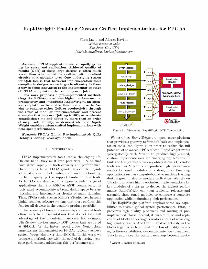
Figure 1. Vivado and RapidWright DCP Compatibility
We introduce RapidWright1, an open source platformthat provides a gateway to Vivado’s back-end implemen-tation tools (see Figure 1) in order to realize the fullpotential of advanced FPGA silicon. RapidWright workssynergistically with Vivado to produce highly-tuned,custom implementations for emerging applications. Itbuilds on the premise of two key observations: (1) Vendortools such as Vivado often produce high performanceresults for small modules of a design. (2) Emergingapplications such as compute-bound or machine learningdesigns grow in size by module replication. We rely onVivado to produce highly optimized implementations forkey modules of a design to deliver the highest perfor-mance. RapidWright can then replicate, relocate andassemble these tuned modules to compose a completeapplication while maintaining high performance.
The RapidWright platform employs three key capa-bilities to sustain global system performance. First, itpreserves high quality placement and routing of pre-implemented blocks. Second, it enables reuse and repli-cation of blocks to leverage Vivado’s efforts of achievinghigh quality results. And third, RapidWright stitches theblocks together with minimal or no loss of quality. Lever-aging these capabilities, we demonstrate how to augmentVivado and close the performance gap between device
1Wright = maker or builder
data sheets and achievable results through vendor tools.Keep in mind, relocating pre-implemented modules is achallenging task and not feasible in Vivado in all butthe smallest cases. RapidWright ultimately enables anew mode of implementation composition that has notbeen feasible previously and this work demonstrates howthese capabilities contribute to both performance andproductivity. Specific contributions of this work include:
1) An open source platform that enables crafting cus-tomized module-based implementations of FPGAapplications.
2) Specific case studies showing how RapidWrightimproves design performance and productivity.
3) A versatile gateway to Vivado by reading and writ-ing design checkpoints (DCPs) natively — settingthe ground work of an academic ecosystem forfurther advancing FPGA tools.
The third contribution empowers researchers by com-bining the commercial credibility of FPGA tools withthe agility of an open source framework, leading toinnovative solutions that might not be feasible otherwise.The next section summarizes background and relatedwork. Section III describes core RapidWright structure.Section IV proposes a pre-implemented design strategybuilt into RapidWright followed by a number of exampleuse cases and results in Section V. We conclude andoutline future work in Section VI.
II. Related WorkThere have been a number of open interfaces to FPGA
vendor tools in the past. The Xilinx Design Language(XDL) [1] provided an open design file format releasedwith ISE (predecessor to Vivado). XDL provided un-precedented access to placement and routing informationthat made building custom CAD tools possible. Opensource projects and tools such as RapidSmith [2], Torc[3], and ReCoBus-Builder [4] capitalized on the XDLinterface to increase productivity. Altera (now part ofIntel) also released the Quartus University InterfaceProgram (QUIP) [5] with similar attributes to XDL.
XDL and QUIP are no longer supported by the latestvendor tool suites Vivado and Quartus Prime. Instead,Xilinx’s Vivado utilizes a new Tcl-based interpreter. Thisallows users to perform customized tasks by writing Tclscripts. For small tasks, this is not a problem. However,as task size and complexity grows, productivity is limitedby Tcl interpreter performance. For example, Tincr [6]and the Vivado Design Interface (VDI) [7] have extendedRapidSmith to be compatible with Vivado by replacingXDL with Tcl interface routines. However, design importby this method is constrained by the low speed ofTcl commands, limiting feasibility to only the smallestdesigns. Townsend [7] reports a design of ~54K LUTstargeting an xc7a100t (Artix 7) takes ~2.5 hours to
import into Vivado (6 LUTs/second). By rough compar-ison, RapidWright writes a 210K LUT DCP targeting anxcvu190 (Virtex UltraScale) in 91 seconds. Vivado readsthe DCP in 303 seconds, for a total import time of 394seconds, or 533 LUTs/second, 88× faster than VDI. Byavoiding Tcl and using DCPs, RapidWright enables amore productive interface.
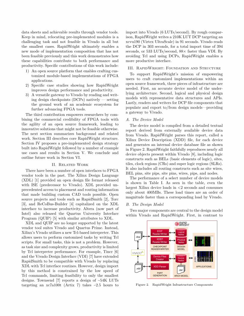
III. RapidWright: Foundation and StructureTo support RapidWright’s mission of empowering
users to craft customized implementations within anopen source framework, three pieces of infrastructure areneeded. First, an accurate device model of the under-lying architecture. Second, logical and physical designmodels with representative data structures and APIs.Lastly, readers and writers for DCP file components thatpopulate and export to/from design models—providinga gateway to Vivado.
A. The Device ModelThe device model is compiled from a detailed textual
report derived from externally available device datafrom Vivado. RapidWright parses this report, called aXilinx Device Description (XDD) file, for each deviceand generates an internal device database file as shownin Figure 2. RapidWright faithfully reproduces nearly alldevice objects present within Vivado [8], including logicconstructs such as BELs (basic elements of logic), sites,tiles, clock regions (CRs) and super logic regions (SLRs).It also includes all routing constructs such as site wires,BEL pins, site pips, site pins, wires, pips, and nodes.
The performance of a select number of device modelsis shown in Table I. As seen in the table, even thelargest Xilinx device loads in <2 seconds and consumesonly about 400MBs. These load times are an order ofmagnitude faster than a corresponding load by Vivado.
B. The Design ModelTwo major components are central to the design model
within Vivado and RapidWright. First, in contrast to
Vivado
PART
GENERATION ARCH MODEL
CHECKPOINT
READER/WRITER
DESIGN
MODEL
Physical
Netlist
Device
Netlist
.dcp
Vivado
EDIF Reader/Writer
XDEF Reader/Writer
Logical
Netlist
XDD Parser.xdd
Device Files Creator
.dat
APPLICATIONS
Figure 2. RapidWright Infrastructure Components
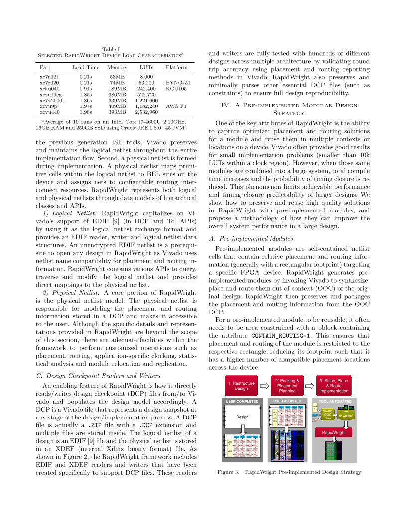
Table ISelected RapidWright Device Load Characteristicsa
Part Load Time Memory LUTs Platform
xc7a12t 0.21s 53MB 8,000xc7z020 0.21s 74MB 53,200 PYNQ-Z1xcku040 0.91s 189MB 242,400 KCU105xczu19eg 1.85s 386MB 522,720xc7v2000t 1.86s 339MB 1,221,600xcvu9p 1.97s 409MB 1,182,240 AWS F1xcvu440 1.98s 393MB 2,532,960aAverage of 10 runs on an Intel Core i7-4600U 2.10GHz,
16GB RAM and 250GB SSD using Oracle JRE 1.8.0_45 JVM.
the previous generation ISE tools, Vivado preservesand maintains the logical netlist throughout the entireimplementation flow. Second, a physical netlist is formedduring implementation. A physical netlist maps primi-tive cells within the logical netlist to BEL sites on thedevice and assigns nets to configurable routing inter-connect resources. RapidWright represents both logicaland physical netlists through data models of hierarchicalclasses and APIs.
1) Logical Netlist: RapidWright capitalizes on Vi-vado’s support of EDIF [9] (in DCP and Tcl APIs)by using it as the logical netlist exchange format andprovides an EDIF reader, writer and logical netlist datastructures. An unencrypted EDIF netlist is a prerequi-site to open any design in RapidWright as Vivado usesnetlist name compatibility for placement and routing in-formation. RapidWright contains various APIs to query,traverse and modify the logical netlist and providesdirect mappings to the physical netlist.
2) Physical Netlist: A core portion of RapidWrightis the physical netlist model. The physical netlist isresponsible for modeling the placement and routinginformation stored in a DCP and makes it accessibleto the user. Although the specific details and represen-tations provided in RapidWright are beyond the scopeof this section, there are adequate facilities within theframework to perform customized operations such asplacement, routing, application-specific clocking, statis-tical analysis and module relocation and replication.
C. Design Checkpoint Readers and WritersAn enabling feature of RapidWright is how it directly
reads/writes design checkpoint (DCP) files from/to Vi-vado and populates the design model accordingly. ADCP is a Vivado file that represents a design snapshot atany stage of the design/implementation process. A DCPfile is actually a .ZIP file with a .DCP extension andmultiple files are stored inside. The logical netlist of adesign is an EDIF [9] file and the physical netlist is storedin an XDEF (internal Xilinx binary format) file. Asshown in Figure 2, the RapidWright framework includesEDIF and XDEF readers and writers that have beencreated specifically to support DCP files. These readers
and writers are fully tested with hundreds of differentdesigns across multiple architecture by validating roundtrip accuracy using placement and routing reportingmethods in Vivado. RapidWright also preserves andminimally parses other essential DCP files (such asconstraints) to ensure full design reproducibility.
IV. A Pre-implemented Modular DesignStrategy
One of the key attributes of RapidWright is the abilityto capture optimized placement and routing solutionsfor a module and reuse them in multiple contexts orlocations on a device. Vivado often provides good resultsfor small implementation problems (smaller than 10kLUTs within a clock region). However, when those samemodules are combined into a large system, total compiletime increases and the probability of timing closure is re-duced. This phenomenon limits achievable performanceand timing closure predictability of larger designs. Weshow how to preserve and reuse high quality solutionsin RapidWright with pre-implemented modules, andpropose a methodology of how they can improve theoverall system performance in a large design.
A. Pre-implemented ModulesPre-implemented modules are self-contained netlist
cells that contain relative placement and routing infor-mation (generally with a rectangular footprint) targetinga specific FPGA device. RapidWright generates pre-implemented modules by invoking Vivado to synthesize,place and route them out-of-context (OOC) of the orig-inal design. RapidWright then preserves and packagesthe placement and routing information from the OOCDCP.
For a pre-implemented module to be reusable, it oftenneeds to be area constrained with a pblock containingthe attribute CONTAIN_ROUTING=1. This ensures thatplacement and routing of the module is restricted to therespective rectangle, reducing its footprint such that ithas a higher number of compatible placement locationsacross the device.
USER COMPLETED USER ASSISTED TOOL AUTOMATED
PE0,0
PE0,1
PE0,2
PE0,3
PE1,0
PE1,1
PE1,2
PE1,3
PE2,0
PE2,1
PE2,2
PE2,3
PE3,0
PE3,1
PE3,2
PE3,3
Acc0 Acc1 Acc2 Acc3
MEM0
MEM1
Design
PE0,0
PE0,1
PE0,2
PE0,3
PE1,0
PE1,1
PE1,2
PE1,3
PE2,0
PE2,1
PE2,2
PE2,3
PE3,0
PE3,1
PE3,2
PE3,3
Acc0 Acc1 Acc2 Acc3
MEM0
MEM1
M
EM
0
MEM1 0,0;
1,0
0,1;
1,1
0,2;
1,2
0,3;
1,3
0,0;
1,0
0,1;
1,1
0,2;
1,2
0,3;
1,3
Acc
0,1
Acc
2,3
1. Restructure
Design
2. Packing &
Placement Planning
3. Stitch, Place
& Route Implementation
MEM0
Acc0
PE0,0
IP Cache*
Vivado
OOC
Flow
RapidWright
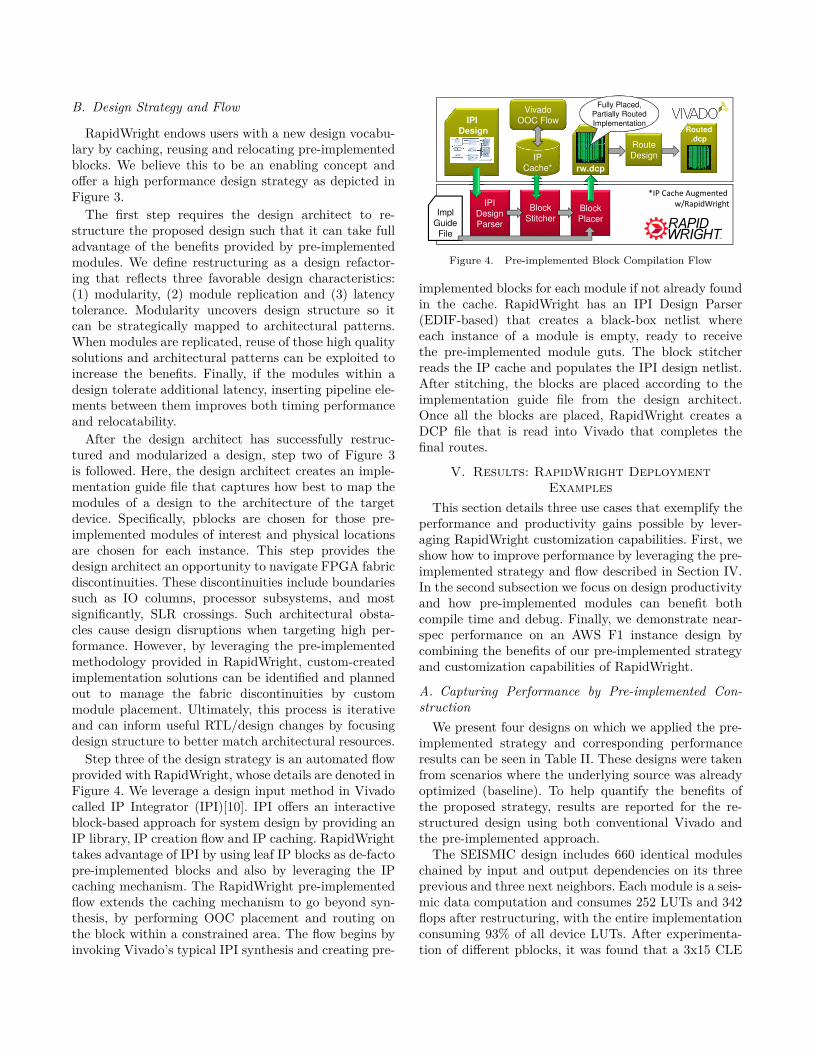
Figure 3. RapidWright Pre-implemented Design Strategy
B. Design Strategy and Flow
RapidWright endows users with a new design vocabu-lary by caching, reusing and relocating pre-implementedblocks. We believe this to be an enabling concept andoffer a high performance design strategy as depicted inFigure 3.
The first step requires the design architect to re-structure the proposed design such that it can take fulladvantage of the benefits provided by pre-implementedmodules. We define restructuring as a design refactor-ing that reflects three favorable design characteristics:(1) modularity, (2) module replication and (3) latencytolerance. Modularity uncovers design structure so itcan be strategically mapped to architectural patterns.When modules are replicated, reuse of those high qualitysolutions and architectural patterns can be exploited toincrease the benefits. Finally, if the modules within adesign tolerate additional latency, inserting pipeline ele-ments between them improves both timing performanceand relocatability.
After the design architect has successfully restruc-tured and modularized a design, step two of Figure 3is followed. Here, the design architect creates an imple-mentation guide file that captures how best to map themodules of a design to the architecture of the targetdevice. Specifically, pblocks are chosen for those pre-implemented modules of interest and physical locationsare chosen for each instance. This step provides thedesign architect an opportunity to navigate FPGA fabricdiscontinuities. These discontinuities include boundariessuch as IO columns, processor subsystems, and mostsignificantly, SLR crossings. Such architectural obsta-cles cause design disruptions when targeting high per-formance. However, by leveraging the pre-implementedmethodology provided in RapidWright, custom-createdimplementation solutions can be identified and plannedout to manage the fabric discontinuities by custommodule placement. Ultimately, this process is iterativeand can inform useful RTL/design changes by focusingdesign structure to better match architectural resources.
Step three of the design strategy is an automated flowprovided with RapidWright, whose details are denoted inFigure 4. We leverage a design input method in Vivadocalled IP Integrator (IPI)[10]. IPI offers an interactiveblock-based approach for system design by providing anIP library, IP creation flow and IP caching. RapidWrighttakes advantage of IPI by using leaf IP blocks as de-factopre-implemented blocks and also by leveraging the IPcaching mechanism. The RapidWright pre-implementedflow extends the caching mechanism to go beyond syn-thesis, by performing OOC placement and routing onthe block within a constrained area. The flow begins byinvoking Vivado’s typical IPI synthesis and creating pre-
Impl
Guide
File
Route
Design
IPI
Design
Parser
Block
StitcherBlock
Placer
rw.dcp
IPI
Design
IP
Cache*
Vivado
OOC FlowRouted
.dcp
*IP Cache Augmented
w/RapidWright
Implementation
Fully Placed, Partially Routed
Implementation
Figure 4. Pre-implemented Block Compilation Flow
implemented blocks for each module if not already foundin the cache. RapidWright has an IPI Design Parser(EDIF-based) that creates a black-box netlist whereeach instance of a module is empty, ready to receivethe pre-implemented module guts. The block stitcherreads the IP cache and populates the IPI design netlist.After stitching, the blocks are placed according to theimplementation guide file from the design architect.Once all the blocks are placed, RapidWright creates aDCP file that is read into Vivado that completes thefinal routes.
V. Results: RapidWright DeploymentExamples
This section details three use cases that exemplify theperformance and productivity gains possible by lever-aging RapidWright customization capabilities. First, weshow how to improve performance by leveraging the pre-implemented strategy and flow described in Section IV.In the second subsection we focus on design productivityand how pre-implemented modules can benefit bothcompile time and debug. Finally, we demonstrate near-spec performance on an AWS F1 instance design bycombining the benefits of our pre-implemented strategyand customization capabilities of RapidWright.
A. Capturing Performance by Pre-implemented Con-struction
We present four designs on which we applied the pre-implemented strategy and corresponding performanceresults can be seen in Table II. These designs were takenfrom scenarios where the underlying source was alreadyoptimized (baseline). To help quantify the benefits ofthe proposed strategy, results are reported for the re-structured design using both conventional Vivado andthe pre-implemented approach.
The SEISMIC design includes 660 identical moduleschained by input and output dependencies on its threeprevious and three next neighbors. Each module is a seis-mic data computation and consumes 252 LUTs and 342flops after restructuring, with the entire implementationconsuming 93% of all device LUTs. After experimenta-tion of different pblocks, it was found that a 3x15 CLE
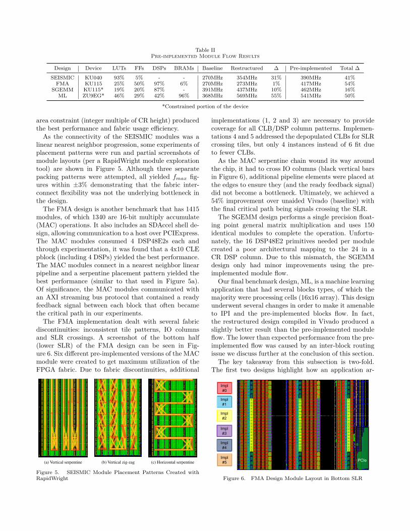
Table IIPre-implemented Module Flow Results
Design Device LUTs FFs DSPs BRAMs Baseline Restructured ∆ Pre-implemented Total ∆
SEISMIC KU040 93% 5% - - 270MHz 354MHz 31% 390MHz 41%FMA KU115 25% 50% 97% 6% 270MHz 273MHz 1% 417MHz 54%
SGEMM KU115* 19% 20% 87% - 391MHz 437MHz 10% 462MHz 16%ML ZU9EG* 46% 29% 42% 96% 368MHz 569MHz 55% 541MHz 50%
*Constrained portion of the device
area constraint (integer multiple of CR height) producedthe best performance and fabric usage efficiency.
As the connectivity of the SEISMIC modules was alinear nearest neighbor progression, some experiments ofplacement patterns were run and partial screenshots ofmodule layouts (per a RapidWright module explorationtool) are shown in Figure 5. Although three separatepacking patterns were attempted, all yielded fmax fig-ures within ±3% demonstrating that the fabric inter-connect flexibility was not the underlying bottleneck inthe design.
The FMA design is another benchmark that has 1415modules, of which 1340 are 16-bit multiply accumulate(MAC) operations. It also includes an SDAccel shell de-sign, allowing communication to a host over PCIExpress.The MAC modules consumed 4 DSP48E2s each andthrough experimentation, it was found that a 4x10 CLEpblock (including 4 DSPs) yielded the best performance.The MAC modules connect in a nearest neighbor linearpipeline and a serpentine placement pattern yielded thebest performance (similar to that used in Figure 5a).Of significance, the MAC modules communicated withan AXI streaming bus protocol that contained a readyfeedback signal between each block that often becamethe critical path in our experiments.
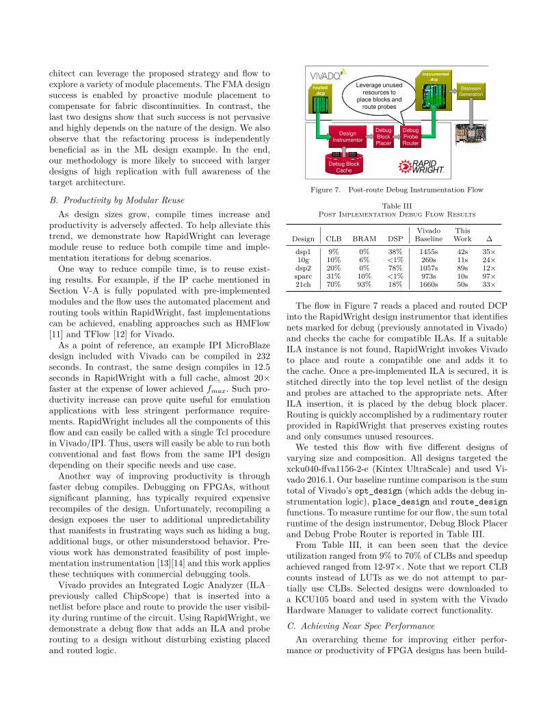
The FMA implementation dealt with several fabricdiscontinuities: inconsistent tile patterns, IO columnsand SLR crossings. A screenshot of the bottom half(lower SLR) of the FMA design can be seen in Fig-ure 6. Six different pre-implemented versions of the MACmodule were created to get maximum utilization of theFPGA fabric. Due to fabric discontinuities, additional
(a) Vertical serpentine (b) Vertical zig-zag (c) Horizontal serpentine
Figure 5. SEISMIC Module Placement Patterns Created withRapidWright
implementations (1, 2 and 3) are necessary to providecoverage for all CLB/DSP column patterns. Implemen-tations 4 and 5 addressed the depopulated CLBs for SLRcrossing tiles, but only 4 instances instead of 6 fit dueto fewer CLBs.
As the MAC serpentine chain wound its way aroundthe chip, it had to cross IO columns (black vertical barsin Figure 6), additional pipeline elements were placed atthe edges to ensure they (and the ready feedback signal)did not become a bottleneck. Ultimately, we achieved a54% improvement over unaided Vivado (baseline) withthe final critical path being signals crossing the SLR.
The SGEMM design performs a single precision float-ing point general matrix multiplication and uses 150identical modules to complete the operation. Unfortu-nately, the 16 DSP48E2 primitives needed per modulecreated a poor architectural mapping to the 24 in aCR DSP column. Due to this mismatch, the SGEMMdesign only had minor improvements using the pre-implemented module flow.
Our final benchmark design, ML, is a machine learningapplication that had several blocks types, of which themajority were processing cells (16x16 array). This designunderwent several changes in order to make it amenableto IPI and the pre-implemented blocks flow. In fact,the restructured design compiled in Vivado produced aslightly better result than the pre-implemented moduleflow. The lower than expected performance from the pre-implemented flow was caused by an inter-block routingissue we discuss further at the conclusion of this section.
The key takeaway from this subsection is two-fold.The first two designs highlight how an application ar-
Impl
#0
Impl
#1
Impl
#2
Impl
#3
Impl
#4
Impl
#5PCIe
Figure 6. FMA Design Module Layout in Bottom SLR
chitect can leverage the proposed strategy and flow toexplore a variety of module placements. The FMA designsuccess is enabled by proactive module placement tocompensate for fabric discontinuities. In contrast, thelast two designs show that such success is not pervasiveand highly depends on the nature of the design. We alsoobserve that the refactoring process is independentlybeneficial as in the ML design example. In the end,our methodology is more likely to succeed with largerdesigns of high replication with full awareness of thetarget architecture.
B. Productivity by Modular ReuseAs design sizes grow, compile times increase and
productivity is adversely affected. To help alleviate thistrend, we demonstrate how RapidWright can leveragemodule reuse to reduce both compile time and imple-mentation iterations for debug scenarios.
One way to reduce compile time, is to reuse exist-ing results. For example, if the IP cache mentioned inSection V-A is fully populated with pre-implementedmodules and the flow uses the automated placement androuting tools within RapidWright, fast implementationscan be achieved, enabling approaches such as HMFlow[11] and TFlow [12] for Vivado.
As a point of reference, an example IPI MicroBlazedesign included with Vivado can be compiled in 232seconds. In contrast, the same design compiles in 12.5seconds in RapidWright with a full cache, almost 20×faster at the expense of lower achieved fmax. Such pro-ductivity increase can prove quite useful for emulationapplications with less stringent performance require-ments. RapidWright includes all the components of thisflow and can easily be called with a single Tcl procedurein Vivado/IPI. Thus, users will easily be able to run bothconventional and fast flows from the same IPI designdepending on their specific needs and use case.
Another way of improving productivity is throughfaster debug compiles. Debugging on FPGAs, withoutsignificant planning, has typically required expensiverecompiles of the design. Unfortunately, recompiling adesign exposes the user to additional unpredictabilitythat manifests in frustrating ways such as hiding a bug,additional bugs, or other misunderstood behavior. Pre-vious work has demonstrated feasibility of post imple-mentation instrumentation [13][14] and this work appliesthese techniques with commercial debugging tools.
Vivado provides an Integrated Logic Analyzer (ILA–previously called ChipScope) that is inserted into anetlist before place and route to provide the user visibil-ity during runtime of the circuit. Using RapidWright, wedemonstrate a debug flow that adds an ILA and proberouting to a design without disturbing existing placedand routed logic.
Debug Block Cache
routed
.dcp
Design
Instrumentor
Debug
ProbeRouter
Debug
Block Placer
Leverage unused resources to
place blocks and route probes
instrumented
.dcp
Bitstream
Generation
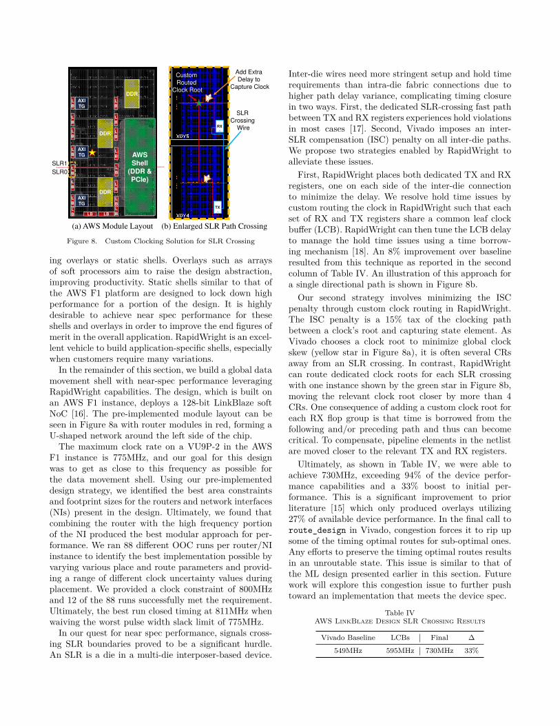
Figure 7. Post-route Debug Instrumentation Flow
Table IIIPost Implementation Debug Flow Results
Vivado ThisDesign CLB BRAM DSP Baseline Work ∆
dsp1 9% 0% 38% 1455s 42s 35×10g 10% 6% <1% 260s 11s 24×dsp2 20% 0% 78% 1057s 89s 12×sparc 31% 10% <1% 973s 10s 97×21ch 70% 93% 18% 1660s 50s 33×
The flow in Figure 7 reads a placed and routed DCPinto the RapidWright design instrumentor that identifiesnets marked for debug (previously annotated in Vivado)and checks the cache for compatible ILAs. If a suitableILA instance is not found, RapidWright invokes Vivadoto place and route a compatible one and adds it tothe cache. Once a pre-implemented ILA is secured, it isstitched directly into the top level netlist of the designand probes are attached to the appropriate nets. AfterILA insertion, it is placed by the debug block placer.Routing is quickly accomplished by a rudimentary routerprovided in RapidWright that preserves existing routesand only consumes unused resources.
We tested this flow with five different designs ofvarying size and composition. All designs targeted thexcku040-ffva1156-2-e (Kintex UltraScale) and used Vi-vado 2016.1. Our baseline runtime comparison is the sumtotal of Vivado’s opt_design (which adds the debug in-strumentation logic), place_design and route_designfunctions. To measure runtime for our flow, the sum totalruntime of the design instrumentor, Debug Block Placerand Debug Probe Router is reported in Table III.
From Table III, it can been seen that the deviceutilization ranged from 9% to 70% of CLBs and speedupachieved ranged from 12-97×. Note that we report CLBcounts instead of LUTs as we do not attempt to par-tially use CLBs. Selected designs were downloaded toa KCU105 board and used in system with the VivadoHardware Manager to validate correct functionality.
C. Achieving Near Spec PerformanceAn overarching theme for improving either perfor-
mance or productivity of FPGA designs has been build-
DDR
DDR
DDR
AXI
TG
AXI
TG
AXI
TG
L
B
L
B
L
B
L
B
L
B
L
B
L
B LB LB
L
B
L
B
L
B
L
B
L
B
L
B
L
B
L
B
SLR0
SLR1
AWS
Shell
(DDR &
PCIe)
L
B
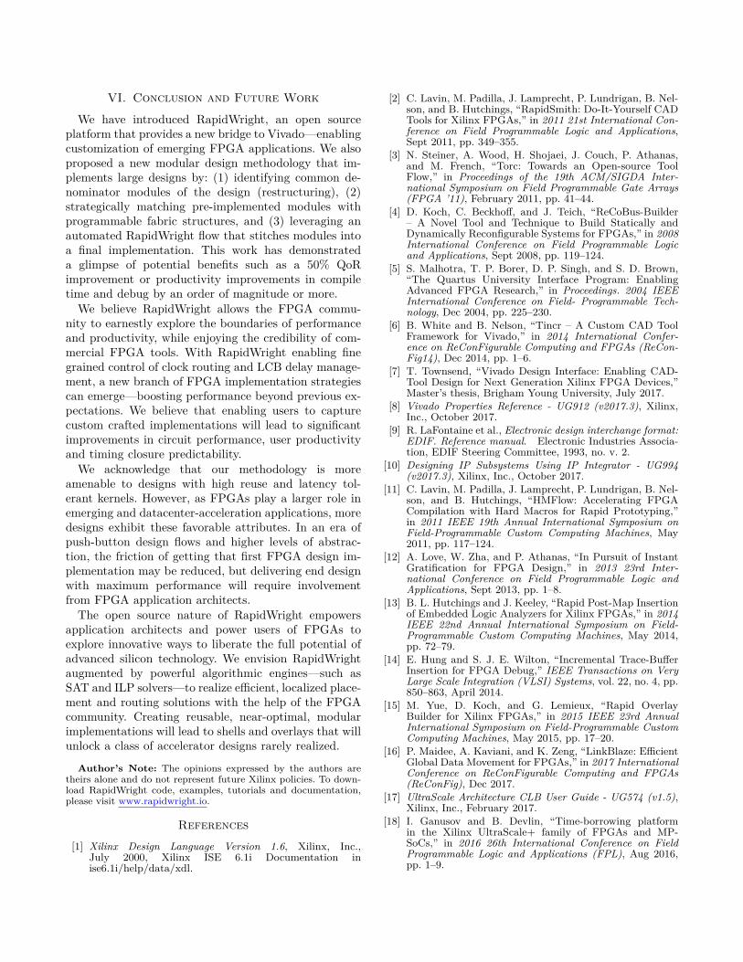
(a) AWS Module Layout (b) Enlarged SLR Path Crossing
RX
Custom
Routed Clock Root
Add Extra
Delay to Capture Clock
TX
SLR
Crossing Wire
Figure 8. Custom Clocking Solution for SLR Crossing
ing overlays or static shells. Overlays such as arraysof soft processors aim to raise the design abstraction,improving productivity. Static shells similar to that ofthe AWS F1 platform are designed to lock down highperformance for a portion of the design. It is highlydesirable to achieve near spec performance for theseshells and overlays in order to improve the end figures ofmerit in the overall application. RapidWright is an excel-lent vehicle to build application-specific shells, especiallywhen customers require many variations.
In the remainder of this section, we build a global datamovement shell with near-spec performance leveragingRapidWright capabilities. The design, which is built onan AWS F1 instance, deploys a 128-bit LinkBlaze softNoC [16]. The pre-implemented module layout can beseen in Figure 8a with router modules in red, forming aU-shaped network around the left side of the chip.
The maximum clock rate on a VU9P-2 in the AWSF1 instance is 775MHz, and our goal for this designwas to get as close to this frequency as possible forthe data movement shell. Using our pre-implementeddesign strategy, we identified the best area constraintsand footprint sizes for the routers and network interfaces(NIs) present in the design. Ultimately, we found thatcombining the router with the high frequency portionof the NI produced the best modular approach for per-formance. We ran 88 different OOC runs per router/NIinstance to identify the best implementation possible byvarying various place and route parameters and provid-ing a range of different clock uncertainty values duringplacement. We provided a clock constraint of 800MHzand 12 of the 88 runs successfully met the requirement.Ultimately, the best run closed timing at 811MHz whenwaiving the worst pulse width slack limit of 775MHz.
In our quest for near spec performance, signals cross-ing SLR boundaries proved to be a significant hurdle.An SLR is a die in a multi-die interposer-based device.
Inter-die wires need more stringent setup and hold timerequirements than intra-die fabric connections due tohigher path delay variance, complicating timing closurein two ways. First, the dedicated SLR-crossing fast pathbetween TX and RX registers experiences hold violationsin most cases [17]. Second, Vivado imposes an inter-SLR compensation (ISC) penalty on all inter-die paths.We propose two strategies enabled by RapidWright toalleviate these issues.
First, RapidWright places both dedicated TX and RXregisters, one on each side of the inter-die connectionto minimize the delay. We resolve hold time issues bycustom routing the clock in RapidWright such that eachset of RX and TX registers share a common leaf clockbuffer (LCB). RapidWright can then tune the LCB delayto manage the hold time issues using a time borrow-ing mechanism [18]. An 8% improvement over baselineresulted from this technique as reported in the secondcolumn of Table IV. An illustration of this approach fora single directional path is shown in Figure 8b.
Our second strategy involves minimizing the ISCpenalty through custom clock routing in RapidWright.The ISC penalty is a 15% tax of the clocking pathbetween a clock’s root and capturing state element. AsVivado chooses a clock root to minimize global clockskew (yellow star in Figure 8a), it is often several CRsaway from an SLR crossing. In contrast, RapidWrightcan route dedicated clock roots for each SLR crossingwith one instance shown by the green star in Figure 8b,moving the relevant clock root closer by more than 4CRs. One consequence of adding a custom clock root foreach RX flop group is that time is borrowed from thefollowing and/or preceding path and thus can becomecritical. To compensate, pipeline elements in the netlistare moved closer to the relevant TX and RX registers.
Ultimately, as shown in Table IV, we were able toachieve 730MHz, exceeding 94% of the device perfor-mance capabilities and a 33% boost to initial per-formance. This is a significant improvement to priorliterature [15] which only produced overlays utilizing27% of available device performance. In the final call toroute_design in Vivado, congestion forces it to rip upsome of the timing optimal routes for sub-optimal ones.Any efforts to preserve the timing optimal routes resultsin an unroutable state. This issue is similar to that ofthe ML design presented earlier in this section. Futurework will explore this congestion issue to further pushtoward an implementation that meets the device spec.
Table IVAWS LinkBlaze Design SLR Crossing Results
Vivado Baseline LCBs Final ∆
549MHz 595MHz 730MHz 33%
VI. Conclusion and Future Work
We have introduced RapidWright, an open sourceplatform that provides a new bridge to Vivado—enablingcustomization of emerging FPGA applications. We alsoproposed a new modular design methodology that im-plements large designs by: (1) identifying common de-nominator modules of the design (restructuring), (2)strategically matching pre-implemented modules withprogrammable fabric structures, and (3) leveraging anautomated RapidWright flow that stitches modules intoa final implementation. This work has demonstrateda glimpse of potential benefits such as a 50% QoRimprovement or productivity improvements in compiletime and debug by an order of magnitude or more.
We believe RapidWright allows the FPGA commu-nity to earnestly explore the boundaries of performanceand productivity, while enjoying the credibility of com-mercial FPGA tools. With RapidWright enabling finegrained control of clock routing and LCB delay manage-ment, a new branch of FPGA implementation strategiescan emerge—boosting performance beyond previous ex-pectations. We believe that enabling users to capturecustom crafted implementations will lead to significantimprovements in circuit performance, user productivityand timing closure predictability.
We acknowledge that our methodology is moreamenable to designs with high reuse and latency tol-erant kernels. However, as FPGAs play a larger role inemerging and datacenter-acceleration applications, moredesigns exhibit these favorable attributes. In an era ofpush-button design flows and higher levels of abstrac-tion, the friction of getting that first FPGA design im-plementation may be reduced, but delivering end designwith maximum performance will require involvementfrom FPGA application architects.
The open source nature of RapidWright empowersapplication architects and power users of FPGAs toexplore innovative ways to liberate the full potential ofadvanced silicon technology. We envision RapidWrightaugmented by powerful algorithmic engines—such asSAT and ILP solvers—to realize efficient, localized place-ment and routing solutions with the help of the FPGAcommunity. Creating reusable, near-optimal, modularimplementations will lead to shells and overlays that willunlock a class of accelerator designs rarely realized.
Author’s Note: The opinions expressed by the authors aretheirs alone and do not represent future Xilinx policies. To down-load RapidWright code, examples, tutorials and documentation,please visit www.rapidwright.io.
References
[1] Xilinx Design Language Version 1.6, Xilinx, Inc.,July 2000, Xilinx ISE 6.1i Documentation inise6.1i/help/data/xdl.
[2] C. Lavin, M. Padilla, J. Lamprecht, P. Lundrigan, B. Nel-son, and B. Hutchings, “RapidSmith: Do-It-Yourself CADTools for Xilinx FPGAs,” in 2011 21st International Con-ference on Field Programmable Logic and Applications,Sept 2011, pp. 349–355.
[3] N. Steiner, A. Wood, H. Shojaei, J. Couch, P. Athanas,and M. French, “Torc: Towards an Open-source ToolFlow,” in Proceedings of the 19th ACM/SIGDA Inter-national Symposium on Field Programmable Gate Arrays(FPGA ’11), February 2011, pp. 41–44.
[4] D. Koch, C. Beckhoff, and J. Teich, “ReCoBus-Builder– A Novel Tool and Technique to Build Statically andDynamically Reconfigurable Systems for FPGAs,” in 2008International Conference on Field Programmable Logicand Applications, Sept 2008, pp. 119–124.
[5] S. Malhotra, T. P. Borer, D. P. Singh, and S. D. Brown,“The Quartus University Interface Program: EnablingAdvanced FPGA Research,” in Proceedings. 2004 IEEEInternational Conference on Field- Programmable Tech-nology, Dec 2004, pp. 225–230.
[6] B. White and B. Nelson, “Tincr – A Custom CAD ToolFramework for Vivado,” in 2014 International Confer-ence on ReConFigurable Computing and FPGAs (ReCon-Fig14), Dec 2014, pp. 1–6.
[7] T. Townsend, “Vivado Design Interface: Enabling CAD-Tool Design for Next Generation Xilinx FPGA Devices,”Master’s thesis, Brigham Young University, July 2017.
[8] Vivado Properties Reference - UG912 (v2017.3), Xilinx,Inc., October 2017.
[9] R. LaFontaine et al., Electronic design interchange format:EDIF. Reference manual. Electronic Industries Associa-tion, EDIF Steering Committee, 1993, no. v. 2.
[10] Designing IP Subsystems Using IP Integrator - UG994(v2017.3), Xilinx, Inc., October 2017.
[11] C. Lavin, M. Padilla, J. Lamprecht, P. Lundrigan, B. Nel-son, and B. Hutchings, “HMFlow: Accelerating FPGACompilation with Hard Macros for Rapid Prototyping,”in 2011 IEEE 19th Annual International Symposium onField-Programmable Custom Computing Machines, May2011, pp. 117–124.
[12] A. Love, W. Zha, and P. Athanas, “In Pursuit of InstantGratification for FPGA Design,” in 2013 23rd Inter-national Conference on Field Programmable Logic andApplications, Sept 2013, pp. 1–8.
[13] B. L. Hutchings and J. Keeley, “Rapid Post-Map Insertionof Embedded Logic Analyzers for Xilinx FPGAs,” in 2014IEEE 22nd Annual International Symposium on Field-Programmable Custom Computing Machines, May 2014,pp. 72–79.
[14] E. Hung and S. J. E. Wilton, “Incremental Trace-BufferInsertion for FPGA Debug,” IEEE Transactions on VeryLarge Scale Integration (VLSI) Systems, vol. 22, no. 4, pp.850–863, April 2014.
[15] M. Yue, D. Koch, and G. Lemieux, “Rapid OverlayBuilder for Xilinx FPGAs,” in 2015 IEEE 23rd AnnualInternational Symposium on Field-Programmable CustomComputing Machines, May 2015, pp. 17–20.
[16] P. Maidee, A. Kaviani, and K. Zeng, “LinkBlaze: EfficientGlobal Data Movement for FPGAs,” in 2017 InternationalConference on ReConFigurable Computing and FPGAs(ReConFig), Dec 2017.
[17] UltraScale Architecture CLB User Guide - UG574 (v1.5),Xilinx, Inc., February 2017.
[18] I. Ganusov and B. Devlin, “Time-borrowing platformin the Xilinx UltraScale+ family of FPGAs and MP-SoCs,” in 2016 26th International Conference on FieldProgrammable Logic and Applications (FPL), Aug 2016,pp. 1–9.


