Embed Size (px)
Citation preview
Experiments with
Electricity and Magnetism
for
Physics 336L
by
Richard Sonnenfeld
New Mexico Tech Physics Department
c©2022 by New Mexico Tech
January 14, 2022
i
Contents
Course schedule 1
0 Introduction 20.1 Course Goals and Time Committment . . . . . . . . . . . . . . . . . . . . . . . . . 20.2 Honesty/Plagiarism . . . . . . . . . . . . . . . . . . . . . . . . . . . . . . . . . . . 20.3 Safety . . . . . . . . . . . . . . . . . . . . . . . . . . . . . . . . . . . . . . . . . . . 20.4 Laboratory Protocol . . . . . . . . . . . . . . . . . . . . . . . . . . . . . . . . . . . 30.5 Required Supplies . . . . . . . . . . . . . . . . . . . . . . . . . . . . . . . . . . . . 30.6 Lab Reports . . . . . . . . . . . . . . . . . . . . . . . . . . . . . . . . . . . . . . . 3
Lab Reports 30.7 Required report sections . . . . . . . . . . . . . . . . . . . . . . . . . . . . . . . . 40.8 Error Analysis . . . . . . . . . . . . . . . . . . . . . . . . . . . . . . . . . . . . . . 5
0.8.1 Random errors . . . . . . . . . . . . . . . . . . . . . . . . . . . . . . . . . . 50.8.2 Systematic errors . . . . . . . . . . . . . . . . . . . . . . . . . . . . . . . . . 50.8.3 Handling Errors . . . . . . . . . . . . . . . . . . . . . . . . . . . . . . . . . 6
0.9 Lab Grades . . . . . . . . . . . . . . . . . . . . . . . . . . . . . . . . . . . . . . . . 7
1 Circuits (n=1) 10Understand DC series and parallel circuits and light-bulbs . . . . . . . . . . . . . . . . . 101.1 Background theory . . . . . . . . . . . . . . . . . . . . . . . . . . . . . . . . . . . . 10
1.1.1 Multimeters . . . . . . . . . . . . . . . . . . . . . . . . . . . . . . . . . . . . 101.1.2 Circuits . . . . . . . . . . . . . . . . . . . . . . . . . . . . . . . . . . . . . . 10
1.2 Basic Formulae for DC Circuits . . . . . . . . . . . . . . . . . . . . . . . . . . . . . 101.3 Series and Parallel Circuits with Resistors . . . . . . . . . . . . . . . . . . . . . . . 111.4 Physics Puzzler [Answer two of these questions] . . . . . . . . . . . . . . . . . . . . 131.5 For Graduate Students . . . . . . . . . . . . . . . . . . . . . . . . . . . . . . . . . . 14
2 Complex Impedance (n=1) 15Measure complex impedance of RLC circuit . . . . . . . . . . . . . . . . . . . . . . . . . 152.1 Motivation for the experiment . . . . . . . . . . . . . . . . . . . . . . . . . . . . . . 152.2 Prelab . . . . . . . . . . . . . . . . . . . . . . . . . . . . . . . . . . . . . . . . . . . 152.3 Background: Introduction to Complex Impedance . . . . . . . . . . . . . . . . . . 152.4 Requirements to use Complex Impedance . . . . . . . . . . . . . . . . . . . . . . . 162.5 Why does it work? . . . . . . . . . . . . . . . . . . . . . . . . . . . . . . . . . . . . 162.6 Overall Approach for the experiment . . . . . . . . . . . . . . . . . . . . . . . . . . 172.7 Make Measurements for RLC Circuit . . . . . . . . . . . . . . . . . . . . . . . . . . 182.8 Compare theory and experiment . . . . . . . . . . . . . . . . . . . . . . . . . . . . 192.9 Physics Puzzler [Answer any two of these questions] . . . . . . . . . . . . . . . . . 202.10 For Graduate Students . . . . . . . . . . . . . . . . . . . . . . . . . . . . . . . . . . 202.11 Equipment . . . . . . . . . . . . . . . . . . . . . . . . . . . . . . . . . . . . . . . . 202.12 Refresher on Complex Arithmetic . . . . . . . . . . . . . . . . . . . . . . . . . . . . 20
ii
3 Magnetic Field, Inductance and Mutual Inductance (n=1) 21Exploring self-inductance, mutual inductance and transformer action . . . . . . . . . . . 213.1 Introduction . . . . . . . . . . . . . . . . . . . . . . . . . . . . . . . . . . . . . . . . 213.2 Self Inductance . . . . . . . . . . . . . . . . . . . . . . . . . . . . . . . . . . . . . . 213.3 Magnetic Field Amplitude and Mutual Inductance . . . . . . . . . . . . . . . . . . 223.4 Transformer . . . . . . . . . . . . . . . . . . . . . . . . . . . . . . . . . . . . . . . . 233.5 Postlab: Calculations and analysis . . . . . . . . . . . . . . . . . . . . . . . . . . . 23
4 Hysteresis (n=2) 25Measure hysteresis loop of a soft iron torus and learn how a transformer works . . . . . 254.1 Prelab . . . . . . . . . . . . . . . . . . . . . . . . . . . . . . . . . . . . . . . . . . . 254.2 Introduction . . . . . . . . . . . . . . . . . . . . . . . . . . . . . . . . . . . . . . . . 25
4.2.1 Hysteresis defined . . . . . . . . . . . . . . . . . . . . . . . . . . . . . . . . 254.2.2 B, H and M . . . . . . . . . . . . . . . . . . . . . . . . . . . . . . . . . . . 254.2.3 Ferromagnetic theory reviewed . . . . . . . . . . . . . . . . . . . . . . . . . 25
4.3 Applying Maxwell’s Equations . . . . . . . . . . . . . . . . . . . . . . . . . . . . . 284.4 Laboratory Measurements . . . . . . . . . . . . . . . . . . . . . . . . . . . . . . . . 304.5 Calculations and Analysis . . . . . . . . . . . . . . . . . . . . . . . . . . . . . . . . 30
5 Operational Amplifiers (n=1) 32Learn basic op-amp theory then build an inverting and non-inverting op-amp . . . . . . 325.1 Uses of Operational Amplifiers . . . . . . . . . . . . . . . . . . . . . . . . . . . . . 325.2 What Operational Amplifiers Do . . . . . . . . . . . . . . . . . . . . . . . . . . . . 325.3 The Golden Rules . . . . . . . . . . . . . . . . . . . . . . . . . . . . . . . . . . . . 335.4 A. Proper operation of an Op-Amp . . . . . . . . . . . . . . . . . . . . . . . . . . . 335.5 B. Clipping of an Op-Amp . . . . . . . . . . . . . . . . . . . . . . . . . . . . . . . . 345.6 C. Slew rate of an Op-Amp . . . . . . . . . . . . . . . . . . . . . . . . . . . . . . . 345.7 D. Bandwidth of an Op-Amp . . . . . . . . . . . . . . . . . . . . . . . . . . . . . . 355.8 E. Theoretical Gain of an Op-Amp . . . . . . . . . . . . . . . . . . . . . . . . . . . 355.9 Analysis . . . . . . . . . . . . . . . . . . . . . . . . . . . . . . . . . . . . . . . . . . 365.10 For Graduate Students . . . . . . . . . . . . . . . . . . . . . . . . . . . . . . . . . . 36
6 Introduction to Arduino (n=2) 37We will learn how to use an Arduino uController and programmably change the bright-
ness of an LED . . . . . . . . . . . . . . . . . . . . . . . . . . . . . . . . . . . . . . 37A Background: . . . . . . . . . . . . . . . . . . . . . . . . . . . . . . . . . . . . . . . 37
A.1 Introduction to the Arduino UNO Microcontroller Hardware: . . . . . . . 38A.2 Introduction to the Arduino UNO Microcontroller Software: . . . . . . . . 39
B Digital Output: Blinking LED . . . . . . . . . . . . . . . . . . . . . . . . . . . . . 40C Digital Input: Switch . . . . . . . . . . . . . . . . . . . . . . . . . . . . . . . . . . . 41D Analog Input: Potentiometers . . . . . . . . . . . . . . . . . . . . . . . . . . . . . 42E Analog Output: Controlling LED Brightness . . . . . . . . . . . . . . . . . . . . . 44
7 Digital to Analog Converters (n=2) 47Learn how to convert a digital number into an analog voltage . . . . . . . . . . . . . . . 47A Saving your data and code . . . . . . . . . . . . . . . . . . . . . . . . . . . . . . . . 47B Motivation for the experiment . . . . . . . . . . . . . . . . . . . . . . . . . . . . . . 47C Overall Approach for the experiment . . . . . . . . . . . . . . . . . . . . . . . . . . 47
iii

D Build a 5-bit Ladder . . . . . . . . . . . . . . . . . . . . . . . . . . . . . . . . . . . 47D.1 Build a ladder using 16 identical resistors . . . . . . . . . . . . . . . . . . . 48
E Build a 5-bit binary counter with the Arduino . . . . . . . . . . . . . . . . . . . . . 48F Build a 5-bit DAC . . . . . . . . . . . . . . . . . . . . . . . . . . . . . . . . . . . . 50G Build an 8-bit DAC using a ladder chip . . . . . . . . . . . . . . . . . . . . . . . . 50
8 Diodes (n=1) 51Characterize a diode, using Arduino as a data acquisition system . . . . . . . . . . . . . 51A Measuring the Constitutive Relation of a Diode . . . . . . . . . . . . . . . . . . . . 51
9 Index of Refraction of Air (n=1) 53Compare optical path length in air to vacuum using an interferometer . . . . . . . . . . 53
10 Negative Resistance (n=1) 54Measure I-V curve of neon lamp. Use negative resistance to create an oscillator . . . . . 54
11 Superconductivity (n=1) 55Understand Meissner effect with a High Tc superconductor . . . . . . . . . . . . . . . . 55
12 Serial Ports (n=1) 60Decode the signals that come out of a computer terminal. . . . . . . . . . . . . . . . . . 60
13 Miscellaneous Experiments (n=various!) 63Develop an outlined experiment or create your own . . . . . . . . . . . . . . . . . . . . . . . . . . . . . . 63A Arduino Experiments . . . . . . . . . . . . . . . . . . . . . . . . . . . . . . . . . . 63The Arduino can measure or control a vast quantity of experiments and there is code for the taking out on the net. . . . . . . 63B Plasma Physics . . . . . . . . . . . . . . . . . . . . . . . . . . . . . . . . . . . . . 63A table-top plasma apparatus allows you to manipulate and measure the plasma you have been learning about in Astrophysics
courses. . . . . . . . . . . . . . . . . . . . . . . . . . . . . . . . . . . . . . . . . . . . . 63C The Radio Spectrum . . . . . . . . . . . . . . . . . . . . . . . . . . . . . . . . . . 64Use a spectrum analyzer to study the radio spectrum . . . . . . . . . . . . . . . . . . . . . . . . . . . . . 64D Lightning Location . . . . . . . . . . . . . . . . . . . . . . . . . . . . . . . . . . . 64Use the time of arrival technique to locate a spark . . . . . . . . . . . . . . . . . . . . . . . . . . . . . . 64E Lock-in Amplifiers . . . . . . . . . . . . . . . . . . . . . . . . . . . . . . . . . . . . 64Lock-in amplifiers allow you to see a tiny signal in the presence of substantial noise . . . . . . . . . . . . . . . . . . 64F TV remote control . . . . . . . . . . . . . . . . . . . . . . . . . . . . . . . . . . . . 64Detect and decode the infra-red control pulses sent by a TV remote . . . . . . . . . . . . . . . . . . . . . . . . 64G Dielectric Constant of Liquid Nitrogen . . . . . . . . . . . . . . . . . . . . . . . . . 64Measure the dielectric constant of liquid nitrogen . . . . . . . . . . . . . . . . . . . . . . . . . . . . . . . 64H Light-emitting diodes . . . . . . . . . . . . . . . . . . . . . . . . . . . . . . . . . . . 64Use a light-emitting diode as a photodetector . . . . . . . . . . . . . . . . . . . . . . . . . . . . . . . . 64I Electric Motors . . . . . . . . . . . . . . . . . . . . . . . . . . . . . . . . . . . . . 64Electric motors can be used in reverse as electric generators . . . . . . . . . . . . . . . . . . . . . . . . . . . 64J Magnetic materials . . . . . . . . . . . . . . . . . . . . . . . . . . . . . . . . . . . 65Measure magnetic properties of materials by incorporating them in an inductor. . . . . . . . . . . . . . . . . . . . 65K Serial ports . . . . . . . . . . . . . . . . . . . . . . . . . . . . . . . . . . . . . . . . 65Decode the signals that come out of a computer terminal. . . . . . . . . . . . . . . . . . . . . . . . . . . . . 65L Build a Geiger Counter . . . . . . . . . . . . . . . . . . . . . . . . . . . . . . . . . 65Build a Geiger Counter . . . . . . . . . . . . . . . . . . . . . . . . . . . . . . . . . . . . . . . . . 65
iv

M Improve an electromagnetic can crusher . . . . . . . . . . . . . . . . . . . . . . . . 65A pulsed magnetic field can cause a coke-can to crush itself via eddy curret . . . . . . . . . . . . . . . . . . . . . 65N Solar Motor-driver . . . . . . . . . . . . . . . . . . . . . . . . . . . . . . . . . . . . 65Use Ultracapacitors in a circuit that extracts mechanical energy from the available sunlight . . . . . . . . . . . . . . . 65
Appendices – Data Sheets 66
v
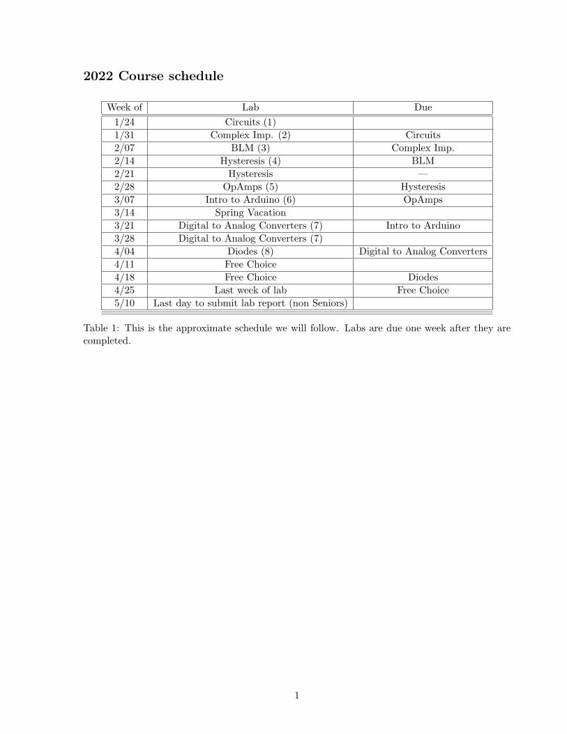
2022 Course schedule
Week of Lab Due
1/24 Circuits (1)
1/31 Complex Imp. (2) Circuits
2/07 BLM (3) Complex Imp.
2/14 Hysteresis (4) BLM
2/21 Hysteresis —
2/28 OpAmps (5) Hysteresis
3/07 Intro to Arduino (6) OpAmps
3/14 Spring Vacation
3/21 Digital to Analog Converters (7) Intro to Arduino
3/28 Digital to Analog Converters (7)
4/04 Diodes (8) Digital to Analog Converters
4/11 Free Choice
4/18 Free Choice Diodes
4/25 Last week of lab Free Choice
5/10 Last day to submit lab report (non Seniors)
Table 1: This is the approximate schedule we will follow. Labs are due one week after they arecompleted.
1
0 Introduction
0.1 Course Goals and Time Committment
There are four purposes for this course.
• To give practical examples of concepts learned in Phys333
• To give you practice thinking about sources of experimental errors.
• To let you experience some of the excitement (and confusion) of experimental physics.
• To encourage your creativity in the context of the complex and subtle world of measurement.
• To give you a working comfort with basic electronics as it appears universally in a modernphysics lab.
• To introduce you to Physical Programming (also called Embedded Systems Programming),a very useful experimental skill with a substantial future potential for employment.
Labs will take at least 2.5 hours to get through and understand. The course grade is basedon your accurate understanding of the labs and completion of the lab reports. The individualmeasurements requested are frequently not time-consuming; that is intentional. The time you arenot spending assembling circuits and making measurements is meant to be spent understandingyour results and how they fit the basic electromagnetic theory that you have learned.
It will require one to three hours after each class session to complete the data analysis, performthe needed derivations, and do the background reading needed to understand your results.
0.2 Honesty/Plagiarism
The Tech honor code is in effect in this class (as in all classes). More specifically, Lab reports usingshared data or analysis, unless explicitly authorized and documented, will result in an automatic“F” for the report and a report to the Associate VP of Academic Affairs.
You can, of course, seek assistance in understanding from other students, the instructor, oronline/library resources.
0.3 Safety
• Shoes and socks are required for minimal safety.
• In case of emergency, campus police are available at 835-5434.
• Know the location of the nearest FIRE EXTINGUISHER. Can this fire extinguisher beused on electrical fires?
• Know the location of the nearest FIRE ALARM pull lever.
• Report defective or damaged equipment to the instructor.
• Construct experiments so they can not fall and so that people will not trip over wires. (Ducttape can be useful!)
• Do not energize any experiment outputting more than 30 V until the instructor has inspectedit.
2
• Conventional lab protocol calls for no food or drink under any circumstances. I have loosenedthis ban because I have observed that science runs on caffeine. Thus, black coffee, tea, orbottled water are the only drinks allowed in the lab. Sugar and sweeteners are destructiveto electronics, and many drinks (e.g. Coca-Cola) are corrosive. In the event of a spill ofany type, you are responsible to promptly clean and dry any lab equipment involved. Youmay be required to dissassemble, dry, and retest your equipment if liquid has penetratedthe case.
• Food and snacks are not permitted in the lab. If you are hungry, you may briefly excuseyourself after the daily introduction and finish your snack/lunch in the Workman lobby.
• Hazardous chemicals (e.g. lead) are associated with electronics. Thus, you shall wash yourhands between working with lab equipment/components and eating.
0.4 Laboratory Protocol
• The Laboratory hours are 2 PM to 4:30 PM. Please arrive on time. Habitual lateness/ab-sence will affect your grade. If you finish an experiment early, begin working on your analysisor on the next experiment.
• Conversations in the laboratory are encouraged but should be limited to the experiments.
• You are encouraged to help your fellow student learn the material or troubleshoot theirexperiment, but all are responsible for their own understanding.
• Feel free to bring computing devices/smart phones to assist in data plotting/analysis or forweb research related to your analysis.
0.5 Required Supplies
Failure to bring the following supplies every time can result in grade reductions. (See section ongrading).
• The lab manual, a printout, or an electronic copy of the day’s lab.
• A lab notebook for your raw data and notes.
• A calculator or smart-phone/computing device that can act as a calculator. This allows youto do data analysis in lab.
0.6 Lab Reports
Lab reports must be typed, and will be uploaded as .pdfs. I need to be able to rapidly see thatyou did the work and that it is correct. Thus it must be well organized and neat. Raw datashould be recopied into well-arranged tables. Figures (e.g. hand-written sketches or cell-phonepictures) should be digitally inserted into your report. In many cases, I have numbered each labwith items of data you should include. Please include these items in your report in that order,and with the appropriate number to make them easy to find.
I have posted LATEX templates for a lab report on Canvas. I can give a short tutorial on LATEXif you are interested in learning it. LibreOffice Writer or other word processors are also perfectlyacceptable.
Your report should NOT HAVE an Introduction, Procedure or a Conclusions section. I shouldONLY have the following sections:
3
0.7 Required report sections
1. Heading – In the following order, state
(a) Your name
(b) The name of the experiment
(c) Date the report was written.
(d) Date the laboratory work was finished.
2. Measured variables and data tables – Numerical values should make clear how manysignificant figures you feel are appropriate. Thus:
2 Volts
2.0 Volts
2.00 Volts
2.000 Volts
mean very different things. If you list a measurement as 5 Volts, that tells me you thinkthere is potentially 20% error in that measurement.
The column headings of your data table should list the name of the variable being measuredand the units of the numbers contained. In theoretical courses, variables often representquantities like ~E or ~B or ǫ. In the laboratory, variables represent the number of divisionson an oscilloscope or the voltage on a voltmeter. An imprecise table would have a columnheaded “Voltage (V)”. A more precise table would indicate the part of the circuit the volt-meter was connected to. A well-defined variable could be called VAB, where A and B arethe two points on your circuit to which the voltmeter probes were applied. VAB would befurther defined by the inclusion of the circuit diagram in the report with A and B markedon it.
It is not unusual for raw data to be somewhat disorganized. For example, when measuringthe current through a diode vs. applied voltage one may take a number of data points thatare not interesting (because the diode has not yet turned on). You might also obtain datathat you later decide are incorrect or ambiguous. For the lab report, you shall recopy thedata table in a well-ordered way. You may omit data that you later concluded is incorrector uninteresting.1
3. Graphs – Show data as points (not lines) and theoretical curves as lines. Use computerplotting software, or plot by hand in your notebook or on graph paper and scan in the plot.Axes should be labeled with tick-marks and and well-defined variables (described previouslyin discussion of tables).
4. Answers to Numbered Questions – For convenience in grading, please number yourresults/analysis with the numbers used in the lab manual. Often the questions will requireeither calculations or derivations. These should be done as follows:
Calculations: When numerical values are plugged into formulae or derived results, theyshould be explicitly written in your report. I know that you can plug ten numbers into aformula in your calculator and just write down the answer, but am explicitly asking that
1Sometimes incorrect data is interesting if it documents a malfunction or, at best, reveals some new physics or
instrumental quirks. Feel free for extra credit to share “weird” results and your best explanation for their cause.
4
you not do that. You (or I) should be able to look at your calculations and see exactlywhat numbers you used at every step. This will help you find your mistakes and documentsexactly what you did.
Derivations: If derivations require a figure; draw large, clear figures. Derivations usingthe integral form of Maxwell’s equations must have an accompanying figure that shows thelocations of line integrals, surface integrals, and volume integrals.
5. Error Discussion – Because formal error analysis can be tedious and does not alwayscontribute much to what you are learning, I generally do not require it. However some labsrequest it and I am also interested in your discussion of what part of the measurement orwhat piece of equipment is most likely to have contributed most to the error. If I do notrequest an error discussion or quantification, it is unnecessary. Even without formal erroranalysis, ALL measurements should be reported with an appropriate number of significantfigures, as already stated in section 2.
0.8 Error Analysis
Types of Error
All experimental uncertainty is due to either random errors or systematic errors. Random errorsare statistical fluctuations (in either direction) in the measured data. They may be due to theprecision limitations of the measurement device, electrical noise, vibration or other uncontrolledvariable. Random errors can also result from the experimenter’s inability to take the same mea-surement in exactly the same way to get exact the same number. Systematic errors, by contrast,are roughly reproducible inaccuracies that are consistently in the same direction. Systematicerrors are often due to a problem which persists throughout the entire experiment. Note thatsystematic and random errors refer to problems associated with making measurements. Mistakesmade in a calculation are not counted as sources of error.
When I do request error quantification, measured quantities should be recorded with errorbars. It is all right to list the error at the beginning of a data table. (e.g. All measurements are±0.001V ).
Minimizing Error
Here are examples of how to minimize and quantify experimental error.
0.8.1 Random errors
You measure the mass of a ring three times using the same balance and get slightly differentvalues: 17.46 g, 17.42 g, 17.44 g The solution to this problem is to take more data. Randomerrors can be evaluated through statistical analysis and can be reduced by averaging over a largenumber of observations.
0.8.2 Systematic errors
The cloth tape measure that you use to measure the length of an object had been stretched outfrom years of use. (As a result, all of your length measurements were too small.) The Ohm-meteryou use reads 1 Ω too high for all your resistance measurements (because of the resistance of theprobe leads). Systematic errors cannot be reduced by averaging because all of the data is off in
5
the same direction (either to high or too low). Spotting and correcting for systematic error takescareful thought into how your equipment works, and cleverness to measure how far off it is fromcorrect.
0.8.3 Handling Errors
Note that uncertainties (Random or Systematic) are not obtained by comparing your results withthe “accepted” values you find in the literature (or a lab manual). Instead, they are found in thefollowing way:
1. Estimate the uncertainties in the measured quantities (e.g. voltages, resistances, frequencies,lengths, etc.) and
• All instruments have an inherent accuracy which can only be determined by comparingthe instrument to a more accurate instrument or to a “standard” for the quantity ofinterest. Explain to what you compared your instruments to determine this inherentaccuracy.2
• Uncertainty in a length may be due to precision with which a scale can be read.Uncertainty in a time may be due to unknown reaction time for starting/stopping atimer.
• Random uncertainties may be estimated by making the same measurement severaltimes and calculating the standard deviation. Show such repeated measurements, andthe standard deviation calculation, in your log-book.
• Repeated measurements will not uncover systematic errors. This requires thought andcalibration.
2. First correct systematic errors.
3. Next propagate the uncertainties in the measured quantities to find uncertainties in thecalculated results.
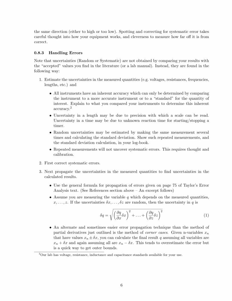
• Use the general formula for propagation of errors given on page 75 of Taylor’s ErrorAnalysis text. (See References section above – An excerpt follows)
• Assume you are measuring the variable q which depends on the measured quantities,x, . . . , z. If the uncertainties δx, . . . , δz are random, then the uncertainty in q is
δq =
√
(
∂q
∂xδx
)2
+ . . .+
(
∂q
∂zδz
)2
(1)
• An alternate and sometimes easier error propagation technique than the method ofpartial derivatives just outlined is the method of corner cases. Given n-variables xnthat have values xn± δx, you can calculate the final result q assuming all variables arexn + δx and again assuming all are xn − δx. This tends to overestimate the error butis a quick way to get outer bounds.
2Our lab has voltage, resistance, inductance and capacitance standards available for your use.
6
0.9 Lab Grades
If you complete a lab and answer all the questions completely as discussed in section 0.6, you willget at least an “A-” for the lab. You can earn an “A” with exceptional clarity of presentation,insightful discussion of the “physics puzzler” questions, or other insights/connections that I didnot think to ask about.
If you start omitting calculations, measurements or making errors in analysis, you are entering“B” territory. Significant omissions or confusions bring you to “C-land”. Annoying your instructorby (for example) writing up the lab on a napkin in the 30 minutes before it is due can result in agrade below “C-”.
Labs marked ”n=2” are nominally two week labs and their grades count double.Even if you lack confidence or facility at lab work, application of effort to this course should
result in at least a grade in the “B” range.
7
Introductory discussion
We define basic terms in lab electricity
Ideal Components
Ideal Voltage Source A source that puts out the same voltage, (e.g. nine Volts) regardless ofthe circuit or load in which it participates.
Ideal Current Source A source that puts out the same current, regardless of its circuit.
Ideal Resistor Follows Ohm’s law, regardless of voltage or current impressed.
These idealizations are useful, because though no real circuit completely match them, theydo match them over certain ranges, and may usually be fairly accurately modeled as COMBINA-TIONS of ideal components.
Real Components
Battery or DC power supply A battery or power supply can generally be considered to bean ideal voltage source, VB. It can be modeled in an almost completely realistic way as anideal source VB in series with an internal resistance, Ri.
Current source Using active components, there are many ways to design a near ideal currentsource. A passive approach to this is to have a very large ideal voltage in series with a largeresistor. Then any load will not change the total load resistance, nor the circuit current.
Resistor Real resistors follow Ohm’s law extraordinarily closely. However, they all have powerratings. Exceeding the power rating will cause the resistor to overheat and fail. Also, veryhigh voltages can cause arcing, and failure. Real resistors may be designed for very highpower or very high voltage, with an increase in size and cost.
More Vocabulary
Open circuit voltage The voltage of a battery with no load.
Short circuit current The current provided by a battery with its terminals shorted together(Isc = Voc/Ri).
Voltage divider A circuit consisting of two resistors in series with a battery. The voltage acrossthe second resistor is always a defined fraction of the battery voltage.
Demonstration
A non-ideal battery is easy to demonstrate with a 9V battery, particularly a dead one. Thebattery is measured with a voltmeter. Then a human’s fingers are put across the clips. Thevoltage will go down dramatically (if the battery is quite dead). One can record Voc, Vh (“h” forhuman) and measure the resistance of the human and determine Ri. Along the way we see Voc
and Ri demonstrated, and also learn the formula for a voltage divider.
8

Multimeters
Analog Multimeters really only measured current that passed through them. However, by havinga resistor placed between their + input and their current sensing element, they converted theircurrent capability to a voltage measurement.
Today we use mostly digital multimeters, that in fact mostly measure voltage via an A/Dcircuit. However, they can measure current by having a resistor in parallel with the voltagesensor that joins the + and - inputs. Likewise, they can measure resistance by providing an idealcurrent source and measuring the voltage dropped across the resistor.
9
1 Circuits (n=1)
1.1 Background theory
1.1.1 Multimeters
A modern multimeter can measure Voltage, Current, Resistance and sometimes capacitance orother quantities. The electronics inside is fundamentally measuring voltage.How then does it measure Resistance?It supplies a small known current to the device under test and measures the voltage developed,then calculates the resistance. Thus, if you use it to measure an energized circuit with currentsfrom a power supply or other sources flowing through it, the results will be misleading.How does it measure current?It puts an internal resistor in series with the circuit and measures the voltage developed acrossthat resistor. Note that this resistor becomes part of the circuit.
1.1.2 Circuits
In Physics 333, you learned the basic principles you need to analyze any circuit.
1. Electrical charge is conserved. This leads to Kirchoff’s current law (KCL).
2. The electrostatic force is a conservative force. This leads to Kirchoff’s voltage law (KVL).
Kirchoff’s famous laws for circuit analysis are stated in the caption of figure 1.Referring to the left panel of Figure 1, we see that the current law means that IA = IB+IC+ID.
This immediately leads to the useful corollary that in a series circuit the current is the same atall points in the circuit.
To understand the origin of the Voltage law shown in the right panel, consider that thedefinition of a conservative force is that the Work done is equal over any possible path betweentwo points. Recalling that Voltage is just the work done per electron, we see that the voltage dropbetween any two points in the circuit must be equal no matter what path is taken. An equivalentway of stating this is that the closed loop voltage is 0 over any possible loop through the circuit.
Because they are derived from fundamental physical principles, Kirchoff’s Laws are valid forany AC or DC circuit containing any combination of passive components, semiconductors andactive components. For this lab, we will also need Ohm’s law, V = IR. Ohm’s law is an exampleof an IV characteristic. IV characteristics depend on the type of device being studied. A resistorfits Ohm’s law exquisitely, while a light-bulb only approximately fits Ohm’s law. Later in thecourse we will study the IV characteristics of diodes. For a diode, I = Ir(e
eV/nkBT − 1), which asyou can see is not Ohm’s law at all!
1.2 Basic Formulae for DC Circuits
V = IR (1)
W = QV (2)
P = IV (3)
Requivalent = R1 +R2 +R3 + ... (4)
1/Requivalent = 1/R1 + 1/R2 + 1/R3 + ... (5)
10
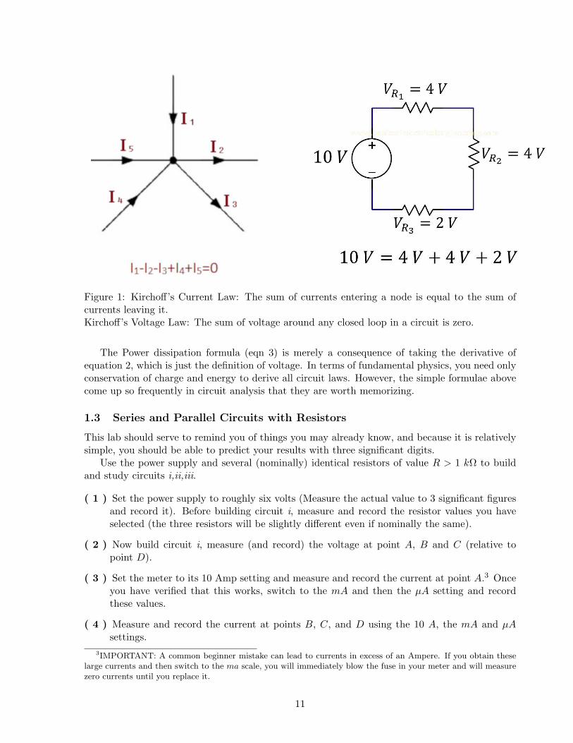
Figure 1: Kirchoff’s Current Law: The sum of currents entering a node is equal to the sum ofcurrents leaving it.Kirchoff’s Voltage Law: The sum of voltage around any closed loop in a circuit is zero.
The Power dissipation formula (eqn 3) is merely a consequence of taking the derivative ofequation 2, which is just the definition of voltage. In terms of fundamental physics, you need onlyconservation of charge and energy to derive all circuit laws. However, the simple formulae abovecome up so frequently in circuit analysis that they are worth memorizing.
1.3 Series and Parallel Circuits with Resistors
This lab should serve to remind you of things you may already know, and because it is relativelysimple, you should be able to predict your results with three significant digits.
Use the power supply and several (nominally) identical resistors of value R > 1 kΩ to buildand study circuits i,ii,iii.
( 1 ) Set the power supply to roughly six volts (Measure the actual value to 3 significant figuresand record it). Before building circuit i, measure and record the resistor values you haveselected (the three resistors will be slightly different even if nominally the same).
( 2 ) Now build circuit i, measure (and record) the voltage at point A, B and C (relative topoint D).
( 3 ) Set the meter to its 10 Amp setting and measure and record the current at point A.3 Onceyou have verified that this works, switch to the mA and then the µA setting and recordthese values.
( 4 ) Measure and record the current at points B, C, and D using the 10 A, the mA and µAsettings.
3IMPORTANT: A common beginner mistake can lead to currents in excess of an Ampere. If you obtain these
large currents and then switch to the ma scale, you will immediately blow the fuse in your meter and will measure
zero currents until you replace it.
11
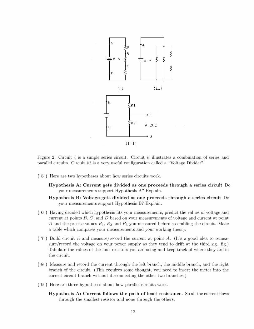
Figure 2: Circuit i is a simple series circuit. Circuit ii illustrates a combination of series andparallel circuits. Circuit iii is a very useful configuration called a “Voltage Divider”.
( 5 ) Here are two hypotheses about how series circuits work.
Hypothesis A: Current gets divided as one proceeds through a series circuit Doyour measurements support Hypothesis A? Explain.
Hypothesis B: Voltage gets divided as one proceeds through a series circuit Doyour measurements support Hypothesis B? Explain.
( 6 ) Having decided which hypothesis fits your measurements, predict the values of voltage andcurrent at points B, C, and D based on your measurements of voltage and current at pointA and the precise values R1, R2 and R3 you measured before assembling the circuit. Makea table which compares your measurements and your working theory.
( 7 ) Build circuit ii and measure/record the current at point A. (It’s a good idea to remea-sure/record the voltage on your power supply as they tend to drift at the third sig. fig.)Tabulate the values of the four resistors you are using and keep track of where they are inthe circuit.
( 8 ) Measure and record the current through the left branch, the middle branch, and the rightbranch of the circuit. (This requires some thought, you need to insert the meter into thecorrect circuit branch without disconnecting the other two branches.)
( 9 ) Here are three hypotheses about how parallel circuits work.
Hypothesis A: Current follows the path of least resistance. So all the current flowsthrough the smallest resistor and none through the others.
12
Hypothesis B: Current divides equally through each branch of the circuit
Hypothesis C: Current divides inversely proportional to the resistance of each branch
Explain which hypothesis your measurements support.
( 10 ) Once again, having selected a working theory you should be able to precisely compareyour measurements of current through each branch to current through point A based onyour measurements of R1, R2, R3, R4. Make a table.
( 11 ) There is a useful trick in circuit analysis called ”Thevenin equivalence”. Any combinationof resistors may be replaced by a single ”equivalent” resistor such that the total currentthrough the circuit (and power consumed) is the same as it was for the several actualresistors used. What is the Thevenin equivalent resistance for circuit i? For circuit ii?
( 12 ) – EXTRA CREDIT Circuit iii is called a “Voltage Divider”. This is because VOUT =VFG is always a fixed fraction of VIN = VAD. Design a 10:1 voltage divider (a circuit forwhich Vout
Vin= 1
10.0 .) You may not find resistors to provide an exact 1/10 ratio; it is sufficientto get between 1/9 and 1/11. Further, predict the division ratio of the circuit you actuallybuild to three significant digits based on the value of resistors you do find. Verify yourprediction with three different values of VIN (that is, not just 6 Volts).
Using resistance to measure temperature of a light-bulb
( 13 ) Get an Ecko #46 lightbulb out of the box and measure and record the resistance throughit with your Ohmmeter.
( 14 ) Remove your meter and instead connect the lightbulb to the 6 V power supply. Measurethe current through the bulb and the Voltage of the supply. Use this to calculate theresistance of the light-bulb.
( 15 ) The following formula allows you to calculate the resistance of tungsten wire as a functionof temperature. Assuming that room temperature (Tref ) is 300 K, calculate the temperatureof the light bulb filament in step 14.
R = Rref × [1 + α(T − Tref )] α = 4.4× 10⁻³ 1/K (6)
( 16 ) The series and parallel circuit laws (eqn 4-5) come directly from Ohm’s law and Kirchoff’slaws. Derive equations 4 and 5 from Ohm’s law, Kirchoff’s laws and the definition ofThevenin equivalent resistance.
1.4 Physics Puzzler [Answer two of these questions]
Lightbulbs are resistors Discuss the truth/falsehood of this statement based on your measure-ments
Which is the more accurate measurement? In 3, 4, 5, and 6 you explicitly compared themeasured currents with the calculated currents based on your resistor measurements. As-sume your resistor measurements are “correct”. Which if the current measurements is mostaccurate? WHY? Can you think of additional tests you might do to help figure this out?
13
Black body radiation The Planck black-body equation can be used to estimate the tempera-ture of a body (e.g. a light-bulb) that appears to glow ”white”. Get the equation and see ifyou can use it to calculate the temperature of the filament just based on it color. Documentyour assumptions.
1.5 For Graduate Students
( 18 ) Answer ALL the physics puzzlers.
( 19 ) Figure out the equivalent series resistance (ESR) for each of the three current scales on thedevice. Explain how you did it. Explain how it impacts the accuracy of your measurementsand try to remove the systematic error from the measurements.
Equipment
- HP 6235A Triple output Power Supply- Proto-board or Spring Board- Your Personal Multimeter (Amprobe 35XP or AM-560)- Resistors
14
2 Complex Impedance (n=1)
2.1 Motivation for the experiment
Complex Impedance is a wonderful “trick” that allows the analysis of complex AC circuit con-sisting of inductors, capacitors and resistors almost as easily as a DC circuit that contains onlyresistors. On the assumption that you have never seen complex impedance before, I explain itbelow, as succinctly as possible. I suggest following along with pencil and paper. If you want alonger explanation (or a different one), read Purcell and Morin, sections 8.3–8.5. I do not expectthat on one reading you will really “believe” that it works, but it really does work and you candefinitely use it to calculate. If you have seen either Fourier or Laplace transforms, then you haveseen similar tricks before.
2.2 Prelab
( P1 ) If frequency f = 10 kHz, what is angular frequency ω?
( P2 ) Given a circuit driven at f = 10 kHz with R and C in series R = 10 kΩ and C = 20 nF ,express the total effective impedance Zeff in cartesian form (the form x+ iy).
( P3 ) Given a circuit with previous values of f , R, C in series with an inductor L = 5 µH,express Zeff in cartesian form.
( P4 ) Express the complex impedance from problem P3 in polar form (Z = Z0eiφ). [That means
calculate Z0 and φ for given conditions.]
( P5 ) Given a R, L, C circuit driven with a 10 V sinewave that passes a maximum of onemilliamp of current, what is Z0?
2.3 Background: Introduction to Complex Impedance
Voltages in a series circuit add. Engineers call this “Kirchoff’s voltage law” (KVL). KVL appliesto ANY circuit, whether it be composed of resistors, inductors, diodes, transformers, capacitors,etc. Physicists know that KVL is merely a consequence of the definition of voltage and its pathindependence around the circuit. Likewise, currents into any circuit “node” sum to the samevalue as currents leaving the node. Engineers call this “Kirchoff’s current law” (KCL). Physicistsrealize that KCL is a consequence of the conservation of charge. In the last experiment, you usedwell-known rules for combining resistors in series and parallel, respectively.
Reff = R1 +R2 +R3 + ... (1)
1/Reff = 1/R1 + 1/R2 + 1/R3 + ... (2)
These rules came from combining KVL, KCL, Ohm’s law and the following definition.
Vsource = IReff (3)
We can generalize the concept of effective (or Thevenin equivalent) resistance beyond purelyresistive circuits to include circuits with resistors, capacitors and inductors. When applied tocircuits with R’s, L’s and C’s, effective resistance (Reff ) becomes effective impedance (Zeff ) andwe have the following formulae.
Zeff = Z1 + Z2 + Z3 + ... (4)
15
1/Zeff = 1/Z1 + 1/Z2 + 1/Z3 + ... (5)
Vsource = IZeff (6)
By analogy, you can see that these formulae apply to series and parallel combinations of R’s, L’sand C’s.
2.4 Requirements to use Complex Impedance
Here are the requirements to use complex effective impedance.
• The circuit must be driven by a sine or cosine voltage.
• The impedance must be manipulated as a complex number.
• ZR = R, i.e., the impedance of a resistor is just its resistance.
• ZL = iωL, i.e., the impedance of an inductor is proportional the angular frequency of thesource, and is purely imaginary.
• ZC = 1iωC = −i
ωC , i.e., the impedance of an capacitor is inversely proportional to the angularfrequency of the source and to the capacitance.
2.5 Why does it work?
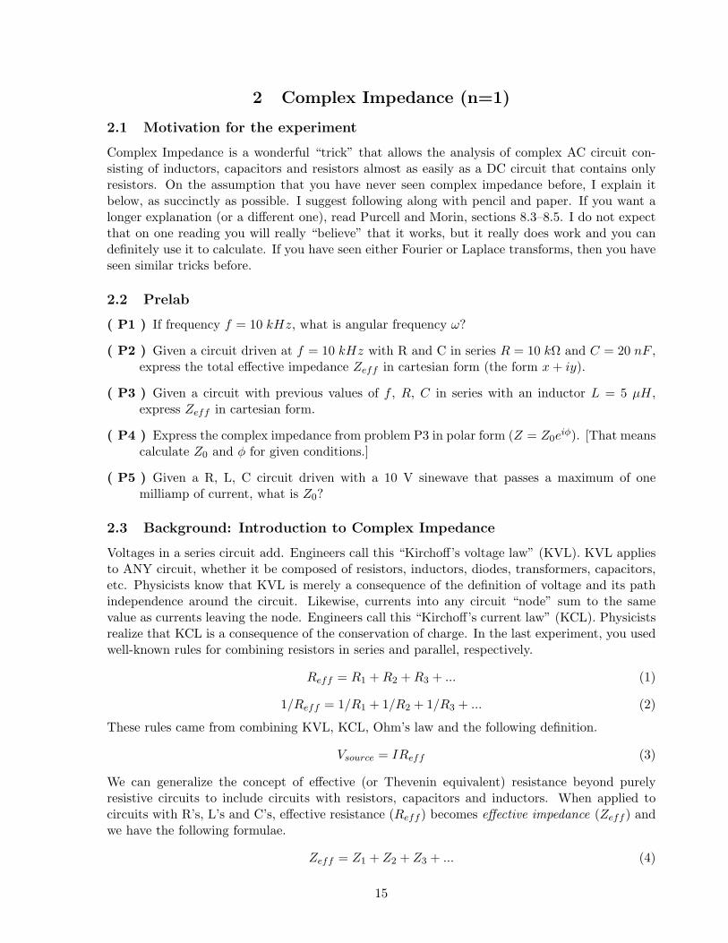
The circuit below is what you will build in this experiment. The complex impedance may be usedfor ANY linear circuit, including ones with several parallel branches, but we will prove it for thisparticular series circuit for concreteness. The differential equation for this circuit, expressed in
+
−Vs(t)
CL
I0Reiωt+φR
terms of the charge on the capacitor is:
Vs(t) = Ld2Q
dt2+R
dQ
dt+
Q
C(7)
If we require that Vs(t) = V0cos(ωt) then we expect Q(t) = Q0cos(ωt+ φ) +Qtransient. Why dowe expect this? Driven oscillators must respond at the driving frequency, but they do not have torespond in phase. Furthermore Qtransient → 0 over several cycles, and will henceforth be ignored4
Because of this property, we can rewrite
Vs(t) = Real[V0eiωt] (8)
4I am assuming that you have solved enough similar equations to understand that this really is the characteristic
of the solution.
16
Q(t) = Real[Q0eiωt+φ] (9)
In analogy to Ohm’s law, we want a relationship between voltage and current, not voltage andcharge. For this simple form of Q(t), it is easy to calculate current.5
I(t) =dQ
dt= Q0iωe
iωt+φ = iωQ(t) (10)
By assuming sinuoidal variation, a derivative becomes as simple as multipling by iω. Furthermore,we can write
I(t) = I0eiωt+φ = iωQ0e
iωt+φ (11)
Where I0 = iωQ0. Let us take individual derivatives and express them in terms of I0 instead ofQ0.
dQ
dt= I0e
iωt+φ (12)
d2Q
dt2= I0iωe
iωt+φ (13)
Q =I0iω
eiωt+φ (14)
Plugging the above three expressions into equation 7, we obtain
V0eiωt = LiωI0e
iωt+φ +RI0eiωt+φ +
I0iωC
eiωt+φ (15)
Note that eiωt can be divided out of both sides, and I0eiφ can be factored out of the right hand
side. This leaves
V0 = I0eiφ[Liω +R+
1
iωC] (16)
This is of the form V = IZeff where
Zeff = iωL+R+1
iωC(17)
Voila! We have shown that Zeff is just the sum of the individual Z’s provided we define compleximpedance as in the list ending section 2.4 above.
2.6 Overall Approach for the experiment
You will build the circuit shown in figure 2 below consisting of a function generator, connected toa capacitor an inductor and a resistor. All measurements will be made by connecting appropriatecables to the circuit and an oscilloscope.
One can measure the impedance of a single component, or of an entire circuit. Regardless ofwhat you are measuring, the following equation always applies:
V = IZ (18)
All that changes in equation 18 is what parts of the circuit V , I, and Z apply to. Since we wantto measure the impedance Z of the entire circuit. a good notation for this experiment is:
5From here on out I will no longer show the “Real” operator. It is assumed.
17
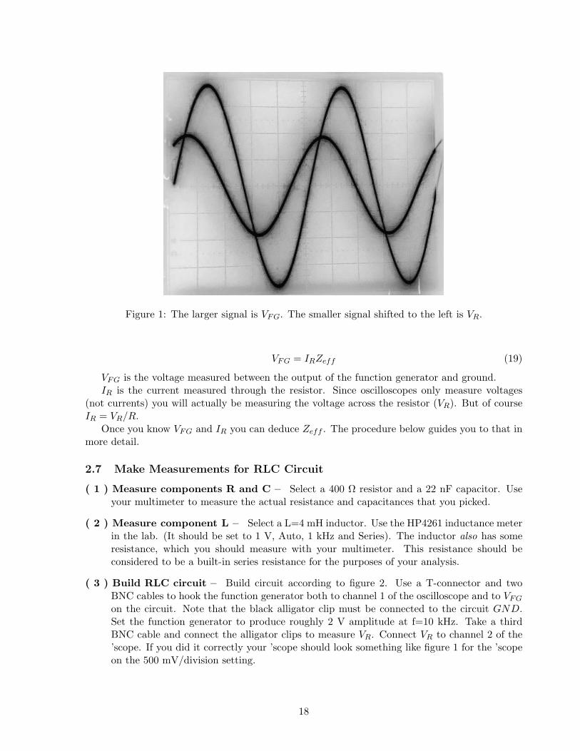
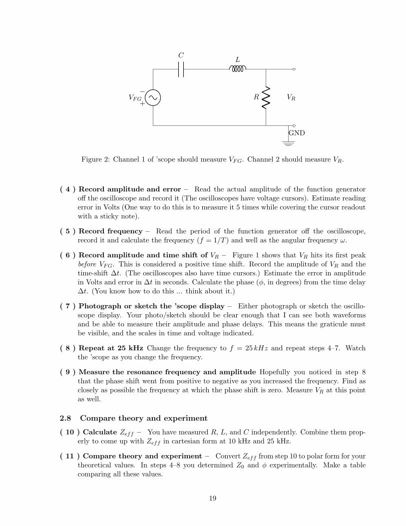
Figure 1: The larger signal is VFG. The smaller signal shifted to the left is VR.
VFG = IRZeff (19)
VFG is the voltage measured between the output of the function generator and ground.IR is the current measured through the resistor. Since oscilloscopes only measure voltages
(not currents) you will actually be measuring the voltage across the resistor (VR). But of courseIR = VR/R.
Once you know VFG and IR you can deduce Zeff . The procedure below guides you to that inmore detail.
2.7 Make Measurements for RLC Circuit
( 1 ) Measure components R and C – Select a 400 Ω resistor and a 22 nF capacitor. Useyour multimeter to measure the actual resistance and capacitances that you picked.
( 2 ) Measure component L – Select a L=4 mH inductor. Use the HP4261 inductance meterin the lab. (It should be set to 1 V, Auto, 1 kHz and Series). The inductor also has someresistance, which you should measure with your multimeter. This resistance should beconsidered to be a built-in series resistance for the purposes of your analysis.
( 3 ) Build RLC circuit – Build circuit according to figure 2. Use a T-connector and twoBNC cables to hook the function generator both to channel 1 of the oscilloscope and to VFG
on the circuit. Note that the black alligator clip must be connected to the circuit GND.Set the function generator to produce roughly 2 V amplitude at f=10 kHz. Take a thirdBNC cable and connect the alligator clips to measure VR. Connect VR to channel 2 of the’scope. If you did it correctly your ’scope should look something like figure 1 for the ’scopeon the 500 mV/division setting.
18
+
−VFG
CL
VRR
GND
Figure 2: Channel 1 of ’scope should measure VFG. Channel 2 should measure VR.
( 4 ) Record amplitude and error – Read the actual amplitude of the function generatoroff the oscilloscope and record it (The oscilloscopes have voltage cursors). Estimate readingerror in Volts (One way to do this is to measure it 5 times while covering the cursor readoutwith a sticky note).
( 5 ) Record frequency – Read the period of the function generator off the oscilloscope,record it and calculate the frequency (f = 1/T ) and well as the angular frequency ω.
( 6 ) Record amplitude and time shift of VR – Figure 1 shows that VR hits its first peakbefore VFG. This is considered a positive time shift. Record the amplitude of VR and thetime-shift ∆t. (The oscilloscopes also have time cursors.) Estimate the error in amplitudein Volts and error in ∆t in seconds. Calculate the phase (φ, in degrees) from the time delay∆t. (You know how to do this ... think about it.)
( 7 ) Photograph or sketch the ’scope display – Either photograph or sketch the oscillo-scope display. Your photo/sketch should be clear enough that I can see both waveformsand be able to measure their amplitude and phase delays. This means the graticule mustbe visible, and the scales in time and voltage indicated.
( 8 ) Repeat at 25 kHz Change the frequency to f = 25 kHz and repeat steps 4–7. Watchthe ’scope as you change the frequency.
( 9 ) Measure the resonance frequency and amplitude Hopefully you noticed in step 8that the phase shift went from positive to negative as you increased the frequency. Find asclosely as possible the frequency at which the phase shift is zero. Measure VR at this pointas well.
2.8 Compare theory and experiment
( 10 ) Calculate Zeff – You have measured R, L, and C independently. Combine them prop-erly to come up with Zeff in cartesian form at 10 kHz and 25 kHz.
( 11 ) Compare theory and experiment – Convert Zeff from step 10 to polar form for yourtheoretical values. In steps 4–8 you determined Z0 and φ experimentally. Make a tablecomparing all these values.
19
2.9 Physics Puzzler [Answer any two of these questions]
Explain the sign problem – At 10 kHz the phase shift is positive. Shouldn’t the phaseshift of a capacitance dominated circuit be negative (per section 2.4)? Explain what isgoing on here.
Predicting resonance frequency – Determine what the resonance frequency should havebeen based on the measured values of your components. Show that the formula forcomplex impedance gives this frequency directly as the point of zero phase shift
Predicting amplitude at resonance – You might think VR at resonance should havebeen equal to VFG. Why wasn’t it? Can you determine what it should have been andcompare it to what you measured.
Properly propagating errors – You may assume that your component measurementswere good to one percent, which makes them much better than your oscilloscope mea-surements. Assuming all your errors were with the oscilloscope revisit the table fromstep 11 and put error bounds on your experimental measurements. I recommend youuse the “corner” method described in the error propagation section of the introduction,but feel free to use the partial derivative method.
2.10 For Graduate Students
( 12 – Filters Theory ) The concept of complex impedance generalizes very nicely to the sub-ject of filters. Calculate the theoretical amplitude and phase response of a single polelow-pass RC filter with a 3-dB point of 1000 Hz. Make Bode plots of amplitude and phasefrom 10.0 Hz to 1.00 MHz for this filter.
( 13 – Filters Experiment) Build this filter and characterize it over the 10.0 Hz to 1.0 MHzfrequency range 6. Overlay the theoretical and experimental curves.
2.11 Equipment
- Oscilloscope- Function generator- Multimeter- C=0.022µF Capacitor- R=400 Ω Resistor- L=4.7 mH Inductor
2.12 Refresher on Complex Arithmetic
Recall that for any complex number Z:
Z = x+ iy = Z0eiφ = Z0(cosφ+ isinφ) (20)
where Z0 =√
x2 + y2 and φ = atan(y/x). Also Z20 = Z∗ Z, where Z∗ ≡ x− iy. Finally, it is
useful to know that if Z = 1a+ib , then Z∗ = 1
a−ib
6You might want to refer to the write-up entitled “Low-Pass Filters” for guidance.
20
3 Magnetic Field, Inductance and Mutual Inductance (n=1)
3.1 Introduction
In this laboratory exercise you will
• reinforce your understanding of complex impedance,
• learn how to measure mutual and self inductance,
• review how to calculate mutual and self inductance,
• learn how to measure the amplitude of an oscillating magnetic field, and
• demonstrate how a transformer works.
This is a good time to review the concepts listed above in a junior-level textbook on electricityand magnetism.
+
−VFG
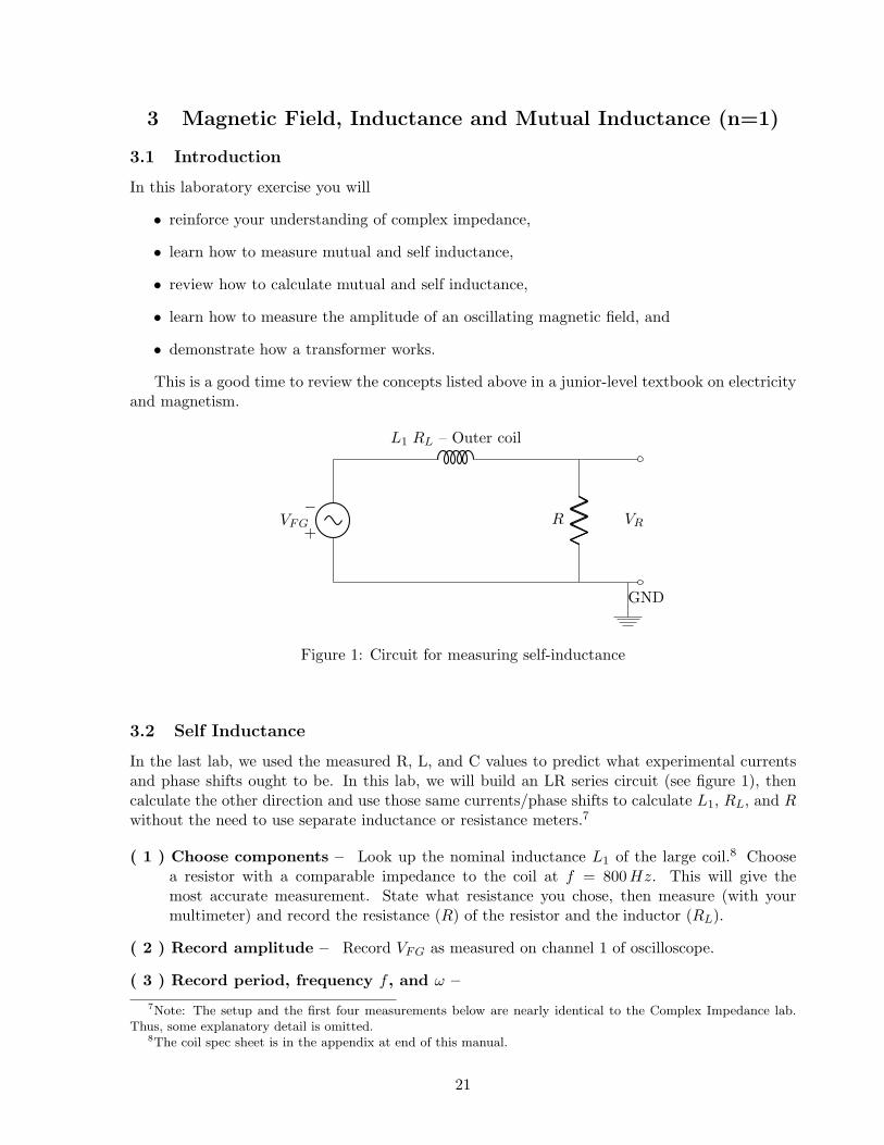
L1 RL – Outer coil
VRR
GND
Figure 1: Circuit for measuring self-inductance
3.2 Self Inductance
In the last lab, we used the measured R, L, and C values to predict what experimental currentsand phase shifts ought to be. In this lab, we will build an LR series circuit (see figure 1), thencalculate the other direction and use those same currents/phase shifts to calculate L1, RL, and Rwithout the need to use separate inductance or resistance meters.7
( 1 ) Choose components – Look up the nominal inductance L1 of the large coil.8 Choosea resistor with a comparable impedance to the coil at f = 800Hz. This will give themost accurate measurement. State what resistance you chose, then measure (with yourmultimeter) and record the resistance (R) of the resistor and the inductor (RL).
( 2 ) Record amplitude – Record VFG as measured on channel 1 of oscilloscope.
( 3 ) Record period, frequency f , and ω –
7Note: The setup and the first four measurements below are nearly identical to the Complex Impedance lab.
Thus, some explanatory detail is omitted.8The coil spec sheet is in the appendix at end of this manual.
21
( 4 ) Record amplitude, time delay, and phase of resistor voltage (VR)– Give phase indegrees.
( 5 ) Calculate the magnitude |Zeff | – From your measurements calculate the amplitude ofthe current through the LR circuit. Using |VFG| = |IR| |Zeff |, what is the magnitude ofZeff?
( 6 ) Write Zeff in polar form –
( 7 ) Write Zeff in cartesian form –
( 8 ) Calculate experimental R and L1 – Identify R and L with terms in x+ iy. Arrive atexperimental values for L1, R and RL (the resistance of the inductor).
( 9 ) Calculate effect of iron on inductance – Insert an iron rod fully into the coil. Repeatsteps 2–8 and arrive at the inductance of the coil with the iron rod in it.
( 10 ) Calculate L1 from geometry – Using the theory you learned in Physics 333, derivean expression for the self-inductance of the outer coil. Measure/look-up relevant quantitiesabout the outer coil (e.g. length, area, windings) and plug these in to obtain a theoreticalestimate of the self-inductance of the coil
( 11 ) Physics Puzzler (required question) The results you get from step 8 and step 10probably do not agree very well. Discuss which one is more likely to be correct and alsowhat you could do to get them to agree better. You probably want to work on this whenyou are still in the lab to see if you can get closer agreement between these quantities.
3.3 Magnetic Field Amplitude and Mutual Inductance
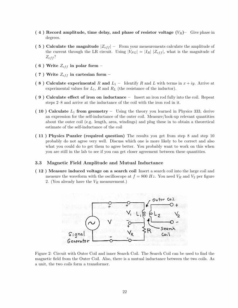
( 12 ) Measure induced voltage on a search coil Insert a search coil into the large coil andmeasure the waveform with the oscilloscope at f = 800 Hz. You need VR and V2 per figure2. (You already have the VR measurement.)
Figure 2: Circuit with Outer Coil and inner Search Coil. The Search Coil can be used to find themagnetic field from the Outer Coil. Also, there is a mutual inductance between the two coils. Asa unit, the two coils form a transformer.
22
3.4 Transformer
The two coils together form a transformer. In a transformer, power flows from the primarywinding (Outer Coil in this case) to the secondary winding (Search Coil in this case). An idealtransformer is defined by the transformer equation (equation 22). Remove the resistor from theprimary circuit so that the function generator is connected directly to the primary winding. Thendo the following:
( 13 ) Find the frequency range where the transformer equation will apply – You shouldhave noted that the transformer equation has no frequency dependence, but it is not validat very low or very high frequencies. Find and note the range of frequencies for which V2 isnearly constant. (Hint, set your frequency to roughly 5 kHz and work your way down andup from there.) The answer can be approximate, but you should include in your lab reporthow you defined nearly constant.
( 14 ) Measure the transformer multiplication ratio – Having determined the frequencyrange over which V2 is roughly constant, set the frequency somewhere in the middle of thisrange and measure and record the voltages V1 and V2.
3.5 Postlab: Calculations and analysis
( 15 ) Find an expression for B – Derive an approximate expression for the magnetic fieldstrength B near the center of the Outer Coil when the current through that coil is I1, thenumber of turns of wire is N1, and the length of the coil is ℓ1. The derivation should includea sketch of the paths of your line integrals. The quantities I1, N1, and ℓ1 have subscript 1to indicate that they are associated with the Outer Coil (transformer primary).
( 16 ) Find a numerical value for B – In step 4 and/or 12 you measured the current am-plitude. What peak magnetic field does this correspond to?
( 17 ) An alternate way to calculate B – The search coil voltage V2 can also be used todetermine B. By Faraday’s law, the search coil voltage is proportional to dB/dt, but it iseasy to calculate B from dB/dt for a sinusoidal voltage. Measure what you need about thesearch coil and arrive at an alternative expression for B. Compare the numerical result toquestion 16.
( 18 ) Experimental mutual inductance between the coils – The definition of mutual in-ductance is Φ2 = M12I1. You know I1 from measurements and B2, Φ2 from steps 16/17.Calculate M12.
( 19 ) Theoretical mutual inductance – Derive the following approximate equation for themutual inductance between the Outer Coil and the Search Coil
M12 = µ0N1N2A2/ℓ1. (21)
( 20 ) Plug and chug – Compare your results from 18 and 19.
( 21 ) Derive the transformer equation – Derive the following expression for the ratio ofvoltages of a transformer:
V2
V1=
N2A2
N1A1, (22)
Compare your measured ratio (from step 14) with that predicted from the above expression.
23

Equipment
- L1 – Outer Coil (2920 turns of 29 AWG wire (diameter D = 0.29 mm).- L2 – Search Coil (50 turns wound on wood)- R – (you choose) Ω resistor- Oscilloscope- Function generator
24
4 Hysteresis (n=2)
4.1 Prelab
Note: If you read through the Introduction to this lab, you will get all the background you needto answer the questions below. (When added to what you learned in 333 and the earlier labs thisterm.)
( P1 ) Given an air-core inductor of length 10 cm and diameter 1 cm with 1000 windings carryinga current of 2 Amperes calculate B and H inside the inductor.
( P2 ) You are given an unknown paramagnetic material with chim=10000. What is µr?
( P3 ) Imagine the air-core is replaced by the previously described paramagnetic material. Whatare H and B now? What is M?
4.2 Introduction
4.2.1 Hysteresis defined
A system is said to exhibit hysteresis when the state of the system does not reversibly followchanges in an external parameter. In other words, the state of system depends on the historyof the system. [hysteresis comes from the Greek word for lagging, but it is probably a bettermnemonic to think of it as “history-sis”]. The classic examples of hysteresis use ferromagneticmaterials. The state of the system is given by the magnetic moment per unit volume, M, andthe external parameter is the auxiliary magnetic field, H. As H increases, M can be said to lagbehind. This is clearer once when looks at a hysteresis loop (figure 4). In this experiment, weexplore hysteresis by measuring both the magnetic field B and the auxiliary field H in an irontoroid. The variable M can be deduced from H and B.
4.2.2 B, H and M
It is important to define terms since the scientific literature is INCONSISTENT.9 In this lab Bis called “magnetic field”, though some literature calls it “magnetic flux density” or “magneticinduction”. H will be referred to as “auxiliary field”, though some sources call it “magneticintensity” and worse, others call it “magnetic field”. Recall that these quantities are usefulbecause H is created by a true external current (which you control in the experiment),while B isthe total field, but it includes the bound currents in the material which you have no direct controlover as an experimentalist.
4.2.3 Ferromagnetic theory reviewed
The auxiliary field H is defined by the equation
H ≡ 1
µ0B−M , (23)
where B is the magnetic field, µ0 is the magnetic permeability of free space and M is the macro-scopic magnetization. The macroscopic and microscopic magnetizations are related by the defining
9Fortunately Maxwell’s equations ARE consistent. You will never see B and H used incorrectly in the math,
but the English descriptions vary.
25
equation
M = lim∆V→0
1
∆V
∑
i
mi . (24)
M is the vector sum of the atomic magnetic moments divided by the volume, ∆V , of the sample.For an isotropic, linear material, M is linear in H, as
M = χmH , (25)
where the dimensionless magnetic susceptibility χm is assumed constant. In this case equation (23)becomes,
H =1
µ0B− χmH (26)
so that µ0H = B− µ0χmH (27)
and B = µ0(1 + χm)H . (28)
By comparing this last equation with the free space equation,
B = µ0H , (29)
the magnetic permeability, µ, of the material is defined to be
µ = µ0(1 + χm) . (30)
The relative permeability Km is defined as
Km =µ
µ0(31)
so that Km = 1 + χm . (32)
In a ferromagnetic material, the magnetization is produced by cooperative action betweendomains of collectively oriented atoms. Ferromagnetic materials are not linear, so that
χm = χm(H) . (33)
However, the above equations are still applicable if we accept that µ is no longer a constant, thatis
µ(H) = µ0[1 + χm(H)] (34)
andB = µ(H)H . (35)
This behavior can be explained by examining the microscopic structure of a ferromagneticmaterial. The material actually is polycrystaline, consisting of many small crystals of the material.Each of these crystal grains is divided into groups or ‘domains’ of atoms. Within a domain,the magnetic moments m of the individual atoms are all aligned parallel to each other. Thesedomains, on the order of hundreds of Angstroms across, are essentially completely magnetized aslong as the temperature remains below the Curie temperature of the material. In the absence ofan externally-applied field H, the magnetization vectors of the domains in a given grain can bealigned so as to minimize the net magnetization of that grain. Furthermore, the grains themselvescan be randomly oriented as shown in Figure 1. Thus the macroscopic magnetization M is zero.
If a weak external magnetic field is applied to a speciman with M = 0, within each crystalgrain the domains whose magnetization vectors are oriented more in the direction of the appliedfield will grow at the expense of the less favorably oriented domains. That is, the domain wallsmove and the material as a whole acquires a net macroscopic magnetization, M.
26
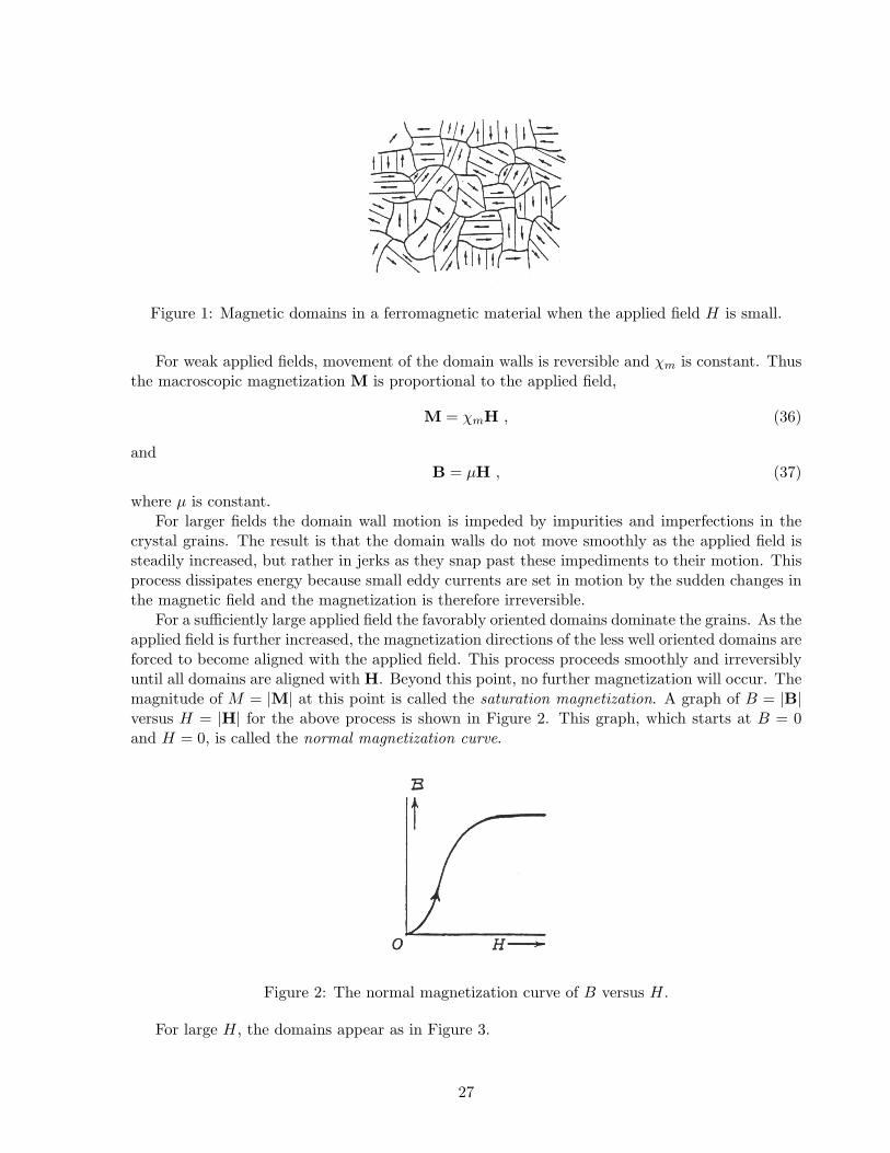
Figure 1: Magnetic domains in a ferromagnetic material when the applied field H is small.
For weak applied fields, movement of the domain walls is reversible and χm is constant. Thusthe macroscopic magnetization M is proportional to the applied field,
M = χmH , (36)
andB = µH , (37)
where µ is constant.For larger fields the domain wall motion is impeded by impurities and imperfections in the
crystal grains. The result is that the domain walls do not move smoothly as the applied field issteadily increased, but rather in jerks as they snap past these impediments to their motion. Thisprocess dissipates energy because small eddy currents are set in motion by the sudden changes inthe magnetic field and the magnetization is therefore irreversible.
For a sufficiently large applied field the favorably oriented domains dominate the grains. As theapplied field is further increased, the magnetization directions of the less well oriented domains areforced to become aligned with the applied field. This process proceeds smoothly and irreversiblyuntil all domains are aligned with H. Beyond this point, no further magnetization will occur. Themagnitude of M = |M| at this point is called the saturation magnetization. A graph of B = |B|versus H = |H| for the above process is shown in Figure 2. This graph, which starts at B = 0and H = 0, is called the normal magnetization curve.
Figure 2: The normal magnetization curve of B versus H.
For large H, the domains appear as in Figure 3.
27
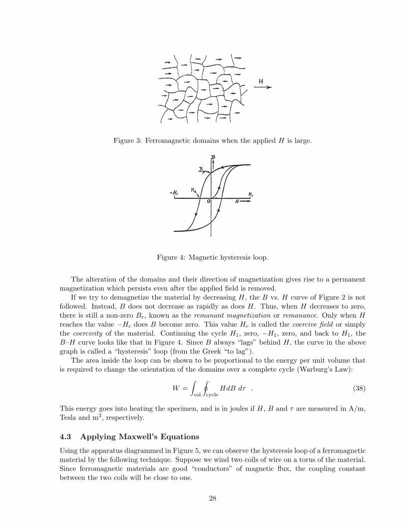
Figure 3: Ferromagnetic domains when the applied H is large.
Figure 4: Magnetic hysteresis loop.
The alteration of the domains and their direction of magnetization gives rise to a permanentmagnetization which persists even after the applied field is removed.
If we try to demagnetize the material by decreasing H, the B vs. H curve of Figure 2 is notfollowed. Instead, B does not decrease as rapidly as does H. Thus, when H decreases to zero,there is still a non-zero Br, known as the remanant magnetization or remanance. Only when Hreaches the value −Hc does B become zero. This value Hc is called the coercive field or simplythe coercivity of the material. Continuing the cycle H1, zero, −H1, zero, and back to H1, theB–H curve looks like that in Figure 4. Since B always “lags” behind H, the curve in the abovegraph is called a “hysteresis” loop (from the Greek “to lag”).
The area inside the loop can be shown to be proportional to the energy per unit volume thatis required to change the orientation of the domains over a complete cycle (Warburg’s Law):
W =
∫
vol
∮
cycleHdB dτ . (38)
This energy goes into heating the specimen, and is in joules if H, B and τ are measured in A/m,Tesla and m3, respectively.
4.3 Applying Maxwell’s Equations
Using the apparatus diagrammed in Figure 5, we can observe the hysteresis loop of a ferromagneticmaterial by the following technique. Suppose we wind two coils of wire on a torus of the material.Since ferromagnetic materials are good “conductors” of magnetic flux, the coupling constantbetween the two coils will be close to one.
28
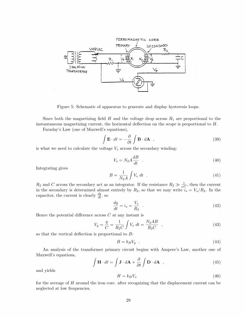
Figure 5: Schematic of apparatus to generate and display hysteresis loops.
Since both the magnetizing field H and the voltage drop across R1 are proportional to theinstantaneous magnetizing current, the horizontal deflection on the scope is proportional to H.
Faraday’s Law (one of Maxwell’s equations),∫
E · dℓ = − ∂
∂t
∫
B · dA , (39)
is what we need to calculate the voltage Vs across the secondary winding:
Vs = N2AdB
dt. (40)
Integrating gives
B =1
N2A
∫
Vs dt . (41)
R2 and C across the secondary act as an integrator. If the resistance R2 ≫ 1ωC , then the current
in the secondary is determined almost entirely by R2, so that we may write is = Vs/R2. In thecapacitor, the current is clearly dq
dt , so
dq
dt= is =
Vs
R2. (42)
Hence the potential difference across C at any instant is
Vy =q
C=
1
R2C
∫
Vs dt =N2AB
R2C, (43)
so that the vertical deflection is proportional to B:
B = kBVy . (44)
An analysis of the transformer primary circuit begins with Ampere’s Law, another one ofMaxwell’s equations,
∫
H · dℓ =∫
J · dA+∂
∂t
∫
D · dA , (45)
and yieldsH = kHVx (46)
for the average of H around the iron core. after recognizing that the displacement current can beneglected at low frequencies.
29
4.4 Laboratory Measurements
( 1 ) Set up apparatus – Assemble the apparatus according to figure 5. The oscilloscopeshould be set to xy mode and display Vx on the x axis and Vy on the y axis. Be sure toinclude the isolation transformer. Use a 10Ω, 5W resistor for R1, a 500kΩ, 1/4W resistorfor R2, and a 0.1 µF capacitor for C. As usual, log their values in your notes.
( 2 ) Measure hysteresis loops – Starting with the Variac at zero, slowly turn up the volt-age in increments such that each successive increment produces a hysteresis curve that isdistinguishable from the previous one. Trace these curves onto clear acetate film, continuinguntil the material reaches saturation. You may be tempted to just take a digital photo ofthe curves, but you will need all the curves on the same piece of film for your analysis,so you are better off with the old technology of Sharpie R©markers tracing on acetate. Irecommend varying the Sharpie color so you can better distinguish adjacent curves. Thesemeasurements must be quantitative so you should include a scale marking for voltage. Tryto set the ’scope channels so that the largest loop fills that display.
( 3 ) Measure temperature rise – Hysteresis loops dissipate energy, so the toroid will slowlywarm. The key phrase is slowly. The maximum temperature rise you will see is a fewdegrees over 20 minutes. It requires some finesse to see this warming and to distinguish itfrom room temperature fluctuations. I recommend leaving the variac turned off and loggingtemperature every 30 seconds for 10 minutes to establish a baseline drift. Then crank thevariac up to show the largest hysteresis loop and track progress for another 20 minutes.Hopefully your temperature vs. time plot will allow you to estimate a temperature riserate.10
4.5 Calculations and Analysis
This is the single most difficult analysis of the term. I encourage you to work on it betweenthe first and second lab period so that you can ask questions on your return.
( 4 ) Analyze Transformer Secondary (derive kB) – Derive equation (44) in whichthe constant kB is replaced by an expression containing other constants having to dowith your experiment. This derivation is almost done for you in section 4.3, but theexpression for kB is never explicitly stated. State it. ALSO, for your derivation to becomplete, it should include a large figure the shows the path for the line integral onthe left side of equation 39 and the integration area implied by the right side of 39.Your figure should look as much as possible like the toroid that we are measuring.
( 5 ) Get a numerical value for kB – Given your expression from above, plug in rel-evant constants to arrive at a numerical value for kB specific to your apparatus. Whatare the units of kB?
( 6 ) Analyze Transformer Primary (derive kH) – The derivation of kB was a bittricky, which is why I largely did it for you. The derivation of an expression for kHis easier, but you have to do it yourself. Start with Ampere’s Law (equation 45) and
10Some of the setups will not show a temperature rise. Report what you find even if it is a null result.
30
arrive at equation 46 where kH is, as before, replaced with variables related to yourapparatus. Ampere’s law again has a line integral on the left and an area on the right.Complete your derivation by drawing the path that is integrated over as well as thearea.
( 7 ) Get a numerical value for kH – Plug in relevant constants and come up with anumerical value for kH specific to your apparatus. What are the units for kH?
( 8 ) Warburg’s Law – Choose one of your largest hysteresis loops (the one for whichyou took temperature data in step 3) and, using Warburg’s law, calculate the energyloss per cycle due to hysteresis, the temperature rise of the core per cycle and thenumber of cycles and elapsed time necessary to raise the temperature of the core by 1C.Be careful doing this calculation; it will take time; be sure your result is reasonable.There are several pieces of cleverness here. First, what exactly does equation 38 mean?How do you do an integral when you have a graph, not a function? Do the unitscome out right? Finally, does your theory match experiment? (If your temperaturemeasurements gave a null result, figure out what the error bars are ... what is themaximum temperature change it could have been?)
( 9 ) Magnetization curve – Plot the normal magnetization curve using the end pointsof the hysteresis loops on your acetate
( 10 ) Saturation Magnetization and Coercivity – Your magnetization curve givesyou the saturation magnetization of iron and your B-H curves give you the Coercivity.Come up with numerical values for these.
( 11 ) Relative permeability – From the normal magnetization curve (B vs. H), plotthe relative permeability µ/µ0 of the material as a function of H.
( 12 ) Physics Puzzler 1 – These are really applied physics – but then there are manyindustries based on magnetic materials. First, can you think of any applicationswherein Warburg’s law would matter? Why would it matter?
( 13 ) Physics Puzzler 2 – Different materials have different coercivities. Some aremuch higher than others. Can you think of applications for low and high coercivitymaterials? Feel free to Google and give a couple sentences about each.
Equipment list
- Isolation transformer- Variac- AC patch cord- Ferromagnetic Torus (Rowland Ring)- Resistor R1 (10 Ω, 5 W) and Resistor R2 (470–530 kΩ)- Capacitor C (0.1 µF)- Plastic film & fine-tip “sharpie” marker for tracing oscilloscope pattern- Thermometer and insulation
31
5 Operational Amplifiers (n=1)
Background
5.1 Uses of Operational Amplifiers
Measurements in every branch of science and engineering typically begin with a transducerthat changes whatever parameter is being measured into an electrical signal for furtheramplification and processing. Because of their versatility, superb performance, ease of use,and low cost, operational amplifiers (op amps) have become the main building block foramplification and processing of electrical signals before they are digitized and ingested by acomputer (such as an Arduino). Operational amplifiers are used in circuits to perform thefollowing functions:
• Amplifying
• Buffering
• Adding, subtracting, and multiplying
• Integrating and differentiating
• Detecting peaks and holding them
• Filtering (low pass, high pass, and band pass)
• Modulating and demodulating
Books listed under References below show many useful circuits using operational amplifiersand explain how they work in more detail than we give in the next section.
5.2 What Operational Amplifiers Do
As you would expect, an amplifier increases some electrical quantity, usually voltage. Ingeneral, VOutput = A × VInput where the factor A is called the Gain of the amplifier. Anintegrated circuit operational amplifier such as we will be studying in this lab amplifies thevoltage difference IN+ − IN− between its ‘+’ and ‘−’ inputs (see Figure 1). The outputvoltage is
OUT = AOL(IN+ − IN−) , (47)
where AOL is the open-loop voltage gain of the amplifier.
Two properties of operational amplifiers make them particularly useful:
• The open-loop gain AOL is large (typically 105 at low frequencies).
• The resistance Rin between the + and − inputs is large (typically 10 MΩ for operationalamplifiers which use bipolar junction transistors (BJT) amplifiers, and 1010 Ω or higherfor operational amplifiers which use field effect transistors (FET’s)).
Operational amplifiers are used by providing negative feedback (usually resistance) from theoutput to an input, which substantially reduces their gain from its open-loop value. Thisnew gain is called the closed-loop gain and we will denote it as G. So long as G << AOL,G is independent of it and the OpAmp is said to be ideal.
32
5.3 The Golden Rules
An ideal operational amplifier can be analyzed by adding the following two simple rules tothe usual rules for circuit analysis:
1. The + and − inputs are at the same potential.
2. No current flows into either input.
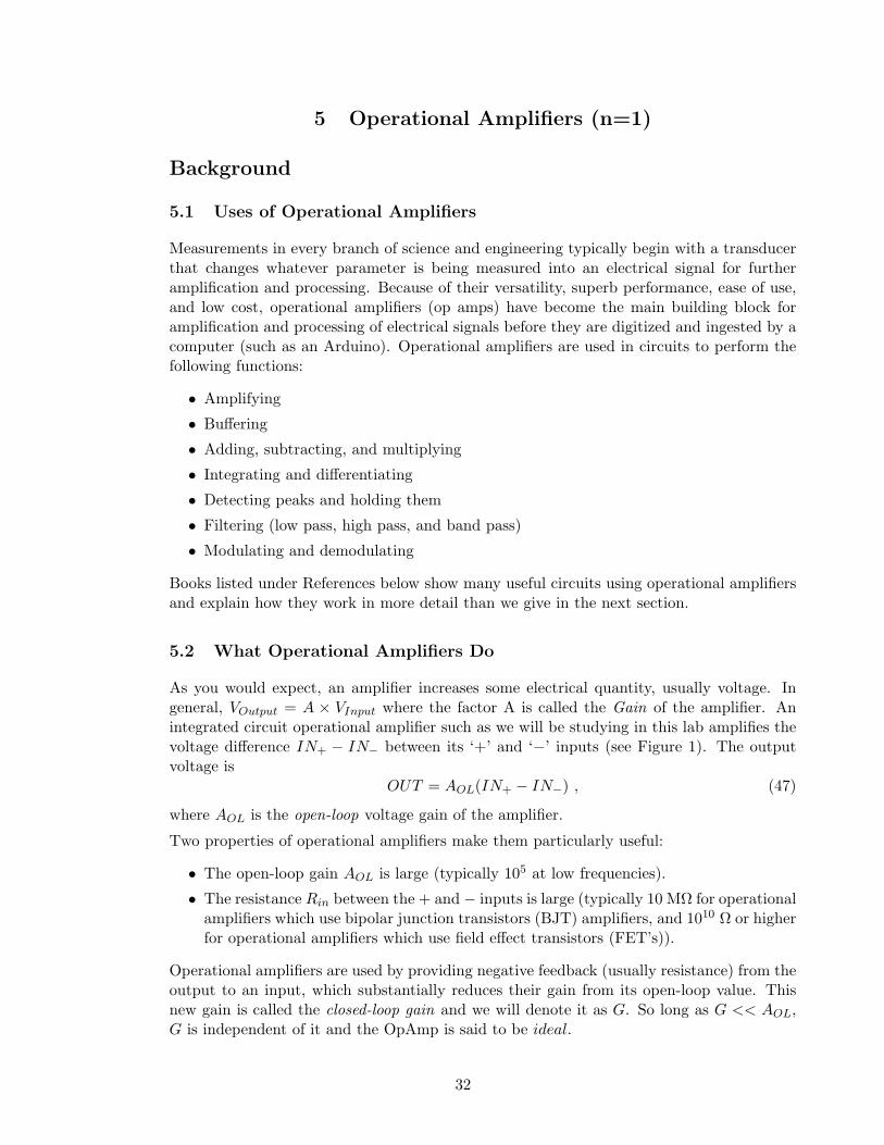
The above rules are so generally useful that they are sometimes call The Golden Rules ofOp-Amp behavior. One implication of these rules, for an ideal operational amplifier is thatthe closed loop gain G depends only on the feedback elements and not on its open-loop gainAOL nor on its internal resistance. Thus an amplifier with poor open-loop tolerance can bemade as precise as resistors can be (which is very precise, even 0.1% if you want to pay forit!). (see Figure 1).
Figure 1: Inverting and non-inverting configurations.
Experiments
You will do five mini-experiments on op-amp circuits. In the first, you will see an op-ampwork properly (ideally). You will then learn some of the limitations of op-amps and seesome non-ideal behavior by observing clipping, slew-rate limit, and band-width limit. In thefifth mini-experiment, you will quantitatively test the OP-AMP GAIN HYPOTHESIS forDC voltages where op-amps behave almost ideally.
This lab calls for some sketching. Sketching by hand is still an important skill for a scientist.Where told to sketch, please do not use your cell-phone camera. Colored pencils/pens anda ruler can be helpful!
5.4 A. Proper operation of an Op-Amp
Build an inverting amplifier. Refer to the left-panel of figure 1 and build that circuit.You should choose 1000 Ω <= R1 <= 100 kΩ and R2 ∼ 10×R1.
33
Set proper Power and Signal voltages Op-amps are “active”, they need power, as wellas inputs and outputs. We call the power voltages VPS (PS for power-supply). Wecall the input and output voltages (“signal voltages”) SIG IN and OUT . In Figure 1,VPS = ± 18 V. On your function generator, set the amplitude of SIG IN to 1.5 V andthe frequency to approximately f = 100 Hz.
(1) Determine approximate gain (G) Apply sine wave and triangle waves at the inputs(SIG IN) and measure/report the amplitude of input and output of the OpAmp.What is the closed loop gain factor G? Why do you think this is called an invertingamplifier?
(2) Sketch the appearance of the output waveforms. Draw one sketch for sine andone for triangle wave. You are doing this because in the next part you will see variousways they are distorted. Do the sketch large enough that you can clearly add to it.Draw only a single cycle of the wave.
5.5 B. Clipping of an Op-Amp
Reduce VPS to ± 11 V. Leave the frequency and amplitude as in part A.
(3) Sketch the appearance of the sine and triangle waves under these conditions.Draw the new curves where they differ from the ones you drew in question (2). Indicatethe differences with a dotted line or a different color of pencil.
(4) Set VPS = ± 13 V Add another layer to the sketches from #2 and #3.
(5) Why do you think this phenomenon is called Clipping? Look upMaximum Out-put Voltage Swing on the data sheet for these Op-Amps.11 Explain how your resultsfit the properties in the data sheet.
5.6 C. Slew rate of an Op-Amp
Increase VPS so that you no longer see clipping. Next, switch your function generator to asquare wave and, increase f until the square wave looks like a triangle wave.
(6) Compare the input to the output waveform . Note the frequency at which thesquare wave looks like a triangle wave. Sketch (or photograph is OK here) the ’scopeshowing both the input square wave and the output triangle wave on the same display.Would you say that they are in phase? Explain.
(7) What’s a slew rate? Based on your observations, how would you define a slew rate?Look up the value of the slew rate in the data sheet.
(8) Determine slew rate experimentally. Use your square wave measurements fromquestion (6) to determine an experimental value of the slew rate. (It will probably behigher than the data sheet says).
11Data sheets are in Appendix to this lab manual
34
5.7 D. Bandwidth of an Op-Amp
The bandwidth of an amplifier is defined as the range of frequencies over which the amplifierperforms correctly. Your Op-Amps operate all the way down to zero frequency, therefortheir bandwidth is defined as the maximum frequency at which they operate correctly.
The word correctly can be defined in several ways. The typical definition is that the band-width of an amplifier is the frequency at which the output (for a sinewave input) is 3 dBlower than it is at low frequencies (beyond the bandwidth, the output generally keeps de-creasing). The location of the 3 dB point is often called the “knee” of the amplifier frequencyresponse. A loss of 3 dB is equivalent to a reduction in Amplitude of roughly a factor of1//
√2. Therefor, if you determined that your amplifier had a gain of 10 at low frequencies,
the bandwidth would be the frequency at which the gain of the op-amp was 7.07.
One of the reasons you learned about slew-rate is, for larger amplitude inputs, the slew-ratedistorts the waveform at lower frequencies than the bandwidth does. Thus, for larger inputs,the bandwidth cannot be measured correctly. To be sure of getting a proper bandwidthmeasurement, you should use the smallest possible input, such as SIG IN =5–20 mVpp.
(9) Measure the bandwidth of your op-amp Once you have set SIG IN properly,increase the frequency to measure the bandwidth using a sinewave.
(10) Compare to GBWP Multiply your measured bandwidth by your gain G and com-pare it to the Gain Bandwidth Product (GBWP) listed in your data sheet.
(11) Check effect of BW on non-sinewaves Try putting in triangle waves or squarewaves (you pick) at different frequencies. Select 3 frequencies which best illustrate(judgement call) the increasing distortion in output waveform you see as you passthrough the op-amp bandwidth. Explain these distortions. Also, explain why the sinewave didn’t distort (or did it? ... the effect is more subtle with a sine wave.)
5.8 E. Theoretical Gain of an Op-Amp
In the last sections you got the approximate gains of the Op-Amps at low frequency, howeverit is hard to measure the Gain precisely using an oscilloscope, so we will do it instead usingDC voltages and voltmeters.
(12) Precisely measure DC gain of Inverting Op-Amp – Hook up the op-amp in-put (SIG IN) to the 6 V output of your power supply and vary (SIG IN) and measureOUT . Use two multimeters to get measurements of SIG IN and OUT to three sig-nificant figures. Make a table of your results for SIG IN and OUT and calculate theprecise op-amp gain.
(13) Precisely measure DC gain of Non-inverting Op-Amp – After doing this, re-build your circuit to make a non-inverting op-amp (Figure 1, right-hand panel). Repeatthe measurements from the previous paragraph and tabulate these as well.
(14) Test your measurements against a hypothesis – Use your two tables (and themeasured values of R1 and R2 to evaluate the truth of the following statement:
OP-AMP GAIN HYPOTHESIS: “The closed-loop gain of an inverting am-plifier is G = −R2/R1 and the gain of an non-inverting amplifier is G =R2/R1.”
35
Based on the precision of the measurements you made, is the OP-AMP GAIN HY-POTHESIS correct? Discuss briefly.
5.9 Analysis
(15) Derive Gain of Op-Amps using Golden Rules Use the Golden Rules of Op-Ampsto arrive at a formula for the gain of inverting and non-inverting op-amps. Show yourwork. Feel free to consult other sources to help you in your analysis.
(16) Compare your new analysis with the measured gains from 13 and 14.
5.10 For Graduate Students
(17) Find out what the output impedance of an op-amp means.
(18) Determine the output impedance of a particular op-amp circuit for two very differentfeedback resistors and test the theory that the output impedance of the OpAmp doesnot depend on the feedback resistor.
References
Powers, Thomas R., The Integrated Circuit Hobbyist’s Handbook, High-Text Publications,Solano Beach, California, 1995.
Horowitz, Paul, and Hill, Winfield, The Art of Electronics, Cambridge University Press,New York City, 1989.
Equipment
- Operational Amplifier (LT1001)- Oscilloscope- HP6235A ±18 volt power supply- Resistors: R and 10R (R > 2000Ω)- Ohmmeter
36
6 Introduction to Arduino (n=2)
A Background:
The goal of this, and following labs, is to introduce you to the important concepts of digitalelectronics in a fun and entertaining way using the Arduino microcontroller. By doing theseexperiments you will develop knowledge and skills that will help you in future employmentand your research careers.
Arduino is a family of microcontrollers (tiny computers) and a software creation environmentthat makes it easy for you to create programs (called sketches) that can interact with thephysical world. The most popular type of Arduino is the UNO, shown in Figure 1. Amicrocontroller is unlike a conventional computer in that it has hardly any memory, nooperating system, and no keyboard, mouse or display. Its purpose is to control things byinterfacing with sensors and actuators. For instance, you might attach a sensor to measurethe temperature and a relay to control the power to a heater.
Installing the Software:
If you want to bring your own laptop, the software installation instructions are on page 2 ofthe SparkFun inventors Guide (which is page 5 of the pdf mentioned below. If you want toadd more examples (to a Linux Arduino installation) and have them immediately accessiblefrom the Arduino IDE, add them to the directory /usr/share/arduino/examples.
Equipment:
Arduino, USB Cable, Power adaptor, Oscilloscope, LEDs, resistors, Protoboard, jumperwires, multimeter.
To use an Arduino, you will need a conventional computer. This can be a Mac, WindowsPC, Linux PC, etc. This computer will have the Arduino IDE Integrated Development En-vironment installed. The IDE allows you to write programs, download them to the Arduinoboard, and get serial debugging data back from the Arduino.
The userid of the computers in our lab is Workman193, the password is one blank character.
References:
The Arduino is programmed in a variant of the C language called ”sketch”. If you arenot familiar with C, an ultrashort introduction is on pages 4–5 of the SparkFun Inventor’sGuide. The SparkFun Inventor’s Guide and the Sketch Programming Language Referenceare installed on the computers in room 193 and are also available athttp://kestrel.nmt.edu/~rsonnenf/phys336L/
You will largely be given the code, and the modifications you will be asked to do shouldbe logical if you read the sample code carefully. A very good way to learn proper syntax issimply to look through the examples.
37
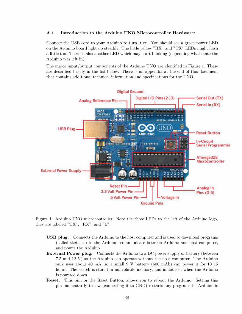
A.1 Introduction to the Arduino UNO Microcontroller Hardware:
Connect the USB cord to your Arduino to turn it on. You should see a green power LEDon the Arduino board light up steadily. The little yellow ”RX” and ”TX” LEDs might flasha little too. There is also another LED which may start blinking (depending what state theArduino was left in).
The major input/output components of the Arduino UNO are identified in Figure 1. Theseare described briefly in the list below. There is an appendix at the end of this documentthat contains additional technical information and specifications for the UNO.
Figure 1: Arduino UNO microcontroller: Note the three LEDs to the left of the Arduino logo,they are labeled ”TX”, ”RX”, and ”L”.
USB plug: Connects the Arduino to the host computer and is used to download programs(called sketches) to the Arduino, communicate between Arduino and host computer,and power the Arduino.
External Power plug: Connects the Arduino to a DC power supply or battery (between7.5 and 12 V) so the Arduino can operate without the host computer. The Arduinoonly uses about 40 mA, so a small 9 V battery (600 mAh) can power it for 10 15hours. The sketch is stored in nonvolatile memory, and is not lost when the Arduinois powered down.
Reset: This pin, or the Reset Button, allows you to reboot the Arduino. Setting thispin momentarily to low (connecting it to GND) restarts any program the Arduino is
38
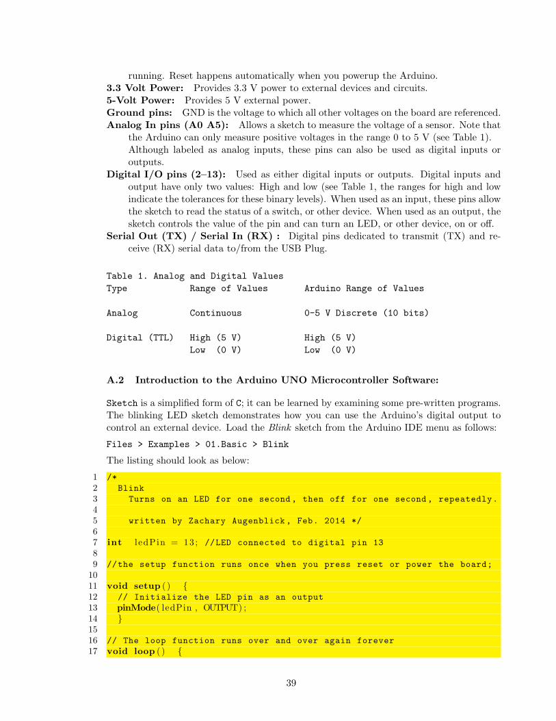
running. Reset happens automatically when you powerup the Arduino.3.3 Volt Power: Provides 3.3 V power to external devices and circuits.5-Volt Power: Provides 5 V external power.Ground pins: GND is the voltage to which all other voltages on the board are referenced.Analog In pins (A0 A5): Allows a sketch to measure the voltage of a sensor. Note that
the Arduino can only measure positive voltages in the range 0 to 5 V (see Table 1).Although labeled as analog inputs, these pins can also be used as digital inputs oroutputs.
Digital I/O pins (2–13): Used as either digital inputs or outputs. Digital inputs andoutput have only two values: High and low (see Table 1, the ranges for high and lowindicate the tolerances for these binary levels). When used as an input, these pins allowthe sketch to read the status of a switch, or other device. When used as an output, thesketch controls the value of the pin and can turn an LED, or other device, on or off.
Serial Out (TX) / Serial In (RX) : Digital pins dedicated to transmit (TX) and re-ceive (RX) serial data to/from the USB Plug.
Table 1. Analog and Digital Values
Type Range of Values Arduino Range of Values
Analog Continuous 0-5 V Discrete (10 bits)
Digital (TTL) High (5 V) High (5 V)
Low (0 V) Low (0 V)
A.2 Introduction to the Arduino UNO Microcontroller Software:
Sketch is a simplified form of C; it can be learned by examining some pre-written programs.The blinking LED sketch demonstrates how you can use the Arduino’s digital output tocontrol an external device. Load the Blink sketch from the Arduino IDE menu as follows:
Files > Examples > 01.Basic > Blink
The listing should look as below:
1 /*
2 Blink
3 Turns on an LED for one second, then off for one second, repeatedly.
45 written by Zachary Augenblick , Feb. 2014 */
67 int l edPin = 13 ; //LED connected to digital pin 13
89 //the setup function runs once when you press reset or power the board;
1011 void setup ( ) 12 // Initialize the LED pin as an output
13 pinMode( ledPin , OUTPUT) ;14 1516 // The loop function runs over and over again forever
17 void loop ( )
39
18 digitalWrite ( ledPin , HIGH) ; // Turn LED on, HIGH is voltage level.
19 delay ( 1 000 ) ;20 digitalWrite ( ledPin ,LOW) ;21 delay ( 1 000 ) ;
A sketch includes the following:
Opening Comments (lines 1–6): These state the purpose of the sketch, provide someinformation about the circuit that it accompanies, and give the authorship and dateof last modification.
Global Constants and Variables (line 7): These identifiers are known everywhere inthe sketch and do not need to be passed as parameters in functions.
Setup Function (lines 11–14): This function is executed only once when the Arduinois powered up, or when you press the reset button. It is used to configure the sketchby specifying pin assignments and pin modes (input/output).
Loop Function (lines 17–21): This function is executed repeatedly, forever, and is usedto input data from sensors and output control commands to actuators.
The Arduino IDE automatically color codes (shown in bold in this manual) predefined itemsin the sketch to improve its readability. These include variable types (e.g., int and void),builtin function names (e.g., setup, loop, pinMode, digitalWrite, delay), and prede-fined constants (e.g., HIGH, LOW, and OUTPUT). Notice also the use of capitalization.Names of variables and functions begin with lower case and capitals are used to separatewords (called camel case). Names of constants are in all caps. Indentation is optional butimproves readability. All loops, ifs and functions must be enclosed in curly brackets, likethis ... .
Look again at the example sketch and note several important characteristics of both C andSketch:
• Every statement is terminated by a semicolon ;
• Multistatement blocks are enclosed in curly brackets
• Comments are preceded by // or enclosed between /* and */ delimiters
• Variables, constants, functions. . . (all known as identifiers) must be defined beforethey can be used. Defining an identifier means specifying its name and type (int,float, void. . . ).
B Digital Output: Blinking LED
Run the sketch by clicking on the rightarrow button at the top of the IDE.
The LED marked ”L” should start blinking slowly off and on.
(1) Hook your voltmeter up to GND and Pin 13: (Use the Jumper wires I provided)measure and record the two voltage levels you observe.
(2) Slow the arduino down: It may be a little difficult to measure the voltage sinceyour voltmeter does not quite settle down in one second. Look at the Blink1 code.Maybe you can change the delay statements so that the LED is on for 5 seconds andoff for 5 seconds.
40
(3) Upload the changed program: Record the voltage levels you observe.
(4) Speed the flash up: Shorten both the delays to make the LED blink faster. Howshort must you make them until you can no longer see the LED blinking?
(5) Time the HIGH and LOW intervals with ’scope: Now that you have made theflashing too fast to see, take the voltmeter off and use the oscilloscope to measure Pin13 relative to GND. How long does Pin 13 spend being high and how long low (for thesetup of step 4.) What blink frequency does this correspond to?
(6) Determine delay units: Based on your measurements in (5), if the instruction says”delay(30)”, how many seconds is that?
(7) Determine maximum Arduino speed: Change the delay intervals to zero. (Alter-nately, you can comment the delay statements out with // characters). In principle thisshould make the Arduino infinitely fast, but the computer still takes time to executeinstructions. Using the oscillscope, you can determine the fastest that the Arduino canmake the LED blink. What is the ON/OFF period (and frequency) with zero delays?
(8) Light an external LED: Stick an LED into a protoboard and connect it to pin 13and ground. Restore the program back to one second blinks. Your external LED shouldnow be blinking. Once this works, move the external LED to some other digital outputpin and make it blink. What line in the Blink program did you change to make thiswork?
(9) Create two flashing LEDs: Add a second LED to your program. Attach each LEDto a different output pin. (Any pins are good except don’t use pin 0). Make sure bothLEDs blink together. Then change the code so that LEDs alternate (one goes on whenother goes off). Put your name on this code. Photograph it with your cell phone, andinclude it in the lab report. (You can also save it. Use ”Save As”, then save it under”Sketchbook”. You will see your program will now appear under Sketchbook.)
C Digital Input: Switch
Remove all Jumper wires from the Arduino and then insert a single jumper wire into theArduino’s Digital I/O Pin 2. Leave the free end of the jumper wire unconnected.
Load and run the Button sketch from the Arduino IDE menu.
Files > Examples > 02.Digital > Button
Watch the LED while you move your hand around in the vicinity of the Arduino. Trygrabbing the free end of the wire or running your fingers slowly up and down it. Try tomake the LED flicker a bit.
(http://playground.arduino.cc/CommonTopics/PullUpDownResistor )
(10) Discover why a floating input is problematic: Connect the free end of the jumperwire to the Arduino’s 5 V Power Pin and then to the GND pin: Which of those twopins makes the LED turn on? Note that it no longer matters whether you wiggle thewire around.
You have just learned the important lesson: A floating digital input will have anunpredictable value. If you want it to be high, you must connect it to 5 V. If you wantit to be low, you must connect it to 0 V. This is done by using pullup and pulldown
41
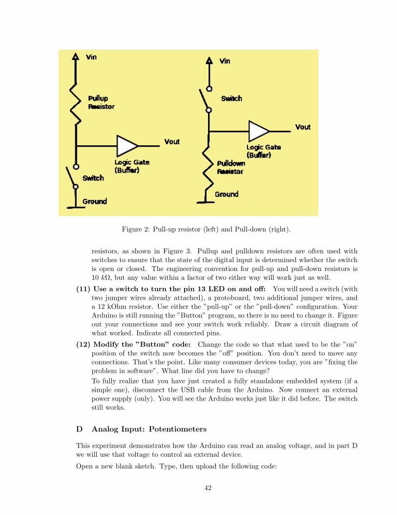
Figure 2: Pull-up resistor (left) and Pull-down (right).
resistors, as shown in Figure 3. Pullup and pulldown resistors are often used withswitches to ensure that the state of the digital input is determined whether the switchis open or closed. The engineering convention for pull-up and pull-down resistors is10 kΩ, but any value within a factor of two either way will work just as well.
(11) Use a switch to turn the pin 13 LED on and off: You will need a switch (withtwo jumper wires already attached), a protoboard, two additional jumper wires, anda 12 kOhm resistor. Use either the ”pull-up” or the ”pull-down” configuration. YourArduino is still running the ”Button” program, so there is no need to change it. Figureout your connections and see your switch work reliably. Draw a circuit diagram ofwhat worked. Indicate all connected pins.
(12) Modify the ”Button” code: Change the code so that what used to be the ”on”position of the switch now becomes the ”off” position. You don’t need to move anyconnections. That’s the point. Like many consumer devices today, you are ”fixing theproblem in software”. What line did you have to change?
To fully realize that you have just created a fully standalone embedded system (if asimple one), disconnect the USB cable from the Arduino. Now connect an externalpower supply (only). You will see the Arduino works just like it did before. The switchstill works.
D Analog Input: Potentiometers
This experiment demonstrates how the Arduino can read an analog voltage, and in part Dwe will use that voltage to control an external device.
Open a new blank sketch. Type, then upload the following code:
42
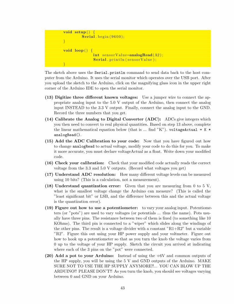
void setup ( ) Serial . begin ( 9600 ) ;
void loop ( ) int sensorValue=analogRead (A2 ) ;Serial . p r i n t l n ( sensorValue ) ;
The sketch above uses the Serial.println command to send data back to the host com-puter from the Arduino. It uses the serial monitor which operates over the USB port. Afteryou upload the sketch to the Arduino, click on the magnifying glass icon in the upper rightcorner of the Arduino IDE to open the serial monitor.
(13) Digitize three different known voltages: Use a jumper wire to connect the ap-propriate analog input to the 5.0 V output of the Arduino, then connect the analoginput INSTEAD to the 3.3 V output. Finally, connect the analog input to the GND.Record the three numbers that you get.
(14) Calibrate the Analog to Digital Converter (ADC): ADCs give integers whichyou then need to convert to real physical quantities. Based on step 13 above, completethe linear mathematical equation below (that is ... find ”K”). voltageActual = K *
analogRead().
(15) Add the ADC Calibration to your code: Now that you have figured out howto change analogRead to actual voltage, modify your code to do this for you. To makeit more accurate, you must declare voltageActual as a float. Write down your modifiedcode.
(16) Check your calibration: Check that your modified code actually reads the correctvoltage from the 3.3 and 5.0 V outputs. (Record what voltages you get)
(17) Understand ADC resolution: How many different voltage levels can be measuredusing 10 bits? (This is a calculation, not a measurement).
(18) Understand quantization error: Given that you are measuring from 0 to 5 V,what is the smallest voltage change the Arduino can measure? (This is called the”least significant bit” or LSB, and the difference between this and the actual voltageis the quantization error).
(19) Figure out how to use a potentiometer: to vary your analog input. Potentiome-ters (or ”pots”) are used to vary voltages (or potentials ... thus the name). Pots usu-ally have three pins. The resistance between two of them is fixed (to something like 10KOhms). The third pin is connected to a ”wiper” which slides along the windings ofthe other pins. The result is a voltage divider with a constant ”R1+R2” but a variable”R2”. Figure this out using your HP power supply and your voltmeter. Figure outhow to hook up a potentiometer so that as you turn the knob the voltage varies from0 up to the voltage of your HP supply. Sketch the circuit you arrived at indicatingwhere each of the 3 pins on the ”pot” were connected.
(20) Add a pot to your Arduino: Instead of using the +6V and common outputs ofthe HP supply, you will be using the 5 V and GND outputs of the Arduino. MAKESURE NOT TO USE THE HP SUPPLY ANYMORE!!... YOU CAN BLOW UP THEARDUINO!! PLEASE DON’T!! As you turn the knob, you should see voltages varyingbetween 0 and GND on your Arduino.
43
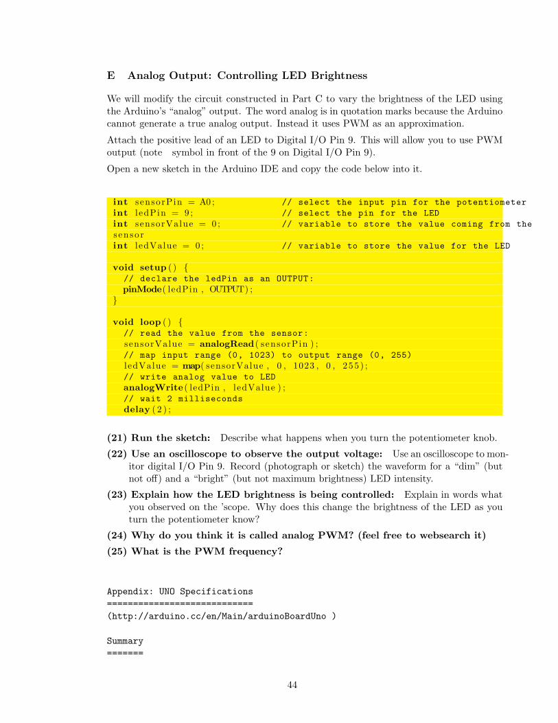
E Analog Output: Controlling LED Brightness
We will modify the circuit constructed in Part C to vary the brightness of the LED usingthe Arduino’s “analog” output. The word analog is in quotation marks because the Arduinocannot generate a true analog output. Instead it uses PWM as an approximation.
Attach the positive lead of an LED to Digital I/O Pin 9. This will allow you to use PWMoutput (note symbol in front of the 9 on Digital I/O Pin 9).
Open a new sketch in the Arduino IDE and copy the code below into it.
int sensorPin = A0 ; // select the input pin for the potentiometer
int l edPin = 9 ; // select the pin for the LED
int sensorValue = 0 ; // variable to store the value coming from the
s enso rint l edValue = 0 ; // variable to store the value for the LED
void setup ( ) // declare the ledPin as an OUTPUT:
pinMode( ledPin , OUTPUT) ;
void loop ( ) // read the value from the sensor:
sensorValue = analogRead ( sensorPin ) ;// map input range (0, 1023) to output range (0, 255)
l edValue = map( sensorValue , 0 , 1023 , 0 , 255 ) ;// write analog value to LED
analogWrite ( ledPin , ledValue ) ;// wait 2 milliseconds
delay ( 2 ) ;
(21) Run the sketch: Describe what happens when you turn the potentiometer knob.
(22) Use an oscilloscope to observe the output voltage: Use an oscilloscope to mon-itor digital I/O Pin 9. Record (photograph or sketch) the waveform for a “dim” (butnot off) and a “bright” (but not maximum brightness) LED intensity.
(23) Explain how the LED brightness is being controlled: Explain in words whatyou observed on the ’scope. Why does this change the brightness of the LED as youturn the potentiometer know?
(24) Why do you think it is called analog PWM? (feel free to websearch it)
(25) What is the PWM frequency?
Appendix: UNO Specifications
============================
(http://arduino.cc/en/Main/arduinoBoardUno )
Summary
=======
44

Microcontroller ATmega328
Operating Voltage 5V
External Input Voltage (recommended) 712V
External Input Voltage (limits) 620V
Digital I/O Pins 14 (of which 6 provide PWM output)
Analog Input Pins 6
DC Current per I/O Pin 40 mA Source or Sink
DC Current for 3.3V Pin 50 mA Source or Sink
DC Current per VCC and GND Pins 200.0 mA
Flash Memory 32 KB (ATmega328) of which 0.5 KB used by
bootloader
SRAM 2 KB (ATmega328)
EEPROM 1 KB (ATmega328)
Clock Speed 16 MHz
Length 68.6 mm
Width 53.4 mm
Weight 25 g
Power
Power
=====
The Arduino Uno can be powered via the USB connection or with an external
power supply. The power source is selected automatically.
External (nonUSB) power can come either from an AC to DC adapter
(wallwart) or battery. The adapter can be connected by plugging a
2.1 mm center-positive plug into the board’s power jack.
Leads from a battery can be inserted in the Gnd and Vin pin headers of the
POWER connector.
Memory
======
The ATmega328 has 32 KB (with 0.5 KB used for the bootloader).
It also has 2 KB of SRAM and 1 KB of EEPROM
(which can be read and written with the EEPROM library).
Input and Output (I/O)
======================
Each of the 14 digital pins on the Uno can be used as an input
or output, using pinMode(), digitalWrite(), and digitalRead() functions.
They operate at 5 volts. Each pin can provide or
receive a maximum of 40 mA and has an internal pullup resistor
(disconnected by default) of 20--50 kOhms.
The Uno also has 6 analog inputs, labeled A0 through A5, each of which provide 10 bits
resolution. By default they measure from ground to 5 volts,
though is it possible to change the upper end of their range using the AREF pin and the
analogReference() function.
45
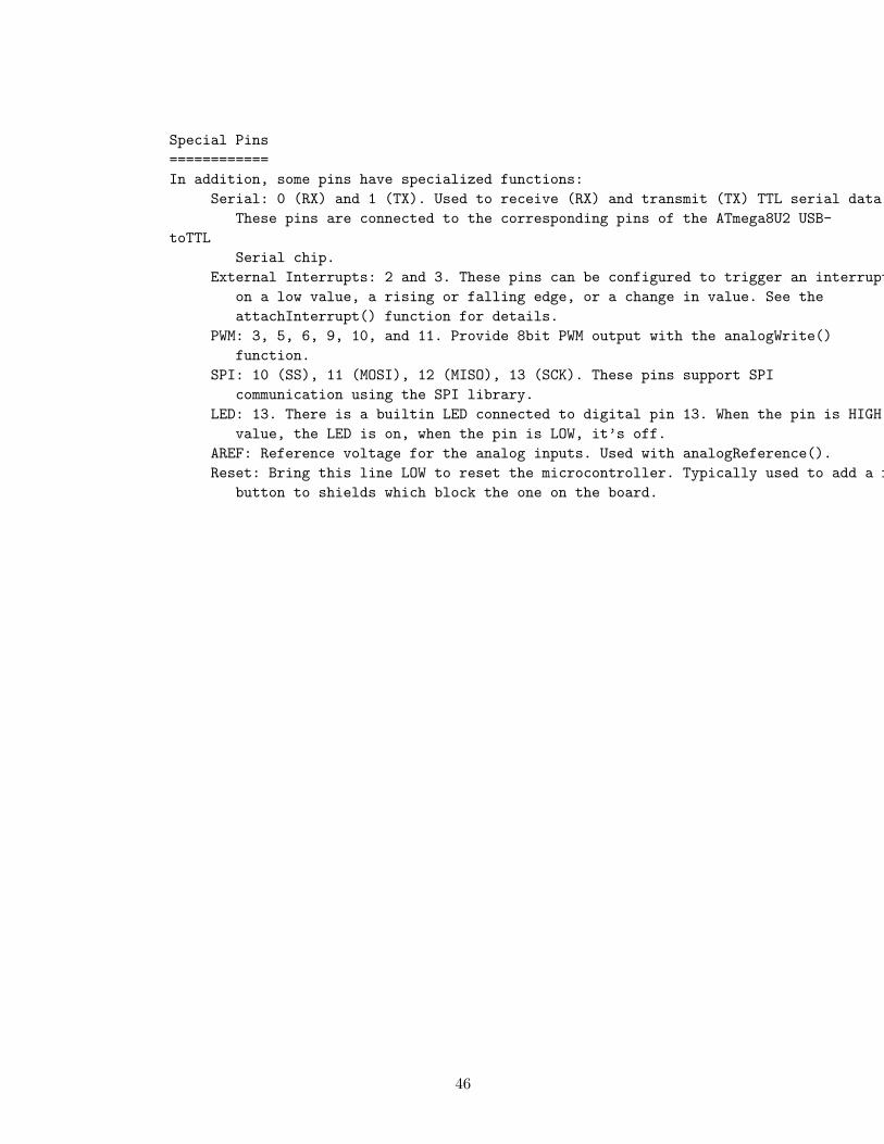
Special Pins
============
In addition, some pins have specialized functions:
Serial: 0 (RX) and 1 (TX). Used to receive (RX) and transmit (TX) TTL serial data.
These pins are connected to the corresponding pins of the ATmega8U2 USB-
toTTL
Serial chip.
External Interrupts: 2 and 3. These pins can be configured to trigger an interrupt
on a low value, a rising or falling edge, or a change in value. See the
attachInterrupt() function for details.
PWM: 3, 5, 6, 9, 10, and 11. Provide 8bit PWM output with the analogWrite()
function.
SPI: 10 (SS), 11 (MOSI), 12 (MISO), 13 (SCK). These pins support SPI
communication using the SPI library.
LED: 13. There is a builtin LED connected to digital pin 13. When the pin is HIGH
value, the LED is on, when the pin is LOW, it’s off.
AREF: Reference voltage for the analog inputs. Used with analogReference().
Reset: Bring this line LOW to reset the microcontroller. Typically used to add a reset
button to shields which block the one on the board.
46
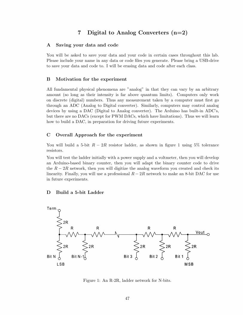
7 Digital to Analog Converters (n=2)
A Saving your data and code
You will be asked to save your data and your code in certain cases throughout this lab.Please include your name in any data or code files you generate. Please bring a USB-driveto save your data and code to. I will be erasing data and code after each class.
B Motivation for the experiment
All fundamental physical phenomena are ”analog” in that they can vary by an arbitraryamount (so long as their intensity is far above quantum limits). Computers only workon discrete (digital) numbers. Thus any measurement taken by a computer must first gothrough an ADC (Analog to Digital converter). Similarly, computers may control analogdevices by using a DAC (Digital to Analog converter). The Arduino has built-in ADC’s,but there are no DACs (except for PWM DACs, which have limitations). Thus we will learnhow to build a DAC, in preparation for driving future experiments.
C Overall Approach for the experiment
You will build a 5-bit R − 2R resistor ladder, as shown in figure 1 using 5% toleranceresistors.
You will test the ladder initially with a power supply and a voltmeter, then you will developan Arduino-based binary counter, then you will adapt the binary counter code to drivethe R − 2R network, then you will digitize the analog waveform you created and check itslinearity. Finally, you will use a professional R− 2R network to make an 8-bit DAC for usein future experiments.
D Build a 5-bit Ladder
Figure 1: An R-2R, ladder network for N-bits.
47
D.1 Build a ladder using 16 identical resistors
The circuit diagram shows how to build an N -bit ladder, but we will only build a 5-bitladder so as to avoid tedium and also to see more clearly how large the least signifcant bits(LSB’s) are. For starters, build only the first 3-bits. Use the same value resistor for allparts. Use the 5 % precision resistors provided. For branches that say 2R, use two resistorsin series. Keep in mind that the central groove on the proto-board separates the two halves.This can be used to your advantage. Try to make your circuit well organized. The bitsshould form a recognizable somewhat repetitious pattern. This will make it less likely thatyou make a mistake.
Ground (or COMMON) every open-dot you see in the figure EXCEPT for the one that saysVout.
(1) Measure resistance between Vout and ground for a 3-bit ladder: Use a multi-meter to measure the resistance between Vout and ground on your 3-bit A/D.
(2) Measure resistance between Vout and ground for a 4-bit ladder: Add anotherstage to your 3-bit ladder, and measure resistance to ground again from your newlycreated Vout position.
(3) Measure resistance to ground for a 5-bit ladder: Complete your ladder and againmeasure resistance to ground.
(4) Explain your results: Using a combination of circuit diagrams and words, I suggestanalyzing the circuit beginning right at the least significant bit and then proceedingrecursively to explain your results.
(5) Measure the effects of voltage applied at different bit positions: You have groundedall the pins except Vout. Now also unground the open circle labeled LSB (which is alsoBit 5) and connect 16.0 V (measure it) from your HP supply at that point. Measurethe voltage at Vout. Now reground the LSB and apply 16.0 V to Bit 4. What is Vout
now? Continue to measure all the bits up to Bit 1. (Always make sure to keep all thebits you are not using grounded). Make a table of results.
(6) Explain what pattern you observe: There should be a regular pattern apparentin your results from step 5. State what the pattern is. If you don’t see a regularpattern, maybe you did not build the circuit correctly.
E Build a 5-bit binary counter with the Arduino
Do not disassemble the resistor ladder (It will be used again). To the proto board on whichyou have built the ladder, add five LEDs. Connect each of the LEDs positive side througha 300 Ohm resistor to five different digital output pins of the Arduino. Connect all fivegrounds to the same ground pin on the Arduino board.
Load up the example code for Sparkfun Circuit 04 (“Dance, LEDs, Dance!”). It was writtenfor 8 LEDs. Modify it for your five LEDs. Exercise the 5 different functions suggested bythe Sparkfun code. (Note that this program uses an array called ledPins. You rememberarrays from Matlab, at least.)
Until now, your Arduino programs have only had the two functions setup and loop. Thoseare ALWAYS required, but you are allowed to add as many additional functions as you
48
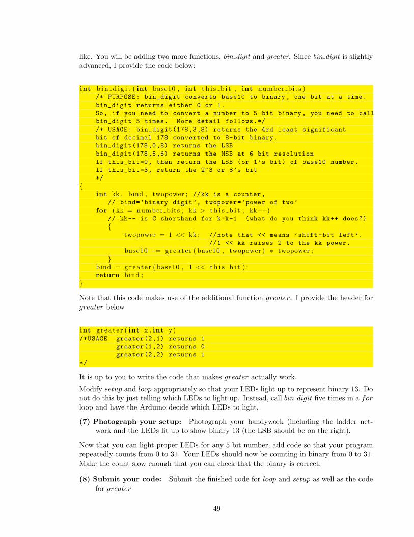
like. You will be adding two more functions, bin digit and greater. Since bin digit is slightlyadvanced, I provide the code below:
int b i n d i g i t ( int base10 , int t h i s b i t , int number bits )/* PURPOSE: bin_digit converts base10 to binary, one bit at a time.
bin_digit returns either 0 or 1.
So, if you need to convert a number to 5-bit binary, you need to call
bin_digit 5 times. More detail follows.*/
/* USAGE: bin_digit(178,3,8) returns the 4rd least significant
bit of decimal 178 converted to 8-bit binary.
bin_digit(178,0,8) returns the LSB
bin_digit(178,5,6) returns the MSB at 6 bit resolution
If this_bit=0, then return the LSB (or 1’s bit) of base10 number.
If this_bit=3, return the 2^3 or 8’s bit
*/
int kk , bind , twopower ; //kk is a counter,
// bind=’binary digit’, twopower=’power of two’
for ( kk = number bits ; kk > t h i s b i t ; kk−−)// kk-- is C shorthand for k=k-1 (what do you think kk++ does?)
twopower = 1 << kk ; //note that << means ’shift-bit left’.
//1 << kk raises 2 to the kk power.
base10 −= grea t e r ( base10 , twopower ) ∗ twopower ;
bind = gr ea t e r ( base10 , 1 << t h i s b i t ) ;return bind ;
Note that this code makes use of the additional function greater. I provide the header forgreater below
int g r e a t e r ( int x , int y )/*USAGE greater(2,1) returns 1
greater(1,2) returns 0
greater(2,2) returns 1
*/
It is up to you to write the code that makes greater actually work.
Modify setup and loop appropriately so that your LEDs light up to represent binary 13. Donot do this by just telling which LEDs to light up. Instead, call bin digit five times in a forloop and have the Arduino decide which LEDs to light.
(7) Photograph your setup: Photograph your handywork (including the ladder net-work and the LEDs lit up to show binary 13 (the LSB should be on the right).
Now that you can light proper LEDs for any 5 bit number, add code so that your programrepeatedly counts from 0 to 31. Your LEDs should now be counting in binary from 0 to 31.Make the count slow enough that you can check that the binary is correct.
(8) Submit your code: Submit the finished code for loop and setup as well as the codefor greater
49
F Build a 5-bit DAC
Your counter is now almost a DAC. Move the wires that went to the 5 LEDs (without theseries resistors) and put them in the appropriate place on the DAC circuit. Now run yourcount program and look at Vout with your meter. (You may need to increase the delay togive your meter time to stabilize between counts).
(9) Check your program output: Submit the first 5 voltages you measure, correspond-ing to first five counting #s.
(10) Digitize your DAC output: Connect Vout to A0. Add code to read the analogvoltage every time you count to a different number. Use Serial.print() to send thedigitized analog voltage to the serial monitor.
(11) Improve your serial output: Add a column to your serial data so that you havetwo columns, the decimal number you sent to the DAC and the analog readback thatcorresponds to it.
(12) Improve your serial output further: Add a third column to your serial data thatgives the voltage value that the DAC count corresponds to.
(13) Submit your output: You can make a text file out of the serial monitor by justhighlighting the text and pasting into a new text file. You need only submit the outputof step 12 (as steps 10 and 11 are included in it.)
(14) Plot your output: Make a plot (MATLAB, Excel, etc.) from the text file you justcreated. Is the DAC you built perfectly linear? It should be close unless you made amistake, but it is probably not perfectly linear because you used 5% resistors to buildit.
(15) Analyze the goodness of fit: Use Matlab, Excel or some other program to mea-sure the R-value of the line. Since it is really quite accurate, report the R-value to atleast 7 decimal places. Congratulations, you built a DAC!
G Build an 8-bit DAC using a ladder chip
You know what to do. You already have the code (except you need to change it to 8-bitcode.) The instructor should have provided you with an R-2R ladder chip at the beginningof the lab. Do NOT build the 8-bit DAC with individual resistors! Hook the provided chipup correctly and you will have an 8-bit DAC.
(16) Set the DAQ to 1, 127, 255: Measure the output voltage with your multimeter.Compare what you got against the LSB, half of full-scale, and full-scale minus oneLSB. If the results are not within 1% of correct, you made a mistake.
(17) Count from 0 to 255: Run your counting code from 0-255, capture the output onthe serial port, and measure the goodness of fit (R-value) of your new DAC. Comparethe R-value to the previous DAC. Keep it setup. You will use it in the next lab.
- Arduino Uno- LEDs- Protoboard- 5% resistors- R-2R ladder chip
50
8 Diodes (n=1)
A Measuring the Constitutive Relation of a Diode
A diode is an example of a non-linear electronic device. Doubling the input does not giveyou twice the output.
Current starts to flow in the forward direction (the direction of the arrow in circuit symbols)through diode junctions when the voltage across the junction reaches a threshold, which youwill determine in this lab. The base-emitter and collector-base junctions of transistors arealso diodes.
The diode we will use is the emitter-base junction of a NPN transistor. The flat side of thetransistor has labels for the three pins: e, b, c, for emitter, base, collector.
1. Set your function generator to produce a sinewave of 400 Hz frequency and 1.5 Vamplitude and attach it to the circuit of Figure 1. (I recommend using a 40–50 kΩresistor as R shown in the circuit diagram). Sketch (or photograph) V1(t) and VR(t)from the oscilloscope; use the same voltage scales and the same zero position for bothV1(t) and VR(t).
Next we will use our Arduino to quantify the current from the diode vs. the appliedvoltage. You already have a circuit with an 8-bit DAC on a chip from the previous lab.
2. Replace the function generator from the previous part with the Arduino DAC output.Again, sketch (or photograph) V1(t) and VR(t) from the oscilloscope. You may need tochange the delay in your Arduino counter code to make the counter run faster so youcan easily view the waveforms on the oscilloscope.
3. Next disconnect the oscilloscope completely and use the Arduino to take data. Runthe output of the DAC (which is now V1(t)) into A0 on the Arduino and run VR(t) intoA1. Modify your code to produce a table of VR vs. V1 as your counter runs through afull cycle. Capture this data and make a plot of it.
4. Of primary interest is the current through the diode I(t) vs. the voltage across thediode VBE . You are already taking the correct data, but you have to crunch it slightlyto turn V1 and VR into VBE and I. A little bit of thought on your part should tell youwhat calculation to do. Once you have figured it out, upgrade your Arduino code tofour columns. The first two are V1 and VR. The next two are VBE and I. Capture thefour column table and make a plot of I vs. VBE . This plot is called the constitutiverelation for a diode. (More casual folk just call it an “I-V Curve”.)
5. To complete the constitutive relation we must turn the diode around. Make the samemeasurements as in the previous step with the diode reversed (VEB instead of VBE).Modify the code to show VBE as a negative voltage and I as a negative current. ALSO,because the currents in the reverse bias direction are so small, you should change theresistor R in figure 1 to around 250 kΩ. Combine these results with the current table.(Not asking you to do that with the Arduino itself ... this is a cut and paste request!)Capture the data and plot the full constitutive relation of a diode. (You may want todo two plots since the reverse bias current probably appears to be zero on the scalewhere you can see the forward current).
6. Explain what you saw in step one of the lab based on the constitutive relation. Inparticular, why is the rectified waveform not an an exact copy of the top half of theinput waveform?
51
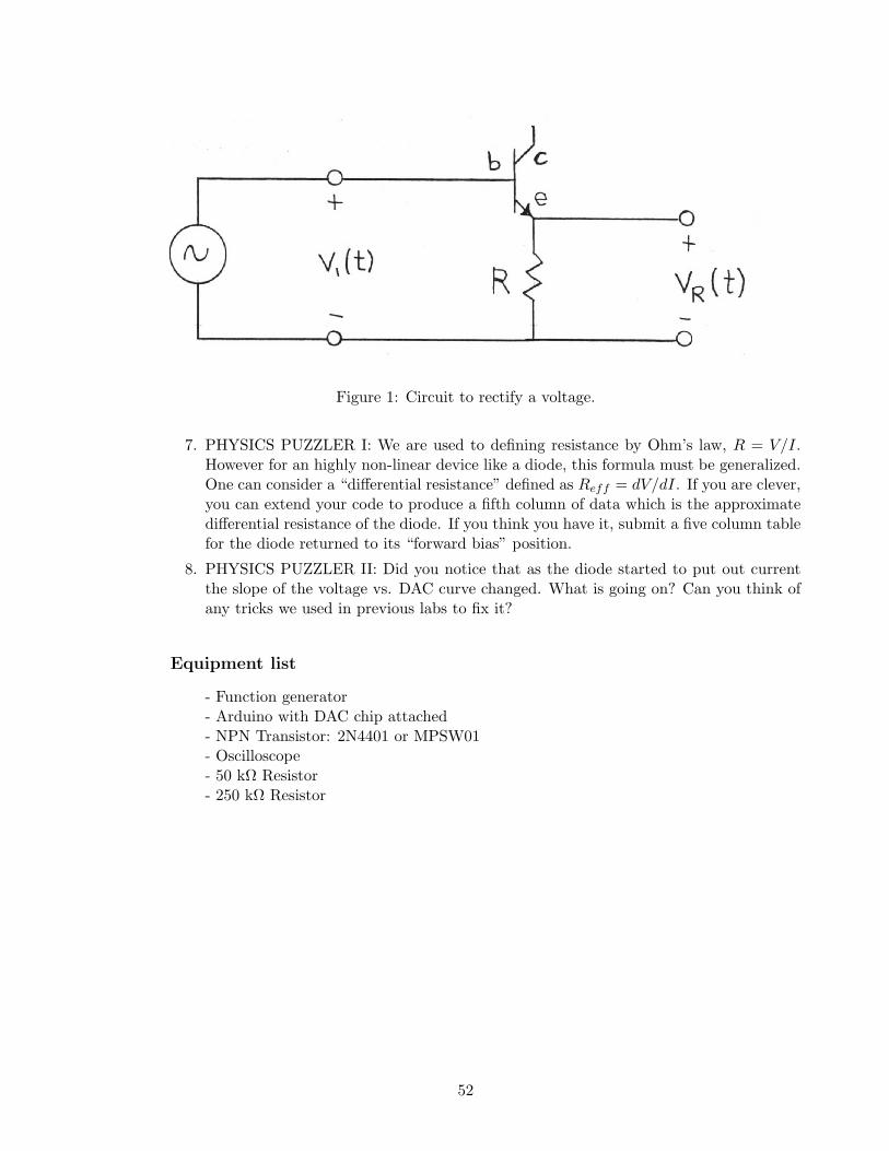
Figure 1: Circuit to rectify a voltage.
7. PHYSICS PUZZLER I: We are used to defining resistance by Ohm’s law, R = V/I.However for an highly non-linear device like a diode, this formula must be generalized.One can consider a “differential resistance” defined as Reff = dV/dI. If you are clever,you can extend your code to produce a fifth column of data which is the approximatedifferential resistance of the diode. If you think you have it, submit a five column tablefor the diode returned to its “forward bias” position.
8. PHYSICS PUZZLER II: Did you notice that as the diode started to put out currentthe slope of the voltage vs. DAC curve changed. What is going on? Can you think ofany tricks we used in previous labs to fix it?
Equipment list
- Function generator- Arduino with DAC chip attached- NPN Transistor: 2N4401 or MPSW01- Oscilloscope- 50 kΩ Resistor- 250 kΩ Resistor
52
9 Index of Refraction of Air (n=1)
Even though the wavelength of light in air is only slightly smaller than the wavelength oflight in a vacuum, it can be measured.Note: This experiment is very cool and requires you to use a Michelson Interferometer.Michelson Interferometers hate some people which means you can never get fringes in them.An instruction manual will be provided. It is a “good experience” to set up an inteferometer,but I cannot help you, because interferometers hate me.
Measurements
1. Use the equipment listed below to determine the index of refraction of air.
2. Extrapolate your results to predict the index of refraction at 1 atmosphere (1013.25millibars) and 0o C.
3. What measurement uncertainty leads to the largest uncertainty in the index of refrac-tion? What is the resulting uncertainty in the index of refraction?
Calculations
4. From your data and the ideal gas law, find out how the ratio of pressure to absolutetemperature, p/T , depends on the fringe number Nf . The fringe number Nf is definedin the following way: fringe number 1 is the fringe you see at the beginning. As newfringes appear as you decrease (or increase) the pressure, number them 2, 3, 4, etc.
5. From theory derive the function Nf (n) where n is the index of refraction.
6. From the above, find the function p(n) relating pressure and index of refraction. Thenfind a relation between 1− n and p(1)− p(n). Put in numbers to get 1− n. Then findn.
Equipment list
- Hand vacuum pump- Chamber with flat windows- Pressure sensor- Laser- Michelson Interferometer- Thermometer
53
10 Negative Resistance (n=1)
Introduction
In linear devices such as ordinary resistors, “resistance” could be defined either as dV/dIor as V/I; in either case the resistance of the device would have the same value. Whatdefinition should be used for non-linear devices such as diodes, neon lamps, and spark gaps?There is some advantage in defining resistance for these kinds of devices as dV/dI. Becauseof this definition, these devices exhibit negative resistance, and because of the negativeresistance they can be made to oscillate in special circuits.
Laboratory Work
1. This experiment will use a high voltage power supply; ask the instructor to look atyour circuit before turning on the supply.
2. Find the relation between voltage V and current I for a neon lamp. This relation iscalled the “constitutive relation” for the neon lamp.
3. Use the constitutive relation to design and construct an oscillator. A capacitor and aresistor will be required in the circuit. Draw a diagram of your circuit. Measure thefrequency of the oscillator. (HINT: The capacitor needs to be put in parallel with thelamp, while the resistor needs to be in series with the combination. Based on yourmeasurementsso far, you should be able to pick a resistor and capacitor that will workwell.)
4. Now that you have seen the oscillator work once, you are more likely to understandwhat is going on. Select a different resistor or capacitor with the goal of either doublingor halving the oscillator frequency (you decide which you want to do. If your firstfrequency came out small, you might want to double it, but if the flashing is prettyrapid, you might aim to halve the frequency.)
Calculations and Analysis
5. From the values of the capacitor and the resistor and the voltage at which the neonlamp becomes conducting, calculate the frequency of the oscillator. Compare yourcalculated frequency with the measured frequency. Repeat the calculation for thesecond resistor/capacitor set you choose.
Equipment list
- High voltage supply- Voltmeters- Neon lamp- Assorted parts
Laboratory Time
Two hours
54
11 Superconductivity (n=1)
Introduction
The discovery of ceramic compounds that are superconductors when immersed in liquidnitrogen has made it possible to investigate some properties of superconductivity using verysimple apparatus. In this lab we will use a commercial high-temperature-superconductivityexperiment kit to study some of aspects of superconductors. The kit contains a disk ofceramic superconductor, a module consisting of a smaller ceramic superconductor disk withan attached thermocouple, and two very strong, small magnets.
A superconductor is a substance which acts like a perfect conductor when its temperature isbelow some critical value, the critical temperature Tc. Thus when T < Tc a superconductoracts as if its resistance were zero, so that if a current were to be established in a ring ofsuperconductor it would persist indefinitely.
In 1933, Meissner discovered that a magnet was repulsed by a superconductor, an effectnow known by his name. The following are some considerations of how the Meissner effectmight come about.
Suppose that a strong magnet is brought up to a superconductor so that the superconductorexperiences a finite dB/dt. Then an emf would be induced in the superconductor such thata current would begin to flow. This induced current would continue to flow after the magnetstops moving (dB/dt = 0) because zero voltage will maintain a current when the resistanceis zero. According to Lenz’s law the induced current will be in a direction such that theB field due to it would be opposed to the B field of the magnet. Thus there would be arepulsive force between the small magnet and the superconductor. If the small magnet hada sufficiently strong field then the repulsion could result in the magnet being levitated abovethe superconductor.
However, if the magnet were placed on the superconductor while the superconductor waswarmer than the critical temperature, and then the superconductor was cooled to belowthe critical temperature, the magnet would not be levitated since dB/dt would never havebeen different from zero. Nevertheless, if one were then to try to remove the magnet fromthe superconductor, there would be an attractive force between the two of them resistingthe removal of the magnet due to the B field of the current induced in the superconductoras the magnet was moved. Since there is zero resistance in the superconductor we mightexpect that the induced current would be entirely on the surface and not in the interior ofthe superconductor.
Another way that a superconductor might repulse a magnet is if microscopic magneticdipoles are induced in the superconductor which then oppose the applied field. Then, insidethe superconductor there would be zero B field, and the external field of the dipoles inducedin the superconductor would repel the source of the applied field, that is, the magnet. Thesuperconductor would then be described as diamagnetic. This implies that the effect wouldbe a volume, or bulk effect, becoming stronger when the volume of the superconductor isincreased. In this case, if the magnet were placed on the superconductor before it was cooled,as the superconductor became superconducting it would exclude the magnetic field from itsinterior and the magnet would be levitated. Of course, this assumes that the strength ofthe magnet is sufficient to support its own weight.
55
This experiment is divided into two parts. In the first part you will study the Meissner Effect.In the second part you will determine the critical temperature of the ceramic superconductor.
Preparation Before Lab
Read the article on Superconductivity by Philip B. Allen in Encyclopedia of Physics, SecondEdition, edited by Lerner and Trigg, VCH Publishers, New York, 1991, pages 1198–1203.
Safety Procedures
Liquid Nitrogen
Liquid nitrogen (LN2) is COLD, it will kill skin cells by freezing them.
• Wear safety glasses when using LN2.
• Do not allow any LN2 to contact your body.
• Do not touch anything that has been immersed in LN2 before it has warmed to roomtemperature. Use the plastic tweezers provided.
• Be very careful to avoid splashing of the LN2.
• Avoid overfilling any vessel or spilling the LN2.
• Do not put LN2 in any vessel with a tight-fitting lid.
• The extreme cold of LN2 will damage many surfaces, so do not pour LN2 on or inanything not intended for LN2 contact.
• Let the lab instructor dispose of any unused LN2.
Ceramic Superconductor Handling Precautions
The ceramic superconducting material is made of oxides of various metals. The salts ofthese metals are toxic if ingested.
• Never handle the ceramic disks with your hands. Use tweezers provided.
• Do not under any circumstances ingest the materials.
• Do not expose the superconductor disk to water. After use in LN2, carefully wipe thesuperconductor to remove water or frost. Then warm it under a lamp to completelydry it.
• The ceramic disks are brittle. Handle gently!
• Do not expose the ceramic disks to temperatures greater than 100 F.
Things to Do
Meissner Effect
The two possible causes of levitation (the Meissner effect) may be summarized as:
56
1. Induced currents (due to change of B with time, which by Lenz’s law oppose the changein magnetic flux).
2. Diamagnetism (induced magnetic dipoles which oppose an applied B field).
Write clear and concise descriptions of your observations and answer the questions below.
1. Place the 1 inch diameter ceramic superconductor disk in an empty styrofoam cup.Place the cubic magnet on the uncooled superconductor, then cool to superconductingstate with liquid nitrogen. If (1), then no levitation (no change in B with time). If (2),levitation.
2. If necessary, lift the magnet above the superconductor. If (1), a force will opposeremoval of magnet (of about same magnitude as force which opposes moving magnetcloser to superconductor). If (2), force always repulsive. Also, try to move the levitatedmagnet toward the edge of the superconductor disk. What happens?
3. Surface current vs. bulk effect. Repeat the previous two steps using two superconduc-tor disks stacked one on top of the other. If (1), the current is only on surface, andthere is no dependance on the thickness of the superconductor. If (2), double thicknessof superconducting disk (two disks), increases height of levitation. Also, as supercon-ductor warms up to non-superconducting state, the magnet will abruptly fall if (1),but gently descend if (2).
Magnetic Field studies
4. What is the orientation of the magnetic field of the suspended cube magnet? To testif there is a preferred orientation, cause the magnet to rotate by blowing on the cube’sedge with a straw. Can you get it to rotate about another axis? From this you shouldbe able to infer the axis of the magnet. (This also demonstrates the possibility of africtionless magnetic bearing.)
5. Try to change the orientation of suspension by using a second magnet (whose polescan be determined using the compass provided) to attract the levitated magnet intoan upright position (while spinning, say). Is the upright position stable? Why or whynot?
Measuring Superconducting transition temperature
6. Measure the critical temperature Tc of the ceramic superconductor using the moduleprovided consisting of encapsulated superconductor disk and attached thermocouple.The module has six wires. The red and blue wires are the thermocouple wires. Sincethe voltages produced by the thermoucouple are just a few millivolts, you need to setyour voltmeter to its most sensitive range. (Some meters have a special 300 mV setting,others just autorange.) In order to determine the temperature of the superconductoryou need to know the relation between temperature and thermocouple voltage. See thetable for the particular thermocouple you are using. The table below is appropriatefor the type K thermocouple included in the Colorado Superconductor kits.
TABLE OBTAINED FROM http://srdata.nist.gov/its90/download/all.tab
May 2009
57
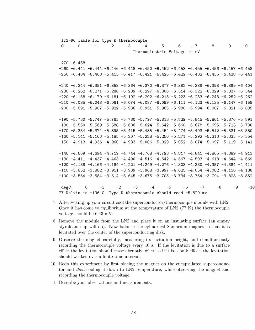
ITS-90 Table for type K thermocouple
C 0 -1 -2 -3 -4 -5 -6 -7 -8 -9 -10
Thermoelectric Voltage in mV
-270 -6.458
-260 -6.441 -6.444 -6.446 -6.448 -6.450 -6.452 -6.453 -6.455 -6.456 -6.457 -6.458
-250 -6.404 -6.408 -6.413 -6.417 -6.421 -6.425 -6.429 -6.432 -6.435 -6.438 -6.441
-240 -6.344 -6.351 -6.358 -6.364 -6.370 -6.377 -6.382 -6.388 -6.393 -6.399 -6.404
-230 -6.262 -6.271 -6.280 -6.289 -6.297 -6.306 -6.314 -6.322 -6.329 -6.337 -6.344
-220 -6.158 -6.170 -6.181 -6.192 -6.202 -6.213 -6.223 -6.233 -6.243 -6.252 -6.262
-210 -6.035 -6.048 -6.061 -6.074 -6.087 -6.099 -6.111 -6.123 -6.135 -6.147 -6.158
-200 -5.891 -5.907 -5.922 -5.936 -5.951 -5.965 -5.980 -5.994 -6.007 -6.021 -6.035
-190 -5.730 -5.747 -5.763 -5.780 -5.797 -5.813 -5.829 -5.845 -5.861 -5.876 -5.891
-180 -5.550 -5.569 -5.588 -5.606 -5.624 -5.642 -5.660 -5.678 -5.695 -5.713 -5.730
-170 -5.354 -5.374 -5.395 -5.415 -5.435 -5.454 -5.474 -5.493 -5.512 -5.531 -5.550
-160 -5.141 -5.163 -5.185 -5.207 -5.228 -5.250 -5.271 -5.292 -5.313 -5.333 -5.354
-150 -4.913 -4.936 -4.960 -4.983 -5.006 -5.029 -5.052 -5.074 -5.097 -5.119 -5.141
-140 -4.669 -4.694 -4.719 -4.744 -4.768 -4.793 -4.817 -4.841 -4.865 -4.889 -4.913
-130 -4.411 -4.437 -4.463 -4.490 -4.516 -4.542 -4.567 -4.593 -4.618 -4.644 -4.669
-120 -4.138 -4.166 -4.194 -4.221 -4.249 -4.276 -4.303 -4.330 -4.357 -4.384 -4.411
-110 -3.852 -3.882 -3.911 -3.939 -3.968 -3.997 -4.025 -4.054 -4.082 -4.110 -4.138
-100 -3.554 -3.584 -3.614 -3.645 -3.675 -3.705 -3.734 -3.764 -3.794 -3.823 -3.852
degC 0 -1 -2 -3 -4 -5 -6 -7 -8 -9 -10
77 Kelvin is -196 C Type K thermocouple should read -5.829 mv
7. After setting up your circuit cool the superconductor/thermocouple module with LN2.Once it has come to equilibrium at the temperature of LN2 (77 K) the thermocouplevoltage should be 6.43 mV.
8. Remove the module from the LN2 and place it on an insulating surface (an emptystyrofoam cup will do). Now balance the cylindrical Samarium magnet so that it islevitated over the center of the superconducting disk.
9. Observe the magnet carefully, measuring its levitation height, and simultaneouslyrecording the thermocouple voltage every 10 s. If the levitation is due to a surfaceeffect the levitation should cease abruptly, whereas if it is a bulk effect, the levitationshould weaken over a finite time interval.
10. Redo this experiment by first placing the magnet on the encapsulated superconduc-tor and then cooling it down to LN2 temperature, while observing the magnet andrecording the thermocouple voltage.
11. Describe your observations and measurements.
58
Four point probes and resistance measurements
You will see text on the superconducting module that says ”500 mA” maximum. Here’swhat it means. The module has two wires connected to a thermocouple. You havealready used those. The other four wires comprise something called a four-point probe,a sketch of which is shown below. Four point probes are the established way to measuresmall resistances. You apply a current betweenn the two out wires, and currect causea small DV
Other questions
12. Why does the LN2 boil when you pour it into the “dish?” and when you put thesuperconductor disk into it?
13. When the LN2 has evaporated, the magnet stays levitated for many more minutes.Why is this so?
14. Describe the way in which the magnet falls as the superconductor warms to above thecritical temperature and explain this behavior.
15. Under some circumstances, the magnet may suddenly scoot to one side of the brasscup as the assembly warms. Why is this?
16. Why does the assembly develop a layer of frost only after the LN2 has boiled away?
17. If the two different determinations of Tc yielded different values of Tc, explain why anddetermine which is the correct value.
Equipment list
- 1 inch diameter ceramic superconductor disk.- Ceramic superconductor and thermocouple module (“device”).- Cubic neodymium rare-earth alloy magnet.- Cylindrical samarium rare-earth alloy magnet.- Plastic tweezers.- Insulated dish (styrofoam cup).- CSI Instruction Manual.- Safety glasses.- Liquid Nitrogen (LN2)- Digital Multimeter.- Magnetic Compass.- Plastic straw.
59
12 Serial Ports (n=1)
Background
Serial data communications is important in many scientific instruments. If you build aninstrument yourself, or need to automate a commercial instrument, you will likely need tounderstand it.
Like so much else in electronics, serial communications have advanced and proliferated sincethe PC revolution of the early 1980’s. You have probably heard of USB (Universal serialbus), and SATA (Serial ATA, for hard drives), which are high performance interfaces forcommercial computers. There are also many serial interfaces used at the chip or subsystemlevel, among these are I2C (Inter-IC bus) and SPI (Serial Peripheral Interface).
The grandparent of all serial-protocols is the RS-232 protocol, often simply called ”the serialport protocol”. Despite its antiquity (a variant was first used in teletypes for telegraphy inthe early 20th century), it is still used by GPS devices and various scientific instruments andis available on your laptop computer via a “terminal program”. In particular, because if itssimplicity, it is a good protocol to learn. The other modern protocols previously mentionedhave much in common with it, and you can understand their more sophisticated featuresmore easily if you already understand RS-232.
Connectors and pin definitions
The RS-232 protocol was used most heavily for PC’s to communicate with modems. Becausemodems interfaced to telephones, they had a lot of complexity. They had to detect dialtones and know when the line was clear for data. In fact the full RS-232 interface defineda 25-pin connector. Early on PC-manufacturers cut this down to 9-pins, and used a “9-pin D connector” (see Figure below). This is still more complicated than needed for mostapplications. In practice, one needs only the “RX” (Receive) and “TX” (Transmit) wires,plus ground, and sometimes power. When you read descriptions of RS-232 and serial portson line, you will run into references to arcane signals like request to send (RTS), clear tosend (CTS) and data terminal ready (DTR) that were important in modem and telephonedays. Fortunately, you need none of these things for this lab. You only need to understandRX and TX.
In this lab, you will be using only RX, TX and ground. The RS-232 specification says thatpin 2 is RX (receive). Pin 2 is sometimes called RD (Receive data). Pin 3 is TX (transmit),also known as TD (Transmit data). Pin 5 is ground (by now you know that you alwaysneed a ground!). Looking at the diagram below, you will see that the “male” and “female”connectors are mirror images. Thus what you think is Pin 2 may be Pin 4, while Pin 1 maybe Pin 5. To make matters worse, there are two types of cables in common use for serialports.
Experiment
Connect an oscilloscope to the serial port of a laptop computer and analyze the waveformsthat come out of MINICOM or HYPERTERM. Figure out how to translate oscilloscope
60
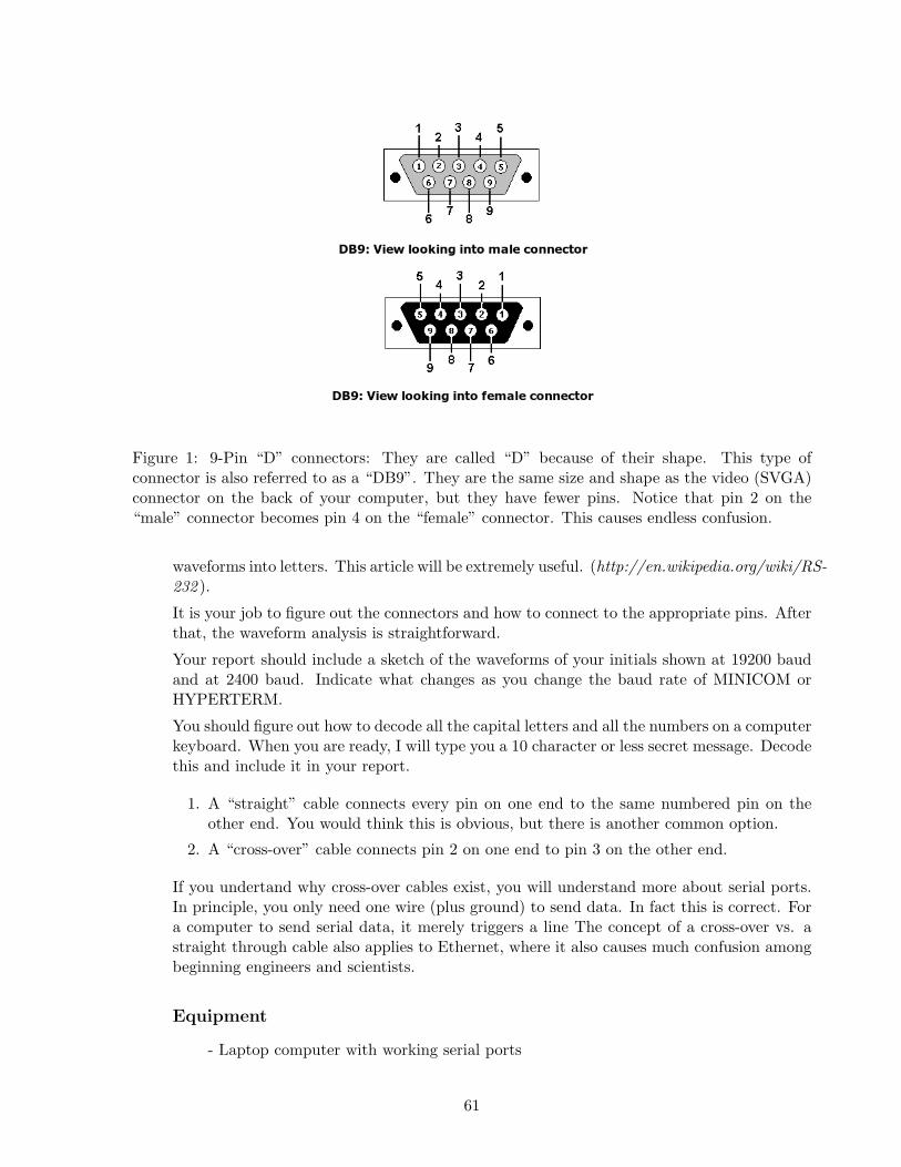
Figure 1: 9-Pin “D” connectors: They are called “D” because of their shape. This type ofconnector is also referred to as a “DB9”. They are the same size and shape as the video (SVGA)connector on the back of your computer, but they have fewer pins. Notice that pin 2 on the“male” connector becomes pin 4 on the “female” connector. This causes endless confusion.
waveforms into letters. This article will be extremely useful. (http://en.wikipedia.org/wiki/RS-232 ).
It is your job to figure out the connectors and how to connect to the appropriate pins. Afterthat, the waveform analysis is straightforward.
Your report should include a sketch of the waveforms of your initials shown at 19200 baudand at 2400 baud. Indicate what changes as you change the baud rate of MINICOM orHYPERTERM.
You should figure out how to decode all the capital letters and all the numbers on a computerkeyboard. When you are ready, I will type you a 10 character or less secret message. Decodethis and include it in your report.
1. A “straight” cable connects every pin on one end to the same numbered pin on theother end. You would think this is obvious, but there is another common option.
2. A “cross-over” cable connects pin 2 on one end to pin 3 on the other end.
If you undertand why cross-over cables exist, you will understand more about serial ports.In principle, you only need one wire (plus ground) to send data. In fact this is correct. Fora computer to send serial data, it merely triggers a line The concept of a cross-over vs. astraight through cable also applies to Ethernet, where it also causes much confusion amongbeginning engineers and scientists.
Equipment
- Laptop computer with working serial ports
61
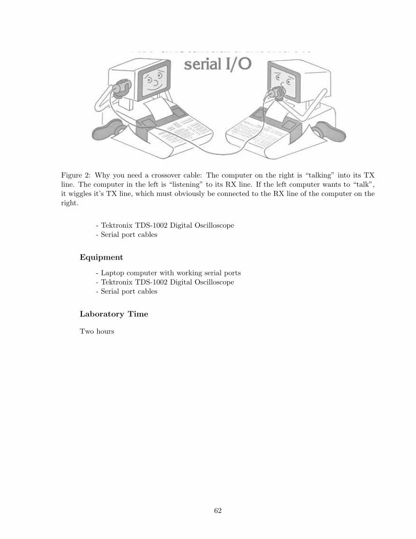
Figure 2: Why you need a crossover cable: The computer on the right is “talking” into its TXline. The computer in the left is “listening” to its RX line. If the left computer wants to “talk”,it wiggles it’s TX line, which must obviously be connected to the RX line of the computer on theright.
- Tektronix TDS-1002 Digital Oscilloscope- Serial port cables
Equipment
- Laptop computer with working serial ports- Tektronix TDS-1002 Digital Oscilloscope- Serial port cables
Laboratory Time
Two hours
62
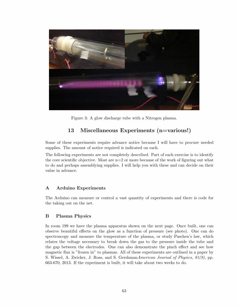
Figure 3: A glow discharge tube with a Nitrogen plasma.
13 Miscellaneous Experiments (n=various!)
Some of these experiments require advance notice because I will have to procure neededsupplies. The amount of notice required is indicated on each.
The following experiments are not completely described. Part of each exercise is to identifythe core scientific objective. Most are n=2 or more because of the work of figuring out whatto do and perhaps assemblying supplies. I will help you with these and can decide on theirvalue in advance.
A Arduino Experiments
The Arduino can measure or control a vast quantity of experiments and there is code forthe taking out on the net.
B Plasma Physics
In room 199 we have the plasma apparatus shown on the next page. Once built, one canobserve beautiful effects on the glow as a function of pressure (see photo). One can dospectroscopy and measure the temperature of the plasma, or study Paschen’s law, whichrelates the voltage necessary to break down the gas to the pressure inside the tube andthe gap between the electrodes. One can also demonstrate the pinch effect and see howmagnetic flux is ”frozen in” to plasmas. All of these experiments are outlined in a paper byS. Wissel, A. Zwicker, J. Ross, and S. GershmanAmerican Journal of Physics, 81(9), pp.663-670, 2013. If the experiment is built, it will take about two weeks to do.
63
C The Radio Spectrum
A spectrum analyzer and a simple antenna allow one to see the emissions of your cel phoneand to find all the radio stations currently broadcasting near Socorro. In the write-up forthis n=1 experiment, measure the frequency and amplitude of the 5 strongest radio stationsand two different cel phones.
D Lightning Location
A lightning flash actually consists of millions of tiny sparks that can be individually locatedin the sky. This is done by putting out a half dozen antennas and measuring when the radiopulse from each spark arrives. You can do a simple version of this test with two cables.Move a sparker back and forth between them and measure its location by correlating thepeaks on an oscilloscope.
E Lock-in Amplifiers
This project has a lot of physics and is not lethal. We have both a lock-in amplifier and amechanical chopper. The ”chopper” when applied to a laser beam or LED, can allow youto see a weak light from an LED in an otherwise brightly lit room. Perhaps you can evenmake a laser motion detector out of this apparatus.
F TV remote control
This requires only one week advance notice.
Using a phototransistor or photodiode, look at the infrared light signal emitted by a remotecontrol unit for a television set. See if you can determine the control codes.
G Dielectric Constant of Liquid Nitrogen
Use a parallel-plate capacitor to measure the dielectric constant of liquid nitrogen. Theexperiment is pretty straightforward. The handling of the liquid nitrogen adds the challenge.
H Light-emitting diodes
Light-emitting diodes can also be used as light detectors. This effect and others are dis-cussed in an article by David A. Johnson (Demonstrating the light-emitting diode, AmericanJournal of Physics, 63(8), 761-762, 1995). The article describes simple circuits for seeingvarious effects.
I Electric Motors
Requires NO advance notice.
If you rotate a motor shaft (say, with another motor) it will generate a voltage. Connectthe shaft of one motor to the shaft of another motor and make measurements to observethe generated voltage in both the driving motor and the driven motor.
64

J Magnetic materials
Requires one month advance notice to order the materials. It should be possible to study themagnetic properties of different types of materials by seeing how they affect the inductanceof a coil in an oscillating circuit.
K Serial ports
Serial data communications is important in many scientific instruments. If you build aninstrument yourself, you will likely need to understand it. Connect an oscilloscope to theserial port of a laptop computer and analyze the waveforms that come out of MINICOM orHYPERTERM. Figure out how to translate oscilloscope waveforms into letters.
L Improve an electromagnetic can crusher
Another good group project that is potentially fatal ... but not until energized. I can guideyou through the steps needed to charge large capacitors and fire them safely. A small groupof students built a crusher in 2014 that was both successful and safe. A new group mayattempt to improve on their work. This is something that should be brought up in March.
M Solar Motor-driver
There is no more important problem for society than energy that is renewable and doesnot contribute to global warming. Solar cells are an important part of the solution, but thecurrent sourced by a solar cell depends directly on the amount of sunlight available. ElectricDC motors typically have a minimum current required to make them turn at all. Can youovercome this limitation?
65

Appendix – Data Sheets
66
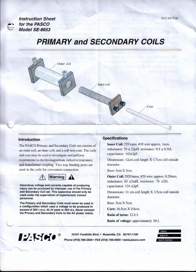

1
LT1001
1001fb
TYPICAL APPLICATIO
U
APPLICATIO SU
DESCRIPTIO
U
FEATURES
Precision OperationalAmplifier
Guaranteed Low Offset VoltageLT1001AM 15µV maxLT1001C 60µV max
Guaranteed Low DriftLT1001AM 0.6µV/°C maxLT1001C 1.0µV/°C max
Guaranteed Low Bias CurrentLT1001AM 2nA maxLT1001C 4nA max
Guaranteed CMRRLT1001AM 114dB minLT1001C 110dB min
Guaranteed PSRRLT1001AM 110dB minLT1001C 106dB min
Low Power DissipationLT1001AM 75mW maxLT1001C 80mW max
Low Noise 0.3µVP-P
The LT®1001 significantly advances the state-of-the-art of precision operational amplifiers. In the design,processing, and testing of the device, particular atten-tion has been paid to the optimization of the entiredistribution of several key parameters. Consequently,the specifications of the lowest cost, commercial tem-perature device, the LT1001C, have been dramaticallyimproved when compared to equivalent grades of com-peting precision amplifiers.
Essentially, the input offset voltage of all units is lessthan 50µV (see distribution plot below). This allows theLT1001AM/883 to be specified at 15µV. Input bias andoffset currents, common-mode and power supply re-jection of the LT1001C offer guaranteed performancewhich were previously attainable only with expensive,selected grades of other devices. Power dissipation isnearly halved compared to the most popular precisionop amps, without adversely affecting noise or speedperformance. A beneficial by-product of lower dissipa-tion is decreased warm-up drift. Output drive capabilityof the LT1001 is also enhanced with voltage gainguaranteed at 10mA of load current. For similar perfor-mance in a dual precision op amp, with guaranteedmatching specifications, see the LT1002. Shown belowis a platinum resistance thermometer application.
Thermocouple amplifiers Strain gauge amplifiers Low level signal processing High accuracy data acquisition
INPUT OFFSET VOLTAGE (µV)–60
NUM
BER
OF U
NITS
200
150
100
50
020
1001 TA02
–40 –20 0 40 60
954 UNITSFROM THREE RUNS
Typical Distributionof Offset Voltage
VS = ±15V, TA = 25°C
Linearized Platinum Resistance Thermometerwith ±0.025°C Accuracy Over 0 to 100°C
–
+LT1001 –
+LT1001
2
3
6
R plat. †
1k = 0°C
10k*
1.2k**
LM129
+15
2
3
6
200Ω
1001 TA01
LINEARITYTRIM
GAINTRIM
OUTPUT
0 TO 10V =0 TO 100°C
1µf
10k*
10k*
* ULTRONIX 105A WIREWOUND** 1% FILM
† PLATINUM RTD118MF (ROSEMOUNT, INC.)
‡ Trim sequence: trim offset (0°C = 1000.0Ω),trim linearity (35°C = 1138.7Ω), trim gain(100°C = 1392.6Ω). Repeat until all threepoints are fixed with ±0.025°C.
90k* 20kOFFSET TRIM
20k330k*
1MEG.**
, LTC and LT are registered trademarks of Linear Technology Corporation.
2
LT1001
1001fb
LT1001AM/883LT1001AC LT1001M/LT1001C
SYMBOL PARAMETER CONDITIONS MIN TYP MAX MIN TYP MAX UNITS
VOS Input Offset Voltage Note 2 LT1001AM/883 7 1518 60 µV
LT1001AC 10 25 ∆VOS Long Term Input Offset Voltage ∆Time Stability Notes 3 and 4 0.2 1.0 0.3 1.5 µV/monthIOS Input Offset Current 0.3 2.0 0.4 3.8 nAIb Input Bias Current ±0.5 ±2.0 ±0.7 ±4.0 nAen Input Noise Voltage 0.1Hz to 10Hz (Note 3) 0.3 0.6 0.3 0.6 µVp-p
en Input Noise Voltage Density fO = 10Hz (Note 6) 10.3 18.0 10.5 18.0 nV√HzfO = 1000Hz (Note 3) 9.6 11.0 9.8 11.0 nV√Hz
AVOL Large Signal Voltage Gain RL ≥ 2kΩ, VO = ±12V 450 800 400 800 V/mVRL ≥ 1kΩ VO = ±10V 300 500 250 500 V/mV
CMRR Common Mode Rejection Ratio VCM = ±13V 114 126 110 126 dBPSRR Power Supply Rejection Ratio VS = ±3V to ±18V 110 123 106 123 dBRin Input Resistance Differential Mode 30 100 15 80 MΩ
ABSOLUTE MAXIMUM RATINGS
W WW U
Supply Voltage ...................................................... ±22VDifferential Input Voltage ...................................... ±30VInput Voltage ........................................................ ±22VOutput Short Circuit Duration ......................... Indefinite
ORDERPART NUMBER
LT1001AMH/883LT1001MHLT1001ACHLT1001CH
PACKAGE/ORDER INFORMATION
W UU
LT1001ACN8LT1001CN8LT1001CS8
S8 PART MARKING1001
ELECTRICAL CHARACTERISTICS
TOP VIEWOFFSET ADJUST
V+
–IN OUT
NC
–
+
+INV– (CASE)
87
6
53
2
1
4
H PACKAGE METAL CAN
1
2
3
4
8
7
6
5
TOP VIEW
V+
OUT
NC
–IN
+IN
V–
–
+
VOSTRIM
VOSTRIM
S8 PACKAGE8 PIN PLASTIC SO
N8 PACKAGE8 PIN PLASTIC DIP
(Note 1)
J8 PACKAGE8 PIN HERMETIC DIP
LT1001AMJ8/883LT1001MJ8LT1001ACJ8LT1001CJ8
ORDERPART NUMBER
ORDERPART NUMBER
OBSOLETE PACKAGE OBSOLETE PACKAGE
Consult LTC Marketing for parts specified with wider operating temperature ranges.
The denotes the specifications which apply over the full operatingtemperature range, otherwise specifications are at TA = 25°C. VS = ±15V, unless otherwise noted
TJMAX = 150°C, θJA = 150°C/W, θjc = 45°C/W
TJMAX = 150°C, θJA = 130°C/W (N)TJMAX = 150°C, θJA = 150°C/W (S)
TJMAX = 150°C, θJA = 100°C/W (J)
Operating Temperature RangeLT1001AM/LT1001M (OBSOLETE) .. –55°C to 150°CLT1001AC/LT1001C .............................. 0°C to 125°CStorage: All Devices.......................... –65°C to 150°C
Lead Temperature (Soldering, 10 sec.) ................. 300°C
Consider the N8 and S8 Packages for Alternate Source Consider the N8 and S8 Packages for Alternate Source
3
LT1001
1001fb
ELECTRICAL CHARACTERISTICS
LT1001AM/883 LT1001MSYMBOL PARAMETER CONDITIONS MIN TYP MAX MIN TYP MAX UNITSVOS Input Offset Voltage 30 60 45 160 µV ∆VOS Average Offset Voltage Drift 0.2 0.6 0.3 1.0 µV/°C ∆TempIOS Input Offset Current 0.8 4.0 1.2 7.6 nAIB Input Bias Current ±1.0 ±4.0 ±1.5 ±8.0 nAAVOL Large Signal Voltage Gain RL ≥ 2kΩ, VO = ±10V 300 700 200 700 V/mVCMRR Common Mode Rejection Ratio VCM = ±13V 110 122 106 120 dBPSRR Power Supply Rejection Ratio VS = ±3 to ±18V 104 117 100 117 dB
Input Voltage Range ±13 ±14 ±13 ±14 VVOUT Output Voltage Swing RL ≥ 2kΩ ±12.5 ±13.5 ±12.0 ±13.5 VPd Power Dissipation No load 55 90 60 100 mW
VS = ±15V, –55°C ≤ TA ≤ 125°C, unless otherwise noted
LT1001AC LT1001CSYMBOL PARAMETER CONDITIONS MIN TYP MAX MIN TYP MAX UNITSVOS Input Offset Voltage 20 60 30 110 µV ∆VOS Average Offset Voltage Drift 0.2 0.6 0.3 1.0 µV/°C ∆TempIOS Input Offset Current 0.5 3.5 0.6 5.3 nAIB Input Bias Current ±0.7 ±3.5 ±1.0 ±5.5 nAAVOL Large Signal Voltage Gain RL ≥ 2kΩ, VO = ±10V 350 750 250 750 V/mVCMRR Common Mode Rejection Ratio VCM = ±13V 110 124 106 123 dBPSRR Power Supply Rejection Ratio VS = ±3V to ±18V 106 120 103 120 dB
Input Voltage Range ±13 ±14 ±13 ±14 VVOUT Output Voltage Swing RL ≥ 2kΩ ±12.5 ±13.8 ±12.5 ±13.8 VPd Power Dissipation No load 50 85 55 90 mW
Note 1: Absolute Maximum Ratings are those values beyond which the lifeof a device may be impaired.Note 2: Offset voltage for the LT1001AM/883 and LT1001AC are measuredafter power is applied and the device is fully warmed up. All other gradesare measured with high speed test equipment, approximately 1 secondafter power is applied. The LT1001AM/883 receives 168 hr. burn-in at125°C. or equivalent.Note 3: This parameter is tested on a sample basis only.
Note 4: Long Term Input Offset Voltage Stability refers to the averagedtrend line of VOS versus Time over extended periods after the first 30 daysof operation. Excluding the initial hour of operation, changes in VOS duringthe first 30 days are typically 2.5µV.Note 5: Parameter is guaranteed by design.Note 6: 10Hz noise voltage density is sample tested on every lot. Devices100% tested at 10Hz are available on request.
VS = ±15V, 0°C ≤ TA ≤ 70°C, unless otherwise noted
LT1001AM/883LT1001AC LT1001M/LT1001C
SYMBOL PARAMETER CONDITIONS MIN TYP MAX MIN TYP MAX UNITSInput Voltage Range ±13 ±14 ±13 ±14 V
VOUT Maximum Output Voltage Swing RL ≥ 2kΩ ±13 ±14 ±13 ±14 VRL ≥ 1kΩ ±12 ±13.5 ±12 ±13.5 V
SR Slew Rate RL ≥ 2kΩ (Note 5) 0.1 0.25 0.1 0.25 V/µsGBW Gain-Bandwidth Product (Note 5) 0.4 0.8 0.4 0.8 MHzPd Power Dissipation No load 46 75 48 80 mW
No load, VS = ±3V 4 6 4 8 mW
The denotes the specifications which apply over the full operatingtemperature range, otherwise specifications are at TA = 25°C. VS = ±15V, TA = 25°C, unless otherwise noted
Features Resistance range: 100 ohms to 1 megohm SIP and DIP packages Surface mount and through-hole available RoHS compliant* (see How to Order “Termination” option)
For information on R/2R Thick Film Networks, download Bourns’ R/2R Application Note.
R/2R Series Thick Film Networks
*RoHS Directive 2002/95/EC Jan 27, 2003 including Annex. Specifi cations are subject to change without notice.
Customers should verify actual device performance in their specifi c applications.
Product CharacteristicsResistance Range Models 4100, 4300, 4400 & 4800 .................... 100 ohms to 100K ohms Model 4600 ...100 ohms to 1 megohmStandard Tolerance ....................... ±2 %
See applicable model data sheet for complete list of product characteristics.
Environmental CharacteristicsSee applicable model data sheet for complete list of environmental characteristics.
Physical CharacteristicsSee applicable model data sheet for complete list of physical characteristics.
Resistor Schematic
How To Order
4116R - R2R - 501 __
Model(See “Available Models”)
Electrical Confi guration R2R = Standard R/2R** 121 = Reversed R/2R***
Resistance Code (for value of R)• First 2 digits are signifi cant; third digit represents the number of zeros to follow.
• 2R is double the value of R in circuit.
Terminations LF = Tin-coated (RoHS compliant version) (Model 4416P is ONLY available in the RoHS compliant version.)Blank = Tin/Lead (Model 4416P is not available with tin/lead terminations.)
**Standard R2R Electrical Confi guration not available for Model 4600H Series.
***Reversed R/2R Electrical Confi guration not available for Model 4600H, 4600M or 4600X Series.
Product Dimensions Typical Part MarkingRepresents total content. Layout may vary.
For Standard Values Used in Capacitors, Inductors, and Resistors, click here.
PARTNUMBER
4114R-R2R-501 YYWW
CIRCUITRESISTANCECODE
PIN ONEINDICATOR
MANUFACTURER'STRADEMARK
DATE CODE
16
1
9
8
2R
R2R
15
2
2R
R
14
3
2R
R
13
4
2R
R
12
5
2R
R
11
6
2R
R
10
7
2R
R
2R
OUT RT
16-PIN8-BITDIP
PIN
BIT 1 82 3 4 5 6 7MSB LSB
2
2R
R
3
2R
R
4
2R
R
5
2R
R
6
2R
R
7
2R
R
8
2R
R
9
2R
1
BIT OUT 1 82 3 4 5 6 7MSB LSB
PIN 10
2R
RT
10-PIN8-BITSIP
16
1
9
8
2R
R
15
2
2R
R
14
3
2R
R
13
4
2R
R
12
5
2R
R
11
6
2R
R
10
7
2R
R
2R2R
OUTRT
16-PIN8-BITDIP
PIN
BIT 8 17 6 5 4 3 2MSBLSB
2
2R
R
3
2R
R
4
2R
R
5
2R
R
6
2R
R
7
2R
R
8
2R
R
9
2R
1
BIT RT 8 17 6 5 4 3 2LSB MSB
PIN 10
2R
OUT
10-PIN8-BITSIP
See applicable model data sheet for complete product dimensions.
R2R Circuit 121 Circuit
Power Derating Curve
100
50
00 25 70 125
AMBIENT TEMPERATURE (°C)
PERC
ENTA
GE O
F RA
TED
POW
ER
Power Rating per ResistorPower per Resistor
Model (Watts)4100R, 4300R, 4400P, 4600X***, 4800P .................................................................. 0.1254300M, 4600M*** .................................................................................................... 0.1704300H ...................................................................................................................... 0.200
*RoH
S COMPLIANT
VERSIO
NS
AVAILABLE
9WIXLMWSRI67
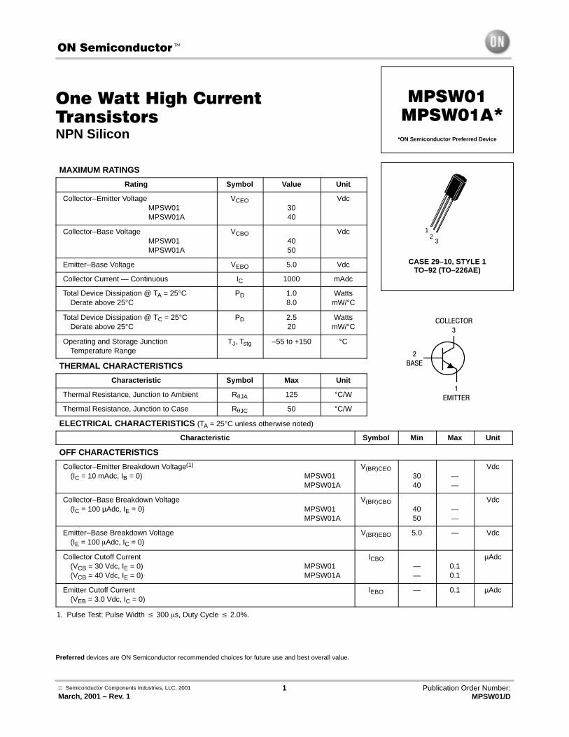
One Watt High CurrentTransistorsNPN Silicon
MAXIMUM RATINGS
Rating Symbol Value Unit
Collector–Emitter VoltageMPSW01MPSW01A
VCEO3040
Vdc
Collector–Base VoltageMPSW01MPSW01A
VCBO4050
Vdc
Emitter–Base Voltage VEBO 5.0 Vdc
Collector Current — Continuous IC 1000 mAdc
Total Device Dissipation @ TA = 25°CDerate above 25°C
PD 1.08.0
WattsmW/°C
Total Device Dissipation @ TC = 25°CDerate above 25°C
PD 2.520
WattsmW/°C
Operating and Storage JunctionTemperature Range
TJ, Tstg –55 to +150 °C
THERMAL CHARACTERISTICS
Characteristic Symbol Max Unit
Thermal Resistance, Junction to Ambient RJA 125 °C/W
Thermal Resistance, Junction to Case RJC 50 °C/W
ELECTRICAL CHARACTERISTICS (TA = 25°C unless otherwise noted)
Characteristic Symbol Min Max Unit
OFF CHARACTERISTICS
Collector–Emitter Breakdown Voltage(1)
(IC = 10 mAdc, IB = 0) MPSW01MPSW01A
V(BR)CEO3040
——
Vdc
Collector–Base Breakdown Voltage(IC = 100 µAdc, IE = 0) MPSW01
MPSW01A
V(BR)CBO4050
——
Vdc
Emitter–Base Breakdown Voltage(IE = 100 Adc, IC = 0)
V(BR)EBO 5.0 — Vdc
Collector Cutoff Current(VCB = 30 Vdc, IE = 0) MPSW01(VCB = 40 Vdc, IE = 0) MPSW01A
ICBO——
0.10.1
µAdc
Emitter Cutoff Current(VEB = 3.0 Vdc, IC = 0)
IEBO — 0.1 µAdc
1. Pulse Test: Pulse Width 300 s, Duty Cycle 2.0%.
Preferred devices are ON Semiconductor recommended choices for future use and best overall value.
ON Semiconductor
Semiconductor Components Industries, LLC, 2001
March, 2001 – Rev. 11 Publication Order Number:
MPSW01/D
MPSW01MPSW01A
*ON Semiconductor Preferred Device
CASE 29–10, STYLE 1TO–92 (TO–226AE)
12
3
*
COLLECTOR
3
2
BASE
1
EMITTER
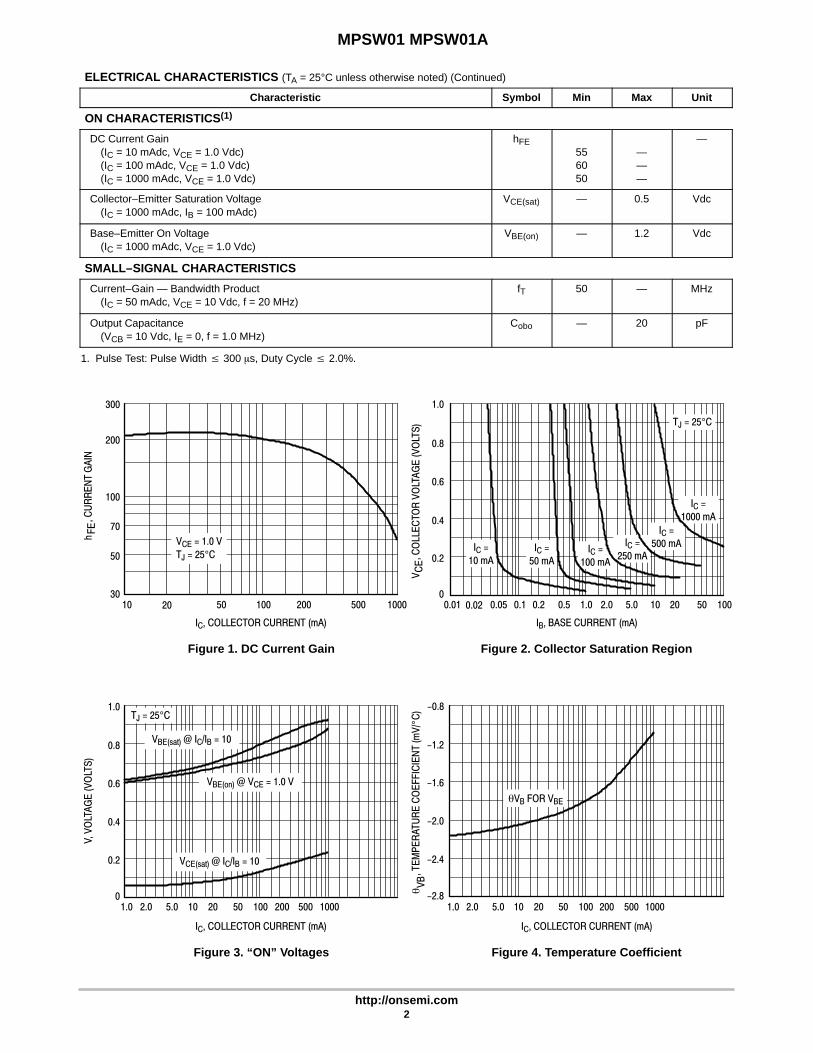
MPSW01 MPSW01A
http://onsemi.com2
ELECTRICAL CHARACTERISTICS (TA = 25°C unless otherwise noted) (Continued)
Characteristic Symbol Min Max Unit
ON CHARACTERISTICS(1)
DC Current Gain(IC = 10 mAdc, VCE = 1.0 Vdc)(IC = 100 mAdc, VCE = 1.0 Vdc)(IC = 1000 mAdc, VCE = 1.0 Vdc)
hFE556050
———
—
Collector–Emitter Saturation Voltage(IC = 1000 mAdc, IB = 100 mAdc)
VCE(sat) — 0.5 Vdc
Base–Emitter On Voltage(IC = 1000 mAdc, VCE = 1.0 Vdc)
VBE(on) — 1.2 Vdc
SMALL–SIGNAL CHARACTERISTICS
Current–Gain — Bandwidth Product(IC = 50 mAdc, VCE = 10 Vdc, f = 20 MHz)
fT 50 — MHz
Output Capacitance(VCB = 10 Vdc, IE = 0, f = 1.0 MHz)
Cobo — 20 pF
1. Pulse Test: Pulse Width 300 s, Duty Cycle 2.0%.
Figure 1. DC Current Gain Figure 2. Collector Saturation Region
Figure 3. “ON” Voltages Figure 4. Temperature Coefficient
50 50010
IC, COLLECTOR CURRENT (mA)
300
200
70
50
30
IB, BASE CURRENT (mA)
1.0
0.8
0.6
0.4
0
IC, COLLECTOR CURRENT (mA)
1.0
0.8
0
IC, COLLECTOR CURRENT (mA)
1.0
-1.2
-1.6
-2.0
-2.4
-2.82.0
VCE = 1.0 V
TJ = 25°C
hV,
VO
LTA
GE
(V
OLT
S)
20 100 0.05 100.01 0.02 0.1 0.2
, CO
LLE
CTO
R V
OLT
AG
E (
VO
LTS
)
200 1000
100
20 50 100
0.2
VC
E
0.2
0.6
0.4
-0.8
5.0 10 20 50 100 200
, CU
RR
EN
T G
AIN
FE
0.5 1.0 2.0 5.0
TJ = 25°C
500 1000
VB FOR VBE
TJ = 25°C
1.0 2.0 5.0 10 20 50 100 200 500 1000
VBE(sat) @ IC/IB = 10
VCE(sat) @ IC/IB = 10
VBE(on) @ VCE = 1.0 V
IC =
1000 mA
IC =
500 mAIC =
10 mA
IC =
50 mAIC =
100 mA
IC =
250 mA
, TE
MP
ER
AT
UR
E C
OE
FF
ICIE
NT
(mV
/ C
)°
VB


