Embed Size (px)
Citation preview
Evaluation of Input Current in the Critical Mode Boost PFC Converter for Distributed Power Systems*
Jindong Zhang, Jianwen Shao, Peng Xu and Fred C. Lee Milan M. JovanoviC
Center for Power Electronics Systems Electrical and Computer Engineering Department Virginia Polytechnic Institute and State University
Delta Product Corp. Power Electronics Laboratory
P.O. Box 12173,5101 Davis Dr. Blacksburg, VA 2406 1-0 1 1 1
ABSTRACT
This paper presents the analysis and evaluation of the input current in the critical mode single-phase boost power-factor-correction (PFC) converter. First, the switching-frequency ripple of the input current is derived and the differential-mode EM1 filters of the critical and continuous mode PFC rectifiers are calculated and compared. Next, the benefits and challenges of interleaving the critical mode PFC rectifiers are discussed. Finally, the low-frequency input current distortions are analyzed with respect to the switching-frequency limits of the critical mode boost PFC rectifier.
I. INTRODUCTION
The front-end of distributed power systems (DPS) used in telecom and high-end server applications requires low input current distortions, high power density, good efficiency with universal line input, and low cost. Generally, to meet the low-input-current-distortion requirement, the continuous-conduction-mode (CCM) boost power-factor-correction (PFC) rectifier is the preferred topology for the input side of a DPS front end because the differential mode electromagnetic interference (DM-EMI) is minimized due to its low input current ripple. However, because of the h g h output voltage of the boost PFC rectifier, a high-voltage fast-recovery boost diode is required, which generates significant reverse- recovery losses when switched under hard-switching conditions. These reverse-recovery losses limit the converter efficiency, especially at low line and full load.
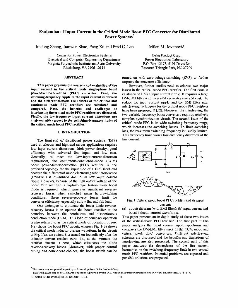
One technique to eliminate the boost diode reverse- recovery losses is to operate the boost rectifier at the boundary between the continuous and discontinuous conduction mode (DCM). This lund of boundary operation is also referred to as the critical mode of operation. Figure l(a) shows the boost PFC circuit, whereas Fig. l(b) shows the critical mode inductor current waveform. In the circuit in Fig. l(a), the switch S is turned on immediately after the inductor current reaches zero, i.e., at the moment the rectifier current is zero, which eliminates the diode reverse-recovery losses. Moreover, with proper control timing and component choices, the boost switch can be
Research Triangle Park, NC 27709
turned on with zero-voltage-switching (ZVS) to further improve the converter efficiency.
However, further studies need to address two major issues in the critical mode PFC rectifier. The first issue is existence of a high input current ripple. It requires a large DM-EM1 filter with increased converter size and cost. To reduce the input current ripple and the EM1 filter size, interleaving techniques for the critical mode PFC rectifiers have been proposed [ 1],[2]. However, the interleaving the two variable-frequency boost converters requires relatively complex synchronization circuit. The second issue of the critical mode PFC is its wide switching-frequency range, which increases the switching losses. To limit switching loss, the maximum switching-frequency is usually limited. This frequency limit causes low-frequency distortion of the line current.
Fig. 1 Critical mode boost PFC rectifier and its input current:
(a) circuit diagram (with EM1 filter); (b) input current and boost inductor current waveforms.
ms paper presents an in-depth study of these two issues of the critical-mode PFC rectifier. The first part of this paper analyzes the input current ripple spectrums and compares the DM-EM1 filter sizes of the CCM mode and critical mode PFC converters. Different interleaving schemes are discussed and the benefits and limitations of interleaving are also presented. The second part of this paper analyzes the dependence of the line current harmonics on the switching-frequency limit in two critical mode PFC rectifiers. Potential problems are exposed and possible solutions are proposed.
This work was supported in part by a fellowship from Delta Product Corp. This work made use of ERC Shared Facilities supported by the U.S. National Science Foundation under Award Number EEC-9731677
0-7803-6618-2/01/$10.00 0 2001 IEEE 130
11. EVALUATION OF THE SWITCHING nUEQUENCY CURRENT RIPPLE
2.1 Boost inductor ripple current spectrum analysis
To achieve unity input power factor, the switch S in the critical mode boost rectifier shown in Fig.1 should be dnven with a variable switching cycle, constant on-time gate signal. The peak inductor current iLB(peak) always has a magnitude twice as great as that of the instantaneous sinusoidal input current ih. Due to its high inductor current ripple, the critical mode boost rectifier requires a much larger DM-EM1 filter than does the CCM boost rectifier. In order to evaluate the EM1 filters, the boost inductor current spectrum should be derived. This section presents the analysis of the CCM and critical mode inductor current in the frequency domain.
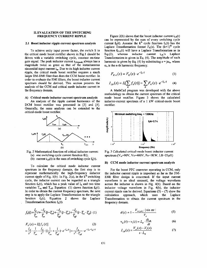
A) Critical-mode inductor current spectrum analysis An analysis of the ripple current harmonics of the
DCM boost rectifier was presented in [3] and [4]. Generally, the same analysis can be extended to the critical-mode boost rectifier.
Ton Toff
t
TK TK+I t
(b)
Fig. 2 Mathematical function of critical inductor current: (a) one switching cycle current function f(t); (b) current iLB(t) is the s u m of switching cycle fk(t).
To calculate the critical mode inductor current spectrum in the frequency domain, the first step is to represent mathematically the high-frequency inductor current ripple of Fig. l(b). In Fig. 2(a), in the kth switching cycle, the inductor current can be regarded as a triangle function fK(t), which has a peak value of IK and two time variables To, and Toff. Equation (1) shows function fK(t). In order to obtain the current frequency spectrum, the next step is to apply the Laplace Transformation to the triangle function fK(t). Equation 2 shows the Laplace Transformation function fK(t).
Figure 2(b) shows that the boost inductor current iLB(t) can be represented by the s u m of every switching cycle current fK(t). Assume the k* cycle function fK(t) has the Laplace Transformation format FK(s). The (k+l)* cycle function fK+l(t) will have a Laplace Transformation as in Eq.(3), whereas inductor current iLB's Laplace Transformation is given in Eq. (4). The amplitude of each harmonic is given by Eq. (4) by substituting s = jo,, where 0, is the n-th harmonic frequency.
(3)
( s ) = f, ( t ) ] = C F~ (S I - e-TK'S (4) K K
A MathCad program was developed with the above methodology to obtain the current spectrum of the critical mode boost rectifier. Figure 3 shows the calculated inductor-current spectrum of a 1 kW critical-mode boost rectifier.
I .lo4
Minimum switching freq. = 1 W W
Ipk2.7A
1.106
Fig. 3 Calculated critical-mode boost inductor current spectrum (Vh=90V, Vo=4OOV, Po=lKW, LB=25pH)
B) CCM mode inductor current spectrum analysis
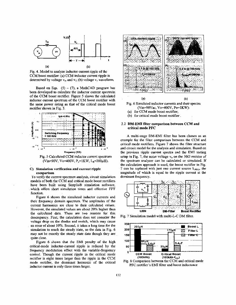
For the boost PFC converter operating in CCM, only the inductor current ripple is important as far as the DM- EM1 filter design is concerned. If the input current waveform is an ideal sinusoid, the voltage waveform across the inductor is shown in Fig. 4(b). Based on the inductor voltage waveform in Fig. 4(b), the inductor current ripple can be derived. Equations ( 5 ) - (7) show the calculation approach, which uses the Laplace Transformation to obtain the current spectrum in the frequency domain.
diLB dt
Vin ( t ) - v, ( t ) = L, * -
131
......................... n ~
k - - T - - - w # t
(a) (b) Fig. 4. Model to analyze inductor current ripple of the CCM boost rectifier: (a) CCM inductor current ripple is determined by voltage vh and vl; (b) voltage v1 waveform.
Based on Eqs. (5) - (7), a MathCAD program has been developed to calculate the inductor current spectrum of the CCM boost rectifier. Figure 5 shows the calculated inductor current spectrum of the CCM boost rectifier with the same power rating as that of the critical mode boost rectifier shown in Fig. 3.
10 I 10 I 10
Frequency (HZ)
Fig. 5 Calculated CCM inductor current spectrum (Vin=90V, V0=400V, P,=lKW, L,=200@).
C) Simulation verification and current ripple comparison
To verify the current spectrum analysis, circuit simulation models of both the CCM and critical mode boost rectifiers have been built using Sunplis@ simulation software, which offers short simulation times and effective FFT function.
Figure 6 shows the simulated inductor currents and their frequency domain spectrum. The amplitudes of the current harmonics are close to their calculated values. However, the simulated values are about 20% higher than the calculated data. There are two reasons for this descrepancy. First, the calculation does not consider the voltage drop on the diodes and switch, which may cause an error of about 10%. Second, it takes a long time for the simulation to reach the steady state, so the data in Fig. 6 may not be exactly the steady state data though they are quite close.
Figure 6 shows that the EM1 penalty of the hgh critical-mode inductor-current ripple is reduced by the frequency modulation effect with the variable-frequency control. Though the current ripple in the critical mode rectifier is eight times larger than the ripple in the CCM mode rectifier, the dominant harmonic of the critical inductor current is only three times larger.
I . . I
(a) (b) Fig. 6 Simulated inductor currents and their spectra
(Vin=90Vac, Vo=4OOV, Po=l KW): (a) for CCM mode boost rectifier; (b) for critical mode boost rectifier .
2.2 DM-EM1 filter comparison between CCM and critical mode PFC
A multi-stage DM-EM1 filter has been chosen as an example for the filter comparison between the CCM and critical mode rectifiers. Figure 7 shows the filter structure and circuit model for the analysis and simulation. Based on the previous ripple current spectra and the EM1 testing setup in Fig. 7, the noise voltage v, on the 50R resistor of the spectrum analyzer can be calculated or simulated. If the calculation approach is used, the boost rectifier in Fig. 7 can be replaced with just one current source IL~(,), the magnitude of which is equal to the ripple current at the dominant frequency.
LISN DM-Filter Boost Rectifier
Fig. 7 Simulation model with multi-L-C DM filter.
(1 OOkHz) (1 OOkHZ-f,,,) Fig. 8 Comparison between the CCM and critical mode
PFC rectifier's EM1 filter and boost inductance
132
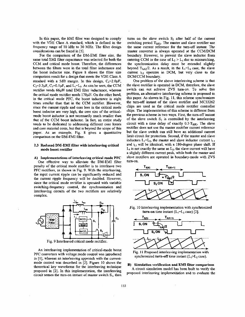
In this paper, the EM1 filter was designed to comply with the VDE Class A standard, which is defined in the frequency range of 10 kHz to 30 MHz. The filter design considerations can be found in [5].
For the comparison of the DM-EM1 filter size, the same total EM1 filter capacitance was selected for both the CCM and critical mode boost. Therefore, the differences between the filters were in the total filter inductance and the boost inductor size. Figure 8 shows the filter size comparison result for a design that meets the VDE Class A standard with a 5dB margin. In this design, CI=2.0pF, C2=3.3pF, C3=0.1pF, and LI=L2. As can be seen, the CCM rectifier needs 66pH total EM1 filter inductance, whereas the critical mode rectifier needs 170pH. On the other hand, in the critical mode PFC, the boost inductance is eight times smaller than that in the CCM rectifier. However, since the current ripple and core loss in the critical mode boost inductor are very high, the core size of the critical- mode boost inductor is not necessarily much smaller than that of the CCM boost inductor. In fact, an entire study needs to be dedicated to addressing different core losses and core material costs, but that is beyond the scope of this paper. As an example, Fig. 8 gives a quantitative comparison on the DM-EM1 filter.
2.3 Reduced DM-EM1 filter with interleaving critical mode boost rectifier
A) Implementations of interleaving critical mode PFC One effective way to alleviate the DM-EM1 filter
penalty of the critical mode rectifier is to interleave two PFC rectifiers, as shown in Fig. 9. With the interleaving, the input current ripple can be significantly reduced and the current ripple frequency will be doubled. However, since the critical mode rectifier is operated with variable switching-frequency control, the synchronization and interleaving circuits of the two rectifiers are relatively
1.. T Fig. 9 Interleaved critical mode rectifier.
An interleaving implementation of critical-mode boost PFC converters with voltage mode control was introduced in [ 11, whereas an interleaving approach with the current- mode control was described in [2]. Figure 10 shows the theoretical key waveforms for the interleaving technique proposed in [2]. In this implementation, the interleaving circuit senses the turn-on instant of master switch S1, then
turns on the slave switch Sz after half of the current switchmg period TqK). The master and slave rectifier use the same current reference for the turn-off instant. The master converter is always operated at the CCM/DCM boundary. However, to prevent the slave inductor from entering CCM in the case of Lz > LI due to mismatching, the synchronization delay must be extended slightly beyond T ~ ( ~ j 2 . As a result, in the Ll=L2 case, the slave current iL2 operates in DCM, but very close to the DCWCCM boundary.
One problem of the above interleaving scheme is that the slave rectifier is operated in DCM, therefore, the slave switch can not achieve ZVS turn-on. To solve this problem, an alternative interleaving scheme is proposed in this paper. As shown in Fig. 11, this scheme synchronizes the turn-off instant of the slave rectifier and MC33262 chips are used as the critical mode rectifier controller chips. The implementation of this scheme is different from the previous scheme in two ways. First, the turn-off instant of the slave switch S2 is controlled by the interleaving circuit with a time delay of exactly 0.5.Ts,~). The slave rectifier does not use the master rectifier current reference but the slave switch can still have an additional current limit circuit for protection. Second, if the master and slave inductors Ll=L2, the master and slave inductor current iL1 and iLI will be identical, with a 180-degree phase shift. If LI is not exactly the same as L2, the slave current will have a slightly different current peak, while both the master and slave rectifiers are operated in boundary-mode with ZVS turn-on.
L
'Fig. 10 Interleaving implementation with synchronized turn-on time instant (Ll=L2 case) [2].
~ TS(K) )f TS(K+l)
Fig. 11 Proposed interleaving implementation with synchronized turn-off time instant (LpLz case).
B) Simulation verification and EM1 filter comparison A circuit simulation model has been built to verify the
proposed interleaving implementation and to evaluate the
133
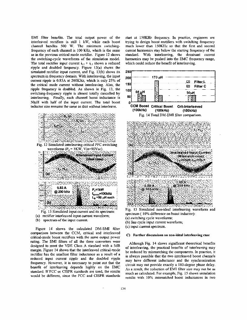
EM1 filter benefits. The total output power of the interleaved rectifiers is still 1 kW, while each boost channel handles 500 W. The minimum switching- frequency of each channel is 100 kHz, which is the same as in the previous critical mode rectifier. Figure 12 shows the switching-cycle waveforms of the simulation model. The total rectifier input current iLI + iL1 shows a reduced ripple and doubled frequency. Figure 13(a) shows the simulated rectifier input current, and Fig. 13(b) shows its spectrum in frequency domain. With interleaving, the input current ripple is 0.83A at 200KHz, which is only 25% of the critical mode current without interleaving. Also, the ripple frequency is doubled. As shown in Fig. 13, the switching-frequency ripple is almost totally cancelled by interleaving. Finally, each channel boost inductance is 50pH with half of the input current. The total boost inductor size remains the same as that without interleave.
Fig. 12Simulated interleaving cntical PFC swtching
Fig. 13 Simulated input current and its spectrum: (a) rectifier interleaved input current waveform; (b) spectrum of the input current.
Figure 14 shows the calculated DM-EM1 filter comparison between the CCM, critical and interleaved critical-mode boost rectifiers with the same output power rating. The EM1 filters of all the three converters were designed to meet the VDE Class A standard with a 5dB margin. Figure 14 shows that the interleaved critical-mode rectifier has the smallest filter inductance as a result of a reduced input current ripple and the doubled ripple frequency. However, it is necessary to point out that the benefit of interleaving depends highly on the EMC standard. If FCC or CISPR standards are used, the results would be different. since the FCC and CISPR standards
start at 150KHz frequency. In practice, engineers are trying to design boost rectifiers with switching frequency much lower than 15OKHz so that the first and second current harmonics stay below the starting frequency of the standard. With interleaving, the dominant current harmonics may be pushed into the EMC frequency range, which could reduce the benefit of interleaving.
20 170 pH
CCM Boost Critical Boost Crit-Interleaved
Fig. 14 Total DM-EM1 filter comparison. (1OOkHz) (100kHz) (1OOkHz)
Interleaved Input Current (Mismatch case) L,,=45pH, L,p55pH
Fig. 15 Simulated non-ideal interleaving waveform and spectrum ( 10% difference on boost inductor): (a) switchng cycle waveforms; (b) line cycle input current waveform; (c) input current spectrum.
C) Further discussions on non-ideal interleaving case
Although Fig. 14 shows significant theoretical benefits of interleaving, the practical benefits of interleaving may be reduced by mismatching the components. In practice, it is always possible that the two interleaved boost channels may have different inductance and the synchronization circuit may not provide exactly a 180-degree phase delay. As a result, the reduction of EM1 filter size may not be as much as calculated. For example, Fig. 15 shows simulation results with 10% mismatched boost inductances in two
134
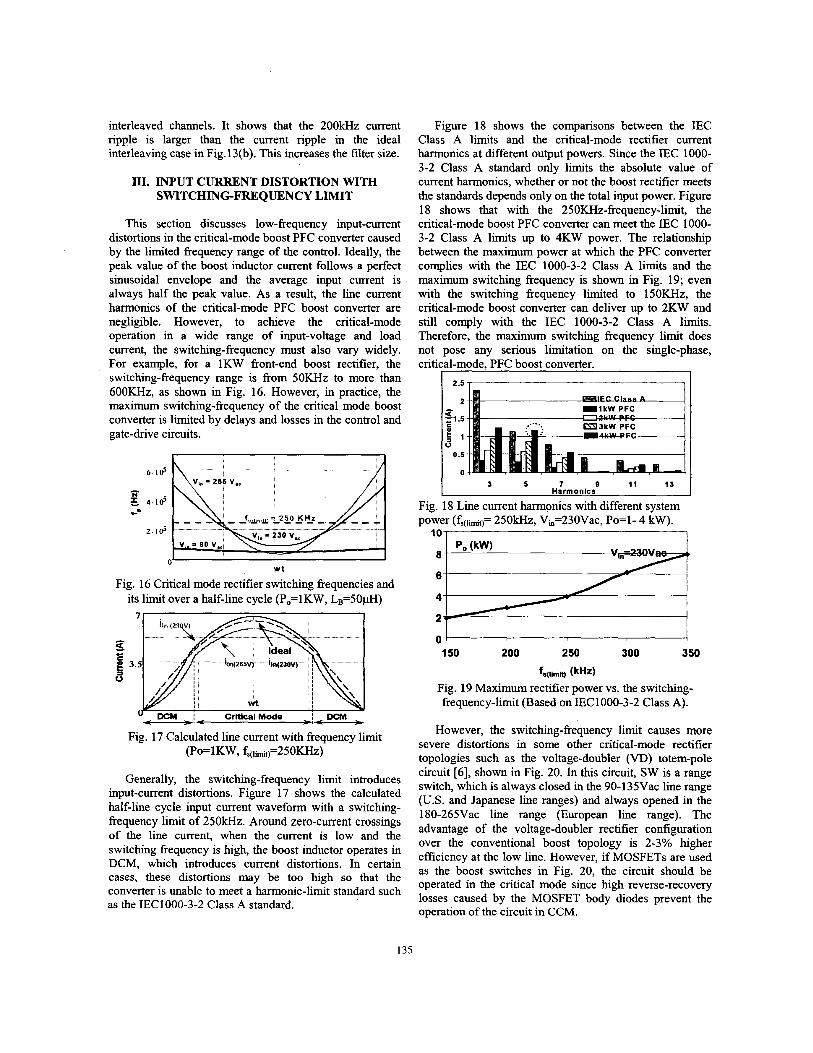
interleaved channels. It shows that the 200kHz current ripple is larger than the current ripple in the ideal interleaving case in Fig. 13(b). This increases the filter size.
111. INPUT CURRENT DISTORTION WITH SWITCHING-FREQUENCY LIMIT
This section discusses low-frequency input-current distortions in the critical-mode boost PFC converter caused by the limited frequency range of the control. Ideally, the peak value of the boost inductor current follows a perfect sinusoidal envelope and the average input current is always half the peak value. As a result, the line current harmonics of the critical-mode PFC boost converter are negligible. However, to achieve the critical-mode operation in a wide range of input-voltage and load current, the switching-frequency must also vary widely. For example, for a 1KW front-end boost rectifier, the switchmg-frequency range is from 5OKHz to more than 600KHz, as shown in Fig. 16. However, in practice, the maximum switching-frequency of the critical mode boost converter is limited by delays and losses in the control and gate-drive circuits.
~ ____
. . .... .._ 6 . 1 6
'i5 I, 4 . 1 6 r-
2 - I d
0- w t
Fig. 16 Critical mode rectifier switching frequencies and its limit over a half-line cycle (P,=lKW, LB=50pH)
Fig. 17 Calculated line current with frequency limit (Po=l KW, f,(li,,,it)=2 SOKHZ)
Generally, the switching-frequency limit introduces input-current distortions. Figure 17 shows the calculated half-line cycle input current waveform with a switching- frequency limit of 250kHz. Around zero-current crossings of the line current, when the current is low and the switching frequency is high, the boost inductor operates in DCM, which introduces current distortions. In certain cases, these distortions may be too high so that the converter is unable to meet a harmonic-limit standard such as the IEC1000-3-2 Class A standard.
Figure 18 shows the comparisons between the IEC Class A limits and the critical-mode rectifier current harmonics at different output powers. Since the IEC 1000- 3-2 Class A standard only limits the absolute value of current harmonics, whether or not the boost rectifier meets the standards depends only on the total input power. Figure 18 shows that with the 250KHz-frequency-limit, the critical-mode boost PFC converter can meet the IEC 1000- 3-2 Class A limits up to 4KW power. The relationship between the maximum power at which the PFC converter complies with the IEC 1000-3-2 Class A limits and the maximum switching frequency is shown in Fig. 19; even with the switching frequency limited to 150KHz, the critical-mode boost converter can deliver up to 2KW and still comply with the IEC 1000-3-2 Class A limits. Therefore, the maximum switching frequency limit does not pose any serious limitation on the single-phase, critical-mode, PFC boost converter.
I I I 2.5r I I
2
g1 .5
g 1 G 0.5
0
3 5 7 9 11 13 Harmonics
Fig. 18 Line current harmonics with different system power (fscli~t)= 250kHz, Vb=230Vac, Po=l- 4 kW).
1oT
I 4- i
I
I 1
150 200 250 300 350
fS(i,") ( k W Fig. 19 Maximum rectifier power vs. the switching- frequency-limit (Based on IEC1000-3-2 Class A).
However, the switching-frequency limit causes more severe distortions in some other critical-mode rectifier topologies such as the voltage-doubler (VD) totem-pole circuit [6], shown in Fig. 20. In th~s circuit, SW is a range switch, which is always closed in the 90-135Vac line range (U.S. and Japanese line ranges) and always opened in the 180-265Vac line range (European line range). The advantage of the voltage-doubler rectifier configuration over the conventional boost topology is 2-3% higher efficiency at the low line. However, if MOSFETs are used as the boost switches in Fig. 20, the circuit should be operated in the critical mode since high reverse-recovery losses caused by the MOSFET body diodes prevent the operation of the circuit in CCM.
135
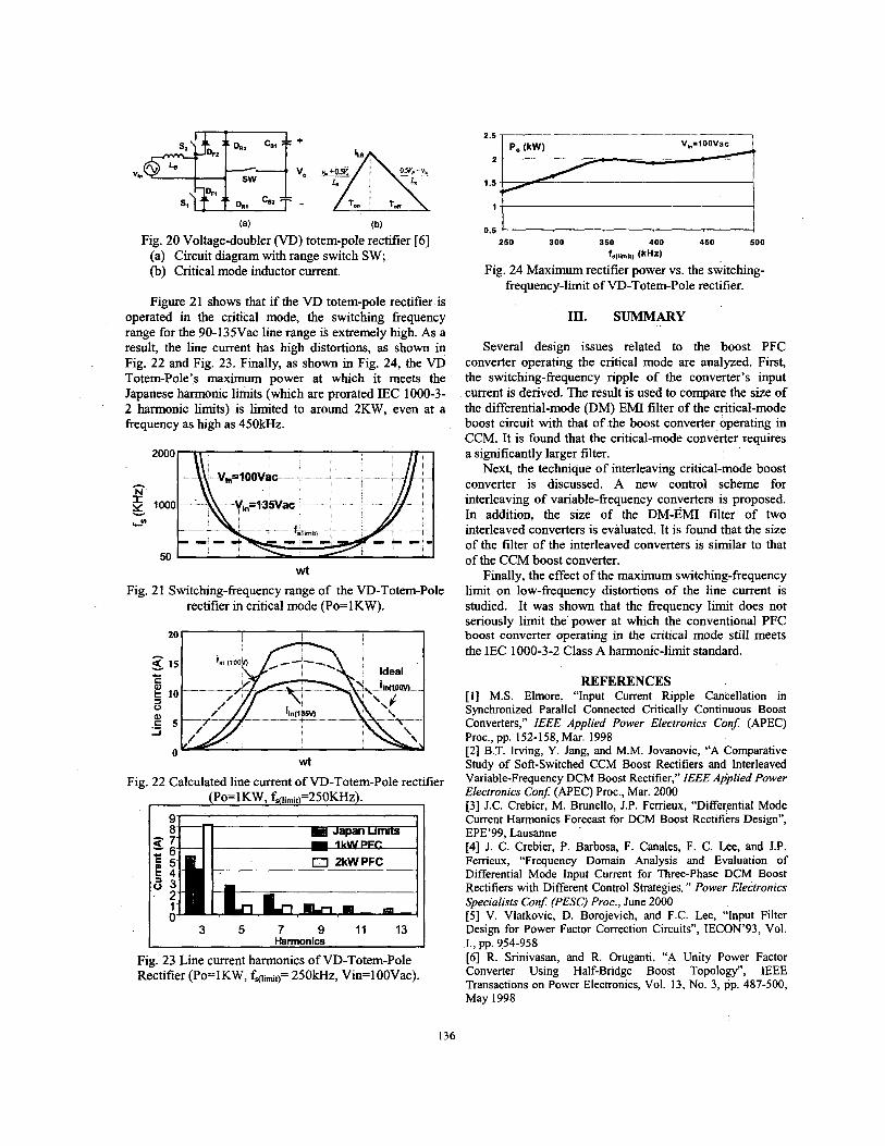
(a) (b)
(a) Circuit diagram with range switch SW; (b) Critical mode inductor current.
Fig. 20 Voltage-doubler (VD) totem-pole rectifier [6]
.
Figure 21 shows that if the VD totem-pole rectifier is operated in the critical mode, the switching frequency range for the 90-135Vac line range is extremely high. As a result, the line current has high distortions, as shown in Fig. 22 and Fig. 23. Finally, as shown in Fig. 24, the VD Totem-Pole’s maximum power at which it meets the Japanese harmonic limits (which are prorated IEC 1000-3- 2 harmonic limits) is limited to around 2KW, even at a frequency as high as 450kHz.
9 8
3; U
E45 a 3
2 1 0
3 5 7 9 1 1 1 3 Harmonics
wt Fig. 2 1 Switchmg-frequency range of the VD-Totem-Pole
rectifier in critical mode (Po=lKW).
,?U I I
0.5 ! I 250 300 350 400 450 500
f‘lll”it) ( k W
Fig. 24 Maximum rectifier power vs. the switchmg- frequency-limit of VD-Totem-Pole rectifier.
111. SUMMARY
Several design issues related to the boost PFC converter operating the critical mode are analyzed. First, the switching-frequency ripple of the converter’s input current is derived. The result is used to compare the size of the differential-mode (DM) EM1 filter of the critical-mode boost circuit with that of the boost converter operating in CCM. It is found that the critical-mode converter requires a significantly larger filter.
Next, the technique of interleaving critical-mode boost converter is discussed. A new control scheme for interleaving of variable-frequency converters is proposed. In addition, the size of the DM-EM1 filter of two interleaved converters is evaluated. It is found that the size of the filter of the interleaved converters is similar to that of the CCM boost converter.
Finally, the effect of the maximum switching-frequency limit on low-frequency distortions of the line current is studied. It was shown that the frequency limit does not seriously limit the power at which the conventional PFC boost converter operating in the critical mode still meets the IEC 1000-3-2 Class A harmonic-limit standard.
REFERENCES [ l ] M.S. Elmore, “Input Current Ripple Cancellation in Synchronized Parallel Connected Critically Continuous Boost Converters,” IEEE Applied Power Electronics ConJ (APEC) Proc., pp. 152-158, Mar. 1998 [2] B.T. Irving, Y. Jang, and M.M. Jovanovic, “A Comparative Study of Soft-Switched CCM Boost Rectifiers and Interleaved Variable-Frequency DCM Boost Rectifier,” IEEE Applied Power Electronics Con$ (APEC) Proc., Mar. 2000 [3] J.C. Crebier, M. Brunello, J.P. Ferrieux, “Differential Mode Current Harmonics Forecast for DCM Boost Rectifiers Design”, EPE’99, Lausanne [4] J. C. Crebier, P. Barbosa, F. Canales, F. C. Lee, and J.P. Femeux, “Frequency Domain Analysis and Evaluation of Differential Mode Input Current for Three-phase DCM Boost Rectifiers with Different Control Strategies, ” Power Electronics Specialists Con$ (PESC) Proc., June 2000 [5] V. Vlatkovic, D. Borojevich, and F.C. Lee, “Input Filter Design for Power Factor Correction Circuits”, IECON’93, Vol.
[6] R. Srinivasan, and R. Oruganti, “A Unity Power Factor Converter Using Half-Bridge Boost Topology”, IEEE Transactions on Power Electronics, Vol. 13, No. 3, pp. 487-500, May 1998
I., pp. 954-958
136


