Embed Size (px)
Citation preview
lable at ScienceDirect
Current Applied Physics 14 (2014) 1389e1395
Contents lists avai
Current Applied Physics
journal homepage: www.elsevier .com/locate/cap
Effect of thermal annealing on the ac impedanceof Co(75)/Al2O3
(2.3)/Co(5.0)/Al2O3(2.3)/Co(50) double-barrier MTJs
Nguyen Tuan Anh a, c, Nguyen Anh Tuan a, *, Nguyen Tuyet Nga b, Nguyen Anh Tue b,Giap Van Cuong a, d
a International Training Institute for Materials Science (ITIMS), 1 Dai Co Viet Road, Hai Ba Trung District, Hanoi 10000, Viet Namb Institute of Engineering Physics (IEP), Hanoi University of Science and Technology (HUST), 1 Dai Co Viet Road, Hai Ba Trung District, Hanoi 10000,Viet namc Hanoi Community College (HCC), 102 Trung Kinh Road, Dong Da District, Hanoi 10000, Viet namd HungYen University of Technology and Education (UTEHY), Khoai Chau, Hung Yen 30009, Viet nam
a r t i c l e i n f o
Article history:Received 20 March 2014Received in revised form18 June 2014Accepted 12 August 2014Available online 21 August 2014
Keywords:Double-barrier magnetic tunnel junctionComplex impedance spectroscopyNyquist plotac Impedance responseDouble-capacitor structure
* Corresponding author.E-mail addresses: [email protected], tuan.nguyen
http://dx.doi.org/10.1016/j.cap.2014.08.0051567-1739/© 2014 Elsevier B.V. All rights reserved.
a b s t r a c t
Double-barrier magnetic tunnel junctions (DBMTJs) were prepared from Co(75 nm)/Al2O3(2.3 nm)/Co(5 nm)/Al2O3(2.3 nm)/Co(50 nm) sputtering pentalayer films. The ac electrical properties of as-deposited DBMTJs and those annealed in a vacuum at 100e350 �C for 30 min were then investigatedusing a complex impedance spectroscopic technique. The ac impedance responses as a function ofannealing temperature were further analyzed based on Maxwell's layered dielectric barrier and MaxwelleWagner capacitor models after considering the DBMTJs as having double-capacitor-type structures. Theeffect of thermal annealing on the ac transport behavior of the DBMTJs was interpreted by examining theequivalent electric circuits fitted to Nyquist plots of each different sample. The effects were found to bedue to changes in the structural characteristics in both bulk and interface morphologies of Co and Al2O3
layers. The structural morphology determined the different ac transport modes that occurred in theDBMTJs.
© 2014 Elsevier B.V. All rights reserved.
1. Introduction
Double-barrier magnetic tunnel junctions (DBMTJs) consistingof a ferromagnetic/isolator/ferromagnetic/isolator/ferromagneticpentalayer structure (FM/I/FM/I/FM) have recently receivedconsiderable interest [1e9] because of their potential applicationsin next-generation spintronic devices [10e15]. Like multilayeredmaterials, DBMTJs exist as heterojunction structures superposed byinhomogeneous resistive layers. To some extent, they are alsoconsidered as granular materials in which resistance betweengrains and grain boundaries is inhomogeneous. For these systems,the frequency-dependent response through ac signals, ac imped-ance, or complex impedance spectroscopy (CIS) is expressed with acomplex number Z(u) because of dephasing between the resultingcurrent and the applied voltage. For a long time, the CIS techniquehas been extensively used to study solid inhomogeneous resistivematerials [16,17]. The following are the main contributions of suchmaterials [17]: (i) intra-granular or bulk properties (i.e., high levelsof conductivity), (ii) inter-granular or grain boundary properties
[email protected] (N.A. Tuan).
(i.e., resistive grain boundary components and conducting cores),(iii) a combination of both inter and intra-granular properties, or(iv) surface properties. A multilayer thin film is then modeled as agranular system to analyze ac impedance data [18].
Recently, the CIS technique has also been widely applied toinvestigate single magnetic tunnel junctions (MTJs) [19e23].Important information on ac electrical properties such as behavioror processes in heterojunction structures, especially the interfacialand bulk characteristics or features of material layers in MTJs, canbe efficiently extracted with this technique. These data are notreadily available from dc or conventional and fixed-frequency acmeasurements [17]. However, studies on the dynamic propertiesand frequency-dependence transport in DBMTJs with the CIStechnique are limited. In the present work, we applied the CIStechnique to estimate the structure and study the behavior of the actransport of DBMTJs after they are annealed.
2. Theoretical overview
The fundamentals of impedance spectroscopy for the analysis ofCIS data can be found in references, such as [24] and [25] that had
N.T. Anh et al. / Current Applied Physics 14 (2014) 1389e13951390
provided professional and detailed attention and [16] and [17] thatexhibited significantly terse interests. To analyze and interpretexperimental CIS data, specific fundamentals of the impedancespectroscopy technique are briefly reviewed in this study using thesaid references. As known in the field of frequency technique, theoverall impedance Z of a medium under ac electric field with fre-quency u ¼ 2pf, in a complex expression, is written as
ZðuÞ ¼ Z0 þ iZ00; or Z ¼ ReZ þ iImZ; (1)
where i ¼ √�1, Z0 ≡ ReZ that represents the real part indicatingresistive response and Z00 ≡ ImZ that represents the imaginary partindicating reactive (capacitive and/or inductive) response. The realand imaginary parts, the impedance modulus jZj, and the phaseshift 4 can be expressed as follows:
ReZ ≡ Z0 ¼ jZjcos 4; ImZ ≡ Z00 ¼ jZjsin 4;
jZj ¼ffiffiffiffiffiffiffiffiffiffiffiffiffiffiffiffiffiffiffiffiffiffiffiffiffiffiffiffiffiffiffiffihðZ0Þ2 þ ðZ00Þ2
ir; 4 ðu Þ ¼ tan�1ðZ00=Z0Þ:
(2)
The complex conjugate of the impedance is
Z* ¼ Z0 � iZ00: (3)
Apart from the impedance Z, other complex quantities aregenerally called immitances, which include the complex admit-tance Y, the complex electric modulus M, and the complexpermittivity ε.
Y ¼ Y 0 þ iY 00; M ¼ M0 þ iM00; ε ¼ ε0 � iε00: (4)
Y (or A) is the inverse of Z, Y ¼ Z�1 and is sometimes calledcomplex conductance. The real component Y0 is known as theconductivity s (or conductance G(u)), and the imaginary compo-nent Y00 is known as the susceptance B(u) [16].M is the inverse of ε,M ¼ 1/ε, and the permittivity can be defined as the inverse of theelectric modulus, ε ¼ M�1.
In sum, the complex forms, which can be denoted generally byany of the four quantities that respond to CIS, may be expressed ineither rectangular or modulus forms.
I ¼ I0 þ iI00; or I ¼ jIjexpði4Þ: (5)
The complex conjugates of these forms are I* ¼ I0 e
iI00 ¼ jIjexp(ei4). Table 1 summarizes the interrelations between thefour immittance functions I [24]. The CIS technique includes thefrequency analysis of behaviors in ac impedance Z(u) or admittanceY(u), capacitance C(u), and inductance L(u) using suitable equiva-lent electric circuits.
A plot of �Z00 (�ImZ) versus Z0 (ReZ) is referred to as a Nyquistplot that indirectly involves a frequency response or plots of Z0,�Z00,jZj and 4 versus u (or f) (referred to as the Bode diagram), whichdirectly express frequency response. Each Nyquist plot correspondswith an equivalent electric circuit (EEC) model fitted with relatedCIS data of a measuring sample. The EECs demonstrate the realistic
Table 1Relations between the four basic immittance functions [24].
M Z Y ε
M M (iuCc)Z (iuCc)Y�1ε�1
Z (iuCc)�1M Z Y�1 (iuCc) �1ε�1
Y (iuCc)M�1 Z�1 Y (iuCc)εε M�1 (iuCc)�1Z�1 (iuCc)�1Y ε
Where Cc ¼ ε0Ac/d, the capacitance of the empty measuring network of electrodearea Ac and electrode separation length d, ε0 ¼ 8.854 � 10�12 F/m, the dielectricpermittivity of free space.
electrical properties of the samples, while the related Nyquist plotsshow distinctive features for certain combinations of EEC elements.The frequency-dependent impedance of a pure capacitor (withohmic contacts) can be written as
Z ðuÞ ¼ �i=ðuCÞ ¼ �i=ð2pfCÞ: (6)
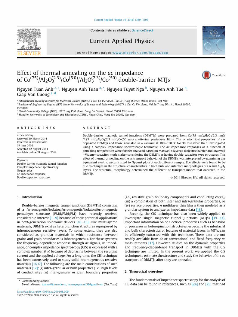
Considering that the structure of an MTJ is similar to that of ametal-insulator-metal capacitor, a simple parallel network (RC) (seeFig. 1(a)) is employed in this structural model. The related Nyquistplot is in the form of a complete semi-circle exposed at a single timeconstant t¼ RC. This constant is the dielectric relaxation time of theinsulator material whose bulk properties are depicted by R and Celements in resistance and capacitance. The dielectric loss of thedielectric material layer is represented by these elements. There-fore, physical phenomena or reactions that occur in the describedsystem have a single-valued time constant. The impedance for the(RC) circuit is
Z ðu Þ ¼ R1þ iuRC
¼ R
1þ ðuRCÞ2� i
uR2 C
1þ ðuRCÞ2
¼�
R
1þ u2t2
�� i�
uRt
1þ u2t2
�:
(7)
Considering the contributions from uncompensated resistancesor a representation of a polarizable electrode or an irreversibleelectrode process, a component R0 should be added to connect inseries to the bulk parallel (R1C1) network (see Fig. 1(b) in which thesymbol of related circuit is R0(R1C1)). This network has beenreferred to as the Randles circuit. The impedance response of thiscircuit is expressed as follows:
Z ðu Þ ¼ R0 þR1
1þ iuR1C1
¼ R0 þR1
1þ ðuR1C1Þ2� i
uR21C11þ ðuR1C1Þ2
¼ R0 þ
R11þ u2t21
!� i
uR1t1
1þ u2t21
!;
(8)
where t1 ¼ R1C1. A typical characteristic of the previouslymentioned EECs (Fig. 1(a) and (b)) is a single time constant-type
Fig. 1. Basic networks for EECs in CIS analysis and related symbols: (a) A simple par-allel circuit: (RC); (b) a typical Randles circuit: R0(R1C1); (c) a circuit modified from thecircuit of (b) due to electrode reaction: R0(C1R1(R2C2)); (d) a circuit modified from thecircuit of (c) by distributed elements (constant phase element, CPE):R0(ZCPE1R1(R2ZCPE2); (e) a pseudo-Randles circuit: R0(R1ZCPE).
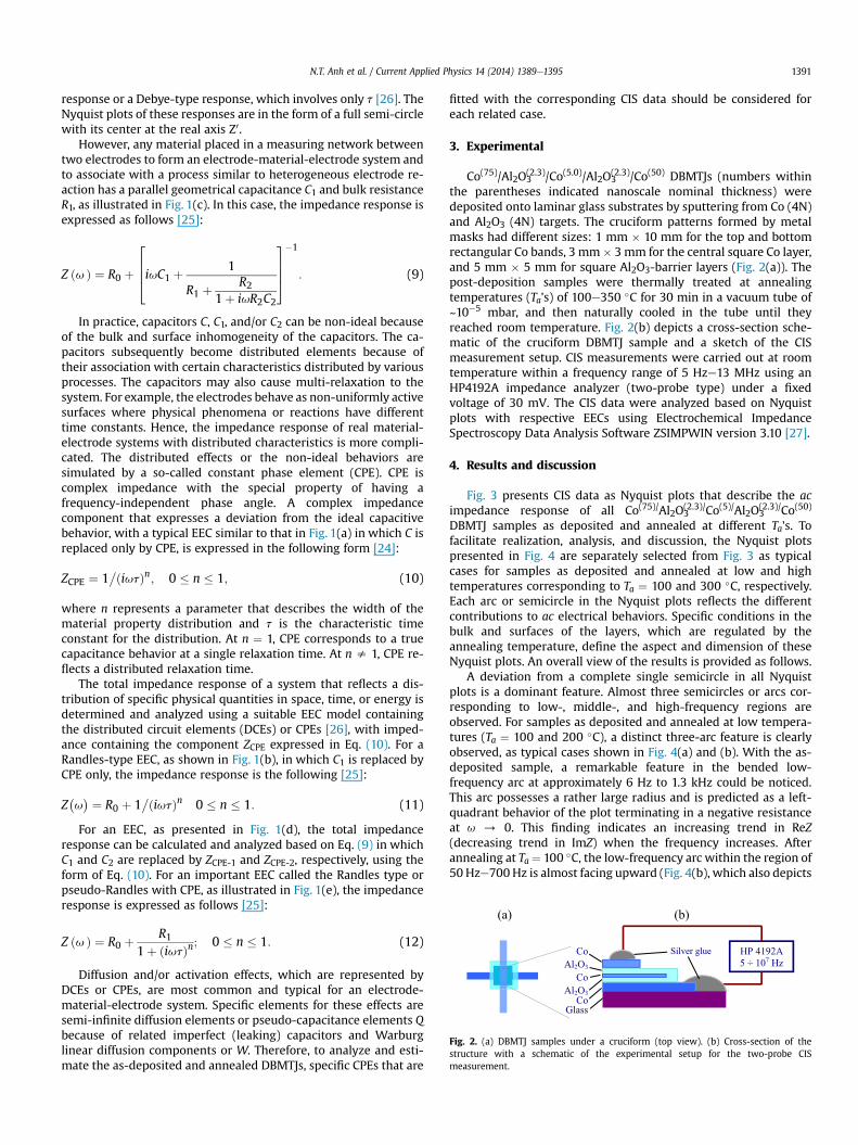
Fig. 2. (a) DBMTJ samples under a cruciform (top view). (b) Cross-section of thestructure with a schematic of the experimental setup for the two-probe CISmeasurement.
N.T. Anh et al. / Current Applied Physics 14 (2014) 1389e1395 1391
response or a Debye-type response, which involves only t [26]. TheNyquist plots of these responses are in the form of a full semi-circlewith its center at the real axis Z0.
However, any material placed in a measuring network betweentwo electrodes to form an electrode-material-electrode system andto associate with a process similar to heterogeneous electrode re-action has a parallel geometrical capacitance C1 and bulk resistanceR1, as illustrated in Fig. 1(c). In this case, the impedance response isexpressed as follows [25]:
Z ðu Þ ¼ R0 þ
2664iuC1 þ 1
R1 þR2
1þ iuR2C2
3775�1
: (9)
In practice, capacitors C, C1, and/or C2 can be non-ideal becauseof the bulk and surface inhomogeneity of the capacitors. The ca-pacitors subsequently become distributed elements because oftheir association with certain characteristics distributed by variousprocesses. The capacitors may also cause multi-relaxation to thesystem. For example, the electrodes behave as non-uniformly activesurfaces where physical phenomena or reactions have differenttime constants. Hence, the impedance response of real material-electrode systems with distributed characteristics is more compli-cated. The distributed effects or the non-ideal behaviors aresimulated by a so-called constant phase element (CPE). CPE iscomplex impedance with the special property of having afrequency-independent phase angle. A complex impedancecomponent that expresses a deviation from the ideal capacitivebehavior, with a typical EEC similar to that in Fig. 1(a) in which C isreplaced only by CPE, is expressed in the following form [24]:
ZCPE ¼ 1�ðiutÞn; 0 � n � 1; (10)
where n represents a parameter that describes the width of thematerial property distribution and t is the characteristic timeconstant for the distribution. At n ¼ 1, CPE corresponds to a truecapacitance behavior at a single relaxation time. At n s 1, CPE re-flects a distributed relaxation time.
The total impedance response of a system that reflects a dis-tribution of specific physical quantities in space, time, or energy isdetermined and analyzed using a suitable EEC model containingthe distributed circuit elements (DCEs) or CPEs [26], with imped-ance containing the component ZCPE expressed in Eq. (10). For aRandles-type EEC, as shown in Fig. 1(b), in which C1 is replaced byCPE only, the impedance response is the following [25]:
Z�u� ¼ R0 þ 1
�ðiutÞn 0 � n � 1: (11)
For an EEC, as presented in Fig. 1(d), the total impedanceresponse can be calculated and analyzed based on Eq. (9) in whichC1 and C2 are replaced by ZCPE-1 and ZCPE-2, respectively, using theform of Eq. (10). For an important EEC called the Randles type orpseudo-Randles with CPE, as illustrated in Fig. 1(e), the impedanceresponse is expressed as follows [25]:
Z ðu Þ ¼ R0 þR1
1þ ðiutÞn; 0 � n � 1: (12)
Diffusion and/or activation effects, which are represented byDCEs or CPEs, are most common and typical for an electrode-material-electrode system. Specific elements for these effects aresemi-infinite diffusion elements or pseudo-capacitance elements Qbecause of related imperfect (leaking) capacitors and Warburglinear diffusion components or W. Therefore, to analyze and esti-mate the as-deposited and annealed DBMTJs, specific CPEs that are
fitted with the corresponding CIS data should be considered foreach related case.
3. Experimental
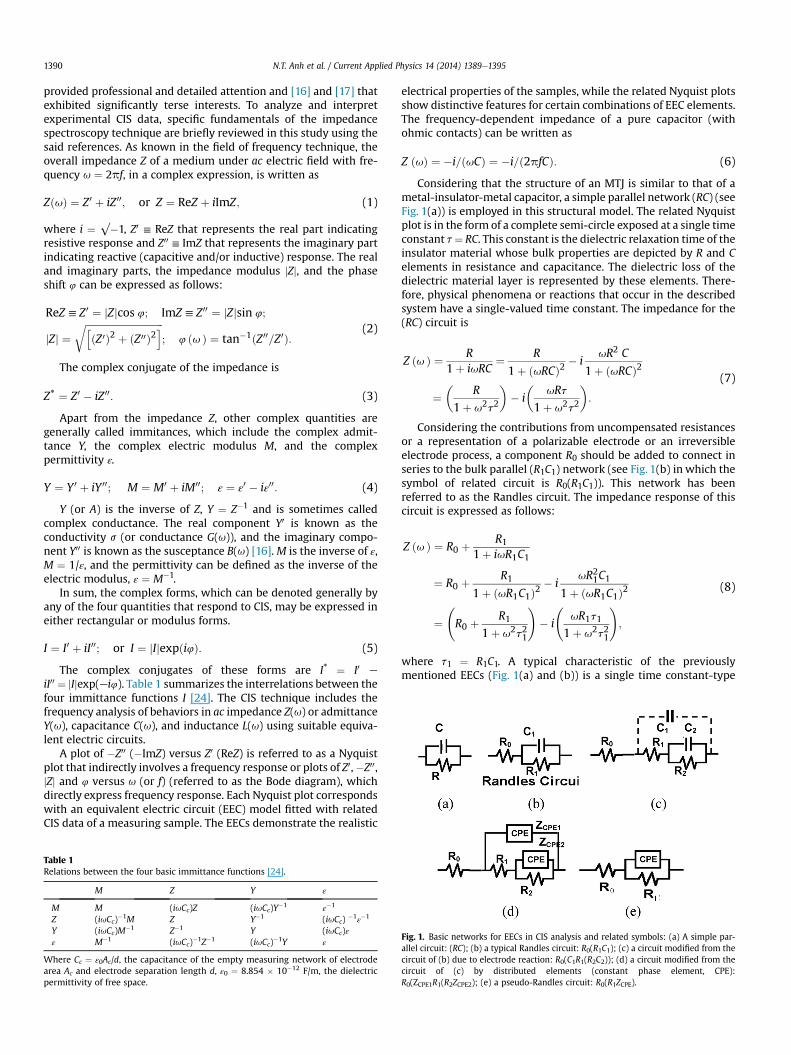
Co(75)/Al2O3(2.3)/Co(5.0)/Al2O3
(2.3)/Co(50) DBMTJs (numbers withinthe parentheses indicated nanoscale nominal thickness) weredeposited onto laminar glass substrates by sputtering from Co (4N)and Al2O3 (4N) targets. The cruciform patterns formed by metalmasks had different sizes: 1 mm � 10 mm for the top and bottomrectangular Co bands, 3 mm� 3mm for the central square Co layer,and 5 mm � 5 mm for square Al2O3-barrier layers (Fig. 2(a)). Thepost-deposition samples were thermally treated at annealingtemperatures (Ta's) of 100e350 �C for 30 min in a vacuum tube of~10�5 mbar, and then naturally cooled in the tube until theyreached room temperature. Fig. 2(b) depicts a cross-section sche-matic of the cruciform DBMTJ sample and a sketch of the CISmeasurement setup. CIS measurements were carried out at roomtemperature within a frequency range of 5 Hze13 MHz using anHP4192A impedance analyzer (two-probe type) under a fixedvoltage of 30 mV. The CIS data were analyzed based on Nyquistplots with respective EECs using Electrochemical ImpedanceSpectroscopy Data Analysis Software ZSIMPWIN version 3.10 [27].
4. Results and discussion
Fig. 3 presents CIS data as Nyquist plots that describe the acimpedance response of all Co(75)/Al2O3
(2.3)/Co(5)/Al2O3(2.3)/Co(50)
DBMTJ samples as deposited and annealed at different Ta's. Tofacilitate realization, analysis, and discussion, the Nyquist plotspresented in Fig. 4 are separately selected from Fig. 3 as typicalcases for samples as deposited and annealed at low and hightemperatures corresponding to Ta ¼ 100 and 300 �C, respectively.Each arc or semicircle in the Nyquist plots reflects the differentcontributions to ac electrical behaviors. Specific conditions in thebulk and surfaces of the layers, which are regulated by theannealing temperature, define the aspect and dimension of theseNyquist plots. An overall view of the results is provided as follows.
A deviation from a complete single semicircle in all Nyquistplots is a dominant feature. Almost three semicircles or arcs cor-responding to low-, middle-, and high-frequency regions areobserved. For samples as deposited and annealed at low tempera-tures (Ta ¼ 100 and 200 �C), a distinct three-arc feature is clearlyobserved, as typical cases shown in Fig. 4(a) and (b). With the as-deposited sample, a remarkable feature in the bended low-frequency arc at approximately 6 Hz to 1.3 kHz could be noticed.This arc possesses a rather large radius and is predicted as a left-quadrant behavior of the plot terminating in a negative resistanceat u / 0. This finding indicates an increasing trend in ReZ(decreasing trend in ImZ) when the frequency increases. Afterannealing at Ta¼ 100 �C, the low-frequency arc within the region of50 Hze700 Hz is almost facing upward (Fig. 4(b), which also depicts
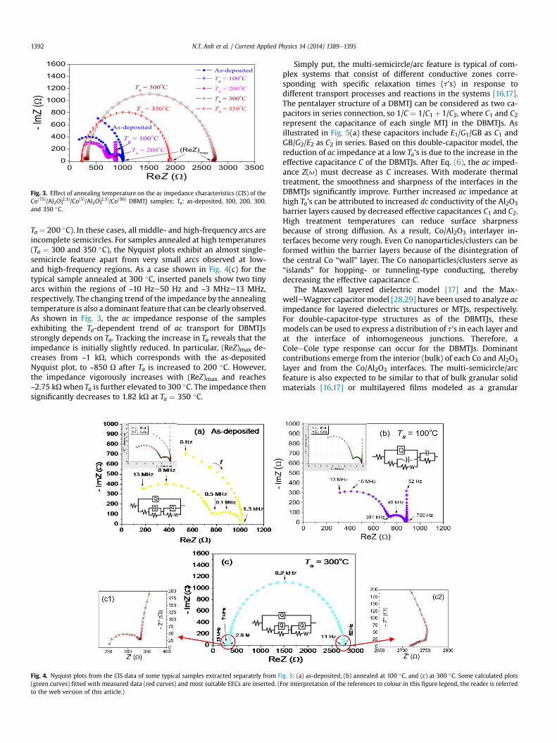
Fig. 3. Effect of annealing temperature on the ac impedance characteristics (CIS) of theCo(75)/Al2O3
(2.3)/Co(5)/Al2O3(2.3)/Co(50) DBMTJ samples; Ta: as-deposited, 100, 200, 300,
and 350 �C.
N.T. Anh et al. / Current Applied Physics 14 (2014) 1389e13951392
Ta ¼ 200 �C). In these cases, all middle- and high-frequency arcs areincomplete semicircles. For samples annealed at high temperatures(Ta ¼ 300 and 350 �C), the Nyquist plots exhibit an almost single-semicircle feature apart from very small arcs observed at low-and high-frequency regions. As a case shown in Fig. 4(c) for thetypical sample annealed at 300 �C, inserted panels show two tinyarcs within the regions of ~10 Hze50 Hz and ~3 MHze13 MHz,respectively. The changing trend of the impedance by the annealingtemperature is also a dominant feature that can be clearly observed.As shown in Fig. 3, the ac impedance response of the samplesexhibiting the Ta-dependent trend of ac transport for DBMTJsstrongly depends on Ta. Tracking the increase in Ta reveals that theimpedance is initially slightly reduced. In particular, (ReZ)max de-creases from ~1 kU, which corresponds with the as-depositedNyquist plot, to ~850 U after Ta is increased to 200 �C. However,the impedance vigorously increases with (ReZ)max and reaches~2.75 kUwhen Ta is further elevated to 300 �C. The impedance thensignificantly decreases to 1.82 kU at Ta ¼ 350 �C.
Fig. 4. Nyquist plots from the CIS data of some typical samples extracted separately from F(green curves) fitted with measured data (red curves) and most suitable EECs are inserted. (Fto the web version of this article.)
Simply put, the multi-semicircle/arc feature is typical of com-plex systems that consist of different conductive zones corre-sponding with specific relaxation times (t's) in response todifferent transport processes and reactions in the systems [16,17].The pentalayer structure of a DBMTJ can be considered as two ca-pacitors in series connection, so 1/C ¼ 1/C1 þ1/C2, where C1 and C2represent the capacitance of each single MTJ in the DBMTJs. Asillustrated in Fig. 5(a) these capacitors include E1/G1/GB as C1 andGB/G2/E2 as C2 in series. Based on this double-capacitor model, thereduction of ac impedance at a low Ta's is due to the increase in theeffective capacitance C of the DBMTJs. After Eq. (6), the ac imped-ance Z(u) must decrease as C increases. With moderate thermaltreatment, the smoothness and sharpness of the interfaces in theDBMTJs significantly improve. Further increased ac impedance athigh Ta's can be attributed to increased dc conductivity of the Al2O3barrier layers caused by decreased effective capacitances C1 and C2.High treatment temperatures can reduce surface sharpnessbecause of strong diffusion. As a result, Co/Al2O3 interlayer in-terfaces become very rough. Even Co nanoparticles/clusters can beformed within the barrier layers because of the disintegration ofthe central Co “wall” layer. The Co nanoparticles/clusters serve as“islands” for hopping- or tunneling-type conducting, therebydecreasing the effective capacitance C.
The Maxwell layered dielectric model [17] and the Max-welleWagner capacitor model [28,29] have been used to analyze acimpedance for layered dielectric structures or MTJs, respectively.For double-capacitor-type structures as of the DBMTJs, thesemodels can be used to express a distribution of t's in each layer andat the interface of inhomogeneous junctions. Therefore, aColeeCole type response can occur for the DBMTJs. Dominantcontributions emerge from the interior (bulk) of each Co and Al2O3layer and from the Co/Al2O3 interfaces. The multi-semicircle/arcfeature is also expected to be similar to that of bulk granular solidmaterials [16,17] or multilayered films modeled as a granular
ig. 3: (a) as-deposited, (b) annealed at 100 �C, and (c) at 300 �C. Some calculated plotsor interpretation of the references to colour in this figure legend, the reader is referred
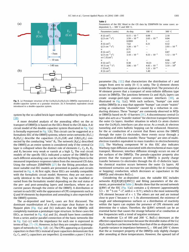
Fig. 5. (a) Pentalayer structure of the Co/Al2O3/Co/Al2O3/Co DBMTJs represented as adouble-capacitor system or a granular structure. (b) A formalistic equivalent circuitintroduced to a double-capacitor system.
Table 2Parameters of the EEC fitted to the CIS data by ZSIMPWIN for some cases: as-deposited, Ta ¼ 100 �C and 300 �C.
Parameters (units) As-dep. 100 �C 300 �C
R (U cm2) 0.15 � 10�3 0.99 2.18Q (S cm�2 sn) 2.59 � 10�9 2.63 � 10�9 0.04n 0.9991 1 <<1R (U cm2) 7.62 6.31 0.32Q (S cm�2 sn) 3.28 � 10�5 e 2.93 � 10�8
n 0.71 e 1R (U cm2) 2.41 e 0.87Q (S cm�2 sn)or C (F/cm2)
3.18 � 10�3 9.33 � 10�3 1.12 � 10�6
n 1 e 0.96R (U cm2) 0.38 10.23 9.52 � 106
W (S cm�2 sn) 3.06 � 10�7 4.43 � 10�3 3.19 � 109
C (F/cm2) e 1.21 � 10�6 e
R (U cm2) e 1.49 e
N.T. Anh et al. / Current Applied Physics 14 (2014) 1389e1395 1393
system by the so-called brick-layer model modified by Ortega et al.[18].
A more detailed analysis of the annealing effect on the actransport of DBMTJs is based on the EECs fitted to the CIS data. A dccircuit model of the double-capacitor system illustrated in Fig. 5(a)is formally expressed in Fig. 5(b). This circuit can be suggested as aformalistic EEC of the DBMTJ systems, where series networks (R1C1)R3(R2C2) describe the capacitors (E1/G1/GB) and (GB/G2/E2) con-nected by the conducting “wire” R3. The network (R0C0) describedthe DBMTJ as an entire system is considered only if the central Colayer is collapsed when the distinct role of elements C1, C2, R1, R2,and R3 become very weak or vanish at a high Ta. The real circuitmodels of the specific EECs indicated a nature of the DBMTJs foreach different annealing case can be selected by fitting them to themeasured impedance responses taken from the measured CIS data.Using the software ZSIMPWIN [27] for the fitting procedure, themost suitable real EEC models are presented in panels and circuitsinserted in Fig. 4. At first sight, these EECs are notably compatiblewith the formalistic circuit model. However, they are not neces-sarily identical to the formalistic EEC. They can be modified orvaried from the formalistic model depending on the real status ofthe pre- and post-annealing layers and interfaces, where an accurrent passes through the entire of the DBMTJ. A distribution orvariant in each EECwith the appearance of CPE components such asQ andW elements by deposition and annealing is also expected forthe DBMTJ systems.
The as-deposited and low-Ta cases are first discussed. Thedominant manifestation of a three-arc-type clear feature in theNyquist plots (Fig. 4(a) and (b)) indicates that the DBMTJs stillcompletely maintain a pentalayer-type structure. In these cases theEECs, as inserted in Fig. 4(a) and (b), should have been combinedfrom a series and/or parallel connection of the basic networks likein Fig. 1(a)e(c) with the impedance for each one is expressed interms of Eqs. (7)e(9). However, in fact they are complex combining-types of networks in Fig. 1(d)e(e). The CPEs appearing as Q pseudo-capacitors in their EECs instead of pure capacitors demonstrate thatC0, C1, and C2 capacitors are imperfect. Q resembles a pure C if its n
parameter (Eq. (12)) that characterizes the distribution of t andranges from zero to unity (0e1) is unity. The Q element showninside the capacitors can appear as a leaking level. The presence of aW element proves that a transport of semi-infinite diffusion typeoccurs in DBMTJs. The junctions between Co and Al2O3 layers cancreate orange-peel-type convexoeconcave interfaces [30], asillustrated in Fig. 5(a)). With such surfaces, “humps” can existwithin DBMTJs in a way that opposite “humps” can create “waists”acting as conduction “channels” caused by a reduction in con-ducting distance. These “humps” are commonly observed in MTJsor DBMTJs based on AleO barriers [31]. A discontinuous central Colayer also acts as a “transfer station” for electron transport betweenthe outer Co layers. Another situation in which Co atom clustersnear the Co/Al2O3 interfaces can also occur. As a result, dc electrontunneling and even ballistic hopping can be enhanced. However,for the ac conduction of a current that flows across the DBMTJthrough the outer Co electrodes, these events occur through amechanism of diffusion transfer. These “humps” are sites of multi-electron transfers equivalent to mass transfers in electrochemistry[32]. The Warburg component W in this EEC also indicatesWarburg-type diffusion associated with electrochemical mass-typetransport. Moreover, interface diffusion strongly occurs on one ofthe surfaces of the DBMTJs. The pseudo-capacitor property alsoproves that the transport process in DBMTJs is purely chargetransfer between Co electrodes through the AleO dielectric layer.No chemical reaction occurs between the outer Co layers. Allmentioned scenarios can increase the possibility for dc (tunnelingor hopping) conduction, which decreases ac capacitance in theDBMTJs and elevates ReZ(u).
Considering the as-deposited case, the suitable EEC includesnetworks R(Q(R(QR)(Q(RW)))) and fitting parameters of the ele-ments, as presented inTable 2. Results show that the second networkQ(RW) of the EEC (Fig. 5(a)) contains a Q element (approximately3.3 � 10�5 S cm�2∙sn, with nz 0.71), which is the most noteworthyCPE element because of n < 1. The others are not and are insteadclose to pure C because n z 1. As aforementioned, the existence ofrough and inhomogeneous surfaces or a distribution of reactivitywithin the layers can explain the presence of CPE elements anddetermine the n values. Therefore, the Q(RW) network can be anessential factor that causes the strange behavior of ac conduction atlow frequencies with a trend of negative resistance.
At moderate Ta's of 100 and 200 �C, ReZ(u) decreases as theeffective capacitance increases because the desirable status of the Co/Al2O3 interfaces can becomebetter than that of the as-deposited case.A gentle variance in impedance between Ta ¼ 100 and 200 �C showsthat the ac transport property of the DBMTJs only slightly changesafter annealing at these temperatures. However, the upward tail of
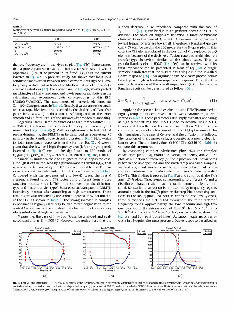
Table 3Parameters of network elements in a pseudo-Randles circuit (Fig.1(e)) at Ta¼ 300 �Cand 350 �C.
Ta 300 �C 350 �C
R1 (U cm2) 3.173 2.305Q (S cm�2 sn) 1.597 � 10�6 6.733 � 10�7
n 0.9391 0.9865R2 (U cm2) 24.3 16.63
N.T. Anh et al. / Current Applied Physics 14 (2014) 1389e13951394
the low-frequency arc in the Nyquist plot (Fig. 4(b)) demonstratesthat a pure capacitive network includes a resistor parallel with acapacitor (CR) must be present in its fitted EEC, as in the currentinserted in Fig. 4(b). A previous study has shown that for a solidconductor sandwiched between two electrodes, this sign of a low-frequency vertical tail indicates the blocking nature of the smoothelectrode interfaces [17]. The upper panel in Fig. 4(b) shows perfectmatching forall high-,medium-, and low-frequencyarcsbetween thecalculating and experiment plots corresponding to this EEC,R(Q(R(Q(RW))))(CR). The parameters of network elements forTa¼ 100 �C are presented inTable2.Notably,R values are rather small,whereas capacitive features (indicated by the similarity of C and Q topure C because n¼ 1) are dominant. This finding confirms the bettersmooth and uniform status of the surfaces after moderate annealing.
Regarding DBMTJ samples annealed at high temperatures (300or 350 �C), the Nyquist plots show a tendency to form nearly fullsemicircles (Figs. 3 and 4(c)). With a single-semicircle feature thatseems dominantly, the DBMTJ can be described as a one-stage RCnetwork in the Randles-type circuit illustrated in Fig. 1(b), to whichits total impedance response is in the form of Eq. (8). However,given that the low- and high-frequency arcs (left and right panelsinserted in Fig. 4(c)) can still be significant, an EEC model ofR(Q(R(QR) (Q(RW)))) for Ta ¼ 300 �C as inserted in Fig. 4(c) is noted.This model is similar to the one assigned to the as-deposited case,although it can be replaced by a pseudo-Randles circuit R(QR) thatis similar to the case of Ta ¼ 350 �C as mentioned below. The pa-rameters of network elements in this EEC are presented in Table 2.Compared with the as-deposited and low-Ta cases, the first Qelement is found to be a CPE factor quite different from a purecapacitor because n << 1. This finding proves that the diffusion-type and “mass transfer-type” features of ac transport in DBMTJsintensively increase after annealing at high temperatures. Thesefeatures are also reflected by the sudden increase in W parametersof the EEC, as shown in Table 2. The strong increase in compleximpedance in high-Ta cases may be due to the degradation of thecentral Co layer, as well as the drastic decline in smoothness at Co/Al2O3 interfaces at high temperatures.
Meanwhile, the case of Ta ¼ 350 �C can be analyzed and eval-uated similarly as Ta ¼ 300 �C. However, we notice here that the
Fig. 6. Real (Z0) and imaginary (�Z00) parts as a function of the frequency present in differentare indicated by dash red arrows) for the (a) as-deposited sample, (b) annealed at 100 �C, an(distribution) by guide-eye. (For interpretation of the references to colour in this figure leg
sudden decrease in ac impedance compared with the case ofTa ¼ 300 �C (Fig. 3) can be due to a significant decrease in CPE. Inaddition, the so-called single-arc behavior is more dominantlyobserved than the case of Ta ¼ 300 �C because the highest andlowest frequency arcs are too small. Therefore, a Randles-type cir-cuit R(CR) can be used in the EEC model for the Nyquist plot. In thiscase, the CPE element placed in the position of C is replaced by a Qelement because of the decisive diffusion-type and multi-electrontransfer-type behaviors similar to the above cases. Thus, apseudo-Randles circuit R(QR) (Fig. 1(e)) can be received with itstotal impedance can be presented in form of Eq. (12). A singlesemicircle indicates that the system has a single t in the so-calledDebye response [26]. This argument can be clearly proved belowby a typical single relaxation impedance response. Then, the fre-quency dependence of the overall impedance Z(u) of the pseudo-Randles circuit can be determined as follows [32]:
Z ¼ R1 þ1
1�R2 þ Y0ðiuÞn
; where Y0 ¼ Y*ðjuÞn: (13)
Applying the pseudo-Randles circuit to the DBMTJs annealed athigh Ta temperatures can reveal the network parameters, as pre-sented in Table 3. These parameters also imply that after annealingat high temperatures, the DBMTJs tend to become single MTJs.However, if this is the case, the barrier layer in these MTJs must be acomposite or granular structure of Co and Al2O3 because of thedisintegration of the central Co layer and the diffusion that follows.The function of this composite layer operates as a new dielectric-barrier layer. The obtained values Q(300 �C) > Q(350 �C) (Table 3)validate this argument.
By comparing complex admittance plots Y(u), the complexcapacitance plots C(u), module jZj versus frequency, and Z0, �Z00
plots as a function of frequency (all these plots are not shown here)between the as-deposited and the moderately annealed samples,we find a general similarity in the common behavior of ac re-sponses between the as-deposited and moderately annealedDBMTJs. This finding is proved in Fig. 6(a) and (b) through the Z0(f)and �Z00(f) plots. Three zones corresponding to different t's and adistributed characteristic in each relaxation zone are clearly indi-cated. Relaxation distribution is represented by frequency regionsaround a peak in the ImZ(f) plots or the step-like decreasing sec-tions in the ReZ(f) plots. For both as-deposited and low-Ta cases,three relaxations are distributed throughout the three differentfrequency zones. Approximately, the low, medium and high fre-quencies are in the intervals of (~1 Hze102 Hz), (5 � 103 Hz to5 � 106 Hz), and (3 � 105 Hze~108 Hz), respectively, as shown inFig. 6(a) and (b) (pink dotted lines). As known, each arc or semi-circle in a Nyquist plot must present a Debye response described as
relaxation zones that correspond to frequency intervals (whose peaks/inflection pointsd (c) annealed at 350 �C. Pink dot lines illustrate an evaluation of the relaxation zonesend, the reader is referred to the web version of this article.)
N.T. Anh et al. / Current Applied Physics 14 (2014) 1389e1395 1395
t for conduction in each certain zone/layer [33]. Thus, the aboveanalysis shows that in a double-capacitor system, the dominantmechanism is electron-charge transport through layers. However,this mechanism is distributed into the different Debye t's (multi-relaxation) because of the different conductivities of the bulk ofeach layer and the status of surfaces. The t's, which can be esti-mated from peaks in the ImZ(f) plots or from inflection points in theReZ(f) plots (at the middle of the step-like decrease) if ut ¼ 1, aretz 0.5, 10�5, and 10�7 s (pointed by red arrows). Once again, theseplots indicate that ac transport is improved by the decrease inimpedance caused bymoderate annealing. The plots also show thatthe feature of a pentalayer-type structure in the DBMTJs is stillmaintained. In the case of high-Ta, ReZ(f) and ImZ(f) plots indicate asingle-relaxation characteristic that implies a trilayer-type struc-ture of a single MTJ, as mentioned above. The relaxation distribu-tion is in the interval of (6� 102 Hz to 5�105 Hz) typically taken forTa ¼ 350 �C (Fig. 6(c)). In this case, t z 10�3 s can be estimated.
Finally, we emphasize that another approach based on thegrainegrain boundary (GeGB) model can be applied. In principle,DBMTJs can also be considered as special granular systems with agrainegrain boundary-type structure. Fig. 5(a) shows that Al2O3
layers can be regarded as grains G1 and G2 separated by the centralCo layer serving as grain boundary GB. These grains are insertedbetween electrodes E1 and E2 created by the outer Co layers. Thisapproach has been applied for long time by Bauerle [16] and Sin-clair [17] for real granular systems. According to the GeGB model,the contributions of each layer to ac impedance in DBMTJs canattributed to electrodes, grains, and grain boundaries.
5. Conclusions
In conclusion, we study the effect of thermal annealing on the acimpedance of DBMTJs using the Maxwell layered dielectric modeland the MaxwelleWagner capacitor model. The ac impedancestrongly and abnormally varies with annealing temperature as aresult of changes in the complexion of interfaces and within thebulk of layers. Diffusion processes occurring on the surfaces andwithin layers as a result of thermal annealing modify the structuraland physical features or the properties of DBMTJs. The importantfactors believed to explain the strong effects of thermal annealingare the roughness/smoothness of Co/Al2O3 interfaces, the structureand conductive mode of the central Co layer and Al2O3 dielectriclayers, as well as the dielectric properties of post-annealing barrierlayers defined by superfine granular behavior. Analysis based on CIStechnique shows that diffusion-type process, multi-electron-typetransport, and mass-type transfer are considered to be the mostdominant transport modes. Depending on Ta, an infinite-diffusiontype is prominent for the as-deposited and low-Ta cases. A mass-type transfer is assigned to the high-Ta cases.
Acknowledgments
This workwas supported by the National Foundation for Scienceand Technology Development (NAFOSTED) of Vietnam underProject Code 103.02.50.09 and a part of 103.02.2012.65.
References
[1] T. Nozaki, N. Tezuka, S. Sugimoto, K. Inomata, Appl. Phys. Lett. 86 (2005)082501;T. Nozaki, N. Tezuka, K. Inomata, Phys. Rev. Lett. 96 (2006) 027208.
[2] Lixian Jiang, Hiroshi Naganuma, Mikihiko Oogane, Yasuo Ando, Appl. Phys.Express 2 (2009) 083002.
[3] Tetsuya Uemura, Keisuke Sawada, Kenichi Matsuda, Masafumi Yamamoto,Appl. Phys. Lett. 95 (2009) 012502.
[4] A. Reinartz, J. Schmalhorst, G. Reiss, J. Appl. Phys. 105 (2009) 014510.[5] Kapsoo Yoon, Kiwoong Kim, Jahyun Koo, Jungyup Yang, Young Ho Do,
Junesik Kwak, Jinpyo Hong, IEEE Trans. Magn. 46 (2010) 7.[6] A.N. Useinov, J. Kosel, N.Kh. Useinov, L.R. Tagirov, Phys. Rev. B 84 (2011)
085424;A. Useinov, J. Kosel, IEEE Trans. Magn. 47 (2011) 2724.
[7] G.Q. Yu, Z. Diao, J.F. Feng, H. Kurt, X.F. Han, J.M.D. Coey, Appl. Phys. Lett. 98(2011) 112504.
[8] Ruisheng Liu, See-Hun Yang, Xin Jiang, Teya Topuria, Philip M. Rice,Charles Rettner, Stuart Parkin, Appl. Phys. Lett. 100 (2012) 012401.
[9] R.S. Liu, See-Hun Yang, Xin Jiang, X.-G. Zhang, Charles Rettner, Li Gao,Teya Topuria, Philip M. Rice, Weifeng Zhang, C.M. Canali, Stuart S.P. Parkin,Phys. Rev. B 87 (2013) 024411.
[10] K. Inomata, Y. Saito, K. Nakajima, M. Sagoi, J. Appl. Phys. 87 (2000) 6064.[11] J.H. Lee, In-Woo Chang, S.J. Byun, T.K. Hong, K. Rhie, W.Y. Lee, Kyung-Ho Shin,
Chanyong Hwang, S.S. Lee, B.C. Lee, J. Magn. Magn. Mater. 240 (2002) 137.[12] G. Rodary, M. Hehn, T. Dimopoulos, D. Lacour, J. Bangert, H. Jaffres,
F. Montaigne, F. Nguyen van Dau, F. Petroff, A. Schuhl, J. Wecker, J. Magn.Magn. Mater. 290-291 (2005) 1097.
[13] Sayeef Salahuddin, Supriyo Datta, Appl. Phys. Lett. 89 (2006) 153504.[14] A. Canizo Cabrera, Che-Hao Chang, Chih-Cheng Hsu, Ming-Chi Weng,
C.C. Chen, C.T. Chao, J.C. Wu, Yang-Hua Chang, Te-Ho Wu, IEEE Trans. Magn.43 (2007) 914.
[15] A. Iovan, S. Andersson, Yu.G. Naidyuk, A. Vedyaev, B. Dieny, V. Korenivski,Nano Lett. 8 (2008) 805.
[16] J.E. Bauerle, J. Phys. Chem. Solids 30 (1969) 2657.[17] C. Derek Sinclair, Bol. Soc. Esp. Ceram. Vidrio 34 (1995) 55.[18] N. Ortega, A. Kumar, P. Bhattacharya, S.B. Majumder, R.S. Katiyar, Phys. Rev. B
77 (2008) 014111.[19] J.C.A. Huang, C.Y. Hsu, Appl. Phys. Lett. 85 (2004) 5947.[20] J.C.A. Huang, C.Y. Hsu, J. Appl. Phys. 98 (2005) 064901;
C.Y. Hsu, J.C.A. Huang, IEEE Trans. Magn. 41 (2005) 3643.[21] P. Padhan, P. LeClair, A. Gupta, K. Tsunekawa, D.D. Djayaprawira, Appl. Phys.
Lett. 90 (2007) 14105;J.C.A. Huang, C.Y. Hsu, W.H. Chen, Y.H. Lee, IEEE Trans. Magn. 43 (2007) 911.
[22] Snorri Ingvarsson, Mustafa Arikan, Matthew Carter, Weifeng Shen, Gang Xiao,Appl. Phys. Lett. 96 (2010) 232506.
[23] Ming-Feng Kuo, Chao-Ming Fu, Xiu-Feng Han, Chia-Ou Chang, Chan-Shin Chou, J. Appl. Phys. 109 (2011) 07C718.
[24] E. Barsoukov, J. Ross Macdonald (Eds.), Impedance Spectroscopy Theory,Experiment, and Applications, second ed., a John Wiley & Sons, Inc., Publi-cation, Hoboken, New Jersey, 2005.
[25] M.E. Orazem, B. Tribollet, Electrochemical Impedance Spectroscopy, A JohnWiley & Sons, Inc., Publication, Hoboken, New Jersey, 2008.
[26] J.R. MacDonald, Ann. Biomed. Eng. 20 (1992) 289.[27] EChem software “ZSimpWin 3.10” by author Bruno Yeum, Copyright a 1999-
2002, released: November 1, 2002.[28] M.F. Gillies, A.E.T. Kuiper, R. Coehoorn, J.J.T.M. Donkers, J. Appl. Phys. 88 (2000)
429.[29] W.C. Chien, L.C. Hsieh, T.Y. Peng, C.K. Lo, Y.D. Yao, X.F. Han, P. Lin, IEEE Trans.
Magn. 43 (2007) 2812.[30] C.L. Platt, M.R. McCartney, F.T. Parker, A.E. Berkowitz, Phys. Rev. B 61 (2000)
9633.[31] J.Y. Hwang, S.Y. Lee, N.I. Lee, H.I. Yim, M.Y. Kim, W.C. Lee, J.R. Rhee, B.S. Chun,
T.W. Kim, Y.K. Kim, S.S. Lee, D.G. Hwang, E.J. Ri, IEEE Trans. Magn. 45 (2009)2396;L.F. Li, X.Y. Liu, G. Xiao, J. Appl. Phys. 93 (2003) 467.
[32] Bruno Yeum, ZSimpWin Version 3.00, 2002 (in documment set of ZSIMPWINprogram).
[33] N. Ortega, A. Kumar, R.S. Katiyar, J.F. Scott, Appl. Phys. Lett. 91 (2007) 102902.


