Embed Size (px)
Citation preview
EC-701: VLSI DESIGN UNIT-1
RUPESH KUMAR DUTTA
Assistant Professor, ECE Department
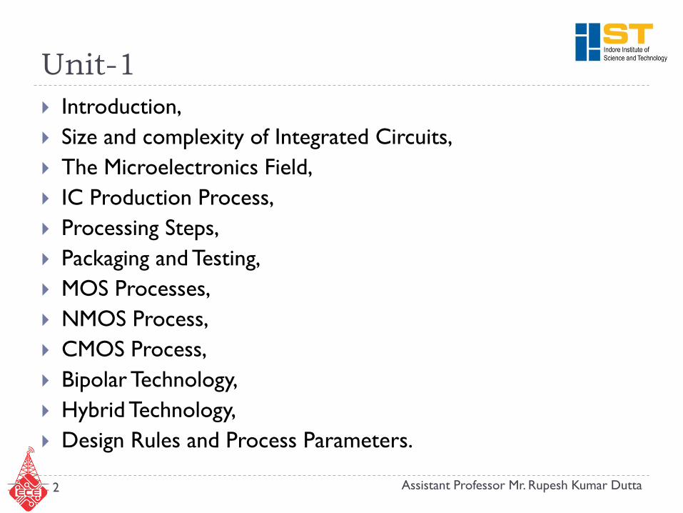
Unit-1
2
Introduction,
Size and complexity of Integrated Circuits,
The Microelectronics Field,
IC Production Process,
Processing Steps,
Packaging and Testing,
MOS Processes,
NMOS Process,
CMOS Process,
Bipolar Technology,
Hybrid Technology,
Design Rules and Process Parameters.
Assistant Professor Mr. Rupesh Kumar Dutta
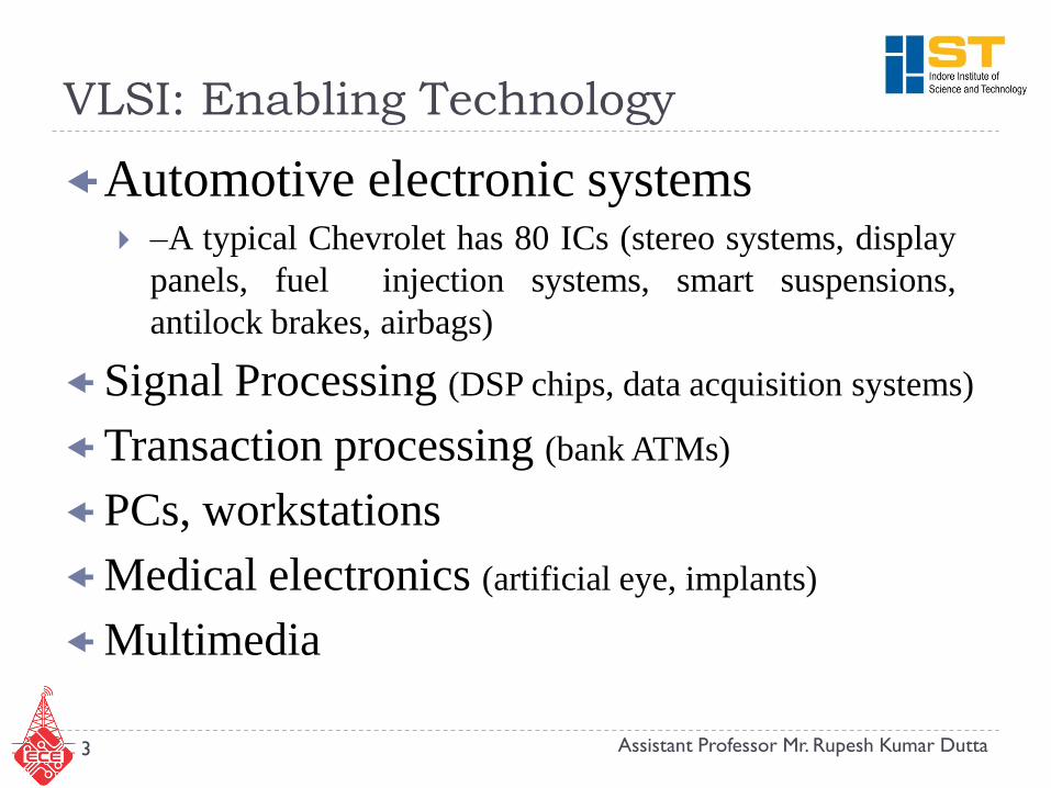
VLSI: Enabling Technology
Automotive electronic systems – A typical Chevrolet has 80 ICs (stereo systems, display
panels, fuel injection systems, smart suspensions,
antilock brakes, airbags)
Signal Processing (DSP chips, data acquisition systems)
Transaction processing (bank ATMs)
PCs, workstations
Medical electronics (artificial eye, implants)
Multimedia
3 Assistant Professor Mr. Rupesh Kumar Dutta
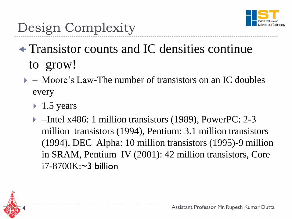
Design Complexity
Transistor counts and IC densities continue
to grow! – Moore’s Law-The number of transistors on an IC doubles
every
1.5 years
– Intel x486: 1 million transistors (1989), PowerPC: 2-3
million transistors (1994), Pentium: 3.1 million transistors
(1994), DEC Alpha: 10 million transistors (1995)-9 million
in SRAM, Pentium IV (2001): 42 million transistors, Core
i7-8700K:~3 billion
4 Assistant Professor Mr. Rupesh Kumar Dutta
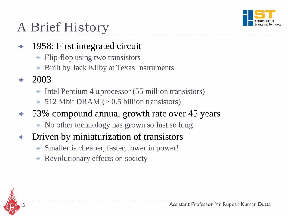
A Brief History
1958: First integrated circuit Flip-flop using two transistors
Built by Jack Kilby at Texas Instruments
2003
Intel Pentium 4 processor (55 million transistors)
512 Mbit DRAM (> 0.5 billion transistors)
53% compound annual growth rate over 45 years No other technology has grown so fast so long
Driven by miniaturization of transistors Smaller is cheaper, faster, lower in power!
Revolutionary effects on society
5 Assistant Professor Mr. Rupesh Kumar Dutta
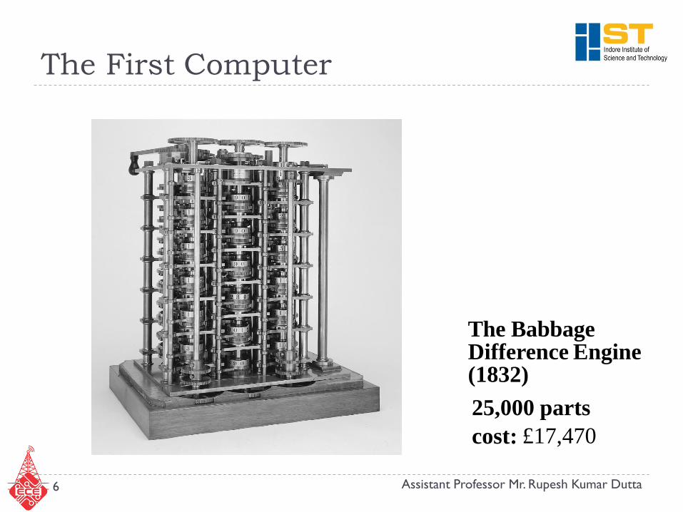
The First Computer
6 Assistant Professor Mr. Rupesh Kumar Dutta
The Babbage Difference Engine (1832)
25,000 parts
cost: £17,470
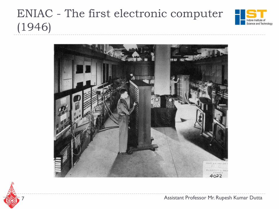
ENIAC - The first electronic computer
(1946)
7 Assistant Professor Mr. Rupesh Kumar Dutta
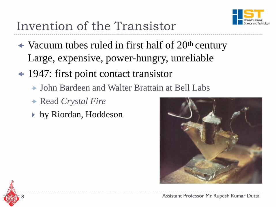
Invention of the Transistor
Vacuum tubes ruled in first half of 20th century
Large, expensive, power-hungry, unreliable
1947: first point contact transistor
John Bardeen and Walter Brattain at Bell Labs
Read Crystal Fire
by Riordan, Hoddeson
8 Assistant Professor Mr. Rupesh Kumar Dutta
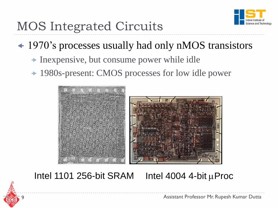
MOS Integrated Circuits
1970’s processes usually had only nMOS transistors
Inexpensive, but consume power while idle
1980s-present: CMOS processes for low idle power
9 Assistant Professor Mr. Rupesh Kumar Dutta
Intel 1101 256-bit SRAM Intel 4004 4-bit Proc

Moore’s Law
10 Assistant Professor Mr. Rupesh Kumar Dutta
Named after Gordon Moore, the co-founder of Fairchild Semiconductor and Intel
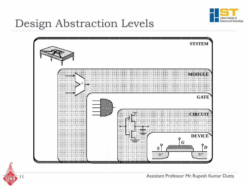
Design Abstraction Levels
11 Assistant Professor Mr. Rupesh Kumar Dutta
n+
S
n+
D
+
DEVICE
G
GATE
CIRCUIT
MODULE
SYSTEM
12 Assistant Professor Mr. Rupesh Kumar Dutta
13 Assistant Professor Mr. Rupesh Kumar Dutta
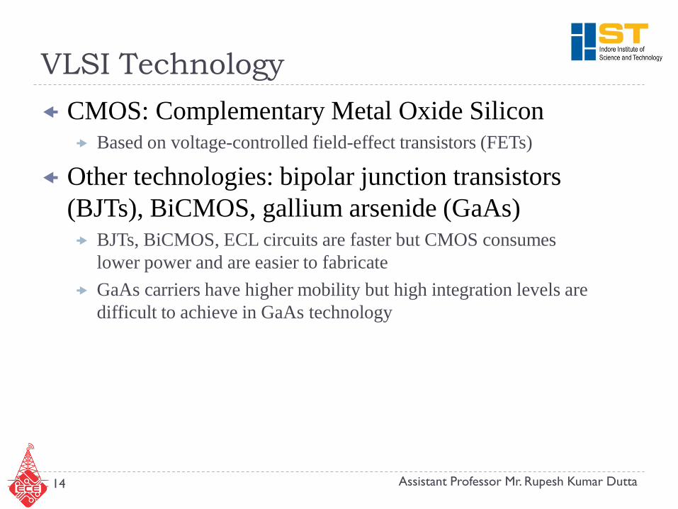
VLSI Technology
CMOS: Complementary Metal Oxide Silicon Based on voltage-controlled field-effect transistors (FETs)
Other technologies: bipolar junction transistors
(BJTs), BiCMOS, gallium arsenide (GaAs) BJTs, BiCMOS, ECL circuits are faster but CMOS consumes
lower power and are easier to fabricate
GaAs carriers have higher mobility but high integration levels are
difficult to achieve in GaAs technology
14 Assistant Professor Mr. Rupesh Kumar Dutta
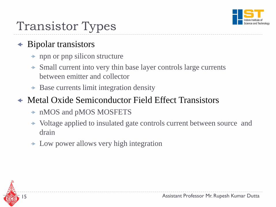
Transistor Types
Bipolar transistors
npn or pnp silicon structure
Small current into very thin base layer controls large currents
between emitter and collector
Base currents limit integration density
Metal Oxide Semiconductor Field Effect Transistors
nMOS and pMOS MOSFETS
Voltage applied to insulated gate controls current between source and
drain
Low power allows very high integration
15 Assistant Professor Mr. Rupesh Kumar Dutta
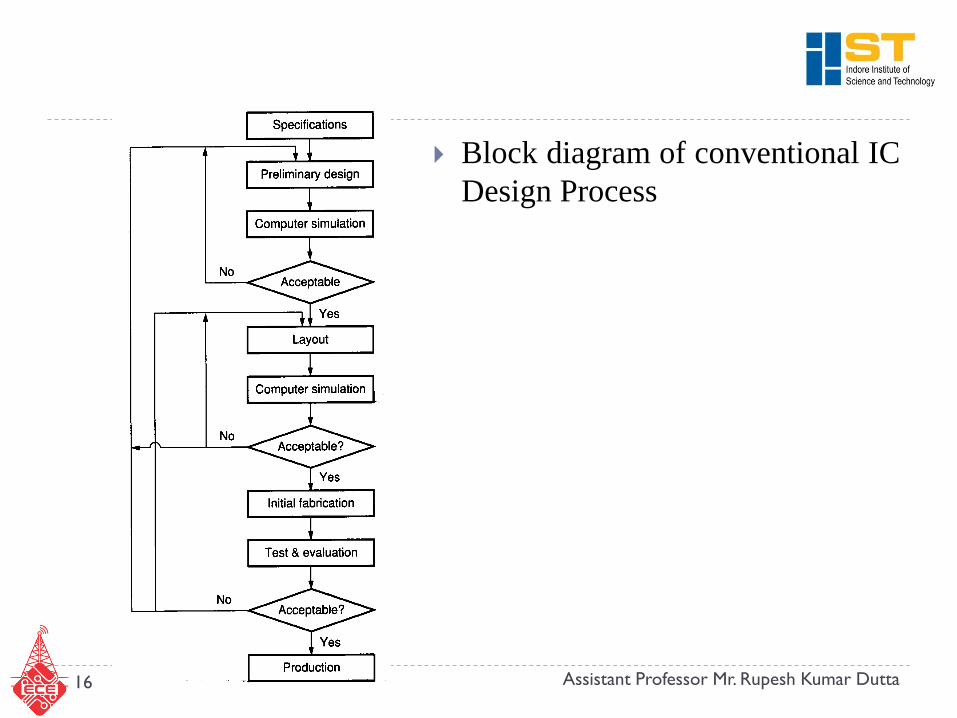
Block diagram of conventional IC
Design Process
16 Assistant Professor Mr. Rupesh Kumar Dutta
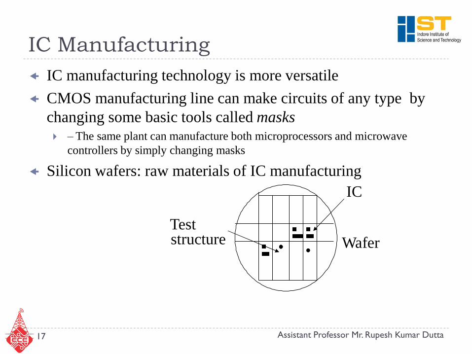
IC Manufacturing
IC manufacturing technology is more versatile
CMOS manufacturing line can make circuits of any type by
changing some basic tools called masks – The same plant can manufacture both microprocessors and microwave
controllers by simply changing masks
Silicon wafers: raw materials of IC manufacturing
IC
17 Assistant Professor Mr. Rupesh Kumar Dutta
Test structure Wafer
18 Assistant Professor Mr. Rupesh Kumar Dutta
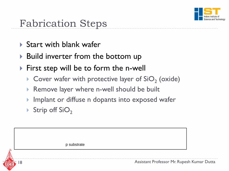
Fabrication Steps
Start with blank wafer
Build inverter from the bottom up
First step will be to form the n-well
Cover wafer with protective layer of SiO2 (oxide)
Remove layer where n-well should be built
Implant or diffuse n dopants into exposed wafer
Strip off SiO2
p substrate
19 Assistant Professor Mr. Rupesh Kumar Dutta
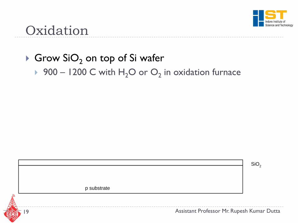
Oxidation
Grow SiO2 on top of Si wafer
900 – 1200 C with H2O or O2 in oxidation furnace
p substrate
SiO2
20 Assistant Professor Mr. Rupesh Kumar Dutta
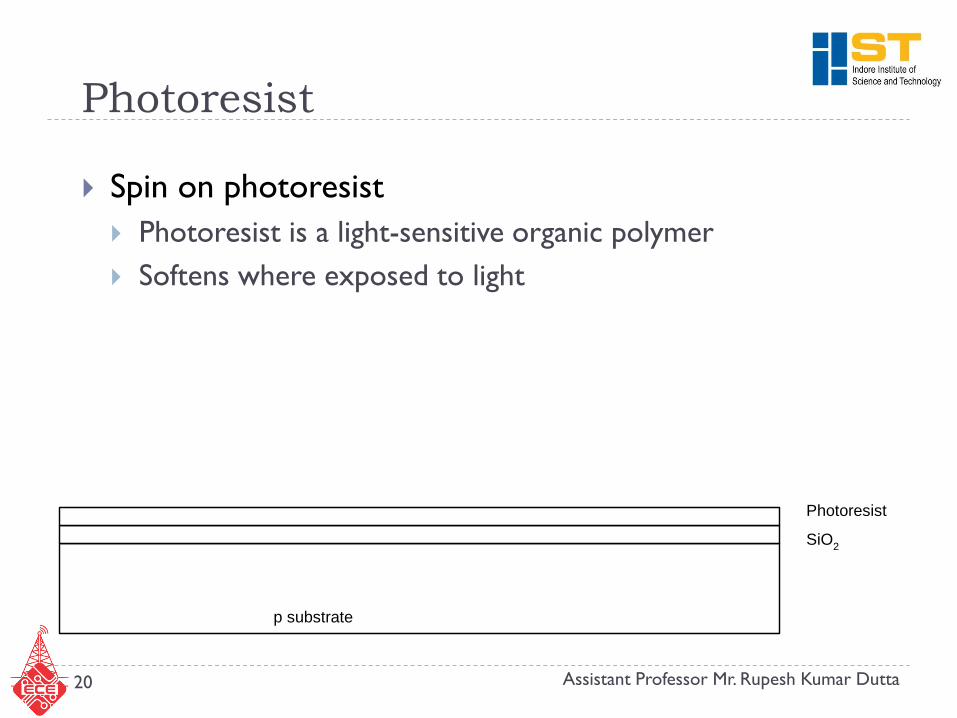
Photoresist
Spin on photoresist
Photoresist is a light-sensitive organic polymer
Softens where exposed to light
p substrate
SiO2
Photoresist
21 Assistant Professor Mr. Rupesh Kumar Dutta
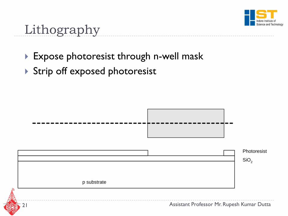
Lithography
Expose photoresist through n-well mask
Strip off exposed photoresist
p substrate
SiO2
Photoresist
22 Assistant Professor Mr. Rupesh Kumar Dutta
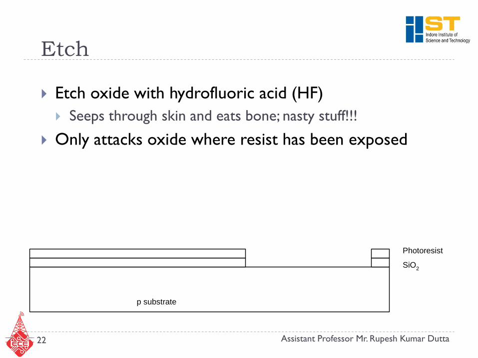
Etch
Etch oxide with hydrofluoric acid (HF)
Seeps through skin and eats bone; nasty stuff!!!
Only attacks oxide where resist has been exposed
p substrate
SiO2
Photoresist
23 Assistant Professor Mr. Rupesh Kumar Dutta
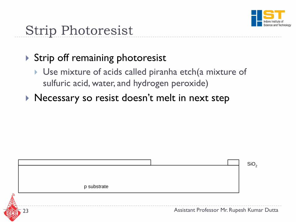
Strip Photoresist
Strip off remaining photoresist
Use mixture of acids called piranha etch(a mixture of
sulfuric acid, water, and hydrogen peroxide)
Necessary so resist doesn’t melt in next step
p substrate
SiO2
24 Assistant Professor Mr. Rupesh Kumar Dutta
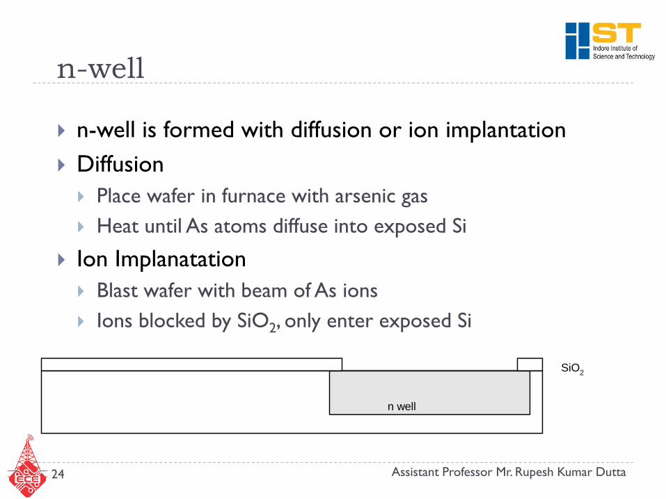
n-well
n-well is formed with diffusion or ion implantation
Diffusion
Place wafer in furnace with arsenic gas
Heat until As atoms diffuse into exposed Si
Ion Implanatation
Blast wafer with beam of As ions
Ions blocked by SiO2, only enter exposed Si
n well
SiO2
25 Assistant Professor Mr. Rupesh Kumar Dutta
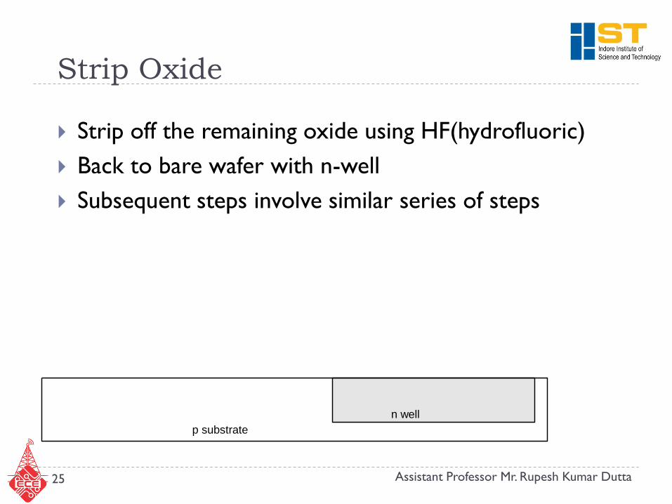
Strip Oxide
Strip off the remaining oxide using HF(hydrofluoric)
Back to bare wafer with n-well
Subsequent steps involve similar series of steps
p substrate
n well
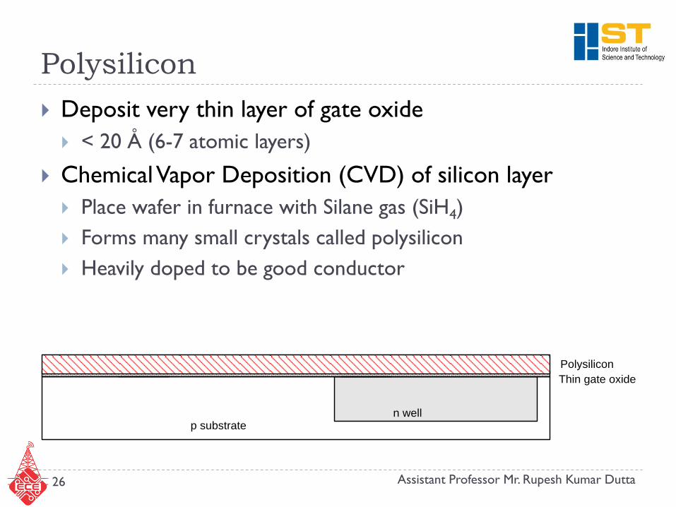
Polysilicon
Deposit very thin layer of gate oxide
< 20 Å (6-7 atomic layers)
Chemical Vapor Deposition (CVD) of silicon layer
Place wafer in furnace with Silane gas (SiH4)
Forms many small crystals called polysilicon
Heavily doped to be good conductor
Thin gate oxide
Polysilicon
p substraten well
Assistant Professor Mr. Rupesh Kumar Dutta 26
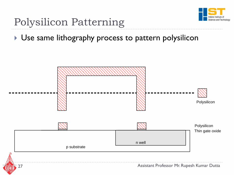
Polysilicon Patterning
Use same lithography process to pattern polysilicon
Polysilicon
p substrate
Thin gate oxide
Polysilicon
n well
27 Assistant Professor Mr. Rupesh Kumar Dutta
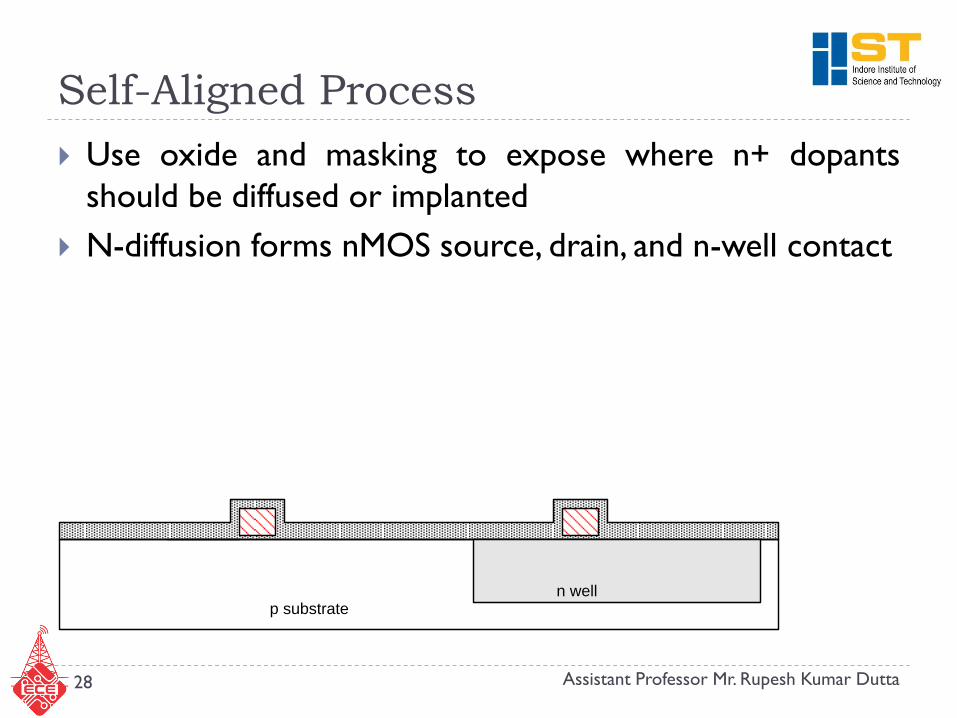
Self-Aligned Process
Use oxide and masking to expose where n+ dopants
should be diffused or implanted
N-diffusion forms nMOS source, drain, and n-well contact
p substraten well
28 Assistant Professor Mr. Rupesh Kumar Dutta
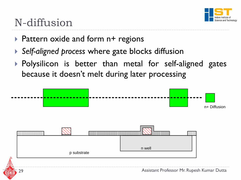
N-diffusion
Pattern oxide and form n+ regions
Self-aligned process where gate blocks diffusion
Polysilicon is better than metal for self-aligned gates
because it doesn’t melt during later processing
p substraten well
n+ Diffusion
29 Assistant Professor Mr. Rupesh Kumar Dutta
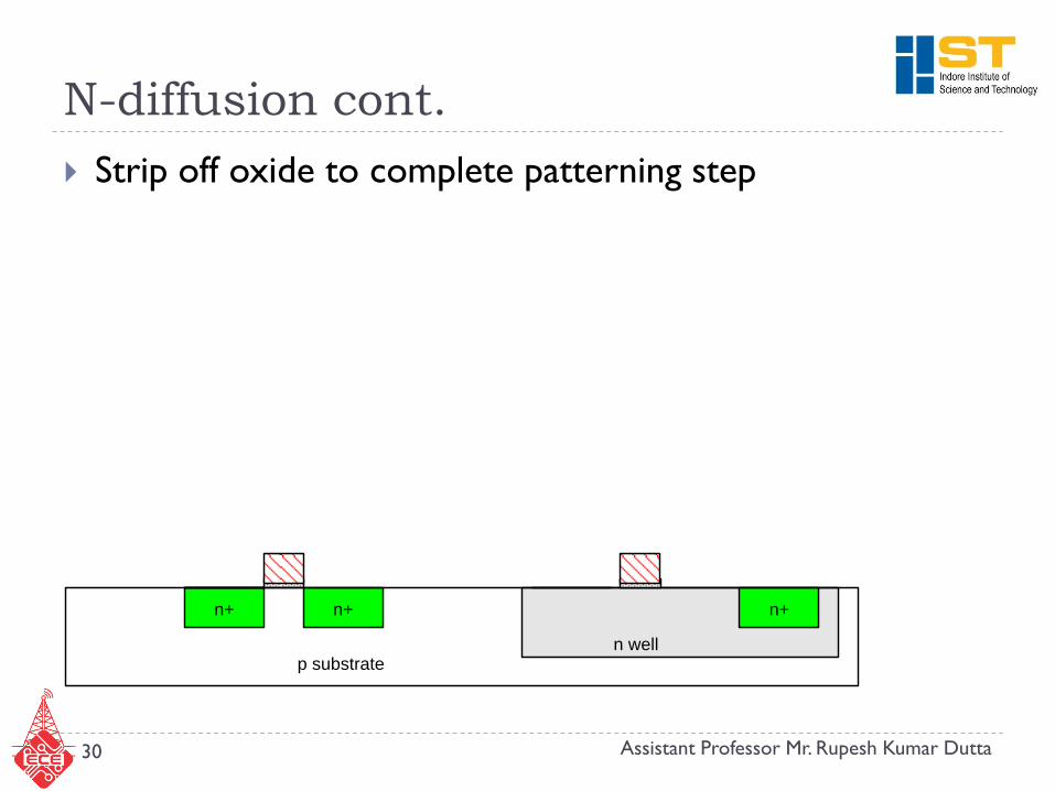
N-diffusion cont.
Strip off oxide to complete patterning step
n wellp substrate
n+n+ n+
30 Assistant Professor Mr. Rupesh Kumar Dutta
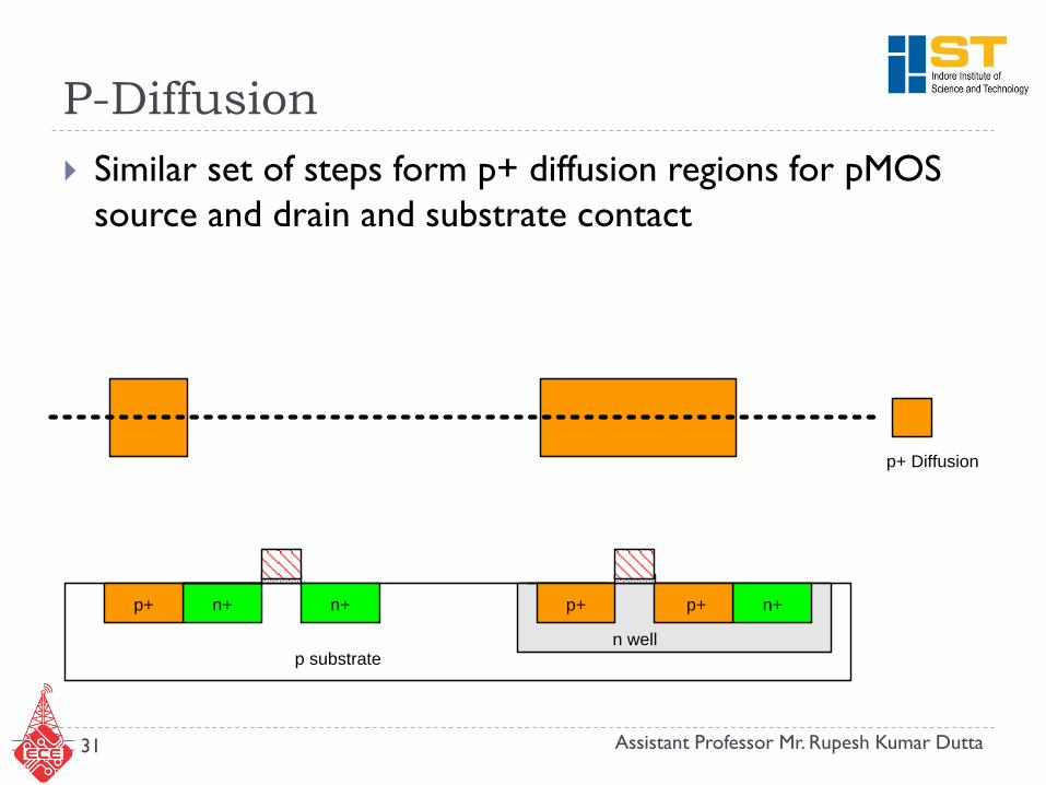
P-Diffusion
Similar set of steps form p+ diffusion regions for pMOS
source and drain and substrate contact
p+ Diffusion
p substraten well
n+n+ n+p+p+p+
31 Assistant Professor Mr. Rupesh Kumar Dutta
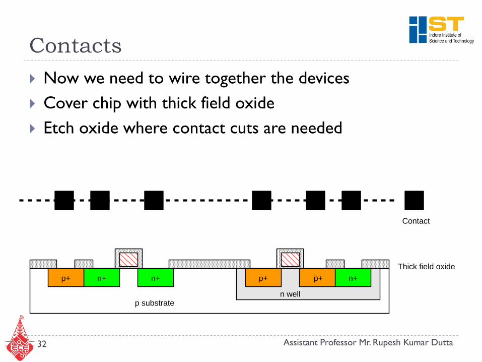
Contacts
Now we need to wire together the devices
Cover chip with thick field oxide
Etch oxide where contact cuts are needed
p substrate
Thick field oxide
n well
n+n+ n+p+p+p+
Contact
32 Assistant Professor Mr. Rupesh Kumar Dutta
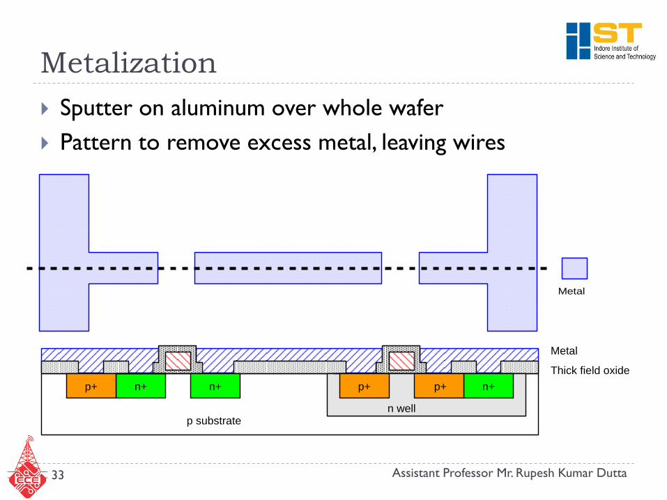
Metalization
Sputter on aluminum over whole wafer
Pattern to remove excess metal, leaving wires
p substrate
Metal
Thick field oxide
n well
n+n+ n+p+p+p+
Metal
33 Assistant Professor Mr. Rupesh Kumar Dutta
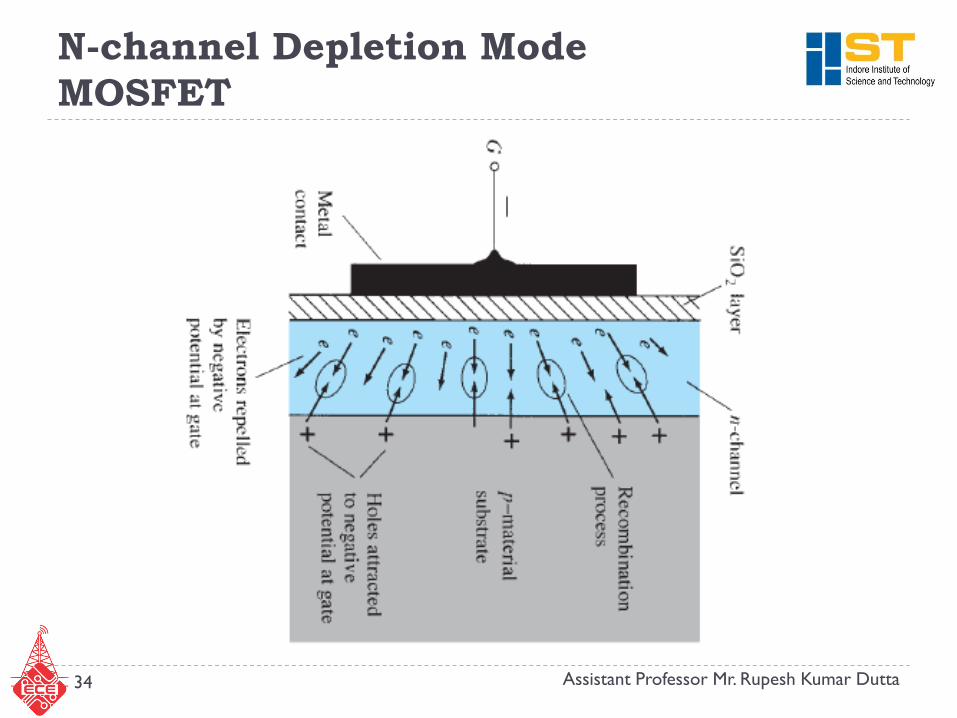
N-channel Depletion Mode
MOSFET
34 Assistant Professor Mr. Rupesh Kumar Dutta
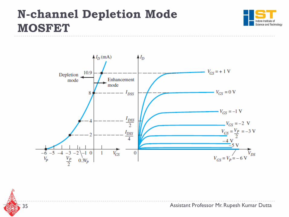
N-channel Depletion Mode
MOSFET
35 Assistant Professor Mr. Rupesh Kumar Dutta
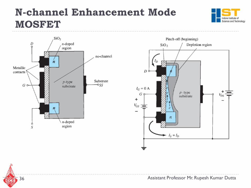
N-channel Enhancement Mode
MOSFET
36 Assistant Professor Mr. Rupesh Kumar Dutta
37 Assistant Professor Mr. Rupesh Kumar Dutta
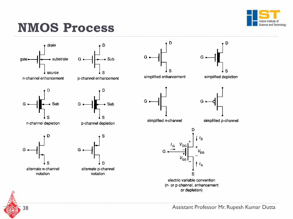
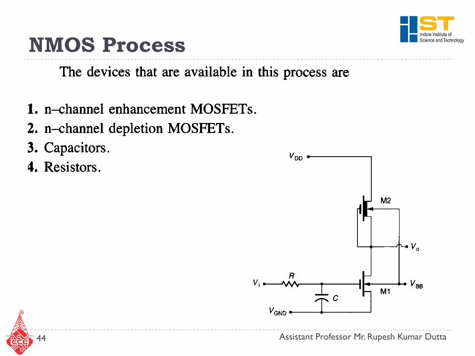
NMOS Process
38 Assistant Professor Mr. Rupesh Kumar Dutta
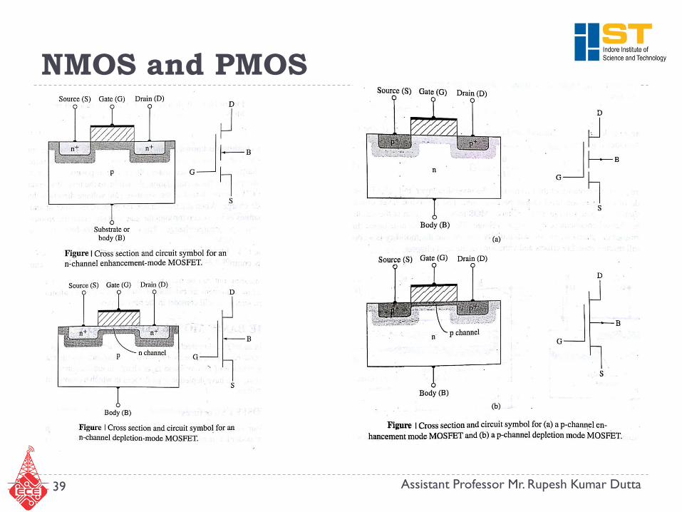
NMOS and PMOS
39 Assistant Professor Mr. Rupesh Kumar Dutta
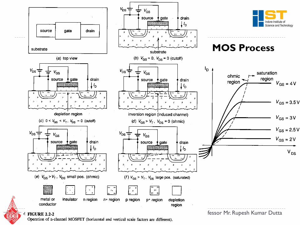
MOS Process
40 Assistant Professor Mr. Rupesh Kumar Dutta
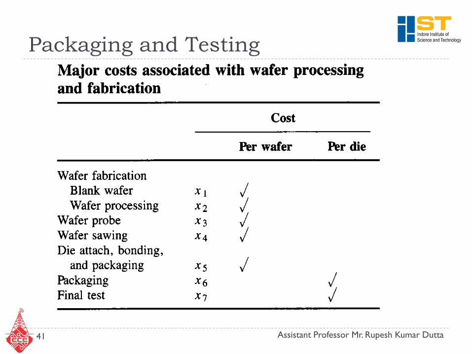
Packaging and Testing
41 Assistant Professor Mr. Rupesh Kumar Dutta
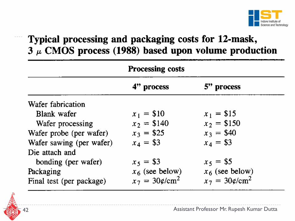
42 Assistant Professor Mr. Rupesh Kumar Dutta
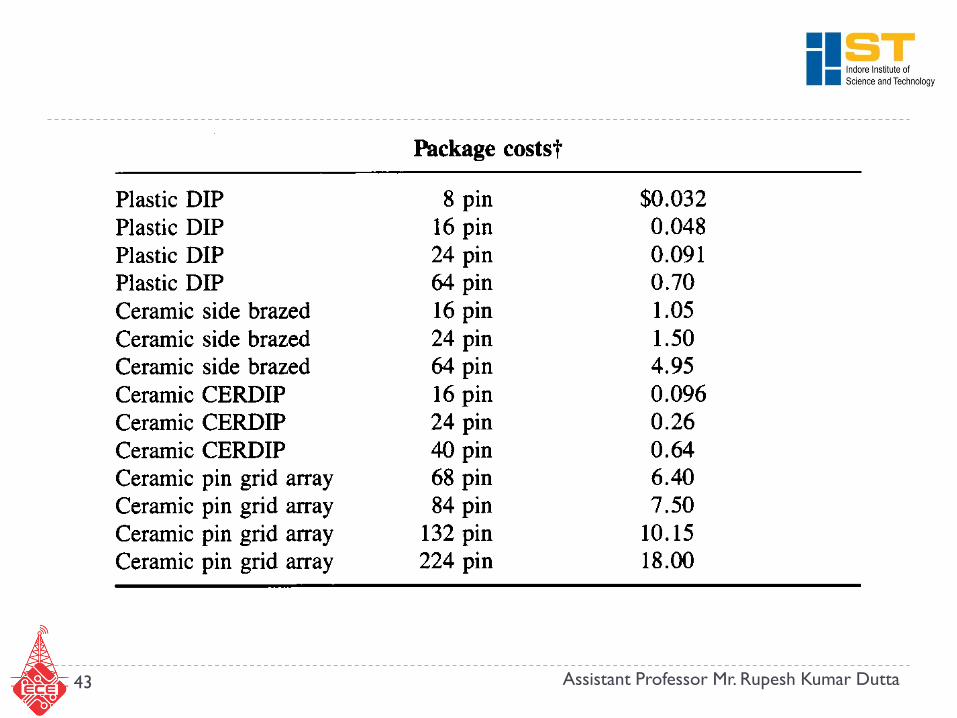
43 Assistant Professor Mr. Rupesh Kumar Dutta
NMOS Process
44 Assistant Professor Mr. Rupesh Kumar Dutta
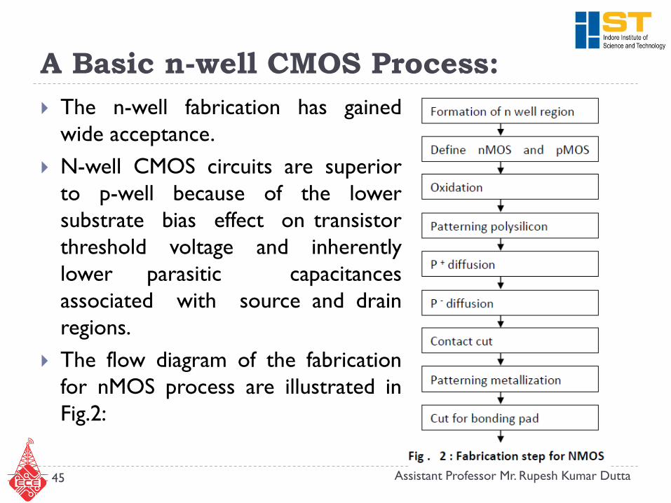
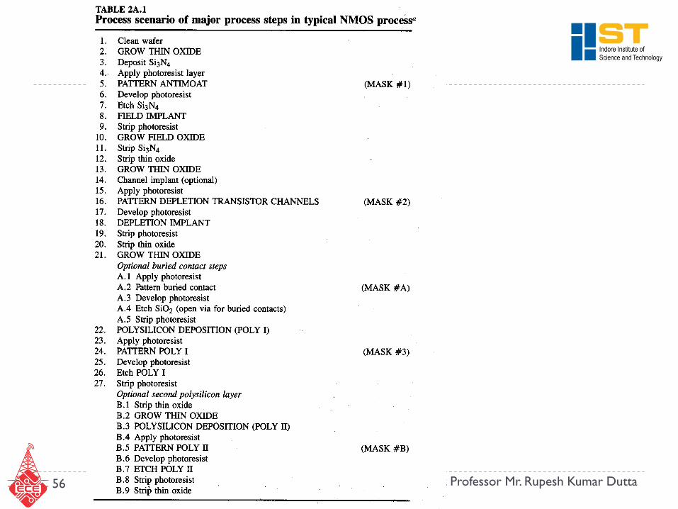
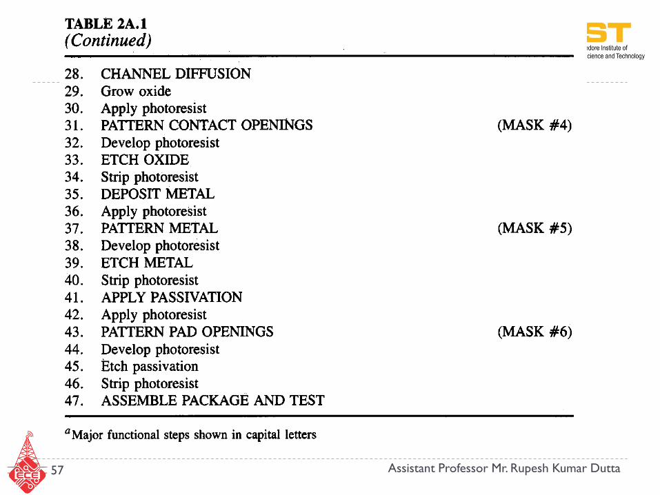
A Basic n-well CMOS Process:
The n-well fabrication has gained
wide acceptance.
N-well CMOS circuits are superior
to p-well because of the lower
substrate bias effect on transistor
threshold voltage and inherently
lower parasitic capacitances
associated with source and drain
regions.
The flow diagram of the fabrication
for nMOS process are illustrated in
Fig.2:
45 Assistant Professor Mr. Rupesh Kumar Dutta
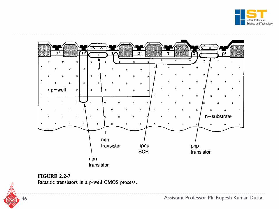
46 Assistant Professor Mr. Rupesh Kumar Dutta
Bipolar Technology
47 Assistant Professor Mr. Rupesh Kumar Dutta

Bipolar Technology
48 Assistant Professor Mr. Rupesh Kumar Dutta
Bipolar Technology
Although minimum feature sizes are comparable for the bipolar
and MOS processes, standard bipolar processes require more
area per device than do the NMOS processes.
A major reason for this increased area is the deep and wide p
channel stops that are required for device isolation in standard
bipolar processes.
An alternative bipolar process using trench isolation is
available which offers a significant improvement in component
density over the standard bipolar process.
49 Assistant Professor Mr. Rupesh Kumar Dutta
Hybrid Technology
The hybrid approach to integrated circuit design involves attaching two or more integrated circuit dies (typically of different types), along with some discrete components in some cases, in a single package to form what is called a hybrid integrated circuit.
It is often, and desirably, transparent to the consumer whether the circuit is monolithic or hybrid; in some cases, however, the hybrid packages are considerably larger.
The hybrid integrated circuit is typically more costly than the monolithic structures.
The extra cost and size of hybrid integrated circuits is offset, in some demanding applications, by improved performance capabilities.
50 Assistant Professor Mr. Rupesh Kumar Dutta
Hybrid Technology Hybrid circuits containing discrete components occupy considerably
less area than the conventional PC board/discrete component approach.
They have played a major role in demanding analog signal processing applications such as high-resolution A/D and D/A converters and precision active filters.
Tolerances, temperature dependence, and area-induced component value limits for resistors and capacitors in standard MOS and bipolar processes have limited the development of monolithic integrated circuits for precision continuous-time signal processing.
Thick film and thin film passive components have reasonable tolerances, are easily trimmable, have acceptable temperature coefficients that can be tailored for tracking, and offer reasonable tradeoffs between area required and component values.
These thick film and thin film networks are commonly used for the passive components in hybrid integrated circuits.
51 Assistant Professor Mr. Rupesh Kumar Dutta
THICK FILM CIRCUITS
The thick film technology is relatively old, requires considerable
area compared to monolithic circuits, can be used for relatively high-
power applications, and can be applied at relatively high frequencies
(up to 1 GHz) although it is typically limited to a few MHz.
The increased area required by the thick film circuits is offset by the
reduced cost in equipment and processing materials required for the
thick film process, the latter being a small fraction of that required
for either bipolar or MOS processes.
The components available in a thick film process are resistors and
capacitors along with conducting interconnects.
Layers of different material are successively screened onto an
insulating substrate.
These materials are used for resistors and conductors as well as for
the dielectrics of capacitors.
52 Assistant Professor Mr. Rupesh Kumar Dutta
THIN FILM CIRCUITS
The components available in thin film processes are resistors and capacitors, although often only resistors are included due to both the specific applications which naturally benefit from thin film technology and the practical limitations of thin film capacitors. Thin film circuits are much smaller than thick film circuits.
They are similar to thick film circuits in that successive layers are applied to an insulating substrate as contrasted to the MOS and bipolar processes, where some of the processing steps involve diffusions that actually penetrate the substrate.
For conductors, thin film thicknesses are typically from 100 to 500 A although thicknesses of several thousand angstroms are occasionally used if a high conductivity is needed.
53 Assistant Professor Mr. Rupesh Kumar Dutta
THIN FILM CIRCUITS
Film thicknesses from 100 to 2000𝐴0 for resistors and film
thicknesses in the 3000𝐴0 region for dielectrics of capacitors
are common.
Note that these film thicknesses are comparable to the
thicknesses of layers applied in the MOS and bipolar processes
but are orders of magnitude thinner than the 20µ (200,000 𝐴0)
typical of thick films.
The thin film layers are applied by uniformly coating the entire
wafer with the film.
Then unwanted areas are selectively patterned and etched with
a photolithographic process similar to that used in the MOS
and bipolar cases.
54 Assistant Professor Mr. Rupesh Kumar Dutta
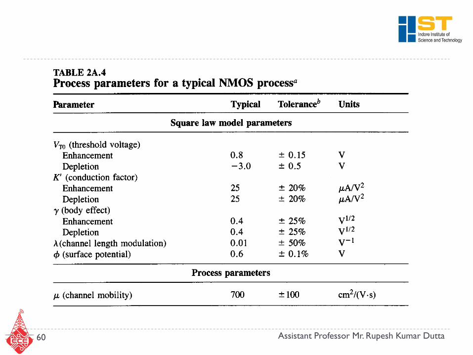
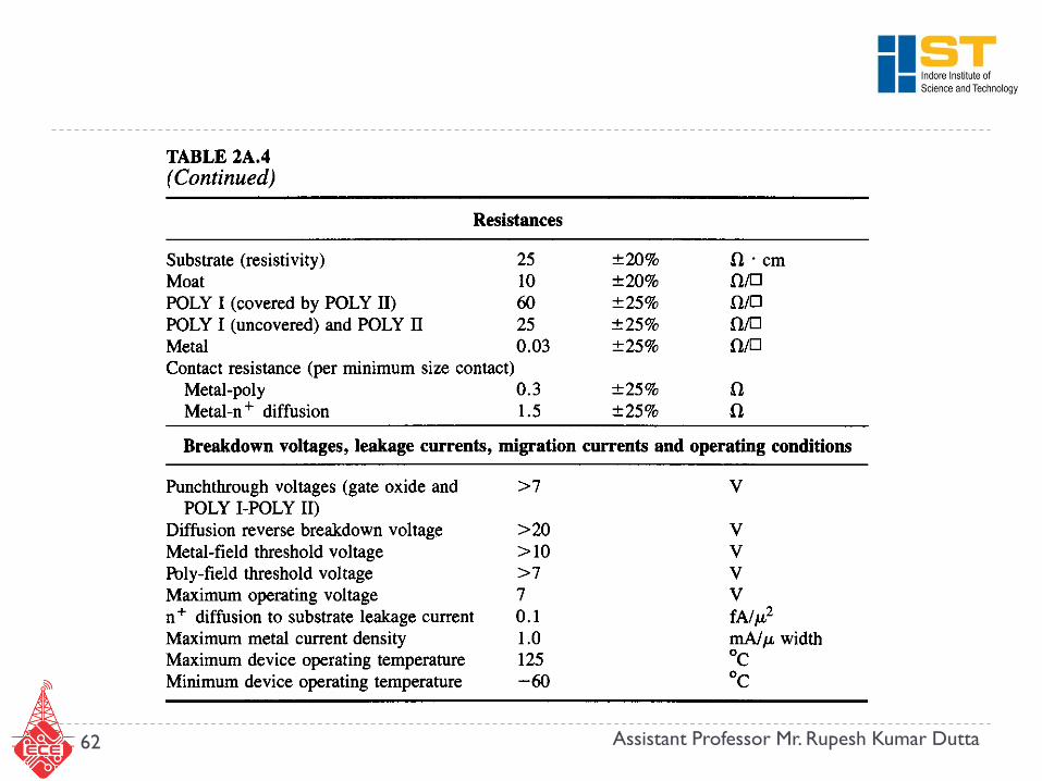
DESIGN RULES AND PROCESS
PARAMETERS
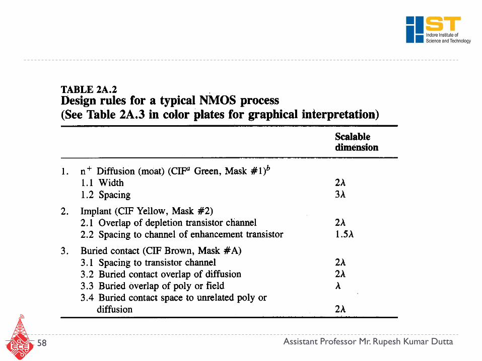
Design rules are generally well-documented specifications
listing minimum widths of features (conductor, moat, resistor,
etc.), minimum spacing's allowable between adjacent features,
overlap requirements, and other measurements that are
compatible with a given process.
The design rules, the process parameters, and their relationship
with device characteristics serve as an interface between the
process engineers and the circuit designers.
Both groups, along with representatives from marketing (since
yield is affected by the design rules), have input into the
evolution of these interfaces.
55 Assistant Professor Mr. Rupesh Kumar Dutta
56 Assistant Professor Mr. Rupesh Kumar Dutta
57 Assistant Professor Mr. Rupesh Kumar Dutta
58 Assistant Professor Mr. Rupesh Kumar Dutta

59 Assistant Professor Mr. Rupesh Kumar Dutta
60 Assistant Professor Mr. Rupesh Kumar Dutta

61 Assistant Professor Mr. Rupesh Kumar Dutta
62 Assistant Professor Mr. Rupesh Kumar Dutta
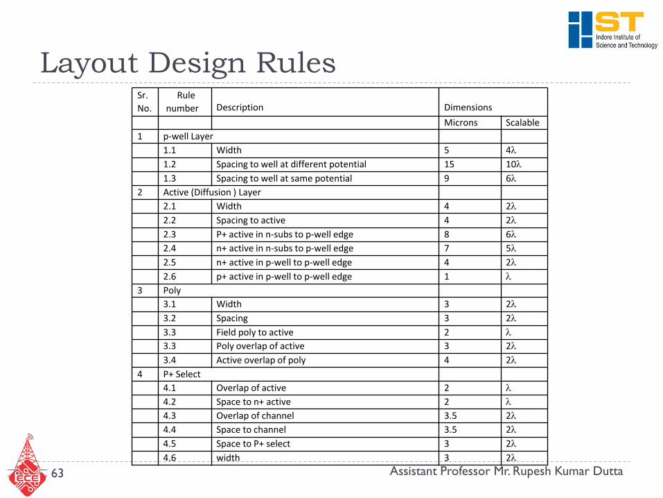
Layout Design Rules Sr.
No.
Rule
number
Description
Dimensions
Microns Scalable
1 p-well Layer
1.1 Width 5 4l
1.2 Spacing to well at different potential 15 10l
1.3 Spacing to well at same potential 9 6l
2 Active (Diffusion ) Layer
2.1 Width 4 2l
2.2 Spacing to active 4 2l
2.3 P+ active in n-subs to p-well edge 8 6l
2.4 n+ active in n-subs to p-well edge 7 5l
2.5 n+ active in p-well to p-well edge 4 2l
2.6 p+ active in p-well to p-well edge 1 l
3 Poly
3.1 Width 3 2l
3.2 Spacing 3 2l
3.3 Field poly to active 2 l
3.3 Poly overlap of active 3 2l
3.4 Active overlap of poly 4 2l
4 P+ Select
4.1 Overlap of active 2 l
4.2 Space to n+ active 2 l
4.3 Overlap of channel 3.5 2l
4.4 Space to channel 3.5 2l
4.5 Space to P+ select 3 2l
4.6 width 3 2l
63 Assistant Professor Mr. Rupesh Kumar Dutta
Layout
Chips are specified with set of masks
Minimum dimensions of masks determine transistor size
(and hence speed, cost, and power)
Feature size f = distance between source and drain
Set by minimum width of polysilicon
Feature size improves 30% every 3 years or so
Normalize for feature size when describing design rules
Express rules in terms of l = f/2
E.g. l = 0.3 m in 0.6 m process
64 Assistant Professor Mr. Rupesh Kumar Dutta
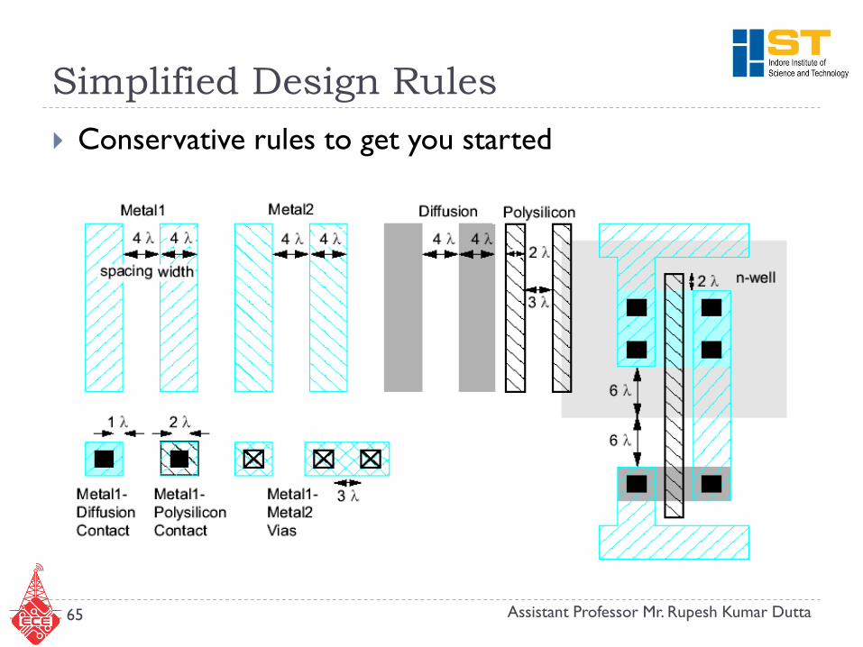
Simplified Design Rules
Conservative rules to get you started
65 Assistant Professor Mr. Rupesh Kumar Dutta
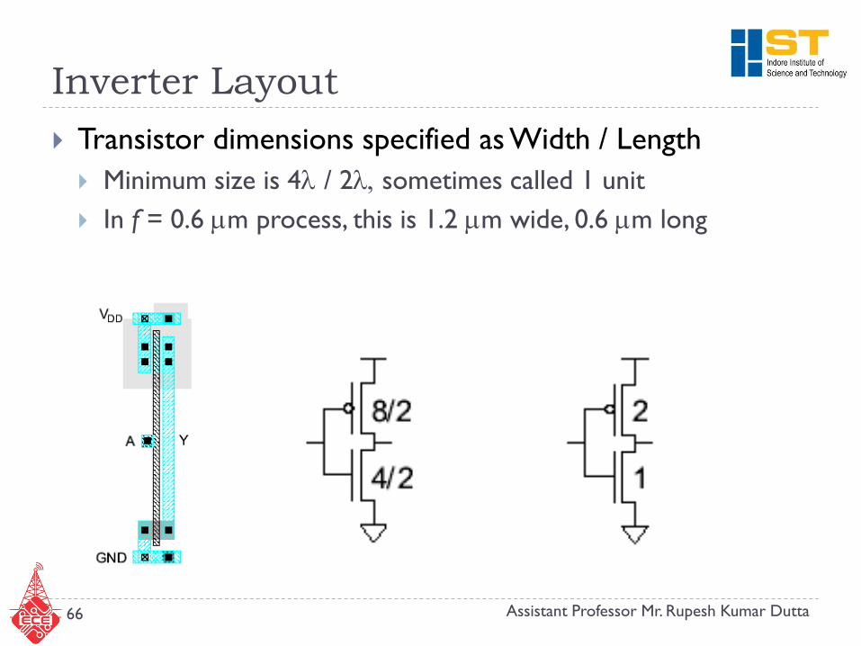
Inverter Layout
Transistor dimensions specified as Width / Length
Minimum size is 4l / 2l, sometimes called 1 unit
In f = 0.6 m process, this is 1.2 m wide, 0.6 m long
66 Assistant Professor Mr. Rupesh Kumar Dutta
Gate Layout
Layout can be very time consuming
Design gates to fit together nicely
Build a library of standard cells
Standard cell design methodology
VDD and GND should abut (standard height)
Adjacent gates should satisfy design rules
nMOS at bottom and pMOS at top
All gates include well and substrate contacts
67 Assistant Professor Mr. Rupesh Kumar Dutta
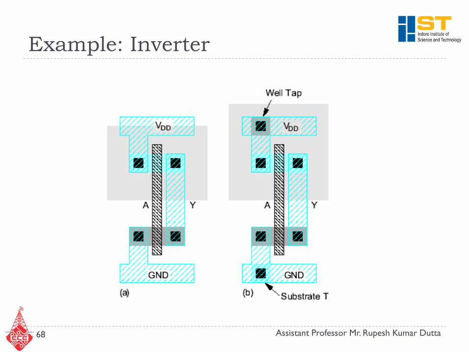
Example: Inverter
68 Assistant Professor Mr. Rupesh Kumar Dutta
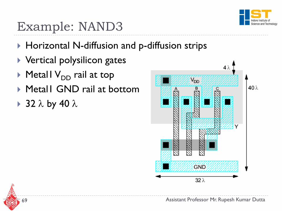
Example: NAND3
Horizontal N-diffusion and p-diffusion strips
Vertical polysilicon gates
Metal1 VDD rail at top
Metal1 GND rail at bottom
32 l by 40 l
69 Assistant Professor Mr. Rupesh Kumar Dutta
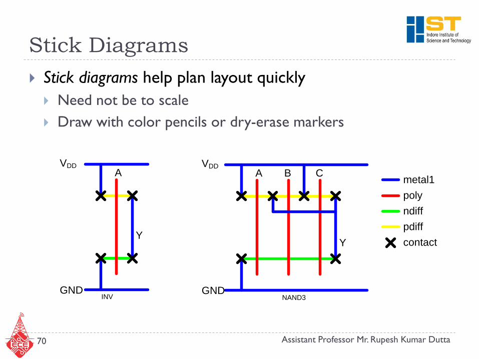
Stick Diagrams
Stick diagrams help plan layout quickly
Need not be to scale
Draw with color pencils or dry-erase markers
c
AVDD
GND
Y
AVDD
GND
B C
Y
INV
metal1
poly
ndiff
pdiff
contact
NAND3
70 Assistant Professor Mr. Rupesh Kumar Dutta
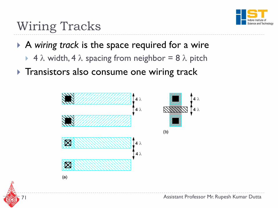
Wiring Tracks
A wiring track is the space required for a wire
4 l width, 4 l spacing from neighbor = 8 l pitch
Transistors also consume one wiring track
71 Assistant Professor Mr. Rupesh Kumar Dutta
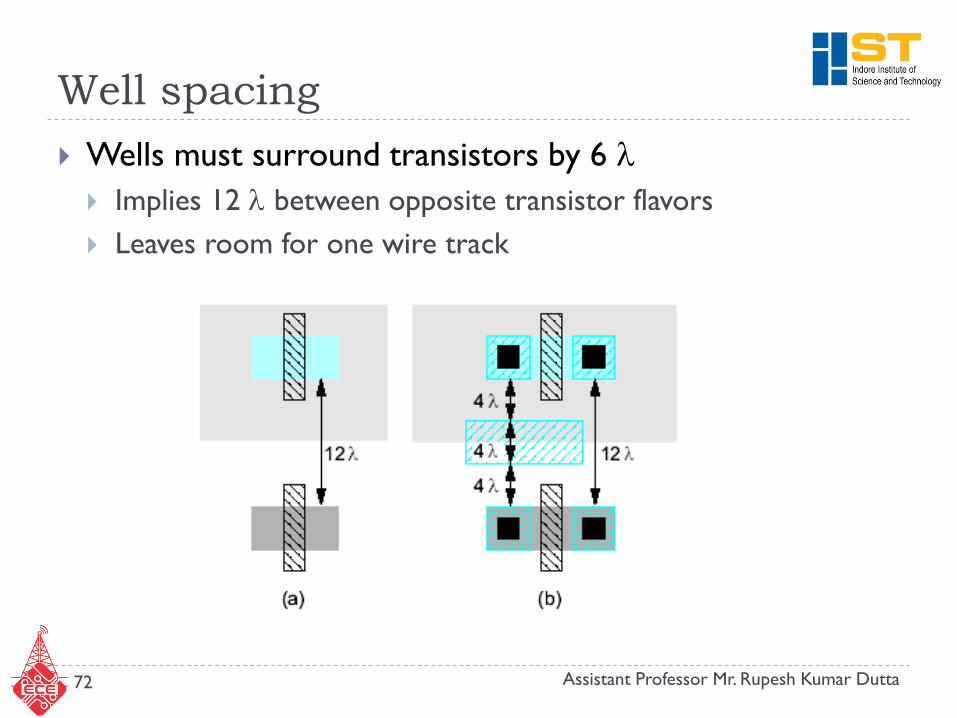
Well spacing
Wells must surround transistors by 6 l
Implies 12 l between opposite transistor flavors
Leaves room for one wire track
72 Assistant Professor Mr. Rupesh Kumar Dutta
Thank You !
73 Assistant Professor Mr. Rupesh Kumar Dutta


