Embed Size (px)
Citation preview

EC-I Lab Manual EC-261
BAPATLA ENGINEERING COLLEGE (Autonomous):: BAPATLA
1
ELECTRONIELECTRONIELECTRONIELECTRONICCCC CIRCUITCIRCUITCIRCUITCIRCUITSSSS ----1111
LabLabLabLab ManualManualManualManual (EC(EC(EC(EC----261)261)261)261)
Prepared By:
T SRINIVASA RAO T SRINIVASA RAO T SRINIVASA RAO T SRINIVASA RAO M.TechM.TechM.TechM.Tech
SUNEEL MIRIYALA SUNEEL MIRIYALA SUNEEL MIRIYALA SUNEEL MIRIYALA M.Tech.M.Tech.M.Tech.M.Tech.
N.Kusuma N.Kusuma N.Kusuma N.Kusuma DECE.DECE.DECE.DECE.
Y.V.Krishna Y.V.Krishna Y.V.Krishna Y.V.Krishna DECE.DECE.DECE.DECE.
Department of ECEDepartment of ECEDepartment of ECEDepartment of ECE
BAPATBAPATBAPATBAPATLA ENGINEERING COLLEGELA ENGINEERING COLLEGELA ENGINEERING COLLEGELA ENGINEERING COLLEGE
(Autonomous)
BAPATLABAPATLABAPATLABAPATLA----522 101522 101522 101522 101

EC-I Lab Manual EC-261
BAPATLA ENGINEERING COLLEGE (Autonomous):: BAPATLA
2
LIST OF EXPERIMENTS
1. Half Wave Rectifier with and without Filters.
2. Full Wave Rectifier with and without Filters.
3. Bridge Rectifier With and Without Filters.
4. Frequency Response of Common Emitter Amplifier.
5. Frequency Response of Common Source Amplifier.
6.Measurement of Parameters of Emitter Follower and Source Follower; RI, AV, AI &R o.
7. Cascode Amplifier.
8. Two Stage RC-Coupled Amplifier.
9. Voltage Series Feedback Amplifier.
10. Voltage Shunt Feedback Amplifier.
11. Complementary Symmetry Push-pull amplifier.
12. Class-A Power Amplifier.
13. RC Phase Shift Oscillator.
14. Colpitt’s Oscillators.
15. Hartley Oscillators.

EC-I Lab Manual EC-261
BAPATLA ENGINEERING COLLEGE (Autonomous):: BAPATLA
3
1. HALF WAVE RECTIFIER Aim:
01. To observe the output waveform of half wave rectifier with and without filter
02. To find ripple factor and percentage regulation of FWR with & without filter
Apparatus:
Silicon Diodes BY126
Resistance 1 kΩ
Capacitor 470 uF CRO
Digital Multimeter
Circuit Diagram:
Theory::::
The half wave rectifier consists of one rectifier circuit with common load. These are connected in such a way that conduction takes place through one diode in alternate half-cycles and current through the load is sum of two currents. Thus, the output voltage waveform contains half sinusoids in the two half-cycles of the AC input signal.
The output of a rectifier is a pulsating DC consisting of a DC component and superimposed ripple. A way to eliminate or reduce the ripple to the required level is to use a filter.

EC-I Lab Manual EC-261
BAPATLA ENGINEERING COLLEGE (Autonomous):: BAPATLA
4
PROCEDURE:
Without filter:
01. Connect the circuit as per the circuit d i a g r a m
02. Connect CRO across the load
03. Note down the peak value VM of the signal observed on the CRO
04. Switch the CRO into DC mode and observe the waveform. Note down
the DC shift
05. Calculate Vrmsand Vdc values by using the formulae
Calculate Vrms & Vdc by using the formulas
Vrms=Vm/√2, Irms=Im/√2
Vdc=2VM/п, Idc=2IM/п,
Where Vr is the peak to peak amplitude of filter output
06. Calculate the ripple factor by using the formulae
Ripple factor=Vac/Vdc=√Vrms 2 –Vdc2/Vdc
07. Remove the load and measure the voltage across the circuit. Take down
the value as VNL; calculate the percentage of voltage regulation using
the formulae
% Regulation = (VNL-FL)/VFL*100
With filter:
01. Connect the capacitor filler across the load in the above circuit diagram
02. Proceed with the same procedure mentioned above to measure Vr value
from the CRO and also dc shift from CRO
03. Calculate Vrrms & Vdc by using the formulas
Vr, rms=Vdc/4√3fCRL
Vdc=2VM/п
Where Vr is the peak to peak amplitude of filter output
04. Calculate ripple factor and % regulation by using the formulae.

EC-I Lab Manual EC-261
BAPATLA ENGINEERING COLLEGE (Autonomous):: BAPATLA
5
Ripple factor=Vrms/Vdc=1/4√3fCRL
%Regulation = (VNL-VFL)/VFL*100
EXPECTED WAVE FORMS:
RECTIFIED OUTPUT:
FILTEROUTPUT
Precautions:
1. Wires should be checked for good continuity.
2. Carefully note down the readings with out any errors.
Result:

EC-I Lab Manual EC-261
BAPATLA ENGINEERING COLLEGE (Autonomous):: BAPATLA
6
2. FULL WAVE RECTIFIER Aim:
01. To observe the output waveform of full wave rectifier with and without filter
02. To find ripple factor and percentage regulation of FWR with & without filter
Apparatus:
Silicon Diodes BY126
Resistance 1 kΩ,
Capacitor 470 uF CRO
Digital Multimeter
Circuit Diagram:
Theory:
The full wave rectifier consists of two half wave rectifier circuits with common load. These are connected in such a way that conduction takes place through two diodes in alternate half-cycles and current through the load is sum of two currents. Thus, the output voltage waveform contains two half sinusoids in the two half-cycles of the AC input signal.
The output of a rectifier is a pulsating DC consisting of a DC component and superimposed ripple. A way to eliminate or reduce the ripple to the required level is to use a filter.

EC-I Lab Manual EC-261
BAPATLA ENGINEERING COLLEGE (Autonomous):: BAPATLA
7
PROCEDURE:
Without filter:
01. Connect the circuit as per the circuit diagram
02. Connect CRO across the load
03. Note down the peak value VM of the signal observed on the CRO
04. Switch the CRO into DC mode and observe the waveform. Note down
the DC shift
05. Calculate Vrmsand Vdc values by using the formulae
Calculate Vrms & Vdc by using the formulas
Vrms=Vm/√2, Irms=Im/√2
Vdc=2VM/п, Idc=2IM/п,
Where Vr is the peak to peak amplitude of filter output
06. Calculate the ripple factor by using the formulae
Ripple factor=Vac/Vdc=√Vrms 2 –Vdc2 /Vdc
07. Remove the load and measure the voltage across the circuit. Take down
the value as VNL; calculate the percentage of voltage regulation using
the formulae
% Regulation = (VNL-VFL)/VFL*100
With filter:
01. Connect the capacitor filler across the load in the above circuit diagram
02. Proceed with the same procedure mentioned above to measure Vr value
from the CRO and also dc shift from CRO
03. Calculate Vrrms & Vdc by using the formulas
Vr, rms=Vdc/4√3fCRL
Vdc=2VM/п
Where Vr is the peak to peak amplitude of filter output
04. Calculate ripple factor and % regulation by using the formulae.

EC-I Lab Manual EC-261
BAPATLA ENGINEERING COLLEGE (Autonomous):: BAPATLA
8
Ripple factor=Vrms/Vdc=1/4√3fCRL
%Regulation = (VNL-VFL)/VFL*100
EXPECTED WAVE FORMS:
RECTIFIED OUTPUT:
FILTEROUTPUT
Precautions:
1. Wires should be checked for good continuity.
2. Carefully note down the readings with out any errors.
Result:

EC-I Lab Manual EC-261
BAPATLA ENGINEERING COLLEGE (Autonomous):: BAPATLA
9
9
3. BRIDGE RECTIFIER
Aim :
1. To observe the output waveform of bridge rectifier with and without filter
2. To find ripple factor and percentage of regulation of bridge rectifier with and without filter
Apparatus:
Silicon Diodes BY126
Resistance 1 KΏ
Capacitor 470 µF
CRO
Multimeter
Circuit Diagram:
Theory:
The bridge is seen to consist of four diodes connected with their arrowhead symbols all pointing toward the positive output terminal of the circuit.

EC-I Lab Manual EC-261
BAPATLA ENGINEERING COLLEGE (Autonomous):: BAPATLA
10
10
During the positive half cycle of input voltage, the load current flows from the positive
input terminal through D1 to RL and then through RL and D4 back to the negative input
terminal. During this time, the positive input terminal is applied to the cathode of D2 so it
is reversed biased and similarly D3 is also reverse biased. These two diodes are forward
biased during negative half cycle; D1 & D4 are reverse biased during this cycle. And finally
both half cycles are rectified.
Procedure: Without filter:
01. Connect the circuit as per the circuit diagram.
02. Connect CRO across the load
03. Note down the peak value VM of the signal observed on the CRO
04. Switch the CRO into DC mode and observe the waveform. Note
down the DC shift.
05. Calculate Vmis and Vdc values by using the formulae
Vrms=Vm/√2, Irms=Im/√2,
Vdc=2VM/п , Idc=2IM/п
06. Calculate the ripple factor by using the formulae
R=√ (Vrms/Vdc)2 -1
07. Remove the load and measure the voltage across the circuit take down
the value as VNL. Calculate the percentage of voltage regulation using
the formula
Regulation = (VNL-VFL)/VFL*100
With Filter: 01. Connect the capacitor filter across the load in the above circuit
diagram.
02. Procedure mentioned above to measure Vr value and also dc shift
from CRO
03. Calculate Vrms by using the formula
Where Vr is the peak to peak amplitude of filter output
04. Calculate ripple factor and % regulation by using the formulae
Regulation = (VNL-VFL)/VFL*100

EC-I Lab Manual EC-261
BAPATLA ENGINEERING COLLEGE (Autonomous):: BAPATLA
11
11
EXPECTED WAVE FORMS:
RECTIFIED OUTPUT:
FILTER OUTPUT
Precautions:
01. Wires should be checked for good continuity.
02. Carefully note down the readings with out any errors.
Result:

EC-I Lab Manual EC-261
BAPATLA ENGINEERING COLLEGE (Autonomous):: BAPATLA
12
12
4. COMMON EMITTER AMPLIFIER
AIM: To find the voltage gain of a CE amplifier and to find its frequency response
APPARATUS: Transistor BC107 Resistors
Capacitors
CRO
Signal generator
CIRCUIT DIAGRAM:
THEORY :
The CE amplifier is a small signal amplifier. This small signal amplifier accepts low
voltage ac inputs and produces amplified outputs. A single stage BJT circuit may be
employed as a small signal amplifier; has two cascaded stages give much more
amplification.
Designing for a particular voltage gain requires the use of a ac negative feedback to

EC-I Lab Manual EC-261
BAPATLA ENGINEERING COLLEGE (Autonomous):: BAPATLA
13
13
stabilize the gain. For good bias stability, the emitter resistor voltage drop should be
much larger than the base -emitter voltage. And Re resistor will provide the required
negative feedback to the circuit. CE is provided to provide necessary gain to the circuit. All
bypass capacitors should be selected to have the smallest possible capacitance value, both
to minimize the physical size of the circuit for economy. The coupling capacitors should
have a negligible effect on the frequency response of the circuit.
PROCEDURE: 1. Connect the circuit as per the circuit diagram.
2. Give l00Hz signal and 20mv p-p as Vs from the signal generator
3. Observe the output on CRO and note down the output voltage.
4. Keeping input voltage constant and by varying the frequency in steps
100Hz-1MHz, note down the corresponding output voltages.
5. Calculate gain in dB and plot the frequency response on semi log sheet
TABULAR FORM:
Input voltage (Vi)=
.NO FREQUENCY OUTPUT
VOLTAGE(Vo)
GAIN Av=Vo/Vi GAIN IN dB
20 log gain
MODEL GRAPH:
Precautions: 01. Wires should be checked for good continuity.
02. Transistor terminals must be identified and connected carefully.
Result:

EC-I Lab Manual EC-261
BAPATLA ENGINEERING COLLEGE (Autonomous):: BAPATLA
14
14
5. COMMON SOURCE AMPLIFIER
AIM:
To find the voltage gain of a CS amplifier and to find its frequency response
APPARATUS:
FETBFW10
RESISTORS
Capacitors
Signal generator &CRO
CIRCUIT DIAGRAM:
THEORY:
The CS amplifier is a small signal amplifier. For good bias stability, the source resistor voltage drop should be as large as possible. Where the supply voltage is small, Vs may be reduced to a minimum to allow for the minimum level of Vds.R2 is usually selected as 1MΏ or less as for BJT capacitor coupled circuit, coupling and bypass capacitors should be selected to have the smallest possible capacitance values. The largest capacitor in the circuit sets the circuit low 3dB frequency (capacitor C2). Generally to have high input impedance FET is used. As in BJT circuit RL is usually much larger than Zo and Zi is often much larger than Rs.

EC-I Lab Manual EC-261
BAPATLA ENGINEERING COLLEGE (Autonomous):: BAPATLA
15
15
PROCEDURE:
1. Connect the circuit as per the circuit diagram
2. Give 1 KHz signal and 25 mv (P-P) as Vs from signal generator.
3 Observe the output on CRO for proper working of the amplifier.
4 After ensuring the amplifier function, vary signal frequency from 50 Hz to
600 Hz in proper steps for 15-20 readings keeping Vs =25mv(P-
P) at every frequency ,note down the resulting output voltage and
tabulate in a table
5. Calculate gain in dB and plot on semi log graph paper for frequency Vs gain in dB
TABULAR FORM:
Input voltage =
S.NO FREQUENCY OUTPUT
VOLTAGE(Vo)
GAIN Av=Vo/Vi GAIN IN dB
20 log gain
MODEL GRAPH:
PRECAUTIONS: 1. Wires should be checked for good continuity
2 FET terminals must be identified and connected carefully.
RESULT:

EC-I Lab Manual EC-261
BAPATLA ENGINEERING COLLEGE (Autonomous):: BAPATLA
16
16
6. MEASUREMENT OF PARAMETERS OF EMITTER
FOLLOWER AND SOURCE FOLLOWER
Aim : To calculate the Voltage gain, Current gain, input resistance and output
resistance of Emitter follower& source follower.
Apparatus:
FETBFW10
Transistor BC107
Resistors
Capacitors
CRO
Function Generator.
Multi meter
CIRCUIT DIAGRAM:
THEORY: EMITTER FOLLOWER
The common collector circuit is also known as emitter follower. The ac output voltage from a CC circuit is essentially the same as the input voltage; there is no voltage gain or phase shift. Thus, the CC circuit can be said to have a voltage gain of 1. The fact that the CC output voltage follows the changes in signal voltage gives the circuit its other name emitter follower. The input impedance of a CC amplifier is high. Output impedance is low and the

EC-I Lab Manual EC-261
BAPATLA ENGINEERING COLLEGE (Autonomous):: BAPATLA
17
17
Voltage gain is almost unity. Because of these Characteristics the CC circuit is normally used as a buffer amplifier, placed between a high impedance signal source and a low impedance load
SOURCE FOLLOWER
The FET common drain circuit has the output voltage developed across the source resistor Rs. Here the ac output voltage is closely equal to the ac input voltage, and the circuit can be said to have unity gain. Because the output voltage at the source terminal follows the signal voltage at the gate, the common drain circuit is also known as a source follower.
A common drain circuit has a voltage gain approximately equal to 1, no phase shift between input and output, very high input impedance and low output impedance. Because of its high Zi, low Zo and unity gain the CD circuit is used as a buffer amplifier between a high impedance signal source and a low impedance load.
PROCEDURE:
1. Connect the circuit as per the circuit diagram.
2. Apply Vslv 1 KHz signal from the signal generator.
3. Observe corresponding output from the CRO and then calculate voltage gain using
the formula Av=Vo/Vi.
4. Measure voltage across AB terminals and then calculate input current by using the
formula Iin=Vab/Rab.
5. Measure current flowing through resistor at Source (or Emitter) terminal and note
down it as Iout.
6. Calculate Current gain using the formula AI=Iin/I out.
7. Calculate input resistance using the formula Rin=Vin/Iin.
8. To calculate the output resistance, connect the pot at the output and vary the
resistance of the pot up to half of the output with RL is equal to infinity. The
resistance of pot is the output resistance.
PRECAUTIONS:
1. Wires should be checked for good continuity
2. FET terminals must be identified and connected carefully.
RESULT:

EC-I Lab Manual EC-261
BAPATLA ENGINEERING COLLEGE (Autonomous):: BAPATLA
18
18
7. CASCODE AMPLIFIER AIM: To measure voltage gain, input resistance and output resistance of cascade Amplifier. APPARATUS:
Transistor BC107 Resistors
Signal generator
Capacitors CIRCUIT DIAGRAM: THEORY : Cascode amplifier is a cascade connection of a common emitter and common base amplifiers. It is used for amplifying the input signals. The common application of cascade amplifier is for impedance matching. The low impedance of CE age is matched with the medium of the CB sage.

EC-I Lab Manual EC-261
BAPATLA ENGINEERING COLLEGE (Autonomous):: BAPATLA
19
19
DESIGN:
IB1=VCE-VBE/RB1
IC1=IE2=IC2=ßIB1
VC1=VE2=VB2-VBE
VC2=VCC-IC2*RC2
VCE2=VC2-VE2
Rin=RB1ß1RE1
Av1=-RL1/RE1=-1
Ro=RC2
RL2=RC2RL
AV2=RL2/RE2
Av=AV1*A V2
PRECAUTIONS:
1. Wires should be checked for good continuity
2. Take the readings carefully
RESULT:

EC-I Lab Manual EC-261
BAPATLA ENGINEERING COLLEGE (Autonomous):: BAPATLA
20
20
8. TWO STAGE RCCOUPLED AMPLIFIERS
AIM: To obtain the frequency response of’ a two stage RC coupled amplifier. Apparatus:
Transistors
BC 107
Resistors
Capacitors
Signal Generators & CRO Circuit Diagram:
Theory : The output from a single stage amplifier is usually insufficient to drive an o/p device. To achieve more gain, the o/p of one stage is given as the input to the other stage which forms multistage amplifier. If the two stages are coupled by R and C, then the amplifier is called RC coupled amplifier. The performance of an amplifier can be determined from the following terms.
Gain:-
The gain is defined as ratio of output to input. The gain of multistage
amplifier is equal to the product of gains of individual stages i.e G=G1.G2.G3.
Frequency Response:-

EC-I Lab Manual EC-261
BAPATLA ENGINEERING COLLEGE (Autonomous):: BAPATLA
21
21
At low frequencies (<50HZ) the reactance of coupling capacitor cc is high
and hence very small part of signal will pass from one stage to next stage. This
increases the loading effect of next stage and reduces the voltage gain.
At high frequencies, capacitance reduces. Due to this base emitter junction is
low which increases the base current. This reduces the amplification factor.
At mid frequencies, the voltage gain of the amplifier is constant. In this
range, as frequency increases, reactance of CC reduces which tends to increase the
gain. At the same time, lower reactance means higher reactance of first stage and
hence lower gain, these two factors cancel each other resulting in a uniform gain at
mid frequency.
PROCEDURE
01. Connect the circuit as per the circuit diagram
02. Give 1 KHz signal, 25 mV (p-p) as Vs from signal generator
03. Observe the output on CRO for proper working of the amplifier
04. After ensuring the amplifier function, vary signal
frequency from 50 Hz to 600 Hz in proper steps for 15 to
20 readings. Keeping Vs = 25 mV (p-p) at every frequency,
note down the resetting output voltage and tabulate in a
table.
05. Calculate gain db and plot on semi log graph paper for frequency VS gain db. Expected waveforms:
Tabular Form:
S.NO FREQUENCY
(HZ)
OUTPUT
VOLTAGE(Vo)
GAIN
Av=Vo/Vi
GAIN IN
dB
RESULT:

EC-I Lab Manual EC-261
BAPATLA ENGINEERING COLLEGE (Autonomous):: BAPATLA
22
22
9. VOLTAGE SERIES FEEDBACK AMPLIFIER Aim:
To plot the frequency response characteristics of voltage series feed back amplifier. Apparatus Required: Transistor Resistors and capacitors, Function generator, CRO
Circuit Diagram:
THEORY: When any increase in the output signal results into the input in such a way as to cause the decrease in the output signal, the amplifier is said to have negative feedback. The advantages of providing negative feedback are that the transfer gain of the amplifier with feedback can be stabilized against variations in the hybrid parameters of the transistor or the parameters of the other active devices used in the circuit. The most advantage of the negative feedback is that by proper use of this, there is significant improvement in the frequency response and in the linearity of the operation of the amplifier. This disadvantage of the negative feedback is that the voltage gain is decreased. In Current-Series Feedback, the input impedance and the output impedance are increased. Noise and distortions are reduced considerably.
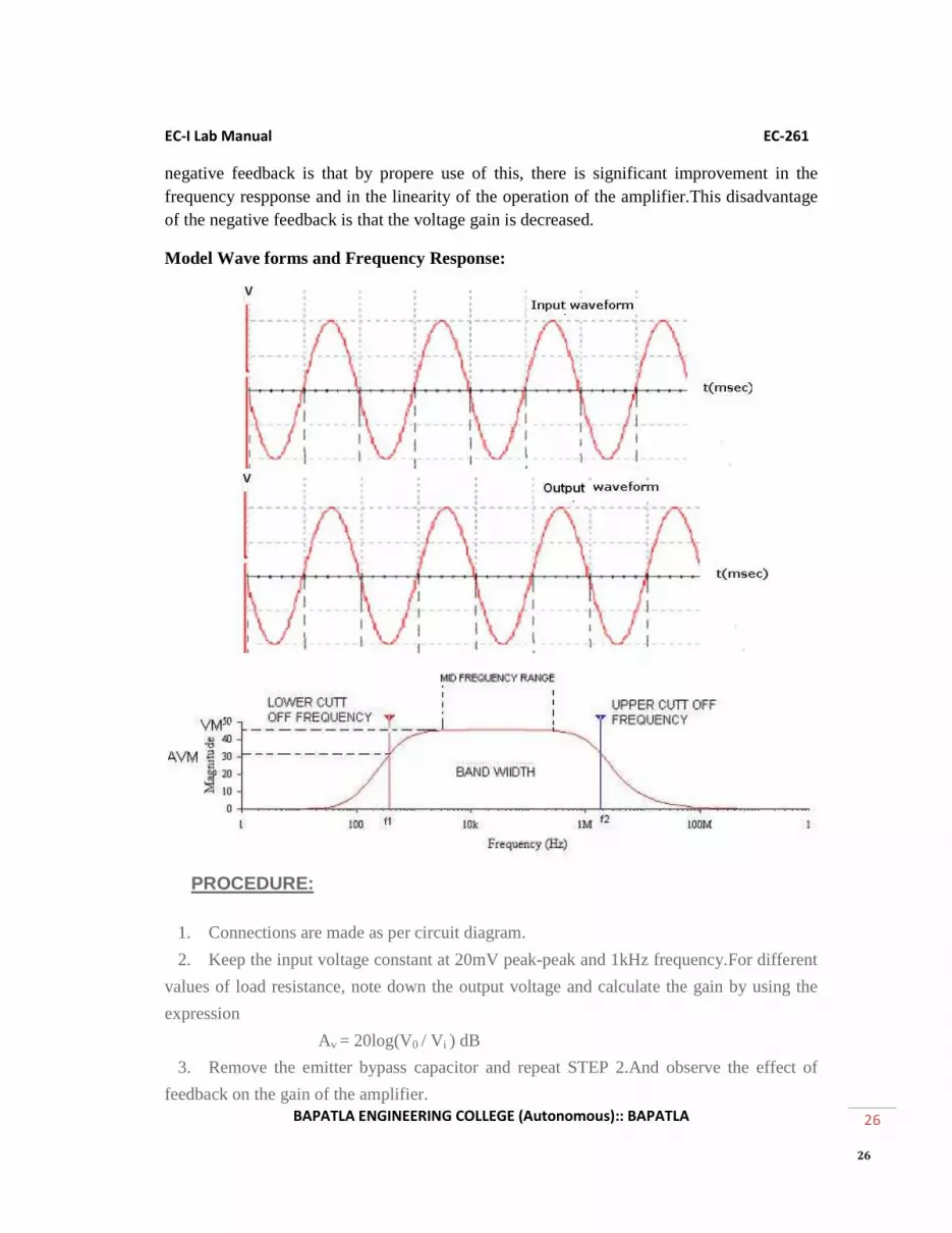
PROCEDURE: 1. Connections are made as per circuit diagram. 2. Keep the input voltage constant at 20mV peak-peak and 1kHz frequency.For different
values of load resistance, note down the output voltage and calculate the gain by using the expression

EC-I Lab Manual EC-261
BAPATLA ENGINEERING COLLEGE (Autonomous):: BAPATLA
23
23
Av = 20log(V0 / Vi ) dB 3. Remove the emitter bypass capacitor and repeat STEP 2.And observe the effect of
feedback on the gain of the amplifier. 4. For plotting the frequency the input voltage is kept constant at 20mV peak-peak and the
frequency is varied from 100Hz to 1MHz. 5. Note down the value of output voltage for each frequency. All the readings are tabulated
and the voltage gain in dB is calculated by using expression Av = 20log (V0 / Vi ) dB 6. A graph is drawn by taking frequency on X-axis and gain on Y-axis on semi log graph 7. The Bandwidth of the amplifier is calculated from the graph using the expression
Bandwidth B.W = f2 – f1. Where f1 is lower cutt off frequency of CE amplifier f 2 is upper cutt off frequency of CE amplifier
8. The gain-bandwidth product of the amplifier is calculated by using the expression Gain-Bandwidth Product = 3-dB midband gain X Bandwidth. Model Graph:

EC-I Lab Manual EC-261
BAPATLA ENGINEERING COLLEGE (Autonomous):: BAPATLA
24
24
Tabular Colums:
Voltage Gain: Vi = 20 mV
S.NO Output Voltage
(Vo) with
feedback
Output Voltage
(Vo)
without feedback
Gain(dB) with
feedback
Gain(dB)
without
feedback
PRECAUTIONS: 1. While taking the observations for the frequency response , the input voltage must be maintained constant at 20mV. 2. The frequency should be slowly increased in steps. 3. The three terminals of the transistor should be carefully identified. 4. All the connections should be correct. RESULT:

EC-I Lab Manual EC-261
BAPATLA ENGINEERING COLLEGE (Autonomous):: BAPATLA
25
25
10. Voltage Shunt Feedback Amplifier
AIM:
To measure the voltage gain of current - series feed back amplifier.
APPARATUS:
Transistor BC 107
Breadboard
Regulated Power Supply (0-30V,1A)
Function Generator
CRO(30 Mhz,dualtrace)
Resistors and Capacitors
CIRCUIT DIAGRAM:
THEORY:
When any increase in the output signal results into the input in such a way as to cause the decrease in the output signal, the amplifier is said to have negative feedback.The advantages of providing negative feedback are that the transfer gain of the amplifier with feedback can be stablised against varations in the hybrid parameteresof the transistor or the parameters of the other active devices used in the circuit. The most advantage of the
EC-I Lab Manual EC-261
BAPATLA ENGINEERING COLLEGE (Autonomous):: BAPATLA
26
26
negative feedback is that by propere use of this, there is significant improvement in the frequency respponse and in the linearity of the operation of the amplifier.This disadvantage of the negative feedback is that the voltage gain is decreased.
Model Wave forms and Frequency Response:
PROCEDURE:
1. Connections are made as per circuit diagram.
2. Keep the input voltage constant at 20mV peak-peak and 1kHz frequency.For different
values of load resistance, note down the output voltage and calculate the gain by using the
expression
Av = 20log(V0 / Vi ) dB
3. Remove the emitter bypass capacitor and repeat STEP 2.And observe the effect of
feedback on the gain of the amplifier.

EC-I Lab Manual EC-261
BAPATLA ENGINEERING COLLEGE (Autonomous):: BAPATLA
27
27
4. For plotting the frquency the input voltage is kept constant at 20mV peak-peak and
the frequency is varied from 100Hz to 1MHz.
5. Note down the value of output voltage for each frequency. All the readings are tabulated
and the voltage gain in dB is calculated by using expression Av = 20log (V0 / Vi ) dB
6. A graph is drawn by takung frquency on X-axis and gain on Y-axis on semi log graph
sheet
7. The Bandwidth of the amplifier is calculated from the graph using the expression
Bandwidth B.W = f2 – f1.
Where f1 is lower cutt off frequency of CE amplifier
f 2 is upper cutt off frequency of CE amplifier
8. The gain-bandwidth product of the amplifier is calculated by using the expression
Gain-Bandwidth Product = 3-dB midband gain X Bandwidth.
Tabular Colums:
Voltage Gain: Vi = 20 mV
S.NO Output Voltage (Vo) with feedback
Output Voltage (Vo) without feedback
Gain(dB) with feedback
Gain(dB) without feedback
PRECAUTIONS:
1. While taking the observations for the frequency response , the input voltage must be maintained constant at 20mV.
2. The frequency should be slowly increased in steps. 3. The three terminals of the transistor should be carefully identified. 4. All the connections should be correct.
RESULT:

EC-I Lab Manual EC-261
BAPATLA ENGINEERING COLLEGE (Autonomous):: BAPATLA
28
28
11. Complementary Symmetry Push-pull amplifier.
AIM:
To construct a Class B complementary symmetry power amplifier and observe the
waveforms with and without cross-over distortion and to compute maximum output power and
efficiency.
APPARATUS REQUIRED:
S.No. Name Range Quantity 1. Transistor CL100, BC558 1,1 2. Resistor 4.7kΩ,15kΩ 2,1 3. Capacitor 100µF 2 4. Diode IN4007 2 5. Signal Generator (0-3)MHz 1 6. CRO 30MHz 1 7. Regulated power supply (0-30)V 1 8. Bread Board 1
CIRCUIT DIAGRAM
FORMULA:
Input power, Pin=2VccIm/П

EC-I Lab Manual EC-261
BAPATLA ENGINEERING COLLEGE (Autonomous):: BAPATLA
29
29
Output power, Pout=VmIm/2
Power Gain or efficiency, η=л/4(Vm/Vcc) 100
THEORY:
A power amplifier is said to be Class B amplifier if the Q-point and the input signal are selected such that the output signal is obtained only for one half cycle for a full input cycle. The Q-point is selected on the X-axis. Hence, the transistor remains in the active region only for the positive half of the input signal.
There are two types of Class B power amplifiers: Push Pull amplifier and complementary symmetry amplifier. In the complementary symmetry amplifier, one n-p-n and another p-n-p transistor is used. The matched pair of transistor are used in the common collector configuration. In the positive half cycle of the input signal, the n-p-n transistor is driven into active region and starts conducting and in negative half cycle, the p-n-p transistor is driven into conduction. However there is a period between the crossing of the half cycles of the input signals, for which none of the transistor is active and output, is zero
OBSERVATION
OUTPUT SIGNAL
AMPLITUDE :
TIME PERIOD :
CALCULATION
POWER, PIN = 2VCC Im/л
OUTPUT POWER, POUT = VmIm/2
EFFICIENCY, η = ( л/4)( Vm/ VCC) x 100
MODEL GRAPH

EC-I Lab Manual EC-261
BAPATLA ENGINEERING COLLEGE (Autonomous):: BAPATLA
30
30
PROCEDURE:
1. Connections are given as per the circuit diagram without diodes. 2. Observe the waveforms and note the amplitude and time period of the input
signal and distorted waveforms. 3. Connections are made with diodes. 4. Observe the waveforms and note the amplitude and time period of the input
signal and output signal. 5. Draw the waveforms for the readings. 6. Calculate the maximum output power and efficiency.
Hence the nature of the output signal gets distorted and no longer remains the same
as the input. This distortion is called cross-over distortion. Due to this distortion, each transistor conducts for less than half cycle rather than the complete half cycle. To overcome this distortion, we add 2 diodes to provide a fixed bias and eliminate cross-over distortion.
RESULT:

EC-I Lab Manual EC-261
BAPATLA ENGINEERING COLLEGE (Autonomous):: BAPATLA
31
31
12. Class-A Power Amplifier.
AIM:
To construct a Class A power amplifier and observe the waveform and to compute maximum output power and efficiency.
APPARATUS REQUIRED:
S.No. Name Range Quantity 1. Transistor CL100, BC558 1,1 2. Resistor 47kΩ,33Ω,220Ω, 2,1 3. Capacitor 47 µF 2 4. Signal Generator (0-3)MHz 1 5. CRO 30MHz 1 6. Regulated power supply (0-30)V 1 7. Bread Board 1
CIRCUIT DIAGRAM
THEORY:
The power amplifier is said to be Class A amplifier if the Q point and the input signal are selected such that the output signal is obtained for a full input signal cycle.
For all values of input signal, the transistor remains in the active region and never enters into cut-off or saturation region. When an a.c signal is applied, the collector voltage varies sinusoidally hence the collector current also varies sinusoidally.The collector current flows for 3600 (full cycle) of the input signal. i e the angle of the collector current flow is 3600 .

EC-I Lab Manual EC-261
BAPATLA ENGINEERING COLLEGE (Autonomous):: BAPATLA
32
32
PROCEDURE:
1. Connect the circuit as per the circuit diagram.
2. Set Vi =50 mv, using the signal generator.
3. Keeping the input voltage constant, vary the frequency from 10 Hz to 1M Hz in regular steps and note down the corresponding output voltage.
4. Plot the graph; Gain (dB) vs Frequency(Hz).
FORMULA
Maximum power transfer =Po,max=Vo2/RL
Effeciency,η = Po,max/Pc
TABLES:
Keep the input voltage constant, Vin =
Frequency (in Hz) Output Voltage (in volts)
Gain= 20 log(Vo/Vin) (in dB)
RESULT:

EC-I Lab Manual EC-261
BAPATLA ENGINEERING COLLEGE (Autonomous):: BAPATLA
33
33
13. RC Phase Shift Oscillator.
Aim:
To design and set up an RC phase shift oscillator using BJT and to observe the sinusoidal output waveform.
Equipments required:
Transistor,
dc source,
capacitors, resis-tors,
potentiometer,
breadboard and CRO.
Circuit Diagram:
Theory: An oscillator is an electronic circuit for generating an ac signal voltage with a dc supply as the only input requirement. The frequency of the generated signal is decided by the circuit elements. An oscillator requires an amplifier, a frequency selective network, and a positive feedback from the output to the input. The Barkhausen criterion for sustained oscillation is A_ = 1 where A is the gain of the amplifier and is the feedback factor. The unity gain means signal is in phase. (If the signal is 180° out of phase, gain will be 1.). If a common emitter amplifier is used, with a resistive collector load, there is a 180 phase shift between the voltages at the base and the collector.

EC-I Lab Manual EC-261
BAPATLA ENGINEERING COLLEGE (Autonomous):: BAPATLA
34
34
In the figure shown, three sections of phase shift networks are used so that each section introduces approximately 60_ phase shift at resonant frequency. By analysis, resonant frequency f can be expressed by the equation,
Procedure: 1. Connections are made as per circuit diagram. 2. Connect CRO output terminals and observe the waveform. 3. Calculate practically the frequency of oscillations by using the expression f = 1 / T ( T= Time period of the waveform) 4. Repeat the above steps 2,3 for different values of L, and note down the practically values of oscillations of the RC-phase shift oscillator. 5. Compare the values of oscillations both theoretically and practically.
MODELWAVEFORM:
RESULT:

EC-I Lab Manual EC-261
BAPATLA ENGINEERING COLLEGE (Autonomous):: BAPATLA
35
35
14. Colpitt’s Oscillators
AIM: To study and calculate frequency of oscillations of colpitt’s oscillator. APPARATUS: Transistor BC 107 Capacitors 0.1µF - 2Nos 10µF - 2Nos 47µF - 1No Resistors 6.8kΩ, 1kΩ,100kΩ Decade Inductance Box (DIB) Decade Resistance Box (DRB) Cathode Ray Oscilloscope (CRO) Regulated Power Supply (0-30V) Connecting Wires
CIRCUITDIAGRAM:
THEORY: The tank circuit is made up of L1,C4 and C5 .The resistance R2 and R3 provides the necessary biasing. The capacitance C2 blocks the D.C component. The frequency of oscillations is determined by the values of L1,C4 and C5, and is given by
f = 1 / (2 (CTL1)1/2) Where CT = C1C2 / ( C1 + C2) The energy supplied to the tank circuit is of correct phase. The tank circuit provides 1800 out of phase. Also the transistor provides another 1800 . In this way, energy feedback to the tank circuit is in phase with the generated oscillations.

EC-I Lab Manual EC-261
BAPATLA ENGINEERING COLLEGE (Autonomous):: BAPATLA
36
36
PROCEDURE: 1. connections are made as per circuit diagram. 2. Connect CRO output terminals and observe the waveform. 3. Calculate practically the frequency of oscillations by using the expression
f = 1 / T ( T= Time period of the waveform) 4. Repeat the above steps 2,3 for different values of L, and note down the practically values of
oscillations of the collpitt’s oscillator. 5. Compare the values of oscillations both theoritically and practically.
OBSERVATIONS:
Inductance ( mH ) Theoretical Frequency ( Hz )
Practical Frequency ( Hz )
MODELWAVEFORM:
PRECAUTIONS: 1. All the connections should be correct.
2. Transistor terminals must be identified properly.
3. Reading should be taken without any parallax error.
RESULT:

EC-I Lab Manual EC-261
BAPATLA ENGINEERING COLLEGE (Autonomous):: BAPATLA
37
37
15. Hartley Oscillators AIM: To study and calculate frequency of oscillations of Hartley oscillator. Compare the
frequency of oscillations, theoretically and practically.
APPARATUS: Transistor BC 107
Capacitors 0.1µF, 10 µF
Resistors 6.8Kohm, 1Kohm and 100Kohm
Decade inductance box (DIB)
Decade resistance box (DRB)
Cathode ray oscilloscope
Bread board
Regulated power supply (0-30V)
Connecting wires
CIRCUIT DIAGRAM:

EC-I Lab Manual EC-261
BAPATLA ENGINEERING COLLEGE (Autonomous):: BAPATLA
38
38
THEORY: Hartley oscillator is very popular and is commonly used as a local oscillator in
radio receivers. It has two main advantages viz... Adaptability to wide range of frequencies
and easy to tune. The tank circuit is made up of L1, L2, and C1. The coil L1 is inductively
coupled to coil L2, the combination functions as auto transformer. The resistances R2 and
R3 provide the necessary biasing. The capacitance C2 blocks the d.c component. The
frequency of oscillations is determined by the values of L1, L2 and C1 and is given by,
F=1/(2π(C1(√L1+L2)))
The energy supplied to the tank circuit is of correct phase. The auto transformer provides
180˚ out of phase. Also another 180˚ is produced
By the transistor. In this way, energy feedback to the tank circuit is in phase with the
generated oscillations.
PROCEDURE: 1. Connections are made as per the circuit diagram.
2. Connect CRO at output terminals and observe wave form.
3. Calculate practically the frequency of oscillations by using the
Expression.
F=1/T, Where T= Time period of the waveform
4. Repeat the above steps 2, 3 for different values of L1 and note
Down practical values of oscillations of colpitts oscillator.
5. Compare the values of frequency of oscillations both theoretically
And Practically.
OBSERVATIONS:
CAPACITANCE(µF) Theoritical frequency
(KHZ)
Practical frequency
(KHZ)

EC-I Lab Manual EC-261
BAPATLA ENGINEERING COLLEGE (Autonomous):: BAPATLA
39
39
MODELWAVEFORM:
PRECAUTIONS: 1. All the connections should be correct.
2. Transistor terminals must be identified properly.
3. Reading should be taken without any parallax error.
RESULT:


