Embed Size (px)
Citation preview
626
NN
T:2
021I
PPA
X09
1
Development and characterization ofFired Passivating Contacts for p-type
silicon solar cells fabricationThese de doctorat de l’Institut Polytechnique de Paris
preparee a l’Ecole Polytechnique
Ecole doctorale n626 Institut Polytechnique de Paris (ED IP Paris)Specialite de doctorat : Physique
These presentee et soutenue a Palaiseau, le 15/11/2021, par
ANATOLE DESTHIEUX
Composition du Jury :
Olivier PalaisProfesseur, Aix-Marseille Universite (Institut MateriauxMicroelectronique Nanosciences de Provence) President
Marie-Estelle Gueunier-FarretMaıtre de Conference - HDR, Universite Paris-Saclay (LaboratoireGenie Electrique et Electronique de Paris) Rapporteur
Lars KorteSenior Scientist, Helmoltz-Zentrum Berlin (Young InvestigatorGroup Perovskite Tandem Solar Cells) Rapporteur
Erwin KesselsProfesseur, Eindhoven University of Technology (Department ofApplied Physics) Examinateur
Delfina MunozIngenieur Chercheur, Commissariat a l’Energie Atomique et auxEnergies Alternatives (Institut National de l’Energie Solaire) Examinateur
Damien AureauCharge de Recherche, Universite de Versaille - Saint Quentin(Laboratoire institut Lavoisier de Versailles) Examinateur
Pere Roca i CabarrocasDirecteur de Recherche, Ecole Polytechnique (Laboratoire dePhysique des Interfaces et Couches Minces) Directeur de these
Jorge PosadaIngenieur Chercheur, EDF R&D Encadrant de these
Barbara Bazer-BachiIngenieur Chercheur, Photowatt - EDF ENR PWT Invite

“It is crucial that the difference principle includes an idea of reci-procity: the better endowed (who have a fortunate place in the dis-tribution of native endowments they do not morally deserve) areencouraged to acquire still further benefits [...] on condition thatthey train their native endowments and use them in ways that con-tribute to the good of the less endowed (whose less fortunate placein the distribution they also do not morally deserve).”
Justice as Fairness, A RestatementJohn Rawls
i

iii
Acknowledgements
Ce manuscrit de these paracheve trois annees de travail que j’ai pu realiser entre EDFR&D, l’Institut Photovoltaıque d’Ile-de-France (IPVF), et le Laboratoire de Physiquedes Interfaces et Couches Minces (LPICM) dans le cadre d’une Convention Industrielle deFormation par la Recherche en Entreprise (CIFRE). Je tiens donc tout d’abord a remercierMattieu Versavel et Marie Jubault pour m’avoir permis de rentrer chez EDF initialementpour mon stage de master. Merci a Cedric Guerard et Mireille Owona pour m’avoir epaulepar la suite dans mes demarches administratives et pour leur aide et encadrement durantle reste de mon contrat de these.
Ensuite, du fond du cœur merci a Jorge Posada pour m’avoir fait confiance dans larealisation de cette these, et merci pour ton encadrement toujours bienveillant, et lesdiscussions (nombreuses) en salle chimie sur la grandeur de l’IRDEP et sur les conteset legendes autour des personnalites de feu ce laboratoire. A Pere Roca i Cabarrocas, uneternel remerciement, pour ta presence, ta passion, ton souci du detail, ton travail acharneet ta bonne humeur constante. A vous deux, je n’aurais pas pu rever un meilleur binomepour m’encadrer.
Par ailleurs, un immense merci aux membres de mon jury de these : Olivier Palaisqui en aura ete le president, mes deux rapporteurs Marie-Estelle Gueunier-Farret et LarsKorte, mais aussi Erwin Kessels, Delfina Munoz et Damien Aureau.
J’ai realise une immense partie de mes travaux experimentaux au LPICM, et rienn’aurait ete possible sans les equipes du BEER qui etaient toujours presentes en sou-tien des experiences ou pour regler des problemes de machines. En particulier, merci aCyril Jadaud, Francois Silva et Jonathan Meot pour leur aide precieuse. Un immensemerci a Pavel Bulkin pour les nombreux decapages HF et depots d’AlOx, et les autresdiscussions autour de l’exodiffusion et des techniques de depot, merci a Ileana Floreapour les preparation FIB et les mesures TEM, ainsi qu’a Mengkoing Sreng pour avoirrendu les mesures de MPL in situ possibles. A Dmitri Daineka, merci pour les repetitionsde musique, ainsi que pour les discussions scientifiques au sein du groupe PROM ou aucoin d’un couloir avec egalement Angelo Pirangelo, Denis Tondelier, Erik Johnson,, Jean-Charles Vanel,Jean-Eric Bourre et Karim Ouaras. Et enfin un enorme big up a tous lesamis du LPICM, toujours la quand il faut, et avec qui j’aurais aime passer un peu plus detemps au quotidien. En particulier, merci a Chloe, Ronan, Malinka (ton bebe Octopus seporte toujours tres bien), Eric, Ghewa, Hindia, Minjin, Tinghui, Junha, Robert, Gookbin,Michel, Hae-yeon Lakshmann, Josef, Junkang, Antonio, Daniel, Monalisa (do not worry,you will definitely end up mastering the beast) et toutes les autres personnes avec qui j’aipu discuter au cours de ces trois dernieres annees. Good luck to Mateusz for the upcomingevolution of in situ passivation measurements, I am sure you will do great.
Je suis infiniment reconnaissant envers mes differents collaborateurs: ceux de l’InstitutLavoisier de Versailles (ILV) avec Davina Messou, Solene Bechu et Muriel Bouttemy,avec qui j’ai beaucoup apprecie echanger et qui ont toujours pris le temps de discuter
des resultats d’XPS, et ceux de l’Ecole Polytechnique Federal de Lausanne (EPFL) avecMario Lehmann, Franz-Josef Haug et Audrey Morisset qui ont eu la gentillesse de mecontacter a l’issue d’une conference en ligne (pas toujours le plus simple pour initier descollaborations) et m’ont apporte beaucoup dans mes reflexions sur la comprehension desresultats de MPL !
Un immense merci a Sophie Gaillard pour les innombrables nettoyages RCA, pour tagentillesse, ton energie, et pour les sorties natation qui m’ont fait le plus grand bien, etmerci a Valerie Daniau pour tous les efforts dans les labos, ton sourire toujours colle auxlevres et la chouette randonnee a Fontainebleau ! Un grand merci a tous permanents EDFqui m’ont aide de pres ou de loin au cours de ma these, avec qui j’ai pu discute autourd’un cafe ou d’un brunch (merci papa Regis Tuyizere).
Et puis l’IPVF c’est beaucoup, beaucoup d’echanges et de belles rencontres realiseesau fil de l’eau ! Une pensee attendrie pour tous les “anciens”, collegues doctorants partistrop tot: Adrien, Cecile, Fabien, Harold, , Louis, Mishael, Rafael, Romaric et Valentincote doctorants, mais aussi Baljeet et Kathy pour les discussions passionnantes et lessuper concerts qu’on a pu preparer ensemble. A Caterine, Christian et Maria un grandmerci pour cet air hispanique que vous avez insuffle a notre openspace du 2B.B13. Je neremercierai jamais assez ceux qui m’ont initie a l’escalade, et toutes les personnes de la teamArkose avec qui ce fut un plaisir de grimper ! Parmi eux Olivier (mon gars sur), Thomas(Monsieur Conseil), Alex Py (le gecko), Arpit (“voiture”), mais aussi Alexandre, Arthur,Geraud et Marie. Merci et bon courage aux doctorants plus jeunes, et merci pour les bonsmoments de convivialites passes ensemble autour d’un verre ou d’une soiree : Carlos, Celia,Claire, Elisa, Guillaume, Javid, Lise, Salim et Thomas. Mentions speciales pour Berengereet les discussions infinies qu’on peut avoir, et pour Capu pour tout, et en particulier nospetits moments musicaux et gourmands. Enfin, ces trois annees auraient ete beaucoupplus fades s’il n’y avait pas eu mes petits Tuches dans l’affaire : Margot, Minouche, Sophieet Yeye et leur enthousiasme debordant pour faire des soirees, s’endormir devant des filmsa la qualite douteuse, et discuter autour des cafes les mardredis et les vendredis philo.
Un coup de chapeau particulier a Daniel Suchet pour les discussions passionnantes,son aide precieuse pour la preparation de la semaine ATHENS, et merci de m’avoir faitdecouvrir Citoyens Pour Le Climat !
A mes amis fideles et toujours presents, qui m’ont permis de sortir ma petite tete dema bulle, un immense merci ! Parmi eux, merci a mes eternels amis d’enfance que je cherisdu fond de mon cœur : ma Juli, et la clique avec Anne So, Claire, Delf, Guigui et Salome! Merci a ma Coco pour les innombrables jap et ses vocaux interminables, aux expats etderniers parisiens de la P2018 avec Alexis, Gabi, Nathan, Louis (on adore les semaines deteletravail poses au bord de la mer), JB, Koen et Pham, et aux anciens de l’OPA: Ivanpour les conseils de pro a l’escalade, Jordan, Pierre et Lucas pour nos petits Skype desfamilles et Gautier pour les soirees musique et magie dans lesquelles il met toujours uneambiance de feu ! Un bisou a Sacha et ses tracos rigolos. Enfin, a Neil et Dinou, vousetes moches mais droles (l’un des deux est faux), et je vous aime fort.
Et pour finir un immense merci a ma famille, pour l’amour qu’ils me donnent depuisma plus tendre enfance, et sans qui je ne serais pas la personne que je suis devenue.
iv
v
Acronyms
µc-Si:H hydrogenated micro-crystalline siliconµc-SiOx:H hydrogenated micro-crystalline silicon oxide4PP 4-points probea-Si:H hydrogenated amorphous silicona-SiNx:H hydrogenated amorphous silicon nitrideAl-BSF aluminum back-surface fieldALD atomic layer depositionAlOx aluminum oxideARC anti-reflection coatingAZO aluminum-doped zinc oxidec-Si crystalline siliconCCGT combined cycle gas turbineCCP capacitively coupled plasmaCOCOS corona oxide characterisation on semiconductorCVD chemical vapor depositionCz CzochralskyDSP double-side polishedEGS electronic grade siliconFGA forming gas annealingFIB focused ion beamFPC fired passivated contactFT fire-throughFTIR fourier transform infrared spectroscopyFZ float-zoneHIT heterojunction with intrinsic thin layerHWCVD hot-wire chemical vapor depositionIBC interdigitated back contactIPCC International Panel on Climate ChangeITO indium-doped tin oxideLCOE levelized cost of electricityLPCVD low pressure chemical vapor depositionmc-Si multi-crystalline siliconMGS metallurgical grade siliconMPL modulated photoluminescenceNAOS nitric acid oxidation of siliconPA-ALD plasma-assisted atomic layer depositionPANO plasma-assisted nitrous oxidePCE power conversion efficiencyPECVD plasma-enhanced chemical vapor deposition
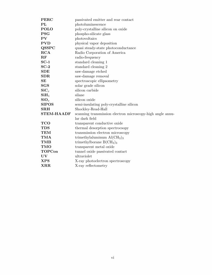
PERC passivated emitter and rear contactPL photoluminescencePOLO poly-crystalline silicon on oxidePSG phospho-silicate glassPV photovoltaicsPVD physical vapor depositionQSSPC quasi steady-state photoconductanceRCA Radio Corporation of AmericaRF radio-frequencySC-1 standard cleaning 1SC-2 standard cleaning 2SDE saw-damage etchedSDR saw-damage removalSE spectroscopic ellipsometrySGS solar grade siliconSiCx silicon carbideSiH4 silaneSiOx silicon oxideSIPOS semi-insulating poly-crystalline siliconSRH Shockley-Read-HallSTEM-HAADF scanning transmission electron microscopy-high angle annu-
lar dark fieldTCO transparent conductive oxideTDS thermal desorption spectrocsopyTEM transmission electron microscopyTMA trimethylaluminum Al(CH3)3TMB trimethylborane B(CH3)3TMO transparent metal oxideTOPCon tunnel oxide passivated contactUV ultravioletXPS X-ray photoelectron spectroscopyXRR X-ray reflectometry
vi

vii
List of Symbols
[X −H] Concentration in X −H bonds
α Absorptivity
∆n Excess electron density
∆p Excess hole density
η Power conversion efficiency
ηn Electro-chemical potential of electrons
ηp Electro-chemical potential of holes
λ Wavelength
V Volume of the studied ensemble of particles
µn Electron mobility
µp Hole mobility
ω Angular frequency of the incident light
φ Phase shift between the laser excitation and the modulated photoluminescencesignal
φn Chemical potential of electrons
φp Chemical potential of holes
ρc Specific contact resistivity
σn Electron conductivity
σp Hole conductivity
σX−H IR-scattering cross-section of X −H bonds
τAuger Characteristic minority carrier lifetime related to Auger recombinations
τeff,diff Differential effective minority carrier lifetime
τeff Effective minority carrier lifetime
τm Minority carrier lifetime measured by modulated photoluminescence
τrad Characteristic minority carrier lifetime related to radiative recombinations

τSRH Characteristic minority carrier lifetime related to SRH recombinations
τsurf Characteristic minority carrier lifetime related to surface recombinations
εFn Quasi-Fermi level of electrons
εFp Quasi-Fermi level of holes
ϕ Electric potential
A Area of the solar cell
AXH Area of the X −H stretching mode peak
Brad Radiative recombination coefficient
c Speed of light in vacuum
Cn Trap capture coefficient of electrons
Cp Trap capture coefficient of holes
CA,n Auger recombination coefficient for electrons
CA,p Auger recombination coefficient for holes
Dn Diffusion coefficient of electrons
Dp Diffusion coefficient of holes
DH Hydrogen diffusion coefficient
Dit Surface defect density
E Electric field
Eg Energy band gap
Ei Fermi level for an intrinsic semiconductor
Et Trap energy level in the band gap
Fa Fraction of amorphous material in the ellipsometric model
Fc Fraction of crystallised material in the ellipsometric model
FF Fill Factor
G Generation rate
h Planck constant
I Light intensity
I0 Incident light intensity
iVoc Implied open-circuit voltage
J Current density
viii

J0 Saturation current density
J0,c Recombination current density at the metallic contact
Jgen Photogenerated current density
Jn,diff Diffusion current density of electrons
Jn Total current density of electrons
Jp,diff Diffusion current density of holes
jPL Luminescence photon flux
Jp Total current density of holes
Jsc Short circuit current density
k Boltzman’s constant
n Density of free electrons
NA Density of acceptor atoms
N−A Density of ionized acceptor atoms
NC Effective density of states of electrons in the conduction band
ND Density of donor atoms
N+D Density of ionized donor atoms
ne Free electron density in a plasma
ni Intrinsic electron density at thermal equilibrium
Nt Trap density
NV Effective density of states of holes in the valence band
Nfiring Density of recombination centers created during a firing step
P Output power of a solar cell
p Density of free holes
Pinc Incident radiative power density
Pmpp Output power at maximum power point
q Elementary charge
Qe Average number of electron-hole pair generated by one photon
Qf Fixed charge density
R Dilution ratio of silane in hydrogen
Rf Front surface reflectivity
ix

Rp Parallel resistance
Rs Series resistance
RAug Auger recombination rate
Rbulk Bulk recombination rate
Reff Effective recombination rate
Rms Surface roughness coefficient
Rrad Radiative recombination rate
RSRH Shockley-Read-Hall recombination rate
Rsurf Surface recombination rate
S Entropy
T Temperature
Te Electron temperature in a plasma
Tg Gas temperature of a plasma
U Internal energy
V Voltage
Voc Open circuit voltage
x
Table of contents
Introduction 1Global energy context . . . . . . . . . . . . . . . . . . . . . . . . . . . . . . . . . 1Purpose and structure of this work . . . . . . . . . . . . . . . . . . . . . . . . . . 4
1 Context, background and objectives 71.1 Basic concepts of solar cells . . . . . . . . . . . . . . . . . . . . . . . . . . . 8
1.1.1 Working principle of a solar cell . . . . . . . . . . . . . . . . . . . . . 81.1.2 Characteristics of a solar cell . . . . . . . . . . . . . . . . . . . . . . 111.1.3 Limits of conversion efficiency . . . . . . . . . . . . . . . . . . . . . . 121.1.4 Homojunction solar cells . . . . . . . . . . . . . . . . . . . . . . . . . 16
1.2 Passivating contacts: toward higher efficiency . . . . . . . . . . . . . . . . . 181.2.1 Working principle . . . . . . . . . . . . . . . . . . . . . . . . . . . . 181.2.2 Heterojunction technology and limitations . . . . . . . . . . . . . . . 191.2.3 Tunnel oxide passivating contacts . . . . . . . . . . . . . . . . . . . . 201.2.4 Transparent Metal Oxides . . . . . . . . . . . . . . . . . . . . . . . . 24
1.3 Metallization of TOPCon solar cells . . . . . . . . . . . . . . . . . . . . . . 251.3.1 Screen printing . . . . . . . . . . . . . . . . . . . . . . . . . . . . . . 251.3.2 Low-temperature metallization . . . . . . . . . . . . . . . . . . . . . 261.3.3 Fire-through metallic paste . . . . . . . . . . . . . . . . . . . . . . . 261.3.4 n-type and p-type TOPCon FT metallisation . . . . . . . . . . . . . 27
1.4 Silicon Wafer manufacturing . . . . . . . . . . . . . . . . . . . . . . . . . . . 281.4.1 From quartzite to polycrystalline silicon rods . . . . . . . . . . . . . 281.4.2 Multi-crystalline silicon . . . . . . . . . . . . . . . . . . . . . . . . . 291.4.3 Mono-crystalline silicon . . . . . . . . . . . . . . . . . . . . . . . . . 291.4.4 Cast-mono wafers . . . . . . . . . . . . . . . . . . . . . . . . . . . . 31
1.5 Objectives of the study . . . . . . . . . . . . . . . . . . . . . . . . . . . . . 31
2 Materials development and optimization 332.1 Deposition tools and methods . . . . . . . . . . . . . . . . . . . . . . . . . . 34
2.1.1 Plasma-enhanced chemical vapor deposition . . . . . . . . . . . . . . 342.1.2 Radio Corporation of America (RCA) cleaning . . . . . . . . . . . . 372.1.3 Substrates and characterizations . . . . . . . . . . . . . . . . . . . . 38
2.2 Tunnel oxide layer . . . . . . . . . . . . . . . . . . . . . . . . . . . . . . . . 392.2.1 PECVD oxide . . . . . . . . . . . . . . . . . . . . . . . . . . . . . . . 392.2.2 Wet-chemical oxide . . . . . . . . . . . . . . . . . . . . . . . . . . . . 40
2.3 Boron-doped silicon layer resistant to firing . . . . . . . . . . . . . . . . . . 402.3.1 Avoiding blistering . . . . . . . . . . . . . . . . . . . . . . . . . . . . 412.3.2 Impact of µc-Si:H deposition on the tunnel oxide layer . . . . . . . . 432.3.3 Optimization of the passivation properties of (p) µc-Si:H . . . . . . . 482.3.4 µc-SiOx:H . . . . . . . . . . . . . . . . . . . . . . . . . . . . . . . . . 51
xi
2.4 Phosphorous-doped silicon layer . . . . . . . . . . . . . . . . . . . . . . . . . 542.5 Capping layer . . . . . . . . . . . . . . . . . . . . . . . . . . . . . . . . . . . 57
2.5.1 Hydrogenated amorphous silicon nitride (a-SiNx:H) layer . . . . . . 572.5.2 Comparison of different capping layers . . . . . . . . . . . . . . . . . 63
2.6 Summary . . . . . . . . . . . . . . . . . . . . . . . . . . . . . . . . . . . . . 64
3 In situ modulated photoluminescence for AlOx 673.1 In situ MPL coupled to a PECVD reactor . . . . . . . . . . . . . . . . . . . 68
3.1.1 Introduction to modulated photoluminescence . . . . . . . . . . . . . 683.1.2 In situ modulated photoluminescence experimental setup . . . . . . 703.1.3 Diffusion phenomena . . . . . . . . . . . . . . . . . . . . . . . . . . . 713.1.4 Temperature correction . . . . . . . . . . . . . . . . . . . . . . . . . 77
3.2 AlOx passivated samples: a case study . . . . . . . . . . . . . . . . . . . . . 793.2.1 Context . . . . . . . . . . . . . . . . . . . . . . . . . . . . . . . . . . 793.2.2 Experimental methods . . . . . . . . . . . . . . . . . . . . . . . . . . 803.2.3 In situ MPL measurements during annealing . . . . . . . . . . . . . 813.2.4 Chemical passivation . . . . . . . . . . . . . . . . . . . . . . . . . . . 833.2.5 Field-effect passivation . . . . . . . . . . . . . . . . . . . . . . . . . . 833.2.6 Investigation of the discrepancy between QSSPC and MPL . . . . . 84
3.3 Summary . . . . . . . . . . . . . . . . . . . . . . . . . . . . . . . . . . . . . 85
4 In situ MPL for fired passivating contacts 874.1 Hydrogenation after firing . . . . . . . . . . . . . . . . . . . . . . . . . . . . 88
4.1.1 Context and experimental methods . . . . . . . . . . . . . . . . . . . 884.1.2 Annealing temperature and hydrogen diffusion . . . . . . . . . . . . 894.1.3 Identification of the different contributions . . . . . . . . . . . . . . 93
4.2 Hydrogenation before firing . . . . . . . . . . . . . . . . . . . . . . . . . . . 994.2.1 In situ MPL setup for acquisition during a PECVD process . . . . . 994.2.2 (p) µc-Si:H and (p) µc-SiOx:H under NH3 + H2 plasma exposure . . 1014.2.3 Evolution of the passivation during a-SiNx:H deposition . . . . . . . 1054.2.4 Cell precursors with p-type and n-type FPC . . . . . . . . . . . . . . 108
4.3 Summary . . . . . . . . . . . . . . . . . . . . . . . . . . . . . . . . . . . . . 109
5 Towards large area FPC cells 1115.1 Process transfer on Cz and cast-mono wafers . . . . . . . . . . . . . . . . . 112
5.1.1 Context and experimental methods . . . . . . . . . . . . . . . . . . . 1125.1.2 Textured wafers . . . . . . . . . . . . . . . . . . . . . . . . . . . . . 1125.1.3 Polished surfaces . . . . . . . . . . . . . . . . . . . . . . . . . . . . . 114
5.2 Solar cell fabrication . . . . . . . . . . . . . . . . . . . . . . . . . . . . . . . 1175.3 Summary . . . . . . . . . . . . . . . . . . . . . . . . . . . . . . . . . . . . . 118
Conclusion 119Optimization of the FPC stack . . . . . . . . . . . . . . . . . . . . . . . . . . . . 119In situ Modulated Photoluminescence for AlOx . . . . . . . . . . . . . . . . . . . 119In situ Modulated Photoluminescence for FPC . . . . . . . . . . . . . . . . . . . 120Towards large area FPC cells . . . . . . . . . . . . . . . . . . . . . . . . . . . . . 120
Bibliography 121
xii
List of Figures
Figure 1: (a) Learning curve of the module spot market prices as a functionof the cumulative PV module shipments [6]. (b) Worldwide cumu-lative capacity of installed solar photovoltaic power in MWp from2000 to 2018 [7]. . . . . . . . . . . . . . . . . . . . . . . . . . . . . . 2
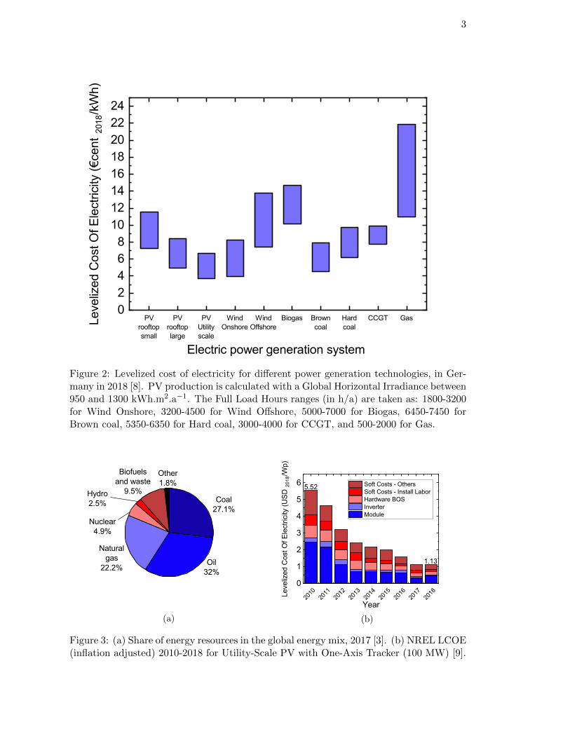
Figure 2: Levelized cost of electricity for different power generation technolo-gies, in Germany in 2018 [8]. . . . . . . . . . . . . . . . . . . . . . . 3
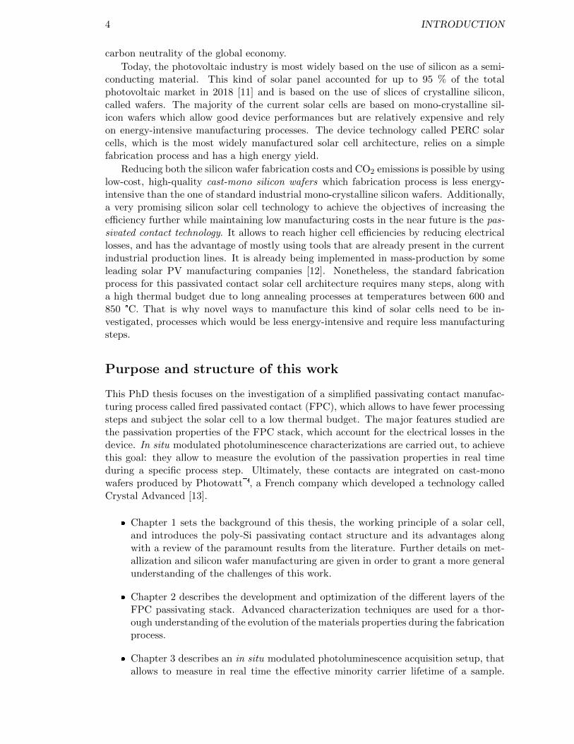
Figure 3: (a) Share of energy resources in the global energy mix, 2017 [3].(b) NREL LCOE (inflation adjusted) 2010-2018 for Utility-ScalePV with One-Axis Tracker (100 MW) [9]. . . . . . . . . . . . . . . 3
Figure 1.1: Scheme of the energy bands of a semi-conductor. . . . . . . . . . . 8
Figure 1.2: Scheme of the working principle of a solar cell. . . . . . . . . . . . . 9
Figure 1.3: Equivalent electrical circuit of a solar cell, one-diode model. . . . . 11
Figure 1.4: Example of evolution of the current density and output power den-sity with applied voltage. . . . . . . . . . . . . . . . . . . . . . . . . 12
Figure 1.5: (a) Schematic of incomplete absorption of the solar spectrum. (b)Thermalization loss of the excited electron and hole. . . . . . . . . 13
Figure 1.6: AM1.5 power spectral density (black line) compared with maximumpower spectral density extractable from a single junction solar cell(1.12 eV semiconductor band gap) after thermalisation and partialabsorption (red line). Adapted from [18]. . . . . . . . . . . . . . . . 14
Figure 1.7: Schematic representation of recombination mechanisms: 1O radia-tive, 2O Auger, and 3O SRH recombinations. . . . . . . . . . . . . . 14
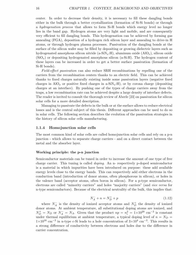
Figure 1.8: (a) Architecture and (b) process-flow for the fabrication of Al-BSFsolar cells. . . . . . . . . . . . . . . . . . . . . . . . . . . . . . . . . 18
Figure 1.9: (a) Architecture and (b) process-flow for the fabrication of PERCsolar cells. . . . . . . . . . . . . . . . . . . . . . . . . . . . . . . . . 18
Figure 1.10: (a) Architecture of a bifacial HIT solar cell and (b) its energy banddiagram in the dark near the rear p-i-n hetero-interface - calculatedwith SCAPS software. . . . . . . . . . . . . . . . . . . . . . . . . . 19
Figure 1.11: (a) Architecture of p-type bifacial TOPCon solar cells and (b) itsEnergy Band Diagram in the dark near the hole-selective contact -calculated with SCAPS software. . . . . . . . . . . . . . . . . . . . 20
Figure 1.12: Historical progression of notable c-Si solar cell efficiencies. . . . . . 22
Figure 1.13: Energy band diagrams calculated with SCAPS for a stack of (a) n-type c-Si/SiOx/MoOx (band alignment extracted from [109]) and(b) n-type c-Si/SiOx/TiOx. . . . . . . . . . . . . . . . . . . . . . . 25
Figure 1.14: The basic screen print process [118]. . . . . . . . . . . . . . . . . . . 26
Figure 1.15: Recommended firing temperature profile [122]. . . . . . . . . . . . . 27
xiii
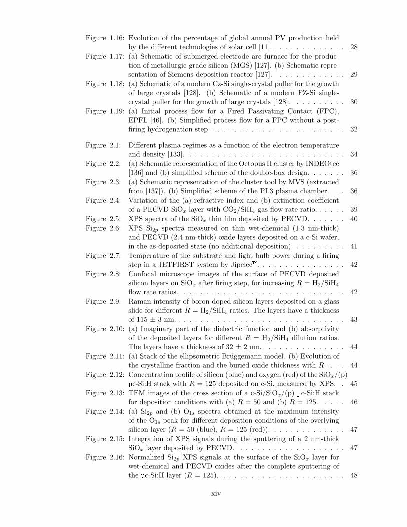
Figure 1.16: Evolution of the percentage of global annual PV production heldby the different technologies of solar cell [11]. . . . . . . . . . . . . . 28
Figure 1.17: (a) Schematic of submerged-electrode arc furnace for the produc-tion of metallurgic-grade silicon (MGS) [127]. (b) Schematic repre-sentation of Siemens deposition reactor [127]. . . . . . . . . . . . . 29
Figure 1.18: (a) Schematic of a modern Cz-Si single-crystal puller for the growthof large crystals [128]. (b) Schematic of a modern FZ-Si single-crystal puller for the growth of large crystals [128]. . . . . . . . . . 30
Figure 1.19: (a) Initial process flow for a Fired Passivating Contact (FPC),EPFL [46]. (b) Simplified process flow for a FPC without a post-firing hydrogenation step. . . . . . . . . . . . . . . . . . . . . . . . . 32
Figure 2.1: Different plasma regimes as a function of the electron temperatureand density [133]. . . . . . . . . . . . . . . . . . . . . . . . . . . . . 34
Figure 2.2: (a) Schematic representation of the Octopus II cluster by INDEOtec[136] and (b) simplified scheme of the double-box design. . . . . . . 36
Figure 2.3: (a) Schematic representation of the cluster tool by MVS (extractedfrom [137]). (b) Simplified scheme of the PL3 plasma chamber. . . 36
Figure 2.4: Variation of the (a) refractive index and (b) extinction coefficientof a PECVD SiOx layer with CO2/SiH4 gas flow rate ratio. . . . . . 39
Figure 2.5: XPS spectra of the SiOx thin film deposited by PECVD. . . . . . . 40
Figure 2.6: XPS Si2p spectra measured on thin wet-chemical (1.3 nm-thick)and PECVD (2.4 nm-thick) oxide layers deposited on a c-Si wafer,in the as-deposited state (no additional deposition). . . . . . . . . . 41
Figure 2.7: Temperature of the substrate and light bulb power during a firingstep in a JETFIRST system by Jipelec. . . . . . . . . . . . . . . . 42
Figure 2.8: Confocal microscope images of the surface of PECVD depositedsilicon layers on SiOx after firing step, for increasing R = H2/SiH4
flow rate ratios. . . . . . . . . . . . . . . . . . . . . . . . . . . . . . 42
Figure 2.9: Raman intensity of boron doped silicon layers deposited on a glassslide for different R = H2/SiH4 ratios. The layers have a thicknessof 115 ± 3 nm. . . . . . . . . . . . . . . . . . . . . . . . . . . . . . . 43
Figure 2.10: (a) Imaginary part of the dielectric function and (b) absorptivityof the deposited layers for different R = H2/SiH4 dilution ratios.The layers have a thickness of 32 ± 2 nm. . . . . . . . . . . . . . . 44
Figure 2.11: (a) Stack of the ellipsometric Bruggemann model. (b) Evolution ofthe crystalline fraction and the buried oxide thickness with R. . . . 44
Figure 2.12: Concentration profile of silicon (blue) and oxygen (red) of the SiOx/(p)µc-Si:H stack with R = 125 deposited on c-Si, measured by XPS. . 45
Figure 2.13: TEM images of the cross section of a c-Si/SiOx/(p) µc-Si:H stackfor deposition conditions with (a) R = 50 and (b) R = 125. . . . . 46
Figure 2.14: (a) Si2p and (b) O1s spectra obtained at the maximum intensityof the O1s peak for different deposition conditions of the overlyingsilicon layer (R = 50 (blue), R = 125 (red)). . . . . . . . . . . . . . 47
Figure 2.15: Integration of XPS signals during the sputtering of a 2 nm-thickSiOx layer deposited by PECVD. . . . . . . . . . . . . . . . . . . . 47
Figure 2.16: Normalized Si2p XPS signals at the surface of the SiOx layer forwet-chemical and PECVD oxides after the complete sputtering ofthe µc-Si:H layer (R = 125). . . . . . . . . . . . . . . . . . . . . . . 48
xiv
Figure 2.17: Variation of iVoc for (a) both PECVD and wet-chemical oxides ata given R = 125 value and (b) a wet-chemical tunnel oxide anddifferent dilution ratios R during the deposition of (p) µc-Si:H. . . . 49
Figure 2.18: Evolution of the conductivity of the boron doped silicon layers withR, after an annealing step at 250 °C for 10 min. . . . . . . . . . . . 50
Figure 2.19: Variation of (a) iVoc and (b) lifetime τeff with the flow rate of TMBused during the deposition of the (p) µc-Si:H layer. . . . . . . . . . 50
Figure 2.20: Evolution of (a) the absorptivity and (b) the conductivity of the(p) µc-SiOx:H layer with the flow rate of CO2. . . . . . . . . . . . . 51
Figure 2.21: Variation of (a) iVoc and (b) τeff with the flow rate of CO2 usedduring the deposition of the (p) µc-SiOx:H layer. . . . . . . . . . . 52
Figure 2.22: Comparison of the H2 ion currents measured by Thermal Desorp-tion Spectrometry (TDS) for (p) µc-Si:H and (p) µc-SiOx:H. . . . . 53
Figure 2.23: Thickness of (p) µc-SiOx:H deposited as a function of the durationof deposition. . . . . . . . . . . . . . . . . . . . . . . . . . . . . . . 53
Figure 2.24: Variation of (a) iVoc and (b) τeff with the (p) µc-SiOx layer depo-sition time. . . . . . . . . . . . . . . . . . . . . . . . . . . . . . . . . 54
Figure 2.25: Evolution of the crystalline fraction of the n-type silicon layer withthe dilution ratio R. . . . . . . . . . . . . . . . . . . . . . . . . . . . 55
Figure 2.26: Variation of (a) iVoc and (b) τeff with the flow rate of SiH4 usedduring the deposition of the (n) µc-Si:H layer. . . . . . . . . . . . . 56
Figure 2.27: Variation of (a) iVoc and (b) τeff with the flow rate of CO2 usedduring the deposition of the (n) µc-SiOx:H layers. . . . . . . . . . . 56
Figure 2.28: (a) Absorbtivity and (b) conductivity of the (n) µc-SiOx layers fordifferent CO2 flow rates during the deposition. . . . . . . . . . . . . 57
Figure 2.29: Evolution of n and k with (a) H2 flow rate, (b) RF Power, (c) Pres-sure, and (d) NH3/SiH4 flow rate ratio for the a-SiNx:H deposition. 58
Figure 2.30: FTIR spectra before and after a firing step for samples with (a)NH3/SiH4 = 4 and (b) NH3/SiH4 = 3. (c) and (d) are the samespectra zoomed on Si-H and N-H stretching modes, between 2000and 3500 cm−1. . . . . . . . . . . . . . . . . . . . . . . . . . . . . . 59
Figure 2.31: Deconvolution of the FTIR signals before firing for the NH3/SiH4
ratios (a) 3 and (b) 4. The deconvolution is processed to identifythe chemical environments of the Si and N atoms in the depositedmaterials. . . . . . . . . . . . . . . . . . . . . . . . . . . . . . . . . 60
Figure 2.32: Evolution of iVoc and τeff for various firing peak temperatures ona sample coated with a SiOx/(p) µc-Si:H/SiNx:H passivating stack. 62
Figure 2.33: Variation of (a) iVoc and (b) τeff with the thickness of a-SiNx:Hdeposited before and after a firing step at 850 °C. . . . . . . . . . . 62
Figure 2.34: Variation of (a) iVoc and (b) τeff with the flow rate of CO2 usedduring the deposition of the a-SiNxOy:H layer. . . . . . . . . . . . . 63
Figure 2.35: Variation of (a) iVoc and (b) τeff before and after a firing step fordifferent capping layers on a SiOx/(p) µc-Si:H passivating stack. . . 64
Figure 3.1: Schematic representation of the in situ MPL acquisition setup cou-pled with a PECVD reactor, Figure from [169]. . . . . . . . . . . . 70
Figure 3.2: LiTe algorithm, adapted from [169]. . . . . . . . . . . . . . . . . . . 72
xv
Figure 3.3: Various measurements (blue dots) and extrapolation of the func-tion τeff (∆n) to derive the minority carrier lifetime at a specificinjection level of 1×1015 cm−3 (green dot) [169]. . . . . . . . . . . . 73
Figure 3.4: Schematic representation of the MPL measurement setup. . . . . . 74
Figure 3.5: Spacial distribution of the excess carrier density in the sample witha simple diffusion model. . . . . . . . . . . . . . . . . . . . . . . . . 75
Figure 3.6: Variation of the relative error in excess carrier lifetime of the currentalgorithm (assuming no diffusion). . . . . . . . . . . . . . . . . . . . 76
Figure 3.7: Modified algorithm, taking lateral diffusion into account. . . . . . . 78
Figure 3.8: Comparison of the previous (blue) and new scheme (red) for thecalculation of the lifetime by MPL. . . . . . . . . . . . . . . . . . . 79
Figure 3.9: Evolution of the minority carrier lifetime with temperature of ann-type FZ wafer passivated with a SiOx/(n) poly-Si stack processedat high temperature. . . . . . . . . . . . . . . . . . . . . . . . . . . 80
Figure 3.10: Evolution of the minority carrier lifetime (at ∆n = 1×1015 cm−3)of an Al2O3-passivated c-Si wafer during annealing at 350 °C for30 minutes in H2. The black curve shows the temperature profile.The black curve shows the temperature profile. The lifetime valuesfollow the temperature correction detailed in Section 3.1.4. . . . . . 81
Figure 3.11: Evolution of the minority carrier lifetime (at ∆n = 1×1015 cm−3)of an Al2O3-passivated c-Si wafer during annealing at 350 °C forless than 1 minute in H2. The black curve shows the temperatureprofile. The black curve shows the temperature profile. The lifetimevalues follow the temperature correction detailed in Section 3.1.4. . 82
Figure 3.12: Evolution of the minority carrier lifetime (at ∆n = 1×1015 cm−3)of an Al2O3-passivated c-Si wafer during annealing at 250 °C forless than 1 minute in H2. The black curve shows the temperatureprofile. The black curve shows the temperature profile. The lifetimevalues follow the temperature correction detailed in Section 3.1.4. . 82
Figure 3.13: STEM-HAADF images of the c-Si/AlOx interface for (a) the as-deposited sample, (b) the sample annealed at 250 °C for 1 min, and(c) the one annealed 30 min at 350 °C. . . . . . . . . . . . . . . . . 84
Figure 3.14: PL Images for samples annealed at (a) 350 °C for 30 min and (b)250 °C for 1 min. In situ MPL was used during the annealing step. 85
Figure 3.15: (a) PL Images and (b) fixed charge density map for a sample an-nealed at 250°C for 1 min. In situ MPL was used during the an-nealing step. . . . . . . . . . . . . . . . . . . . . . . . . . . . . . . . 86
Figure 4.1: iVoc values as a function of the processing step of samples fabricatedwith a p-type or n-type SiCx layer on p-type shiny etched waferswith a 25 nm-thick thermal oxide. Figure and caption adaptedfrom Lehmann et al. [87] . . . . . . . . . . . . . . . . . . . . . . . . 88
Figure 4.2: Lifetime values of EPFL samples after the annealing step of thehydrogenation process for various (a) annealing times (at 450 °C)and (b) annealing temperatures (for 30 min-long annealing steps).Courtesy of M. Lehmann. . . . . . . . . . . . . . . . . . . . . . . . 89
Figure 4.3: Evolution of the minority carrier lifetime of a p-type FPC samplemade at EPFL measured in situ by MPL during an annealing at(a) 400 °C and (b) 450 °C for 30 min. . . . . . . . . . . . . . . . . . 90
xvi
Figure 4.4: Lifetime calibrated PL images of p-type FPC samples (a) in the as-deposited state, (b) annealed for 30 min at 400 °C, and (c) annealedfor 30 min at 450 °C. . . . . . . . . . . . . . . . . . . . . . . . . . . 91
Figure 4.5: (a) Evolution of the minority carrier lifetime of a p-type FPC sam-ple made at EPFL, and pre-annealed for 2 min at 450 °C, duringan annealing step at 450 °C for 30 min. Lifetime calibrated PLimages of the sample (b) after the pre-annealing step and (c) afterannealing for 30 min at 450 °C. . . . . . . . . . . . . . . . . . . . . 92
Figure 4.6: Evolution of the minority carrier lifetime of a p-type FPC samplemade at EPFL during consecutive annealing steps at (a) 450 °C,(b) 350 °C, (c) 250 °C, and (d) 450 °C for 30 min. . . . . . . . . . . 93
Figure 4.7: (a) Evolution of the intrinsic carrier density as a function of tem-perature (adapted from [202]). (b) Variation of the minority carrierdensity at a fixed value of ∆n = 1×1015 cm−3 during an annealingstep at 450 °C for 30 min. . . . . . . . . . . . . . . . . . . . . . . . 95
Figure 4.8: (a) Lifetime versus minority carrier density of the sample after thelast annealing step (measured by QSSPC). (b) Evolution of the life-time with time (in red), by simply taking into account the increasein minority carrier density. . . . . . . . . . . . . . . . . . . . . . . . 96
Figure 4.9: (a) Superposition of the first (blue) and last (red) annealing stepsfor 30 min at 450 °C (see Figure 4.6). (b) Bulk lifetime evolutioncalculated with Equation 4.6, under the assumption that the bulklifetime in the reference sample is τbulk,0 = 2000 µs (red points). . . 97
Figure 4.10: Simulated evolution of the bulk lifetime value for a linear decreaseof the defect density Nfiring. . . . . . . . . . . . . . . . . . . . . . . 98
Figure 4.11: (a) Evolution of the minority carrier lifetime of a n-type FPC sam-ple made at EPFL during an annealing at 450 °C and (b) PL Imageof the sample after the annealing step. . . . . . . . . . . . . . . . . 99
Figure 4.12: Optical system designed for the integration of in situ MPL into theMVS cluster tool (extracted from [169]). . . . . . . . . . . . . . . . 100
Figure 4.13: Evolution of the lifetime for a passivated sample after its introduc-tion in the PECVD chamber at 350 °C. . . . . . . . . . . . . . . . . 101
Figure 4.14: Effective lifetime measured by QSSPC of either SiOx/(p) µc-SiOx
or SiOx/(p) µc-Si:H passivating stacks . . . . . . . . . . . . . . . . 102
Figure 4.15: Evolution of the minority carrier lifetime of a sample passivatedwith a SiOx/(p) µc-SiOx:H symmetric stack, exposed to an NH3 +H2 plasma of 5 W at 350 °C on (a) the first side of the sample andsubsequently on (b) the second side. . . . . . . . . . . . . . . . . . . 103
Figure 4.16: Evolution of the minority carrier lifetime of a sample passivatedwith a SiOx/(p) µc-Si:H symmetric stack, exposed to an NH3 + H2
plasma of 5 W at 350 °C. . . . . . . . . . . . . . . . . . . . . . . . . 103
Figure 4.17: Evolution of the minority carrier lifetime of a sample passivatedwith a SiOx/(p) µc-Si:H symmetric stack, (i) either exposed to anNH3 + H2 plasma at 350 °C (in black) or (ii) simply put in thePECVD chamber at 350 °C (in red). . . . . . . . . . . . . . . . . . 104
Figure 4.18: Evolution of the minority carrier lifetime of a sample passivatedwith a SiOx/(p) µc-Si:H symmetric stack, exposed to a NH3/H2
plasma of 10 W at 350 °C. . . . . . . . . . . . . . . . . . . . . . . . 104
xvii
Figure 4.19: Evolution of the minority carrier lifetime of a sample passivatedwith a SiOx/(p) µc-SiOx:H symmetric stack, during the depositionof a-SiNx:H at 350 °C. . . . . . . . . . . . . . . . . . . . . . . . . . 105
Figure 4.20: Evolution of the minority carrier lifetime of a sample passivatedwith a SiOx/(n) µc-Si:H symmetric stack, during the deposition ofa-SiNx:H at 350 °C. . . . . . . . . . . . . . . . . . . . . . . . . . . . 106
Figure 4.21: Evolution of the minority carrier lifetime of a sample passivatedwith a SiOx/(n) µc-SiOx:H symmetric stack, during the depositionof a-SiNx:H at 350 °C. . . . . . . . . . . . . . . . . . . . . . . . . . 106
Figure 4.22: Evolution of the minority carrier lifetime of a sample passivatedwith a SiOx/(n) µc-SiOx:H symmetric stack, during the depositionof a-SiNx:H at 350 °C. In this sample, the (n) µc-SiOx:H layer is140 nm-thick. . . . . . . . . . . . . . . . . . . . . . . . . . . . . . . 107
Figure 4.23: Evolution of the minority carrier lifetime of a sample passivatedwith a SiOx/(p) µc-SiOx:H on side 1 and (n) µc-Si:H on side 2,during the deposition of a-SiNx:H at 350 °C. . . . . . . . . . . . . . 108
Figure 4.24: Evolution of the minority carrier lifetime of a sample passivatedwith a SiOx/(n) µc-Si:H on side 1 and (p) µc-SiOx:H on side 2,during the deposition of a-SiNx:H at 350 °C. . . . . . . . . . . . . . 109
Figure 5.1: Lifetime calibrated PL images of a textured cast-mono wafers ofarea 156×156 mm2 passivated by a SiOx/(p) µc-Si:H/a-SiNx:Hstack on both sides after a bad cleaning procedure. . . . . . . . . . 113
Figure 5.2: Lifetime calibrated PL images of a textured (a) Cz and (b) cast-mono wafer of area 50×50 mm2 passivated by a SiOx/(p) µc-Si:H/a-SiNx:H stack on both sides. . . . . . . . . . . . . . . . . . . . . . . 113
Figure 5.3: Lifetime calibrated PL images of a textured (a) Cz and (b) cast-mono wafer of area 156×156 mm2 passivated by a SiOx/(p) µc-Si:H/a-SiNx:H stack on both sides. . . . . . . . . . . . . . . . . . . 114
Figure 5.4: 3D confocal images of the surface of Cz wafers polished for (a) 0min, (b) 1 min, (c) 2 min, and (d) 5 min. . . . . . . . . . . . . . . . 115
Figure 5.5: Evolution of the surface roughness and of the silicon wafer thicknessof a Cz wafer initially textured, after (a) 0 min, (b) 1 min, (c) 2min, and (d) 5 min of chemical polishing in HF/HNO3/CH3COOH. 116
Figure 5.6: Lifetime calibrated PL images of a polished (a) Cz and (b) cast-mono wafer of area 156×156 mm2 passivated by a SiOx/(p) µc-Si:H/a-SiNx:H stack on both sides. . . . . . . . . . . . . . . . . . . 116
Figure 5.7: (a) PL images of a double-sided FPC solar cell after metallizationand a-SiNx:H deposition. (b) I(V) characteristic of the solar cell. . 117
xviii
List of Tables
1.1 Table of TOPCon solar cells efficiencies. . . . . . . . . . . . . . . . . . . . . 231.2 Table of passivation properties for TOPCon. . . . . . . . . . . . . . . . . . . 23
2.1 Fixed conditions during the deposition of the boron doped layers by PECVD. 412.2 Fixed conditions during the deposition of the n-type layers by PECVD. . . 542.3 Bond absolute concentrations and ratios in the a-SiNx:H thin films de-
posited for NH3/SiH4 = 4 and 3. . . . . . . . . . . . . . . . . . . . . . . . . 612.4 Optimized deposition conditions for the different materials studied in chap-
ter 2. . . . . . . . . . . . . . . . . . . . . . . . . . . . . . . . . . . . . . . . . 64
3.1 Fixed charge and surface defect densities measured by corona charge ex-periments on AlOx films after different thermal treatments in the PECVDchamber with in situ MPL. . . . . . . . . . . . . . . . . . . . . . . . . . . . 84
xix
1
Introduction
Global energy context
The Human Development Index (HDI) is an indicator of life expectancy, education andper capita income. It is broadly considered as a gauge of progress and development of thecountries. According to the United Nations Development program, there appears to be acorrelation between HDI and the energy consumption per capita [1]. Access to affordableenergy is thus of paramount importance for the development of countries and their abilityto provide higher standards of living to their populations. The World Energy Councilpointed out three main challenges that the energy sector needs to tackle: the energyTrilemma [2]. These three pillars are energy equity, energy security and environmentalsustainability.
Energy inequality is very large worldwide, with energy consumption per capita varyinga hundredfold between nations (0.25 toe/cap for Bangladesh versus 16.38 toe/cap for Qatarin 2017 [3]) mostly due to the differences in gross domestic product. Even within countries,households can be very unevenly provided with energy because of high prices or lack ofgrid connection. Energy systems should also be safe, flexible and resilient in order toavoid blackouts that can have dire effects on mortality (shutdown of hospitals) or on theeconomy. The International Panel on Climate Change (IPCC) additionally reports thatthe climate change that scientists have been reporting on for decades - related to globalwarming, ocean acidification and biodiversity collapse - is due to human activities andmore specifically to the emission of CO2 or other greenhouse gases [4]. Indeed, a strongeconomical activity is correlated with a high energy consumption, and the world energymix of today is mostly based on fossil fuels that are carbon intensive when being used(combustion to transform chemical energy into mechanical, thermal or electrical energy)[3].
Solar photovoltaics (PV) is an energy source that could address at least two of theaforementioned issues. The sun shines in every country of the globe, thus nearly removingthe problem of resource distribution and allowing energy independence of countries (energyequity). Most of all, its working principle does not rely on fossil fuels and emits significantlyless greenhouse gas per kWh of generated energy compared with conventional energysources (on average, 48 gCO2eq/kWh for solar PV versus 469 gCO2eq/kWh for naturalgas in 2011 [5]), which is relevant to tackle the problem of environmental sustainability.
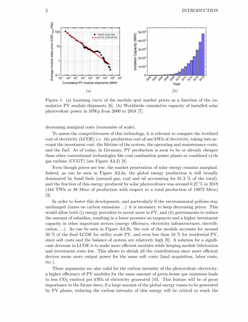
In order to make this energy generation system relevant, it needs to be able to provideenergy at a competitive cost. The average sales price in USD2018/kWp has tremendouslydecreased during the last decade, and its learning rate is of 23.2 % per doubling of thecumulative PV module shipments [6] as shown in Figure A3.1a. This decrease is due todifferent factors such as the relocation of activities, a dedicated silicon wafer manufacturingindustry and an increase in module efficiency. These additionally went along with aboom in annual worldwide installed capacity (as shown in Figure A3.1b) thus significantly
2 INTRODUCTION
10-1 100 101 102 103 104 105 106 1070.1
1
10
100 historic price data 23.2% (1976-2018)
Aver
age
mod
ule
sale
s pr
ice
(USD
2018
/Wp)
Cumulative PV module shipments (MW)
(a)
2000
2002
2004
2006
2008
2010
2012
2014
2016
2018
0
1x10⁵
2x10⁵
3x10⁵
4x10⁵
5x10⁵
Year
Inst
alle
d C
apac
ity (M
W)
(b)
Figure 1: (a) Learning curve of the module spot market prices as a function of the cu-mulative PV module shipments [6]. (b) Worldwide cumulative capacity of installed solarphotovoltaic power in MWp from 2000 to 2018 [7].
decreasing marginal costs (economies of scale).
To assess the competitiveness of this technology, it is relevant to compare the levelizedcost of electricity (LCOE) i.e. the production cost of one kWh of electricity, taking into ac-count the investment cost, the lifetime of the system, the operating and maintenance costs,and the fuel. As of today, in Germany, PV production is soon to be or already cheaperthan other conventional technologies like coal combustion power plants or combined cyclegas turbine (CCGT) (see Figure A3.2) [8].
Even though prices are low, the market penetration of solar energy remains marginal.Indeed, as can be seen in Figure A3.3a, the global energy production is still broadlydominated by fossil fuels (natural gas, coal and oil accounting for 81.3 % of the total),and the fraction of this energy produced by solar photovoltaics was around 0.27 % in 2018(444 TWh or 38 Mtoe of production with respect to a total production of 13972 Mtoe)[3].
In order to foster this development, and particularly if the environmental policies stayunchanged (taxes on carbon emissions ...) it is necessary to keep decreasing prices. Thiswould allow both (i) energy providers to invest more in PV, and (ii) governments to reducethe amount of subsidies, resulting in a lower pressure on taxpayers and a higher investmentcapacity in other important sectors (energy efficiency, electricity infrastructures, electrifi-cation, ...). As can be seen in Figure A3.3b, the cost of the module accounts for around50 % of the final LCOE for utility scale PV, and even less than 10 % for residential PV,since soft costs and the balance of system are relatively high [9]. A solution for a signifi-cant decrease in LCOE is to make more efficient modules while keeping module fabricationand investment costs low. This allows to shrink all the contributions since more efficientdevices mean more output power for the same soft costs (land acquisition, labor costs,etc.).
These arguments are also valid for the carbon intensity of the photovoltaic electricity:a higher efficiency of PV modules for the same amount of green-house gas emissions leadsto less CO2 emitted per kWh of electricity generated [10]. This feature will be of greatimportance in the future since, if a large amount of the global energy comes to be generatedby PV plants, reducing the carbon intensity of this energy will be critical to reach the
3
PVrooftopsmall
PVrooftoplarge
PVUtilityscale
WindOnshore
WindOffshore
Biogas Browncoal
Hardcoal
CCGT Gas02468
1012141618202224
Electric power generation system
Leve
lized
Cos
t Of E
lect
ricity
(ce
nt20
18/k
Wh)
Figure 2: Levelized cost of electricity for different power generation technologies, in Ger-many in 2018 [8]. PV production is calculated with a Global Horizontal Irradiance between950 and 1300 kWh.m2.a−1. The Full Load Hours ranges (in h/a) are taken as: 1800-3200for Wind Onshore, 3200-4500 for Wind Offshore, 5000-7000 for Biogas, 6450-7450 forBrown coal, 5350-6350 for Hard coal, 3000-4000 for CCGT, and 500-2000 for Gas.
Other1.8%
Biofuelsand waste
9.5%Hydro2.5%
Nuclear4.9%
Naturalgas
22.2% Oil32%
Coal27.1%
(a)
2010
2011
2012
2013
2014
2015
2016
2017
2018
0
1
2
3
4
5
6
1.13
Year
Leve
lized
Cos
t Of E
lect
ricity
(USD
2018
/Wp)
Soft Costs - Others Soft Costs - Install Labor Hardware BOS Inverter Module
5.52
(b)
Figure 3: (a) Share of energy resources in the global energy mix, 2017 [3]. (b) NREL LCOE(inflation adjusted) 2010-2018 for Utility-Scale PV with One-Axis Tracker (100 MW) [9].
4 INTRODUCTION
carbon neutrality of the global economy.
Today, the photovoltaic industry is most widely based on the use of silicon as a semi-conducting material. This kind of solar panel accounted for up to 95 % of the totalphotovoltaic market in 2018 [11] and is based on the use of slices of crystalline silicon,called wafers. The majority of the current solar cells are based on mono-crystalline sil-icon wafers which allow good device performances but are relatively expensive and relyon energy-intensive manufacturing processes. The device technology called PERC solarcells, which is the most widely manufactured solar cell architecture, relies on a simplefabrication process and has a high energy yield.
Reducing both the silicon wafer fabrication costs and CO2 emissions is possible by usinglow-cost, high-quality cast-mono silicon wafers which fabrication process is less energy-intensive than the one of standard industrial mono-crystalline silicon wafers. Additionally,a very promising silicon solar cell technology to achieve the objectives of increasing theefficiency further while maintaining low manufacturing costs in the near future is the pas-sivated contact technology. It allows to reach higher cell efficiencies by reducing electricallosses, and has the advantage of mostly using tools that are already present in the currentindustrial production lines. It is already being implemented in mass-production by someleading solar PV manufacturing companies [12]. Nonetheless, the standard fabricationprocess for this passivated contact solar cell architecture requires many steps, along witha high thermal budget due to long annealing processes at temperatures between 600 and850 °C. That is why novel ways to manufacture this kind of solar cells need to be in-vestigated, processes which would be less energy-intensive and require less manufacturingsteps.
Purpose and structure of this work
This PhD thesis focuses on the investigation of a simplified passivating contact manufac-turing process called fired passivated contact (FPC), which allows to have fewer processingsteps and subject the solar cell to a low thermal budget. The major features studied arethe passivation properties of the FPC stack, which account for the electrical losses in thedevice. In situ modulated photoluminescence characterizations are carried out, to achievethis goal: they allow to measure the evolution of the passivation properties in real timeduring a specific process step. Ultimately, these contacts are integrated on cast-monowafers produced by Photowatt, a French company which developed a technology calledCrystal Advanced [13].
Chapter 1 sets the background of this thesis, the working principle of a solar cell,and introduces the poly-Si passivating contact structure and its advantages alongwith a review of the paramount results from the literature. Further details on met-allization and silicon wafer manufacturing are given in order to grant a more generalunderstanding of the challenges of this work.
Chapter 2 describes the development and optimization of the different layers of theFPC passivating stack. Advanced characterization techniques are used for a thor-ough understanding of the evolution of the materials properties during the fabricationprocess.
Chapter 3 describes an in situ modulated photoluminescence acquisition setup, thatallows to measure in real time the effective minority carrier lifetime of a sample.
5
A case study of the evolution of the passivation properties of an aluminum oxidepassivated sample is performed using this tool.
Chapter 4 focuses on the use of this in situ modulated photoluminescence techniqueto study FPC samples. The evolution of the passivation properties during differentprocess steps (annealing, plasma processes, and layer deposition) of the passivatingcontacts fabrication is investigated.
Chapter 5 studies the transfer of the optimized FPC process on industrial-size wafers.Both Czochralski and cast-mono silicon wafers are investigated in this section. Theimportance of the surface morphology for FPC samples is discussed. The electricalproperties of a first device are finally presented.
A summary of these results and a general conclusion of the work performed duringthis PhD thesis are proposed. Ways of improvement of the solar cell architecture and ofthe fabrication process are discussed to put this work in perspective.

6 INTRODUCTION
7
Chapter 1
Context, background andobjectives
In order to know how to improve PV devices and its market penetration, it is worth un-derstanding how a solar cell works, what are the current architectures that can be foundon the market, and how to make them more efficient while keeping the fabrication costslow.
Contents
1.1 Basic concepts of solar cells . . . . . . . . . . . . . . . . . . . . . . . . . 81.1.1 Working principle of a solar cell . . . . . . . . . . . . . . . . . . . . . 81.1.2 Characteristics of a solar cell . . . . . . . . . . . . . . . . . . . . . . 111.1.3 Limits of conversion efficiency . . . . . . . . . . . . . . . . . . . . . . 121.1.4 Homojunction solar cells . . . . . . . . . . . . . . . . . . . . . . . . . 16
1.2 Passivating contacts: toward higher efficiency . . . . . . . . . . . . . 181.2.1 Working principle . . . . . . . . . . . . . . . . . . . . . . . . . . . . 181.2.2 Heterojunction technology and limitations . . . . . . . . . . . . . . . 191.2.3 Tunnel oxide passivating contacts . . . . . . . . . . . . . . . . . . . . 201.2.4 Transparent Metal Oxides . . . . . . . . . . . . . . . . . . . . . . . . 24
1.3 Metallization of TOPCon solar cells . . . . . . . . . . . . . . . . . . . 251.3.1 Screen printing . . . . . . . . . . . . . . . . . . . . . . . . . . . . . . 251.3.2 Low-temperature metallization . . . . . . . . . . . . . . . . . . . . . 261.3.3 Fire-through metallic paste . . . . . . . . . . . . . . . . . . . . . . . 261.3.4 n-type and p-type TOPCon FT metallisation . . . . . . . . . . . . . 27
1.4 Silicon Wafer manufacturing . . . . . . . . . . . . . . . . . . . . . . . . 281.4.1 From quartzite to polycrystalline silicon rods . . . . . . . . . . . . . 281.4.2 Multi-crystalline silicon . . . . . . . . . . . . . . . . . . . . . . . . . 291.4.3 Mono-crystalline silicon . . . . . . . . . . . . . . . . . . . . . . . . . 291.4.4 Cast-mono wafers . . . . . . . . . . . . . . . . . . . . . . . . . . . . 31
1.5 Objectives of the study . . . . . . . . . . . . . . . . . . . . . . . . . . . . 31
8 CHAPTER 1. CONTEXT, BACKGROUND AND OBJECTIVES
1.1 Basic concepts of solar cells
We first describe the theoretical framework to understand the physics behind the energyconversion in a solar cell. This allows us to introduce intrinsic limitations of standardsolar cells, and the main features that we are interested in at the device level. A morethorough description of the physics of solar cells can be found in the book of Wurfel andWurfel [14].
1.1.1 Working principle of a solar cell
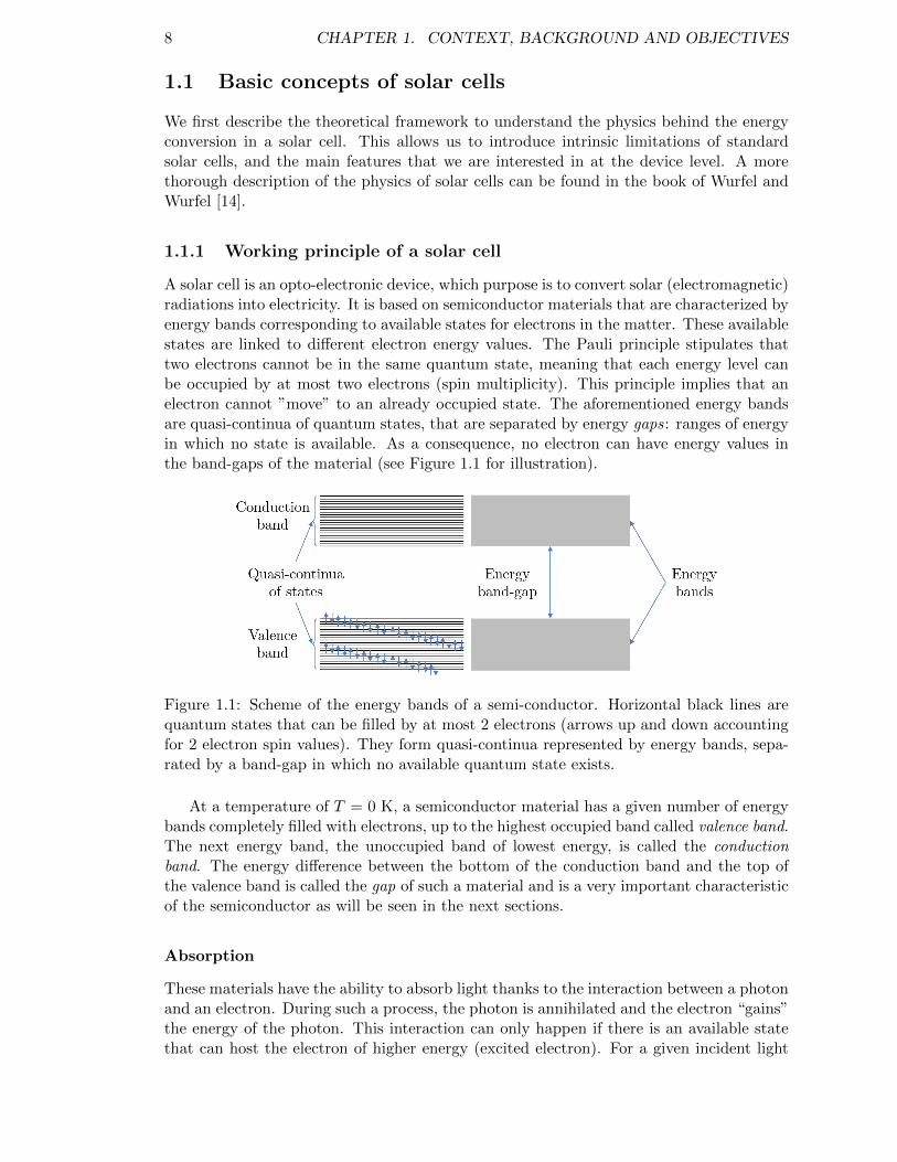
A solar cell is an opto-electronic device, which purpose is to convert solar (electromagnetic)radiations into electricity. It is based on semiconductor materials that are characterized byenergy bands corresponding to available states for electrons in the matter. These availablestates are linked to different electron energy values. The Pauli principle stipulates thattwo electrons cannot be in the same quantum state, meaning that each energy level canbe occupied by at most two electrons (spin multiplicity). This principle implies that anelectron cannot ”move” to an already occupied state. The aforementioned energy bandsare quasi-continua of quantum states, that are separated by energy gaps: ranges of energyin which no state is available. As a consequence, no electron can have energy values inthe band-gaps of the material (see Figure 1.1 for illustration).
Figure 1.1: Scheme of the energy bands of a semi-conductor. Horizontal black lines arequantum states that can be filled by at most 2 electrons (arrows up and down accountingfor 2 electron spin values). They form quasi-continua represented by energy bands, sepa-rated by a band-gap in which no available quantum state exists.
At a temperature of T = 0 K, a semiconductor material has a given number of energybands completely filled with electrons, up to the highest occupied band called valence band.The next energy band, the unoccupied band of lowest energy, is called the conductionband. The energy difference between the bottom of the conduction band and the top ofthe valence band is called the gap of such a material and is a very important characteristicof the semiconductor as will be seen in the next sections.
Absorption
These materials have the ability to absorb light thanks to the interaction between a photonand an electron. During such a process, the photon is annihilated and the electron “gains”the energy of the photon. This interaction can only happen if there is an available statethat can host the electron of higher energy (excited electron). For a given incident light
1.1. BASIC CONCEPTS OF SOLAR CELLS 9
intensity I0 at the surface, the absorption profile in the material is usually described by aBeer-Lambert law:
I(z, λ) = (1−Rf )I0e−α(λ)z (1.1)
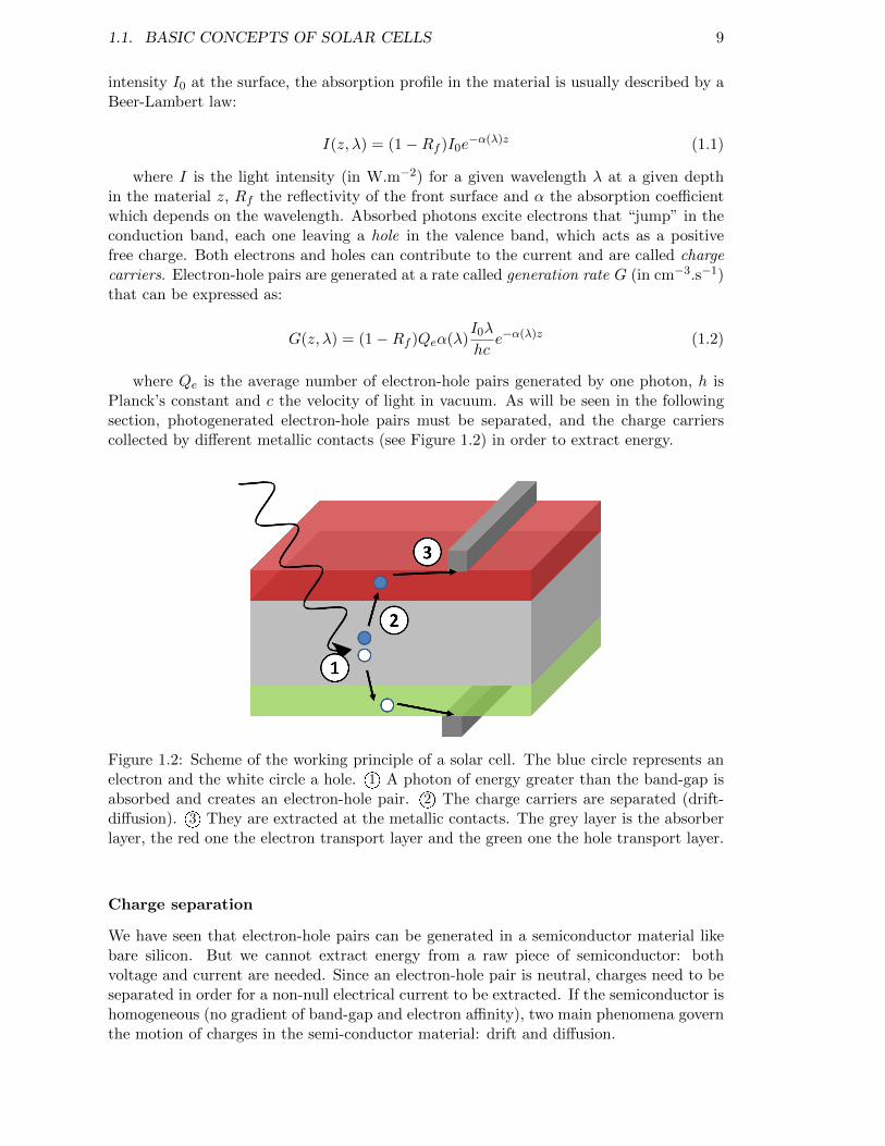
where I is the light intensity (in W.m−2) for a given wavelength λ at a given depthin the material z, Rf the reflectivity of the front surface and α the absorption coefficientwhich depends on the wavelength. Absorbed photons excite electrons that “jump” in theconduction band, each one leaving a hole in the valence band, which acts as a positivefree charge. Both electrons and holes can contribute to the current and are called chargecarriers. Electron-hole pairs are generated at a rate called generation rate G (in cm−3.s−1)that can be expressed as:
G(z, λ) = (1−Rf )Qeα(λ)I0λ
hce−α(λ)z (1.2)
where Qe is the average number of electron-hole pairs generated by one photon, h isPlanck’s constant and c the velocity of light in vacuum. As will be seen in the followingsection, photogenerated electron-hole pairs must be separated, and the charge carrierscollected by different metallic contacts (see Figure 1.2) in order to extract energy.
Figure 1.2: Scheme of the working principle of a solar cell. The blue circle represents anelectron and the white circle a hole. 1O A photon of energy greater than the band-gap isabsorbed and creates an electron-hole pair. 2O The charge carriers are separated (drift-diffusion). 3O They are extracted at the metallic contacts. The grey layer is the absorberlayer, the red one the electron transport layer and the green one the hole transport layer.
Charge separation
We have seen that electron-hole pairs can be generated in a semiconductor material likebare silicon. But we cannot extract energy from a raw piece of semiconductor: bothvoltage and current are needed. Since an electron-hole pair is neutral, charges need to beseparated in order for a non-null electrical current to be extracted. If the semiconductor ishomogeneous (no gradient of band-gap and electron affinity), two main phenomena governthe motion of charges in the semi-conductor material: drift and diffusion.
10 CHAPTER 1. CONTEXT, BACKGROUND AND OBJECTIVES
Drift is the action of an electric field E (in V.cm−1) on an electrically charged body.If such an electric field exists in some part of the solar cell and is the only driving force,then it induces a drift current density which can be expressed as:
Jn,drift = qnµnE = σnE = −σnq∇ (qϕ) (1.3a)
Jp,drift = qpµpE = σpE =σpq∇ (qϕ) (1.3b)
where Jn,drift and Jp,drift are drift current densities for respectively electrons and holes(in A.cm−2), q = 1.62×10⁻¹⁹ C is the elementary charge, n and p the (free) electron andhole densities (in cm−3) and µn and µp the electron and hole mobilities (in cm2.V−1.s−1).σn = nqµn and σp = pqµp are the electron and hole conductivities and ϕ the electricpotential. The electric force acting on the particles is thus −∇ (qϕ) for electrons and+∇ (qϕ) for holes.
Diffusion results from nonuniformities in the charge carrier concentration. Accordingto Fick’s law, charge carriers diffuse from regions of high concentration (or high chemicalpotential) towards regions of low concentration. Consequently, if no electric field exists inthe material, the diffusion current densities are given by:
Jn,diff = qDn∇n = −σnq∇φn (1.4a)
Jp,diff = −qDp∇p = −σpq∇φp (1.4b)
Where Jn,diff and Jp,diff are diffusion current densities of respectively electrons andholes (in A.cm−2) and Dn and Dp the diffusion coefficients of electrons and holes with
Dn/p = µn/pkT/q. Here φn = kT ln
(n
NC
)is the chemical potential of electrons with
NC the effective density of states of electrons in the conduction band. Equivalently,
φp = kT ln
(p
NV
)is the chemical potential of holes, with NV the effective density of
states of holes in the valence band. The driving force is thus −∇φ.
If both these phenomena apply, the resulting force is −∇(φn/p ∓ qϕ
)= −∇ηn/p with
∇ηn/p the electro-chemical potential of electrons or holes. The probability of occupationof an energy state being described by a Fermi-Dirac distribution, the electro-chemicalpotential values can be identified as the quasi-Fermi levels of electron and holes: ηn = εFnand ηp = −εFp. These are the energy values of virtual states that have a probability of50 % to be occupied by an electron (for ηn = εFn) or by a hole (for ηp = −εFp). Thisleads to the expressions of the real charge current densities:
Jn =σnq∇εFn (1.5a)
Jp =σpq∇εFp (1.5b)
An asymmetry in the solar cell electro-chemical properties results in the separation ofthe charge carriers, and may allow their collection in electrical contacts. Under thermo-dynamic equilibrium, εFn = εFp. Under illumination, these quasi-Fermi levels split, andtheir difference corresponds to the chemical energy produced, which is the maximum
1.1. BASIC CONCEPTS OF SOLAR CELLS 11
energy that can be extracted from an electron-hole pair. This value is called implied open-circuit voltage iVoc = εFn − εFp. Creating an asymmetric gradient of quasi-Fermi levelsis difficult under no bias-voltage. As a consequence, the easiest way to separate chargecarriers is to tune their conductivity close to metallic contacts, in order to selectively directelectrons and holes towards separated electrodes. A thorough description of the physicsof solar cells can be found in the book ”Physics of Solar Cells: From Basic Principles toAdvanced Concepts” by P. and U. Wurfel [14], [15].
At the device level, the output power will result from the flow of charge carriers col-lected (current) and the amount of usable energy that each one of them carries (voltage).
1.1.2 Characteristics of a solar cell
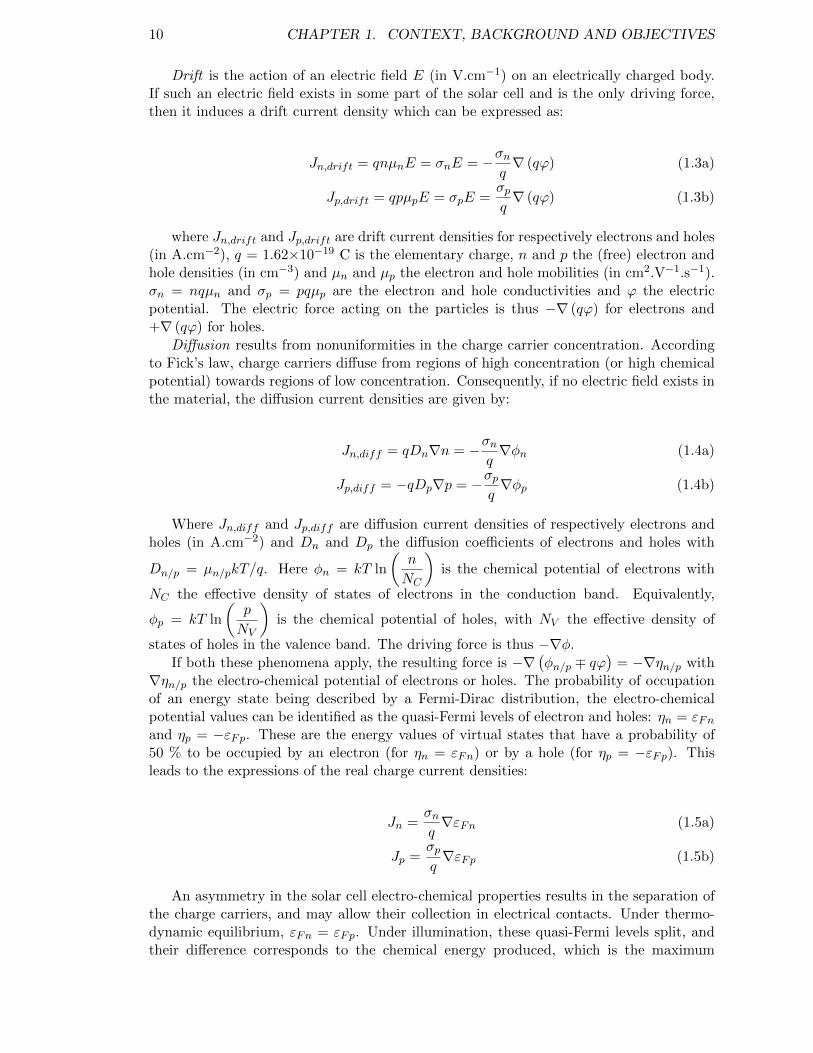
A solar cell in the dark acts electrically as a diode, and additionally generates currentunder illumination (electron-hole pair generation, separation and extraction). As shownin the equivalent electrical circuit of Figure 1.3, it also comes with parasitic resistances:series resistance Rs (contact resistance, finite conductivity of the layers, ...) and parallelresistance Rp (shunt currents, leaky layers, ...). In order for the device to be efficient, Rsneeds to be minimized and Rp maximized.
Figure 1.3: Equivalent electrical circuit of a solar cell, one-diode model.
The J(V ) characteristic follows the equation:
J(V ) = J0
[exp
(q (V −AJRs)
kT
)− 1
]+V −AJRs
ARp− Jgen (1.6)
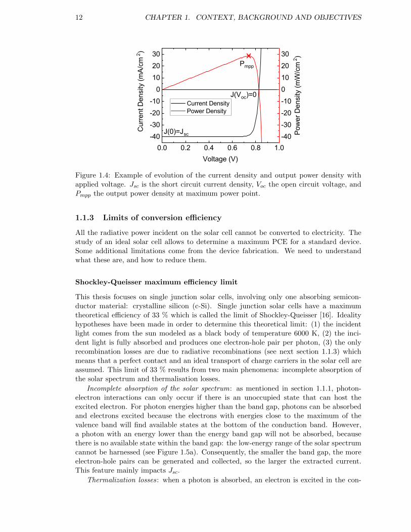
with J0 the saturation current density, A the area of the solar cell, and Jgen the photo-generated current density. From Figure 1.4, which represents the J(V ) characteristic ofsuch a device, we can identify three characteristic parameters: the open circuit voltage Voc(at which J = 0), the short circuit current density Jsc (at V = 0) and the maximum powerpoint (at which ∂P/∂V = 0). We may introduce an additional feature called Fill-FactorFF defined as:
FF =PmppJscVoc
(1.7)
From FF , Jsc and Voc can be extracted the power conversion efficiency (PCE) η at a givenincident radiative power density Pinc:
η =FFJscVocPinc
(1.8)
In the photovoltaic industry, these characteristics are measured under standard testconditions: 25 °C and an illumination of the AM1.5 solar spectrum (see Figure 1.6 furtherdown) corresponding to a power density of 1000 W.m−2.
12 CHAPTER 1. CONTEXT, BACKGROUND AND OBJECTIVES
0.0 0.2 0.4 0.6 0.8 1.0-40-30-20-10
0102030
J(Voc)=0
Pmpp
Cur
rent
Den
sity
(mA/
cm2 )
Voltage (V)
Current Density Power Density
J(0)=Jsc -40-30-20-100102030
Pow
er D
ensi
ty (m
W/c
m2 )
Figure 1.4: Example of evolution of the current density and output power density withapplied voltage. Jsc is the short circuit current density, Voc the open circuit voltage, andPmpp the output power density at maximum power point.
1.1.3 Limits of conversion efficiency
All the radiative power incident on the solar cell cannot be converted to electricity. Thestudy of an ideal solar cell allows to determine a maximum PCE for a standard device.Some additional limitations come from the device fabrication. We need to understandwhat these are, and how to reduce them.
Shockley-Queisser maximum efficiency limit
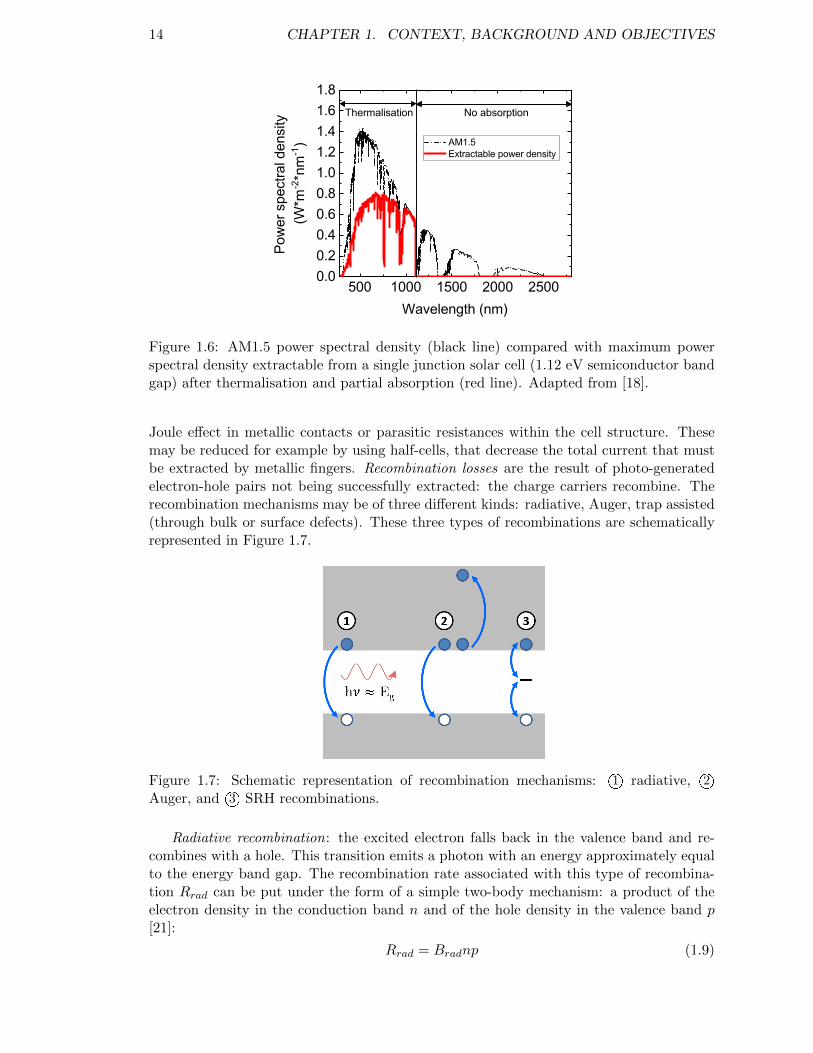
This thesis focuses on single junction solar cells, involving only one absorbing semicon-ductor material: crystalline silicon (c-Si). Single junction solar cells have a maximumtheoretical efficiency of 33 % which is called the limit of Shockley-Queisser [16]. Idealityhypotheses have been made in order to determine this theoretical limit: (1) the incidentlight comes from the sun modeled as a black body of temperature 6000 K, (2) the inci-dent light is fully absorbed and produces one electron-hole pair per photon, (3) the onlyrecombination losses are due to radiative recombinations (see next section 1.1.3) whichmeans that a perfect contact and an ideal transport of charge carriers in the solar cell areassumed. This limit of 33 % results from two main phenomena: incomplete absorption ofthe solar spectrum and thermalisation losses.
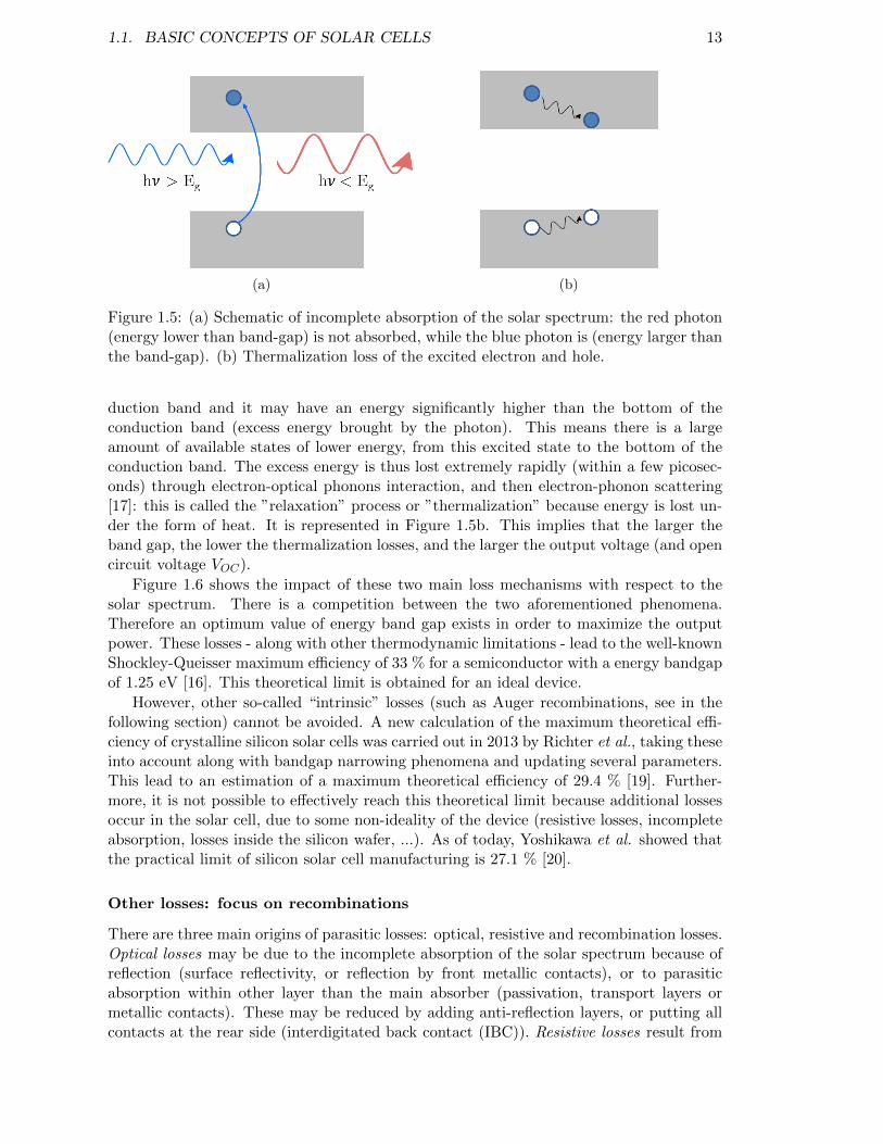
Incomplete absorption of the solar spectrum: as mentioned in section 1.1.1, photon-electron interactions can only occur if there is an unoccupied state that can host theexcited electron. For photon energies higher than the band gap, photons can be absorbedand electrons excited because the electrons with energies close to the maximum of thevalence band will find available states at the bottom of the conduction band. However,a photon with an energy lower than the energy band gap will not be absorbed, becausethere is no available state within the band gap: the low-energy range of the solar spectrumcannot be harnessed (see Figure 1.5a). Consequently, the smaller the band gap, the moreelectron-hole pairs can be generated and collected, so the larger the extracted current.This feature mainly impacts Jsc.
Thermalization losses: when a photon is absorbed, an electron is excited in the con-
1.1. BASIC CONCEPTS OF SOLAR CELLS 13
(a) (b)
Figure 1.5: (a) Schematic of incomplete absorption of the solar spectrum: the red photon(energy lower than band-gap) is not absorbed, while the blue photon is (energy larger thanthe band-gap). (b) Thermalization loss of the excited electron and hole.
duction band and it may have an energy significantly higher than the bottom of theconduction band (excess energy brought by the photon). This means there is a largeamount of available states of lower energy, from this excited state to the bottom of theconduction band. The excess energy is thus lost extremely rapidly (within a few picosec-onds) through electron-optical phonons interaction, and then electron-phonon scattering[17]: this is called the ”relaxation” process or ”thermalization” because energy is lost un-der the form of heat. It is represented in Figure 1.5b. This implies that the larger theband gap, the lower the thermalization losses, and the larger the output voltage (and opencircuit voltage VOC).
Figure 1.6 shows the impact of these two main loss mechanisms with respect to thesolar spectrum. There is a competition between the two aforementioned phenomena.Therefore an optimum value of energy band gap exists in order to maximize the outputpower. These losses - along with other thermodynamic limitations - lead to the well-knownShockley-Queisser maximum efficiency of 33 % for a semiconductor with a energy bandgapof 1.25 eV [16]. This theoretical limit is obtained for an ideal device.
However, other so-called “intrinsic” losses (such as Auger recombinations, see in thefollowing section) cannot be avoided. A new calculation of the maximum theoretical effi-ciency of crystalline silicon solar cells was carried out in 2013 by Richter et al., taking theseinto account along with bandgap narrowing phenomena and updating several parameters.This lead to an estimation of a maximum theoretical efficiency of 29.4 % [19]. Further-more, it is not possible to effectively reach this theoretical limit because additional lossesoccur in the solar cell, due to some non-ideality of the device (resistive losses, incompleteabsorption, losses inside the silicon wafer, ...). As of today, Yoshikawa et al. showed thatthe practical limit of silicon solar cell manufacturing is 27.1 % [20].
Other losses: focus on recombinations
There are three main origins of parasitic losses: optical, resistive and recombination losses.Optical losses may be due to the incomplete absorption of the solar spectrum because ofreflection (surface reflectivity, or reflection by front metallic contacts), or to parasiticabsorption within other layer than the main absorber (passivation, transport layers ormetallic contacts). These may be reduced by adding anti-reflection layers, or putting allcontacts at the rear side (interdigitated back contact (IBC)). Resistive losses result from
14 CHAPTER 1. CONTEXT, BACKGROUND AND OBJECTIVES
500 1000 1500 2000 25000.00.20.40.60.81.01.21.41.61.8
No absorption
Pow
er s
pect
ral d
ensi
ty(W
*m-2
*nm
-1)
Wavelength (nm)
AM1.5 Extractable power density
Thermalisation
Figure 1.6: AM1.5 power spectral density (black line) compared with maximum powerspectral density extractable from a single junction solar cell (1.12 eV semiconductor bandgap) after thermalisation and partial absorption (red line). Adapted from [18].
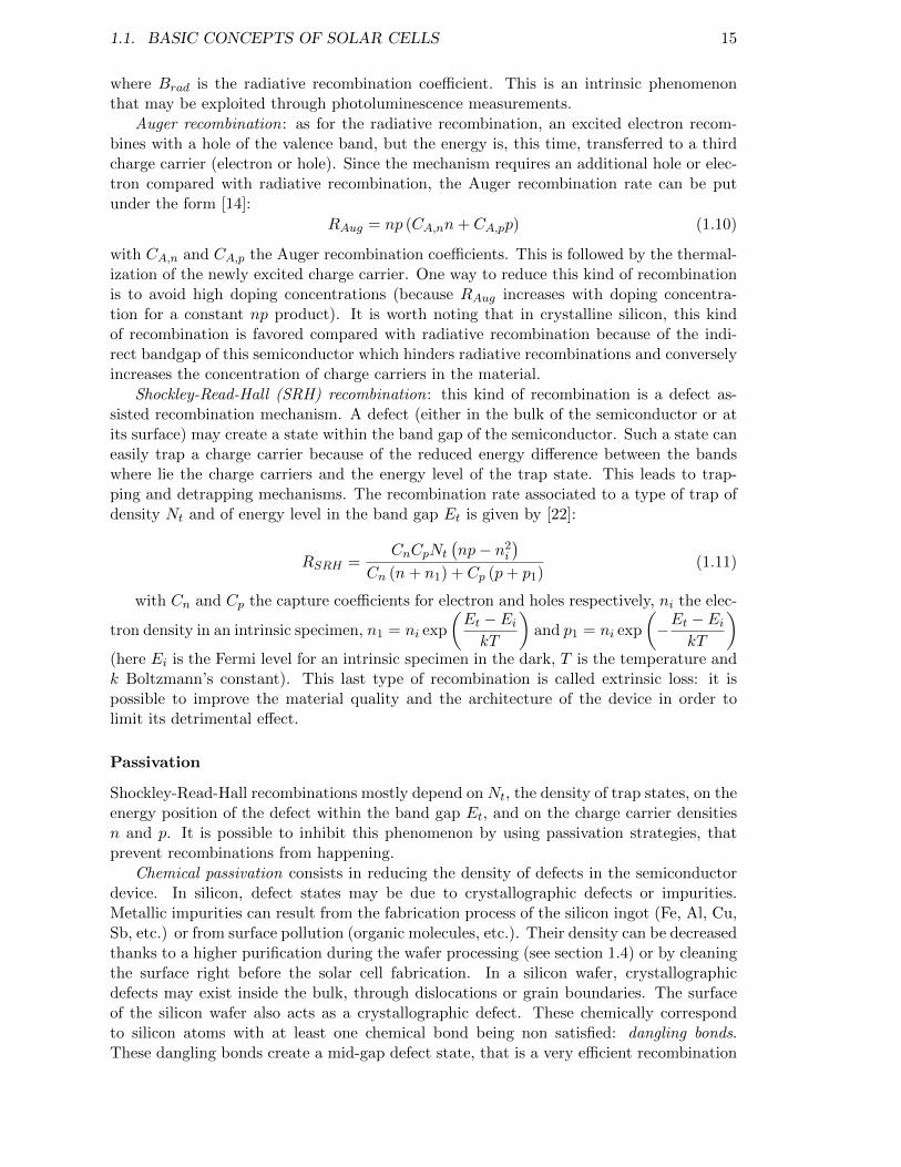
Joule effect in metallic contacts or parasitic resistances within the cell structure. Thesemay be reduced for example by using half-cells, that decrease the total current that mustbe extracted by metallic fingers. Recombination losses are the result of photo-generatedelectron-hole pairs not being successfully extracted: the charge carriers recombine. Therecombination mechanisms may be of three different kinds: radiative, Auger, trap assisted(through bulk or surface defects). These three types of recombinations are schematicallyrepresented in Figure 1.7.
Figure 1.7: Schematic representation of recombination mechanisms: 1O radiative, 2OAuger, and 3O SRH recombinations.
Radiative recombination: the excited electron falls back in the valence band and re-combines with a hole. This transition emits a photon with an energy approximately equalto the energy band gap. The recombination rate associated with this type of recombina-tion Rrad can be put under the form of a simple two-body mechanism: a product of theelectron density in the conduction band n and of the hole density in the valence band p[21]:
Rrad = Bradnp (1.9)
1.1. BASIC CONCEPTS OF SOLAR CELLS 15
where Brad is the radiative recombination coefficient. This is an intrinsic phenomenonthat may be exploited through photoluminescence measurements.
Auger recombination: as for the radiative recombination, an excited electron recom-bines with a hole of the valence band, but the energy is, this time, transferred to a thirdcharge carrier (electron or hole). Since the mechanism requires an additional hole or elec-tron compared with radiative recombination, the Auger recombination rate can be putunder the form [14]:
RAug = np (CA,nn+ CA,pp) (1.10)
with CA,n and CA,p the Auger recombination coefficients. This is followed by the thermal-ization of the newly excited charge carrier. One way to reduce this kind of recombinationis to avoid high doping concentrations (because RAug increases with doping concentra-tion for a constant np product). It is worth noting that in crystalline silicon, this kindof recombination is favored compared with radiative recombination because of the indi-rect bandgap of this semiconductor which hinders radiative recombinations and converselyincreases the concentration of charge carriers in the material.
Shockley-Read-Hall (SRH) recombination: this kind of recombination is a defect as-sisted recombination mechanism. A defect (either in the bulk of the semiconductor or atits surface) may create a state within the band gap of the semiconductor. Such a state caneasily trap a charge carrier because of the reduced energy difference between the bandswhere lie the charge carriers and the energy level of the trap state. This leads to trap-ping and detrapping mechanisms. The recombination rate associated to a type of trap ofdensity Nt and of energy level in the band gap Et is given by [22]:
RSRH =CnCpNt
(np− n2i
)Cn (n+ n1) + Cp (p+ p1)
(1.11)
with Cn and Cp the capture coefficients for electron and holes respectively, ni the elec-
tron density in an intrinsic specimen, n1 = ni exp
(Et − EikT
)and p1 = ni exp
(−Et − Ei
kT
)(here Ei is the Fermi level for an intrinsic specimen in the dark, T is the temperature andk Boltzmann’s constant). This last type of recombination is called extrinsic loss: it ispossible to improve the material quality and the architecture of the device in order tolimit its detrimental effect.
Passivation
Shockley-Read-Hall recombinations mostly depend on Nt, the density of trap states, on theenergy position of the defect within the band gap Et, and on the charge carrier densitiesn and p. It is possible to inhibit this phenomenon by using passivation strategies, thatprevent recombinations from happening.
Chemical passivation consists in reducing the density of defects in the semiconductordevice. In silicon, defect states may be due to crystallographic defects or impurities.Metallic impurities can result from the fabrication process of the silicon ingot (Fe, Al, Cu,Sb, etc.) or from surface pollution (organic molecules, etc.). Their density can be decreasedthanks to a higher purification during the wafer processing (see section 1.4) or by cleaningthe surface right before the solar cell fabrication. In a silicon wafer, crystallographicdefects may exist inside the bulk, through dislocations or grain boundaries. The surfaceof the silicon wafer also acts as a crystallographic defect. These chemically correspondto silicon atoms with at least one chemical bond being non satisfied: dangling bonds.These dangling bonds create a mid-gap defect state, that is a very efficient recombination
16 CHAPTER 1. CONTEXT, BACKGROUND AND OBJECTIVES
center. In order to decrease their density, it is necessary to fill these dangling bondseither in the bulk through a better crystallization (formation of Si-Si bonds) or througha hydrogenation process that allows to form Si-H bonds which energy level no longerlies in the band gap. Hydrogen atoms are very light and mobile, and are consequentlyvery efficient to fill dangling bonds. This hydrogenation can be achieved by forming gasannealing (FGA), deposition of a hydrogen rich silicon layer and annealing to drive-in Hatoms, or through hydrogen plasma processes. Passivation of the dangling bonds at thesurface of the silicon wafer may be filled by depositing or growing dielectric layers such ashydrogenated amorphous silicon nitride (a-SiNx:H), aluminum oxide (AlOx), silicon oxide(SiOx) or depositing hydrogenated amorphous silicon (a-Si:H). The hydrogen content ofthese layers can be increased in order to get a better surface passivation (formation ofSi-H bonds).
Field-effect passivation can also reduce SRH recombinations by repelling one of thecarriers from the recombination centers thanks to an electric field. This can be achievedthanks to fixed charges naturally existing inside some passivation layers (negative fixedcharges in AlOx or positive fixed charges in a-SiNx:H), or by corona charge (depositingcharges at an interface). By pushing one of the types of charge carriers away from thetraps, a low recombination rate can be achieved despite a large density of interface defects.The reader is invited to consult the thorough review of Aberle [23] on passivation for siliconsolar cells for a more detailed description.
Managing to passivate the defects in the bulk or at the surface allows to reduce electricallosses and is the central subject of this thesis. Different approaches can be used to do soin solar cells. The following section describes the evolution of the passivation strategies inthe history of silicon solar cells manufacturing.
1.1.4 Homojunction solar cells
The most common kind of solar cells are called homojunction solar cells and rely on a p-njunction - which allows to separate charge carriers - and on a direct contact between themetal and the absorber layer.
Working principle: the p-n junction
Semiconductor materials can be tuned in order to increase the amount of one type of freecharge carrier. This tuning is called doping. An n- respectively p-doped semiconductoris a material in which impurities have been introduced on purpose: these add availableenergy levels close to the energy bands. This can respectively add either electrons in theconduction band (introduction of donor atoms, often phosphorous in silicon), or holes inthe valence band (acceptor atoms, often boron in silicon). For a p-type semiconductor,electrons are called “minority carriers” and holes “majority carriers” (and vice versa forn-type semiconductors). Because of the electrical neutrality of the bulk, this implies that:
N−A + n = N+D + p (1.12)
where N−A is the density of ionized acceptor atoms and N+D the density of ionized
donor atoms. At ambient temperature, all substitutional doping atoms are ionized, andN+D = ND or N−A = NA. Given that the product np = n2i = 1×1020 cm−3 is constant
under thermal equilibrium at ambient temperature, a typical doping level of n = ND =1×1016 cm−3 in n-type c-Si leads to a hole concentration of 3×104 cm−3. This results ina strong difference of conductivity between electrons and holes due to the difference incarrier concentration.
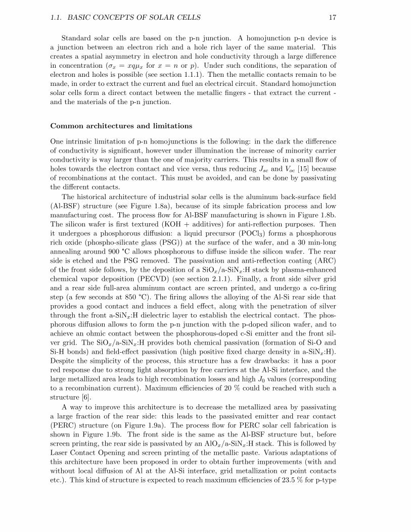
1.1. BASIC CONCEPTS OF SOLAR CELLS 17
Standard solar cells are based on the p-n junction. A homojunction p-n device isa junction between an electron rich and a hole rich layer of the same material. Thiscreates a spatial asymmetry in electron and hole conductivity through a large differencein concentration (σx = xqµx for x = n or p). Under such conditions, the separation ofelectron and holes is possible (see section 1.1.1). Then the metallic contacts remain to bemade, in order to extract the current and fuel an electrical circuit. Standard homojunctionsolar cells form a direct contact between the metallic fingers - that extract the current -and the materials of the p-n junction.
Common architectures and limitations
One intrinsic limitation of p-n homojunctions is the following: in the dark the differenceof conductivity is significant, however under illumination the increase of minority carrierconductivity is way larger than the one of majority carriers. This results in a small flow ofholes towards the electron contact and vice versa, thus reducing Jsc and Voc [15] becauseof recombinations at the contact. This must be avoided, and can be done by passivatingthe different contacts.
The historical architecture of industrial solar cells is the aluminum back-surface field(Al-BSF) structure (see Figure 1.8a), because of its simple fabrication process and lowmanufacturing cost. The process flow for Al-BSF manufacturing is shown in Figure 1.8b.The silicon wafer is first textured (KOH + additives) for anti-reflection purposes. Thenit undergoes a phosphorous diffusion: a liquid precursor (POCl3) forms a phosphorousrich oxide (phospho-silicate glass (PSG)) at the surface of the wafer, and a 30 min-longannealing around 900 °C allows phosphorous to diffuse inside the silicon wafer. The rearside is etched and the PSG removed. The passivation and anti-reflection coating (ARC)of the front side follows, by the deposition of a SiOx/a-SiNx:H stack by plasma-enhancedchemical vapor deposition (PECVD) (see section 2.1.1). Finally, a front side silver gridand a rear side full-area aluminum contact are screen printed, and undergo a co-firingstep (a few seconds at 850 °C). The firing allows the alloying of the Al-Si rear side thatprovides a good contact and induces a field effect, along with the penetration of silverthrough the front a-SiNx:H dielectric layer to establish the electrical contact. The phos-phorous diffusion allows to form the p-n junction with the p-doped silicon wafer, and toachieve an ohmic contact between the phosphorous-doped c-Si emitter and the front sil-ver grid. The SiOx/a-SiNx:H provides both chemical passivation (formation of Si-O andSi-H bonds) and field-effect passivation (high positive fixed charge density in a-SiNx:H).Despite the simplicity of the process, this structure has a few drawbacks: it has a poorred response due to strong light absorption by free carriers at the Al-Si interface, and thelarge metallized area leads to high recombination losses and high J0 values (correspondingto a recombination current). Maximum efficiencies of 20 % could be reached with such astructure [6].
A way to improve this architecture is to decrease the metallized area by passivatinga large fraction of the rear side: this leads to the passivated emitter and rear contact(PERC) structure (on Figure 1.9a). The process flow for PERC solar cell fabrication isshown in Figure 1.9b. The front side is the same as the Al-BSF structure but, beforescreen printing, the rear side is passivated by an AlOx/a-SiNx:H stack. This is followed byLaser Contact Opening and screen printing of the metallic paste. Various adaptations ofthis architecture have been proposed in order to obtain further improvements (with andwithout local diffusion of Al at the Al-Si interface, grid metallization or point contactsetc.). This kind of structure is expected to reach maximum efficiencies of 23.5 % for p-type
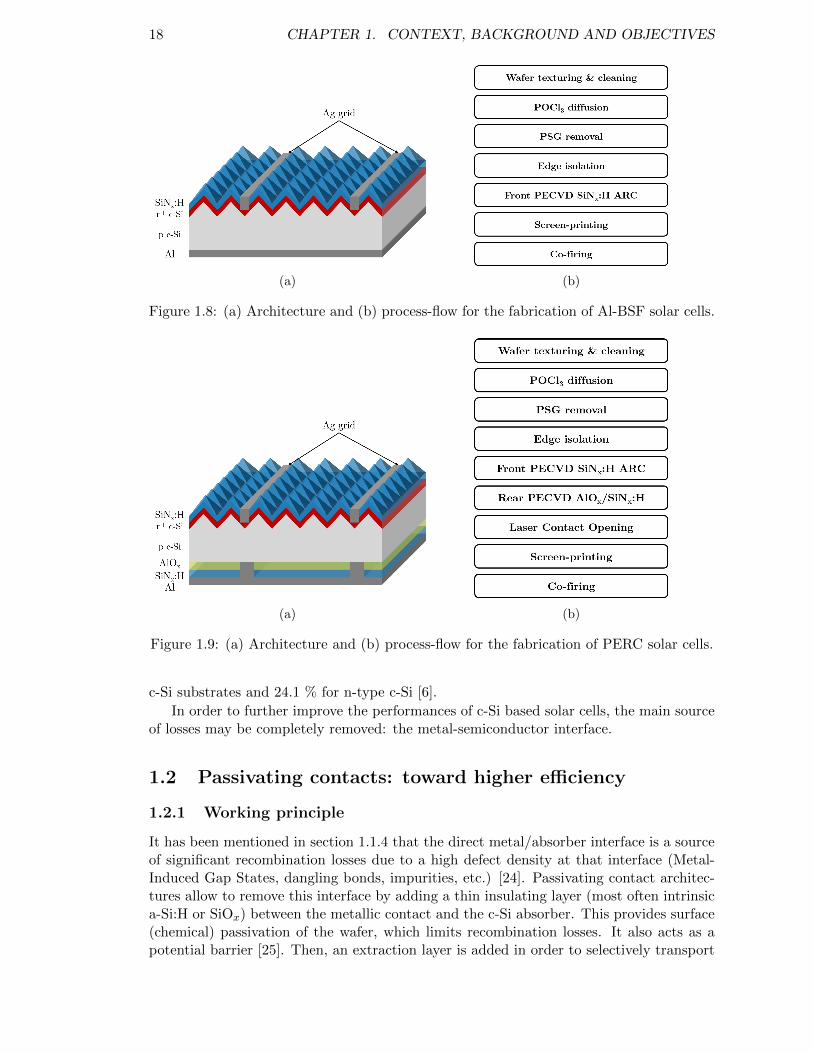
18 CHAPTER 1. CONTEXT, BACKGROUND AND OBJECTIVES
(a) (b)
Figure 1.8: (a) Architecture and (b) process-flow for the fabrication of Al-BSF solar cells.
(a) (b)
Figure 1.9: (a) Architecture and (b) process-flow for the fabrication of PERC solar cells.
c-Si substrates and 24.1 % for n-type c-Si [6].
In order to further improve the performances of c-Si based solar cells, the main sourceof losses may be completely removed: the metal-semiconductor interface.
1.2 Passivating contacts: toward higher efficiency
1.2.1 Working principle
It has been mentioned in section 1.1.4 that the direct metal/absorber interface is a sourceof significant recombination losses due to a high defect density at that interface (Metal-Induced Gap States, dangling bonds, impurities, etc.) [24]. Passivating contact architec-tures allow to remove this interface by adding a thin insulating layer (most often intrinsica-Si:H or SiOx) between the metallic contact and the c-Si absorber. This provides surface(chemical) passivation of the wafer, which limits recombination losses. It also acts as apotential barrier [25]. Then, an extraction layer is added in order to selectively transport
1.2. PASSIVATING CONTACTS: TOWARD HIGHER EFFICIENCY 19
one of the two types of charge carriers to the metallic contact while blocking the other one,which is necessary in order to achieve the carrier selectivity (see section 1.1.1) and keep alow contact resistivity. This structure prevents Fermi level pinning and the formation of aSchottky-barrier at the metal/semi-conductor interface and allows to significantly reducethe total J0 [26].
1.2.2 Heterojunction technology and limitations
The architecture that allowed to reach the highest power conversion efficiency is the het-erojunction with intrinsic thin layer (HIT) solar cell [27]. It relies on junctions between twodifferent materials: c-Si and a-Si:H. The passivated contact is a stack of thin (≈ 5-10 nm)(i) a-Si:H/doped a-Si:H (≈ 10-20 nm)/transparent conductive oxide (TCO) layer such asindium-doped tin oxide (ITO) and a low temperature screen printed silver grid (see Figure1.10a). a high passivation is achieved thanks to the intrinsic a-Si:H layer which provides alot of atomic hydrogen that binds to silicon dangling bonds. This hetero-structure also in-duces a strong inversion layer at the hetero-interface, which favors the tunneling of chargecarriers through the potential barrier (see Figure 1.10b). Such a structure, along with anIBC architecture lead to the record high efficiency for a single junction solar cell: 26.7 %[20].
(a)
-0.02 0.0 0.2 0.4 0.6 0.8 1.0
-20 0 200 400 600 800 1000
-1.5
-1.0
-0.5
0.0
0.5
1.0
1.5
2.0
x(nm)
(n) c
-Si
(p) a
-Si:H
Ener
gy(e
V)
x(um)
Ec(eV) Ef(eV) Ev(eV)
(i) a
-Si:H
(b)
Figure 1.10: (a) Architecture of a bifacial HIT solar cell and (b) its energy band diagramin the dark near the rear p-i-n hetero-interface - calculated with SCAPS software. Whiteand black circles represent respectively holes and electrons, and the arrows the directionsof the current densities.
However, HIT solar cells have a poor blue response due to the strong parasitic absorp-tion in this spectral range of a-Si:H, and especially of (p) a-Si:H. This is why the emitteris placed at the rear side of the solar cell. However this inverted structure requires high-lifetime silicon wafers since most of the charge carriers are photogenerated at the frontside of the solar cell (see equation 1.2) [28]: the minority carriers (holes) need to travelthrough the wafer all the way to the rear side of the solar cell to be collected. a-Si:H pas-sivation also degrades at temperatures higher than 300 °C and its conductivity is ratherlow due to a poor doping efficiency. This results in the necessity of using a TCO thatis expensive (and often contains indium, a scarce material) and low temperature screenprinting metallic pastes (not yet an industrial standard).
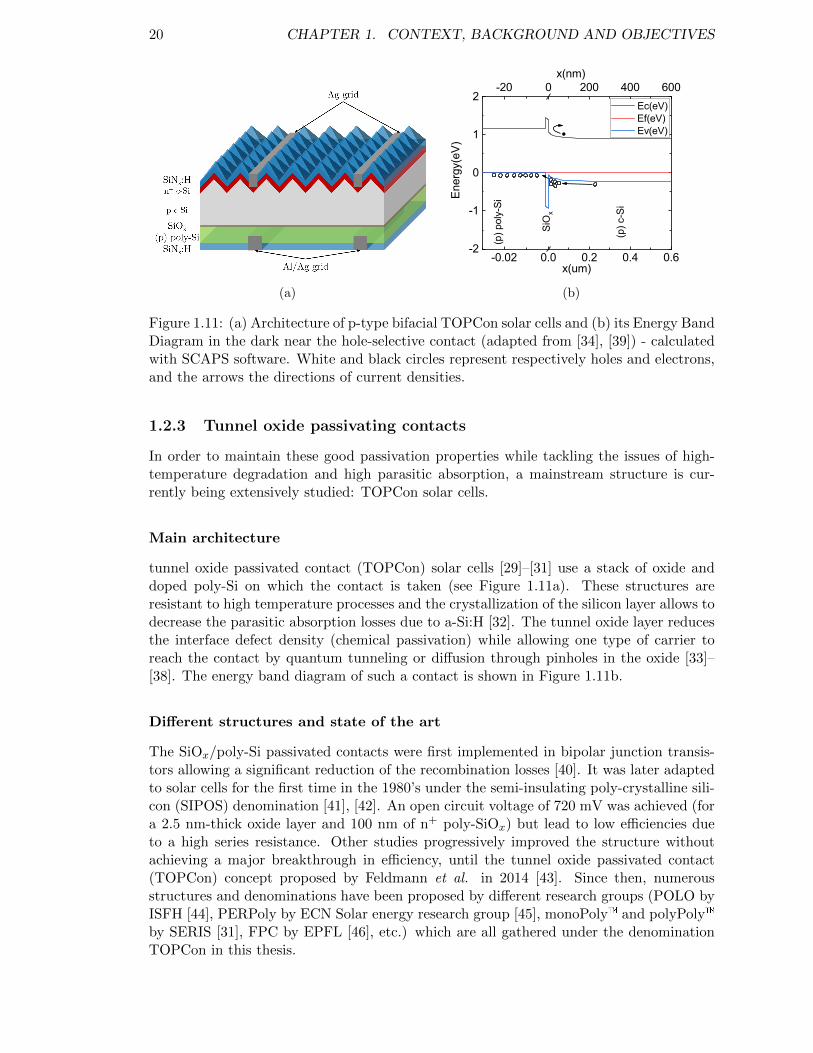
20 CHAPTER 1. CONTEXT, BACKGROUND AND OBJECTIVES
(a)
-0.02 0.0 0.2 0.4 0.6
-20 0 200 400 600
-2
-1
0
1
2
x(nm)
(p) c
-Si
SiO
x
(p) p
oly-
Si
Ener
gy(e
V)
x(um)
Ec(eV) Ef(eV) Ev(eV)
(b)
Figure 1.11: (a) Architecture of p-type bifacial TOPCon solar cells and (b) its Energy BandDiagram in the dark near the hole-selective contact (adapted from [34], [39]) - calculatedwith SCAPS software. White and black circles represent respectively holes and electrons,and the arrows the directions of current densities.
1.2.3 Tunnel oxide passivating contacts
In order to maintain these good passivation properties while tackling the issues of high-temperature degradation and high parasitic absorption, a mainstream structure is cur-rently being extensively studied: TOPCon solar cells.
Main architecture
tunnel oxide passivated contact (TOPCon) solar cells [29]–[31] use a stack of oxide anddoped poly-Si on which the contact is taken (see Figure 1.11a). These structures areresistant to high temperature processes and the crystallization of the silicon layer allows todecrease the parasitic absorption losses due to a-Si:H [32]. The tunnel oxide layer reducesthe interface defect density (chemical passivation) while allowing one type of carrier toreach the contact by quantum tunneling or diffusion through pinholes in the oxide [33]–[38]. The energy band diagram of such a contact is shown in Figure 1.11b.
Different structures and state of the art
The SiOx/poly-Si passivated contacts were first implemented in bipolar junction transis-tors allowing a significant reduction of the recombination losses [40]. It was later adaptedto solar cells for the first time in the 1980’s under the semi-insulating poly-crystalline sili-con (SIPOS) denomination [41], [42]. An open circuit voltage of 720 mV was achieved (fora 2.5 nm-thick oxide layer and 100 nm of n+ poly-SiOx) but lead to low efficiencies dueto a high series resistance. Other studies progressively improved the structure withoutachieving a major breakthrough in efficiency, until the tunnel oxide passivated contact(TOPCon) concept proposed by Feldmann et al. in 2014 [43]. Since then, numerousstructures and denominations have been proposed by different research groups (POLO byISFH [44], PERPoly by ECN Solar energy research group [45], monoPoly and polyPolyby SERIS [31], FPC by EPFL [46], etc.) which are all gathered under the denominationTOPCon in this thesis.
1.2. PASSIVATING CONTACTS: TOWARD HIGHER EFFICIENCY 21
Record efficiencies of 25.7% for TOPCon [47] and 26.1 % for POLO with IBC [48]were achieved on lab scale solar cells (≈ 4×4 cm2), while on industrial wafers (244 cm2)SERIS achieved 22.8 % of PCE [49] and Trina Solar claimed a record efficiency of 24.58 %in mass production [50]. A thorough literature revue was carried out, and state of the artefficiencies along with process, main features and solar cell area are summarized in Table1.1. The evolution of record efficiencies with time can also be found in Figure 1.12. Thetable was made in order to give some insight on the best efficiencies for TOPCon solar cellswith different specific features: higher constraints from the wafer bulk quality (p-type vs.n-type and Cz vs FZ silicon wafers, see Section 1.4 for the difference in wafer types), fromthe size of the cell (lab scale vs. industrial size wafers), from the metallization process(high temperature fire-through pastes), or from mass production industrial pilot lines.
A similar work was carried out for the passivation properties of these passivatingstacks. Table 1.2 displays some of the highest passivation properties for n-type and p-type TOPCon on different kinds of substrate (n-type or p-type, Cz or FZ) and surfacepreparation (textured, after saw-damage removal (SDR), saw-damage etched (SDE), ordouble-side polished (DSP)). The results are mainly categorized by the doping of thepassivating contact (n-type for the top part of the Table, p-type for the bottom part), andsubdivided by bulk wafer type. It can be noticed that boron-doped TOPCon generallyprovide a lower passivation quality. A few propositions have been made to explain thisphenomenon: a larger diffusion of boron in silicon, boron-induced defects in the gate oxide[51], [52], as well as SiOx being a larger potential barrier for holes than for electrons [35].Another limitation to TOPCon integration on c-Si solar cells is the lower passivation itprovides on textured surfaces. It was shown to be due to a lower passivation of surfaceswith a <111> crystal orientation compared with <100> [53], [54]. In the context ofthis thesis, the most relevant results are the last 3 lines corresponding to the maximumpassivation properties for p-type TOPCon on p-type silicon wafers. These reach up to735 mV and 5 fA/cm2 after a hydogenation step at the end of the process to boost thepassivation properties [55].
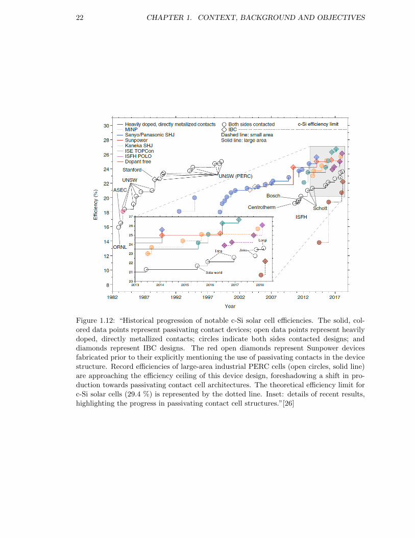
22 CHAPTER 1. CONTEXT, BACKGROUND AND OBJECTIVES
Figure 1.12: “Historical progression of notable c-Si solar cell efficiencies. The solid, col-ored data points represent passivating contact devices; open data points represent heavilydoped, directly metallized contacts; circles indicate both sides contacted designs; anddiamonds represent IBC designs. The red open diamonds represent Sunpower devicesfabricated prior to their explicitly mentioning the use of passivating contacts in the devicestructure. Record efficiencies of large-area industrial PERC cells (open circles, solid line)are approaching the efficiency ceiling of this device design, foreshadowing a shift in pro-duction towards passivating contact cell architectures. The theoretical efficiency limit forc-Si solar cells (29.4 %) is represented by the dotted line. Inset: details of recent results,highlighting the progress in passivating contact cell structures.”[26]

1.2. PASSIVATING CONTACTS: TOWARD HIGHER EFFICIENCY 23
Tab
le1.
1:
Tab
leof
TO
PC
on
sola
rce
lls
effici
enci
es.
Th
issh
ows
the
vari
ety
ofth
ety
pe
ofsu
bst
rate
,fa
bri
cati
on
pro
cess
esan
darc
hit
ectu
res
that
are
stu
die
din
the
lite
ratu
re,
as
wel
las
the
area
ofth
eso
lar
cell
s.S
tron
geff
orts
hav
eb
een
mad
eon
goi
ng
from
lab
scale
toin
du
stri
al
waf
ers
and
pro
cess
es.
Inst
itu
teS
ub
stra
teO
xid
ep
oly
-Si
Are
aT
yp
eof
cell
Effi
cien
cyM
ain
featu
res
Ref
EC
Nn
Cz
Ch
emic
al(N
AO
S)
LP
CV
Dp
oly
-Si
n+
239
cm2
rear
nT
OP
Con
20.7
%la
rge,
FT
met
al,
Bif
aci
al
[45]
Fra
unh
ofer
-IS
En
FZ
Ch
emic
al(N
AO
S)
PE
CV
Dp
oly-S
in+
4cm
2re
ar
nT
OP
Con
25.7
%B
oth
-sid
eco
nta
cted
[47]
ISF
Hp
FZ
Th
erm
alL
PC
VD
pol
y-S
in+
&p+
4cm
2P
OL
O-I
BC
26.1
%R
ecord
,IB
C[4
8]
SE
RIS
nC
zP
EC
VD
PE
CV
Dp
oly-S
in+
4cm
2re
ar
nT
OP
Con
22.8
%F
ull
PE
CV
D[4
9]
EP
FL
nF
ZC
hem
ical
(NA
OS
)P
EC
VD
poly
-SiC
n+
&p+
4.4
cm2
Both
-sid
eT
OP
Con
22.6
%S
iCx,
2p
ola
riti
es[5
5]
EP
FL
pF
ZL
PC
VD
PE
CV
DS
iCx
p+
4cm
2re
arp
TO
PC
on,
front
HIT
21.9
%p
TO
PC
on
,S
iC,
FP
C(n
oan
nea
lin
g)
[46]
CS
EM
pC
zL
PC
VD
PE
CV
DS
iCx
p+
256
cm2
rear
pT
OP
Con
,fr
ont
HIT
21.7
%la
rge,
pT
OP
Con
,p
Cz,
SiC
,F
PC
[56]
Tri
na
Sol
arn
Cz
LP
CV
DL
PC
VD
poly
-Si
n+
256
cm2
rear
nT
OP
Con
24.6
%M
ass
pro
du
ctio
n[5
0]
SE
RIS
nC
zL
PC
VD
LP
CV
Dp
oly
-Si
n+
256
cm2
rear
nT
OP
Con
22.6
%M
2,
FT
met
al
[57]
ISF
Hp
Cz
H2O
-O3
PE
CV
Dp
oly-S
in+
256
cm2
rear
nT
OP
Con
22.2
3%
M2,
pC
zw
afe
rs[5
8]
Tab
le1.
2:
Tab
leof
pas
siva
tion
pro
per
ties
for
TO
PC
on.
Th
issu
mm
ariz
esth
eb
est
pas
siva
tion
pro
per
ties
ach
ieve
dfo
rd
iffer
ent
kin
ds
of
sub
stra
te,
surf
ace
morp
hol
ogy
,ox
ide
gro
wth
and
pol
y-S
ifa
bri
cati
onte
chn
iqu
e.O
uts
tan
din
gJ0
valu
eslo
wer
than
1fA
.cm−2
wer
ere
ach
ed.
1st
Auth
orD
ate
Subst
rate
Surf
ace
Oxid
ep
oly-S
iD
opin
gA
nnea
ling
Hydro
genat
ion
iVoc
(mV
)J0
(fA
/cm
2)
Ref
Fel
dm
ann
2018
nF
ZD
SP
Ther
mal
PE
CV
Dp
oly-S
in+
in-s
itu
PE
CV
D90
0°C
,10
min
RP
HP
736
1.8
[59]
Pol
zin
2018
nF
Zte
xtu
red
Ther
mal
PE
CV
Dp
oly-S
in+
in-s
itu
PE
CV
D90
0°C
,10
min
RP
HP
732
[60]
Pei
bst
2016
nC
zSD
RH
2O
-O3
LP
CV
Dp
oly-S
in+
ion
impla
nta
tion
900°C
,30
min
SiN
x74
70.
6[3
5]
Pei
bst
2016
nC
zte
xtu
red
Ther
mal
LP
CV
Dp
oly-S
in+
ion
impla
nta
tion
900°C
,30
min
SiN
x74
13.
8[3
5]
Chen
2020
nC
zSD
EN
AO
SP
EC
VD
pol
y-S
in+
PO
Cl 3
diff
.none
FG
A74
72
[61]
Yan
g20
20n
Cz
SD
EN
AO
SP
EC
VD
pol
y-S
in+
in-s
itu
PE
CV
D82
0°C
,10
min
AlO
x+
450°C
10
min
730
4.2
[62]
Haa
se20
18p
FZ
DSP
Ther
mal
LP
CV
Dp
oly-S
in+
ion
impla
nta
tion
900°C
,30
min
+10
00°C
1h
SiN
x:H
+42
5°C
,30
min
733
2[4
8]
Inge
nit
o20
18p
FZ
DSP
Ther
mal
PE
CV
Dp
oly-S
iCn+
in-s
itu
PE
CV
D85
0°C
8m
inSiN
x:H
+45
0°C
,30
min
746
4[6
3]
Inge
nit
o20
18p
FZ
textu
red
Ther
mal
PE
CV
Dp
oly-S
iCn+
in-s
itu
PE
CV
D85
0°C
8m
inSiN
x+
450°C
,30
min
737
7[6
3]
Gao
2019
pC
zSD
RP
AN
OP
EC
VD
pol
y-S
in+
in-s
itu
PE
CV
D88
0°C
,30
min
FG
A+
AlO
x+
400°C
742
3[6
4]
Lim
odio
2019
nF
Zte
xtu
red
NA
OS
LP
CV
Dp
oly-S
ip+
ion
impla
nta
tion
950°C
,5
min
FG
A400°C
,2h
716
10[6
5]
Pol
zin
2018
nF
Zte
xtu
red
Ther
mal
PE
CV
Dp
oly-S
ip+
in-s
itu
PE
CV
D90
0°C
,10
min
RP
HP
732
[60]
Mor
isse
t20
19n
Cz
DSP
H2O
-O3
PE
CV
Dp
oly-S
ip+
in-s
itu
PE
CV
D80
0°C
,30
min
SiN
x+
firi
ng
734
7[6
6]
Sto
doln
y20
18n
Cz
SD
RL
PC
VD
LP
CV
Dp
oly-S
ip+
BB
r 3diff
.none
AlO
x/S
iNx/A
lOx
741
3[6
7]
Sto
doln
y20
18n
Cz
textu
red
LP
CV
DL
PC
VD
pol
y-S
ip+
BB
r 3diff
.none
AlO
x/S
iNx/A
lOx
722
9[6
7]
Haa
se20
18p
FZ
DSP
Ther
mal
LP
CV
Dp
oly-S
ip+
ion
impla
nta
tion
900°C
,30
min
+10
00°C
1h
SiN
x:H
+42
5°C
,30
min
717
6[4
8]
Nog
ay20
18p
FZ
DSP
NA
OS
PE
CV
Dp
oly-S
iCp+
in-s
itu
PE
CV
Dnone
SiN
x:H
+45
0°C
,30
min
735
5[5
5]
Alleb
e20
18p
Cz
SD
EN
AO
SP
EC
VD
pol
y-S
iCp+
in-s
itu
PE
CV
Dnone
SiN
x:H
+45
0°C
,30
min
735
5[5
6]
24 CHAPTER 1. CONTEXT, BACKGROUND AND OBJECTIVES
Process for passivating contact integration
The large variety of solar cell architectures mentioned above also comes along with verydifferent process flows. The doped semi-conductor layer can be made of poly-Si (most ofthe studies), silicon carbide (SiCx) [46], [55], [56], [68] or SiOx [49], with various depositiontechniques such as plasma-enhanced chemical vapor deposition (PECVD) [29], [60], [69],[70], low pressure chemical vapor deposition (LPCVD) [45], [50], [57] or hot-wire chemicalvapor deposition (HWCVD) [71], [72]. The doping of this layer can be achieved in situin PECVD [60] and LPCVD deposition chambers, as well as ex situ by ion implantation[65], [73], [74], or diffusion [75]–[77]. The fabrication of the thin oxide layer may be doneby nitric acid oxidation of silicon (NAOS) [43], [65], [74], [78], [79], chemical oxidation byRadio Corporation of America (RCA) Cleaning [33], [80]–[82], thermal oxidation in quartzfurnace [37], [83] or LPCVD chamber [31], [67], plasma-assisted nitrous oxide (PANO)oxidation [64], [84], [85], PECVD deposition [49], [69], [86], UV-O3 [87]–[89], H2O-O3 [66],[89], [90], atomic layer deposition (ALD) [91], [92]... or even replacing it by AlOx [80]or a-SiNx:H [93]. Many studies have been made on benchmarking the SiOx depositionprocess [54], [87], [94]–[97]. Thermal oxides usually lead to better passivation properties,but require higher process temperatures.
In the most standard processes, the thermal budget of such structures is high, oftenrequiring a 5-to-15-min long annealing step between 800 and 1000 °C for crystallization anddopant activation (sometimes much more). This is not desirable in industrial processing,and especially for the integration of such structures on multi-crystalline or cast-monosilicon wafers [23]. One way to tackle this issue was presented by Ingenito et al. fromEPFL through the development of fired passivated contact (FPC) [46]. The aim of thisapproach is to remove the long-and-high-temperature annealing step, and to limit the hightemperature processes to a single firing step (> 700 °C for a few seconds) necessary for thefront side metallization. However, one problem that emerges from annealing the siliconlayer is the formation of blisters, that are highly detrimental for the electrical propertiesof the device [62], [98]–[100]. To prevent this from happening, the silicon layer in the FPCmust be mechanically resistant to the firing step. Their research group uses SiCx (with alow carbon content of approximately 2.5 at%), which has a larger mechanical resistancethan a-Si:H, and a larger optical band gap, thus leading to less parasitic absorption. Moredetails on this process will be given in section 1.5.
1.2.4 Transparent Metal Oxides
Another technology that is being investigated by the PV research community is basedon the dopant-free passivating contacts, such as Transparent Metal Oxides (TMOs). The”dopant-free” denomination implies that highly-doped silicon layers are not used in suchdevices. The optical and electrical properties of TMOs can be tuned in order to meetspecific needs in the silicon solar cells. Noticeably, these materials are wide band-gapsemiconductors allowing to reduce parasitic absorption and are dopant-free therefore sup-pressing free-carrier absorption thus tacking the two main limiting factors in poly-Si anda-Si:H-based passivated contacts. TMOs were first explored in the 1970’s as an alterna-tive to homojunction solar cells [101]. There has recently been a regain of interest inthese technologies due to improvements of the passivating layers, the current limitationsof solar cell efficiencies by parasitic absorption, and improvements in the manufacturingof high/low work function materials [102] from organic electronics [103]. A thin passivat-ing layer between the TMO and the c-Si bulk is usually required: an (i) a-Si:H layer isdeposited or a thin SiOx layer grows at the Si/TMO interface (either naturally [104] or
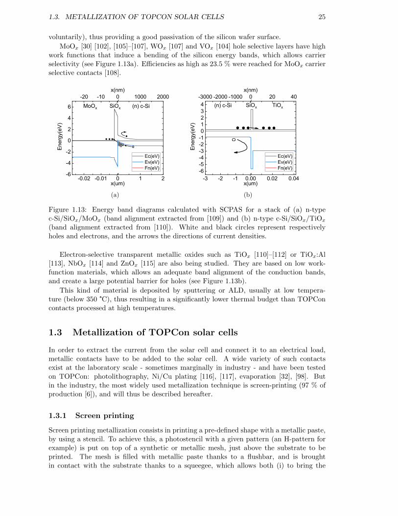
1.3. METALLIZATION OF TOPCON SOLAR CELLS 25
voluntarily), thus providing a good passivation of the silicon wafer surface.
MoOx [30] [102], [105]–[107], WOx [107] and VOx [104] hole selective layers have highwork functions that induce a bending of the silicon energy bands, which allows carrierselectivity (see Figure 1.13a). Efficiencies as high as 23.5 % were reached for MoOx carrierselective contacts [108].
-0.02 -0.01 0 1 2
-20 -10 0 1000 2000
-6
-4
-2
0
2
4
6
x(nm)
MoOx (n) c-SiSiOx
Energy
(eV)
x(um)
Ec(eV) Ev(eV) Fn(eV)
(a)
-3 -2 -1 0.00 0.02 0.04
-3000 -2000 -1000 0 20 40
-6-5-4-3-2-101234
x(nm)
TiOx(n) c-Si SiOx
Energy
(eV)
x(um)
Ec(eV) Ev(eV) Fn(eV)
(b)
Figure 1.13: Energy band diagrams calculated with SCPAS for a stack of (a) n-typec-Si/SiOx/MoOx (band alignment extracted from [109]) and (b) n-type c-Si/SiOx/TiOx
(band alignment extracted from [110]). White and black circles represent respectivelyholes and electrons, and the arrows the directions of current densities.
Electron-selective transparent metallic oxides such as TiOx [110]–[112] or TiOx:Al[113], NbOx [114] and ZnOx [115] are also being studied. They are based on low work-function materials, which allows an adequate band alignment of the conduction bands,and create a large potential barrier for holes (see Figure 1.13b).
This kind of material is deposited by sputtering or ALD, usually at low tempera-ture (below 350 °C), thus resulting in a significantly lower thermal budget than TOPConcontacts processed at high temperatures.
1.3 Metallization of TOPCon solar cells
In order to extract the current from the solar cell and connect it to an electrical load,metallic contacts have to be added to the solar cell. A wide variety of such contactsexist at the laboratory scale - sometimes marginally in industry - and have been testedon TOPCon: photolithography, Ni/Cu plating [116], [117], evaporation [32], [98]. Butin the industry, the most widely used metallization technique is screen-printing (97 % ofproduction [6]), and will thus be described hereafter.
1.3.1 Screen printing
Screen printing metallization consists in printing a pre-defined shape with a metallic paste,by using a stencil. To achieve this, a photostencil with a given pattern (an H-pattern forexample) is put on top of a synthetic or metallic mesh, just above the substrate to beprinted. The mesh is filled with metallic paste thanks to a flushbar, and is broughtin contact with the substrate thanks to a squeegee, which allows both (i) to bring the
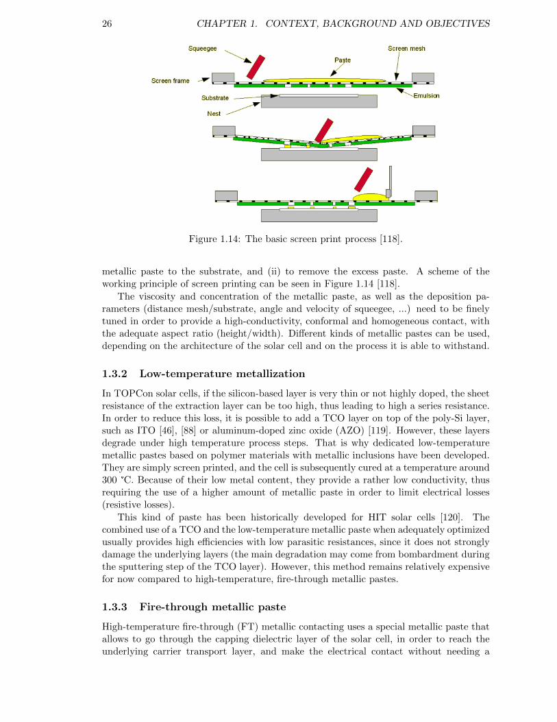
26 CHAPTER 1. CONTEXT, BACKGROUND AND OBJECTIVES
Figure 1.14: The basic screen print process [118].
metallic paste to the substrate, and (ii) to remove the excess paste. A scheme of theworking principle of screen printing can be seen in Figure 1.14 [118].
The viscosity and concentration of the metallic paste, as well as the deposition pa-rameters (distance mesh/substrate, angle and velocity of squeegee, ...) need to be finelytuned in order to provide a high-conductivity, conformal and homogeneous contact, withthe adequate aspect ratio (height/width). Different kinds of metallic pastes can be used,depending on the architecture of the solar cell and on the process it is able to withstand.
1.3.2 Low-temperature metallization
In TOPCon solar cells, if the silicon-based layer is very thin or not highly doped, the sheetresistance of the extraction layer can be too high, thus leading to high a series resistance.In order to reduce this loss, it is possible to add a TCO layer on top of the poly-Si layer,such as ITO [46], [88] or aluminum-doped zinc oxide (AZO) [119]. However, these layersdegrade under high temperature process steps. That is why dedicated low-temperaturemetallic pastes based on polymer materials with metallic inclusions have been developed.They are simply screen printed, and the cell is subsequently cured at a temperature around300 °C. Because of their low metal content, they provide a rather low conductivity, thusrequiring the use of a higher amount of metallic paste in order to limit electrical losses(resistive losses).
This kind of paste has been historically developed for HIT solar cells [120]. Thecombined use of a TCO and the low-temperature metallic paste when adequately optimizedusually provides high efficiencies with low parasitic resistances, since it does not stronglydamage the underlying layers (the main degradation may come from bombardment duringthe sputtering step of the TCO layer). However, this method remains relatively expensivefor now compared to high-temperature, fire-through metallic pastes.
1.3.3 Fire-through metallic paste
High-temperature fire-through (FT) metallic contacting uses a special metallic paste thatallows to go through the capping dielectric layer of the solar cell, in order to reach theunderlying carrier transport layer, and make the electrical contact without needing a
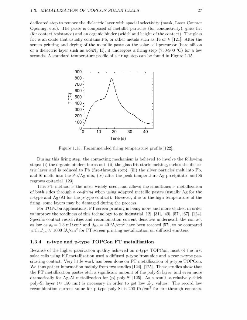
1.3. METALLIZATION OF TOPCON SOLAR CELLS 27
dedicated step to remove the dielectric layer with spacial selectivity (mask, Laser ContactOpening, etc.). The paste is composed of metallic particles (for conductivity), glass frit(for contact resistance) and an organic binder (width and height of the contact). The glassfrit is an oxide that usually contains Pb, or other metals such as Te or V [121]. After thescreen printing and drying of the metallic paste on the solar cell precursor (bare siliconor a dielectric layer such as a-SiNx:H), it undergoes a firing step (750-900 °C) for a fewseconds. A standard temperature profile of a firing step can be found in Figure 1.15.
0 10 20 30 400
100200300400500600700800900
T (°
C)
Time (s)
Figure 1.15: Recommended firing temperature profile [122].
During this firing step, the contacting mechanism is believed to involve the followingsteps: (i) the organic binders burns out, (ii) the glass frit starts melting, etches the dielec-tric layer and is reduced to Pb (fire-through step), (iii) the silver particles melt into Pb,and Si melts into the Pb/Ag mix, (iv) after the peak temperature Ag precipitates and Siregrows epitaxial [123].
This FT method is the most widely used, and allows the simultaneous metallizationof both sides through a co-firing when using adapted metallic pastes (usually Ag for then-type and Ag/Al for the p-type contact). However, due to the high temperature of thefiring, some layers may be damaged during the process.
For TOPCon applications, FT screen printing is being more and more studied in orderto improve the readiness of this technology to go industrial [12], [31], [49], [57], [67], [124].Specific contact resistivities and recombination current densities underneath the contactas low as ρc = 1.3 mΩ.cm2 and J0,c = 40 fA/cm2 have been reached [57], to be comparedwith J0,c ≈ 1000 fA/cm2 for FT screen printing metallization on diffused emitters.
1.3.4 n-type and p-type TOPCon FT metallisation
Because of the higher passivation quality achieved on n-type TOPCon, most of the firstsolar cells using FT metallization used a diffused p-type front side and a rear n-type pas-sivating contact. Very little work has been done on FT metallization of p-type TOPCon.We thus gather information mainly from two studies [124], [125]. These studies show thatthe FT metallization pastes etch a significant amount of the poly-Si layer, and even moredramatically for Ag-Al metallization for (p) poly-Si [125]. As a result, a relatively thickpoly-Si layer (≈ 150 nm) is necessary in order to get low J0,c values. The record lowrecombination current value for p-type poly-Si is 200 fA/cm2 for fire-through contacts.
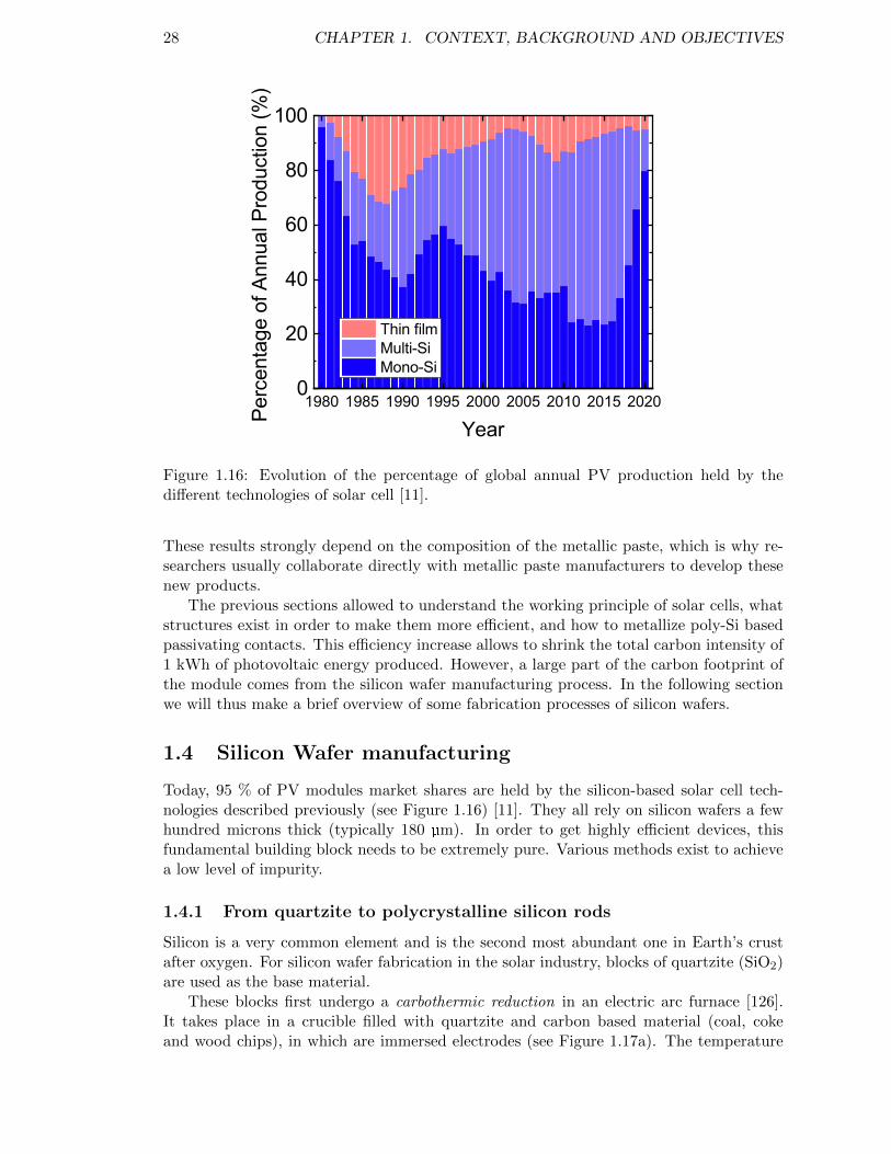
28 CHAPTER 1. CONTEXT, BACKGROUND AND OBJECTIVES
1980 1985 1990 1995 2000 2005 2010 2015 20200
20
40
60
80
100
Perc
enta
ge o
f Ann
ual P
rodu
ctio
n (%
)
Year
Thin film Multi-Si Mono-Si
Figure 1.16: Evolution of the percentage of global annual PV production held by thedifferent technologies of solar cell [11].
These results strongly depend on the composition of the metallic paste, which is why re-searchers usually collaborate directly with metallic paste manufacturers to develop thesenew products.
The previous sections allowed to understand the working principle of solar cells, whatstructures exist in order to make them more efficient, and how to metallize poly-Si basedpassivating contacts. This efficiency increase allows to shrink the total carbon intensity of1 kWh of photovoltaic energy produced. However, a large part of the carbon footprint ofthe module comes from the silicon wafer manufacturing process. In the following sectionwe will thus make a brief overview of some fabrication processes of silicon wafers.
1.4 Silicon Wafer manufacturing
Today, 95 % of PV modules market shares are held by the silicon-based solar cell tech-nologies described previously (see Figure 1.16) [11]. They all rely on silicon wafers a fewhundred microns thick (typically 180 µm). In order to get highly efficient devices, thisfundamental building block needs to be extremely pure. Various methods exist to achievea low level of impurity.
1.4.1 From quartzite to polycrystalline silicon rods
Silicon is a very common element and is the second most abundant one in Earth’s crustafter oxygen. For silicon wafer fabrication in the solar industry, blocks of quartzite (SiO2)are used as the base material.
These blocks first undergo a carbothermic reduction in an electric arc furnace [126].It takes place in a crucible filled with quartzite and carbon based material (coal, cokeand wood chips), in which are immersed electrodes (see Figure 1.17a). The temperature
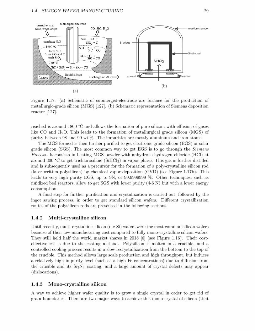
1.4. SILICON WAFER MANUFACTURING 29
(a)(b)
Figure 1.17: (a) Schematic of submerged-electrode arc furnace for the production ofmetallurgic-grade silicon (MGS) [127]. (b) Schematic representation of Siemens depositionreactor [127].
reached is around 1800 °C and allows the formation of pure silicon, with effusion of gaseslike CO and H2O. This leads to the formation of metallurgical grade silicon (MGS) ofpurity between 98 and 99 wt.%. The impurities are mostly aluminum and iron atoms.
The MGS formed is then further purified to get electronic grade silicon (EGS) or solargrade silicon (SGS). The most common way to get EGS is to go through the SiemensProcess. It consists in heating MGS powder with anhydrous hydrogen chloride (HCl) ataround 300 °C to get trichlorosilane (SiHCl3) in vapor phase. This gas is further distilledand is subsequently used as a precursor for the formation of a poly-crystalline silicon rod(later written polysilicon) by chemical vapor deposition (CVD) (see Figure 1.17b). Thisleads to very high purity EGS, up to 9N, or 99.9999999 %. Other techniques, such asfluidized bed reactors, allow to get SGS with lower purity (4-6 N) but with a lower energyconsumption.
A final step for further purification and crystallization is carried out, followed by theingot sawing process, in order to get standard silicon wafers. Different crystallizationroutes of the polysilicon rods are presented in the following sections.
1.4.2 Multi-crystalline silicon
Until recently, multi-crystalline silicon (mc-Si) wafers were the most common silicon wafersbecause of their low manufacturing cost compared to fully mono-crystalline silicon wafers.They still held half the world market shares in 2018 [6] (see Figure 1.16). Their cost-effectiveness is due to the casting method. Polysilicon is molten in a crucible, and acontrolled cooling process results in a slow recrystallization from the bottom to the top ofthe crucible. This method allows large scale production and high throughput, but inducesa relatively high impurity level (such as a high Fe concentrations) due to diffusion fromthe crucible and its Si3N4 coating, and a large amount of crystal defects may appear(dislocations).
1.4.3 Mono-crystalline silicon
A way to achieve higher wafer quality is to grow a single crystal in order to get rid ofgrain boundaries. There are two major ways to achieve this mono-crystal of silicon (that
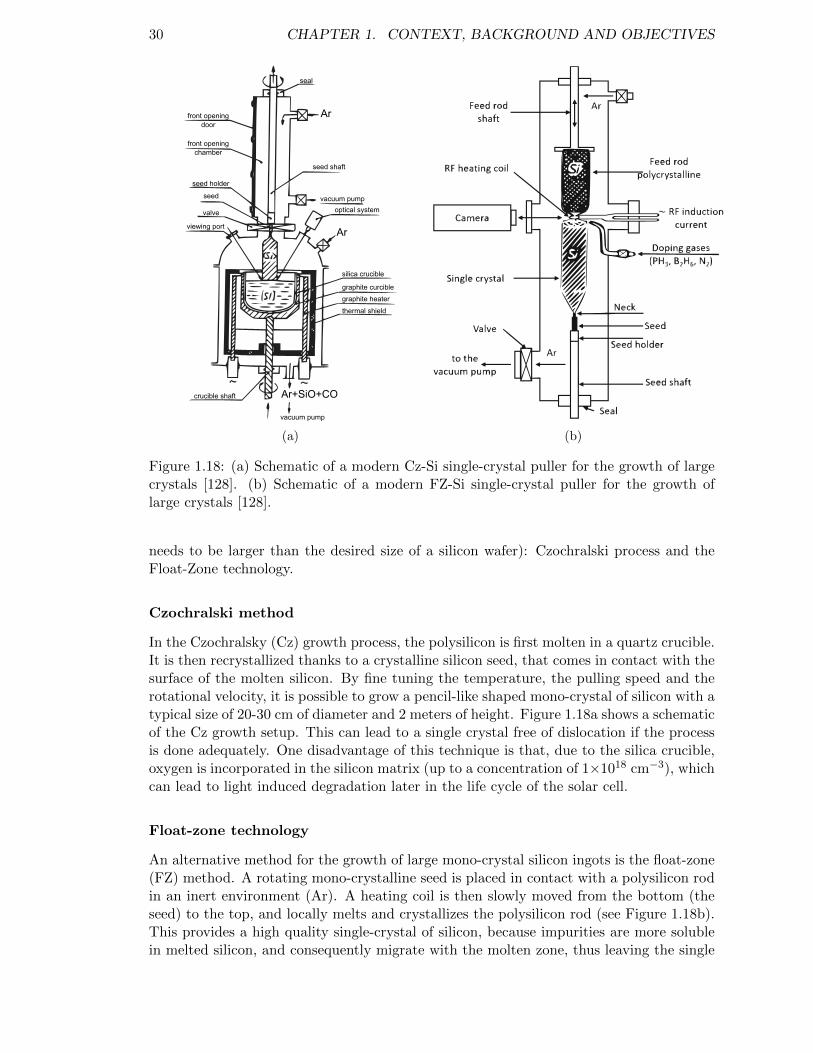
30 CHAPTER 1. CONTEXT, BACKGROUND AND OBJECTIVES
(a) (b)
Figure 1.18: (a) Schematic of a modern Cz-Si single-crystal puller for the growth of largecrystals [128]. (b) Schematic of a modern FZ-Si single-crystal puller for the growth oflarge crystals [128].
needs to be larger than the desired size of a silicon wafer): Czochralski process and theFloat-Zone technology.
Czochralski method
In the Czochralsky (Cz) growth process, the polysilicon is first molten in a quartz crucible.It is then recrystallized thanks to a crystalline silicon seed, that comes in contact with thesurface of the molten silicon. By fine tuning the temperature, the pulling speed and therotational velocity, it is possible to grow a pencil-like shaped mono-crystal of silicon with atypical size of 20-30 cm of diameter and 2 meters of height. Figure 1.18a shows a schematicof the Cz growth setup. This can lead to a single crystal free of dislocation if the processis done adequately. One disadvantage of this technique is that, due to the silica crucible,oxygen is incorporated in the silicon matrix (up to a concentration of 1×1018 cm−3), whichcan lead to light induced degradation later in the life cycle of the solar cell.
Float-zone technology
An alternative method for the growth of large mono-crystal silicon ingots is the float-zone(FZ) method. A rotating mono-crystalline seed is placed in contact with a polysilicon rodin an inert environment (Ar). A heating coil is then slowly moved from the bottom (theseed) to the top, and locally melts and crystallizes the polysilicon rod (see Figure 1.18b).This provides a high quality single-crystal of silicon, because impurities are more solublein melted silicon, and consequently migrate with the molten zone, thus leaving the single
1.5. OBJECTIVES OF THE STUDY 31
crystal extremely pure. However, the temperature gradient also induces the formation ofextended defects that can be passivated by doping the wafer with nitrogen [129].
1.4.4 Cast-mono wafers
The aim of cast-mono wafers is to ally the high throughput, simple process of mc-Sicasting with the high crystalline quality of single-crystal silicon wafers. It consists incasting polysilicon chunks like in the case of mc-Si, that is to say melting the polysiliconin a crucible and vertically controlling the cooling step (Directional Solidification System).The major change is that mono crystal seeds are put at the bottom of the crucible, whichallows an epitaxial growth, with the same orientation as the seed [130]. This producesa chessboard patterned ingot, with large grains that have the size of the desired wafersand with the height of the ingot. This has the advantage of getting rid of most grain-boundary-related defects, keeping the oxygen content lower than in Cz ingots, and allowingeasy mass production. However, a relatively high level of metallic impurities (mostly Fe)can still be found due to diffusion from the crucible, and dislocations may still appear dueto high stress points during the crystallization process.
One growth technology is the SMART technology developed by Takahashi et al. fromFraunhofer ISE [131]. The crystal orientation of the seed is chosen to create artificialgrain boundaries. This allows to grow controlled sections of dislocation-rich silicon, pre-venting dislocations to expand in the silicon-wafers over a quality-controlled area. Anenvironmental analysis shows that using SMART cast-mono wafers instead of Cz wafersfor manufacturing PERC solar cells allows to reduce the global warming potential from42.0 to 37.9 gCO2eq/kWh [132]. This highlights the interest of investigating the use ofcast-mono wafers for a more environmental-friendly PV industry.
1.5 Objectives of the study
Ingenito et al. [46] proposed a process flow shown in Figure A3.4a for the formation of apassivating contact without a long (5 to 15 min) and high-temperature (800 to 1000 °C)annealing step. It consists in depositing a silicon-based layer resistant to the firing stepsuch as amorphous or nano-crystalline silicon carbide (a-SiCx or nc-SiCx) in their case,on top of a thin tunnel oxide layer. Then the sample is subject to a firing step forfurther crystallization of the (p) a-SiCx:H layer and front side metallization. In order toreach a high quality of passivation, an additional hydrogenation process was shown to benecessary [87]. A hydrogenated amorphous silicon nitride layer is deposited by PECVD,and annealed at 450 °C for 30 minutes. It is subsequently removed thanks to a dip inhydrofluoric acid, and the cell is completed by depositing a TCO layer and screen printinga silver grid at low temperature.
As shown in the previous sections, long hydrogenation steps are not desirable forindustrial integration and high-temperature is preferred to low-temperature metallizationfor an easy compatibility with preexisting industrial tools and processes. For simplificationpurposes, we investigate another process-flow for the fabrication of FPC, shown in figureA3.4b. It starts with a Radio Corporation of America (RCA) standard cleaning stepfollowed by the deposition of a tunnel oxide layer. We then deposit a boron doped siliconlayer by PECVD at 13.56 MHz, which needs to be resistant to the firing step. This isfollowed by the deposition of a-SiNx:H by PECVD on top of it, the screen printing of themetallic contacts, and finishing with a high temperature firing step in order to contactthe cell. This process flow, which reduces the number of process steps from 9 to 6, is
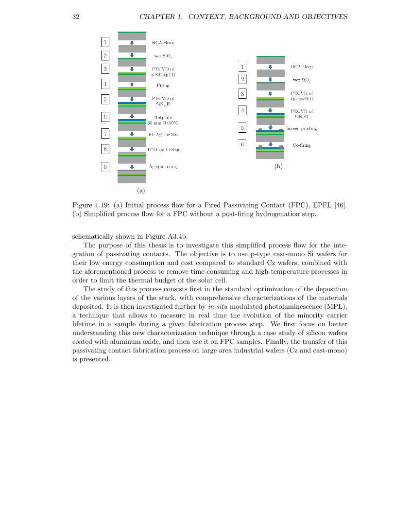
32 CHAPTER 1. CONTEXT, BACKGROUND AND OBJECTIVES
(a)
(b)
Figure 1.19: (a) Initial process flow for a Fired Passivating Contact (FPC), EPFL [46].(b) Simplified process flow for a FPC without a post-firing hydrogenation step.
schematically shown in Figure A3.4b.The purpose of this thesis is to investigate this simplified process flow for the inte-
gration of passivating contacts. The objective is to use p-type cast-mono Si wafers fortheir low energy consumption and cost compared to standard Cz wafers, combined withthe aforementioned process to remove time-consuming and high-temperature processes inorder to limit the thermal budget of the solar cell.
The study of this process consists first in the standard optimization of the depositionof the various layers of the stack, with comprehensive characterizations of the materialsdeposited. It is then investigated further by in situ modulated photoluminescence (MPL),a technique that allows to measure in real time the evolution of the minority carrierlifetime in a sample during a given fabrication process step. We first focus on betterunderstanding this new characterization technique through a case study of silicon waferscoated with aluminum oxide, and then use it on FPC samples. Finally, the transfer of thispassivating contact fabrication process on large area industrial wafers (Cz and cast-mono)is presented.
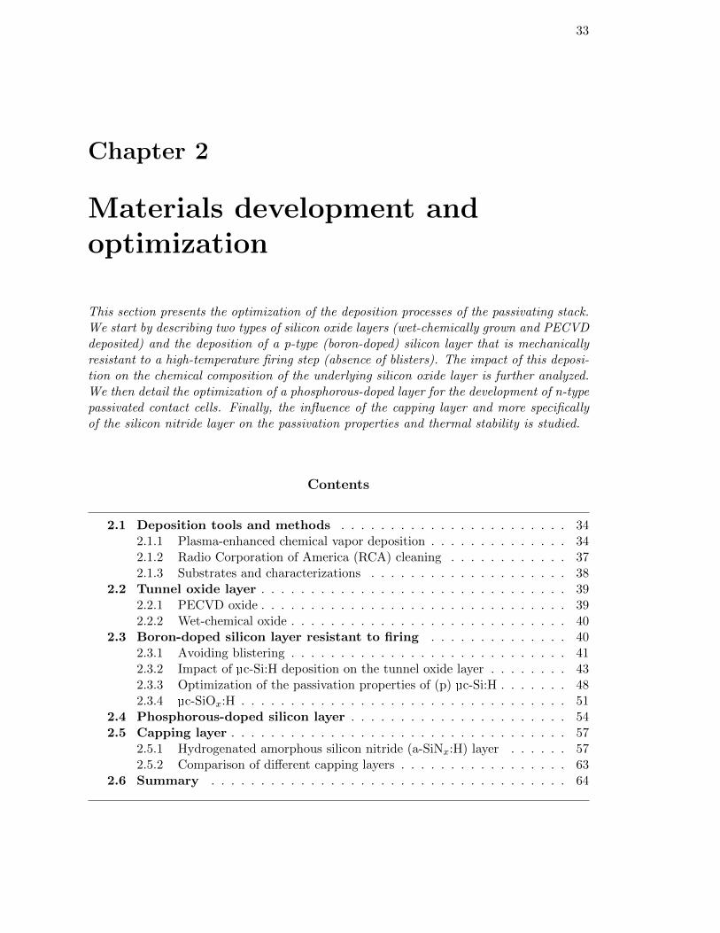
33
Chapter 2
Materials development andoptimization
This section presents the optimization of the deposition processes of the passivating stack.We start by describing two types of silicon oxide layers (wet-chemically grown and PECVDdeposited) and the deposition of a p-type (boron-doped) silicon layer that is mechanicallyresistant to a high-temperature firing step (absence of blisters). The impact of this deposi-tion on the chemical composition of the underlying silicon oxide layer is further analyzed.We then detail the optimization of a phosphorous-doped layer for the development of n-typepassivated contact cells. Finally, the influence of the capping layer and more specificallyof the silicon nitride layer on the passivation properties and thermal stability is studied.
Contents
2.1 Deposition tools and methods . . . . . . . . . . . . . . . . . . . . . . . 342.1.1 Plasma-enhanced chemical vapor deposition . . . . . . . . . . . . . . 342.1.2 Radio Corporation of America (RCA) cleaning . . . . . . . . . . . . 372.1.3 Substrates and characterizations . . . . . . . . . . . . . . . . . . . . 38
2.2 Tunnel oxide layer . . . . . . . . . . . . . . . . . . . . . . . . . . . . . . . 392.2.1 PECVD oxide . . . . . . . . . . . . . . . . . . . . . . . . . . . . . . . 392.2.2 Wet-chemical oxide . . . . . . . . . . . . . . . . . . . . . . . . . . . . 40
2.3 Boron-doped silicon layer resistant to firing . . . . . . . . . . . . . . 402.3.1 Avoiding blistering . . . . . . . . . . . . . . . . . . . . . . . . . . . . 412.3.2 Impact of µc-Si:H deposition on the tunnel oxide layer . . . . . . . . 432.3.3 Optimization of the passivation properties of (p) µc-Si:H . . . . . . . 482.3.4 µc-SiOx:H . . . . . . . . . . . . . . . . . . . . . . . . . . . . . . . . . 51
2.4 Phosphorous-doped silicon layer . . . . . . . . . . . . . . . . . . . . . . 542.5 Capping layer . . . . . . . . . . . . . . . . . . . . . . . . . . . . . . . . . . 57
2.5.1 Hydrogenated amorphous silicon nitride (a-SiNx:H) layer . . . . . . 572.5.2 Comparison of different capping layers . . . . . . . . . . . . . . . . . 63
2.6 Summary . . . . . . . . . . . . . . . . . . . . . . . . . . . . . . . . . . . . 64
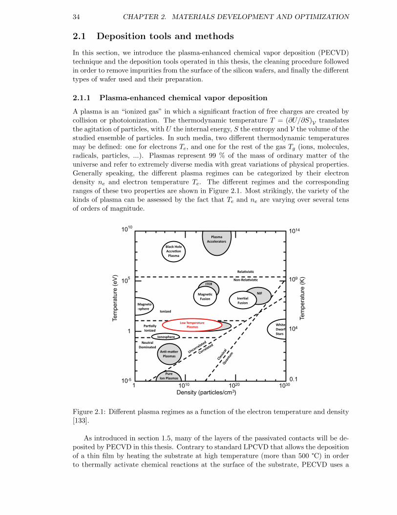
34 CHAPTER 2. MATERIALS DEVELOPMENT AND OPTIMIZATION
2.1 Deposition tools and methods
In this section, we introduce the plasma-enhanced chemical vapor deposition (PECVD)technique and the deposition tools operated in this thesis, the cleaning procedure followedin order to remove impurities from the surface of the silicon wafers, and finally the differenttypes of wafer used and their preparation.
2.1.1 Plasma-enhanced chemical vapor deposition
A plasma is an “ionized gas” in which a significant fraction of free charges are created bycollision or photoionization. The thermodynamic temperature T = (∂U/∂S)V translatesthe agitation of particles, with U the internal energy, S the entropy and V the volume of thestudied ensemble of particles. In such media, two different thermodynamic temperaturesmay be defined: one for electrons Te, and one for the rest of the gas Tg (ions, molecules,radicals, particles, ...). Plasmas represent 99 % of the mass of ordinary matter of theuniverse and refer to extremely diverse media with great variations of physical properties.Generally speaking, the different plasma regimes can be categorized by their electrondensity ne and electron temperature Te. The different regimes and the correspondingranges of these two properties are shown in Figure 2.1. Most strikingly, the variety of thekinds of plasma can be assessed by the fact that Te and ne are varying over several tensof orders of magnitude.
Figure 2.1: Different plasma regimes as a function of the electron temperature and density[133].
As introduced in section 1.5, many of the layers of the passivated contacts will be de-posited by PECVD in this thesis. Contrary to standard LPCVD that allows the depositionof a thin film by heating the substrate at high temperature (more than 500 °C) in orderto thermally activate chemical reactions at the surface of the substrate, PECVD uses a
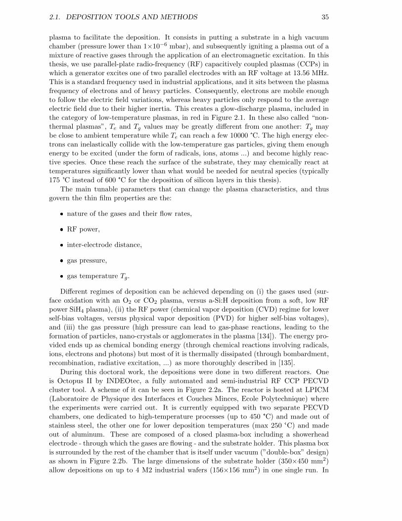
2.1. DEPOSITION TOOLS AND METHODS 35
plasma to facilitate the deposition. It consists in putting a substrate in a high vacuumchamber (pressure lower than 1×10⁻⁶ mbar), and subsequently igniting a plasma out of amixture of reactive gases through the application of an electromagnetic excitation. In thisthesis, we use parallel-plate radio-frequency (RF) capacitively coupled plasmas (CCPs) inwhich a generator excites one of two parallel electrodes with an RF voltage at 13.56 MHz.This is a standard frequency used in industrial applications, and it sits between the plasmafrequency of electrons and of heavy particles. Consequently, electrons are mobile enoughto follow the electric field variations, whereas heavy particles only respond to the averageelectric field due to their higher inertia. This creates a glow-discharge plasma, included inthe category of low-temperature plasmas, in red in Figure 2.1. In these also called “non-thermal plasmas”, Te and Tg values may be greatly different from one another: Tg maybe close to ambient temperature while Te can reach a few 10000 °C. The high energy elec-trons can inelastically collide with the low-temperature gas particles, giving them enoughenergy to be excited (under the form of radicals, ions, atoms ...) and become highly reac-tive species. Once these reach the surface of the substrate, they may chemically react attemperatures significantly lower than what would be needed for neutral species (typically175 °C instead of 600 °C for the deposition of silicon layers in this thesis).
The main tunable parameters that can change the plasma characteristics, and thusgovern the thin film properties are the:
nature of the gases and their flow rates,
RF power,
inter-electrode distance,
gas pressure,
gas temperature Tg.
Different regimes of deposition can be achieved depending on (i) the gases used (sur-face oxidation with an O2 or CO2 plasma, versus a-Si:H deposition from a soft, low RFpower SiH4 plasma), (ii) the RF power (chemical vapor deposition (CVD) regime for lowerself-bias voltages, versus physical vapor deposition (PVD) for higher self-bias voltages),and (iii) the gas pressure (high pressure can lead to gas-phase reactions, leading to theformation of particles, nano-crystals or agglomerates in the plasma [134]). The energy pro-vided ends up as chemical bonding energy (through chemical reactions involving radicals,ions, electrons and photons) but most of it is thermally dissipated (through bombardment,recombination, radiative excitation, ...) as more thoroughly described in [135].
During this doctoral work, the depositions were done in two different reactors. Oneis Octopus II by INDEOtec, a fully automated and semi-industrial RF CCP PECVDcluster tool. A scheme of it can be seen in Figure 2.2a. The reactor is hosted at LPICM(Laboratoire de Physique des Interfaces et Couches Minces, Ecole Polytechnique) wherethe experiments were carried out. It is currently equipped with two separate PECVDchambers, one dedicated to high-temperature processes (up to 450 °C) and made out ofstainless steel, the other one for lower deposition temperatures (max 250 °C) and madeout of aluminum. These are composed of a closed plasma-box including a showerheadelectrode - through which the gases are flowing - and the substrate holder. This plasma boxis surrounded by the rest of the chamber that is itself under vacuum (”double-box” design)as shown in Figure 2.2b. The large dimensions of the substrate holder (350×450 mm2)allow depositions on up to 4 M2 industrial wafers (156×156 mm2) in one single run. In
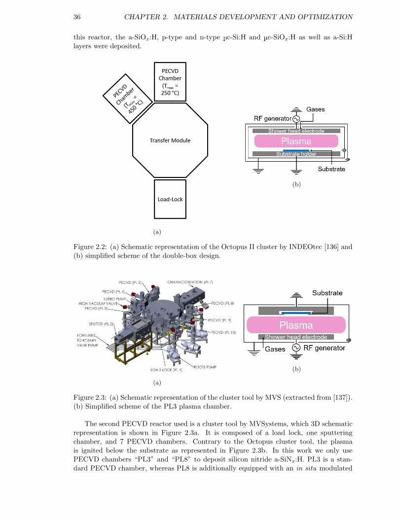
36 CHAPTER 2. MATERIALS DEVELOPMENT AND OPTIMIZATION
this reactor, the a-SiOx:H, p-type and n-type µc-Si:H and µc-SiOx:H as well as a-Si:Hlayers were deposited.
(a)
(b)
Figure 2.2: (a) Schematic representation of the Octopus II cluster by INDEOtec [136] and(b) simplified scheme of the double-box design.
(a)
(b)
Figure 2.3: (a) Schematic representation of the cluster tool by MVS (extracted from [137]).(b) Simplified scheme of the PL3 plasma chamber.
The second PECVD reactor used is a cluster tool by MVSystems, which 3D schematicrepresentation is shown in Figure 2.3a. It is composed of a load lock, one sputteringchamber, and 7 PECVD chambers. Contrary to the Octopus cluster tool, the plasmais ignited below the substrate as represented in Figure 2.3b. In this work we only usePECVD chambers “PL3” and “PL8” to deposit silicon nitride a-SiNx:H. PL3 is a stan-dard PECVD chamber, whereas PL8 is additionally equipped with an in situ modulated
2.1. DEPOSITION TOOLS AND METHODS 37
photoluminescence acquisition setup that will be further described in chapter 4.
The optimization of the PECVD deposition conditions of the various layers will be theobject of this chapter.
2.1.2 Radio Corporation of America (RCA) cleaning
Silicon crystal surfaces are very reactive to ambient air, and naturally get oxidized veryrapidly. This forms a thin layer at the surface of a raw silicon wafer, called native oxide.However, this layer is very defective, which leads to relatively poor passivation propertieswhatever the kind of materials deposited on top of this oxide. Consequently, chemicalcleaning of the wafers is necessary before any deposition step in order to get a high qual-ity final device. A standard chemical used in order to remove the native oxide layer ishydrofluoric acid (HF). The chemical reaction describing the etching of the surface siliconoxide layer may be written as [138]
SiO2(s) + 6HF(aq) −→ H2 [SiF6](aq) + 2H2O(l)
This results in a silicon wafer with hydrogen terminated bonds at its surface. However,organic, ionic (alkali), and metallic contaminations may remain at the surface of the waferand deteriorate the final device performances. A more thorough cleaning procedure wasdeveloped by W. Kern and D.A. Puotinen while working at Radio Corporation of America[139], which gave the name RCA cleaning. It is mostly based on the use of hydrogenperoxide H2O2 that can easily oxidize silicon. The full standard procedure consists in 4steps:
standard cleaning 1 (SC-1) - Organic contaminants removal: removal of contami-nants from the wafer surface and formation of complexes with group I and II metalsProcess: De-Ionized H2O(l):H2O2(aq):NH3(aq) with a 5:1:1 ratio at 75 °C for 5 minRinsing 3 min in De-Ionized H2O(l)
Oxide layer removalProcess: HF 5% in De-Ionized H2O(l) for 15 sRinsing 30 s in De-Ionized H2O(l)
standard cleaning 2 (SC-2) - Ionic contamination removal: dissolution of the metaland ionic complexesProcess: De-Ionized H2O(l):H2O2(aq):HCl(aq) with a 6:1:1 ratio at 75 °C for 10 minRinsing 5 min in De-Ionized H2O(l)
Oxide layer removalProcess: HF 5% in De-Ionized H2O(l) for 15 sRinsing 30 s in De-Ionized H2O(l)
This provides a contamination-free surface and a clean silicon wafer, with hydrogen-terminated silicon bonds. Depositions can subsequently be carried out on the clean sam-ples. It is worth noting that the high viscosity of the SC-2 solution can lead to difficultiesduring the subsequent rinsing step. All the cleaning steps were done by permanent EDFR&D staff for safety reasons.
38 CHAPTER 2. MATERIALS DEVELOPMENT AND OPTIMIZATION
2.1.3 Substrates and characterizations
In this work, different kinds of substrates are used in order to characterize the variousphysical properties of the deposited layers.
double-side polished (DSP) n-type Cz 1/4 wafers (100 mm of diameter, 280 µm-thick, 1-5 Ω.cm) are used as substrates for spectroscopic ellipsometry (SE), X-rayphotoelectron spectroscopy (XPS), confocal microscope images, transmission elec-tron microscopy (TEM), thermal desorption spectrocsopy (TDS), and corona oxidecharacterisation on semiconductor (COCOS).
DSP p-type float-zone (FZ) 1/4 wafers (100 mm of diameter, 280 µm-thick, 2-4 Ω.cm)are needed in order to assess the passivation properties of the layers or stacks de-posited. quasi steady-state photoconductance (QSSPC) and fourier transform in-frared spectroscopy (FTIR) spectroscopy were done on these samples.
Corning glass slides (2 mm-thick, 1”×1”) are used as substrates for the samplescharacterized by Raman spectroscopy and 4-points probe (4PP) conductivity mea-surements.
The p-type FZ wafers were RCA cleaned before the deposition of the passivation layers.For the optical and chemical characterization of the n-type Cz wafers, a simple HF dip for30 s was made in order to remove the native oxide. No specific pre-treatment was doneon the glass substrates.
Some characterizations result from collaborations with researchers from various re-search units.
The XPS experiments shown in the following sections were carried out at InstitutLavoisier de Versailles (ILV) - Universite de Versailles Saint-Quentin. A ThermoFischer K-Alpha+ spectrometer was used with a monochromatic Al-Kα source at1486.6 eV. The in-depth composition and chemical environments were obtained bysequential Ar+ sputtering (1000 eV, 10 mA, static mode, raster size 2 mm, 10 s to30 s sputtering steps depending on the depth probed). The XPS spot size was 400 µmwith a probed depth of the order of 10 nm. High resolution spectra were acquiredusing a 20 eV pass energy. Data were processed using the Thermo Advantage©software. Si2p spectra were deconvoluted using two contributions corresponding tothe c-Si matrix (at 98.8 eV) and the Si oxide (around 103.0 eV) environments [140]–[142]. The respective proportion of each environment was determined by comparingthe corresponding areas of the contributions after a Shirley background substraction.
The TEM characterizations were performed at Ecole Polytechnique on a Titan-Themis electron microscope operating at 200 kV equipped with a Cs probe cor-rector with a spatial resolution within nm range using the scanning transmissionelectron microscopy-high angle annular dark field (STEM-HAADF) imaging mode.For all the studied samples, cross-section-lamellas have been prepared using a stan-dard lift-out procedure within a focused-ion, dual-beam microscope (FIB, FEI-SciosDualBeam).
The FTIR spectroscopy was carried out at Air Liquid R&D lab on a Nicolet 6700spectrometer.
All the other characterizations (QSSPC, SE, 4PP, Raman spectroscopy, TDS, confocalmicroscopy, COCOS), data treatment (FTIR), and depositions were made by the PhDcandidate. The various characterization techniques are shortly described in Appendix A2.
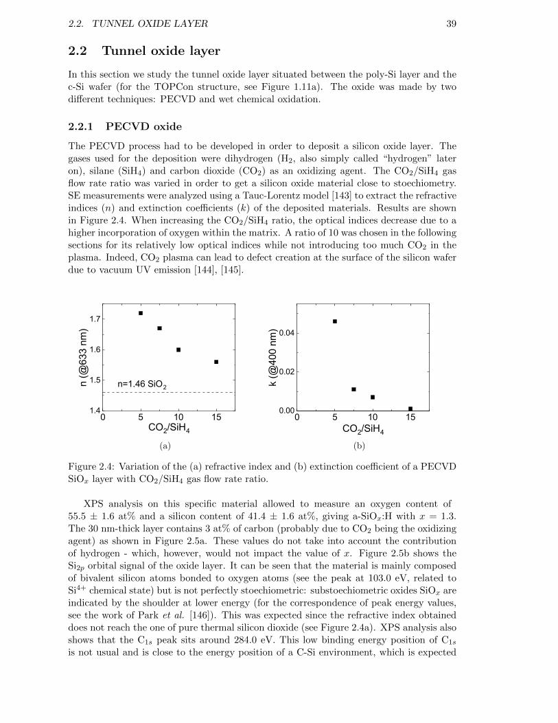
2.2. TUNNEL OXIDE LAYER 39
2.2 Tunnel oxide layer
In this section we study the tunnel oxide layer situated between the poly-Si layer and thec-Si wafer (for the TOPCon structure, see Figure 1.11a). The oxide was made by twodifferent techniques: PECVD and wet chemical oxidation.
2.2.1 PECVD oxide
The PECVD process had to be developed in order to deposit a silicon oxide layer. Thegases used for the deposition were dihydrogen (H2, also simply called “hydrogen” lateron), silane (SiH4) and carbon dioxide (CO2) as an oxidizing agent. The CO2/SiH4 gasflow rate ratio was varied in order to get a silicon oxide material close to stoechiometry.SE measurements were analyzed using a Tauc-Lorentz model [143] to extract the refractiveindices (n) and extinction coefficients (k) of the deposited materials. Results are shownin Figure 2.4. When increasing the CO2/SiH4 ratio, the optical indices decrease due to ahigher incorporation of oxygen within the matrix. A ratio of 10 was chosen in the followingsections for its relatively low optical indices while not introducing too much CO2 in theplasma. Indeed, CO2 plasma can lead to defect creation at the surface of the silicon waferdue to vacuum UV emission [144], [145].
0 5 10 151.4
1.5
1.6
1.7
n (@
633
nm)
CO2/SiH4
n=1.46 SiO2
(a)
0 5 10 150.00
0.02
0.04
k (@
400
nm)
CO2/SiH4
(b)
Figure 2.4: Variation of the (a) refractive index and (b) extinction coefficient of a PECVDSiOx layer with CO2/SiH4 gas flow rate ratio.
XPS analysis on this specific material allowed to measure an oxygen content of55.5 ± 1.6 at% and a silicon content of 41.4 ± 1.6 at%, giving a-SiOx:H with x = 1.3.The 30 nm-thick layer contains 3 at% of carbon (probably due to CO2 being the oxidizingagent) as shown in Figure 2.5a. These values do not take into account the contributionof hydrogen - which, however, would not impact the value of x. Figure 2.5b shows theSi2p orbital signal of the oxide layer. It can be seen that the material is mainly composedof bivalent silicon atoms bonded to oxygen atoms (see the peak at 103.0 eV, related toSi4+ chemical state) but is not perfectly stoechiometric: substoechiometric oxides SiOx areindicated by the shoulder at lower energy (for the correspondence of peak energy values,see the work of Park et al. [146]). This was expected since the refractive index obtaineddoes not reach the one of pure thermal silicon dioxide (see Figure 2.4a). XPS analysis alsoshows that the C1s peak sits around 284.0 eV. This low binding energy position of C1s
is not usual and is close to the energy position of a C-Si environment, which is expected
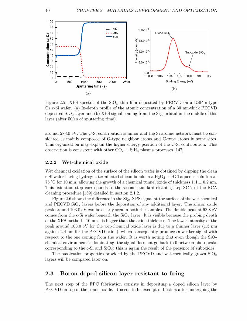
40 CHAPTER 2. MATERIALS DEVELOPMENT AND OPTIMIZATION
(a)
108 106 104 102 100 98 960.0
5.0x10³
1.0x10⁴
1.5x10⁴
2.0x10⁴
Oxide SiO2
Inte
nsity
(cou
nts/
s)
Binding Energy (eV)
Suboxide SiOx
(b)
Figure 2.5: XPS spectra of the SiOx thin film deposited by PECVD on a DSP n-typeCz c-Si wafer. (a) In-depth profile of the atomic concentration of a 30 nm-thick PECVDdeposited SiOx layer and (b) XPS signal coming from the Si2p orbital in the middle of thislayer (after 500 s of sputtering time).
around 283.0 eV. The C-Si contribution is minor and the Si atomic network must be con-sidered as mainly composed of O-type neighbor atoms and C-type atoms in some sites.This organization may explain the higher energy position of the C-Si contribution. Thisobservation is consistent with other CO2 + SiH4 plasma processes [147].
2.2.2 Wet-chemical oxide
Wet chemical oxidation of the surface of the silicon wafer is obtained by dipping the cleanc-Si wafer having hydrogen terminated silicon bonds in a H2O2 + HCl aqueous solution at75 °C for 10 min, allowing the growth of a chemical tunnel oxide of thickness 1.4 ± 0.2 nm.This oxidation step corresponds to the second standard cleaning step SC-2 of the RCAcleaning procedure [139] detailed in section 2.1.2.
Figure 2.6 shows the difference in the Si2p XPS signal at the surface of the wet-chemicaland PECVD SiOx layers before the deposition of any additional layer. The silicon oxidepeak around 103.0 eV can be clearly seen in both the samples. The double peak at 98.8 eVcomes from the c-Si wafer beneath the SiOx layer. It is visible because the probing depthof the XPS method - 10 nm - is bigger than the oxide thickness. The lower intensity of thepeak around 103.0 eV for the wet-chemical oxide layer is due to a thinner layer (1.3 nmagainst 2.4 nm for the PECVD oxide), which consequently produces a weaker signal withrespect to the one coming from the wafer. It is worth noting that even though the SiO2
chemical environment is dominating, the signal does not go back to 0 between photopeakscorresponding to the c-Si and SiO2: this is again the result of the presence of suboxides.
The passivation properties provided by the PECVD and wet-chemically grown SiOx
layers will be compared later on.
2.3 Boron-doped silicon layer resistant to firing
The next step of the FPC fabrication consists in depositing a doped silicon layer byPECVD on top of the tunnel oxide. It needs to be exempt of blisters after undergoing the
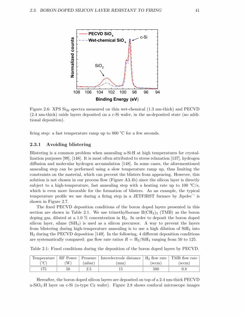
2.3. BORON-DOPED SILICON LAYER RESISTANT TO FIRING 41
108 106 104 102 100 98 96 94
SiO2
PECVD SiOx Wet-chemical SiO x
Nor
mal
ized
cou
nts
Binding Energy (eV)
c-Si
Figure 2.6: XPS Si2p spectra measured on thin wet-chemical (1.3 nm-thick) and PECVD(2.4 nm-thick) oxide layers deposited on a c-Si wafer, in the as-deposited state (no addi-tional deposition).
firing step: a fast temperature ramp up to 800 °C for a few seconds.
2.3.1 Avoiding blistering
Blistering is a common problem when annealing a-Si:H at high temperatures for crystal-lization purposes [99], [148]. It is most often attributed to stress relaxation [137], hydrogendiffusion and molecular hydrogen accumulation [148]. In some cases, the aforementionedannealing step can be performed using a slow temperature ramp up, thus limiting theconstraints on the material, which can prevent the blisters from appearing. However, thissolution is not chosen in our process flow (Figure A3.4b) since the silicon layer is directlysubject to a high-temperature, fast annealing step with a heating rate up to 100 °C/s,which is even more favorable for the formation of blisters. As an example, the typicaltemperature profile we use during a firing step in a JETFIRST furnace by Jipelec isshown in Figure 2.7.
The fixed PECVD deposition conditions of the boron doped layers presented in thissection are shown in Table 2.1. We use trimethylborane B(CH3)3 (TMB) as the borondoping gas, diluted at a 1.0 % concentration in H2. In order to deposit the boron dopedsilicon layer, silane (SiH4) is used as a silicon precursor. A way to prevent the layersfrom blistering during high-temperature annealing is to use a high dilution of SiH4 intoH2 during the PECVD deposition [149]. In the following, 4 different deposition conditionsare systematically compared: gas flow rate ratios R = H2/SiH4 ranging from 50 to 125.
Table 2.1: Fixed conditions during the deposition of the boron doped layers by PECVD.
Temperature RF Power Pressure Interelectrode distance H2 flow rate TMB flow rate(°C) (W) (mbar) (mm) (sccm) (sccm)
175 50 2.5 15 500 0.8
Hereafter, the boron doped silicon layers are deposited on top of a 2.4 nm-thick PECVDa-SiOx:H layer on c-Si (n-type Cz wafer). Figure 2.8 shows confocal microscope images
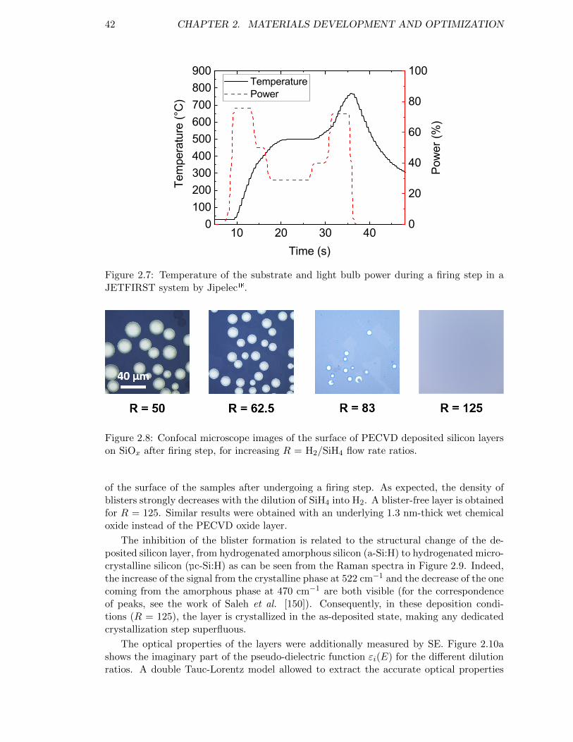
42 CHAPTER 2. MATERIALS DEVELOPMENT AND OPTIMIZATION
10 20 30 400
100200300400500600700800900
Tem
pera
ture
(°C
)
Time (s)
Temperature Power
0
20
40
60
80
100
Pow
er (%
)
Figure 2.7: Temperature of the substrate and light bulb power during a firing step in aJETFIRST system by Jipelec.
Figure 2.8: Confocal microscope images of the surface of PECVD deposited silicon layerson SiOx after firing step, for increasing R = H2/SiH4 flow rate ratios.
of the surface of the samples after undergoing a firing step. As expected, the density ofblisters strongly decreases with the dilution of SiH4 into H2. A blister-free layer is obtainedfor R = 125. Similar results were obtained with an underlying 1.3 nm-thick wet chemicaloxide instead of the PECVD oxide layer.
The inhibition of the blister formation is related to the structural change of the de-posited silicon layer, from hydrogenated amorphous silicon (a-Si:H) to hydrogenated micro-crystalline silicon (µc-Si:H) as can be seen from the Raman spectra in Figure 2.9. Indeed,the increase of the signal from the crystalline phase at 522 cm−1 and the decrease of the onecoming from the amorphous phase at 470 cm−1 are both visible (for the correspondenceof peaks, see the work of Saleh et al. [150]). Consequently, in these deposition condi-tions (R = 125), the layer is crystallized in the as-deposited state, making any dedicatedcrystallization step superfluous.
The optical properties of the layers were additionally measured by SE. Figure 2.10ashows the imaginary part of the pseudo-dielectric function εi(E) for the different dilutionratios. A double Tauc-Lorentz model allowed to extract the accurate optical properties
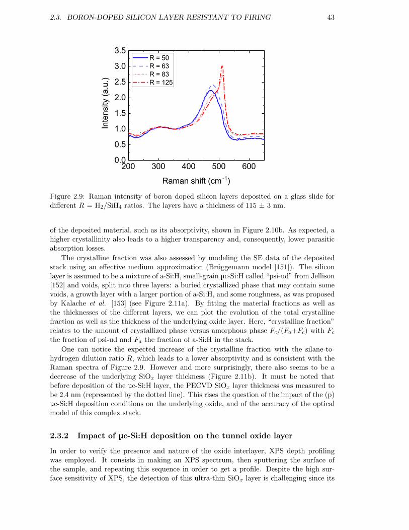
2.3. BORON-DOPED SILICON LAYER RESISTANT TO FIRING 43
200 300 400 500 6000.0
0.5
1.0
1.5
2.0
2.5
3.0
3.5
Inte
nsity
(a.u
.)
Raman shift (cm -1)
R = 50 R = 63 R = 83 R = 125
Figure 2.9: Raman intensity of boron doped silicon layers deposited on a glass slide fordifferent R = H2/SiH4 ratios. The layers have a thickness of 115 ± 3 nm.
of the deposited material, such as its absorptivity, shown in Figure 2.10b. As expected, ahigher crystallinity also leads to a higher transparency and, consequently, lower parasiticabsorption losses.
The crystalline fraction was also assessed by modeling the SE data of the depositedstack using an effective medium approximation (Bruggemann model [151]). The siliconlayer is assumed to be a mixture of a-Si:H, small-grain µc-Si:H called “psi-ud” from Jellison[152] and voids, split into three layers: a buried crystallized phase that may contain somevoids, a growth layer with a larger portion of a-Si:H, and some roughness, as was proposedby Kalache et al. [153] (see Figure 2.11a). By fitting the material fractions as well asthe thicknesses of the different layers, we can plot the evolution of the total crystallinefraction as well as the thickness of the underlying oxide layer. Here, “crystalline fraction”relates to the amount of crystallized phase versus amorphous phase Fc/(Fa+Fc) with Fcthe fraction of psi-ud and Fa the fraction of a-Si:H in the stack.
One can notice the expected increase of the crystalline fraction with the silane-to-hydrogen dilution ratio R, which leads to a lower absorptivity and is consistent with theRaman spectra of Figure 2.9. However and more surprisingly, there also seems to be adecrease of the underlying SiOx layer thickness (Figure 2.11b). It must be noted thatbefore deposition of the µc-Si:H layer, the PECVD SiOx layer thickness was measured tobe 2.4 nm (represented by the dotted line). This rises the question of the impact of the (p)µc-Si:H deposition conditions on the underlying oxide, and of the accuracy of the opticalmodel of this complex stack.
2.3.2 Impact of µc-Si:H deposition on the tunnel oxide layer
In order to verify the presence and nature of the oxide interlayer, XPS depth profilingwas employed. It consists in making an XPS spectrum, then sputtering the surface ofthe sample, and repeating this sequence in order to get a profile. Despite the high sur-face sensitivity of XPS, the detection of this ultra-thin SiOx layer is challenging since its
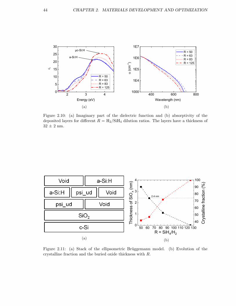
44 CHAPTER 2. MATERIALS DEVELOPMENT AND OPTIMIZATION
2 3 40
5
10
15
20
25
30
a-Si:H
e i
Energy (eV)
R = 50 R = 63 R = 83 R = 125
µc-Si:H
(a)
400 600 8001000
1E4
1E5
1E6
1E7
a (c
m-1
)
Wavelength (nm)
R = 50 R = 63 R = 83 R = 125
(b)
Figure 2.10: (a) Imaginary part of the dielectric function and (b) absorptivity of thedeposited layers for different R = H2/SiH4 dilution ratios. The layers have a thickness of32 ± 2 nm.
(a)
50 60 70 80 90 100 110 120 1300
1
2
3
4
2.4 nm
Thic
knes
s of
SiO
x (nm
)
R = SiH4/H2
40
50
60
70
80
90
100
Cry
stal
line
fract
ion
(%)
(b)
Figure 2.11: (a) Stack of the ellipsometric Bruggemann model. (b) Evolution of thecrystalline fraction and the buried oxide thickness with R.
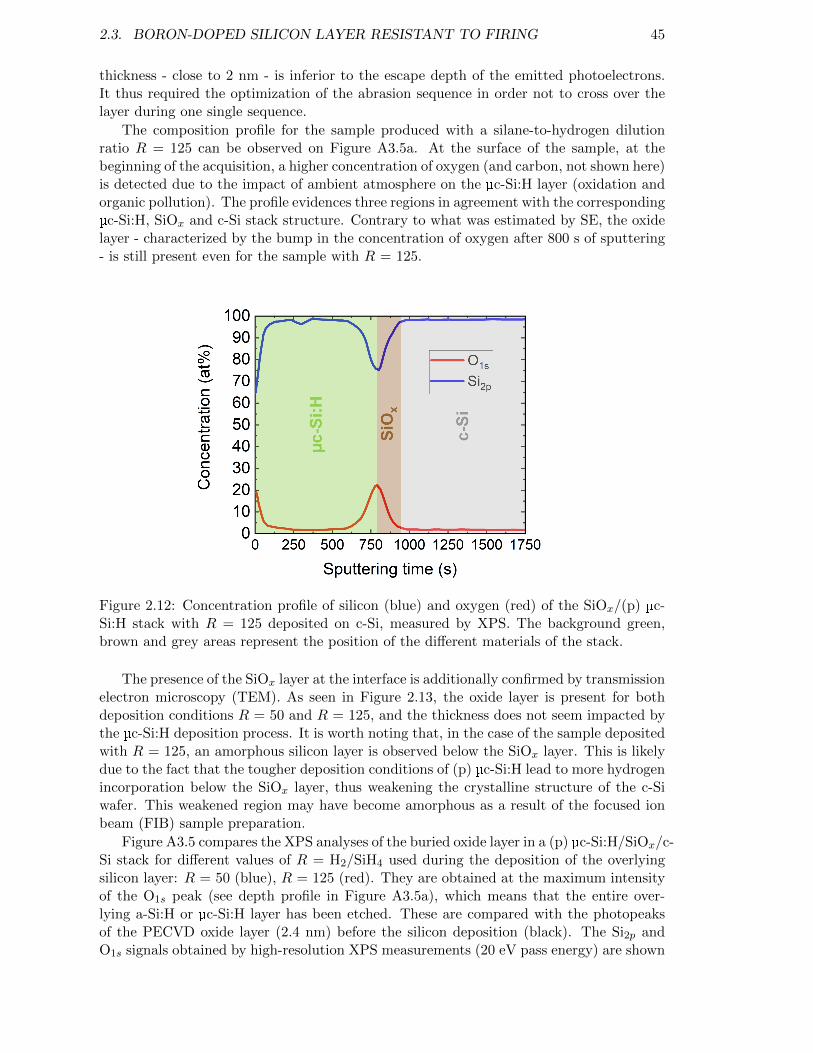
2.3. BORON-DOPED SILICON LAYER RESISTANT TO FIRING 45
thickness - close to 2 nm - is inferior to the escape depth of the emitted photoelectrons.It thus required the optimization of the abrasion sequence in order not to cross over thelayer during one single sequence.
The composition profile for the sample produced with a silane-to-hydrogen dilutionratio R = 125 can be observed on Figure A3.5a. At the surface of the sample, at thebeginning of the acquisition, a higher concentration of oxygen (and carbon, not shown here)is detected due to the impact of ambient atmosphere on the µc-Si:H layer (oxidation andorganic pollution). The profile evidences three regions in agreement with the correspondingµc-Si:H, SiOx and c-Si stack structure. Contrary to what was estimated by SE, the oxidelayer - characterized by the bump in the concentration of oxygen after 800 s of sputtering- is still present even for the sample with R = 125.
Figure 2.12: Concentration profile of silicon (blue) and oxygen (red) of the SiOx/(p) µc-Si:H stack with R = 125 deposited on c-Si, measured by XPS. The background green,brown and grey areas represent the position of the different materials of the stack.
The presence of the SiOx layer at the interface is additionally confirmed by transmissionelectron microscopy (TEM). As seen in Figure 2.13, the oxide layer is present for bothdeposition conditions R = 50 and R = 125, and the thickness does not seem impacted bythe µc-Si:H deposition process. It is worth noting that, in the case of the sample depositedwith R = 125, an amorphous silicon layer is observed below the SiOx layer. This is likelydue to the fact that the tougher deposition conditions of (p) µc-Si:H lead to more hydrogenincorporation below the SiOx layer, thus weakening the crystalline structure of the c-Siwafer. This weakened region may have become amorphous as a result of the focused ionbeam (FIB) sample preparation.
Figure A3.5 compares the XPS analyses of the buried oxide layer in a (p) µc-Si:H/SiOx/c-Si stack for different values of R = H2/SiH4 used during the deposition of the overlyingsilicon layer: R = 50 (blue), R = 125 (red). They are obtained at the maximum intensityof the O1s peak (see depth profile in Figure A3.5a), which means that the entire over-lying a-Si:H or µc-Si:H layer has been etched. These are compared with the photopeaksof the PECVD oxide layer (2.4 nm) before the silicon deposition (black). The Si2p andO1s signals obtained by high-resolution XPS measurements (20 eV pass energy) are shown
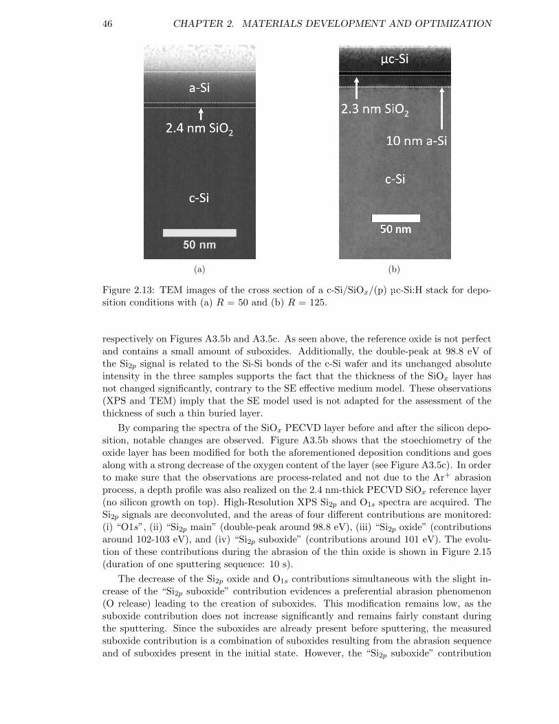
46 CHAPTER 2. MATERIALS DEVELOPMENT AND OPTIMIZATION
(a) (b)
Figure 2.13: TEM images of the cross section of a c-Si/SiOx/(p) µc-Si:H stack for depo-sition conditions with (a) R = 50 and (b) R = 125.
respectively on Figures A3.5b and A3.5c. As seen above, the reference oxide is not perfectand contains a small amount of suboxides. Additionally, the double-peak at 98.8 eV ofthe Si2p signal is related to the Si-Si bonds of the c-Si wafer and its unchanged absoluteintensity in the three samples supports the fact that the thickness of the SiOx layer hasnot changed significantly, contrary to the SE effective medium model. These observations(XPS and TEM) imply that the SE model used is not adapted for the assessment of thethickness of such a thin buried layer.
By comparing the spectra of the SiOx PECVD layer before and after the silicon depo-sition, notable changes are observed. Figure A3.5b shows that the stoechiometry of theoxide layer has been modified for both the aforementioned deposition conditions and goesalong with a strong decrease of the oxygen content of the layer (see Figure A3.5c). In orderto make sure that the observations are process-related and not due to the Ar+ abrasionprocess, a depth profile was also realized on the 2.4 nm-thick PECVD SiOx reference layer(no silicon growth on top). High-Resolution XPS Si2p and O1s spectra are acquired. TheSi2p signals are deconvoluted, and the areas of four different contributions are monitored:(i) “O1s”, (ii) “Si2p main” (double-peak around 98.8 eV), (iii) “Si2p oxide” (contributionsaround 102-103 eV), and (iv) “Si2p suboxide” (contributions around 101 eV). The evolu-tion of these contributions during the abrasion of the thin oxide is shown in Figure 2.15(duration of one sputtering sequence: 10 s).
The decrease of the Si2p oxide and O1s contributions simultaneous with the slight in-crease of the “Si2p suboxide” contribution evidences a preferential abrasion phenomenon(O release) leading to the creation of suboxides. This modification remains low, as thesuboxide contribution does not increase significantly and remains fairly constant duringthe sputtering. Since the suboxides are already present before sputtering, the measuredsuboxide contribution is a combination of suboxides resulting from the abrasion sequenceand of suboxides present in the initial state. However, the “Si2p suboxide” contribution
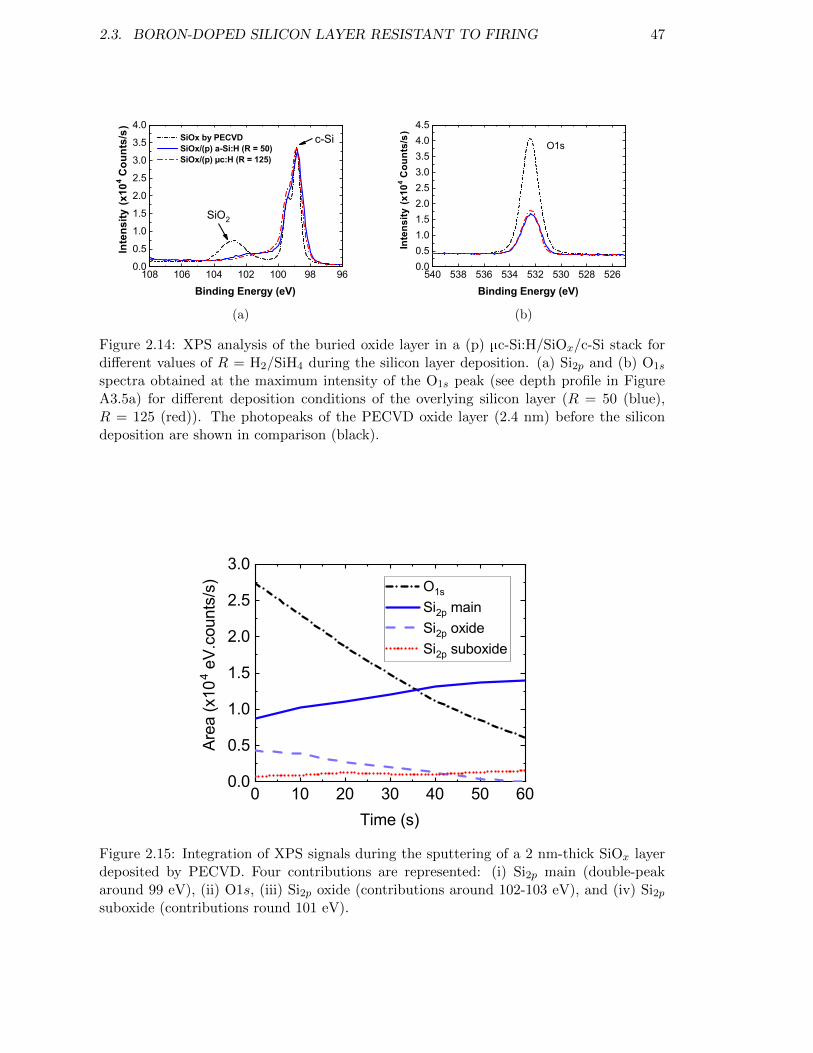
2.3. BORON-DOPED SILICON LAYER RESISTANT TO FIRING 47
108 106 104 102 100 98 960.0
0.5
1.0
1.5
2.0
2.5
3.0
3.5
4.0c-Si SiOx by PECVD
SiOx/(p) a-Si:H (R = 50) SiOx/(p) µc:H (R = 125)
Inte
nsity
(x10
4 Cou
nts/
s)
Binding Energy (eV)
SiO2
(a)
540 538 536 534 532 530 528 5260.00.51.01.52.02.53.03.54.04.5
Inte
nsity
(x10
4 Cou
nts/
s)
Binding Energy (eV)
O1s
(b)
Figure 2.14: XPS analysis of the buried oxide layer in a (p) µc-Si:H/SiOx/c-Si stack fordifferent values of R = H2/SiH4 during the silicon layer deposition. (a) Si2p and (b) O1s
spectra obtained at the maximum intensity of the O1s peak (see depth profile in FigureA3.5a) for different deposition conditions of the overlying silicon layer (R = 50 (blue),R = 125 (red)). The photopeaks of the PECVD oxide layer (2.4 nm) before the silicondeposition are shown in comparison (black).
0 10 20 30 40 50 600.0
0.5
1.0
1.5
2.0
2.5
3.0
Area
(x10
4 eV.
coun
ts/s
)
Time (s)
O1s
Si2p main Si2p oxide Si2p suboxide
Figure 2.15: Integration of XPS signals during the sputtering of a 2 nm-thick SiOx layerdeposited by PECVD. Four contributions are represented: (i) Si2p main (double-peakaround 99 eV), (ii) O1s, (iii) Si2p oxide (contributions around 102-103 eV), and (iv) Si2psuboxide (contributions round 101 eV).
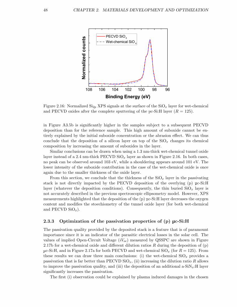
48 CHAPTER 2. MATERIALS DEVELOPMENT AND OPTIMIZATION
108 106 104 102 100 98 96
PECVD SiOx
Wet-chemical SiO x
Nor
mal
ized
cou
nts
Binding Energy (eV)
Figure 2.16: Normalized Si2p XPS signals at the surface of the SiOx layer for wet-chemicaland PECVD oxides after the complete sputtering of the µc-Si:H layer (R = 125).
in Figure A3.5b is significantly higher in the samples subject to a subsequent PECVDdeposition than for the reference sample. This high amount of suboxide cannot be en-tirely explained by the initial suboxide concentration or the abrasion effect. We can thusconclude that the deposition of a silicon layer on top of the SiOx changes its chemicalcomposition by increasing the amount of suboxides in the layer.
Similar conclusions can be drawn when using a 1.3 nm-thick wet-chemical tunnel oxidelayer instead of a 2.4 nm-thick PECVD SiOx layer as shown in Figure 2.16. In both cases,no peak can be observed around 103 eV, while a shouldering appears around 101 eV. Thelower intensity of the suboxide contribution in the case of the wet-chemical oxide is onceagain due to the smaller thickness of the oxide layer.
From this section, we conclude that the thickness of the SiOx layer in the passivatingstack is not directly impacted by the PECVD deposition of the overlying (p) µc-Si:Hlayer (whatever the deposition conditions). Consequently, the thin buried SiOx layer isnot accurately described in the previous spectroscopic ellipsometry model. However, XPSmeasurements highlighted that the deposition of the (p) µc-Si:H layer decreases the oxygencontent and modifies the stoechiometry of the tunnel oxide layer (for both wet-chemicaland PECVD SiOx).
2.3.3 Optimization of the passivation properties of (p) µc-Si:H
The passivation quality provided by the deposited stack is a feature that is of paramountimportance since it is an indicator of the parasitic electrical losses in the solar cell. Thevalues of implied Open-Circuit Voltage (iVoc) measured by QSSPC are shown in Figure2.17b for a wet-chemical oxide and different dilution ratios R during the deposition of (p)µc-Si:H, and in Figure 2.17a for both PECVD and wet-chemical SiOx (for R = 125). Fromthese results we can draw three main conclusions: (i) the wet-chemical SiOx provides apassivation that is far better than PECVD SiOx, (ii) increasing the dilution ratio R allowsto improve the passivation quality, and (iii) the deposition of an additional a-SiNx:H layersignificantly increases the passivation.
The first (i) observation could be explained by plasma induced damages in the chosen
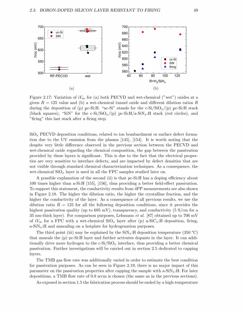
2.3. BORON-DOPED SILICON LAYER RESISTANT TO FIRING 49
RF-PECVD wet500
550
600
650
700
iVoc
(mV)
uc-Si SiN
(a)
40 60 80 100 120560
580
600
620
640
660
680
700
uc-Si SiN firing
iVoc
(mV)
R=H2/SiH4
(b)
Figure 2.17: Variation of iVoc for (a) both PECVD and wet-chemical (”wet”) oxides at agiven R = 125 value and (b) a wet-chemical tunnel oxide and different dilution ratios Rduring the deposition of (p) µc-Si:H. “uc-Si” stands for the c-Si/SiOx/(p) µc-Si:H stack(black squares), “SiN” for the c-Si/SiOx/(p) µc-Si:H/a-SiNx:H stack (red circles), and”firing” this last stack after a firing step.
SiOx PECVD deposition conditions, related to ion bombardment or surface defect forma-tion due to the UV emission from the plasma [145], [154]. It is worth noting that thedespite very little difference observed in the previous section between the PECVD andwet-chemical oxide regarding the chemical composition, the gap between the passivationprovided by these layers is significant. This is due to the fact that the electrical proper-ties are very sensitive to interface defects, and are impacted by defect densities that arenot visible through standard chemical characterization techniques. As a consequence, thewet-chemical SiOx layer is used in all the FPC samples studied later on.
A possible explanation of the second (ii) is that µc-Si:H has a doping efficiency about100 times higher than a-Si:H [155], [156], thus providing a better field-effect passivation.To support this statement, the conductivity results from 4PP measurements are also shownin Figure 2.18. The higher the dilution ratio, the higher the crystalline fraction, and thehigher the conductivity of the layer. As a consequence of all previous results, we use thedilution ratio R = 125 for all the following deposition conditions, since it provides thehighest passivation quality (up to 695 mV), transparency, and conductivity (5 S/cm for a35 nm-thick layer). For comparison purposes, Lehmann et al. [87] obtained up to 706 mVof iVoc for a FPC with a wet-chemical SiOx layer after (p) a-SiCx:H deposition, firing,a-SiNx:H and annealing on a hotplate for hydrogenation purposes.
The third point (iii) may be explained by the SiNx:H deposition temperature (350 °C)that anneals the (p) µc-Si:H layer and further activates dopants in the layer. It can addi-tionally drive more hydrogen to the c-Si/SiOx interface, thus providing a better chemicalpassivation. Further investigations will be carried out in section 2.5 dedicated to cappinglayers.
The TMB gas flow rate was additionally varied in order to estimate the best conditionfor passivation purposes. As can be seen in Figure 2.19, there is no major impact of thisparameter on the passivation properties after capping the sample with a-SiNx:H. For laterdepositions, a TMB flow rate of 0.8 sccm is chosen (the same as in the previous sections).
As exposed in section 1.5 the fabrication process should be ended by a high-temperature
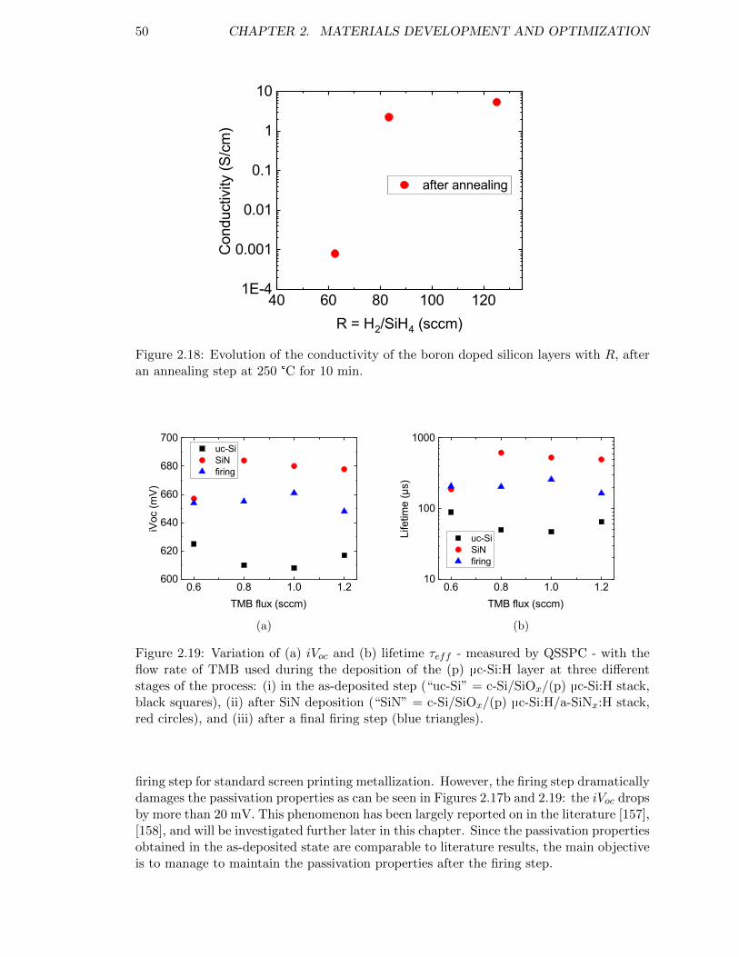
50 CHAPTER 2. MATERIALS DEVELOPMENT AND OPTIMIZATION
40 60 80 100 1201E-4
0.001
0.01
0.1
1
10
after annealing
Con
duct
ivity
(S/c
m)
R = H2/SiH4 (sccm)
Figure 2.18: Evolution of the conductivity of the boron doped silicon layers with R, afteran annealing step at 250 °C for 10 min.
0.6 0.8 1.0 1.2600
620
640
660
680
700 uc-Si SiN firing
iVoc
(mV)
TMB flux (sccm)
(a)
0.6 0.8 1.0 1.210
100
1000
uc-Si SiN firing
Life
time
(µs)
TMB flux (sccm)
(b)
Figure 2.19: Variation of (a) iVoc and (b) lifetime τeff - measured by QSSPC - with theflow rate of TMB used during the deposition of the (p) µc-Si:H layer at three differentstages of the process: (i) in the as-deposited step (“uc-Si” = c-Si/SiOx/(p) µc-Si:H stack,black squares), (ii) after SiN deposition (“SiN” = c-Si/SiOx/(p) µc-Si:H/a-SiNx:H stack,red circles), and (iii) after a final firing step (blue triangles).
firing step for standard screen printing metallization. However, the firing step dramaticallydamages the passivation properties as can be seen in Figures 2.17b and 2.19: the iVoc dropsby more than 20 mV. This phenomenon has been largely reported on in the literature [157],[158], and will be investigated further later in this chapter. Since the passivation propertiesobtained in the as-deposited state are comparable to literature results, the main objectiveis to manage to maintain the passivation properties after the firing step.
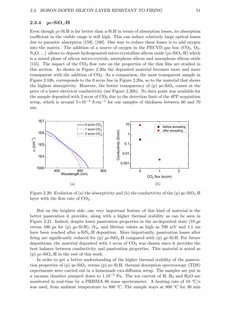
2.3. BORON-DOPED SILICON LAYER RESISTANT TO FIRING 51
2.3.4 µc-SiOx:H
Even though µc-Si:H is far better than a-Si:H in terms of absorption losses, its absorptioncoefficient in the visible range is still high. This can induce relatively large optical lossesdue to parasitic absorption [159], [160]. One way to reduce these losses is to add oxygeninto the matrix. The addition of a source of oxygen in the PECVD gas box (CO2, O2,N2O, ...) allows to deposit hydrogenated micro-crystalline silicon oxide (µc-SiOx:H) whichis a mixed phase of silicon micro-crystals, amorphous silicon and amorphous silicon oxide[155]. The impact of the CO2 flow rate on the properties of the thin film are studied inthis section. As shown in Figure 2.20a the deposited material becomes more and moretransparent with the addition of CO2. As a comparison, the most transparent sample inFigure 2.10b, corresponds to the 0 sccm line in Figure 2.20a, so to the material that showsthe highest absorptivity. However, the better transparency of (p) µc-SiOx comes at theprice of a lower electrical conductivity (see Figure 2.20b). No data point was available forthe sample deposited with 2 sccm of CO2 due to the detection limit of the 4PP acquisitionsetup, which is around 5×10⁻⁴ S.cm−1 for our samples of thickness between 60 and 70nm.
400 600 8001000
1E4
1E5
1E6
1E7
a (c
m-1
)
Wavelength (nm)
0 sccm CO2
1 sccm CO2
2 sccm CO2
(a)
0 1 2
0.001
0.01
0.1
1
10 before annealing after annealing
Con
duct
ivity
(S/c
m)
CO2 flux (sccm)
(b)
Figure 2.20: Evolution of (a) the absorptivity and (b) the conductivity of the (p) µc-SiOx:Hlayer with the flow rate of CO2.
But on the brighter side, one very important feature of this kind of material is thebetter passivation it provides, along with a higher thermal stability as can be seen inFigure 2.21. Indeed, despite lower passivation properties in the as-deposited state (10 µsversus 100 µs for (p) µc-Si:H), iVoc and lifetime values as high as 700 mV and 1.1 mshave been reached after a-SiNx:H deposition. More importantly, passivation losses afterfiring are significantly reduced for (p) µc-SiOx:H compared with (p) µc-Si:H. For futuredepositions, the material deposited with 1 sccm of CO2 was chosen since it provides thebest balance between conductivity and passivation properties. This material is noted as(p) µc-SiOx:H in the rest of this work.
In order to get a better understanding of the higher thermal stability of the passiva-tion properties of (p) µc-SiOx versus (p) µc-Si:H, thermal desorption spectrocsopy (TDS)experiments were carried out in a homemade exo-diffusion setup. The samples are put ina vacuum chamber pumped down to 1.10−5 Pa. The ion current of H, H2 and H2O aremonitored in real-time by a PRISMA 80 mass spectrometer. A heating rate of 10 °C/swas used, from ambient temperature to 800 °C. The sample stays at 800 °C for 30 min
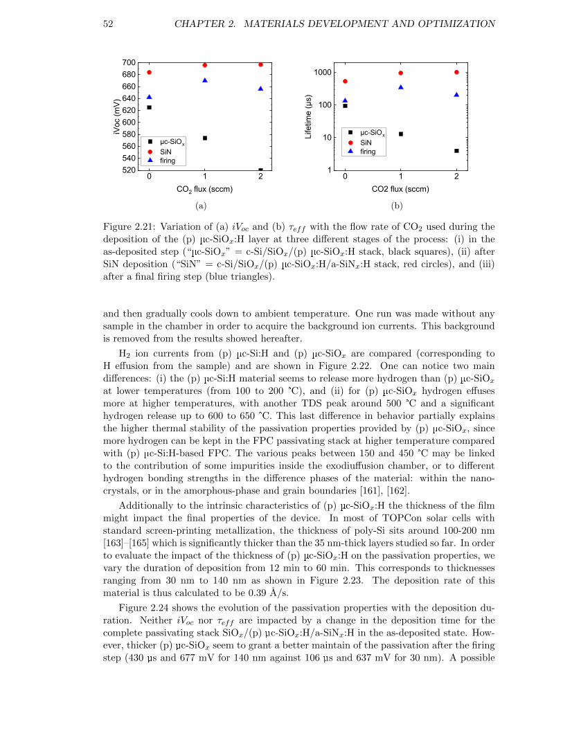
52 CHAPTER 2. MATERIALS DEVELOPMENT AND OPTIMIZATION
0 1 2520540560580600620640660680700
µc-SiOx
SiN firing
iVoc
(mV)
CO2 flux (sccm)
(a)
0 1 21
10
100
1000
µc-SiOx
SiN firing
Life
time
(µs)
CO2 flux (sccm)
(b)
Figure 2.21: Variation of (a) iVoc and (b) τeff with the flow rate of CO2 used during thedeposition of the (p) µc-SiOx:H layer at three different stages of the process: (i) in theas-deposited step (“µc-SiOx” = c-Si/SiOx/(p) µc-SiOx:H stack, black squares), (ii) afterSiN deposition (“SiN” = c-Si/SiOx/(p) µc-SiOx:H/a-SiNx:H stack, red circles), and (iii)after a final firing step (blue triangles).
and then gradually cools down to ambient temperature. One run was made without anysample in the chamber in order to acquire the background ion currents. This backgroundis removed from the results showed hereafter.
H2 ion currents from (p) µc-Si:H and (p) µc-SiOx are compared (corresponding toH effusion from the sample) and are shown in Figure 2.22. One can notice two maindifferences: (i) the (p) µc-Si:H material seems to release more hydrogen than (p) µc-SiOx
at lower temperatures (from 100 to 200 °C), and (ii) for (p) µc-SiOx hydrogen effusesmore at higher temperatures, with another TDS peak around 500 °C and a significanthydrogen release up to 600 to 650 °C. This last difference in behavior partially explainsthe higher thermal stability of the passivation properties provided by (p) µc-SiOx, sincemore hydrogen can be kept in the FPC passivating stack at higher temperature comparedwith (p) µc-Si:H-based FPC. The various peaks between 150 and 450 °C may be linkedto the contribution of some impurities inside the exodiuffusion chamber, or to differenthydrogen bonding strengths in the difference phases of the material: within the nano-crystals, or in the amorphous-phase and grain boundaries [161], [162].
Additionally to the intrinsic characteristics of (p) µc-SiOx:H the thickness of the filmmight impact the final properties of the device. In most of TOPCon solar cells withstandard screen-printing metallization, the thickness of poly-Si sits around 100-200 nm[163]–[165] which is significantly thicker than the 35 nm-thick layers studied so far. In orderto evaluate the impact of the thickness of (p) µc-SiOx:H on the passivation properties, wevary the duration of deposition from 12 min to 60 min. This corresponds to thicknessesranging from 30 nm to 140 nm as shown in Figure 2.23. The deposition rate of thismaterial is thus calculated to be 0.39 A/s.
Figure 2.24 shows the evolution of the passivation properties with the deposition du-ration. Neither iVoc nor τeff are impacted by a change in the deposition time for thecomplete passivating stack SiOx/(p) µc-SiOx:H/a-SiNx:H in the as-deposited state. How-ever, thicker (p) µc-SiOx seem to grant a better maintain of the passivation after the firingstep (430 µs and 677 mV for 140 nm against 106 µs and 637 mV for 30 nm). A possible
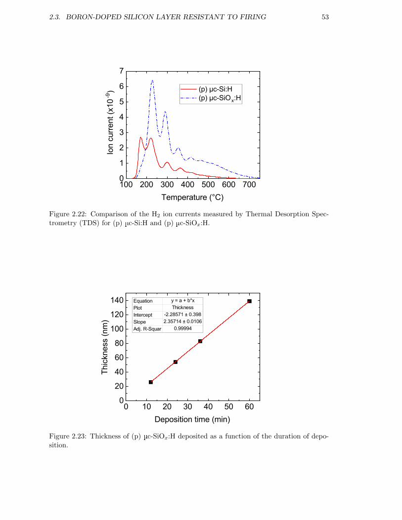
2.3. BORON-DOPED SILICON LAYER RESISTANT TO FIRING 53
100 200 300 400 500 600 7000
1
2
3
4
5
6
7
Ion
curre
nt (x
10-9
)
Temperature (°C)
(p) µc-Si:H (p) µc-SiOx:H
Figure 2.22: Comparison of the H2 ion currents measured by Thermal Desorption Spec-trometry (TDS) for (p) µc-Si:H and (p) µc-SiOx:H.
0 10 20 30 40 50 600
20
40
60
80
100
120
140
Thic
knes
s (n
m)
Deposition time (min)
Equation y = a + b*xPlot ThicknessIntercept -2.28571 ± 0.398Slope 2.35714 ± 0.0106Adj. R-Squar 0.99994
Figure 2.23: Thickness of (p) µc-SiOx:H deposited as a function of the duration of depo-sition.
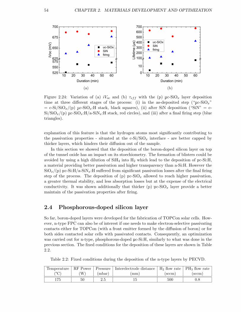
54 CHAPTER 2. MATERIALS DEVELOPMENT AND OPTIMIZATION
10 20 30 40 50 60525550575625
650
675
700
uc-SiOx SiN firingiV
oc (m
V)
Duration (min)
(a)
10 20 30 40 50 600
10
100200300400500600700
uc-SiOx SiN firing
Life
time
(µs)
Duration (min)
(b)
Figure 2.24: Variation of (a) iVoc and (b) τeff with the (p) µc-SiOx layer depositiontime at three different stages of the process: (i) in the as-deposited step (“µc-SiOx”= c-Si/SiOx/(p) µc-SiOx:H stack, black squares), (ii) after SiN deposition (“SiN” = c-Si/SiOx/(p) µc-SiOx:H/a-SiNx:H stack, red circles), and (iii) after a final firing step (bluetriangles).
explanation of this feature is that the hydrogen atoms most significantly contributing tothe passivation properties - situated at the c-Si/SiOx interface - are better capped bythicker layers, which hinders their diffusion out of the sample.
In this section we showed that the deposition of the boron-doped silicon layer on topof the tunnel oxide has an impact on its stoechiometry. The formation of blisters could beavoided by using a high dilution of SiH4 into H2 which lead to the deposition of µc-Si:H,a material providing better passivation and higher transparency than a-Si:H. However theSiOx/(p) µc-Si:H/a-SiNx:H suffered from significant passivation losses after the final firingstep of the process. The deposition of (p) µc-SiOx allowed to reach higher passivation,a greater thermal stability, and less absorption losses but at the expense of the electricalconductivity. It was shown additionally that thicker (p) µc-SiOx layer provide a bettermaintain of the passivation properties after firing.
2.4 Phosphorous-doped silicon layer
So far, boron-doped layers were developed for the fabrication of TOPCon solar cells. How-ever, n-type FPC can also be of interest if one needs to make electron-selective passivatingcontacts either for TOPCon (with a front emitter formed by the diffusion of boron) or forboth sides contacted solar cells with passivated contacts. Consequently, an optimizationwas carried out for n-type, phosphorous-doped µc-Si:H, similarly to what was done in theprevious section. The fixed conditions for the deposition of these layers are shown in Table2.2.
Table 2.2: Fixed conditions during the deposition of the n-type layers by PECVD.
Temperature RF Power Pressure Interelectrode distance H2 flow rate PH3 flow rate(°C) (W) (mbar) (mm) (sccm) (sccm)
175 50 2.5 15 500 0.8
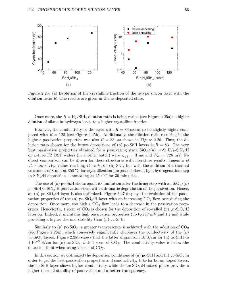
2.4. PHOSPHOROUS-DOPED SILICON LAYER 55
40 60 80 100 12020
40
60
80
100
Cry
stal
line
fract
ion
(%)
R=H2/SiH4
(a)
40 60 80 100 1200.1
1
10
before annealing after annealing
Con
duct
ivity
(S/c
m)
R = H2/SiH4 (sccm)
(b)
Figure 2.25: (a) Evolution of the crystalline fraction of the n-type silicon layer with thedilution ratio R. The results are given in the as-deposited state.
Once more, the R = H2/SiH4 dilution ratio is being varied (see Figure 2.25a): a higherdilution of silane in hydrogen leads to a higher crystalline fraction.
However, the conductivity of the layer with R = 83 seems to be slightly higher com-pared with R = 125 (see Figure 2.25b). Additionally, the dilution ratio resulting in thehighest passivation properties was also R = 83, as shown in Figure 2.26. Thus, the di-lution ratio chosen for the future depositions of (n) µc-Si:H layers is R = 83. The verybest passivation properties obtained for a passivating stack SiOx/(n) µc-Si:H/a-SiNx:Hon p-type FZ DSP wafers (in another batch) were τeff = 3 ms and iVoc = 726 mV. Nodirect comparison can be drawn for these structures with literature results. Ingenito etal. showed iVoc values reaching 746 mV, on (n) SiCx but with the addition of a thermaltreatment of 8 min at 850 °C for crystallization purposes followed by a hydrogenation step(a-SiNx:H deposition + annealing at 450 °C for 30 min) [63].
The use of (n) µc-Si:H shows again its limitation after the firing step with an SiOx/(n)µc-Si:H/a-SiNx:H passivation stack with a dramatic degradation of the passivation. Hence,an (n) µc-SiOx:H layer is also optimized. Figure 2.27 displays the evolution of the passi-vation properties of the (n) µc-SiOx:H layer with an increasing CO2 flow rate during thedeposition. Once more, too high a CO2 flow leads to a decrease in the passivation prop-erties. Henceforth, 1 sccm of CO2 is chosen for the deposition of so-called (n) µc-SiOx:Hlater on. Indeed, it maintains high passivation properties (up to 717 mV and 1.7 ms) whileproviding a higher thermal stability than (n) µc-Si:H.
Similarly to (p) µc-SiOx, a greater transparency is achieved with the addition of CO2
(see Figure 2.28a), which conversely significantly decreases the conductivity of the (n)µc-SiOx layers. Figure 2.28b shows that the latter drops from 10 S/cm for (n) µc-Si:H to1.10−3 S/cm for (n) µc-SiOx with 1 sccm of CO2. The conductivity value is below thedetection limit when using 2 sccm of CO2.
In this section we optimized the deposition conditions of (n) µc-Si:H and (n) µc-SiOx inorder to get the best passivation properties and conductivity. Like for boron doped layers,the µc-Si:H layer shows higher conductivity while the µc-SiOx:H mixed phase provides ahigher thermal stability of passivation and a better transparency.
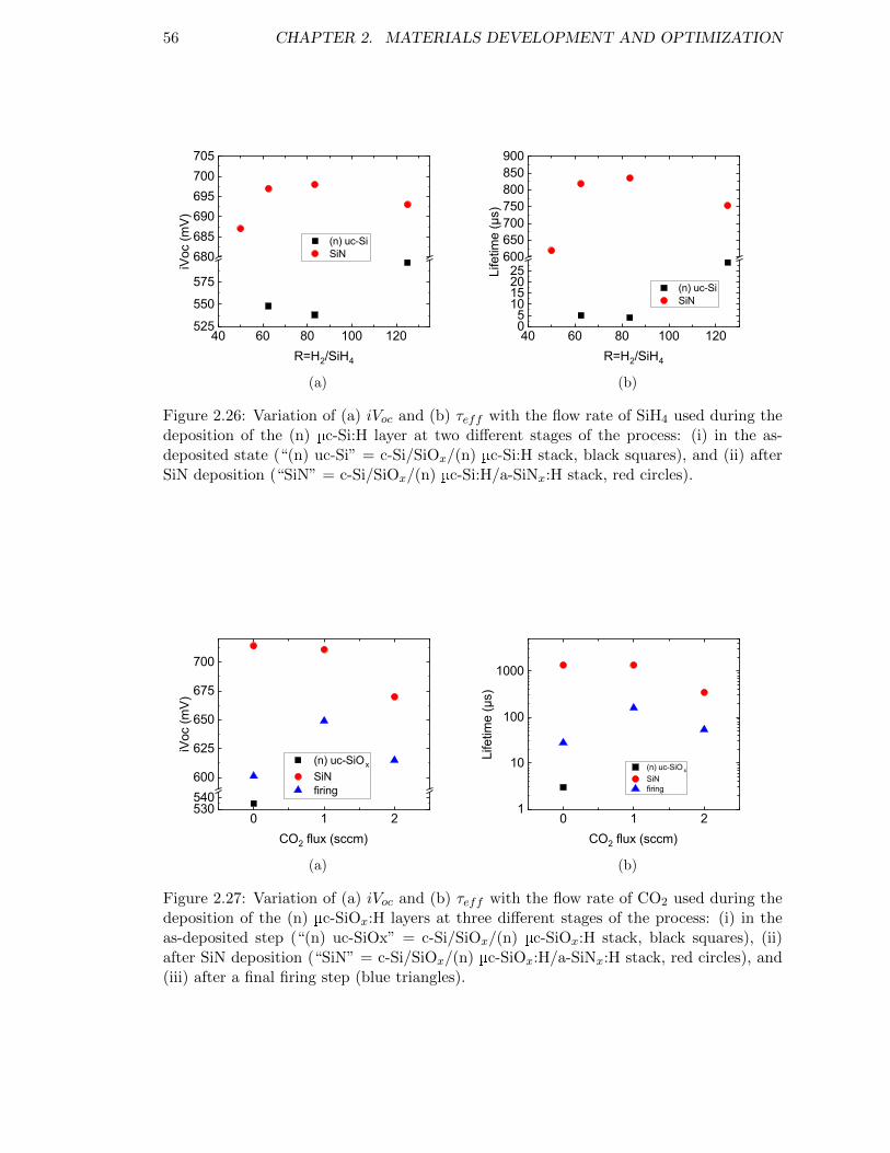
56 CHAPTER 2. MATERIALS DEVELOPMENT AND OPTIMIZATION
40 60 80 100 120525
550
575
680685690695700705
(n) uc-Si SiN
iVoc
(mV)
R=H2/SiH4
(a)
40 60 80 100 12005
10152025
600650700750800850900
(n) uc-Si SiN
Life
time
(µs)
R=H2/SiH4
(b)
Figure 2.26: Variation of (a) iVoc and (b) τeff with the flow rate of SiH4 used during thedeposition of the (n) µc-Si:H layer at two different stages of the process: (i) in the as-deposited state (“(n) uc-Si” = c-Si/SiOx/(n) µc-Si:H stack, black squares), and (ii) afterSiN deposition (“SiN” = c-Si/SiOx/(n) µc-Si:H/a-SiNx:H stack, red circles).
0 1 2530540600
625
650
675
700
(n) uc-SiOx
SiN firing
iVoc
(mV)
CO2 flux (sccm)
(a)
0 1 21
10
100
1000
(n) uc-SiO x
SiN firing
Life
time
(µs)
CO2 flux (sccm)
(b)
Figure 2.27: Variation of (a) iVoc and (b) τeff with the flow rate of CO2 used during thedeposition of the (n) µc-SiOx:H layers at three different stages of the process: (i) in theas-deposited step (“(n) uc-SiOx” = c-Si/SiOx/(n) µc-SiOx:H stack, black squares), (ii)after SiN deposition (“SiN” = c-Si/SiOx/(n) µc-SiOx:H/a-SiNx:H stack, red circles), and(iii) after a final firing step (blue triangles).
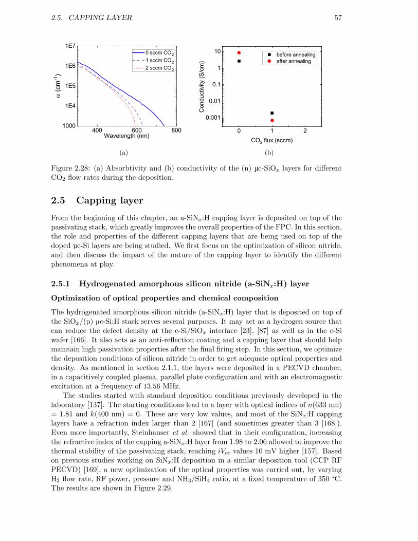
2.5. CAPPING LAYER 57
400 600 8001000
1E4
1E5
1E6
1E7
a (c
m-1
)
Wavelength (nm)
0 sccm CO2
1 sccm CO2
2 sccm CO2
(a)
0 1 2
0.001
0.01
0.1
1
10 before annealing after annealing
Con
duct
ivity
(S/c
m)
CO2 flux (sccm)
(b)
Figure 2.28: (a) Absorbtivity and (b) conductivity of the (n) µc-SiOx layers for differentCO2 flow rates during the deposition.
2.5 Capping layer
From the beginning of this chapter, an a-SiNx:H capping layer is deposited on top of thepassivating stack, which greatly improves the overall properties of the FPC. In this section,the role and properties of the different capping layers that are being used on top of thedoped µc-Si layers are being studied. We first focus on the optimization of silicon nitride,and then discuss the impact of the nature of the capping layer to identify the differentphenomena at play.
2.5.1 Hydrogenated amorphous silicon nitride (a-SiNx:H) layer
Optimization of optical properties and chemical composition
The hydrogenated amorphous silicon nitride (a-SiNx:H) layer that is deposited on top ofthe SiOx/(p) µc-Si:H stack serves several purposes. It may act as a hydrogen source thatcan reduce the defect density at the c-Si/SiOx interface [23], [87] as well as in the c-Siwafer [166]. It also acts as an anti-reflection coating and a capping layer that should helpmaintain high passivation properties after the final firing step. In this section, we optimizethe deposition conditions of silicon nitride in order to get adequate optical properties anddensity. As mentioned in section 2.1.1, the layers were deposited in a PECVD chamber,in a capacitively coupled plasma, parallel plate configuration and with an electromagneticexcitation at a frequency of 13.56 MHz.
The studies started with standard deposition conditions previously developed in thelaboratory [137]. The starting conditions lead to a layer with optical indices of n(633 nm)= 1.81 and k(400 nm) = 0. These are very low values, and most of the SiNx:H cappinglayers have a refraction index larger than 2 [167] (and sometimes greater than 3 [168]).Even more importantly, Steinhauser et al. showed that in their configuration, increasingthe refractive index of the capping a-SiNx:H layer from 1.98 to 2.06 allowed to improve thethermal stability of the passivating stack, reaching iVoc values 10 mV higher [157]. Basedon previous studies working on SiNx:H deposition in a similar deposition tool (CCP RFPECVD) [169], a new optimization of the optical properties was carried out, by varyingH2 flow rate, RF power, pressure and NH3/SiH4 ratio, at a fixed temperature of 350 °C.The results are shown in Figure 2.29.
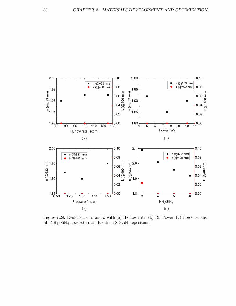
58 CHAPTER 2. MATERIALS DEVELOPMENT AND OPTIMIZATION
70 80 90 100 110 120 1301.92
1.94
1.96
1.98
2.00 n (@633 nm) k (@400 nm)
n (@
633
nm)
H2 flow rate (sccm)
0.00
0.02
0.04
0.06
0.08
0.10
k (@
400
nm)
(a)
4 5 6 7 8 9 10 111.80
1.85
1.90
1.95
2.00 n (@633 nm) k (@400 nm)
n (@
633
nm)
Power (W)
0.00
0.02
0.04
0.06
0.08
0.10
k (@
400
nm)
(b)
0.50 0.75 1.00 1.25 1.501.85
1.90
1.95
2.00
n (@633 nm) k (@400 nm)
n (@
633
nm)
Pressure (mbar)
0.00
0.02
0.04
0.06
0.08
0.10
k (@
400
nm)
(c)
3 4 5 61.8
1.9
2.0
2.1 n (@633 nm) k (@400 nm)
n (@
633
nm)
NH3/SiH4
0.00
0.02
0.04
0.06
0.08
0.10
k (@
400
nm)
(d)
Figure 2.29: Evolution of n and k with (a) H2 flow rate, (b) RF Power, (c) Pressure, and(d) NH3/SiH4 flow rate ratio for the a-SiNx:H deposition.
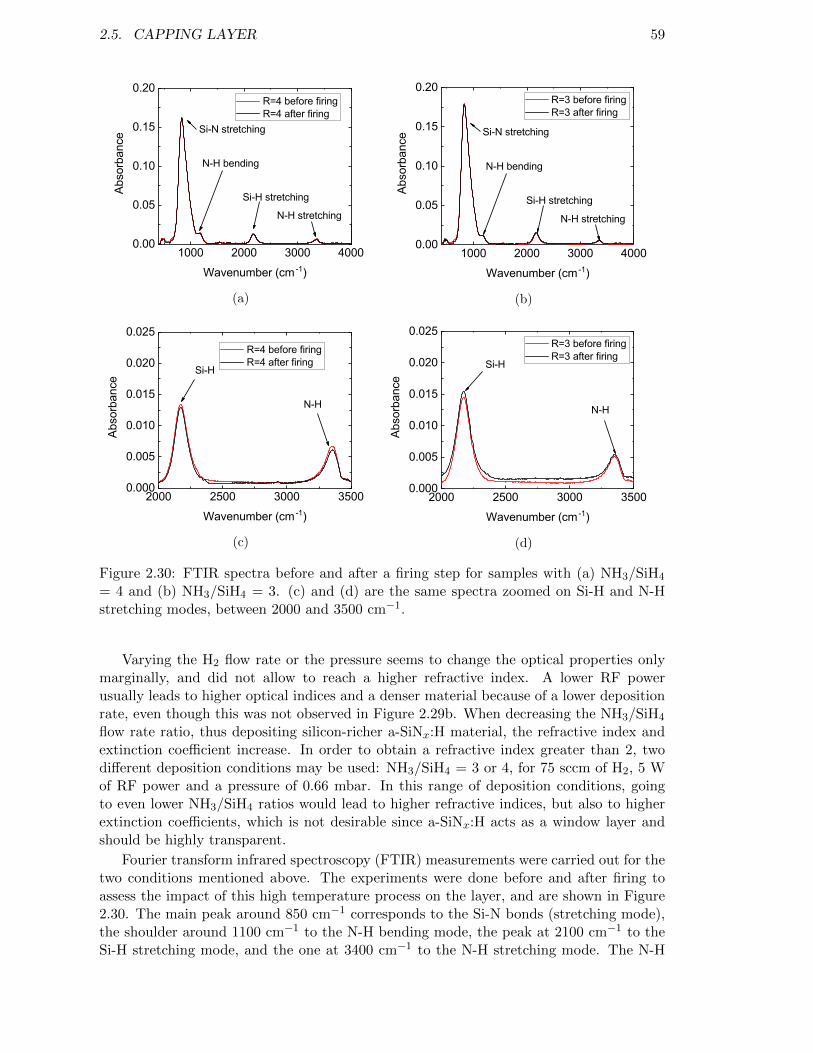
2.5. CAPPING LAYER 59
1000 2000 3000 40000.00
0.05
0.10
0.15
0.20
Absorban
ce
Wavenumber (cm -1)
R=4 before firing R=4 after firing
N-H bending
Si-N stretching
Si-H stretching
N-H stretching
(a)
1000 2000 3000 40000.00
0.05
0.10
0.15
0.20
N-H bending
Si-N stretching
Absorban
ce
Wavenumber (cm -1)
R=3 before firing R=3 after firing
N-H stretching
Si-H stretching
(b)
2000 2500 3000 35000.000
0.005
0.010
0.015
0.020
0.025
Absorban
ce
Wavenumber (cm -1)
R=4 before firing R=4 after firing
Si-H
N-H
(c)
2000 2500 3000 35000.000
0.005
0.010
0.015
0.020
0.025
Absorban
ce
Wavenumber (cm -1)
R=3 before firing R=3 after firing
N-H
Si-H
(d)
Figure 2.30: FTIR spectra before and after a firing step for samples with (a) NH3/SiH4
= 4 and (b) NH3/SiH4 = 3. (c) and (d) are the same spectra zoomed on Si-H and N-Hstretching modes, between 2000 and 3500 cm−1.
Varying the H2 flow rate or the pressure seems to change the optical properties onlymarginally, and did not allow to reach a higher refractive index. A lower RF powerusually leads to higher optical indices and a denser material because of a lower depositionrate, even though this was not observed in Figure 2.29b. When decreasing the NH3/SiH4
flow rate ratio, thus depositing silicon-richer a-SiNx:H material, the refractive index andextinction coefficient increase. In order to obtain a refractive index greater than 2, twodifferent deposition conditions may be used: NH3/SiH4 = 3 or 4, for 75 sccm of H2, 5 Wof RF power and a pressure of 0.66 mbar. In this range of deposition conditions, goingto even lower NH3/SiH4 ratios would lead to higher refractive indices, but also to higherextinction coefficients, which is not desirable since a-SiNx:H acts as a window layer andshould be highly transparent.
Fourier transform infrared spectroscopy (FTIR) measurements were carried out for thetwo conditions mentioned above. The experiments were done before and after firing toassess the impact of this high temperature process on the layer, and are shown in Figure2.30. The main peak around 850 cm−1 corresponds to the Si-N bonds (stretching mode),the shoulder around 1100 cm−1 to the N-H bending mode, the peak at 2100 cm−1 to theSi-H stretching mode, and the one at 3400 cm−1 to the N-H stretching mode. The N-H
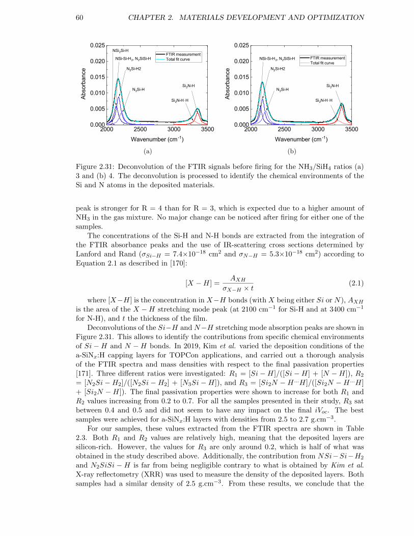
60 CHAPTER 2. MATERIALS DEVELOPMENT AND OPTIMIZATION
2000 2500 3000 35000.000
0.005
0.010
0.015
0.020
0.025
Absorban
ce
Wavenumber (cm -1)
FTIR measurement Total fit curve
NSi2Si-H
NSi-Si-H2, N2SiSi-H
N2Si-H2
N3Si-HSi2N-H
Si2N-H...H
(a)
2000 2500 3000 35000.000
0.005
0.010
0.015
0.020
0.025
Absorban
ce
Wavenumber (cm -1)
FTIR measurement Total fit curve
NSi-Si-H2, N2SiSi-H
N2Si-H2
N3Si-HSi2N-H
Si2N-H...H
(b)
Figure 2.31: Deconvolution of the FTIR signals before firing for the NH3/SiH4 ratios (a)3 and (b) 4. The deconvolution is processed to identify the chemical environments of theSi and N atoms in the deposited materials.
peak is stronger for R = 4 than for R = 3, which is expected due to a higher amount ofNH3 in the gas mixture. No major change can be noticed after firing for either one of thesamples.
The concentrations of the Si-H and N-H bonds are extracted from the integration ofthe FTIR absorbance peaks and the use of IR-scattering cross sections determined byLanford and Rand (σSi−H = 7.4×10⁻¹⁸ cm2 and σN−H = 5.3×10⁻¹⁸ cm2) according toEquation 2.1 as described in [170]:
[X −H] =AXH
σX−H × t(2.1)
where [X−H] is the concentration in X−H bonds (with X being either Si or N), AXHis the area of the X −H stretching mode peak (at 2100 cm−1 for Si-H and at 3400 cm−1
for N-H), and t the thickness of the film.Deconvolutions of the Si−H and N−H stretching mode absorption peaks are shown in
Figure 2.31. This allows to identify the contributions from specific chemical environmentsof Si−H and N −H bonds. In 2019, Kim et al. varied the deposition conditions of thea-SiNx:H capping layers for TOPCon applications, and carried out a thorough analysisof the FTIR spectra and mass densities with respect to the final passivation properties[171]. Three different ratios were investigated: R1 = [Si−H]/([Si−H] + [N −H]), R2
= [N2Si−H2]/([N2Si−H2] + [N3Si−H]), and R3 = [Si2N −H ...H]/([Si2N −H ...H]+ [Si2N −H]). The final passivation properties were shown to increase for both R1 andR2 values increasing from 0.2 to 0.7. For all the samples presented in their study, R3 satbetween 0.4 and 0.5 and did not seem to have any impact on the final iVoc. The bestsamples were achieved for a-SiNx:H layers with densities from 2.5 to 2.7 g.cm−3.
For our samples, these values extracted from the FTIR spectra are shown in Table2.3. Both R1 and R2 values are relatively high, meaning that the deposited layers aresilicon-rich. However, the values for R3 are only around 0.2, which is half of what wasobtained in the study described above. Additionally, the contribution from NSi−Si−H2
and N2SiSi −H is far from being negligible contrary to what is obtained by Kim et al.X-ray reflectometry (XRR) was used to measure the density of the deposited layers. Bothsamples had a similar density of 2.5 g.cm−3. From these results, we conclude that the
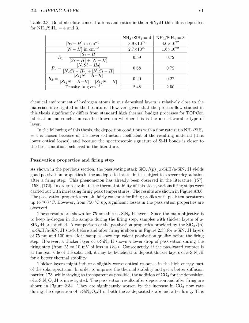
2.5. CAPPING LAYER 61
Table 2.3: Bond absolute concentrations and ratios in the a-SiNx:H thin films depositedfor NH3/SiH4 = 4 and 3.
NH3/SiH4 = 4 NH3/SiH4 = 3
[Si−H] in cm−3 3.9×10²² 4.0×10²²
[N −H] in cm−3 2.7×10²² 1.6×10²²
R1 =[Si−H]
[Si−H] + [N −H]0.59 0.72
R2 =[N2Si−H2]
[N2Si−H2] + [N3Si−H]0.68 0.72
R3 =[Si2N −H ...H]
[Si2N −H ...H] + [Si2N −H]0.20 0.22
Density in g.cm−3 2.48 2.50
chemical environment of hydrogen atoms in our deposited layers is relatively close to thematerials investigated in the literature. However, given that the process flow studied inthis thesis significantly differs from standard high thermal budget processes for TOPConfabrication, no conclusion can be drawn on whether this is the most favorable type oflayer.
In the following of this thesis, the deposition conditions with a flow rate ratio NH3/SiH4
= 4 is chosen because of the lower extinction coefficient of the resulting material (thuslower optical losses), and because the spectroscopic signature of Si-H bonds is closer tothe best conditions achieved in the literature.
Passivation properties and firing step
As shown in the previous section, the passivating stack SiOx/(p) µc-Si:H/a-SiNx:H yieldsgood passivation properties in the as-deposited state, but is subject to a severe degradationafter a firing step. This phenomenon has already been observed in the literature [157],[158], [172]. In order to evaluate the thermal stability of this stack, various firing steps werecarried out with increasing firing peak temperatures. The results are shown in Figure A3.6.The passivation properties remain fairly constant for firing profiles with peak temperaturesup to 700 °C. However, from 750 °C up, significant losses in the passivation properties areobserved.
These results are shown for 75 nm-thick a-SiNx:H layers. Since the main objective isto keep hydrogen in the sample during the firing step, samples with thicker layers of a-SiNx:H are studied. A comparison of the passivation properties provided by the SiOx/(p)µc-Si:H/a-SiNx:H stack before and after firing is shown in Figure 2.33 for a-SiNx:H layersof 75 nm and 100 nm. Both samples show equivalent passivation quality before the firingstep. However, a thicker layer of a-SiNx:H shows a lower drop of passivation during thefiring step (from 25 to 10 mV of loss in iVoc). Consequently, if the passivated contact isat the rear side of the solar cell, it may be beneficial to deposit thicker layers of a-SiNx:Hfor a better thermal stability.
Thicker layers might induce a slightly worse optical response in the high energy partof the solar spectrum. In order to improve the thermal stability and get a better diffusionbarrier [173] while staying as transparent as possible, the addition of CO2 for the depositionof a-SiNxOy:H is investigated. The passivation results after deposition and after firing areshown in Figure 2.34. They are significantly worsen by the increase in CO2 flow rateduring the deposition of a-SiNxOy:H in both the as-deposited state and after firing. This
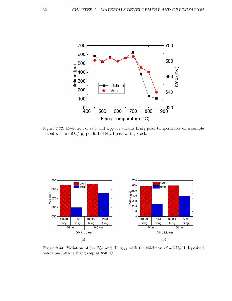
62 CHAPTER 2. MATERIALS DEVELOPMENT AND OPTIMIZATION
400 500 600 700 800 9000
100
200
300
400
500
600
700
Life
time
(µs)
Firing Temperature (°C)
Lifetime iVoc
620
640
660
680
700
iVoc
(mV)
Figure 2.32: Evolution of iVoc and τeff for various firing peak temperatures on a samplecoated with a SiOx/(p) µc-Si:H/SiNx:H passivating stack.
firing firing firing firingBefore After Before After
75 nm 100 nm
650
660
670
680
690 SiN firing
iVoc
(mV)
SiN thickness
(a)
firing firing firing firingBefore After Before After
75 nm 100 nm
0
100
200
300
400
500
600
700 SiN firing
Life
time
(µs)
SiN thickness
(b)
Figure 2.33: Variation of (a) iVoc and (b) τeff with the thickness of a-SiNx:H depositedbefore and after a firing step at 850 °C.
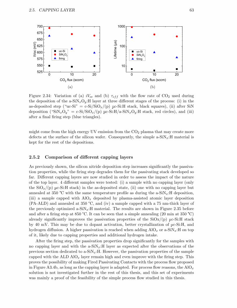
2.5. CAPPING LAYER 63
0 10 20525
550
575
600
625
650
675
700
uc-Si SiNxOy
firing
iVoc
(mV)
CO2 flux (sccm)
(a)
0 10 20
10
100
1000
uc-Si SiNxOy
firingLife
time
(µs)
CO2 flux (sccm)
(b)
Figure 2.34: Variation of (a) iVoc and (b) τeff with the flow rate of CO2 used duringthe deposition of the a-SiNxOy:H layer at three different stages of the process: (i) in theas-deposited step (“uc-Si” = c-Si/SiOx/(p) µc-Si:H stack, black squares), (ii) after SiNdeposition (“SiNxOy” = c-Si/SiOx/(p) µc-Si:H/a-SiNxOy:H stack, red circles), and (iii)after a final firing step (blue triangles).
might come from the high energy UV emission from the CO2 plasma that may create moredefects at the surface of the silicon wafer. Consequently, the simple a-SiNx:H material iskept for the rest of the depositions.
2.5.2 Comparison of different capping layers
As previously shown, the silicon nitride deposition step increases significantly the passiva-tion properties, while the firing step degrades them for the passivating stack developed sofar. Different capping layers are now studied in order to assess the impact of the natureof the top layer. 4 different samples were tested: (i) a sample with no capping layer (onlythe SiOx/(p) µc-Si:H stack) in the as-deposited state, (ii) one with no capping layer butannealed at 350 °C with the same temperature profile as during the a-SiNx:H deposition,(iii) a sample capped with AlOx deposited by plasma-assisted atomic layer deposition(PA-ALD) and annealed at 350 °C, and (iv) a sample capped with a 75 nm-thick layer ofthe previously optimized a-SiNx:H material. The results are shown in Figure 2.35 beforeand after a firing step at 850 °C. It can be seen that a simple annealing (20 min at 350 °C)already significantly improves the passivation properties of the SiOx/(p) µc-Si:H stackby 40 mV. This may be due to dopant activation, better crystallization of µc-Si:H, andhydrogen diffusion. A higher passivation is reached when adding AlOx or a-SiNx:H on topof it, likely due to capping properties and additional hydrogen intake.
After the firing step, the passivation properties drop significantly for the samples withno capping layer and with the a-SiNx:H layer as expected after the observations of theprevious section dedicated to a-SiNx:H. However, the passivation properties of the samplecapped with the ALD AlOx layer remain high and even improve with the firing step. Thisproves the possibility of making Fired Passivating Contacts with the process flow proposedin Figure A3.4b, as long as the capping layer is adapted. For process flow reasons, the AlOx
solution is not investigated further in the rest of this thesis, and this set of experimentswas mainly a proof of the feasibility of the simple process flow studied in this thesis.
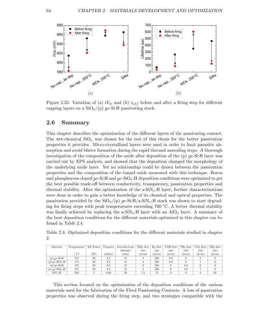
64 CHAPTER 2. MATERIALS DEVELOPMENT AND OPTIMIZATION
No cap., as dep
No cap., 350°C
AlOx, 350°C SiNx580
600
620
640
660
680 Before firing After firing
iVoc
(mV)
(a)
No cap., as dep
No cap., 350°C
AlOx, 350°C SiNx0
100
200
300
400
500
600
700
Before firing After firing
Life
time
(µs)
(b)
Figure 2.35: Variation of (a) iVoc and (b) τeff before and after a firing step for differentcapping layers on a SiOx/(p) µc-Si:H passivating stack.
2.6 Summary
This chapter describes the optimization of the different layers of the passivating contact.The wet-chemical SiOx was chosen for the rest of this thesis for the better passivationproperties it provides. Micro-crystallized layers were used in order to limit parasitic ab-sorption and avoid blister formation during the rapid thermal annealing steps. A thoroughinvestigation of the composition of the oxide after deposition of the (p) µc-Si:H layer wascarried out by XPS analysis, and showed that the deposition changed the morphology ofthe underlying oxide layer. Yet no relationship could be drawn between the passivationproperties and the composition of the tunnel oxide measured with this technique. Boronand phosphorous doped µc-Si:H and µc-SiOx:H deposition conditions were optimized to getthe best possible trade-off between conductivity, transparency, passivation properties andthermal stability. After the optimization of the a-SiNx:H layer, further characterizationswere done in order to gain a better knowledge of its chemical and optical properties. Thepassivation provided by the SiOx/(p) µc-Si:H/a-SiNx:H stack was shown to start degrad-ing for firing steps with peak temperatures exceeding 700 °C. A better thermal stabilitywas finally achieved by replacing the a-SiNx:H layer with an AlOx layer. A summary ofthe best deposition conditions for the different materials optimized in this chapter can befound in Table 2.4.
Table 2.4: Optimized deposition conditions for the different materials studied in chapter2.
Material Temperature RF Power Pressure Interelectrode SiH4 flow H2 flow TMB flow PH3 flow CO2 flow NH3 flowdistance rate rate rate rate rate rate
(°C) (W) (mbar) (mm) (sccm) (sccm) (sccm) (sccm) (sccm) (sccm)
(p) µc-Si:H 175 50 2.5 15 4 500 0.8 0 0 0
(p) µc-SiOx:H 175 50 2.5 15 4 500 0.8 0 1 0
(n) µc-Si:H 175 50 2.5 15 6 500 0 0.8 0 0
(n) µc-SiOx:H 175 50 2.5 15 4 500 0 0.8 1 0
SiNx:H 350 5 0.66 20 7.5 75 0 0 0 30
This section focused on the optimization of the deposition conditions of the variousmaterials used for the fabrication of the Fired Passivating Contacts. A loss of passivationproperties was observed during the firing step, and two strategies compatible with the

2.6. SUMMARY 65
investigated process flow were found to hinder it: replacing µc-Si:H by µc-SiOx:H layersand depositing thicker layers of µc-SiOx:H and/or a-SiNx:H. The complexity of the stackand the impact of the deposition steps on the whole structure motivate the use of real-time characterization techniques. Consequently, in situ characterization is used in thefollowing chapters in order to optimize the process steps more efficiently and gain a betterunderstanding on the kinetics of the passivation properties.

66 CHAPTER 2. MATERIALS DEVELOPMENT AND OPTIMIZATION
67
Chapter 3
In situ modulatedphotoluminescence for AlOx
Modulated photoluminescence (MPL) allows to measure the minority carrier lifetime ina sample. In situ, real-time lifetime measurement is extremely interesting since it givessome insight on the evolution of the passivation properties during a given process step. Inthis section, an in situ MPL measurement tool is described along with the improvementsthat have been made during this doctoral thesis. We also report on a case study dealingwith AlOx passivated samples undergoing an annealing step. These allow to show that thecombined action of light and temperature activates stable positive fixed charges in the layer,which is highly unusual for this kind of material.
Contents
3.1 In situ MPL coupled to a PECVD reactor . . . . . . . . . . . . . . . 683.1.1 Introduction to modulated photoluminescence . . . . . . . . . . . . . 683.1.2 In situ modulated photoluminescence experimental setup . . . . . . 703.1.3 Diffusion phenomena . . . . . . . . . . . . . . . . . . . . . . . . . . . 713.1.4 Temperature correction . . . . . . . . . . . . . . . . . . . . . . . . . 77
3.2 AlOx passivated samples: a case study . . . . . . . . . . . . . . . . . . 793.2.1 Context . . . . . . . . . . . . . . . . . . . . . . . . . . . . . . . . . . 793.2.2 Experimental methods . . . . . . . . . . . . . . . . . . . . . . . . . . 803.2.3 In situ MPL measurements during annealing . . . . . . . . . . . . . 813.2.4 Chemical passivation . . . . . . . . . . . . . . . . . . . . . . . . . . . 833.2.5 Field-effect passivation . . . . . . . . . . . . . . . . . . . . . . . . . . 833.2.6 Investigation of the discrepancy between QSSPC and MPL . . . . . 84
3.3 Summary . . . . . . . . . . . . . . . . . . . . . . . . . . . . . . . . . . . . 85
68 CHAPTER 3. IN SITU MODULATED PHOTOLUMINESCENCE FOR ALOX
3.1 In situ MPL coupled to a PECVD reactor
3.1.1 Introduction to modulated photoluminescence
As discussed in section 1.1.3, 4 main recombination mechanisms can be identified: ra-diative, Auger, SRH, and surface recombinations. Specific recombination rates can beattributed to each of them, respectively Rrad, RAuger, RSRH , and Rsurf , the latter includ-ing the contribution of all surface recombinations. The total effective recombination rateReff (expressed in cm−3.s−1) is defined as the sum of these contributions:
Reff = Rbulk +Rsurf = Rrad +RAuger +RSRH +Rsurf (3.1)
with Rbulk the recombination rate accounting for all recombination mechanisms inthe bulk of the silicon wafer. To each of these phenomena, one can attribute a related
characteristic carrier lifetime τ =∆n
R. This allows to define an effective minority carrier
lifetime τeff in the material, such as described in Equation 3.2:
1
τeff=Reff∆n
=1
τrad+
1
τAuger+
1
τSRH+
1
τsurf(3.2)
This is (under a few minor approximations) the value derived from QSSPC measure-ments and used in the previous section. At this point, it is worth reminding that therecombination rates depend on the charge carrier density. Typically, the rate of Augerrecombination events dramatically increase at high excess carrier densities (see Equation1.10).
Harmonically modulated photoluminescence consists in illuminating a sample with amonochromatic light of modulated intensity [174]. The illumination intensity varies atan angular frequency ω and can be expressed as the superposition of a continuous and atime-depend contribution:
I = I0 + I1eiωt (3.3)
As a consequence of this modulated intensity and by linearity of the electron-hole pairgeneration with the incident photon flux, the generation rate G (in cm−3.s−1) and theexcess carrier densities ∆n and ∆p (in cm−3) also follow this harmonic modulation.
G =G0 +G1eiωt
∆n =∆n0 +∆n1eiωt
∆p =∆p0 +∆p1eiωt
(3.4)
Radiative recombinations govern the luminescence intensity. The luminescence photonflux jPL coming out of the sample is given by the expression:
jPL = Bnp (3.5)
with B the radiative coefficient depending on the material properties and np the productof electron and hole densities. As a consequence of the excitation of the sample, themodulated photoluminescence intensity can be written:
jPL = B(n0 +∆n)(p0 +∆p) (3.6)
where n0 and p0 are respectively the electron and hole densities in the material under noexcitation (thermal equilibrium). Assuming that the modulated part of the laser intensity
3.1. IN SITU MPL COUPLED TO A PECVD REACTOR 69
is relatively small compared to the continuous contribution, one can assume ∆n1 ∆n0,along with ∆n0 = ∆p0 and ∆n1 = ∆p1. From Equation 3.4 one can induce that the firstorder term jPL,1 can be expressed under the form:
jPL,1 = B (n0 + p0 + 2∆n0)∆n1 (3.7)
The continuity equation for the excess minority carrier lifetime in p-type semiconduc-tors is given by:
∂∆n
∂t= G(r, t)−R(r, t)−∇j∆n(r, t) (3.8)
where ∇j∆n is the gradient of the excess carrier current density. In uniform materialsunder uniform illumination, this last contribution is null. When deriving the continuityequation (Equation 3.8) with respect to time, one gets:
d2∆n(t)
dt2=dG
dt− dR
dt
=dG
dt− dR
d∆n
d∆n
dt
d2∆n(t)
dt2=dG
dt− 1
τeff,diff
d∆n
dt(3.9)
with the introduction of the differential lifetime τeff,diff =d∆n
dR. When using the set
of Equations 3.4 to account for the time dependence of the various quantities, one canrewrite equation 3.9:
(iω)2∆n1eiωt = iωG1e
iωt − 1
τeff,diff(iω)∆n1e
iωt
iω∆n1 = G1 −1
τeff,diff∆n1
∆n1
(iω +
1
τeff,diff
)= G1
∆n1 =G1τeff,diff
1 + iωτeff,diff(3.10)
From Equation 3.10, one can finally derive the module and phase shift of ∆n1:
|∆n1| =G1τeff,diff√
1 + (ωτeff,diff )2(3.11)
φ = − arctan(ωτeff,diff ) (3.12)
This relates directly to the photoluminescence intensity as Equation 3.7 shows. Asa consequence, a simple measurement of the phase-shift between the excitation and thephotoluminescence signal allows to extract a measured lifetime τm which corresponds tothe differential effective lifetime τeff,diff . For simplification purposes, the notation τm willbe used to relate to the differential effective lifetime in the rest of this chapter.
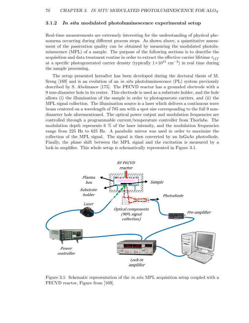
70 CHAPTER 3. IN SITU MODULATED PHOTOLUMINESCENCE FOR ALOX
3.1.2 In situ modulated photoluminescence experimental setup
Real-time measurements are extremely interesting for the understanding of physical phe-nomena occurring during different process steps. As shown above, a quantitative assess-ment of the passivation quality can be obtained by measuring the modulated photolu-minescence (MPL) of a sample. The purpose of the following sections is to describe theacquisition and data treatment routine in order to extract the effective carrier lifetime τeffat a specific photogenerated carrier density (typically 1×1015 cm−3) in real time duringthe sample processing.
The setup presented hereafter has been developed during the doctoral thesis of M.Sreng [169] and is an evolution of an in situ photoluminescence (PL) system previouslydescribed by S. Abolmasov [175]. The PECVD reactor has a grounded electrode with a9 mm-diameter hole in its center. This electrode is used as a substrate holder, and the holeallows (i) the illumination of the sample in order to photogenerate carriers, and (ii) theMPL signal collection. The illumination source is a laser which delivers a continuous wavebeam centered on a wavelength of 785 nm with a spot size corresponding to the full 9 mm-diameter hole aforementioned. The optical power output and modulation frequencies arecontrolled through a programmable current/temperature controller from Thorlabs. Themodulation depth represents 6 % of the laser intensity, and the modulation frequenciesrange from 225 Hz to 625 Hz. A parabolic mirror was used in order to maximize thecollection of the MPL signal. The signal is then converted by an InGaAs photodiode.Finally, the phase shift between the MPL signal and the excitation is measured by alock-in amplifier. This whole setup is schematically represented in Figure 3.1.
Figure 3.1: Schematic representation of the in situ MPL acquisition setup coupled with aPECVD reactor, Figure from [169].
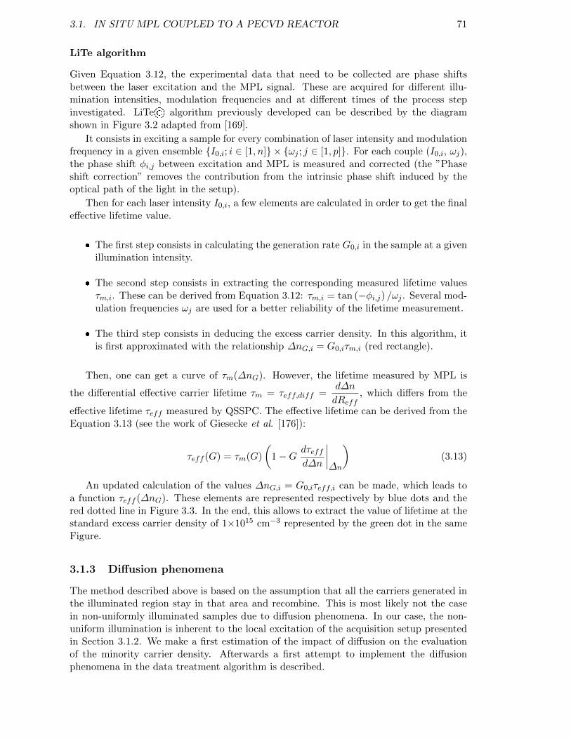
3.1. IN SITU MPL COUPLED TO A PECVD REACTOR 71
LiTe algorithm
Given Equation 3.12, the experimental data that need to be collected are phase shiftsbetween the laser excitation and the MPL signal. These are acquired for different illu-mination intensities, modulation frequencies and at different times of the process stepinvestigated. LiTe© algorithm previously developed can be described by the diagramshown in Figure 3.2 adapted from [169].
It consists in exciting a sample for every combination of laser intensity and modulationfrequency in a given ensemble I0,i; i ∈ [1, n] × ωj ; j ∈ [1, p]. For each couple (I0,i, ωj),the phase shift φi,j between excitation and MPL is measured and corrected (the ”Phaseshift correction” removes the contribution from the intrinsic phase shift induced by theoptical path of the light in the setup).
Then for each laser intensity I0,i, a few elements are calculated in order to get the finaleffective lifetime value.
The first step consists in calculating the generation rate G0,i in the sample at a givenillumination intensity.
The second step consists in extracting the corresponding measured lifetime valuesτm,i. These can be derived from Equation 3.12: τm,i = tan (−φi,j) /ωj . Several mod-ulation frequencies ωj are used for a better reliability of the lifetime measurement.
The third step consists in deducing the excess carrier density. In this algorithm, itis first approximated with the relationship ∆nG,i = G0,iτm,i (red rectangle).
Then, one can get a curve of τm(∆nG). However, the lifetime measured by MPL is
the differential effective carrier lifetime τm = τeff,diff =d∆n
dReff, which differs from the
effective lifetime τeff measured by QSSPC. The effective lifetime can be derived from theEquation 3.13 (see the work of Giesecke et al. [176]):
τeff (G) = τm(G)
(1−G
dτeffd∆n
∣∣∣∣∆n
)(3.13)
An updated calculation of the values ∆nG,i = G0,iτeff,i can be made, which leads toa function τeff (∆nG). These elements are represented respectively by blue dots and thered dotted line in Figure 3.3. In the end, this allows to extract the value of lifetime at thestandard excess carrier density of 1×1015 cm−3 represented by the green dot in the sameFigure.
3.1.3 Diffusion phenomena
The method described above is based on the assumption that all the carriers generated inthe illuminated region stay in that area and recombine. This is most likely not the casein non-uniformly illuminated samples due to diffusion phenomena. In our case, the non-uniform illumination is inherent to the local excitation of the acquisition setup presentedin Section 3.1.2. We make a first estimation of the impact of diffusion on the evaluationof the minority carrier density. Afterwards a first attempt to implement the diffusionphenomena in the data treatment algorithm is described.
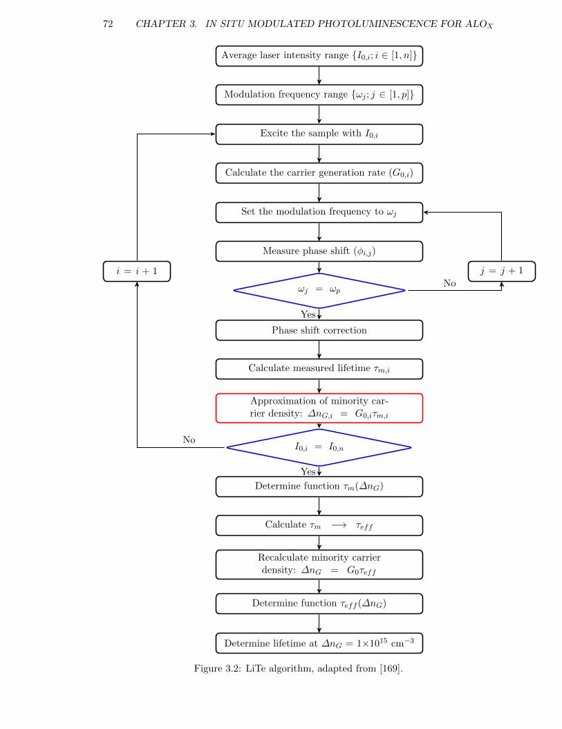
72 CHAPTER 3. IN SITU MODULATED PHOTOLUMINESCENCE FOR ALOX
Average laser intensity range I0,i; i ∈ [1, n]
Modulation frequency range ωj ; j ∈ [1, p]
Excite the sample with I0,i
Calculate the carrier generation rate (G0,i)
Set the modulation frequency to ωj
Measure phase shift (φi,j)
j = j + 1
ωj = ωp
i = i + 1
Phase shift correction
Calculate measured lifetime τm,i
Approximation of minority car-rier density: ∆nG,i = G0,iτm,i
I0,i = I0,n
Determine function τm(∆nG)
Calculate τm −→ τeff
Recalculate minority carrierdensity: ∆nG = G0τeff
Determine function τeff (∆nG)
Determine lifetime at ∆nG = 1×1015 cm−3
Yes
Yes
No
No
Figure 3.2: LiTe algorithm, adapted from [169].
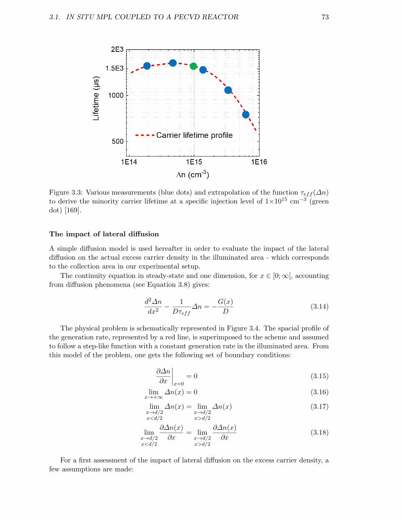
3.1. IN SITU MPL COUPLED TO A PECVD REACTOR 73
Figure 3.3: Various measurements (blue dots) and extrapolation of the function τeff (∆n)to derive the minority carrier lifetime at a specific injection level of 1×1015 cm−3 (greendot) [169].
The impact of lateral diffusion
A simple diffusion model is used hereafter in order to evaluate the impact of the lateraldiffusion on the actual excess carrier density in the illuminated area - which correspondsto the collection area in our experimental setup.
The continuity equation in steady-state and one dimension, for x ∈ [0;∞[, accountingfrom diffusion phenomena (see Equation 3.8) gives:
d2∆n
dx2− 1
Dτeff∆n = −G(x)
D(3.14)
The physical problem is schematically represented in Figure 3.4. The spacial profile ofthe generation rate, represented by a red line, is superimposed to the scheme and assumedto follow a step-like function with a constant generation rate in the illuminated area. Fromthis model of the problem, one gets the following set of boundary conditions:
∂∆n
∂x
∣∣∣∣x=0
= 0 (3.15)
limx→+∞
∆n(x) = 0 (3.16)
limx→d/2x<d/2
∆n(x) = limx→d/2x>d/2
∆n(x) (3.17)
limx→d/2x<d/2
∂∆n(x)
∂x= lim
x→d/2x>d/2
∂∆n(x)
∂x(3.18)
For a first assessment of the impact of lateral diffusion on the excess carrier density, afew assumptions are made:
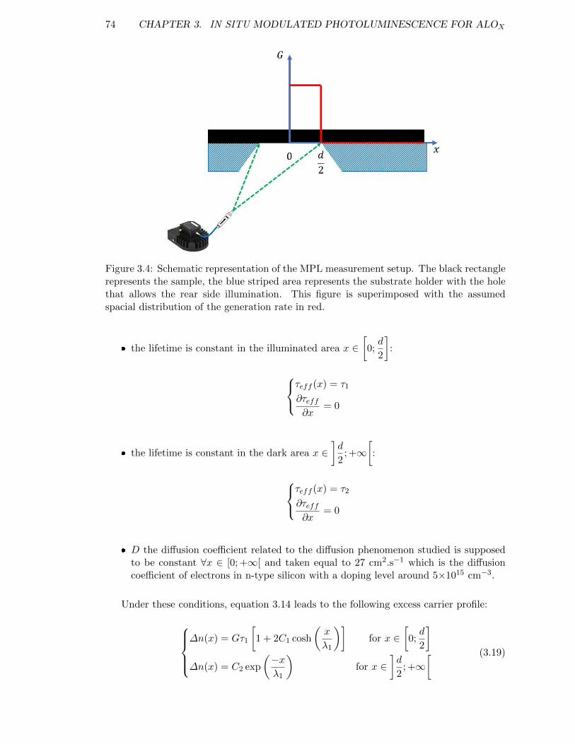
74 CHAPTER 3. IN SITU MODULATED PHOTOLUMINESCENCE FOR ALOX
Figure 3.4: Schematic representation of the MPL measurement setup. The black rectanglerepresents the sample, the blue striped area represents the substrate holder with the holethat allows the rear side illumination. This figure is superimposed with the assumedspacial distribution of the generation rate in red.
the lifetime is constant in the illuminated area x ∈[0;d
2
]:
τeff (x) = τ1
∂τeff∂x
= 0
the lifetime is constant in the dark area x ∈]d
2; +∞
[:
τeff (x) = τ2
∂τeff∂x
= 0
D the diffusion coefficient related to the diffusion phenomenon studied is supposedto be constant ∀x ∈ [0; +∞[ and taken equal to 27 cm2.s−1 which is the diffusioncoefficient of electrons in n-type silicon with a doping level around 5×1015 cm−3.
Under these conditions, equation 3.14 leads to the following excess carrier profile:
∆n(x) = Gτ1
[1 + 2C1 cosh
(x
λ1
)]for x ∈
[0;d
2
]∆n(x) = C2 exp
(−xλ1
)for x ∈
]d
2; +∞
[ (3.19)
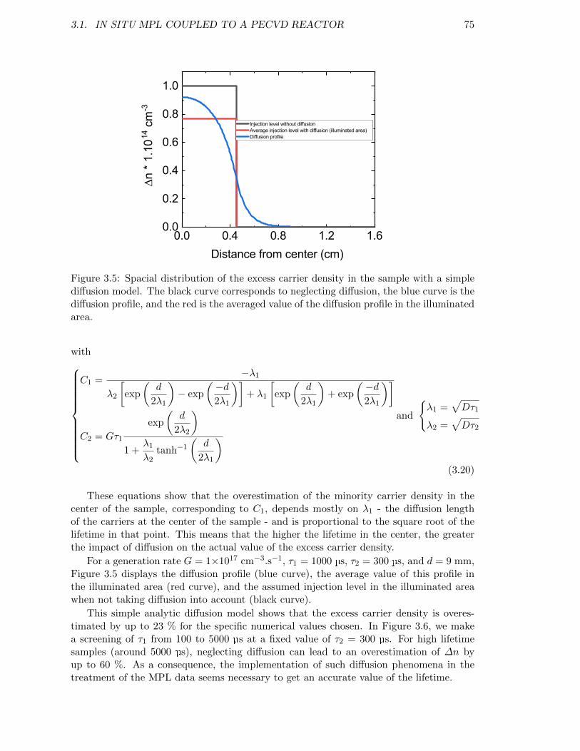
3.1. IN SITU MPL COUPLED TO A PECVD REACTOR 75
0.0 0.4 0.8 1.2 1.60.0
0.2
0.4
0.6
0.8
1.0
Dn *
1.10
14 c
m-3
Distance from center (cm)
Injection level without diffusion Average injection level with diffusion (illuminated area) Diffusion profile
Figure 3.5: Spacial distribution of the excess carrier density in the sample with a simplediffusion model. The black curve corresponds to neglecting diffusion, the blue curve is thediffusion profile, and the red is the averaged value of the diffusion profile in the illuminatedarea.
with
C1 =−λ1
λ2
[exp
(d
2λ1
)− exp
(−d2λ1
)]+ λ1
[exp
(d
2λ1
)+ exp
(−d2λ1
)]
C2 = Gτ1
exp
(d
2λ2
)1 +
λ1λ2
tanh−1(
d
2λ1
)and
λ1 =
√Dτ1
λ2 =√Dτ2
(3.20)
These equations show that the overestimation of the minority carrier density in thecenter of the sample, corresponding to C1, depends mostly on λ1 - the diffusion lengthof the carriers at the center of the sample - and is proportional to the square root of thelifetime in that point. This means that the higher the lifetime in the center, the greaterthe impact of diffusion on the actual value of the excess carrier density.
For a generation rate G = 1×1017 cm−3.s−1, τ1 = 1000 µs, τ2 = 300 µs, and d = 9 mm,Figure 3.5 displays the diffusion profile (blue curve), the average value of this profile inthe illuminated area (red curve), and the assumed injection level in the illuminated areawhen not taking diffusion into account (black curve).
This simple analytic diffusion model shows that the excess carrier density is overes-timated by up to 23 % for the specific numerical values chosen. In Figure 3.6, we makea screening of τ1 from 100 to 5000 µs at a fixed value of τ2 = 300 µs. For high lifetimesamples (around 5000 µs), neglecting diffusion can lead to an overestimation of ∆n byup to 60 %. As a consequence, the implementation of such diffusion phenomena in thetreatment of the MPL data seems necessary to get an accurate value of the lifetime.
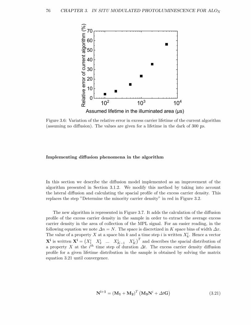
76 CHAPTER 3. IN SITU MODULATED PHOTOLUMINESCENCE FOR ALOX
102 103 1040
10
20
30
40
50
60
70
Rel
ativ
e er
ror o
f cur
rent
alg
orith
m (%
)
Assumed lifetime in the illuminated area (µs)
Figure 3.6: Variation of the relative error in excess carrier lifetime of the current algorithm(assuming no diffusion). The values are given for a lifetime in the dark of 300 µs.
Implementing diffusion phenomena in the algorithm
In this section we describe the diffusion model implemented as an improvement of thealgorithm presented in Section 3.1.2. We modify this method by taking into accountthe lateral diffusion and calculating the spacial profile of the excess carrier density. Thisreplaces the step ”Determine the minority carrier density” in red in Figure 3.2.
The new algorithm is represented in Figure 3.7. It adds the calculation of the diffusionprofile of the excess carrier density in the sample in order to extract the average excesscarrier density in the area of collection of the MPL signal. For an easier reading, in thefollowing equation we note ∆n = N . The space is discretized in K space bins of width ∆x.The value of a property X at a space bin k and a time step i is written Xi
k. Hence a vector
Xi is written Xi =(Xi
1 Xi2 ... Xi
K−1 XiK
)Tand describes the spacial distribution of
a property X at the ith time step of duration ∆t. The excess carrier density diffusionprofile for a given lifetime distribution in the sample is obtained by solving the matrixequation 3.21 until convergence.
Ni+1 = (M1 + M2)T(M3Ni +∆tG
)(3.21)
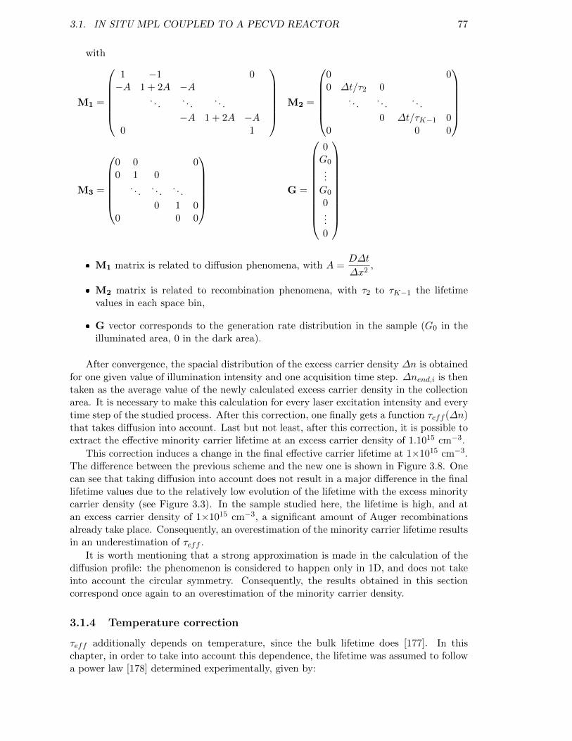
3.1. IN SITU MPL COUPLED TO A PECVD REACTOR 77
with
M1 =
1 −1 0−A 1 + 2A −A
. . .. . .
. . .
−A 1 + 2A −A0 1
M2 =
0 00 ∆t/τ2 0
. . .. . .
. . .
0 ∆t/τK−1 00 0 0
M3 =
0 0 00 1 0
. . .. . .
. . .
0 1 00 0 0
G =
0G0...G0
0...0
M1 matrix is related to diffusion phenomena, with A =
D∆t
∆x2,
M2 matrix is related to recombination phenomena, with τ2 to τK−1 the lifetimevalues in each space bin,
G vector corresponds to the generation rate distribution in the sample (G0 in theilluminated area, 0 in the dark area).
After convergence, the spacial distribution of the excess carrier density ∆n is obtainedfor one given value of illumination intensity and one acquisition time step. ∆nend,i is thentaken as the average value of the newly calculated excess carrier density in the collectionarea. It is necessary to make this calculation for every laser excitation intensity and everytime step of the studied process. After this correction, one finally gets a function τeff (∆n)that takes diffusion into account. Last but not least, after this correction, it is possible toextract the effective minority carrier lifetime at an excess carrier density of 1.1015 cm−3.
This correction induces a change in the final effective carrier lifetime at 1×1015 cm−3.The difference between the previous scheme and the new one is shown in Figure 3.8. Onecan see that taking diffusion into account does not result in a major difference in the finallifetime values due to the relatively low evolution of the lifetime with the excess minoritycarrier density (see Figure 3.3). In the sample studied here, the lifetime is high, and atan excess carrier density of 1×1015 cm−3, a significant amount of Auger recombinationsalready take place. Consequently, an overestimation of the minority carrier lifetime resultsin an underestimation of τeff .
It is worth mentioning that a strong approximation is made in the calculation of thediffusion profile: the phenomenon is considered to happen only in 1D, and does not takeinto account the circular symmetry. Consequently, the results obtained in this sectioncorrespond once again to an overestimation of the minority carrier density.
3.1.4 Temperature correction
τeff additionally depends on temperature, since the bulk lifetime does [177]. In thischapter, in order to take into account this dependence, the lifetime was assumed to followa power law [178] determined experimentally, given by:
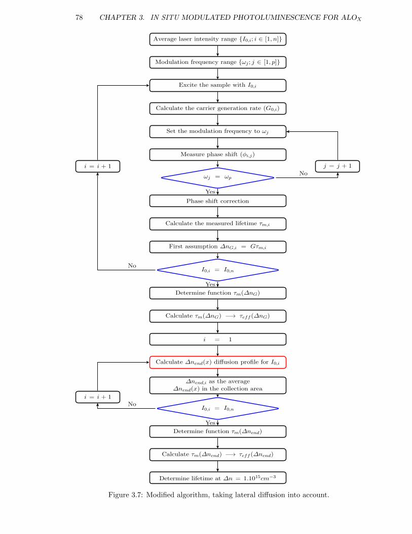
78 CHAPTER 3. IN SITU MODULATED PHOTOLUMINESCENCE FOR ALOX
Average laser intensity range I0,i; i ∈ [1, n]
Modulation frequency range ωj ; j ∈ [1, p]
Excite the sample with I0,i
Calculate the carrier generation rate (G0,i)
Set the modulation frequency to ωj
Measure phase shift (φi,j)
j = j + 1
ωj = ωp
i = i + 1
Phase shift correction
Calculate the measured lifetime τm,i
First assumption ∆nG,i = Gτm,i
I0,i = I0,n
Determine function τm(∆nG)
Calculate τm(∆nG) −→ τeff (∆nG)
i = 1
Calculate ∆nend(x) diffusion profile for I0,i
∆nend,i as the average∆nend(x) in the collection area
I0,i = I0,n
i = i + 1
Determine function τm(∆nend)
Calculate τm(∆nend) −→ τeff (∆nend)
Determine lifetime at ∆n = 1.1015cm−3
Yes
Yes
Yes
No
No
No
Figure 3.7: Modified algorithm, taking lateral diffusion into account.
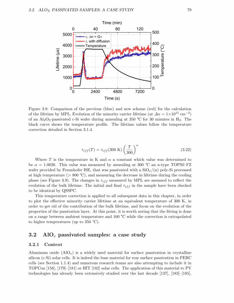
3.2. ALOX PASSIVATED SAMPLES: A CASE STUDY 79
0 2400 4800 7200
0 40 80 120
0
1000
2000
3000
4000
5000
Time (min)
Life
time
(µs)
Time (s)
t, Dn = Gt t, with diffusion Temperature
0
100
200
300
400
500
Tem
pera
ture
(°C
)
Figure 3.8: Comparison of the previous (blue) and new scheme (red) for the calculationof the lifetime by MPL. Evolution of the minority carrier lifetime (at ∆n = 1×1015 cm−3)of an Al2O3-passivated c-Si wafer during annealing at 350 °C for 30 minutes in H2. Theblack curve shows the temperature profile. The lifetime values follow the temperaturecorrection detailed in Section 3.1.4.
τeff (T ) = τeff (300 K)
(T
300
)α(3.22)
Where T is the temperature in K and α a constant which value was determined tobe α = 1.0026. This value was measured by annealing at 300 °C an n-type TOPSil FZwafer provided by Fraunhofer ISE, that was passivated with a SiOx/(n) poly-Si processedat high temperature (> 800 °C), and measuring the decrease in lifetime during the coolingphase (see Figure 3.9). The changes in τeff measured by MPL are assumed to reflect theevolution of the bulk lifetime. The initial and final τeff in the sample have been checkedto be identical by QSSPC.
This temperature correction is applied to all subsequent data in this chapter, in orderto plot the effective minority carrier lifetime at an equivalent temperature of 300 K, inorder to get rid of the contribution of the bulk lifetime, and focus on the evolution of theproperties of the passivation layer. At this point, it is worth noting that the fitting is doneon a range between ambient temperature and 160 °C while the correction is extrapolatedto higher temperatures (up to 350 °C).
3.2 AlOx passivated samples: a case study
3.2.1 Context
Aluminum oxide (AlOx) is a widely used material for surface passivation in crystallinesilicon (c-Si) solar cells. It is indeed the base material for rear surface passivation in PERCcells (see Section 1.1.4) and numerous research teams are also attempting to include it inTOPCon [158], [179]–[181] or HIT [182] solar cells. The application of this material to PVtechnologies has already been extensively studied over the last decade [137], [183]–[185],
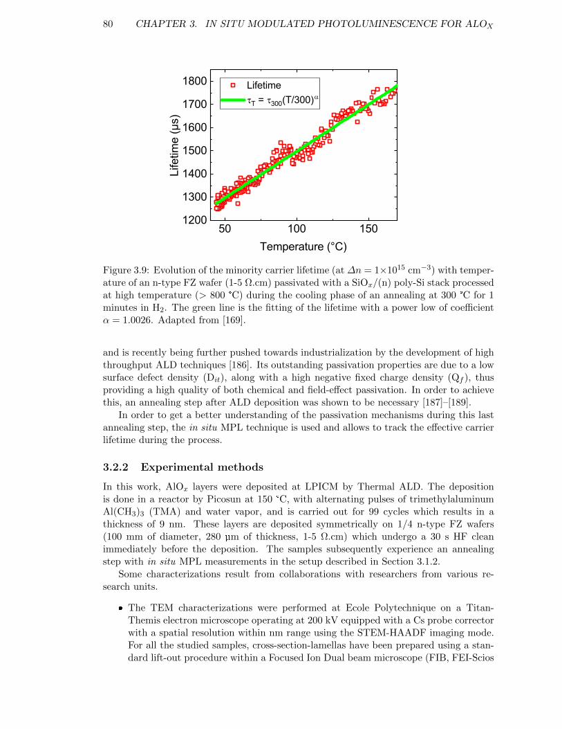
80 CHAPTER 3. IN SITU MODULATED PHOTOLUMINESCENCE FOR ALOX
50 100 1501200
1300
1400
1500
1600
1700
1800 Lifetime tT = t300(T/300)a
Life
time
(µs)
Temperature (°C)
Figure 3.9: Evolution of the minority carrier lifetime (at ∆n = 1×1015 cm−3) with temper-ature of an n-type FZ wafer (1-5 Ω.cm) passivated with a SiOx/(n) poly-Si stack processedat high temperature (> 800 °C) during the cooling phase of an annealing at 300 °C for 1minutes in H2. The green line is the fitting of the lifetime with a power low of coefficientα = 1.0026. Adapted from [169].
and is recently being further pushed towards industrialization by the development of highthroughput ALD techniques [186]. Its outstanding passivation properties are due to a lowsurface defect density (Dit), along with a high negative fixed charge density (Qf ), thusproviding a high quality of both chemical and field-effect passivation. In order to achievethis, an annealing step after ALD deposition was shown to be necessary [187]–[189].
In order to get a better understanding of the passivation mechanisms during this lastannealing step, the in situ MPL technique is used and allows to track the effective carrierlifetime during the process.
3.2.2 Experimental methods
In this work, AlOx layers were deposited at LPICM by Thermal ALD. The depositionis done in a reactor by Picosun at 150 °C, with alternating pulses of trimethylaluminumAl(CH3)3 (TMA) and water vapor, and is carried out for 99 cycles which results in athickness of 9 nm. These layers are deposited symmetrically on 1/4 n-type FZ wafers(100 mm of diameter, 280 µm of thickness, 1-5 Ω.cm) which undergo a 30 s HF cleanimmediately before the deposition. The samples subsequently experience an annealingstep with in situ MPL measurements in the setup described in Section 3.1.2.
Some characterizations result from collaborations with researchers from various re-search units.
The TEM characterizations were performed at Ecole Polytechnique on a Titan-Themis electron microscope operating at 200 kV equipped with a Cs probe correctorwith a spatial resolution within nm range using the STEM-HAADF imaging mode.For all the studied samples, cross-section-lamellas have been prepared using a stan-dard lift-out procedure within a Focused Ion Dual beam microscope (FIB, FEI-Scios
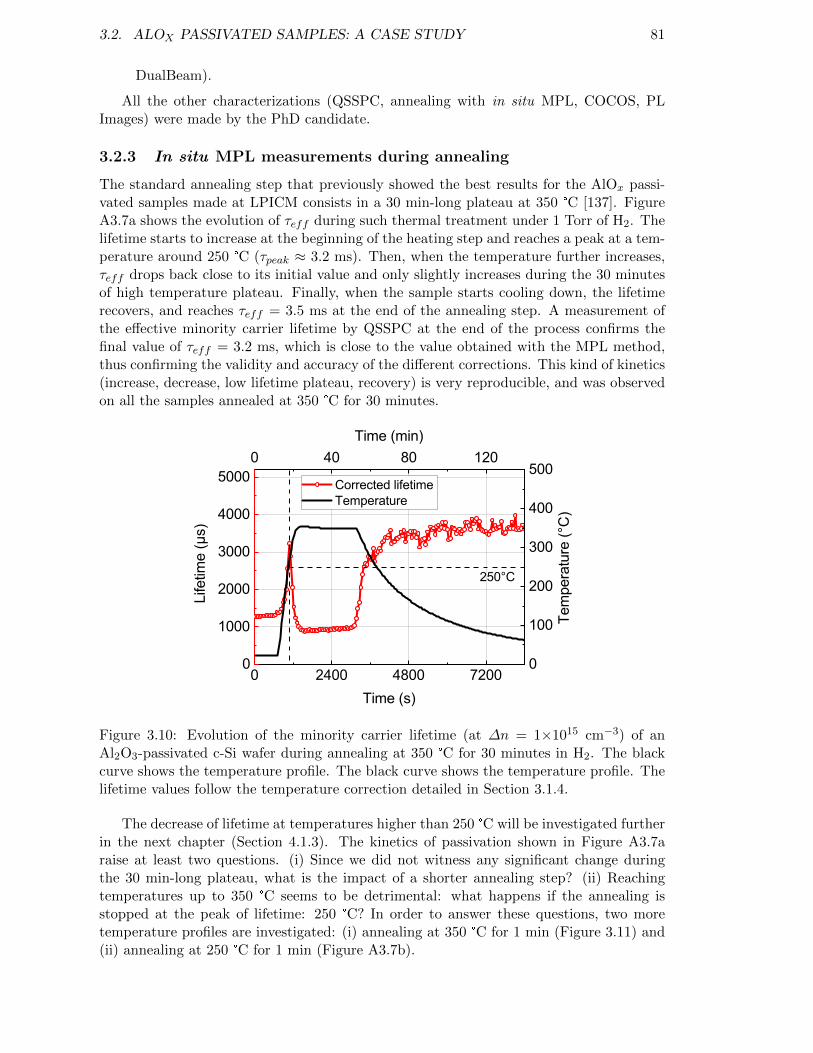
3.2. ALOX PASSIVATED SAMPLES: A CASE STUDY 81
DualBeam).
All the other characterizations (QSSPC, annealing with in situ MPL, COCOS, PLImages) were made by the PhD candidate.
3.2.3 In situ MPL measurements during annealing
The standard annealing step that previously showed the best results for the AlOx passi-vated samples made at LPICM consists in a 30 min-long plateau at 350 °C [137]. FigureA3.7a shows the evolution of τeff during such thermal treatment under 1 Torr of H2. Thelifetime starts to increase at the beginning of the heating step and reaches a peak at a tem-perature around 250 °C (τpeak ≈ 3.2 ms). Then, when the temperature further increases,τeff drops back close to its initial value and only slightly increases during the 30 minutesof high temperature plateau. Finally, when the sample starts cooling down, the lifetimerecovers, and reaches τeff = 3.5 ms at the end of the annealing step. A measurement ofthe effective minority carrier lifetime by QSSPC at the end of the process confirms thefinal value of τeff = 3.2 ms, which is close to the value obtained with the MPL method,thus confirming the validity and accuracy of the different corrections. This kind of kinetics(increase, decrease, low lifetime plateau, recovery) is very reproducible, and was observedon all the samples annealed at 350 °C for 30 minutes.
0 2400 4800 7200
0 40 80 120
0
1000
2000
3000
4000
5000
Time (min)
Life
time
(µs)
Time (s)
Corrected lifetime Temperature
250°C
0
100
200
300
400
500
Tem
pera
ture
(°C
)
Figure 3.10: Evolution of the minority carrier lifetime (at ∆n = 1×1015 cm−3) of anAl2O3-passivated c-Si wafer during annealing at 350 °C for 30 minutes in H2. The blackcurve shows the temperature profile. The black curve shows the temperature profile. Thelifetime values follow the temperature correction detailed in Section 3.1.4.
The decrease of lifetime at temperatures higher than 250 °C will be investigated furtherin the next chapter (Section 4.1.3). The kinetics of passivation shown in Figure A3.7araise at least two questions. (i) Since we did not witness any significant change duringthe 30 min-long plateau, what is the impact of a shorter annealing step? (ii) Reachingtemperatures up to 350 °C seems to be detrimental: what happens if the annealing isstopped at the peak of lifetime: 250 °C? In order to answer these questions, two moretemperature profiles are investigated: (i) annealing at 350 °C for 1 min (Figure 3.11) and(ii) annealing at 250 °C for 1 min (Figure A3.7b).
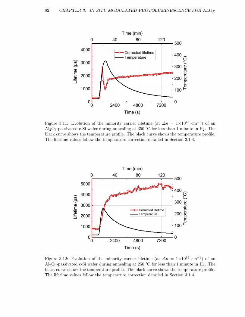
82 CHAPTER 3. IN SITU MODULATED PHOTOLUMINESCENCE FOR ALOX
0 2400 4800 7200
0 40 80 120
0
1000
2000
3000
4000
Time (min)
Life
time
(µs)
Time (s)
Corrected lifetime Temperature
0
100
200
300
400
500
Tem
pera
ture
(°C
)
Figure 3.11: Evolution of the minority carrier lifetime (at ∆n = 1×1015 cm−3) of anAl2O3-passivated c-Si wafer during annealing at 350 °C for less than 1 minute in H2. Theblack curve shows the temperature profile. The black curve shows the temperature profile.The lifetime values follow the temperature correction detailed in Section 3.1.4.
0 2400 4800 7200
0 40 80 120
0
1000
2000
3000
4000
5000
Time (min)
Life
time
(µs)
Time (s)
Corrected lifetime Temperature
0
100
200
300
400
500Te
mpe
ratu
re (°
C)
Figure 3.12: Evolution of the minority carrier lifetime (at ∆n = 1×1015 cm−3) of anAl2O3-passivated c-Si wafer during annealing at 250 °C for less than 1 minute in H2. Theblack curve shows the temperature profile. The black curve shows the temperature profile.The lifetime values follow the temperature correction detailed in Section 3.1.4.
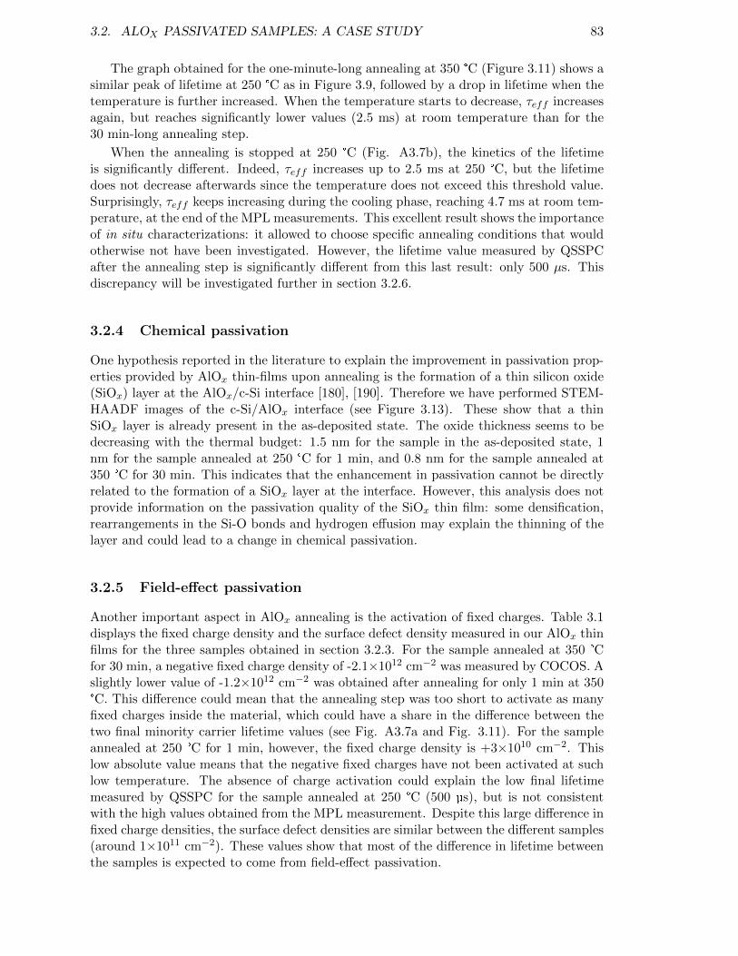
3.2. ALOX PASSIVATED SAMPLES: A CASE STUDY 83
The graph obtained for the one-minute-long annealing at 350 °C (Figure 3.11) shows asimilar peak of lifetime at 250 °C as in Figure 3.9, followed by a drop in lifetime when thetemperature is further increased. When the temperature starts to decrease, τeff increasesagain, but reaches significantly lower values (2.5 ms) at room temperature than for the30 min-long annealing step.
When the annealing is stopped at 250 °C (Fig. A3.7b), the kinetics of the lifetimeis significantly different. Indeed, τeff increases up to 2.5 ms at 250 °C, but the lifetimedoes not decrease afterwards since the temperature does not exceed this threshold value.Surprisingly, τeff keeps increasing during the cooling phase, reaching 4.7 ms at room tem-perature, at the end of the MPL measurements. This excellent result shows the importanceof in situ characterizations: it allowed to choose specific annealing conditions that wouldotherwise not have been investigated. However, the lifetime value measured by QSSPCafter the annealing step is significantly different from this last result: only 500 µs. Thisdiscrepancy will be investigated further in section 3.2.6.
3.2.4 Chemical passivation
One hypothesis reported in the literature to explain the improvement in passivation prop-erties provided by AlOx thin-films upon annealing is the formation of a thin silicon oxide(SiOx) layer at the AlOx/c-Si interface [180], [190]. Therefore we have performed STEM-HAADF images of the c-Si/AlOx interface (see Figure 3.13). These show that a thinSiOx layer is already present in the as-deposited state. The oxide thickness seems to bedecreasing with the thermal budget: 1.5 nm for the sample in the as-deposited state, 1nm for the sample annealed at 250 °C for 1 min, and 0.8 nm for the sample annealed at350 °C for 30 min. This indicates that the enhancement in passivation cannot be directlyrelated to the formation of a SiOx layer at the interface. However, this analysis does notprovide information on the passivation quality of the SiOx thin film: some densification,rearrangements in the Si-O bonds and hydrogen effusion may explain the thinning of thelayer and could lead to a change in chemical passivation.
3.2.5 Field-effect passivation
Another important aspect in AlOx annealing is the activation of fixed charges. Table 3.1displays the fixed charge density and the surface defect density measured in our AlOx thinfilms for the three samples obtained in section 3.2.3. For the sample annealed at 350 °Cfor 30 min, a negative fixed charge density of -2.1×1012 cm−2 was measured by COCOS. Aslightly lower value of -1.2×1012 cm−2 was obtained after annealing for only 1 min at 350°C. This difference could mean that the annealing step was too short to activate as manyfixed charges inside the material, which could have a share in the difference between thetwo final minority carrier lifetime values (see Fig. A3.7a and Fig. 3.11). For the sampleannealed at 250 °C for 1 min, however, the fixed charge density is +3×1010 cm−2. Thislow absolute value means that the negative fixed charges have not been activated at suchlow temperature. The absence of charge activation could explain the low final lifetimemeasured by QSSPC for the sample annealed at 250 °C (500 µs), but is not consistentwith the high values obtained from the MPL measurement. Despite this large difference infixed charge densities, the surface defect densities are similar between the different samples(around 1×1011 cm−2). These values show that most of the difference in lifetime betweenthe samples is expected to come from field-effect passivation.
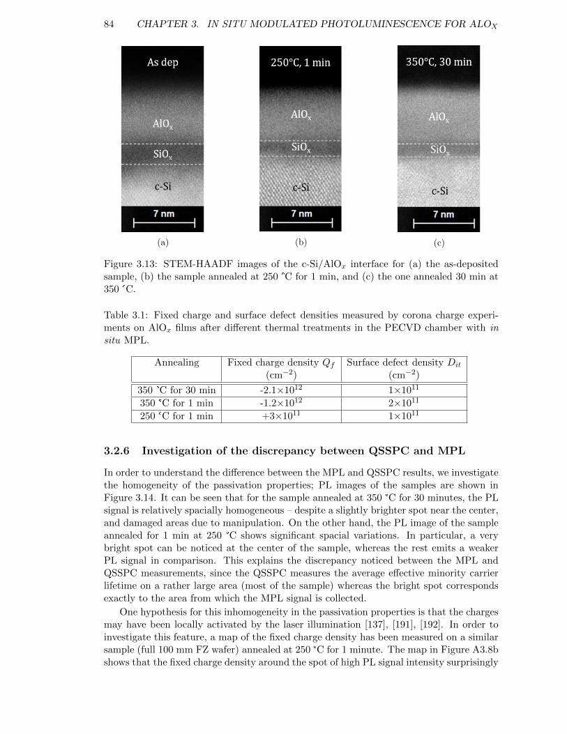
84 CHAPTER 3. IN SITU MODULATED PHOTOLUMINESCENCE FOR ALOX
(a) (b) (c)
Figure 3.13: STEM-HAADF images of the c-Si/AlOx interface for (a) the as-depositedsample, (b) the sample annealed at 250 °C for 1 min, and (c) the one annealed 30 min at350 °C.
Table 3.1: Fixed charge and surface defect densities measured by corona charge experi-ments on AlOx films after different thermal treatments in the PECVD chamber with insitu MPL.
Annealing Fixed charge density Qf Surface defect density Dit
(cm−2) (cm−2)
350 °C for 30 min -2.1×10¹² 1×10¹¹
350 °C for 1 min -1.2×10¹² 2×10¹¹
250 °C for 1 min +3×10¹¹ 1×10¹¹
3.2.6 Investigation of the discrepancy between QSSPC and MPL
In order to understand the difference between the MPL and QSSPC results, we investigatethe homogeneity of the passivation properties; PL images of the samples are shown inFigure 3.14. It can be seen that for the sample annealed at 350 °C for 30 minutes, the PLsignal is relatively spacially homogeneous – despite a slightly brighter spot near the center,and damaged areas due to manipulation. On the other hand, the PL image of the sampleannealed for 1 min at 250 °C shows significant spacial variations. In particular, a verybright spot can be noticed at the center of the sample, whereas the rest emits a weakerPL signal in comparison. This explains the discrepancy noticed between the MPL andQSSPC measurements, since the QSSPC measures the average effective minority carrierlifetime on a rather large area (most of the sample) whereas the bright spot correspondsexactly to the area from which the MPL signal is collected.
One hypothesis for this inhomogeneity in the passivation properties is that the chargesmay have been locally activated by the laser illumination [137], [191], [192]. In order toinvestigate this feature, a map of the fixed charge density has been measured on a similarsample (full 100 mm FZ wafer) annealed at 250 °C for 1 minute. The map in Figure A3.8bshows that the fixed charge density around the spot of high PL signal intensity surprisingly
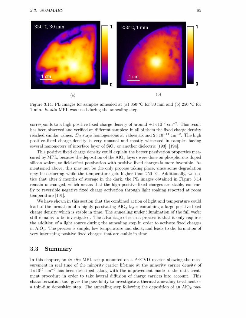
3.3. SUMMARY 85
(a) (b)
Figure 3.14: PL Images for samples annealed at (a) 350 °C for 30 min and (b) 250 °C for1 min. In situ MPL was used during the annealing step.
corresponds to a high positive fixed charge density of around +1×1012 cm−2. This resulthas been observed and verified on different samples: in all of them the fixed charge densityreached similar values. Dit stays homogeneous at values around 2×10⁻¹¹ cm−2. The highpositive fixed charge density is very unusual and mostly witnessed in samples havingseveral nanometers of interface layer of SiOx or another dielectric [193], [194].
This positive fixed charge density could explain the better passivation properties mea-sured by MPL, because the deposition of the AlOx layers were done on phosphorous dopedsilicon wafers, so field-effect passivation with positive fixed charges is more favorable. Asmentioned above, this may not be the only process taking place, since some degradationmay be occurring while the temperature gets higher than 250 °C. Additionally, we no-tice that after 2 months of storage in the dark, the PL images obtained in Figure 3.14remain unchanged, which means that the high positive fixed charges are stable, contrar-ily to reversible negative fixed charge activation through light soaking reported at roomtemperature [191].
We have shown in this section that the combined action of light and temperature couldlead to the formation of a highly passivating AlOx layer containing a large positive fixedcharge density which is stable in time. The annealing under illumination of the full waferstill remains to be investigated. The advantage of such a process is that it only requiresthe addition of a light source during the annealing step in order to activate fixed chargesin AlOx. The process is simple, low temperature and short, and leads to the formation ofvery interesting positive fixed charges that are stable in time.
3.3 Summary
In this chapter, an in situ MPL setup mounted on a PECVD reactor allowing the mea-surement in real time of the minority carrier lifetime at the minority carrier density of1×1015 cm−3 has been described, along with the improvement made to the data treat-ment procedure in order to take lateral diffusion of charge carriers into account. Thischaracterization tool gives the possibility to investigate a thermal annealing treatment ora thin-film deposition step. The annealing step following the deposition of an AlOx pas-
86 CHAPTER 3. IN SITU MODULATED PHOTOLUMINESCENCE FOR ALOX
(a)
-20 -10 0 10 20-20
-10
0
10
20
Y[mm]
X[mm]
-4.0x10
11-2.1x10
11-1.3x10
101.8x10
113.8x10
115.7x
1011
7.6x10
119.6x10
111.1x
1012L
(b)
Figure 3.15: (a) PL Images and (b) fixed charge density map for a sample annealed at250°C for 1 min. In situ MPL was used during the annealing step.
sivation layer was studied. The experiments carried out evidenced the rich kinetics of thepassivation during the annealing. A large drop of lifetime is observed when the AlOx passi-vated sample reaches a temperature greater than 250 °C. This spurred the investigation ofa faster annealing step at lower temperature (1 min at 250 °C instead of 30 min at 350 °C).Such a thermal profile allowed to achieve an effective lifetime of 5 ms, but only locally,on the area where the laser used for the MPL measurement was shining the sample. Thecombined action of light and temperature was shown to activate a high density of fixedcharges, which were both positive and stable. This could lead to an additional interestin the use of AlOx for passivating both n-type and p-type semiconductors. This studyshows that annealing under illumination provides a simple and fast way to get positivelycharged AlOx layers. As a perspective, it would be interesting to add a light source toshine the whole sample during the thermal annealing. This could allow more thoroughinvestigations on this state of the alumina layer.
This chapter shows the advantage of using in situ MPL in order to highlight specificmechanisms during some process steps. However, in the process flow for FPC fabricationstudied in this thesis, we do not focus on AlOx deposited by ALD. Consequently, in thefollowing chapters, we focus on using this newly developed in situ MPL technique for theoptimization of the FPC fabrication processes.
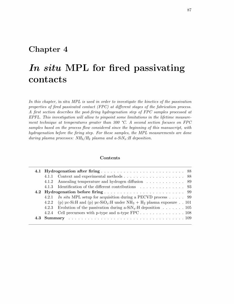
87
Chapter 4
In situ MPL for fired passivatingcontacts
In this chapter, in situ MPL is used in order to investigate the kinetics of the passivationproperties of fired passivated contact (FPC) at different stages of the fabrication process.A first section describes the post-firing hydrogenation step of FPC samples processed atEPFL. This investigation will allow to pinpoint some limitations in the lifetime measure-ment technique at temperatures greater than 300 °C. A second section focuses on FPCsamples based on the process flow considered since the beginning of this manuscript, withhydrogenation before the firing step. For these samples, the MPL measurements are doneduring plasma processes: NH3/H2 plasma and a-SiNx:H deposition.
Contents
4.1 Hydrogenation after firing . . . . . . . . . . . . . . . . . . . . . . . . . . 884.1.1 Context and experimental methods . . . . . . . . . . . . . . . . . . . 884.1.2 Annealing temperature and hydrogen diffusion . . . . . . . . . . . . 894.1.3 Identification of the different contributions . . . . . . . . . . . . . . 93
4.2 Hydrogenation before firing . . . . . . . . . . . . . . . . . . . . . . . . . 994.2.1 In situ MPL setup for acquisition during a PECVD process . . . . . 994.2.2 (p) µc-Si:H and (p) µc-SiOx:H under NH3 + H2 plasma exposure . . 1014.2.3 Evolution of the passivation during a-SiNx:H deposition . . . . . . . 1054.2.4 Cell precursors with p-type and n-type FPC . . . . . . . . . . . . . . 108
4.3 Summary . . . . . . . . . . . . . . . . . . . . . . . . . . . . . . . . . . . . 109
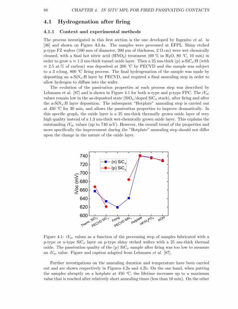
88 CHAPTER 4. IN SITU MPL FOR FIRED PASSIVATING CONTACTS
4.1 Hydrogenation after firing
4.1.1 Context and experimental methods
The process investigated in this first section is the one developed by Ingenito et al. in[46] and shown on Figure A3.4a. The samples were processed at EFPL. Shiny etchedp-type FZ wafers (100 mm of diameter, 200 µm of thickness, 2 Ω.cm) were wet chemicallycleaned, with a final hot nitric acid (HNO3) treatment (69 % in H2O, 80 °C, 10 min) inorder to grow a ≈ 1.3 nm-thick tunnel oxide layer. Then a 25 nm-thick (p) a-SiCx:H (with≈ 2.5 at.% of carbon) was deposited at 200 °C by PECVD and the sample was subjectto a 3 s-long, 800 °C firing process. The final hydrogenation of the sample was made bydepositing an a-SiNx:H layer by PECVD, and required a final annealing step in order toallow hydrogen to diffuse into the wafer.
The evolution of the passivation properties at each process step was described byLehmann et al. [87] and is shown in Figure 4.1 for both n-type and p-type FPC. The iVocvalues remain low in the as-deposited state (SiOx/doped SiCx stack), after firing and afterthe a-SiNx:H layer deposition. The subsequent “Hotplate” annealing step is carried outat 450 °C for 30 min, and allows the passivation properties to improve dramatically. Inthis specific graph, the oxide layer is a 25 nm-thick thermally grown oxide layer of veryhigh quality instead of a 1.3 nm-thick wet-chemically grown oxide layer. This explains theoutstanding iVoc values (up to 740 mV). However, the overall trend of the properties andmore specifically the improvement during the ”Hotplate” annealing step should not differupon the change in the nature of the oxide layer.
Therm. SiO 2
PECVD SiC xFiring
PECVD SiN x
Hotplate
HF/H 3PO 4 KOH600
620
640
660
680
700
720
740
iVoc
(mV)
(n) SiCx
(p) SiCx
Figure 4.1: iVoc values as a function of the processing step of samples fabricated with ap-type or n-type SiCx layer on p-type shiny etched wafers with a 25 nm-thick thermaloxide. The passivation quality of the (p) SiCx sample after firing was too low to measurean iVoc value. Figure and caption adapted from Lehmann et al. [87].
Further investigations on the annealing duration and temperature have been carriedout and are shown respectively in Figures 4.2a and 4.2b. On the one hand, when puttingthe samples abruptly on a hotplate at 450 °C, the lifetime increases up to a maximumvalue that is reached after relatively short annealing times (less than 10 min). On the other
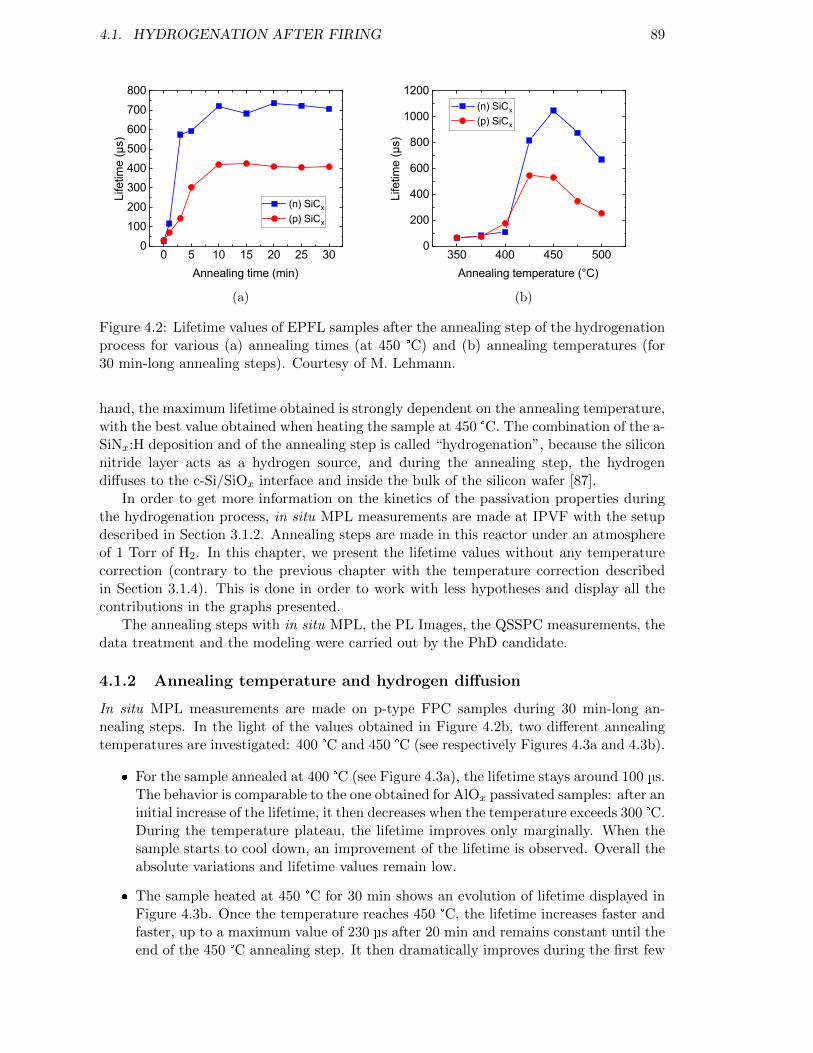
4.1. HYDROGENATION AFTER FIRING 89
0 5 10 15 20 25 300
100200300400500600700800
Life
time
(µs)
Annealing time (min)
(n) SiCx
(p) SiCx
(a)
350 400 450 5000
200
400
600
800
1000
1200
Life
time
(µs)
Annealing temperature (°C)
(n) SiCx
(p) SiCx
(b)
Figure 4.2: Lifetime values of EPFL samples after the annealing step of the hydrogenationprocess for various (a) annealing times (at 450 °C) and (b) annealing temperatures (for30 min-long annealing steps). Courtesy of M. Lehmann.
hand, the maximum lifetime obtained is strongly dependent on the annealing temperature,with the best value obtained when heating the sample at 450 °C. The combination of the a-SiNx:H deposition and of the annealing step is called “hydrogenation”, because the siliconnitride layer acts as a hydrogen source, and during the annealing step, the hydrogendiffuses to the c-Si/SiOx interface and inside the bulk of the silicon wafer [87].
In order to get more information on the kinetics of the passivation properties duringthe hydrogenation process, in situ MPL measurements are made at IPVF with the setupdescribed in Section 3.1.2. Annealing steps are made in this reactor under an atmosphereof 1 Torr of H2. In this chapter, we present the lifetime values without any temperaturecorrection (contrary to the previous chapter with the temperature correction describedin Section 3.1.4). This is done in order to work with less hypotheses and display all thecontributions in the graphs presented.
The annealing steps with in situ MPL, the PL Images, the QSSPC measurements, thedata treatment and the modeling were carried out by the PhD candidate.
4.1.2 Annealing temperature and hydrogen diffusion
In situ MPL measurements are made on p-type FPC samples during 30 min-long an-nealing steps. In the light of the values obtained in Figure 4.2b, two different annealingtemperatures are investigated: 400 °C and 450 °C (see respectively Figures 4.3a and 4.3b).
For the sample annealed at 400 °C (see Figure 4.3a), the lifetime stays around 100 µs.The behavior is comparable to the one obtained for AlOx passivated samples: after aninitial increase of the lifetime, it then decreases when the temperature exceeds 300 °C.During the temperature plateau, the lifetime improves only marginally. When thesample starts to cool down, an improvement of the lifetime is observed. Overall theabsolute variations and lifetime values remain low.
The sample heated at 450 °C for 30 min shows an evolution of lifetime displayed inFigure 4.3b. Once the temperature reaches 450 °C, the lifetime increases faster andfaster, up to a maximum value of 230 µs after 20 min and remains constant until theend of the 450 °C annealing step. It then dramatically improves during the first few
90 CHAPTER 4. IN SITU MPL FOR FIRED PASSIVATING CONTACTS
0 2400 4800 7200 9600 12000
0 40 80 120 160 200
020406080
100120140160180200
Time (min)
Life
time
(µs)
Time (s)
Lifetime Temperature
0
100
200
300
400
500
Tem
pera
ture
(°C
)
(a)
0 2400 4800 7200 9600
0 40 80 120 160
0
200
400
600
800
1000
Time (min)
Life
time
(µs)
Time (s)
Lifetime Temperature
0
100
200
300
400
500
Tem
pera
ture
(°C
)
(b)
Figure 4.3: Evolution of the minority carrier lifetime of a p-type FPC sample made atEPFL measured in situ by MPL during an annealing at (a) 400 °C and (b) 450 °C for30 min. The black curves display the temperature profiles, the red dots are the lifetimevalues measured by MPL.
minutes of the cooling step. The final lifetime for this sample annealed at 450 °Cmeasured by QSSPC is 512 µs, and is similar to the results obtained by annealingthe samples on a hotplate at EPFL (≈ 500 µs).
The lifetime is very low in the as-deposited state (28 µs), slightly higher after theannealing at 400 °C (90 µs) and significantly improved after the annealing at 450 °C(512 µs). The difference in final lifetime between these two samples is consistent withthe observation of Figure 4.2b. For the second sample, the plateau of lifetime is reachedafter 20 min at 450 °C, which is later than the 10 min expected from the measurementsafter annealing on a hoptlate (see Figure 4.2a). This might be due to dynamic effectssince, in the in situ MPL experiment, the temperature rises relatively slowly (around30 °C/min) while the sample annealed at EPFL is directly put on a hotplate which isalready at 450 °C. The decreasing trend during the cooling step in both graphs is likelydue to evolutions of the lifetime with temperature (evolution of defects hole and electroncapture cross-sections [177], thermal phenomena ...), that were taken into account in the“temperature correction” in the previous chapter.
Photoluminescence images calibrated in lifetime are shown in Figure 4.4. The pas-sivation properties are relatively homogeneous in the samples annealed at 450 °C andin the as-deposited state. However, the sample annealed at 400 °C for 30 min shows aring-shaped distribution of the minority carrier lifetime. Grant et al. [195] also observedsuch a ring-shape in FZ wafers, with defects related to vacancies appearing in the cen-ter of the sample upon rapid thermal annealing at temperatures ranging from 450 °C to700 °C. These defects were shown to be cured upon annealing at temperatures higherthan 1000 °C. Hiller et al. [196] showed that one type of defect causing the low values oflifetime is a silicon vacancy with a nitrogen atom in a substitutional position, called V1N1
center. These defects are characterized by the formation of a silicon dangling bond (dueto the fact that silicon atoms are tetravalent and nitrogen atoms are trivalent), that canbe passivated by hydrogenation at lower temperatures. The ring shape originates fromthe uneven distribution of point-defects during the growth of the silicon ingot [197] (largerdefect density in the center than on the edge), that are being stabilized through nitrogendoping during the float-zone process.
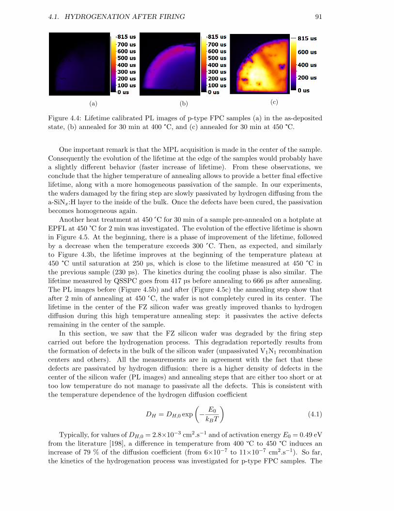
4.1. HYDROGENATION AFTER FIRING 91
(a) (b) (c)
Figure 4.4: Lifetime calibrated PL images of p-type FPC samples (a) in the as-depositedstate, (b) annealed for 30 min at 400 °C, and (c) annealed for 30 min at 450 °C.
One important remark is that the MPL acquisition is made in the center of the sample.Consequently the evolution of the lifetime at the edge of the samples would probably havea slightly different behavior (faster increase of lifetime). From these observations, weconclude that the higher temperature of annealing allows to provide a better final effectivelifetime, along with a more homogeneous passivation of the sample. In our experiments,the wafers damaged by the firing step are slowly passivated by hydrogen diffusing from thea-SiNx:H layer to the inside of the bulk. Once the defects have been cured, the passivationbecomes homogeneous again.
Another heat treatment at 450 °C for 30 min of a sample pre-annealed on a hotplate atEPFL at 450 °C for 2 min was investigated. The evolution of the effective lifetime is shownin Figure 4.5. At the beginning, there is a phase of improvement of the lifetime, followedby a decrease when the temperature exceeds 300 °C. Then, as expected, and similarlyto Figure 4.3b, the lifetime improves at the beginning of the temperature plateau at450 °C until saturation at 250 µs, which is close to the lifetime measured at 450 °C inthe previous sample (230 µs). The kinetics during the cooling phase is also similar. Thelifetime measured by QSSPC goes from 417 µs before annealing to 666 µs after annealing.The PL images before (Figure 4.5b) and after (Figure 4.5c) the annealing step show thatafter 2 min of annealing at 450 °C, the wafer is not completely cured in its center. Thelifetime in the center of the FZ silicon wafer was greatly improved thanks to hydrogendiffusion during this high temperature annealing step: it passivates the active defectsremaining in the center of the sample.
In this section, we saw that the FZ silicon wafer was degraded by the firing stepcarried out before the hydrogenation process. This degradation reportedly results fromthe formation of defects in the bulk of the silicon wafer (unpassivated V1N1 recombinationcenters and others). All the measurements are in agreement with the fact that thesedefects are passivated by hydrogen diffusion: there is a higher density of defects in thecenter of the silicon wafer (PL images) and annealing steps that are either too short or attoo low temperature do not manage to passivate all the defects. This is consistent withthe temperature dependence of the hydrogen diffusion coefficient
DH = DH,0 exp
(− E0
kBT
)(4.1)
Typically, for values of DH,0 = 2.8×10⁻³ cm2.s−1 and of activation energy E0 = 0.49 eVfrom the literature [198], a difference in temperature from 400 °C to 450 °C induces anincrease of 79 % of the diffusion coefficient (from 6×10⁻⁷ to 11×10−7 cm2.s−1). So far,the kinetics of the hydrogenation process was investigated for p-type FPC samples. The
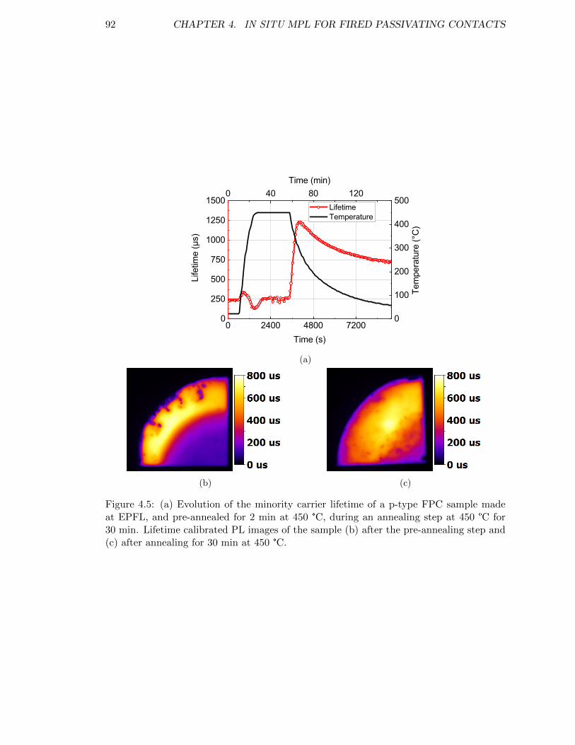
92 CHAPTER 4. IN SITU MPL FOR FIRED PASSIVATING CONTACTS
0 2400 4800 7200
0 40 80 120
0
250
500
750
1000
1250
1500
Time (min)Li
fetim
e (µ
s)
Time (s)
Lifetime Temperature
0
100
200
300
400
500
Tem
pera
ture
(°C
)
(a)
(b) (c)
Figure 4.5: (a) Evolution of the minority carrier lifetime of a p-type FPC sample madeat EPFL, and pre-annealed for 2 min at 450 °C, during an annealing step at 450 °C for30 min. Lifetime calibrated PL images of the sample (b) after the pre-annealing step and(c) after annealing for 30 min at 450 °C.
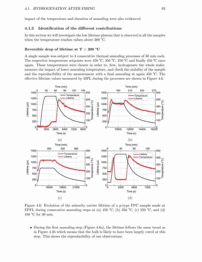
4.1. HYDROGENATION AFTER FIRING 93
impact of the temperature and duration of annealing were also evidenced.
4.1.3 Identification of the different contributions
In this section we will investigate the low lifetime plateau that is observed in all the sampleswhen the temperature reaches values above 300 °C.
Reversible drop of lifetime at T > 300 °C
A single sample was subject to 4 consecutive thermal annealing processes of 30 min each.The respective temperature setpoints were 450 °C, 350 °C, 250 °C and finally 450 °C onceagain. These temperatures were chosen in order to, first, hydrogenate the whole wafer,measure the impact of lower annealing temperature, and check the stability of the sampleand the reproducibility of the measurement with a final annealing at again 450 °C. Theeffective lifetime values measured by MPL during the processes are shown in Figure 4.6.
0 1800 3600 5400 7200 9000
0 30 60 90 120 150
0
250
500
750
1000
1250
1500
Time (min)
Life
time
(µs)
Time (s)
Temperature Lifetime
0
100
200
300
400
500Te
mpe
ratu
re (°
C)
(a)
10800 12600 14400 16200
180 210 240 270
0
250
500
750
1000
1250
1500
Time (min)
Life
time
(µs)
Time (s)
Temperature Lifetime
0
100
200
300
400
500
Tem
pera
ture
(°C
)
(b)
18000 19800 21600
300 330 360
0
250
500
750
1000
1250
1500
Time (min)
Life
time
(µs)
Time (s)
Temperature Lifetime
0
100
200
300
400
500
Tem
pera
ture
(°C
)
(c)
0 2400 4800 7200
0 40 80 120
0
250
500
750
1000
1250
1500
Time (min)
Life
time
(µs)
Time (s)
Lifetime Temperature
0
100
200
300
400
500
Tem
pera
ture
(°C
)
(d)
Figure 4.6: Evolution of the minority carrier lifetime of a p-type FPC sample made atEPFL during consecutive annealing steps at (a) 450 °C, (b) 350 °C, (c) 250 °C, and (d)450 °C for 30 min.
During the first annealing step (Figure 4.6a), the lifetime follows the same trend asin Figure 4.3b which means that the bulk is likely to have been largely cured at thisstep. This shows the reproducibility of our observations.
94 CHAPTER 4. IN SITU MPL FOR FIRED PASSIVATING CONTACTS
The lifetime during the subsequent step at 350 °C starts by increasing, and decreaseswhen the temperature exceeds 300 °C (see Figure 4.6b). It stays constant during thetemperature plateau.
In Figure 4.6c, the 250 °C annealing step, no decrease in the measured lifetime canbe observed. The lifetime simply follows the temperature profile.
The evolution of the effective lifetime during the last annealing step at 450 °C for30 min is shown in Figure 4.6d. First, the lifetime increases for temperatures goingup to 300 °C. When exceeding that temperature, the lifetime drops. It is thenfollowed by a quick recovery at the beginning of the cooling phase and then by adecrease in lifetime during the slow decrease of temperature (below 300 °C).
First, in all the samples of this chapter, the increase of lifetime at the beginning ofthe heating and the decrease during the cooling phase (at temperatures lower than 300°C) can be, once again, linked to thermal phenomena leading to a change in the minoritycarrier lifetime of the sample with temperature.
The lifetime measured by QSSPC on the sample before and after the last annealingstep (450 °C) stays fairly constant, going from 687 to 744 µs. The last annealing step henceonly resulted in a marginal change of the final passivation properties while the lifetimemeasured by MPL shows significant variations during the process. This is the case for thethree last annealing steps. As a consequence, the drop of lifetime at temperatures greaterthan 300 °C is a reversible phenomenon contrary to the bulk degradations evidencedin the studies mentioned above [195], [197], [199], [200]. Interestingly, when comparingthe annealing steps at 350 °C and 450 °C, one can see that the lifetime has a similarbehavior, but the values measured at 450 °C are significantly lower (250 µs) than the onesmeasured at 350 °C (1000 µs). One of the most plausible explanations for this observationis that, when the temperature increases, the amount of thermally generated electron-holepairs rises dramatically, which puts the sample in conditions where Auger and SRH aresignificantly increased and become limiting for the measurement of the effective minoritycarrier lifetime. This is shown in the following paragraphs.
The intrinsic minority carrier density ni as a function of temperature [201] is given bythe equation
ni(T ) = AT 3/2 exp
(−Eg(T )
2kT
)(4.2)
where A is a constant depending on the electron and hole effective masses (assumedindependent of temperature), T the temperature of the sample, k = 1.38×10⁻²³ J.K−1,and Eg the energy band gap which varies with temperature, following the equation
Eg(T ) = Eg(0 K)− αT 2
T + β(4.3)
with Eg(0 K) = 1.170 eV, α = 4.73×10⁻⁴ eV.K−1, and β = 636 K for silicon [202].Knowing that ni(300 K) = 1.08×1010 cm−3, the value of ni can be derived in all the rangeof temperatures investigated during the various processes. The function ni(T ) is shown inFigure 4.7a. For the temperature profile of an annealing at 450 °C for 30 min, the minoritycarrier density of an intrinsic semiconductor n = ∆n+ ni is plotted in Figure 4.7b (with∆n = 1×1015 cm−3 the photo-generated electron-hole pair density).
In order to get a better visualization of the impact of the higher minority carrier densitygenerated during the annealing process, we use the τeff (n) plot measured by QSSPC for
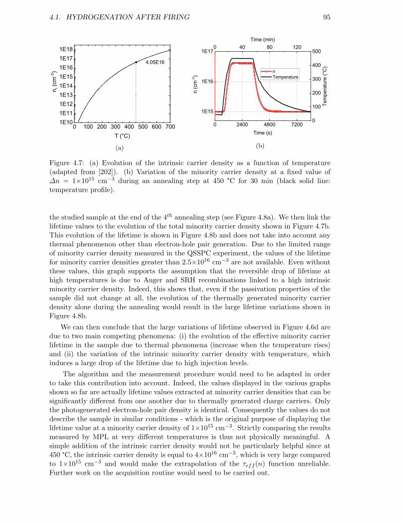
4.1. HYDROGENATION AFTER FIRING 95
0 100 200 300 400 500 600 7001E101E111E121E131E141E151E161E171E18
4.05E16n i
(cm
-3)
T (°C)
(a)
0 2400 4800 7200
0 40 80 120
1E15
1E16
1E17
Time (min)
n (c
m-3
)
Time (s)
n Temperature
0
100
200
300
400
500
Tem
pera
ture
(°C
)
(b)
Figure 4.7: (a) Evolution of the intrinsic carrier density as a function of temperature(adapted from [202]). (b) Variation of the minority carrier density at a fixed value of∆n = 1×1015 cm−3 during an annealing step at 450 °C for 30 min (black solid line:temperature profile).
the studied sample at the end of the 4th annealing step (see Figure 4.8a). We then link thelifetime values to the evolution of the total minority carrier density shown in Figure 4.7b.This evolution of the lifetime is shown in Figure 4.8b and does not take into account anythermal phenomenon other than electron-hole pair generation. Due to the limited rangeof minority carrier density measured in the QSSPC experiment, the values of the lifetimefor minority carrier densities greater than 2.5×1016 cm−3 are not available. Even withoutthese values, this graph supports the assumption that the reversible drop of lifetime athigh temperatures is due to Auger and SRH recombinations linked to a high intrinsicminority carrier density. Indeed, this shows that, even if the passivation properties of thesample did not change at all, the evolution of the thermally generated minority carrierdensity alone during the annealing would result in the large lifetime variations shown inFigure 4.8b.
We can then conclude that the large variations of lifetime observed in Figure 4.6d aredue to two main competing phenomena: (i) the evolution of the effective minority carrierlifetime in the sample due to thermal phenomena (increase when the temperature rises)and (ii) the variation of the intrinsic minority carrier density with temperature, whichinduces a large drop of the lifetime due to high injection levels.
The algorithm and the measurement procedure would need to be adapted in orderto take this contribution into account. Indeed, the values displayed in the various graphsshown so far are actually lifetime values extracted at minority carrier densities that can besignificantly different from one another due to thermally generated charge carriers. Onlythe photogenerated electron-hole pair density is identical. Consequently the values do notdescribe the sample in similar conditions - which is the original purpose of displaying thelifetime value at a minority carrier density of 1×1015 cm−3. Strictly comparing the resultsmeasured by MPL at very different temperatures is thus not physically meaningful. Asimple addition of the intrinsic carrier density would not be particularly helpful since at450 °C, the intrinsic carrier density is equal to 4×1016 cm−3, which is very large comparedto 1×1015 cm−3 and would make the extrapolation of the τeff (n) function unreliable.Further work on the acquisition routine would need to be carried out.
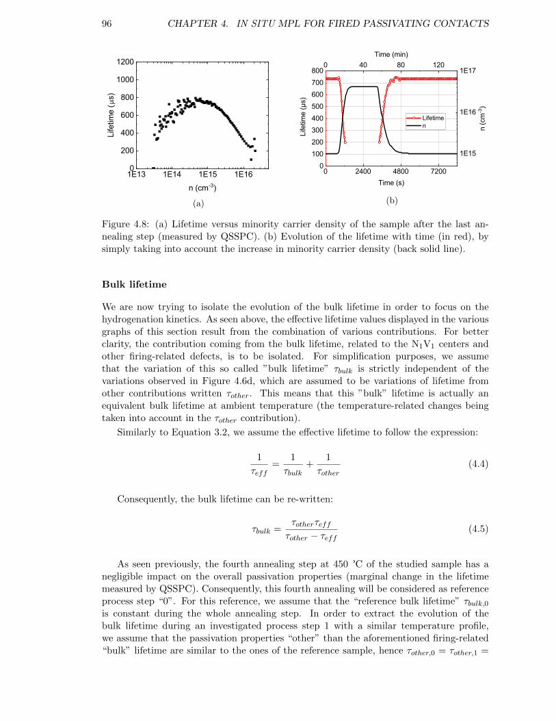
96 CHAPTER 4. IN SITU MPL FOR FIRED PASSIVATING CONTACTS
1E13 1E14 1E15 1E160
200
400
600
800
1000
1200
Life
time
(ms)
n (cm-3)
(a)
0 2400 4800 7200
0 40 80 120
0100200300400500600700800
Time (min)
Life
time
(µs)
Time (s)
Lifetime n
1E15
1E16
1E17
n (c
m-3
)
(b)
Figure 4.8: (a) Lifetime versus minority carrier density of the sample after the last an-nealing step (measured by QSSPC). (b) Evolution of the lifetime with time (in red), bysimply taking into account the increase in minority carrier density (back solid line).
Bulk lifetime
We are now trying to isolate the evolution of the bulk lifetime in order to focus on thehydrogenation kinetics. As seen above, the effective lifetime values displayed in the variousgraphs of this section result from the combination of various contributions. For betterclarity, the contribution coming from the bulk lifetime, related to the N1V1 centers andother firing-related defects, is to be isolated. For simplification purposes, we assumethat the variation of this so called ”bulk lifetime” τbulk is strictly independent of thevariations observed in Figure 4.6d, which are assumed to be variations of lifetime fromother contributions written τother. This means that this ”bulk” lifetime is actually anequivalent bulk lifetime at ambient temperature (the temperature-related changes beingtaken into account in the τother contribution).
Similarly to Equation 3.2, we assume the effective lifetime to follow the expression:
1
τeff=
1
τbulk+
1
τother(4.4)
Consequently, the bulk lifetime can be re-written:
τbulk =τotherτeffτother − τeff
(4.5)
As seen previously, the fourth annealing step at 450 °C of the studied sample has anegligible impact on the overall passivation properties (marginal change in the lifetimemeasured by QSSPC). Consequently, this fourth annealing will be considered as referenceprocess step “0”. For this reference, we assume that the “reference bulk lifetime” τbulk,0is constant during the whole annealing step. In order to extract the evolution of thebulk lifetime during an investigated process step 1 with a similar temperature profile,we assume that the passivation properties “other” than the aforementioned firing-related“bulk” lifetime are similar to the ones of the reference sample, hence τother,0 = τother,1 =
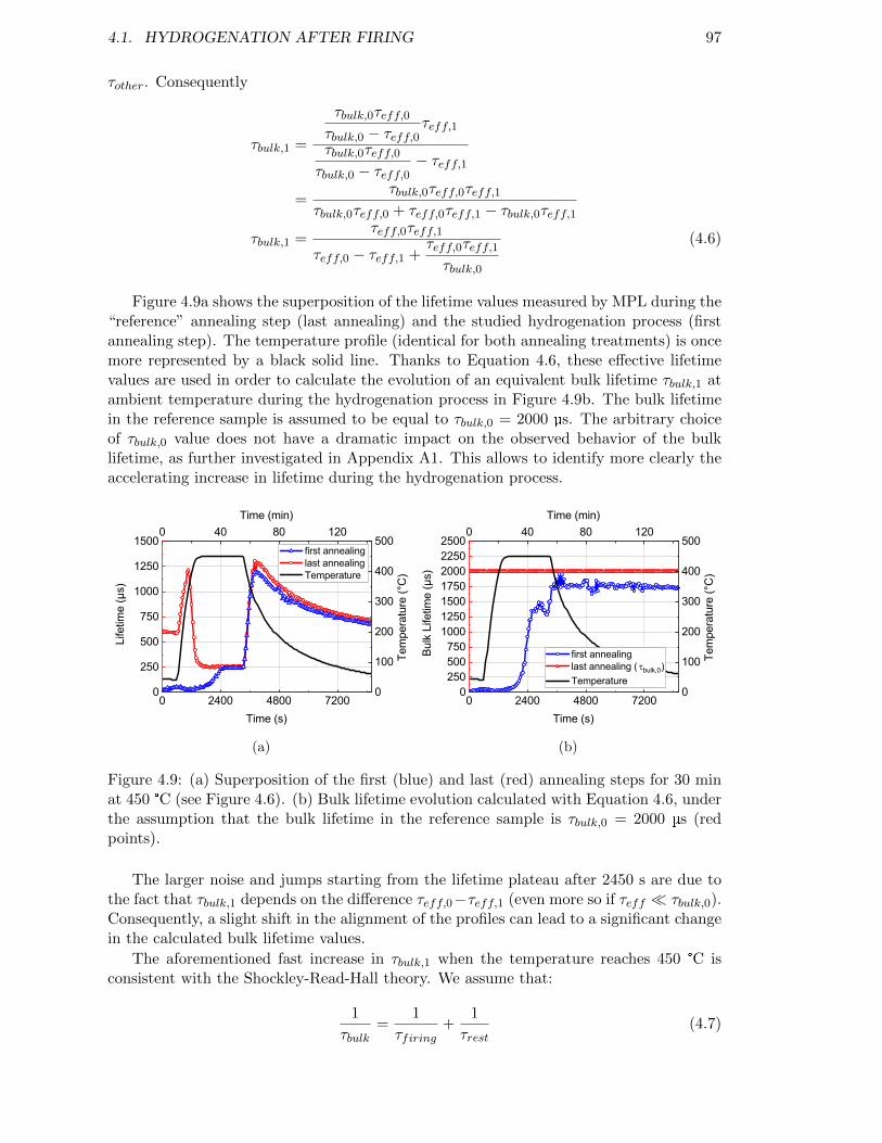
4.1. HYDROGENATION AFTER FIRING 97
τother. Consequently
τbulk,1 =
τbulk,0τeff,0τbulk,0 − τeff,0
τeff,1
τbulk,0τeff,0τbulk,0 − τeff,0
− τeff,1
=τbulk,0τeff,0τeff,1
τbulk,0τeff,0 + τeff,0τeff,1 − τbulk,0τeff,1τbulk,1 =
τeff,0τeff,1
τeff,0 − τeff,1 +τeff,0τeff,1τbulk,0
(4.6)
Figure 4.9a shows the superposition of the lifetime values measured by MPL during the“reference” annealing step (last annealing) and the studied hydrogenation process (firstannealing step). The temperature profile (identical for both annealing treatments) is oncemore represented by a black solid line. Thanks to Equation 4.6, these effective lifetimevalues are used in order to calculate the evolution of an equivalent bulk lifetime τbulk,1 atambient temperature during the hydrogenation process in Figure 4.9b. The bulk lifetimein the reference sample is assumed to be equal to τbulk,0 = 2000 µs. The arbitrary choiceof τbulk,0 value does not have a dramatic impact on the observed behavior of the bulklifetime, as further investigated in Appendix A1. This allows to identify more clearly theaccelerating increase in lifetime during the hydrogenation process.
0 2400 4800 7200
0 40 80 120
0
250
500
750
1000
1250
1500
Time (min)
Life
time
(µs)
Time (s)
first annealing last annealing Temperature
0
100
200
300
400
500
Tem
pera
ture
(°C
)
(a)
0 2400 4800 7200
0 40 80 120
0250500750
1000125015001750200022502500
Time (min)
Bulk
Life
time
(µs)
Time (s)
first annealing last annealing ( tbulk,0) Temperature
0
100
200
300
400
500
Tem
pera
ture
(°C
)
(b)
Figure 4.9: (a) Superposition of the first (blue) and last (red) annealing steps for 30 minat 450 °C (see Figure 4.6). (b) Bulk lifetime evolution calculated with Equation 4.6, underthe assumption that the bulk lifetime in the reference sample is τbulk,0 = 2000 µs (redpoints).
The larger noise and jumps starting from the lifetime plateau after 2450 s are due tothe fact that τbulk,1 depends on the difference τeff,0−τeff,1 (even more so if τeff τbulk,0).Consequently, a slight shift in the alignment of the profiles can lead to a significant changein the calculated bulk lifetime values.
The aforementioned fast increase in τbulk,1 when the temperature reaches 450 °C isconsistent with the Shockley-Read-Hall theory. We assume that:
1
τbulk=
1
τfiring+
1
τrest(4.7)
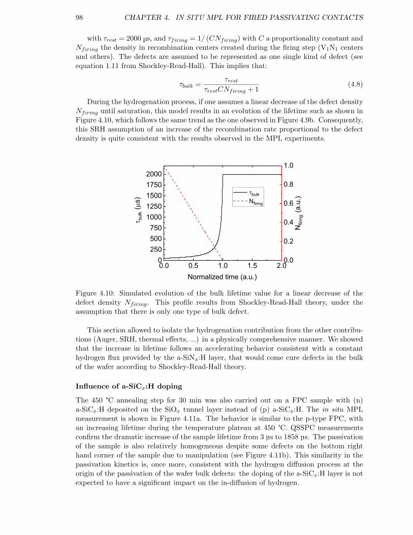
98 CHAPTER 4. IN SITU MPL FOR FIRED PASSIVATING CONTACTS
with τrest = 2000 µs, and τfiring = 1/ (CNfiring) with C a proportionality constant andNfiring the density in recombination centers created during the firing step (V1N1 centersand others). The defects are assumed to be represented as one single kind of defect (seeequation 1.11 from Shockley-Read-Hall). This implies that:
τbulk =τrest
τrestCNfiring + 1(4.8)
During the hydrogenation process, if one assumes a linear decrease of the defect densityNfiring until saturation, this model results in an evolution of the lifetime such as shown inFigure 4.10, which follows the same trend as the one observed in Figure 4.9b. Consequently,this SRH assumption of an increase of the recombination rate proportional to the defectdensity is quite consistent with the results observed in the MPL experiments.
0.0 0.5 1.0 1.5 2.00
250500750
10001250150017502000
tbulk
Nfiring
t bul
k (ms
)
Normalized time (a.u.)
0.0
0.2
0.4
0.6
0.8
1.0
Nfir
ing
(a.u
.)Figure 4.10: Simulated evolution of the bulk lifetime value for a linear decrease of thedefect density Nfiring. This profile results from Shockley-Read-Hall theory, under theassumption that there is only one type of bulk defect.
This section allowed to isolate the hydrogenation contribution from the other contribu-tions (Auger, SRH, thermal effects, ...) in a physically comprehensive manner. We showedthat the increase in lifetime follows an accelerating behavior consistent with a constanthydrogen flux provided by the a-SiNx:H layer, that would come cure defects in the bulkof the wafer according to Shockley-Read-Hall theory.
Influence of a-SiCx:H doping
The 450 °C annealing step for 30 min was also carried out on a FPC sample with (n)a-SiCx:H deposited on the SiOx tunnel layer instead of (p) a-SiCx:H. The in situ MPLmeasurement is shown in Figure 4.11a. The behavior is similar to the p-type FPC, withan increasing lifetime during the temperature plateau at 450 °C. QSSPC measurementsconfirm the dramatic increase of the sample lifetime from 3 µs to 1858 µs. The passivationof the sample is also relatively homogeneous despite some defects on the bottom righthand corner of the sample due to manipulation (see Figure 4.11b). This similarity in thepassivation kinetics is, once more, consistent with the hydrogen diffusion process at theorigin of the passivation of the wafer bulk defects: the doping of the a-SiCx:H layer is notexpected to have a significant impact on the in-diffusion of hydrogen.
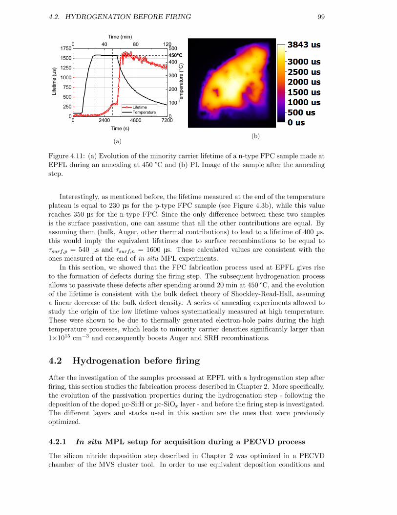
4.2. HYDROGENATION BEFORE FIRING 99
0 2400 4800 7200
0 40 80 120
0
250
500
750
1000
1250
1500
1750
Time (min)
Life
time
(µs)
Time (s)
Lifetime Temperature
450°C
0
100
200
300
400
500
Tem
pera
ture
(°C
)
(a)(b)
Figure 4.11: (a) Evolution of the minority carrier lifetime of a n-type FPC sample made atEPFL during an annealing at 450 °C and (b) PL Image of the sample after the annealingstep.
Interestingly, as mentioned before, the lifetime measured at the end of the temperatureplateau is equal to 230 µs for the p-type FPC sample (see Figure 4.3b), while this valuereaches 350 µs for the n-type FPC. Since the only difference between these two samplesis the surface passivation, one can assume that all the other contributions are equal. Byassuming them (bulk, Auger, other thermal contributions) to lead to a lifetime of 400 µs,this would imply the equivalent lifetimes due to surface recombinations to be equal toτsurf,p = 540 µs and τsurf,n = 1600 µs. These calculated values are consistent with theones measured at the end of in situ MPL experiments.
In this section, we showed that the FPC fabrication process used at EPFL gives riseto the formation of defects during the firing step. The subsequent hydrogenation processallows to passivate these defects after spending around 20 min at 450 °C, and the evolutionof the lifetime is consistent with the bulk defect theory of Shockley-Read-Hall, assuminga linear decrease of the bulk defect density. A series of annealing experiments allowed tostudy the origin of the low lifetime values systematically measured at high temperature.These were shown to be due to thermally generated electron-hole pairs during the hightemperature processes, which leads to minority carrier densities significantly larger than1×1015 cm−3 and consequently boosts Auger and SRH recombinations.
4.2 Hydrogenation before firing
After the investigation of the samples processed at EPFL with a hydrogenation step afterfiring, this section studies the fabrication process described in Chapter 2. More specifically,the evolution of the passivation properties during the hydrogenation step - following thedeposition of the doped µc-Si:H or µc-SiOx layer - and before the firing step is investigated.The different layers and stacks used in this section are the ones that were previouslyoptimized.
4.2.1 In situ MPL setup for acquisition during a PECVD process
The silicon nitride deposition step described in Chapter 2 was optimized in a PECVDchamber of the MVS cluster tool. In order to use equivalent deposition conditions and
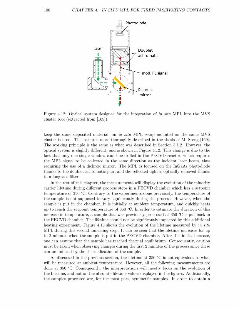
100 CHAPTER 4. IN SITU MPL FOR FIRED PASSIVATING CONTACTS
Figure 4.12: Optical system designed for the integration of in situ MPL into the MVScluster tool (extracted from [169]).
keep the same deposited material, an in situ MPL setup mounted on the same MVScluster is used. This setup is more thoroughly described in the thesis of M. Sreng [169].The working principle is the same as what was described in Section 3.1.2. However, theoptical system is slightly different, and is shown in Figure 4.12. This change is due to thefact that only one single window could be drilled in the PECVD reactor, which requiresthe MPL signal to be collected in the same direction as the incident laser beam, thusrequiring the use of a dichroic mirror. The MPL is focused on the InGaAs photodiodethanks to the doublet achromatic pair, and the reflected light is optically removed thanksto a longpass filter.
In the rest of this chapter, the measurements will display the evolution of the minoritycarrier lifetime during different process steps in a PECVD chamber which has a setpointtemperature of 350 °C. Contrary to the experiments done previously, the temperature ofthe sample is not supposed to vary significantly during the process. However, when thesample is put in the chamber, it is initially at ambient temperature, and quickly heatsup to reach the setpoint temperature of 350 °C. In order to estimate the duration of thisincrease in temperature, a sample that was previously processed at 350 °C is put back inthe PECVD chamber. The lifetime should not be significantly impacted by this additionalheating experiment. Figure 4.13 shows the evolution of the lifetime measured by in situMPL during this second annealing step. It can be seen that the lifetime increases for upto 2 minutes when the sample is put in the PECVD chamber. After this initial increase,one can assume that the sample has reached thermal equilibrium. Consequently, cautionmust be taken when observing changes during the first 2 minutes of the process since thesecan be induced by the thermalization of the sample.
As discussed in the previous section, the lifetime at 350 °C is not equivalent to whatwill be measured at ambient temperature. However, all the following measurements aredone at 350 °C. Consequently, the interpretations will mostly focus on the evolution ofthe lifetime, and not on the absolute lifetime values displayed in the figures. Additionally,the samples processed are, for the most part, symmetric samples. In order to obtain a
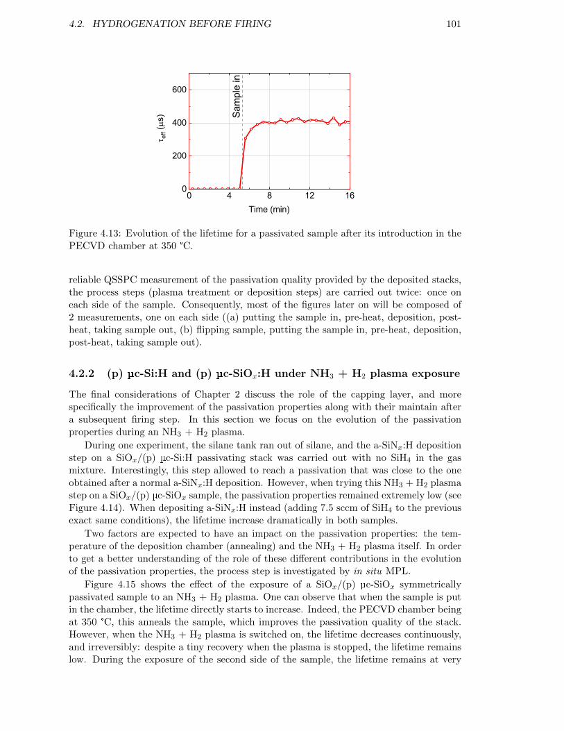
4.2. HYDROGENATION BEFORE FIRING 101
0 4 8 12 160
200
400
600
t eff (ms
)
Time (min)
Sam
ple
inFigure 4.13: Evolution of the lifetime for a passivated sample after its introduction in thePECVD chamber at 350 °C.
reliable QSSPC measurement of the passivation quality provided by the deposited stacks,the process steps (plasma treatment or deposition steps) are carried out twice: once oneach side of the sample. Consequently, most of the figures later on will be composed of2 measurements, one on each side ((a) putting the sample in, pre-heat, deposition, post-heat, taking sample out, (b) flipping sample, putting the sample in, pre-heat, deposition,post-heat, taking sample out).
4.2.2 (p) µc-Si:H and (p) µc-SiOx:H under NH3 + H2 plasma exposure
The final considerations of Chapter 2 discuss the role of the capping layer, and morespecifically the improvement of the passivation properties along with their maintain aftera subsequent firing step. In this section we focus on the evolution of the passivationproperties during an NH3 + H2 plasma.
During one experiment, the silane tank ran out of silane, and the a-SiNx:H depositionstep on a SiOx/(p) µc-Si:H passivating stack was carried out with no SiH4 in the gasmixture. Interestingly, this step allowed to reach a passivation that was close to the oneobtained after a normal a-SiNx:H deposition. However, when trying this NH3 + H2 plasmastep on a SiOx/(p) µc-SiOx sample, the passivation properties remained extremely low (seeFigure 4.14). When depositing a-SiNx:H instead (adding 7.5 sccm of SiH4 to the previousexact same conditions), the lifetime increase dramatically in both samples.
Two factors are expected to have an impact on the passivation properties: the tem-perature of the deposition chamber (annealing) and the NH3 + H2 plasma itself. In orderto get a better understanding of the role of these different contributions in the evolutionof the passivation properties, the process step is investigated by in situ MPL.
Figure 4.15 shows the effect of the exposure of a SiOx/(p) µc-SiOx symmetricallypassivated sample to an NH3 + H2 plasma. One can observe that when the sample is putin the chamber, the lifetime directly starts to increase. Indeed, the PECVD chamber beingat 350 °C, this anneals the sample, which improves the passivation quality of the stack.However, when the NH3 + H2 plasma is switched on, the lifetime decreases continuously,and irreversibly: despite a tiny recovery when the plasma is stopped, the lifetime remainslow. During the exposure of the second side of the sample, the lifetime remains at very
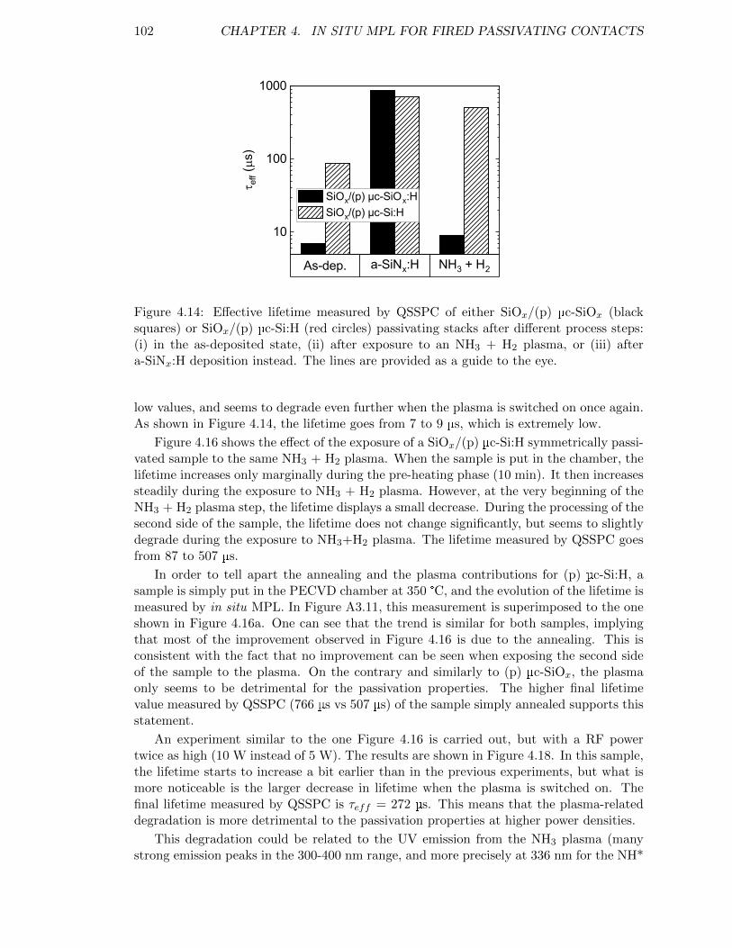
102 CHAPTER 4. IN SITU MPL FOR FIRED PASSIVATING CONTACTS
As-dep. a-SiNx:H NH3 + H2
10
100
1000
t eff (ms
)
SiOx/(p) µc-SiOx:H SiOx/(p) µc-Si:H
Figure 4.14: Effective lifetime measured by QSSPC of either SiOx/(p) µc-SiOx (blacksquares) or SiOx/(p) µc-Si:H (red circles) passivating stacks after different process steps:(i) in the as-deposited state, (ii) after exposure to an NH3 + H2 plasma, or (iii) aftera-SiNx:H deposition instead. The lines are provided as a guide to the eye.
low values, and seems to degrade even further when the plasma is switched on once again.As shown in Figure 4.14, the lifetime goes from 7 to 9 µs, which is extremely low.
Figure 4.16 shows the effect of the exposure of a SiOx/(p) µc-Si:H symmetrically passi-vated sample to the same NH3 + H2 plasma. When the sample is put in the chamber, thelifetime increases only marginally during the pre-heating phase (10 min). It then increasessteadily during the exposure to NH3 + H2 plasma. However, at the very beginning of theNH3 + H2 plasma step, the lifetime displays a small decrease. During the processing of thesecond side of the sample, the lifetime does not change significantly, but seems to slightlydegrade during the exposure to NH3+H2 plasma. The lifetime measured by QSSPC goesfrom 87 to 507 µs.
In order to tell apart the annealing and the plasma contributions for (p) µc-Si:H, asample is simply put in the PECVD chamber at 350 °C, and the evolution of the lifetime ismeasured by in situ MPL. In Figure A3.11, this measurement is superimposed to the oneshown in Figure 4.16a. One can see that the trend is similar for both samples, implyingthat most of the improvement observed in Figure 4.16 is due to the annealing. This isconsistent with the fact that no improvement can be seen when exposing the second sideof the sample to the plasma. On the contrary and similarly to (p) µc-SiOx, the plasmaonly seems to be detrimental for the passivation properties. The higher final lifetimevalue measured by QSSPC (766 µs vs 507 µs) of the sample simply annealed supports thisstatement.
An experiment similar to the one Figure 4.16 is carried out, but with a RF powertwice as high (10 W instead of 5 W). The results are shown in Figure 4.18. In this sample,the lifetime starts to increase a bit earlier than in the previous experiments, but what ismore noticeable is the larger decrease in lifetime when the plasma is switched on. Thefinal lifetime measured by QSSPC is τeff = 272 µs. This means that the plasma-relateddegradation is more detrimental to the passivation properties at higher power densities.
This degradation could be related to the UV emission from the NH3 plasma (manystrong emission peaks in the 300-400 nm range, and more precisely at 336 nm for the NH*
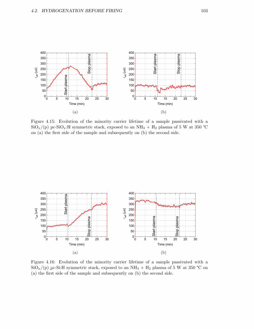
4.2. HYDROGENATION BEFORE FIRING 103
0 5 10 15 20 25 300
50100150200250300350400
t eff (ms
)
Time (min)
Star
t pla
sma
Stop
pla
sma
(a)
0 5 10 15 20 25 300
50100150200250300350400
t eff (ms
)
Time (min)
Stop
pla
sma
Star
t pla
sma
(b)
Figure 4.15: Evolution of the minority carrier lifetime of a sample passivated with aSiOx/(p) µc-SiOx:H symmetric stack, exposed to an NH3 + H2 plasma of 5 W at 350 °Con (a) the first side of the sample and subsequently on (b) the second side.
0 5 10 15 20 25 300
50100150200250300350400
t eff (ms
)
Time (min)
Star
t pla
sma
Stop
pla
sma
(a)
0 5 10 15 20 25 300
50100150200250300350400
t eff (ms
)
Time (min)
Star
t pla
sma
Stop
pla
sma
(b)
Figure 4.16: Evolution of the minority carrier lifetime of a sample passivated with aSiOx/(p) µc-Si:H symmetric stack, exposed to an NH3 + H2 plasma of 5 W at 350 °C on(a) the first side of the sample and subsequently on (b) the second side.
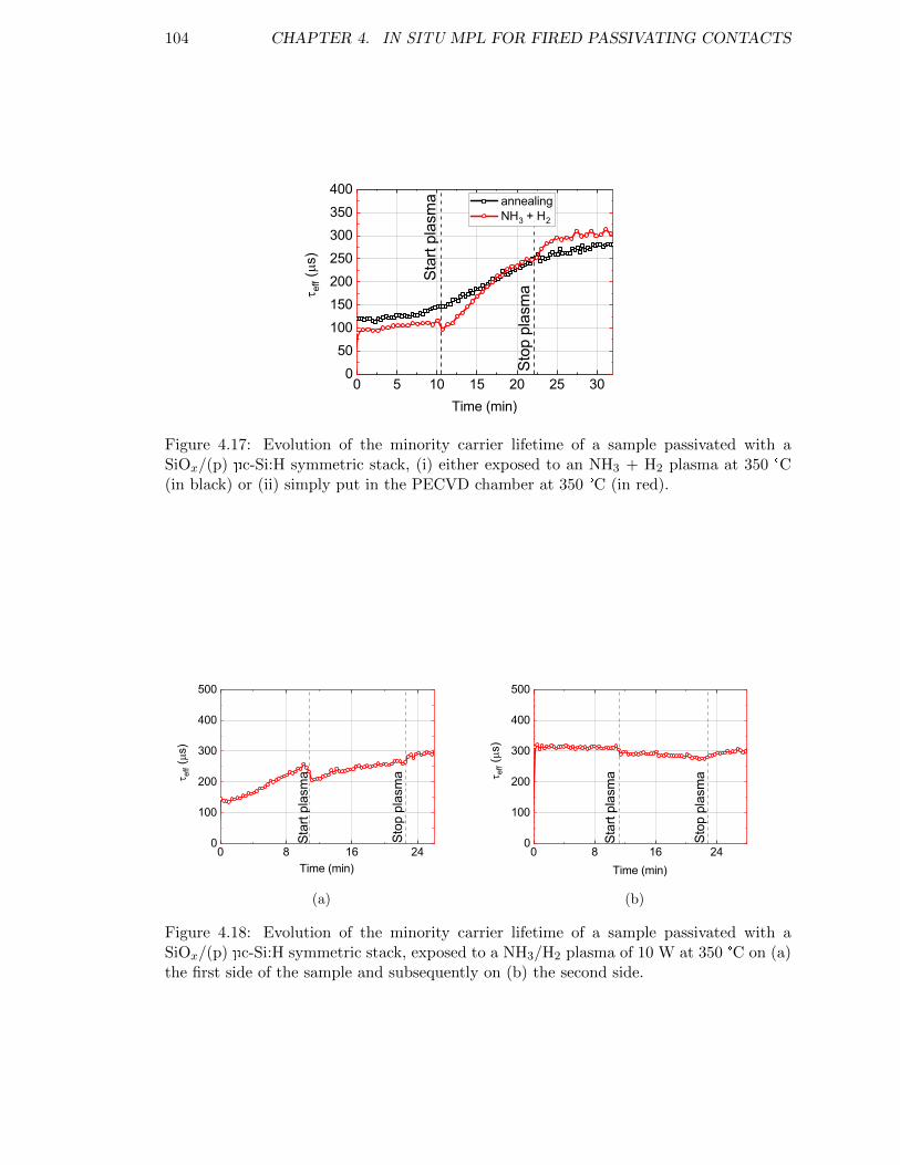
104 CHAPTER 4. IN SITU MPL FOR FIRED PASSIVATING CONTACTS
0 5 10 15 20 25 300
50100150200250300350400
annealing NH3 + H2
t eff (ms
)
Time (min)
Star
t pla
sma
Stop
pla
sma
Figure 4.17: Evolution of the minority carrier lifetime of a sample passivated with aSiOx/(p) µc-Si:H symmetric stack, (i) either exposed to an NH3 + H2 plasma at 350 °C(in black) or (ii) simply put in the PECVD chamber at 350 °C (in red).
0 8 16 240
100
200
300
400
500
t eff (ms
)
Time (min)
Star
t pla
sma
Stop
pla
sma
(a)
0 8 16 240
100
200
300
400
500
t eff (ms
)
Time (min)
Star
t pla
sma
Stop
pla
sma
(b)
Figure 4.18: Evolution of the minority carrier lifetime of a sample passivated with aSiOx/(p) µc-Si:H symmetric stack, exposed to a NH3/H2 plasma of 10 W at 350 °C on (a)the first side of the sample and subsequently on (b) the second side.
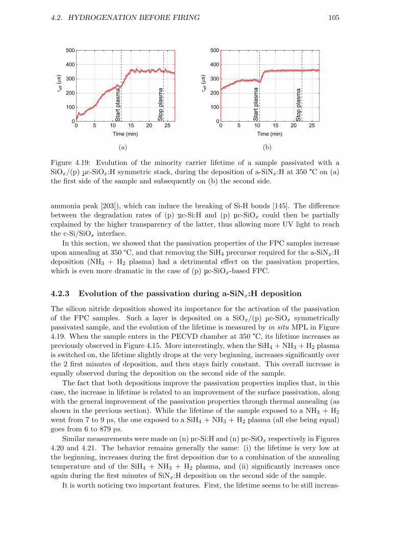
4.2. HYDROGENATION BEFORE FIRING 105
0 5 10 15 20 250
100
200
300
400
500t e
ff (ms
)
Time (min)
Star
t pla
sma
Stop
pla
sma
(a)
0 5 10 15 20 250
100
200
300
400
500
t eff (ms
)
Time (min)
Star
t pla
sma
Stop
pla
sma
(b)
Figure 4.19: Evolution of the minority carrier lifetime of a sample passivated with aSiOx/(p) µc-SiOx:H symmetric stack, during the deposition of a-SiNx:H at 350 °C on (a)the first side of the sample and subsequently on (b) the second side.
ammonia peak [203]), which can induce the breaking of Si-H bonds [145]. The differencebetween the degradation rates of (p) µc-Si:H and (p) µc-SiOx could then be partiallyexplained by the higher transparency of the latter, thus allowing more UV light to reachthe c-Si/SiOx interface.
In this section, we showed that the passivation properties of the FPC samples increaseupon annealing at 350 °C, and that removing the SiH4 precursor required for the a-SiNx:Hdeposition (NH3 + H2 plasma) had a detrimental effect on the passivation properties,which is even more dramatic in the case of (p) µc-SiOx-based FPC.
4.2.3 Evolution of the passivation during a-SiNx:H deposition
The silicon nitride deposition showed its importance for the activation of the passivationof the FPC samples. Such a layer is deposited on a SiOx/(p) µc-SiOx symmetricallypassivated sample, and the evolution of the lifetime is measured by in situ MPL in Figure4.19. When the sample enters in the PECVD chamber at 350 °C, its lifetime increases aspreviously observed in Figure 4.15. More interestingly, when the SiH4 + NH3 + H2 plasmais switched on, the lifetime slightly drops at the very beginning, increases significantly overthe 2 first minutes of deposition, and then stays fairly constant. This overall increase isequally observed during the deposition on the second side of the sample.
The fact that both depositions improve the passivation properties implies that, in thiscase, the increase in lifetime is related to an improvement of the surface passivation, alongwith the general improvement of the passivation properties through thermal annealing (asshown in the previous section). While the lifetime of the sample exposed to a NH3 + H2
went from 7 to 9 µs, the one exposed to a SiH4 + NH3 + H2 plasma (all else being equal)goes from 6 to 879 µs.
Similar measurements were made on (n) µc-Si:H and (n) µc-SiOx respectively in Figures4.20 and 4.21. The behavior remains generally the same: (i) the lifetime is very low atthe beginning, increases during the first deposition due to a combination of the annealingtemperature and of the SiH4 + NH3 + H2 plasma, and (ii) significantly increases onceagain during the first minutes of SiNx:H deposition on the second side of the sample.
It is worth noticing two important features. First, the lifetime seems to be still increas-
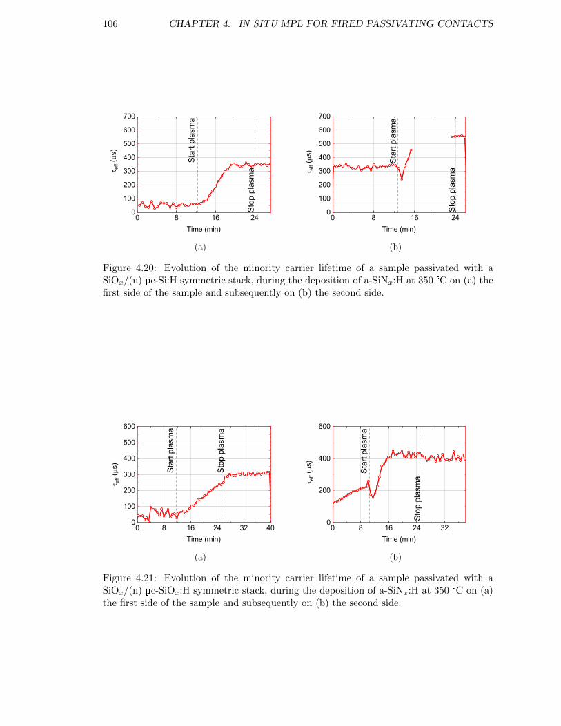
106 CHAPTER 4. IN SITU MPL FOR FIRED PASSIVATING CONTACTS
0 8 16 240
100
200
300
400
500
600
700t e
ff (ms
)
Time (min)
Star
t pla
sma
Stop
pla
sma
(a)
0 8 16 240
100
200
300
400
500
600
700
Stop
pla
sma
Star
t pla
sma
t eff (ms
)
Time (min)
(b)
Figure 4.20: Evolution of the minority carrier lifetime of a sample passivated with aSiOx/(n) µc-Si:H symmetric stack, during the deposition of a-SiNx:H at 350 °C on (a) thefirst side of the sample and subsequently on (b) the second side.
0 8 16 24 32 400
100
200
300
400
500
600
t eff (ms
)
Time (min)
Star
t pla
sma
Stop
pla
sma
(a)
0 8 16 24 320
200
400
600
t eff (ms
)
Time (min)
Star
t pla
sma
Stop
pla
sma
(b)
Figure 4.21: Evolution of the minority carrier lifetime of a sample passivated with aSiOx/(n) µc-SiOx:H symmetric stack, during the deposition of a-SiNx:H at 350 °C on (a)the first side of the sample and subsequently on (b) the second side.
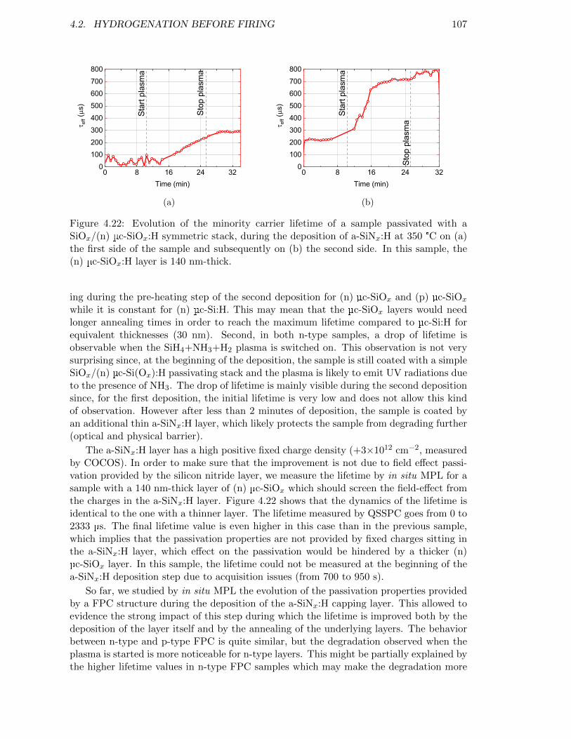
4.2. HYDROGENATION BEFORE FIRING 107
0 8 16 24 320
100200300400500600700800
t eff (ms
)
Time (min)
Star
t pla
sma
Stop
pla
sma
(a)
0 8 16 24 320
100200300400500600700800
t eff (ms
)
Time (min)
Star
t pla
sma
Stop
pla
sma
(b)
Figure 4.22: Evolution of the minority carrier lifetime of a sample passivated with aSiOx/(n) µc-SiOx:H symmetric stack, during the deposition of a-SiNx:H at 350 °C on (a)the first side of the sample and subsequently on (b) the second side. In this sample, the(n) µc-SiOx:H layer is 140 nm-thick.
ing during the pre-heating step of the second deposition for (n) µc-SiOx and (p) µc-SiOx
while it is constant for (n) µc-Si:H. This may mean that the µc-SiOx layers would needlonger annealing times in order to reach the maximum lifetime compared to µc-Si:H forequivalent thicknesses (30 nm). Second, in both n-type samples, a drop of lifetime isobservable when the SiH4+NH3+H2 plasma is switched on. This observation is not verysurprising since, at the beginning of the deposition, the sample is still coated with a simpleSiOx/(n) µc-Si(Ox):H passivating stack and the plasma is likely to emit UV radiations dueto the presence of NH3. The drop of lifetime is mainly visible during the second depositionsince, for the first deposition, the initial lifetime is very low and does not allow this kindof observation. However after less than 2 minutes of deposition, the sample is coated byan additional thin a-SiNx:H layer, which likely protects the sample from degrading further(optical and physical barrier).
The a-SiNx:H layer has a high positive fixed charge density (+3×1012 cm−2, measuredby COCOS). In order to make sure that the improvement is not due to field effect passi-vation provided by the silicon nitride layer, we measure the lifetime by in situ MPL for asample with a 140 nm-thick layer of (n) µc-SiOx which should screen the field-effect fromthe charges in the a-SiNx:H layer. Figure 4.22 shows that the dynamics of the lifetime isidentical to the one with a thinner layer. The lifetime measured by QSSPC goes from 0 to2333 µs. The final lifetime value is even higher in this case than in the previous sample,which implies that the passivation properties are not provided by fixed charges sitting inthe a-SiNx:H layer, which effect on the passivation would be hindered by a thicker (n)µc-SiOx layer. In this sample, the lifetime could not be measured at the beginning of thea-SiNx:H deposition step due to acquisition issues (from 700 to 950 s).
So far, we studied by in situ MPL the evolution of the passivation properties providedby a FPC structure during the deposition of the a-SiNx:H capping layer. This allowed toevidence the strong impact of this step during which the lifetime is improved both by thedeposition of the layer itself and by the annealing of the underlying layers. The behaviorbetween n-type and p-type FPC is quite similar, but the degradation observed when theplasma is started is more noticeable for n-type layers. This might be partially explained bythe higher lifetime values in n-type FPC samples which may make the degradation more
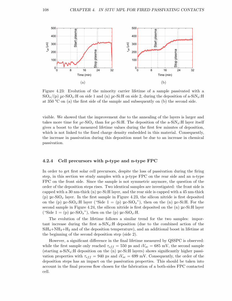
108 CHAPTER 4. IN SITU MPL FOR FIRED PASSIVATING CONTACTS
0 8 16 24 320
100
200
300
400
500
t eff (ms
)
Time (min)St
art p
lasm
a
Stop
pla
sma
(a)
0 8 16 24 320
100
200
300
400
500
t eff (ms
)
Time (min)
Star
t pla
sma
Stop
pla
sma
(b)
Figure 4.23: Evolution of the minority carrier lifetime of a sample passivated with aSiOx/(p) µc-SiOx:H on side 1 and (n) µc-Si:H on side 2, during the deposition of a-SiNx:Hat 350 °C on (a) the first side of the sample and subsequently on (b) the second side.
visible. We showed that the improvement due to the annealing of the layers is larger andtakes more time for µc-SiOx than for µc-Si:H. The deposition of the a-SiNx:H layer itselfgives a boost to the measured lifetime values during the first few minutes of deposition,which is not linked to the fixed charge density embedded in this material. Consequently,the increase in passivation during this deposition must be due to an increase in chemicalpassivation.
4.2.4 Cell precursors with p-type and n-type FPC
In order to get first solar cell precursors, despite the loss of passivation during the firingstep, in this section we study samples with a p-type FPC on the rear side and an n-typeFPC on the front side. Since the sample is not symmetric anymore, the question of theorder of the deposition steps rises. Two identical samples are investigated: the front side iscapped with a 30 nm-thick (n) µc-Si:H layer, and the rear side is capped with a 45 nm-thick(p) µc-SiOx layer. In the first sample in Figure 4.23, the silicon nitride is first depositedon the (p) µc-SiOx:H layer (“Side 1 = (p) µc-SiOx”), then on the (n) µc-Si:H. For thesecond sample in Figure 4.24, the silicon nitride is first deposited on the (n) µc-Si:H layer(“Side 1 = (p) µc-SiOx”), then on the (p) µc-SiOx:H.
The evolution of the lifetime follows a similar trend for the two samples: impor-tant increase during the first a-SiNx:H deposition (due to the combined action of theSiH4+NH3+H2 and of the deposition temperature), and an additional boost in lifetime atthe beginning of the second deposition step (side 2).
However, a significant difference in the final lifetime measured by QSSPC is observed:while the first sample only reached τeff = 550 µs and iVoc = 685 mV, the second sample(starting a-SiNx:H deposition on the (n) µc-Si:H layers) shows significantly higher passi-vation properties with τeff = 940 µs and iVoc = 699 mV. Consequently, the order of thedeposition steps has an impact on the passivation properties. This should be taken intoaccount in the final process flow chosen for the fabrication of a both-sides FPC contactedcell.
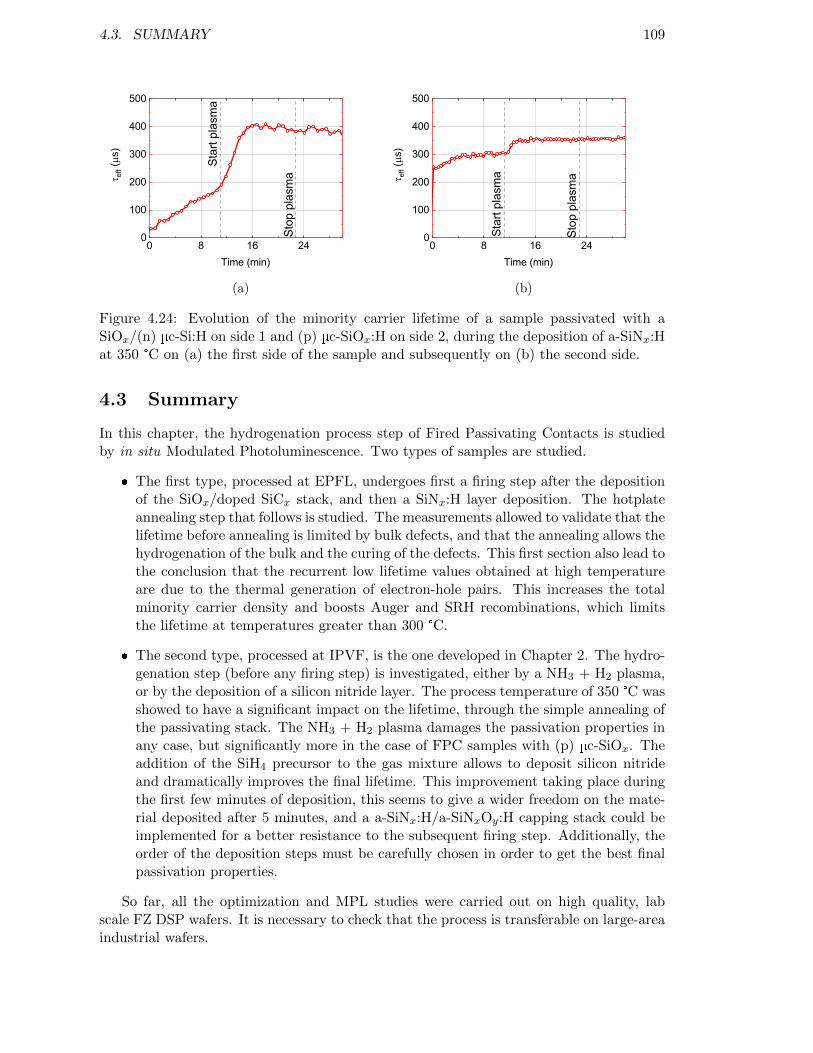
4.3. SUMMARY 109
0 8 16 240
100
200
300
400
500t e
ff (ms
)
Time (min)
Star
t pla
sma
Stop
pla
sma
(a)
0 8 16 240
100
200
300
400
500
t eff (ms
)
Time (min)
Star
t pla
sma
Stop
pla
sma
(b)
Figure 4.24: Evolution of the minority carrier lifetime of a sample passivated with aSiOx/(n) µc-Si:H on side 1 and (p) µc-SiOx:H on side 2, during the deposition of a-SiNx:Hat 350 °C on (a) the first side of the sample and subsequently on (b) the second side.
4.3 Summary
In this chapter, the hydrogenation process step of Fired Passivating Contacts is studiedby in situ Modulated Photoluminescence. Two types of samples are studied.
The first type, processed at EPFL, undergoes first a firing step after the depositionof the SiOx/doped SiCx stack, and then a SiNx:H layer deposition. The hotplateannealing step that follows is studied. The measurements allowed to validate that thelifetime before annealing is limited by bulk defects, and that the annealing allows thehydrogenation of the bulk and the curing of the defects. This first section also lead tothe conclusion that the recurrent low lifetime values obtained at high temperatureare due to the thermal generation of electron-hole pairs. This increases the totalminority carrier density and boosts Auger and SRH recombinations, which limitsthe lifetime at temperatures greater than 300 °C.
The second type, processed at IPVF, is the one developed in Chapter 2. The hydro-genation step (before any firing step) is investigated, either by a NH3 + H2 plasma,or by the deposition of a silicon nitride layer. The process temperature of 350 °C wasshowed to have a significant impact on the lifetime, through the simple annealing ofthe passivating stack. The NH3 + H2 plasma damages the passivation properties inany case, but significantly more in the case of FPC samples with (p) µc-SiOx. Theaddition of the SiH4 precursor to the gas mixture allows to deposit silicon nitrideand dramatically improves the final lifetime. This improvement taking place duringthe first few minutes of deposition, this seems to give a wider freedom on the mate-rial deposited after 5 minutes, and a a-SiNx:H/a-SiNxOy:H capping stack could beimplemented for a better resistance to the subsequent firing step. Additionally, theorder of the deposition steps must be carefully chosen in order to get the best finalpassivation properties.
So far, all the optimization and MPL studies were carried out on high quality, labscale FZ DSP wafers. It is necessary to check that the process is transferable on large-areaindustrial wafers.

110 CHAPTER 4. IN SITU MPL FOR FIRED PASSIVATING CONTACTS

111
Chapter 5
Towards large area FPC cells
In this chapter, the FPC solar cell upscale from the 50×50 mm2 FZ wafers to industrial156×156 mm2 Cz and cast-mono wafers is investigated. The integration of the previouslyoptimized passivating stack is deposited on both textured and polished surfaces. iVOC valuesup to 691 mV are achieved on cast-mono wafers, which is a very promising result. A firstattempt of a complete solar cell is finally made on a lab scale FZ wafer.
Contents
5.1 Process transfer on Cz and cast-mono wafers . . . . . . . . . . . . . 1125.1.1 Context and experimental methods . . . . . . . . . . . . . . . . . . . 1125.1.2 Textured wafers . . . . . . . . . . . . . . . . . . . . . . . . . . . . . 1125.1.3 Polished surfaces . . . . . . . . . . . . . . . . . . . . . . . . . . . . . 114
5.2 Solar cell fabrication . . . . . . . . . . . . . . . . . . . . . . . . . . . . . 1175.3 Summary . . . . . . . . . . . . . . . . . . . . . . . . . . . . . . . . . . . . 118
112 CHAPTER 5. TOWARDS LARGE AREA FPC CELLS
5.1 Process transfer on Cz and cast-mono wafers
5.1.1 Context and experimental methods
Standard solar cells are made from industrial silicon wafers which areas are larger than labscale samples. Nowadays, standard wafers have an area of 156×156 mm2 and are namedM2 wafers. The size of industrial wafers tends to increase and M6 wafers (166×166 mm2)or greater - up to G12+ (217×217 mm2) - are expected to account for more than 50 %of the market shares by 2027 according to the projections of the International TechnologyRoadmap for Photovoltaics [204]. However, such large wafers require the adaptation ofsome processing tools which are currently designed for M2 wafers.
In this thesis, M2 wafers were used due to their current availability and the dimensionsof the deposition tools. Two kinds of silicon bulks were used: Cz and cast-mono siliconcrystals. The Cz crystals were bought from a supplier under the form of silicon ingots. Thecast-mono ingots were grown at Photowatt in G5 furnaces by ECM Greentech. Thesetwo kinds of silicon ingots underwent the same process steps in order to end up withtextured silicon wafers: diamond sawing, saw-damage removal (SDR) and texturization(in a chemical bath of KOH and additives). The final M2 wafers obtained have texturedsurfaces with a random-pyramid pattern. They are 170 µm thick and have a resistivityaround 1.6 Ω.cm for cast-mono wafers and 2.3 Ω.cm for Cz wafers. All these steps werecarried out by the technical and research staff of Photowatt.
Once at IPVF, some of the wafers were polished (see Section 5.1.3), and all the sampleswere cleaned with a RCA cleaning procedure. Like previously, for safety reasons, all thewet-chemical steps were carried out by the EDF R&D research team.
The wafers are subsequently coated with the passivating layers developed previously inthis PhD thesis. The confocal microscope images were acquired with an Olympus OLS5000microscope. The PECVD deposition of the passivating layers, metallic evaporation, theconfocal microscope images, QSSPC measurements, lifetime calibrated photoluminescenceimages, and IV measurement were made by the PhD candidate.
5.1.2 Textured wafers
The thorough RCA cleaning procedure on the textured surfaces of industrial wafers isa challenge because of the high aspect ratio of the pyramids, which makes the secondcleaning step (SC-2) very hard to rinse due to the viscosity of the solution. Figure 5.1shows a couple of PL images that result from a bad rinsing procedure. Figure 5.1a showsa wafer that got accidentally stuck to another sample right before the rinsing step: thelarge liquid surface tension due to a thin water film between the two samples makes theirseparation tedious, resulting in a longer exposure of the sample to the reaction medium,hence the large chemical traces in the PL image. In Figure 5.1b, an improper rinsing alongwith projections during the drying step resulted in drops of the reaction medium landingon the wafer and forming black dots on the PL image. These problems were tackled byusing several rinsing beakers and a larger spacing between the wafers.
The cleaning and SiOx growth steps were initially not adapted to large area wafers(due to the use of relatively small beakers) and was limited to 50×50 mm2 of surface area.Consequently, the SiOx/(p) µc-Si:H/a-SiNx:H passivating stacks were initially depositedon 50×50 mm2 Cz and cast-mono samples, cut inside larger (M2) silicon wafers. SimilariVOC values (650 mV) were obtained for the two kinds of wafers. The cast-mono wafersreached slightly lower lifetime values than Cz wafers (48 µs vs. 67 µs), most likely becauseof the difference in doping and impurity levels. Lifetime calibrated images are shown in
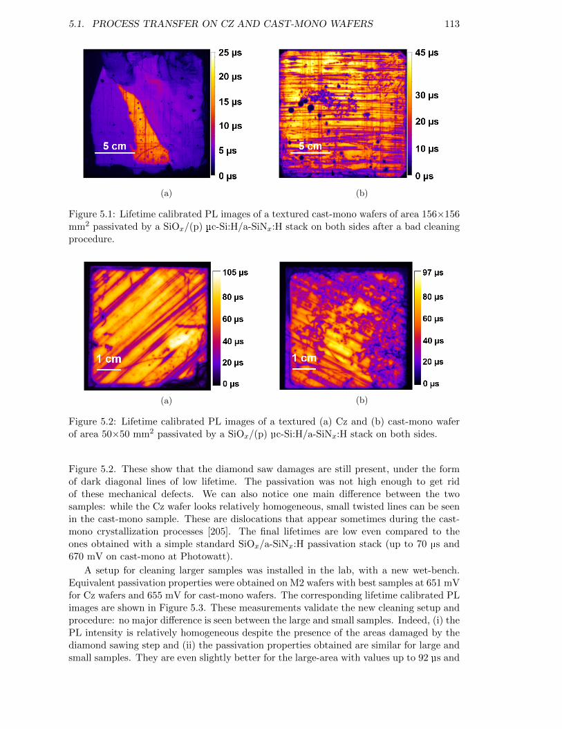
5.1. PROCESS TRANSFER ON CZ AND CAST-MONO WAFERS 113
(a) (b)
Figure 5.1: Lifetime calibrated PL images of a textured cast-mono wafers of area 156×156mm2 passivated by a SiOx/(p) µc-Si:H/a-SiNx:H stack on both sides after a bad cleaningprocedure.
(a) (b)
Figure 5.2: Lifetime calibrated PL images of a textured (a) Cz and (b) cast-mono waferof area 50×50 mm2 passivated by a SiOx/(p) µc-Si:H/a-SiNx:H stack on both sides.
Figure 5.2. These show that the diamond saw damages are still present, under the formof dark diagonal lines of low lifetime. The passivation was not high enough to get ridof these mechanical defects. We can also notice one main difference between the twosamples: while the Cz wafer looks relatively homogeneous, small twisted lines can be seenin the cast-mono sample. These are dislocations that appear sometimes during the cast-mono crystallization processes [205]. The final lifetimes are low even compared to theones obtained with a simple standard SiOx/a-SiNx:H passivation stack (up to 70 µs and670 mV on cast-mono at Photowatt).
A setup for cleaning larger samples was installed in the lab, with a new wet-bench.Equivalent passivation properties were obtained on M2 wafers with best samples at 651 mVfor Cz wafers and 655 mV for cast-mono wafers. The corresponding lifetime calibrated PLimages are shown in Figure 5.3. These measurements validate the new cleaning setup andprocedure: no major difference is seen between the large and small samples. Indeed, (i) thePL intensity is relatively homogeneous despite the presence of the areas damaged by thediamond sawing step and (ii) the passivation properties obtained are similar for large andsmall samples. They are even slightly better for the large-area with values up to 92 µs and
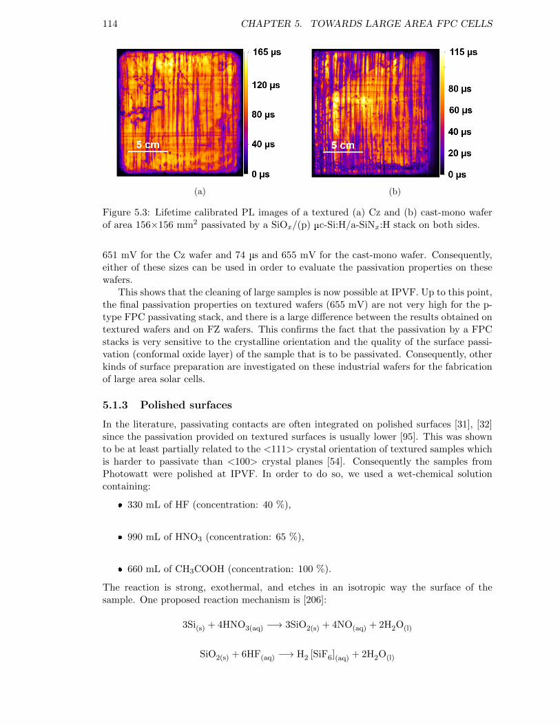
114 CHAPTER 5. TOWARDS LARGE AREA FPC CELLS
(a) (b)
Figure 5.3: Lifetime calibrated PL images of a textured (a) Cz and (b) cast-mono waferof area 156×156 mm2 passivated by a SiOx/(p) µc-Si:H/a-SiNx:H stack on both sides.
651 mV for the Cz wafer and 74 µs and 655 mV for the cast-mono wafer. Consequently,either of these sizes can be used in order to evaluate the passivation properties on thesewafers.
This shows that the cleaning of large samples is now possible at IPVF. Up to this point,the final passivation properties on textured wafers (655 mV) are not very high for the p-type FPC passivating stack, and there is a large difference between the results obtained ontextured wafers and on FZ wafers. This confirms the fact that the passivation by a FPCstacks is very sensitive to the crystalline orientation and the quality of the surface passi-vation (conformal oxide layer) of the sample that is to be passivated. Consequently, otherkinds of surface preparation are investigated on these industrial wafers for the fabricationof large area solar cells.
5.1.3 Polished surfaces
In the literature, passivating contacts are often integrated on polished surfaces [31], [32]since the passivation provided on textured surfaces is usually lower [95]. This was shownto be at least partially related to the <111> crystal orientation of textured samples whichis harder to passivate than <100> crystal planes [54]. Consequently the samples fromPhotowatt were polished at IPVF. In order to do so, we used a wet-chemical solutioncontaining:
330 mL of HF (concentration: 40 %),
990 mL of HNO3 (concentration: 65 %),
660 mL of CH3COOH (concentration: 100 %).
The reaction is strong, exothermal, and etches in an isotropic way the surface of thesample. One proposed reaction mechanism is [206]:
3Si(s) + 4HNO3(aq) −→ 3SiO2(s) + 4NO(aq) + 2H2O(l)
SiO2(s) + 6HF(aq) −→ H2 [SiF6](aq) + 2H2O(l)
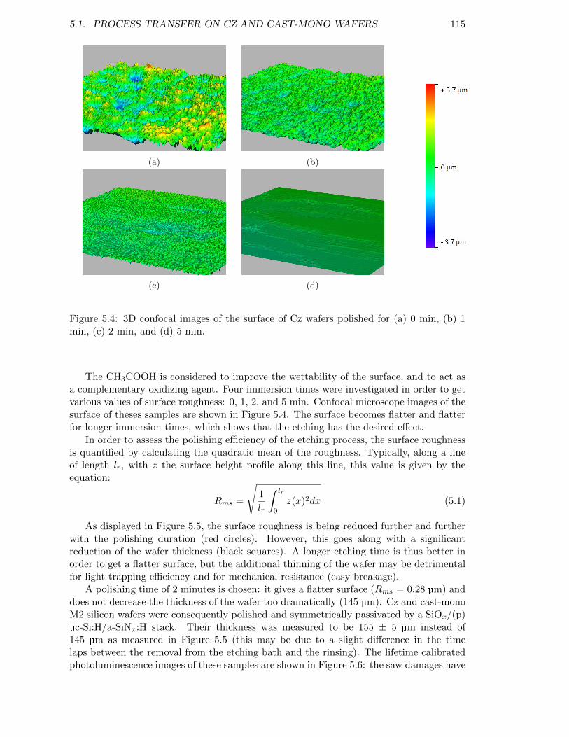
5.1. PROCESS TRANSFER ON CZ AND CAST-MONO WAFERS 115
(a) (b)
(c) (d)
Figure 5.4: 3D confocal images of the surface of Cz wafers polished for (a) 0 min, (b) 1min, (c) 2 min, and (d) 5 min.
The CH3COOH is considered to improve the wettability of the surface, and to act asa complementary oxidizing agent. Four immersion times were investigated in order to getvarious values of surface roughness: 0, 1, 2, and 5 min. Confocal microscope images of thesurface of theses samples are shown in Figure 5.4. The surface becomes flatter and flatterfor longer immersion times, which shows that the etching has the desired effect.
In order to assess the polishing efficiency of the etching process, the surface roughnessis quantified by calculating the quadratic mean of the roughness. Typically, along a lineof length lr, with z the surface height profile along this line, this value is given by theequation:
Rms =
√1
lr
∫ lr
0z(x)2dx (5.1)
As displayed in Figure 5.5, the surface roughness is being reduced further and furtherwith the polishing duration (red circles). However, this goes along with a significantreduction of the wafer thickness (black squares). A longer etching time is thus better inorder to get a flatter surface, but the additional thinning of the wafer may be detrimentalfor light trapping efficiency and for mechanical resistance (easy breakage).
A polishing time of 2 minutes is chosen: it gives a flatter surface (Rms = 0.28 µm) anddoes not decrease the thickness of the wafer too dramatically (145 µm). Cz and cast-monoM2 silicon wafers were consequently polished and symmetrically passivated by a SiOx/(p)µc-Si:H/a-SiNx:H stack. Their thickness was measured to be 155 ± 5 µm instead of145 µm as measured in Figure 5.5 (this may be due to a slight difference in the timelaps between the removal from the etching bath and the rinsing). The lifetime calibratedphotoluminescence images of these samples are shown in Figure 5.6: the saw damages have
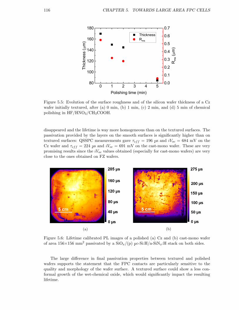
116 CHAPTER 5. TOWARDS LARGE AREA FPC CELLS
0 1 2 3 4 580
100
120
140
160
180 Thickness Rms
Thic
knes
s (m
m)
Polishing time (min)
0.0
0.1
0.2
0.3
0.4
0.5
0.6
0.7
Rm
s (mm
)
Figure 5.5: Evolution of the surface roughness and of the silicon wafer thickness of a Czwafer initially textured, after (a) 0 min, (b) 1 min, (c) 2 min, and (d) 5 min of chemicalpolishing in HF/HNO3/CH3COOH.
disappeared and the lifetime is way more homogeneous than on the textured surfaces. Thepassivation provided by the layers on the smooth surfaces is significantly higher than ontextured surfaces: QSSPC measurements gave τeff = 196 µs and iVoc = 684 mV on theCz wafer and τeff = 224 µs and iVoc = 691 mV on the cast-mono wafer. These are verypromising results since the iVoc values obtained (especially for cast-mono wafers) are veryclose to the ones obtained on FZ wafers.
(a) (b)
Figure 5.6: Lifetime calibrated PL images of a polished (a) Cz and (b) cast-mono waferof area 156×156 mm2 passivated by a SiOx/(p) µc-Si:H/a-SiNx:H stack on both sides.
The large difference in final passivation properties between textured and polishedwafers supports the statement that the FPC contacts are particularly sensitive to thequality and morphology of the wafer surface. A textured surface could show a less con-formal growth of the wet-chemical oxide, which would significantly impact the resultinglifetime.
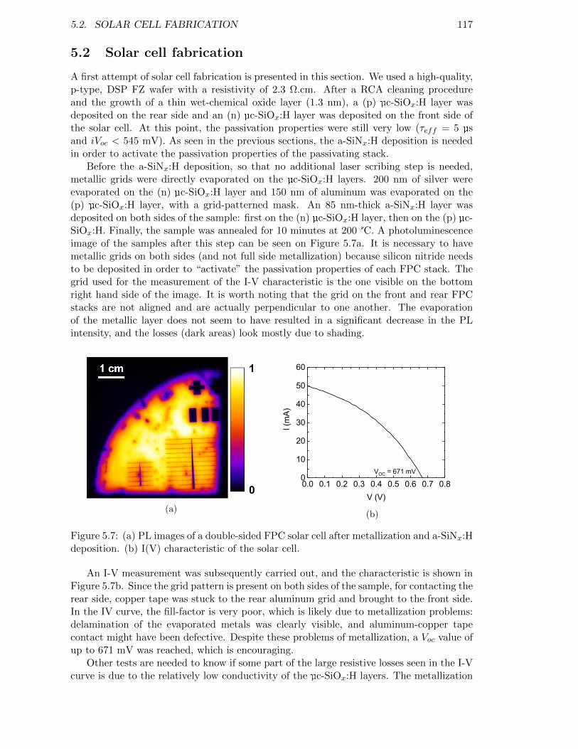
5.2. SOLAR CELL FABRICATION 117
5.2 Solar cell fabrication
A first attempt of solar cell fabrication is presented in this section. We used a high-quality,p-type, DSP FZ wafer with a resistivity of 2.3 Ω.cm. After a RCA cleaning procedureand the growth of a thin wet-chemical oxide layer (1.3 nm), a (p) µc-SiOx:H layer wasdeposited on the rear side and an (n) µc-SiOx:H layer was deposited on the front side ofthe solar cell. At this point, the passivation properties were still very low (τeff = 5 µsand iVoc < 545 mV). As seen in the previous sections, the a-SiNx:H deposition is neededin order to activate the passivation properties of the passivating stack.
Before the a-SiNx:H deposition, so that no additional laser scribing step is needed,metallic grids were directly evaporated on the µc-SiOx:H layers. 200 nm of silver wereevaporated on the (n) µc-SiOx:H layer and 150 nm of aluminum was evaporated on the(p) µc-SiOx:H layer, with a grid-patterned mask. An 85 nm-thick a-SiNx:H layer wasdeposited on both sides of the sample: first on the (n) µc-SiOx:H layer, then on the (p) µc-SiOx:H. Finally, the sample was annealed for 10 minutes at 200 °C. A photoluminescenceimage of the samples after this step can be seen on Figure 5.7a. It is necessary to havemetallic grids on both sides (and not full side metallization) because silicon nitride needsto be deposited in order to “activate” the passivation properties of each FPC stack. Thegrid used for the measurement of the I-V characteristic is the one visible on the bottomright hand side of the image. It is worth noting that the grid on the front and rear FPCstacks are not aligned and are actually perpendicular to one another. The evaporationof the metallic layer does not seem to have resulted in a significant decrease in the PLintensity, and the losses (dark areas) look mostly due to shading.
(a)
0.0 0.1 0.2 0.3 0.4 0.5 0.6 0.7 0.80
10
20
30
40
50
60
I (m
A)
V (V)
VOC = 671 mV
(b)
Figure 5.7: (a) PL images of a double-sided FPC solar cell after metallization and a-SiNx:Hdeposition. (b) I(V) characteristic of the solar cell.
An I-V measurement was subsequently carried out, and the characteristic is shown inFigure 5.7b. Since the grid pattern is present on both sides of the sample, for contacting therear side, copper tape was stuck to the rear aluminum grid and brought to the front side.In the IV curve, the fill-factor is very poor, which is likely due to metallization problems:delamination of the evaporated metals was clearly visible, and aluminum-copper tapecontact might have been defective. Despite these problems of metallization, a Voc value ofup to 671 mV was reached, which is encouraging.
Other tests are needed to know if some part of the large resistive losses seen in the I-Vcurve is due to the relatively low conductivity of the µc-SiOx:H layers. The metallization
118 CHAPTER 5. TOWARDS LARGE AREA FPC CELLS
step needs to be improved. Screen-printing metallization of a fire-through paste couldallow for the deposition of a-SiNx:H on the full area of the wafer, thus simplifying thefabrication process, and making the contact easier for large area I-V characterization.This, however, requires the FPC to maintain its passivation properties during the firingstep.
5.3 Summary
In this chapter, p-type FPC were integrated on industrial Cz and cast-mono wafers, reach-ing similar iVoc values. This highlights the interest of integrating FPC on cast-mono wafers,that are both cheaper and require less energy for the cell fabrication. This study addi-tionally pinpoints the sensitivity of the FPC passivating stacks to the surface preparation,which needs a high-quality, conformal SiOx layer in order to provide good passivationproperties. An encouraging iVoc value of 691 mV for the integration of p-type FPC on apolished cast-mono wafer was even reached, which is close to the maximum values obtainedon p-type DSP, FZ wafers.
A first prototype of solar cell was made, with an (n) µc-SiOx:H layer on the front sideand a (p) µc-SiOx:H on the rear side. A Voc of 671 mV was achieved, despite large resistivelosses. Some improvements of the metallization process are required to unravel the fullpotential of the FPC integration on silicon solar cells.
119
Conclusion and perspectives
This doctoral work focused on the study of a simplified process flow for the fabricationof tunnel oxide passivated contact (TOPCon) called fired passivated contact (FPC). Thissolar cell fabrication process has the advantage of being simple (few steps) and requiringa low thermal budget, thus reducing the carbon intensity of the photovoltaic energy pro-duced. In order to carry out this comprehensive study, various characterization techniqueswere used and optimized, among which in situ modulated photoluminescence (MPL) whichallowed the measurement in real time of the minority carrier lifetime in solar cell precursorsduring a specific process step. The major contributions of this thesis are listed below.
Optimization of the FPC stack
A layer-by-layer optimization of the passivating stack was carried out in order to developthe FPC cell fabrication process at IPVF and LPICM laboratories. This optimizationcoupled with several characterization techniques allowed to measure the various physicalproperties of the layers chosen for the final passivating stack: SiOx, doped µc-Si:H andµc-SiOx:H, and a-SiNx:H. During this thesis µc-Si:H and µc-SiOx:H materials were chosenas carrier transport layers, since they degrade less than a-Si:H during the final high-temperature firing step. These materials were optimized in order to get the best possibletrade-off between transparency, conductivity and passivation properties. Notably, XPSanalyses allowed to show that the deposition of (p) µc-Si:H on top of the thin SiOx layerleads to a rearrangement of the tunnel oxide, that forms substoechiometric oxides. Thefinal firing step systematically degraded the passivation properties, but this detrimentaleffect could be mitigated by the use of µc-SiOx:H instead of µc-Si:H, and depositing thickerlayers of either µc-SiOx:H or a-SiNx:H. The use of an AlOx layer deposited by ALD allowedto show the feasibility of our process, while maintaining the passivation properties afterfiring. The complexity of the stack and the interactions of the consecutive process stepson the properties of the whole structure motivated the use of real-time measurements ofthe passivation properties.
In situ modulated photoluminescence for AlOx
An in situ MPL acquisition setup mounted on a PECVD reactor is described, along withthe data treatment necessary to extract the minority carrier lifetime at the specific excessminority carrier density of 1×1015 cm−3. New corrections were made in order to takelateral diffusion into account in the data treatment procedure, which is shown to result insignificant overestimations of the minority carrier density for a very local illumination ofhighly passivated samples.
A case study of the evolution of AlOx passivated n-type silicon wafers was carried outusing the in situ MPL setup. We showed that the negative fixed charge density is not
120 CONCLUSION AND PERSPECTIVES
activated at 250 °C, while it is fully activated after a 30 min-long annealing step at 350 °C.Interestingly we showed that the combined action of temperature (250 °C) and light (laserillumination needed for the MPL measurement) activates a large amount of stable positivefixed charges in AlOx, which is a phenomenon never reported before.
In situ MPL for Fired Passivating Contacts
In situ MPL measurements were also carried out on silicon wafers coated with FPC pas-sivating stacks. The hydrogenation process of samples made at EPFL was investigated.Their team showed that the firing step creates bulk defects in the FZ silicon wafers. Thereal-time lifetime measurements allowed to evidence that bulk defects are cured during a30 min-long annealing at 450 °C after the deposition of a hydrogen-rich a-SiNx:H layer.This dynamics was shown to strongly depend on temperature, which is consistent with thehypothesis of the diffusion of hydrogen and a decrease of the bulk defect density. In ourexperiments, the in situ MPL experiments allowed to show that 20 minutes of annealingwere enough to completely passivate the bulk.
The lifetime measured by MPL were shown to strongly vary with temperature even forsamples which passivation properties were not impacted by annealing steps. Increases oflifetime were observed during the beginning of the increase of temperature, and low lifetimevalues were systematically measured in all samples when the temperature exceeded 300 °C.These variations were shown to result from two competing phenomena: (i) the increase ofthe effective minority carrier lifetime of the sample with temperature (due to variationsof the electron and hole trap capture cross sections, ...) and (ii) the strong increase ofthe thermally generated minority carrier density at high temperatures (4×1016 cm−3 at450 °C) which boosts recombinations losses. Consequently, at very high temperatures, theevolution of the actual passivation properties is harder to measure.
Finally, in situ MPL was used during PECVD processes for the fabrication of FPC atIPVF. NH3 + H2 plasmas were shown to degrade the passivation provided by FPC samplesin all cases, but more dramatically for FPC with µc-SiOx:H than FPC with µc-Si:H, whilethe annealing of the samples at 350 °C boosts the passivation of the samples. The additionof SiH4 in the gas mixture allows to deposit a-SiNx:H and leads to a dramatic increase ofthe effective lifetime, especially during the first few minutes of deposition. It must also benoted that the order of the deposition sequence in the case of solar cells with both n-typeand p-type FPC is reported to be of importance: a deposition of a-SiNx:H first on then-type FPC could lead to better performances.
Towards large area FPC cells
A first integration of the p-type FPC stack with (p) µc-Si:H was carried out on texturedand polished Cz and cast-mono wafers of area 156×156 mm2. This confirmed that FPCpassivating stacks depend dramatically on the quality of the c-Si/SiOx interface. Theyprovide iVOC values around 655 mV on textured wafers, while 684 mV on Cz and 691 mVon cast-mono polished wafers were reached, which are very promising results. It is thus ofsignificant interest to keep implementing the newest solar cell architectures on cast-monowafers to show the potential of such wafers
121
Perspectives
As a sum up, we showed that in complex passivating stacks, each processing step modifiesthe overall properties of the sample and the deposition of the layers impact one another(see XPS and ellipsometry measurements). Because of the critical role of interfaces in theperformances of our devices, standard optical and chemical characterization techniquesare not sufficient, and electronic measurements are necessary: a slight change in the depo-sition conditions of materials can lead to completely different electronic properties (see thecharacterization of positively charged AlOx). Electrical characterization on final devices isnot enough to understand the mechanisms at stake, which motivated the use of real-time,in situ MPL measurements for a finer tuning of the processing times and conditions. Itmust be stressed out that what counts in the end are the properties after the final firingstep in FPC samples: the in situ MPL measurements can help find the best combinationof materials to maximize both the final passivation properties and the thermal stability.Many interesting studies can be made in order to push further the understanding andimprovements achieved during this thesis.
Thorougher investigations must be carried out on the surprising positively chargedAlOx thin films: XPS analyses in order to learn more about the chemical configurationof the AlOx layer with such positive fixed charges, variations of the light source (spectraldistribution, photon flux, ...) to narrow down the possible mechanisms at stake, and finallya verification of the possibility to get positively charged AlOx on larger areas.
An improvement of the MPL acquisition routine and data treatment should be madein order to better take temperature variations into account. The treatment should befully rethought for high-temperature measurements (higher than 350 °C) if one wantsto visualize only the evolution of the surface and bulk passivation. However, it is worthreminding that, at fixed temperature, the variations of the lifetime that are being measuredstill account for real variations of the passivation properties.
A more extensive study on the capping layer should be carried out for future im-provements. The increase in lifetime occurring exclusively during the first few minutes ofa-SiNx:H deposition, this paves the way for the development of new capping stacks: thedeposition of the first few nm of a hydrogen-rich material that could increase the passiva-tion of the c-Si/SiOx interface (such as a-SiNx:H) until the maximum lifetime value couldbe followed by the deposition of a layer which could increase the thermal stability of thepassivating stack upon firing (such as a-SiNxOyCz:H) while not impacting directly the pas-sivation properties. These bi-layers should be investigated using in situ MPL during theirdeposition in order to optimize the duration of deposition and get a better understandingof the impact of the different species present inside the plasma.
A full study on the metallisation and on the optimal firing temperature profile shouldbe made in order to allow for the integration of FPC on industrial size silicon wafers.Additionally, it would be of great interest to investigate the long-term stability and agingof FPC solar cells, and compare it with the lifetime of passivated contact solar cells madewith other fabrication processes.
The investigation of solar cell manufacturing processes that have lower and lower en-vironmental impacts is of major importance, and is fundamental for the acceptability andthe larger adoption of photovoltaic devices. Fundamental and comprehensive research onfabrication processes should spur the photovoltaic industry to adopt abstemious methodsin order to contribute to a more sustainable future.

122 CONCLUSION AND PERSPECTIVES
123
Bibliography
[1] U. N. D. Program, “Human Development Data (1990-2018),” Tech. Rep., 2019.
[2] W. E. Council, World Energy Trilemma Index 2019. 2019.
[3] IEA, “Key World Energy Statistics,” p. 81, 2019.
[4] I. P. o. C. Change, “6th assessment report, climate change 2021: The physicalscience basis,” IPCC, Tech. Rep., Aug. 2021.
[5] ——, “IPCC Special Report on Renewable Energy Sources and Climate ChangeMitigation,” IPCC, Tech. Rep., 2011.
[6] ITRPV, “International Technology Roadmap for Photovoltaic (ITRPV) 10th edi-tion,” Tech. Rep. 10th edition, Mar. 2019, p. 80.
[7] IRENA, “Renewable Energy Statistics 2019,” International Renewable Energy Agency,Abu Dhabi, Tech. Rep., 2019, p. 398.
[8] C. Kost, S. Shammugam, V. Julch, H.-T. Nguyen, and T. Schlegl, “Levelized Costof Electricity- Renewable Energy Technologies,” Fraunhofer ISE, Tech. Rep., Mar.2018, p. 42.
[9] R. Fu, D. Feldman, and R. Margolis, “U.S. Solar Photovoltaic System Cost Bench-mark: Q1 2018,” NREL, Tech. Rep., 2018, p. 63.
[10] S. Europe, “Solar Sustainability: Best Practices Benchmark,” p. 54, 2021.
[11] ISE, “Photovoltaics Report,” Fraunhofer ISE, Tech. Rep., Jul. 2021.
[12] D. Chen, Y. Chen, Z. Wang, J. Gong, C. Liu, Y. Zou, Y. He, Y. Wang, L. Yuan, W.Lin, R. Xia, L. Yin, X. Zhang, G. Xu, Y. Yang, H. Shen, Z. Feng, P. Altermatt, andP. Verlinden, “24.58% total area efficiency of screen-printed, large area industrialsilicon solar cells with the tunnel oxide passivated contacts (i-TOPCon) design,”Solar Energy Materials and Solar Cells, vol. 206, p. 110 258, Mar. 2020. doi: 10.1016/j.solmat.2019.110258.
[13] Photowatt, PW2450F Crystal Advanced sur Photowatt. [Online]. Available: http://www.photowatt.com/produits/modules/pw2450f-crystal-advanced.
[14] P. Wurfel and U. Wurfel, Physics of Solar Cells: From Basic Principles to AdvancedConcepts, 3rd. Wiley-VCH, 2016.
[15] U. Wurfel, A. Cuevas, and P. Wurfel, “Charge Carrier Separation in Solar Cells,”IEEE Journal of Photovoltaics, vol. 5, no. 1, pp. 461–469, Jan. 2015. doi: 10.1109/JPHOTOV.2014.2363550.
[16] W. Shockley and H. Queisser, “Detailed Balance Limit of Efficiency of p-n JunctionSolar Cells,” Journal of Applied Physics, vol. 32, no. 3, pp. 510–519, Mar. 1961.doi: 10.1063/1.1736034.
124 BIBLIOGRAPHY
[17] M. Rodrıguez-Meza and J. Carrillo, “Thermalization process of a photo-generatedplasma in semiconductors,” Revista Mexicana de Fisica, vol. 48, no. 1, pp. 52–60,2002.
[18] M. Hudedmani, V. Soppimath, and C. Jambotkar, “A Study of Materials for SolarPV Technology and Challenges,” European Journal of Applied Engineering andScientific Research, vol. 1, no. 5, pp. 1–13, 2017.
[19] A. Richter, M. Hermle, and S. Glunz, “Reassessment of the Limiting Efficiencyfor Crystalline Silicon Solar Cells,” IEEE Journal of Photovoltaics, vol. 3, no. 4,pp. 1184–1191, Oct. 2013. doi: 10.1109/JPHOTOV.2013.2270351.
[20] K. Yoshikawa, H. Kawasaki, W. Yoshida, T. Irie, K. Konishi, K. Nakano, T. Uto, D.Adachi, M. Kanematsu, H. Uzu, and K. Yamamoto, “Silicon heterojunction solarcell with interdigitated back contacts for a photoconversion efficiency over 26%,”Nature Energy, vol. 2, no. 5, May 2017. doi: 10.1038/nenergy.2017.32.
[21] W. Gerlach, H. Schlangenotto, and H. Maeder, “On the radiative recombinationrate in silicon,” Physica Status Solidi (a), vol. 13, no. 1, pp. 277–283, Sep. 1972.doi: 10.1002/pssa.2210130129.
[22] W. Shockley and W. T. Read, “Statistics of the Recombinations of Holes andElectrons,” Physical Review, vol. 87, no. 5, pp. 835–842, Sep. 1952. doi: 10.1103/PhysRev.87.835.
[23] A. Aberle, “Surface passivation of crystalline silicon solar cells: A review,” Progressin Photovoltaics: Research and Applications, vol. 8, no. 5, pp. 473–487, Sep. 2000.doi: 10.1002/1099-159X(200009/10)8:5<473::AID-PIP337>3.0.CO;2-D.
[24] M. Sajjad, X. Yang, P. Altermatt, N. Singh, U. Schwingenschlogl, and S. De Wolf,“Metal-induced gap states in passivating metal/silicon contacts,” Applied PhysicsLetters, vol. 114, no. 7, p. 071 601, Feb. 2019. doi: 10.1063/1.5066423.
[25] A. Aberle, “Overview on SiN surface passivation of crystalline silicon solar cells,”Solar Energy Materials and Solar Cells, vol. 65, no. 1-4, pp. 239–248, Jan. 2001.doi: 10.1016/S0927-0248(00)00099-4.
[26] T. Allen, J. Bullock, X. Yang, A. Javey, and S. De Wolf, “Passivating contacts forcrystalline silicon solar cells,” Nature Energy, Sep. 2019. doi: 10.1038/s41560-019-0463-6.
[27] M. Tanaka, M. Taguchi, T. Matsuyama, T. Sawada, S. Tsuda, S. Nakano, H. Hana-fusa, and Y. Kuwano, “Development of New a-Si/c-Si Heterojunction Solar Cells:ACJ-HIT (Artificially Constructed Junction-Heterojunction with Intrinsic Thin-Layer),” Japanese Journal of Applied Physics, vol. 31, no. Part 1, No. 11, pp. 3518–3522, Nov. 1992. doi: 10.1143/JJAP.31.3518.
[28] R. Varache, A. Valla, N. Nguyen, and D. Munoz, “Front Side Recombination LossesAnalysis in Rear Emitter Silicon Heterojunction Solar Cells,” Energy Procedia,vol. 55, pp. 302–309, 2014. doi: 10.1016/j.egypro.2014.08.089.
[29] F. Feldmann, M. Bivour, C. Reichel, H. Steinkemper, M. Hermle, and S. Glunz,“Tunnel oxide passivated contacts as an alternative to partial rear contacts,” SolarEnergy Materials and Solar Cells, vol. 131, pp. 46–50, Dec. 2014. doi: 10.1016/j.solmat.2014.06.015.
BIBLIOGRAPHY 125
[30] P. Spinelli, M. Sen, E. Hoek, B. Kikkert, G. Yang, O. Isabella, A. Weeber, and P.Bronsveld, “Moly-poly solar cell: Industrial application of metal-oxide passivatingcontacts with a starting efficiency of 18.1%,” 2018, p. 040 021. doi: 10.1063/1.5049284.
[31] S. Duttagupta, N. Nandakumar, P. Padhamnath, J. Buatis, R. Stangl, and A.Aberle, “monoPolyTM cells: Large-area crystalline silicon solar cells with fire-through screen printed contact to doped polysilicon surfaces,” Solar Energy Ma-terials and Solar Cells, vol. 187, pp. 76–81, Dec. 2018. doi: 10.1016/j.solmat.2018.05.059.
[32] F. Feldmann, M. Simon, M. Bivour, C. Reichel, M. Hermle, and S. Glunz, “Efficientcarrier-selective p- and n-contacts for Si solar cells,” Solar Energy Materials andSolar Cells, vol. 131, pp. 100–104, Dec. 2014. doi: 10.1016/j.solmat.2014.05.039.
[33] U. Romer, R. Peibst, T. Ohrdes, B. Lim, J. Krugener, E. Bugiel, T. Wietler,and R. Brendel, “Recombination behavior and contact resistance of n+ and p+poly-crystalline Si/mono-crystalline Si junctions,” Solar Energy Materials and So-lar Cells, vol. 131, pp. 85–91, Dec. 2014. doi: 10.1016/j.solmat.2014.06.003.
[34] U. Romer, “Polycrystalline silicon / monocrystalline silicon junctions and theirapplication as passivated contacts for Si solar cells,” PhD Thesis, 2015.
[35] R. Peibst, U. Romer, Y. Larionova, M. Rienacker, A. Merkle, N. Folchert, S. Reiter,M. Turcu, B. Min, J. Krugener, D. Tetzlaff, E. Bugiel, T. Wietler, and R. Brendel,“Working principle of carrier selective poly-Si/c-Si junctions: Is tunnelling the wholestory?” Solar Energy Materials and Solar Cells, vol. 158, pp. 60–67, Dec. 2016. doi:10.1016/j.solmat.2016.05.045.
[36] A. Kale, W. Nemeth, H. Guthrey, E. Kennedy, A. Norman, M. Page, M. Al-Jassim,D. Young, S. Agarwal, and P. Stradins, “Understanding the charge transport mech-anisms through ultrathin SiOx layers in passivated contacts for high-efficiency sili-con solar cells,” Applied Physics Letters, vol. 114, no. 8, p. 083 902, Feb. 2019. doi:10.1063/1.5081832.
[37] A. Kale, W. Nemeth, S. Nanayakkara, H. Guthrey, M. Page, M. Al-Jassim, S.Agarwal, and P. Stradins, “Tunneling or Pinholes: Understanding the TransportMechanisms in SiOx Based Passivated Contacts for High-Efficiency Silicon SolarCells,” 2018, p. 5.
[38] Z. Zhang, Y. Zeng, C.-S. Jiang, Y. Huang, M. Liao, H. Tong, M. Al-Jassim, P. Gao,C. Shou, X. Zhou, B. Yan, and J. Ye, “Carrier transport through the ultrathinsilicon-oxide layer in tunnel oxide passivated contact (TOPCon) c-Si solar cells,”Solar Energy Materials and Solar Cells, vol. 187, pp. 113–122, Dec. 2018. doi:10.1016/j.solmat.2018.07.025.
[39] G. R. Wolstenholme, N. Jorgensen, P. Ashburn, and G. R. Booker, “An inves-tigation of the thermal stability of the interfacial oxide in polycrystalline siliconemitter bipolar transistors by comparing device results with high-resolution elec-tron microscopy observations,” Journal of Applied Physics, vol. 61, no. 1, pp. 225–233, Jan. 1987. doi: 10.1063/1.338861.
[40] I. Post, P. Ashburn, and G. Wolstenholme, “Polysilicon emitters for bipolar transis-tors: A review and re-evaluation of theory and experiment,” IEEE Transactions onElectron Devices, vol. 39, no. 7, pp. 1717–1731, Jul. 1992. doi: 10.1109/16.141239.
126 BIBLIOGRAPHY
[41] T. Matsushita, N. Oh-uchi, H. Hayashi, and H. Yamoto, “A silicon heterojunctiontransistor,” Applied Physics Letters, vol. 35, no. 7, pp. 549–550, Oct. 1979. doi:10.1063/1.91174.
[42] E. Yablonovitch, T. Gmitter, R. M. Swanson, and Y. H. Kwark, “A 720 mV opencircuit voltage SiOx / c-Si/SiOx double heterostructure solar cell,” Applied PhysicsLetters, vol. 47, no. 11, pp. 1211–1213, Dec. 1985. doi: 10.1063/1.96331.
[43] F. Feldmann, M. Bivour, C. Reichel, M. Hermle, and S. Glunz, “Passivated rearcontacts for high-efficiency n-type Si solar cells providing high interface passivationquality and excellent transport characteristics,” Solar Energy Materials and SolarCells, vol. 120, pp. 270–274, Jan. 2014. doi: 10.1016/j.solmat.2013.09.017.
[44] R. Peibst, U. Romer, K. Hofmann, B. Lim, T. Wietler, J. Krugener, N.-P. Harder,and R. Brendel, “A Simple Model Describing the Symmetric IV Characteristics of pPolycrystalline Si/n Monocrystalline Si, and n Polycrystalline Si/p MonocrystallineSi Junctions,” IEEE Journal of Photovoltaics, vol. 4, no. 3, pp. 841–850, May 2014.doi: 10.1109/JPHOTOV.2014.2310740.
[45] M. Stodolny, M. Lenes, Y. Wu, G. Janssen, I. Romijn, J. Luchies, and L. Geerligs,“N-Type polysilicon passivating contact for industrial bifacial n-type solar cells,”Solar Energy Materials and Solar Cells, vol. 158, pp. 24–28, Dec. 2016. doi: 10.1016/j.solmat.2016.06.034.
[46] A. Ingenito, G. Nogay, Q. Jeangros, E. Rucavado, C. Allebe, S. Eswara, N. Valle, T.Wirtz, J. Horzel, T. Koida, M. Morales-Masis, M. Despeisse, F.-J. Haug, P. Loper,and C. Ballif, “A passivating contact for silicon solar cells formed during a singlefiring thermal annealing,” Nature Energy, vol. 3, no. 9, pp. 800–808, Sep. 2018. doi:10.1038/s41560-018-0239-4.
[47] A. Richter, J. Benick, F. Feldmann, A. Fell, M. Hermle, and S. Glunz, “N-TypeSi solar cells with passivating electron contact: Identifying sources for efficiencylimitations by wafer thickness and resistivity variation,” Solar Energy Materials andSolar Cells, vol. 173, pp. 96–105, Dec. 2017. doi: 10.1016/j.solmat.2017.05.042.
[48] F. Haase, C. Hollemann, S. Schafer, A. Merkle, M. Rienacker, J. Krugener, R.Brendel, and R. Peibst, “Laser contact openings for local poly-Si-metal contactsenabling 26.1%-efficient POLO-IBC solar cells,” Solar Energy Materials and SolarCells, vol. 186, pp. 184–193, Nov. 2018. doi: 10.1016/j.solmat.2018.06.020.
[49] N. Nandakumar, J. Rodriguez, T. Kluge, T. Groβe, L. Fondop, P. Padhamnath, N.Balaji, M. Konig, and S. Duttagupta, “Approaching 23% with large-area monoPolycells using screen-printed and fired rear passivating contacts fabricated by inlinePECVD,” Progress in Photovoltaics: Research and Applications, Dec. 2018. doi:10.1002/pip.3097.
[50] Y. Chen, D. Chen, C. Liu, Z. Wang, Y. Zou, Y. He, Y. Wang, L. Yuan, J. Gong,W. Lin, X. Zhang, Y. Yang, H. Shen, Z. Feng, P. P. Altermatt, and P. J. Verlinden,“Mass production of industrial tunnel oxide passivated contacts (i-TOPCon) siliconsolar cells with average efficiency over 23% and modules over 345 W,” Progress inPhotovoltaics: Research and Applications, Jul. 2019. doi: 10.1002/pip.3180.
[51] C. Maritan and N. Tarr, “Polysilicon emitter p-n-p transistors,” IEEE Transactionson Electron Devices, vol. 36, no. 6, pp. 1139–1144, Jun. 1989. doi: 10.1109/16.24359.
BIBLIOGRAPHY 127
[52] T. Yamamoto, K. Uwasawa, and T. Mogami, “Bias Temperature Instability inScaled p Polysilicon Gate p-MOSFET’s,” IEEE TRANSACTIONS ON ELEC-TRON DEVICES, vol. 46, no. 5, p. 6, 1999.
[53] A. Kale, W. Nemeth, H. Guthrey, M. Page, M. Al-Jassim, D. Young, S. Agarwal,and P. Stradins, “Modifications of Textured Silicon Surface Morphology and ItsEffect on Poly-Si/SiOx Contact Passivation for Silicon Solar Cells,” IEEE Journalof Photovoltaics, pp. 1–9, 2019. doi: 10.1109/JPHOTOV.2019.2937230.
[54] Y. Larionova, M. Turcu, S. Reiter, R. Brendel, D. Tetzlaff, J. Krugener, T. Wietler,U. Hohne, J.-D. Kahler, and R. Peibst, “On the recombination behavior of p-type polysilicon on oxide junctions deposited by different methods on textured andplanar surfaces.,” physica status solidi (a), vol. 214, no. 8, p. 1 700 058, Aug. 2017.doi: 10.1002/pssa.201700058.
[55] G. Nogay, A. Ingenito, E. Rucavado, Q. Jeangros, J. Stuckelberger, P. Wyss, M.Morales-Masis, F.-J. Haug, P. Loper, and C. Ballif, “Crystalline Silicon Solar CellsWith Coannealed Electron- and Hole-Selective SiCx Passivating Contacts,” IEEEJournal of Photovoltaics, vol. 8, no. 6, pp. 1478–1485, Nov. 2018. doi: 10.1109/JPHOTOV.2018.2866189.
[56] C. Allebe, C. Ballif, J. Leon, A. Ingenito, A. Descoeudres, G. Nogay, P. Wyss,F.-J. Haug, M. Despeisse, and S. Nicolay, “PECVD based layers for improved hightemperature industrial Solar cell processes,” IEEE, Jun. 2019, pp. 2196–2199. doi:10.1109/PVSC40753.2019.8980583.
[57] P. Padhamnath, J. Buatis, A. Khanna, N. Nampalli, N. Nandakumar, V. Shan-mugam, A. Aberle, and S. Duttagupta, “Characterization of screen printed andfire-through contacts on LPCVD based passivating contacts in monoPoly solarcells,” Solar Energy, vol. 202, pp. 73–79, May 2020. doi: 10.1016/j.solener.2020.03.087.
[58] B. Min, N. Wehmeier, T. Brendemuehl, A. Merkle, F. Haase, Y. Larionova, L.David, H. Schulte-Huxel, R. Peibst, and R. Brendel, “A 22.3% Efficient p-TypeBack Junction Solar Cell with an Al-Printed Front-Side Grid and a Passivating n+-Type Polysilicon on Oxide Contact at the Rear Side,” Solar RRL, p. 2 000 435,Sep. 2020. doi: 10.1002/solr.202000435.
[59] F. Feldmann, G. Nogay, J.-I. Polzin, B. Steinhauser, A. Richter, A. Fell, C. Schmiga,M. Hermle, and S. Glunz, “A Study on the Charge Carrier Transport of PassivatingContacts,” IEEE Journal of Photovoltaics, vol. 8, no. 6, pp. 1503–1509, Nov. 2018.doi: 10.1109/JPHOTOV.2018.2870735.
[60] J.-I. Polzin, F. Feldmann, B. Steinhauser, M. Hermle, and S. Glunz, “Realizationof TOPCon using industrial scale PECVD equipment,” 2018, p. 040 018. doi: 10.1063/1.5049281.
[61] W. Chen, T. Truong, H. Nguyen, C. Samundsett, S. Phang, D. MacDonald, A.Cuevas, L. Zhou, Y. Wan, and D. Yan, “Influence of PECVD deposition temper-ature on phosphorus doped poly-silicon passivating contacts,” Solar Energy Mate-rials and Solar Cells, vol. 206, p. 110 348, Mar. 2020. doi: 10.1016/j.solmat.2019.110348.
128 BIBLIOGRAPHY
[62] Q. Yang, M. Liao, Z. Wang, J. Zheng, Y. lin, X. Guo, Z. Rui, D. Huang, L. Lu,M. Feng, P. Cheng, C. Shou, Y. Zeng, B. Yan, and J. Ye, “In-situ phosphorus-doped polysilicon prepared using rapid-thermal anneal (RTA) and its applicationfor polysilicon passivated-contact solar cells,” Solar Energy Materials and SolarCells, vol. 210, p. 110 518, Jun. 2020. doi: 10.1016/j.solmat.2020.110518.
[63] A. Ingenito, G. Nogay, J. Stuckelberger, P. Wyss, L. Gnocchi, C. Allebe, J. Horzel,M. Despeisse, F.-J. Haug, P. Loper, and C. Ballif, “Phosphorous-Doped SiliconCarbide as Front-Side Full-Area Passivating Contact for Double-Side Contactedc-Si Solar Cells,” IEEE Journal of Photovoltaics, pp. 1–9, 2018. doi: 10.1109/JPHOTOV.2018.2886234.
[64] T. Gao, Q. Yang, X. Guo, Y. Huang, Z. Zhang, Z. Wang, M. Liao, C. Shou, Y. Zeng,B. Yan, G. Hou, X. Zhang, Y. Zhao, and J. Ye, “An industrially viable TOPConstructure with both ultra-thin SiOx and n+-poly-Si processed by PECVD for p-type c-Si solar cells,” Solar Energy Materials and Solar Cells, vol. 200, p. 109 926,Sep. 2019. doi: 10.1016/j.solmat.2019.109926.
[65] G. Limodio, G. Yang, H. Ge, P. Procel, Y. De Groot, L. Mazzarella, O. Isabella, andM. Zeman, “Front and rear contact Si solar cells combining high and low thermalbudget Si passivating contacts,” Solar Energy Materials and Solar Cells, vol. 194,pp. 28–35, Jun. 2019. doi: 10.1016/j.solmat.2019.01.039.
[66] A. Morisset, R. Cabal, B. Grange, C. Marchat, J. Alvarez, M.-E. Gueunier-Farret,S. Dubois, and J.-P. Kleider, “Highly passivating and blister-free hole selectivepoly-silicon based contact for large area crystalline silicon solar cells,” Solar EnergyMaterials and Solar Cells, vol. 200, p. 109 912, Sep. 2019. doi: 10.1016/j.solmat.2019.109912.
[67] M. Stodolny, J. Anker, C. Tool, M. Koppes, A. Mewe, P. Manshanden, M. Lenes,and I. Romijn, “Novel Schemes of p+ poly-Si Hydrogenation Implemented in In-dustrial 6” Bifacial Front-and-Rear Passivating Contacts Solar Cells,” 35th Eu-ropean Photovoltaic Solar Energy Conference and Exhibition; 414-417, 2018. doi:10.4229/35theupvsec20182018-2co.10.3.
[68] Z. Xu, K. Tao, S. Jiang, R. Jia, W. Li, Y. Zhou, Z. Jin, and X. Liu, “Application ofpolycrystalline silicon carbide thin films as the passivating contacts for silicon solarcells,” Solar Energy Materials and Solar Cells, vol. 206, p. 110 329, Mar. 2020. doi:10.1016/j.solmat.2019.110329.
[69] N. Nandakumar, J. Rodriguez, T. Kluge, T. Grosse, D. Landgraf, N. Balaji, M.Esber, P. Padhamnath, and S. Duttagupta, “21.6% monoPolyTM cells with in-situinterfacial oxide and poly-Si layers deposited by inline PECVD,” Waikoloa Village,HI, USA, Jun. 2018, p. 4. doi: 10.1109/PVSC.2018.8547271.
[70] J. Temmler, J.-I. Polzin, F. Feldmann, L. Kraus, B. Kafle, S. Mack, A. Moldovan,M. Hermle, and J. Rentsch, “Inline PECVD Deposition of Poly-Si-Based TunnelOxide Passivating Contacts,” physica status solidi (a), vol. 215, no. 23, p. 1 800 449,Dec. 2018. doi: 10.1002/pssa.201800449.
[71] M. Koehler, F. Finger, U. Rau, K. Ding, M. Pomaska, A. Zamchiy, A. Lambertz,W. Duan, F. Lentz, S. Li, V. Smirnov, and T. Kirchartz, “Optimization of Trans-parent Passivating Contact for Crystalline Silicon Solar Cells,” IEEE Journal ofPhotovoltaics, pp. 1–8, 2019. doi: 10.1109/JPHOTOV.2019.2947131.
BIBLIOGRAPHY 129
[72] E. Khorani, T. Scheul, A. Tarazona, J. Nutter, T. Rahman, and S. Boden, “P+polycrystalline silicon growth via hot wire chemical vapour deposition for siliconsolar cells,” Thin Solid Films, p. 137 978, Apr. 2020. doi: 10.1016/j.tsf.2020.137978.
[73] Y. Tao, V. Upadhyaya, C.-W. Chen, A. Payne, E. Chang, A. Upadhyaya, and A.Rohatgi, “Large area tunnel oxide passivated rear contact n-type Si solar cells with21.2% efficiency,” Progress in Photovoltaics: Research and Applications, vol. 24,no. 6, pp. 830–835, Jun. 2016. doi: 10.1002/pip.2739.
[74] G Yang, A. Ingenito, N. van Hameren, O. Isabella, and M. Zeman, “Design andapplication of ion-implanted polySi passivating contacts for interdigitated back con-tact c-Si solar cells,” Applied Physics Letters, vol. 108, no. 3, p. 033 903, Jan. 2016.doi: 10.1063/1.4940364.
[75] D. Yan, A. Cuevas, Y. Wan, and J. Bullock, “Passivating contacts for silicon solarcells based on boron-diffused recrystallized amorphous silicon and thin dielectricinterlayers,” Solar Energy Materials and Solar Cells, vol. 152, pp. 73–79, Aug.2016. doi: 10.1016/j.solmat.2016.03.033.
[76] M. K. Stodolny, J. Anker, B. Geerligs, G. Janssen, B. van de Loo, J. Melskens,R. Santbergen, O. Isabella, J. Schmitz, M. Lenes, J.-M. Luchies, W. Kessels, andI. Romijn, “Material properties of LPCVD processed n-type polysilicon passivatingcontacts and its application in PERPoly industrial bifacial solar cells,” EnergyProcedia, vol. 124, pp. 635–642, Sep. 2017. doi: 10.1016/j.egypro.2017.09.250.
[77] Y. Chen, Y. Yang, G. Xu, J. K. Marmon, Z. Feng, and H. Shen, “Optimizationof micron size passivated contact and doping level for high efficiency interdigitatedback contact solar cells,” Solar Energy, vol. 178, pp. 308–313, Jan. 2019. doi: 10.1016/j.solener.2018.12.049.
[78] X. Guo, M. Liao, Z. Rui, Q. Yang, Z. Wang, C. Shou, W. Ding, X. Luo, Y. Cao, J.Xu, L. Fu, Y. Zeng, B. Yan, and J. Ye, “Comparison of different types of interfacialoxides on hole-selective p+-poly-Si passivated contacts for high-efficiency c-Si solarcells,” Solar Energy Materials and Solar Cells, vol. 210, p. 110 487, Jun. 2020. doi:10.1016/j.solmat.2020.110487.
[79] Q. Li, K. Tao, Y. Sun, R. Jia, S.-M. Wang, Z. Jin, and X.-Y. Liu, “Replacing theamorphous silicon thin layer with microcrystalline silicon thin layer in TOPConsolar cells,” Solar Energy, vol. 135, pp. 487–492, Oct. 2016. doi: 10.1016/j.
solener.2016.06.012.
[80] Z. Xin, Z. Ling, P. Wang, J. Ge, C. Ke, K. Choi, A. Aberle, and R. Stangl, “Ultra-thin atomic layer deposited aluminium oxide tunnel layer passivated hole-selectivecontacts for silicon solar cells,” Solar Energy Materials and Solar Cells, vol. 191,pp. 164–174, Mar. 2019. doi: 10.1016/j.solmat.2018.11.011.
[81] A. Desthieux, J. Posada, P.-P. Grand, C. Broussillou, B. Bazer-Bachi, G. Goaer,D. Messou, M. Bouttemy, E. Drahi, and P. Roca i Cabarrocas, “Impact of PECVDµc-Si:H deposition on tunnel oxide for passivating contacts,” EPJ Photovoltaics,vol. 11, no. 3, M. Guenier-Farret and J. Alvarez, Eds., 2020. doi: 10.1051/epjpv/2020001.
130 BIBLIOGRAPHY
[82] H. Park, S. Bae, S. Park, J. Hyun, C. Lee, D. Choi, D. Kang, H. Han, Y. Kang,H.-S. Lee, and D. Kim, “Role of polysilicon in poly-Si/SiOx passivating contacts forhigh-efficiency silicon solar cells,” RSC Advances, vol. 9, no. 40, pp. 23 261–23 266,2019. doi: 10.1039/C9RA03560E.
[83] A. Kale, W. Nemeth, S. Harvey, M. Page, D. Young, S. Agarwal, and P. Stradins,“Effect of silicon oxide thickness on polysilicon based passivated contacts for high-efficiency crystalline silicon solar cells,” Solar Energy Materials and Solar Cells,vol. 185, pp. 270–276, Oct. 2018. doi: 10.1016/j.solmat.2018.05.011.
[84] Y. Huang, M. Liao, Z. Wang, X. Guo, C. Jiang, Q. Yang, Z. Yuan, D. Huang, J.Yang, X. Zhang, Q. Wang, H. Jin, M. Al-Jassim, C. Shou, Y. Zeng, B. Yan, andJ. Ye, “Ultrathin silicon oxide prepared by in-line plasma-assisted N2O oxidation(PANO) and the application for n-type polysilicon passivated contact,” Solar En-ergy Materials and Solar Cells, vol. 208, p. 110 389, May 2020. doi: 10.1016/j.solmat.2019.110389.
[85] Z. Rui, Y. Zeng, X. Guo, Q. Yang, Z. Wang, C. Shou, W. Ding, J. Yang, X. Zhang,Q. Wang, H. Jin, M. Liao, S. Huang, B. Yan, and J. Ye, “On the passivationmechanism of poly-silicon and thin silicon oxide on crystal silicon wafers,” SolarEnergy, vol. 194, pp. 18–26, Dec. 2019. doi: 10.1016/j.solener.2019.10.064.
[86] S. Chao, Y. Takagi, G. Lucovsky, P. Pai, R. Custer, J. Tyler, and J. Keem, “Chem-ical states study of Si in SiOx films grown by PECVD,” Applied Surface Science,vol. 26, no. 4, pp. 575–583, Oct. 1986. doi: 10.1016/0169-4332(86)90128-5.
[87] M. Lehmann, N. Valle, J. Horzel, A. Pshenova, P. Wyss, M. Dobeli, M. Despeisse,S. Eswara, T. Wirtz, Q. Jeangros, A. Hessler-Wyser, F.-J. Haug, A. Ingenito, andC. Ballif, “Analysis of hydrogen distribution and migration in fired passivatingcontacts (FPC),” Solar Energy Materials and Solar Cells, vol. 200, Sep. 2019. doi:10.1016/j.solmat.2019.110018.
[88] F.-J. Haug, A. Ingenito, F. Meyer, S. Libraro, N. Bolis, J. Leon, C. Allebe, and C.Ballif, “Contributions to the Contact Resistivity in Fired Tunnel-Oxide PassivatingContacts for Crystalline Silicon Solar Cells,” IEEE Journal of Photovoltaics, pp. 1–6, 2019. doi: 10.1109/JPHOTOV.2019.2939880.
[89] A. Moldovan, F. Feldmann, M. Zimmer, J. Rentsch, J. Benick, and M. Hermle,“Tunnel oxide passivated carrier-selective contacts based on ultra-thin SiO2 layers,”Solar Energy Materials and Solar Cells, vol. 142, pp. 123–127, Nov. 2015. doi:10.1016/j.solmat.2015.06.048.
[90] M. Hayes, B. Martel, S. Dubois, A. Morisset, and O. Palais, “Study of non fire-through metallization processes of boron-doped polysilicon passivated contacts forhigh efficiency silicon solar cells,” 2019, p. 040 006. doi: 10.1063/1.5123833.
[91] M. Lozac’h, S. Nunomura, H. Umishio, T. Matsui, and K. Matsubara, “Hydrogenpassivation effect on p-type poly-Si/SiOx stack for crystalline silicon solar cells,”2019, p. 040 010. doi: 10.1063/1.5123837.
[92] M. Lozac’h, S. Nunomura, and K. Matsubara, “Double-sided TOPCon solar cellson textured wafer with ALD SiOx layer,” Solar Energy Materials and Solar Cells,vol. 207, p. 110 357, Apr. 2020. doi: 10.1016/j.solmat.2019.110357.
[93] G. Kaur, T. Dutta, Z. Xin, Z. Ling, M. John Naval, M. Saifullah, R. Stangl, and A.Danner, “Ultra-thin LPCVD SiNx/n+poly-Si passivated contacts – A possibility?,”Chiago: IEEE, Jun. 2019, pp. 2679–2683. doi: 10.1109/PVSC40753.2019.8980624.
BIBLIOGRAPHY 131
[94] D. Yan, A. Cuevas, J. Bullock, Y. Wan, and C. Samundsett, “Phosphorus-diffusedpolysilicon contacts for solar cells,” Solar Energy Materials and Solar Cells, vol. 142,pp. 75–82, Nov. 2015. doi: 10.1016/j.solmat.2015.06.001.
[95] Z. Ling, Z. Xin, P. Wang, R. Sridharan, C. Ke, and R. Stangl, “Double-SidedPassivated Contacts for Solar Cell Applications: An Industrially Viable ApproachToward 24% Efficient Large Area Silicon Solar Cells,” p. 45, 2019. doi: 10.5772/intechopen.85039.
[96] J. Schmidt, R. Peibst, and R. Brendel, “Surface passivation of crystalline siliconsolar cells: Present and future,” Solar Energy Materials and Solar Cells, vol. 187,pp. 39–54, Dec. 2018. doi: 10.1016/j.solmat.2018.06.047.
[97] R. van der Vossen, F. Feldmann, A. Moldovan, and M. Hermle, “Comparative studyof differently grown tunnel oxides for p-type passivating contacts,” Energy Procedia,vol. 124, pp. 448–454, Sep. 2017. doi: 10.1016/j.egypro.2017.09.273.
[98] Y. Tao, E. Chang, A. Upadhyaya, B. Roundaville, Y.-W. Ok, K. Madani, C.-W.Chen, K. Tate, V. Upadhyaya, F. Zimbardi, J. Keane, A. Payne, and A. Rohatgi,“730 mV implied Voc enabled by tunnel oxide passivated contact with PECVDgrown and crystallized n+ polycrystalline Si,” IEEE, Jun. 2015, pp. 1–5. doi: 10.1109/PVSC.2015.7356218.
[99] H. Kim, S. Bae, K.-S. Ji, S. Kim, J. Yang, C. Lee, K. Lee, S. Kim, Y. Kang, H.-S.Lee, and D. Kim, “Passivation properties of tunnel oxide layer in passivated contactsilicon solar cells,” Applied Surface Science, vol. 409, pp. 140–148, Jul. 2017. doi:10.1016/j.apsusc.2017.02.195.
[100] A. Morisset, R. Cabal, B. Grange, C. Marchat, J. Alvarez, M.-E. Gueunier-Farret,S. Dubois, and J.-P. Kleider, “Conductivity and Surface Passivation Properties ofBoron-Doped Poly-Silicon Passivated Contacts for c-Si Solar Cells,” physica statussolidi (a), p. 1 800 603, Oct. 2018. doi: 10.1002/pssa.201800603.
[101] J. Shewchun, D. Burk, and M. Spitzer, “MIS and SIS solar cells,” IEEE Transac-tions on Electron Devices, vol. 27, no. 4, pp. 705–716, Apr. 1980. doi: 10.1109/T-ED.1980.19926.
[102] J. Bullock, M. Hettick, J. Geissbuhler, A. Ong, T. Allen, C. Sutter-Fella, T. Chen,H. Ota, E. Schaler, S. De Wolf, C. Ballif, A. Cuevas, and A. Javey, “Efficient siliconsolar cells with dopant-free asymmetric heterocontacts,” Nature Energy, vol. 1,no. 3, Mar. 2016. doi: 10.1038/nenergy.2015.31.
[103] J. Meyer, S. Hamwi, M. Kroger, W. Kowalsky, T. Riedl, and A. Kahn, “Tran-sition Metal Oxides for Organic Electronics: Energetics, Device Physics and Ap-plications,” Advanced Materials, vol. 24, no. 40, pp. 5408–5427, Oct. 2012. doi:10.1002/adma.201201630.
[104] L. Gerling, C. Voz, R. Alcubilla, and J. Puigdollers, “Origin of passivation in hole-selective transition metal oxides for crystalline silicon heterojunction solar cells,”Journal of Materials Research, vol. 32, no. 2, pp. 260–268, Jan. 2017. doi: 10.1557/jmr.2016.453.
[105] C. Battaglia, S. de Nicolas, S. De Wolf, X. Yin, M. Zheng, C. Ballif, and A. Javey,“Silicon heterojunction solar cell with passivated hole selective MoOx contact,”Applied Physics Letters, vol. 104, no. 11, p. 113 902, Mar. 2014. doi: 10.1063/1.4868880.
132 BIBLIOGRAPHY
[106] M. Bivour, “Principles of carrier-selective contacts based on induced junctions,”p. 5, 2017.
[107] M. Bivour, J. Temmler, H. Steinkemper, and M. Hermle, “Molybdenum and tung-sten oxide: High work function wide band gap contact materials for hole selectivecontacts of silicon solar cells,” Solar Energy Materials and Solar Cells, vol. 142,pp. 34–41, Nov. 2015. doi: 10.1016/j.solmat.2015.05.031.
[108] J. Dreon, Q. Jeangros, J. Cattin, J. Haschke, L. Antognini, C. Ballif, and M. Boc-card, “23.5%-efficient silicon heterojunction silicon solar cell using molybdenumoxide as hole-selective contact,” Nano Energy, vol. 70, p. 104 495, Apr. 2020. doi:10.1016/j.nanoen.2020.104495.
[109] L. Gerling, S. Mahato, A. Morales-Vilches, G. Masmitja, P. Ortega, C. Voz, R.Alcubilla, and J. Puigdollers, “Transition metal oxides as hole-selective contacts insilicon heterojunctions solar cells,” Solar Energy Materials and Solar Cells, vol. 145,pp. 109–115, Feb. 2016. doi: 10.1016/j.solmat.2015.08.028.
[110] S. Avasthi, W. E. W.E., G. Man, A. Kahn, J. Schwartz, and J. Sturm, “Hole-blocking titanium-oxide/silicon heterojunction and its application to photovoltaics,”Applied Physics Letters, vol. 102, no. 20, p. 203 901, May 2013. doi: 10.1063/1.4803446.
[111] X. Yang, Q. Bi, H. Ali, K. Davis, W. Schoenfeld, and K. Weber, “High-PerformanceTiO2 -Based Electron-Selective Contacts for Crystalline Silicon Solar Cells,” Ad-vanced Materials, vol. 28, no. 28, pp. 5891–5897, Jul. 2016. doi: 10.1002/adma.201600926.
[112] K. Nagamatsu, S. Avasthi, G. Sahasrabudhe, G. Man, J. Jhaveri, A. Berg, J.Schwartz, A. Kahn, S. Wagner, and J. Sturm, “Titanium dioxide/silicon hole-blocking selective contact to enable double-heterojunction crystalline silicon-basedsolar cell,” Applied Physics Letters, vol. 106, no. 12, p. 123 906, Mar. 2015. doi:10.1063/1.4916540.
[113] W. Liang, J. Tong, P. Narangari, S. Armand, T. Kho, M. Ernst, D. Walter, S.Surve, K. McIntosh, M. Stocks, K. Weber, A. Blakers, and K. Fong, “Impact ofAl Doping on Surface Passivation of TiOx on Si,” IEEE Journal of Photovoltaics,pp. 1–5, 2020. doi: 10.1109/JPHOTOV.2020.2982169.
[114] B. Macco, L. Black, J. Melskens, B. van de Loo, W.-J. H. Berghuis, M. Verheijen,and W. Kessels, “Atomic-layer deposited Nb2O5 as transparent passivating electroncontact for c-Si solar cells,” Solar Energy Materials and Solar Cells, vol. 184, pp. 98–104, Sep. 2018. doi: 10.1016/j.solmat.2018.04.037.
[115] B. W. H. van de Loo, B. Macco, J. Melskens, W. Beyer, and W. M. M. Kessels, “Sil-icon surface passivation by transparent conductive zinc oxide,” Journal of AppliedPhysics, vol. 125, no. 10, p. 105 305, Mar. 2019. doi: 10.1063/1.5054166.
[116] J. Heng, “23% High-Efficiency Tunnel Oxide Junction Bifacial Solar Cell WithElectroplated Cu Gridlines,” IEEE JOURNAL OF PHOTOVOLTAICS, vol. 5,no. 1, pp. 82–86, 2015.
[117] M. Green, “Photovoltaic technology and visions for the future,” Progress in Energy,vol. 1, no. 1, p. 013 001, Jul. 2019. doi: 10.1088/2516-1083/ab0fa8.
[118] G. Group, Screen Printing For The Industrial User. Mar. 1997. [Online]. Available:http://www.gwent.org/gem_screen_printing.html.
BIBLIOGRAPHY 133
[119] E. Bruhat, T. Desrues, D. Blanc-Pelissier, B. Martel, R. Cabal, and S. Dubois,“TCO contacts on poly-Si layers: High and low temperature approaches to maintainpassivation and contact properties,” 2019, p. 040 001. doi: 10.1063/1.5123828.
[120] A. Faes, A. Lachowicz, A. Bettinelli, P.-J. Ribeyron, J.-F. Lerat, D. Munoz, J.Geissbuhler, H.-Y. Li, C. Ballif, and M. Despeisse, “Metallization and intercon-nection for high-efficiency bifacial silicon heterojunction solar cells and modules,”p. 12,
[121] J. Zhang, H. Li, H. Tong, S. Xiong, Y. Yang, X. Yuan, H. Li, and C. Liu, “Influenceof Glass Phase in Silver Paste on Metallized Contact Resistance between Rear Silverand Aluminum Electrodes of Crystalline Silicon PERC Cells,” Applied Sciences,vol. 9, no. 5, p. 891, Mar. 2019. doi: 10.3390/app9050891.
[122] A. Z. O. Materials, Front-side Metallization Pastes for Photovoltaic Manufacture.Apr. 2020. [Online]. Available: https://www.azom.com/article.aspx?ArticleID=10081.
[123] A. Ebong and N. Chen, “Metallization of crystalline silicon solar cells: A review,”IEEE, Dec. 2012, pp. 102–109. doi: 10.1109/HONET.2012.6421444.
[124] P. Padhamnath, J. Wong, B. Nagarajan, J. Buatis, L. Ortega, N. Nandakumar,A. Khanna, V. Shanmugam, and S. Duttagupta, “Metal contact recombination inmonoPolyTM solar cells with screen-printed & fire-through contacts,” Solar EnergyMaterials and Solar Cells, vol. 192, pp. 109–116, Apr. 2019. doi: 10.1016/j.
solmat.2018.12.026.
[125] M. Stodolny, K. Tool, B. Geerligs, J. Loffler, A. Weeber, Y. Wu, J. Anker, X. Lu, J.Liu, P. Bronsveld, A. Mewe, G. Janssen, and G. Coletti, “PolySi Based PassivatingContacts Enabling Industrial Silicon Solar Cell Efficiencies up to 24%,” IEEE, Jun.2019, pp. 1456–1459. doi: 10.1109/PVSC40753.2019.8980806.
[126] A. Luque Lopez and S. Hegedus, Eds., Handbook of photovoltaic science and engi-neering, 2. ed., [fully rev. and updated]. Chichester: Wiley, 2011.
[127] A. R. Barron, “Chemistry of the Main Group Elements,” pp. 336–344, 2014. [On-line]. Available: http://cnx.org/content/col11124/1.25/.
[128] W. Zulehner, “Historical overview of silicon crystal pulling development,” MaterialsScience and Engineering: B, vol. 73, no. 1-3, pp. 7–15, Apr. 2000. doi: 10.1016/S0921-5107(99)00427-4.
[129] W. Ammon, P. Dreier, W. Hensel, U. Lambert, and L. Koster, “Influence of oxygenand nitrogen on point defect aggregation in silicon single crystals,” Materials Sci-ence and Engineering: B, vol. 36, no. 1-3, pp. 33–41, Jan. 1996. doi: 10.1016/0921-5107(95)01295- 8. [Online]. Available: https://linkinghub.elsevier.com/
retrieve/pii/0921510795012958.
[130] N. Stoddard, B. Wu, I. Witting, M. Wagener, Y. Park, G. Rozgonyi, and R.Clark, “Casting Single Crystal Silicon: Novel Defect Profiles from BP Solar’s MonoWafers,” Solid State Phenomena, vol. 131-133, pp. 1–8, Oct. 2007. doi: 10.4028/www.scientific.net/SSP.131-133.1.
[131] I. Takahashi, S. Joonwichien, T. Iwata, and N. Usami, “Seed manipulation for arti-ficially controlled defect technique in new growth method for quasi-monocrystallineSi ingot based on casting,” Applied Physics Express, vol. 8, no. 10, p. 105 501, Oct.2015. doi: 10.7567/APEX.8.105501.
134 BIBLIOGRAPHY
[132] S. Riepe, S. Nold, P. Brailovsky, P. Krenckel, L. Friedrich, S. Janz, and R. Preu,“Cast-Mono Silicon Wafers For A Sustainable PV Market Growth,” 2020, p. 5.
[133] N. R. Council, Plasma Science: Advancing Knowledge in the National Interest.Washington, D.C.: National Academies Press, 2007. doi: 10.17226/11960.
[134] P. Roca i Cabarrocas, “Deposition Techniques and Processes Involved in the Growthof Amorphous and Microcrystalline Silicon Thin Films,” in Physics and Technol-ogy of Amorphous-Crystalline Heterostructure Silicon Solar Cells, W. G. J. H. M.van Sark, L. Korte, and F. Roca, Eds., vol. 0, Berlin, Heidelberg: Springer BerlinHeidelberg, 2012, pp. 131–160. doi: 10.1007/978-3-642-22275-7_5.
[135] N. S. J. Braithwaite, “Introduction to gas discharges,” Plasma Sources Science andTechnology, vol. 9, no. 4, pp. 517–527, Nov. 2000. doi: 10.1088/0963-0252/9/4/307.
[136] M. Chrostowski, “Growth of doped epitaxial silicon at low temperature by RF-PECVD for photovoltaic applications,” Ph.D. dissertation, Institut Polytechniquede Paris, Palaiseau, France, 2020.
[137] F. Lebreton, “Silicon surface passivation properties of aluminum oxide grown byatomic layer deposition for low temperature solar cells processes,” PhD thesis,Universite Paris-Saclay, Dec. 2017.
[138] J. C. Looney and M. C. McFeely, “Thermal growth and chemical etching of silicondioxide films (dimensional control of oxide films on n- and p-type silicon by thermaloxidation and chemical etching in hf),” Semiconductor products and solid statetechnology, vol. 9, pp. 19–24, 1966.
[139] W Kern and D. Puotinen, “Cleaning solutions based on hydrogen peroxide for usein silicon semiconductor technology,” vol. 31, no. 2, pp. 187–206, 1970.
[140] F. J. Himpsel, F. R. McFeely, A. Taleb-Ibrahimi, J. A. Yarmoff, and G. Hollinger,“Microscopic structure of the SiO 2 /Si interface,” Physical Review B, vol. 38, no. 9,pp. 6084–6096, Sep. 1988. doi: 10.1103/PhysRevB.38.6084.
[141] Z. H. Lu, M. J. Graham, D. T. Jiang, and K. H. Tan, “SiO2/Si(100) interfacestudied by Al Kα x-ray and synchrotron radiation photoelectron spectroscopy,”Applied Physics Letters, vol. 63, no. 21, pp. 2941–2943, Nov. 1993. doi: 10.1063/1.110279.
[142] O. Sublemontier, C. Nicolas, D. Aureau, M. Patanen, H. Kintz, X. Liu, M.-A.Gaveau, J.-L. Le Garrec, E. Robert, F.-A. Barreda, A. Etcheberry, C. Reynaud, J.Mitchell, and C. Miron, “X-ray Photoelectron Spectroscopy of Isolated Nanopar-ticles,” The Journal of Physical Chemistry Letters, vol. 5, no. 19, pp. 3399–3403,Oct. 2014. doi: 10.1021/jz501532c.
[143] G. E. Jellison and F. A. Modine, “Parameterization of the optical functions ofamorphous materials in the interband region,” Applied Physics Letters, vol. 69,no. 3, pp. 371–373, Jul. 1996. doi: 10.1063/1.118064.
[144] L. Yan, S. Huang, H. Ren, D. Zhang, W. Liu, Y. Zhao, and X. Zhang, “BifunctionalCO2 Plasma Treatment at the i/p Interface Enhancing the Performance of PlanarSilicon Heterojunction Solar Cells,” physica status solidi (RRL) – Rapid ResearchLetters, p. 2 100 010, Feb. 2021. doi: 10.1002/pssr.202100010.
BIBLIOGRAPHY 135
[145] M. Sreng, F. Silva, and P. Roca i Cabarrocas, “In situ Photoluminescence Studyof Plasma Effects on Passivation of Crystalline Silicon Coated with AluminumOxide,” physica status solidi (a), vol. 216, no. 10, p. 1 800 612, May 2019. doi:10.1002/pssa.201800612.
[146] C. Park, N. Balaji, S. Ahn, J. Park, E.-C. Cho, and J. Yi, “Effects of tunnelingoxide defect density and inter-diffused carrier concentration on carrier selectivecontact solar cell performance: Illumination and temperature effects,” Solar Energy,vol. 211, pp. 62–73, Nov. 2020. doi: 10.1016/j.solener.2020.09.060.
[147] L. Shen, J. Zhou, C. Liu, H. Li, Y. Gong, Y. Bao, and J. Fang, “Investigation andcharacterization of silicon concentration in N-free anti-reflective layer films,” IEEE,Jun. 2020, pp. 1–3. doi: 10.1109/CSTIC49141.2020.9282476.
[148] S. Choi, O. Kwon, K. Min, M. Jeong, K. Jeong, M. Kang, S. Park, K. Hong, H. Song,and K. Kim, “Formation and suppression of hydrogen blisters in tunnelling oxidepassivating contact for crystalline silicon solar cells,” Scientific Reports, vol. 10,no. 1, Dec. 2020. doi: 10.1038/s41598-020-66801-4.
[149] A. Morisset, R. Cabal, B. Grange, C. Marchat, J. Alvarez, M.-E. Gueunier-Farret,S. Dubois, and J.-P. Kleider, “Improvement of the conductivity and surface pas-sivation properties of boron-doped poly-silicon on oxide,” 2018, p. 040 017. doi:10.1063/1.5049280.
[150] R. Saleh and N. Nickel, “Raman spectroscopy of B-doped microcrystalline siliconfilms,” Thin Solid Films, vol. 427, no. 1-2, pp. 266–269, Mar. 2003. doi: 10.1016/S0040-6090(02)01203-8.
[151] D. A. G. Bruggeman, “Berechnung verschiedener physikalischer Konstanten vonheterogenen Substanzen. I. Dielektrizitatskonstanten und Leitfahigkeiten der Mis-chkorper aus isotropen Substanzen,” Annalen der Physik, vol. 416, no. 7, pp. 636–664, 1935. doi: 10.1002/andp.19354160705.
[152] G. E. Jellison, M. F. Chisholm, and S. M. Gorbatkin, “Optical functions of chemicalvapor deposited thin-film silicon determined by spectroscopic ellipsometry,” AppliedPhysics Letters, vol. 62, no. 25, pp. 3348–3350, Jun. 1993. doi: 10.1063/1.109067.
[153] B. Kalache, A. I. Kosarev, R. Vanderhaghen, and P. R. i Cabarrocas, “Ion bom-bardment effects on microcrystalline silicon growth mechanisms and on the filmproperties,” Journal of Applied Physics, vol. 93, no. 2, pp. 1262–1273, Jan. 2003.doi: 10.1063/1.1524707.
[154] F. Lebreton, S. N. Abolmasov, F. Silva, and P. Roca i Cabarrocas, “In situ photolu-minescence study of plasma-induced damage at the a-Si:H/c-Si interface,” AppliedPhysics Letters, vol. 108, no. 5, p. 051 603, Feb. 2016. doi: 10.1063/1.4941298.
[155] R. Martins, I. Ferreira, and E. Fortunato, “Wide Band Gap Microcrystalline SiliconThin Films,” Solid State Phenomena, vol. 44-46, pp. 299–346, Jul. 1995. doi: 10.4028/www.scientific.net/SSP.44-46.299.
[156] S. Hamma and P. Roca i Cabarrocas, “Low-temperature growth of thick intrinsicand ultrathin phosphorous or boron-doped microcrystalline silicon films: Optimumcrystalline fractions for solar cell applications,” Solar Energy Materials and SolarCells, vol. 69, no. 3, pp. 217–239, Oct. 2001. doi: 10.1016/S0927-0248(00)00391-3.
136 BIBLIOGRAPHY
[157] B. Steinhauser, F. Feldmann, D. Ourinson, H. Nagel, T. Fellmeth, and M. Hermle,“On the Influence of the SiNx Composition on the Firing Stability of Poly-Si/SiNxStacks,” physica status solidi (a), vol. 217, no. 21, p. 2 000 333, Nov. 2020. doi:10.1002/pssa.202000333.
[158] C. Hollemann, F. Haase, J. Krugener, R. Brendel, and R. Peibst, “Firing stabilityof n-type poly-Si on oxide junctions formed by quartz tube annealing,” in 46thIEEE PVSC, Online, 2020, p. 5.
[159] C. Messmer, A. Fell, F. Feldmann, N. Wohrle, J. Schon, and M. Hermle, “EfficiencyRoadmap for Evolutionary Upgrades of PERC Solar Cells by TOPCon: Impact ofParasitic Absorption,” IEEE Journal of Photovoltaics, vol. 10, no. 2, pp. 335–342,Mar. 2020. doi: 10.1109/JPHOTOV.2019.2957642.
[160] M. Khokhar, S. Chowdhury, D. Pham, S. Hussain, E.-C. Cho, and J. Yi, “Improvingpassivation properties using a nano-crystalline silicon oxide layer for high-efficiencyTOPCon cells,” Infrared Physics & Technology, vol. 115, p. 103 723, Jun. 2021. doi:10.1016/j.infrared.2021.103723. [Online]. Available: https://linkinghub.elsevier.com/retrieve/pii/S1350449521000955.
[161] B. Pan and R. Biswas, “Simulation of hydrogen evolution from nano-crystallinesilicon,” Journal of Non-Crystalline Solids, vol. 333, no. 1, pp. 44–47, Jan. 2004.doi: 10.1016/j.jnoncrysol.2003.09.058.
[162] S. Lebib and P. Roca i Cabarrocas, “Effects of ion energy on the crystal size andhydrogen bonding in plasma-deposited nanocrystalline silicon thin films,” Journalof Applied Physics, vol. 97, no. 10, p. 104 334, May 2005. doi: 10.1063/1.1913803.
[163] P. Padhamnath, A. Khanna, N. Balaji, V. Shanmugam, N. Nandakumar, D. Wang,Q. Sun, M. Huang, S. Huang, B. Fan, B. Ding, A. Aberle, and S. Duttagupta,“Progress in screen-printed metallization of industrial solar cells with SiOx/poly-Sipassivating contacts,” Solar Energy Materials and Solar Cells, vol. 218, p. 110 751,Dec. 2020. doi: 10.1016/j.solmat.2020.110751.
[164] Y.-W. Ok, A. Tam, Y.-Y. Huang, V. Yelundur, A. Das, A. Payne, V. Chan-drasekaran, A. Upadhyaya, A. Jain, and A. Rohatgi, “Screen printed, large areabifacial N-type back junction silicon solar cells with selective phosphorus front sur-face field and boron doped poly-Si/SiOx passivated rear emitter,” Applied PhysicsLetters, vol. 113, no. 26, p. 263 901, Dec. 2018. doi: 10.1063/1.5059559.
[165] H. Ciftpınar, M. Stodolny, Y. Wu, G. Janssen, J. Loffler, J. Schmitz, M. Lenes,J.-M. Luchies, and L. Geerligs, “Study of screen printed metallization for polysiliconbased passivating contacts,” Energy Procedia, vol. 124, pp. 851–861, Sep. 2017. doi:10.1016/j.egypro.2017.09.242.
[166] H. Dekkers, S. De Wolf, G. Agostinelli, F. Duerinckx, and G. Beaucarne, “Re-quirements of PECVD SiNx:H layers for bulk passivation of mc-Si,” Solar En-ergy Materials and Solar Cells, vol. 90, no. 18-19, pp. 3244–3250, Nov. 2006. doi:10.1016/j.solmat.2006.06.024. [Online]. Available: https://linkinghub.elsevier.com/retrieve/pii/S0927024806002443.
[167] S. Duttagupta, F.-J. Ma, B. Hoex, and A. G. Aberle, “Excellent surface passivationof heavily doped p+ silicon by low-temperature plasma-deposited SiOx/SiNy di-electric stacks with optimised antireflective performance for solar cell application,”Solar Energy Materials and Solar Cells, vol. 120, pp. 204–208, Jan. 2014. doi:
BIBLIOGRAPHY 137
10.1016/j.solmat.2013.09.004. [Online]. Available: https://linkinghub.elsevier.com/retrieve/pii/S092702481300456X.
[168] S. Gatz, T. Dullweber, V. Mertens, F. Einsele, and R. Brendel, “Firing stability ofSiNy/SiNx stacks for the surface passivation of crystalline silicon solar cells,” SolarEnergy Materials and Solar Cells, vol. 96, pp. 180–185, Jan. 2012. doi: 10.1016/j.solmat.2011.09.051.
[169] M. Sreng, “Development of in-situ photoluminescence characterization tools forthe real-time study of semiconductor materials for photovoltaic application,” PhDthesis, IPParis, Palaiseau, France, Oct. 2019.
[170] D. Benoit, P. Morin, and J. Regolini, “Determination of silicon nitride film chemicalcomposition to study hydrogen desorption mechanisms,” Thin Solid Films, vol. 519,no. 19, pp. 6550–6553, Jul. 2011. doi: 10.1016/j.tsf.2011.04.130.
[171] J. Kim, S. Park, J. Hyun, H. Park, S. Bae, K.-S. Ji, H. Kim, K. Lee, Y. Kang, H.-S.Lee, and D. Kim, “Characterization of SiNx:H thin film as a hydrogen passivationlayer for silicon solar cells with passivated contacts,” Thin Solid Films, vol. 675,pp. 109–114, Apr. 2019. doi: 10.1016/j.tsf.2019.02.016.
[172] X. Yan, F. Suhaimi, M. Xu, J. Yang, X. Zhang, Q. Wang, H. Jin, V. Shanmugam,and S. Duttagupta, “Development of ultra-thin doped poly-Si via LPCVD andex-situ tube diffusion for passivated contact solar cell applications,” Solar EnergyMaterials and Solar Cells, vol. 209, p. 110 458, Jun. 2020. doi: 10.1016/j.solmat.2020.110458.
[173] V. Shanmugam, N. Chen, X. Yan, A. Khanna, B. Nagarajan, J. Rodriguez, N.Nandakumar, H. Knauss, H. Haverkamp, A. Aberle, and S. Duttagupta, “Impactof the manufacturing process on the reverse-bias characteristics of high-efficiencyn-type bifacial silicon wafer solar cells,” Solar Energy Materials and Solar Cells,vol. 191, pp. 117–122, Mar. 2019. doi: 10.1016/j.solmat.2018.11.014.
[174] R. Bruggemann and S. Reynolds, “Modulated photoluminescence studies for life-time determination in amorphous-silicon passivated crystalline-silicon wafers,” Jour-nal of Non-Crystalline Solids, vol. 352, no. 9-20, pp. 1888–1891, Jun. 2006. doi:10.1016/j.jnoncrysol.2005.11.092.
[175] S. Abolmasov, H. Woo, R. Planques, J. Holovsky, E. Johnson, A. Purkrt, and P.Roca i Cabarrocas, “Substrate and p-layer effects on polymorphous silicon solarcells,” EPJ Photovoltaics, vol. 5, p. 55 206, 2014. doi: 10.1051/epjpv/2014007.
[176] J. A. Giesecke, S. W. Glunz, and W. Warta, “Understanding and resolving thediscrepancy between differential and actual minority carrier lifetime,” Journal ofApplied Physics, vol. 113, no. 7, Feb. 2013. doi: 10.1063/1.4790716.
[177] S. Bernardini, T. Naerland, A. Blum, G. Coletti, and M. Bertoni, “Unravelingbulk defects in high-quality c-Si material via TIDLS: Unraveling bulk defects inhigh-quality c-Si material,” Progress in Photovoltaics: Research and Applications,vol. 25, no. 3, pp. 209–217, Mar. 2017. doi: 10.1002/pip.2847.
[178] P. C. Mathur, R. P. Sharma, P. Saxena, and J. D. Arora, “Temperature dependenceof minority carrier lifetime in single-crystal and polycrystalline Si solar cells,” Jour-nal of Applied Physics, vol. 52, no. 5, pp. 3651–3654, May 1981. doi: 10.1063/1.329101.
138 BIBLIOGRAPHY
[179] C.-H. Hsu, C.-W. Huang, Y.-S. Cho, W.-Y. Wu, D.-W. Wuu, X.-Y. Zhang, W.-Z.Zhu, S.-Y. Lien, and C.-S. Ye, “Efficiency improvement of PERC solar cell usingan aluminum oxide passivation layer prepared via spatial atomic layer depositionand post-annealing,” Surface and Coatings Technology, Dec. 2018. doi: 10.1016/j.surfcoat.2018.12.016.
[180] G. Kaur, N. Dwivedi, X. Zheng, B. Liao, L. Peng, A. Danner, R. Stangl, andC. Bhatia, “Understanding Surface Treatment and ALD AlOx Thickness InducedSurface Passivation Quality of c-Si Cz Wafers,” IEEE Journal of Photovoltaics,vol. 7, no. 5, pp. 1224–1235, Sep. 2017. doi: 10.1109/JPHOTOV.2017.2717040.
[181] B. van de Loo, B. Macco, M. Schnabel, M. Stodolny, A. Mewe, D. Young, W.Nemeth, P. Stradins, and W. Kessels, “On the hydrogenation of Poly-Si passivatingcontacts by Al2O3 and SiN thin films,” Solar Energy Materials and Solar Cells,vol. 215, p. 110 592, Sep. 2020. doi: 10.1016/j.solmat.2020.110592.
[182] D. Troger, M. Grube, J. Lehnert, and T. Mikolajick, “Al2O3-TiOx as full areapassivating contacts for silicon surfaces utilizing oxygen scavenging titanium inter-layers,” Solar Energy Materials and Solar Cells, vol. 215, p. 110 651, Sep. 2020.doi: 10.1016/j.solmat.2020.110651.
[183] G. Dingemans and W. M. M. Kessels, “Status and prospects of Al2O3 -basedsurface passivation schemes for silicon solar cells,” Journal of Vacuum Science &Technology A: Vacuum, Surfaces, and Films, vol. 30, no. 4, p. 040 802, Jul. 2012.doi: 10.1116/1.4728205.
[184] B Liao, R Stangl, F Ma, T Mueller, F Lin, A. G. Aberle, C. S. Bhatia, and B Hoex,“Excellent c-Si surface passivation by thermal atomic layer deposited aluminumoxide after industrial firing activation,” Journal of Physics D: Applied Physics,vol. 46, no. 38, p. 385 102, Sep. 2013. doi: 10.1088/0022-3727/46/38/385102.
[185] E. Simoen, A. Rothschild, B. Vermang, J. Poortmans, and R. Mertens, “A Deep-Level Transient Spectroscopy Comparison of the SiO2/Si and Al2O3/Si InterfaceStates,” ECS Transactions, vol. 41, no. 4, pp. 37–44, Dec. 2019. doi: 10.1149/1.3628607.
[186] J. Melskens, B. W. H. van de Loo, B. Macco, M. F. J. Vos, J. Palmans, S. Smit, andW. M. M. Kessels, “Concepts and prospects of passivating contacts for crystallinesilicon solar cells,” IEEE, Jun. 2015, pp. 1–6. doi: 10.1109/PVSC.2015.7355646.
[187] G. Dingemans, P. Engelhart, R. Seguin, F. Einsele, B. Hoex, M. C. M. van deSanden, and W. M. M. Kessels, “Stability of Al2O3 and Al2O3/a-SiNx:H stacksfor surface passivation of crystalline silicon,” Journal of Applied Physics, vol. 106,no. 11, p. 114 907, Dec. 2009. doi: 10.1063/1.3264572.
[188] K. Arafune, S. Miki, R. Matsutani, J. Hamano, H. Yoshida, T. Tachibana, H.Lee, A. Ogura, Y. Ohshita, and S.-I. Satoh, “Surface Recombination of CrystallineSilicon Substrates Passivated by Atomic-Layer-Deposited AlOx,” Japanese Journalof Applied Physics, vol. 51, 04DP06, Apr. 2012. doi: 10.1143/JJAP.51.04DP06.
[189] J. Tofflinger, A. Laades, C. Leendertz, L. Montanez, L. Korte, U. Sturzebecher,H.-P. Sperlich, and B. Rech, “PECVD-AlOx/SiNx Passivation Stacks on Silicon:Effective Charge Dynamics and Interface Defect State Spectroscopy,” Energy Pro-cedia, vol. 55, pp. 845–854, 2014. doi: 10.1016/j.egypro.2014.08.068.
BIBLIOGRAPHY 139
[190] V. Naumann, M. Otto, R. Wehrspohn, and C. Hagendorf, “Chemical and struc-tural study of electrically passivating Al2O3/Si interfaces prepared by atomic layerdeposition,” Journal of Vacuum Science & Technology A: Vacuum, Surfaces, andFilms, vol. 30, no. 4, p. 04D106, Jul. 2012. doi: 10.1116/1.4704601.
[191] B. Liao, R. Stangl, T. Mueller, F. Lin, C. Bhatia, and B. Hoex, “The effect oflight soaking on crystalline silicon surface passivation by atomic layer depositedAl2O3,” Journal of Applied Physics, vol. 113, no. 2, p. 024 509, Jan. 2013. doi:10.1063/1.4775595. [Online]. Available: http://aip.scitation.org/doi/10.1063/1.4775595.
[192] F. Lebreton, R. Lachaume, P. Bulkin, F. Silva, S. Filonovich, E. Johnson, andP. Roca i Cabarrocas, “Deleterious electrostatic interaction in silicon passivationstack between thin ALD Al2O3 and its a-SiNx:H capping layer: Numerical andexperimental evidences,” Energy Procedia, vol. 124, pp. 91–98, Sep. 2017. doi: 10.1016/j.egypro.2017.09.328.
[193] G. Dingemans, N. M. Terlinden, M. A. Verheijen, M. C. M. van de Sanden, andW. M. M. Kessels, “Controlling the fixed charge and passivation properties ofSi(100)/Al2O3 interfaces using ultrathin SiO2 interlayers synthesized by atomiclayer deposition,” Journal of Applied Physics, vol. 110, no. 9, p. 093 715, Nov.2011. doi: 10.1063/1.3658246.
[194] N. M. Terlinden, G. Dingemans, V. Vandalon, R. H. E. C. Bosch, and W. M. M.Kessels, “Influence of the SiO2 interlayer thickness on the density and polarityof charges in Si/SiO2/Al2O3 stacks as studied by optical second-harmonic gen-eration,” Journal of Applied Physics, vol. 115, no. 3, p. 033 708, Jan. 2014. doi:10.1063/1.4857075.
[195] N. Grant, V. Markevich, J. Mullins, A. Peaker, F. Rougieux, D. Macdonald, andJ. Murphy, “Permanent annihilation of thermally activated defects which limit thelifetime of float-zone silicon: Permanent annihilation of thermally activated defectsin FZ-Si,” physica status solidi (a), vol. 213, no. 11, pp. 2844–2849, Nov. 2016. doi:10.1002/pssa.201600360.
[196] D. Hiller, V. Markevich, J. de Guzman, D. Konig, S. Prucnal, W. Bock, J. Julin,A. Peaker, D. Macdonald, N. Grant, and J. Murphy, “Kinetics of Bulk LifetimeDegradation in Float-Zone Silicon: Fast Activation and Annihilation of Grown-InDefects and the Role of Hydrogen versus Light,” physica status solidi (a), vol. 217,no. 17, p. 2 000 436, Sep. 2020. doi: 10.1002/pssa.202000436.
[197] T. Abe, “Generation and annihilation of point defects by doping impurities duringFZ silicon crystal growth,” Journal of Crystal Growth, vol. 334, no. 1, pp. 4–15,Nov. 2011. doi: 10.1016/j.jcrysgro.2011.04.017.
[198] A. Hara, “Diffusion Coefficient of Hydrogen in Silicon at an Intermediate Temper-ature,” Japanese Journal of Applied Physics, vol. 46, no. 3A, pp. 962–964, Mar.2007. doi: 10.1143/JJAP.46.962.
[199] Y. Zhu, F. Rougieux, N. Grant, J. De Guzman, J. Murphy, V. Markevich, G. Coletti,A. Peaker, and Z. Hameiri, “Electrical Characterization of Thermally Activated De-fects in n-Type Float-Zone Silicon,” IEEE Journal of Photovoltaics, vol. 11, no. 1,pp. 26–35, Jan. 2021. doi: 10.1109/JPHOTOV.2020.3031382.
140 BIBLIOGRAPHY
[200] F. Rougieux, N. Grant, C. Barugkin, D. Macdonald, and J. Murphy, “Influenceof Annealing and Bulk Hydrogenation on Lifetime-Limiting Defects in Nitrogen-Doped Floating Zone Silicon,” IEEE Journal of Photovoltaics, vol. 5, no. 2, pp. 495–498, Mar. 2015. doi: 10.1109/JPHOTOV.2014.2367912.
[201] S. M. Sze and K. K. Ng, Physics of semiconductor devices, 3rd ed. Hoboken, N.J:Wiley-Interscience, 2007.
[202] C. Thurmond, “The Standard Thermodynamic Functions for the Formation ofElectrons and Holes in Ge, Si, GaAs , and GaP,” Journal of The ElectrochemicalSociety, vol. 122, no. 8, pp. 1133–1141, Aug. 1975. doi: 10.1149/1.2134410.
[203] Y.-B. Park and S.-W. Rhee, “Bulk and interface properties of low-temperature sili-con nitride fillms deposited by remote plasma enhanced chemical vapor deposition,”Journal of materials science: materials in electronics, vol. 12, pp. 515–522, 2001.doi: https://doi.org/10.1023/A:1012449425744.
[204] ITRPV, “International Technology Roadmap for Photovoltaic (ITRPV) 11th edi-tion,” Tech. Rep. 11th edition, Apr. 2020, p. 88.
[205] I. Guerrero, V. Parra, T. Carballo, A. Black, M. Miranda, D. Cancillo, B. Moralejo,J. Jimenez, J.-F. Lelievre, and C. del Canizo, “About the origin of low wafer per-formance and crystal defect generation on seed-cast growth of industrial mono-likesilicon ingots: Seed-cast growth of industrial mono-like silicon ingots,” Progress inPhotovoltaics: Research and Applications, vol. 22, no. 8, pp. 923–932, Aug. 2014.doi: 10.1002/pip.2344.
[206] D. R. Turner, “On the Mechanism of Chemically Etching Germanium and Silicon,”Journal of The Electrochemical Society, vol. 107, no. 10, p. 810, 1960. doi: 10.1149/1.2427519.
[207] S. S. LLC, PV-20000a Operation Manual, 2013.
[208] I. P. o. C. Change, “Global Warming of 1.5°C, Summary for Polycimakers,” IPCC,Tech. Rep., Oct. 2018.
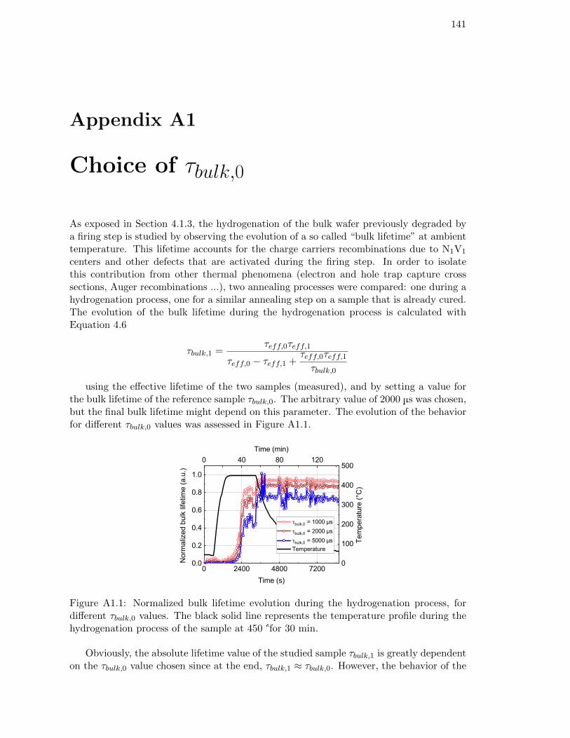
141
Appendix A1
Choice of τbulk,0
As exposed in Section 4.1.3, the hydrogenation of the bulk wafer previously degraded bya firing step is studied by observing the evolution of a so called “bulk lifetime” at ambienttemperature. This lifetime accounts for the charge carriers recombinations due to N1V1
centers and other defects that are activated during the firing step. In order to isolatethis contribution from other thermal phenomena (electron and hole trap capture crosssections, Auger recombinations ...), two annealing processes were compared: one during ahydrogenation process, one for a similar annealing step on a sample that is already cured.The evolution of the bulk lifetime during the hydrogenation process is calculated withEquation 4.6
τbulk,1 =τeff,0τeff,1
τeff,0 − τeff,1 +τeff,0τeff,1τbulk,0
using the effective lifetime of the two samples (measured), and by setting a value forthe bulk lifetime of the reference sample τbulk,0. The arbitrary value of 2000 µs was chosen,but the final bulk lifetime might depend on this parameter. The evolution of the behaviorfor different τbulk,0 values was assessed in Figure A1.1.
0 2400 4800 7200
0 40 80 120
0.0
0.2
0.4
0.6
0.8
1.0
Time (min)
Nor
mal
ized
bul
k lif
etim
e (a
.u.)
Time (s)
tbulk,0 = 1000 µs tbulk,0 = 2000 µs tbulk,0 = 5000 µs Temperature
0
100
200
300
400
500
Tem
pera
ture
(°C
)
Figure A1.1: Normalized bulk lifetime evolution during the hydrogenation process, fordifferent τbulk,0 values. The black solid line represents the temperature profile during thehydrogenation process of the sample at 450 °for 30 min.
Obviously, the absolute lifetime value of the studied sample τbulk,1 is greatly dependenton the τbulk,0 value chosen since at the end, τbulk,1 ≈ τbulk,0. However, the behavior of the

142 APPENDIX A1. CHOICE OF τBULK,0
normalized bulk lifetime τbulk,1/τbulk,0 is very similar for lifetime values of 1000, 2000, and5000 µs, which are reasonable guesses of bulk lifetime for a p-type float-zone wafer. Theconclusions drawn are consequently not impacted by the arbitrary choice of the value ofτbulk,0.
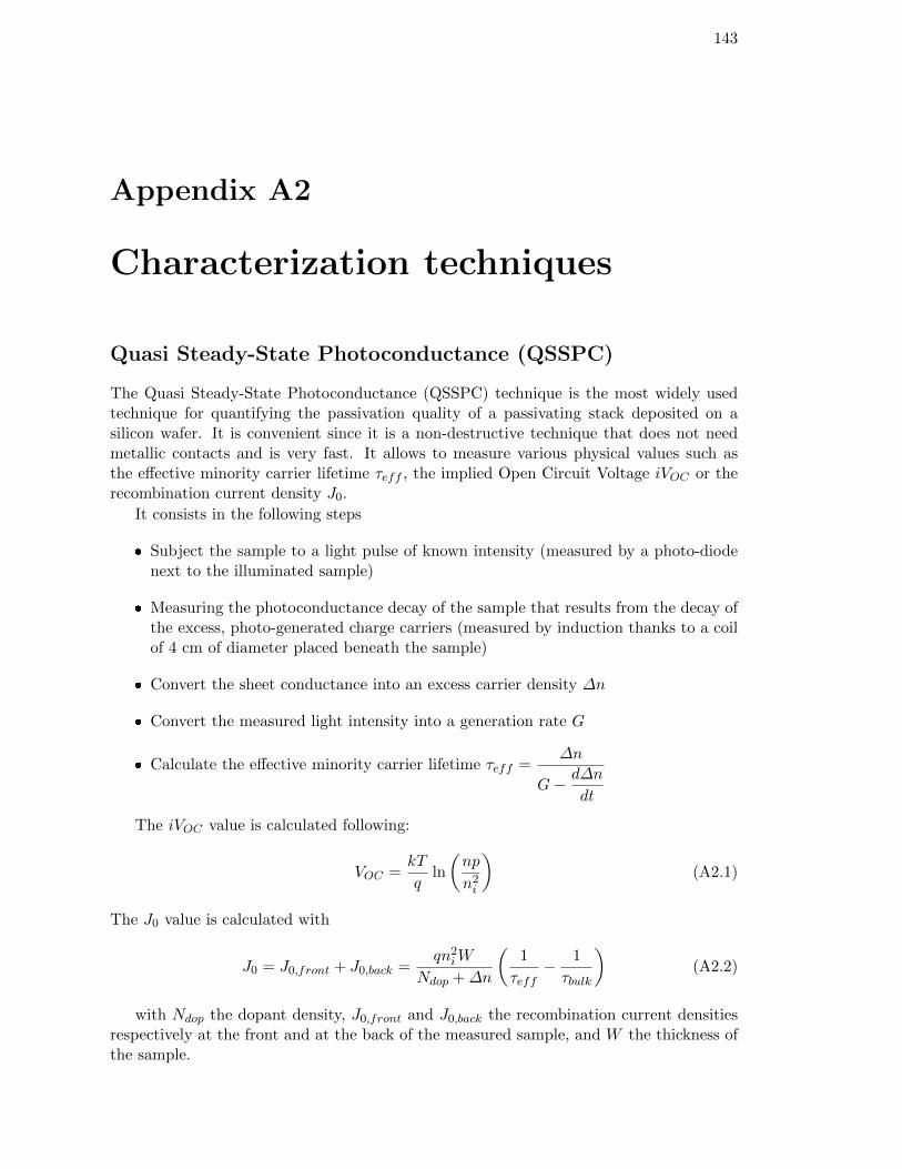
143
Appendix A2
Characterization techniques
Quasi Steady-State Photoconductance (QSSPC)
The Quasi Steady-State Photoconductance (QSSPC) technique is the most widely usedtechnique for quantifying the passivation quality of a passivating stack deposited on asilicon wafer. It is convenient since it is a non-destructive technique that does not needmetallic contacts and is very fast. It allows to measure various physical values such asthe effective minority carrier lifetime τeff , the implied Open Circuit Voltage iVOC or therecombination current density J0.
It consists in the following steps
Subject the sample to a light pulse of known intensity (measured by a photo-diodenext to the illuminated sample)
Measuring the photoconductance decay of the sample that results from the decay ofthe excess, photo-generated charge carriers (measured by induction thanks to a coilof 4 cm of diameter placed beneath the sample)
Convert the sheet conductance into an excess carrier density ∆n
Convert the measured light intensity into a generation rate G
Calculate the effective minority carrier lifetime τeff =∆n
G− d∆n
dt
The iVOC value is calculated following:
VOC =kT
qln
(np
n2i
)(A2.1)
The J0 value is calculated with
J0 = J0,front + J0,back =qn2iW
Ndop +∆n
(1
τeff− 1
τbulk
)(A2.2)
with Ndop the dopant density, J0,front and J0,back the recombination current densitiesrespectively at the front and at the back of the measured sample, and W the thickness ofthe sample.
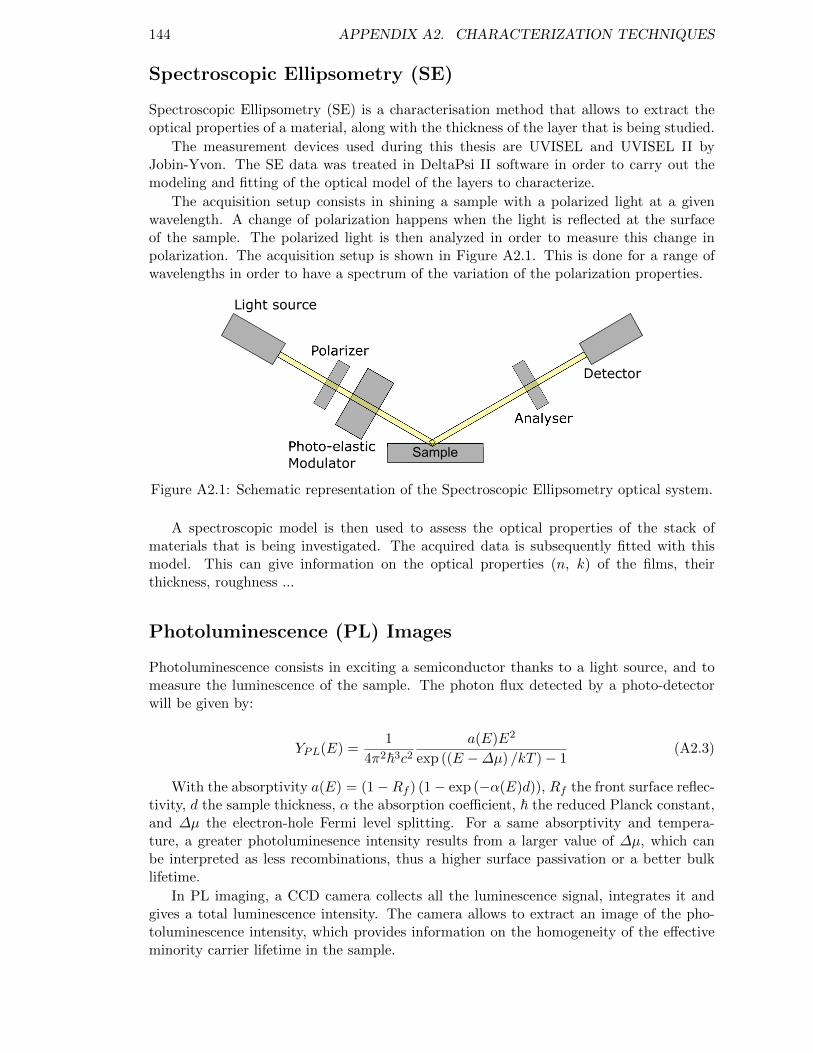
144 APPENDIX A2. CHARACTERIZATION TECHNIQUES
Spectroscopic Ellipsometry (SE)
Spectroscopic Ellipsometry (SE) is a characterisation method that allows to extract theoptical properties of a material, along with the thickness of the layer that is being studied.
The measurement devices used during this thesis are UVISEL and UVISEL II byJobin-Yvon. The SE data was treated in DeltaPsi II software in order to carry out themodeling and fitting of the optical model of the layers to characterize.
The acquisition setup consists in shining a sample with a polarized light at a givenwavelength. A change of polarization happens when the light is reflected at the surfaceof the sample. The polarized light is then analyzed in order to measure this change inpolarization. The acquisition setup is shown in Figure A2.1. This is done for a range ofwavelengths in order to have a spectrum of the variation of the polarization properties.
Figure A2.1: Schematic representation of the Spectroscopic Ellipsometry optical system.
A spectroscopic model is then used to assess the optical properties of the stack ofmaterials that is being investigated. The acquired data is subsequently fitted with thismodel. This can give information on the optical properties (n, k) of the films, theirthickness, roughness ...
Photoluminescence (PL) Images
Photoluminescence consists in exciting a semiconductor thanks to a light source, and tomeasure the luminescence of the sample. The photon flux detected by a photo-detectorwill be given by:
YPL(E) =1
4π2~3c2a(E)E2
exp ((E −∆µ) /kT )− 1(A2.3)
With the absorptivity a(E) = (1−Rf ) (1− exp (−α(E)d)), Rf the front surface reflec-tivity, d the sample thickness, α the absorption coefficient, ~ the reduced Planck constant,and ∆µ the electron-hole Fermi level splitting. For a same absorptivity and tempera-ture, a greater photoluminesence intensity results from a larger value of ∆µ, which canbe interpreted as less recombinations, thus a higher surface passivation or a better bulklifetime.
In PL imaging, a CCD camera collects all the luminescence signal, integrates it andgives a total luminescence intensity. The camera allows to extract an image of the pho-toluminescence intensity, which provides information on the homogeneity of the effectiveminority carrier lifetime in the sample.
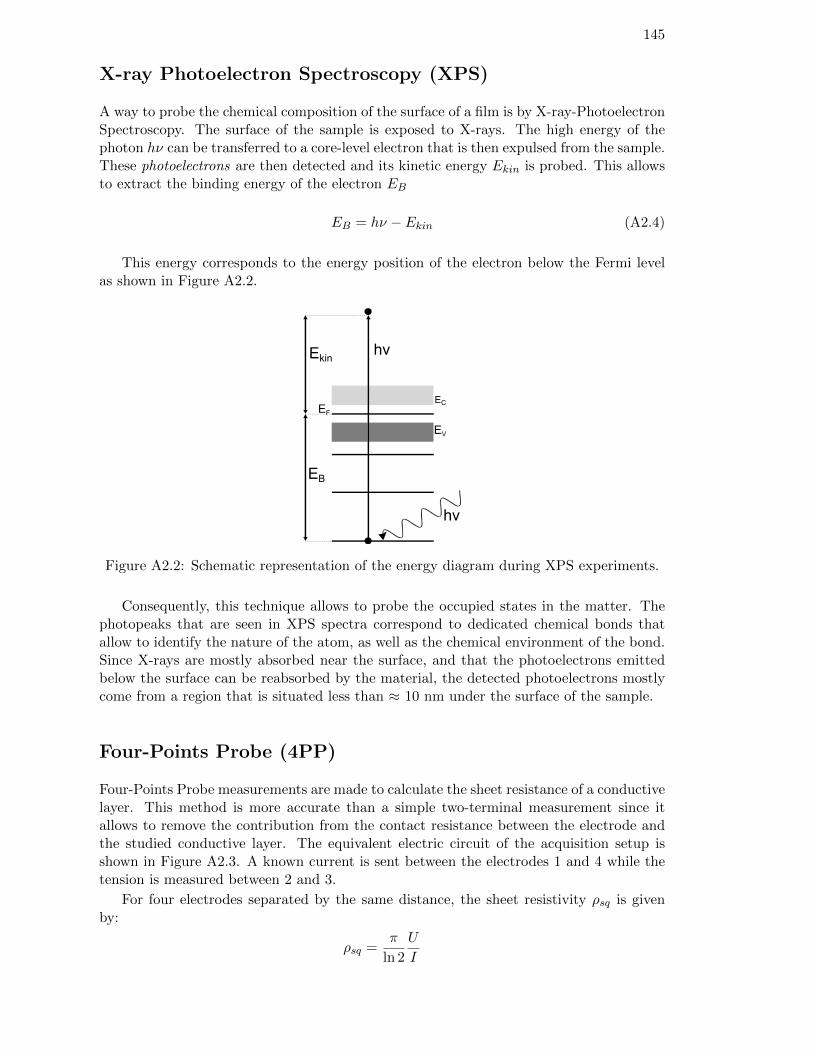
145
X-ray Photoelectron Spectroscopy (XPS)
A way to probe the chemical composition of the surface of a film is by X-ray-PhotoelectronSpectroscopy. The surface of the sample is exposed to X-rays. The high energy of thephoton hν can be transferred to a core-level electron that is then expulsed from the sample.These photoelectrons are then detected and its kinetic energy Ekin is probed. This allowsto extract the binding energy of the electron EB
EB = hν − Ekin (A2.4)
This energy corresponds to the energy position of the electron below the Fermi levelas shown in Figure A2.2.
Figure A2.2: Schematic representation of the energy diagram during XPS experiments.
Consequently, this technique allows to probe the occupied states in the matter. Thephotopeaks that are seen in XPS spectra correspond to dedicated chemical bonds thatallow to identify the nature of the atom, as well as the chemical environment of the bond.Since X-rays are mostly absorbed near the surface, and that the photoelectrons emittedbelow the surface can be reabsorbed by the material, the detected photoelectrons mostlycome from a region that is situated less than ≈ 10 nm under the surface of the sample.
Four-Points Probe (4PP)
Four-Points Probe measurements are made to calculate the sheet resistance of a conductivelayer. This method is more accurate than a simple two-terminal measurement since itallows to remove the contribution from the contact resistance between the electrode andthe studied conductive layer. The equivalent electric circuit of the acquisition setup isshown in Figure A2.3. A known current is sent between the electrodes 1 and 4 while thetension is measured between 2 and 3.
For four electrodes separated by the same distance, the sheet resistivity ρsq is givenby:
ρsq =π
ln 2
U
I
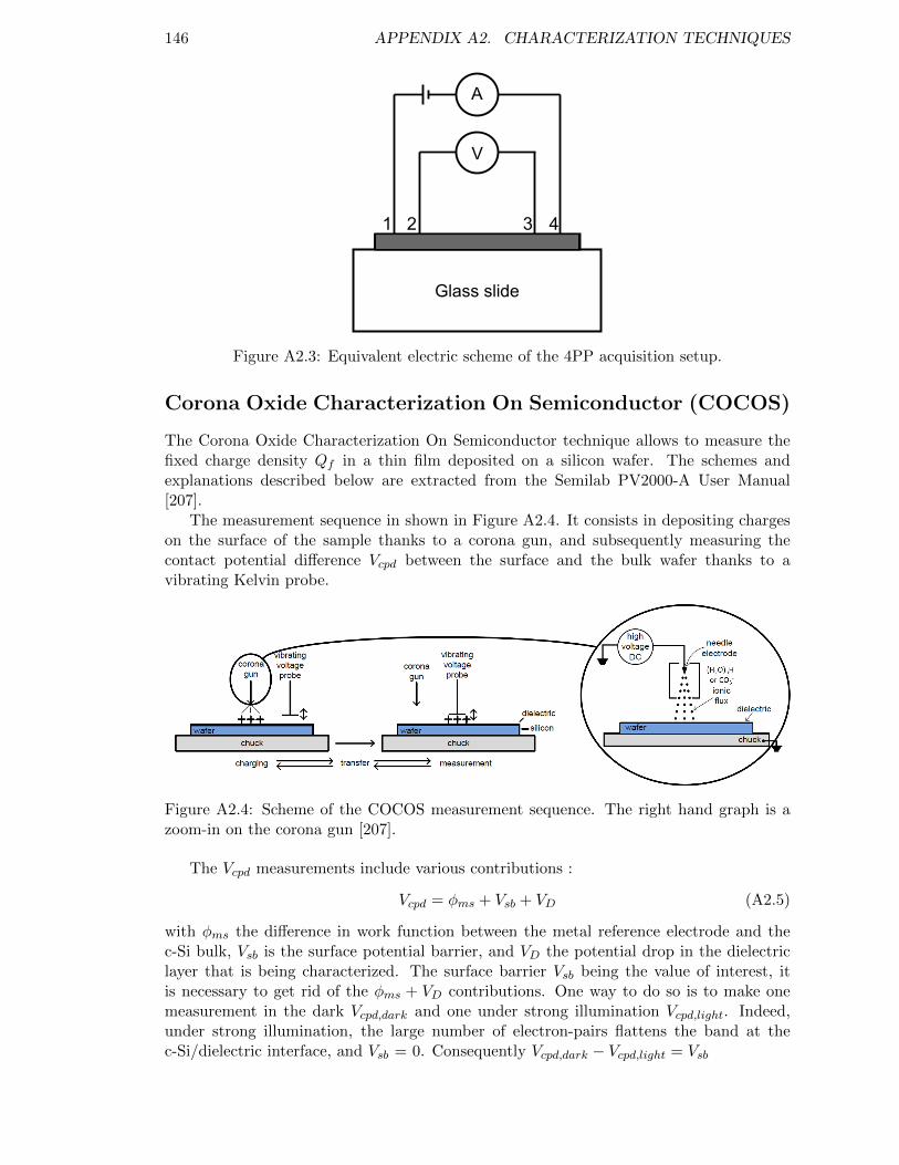
146 APPENDIX A2. CHARACTERIZATION TECHNIQUES
Figure A2.3: Equivalent electric scheme of the 4PP acquisition setup.
Corona Oxide Characterization On Semiconductor (COCOS)
The Corona Oxide Characterization On Semiconductor technique allows to measure thefixed charge density Qf in a thin film deposited on a silicon wafer. The schemes andexplanations described below are extracted from the Semilab PV2000-A User Manual[207].
The measurement sequence in shown in Figure A2.4. It consists in depositing chargeson the surface of the sample thanks to a corona gun, and subsequently measuring thecontact potential difference Vcpd between the surface and the bulk wafer thanks to avibrating Kelvin probe.
Figure A2.4: Scheme of the COCOS measurement sequence. The right hand graph is azoom-in on the corona gun [207].
The Vcpd measurements include various contributions :
Vcpd = φms + Vsb + VD (A2.5)
with φms the difference in work function between the metal reference electrode and thec-Si bulk, Vsb is the surface potential barrier, and VD the potential drop in the dielectriclayer that is being characterized. The surface barrier Vsb being the value of interest, itis necessary to get rid of the φms + VD contributions. One way to do so is to make onemeasurement in the dark Vcpd,dark and one under strong illumination Vcpd,light. Indeed,under strong illumination, the large number of electron-pairs flattens the band at thec-Si/dielectric interface, and Vsb = 0. Consequently Vcpd,dark − Vcpd,light = Vsb
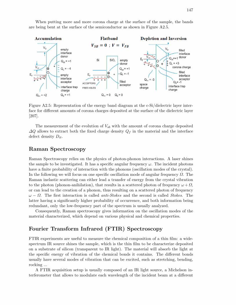
147
When putting more and more corona charge at the surface of the sample, the bandsare being bent at the surface of the semiconductor as shown in Figure A2.5.
Figure A2.5: Representation of the energy band diagram at the c-Si/dielectric layer inter-face for different amounts of corona charges deposited at the surface of the dielectric layer[207].
The measurement of the evolution of Vsb with the amount of corona charge deposited∆Q allows to extract both the fixed charge density Qf in the material and the interfacedefect density Dit.
Raman Spectroscopy
Raman Spectroscopy relies on the physics of photon-phonon interactions. A laser shinesthe sample to be investigated. It has a specific angular frequency ω. The incident photonshave a finite probability of interaction with the phonons (oscillation modes of the crystal).In the following we will focus on one specific oscillation mode of angular frequency Ω. TheRaman inelastic scattering can either lead a transfer of energy from the crystal vibrationto the photon (phonon-anihilation), that results in a scattered photon of frequency ω+Ω,or can lead to the creation of a phonon, thus resulting on a scattered photon of frequencyω − Ω. The first interaction is called anti-Stokes and the second is called Stokes. Thelatter having a significantly higher probability of occurrence, and both information beingredundant, only the low-frequency part of the spectrum is usually analyzed.
Consequently, Raman spectroscopy gives information on the oscillation modes of thematerial characterized, which depend on various physical and chemical properties.
Fourier Transform Infrared (FTIR) Spectroscopy
FTIR experiments are useful to measure the chemical composition of a thin film: a wide-spectrum IR source shines the sample, which is the thin film to be characterize depositedon a substrate of silicon (transparent to IR light). The material will absorb the light atthe specific energy of vibration of the chemical bonds it contains. The different bondsusually have several modes of vibration that can be excited, such as stretching, bending,rocking ...
A FTIR acquisition setup is usually composed of an IR light source, a Michelson in-terferometer that allows to modulate each wavelength of the incident beam at a different

148 APPENDIX A2. CHARACTERIZATION TECHNIQUES
frequency. The signal that is measured depends on the position of the Michelson configu-ration (position of the mirror). This signal actually corresponds to the Fourier transformof the incident light intensity. Consequently, calculating the inverted Fourier transform ofthe signal allows to get the spectral decomposition of the light intensity. By reflecting thelight beam to go through the sample, analyzing this new interferogram and comparing theresulting spectrum with the one of the incident beam, this allows to extract the spectralabsorption of the sample.
In our analyzes of the SiNx:H layers, a FTIR of the bare silicon wafer is carried out inorder to remove this contribution (background).
149
Appendix A3
Resume en Francais
Introduction
L’indice de developpement humain (IDH) est un indicateur de l’esperance de vie, del’education et du revenu par habitant des differentes regions du monde. Il est generalementconsidere comme un element de mesure du progres et du developpement des pays. D’apresle programme de developpement des Nations Unies, il existe une correlation entre l’IDHet la consommation d’energie par habitant [1]. L’acces a une energie abordable est donccapital pour le developpement des pays et leur capacite a offrir un meilleur niveau devie a leurs habitants. Le Conseil Mondial de l’Energie a identifie trois grands defis quel’industrie de l’energie doit relever : le ”trilemme” energetique [2]. Ces trois piliers sontl’equite energetique, la securite energetique et la durabilite environnementale.
Sur notre planete, la consommation d’energie par habitant est repartie de maniere tresinhomogene d’un pays a l’autre (0,25 tep/hab.1 pour le Bangladesh contre 16,38 tep/hab.pour le Qatar en 2017 [3]), principalement en raison des differences de produit interieurbrut et d’acces aux ressources. Au sein meme des pays, les menages peuvent etre ap-provisionnes en energie de maniere tres inegale en raison de prix eleves ou d’absence deconnexion au reseau. Les systemes energetiques doivent egalement etre surs, flexibles etresilients afin d’eviter les pannes d’electricite qui peuvent avoir des effets desastreux surla mortalite (blackout dans les hopitaux) ou sur l’economie. Le Groupe d’experts Inter-gouvernemental sur l’Evolution du Climat (GIEC) indique en outre que le changementclimatique et ses consequences - tels que le rechauffement de la planete, l’acidification desoceans et l’effondrement de la biodiversite - sont principalement dus aux activites humaineset plus particulierement aux emissions de dioxyde de carbone (CO2) ou d’autres gaz a effetde serre [208]. En effet, une forte activite economique est correlee a une consommationd’energie importante, alors que le mix energetique mondial actuel est principalement basesur les combustibles fossiles qui emettent du CO2 dans l’atmosphere lors de leur utilisa-tion (combustion pour transformer l’energie chimique en energie mecanique, thermique ouelectrique) [3].
L’energie solaire photovoltaıque (PV) est une source d’energie qui pourrait apporterune reponse a au moins deux des problemes evoques. Le soleil brille dans tous les paysdu globe, ce qui contribue a l’attenuation du probleme de la distribution des ressourceset permet une meilleure independance energetique des pays (equite energetique). Maissurtout, son principe de fonctionnement ne repose pas sur les combustibles fossiles cequi en fait un moyen de production d’electricite qui emet beaucoup moins de gaz a effet
1tep = tonne d’equivalent petrole, 1 tep = 11630 kWh, source : Agence Internationale de l’Energie
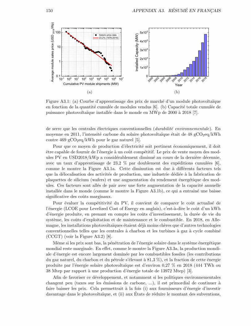
150 APPENDIX A3. RESUME EN FRANCAIS
10-1 100 101 102 103 104 105 106 1070.1
1
10
100 historic price data 23.2% (1976-2018)
Aver
age
mod
ule
sale
s pr
ice
(USD
2018
/Wp)
Cumulative PV module shipments (MW)
(a)
2000
2002
2004
2006
2008
2010
2012
2014
2016
2018
0
1x10⁵
2x10⁵
3x10⁵
4x10⁵
5x10⁵
Year
Inst
alle
d C
apac
ity (M
W)
(b)
Figure A3.1: (a) Courbe d’apprentissage des prix de marche d’un module photovoltaıqueen fonction de la quantite cumulee de modules vendus [6]. (b) Capacite totale cumulee depuissance photovoltaıque installee dans le monde en MWp de 2000 a 2018 [7].
de serre que les centrales electriques conventionnelles (durabilite environnementale). Enmoyenne en 2011, l’intensite carbone du solaire photovoltaıque etait de 48 gCO2eq/kWhcontre 469 gCO2eq/kWh pour le gaz naturel [5].
Pour que ce moyen de production d’electricite soit pertinent economiquement, il doitetre capable de fournir de l’energie a un cout competitif. Le prix de vente moyen des mod-ules PV en USD2018/kWp a considerablement diminue au cours de la derniere decennie,avec un taux d’apprentissage de 23,2 % par doublement des expeditions cumulees [6],comme le montre la Figure A3.1a. Cette diminution est due a differents facteurs telsque la delocalisation des activites de production, une industrie dediee a la fabrication deplaquettes de silicium (wafers) et une augmentation du rendement energetique des mod-ules. Ces facteurs sont alles de pair avec une forte augmentation de la capacite annuelleinstallee dans le monde (comme le montre la Figure A3.1b), ce qui a entraıne une baissesignificative des couts marginaux.
Pour evaluer la competitivite du PV, il convient de comparer le cout actualise del’energie (LCOE pour Levelized Cost of Energy en anglais), c’est-a-dire le cout d’un kWhd’energie produite, en prenant en compte les couts d’investissement, la duree de vie dusysteme, les couts d’exploitation et de maintenance et le combustible. En 2018, en Alle-magne, les installations photovoltaıques etaient deja moins cheres que d’autres technologiesconventionnelles telles que les centrales a charbon et les turbines a gaz a cycle combine(CCGT) (voir la Figure A3.2) [8].
Meme si les prix sont bas, la penetration de l’energie solaire dans le systeme energetiquemondial reste marginale. En effet, comme le montre la Figure A3.3a, la production mondi-ale d’energie est encore largement dominee par les combustibles fossiles (les contributionsdu gaz naturel, du charbon et du petrole s’elevant a 81,3 %), et la fraction de cette energieproduite par l’energie solaire photovoltaıque est d’environ 0,27 % en 2018 (444 TWh ou38 Mtep par rapport a une production d’energie totale de 13972 Mtep) [3].
Afin de favoriser ce developpement, et notamment si les politiques environnementaleschangent peu (taxes sur les emissions de carbone, ...), il est primordial de continuer afaire baisser les prix. Cela permettrait a la fois (i) aux fournisseurs d’energie d’investirdavantage dans le photovoltaıque, et (ii) aux Etats de reduire le montant des subventions,
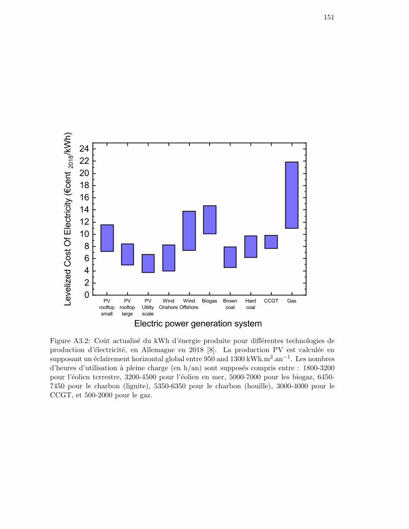
151
PVrooftopsmall
PVrooftoplarge
PVUtilityscale
WindOnshore
WindOffshore
Biogas Browncoal
Hardcoal
CCGT Gas02468
1012141618202224
Electric power generation system
Leve
lized
Cos
t Of E
lect
ricity
(ce
nt20
18/k
Wh)
Figure A3.2: Cout actualise du kWh d’energie produite pour differentes technologies deproduction d’electricite, en Allemagne en 2018 [8]. La production PV est calculee ensupposant un eclairement horizontal global entre 950 and 1300 kWh.m2.an−1. Les nombresd’heures d’utilisation a pleine charge (en h/an) sont supposes compris entre : 1800-3200pour l’eolien terrestre, 3200-4500 pour l’eolien en mer, 5000-7000 pour les biogaz, 6450-7450 pour le charbon (lignite), 5350-6350 pour le charbon (houille), 3000-4000 pour leCCGT, et 500-2000 pour le gaz.
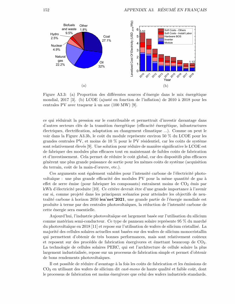
152 APPENDIX A3. RESUME EN FRANCAIS
Other1.8%
Biofuelsand waste
9.5%Hydro2.5%
Nuclear4.9%
Naturalgas
22.2% Oil32%
Coal27.1%
(a)
2010
2011
2012
2013
2014
2015
2016
2017
2018
0
1
2
3
4
5
6
1.13
Year
Leve
lized
Cos
t Of E
lect
ricity
(USD
2018
/Wp)
Soft Costs - Others Soft Costs - Install Labor Hardware BOS Inverter Module
5.52
(b)
Figure A3.3: (a) Proportion des differentes sources d’energie dans le mix energetiquemondial, 2017 [3]. (b) LCOE (ajuste en fonction de l’inflation) de 2010 a 2018 pour lescentrales PV avec traqueur a un axe (100 MW) [9].
ce qui reduirait la pression sur le contribuable et permettrait d’investir davantage dansd’autres secteurs cles de la transition energetique (efficacite energetique, infrastructureselectriques, electrification, adaptation au changement climatique ...). Comme on peut levoir dans la Figure A3.3b, le cout du module represente environ 50 % du LCOE pour lesgrandes centrales PV, et moins de 10 % pour le PV residentiel, car les couts de systemesont relativement eleves [9]. Une solution pour reduire de maniere significative le LCOE estde fabriquer des modules plus efficaces tout en maintenant de faibles couts de fabricationet d’investissement. Cela permet de reduire le cout global, car des dispositifs plus efficacesgenerent une plus grande puissance de sortie pour les memes couts de systeme (acquisitiondu terrain, cout de la main-d’œuvre, etc.).
Ces arguments sont egalement valables pour l’intensite carbone de l’electricite photo-voltaıque : une plus grande efficacite des modules PV pour la meme quantite de gaz aeffet de serre emise (pour fabriquer les composants) entraınent moins de CO2 emis parkWh d’electricite produite [10]. Ce critere devrait etre d’une grande importance a l’avenircar si, comme projete dans les principaux scenarios pour atteindre les objectifs de neu-tralite carbone a horizon 2050 iea˙net˙2021, une grande partie de l’energie mondiale estproduite a terme par des centrales photovoltaıques, la reduction de l’intensite carbone decette energie sera essentielle.
Aujourd’hui, l’industrie photovoltaıque est largement basee sur l’utilisation du siliciumcomme materiau semi-conducteur. Ce type de panneau solaire represente 95 % du marchedu photovoltaıque en 2018 [11] et repose sur l’utilisation de wafers de silicium cristallise. Lamajorite des cellules solaires actuelles sont basees sur des wafers de silicium monocristallinqui permettent d’obtenir de tres bonnes performances, mais sont relativement couteuxet reposent sur des procedes de fabrication energivores et emettant beaucoup de CO2.La technologie de cellules solaires PERC, qui est l’architecture de cellule solaire la pluslargement industrialisee, repose sur un processus de fabrication simple et permet d’obtenirde bons rendements photovoltaıques.
Il est possible de reduire d’avantage a la fois les couts de fabrication et les emissions deCO2 en utilisant des wafers de silicium dit cast-mono de haute qualite et faible cout, dontle processus de fabrication est moins energivore que celui des wafers industriels standards.
153
En outre, une technologie de cellules solaires tres prometteuse pour augmenter encoreles rendements tout en maintenant de faibles couts de fabrication dans un avenir procheest la technologie des cellules a contacts passives. Elle permet d’atteindre des efficacitesde cellule solaire plus elevees en reduisant les pertes electriques, et presente l’avantaged’utiliser principalement des machines qui sont deja presentes dans les lignes de productionindustrielles actuelles. Cette technologie est deja en cours d’industrialisation dans certainesentreprises [12]. Neanmoins, le processus de fabrication standard pour cette architecturede cellule solaire a contacts passives necessite de nombreuses etapes, ainsi qu’un budgetthermique eleve entre autre a cause de la necessite d’une etape de recuit de plusieursminutes entre 600 et 1000 °C. C’est pourquoi il convient d’etudier de nouvelles methodesde fabrication de ce type de cellules solaires, procedes qui seraient moins gourmands enenergie et qui necessiteraient moins d’etapes de fabrication.
Cette these de doctorat porte sur l’etude d’un procede de fabrication simplifie decontacts passives, appele contact passive avec recuit rapide (FPC pour Fired PassivatedContact en anglais), qui permet de reduire le nombre d’etapes de fabrication et d’exposerla cellule solaire a un budget thermique reduit. Les principales caracteristiques etudieessont les proprietes de passivation des FPC, qui traduisent les pertes electriques dans ledispositif. Des caracterisations par photoluminescence modulee in situ sont realisees pouratteindre cet objectif : elles permettent de mesurer l’evolution des proprietes de passivationen temps reel pendant une etape specifique du fabrication. Pour conclure, ces contactssont integres sur des wafers de silicium cast-mono fabriques par Photowatt [13].
Chapitre 1 : Contexte et objectifs
Un procede de fabrication ne necessitant pas de longue etape de recuit (5-15 min) a hautetemperature (600-1000 °C) pour la formation de contacts passives (voir Figure A3.4a)a ete propose par Ingenito et al. [46]. Il s’appuie sur l’utilisation du recuit rapide ahaute temperature (firing, environ 3 s a 800 °C) deja necessaire pour la metallisation de lacellule. Le procede de fabrication consiste a deposer une couche de silicium resistante aufiring. Dans l’etude en question, il s’agit de carbure de silicium amorphe ou nanocristallinhydrogene (a-SiCx:H ou nc-SiCx:H), depose sur une fine couche d’oxyde de silicium (SiOx).Pendant le depot, la couche de carbure de silicium est dopee au bore ((p) SiCx:H) pourpermettre d’extraire les trous, porteurs de charge positifs. Ensuite, l’echantillon est soumisa l’etape de firing, qui engendre une cristallisation supplementaire de la couche de (p) a-SiCx:H et permet la metallisation de la face avant (non etudiee dans cette these). Afind’atteindre une qualite de passivation elevee, un processus d’hydrogenation supplementaireest necessaire [87]: de l’hydrogene diffusant a l’interieur de la cellule permet de passiverdes defauts et ameliorer la qualite de la cellule. Pour ce faire, une couche de nitrure desilicium amorphe hydrogene (a-SiNx:H) est deposee par PECVD, puis recuite a 450 °Cpendant 30 minutes. Elle est ensuite gravee par immersion dans de l’acide hydrofluorique,et la cellule est completee par le depot d’une couche d’oxyde transparent conducteur et enserigraphiant une grille d’argent a basse temperature.
Cependant, les longues etapes d’hydrogenation ne sont pas souhaitables pour uneintegration industrielle (reduction de la cadence de production) et la metallisation a hautetemperature est preferable a la metallisation a basse temperature pour une meilleure com-patibilite avec les outils de production industriels preexistants. Pour outrepasser ces lim-itations, nous etudions un procede pour la fabrication de FPC alternatif, illustre dans laFigure A3.4b. Il commence par une etape de nettoyage standard (dit RCA) suivie du depotd’une fine couche de SiOx. Une couche de silicium dopee au bore est ensuite deposee par
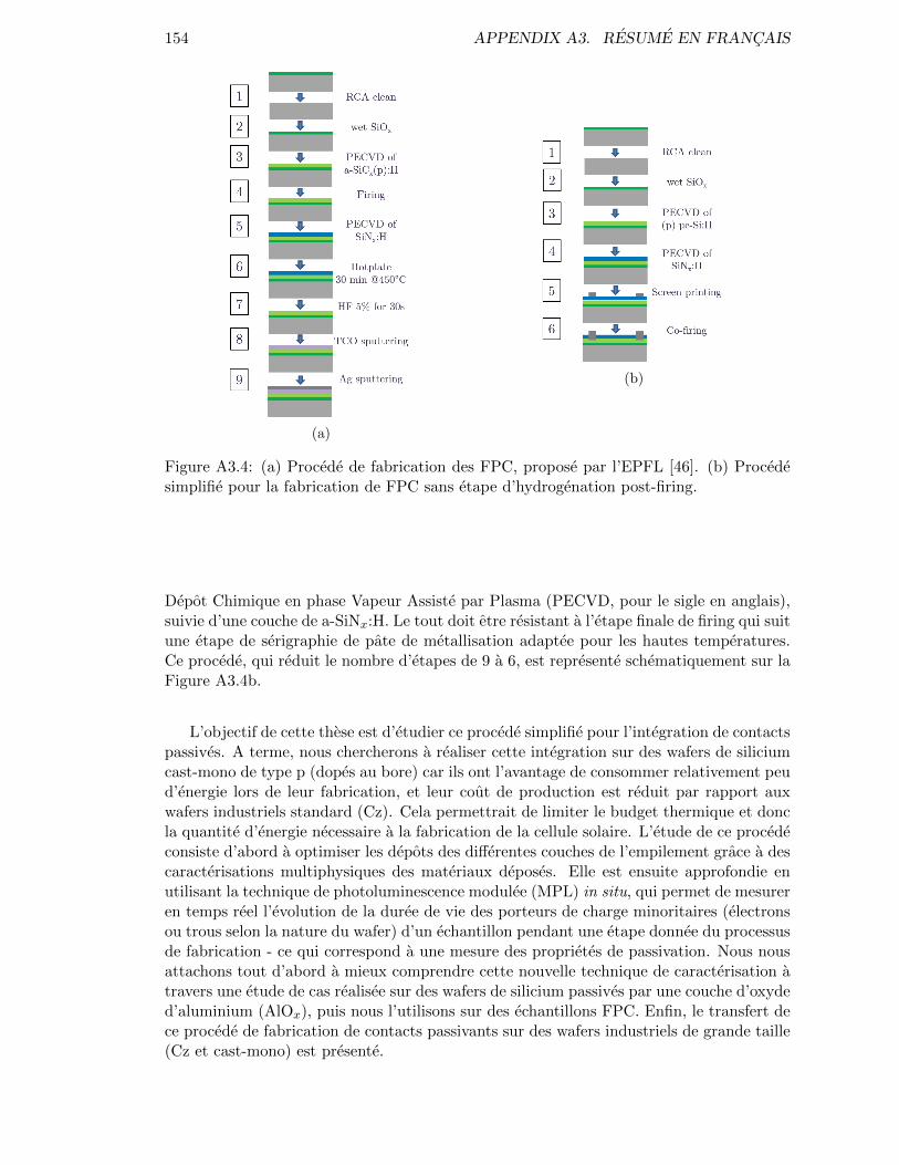
154 APPENDIX A3. RESUME EN FRANCAIS
(a)
(b)
Figure A3.4: (a) Procede de fabrication des FPC, propose par l’EPFL [46]. (b) Procedesimplifie pour la fabrication de FPC sans etape d’hydrogenation post-firing.
Depot Chimique en phase Vapeur Assiste par Plasma (PECVD, pour le sigle en anglais),suivie d’une couche de a-SiNx:H. Le tout doit etre resistant a l’etape finale de firing qui suitune etape de serigraphie de pate de metallisation adaptee pour les hautes temperatures.Ce procede, qui reduit le nombre d’etapes de 9 a 6, est represente schematiquement sur laFigure A3.4b.
L’objectif de cette these est d’etudier ce procede simplifie pour l’integration de contactspassives. A terme, nous chercherons a realiser cette integration sur des wafers de siliciumcast-mono de type p (dopes au bore) car ils ont l’avantage de consommer relativement peud’energie lors de leur fabrication, et leur cout de production est reduit par rapport auxwafers industriels standard (Cz). Cela permettrait de limiter le budget thermique et doncla quantite d’energie necessaire a la fabrication de la cellule solaire. L’etude de ce procedeconsiste d’abord a optimiser les depots des differentes couches de l’empilement grace a descaracterisations multiphysiques des materiaux deposes. Elle est ensuite approfondie enutilisant la technique de photoluminescence modulee (MPL) in situ, qui permet de mesureren temps reel l’evolution de la duree de vie des porteurs de charge minoritaires (electronsou trous selon la nature du wafer) d’un echantillon pendant une etape donnee du processusde fabrication - ce qui correspond a une mesure des proprietes de passivation. Nous nousattachons tout d’abord a mieux comprendre cette nouvelle technique de caracterisation atravers une etude de cas realisee sur des wafers de silicium passives par une couche d’oxyded’aluminium (AlOx), puis nous l’utilisons sur des echantillons FPC. Enfin, le transfert dece procede de fabrication de contacts passivants sur des wafers industriels de grande taille(Cz et cast-mono) est presente.
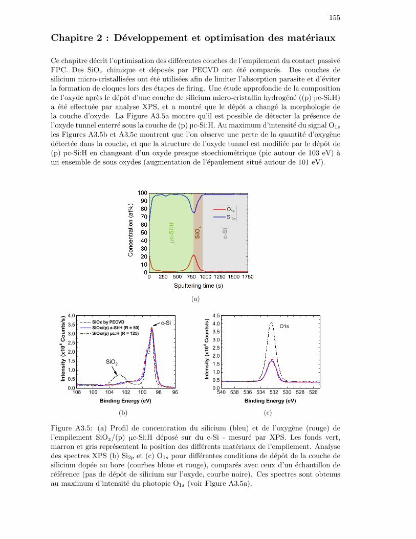
155
Chapitre 2 : Developpement et optimisation des materiaux
Ce chapitre decrit l’optimisation des differentes couches de l’empilement du contact passiveFPC. Des SiOx chimique et deposes par PECVD ont ete compares. Des couches desilicium micro-cristallisees ont ete utilisees afin de limiter l’absorption parasite et d’eviterla formation de cloques lors des etapes de firing. Une etude approfondie de la compositionde l’oxyde apres le depot d’une couche de silicium micro-cristallin hydrogene ((p) µc-Si:H)a ete effectuee par analyse XPS, et a montre que le depot a change la morphologie dela couche d’oxyde. La Figure A3.5a montre qu’il est possible de detecter la presence del’oxyde tunnel enterre sous la couche de (p) µc-Si:H. Au maximum d’intensite du signal O1s
les Figures A3.5b et A3.5c montrent que l’on observe une perte de la quantite d’oxygenedetectee dans la couche, et que la structure de l’oxyde tunnel est modifiee par le depot de(p) µc-Si:H en changeant d’un oxyde presque stoechiometrique (pic autour de 103 eV) aun ensemble de sous oxydes (augmentation de l’epaulement situe autour de 101 eV).
(a)
108 106 104 102 100 98 960.0
0.5
1.0
1.5
2.0
2.5
3.0
3.5
4.0c-Si SiOx by PECVD
SiOx/(p) a-Si:H (R = 50) SiOx/(p) µc:H (R = 125)
Inte
nsity
(x10
4 Cou
nts/
s)
Binding Energy (eV)
SiO2
(b)
540 538 536 534 532 530 528 5260.00.51.01.52.02.53.03.54.04.5
Inte
nsity
(x10
4 Cou
nts/
s)
Binding Energy (eV)
O1s
(c)
Figure A3.5: (a) Profil de concentration du silicium (bleu) et de l’oxygene (rouge) del’empilement SiOx/(p) µc-Si:H depose sur du c-Si - mesure par XPS. Les fonds vert,marron et gris representent la position des differents materiaux de l’empilement. Analysedes spectres XPS (b) Si2p et (c) O1s pour differentes conditions de depot de la couche desilicium dopee au bore (courbes bleue et rouge), compares avec ceux d’un echantillon dereference (pas de depot de silicium sur l’oxyde, courbe noire). Ces spectres sont obtenusau maximum d’intensite du photopic O1s (voir Figure A3.5a).
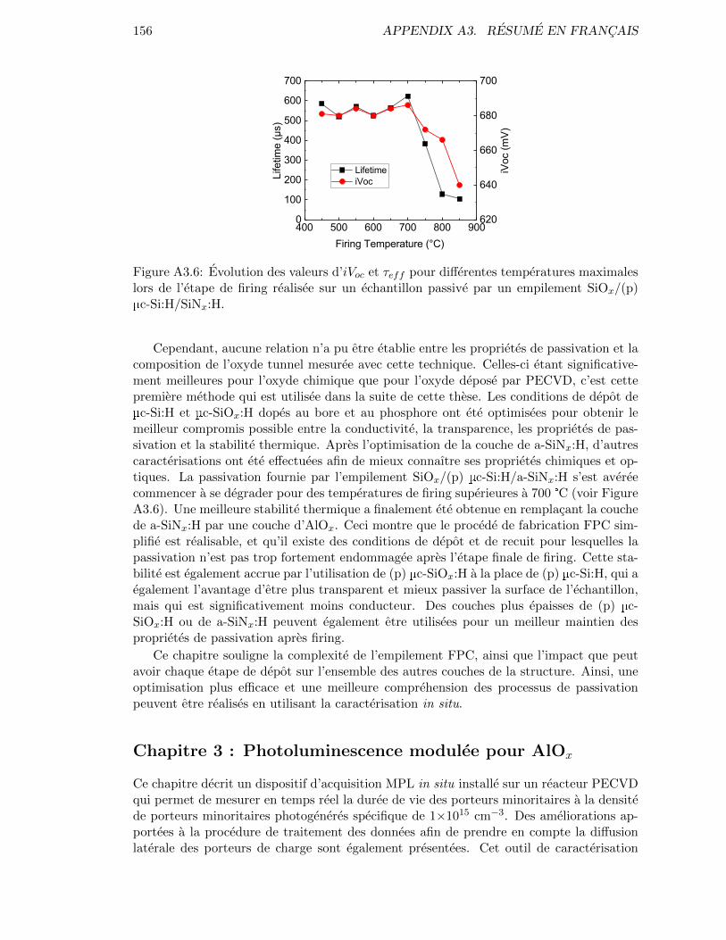
156 APPENDIX A3. RESUME EN FRANCAIS
400 500 600 700 800 9000
100
200
300
400
500
600
700
Life
time
(µs)
Firing Temperature (°C)
Lifetime iVoc
620
640
660
680
700
iVoc
(mV)
Figure A3.6: Evolution des valeurs d’iVoc et τeff pour differentes temperatures maximaleslors de l’etape de firing realisee sur un echantillon passive par un empilement SiOx/(p)µc-Si:H/SiNx:H.
Cependant, aucune relation n’a pu etre etablie entre les proprietes de passivation et lacomposition de l’oxyde tunnel mesuree avec cette technique. Celles-ci etant significative-ment meilleures pour l’oxyde chimique que pour l’oxyde depose par PECVD, c’est cettepremiere methode qui est utilisee dans la suite de cette these. Les conditions de depot deµc-Si:H et µc-SiOx:H dopes au bore et au phosphore ont ete optimisees pour obtenir lemeilleur compromis possible entre la conductivite, la transparence, les proprietes de pas-sivation et la stabilite thermique. Apres l’optimisation de la couche de a-SiNx:H, d’autrescaracterisations ont ete effectuees afin de mieux connaıtre ses proprietes chimiques et op-tiques. La passivation fournie par l’empilement SiOx/(p) µc-Si:H/a-SiNx:H s’est avereecommencer a se degrader pour des temperatures de firing superieures a 700 °C (voir FigureA3.6). Une meilleure stabilite thermique a finalement ete obtenue en remplacant la couchede a-SiNx:H par une couche d’AlOx. Ceci montre que le procede de fabrication FPC sim-plifie est realisable, et qu’il existe des conditions de depot et de recuit pour lesquelles lapassivation n’est pas trop fortement endommagee apres l’etape finale de firing. Cette sta-bilite est egalement accrue par l’utilisation de (p) µc-SiOx:H a la place de (p) µc-Si:H, qui aegalement l’avantage d’etre plus transparent et mieux passiver la surface de l’echantillon,mais qui est significativement moins conducteur. Des couches plus epaisses de (p) µc-SiOx:H ou de a-SiNx:H peuvent egalement etre utilisees pour un meilleur maintien desproprietes de passivation apres firing.
Ce chapitre souligne la complexite de l’empilement FPC, ainsi que l’impact que peutavoir chaque etape de depot sur l’ensemble des autres couches de la structure. Ainsi, uneoptimisation plus efficace et une meilleure comprehension des processus de passivationpeuvent etre realises en utilisant la caracterisation in situ.
Chapitre 3 : Photoluminescence modulee pour AlOx
Ce chapitre decrit un dispositif d’acquisition MPL in situ installe sur un reacteur PECVDqui permet de mesurer en temps reel la duree de vie des porteurs minoritaires a la densitede porteurs minoritaires photogeneres specifique de 1×1015 cm−3. Des ameliorations ap-portees a la procedure de traitement des donnees afin de prendre en compte la diffusionlaterale des porteurs de charge sont egalement presentees. Cet outil de caracterisation
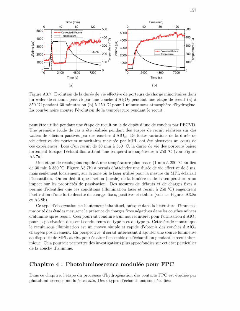
157
0 2400 4800 7200
0 40 80 120
0
1000
2000
3000
4000
5000
Time (min)
Life
time
(µs)
Time (s)
Corrected lifetime Temperature
250°C
0
100
200
300
400
500
Tem
pera
ture
(°C
)
(a)
0 2400 4800 7200
0 40 80 120
0
1000
2000
3000
4000
5000
Time (min)
Life
time
(µs)
Time (s)
Corrected lifetime Temperature
0
100
200
300
400
500
Tem
pera
ture
(°C
)
(b)
Figure A3.7: Evolution de la duree de vie effective de porteurs de charge minoritaires dansun wafer de silicium passive par une couche d’Al2O3 pendant une etape de recuit (a) a350 °C pendant 30 minutes ou (b) a 250 °C pour 1 minute sous atmosphere d’hydrogene.La courbe noire montre l’evolution de la temperature pendant le recuit.
peut etre utilise pendant une etape de recuit ou le de depot d’une de couches par PECVD.Une premiere etude de cas a ete realisee pendant des etapes de recuit realisees sur deswafers de silicium passives par des couches d’AlOx. De fortes variations de la duree devie effective des porteurs minoritaires mesuree par MPL ont ete observees au cours deces experiences. Lors d’un recuit de 30 min a 350 °C, la duree de vie des porteurs baissefortement lorsque l’echantillon atteint une temperature superieure a 250 °C (voir FigureA3.7a).
Une etape de recuit plus rapide a une temperature plus basse (1 min a 250 °C au lieude 30 min a 350 °C, Figure A3.7b) a permis d’atteindre une duree de vie effective de 5 ms,mais seulement localement, sur la zone ou le laser utilise pour la mesure du MPL eclairaitl’echantillon. On en deduit que l’action (locale) de la lumiere et de la temperature a unimpact sur les proprietes de passivation. Des mesures de defauts et de charges fixes apermis d’identifier que ces conditions (illumination laser et recuit a 250 °C) engendrentl’activation d’une forte densite de charges fixes, positives et stables (voir les Figures A3.8aet A3.8b).
Ce type d’observation est hautement inhabituel, puisque dans la litterature, l’immensemajorite des etudes mesurent la presence de charges fixes negatives dans les couches mincesd’alumine apres recuit. Ceci pourrait conduire a un nouvel interet pour l’utilisation d’AlOx
pour la passivation des semi-conducteurs de type n et de type p. Cette etude montre quele recuit sous illumination est un moyen simple et rapide d’obtenir des couches d’AlOx
chargees positivement. En perspective, il serait interessant d’ajouter une source lumineuseau dispositif de MPL in situ pour eclairer l’ensemble de l’echantillon pendant le recuit ther-mique. Cela pourrait permettre des investigations plus approfondies sur cet etat particulierde la couche d’alumine.
Chapitre 4 : Photoluminescence modulee pour FPC
Dans ce chapitre, l’etape du processus d’hydrogenation des contacts FPC est etudiee parphotoluminescence modulee in situ. Deux types d’echantillons sont etudies:
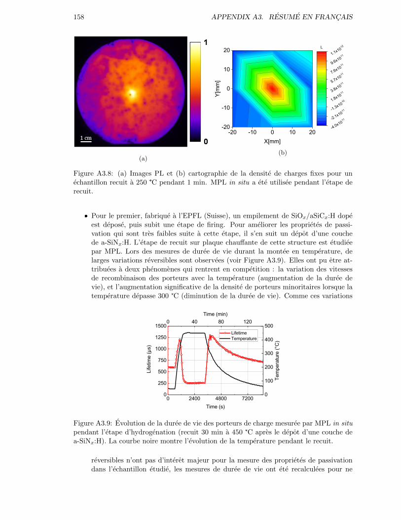
158 APPENDIX A3. RESUME EN FRANCAIS
(a)
-20 -10 0 10 20-20
-10
0
10
20
Y[mm]
X[mm]
-4.0x10
11-2.1x10
11-1.3x10
101.8x10
113.8x10
115.7x
1011
7.6x10
119.6x10
111.1x
1012L
(b)
Figure A3.8: (a) Images PL et (b) cartographie de la densite de charges fixes pour unechantillon recuit a 250 °C pendant 1 min. MPL in situ a ete utilisee pendant l’etape derecuit.
Pour le premier, fabrique a l’EPFL (Suisse), un empilement de SiOx/aSiCx:H dopeest depose, puis subit une etape de firing. Pour ameliorer les proprietes de passi-vation qui sont tres faibles suite a cette etape, il s’en suit un depot d’une couchede a-SiNx:H. L’etape de recuit sur plaque chauffante de cette structure est etudieepar MPL. Lors des mesures de duree de vie durant la montee en temperature, delarges variations reversibles sont observees (voir Figure A3.9). Elles ont pu etre at-tribuees a deux phenomenes qui rentrent en competition : la variation des vitessesde recombinaison des porteurs avec la temperature (augmentation de la duree devie), et l’augmentation significative de la densite de porteurs minoritaires lorsque latemperature depasse 300 °C (diminution de la duree de vie). Comme ces variations
0 2400 4800 7200
0 40 80 120
0
250
500
750
1000
1250
1500
Time (min)
Life
time
(µs)
Time (s)
Lifetime Temperature
0
100
200
300
400
500
Tem
pera
ture
(°C
)
Figure A3.9: Evolution de la duree de vie des porteurs de charge mesuree par MPL in situpendant l’etape d’hydrogenation (recuit 30 min a 450 °C apres le depot d’une couche dea-SiNx:H). La courbe noire montre l’evolution de la temperature pendant le recuit.
reversibles n’ont pas d’interet majeur pour la mesure des proprietes de passivationdans l’echantillon etudie, les mesures de duree de vie ont ete recalculees pour ne
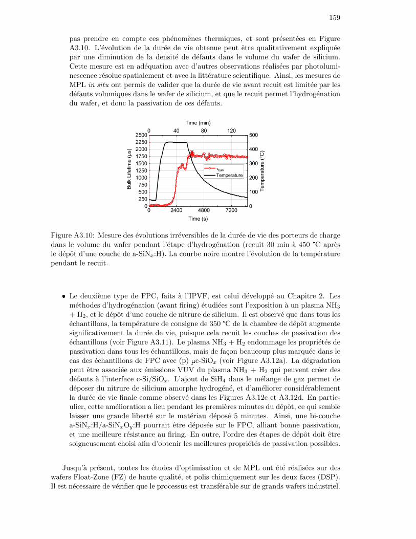
159
pas prendre en compte ces phenomenes thermiques, et sont presentees en FigureA3.10. L’evolution de la duree de vie obtenue peut etre qualitativement expliqueepar une diminution de la densite de defauts dans le volume du wafer de silicium.Cette mesure est en adequation avec d’autres observations realisees par photolumi-nescence resolue spatialement et avec la litterature scientifique. Ainsi, les mesures deMPL in situ ont permis de valider que la duree de vie avant recuit est limitee par lesdefauts volumiques dans le wafer de silicium, et que le recuit permet l’hydrogenationdu wafer, et donc la passivation de ces defauts.
0 2400 4800 7200
0 40 80 120
0250500750
1000125015001750200022502500
Time (min)Bu
lk L
ifetim
e (µ
s)
Time (s)
tbulk
Temperature
0
100
200
300
400
500
Tem
pera
ture
(°C
)
Figure A3.10: Mesure des evolutions irreversibles de la duree de vie des porteurs de chargedans le volume du wafer pendant l’etape d’hydrogenation (recuit 30 min a 450 °C apresle depot d’une couche de a-SiNx:H). La courbe noire montre l’evolution de la temperaturependant le recuit.
Le deuxieme type de FPC, faits a l’IPVF, est celui developpe au Chapitre 2. Lesmethodes d’hydrogenation (avant firing) etudiees sont l’exposition a un plasma NH3
+ H2, et le depot d’une couche de nitrure de silicium. Il est observe que dans tous lesechantillons, la temperature de consigne de 350 °C de la chambre de depot augmentesignificativement la duree de vie, puisque cela recuit les couches de passivation desechantillons (voir Figure A3.11). Le plasma NH3 + H2 endommage les proprietes depassivation dans tous les echantillons, mais de facon beaucoup plus marquee dans lecas des echantillons de FPC avec (p) µc-SiOx (voir Figure A3.12a). La degradationpeut etre associee aux emissions VUV du plasma NH3 + H2 qui peuvent creer desdefauts a l’interface c-Si/SiOx. L’ajout de SiH4 dans le melange de gaz permet dedeposer du nitrure de silicium amorphe hydrogene, et d’ameliorer considerablementla duree de vie finale comme observe dans les Figures A3.12c et A3.12d. En partic-ulier, cette amelioration a lieu pendant les premieres minutes du depot, ce qui semblelaisser une grande liberte sur le materiau depose 5 minutes. Ainsi, une bi-couchea-SiNx:H/a-SiNxOy:H pourrait etre deposee sur le FPC, alliant bonne passivation,et une meilleure resistance au firing. En outre, l’ordre des etapes de depot doit etresoigneusement choisi afin d’obtenir les meilleures proprietes de passivation possibles.
Jusqu’a present, toutes les etudes d’optimisation et de MPL ont ete realisees sur deswafers Float-Zone (FZ) de haute qualite, et polis chimiquement sur les deux faces (DSP).Il est necessaire de verifier que le processus est transferable sur de grands wafers industriel.
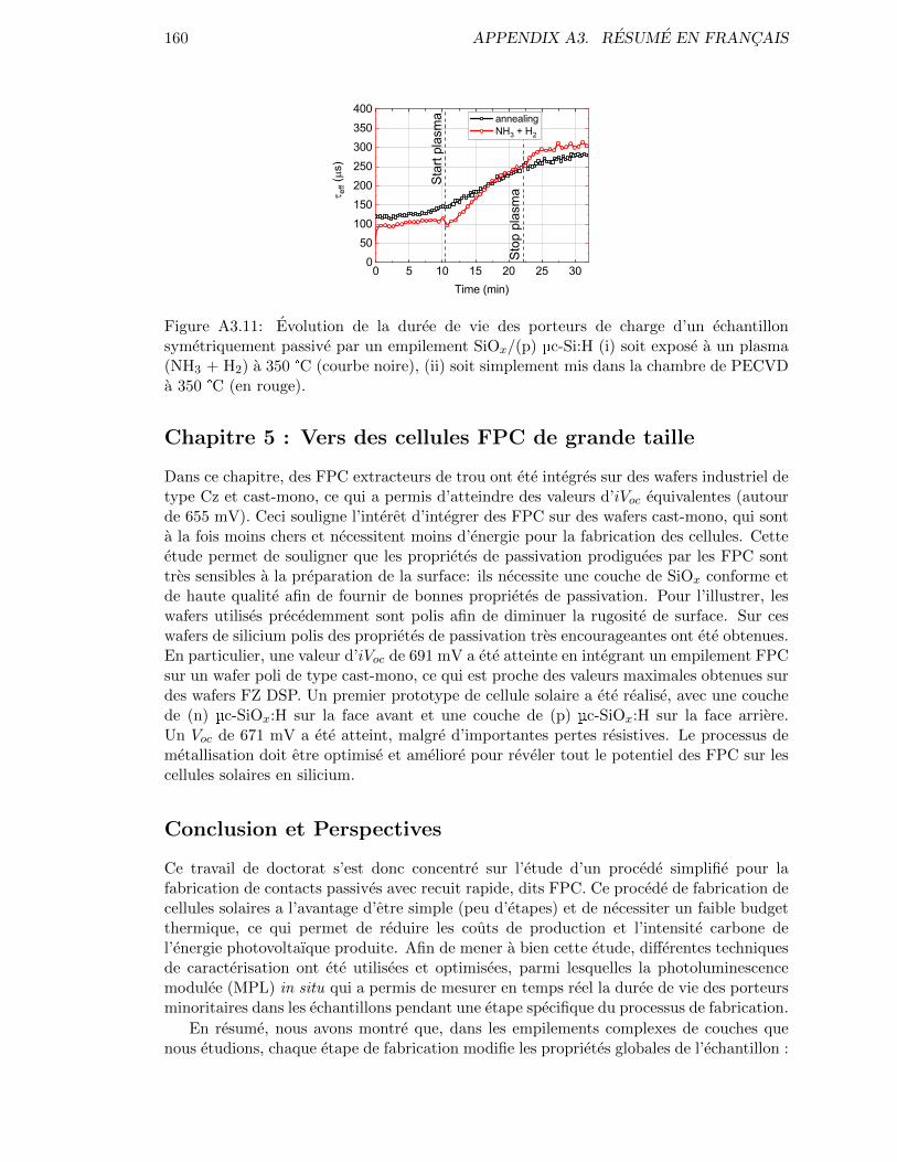
160 APPENDIX A3. RESUME EN FRANCAIS
0 5 10 15 20 25 300
50100150200250300350400
annealing NH3 + H2
t eff (ms
)
Time (min)
Star
t pla
sma
Stop
pla
sma
Figure A3.11: Evolution de la duree de vie des porteurs de charge d’un echantillonsymetriquement passive par un empilement SiOx/(p) µc-Si:H (i) soit expose a un plasma(NH3 + H2) a 350 °C (courbe noire), (ii) soit simplement mis dans la chambre de PECVDa 350 °C (en rouge).
Chapitre 5 : Vers des cellules FPC de grande taille
Dans ce chapitre, des FPC extracteurs de trou ont ete integres sur des wafers industriel detype Cz et cast-mono, ce qui a permis d’atteindre des valeurs d’iVoc equivalentes (autourde 655 mV). Ceci souligne l’interet d’integrer des FPC sur des wafers cast-mono, qui sonta la fois moins chers et necessitent moins d’energie pour la fabrication des cellules. Cetteetude permet de souligner que les proprietes de passivation prodiguees par les FPC sonttres sensibles a la preparation de la surface: ils necessite une couche de SiOx conforme etde haute qualite afin de fournir de bonnes proprietes de passivation. Pour l’illustrer, leswafers utilises precedemment sont polis afin de diminuer la rugosite de surface. Sur ceswafers de silicium polis des proprietes de passivation tres encourageantes ont ete obtenues.En particulier, une valeur d’iVoc de 691 mV a ete atteinte en integrant un empilement FPCsur un wafer poli de type cast-mono, ce qui est proche des valeurs maximales obtenues surdes wafers FZ DSP. Un premier prototype de cellule solaire a ete realise, avec une couchede (n) µc-SiOx:H sur la face avant et une couche de (p) µc-SiOx:H sur la face arriere.Un Voc de 671 mV a ete atteint, malgre d’importantes pertes resistives. Le processus demetallisation doit etre optimise et ameliore pour reveler tout le potentiel des FPC sur lescellules solaires en silicium.
Conclusion et Perspectives
Ce travail de doctorat s’est donc concentre sur l’etude d’un procede simplifie pour lafabrication de contacts passives avec recuit rapide, dits FPC. Ce procede de fabrication decellules solaires a l’avantage d’etre simple (peu d’etapes) et de necessiter un faible budgetthermique, ce qui permet de reduire les couts de production et l’intensite carbone del’energie photovoltaıque produite. Afin de mener a bien cette etude, differentes techniquesde caracterisation ont ete utilisees et optimisees, parmi lesquelles la photoluminescencemodulee (MPL) in situ qui a permis de mesurer en temps reel la duree de vie des porteursminoritaires dans les echantillons pendant une etape specifique du processus de fabrication.
En resume, nous avons montre que, dans les empilements complexes de couches quenous etudions, chaque etape de fabrication modifie les proprietes globales de l’echantillon :
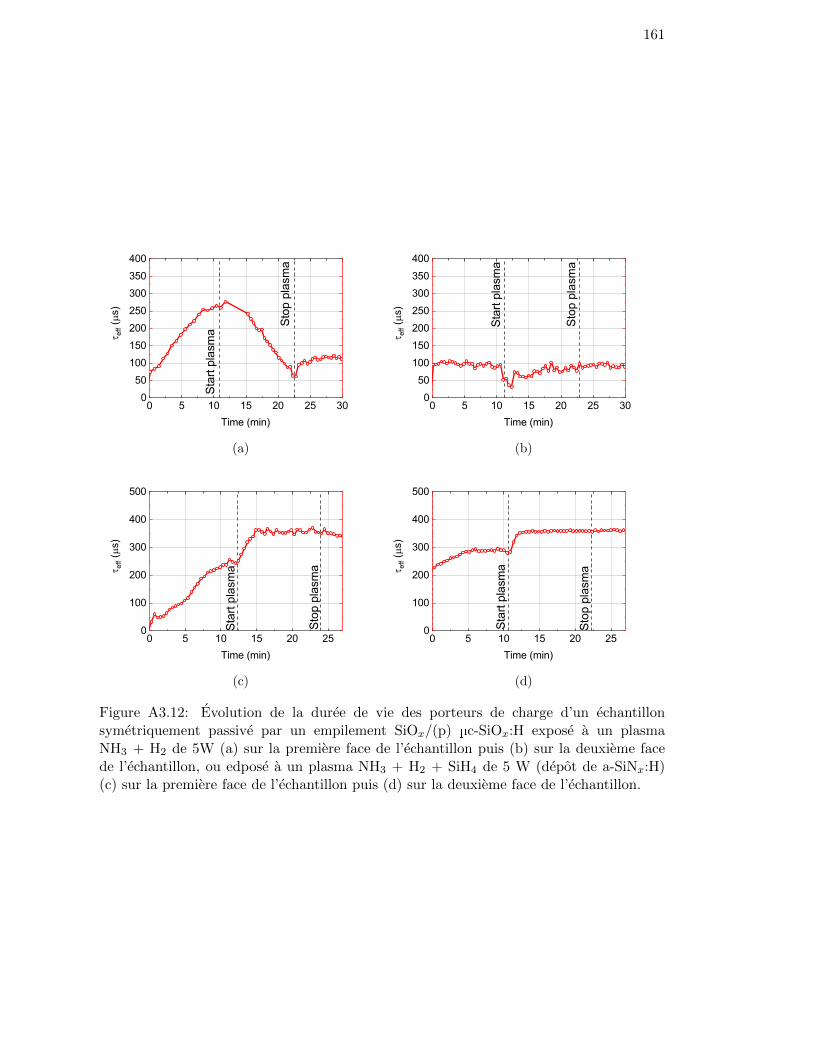
161
0 5 10 15 20 25 300
50100150200250300350400
t eff (ms
)
Time (min)
Star
t pla
sma
Stop
pla
sma
(a)
0 5 10 15 20 25 300
50100150200250300350400
t eff (ms
)
Time (min)
Stop
pla
sma
Star
t pla
sma
(b)
0 5 10 15 20 250
100
200
300
400
500
t eff (ms
)
Time (min)
Star
t pla
sma
Stop
pla
sma
(c)
0 5 10 15 20 250
100
200
300
400
500
t eff (ms
)
Time (min)
Star
t pla
sma
Stop
pla
sma
(d)
Figure A3.12: Evolution de la duree de vie des porteurs de charge d’un echantillonsymetriquement passive par un empilement SiOx/(p) µc-SiOx:H expose a un plasmaNH3 + H2 de 5W (a) sur la premiere face de l’echantillon puis (b) sur la deuxieme facede l’echantillon, ou edpose a un plasma NH3 + H2 + SiH4 de 5 W (depot de a-SiNx:H)(c) sur la premiere face de l’echantillon puis (d) sur la deuxieme face de l’echantillon.
162 APPENDIX A3. RESUME EN FRANCAIS
les depots des differents films ont un impact sur les couches deposees precedemment (voirles mesures XPS et d’ellipsometrie). En raison du role critique des interfaces dans les per-formances de nos dispositifs, les techniques de caracterisation optique et chimique standardne sont pas suffisantes, et des mesures electroniques sont necessaires : un leger changementdans les conditions de depot des materiaux peut conduire a des proprietes electroniquescompletement differentes (comme des charges fixes positives ou negatives dans les couchesd’AlOx en fonction du type de recuit applique). La caracterisation electrique sur les dis-positifs finaux n’est pas suffisante pour comprendre les mecanismes physico-chimiques enjeu, ce qui a motive l’utilisation de techniques de caracterisation in situ. Les mesures deMPL in situ peuvent aider a trouver la meilleure combinaison de materiaux pour max-imiser a la fois la resistance au firing et les proprietes de passivation. Au regard desresultats obtenus, de nombreuses etudes pourraient etre realisees afin de pousser plus loinla comprehension et les ameliorations qu’ont permis cette these.
Par la suite, des caracterisations supplementaires doivent etre realisees pour mieuxcomprendre l’origine et la nature des charges fixes positives observees dans les couchesd’AlOx : des analyses XPS permettraient de connaıtre la configuration chimique de lacouche d’AlOx, la variation de la source lumineuse (distribution spectrale, flux de photons,...) permettraient de mieux comprendre les mecanismes de formations de ces charges, etenfin il est necessaire de verifier la possibilite d’obtenir de l’AlOx charge positivement surde plus grandes surfaces.
Une amelioration de la routine d’acquisition MPL et du traitement des donnees devraitetre realisee afin de mieux prendre en compte les variations de temperature. Le traitementdoit etre entierement repense pour les mesures a haute temperature (plus de 350 °C) sil’on veut visualiser uniquement les evolution de la passivation de surface et de volume.Toutefois, il est utile de rappeler qu’a temperature constante, les variations de la duree devie mesurees representent des variations reelles des proprietes de passivation.
Une etude plus approfondie de la couche superieure du FPC devrait etre menee pourde futures ameliorations. L’augmentation de la duree de vie se produisant exclusivementpendant les premieres minutes du depot de a-SiNx:H, cela ouvre la voie au developpementde nouveaux empilements : il peut etre envisage de faire un depot d’une couche de quelquesnm d’un materiau riche en hydrogene qui pourrait augmenter la passivation de l’interfacec-Si/SiOx (comme du a-SiNx:H) jusqu’a atteindre une duree de vie maximale, puis d’unecouche qui pourrait augmenter la stabilite thermique de l’empilement de passivation lorsdu firing, comme le a-SiNxOyCz:H. Ces bi-couches doivent etre etudiees en utilisant laMPL in situ pendant leur depot afin d’optimiser la duree du procede et d’obtenir unemeilleure comprehension de l’impact des differentes especes presentes dans le plasma.
Des recherches approfondies sur la metallisation et sur la temperature optimale defiring doivent etre realisees afin de permettre l’integration des FPC sur des wafers desilicium de taille industrielle. De plus, il serait tres interessant d’etudier la stabilite a longterme et le vieillissement des cellules solaires FPC, et de les comparer a la duree de viedes cellules solaires a contacts passives fabriquees par d’autres procedes de fabrication.
La recherche de procedes de fabrication de cellules solaires ayant un impact environ-nemental de plus en plus faible est d’une importance majeure pour adresser les problematiquesd’acceptabilite du PV et justifier l’adoption a plus grande echelle de ces dispositifs (TW decapacite de production installee chaque annee). Des recherches amont sur les procedes defabrication devraient inciter l’industrie photovoltaıque a adopter des methodes plus sobresafin de contribuer a un avenir plus durable.
Titre: Developpement et caracterisation de contacts passives avec recuit rapide (FPC) pour la fabrication decellules solaires en silicium.
Mots cles: photovoltaıque, cellules solaires en silicium, contacts passives, caracterisation in situ, photolumi-nescence modulee
Resume: Etant appelee a jouer un role determinantdans la transition energetique, l’industrie photo-voltaıque est mise au defi de reduire l’impact envi-ronnemental de la fabrication de panneaux solaires.Selon toute probabilite, les cellules solaires en sili-cium a contacts passives (TOPCon) domineront lemarche dans les prochaines annees grace a leurs ex-cellentes performances electriques. Cependant, leurintegration est energivore, d’ou l’etude de nouveauxprocedes de fabrication comme les contacts passivesavec recuit rapide (FPC).Ce manuscrit presente l’optimisation des conditionsde depots des differentes couches utilisees dans unecellule FPC, ainsi que des caracterisations pousseesde ces couches. Des analyses de spectroscopiephotoelectronique X ont permis de montrer que ledepot d’une couche de (p) µc-Si:H par depot chim-ique en phase vapeur assiste par plasma (PECVD)modifie la composition chimique de l’oxyde tunnel en-terre dans l’empilement passivant.Des ameliorations ont ete apportees a un disposi-tif d’acquisition de Photoluminescence Modulee em-barque sur un reacteur de depot PECVD. Cette tech-
nique permet de mesurer en temps reel l’evolutionde la duree de vie des porteurs de charge dans unechantillon durant une etape de fabrication. Celaa permis de montrer que l’action combinee de latemperature et de la lumiere engendre l’activationde charges fixes positives stables dans des couchesd’AlOx, ce qui est tres inhabituel.Les mesures de passivation en tempsreel d’echantillons FPC pendant une etaped’hydrogenation ont mis en evidence l’importancemajeure de la temperature et de la duree du recuitpour atteindre les niveaux de passivation attendus.Cette technique a egalement ete utilisee pendant ledepot de couches de SiNx:H. Elle a permis d’observer(i) les fortes degradations liees aux plasmas directsde H2 et NH3 sur des couches de (p) µc-SiOx et(ii) que pendant le depot de SiNx:H, la majorite del’amelioration de la passivation a lieu pendant lespremieres minutes de depot. L’integration de contactsFPC a ete realise sur de grands wafers industriels detype mono-cast, donnant des resultats prometteurssur surfaces polies.
Title: Development and characterization of Fired Passivating Contacts for p-type silicon solar cells fabrication.
Keywords: photovoltaics, silicon solar cells, passivating contacts, in situ characterization, modulated photo-luminescence
Abstract: Due to its expected role in the energy tran-sition, the photovoltaic industry is being challenged toreduce the environmental impact of the manufactur-ing of solar panels. The silicon solar cells with TunnelOxide Passivated Contact (TOPCon) technology arelikely to broadly hit the market within the next yearsdue to their great electrical performances. Yet their in-tegration is rather energy intensive, which is why novelmanufacturing options such as the Fired PassivatingContact (FPC) cells are being investigated.This dissertation presents the optimization of the de-position conditions of the various layers of a FPC cell,along with their thorough characterization. X-ray pho-toelectron spectroscopy analysis allowed to show thatthe deposition of a Plasma Enhanced Chemical Va-por Deposited (PECVD) (p) µc-Si:H layer modified thechemical composition of the buried tunnel oxide layerin the passivating stack.Improvements were made on an in situ ModulatedPhotoluminescence acquisition setup mounted on a
PECVD reactor. This technique allows to monitor inreal time the evolution of the passivation properties ofa sample during a given processing step. In a casestudy, this resulted to the demonstration that the com-bined action of light and temperature on AlOx layersleads to the activation of stable positive fixed charges,which is highly unusual.The real-time lifetime measurements of FPC sam-ples during a hydrogenation step evidenced the im-portance of the temperature and duration of the an-nealing step in order to fully achieve high passivationproperties. The technique was also used during theSiNx:H deposition and allowed to show (i) the detri-mental effect of direct H2 and NH3 plasma on FPCand especially on the ones based on (p) µc-SiOx lay-ers, and (ii) that during the SiNx:H deposition, mostof the improvement happens during the first minutesof deposition. The integration of FPC was carried outon large area mono-cast wafers with very promisingresults on polished surfaces.
Institut Polytechnique de Paris91120 Palaiseau, France


