Embed Size (px)
Citation preview

International Journal of Infrared and Millimeter Waves, Vol. 18, No. 2, 1997
D E S I G N O F LAYERED R I D G E D I E L E C T R I C W A V E G U I D E F O R
M I L L I M E T E R AND S U B - M I L L I M E T E R WAVE C I R C U I T S
George E. Ponchak 1 and Linda P. B. Katehi 2
1NASA Lewis Research Center, MS 54/5 21000 Brookpark Road Cleveland, Ohio 44135 2University of Michigan 3240 EECS Building
1301 Beal Avenue Ann Arbor, Michigan 48109-2122
Received November 18, 1996
Abstract
Design rules for Layered Ridge Dielectric Wavegnide (LRDW) are presented for the fLrst time through simple figures and closed form equations. The Effective Dielectric Constant (EDC) method is used to develop the design hies that account for typical circuit spec- ifications such as higher order mode suppression, dispersion, attenuation, and coupling between adjacent transmission lines. Comparisons between the design of LRDW, image guide, and millimeter-wave dielectric ridge guide are made.
Keywords:Dieleclri¢ waveguide, image guide, insulated image guide, millimeter-wave waveguides
1. Introduction
Most millimeter and sub-millimeter wave circuits developed to date have relied on the extension of microwave transmission lines such as microstrip and coplanar wavegnide on thin substrates, but these transmission lines have several disadvantages. The surface re- sistivity of the metal lines increases as .¢rf [1] and the transmission line geometry and
369
0195-9271/97/0200-0369512.50/0 © 1997 Plenum Publishing Corporation

370 Ponchak and Katehi
suhstrate thickness must decrease as 1/f to maintain a single mode transmission line and minimize leakage and dispersion. The result is that the conductor loss per guided wave- length increases with frequency while the dielectric and radiation loss per guided wave- length remain nearly constant.
eliminate the high conductor loss, dielectric waveguldes have been developed. They do not require metallic lines or ground planes to guide the electromagnetic energy, but instead they use the difference in permitlivity between two or more materials to propagate the excited waves. Practical implementation of the wavegnides often necessitates a ground plane for mechanical support and heat sinking. However; since the current is distributed over a wider area on the ground plane than the microstrip line or the center strip of coplanar wavegnide, the conductor loss is greatly reduced. Examples of dielectric waveguides that have been reported are Image Guide[2], Insulated Image GuLide[3], Millimeter-wave Dielectric Ridge Gulde[4], and Layered Ridge Dielectric Wavegtdde (LRDW)[5].
Image guide, insulated image guide, and millimeter-wave dielectric waveguide have been well documented in the literaaue and design procedures have been reported for each wavegnide [4] [6] [7]. Although, LRDW has been analyzed theoretically [5] [8] , LRDW directional couplers have been characterized using the Finite Difference Time Domain method[9], transitions between rectangular wavegnide and LRDW have been developed and modeled using the EDC method[10], and LRDW leaky wave antennas haveheendemonstrated[ll], designprocedures forLRDW have net beenpresented. This paper presents design roles and procedures for LRDW that may be used to optimize the waveguide performance over a specified bandwidth. When possible, closed form equa- tions or charts are given for the design parameters. In addition, comparisons between LRDW and other dielectric waveguides will be given.
2. L R D W Description and Design Criteria
LRDW consists of a strip comprised of two or more layers of insulating materials on a conductor backed dielectric substrate as shown in Figure la. Alternatively, a single layer strip may be used with a multi-layered dielectric substrate as shown in Figure lb. The
design guidelines presented in this paper are meant to optimize the dielectric thickness and permittivity tl,t2, and ta and ~rl, ~r2, and ~r3 respectively and the ridge width, 2a, so that the following design criteria are met:
I. Cutoff higher order modes 2. High field confinement in the ridge 3. Lmge field decay in y - direction 4. Low dispersion
Throughout this study, two assumptions are made. The first is Erl = era which not only simplifies the design, but it also describes semiconductor LRDW fabricated using MBE [5] and silicon-insulator-silicon LRDW. The second assumption is that the design is for the LRDW shown in Figure la. The procedures for the LRDW shown in Figure lb are similar with the only difference being a change in the effective dielectric constant for reglonlI.
LRDW supports two fundamental modes; an E~pq mode that has a dominant y- directed electric field and an E~,q mode that has a dominant x- directed electric field where p and

Dielectric Waveguide for Submillimeter Wave 371
II I I I i !
" I
Sr3 J
.,2J ~rl !
(a)
I I I I
j r
L
,t3
:t2 b , i t l i
3' ground plane
I x ~ I I I I
I
I I II I !
, ,t3
¢r2 ~ ; t2
I 'I Srl ~ t l
£o) ground plane
b
Figure 1: Layered ridge dielectric waveguide (a) consisting of a multilayered dieleclxic ridge on a conductor backed substrate (1o) consisting of a single layered ridge on a multi- layered conductor backed substrate.

372 Ponchak and Katehi
q indicate the order of the mode in the x and y directions respectively. The E ~ mode is shorted out at low frequencies by the ground plane whereas the E~I mode has no cutoff frequency and is dominant at low frequencies. For E* modes, the continuity of the electric flux density across the dielectric layers allows the electric field in the second layer to be given by E2 = ( E 1 / e 2 ) E 1 ---- (ea/e2)E3. Therefore by selecting the permittivity of the dielectric layers such that e2 < El, Ea and operating the guide over the frequency range where (:/ko) 2 < e2, the propagating signal is confined in!he second layer or !be "guiding layer" As the frequency increases, (~/ko) 2 > e2, the signal is still guided by the ridge but becomes confined in one of the two higher permittivity layers.
Since LRDW is similar to the other dielectric waveguides listed above, some aspects of its design are similar Extending Oliner's analysis[13], all of these guides except image guide will leak energy ff ~ / ! H z ~x < eat ! where %:! and eat ! are the effective dielectric con- stants of the strip and the substrate regions shown in Figure I respectively when they are analyzed independently. Furthermore, the mode of the propagating signal is not relevant since reflections at the sidewalls of the ridge create oppositely polarized modes in both regions I and II [13]. Therefore, ira dominant E = mode is to be maintained, the LRDW must be designed to cutoff the E u mode and higher order E = modes in each region. Al- though this criteria leads to more conservative designs, it will be used in this pape~
High field confinement, the ratio of power in the dielectric to the total power.
R --. ffai~t'c'"ic[Re(E x H) • z]dS f f ,# [Re(E × H) • z]dS (1)
is required to reduce parasitic influences of the package and coupling to other waveguides. Furthermore, it has been shown that weak, lateral field confinement increases radiation loss from dielectric waveguide bends [14]. Therefore, R > 0.5 is often cited as a design criteria [6]. In addition, high field confinement in the y- direction is critical for antenna distribution networks where coupling between adjacent feed lines that may be several wavelengths long must be minimized.
Furthermore, field confinement in the guiding layer has several advantages. First, the magnetic field is lower at the ground plane resulting in reduced conductor losses [7] . In addition, the fields are lower at the top of the guide where fabrication defects induce radiation loss, and if the second variation of LRDW shown in Figure lb is.used, defects along the sides of the strip will not contn'bute to radiation loss[12]. Finally, the fields are similar to those of microstrip which facilitates easy transitions between microsaip and LRDW required for integration of active elements or microstrip patch antennas. Thus, besides maximizing the total field conf'mement R, the design should also maximize the ratio of the power in the guiding layer to the total power, P~.
3. LRDW Design
The Effective Dielectric Constant (EDC) method first proposed by Knox and Toulios for image guide and iusulate~l image guide [2] [7] and later generalized by McLcvige [3] has proven useful for estimating the effective dielectric constant, ~ I ! , and the magnitudes of the electromagnetic fields of several transmission lines and dielectric waveguldes. In addition, it has been used in tie design of transitions between LRDW and rectangular waveguide [10] and image guide couplers [2] [3]. It is therefore reasonable to use the EDC method in the design of LRDW with the waveguide initially partitioned into regions

Dielectric Waveguide for Submillimeter Wave 373
I and II as shown in Figure 2 and later recombined as shown in Figure 3 as is normally clone in the EDC method [3] [10].
x
S r 3 ,13
1 a t 1 t l
g r o u n d p l a n e OO
Co) p l a n e
Y
Y
Figure 2: Layered ridge dielectric waveguide partitioned into (a) region I (b) region II.
Before proceeding, the power confinement ratio defined inEqrL 1 is not easily applied in the EDC method since a full description of the fields for tie dielectric waveguide are not determined. Therefore, two new power confinement ratios:
b , R: = fo Re[Ez(x)H~(x)]dx (2)
f o Re[ExCx)I-I;(x)]dx G , f~ Re[Ex(y)H; (y)]dy (3)
R, = f o Re[Ez(y)H~(y)]dy am defined for Figures 2 and 3 respectively. Since the product of R , and R~ is approxi- mately equal to R, the design criteria e r r > 0.5 is replaced by RxR~ > 0.5. Similarly, the ratio of the power in the guiding layer to the total power is defined from Figure 2a to be:
f::+" R~ = oo , (4)
fo Re[E~(x)H;(x)I dx An appropriate starting point in the design process is to determine the maximum ridge
thickness, b, for a specific upper frequency limit. At low frequencies, a conductor backed dielectric slab supports a single mode with an electric field component normal to the ground plane. As the frequency increases, higher order modes may propagate, the first of which has an electric field component in the plane of the dielectric slab. The cutoff frequency for this E v mode is dependent on the dielectric thickness and ponnittivity by

374 Ponchak and Katehi
sll
l X
sl Yl Y
sll
Figure 3: Layered ridge dielectric waveguide as modelled in the effective dielectric con- stant method.
the simple relatiomhip f~ = c/4be,xff~-i-1 [1] where c is the velocity of light. For the dielectric ridge structure comprised of thm¢ dielectric slabs, the cutofffrequency must be determined by solving the following equation:
O = cot(k=~lt l ) -K tan(kzc2t~)-tan(k=cata) { l cot(kzcltl) tan(k~c2t2) + l } (5)
where k=~ = k ~ e ~ - - 1, k.~l = k=~3 since e~t = era. k~ = 2 7 r f ~ , and:
K = ~ e / ~ - 1 v ~r~ ---/ (6)
All of the k=~ti terms can be related to b by introducing normalized thicknesses:
t t Q = - - (7) b
t2 t2 X = b - t 1 - b ( 1 - Q ) (8)
and since t l + t2 + ta = b, ta = b(1 - Q)(1 - x ) . The k=~ti terms are now:
k=cltt = V~Q (9)
k,~t2 = V~X(1 - Q ) K (10)
k~,ats = V~(1 - X)(1 - Q) (11)
wl~m: V~ = b_..f,x/e,.l~r _ _ _ 1 (12)
C is similar to the normalized cutofffrequency used for image guide [2].
For a given dielectric waveguid¢, it is desirable to operate at or mar the cutoff fre- quenoy [6] which is equivalent to operating at Vc, and for a given dielectric ridge thick- ness, the cutoff fmquenoy should be maximized. Thus, the design of the LRDW should maximize V,. Upon solving EqrL 5 for V~, the value of Q that yields the maximum V~, Qmax, 8s a function of K and X can be determined, and using these values of Qm~,, V~max as a function of K and X can be found. Both of these are plotted in Figures 4 and

Dielectric Waveguide for Submillimeter Wave 375
5 respectively where it is seen that ~7~max of LRDW is significantly greater than Vcmax of image guide and millimeter-wave dielectric ridge guide (K=I). Furthermore,
0.6
0.5
0.4
E 0 . 3
0
0.2
OA
0.0
- - - K=0.5 ~'~.,~'~ - - - - K=0.7 "~ . . . . . . . K=0.9 '~
0.0 0.1 0.2 0.3 0.4 0.5 0.6 0.7 0.8 0.9 1.0
X
Figure 4: Value of Q that results in the maximum normalized cutoff frequem'y, V ~ , in the ridge region as a function of X and K.
if the permittivity of the guiding layer is decreased, K decreased, or the thickness of the guiding layer increased, X increased, V~m~ increases. As a result, the LRDW should be designed with a large X and small K to maximize the cntoff freqnenc3r. These conditions also result in a small Om~, and a larger ridge thickness for a specific cutoff frequency. To design LRDW for a broad range of X and K, the following equations derived from Figures 4 and 5 may be used:
Q, ,=(v~ = v~m~,)= (13)
0.5864 - 0.7085x - 0.0285x 2 + 0.1532x a - 0.0038K 1 - 0.9398X + 0.0058K
v~m~(Q = Q ~ = ) = (14)
1.5718 - 0.7254X - 1.4175K - 0.2999X 2 + 0.3921K 2 ÷ 0.9601XK 1 -- 0.7283X - 0.8981K - 0.1946X 2 -}-0.2460K 2 + 0 .8799XK
Since the Qm~ and VCm,~ have been determined, the best choice for X, E~I, and K now needs to be found. First, the optimum value of X will be determined. Using the EDC method to determine ~z, ~zz, and the fields E= and Hy for the ridge structures shown in Figure 2 with Q = Qm~, the field confinement ratios R ~ and R e and A ~ = e z - e H
which is critical in determining R u can be found. Figures 6, 7, and 8 show these design criteria as a function of X, and although Ae, R=, and R~ axe also dependent on K and e~l, the general observations are not. To illustrate the results, a higher order mode cutoff frequency of 42 GHz was assumed in the determination of f~ * b and is shown on the curves along with a set of points at 32 GHz. From the criteria of maximizing/~ a n d / ~ over a broad frequency bandwidth, X should be as large as possible. The parameter Ae should be large to maximiTe Phi which indicates the need to choose a small value of X, however AE is more frequency dependant for small X. Furthermore, Ae is large only at

376
5.5
5.0
4.5 E o 4.0
> 3.5
3.0
2.5
2.o
1.5
Ponchak and Katehi
' .'-K--'o.1 . . . . . . / - ,=0.3 ! 1
:_-:..'<:I:, I f . . . . . . . K=0.9 / / _ - - - ~ K=I.0 / / 1
/2 0.0 0.1 0.2 0.3 0.4 0.5 0.6 0.7 0.8 0.9 1.0
×
Figure 5: Maximum nonualized cutoff frequency, V~m=, as a function of X and K when
Q = Qm=,.
x n,'
1.0
0.9
0.8
0.7
0.6
0.5
0.4
0.3
0.2
0.1
0.0 0
////.~, / / - - - x:o_2 o.Tsf~-b ~ / / / - - - - x=o.3 (32 GHz} ~.../Z//// - - - - - - X=0.4
/ ~ , , ~ . . . . . . . . . • x=o.s ~ - - - - - x=o.6
. . . . x=oz - - x=o.8 - - - X:0.9
1 2 3 4 5
f *b ( G H z * c m )
Figure 6: Field confinement factor, R=, as a function of normalized frequency, f • b, and X for K = 0.5, Q = Qm~, and e~l = 6.0.
Dielectric Waveguide for Submillimeter Wave 377
0.7
0.6
0.5
0.4
0.3
0.2
0.1
0.0
' ' ' / .,.~']X=0.g
/ . - / . . . . . . . . . ,,.....:..;_LJ=: " / i ) ' . . " i ~ _ _ . - . - -.Ix=o.2
I / < . . < / . . C I I _ . . ~ - J
I 10 20 30 40 50
Frequency (GHz)
Figure 7: Ratio of power in the guiding layer to total power, R~, as a function of frequency and X f o r k = 0.5, Q = Qm~,, and ~-1 = 6.0.
2.0
1.5
<~ 1.0
0.5
0.0
- - X = 0 . 1 - - - X = 0 . 2
X=0.3 , / / / x=o.4 / / /
.......... x=o.s ~:.~ / I / / - x=o.6 (42 G ~ ) / / / / . . ' " / . - X = 0 , 7 / ) % / / / " / ' / . . . - X=0.8 .." '
o.Te ~'b ,~7/%.;,-'/
i
1 2 3 4 5
f*b (GHz*cm)
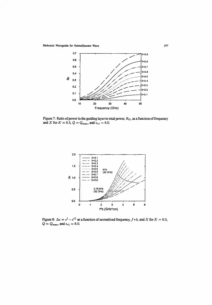
Figure 8: AE = e x -- E I I as a function of normalized frequency, f • b, and X for K ---- 0.5,
O = Om~, , and E~t = 6.0.

378 PonchakandKatehi
Vc max, while at lower frequencies, it is less dependent on X. Thus, an appropriate choice for X is 0.8. Nora that larger values of X (X ~ 1) changes tl~ dielectric wavcguide from LRDW to a form of millimeter-wave dielectric ridge guide.
By analyzing LRDW with the known parameters X = 0.8 and Q = Qm~, K and er I can bc determined to optimize the design. Figures 9, 10, and 11 show P~, P~, and Ae respectively as a function of frequency, K, and e~1. Also shown on the figures is the locus of points at a cutoff frequency of 42 GHz and a lower frequency of 32 GHz, or in morn general term, a normalized frequency of f~ * b ~ 0.76f~ • b. Maximum R= occurs whcn K ~ 0.5 at the higher order mode cutoff frcquenc'y and 0.3 at lower frcqnencies, whereas P~ is maximum when K ~ 0.3 across the frequency bandwidth ff erl > 4. Although Ae is maximum for larger values of K, dispersion also increases as K increases. Thus, a good value of K is 0.4. To minimize dispersion and maximize R= and P~, a small e~1 is desired. Howcvcl; materials with relative dielectric constants smaller than 2.0 am not widely available. Therefore, ffK = 0.4 and e~2 = 2.0 am used in Eqlt 6, the minimum practical e~z is found to be 7.0 which reduces the bandwidtk Before proceeding, notice that dispersion is grcater and R= is smaller ffK = i which is the condition required for image guide and millimeter-wave dielectric ridge wavcguidc.
0.9
0.8
0.7
0.6 x
0.5
0.4
0.3
0.2
W'b (42 dHz)
Irff i l 4 I ' s
\ ~ : : : ~ = o ~ '
K-0.1 "" ~ v " ~ : .........
~ . . . . " 0.76 fe'~ (32 GHz) ,.. i=r=lO
4 6
f*b (GHz*cm) 8 10
Figure 9: Field confinement facto1; P~, as a function of normalized frequency, f • b, K, and erl for LRDW with Q = Qm~, and X = 0.8. (constant permittivity in solid lines, constant K in dotted lines)
At this point, the optimum values of Q, X, and K are know~ Continuing with the EDC method of analysis in an effort to determine the ridge width a and to relate it to the parameters found above, consider the structure shown in Figure 3. Assuming E= and H~ fields with a magnetic wall at y = 0, the eigenvalue equation required to determine eel/ is:
(kula) tan(kuza) - ha ----- 0 (15) whom:
k~la = koav/~-e~l ! (16)

Dielectric Waveguide for Submillimeter Wave 379
0.7 fc"b (42 GHz)
0.6 ~ r =6 er:14 er=10 e 4 ] K-0.3 A'" ' 7% '"~ ; - : : : : : , . - - . ~ .~ , : :~ : : : : . . . . . r:
0.5 J /y~f ~ ,.. , ,o.,///~...~----~
I , i " / " , " o., ~ . , / " / s : ~ o-o,.-.<~,o.,,
o., 411 "'=~ ylo,~o
0.1 "| ¢r=14 ,
2 4 6 8
f*b (GHz*cm) 10
Figure 10: Ratio of power in the guiding layer to total powel; R e , as a function of nor- malized frequency, f * b, K , and e,z for Q = Qm~, and X = 0.8. (constant permittivity in solid lines, constant K in dotted lines.)
2.4
2.2 2.0 1.8
1.6 1.4
1.2
1.0
0.8
0.6 0.4
0.2
0.0 2
~ ¢r=14 ' , , ~ . fc~ (42 GHz)
\ \ ~ ~ . .-~4 ~ "6 "4 ......... ~-o.r"~..~
4 6 8
f i b (GHz*cm)
0.76 fc"o ~2 GHz)
10
Figure 11: Ae = e x - e H as a function of normalized frequency, f * b, K , and Erl for Q = Q=~, and X = 0.8. (constant permitlivity in solid lines, constant K in dotted lines.)

380 Ponchak and Katehi
f - - . - ha = koa~/ee/! - e H (17)
Defining a filling factor of [15] •
~ e f f - - ¢5II e ~ f f - - e I I
q = e / - d I -- Ae (18)
and a normalized frequency term [15] :
W = ~ (k~ la ) 2 + (ha) 2 ---- k o a V ~ e (19)
permits kvla and ha to be written as:
k~ia = W v / 1 - q (20)
ha = W V ~ (21)
Thus, all of the terms arc now related to Ae which was determined in Figure 11 and e~iI which is required for circuit designs. Using these new parameters, EqrL 15 results in:
1 tan -1 ~/ q (22) W = ~/1 - q --'1 -- q
Unfortunately, in a typical design, W is known and q needs to be found. Although F_xpx 22 cannot be inverted directly, a simple expression for q has been found:
0.97487 q = 1 "4- ( V~ )--1.83984 (23)
1.0816 which is accurate for W < ~v. Note that this equation is general and can be used to find the effective dielectric constant of dielectric slab waveguide without solving transcendental equations as is normally done. From the eigenvalue equation for the E ~ and EV modes, it is found that the cutoff frequem'y is given by W = n~r/2 which results in a maximum Idling factor of 0£46 and a maximum value of a of:
C amax ---- 4 A V / ~ (24)
At this point, no knowledge of the power confinement parameters in the y- direction exists. Determining the fields for Figure 3 and using Eqn. 3, t1 v can be found to be:
sin s B + B tan B Rv = 1 + B tan B (25)
where B = W lv/Y~- q. The maximum R. is found at the cutoff frequency to be 0.844. Although R v is a useful design cdterha, it is not easily related to circuit designs. A more useful design criteria is the ratio of the power at some distance from the center of the waveguide to the power at the centel; D = P ( y = Y l ) / P ( Y = 0), which is found to be:
D = cos 2 ( B ) e - 2s(n- 1) t ~ B (26)
where n = Yl /a . A typical design requirement is to determine the value o f w or n for a specific value of D. This relationship is found from EqrL 26 to be:
n ---- 1 In ~ (27) 2B tan B
Note that q, Rv, and D are all a function of W which is shown in Figure 12.

Dielectric Waveguide for Submillimeter Wave
1.0 >,0.9 n~0.8 ~0.7 toO.6 o'0. 5
0.4 0.3 0.2 / / : O. 1 / / cutoff frequency i n=3 0.0 ~ / / i t i
0.0
-2O
-30
-40 0.5 1.0 1.5 2.0
N o r m a l i z e d f r e q u e n c y W
-10 ~ . m -lO
£3
381
Figure 12: Field confinement terms in the v-direction, D and/~ , and the filling factor q as a function of the normalized frequency W = koaV'A'~.
4. Design Results
To review the optimum designfor LRDW, it has been shown that X = 0.8 and K = 0.4 are the preferred values. Using these parameters in Eqns. 13 and 14 results in Q = Qm= = 0.3125 and Vema. x = 2.367. Thus, if the upper frequency and ¢rz are specified, b can be found from EqrL 12. Then, either by using the EDC method and determining Ae or reading it fromFigure 11, a canbe determined fromEqn. 24. The effective dielectric constant, e , / f , can be determined by finding q from Eqn. 23 or Figure 12 and Eqn. 18. Finally, the power confinement and dispersion can be obtained from Figures 9-12. An alternative design procedure is to start with the upper frequency and a required power decay in the V- direction to minimize coupling to other lines. Using Figure 12, a and Ae can be determined, and then the required erz can be found from Figure 11. Finally, the dielectric thicknesses and the permittivity of the guiding layer can be determined from the optimum values of Q, X, K, and V,m~,. If this design procedure is followed, the ratio of c~/b is found to be approximately twice the optimum value of one found for image guide [6].
5. Conclusions
A set of design procedures consisting of closed form equations and design graphs for layered ridge dielectric waveguide has been developed. The design is conservative in that it places strict requirements on the cutoff frequency of higher order modes. Thus, since some of these modes are weakly excited by the LRDW, it may be possible to operate the waveguide above the upper frequency specified in this design. Throughout the paper; comparisons to image guide have been made. Lastly, several new closed form equations which are useful for dielectric waveguide design in general have been presented.

382 Ponchak and Katehi
6. References
[1] D. M. Pozar, Microwave Engineering, Addison-Wesley Publishing Co., New York, New York, 1990. [2] R. M. Knox and E E Toulios, "Integrated circuits for the millimeter through the optical frequency range," Proc. Symp. Submillimeter Waves, New York, March 31-April 2, 1970, pp. 497-516. [3] W. V. McLevige, T. Itoh, and R. Mittra, "New waveguide structures for millimeter- wave and optical integrated cirguits," IEEE Trans. Microwave Theory Tech., Vol. M'I~-23, pp. 788-794, Oct. 1975. [4] Z Wang and S. E. Schwarz, "Design of dielectric waveguides for millimeter-wave integrated circuits," I~FF Trans. Microwave Theory Tech., Vol. MTF-31, pp. 128-134, Feb. 1983. [5] A. G. EngeI, 1r and L. E B. Katehi, "Lowqoss monolithic transmission lines for sub- millimeter and terahettz frequency applications," I~mF. Trans. Microwave Theory Tech., '~bl. MTT-39, pp. 1847-1854, Nov. 1991. [6] R. J. Collier and R. D. Birch, "The bandwidth of image guide," IEEE Trans. Mi- crowave Theory Tech., Vol. MTT-28, pp. 932-935, Aug. 1980. [7] P. P. Toulios and R. M. Knox, "Image line integrated circuits for system applications at millimeter wavelengths, ~ Final Report: June 1973-Mamh 1974, Contract No. DAAB07- 73-C-0217, Report No. ECOM-73-0217-E [8] G. Athanasoulias and N. K. Uzunoglu, "An entire-domain basis Galerkin's method for the modeling of integrated mm-wave and optical circuits," 1995 IEEE M'IT-S Int. Microwave Syrup. Dig., Orlando, FL, May 16-20, 1995, pp. 471-474. [9] N. D~ and L. Katehi, "Characterization of sub-nun-wave dielectric waveguide direc- tional coupler using the FDTD method," 1994 IEEEMIT-Slnt. Microwave Symp. Dig., San Diego, CA, May 23-27, 1994, pp. 297-300.
[10] G. E. Ponchak, N. I. Dib, and L. E B. Katehi, "Design and analysis of transitions from rectangular waveguide to layered ridge dielectric waveguide," IEEE Trans. Microwave Theory Tech., Vol. MTr-44, pp. 1032-1040, Jialy 1996.
[11] G. E. Ponchak and L. P. B. Katehi, "Development of leaky wave antennas for layered ridge dielectric waveguide, " 1993 IEEE Antennas and Propagation Society Int. Symp. Dig., Ann Arbor, MI, pp. 580-583. [12] D. Marcnse, "Mode conversion caused by surface imperfections of a dielectric slab waveguide," The Bell System Technical Journal, pp. 3187-3215, Dec. 1969. [13] A. A. Oliner, S.-T. Peng, T-I. Hsu, and A. Sanchez, "Guidance and leakage proper- ties of a class of open dielectric waveguides: part II- new physical effects," IEEE Trans. Microwave Theory Tech., Vol. M'IT-29, pp. 855-869, Sept. 1981. [14] K. Solbach, "The measurement of the radiation losses in dielectric image line bends and the calculation of a minimum ae-ceptable curvature radius,'lEEE Trans. Microwave Theory Tech., Vol. M'I~-27, pp. 51-53, Jan. 1979.
[15] D. Gloge, "~kly guidingfibers," Applied Optics, Vol. I0, pp. 2252-2258, Oct. 1971.