Embed Size (px)
Citation preview

Cp
Ya
b
a
ARRA
KPMSAC
1
bfmlcIwsarrpcwm[dag
(
0h
Synthetic Metals 162 (2012) 1059– 1064
Contents lists available at SciVerse ScienceDirect
Synthetic Metals
journa l h o me page: www.elsev ier .com/ locate /synmet
onductivity switching and memory effect in polymer brushes with carbazoleendant moieties
ang Liua, Shujun Lva, Liang Lia,∗, Songmin Shangb,∗
Key Laboratory for Green Chemical Process of Ministry of Education, School of Materials Science and Engineering, Wuhan Institute of Technology, Wuhan 430073, PR ChinaInstitute of Textiles and Clothing, The Hong Kong Polytechnic University, Hung Hom, Kowloon, Hong Kong, PR China
r t i c l e i n f o
rticle history:eceived 21 March 2012eceived in revised form 15 May 2012ccepted 17 May 2012
eywords:
a b s t r a c t
In this paper, poly(2-(N-carbazolyl)ethyl methacrylate) (PCEM) brushes have been prepared on theindium-tin oxide (ITO) surfaces via surface-initiated atom transfer radical polymerization (ATRP) usinga silane coupling agent containing the initiator moiety. Films of PCEM brushes between bottom ITO elec-trode and Al top electrode are sandwiched to fabricate the ITO-g-PCEM/Al device. The device exhibitstwo conductivity states and can be switched from the initial low-conductivity (OFF) state to the high-
olymer brushesemory effect
witchingtom transfer radical polymerizationarbazole
conductivity (ON) state at the switching threshold voltages of −1.5 V with the ON/OFF current ratio upto 106. The ON state of the device is nonvolatile and can withstand 106 pulse read cycles at −0.8 V underambient conditions. Upon reversing the bias, the ON state cannot be reset to the initial OFF states. TheITO-g-PCEM/Al device behaves as a write-once read-many-times (WORM) memory. Compared with thatof the conventional ITO/PCEM/Al device fabricated by spin-coating, the switching voltage is lower in theITO-g-PCEM/Al memory device.
. Introduction
Recently, polymer materials exhibiting electrically bistableehavior are being extensively investigated as an alternative foruture data storage and memory device applications. Polymer
emories offer advantages including low cost, simple structure,ight weight, good scalability, good processability, 3D stackingapability, device flexibility and large-capacity data storage [1–5].n contrast to memory devices based on inorganic materials,
hich store and retrieve data based on the amount of chargetored in the device, polymer memory devices store data innother form, for instance, based on the electrical bistability inesponse to an applied electric field. A number of polymer mate-ials such as conjugated polymers doped with gold nanoparticles,olyelectrolytes, dendritic polymers, and organic donor-acceptoromplexes, have been reported to fabricate memory devicesith the sandwiched structures [6–9]. The reported polymeremory devices exhibit write-once read-many times (WORM)
10,11], flash [12,13], static random access and dynamic ran-
om access memory effects [14]. Up to now, polymer materialsre usually deposited by spin-coating on a variety of inor-anic substrates in the fabrication of memory devices [15–17].∗ Corresponding authors. Tel.: +86 27 87195661; fax: +86 27 87195661.E-mail addresses: [email protected] (L. Li), [email protected]
S. Shang).
379-6779/$ – see front matter © 2012 Elsevier B.V. All rights reserved.ttp://dx.doi.org/10.1016/j.synthmet.2012.05.015
© 2012 Elsevier B.V. All rights reserved.
However, incompatibility between inorganic electrodes, withorganic thin films is a problem commonly encountered in thefabrication of high performance and stable photovoltaic cellsand organic light-emitting devices [18,19]. It may result in thedelamination of the spin-coated or vacuum-sublimated organiclayer and a high resistance in such device [20]. To overcomethe above problem, chemisorption or covalent attachment offunctional groups, such as carboxylic acid and alkanethiols, sur-face cleaning/pretreatment by plasma, or intercalation of a thinfilm of poly(3,4-ethylene dioxythiophene) doped with poly(4-styrenesulfonate) [21–23] have been employed to improve theinterfacial contact between the inorganic electrode and the organicthin film.
Tethering of polymer brushes on a solid substrate has been usedas alternatives to modify the surface properties of the substrate[24]. Consequently, the problems associated with the inorganicsubstrate/organic polymer interface may be minimized if the poly-mer film is covalently attached to the inorganic surface. Withthe progress in polymer chemistry, it has been realized to pre-pare well-defined polymer brushes on various substrates, in theform of well-defined polymer-inorganic hybrids, for various appli-cations by surface-initiated atom transfer radical polymerization(ATRP) [25–27]. Surface-initiated polymerization has been utilized
to functionalize the conducting transparent electrode, indium tinoxide (ITO) with polyvinylcarbazole brushes [28]. Herein, poly-mer brushes containing carbazole pendant moieties, tethereddirectly on the ITO surface, have been successfully prepared by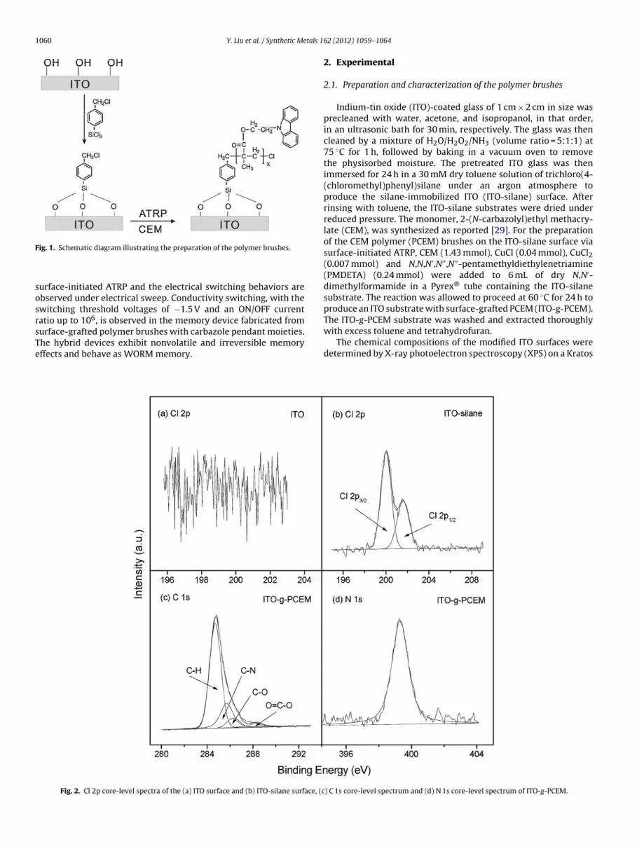
1060 Y. Liu et al. / Synthetic Metals 1
F
sosrsTe
The ITO-g-PCEM substrate was washed and extracted thoroughly
ig. 1. Schematic diagram illustrating the preparation of the polymer brushes.
urface-initiated ATRP and the electrical switching behaviors arebserved under electrical sweep. Conductivity switching, with thewitching threshold voltages of −1.5 V and an ON/OFF currentatio up to 106, is observed in the memory device fabricated from
urface-grafted polymer brushes with carbazole pendant moieties.he hybrid devices exhibit nonvolatile and irreversible memoryffects and behave as WORM memory.Fig. 2. Cl 2p core-level spectra of the (a) ITO surface and (b) ITO-silane surface, (c
62 (2012) 1059– 1064
2. Experimental
2.1. Preparation and characterization of the polymer brushes
Indium-tin oxide (ITO)-coated glass of 1 cm × 2 cm in size wasprecleaned with water, acetone, and isopropanol, in that order,in an ultrasonic bath for 30 min, respectively. The glass was thencleaned by a mixture of H2O/H2O2/NH3 (volume ratio = 5:1:1) at75 ◦C for 1 h, followed by baking in a vacuum oven to removethe physisorbed moisture. The pretreated ITO glass was thenimmersed for 24 h in a 30 mM dry toluene solution of trichloro(4-(chloromethyl)phenyl)silane under an argon atmosphere toproduce the silane-immobilized ITO (ITO-silane) surface. Afterrinsing with toluene, the ITO-silane substrates were dried underreduced pressure. The monomer, 2-(N-carbazolyl)ethyl methacry-late (CEM), was synthesized as reported [29]. For the preparationof the CEM polymer (PCEM) brushes on the ITO-silane surface viasurface-initiated ATRP, CEM (1.43 mmol), CuCl (0.04 mmol), CuCl2(0.007 mmol) and N,N,N′,N′′,N′′-pentamethyldiethylenetriamine(PMDETA) (0.24 mmol) were added to 6 mL of dry N,N′-dimethylformamide in a Pyrex® tube containing the ITO-silanesubstrate. The reaction was allowed to proceed at 60 ◦C for 24 h toproduce an ITO substrate with surface-grafted PCEM (ITO-g-PCEM).
with excess toluene and tetrahydrofuran.The chemical compositions of the modified ITO surfaces were
determined by X-ray photoelectron spectroscopy (XPS) on a Kratos
) C 1s core-level spectrum and (d) N 1s core-level spectrum of ITO-g-PCEM.
tals 162 (2012) 1059– 1064 1061
Astrm
2
0nbabews
3
iImisso2ttattwar
iDcdlFa2aCds
isAbfiat
biltai
Y. Liu et al. / Synthetic Me
XIS Ultra spectrometer. The static water contact angles were mea-ure by the sessile drop method, using a 3 �L water droplet, in aelescopic goniometer (Rame-Hart model 100-00230). The topog-aphy of the modified ITO surfaces was studied by atomic forceicroscope (AFM).
.2. Fabrication of the device
Thermal evaporation of the aluminum electrodes of.4 mm × 0.4 mm, and 0.2 mm × 0.2 mm (about 100 nm in thick-ess), at about 10−6 Torr through a shadow mask, on the polymerrushes fabricated the ITO-g-PCEM/Al devices. For comparison,nother device, with the structure of ITO/PCEM/Al, was preparedy spin-coating a 10 mg/mL solution of PCEM in dimethylac-tamide onto a clean ITO substrate. All electrical measurementsere carried out on the fabricated devices using a HP 4145B
emiconductor parameter analyzer under ambient conditions.
. Results and discussion
The synthesis process of polymer brushes on the ITO surfaces shown schematically in Fig. 1. The chemical composition of theTO surfaces at various stages of surface modification is deter-
ined by XPS. As shown in Fig. 2a, no signal attributable to Cls discernable in Cl 2p core-level spectrum of the pristine ITOurface. For the preparation of polymer brushes on the substrateurface, a uniform and dense monolayer of initiators immobilizedn the surface is necessary. Fig. 2b shows the corresponding Clp core-level spectrum of the ITO surface after the reaction withrichloro(4-(chloromethyl)phenyl)silane. The Cl 2p core-level spec-rum in Fig. 2b consists of the Cl 2p3/2 and Cl 2p1/2 peak componentst the BE’s of about 199.3 and 201.5 eV, respectively, attributableo the covalently bonded chlorine species [30]. The immobiliza-ion of the ATRP initiator is also accompanied by a change in staticater contact angle of the Si surface. The water contact angles are
bout 63◦ and 92◦ for the pristine surface and after silanization,espectively.
The immobilized initiator is subsequently used for surface-nitiated atom-transfer radical polymerization (ATRP) of CEM.uring the surface-initiated ATRP, the method of addition of Cu(II)omplex (CuCl2) is chosen to control the concentration of theeactivating Cu(II) complex for the rapid establishment of an equi-
ibrium between the dormant and active chains [31]. As shown inig. 1c, the C 1s core-level spectrum of the ITO-g-PCEM surface, aftern ATRP time of 24 h with the thickness of polymer brush of about5 nm, can be curve-fitted with three peak components with BEst about 284.6, 285.4, 286.2 and 288.5 eV, attributable to the C H,
N, C O, O C O species [32], respectively. The appearance of aistinct N 1s signal at about 399 eV [32] in Fig. 2d also indicates theuccessful graft polymerization of CEM from the ITO-silane surface.
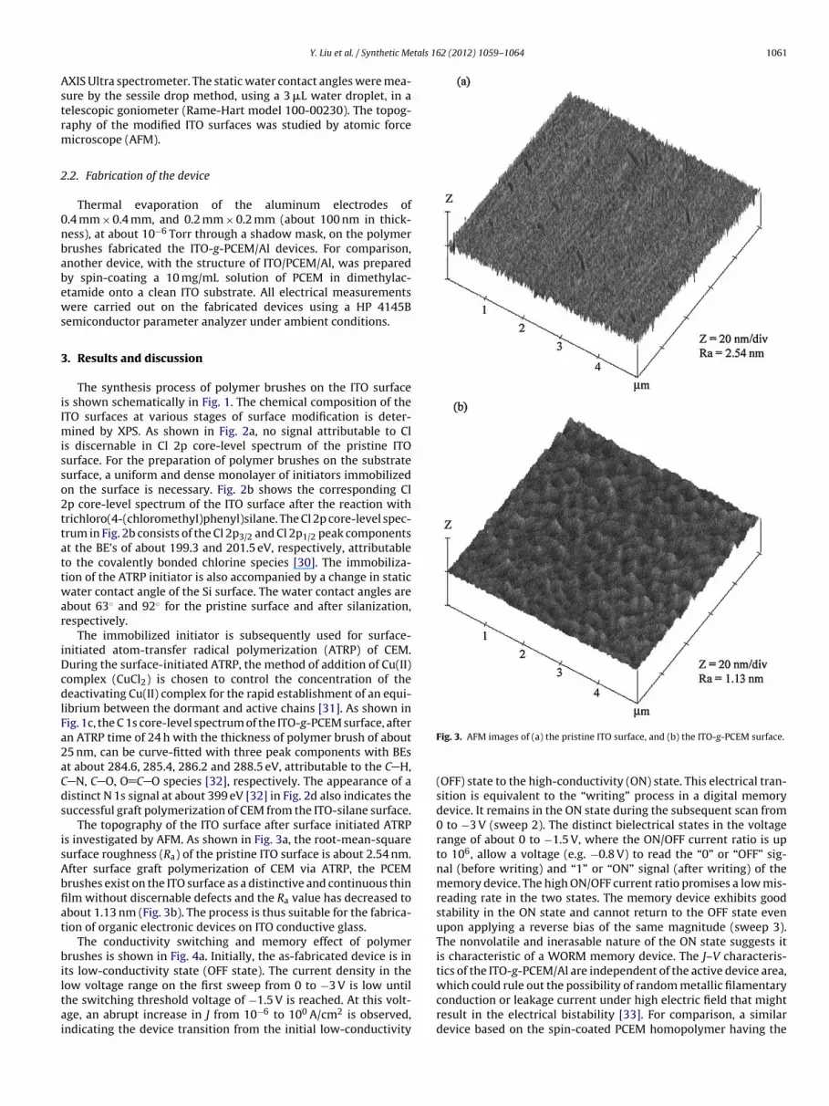
The topography of the ITO surface after surface initiated ATRPs investigated by AFM. As shown in Fig. 3a, the root-mean-squareurface roughness (Ra) of the pristine ITO surface is about 2.54 nm.fter surface graft polymerization of CEM via ATRP, the PCEMrushes exist on the ITO surface as a distinctive and continuous thinlm without discernable defects and the Ra value has decreased tobout 1.13 nm (Fig. 3b). The process is thus suitable for the fabrica-ion of organic electronic devices on ITO conductive glass.
The conductivity switching and memory effect of polymerrushes is shown in Fig. 4a. Initially, the as-fabricated device is in
ts low-conductivity state (OFF state). The current density in the
ow voltage range on the first sweep from 0 to −3 V is low untilhe switching threshold voltage of −1.5 V is reached. At this volt-ge, an abrupt increase in J from 10−6 to 100 A/cm2 is observed,ndicating the device transition from the initial low-conductivityFig. 3. AFM images of (a) the pristine ITO surface, and (b) the ITO-g-PCEM surface.
(OFF) state to the high-conductivity (ON) state. This electrical tran-sition is equivalent to the “writing” process in a digital memorydevice. It remains in the ON state during the subsequent scan from0 to −3 V (sweep 2). The distinct bielectrical states in the voltagerange of about 0 to −1.5 V, where the ON/OFF current ratio is upto 106, allow a voltage (e.g. −0.8 V) to read the “0” or “OFF” sig-nal (before writing) and “1” or “ON” signal (after writing) of thememory device. The high ON/OFF current ratio promises a low mis-reading rate in the two states. The memory device exhibits goodstability in the ON state and cannot return to the OFF state evenupon applying a reverse bias of the same magnitude (sweep 3).The nonvolatile and inerasable nature of the ON state suggests itis characteristic of a WORM memory device. The J–V characteris-tics of the ITO-g-PCEM/Al are independent of the active device area,which could rule out the possibility of random metallic filamentary
conduction or leakage current under high electric field that mightresult in the electrical bistability [33]. For comparison, a similardevice based on the spin-coated PCEM homopolymer having the
1062 Y. Liu et al. / Synthetic Metals 162 (2012) 1059– 1064
FI
sstotbitTiO
pcbattctPprcCs
Fig. 5. (a) Stability of the ITO-g-PCEM/Al device in either ON or OFF state under a
ig. 4. Current density–voltage curves of the (a) ITO-g-PCEM/Al device and (b)TO/PCEM/Al device.
imilar thickness with the polymer brush, is also fabricated. Thepin-coated PCEM is synthesized by free-radical homopolymeriza-ion of the monomer, and had a weight-average molecular weightf about 16,500 g/mol and a polydispersity index of about 2.4. Thehickness of the spin-coated film is similar to that of the polymerrush. The J–V characteristics of the ITO/PCEM/Al device are shown
n Fig. 4b. The ITO/PCEM/Al device switches from the OFF state tohe ON state at about −2 V with an ON/OFF ratio of about 105–106
.
he ITO/PCEM/Al device also exhibits WORM memory behavior, ast is both non-rewritable and nonvolatile after it has been switchedN.
The high-conductivity state of PCEM is perhaps similar to that ofoly(N-vinylcarbazole) (PVK) since both polymers have the samearbazole pendant groups and a saturated main chain. The car-azole group is an electron-donor and hole-transporter [34,35]nd tends to form a partial or full face-to-face conformation withhe neighboring carbazole groups to result in the extended elec-ron delocalization [36]. In the region of electron delocalization,harge-carrier hopping easily occurs via the carbazole groups inhe direction of the electric field [37]. The switching effect in theCEM devices probably arises from a change in conformation of theolymers via rotations of the carbazole groups to result in a more
egioregular arrangement [38]. Initially, at low applied voltage, thearbazole pendant groups attached to the main chain via flexibleO linkages are in random orientations, corresponding to the OFFtate. When the applied voltage exceeds the threshold value, charge
constant stress at −0.8 V. (b) Effect of read cycles of −0.8 V on the ON and OFF statesin the ITO-g-PCEM/Al device.
transfer occurs through the neighboring carbazole groups eitheron the same or neighboring polymer chains (intrachain or inter-chain hopping) [39] and the carbazole groups re-organize from aregiorandom to a regioregular structure in the general direction ofthe electric field. As a result, a high conductivity path among thehole-transporting carbazole groups is established and the device isswitched to the ON state.
In addition to the electrical switching effect, other parameters,such as the stability and read cycles, are of importance to the per-formance of the memory device. Both stress and read pulse cyclestests are conducted under ambient conditions. Fig. 5a shows theeffect of operation time on the memory device based on polymerbrushes. Under a constant stress of −0.8 V, an ON/OFF current ratioof about 106 can be maintained and no degradation in current forthe ON and OFF states is observed during the test. The effect of con-tinuous read pulses (with a read voltage of −0.8 V, a pulse width of1 �s, and a pulse period of 2 �s) on the ON and OFF states is alsoinvestigated. The ON and OFF states are also stable in more thanone million read cycles, as shown in Fig. 5b. These results indicatethat these memory devices exhibit good stability and performance.
Further information about the charge transport mechanism canbe obtained from the J–V curves in the OFF state and the ON stateaccording to the theoretical models. For the OFF-state, the J–V curve

Y. Liu et al. / Synthetic Metals 16
Fd
ct
J
wbtFenflotAdcmpcvidd
cb
[
ig. 6. Experimental and fitted current density–voltage curves of the ITO-g-PCEM/Alevice: (a) OFF state and (b) ON state.
an be fitted by a combination of the Schottky emission model andhe space-charge-limited model:
= BT2 exp
(+a
√V
T− q�B
kT
)+ A
9εi�V2
8d3
here T is room temperature (298 K), a =√
q/(4�εid), �B is thearrier height, εi is the dynamic permittivity of the insulator, d ishe film thickness, and � is the mobility of carriers. As shown inig. 6a, at the low voltage the current is dominated by Schottkymission from the electrode. As the voltage is increased, the largeumber of holes readily supplied by the ITO anode results in theow of current through the device being limited by the buildupf space charges in the PCEM layer, and the current is a combina-ion of the Schottky emission and space-charge-limited conduction.t the threshold voltage, the applied voltage may be able to pro-uce enough large electric field strength to effect the conformationhange of the groups close to the ITO surface. The charge carriersay be easily transported along aligned carbazole groups via hop-
ing, resulting in a surge in current and Ohmic conduction. Theurrent in the ON state is almost linear in dependence on appliedoltage, indicating that in the ON state the charge transport is dom-nated by the ohmic model (Fig. 6b). The ohmic nature of the PCEMevice in the ON state is similar to the ohmic characteristic of con-
uction in PVK [39].In comparison to the ITO/PCEM/Al device fabricated by spin-oated PCEM, the ITO-g-PCEM/Al device based on the polymerrushes shows a reduced switching voltage, as well as a slightly
[
[
2 (2012) 1059– 1064 1063
higher ON/OFF current ratio. The conductivity switching in PCEMoccurs via a conformation change of the carbazole groups toincrease the extent of electron delocalization [38]. Compared withthe randomly arranged chains in the bulk polymer film by spincoating, the more ordered polymer brushes from the ATRP processincreases the ease of such transformation. A smaller applied volt-age may be able to produce sufficiently large electric field strengthto perhaps effect the conformation change of the groups close tothe ITO surface. The buildup of space charges in the PCEM layer atthe low applied voltage may result in the smaller OFF current in theITO-g-PCEM/Al device. After switching, charge transport is domi-nated by the ohmic model in the ITO-g-PCEM/Al device and theITO/PCEM/Al device, as discussed above. The ON current is similarfor the ITO-g-PCEM/Al device and the ITO/PCEM/Al device. Furtherinvestigations on the switching mechanism in the ITO-g-PCEM/Aldevice need to be conducted in future.
4. Conclusions
This study reports the preparation of well-defined polymer-ITOhybrids, consisting of covalently tethered polymer brushes of CEMvia surface-initiated ATRP. Bistable electrical switching devicesbased on the polymer brushes exhibit nonvolatile and irreversibleWORM memory effects with the switching threshold voltage of−1.5 V and an ON/OFF current ratio up to 106. Both the ON andOFF states are stable under a constant read voltage stress of −0.8 Vand even can endure 106 read cycles under a pulse read voltage. Theswitching threshold voltage of the ITO-g-PCEM/Al device is superiorto that of the conventional spin-coated ITO/PCEM/Al device. Furtherinvestigations on the switching mechanism and the effect of manyfactors, such as the temperature and time of surface-initiated ATRP,on the memory properties of polymer brushes are in progress in ourlab. The present work provides an alternative method to the directfabrication of organic electronics and devices via surface-initiatedcontrollable polymerization.
Acknowledgments
The work is supported by National Natural Science Foundationof China (20904044) and the New Century Excellent Talents inUniversity of Ministry of Education of China (NCET-10-0157). Theauthors thank Prof. E.T. Kang (Department of Chemical & Biomolec-ular Engineering, National University of Singapore) for his kindhelp.
References
[1] R.C.G. Naber, K. Asadi, P.W.M. Blom, D.M. de Leeuw, B. de Boer, AdvancedMaterials 22 (2010) 933–945.
[2] H. Li, N. Li, H. Gu, Q. Xu, F. Yan, J. Lu, X. Xia, J. Ge, L. Wang, Journal of PhysicalChemistry C 114 (2010) 6117–6122.
[3] S. Paul, A. Kanwal, M. Chhowalla, Nanotechnology 17 (2006) 145–151.[4] R.J. Tseng, J.X. Huang, J. Ouyang, R.B. Kaner, Y. Yang, Nano Letters 5 (2005)
1077–1080.[5] C. Liu, J. Hsu, W. Chen, K. Sugiyama, A. Hirao, ACS Applied Materials and Inter-
faces 1 (2009) 1974–1979.[6] D. Mao, M.A. Quevedo-Lopez, H. Stiegler, B.E. Gnade, H.N. Alshareef, Organic
Electronics 11 (2010) 925–932.[7] C.W. Joo, S.O. Jeon, K.S. Yook, J.Y. Lee, Synthetic Metals 17–18 (2009)
1809–1811.[8] S. Choi, S.H. Hong, S.H. Cho, S. Park, S.M. Park, O. Kim, M. Ree, Advanced Materials
20 (2008) 1766–1771.[9] Y.L. Liu, K.L. Wang, G.S. Huang, C.X. Zhu, E.S. Tok, K.G. Neoh, E.T. Kang, Chemistry
of Materials 21 (2009) 3391–3399.10] Q. Chen, L. Zhao, C. Li, G.Q. Shi, Journal of Physical Chemistry C 111 (2007)
18392–18396.11] L. Li, Q.D. Ling, S.L. Lim, Y.P. Tan, C. Zhu, D.S.H. Chan, E.T. Kang, K.G. Neoh, Organic
Electronics 8 (2007) 401–406.12] N.H. You, C.C. Chueh, C.L. Liu, M. Ueda, W.C. Chen, Macromolecules 42 (2009)
4456–4463.

1 tals 1
[
[
[
[
[[
[[
[
[
[
[
[
[
[
[
[
[
[
[
[
[
[[
[
064 Y. Liu et al. / Synthetic Me
13] Y.S. Lai, C.H. Tu, D.L. Kwong, J.S. Chen, IEEE Electron Device Letters 27 (2006)451–453.
14] Q.D. Ling, Y. Song, S.L. Lim, E.Y.H. Teo, Y.P. Tan, C. Zhu, E.T. Kang, K.G. Neoh,Angewandte Chemie International Edition 45 (2006) 2947–2951.
15] S. Moller, C. Perlov, W. Jackson, C. Taussig, S.R. Forrest, Nature 426 (2003)166–169.
16] S.J. Kang, Y.J. Park, I. Bae, K.J. Kim, H. Kim, S. Bauer, E.L. Thomas, C. Park, AdvancedFunctional Materials 19 (2009) 2812–2818.
17] A. Kanwal, M. Chhowalla, Applied Physics Letters 89 (2006) 203103.18] E.L. Hanson, J. Guo, N. Koch, J. Schwartz, S.L. Bernasek, Journal of the American
Chemical Society 127 (2005) 10058–10062.19] J.G.C. Veinot, T.J. Marks, Accounts of Chemical Research 38 (2005) 632–643.20] N.R. Armstrong, C. Carter, C. Donley, A. Simmonds, P. Lee, M. Brumbach, B.
Kippelen, B. Domercq, S. Too, Thin Solid Films 445 (2003) 342–352.21] C. Yan, M. Zharnikov, A. Golzhauser, M. Grunze, Langmuir 16 (2000)
6208–6215.22] J.S. Kim, P.K.H. Ho, D.S. Thomas, R.H. Friend, F. Cacialli, G.W. Bao, S.F.Y. Li,
Chemical Physics Letters 315 (1999) 307–312.23] J.C. Bernede, H. Derouiche, V. Djara, Solar Energy Materials and Solar Cells 87
(2005) 261–270.24] F.J. Xu, Y. Song, Z.P. Cheng, X.L. Zhu, C.X. Zhu, E.T. Kang, K.G. Neoh, Macro-
molecules 38 (2005) 6254–6258.25] D. Nystrm, J. Lindqvist, E. Stmark, P. Antoni, A. Carlmark, A. Hult, E. Malmstrom,
ACS Applied Materials and Interfaces 1 (2009) 816–823.26] L. Li, G. Yan, Z. Cheng, J. Wu, X. Yu, Q. Guo, Surface and Interface Analysis 41
(2009) 69–74.
[
[
62 (2012) 1059– 1064
27] S. Edmondson, V.L. Osborne, W.T.S. Huck, Chemical Society Reviews 33 (2004)14–22.
28] T.M. Fulghum, P. Taranekar, R.C. Advincula, Macromolecules 41 (2008)5681–5687.
29] J. Sanetra, D. Bogdal, M. Warzala, A. Boron, Chemistry of Materials 14 (2002)89–95.
30] G. Beamson, D. Briggs, High-Resolution XPS of Organic Polymers: the ScientaESCA300 Database, John Wiley, Chichester, UK, 1992.
31] K. Matyjaszewski, P.J. Miller, N. Shukla, B. Immaraporn, A. Gelman, B.B. Luokala,T.M. Siclovan, G. Kickelbick, T. Vallant, H. Hoffman, T. Pakula, Macromolecules32 (1999) 8716–8724.
32] J.F. Moulder, W.F. Stickle, P.E. Sobol, K.D. Bomben, Handbook of X-ray Photo-electron Spectroscopy, Perkin-Elmer, Eden Prairie, MN, 1992, p. 40.
33] W.J. Joo, T.L. Choi, J. Lee, S.K. Lee, M.S. Jung, N. Kim, J.M. Kim, Journal of PhysicalChemistry B 110 (2006) 23812–23816.
34] J.F. Morin, M. Leclerc, D. Ades, A. Siove, Macromolecular Rapid Communications26 (2005) 761–778.
35] L. Akcelrud, Progress in Polymer Science 28 (2003) 875–962.36] J. Vandendriessche, P. Palmans, S. Toppet, N. Boens, F.C. de Schryver, H.
Masuhara, Journal of the American Chemical Society 106 (1984) 8057–8064.37] J.V. Grazulevicius, P. Strohrirgl, J. Pielichowski, K. Pielichowski, Progress in Poly-
mer Science 28 (2003) 1297–1353.38] E.Y.H. Teo, Q.D. Ling, Y. Song, Y.P. Tan, W. Wang, E.T. Kang, D.S.H. Chan, C.X. Zhu,
Organic Electronics 7 (2006) 173–180.39] G. Safoula, K. Napo, J.C. Bernede, S. Touihri, K. Alimi, European Polymer Journal
37 (2001) 843–849.


