Embed Size (px)
Citation preview
Characterization of two dimensional self-organized Au nanoparticlesembedded in Si3N4
Eva Céspedes,1 David Babonneau,2 Olivier Lyon,3 Jorge Sánchez-Marcos,1
Stéphan Rouzière,4 Carlos Prieto,1 Luca Olivi,5 and Agnès Traverse6,a�
1Instituto de Ciencia de Materiales de Madrid, Consejo Superior de Investigaciones Científicas,Cantoblanco, Madrid, 28049, Spain2Laboratoire de Physique des Matériaux (PHYMAT), UMR 6630 CNRS, Université de Poitiers, SP2MI, BvdMarie et Pierre Curie, 86962 Futuroscope Chasseneuil, France3Synchrotron-SOLEIL, L’Orme des Merisiers Saint-Aubin, BP 48, 91192 Gif-sur-Yvette, France4Laboratoire de Physique des Solides, Université Paris-Sud, CNRS, UMR 8502, Bâtiment 510, F-91405Orsay cedex, France5Sincrotrone Trieste, S. C. p. A., S. S. 14 km 163.5 Basovizza (Trieste) 34012, Italy6Laboratoire de Chimie Physique, UMR 8000, Université Paris-Sud, CNRS—Bâtiment 349, F-91405 Orsaycedex, France
�Received 7 September 2009; accepted 10 February 2010; published online 20 May 2010�
Au /Si3N4 films have been prepared by gold and silicon nitride sequential sputtering with differentAu thicknesses. The goal is to investigate the Au growth mode and to identify the regime where Aunanoparticles �NPs� can be prepared. The number of Au atoms, the bilayer thickness, the Auenvironment, the size, and the organization of the particles have been determined. Gold appears inmetallic form. The thickest Au layer �8 nm� is continuous whereas the thinnest ones �with averagevalues of 1–3 nm� are formed by nearly spherical Au NPs with diameters in the 5–7 nm range. AuNPs spatial self-organization is observed for average thickness of tAu=2.9 nm. These growth modesare discussed and compared with those observed for other metal/Si3N4 systems prepared in similarconditions. © 2010 American Institute of Physics. �doi:10.1063/1.3359705�
I. INTRODUCTION
Materials made of metallic nanoparticles �NPs� dis-persed in dielectric matrices �nanocermets� exhibit specificproperties particularly interesting for optical applications inthe linear and nonlinear regime. In the case of noble metals,one can mention the existence of the surface plasmon reso-nance �SPR�,1 second,2,3 and third-order nonlinearsusceptibility.4,5 These potentialities and the fundamental un-derstanding still needed to interpret their properties, justifythe efforts to build such nanocermets, efforts that must beassociated with a precise characterization of their propertiesin terms of average size, size distribution, morphology, andorganization in the matrix.6 In order to prepare samples withthe optimized properties, growth mechanisms have to be un-derstood.
Significant research has been done on Au NPs preparedby different techniques. Some of these techniques are basedon chemical reduction processes.7,8 Others are based onphysical vapor deposition. Magnetron sputtering has beenused for example to prepare films to study nonlinearsusceptibility9,10 and transport properties.11 Electron beamevaporation12 or cluster deposition13 allowed electron dy-namics characterization. Ion beam techniques appeared to besuccessful in embedding metallic NPs in matrices.14–16 AuNPs are mostly embedded in oxide matrices such as SiO2
and TiO2.9,10,17 Thus, we have chosen to study Au NPs inanother matrix, the transparent nitride Si3N4, and to use se-
quential sputtering, a tool that allows the experimentalists tovary parameters such as the total amount of deposited mate-rial, the layer thickness or the deposition rate. The refractiveindex of Si3N4, known to play a role on the SPR energy, isequal to 2 which is intermediate between the one of SiO2
�1.5� and TiO2 �2.7�. We present here a structural study ofsamples fabricated by alternate Au and Si3N4 deposition.Several nondestructive techniques have been combined toget a fine description of the samples, such as x-ray absorp-tion spectroscopy �XAS�, grazing incidence small anglex-ray scattering �GISAXS�, x-ray reflectometry �XRR�, Ru-therford Backscattering spectrometry �RBS�, transmissionelectron microscopy �TEM�, and atomic force microscopy�AFM�.
In a recent paper, Garcia del Muro et al.18 showed thatthe NP growth is different for Au deposited on ZrO2 as com-pared with Co and Ag. The final NP properties depend alsostrongly on the chemical environment of their surface atoms.Thus it is important to know whether Au NPs are surroundedby Si or N atoms. In order to answer this question, we com-pared the Au /Si3N4 system to others prepared with the sametechnique, i.e., Ni, Fe, Mn /Si3N4.19–21
The goal of the present paper is to describe �i� the indi-vidual particles, i.e., their average size, size distribution, andmorphology, �ii� the particle organization in the matrix, ran-domly distributed or self-organized, and �iii� the chemicalNPs environment and finally to propose a growth process.
II. EXPERIMENTAL
Au /Si3N4 multilayered films were prepared by sequen-tial sputtering of Si3N4 and Au on Si�100� substrates at room
a�Author to whom correspondence should be addressed. Electronic mail:[email protected]; Tel.: �330169153298.
JOURNAL OF APPLIED PHYSICS 107, 104306 �2010�
0021-8979/2010/107�10�/104306/9/$30.00 © 2010 American Institute of Physics107, 104306-1
temperature. The sputtering system allows controlling auto-matically the movement of the sample-holder disk, the timeit is placed on each sputtering �or presputtering� position, aswell as the sputtering working gas. The residual pressure wasnear 1�10−7 mbar. Si3N4 layers were deposited by rf sput-tering from a pure silicon target �99.99%� using N2 as reac-tive sputtering gas. The deposition rate was about 2 nm/minfor a rf power of 100 W. Au layers were grown from a goldtarget �99.999%� at 5.0�10−3 mbar pressure of pure Ar. Thedeposition rate was about 6 nm/min for a dc power of�10 W. For all samples, multilayer structure fabrication be-gan with a Si3N4 layer and a last additional layer �6 nmthick� was deposited on top. A series of five Au /Si3N4 films,labeled as �Si3N4�6 nm� /Au�t��n, was prepared, keeping theSi3N4 layer nominal thickness constant in every sample �6nm� and varying the Au thickness �tAu� in the range of about1–10 nm. The number of bilayers �n� was increased as tAu
values were reduced in order to maintain the Au total amountlarge enough to get reliable experimental data whatever thecharacterization technique.
To measure the period of the multilayers �i.e., the bilayerthickness ��, low angle XRR measurements were carried outon a Bruker D8 x-ray diffractometer with a Cu K� source��=0.154 nm�. Simulations of reflectivity data were donewith the XREAL software developed in Ref. 22. In addition,AFM measurements were performed under ambient condi-tions using a commercial head from NanotecTM and com-mercial Nanosensors PPP-NCH-w tips with k=42 Nm−1 andf0=330 kHz. Topographic characterization was performed intapping mode and images and roughness analysis were stud-ied with software from Nanotec.23
RBS experiments were done24 using a 1.2 MeV He+
beam in order to get the number of Au atoms per layer�at. /cm2� and average Au /Si3N4 composition. The experi-mental data were simulated by using the RBX code.25
XAS experiments were carried out at the Au LIII-edge intotal electron yield �TEY� detection mode at room tempera-ture on the XAFS beamline at ELETTRA to characterize theatomic surrounding of the Au atoms. The double crystalmonochromator was equipped with Si�111� detuned for har-monic rejection. Standard analysis of the XAS data was per-formed by means of the VIPER software.26 XRD was per-formed with an x-ray imaging plate chamber using theMo K� radiation ��=0.071 nm� to get NPs average diam-eters when they exist. More precise information about the Aumorphology and NPs dimensions was obtained by GISAXSmeasurements, carried out on the SWING beamline atSOLEIL synchrotron. The energy of the incident x-ray beamwas set at 9.03 keV ��=0.137 nm�, the angle of incidencewas slightly higher than the critical angle for total externalreflection, �c, in order to achieve good surface sensitivity,and the sample-to-detector distance was varied between1.305 and 2.425 m. The transmitted and specularly reflectedbeams were masked by a vertical beam stop and the scatteredintensity was collected as a function of the in-plane �2�f� andout-of-plane ��f� exit angles with a two dimensional �2D�detector made of four charge-coupled devices cooled at−25 °C, illuminated through a phosphor screen and a reduc-ing optic fiber. The experimental data were analyzed with the
home-made FITGISAXS package developed within the IGOR
PRO analysis software �WaveMetrics, Inc.�.Electron microscopy studies were undertaken using a
200 kV JEOL2000FX TEM. Samples were prepared inplane-view using a GATAN656 dimpler grinder and a Fis-chione 1010 ion beam mill.
Before presenting the experimental results, it is neces-sary to compare the probed sample depths versus the differ-ent techniques. For RBS, the fact that the Si substrate isdetected ensures that the whole stack is probed. When inci-dent beams are x rays in the energy range of 10 keV, theincident path is a few microns. For GISAXS the recordedbeam is still an x-ray beam, thus the information is alsocollected over a large path. The probed sample depth de-pends actually on the incident beam angle, �i, usually rathersmall for this technique. Typically the probed depth is 61 nmfor �Si3N4�6 nm� /Au�2.9 nm��20 with �i=0.47°. The questionarises also for XAS performed in TEY mode where emittedelectrons are collected. From Girardeau et al.,27 where theauthors checked the electron escaping depth, one can expectdepending on the Au concentration and the Si3N4 densitythat the sample thickness is totally probed in the thinnestsamples and only partially in �Si3N4�6 nm� /Au�2.1 nm��40 andin �Si3N4�6 nm� /Au�1.6 nm��75. Thus for the thinner Au layer,we also prepared the �Si3N4�6 nm� /Au�1.6 nm� /Si3N4�6 nm��trilayer stack, in which a plane-view observation was carriedout by TEM.
III. RESULTS
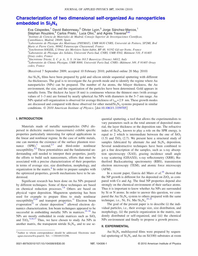
The XRR curves of the Au /Si3N4 multilayer films areshown in Fig. 1. Satellite maxima corresponding to a hetero-structure periodicity can be observed for all samples at �=�m �m=1,2 ,3, etc.� proving that they are actually formedby alternated Si3N4 and Au-rich regions with a vertical pe-riod �, given by m�=2� �sin2 �m−sin2 �c�1/2. � periodici-ties can be obtained from the slope of m versus sin �m rep-resentation independently of the critical angle �c. The aboveexpression, apart from the bilayer period ���, also accountsfor the total thin film thickness �with ��=n�+ tC, consider-ing an additional capping layer of thickness tC and n beingthe number of repetitions�.
FIG. 1. XRR curves of �Si3N4�6 nm� /Au�t��n multilayers �dots� and theirsimulations �solid lines�. Curves have been vertically shifted for clearness.
104306-2 Céspedes et al. J. Appl. Phys. 107, 104306 �2010�
In Fig. 1, only the �Si3N4�6 nm� /Au�8.3 nm��5 sampleshows clearly both periodicities. Samples with large numberof repetitions, as for instance more than 20 bilayers, providea total thickness too large to exhibit the short oscillationscorresponding to finite size film interferences. Simulations,also included in the figure, have been made in a simple way,using a short number of parameters in the calculated spectrato ensure a reliable determination of the bilayer thickness.The critical angle values ��C� and the obtained bilayer thick-nesses � are gathered in Table I. The measured � are inagreement with the expected values within less than a 15%of deviation. The critical angle ��c� increases with the aver-aged Au concentration in the film, which gives an enhance-ment of the electronic density as well as of the refractionindex at the x-ray frequencies. In this sense, the observeddiminution of �c from 0.8° for samples with high Au layerthickness to about 0.4° for the �Si3N4�6 nm� /Au�1.6 nm��75
sample is in agreement with the reduction in the Au layerthickness obtained from the simulations to fit the bilayer pe-riodicity. Furthermore, a first estimation of the roughnessvalues can be also inferred. Interface roughness inferredfrom simulations, labeled in Table I as interface R, rangesfrom 1 nm, for the thinnest sample labeled as�Si3N4�6 nm� /Au�8.3��5, to about 1.5 nm for the thickest one.Although these simple calculations do not completely repro-duce the experimental data, the interface R values, which areaverage over the whole stack, can be understood as a lowerlimit to the actual value.
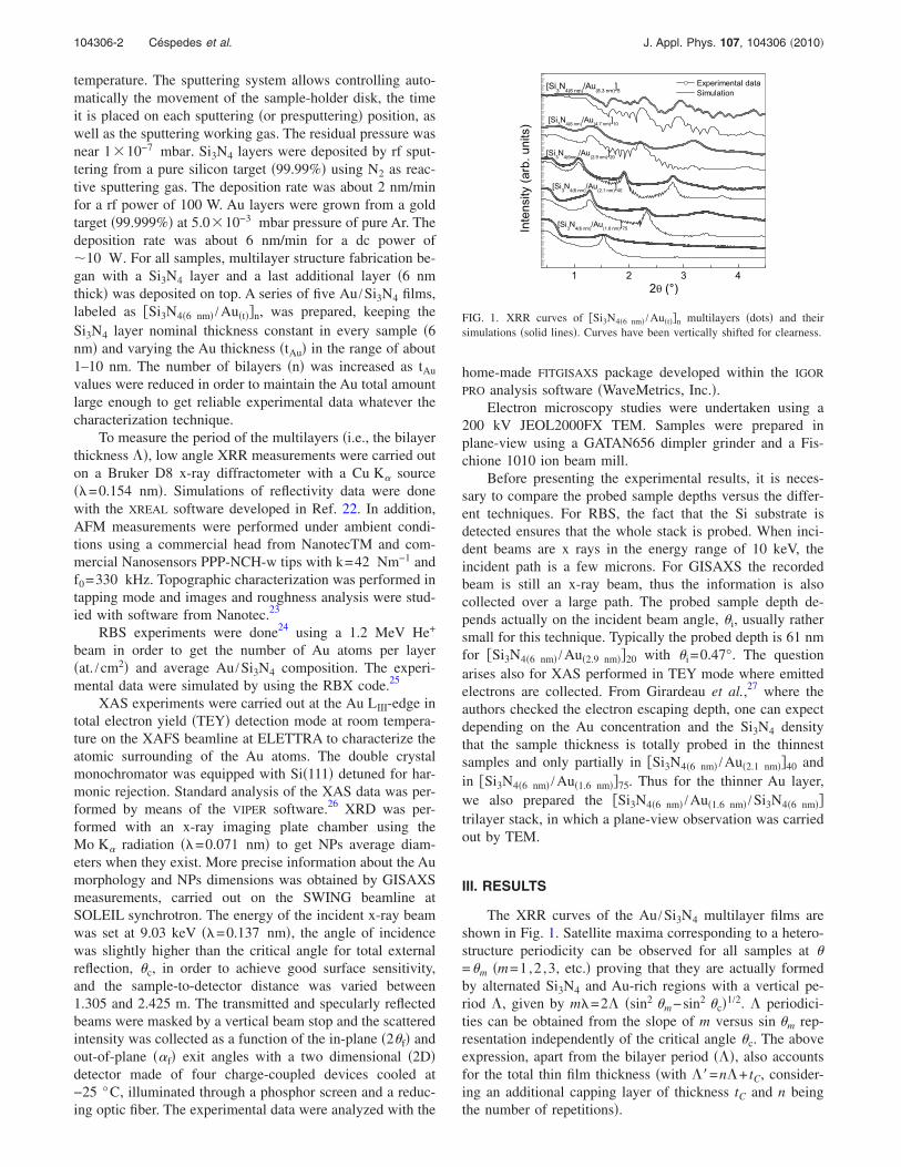
The surface roughness is given by AFM images of thesamples named as �Si3N4�6 nm� /Au�4.7��10, �Si3N4�6 nm� /Au�2.9��20, and �Si3N4�6 nm� /Au�1.6��75 �Fig. 2�. The obtainedsurface rms roughness values �surface R in Table I� rangesbetween 2.5 and 3.5 nm, all of them being of the same order,indicating that the overall deposited thickness does not play akey role in the stack roughness. As expected, these values arelarger than the interface R ones which are average ones. It is
important to comment also that both measured roughnesscorrespond to different physical measurements. While AFMmeasures the surface roughness, surface R, at the lengthscale of the image dimension �of the one micron order�, theXRR-obtained interface roughness, interface R, is related tothe declination of the interfacial parallelism between layersevaluated at the x-ray coherence length scale �of the order ofsome tens nanometer�.
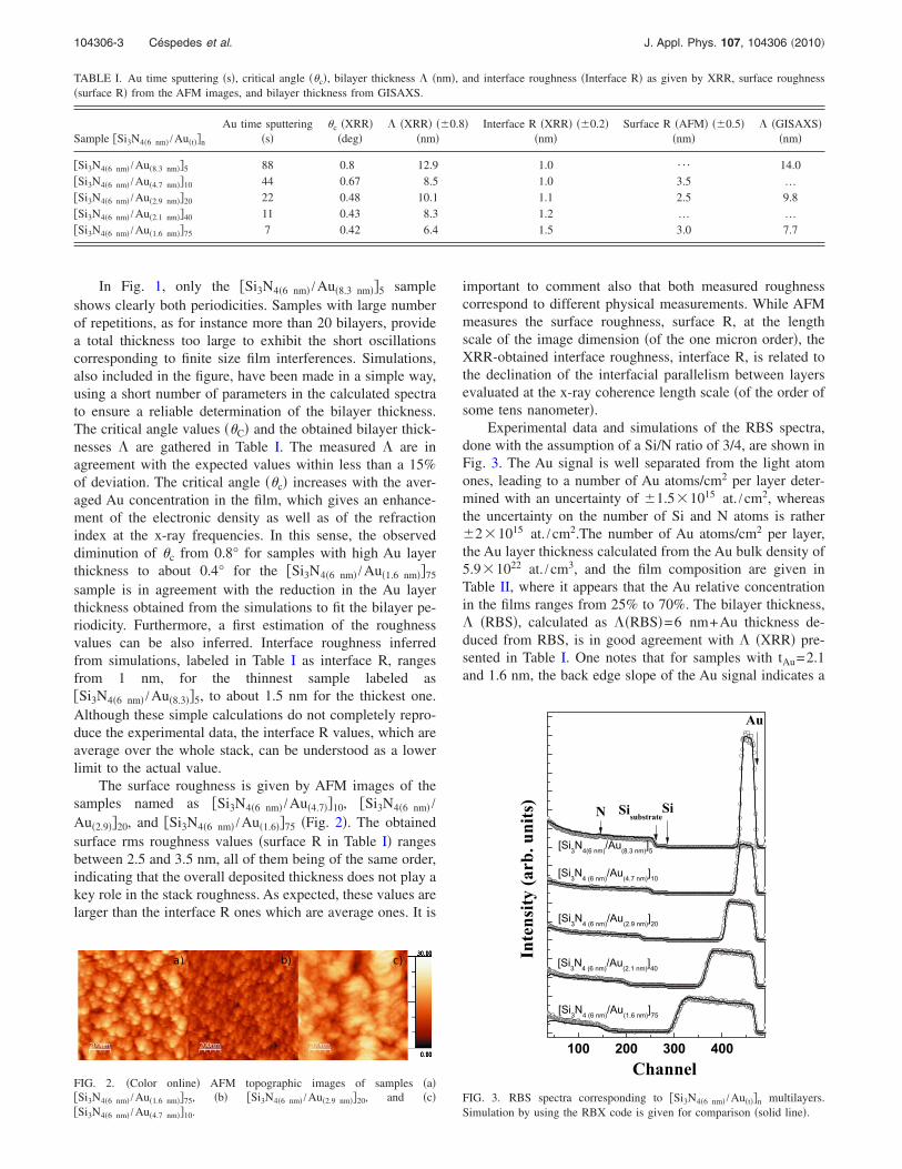
Experimental data and simulations of the RBS spectra,done with the assumption of a Si/N ratio of 3/4, are shown inFig. 3. The Au signal is well separated from the light atomones, leading to a number of Au atoms/cm2 per layer deter-mined with an uncertainty of �1.5�1015 at. /cm2, whereasthe uncertainty on the number of Si and N atoms is rather�2�1015 at. /cm2.The number of Au atoms/cm2 per layer,the Au layer thickness calculated from the Au bulk density of5.9�1022 at. /cm3, and the film composition are given inTable II, where it appears that the Au relative concentrationin the films ranges from 25% to 70%. The bilayer thickness,� �RBS�, calculated as ��RBS�=6 nm+Au thickness de-duced from RBS, is in good agreement with � �XRR� pre-sented in Table I. One notes that for samples with tAu=2.1and 1.6 nm, the back edge slope of the Au signal indicates a
TABLE I. Au time sputtering �s�, critical angle ��c�, bilayer thickness � �nm�, and interface roughness �Interface R� as given by XRR, surface roughness�surface R� from the AFM images, and bilayer thickness from GISAXS.
Sample �Si3N4�6 nm� /Au�t��n
Au time sputtering�s�
�c �XRR��deg�
� �XRR� ��0.8��nm�
Interface R �XRR� ��0.2��nm�
Surface R �AFM� ��0.5��nm�
� �GISAXS��nm�
�Si3N4�6 nm� /Au�8.3 nm��5 88 0.8 12.9 1.0 ¯ 14.0�Si3N4�6 nm� /Au�4.7 nm��10 44 0.67 8.5 1.0 3.5 …�Si3N4�6 nm� /Au�2.9 nm��20 22 0.48 10.1 1.1 2.5 9.8�Si3N4�6 nm� /Au�2.1 nm��40 11 0.43 8.3 1.2 … …�Si3N4�6 nm� /Au�1.6 nm��75 7 0.42 6.4 1.5 3.0 7.7
FIG. 2. �Color online� AFM topographic images of samples �a��Si3N4�6 nm� /Au�1.6 nm��75, �b� �Si3N4�6 nm� /Au�2.9 nm��20, and �c��Si3N4�6 nm� /Au�4.7 nm��10.
FIG. 3. RBS spectra corresponding to �Si3N4�6 nm� /Au�t��n multilayers.Simulation by using the RBX code is given for comparison �solid line�.
104306-3 Céspedes et al. J. Appl. Phys. 107, 104306 �2010�
larger overall roughness than for samples with thicker Aulayers in qualitative agreement with the interface R valuedecreasing from 1.5 to 1.0 nm when tAu increases �Table I�.
Au LIII-edge X-ray absorption near-edge structure�XANES� of several Au /Si3N4 multilayers and of a Au metalfoil are displayed in Fig. 4. A direct comparison shows thatAu is present in the metallic form. In order to obtain preciseinformation on the local environment around Au, EXAFSoscillations were obtained after removing the atomic back-ground by a cubic spline polynomial fitting, and the EXAFSsignal ���k�� was found by normalizing the magnitude of theoscillations to the edge jump. The pseudoradial distributionfunction around the absorber atoms has been calculated byFourier transforming the k2-weighted EXAFS signal�k2 ·��k�� multiplied previously by a Hanning window. Forall the samples, FTs were obtained over the samek2-weighted interval over a wave vector range from 2 to14 Å−1 �except for the thinnest Au layer where the rangewas 2–12 Å−1�, then fitted to the well-known EXAFSequation28 by using amplitude and phase backscatteringfunctions calculated by the FEFF6 code.29,30 The number ofneighbors and distances is summarized in Table III. Simula-tions of the experimental data for four representative samplesand a standard Au metal foil can be observed in Fig. 5. TheAu–Au distances coincide with the Au metal reference,which justifies the use of Au bulk atomic density in the thick-ness calculations. Considering additional Au–N or Au–Sicontributions in the simulations is not necessary sinceAu–Au simulations reproduce the experimental data. The
TABLE II. Number of Au atoms per layer �1015 at. /cm2�, Au thickness per layer �nm�, chemical composition, and Au relative atomic concentration as givenby RBS. The bilayer thickness, � �RBS�, is calculated as 6 nm+the Au thickness deduced from RBS.
Sample �Si3N4�6 nm� /Au�t��n
Number of Au atoms per layer ��1.5��1015 at. /cm2�
Au thickness per layer��0.3��nm�
Atomiccomposition
�Au�/�Au�+ �Si�+ �N��%�
� �RBS��nm��Au� �Si� �N�
�Si3N4�6 nm� /Au�8.3 nm��5 49 8.3 16 3 4 70 14.3�Si3N4�6 nm� /Au�4.7 nm��10 27.5 4.7 8.9 3 4 56 10.7�Si3N4�6 nm� /Au�2.9 nm��20 17.3 2.9 3.8 3 4 35 8.9�Si3N4�6 nm� /Au�2.1 nm��40 12.6 2.1 3.0 3 4 30 8.1�Si3N4�6 nm� /Au�1.6 nm��75 9.4 1.6 2.3 3 4 25 7.6
TABLE III. Au atomic surrounding as given by EXAFS. R, N, and 2
correspond to the atomic distance, number of neighbors, and the Debye–Waller factor.
Sample
EXAFS
Au–AuR
�� N2
�10−3 Å2�
Au foil 2.85�0.01 12.0�0.5 8.9�0.5�Si3N4�6 nm� /Au�8.3 nm��5 2.85�0.01 10.5�1.0 9.5�1.0�Si3N4�6 nm� /Au�2.9 nm��20 2.84�0.01 10.4�0.5 9.7�0.5�Si3N4�6 nm� /Au�2.1 nm��40 2.84�0.01 10.2�0.5 9.8�0.5�Si3N4�6 nm� /Au�1.6 nm��75 2.84�0.01 10.6�0.5 11.0�0.5
FIG. 4. XANES of several samples in comparison with the Au metalreference.
FIG. 5. �a� k-space comparison between the experimental EXAFS signal�dots� and simulations �lines� for samples with t=8.3, 2.9, 2.1, and 1.6 nmand a Au foil. �b� Modulus and imaginary part of the Fourier transformscompared with the simulations �lines�.
104306-4 Céspedes et al. J. Appl. Phys. 107, 104306 �2010�
EXAFS results clearly indicate Au metal formation in all thesample series. However, it should be noted that the decreasein tAu entails a slight increase in the amplitude loss factor S0
2.Moreover, it appears that for tAu=8.3 nm, the N value isstrongly dependent on the 2 value. An uncertainty in the Aucoordination number of the order of �1 is thus expected herewhereas it is of �0.5 for the other samples.
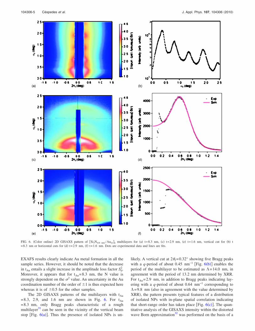
The 2D GISAXS patterns of the multilayers with tAu
=8.3, 2.9, and 1.6 nm are shown in Fig. 6. For tAu
=8.3 nm, only Bragg peaks characteristic of a roughmultilayer31 can be seen in the vicinity of the vertical beamstop �Fig. 6�a��. Thus the presence of isolated NPs is un-
likely. A vertical cut at 2�f=0.32° showing five Bragg peakswith a q-period of about 0.45 nm−1 �Fig. 6�b�� enables theperiod of the multilayer to be estimated as �=14.0 nm, inagreement with the period of 13.2 nm determined by XRR.For tAu=2.9 nm, in addition to Bragg peaks indicating lay-ering with a q-period of about 0.64 nm−1 corresponding to�=9.8 nm �also in agreement with the value determined byXRR�, the pattern presents typical features of a distributionof isolated NPs with in-plane spatial correlation indicatingthat short-range order has taken place �Fig. 6�c��. The quan-titative analysis of the GISAXS intensity within the distortedwave Born approximation32 was performed on the basis of a
FIG. 6. �Color online� 2D GISAXS pattern of �Si3N4�6 nm� /Au�t��n multilayers for �a� t=8.3 nm, �c� t=2.9 nm, �e� t=1.6 nm, vertical cut for �b� t=8.3 nm or horizontal cuts for �d� t=2.9 nm, �f� t=1.6 nm. Dots are experimental data and lines are fits.
104306-5 Céspedes et al. J. Appl. Phys. 107, 104306 �2010�
horizontal cut at �f=0.19° using the local monodisperseapproximation33 and assuming spherical NPs with no verticalcorrelation between NPs �i.e., each layer has a morphologywhich is completely independent from the adjacentlayers�.34,35 The structure factor of the assembly, which de-scribes the interference effects between neighboring par-ticles, was computed by the Percus–Yevick formula for in-teracting hard spheres. The diameter of the hard spheres, Dhs,was considered to be proportional to the diameter of the NPs,D, with a constant factor Chs �Dhs=ChsD�, and the hardsphere volume fraction that characterizes the local arrange-ment of NPs relative to one another was hs.
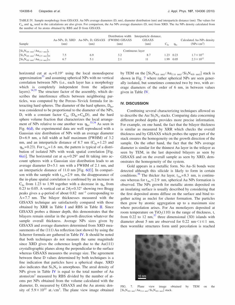
33,34 As seen inFig. 6�d�, the experimental data are well reproduced with aGaussian size distribution of NPs with an average diameterD=6.9 nm, a full width at half maximum �FWHM� of 3.2nm, and an interparticle distance of 8.7 nm �Chs=1.23 andhs=0.23�. For tAu=1.6 nm, the pattern is typical of a distri-bution of isolated NPs with weak spatial correlation �Fig.6�e��. The horizontal cut at �f=0.29° and fit taking into ac-count spheres with a Gaussian size distribution leads to anaverage diameter D=5.1 nm with a FWHM of 2.1 nm, andan interparticle distance of 11.0 nm �Fig. 6�f��. In compari-son with the sample with tAu=2.9 nm, the disappearance ofthe in-plane spatial correlation is confirmed by an increase inChs from 1.23 to 1.99 together with a decrease in hs from0.23 to 0.05. A vertical cut at 2�f=0.32° showing two Braggpeaks gives a q-period of about 0.82 nm−1 corresponding to�=7.7 nm. The bilayer thicknesses measured with theGISAXS technique are satisfactorily compared with thoseobtained by XRR in Table I and RBS in Table II. SinceGISAXS probes a thinner depth, this demonstrates that thebilayers remain similar in the growth direction whatever thesample overall thickness. Average NPs sizes given byGISAXS and average diameters determined from XRD mea-surements of the �111� Au reflection �not shown� by using theScherrer formula are gathered in Table IV. It should be notedthat both techniques do not measure the same magnitudesince XRD gives the coherence length due to the Au�111�crystallographic planes along the perpendicular to the surfacewhereas GISAXS measures the average size. The agreementbetween these D values determined by both techniques is afine indication that particles have a spherical shape. XRDalso indicates that Si3N4 is amorphous. The areal density ofNPs given in Table IV is equal to the total number of Auatoms/cm2 measured by RBS divided by the number of at-oms per NPs obtained from the volume calculated with thediameter, D, measured by GISAXS and the Au atomic den-sity of 5.9�1022 at. /cm3. The plane view image obtained
by TEM on the �Si3N4�6 nm� /Au�1.6 nm� /Si3N4�6 nm�� stack isshown in Fig. 7 where rather spherical NPs are seen gener-ally isolated, but sometimes connected two by two, with av-erage diameters of the order of 6 nm, in between valuesgiven in Table IV.
IV. DISCUSSION
Combining several characterizing techniques allowed usto describe the Au /Si3N4 stacks. Comparing data concerningdifferent probed depths provides more precise information.For example, on one hand, the fact that the bilayer thicknessis similar as measured by XRR which checks the overallthickness and by GISAXS which probes the upper part of thestack ensures the homogeneity on the growth direction of thesample. On the other hand, the fact that the NPs averagediameter is similar for the thinnest Au layer in the trilayer asseen by TEM, in the last deposited bilayers as seen byGISAXS and on the overall sample as seen by XRD, dem-onstrates the homogeneity of the system.
Gold appears in a metallic form. No Au–Si bonds weredetected although this silicide is likely to form in certainconditions.36 The thicker Au layer, tAu=8.3 nm, is continu-ous whereas for tAu�2.9 nm, spherical Au NPs formation isobserved. The NPs growth for metallic atoms deposited onan insulating surface is usually described by considering thatthe first deposited atoms diffuse on the surface and bind to-gether acting as nuclei for cluster formation. The particlesthen grow by atomic aggregation up to a maximum sizewhere percolation arises. For Au monolayers deposited atroom temperature on TiO2�110� in the range of thickness, t,from 0.22 to 12 nm,37 three dimensional �3D� islands withdiameter about 5 nm are observed for 0.22 nm� t�1 nm,then wormlike structures form until percolation is reached
TABLE IV. Sample morphology from GISAXS. Au NPs average diameters �D, nm�, diameter distribution �nm� and interparticle distance �nm�. The values forChs and hs used in the calculations are also given. For comparison, the Au NPs average diameters �D, nm� from XRD. The Au NPs density calculated fromthe number of Au atoms obtained by RBS and D from GISAXS.
SampleAu-NPs, D, XRD
�nm�Au-NPs, D, GISAXS
�nm�
Distribution width�FWHM� GISAXS
�nm�
Interparticle distance,GISAXS
�nm� Chs hs
Calculated Au-NPs density�NPs /cm2�
�Si3N4�6 nm� /Au�8.3 nm��5 Continuous layer�Si3N4�6 nm� /Au�2.9 nm��20 7.5 6.9 3.2 8.7 1.23 0.23 1.7�1012
�Si3N4�6 nm� /Au�1.6 nm��75 6.7 5.1 2.1 11 1.99 0.05 2.3�1012
FIG. 7. Plane view image obtained by TEM on the�Si3N4�6 nm� /Au�1.6 nm� /Si3N4�6 nm�� stack.
104306-6 Céspedes et al. J. Appl. Phys. 107, 104306 �2010�
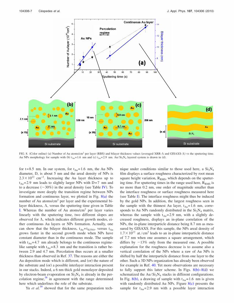
for t=8.5 nm. In our system, for tAu=1.6 nm, the Au NPsdiameter, D, is about 5 nm and the areal density of NPs is2.3�1012 cm−2. Increasing the Au layer thickness up totAu=2.9 nm leads to slightly larger NPs with D=7 nm andto a decrease ��30%� in the areal density �see Table IV�. Toinvestigate more deeply the transition regime between NPsformation and continuous layer, we plotted in Fig. 8�a� thenumber of Au atoms/cm2 per layer and the experimental bi-layer thickness, �, versus the sputtering time given in TableI. Whereas the number of Au atoms/cm2 per layer varieslinearly with the sputtering time, two different slopes areobserved for �, which indicates different growth modes, ei-ther continuous Au layers or NPs formation. Actually, onecan show that the bilayer thickness, tAu+tSi3N4, versus tAu
grows faster in the second growth mode when NPs haveconstant diameter than in the continuous mode. The samplewith tAu=4.7 nm already belongs to the continuous regime-like sample with tAu=8.3 nm and the transition is rather be-tween 2.9 and 4.7 nm. Percolation thus occurs at a smallerthickness than observed in Ref. 37. The reasons are either theAu deposition mode which is different, and �or� the nature ofthe substrate and �or� a possible interlayer interaction presentin our stacks. Indeed, a 6 nm thick gold monolayer depositedby electron-beam evaporation on Si3N4 is already in the per-colation regime,38 in agreement with the range determinedhere which underlines the role of the substrate.
Yu et al.39 showed that for the same preparation tech-
nique under conditions similar to those used here, a Si3N4
film displays a surface roughness characterized by root meansquare height variation, RRMS, which depends on the sputter-ing time. For sputtering times in the range used here, RRMS isno more than 0.2 nm, one order of magnitude smaller thanthe interface roughness or surface roughness measured here�see Table I�. The interface roughness might thus be inducedby the gold NPs. In addition, the largest roughness seen inthe sample with the thinnest Au layer, tAu=1.6 nm, corre-sponds to Au NPs randomly distributed in the Si3N4 matrix,whereas the sample with tAu=2.9 nm, with a slightly de-creased roughness, displays an in-plane correlation of theNPs, the in-plane interparticle distance being 8.7 nm as mea-sured by GISAXS. For this sample, the NPs areal density of1.7�1012 at. /cm2 leads to an in-plane interparticle distanceof 7.7 nm when one assumes a square arrangement, whichdiffers by 13% only from the measured one. A possibleexplanation for the roughness decrease is to assume also avertical correlation of the NPs where a raw of Au NPs isshifted by half the interparticle distance from one layer to theother. Such a 3D NPs organization has already been observedfor example in Ref. 40. Yet more observations are necessaryto fully support this latter scheme. In Figs. 8�b�–8�d� weschematized the Au /Si3N4 stacks in different configurations.In Fig. 8�b�, a drawing of sample with tAu=1.6 nm is givenwith randomly distributed Au NPs. Figure 8�c� presents thesample for tAu=2.9 nm with a possible layer interaction
FIG. 8. �Color online� �a� Number of Au atoms/cm2 per layer �RBS� and bilayer thickness values �averaged XRR-� and GISAXS-�� vs the sputtering time.Au NPs morphology for sample with �b� tAu=1.6 nm and �c� tAu=2.9 nm. Au /Si3N4 layered system is drawn in �d�.
104306-7 Céspedes et al. J. Appl. Phys. 107, 104306 �2010�
leading to a better organization of the NPs and a roughnessdecrease. The scheme of the continuous Au layers is in Fig.8�d�.
NPs formation requires atomic diffusion and aggrega-tion. To identify the main parameters playing a role on thisinitial stage, we can compare the behavior of the Fe /Si3N4,Mn /Si3N4, Ni /Si3N4, and Au /Si3N4 systems. They wereprepared by the same sequential sputtering technique underthe same experimental conditions. Indeed, in Ni /Si3N4,19 therole of the deposition velocity had been pointed out on thepercolation threshold. The Fe /Si3N4, Mn /Si3N4, Ni /Si3N4,and Au /Si3N4 systems have been deposited with a rate in therange 2–2.5 nm/min. For the Mn /Si3N4 stack, a Mn3N2 com-pound is formed with no presence of Mn–Mn closeneighbors.21 For Fe /Si3N4 �Ref. 20� and Ni /Si3N4,19 there iscoexistence of metal-N and metal-metal bonds. To explainthese different behaviors, one can look at the heat of forma-tion, �H, of bulk metallic nitride. �H=−44 kJ �moleof atoms�−1 for Mn5N2, −31 kJ �mole of atoms�−1 forMn4N, −16 kJ �mole of atoms�−1 for Fe4N, and+0.2 kJ �mole of atoms�−1 for Ni3N.41,42 ConcerningAu /Si3N4, no heat of formation value for any gold nitridehas been found in the literature. Yet, it has been shown that,for crystalline Si3N4,43 the Au–Si3N4 interface is nonreac-tive, in agreement with our observation although the Si3N4
layer is amorphous here. The possibility to prepare Au3N,demonstrated recently,44 requires very specific conditions notmet in the deposition process used here. Although we aredealing with first stages of layer deposition which could beseen as far from thermodynamical equilibrium process, theheat of formation for bulk nitride appears to be the key pa-rameter in determining the initial chemical bounds. A ques-tion is why metallic nitrides are formed instead of silicidessince these latter have sometimes more negative heat of for-mation than nitrides: �H for NiSix, whatever x, is about−25 kJ �mole of atoms�−1 as compared to+0.2 kJ �mole of atoms�−1 for Ni3N.42 An answer could begiven by considering that amorphous Si3N4 displays N dan-gling bonds and no Si dangling ones.
V. CONCLUSION
The deposition of Au layers sandwiched between Si3N4
using sequential sputtering of Si3N4 and Au has been studied.The deposition process with the stages of particle formation,percolation regime leading to continuous layer is observed asusual. For tAu�2.9 nm, Au NPs formed whereas for largertAu the Au layer is continuous. The percolation transitionoccurs for 2.9 nm� tAu�4.7 nm. By comparing to other Audeposited systems, we underline the role of the substrate anddeposition parameters on the percolation transition.
The pure metallic Au NPs have spherical shape withaverage diameters in the range 5–7 nm, size distribution witha FWHM of 40%–45%, and high areal density of the orderof 1012 /cm2. They are randomly distributed in the samplevolume except for tAu=2.9 nm where an in-plane organizedarray is detected. The NPs volume density over the wholesample is controlled by the in-plane organization which de-pends on the metal wettability on Si3N4 and by the number
of layers which can be adjusted by the experimentalists. Onthe same substrate, Ni, Fe, and Mn have a different behaviorwhich can be understood by considering the heat of forma-tion of the metal nitride. This gives an indication that Si3N4
layers are terminated by N dangling bonds, so that Au NPsare surrounded by N atoms. Preparation of such well charac-terized samples with NPs of similar diameters and areal den-sity but either randomly dispersed or spatially self-organizedare interesting to study the consequences of order and disor-der on the sample polarization, the Au SPR position andnonlinear susceptibility.
ACKNOWLEDGMENTS
This work has been partially supported under SpanishMICINN Contract No. MAT2009-08786. One of us, E.C.,acknowledges to CSIC JAE-grants for the stay at the Lab-oratoire de Chimie Physique, Orsay, France. We also thankthe TEM service of the ICMM.
1U. Kreibig and M. Vollmer, Optical Properties of Metal Clusters�Springer, New York, 1995�.
2T.A. Luce, W. Hübner, K.H. Benneman, Z. Phys. B 102, 223 �1997�.3M. Breit, V. A. Podolskiy, S. Grésillon, G. von Plessen, J. Feldmann, J. C.Rivoal, P. Gadenne, A. K. Sarychev, and V. M. Shalaev, Phys. Rev. B 64,125106 �2001�.
4D. Ricard, P. Roussignol, and C. Flytzanis, Opt. Lett. 10, 511 �1985�.5J.-M. Lamarre, F. Billard, C. H. Kerboua, M. Lequime, S. Roorda, and L.Martinu, Opt. Commun. 281, 331 �2008�.
6C. Flytzanis, J. Phys. B 38, S661 �2005�.7S. Guo and E. Wang, Anal. Chim. Acta 598, 181 �2007�.8R. Sardar, A. M. Funston, P. Mulvaney, and R. W. Murray, Langmuir 25,13840 �2009�.
9S. W. Yu, H. B. Liao, W. J. Wen, and G. K. L. Wong, Opt. Mater. �Am-sterdam, Neth.� 27, 1433 �2005�.
10A. I. Ryasnyanskiy, B. Palpant, S. Debrus, U. Pal, and A. Stepanov, J.Lumin. 127, 181 �2007�.
11S. Pal, M. K. Sanyal, S. Hazra, S. Kundu, F. Schreiber, and J. Pflaum, J.Appl. Phys. 95, 1430 �2004�.
12F. Hubenthal, N. Borg, and F. Träger, Appl. Phys. B 93, 39 �2008�.13C. Voisin, D. Christofilos, P. A. Loukakos, N. Del Fatti, F. Vallée, J.
Lermé, M. Gaudry, E. Cottancin, M. Pellarin, and M. Broyer, Phys. Rev.B 69, 195416 �2004�.
14P. Kluth, B. Johannessen, G. J. Foran, D. J. Cookson, S. M. Kluth, and M.C. Ridgway, Phys. Rev. B 74, 014202 �2006�.
15A. Traverse, Nucl. Instrum. Methods Phys. Res. B 249, 126 �2006�.16G. De Marchi, G. Mattei, P. Mazzoldi, C. Sada, and A. Miotello, J. Appl.
Phys. 92, 4249 �2002�.17L. Armelao, D. Barreca, G. Bottaro, A. Gasparotto, S. Gross, C. Maragno,
and E. Tondello, Coord. Chem. Rev. 250, 1294 �2006�.18M. Garcia del Muro, Z. Konstantinovic, M. Varela, X. Batlle and A. La-
barta, “Metallic Nanoparticles Embedded in a Dielectric Matrix: GrowthMechanisms and Percolation,”J. Nanomater. 2008, article ID 475168�2008�.
19M. Vila, C. Prieto, A. Traverse, and R. Ramirez, J. Appl. Phys. 98, 113507�2005�.
20F. Jiménez-Villacorta, E. Céspedes, M. Vila, A. Muñoz-Martin, G. R. Cas-tro, and C. Prieto, J. Phys. D 41, 205009 �2008�.
21E. Céspedes, Y. Huttel, L. Martínez, A. De Andrés, J. Chaboy, M. Vila, N.D. Telling, G. van der Laan, and C. Prieto, Appl. Phys. Lett. 93, 252506�2008�.
22N. D. Telling, S. J. Guilfoyle, D. R. Lovett, C. C. Tang, M.-D. Crapper,and M. Petty, J. Phys. D 31, 472 �1998�.
23I. Horcas, R. Fernández, J. M. Gómez-Rodriguez, and J. Colchero, Rev.Sci. Instrum. 78, 013705 �2007�.
24H. Bernas, J. Chaumont, E. Cottereau, R. Meunier, A. Traverse, C. Clerc,O. Kaitasov, F. Lalu, D. Le Du, G. Moroy, and M. Salomé, Nucl. Instrum.Methods Phys. Res. B 62, 416 �1992�.
25E. Kotai, Nucl. Instrum. Methods Phys. Res. B 85, 588 �1994�.26K. V. Klementev, J. Phys. D 34, 209 �2001�.
104306-8 Céspedes et al. J. Appl. Phys. 107, 104306 �2010�
27T. Girardeau, J. Mimault, M. Jouen, and P. Chartier, Phys. Rev. B 46, 7144�1992�.
28D. C. Koninsberger and R. Prins, X-Ray Absorption: Principles, Applica-tions, Techniques of EXAFS, SEXAFS and XANES �Wiley, New York,1988�.
29S. I. Zabinsky and J. J. Rehr, Phys. Rev. B 52, 2995 �1995�.30J. J. Rehr and R. C. Albers, Rev. Mod. Phys. 72, 621 �2000�.31V. Holý and T. Baumbach, Phys. Rev. B 49, 10668 �1994�.32M. Rauscher, T. Salditt, and H. Spohn, Phys. Rev. B 52, 16855 �1995�.33J. S. Pedersen, J. Appl. Crystallogr. 27, 595 �1994�.34D. Babonneau, G. Abadias, J. Toudert, T. Girardeau, E. Fonda, J.-S.
Micha, and F. Petroff, J. Phys.: Condens. Matter 20, 035218 �2008�.35K. Salamon, O. Milat, M. Buljan, U. V. Desnica, N. Radić, P. Dubček, and
S. Bernstorff, Thin Solid Films 517, 1899 �2009�.36J. S. Wu, Y. F. Yen, S. Dhara, C. T. Wu, K. H. Chen, and L. C. Chen, Appl.
Phys. Lett. 82, 4468 �2003�.
37L. Zhang, F. Cosandey, R. Persaud, and T. E. Madey, Surf. Sci. 439, 73�1999�.
38R. F. Voss, R. B. Laibowitz, and E. I. Allessandrini, Phys. Rev. Lett. 49,1441 �1982�.
39L. Yu, J. Xu, S. Dong, and I. Kojima, Thin Solid Films 516, 1781 �2008�.40A. Naudon, D. Babonneau, F. Petroff, and A. Vaurès, Thin Solid Films
319, 81 �1998�.41F. R. de Boer, R. Boom, W. C. M. Mattens, A. R. Miedema, and A. K.
Niessen, Cohesion in Metals, �North Holland, Amsterdam, 1988�.42Smithells Metals Reference Book, 6th ed., edited by E. A. Brandes �But-
terworths, London, 1983�.43R. Flammini, F. Wiame, R. Belkou, A. Taleb-Ibrahimi, C. Spezzani, P.
Moras, and C. Crotti, J. Appl. Phys. 103, 083528 �2008�.44S. Krishnamurthy, M. Montalti, M. G. Wardle, M. J. Shaw, P. R. Briddon,
K. Svensson, M. R. C. Hunt, and L. Šiller, Phys. Rev. B 70, 045414�2004�.
104306-9 Céspedes et al. J. Appl. Phys. 107, 104306 �2010�

![Characterization of two dimensional self-organized Au nanoparticles embedded in Si[sub 3]N[sub 4]](https://img.dokumen.tips/doc/110x75/6355f63286104ea1570bf465/characterization-of-two-dimensional-self-organized-au-nanoparticles-embedded-in-1700952131.jpg)


