Embed Size (px)
Citation preview
CALIFORNIA STATE UNIVERSITY, NORTHRIDGE
Fabrication and Characterization of Silicon Carbide (SiC) MESFET
A graduate project in partial fulfillment of the requirements
for the degree of Master of Science
in Electrical Engineering
By
Kaushal D. Patel
August 2017
ii
The graduate project of Kaushal D. Patel is approved:
__________________________________________ _______________
Dr. Robert D. Conner Date
___________________________________________ ______________
Dr. Xiaojun (Ashley) Geng Date
____________________________________________ _______________
Dr. Somnath Chattopadhyay, Chair Date
California State University, Northridge

iii
ACKNOWLEDGEMENT
It is with pleasure and gratitude to dedicate the project which enables me to fortify my
vision. It was not possible for me to complete the project without timely help and
guidance from my professor Dr. Somnath Chattopadhyay. He has stood to support me
throughout my project and helped me on all corners to complete my thesis. It is also with
much thanks to Mr. Charles B. Overton for his kind help and guidance to reach my goal
in the project. I express my gratitude to committee member Dr. Robert D Corner and Dr.
Xiaojun (Ashley) Geng for their continuous indulgence without which my project would
be not complete. It is pertinent to mention that my project would not take its effect if it
had not taken place in the good workspace. In view of all, I am abundantly thankful and
eternally in obligation to the CSUN Electrical Engineering Department for providing
such detailed instruction and access to a remarkable semiconductor facility and lab to
study and go through my project.

iv
TABLE OF CONTENTS
SIGNATURE PAGE ii
ACKNOWLEDGEMENT iii
LIST OF FIGURES vi
LIST OF TABLES x
ABSTRACT xi
Chapter 1. Introduction 1
1.1. Silicon Carbide (SiC) MESFET 1
1.2. Gallium Nitrate (GaN) MESFET 3
1.3. The AlGaN-GaN HEMT 4
1.4. Silicon Carbide (SiC) Schottky diode 5
1.5. Reverse recovery time of the silicon carbide diode 5
1.6. Specific resistance (Ron) 8
Chapter 2. Silicon Carbide (SiC) Material 11
2.1. The Crystal Structure of Silicon Carbide 11
2.1.1. The Structure of the Silicon Carbide Atom 11
2.1.2. Polytypism 11
2.1.3. Impurities in Different Polytypes 12
2.2. Properties of Silicon Carbide (SiC) 14
2.2.1. Crystal Structure 14
2.2.2. 3C-SiC 15
2.2.3. 4H-SiC 15
2.2.4. 6H-SiC 16
2.3. Characteristics of Silicon Carbide (SiC) 16
2.4. Energy Band Diagram 18
2.5. Drift-velocity of 4H-Silicon Carbide 20
v
Chapter 3. Fabrication of Silicon Carbide (SiC) MESFET Device 21
3.1 Silicon Carbide (SiC) Fabrication Process 21
3.1.1. RCA process for cleaning the Silicon Carbide Wafer 21
3.1.2. Oxidation of Silicon Dioxide on Silicon carbide wafer 22
3.1.3. The Photo-lithography method for the Silicon Carbide
MESFET 23
3.1.4. The Spin-Coating of the Photoresist S1813 and
Hexamethyldisilazane (HMDS) primer on the silicon
Carbide wafer 23
3.1.5. The Etching and Cleaning process for the Silicon Carbide
Wafer 26
3.1.5.1 Oxide Etching by BOE (buffered oxide etching) 27
3.1.6. Ion Implantation 29
3.1.7. The Annealing step for the Silicon Carbide MESFET 32
3.1.8. Device Isolation by using Ion Implantation Process 32
3.2. Fabrication process of Silicon Carbide MESFET device 34
Chapter 4. Oxidation Process for Silicon Carbide (SiC) 57
4.1 The Wet Oxidation Process for the 4H-Silicon Carbide Wafer 58
4.2. The Sputtering Oxidation Process for the 4H-Silicon Carbide
Wafer 60
Chapter 5. Result: Current-Voltage Characteristics of Silicon Carbide (SiC)
MESFET 62
Chapter 6. Conclusion 65
REFERENCES 66

vi
LIST OF FIGURES
Figure 1.1 The current versus the time graph shows the reverse recovery of the
silicon carbide diode with diverse doping level 7
Figure 1.2 The forward voltage versus current graph shows the reverse
Recovery of the silicon carbide diode with diverse dope
Level 7
Figure 1.3 The Excess minority carrier distribution cause the soft recovery
Characteristic 8
Figure 1.4 The Characteristics of Soft reverse-recovery 8
Figure 1.5 On resistance Ron as a function of breakdown voltage for
Switching Applications 10
Figure 2.1 The Atomic structure of Silicon Carbide atom 11
Figure 2.2 The Scopes of the Three-Closed Plane 12
Figure 2.3 The Three type of Silicon Carbide polytype 13
Figure 2.4 The Photograph iridescence range that has the molecule of 4H-
Silicon Carbide. 14
Figure 2.5 The Silicon Carbide (SiC) material structure 15
Figure 2.6 The Structure of (β) 3C-SiC 15
Figure 2.7 The Structure of 4H-SiC 16
Figure 2.8 The Structure of 6H-SiC 16
Figure 2.9 The 4H-Silicon Carbide Energy Band structure 18
Figure 2.10 The 4H-SiC Excitonic Energy vs. Temperature 19
Figure 2.11 The Bandgap of 3C-Silicon carbide, 4H-Silicon carbide and
6H-Silicon Carbide versus Temperatures 19
Figure 2.12 The concentration versus temperature of 3C-Silicon Carbide,
4H-Silicon Carbide and 6H-Silicon Carbide 20
vii
Figure 2.13 The 4H-Silicon Carbide: Drift-Velocity vs. Electric field 20
Figure 3.1 The photoresist film thickness versus the spinning speed of the spin
Coater 24
Figure 3.2 The Characteristic curve of Exposure energy versus Photoresist
Thickness 24
Figure 3.3 Typical view of a good/clear alignment mark 25
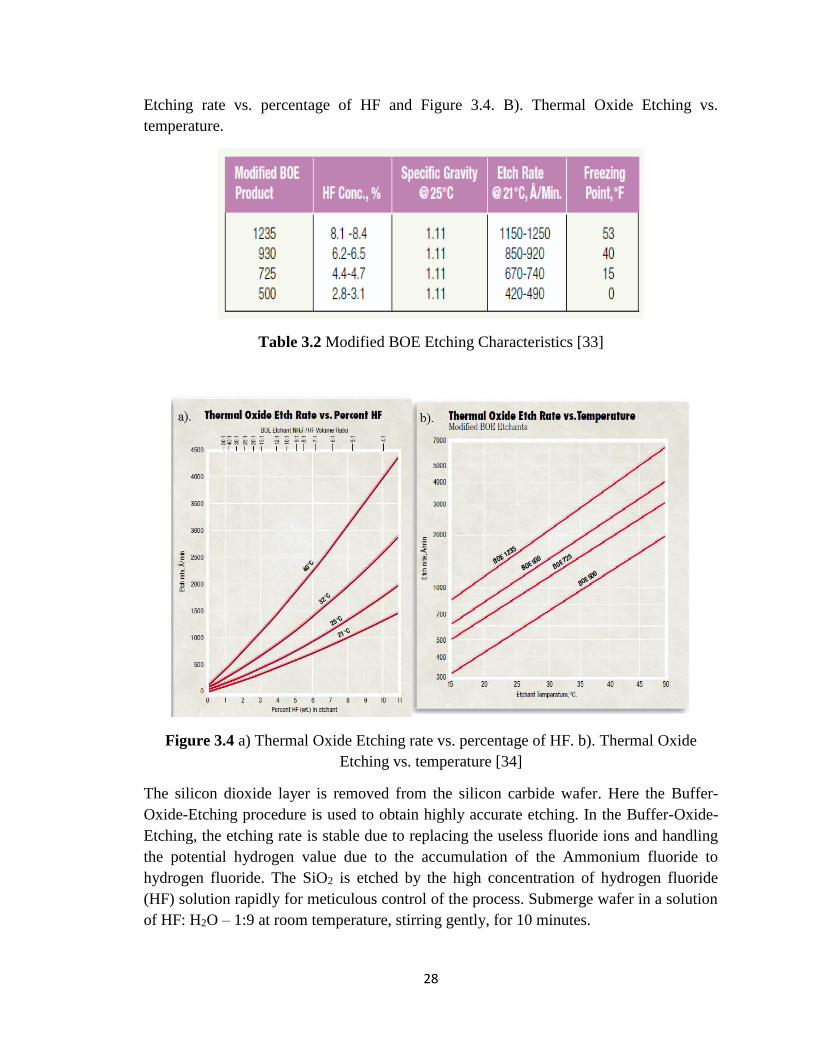
Figure 3.4 a). Thermal Oxide Etching rate vs. percentage of HF 28
b). Thermal Oxide Etching vs. temperature 28
Figure 3.5 The Cross-Sectional Sight of 6H-Silicon-Carbide MESFET 30
Figure 3.6 The Cross-Sectional Sight of an Ion Implant Machine 30
Figure 3.7 The Energy Band of P-type Epitaxial-layer of N-Nitrogen 31
Figure 3.8 Isolation of active areas by using ion implantation 33
Figure 3.9 Photograph of patterns for Ar isolation, ITO gate, and source/drain
contact pad 33
Figure 3.10 New SiC wafer including Epitaxial layers 34
Figure 3.11 Silicon Dioxide (SiO2) is deposited on the Silicon Carbide (SiC)
Wafer 35
Figure 3.12 Photoresist S1813 deposited on the Silicon dioxide (SiO2) layers 36
Figure 3.13 Mask# 1 pattern for source and drain doping oxide etch 37
Figure 3.14 Resist pattern for the source and drain doping after UV exposure and
Image development 38
Figure 3.15 Silicon dioxide (SiO2) is etched for source and drain doping 38
Figure 3.16 Nitrogen Ion N+ implanted in the n-type layer for Drain and Source
Well 39
Figure 3.17 The device structure after stripping the photoresist S1813 39
Figure 3.18 Device structure after annealing process 40
viii
Figure 3.19 The Annealing Temperature Profile of the SiC wafer at up to
1600oC 40
Figure 3.20 Surface morphology of high temperature annealed AlN film study
using Augerscope 41
Figure 3.21 Photoresist S1813 is deposited on Silicon dioxide (SiO2) layer 42
Figure 3.22 Mask#2 pattern for the electrical isolation 42
Figure 3.23 Photoresist pattern for the electrical isolation after UV exposure and
PR image development 43
Figure 3.24 The Silicon dioxide (SiO2) is etched for the electrical isolation 43
Figure 3.25 The Argon (Ar) is implanted for electrical isolation of the device 44
Figure 3.26 The device structure after stripping the photoresist S1813 44
Figure 3.27 The Silicon dioxide (SiO2) is deposited 45
Figure 3.28 The photoresist S1813 is deposited on the wafer 45
Figure 3.29 Mask#1 pattern for the Ohmic contact window before UV exposure 46
Figure 3.30 Mask#1 pattern for the Ohmic contact window after UV exposure
and PR image development 46
Figure 3.31 Silicon Dioxide (SiO2) is etched from the top of Source and Drain
Well 47
Figure 3.32 Device structure after stripping the photoresist S1813 47
Figure 3.33 Deposition of nickel for the sources and drain contact 48
Figure 3.34 Photoresist S1813 is deposited on the wafer 48
Figure 3.35 The Mask# 3 Metal Pattern for the Source and Drain Ohmic contacts
before UV exposure 49
Figure 3.36 Photoresist metal pattern for the Source and Drain contacts after
the UV exposure and PR image developing 49
Figure 3.37 The nickel is etched from the top of gate area 50
Figure 3.38 The device structure after stripping the photoresist S1813 50
ix
Figure 3.39 Photoresist S1813 is spin coated on the wafer 51
Figure 3.40 The Mask #4 pattern for off-set Gate Contact before UV exposure 51
Figure 3.41 Photoresist pattern is for off-set gate contact after UV exposure
and PR image developing 52
Figure 3.42 The Silicon dioxide (SiO2) is etched for gate contact 52
Figure 3.43 The device structure after stripping the photoresist S1813 53
Figure 3.44 The Polymethylglutarimide (PMGI) Spin Coating 53
Figure 3.45 Photoresist S1813 is deposited on PMGI SF-6 layers 54
Figure 3.46 The Mask #5 Pattern for the formation of Gate Contact,
ITO deposition, and lift-off before UV exposure 54
Figure 3.47 Photoresist pattern for the formation of Gate Contact, ITO deposition,
and lift-off after UV exposure and PR image developing 55
Figure 3.48 The Indium Tin Oxide (ITO) deposition 56
Figure 3.49 The Offset Gate Structure MESFET 56
Figure 4.1 The Wet Oxidation Process for the 4H-Silicon Carbide Wafer 59
Figure 4.2 The Sputtering Oxidation Process for the 4H-Silicon Carbide Wafer 61
Figure 5.1 The First graph of the Current-Voltage Characteristics Silicon
Carbide MESFET 62
Figure 5.2 I-V Characteristics of GaN MESFET with gate offset 63
Figure 5.3 The third graph of the Current-Voltage Characteristics Silicon
Carbide MESFET 64

x
LIST OF TABLES
Table 2.1 The Silicon-Carbide versus the silicon polytype properties 17-18
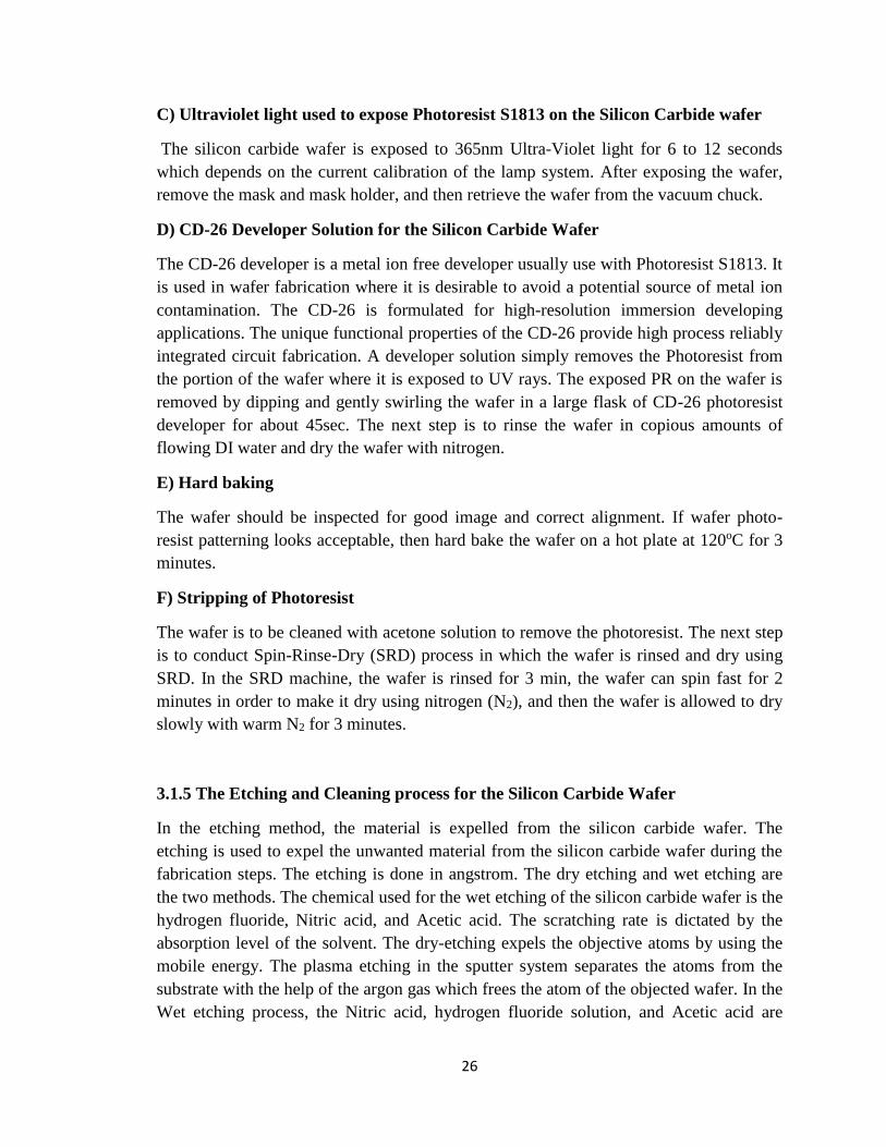
Table 3.1 Standard BOE Etchant Characteristics 27
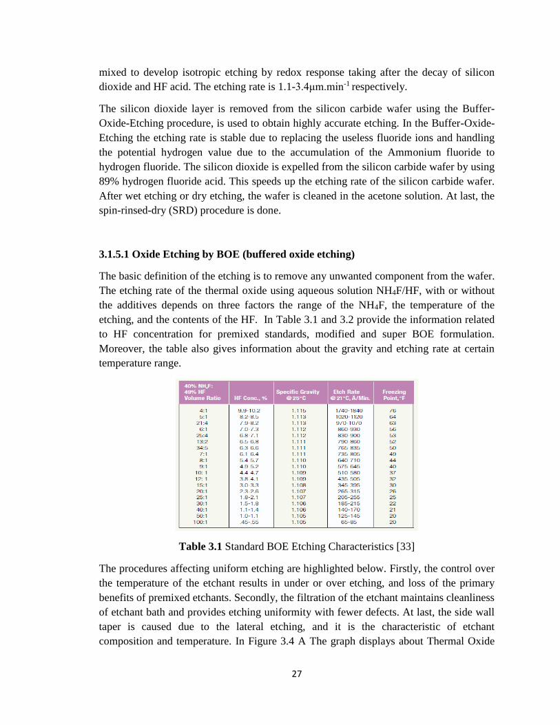
Table 3.2 Modified BOE Etchant Characteristics 28
xi
ABSTRACT
FABRICATION AND CHARACTERISATION OF SILICON CARBIDE MESFET
BY
Kaushal D. Patel
Master of Science in Electrical Engineering
This research work is dealt with the fabrication of the optically triggered silicon carbide
MESFET. The fabrication of the silicon carbide MESFET device has been
chronologically described to study the device structure, process development, and
material properties. In order to understand the fabrication process, the optimization of
photo-resist processing, ion implanted doping process, chemical etching process, silicon
oxide growth on SiC material, stoichiometry silicon oxide with SiC material and
comparative study of silicon oxide growth for silicon and carbon faces of SiC, nickel and
indium tin oxide materials deposition for ohmic and Schottky contacts have been studied
to optimize the unit steps of fabrication process. A detailed study on ion implantation,
high-temperature annealing, and electrical device isolation has been performed. Different
failure analyses for wafer and device level have been conducted to monitor the device
performance, fabrication processing and material properties. I-V characteristics of
fabricated SiC MESFET device has been measured by the curve tracer and compared
with other fabricated GaN MESFE device.
1
Chapter 1. Introduction
In power semiconductor industry, the Silicon Carbide based device turn into a noticeable
option in contrasted with Silicon (Si) based device because of its predominant attributes.
For example, in the term of power dissipation; high voltage blocking capability due to
breakdown electrical field, electron drift velocity and thermal conductivity and a radio-
active hardness capable due to the structure of silicon carbide, and the wide-ranging band
gap vitality prompts the elevated temperature operation capacity. Recently, the wireless
communication is on demand which creates the demand of the silicon carbide transistor
for the mobile antenna station. In fact, in the satellite communication and Military Radar
field; traveling wave tube and high-power transistors have replaced magnetrons due to a
compact size, low weight, and long life of the transistor. Thus, silicon carbide (SiC)
device becomes more attracting in the market.
Silicon carbide (SiC) devices can work under such an extreme condition that it is required
to empower critical upgrades to a far-extending assortment of applications and systems.
The excellent perform silicon carbide devices improve the high voltage switching for
efficient power distribution, and silicon carbide device can drive the electronics, used in
military radar for communication, and the fuel or engine of aircraft and automobile can
be regulated for higher efficiency and accuracy. In compared to the silicon carbide (SiC)
devices, the other semiconductors are not able to perform under extreme condition [1-2].
1.1 Silicon Carbide (SiC) MESFET device
In microwave power amplifier applications, the Metal Semiconductor Field Effect
Transistors (MESFET) with wide band gap begin to look very promising performance.
The properties of the semiconductor devices are high power and speed, high temperature
and capable of fronting the radiation effect. These properties make them more reliable to
use in Military or Space research applications. Also, device properties like wide band-gap
energy, high saturated electron velocity, and thermal conductivity are used to make high
power switching device for the data server [3] - [6]. Because of the wide band gap, the
device has low intrinsic concentration and low device leakage at high temperatures.
The Silicon Carbide’s superior properties make the SiC MESFET devices common for
the high-power amplifier and the application having a high-temperature operation. In the
field of the wireless device applications, the development of silicon carbide (SiC) devices
gives motivation for researching in nonlinear modeling. In which the device is used to
analyze the device performance of the microwave circuit. Also, it helps in characterizing
the device process.
2
In power system for switching circuit and protection circuit, silicon carbide (SiC) devices
are used. Recently silicon carbide (SiC) device is also used in rectifier circuit. Silicon
carbide (SiC) devices are widely used in military or space research application; it also has
a bright future in commercial products [7]. The silicon carbide (SiC) MESFET devices
with a package of 30mm have an extreme power of 2.92W/mm and Power-Added-
Efficiency of 52% is used in L-band communication. The gate dimension of 400μm and
the oxide thickness (tox) of 10nm have on-resistance (RON) of 0.9k , the saturation
current density of 211mA/mm and an extrinsic gm of 34mS/mm make it a discrete device.
Also, the fcut-off-frequency is 12GHz, and the fmax-frequency oscillation is 17GHz. In a system, a
huge number of periphery circuit with MESFET device having 10Watt o/p power gain
shows constant electrical routine for the duration of 1100hours [8], and the drift in
Source-Drain current under constant Direct current stress is less than ±10% respectively.
The electrical characteristics of silicon carbide (SiC) MESFET device have instabilities
due to charged surface state. Due to this, the silicon carbide (SiC) MESFET device has
undoped spacer film on upper, and the formation of the buried-channel structure in which
the vigorous current carrying channel is detached from the wafer surface. By this method,
in the channel region, the tempted exterior traps are detached. In fact, the depth of the
depletion formed by the un-neutralized exterior States is unable to influence the
conductive channel. Thus, nominal Radio Frequency scattering and the performance is
improved [9]. Also, the wide-ranging and undeviating (gm) with gate-bias (Vgs), the SiC
MESFET device with the buried-channel approach are more efficient, improved in
linearity and lower signal distortion. A silicon carbide (SiC) MESFET is fabricated with
gate periphery 4.8mm of which gate length is 2.3mm, and the gate width is 1.1mm
having on-resistance (RON) of 854 . The results are 21Watt output power, 53% Power-
Aid-Efficiency, and 9.7dB power gain at 2.1GHz under pulse procedure. At constant
upsurge operation with 3.8mm gate periphery of the silicon carbide (SiC) MESFET
device obtain an output power of 9.2Watts, power aid efficiency (PAE) up to 40%, and at
3GHz frequency 7 dB of power gain. At last, silicon carbide (SiC) MESFET device is
fabricated to obtain more output power above 60Watts for the frequency 450MHz with
gate periphery 21.6mm [10].
In wireless handy phone system (PHS), an ion implantation technology is used to acquire
high efficiency and low distortion power of silicon carbide (SiC) MESFET. The PHS
standard signals are modulated by the 1.9GHz Pi/4 quadrature phase shift keying
(QPSK). The device with gate length of 2.6mm and the gate width of 2mm having on-
resistance (RON) of 954 revealed a Power-Aid-Efficiency of 65.4% and power (Padjacent
channel leakage) of 58Watts at a power gain of 19.3dB. In PHS application, the silicon carbide
(SiC) MESFET device can be optimized by ion implant and fabrication procedure to
obtain highest Power-Aid-Efficiency [11].
3
Two techniques buried channel and field plate (FP) are used in the standard fabrication
procedure of silicon carbide (SiC) MESFET device. The combination of that both
techniques make the silicon carbide (SiC) MESFET device more acceptable in concern to
density and the Power-Aid-Efficiency (PAE) due to higher breakdown voltage and low
o/p conductance. On the silicon carbide (SiC) wafer at 3GHz a density of 6.8W/mm was
calculated with MESFET of 400μm gate periphery have on-resistance (RON) of 0.9k ,
and the power aid efficiency (PAE) was 70%. Two measurements showed the finest
length of the linear operation at 3GHz ±100kHz. By using 3Volt supply, 9.6dB of power
gain was obtained and most surprising was the Ultra-high power aid efficiency (PAE)
89%. Moreover, with increased in the voltage 4Volt respectively, the PAE reach to 93%
and the gain up to 9.2dB. The ideal current-voltage characteristics of silicon carbide
(SiC) MESFET device with zero leakage current and transconductance (gm) near the
pinch-off yield the power aid efficiency (PAE) value to reach the theoretical limits of the
overdriven operation. The S-band MESFET technology has been stretched to x-band
technology. This technology shows silicon carbide (SiC) transistor to exabit the output
power 30Watts at 10GHz under pulsed mode conditions.
1.2 Gallium Nitrate (GaN) MESFET
In recent year, the GaN MESFET device provides a decent performance. In fact, the
manufacturing process of the GaN MESFET device becomes more stable and reliable.
The GaN MESFET device has a great performance in the area of the radio frequency and
related application. In which the GaN MESFET device has the feature like high current
density, high (gm), and high-frequency performance. Moreover, it also has low Direct
Current to Radio Frequency scattering, and low gate or drain leak current [12].
The research works of GaN MESFET device show cutoff frequency (ft) of 900MHz in
which the output power is 51.1Watts with 78% Power Aid Efficiency (PAE) [13].
Moreover, GaN MESFET device with a cutoff frequency (ft) of 700MHz show 10Watts
output power and 34% of PAE at VD = 48Volt [14]. One of GaN MESFET device with
0.8μm gate width and 15μm channel length having on-resistance (Ron) of 13k exhibit
cut-off frequency (ft) of 6.5GHz, close to the value 6GHz which was measured by using
Volterra series technique [18]. Conducted research of GaN MESFET device display cut-
off frequency (ft) of 2GHz and density of 1.2W/mm and (PAE) of 32% at Vdrain-source =
30Volt and Vgate-source = -2Volt [15]. In one investigation, a researcher examined about the
Vthreshold-voltage of Gallium nitrate MESFET device to perform for a high frequency that
ranged from 4Volts to 20Volts with a maximum drain current 300mA/mm and
transconductance (gm) 60mS/mm [16]. Now a day the GaN MESFET device can obtain
power density of approx. 4.0W/mm and with power aid efficiency (PAE) more than 50%
in comparison to past consistent value. In some research, a cutoff frequency (ft) of 11GHz
4
was found by fabricating the GaN MESFET in which the source-drain space is 2.3μm,
gate periphery 0.3μm, and gate length 2x50μm with on-resistance (Ron) of 120k . The
gate to source space was 1μm [17], and the max frequency (fmax) oscillation was 36GHz
with 1dB min noise figure and 7.5 dB power gain [18].
In the University of Illinois, a researcher found a Gallium nitrate MESFET device exhibit
a density of 1.2W/mm and (PAE) of 33% at Vdrain-source = 30Volt and Vgate-sources = -2Volt
[19]. Also, the (fcut-off frequency) and (fmax-frequency) were calculated to be 28GHz and 55GHz
respectively. At last a researcher found that Gallium nitrate MESFET device with (fmax-
frequency) oscillation is 15.6GHz and a (fcut-off-frequency) is 6.4GHz in which the
transconductance (gm) is 164mS/mm have power aid efficiency (PAE) of 38% at Vds =
3.5Volt [20].
1.3 The AlGaN-GaN HEMT
Presently, in the efficient power conversion application, the AlGaN-GaN (HEMT) device
is a robust applicant for the military and space research application. This device is used in
making high-power millimeter-wave amplifiers. This amplifier is used in the wireless
network for long distance coverage. The main disadvantage of the device in compared to
other semiconductor device is the high flicker noise because of that the performance of
the near carrier phase noise become restrictive. Although the device has become
attractive because of it has characteristic like high-power, high-frequency, high-voltage,
and high temperature. The capability to work in high-temp makes the device to face
extreme environmental condition.
In the UC Santa Barbara, a researcher has fabricated the device exhibits 850mA/mm
current density and 93 mS/mm transconductance under Direct Current conditions. Also,
the (fcut-off frequency) and (fmax-frequency) were 19GHz and 46GHz respectively, and the gate
periphery is 0.7μm with on-resistance (Ron) of 723 . In some research, AlGaN mole
fraction (HEMT) of 17% was found on semi-insulating silicon carbide (SiC) substrate.
This research shows o/p power of 99Watts with high-power density of 4.2W/mm and
Power-Aid -Efficiency of 40.1%. In other research, the power device obtained a power
density of 2.2W/mm with (fcutoff-frequency) and (fmax-frequency) of 36GHz and 69GHz
respectively, and power aid efficiency (PAE) is 20.1% where gate-to-drain breakdown
voltages are maximum 230Volt and channel current is greater than 300mA/mm [21]. A
researcher in the device research achieved a transconductance (gm) of 68mS/mm with
(fmax-frequency) approx. 31GHz and (fcut-off frequency) approx. 1.8GHz and the Radio Frequency
power is 79mW/mm, and the Max Idrain-source current density is approx. 169mA/mm where
1400mm wide gate periphery at Vgs = -1.1Volt and Vds = 6Volt [18]. At last, the HEMT
device on silicon carbide (SiC) substrate has achieved a Direct Current transconductance
(gm) of 150mS/mm with (fcut-off frequency) of 25GHz and (fmax-frequency) of 50GHz with a
5
saturated drain current (Idsat) of 950mA/mm from S-constraint calculation achieved on a
100μm HEMT.
1.4 Silicon Carbide (SiC) Schottky diode
According to the research work, recently the silicon carbide (SiC) is on the top list for the
high-temperature semiconductor material. Theoretically, the temperature range cannot
exceed the max value 150°C respectively. Also, the manufacturer of silicon carbide (SiC)
semiconductor devices describe that the operating temperature cannot go above the
250°C. In this case, the silicon carbide Schottky diode has capabilities to reach range
from 150°C to 175°C respectively. Further, the silicon carbide (SiC) Schottky diodes are
capable of being rectifiers due to fast switching speed and low reverse current, and the
device has the high reverse breakdown voltage. At last, the main advantage of silicon
carbide (SiC) Schottky diodes is the high voltage blocking with a moderate epitaxial
thickness is compared to silicon (Si) device.
A single model Silicon carbide (SiC) Schottky parameters are abstracted from a nonlinear
least squares optimization algorithm. This parameter was obtained by experiment the
characteristic of Tungsten (W), Nickel (Ni) and Molybdenum (Mo) Schottky on the 4H-
SiC wafer, and in which by doing forward and reverse bias at a different temperature.
The model of Schottky diode performs well due to a reliable and accurate method. The
silicon carbide (SiC) Schottky diodes exhibit barrier height of three elements 1). ϕb =
1.013eV (Mo) 2). ϕb = 1.15eV (W) 3). ϕb = 1.57 eV (Ni), series resistance ranged from
6Ω to 15Ω, and a shunt conductance ranged from 10-12S to 10-11S.
The silicon carbide (SiC) Schottky diodes with voltage 1200Volt and current rating
15Amp have achieved high avalanche robustness under unclamped inductive load
conditions. The avalanche energy is 0.38J and 0.62J to load 0.02mH and 20mH
respectively. There is no change in the breakdown voltage in respect to repetitive
avalanche test until the destruction of a diode.
The Schottky diode has faster recovery time due to which it used in high power switching
application. A silicon carbide (SiC) Schottky diode having 3.2 eV wide band gap obtain
the maximum reverse voltage of 600Volt, and the reverse recovery time is evaluated
135ns.
1.5 Reverse recovery time of the Silicon Carbide Diode
The silicon carbide diode has the quench free carriers around the junction. The electron
and hole are recombined at the positive and negative terminal of the diode. The required
time to recombine is known as the reverse recovery time. The carrier drift in reverse
6
direction is in admiration of the forward bias it is due to the negative current drift along
the diode. This negative charge drifts along the diode are known as the reverse recovery
charge. The reverse recovery is contingent on the dope level, structure of the device and
the outcome parasitic of the silicon carbide diode.
The Silicon Carbide fast recovery diode is an essential component of the powerful
hardware circuits. The fast power silicon carbide diode has a small duration of the time to
reverse recovery. The factor is affecting the epitaxial layer, the dispersal of the profound
level impurities, dope profile and lifetime (τ). To surge the switching speed of the silicon
carbide diode the lifetime of the drift region is diminished. The precise value to expect
the forward drop and reverse recovery switching characteristics can be modeled. In order
to obtain the soft recovery, the reverse recovery is examined by the dispersal of the extra
minority carrier. By decreasing the lifetime of the silicon carbide diode, the time to
achieve the reverse recovery charge also declines due to fewer minority carriers. The
decline in the lifetime of the diode leads to the effects of non-uniformities. The emitter
efficiency technique can achieve the recovery. In which the quicker withdrawal of the
carriers is due to the declining carrier concentration in the drift area. At last, the quicker
reverse recovery and less reverse current are obtained.
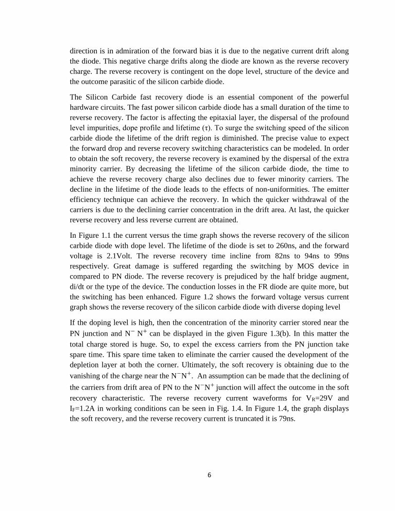
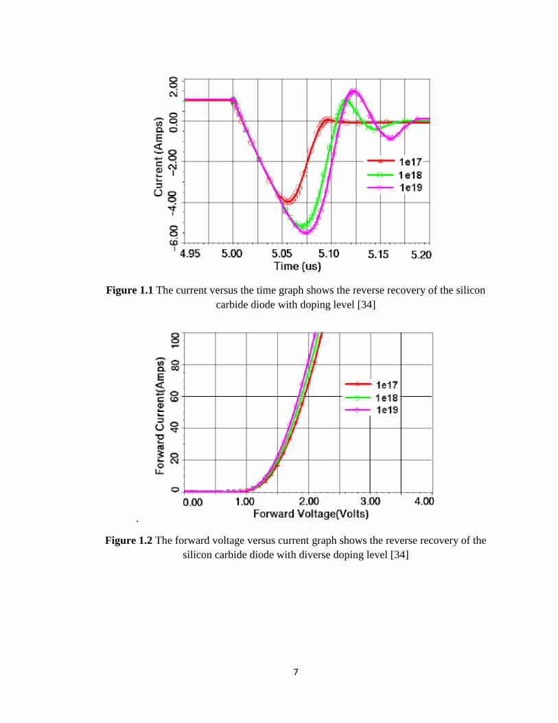
In Figure 1.1 the current versus the time graph shows the reverse recovery of the silicon
carbide diode with dope level. The lifetime of the diode is set to 260ns, and the forward
voltage is 2.1Volt. The reverse recovery time incline from 82ns to 94ns to 99ns
respectively. Great damage is suffered regarding the switching by MOS device in
compared to PN diode. The reverse recovery is prejudiced by the half bridge augment,
di/dt or the type of the device. The conduction losses in the FR diode are quite more, but
the switching has been enhanced. Figure 1.2 shows the forward voltage versus current
graph shows the reverse recovery of the silicon carbide diode with diverse doping level
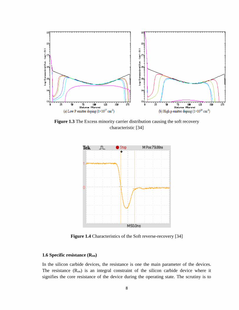
If the doping level is high, then the concentration of the minority carrier stored near the
PN junction and N- N+ can be displayed in the given Figure 1.3(b). In this matter the
total charge stored is huge. So, to expel the excess carriers from the PN junction take
spare time. This spare time taken to eliminate the carrier caused the development of the
depletion layer at both the corner. Ultimately, the soft recovery is obtaining due to the
vanishing of the charge near the N-N+. An assumption can be made that the declining of
the carriers from drift area of PN to the N-N+ junction will affect the outcome in the soft
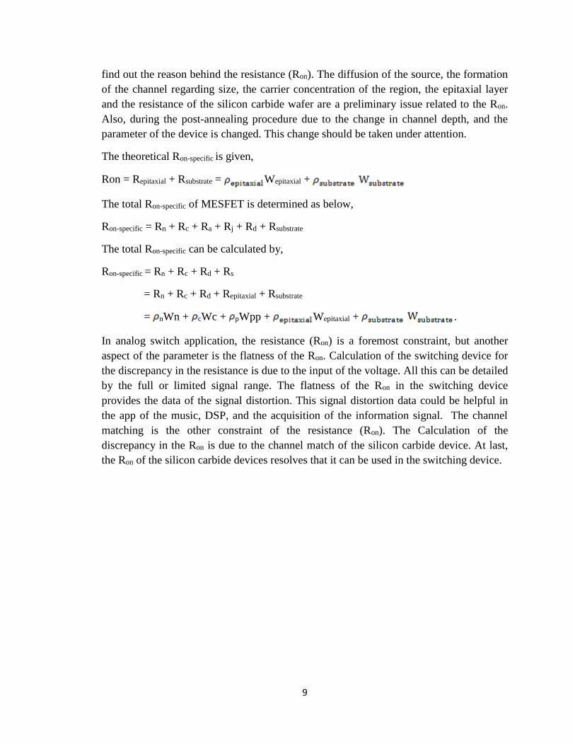
recovery characteristic. The reverse recovery current waveforms for VR=29V and
IF=1.2A in working conditions can be seen in Fig. 1.4. In Figure 1.4, the graph displays
the soft recovery, and the reverse recovery current is truncated it is 79ns.
7
Figure 1.1 The current versus the time graph shows the reverse recovery of the silicon
carbide diode with doping level [34]
.
Figure 1.2 The forward voltage versus current graph shows the reverse recovery of the
silicon carbide diode with diverse doping level [34]
8
Figure 1.3 The Excess minority carrier distribution causing the soft recovery
characteristic [34]
Figure 1.4 Characteristics of the Soft reverse-recovery [34]
1.6 Specific resistance (Ron)
In the silicon carbide devices, the resistance is one the main parameter of the devices.
The resistance (Ron) is an integral constraint of the silicon carbide device where it
signifies the core resistance of the device during the operating state. The scrutiny is to
9
find out the reason behind the resistance (Ron). The diffusion of the source, the formation
of the channel regarding size, the carrier concentration of the region, the epitaxial layer
and the resistance of the silicon carbide wafer are a preliminary issue related to the Ron.
Also, during the post-annealing procedure due to the change in channel depth, and the
parameter of the device is changed. This change should be taken under attention.
The theoretical Ron-specific is given,
Ron = Repitaxial + Rsubstrate = Wepitaxial +
The total Ron-specific of MESFET is determined as below,
Ron-specific = Rn + Rc + Ra + Rj + Rd + Rsubstrate
The total Ron-specific can be calculated by,
Ron-specific = Rn + Rc + Rd + Rs
= Rn + Rc + Rd + Repitaxial + Rsubstrate
= nWn + cWc + pWpp + Wepitaxial + .
In analog switch application, the resistance (Ron) is a foremost constraint, but another
aspect of the parameter is the flatness of the Ron. Calculation of the switching device for
the discrepancy in the resistance is due to the input of the voltage. All this can be detailed
by the full or limited signal range. The flatness of the Ron in the switching device
provides the data of the signal distortion. This signal distortion data could be helpful in
the app of the music, DSP, and the acquisition of the information signal. The channel
matching is the other constraint of the resistance (Ron). The Calculation of the
discrepancy in the Ron is due to the channel match of the silicon carbide device. At last,
the Ron of the silicon carbide devices resolves that it can be used in the switching device.
10
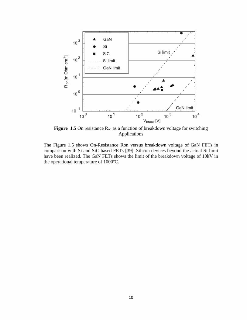
Figure 1.5 On resistance Ron as a function of breakdown voltage for switching
Applications
The Figure 1.5 shows On-Resistance Ron versus breakdown voltage of GaN FETs in
comparison with Si and SiC based FETs [39]. Silicon devices beyond the actual Si limit
have been realized. The GaN FETs shows the limit of the breakdown voltage of 10kV in
the operational temperature of 1000oC.
11
Chapter 2. Silicon Carbide (SiC) Material
2.1 The Crystal Structure of Silicon Carbide
2.1.1 The Structure of the Silicon Carbide Atom
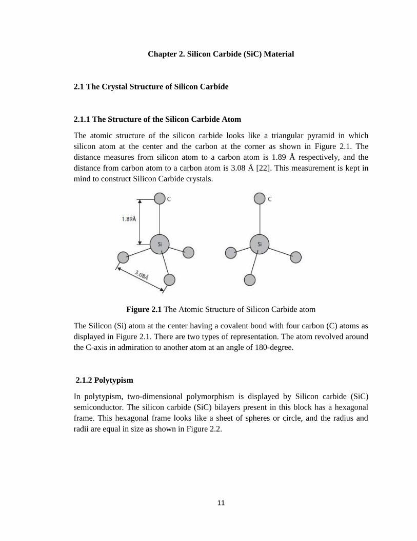
The atomic structure of the silicon carbide looks like a triangular pyramid in which
silicon atom at the center and the carbon at the corner as shown in Figure 2.1. The
distance measures from silicon atom to a carbon atom is 1.89 Å respectively, and the
distance from carbon atom to a carbon atom is 3.08 Å [22]. This measurement is kept in
mind to construct Silicon Carbide crystals.
Figure 2.1 The Atomic Structure of Silicon Carbide atom
The Silicon (Si) atom at the center having a covalent bond with four carbon (C) atoms as
displayed in Figure 2.1. There are two types of representation. The atom revolved around
the C-axis in admiration to another atom at an angle of 180-degree.
2.1.2 Polytypism
In polytypism, two-dimensional polymorphism is displayed by Silicon carbide (SiC)
semiconductor. The silicon carbide (SiC) bilayers present in this block has a hexagonal
frame. This hexagonal frame looks like a sheet of spheres or circle, and the radius and
radii are equal in size as shown in Figure 2.2.
12
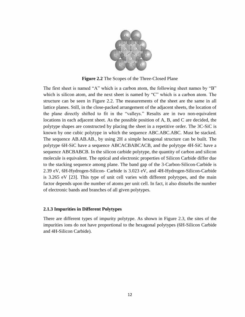
Figure 2.2 The Scopes of the Three-Closed Plane
The first sheet is named “A” which is a carbon atom, the following sheet names by “B”
which is silicon atom, and the next sheet is named by “C” which is a carbon atom. The
structure can be seen in Figure 2.2. The measurements of the sheet are the same in all
lattice planes. Still, in the close-packed arrangement of the adjacent sheets, the location of
the plane directly shifted to fit in the “valleys.” Results are in two non-equivalent
locations in each adjacent sheet. As the possible position of A, B, and C are decided, the
polytype shapes are constructed by placing the sheet in a repetitive order. The 3C-SiC is
known by one cubic polytype in which the sequence ABC.ABC.ABC. Must be stacked.
The sequence AB.AB.AB., by using 2H a simple hexagonal structure can be built. The
polytype 6H-SiC have a sequence ABCACBABCACB, and the polytype 4H-SiC have a
sequence ABCBABCB. In the silicon carbide polytype, the quantity of carbon and silicon
molecule is equivalent. The optical and electronic properties of Silicon Carbide differ due
to the stacking sequence among plane. The band gap of the 3-Carbon-Silicon-Carbide is
2.39 eV, 6H-Hydrogen-Silicon- Carbide is 3.023 eV, and 4H-Hydrogen-Silicon-Carbide
is 3.265 eV [23]. This type of unit cell varies with different polytypes, and the main
factor depends upon the number of atoms per unit cell. In fact, it also disturbs the number
of electronic bands and branches of all given polytypes.
2.1.3 Impurities in Different Polytypes
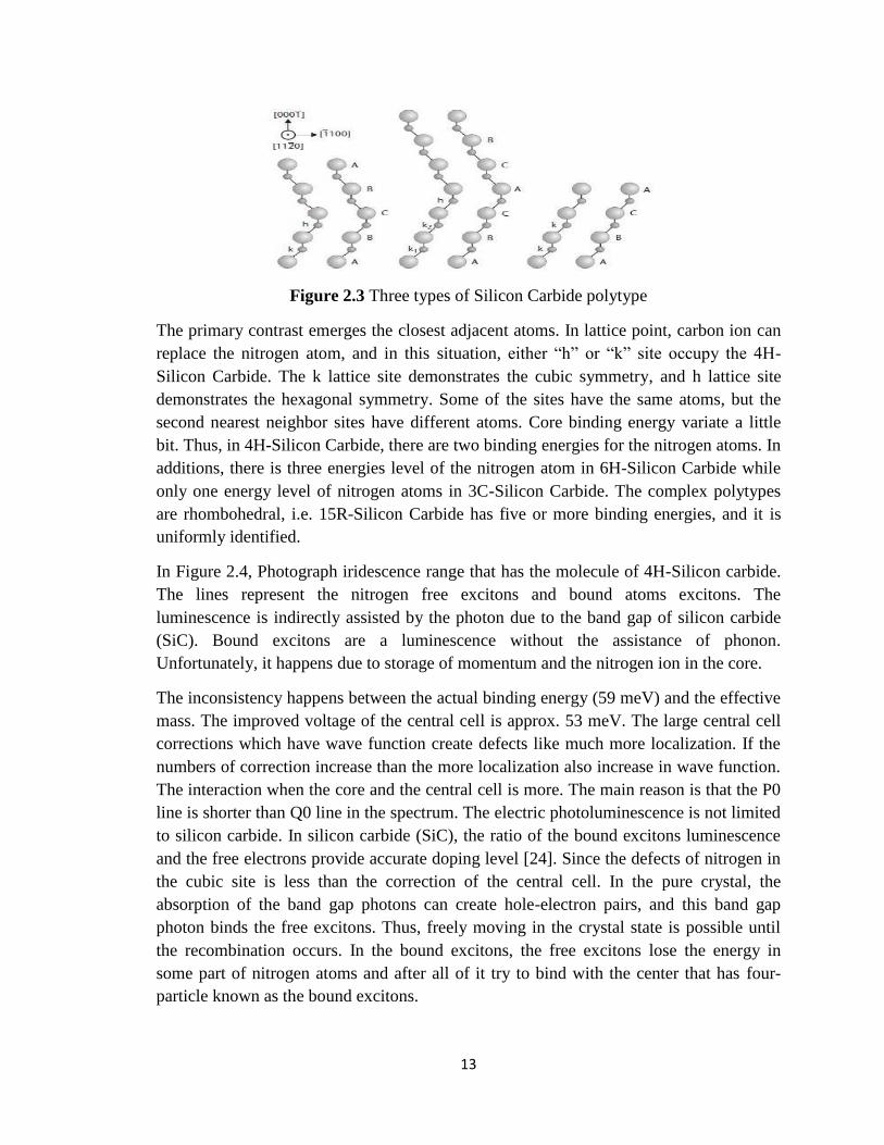
There are different types of impurity polytype. As shown in Figure 2.3, the sites of the
impurities ions do not have proportional to the hexagonal polytypes (6H-Silicon Carbide
and 4H-Silicon Carbide).
13
Figure 2.3 Three types of Silicon Carbide polytype
The primary contrast emerges the closest adjacent atoms. In lattice point, carbon ion can
replace the nitrogen atom, and in this situation, either “h” or “k” site occupy the 4H-
Silicon Carbide. The k lattice site demonstrates the cubic symmetry, and h lattice site
demonstrates the hexagonal symmetry. Some of the sites have the same atoms, but the
second nearest neighbor sites have different atoms. Core binding energy variate a little
bit. Thus, in 4H-Silicon Carbide, there are two binding energies for the nitrogen atoms. In
additions, there is three energies level of the nitrogen atom in 6H-Silicon Carbide while
only one energy level of nitrogen atoms in 3C-Silicon Carbide. The complex polytypes
are rhombohedral, i.e. 15R-Silicon Carbide has five or more binding energies, and it is
uniformly identified.
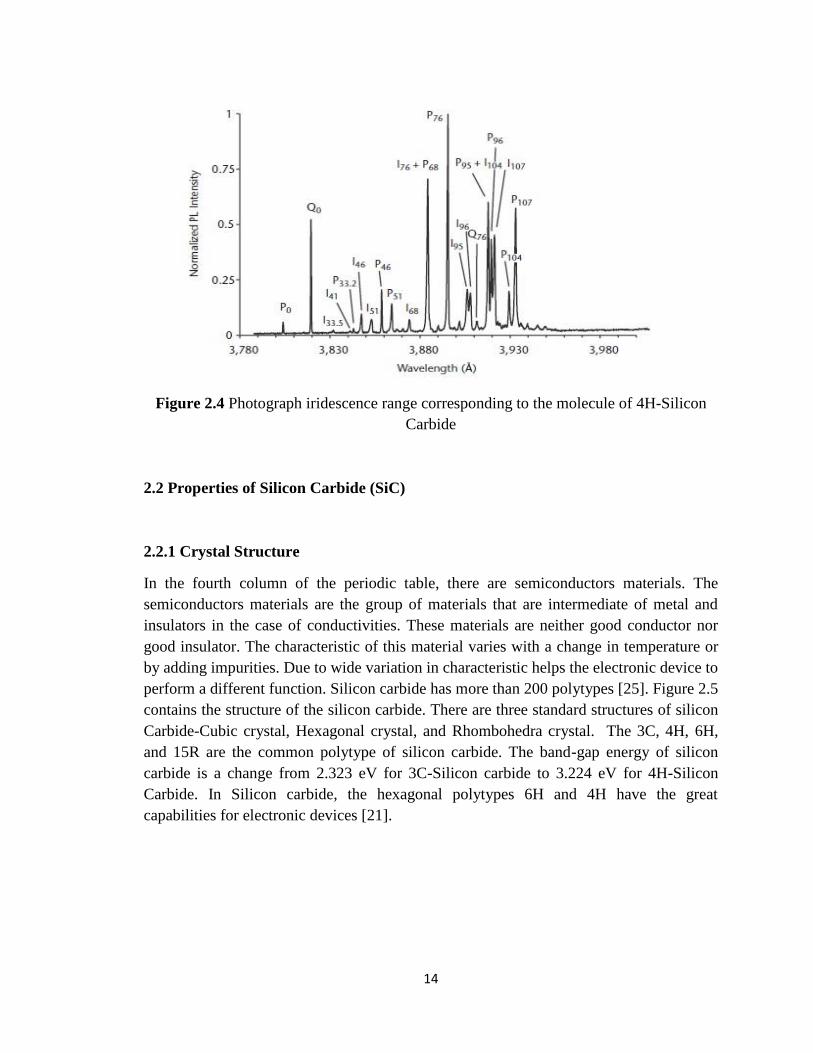
In Figure 2.4, Photograph iridescence range that has the molecule of 4H-Silicon carbide.
The lines represent the nitrogen free excitons and bound atoms excitons. The
luminescence is indirectly assisted by the photon due to the band gap of silicon carbide
(SiC). Bound excitons are a luminescence without the assistance of phonon.
Unfortunately, it happens due to storage of momentum and the nitrogen ion in the core.
The inconsistency happens between the actual binding energy (59 meV) and the effective
mass. The improved voltage of the central cell is approx. 53 meV. The large central cell
corrections which have wave function create defects like much more localization. If the
numbers of correction increase than the more localization also increase in wave function.
The interaction when the core and the central cell is more. The main reason is that the P0
line is shorter than Q0 line in the spectrum. The electric photoluminescence is not limited
to silicon carbide. In silicon carbide (SiC), the ratio of the bound excitons luminescence
and the free electrons provide accurate doping level [24]. Since the defects of nitrogen in
the cubic site is less than the correction of the central cell. In the pure crystal, the
absorption of the band gap photons can create hole-electron pairs, and this band gap
photon binds the free excitons. Thus, freely moving in the crystal state is possible until
the recombination occurs. In the bound excitons, the free excitons lose the energy in
some part of nitrogen atoms and after all of it try to bind with the center that has four-
particle known as the bound excitons.
14
Figure 2.4 Photograph iridescence range corresponding to the molecule of 4H-Silicon
Carbide
2.2 Properties of Silicon Carbide (SiC)
2.2.1 Crystal Structure
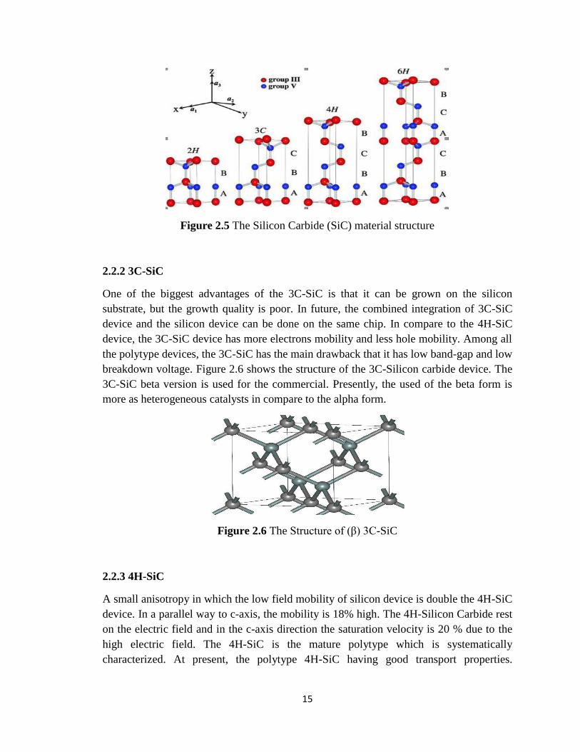
In the fourth column of the periodic table, there are semiconductors materials. The
semiconductors materials are the group of materials that are intermediate of metal and
insulators in the case of conductivities. These materials are neither good conductor nor
good insulator. The characteristic of this material varies with a change in temperature or
by adding impurities. Due to wide variation in characteristic helps the electronic device to
perform a different function. Silicon carbide has more than 200 polytypes [25]. Figure 2.5
contains the structure of the silicon carbide. There are three standard structures of silicon
Carbide-Cubic crystal, Hexagonal crystal, and Rhombohedra crystal. The 3C, 4H, 6H,
and 15R are the common polytype of silicon carbide. The band-gap energy of silicon
carbide is a change from 2.323 eV for 3C-Silicon carbide to 3.224 eV for 4H-Silicon
Carbide. In Silicon carbide, the hexagonal polytypes 6H and 4H have the great
capabilities for electronic devices [21].
15
Figure 2.5 The Silicon Carbide (SiC) material structure
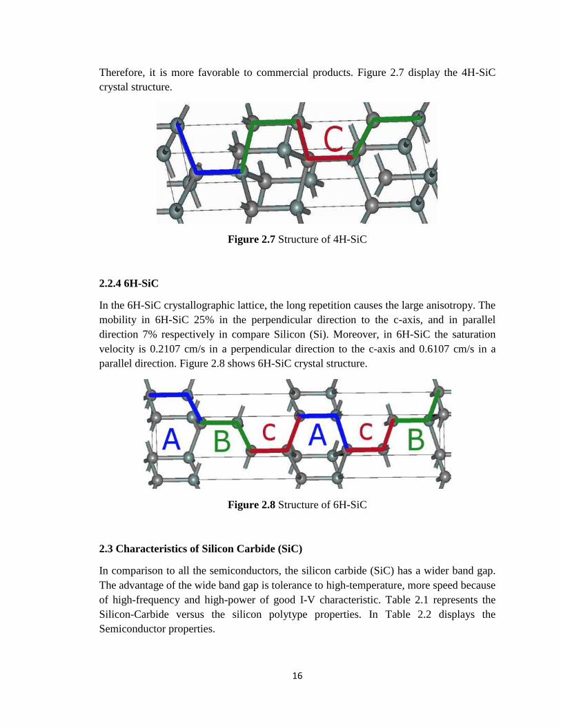
2.2.2 3C-SiC
One of the biggest advantages of the 3C-SiC is that it can be grown on the silicon
substrate, but the growth quality is poor. In future, the combined integration of 3C-SiC
device and the silicon device can be done on the same chip. In compare to the 4H-SiC
device, the 3C-SiC device has more electrons mobility and less hole mobility. Among all
the polytype devices, the 3C-SiC has the main drawback that it has low band-gap and low
breakdown voltage. Figure 2.6 shows the structure of the 3C-Silicon carbide device. The
3C-SiC beta version is used for the commercial. Presently, the used of the beta form is
more as heterogeneous catalysts in compare to the alpha form.
Figure 2.6 The Structure of (β) 3C-SiC
2.2.3 4H-SiC
A small anisotropy in which the low field mobility of silicon device is double the 4H-SiC
device. In a parallel way to c-axis, the mobility is 18% high. The 4H-Silicon Carbide rest
on the electric field and in the c-axis direction the saturation velocity is 20 % due to the
high electric field. The 4H-SiC is the mature polytype which is systematically
characterized. At present, the polytype 4H-SiC having good transport properties.
16
Therefore, it is more favorable to commercial products. Figure 2.7 display the 4H-SiC
crystal structure.
Figure 2.7 Structure of 4H-SiC
2.2.4 6H-SiC
In the 6H-SiC crystallographic lattice, the long repetition causes the large anisotropy. The
mobility in 6H-SiC 25% in the perpendicular direction to the c-axis, and in parallel
direction 7% respectively in compare Silicon (Si). Moreover, in 6H-SiC the saturation
velocity is 0.2107 cm/s in a perpendicular direction to the c-axis and 0.6107 cm/s in a
parallel direction. Figure 2.8 shows 6H-SiC crystal structure.
Figure 2.8 Structure of 6H-SiC
2.3 Characteristics of Silicon Carbide (SiC)
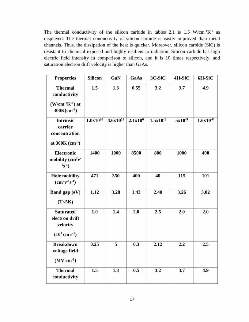
In comparison to all the semiconductors, the silicon carbide (SiC) has a wider band gap.
The advantage of the wide band gap is tolerance to high-temperature, more speed because
of high-frequency and high-power of good I-V characteristic. Table 2.1 represents the
Silicon-Carbide versus the silicon polytype properties. In Table 2.2 displays the
Semiconductor properties.
17
The thermal conductivity of the silicon carbide in tables 2.1 is 1.5 W/cm-1K-1 as
displayed. The thermal conductivity of silicon carbide is vastly improved than metal
channels. Thus, the dissipation of the heat is quicker. Moreover, silicon carbide (SiC) is
resistant to chemical exposed and highly resilient to radiation. Silicon carbide has high
electric field intensity in comparison to silicon, and it is 10 times respectively, and
saturation electron drift velocity is higher than GaAs.
Properties Silicon GaN GaAs 3C-SiC 4H-SiC 6H-SiC
Thermal
conductivity
(W/cm-1K-1) at
300K(cm-3)
1.5 1.3 0.55 3.2 3.7 4.9
Intrinsic
carrier
concentration
at 300K (cm-3)
1.0x10²⁰ 4.6x10¹⁹ 2.1x10⁶ 1.5x10⁻¹ 5x10⁻⁹ 1.6x10⁻⁶
Electronic
mobility (cm2v-
1s-1)
1400 1000 8500 800 1000 400
Hole mobility
(cm2v-1s-1)
471 350 400 40 115 101
Band gap (eV)
(T<5K)
1.12 3.28 1.43 2.40 3.26 3.02
Saturated
electron drift
velocity
(107 cm s-1)
1.0 1.4 2.0 2.5 2.0 2.0
Breakdown
voltage field
(MV cm-1)
0.25 5 0.3 2.12 2.2 2.5
Thermal
conductivity
1.5 1.3 0.5 3.2 3.7 4.9
18
Table 2.1 Silicon-Carbide versus the Silicon polytype properties [25] [26]
2.4 Energy Band Diagram
The energy combination of molecular orbital in a graphical image displays the energy
bands. There is a mass amount of molecular energies which result in formation different
energy bands [28]. The Figure 2.9 is the energy band diagram shows the various
molecular energies.
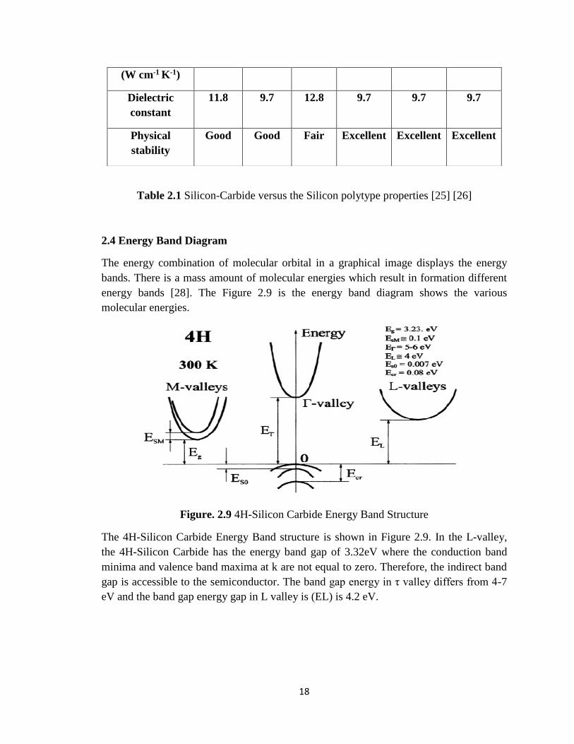
Figure. 2.9 4H-Silicon Carbide Energy Band Structure
The 4H-Silicon Carbide Energy Band structure is shown in Figure 2.9. In the L-valley,
the 4H-Silicon Carbide has the energy band gap of 3.32eV where the conduction band
minima and valence band maxima at k are not equal to zero. Therefore, the indirect band
gap is accessible to the semiconductor. The band gap energy in τ valley differs from 4-7
eV and the band gap energy gap in L valley is (EL) is 4.2 eV.
(W cm-1 K-1)
Dielectric
constant
11.8 9.7 12.8 9.7 9.7 9.7
Physical
stability
Good Good Fair Excellent Excellent Excellent
19
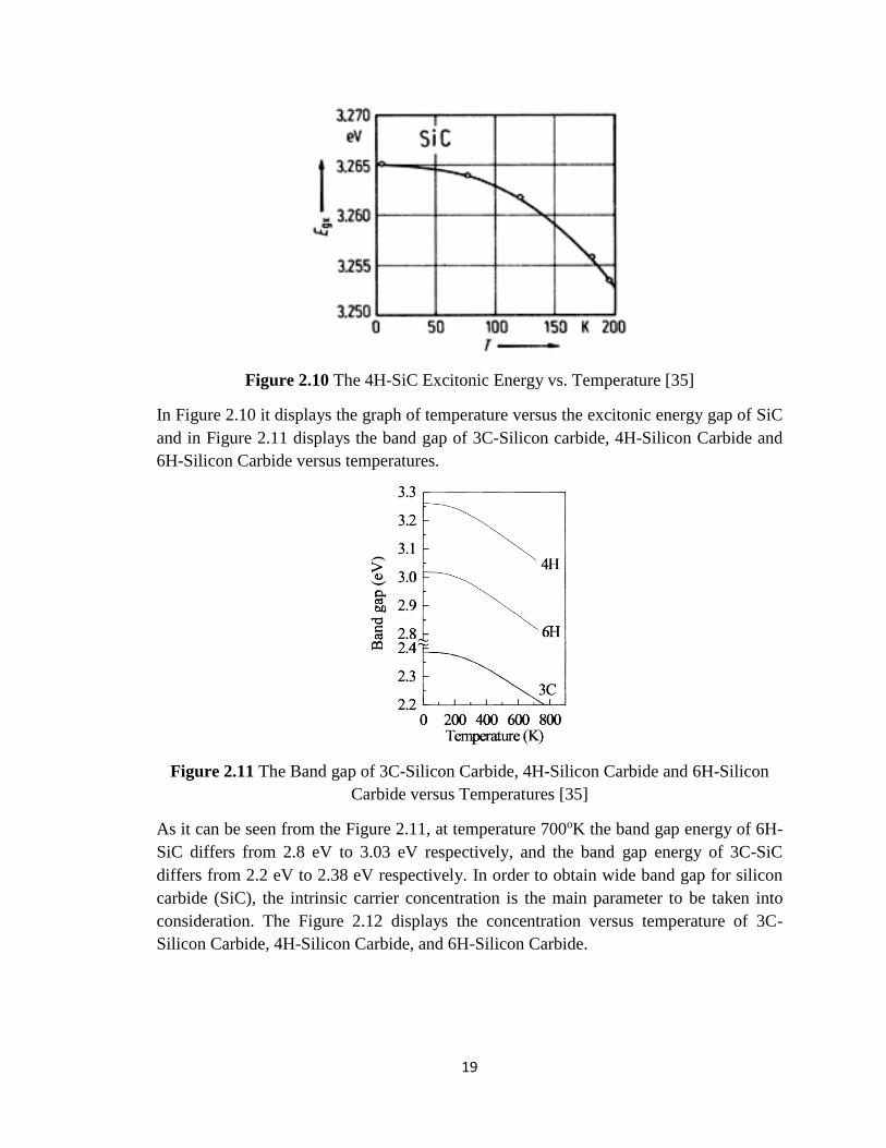
Figure 2.10 The 4H-SiC Excitonic Energy vs. Temperature [35]
In Figure 2.10 it displays the graph of temperature versus the excitonic energy gap of SiC
and in Figure 2.11 displays the band gap of 3C-Silicon carbide, 4H-Silicon Carbide and
6H-Silicon Carbide versus temperatures.
Figure 2.11 The Band gap of 3C-Silicon Carbide, 4H-Silicon Carbide and 6H-Silicon
Carbide versus Temperatures [35]
As it can be seen from the Figure 2.11, at temperature 700oK the band gap energy of 6H-
SiC differs from 2.8 eV to 3.03 eV respectively, and the band gap energy of 3C-SiC
differs from 2.2 eV to 2.38 eV respectively. In order to obtain wide band gap for silicon
carbide (SiC), the intrinsic carrier concentration is the main parameter to be taken into
consideration. The Figure 2.12 displays the concentration versus temperature of 3C-
Silicon Carbide, 4H-Silicon Carbide, and 6H-Silicon Carbide.
20
Figure 2.12 The concentration versus temperature of 3C-Silicon Carbide, 4H-Silicon
Carbide and 6H-Silicon Carbide [36]
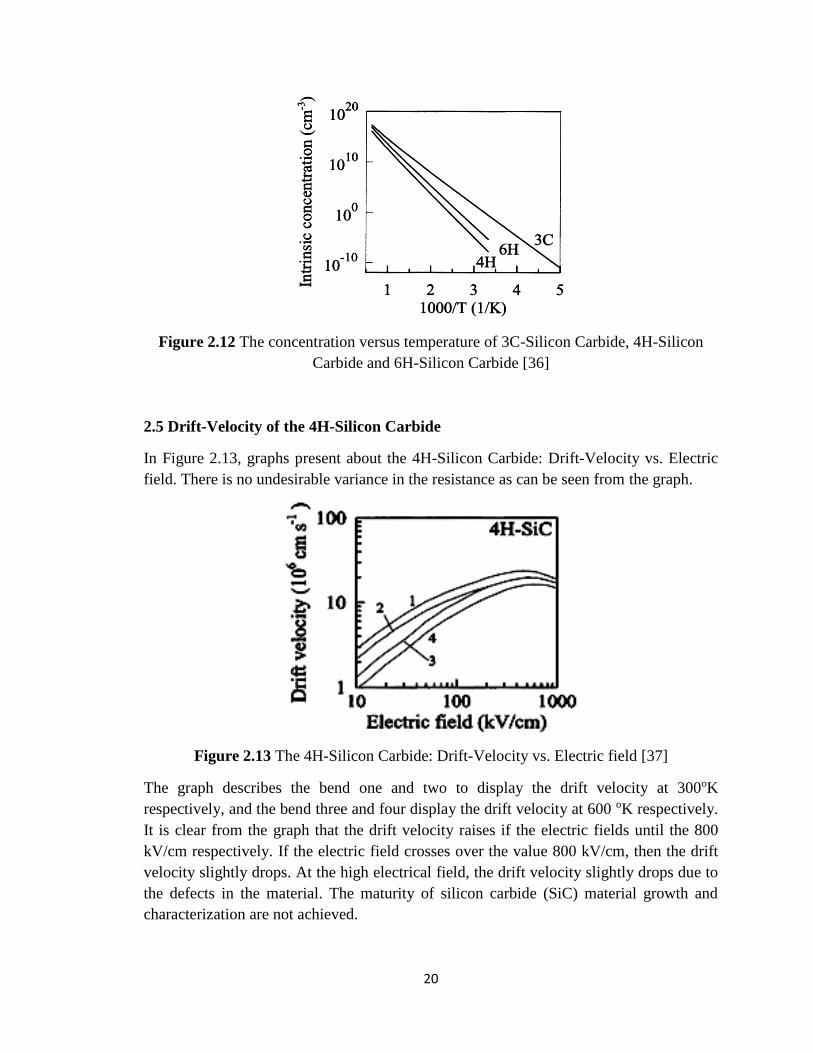
2.5 Drift-Velocity of the 4H-Silicon Carbide
In Figure 2.13, graphs present about the 4H-Silicon Carbide: Drift-Velocity vs. Electric
field. There is no undesirable variance in the resistance as can be seen from the graph.
Figure 2.13 The 4H-Silicon Carbide: Drift-Velocity vs. Electric field [37]
The graph describes the bend one and two to display the drift velocity at 300oK
respectively, and the bend three and four display the drift velocity at 600 oK respectively.
It is clear from the graph that the drift velocity raises if the electric fields until the 800
kV/cm respectively. If the electric field crosses over the value 800 kV/cm, then the drift
velocity slightly drops. At the high electrical field, the drift velocity slightly drops due to
the defects in the material. The maturity of silicon carbide (SiC) material growth and
characterization are not achieved.
21
Chapter 3. Fabrication of Silicon Carbide (SiC) MESFET devices
SiC MESFET and Si FETs have similar fabrication technique. The fabrication process for
the SiC is very hard in comparison to Si, GaAs, and InP, and just a few individuals know
the fabrication technique in industry. The procedures used right now for SiC are youthful.
The RF device made of SiC still needs considerably more innovative work to contend
financially with Si.
3.1 Silicon Carbide (SiC) Fabrication Process
The processes steps clarified here could use as a part of a specific trial yet it is essential
data to depict a wide plan for the fabrication process of silicon carbide device.
3.1.1 RCA process for cleaning the Silicon Carbide Wafer
The RCA process is a wafer cleaning process which needs to be performed before
oxidation, diffusion, or Chemical Vapor Deposition process. The RCA process is divided
into sub process like the pre-cleaning process for the silicon carbide wafer, the inorganic
cleaning process for removing the inorganic contaminants, and Organic cleaning process
for removing organic contaminants.
In the pre-cleaning process of the silicon carbide wafer, the wafer is cleaned in the
ultrasonic bath of acetone solution for 20 minutes. After 20 minutes of an ultrasonic bath
of acetone solution, the wafer is removed from the ultrasonic bath of acetone solution to
isopropyl alcohol bath. Here the wafer is submerged in the isopropyl alcohol bath for 20
minutes. After 20 minutes of isopropyl alcohol bath, the wafer is rinsed with a copious
amount of running De-Ionized (DI) Water.
In the inorganic cleaning process, the wafer is submerged for 10 minutes in the mixed
solution of sulfuric acid and water (H2SO4: H2O) in the ratio about 4:1 at 100oC. After 10
minutes, the wafer is rinsed with a copious amount of running DI-water.
The organic cleaning process is a cleaning process for removing the organic
contaminants. The first organic cleaning process is a weak base-piranha bath in which the
temperature of the mixed solution of ammonia and water (NH4OH: H2O) is maintained
to 70oC. After the temperature of the ammonia and water (NH4OH: H2O) solution reach
to 70oC, carefully add the hydrogen peroxide (H2O2) solution. Now wait for 3 to 5
minutes, the bubbles start forming in the solution. The ratio of ammonia, hydrogen
peroxide and water (NH4OH: H2O2: H2O) is 1:1:5. At last, the wafer is submerged in the
solution of ammonia, hydrogen peroxide and water (NH4OH: H2O2: H2O) at 70°C for 10
22
minutes and the wafer are rinsed with a copious amount of running DI water. The second
organic cleaning process is weak acid piranha bath in which the temperature of the mixed
solution of hydrochloric acid and water (HCL: H2O) is maintained to 70oC. After the
temperature of the hydrochloric acid and water (HCL: H2O) solution reach to 70oC,
carefully add the hydrogen peroxide (H2O2) solution. Now wait for 3 to 5 minutes, the
bubbles start forming in solution. The ratio of hydrochloric acid, hydrogen peroxide, and
water (HCL: H2O2: H2O) is 1:1:6. At last, the wafer is submerged for 10 minutes in the
solution of hydrochloric acid, hydrogen peroxide, and water (HCL: H2O2: H2O) at 70°C,
and the wafer is rinsed with a copious amount of running DI water.
3.1.2 Oxidation of Silicon Dioxide on Silicon carbide wafer
There are two types of structure in silicon dioxide (SiO2) - Crystalline and Amorphous.
The constituent of silica is found in gemstones. Volcanic rocks have the trace of silica
compound. On the earth, the silicon compounds are the most plentiful in quantity and
mostly found in oxides forms. The sand has an amorphous structure of silica and quartz
has the crystalline structure of the silica.
Silicon dioxide (SiO2) has high melting point due to its tetrahedral structure. In fact, at
1700oC, the silicon-oxygen covalent bonds can be broken that is possible only at high
temperature. Due to the covalent bond of silicon dioxide (SiO2), it is having properties
like very hard and rigid material. Moreover, silicon dioxide (SiO2) cannot be soluble in
water or organic solvents, but it is possible in alkalies and hydrofluoric acids.
Silicon dioxide (SiO2) is good insulator because there are no free electrons in molecular
structure. It is used as a gate oxide (SiO2) in all semiconductor devices. The gate oxide
(SiO2) layer acts as a dielectric layer in MESFET device between gate terminal and
source or drain terminal. The gate oxide (SiO2) is formed by two methods wet oxidation
and dry oxidation process.
The silicon dioxide (SiO2) layer is very small, so consider the leakage current if not
eliminated, it leads to direct tunneling. In this case, even if there is ideal perfect layer still
the possibilities of tunneling may occur. Now increasing the thickness may be the path to
succeed still you need to take care of some of the points below:
1. The tunneling length must be shorter than the physical thickness.
2. The quality of the layer and the interface with the semiconductor should be so good to
inhibit other conduction mechanisms virtually.
3. The dielectric thickness and its barrier for electrons (or holes) at the interface with the
semiconductor must comply with Fowler-Nordheim tunnel conduction.
23
In the case, silicon dioxide (SiO2) layers start at a transverse field of about 5.5mV/cm to
6.5mV/cm. For example, even if the direct tunneling is reduced using a thicker silicon
dioxide film, say about 10nm respectively then the Fowler-Nordheim tunnel conduction
onset would occur at about 0.5Volt to 0.6Volt.
Two techniques have been adopted to deposit oxidation layer on the silicon carbide (SiC)
wafer. The first technique is the thermal oxidation process, in which silicon dioxide
(SiO2) layer is grown on silicon carbide (SiC) wafer by dry oxidation using the high
temperature (1225oC) furnace. In this fabrication process, the dry thermal oxidation
process is selected to obtain the growth rate 1 m/5.7 h (176 nm/h) for the silicon dioxide
(SiO2) on the Silicon carbide substrates. The 4H-SiC substrate is inserted into the furnace
at an initial temperature of 700 oC, and then the temperature rises to 1225 oC at
inclination rate of 2oC/min respectively. The silicon dioxide (SiO2) layers are grown on
the silicon carbide substrates with a thickness of 320 nm at 1225 oC through the duration
of 85 minutes. The second technique is the sputtering process, where the silicon dioxide
(SiO2) is deposited on thermally grown silicon oxide from silicon oxide target. The RF
sputtering has been accomplished at 2.5mTorr with 99.999% Argon and Nitrogen at a
ratio of 100:1 as the sputtering gas. The silicon dioxide (SiO2) layer of 400Å is
maintained throughout the fabrication process.
3.1.3 The Photo-lithography method for the Silicon Carbide MESFET
The photolithography process for the silicon carbide device fabrication has been
conducted in class 100 room. The procedure to obtain a pattern of positive Photoresist
S1813 layer over the Silicon Carbide Wafer is called Photo-lithography. The
photolithography is used to make the connection between the different layers of the
integrated circuits. Photolithography is the process by which we create repeatable and
consistent patterns on a wafer.
3.1.4 The Spin-Coating of the Photoresist S1813 and Hexamethyldisilazane (HMDS)
primer on the silicon carbide wafer
The S1813 is a positive Photoresist which is used in microelectronics industries for IC
fabrication device. A Photoresist S1813 is standard positive Photoresist which is widely
used for the process like wet etching, dry etching and even for lift-off processes. The
main advantage of the S1813 Photoresist is to minimize the notching and maintain
linewidth control during the process on highly reflective substrates. The Photoresist has
good properties like excellent adhesion, uniformly coated on the wafer, xylene free, and
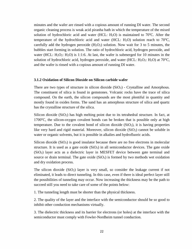
at last a standard viscosity is available for single layer process. Figure 3.1 shows the
graph of photoresist film thickness versus the spinning speed of the spin coater. The
24
graph helps to select the Photoresist to obtain a proper thickness of the photoresist on the
wafer.
Figure 3.1 Photoresist film thickness versus the spinning speed of the spin coater [31]
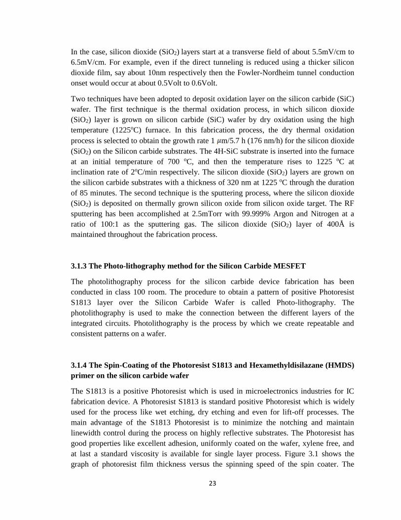
Figure 3.2 shows the characteristic curve of Exposure energy versus Photoresist
thickness.
Figure 3.2 The Characteristic curve of Exposure energy versus Photoresist thickness[32]
In order to prepare for the photolithography process; the first step is to clean the mask
aligner Karl Suss MA-56, and the photomask is cleaned with acetone solution and
isopropyl alcohol. Moreover, the photomask is dried with nitrogen. Also, all steps related
to fabrication of the silicon carbide device must be completed with clean gloves, and the
care of wafer must be taken to avoid any dust or large particle contamination which can
have a major negative impact on the alignment and image. The humidity of the class 100
room should be maintained between 40% and 50%. The temperature of the class 100
room should be maintained between 18.5oC and 21oC, and dry bake the wafer on a hot
plate at a greater temperature than 175oC for 3min.
25
A) Spin Coating
In order to obtain a good pattern of Photoresist S1813 on the silicon carbide wafer; the
wafer is placed in the spin coater. Here the wafer is spin at 3500rpm for at least 45
seconds after placing 3.5mL of Hexamethyldisilazane (HMDS) primer on the wafer. The
HMDS is highly hydrophobic and drives off any remaining humidity from the surface of
the wafer. The residual humidity of the wafer cannot provide a proper pattern of the
photoresist (PR) S1813. The next step is to deposit 3.5mL of Shipley S1813 Photoresist
on the wafer and restart the spinner at 3500rpm for at least 45seconds. The obtained
thickness of the Photoresist is 1.5µm, and it is maintained throughout the fabrication
process of silicon carbide device. At last, after completing the spin coating process of the
photoresist, wait for about 1 minute then inspect the wafer for any streaks, comet tails,
uncoated areas or other signs of lacks uniformity. Moreover, if the coating of the
photoresist on the wafer looks good then remove the wafer from the spin coater. Now, the
wafer is placed on a hot plate at 115oC for 120 seconds. The next step is to remove the
wafer from the hot plate, and then the wafer is set on a clean surface to cool down for at
least 2 to 5 minutes.
B) Alignment Mark
The pre-alignment of the wafer is critical due to a limited range of motion of the mask
aligner. The wafer is placed into the mask aligner. In order to align the primary flat with
the register pins on the vacuum chuck of the mask aligner; a proper care should be taken.
Place the mask holder with the mask into place above the wafer in the vacuum chuck and
initialize the alignment procedures.
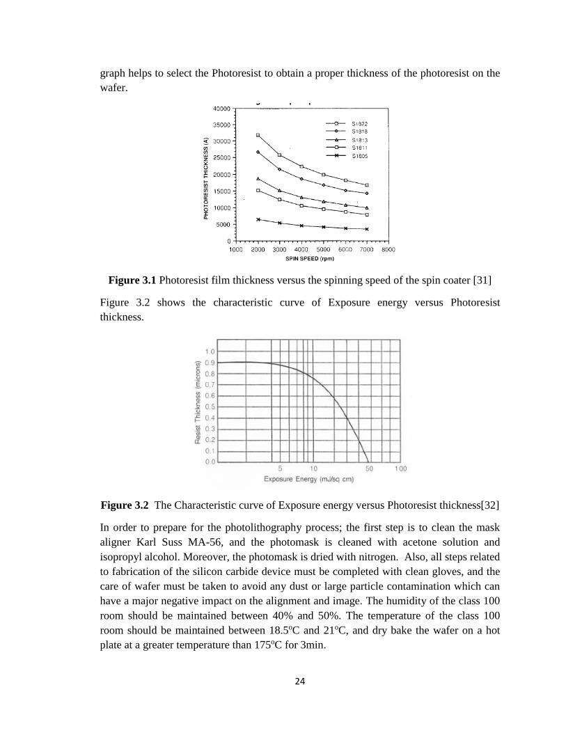
Figure 3.3 Typical view of a good/clear alignment mark
The silicon carbide (SiC) wafer is transparent like glass. Figure 3.3 shows the typical
views of the alignment of the mask on silicon carbide wafers. Presently, to improve the
visibility of the alignment marks, at every step of the alignment, the wafer is processed in
the sputtering system for the nickel metallization on the back portion. In the case of
failure alignment or other process problem, the nickel metallization process is repeated.
26
C) Ultraviolet light used to expose Photoresist S1813 on the Silicon Carbide wafer
The silicon carbide wafer is exposed to 365nm Ultra-Violet light for 6 to 12 seconds
which depends on the current calibration of the lamp system. After exposing the wafer,
remove the mask and mask holder, and then retrieve the wafer from the vacuum chuck.
D) CD-26 Developer Solution for the Silicon Carbide Wafer
The CD-26 developer is a metal ion free developer usually use with Photoresist S1813. It
is used in wafer fabrication where it is desirable to avoid a potential source of metal ion
contamination. The CD-26 is formulated for high-resolution immersion developing
applications. The unique functional properties of the CD-26 provide high process reliably
integrated circuit fabrication. A developer solution simply removes the Photoresist from
the portion of the wafer where it is exposed to UV rays. The exposed PR on the wafer is
removed by dipping and gently swirling the wafer in a large flask of CD-26 photoresist
developer for about 45sec. The next step is to rinse the wafer in copious amounts of
flowing DI water and dry the wafer with nitrogen.
E) Hard baking
The wafer should be inspected for good image and correct alignment. If wafer photo-
resist patterning looks acceptable, then hard bake the wafer on a hot plate at 120oC for 3
minutes.
F) Stripping of Photoresist
The wafer is to be cleaned with acetone solution to remove the photoresist. The next step
is to conduct Spin-Rinse-Dry (SRD) process in which the wafer is rinsed and dry using
SRD. In the SRD machine, the wafer is rinsed for 3 min, the wafer can spin fast for 2
minutes in order to make it dry using nitrogen (N2), and then the wafer is allowed to dry
slowly with warm N2 for 3 minutes.
3.1.5 The Etching and Cleaning process for the Silicon Carbide Wafer
In the etching method, the material is expelled from the silicon carbide wafer. The
etching is used to expel the unwanted material from the silicon carbide wafer during the
fabrication steps. The etching is done in angstrom. The dry etching and wet etching are
the two methods. The chemical used for the wet etching of the silicon carbide wafer is the
hydrogen fluoride, Nitric acid, and Acetic acid. The scratching rate is dictated by the
absorption level of the solvent. The dry-etching expels the objective atoms by using the
mobile energy. The plasma etching in the sputter system separates the atoms from the
substrate with the help of the argon gas which frees the atom of the objected wafer. In the
Wet etching process, the Nitric acid, hydrogen fluoride solution, and Acetic acid are
27
mixed to develop isotropic etching by redox response taking after the decay of silicon
dioxide and HF acid. The etching rate is 1.1-3.4μm.min-1 respectively.
The silicon dioxide layer is removed from the silicon carbide wafer using the Buffer-
Oxide-Etching procedure, is used to obtain highly accurate etching. In the Buffer-Oxide-
Etching the etching rate is stable due to replacing the useless fluoride ions and handling
the potential hydrogen value due to the accumulation of the Ammonium fluoride to
hydrogen fluoride. The silicon dioxide is expelled from the silicon carbide wafer by using
89% hydrogen fluoride acid. This speeds up the etching rate of the silicon carbide wafer.
After wet etching or dry etching, the wafer is cleaned in the acetone solution. At last, the
spin-rinsed-dry (SRD) procedure is done.
3.1.5.1 Oxide Etching by BOE (buffered oxide etching)
The basic definition of the etching is to remove any unwanted component from the wafer.
The etching rate of the thermal oxide using aqueous solution NH4F/HF, with or without
the additives depends on three factors the range of the NH4F, the temperature of the
etching, and the contents of the HF. In Table 3.1 and 3.2 provide the information related
to HF concentration for premixed standards, modified and super BOE formulation.
Moreover, the table also gives information about the gravity and etching rate at certain
temperature range.
Table 3.1 Standard BOE Etching Characteristics [33]
The procedures affecting uniform etching are highlighted below. Firstly, the control over
the temperature of the etchant results in under or over etching, and loss of the primary
benefits of premixed etchants. Secondly, the filtration of the etchant maintains cleanliness
of etchant bath and provides etching uniformity with fewer defects. At last, the side wall
taper is caused due to the lateral etching, and it is the characteristic of etchant
composition and temperature. In Figure 3.4 A The graph displays about Thermal Oxide
28
Etching rate vs. percentage of HF and Figure 3.4. B). Thermal Oxide Etching vs.
temperature.
Table 3.2 Modified BOE Etching Characteristics [33]
Figure 3.4 a) Thermal Oxide Etching rate vs. percentage of HF. b). Thermal Oxide
Etching vs. temperature [34]
The silicon dioxide layer is removed from the silicon carbide wafer. Here the Buffer-
Oxide-Etching procedure is used to obtain highly accurate etching. In the Buffer-Oxide-
Etching, the etching rate is stable due to replacing the useless fluoride ions and handling
the potential hydrogen value due to the accumulation of the Ammonium fluoride to
hydrogen fluoride. The SiO2 is etched by the high concentration of hydrogen fluoride
(HF) solution rapidly for meticulous control of the process. Submerge wafer in a solution
of HF: H2O – 1:9 at room temperature, stirring gently, for 10 minutes.
29
3.1.6 Ion Implantation
In an active region of MESFETs, Ion Implantation plays a significant role for the addition
of dopants. The N-type device has a P-type insulation substrate. An N-type of the
epitaxial layer is full-grown with an N-type conducting channel on the top of the P-type
substrate. For silicon carbide (SiC) MESFET, Nitrogen is the n-type dopant which is
implanted in the n-type channel layer. In order define the n-type source and drain in the
n-type channel layer, nickel is deposited on the top of N+ region for the sources and drain
ohmic contacts.
In the case of silicon carbide, it is enormously stable in nature which in return make
diffusion step difficult. Therefore, ions are forced to dope through ion implantation
method. In which the ions are regulated, and a vast variety of ions can be used in
compared to diffusion procedure. In the host grid atoms, the atoms are blocked because
of the electronic and atomic ceasing system which oversees inelastic impact and flexible
crash. The electronic and nuclear stopping mechanism obstructs the crystal atom due to
the host grid atoms, and in outcome responsible for the collision. The dope entering the
crystal built impurity. The peak concentration (Np) showing up at the focal point of the
bend where x = Rp. The trail (ΔRp) is indicated by the standard deviation (σp). A Cross-
sectional perspective of the silicon carbide MESFETs is appeared underneath with its
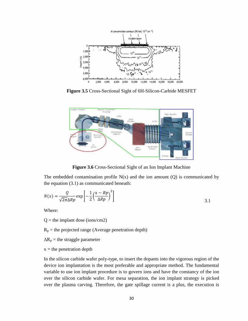
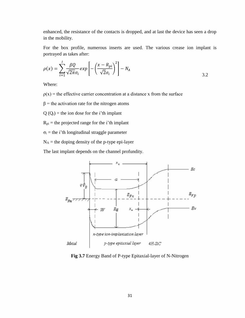
doping focuses after the ion implant procedure. Figure 3.5 shows 6H-Silicon-Carbide
MESFET cross-sectional perspective, and Figure 3.6 shows the Cross-sectional
perspective of an ion implant machine.
In the ion implant machine, the first stage is the source section. In the source section,
either the cathode or the anode rods are used to ionize the impurity gas. The second stage
is the beam line section, in which the ions are pulled out and quickened in the mass
strainer. The third stage is the End-station section; this is the area where the ions are a
target on the wafer.
The inserter tool scans the surface of the wafer electrostatically to check the evenness of
dope. The ion dopant is overwhelmed into the crystals, and the molecules cease to move
at some profundity at the minuscule level. The projected Range (Rp) is approximated in
the range of 280Å to 0.10μm.
30
Figure 3.5 Cross-Sectional Sight of 6H-Silicon-Carbide MESFET
Figure 3.6 Cross-Sectional Sight of an Ion Implant Machine
The embedded contamination profile N(x) and the ion amount (Q) is communicated by
the equation (3.1) as communicated beneath:
3.1
Where:
Q = the implant dose (ions/cm2)
Rp = the projected range (Average penetration depth)
ΔRp = the straggle parameter
x = the penetration depth
In the silicon carbide wafer poly-type, to insert the dopants into the vigorous region of the
device ion implantation is the most preferable and appropriate method. The fundamental
variable to use ion implant procedure is to govern ions and have the constancy of the ion
over the silicon carbide wafer. For mesa separation, the ion implant strategy is picked
over the plasma carving. Therefore, the gate spillage current is a plus, the execution is
31
enhanced, the resistance of the contacts is dropped, and at last the device has seen a drop
in the mobility.
For the box profile, numerous inserts are used. The various crease ion implant is
portrayed as takes after:
3.2
Where:
ρ(x) = the effective carrier concentration at a distance x from the surface
β = the activation rate for the nitrogen atoms
Q (Qi) = the ion dose for the i’th implant
Rpi = the projected range for the i’th implant
σi = the i’th longitudinal straggle parameter
NA = the doping density of the p-type epi-layer
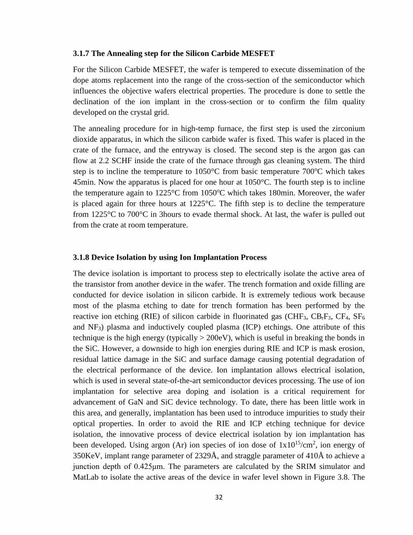
The last implant depends on the channel profundity.
Fig 3.7 Energy Band of P-type Epitaxial-layer of N-Nitrogen
32
3.1.7 The Annealing step for the Silicon Carbide MESFET
For the Silicon Carbide MESFET, the wafer is tempered to execute dissemination of the
dope atoms replacement into the range of the cross-section of the semiconductor which
influences the objective wafers electrical properties. The procedure is done to settle the
declination of the ion implant in the cross-section or to confirm the film quality
developed on the crystal grid.
The annealing procedure for in high-temp furnace, the first step is used the zirconium
dioxide apparatus, in which the silicon carbide wafer is fixed. This wafer is placed in the
crate of the furnace, and the entryway is closed. The second step is the argon gas can
flow at 2.2 SCHF inside the crate of the furnace through gas cleaning system. The third
step is to incline the temperature to 1050°C from basic temperature 700oC which takes
45min. Now the apparatus is placed for one hour at 1050°C. The fourth step is to incline
the temperature again to 1225°C from 1050oC which takes 180min. Moreover, the wafer
is placed again for three hours at 1225°C. The fifth step is to decline the temperature
from 1225°C to 700°C in 3hours to evade thermal shock. At last, the wafer is pulled out
from the crate at room temperature.
3.1.8 Device Isolation by using Ion Implantation Process
The device isolation is important to process step to electrically isolate the active area of
the transistor from another device in the wafer. The trench formation and oxide filling are
conducted for device isolation in silicon carbide. It is extremely tedious work because
most of the plasma etching to date for trench formation has been performed by the
reactive ion etching (RIE) of silicon carbide in fluorinated gas (CHF3, CBrF3, CF4, SF6
and NF3) plasma and inductively coupled plasma (ICP) etchings. One attribute of this
technique is the high energy (typically > 200eV), which is useful in breaking the bonds in
the SiC. However, a downside to high ion energies during RIE and ICP is mask erosion,
residual lattice damage in the SiC and surface damage causing potential degradation of
the electrical performance of the device. Ion implantation allows electrical isolation,
which is used in several state-of-the-art semiconductor devices processing. The use of ion
implantation for selective area doping and isolation is a critical requirement for
advancement of GaN and SiC device technology. To date, there has been little work in
this area, and generally, implantation has been used to introduce impurities to study their
optical properties. In order to avoid the RIE and ICP etching technique for device
isolation, the innovative process of device electrical isolation by ion implantation has
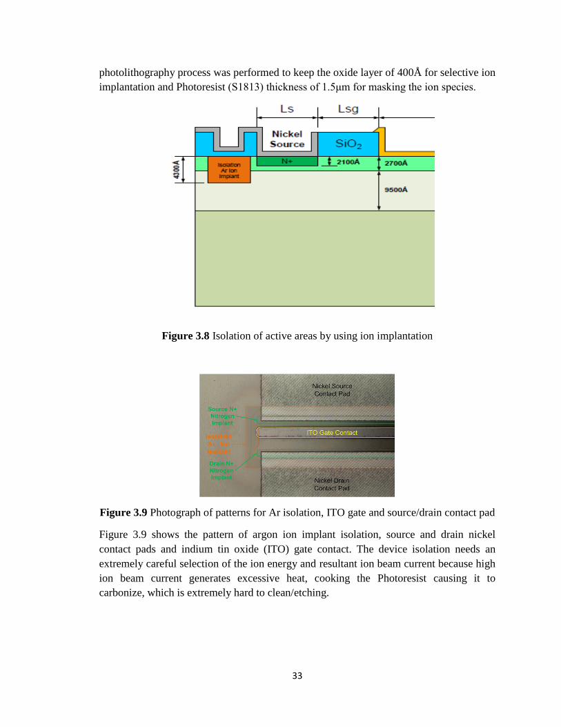
been developed. Using argon (Ar) ion species of ion dose of 1x10¹⁵/cm2, ion energy of
350KeV, implant range parameter of 2329Å, and straggle parameter of 410Å to achieve a
junction depth of 0.425μm. The parameters are calculated by the SRIM simulator and
MatLab to isolate the active areas of the device in wafer level shown in Figure 3.8. The
33
photolithography process was performed to keep the oxide layer of 400Å for selective ion
implantation and Photoresist (S1813) thickness of 1.5μm for masking the ion species.
Figure 3.8 Isolation of active areas by using ion implantation
Figure 3.9 Photograph of patterns for Ar isolation, ITO gate and source/drain contact pad
Figure 3.9 shows the pattern of argon ion implant isolation, source and drain nickel
contact pads and indium tin oxide (ITO) gate contact. The device isolation needs an
extremely careful selection of the ion energy and resultant ion beam current because high
ion beam current generates excessive heat, cooking the Photoresist causing it to
carbonize, which is extremely hard to clean/etching.
34
3.2 Fabrication process of Silicon Carbide MESFET device
The fabrication of Silicon carbide based MESFET is almost the same as a conventional
silicon-based MESFET. However, fabrication of a Silicon carbide MESFET is extremely
difficult compared to silicon (Si), gallium arsenide (GaAs) and Indium Phosphide (InP)
semiconductors. The fabrication steps for silicon carbide (SiC) MESFET are below.
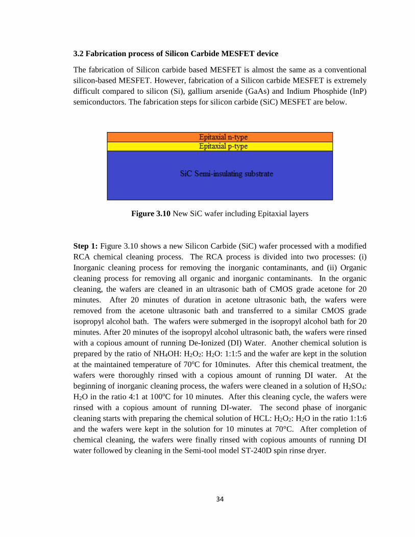
Figure 3.10 New SiC wafer including Epitaxial layers
Step 1: Figure 3.10 shows a new Silicon Carbide (SiC) wafer processed with a modified
RCA chemical cleaning process. The RCA process is divided into two processes: (i)
Inorganic cleaning process for removing the inorganic contaminants, and (ii) Organic
cleaning process for removing all organic and inorganic contaminants. In the organic
cleaning, the wafers are cleaned in an ultrasonic bath of CMOS grade acetone for 20
minutes. After 20 minutes of duration in acetone ultrasonic bath, the wafers were
removed from the acetone ultrasonic bath and transferred to a similar CMOS grade
isopropyl alcohol bath. The wafers were submerged in the isopropyl alcohol bath for 20
minutes. After 20 minutes of the isopropyl alcohol ultrasonic bath, the wafers were rinsed
with a copious amount of running De-Ionized (DI) Water. Another chemical solution is
prepared by the ratio of NH4OH: H2O2: H2O: 1:1:5 and the wafer are kept in the solution
at the maintained temperature of 70oC for 10minutes. After this chemical treatment, the
wafers were thoroughly rinsed with a copious amount of running DI water. At the
beginning of inorganic cleaning process, the wafers were cleaned in a solution of H2SO4:
H2O in the ratio 4:1 at 100oC for 10 minutes. After this cleaning cycle, the wafers were
rinsed with a copious amount of running DI-water. The second phase of inorganic
cleaning starts with preparing the chemical solution of HCL: H2O2: H2O in the ratio 1:1:6
and the wafers were kept in the solution for 10 minutes at 70°C. After completion of
chemical cleaning, the wafers were finally rinsed with copious amounts of running DI
water followed by cleaning in the Semi-tool model ST-240D spin rinse dryer.
35
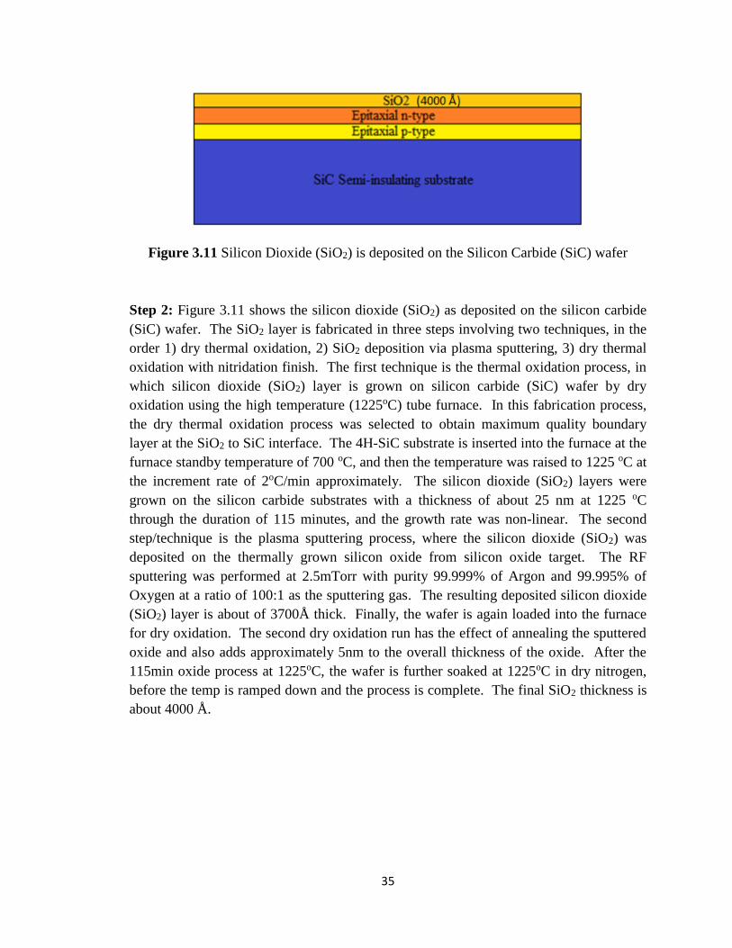
Figure 3.11 Silicon Dioxide (SiO2) is deposited on the Silicon Carbide (SiC) wafer
Step 2: Figure 3.11 shows the silicon dioxide (SiO2) as deposited on the silicon carbide
(SiC) wafer. The SiO2 layer is fabricated in three steps involving two techniques, in the
order 1) dry thermal oxidation, 2) SiO2 deposition via plasma sputtering, 3) dry thermal
oxidation with nitridation finish. The first technique is the thermal oxidation process, in
which silicon dioxide (SiO2) layer is grown on silicon carbide (SiC) wafer by dry
oxidation using the high temperature (1225oC) tube furnace. In this fabrication process,
the dry thermal oxidation process was selected to obtain maximum quality boundary
layer at the SiO2 to SiC interface. The 4H-SiC substrate is inserted into the furnace at the
furnace standby temperature of 700 oC, and then the temperature was raised to 1225 oC at
the increment rate of 2oC/min approximately. The silicon dioxide (SiO2) layers were
grown on the silicon carbide substrates with a thickness of about 25 nm at 1225 oC
through the duration of 115 minutes, and the growth rate was non-linear. The second
step/technique is the plasma sputtering process, where the silicon dioxide (SiO2) was
deposited on the thermally grown silicon oxide from silicon oxide target. The RF
sputtering was performed at 2.5mTorr with purity 99.999% of Argon and 99.995% of
Oxygen at a ratio of 100:1 as the sputtering gas. The resulting deposited silicon dioxide
(SiO2) layer is about of 3700Å thick. Finally, the wafer is again loaded into the furnace
for dry oxidation. The second dry oxidation run has the effect of annealing the sputtered
oxide and also adds approximately 5nm to the overall thickness of the oxide. After the
115min oxide process at 1225oC, the wafer is further soaked at 1225oC in dry nitrogen,
before the temp is ramped down and the process is complete. The final SiO2 thickness is
about 4000 Å.
36
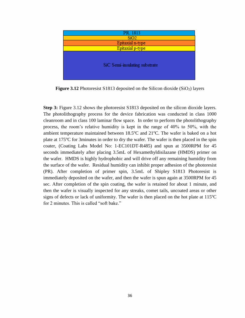
Figure 3.12 Photoresist S1813 deposited on the Silicon dioxide (SiO2) layers
Step 3: Figure 3.12 shows the photoresist S1813 deposited on the silicon dioxide layers.
The photolithography process for the device fabrication was conducted in class 1000
cleanroom and in class 100 laminar flow space. In order to perform the photolithography
process, the room’s relative humidity is kept in the range of 40% to 50%, with the
ambient temperature maintained between 18.5oC and 21oC. The wafer is baked on a hot
plate at 175oC for 3minutes in order to dry the wafer. The wafer is then placed in the spin
coater, (Coating Labs Model No: 1-EC101DT-R485) and spun at 3500RPM for 45
seconds immediately after placing 3.5mL of Hexamethyldisilazane (HMDS) primer on
the wafer. HMDS is highly hydrophobic and will drive off any remaining humidity from
the surface of the wafer. Residual humidity can inhibit proper adhesion of the photoresist
(PR). After completion of primer spin, 3.5mL of Shipley S1813 Photoresist is
immediately deposited on the wafer, and then the wafer is spun again at 3500RPM for 45
sec. After completion of the spin coating, the wafer is retained for about 1 minute, and
then the wafer is visually inspected for any streaks, comet tails, uncoated areas or other
signs of defects or lack of uniformity. The wafer is then placed on the hot plate at 115oC
for 2 minutes. This is called “soft bake.”
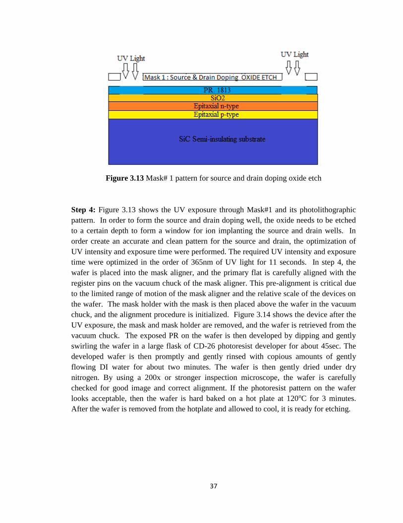
37
Figure 3.13 Mask# 1 pattern for source and drain doping oxide etch
Step 4: Figure 3.13 shows the UV exposure through Mask#1 and its photolithographic
pattern. In order to form the source and drain doping well, the oxide needs to be etched
to a certain depth to form a window for ion implanting the source and drain wells. In
order create an accurate and clean pattern for the source and drain, the optimization of
UV intensity and exposure time were performed. The required UV intensity and exposure
time were optimized in the order of 365nm of UV light for 11 seconds. In step 4, the
wafer is placed into the mask aligner, and the primary flat is carefully aligned with the
register pins on the vacuum chuck of the mask aligner. This pre-alignment is critical due
to the limited range of motion of the mask aligner and the relative scale of the devices on
the wafer. The mask holder with the mask is then placed above the wafer in the vacuum
chuck, and the alignment procedure is initialized. Figure 3.14 shows the device after the
UV exposure, the mask and mask holder are removed, and the wafer is retrieved from the
vacuum chuck. The exposed PR on the wafer is then developed by dipping and gently
swirling the wafer in a large flask of CD-26 photoresist developer for about 45sec. The
developed wafer is then promptly and gently rinsed with copious amounts of gently
flowing DI water for about two minutes. The wafer is then gently dried under dry
nitrogen. By using a 200x or stronger inspection microscope, the wafer is carefully
checked for good image and correct alignment. If the photoresist pattern on the wafer
looks acceptable, then the wafer is hard baked on a hot plate at 120oC for 3 minutes.
After the wafer is removed from the hotplate and allowed to cool, it is ready for etching.
38
Figure 3.14 Resist pattern for the source and drain doping after UV exposure and image
development
Figure 3.15 Silicon dioxide (SiO2) is etched for source and drain doping
Step 5: Figure 3.15 shows the SiO2 was etched for source and drain doping. The process
for removing the oxide material is wet chemical etching process using hydrofluoric acid
(HF) based buffered oxide etch (BOE). The wafer is dipped and gently stirred in a plastic
beaker of 20:1 BOE for approximately 6min 30sec at 25 oC, then immediately rinsed with
copious amounts of DI water, followed by cleaning in the spin rinse dryer (SRD). During
etching, a small layer of 300Ǻ to 400Ǻ SiO2 was kept as a protective layer to avoid
excess crystal damage due to huge ion bombardment during ion implantation.
39
Figure 3.16 Nitrogen Ion N+ implanted in the n-type layer for Drain and Source well
Step 6: Figure 3.16 shows the N+ ion-implanted in the drain and source well. For silicon
carbide (SiC) material and MESFET device structure, Nitrogen is the suitable n-type
dopant. The Ion implantation for drain and source formation was conducted with the
following parameters: ion dose of 2x1015cm-2, the Ion Energy of 80KeV, the Ion Species
is Nitrogen, the temperature during ion implantation is 500oC, and the tilt Angle is 0o.
The resultant impurity concentration and the junction depth were found to be about
5x1019cm-3 and 0.21μm, respectively.
Figure 3.17 The device structure after stripping the photoresist S1813
Step 7: Figure 3.17 shows the device structure after stripping the photoresist S1813. The
wafer is cleaned in an ultrasonic acetone bath for 3 hours, followed by plasma cleaning in
90% Ar and 10% O2 at 75 watts for 20min. The additional plasma cleaning step is
required due to partial carbonization of the PR resulting from the excess heat during ion
implant.
40
Figure 3.18 Device structure after annealing process
Step 8: Figure 3.18 shows the device structure after the annealing process. In order to
perform high-temperature annealing of SiC, AlN film thickness about 700Å was
deposited using the plasma sputtering system. The deposition of AlN film on the SiC
wafer was chosen to avoid the sublimation of the silicon from the silicon carbide wafer.
The process of the AlN film deposition was performed by RF sputtering from 3 inch AlN
target with a purity of 99.99% by maintaining the gas pressure of 2.5 m-torr with purity
99.99% of argon and 99.9% of nitrogen at a ratio of 100:1, and RF power of 125 watts
for 25 minutes. The Silicon carbide wafer was annealed in the customized furnace for
three hours in argon ambient at the temperature of 1600oC. The temperature profile for
1600oC is given in the Figure 3.19.
Figure 3.19 The Annealing Temperature Profile of the SiC wafer at up to 1600oC
Several attempts have been made to etch the AlN coating of the post-annealed SiC wafer
by using individual wet chemical etching of KOH, NaOH, and HF. The sample was
initially etched by dilute HF to remove the oxide layer, and no satisfactory result was
41
found. The sample was again dipped in the hot KOH at 70oC followed by NaOH dipping
at 70oC, and the Al2O3 film was removed, but the process damaged the underlying oxide
layer and device structure. All chemical etchants were failed to etch the high-temperature
AlN film because the film became harder due to the probable cause of the phase
transformation of AlN to Al2O3. The phase transformation may have occurred due to
oxygen leakage from the atmosphere during high-temperature annealing. In order to
study material phase transformation and failure analysis, the sample was sent to Seal
Laboratories in El Segundo, CA for Auger study. Figure 3.20 shows the report of Auger
study in detail.
Figure 3.20 Surface morphology of high temperature annealed AlN film study using
Augerscope
The Augerscope demonstrates the trace of SiO2, Argon, Al2O3, Al, and silicon. This
indicated that some silicon had been sublimated and caught in the Al2O3. The trace of Al
content affirms the escape of nitrogen and contains a change of Al2O3 arrangement. This
review explains the reason for difficulty cleaning the AlN film by KOH because of the
layer of SiO2 and Al2O3. The silicon carbide wafer is first cleaned by using HF to weaken
the oxide layer. The specimen was again dunked in the hot KOH at >70oC and hot NaOH
at >70oC, and the Al2O3 film was mostly removed.
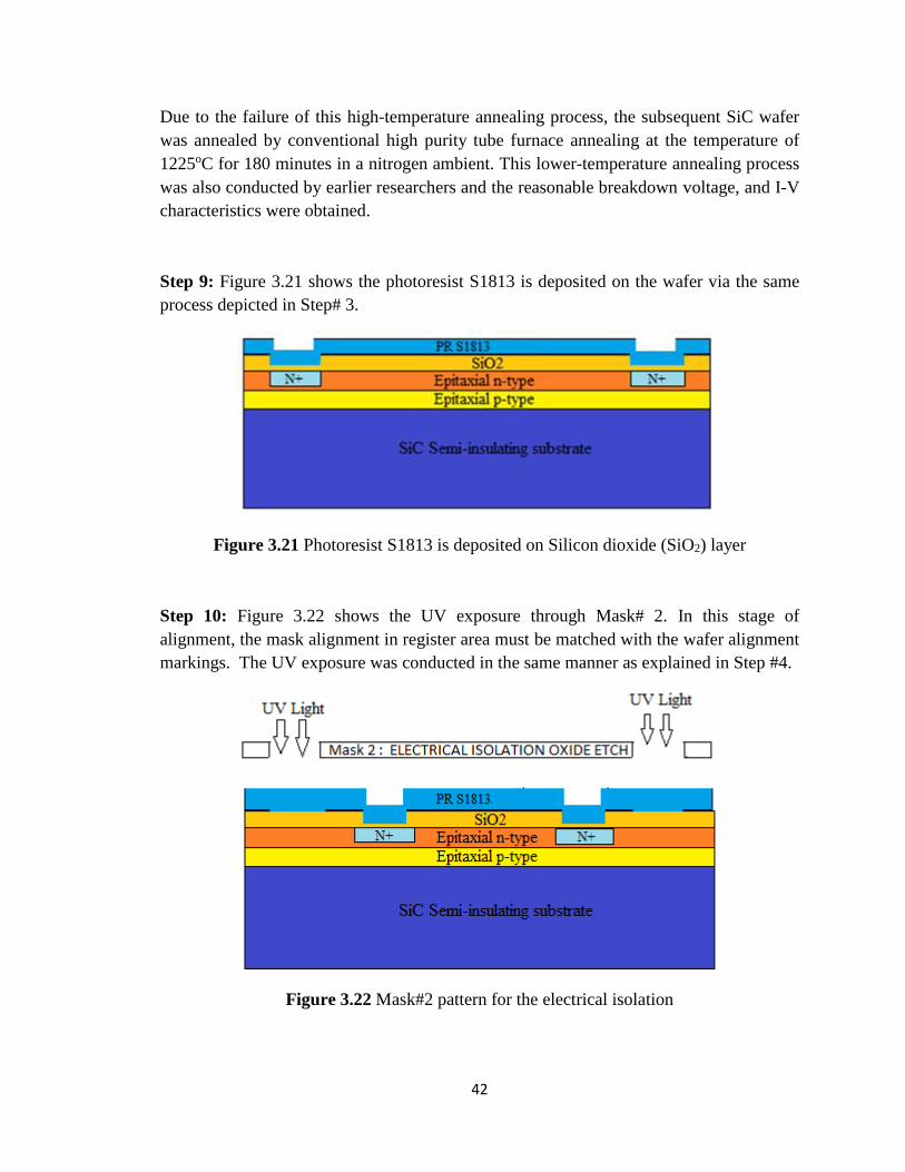
42
Due to the failure of this high-temperature annealing process, the subsequent SiC wafer
was annealed by conventional high purity tube furnace annealing at the temperature of
1225oC for 180 minutes in a nitrogen ambient. This lower-temperature annealing process
was also conducted by earlier researchers and the reasonable breakdown voltage, and I-V
characteristics were obtained.
Step 9: Figure 3.21 shows the photoresist S1813 is deposited on the wafer via the same
process depicted in Step# 3.
Figure 3.21 Photoresist S1813 is deposited on Silicon dioxide (SiO2) layer
Step 10: Figure 3.22 shows the UV exposure through Mask# 2. In this stage of
alignment, the mask alignment in register area must be matched with the wafer alignment
markings. The UV exposure was conducted in the same manner as explained in Step #4.
Figure 3.22 Mask#2 pattern for the electrical isolation
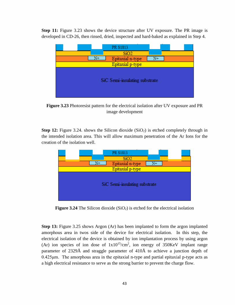
43
Step 11: Figure 3.23 shows the device structure after UV exposure. The PR image is
developed in CD-26, then rinsed, dried, inspected and hard-baked as explained in Step 4.
Figure 3.23 Photoresist pattern for the electrical isolation after UV exposure and PR
image development
Step 12: Figure 3.24. shows the Silicon dioxide (SiO2) is etched completely through in
the intended isolation area. This will allow maximum penetration of the Ar Ions for the
creation of the isolation well.
Figure 3.24 The Silicon dioxide (SiO2) is etched for the electrical isolation
Step 13: Figure 3.25 shows Argon (Ar) has been implanted to form the argon implanted
amorphous area in twos side of the device for electrical isolation. In this step, the
electrical isolation of the device is obtained by ion implantation process by using argon
(Ar) ion species of ion dose of 1x10¹⁵/cm2, ion energy of 350KeV implant range
parameter of 2329Å and straggle parameter of 410Å to achieve a junction depth of
0.425μm. The amorphous area in the epitaxial n-type and partial epitaxial p-type acts as
a high electrical resistance to serve as the strong barrier to prevent the charge flow.
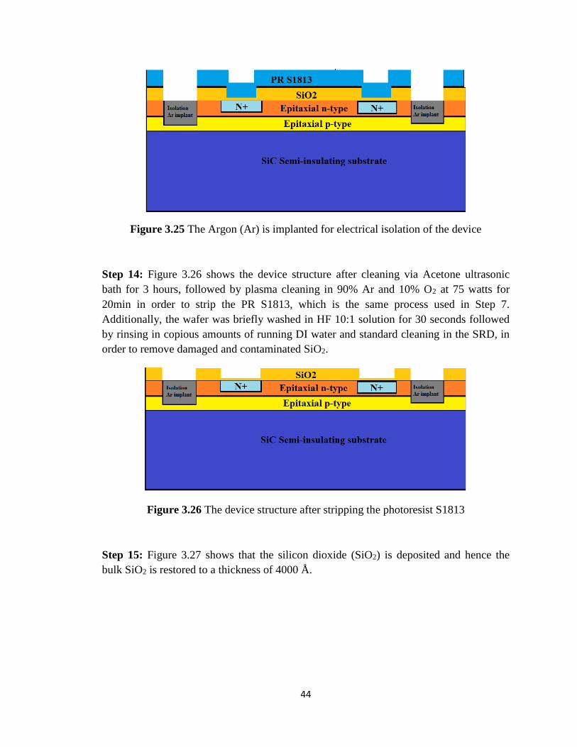
44
Figure 3.25 The Argon (Ar) is implanted for electrical isolation of the device
Step 14: Figure 3.26 shows the device structure after cleaning via Acetone ultrasonic
bath for 3 hours, followed by plasma cleaning in 90% Ar and 10% O2 at 75 watts for
20min in order to strip the PR S1813, which is the same process used in Step 7.
Additionally, the wafer was briefly washed in HF 10:1 solution for 30 seconds followed
by rinsing in copious amounts of running DI water and standard cleaning in the SRD, in
order to remove damaged and contaminated SiO2.
Figure 3.26 The device structure after stripping the photoresist S1813
Step 15: Figure 3.27 shows that the silicon dioxide (SiO2) is deposited and hence the
bulk SiO2 is restored to a thickness of 4000 Å.
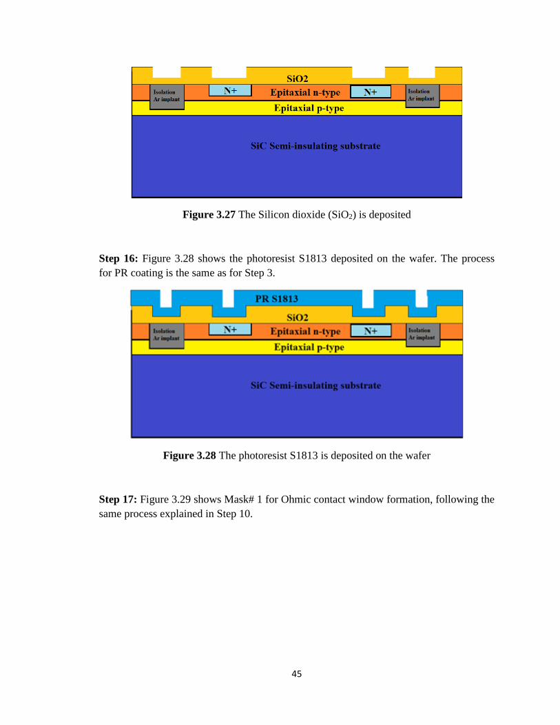
45
Figure 3.27 The Silicon dioxide (SiO2) is deposited
Step 16: Figure 3.28 shows the photoresist S1813 deposited on the wafer. The process
for PR coating is the same as for Step 3.
Figure 3.28 The photoresist S1813 is deposited on the wafer
Step 17: Figure 3.29 shows Mask# 1 for Ohmic contact window formation, following the
same process explained in Step 10.
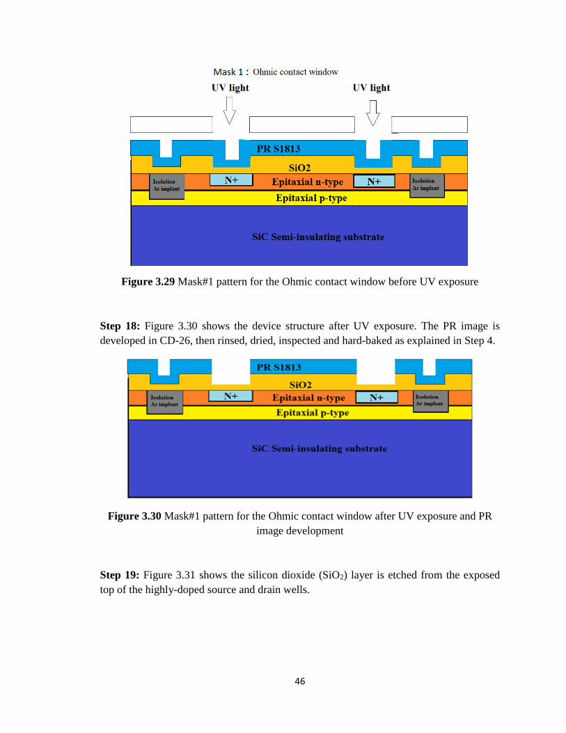
46
Figure 3.29 Mask#1 pattern for the Ohmic contact window before UV exposure
Step 18: Figure 3.30 shows the device structure after UV exposure. The PR image is
developed in CD-26, then rinsed, dried, inspected and hard-baked as explained in Step 4.
Figure 3.30 Mask#1 pattern for the Ohmic contact window after UV exposure and PR
image development
Step 19: Figure 3.31 shows the silicon dioxide (SiO2) layer is etched from the exposed
top of the highly-doped source and drain wells.
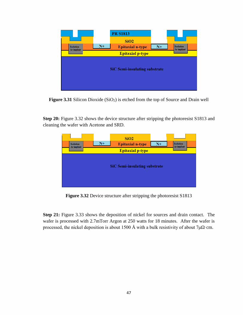
47
Figure 3.31 Silicon Dioxide (SiO2) is etched from the top of Source and Drain well
Step 20: Figure 3.32 shows the device structure after stripping the photoresist S1813 and
cleaning the wafer with Acetone and SRD.
Figure 3.32 Device structure after stripping the photoresist S1813
Step 21: Figure 3.33 shows the deposition of nickel for sources and drain contact. The
wafer is processed with 2.7mTorr Argon at 250 watts for 18 minutes. After the wafer is
processed, the nickel deposition is about 1500 Å with a bulk resistivity of about 7μΩ·cm.
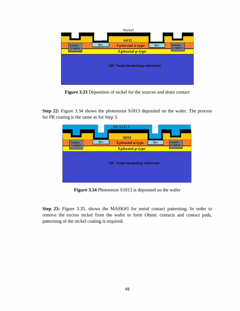
48
Figure 3.33 Deposition of nickel for the sources and drain contact
Step 22: Figure 3.34 shows the photoresist S1813 deposited on the wafer. The process
for PR coating is the same as for Step 3.
Figure 3.34 Photoresist S1813 is deposited on the wafer
Step 23: Figure 3.35. shows the MASK#3 for metal contact patterning. In order to
remove the excess nickel from the wafer to form Ohmic contacts and contact pads,
patterning of the nickel coating is required.
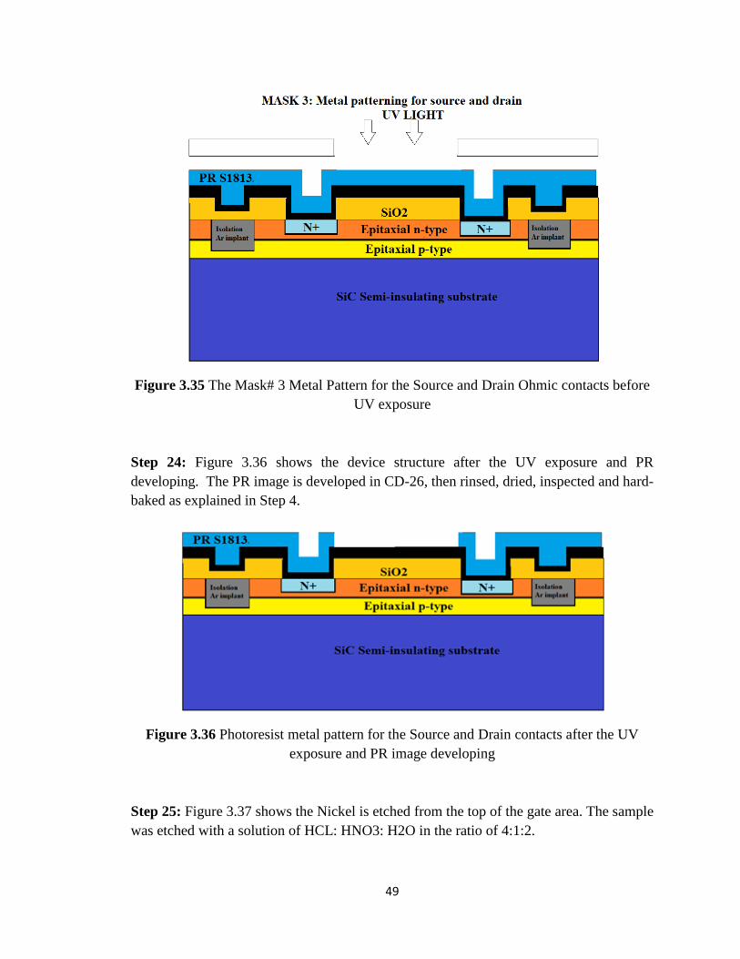
49
Figure 3.35 The Mask# 3 Metal Pattern for the Source and Drain Ohmic contacts before
UV exposure
Step 24: Figure 3.36 shows the device structure after the UV exposure and PR
developing. The PR image is developed in CD-26, then rinsed, dried, inspected and hard-
baked as explained in Step 4.
Figure 3.36 Photoresist metal pattern for the Source and Drain contacts after the UV
exposure and PR image developing
Step 25: Figure 3.37 shows the Nickel is etched from the top of the gate area. The sample
was etched with a solution of HCL: HNO3: H2O in the ratio of 4:1:2.
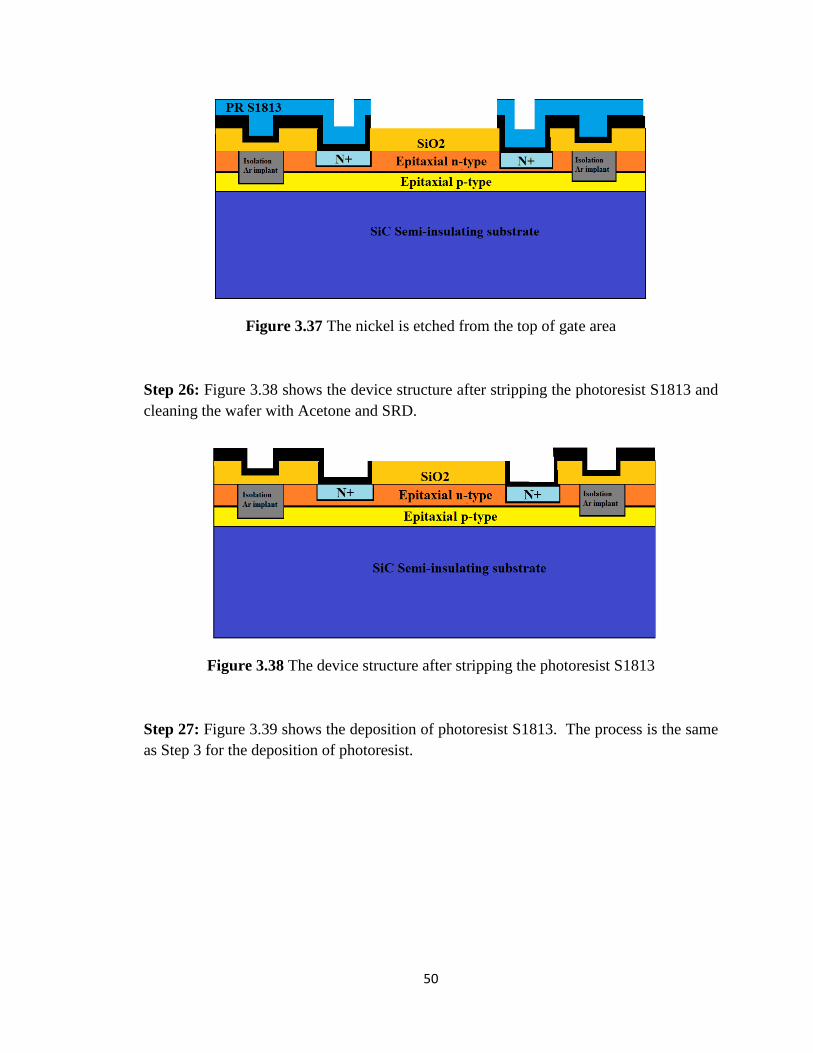
50
Figure 3.37 The nickel is etched from the top of gate area
Step 26: Figure 3.38 shows the device structure after stripping the photoresist S1813 and
cleaning the wafer with Acetone and SRD.
Figure 3.38 The device structure after stripping the photoresist S1813
Step 27: Figure 3.39 shows the deposition of photoresist S1813. The process is the same
as Step 3 for the deposition of photoresist.
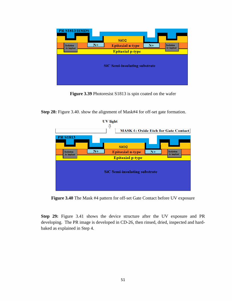
51
Figure 3.39 Photoresist S1813 is spin coated on the wafer
Step 28: Figure 3.40. show the alignment of Mask#4 for off-set gate formation.
Figure 3.40 The Mask #4 pattern for off-set Gate Contact before UV exposure
Step 29: Figure 3.41 shows the device structure after the UV exposure and PR
developing. The PR image is developed in CD-26, then rinsed, dried, inspected and hard-
baked as explained in Step 4.
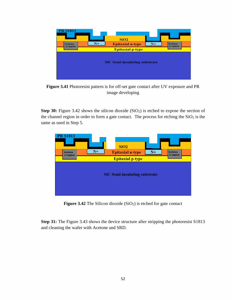
52
Figure 3.41 Photoresist pattern is for off-set gate contact after UV exposure and PR
image developing
Step 30: Figure 3.42 shows the silicon dioxide (SiO2) is etched to expose the section of
the channel region in order to form a gate contact. The process for etching the SiO2 is the
same as used in Step 5.
Figure 3.42 The Silicon dioxide (SiO2) is etched for gate contact
Step 31: The Figure 3.43 shows the device structure after stripping the photoresist S1813
and cleaning the wafer with Acetone and SRD.
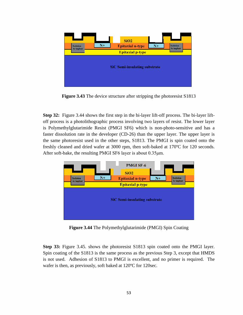
53
Figure 3.43 The device structure after stripping the photoresist S1813
Step 32: Figure 3.44 shows the first step in the bi-layer lift-off process. The bi-layer lift-
off process is a photolithographic process involving two layers of resist. The lower layer
is Polymethylglutarimide Resist (PMGI SF6) which is non-photo-sensitive and has a
faster dissolution rate in the developer (CD-26) than the upper layer. The upper layer is
the same photoresist used in the other steps, S1813. The PMGI is spin coated onto the
freshly cleaned and dried wafer at 3000 rpm, then soft-baked at 170ºC for 120 seconds.
After soft-bake, the resulting PMGI SF6 layer is about 0.35μm.
Figure 3.44 The Polymethylglutarimide (PMGI) Spin Coating
Step 33: Figure 3.45. shows the photoresist S1813 spin coated onto the PMGI layer.
Spin coating of the S1813 is the same process as the previous Step 3, except that HMDS
is not used. Adhesion of S1813 to PMGI is excellent, and no primer is required. The
wafer is then, as previously, soft baked at 120ºC for 120sec.
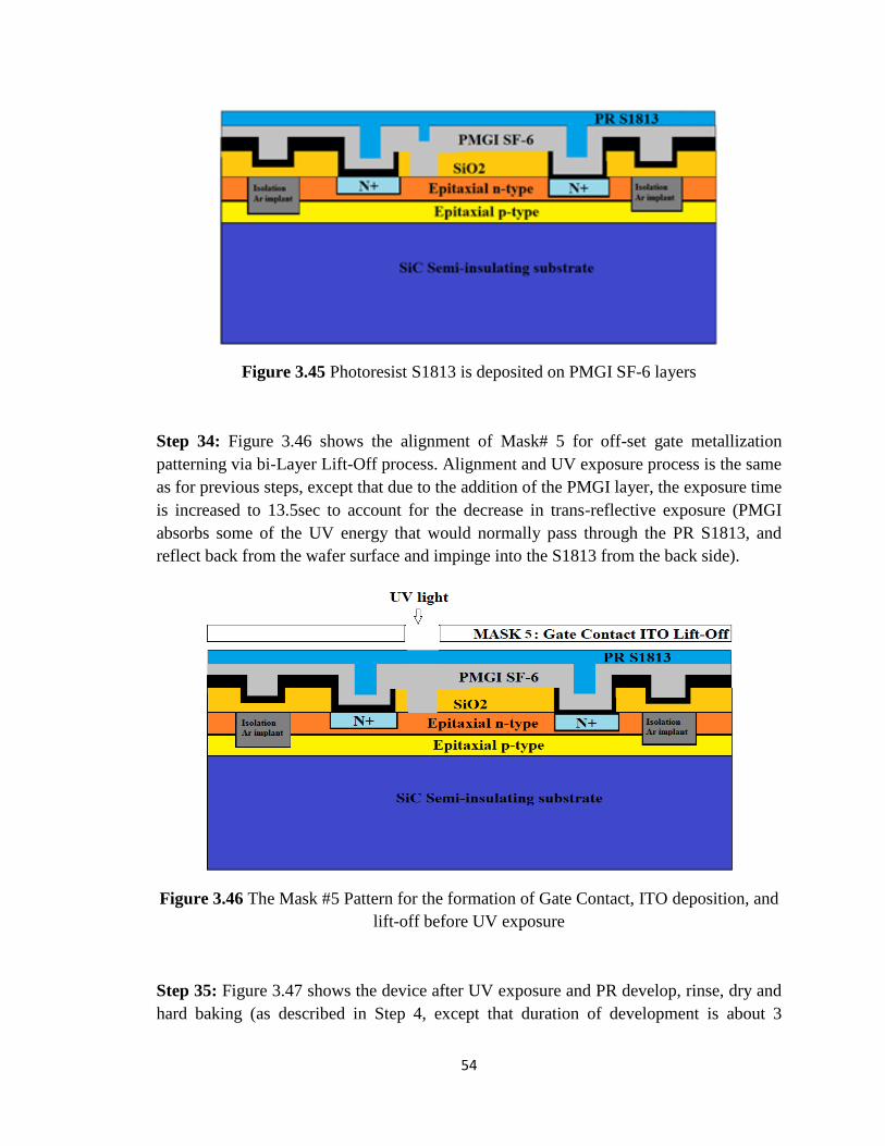
54
Figure 3.45 Photoresist S1813 is deposited on PMGI SF-6 layers
Step 34: Figure 3.46 shows the alignment of Mask# 5 for off-set gate metallization
patterning via bi-Layer Lift-Off process. Alignment and UV exposure process is the same
as for previous steps, except that due to the addition of the PMGI layer, the exposure time
is increased to 13.5sec to account for the decrease in trans-reflective exposure (PMGI
absorbs some of the UV energy that would normally pass through the PR S1813, and
reflect back from the wafer surface and impinge into the S1813 from the back side).
Figure 3.46 The Mask #5 Pattern for the formation of Gate Contact, ITO deposition, and
lift-off before UV exposure
Step 35: Figure 3.47 shows the device after UV exposure and PR develop, rinse, dry and
hard baking (as described in Step 4, except that duration of development is about 3
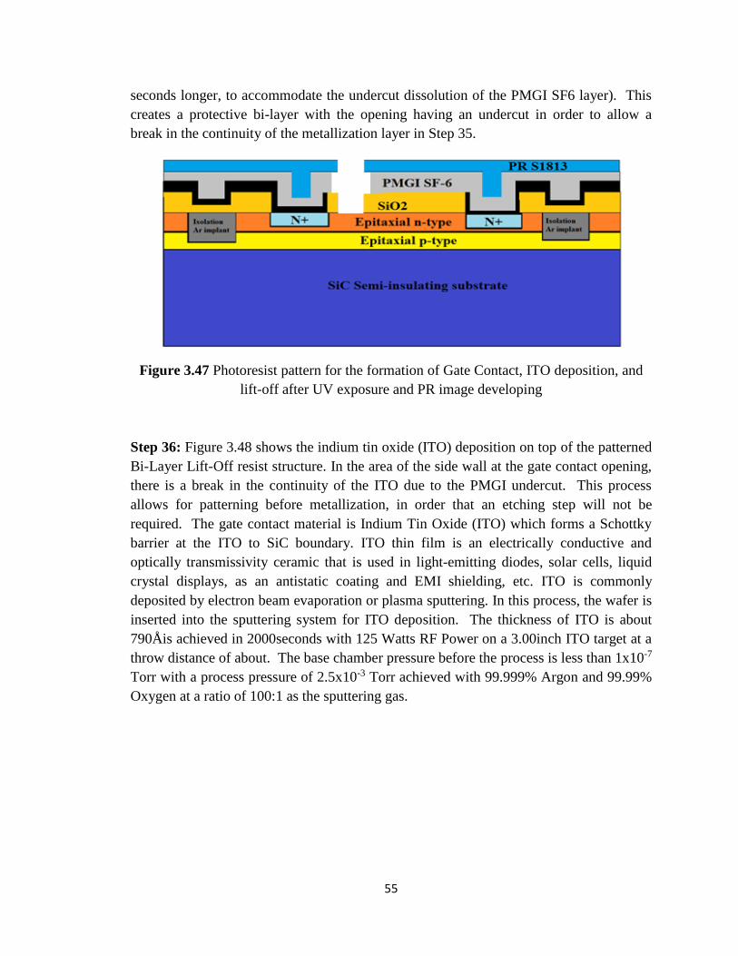
55
seconds longer, to accommodate the undercut dissolution of the PMGI SF6 layer). This
creates a protective bi-layer with the opening having an undercut in order to allow a
break in the continuity of the metallization layer in Step 35.
Figure 3.47 Photoresist pattern for the formation of Gate Contact, ITO deposition, and
lift-off after UV exposure and PR image developing
Step 36: Figure 3.48 shows the indium tin oxide (ITO) deposition on top of the patterned
Bi-Layer Lift-Off resist structure. In the area of the side wall at the gate contact opening,
there is a break in the continuity of the ITO due to the PMGI undercut. This process
allows for patterning before metallization, in order that an etching step will not be
required. The gate contact material is Indium Tin Oxide (ITO) which forms a Schottky
barrier at the ITO to SiC boundary. ITO thin film is an electrically conductive and
optically transmissivity ceramic that is used in light-emitting diodes, solar cells, liquid
crystal displays, as an antistatic coating and EMI shielding, etc. ITO is commonly
deposited by electron beam evaporation or plasma sputtering. In this process, the wafer is
inserted into the sputtering system for ITO deposition. The thickness of ITO is about
790Åis achieved in 2000seconds with 125 Watts RF Power on a 3.00inch ITO target at a
throw distance of about. The base chamber pressure before the process is less than 1x10⁻⁷
Torr with a process pressure of 2.5x10⁻³ Torr achieved with 99.999% Argon and 99.99%
Oxygen at a ratio of 100:1 as the sputtering gas.
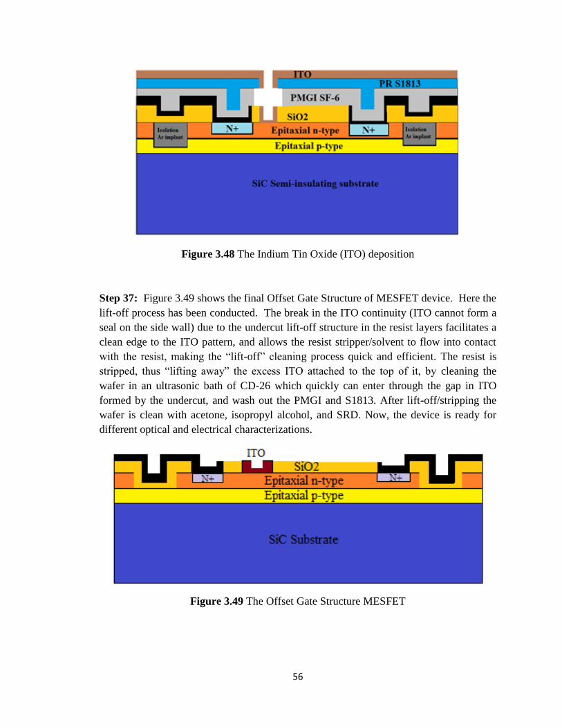
56
Figure 3.48 The Indium Tin Oxide (ITO) deposition
Step 37: Figure 3.49 shows the final Offset Gate Structure of MESFET device. Here the
lift-off process has been conducted. The break in the ITO continuity (ITO cannot form a
seal on the side wall) due to the undercut lift-off structure in the resist layers facilitates a
clean edge to the ITO pattern, and allows the resist stripper/solvent to flow into contact
with the resist, making the “lift-off” cleaning process quick and efficient. The resist is
stripped, thus “lifting away” the excess ITO attached to the top of it, by cleaning the
wafer in an ultrasonic bath of CD-26 which quickly can enter through the gap in ITO
formed by the undercut, and wash out the PMGI and S1813. After lift-off/stripping the
wafer is clean with acetone, isopropyl alcohol, and SRD. Now, the device is ready for
different optical and electrical characterizations.
Figure 3.49 The Offset Gate Structure MESFET
57
Chapter 4: Oxidation Process for Silicon Carbide (SiC)
Silicon Dioxide (SiO2) is mainly obtained from the constituents of silica. A trace of the
silica is found in the volcanic rocks and gemstone. Silicon dioxide (SiO2) has two types
of structure Crystalline and Amorphous. The sand has the amorphous structure of silica
and quartz has the crystalline structure of the silica. A Silicon Dioxide (SiO2) in
Amorphous form is used due to band gap approx. 8.2 eV. In silicon (Si) based device, a
thin film of the SiO2 is used as an electrical insulator. In fact, SiO2 is chemically stable
compound, and it helps as a barrier for the impurity diffusion process. Moreover, SiO2
layer protects from the atmosphere and package process due to the layer acts as
passivation layers.
A SiO2 thin film is grown on the silicon carbide (SiC) substrate. The n-type 4H-SiC
substrate can be selected due to the excellent properties like high electron mobility is
800cm2/Vs, saturated electron velocity is 2.2×107cm/s, thermal conductivity is
4.89W/cm-K, and high chemical stability. The main advantage of the 4H-SiC substrate is
that it can face high-temperature 300oC to 700oC, the wide band approx. 3.32eV, high
breakdown field is 3.9mV/cm, and high-frequency 75GHz in power electronic.
On the silicon carbide (SiC) while growing the silicon dioxide, carbon (C) is an extra
element which causes the trouble in the growth process. This extra element must be
removed during the transition from SiC to SiO2. A high density of the interface trap state
corrupts the execution with age amid the operation timeframe. Now there is a need to
finding a new procedure of the silicon dioxide growth on the Silicon carbide substrate,
and need to figure out that the carbon face 4H-Silicon Carbide or the silicon face 4H-
Silicon Carbide is better. The silicon face 4H-Silicon Carbide is much better than carbon
face 4H-Silicon Carbide due to it inserts additional carbon in SiO2 [29]. On the other
hand, the silicon dioxide (SiO2) growth on the carbon face 4H-Silicon Carbide is more
than the silicon face 4H-Silicon Carbide due to the growth variables or the contamination
of the carbon. [30].
Conducted research on the oxide layer growth, results that near the interface of the oxide
layer it seems to be very small. In fact, it is found that near the interface of silicon dioxide
layer and 4H-SiC substrate are hotspots of interface trap density (Dit). The cause for the
formation of the interface density state can be described by giving a valid reason. The
first reason is the creation of dangling bond due to a vast number of the silicon (Si)
atoms. In compare to the SiO2/Si framework, the SiC/SiO2 have a more dangling bond
due to the plenty silicon (Si) atoms. Also, the second reason is the breaking of the bond
between carbon and silicon where carbon clusters initiate. Moreover, the breaking of the
bond is necessary for the transition from SiC to SiO2. In MOS device, the cluster or the
dimers are the part of interface state. It is possible to restrict the interface trap density
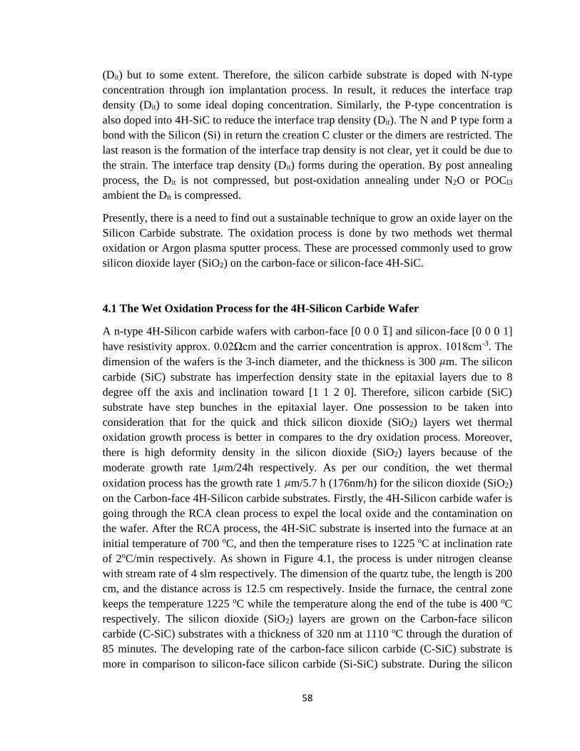
58
(Dit) but to some extent. Therefore, the silicon carbide substrate is doped with N-type
concentration through ion implantation process. In result, it reduces the interface trap
density (Dit) to some ideal doping concentration. Similarly, the P-type concentration is
also doped into 4H-SiC to reduce the interface trap density (Dit). The N and P type form a
bond with the Silicon (Si) in return the creation C cluster or the dimers are restricted. The
last reason is the formation of the interface trap density is not clear, yet it could be due to
the strain. The interface trap density (Dit) forms during the operation. By post annealing
process, the Dit is not compressed, but post-oxidation annealing under N2O or POCl3
ambient the Dit is compressed.
Presently, there is a need to find out a sustainable technique to grow an oxide layer on the
Silicon Carbide substrate. The oxidation process is done by two methods wet thermal
oxidation or Argon plasma sputter process. These are processed commonly used to grow
silicon dioxide layer (SiO2) on the carbon-face or silicon-face 4H-SiC.
4.1 The Wet Oxidation Process for the 4H-Silicon Carbide Wafer
A n-type 4H-Silicon carbide wafers with carbon-face [0 0 0 ] and silicon-face [0 0 0 1]
have resistivity approx. 0.02Ωcm and the carrier concentration is approx. 1018cm-3. The
dimension of the wafers is the 3-inch diameter, and the thickness is 300 m. The silicon
carbide (SiC) substrate has imperfection density state in the epitaxial layers due to 8
degree off the axis and inclination toward [1 1 2 0]. Therefore, silicon carbide (SiC)
substrate have step bunches in the epitaxial layer. One possession to be taken into
consideration that for the quick and thick silicon dioxide (SiO2) layers wet thermal
oxidation growth process is better in compares to the dry oxidation process. Moreover,
there is high deformity density in the silicon dioxide (SiO2) layers because of the
moderate growth rate 1 m/24h respectively. As per our condition, the wet thermal
oxidation process has the growth rate 1 m/5.7 h (176nm/h) for the silicon dioxide (SiO2)
on the Carbon-face 4H-Silicon carbide substrates. Firstly, the 4H-Silicon carbide wafer is
going through the RCA clean process to expel the local oxide and the contamination on
the wafer. After the RCA process, the 4H-SiC substrate is inserted into the furnace at an
initial temperature of 700 oC, and then the temperature rises to 1225 oC at inclination rate
of 2oC/min respectively. As shown in Figure 4.1, the process is under nitrogen cleanse
with stream rate of 4 slm respectively. The dimension of the quartz tube, the length is 200
cm, and the distance across is 12.5 cm respectively. Inside the furnace, the central zone
keeps the temperature 1225 oC while the temperature along the end of the tube is 400 oC
respectively. The silicon dioxide (SiO2) layers are grown on the Carbon-face silicon
carbide (C-SiC) substrates with a thickness of 320 nm at 1110 oC through the duration of
85 minutes. The developing rate of the carbon-face silicon carbide (C-SiC) substrate is
more in comparison to silicon-face silicon carbide (Si-SiC) substrate. During the silicon
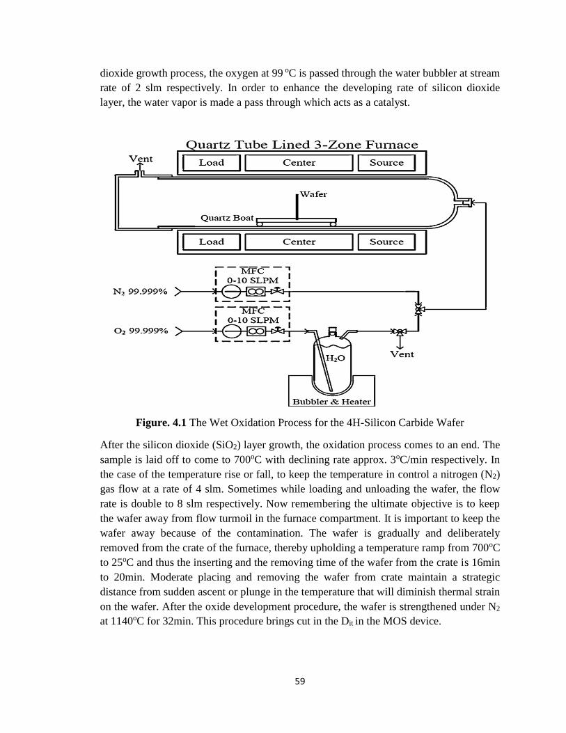
59
dioxide growth process, the oxygen at 99 oC is passed through the water bubbler at stream
rate of 2 slm respectively. In order to enhance the developing rate of silicon dioxide
layer, the water vapor is made a pass through which acts as a catalyst.
Figure. 4.1 The Wet Oxidation Process for the 4H-Silicon Carbide Wafer
After the silicon dioxide (SiO2) layer growth, the oxidation process comes to an end. The
sample is laid off to come to 700oC with declining rate approx. 3oC/min respectively. In
the case of the temperature rise or fall, to keep the temperature in control a nitrogen (N2)
gas flow at a rate of 4 slm. Sometimes while loading and unloading the wafer, the flow
rate is double to 8 slm respectively. Now remembering the ultimate objective is to keep
the wafer away from flow turmoil in the furnace compartment. It is important to keep the
wafer away because of the contamination. The wafer is gradually and deliberately
removed from the crate of the furnace, thereby upholding a temperature ramp from 700oC
to 25oC and thus the inserting and the removing time of the wafer from the crate is 16min
to 20min. Moderate placing and removing the wafer from crate maintain a strategic
distance from sudden ascent or plunge in the temperature that will diminish thermal strain
on the wafer. After the oxide development procedure, the wafer is strengthened under N2
at 1140oC for 32min. This procedure brings cut in the Dit in the MOS device.
60
4.2 The Sputtering Oxidation Process for the 4H-Silicon Carbide Wafer
A 3-inch diameter carbon-face and the silicon-face 4H-SiC substrate are used to growth
silicon dioxide (SiO2) layer. In fig 4.2, the schematic diagram of the sputtering process to
grow silicon dioxide (SiO2) layer. Before the growth of the silicon dioxide (SiO2) layer,
for several hours the sputter compartment is kept at 10−7 Torr vacuum. The Argon (Ar) is
used as a sputtering gas in the chamber at a flow rate of 15-45 sccm, and the pressure is
maintained during the process. Increase 300 nm thick silicon dioxide (SiO2) layer; the
process is conducted for 3 hours. The RF power is 250 watts, and the chamber pressure is
maintained at 2.5 mtorr respectively. A small amount of oxygen (O2) is added into the
sputter gas in the chamber during silicon dioxide (SiO2) molecules to break or partially
break from the target to the wafer, and the argon is ionized due to O2. The extra oxygen
ions in the chamber reduce the dangling bonds and the potential carriers in the silicon
dioxide (SiO2) layers. Thus, improve the dielectric strength. The sputtering process is a
deposition process, rather than a true growth of a SiO2 material on the wafer surface. The
growth rate on both the Silicon-face Silicon carbide and Carbon-faces silicon carbide is
almost identical, and there is no difference in thickness due to non-involvement of
Cluster. For the uniform growth of the silicon dioxide, the wafer is rotated at the speed of
25 rpm. The silicon carbide substrate (SiC) is configured to face down during the silicon
dioxide (SiO2) deposition because it avoids the unwanted residues on the wafers. In
general, the sputtering deposition is not better in a matter of quality, but it is quite good
for the thickness of the layers.
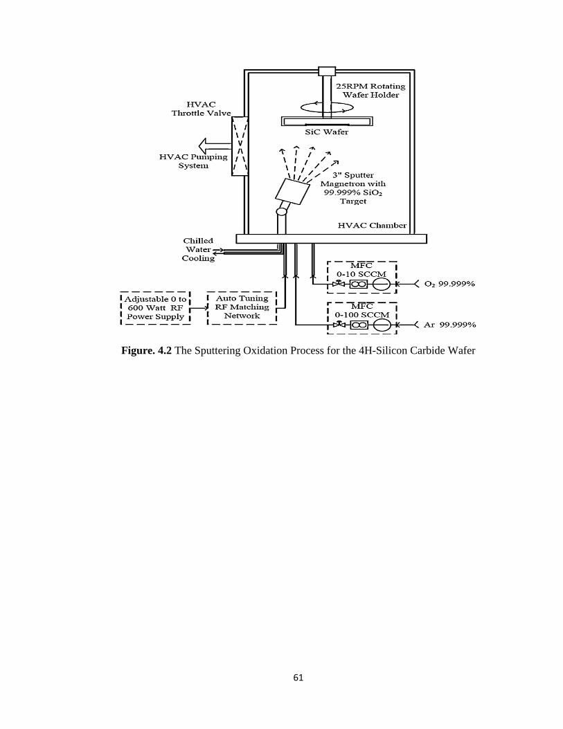
61
Figure. 4.2 The Sputtering Oxidation Process for the 4H-Silicon Carbide Wafer
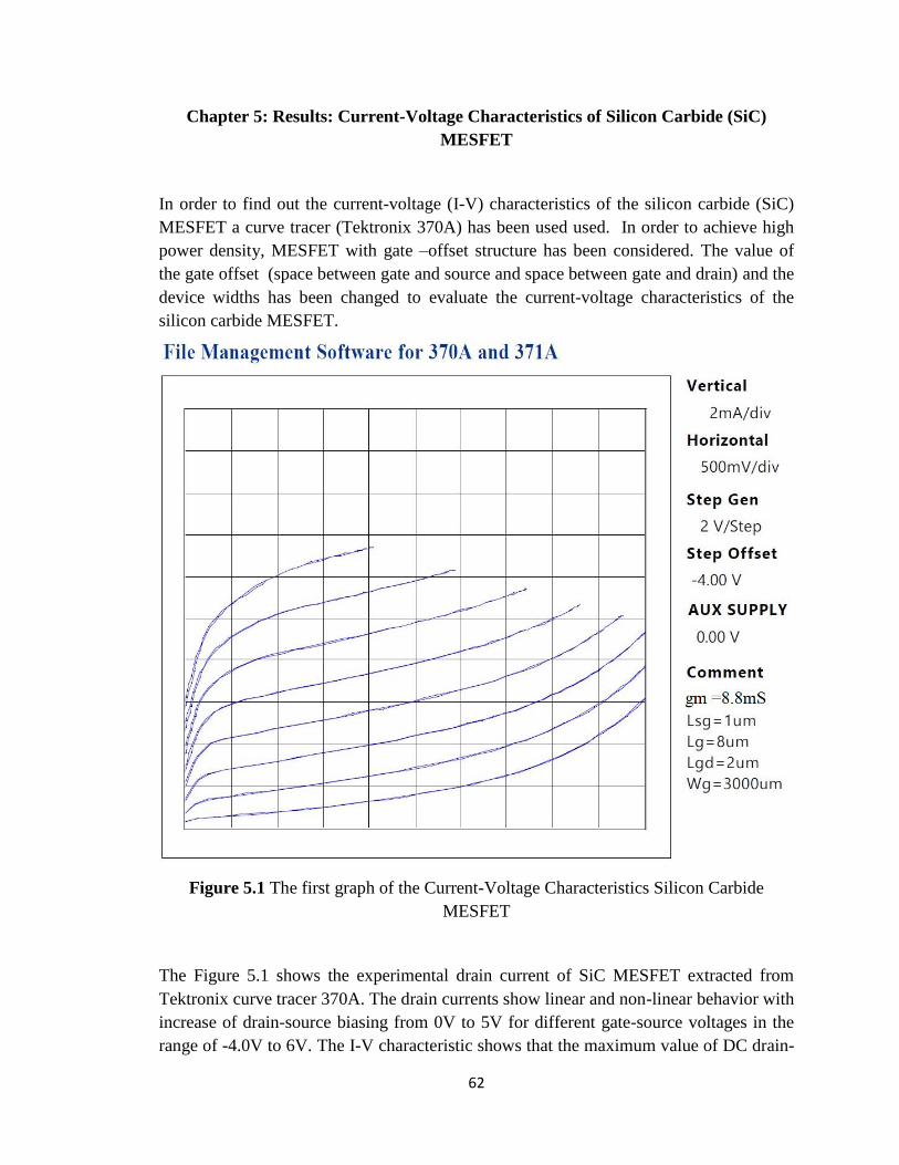
62
Chapter 5: Results: Current-Voltage Characteristics of Silicon Carbide (SiC)
MESFET
In order to find out the current-voltage (I-V) characteristics of the silicon carbide (SiC)
MESFET a curve tracer (Tektronix 370A) has been used used. In order to achieve high
power density, MESFET with gate –offset structure has been considered. The value of
the gate offset (space between gate and source and space between gate and drain) and the
device widths has been changed to evaluate the current-voltage characteristics of the
silicon carbide MESFET.
Figure 5.1 The first graph of the Current-Voltage Characteristics Silicon Carbide
MESFET
The Figure 5.1 shows the experimental drain current of SiC MESFET extracted from
Tektronix curve tracer 370A. The drain currents show linear and non-linear behavior with
increase of drain-source biasing from 0V to 5V for different gate-source voltages in the
range of -4.0V to 6V. The I-V characteristic shows that the maximum value of DC drain-
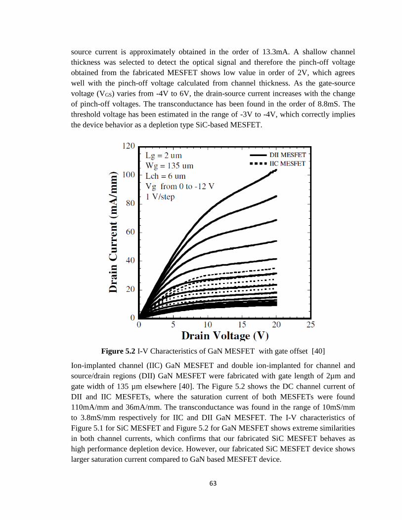
63
source current is approximately obtained in the order of 13.3mA. A shallow channel
thickness was selected to detect the optical signal and therefore the pinch-off voltage
obtained from the fabricated MESFET shows low value in order of 2V, which agrees
well with the pinch-off voltage calculated from channel thickness. As the gate-source
voltage (VGS) varies from -4V to 6V, the drain-source current increases with the change
of pinch-off voltages. The transconductance has been found in the order of 8.8mS. The
threshold voltage has been estimated in the range of -3V to -4V, which correctly implies
the device behavior as a depletion type SiC-based MESFET.
Figure 5.2 I-V Characteristics of GaN MESFET with gate offset [40]
Ion-implanted channel (IIC) GaN MESFET and double ion-implanted for channel and
source/drain regions (DII) GaN MESFET were fabricated with gate length of 2µm and
gate width of 135 µm elsewhere [40]. The Figure 5.2 shows the DC channel current of
DII and IIC MESFETs, where the saturation current of both MESFETs were found
110mA/mm and 36mA/mm. The transconductance was found in the range of 10mS/mm
to 3.8mS/mm respectively for IIC and DII GaN MESFET. The I-V characteristics of
Figure 5.1 for SiC MESFET and Figure 5.2 for GaN MESFET shows extreme similarities
in both channel currents, which confirms that our fabricated SiC MESFET behaves as
high performance depletion device. However, our fabricated SiC MESFET device shows
larger saturation current compared to GaN based MESFET device.
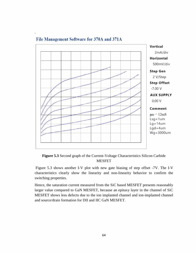
64
.
Figure 5.3 Second graph of the Current-Voltage Characteristics Silicon Carbide
MESFET
Figure 5.3 shows another I-V plot with new gate biasing of step offset -7V. The I-V
characteristics clearly show the linearity and non-linearity behavior to confirm the
switching properties.
Hence, the saturation current measured from the SiC based MESFET presents reasonably
larger value compared to GaN MESFET, because an epitaxy layer in the channel of SiC
MESFET shows less defects due to the ion implanted channel and ion-implanted channel
and source/drain formation for DII and IIC GaN MESFET.
65
Chapter 6: Conclusion
The Silicon Carbide (SiC) MESFET device with different gate length has been
fabricated. Different process steps including photoresist processing, etching processing,
ion implantation process for source and drain formation, electrical device isolation by ion
implantation, high temperature annealing, silicon oxide growth on silicon face of SiC and
silicon oxide process technology development, nickel and indium tin oxide deposition for
ohmic and Schottky contacts have been studied. The developed process technology and
design of MESFET device were considerably accurate and therefore a single SiC wafer
was used for fabrication of SiC based MESFET device with high saturation current. I-V
characteristics of fabricated SiC MESFET clearly demonstrated the linearity and non-
linearity properties to offer high speed switching performance. The fabricated SiC
MESFET device showed the channel current and transconductance in the order 13.3mA
and 8.8mS respectively. Other fabricated GaN MESFET demonstrated the channel
current and transconductance in the order 110mA/mm and 10mS respectively. Hence, the
saturation current measured from the SiC based MESFET shows reasonably higher value
compared to GaN MESFET. The results of fabricated SiC shows very promising for high
power RF amplifier, which has tremendous impact on future research scope.
66
Reference
[1] W. J. Schaffer, G. H. Negley, K. G. Irvine, and J. W. Palmour, “Conductivity
anisotropy in epitaxial 6H and 4H SiC,” in Diamond, Sic, and Nitride Wide Bandgap
Semiconductors, C.H. Carter, Jr., G. Gildenblatt, S. Nakamura, and R.J. Nemanich,
Eds., Material Research Society Proc., vol. 339. Pittsburgh, PA: MRS, 1994, pp. 595-
600.
[2] Baliga, B.J., “Power Semiconductor Devices for Variable-Frequency Drives,”
Proceedings of the IEEE 82(8), 1112, 1994.
[3] Careles E. Weitzel, IEEE Electron Dev. Lett. 16, 451 (1995).
[4] J. Jung, H. P. Park, J. Park, H. Park, K. Bae, D. Shin, N. J. Song and J. Burm, J.
Korean Phys. - 60 - Soc. 40, 58 (2002).
[5] J. I. Roh, K. S. Lee, S. H. Lee, K. S. Nahm, K. C. Kim, and K. Y. Lim, J. Korean
Phys. Soc. 43, 96 (2003).
[6] C. Codreanu, M. Avram, E. Carbunescu and E. Iliescu, Materials Science in
Semiconductor Processing 3, 137 (2000).
[7] S.E. Saddow, A. Agarwal (editors), "Advances in Silicon Carbide Processing and
Applications ", Artech House Inc., Boston 2004.
[8] B Luo, et la “56 W SiC MESFET Transistor with > 50% PAE for L-band
Applications”
[9] Henry, H.G. et la “S-band operation of SiC power MESFET with 20 W (4.4 W/mm)
output power and 60% PAE” Electron Devices, IEEE Transactions on Volume: 51,
Issue: 6, 839 – 845
[10] S.T.Allen , et la “SILICON CARBIDE MESFET’s WITH 2 Wlmm AND 50%
P.A.E. AT 1.8 GHz” pages 681 – 684
[11] Yeong-Lin Lai, et la” High-Efficiency and Low-Distortion Directly- Ion-Implanted
GaAs Power MESFET’s for Digital Personal Handy-Phone Applications” IEEE
67
ELECTRON DEVICE LETTERS, VOL. 18, NO. 9, SEPTEMBER 1997
[12]. Binari S C, Dietrich H B, Kelner G, Rowland L B, Doverspike K and Gaskill D K
1994 Electron. Lett. 30 909
[13] J. Baliga, Fundamentals of Power Semiconductor Devices. New York, Springer,
2008.
[14]. R. J. Trew, SiC and GaN transistors - Is there one winer for microwave power
applications Proceedings of the IEEE, vol. 90, pp. 1032–1047, June 2002.
[15] R. Borges, Gallium nitride electronic devices for high-power wireless applications,
RF Design, pp. 72–82, Sept. 2001.
[16] N. Vellas, C. Gaquière, A. Minko, V. Hoël, J. C. D. Jaeger, Y. Cordier, and F.
Semond, Power results at 4 GHz of AlGaN/GaN HEMTs on high resistivity silicon
(111) The substrate,IEEE Microwave and Wireless Components Letters, vol. 13,
no. 3, pp. 99–101, Mar. 2003.
[17] ATIP07.033: GaN Amplifiers for RF Communications in Japan - ATIP Document
ID: 071010R
[18]. R. Gaska, M. Asif Khan, X. Hu, G. Simin, and J. Yang – GaN-based MESFETs and
DC- MOSFETs Device Research Conference, 2000. Conference Digest. 58th DRC
[19] S. Müller, K. Köhler, R. Kiefer, R. Quay, M. Baeumler, and L. Kirste- Growth of
AlGaN/GaN-based electronic device structures with semi-insulating GaN buffer
and AlN interlayer- 2005 WILEY-VCH Verlag GmbH & Co. KGaA, Weinheim
[20] Tzu-Jin Yeh, Yi-Jen Chan and Tien-Huat, Ion-implanted GaAs MESFET's with
W/WNx Bi-layer Gate Designs - Gan EDMS'94
[21] Sebastien Nuttinck, Edward Gebara, Joy Laskar, Study of Self-Heating Effects,
Temperature-Dependent Modeling, and Pulsed Load–Pull Measurements on GaN
HEMTs – IEEE TRANSACTIONS ON MICROWAVE THEORY AND
TECHNIQUES, VOL. 49, NO. 12, DECEMBER 2001
[22] Ryu, S. -H., et al., “1800V NPN Bipolar Junction Transistors in 4H-SiC,” IEEE
68
Electron Device Letters, Vol. 22, No. 3, pp. 124–126, 2001.
[23] Palmour, J. W., et al., “6H-Slicon Carbide Power Devices for Aerospace
Applications,” Proc. of the 28th Intersociety Energy Conversion Engineering
The conference, American Chem. Soc., Vol. 1, pp. 249–254, 1993.
[24] Agarwal, A. K., et al., “Power Amplification in UHF Band Using SiC RF Power
BJTs,” Proc. of the 4th European Conference on Silicon Carbide and Related
Materials, Linköping, Sweden, September 2–5, 2002, Mat. Sci. Forum, Vols. 433–
436, pp. 785–788, 2003.
[25] Streetman, Ben. Solid State Electronic Devices. Englewood Cliffs, N.J.: Prentice-
Hall, pp.1,1990.
[26] J. B. Casady and R. W. Johnson, "Status of silicon carbide (SiC) as a wide-band gap
semiconductor for high-temperature applications: A Review, Solid State Electronics,
vol. 39, pp. 1409 (1996).
[27] R. Han, X. Hu, N. Yu, J. Wang, Y. Tan, and W. Huang, Development of bulk SiC
the single crystal is grown by physical vapor transport method, Optical Materials,
vol. 23, pp. 415 (2003).
[28] Sorab K. Ghandi. VLSI Fabrication Principles: Silicon and Gallium Arsenide, 2nd
Edition. New York: John Wiley & Sons, Inc., 1994.
[29] Y. Iwasaki, H. Yano, T. Hatayama, Y. Uraoka, T. Fuyuki, Mater. Sci. Forum645–
648 (2010) 503.
[30] T. Iida, Y. Tomioka, K. Yoshimoto, M. Midorikawa, H. Tukada, M. Orihara,
Y. Hijikata, H. Yaguchi, M. Yoshikawa, H. Itoh, Y. Ishida, S. Yoshida, Jpn. J.
Appl.Phys. 41 (2002) 800. - 66
[31] The data sheet of MICROPOSIT S1800 Series Photo Resists by Shipley.
[32] The data sheet of MICROPOSIT MF CD-26 developer by Shipley.
[33] The Technical data of the BOE: buffer oxide etching by General chemicals.
[34] A Physics-Based Model for Fast Recovery Diodes with Lifetime Control and
69
Emitter Efficiency Reduction by Chengjie Wang, Li Yin, and Chuanmin Wang
[35] Choyke, W.J., Patrick, L. Luminescence of Donor-Acceptor Pairs in Cubic SiC.
Phys. Rev. B 2 (1970) 4959.
[36] Goldberg Yu., Levinshtein M.E., Rumyantsev S.L. in Properties of Advanced
Semiconductor Materials GaN, AlN, SiC, BN, SiC, SiGe. Eds. Levinshtein M.E.,
Rumyantsev S.L., Shur M.S., John Wiley & Sons, Inc., New York, 2001, 93-148.
[37] Mickevicius, R., J.H. Zhao, Monte Carlo study of electron transport in SiC. J. Appl.
Phys. 83, 6 (1998), 3161-3167.
[38] Characteristics of Offset-Structure Polycrystalline-Silicon Thin-Film Transistors by
keiji tanaka
[39] R. Quay, Gallium nitride Electronics, Springer, ISBN: 978-3-549-71890-1
[40] K. Nomoto, N. ITO, T. Tajima, et al, “Double-ion implanted GaN MESFETs with
extremely low source/drain resistance”, Mater. Res. Soc. Symp. Proc., Vol. 892,
0892-FF13-06.1, 2006