Embed Size (px)
Citation preview
AUTOMATIC STUDENT ATTENDANCE REGISTRATION
USING RADIO FREQUENCY IDENTIFICATION (RFID)
by
Rengith Baby Kuriakose
Dissertation submitted in fulfilment of the requirements for the degree
Magister Technologiae: Engineering: Electrical
in the
School of Electrical and Computer Systems Engineering
of the
Faculty of Engineering, Information and Communication Technology
of the
Central University of Technology, Free State
Supervisor: Prof. Farhad Aghdasi, PhD
Co-supervisor: Andrew Sibanda

i
DECLARATION OF INDEPENDENT WORK
I, RENGITH BABY KURIAKOSE, hereby declare that this research project, submitted for the
degree Magister Technologiae: Engineering: Electrical, is my own independent work and has
not been submitted before to any institution by me or anyone else as part of any qualification.
09-03-2010
……………………………………………… ………………………..
Student’s signature Date

ii
ACKNOWLEDGEMENTS
I would like to take this opportunity to acknowledge and extend my heartfelt gratitude to the
following persons who have made the completion of this thesis possible:
Prof Farhad Aghdasi who supervised my thesis.
A special mention of thanks to Andrew Sibanda, Lecturer in the Electrical and Computer
systems Engineering faculty, C.U.T, Free State, for being my co-supervisor at the later stage of
my work. Thank you for sitting with me, dedicating your time and effort in rectifying my
thesis.
The Central University of Technology, Free State and the Innovation Fund who have provided
fiscal and material support for my research
Prof. Barnabas Gatsheni, Riaan Van Der Walt, Dion De Beer (FABLAB, Free State), N
Moshoshoe, K Katiso, Libe Massawe, and P Veldtsman who have all assisted me at some point
during this project with advice and expertise.
My parents, Mr Baby Kuriakose and Mrs Lissy Baby who were a constant source of inspiration
and motivation during some very difficult personal and professional times over the course of
this thesis.
Lastly, but most importantly, I would like to thank God Almighty for giving me the
opportunity to start, progress and complete my research.
iii
ABSTRACT
The main aim of this research was to automate student attendance registration, thereby
reducing human involvement in the whole process. This was made possible using Radio
Frequency Identification (RFID) technology.
The Central University of Technology uses student cards that are compatible for use with
RFID technology. As a result, no initial investment (except for the existing personal
computer’s and the constructed RFID reader) in infrastructure was required for this project.
The basic working of the project was as follows. The students belonging to a specific class had
their vital educational data (Student number, Name) entered into a database table at the time of
registration. A student card containing a serial number, with reference to the data contained in
the database table, was given to the students after registration.
The students walk into their respective classes and scan their student cards with the RFID
reader. The serial number stored in the student card is transferred to the reader and from there
wirelessly to the main server using ZigBee technology. In the main server, using Java
programming language, the card serial number is sent to the Integrated Development
Environment (IDE). In this project the Netbeans IDE (Java platform) was used.
The Netbeans IDE is connected to the Apache Derby database using Java Database Connector
(JDBC), so the serial number (which is referenced to the educational data of the students) from
the student card is automatically compared with the original database created at the time of

iv
registration. Once a match is confirmed between the two entries, the data is entered into a
separate database table which serves as the basic attendance sheet for a specific day.

v
TABLE OF CONTENTS
DECLARATION OF INDEPENDENT WORK........................................................................i
ACKNOWLEDGEMENTS...................................................................................................... ii
ABSTRACT............................................................................................................................. iii
LIST OF FIGURES ..................................................................................................................xi
LIST OF TABLES...................................................................................................................xv
LIST OF ABBREVIATIONS.................................................................................................xvi
PART 1 ......................................................................................................................................1
CHAPTER 1 INTRODUCTION .........................................................................................1
1.1 Scope of the Research ………………………………………………………………….2
1.2 Research Objectives ………………………………………………………………….2
1.2.1 Hypothesis..........................................................................................................2
1.2.2 Corollary ............................................................................................................3
1.3 Structure of the Thesis …………………………………………………………3
PART 2 ......................................................................................................................................5
CHAPTER 2 LITERATURE SURVEY..............................................................................5
2.1 Current Procedure for Attendance Registration …………………………………5
2.2 Challenges Facing the Current System …………………………………………5
2.2.1 Tedious Procedure .............................................................................................6
2.2.2 Errors on the Part of Students and Lecturers .....................................................6
2.2.3 Not Foolproof.....................................................................................................6
2.2.4 Loss of Data .......................................................................................................7
2.2.5 Neglect ...............................................................................................................7
2.3 Automatic Student Attendance Registration Systems ………………………….7
vi
2.3.1 Barcode Systems................................................................................................7
2.3.2 Biometric Scanning (Dactyloscopy) ..................................................................8
2.3.3 Smart Card Systems...........................................................................................9
2.3.4 Radio Frequency Identification Systems .........................................................10
2.4 Comparison between Various Automatic Identification Systems…………………. 11
2.5 Introduction to Radio Frequency Identification (RFID) Technology ………………..12
2.5.1 RFID Tags........................................................................................................13
2.5.1.1 Types of tag constructions…………………………………………………. 14
2.5.2 RFID Reader ....................................................................................................15
2.5.2.1 Types of RFID readers……………………………………………………... 18
2.5.3 RFID Middleware ............................................................................................22
2.5.4 Physics behind RFID .......................................................................................25
2.5.4.1 Magnetic field strength……………………………………………………. 25
2.5.4.2 Path of field strength h(x) in a conductor loop……………………………. 27
2.5.4.3 Magnetic flux (Φ)………………………………………………………….. 28
2.5.4.4 Inductance…………………………………………………………………. 29
2.5.4.5 Mutual inductance (M)…………………………………………………….. 30
2.5.4.6 Faraday’s law………………………………………………………………. 34
2.5.4.7 Resonance……………………………………………………………….. 37
2.5.4.8 Interrogation field strength HMIN………………………………………………………………… 39
2.5.4.9 Energy range of transponder systems……………………………………… 42
2.5.4.10 Interrogation zone of readers………………………………………. 43
2.5.5 Operation of RFID ...........................................................................................44
2.5.5.1 Communication modes in RFID…………………………………….. 44
2.5.5.2 Types of modulation used in RFID……………………………………. 47
vii
2.5.5.3 Data coding in RFID……………………………………………………. 50
2.5.5.4 Coupling mechanisms in RFID…………………………………………….. 53
2.5.6 Collision and Anti-Collision Procedures in RFID......................................... 56
2.5.6.1 Reader anti-collision algorithm……………………………………………. 57
2.5.6.2 Tag anti-collision algorithms ………………………………………………..59
2.5.7 Frequency Ranges used in RFID .....................................................................67
2.5.7.1 Standardisation in RFID…………………………………………….. 68
2.5.7.2 Container identification……………………………………………………. 75
2.5.7.3 Item management…………………………………………………………. 75
2.5.8 Data Integrity in RFID.....................................................................................75
2.5.8.1 Parity checking method…………………………………………………….. 76
2.5.8.2 Longitudinal Redundancy Check (LRC) procedure……………………….. 77
2.5.8.3 Cyclic Redundancy Check (CRC) procedure……………………………… 79
2.5.9 Security in RFID..............................................................................................79
2.5.9.1 Security threats in RFID…………………………………………………… 79
2.5.9.2 Overcoming security threats in RFID……………………………………… 79
2.6 Need for Wireless Link between RFID Reader and RFID Middleware…………… 86
2.7 Comparison between Wireless Technologies . ………………………………………88
2.8 ZigBee Technology………………………………………………………………… 88
2.8.1 Components of a ZigBee System.....................................................................89
2.8.1.1 ZigBee coordinator………………………………………………………… 89
2.8.1.2 ZigBee router……………………………………………………………… 89
2.8.1.3 ZigBee end device…………………………………………………………. 91
2.8.2 Network Topologies in ZigBee Technology....................................................92
2.8.2.1 Star topology……………………………………………………………….. 92
viii
2.8.2.2 Peer-to-peer topology………………………………………………………. 93
2.8.2.3 Tree topology ……………………………………………………………… 94
2.8.3 The ZigBee Stack.........................................................................................…95
2.8.4 The IEEE 802.15.4 Standard ...........................................................................96
2.8.4.1 Physical layer ………………………………………………………………..97
2.8.4.2 Media Access Control (MAC) layer ……………………………………… 98
2.8.5 The ZigBee Standard .....................................................................................101
2.8.5.1 Network layer ……………………………………………………………….101
2.8.5.2 Application layer ……………………………………………………….102
2.8.6 Security Issues and Solutions in ZigBee Technology....................................103
2.9 Software Section ……………………………………………………………….104
2.9.1 The Components of RFID Middleware .........................................................104
2.9.2 Programming Concept ...................................................................................106
2.9.3 JDBC Concepts..............................................................................................107
2.9.4 The JAVA.SQL Package ...............................................................................108
2.9.4.1 Connection with database ……………………………………………….108
2.9.4.2 Sending SQL parameters to a database ……………………………….109
2.9.4.3 Updating and retrieving results of an SQL query …………………… ..109
2.9.4.4 Metadata object ……………………………………………………….109
2.9.4.5 Exceptions ……………………………………………………………….109
2.9.5 SQL Concepts ............................................................................................. 110
2.9.6 SQL statements and their syntax....................................................................112
2.9.6.1 SQL CREATE table statement ……………………………………….112
2.9.6.2 SQL INSERT INTO statement ………………………………………..113
2.9.6.3 SQL SELECT statement ………………………………………………...114
ix
2.9.6.4 SQL UPDATE statement ……………………………………………….115
2.9.6.5 SQL DELETE statement ……………………………………………….116
CHAPTER 3 RESEARCH STRUCTURE ......................................................................117
3.1 Hardware Section ………………………………………………………………118
3.1.1 RFID Tags......................................................................................................118
3.1.2 RFID Reader ..................................................................................................120
3.1.2.1 Programming the reader module……………………………………. 122
3.1.3 Anti-collision in the RFID Reader……………………………………… 128
3.1.4 Antennna........................................................................................................129
3.1.4.1 Circuit diagram for the antenna ………………………………………130
3.1.4.2 Design of antenna components ……………………………………….131
3.1.4.3 Antenna design ……………………………………………………….134
3.1.4.4 Antenna construction ……………………………………………………….135
3.2 Wireless Section ……………………………………………………………….141
3.2.1 Selecting ZigBee Modules.............................................................................141
3.2.2 The X-Bee ZigBee Module............................................................................142
3.2.3 The X-Bee RF Interface Module ...................................................................144
3.2.4 Setting up the X-Bee Module with the RFID reader .....................................146
3.2.5 Setting up the X-Bee Module and RFID middleware....................................147
3.3 Software Section ……………………………………………………………….149
3.3.1 Creating Database Tables using Apache Derby Database………………….. 151
3.3.2 Java Programming .........................................................................................152
CHAPTER 4 RESULTS……………………………………………………………………154
4.1 Hardware setup…………………………………………… ………….. ………...153
4.2 Hardware Testing....................................................................................................155
x
4.2.1 Testing of the antenna ………………………………………………………155
4.2.2 RFID reader Testing ……………………………………………………….156
4.2.3 Reader range Testing ……………………………………………………….158
4.3 Wireless Testing.....................................................................................................159
4.3.1 X-Bee module range testing ……………………………………………………….159
4.4 Software Testing………………………………………………………………….162
CHAPTER 5 CONCLUSION AND FUTURE WORK ..................................................169
REFERENCES………………………………………………………………………..…….173
APPENDIX A: Hardware specification of the reader module ........................................174
APPENDIX B: PIN numbers of the reader module ........................................................177
APPENDIX C: External connection to the reader module .............................................181
APPENDIX D: EEPROM memory organisation ............................................................184
APPENDIX E: X-Bee module specifications .................................................................185
APPENDIX F: X-Bee module PIN configuration ..........................................................186
APPENDIX G: Java program..........................................................................................187
xi
LIST OF FIGURES
Figure 2.1: Physical layout of a glass tube transponder .....................................................14
Figure 2.2 Smart label next to a pen top to show its size ..................................................15
Figure 2.3 Physical components of RFID………………………………………………. 16
Figure 2.4: The antenna energises a tag when it comes within
read range and the tag transmits its data ..........................................................17
Figure 2.5: RFID reader operating with two antennas.......................................................18
Figure2.6: Forklift carrying RFID-tagged items though an RFID portal..........................19
Figure 2.7: RFID tunnel with tagged goods on a conveyor belt ........................................20
Figure 2.8: Handheld RFID reader.....................................................................................20
Figure 2.9: Stationery RFID reader and a tag.....................................................................21
Figure 2.10: Components of RFID middleware...................................................................22
Figure 2.11: Raw data and application relevance at different levels ....................................
of RFID m.idleware…………………………………………………..………24
Figure 2.12: Current I flowing through a straight conductor creating a
magnetic field with strength H.........................................................................26
Figure 2.13: RFID antenna and magnetic field ....................................................................27
Figure 2.14: Inductance in a current-carrying metal conductor ...........................................30
Figure 2.15: Mutual inductance M21 .....................................................................................32
Figure 2.16: Faraday’s law applied to a metal conductor ....................................................34
Figure 2.17: Equivalent circuit for a reader and a tag ..........................................................35
Figure 2.18: Equivalent circuit for an RFID tag circuitry ....................................................38
Figure 2.19: Effective circuit diagram of an inductively coupled
RFID system with the addition of parallel and parasitic capacitors ................39
xii
Figure 2.20: Reader range for different tag positions...........................................................44
Figure 2.21: Full duplex system...........................................................................................45
Figure 2.22: Half duplex operation. Note the data transmission
interval between the tag and the reader............................................................46
Figure 2.23: Sequential mode of communication.................................................................47
Figure 2.24: ASK mixer .......................................................................................................48
Figure 2.25: Data coding techniques ....................................................................................51
Figure 2.26: Multi-access procedures in RFID systems.......................................................57
Figure 2.27: Reader with electronically controlled directional antenna...............................58
Figure 2.28: FDMA procedure.............................................................................................59
Figure 2.29: Flowchart of simple ALOHA procedure .........................................................61
Figure 2.30: Functioning of simple ALOHA procedure ......................................................62
Figure 2.31: Flow chart of slotted ALOHA procedure ........................................................64
Figure 2.32: Functioning of slotted ALOHA procedure......................................................65
Figure 2.33: Binary search algorithm for a tag with 5-bit ID...............................................66
Figure 2.34: Field strength curve for a proximity integrated circuit card ............................72
Figure 2.35: Parity checking method using sample data 1100 0110....................................77
Figure 2.36: Faraday cage ....................................................................................................81
Figure 2.37: Data flow from the ZigBee coordinator to the end device through a router....92
Figure 2.38: Star topology....................................................................................................93
Figure 2.39: Peer-to-peer technology ...................................................................................94
Figure 2.40: Tree topology ...................................................................................................95
Figure 2.41: The ZigBee stack .............................................................................................96
Figure 2.42: The different frequency ranges in the physical
layer of the IEEE 802.15.4 standard ................................................................98
xiii
Figure 2.43: MAC super-frame ............................................................................................99
Figure 2.44: Components of the ZigBee application layer.................................................103
Figure 2.45: JDBC architecture..........................................................................................108
Figure 3.1: Memory organisation of the SR176 RFID tag...............................................119
Figure 3.2: Serial number of the SR176 tag .....................................................................120
Figure 3.3: Lock byte of the SR176 tag ...........................................................................120
Figure 3.4: The ACG HF Multi ISO reader module ........................................................121
Figure 3.5: Circuit diagram for connecting the reader module to the computer ..............124
Figure 3.6: Baud rate control registry...............................................................................125
Figure 3.7: Baud rate settings...........................................................................................125
Figure 3.8: OPMODE register..........................................................................................126
Figure 3.9: PCON2 registry..............................................................................................128
Figure 3.10: Equivalent circuit diagram for the reader antenna.........................................130
Figure 3.11: Equivalent circuit for an antenna that only reads ISO 14443B tags ..............131
Figure 3.12: Antenna circuit indicating the values of components ....................................134
Figure 3.13: Correlation between read range and antenna diameter ..................................135
Figure 3.14: The Roland Modela MDX-20........................................................................136
Figure 3.15: Screenshot of new schematic in Eagle software............................................137
Figure 3.16: Adding components on the schematic page...................................................138
Figure 3.17: Schematic of the antenna in Eagle software ..................................................139
Figure 3.18: Board schematic of the antenna .....................................................................140
Figure 3.19: Antenna constructed using the Roland Modela MDX-20..............................141
Figure 3.20: X-Bee communication link between reader and computer............................143
Figure 3.22: Internal configuration of X-Bee module........................................................143
Figure 3.23: The RF interface module and its parts ...........................................................145
xiv
Figure 3.24: Pin J5 of the RF interface board ....................................................................146
Figure 3.25: The jumper settings for X-Bee as DCE .........................................................146
Figure 3.26: Experimental set-up of the RFID reader with X-Bee module .......................147
Figure 3.27: The jumper settings for X-Bee as DTE.........................................................148
Figure 3.28: Experimental set-up of X-Bee module to computer ......................................148
Figure 3.29: Flowchart explaining the software section………………………………….148
Figure 3.30: The ‘admin’ database table ............................................................................151
Figure 3.31: The ‘attendee’ database table.........................................................................152
Figure 4.1: Schematic showing Hardware setup of the RFID reader and Host…............154
Figure 4.2: Fine tuning antenna operating frequency with an oscilloscope.....................156
Figure 4.3: Hyper-terminal settings..................................................................................157
Figure 4.4: Hyper-terminal output after scanning a student card.....................................157
Figure 4.5: Reader range testing (note the range is about 35 mm in this test) .................158
Figure 4.6: Graphical representation of read strength of the RFID reader
with respect to the distance between the Reader and the tag………… 158
Figure 4.7: Hardware set-up for X-Bee module range testing .........................................160
Figure 4.8: X-CTU window screen shot...........................................................................161
Figure 4.9: The range test window of X-CTU software...................................................162
Figure 4.10: Admin database table created for test group…….…………………………..163
Figure 4.11: The attendee database table…………………………….……………………164
Figure 4.12: Attendee database table for 21-01-2008…………………………………….165
Figure 4.13: Attendee database table for 28-01-008……………………………..……….166
Figure 4.14: Attendee database table for 04-02-2008………..………………..………….166
Figure 4.15: Attendee database table for 11-02-2008…………..…………..…………….167
Figure 4.16: Attendance of a student during test period…..……………………...……….168

xv
LIST OF TABLES
Table 2.1: Comparison between different automatic identification systems ....................12
Table 2.2: Frequency ranges used in RFID.......................................................................67
Table 2.3: Data transfer parameters between reader and smart card ................................73
Table 2.4: Modulation and coding procedures for data transfer
etween smart card and reader...........................................................................73
Table 2.5: Modulation and coding procedures for data transfer
between reader and card...................................................................................74
Table 2.6: Modulation and coding procedures for data
transfer between smart card and reader ........................................................74
Table 2.7: Comparison between wireless technologies....................................................88
Table 2.8: Features of the three frequency bands .............................................................98
Table 2.9: ‘Students’ table with three columns and three entries for the columns .........111
Table 2.10: Example of database table .............................................................................112
Table 2.11: The result for INSERT INTO statement........................................................114
Table 2.12: Result of the SELECT student number FROM students statement...............115
Table 2.13: The updated ‘students’ table ..........................................................................116
Table 2.14: ‘Students’ table with data of John deleted .....................................................116
Table 3.1: Write command in an ACG reader module ...................................................122
Table 3.2: Responses to a write command......................................................................122
Table 3.3: Write command example ...............................................................................123
Table 3.4: Delay and corresponding hexadecimal value ................................................127

xvi
LIST OF ABBREVIATIONS
ASK - Amplitude Shift Keying
CAP - Contention Access Period
CRC - Cyclic Redundancy Check
CSMA - Carrier Sense Multiple Access
CSMA-CA - Carrier Sense Multiple Access with Collision Avoidance
DCE - Data Communication Equipment
DTE - Data Terminal Equipment
EAN - European Article Number
EEPROM - Electrically Erasable Programmable Read-only Memory
FDMA - Frequency Division Multiple Access
FSK - Frequency Shift Keying
GTS - Guaranteed Time Slot
ICASA - Independent Communication Authority of South Africa
IDE - Integrated Development Environment
ISM - Industrial, Scientific and Medical band
JDBC - Java Data Base Connectivity
LRC - Longitudinal Redundancy Check
MAC - Media Access Control
NRZ - Non-Return to Zero (Data coding technique)
PAN - Personal Area Network
PSK - Phase Shift Keying
RAM - Random Access Memory
RFID - Radio Frequency Identification
ROM - Rea- Only Memory
SDMA - Space Division Multiple Access
TDMA - Time Division Multiple Access
UART - Universal Asynchronous Receiver Transmitter
VRC - Vertical Redundancy Check (Parity checking method)
WLAN - Wireless Local Area Network
1
PART 1
CHAPTER 1 INTRODUCTION
The monitoring and registration of attendance in any educational institution is an important
but often neglected procedure. Distribution of attendance sheets, getting them filled in by the
students, safekeeping of the sheets and finally entering the information into a central database
system is an essential but painstaking process. The abovementioned factors, coupled with the
main responsibility of the lecturers, namely lecturing and evaluating answer scripts, can
undermine the important role that attendance registration plays in any educational institution.
The use of technology in attendance registration has evolved at a slower pace than the
corresponding growth in other areas of educational institutions, such as the use of projectors
and e-education [1], to name only a few.
The tight schedules of lecturers and the need to reduce the paperwork involved in manual
attendance registration require an innovative solution to improve the monitoring of student
participation in an educational institution. The use of Radio Frequency Identification (RFID)
technology to automate attendance registration is presented in this thesis as a possible
solution to the challenge posed here.
However, the consideration and adoption of RFID technology as a possible solution has been
slow. This is due to various factors, notably the sophistication of the technology itself.
However, an important criticism of RFID technology is the question of the cost of developing
an efficient solution.
2
The objections mentioned in the paragraph above have been overcome to a small extent by a
number of salient developments in the field of RFID technology in the recent past. The use of
RFID technology in access control [2] and the retail shopping sector [3] have considerably
decreased the costs of major elements of RFID technology [4]. These developments have also
helped to give much-needed exposure to RFID technology.
RFID is a technology that is capable of transferring data from one end of the communication
link to the other with minimal human intervention [5, p.10]. This aspect of RFID technology
is perceived as a critical element that will assist in finding a solution.
1.1 Scope of the Research
In this research, the Central University of Technology, Free State, was used as a basis for
defining the problem and finding a solution. A solution is given at the end of this thesis
which extended as solution to other educational institutions facing similar challenges.
1.2 Research Objectives
The main objective of this research is the automating of the student attendance register using
RFID technology. The thesis guides the reader through the step-by-step procedure that was
used to arrive at a cost-effective solution to automate the student attendance register.
1.2.1 Hypothesis
The hypothesis of this research is that RFID technology is a growing trend worldwide which
allows the transfer of data from one end to the other with the minimum of human

3
intervention, and that this same technology can be used to automate a student attendance
register.
1.2.2 Corollary
How the hypothesis mentioned in Section 1.2.1 can be practically implemented forms the
basis of the corollary. A step-by-step explanation is given in Section 3 which details how the
challenge was addressed and overcome.
1.3 Structure of the Thesis
This thesis is divided into four parts comprising five chapters. Part 1 contains Chapter 1 -
Introduction. This part of the thesis gives a general overview of the problem and a possible
solution to the challenges posed by RFID technology.
Part 2 consists of Chapter 2 - Literature Survey. This part of the thesis examines the various
elements that require further study in order to understand the different challenges mentioned
in Chapter 1 (Section 2.1). This Chapter also examines the different technologies available to
solve the problem (Section 2.3). It then goes on to discuss RFID technology in detail (Section
2.5). It will become clear that RFID technology alone cannot solve the problem on hand. As a
result, wireless technologies such as ZigBee technology (Section 2.8) and data manipulation
techniques are discussed in this chapter (Section 2.9).
Part 3 comprises Chapters 3. Chapter 3 - Research Structure is divided into three sections:
the Hardware section (Section 3.1), the Wireless section (Section 3.2) and the Software

4
section (Section 3.3). This is the main part of the thesis as it presents the solution to the
problem explained in Section 2.1.
Part 4 comprises of Chapter 4 and Chapter 5
Chapter 4 – Results. This section looks at the different tests that were done during the course
of the project and their results. This chapter holds up the bulk of research that was mention in
Chapter’s 2 and 3.
Chapter 5 Conclusion and Future work. Concludes the thesis by examining some of the
challenges that arose during the research for the solution. This part also investigates certain
areas which were outside the scope of this research but nevertheless are worth further
research by other people with access to this thesis.

5
PART 2
CHAPTER 2 LITERATURE SURVEY
This part describes the background study that was done prior to starting the practical work on
the project.
2.1 Current Procedure for Attendance Registration
During class hours in an educational institution, the lecturer in charge of the class distributes
an attendance list to the students. The attendance list contains the names and student numbers
of the students. Each student signs against his/her name on the attendance list.
At the end of the lecture period, the lecturer takes the attendance list from the students and
enters the details into his/her computer. This process is repeated by the lecturer for every
class taken during the academic term.
At the end of the academic term the lecturer tabulates the attendance of each student. This is
done by dividing the number of classes attended by a student by the total number of working
days in the academic year. This process is repeated for every class the lecturer is in charge of.
2.2 Challenges Facing the Current System
The current system discussed in Section 2.1 poses some challenges which are discussed in
detail in the following sections.

6
2.2.1 Tedious Procedure
The main aim of the project, as discussed in the introduction in Chapter 1, is to relieve the
teaching and non-teaching staff of avoidable and often tedious paperwork. With the current
system, the lecturers first have to manually enter the attendance of each class daily. Next, the
tabulation involves a lot of attendance calculations for the lecturer. This is not the only work
for which the lecturer has a deadline - s/he must also set examination papers, mark answer
sheets, etc.
2.2.2 Errors on the Part of Students and Lecturers
When the attendance list is passed around the classroom, some of the students forget to sign
or sign for another student. The lecturer may also forget to bring the attendance list. These
may be minor problems on the scale of things, but they complicate the current procedure.
2.2.3 Not Foolproof
One of the major drawbacks of the current system is that it can easily be cheated. The
students may sign as proxy for their friends who are not present in the classroom when the
attendance list is being filled in. This may not be noticed by the lecturer who is busy giving a
lecture.
A manual head count and comparison with the attendance list is a way around this problem,
but more often than not this is not practical. Even if this is possible, it makes the entire
process more tedious.

7
2.2.4 Loss of Data
There is an immense amount of material on paper in any lecturer’s office at any given time,
and it is very easy to loose track of the attendance lists. The problems will be compounded if
the information has not been entered into a computer. With the current method used for
attendance registration, it is easy to misplace an attendance list.
2.2.5 Neglect
The current system is monotonous and tedious as mentioned in Section 2.2.1. In time this
may lead to neglect on the part of the lecturer. An important responsibility thus gets
neglected. Neglect of the attendance registration procedure will undermine its importance.
2.3 Automatic Student Attendance Registration Systems
This section examines some of the technologies available for meeting the challenges
mentioned in Section 2.2. These are the following:
Barcode systems
Biometric systems
Smart card systems
RFID systems.
2.3.1 Barcode Systems
Barcode technology is widely used in the retail shopping sector [6, p.6]. It is a very cheap and
simple technology. It is a binary code comprising fields of bars and gaps arranged in a
parallel configuration. The bars and gaps are arranged in a predetermined pattern and
represent a symbol.

8
Despite appearing identical, there are considerable differences between each barcode. This is
the result of the different coding techniques used in the design. The European Article Number
(EAN) is the most common type of coding used for designing barcodes [7, p.2]. A barcode
has a data density of 100 bytes.
Barcodes are usually read with optical scanners. The different reflections of a laser beam
from the black bars and the white gaps assist in interpreting the bars and graphs on a barcode
numerically and alphanumerically. The optical scanner has to be placed very close (10-50
cm) and in the line of sight of the barcode for data to be read from it.
A barcode system could have been an ideal replacement for the current manual system
because barcode systems are cheap and easy to operate. However, these advantages are
negated by the fact that they are affected by dirt, highly susceptible to wear and tear, and fail
completely if the barcode is blocked from the direct view of the optical scanner. Barcode
systems are therefore not suitable for attendance registration.
2.3.2 Biometric Scanning (Dactyloscopy)
Biometrics is the study of methods of uniquely recognising persons based upon one or more
intrinsic physical characteristic. There are various biometric techniques, but in keeping with
the context of this project, dactyloscopy [7, p.3] or fingerprint scanning will be examined in
some detail.
Fingerprint scanning was first used, and is still being used, by criminologists [7, p.4].
Criminal offenders are fingerprinted when they are charged with a crime. If there is a match
9
between a fingerprint found at a crime scene and one stored in the criminal database, this is
regarded as conclusive evidence against the criminal, as fingerprints differ in every person.
Fingerprint readers are used in dactyloscopy. Users must first register their fingerprints in the
central database. This is done by placing the fingertip on the reader. The reader system
calculates a data record from the fingerprint pattern and stores it in the memory.
Once the fingerprints of the users have been registered in the database, the fingerprint reader
can be used to register the attendance of the users. Every time the users enter a classroom
their fingers are scanned. A match between the scanned images and those already stored in
the database will prove that the users belong in the classroom and thus confirm their
attendance.
The advantages of the biometric scanning system are that it is very accurate, compact and
resistant to data tampering. However, the high cost and complexity of the system make it less
attractive compared to the other technologies available for automating attendance
registration.
2.3.3 Smart Card Systems
Smart card systems are mainly used for electronic data storage. Their applications range from
prepaid telephone cards to the SIM cards used in GSM mobile phones [8, p.5]. Smart cards
are equipped with galvanic contacts. The smart card is provided with the necessary voltage
and pulse from the smart card reader when the two come into contact with each other.
10
There are two types of smart cards, namely memory cards and microprocessor cards.
Memory cards [8, p.11] have an Electrically Erasable Programmable Read-Only Memory
(EEPROM). The end application that needs to be run using the memory card is stored in the
EEPROM. The security algorithms used in the card are also stored in the EEPROM. The
advantage of the memory card is that it is very cheap to manufacture. However, low data
storage capacity and susceptibility to wear and tear have resulted in memory cards slowly
being phased out of the market.
Microprocessor cards, on the other hand, have different sectors, namely a Read-Only
Memory (ROM), a Random Access Memory (RAM) and an EEPROM. As a result
microprocessor cards can store many more applications. This advantage of the
microprocessor card is negated by its cost.
2.3.4 Radio Frequency Identification Systems
RFID systems are similar to smart cards except that they do not have to be physically in
contact with the RFID reader. Data stored in an RFID card are transferred via radio waves to
the RFID reader.
RFID systems comprise of an RFID transponder, an RFID reader and RFID middleware
[9, p.6]. RFID transponders have a very high data density. RFID transponders are small
microchips that can store data. RFID systems are not influenced by dirt or by obscuring the
tags.

11
RFID readers have a range of up to 5 m without the transponder being in the line of sight of
the RFID reader. The advantages mentioned in this section have prompted the use of RFID in
automating the student attendance register. RFID technology will be discussed in detail in
Section 2.5.
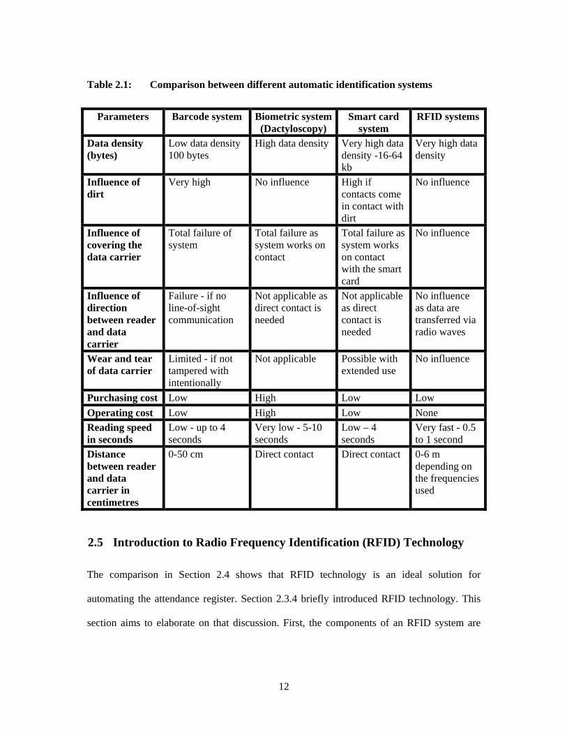
2.4 Comparison between Various Automatic Identification Systems
In Section 2.3 the different technologies available for automating the student attendance
register were discussed. This section will examine the pros and cons of each of these
technologies, bearing in mind the objective of this project. The aim of this section is to
narrow down the technology that can be used for automating the student attendance register.
A comparison is made of the technologies with respect to some of the vital parameters
concerned with automating the student attendance register (see Table 2.1).
12
Table 2.1: Comparison between different automatic identification systems
Parameters Barcode system Biometric system (Dactyloscopy)
Smart card system
RFID systems
Data density (bytes)
Low data density 100 bytes
High data density
Very high data density -16-64 kb
Very high data density
Influence of dirt
Very high No influence High if contacts come in contact with dirt
No influence
Influence of covering the data carrier
Total failure of system
Total failure as system works on contact
Total failure as system works on contact with the smart card
No influence
Influence of direction between reader and data carrier
Failure - if no line-of-sight communication
Not applicable as direct contact is needed
Not applicable as direct contact is needed
No influence as data are transferred via radio waves
Wear and tear of data carrier
Limited - if not tampered with intentionally
Not applicable Possible with extended use
No influence
Purchasing cost Low High Low Low
Operating cost Low High Low None
Reading speed in seconds
Low - up to 4 seconds
Very low - 5-10 seconds
Low – 4 seconds
Very fast - 0.5 to 1 second
Distance between reader and data carrier in centimetres
0-50 cm Direct contact Direct contact 0-6 m depending on the frequencies used
2.5 Introduction to Radio Frequency Identification (RFID) Technology
The comparison in Section 2.4 shows that RFID technology is an ideal solution for
automating the attendance register. Section 2.3.4 briefly introduced RFID technology. This
section aims to elaborate on that discussion. First, the components of an RFID system are

13
examined in detail. Secondly, anti-collision in RFID technology is studied. Thirdly, the
security issues concerning RFID technology are elaborated on.
An RFID system consists of three main components, namely the RFID tag, the RFID reader
and RFID middleware.
2.5.1 RFID Tags
RFID tags (hereafter referred to as tags) are also called transponders. The tag is placed on the
object that needs to be identified. It contains an internal antenna and a microchip [6, p.22].
The microchip stores the data which define and distinguish each tag.
There are three types of tags in use: active tags, passive tags and semi-passive tags.
Active tags incorporate a battery along with the antenna and the microchip. The battery
affects the cost and size of active tags. As a result active tags [7, p.13] are not very commonly
used.
Passive tags do not have a built-in battery. The power requirements of a passive tag are
generated from the electric or magnetic fields generated by the RFID reader. How the power
requirements are met is explained in Section 2.5.5.3. Passive tags [9, p.66] are very cheap and
smaller than active tags. As a result they are used in the project on attendance registration.
Semi-passive tags have an onboard power source and may have onboard sensors. The
onboard power source provides a continuous power source for the sensors. This enables the
14
semi-passive tags to transfer data even in the absence of an RFID reader. The semi-passive
also has an increased read range. The cost of semi-passive tags lies between the costs of
active and passive tags [10, p.3].
2.5.1.1 Types of tag constructions
The type of tag construction depends on various factors such as the type of tag used (active,
passive or semi-passive), the desired read range, and the end-user application. Some of the
different types of tag construction are discussed briefly in this section.
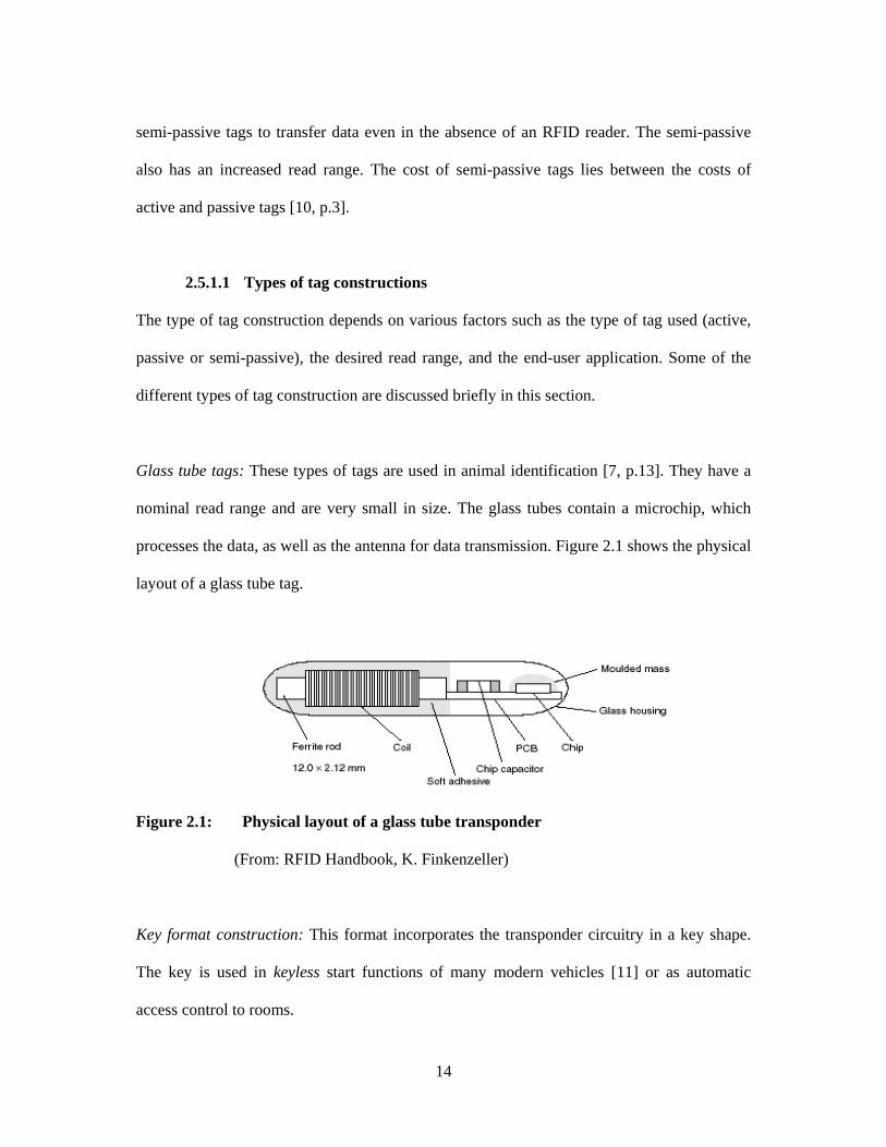
Glass tube tags: These types of tags are used in animal identification [7, p.13]. They have a
nominal read range and are very small in size. The glass tubes contain a microchip, which
processes the data, as well as the antenna for data transmission. Figure 2.1 shows the physical
layout of a glass tube tag.
Figure 2.1: Physical layout of a glass tube transponder
(From: RFID Handbook, K. Finkenzeller)
Key format construction: This format incorporates the transponder circuitry in a key shape.
The key is used in keyless start functions of many modern vehicles [11] or as automatic
access control to rooms.
15
Identification card formats: These types of tags come in standard credit card size (85.72 mm
× 54.03 mm × 0.76 mm). They have coil antennas attached to the microchip circuitry
[7, p.18] which is laminated between two sheets of polyvinyl chloride (PVC) foil. These are
then baked at high temperature to seal the bond. These types of tags are used in this project.
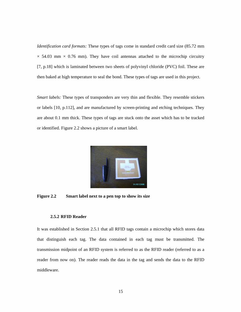
Smart labels: These types of transponders are very thin and flexible. They resemble stickers
or labels [10, p.112], and are manufactured by screen-printing and etching techniques. They
are about 0.1 mm thick. These types of tags are stuck onto the asset which has to be tracked
or identified. Figure 2.2 shows a picture of a smart label.
Figure 2.2 Smart label next to a pen top to show its size
2.5.2 RFID Reader
It was established in Section 2.5.1 that all RFID tags contain a microchip which stores data
that distinguish each tag. The data contained in each tag must be transmitted. The
transmission midpoint of an RFID system is referred to as the RFID reader (referred to as a
reader from now on). The reader reads the data in the tag and sends the data to the RFID
middleware.
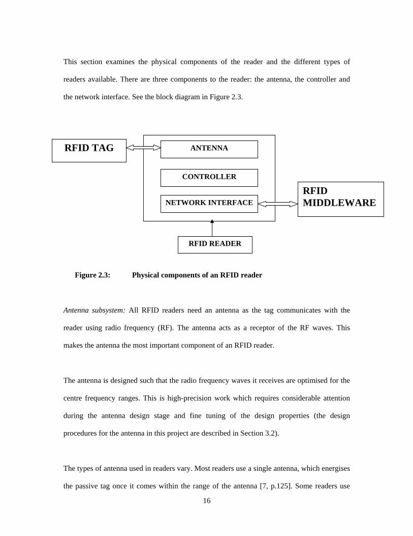
16
This section examines the physical components of the reader and the different types of
readers available. There are three components to the reader: the antenna, the controller and
the network interface. See the block diagram in Figure 2.3.
Figure 2.3: Physical components of an RFID reader
Antenna subsystem: All RFID readers need an antenna as the tag communicates with the
reader using radio frequency (RF). The antenna acts as a receptor of the RF waves. This
makes the antenna the most important component of an RFID reader.
The antenna is designed such that the radio frequency waves it receives are optimised for the
centre frequency ranges. This is high-precision work which requires considerable attention
during the antenna design stage and fine tuning of the design properties (the design
procedures for the antenna in this project are described in Section 3.2).
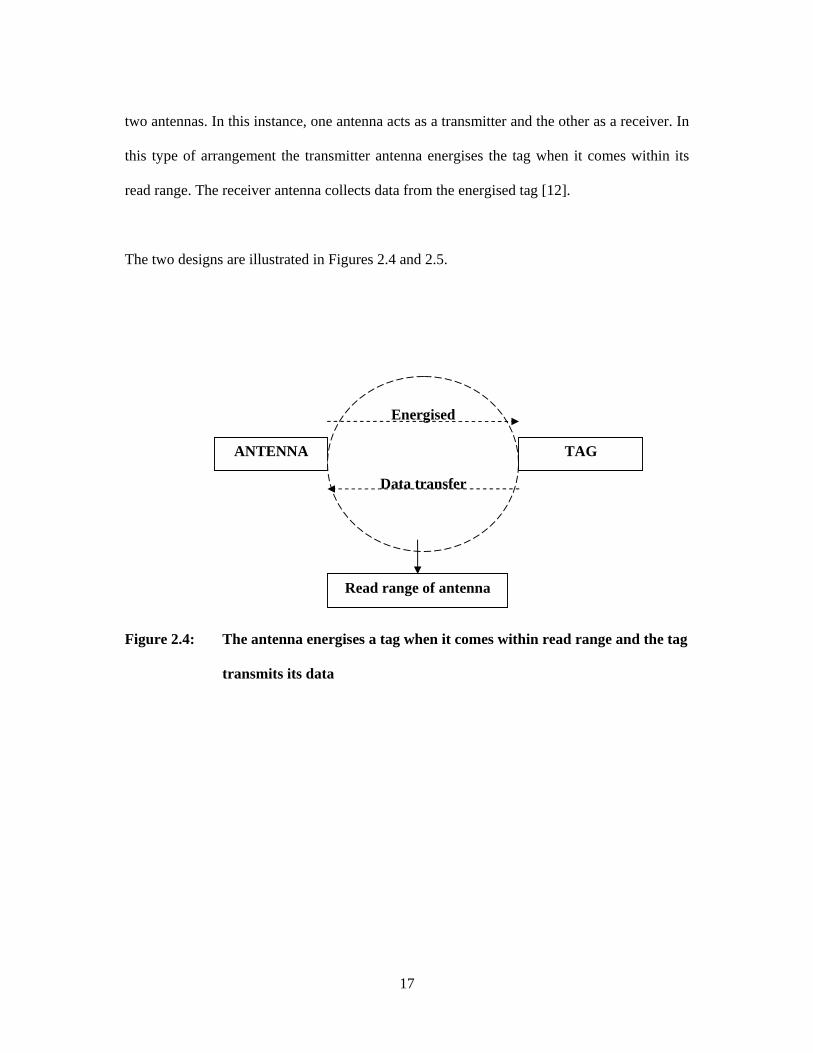
The types of antenna used in readers vary. Most readers use a single antenna, which energises
the passive tag once it comes within the range of the antenna [7, p.125]. Some readers use
ANTENNA
CONTROLLER
NETWORK INTERFACE
RFID TAG
RFID MIDDLEWARE
RFID READER
17
two antennas. In this instance, one antenna acts as a transmitter and the other as a receiver. In
this type of arrangement the transmitter antenna energises the tag when it comes within its
read range. The receiver antenna collects data from the energised tag [12].
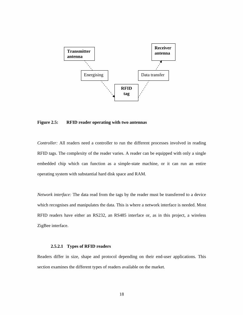
The two designs are illustrated in Figures 2.4 and 2.5.
Figure 2.4: The antenna energises a tag when it comes within read range and the tag
transmits its data
ANTENNA
Energised
Data transfer
TAG
Read range of antenna
18
Figure 2.5: RFID reader operating with two antennas
Controller: All readers need a controller to run the different processes involved in reading
RFID tags. The complexity of the reader varies. A reader can be equipped with only a single
embedded chip which can function as a simple-state machine, or it can run an entire
operating system with substantial hard disk space and RAM.
Network interface: The data read from the tags by the reader must be transferred to a device
which recognises and manipulates the data. This is where a network interface is needed. Most
RFID readers have either an RS232, an RS485 interface or, as in this project, a wireless
ZigBee interface.
2.5.2.1 Types of RFID readers
Readers differ in size, shape and protocol depending on their end-user applications. This
section examines the different types of readers available on the market.
Transmitter antenna
Receiver antenna
RFID tag
Data transfer Energising
19
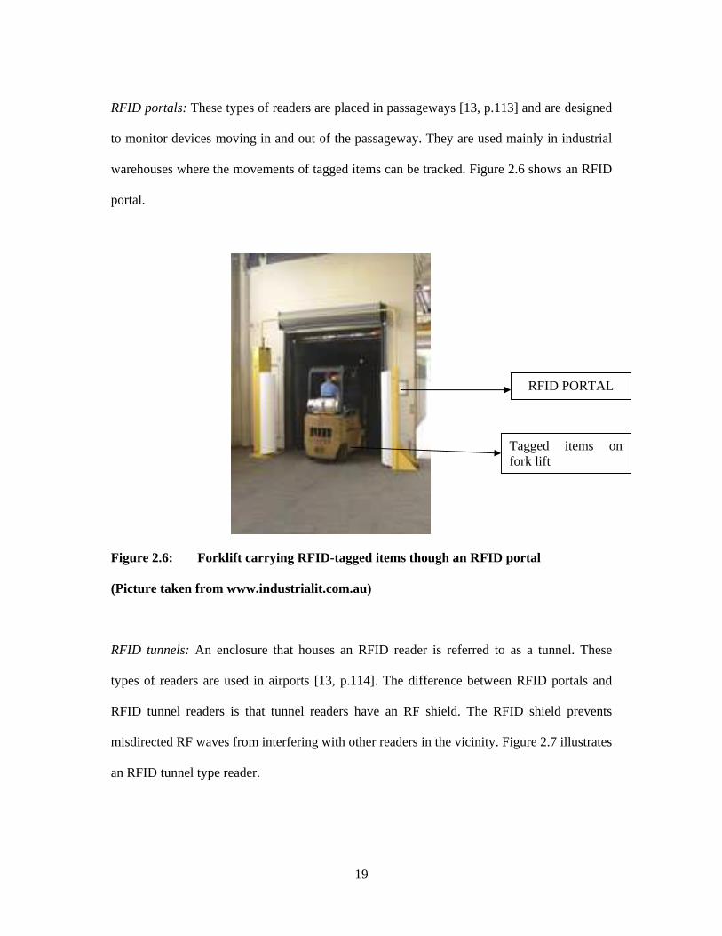
RFID portals: These types of readers are placed in passageways [13, p.113] and are designed
to monitor devices moving in and out of the passageway. They are used mainly in industrial
warehouses where the movements of tagged items can be tracked. Figure 2.6 shows an RFID
portal.
Figure 2.6: Forklift carrying RFID-tagged items though an RFID portal
(Picture taken from www.industrialit.com.au)
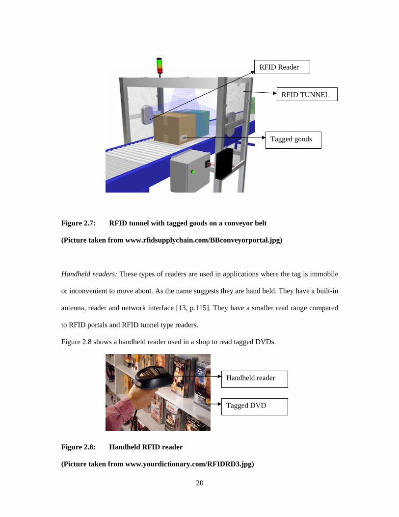
RFID tunnels: An enclosure that houses an RFID reader is referred to as a tunnel. These
types of readers are used in airports [13, p.114]. The difference between RFID portals and
RFID tunnel readers is that tunnel readers have an RF shield. The RFID shield prevents
misdirected RF waves from interfering with other readers in the vicinity. Figure 2.7 illustrates
an RFID tunnel type reader.
RFID PORTAL
Tagged items on fork lift
20
Figure 2.7: RFID tunnel with tagged goods on a conveyor belt
(Picture taken from www.rfidsupplychain.com/BBconveyorportal.jpg)
Handheld readers: These types of readers are used in applications where the tag is immobile
or inconvenient to move about. As the name suggests they are hand held. They have a built-in
antenna, reader and network interface [13, p.115]. They have a smaller read range compared
to RFID portals and RFID tunnel type readers.
Figure 2.8 shows a handheld reader used in a shop to read tagged DVDs.
Figure 2.8: Handheld RFID reader
(Picture taken from www.yourdictionary.com/RFIDRD3.jpg)
RFID TUNNEL
Tagged goods
RFID Reader
Handheld reader
Tagged DVD
21
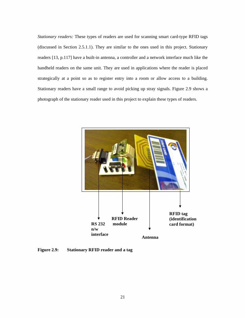
Stationary readers: These types of readers are used for scanning smart card-type RFID tags
(discussed in Section 2.5.1.1). They are similar to the ones used in this project. Stationary
readers [13, p.117] have a built-in antenna, a controller and a network interface much like the
handheld readers on the same unit. They are used in applications where the reader is placed
strategically at a point so as to register entry into a room or allow access to a building.
Stationary readers have a small range to avoid picking up stray signals. Figure 2.9 shows a
photograph of the stationary reader used in this project to explain these types of readers.
Figure 2.9: Stationary RFID reader and a tag
RFID tag (identification card format) RS 232
n/w interface
RFID Reader module
Antenna
22
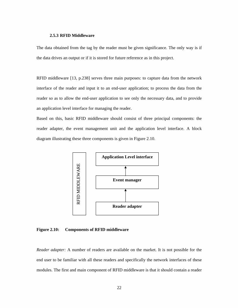
2.5.3 RFID Middleware
The data obtained from the tag by the reader must be given significance. The only way is if
the data drives an output or if it is stored for future reference as in this project.
RFID middleware [13, p.238] serves three main purposes: to capture data from the network
interface of the reader and input it to an end-user application; to process the data from the
reader so as to allow the end-user application to see only the necessary data, and to provide
an application level interface for managing the reader.
Based on this, basic RFID middleware should consist of three principal components: the
reader adapter, the event management unit and the application level interface. A block
diagram illustrating these three components is given in Figure 2.10.
Figure 2.10: Components of RFID middleware
Reader adapter: A number of readers are available on the market. It is not possible for the
end user to be familiar with all these readers and specifically the network interfaces of these
modules. The first and main component of RFID middleware is that it should contain a reader
RRFF I
I DD MM
II DDDD
LLEE
WWAA
RREE
Application Level interface
Event manager
Reader adapter
23
adapter [13, p.116] which will spare the end user the need to learn about the network
interface capabilities of each individual RFID reader.
Event management: The data that a reader captures from the tag is said to be “raw” data.
This means that the reader reads many data, which may not be necessary for the end-user
application.
The RFID readers used today can handle suitable data, but they are not intelligent enough to
adjust to a specific end-user application. The event manager [13, p.144] in the middleware
makes up for this deficiency on the reader side with a high-level filter. As a result only the
necessary data reach the end-user application.
Sometimes certain types of data need to be added to the data from the tags, which the reader
cannot do. The event manager can add these data. This aspect is a problem encountered in
this project.
The data contained in the tag is a unique 8-character numeral. The code differs from the
student number, which identifies each student. The RFID reader cannot read the student
number from a tag; it can only read the unique code. The specific reader used in this project
cannot output the date and time once the tag has been scanned, which is necessary for
registering the attendance.
The event manager in the RFID middleware can be programmed to input the corresponding
student number for a unique code as well as a time stamp when a tag is scanned. Section 3.3
explains this example in detail, and there is further discussion on the example.
24
Application-level interface: This is the top layer of the RFID middleware. The primary
objective of this component is to provide a standard output that allows an application to
receive filtered data from the RFID reader. In addition, the application-level interface
[13, p.141] should enable the end user to manage and improvise the data from the reader so
as to provide multi-functionality, i.e. there should be room for development if and when the
end user deems it necessary.
Figure 2.11 summarises the function of the middleware, which is in essence to reduce the
complexity of the raw data from the reader and maximise the functionality of the
application.
Figure 2.11: Raw data and application relevance at different levels of RFID
middleware
Application level
Event manager
Reader adapter
Raw data
Maximum raw data
Maximum application
Application
25
2.5.4 Physics behind RFID
The last three sections introduced the basic components of an RFID system. This section
aims to shed some light on the physics behind the actual working of the various RFID
components, especially the RFID tags and the readers. Radio waves are the main component
used in the functioning of an RFID system.
Data transfer in RFID is done mainly through magnetic principles. The derivations done in
this section go a long way towards the design of major components of the RFID reader
discussed in detail in Section 3.
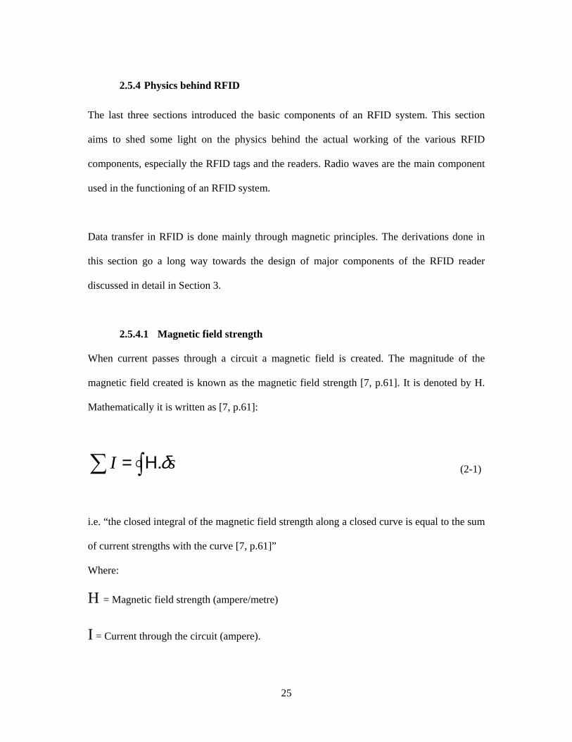
2.5.4.1 Magnetic field strength
When current passes through a circuit a magnetic field is created. The magnitude of the
magnetic field created is known as the magnetic field strength [7, p.61]. It is denoted by H.
Mathematically it is written as [7, p.61]:
∑ ∫Η= sI δ. (2-1)
i.e. “the closed integral of the magnetic field strength along a closed curve is equal to the sum
of current strengths with the curve [7, p.61]”
Where:
H = Magnetic field strength (ampere/metre)
I = Current through the circuit (ampere).
26
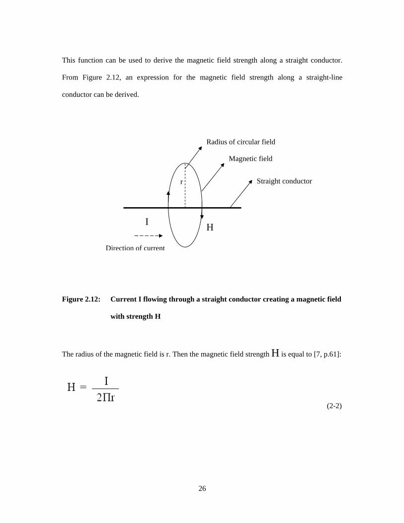
This function can be used to derive the magnetic field strength along a straight conductor.
From Figure 2.12, an expression for the magnetic field strength along a straight-line
conductor can be derived.
Figure 2.12: Current I flowing through a straight conductor creating a magnetic field
with strength H
The radius of the magnetic field is r. Then the magnetic field strength H is equal to [7, p.61]:
(2-2)
r
H
Radius of circular field
Straight conductor
Magnetic field
Direction of current
I
27
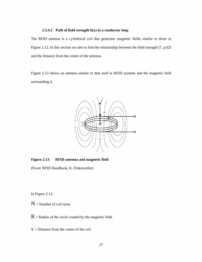
2.5.4.2 Path of field strength h(x) in a conductor loop
The RFID antenna is a cylindrical coil that generates magnetic fields similar to those in
Figure 2.12. In this section we aim to find the relationship between the field strength [7, p.62]
and the distance from the centre of the antenna.
Figure 2.13 shows an antenna similar to that used in RFID systems and the magnetic field
surrounding it.
Figure 2.13: RFID antenna and magnetic field
(From: RFID Handbook, K. Finkenzeller)
In Figure 2.12:
N = Number of coil turns
R = Radius of the circle created by the magnetic field
x = Distance from the centre of the coil.
28
d = Diameter of the wire coil.
Then the equation can be re-written as [7, p.62]:
(2-3)
The field strength at the centre of the antenna (where x = 0) is:
(2-4)
2.5.4.3 Magnetic flux (Φ)
Magnetic flux [7, p.66] is denoted by Φ. It is the total number of magnetic field lines
passing through a current-carrying coil. It can be written mathematically as [7, p.66]:
Φ = B. A (2-5)
Where;
B = Magnetic flux density, which is the magnetic flux per unit area of the section
perpendicular to the direction of flux. Magnetic flux density can be expressed in terms of
magnetic field strength as follows [7, p.66]:
B = µ0 µr H = µ H (2-6)
Where;
µ0 = permeability of free space
29
µr = permeability of the medium
µ0 µr = µ = permeability.
2.5.4.4 Inductance
Magnetic flux is generated in a current-carrying conductor as explained in Section 2.5.4.3. If
the current-carrying conductor has N loops, then a magnetic flux will be generated in every
loop. Therefore the total flux ψ can be expressed mathematically as follows [7, p.66]:
Ψ = ∑ ΦN = N. Φ = N. µ. H. A (2-7)
Where;
N = Number of turns in the current-carrying coil
Φ = Magnetic flux
H = Magnetic field strength.
Now inductance [7, p.66] is defined as the total flux ψ that arises in an area ‘A ’ enclosed by
the current ‘I’. It can be mathematically defined as follows [7, p.66]:
(2-8)
Where;
L = Inductance
Ψ = Total flux in an enclosed area
30
Φ = Magnetic flux
N = Number of coil windings
I = Current flowing through the conductor coil
H = Magnetic field strength
A = Area
µ = permeability of the medium.
Figure 2.14 illustrates the concept of inductance.
Figure 2.14: Inductance in a current-carrying metal conductor
(From: RFID Handbook, K. Finkenzeller)
2.5.4.5 Mutual inductance (M)
Section 2.5.4.4 explained the phenomenon of inductance in a single conductor with area A.
Now suppose a second conductor loop (loop 2) with area A2 and current I2 flowing through
Current-carrying conductor loop
Magnetic flux lines

31
it enters the magnetic field created by the first conductor loop (loop 1) with Area A1 and
current I1. Loop 2 will then be subjected to a portion of the magnetic flux generated in
loop 1. This is called a coupling flux.
The coupling flux, ψ21, like the total flux, depends on the area of the loops, the current
flowing through the circuits, the permeability of the material used in the conductor loops and
the field strength.
The voltage induced on loop 2 as a result of the partial flux changes, ψ21, in loop 1 is called
mutual inductance, M21. The mathematical expression for M21 can be written as follows
[7, p.68]:
(2-9)
Where
ψ21 = Partial flux on conductor loop 2 due to current I1 on loop 1
I1 = Current flowing through loop 1
B2 = Flux density induced in loop 2
A2 = Area of loop 2.
There will also be an equal inductance on loop 1 as a result of current I2 flowing through
loop 2. This inductance is referred to as mutual inductance [7, p.68] M12. This creates a
32
coupling flux ψ12. The mutual inductance M12 is the same as M21. They can thus be written
as:
M12 = M21 = M .
The mutual inductance phenomenon is shown in Figure 2.15.
Figure 2.15: Mutual inductance M 21
(From: RFID Handbook, K. Finkenzeller)
Mutual inductance is an important phenomenon as far as RFID is concerned. It forms the
basis for inductive coupling (explained in Section 2.5.5.4) in the RFID system.
Equation 2-9 can be re-written as [7, p.68]
(2-10)
Where;
H (I1) = Magnetic field strength H due to current I1. (It is the same as H.)

33
Substituting for H in Equation 2-10 with Equation 2-3, a new expression for M12 is
obtained. This is expressed as Equation 2-11.
(2-11)
Where;
M12 = Mutual inductance
µ0 = permeability
H (I1) = Magnetic field strength due to current I1
R1 = Radius of circular loop 1
R2 = Radius of circular loop 2
N1 = Number of coil turns in loop 1
N2 = Number of coil turns in loop 2
x = distance from the centre of the coil
Π = constant (3.14).
This formula is used to calculate the mutual inductance.
34
2.5.4.6 Faraday’s law
This law states that a change in the magnetic flux φ will result in an electric field E being
generated. The electric field generated depends on the magnetic properties of the medium.
For a conductor with N windings, Faraday’s law can be written as follows [14, p.231]:
Ei = N .δφ/δt (2-12)
Where;
Ei = Electric field induced as a result of change in flux
N = Number of windings on the conductor coil
δφ/δt = Change in flux with respect to time.
Faraday’s law is important in the study of RFID, as Faraday’s law applied to metallic surface
results in the creation of a back electromotive force called eddy current. Eddy currents
increase with an increase in the alternating flux. As a result, in the design of RFID systems
(tags or readers) it is vital to avoid construction or installation on or near metallic surfaces.
This is shown in Figure 2.16
Figure 2.16: Faraday’s law applied to a metal conductor
Flux change δφ/δt
Metal surface
Eddy currents
35
(From: RFID Handbook, K. Finkenzeller)
The concepts discussed thus far in this chapter can be used to enhance the understanding of
inductively coupled RFID systems. An equivalent circuit for an RFID system comprising a
reader and a tag is shown in Figure 2.17. Both the reader and the tag are shown as inductors.
Figure 2.17: Equivalent circuit for a reader and a tag
Where;
L1 = Reader antenna
L2 = Tag antenna
R2 = Coil resistance of L2
RL = Load resistance of L2
I1 = Current flowing through L1
I2 = Current flowing through L2
V2 = Voltage across RL.
V2
I1 I2
36
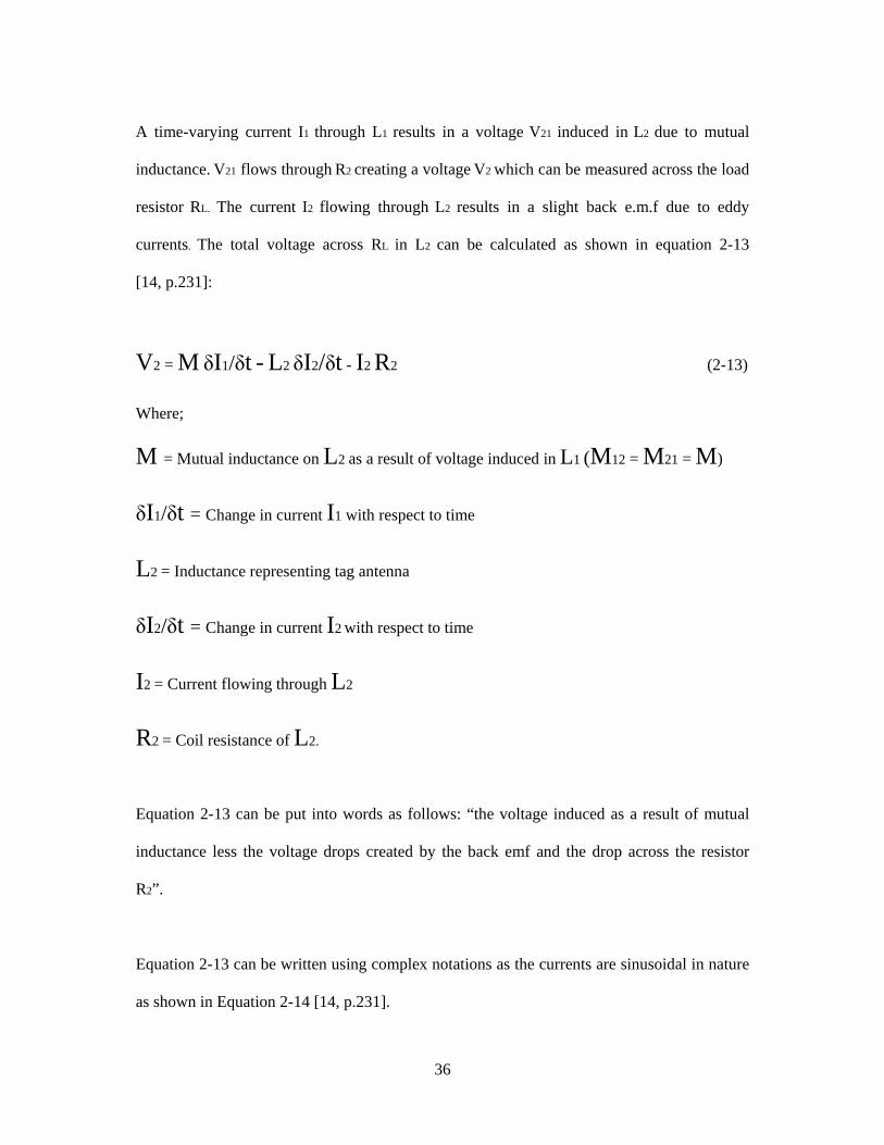
A time-varying current I1 through L1 results in a voltage V21 induced in L2 due to mutual
inductance. V21 flows through R2 creating a voltage V2 which can be measured across the load
resistor RL. The current I2 flowing through L2 results in a slight back e.m.f due to eddy
currents. The total voltage across RL in L2 can be calculated as shown in equation 2-13
[14, p.231]:
V2 = M δI1/δt - L2 δI2/δt - I2 R2 (2-13)
Where;
M = Mutual inductance on L2 as a result of voltage induced in L1 (M12 = M21 = M)
δI1/δt = Change in current I1 with respect to time
L2 = Inductance representing tag antenna
δI2/δt = Change in current I2 with respect to time
I2 = Current flowing through L2
R2 = Coil resistance of L2.
Equation 2-13 can be put into words as follows: “the voltage induced as a result of mutual
inductance less the voltage drops created by the back emf and the drop across the resistor
R2”.
Equation 2-13 can be written using complex notations as the currents are sinusoidal in nature
as shown in Equation 2-14 [14, p.231].
37
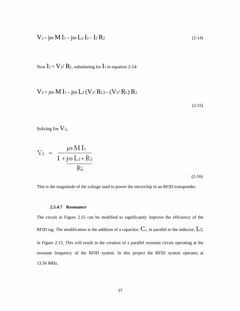
V2 = jω M I1 – jω L2 I2 – I2 R2 (2-14)
Now I2 = V2/ RL, substituting for I1 in equation 2-14:
V2 = jω M I1 – jω L2 (V2/ RL) – (V2/ RL) R2
(2-15)
Solving for V2,
(2-16)
This is the magnitude of the voltage used to power the microchip in an RFID transponder.
2.5.4.7 Resonance
The circuit in Figure 2.15 can be modified to significantly improve the efficiency of the
RFID tag. The modification is the addition of a capacitor, C2, in parallel to the inductor, L2,
in Figure 2.15. This will result in the creation of a parallel resonant circuit operating at the
resonant frequency of the RFID system. In this project the RFID system operates at
13.56 MHz.

38
The equivalent circuit diagram is shown in Figure 2.18.
Figure 2.18: Equivalent circuit for an RFID tag circuitry
The equation for finding the resonant frequency is [14, p.231]:
(2-17)
In practice, C2 is made up of parallel capacitor C2p and a parasitic capacitance Cp. The value
for the parallel capacitor C2p can be found with the same formula used in Equation 2-17, but
subtracting the parasitic capacitance.
(2-18)
39
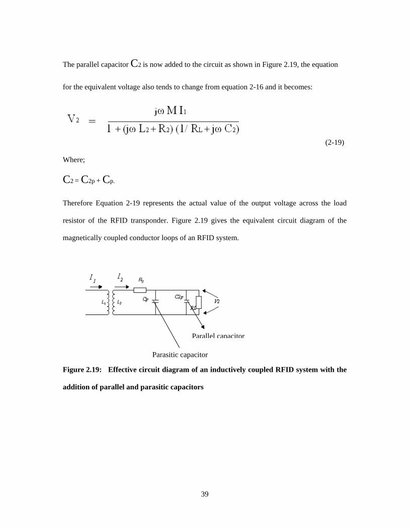
The parallel capacitor C2 is now added to the circuit as shown in Figure 2.19, the equation
for the equivalent voltage also tends to change from equation 2-16 and it becomes:
(2-19)
Where;
C2 = C2p + Cp.
Therefore Equation 2-19 represents the actual value of the output voltage across the load
resistor of the RFID transponder. Figure 2.19 gives the equivalent circuit diagram of the
magnetically coupled conductor loops of an RFID system.
Figure 2.19: Effective circuit diagram of an inductively coupled RFID system with the
addition of parallel and parasitic capacitors
Parasitic capacitor
Parallel capacitor

40
2.5.4.8 Interrogation field strength HMIN
The results from the study of resonance in Section 2.5.3.6 can be used to find the minimum
field strength Hmin at which the voltage V2 (voltage at the terminal L2 in Figure 2.17 (of
last resonance) is just high enough for the operation of the data carrier.
An expression for mutual inductance can be written using Equation 2-10 as follows:
(2-20)
Where;
H (I1) = Magnetic field strength due to current I1. H (I1) can be replaced with Heff which
is the effective field strength of a sinusoidal magnetic field
µ0 = permeability of free space
N = number of coil windings
A = cross-sectional area of the coil
I1 = Current through the coil.
Since H (I1) = Heff, Equation 2-20 can be re-written as follows:
(2-21)
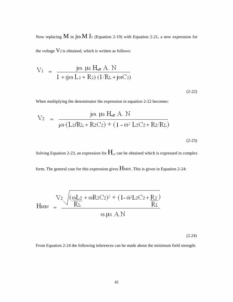
41
Now replacing M in jω.M I1 (Equation 2-19) with Equation 2-21, a new expression for
the voltage V2 is obtained, which is written as follows:
(2-22)
When multiplying the denominator the expression in equation 2-22 becomes:
(2-23)
Solving Equation 2-23, an expression for Heff can be obtained which is expressed in complex
form. The general case for this expression gives HMIN . This is given in Equation 2-24:
(2.24)
From Equation 2-24 the following inferences can be made about the minimum field strength:
42
HMIN depends on the frequency (ω = 2Πf) of the operation of the RFID system, the area
of the coil (antenna) A , the number of coil windings, N, the minimum input voltage V2
and input resistance R2.
For optimum functioning of the antenna, the resonant frequency of the tag should match that
of the reader. This is not always possible as the tolerance factor in the manufacture of the tags
tends to make them deviate from the resonant frequency. Also to account for anti-collision,
(Section 2.5.6) the resonant frequency is always placed higher.
2.5.4.9 Energy range of transponder systems
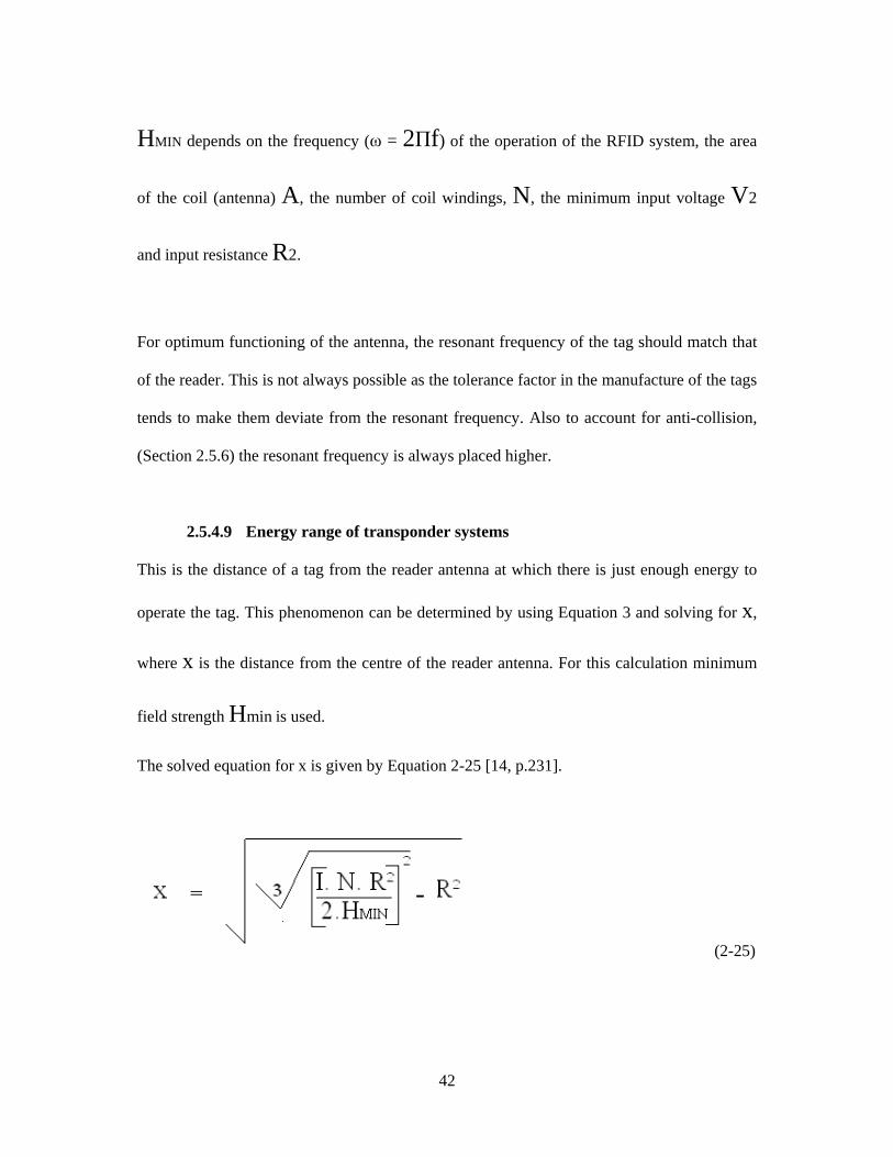
This is the distance of a tag from the reader antenna at which there is just enough energy to
operate the tag. This phenomenon can be determined by using Equation 3 and solving for x,
where x is the distance from the centre of the reader antenna. For this calculation minimum
field strength Hmin is used.
The solved equation for x is given by Equation 2-25 [14, p.231].
(2-25)
43
2.5.4.10 Interrogation zone of readers
The interrogation zone of an RFID reader [7, p.80] refers to the area in which the reader has
the ability to pick up the signals of an RFID tag. Up to this section all the calculations were
made assuming that the tag is parallel to the antenna of the reader. This section examines the
effects of tilting the angle of the transponder antenna with respect to the central axis of the
coil.
Consider that VO is the voltage induced on the coil and is perpendicular to the magnetic
field. Then the voltage when the coil is at an angle θ will be VOθ, which is given by;
[7, p.80]:
VOθ = VO .cos(θ) (2-26)
Where;
θ = 90°, cos 90° = 0 and therefore VOθ = 0.
The antenna radiation patterns with the angle of the tag at θ = 0 and θ = 90° is shown in
Figure 2.20.
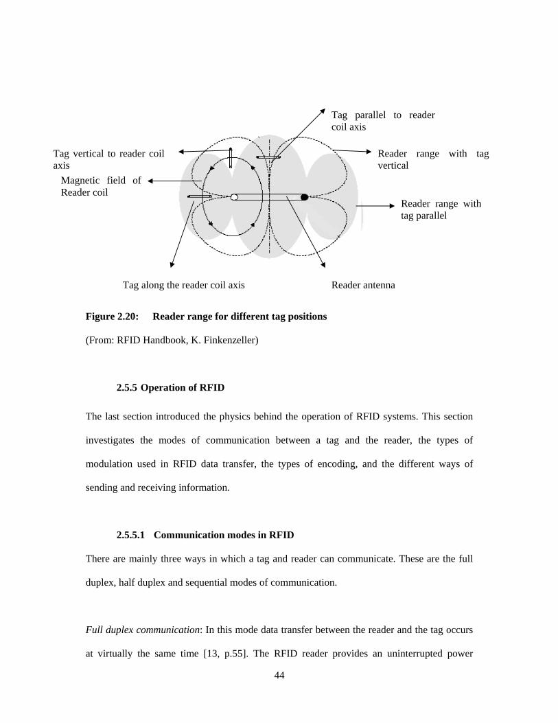
44
Figure 2.20: Reader range for different tag positions
(From: RFID Handbook, K. Finkenzeller)
2.5.5 Operation of RFID
The last section introduced the physics behind the operation of RFID systems. This section
investigates the modes of communication between a tag and the reader, the types of
modulation used in RFID data transfer, the types of encoding, and the different ways of
sending and receiving information.
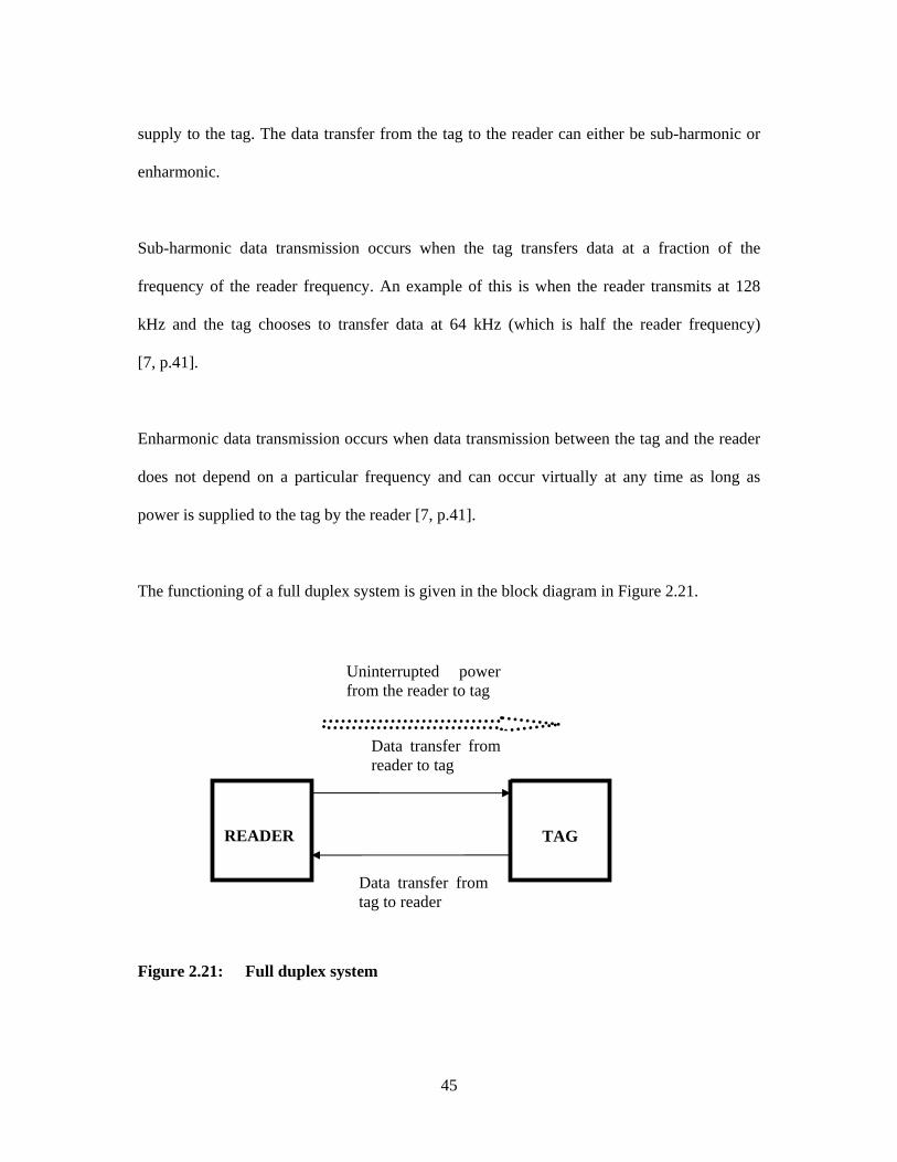
2.5.5.1 Communication modes in RFID
There are mainly three ways in which a tag and reader can communicate. These are the full
duplex, half duplex and sequential modes of communication.
Full duplex communication: In this mode data transfer between the reader and the tag occurs
at virtually the same time [13, p.55]. The RFID reader provides an uninterrupted power
Reader range with tag vertical
Reader range with tag parallel
Reader antenna
Tag parallel to reader coil axis
Tag along the reader coil axis
Tag vertical to reader coil axis
Magnetic field of Reader coil
45
supply to the tag. The data transfer from the tag to the reader can either be sub-harmonic or
enharmonic.
Sub-harmonic data transmission occurs when the tag transfers data at a fraction of the
frequency of the reader frequency. An example of this is when the reader transmits at 128
kHz and the tag chooses to transfer data at 64 kHz (which is half the reader frequency)
[7, p.41].
Enharmonic data transmission occurs when data transmission between the tag and the reader
does not depend on a particular frequency and can occur virtually at any time as long as
power is supplied to the tag by the reader [7, p.41].
The functioning of a full duplex system is given in the block diagram in Figure 2.21.
Figure 2.21: Full duplex system
READER
TAG
Data transfer from reader to tag
Data transfer from tag to reader
Uninterrupted power from the reader to tag
46
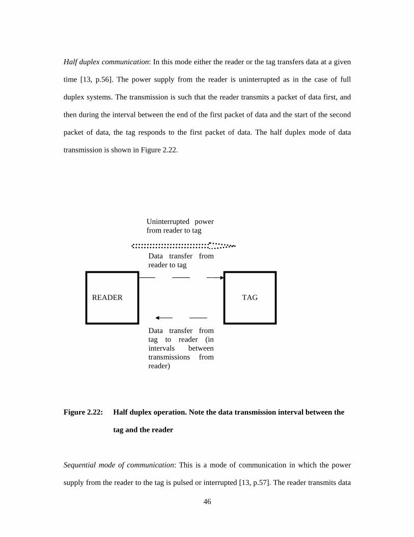
Half duplex communication: In this mode either the reader or the tag transfers data at a given
time [13, p.56]. The power supply from the reader is uninterrupted as in the case of full
duplex systems. The transmission is such that the reader transmits a packet of data first, and
then during the interval between the end of the first packet of data and the start of the second
packet of data, the tag responds to the first packet of data. The half duplex mode of data
transmission is shown in Figure 2.22.
Figure 2.22: Half duplex operation. Note the data transmission interval between the
tag and the reader
Sequential mode of communication: This is a mode of communication in which the power
supply from the reader to the tag is pulsed or interrupted [13, p.57]. The reader transmits data
READER
TAG
Uninterrupted power from reader to tag
Data transfer from reader to tag
Data transfer from tag to reader (in intervals between transmissions from reader)
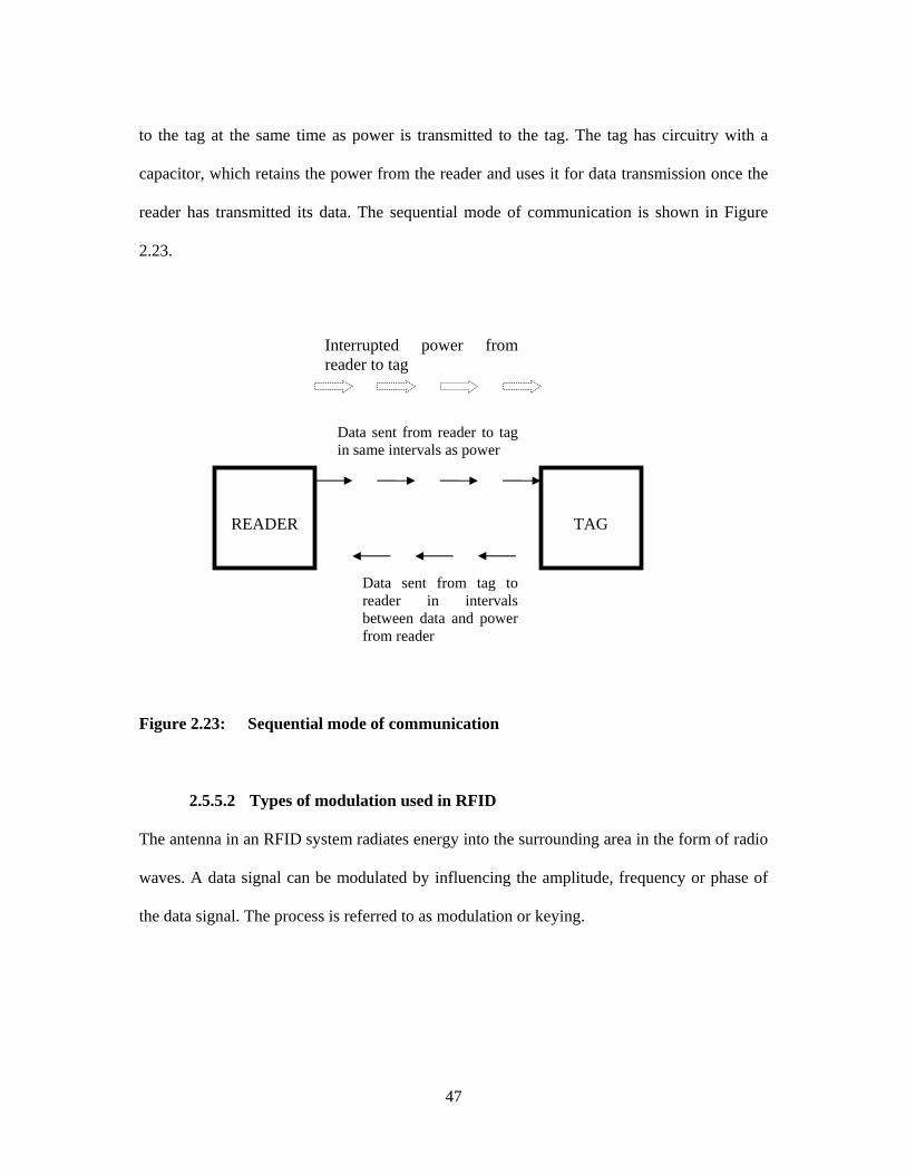
47
to the tag at the same time as power is transmitted to the tag. The tag has circuitry with a
capacitor, which retains the power from the reader and uses it for data transmission once the
reader has transmitted its data. The sequential mode of communication is shown in Figure
2.23.
Figure 2.23: Sequential mode of communication
2.5.5.2 Types of modulation used in RFID
The antenna in an RFID system radiates energy into the surrounding area in the form of radio
waves. A data signal can be modulated by influencing the amplitude, frequency or phase of
the data signal. The process is referred to as modulation or keying.
READER
TAG
Interrupted power from reader to tag
Data sent from reader to tag in same intervals as power
Data sent from tag to reader in intervals between data and power from reader
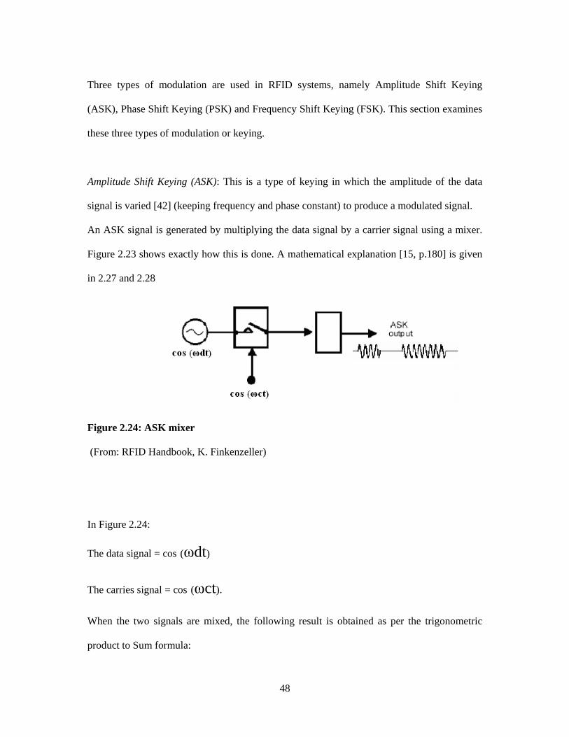
48
Three types of modulation are used in RFID systems, namely Amplitude Shift Keying
(ASK), Phase Shift Keying (PSK) and Frequency Shift Keying (FSK). This section examines
these three types of modulation or keying.
Amplitude Shift Keying (ASK): This is a type of keying in which the amplitude of the data
signal is varied [42] (keeping frequency and phase constant) to produce a modulated signal.
An ASK signal is generated by multiplying the data signal by a carrier signal using a mixer.
Figure 2.23 shows exactly how this is done. A mathematical explanation [15, p.180] is given
in 2.27 and 2.28
Figure 2.24: ASK mixer
(From: RFID Handbook, K. Finkenzeller)
In Figure 2.24:
The data signal = cos (ωdt)
The carries signal = cos (ωct).
When the two signals are mixed, the following result is obtained as per the trigonometric
product to Sum formula:
49
cosA .cosB = ½ cos (A-B) + ½ cos (A+B). (2-27)
Applying this to the ASK mixer, the following result is obtained:
cos (ωdt). cos (ωct) = ½ cos (ωd-ωc)t + ½ cos (ωd+ωc)t. (2-28)
The terms (ωd-ωc) and (ωd+ωc) represent the lower and upper sidebands of the ASK
wave, respectively. The mathematical analysis is done to show that the bandwidth obtained
by a modulated ASK signal is twice that of the original data signal.
Frequency Shift Keying (FSK): This form of modulation changes the frequency parameters
(keeping voltages and phase constant) [15, p.181-186] of the data signal by multiplying them
by a carrier wave with a different frequency.
There are two methods of generating FSK signals. The first and obvious method is by
switching between two different frequency sources using a mixer. The disadvantage of this
method is that it results in a phase discontinuity.
The second method overcomes the disadvantage of the first method. A Voltage Controlled
Oscillator (VCO) is used. The VCO gives a frequency change that is linearly proportional to
the applied voltage. Therefore when a data signal is multiplied by an output from a VCO, the
output will be a continuous waveform.
50
Phase Shift Keying (PSK): A PSK output is generated by varying the phase of the data signal
[15, p.187]. This is done by switching the data signal with an in-phase (0°) and out-of-phase
(180°) signal.
2.5.5.3 Data coding in RFID
After modulating, the data signal has to be encoded. Encoding [13, p.67] is done mainly for
security reasons. The RFID reader and the tag have to agree on a similar coding technique so
that the transmitted data will only be decoded by a specific reader that knows the encoding
technique used by the tag.
Some of the different coding techniques used in RFID are discussed in this section, followed
by a graphical representation of each code with respect to a data signal and a clock.
Non-Return to Zero (NRZ) coding: In this method a binary 1 is represented as one significant
condition (logic level high) and a binary 0 is represented by a logic level zero [9, p.101].
Manchester encoding: This method is self-clocking. The level changes always occur in the
middle of a clock cycle. A binary 0 is translated into a low-to-high transition (0 to 1) and a 1
is translated into a high-to-low transition (1 to 0). This type of coding is also called split-
phase coding [9, p.101].
Miller coding: In this method a binary 1 is represented by a transition. The transition can
either be low-to-high or high-to-low and occurs in the middle of a clock cycle [7, p.185]. A
binary 0 is represented by a continuation of the 1 over the next clock cycle. This type of
coding is also known as Miller sub-carrier encoding.
51
FMO coding: In this coding a transition occurs at the beginning of each clock cycle. A binary
1 is represented by no transition in the middle of the clock cycle. A binary 0 is represented by
an additional transition in the middle of the clock cycle [16, p.41]. The FMO coding is also
called bi-phase space encoding.
Uni-polar RZ coding: A binary 1 is represented by a high logic level during the first half of
the clock cycle and a binary 0 is represented by a low logic level for the duration of the clock
cycle[9, p.102].
Differential coding: A binary 1 changes the logic level and a binary 0 causes no change in the
logic level [7, p.185].
The data coding techniques explained in this section are shown diagrammatically in Figure
2.25.
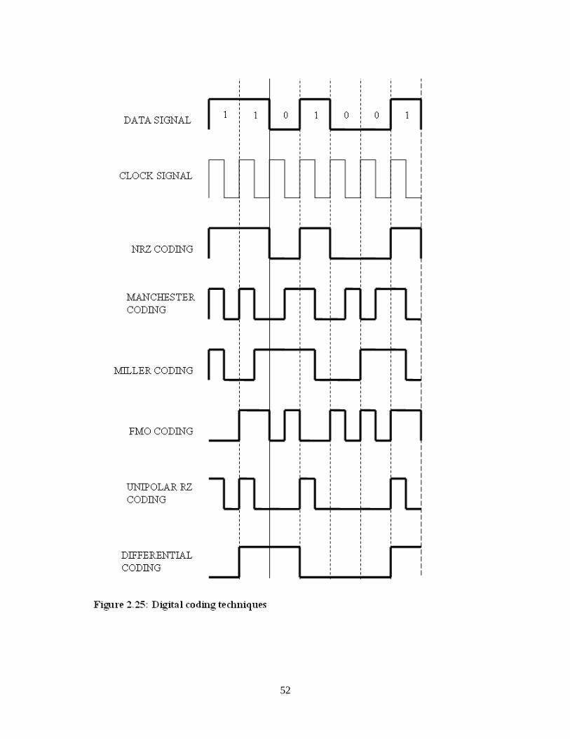
52
53
2.5.5.4 Coupling mechanisms in RFID
The coupling mechanism used by an RFID tag determines the way a circuit on the tag and the
RFID reader influence each other to send and receive information. Based on the read range
created between the reader and a tag, there are three types of coupling: vicinity coupling,
close coupling and long-range coupling.
In close coupling [7, p.49] the read range between the tag and the reader is within 10 mm.
Examples of close coupling are capacitive and magnetic coupling.
In vicinity coupling [7, p.57] the read range is between 10 mm and 1000 mm. This type of
coupling is also called remote coupling. Inductive coupling is an example of vicinity
coupling.
Long-range coupling [6, p.240] offers the highest range of all the coupling methods. The
range extends beyond 1 000 mm. Backscatter coupling is an example of long-range coupling.
Magnetic coupling: In this close coupling method [7, p.49] the reader and the tag are very
close to each other. If the tag is placed within the alternating field of an RFID reader, the tag
draws energy from the magnetic field which powers the tag.
A load resistor placed at the tag can be switched on or off in the tag, which will result in a
fluctuation in the magnetic field generated by the reader. This will result in voltage changes
in the reader antenna.
54
This voltage change effectively works as amplitude modulation. If the timing of the load
resistor is controlled by the data present in the tag, then data can be transferred from the tag
to the reader. This type of data transfer is referred to as load modulation.
Capacitive coupling: This is the second type of close coupling [7, p.49]. For the operation of
this type of coupling the tag has to be inserted into the reader. A property of an RFID system
that functions using capacitive coupling is that antennas are replaced by electrodes.
When the tag is inserted into the reader slot, the electrodes of the reader and the tag come
very close together, forming a capacitor. As with magnetic coupling, data can be transferred
using load modulation in capacitive coupling.
Inductive coupling: This coupling is used in the RFID system for this project. The tag is
powered in the same manner as in magnetic coupling. The tag comes into the magnetic field
of the reader, and by induction transfers power to the microchip in the tag. Inductive coupling
is also referred to as transformer coupling [9, p.96] [7, p.41].
Data transfer is carried out by using load modulation but with some differences. Inductive
coupling uses three main methods to transfer data from the tag to the reader. The first of these
methods is called the sub-carrier method [7, p.42]. In this method the tag rapidly switches its
load resistor on and off. This results in two different frequencies being generated, which are
different from the operating frequency of the reader.
These two frequencies generated by the reader are called sub-carrier frequencies. Data are
transferred by modulation with either of the sub-carrier frequencies.
55
The second method of data transfer is called the sub-harmonic method [7, p.36]. The tag
splits the operating frequency of the reader by an integral value and transmits data back to the
reader at this frequency.
The third method of data transfer in an inductive system is called sequential data transfer
[7, p.41]. Here the power from the reader to the tag is not continuous, so the tag contains a
capacitor circuit which stores the power from the reader when it comes within the magnetic
field generated by the reader.
The tag also contains an oscillator circuit to create its own magnetic field. Since the reader is
powered down at this stage, it is able to detect the field generated by the tag and transfer data.
In this method Frequency Shift Keying is used for transferring data.
The first two methods of data transfer in inductive coupling are full duplex methods while the
last is a sequential method. These methods were discussed in Section 2.5.5.1.
Backscatter coupling method: In this type of coupling the tags contain a photovoltaic cell,
which is powered by the energy (field generated from the magnetic field) of the RFID reader.
The power generated in this manner gives backscatter coupling the longest range [9, p 101]
of all three couplings discussed in this section.
The tag also contains a load resistor at its output as explained previously in the discussion on
coupling methods. The tag communicates back to the reader using the same frequency by
switching the load resistor on or off.

56
The tag is continuously powered by the reader, but the communication between the tag and
the reader is in intervals. The reader sends a request and the tag replies once the data from the
reader have been sent. This makes backscatter coupling the best example for half duplex
communication (Section 2.5.5.1) in RFID. An interesting fact about backscatter coupling is
that it uses the same frequency to power the circuitry as well as transfer data, unlike in close
and vicinity coupling.
2.5.6 Collision and Anti-Collision Procedures in RFID
Collision in an RFID system [17, p.139] can be best explained with an example. The example
used is a possible scenario in an RFID application where the read range exceeds 15 cm. RFID
systems having read range less than 10 cm are not affected by anti-collision as only one user
can be scanned at time.
Suppose a reader is placed in a classroom to register attendance of students entering a class.
If a group of students pass the reader with their student cards (tags) at the same time, the
RFID reader may be confused as to which card to read first. It would be even worse if one of
the tags were not read. This undesirable situation is referred to as collision in RFID.
The seriousness of this problem is such that anti-collision procedures have been put in place
to counter and thereby reduce collision. This section examines some of these procedures and
explains how collision is minimised in an RFID system.
There are two types of anti-collision procedures in use:
• Reader anti-collision algorithm
• Tag anti-collision algorithm.
57
2.5.6.1 Reader anti-collision algorithm
To counter collision, the reader has to communicate with all tags that come within the read
range within a short space of time. This type of communication is referred to as multi-access.
Multi-access is diagrammatically represented in Figure 2.26. Some multi-access procedures
that are used in RFID systems are described in this section. They are:
Space Division Multiple Access (SDMA)
Frequency Division Multiple Access (FDMA)
Time Division Multiple Access (TDMA)
Figure 2.26: Multi-access procedures in RFID systems
(From: RFID Handbook, K. Finkenzeller)
Space Division Multiple Access (SDMA): This multi-access procedure is implemented in
RFID by re-using the channel capacity [7, p.202] of the readers that are separated by
distance.
58
This is implied in a real-life RFID system by combining several readers and aligning them in
such a way that the net read range is vastly increased. Therefore the tags communicating with
the reader will be differentiated based on their angular frequency.
A practical implementation of SDMA is to use a reader with an electronically controlled
directional antenna. This is shown in Figure 2.27.
Figure 2.27: Reader with electronically controlled directional antenna
(From: RFID Handbook, K. Finkenzeller)
(The beam of the antenna shifts position so as to accommodate as many tags as possible).
SDMA is rarely used in RFID systems due to the complexity of the system and the high
implementation cost.
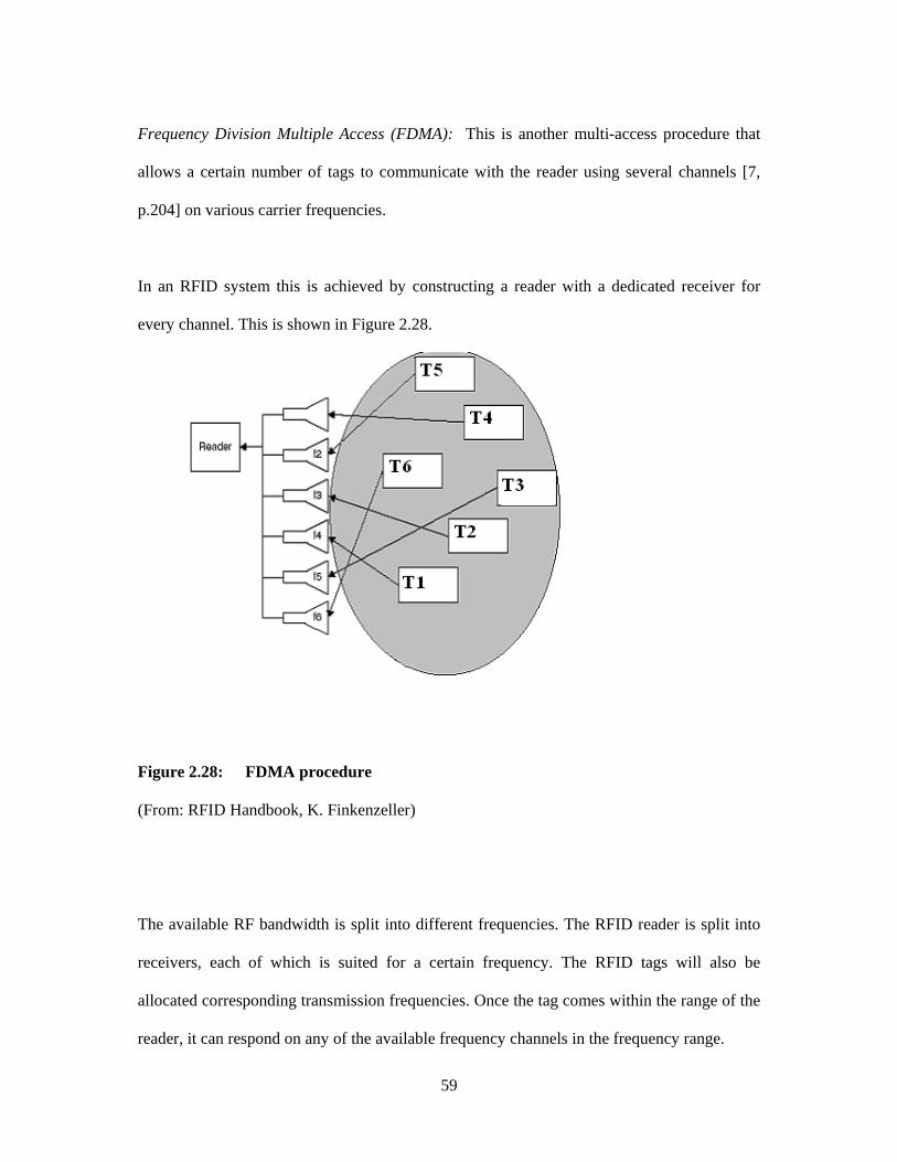
59
Frequency Division Multiple Access (FDMA): This is another multi-access procedure that
allows a certain number of tags to communicate with the reader using several channels [7,
p.204] on various carrier frequencies.
In an RFID system this is achieved by constructing a reader with a dedicated receiver for
every channel. This is shown in Figure 2.28.
Figure 2.28: FDMA procedure
(From: RFID Handbook, K. Finkenzeller)
The available RF bandwidth is split into different frequencies. The RFID reader is split into
receivers, each of which is suited for a certain frequency. The RFID tags will also be
allocated corresponding transmission frequencies. Once the tag comes within the range of the
reader, it can respond on any of the available frequency channels in the frequency range.
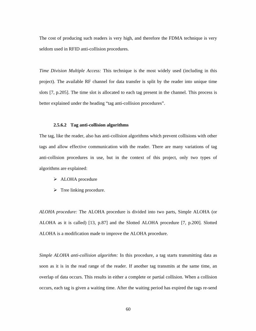
60
The cost of producing such readers is very high, and therefore the FDMA technique is very
seldom used in RFID anti-collision procedures.
Time Division Multiple Access: This technique is the most widely used (including in this
project). The available RF channel for data transfer is split by the reader into unique time
slots [7, p.205]. The time slot is allocated to each tag present in the channel. This process is
better explained under the heading “tag anti-collision procedures”.
2.5.6.2 Tag anti-collision algorithms
The tag, like the reader, also has anti-collision algorithms which prevent collisions with other
tags and allow effective communication with the reader. There are many variations of tag
anti-collision procedures in use, but in the context of this project, only two types of
algorithms are explained:
ALOHA procedure
Tree linking procedure.
ALOHA procedure: The ALOHA procedure is divided into two parts, Simple ALOHA (or
ALOHA as it is called) [13, p.87] and the Slotted ALOHA procedure [7, p.200]. Slotted
ALOHA is a modification made to improve the ALOHA procedure.
Simple ALOHA anti-collision algorithm: In this procedure, a tag starts transmitting data as
soon as it is in the read range of the reader. If another tag transmits at the same time, an
overlap of data occurs. This results in either a complete or partial collision. When a collision
occurs, each tag is given a waiting time. After the waiting period has expired the tags re-send
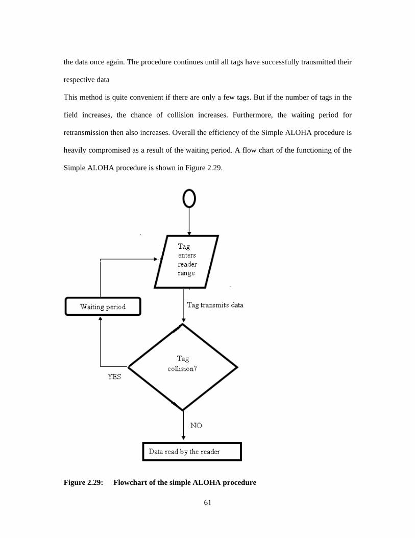
61
the data once again. The procedure continues until all tags have successfully transmitted their
respective data
This method is quite convenient if there are only a few tags. But if the number of tags in the
field increases, the chance of collision increases. Furthermore, the waiting period for
retransmission then also increases. Overall the efficiency of the Simple ALOHA procedure is
heavily compromised as a result of the waiting period. A flow chart of the functioning of the
Simple ALOHA procedure is shown in Figure 2.29.
Figure 2.29: Flowchart of the simple ALOHA procedure
62
The diagram in Figure 2.30 shows the functioning of the simple ALOHA procedure.
Figure 2.30: Functioning of the simple ALOHA procedure
TAG 3 TAG 1 TAG 2 TAG 2
TAG 1
TAG 2
TAG 3
Time
TAGS READ BY READER
Complete collision
Tag 1 read by reader
Tag 2 read by reader
Tag 3 read by reader
Partial collision
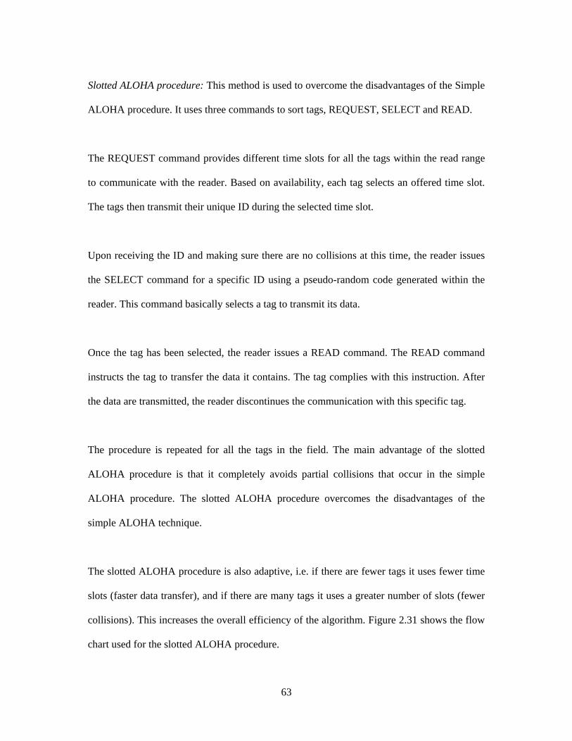
63
Slotted ALOHA procedure: This method is used to overcome the disadvantages of the Simple
ALOHA procedure. It uses three commands to sort tags, REQUEST, SELECT and READ.
The REQUEST command provides different time slots for all the tags within the read range
to communicate with the reader. Based on availability, each tag selects an offered time slot.
The tags then transmit their unique ID during the selected time slot.
Upon receiving the ID and making sure there are no collisions at this time, the reader issues
the SELECT command for a specific ID using a pseudo-random code generated within the
reader. This command basically selects a tag to transmit its data.
Once the tag has been selected, the reader issues a READ command. The READ command
instructs the tag to transfer the data it contains. The tag complies with this instruction. After
the data are transmitted, the reader discontinues the communication with this specific tag.
The procedure is repeated for all the tags in the field. The main advantage of the slotted
ALOHA procedure is that it completely avoids partial collisions that occur in the simple
ALOHA procedure. The slotted ALOHA procedure overcomes the disadvantages of the
simple ALOHA technique.
The slotted ALOHA procedure is also adaptive, i.e. if there are fewer tags it uses fewer time
slots (faster data transfer), and if there are many tags it uses a greater number of slots (fewer
collisions). This increases the overall efficiency of the algorithm. Figure 2.31 shows the flow
chart used for the slotted ALOHA procedure.
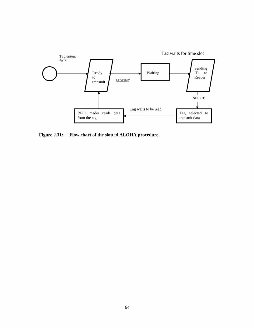
64
Figure 2.31: Flow chart of the slotted ALOHA procedure
Ready to transmit
Waiting
Sending ID to Reader
Tag selected to transmit data
RFID reader reads data from the tag
Tag enters field
REQUEST
Tag waits for time slot
SELECT
Tag waits to be read
65
Figure 2.32: Functioning of the slotted ALOHA procedure
Tree walking procedure: The ALOHA procedure is used in high-frequency systems typically
operating at 13.56 MHz. For ultra-high-frequency applications, typically between 860 and
915 MHz, the tree walking [6, p.437] procedure is used. (The various frequencies used in
RFID are discussed in Section 2.5.7.)
This is a more deterministic scheme which uses a process called ‘singulation’. ‘Singulation’
[13, p.87] is the means whereby an RFID reader identifies a tag with a specific serial number
(tag ID) from a number of tags in the read range of the reader.
TAG 1
TAG 2
TAG 3
TAGS READ BY READER
Complete collision
Tag 1 read by reader
Tag 2 read by reader
Tag 3 read by reader
Time
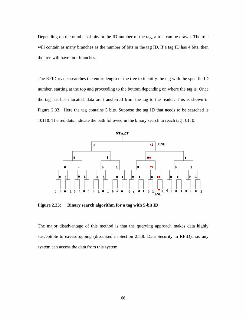
66
Depending on the number of bits in the ID number of the tag, a tree can be drawn. The tree
will contain as many branches as the number of bits in the tag ID. If a tag ID has 4 bits, then
the tree will have four branches.
The RFID reader searches the entire length of the tree to identify the tag with the specific ID
number, starting at the top and proceeding to the bottom depending on where the tag is. Once
the tag has been located, data are transferred from the tag to the reader. This is shown in
Figure 2.33. Here the tag contains 5 bits. Suppose the tag ID that needs to be searched is
10110. The red dots indicate the path followed in the binary search to reach tag 10110.
Figure 2.33: Binary search algorithm for a tag with 5-bit ID
The major disadvantage of this method is that the querying approach makes data highly
susceptible to eavesdropping (discussed in Section 2.5.8: Data Security in RFID), i.e. any
system can access the data from this system.
67
2.5.7 Frequency Ranges used in RFID
The discussion thus far has made clear the importance of radio waves in the functioning of an
RFID system. This section analyses the electromagnetic spectrum with respect to RFID in
more detail.
There are mainly four frequency ranges [6, p.437] used by RFID. They are low frequency
(LF), high frequency (HF), ultra-high frequency (UHF) and microwave frequency. Not all
frequencies in these ranges are used in RFID, as some have already been allocated for other
purposes. The frequency used in RFID is in the Industrial, Scientific and Medical (ISM)
band.
The applications of an RFID reader also vary with operating frequency. Table 2.2 shows the
frequency ranges used in RFID. It also shows the applications at the various frequencies.
Table 2.2: Frequency ranges used in RFID
Frequency Range Common frequencies used in RFID
Typical application Max. read range (theoretical)
LF - low frequency (30 to300 kHz)
30 kHz 125 kHz 135 kHz 300 kHz
Access control Animal identification Lot identification Chemical distribution
500 mm
HF - high frequency (3 to 30 MHz)
3.0 MHz 13.56 MHz 30.0 MHz
Warehouse management Tracking and monitoring Baggage checking Library management Parcel tracking Security
Up to 100 mm
68
applications
UHF – ultra-high frequency (300 MHz to 1 GHz)
300 MHz 433 MHz 866 MHz (Europe) 915 MHz (USA)
Retail vendors Toll roads Warehouse logistics Long-range applications
4 metres
Microwave frequency > 3 GHz
2.45 GHz 3.0 GHz
Long-range applications Freight tracking
6-10 metres
2.5.7.1 Standardisation in RFID
Standardisation in RFID [6, p.89] refers to the regulatory codes set by an international body
for all products. Standards ensure a minimum level of product characteristics such as quality,
interoperability, reliability and safety for the end user.
RFID technology and RFID systems rely heavily on the electromagnetic spectrum for
communication, as previously discussed in this chapter. Therefore it is essential that RFID
devices (readers and tags) should adhere to specific standards in the countries in which they
are used.
The international bodies that set and monitor the standard for RFID technology are ISO
(International Standards Organization) and IEC (International Electro technical Commission).
These bodies are usually supported by a local body in the country in which the RFID
products are used. In South Africa (where the study for this thesis was done) the body
responsible is ICASA (Independent Communications Authority of South Africa).
There is much data pertaining to these ISO standards. Some are still being prepared at
present, and others undergo constant scrutiny and changes. Therefore this section only gives
69
the essence of the relevant standards. However, the two standards employed in the RFID
product used in this project, ISO 14443 and ISO 15693, are treated in depth.
2.5.7.1.1 Standards for animal identification
The standards used for animal identification [6, p209] are ISO 11784, ISO 11785 and
ISO 14223.
The ISO 11784 [7, p229] standard gives the code structure for radio frequency
identification of animals. Basically the identification code in the tags for animal
identification consists of 64 bits. Each of these bits (or block of bits) describes a
certain function.
ISO 11785 [7, p.230] is the second standard for animal identification. It deals with the
reader frequency (134 kHz ± 1.8 kHz) and the operation of the RFID system in
full/half duplex and sequential mode.
ISO 14223 [7, p.233] is the third standard in animal identification. It defines the high-
frequency (HF) interface and data structure of active transponders. It consists of three
parts:
Part 1 - Air interface
Part 2 - Code and command structure
Part 3 - Application details
70
2.5.7.1.2 Standards for smart cards
This is the major area of concern as far as this project is concerned. The standards
discussed in this section concern the tags and reader used in this project. Three
standards are defined under this heading: ISO 10536 [7, p.237], ISO 14443 [9, p.195]
and ISO 15693 [9, p.204].
ISO 10536 defines the standards for close coupling of smart cards. RFID systems
adhering to this standard have a range of up to 10 mm. The standards are subdivided
into four parts.
Part 1 - Physical characteristics: These define the mechanical dimensions and
physical properties of close-coupling cards.
Part 2 - Dimensions and locations of coupling areas: In close-coupling techniques
(Section 2.5.5.3) antennas are replaced with electrodes. This part specifies the
position and dimensions of the coupling elements.
Part 3 - Electrical signals and reset procedures: This part defines how the close-
coupled cards are powered, how data are transferred from card to reader (the magnetic
and capacitive coupling techniques used) and how data are transferred from reader to
card (including the modulation and data coding).
Part 4 - Answer to reset transmission: This deals with the transmission protocols
used in data transfer. This section is still in preparation by ISO.
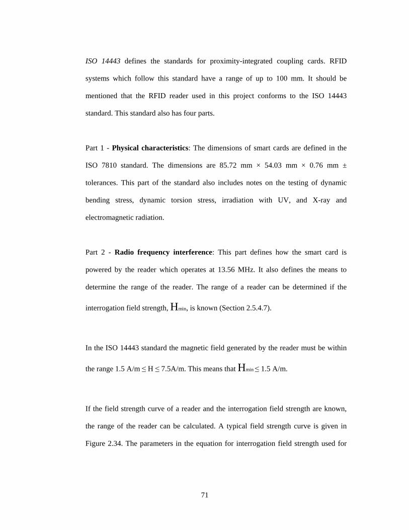
71
ISO 14443 defines the standards for proximity-integrated coupling cards. RFID
systems which follow this standard have a range of up to 100 mm. It should be
mentioned that the RFID reader used in this project conforms to the ISO 14443
standard. This standard also has four parts.
Part 1 - Physical characteristics: The dimensions of smart cards are defined in the
ISO 7810 standard. The dimensions are 85.72 mm × 54.03 mm × 0.76 mm ±
tolerances. This part of the standard also includes notes on the testing of dynamic
bending stress, dynamic torsion stress, irradiation with UV, and X-ray and
electromagnetic radiation.
Part 2 - Radio frequency interference: This part defines how the smart card is
powered by the reader which operates at 13.56 MHz. It also defines the means to
determine the range of the reader. The range of a reader can be determined if the
interrogation field strength, Hmin, is known (Section 2.5.4.7).
In the ISO 14443 standard the magnetic field generated by the reader must be within
the range 1.5 A/m ≤ H ≤ 7.5A/m. This means that Hmin ≤ 1.5 A/m.
If the field strength curve of a reader and the interrogation field strength are known,
the range of the reader can be calculated. A typical field strength curve is given in
Figure 2.34. The parameters in the equation for interrogation field strength used for
72
drawing the curve are as follows: antenna current, I = 1A, antenna diameter, D = 150
mm, number of windings, N = 1.
Figure 2.34: Field strength curve for a proximity-integrated circuit card
(From: RFID Handbook, K. Finkenzeller)
If Hmin = 1.5 A/m, then it is clearly shown by Figure 2.34 that the Hmin line cuts the
curve at 100 mm, thereby proving that the range of the reader is about 100 mm.
A common communication interface could not be developed for the ISO 14443
standard, so two types of smart card are used in this instance. They are TYPE A and
TYPE B smart cards. The ISO 14443 standard supports communication with both
types of card.
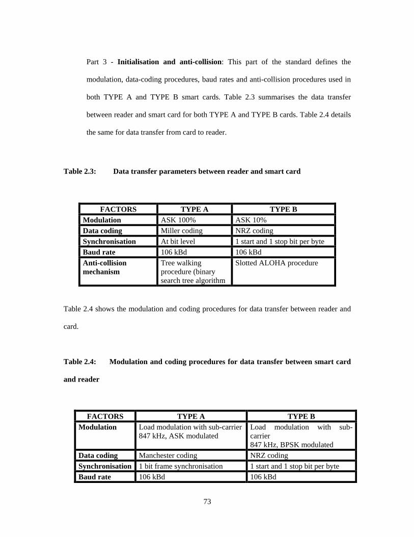
73
Part 3 - Initialisation and anti-collision : This part of the standard defines the
modulation, data-coding procedures, baud rates and anti-collision procedures used in
both TYPE A and TYPE B smart cards. Table 2.3 summarises the data transfer
between reader and smart card for both TYPE A and TYPE B cards. Table 2.4 details
the same for data transfer from card to reader.
Table 2.3: Data transfer parameters between reader and smart card
Table 2.4 shows the modulation and coding procedures for data transfer between reader and
card.
Table 2.4: Modulation and coding procedures for data transfer between smart card
and reader
FACTORS TYPE A TYPE B Modulation Load modulation with sub-carrier
847 kHz, ASK modulated Load modulation with sub-carrier 847 kHz, BPSK modulated
Data coding Manchester coding NRZ coding
Synchronisation 1 bit frame synchronisation 1 start and 1 stop bit per byte
Baud rate 106 kBd 106 kBd
FACTORS TYPE A TYPE B Modulation ASK 100% ASK 10%
Data coding Miller coding NRZ coding
Synchronisation At bit level 1 start and 1 stop bit per byte
Baud rate 106 kBd 106 kBd
Anti-collision mechanism
Tree walking procedure (binary search tree algorithm
Slotted ALOHA procedure
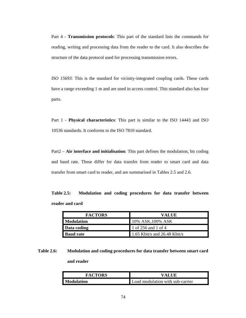
74
Part 4 - Transmission protocols: This part of the standard lists the commands for
reading, writing and processing data from the reader to the card. It also describes the
structure of the data protocol used for processing transmission errors.
ISO 15693: This is the standard for vicinity-integrated coupling cards. These cards
have a range exceeding 1 m and are used in access control. This standard also has four
parts.
Part 1 - Physical characteristics: This part is similar to the ISO 14443 and ISO
10536 standards. It conforms to the ISO 7810 standard.
Part2 – Air interface and initialisation : This part defines the modulation, bit coding
and baud rate. These differ for data transfer from reader to smart card and data
transfer from smart card to reader, and are summarised in Tables 2.5 and 2.6.
Table 2.5: Modulation and coding procedures for data transfer between
reader and card
FACTORS VALUE Modulation 10% ASK,100% ASK
Data coding 1 of 256 and 1 of 4
Baud rate 1.65 Kbit/s and 26.48 Kbit/s
Table 2.6: Modulation and coding procedures for data transfer between smart card
and reader
FACTORS VALUE Modulation Load modulation with sub-carrier
75
Data coding Manchester encoding
Baud rate 6.62 Kbit/s and 26.48 Kbit/s
Part 3 - Protocols and Part 4 - Registration of Applications are still being prepared
by the governing bodies. Therefore they cannot be detailed at this point in time.
2.5.7.2 Container identification
The ISO standard defines the standard used in the identification of containers using active
tags. These tags use microwave transponders. These are activated by unmodulated carrier
frequencies ranging from 850 to 950 MHz and from 2.4 GHz to 2.5 GHz. The tags use
backscatter coupling (Section 2.5.5.3) for data transmission via FSK modulation.
2.5.7.3 Item management
This is the standard used in item management, especially warehouse management. The
standard used is ISO 18000 [7, p.268]. The standard consists of six parts:
Part 1 - Generic parameter for Air Interface Communication for Globally Accepted
Frequencies
Part 2 - Parameters for Air Interface Communication below 135 kHz
Part 3 - Parameters for Air Interface Communication at 13.56 MHz
Part 4 - Parameters for Air Interface Communication at 2.45 GHz
Part 5 - Parameters for Air Interface Communication at 5.8 GHz
Part 6 - Parameters for Air Interface Communication – UHF frequency band
2.5.8 Data Integrity in RFID
As RFID involves data transfer using contactless technology, it is highly probable that some
form of interference may occur during data transfer. It is essential for the proper functioning
76
of an RFID system that the data being transmitted (from tag to reader or vice versa) should
not contain any errors. In other words, the integrity of the data should be maintained.
This section examines the different methods used for maintaining data integrity in RFID.
This can be done by using checksum procedures. Three main types of checksum procedures
are used in RFID: the parity checking method [7, p.195], the Longitudinal Redundancy
Check (LRC) method [7, p.196] and the Cyclic Redundancy Check (CRC) method [7, p.197].
2.5.8.1 Parity checking method
This is the simplest checksum method available. It is also called the Vertical Redundancy
Check method (VRC). In this method a parity bit is assigned to each transmitted data bit.
Before the data are transmitted, a decision is taken to check for either odd or even parity by
the sender and receiver. This is done to maintain synchronisation between both parties (tag
and reader in RFID).
If odd parity is used then there should be an odd number of 1’s in the sent data bits, and if
even parity is used then there should be an even number of 1’s in the data bits received at the
receiver end. A simple parity check method can be implemented using XOR (EX-OR) gates.
XOR gates are basic adders. By adding the two binary inputs to an XOR gate, their sum is
obtained.
If even parity (even number of 1’s) is used the sum of the bits is always equal to zero, and if
odd parity (odd number of 1’s) is used the output of the XOR gate will be equal to 1.
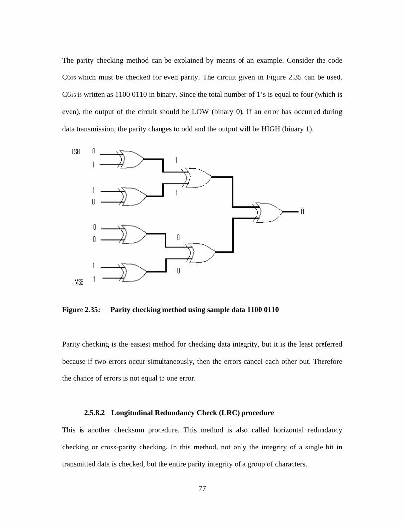
77
The parity checking method can be explained by means of an example. Consider the code
C616 which must be checked for even parity. The circuit given in Figure 2.35 can be used.
C616 is written as 1100 0110 in binary. Since the total number of 1’s is equal to four (which is
even), the output of the circuit should be LOW (binary 0). If an error has occurred during
data transmission, the parity changes to odd and the output will be HIGH (binary 1).
Figure 2.35: Parity checking method using sample data 1100 0110
Parity checking is the easiest method for checking data integrity, but it is the least preferred
because if two errors occur simultaneously, then the errors cancel each other out. Therefore
the chance of errors is not equal to one error.
2.5.8.2 Longitudinal Redundancy Check (LRC) procedure
This is another checksum procedure. This method is also called horizontal redundancy
checking or cross-parity checking. In this method, not only the integrity of a single bit in
transmitted data is checked, but the entire parity integrity of a group of characters.
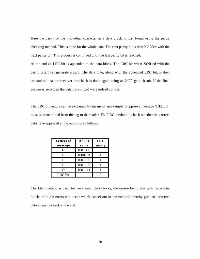
78
Here the parity of the individual character in a data block is first found using the parity
checking method. This is done for the whole data. The first parity bit is then XOR’ed with the
next parity bit. This process is continued until the last parity bit is reached.
At the end an LRC bit is appended to the data block. The LRC bit when XOR’ed with the
parity bits must generate a zero. The data byte, along with the appended LRC bit, is then
transmitted. At the receiver the check is done again using an XOR gate circuit. If the final
answer is zero then the data transmitted were indeed correct.
The LRC procedure can be explained by means of an example. Suppose a message ‘HELLO’
must be transmitted from the tag to the reader. The LRC method to check whether the correct
data have appeared at the output is as follows:
Letters of message
ASCII value
LRC parity
H 1001000 0 E 1000101 1 L 1001100 1 L 1001100 1 O 1001111 1
LRC bit 0
The LRC method is used for very small data blocks, the reason being that with large data
blocks multiple errors can occur which cancel out in the end and thereby give an incorrect
data integrity check at the end.
79
2.5.8.3 Cyclic Redundancy Check (CRC) procedure
The Cyclic Redundancy Check is another technique for detecting errors in digital data. It
does not correct the errors when detected. In the CRC method a certain number of check bits
are appended to the data message that is to be transmitted. This is called the checksum.
The receiver checks whether the received checksum agrees with the checksum sent with the
data when it is received. If an error has occurred during transmission, the receiver asks for a
re-transmission of the data. The mathematical procedures and hardware implementations are
similar to those discussed in the parity checking and longitudinal redundancy checking
methods.
2.5.9 Security in RFID
Security is a vital aspect of any technology, none more so than in RFID technology. Since
RFID involves contactless data transfer, it is highly prone to some security threats. This
section discusses some of the possible security threats to RFID as well as measures against
the threats.
2.5.9.1 Security threats in RFID
There are different types of security threats in RFID. Those analysed here are:
Cloning
Spoofing
Eavesdropping.
80
Cloning: This type of threat arises when an ‘attacker’, posing as the reader, intercepts data
from an RFID tag. The attacker then re-transmits the data. In this way the attacker abuses the
RFID application by cloning [18, p.292-295] a genuine RFID tag.
This type of security threat is exemplified by automatic pay-points using RFID technology.
The attacker can read and intercept an encrypted code from a tag using a reader which can
read data from similar tags. Once the attacker has read the tag, he can re-transmit the data at
the pay-point using the encrypted data, thus avoiding payment.
Spoofing: This type of threat arises when a foreign data carrier is placed within the
interrogation zone of the reader with malicious intent [18, p.329]. If the security protocols of
an RFID reader are known, the attacker can design a tag which follows similar security
protocols and contains the same data as the original tag. This ‘spoofed’ tag can be used to
gain access to an RFID-enabled room or building which is otherwise out of bounds.
Eavesdropping: All tags follow certain standards as explained in the study (Section 2.5.8).
The readers are designed to capture data based on the standards followed by the tags. If the
standards and protocols followed by a tag are known, the attacker can design a reader that can
read data from a tag if the reader is brought within the data transfer range of the tag
[18, p.283]. This is especially dangerous if the tag stores highly confidential data.
2.5.9.2 Overcoming security threats in RFID
The security threats mentioned in Section 2.5.9.1 can be overcome by using two methods:
physical methods and technical methods.
81
Physical methods use certain physical parameters of RFID technology to create a barrier for
unauthorised data access. Two methods are used here:
The Faraday cage method
The read range limiting method.
Faraday cage method: A Faraday cage [18, p.330] is an enclosure formed by a conducting
material. Such an enclosure blocks external static fields. An external electric field on the
conductor will cause the electric charges within the conducting material to re-align in such a
way as to nullify the net electric field in the interior of the cage. This is shown in Figure 2.36.
Figure 2.36: Faraday cage
- - - - -- - - - - -- - - - - - - - - - - - -
- -
- -
- -
- -
+
+
+
+
+
+
+
Positively charged external field
The charges inside the conductor align negatively due to the positive charge in the exterior.
Net charge inside the cage is equal to zero
Faraday cage
82
A Faraday cage has the same effect on radio waves. The radio waves are unable to penetrate
a Faraday’s cage. Therefore if an RFID tag is placed inside a Faraday cage, the interrogation
zone created by the reader will not have an effect on the tag and therefore data from the tag
cannot be accessed.
This method requires the user to place the tag in a metallic enclosure at all times except when
it is read by the authorised reader. The new American passports, which have embedded RFID
tags, have metallic enclosures which shield them from unauthorised access.
A Faraday cage alone is not a very effective method to ensure RFID security. Therefore it is
often incorporated with other security features such as encryption (discussed under technical
security methods).
Read range limiting method: Most RFID fraud occurs when the attacker uses a tag to capture
the data from a tag. If the read range of the tag is significantly reduced to a few centimetres, it
would be practically difficult for an attacker to bring the RFID reader close enough to capture
data from the tag.
This method reduces the cost of an RFID system, but offers minimal security as close
monitoring by an individual is necessary to avoid malpractice. Therefore this method cannot
be used for applications that store confidential data.
Technical methods of securing data in RFID use mathematical algorithms and electrical
circuitry to prevent data from being accessed by unauthorised personnel. There are mainly
four methods of accomplishing this:
83
Kill command
Blocking
Mutual symmetrical authentication
Encryption.
Kill command: The RFID tag not only transfers the data it contains, but acts as a transponder
which allows it to be monitored from any given distance depending on the tag used. This is
an advantage in the shipping industry where freight can be tagged and monitored from shore.
But it becomes a major disadvantage and a security threat if the tag can be tracked without
the knowledge of the user.
This can be better explained by an application of RFID in the textile industry [18, p.291].
Textile material can be tagged for keeping track of inventory at the time of fabrication. The
same tag can be used in a retail store up to the point of sale. But after the point of sale, if the
tag continues to be active, it poses a threat to the consumer as his/her whereabouts can be
tracked by an attacker with a reader.
This obvious breach of security can be overcome by using a kill command [7, p.201]. The
tags are designed such that at the point of sale when it is read by the reader, the reader
executes a kill command which kills or deactivates the tag.
The kill command is a good technique to ensure security and privacy in RFID, but severely
limits the functionality of RFID tags beyond the point of sale.
84
Blocking: This is a modification of the kill command technique. The difference is that the
tags are given a privacy bit. The privacy bit can be activated or deactivated as intended by the
user. The privacy bit can be set to ‘0’ at or before the point of sale. Once it has passed the
point of sale the privacy bit can be activated.
Blocking [13, p.332-335] requires a blocker tag which makes a normal tag unreadable in its
presence but allows the same tag to be read once the blocker tag is removed. The advantage
of blocking is that the tags are not killed, but are in effect put into sleep mode when required,
thereby enhancing the life cycle of a tag as well as increasing the functionality of RFID
technology beyond the point of sale.
Mutual symmetrical authentication: This is a security measure used by the reader and the tag.
In this method both the reader and the tag check each other’s knowledge of a common
crypto-logical key [7, p.221].
The tag and the reader have a common crypto-logical key, K. When the tag enters the
interrogation zone of the reader, both the reader and the tag will not be sure if they are
communicating with the correct device.
In order to ascertain the validity of the tag in the interrogation zone, the reader sends a
request for a random number from the tag. The tag responds by sending a random number,
Ra. The reader encrypts this random number using the common crypto-logical key and sends
it back along with another randomly generated number Rb.
85
If the tag uses the same crypto-logical key as the reader, it will decrypt the message from the
reader. The tag checks to make sure that the decrypted message is similar to the one it
initially generated (Ra).
This process is reversed by the tag which encrypts the randomly generated number, Rb,
which it received from the reader and transmits it back to the reader. If the reader is able to
decipher the message, then the reader and the tag have mutually authenticated each other
using a common crypto-logical key.
Encryption: This is the most logical method for securing data in RFID. Using encryption
[7, p.224], the data to be transmitted from the tag to the reader are encrypted using a crypto-
logical key K and a secret algorithm. The data can only be decrypted by the attacker if he
knows the secret key as well as the secret algorithm. The secret algorithm is not a fixed one;
it is generated at the time of encryption, so it cannot be decoded easily.
There are two types of encryption used in RFID: symmetrical and asymmetrical. Symmetrical
encryption involves using the same key for ciphering and deciphering the data. If two
different sets of ciphering keys are used for encrypting and decrypting data, then it falls under
asymmetrical encryption.
Symmetrical encryption is most often used in RFID. The data to be transmitted are encrypted
using a crypto-logical key. The ciphered data are then passed from the tag to the reader. A
potential attacker cannot do anything with the ciphered data if he does not have the secret key
or the secret algorithm used for encryption. The ciphered data can only be deciphered by the
reader which has the secret key and the algorithm used for ciphering the data.
86
2.6 Need for Wireless Link between RFID Reader and RFID Middleware
Typical readers come with an RS232 or RS485 interface. These interfaces can be connected
to the RFID middleware. However, wired links have some disadvantages, namely:
Mobility limitations
Flexibility limitations
Cost of installation and maintenance
Architectural limitations.
Mobility: A wired connection between a reader and the RFID middleware will mean that the
reader has to be made stationary. In a system such as RFID in which all the components work
on contact-less data transfer, a stationary reader will reduce overall mobility.
Flexibility: An RFID tagged object is usually placed in areas that cannot be easily accessed
by human beings. A handheld RFID reader (discussed in Section 2.5.2.1) will be able to read
these tags. If the handheld reader is wired to the middleware, the flexibility of the RFID
system is compromised.
Cost of installation and maintenance: To set up a wired network for the RFID system in a
university environment is expensive as many metres of cable have to be linked between each
reader and the RFID middleware. The cost concerns do not end there. If a fault occurs
somewhere along the line, the entire length of the cable has to be replaced.
Architectural limitations: Another problem with the wired approach is linking between a
reader and the RFID middleware which are located in two different buildings. It is not
87
practical to have a wired link between two buildings as the cables are exposed to
environmental factors.
This project examines the viability of a wireless link between the reader and the RFID
middleware to overcome these challenges. A number of wireless technologies available on
the market today were closely examined for this purpose. Three technologies were short-
listed. They are Bluetooth technology, Wireless Local Area Network (WLAN) technology
and ZigBee technology.
The different factors that were considered when short-listing the three technologies
mentioned in the last paragraph were cost, power consumption, data bandwidth capabilities,
transmission range and system complexity.
Section 2.7 compares the three technologies based on the criteria mentioned in the above
paragraph. This comparison was undertaken to determine which wireless technique is most
suitable for the desired end application of this project. Table 2.7 shows the comparison.

88
2.7 Comparison between Wireless Technologies
Table 2.7: Comparison between wireless technologies
The comparison shows that all three technologies have their own advantages and
disadvantages and that any one of the three can be used for this project. WLAN technology
would probably be the cheapest as the Central University of Technology (where this project
was done) already has a well-established infrastructure. But WLAN needs an uninterrupted
DC power supply as the battery life is very short.
Bluetooth technology also has distinct advantages (cost and convenience), but a transmission
range of only 10 metres was an obvious disadvantage along with the limited battery life.
Throughout this project, the main idea was to stretch the limits of knowledge and study new
techniques and methods which have not been used previously. Therefore when ZigBee
presented itself as a possible cable replacement method, it was carefully considered. The
MARKET NAME ZIGBEE WLAN BLUETOOTH
Standard IEEE 802.15.4 IEEE 802.11 IEEE 802.11.1
Application focus Monitoring and Control
Web applications, e-mail
Cable replacement
Battery life (days) 100-1000 0.5-5 1-7
Bandwidth (KB/s) 20-250 11000 720
Transmission range (metres)
1-100 1-100 1-10
Advantages Reliability, cost, power
Speed, flexibility Cost, convenience
System Complexity
Low Medium Medium
Shortfalls Relatively new technology
Cost Range
89
advantages of battery life and transmission range obviously strengthened the case and this
ultimately resulted in the use of ZigBee technology as a wireless link between the RFID
reader and the middleware. Section 2.8 analyses ZigBee technology in detail.
2.8 ZigBee Technology
ZigBee [19, p.3] is a low data rate, low-power consumption, low-cost, wireless networking
protocol. It is based on the IEEE 802.15.4 standard for low data rate Wireless Personal Area
Networks (WPAN). As seen from the comparison in the last section, ZigBee consumes very
little power and transfers small packets of data over large networks with a substantial
transmission range.
ZigBee technology is developed by ZigBee Alliance [19] (an association of companies that
collaborate to develop standards and products for reliable, cost-effective, low-power wireless
networking) and IEEE 802.15.4.
The technical specifications of ZigBee technology are based on the ZigBee stack. The
ZigBee stack is made up of IEEE 802.15.4 [20] standards and the ZigBee standards [20].
IEEE 802.15.4 defines the physical [19, p9] and Media Access Control (MAC) layer [21]
while the ZigBee standard defines the network layer [20] and the application layer [21]. The
ZigBee stack and its components are defined in Section 2.8.2.
The discussion of ZigBee technology starts with a look at the different components of a
ZigBee system. This is to give a rough idea of the working of ZigBee technology. Next, the
different network topologies used in ZigBee are described in Section 2.8.2. The technical
90
details of ZigBee are then studied (Section 2.8.4 and 2.8.5) by analysing the ZigBee stack in
Section 2.8.3, and finally issues of security in ZigBee technology are studied in Section 2.8.6.
2.8.1 Components of a ZigBee System
A typical ZigBee wireless network system consists of three types of devices:
ZigBee coordinator
ZigBee router
ZigBee end device.
2.8.1.1 ZigBee coordinator
This is the most intelligent unit in a ZigBee wireless system. It is also called a Fully
Functional Device or FFD. The coordinator is connected to middleware. When the
coordinator is powered up, it scans the network to establish a connection. The ZigBee
coordinator [22] establishes connection with the other components in the system by a unique
16-bit network address. This unique network address is used for finding each device in a
ZigBee network. The coordinator can communicate with all the other components in a
ZigBee network. There will always be only one coordinator per network.
2.8.1.2 ZigBee router
The ZigBee router [22] is an optional device in a ZigBee wireless network. It has less
processing capability than a coordinator, and is therefore referred to as a Reduced Functional
Device (RFD). The router can also be a Full Functional Device (FFD). The main purpose of
the router is to connect a coordinator and an end device. The number of routers in a network
is dependent solely on the size of the network.

91
ZigBee can drive up to 256 devices [19, p.4] in a single wireless network. It is in such a
scenario that the router becomes essential, as the router can transmit the necessary data from
the coordinator (given the correct destination address) to the end device. The router can
communicate with both the coordinator as well as the end device.
2.8.1.3 ZigBee end device
The ZigBee end device [22] is connected to the end-user application. This component is
usually powered down (sleep mode) and only active when it has to transmit data. Once it has
transmitted data, it goes back to sleep, thereby saving battery life. The ZigBee end device can
communicate only with the coordinator and cannot transfer data directly to other end devices
in a network.
A simple diagrammatical representation of the ZigBee components and how they would work
in real life is given in Figure 2.37.
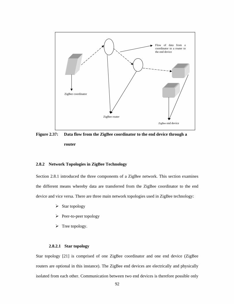
92
Figure 2.37: Data flow from the ZigBee coordinator to the end device through a
router
2.8.2 Network Topologies in ZigBee Technology
Section 2.8.1 introduced the three components of a ZigBee network. This section examines
the different means whereby data are transferred from the ZigBee coordinator to the end
device and vice versa. There are three main network topologies used in ZigBee technology:
Star topology
Peer-to-peer topology
Tree topology.
2.8.2.1 Star topology
Star topology [21] is comprised of one ZigBee coordinator and one end device (ZigBee
routers are optional in this instance). The ZigBee end devices are electrically and physically
isolated from each other. Communication between two end devices is therefore possible only
ZigBee coordinator
ZigBee router
ZigBee end device
Flow of data from a coordinator to a router to the end device
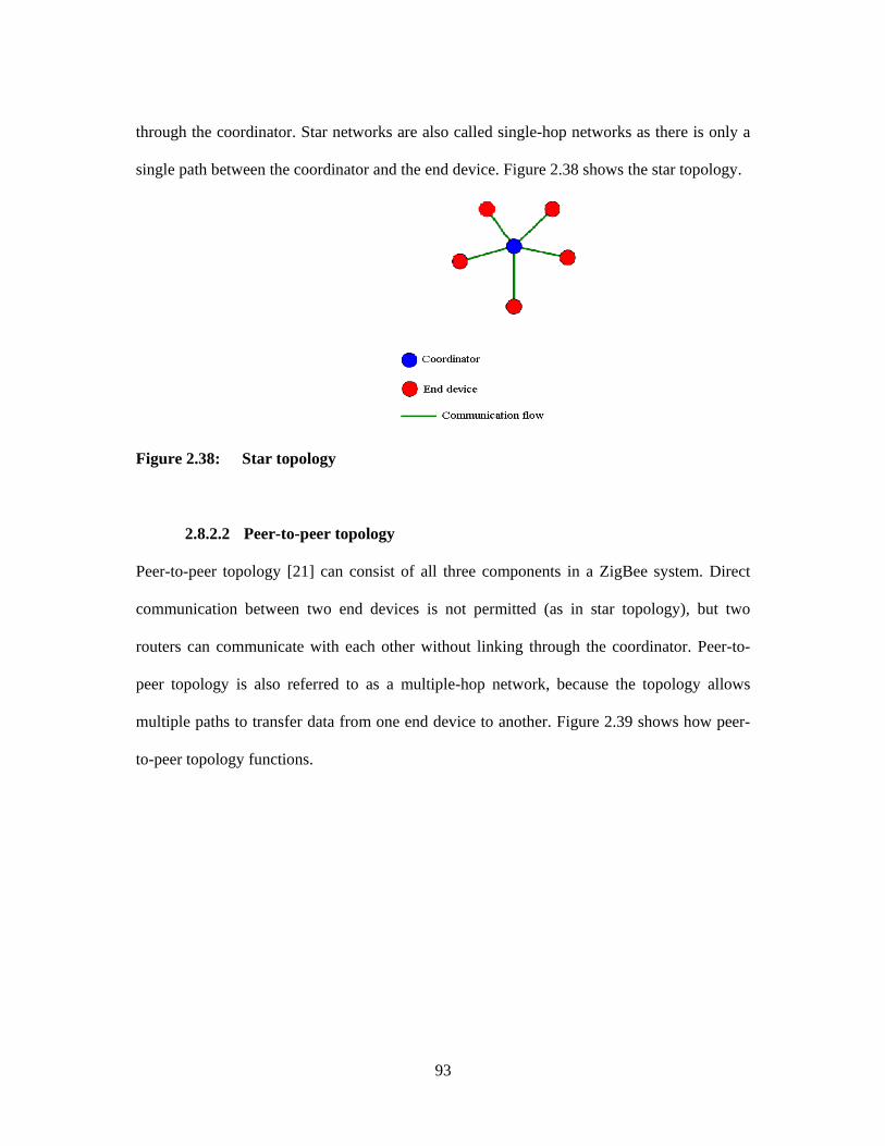
93
through the coordinator. Star networks are also called single-hop networks as there is only a
single path between the coordinator and the end device. Figure 2.38 shows the star topology.
Figure 2.38: Star topology
2.8.2.2 Peer-to-peer topology
Peer-to-peer topology [21] can consist of all three components in a ZigBee system. Direct
communication between two end devices is not permitted (as in star topology), but two
routers can communicate with each other without linking through the coordinator. Peer-to-
peer topology is also referred to as a multiple-hop network, because the topology allows
multiple paths to transfer data from one end device to another. Figure 2.39 shows how peer-
to-peer topology functions.
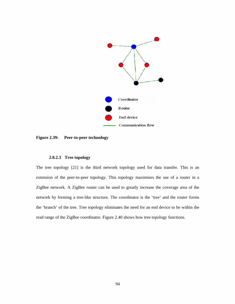
94
Figure 2.39: Peer-to-peer technology
2.8.2.3 Tree topology
The tree topology [21] is the third network topology used for data transfer. This is an
extension of the peer-to-peer topology. This topology maximises the use of a router in a
ZigBee network. A ZigBee router can be used to greatly increase the coverage area of the
network by forming a tree-like structure. The coordinator is the ‘tree’ and the router forms
the ‘branch’ of the tree. Tree topology eliminates the need for an end device to be within the
read range of the ZigBee coordinator. Figure 2.40 shows how tree topology functions.
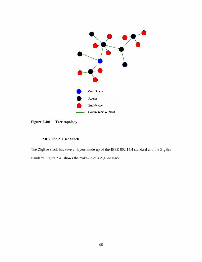
95
Figure 2.40: Tree topology
2.8.3 The ZigBee Stack
The ZigBee stack has several layers made up of the IEEE 802.15.4 standard and the ZigBee
standard. Figure 2.41 shows the make-up of a ZigBee stack.
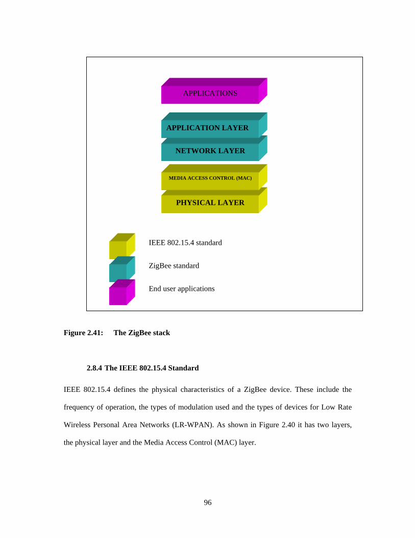
96
Figure 2.41: The ZigBee stack
2.8.4 The IEEE 802.15.4 Standard
IEEE 802.15.4 defines the physical characteristics of a ZigBee device. These include the
frequency of operation, the types of modulation used and the types of devices for Low Rate
Wireless Personal Area Networks (LR-WPAN). As shown in Figure 2.40 it has two layers,
the physical layer and the Media Access Control (MAC) layer.
PHYSICAL LAYER
MEDIA ACCESS CONTROL (MAC)
LAYER
NETWORK LAYER
APPLICATION LAYER
APPLICATIONS
IEEE 802.15.4 standard
ZigBee standard
End user applications
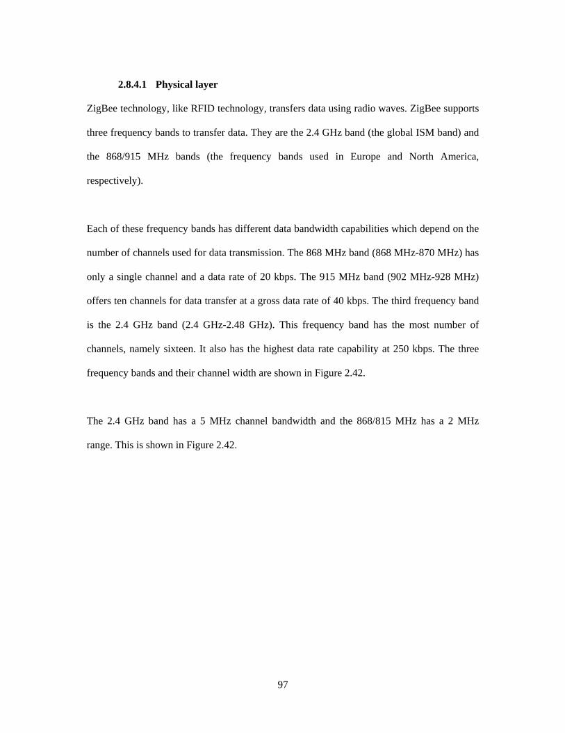
97
2.8.4.1 Physical layer
ZigBee technology, like RFID technology, transfers data using radio waves. ZigBee supports
three frequency bands to transfer data. They are the 2.4 GHz band (the global ISM band) and
the 868/915 MHz bands (the frequency bands used in Europe and North America,
respectively).
Each of these frequency bands has different data bandwidth capabilities which depend on the
number of channels used for data transmission. The 868 MHz band (868 MHz-870 MHz) has
only a single channel and a data rate of 20 kbps. The 915 MHz band (902 MHz-928 MHz)
offers ten channels for data transfer at a gross data rate of 40 kbps. The third frequency band
is the 2.4 GHz band (2.4 GHz-2.48 GHz). This frequency band has the most number of
channels, namely sixteen. It also has the highest data rate capability at 250 kbps. The three
frequency bands and their channel width are shown in Figure 2.42.
The 2.4 GHz band has a 5 MHz channel bandwidth and the 868/815 MHz has a 2 MHz
range. This is shown in Figure 2.42.
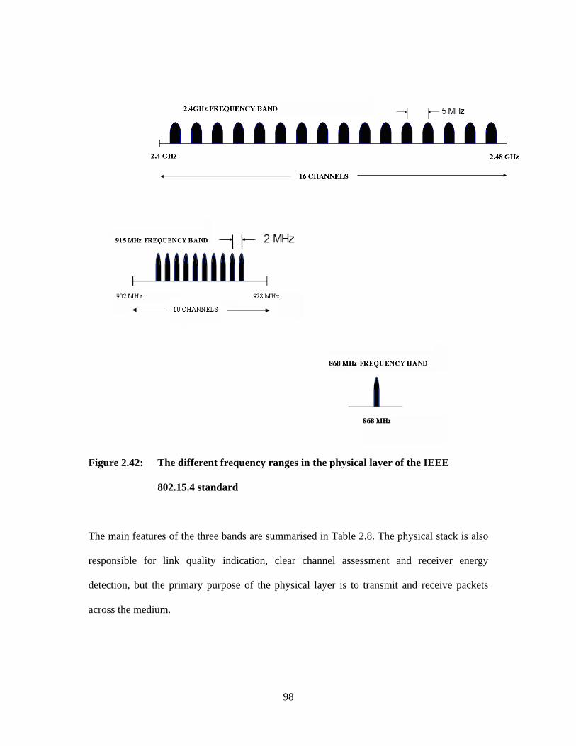
98
Figure 2.42: The different frequency ranges in the physical layer of the IEEE
802.15.4 standard
The main features of the three bands are summarised in Table 2.8. The physical stack is also
responsible for link quality indication, clear channel assessment and receiver energy
detection, but the primary purpose of the physical layer is to transmit and receive packets
across the medium.
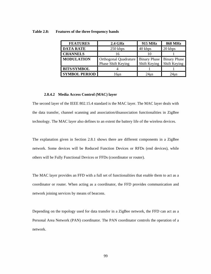
99
Table 2.8: Features of the three frequency bands
2.8.4.2 Media Access Control (MAC) layer
The second layer of the IEEE 802.15.4 standard is the MAC layer. The MAC layer deals with
the data transfer, channel scanning and association/disassociation functionalities in ZigBee
technology. The MAC layer also defines to an extent the battery life of the wireless devices.
The explanation given in Section 2.8.1 shows there are different components in a ZigBee
network. Some devices will be Reduced Function Devices or RFDs (end devices), while
others will be Fully Functional Devices or FFDs (coordinator or router).
The MAC layer provides an FFD with a full set of functionalities that enable them to act as a
coordinator or router. When acting as a coordinator, the FFD provides communication and
network joining services by means of beacons.
Depending on the topology used for data transfer in a ZigBee network, the FFD can act as a
Personal Area Network (PAN) coordinator. The PAN coordinator controls the operation of a
network.
FEATURES 2.4 GHz 915 MHz 868 MHz DATA RATE 250 kbps 40 kbps 20 kbps CHANNELS 16 10 1 MODULATION Orthogonal Quadrature
Phase Shift Keying Binary Phase Shift Keying
Binary Phase Shift Keying
BITS/SYMBOL 4 1 1 SYMBOL PERIOD 16µs 24µs 24µs
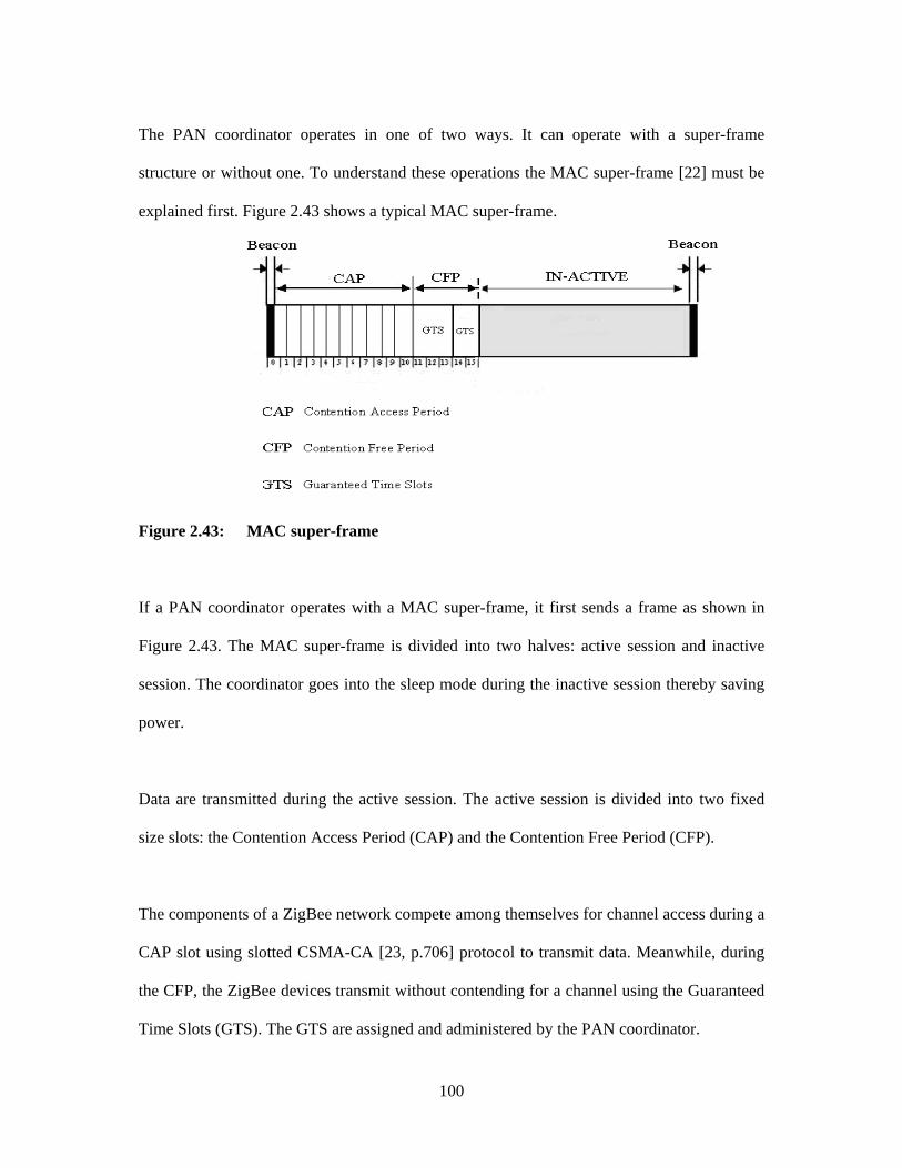
100
The PAN coordinator operates in one of two ways. It can operate with a super-frame
structure or without one. To understand these operations the MAC super-frame [22] must be
explained first. Figure 2.43 shows a typical MAC super-frame.
Figure 2.43: MAC super-frame
If a PAN coordinator operates with a MAC super-frame, it first sends a frame as shown in
Figure 2.43. The MAC super-frame is divided into two halves: active session and inactive
session. The coordinator goes into the sleep mode during the inactive session thereby saving
power.
Data are transmitted during the active session. The active session is divided into two fixed
size slots: the Contention Access Period (CAP) and the Contention Free Period (CFP).
The components of a ZigBee network compete among themselves for channel access during a
CAP slot using slotted CSMA-CA [23, p.706] protocol to transmit data. Meanwhile, during
the CFP, the ZigBee devices transmit without contending for a channel using the Guaranteed
Time Slots (GTS). The GTS are assigned and administered by the PAN coordinator.
101
The end devices in a ZigBee network are usually in sleep mode, which means that they are
only in an active state when they have to transmit data or ‘wake-up’ at periodic intervals to
detect whether there is any incoming data from the coordinator.
If a PAN coordinator wishes to transmit data without using a MAC super-frame, then there
are no beacons, and unslotted CSMA-CA is used for communication. The coordinator is
always in the active state and ready to receive data from the end device. The transfer of data
from the end device to the coordinator is poll based.
The MAC layer is also responsible for the association process as mentioned at the beginning
of this section. Association is the process of joining the ZigBee devices to form a network.
This is done by sending a request to the end device from the coordinator. If the request is
accepted, the coordinator assigns a 16-bit short address to differentiate the different
components.
2.8.5 The ZigBee Standard
The ZigBee standard is built on the IEEE 802.15.4 standard. This consists of two layers:
Network layer
Application layer.
2.8.5.1 Network layer
The network layer is responsible for routing over a network. In Section 2.8.2 the different
network topologies used in a ZigBee network were discussed. The network layer is
responsible for providing a multi-hop routing (peer-to-peer and tree topology), discovering a
102
route, maintenance of a route, security in a route and joining/leaving a network with 16-bit
addresses obtained from the MAC layer.
The above functionalities of the network layer are created by using several algorithms and
protocols [21]. A full explanation of these algorithms and protocols is not within the scope of
this thesis.
2.8.5.2 Application layer
The application layer is made up of three components: the Application Object (APO), the
ZigBee Device Objects (ZDO) and the Application Sub-layer (APS).
The APO falls under the application framework of a ZigBee system. It controls all the
hardware units in a ZigBee network. The ZDO is a special object which allows the APO’s to
discover devices within a network and the services they implement. The ZDO also provides
communication, network and security management services. The APS acts as an interface
between the APO’s and the ZDO’s. Figure 2.44 illustrates the various components of the
application layer and how they interact with each other.
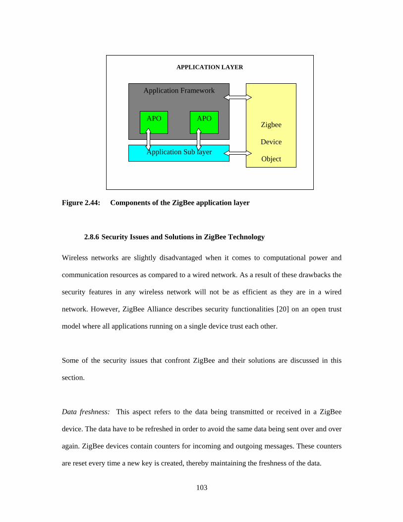
103
Figure 2.44: Components of the ZigBee application layer
2.8.6 Security Issues and Solutions in ZigBee Technology
Wireless networks are slightly disadvantaged when it comes to computational power and
communication resources as compared to a wired network. As a result of these drawbacks the
security features in any wireless network will not be as efficient as they are in a wired
network. However, ZigBee Alliance describes security functionalities [20] on an open trust
model where all applications running on a single device trust each other.
Some of the security issues that confront ZigBee and their solutions are discussed in this
section.
Data freshness: This aspect refers to the data being transmitted or received in a ZigBee
device. The data have to be refreshed in order to avoid the same data being sent over and over
again. ZigBee devices contain counters for incoming and outgoing messages. These counters
are reset every time a new key is created, thereby maintaining the freshness of the data.
Application Sub layer
Application Framework
Zigbee
Device
Object
APO APO
APPLICATION LAYER
104
Data integrity: This is similar to the problem discussed in RFID systems (Section 2.5.9).
ZigBee tackles this problem by providing 0-, 32-, 64- or 128-bit data integrity for the
transmitted messages. The procedure is similar to the checksum methods used in RFID. 64-
bit data integrity is the default in most ZigBee devices. These bits are used in checksum
procedures to ascertain the integrity of transmitted data.
2.9 Software Section
The data from the RFID reader make little sense on their own - the aim of this project is to
automate attendance registration. The RFID reader can read a student card (tag) once it
comes into the read range of the reader, but the data from the tag on their own cannot
automate the attendance register. Therefore RFID middleware is used to automate the
attendance register.
RFID middleware is the software part of this project. It contains the logic for the RFID
application and a database system. The software section of this project runs on a personal
computer for testing purposes.
2.9.1 The Components of RFID Middleware
The middleware is the software part of this project as mentioned in the last section. This
project uses Java and Apache Derby to manipulate data from the reader and use it for
automating the attendance register.

105
Java: Java is an object-oriented programming language developed by Sun Microsystems in
1995 [24]. It derives most of its syntax from C and C++. It has some distinct advantages that
are suited to the structure of this project:
Simplicity
Robustness
Security
High performance
Architectural neutrality.
Above all, the most important aspect is that Java is a write-once, compile-once, run-anywhere
sort of program. This means that irrespective of the hardware used, Java adapts to it such that
the original coding remains the same.
Another advantage of Java is that it has Application Program Interfaces (API) that can be
used for linking two software components. One such API used in this project is called Java
Data Base Connectivity (JDBC). JDBC allows an end user to query and update a relational
database with the Java program.
In order to program with Java, one needs a platform. Netbeans 6 is the platform used for Java
programming in this project.
Apache Derby: This is a Java relational database management system that can be embedded
in Java programs and be used for data manipulation. The Apache Derby database works on
the Structured Query Language (SQL) used by the majority of database programs such as
MySQL and Oracle.

106
The reason for using the Apache Derby database is that it works with JDBC and Java as a
single program. Therefore all the work relating to this project is done on a Java platform.
2.9.2 Programming Concept
This section outlines what is expected of the software section of this project. The detailed
working of JDBC and the Apache Derby database are given in Part 3 of this thesis.
The data scanned from the student card (tag) by the RFID reader are brought to the serial port
of the computer. A program is written in Java to retrieve the data from the serial port and
bring it to the Netbeans Java platform.
A database containing the 8-bit numbers on a student card and the corresponding student
numbers of all the students belonging to a class is created using the Apache Derby database.
The scanned data from the student card are compared with the data in the created database
using JDBC. If there is a match, the scanned data are entered into another database with the
date and student number. This process is repeated on all class days.
At the end of the academic term or semester, a ‘count’ function in the Apache Derby database
is done on each student number. This will give the total number of days a student was present
in class, thereby automating the attendance register.

107
2.9.3 JDBC Concepts
JDBC [25] is used by Java to access and manipulate a database. JDBC has four components:
JDBC API
JDBC driver manager
JDBC test suite
JDBC-ODBC Bridge
JDBC API: The API provides the industrial standard for connecting Java programming
language and a wide range of databases. The API is designed such that it only needs to be
written once and can be run any time. There are two packages in a JDBC API:
-java.sql
-javax.sql.
These two packages are used to connect the Java program and the databases.
JDBC driver manager: This is the backbone of the JDBC architecture. It defines objects
which connect a Java application to a JDBC driver. The main responsibility of the JDBC
driver is to load all drivers found in the system properly as well as to select the most
appropriate driver for opening a database connection.
JDBC test suite: The test suite checks whether the driver will run a specific user program.
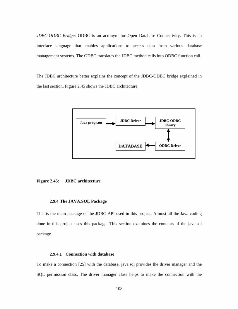
108
JDBC-ODBC Bridge: ODBC is an acronym for Open Database Connectivity. This is an
interface language that enables applications to access data from various database
management systems. The ODBC translates the JDBC method calls into ODBC function call.
The JDBC architecture better explains the concept of the JDBC-ODBC bridge explained in
the last section. Figure 2.45 shows the JDBC architecture.
Figure 2.45: JDBC architecture
2.9.4 The JAVA.SQL Package
This is the main package of the JDBC API used in this project. Almost all the Java coding
done in this project uses this package. This section examines the contents of the java.sql
package.
2.9.4.1 Connection with database
To make a connection [25] with the database, java.sql provides the driver manager and the
SQL permission class. The driver manager class helps to make the connection with the
Java program JDBC Driver JDBC-ODBC library
ODBC Driver DATABASE
109
database using a driver interface. The SQL permission class, on the other hand, provides the
security for the connection by setting up a username and password to access the database.
2.9.4.2 Sending SQL parameters to a database
In order to access the database some SQL statements must be sent to the database. Using the
java.sql package, the programmer can send basic SQL statements and prepared statements
using the statement objects. The statements are sent through the connection interface which
provides methods for creating statements and managing their connections and properties. The
SQL statements will be discussed in detail in Section 2.10.
2.9.4.3 Updating and retrieving results of an SQL query
Updating and retrieving results from a database is a crucial aspect as far as this project is
concerned. The ResultSet object is responsible for this process. The ResultSet maintains a
cursor pointing to the current row of data at the start of the program and moves through each
of the rows, until there are no rows left.
2.9.4.4 Metadata object
This object provides information to the application about the database. ResultSetMetadata is
a method in the Metadata object that provides information about the columns of a database to
the ResultSet object.
2.9.4.5 Exceptions
Exceptions are error messages generated by the Java program in various instances of the
programming. Some of the common exceptions generated are:
110
SQLException - An error generated by the methods of a program whenever there is a
problem accessing the database. The program will not execute if there is as SQLException.
SQLWarning - An exception which generates a warning due to some missing parameters.
The program will execute with the warning, but might not output the desired results.
BatchUpdateException - Indicates that all commands have not been updated successfully.
Data Truncation - Indicates that some part of the code is missing.
2.9.5 SQL Concepts
SQL is a standard language for accessing and manipulating databases. There are different
Relational Database Management Systems (RDBMS) that use SQL, such as MySQL, DB2,
Oracle, MS Access and Apache Derby.
The data in a RDBMS are stored in database objects called tables. A table is a collection of
related database entries and it consists of rows and columns. A database may contain one or
more tables. Each table is identified with a name. Table 2.9 shows a database table called
“students” with three columns for student name, age and student number. It has three entries,
one for each student.

111
Table 2.9:‘Students’ table with three columns and three entries for the columns
A database table is created using certain SQL statements. There are basically two types of
SQL statements: the Data Manipulation Language (DML) and the Data Definition Language
(DDL).
The Data Manipulation Language statements are used for querying and updating a database
table. Some of the DML commands are given below.
SELECT - command used for extracting data from a database
UPDATE - command used for updating data in a database
DELETE - command used for deleting data from a database
INSERT INTO – command used for inserting data into a database.
The Data Definition Language statements are used for creating and deleting database tables.
They also provide indexes, specify links between tables and impose constraints between
tables. Some of the commonly used DDL statements are as follows:
CREATE DATABASE - used for creating new database tables
ALTER DATABASE - used for modifying a database
CREATE TABLE - used for creating a new table
ALTER TABLE - modifies a created database table
Student name Age Student number Alex 19 3229 John 21 3230 Mary 20 3231
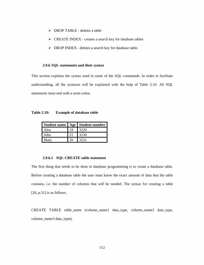
112
DROP TABLE - deletes a table
CREATE INDEX - creates a search key for database tables
DROP INDEX - deletes a search key for database table.
2.9.6 SQL statements and their syntax
This section explains the syntax used in some of the SQL commands. In order to facilitate
understanding, all the syntaxes will be explained with the help of Table 2.10. All SQL
statements must end with a semi-colon.
Table 2.10: Example of database table
2.9.6.1 SQL CREATE table statement
The first thing that needs to be done in database programming is to create a database table.
Before creating a database table the user must know the exact amount of data that the table
contains, i.e. the number of columns that will be needed. The syntax for creating a table
[26, p.51] is as follows.
CREATE TABLE table_name (column_name1 data_type, column_name2 data_type,
column_name3 data_type);
Student name Age Student number Alex 19 3229 John 21 3230 Mary 20 3231

113
The data type specifies what type of data the column holds, for example variable character
(names, addresses) and integer (student numbers, telephone numbers, ages).
In order to create the database table shown in Table 2.9, three columns are needed. The table
is created using the following syntax:
CREATE TABLE students (student name varchar (255), age integer (40), student number
integer (40));
The data types used in this instance are variable character (varchar) and integer. The number
in the bracket specifies the maximum length of the data in characters.
2.9.6.2 SQL INSERT INTO statement
The insert statement [26, p.75] is used for inserting values into a database table. The syntax
for the insert statement is as follows.
INSERT INTO table_name (column_name1, column_name2, column_name3) VALUES
(value1, value2, value3);
The INSERT INTO statement is exemplified by inserting the first set of values into the
‘students’ table (Table 2.10). It is important to note that the variable characters must be
placed in single quotes to differentiate them from integers.
INSERT INTO table_name (student name, age, student number) VALUES (‘Alex’, 19,
3229);
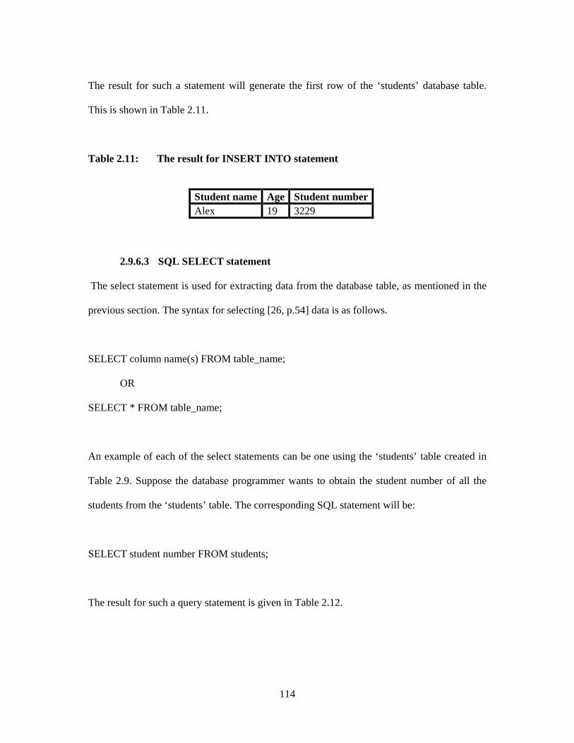
114
The result for such a statement will generate the first row of the ‘students’ database table.
This is shown in Table 2.11.
Table 2.11: The result for INSERT INTO statement
2.9.6.3 SQL SELECT statement
The select statement is used for extracting data from the database table, as mentioned in the
previous section. The syntax for selecting [26, p.54] data is as follows.
SELECT column name(s) FROM table_name;
OR
SELECT * FROM table_name;
An example of each of the select statements can be one using the ‘students’ table created in
Table 2.9. Suppose the database programmer wants to obtain the student number of all the
students from the ‘students’ table. The corresponding SQL statement will be:
SELECT student number FROM students;
The result for such a query statement is given in Table 2.12.
Student name Age Student number Alex 19 3229
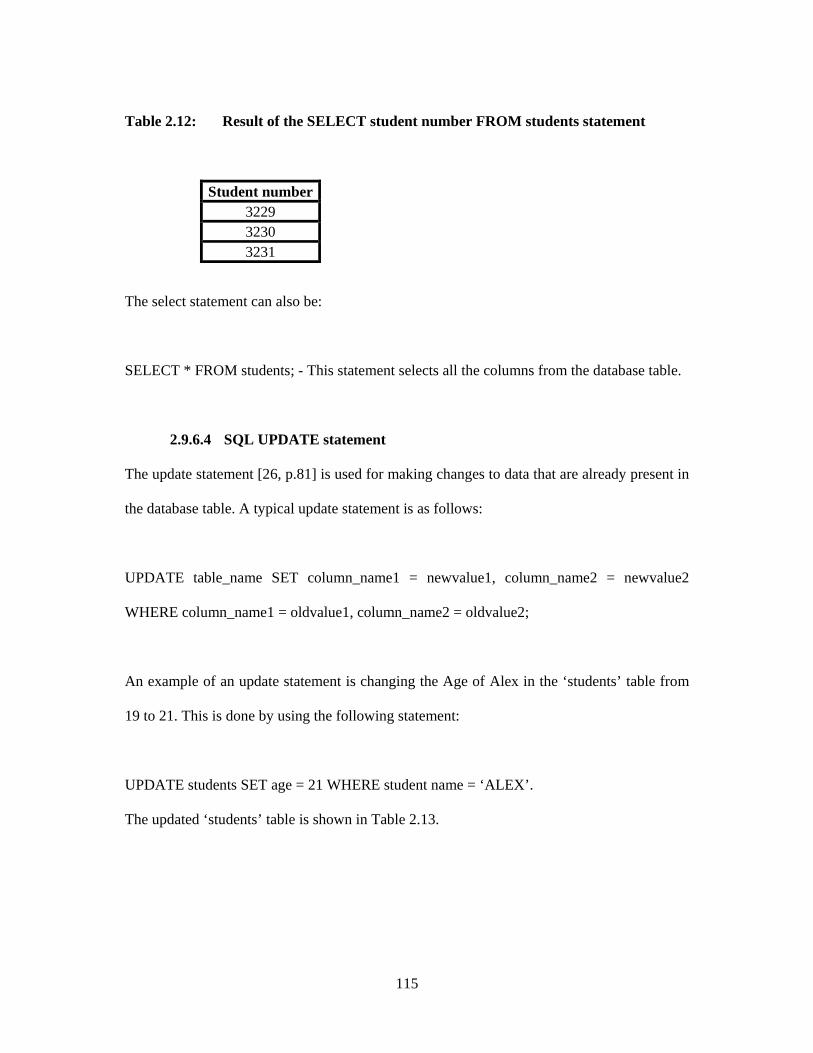
115
Table 2.12: Result of the SELECT student number FROM students statement
The select statement can also be:
SELECT * FROM students; - This statement selects all the columns from the database table.
2.9.6.4 SQL UPDATE statement
The update statement [26, p.81] is used for making changes to data that are already present in
the database table. A typical update statement is as follows:
UPDATE table_name SET column_name1 = newvalue1, column_name2 = newvalue2
WHERE column_name1 = oldvalue1, column_name2 = oldvalue2;
An example of an update statement is changing the Age of Alex in the ‘students’ table from
19 to 21. This is done by using the following statement:
UPDATE students SET age = 21 WHERE student name = ‘ALEX’.
The updated ‘students’ table is shown in Table 2.13.
Student number 3229 3230 3231
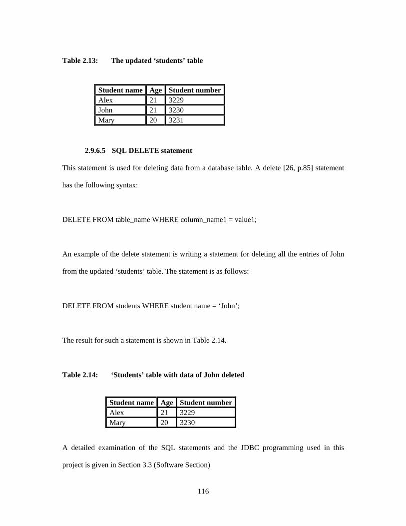
116
Table 2.13: The updated ‘students’ table
2.9.6.5 SQL DELETE statement
This statement is used for deleting data from a database table. A delete [26, p.85] statement
has the following syntax:
DELETE FROM table_name WHERE column_name1 = value1;
An example of the delete statement is writing a statement for deleting all the entries of John
from the updated ‘students’ table. The statement is as follows:
DELETE FROM students WHERE student name = ‘John’;
The result for such a statement is shown in Table 2.14.
Table 2.14: ‘Students’ table with data of John deleted
A detailed examination of the SQL statements and the JDBC programming used in this
project is given in Section 3.3 (Software Section)
Student name Age Student number Alex 21 3229 John 21 3230 Mary 20 3231
Student name Age Student number Alex 21 3229 Mary 20 3230
117
PART 3
CHAPTER 3 RESEARCH STRUCTURE
This chapter describes the research methodology of this thesis. It aims to practically
implement all the topics discussed in Chapter 2. A step-by-step approach is used to bring
together all the components discussed in the previous sections to automate the student
attendance register using RFID technology.
This chapter is divided into three sections: the hardware section, the wireless section and the
software section.
The hardware section examines the tags used in this project, the programming of an RFID
module which can read the tags and the design of an antenna which will act as the interface
between the reader and the tag.
The wireless section examines how ZigBee wireless technology is used to connect a reader
and remotely located RFID middleware.
The software section examines how the data from the RFID reader are manipulated so that it
can be used to automate student attendance register.

118
3.1 Hardware Section
This section examines three important aspects of this project:
RFID tags
RFID reader
Antenna.
3.1.1 RFID Tags
RFID tags contain some data, and when they come within the read range of a reader, they
transfer the data. In doing so they can identify the person or object that carries the tag. As
mentioned in Section 2.5.1, there are different types of tags (active, passive and semi-
passive).
This project was undertaken to automate the student attendance register at the Central
University of Technology, Free State, South Africa. Upon enrolling at the institution, each
student is given a student card. The student card contains a picture of the student, his/her
name, the course for which s/he has enrolled, and a student number. The student number is a
unique ID which is used to distinguish each student.
In one of the experiments done very early on this project, it was noted that the student card
was indeed an RFID tag constructed in identification card format (Section 2.5.1.1). The
student cards have the same dimensions as a credit card (85.72 mm x 54.03 mm x 0.76mm)
and have a coil antenna with a microchip. The tags are designed to work at 13.56 MHz.
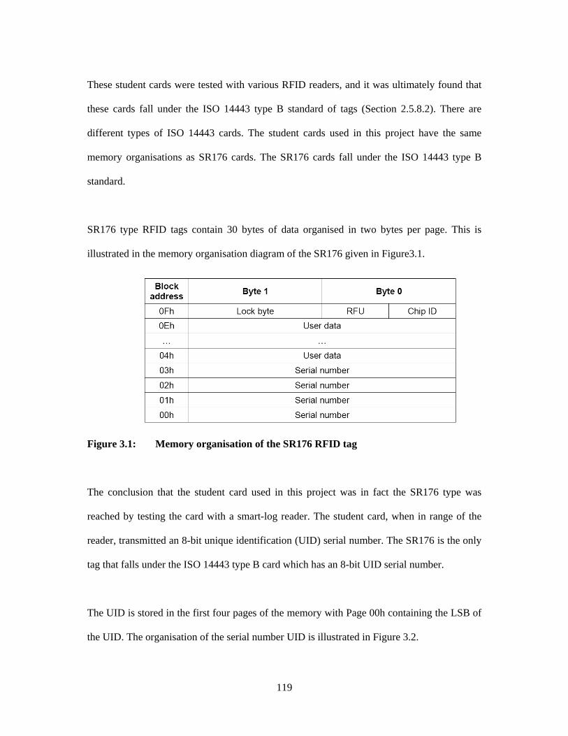
119
These student cards were tested with various RFID readers, and it was ultimately found that
these cards fall under the ISO 14443 type B standard of tags (Section 2.5.8.2). There are
different types of ISO 14443 cards. The student cards used in this project have the same
memory organisations as SR176 cards. The SR176 cards fall under the ISO 14443 type B
standard.
SR176 type RFID tags contain 30 bytes of data organised in two bytes per page. This is
illustrated in the memory organisation diagram of the SR176 given in Figure3.1.
Figure 3.1: Memory organisation of the SR176 RFID tag
The conclusion that the student card used in this project was in fact the SR176 type was
reached by testing the card with a smart-log reader. The student card, when in range of the
reader, transmitted an 8-bit unique identification (UID) serial number. The SR176 is the only
tag that falls under the ISO 14443 type B card which has an 8-bit UID serial number.
The UID is stored in the first four pages of the memory with Page 00h containing the LSB of
the UID. The organisation of the serial number UID is illustrated in Figure 3.2.
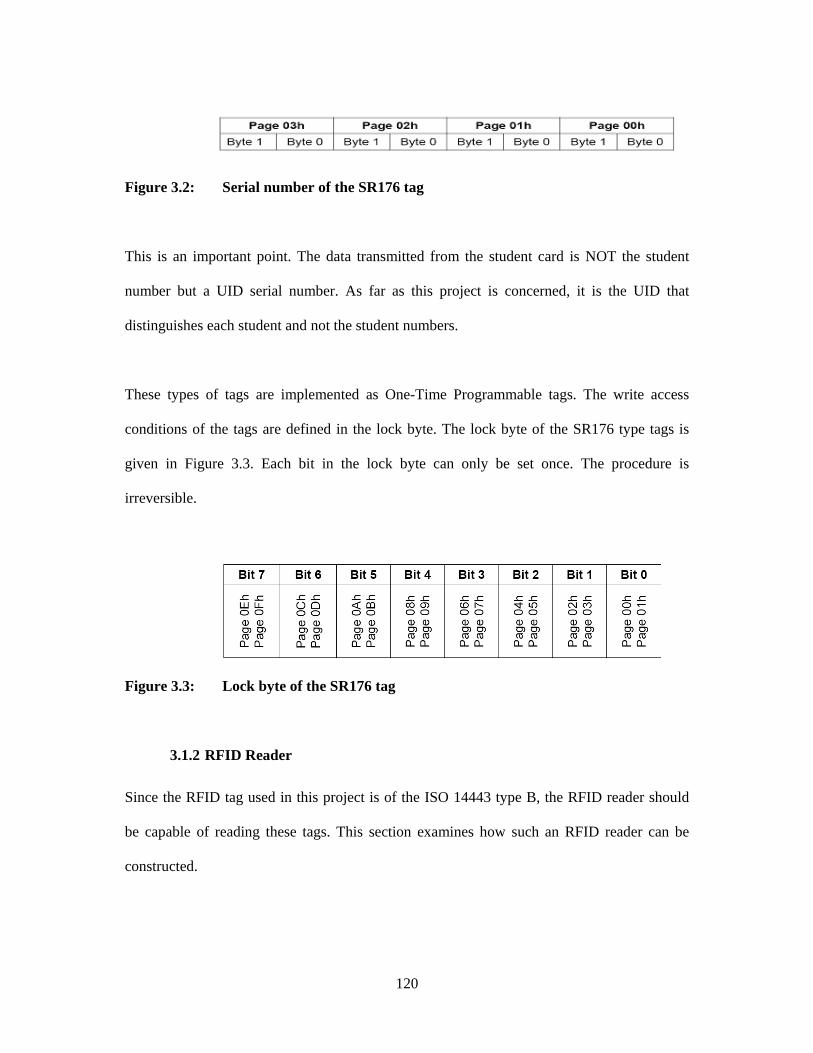
120
Figure 3.2: Serial number of the SR176 tag
This is an important point. The data transmitted from the student card is NOT the student
number but a UID serial number. As far as this project is concerned, it is the UID that
distinguishes each student and not the student numbers.
These types of tags are implemented as One-Time Programmable tags. The write access
conditions of the tags are defined in the lock byte. The lock byte of the SR176 type tags is
given in Figure 3.3. Each bit in the lock byte can only be set once. The procedure is
irreversible.
Figure 3.3: Lock byte of the SR176 tag
3.1.2 RFID Reader
Since the RFID tag used in this project is of the ISO 14443 type B, the RFID reader should
be capable of reading these tags. This section examines how such an RFID reader can be
constructed.
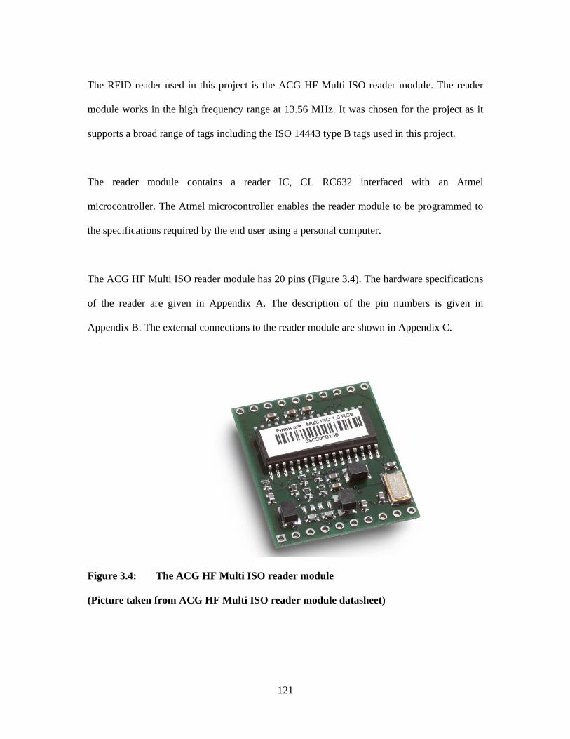
121
The RFID reader used in this project is the ACG HF Multi ISO reader module. The reader
module works in the high frequency range at 13.56 MHz. It was chosen for the project as it
supports a broad range of tags including the ISO 14443 type B tags used in this project.
The reader module contains a reader IC, CL RC632 interfaced with an Atmel
microcontroller. The Atmel microcontroller enables the reader module to be programmed to
the specifications required by the end user using a personal computer.
The ACG HF Multi ISO reader module has 20 pins (Figure 3.4). The hardware specifications
of the reader are given in Appendix A. The description of the pin numbers is given in
Appendix B. The external connections to the reader module are shown in Appendix C.
Figure 3.4: The ACG HF Multi ISO reader module
(Picture taken from ACG HF Multi ISO reader module datasheet)
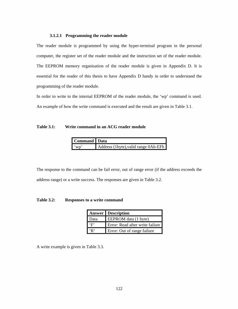
122
3.1.2.1 Programming the reader module
The reader module is programmed by using the hyper-terminal program in the personal
computer, the register set of the reader module and the instruction set of the reader module.
The EEPROM memory organisation of the reader module is given in Appendix D. It is
essential for the reader of this thesis to have Appendix D handy in order to understand the
programming of the reader module.
In order to write to the internal EEPROM of the reader module, the ‘wp’ command is used.
An example of how the write command is executed and the result are given in Table 3.1.
Table 3.1: Write command in an ACG reader module
The response to the command can be fail error, out of range error (if the address exceeds the
address range) or a write success. The responses are given in Table 3.2.
Table 3.2: Responses to a write command
Answer Description Data EEPROM data (1 byte) ‘F’ Error: Read after write failure ‘R’ Error: Out of range failure
A write example is given in Table 3.3.
Command Data ‘wp’ Address (1byte),valid range 0Ah-EFh
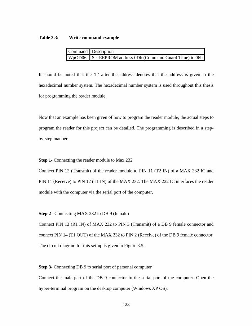
123
Table 3.3: Write command example
Command Description WpOD06 Set EEPROM address 0Dh (Command Guard Time) to 06h
It should be noted that the ‘h’ after the address denotes that the address is given in the
hexadecimal number system. The hexadecimal number system is used throughout this thesis
for programming the reader module.
Now that an example has been given of how to program the reader module, the actual steps to
program the reader for this project can be detailed. The programming is described in a step-
by-step manner.
Step 1- Connecting the reader module to Max 232
Connect PIN 12 (Transmit) of the reader module to PIN 11 (T2 IN) of a MAX 232 IC and
PIN 11 (Receive) to PIN 12 (T1 IN) of the MAX 232. The MAX 232 IC interfaces the reader
module with the computer via the serial port of the computer.
Step 2 –Connecting MAX 232 to DB 9 (female)
Connect PIN 13 (R1 IN) of MAX 232 to PIN 3 (Transmit) of a DB 9 female connector and
connect PIN 14 (T1 OUT) of the MAX 232 to PIN 2 (Receive) of the DB 9 female connector.
The circuit diagram for this set-up is given in Figure 3.5.
Step 3- Connecting DB 9 to serial port of personal computer
Connect the male part of the DB 9 connector to the serial port of the computer. Open the
hyper-terminal program on the desktop computer (Windows XP OS).
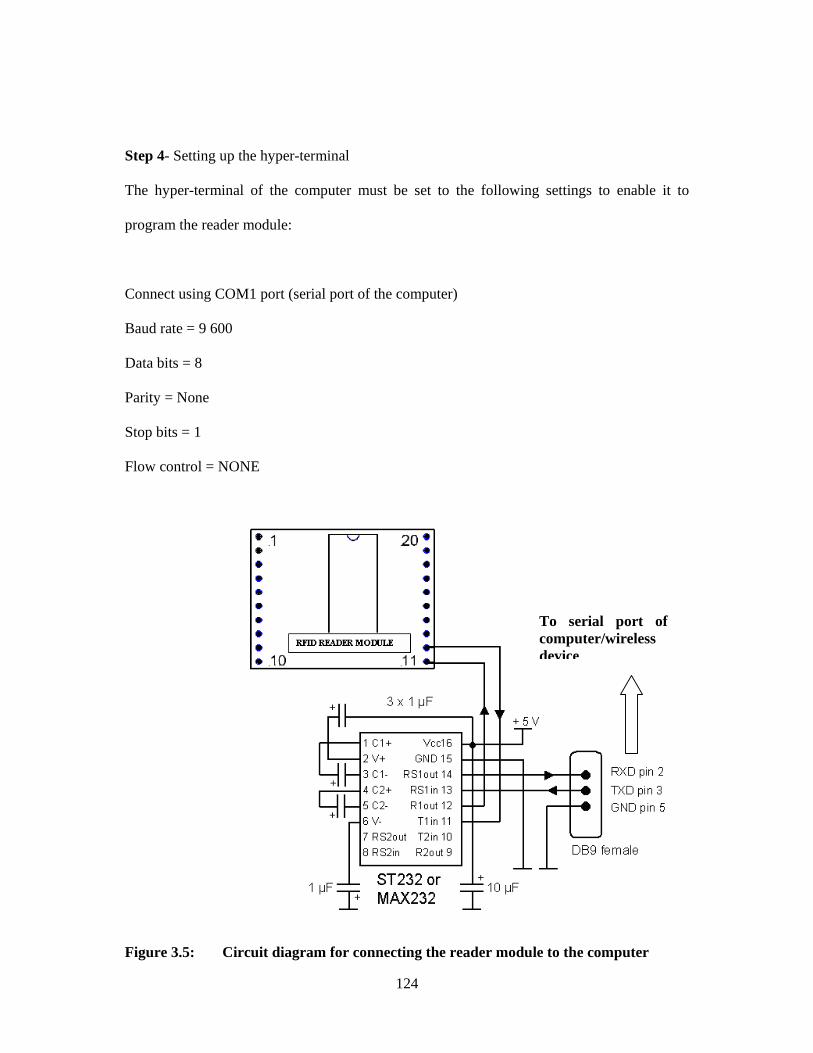
124
Step 4- Setting up the hyper-terminal
The hyper-terminal of the computer must be set to the following settings to enable it to
program the reader module:
Connect using COM1 port (serial port of the computer)
Baud rate = 9 600
Data bits = 8
Parity = None
Stop bits = 1
Flow control = NONE
Figure 3.5: Circuit diagram for connecting the reader module to the computer
To serial port of computer/wireless device
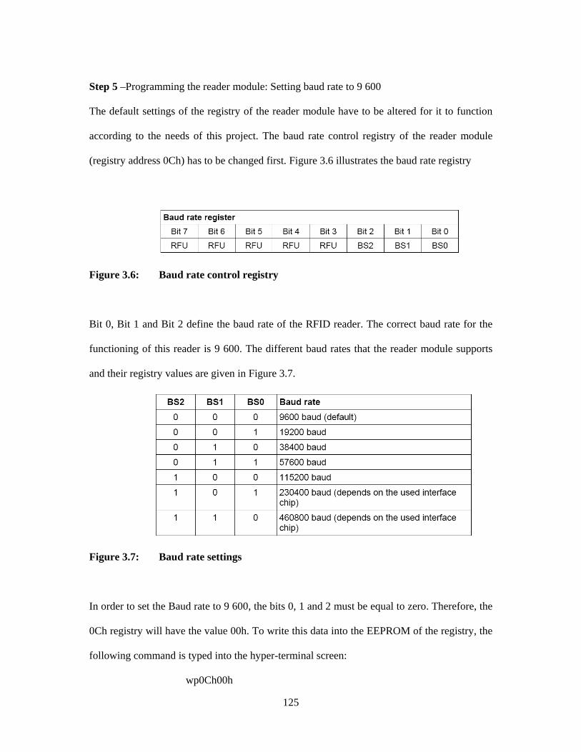
125
Step 5 –Programming the reader module: Setting baud rate to 9 600
The default settings of the registry of the reader module have to be altered for it to function
according to the needs of this project. The baud rate control registry of the reader module
(registry address 0Ch) has to be changed first. Figure 3.6 illustrates the baud rate registry
Figure 3.6: Baud rate control registry
Bit 0, Bit 1 and Bit 2 define the baud rate of the RFID reader. The correct baud rate for the
functioning of this reader is 9 600. The different baud rates that the reader module supports
and their registry values are given in Figure 3.7.
Figure 3.7: Baud rate settings
In order to set the Baud rate to 9 600, the bits 0, 1 and 2 must be equal to zero. Therefore, the
0Ch registry will have the value 00h. To write this data into the EEPROM of the registry, the
following command is typed into the hyper-terminal screen:
wp0Ch00h
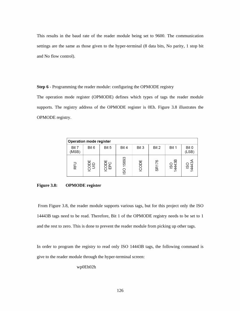
126
This results in the baud rate of the reader module being set to 9600. The communication
settings are the same as those given to the hyper-terminal (8 data bits, No parity, 1 stop bit
and No flow control).
Step 6 - Programming the reader module: configuring the OPMODE registry
The operation mode register (OPMODE) defines which types of tags the reader module
supports. The registry address of the OPMODE register is 0Eh. Figure 3.8 illustrates the
OPMODE registry.
Figure 3.8: OPMODE register
From Figure 3.8, the reader module supports various tags, but for this project only the ISO
14443B tags need to be read. Therefore, Bit 1 of the OPMODE registry needs to be set to 1
and the rest to zero. This is done to prevent the reader module from picking up other tags.
In order to program the registry to read only ISO 14443B tags, the following command is
give to the reader module through the hyper-terminal screen:
wp0Eh02h
127
This results in all the bits except Bit 1 being set to zero, thereby enabling the reader module
to read only ISO 14443B tags.
Step 7 - Programming the reader module: configuring the Single Shot Time-out
The Single Shot Time-out occupies the 0Fh address in the reader module registry. The time-
out value defines the delay time between two responses to the reader module, i.e. the interval
between reading two tags. The time-out value should not be too small or too big in the
context of this project. There are 8 bits in this register. The Least Significant bit denotes a
time-out of 100 ms (refer to register set information in Appendix D). A delay of 1 second is
suitable for the functioning of this device. The delay therefore has to be set to 1 000 ms.
Table 3.4 shows how the time delay is set to 1 second.
In order to obtain a delay of 1 second (1 000 milliseconds), the Single-Shot Time-out register
has to be set to 0Ah. The following command is written to the hyper-terminal to do this:
wp0Fh0Ah
This sets the time-out delay
to 1 second.
Table 3.4: Delay and corresponding hexadecimal value
Delay in milliseconds Hexadecimal value of register 0 milliseconds 00h 100 milliseconds 01h 1 000 milliseconds 0Ah
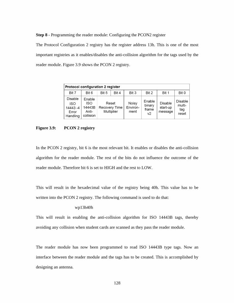
128
Step 8 - Programming the reader module: Configuring the PCON2 register
The Protocol Configuration 2 registry has the register address 13h. This is one of the most
important registries as it enables/disables the anti-collision algorithm for the tags used by the
reader module. Figure 3.9 shows the PCON 2 registry.
Figure 3.9: PCON 2 registry
In the PCON 2 registry, bit 6 is the most relevant bit. It enables or disables the anti-collision
algorithm for the reader module. The rest of the bits do not influence the outcome of the
reader module. Therefore bit 6 is set to HIGH and the rest to LOW.
This will result in the hexadecimal value of the registry being 40h. This value has to be
written into the PCON 2 registry. The following command is used to do that:
wp13h40h
This will result in enabling the anti-collision algorithm for ISO 14443B tags, thereby
avoiding any collision when student cards are scanned as they pass the reader module.
The reader module has now been programmed to read ISO 14443B type tags. Now an
interface between the reader module and the tags has to be created. This is accomplished by
designing an antenna.
129
3.1.3 Anti-collision in RFID reader
Collision is defined in section 2.5.6. The read range of the antenna used in this project is 3-4
cm (refer to Results Chapter 4 for experiment results done to arrive at this conclusion.),
therefore collision does not pose a major problem in this chapter. If the read range were to
exceed 15 cm then appropriate remedial solutions have to be used. Techniques used in the
Multi ISO reader module to overcome collision in reader modules with greater than 15 cm
range is given in Section 2.5.6.1 and 2.5.6.2
3.1.4 Antennna
Since the reader module and the tags operate at 13.56 MHz, the antenna should also be
designed to operate at this frequency. The antenna should be connected to pins 1, 2, 5 and 6
of the reader module (refer to Appendix C). The antenna must have the correct combination
of inductance, resistance and capacitance for optimised frequency and antenna matching. The
inductance is achieved by using a coil antenna with a number of turns.
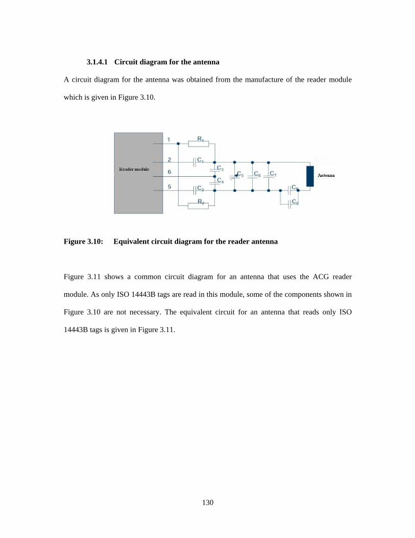
130
3.1.4.1 Circuit diagram for the antenna
A circuit diagram for the antenna was obtained from the manufacture of the reader module
which is given in Figure 3.10.
Figure 3.10: Equivalent circuit diagram for the reader antenna
Figure 3.11 shows a common circuit diagram for an antenna that uses the ACG reader
module. As only ISO 14443B tags are read in this module, some of the components shown in
Figure 3.10 are not necessary. The equivalent circuit for an antenna that reads only ISO
14443B tags is given in Figure 3.11.
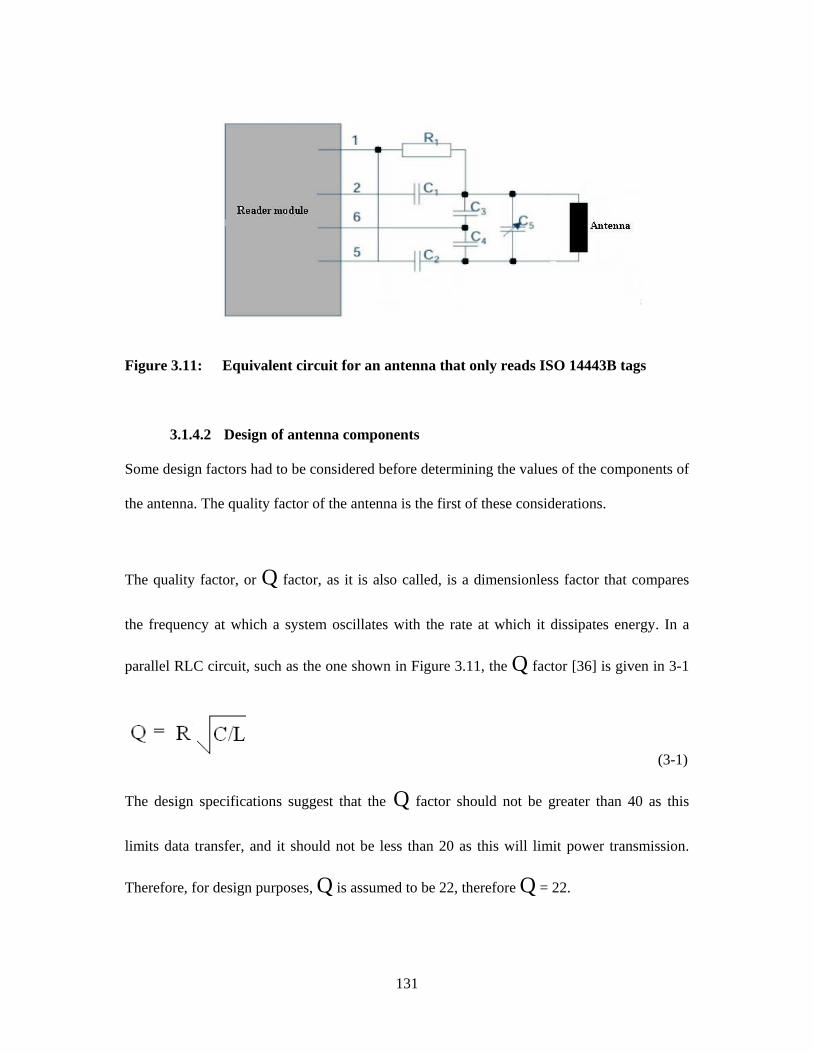
131
Figure 3.11: Equivalent circuit for an antenna that only reads ISO 14443B tags
3.1.4.2 Design of antenna components
Some design factors had to be considered before determining the values of the components of
the antenna. The quality factor of the antenna is the first of these considerations.
The quality factor, or Q factor, as it is also called, is a dimensionless factor that compares
the frequency at which a system oscillates with the rate at which it dissipates energy. In a
parallel RLC circuit, such as the one shown in Figure 3.11, the Q factor [36] is given in 3-1
(3-1)
The design specifications suggest that the Q factor should not be greater than 40 as this
limits data transfer, and it should not be less than 20 as this will limit power transmission.
Therefore, for design purposes, Q is assumed to be 22, therefore Q = 22.
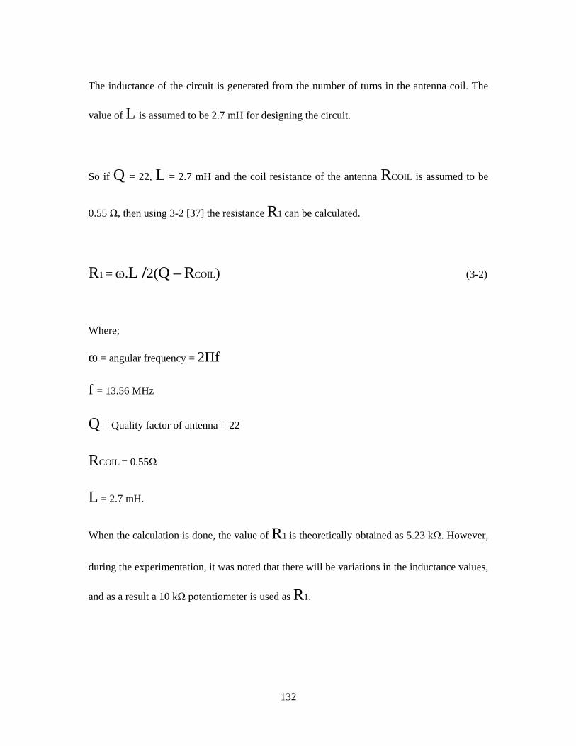
132
The inductance of the circuit is generated from the number of turns in the antenna coil. The
value of L is assumed to be 2.7 mH for designing the circuit.
So if Q = 22, L = 2.7 mH and the coil resistance of the antenna RCOIL is assumed to be
0.55 Ω, then using 3-2 [37] the resistance R1 can be calculated.
R1 = ω.L /2(Q – RCOIL) (3-2)
Where;
ω = angular frequency = 2Πf
f = 13.56 MHz
Q = Quality factor of antenna = 22
RCOIL = 0.55Ω
L = 2.7 mH.
When the calculation is done, the value of R1 is theoretically obtained as 5.23 kΩ. However,
during the experimentation, it was noted that there will be variations in the inductance values,
and as a result a 10 kΩ potentiometer is used as R1.

133
The value of capacitors C3 and C4 can be calculated similarly using Equation 3-3 [37]. In
this instance input impedance is assumed to be 0.7kΩ. The rest of the terms are the same as in
Equation 3-2.
(3-3)
The value of C3 and C4 is rounded off to the nearest value as 220 pF.
The value of C1 and C2 can be determined by using Equation 3-4. The value of C3 = C4 is
used for this calculation.
(3-4)
When the calculation is done, the value of C1 and C2 = 13.4 pF, and this is rounded off to
18 pF.
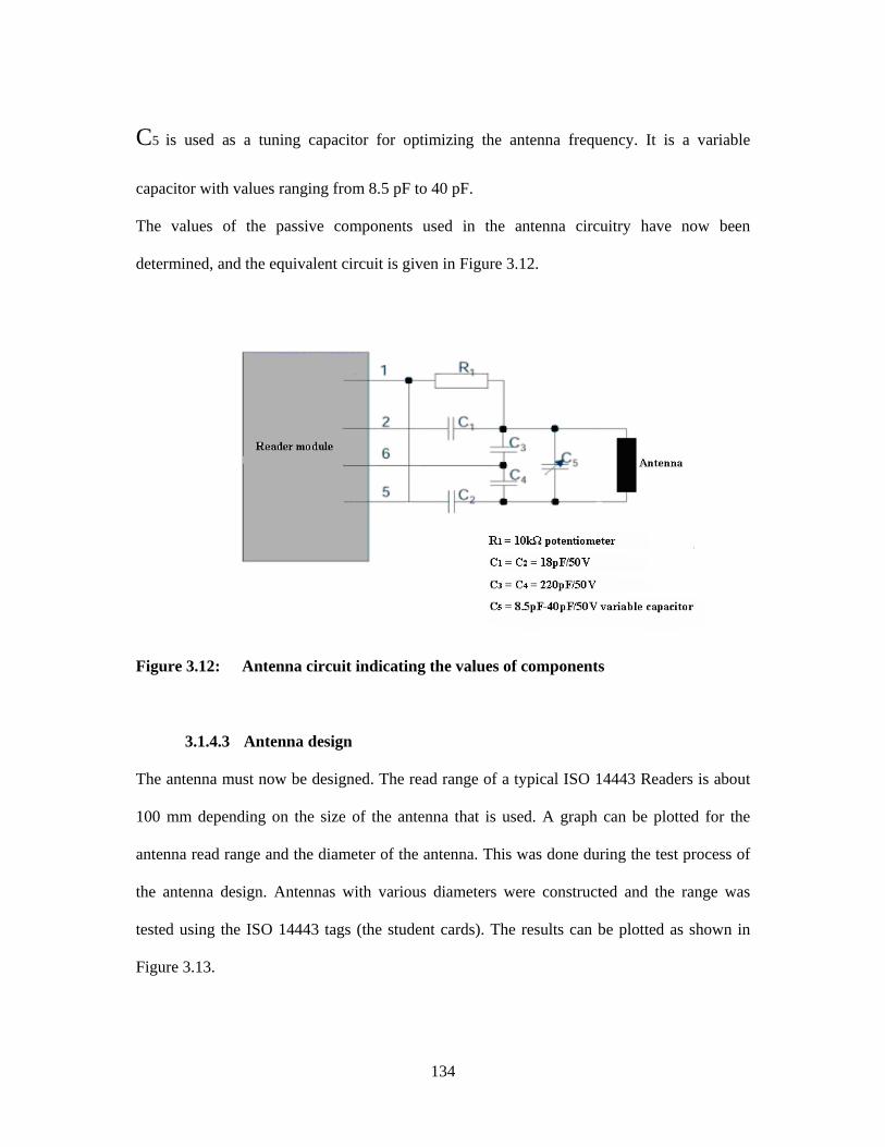
134
C5 is used as a tuning capacitor for optimizing the antenna frequency. It is a variable
capacitor with values ranging from 8.5 pF to 40 pF.
The values of the passive components used in the antenna circuitry have now been
determined, and the equivalent circuit is given in Figure 3.12.
Figure 3.12: Antenna circuit indicating the values of components
3.1.4.3 Antenna design
The antenna must now be designed. The read range of a typical ISO 14443 Readers is about
100 mm depending on the size of the antenna that is used. A graph can be plotted for the
antenna read range and the diameter of the antenna. This was done during the test process of
the antenna design. Antennas with various diameters were constructed and the range was
tested using the ISO 14443 tags (the student cards). The results can be plotted as shown in
Figure 3.13.
135
Figure 3.13: Correlation between read range and antenna diameter
It was observed that the read range increases with an increase in antenna diameter until it
reaches a certain point (80 mm). After this point the read range continues to increase but only
marginally. This observation was taken into consideration when designing the actual antenna.
The inductance of the antenna circuit is obtained by constructing a coil antenna, as
mentioned in Section 3.1.3. The coil antenna designed for this project has 3 to 4 turns, a
diameter of 80 mm and a track width of about 2 mm.
3.1.4.4 Antenna construction
The antenna is constructed using a milling process with Eagle software and a Roland Modela
milling machine.
The Roland Modela milling machine mills a printed circuit board (PCB) to the exact
specifications provided to the machine. This replaces the etching process previously used for
constructing a PCB. For this project a Modela MDX-20 was used. A photograph of this
etching machine is shown in Figure 3.14.
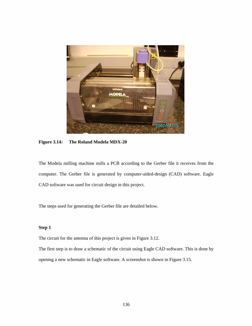
136
Figure 3.14: The Roland Modela MDX-20
The Modela milling machine mills a PCB according to the Gerber file it receives from the
computer. The Gerber file is generated by computer-aided-design (CAD) software. Eagle
CAD software was used for circuit design in this project.
The steps used for generating the Gerber file are detailed below.
Step 1
The circuit for the antenna of this project is given in Figure 3.12.
The first step is to draw a schematic of the circuit using Eagle CAD software. This is done by
opening a new schematic in Eagle software. A screenshot is shown in Figure 3.15.
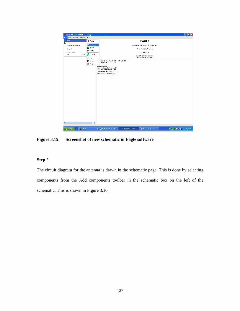
137
Figure 3.15: Screenshot of new schematic in Eagle software
Step 2
The circuit diagram for the antenna is drawn in the schematic page. This is done by selecting
components from the Add components toolbar in the schematic box on the left of the
schematic. This is shown in Figure 3.16.
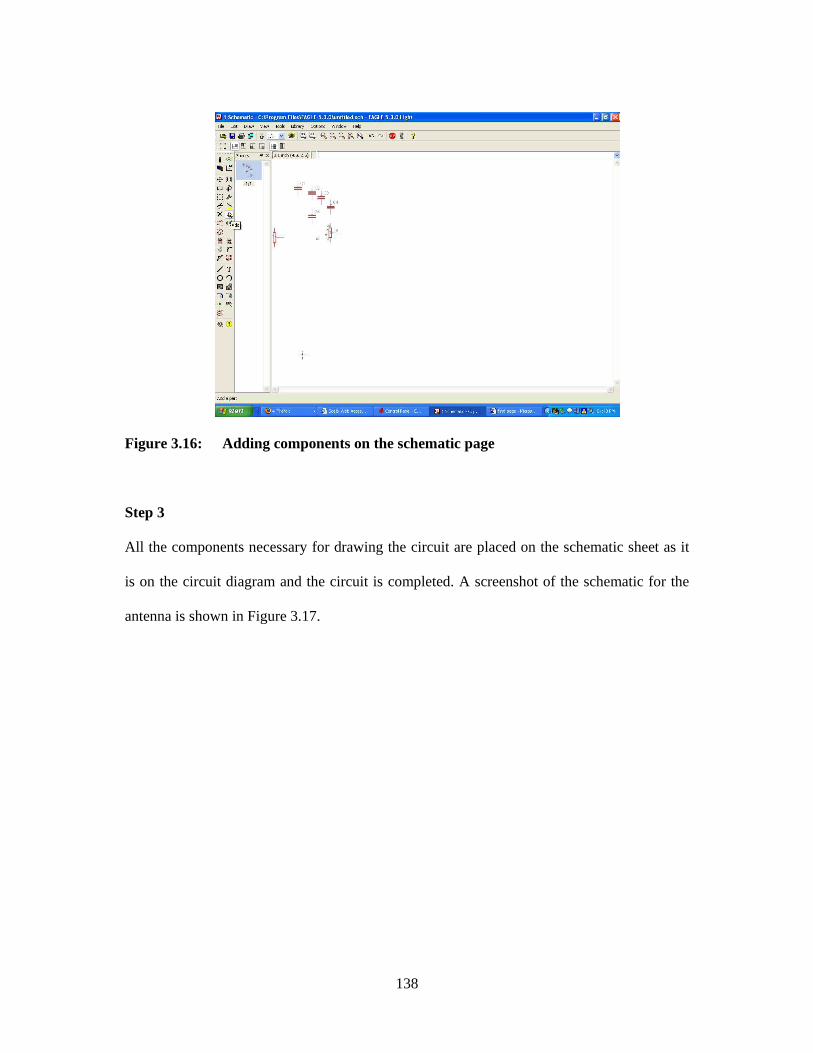
138
Figure 3.16: Adding components on the schematic page
Step 3
All the components necessary for drawing the circuit are placed on the schematic sheet as it
is on the circuit diagram and the circuit is completed. A screenshot of the schematic for the
antenna is shown in Figure 3.17.
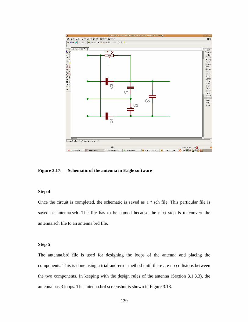
139
Figure 3.17: Schematic of the antenna in Eagle software
Step 4
Once the circuit is completed, the schematic is saved as a *.sch file. This particular file is
saved as antenna.sch. The file has to be named because the next step is to convert the
antenna.sch file to an antenna.brd file.
Step 5
The antenna.brd file is used for designing the loops of the antenna and placing the
components. This is done using a trial-and-error method until there are no collisions between
the two components. In keeping with the design rules of the antenna (Section 3.1.3.3), the
antenna has 3 loops. The antenna.brd screenshot is shown in Figure 3.18.
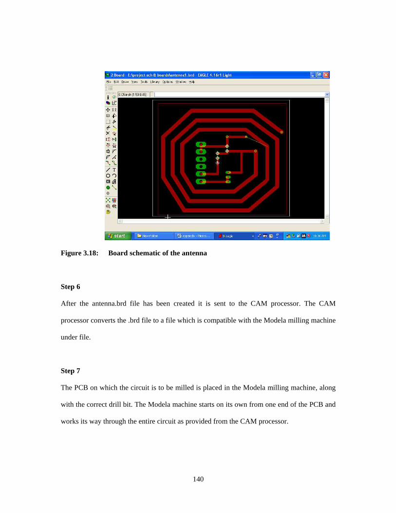
140
Figure 3.18: Board schematic of the antenna
Step 6
After the antenna.brd file has been created it is sent to the CAM processor. The CAM
processor converts the .brd file to a file which is compatible with the Modela milling machine
under file.
Step 7
The PCB on which the circuit is to be milled is placed in the Modela milling machine, along
with the correct drill bit. The Modela machine starts on its own from one end of the PCB and
works its way through the entire circuit as provided from the CAM processor.
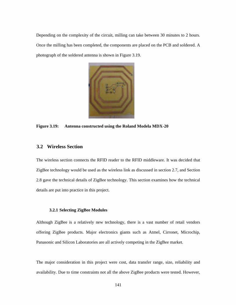
141
Depending on the complexity of the circuit, milling can take between 30 minutes to 2 hours.
Once the milling has been completed, the components are placed on the PCB and soldered. A
photograph of the soldered antenna is shown in Figure 3.19.
Figure 3.19: Antenna constructed using the Roland Modela MDX-20
3.2 Wireless Section
The wireless section connects the RFID reader to the RFID middleware. It was decided that
ZigBee technology would be used as the wireless link as discussed in section 2.7, and Section
2.8 gave the technical details of ZigBee technology. This section examines how the technical
details are put into practice in this project.
3.2.1 Selecting ZigBee Modules
Although ZigBee is a relatively new technology, there is a vast number of retail vendors
offering ZigBee products. Major electronics giants such as Atmel, Cirronet, Microchip,
Panasonic and Silicon Laboratories are all actively competing in the ZigBee market.
The major consideration in this project were cost, data transfer range, size, reliability and
availability. Due to time constraints not all the above ZigBee products were tested. However,

142
extensive research was done by consulting other researchers in various countries who had
used several of these and other ZigBee products, bearing the considerations of this project in
mind.
ZigBee technology was used in this project to eliminate what would otherwise have been a
wired serial connection between the reader and the RFID middleware. The product which
best fits the description is the Maxstream X-Bee module. The specifications of this product
are given in Appendix F. X-Bee modules can be used as an RF interface between two devices
by setting one device as the data transmitter and the other as the receiver.
This fits very well into this project as communication is always one way only (from the
reader to RFID middleware). The next section discusses how the X-Bee modules were set up
to operate as transmitter and receiver.
3.2.2 The X-Bee ZigBee Module
The X-Bee transceiver module is a 20-pin chip with an on-chip antenna for data transmission.
The main advantage of the X-Bee module is that it has a Universal Asynchronous Receiver
Transmitter (UART) interface which allows data transfer from the transmitter to the receiver
using the ZigBee protocols.
The ZigBee hardware has to be designed such that the serial port logic levels are compatible
with the X-Bee’s 2.8-3.4 V logic levels. This is achieved by using a MAX 232 chip, the same
technique used to connect the reader module to the computer. For this project, two X-Bee
modules are needed. One module is connected to the reader and the other to the computer to
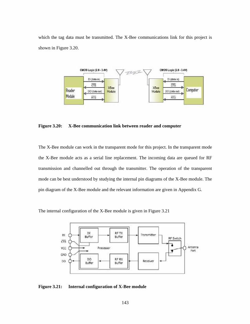
143
which the tag data must be transmitted. The X-Bee communications link for this project is
shown in Figure 3.20.
Figure 3.20: X-Bee communication link between reader and computer
The X-Bee module can work in the transparent mode for this project. In the transparent mode
the X-Bee module acts as a serial line replacement. The incoming data are queued for RF
transmission and channelled out through the transmitter. The operation of the transparent
mode can be best understood by studying the internal pin diagrams of the X-Bee module. The
pin diagram of the X-Bee module and the relevant information are given in Appendix G.
The internal configuration of the X-Bee module is given in Figure 3.21
Figure 3.21: Internal configuration of X-Bee module
144
In Figure 3.22 DI is the data input pin, and DO is the data output pin. CTS is the Clear To
Send flow control pin it is active LOW signal. The data that need to be sent from the RFID
reader come to the DI pin and are sent to the DI buffer until they can be transmitted. The
hardware flow control of the DI buffer is implemented using the CTS pin.
When the DI buffer is 17 bytes from being full, the CTS pin goes logically HIGH. This
signals the reader to stop sending data. The data remaining in the DI buffer are sent to the RF
Tx (RF transmitter) buffer and from there to the transmitter. The RF switch in the antenna
port of the X-Bee module transmits the data. The CTS pin returns to logic LOW after the DI
buffer has been cleared.
The same process is repeated but in reverse order at the X-Bee module connected to the
computer. Here the data are collected by the receiver and passed on to the RF Rx (RF
Receiver) input. In the receiver section the RTS (Request To Send Flow) pin checks whether
the RF Rx buffer is full. If yes, it transfers the data in the RF Rx buffer to the DO buffer. The
data are then transferred from the X-Bee module to the computer through the DI pin.
3.2.3 The X-Bee RF Interface Module
Section 3.2.2 explains the basic functioning of the X-Bee module. This section examines the
RF interface module used for connecting the X-Bee module to external devices. Figure 3.22
shows the RF interface board.
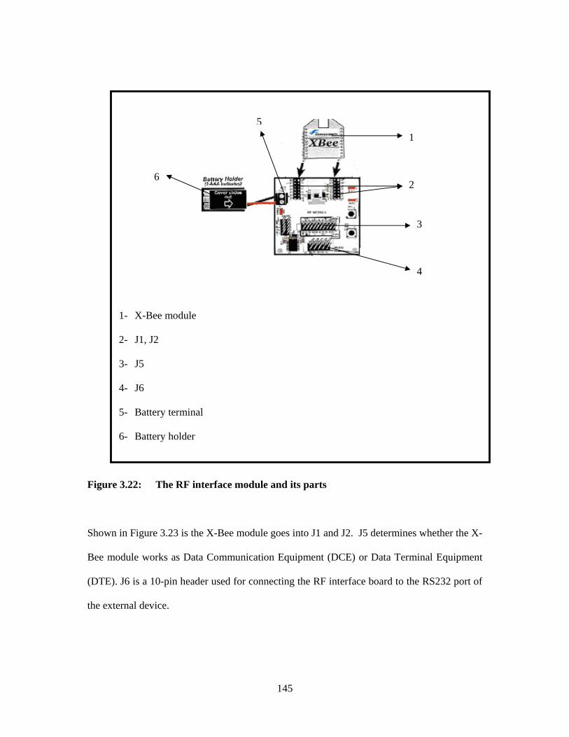
145
1- X-Bee module
2- J1, J2
3- J5
4- J6
5- Battery terminal
6- Battery holder
Figure 3.22: The RF interface module and its parts
Shown in Figure 3.23 is the X-Bee module goes into J1 and J2. J5 determines whether the X-
Bee module works as Data Communication Equipment (DCE) or Data Terminal Equipment
(DTE). J6 is a 10-pin header used for connecting the RF interface board to the RS232 port of
the external device.
1
2
3
4
5
6
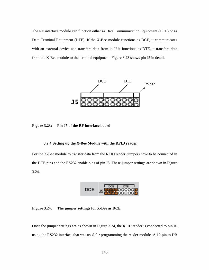
146
The RF interface module can function either as Data Communication Equipment (DCE) or as
Data Terminal Equipment (DTE). If the X-Bee module functions as DCE, it communicates
with an external device and transfers data from it. If it functions as DTE, it transfers data
from the X-Bee module to the terminal equipment. Figure 3.23 shows pin J5 in detail.
Figure 3.23: Pin J5 of the RF interface board
3.2.4 Setting up the X-Bee Module with the RFID reader
For the X-Bee module to transfer data from the RFID reader, jumpers have to be connected in
the DCE pins and the RS232 enable pins of pin J5. These jumper settings are shown in Figure
3.24.
Figure 3.24: The jumper settings for X-Bee as DCE
Once the jumper settings are as shown in Figure 3.24, the RFID reader is connected to pin J6
using the RS232 interface that was used for programming the reader module. A 10-pin to DB
DCE DTE RS232
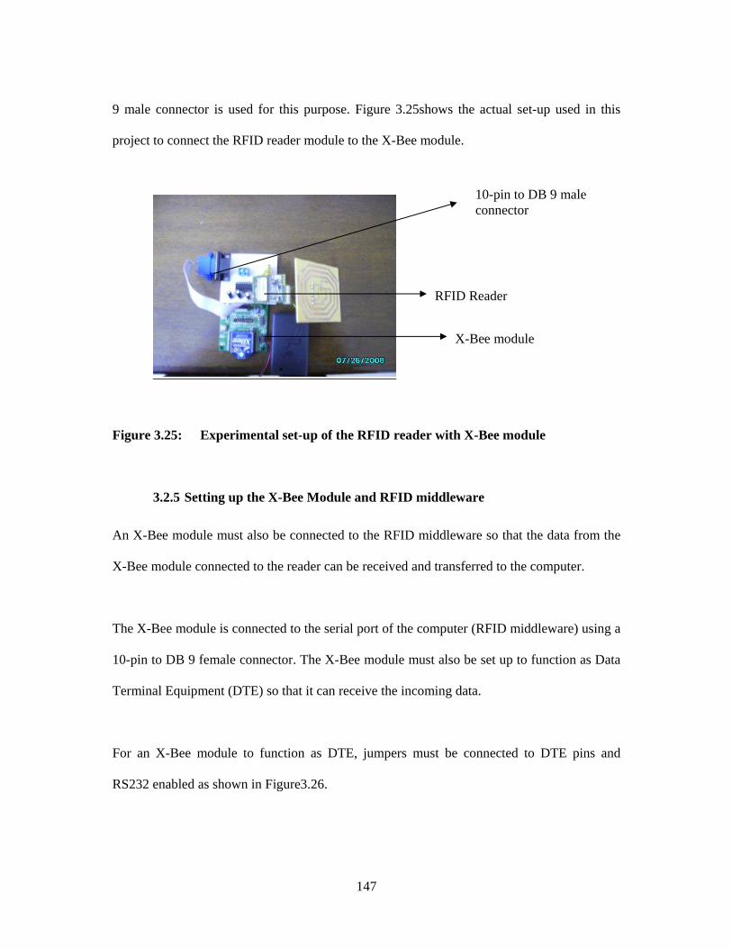
147
9 male connector is used for this purpose. Figure 3.25shows the actual set-up used in this
project to connect the RFID reader module to the X-Bee module.
Figure 3.25: Experimental set-up of the RFID reader with X-Bee module
3.2.5 Setting up the X-Bee Module and RFID middleware
An X-Bee module must also be connected to the RFID middleware so that the data from the
X-Bee module connected to the reader can be received and transferred to the computer.
The X-Bee module is connected to the serial port of the computer (RFID middleware) using a
10-pin to DB 9 female connector. The X-Bee module must also be set up to function as Data
Terminal Equipment (DTE) so that it can receive the incoming data.
For an X-Bee module to function as DTE, jumpers must be connected to DTE pins and
RS232 enabled as shown in Figure3.26.
RFID Reader
10-pin to DB 9 male connector
X-Bee module
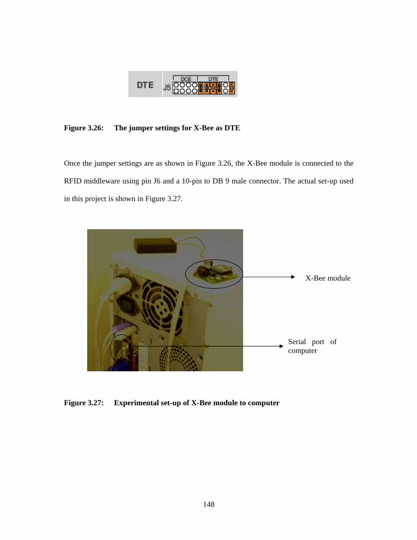
148
Figure 3.26: The jumper settings for X-Bee as DTE
Once the jumper settings are as shown in Figure 3.26, the X-Bee module is connected to the
RFID middleware using pin J6 and a 10-pin to DB 9 male connector. The actual set-up used
in this project is shown in Figure 3.27.
Figure 3.27: Experimental set-up of X-Bee module to computer
X-Bee module
Serial port of computer

149
3.3 Software Section
In the software section of the project, data are collected from the serial port of the computer
and entered into a database table. As indicated, Apache Derby Database and Java
programming are used to manipulate data. The general idea is that a database table is initially
created which contains all the details of a student in a class from his/her student card.
Once the student enters a classroom, s/he scans his/her card with the RFID reader. The reader
picks up the unique card number from the student card and sends the data to the serial port of
the RFID middleware (computer). Using the Java program, a comparison is made between
the incoming data and the data contained in the initial database table. If there is a match
between the two, the received data are entered into a second database table along with the
date.
The second database table serves as the attendance register. It contains the attendance details
of all the students who have been enrolled in the class. A flow chart showing detailing the
complete process is shown in figure 3.28.
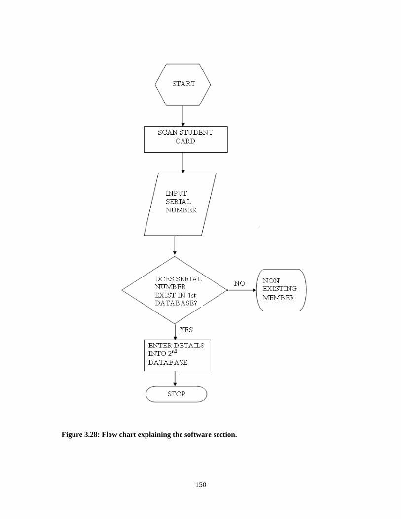
150
Figure 3.28: Flow chart explaining the software section.
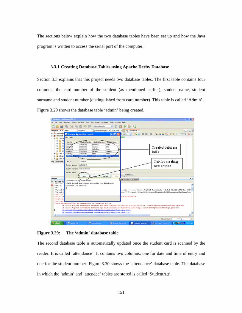
151
The sections below explain how the two database tables have been set up and how the Java
program is written to access the serial port of the computer.
3.3.1 Creating Database Tables using Apache Derby Database
Section 3.3 explains that this project needs two database tables. The first table contains four
columns: the card number of the student (as mentioned earlier), student name, student
surname and student number (distinguished from card number). This table is called ‘Admin’.
Figure 3.29 shows the database table ‘admin’ being created.
Figure 3.29: The ‘admin’ database table
The second database table is automatically updated once the student card is scanned by the
reader. It is called ‘attendance’. It contains two columns: one for date and time of entry and
one for the student number. Figure 3.30 shows the ‘attendance’ database table. The database
in which the ‘admin’ and ‘attendee’ tables are stored is called ‘StudentAtt’.
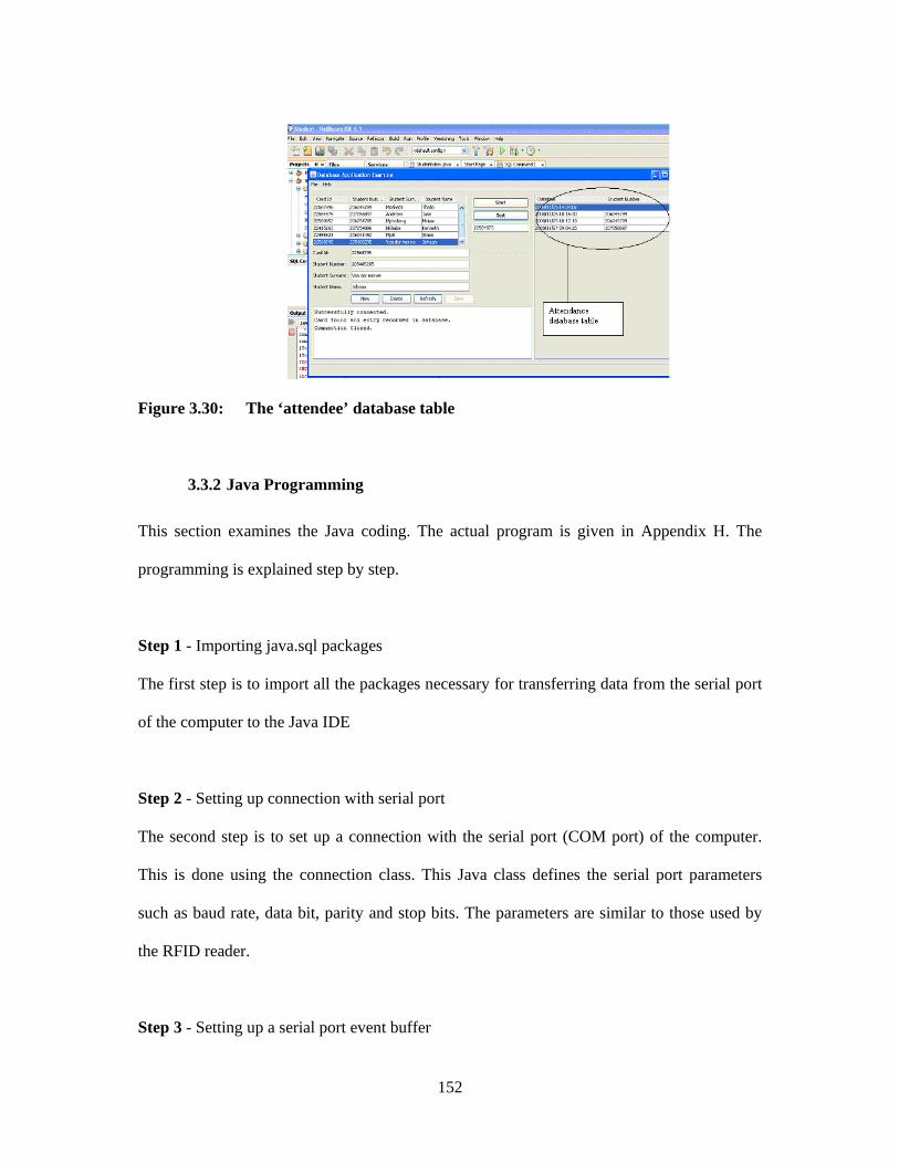
152
Figure 3.30: The ‘attendee’ database table
3.3.2 Java Programming
This section examines the Java coding. The actual program is given in Appendix H. The
programming is explained step by step.
Step 1 - Importing java.sql packages
The first step is to import all the packages necessary for transferring data from the serial port
of the computer to the Java IDE
Step 2 - Setting up connection with serial port
The second step is to set up a connection with the serial port (COM port) of the computer.
This is done using the connection class. This Java class defines the serial port parameters
such as baud rate, data bit, parity and stop bits. The parameters are similar to those used by
the RFID reader.
Step 3 - Setting up a serial port event buffer
153
The third step is to set up a serial port event listener method. This method checks for
incoming data from the reader to the serial port. If there are any data at the serial port, it is
transferred to an output buffer.
Step 4- Setting up connection with database
This step of the Java coding uses JDBC to connect with the Apache database. The
DriverManager.getConnection statement is used to establish a connection with the StudentAtt
database.
Step 5 - Comparison of received data with database tables
The fifth step is to make a comparison between the received data from the reader and the
‘students’ database table. If there is a match then the data are entered into the ‘attendance’
database table along with date and time.

154
PART 4
CAHPTER 4 RESULTS
Tests were conducted at various stages of the project work. The results of these tests are
detailed in this section. At the beginning of Part 3, the project was split into three sections:
the hardware, the wireless and the software sections. Testing was done at the end of each
section before proceeding to the next stage.
4.1 Hardware Setup
The RFID reader is placed by the entrance of the classroom where the attendance needs to be
registered. The students walk into the classroom and scan their student cards as they enter the
classroom. Therefore, the scanning of student cards is an instantaneous process. A laptop
computer with a ZigBee end device is placed at lecturer’s table. A schematic of the set-up is
shown in Figure 4.1. The range between the RFID reader and the student card (indicated as a
tag in Figure 4.1) is about 3-4 cm.
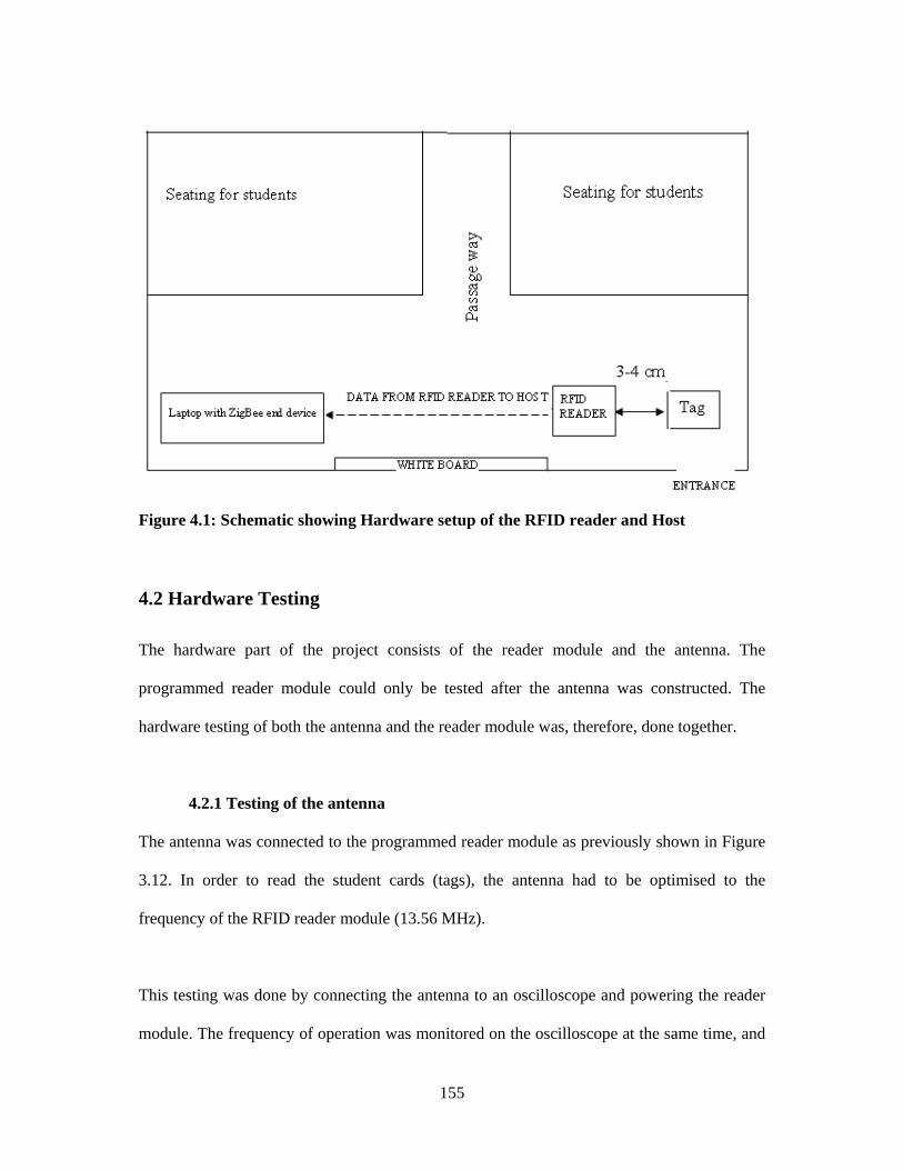
155
Figure 4.1: Schematic showing Hardware setup of the RFID reader and Host
4.2 Hardware Testing
The hardware part of the project consists of the reader module and the antenna. The
programmed reader module could only be tested after the antenna was constructed. The
hardware testing of both the antenna and the reader module was, therefore, done together.
4.2.1 Testing of the antenna
The antenna was connected to the programmed reader module as previously shown in Figure
3.12. In order to read the student cards (tags), the antenna had to be optimised to the
frequency of the RFID reader module (13.56 MHz).
This testing was done by connecting the antenna to an oscilloscope and powering the reader
module. The frequency of operation was monitored on the oscilloscope at the same time, and
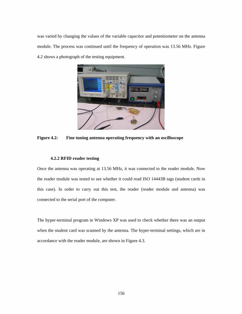
156
was varied by changing the values of the variable capacitor and potentiometer on the antenna
module. The process was continued until the frequency of operation was 13.56 MHz. Figure
4.2 shows a photograph of the testing equipment.
Figure 4.2: Fine tuning antenna operating frequency with an oscilloscope
4.2.2 RFID reader testing
Once the antenna was operating at 13.56 MHz, it was connected to the reader module. Now
the reader module was tested to see whether it could read ISO 14443B tags (student cards in
this case). In order to carry out this test, the reader (reader module and antenna) was
connected to the serial port of the computer.
The hyper-terminal program in Windows XP was used to check whether there was an output
when the student card was scanned by the antenna. The hyper-terminal settings, which are in
accordance with the reader module, are shown in Figure 4.3.
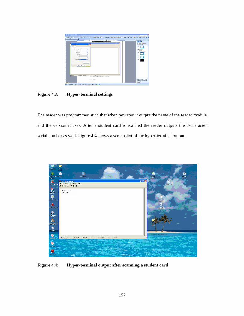
157
Figure 4.3: Hyper-terminal settings
The reader was programmed such that when powered it output the name of the reader module
and the version it uses. After a student card is scanned the reader outputs the 8-character
serial number as well. Figure 4.4 shows a screenshot of the hyper-terminal output.
Figure 4.4: Hyper-terminal output after scanning a student card
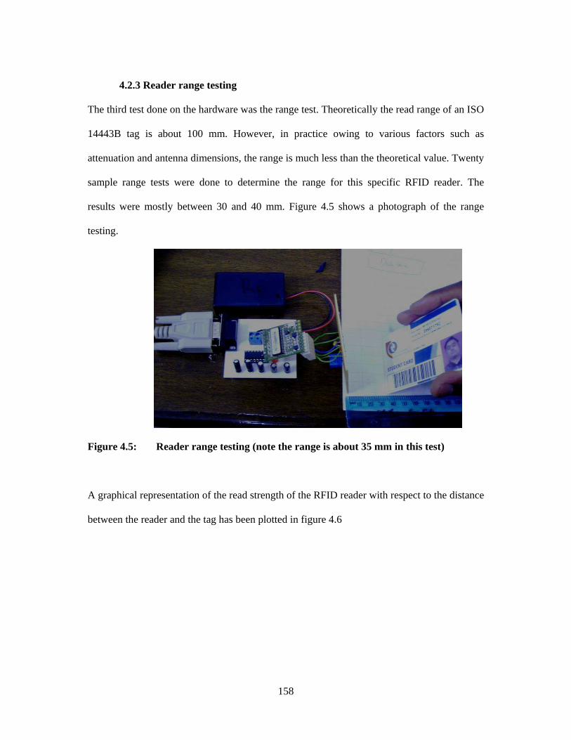
158
4.2.3 Reader range testing
The third test done on the hardware was the range test. Theoretically the read range of an ISO
14443B tag is about 100 mm. However, in practice owing to various factors such as
attenuation and antenna dimensions, the range is much less than the theoretical value. Twenty
sample range tests were done to determine the range for this specific RFID reader. The
results were mostly between 30 and 40 mm. Figure 4.5 shows a photograph of the range
testing.
Figure 4.5: Reader range testing (note the range is about 35 mm in this test)
A graphical representation of the read strength of the RFID reader with respect to the distance
between the reader and the tag has been plotted in figure 4.6
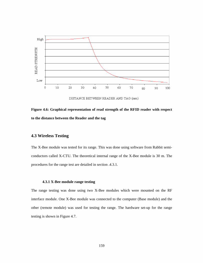
159
Figure 4.6: Graphical representation of read strength of the RFID reader with respect
to the distance between the Reader and the tag
4.3 Wireless Testing
The X-Bee module was tested for its range. This was done using software from Rabbit semi-
conductors called X-CTU. The theoretical internal range of the X-Bee module is 30 m. The
procedures for the range test are detailed in section .4.3.1.
4.3.1 X-Bee module range testing
The range testing was done using two X-Bee modules which were mounted on the RF
interface module. One X-Bee module was connected to the computer (Base module) and the
other (remote module) was used for testing the range. The hardware set-up for the range
testing is shown in Figure 4.7.
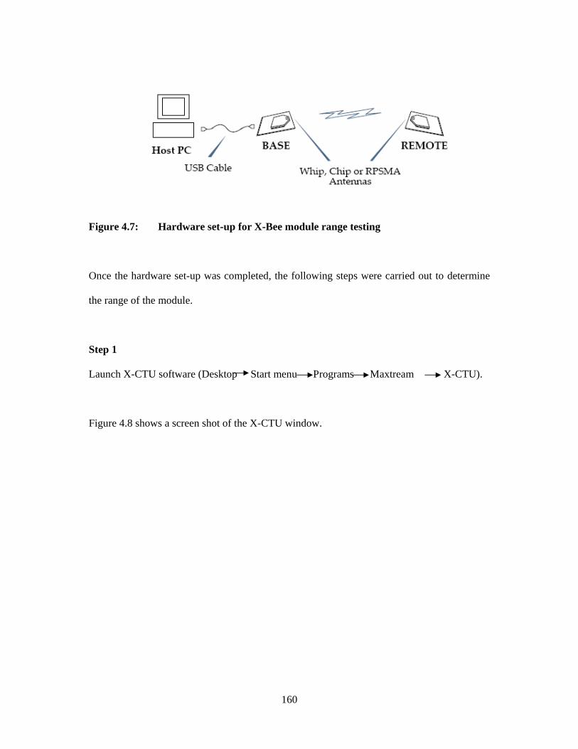
160
Figure 4.7: Hardware set-up for X-Bee module range testing
Once the hardware set-up was completed, the following steps were carried out to determine
the range of the module.
Step 1
Launch X-CTU software (Desktop Start menu Programs Maxtream X-CTU).
Figure 4.8 shows a screen shot of the X-CTU window.
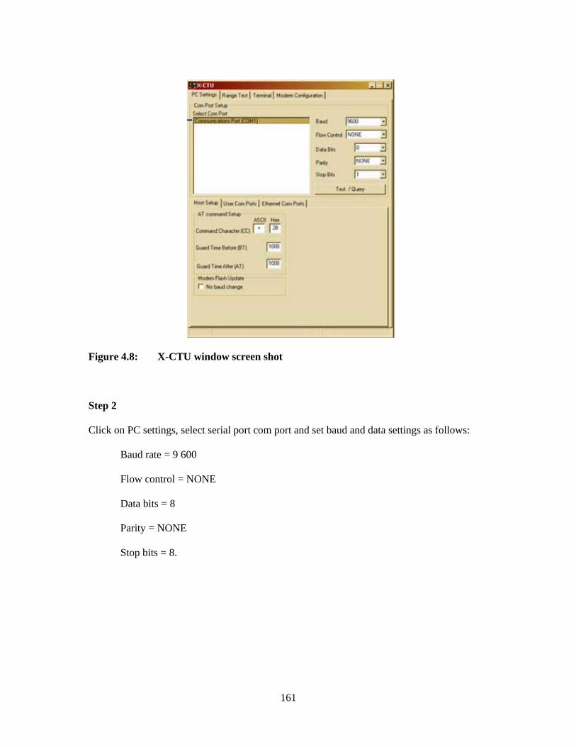
161
Figure 4.8: X-CTU window screen shot
Step 2
Click on PC settings, select serial port com port and set baud and data settings as follows:
Baud rate = 9 600
Flow control = NONE
Data bits = 8
Parity = NONE
Stop bits = 8.
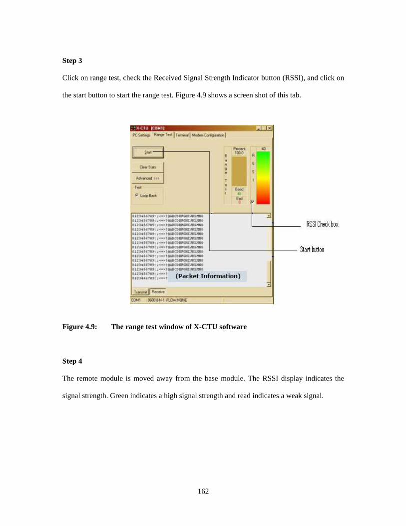
162
Step 3
Click on range test, check the Received Signal Strength Indicator button (RSSI), and click on
the start button to start the range test. Figure 4.9 shows a screen shot of this tab.
Figure 4.9: The range test window of X-CTU software
Step 4
The remote module is moved away from the base module. The RSSI display indicates the
signal strength. Green indicates a high signal strength and read indicates a weak signal.
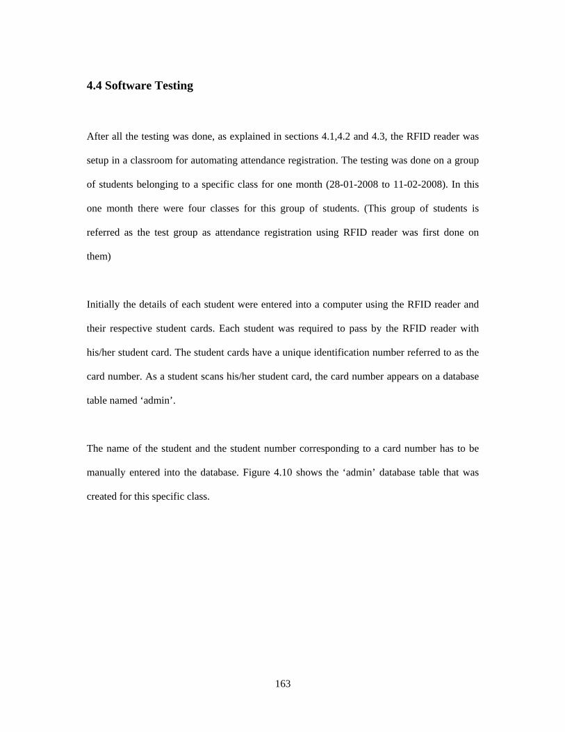
163
4.4 Software Testing
After all the testing was done, as explained in sections 4.1,4.2 and 4.3, the RFID reader was
setup in a classroom for automating attendance registration. The testing was done on a group
of students belonging to a specific class for one month (28-01-2008 to 11-02-2008). In this
one month there were four classes for this group of students. (This group of students is
referred as the test group as attendance registration using RFID reader was first done on
them)
Initially the details of each student were entered into a computer using the RFID reader and
their respective student cards. Each student was required to pass by the RFID reader with
his/her student card. The student cards have a unique identification number referred to as the
card number. As a student scans his/her student card, the card number appears on a database
table named ‘admin’.
The name of the student and the student number corresponding to a card number has to be
manually entered into the database. Figure 4.10 shows the ‘admin’ database table that was
created for this specific class.
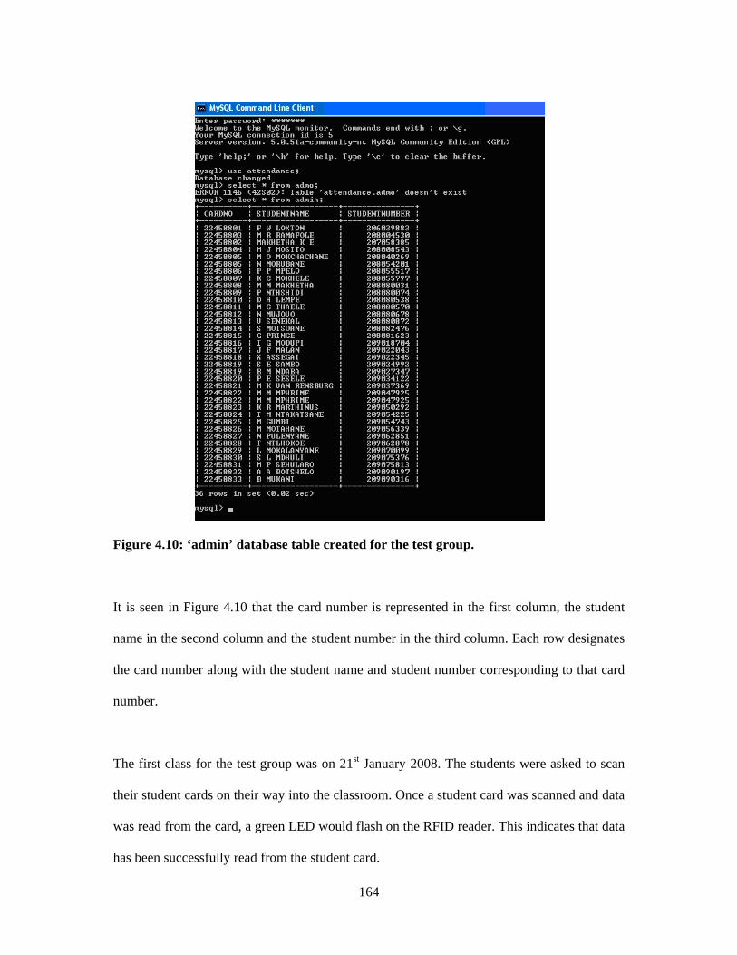
164
Figure 4.10: ‘admin’ database table created for the test group.
It is seen in Figure 4.10 that the card number is represented in the first column, the student
name in the second column and the student number in the third column. Each row designates
the card number along with the student name and student number corresponding to that card
number.
The first class for the test group was on 21st January 2008. The students were asked to scan
their student cards on their way into the classroom. Once a student card was scanned and data
was read from the card, a green LED would flash on the RFID reader. This indicates that data
has been successfully read from the student card.
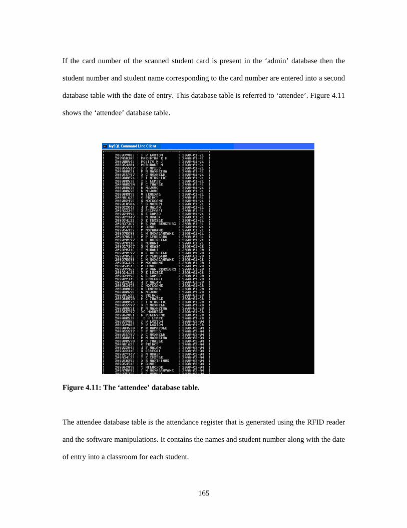
165
If the card number of the scanned student card is present in the ‘admin’ database then the
student number and student name corresponding to the card number are entered into a second
database table with the date of entry. This database table is referred to ‘attendee’. Figure 4.11
shows the ‘attendee’ database table.
Figure 4.11: The ‘attendee’ database table.
The attendee database table is the attendance register that is generated using the RFID reader
and the software manipulations. It contains the names and student number along with the date
of entry into a classroom for each student.
166
Once all the students have scanned their student cards the RFID reader was switched off and
put aside for the lecture to continue. This process was repeated on three occasions for the
remainder of the month. The attendance list for every other day that class was conducted is
shown in figure 4.12, 4.13, 4.14 and 4.15.
Figure 4.12: Attendee database table for 21 -01-2008
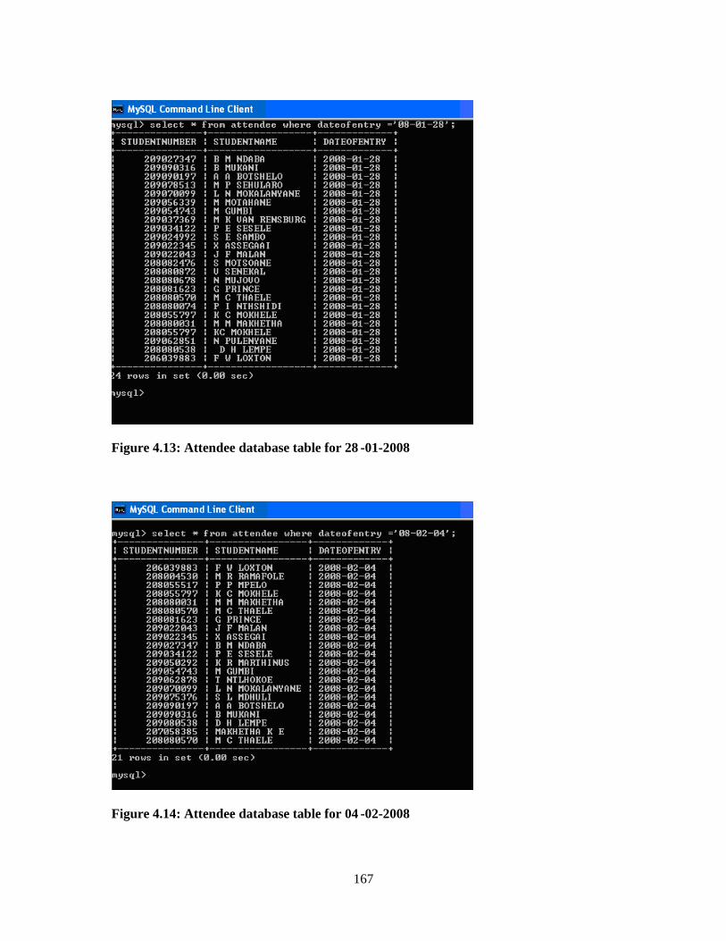
167
Figure 4.13: Attendee database table for 28 -01-2008
Figure 4.14: Attendee database table for 04 -02-2008
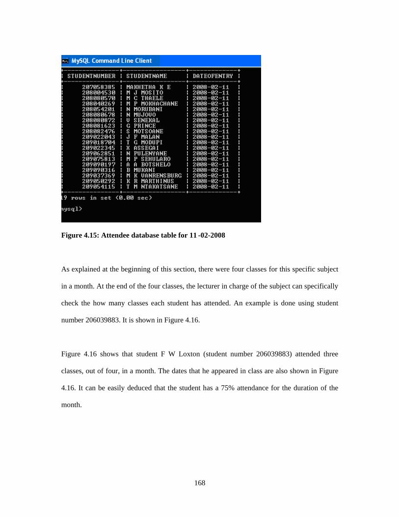
168
Figure 4.15: Attendee database table for 11 -02-2008
As explained at the beginning of this section, there were four classes for this specific subject
in a month. At the end of the four classes, the lecturer in charge of the subject can specifically
check the how many classes each student has attended. An example is done using student
number 206039883. It is shown in Figure 4.16.
Figure 4.16 shows that student F W Loxton (student number 206039883) attended three
classes, out of four, in a month. The dates that he appeared in class are also shown in Figure
4.16. It can be easily deduced that the student has a 75% attendance for the duration of the
month.
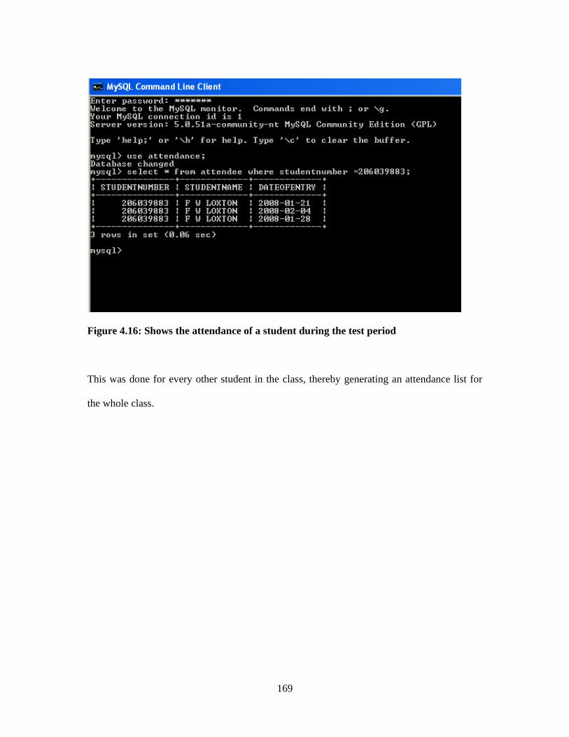
169
Figure 4.16: Shows the attendance of a student during the test period
This was done for every other student in the class, thereby generating an attendance list for
the whole class.

170
CHAPTER 5 CONCLUSION AND FUTURE WORK
The RFID system used for automating the attendance register in this project can scan a single
student card at a time. The reason for this being that the read range of the RFID reader is
about 3-4 cm (Section 4.2.3). The range was fixed at this level so as to avoid anti-collision
(Section 3.1.3). Once the student card is scanned at this read range by the RFID reader, the
data from the student card (Section 4.4) gets transferred to the software section. The software
section is by design very flexible, thus allowing search function (Figure 4.6) and results in
percentile as well.
The design of the software section is such that if the same student card is scanned by the
RFID reader twice within a very short space in time, the student card will be read twice by
the RFID reader. But the software section is designed such that only a single entry will be
made into the database table for student card accidentally scanned twice.
This project was aimed at automating the student attendance register of the Central
University of Technology (CUT) using RFID technology. It was noted during the project that
the student cards issued to students at the time of registration were indeed RFID tags. This
considerably reduced the cost of the project and also made the application of the project cost
effective.
After testing with various RFID readers in order to better understand the concepts of RFID,
the MIFARE MultiISO reader module was selected as the best for this project. The module
was consequently programmed and an interface between the reader and the tag was created
using an antenna.

171
The design of the antenna posed the first challenge as slight variation in the value of the
antenna components resulted in the malfunctioning of the antenna. However, after many
trials the antenna parameters were finally corrected and the antenna was able to read data
from the RFID tags (student cards) and transfer them to the reader.
The software section of the project was then designed. Programming was done using Java
and Apache Derby databases. A lot of thought went into the most suitable programming
languages. In the end the versatility of Java programming, and the ease of use and user
flexibility of the Apache Derby database resulted in their being selected over C-Sharp and
MySQL.
The programming offered the second set of challenges for the project as it required
knowledge of some of the major components of a huge programming language. This was
achieved with the help of some of the classes from the Information Technology staff of the
University. It is worth mentioning that only a part of the Java programming language was
used and is discussed in this thesis.
The final and undoubtedly most challenging part of the project was to set up the wireless link
between the reader and the middleware. This was because ZigBee technology was a fairly
new technology in South Africa at the time of the project (April 2007). There was very little
local support for ZigBee devices, but using the social networking site, ORKUT, many people
overseas (mainly in Finland, India and USA) who had worked with ZigBee technology were
contacted.
172
After very detailed discussions with several people in various countries, the idea of
Maxstream’s X-Bee modules came to the fore. The same people also provided much-needed
support with the installation.
Finally, after months of planning and detailed study of all the components used in the project,
they were put together and the project started functioning exactly as planned. The project was
implemented on a test basis in the Digital Electronics laboratory of the Central University of
Technology. The laboratory was chosen as there were only two batches of students per week
and it provided the best opportunity to uncover any glitches in the project. The results
mentioned in Section 4 were taken from the use of the RFID reader in this lab.
5.1 Future Works
This Central University of Technology uses Oracle as the software for maintaining its
database. A person doing further research in this field may look at ways to integrate Java
program with Oracle instead of MySQL used in this project. MySQL was used at the time
because it was a freeware and it considerably reduced the cost of the system.
This specific project looks at automating attendance registration from a single class room
point of view. Research can be done to see if multiple RFID readers can be placed in
different classes at the same time and their outputs be channelled into a single server
machine. A web interface for such an application can also be a focus area for students
working in Information Technology department of the university.
173
RFID is a technology which is still in its growing phase in South Africa as well as the world.
This thesis dwells into one of the applications of RFID and how it can be set about to solve a
real environment problem. Research can be done by students on certain aspects mentioned in
this thesis like anti-collision, increasing the read range of the antenna or making RFID
systems with onboard memory.
The possibilities of research in this field are endless and it I sincerely hope that readers of this
thesis will be able to think of ways to innovate their surroundings using RFID technology
174
REFERENCES
[1] Government gazette, Draft white paper on e-education in South Africa, Notice 1869 of
August 26, 2004 (last accessed)
[2] Frost and Sullivan, Tracking activity on a small scale with RFID, Dataweek:
Electronics & Communication Technology magazine, 2nd April 2008
[3] RFID Gazette, Wal-Mart and RFID requirement, www.rfidgazette.org/walmart/ ,
February 27, 2007 (last accessed)
[4] Anna Lewcock, RFID set for explosive growth,
http://www.in-pharmatechnologist.com/Product-Categories/IT-solutions/RFID-set-for-
explosive-growth, July 26, 2007 (last accessed)
[5] Marlin H. Mickle, Leonid Mats and Peter J. Hawrylak, RFID Handbook,applications,
technology, security and privacy, CRC press 2008.
[6] Eric C John and Christopher A Chung, RFID in Logistics, CRC press 2008.
[7] Klaus Finkenzeller, RFID Handbook 2nd edition, Wiley press 2003.
[8] Zhiqun Chen, Java Card ™ Tecchnology for smart cards, Addison-Wesley 2000.
[9] David Hanny, Jerry Banks,Manuel Pachano, Les Thompson, RFID Applied, John Wiley
and sons, 2007.
[10] Syed Ahson and Mohammed Ilyas, RFID Handbook, CRC press 2008.
[11] Mary Catherine O'Connor, “RFID is key to car clubs’ success”,
http://www.rfidjournal.com/article/articleview/3839/1/1 , January 7 2008. (last accessed) [12]
Trolley scan product brochure, Working of ECOTAG Reader,
http://trolleyscan.com/brochure.pdf, April 2008.(last accessed)
[13] Bill Glover & Himanshu Bhatt, RFID Essentials, O’ Reilly publications January 2006.
[14] Peter H. Cole and Damith C. Ramasinghe, RFID Handbook Applications,
Technology, Security and Privacy, CRC press 2008.
[15] John G Proakis, Digital Communications, Digital modulation techniques, Mcgraw-
Hill, 2008.
[16] Swapna Dontharaju, Shechih Tung, Raymond H. Hoare, James T. Cain, Marlin h.
Mickle and Alex K. Jones, RFID Handbook Applications, Technology, Security and
Privacy, CRC press 2008.
[17] Jihoon Myung, Wonjun Lee, Timothy K. Shih, RFID Handbook Applications,
Technology, Security and Privacy, CRC press 2008.

175
2003.
[18] Simson Garfinkel & Beth Rosenberg, RFID: Applications, Security and Privacy,
Addilson-Wesley 2006.
[19] Fred Eady, Hands on ZigBee-Implementing 802.15.4 with Microcontrollers , Newnes
publications 2007.
[89] Paolo Baronti, Prashant Pillai, Vince Chook, Steffano Chessa, Wireless sensor
networks: A survey on the state of the art and the 802.15.4 and ZigBee standards-
ZigBee and 802.15.4 overview, www.sciencedirect.com , 29 December 2006. (Last
accessed)
[20] Paolo Baronti, Prashant Pillai, Wireless sensor networks: A survey on the state of the
art and the 802.15.4 and ZigBee standards- IEEE 802.15.4 standard,
www.sciencedirect.com , 29 December 2006. (Last accessed)
[21] Steven Myers, ZigBee/ IEEE 802.15.4-ZigBee devices, tutorial paper written for the
University of Wisconsin, Madison, 10 July 2006(Last accessed)
[22] Sinem Coleri Ergen ,ZigBee/IEEE 802.15.4 SUMMARY-Network topologies; Star
topology, www.sciencedirect.com, 10 September 2004. (Last accessed)
[23] Paul H Young, Electronic communication techniques:Prentice-Hall.
[24] Kenneth Alfred Lambert, Java: A framework for program design and data
structures, Thomson-Brooks/Cole 2004.
[25] David Reilly, GETTING STRATED WITH JDBC,
http://www.javacoffeebreak.com/articles/jdbc/, 5 June 2006 (Last accessed)
[26] Judith S. Bowman, Sandra L. Emerson, Marcy Darnovsky, The practical SQL
Handbook 3rd Edition, Addison-Wesley books, August 1996.
176
APPENDIX A: HARDWARE SPECIFICATION OF THE
READER MODULE
177
APPENDIX B: PIN NUMBERS OF THE READER MODULE
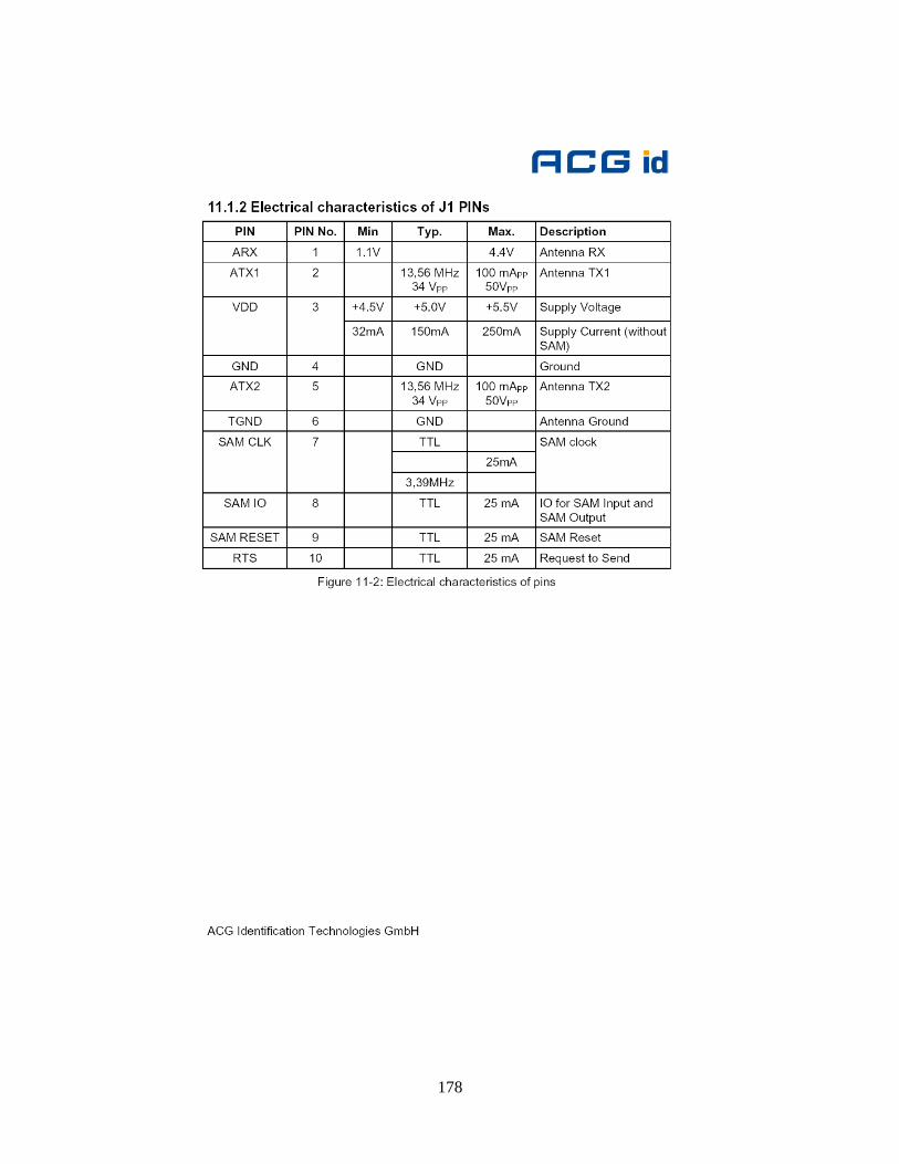
178
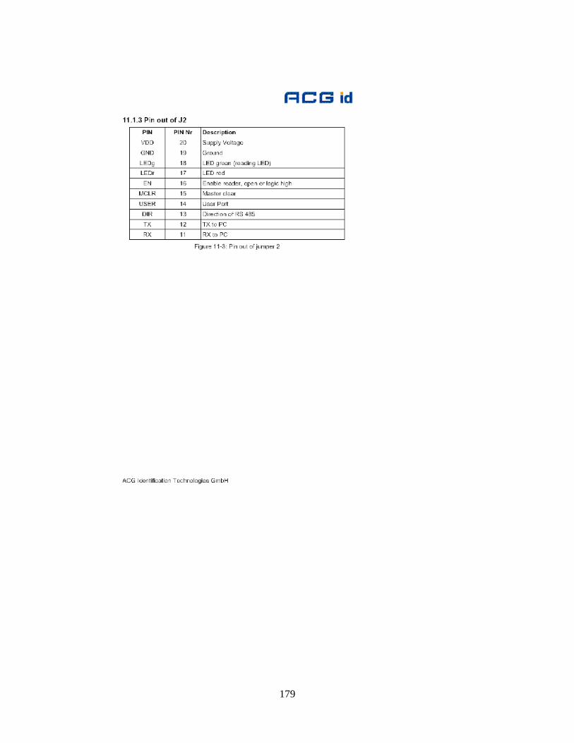
179
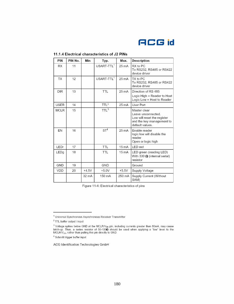
180
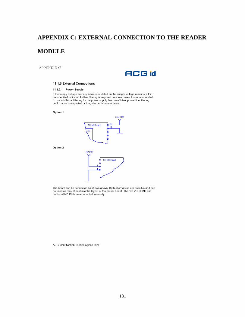
181
APPENDIX C: EXTERNAL CONNECTION TO THE READER
MODULE
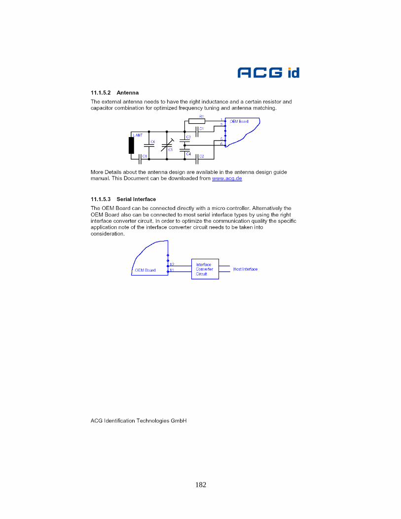
182
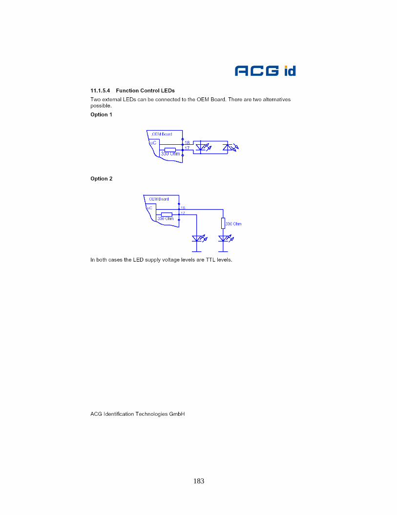
183
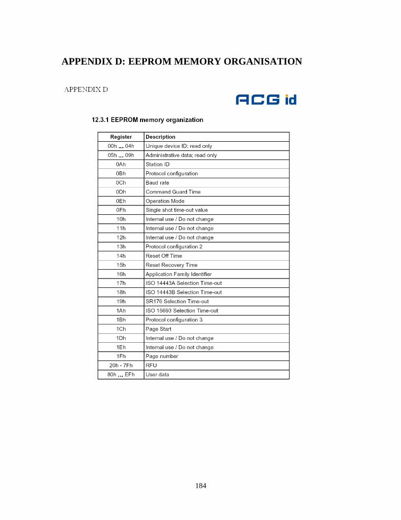
184
APPENDIX D: EEPROM MEMORY ORGANISATION
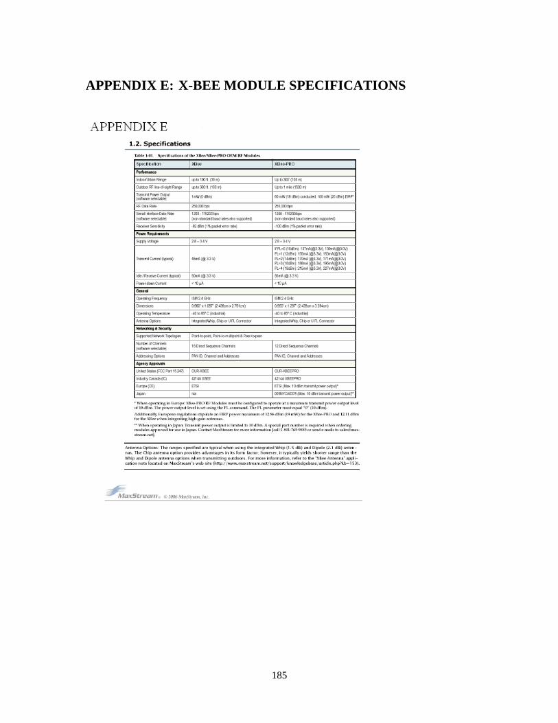
185
APPENDIX E: X-BEE MODULE SPECIFICATIONS
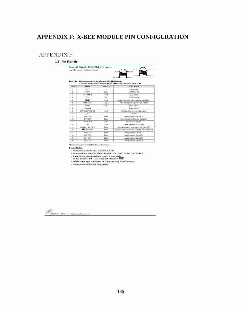
186
APPENDIX F: X-BEE MODULE PIN CONFIGURATION

187
APPENDIX G: JAVA PROGRAM
/*
* StudentView.java
*/
package student;
import java.sql.Connection;
import java.sql.Statement;
import java.sql.DriverManager;
import java.sql.ResultSet;
import java.sql.SQLException;
import java.text.SimpleDateFormat;
import java.text.DateFormat;
import javax.comm.*;
import java.io.*; // enables input and output streams
import java.util.*; //?
import org.jdesktop.application.Action;
import org.jdesktop.application.ResourceMap;
Java program used for the project
188
import org.jdesktop.application.SingleFrameApplication;
import org.jdesktop.application.FrameView;
import org.jdesktop.application.TaskMonitor;
import org.jdesktop.application.Task;
import java.awt.event.ActionEvent;
import java.awt.event.ActionListener;
import java.util.ArrayList;
import java.util.List;
import javax.persistence.RollbackException;
import javax.swing.Timer;
import javax.swing.Icon;
import javax.swing.JDialog;
import javax.swing.JFrame;
import javax.swing.event.ListSelectionEvent;
import javax.swing.event.ListSelectionListener;
import org.jdesktop.beansbinding.AbstractBindingListener;
import org.jdesktop.beansbinding.Binding;
import org.jdesktop.beansbinding.PropertyStateEvent;
/**
* The application's main frame.
*/
public class StudentView extends FrameView
/** Creates a new instance of Connection */
189
public SConnection()
/*Open COM1 port for communication*/
try
TimeStamp = new java.util.Date().toString();
serialPort1 = (SerialPort) portId1.open("Connection", 1000);
taOutput.setText(taOutput.getText() + TimeStamp + ": " + portId1.getName() + "
opened for scanner input\n");
catch (PortInUseException e)
try
/*check for incoming input*/
inputStream = serialPort1.getInputStream();
catch (IOException e)
try
serialPort1.addEventListener(this);
190
catch (TooManyListenersException e)
serialPort1.notifyOnDataAvailable(true);
try
/*Define properties of the serial port*/
serialPort1.setSerialPortParams(9600,
SerialPort.DATABITS_8,
SerialPort.STOPBITS_1,
SerialPort.PARITY_NONE);
serialPort1.setDTR(false);
serialPort1.setRTS(false);
catch (UnsupportedCommOperationException e)
readThread = new Thread(this);
readThread.start();
public void startPort()//old main method
/*establish the existance of serial port COM1 - moved to button click*/
try
191
portId1 = CommPortIdentifier.getPortIdentifier("COM1");
SConnection reader = new SConnection();
catch (Exception e)
TimeStamp = new java.util.Date().toString();
System.out.println(TimeStamp + ": COM1 " + portId1);//display port identifier
System.out.println(TimeStamp + ": msg1 - " + e);//display an exception
public void run()
try
Thread.sleep(100);
catch (InterruptedException e)
public void serialEvent(SerialPortEvent event)
/*Check for data */
switch(event.getEventType())
192
case SerialPortEvent.OUTPUT_BUFFER_EMPTY:
break;
case SerialPortEvent.DATA_AVAILABLE:
StringBuffer readBuffer = new StringBuffer();
int c;
try
while ((c=inputStream.read()) != 10)
if(c!=13) readBuffer.append((char) c);
String scannedInput = readBuffer.toString();
TimeStamp = new java.util.Date().toString();
handleInput(scannedInput);
outputStream = serialPort1.getOutputStream();
outputStream.write(scannedInput.getBytes());
javax.swing.JOptionPane.showMessageDialog( null,TimeStamp + "\n Received
Message: " + scannedInput );
inputStream.close();
catch (IOException e)

193
break;
private void handleInput(String input)
Connection connection = null;
Statement statement = null;
ResultSet resultSet;
int numberOfRows;
try
connection = DriverManager.getConnection("jdbc:derby://localhost:1527/StudentAtt");
taOutput.setText(taOutput.getText() + "Successfully connected.\n");
statement =
connection.createStatement(ResultSet.TYPE_SCROLL_INSENSITIVE,ResultSet.CONCUR
_UPDATABLE);
194
resultSet = statement.executeQuery("Select * from Students where CARD_ID ='" +
input + "'");
resultSet.last();
numberOfRows = resultSet.getRow();
if (numberOfRows == 1)
Attendance a = new Attendance();
DateFormat dateFormat = new SimpleDateFormat("yyyy/MM/dd HH:mm:ss");
java.util.Date date = new java.util.Date();
String s = dateFormat.format(date);
a.setDatetime(s);
a.setStudentNumber((resultSet.getObject(2).toString()));
try
entityManager.persist(a);
entityManager.getTransaction().commit();
attendanceList.add(a);
catch (Exception e)
e.printStackTrace();
entityManager.getTransaction().rollback();
attTable.setName("attTable"); // NOI18N
org.jdesktop.swingbinding.JTableBinding jTableBinding =
org.jdesktop.swingbinding.SwingBindings.createJTableBinding(org.jdesktop.beansbinding.A
utoBinding.UpdateStrategy.READ_WRITE, attendanceList, attTable);

195
org.jdesktop.swingbinding.JTableBinding.ColumnBinding columnBinding =
jTableBinding.addColumnBinding(org.jdesktop.beansbinding.ELProperty.create("$datetime
"));
columnBinding.setColumnName("Datetime");
columnBinding.setColumnClass(String.class);
columnBinding =
jTableBinding.addColumnBinding(org.jdesktop.beansbinding.ELProperty.create("$student
Number"));
columnBinding.setColumnName("Student Number");
columnBinding.setColumnClass(String.class);
bindingGroup.addBinding(jTableBinding);
jTableBinding.bind();
taOutput.setText(taOutput.getText() + "Card found and entry recorded in
database.\n");
else
taOutput.setText(taOutput.getText() + "Card not in database.\n");
catch (SQLException err)
taOutput.setText(taOutput.getText() + err.toString() + "\n");

196
finally
try
statement.close();
connection.close();