Embed Size (px)
Citation preview
1
Answers to Problems and Exercises
Chapter 1 Circuit Variables and Elements
P1.1.1 36 kWh.
P1.1.2 (a) 0, 2.5, 5.5, 8.5, 11, 11 mC.
(b) 0:10 =≤≤ pt ; ttpt 22:21 2 +=≤≤ mW; tpt 6:32 =≤≤ mW;
366:43 +−=≤≤ tpt mW; 84262:54 2 +−=≤≤ ttpt mW;
0:65 =≤≤ pt .
(c) 45.3 μJ.
P1.1.3 (a) s75.0 .
(b) s2 .
(c) 9.3, –21.3 mJ.
P1.1.4 (a) Power is absorbed by device during the first and third quarter cycles,
when v and i have the same sign, and is delivered during the second and
fourth quarter cycles, when v and i have opposite signs.
(b) 0.5 W.
(c) 0.5 W.
(d) 0.
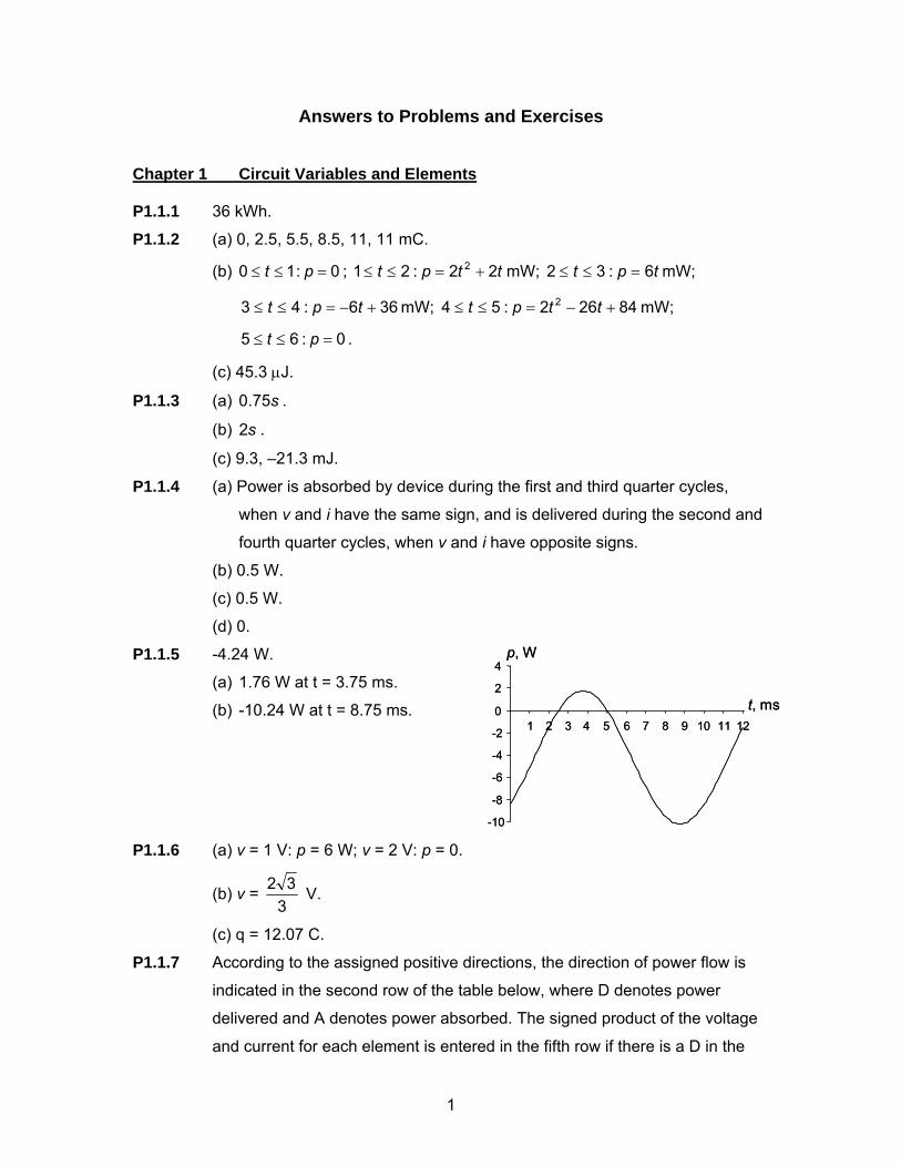
P1.1.5 -4.24 W.
(a) 1.76 W at t = 3.75 ms.
(b) -10.24 W at t = 8.75 ms.
P1.1.6 (a) v = 1 V: p = 6 W; v = 2 V: p = 0.
(b) v = 3
32 V.
(c) q = 12.07 C.
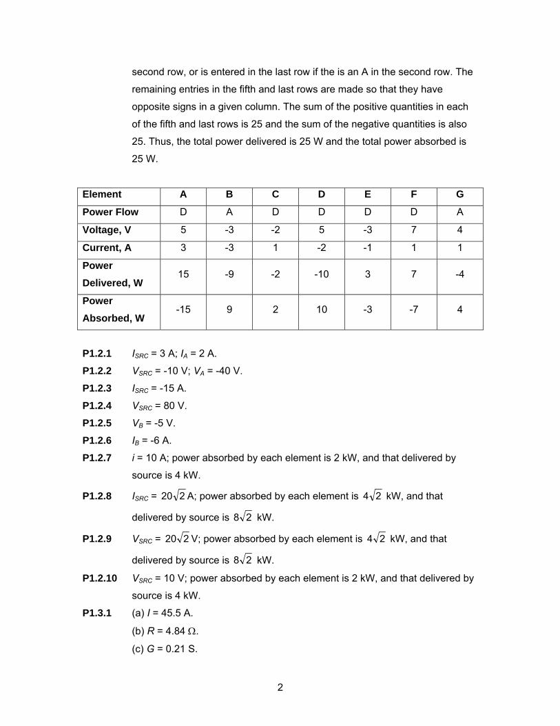
P1.1.7 According to the assigned positive directions, the direction of power flow is
indicated in the second row of the table below, where D denotes power
delivered and A denotes power absorbed. The signed product of the voltage
and current for each element is entered in the fifth row if there is a D in the
-10
-8
-6
-4
-2
0
2
4
1 2 3 4 5 6 7 8 9 10 11 12
t, ms
p, W
-10
-8
-6
-4
-2
0
2
4
1 2 3 4 5 6 7 8 9 10 11 12
t, ms
p, W
2
second row, or is entered in the last row if the is an A in the second row. The
remaining entries in the fifth and last rows are made so that they have
opposite signs in a given column. The sum of the positive quantities in each
of the fifth and last rows is 25 and the sum of the negative quantities is also
25. Thus, the total power delivered is 25 W and the total power absorbed is
25 W.
Element A B C D E F G
Power Flow D A D D D D A
Voltage, V 5 -3 -2 5 -3 7 4
Current, A 3 -3 1 -2 -1 1 1
Power Delivered, W
15 -9 -2 -10 3 7 -4
Power Absorbed, W
-15 9 2 10 -3 -7 4
P1.2.1 ISRC = 3 A; IA = 2 A.
P1.2.2 VSRC = -10 V; VA = -40 V.
P1.2.3 ISRC = -15 A.
P1.2.4 VSRC = 80 V.
P1.2.5 VB = -5 V.
P1.2.6 IB = -6 A.
P1.2.7 i = 10 A; power absorbed by each element is 2 kW, and that delivered by
source is 4 kW.
P1.2.8 ISRC = 220 A; power absorbed by each element is 24 kW, and that
delivered by source is 28 kW.
P1.2.9 VSRC = 220 V; power absorbed by each element is 24 kW, and that
delivered by source is 28 kW.
P1.2.10 VSRC = 10 V; power absorbed by each element is 2 kW, and that delivered by
source is 4 kW.
P1.3.1 (a) I = 45.5 A.
(b) R = 4.84 Ω.
(c) G = 0.21 S.
3
P1.3.2 62.7oC.
P1.3.3 866.0 V.
P1.3.4 10 mV; 10 μA.
P1.3.5 (a) 1.20 mA.
(b) -1 nA.
P1.3.6 (a) i = 0.1t A, 0 ≤ t ≤ 1 min; i = -0.1t + 0.2 A, 1 ≤ t ≤ 3 min; i = 0.1t – 0.4 A,
3 ≤ t ≤ 4 min.
(b) p = t2 W, 0 ≤ t ≤ 1 min; p = 100
)2010( 2+− t W, 1 ≤ t ≤ 3 min;
p = 100
)4010( 2−t W, 3 ≤ t ≤ 4 min.3< t < 4 min.
(c) P = 5.56 mJ.
(d) Vavg = 0, since the waveform is symmetrical about the horizontal axis. This
makes Iavg = 0 as well. Thus, Vavg×Iavg = 0, whereas P ≠ 0. The average
power in a resistor is not the product of the average voltage across the
resistor and the average current through the resistor, because power,
being the product of voltage and current, is a nonlinear quantity.
P1.3.7 15 Ω; 120 W.
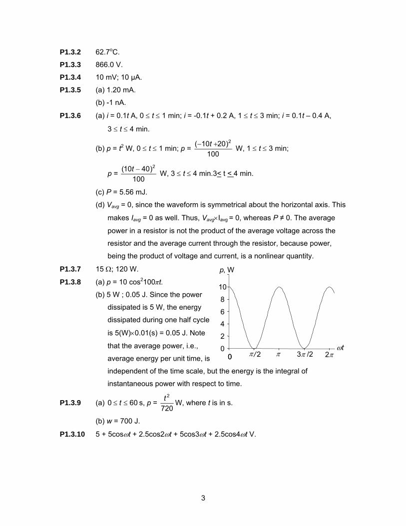
P1.3.8 (a) p = 10 cos2100πt.
(b) 5 W ; 0.05 J. Since the power
dissipated is 5 W, the energy
dissipated during one half cycle
is 5(W)×0.01(s) = 0.05 J. Note
that the average power, i.e.,
average energy per unit time, is
independent of the time scale, but the energy is the integral of
instantaneous power with respect to time.
P1.3.9 (a) 600 ≤≤ t s, p = 720
2t W, where t is in s.
(b) w = 700 J.
P1.3.10 5 + 5cosωt + 2.5cos2ωt + 5cos3ωt + 2.5cos4ωt V.
0
2
46
8
10
0
p, W
π /2 π0 3π /2 2πωt
4
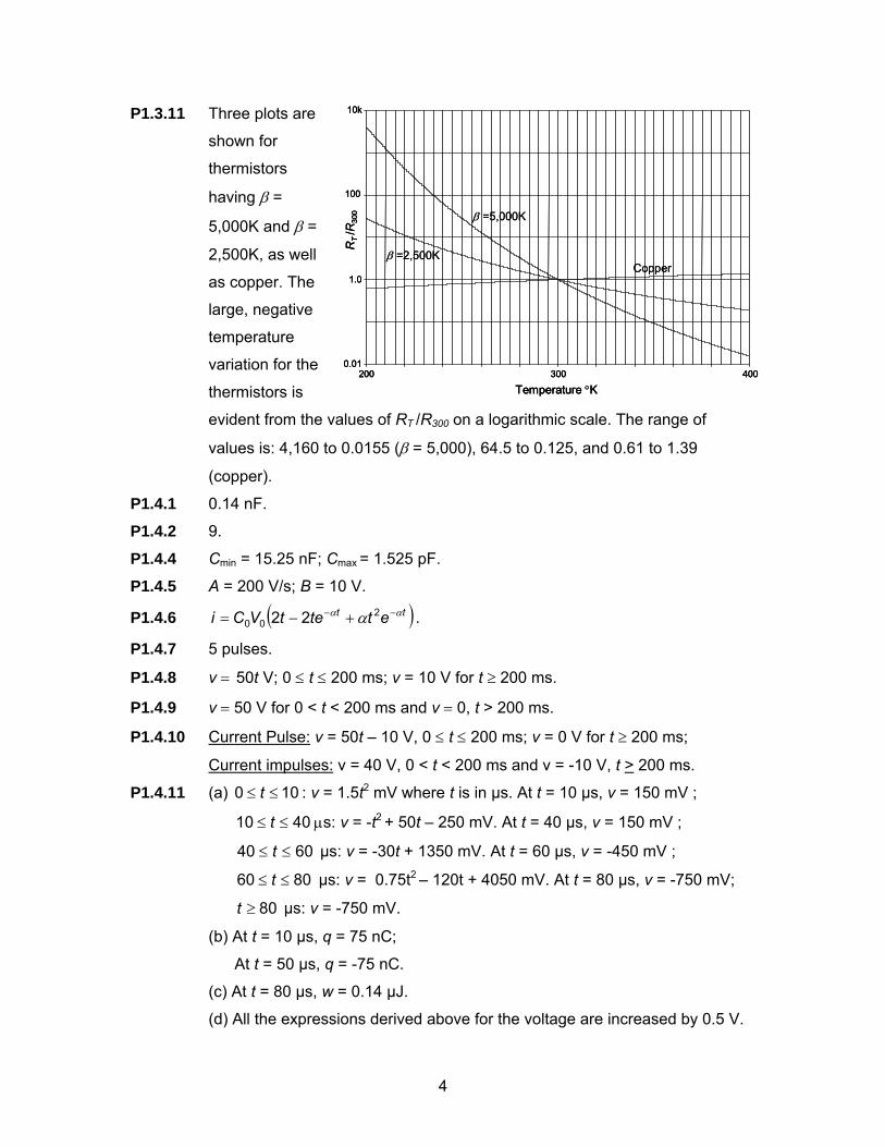
P1.3.11 Three plots are
shown for
thermistors
having β =
5,000K and β =
2,500K, as well
as copper. The
large, negative
temperature
variation for the
thermistors is
evident from the values of RT /R300 on a logarithmic scale. The range of
values is: 4,160 to 0.0155 (β = 5,000), 64.5 to 0.125, and 0.61 to 1.39
(copper).
P1.4.1 0.14 nF.
P1.4.2 9.
P1.4.4 Cmin = 15.25 nF; Cmax = 1.525 pF.
P1.4.5 A = 200 V/s; B = 10 V.
P1.4.6 ( )tt ettetVCi αα α −− +−= 200 22 .
P1.4.7 5 pulses.
P1.4.8 v = t50 V; 0 ≤ t ≤ 200 ms; v = 10 V for t ≥ 200 ms.
P1.4.9 v = 50 V for 0 < t < 200 ms and v = 0, t > 200 ms.
P1.4.10 Current Pulse: v = 50t – 10 V, 0 ≤ t ≤ 200 ms; v = 0 V for t ≥ 200 ms;
Current impulses: v = 40 V, 0 < t < 200 ms and v = -10 V, t > 200 ms. P1.4.11 (a) 100 ≤≤ t : v = 1.5t2 mV where t is in μs. At t = 10 μs, v = 150 mV ;
4010 ≤≤ t μs: v = -t2 + 50t – 250 mV. At t = 40 μs, v = 150 mV ;
6040 ≤≤ t μs: v = -30t + 1350 mV. At t = 60 μs, v = -450 mV ;
8060 ≤≤ t μs: v = 0.75t2 – 120t + 4050 mV. At t = 80 μs, v = -750 mV;
80≥t μs: v = -750 mV.
(b) At t = 10 μs, q = 75 nC;
At t = 50 μs, q = -75 nC.
(c) At t = 80 μs, w = 0.14 μJ.
(d) All the expressions derived above for the voltage are increased by 0.5 V.
Temperature °K200 300 400
0.01
1.0
100
10k
RT
/R30
0
Copper
β =5,000K
β =2,500K
Temperature °K200 300 400
0.01
1.0
100
10k
RT
/R30
0
Temperature °K200 300 400
0.01
1.0
100
10k
RT
/R30
0
Copper
β =5,000K
β =2,500K
5
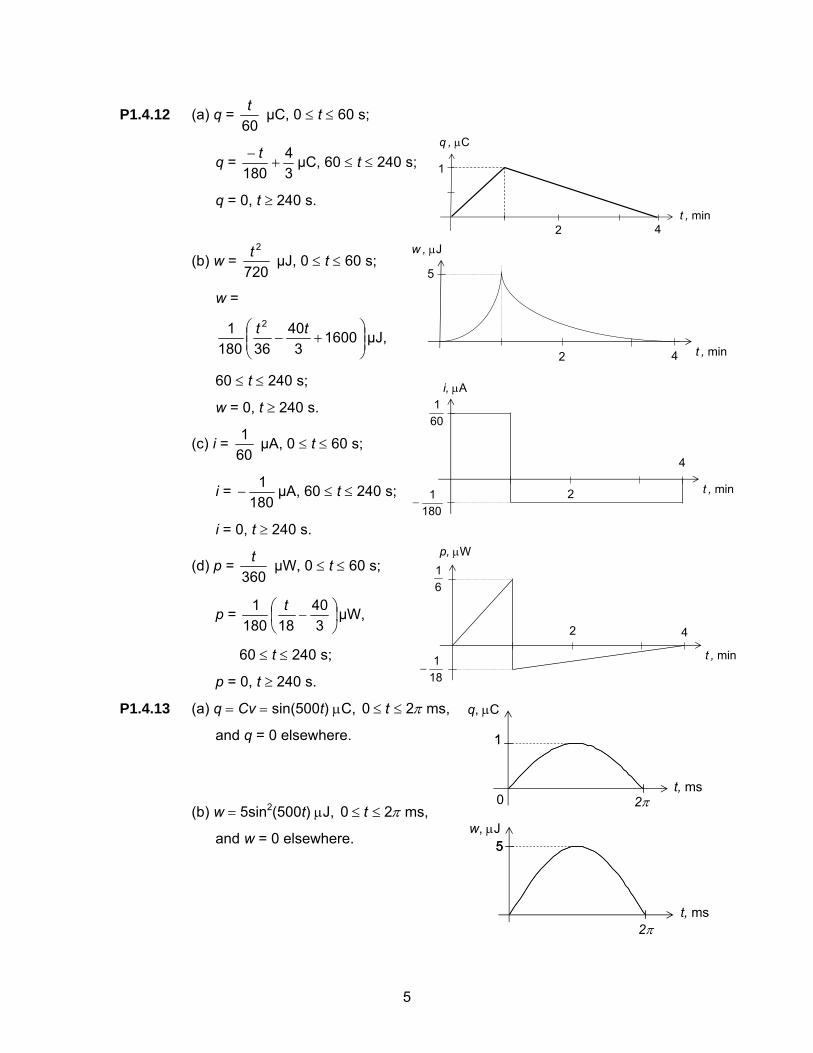
P1.4.12 (a) q = 60t μC, 0 ≤ t ≤ 60 s;
q = 34
180+
− t μC, 60 ≤ t ≤ 240 s;
q = 0, t ≥ 240 s.
(b) w = 720
2t μJ, 0 ≤ t ≤ 60 s;
w =
⎟⎟⎠
⎞⎜⎜⎝
⎛+− 1600
340
361801 2 tt μJ,
60 ≤ t ≤ 240 s;
w = 0, t ≥ 240 s.
(c) i = 601 μA, 0 ≤ t ≤ 60 s;
i = 180
1− μA, 60 ≤ t ≤ 240 s;
i = 0, t ≥ 240 s.
(d) p = 360
t μW, 0 ≤ t ≤ 60 s;
p = ⎟⎠⎞
⎜⎝⎛ −
340
181801 t μW,
60 ≤ t ≤ 240 s;
p = 0, t ≥ 240 s.
P1.4.13 (a) q = Cv = sin(500t) μC, π20 ≤≤ t ms,
and q = 0 elsewhere.
(b) w = 5sin2(500t) μJ, π20 ≤≤ t ms,
and w = 0 elsewhere.
4t , min
q , μC
1
2
4 t , min
w , μJ
5
2
4
t , min
i, μA
2
601
1801
−
4
t , min
p, μW
2
61
181
−
2πt, ms
11
q, μC
0
55w, μJ
2πt, ms
6
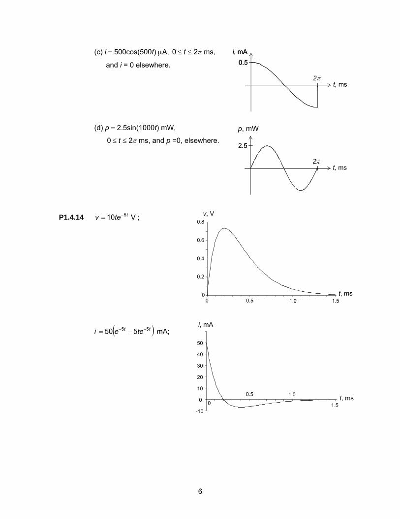
(c) i = 500cos(500t) μA, π20 ≤≤ t ms,
and i = 0 elsewhere.
(d) p = 2.5sin(1000t) mW,
π20 ≤≤ t ms, and p =0, elsewhere.
P1.4.14 V10 5ttev −= ;
i ( )tt tee 55 550 −− −= mA;
0.5i, mA
0.5i, mA
t, ms2π
0
0.2
0.4
0.6
0.8
0 0.5 1.0 1.5t, ms
v, V
-10
0
10
20
30
40
50
0
0.5 1.0
1.5t, ms
i, mA
2.5.5
t, ms2π
p, mW
7
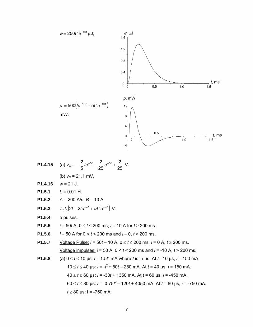
w tet 102250 −= μJ;
p ( )tt ette 10210 5500 −− −=
mW.
P1.4.15 (a) vC = 252
252
52 55 +−− −− tt ete V.
(b) vC = 21.1 mV.
P1.4.16 w = 21 J.
P1.5.1 L = 0.01 H.
P1.5.2 A = 200 A/s, B = 10 A.
P1.5.3 ( )tt ettetIL αα α −− +− 200 22 V.
P1.5.4 5 pulses.
P1.5.5 i = 50t A, 0 ≤ t ≤ 200 ms; i = 10 A for t ≥ 200 ms.
P1.5.6 i = 50 A for 0 < t < 200 ms and i = 0, t > 200 ms.
P1.5.7 Voltage Pulse: i = 50t – 10 A, 0 ≤ t ≤ 200 ms; i = 0 A, t ≥ 200 ms.
Voltage impulses: i = 50 A, 0 < t < 200 ms and i = -10 A, t > 200 ms.
P1.5.8 (a) 0 ≤ t ≤ 10 μs: i = 1.5t2 mA where t is in μs. At t =10 μs, i = 150 mA.
10 ≤ t ≤ 40 μs: i = -t2 + 50t – 250 mA. At t = 40 μs, i = 150 mA.
40 ≤ t ≤ 60 μs: i = -30t + 1350 mA. At t = 60 μs, i = -450 mA.
60 ≤ t ≤ 80 μs: i = 0.75t2 – 120t + 4050 mA. At t = 80 μs, i = -750 mA.
t ≥ 80 μs: i = -750 mA.
0
4
8
12
0
0.5
1.0 1.5t, ms
-4
p, mW
0
0.4
0.8
1.2
1.6
0 0.5 1.0 1.5t, ms
w, μJ
8
(b) At t = 10 μs, λ = 75 nWb-turns; at t = 50 μs, λ = -75 nWb-turns.
(c) At t = 80 μs, w = 0.14 μJ.
(d) All the expressions derived above for the current are increased by 0.5 V.
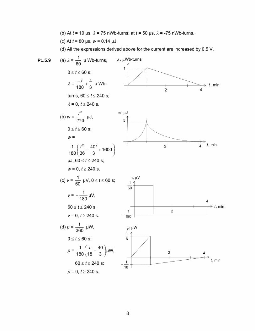
P1.5.9 (a) λ = 60t μ Wb-turns,
0 ≤ t ≤ 60 s;
λ = 34
180+
− t μ Wb-
turns, 60 ≤ t ≤ 240 s;
λ = 0, t ≥ 240 s.
(b) w = 720
2t μJ,
0 ≤ t ≤ 60 s;
w =
⎟⎟⎠
⎞⎜⎜⎝
⎛+− 1600
340
361801 2 tt
μJ, 60 ≤ t ≤ 240 s;
w = 0, t ≥ 240 s.
(c) v = 601 μV, 0 ≤ t ≤ 60 s;
v = 180
1− μV,
60 ≤ t ≤ 240 s;
v = 0, t ≥ 240 s.
(d) p = 360
t μW,
0 ≤ t ≤ 60 s;
p = ⎟⎠⎞
⎜⎝⎛ −
340
181801 t μW,
60 ≤ t ≤ 240 s;
p = 0, t ≥ 240 s.
4t , min
λ , μWb-turns
1
2
4 t , min
w , μJ
5
2
4t , min
v, μV
2
601
1801
−
4
t , min
p, μW
2
61
181
−
9
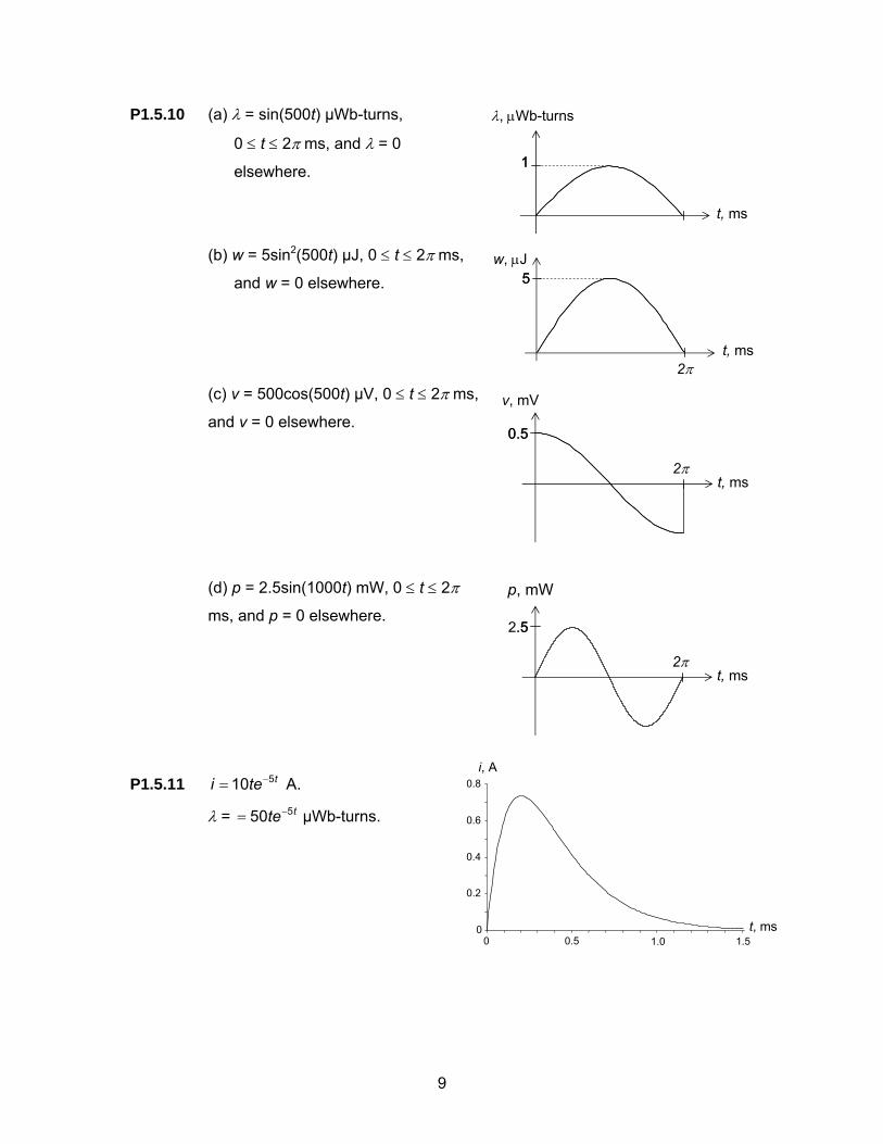
P1.5.10 (a) λ = sin(500t) μWb-turns,
0 ≤ t ≤ 2π ms, and λ = 0
elsewhere.
(b) w = 5sin2(500t) μJ, 0 ≤ t ≤ 2π ms,
and w = 0 elsewhere.
(c) v = 500cos(500t) μV, 0 ≤ t ≤ 2π ms,
and v = 0 elsewhere.
(d) p = 2.5sin(1000t) mW, 0 ≤ t ≤ 2π
ms, and p = 0 elsewhere.
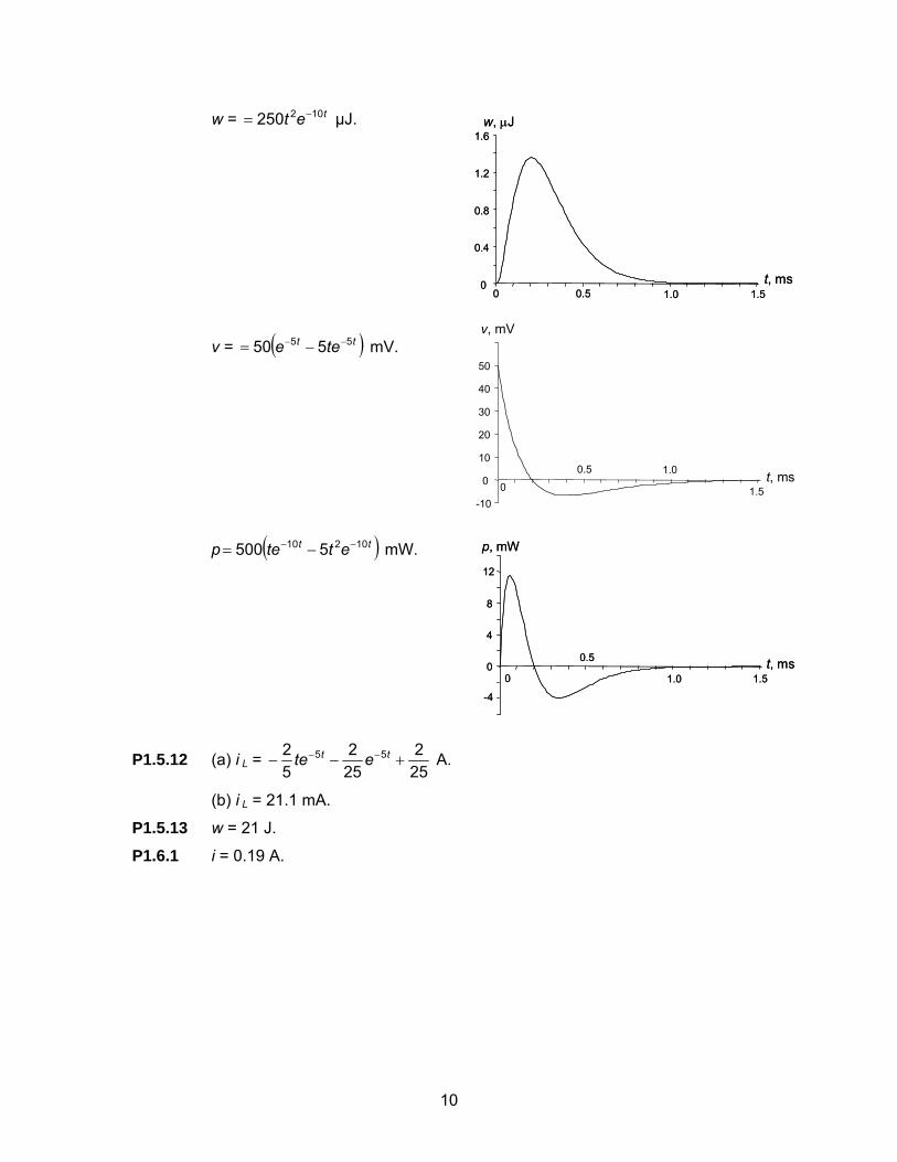
P1.5.11 ttei 510 −= A.
λ = tte 550 −= μWb-turns.
t, ms
11
λ, μWb-turns
55w, μJ
2πt, ms
0.50.5
v, mV
t, ms2π
2.5.5
t, ms2π
p, mW
0
0.2
0.4
0.6
0.8
0 0.5 1.0 1.5t, ms
i, A
10
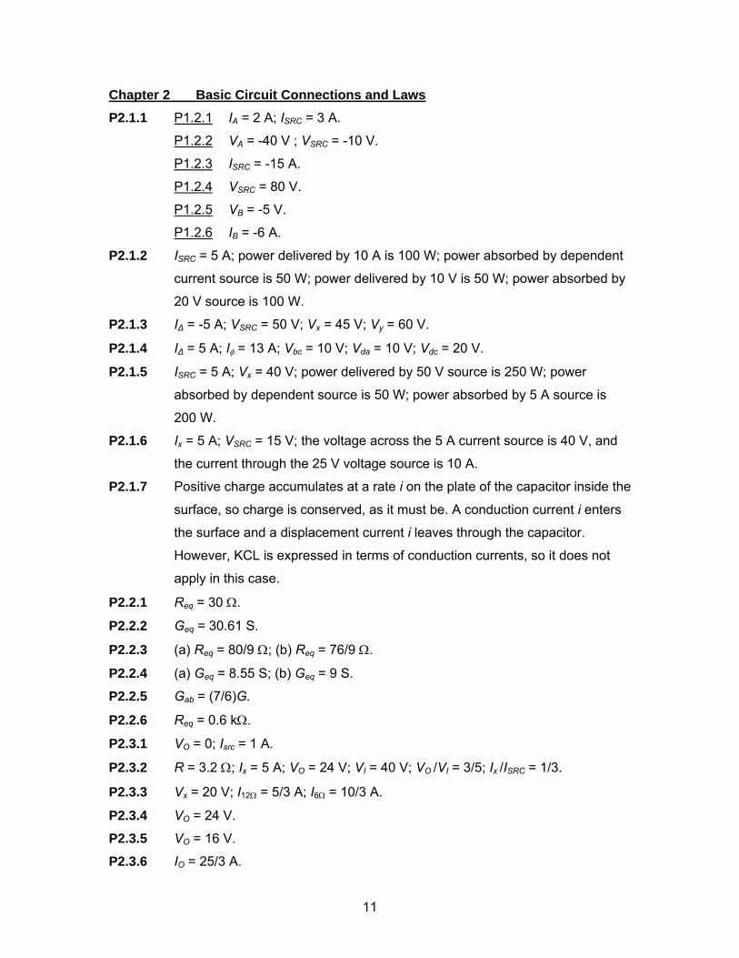
w = tet 102250 −= μJ.
v = ( )tt tee 55 550 −− −= mV.
p ( )tt ette 10210 5500 −− −= mW.
P1.5.12 (a) i L = 252
252
52 55 +−− −− tt ete A.
(b) i L = 21.1 mA.
P1.5.13 w = 21 J.
P1.6.1 i = 0.19 A.
0
0.4
0.8
1.2
1.6
0 0.5 1.0 1.5t, ms
w, μJ
0
0.4
0.8
1.2
1.6
0 0.5 1.0 1.5t, ms
w, μJ
-10
0
10
20
30
40
50
0
0.5 1.0
1.5t, ms
v, mV
0
4
8
12
0
0.5
1.0 1.5t, ms
-4
p, mW
0
4
8
12
0
0.5
1.0 1.5t, ms
-4
p, mW
11
Chapter 2 Basic Circuit Connections and Laws P2.1.1 P1.2.1 IA = 2 A; ISRC = 3 A.
P1.2.2 VA = -40 V ; VSRC = -10 V.
P1.2.3 ISRC = -15 A.
P1.2.4 VSRC = 80 V.
P1.2.5 VB = -5 V.
P1.2.6 IB = -6 A. P2.1.2 ISRC = 5 A; power delivered by 10 A is 100 W; power absorbed by dependent
current source is 50 W; power delivered by 10 V is 50 W; power absorbed by
20 V source is 100 W. P2.1.3 IΔ = -5 A; VSRC = 50 V; Vx = 45 V; Vy = 60 V.
P2.1.4 IΔ = 5 A; Iφ = 13 A; Vbc = 10 V; Vda = 10 V; Vdc = 20 V.
P2.1.5 ISRC = 5 A; Vx = 40 V; power delivered by 50 V source is 250 W; power
absorbed by dependent source is 50 W; power absorbed by 5 A source is
200 W. P2.1.6 Ix = 5 A; VSRC = 15 V; the voltage across the 5 A current source is 40 V, and
the current through the 25 V voltage source is 10 A. P2.1.7 Positive charge accumulates at a rate i on the plate of the capacitor inside the
surface, so charge is conserved, as it must be. A conduction current i enters
the surface and a displacement current i leaves through the capacitor.
However, KCL is expressed in terms of conduction currents, so it does not
apply in this case.
P2.2.1 Req = 30 Ω.
P2.2.2 Geq = 30.61 S.
P2.2.3 (a) Req = 80/9 Ω; (b) Req = 76/9 Ω.
P2.2.4 (a) Geq = 8.55 S; (b) Geq = 9 S.
P2.2.5 Gab = (7/6)G.
P2.2.6 Req = 0.6 kΩ.
P2.3.1 VO = 0; Isrc = 1 A.
P2.3.2 R = 3.2 Ω; Ix = 5 A; VO = 24 V; VI = 40 V; VO /VI = 3/5; Ix /ISRC = 1/3.
P2.3.3 Vx = 20 V; I12Ω = 5/3 A; I6Ω = 10/3 A.
P2.3.4 VO = 24 V.
P2.3.5 VO = 16 V.
P2.3.6 IO = 25/3 A.
12
P2.3.7 Vx = 8 V; Iy = 0.375 A.
P2.4.1 VO = 6 V.
P2.4.2 VO = 40 V.
P2.4.3 Isrc = -1 mA. P2.4.4 VO = 12 V.
P2.4.5 VO = 12 V.
P2.4.6 Ix = 7 A.
P2.4.7 Ix = 75.33 A; VA = -20 V; VB = 20 V.
P2.4.8 Vx = 490/3 V.
P2.4.9 Vx = 50 V; Vy = 46.67 V.
P2.4.10 Ix = -1 A.
P2.4.11 Ix = 1.2 A.
P2.4.12 VSRC = 120 V; Vx = 48 V; Vy = 72 V; Isrc = 12 A; I6Ω = 8 A; I12Ω = 4 A; I24Ω = 3 A;
I8Ω = 9 A.
P2.4.13 Vx /Ix = -100/49 kΩ.
P2.4.14 R0 = 3 kΩ; Rx = 27 kΩ.
P2.4.15 R0 = 30 kΩ; Rx = 3.75 kΩ.
P2.4.16 VO = 3 V.
P2.4.17 Vx = 30 V; VSRC = 195 V.
P2.4.18 R = 3.2 Ω; Ix = 2 A.
P2.4.19 Ix = 1.19 A.
P2.4.20 Ix = 0.75 A.
P2.4.21 Vx = 1.71 V.
Chapter 3 Basic Analysis of Resistive Circuits
P3.1.1 66
204
10 ababab VVV=
−+
− ; Vab = 10 V; I1 = 0; I2 = -5/3 A. Since Vab = 10 V, the
two terminals of the 4 Ω resistor are at the same voltage, so that I1 = 0 and
Vab can be found by voltage division.
P3.1.2 ISRC1 = -1.3 A; ISRC2 = 2.2 A. P3.1.3 ISRC1 = -1.3 A; ISRC2 = 2.2 A. P3.1.4 Vac = 0 V; Vbc = -5/3 V. Since Vac = 0, node a is at the same voltage as node
c, so that Vbc can be found by current division. P3.1.5 VSRC1 = -1.3 V; VSRC2 = 2.2 V.
13
P3.1.6 VSRC1 = -1.3 V; VSRC2 = 2.2 V.
P3.1.7 VO = 20 V. The 20 Ω and 40 Ω resistances are in the same ratio as the
voltage sources, so the voltages across the resistors are the same as those
of the corresponding sources. P3.1.8 VO = 20 V. P3.1.9 IO = 20 A. The 20 S and 40 S conductances are in the same ratio as the
current sources, so that the current in each resistor is equal to that of the
source in series with it. P3.1.10 IO = 20 A. P3.1.11 VO = 15.5 V. P3.1.12 VO = 15.5 V. P3.1.13 IO = 15.5 A. P3.1.14 IO = 15.5 A. P3.1.15 VO = -10/3 V. P3.1.16 VO = -10/3 V. P3.1.17 IO = -10/3 A. P3.1.18 IO = -10/3 A. P3.1.19 VO = 30 V. P3.1.20 VO = 30 V. P3.1.21 IO = 30 A. P3.1.22 IO = 30 A; ISRC1 = 1 A; ISRC2 = 95 A. P3.1.23 IO = -22 A. P3.1.24 IO = -22 A. P3.1.25 VO = 0 V. P3.1.26 VO = 0 V. P3.1.27 VO = 1.82 V.
P3.2.1 Vab = 10 V. P3.2.2 VO = 10 V. P3.2.3 Vab = 18 V; ISRC1 = -1.3 A; ISRC2 = 2.2 A. P3.2.4 Vac = 0 V; Vbc = -5/3 V. P3.2.5 VSRC1 = -1.3 V; VSRC2 = 2.2 V. P3.2.6 VO = 20 V. P3.2.7 IO = 20 A. P3.2.8 VO = 15.5 V.
14
P3.2.9 Va = 10/49 V; Ix = 5/49 A; VO = 15.51 V. P3.2.10 IO = 15.5 A; power dissipated = 30.03 W. P3.2.11 Ix = 10/49 A; Vx = 5/49 V; IO = 15.510 A. P3.2.12 VO = 30V; power dissipated = 180 W. P3.2.13 IO = 30 A; power dissipated = 180 W. P3.2.14 IO = -22 A; power dissipated = 121 W. P3.2.15 VO = 0V. P3.2.16 Ix = -10 A; VO = 0V. P3.2.17 IO = 10/13 A. P3.2.18 VSRC = 8 V.
Chapter 4 Circuit Simplification
P4.1.1 VTh = 4 V; RTh = 4 Ω.
P4.1.2 IN = 0.3 A; GN = 0.025 S.
P4.1.3 VTh = 0; RTh = 10 Ω.
P4.1.4 VTh = 0; RTh = -10 Ω.
P4.1.5 (a) VTh = 0; RTh = 1 Ω.
(b) VTh = -VSRC; RTh =0.
P4.1.6 VTh = 16 V; RTh = 8 Ω.
P4.1.7 IN = 4.4 A; GN = 0.04 S.
P4.1.8 VTh = 10 V; RTh = 10 Ω.
P4.1.9 VTh = 40 V; RTh = 0. P4.1.10 IN = 8 A; GN = 0.
P4.1.11 VTh = 70/3 V; RTh = 20/3 Ω; VO = 20V.
P4.1.12 IO = 20 A. P4.1.13 VO = 15.5 V. P4.1.14 IO = 15.5 A. P4.1.15 VO = -10/3 V. P4.1.16 IO = -10/3 A. P4.1.17 VO = 30 V. P4.1.18 IO = 30 A. P4.1.19 IO = -22 A. P4.1.20 VO = 0.
P4.2.1 Ix = 0.9 A.
15
P4.2.2 Vcd = -1 V. P4.2.3 VO = -10/3 V. P4.2.4 IO = -10/3 A. P4.2.5 IO = -22 A. P4.2.6 VO = 0. P4.3.7 Vab = 12 V.
P4.3.8 Vab = 15 V.
P4.3.9 Vab = 5 V.
P4.3.10 Rab = 0.5 Ω.
P4.3.11 VTh = 0; RTh = 14 Ω; ISRC2 = 0.5 A. VSRC1 = 5 V. ISRC1 = 31 A.
Chapter 5 Sinusoidal Steady State
P5.1.1 (a) 3.19 + j16.37; 16.68∠78.96°. (b) 23.19 – j18.27; 29.52∠-38.22°.
(c) -3.88 + j23.44; 23.76∠99.39°.
(d) 16.12 – j11.20; 19.63∠-34.78°.
P5.1.2 (a) -312 + j840; 896.1∠110.4°.
(b) 2.1667 – j5.8333; 6.223∠-69.62°. (c) -5.4146 – j0.7317; 6.223∠-172.3°.
(d) 0.0376 + j0.0051; 0.0379∠7.69°.
P5.1.3 -4375 – j15000; 15,625∠-106.3o.
P5.1.4 3.42∠17.71°; 3.42∠137.71°; 3.42∠257.71°.
P5.1.5 y = 0.472cos(4t – 146.2°).
P5.1.6 v = 10cos(200πt + 72.54°) V = 10∠72.54°.
P5.2.1 (a) V = 145.02∠-57.87° ≡ 145.02cos(2500πt – 57.87°) V; I2 = -1.015 – j2.716
≡ 2.9cos(2500πt – 110.49°) A.
(b) Z = 15.43 – j5.88 Ω (i) R = 15.43 Ω, C = 21.65 μF; (ii) Y = 0.0566 +
j0.0216 S, where G = 0.0566 S and C = 2.75 µF.
P5.2.2 Yi = 0.478 – j0.0614 S.
P5.2.3 Zi = 2(1 + j) Ω.
P5.2.4 Yi =2.49 + j0.15 S.
P5.2.5 Zi = -10 + j5 Ω.
16
P5.2.6 C = 1.55 μF.
P5.2.7 R = 1 Ω; C = 1 F.
P5.2.8 IL = 4.03∠-82.9° A; VC = 201∠-5.7° V.
P5.3.1 VL = 23
8∠90° ≡ -
238 sin(t) V.
P5.3.2 VO = 10.54∠-63.43° ≡ 10.54cos(ωt – 63.43°) V.
P5.3.3 I1 = -0.0517 – j0.621 A; I2 = -0.466 + j1.91 A.
P5.3.4 Ix = -4.38 – j5.41 ≡ -6.96cos(104t + 51.1°) A;
Iy = -5.41 + j4.38 ≡ 6.96cos(104t + 141.1°)A.
P5.3.5 C = 5 μF.
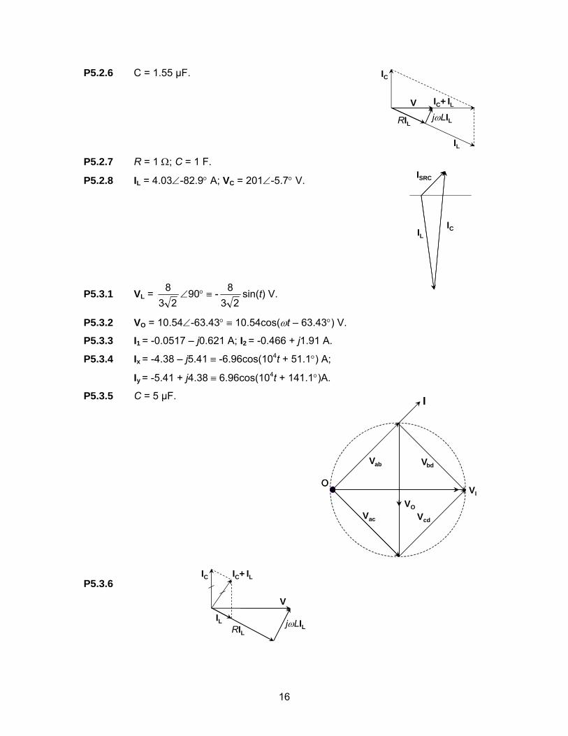
P5.3.6
V
IC
IL
IC+ IL
RIL jωLIL
ISRC
ILIC
I
O
VO
VI
V
Vac Vcd
Vbd
O
ab
V
IC
IL
IC+ IL
RILjωLIL
17
P5.3.8 IO = 2 + j4 A.
P5.3.9 VO = -9 + j10 V.
P5.3.10 ISRC = 0.5 A.
P5.3.11 (a) Series branch is 75 nF. Shunt branch is 0.42 μH.
(b) Impedances of the T-circuit are all infinite.
P5.3.12 Vc = -30 – j90 V; IL = 8 – j6 A.
P5.3.13 Ix = -j A.
P5.3.15 VO = 0.544 – j0.543 ≡ 0.769cos(ωt – 44.95°) V.
P5.3.16 IO = -0.0868 + j0.101 ≡ 0.133cos(ωt + 130.1°) A.
P5.3.17 IO = 0.71 – j0.45 A.
P5.3.18 Vx = 20∠0 V.
P5.3.19 VO = 13.98 – j2.851 V.
P5.3.20 )6.26cos(52 o−tω A.
P5.3.21 VO = -j20 2 V.
P5.3.22 ISRC = 0.469 + j0.164 = 0.5∠19.3° A; VL = 13.4 + j11.7 = 17.8∠41.1° V.
P5.3.23 ISRC = 0.469 + j0.164 = 0.5∠19.3° A; VL = 13.4 + j11.7 = 17.8∠41.1° V.
P5.3.24 VO = 4.88 – j20.0 V.
P5.3.25 VO = 12.1 + j3.52 ≡ 12.60cos(ωt + 16.2°) V.
P5.3.26 IO = 5 + j5 A.
P5.3.27 IO = 5 + j5 A.
P5.3.28 VO = 10 – j20 V.
P5.3.29 VO = 10 – j20 V.
P5.3.30 IO = 5 – j9 A.
P5.3.31 IO = 5 – j9 A.
P5.3.32 Vab = 31.63∠41.6° V; I1 = 3.16∠131.6° A; I2 =
2.24∠-3.43° A.
P5.3.33 VO = 1.818 V.
P5.3.37 IN = -0.1 A; YN = o9.36501)34(
2501
−∠=− j S.
P5.3.38 VTh = ( ) ( )[ ]341341715
++− j = 7.277∠44.0° V; ZTh = -20/17 – j5/17 Ω.
VSRC
Vab
I1
I2
18
Chapter 6 Linear and Ideal Transformers P6.1.1
P6.1.2 3.5 J. The same sign of φ21 and φ12 implies that i1 and i2 both enter the dotted
terminals.
P6.1.3 (a) φ12 = 500 μWb.
(b) k = 0.342.
(c) M == 20 mH.
(d) L1 = 72 mH; L2 = 47.50 mH.
P6.1.4 L2 = 6.4 H; k = 2/3.
P6.1.5 ω = 310 krad/s.
For the maximum inductance connection: Ipeak = 310 A, Wpeak =15
2 J.
For the maximum inductance connection: Ipeak = 310 A, Wpeak = 30
1 J.
P6.1.6 (a) Leqs = 320 mH.
(b) Leqs = 120 mH.
(c) Leqs = 80 mH.
P6.1.7 I2 = 32 A.
P6.1.8 (a) The fluxes due to each coil alone are 1
1
NIL and
2
2
NIL . The total flux is
INN
LNLN
21
2112 + .
(b) INN
NNLNLN
21
212112 ))(( ++ .
19
(c) 2
21
1
1221 N
LNN
LNLL +++ = L1 + L2 + 2M.
P6.2.1 4 H, 16 H, 0.5.
P6.2.2 Reflected impedance = 8.82 + j13.22 Ω. Input impedance = 8.82 + j58.22 Ω.
reflected impedance and input impedance of ideal transformer =
45 – j112.5 Ω.
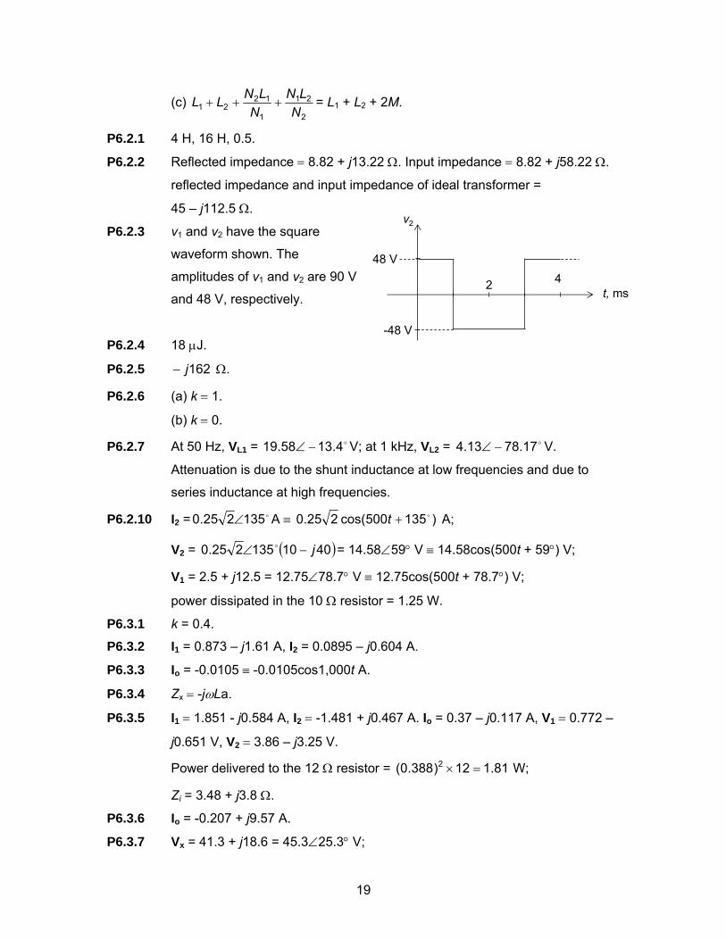
P6.2.3 v1 and v2 have the square
waveform shown. The
amplitudes of v1 and v2 are 90 V
and 48 V, respectively.
P6.2.4 18 μJ.
P6.2.5 162j− Ω.
P6.2.6 (a) k = 1.
(b) k = 0.
P6.2.7 At 50 Hz, VL1 = o4.1358.19 −∠ V; at 1 kHz, VL2 = o17.7813.4 −∠ V.
Attenuation is due to the shunt inductance at low frequencies and due to
series inductance at high frequencies.
P6.2.10 I2 = o135225.0 ∠ A ≡ )135500cos(225.0 o+t A;
V2 = ( )4010135225.0 j−∠ o = 14.58∠59° V ≡ 14.58cos(500t + 59°) V;
V1 = 2.5 + j12.5 = 12.75∠78.7° V ≡ 12.75cos(500t + 78.7°) V;
power dissipated in the 10 Ω resistor = 1.25 W.
P6.3.1 k = 0.4.
P6.3.2 I1 = 0.873 – j1.61 A, I2 = 0.0895 – j0.604 A.
P6.3.3 Io = -0.0105 ≡ -0.0105cos1,000t A.
P6.3.4 Zx = -jωLa.
P6.3.5 I1 = 1.851 - j0.584 A, I2 = -1.481 + j0.467 A. Io = 0.37 – j0.117 A, V1 = 0.772 –
j0.651 V, V2 = 3.86 – j3.25 V.
Power delivered to the 12 Ω resistor = 81.112)388.0( 2 =× W;
Zi = 3.48 + j3.8 Ω.
P6.3.6 Io = -0.207 + j9.57 A.
P6.3.7 Vx = 41.3 + j18.6 = 45.3∠25.3° V;
2 4t, ms
48 V
v2
-48 V
20
Vy = -13.6 – j10.03 = 16.89∠-143.6° V.
P6.3.8 Ix = -0.0158 – j0.0123 A.
P6.3.9 VO = 20I2 = 17.94 – j15.53 V.
P6.3.10 iO = 1.96cos(100πt +86.6°) A.
P6.3.11 vO = 19.71sin(ωt – 9.8°) V.
P6.3.12 VO = 14.33 + j20.07 V.
P6.3.13 iO = 3.33cos(500t – 7.87°) A.
P6.3.14 vO = 16.72cos(500t + 35.4°) V.
P6.3.15 VTh = 46.96.4)6(3728
∠=+ j V; ZTh = =+
185304751 j 4.060 + j1.643 =
4.38∠22.04° Ω.
P6.3.16 VTh = )1711(4110 j− V; ZTh = 2 + j 6 Ω.
P6.3.17 VTh = -26.1 + j 9.65 V; ZTh = 26.1 – j 9.65 A.
P6.3.18 VTH 10−= V; RTh = 2.5 Ω.
P6.3.19 VTh = 60(1 + j) V; ZTh = )173(3 j+ Ω.
P6.3.20 VTh = )14(197160 j+− V; ZTh = )183(
19720 j− Ω.
P6.3.21 Zin = j20 Ω.
P6.4.1 5.1=mφ mWb; maximum rate of change = 120π×1.5 ≅ 0.566 Wb/s.
At 50 Hz, 8.1=mφ mWb; core loss increases by a factor of (60/50)2 ≅ 1.44,
or about 45%; copper loss in the primary winding also increases by about
45%.
Primary voltage must be reduced to 200 V rms.
P6.4.2 Changing the relative dot markings gives a different output voltage, current,
and input impedance.
P6.4.3 current rating of the 10 kV winding = 6.6 A, that of the 2.2.kV winding = 30 A.
(a) VO = 2.2 kV, IO = 36.6 A, rating = 80.52 kVA.
(b) VO = -2.2 kV, IO = 23.4 A, rating = 50.48 kVA.
(c) VO = 12.2 kV, IO = 30 A, rating = 366 kVA.
(d) VO = 7.8 kV, IO = 30 A, rating = 234 kVA.
The insulation level of the 2.2 kV winding in (c) should be at least 12.2 kV
with respect to ground.
21
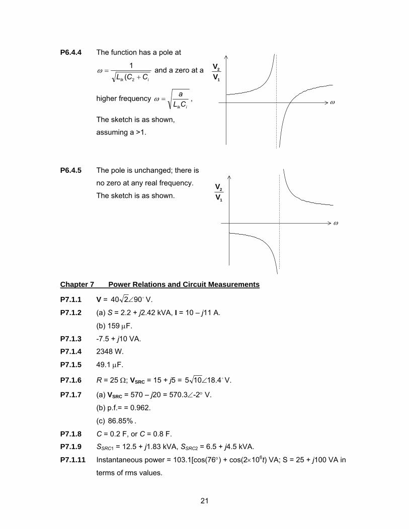
P6.4.4 The function has a pole at
ilk CCL +=
2(1ω and a zero at a
higher frequency ilkCL
a=ω ,
The sketch is as shown,
assuming a >1.
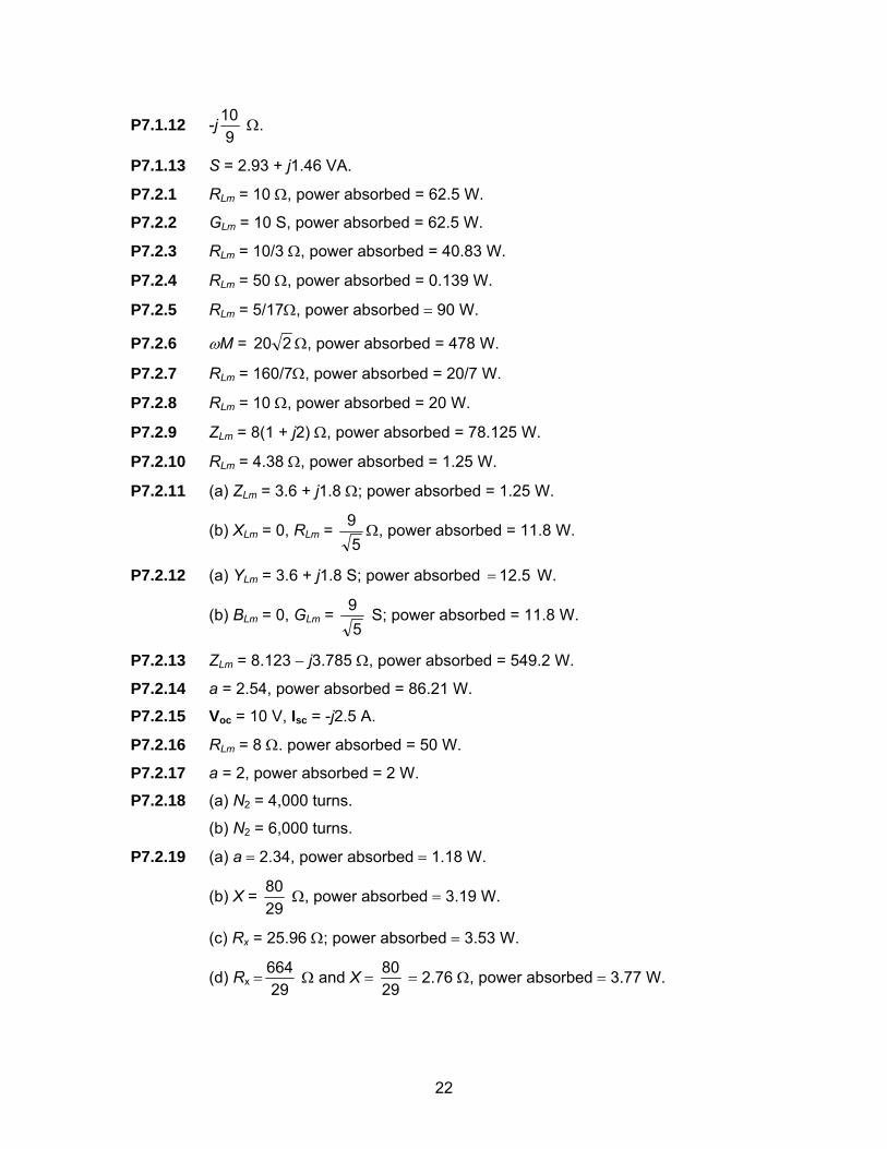
P6.4.5 The pole is unchanged; there is
no zero at any real frequency.
The sketch is as shown.
Chapter 7 Power Relations and Circuit Measurements
P7.1.1 V = o90240 ∠ V.
P7.1.2 (a) S = 2.2 + j2.42 kVA, I = 10 – j11 A.
(b) 159 μF.
P7.1.3 -7.5 + j10 VA.
P7.1.4 2348 W.
P7.1.5 49.1 μF.
P7.1.6 R = 25 Ω; VSRC = 15 + j5 = o4.18105 ∠ V.
P7.1.7 (a) VSRC = 570 – j20 = 570.3∠-2° V.
(b) p.f.= = 0.962.
(c) %85.86 .
P7.1.8 C = 0.2 F, or C = 0.8 F.
P7.1.9 SSRC1 = 12.5 + j1.83 kVA, SSRC2 = 6.5 + j4.5 kVA.
P7.1.11 Instantaneous power = 103.1[cos(76°) + cos(2×10⁶t) VA; S = 25 + j100 VA in
terms of rms values.
1
2
VV
ω
1
2
VV
ω
22
P7.1.12 -j9
10 Ω.
P7.1.13 S = 2.93 + j1.46 VA.
P7.2.1 RLm = 10 Ω, power absorbed = 62.5 W.
P7.2.2 GLm = 10 S, power absorbed = 62.5 W.
P7.2.3 RLm = 10/3 Ω, power absorbed = 40.83 W.
P7.2.4 RLm = 50 Ω, power absorbed = 0.139 W.
P7.2.5 RLm = 5/17Ω, power absorbed = 90 W.
P7.2.6 ωM = 220 Ω, power absorbed = 478 W.
P7.2.7 RLm = 160/7Ω, power absorbed = 20/7 W.
P7.2.8 RLm = 10 Ω, power absorbed = 20 W.
P7.2.9 ZLm = 8(1 + j2) Ω, power absorbed = 78.125 W.
P7.2.10 RLm = 4.38 Ω, power absorbed = 1.25 W.
P7.2.11 (a) ZLm = 3.6 + j1.8 Ω; power absorbed = 1.25 W.
(b) XLm = 0, RLm = 5
9Ω, power absorbed = 11.8 W.
P7.2.12 (a) YLm = 3.6 + j1.8 S; power absorbed 5.12= W.
(b) BLm = 0, GLm = 5
9 S; power absorbed = 11.8 W.
P7.2.13 ZLm = 8.123 − j3.785 Ω, power absorbed = 549.2 W.
P7.2.14 a = 2.54, power absorbed = 86.21 W.
P7.2.15 Voc = 10 V, Isc = -j2.5 A.
P7.2.16 RLm = 8 Ω. power absorbed = 50 W.
P7.2.17 a = 2, power absorbed = 2 W.
P7.2.18 (a) N2 = 4,000 turns.
(b) N2 = 6,000 turns.
P7.2.19 (a) a = 2.34, power absorbed = 1.18 W.
(b) X = 2980 Ω, power absorbed = 3.19 W.
(c) Rx = 25.96 Ω; power absorbed = 3.53 W.
(d) Rx = 29664 Ω and X =
2980 = 2.76 Ω, power absorbed = 3.77 W.
23
P7.2.20 (a) a = 2.34, power absorbed = 1.18 W.
(b) B = 2980 S, power absorbed = 3.19 W.
(c) Gx = 25.96 S; power absorbed = 3.53 W.
(d) Gx = 29664 S and B =
2980 = 2.76 S; power absorbed = 3.77 W.
P7.3.1 Rsh = =95.05 26.5 Ω.
P7.3.2 Rv = 200μA 50 V10
= kΩ.
P7.3.3 %20− .
P7.3.4 9.0%.
P7.3.5 6,666,433 Ω.
P7.3.6 499,990 Ω.
P7.3.7 (a) RV =A 50
V20μ
- 100 = 399,900 Ω.
(b) 40 V.
(c) R1 = 3
400 kΩ, R2 = 0.4 MΩ.
Chapter 8 Balanced Three-Phase Systems
P8.1.1 2.591∠37.2° Ω.
P8.1.2 5.1143.16 −∠ A.
P8.1.3 379.77 o19.0−∠ V.
P8.1.4 IaA = 59 o75∠ A, IAB = 34 o45∠ A.
P8.1.5 InN = 2.233∠29.4° A.
P8.1.6 IaA = 5.82∠40° A, IbB = 3∠142.5° A, IcC = 6∠-110° A.
P8.1.7 |Zφ| = 16.0508
= Ω. Since a percentage voltage drop is involved, the
impedance per phase is independent of whether the generators are
connected in Y or in Δ. |Zφ| = 16.0508
= Ω. Magnitude of circulating = 42.10 A.
P8.1.8 3
10∠30° A.
24
P8.2.3 4.3A.
P8.2.4 12.06 A.
P8.2.5 IN = 204.0∠-162.7° A before the phase is open circuited and IN =
176.8∠111.6° A after the phase is open circuited.
P8.2.6 |V6Ω| = 130.8 V, |V10Ω| = 187.4 V, |V15Ω| = 210 V.
P8.2.7 IaA = 20320 j+− A; IbB = )32(2020 +−− j A, IcC = )1)(13(20 j++ A.
P8.2.8 IaA = 20320 j+− A.
P8.2.9 13.13 kV.
P8.2.10 IaA = 26.17∠64.5° A.
P8.2.11 InN = 12.2∠-150° A.
P8.2.12 V1 = 181.5∠-30° V.
P8.2.13 VAB = 75.2∠39.4° V.
P8.2.14 IC = 1.36∠8.61°A.
P8.2.15 3
13πj Ω.
P8.2.16 The single-phase equivalent circuit is ( ) 253225 j−− V with respect to n, in
series with 5 Ω.
P8.2.17 Equivalent phase impedance is –j5 Ω.
P8.3.1 30 + j23.49 Ω.
P8.3.2 C = 5.55 mF.
P8.3.3 Total real power = 5.73 Kw, total reactive power = 1.27 kVAR.
P8.3.4 35.7%.
P8.3.5 Total real power absorbed = 18.392 kW; total reactive power absorbed =
7744 – 5808 = 1.936 kVAR; total apparent power absorbed = 18.49 kVA.
P8.3.6 C = 1.78 mF.
P8.3.7 (a) IC = 25.58∠180° A.
(b) RC = 4.29 Ω; XC = -7.43 Ω.
(c) QB = 1900 VAR, QC = -4860 VAR.
P8.3.8 Total real power = 1731 W, total reactive power -1729 VAR; apparent power
= 2446 W.
P8.3.9 577 V.
25
P8.3.10 363 V.
P8.3.11 9584 W; p.f. = 0.73.
P8.3.12 (a) 128.3 A.
(b) 491 V.
(c) 109.1 kVA.
P8.3.15 57.74 kW and 28.87 kW.
P8.3.16 W1 = 6.38 kW and W2 = 19.62 kW.
P8.3.17 0.87.
P8.3.18 =2W 39.6 W.
P8.3.19 W1 = 8848 W; W2 = 5572 W.
P8.3.20 -j125.1 Ω.
Chapter 9 Responses to Periodic Inputs P9.1.1 (a) 20 ms;
(b) Function is not periodic.
P9.1.2 (a) period = 0.02 s; f(t) = 0.5sin(100πt) + 0.5sin(300πt).
(b) period = 0.02 s; f(t) = 0.25 – 0.25[0.5cos(200πt) + sin(200πt)] +
0.25sin(400πt) + 0.125cos(600πt)].
P9.1.3 1/π.
P9.1.5 ∑ ⎟⎟⎠
⎞⎜⎜⎝
⎛⎟⎠⎞
⎜⎝⎛−−⎟
⎠⎞
⎜⎝⎛+=
∞
≠−∞=0
22 2sin1
2cos145.1)(
nn
njnn
tf πππ
; in trigonometric form: a0 =
1.5, 222281
2cos8
nn
nan π
ππ
−=⎟⎟⎠
⎞⎜⎜⎝
⎛−⎟
⎠⎞
⎜⎝⎛= , n = 1, 3, 5, 7, etc., an 22
16nπ
−= , n =
2, 6, 10, 14, etc., and an = 0, n = 4, 8, 12, 16, etc. ⎟⎠⎞
⎜⎝⎛=
2sin8
22π
πn
nbn = 0 for
even n, bn 228nπ
= 1, n = 1, 5, 9, 13, etc. and bn 228nπ
−= , n = 3, 7, 11, 15, etc.
P9.1.6 f(t) =∑∞
=
−1
22 )1(4
cos16
n
tnn
ππ
.
P9.1.7 f(t) = 6 − ∑∞
= ,...5,3,1 2216
n nπcosnπt − ∑
∞
= ...5,3,,1
8
n nπsinnπt.
P9.1.8 an = 0 for even n, and 222πn
an−
= for odd n; πn
bn1−
= for even n, and
26
πnbn
5= for odd n.
P9.1.9 2
2121 AAAA −+
+π
cosω0t + π2 (
321 AA + cos2ω0t - 15
21 AA + cos4ω0t +
3521 AA + cos6ω0t + … +
14)1(
2
1
−− +
n
n
(A1 + A2)cos6ω0t + …
P9.1.10 224πnAa m
n −= , and πn
Ab mn
2= .
P9.1.11 (a) an = 221)1cos(2
ππ
nne
+− ; 221
)1(2πn
ean +−
= for even n, and 221)1(2
πnean ++
−= for
odd n.
(b) bn = 221)1cos(2
πππ
nnen
+−
− ; 221)1(2
ππ
nenbn +−
−= for even n, and
221)1(2
ππ
nenbn ++
= for odd n.
P9.1.12 (a) ⎜⎝⎛ ++++= tttAAtf 0002 3cos
912cos
21cos4
4)( ωωω
π⎟⎠⎞+ ...5cos
251
0tω .
(c) the FSE of the required function could
be obtained as the product of –ftr(t) of
Eq. (9.3.12) and the FSE of the
rectangular pulse train shown.
P9.1.13 (a) −−+−= tAtAtAAtf 0002 2sin2
)sincos2(4
)( ωπ
ωπ
ωπ
−+ )3sin3
3cos92( 002 tAtA ω
πω
π
....4sin4 0 −tA ωπ
(b) The FSE can be obtained as the
product of the two functions shown.
f (t)
t
A
T
T/2
-T/4 T/4
1
f(t)
t
A
-T/2 T 2T
1
T/2
27
P9.1.14 −+−−= tAtAtAAtf 0002 2sin2
)sincos2(4
)( ωπ
ωπ
ωπ
....4sin4
)3sin3
3cos92( 0002 −+− tAtAtA ω
πω
πω
π
P9.1.16 ( )2/20
2 11 π
ωjn
n en
C −= .
P9.1.18 f(t) = ⎥⎦⎤
⎢⎣⎡ ++ tt
2sin9
2cos1
41 ππ
π+ sinπt + +⎟
⎠⎞
⎜⎝⎛ +− tt
23sin9
23cos
31 ππ
⎥⎦
⎤+⎟
⎠⎞
⎜⎝⎛ + ...
25sin9
25cos
51 tt ππ .
P9.1.19 The harmonics vary with n as 1/n3.
P9.1.20 a1 = -1.1024, a3 = 0.6460, a5 = 0.4564, b1 = 3.4065, b3 = 0.2, b5 = 0.0935.
P9.2.1 ( )⎢⎢⎣
⎡+−
+= αω
ω
ωπ
tRC
CRAv mO 0222
02 sin
1
8 ( ) +−+
αωω
ω tRC
CR0222
0
0 3sin913
( ) ...5sin2515
02220
0 +−+
αωω
ω tRC
CR
P9.2.2 4.37cos(ωt + 158.5°) + 0.34cos(ωt + 130.2°) + 0.085cos(ωt + 116.9°) V.
P9.2.3 vO(t) = 31.83 + 3.00cos(200πt + 12.8°) + 0.138cos(400πt -174.1°) +
0.026cos(600πt +3.85°) V; rms of AC components of output = 2.12 V.
P9.2.4 vO(t) =25 + 25.44cos(200πt + 38.9°) + 0.63cos(400πt -172°) + 0.13cos(600πt
+4.64°) V; rms of AC components of output = 18 V.
P9.2.5 vO(t) = -0.0106cos(106t – 90.38°) -0.0018cos(2×10⁶t – 90.13°) -
0.00074cos(3×10⁶t – 90.08°) -0.00041cos(4×10⁶t – 90.06°) -
0.00026cos(5×10⁶t – 90.05°) V. The second harmonic is attenuated by a
factor of 0.013. The capacitor blocks the DC component from the output
without affecting the AC component.
P9.2.6 vO(t) = 85.1cos(ω0t – 85.8°) + 3.03cos(3ω0t – 89.7°) +
0.651cos(5ω0t – 89.8°) V.
P9.2.7 10 V.
P9.2.8 0, ωt, 2ωt, 2ωt, 3ωt, and 4ωt.
P9.2.9 vO = 25 + 5 cos(ωot – 63.4°) + 2.06 cos(2ωot – 76.0°) + 2sin3ωot –
2cos4ωot V.
28
P9.2.10 vo(t) = 4 + 24.8sin2,000πt – 4cos4,000πt – 1.6sin6,000πt V. The output does
not possess half-wave symmetry because of the DC and the cosine terms
due to 2iv .
P9.3.1 rms value = 9.46 V; % error %56.0= .
P9.3.2 87.11 A.
P9.3.3 5 A.
P9.3.4 44.4 W.
P9.3.5 I1 = 3/115.2 A, I3 = 3/5.2 A, V1 = 3/1105.2 V, and V3 = 3/825.2 V.
P9.3.6 3/552 V.
P9.3.8 (a) rms value = 14.44;
(b) f(t) = -20sin103t + 4sin3×103t – sin5×103t + 0.2sin7×103t.
(c) The function is odd and half-wave symmetric.
If the function is negated, f(t) = 20sin103t – 4sin3×103t + sin5×103t –
0.2sin7×103t. the rms value is the same and the function is still odd and half-
wave symmetric.
P9.3.9 (a) 54.9 V.
(b) 11.13 A.
(c) 12 W.
Chapter 10 Frequency Responses
P10.1.1 (a) 0.958sin(0.3×10⁶t – 16.7°) V.
(b) 0.707sin(106t – 45°) V.
(c) 0.316sin(3×10⁶t – 71.6°) V.
P10.1.2 ( )ωω
ωω
jjIjVjH
SRC
O
+×
===1
105)(
)( 3
V/A; response is lowpass; passband gain =
5×10³; corner frequency = 1 krad/s.
P10.1.3 ( )ω
ωωω
ωj
jjI
jVjHSRC
O
+×
==1
105.2)(
)( 3
V/A; response is highpass; passband gain =
2.5×10³; corner frequency = 1 krad/s,
P10.1.4 I
O
VV
)||(11
2121
2
RRsCRRR
+×
+= ; the effect of R2 is to reduce the magnitude by
R2/(R1 + R2) and to increase the cutoff frequency from 1/CR1 to 1/C(R1||R2).
29
P10.1.5 ( )ωjHω401
5.0j+
= ; ( )2)40(1
5.0ω
ω+
=jH , )40(tan)( 1 ωω −−=∠ jH ; response is
lowpass; passband gain = 0.5; corner frequency = 25 krad/s.
P10.1.6 ( )ω
ωω401
40jjjH
+= ; ( )
2)40(1
40
ω
ωω+
=jH , )40(tan90)( 1 ωω −−=∠ ojH ; response
is highpass; passband gain = 1; corner frequency = 25 krad/s.
P10.1.7 ( ) =ωjHω09.01
102 3
j+× V/A; ( )
2
3
)09.0(1102
ωω
+
×=jH V/A,
)09.0(tan)( 1 ωω −−=∠ jH ; response is lowpass; passband gain = 2×10³;
corner frequency = 100/9 krad/s.
P10.1.8 =)( ωjHω
ω4
5
1031105
−
−
×+×
jj ; ( )
24
5
)103(1105
ω
ωω−
−
×+
×=jH ,
)103(tan90)( 41 ωω −− ×−=∠ ojH ; response is highpass; passband gain = 1/6;
corner frequency = 10/3 krad/s.
P10.1.9 =)( ωjH3/251
6/1ωj+
, where ω is in Mrad/s. It follows that
( )2)3/25(1
6/1ω
ω+
=jH . )3/25(tan)( 1 ωω −−=∠ jH ; response is lowpass;
passband gain = 1/6; corner frequency = 120 krad/s.
P10.1.10 ω
ωj
jH04.018.0)(
+= . It follows that ( )
2)04.0(18.0
ωω
+=jH .
)04.0(tan)( 1 ωω −−=∠ jH ; response is lowpass; passband gain = 0.8; corner
frequency = 25 krad/s.
P10.1.11 16/1
05.0)(ω
ωωj
jjH+
= . It follows that ( )2)16/(1
05.0ω
ωω+
=jH ,
)16/(tan90)( 1 ωω −−=∠ ojH ; response is highpass; passband gain = 0.8;
corner frequency = 16 krad/s.
P10.1.12 ω
ωω8.11
2)(jjjH
+= . It follows that ( )
2)8.1(12
ω
ωω+
=jH ,
)8.1(tan90)( 1 ωω −−=∠ ojH ; response is highpass; passband gain = 10/9;
corner frequency is ωcl = 5/9 krad/s.
30
P10.1.13 180/19/10)(
ωω
jjH
+= . It follows that ( )
2)180/(19/10
ωω
+=jH ,
)180/(tan)( 1 ωω −−=∠ jH ; response is lowpass; passband gain = 10/9; corner
frequency = 180 krad/s.
P10.1.14
P10.2.1 No, the lowest-order bandpass and bandstop filters are second order.
P10.2.2 R = 10 kΩ, =C 25 nF, and L = 4 mH.
P10.2.3 20log102 = 6 dB.
P10.2.4 L1 = 0.1 mH, L2 = 0.3 mH.
P10.2.5 0
2ωωθ′
≅ .
P10.2.6 410 rad/s.
P10.2.7 (a) H(s) =6255
42 ++ ss
s , where s is in krad/s.
(b) 25 krad/s.
(c) Q = 5.
(d) BW = 5 krad/s.
P10.2.8 Q is reduced from 200 to 500/3.
P10.2.9 (a) Q = 1/3.
(b) Q = 1/2.
The interpretation is that when k is large, the circuit composed of kR and C/k
has a negligible loading effect on the first circuit. The two circuits, of identical
time constant RC, are cascaded but effectively isolated.
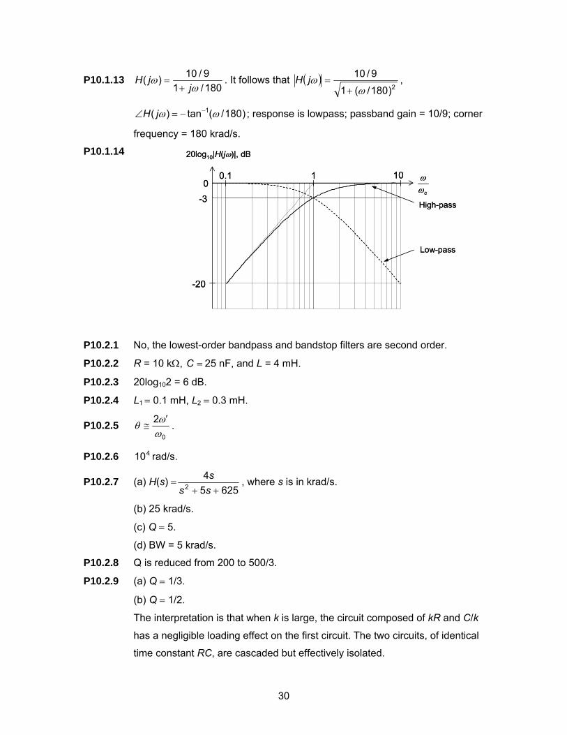
20log10|H(jω)|, dB
cωω
Low-pass
0.1 1 10
-3
-20
0
High-pass
20log10|H(jω)|, dB
cωω
Low-pass
0.1 1 10
-3
-20
0
High-pass
31
P10.2.10 (a) ωch = 5 krad/s, R = 200 Ω.
(b) the response is -20.04 dB when the switch is open and -46 dB when the
switch is closed.
P10.2.11 (a) =)( ωjH 1 at all frequencies.
(b) Phase angle varies between 0 and 360°.
P10.2.17 0.56.
P10.2.18 (a) Response is highpass with peaking.
(b) 40 dB.
(c) 09951.0 ω and 00051.1 ω . For a bandpass response having Q = 100, the
half-power frequencies are at 09950.0 ω and 00050.1 ω .
P10.3.1 R = 1000 2 Ω and L′ =0.1 H.
P10.3.2 R = 1000 2 Ω and L′ =0.1 H.
P10.3.3
1
212
1
21
2
111
RRR
LCLR
CRss
LCRR
VV
SRC
O
++⎟⎟
⎠
⎞⎜⎜⎝
⎛++
= ; =C ( )134
65±
π nF,
=′L ( )134
6m
π.
P10.3.4
21
121
21
2
2
21
2
11)( RR
RLCL
RRCRR
ss
sRR
RVV
SRC
O
++⎟
⎠⎞
⎜⎝⎛ +
+++
= ;
C = ( )136
5±
π nF, =L ( )13
61
mπ
H.
P10.3.5 ( ) 1222)()(
2223
3
++++=
sCCLCsLCsCLs
sVsV
SRC
O ; 9.15=L mH, =C 7.96 nF.
P10.4.3 (a) SRC
O
VV =
( ) ( ) ( )( )Csrc
LsrcsrcCCLLsrc
Csrc
L
C
Csrc
C
RRLCRRRRRRRR
LCRRss
LCLR
CRss
RRR
++
+⎥⎦⎤
⎢⎣⎡ +++
++
+⎟⎟⎠
⎞⎜⎜⎝
⎛++
+ 11
11
2
2
;
(c) 01.100 =ω krad/s, 27.6=Q .
32
P10.4.4 (a) 0 dB.
(b) )10)(10)(100(
10)10()( 64
65
+++×+
=sss
sssH .
Chapter 11 Duality and Energy-Storage Elements P11.1.1 The circuit of Fig. P1.2.10 is the dual of the circuit of Fig. P1.2.7, and the
circuit of Fig. P1.2.9 is the dual of the circuit of Fig. P1.2.8.
P11.1.2 It is the same transformer with the input and output interchanged.
P11.1.3 The series impedance is a resistance of 1/20 Ω in series with a capacitive
reactance of −j /30Ω. The shunt impedances consist of a resistance of 1/8 Ω
in parallel with an inductive reactance j /12 Ω.
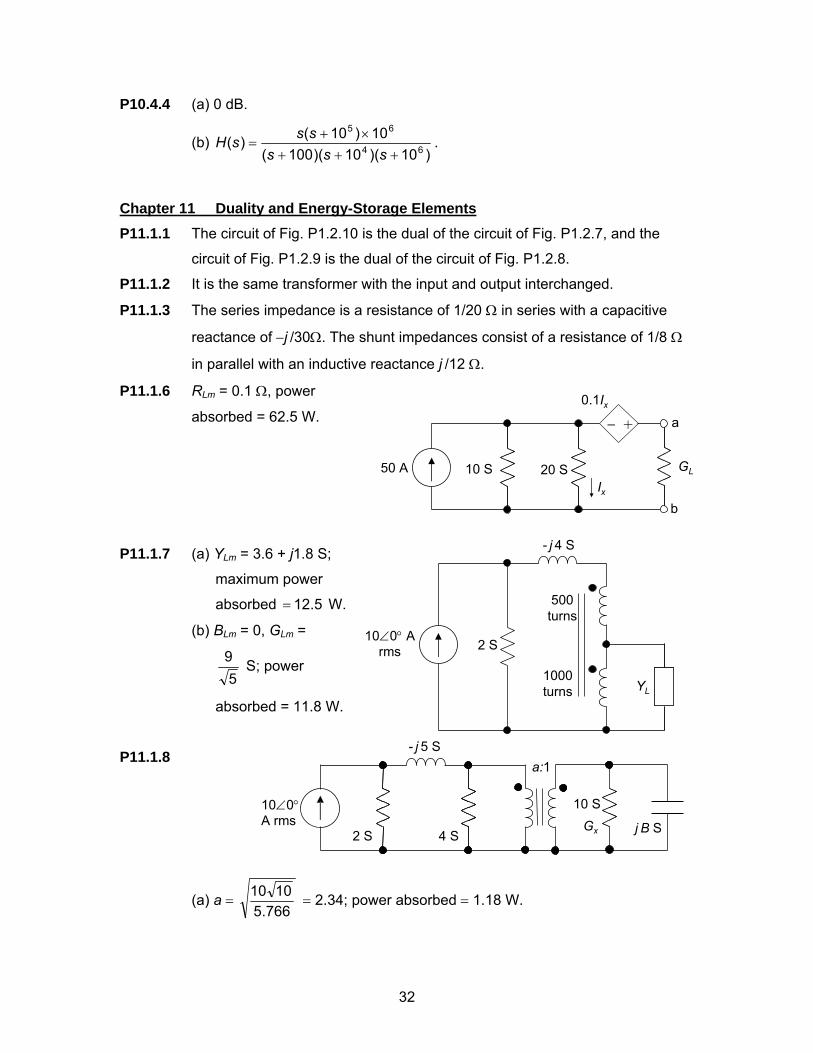
P11.1.6 RLm = 0.1 Ω, power
absorbed = 62.5 W.
P11.1.7 (a) YLm = 3.6 + j1.8 S;
maximum power
absorbed 5.12= W.
(b) BLm = 0, GLm =
59 S; power
absorbed = 11.8 W.
P11.1.8
(a) a = 766.5
1010 = 2.34; power absorbed = 1.18 W.
GL
– +0.1Ix
10 S 20 S50 AIx
a
b
500turns
1000turns
- j 4 S
2 S10∠0° A
rms
YL
a:1
4 S2 S
10 S
j B S
- j 5 S
Gx
10∠0°A rms
33
(b) B = 2980 ; power absorbed = 3.19 W.
(c) Gx = 25.96 S; power absorbed = 3.53 W.
(d) Gx = 29664 S, B =
2980 = 2.76 S, power absorbed = 3.77 W
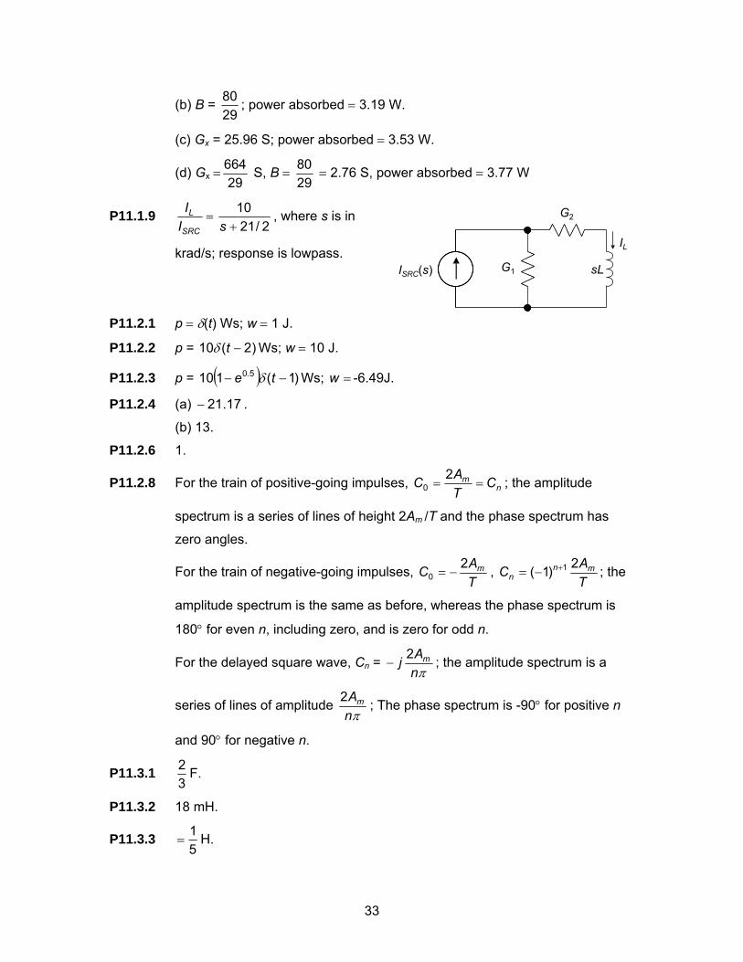
P11.1.9 =SRC
L
II
2/2110+s
, where s is in
krad/s; response is lowpass.
P11.2.1 p = δ(t) Ws; w = 1 J.
P11.2.2 p = )2(10 −tδ Ws; w = 10 J.
P11.2.3 p = ( ) )1(110 5.0 −− te δ Ws; =w -6.49J.
P11.2.4 (a) 17.21− .
(b) 13.
P11.2.6 1.
P11.2.8 For the train of positive-going impulses, nm C
TAC ==
20 ; the amplitude
spectrum is a series of lines of height 2Am /T and the phase spectrum has
zero angles.
For the train of negative-going impulses, TAC m2
0 −= , TAC mn
n2)1( 1+−= ; the
amplitude spectrum is the same as before, whereas the phase spectrum is
180° for even n, including zero, and is zero for odd n.
For the delayed square wave, Cn = πn
Aj m2− ; the amplitude spectrum is a
series of lines of amplitude πn
Am2 ; The phase spectrum is -90° for positive n
and 90° for negative n.
P11.3.1 32 F.
P11.3.2 18 mH.
P11.3.3 51
= H.
ISRC(s)
G2
G1 sL
IL
34
P11.3.4 15/41 F.
P11.3.5 5/8 F.
P11.3.6 2.2 H.
P11.3.8 (a) 2.35 V; charges on capacitors are: 47/5 C, 141/10 C, and 47/2 C.
(b) Initial energy = 75.56 J; final energy 225.55= J.
P11.3.9 (a) q1f = –78/31 C, q2f = 15/31 C, q3f = 170/31 C; 62/391 =fv V,
62/52 =fv V, and 31/173 =fv V.
(b) Initial energy = 56.75 J; final energy = 2.31 J.
P11.3.10 (a) 21 −=fλ Wb-turns, 62 −=fλ Wb-turns, 183 =fλ Wb-turns; 5.01 −=fi A,
12 −=fi A, and 5.13 =fi A.
(b) Initial energy = 98 J; final energy = 17 J.
P11.3.11 (a) final current: 11/20 A; final flux linkage are: 11/80 Wb-turns, 11/120 Wb-
turns, and 11/240 Wb-turns.
(b) Initial energy = 98 J; final energy = 400/11 J.
P11.3.13 q1f = 2 – 0.4 = 1.6 C, q2f = –3 – 0.4 = –3.4 C, q34f = 3 – 0.4 = 2.6 C.
15/41 =fv V, 15/172 −=fv V, 15/133 =fv V. The charges on C3 and C4 are:
15/133 =fq C and 15/264 =fq C.
P11.3.15 vO = te 25.120 − V, where t is in s.
Chapter 12 Natural Responses and Convolution
P12.1.1 40/2 tL ei −= A, 40/
1 40 tev −−= V, where t is in ms.
P12.1.2 40/2 tev −= V and 40/1 40 tei −−= A,
where t is in ms.
P12.1.3 tev 550 −−= V, where t is in ms.
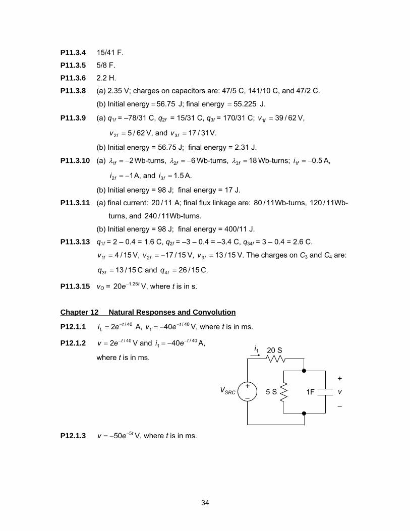
5 S+–
VSRC 1F
20 Si1
+
–
v
35
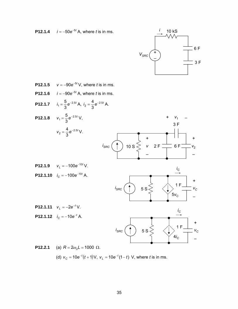
P12.1.4 tei 550 −−= A, where t is in ms.
P12.1.5 tev 590 −−= V, where t is in ms.
P12.1.6 tei 590 −−= A, where t is in ms.
P12.1.7 tei 5.21 3
5 −= A, tei 5.22 3
4 −= A.
P12.1.8 tev 5.21 3
5 −= V,
tev 5.22 3
4 −= V.
P12.1.9 tL ev 10100 −−= V.
P12.1.10 tC ei 10100 −−= A.
P12.1.11 tL ev −−= 2 V.
P12.1.12 tC ei −−= 10 A.
P12.2.1 (a) 10002 == LR oω Ω.
(d) ( )110 += − tev tC V, )1(10 tev t
L −= − V, where t is in ms.
+–
VSRC
6 F
10 kSi
3 F
10 S
+
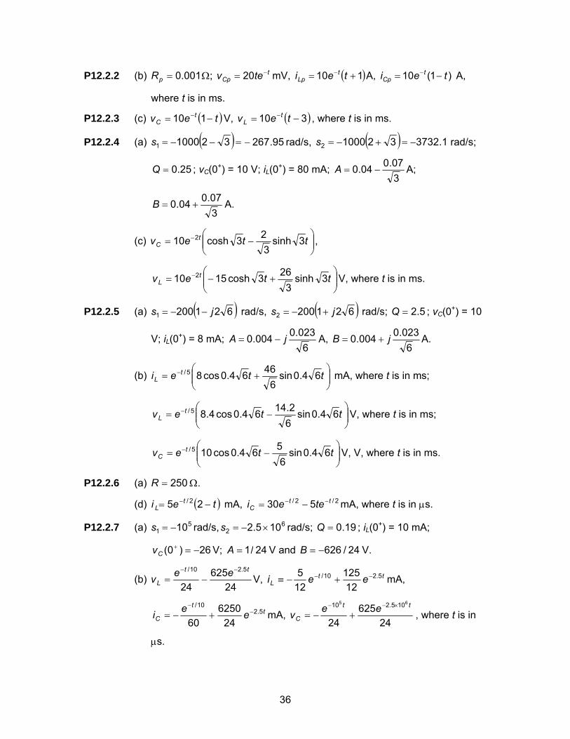
–
v2iSRC 6 F
3 F
2 F
+
–
v
+
–
v1 –
5 S
+
–
vCiSRC
5vC
iC
1 F
5 S
+
–
vCiSRC
4iC
iC
1 F
36
P12.2.2 (b) 001.0=pR Ω; tCp tev −= 20 mV, ( )110 += − tei t
Lp A, )1(10 tei tCp −= − A,
where t is in ms.
P12.2.3 (c) ( )tev tC −= − 110 V, ( )310 −= − tev t
L , where t is in ms.
P12.2.4 (a) ( )=−−= 3210001s 95.267− rad/s, ( ) 1.37323210002 −=+−=s rad/s;
25.0=Q ; vC(0+) = 10 V; iL(0+) = 80 mA; 307.004.0 −=A A;
307.004.0 +=B A.
(c) =Cv ⎟⎟⎠
⎞⎜⎜⎝
⎛−− tte t 3sinh
323cosh10 2 ,
⎟⎟⎠
⎞⎜⎜⎝
⎛+−= − ttev t
L 3sinh3
263cosh1510 2 V, where t is in ms.
P12.2.5 (a) ( )6212001 js −−= rad/s, ( )6212002 js +−= rad/s; 5.2=Q ; vC(0+) = 10
V; iL(0+) = 8 mA; 6
023.0004.0 jA −= A, 6
023.0004.0 jB += A.
(b) ⎟⎟⎠
⎞⎜⎜⎝
⎛+= − ttei t
L 64.0sin6
4664.0cos85/ mA, where t is in ms;
⎟⎟⎠
⎞⎜⎜⎝
⎛−= − ttev t
L 64.0sin62.1464.0cos4.85/ V, where t is in ms;
⎟⎟⎠
⎞⎜⎜⎝
⎛−= − ttev t
C 64.0sin6
564.0cos105/ V, V, where t is in ms.
P12.2.6 (a) 250=R Ω.
(d) ( )tei tL −= − 25 2/ mA, 2/2/ 530 tt
C teei −− −= mA, where t is in μs.
P12.2.7 (a) 51 10−=s rad/s, 6
2 105.2 ×−=s rad/s; 19.0=Q ; iL(0+) = 10 mA;
26)0( −=+Cv V; 24/1=A V and 24/626−=B V.
(b) 24
62524
5.210/ tt
Leev−−
−= V, ttL eei 5.210/
12125
125 −− +−≡ mA,
tt
C eei 5.210/
246250
60−
−
+−= mA, 24
62524
65 105.210 tt
Ceev
×−−
+−= , where t is in
μs.
37
P12.2.8 (a) 661 103.0104.0 ×+×−= js rad/s, 66
2 103.0104.0 ×−×−= js rad/s;
625.0=Q ; iL(0+) = 10 mA; 84
32)0( −=−=+Cv V;
674 jA −−= V,
674 jB +−= V.
(b) ⎟⎠⎞
⎜⎝⎛ −−= − ttev t
L 3.0sin373.0cos84.0 , ⎟
⎠⎞
⎜⎝⎛ −= − ttei t
L 3.0sin343.0cos10 4.0 mA,
⎟⎠⎞
⎜⎝⎛ += − ttei t
C 3.0sin3443.0cos394.0 4.0 mA, where t is in μs.
P12.2.9 (a) β = 1.
(b) β 12 −= .
P12.2.10 (a) β = 1.
(b) β 12 −= .
P12.2.11 β 125 −= , 12 −=σ .
P12.2.12 β 125 −= ,
12 −=σ .
P12.2.13 25.6=L H, R = 5 KΩ, tC tev 4004102 −×= V.
P12.2.16 62cos4 += t J.
P12.3.1 1 + e-2t − 2e-t.
P12.3.2 (a) tt ωsin2
.
(b) 2t cosωt +
ωω
2sin t .
(c) 22sinsinh
ataat
+−
ωωω .
P12.3.3 2
2ty −= , 0 ≤ t ≤ 1; y = 122
2
+− tt , 1 ≤ t ≤ 3; y = 122
2
+− tt , 3 ≤ t ≤ 4;
y = 31142
3 2
−+− tt , 4 ≤ t ≤ 5; 642
2
−+−= tty , 5 ≤ t ≤ 6;
100 S
+
–
v
100 nH
iSRC
iC
1 mF
iL iG
βiG
100 S
+
–
v
2 μH
iSRC
iC
1 mF
iL iG
β iC + σ iL
38
y = 3082
2
+− tt , 6 ≤ t ≤ 7; 79222
3 2
+−= tty , 7 ≤ t ≤ 8;
49102
2
−+−= tty , 9 ≤ t ≤ 11; 72122
2
+−= tty , 11 ≤ t ≤ 12;
y(t) = 0, t ≥ 12. At t = 5, y = 3/2.
P12.3.4 The functions to be convolved are:
=− )()1( tf )(2
2
tut− [ ] )1(122 −+−+ tutt [ ] )3(962 −−+−+ tutt
[ ] )5(25102 −+−+ tutt )6(1862
2
−⎥⎦
⎤⎢⎣
⎡−+−+ tutt , and:
)6()3(2)()()1( −+−−= ttttg δδδ .
P12.3.5 tty +−=6
3
, 0 ≤ t ≤ 1; 3232
22
3
−+−= ttty , 1 ≤ t ≤ 2;
334114
22
3
+−+− ttt , 2 ≤ t ≤ 3; 32072
62
3
−+− ttt , 3 ≤ t ≤ 4;
y(t) = 0, t ≥ 4.
P12.3.6 The functions to be convolved are:
=− )()1( tf )(2
2
tutt⎟⎟⎠
⎞⎜⎜⎝
⎛+ + ( ) )1(122 −−+− tutt + )2(43
2
2
−⎟⎟⎠
⎞⎜⎜⎝
⎛+− tutt , and:
=)()1( tg )()( tut −δ + 2 )1( −tu )2( −− tu )2( −− tδ .
P12.3.7 y = 9t, 0 ≤ t ≤ 1; y = 18 – 9t, 1 ≤ t ≤ 2; y = 2t – 4, 2 ≤ t ≤ 3; y = 8 – 2t, 3 ≤ t ≤ 4;
y = t – 4, 4 ≤ t ≤ 5; y = 6 – t, 5 ≤ t ≤ 6; y = 0, t ≥ 6.
P12.3.8 y = t, 0 ≤ t ≤ 1; y = 2 – t, 1 ≤ t ≤ 2; y = 2t – 4, 2 ≤ t ≤ 3; y = 8 – 2t, 3 ≤ t ≤ 4;
y = 9t – 36, 4 ≤ t ≤ 5; y = 9(6 – t), 5 ≤ t ≤ 6; y = 0, t ≥ 6.
P12.3.9 0)/1(
/11)0(
∞−
+−
⎥⎦
⎤⎢⎣
⎡+−
=CRa
eCR
yCRa λ
.
P12.3.11 8u(t – 1) – 12u(t – 3) – 4u(t – 6) + 6u(t – 8).
P12.3.12 1+= ty V, ;0≤t = 12 +−− tte t V, 0≥t .
P12.3.13 (a) y =21
2
2
++ tt , 01 ≤≤− t ; y =21
23 2 ++− tt , 10 ≤≤ t ;
y = 275
23 2 +− tt , 21 ≤≤ t ; y =
293
2
2
−+− tt , 32 ≤≤ t ; y = 0, t ≥ 6.
39
(b) The functions to be convolved are:
)1(21
2)()1(
21
2)(
22
2)1( −⎟⎟
⎠
⎞⎜⎜⎝
⎛+−+−+⎟⎟
⎠
⎞⎜⎜⎝
⎛++=− tutttuttutttg , and:
)2()1(2)()()1( −+−−= ttttf δδδ .
P12.3.14 The two functions are expressed in terms of step functions as:
)2()1(3)(2)( −+−−= tutututf ;
)3()2(2)1()(2)( −−−−−+= tututututg .
Chapter 13 Switched Circuits
P13.1.1 tO ev 580 −−= V.
P13.1.2 vC = –50 + 30/95 te− V, where t is in ms; vC =0 at t = 19.3 ms.
P13.1.3 ix = ci64
− =61
− 72.0t
e−
mA.
P13.1.4 5 J.
P13.1.5 1.44 kHz.
P13.1.6 vC = 30 ( )te 3.01 −− V, ix = 3 + te 3.06 − mA.
P13.1.7 vO = 24 + 48e-t/0.12 V.
P13.1.8 vC = ( )48.0/18.12 te−−− V, 0 ≤ t ≤ 1 s; 12/)1(35)21.19(8 −−−+= tC ev V, t ≥ 1 s.
P13.1.9 vx(t) = 1400/17
7500 te− V, μs 500 ≤≤ t ; vx(t) = 200/)50(9.38 −− te V, μs 10050 ≤≤ t ;
vx(t) = 1400/)100(173.30 −− te V, μs 100≥t .
P13.1.10 10/10 tC ev −= V, where t is in ms.
P13.1.11 2.1/
31 t
x ei −= mA, where t is in ms.
P13.1.12 ( )tC ev 721
7160 −−= V.
P13.1.13 Switch in position b: ( )74.0/186.14 tC ev −−= V, where t is in ms;
switch in position c: vC = 0.94 + 76.4/)83.0(06.9 −te V, t ≥ 0.83 ms,
P13.1.14 29/27812 tx ev −−= V, t ≥ 0 s.
40
P13.1.15 (a) vC = ( )te−−16 V, tC ei −= 6 mA, t ≥ 0 ms.
(b) energy delivered by supply = ( )te−−172 mJ; energy absorbed by battery
= ( )te−−136 mJ.
(c) 18 J.
(d) tC ev ′−+−= 126 V, t
C ei ′−−= 12 ; as ∞→′t , energy delivered by battery =
72 J, net energy lost by the capacitor = 0, energy dissipated in resistor =
72 J.
P13.1.16 i1 = 3
16 (1- e-2.5t), 0 ≤ t ≤ 1 ms; i1 = 4.9e-t/2 mA, t ≥ 1 ms.
P13.1.17 tev −= 75φ V, R = 3/1250 kΩ.
P13.1.18 iφ = te 5.2− A, R = 50 Ω.
P13.1.19 80/2112 tO ev −= V, t ≥ 0 ms; final current is 8/7 A in the 0.8 H inductor, 3/35 A in
the 0.4 H inductor, and 43/35 in the 0.2.H inductor.
P13.1.20 vL = 10e40t/11 V, t ≥ 0 μs.
P13.1.21 vO = 16/101
1010168
1011680 te−+ V, t ≥ 0.
P13.1.22 i1 = ( )4/1514 te−+ V, t ≥ 0.
P13.1.23 v1 = 8/)3(535.1 −− te , t ≥ 3 ms.
P13.2.1 (a) 311.88 Ω.
(b) 289.48 Ω.
P13.2.2 (a) 0)0( =+Cv , 0)0( =+
Li , 10)0( =+Lv V, and 10)0( =+i A.
(b) underdamped.
(c) )2/sin(10 2/ tei tL
−= A; =Lv [ ])2/sin()2/cos(10 2/ tte t −− V;
=Cv( )[ ])2/sin()2/(cos(110 2/ tte t −− −
V; )2/cos(10 2/ tei t−= A.
P13.2.3 (a) 0)0( =+Cv , 0)0( =+
Li ,
10)0( =+Ci A, and
10)0( =+v V.
(b) underdamped.
10u(t) A 1 H
iL
2 F
1 S
+
–
vC
+
–
v
41
(c) )2/sin(10 2/ tev tC
−= A; =Ci [ ])2/sin()2/cos(10 2/ tte t −− V;
( )[ ])2/sin()2/(cos(110 2/ ttei tL −−= − A; )2/cos(10 2/ tev t−= A.
P13.2.4 (a) 500 Ω.
(b) iL )0( + = 100 μA, vC )0( + = 50 mV, and vL )0( + = -50 mV.
(c) iL = te 2.0100 − μA, tC ev 2.050 −= mV, where t is in μs.
P13.2.5 (a) 500 S.
(b) vC )0( + = 100 μV, iL )0( + = 50 mA, and iC )0( + = -50 mA.
(c) vC = te 2.0100 − μV and iL = te 2.050 − mA, where t is in μs.
P13.2.6 (a) ρ = 0.
(b) v = 100te-10t V, iC = 100(e-10t – 10te-10t) mA, and
iL = 100 –100(e-10t + 10te-10t) mA, t being in ms.
P13.2.7 (a) ρ = 0.
(b) i = 10te-10t mA, vL = tt tee −− −101.0 V, and iL = 100 –100(e-10t + 10te-10t) mA, t
being in ms.
P13.2.8 Response is underdamped; tei t 8sin45 6−= mA,
=Lv [ ]tte t 8sin38cos425 6 −− mV, and
vC = 100 – [ ]tte t 8sin38cos425 6 +− mV, where t is in ms.
P13.2.9 tei t sin20 −= mA and v0 = ( )tte t sincos10 −− V, where t is in ms.
P13.2.10 ( ) ( )[ ]2/32/35.0
3253431
5 ttt
O eeev −−
+−++
= V, where t is in ms.
P13.2.11 ( ) ( )[ ]2/32/3 3/2801603/280160 tttO eeev −− −++= V, where t is in ms.
P13.2.12 vO = 0.
P13.2.13 tO ev 2= V,
Chapter 14 Two-Port Circuits
P14.1.1 511
1
111 ==
IVz Ω,
511
12 =z Ω; 5199
21 −=z Ω, 171
22 =z Ω;
y11 = 1.5 S, y12 = -0.5 S, y21 = 49.5 S, and y22 = 0.5 S.
42
P14.1.2 32
11 =h Ω, 31
12 =h , 3321 =h , h22 = 17 S;
5111 =g S, g21 = -1, 9921 −=g , 222 =g Ω.
P14.1.3 991
11 −=a , 5.49
112 −=a Ω,
3317
21 −=a S. 331
22 −=a ;
311 =b , 212 =b Ω, 511
221 ==
VIb S; 122 =b .
P14.1.4 z11=1 Ω, z12= 1 Ω, z21= -0.5 Ω, z22= 0.5 Ω;
y11= 0.5 S, y12 = -1S, y21= 0.5 S, y22 0V2
21V
I== = 1S.
P14.1.5 h11= 2 Ω, h12 2= , h21= 1, h22= 2 S;
g11= 1S, g12= -1, g21= -0.5; g22= 1Ω.
P14.1.6 a11= -2, a12= -2 Ω, a21= -2 S, a22= -1;
b11= 0.5; b12= 1 Ω, b21= 1 S; b22= 1.
P14.1.7 =11z j Ω; z12 = j2 Ω, 221 jz = Ω, z22 = 0;
y11 = 0, y21 2j
−= S, y21 2j
−= S. y22 4j
−= S.
P14.1.8 h11 ∞= , h12 ∞= , h21 ∞= h22 ∞= ;
g11 = j S, g12 = 2, g21 = -2, g22 = j4 Ω.
P14.1.9 a11 21
−= ,a12 = -j2 Ω, a21 2j
−= S; a22 = 0;
b11 = 0, b12 = -j2Ω, b21 = 2j
−= S, b22 21
−= .
P14.1.10 z11 = ωωω
6132 2
jj
++− Ω, z12 ω
ωj
j614
+= = z21 Ω, z21 ω
ω61
4j
j+
= Ω, z22 ωω61
6j
j+
= Ω;
y11 ωj3
= ; y12 ωj2
−= S = y21, y22= ω2
31j
+ S.
P14.1.11 h11= 3ωj Ω, h12 3
2= , h21= 3
2− ; h22 ω6
11j
+= S;
g11=ωω
ω3
612 j
j+−
+ S, g12 ω234j+
−= , g21 ω23
4j+
= , g22 ωω23
2j
j+
= Ω.
P14.1.12 a11 423 ωj+
= , a12 2ωj
= Ω, a21= ωω
461
jj+ S; a22 0V
2
12I
I=−=
23
= ;
43
b11 23
= ; b12 2ωj
= Ω, b21 ωω
461
jj+
= S, b22 423 ωj+
= .
P14.1.13 z11= 2(s + 1/s) Ω = z22, z21= (s + 1 /s) = z12 Ω.
P14.1.14 y11 = 1 S = y22, y12 = ωj+
−1
1 = y22.
P14.1.15 32
2
11 23122
ωωωωω
jjjz−−+
+−= , 213212 231
1 zjj
z =−−+
=ωωω
,
32
2
22 2311
ωωωωω
jjjz−−+
+−= .
P14.1.16 z11 102 j+= Ω, z12= (1 – jω) Ω, z21= (1 – jω) Ω, z22 ω22 j+= Ω.
P14.1.17 z11 = ( )34165
2
23
+++++
ssssss
Ω, z12 = ( )341
2 ++ sssΩ, z21= ( )34
12 ++ sss
Ω,
z22 = )3(
2++
=sss
Ω,
P14.1.18 y11 = ⎟⎟⎠
⎞⎜⎜⎝
⎛
+−−
++ ωω
ωω
ωjj
j2
2
11
4S, ⎟⎟
⎠
⎞⎜⎜⎝
⎛
+−+
+−=
ωωωω
jjjy 212 1
14
2 = y21,
y22 = ωωj
j+44
ωωω
jj+−
++ 21
1 .
P14.1.19 h11 = ( )μππ CCsrrx +++
/11 , h12 = =
2
1
VV
( )μππ
μ
CCsrsC
++/1,
h21 = =1
2
II
( )μππ
μ
CCsrgsC m
++
+
/1, h22 = =
2
2
VI
( )μππ
ππμ
CCsrrgsCsC m
++
++
/1)/1(
.
P14.2.4 VTh 40/3010
j
o∠= ≡ 9.97cos(1,000t + 4.29°) V,
40/314/2385110
jjZTh −
+=
o8.830.605 ∠≡ Ω; v2 = 1.6cos(1,000t – 70.4°) V.
P14.2.5 power input is = 197.8 W; power delivered to load = 27.3 W.
P14.2.6 ZLm = 4 – j4 Ω, maximum power delivered = 100 W.
P14.2.7 31.4=LmR kΩ, maximum power delivered 9.8= μW.
P14.2.8 a11 = a22 = 2, 312 =a Ω, and 21a = 1 S.
P14.2.9 Zin1 = 841.0 kΩ, Zin2 = 196.01.5
1= kΩ, overall gain = 8446.
P14.2.10 Rm = 10 kΩ.
44
P14.2.11 1
2
VV )94(
9710 j+−= .
P14.2.14 =inZ j0156.038.14 − Ω, 260=outZ Ω, v2 = 12.9cos(1,000t + 0.24°) V.
P14.2.15 VTh = 0, ZThsrc
src
ZbbZbb
2122
1112
++
= = 1020 j− Ω, v2 = 0.
P14.2.16 VTh = -10.181 + j0.5325 V, ZTh = 1.0432 – j0.0546 Ω,
v2 = 9.23cos(1000t + 177.3°) V.
P14.2.17 jZin 13021
6546
+= kΩ, jZout 13742
13790
+= kΩ, 1
2
VV o8.4146.0 −∠= .
P14.2.18 VO/VSRC= 0.0068 - j0.0653.
P14.2.19 911 krad/s.
P14.2.20 2 krad/s.
P14.2.21 =inZ 5.2035 + j1.9469 Ω, ZTh = -0.3529 - j0.5882 Ω,
VO/VSRC = -0.4795 - j0.4452.
P14.2.22 Zin = 0.3904 - j0.4589 Ω, ZTh = 2.6154 + j2.9231 Ω,
VO/VSRC = 0.1308 + j0.1462.
Chapter 15 Laplace Transform
P15.1.3 (a) 22 ass−
.
(b) 22 asa−
.
(c) ( )22
2
152
172
−+
++
ss
ss .
P15.1.4 (a) 2
2)2(
+
+−
se s
.
(b) 16
)1sin(4)1cos(2 ++
ss .
P15.1.9 −21
sTAα
+−
−
2)1( se
TA Tsα
αα 2)1( se
TA Ts−
−α.
P15.1.10 (a) )1( sTe
A−−
.
45
(b) )1(
2/
sT
sT
eAe
−
−
−− .
P15.1.11 tt ee 2234724 −− +− .
P15.1.12 (a) F(s) = −+
++
−8198.8
4857.17154.16
4643.31.0ss
−−−
+1240.57676.2
1226.00107.0js
j
1240.57676.21226.00107.0
jsj+−
− , f(t) = 0.1δ(t) – 3.4643 te 7154.16− – 1.4857 te 8198.8− +
)951240.5cos(2462.0 7676.2 o−te t .
(b) F(s) = −+
−0567.4
3733.35.0s
+−−
+1732.21176.1
0224.01727.0js
j+
+−−
1732.21176.10224.01727.0
jsj
1750.10893.17716.05140.0
jsj−+
− + 1750.10893.1
7716.05140.0js
j++
+ , f(t) = 0.5δ(t) –
3.3733 te 0567.4− + )4.71732.2cos(1741.0 1176.1 o+te t +
)3.561750.1cos(9271.0 1176.1 o−te t .
P15.1.13 x(t) = )(25
435
2125
43 2 tuejtejej tttj⎥⎦⎤
⎢⎣⎡ +
+−
−+
− −−+ ; because of the differences
in the values at −= 0t .
P15.1.14 teteth tt 2sin22cos4)( −− −= .
P15.1.15 H(s) = )1()1()387(2
23
2
++++
ssss , ( ) tttteth t sin6cos242)( 2 +−+−= − .
P15.1.16 (a) ⎟⎠⎞
⎜⎝⎛ +−
sse s 11
22 .
(b) ⎟⎠⎞
⎜⎝⎛ −−
sse s 11
2 .
P15.1.18 f(t) = tt cos)()1( +δ .
P15.2.1 vo(t) = 5e-t where t is ms; the pole of VO(s) is located at s = -1 krad/s.
P15.2.2 vO(t) = 3
10 V; The pole of VO(s) is at the origin.
P15.2.3 90/
310)( t
O eti −= mA, where t is in μs; the pole of IO(s) is at 901
− Mrad/s.
P15.2.4 vo(t) = 3/38
19710
19900 te−− , where t is in ms; the poles of VO(s) are at zero and
46
338 krad/s.
P15.2.5 3/5.0)( tO etv −= V, where t is in ms; the pole of VO (s) is at -1000/3 rad/s.
P15.2.6 10)( =tvO V, the pole of VO is at the origin.
P15.2.7 H(s) = 1
1+s
, VSRC = s2 – 2
6
2
4
se
se ss −−
+ .
P15.3.1 C2R2 = C1R1.
P15.3.2 vO(t) = 0.5δ(t) − 12.5e-57t, t ≥ 0, 2
2
304.01
)02.0(131
⎟⎠⎞
⎜⎝⎛+
+
ωω
tanφ = )3/04.0)(02.0(1
3/04.002.0ωωωω
+− ,
P15.3.3 h(t) = ⎥⎥⎥
⎦
⎤
⎢⎢⎢
⎣
⎡−
⎟⎟⎠
⎞⎜⎜⎝
⎛ +−⎟
⎟⎠
⎞⎜⎜⎝
⎛ −− tt
ee 253
253
51 .
P15.3.4 =)( ωjH ωω j5210
10
1031010
×+−; at ω = 105 rad/s, |H(jω)| = 1/3, and
∠H(jω) = -90°.
P15.3.5 510265.1 × rad/s.
P15.3.6 VO(s) = 2/12 ++ ss
s , vO(t) = 2 e-t/2(cos t/2 + 45°) V.
P15.3.7 L = 2.5 H, C = 400 2 μF.
P15.3.8 122
)1(22 ++
+=
ssss
VV
I
O .
P15.3.9 76
1+
=sI
V
I
o .
P15.3.10 vO(t) = ⎟⎠⎞
⎜⎝⎛ −
−
te t
31
32 ,
222
2
121)35(
2)(ωω
ωω+−
=jH , ⎟⎠⎞
⎜⎝⎛
−= −
21
3511tan
ωωφ .
P15.3.11 )1()1()()()( 11 −−−= tutvtutvtv OOO V, where vO1 =
t
e⎟⎟⎠
⎞⎜⎜⎝
⎛ +−
⎟⎟⎠
⎞⎜⎜⎝
⎛+ 6
1161
1836111
31 t
e⎟⎟⎠
⎞⎜⎜⎝
⎛ −
⎟⎟⎠
⎞⎜⎜⎝
⎛−− 6
1161
1836111
21 V.
47
P15.3.12 )()()()()( 11 ππ −−−= tutvtutvtv OOO V, where vO1 =
tt sin125
4cos12522
−⎥⎥⎦
⎤
⎢⎢⎣
⎡⎟⎟⎠
⎞⎜⎜⎝
⎛+⎟
⎟⎠
⎞⎜⎜⎝
⎛−+
−
6 61sinh
61141
6 61cosh11
1252 6/ 11 tte t
V.
P15.3.13 )2()2()()()( 11 ππ −−−= tutvtutvtv OOO V where vO1 =
tt sin125
4cos12522
−⎥⎥⎦
⎤
⎢⎢⎣
⎡⎟⎟⎠
⎞⎜⎜⎝
⎛+⎟
⎟⎠
⎞⎜⎜⎝
⎛−+
−
6 61sinh
61141
6 61cosh11
1252 6/ 11 tte t
V.
P15.3.14 vO = )1()1(1 −−− tutvO + vO2 + vO3, where vO1 is as derived in P15.3.11; vO2 =
⎟⎟⎟
⎠
⎞
⎜⎜⎜
⎝
⎛+
⎟⎟⎠
⎞⎜⎜⎝
⎛ −⎟⎟⎠
⎞⎜⎜⎝
⎛ +− tt
ee 61161
61161
612 V, and vO3 = -vO2u(t – 1) V.
P15.3.15 vO = vO1 + vO2 + vO3, where vO1 is as derived in P15.3.11, vO2 + vO3 are the
negations of those derived in P15.3.14.
P15.3.16 vO = (1.3 + 4.5e-2t)u(t); |H(jω)| = 24 ω
ω
+, ∠H(jω) = 90° - tan-1
2ω
= φ.
P15.3.17 vO = ⎥⎥⎦
⎤
⎢⎢⎣
⎡−+⎟
⎠⎞
⎜⎝⎛ −
−− tteet
tt
25sin
51
25cos
331 2/
V; |H(jω)| = 241 ω
ω
+,
∠H(jω) = 90° - tan-1(2ω) .
P15.3.18 vO = ( )( ) )(sincos121 tutte t +− − – ( )( ) )1()1sin()1cos(1
21 )1( −−+−− −− tutte t ;
412
1)(ω
ω+
=jH , 21
22tan)(ωωω−
−=∠ −jH .
P15.3.19 ( ) ⎟⎟⎠
⎞⎜⎜⎝
⎛−++−+=
−
ttettttttvt
x 25sinh
51
25cosh
52coscos2sin2sin
51 2/
;
222
2
4)1()(
ωω
ωω++
=jH , 1
2tan)( 21
+=∠ −
ωωωjH .
P15.3.20 vO = 3/240
17740
5926220 tt ee −− −− V.
P15.3.21 vO = 3/240
17720
595182 tt ee −− +− V.
P15.3.22 tetev ttO 2
11sin5
1132211cos
524810 2/2/ ++= V.
48
P15.3.23 tetev ttO 2
11sin33
11910211cos
3110
310 2/2/ ++= V.
P15.3.24 −−= − tev tO 3
28390cosh109710 3/170
te t
328390sinh
283901634 3/170− t⎟
⎟⎠
⎞⎜⎜⎝
⎛−+ 170
328390cosh
1097 V.
P15.3.25 tev tO 3
28390cosh1010 3/170−−= −− − te t
328390sinh
567828390337 3/170
t⎟⎟⎠
⎞⎜⎜⎝
⎛−
⎥⎥⎦
⎤
⎢⎢⎣
⎡+ 170
328390sinh
2839041615
567828390513 V.
P15.3.26 ttvO 25sin10
23925cos2020 +−= V.
P15.3.27 ttvO 25sin2425cos1720 +−= V.
P15.3.28 ⎥⎥⎦
⎤
⎢⎢⎣
⎡+−= − ttev t
O 3515520sinh281240
351551499973515520cosh100100 3750 V.
P15.3.29 ⎥⎦
⎤⎢⎣
⎡+−= − ttev t
O 3515520sinh35155
178123515520cosh95100 3750 V.
P15.3.30 tei 5.12 6.0 −−= A.
P15.3.31 44/5.2 22
9 tei −−= A,
P15.4.1 tetf −=)( .
P15.4.2 (a) tt ωsin2
.
(b) 2t cosωt +
ωω
2sin t .
(c) 22sinsinh
ataat
+−
ωωω .
P15.4.3 vO = 8u(t – 1) – 12u(t – 3) – 4u(t – 6) + 6u(t – 8) V.
P15.4.4 iSRC = 2.5δ(t) – 5e-4t, vSRC = 2.5δ(t).
P15.4.5 iC = 2 2 sint/ 2 − cost/ 2 .
49
Chapter 16 Fourier Transform
P16.1.1 (a) ( )ω
ω411 je
j−− .
(b) 3)3(2ωj+
.
(c) 22ω
− .
(d) 222ωω
+aaj .
(e) ae −− ωπ ( + ae +− ω ).
P16.1.2 (a) 21 sgn(t) – )(5 tue t− .
(b) )()54( 32 tuee tt −− − .
(c) ( ) ( ) )(141)(1
41 tuettuet tt −++ − .
(d) π4 sinc(2t).
(e) te 21 −− .
P16.1.3 f(t) = ⎟⎠⎞
⎜⎝⎛ −⎟⎟⎠
⎞⎜⎜⎝
⎛2
cos1 ttj
A τπ
.
P16.1.4 F(jω) ( )ωωω
sin2sin22+=
P16.1.5 f(t) = 2/cos tt
Aj τπ
− 2/sin22 t
tAj τ
πτ+ .
P16.1.6 f(t) [ ]2/2
2/ 112
tjtj et
etj
τττ −− −+= .
P16.1.7 (a) ⎟⎠⎞
⎜⎝⎛−⎟
⎠⎞
⎜⎝⎛=
4sin8
2sin2)( 2
2τω
τωτω
ωω AAjF .
(b) F(jω) = ⎟⎠⎞
⎜⎝⎛
2sin2 τωAj ⎟⎟
⎠
⎞⎜⎜⎝
⎛−⎟
⎠⎞
⎜⎝⎛+ 1
2cos4 τω
τωAj .
P16.1.8 f(t) ⎟⎠⎞
⎜⎝⎛−⎟
⎠⎞
⎜⎝⎛=
4sin4
2sin 2
2t
tt
tτττ .
P16.1.9 21)2/cos()(
ttAtf
−=
ππ
.
50
P16.1.10 F(jω) = 2
4sinc
2⎟⎠⎞
⎜⎝⎛ ωττA .
P16.1.11 πωω
ω sin1
2)( 2 −=
AjjF .
P16.1.13 F(jω) = ωω
ωω
3sin202sin3022
jj− .
P16.1.14 =)( ωjF ∑∞
−∞=
−n
nnjA )( 0ωωδ , where n ≠ 0 and F(jω) = )()(
22 ωδπωδπ AA
=× for
n = 0.
P16.1.15 =)( ωjF ∑∞
−∞=
−−n
nnjA )( 0ωωδ , where n ≠ 0 and F(jω) = )()(
22 ωδπωδπ AA
=×
for n = 0.
P16.1.16 =)( ωjF ∑∞
−∞=
−−n
m nnA )(8
02 ωωδπ
, n odd.
P16.1.17 =)( ωjFhw [ ]∑∞
∞−
−++−− )()()2/(sinc2 0000 ωωωδωωωδππ nnnA .
P16.1.18 =)( ωjFhw )(4 ωδA + [ ]∑∞
∞−
−++−− )()(12 0000 ωωωδωωωδ nnn
A , n odd.
P16.1.19 ))(( ba +−ωδ .
P16.1.20 F(jω) ωjre−−=
11 .
P16.1.21 F(jω) 3
2
23242ωωω
ωω
jee
j
jj −−
++−= ( )ωω
ω
sinc142 −=− je .
P16.1.22 F(jω) [ ]ωωωω
sinc22coscos322 −−= .
P16.1.23 F(jω) = ( )1sincos43 −+ ωωω
ωj .
P16.1.24 ( ) )(sinhcosh2)( tuttttf += .
P16.1.25 ω
ωπδω jjH −= )()(ω
ωπδj1)( += ; h(t) = u(t).
P16.2.1 vO )(94)(
32 3/2 tuet t−= δ .
51
P16.2.2 vO = )(32 3/2 tue t− .
P16.2.3 vO = )(32 3/2 tue t− .
P16.2.4 vO = )(322 3/2 tuee tjt ⎟
⎠⎞
⎜⎝⎛ − −− .
P16.2.5 vO = )4.182cos(104 o+t V.
P16.2.6 vO = ( ) )(13
25 25/6 tue t−− , iO = )(102 25/63 tue t−−× A.
P16.2.7 vO = 6
25 sgn(t) )(3
25 25/6 tue t−− , iO = )(2 25/6 tue t− mA, where t is in ms.
P16.2.8 (a) iO = )(tute t− A, vO = )()()( tutetuetu tt −− −− V.
(b) iO = ( ) )(32 25.0 tuee tt −− − A, vO = )(
31)(
34)( 25.0 tuetuetu tt −− +− V.
(c) iO = )8.0(sin25.1 6.0 te t− u(t) A, vO = ( )[ ] )(8.0sin75.08.0cos1 6.0 tutte t +− − V.
P16.2.9 (a) iO = )(tute t− A, vO = )()()sgn(5.0 tutetuet tt −− −− V.
(b) iO = ( ) )(32 25.0 tuee tt −− − A, vO = )(
31)(
34)sgn(5.0 25.0 tuetuet tt −− +− V.
(c) iO = )8.0(sin25.1 6.0 te t− u(t) A, vO = 0.5sgn(t) +
( )[ ] )(8.0sin75.08.0cos6.0 tutte t +− − V.
P16.2.10 iO = ||5.02
91)(
98)(
916)(
98 tttt etuetuetue −−−− +−+− A,
vO = ||5.02
91)(
916)(
920)(
94 tttt etuetuetue −−−− ++− V.
P16.2.11 iO = ||6
165)(
1625)()8.0cos(
1625 ttt etuetute −−− +− A,
vO )()8.0cos(1615 6.0 ttue t−−= ||6.0
165)(
1615)()8.0sin(
45 ttt etuetute −−− +++ V.
P16.2.12 =Ov [ +−−−++++− −+− )1sgn()(4)sgn(2)1(2)1sgn(5 )1( ttuettuet tt
])1(2 )1( −−− tue t V.
Oi = [ ])1()(2)1(10 )1()1( −−++− −−−+− tuetuetue ttt mA, where t is in ms.
52
P16.2.13 vO = [ )1(2)1sgn()1(2)1sgn(5 )1()1( −+−−+++− −−+− tuettuet tt −++ |1|2 t
++ )1sgn(t )1(2 )1( ++− tue t −−+−− )1sgn(|1|2 tt ])1(2 )1( −−− tue t V,
iO = [ )1(2)1(25 )1()1( −−+− −−+− tuetue tt −++ )1sgn(t −++− )1(2 )1( tue t
+− )1sgn(t ])1(2 )1( −−− tue t mA, where t is in ms.
P16.2.14 vO = [ −+ |1|25 t −+++ +− )1(2)1sgn( )1( tuet t
)1sgn(|1|2)(4)sgn(2||4 −−−+−+ − tttuett t ])1(2 )1( −+ −− tue t V,
iO = [ )1(2)1sgn(5 )1( +−+ +− tuet t −−++− − )1sgn()(4)sgn(2 ttuet t
])1(2 )1( −−− tue t mA, where t is in ms.
P16.2.15 [ −+= +− )2/(5 )2/( ππ tuev tO
−++++++ )2/cos(21)2/()2/sin()2/sin(
21 ππππ ttutt
)2/()2/()2/cos( )2/( πππ π −+++ −− tuetut t +−− )2/sin(21 πt
−−+−− )2/cos(21)2/()2/sin( πππ ttut ])2/()2/cos( ππ −− tut V,
[ )2/(5 )2/( ππ +−= +− tuei tO −++++− )2/()2/sin()2/sin(
21 πππ tutt
++ )2/cos(21 πt +−− )2/sin(
21 πt −++ )2/()2/cos( ππ tut
)2/()2/( ππ −−− tue t + +−−−− )2/cos(21)2/()2/sin( πππ ttut
])2/()2/cos( ππ −− tut A, where t is in ms.
P16.2.16 [ )(5 )( ππ +−= +− tuev tO −++ )sin(
21 πt ++−++ )cos(
21)()sin( πππ ttut
)()()cos( )( πππ π −+++ −− tuetut t +−− )sin(21 πt +−− )()sin( ππ tut
−− )cos(21 πt ])()cos( ππ −− tut V,
[ )(5 )( ππ += +− tuei tO )cos(
21)()sin()sin(
21 ππππ ++++++− ttutt
)()cos( ππ ++− tut )()( ππ −− −− tue t +−− )sin(21 πt
53
+−− )()sin( ππ tut )cos(21 π−t ])()cos( ππ −−− tut A, where t is in ms.
P16.2.17 ⎢⎣⎡ −+++−= )2sgn(
21|2|15 ttvO +−−−+++− )2sgn(
21|2|)2()2( tttue t
])2()2( −−− tue t + [ −+ |3|10 t )3()3sgn(21 )3( +++ +− tuet t
−−+−− )3sgn(21|3| tt ])3()3( −−− tue t V.
iO = ⎢⎣⎡ ++− )2sgn(
2115 t −−+++− )2sgn(
21)2()2( ttue t ])2()2( −−− tue t +
⎢⎣⎡ +−+ +− )3()3sgn(2110 )3( tuet t +−− )3sgn(
21 t ])3()3( −−− tue t A, where
t is in ms.
P16.2.18 vO = )(103
21
54 62 tueee ttt ⎟
⎠⎞
⎜⎝⎛ −− −−− .
P16.3.2 41
= J.
P16.3.3 161 J.
P16.3.4 321 J.
P16.3.5 %4.98 .
P16.3.6 (a) 38.5%.
(b) 44.0%.
P16.3.7 (a) 72.5%.
(b) 77.2%.
Chapter 17 Basic Signal Processing Operations
P17.1.1 0, ωt, 2ωt, 3ωt, and 4ωt, where ω = 4,000 rad/s.
P17.1.2 The amplitude of the fundamental is multiplied by 5 and its phase is
delayed by 63.4°. The amplitude of the second harmonic is multiplied by 1.03
and its phase is delayed by 76.0°.
P17.1.3 (a) Amplitude ratio = 0.415 and phase angle = -94.76°.
(b) Amplitude ratio = 0.0445 and phase angle = -32.27°.
54
P17.1.4 Not if the system is causal.
P17.1.5 No, unless πθ k= , where k is a positive or negative integer.
P17.1.6 27.8 μs.
P17.2.1 =)(tfAM +× )103cos(10 6 tπ t)10103cos(5.2 46 ππ +×
t)10103cos(5.2 46 ππ −×+ V.
[ ]+×++×−= )103()103(10)( 66 πωδπωδπωjFAM
[ ]++×−+−×− )10103()10103(5.2 4646 ππωδππωδπ
[ ].)10103()10103(5.2 4646 ππωδππωδπ +×++−×+
50 W for the carrier and 3.125 W for each of the sidebands.
P17.2.2 Lower sideband extends from 0.97 MHz to 0.99999 MHz, upper sideband
extends from 1.00001 MHz to 1.03 MHz.
P17.2.3 107.
P17.2.4 15, 30.
P17.2.5 Spectrum is from minmf to max2 mc ff + and contains the modulating
frequencies, which can be recovered by lowpass filtering and removal of the
DC component. The main difficulty is in having the local oscillator always
synchronized with the carrier frequency of the received signal.
P17.2.6 CnF in F (jω) of the modulated signal is:
[ ] [ ]⎭⎬⎫
⎩⎨⎧
−−
++
+)10(
2/)10(sin)10(
2/)10(sin16
06
60
6
2 nn
nn τωτω
π.
P17.3.1 Hinv(jω) = ( )22
2ωωj
j+
, hinv(t) = ( ) )(212 2 tute t −− .
P17.3.2 Hinv(jω) = ω
ω
jee j
+
−−
1
1
, hinv(t) = )1( −− tue t .
P17.3.3 )( ωjH = ⎥⎦
⎤⎢⎣
⎡+
−ωj2
112 , h(t) = )(2)(2 2 tuet t−−δ .
P17.4.1 (a) 800π rad/s.
(b) 800π rad/s.
55
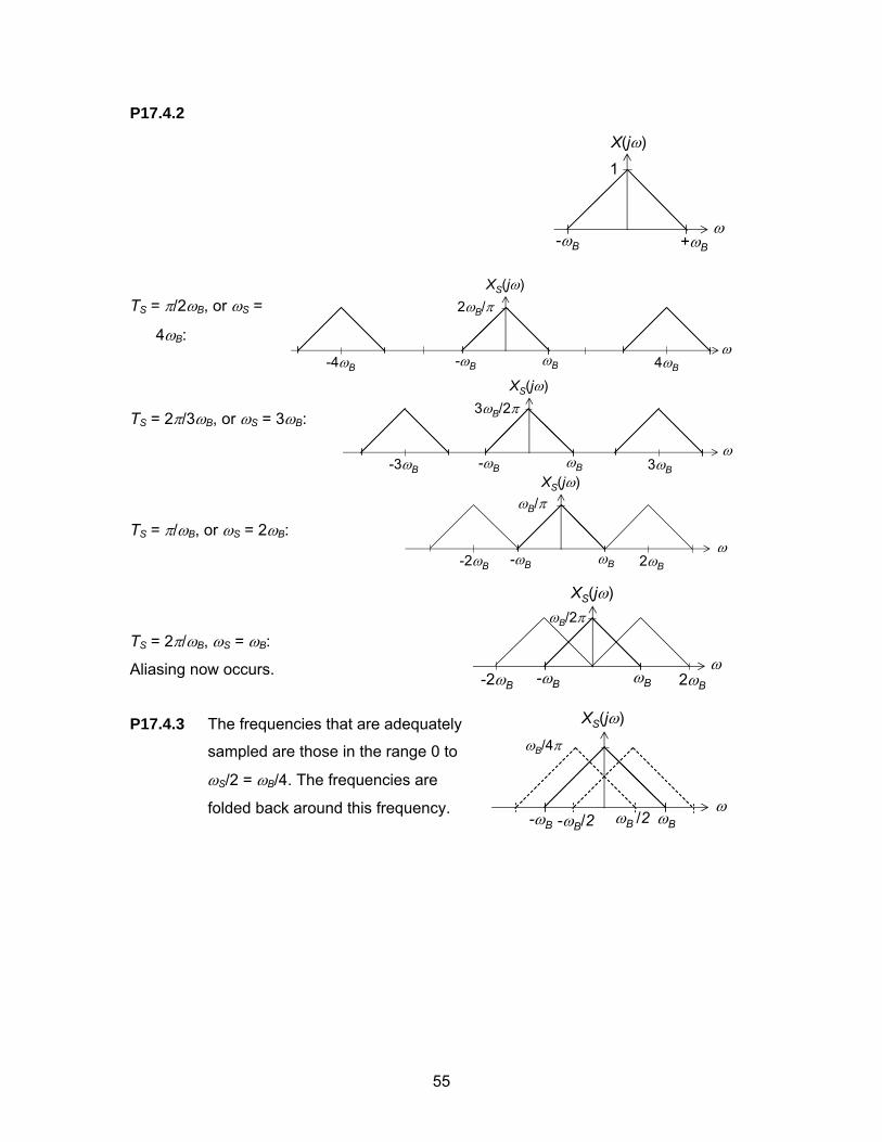
P17.4.2
TS = π/2ωB, or ωS =
4ωB:
TS = 2π/3ωB, or ωS = 3ωB:
TS = π/ωB, or ωS = 2ωB:
TS = 2π/ωB, ωS = ωB:
Aliasing now occurs.
P17.4.3 The frequencies that are adequately
sampled are those in the range 0 to
ωS/2 = ωB/4. The frequencies are
folded back around this frequency.
1
X(jω)
-ωB +ωB
ω
ωB 4ωB-ωB-4ωB
XS(jω)2ωB/π
ω
ωB 3ωB-ωB-3ωB
XS(jω)3ωB/2π
ω
ωB 2ωB-ωB-2ωB
XS(jω)ωB/π
ω
ωB 2ωB-ωB-2ωB
XS(jω)ωB/2π
ω
ωBωB /2-ωB -ωB/2
ωB/4π
ω
XS(jω)
56
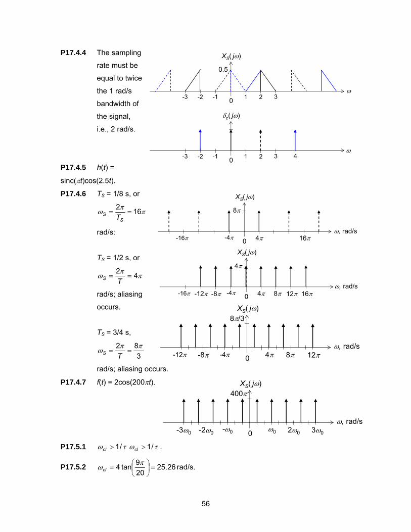
P17.4.4 The sampling
rate must be
equal to twice
the 1 rad/s
bandwidth of
the signal,
i.e., 2 rad/s.
P17.4.5 h(t) =
sinc(πt)cos(2.5t).
P17.4.6 TS = 1/8 s, or
ππω 162==
SS T
rad/s:
TS = 1/2 s, or
ππω 42==
TS
rad/s; aliasing
occurs.
TS = 3/4 s,
382 ππω ==
TS
rad/s; aliasing occurs.
P17.4.7 f(t) = 2cos(200πt).
P17.5.1 τω /1>cl τω /1>cl .
P17.5.2 26.25209tan4 =⎟
⎠⎞
⎜⎝⎛=πωcl rad/s.
0
XS( jω)
ω321-1-2-3
0
δc( jω)
ω321-1-2-3 4
0.5
0
XS( jω)
ω, rad/s-4π-16π 16π4π
8π
0
XS( jω)
ω, rad/s-4π-16π 8π4π
4π
12π 16π-8π-12π
0
XS( jω)
ω, rad/s-4π-12π 8π4π
8π/3
12π-8π
0
XS( jω)
ω, rad/s2ω0ω0
400π
3ω0-ω0-2ω0-3ω0
57
P17.5.3 1200π rad/s.
P17.5.4 (a) 0, 250 Hz, 500 Hz, 750 Hz, and 1000 Hz.
(b) 4500 Hz, 4750 Hz, 5000 Hz, etc.
(c) 2500 Hz, 2750 Hz, 3000 Hz, 3250 Hz, and 3500 Hz.
(d) 0, 250 Hz, 500 Hz, 750 Hz, 1000 Hz, 1250 Hz, 1500 Hz, 1750 Hz, 2000
Hz, 2250 Hz, 3750 Hz, 4000 Hz, etc.
P17.5.5 Series RL circuit to which a voltage is applied,
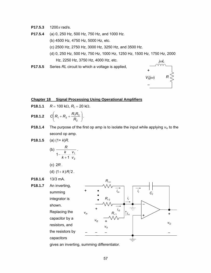
Chapter 18 Signal Processing Using Operational Amplifiers
P18.1.1 R = 100 kΩ, RL = 20 kΩ.
P18.1.2 ⎟⎟⎠
⎞⎜⎜⎝
⎛++
2
3131 R
RRRRC .
P18.1.4 The purpose of the first op amp is to isolate the input while applying vin to the
second op amp.
P18.1.5 (a) (1+ k)R.
(b)
2
1
11
vv
kkR
⋅+
−.
(c) R2 .
(d) 2)1( Rk+ .
P18.1.6 13/3 mA.
P18.1.7 An inverting,
summing
integrator is
shown.
Replacing the
capacitor by a
resistors, and
the resistors by
capacitors
gives an inverting, summing differentiator.
R
jωL
VI(jω)
+
–
vO
ir
ir
Cf
vI2
Rr 2
Rr n
Rr 1
irn
ir2ir1
vI1
vIn
•••
–
++
–
+
–––
+
+
58
P18.1.8 Rin = 0.
P18.1.13 (a) 70=R kΩ.
(b) VSRC = ±1.5 V.
P18.1.14 ⎟⎟⎠
⎞⎜⎜⎝
⎛++
3
4
1
21RR
RR .
P18.1.15 vO = 21
2
3
41
31
42 1 vRR
RRv
RRRR
⎟⎟⎠
⎞⎜⎜⎝
⎛+− .
P18.1.16 1740
−=Ov V.
P18.1.17 vO = -5/2 – 0.005*exp(-10000*t) + 2.5*exp(-20*t) V.
P18.1.18 (a) f = 11.2 Hz; phase deviation = 8.1°.
(b) 2.01 ms.
P18.1.19 The simulation results
are shown for Rr = 10
kΩ, Rf = 20 kΩ, and Cf =
1μF.
P18.1.20 12 mV.
P18.1.24 8≅oC μF, Cr ≅ 0.8 μF.
P18.2.3 SRC
O
vv = -0.96 + j 0.19.
P18.2.4 51026.1 −×=AAv
S .
P18.2.5 CMRR = 10,000.
P18.2.6 0.1%.
P18.2.7 Avcm = 10 , the output is 2 ± 1 V.
P18.2.8 (a) 3.318max =f kHz.
(b) =maxf 63.7 kHz.
P18.2.9 0.2 μs.
P18.2.10 (a) 5.03×10⁻¹⁶ VA.
(b) μV71.0 .
(c) 7.1 μV.
Time0s 5ms 10ms 15ms 20ms 25ms 30ms 35ms 40ms
-6.0V
-4.0V
-2.0V
0V
vO
59
P18.2.11 (a) vo = Vio.
(b) vo = Vio + RIbP.
(c) vo = Vio – RIbN.
(d) vo = Vio + R(IbP – IbN).
P18.2.12 R2, = 100 Ω, R1 = 9 kΩ, R3 = 65 kΩ, Rp = 1 kΩ, Ra = 9.5 kΩ.
P18.3.6 ω0 = rad/s, Q = 0.5; passband gain: 21
= ; input impedance = 10(1 – j) kΩ.
P18.3.7 160≅flR kΩ, Rrl = 16 kΩ, Rrh = 1.6 kΩ = Rfh.
P18.3.8
n = 1 2 3 10 50
(a) -10 -20 -30 -100 -500 dB/decade
(b) -10 -11.7 -12.4 -13.4 -13.8
P18.3.9 R = 8.31 kΩ, 2QR = 3.18 MΩ, QC2
= 1 nF.
P18.3.10 Highpass filter. First-order section: Rr = 160 Ω, Rf = 1.6 kΩ; second-order
section: R1 =80 Ω and R2 =320 Ω.
Lowpass filter. First-order section: Cf = 0.2 nF; second-order section: C1 = 0.4
nF, C2 = 0.1 nF.
Attenuation = -23.9 dB at 4 kHz and 200 kHz, with respect to the midband
gain.
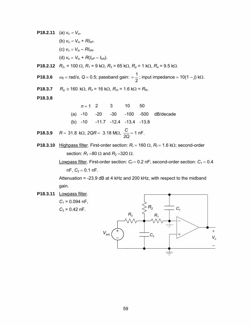
P18.3.11 Lowpass filter.
C1 = 0.094 nF,
C3 = 0.42 nF.
R3
C3
C1
R1
Vo
R2
Vsrc
60
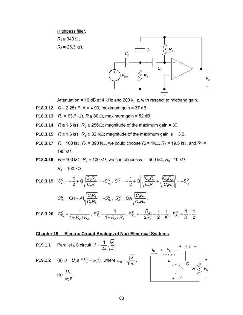
Highpass filter.
R1 ≅ 340 Ω,
R3 = 25.3 kΩ.
Attenuation = 16 dB at 4 kHz and 200 kHz, with respect to midband gain.
P18.3.12 25.2=C nF, A = 4.93, maximum gain = 37 dB.
P18.3.13 1R = 63.7 kΩ, R ≅ 80 Ω, maximum gain = 52 dB.
P18.3.14 6.1≅R kΩ, 2562 ≅R Ω; magnitude of the maximum gain = 39.
P18.3.15 6.1≅R kΩ, 323 ≅R kΩ; magnitude of the maximum gain is 2.3= .
P18.3.17 100=R kΩ, R3 = 390 kΩ, we could choose Rf = 1kΩ, RB = 19.5 kΩ, and RL =
195 kΩ.
P18.3.18 100=R kΩ, 1002 =R kΩ, we can choose R1 = 500 kΩ, Ra =10 kΩ,
R3 = 100 kΩ.
P18.3.19 QQRR
SRCRCQS
2111
22
21
−=+−= , QQCC
SRCRC
RCRCQS
2111
22
21
12
21
−=⎥⎥⎦
⎤
⎢⎢⎣
⎡++−= ,
( ) QR
QR rf
SRCRCAQS −=−=
22
111 , 22
11
RCRCQASQ
A = .
P18.3.20 32 /1
13 RR
SQR +
= , 32 /1
12 RR
SQR +
− , KR
RSKR
121
2 3
22
−=−= , 211
3−=
KSK
R .
Chapter 19 Electric Circuit Analogs of Non-Electrical Systems
P19.1.1 Parallel LC circuit, Jkf
π21
= .
P19.1.2 (a) ( )teUu t00 10 ωω −= − , where
mk
=0ω ,
(b) e
U
0
0
ω.
C3
C2
C1
R1
R3Vsrc Vo
+
–
vRR
LC
+ –vL+ –vC
i
I0
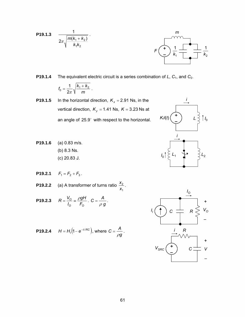
61
P19.1.3
21
21 )(2
1
kkkkm +π
.
P19.1.4 The equivalent electric circuit is a series combination of L, C1, and C2.
0f mkk 21
21 +
=π
.
P19.1.5 In the horizontal direction, =xK 2.91 Ns, in the
vertical direction, =yK 1.41 Ns, 23.3=K Ns at
an angle of o9.25 with respect to the horizontal.
P19.1.6 (a) 0.83 m/s.
(b) 8.3 Ns.
(c) 20.83 J.
P19.2.1 321 FFF += .
P19.2.2 (a) A transformer of turns ratio 1
2
xx .
P19.2.3 OO
O
FgH
IVR ρ
≡= . g
AC ρ
= .
P19.2.4 ( )RCtI eHH /1 −−= , where
gACρ
= .
–+–+
m
F1
1k 2
1k
I0LKδ(t)–+–+
i
i
I0 L1 L2
IO
II C R
+
–
VO
–+–+VSRC
R
C
i
+
–
V
62
P19.2.5 The equivalent circuit is an LC circuit with an initial charge on C, with LC =
l/g; lgf
π21
0 = .
P19.3.1 (a) junction temperature = 164°C, temperature of the case = 155°C.
(b) junction temperature = 54°C, temperature of the case = 45°C.
P19.3.2 40 W.
P19.3.3 19=JCθ °C/W, maximum power dissipation 11.2= W.
P19.3.4 3.27 W.
P19.3.5 3,626.0 W.
P19.3.6 The equivalent circuit is that of a capacitor having an initial voltage
corresponding to 25°C and is being charged through a resistance R from a
source of voltage corresponding to 200°C; temperature at any time t is: T =
200 + τ/)20025( te−− , time t taken to reach a temperature of 195°C = 47.4 s.
P19.4.1 (a) 2
112 ]Na[
]Na[ln +
+
==−q
kTEVV Na .
(b) 2
112 ]Cl[
]Cl[ln−
−
−==−q
kTEVV Cl , so that ECl of opposite
polarity to ENa.
P19.4.2 (a) 710− C/cm2.
(b) 1119
7
103.6106.1
10×≅
× −
−
monovalent ions/cm3.
(c) 19323 106101.0106 ×=××× − monovalent ions/cm3.
(d) 819
11
10106103.6 −≅
×× cm.
P19.4.6 Vm = -70 mV; JK = 120 nA/cm2 = -JKP.
+– ENa
+
–
V2 – V1
R
i = 0


