Embed Size (px)
Citation preview

616 . IEEE JOURNAL ON SELECTED AREAS IN COMMUNICATIONS, VOL. SAC-3. NO. 5, SEPTEMBER 1985
An Adaptive Digital Suppression Filter for ~
Direct-Sequence Spread-Spectrum Communications
Ahstruct -This paper describes the structure of a digital implementation of the Widrow-Hoff LMS algorithm which uses a burst processing tech- nique to obtain some hardware simplification. This adaptive system is used to suppress narrow-band interference in a direct-sequence spread-spectrum communication system. Several different narrow-band interferers are con- sidered, and probability of error results are presented for all cases. While, in general, the results show significant improvement in performance when the LMS algorithm is used, certain disadvantages are also present and are discussed in this paper.
I. INTRODUCTION
A NALYTICAL and simulation results have shown that least-mean-squared (LMS) adaptive filtering is a
useful tool for the suppression of narrow-band interference in a direct-sequence (DS) spread-spectrum system [1]-[8]. Fig. 1 shows how the LMS adaptive system fits into the structure of a DS spread-spectrum receiver. The adaptive filtering process is 'performed at baseband and, for the purposes of t h s paper, it is assumed that perfect carrier synchronization has been obtained. The LMS adaptive filter selectively suppresses the narrow-band jammer in the presence of the DS code because of the low correlation between the code samples and the relatively high correla- tion between the jammer samples. The LMS adaptive filter, shown in Fig. 2, uses past samples of the input signal, x(k - l), . . . , x(k - N), to produce an estimate of the cur- rent sample of the input signal, x ( k ) . The tap weights are adjusted to minimize the mean-squared-error, Z2( k ) , where ~ ( k ) is the difference between the output of the signal estimator, y ( k ) , and x(k).
In the process of suppressing the jammer, the filter introduces a notch in the frequency domain which, while
attenuating the jammer, also removes some code energy (i.e., the code is distorted by the jammer suppression process). Naturally, the amount of code distortion is de- pendent on the jammer bandwidth, with the suppression of a jammer with larger bandwidth causing the loss of more code energy than the suppression of a jammer with smaller bandwidth.
This paper investigates the use of adaptive filtering for the suppression of several jammer types. Experimental probability of error data is presented for single-tone, swept-tone, and narrow-band Gaussian jammers. In ad- dition, a hardware-efficient implementation of the digital adaptive filter is discussed in detail.
11. DIGITAL IMPLEMENTATION OF THE ADAPTIVE ALGORITHM
The Widrow-Hoff LMS algorithm is given by
w j ( k + 1 ) = w j ( k ) + 2 p ~ ( k ) x ( k - z ) (1)
where w j ( k + 1) and w j ( k ) , are the values of the ith tap weight at times k + 1 and k , respectively, E ( k ) is the error signal at time k , x(k - i) is a delayed input signal sample, and p is the convergence factor. As described in [l], direct implementation of (1) requires 2N multipliers for an N-tap filter, an undesirable property from a hardware point of view. Therefore, a burst processing architecture which re- quires only two multipliers regardless of filter order was developed and a charge-coupled device implementation was constructed and used to obtain experimental results 111.
In this paper, the same architecture will be implemented Manuscript received August 31,1984: revised May 28, 1985. This paper digitally. Before discussing the details of the implementa-
was presented in p a t at MILCoM '84, LoS Angeles, CA, October 21-24, tion, however, the architecture will be briefly review& The 1984 and GLOBCOM '84, Atlanta, GA, November 26-29, 1984. Ths work was supported in part by the Office of Naval Research under adaptive system is constructed around the two-delay line Contract ONR N00014-82-K-0376 and in part by the National Science structure of ~ i ~ . 3. H ~ ~ ~ , input signal samples are stored in Foundation.
G. J. Saulnier is with Comorate Research and DeveloDment. General the upper delay line and tap weight values are stored in the Electric Company, Schenectady, NY 12301.
P. K. Das is with the Department of Electrical, Computer, and Systems Engineering, Rensselaer Polytechnic Institute, Troy, NY 12180. are positioned as shown in Fig. 3, one new weight value, Computer Sciences, University of California at San Diego, La Jolla, CA
L. B. Milstein is with the Department of Electrical Engineering and
92093. W N ( k + l ) = w N ( k ) + 2 p € ( k ) x ( k - N ) ( 2 )
lower delay line. If the signal samples and weight values
0733-8716/85/0900-0676$01.00 01985 IEEE
SAULNIER et al.: ADAPTIVE DIGITAL SUPPRESSION FILTER
I I
611
I I
Oscil.
PN Code
Fig. 1. Spread-spectrum receiver with an adaptive suppressor.
x(k-I) x(k-2) x(k-N+i) x(k-N)
Fig. 2. LMS adaptive filter
x(k - N + 1) x(k - N) II..
WN(k + 1)
Fig. 3. Two-delay-line structure for weight update.
can be calculated by the multiplier-summer combination. If the contents of both delay lines are shifted one position to the right, another new tap weight value,
W N & +1) = WN-l(k)+2p€(k)X(k- N t l ) (3)
can be. calculated by the same multiplier-summer combina- tion. Shifting both delay lines N times allows all N new tap weights to be calculated using one multiplier.
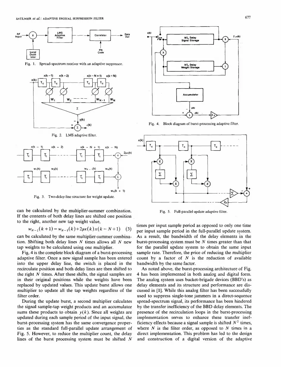
Fig. 4 is the complete block diagram of a burst-processing adaptive filter. Once a new signal sample has been entered into the upper delay line, the switch is placed in the recircuiate position and both delay lines are then shifted to the right N times. After these shifts, the signal samples are in their original positions while the weights have been replaced by updated values. This update burst allows one multiplier to update all the tap weights regardless of the filter order.
During the update burst, a second multiplier calculates the signal sample-tap weight products and an accumulator sums these products to obtain. y ( k ) . Since all weights are updated during each sample period of the input signal, the burst-processing system has the same convergence proper- ties as the standard full-parallel update arrangement of Fig. 5. However, to reduce the multiplier count, the delay lines of the burst processing system must be shifted N
I ' 1 I Q I ' I I
I Accumulator
Fig. 4. Block diagram of burst-processing adaptive filter.
' +
Fig. 5. Full-parallel update adaptive filter.
times per input sample period as opposed to only one time per input sample period in the full-parallel update system. As a result, the bandwidth of the delay elements in the burst-processing system must be N times greater than that for the parallel update system to obtain the same input sample rate. Therefore, the price of reducing the multiplier count by a factor of N is the reduction of available bandwidth by the same factor.
As noted above, the burst-processing architecture of Fig. 4 has been implemented in both analog and digital form. The analog system uses bucket-brigade devices (BBD's) as delay elements and its structure and performance are dis- cussed in [l]. Whde this analog filter has been successfully used to suppress single-tone jammers in a direct-sequence spread-spectrum signal, its performance has been hindered by the transfer inefficiency of the BBD delay elements. The presence of the recirculation loops in the burst-processing implementation serves to enhance these transfer inef- ficiency effects because a signal sample is shifted N 2 times, where N is the filter order, as opposed to N times in a direct implementation. This problem has led to the design and construction of a digital version of the adaptive

678 IEEE JOURNAL ON SELECTED AREAS IN COMMUNICATIONS, VOL. SAC-3, NO. 5 , SEPTEMBER 1985
processor wherein the. recirculation necessary for burst processing does not cause any signal degradation.
In m a y applications, the adaptive filter has two inputs: the reference input and the primary input. This additional input is used to help the,adaptive filter distinguish between the desired and undesired portions of the main input signal. In the spread-spectrum receiver considered here, only one input is available. Consequently, the digital im- plementation requires only one analog-to-digital converter. This one input signal is quantized to 8 bits and represented in two's complement ,notation. This number system is used because the adaptive algorithm requires both sign and magnitude information. The two's complement notation
, encodes 0 V to midscale, positive voltages above midscale, and negative voltages below midscale.
The digital adaptive filter has a pipelined structure to allow several operations to be performed concurrently and, consequently, 'to obtain as much bandwidth as possible. As explained in the discussion of burst processing, the price of reducing the multiplier count by a factor of N is a reduc- tion in available bandwidth by 'the same factor. Conse- quently, every attempt is made to eliminate other sources of bandwidth loss by using techniques like pipelining.
111. FILTER HARDWARE
The digital 'adaptive filter is an implementation of the block diagram shown in Fig. 4. 'The adaptive filter has 16 taps and uses TRW LSI multipliers to provide high-speed two's complement multiplication. This section de tds the design of the, adaptive filter and 'shows how the functions of Fig. 4 are implemented in digital form.
The heart of the burst processing configuration is the two-delay -line structure of Fig. 3. Naturally, these delay lines could be realized using shift registers, but that proves to; be a cumbersome approach. Instead, both the, signal sampies and weight values are stored in a random-access memory (RAM). Since the filter is 16th order, there are 16 signal samples and 16 tap weight values stored in this memory.
Fig. 6 is a Mock diagram.of the weight update portion of the adaptive filter. Even though the RAM functions .as a delay line, signal samples are never actually moved from one location to another but, rather, the time reference is shifted to simulate this movement. To clarify the memory operation, a complete update burst for a 4th-order filter will be explained. The update burst for the 16th-order filter is the same ,as that for the 4th-order filter except, naturally, the internal update cycle repeats 16 times rather than 4 times.
The memory address generator of Fig, 6 is a ririg counter which, in the 4th-order case, counts up to 3 (binary 11) and, if incremented again, returns to 0 (binary 00). As a result, the memory is circular, having no actual "begin- ning" or "end." This property is essential to the memory operation during the update burst. Fig. 7 graphically shows the movement of signal samples and weight values into and out of the memory locations during the update operation.
INPUT SIGNAL x(k)a (SIGNAL STORAGE)
RAM Q MULTIPLIER
A I I
GENERATOR - ADDRESS. -
v V _i
LATCH RAM
LATCH - (WEIGHT STORAGE) a@- ADDER
@ - Fig. 6 . Digital weight-update system.
SIGNAL
WEIGHT
1 1 ' I ; . I I I 1
I I I I
I 1 I I I I I 1
I I I I
I
Fig. 7. Signal-flow diagram for a 4-tap adaptive filter.
Suppose the memory address counter has just been incre- mented to binary 10. From Fig. 7 it can be seen that w4(k) is stored in the 10 location of the weight RAM and x(k - 4) is stored in 'the 10 location of the signal RAM. These values are read from the memory .and used to calculate w4( k + 1 j where
w 4 ( k +1) = w4(k)+2p<(&)x(k-4). (4)
This new weight value is stored in latch B of Fig. 6. The address counter is then advanced to binary 11.where w 3 ( k ) and x(k - 3) are stored in the weight memory and signal memory, respectively. These values are read from the mem- ory and used to calculate w3(k + 1). The first step in the calculation of this new weight is the storage of w 3 ( k ) in latch A of Fig. 6. Once w3(k) is stored in latch A, w4( k + 1) is transferred to memory location 11, as shown in Fig. 7. This latch structure allows the memory-write operation to proceed while w3(k + 1) being calculated. As was the case with w4(k + l) , w3(k + 1) is temporarily stored in latch B. The memory counter is again advanced, accessing memory location 00. Here, w2(k) is moved to latch A, w3(k + 1) written into memory, and w2(k + 1) calculated and stored in latch B. The memory address counter is incremented again and the process repeated, resulting in w2( k + 1) being stored in location 01 and wl(k + 1) stored in latch B.

SAULNIER et al.: ADAPTIVE DIGITAL SUPPRESSION FILTER
Up to this point, the memory address counter has been incremented N times, where N = 4. However, the update process is not complete because w4( k + 1) is still tempo- rarily stored in latch B. Consequently, the memory address counter is incremented a fifth time which returns- it to 10. Earlier, during the update burst, w4(k) was read from this location in the weight RAM but no new weight value5vas stored there. Now, wl(k + 1) is written into this location. In addition, a new signal sample, x(k), is written into the signal RAM, replacing x( k - 4). This operation completes the update burst, and advancing the memory counter again will begin the next update.
The signal storage RAM now contains x(k), x(k -l), x( k - 2), and x(k - 3). Therefore, x(k - 3) has become the oldest signal sample in the delay line. The next update burst begins by multiplying x(k - 3) by 2 p c ( k ) and add- ing .the product to w4(k + 1). Consequently, x(k - 3) has assumed the last position in the “delay line” without actually moving from one memory location to another. This change is made possible by advancing the memory positions of the weight values by one location during the update burst, i.e., while w4(k) was in location 10 at the beginning of the update burst, w4(k + 1) is in location 11 after the burst. After the next update burst w4(k + 2) will be stored in location 00 and its location will be incre- mented during each successive update burst.
Besides calculating the new weight values, it is necessary to calculate the signal sample-tap weight products and sum them to obtain y ( k ) . Fortunately, this process can be performed concurrently with the update operation. Con- sider the situation in Fig. 7 when the memory address counter is’ first incremented to 11. Latch B contains w4( k + 1) and the signal memory output is x( k - 3). While the new weight, w3(k + l), is being calculated, the product w4(k +l)x[(k +1)-4 is also evaluated and stored in an accumulator. This process continues as the memory ad- dress counter advances and an accumulator sums the prod- ucts to obtain y ( k ) .
Fig. 8 is a block diagram of the portion of the adaptive filter which calculates. y ( k ) and processes it to determine 2 p c ( k), the scaled value of the error signal. For simplicity, the time index will be taken as k even though in relation to the weight update operation it is actually y ( k + 1) which is produced rather than y ( k ) . A TRW LSI multiplier-accu- mulator is used to calculate and sum the signal sample-tap weight products during the weight update burst. The value of y ( k ) that is computed is then subtracted from the input signal, x ( k ) , to generate the error signal, c (k ) . It is im- portant to note that the input signal sample, x(k), used here was not used in the calculation of y ( k ) . This x(k) is the input signal sample which is being predicted by the filter by using past signal samples. The error signal is a measure of the difference between the predicted value, y( k ) , and the actual value, x( k ) .
Once the filter has begun to converge, x(k) and y ( k ) are nearly equal, meaning that c ( k ) is small. However, when the filter is first turned on or when the input signal
679
x k- i )
Fig. 8. Calculation of the scaled error signal.
large. In fact, with x(k) and y ( k ) represented by 8 bit numbers, c ( k ) must be a 9 bit number to insure against two’s complement overflow in the large c ( k ) condition. This overflow must be avoided since it causes a large positive number to become a large negative number or vice versa, and this would cause instability in the adaptive algorithm. From a hardware point of view, it is undesirable to expand to 9 bits since all further processing would have to accommodate this extra bit. Also, discarding the least significant bit proves to be an unacceptable way to eliminate the extra bit because it causes small values of c(k).to be ignored which, in turn, allows adaptation to stop before c ( k ) is minimized. Therefore, instead of discarding the least significant bit, a soft limiter is installed which keeps the error signal in the 8 bit range and removes the possibil- ity of two’s complement overflow. The only penalty of this soft-limiting process is a slight decrease in convergence rate for values of c ( k ) which exceed the limiting values.
After limiting, the error signal is multiplied by the convergence factor, 2 p . Here, the problem of bit expansion which was temporarily sidestepped by the soft limiter becomes a serious problem. The multiplication of two 8 bit numbers produces a 16 bit product. Again, truncation of the product is not a viable solution since both 2 p and c ( k ) can be very small, which makes the least significant bits of the product valuable. Similarly, soft limiting the product to keep only 8 bits would seriously decrease the dynamic range of 2 p c ( k ) and could greatly affect the convergence rate.
The effect of soft limiting is directly related to the value of 2p . If 2 p is very small, even large values of c ( k ) would result in very little limiting. However, large values of 2 p could cause severe limiting and, subsequently, greatly re- duce the convergence rate. Since this filter will be used in -
changes suddenly, the value of c ( k ) can become quite experiments where 2 p will, at times, be made large and in
680 lEEE JOURNAL ON SlZJXTED AREAS IN COMMUNICATIONS, VOL. SAC-3, NO. 5, SEPTEMBER 1985
which convergence rate is important, soft limiting to 8 bits is unacceptable.
Consequently, it is necessary to expand to 16 bits at this multiplication. The 16 bit 2 p c ( k ) signal is used to multiply the delayed input signal samples, x ( k - i). Since x ( k - i) is an 8 bit number, the product, 2 p c ( k ) x ( k - i), is a 24 bit number. This product, 2 p c ( k ) x ( k - i), is added to an old weight value w i ( k ) to produce the updated value, wi(k + 1). Consequently, the number of bits necessary to represent the weights will depend on the number of bits necessary to represent this product. The error signal, 2pc(k ) , is a 16 bit number and it will be assumed that 2pc(k ) can take any value which can be represented by those 16 bits. This indicates that 2 p c ( k ) can be very large, very small, or some middle value. Because of this, the product 2 p c ( k ) x ( k - i) must be represented by at least 16 bits. However, the input signal, x ( k ) , is assumed to always be large. This does not mean that every sample of x ( k ) is large, but that some type of automatic gain control (AGC) forces a portion of the samples to approach full scale in the 8 bit represen- tation. This, in turn, means that the error signal, 2pc(k ) , is regularly multiplied by an x ( k - i) which approaches plus or minus full scale. As a result, even if 2 p c ( k ) is only the size of the least significant bit in its 16 bit representation, the top 16 bits of the 2 p e ( k ) x ( k - i) product will regularly become nonzero because, when x ( k - i) is plus or ininus full scale, the top 16 bits of the product are either k 2pc(k ) . Consequently, a 16 bit representation of the weight values will not compromise the adaptation for small values of 4 k ) .
Because of these considerations, the weight values are represented by 16 bit numbers. These weights and the 8 bit signal samples are used to form the products wi( k ) x ( k - i) which are summed to obtain y ( k ) . Since only 8 bits of these products are summed in the accumulator of Fig. 8, it is not necessary to use the total 16 bits of the weight values in the w , ( k ) x ( k - i) multiplication but, instead, only the 8 most significant bits. However, this does not indicate that the 8 least significant bits of the weight values are extra- neous. As already discussed, a 16 bit weight representation is necessary so that small values of 2 p c ( k ) will be able to cause some change in the weight values. Since only the 8 most significant bits of the weights are used to produce w , ( k ) x ( k - i) and subsequently y ( k ) , small values of 2 p c ( k ) may not cause any immediate change in the filter response. However, the changes in the 8 least significant bits of the weights may “accumulate” and eventually prop- agate into the upper 8 bits. Consequently, convergence properties do require the storage of 16 bit weights even though only 8 bits are actually used to multiply the input signal samples.
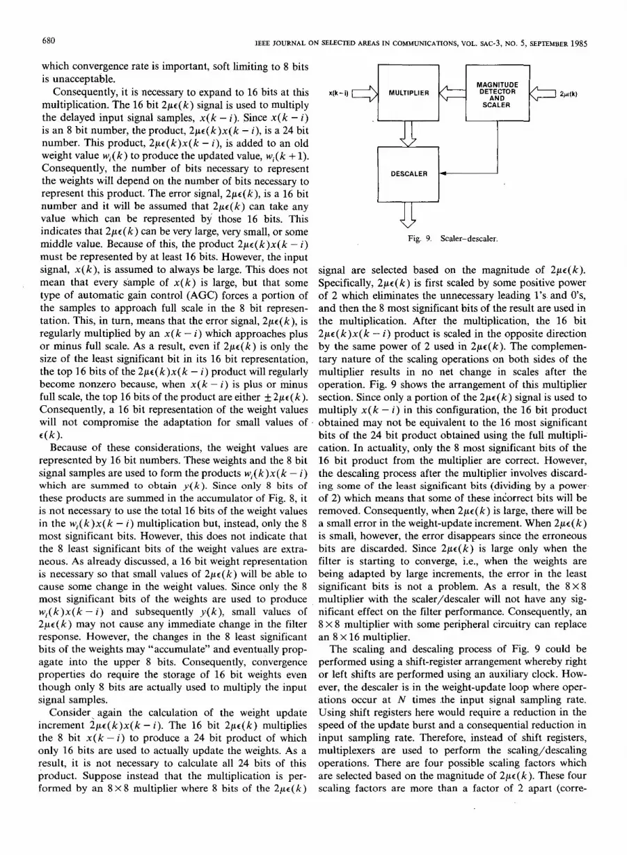
Consider- again the calculation of the weight update increment 2 p c ( k ) x ( k - i). The 16 bit 2 p c ( k ) multiplies the 8 bit x ( k - i) to produce a 24 bit product of which only 16 bits are used to actually update the weights. As a result, it is not necessary to calculate all 24 bits of this product. Suppose instead that the multiplication is per- formed by an 8 X 8 multiplier where 8 bits of the 2 p c ( k )
x(k - i)
v Fig. 9. Scaler-descaler.
signal are selected based on the magnitude of 2pc(k ) . Specifically, 2 p c ( k ) is first scaled by some positive power of 2 which eliminates the unnecessary leading 1’s and O’s, and then the 8 most significant bits of the result are used in the multiplication. After the multiplication, the 16 bit 2 p c ( k ) x ( k - i) product is scaled in the opposite direction by the same power of 2 used in 2pc(k ) . The complemen- tary nature of the scaling operations on both sides of the multiplier results in no net change in scales after the operation. Fig. 9 shows the arrangement of this multiplier section. Since only a portion of the 2pc( k ) signal is used to multiply x ( k - i) in this configuration, the 16 bit product obtained may not be equivalent to the 16 most significant bits of the 24 bit product obtained using the full multipli- cation. In actuality, only the 8 most significant bits of the 16 bit product from the multiplier are correct. However, the descaling process after the multiplier involves discard- ing some of the least significant bits (dividing by a power of 2) which means that some of these incorrect bits will be removed. Consequently, when 2pc( k ) is large, there will be a small error in the weight-update increment. When 2 p c ( k ) is small, however, the error disappears since the erroneous bits are discarded. Since 2 p c ( k ) is large only when the filter is starting to converge, i.e., when the weights are being adapted by large increments, the error in the least significant bits is not a problem. As a result, the 8 X 8 multiplier with the scaler/descaler will not have any sig- nificant effect on the filter performance. Consequently, an 8 X 8 multiplier with some peripheral circuitry can replace an 8 X 16 multiplier.
The scaling and descaling process of Fig. 9 could be performed using a shift-register arrangement whereby right or left shifts are performed using an auxiliary clock. How- ever, the descaler is in the weight-update loop where oper- ations occur at N times .the input signal sampling rate. Using shift registers here would require a reduction in the speed of the update burst and a consequential reduction in input sampling rate. Therefore, instead of shft registers, multiplexers are used to perform the scaling/descaling operations. There are four possible scaling factors which are selected based on the magnitude of 2pc(k ) . These four scaling factors are more than a factor of 2 apart (corre-
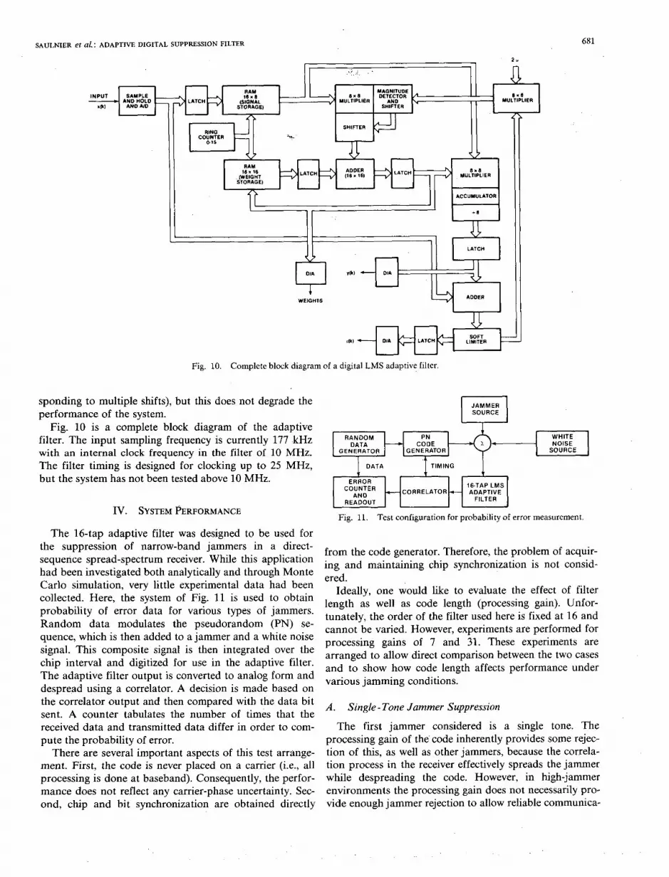
Fig. 10. Complete block diagram OF a digital LMS adaptive Filter.
sponding to multiple shifts), but this does not degrade the performance of the system.
Fig. 10 is a complete block diagram of the adaptive filter. The input sampling frequency is currently 177 kHz with an internal clock frequency in the filter of 10 MHz. The filter timing is designed for clocking up to 25 MHz, but the system has not been tested above 10 MHz.
IV. SYSTEM PERFORMANCE
The 16-tap adaptive filter was designed to be used for the suppression of narrow-band jammers in a direct- sequence spread-spectrum receiver. While this application had been investigated both analytically and through Monte Carlo simulation, very little experimental data had been collected. Here, the system of Fig. 11 is used to obtain probability of error data for various types of jammers. Random data modulates the pseudorandom (PN) se- quence, which is then added to a jammer and a white noise signal. This composite signal is then integrated over the chip interval and digitized for use in the adaptive filter. The adaptive filter output is converted to analog form and despread using a correlator. A decision is made based on the correlator output and then compared with the data bit sent. A counter tabulates the number of times that the received data and transmitted data differ in order to com- pute the probability of error.
There are several important aspects of this test arrange- ment. First, the code is never placed on a carrier (i.e., all processing is done at baseband). Consequently, the perfor- mance does not reflect any carrier-phase uncertainty. Sec- ond, chip and bit synchronization are obtained directly
JAMMER SOURCE
WHITE NOISE
SOURCE GENERATOR
ERROR
READOUT FILTER
Fig. 11. Test configuration For probability of error measurement,
from the code generator. Therefore, the problem of acquir- ing and maintaining chip synchronization is not consid- ered.
Ideally, one would like to evaluate the effect of filter length as well as code length (processing gain). Unfor- tunately, the order of the filter used here is fixed at 16 and cannot be varied. However, experiments are performed for processing gains of 7 and 31. These experiments are arranged to allow direct comparison between the two cases and to show how code length affects performance under various jamming conditions.
A . Single - Tone Jammer Suppression
The first jammer considered is a single tone. The processing gain of the- code inherently provides some rejec- tion of this, as well as other jammers, because the correla- tion process in the receiver effectively spreads the jammer while despreading the code. However, in high-jammer environments the processing gain does not necessarily pro- vide enough jammer rejection to allow reliable communica-
682
100
10-1
10-2
P(E)
10 -3
IO -'
IEEE JOURNAL ON SELECTED AREAS I N COMMUNICATIONS, VOL. SAC-3, NO. 5, SEPTEMBER 1985
2 4 6 8 10 12 14
EJN, (dB)
Fig. 12. Single-tone jammer performance for 7- and 31-chip PN codes.
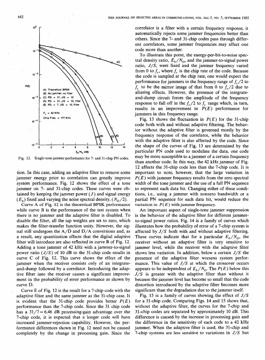
tion. In this case, adding an adaptive filter to remove some jammer energy prior to correlation can greatly improve system performance. Fig. 12 shows the effect of a tone jammer on 7- and 31-chip codes. These curves were ob- tained by keeping the jammer power ( J ) and signal energy ( Eb) fixed and varying the noise spectral density, ( N0/2).
Curve A of Fig. 12 is the theoretical BPSK performance while curve B is the performance of the test system when there is no jammer and the adaptive filter is disabled. To disable the filter, all the tap weights are set to zero, which makes the filter-transfer function unity. However, the sig- nal still undergoes the A/D and D/A conversions and, as a result, any quantization effects that the digital adaptive filter will introduce are also reflected in curve B of Fig. 12. Adding a tone jammer of 42 kHz with a jammer-to-signal power ratio ( J / S ) of 10 dB to the 31-chip code results in curve C of Fig. 12. This curve shows the effect of the jammer when the receiver consists only of an integrate- and-dump followed by a correlator. Introducing the adap- tive filter into the receiver causes a significant improve- ment in the probability of error performance as shown by curve D.
Curve E of Fig. 12 is the result for a 7-chip code with the adaptive filter and the same jammer as the 31-chip case. It is evident that the 31-chip code provides better P(E) performance than the 7-chip code. Since the 31 chip code has a 31/7 = 6.46 dB processing-gain advantage over the 7-chip code, it is expected that a longer code will have increased jammer-rejection capability. However, the per- formance differences shown in Fig. 12 need not be caused completely by the change in processing gain. Since the
correlator is a filter with a certain frequency response, it automatically rejects some jammer frequencies better than others. Since the 7- and 31-chip codes pass through differ- ent correlators, some jammer frequencies may affect one code more than another.
To illustrate this point, the energy-per-bit-to-noise spec- tral density ratio, E, /No , and the jammer-to-signal power ratio, J /S , were fixed and the jammer frequency varied from 0 to f,, where f, is the chip rate of the code. Because the code is sampled at the chip rate, one would expect the performance for jammers in the frequency range of f,/2 to f, to be the mirror image of that from 0 to f,/2 due to aliasing effects. However, the presence of the integrate- and-dump circuit forces the amplitude of the frequency response to fall off in the f,/2 to f, range which, in turn, results in an improvement in P ( E ) performance for jammers in this frequency range.
Fig. 13 shows the fluctuation in P ( E ) for the 31-chip code both with and without adaptive filtering. The behav- ior without the adaptive filter is governed mostly by the frequency response of the correlator, while the behavior with the adaptive filter is also affected by the code. Since the shape of the curves of Fig. 13 are determined by the particular PN code used to modulate the data, one code may be more susceptible to a jammer of a certain frequency than another code. In this way, the 42 kHz jammer of Fig. 12 affects the 31-chip code less than the 7-chip code. It is important to note, however, that the large variation in P( E ) with jammer frequency results from the zero spectral width of the tone jammer and the use of a full PN sequence to represent each data bit. Changing either of these condi- tions, i.e., using a jammer with nonzero bandwidth or a partial PN sequence for each data bit, would reduce the variation in P( E ) with jammer frequency.
An important aspect of single-tone jammer suppression is the behavior of the adaptive filter for different jammer- to-signal power ratios. Fig. 14 is a family of curves which illustrates how the probability of error of a 7-chip system is affected by J /S both with and without adaptive filtering. These curves. indicate that for a particular E,/N,, the receiver without an adaptive' filter is very sensitive to jammer level, while the receiver with the adaptive filter shows less variation. In addition, below a certain J /S the presence of the adaptive filter worsens system perfor- mance. This value of J /S at which the crossover' occurs appears to be independent of E,/No. The P( E ) below this J /S is greater with the adaptive filter than without it because the jammer level has become so small that the code distortion introduced by the adaptive filter becomes more significant than the degradation due to the jammer itself.
Fig. 15 is a family of curves showing the effect of J/S for a 31-chip code. Comparing Figs. 14 and 15 shows that, without the adaptive filter, the curves for the 7-chip and 31-chip codes are separated by approximately 10 dB. This difference is caused by the increase in processing gain and the difference in the sensitivity of each code to a 42. kHz jammer. When the adaptive filter is used, the 31-chip and 7-chip systems are less sensitive to variations in J / S .but
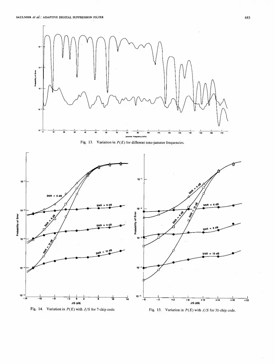
SAULNIER et al.: ADAPTIVE DIGITAL SUPPRESSION FILTER 683
I I I l l I I -10 -6 -2 0 2 6 10
I 14
JIS (dB)
Fig. 14. Variation in P ( E ) with J / S for 7-chip code.
lo-'
10-2
10.'
Y 10-5 I I I I 1
-6 - 2 +2 + 6 + I O +I4 JIS (dB)
1 I J +I6 +22
Fig. 15. Variation in P ( E ) with J / S for 31-chip code.

684 IEEE JOURNAL ON SELECTED AREAS IN COMMUNICATIONS, VOL. SAC-3, NO. 5 ; SEPTEMBER 1985
the curves remain offset by approximately 10 dB. In ad- dition, the crossover point below which the adaptive filter worsens the P ( E ) performance is moved to a higher J / S for the 31-chip code.
B. Swept -Tone Jammer
Up to this point, the frequency of the tone jammer has been kept constant. Suppose instead that the jammer sweeps through the frequency band of the DS signal. Since the
I jammer frequency is now constantly changing, the transfer function of the adaptive filter must also be constantly changing to track the jammer. Hence, the transient behav- ior of the adaptive system becomes an important factor because the filter must not only converge, but it must converge quickly enough to adjust to any change’ in the jammer. .
Consequently, the convergence factor, p, of the adaptive filter becomes an important parameter. As discussed earlier, this parameter governs the rate at which the filter con- verges, with a larger value of p causing faster convergence. However, the amount of variation in the final weight values after convergence is also dependent on the convergence factor. While a larger value of p results in faster conver- gence, it also causes more variation in the weight values after convergence. In terms of the input signal to the adaptive filter, x(k), a larger p makes the weight values more susceptible to short-term correlations in x ( k ) . The premise for using the adaptive filter for jammer suppres- sion in a PN code is that the filter will cancel the highly correlated jammer while having only a small effect on the poorly correlated code. However, even though the correla- tion between the code samples is small, there can be segments of code which, when viewed separately, appear to be correlated. An example of these code segments are the runs of 1’s or 0’s that are contained in the PN code. Since the Widrow-Hoff algorithm does not use the actual corre- lation matrix of the input signal, these runs can affect the filter-transfer function. If the convergence factor of the adaptive filter is sm.all, the runs of 1’s or 0’s will not greatly influence the weight values. However, as p gets larger these runs become more significant and do indeed cause a change in the filter-transfer function. Therefore, a larger value of p will result in increased code distortion because the filter will tend to cancel the long runs of 1’s and 0’s.
. While a larger p introduces more code distortion, it is necessary to have a large p if the jammer frequency is changing quickly. Fig. 16 shows the effect of p on prob- ability of error for a tone jammer whose frequency is swept linearly over the frequency band of the code. The jammer frequency moves from 0 to 177 kHz with a constant change in frequency per unit time and then returns to 0 at the same rate. When the rate of the frequency sweep is low, a small p provides better P ( E ) performance because less code distortion is introduced and the jammer frequency is changing slowly enough to allow the filter to track its path. However, as the jammer frequency changes more rapidly the larger p results in better P( E ) performance. Therefore,
lo-‘ t
Fig. 16. P( E ) performance for a swept-tone jammer with various values of the convergence factor.
to achieve optimal performance in a variable jammer en- vironment, the convergence factor of the adaptive filter would have to be varied to accommodate the rate of change of the jammer frequency.
C. Narrow - Band Gaussian Jammer
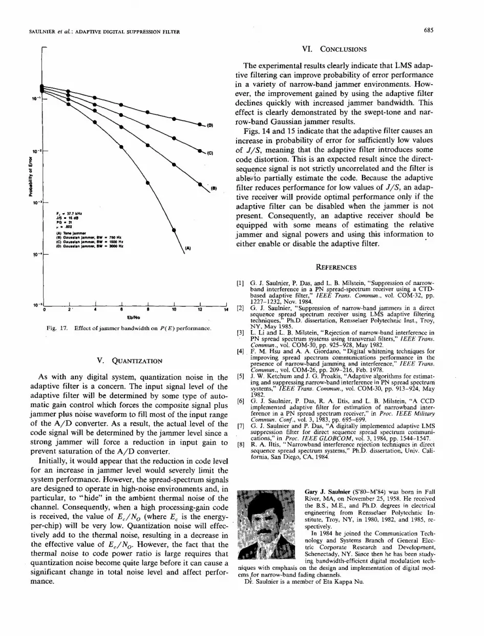
A narrow-band Gaussian jammer is generated by pass- ing white Gaussian noise through a bandpass filter. To remove this type of narrow-band jammer, the filter must create a notch in the frequency domain with a spectral width that is deterniined by the bandwidth of the janimer. Since a wider notch will also remove a greater amount of code energy, the jammer bandwidth will greatly affect .probability of error performance. In addition, the wider the jammer bandwidth, the lower the correlation of that jammer, which means that the adaptive filter is less able to estimate and suppress the jammer.
Fig. 17 shows probability of error results obtained using a Gaussian jammer with a variable bandwidth. Curve A is the P( E ) result for a tone jammer and curves B, C, and D are the P ( E ) results for Gaussian jammers of bandwidth 750 Hz, 1500 Hz, and 3000 Hz, respectively. This figure shows that increasing the jammer bandwidth results in a significant increase in‘ P ( E ) . If the jammer bandwidth becomes large enough, the jammer behaves like a white noise source and the adaptive filter is unable to provide any suppression.
SAULNIER et al. : ADAPTIVE DIGITAL SUPPRESSION FILTER 685
lo-‘
10 -
f
i 0
- r - a
10-
10 -
10-
VI. CONCLUSIONS
The experimental results clearly indicate that LMS adap- tive filtering can improve probability of error performance in a variety of narrow-band jammer environments. How- ever, the improvement gained by using the adaptive filter declines quickly with increased jammer bandwidth. This effect is clearly demonstrated by the swept-tone and nar- row-band Gaussian jammer results.
Figs. 14 and 15 indicate that the adaptive filter causes an increase in probability of error for sufficiently low values of J / S , meaning that the adaptive filter introduces some code distortion. This is an expected result since the direct- sequence signal is not strictly uncorrelated and the filter is ablwto partially estimate the code. Because the adaptive filter reduces performance for low values of J / S , an adap- tive receiver will provide optimal performance only if the adaptive filter can be disabled when the jammer is not present. Consequently, an adaptive receiver should be equipped with some means of estimating the relative jammer and signal powers and using this information to either enable or disable the adaptive filter.
REFERENCES
[l] G. J. Saulnier, P. Das, and L. B. Milstein, “Suppression of narrow- band Interference in a PN spread-spectrum receiver using a CTD- based adaptive filter,” IEEE Trans. Commun., vol. COM-32, pp. 1227-1232. Nov. 1984. 1 I I I 1 I
1 ’ 4 8 8 10 12 [2] G. J. Saikier, “Suppression of narrow-band jammers in a direct EblNo
sequence spread spectrum receiver using LMS adaptive filtering techniques,” Ph.D. dissertation, Rensselaer Polytechnic Inst., Troy,
Fig. 17. Effect of jammer bandwidth on P ( E ) performance. NY, May 1985. [3] L. Li and L. B. Milstein, “Rejection of narrow-band interference in
PN spread spectrum systems using transversal filters,” IEEE Trans. Commun., vol. COM-30, pp. 925-928, May 1982.
[4] , F. M. Hsu and A. A. Giordano, “Digital whitening techniques for improving spread spectrum communications performance in the V. QUANTIZATION nresence of narrow-band iamminz and interference.” IEEE Trans. r~ .... ~ . . .~ ~ ~ . - ~ ~ ~ ~~~~~
Commun., vol. COM-26, p”p. 209-516. Feb. 1978. ’
As with any digital system, quantization noise in the [5] J. W. Ketchum and J. G. Proakis, “Adaptive algorithms for estimat- ing and fyppressing narrow-band interference in PN spread spectrum systems. IEEE Trans. Commun., vol. COM-30, vp. 913-924. May adaptive filter is a concern. The input signal level of the f982.
[6] G. J. Saulnier, P. Das, R. A. Iltis, and L. B. Milstein, “A CCD irndemented adaDtive filter for estimation of narrowband inter-
_ -
fer‘ence in a PN spread spectrum receiver,” in Proc. IEEE Militar?,
171 G. J. Saulnier and P. Das, “A digitally implemented adaptive LMS Commun. Conf., vol. 3, 1983, pp. 695-699.
. . suppression filter for direct seqiience spread spectrum -communi-
[8] R. A. Iltis, “Narrowband interference rejection techniques in direct cations,” in Proc. IEEE GLOBCOM, vol. 3, 1984, pp. 1544-1547.
sequence spread spectrum systems,” Ph.D. dissertation, Univ. Cali- fornia, San Diego, CA, 1984.
adaptive filter will be determined by some type of auto- matic gain control which forces the composite signal plus jammer plus noise waveform to fill most of the input range of the A/D converter. As a result, the actual level of the code signal will be determined by the jammer level since a strong jammer will force a reduction in input gain to prevent saturation of the A/D converter.
Initially, it would appear that the reduction in code level for an increase in jammer level would severely limit the system performance. However, the spread-spectrum signals are designed to operate in hgh-noise environments and, in Gary J. Saulnier (S’80-M84) was born in Fall particular, to “hide” in the ambient thermal noise of the River, MA, on November 25, 1958. He received channel. Consequently, when a high processing-gain code the B.S., M.E., and Ph.D. degrees in electrical is received, the value of E , / N , (where E, is the energy- engineering from Rensselaer Polytechnic In-
stitute, Troy, NY, in 1980, 1982, and 1985, re- per-chip) will be very low. Quantization noise will effec- spectively. tively add to the thermal noise, resulting in a decrease in In 1984 he joined the Communication Tech-
the effective value of E,/N, . However, the fact that the nology and Systems Branch of General Elec- tric Corporate Research and Development,
thermal noise to code power ratio is large requires that Schenectady, NY. Since then he has been study- quantization noise become quite large before it can cause a ing bandwidth-efficient digital modulation tech-
niques with emphasis on the design and implementation of digital mod- significant change in total noise level and affect perfor- ems for narrow-band fading mance. D:. Saulnier is a member of Eta Kappa Nu.

686 IEEE JOURNAL ON SELECTED AREAS IN COMMUNICATIONS, VOL. SAC-3, NO. 5, SEPTEMBER 1985
and integrated optics area. He was formerly with the Electrical Engineer- ing Faculties of the Polytechnic Institute of New York, Brooklyn, and the University of Rochester, Rochester, NY. He has published numerous papers and is performing research in CCD and SAW signal processing devices, acoustooptic devices, nondestructive testing using elastic waves, and ultrasonic imaging.
Laurence B. Mils& (S’66-”68-SM’77-F’85), for a photograph and biography, see this issue, p. 6 5 1 .


