Embed Size (px)
Citation preview


ADVANCED ENGINEERINGELECTROMAGNETICS

ADVANCED ENGINEERINGELECTROMAGNETICS
SECOND EDITION
Constantine A. BalanisArizona State University
John Wiley & Sons, Inc.

Vice-President & Publisher: Don FowleyAssociate Publisher: Daniel SayreEditorial Assistants: Katie Singleton, Samantha Mandel, Charlotte CerfMarketing Manager: Christopher RuelExecutive Media Editor: Tom KulesaMedia Editor: Wendy AshenbergMedia Specialist: Jennifer MullinSenior Production Manager: Janis SooAssociate Production Manager: Joyce PohAssistant Production Editor: Annabelle Ang-BokDesigner: Maureen Eide, Kristine CarneyCover Photo: Lockheed Martin Corp.
This book was set in 10/12 Times Roman by Laserwords Private Limited and printed and bound by Courier Westford.
This book is printed on acid free paper.
Founded in 1807, John Wiley & Sons, Inc. has been a valued source of knowledge and understanding for more than 200years, helping people around the world meet their needs and fulfill their aspirations. Our company is built on a foundationof principles that include responsibility to the communities we serve and where we live and work. In 2008, we launched aCorporate Citizenship Initiative, a global effort to address the environmental, social, economic, and ethical challenges weface in our business. Among the issues we are addressing are carbon impact, paper specifications and procurement, ethicalconduct within our business and among our vendors, and community and charitable support. For more information, pleasevisit our website: www.wiley.com/go/citizenship.
Copyright © 2012, 1989 John Wiley & Sons, Inc. All rights reserved. No part of this publication may be reproduced,stored in a retrieval system or transmitted in any form or by any means, electronic, mechanical, photocopying, recording,scanning or otherwise, except as permitted under Sections 107 or 108 of the 1976 United States Copyright Act, withouteither the prior written permission of the Publisher, or authorization through payment of the appropriate per-copy fee to theCopyright Clearance Center, Inc. 222 Rosewood Drive, Danvers, MA 01923, website www.copyright.com. Requests to thePublisher for permission should be addressed to the Permissions Department, John Wiley & Sons, Inc., 111 River Street,Hoboken, NJ 07030-5774, (201)748-6011, fax (201)748-6008, website http://www.wiley.com/go/permissions.
Evaluation copies are provided to qualified academics and professionals for review purposes only, for use in their coursesduring the next academic year. These copies are licensed and may not be sold or transferred to a third party. Uponcompletion of the review period, please return the evaluation copy to Wiley. Return instructions and a free of charge returnmailing label are available at www.wiley.com/go/returnlabel. If you have chosen to adopt this textbook for use in yourcourse, please accept this book as your complimentary desk copy. Outside of the United States, please contact your localsales representative.
Library of Congress Cataloging-in-Publication Data
Balanis, Constantine A., 1938-Advanced engineering electromagnetics / Constantine A. Balanis. – 2nd ed.
p.cm.Includes bibliographical references and index.
ISBN 978-0-470-58948-9 (hardback)1. Electromagnetism. I. Title.QC760.B25 2012537–dc23
2011029122
Printed in the United States of America
10 9 8 7 6 5 4 3 2 1

To my family:
Helen, Renie, Stephanie, Bill and Pete


Balanis ftoc.tex V1 - 11/24/2011 1:25 P.M. Page vii
Contents
Preface xvii
1 Time-Varying and Time-Harmonic Electromagnetic Fields 1
1.1 Introduction 11.2 Maxwell’s Equations 1
1.2.1 Differential Form of Maxwell’s Equations 21.2.2 Integral Form of Maxwell’s Equations 3
1.3 Constitutive Parameters and Relations 51.4 Circuit-Field Relations 7
1.4.1 Kirchhoff’s Voltage Law 71.4.2 Kirchhoff’s Current Law 81.4.3 Element Laws 10
1.5 Boundary Conditions 121.5.1 Finite Conductivity Media 121.5.2 Infinite Conductivity Media 151.5.3 Sources Along Boundaries 17
1.6 Power and Energy 181.7 Time-Harmonic Electromagnetic Fields 21
1.7.1 Maxwell’s Equations in Differential and Integral Forms 221.7.2 Boundary Conditions 221.7.3 Power and Energy 25
1.8 Multimedia 29References 29Problems 30
2 Electrical Properties of Matter 39
2.1 Introduction 392.2 Dielectrics, Polarization, and Permittivity 412.3 Magnetics, Magnetization, and Permeability 482.4 Current, Conductors, and Conductivity 55
2.4.1 Current 552.4.2 Conductors 562.4.3 Conductivity 57
2.5 Semiconductors 592.6 Superconductors 642.7 Metamaterials 66
vii
Balanis ftoc.tex V1 - 11/24/2011 1:25 P.M. Page viii
viii CONTENTS
2.8 Linear, Homogeneous, Isotropic, and Nondispersive Media 672.9 A.C. Variations in Materials 68
2.9.1 Complex Permittivity 682.9.2 Complex Permeability 792.9.3 Ferrites 80
2.10 Multimedia 89References 89Problems 91
3 Wave Equation and its Solutions 99
3.1 Introduction 993.2 Time-Varying Electromagnetic Fields 993.3 Time-Harmonic Electromagnetic Fields 1013.4 Solution to the Wave Equation 102
3.4.1 Rectangular Coordinate System 102A. Source-Free and Lossless Media 102B. Source-Free and Lossy Media 107
3.4.2 Cylindrical Coordinate System 1103.4.3 Spherical Coordinate System 115
3.5 Multimedia 120References 120Problems 121
4 Wave Propagation and Polarization 123
4.1 Introduction 1234.2 Transverse Electromagnetic Modes 123
4.2.1 Uniform Plane Waves in an Unbounded Lossless Medium—PrincipalAxis 124A. Electric and Magnetic Fields 124B. Wave Impedance 126C. Phase and Energy (Group) Velocities, Power, and Energy
Densities 128D. Standing Waves 129
4.2.2 Uniform Plane Waves in an Unbounded Lossless Medium—ObliqueAngle 131A. Electric and Magnetic Fields 132B. Wave Impedance 135C. Phase and Energy (Group) Velocities 136D. Power and Energy Densities 137
4.3 Transverse Electromagnetic Modes in Lossy Media 1384.3.1 Uniform Plane Waves in an Unbounded Lossy Medium—Principal
Axis 138A. Good Dielectrics [(σ/ωε)2 � 1] 142B. Good Conductors [(σ/ωε)2 � 1] 143
4.3.2 Uniform Plane Waves in an Unbounded Lossy Medium—ObliqueAngle 143
4.4 Polarization 1464.4.1 Linear Polarization 1484.4.2 Circular Polarization 150

Balanis ftoc.tex V1 - 11/24/2011 1:25 P.M. Page ix
CONTENTS ix
A. Right-Hand (Clockwise) Circular Polarization 150B. Left-Hand (Counterclockwise) Circular Polarization 153
4.4.3 Elliptical Polarization 1554.4.4 Poincaré Sphere 160
4.5 Multimedia 166References 166Problems 167
5 Reflection and Transmission 173
5.1 Introduction 1735.2 Normal Incidence—Lossless Media 1735.3 Oblique Incidence—Lossless Media 177
5.3.1 Perpendicular (Horizontal or E) Polarization 1785.3.2 Parallel (Vertical or H ) Polarization 1825.3.3 Total Transmission–Brewster Angle 184
A. Perpendicular (Horizontal) Polarization 186B. Parallel (Vertical) Polarization 187
5.3.4 Total Reflection–Critical Angle 188A. Perpendicular (Horizontal) Polarization 188B. Parallel (Vertical) Polarization 198
5.4 Lossy Media 1985.4.1 Normal Incidence: Conductor–Conductor Interface 1985.4.2 Oblique Incidence: Dielectric–Conductor Interface 2015.4.3 Oblique Incidence: Conductor–Conductor Interface 205
5.5 Reflection and Transmission of Multiple Interfaces 2055.5.1 Reflection Coefficient of a Single Slab Layer 2065.5.2 Reflection Coefficient of Multiple Layers 213
A. Quarter-Wavelength Transformer 214B. Binomial (Maximally Flat) Design 215C. Tschebyscheff (Equal-Ripple) Design 217D. Oblique-Wave Incidence 219
5.6 Polarization Characteristics on Reflection 2205.7 Metamaterials 227
5.7.1 Classification of Materials 2285.7.2 Double Negative (DNG) Materials 2295.7.3 Historical Perspective 2305.7.4 Propagation Characteristics of DNG Materials 2315.7.5 Refraction and Propagation Through DNG Interfaces and Materials 2335.7.6 Negative-Refractive-Index (NRI) Transmission Lines 241
5.8 Multimedia 245References 246Problems 247
6 Auxiliary Vector Potentials, Construction of Solutions, and Radiation andScattering Equations 259
6.1 Introduction 2596.2 The Vector Potential A 2606.3 The Vector Potential F 2626.4 The Vector Potentials A and F 263
Balanis ftoc.tex V1 - 11/24/2011 1:25 P.M. Page x
x CONTENTS
6.5 Construction of Solutions 2656.5.1 Transverse Electromagnetic Modes: Source-Free Region 265
A. Rectangular Coordinate System 265B. Cylindrical Coordinate System 269
6.5.2 Transverse Magnetic Modes: Source-Free Region 272A. Rectangular Coordinate System 273B. Cylindrical Coordinate System 275
6.5.3 Transverse Electric Modes: Source-Free Region 276A. Rectangular Coordinate System 276B. Cylindrical Coordinate System 278
6.6 Solution of the Inhomogeneous Vector Potential Wave Equation 2796.7 Far-Field Radiation 2836.8 Radiation and Scattering Equations 284
6.8.1 Near Field 2846.8.2 Far Field 286
A. Rectangular Coordinate System 290B. Cylindrical Coordinate System 299
6.9 Multimedia 305References 305Problems 306
7 Electromagnetic Theorems and Principles 311
7.1 Introduction 3117.2 Duality Theorem 3117.3 Uniqueness Theorem 3137.4 Image Theory 315
7.4.1 Vertical Electric Dipole 3177.4.2 Horizontal Electric Dipole 321
7.5 Reciprocity Theorem 3237.6 Reaction Theorem 3257.7 Volume Equivalence Theorem 3267.8 Surface Equivalence Theorem: Huygens’s Principle 3287.9 Induction Theorem (Induction Equivalent) 333
7.10 Physical Equivalent and Physical Optics Equivalent 3377.11 Induction and Physical Equivalent Approximations 3397.12 Multimedia 344
References 344Problems 345
8 Rectangular Cross-Section Waveguides and Cavities 351
8.1 Introduction 3518.2 Rectangular Waveguide 352
8.2.1 Transverse Electric (TEz ) 3538.2.2 Transverse Magnetic (TMz ) 3618.2.3 Dominant TE10 Mode 3658.2.4 Power Density and Power 3728.2.5 Attenuation 374
A. Conduction (Ohmic) Losses 374B. Dielectric Losses 378C. Coupling 381

Balanis ftoc.tex V1 - 11/24/2011 1:25 P.M. Page xi
CONTENTS xi
8.3 Rectangular Resonant Cavities 3828.3.1 Transverse Electric (TEz ) Modes 3858.3.2 Transverse Magnetic (TMz ) Modes 389
8.4 Hybrid (LSE and LSM) Modes 3908.4.1 Longitudinal Section Electric (LSEy ) or Transverse Electric (TEy ) or
H y Modes 3908.4.2 Longitudinal Section Magnetic (LSMy ) or Transverse Magnetic (TMy )
or E y Modes 3938.5 Partially Filled Waveguide 393
8.5.1 Longitudinal Section Electric (LSEy ) or Transverse Electric (TEy ) 3938.5.2 Longitudinal Section Magnetic (LSMy ) or Transverse Magnetic (TMy ) 400
8.6 Transverse Resonance Method 4058.6.1 Transverse Electric (TEy ) or Longitudinal Section Electric
(LSEy ) or H y 4078.6.2 Transverse Magnetic (TMy ) or Longitudinal Section Magnetic
(LSMy ) or E y 4088.7 Dielectric Waveguide 408
8.7.1 Dielectric Slab Waveguide 4088.7.2 Transverse Magnetic (TMz ) Modes 410
A. TMz (Even) 411B. TMz (Odd) 414C. Summary of TMz (Even) and TMz (Odd) Modes 414D. Graphical Solution for TMz
m (Even) and TMzm (Odd) Modes 416
8.7.3 Transverse Electric (TEz ) Modes 4198.7.4 Ray-Tracing Method 423
A. Transverse Magnetic (TMz ) Modes (Parallel Polarization) 428B. Transverse Electric (TEz ) Modes (Perpendicular Polarization) 431
8.7.5 Dielectric-Covered Ground Plane 4338.8 Artificial Impedance Surfaces 436
8.8.1 Corrugations 4398.8.2 Artificial Magnetic Conductors (AMC), Electromagnetic
Band-Gap (EBG), and Photonic Band-Gap (PBG) Surfaces 4418.8.3 Antenna Applications 444
A. Monopole 444B. Aperture 444C. Microstrip 446
8.8.4 Design of Mushroom AMC 4488.8.5 Surface Wave Dispersion Characteristics 4518.8.6 Limitations of the Design 454
8.9 Stripline and Microstrip Lines 4558.9.1 Stripline 4578.9.2 Microstrip 4598.9.3 Microstrip: Boundary-Value Problem 465
8.10 Ridged Waveguide 4668.11 Multimedia 470
References 471Problems 474

Balanis ftoc.tex V1 - 11/24/2011 1:25 P.M. Page xii
xii CONTENTS
9 Circular Cross-Section Waveguides and Cavities 483
9.1 Introduction 4839.2 Circular Waveguide 483
9.2.1 Transverse Electric (TEz ) Modes 4839.2.2 Transverse Magnetic (TMz ) Modes 4889.2.3 Attenuation 495
9.3 Circular Cavity 5009.3.1 Transverse Electric (TEz ) Modes 5039.3.2 Transverse Magnetic (TMz ) Modes 5049.3.3 Quality Factor Q 505
9.4 Radial Waveguides 5099.4.1 Parallel Plates 509
A. Transverse Electric (TEz ) Modes 509B. Transverse Magnetic (TMz ) Modes 512
9.4.2 Wedged Plates 513A. Transverse Electric (TEz ) Modes 514B. Transverse Magnetic (TMz ) Modes 515
9.5 Dielectric Waveguides and Resonators 5169.5.1 Circular Dielectric Waveguide 5169.5.2 Circular Dielectric Resonator 526
A. TEz Modes 528B. TMz Modes 529C. TE01δ Mode 530
9.5.3 Optical Fiber Cable 5329.5.4 Dielectric-Covered Conducting Rod 534
A. TMz Modes 534B. TEz Modes 540
9.6 Multimedia 541References 541Problems 543
10 Spherical Transmission Lines and Cavities 549
10.1 Introduction 54910.2 Construction of Solutions 549
10.2.1 The Vector Potential F(J = 0, M �= 0) 55010.2.2 The Vector Potential A(J �= 0, M = 0) 55210.2.3 The Vector Potentials F and A 55210.2.4 Transverse Electric (TE) Modes: Source-Free Region 55310.2.5 Transverse Magnetic (TM) Modes: Source-Free Region 55510.2.6 Solution of the Scalar Helmholtz Wave Equation 556
10.3 Biconical Transmission Line 55710.3.1 Transverse Electric (TEr ) Modes 55710.3.2 Transverse Magnetic (TMr ) Modes 55910.3.3 Transverse Electromagnetic (TEMr ) Modes 559
10.4 The Spherical Cavity 56110.4.1 Transverse Electric (TEr ) Modes 56210.4.2 Transverse Magnetic (TMr ) Modes 56410.4.3 Quality Factor Q 566
10.5 Multimedia 569

Balanis ftoc.tex V1 - 11/24/2011 1:25 P.M. Page xiii
CONTENTS xiii
References 569Problems 569
11 Scattering 575
11.1 Introduction 57511.2 Infinite Line-Source Cylindrical Wave Radiation 575
11.2.1 Electric Line Source 57611.2.2 Magnetic Line Source 58011.2.3 Electric Line Source Above Infinite Plane Electric Conductor 580
11.3 Plane Wave Scattering by Planar Surfaces 58311.3.1 TMz Plane Wave Scattering from a Strip 58411.3.2 TEx Plane Wave Scattering from a Flat Rectangular Plate 591
11.4 Cylindrical Wave Transformations and Theorems 59911.4.1 Plane Waves in Terms of Cylindrical Wave Functions 59911.4.2 Addition Theorem of Hankel Functions 60111.4.3 Addition Theorem for Bessel Functions 60411.4.4 Summary of Cylindrical Wave Transformations and Theorems 606
11.5 Scattering by Circular Cylinders 60711.5.1 Normal Incidence Plane Wave Scattering by Conducting
Circular Cylinder: TMz Polarization 607A. Small Radius Approximation 610B. Far-Zone Scattered Field 610
11.5.2 Normal Incidence Plane Wave Scattering by ConductingCircular Cylinder: TEz Polarization 612A. Small Radius Approximation 614B. Far-Zone Scattered Field 615
11.5.3 Oblique Incidence Plane Wave Scattering by Conducting CircularCylinder: TMz Polarization 617A. Far-Zone Scattered Field 621
11.5.4 Oblique Incidence Plane Wave Scattering by Conducting CircularCylinder: TEz Polarization 623A. Far-Zone Scattered Field 627
11.5.5 Line-Source Scattering by a Conducting Circular Cylinder 628A. Electric Line Source (TMz Polarization) 628B. Magnetic Line Source (TEz Polarization) 632
11.6 Scattering By a Conducting Wedge 63911.6.1 Electric Line-Source Scattering by a Conducting Wedge: TMz Polar-
ization 639A. Far-Zone Field 643B. Plane Wave Scattering 644
11.6.2 Magnetic Line-Source Scattering by a Conducting Wedge: TEz Polar-ization 644
11.6.3 Electric and Magnetic Line-Source Scattering by a Conducting Wedge 64811.7 Spherical Wave Orthogonalities, Transformations, and Theorems 650
11.7.1 Vertical Dipole Spherical Wave Radiation 65011.7.2 Orthogonality Relationships 65211.7.3 Wave Transformations and Theorems 653
11.8 Scattering by a Sphere 65511.8.1 Perfect Electric Conducting (PEC) Sphere 65511.8.2 Lossy Dielectric Sphere 663

Balanis ftoc.tex V1 - 11/24/2011 1:25 P.M. Page xiv
xiv CONTENTS
11.9 Multimedia 665References 666Problems 668
12 Integral Equations and the Moment Method 679
12.1 Introduction 67912.2 Integral Equation Method 679
12.2.1 Electrostatic Charge Distribution 680A. Finite Straight Wire 680B. Bent Wire 684
12.2.2 Integral Equation 68612.2.3 Radiation Pattern 68812.2.4 Point-Matching (Collocation) Method 68912.2.5 Basis Functions 691
A. Subdomain Functions 691B. Entire-Domain Functions 693
12.2.6 Application of Point Matching 69512.2.7 Weighting (Testing) Functions 69712.2.8 Moment Method 697
12.3 Electric and Magnetic Field Integral Equations 70312.3.1 Electric Field Integral Equation 704
A. Two-Dimensional EFIE: TMz Polarization 705B. Two-Dimensional EFIE: TEz Polarization 709
12.3.2 Magnetic Field Integral Equation 713A. Two-Dimensional MFIE: TMz Polarization 715B. Two-Dimensional MFIE: TEz Polarization 717C. Solution of the Two-Dimensional MFIE TEz Polarization 719
12.4 Finite Diameter Wires 72312.4.1 Pocklington’s Integral Equation 72412.4.2 Hallén’s Integral Equation 72712.4.3 Source Modeling 729
A. Delta Gap 729B. Magnetic Frill Generator 729
12.5 Computer Codes 73212.5.1 Two-Dimensional Radiation and Scattering 732
A. Strip 733B. Circular, Elliptical, or Rectangular Cylinder 733
12.5.2 Pocklington’s Wire Radiation and Scattering 734A. Radiation 734B. Scattering 734
12.5.3 Numerical Electromagnetics Code 73412.6 Multimedia 735
References 735Problems 737
13 Geometrical Theory of Diffraction 741
13.1 Introduction 74113.2 Geometrical Optics 742
13.2.1 Amplitude Relation 745
Balanis ftoc.tex V1 - 11/24/2011 1:25 P.M. Page xv
CONTENTS xv
13.2.2 Phase and Polarization Relations 74913.2.3 Reflection from Surfaces 751
13.3 Geometrical Theory of Diffraction: Edge Diffraction 76113.3.1 Amplitude, Phase, and Polarization Relations 76113.3.2 Straight Edge Diffraction: Normal Incidence 765
A. Modal Solution 767B. High-Frequency Asymptotic Solution 768C. Method of Steepest Descent 772D. Geometrical Optics and Diffracted Fields 777E. Diffraction Coefficients 780
13.3.3 Straight Edge Diffraction: Oblique Incidence 80013.3.4 Curved Edge Diffraction: Oblique Incidence 80813.3.5 Equivalent Currents in Diffraction 81513.3.6 Slope Diffraction 81913.3.7 Multiple Diffractions 821
A. Higher-Order Diffractions 822B. Self-Consistent Method 824C. Overlap Transition Diffraction Region 827
13.4 Computer Codes 82913.4.1 Wedge Diffraction Coefficients 83013.4.2 Fresnel Transition Function 83113.4.3 Slope Wedge Diffraction Coefficients 831
13.5 Multimedia 831References 832Problems 835
14 Diffraction by Wedge with Impedance Surfaces 849
14.1 Introduction 84914.2 Impedance Surface Boundary Conditions 85014.3 Impedance Surface Reflection Coefficients 85114.4 The Maliuzhinets Impedance Wedge Solution 85414.5 Geometrical Optics 85714.6 Surface Wave Terms 86514.7 Diffracted Fields 868
14.7.1 Diffraction Terms 86814.7.2 Asymptotic Expansions 86914.7.3 Diffracted Field 870
14.8 Surface Wave Transition Field 87514.9 Computations 877
14.10 Multimedia 879References 880Problems 883
15 Green’s Functions 885
15.1 Introduction 88515.2 Green’s Functions in Engineering 886
15.2.1 Circuit Theory 88615.2.2 Mechanics 889
15.3 Sturm–Liouville Problems 891

Balanis ftoc.tex V1 - 11/24/2011 1:25 P.M. Page xvi
xvi CONTENTS
15.3.1 Green’s Function in Closed Form 89315.3.2 Green’s Function in Series 898
A. Vibrating String 898B. Sturm-Liouville Operator 899
15.3.3 Green’s Function in Integral Form 90415.4 Two-Dimensional Green’s Function in Rectangular Coordinates 908
15.4.1 Static Fields 908A. Closed Form 908B. Series Form 914
15.4.2 Time-Harmonic Fields 91715.5 Green’s Identities and Methods 919
15.5.1 Green’s First and Second Identities 92015.5.2 Generalized Green’s Function Method 922
A. Nonhomogeneous Partial Differential Equation withHomogeneous Dirichlet Boundary Conditions 923
B. Nonhomogeneous Partial Differential Equation withNonhomogeneous Dirichlet Boundary Conditions 923
C. Nonhomogeneous Partial Differential Equation withHomogeneous Neumann Boundary Conditions 924
D. Nonhomogeneous Partial Differential Equation withMixed Boundary Conditions 925
15.6 Green’s Functions of the Scalar Helmholtz Equation 92515.6.1 Rectangular Coordinates 92515.6.2 Cylindrical Coordinates 92815.6.3 Spherical Coordinates 933
15.7 Dyadic Green’s Functions 93815.7.1 Dyadics 93815.7.2 Green’s Functions 939
15.8 Multimedia 941References 941Problems 942
Appendix I Identities 947
Appendix II Vector Analysis 951
Appendix III Fresnel Integrals 961
Appendix IV Bessel Functions 967
Appendix V Legendre Polynomials and Functions 981
Appendix VI The Method of Steepest Descent (Saddle-Point Method) 997
Index 1003

Preface
Because of the immense interest in and success of the first edition, the second edition of AdvancedEngineering Electromagnetics has maintained all the attractive features of the first edition. Thisedition contains many new features and additions, in particular:
• A new chapter, Chapter 14, on diffraction by a wedge with impedance surfaces• A section on double negative (DNG) metamaterials (Section 5.7)• A section on artificial impedance surfaces (AIS, EBG, PBG, HIS, AMC, PMC) (Section 8.8)• Additional smaller inserts throughout the book• New figures, photos, and tables• Additional examples and numerous end-of-chapter problems
Purchase of this book also provides you with access to a password-protected website that containssupplemental multimedia resources. Open the sealed envelope attached to the book, go to theURL below and, when prompted, enter the unique code printed on the registration card:
[http://placeholder.for.actual.url.tk.com]
Multimedia material include:
• PowerPoint view graphs in multicolor, over 4,200, of lecture notes for each of the fifteenchapters
• Forty-eight MATLAB R© computer programs (most of them new; the four Fortran programsfrom the first edition were translated to MATLAB R©)
Given the space limitations, the added material supplements, expands, and reinforces the ana-lytical methods that were, and continue to be, the main focus of this book. The analytical methodsare the foundation of electromagnetics and provide understanding and physical interpretation ofelectromagnetic phenomena and interactions. Although numerical and computational methodshave, especially in the last four decades, played a key role in the solution of complex elec-tromagnetic problems, they are highly dependent on fundamental principles. Not understandingthe basic fundamentals of electromagnetics, represented by analytical methods, may lead to thelack of physical realization, interpretation and verification of simulated results. In fact, there area plethora of personal and commercial codes that are now available, and they are expandingvery rapidly. Users are now highly dependent on these codes, and we seem to lose focus on theinterpretation and physical realization of the simulated results because, possibly, of the lack ofunderstanding of fundamental principles. There are numerous books that address numerical andcomputational methods, and this author did not want to repeat what is already available in the lit-erature, especially with space limitations. Only the moment method (MM), in support of Integral
xvii
xviii PREFACE
Equations (IEs), and Diffraction Theory (GTD/UTD) are included in this book. However, to aid inthe computation, simulation and animation of results based on analytical formulations includedin this book, even provide some of the data in graphical form, forty-eight basic MATLAB R©computer programs have been developed and are included in the website that is part of this book.
The first edition was based on material taught on a yearly basis and notes developed over nearly20 years. This second edition, based on an additional 20 years of teaching and development ofnotes and multimedia (for a total of over 40 years of teaching), refined any shortcomings ofthe first edition and added: a new chapter, two new complete sections, numerous smaller inserts,examples, numerous end-of-chapter problems, and Multimedia (including PPT notes, MATLAB R©computer programs for computations, simulations, visualization, and animation). The four Fortranprograms from the first edition were translated in MATLAB R©, and numerous additional oneswere developed only in MATLAB R©. These are spread throughout Chapters 4 through 14. Therevision of the book also took into account suggestions of nearly 20 reviewers selected bythe publisher, some of whom are identified and acknowledged based on their approval. Themulticolor PowerPoint (PPT) notes, over 4,200 viewgraphs, can be used as ready-made lecturesso that instructors will not have to labor at developing their own notes. Instructors also have theoption to add PPT viewgraphs of their own or delete any that do not fit their class objectives.
The book can be used for at least a two-semester sequence in Electromagnetics, beyond anintroduction to basic undergraduate EM. Although the first part of the book in intended for seniorundergraduates and beginning graduates in electrical engineering and physics, the later chaptersare targeted for advanced graduate students and practicing engineers and scientists. The majorityof Chapters 1 through 10 can be covered in the first semester, and most of Chapter 11 through 15can be covered in the second semester. To cover all of the material in the proposed time framewould be, in many instances, an ambitious task. However, sufficient topics have been includedto make the text complete and to allow instructors the flexibility to emphasize, de-emphasize, oromit sections and/or chapters. Some chapters can be omitted without loss of continuity.
The discussion presumes that the student has general knowledge of vector analysis, differentialand integral calculus, and electromagnetics either from at least an introductory undergraduateelectrical engineering or physics course. Mathematical techniques required for understandingsome advanced topics, mostly in the later chapters, are incorporated in the individual chapters orare included as appendixes.
Like the first edition, this second edition is a thorough and detailed student-oriented book. Theanalytical detail, rigor, and thoroughness allow many of the topics to be traced to their origin,and they are presented in sufficient detail so that the students, and even the instructors, willfollow the analytical developments. In addition to the coverage of traditional classical topics,the book includes state of the art advanced topics on DNG Metamaterials, Artificial ImpedanceSurfaces (AIS, EBG, PBG, HIS, AMC, PMC), Integral Equations (IE), Moment Method (MM),Geometrical and Uniform Theory of Diffraction (GTD/UTD) for PEC and impedance surfaces,and Green’s functions. Electromagnetic theorems, as applied to the solution of boundary-valueproblems, are also included and discussed.
The material is presented in a methodical, sequential, and unified manner, and each chapter issubdivided into sections or subsections whose individual headings clearly identify the topics dis-cussed, examined, or illustrated. The examples and end-of-chapter problems have been designedto illustrate basic principles and to challenge the knowledge of the student. An exhaustive list ofreferences is included at the end of each chapter to allow the interested reader to trace each topic.A number of appendixes of mathematical identities and special functions, some represented alsoin tabular and graphical forms, are included to aid the student in the solution of the examplesand assigned end-of-chapter problems. A solutions manual for all end-of-chapter problems isavailable exclusively to instructors.
PREFACE xix
In Chapter 1, the book covers classical topics on Maxwell’s equations, constitutive param-eters and relations, circuit relations, boundary conditions, and power and energy relations. Theelectrical properties of matter for both direct-current and alternating-current, including an updateon superconductivity, are covered in Chapter 2. The wave equation and its solution in rectan-gular, cylindrical and spherical coordinates are discussed in Chapter 3. Electromagnetic wavepropagation and polarization is introduced in Chapter 4. Reflection and transmission at normaland oblique incidences are considered in Chapter 5, along with depolarization of the wave dueto reflection and transmission and an introduction to metamaterials (especially those with neg-ative index of refraction, referred to as double negative, DNG). Chapter 6 covers the auxiliaryvector potentials and their use toward the construction of solutions for radiation and scatteringproblems. The theorems of duality, uniqueness, image, reciprocity, reaction, volume and surfaceequivalences, induction, and physical and physical optics equivalents are introduced and appliedin Chapter 7. Rectangular cross section waveguides and cavities, including dielectric slabs, arti-ficial impedance surfaces (AIS) [also referred to as Electromagnetic Band-Gap (EBG) structures;Photonic Band-Gap (PBG) structures; High Impedance Surfaces (HIS), Artificial Magnetic Con-ductors (AMC), Perfect Magnetic Conductors (PMC)], striplines and microstrips, are discussed inChapter 8. Waveguides and cavities with circular cross section, including the fiber optics cable,are examined in Chapter 9, and those of spherical geometry are introduced in Chapter 10. Scat-tering by strips, plates, circular cylinders, wedges, and spheres is analyzed in Chapter 11. Chapter12 covers the basics and applications of Integral Equations (IE) and Moment Method (MM). Thetechniques and applications of the Geometrical and Uniform Theory of Diffraction (GTD/UTD)are introduced and discussed in Chapter 13. The PEC GTD/UTD techniques of Chapter 13are extended in the new Chapter 14 to wedges with impedance surfaces, utilizing Maliuzhinetsfunctions. The classic topic of Green’s functions is introduced and applied in Chapter 15.
Throughout the book an ejωt time convention is assumed, and it is suppressed in almost all thechapters. The International System of Units, which is an expanded form of the rationalized MKSsystem, is used throughout the text. In some instances, the units of length are given in meters (orcentimeters) and feet (or inches). Numbers in parentheses ( ) refer to equations, whereas thosein brackets [ ] refer to references. For emphasis, the most important equations, once they arederived, are boxed.
I would like to acknowledge the invaluable suggestions from those that contributed to thefirst edition, too numerous to mention here. Their names and contributions are stated in the firstedition. It is a pleasure to acknowledge the invaluable suggestions and constructive criticisms ofthe reviewers of this edition who allowed their names to be identified (in alphabetical order):Prof. James Breakall, Penn State University; Prof. Yinchao Chen, University of South Carolina;Prof. Ramakrishna Janaswamy, University of Massachusetts, Amherst; Prof. Ahmed Kishk, Uni-versity of Mississippi; Prof. Duncan McFarlane, University of Texas at Dallas; Prof. Jeffrey Mills,formerly of IIT, Chicago; Prof. James Richie, Marquette University; Prof. Yahya Rahmat-Samii,UCLA (including additional correspondence on the topics of DNG metamaterials and ArtificialImpedance Surfaces); Prof. Phillip E. Serafim, Northeastern University; Prof. Ahmed Sharkawy,University of Delaware; and Prof. James West, Oklahoma State University. There have been otherreviewers and contributors to this edition. In addition, I would like to thank Dr. Timothy Griesser,Agilent Technologies, for allowing me to use material from his PhD dissertation at Arizona StateUniversity for the new Chapter 14; Prof. Sergey N. Makarov, Worcester Polytechnic Institute,for providing MATLAB R© programs for computations and animations of scattering by cylindersand spheres; Prof. Nathan Newman, Arizona State University, for updates on superconductivity;Prof. Donald R. Wilton, University of Houston, for elucidations on the topic of integral equations;Dr. Arthur D. Yaghjian for his review and comments on the Veselago planar lens; Prof. DaniloEriccolo, University of Illinois at Chicago, for bringing to my attention some updates to the firstedition; and Dr. Lesley A. Polka, Intel, for allowing me to use figures from her MS Thesis and
xx PREFACE
PhD dissertation at Arizona State University. Special thanks to Lockheed Martin Corporation forproviding me permission to use a photo of the F-117 Nighthawk on the cover of the book and inChapter 13. There have been others, especially many of my graduate students and staff at ArizonaState University and AFRL, who wrote, validated and converted to executables a number of theMATLAB® computer programs, translated the Fortran programs to MATLAB®, and aided inthe proofreading of the manuscript. In particular I would like to acknowledge those of Ahmet C.Durgun, Victor G. Kononov, Manpreet Saini, Craig R. Bircher, Alix Rivera-Albino, Nivia Colon-Diaz, John F. McCann, Thomas Pemberton, Peter Buxa, Nafati Aboserwal and SivaseetharamanPandi.
Over my 50 or so years of educational and professional career, I have been influenced andinspired, directly and indirectly, by outstanding book authors and leading researchers for whom Ideveloped respect and admiration. Many of them I consider mentors, role models, and colleagues.Over the same time period I developed many professional and social friends and colleagues whosupported me in advancing and reaching many of my professional objectives and goals. They arealso too numerous, and I will not attempt to list them as I may, inadvertently, leave someoneout. However, I want to sincerely acknowledge their continued interest, support and friendship.
I am also grateful to the Dan Sayre, Associate Publisher, Katie Singleton and Samantha Mandel,Sr. Editorial Assistants, Charlotte Cerf, Editorial Assistant, and Annabelle Ang-Bok, ProductionEditor, of John Wiley & Sons, Inc., for their interest, support and cooperation in the productionof this book. Finally, I must pay tribute to my family (Helen, Renie, Stephanie, Bill, and Pete) fortheir continued and unwavering support, encouragement, patience, sacrifice, and understanding forthe many hours of neglect during the preparation and completion of the first and second editionsof this book, and editions of my other books. The writing of my books over the years has been mymost pleasant and rewarding, although daunting, task. The interest and support shown toward mybooks by the international readership, especially students, instructors, engineers, and scientists,has been a lifelong, rewarding, and fulfilling professional accomplishment. I am most appreciativeand grateful for the interest, support, and acknowledgement of those who were influenced andinspired, and hopefully benefitted, in advancing their educational and professional knowledge,objectives, and careers.
Constantine A. BalanisArizona State University
Tempe, AZ

Balanis c01.tex V3 - 11/22/2011 3:03 P.M. Page 1
CHAPTER 1Time-Varying and Time-Harmonic
Electromagnetic Fields
1.1 INTRODUCTION
Electromagnetic field theory is a discipline concerned with the study of charges, at rest and inmotion, that produce currents and electric-magnetic fields. It is, therefore, fundamental to thestudy of electrical engineering and physics and indispensable to the understanding, design, andoperation of many practical systems using antennas, scattering, microwave circuits and devices,radio-frequency and optical communications, wireless communications, broadcasting, geosciencesand remote sensing, radar, radio astronomy, quantum electronics, solid-state circuits and devices,electromechanical energy conversion, and even computers. Circuit theory, a required area in thestudy of electrical engineering, is a special case of electromagnetic theory, and it is valid whenthe physical dimensions of the circuit are small compared to the wavelength. Circuit concepts,which deal primarily with lumped elements, must be modified to include distributed elements andcoupling phenomena in studies of advanced systems. For example, signal propagation, distortion,and coupling in microstrip lines used in the design of sophisticated systems (such as computers andelectronic packages of integrated circuits) can be properly accounted for only by understandingthe electromagnetic field interactions associated with them.
The study of electromagnetics includes both theoretical and applied concepts. The theoreticalconcepts are described by a set of basic laws formulated primarily through experiments conductedduring the nineteenth century by many scientists—Faraday, Ampere, Gauss, Lenz, Coulomb,Volta, and others. They were then combined into a consistent set of vector equations by Maxwell.These are the widely acclaimed Maxwell’s equations . The applied concepts of electromagneticsare formulated by applying the theoretical concepts to the design and operation of practicalsystems.
In this chapter, we will review Maxwell’s equations (both in differential and integral forms),describe the relations between electromagnetic field and circuit theories, derive the boundaryconditions associated with electric and magnetic field behavior across interfaces, relate power andenergy concepts for electromagnetic field and circuit theories, and specialize all these equations,relations, conditions, concepts, and theories to the study of time-harmonic fields.
1.2 MAXWELL’S EQUATIONS
In general, electric and magnetic fields are vector quantities that have both magnitude anddirection. The relations and variations of the electric and magnetic fields, charges, and cur-rents associated with electromagnetic waves are governed by physical laws, which are known
1
Balanis c01.tex V3 - 11/22/2011 3:03 P.M. Page 2
2 TIME-VARYING AND TIME-HARMONIC ELECTROMAGNETIC FIELDS
as Maxwell’s equations. These equations, as we have indicated, were arrived at mostly throughvarious experiments carried out by different investigators, but they were put in their final formby James Clerk Maxwell, a Scottish physicist and mathematician. These equations can be writteneither in differential or in integral form.
1.2.1 Differential Form of Maxwell’s Equations
The differential form of Maxwell’s equations is the most widely used representation to solveboundary-value electromagnetic problems. It is used to describe and relate the field vectors, currentdensities, and charge densities at any point in space at any time. For these expressions to be valid,it is assumed that the field vectors are single-valued, bounded, continuous functions of positionand time and exhibit continuous derivatives . Field vectors associated with electromagnetic wavespossess these characteristics except where there exist abrupt changes in charge and current densi-ties. Discontinuous distributions of charges and currents usually occur at interfaces between mediawhere there are discrete changes in the electrical parameters across the interface. The variations ofthe field vectors across such boundaries (interfaces) are related to the discontinuous distributionsof charges and currents by what are usually referred to as the boundary conditions . Thus a com-plete description of the field vectors at any point (including discontinuities) at any time requiresnot only Maxwell’s equations in differential form but also the associated boundary conditions .
In differential form, Maxwell’s equations can be written as
∇ × � = −�i − ∂�
∂t= −�i − �d = −�t (1-1)
∇ × � = �i + �c + ∂�
∂t= �ic + ∂�
∂t= �ic + �d = �t (1-2)
∇ • � = qev
(1-3)
∇ • � = qmv
(1-4)
where
�ic = �i + �c (1-5a)
�d = ∂�
∂t(1-5b)
�d = ∂�
∂t(1-5c)
All these field quantities—�, �, �, �, �, �, and qv
—are assumed to be time-varying, andeach is a function of the space coordinates and time, that is, � = � (x , y , z ; t). The definitionsand units of the quantities are
� = electric field intensity (volts/meter)� = magnetic field intensity (amperes/meter)� = electric flux density (coulombs/square meter)� = magnetic flux density (webers/square meter)�i = impressed (source) electric current density (amperes/square meter)�c = conduction electric current density (amperes/square meter)�d = displacement electric current density (amperes/square meter)�i = impressed (source) magnetic current density (volts/square meter)�d = displacement magnetic current density (volts/square meter)q
ev= electric charge density (coulombs/cubic meter)
qmv
= magnetic charge density (webers/cubic meter)
Balanis c01.tex V3 - 11/22/2011 3:03 P.M. Page 3
MAXWELL’S EQUATIONS 3
The electric displacement current density �d = ∂�/∂t was introduced by Maxwell to completeAmpere’s law for statics, ∇ × � = �. For free space, �d was viewed as a motion of boundcharges moving in “ether,” an ideal weightless fluid pervading all space. Since ether proved to beundetectable and its concept was not totally reasonable with the special theory of relativity, it hassince been disregarded. Instead, for dielectrics, part of the displacement current density has beenviewed as a motion of bound charges creating a true current. Because of this, it is convenient toconsider, even in free space, the entire ∂�/∂t term as a displacement current density.
Because of the symmetry of Maxwell’s equations, the ∂�/∂t term in (1-1) has been des-ignated as a magnetic displacement current density. In addition, impressed (source) magneticcurrent density �i and magnetic charge density q
mvhave been introduced, respectively, in
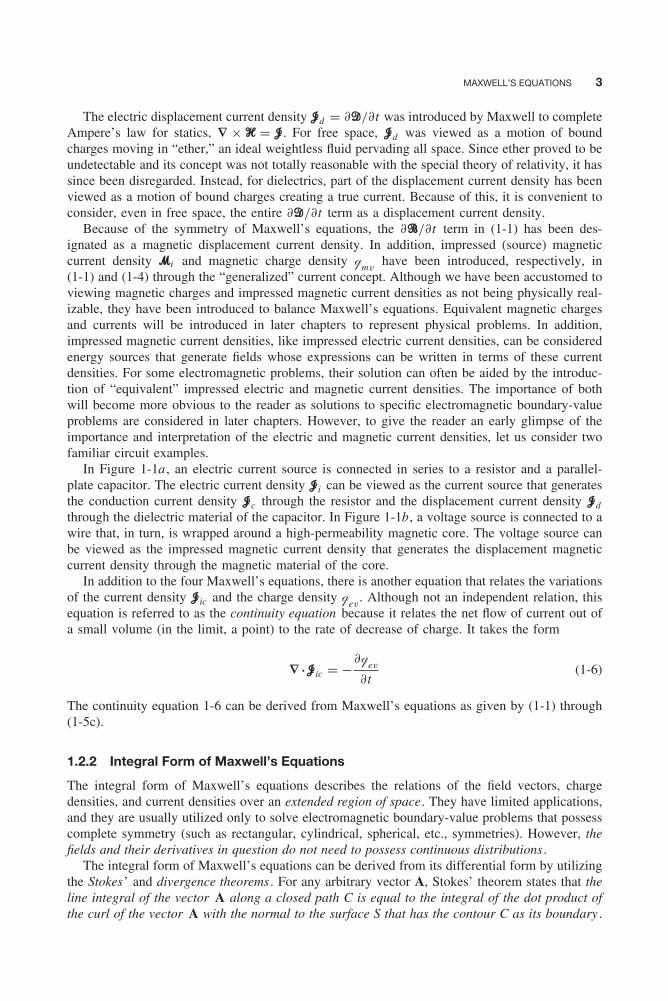
(1-1) and (1-4) through the “generalized” current concept. Although we have been accustomed toviewing magnetic charges and impressed magnetic current densities as not being physically real-izable, they have been introduced to balance Maxwell’s equations. Equivalent magnetic chargesand currents will be introduced in later chapters to represent physical problems. In addition,impressed magnetic current densities, like impressed electric current densities, can be consideredenergy sources that generate fields whose expressions can be written in terms of these currentdensities. For some electromagnetic problems, their solution can often be aided by the introduc-tion of “equivalent” impressed electric and magnetic current densities. The importance of bothwill become more obvious to the reader as solutions to specific electromagnetic boundary-valueproblems are considered in later chapters. However, to give the reader an early glimpse of theimportance and interpretation of the electric and magnetic current densities, let us consider twofamiliar circuit examples.
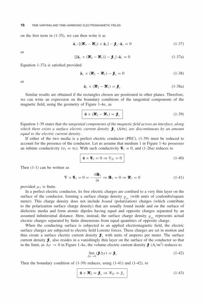
In Figure 1-1a , an electric current source is connected in series to a resistor and a parallel-plate capacitor. The electric current density �i can be viewed as the current source that generatesthe conduction current density �c through the resistor and the displacement current density �dthrough the dielectric material of the capacitor. In Figure 1-1b, a voltage source is connected to awire that, in turn, is wrapped around a high-permeability magnetic core. The voltage source canbe viewed as the impressed magnetic current density that generates the displacement magneticcurrent density through the magnetic material of the core.
In addition to the four Maxwell’s equations, there is another equation that relates the variationsof the current density �ic and the charge density q
ev. Although not an independent relation, this
equation is referred to as the continuity equation because it relates the net flow of current out ofa small volume (in the limit, a point) to the rate of decrease of charge. It takes the form
∇ • �ic = −∂qev
∂t(1-6)
The continuity equation 1-6 can be derived from Maxwell’s equations as given by (1-1) through(1-5c).
1.2.2 Integral Form of Maxwell’s Equations
The integral form of Maxwell’s equations describes the relations of the field vectors, chargedensities, and current densities over an extended region of space. They have limited applications,and they are usually utilized only to solve electromagnetic boundary-value problems that possesscomplete symmetry (such as rectangular, cylindrical, spherical, etc., symmetries). However, thefields and their derivatives in question do not need to possess continuous distributions .
The integral form of Maxwell’s equations can be derived from its differential form by utilizingthe Stokes’ and divergence theorems . For any arbitrary vector A, Stokes’ theorem states that theline integral of the vector A along a closed path C is equal to the integral of the dot product ofthe curl of the vector A with the normal to the surface S that has the contour C as its boundary .
Balanis c01.tex V3 - 11/22/2011 3:03 P.M. Page 4
4 TIME-VARYING AND TIME-HARMONIC ELECTROMAGNETIC FIELDS
Dielectricslab
(a)
(b)
�i
�c
�d
�i
�d
Figure 1-1 Circuits with electric and magnetic current densities. (a) Electric current density. (b) Magneticcurrent density.
In equation form, Stokes’ theorem can be written as∮C
A • d� =∫∫
S(∇ × A) • ds (1-7)
The divergence theorem states that, for any arbitrary vector A, the closed surface integral of thenormal component of vector A over a surface S is equal to the volume integral of the divergence ofA over the volume V enclosed by S . In mathematical form, the divergence theorem is stated as
#SA • ds =
∫∫∫V
∇ • A dv (1-8)
Taking the surface integral of both sides of (1-1), we can write∫∫S(∇ × �) • ds = −
∫∫S
�i • ds −∫∫
S
∂�
∂t• ds = −
∫∫S
�i • ds − ∂
∂t
∫∫S
�i • ds (1-9)
Applying Stokes’ theorem, as given by (1-7), on the left side of (1-9) reduces it to∮C
� • d� = −∫∫
S�i • ds − ∂
∂t
∫∫S
� • ds (1-9a)

Balanis c01.tex V3 - 11/22/2011 3:03 P.M. Page 5
CONSTITUTIVE PARAMETERS AND RELATIONS 5
which is referred to as Maxwell’s equation in integral form as derived from Faraday’s law . In theabsence of an impressed magnetic current density, Faraday’s law states that the electromotiveforce (emf) appearing at the open-circuited terminals of a loop is equal to the time rate of decreaseof magnetic flux linking the loop.
Using a similar procedure, we can show that the corresponding integral form of (1-2) can bewritten as ∮
C� • d� =
∫∫S
�ic • ds + ∂
∂t
∫∫S
� • ds =∫∫
S�ic • ds +
∫∫S
�d • ds (1-10)
which is usually referred to as Maxwell’s equation in integral form as derived from Ampere’s law.Ampere’s law states that the line integral of the magnetic field over a closed path is equal to thecurrent enclosed.
The other two Maxwell equations in integral form can be obtained from the correspondingdifferential forms, using the following procedure. First take the volume integral of both sides of(1-3); that is, ∫∫∫
V∇ • � dv =
∫∫∫V
qev
dv = �e (1-11)
where �e is the total electric charge. Applying the divergence theorem, as given by (1-8), on theleft side of (1-11) reduces it to
#S� • ds =
∫∫∫V
qev
dv = �e (1-11a)
which is usually referred to as Maxwell’s electric field equation in integral form as derived fromGauss’s law. Gauss’s law for the electric field states that the total electric flux through a closedsurface is equal to the total charge enclosed.
In a similar manner, the integral form of (1-4) is given in terms of the total magnetic charge�m by
#S� • ds = �m (1-12)
which is usually referred to as Maxwell’s magnetic field equation in integral form as derived fromGauss’s law . Even though magnetic charge does not exist in nature, it is used as an equivalentto represent physical problems. The corresponding integral form of the continuity equation, asgiven by (1-6) in differential form, can be written as
#S�ic • ds = − ∂
∂t
∫∫∫V
qev
dv = −∂�e
∂t(1-13)
Maxwell’s equations in differential and integral form are summarized and listed in Table 1-1.
1.3 CONSTITUTIVE PARAMETERS AND RELATIONS
Materials contain charged particles, and when these materials are subjected to electromagneticfields, their charged particles interact with the electromagnetic field vectors, producing currentsand modifying the electromagnetic wave propagation in these media compared to that in freespace. A more complete discussion of this is in Chapter 2. To account on a macroscopic scale forthe presence and behavior of these charged particles, without introducing them in a microscopiclattice structure, we give a set of three expressions relating the electromagnetic field vectors.These expressions are referred to as the constitutive relations , and they will be developed inmore detail in Chapter 2.
Balanis c01.tex V3 - 11/22/2011 3:03 P.M. Page 6
6 TIME-VARYING AND TIME-HARMONIC ELECTROMAGNETIC FIELDS
TABLE 1-1 Maxwell’s equations and the continuity equation in differential and integral forms fortime-varying fields
Differential form Integral form
∇ × � = −�i − ∂�∂t
∮C
� · d� = −∫∫
S�i · ds − ∂
∂t
∫∫S
� · ds
∇ × � = �i + �c + ∂�∂t
∮C
� · d� =∫∫
S�i · ds +
∫∫S
�c · ds + ∂
∂t
∫∫S
� · ds
∇ · � = qev #S
� · ds = �e
∇ · � = qmv #S
� · ds = �m
∇ · �ic = −∂qev
∂t #S�ic · ds = − ∂
∂t
∫∫∫V
qev
dv = −∂�e
∂t
One of the constitutive relations relates in the time domain the electric flux density � to theelectric field intensity � by
� = ε̂ ∗ � (1-14)
where ε̂ is the time-varying permittivity of the medium (farads/meter) and ∗ indicates convolution.For free space
ε̂ = ε0 = 8.854×10⁻¹² � 10−9
36π(farads/meter) (1-14a)
and (1-14) reduces to a product.Another relation equates in the time domain the magnetic flux density � to the magnetic field
intensity � by� = μ̂ ∗ � (1-15)
where μ̂ is the time-varying permeability of the medium (henries/meter). For free space
μ̂ = μ0 = 4π×10−7 (henries/meter) (1-15a)
and (1-15) reduces to a product.Finally, the conduction current density �c is related in the time domain to the electric field
intensity � by�c = σ̂ ∗ � (1-16)
where σ̂ is the time-varying conductivity of the medium (siemens/meter). For free space
σ̂ = 0 (1-16a)
In the frequency domain or for frequency nonvarying constitutive parameters, the relations (1-14),(1-15) and (1-16) reduce to products. For simplicity of notation, they will be indicated everywherefrom now on as products, and the caret ( )̂ in the time-varying constitutive parameters will beomitted.
Whereas (1-14), (1-15), and (1-16) are referred to as the constitutive relations , ε̂, μ̂ and σ̂ arereferred to as the constitutive parameters , which are, in general, functions of the applied fieldstrength, the position within the medium, the direction of the applied field, and the frequency ofoperation.
Balanis c01.tex V3 - 11/22/2011 3:03 P.M. Page 7
CIRCUIT-FIELD RELATIONS 7
The constitutive parameters are used to characterize the electrical properties of a material.In general, materials are characterized as dielectrics (insulators), magnetics , and conductors ,depending on whether polarization (electric displacement current density), magnetization (mag-netic displacement current density), or conduction (conduction current density) is the predominantphenomenon. Another class of material is made up of semiconductors , which bridge the gapbetween dielectrics and conductors where neither displacement nor conduction currents are, ingeneral, predominant. In addition, materials are classified as linear versus nonlinear, homoge-neous versus nonhomogeneous (inhomogeneous), isotropic versus nonisotropic (anisotropic), anddispersive versus nondispersive, according to their lattice structure and behavior. All these typesof materials will be discussed in detail in Chapter 2.
If all the constitutive parameters of a given medium are not functions of the applied fieldstrength, the material is known as linear ; otherwise it is nonlinear . Media whose constitu-tive parameters are not functions of position are known as homogeneous; otherwise they arereferred to as nonhomogeneous (inhomogeneous). Isotropic materials are those whose constitu-tive parameters are not functions of direction of the applied field; otherwise they are designatedas nonisotropic (anisotropic). Crystals are one form of anisotropic material. Material whose con-stitutive parameters are functions of frequency are referred to as dispersive; otherwise they areknown as nondispersive. All materials used in our everyday life exhibit some degree of disper-sion, although the variations for some may be negligible and for others significant. More detailsconcerning the development of the constitutive parameters can be found in Chapter 2.
1.4 CIRCUIT-FIELD RELATIONS
The differential and integral forms of Maxwell’s equations were presented, respectively, inSections 1.2.1 and 1.2.2. These relations are usually referred to as field equations , since thequantities appearing in them are all field quantities . Maxwell’s equations can also be written interms of what are usually referred to as circuit quantities; the corresponding forms are denotedcircuit equations . The circuit equations are introduced in circuit theory texts, and they are specialcases of the more general field equations.
1.4.1 Kirchhoff’s Voltage Law
According to Maxwell’s equation 1-9a, the left side represents the sum voltage drops (use theconvention where positive voltage begins at the start of the path) along a closed path C , whichcan be written as ∑
v =∮
C� • d� (volts) (1-17)
The right side of (1-9a) must also have the same units (volts) as its left side. Thus, in the absenceof impressed magnetic current densities (�i = 0), the right side of (1-9a) can be written as
− ∂
∂t
∫∫S
� • ds = −∂ψm
∂t= − ∂
∂t(Ls i ) = −Ls
∂i
∂t(webers/second = volts) (1-17a)
because by definition ψm = Ls i where Ls is an inductance (assumed to be constant) and i is theassociated current. Using (1-17) and (1-17a), we can write (1-9a) with �i = 0 as∑
v = −∂ψm
∂t= − ∂
∂t(Ls i ) = −Ls
∂i
∂t(1-17b)
Equation 1-17b states that the voltage drops along a closed path of a circuit are equal to the timerate of change of the magnetic flux passing through the surface enclosed by the closed path, or
Balanis c01.tex V3 - 11/22/2011 3:03 P.M. Page 8
8 TIME-VARYING AND TIME-HARMONIC ELECTROMAGNETIC FIELDS
equal to the voltage drop across an inductor Ls that is used to represent the stray inductance ofthe circuit. This is the well-known Kirchhoff loop voltage law , which is used widely in circuittheory, and its form represents a circuit relation. Thus we can write the following field and circuitrelations:
Field Relation Circuit Relation∮C
� • d� = − ∂
∂t
∫∫S
� • ds = −∂ψm
∂t⇔
∑v = −∂ψm
∂t= −Ls
∂i
∂t(1-17c)
In lumped-element circuit analysis, where usually the wavelength is very large (or the dimen-sions of the total circuit are small compared to the wavelength) and the stray inductance of thecircuit is very small, the right side of (1-17b) is very small and it is usually set equal to zero. Inthese cases, (1-17b) states that the voltage drops (or rises) along a closed path are equal to zero,and it represents a widely used relation to electrical engineers and many physicists.
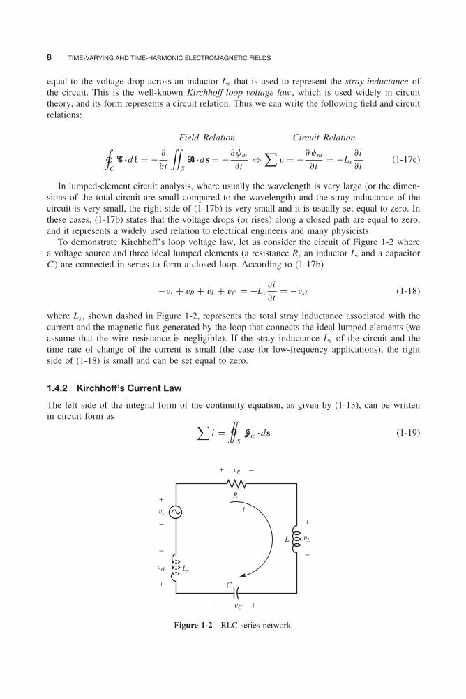
To demonstrate Kirchhoff’s loop voltage law, let us consider the circuit of Figure 1-2 wherea voltage source and three ideal lumped elements (a resistance R, an inductor L, and a capacitorC ) are connected in series to form a closed loop. According to (1-17b)
−vs + vR + vL + vC = −Ls∂i
∂t= −vsL (1-18)
where Ls , shown dashed in Figure 1-2, represents the total stray inductance associated with thecurrent and the magnetic flux generated by the loop that connects the ideal lumped elements (weassume that the wire resistance is negligible). If the stray inductance Ls of the circuit and thetime rate of change of the current is small (the case for low-frequency applications), the rightside of (1-18) is small and can be set equal to zero.
1.4.2 Kirchhoff’s Current Law
The left side of the integral form of the continuity equation, as given by (1-13), can be writtenin circuit form as ∑
i =#S�ic • ds (1-19)
i
R
vR
vL
vC
LsvsL
vs
L
C
− +
+
−
+
+
−
−
−
+
Figure 1-2 RLC series network.

Balanis c01.tex V3 - 11/22/2011 3:03 P.M. Page 9
CIRCUIT-FIELD RELATIONS 9
where∑
i represents the sum of the currents passing through closed surface S . Using (1-19)reduces (1-13) to ∑
i = −∂�e
∂t= − ∂
∂t(Csv) = −Cs
∂v
∂t(1-19a)
since by definition �e = Csv where Cs is a capacitance (assumed to be constant) and v is theassociated voltage.
Equation 1-19a states that the sum of the currents crossing a surface that encloses a circuitis equal to the time rate of change of the total electric charge enclosed by the surface, or equalto the current flowing through a capacitor Cs that is used to represent the stray capacitance ofthe circuit. This is the well-known Kirchhoff node current law, which is widely used in circuittheory, and its form represents a circuit relation. Thus, we can write the following field and circuitrelations:
Field Relation Circuit Relation
#S�ic • ds = − ∂
∂t
∫∫∫V
qev
dv = −∂�e
∂t⇔
∑i = −∂�e
∂t= −Cs
∂v
∂t(1-19b)
In lumped-element circuit analysis, where the stray capacitance associated with the circuit is verysmall, the right side of (1-19a) is very small and it is usually set equal to zero. In these cases,(1-19a) states that the currents exiting (or entering) a surface enclosing a circuit are equal to zero.This represents a widely used relation to electrical engineers and many physicists.
To demonstrate Kirchhoff’s node current law, let us consider the circuit of Figure 1-3 wherea current source and three ideal lumped elements (a resistance R, an inductor L, and a capacitorC ) are connected in parallel to form a node. According to (1-19a)
−is + iR + iL + iC = −Cs∂v
∂t= −isC (1-20)
where Cs , shown dashed in Figure 1-3, represents the total stray capacitance associated with thecircuit of Figure 1-3. If the stray capacitance Cs of the circuit and the time rate of change ofthe total charge �e are small (the case for low-frequency applications), the right side of (1-20) issmall and can be set equal to zero. The current isC associated with the stray capacitance Cs also
vCLCsis
is
iR isC
iL
iC
S
R
+
−
Figure 1-3 RLC parallel network.
Balanis c01.tex V3 - 11/22/2011 3:03 P.M. Page 10
10 TIME-VARYING AND TIME-HARMONIC ELECTROMAGNETIC FIELDS
includes the displacement (leakage) current crossing the closed surface S of Figure 1-3 outside ofthe wires .
1.4.3 Element Laws
In addition to Kirchhoff’s loop voltage and node current laws as given, respectively, by (1-17b)and (1-19a), there are a number of current element laws that are widely used in circuit theory.One of the most popular is Ohm’s law for a resistor (or a conductance G), which states that thevoltage drop vR across a resistor R is equal to the product of the resistor R and the current iRflowing through it (vR = RiR or iR = vR/R = GvR). Ohm’s law of circuit theory is a special caseof the constitutive relition given by (1-16). Thus
Field Relation Circuit Relation
�c = σ� ⇔ iR = 1
RvR = GvR
(1-21)
Another element law is associated with an inductor L and states that the voltage drop across aninductor is equal to the product of L and the time rate of change of the current through the inductor(vL = L diL/dt). Before proceeding to relate the inductor’s voltage drop to the corresponding fieldrelation, let us first define inductance. To do this we state that the magnetic flux ψm is equal to theproduct of the inductance L and the corresponding current i . That is ψm = Li . The correspondingfield equation of this relation is (1-15). Thus
Field Relation Circuit Relation� = μ� ⇔ ψm = LiL
(1-22)
Using (1-5c) and (1-15), we can write for a homogeneous and non-time-varying medium that
�d = ∂�
∂t= ∂
∂t(μ�) = μ
∂�
∂t(1-22a)
where �d is defined as the magnetic displacement current density [analogous to the electricdisplacement current density �d = ∂�/∂t = ∂(ε�)/∂t = ε∂�/∂t]. With the aid of the right sideof (1-9a) and the circuit relation of (1-22), we can write
∂
∂t
∫∫S
� • ds = ∂ψm
∂t= ∂
∂t(LiL) = L
∂iL∂t
= vL (1-22b)
Using (1-22a) and (1-22b), we can write the following relations:
Field Relation Circuit Relation
�d = μ∂�
∂t⇔ vL = L
∂iL∂t
(1-22c)
Using a similar procedure for a capacitor C , we can write the field and circuit relationsanalogous to (1-22) and (1-22c):
Field Relation Circuit Relation
� = ε� ⇔ �e = Cve (1-23)
�d = ε∂�
∂t⇔ iC = C
∂vC
∂t(1-24)
A summary of the field theory relations and their corresponding circuit concepts are listed inTable 1-2.

Balanis c01.tex V3 - 11/22/2011 3:03 P.M. Page 11
TA
BL
E1-
2R
elat
ions
betw
een
elec
trom
agne
tic
field
and
circ
uit
theo
ries
Fie
ldth
eory
Cir
cuit
theo
ry
1.�
(ele
ctri
cfie
ldin
tens
ity)
1.v
(vol
tage
)
2.�
(mag
netic
field
inte
nsity
)2.
i(c
urre
nt)
3.�
(ele
ctri
cflu
xde
nsity
)3.
q ev(e
lect
ric
char
gede
nsity
)
4.�
(mag
netic
flux
dens
ity)
4.q m
v(m
agne
ticch
arge
dens
ity)
5.�
(ele
ctri
ccu
rren
tde
nsity
)5.
i e(e
lect
ric
curr
ent)
6.�
(mag
netic
curr
ent
dens
ity)
6.i m
(mag
netic
curr
ent)
7.�
d=
ε∂� ∂t
(ele
ctri
cdi
spla
cem
ent
curr
ent
dens
ity)
7.i
=C
dv dt
(cur
rent
thro
ugh
aca
paci
tor)
8.�
d=
μ∂� ∂t
(mag
netic
disp
lace
men
tcu
rren
tde
nsity
)8.
v=
Ldi dt
(vol
tage
acro
ssan
indu
ctor
)
9.C
onst
itut
ive
rela
tion
s9.
Ele
men
tla
ws
(a)
�c
=σ
�(e
lect
ric
cond
uctio
ncu
rren
tde
nsity
)(a
)i
=G
v=
1 Rv
(Ohm
’sla
w)
(b)
�=
ε�
(die
lect
ric
mat
eria
l)(b
)�
e=
Cv
(cha
rge
ina
capa
cito
r)
(c)
�=
μ�
(mag
netic
mat
eria
l)(c
)ψ
=L
i(fl
uxof
anin
duct
or)
10.∮ C
�·d
�=
−∂ ∂t
∫∫ S�
·ds
(Max
wel
l–Fa
rada
yeq
uatio
n)10
.∑ v
=−L
s∂
i
∂t
�0
(Kir
chho
ff’s
volta
gela
w)
11.# S
�ic
·ds
=−
∂ ∂t
∫∫∫ Vq ev
dv
=−
∂�
e
∂t
11.∑ i
=−
∂�
e
∂t
=−C
s∂v
∂t
�0
(con
tinui
tyeq
uatio
n)(K
irch
hoff
’scu
rren
tla
w)
12.
Pow
eran
den
ergy
dens
itie
s12
.P
ower
and
ener
gy
(a)# S
(�×
�)·d
s(i
nsta
ntan
eous
pow
er)
(a)
�=
vi
(pow
er–
volta
ge–
curr
ent
rela
tion)
(b)∫∫∫ V
σ�
2dv
(dis
sipa
ted
pow
er)
(b)
�d
=G
v2
=1 R
v2
(pow
erdi
ssip
ated
ina
resi
stor
)
(c)
1 2
∫∫∫ Vε�
2dv
(ele
ctri
cst
ored
ener
gy)
(c)
1 2C
v2
(ene
rgy
stor
edin
aca
paci
tor)
(d)
1 2
∫∫∫ Vμ
�2dv
(mag
netic
stor
eden
ergy
)(d
)1 2
Li2
(ene
rgy
stor
edin
anin
duct
or)
11

Balanis c01.tex V3 - 11/22/2011 3:03 P.M. Page 12
12 TIME-VARYING AND TIME-HARMONIC ELECTROMAGNETIC FIELDS
1.5 BOUNDARY CONDITIONS
As previously stated, the differential form of Maxwell’s equations are used to solve for the fieldvectors provided the field quantities are single-valued, bounded, and possess (along with theirderivatives) continuous distributions. Along boundaries where the media involved exhibit discon-tinuities in electrical properties (or there exist sources along these boundaries), the field vectorsare also discontinuous and their behavior across the boundaries is governed by the boundaryconditions .
Maxwell’s equations in differential form represent derivatives, with respect to the space coor-dinates, of the field vectors. At points of discontinuity in the field vectors, the derivatives of thefield vectors have no meaning and cannot be properly used to define the behavior of the fieldvectors across these boundaries. Instead, the behavior of the field vectors across discontinuousboundaries must be handled by examining the field vectors themselves and not their derivatives.The dependence of the field vectors on the electrical properties of the media along boundaries ofdiscontinuity is manifested in our everyday life. It has been observed that cell phone, radio, ortelevision reception deteriorates or even ceases as we move from outside to inside an enclosure(such as a tunnel or a well-shielded building). The reduction or loss of the signal is governednot only by the attenuation as the signal/wave travels through the medium, but also by its behav-ior across the discontinuous interfaces. Maxwell’s equations in integral form provide the mostconvenient formulation for derivation of the boundary conditions.
1.5.1 Finite Conductivity Media
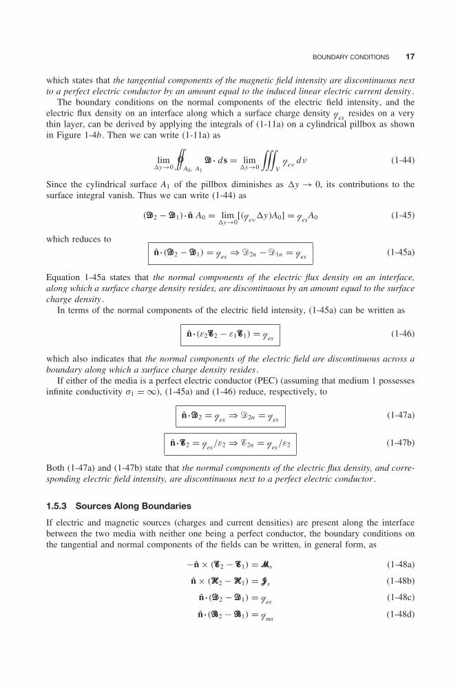
Initially, let us consider an interface between two media, as shown in Figure 1-4a , along whichthere are no charges or sources. These conditions are satisfied provided that neither of the twomedia is a perfect conductor or that actual sources are not placed there. Media 1 and 2 arecharacterized, respectively, by the constitutive parameters ε1, μ1, σ1 and ε2, μ2, σ2.
At a given point along the interface, let us choose a rectangular box whose boundary is denotedby C0 and its area by S0. The x, y, z coordinate system is chosen to represent the local geometryof the rectangle. Applying Maxwell’s equation 1-9a, with �i = 0, on the rectangle along C0 andon S0, we have ∮
C0
� • d� = − ∂
∂t
∫∫S0
� • ds (1-25)
As the height y of the rectangle becomes progressively shorter, the area S0 also becomesvanishingly smaller so that the contributions of the surface integral in (1-25) are negligible. Inaddition, the contributions of the line integral in (1-25) along y are also minimal, so that in thelimit (y → 0), (1-25) reduces to
�1 • âxx − �2 • âxx = 0
�1t − �2t = 0 ⇒ �1t = �2t (1-26)
or
n̂ × (�2 − �1) = 0 σ1, σ2 are finite (1-26a)
In (1-26), �1t and �2t represent, respectively, the tangential components of the electric field inmedia 1 and 2 along the interface. Both (1-26) and (1-26a) state that the tangential componentsof the electric field across an interface between two media, with no impressed magnetic currentdensities along the boundary of the interface, are continuous .
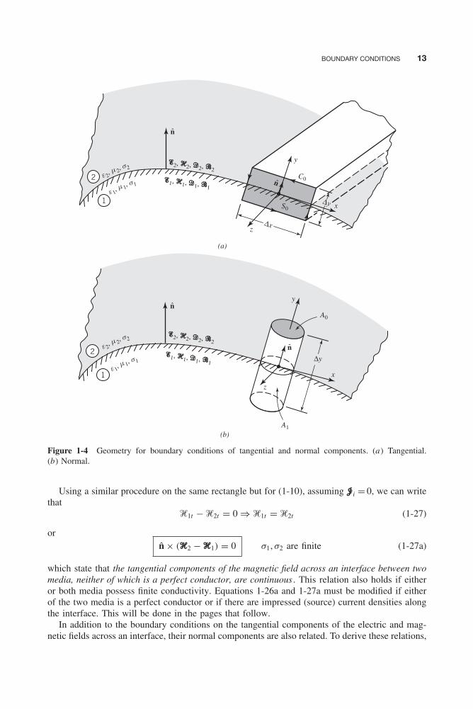
Balanis c01.tex V3 - 11/22/2011 3:03 P.M. Page 13
BOUNDARY CONDITIONS 13
e 2,m2, s2
e 1,m1, s1
e 2,m2, s2
e 1,m1, s1
(a)
(b)
z
x
y
Δy
zΔx
Δy x
y
C0
A0
A1
S0
1
1
2
2
n
n
n
n
�2, �2, �2, �2
�1, �1, �1, �1
�2, �2, �2, �2
�1, �1, �1, �1
Figure 1-4 Geometry for boundary conditions of tangential and normal components. (a) Tangential.(b) Normal.
Using a similar procedure on the same rectangle but for (1-10), assuming �i = 0, we can writethat
�1t − �2t = 0 ⇒ �1t = �2t (1-27)
orn̂ × (�2 − �1) = 0 σ1, σ2 are finite (1-27a)
which state that the tangential components of the magnetic field across an interface between twomedia, neither of which is a perfect conductor, are continuous . This relation also holds if eitheror both media possess finite conductivity. Equations 1-26a and 1-27a must be modified if eitherof the two media is a perfect conductor or if there are impressed (source) current densities alongthe interface. This will be done in the pages that follow.
In addition to the boundary conditions on the tangential components of the electric and mag-netic fields across an interface, their normal components are also related. To derive these relations,
Balanis c01.tex V3 - 11/22/2011 3:03 P.M. Page 14
14 TIME-VARYING AND TIME-HARMONIC ELECTROMAGNETIC FIELDS
let us consider the geometry of Figure 1-4b where a cylindrical pillbox is chosen at a given pointalong the interface. If there are no charges along the interface, which is the case when there areno sources or either of the two media is not a perfect conductor, (1-11a) reduces to
#A0,A1
� • ds = 0 (1-28)
As the height y of the pillbox becomes progressively shorter, the total circumferential area A1
also becomes vanishingly smaller, so that the contributions to the surface integral of (1-28) byA1 are negligible. Thus (1-28) can be written, in the limit (y → 0), as
�2 • ây A0 − �1 • ây A0 = 0
�2n − �in = 0 ⇒ �2n = �1n (1-29)
orn̂ • (�2 − �1) = 0 σ1, σ2 are finite (1-29a)
In (1-29), �1n and �2n represent, respectively, the normal components of the electric flux densityin media 1 and 2 along the interface. Both (1-29) and (1-29a) state that the normal componentsof the electric flux density across an interface between two media, both of which are imperfectelectric conductors and where there are no sources, are continuous . This relation also holds ifeither or both media possess finite conductivity. Equation 1-29a must be modified if either of themedia is a perfect conductor or if there are sources along the interface. This will be done in thepages that follow.
In terms of the electric field intensities, (1-29) and (1-29a) can be written as
ε2�2n = ε1�1n ⇒ �2n = ε1
ε2�1n ⇒ �1n = ε2
ε1�2n (1-30)
n̂ • (ε2�2 − ε1�1) = 0 σ1, σ2 are finite (1-30a)
which state that the normal components of the electric field intensity across an interface arediscontinuous .
Using a similar procedure on the same pillbox, but for (1-12) with no charges along theinterface, we can write that
�2n − �1n = 0 ⇒ �2n = �1n (1-31)
n̂ • (�2 − �1) = 0 (1-31a)
which state that the normal components of the magnetic flux density, across an interface betweentwo media where there are no sources, are continuous . In terms of the magnetic field intensities,(1-31) and (1-31a) can be written as
μ2�2n = μ1�1n ⇒ �2n = μ1
μ2�1n ⇒ �1n = μ2
μ1�2n (1-32)
n̂ • (μ2�2 − μ1�1) = 0 (1-32a)
which state that the normal components of the magnetic field intensity across an interface arediscontinuous .

Balanis c01.tex V3 - 11/22/2011 3:03 P.M. Page 15
BOUNDARY CONDITIONS 15
1.5.2 Infinite Conductivity Media
If actual electric sources and charges exist along the interface between the two media, or if eitherof the two media forming the interface displayed in Figure 1-4 is a perfect electric conductor(PEC), the boundary conditions on the tangential components of the magnetic field [stated by(1-27a)] and on the normal components of the electric flux density or normal components ofthe electric field intensity [stated by (1-29a) or (1-30a)] must be modified to include the sourcesand charges or the induced linear electric current density (�s) and surface electric charge density(q
es). Similar modifications must be made to (1-26a), (1-31a), and (1-32a) if magnetic sources
and charges exist along the interface between the two media, or if either of the two media is aperfect magnetic conductor (PMC).
To derive the appropriate boundary conditions for such cases, let us refer first to Figure 1-4a and assume that on a very thin layer along the interface there exists an electric surfacecharge density q
es(C/m2) and linear electric current density �s (A/m). Applying (1-10) along the
rectangle of Figure 1-4a , we can write that∮C0
� • d� =∫∫
S0
�ic • ds + ∂
∂t
∫∫S0
� • ds (1-33)
In the limit as the height of the rectangle is shrinking, the left side of (1-33) reduces to
limy→0
∮C0
� • d� = (�1 − �2) • âxx (1-33a)
Since the electric current density �ic is confined on a very thin layer along the interface, the firstterm on the right side of (1-33) can be written as
limy→0
∫∫S0
�ic • ds
= limy→0
[�ic • âz xy] = limy→0
[(�icy) • âz x ] = �s • âz x (1-33b)
Since S0 becomes vanishingly smaller as y → 0, the last term on the right side of (1-33) reducesto
limy→0
∂
∂t
∫∫S0
� • ds = limy→0
∂
∂t
∫∫S0
� • âz ds = 0 (1-33c)
Substituting (1-33a) through (1-33c) into (1-33), we can write it as
(�1 − �2) • âxx = �s • âz x
or(�1 − �2) • âx − �s • âz = 0 (1-33d)
Sinceâx = ây × âz (1-34)
(1-33d) can be written as(�1 − �2) • (ây × âz ) − �s • âz = 0 (1-35)
Using the vector identityA • B × C = C • A × B (1-36)
Balanis c01.tex V3 - 11/22/2011 3:03 P.M. Page 16
16 TIME-VARYING AND TIME-HARMONIC ELECTROMAGNETIC FIELDS
on the first term in (1-35), we can then write it as
âz • [(�1 − �2) × ây ] − �s • âz = 0 (1-37)
or{[ây × (�2 − �1)] − �s} • âz = 0 (1-37a)
Equation 1-37a is satisfied provided
ây × (�2 − �1) − �s = 0 (1-38)
orây × (�2 − �1) = �s (1-38a)
Similar results are obtained if the rectangles chosen are positioned in other planes. Therefore,we can write an expression on the boundary conditions of the tangential components of themagnetic field, using the geometry of Figure 1-4a , as
n̂ × (�2 − �1) = �s (1-39)
Equation 1-39 states that the tangential components of the magnetic field across an interface, alongwhich there exists a surface electric current density �s (A/m), are discontinuous by an amountequal to the electric current density .
If either of the two media is a perfect electric conductor (PEC), (1-39) must be reduced toaccount for the presence of the conductor. Let us assume that medium 1 in Figure 1-4a possessesan infinite conductivity (σ1 = ∞). With such conductivity �1 = 0, and (1-26a) reduces to
n̂ × �2 = 0 ⇒ �2t = 0 (1-40)
Then (1-1) can be written as
∇ × �1 = 0 = −∂�1
∂t⇒ �1 = 0 ⇒ �1 = 0 (1-41)
provided μ1 is finite.In a perfect electric conductor, its free electric charges are confined to a very thin layer on the
surface of the conductor, forming a surface charge density qes
(with units of coulombs/squaremeter). This charge density does not include bound (polarization) charges (which contributeto the polarization surface charge density) that are usually found inside and on the surface ofdielectric media and form atomic dipoles having equal and opposite charges separated by anassumed infinitesimal distance. Here, instead, the surface charge density q
esrepresents actual
electric charges separated by finite dimensions from equal quantities of opposite charge.When the conducting surface is subjected to an applied electromagnetic field, the electric
surface charges are subjected to electric field Lorentz forces. These charges are set in motion andthus create a surface electric current density �s with units of amperes per meter. The surfacecurrent density �s also resides in a vanishingly thin layer on the surface of the conductor so thatin the limit, as y → 0 in Figure 1-4a , the volume electric current density � (A/m2) reduces to
limy→0
(�y) = �s (1-42)
Then the boundary condition of (1-39) reduces, using (1-41) and (1-42), to
n̂ × �2 = �s ⇒ �2t = �s (1-43)
Balanis c01.tex V3 - 11/22/2011 3:03 P.M. Page 17
BOUNDARY CONDITIONS 17
which states that the tangential components of the magnetic field intensity are discontinuous nextto a perfect electric conductor by an amount equal to the induced linear electric current density .
The boundary conditions on the normal components of the electric field intensity, and theelectric flux density on an interface along which a surface charge density q
esresides on a very
thin layer, can be derived by applying the integrals of (1-11a) on a cylindrical pillbox as shownin Figure 1-4b. Then we can write (1-11a) as
limy→0#A0, A1
� • ds = limy→0
∫∫∫V
qeν
dν (1-44)
Since the cylindrical surface A1 of the pillbox diminishes as y → 0, its contributions to thesurface integral vanish. Thus we can write (1-44) as
(�2 − �1) • n̂ A0 = limy→0
[(qeν
y)A0] = qes
A0 (1-45)
which reduces to
n̂ • (�2 − �1) = qes
⇒ �2n − �1n = qes
(1-45a)
Equation 1-45a states that the normal components of the electric flux density on an interface,along which a surface charge density resides, are discontinuous by an amount equal to the surfacecharge density .
In terms of the normal components of the electric field intensity, (1-45a) can be written as
n̂ • (ε2�2 − ε1�1) = qes
(1-46)
which also indicates that the normal components of the electric field are discontinuous across aboundary along which a surface charge density resides .
If either of the media is a perfect electric conductor (PEC) (assuming that medium 1 possessesinfinite conductivity σ1 = ∞), (1-45a) and (1-46) reduce, respectively, to
n̂ • �2 = qes
⇒ �2n = qes
(1-47a)
n̂ • �2 = qes
/ε2 ⇒ �2n = qes
/ε2 (1-47b)
Both (1-47a) and (1-47b) state that the normal components of the electric flux density, and corre-sponding electric field intensity, are discontinuous next to a perfect electric conductor .
1.5.3 Sources Along Boundaries
If electric and magnetic sources (charges and current densities) are present along the interfacebetween the two media with neither one being a perfect conductor, the boundary conditions onthe tangential and normal components of the fields can be written, in general form, as
−n̂ × (�2 − �1) = �s (1-48a)
n̂ × (�2 − �1) = �s (1-48b)
n̂ • (�2 − �1) = qes
(1-48c)
n̂ • (�2 − �1) = qms
(1-48d)
Balanis c01.tex V3 - 11/22/2011 3:03 P.M. Page 18
18 TIME-VARYING AND TIME-HARMONIC ELECTROMAGNETIC FIELDS
TABLE 1-3 Boundary conditions on instantaneous electromagnetic fields
Finiteconductivity media, Medium 1 of Medium 1 of
no sources or infinite electric infinitecharges conductivity magnetic
σ1, σ2 �= ∞ (�1 = �1 = 0) conductivity�s = 0; q
es= 0 σ1 = ∞; σ2 �= ∞ (�1 = �1 = 0)
General �s = 0; qms
= 0 �s = 0; qms
= 0 �s = 0; qes
= 0
Tangentialelectric fieldintensity
−n̂ × (�2 − �1) = �s n̂ × (�2 − �1) = 0 n̂ × �2 = 0 −n̂ × �2 = �s
Tangentialmagnetic fieldintensity
n̂ × (�2 − �1) = �s n̂ × (�2 − �1) = 0 n̂ × �2 = �s n̂ × �2 = 0
Normal electricflux density
n̂ · (�2 − �1) = qes
n̂ · (�2 − �1) = 0 n̂ · �2 = qes
n̂ · �2 = 0
Normal magneticflux density
n̂ · (�2 − �1) = qms
n̂ · (�2 − �1) = 0 n̂ · �2 = 0 n̂ · �2 = qms
where (�s , �s ) and (qms
, qes
) are the magnetic and electric linear (per meter) current and surface(per square meter) charge densities, respectively. The derivation of (1-48a) and (1-48d) proceedsalong the same lines, respectively, as the derivation of (1-48b) and (1-48c) in Section 1.5.2, butbegins with (1-9a) and (1-12).
A summary of the boundary conditions on all the field components is found in Table 1-3,which also includes the boundary conditions assuming that medium 1 is a perfect magneticconductor (PMC). In general, a magnetic conductor is defined as a material inside of which bothtime-varying electric and magnetic fields vanish when it is subjected to an electromagnetic field.The tangential components of the magnetic field also vanish next to its surface. In addition, themagnetic charge moves to the surface of the material and creates a magnetic current density thatresides on a very thin layer at the surface. Although such materials do not physically exist, theyare often used in electromagnetics to develop electrical equivalents that yield the same answersas the actual physical problems. PMCs can be synthesized approximately over a limited frequencyrange (band-gap); see Section 8.8 .
1.6 POWER AND ENERGY
In a wireless communication system, electromagnetic fields are used to transport information overlong distances. To accomplish this, energy must be associated with electromagnetic fields. Thistransport of energy is accomplished even in the absence of any intervening medium.
To derive the equations that indicate that energy (and forms of it) is associated with electro-magnetic waves, let us consider a region V characterized by ε, μ, σ and enclosed by the surface S ,as shown in Figure 1-5. Within that region there exist electric and magnetic sources represented,respectively, by the electric and magnetic current densities �i and �i . The fields generated by�i and �i that exist within S are represented by �, �. These fields obey Maxwell’s equations,and we can write using (1-1) and (1-2) that
∇ × � = −�i − ∂�
∂t= −�i − μ
∂�
∂t= −�i − �d (1-49a)
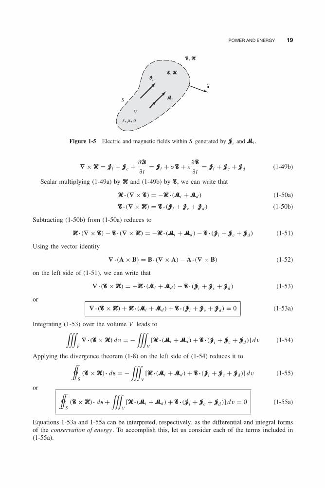
Balanis c01.tex V3 - 11/22/2011 3:03 P.M. Page 19
POWER AND ENERGY 19
S
V
e, m, s
n
�, �
�, ��i
�i
Figure 1-5 Electric and magnetic fields within S generated by �i and �i .
∇ × � = �i + �c + ∂�
∂t= �i + σ� + ε
∂�
∂t= �i + �c + �d (1-49b)
Scalar multiplying (1-49a) by � and (1-49b) by �, we can write that
� • (∇ × �) = −� • (�i + �d ) (1-50a)
� • (∇ × �) = � • (�i + �c + �d ) (1-50b)
Subtracting (1-50b) from (1-50a) reduces to
� • (∇ × �) − � • (∇ × �) = −� • (�i + �d ) − � • (�i + �c + �d ) (1-51)
Using the vector identity
∇ • (A × B) = B • (∇ × A) − A • (∇ × B) (1-52)
on the left side of (1-51), we can write that
∇ • (� × �) = −� • (�i + �d ) − � • (�i + �c + �d ) (1-53)
or∇ • (� × �) + � • (�i + �d ) + � • (�i + �c + �d ) = 0 (1-53a)
Integrating (1-53) over the volume V leads to∫∫∫V
∇ • (� × �) dv = −∫∫∫
V[� • (�i + �d ) + � • (�i + �c + �d )] dv (1-54)
Applying the divergence theorem (1-8) on the left side of (1-54) reduces it to
#S(� × �) • ds = −
∫∫∫V
[� • (�i + �d ) + � • (�i + �c + �d )] dv (1-55)
or
#S(� × �) • ds +
∫∫∫V
[� • (�i + �d ) + � • (�i + �c + �d )] dv = 0 (1-55a)
Equations 1-53a and 1-55a can be interpreted, respectively, as the differential and integral formsof the conservation of energy . To accomplish this, let us consider each of the terms included in(1-55a).
Balanis c01.tex V3 - 11/22/2011 3:03 P.M. Page 20
20 TIME-VARYING AND TIME-HARMONIC ELECTROMAGNETIC FIELDS
The integrand, in the first term of (1-55a), has the form
= � × � (1-56)
where is known as the Poynting vector. It has the units of power density (watts/square meter),since � has units of volts/meter and � has units of ampere/meter, so that the units of arevolts · ampere/meter2 = watts/meter2. Thus the first term of (1-55a), written as
�e =#S(� × �) • ds =#S
• ds (1-57)
represents the total power �e exiting the volume V bounded by the surface S .The other terms in (1-55a), which represent the integrand of the volume integral, can be written
as
ps = −(� • �i + � • �i ) (1-58a)
� • �d = � •∂�
∂t= μ� •
∂�
∂t= 1
2μ
∂�2
∂t= ∂
∂t
(1
2μ�2
)= ∂
∂twm (1-58b)
pd = � • �c = � • (σ�) = σ�2 (1-58c)
� • �d = � •∂�
∂t= ε� •
∂�
∂t= 1
2ε∂�2
∂t= ∂
∂t
(1
2ε�2
)= ∂
∂twe (1-58d)
where
wm = 1
2μ�2 = magnetic energy density(J/m3) (1-58e)
we = 1
2ε�2 = electric energy density(J/m3) (1-58f)
ps = −(� • �i + � • �i ) = supplied power density(W/m3) (1-58g)
pd = σ�2 = dissipated power density(W/m3) (1-58h)
Integrating each of the terms in (1-58a) through (1-58d), we can write the corresponding formsas
�s = −∫∫∫
V(� • �i + � • �i ) dv =
∫∫∫V
ps dv (1-59a)∫∫∫V(� • �d ) dv = ∂
∂t
∫∫∫V
1
2μ�2 dv = ∂
∂t
∫∫∫V
wm dv = ∂
∂tm (1-59b)
�d =∫∫∫
V(� • �c) dv =
∫∫∫V
σ�2 dv =∫∫∫
Vpd dv (1-59c)∫∫∫
V(� • �d ) dv = ∂
∂t
∫∫∫V
1
2ε�2 dv = ∂
∂t
∫∫∫V
we dv = ∂
∂te (1-59d)
Balanis c01.tex V3 - 11/22/2011 3:03 P.M. Page 21
TIME-HARMONIC ELECTROMAGNETIC FIELDS 21
where m = magnetic energy (J)e = electric energy (J)�s = supplied power (W)�e = exiting power (W)�d = dissipated power (W)
Using (1-57) and (1-59a) through (1-59d), we can write (1-55a) as
�e − �s + �d + ∂
∂t(e + m) = 0 (1-60)
or�s = �e + �d + ∂
∂t(e + m) (1-60a)
which is the conservation of power law . This law states that within a volume V , bounded by S ,the supplied power �s is equal to the power �e exiting S plus the power �d dissipated withinthat volume plus the rate of change (increase if positive) of the electric (e) and magnetic (m)
energies stored within that same volume.A summary of the field theory relations and their corresponding circuit concepts is found listed
in Table 1-2.
1.7 TIME-HARMONIC ELECTROMAGNETIC FIELDS
Maxwell’s equations in differential and integral forms, for general time-varying electromagneticfields, were presented in Sections 1.2.1 and 1.2.2. In addition, various expressions involvingand relating the electromagnetic fields (such as the constitutive parameters and relations, circuitrelations, boundary conditions, and power and energy) were also introduced in the precedingsections. However, in many practical systems involving electromagnetic waves, the time variationsare of cosinusoidal form and are referred to as time-harmonic. In general, such time variationscan be represented by1 ejωt , and the instantaneous electromagnetic field vectors can be related totheir complex forms in a very simple manner. Thus for time-harmonic fields, we can relate theinstantaneous fields, current density and charge (represented by script letters) to their complexforms (represented by roman letters) by
�(x , y , z ; t) = Re[E(x , y , z )ejωt ] (1-61a)
�(x , y , z ; t) = Re[H(x , y , z )ejωt ] (1-61b)
�(x , y , z ; t) = Re[D(x , y , z )ejωt ] (1-61c)
�(x , y , z ; t) = Re[B(x , y , z )ejωt ] (1-61d)
�(x , y , z ; t) = Re[J(x , y , z )ejωt ] (1-61e)
q(x , y , z ; t) = Re[q(x , y , z )ejωt ] (1-61f)
where �, �, �, �, �, and q represent the instantaneous field vectors, current density and charge,while E, H, D, B, J, and q represent the corresponding complex spatial forms which are onlya function of position. In this book we have chosen to represent the instantaneous quantities bythe real part of the product of the corresponding complex spatial quantities with ejωt . Another
1 Another representation form of time-harmonic variations is e−jωt (most scientists prefer eiωt or e−iωt where i = √−1).Throughout this book, we will use the ejωt form, which when it is not stated will be assumed. The e−jωt fields are relatedto those of the ejωt form by the complex conjugate.
Balanis c01.tex V3 - 11/22/2011 3:03 P.M. Page 22
22 TIME-VARYING AND TIME-HARMONIC ELECTROMAGNETIC FIELDS
option would be to represent the instantaneous quantities by the imaginary part of the products.It should be stated that throughout this book the magnitudes of the instantaneous fields representpeak values that are related to their corresponding root-mean-square (rms) values by the squareroot of 2 (peak = √
2 rms). If the complex spatial quantities can be found, it is then a very simpleprocedure to find their corresponding instantaneous forms by using (1-61a) through (1-61f). Inwhat follows, it will be shown that Maxwell’s equations in differential and integral forms fortime-harmonic electromagnetic fields can be written in much simpler forms using the complexfield vectors.
1.7.1 Maxwell’s Equations in Differential and Integral Forms
It is a very simple exercise to show that, by substituting (1-61a) through (1-61f) into (1-1) through(1-4) and (1-6), Maxwell’s equations and the continuity equation in differential form for time-harmonic fields can be written in terms of the complex field vectors as shown in Table 1-4. Usinga similar procedure, we can write the corresponding integral forms of Maxwell’s equations andthe continuity equation listed in Table 1-1 in terms of the complex spatial field vectors as shownin Table 1-4. Both of these derivations have been assigned as exercises to the reader at the endof the chapter.
By examining the two forms in Table 1-4, we see that one form can be obtained from theother by doing the following:
1. Replace the instantaneous field vectors by the corresponding complex spatial forms, or viceversa.
2. Replace ∂/∂t by jω(∂/∂t = jω), or vice versa.
The second step is very similar to that followed in circuit analysis when Laplace transforms areused to analyze RLC a.c. circuits. In these analyses ∂/∂t is replaced by s (∂/∂t ≡ s). For steady-state conditions ∂/∂t is replaced by jω(∂/∂t ≡ s ≡ jω). The reason for using Laplace transformsis to transform differential equations to algebraic equations, which are simpler to solve. The sameintent is used here to write Maxwell’s equations in forms that are easier to solve. Thus, if it isdesired to solve for the instantaneous field vectors of time-harmonic fields, it is easier to usethe following two-step procedure, instead of attempting to do it in one step using the generalinstantaneous forms of Maxwell’s equations:
1. Solve for the complex spatial field vectors, current densities and charges (E, H, D, B, J,M, q), using Maxwell’s equations from Table 1-4 that are written in terms of the complexspatial field vectors, current densities and charges.
2. Determine the corresponding instantaneous field vectors, current densities and charges using(1-61a) through (1-61f).
Step 1 is obviously the most difficult, and it is often the only step needed. Step 2 is straight-forward, and it is often omitted. In practice, the time variations of ejωt are stated at the outset,but then are suppressed.
1.7.2 Boundary Conditions
The boundary conditions for time-harmonic fields are identical to those of general time-varyingfields, as derived in Section 1.5, and they can be expressed simply by replacing the instantaneousfield vectors, current densities and charges in Table 1-3 with their corresponding complex spatialfield vectors, current densities and charges. A summary of all the boundary conditions for time-harmonic fields, referring to Figure 1-4, is found in Table 1-5.
In addition to the boundary conditions found in Table 1-5, an additional boundary conditionon the tangential components of the electric field is often used along an interface when one of
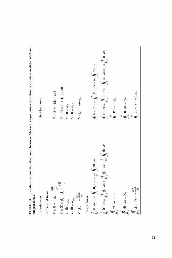
Balanis c01.tex V3 - 11/22/2011 3:03 P.M. Page 23
TA
BL
E1-
4In
stan
tane
ous
and
tim
e-ha
rmon
icfo
rms
ofM
axw
ell’
seq
uati
ons
and
cont
inui
tyeq
uati
onin
diff
eren
tial
and
inte
gral
form
s
Inst
anta
neou
sT
ime
harm
onic
Dif
fere
ntia
lfo
rm
∇×
�=
−�i−
∂� ∂t
∇×
E=
−Mi−
jωB
∇×
�=
�i+
�c+
∂� ∂t
∇×
H=
J i+
J c+
jωD
∇·�
=q ev
∇·D
=q e
v
∇·�
=q m
v∇
·B=
q mv
∇·�
ic=
−∂q ev
∂t
∇·J
ic=
−jω
q ev
Inte
gral
form
∮ C�
·d�
=−
∫∫ S�
i·d
s−
∂ ∂t
∫∫ S�
·ds
∮ CE
·d�
=−
∫∫ SM
i·d
s−
jω∫∫ S
B·d
s
∮ C�
·d�
=∫∫ S
�i·d
s+
∫∫ S�
c·d
s+
∂ ∂t
∫∫ S�
·ds
∮ CH
·d�
=∫∫ S
J i·d
s+
∫∫ SJ c
·ds+
jω∫∫ S
D·d
s
# S�
·ds=
�e
# SD
·ds
=Q
e
# S�
·ds
=�
m# S
B·d
s=
Qm
# S�
ic·d
s=
−∂�
e
∂t
# SJ i
c·d
s=
−jω
Qe
23

Balanis c01.tex V3 - 11/22/2011 3:03 P.M. Page 24
24 TIME-VARYING AND TIME-HARMONIC ELECTROMAGNETIC FIELDS
TABLE 1-5 Boundary conditions on time-harmonic electromagnetic fields
Finiteconductivity media, Medium 1 of Medium 1 of
no sources or infinite electric infinitecharges conductivity magnetic
σ1, σ2 �= ∞ (E1 = H1 = 0) conductivityJs = Ms = 0 σ1 = ∞; σ2 �= ∞ (E1 = H1 = 0)
General qes = qms = 0 Ms = 0; qms = 0 Js = 0; qes = 0
Tangentialelectric fieldintensity
−n̂ × (E2 − E1) = Ms n̂ × (E2 − E1) = 0 n̂ × E2 = 0 −n̂ × E2 = Ms
Tangentialmagnetic fieldintensity
n̂ × (H2 − H1) = Js n̂ × (H2 − H1) = 0 n̂ × H2 = Js n̂ × H2 = 0
Normal electricflux density
n̂ · (D2 − D1) = qes n̂ · (D2 − D1) = 0 n̂ · D2 = qes n̂ · D2 = 0
Normal magneticflux density
n̂ · (B2 − B1) = qms n̂ · (B2 − B1) = 0 n̂ · B2 = 0 n̂ · B2 = qms
the two media is a very good conductor (material that possesses large but finite conductivity).This is illustrated in Figure 1-6 where it is assumed that medium 1 is a very good conductorwhose surface, as will be shown in Section 4.3.1, exhibits a surface impedance Zs (ohms) given,approximately, by (4-42) or
Zs = Rs + jXs = (1 + j )
√ωμ1
2σ1(1-62)
with equal real and imaginary (inductive) parts (σ1 is the conductivity of the conductor). At thesurface there exists a linear current density Js (A/m) related to the tangential magnetic field inmedium 2 by
Js � n̂ × H2 (1-63)
Since the conductivity is finite (although large), the most intense current density resides at thesurface, and it diminishes (in an exponential form) as the observations are made deeper into theconductor. This is demonstrated in Example 5.7 of Section 5.4.1. In addition, the electric fieldintensity along the interface cannot be zero (although it may be small). Thus, we can write that
E2, H
2, D2, B
2E
1, H1, D
1, B1
e 2,m2, s2
e 1,m1, s1
1
2
y
xZs = Rs + jXs
large)(s1
z
n
Figure 1-6 Surface impedance along the surface of a very good conductor.
Balanis c01.tex V3 - 11/22/2011 3:03 P.M. Page 25
TIME-HARMONIC ELECTROMAGNETIC FIELDS 25
the tangential component of the electric field in medium 2, along the interface, is related to theelectric current density Js and tangential component of the magnetic field by
Et2 = ZsJs = Zs n̂ × H2 = n̂ × H2
√ωμ1
2σ1(1 + j ) (1-64)
For time-harmonic fields, the boundary conditions on the normal components are not inde-pendent of those on the tangential components, and vice-versa, since they are related throughMaxwell’s equations. In fact, if the tangential components of the electric and magnetic fields sat-isfy the boundary conditions, then the normal components of the same fields necessarily satisfythe appropriate boundary conditions. For example, if the tangential components of the electricfield are continuous across a boundary, their derivatives (with respect to the coordinates on theboundary surface) are also continuous. This, in turn, ensures continuity of the normal componentof the magnetic field.
To demonstrate that, let us refer to the geometry of Figure 1-6 where the local surface alongthe interface is described by the x, z coordinates with y being normal to the surface. Let usassume that Ex and Ez are continuous, which ensures that their derivatives with respect to x andz (∂Ex/∂x , ∂Ex/∂z , ∂Ez /∂x , ∂Ez /∂z ) are also continuous. Therefore, according to Maxwell’s curlequation of the electric field
∇ × E = ∇ × (âx Ex + âz Ez ) =
∣∣∣∣∣∣∣∣âx ây âz
∂
∂x0
∂
∂zEx 0 Ez
∣∣∣∣∣∣∣∣= âx (0) + ây
(∂Ex
∂z− ∂Ez
∂x
)+ âz (0)
∇ × E = ây
(∂Ex
∂z− ∂Ez
∂x
)= −jωμH (1-65)
or
By = μHy = − 1
jω
(∂Ex
∂z− ∂Ez
∂x
)(1-65a)
According to (1-65a), By , the normal component of the magnetic flux density along the interface,is continuous across the boundary if ∂Ex/∂z and ∂Ez /∂x are also continuous across the boundary.
In a similar manner, it can be shown that continuity of the tangential components of themagnetic field ensures continuity of the normal component of the electric flux density (D).
1.7.3 Power and Energy
In Section 1.6, it was shown that power and energy are associated with time-varying electromag-netic fields. The conservation-of-energy equation, in differential and integral forms, was statedrespectively by (1-53a) and (1-55a). Similar equations can be derived for time-harmonic electro-magnetic fields using the complex spatial forms of the field vectors. Before we attempt this, letus first rewrite the instantaneous Poynting vector in terms of the complex field vectors.
The instantaneous Poynting vector was defined by (1-56) and is repeated here as
= � × � (1-66)
The electric and magnetic fields of (1-61a) and (1-61b) can also be written as
�(x , y , z ; t) = Re[E(x , y , z )ejωt ] = 12 [Eejωt + (Eejωt )∗] (1-67a)
�(x , y , z ; t) = Re[H(x , y , z )ejωt ] = 12 [Hejωt + (Hejωt )∗] (1-67b)

Balanis c01.tex V3 - 11/22/2011 3:03 P.M. Page 26
26 TIME-VARYING AND TIME-HARMONIC ELECTROMAGNETIC FIELDS
where the asterisk (*) indicates complex conjugate. Substituting (1-67a) and (1-67b) into (1-66),we have that
= � × � = 12 (Eejωt + E∗e−jωt ) × 1
2 (Hejωt + H∗e−jωt )
= 12
{12 [E × H∗ + E∗ × H] + 1
2 [E × Hej 2ωt + E∗ × H∗e−j 2ωt ]}
= 12
{12 [E × H∗ + (E × H∗)∗] + 1
2 [E × Hej 2ωt + (E × Hej 2ωt )∗]}
(1-68)
Using the equalities (1-67a) or (1-67b) in reverse order, we can write (1-68) as
= 12 [Re(E × H∗) + Re(E × Hej 2ωt )] (1-69)
Since both E and H are not functions of time and the time variations of the second term are twicethe frequency of the field vectors, the time-average Poynting vector (average power density) overone period is equal to
av = S = 12 Re[E × H∗] (1-70)
Since E × H∗ is, in general, complex and the real part of E × H∗ represents the real part ofthe power density, what does the imaginary part represent? As will be seen in what follows, theimaginary part represents the reactive power. With (1-69) and (1-70) in mind, let us now derivethe conservation-of-energy equation in differential and integral forms using the complex formsof the field vector.
From Table 1-4, the first two of Maxwell’s equations can be written as
∇ × E = −Mi − jωμH (1-71a)
∇ × H = Ji + Jc + jωεE = Ji + σE + jωεE (1-71b)
Dot multiplying (1-71a) by H∗ and the conjugate of (1-71b) by E, we have that
H∗ • (∇ × E) = −H∗ • Mi − jωμH • H∗ (1-72a)
E • (∇ × H∗) = E • J∗i + σE • E∗ − jωεE • E∗ (1-72b)
Subtracting (1-72a) from (1-72b), we can write that
E • (∇ × H∗) − H∗ • (∇ × E)
= H∗ • Mi + E • J∗i + σE • E∗ − jωεE • E∗ + jωμH • H∗ (1-73)
Using the vector identity (1-52) reduces (1-73) to
∇ • (H∗ × E) = H∗ • Mi + E • J∗i + σ |E|2 + jωμ|H|2 − jωε|E|2 (1-74)
or−∇ • (E × H∗) = H∗ • Mi + E • J∗
i + σ |E|2 + jω(μ|H|2 − ε|E|2) (1-74a)
Dividing both sides by 2, we can write that
−∇ • ( 12 E × H∗) = 1
2 H∗ • Mi + 12 E • J∗
i + 12σ |E|2 + j 2ω( 1
4μ|H|2 − 14ε|E|2) (1-75)
For time-harmonic fields, (1-75) represents the conservation-of-energy equation in differentialform.
To verify that (1-75) represents the conservation-of-energy equation in differential form, it iseasier to examine its integral form. To accomplish this, let us first take the volume integral of
Balanis c01.tex V3 - 11/22/2011 3:03 P.M. Page 27
TIME-HARMONIC ELECTROMAGNETIC FIELDS 27
both sides of (1-75) and then apply the divergence theorem (1-8) to the left side. Doing both ofthese steps reduces (1-75) to
−∫∫∫
V∇ • ( 1
2 E × H∗) dv = −#S( 1
2 E × H∗) • ds
= 1
2
∫∫∫V(H∗ • Mi + E • J∗
i ) dv
+ 1
2
∫∫∫V
σ |E|2 dv + j 2ω
∫∫∫V( 1
4μ|H|2 − 14ε|E|2) dv
or
−1
2
∫∫∫V(H∗ • Mi + E • J∗
i ) dv =#S( 1
2 E × H∗) • ds + 12
∫∫∫V
σ |E|2 dv
+ j 2ω
∫∫∫V( 1
4μ|H|2 − 14ε|E|2) dv (1-76)
which can be written asPs = Pe + Pd + j 2ω(W m − W e) (1-76a)
where
Ps = −1
2
∫∫∫V(H∗ • Mi + E • J∗
i ) dv = supplied complex power (W) (1-76b)
Pe =#S
(1
2E × H∗
)• ds = exiting complex power (W) (1-76c)
Pd = 1
2
∫∫∫V
σ |E|2 dv = dissipated real power (W) (1-76d)
W m =∫∫∫
V
14μ|H|2 dv = time-average magnetic energy (J) (1-76e)
W e =∫∫∫
V
14ε|E|2 dv = time-average electric energy (J) (1-76f)
For an electromagnetic source (represented in Figure 1-5 by electric and magnetic current densitiesJi and Mi , respectively) supplying power in a region within S , (1-76) and (1-76a) represent theconservation-of-energy equation in integral form. Now, it is also much easier to accept that (1-75), from which (1-76) was derived, represents the conservation-of-energy equation in differentialform. In (1-76a), Ps and Pe are in general complex and Pd is always real, but the last two termsare always imaginary and represent the reactive power associated, respectively, with magneticand electric fields. It should be stated that for complex permeabilities and permittivities thecontributions from their imaginary parts to the integrals of (1-76e) and (1-76f) should both becombined with (1-76d), since they both represent losses associated with the imaginary parts ofthe permeabilities and permittivities.
It should be stated that the imaginary term of the right side of (1-76), including its signs, whichrepresents the complex stored power (inductive and capacitive), does conform to the notation ofconventional circuit theory. For example, defining the complex power P , assuming V and I arepeak values, as
P = 1
2(VI ∗) (1-77)

Balanis c01.tex V3 - 11/22/2011 3:03 P.M. Page 28
28 TIME-VARYING AND TIME-HARMONIC ELECTROMAGNETIC FIELDS
the complex power of a series circuit consisting of a resistor R in series with an inductor L, witha current I through both R and L and total voltage V across both the resistor and inductor, canbe written, based on (1-77), as
P = 1
2(VI ∗) = 1
2(ZI )I ∗ = 1
2Z |I |2 = 1
2(R + jωL)|I |2 (1-77a)
The imaginary part of (1-77a) is positive. Similarly, for a parallel circuit consisting of a conductorG in parallel with a capacitor C , with a voltage V across G and C and a total current I (I =IG + IC , where IG is the current through the conductor and IC is the current through the capacitor),its complex power P , based on (1-77), can be expressed as
P = 1
2(VI ∗) = 1
2V (YV )∗ = 1
2Y ∗|V |2 = 1
2(G + jωC )∗|V |2 = 1
2(G − jωC )|V |2 (1-77b)
TABLE 1-6 Relations between time-harmonic electromagnetic field and steady-state a.c. circuittheories
Field theory Circuit theory
1. E (electric field intensity) 1. v (voltage)
2. H (magnetic field intensity) 2. i (current)
3. D (electric flux density) 3. qev (electric charge density)
4. B (magnetic flux density) 4. qmv (magnetic charge density)
5. J (electric current density) 5. ie (electric current)
6. M (magnetic current density) 6. im (magnetic current)
7. Jd = jωεE(electric displacementcurrent density)
7. i = jωCv(current through acapacitor)
8. Md = jωμH(magnetic displacementcurrent density)
8. v = jωLi(voltage across aninductor)
9. Constitutive relations 9. Element laws
(a) Jc = σE(electric conductioncurrent density)
(a) i = Gv = 1
Rv (Ohm’s law)
(b) D = εE (dielectric material) (b) Qe = Cv (charge in a capacitor)
(c) B = μH (magnetic material) (c) ψ = Li (flux of an inductor)
10.∮
CE · d� = −jω
∫∫S
B · ds(Maxwell–Faradayequation)
10.∑
v = −jωLs i � 0(Kirchhoff’svoltage law)
11. #SJic · ds = −jω
∫∫∫V
qevdv = −∂Qe
∂t(continuity equation)
11.∑
i = −jωQe = −jωCsv � 0(Kirchoff’s current law)
12. Power and energy densities 12. Power and energy(v and i represent peak values)
(a)1
2#S(E × H∗) · ds (complex power) (a) P = 1
2vi
(power-voltage-currentrelation)
(b)1
2
∫∫∫V
σ |E|2dv (dissipated real power) (b) Pd = 1
2Gv2 = 1
2
v2
R(power dissipatedin a resistor)
(c)1
4
∫∫∫V
ε|E|2dv(time-average electricstored energy)
(c)1
4Cv2 (energy stored in a
capacitor)
(d)1
4
∫∫∫V
μ|H|2dv(time-average magneticstored energy)
(d)1
4Li 2 (energy stored in an
inductor)

Balanis c01.tex V3 - 11/22/2011 3:03 P.M. Page 29
MULTIMEDIA 29
The imaginary part of (1-77b) is negative. Therefore the imaginary parts of (1-77a) and (1-77b) conform, respectively, to the notation (positive and negative) of the imaginary parts of thecomplex power in (1-76) due to the H and E fields.
The field and circuit theory relations for time-harmonic electromagnetic fields are similar tothose found in Table 1-2 for the general time-varying electromagnetic fields, but with the instan-taneous field quantities (represented by script letters) replaced by their corresponding complexfield quantities (represented by roman letters) and with ∂/∂t replaced by jω (∂/∂t ≡ jω). Theseare shown listed in Table 1-6.
Over the years many excellent introductory books on electromagnetics, [1] through [28], andadvanced books, [29] through [40], have been published. Some of them can serve both purposes,and a few may not now be in print. Each is contributing to the general knowledge of electro-magnetic theory and its applications. The reader is encouraged to consult them for an even betterunderstanding of the subject.
1.8 MULTIMEDIA
On the website that accompanies this book, the following multimedia resources are included forthe review, understanding and presentation of the material of this chapter.
• Power Point (PPT) viewgraphs, in multicolor.
REFERENCES
1. F. T. Ulaby, E. Michielssen and U. Ravaioli, Fundamentals of Applied Electromagnetics , Sixth Edition,Pearson Education, Inc., Upper Saddle River, NJ, 2010.
2. M. N. Sadiku, Elements of Electromagnetics , Fifth Edition, Oxford University Press, Inc., New York,2010.
3. S. M. Wenthworth, Fundamentals of Electromagnetics with Engineering Applications , John Wiley &Sons, 2005.
4. C. R. Paul, Electromagnetics for Engineers: With Applications to Digital Systems and ElectromagneticInterference, John Wiley & Sons, Inc., 2004.
5. N. Ida, Engineering Electromagnetics , Second Edition, Springer, NY, 2004.
6. U. S. Inan and A. S. Inan, Electromagnetic Waves , Prentice-Hall, Inc., Upper Saddle River, NJ, 2000.
7. M. F. Iskander, Electromagnetic Fields & Waves , Waveland Press, Inc., Long Grove, IL, 2000.
8. K. R. Demarest, Engineering Electromagnetics , Prentice-Hall, Inc., Upper Saddle River, NJ, 1998.
9. G. F. Miner, Lines and Electromagnetic Fields for Engineers , Oxford University Press, Inc., New York,1996.
10. D. H. Staelin, A. W. Morgenthaler and J. A. Kong, Electromagnetic Waves , Prentice-Hall, Inc., Engle-wood Cliffs, NJ, 1994.
11. J. D. Kraus, Electromagnetics , Third Edition, McGraw-Hill, New York, 1992.
12. S. Ramo, J. R. Whinnery and T. Van Duzer, Fields and Waves in Communication Electronics , SecondEdition, John Wiley & Sons, New York, 1984.
13. W. H. Hayt, Jr. and John A. Buck, Engineering Electromagnetics , Sixth Edition, McGraw-Hill, NewYork, 2001.
14. D. T. Paris and F. K. Hurd, Basic Electromagnetic Theory , McGraw-Hill, New York, 1969.
15. C. T. A. Johnk, Engineering Electromagnetic Fields and Waves , Second Edition, John Wiley & Sons,New York, 1988.
16. H. P. Neff, Jr., Basic Electromagnetic Fields , Second Edition, John Wiley & Sons, New York, 1987.

Balanis c01.tex V3 - 11/22/2011 3:03 P.M. Page 30
30 TIME-VARYING AND TIME-HARMONIC ELECTROMAGNETIC FIELDS
17. S. V. Marshall, R. E. DuBroff and G. G. Skitek, Electromagnetic Concepts and Applications , FourthEdition, Prentice-Hall, Englewood Cliffs, NJ, 1996.
18. D. K. Cheng, Field and Wave Electromagnetics , Addison-Wesley, Reading, MA, 1983.
19. C. R. Paul and S. A. Nasar, Introduction to Electromagnetic Fields , Third Edition, McGraw-Hill, NewYork, 1998.
20. L. C. Shen and J. A. Kong, Applied Electromagnetism , Third Edition, PWS Publishing Co., Boston,MA, 1987
21. N. N. Rao, Elements of Engineering Electromagnetics , Fourth Edition, Prentice-Hall, Englewood Cliffs,NJ, 1994.
22. M. A. Plonus, Applied Electromagnetics , McGraw-Hill, New York, 1978.
23. A. T. Adams, Electromagnetics for Engineers , Ronald Press, New York, 1971.
24. M. Zahn, Electromagnetic Field Theory , John Wiley & Sons, New York, 1979.
25. L. M. Magid, Electromagnetic Fields, Energy, and Waves , John Wiley & Sons, New York, 1972.
26. S. Seely and A. D. Poularikas, Electromagnetics: Classical and Modern Theory and Applications ,Dekker, New York, 1979.
27. D. M. Cook, The Theory of the Electromagnetic Field , Prentice-Hall, Englewood Cliffs, NJ, 1975.
28. R. P. Feynman, R. B. Leighton, and M. Sands, The Feynman Lectures on Physics: Mainly Electromag-netism and Matter , Volume II, Addison-Wesley, Reading, MA, 1964.
29. W. R. Smythe, Static and Dynamic Electricity , McGraw-Hill, New York, 1939.
30. J. A. Stratton, Electromagnetic Theory , Wiley-Interscience, New York, 2007.
31. R. E. Collin, Field Theory of Guided Waves , IEEE Press, New York, 1991.
32. E. C. Jordan and K. G. Balmain, Electromagnetic Waves and Radiating Systems , Second Edition,Prentice-Hall, Englewood Cliffs, NJ, 1968.
33. R. F. Harrington, Time-Harmonic Electromagnetic Fields , McGraw-Hill, New York, 1961.
34. J. R. Wait, Electromagnetic Wave Theory , Harper & Row, New York, 1985.
35. J. A. Kong, Theory of Electromagnetic Waves , John Wiley & Sons, New York, 1975.
36. C. C. Johnson, Field and Wave Electrodynamics , McGraw-Hill, New York, 1965.
37. J. D. Jackson, Classical Electrodynamics , Third Edition, John Wiley & Sons, New York, 1999.
38. D. S. Jones, Methods in Electromagnetic Wave Propagation , Oxford Univ. Press (Clarendon), Lon-don/New York, 1979.
39. M. Kline (Ed.), The Theory of Electromagnetic Waves , Interscience, New York, 1951.
40. J. Van Bladel, Electromagnetic Fields , Second Edition, Wiley-Interscience, New York, 2007.
PROBLEMS
1.1. Derive the differential form of the continuityequation, as given by (1-6), from Maxwell’sequations 1-1 through 1-4.
1.2. Derive the integral forms of Maxwell’sequations and the continuity equation, aslisted in Table 1-1, from the correspondingones in differential form.
1.3. The electric flux density inside a cube isgiven by:(a) D = âx (3 + x)
(b) D = ây (4 + y2)
Find the total electric charge enclosed insidethe cubical volume when the cube is in the
first octant with three edges coincident withthe x , y , z axes and one corner at the origin.Each side of the cube is 1 m long.
1.4. An infinite planar interface between media,as shown in the figure, is formed by havingair (medium #1) on the left of the inter-face and lossless polystyrene (medium #2)(with a dielectric constant of 2.56) to theright of the interface. An electric surfacecharge density qes = 0.2 C/m2 exists alongthe entire interface.The static electric flux density inside thepolystyrene is given by
D2 = 6âx + 3âz C/m2
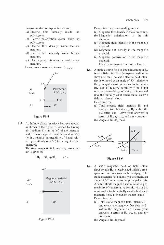
Balanis c01.tex V3 - 11/22/2011 3:03 P.M. Page 31
PROBLEMS 31
Determine the corresponding vector:(a) Electric field intensity inside the
polystyrene.(b) Electric polarization vector inside the
polystyrene.(c) Electric flux density inside the air
medium.(d) Electric field intensity inside the air
medium.(e) Electric polarization vector inside the air
medium.Leave your answers in terms of εo , μo .
Aireo, mo
Polystyrene2.56eo, mo
z
x
y
qes
#1 #2n
Figure P1-4
1.5. An infinite planar interface between media,as shown in the figure, is formed by havingair (medium #1) on the left of the interfaceand lossless magnetic material (medium #2)(with a relative permeability of 4 and rela-tive permittivity of 2.56) to the right of theinterface.The static magnetic field intensity inside theair is given by
H1 = 3âx + 9âz A/m
Magnetic material2.46eo, 4mo
Aireo, mo
z
x
y
#1 #2
Figure P1-5
Determine the corresponding vector:(a) Magnetic flux density in the air medium.(b) Magnetic polarization in the air
medium.(c) Magnetic field intensity in the magnetic
material.(d) Magnetic flux density in the magnetic
material.(e) Magnetic polarization in the magnetic
material.Leave your answers in terms of ε0, μo .
1.6. A static electric field of intensity/strength Eo
is established inside a free-space medium asshown below. The static electric field inten-sity is oriented at an angle of 30◦ relative tothe principal z axis. A semi-infinite dielec-tric slab of relative permittivity of 4 andrelative permeability of unity is immersedinto the initially established static electricfield, as shown below.Determine the:(a) Total electric field intensity E1 and
total electric flux density D1 within thedielectric slab. Leave your answers interms of Eo, εo , μo , and any constants.
(b) Angle θ (in degrees).
z
Eo, Do
Eo, Do
E1, D1
z
30°
30°
q
eo, mo
eo, mo
4eo, mo
Figure P1-6
1.7. A static magnetic field of field inten-sity/strength Ho is established inside a free-space medium as shown on the next page. Thestatic magnetic field intensity is oriented at anangle of 30◦ relative to the principal z axis.A semi-infinite magnetic slab of relative per-meability of 4 and relative permittivity of 9 isimmersed into the initially established staticmagnetic field, as shown on the next page.Determine the:(a) Total static magnetic field intensity H1
and total static magnetic flux density B1
within the magnetic slab. Leave youranswers in terms of Ho, εo , μo and anyconstants.
(b) Angle θ (in degrees).
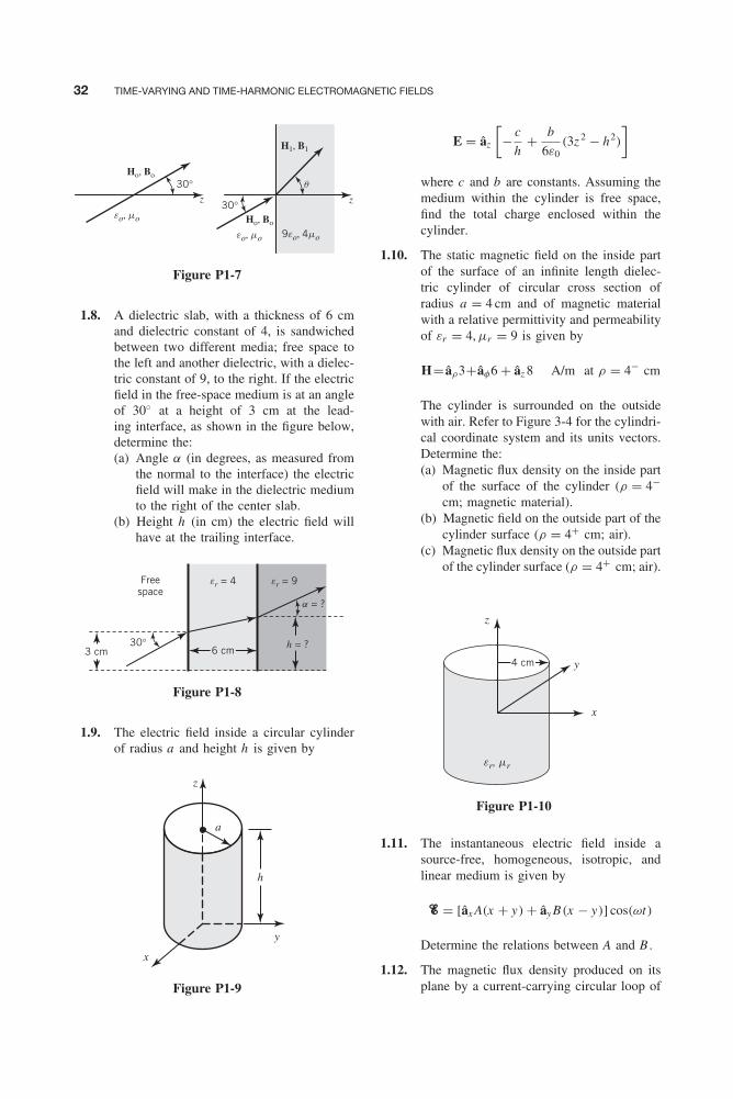
Balanis c01.tex V3 - 11/22/2011 3:03 P.M. Page 32
32 TIME-VARYING AND TIME-HARMONIC ELECTROMAGNETIC FIELDS
z
Ho, Bo
Ho, Bo
H1, B1
z
30°
30°
q
eo, mo
eo, mo 9eo, 4mo
Figure P1-7
1.8. A dielectric slab, with a thickness of 6 cmand dielectric constant of 4, is sandwichedbetween two different media; free space tothe left and another dielectric, with a dielec-tric constant of 9, to the right. If the electricfield in the free-space medium is at an angleof 30◦ at a height of 3 cm at the lead-ing interface, as shown in the figure below,determine the:(a) Angle α (in degrees, as measured from
the normal to the interface) the electricfield will make in the dielectric mediumto the right of the center slab.
(b) Height h (in cm) the electric field willhave at the trailing interface.
h = ?
Freespace
er = 4 er = 9
3 cm
a = ?
6 cm30°
Figure P1-8
1.9. The electric field inside a circular cylinderof radius a and height h is given by
x
y
z
a
h
Figure P1-9
E = âz
[− c
h+ b
6ε0(3z 2 − h2)
]where c and b are constants. Assuming themedium within the cylinder is free space,find the total charge enclosed within thecylinder.
1.10. The static magnetic field on the inside partof the surface of an infinite length dielec-tric cylinder of circular cross section ofradius a = 4 cm and of magnetic materialwith a relative permittivity and permeabilityof εr = 4, μr = 9 is given by
H= âρ3+âφ6 + âz 8 A/m at ρ = 4− cm
The cylinder is surrounded on the outsidewith air. Refer to Figure 3-4 for the cylindri-cal coordinate system and its units vectors.Determine the:(a) Magnetic flux density on the inside part
of the surface of the cylinder (ρ = 4−cm; magnetic material).
(b) Magnetic field on the outside part of thecylinder surface (ρ = 4+ cm; air).
(c) Magnetic flux density on the outside partof the cylinder surface (ρ = 4+ cm; air).
x
y
z
er, mr
4 cm
Figure P1-10
1.11. The instantaneous electric field inside asource-free, homogeneous, isotropic, andlinear medium is given by
� = [âx A(x + y) + ây B(x − y)] cos(ωt)
Determine the relations between A and B .
1.12. The magnetic flux density produced on itsplane by a current-carrying circular loop of
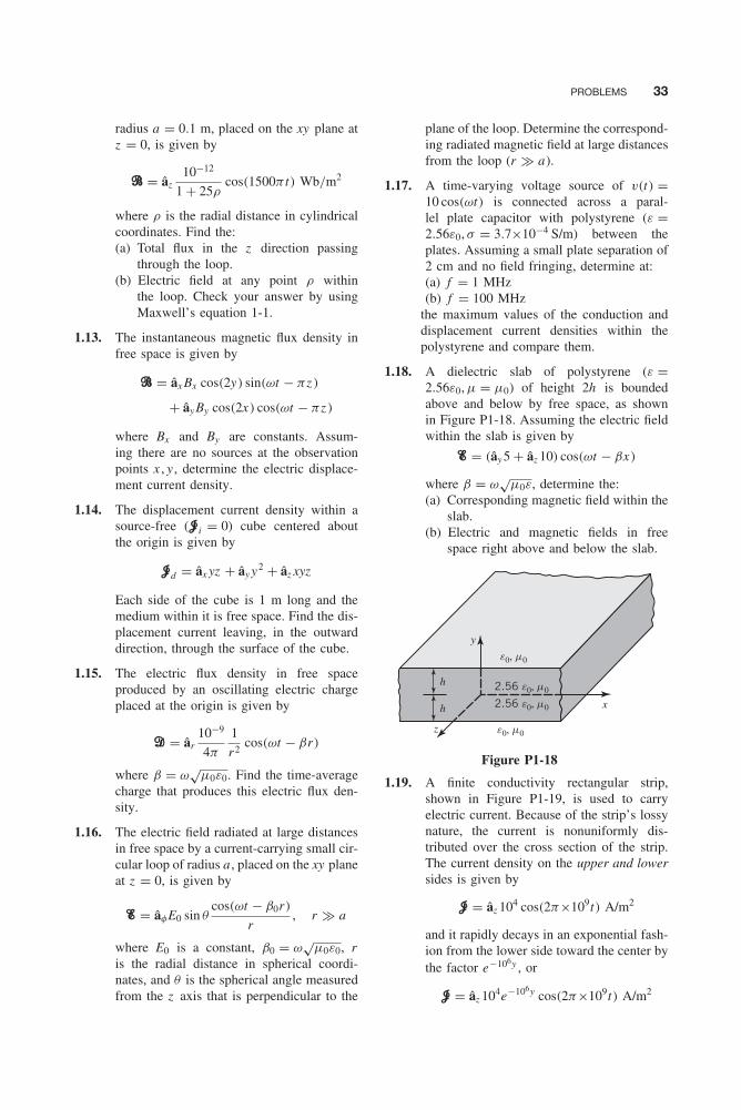
Balanis c01.tex V3 - 11/22/2011 3:03 P.M. Page 33
PROBLEMS 33
radius a = 0.1 m, placed on the xy plane atz = 0, is given by
� = âz10−12
1 + 25ρcos(1500π t) Wb/m2
where ρ is the radial distance in cylindricalcoordinates. Find the:(a) Total flux in the z direction passing
through the loop.(b) Electric field at any point ρ within
the loop. Check your answer by usingMaxwell’s equation 1-1.
1.13. The instantaneous magnetic flux density infree space is given by
� = âx Bx cos(2y) sin(ωt − πz )
+ ây By cos(2x) cos(ωt − πz )
where Bx and By are constants. Assum-ing there are no sources at the observationpoints x , y , determine the electric displace-ment current density.
1.14. The displacement current density within asource-free (�i = 0) cube centered aboutthe origin is given by
�d = âx yz + ây y2 + âz xyz
Each side of the cube is 1 m long and themedium within it is free space. Find the dis-placement current leaving, in the outwarddirection, through the surface of the cube.
1.15. The electric flux density in free spaceproduced by an oscillating electric chargeplaced at the origin is given by
� = âr10−9
4π
1
r2cos(ωt − βr)
where β = ω√
μ0ε0. Find the time-averagecharge that produces this electric flux den-sity.
1.16. The electric field radiated at large distancesin free space by a current-carrying small cir-cular loop of radius a , placed on the xy planeat z = 0, is given by
� = âφE0 sin θcos(ωt − β0r)
r, r � a
where E0 is a constant, β0 = ω√
μ0ε0, ris the radial distance in spherical coordi-nates, and θ is the spherical angle measuredfrom the z axis that is perpendicular to the
plane of the loop. Determine the correspond-ing radiated magnetic field at large distancesfrom the loop (r � a).
1.17. A time-varying voltage source of v(t) =10 cos(ωt) is connected across a paral-lel plate capacitor with polystyrene (ε =2.56ε0, σ = 3.7×10⁻⁴ S/m) between theplates. Assuming a small plate separation of2 cm and no field fringing, determine at:(a) f = 1 MHz(b) f = 100 MHz
the maximum values of the conduction anddisplacement current densities within thepolystyrene and compare them.
1.18. A dielectric slab of polystyrene (ε =2.56ε0, μ = μ0) of height 2h is boundedabove and below by free space, as shownin Figure P1-18. Assuming the electric fieldwithin the slab is given by
� = (ây 5 + âz 10) cos(ωt − βx)
where β = ω√
μ0ε, determine the:(a) Corresponding magnetic field within the
slab.(b) Electric and magnetic fields in free
space right above and below the slab.
x
e0, m0
e0, m0
2.56 e0, m0
2.56 e0, m0
y
z
h
h
Figure P1-18
1.19. A finite conductivity rectangular strip,shown in Figure P1-19, is used to carryelectric current. Because of the strip’s lossynature, the current is nonuniformly dis-tributed over the cross section of the strip.The current density on the upper and lowersides is given by
� = âz 104 cos(2π×109t) A/m2
and it rapidly decays in an exponential fash-ion from the lower side toward the center bythe factor e−106y , or
� = âz 104e−106y cos(2π×109t) A/m2

Balanis c01.tex V3 - 11/22/2011 3:03 P.M. Page 34
34 TIME-VARYING AND TIME-HARMONIC ELECTROMAGNETIC FIELDS
A similar decay is experienced by the cur-rent density from the upper side toward thecenter. Assuming no variations of the cur-rent density with respect to x , determine thetotal current flowing through the wire.
x
y
z5 mm
0.5 mm
Figure P1-19
1.20. The instantaneous electric field inside aconducting rectangular pipe (waveguide) ofwidth a is given by
� = ây E0 sin(π
ax)
cos(ωt − βz z )
where βz is the waveguide’s phase constant.Assuming there are no sources within thefree-space-filled pipe determine the:(a) Corresponding instantaneous magnetic
field components inside the conductingpipe.
(b) Phase constant βz .The height of the waveguide is b.
1.21. The instantaneous electric field intensityinside a source-free coaxial line with innerand outer radii of a and b, respectively, thatis filled with a homogeneous dielectric ofε = 2.25ε0, μ = μ0, and σ = 0, is given by
� = âρ
(100
ρ
)cos(108t − βz )
where β is the phase constant and ρ is thecylindrical radial distance from the center ofthe coaxial line. Determine the:(a) Corresponding instantaneous magnetic
field �.(b) Phase constant β.(c) Displacement current density �d .
1.22. A coaxial line resonator with inner andouter conductors at a = 5 mm and b = 20mm, and with conducting plates at z = 0and z = �, is filled with a dielectric withεr = 2.56, μr = 1, and σ = 0. The instan-taneous magnetic field intensity inside the
source-free dielectric medium is given by
� = âφ
(2
ρ
)cos
(π
�z)
cos(4π×108t)
Find the following:(a) Electric field intensity within the dielec-
tric.(b) Surface current density �s at the con-
ductor surfaces at ρ = a and ρ = b.(c) Displacement current density �d at any
point within the dielectric.(d) Total displacement current flowing
through the circumferential surface ofthe resonator.
1.23. Using the instantaneous forms of Maxwell’sequation and the continuity equations listedin Tables 1-1 and 1-4, derive the correspond-ing time-harmonic forms (in differential andintegral forms) listed in Table 1-4. Use def-initions (1-61a) through (1-61f).
1.24. Show that the electric and magnetic fields(1-61a) and (1-61b) can be written, respec-tively, as in (1-67a) and (1-67b).
1.25. The time-harmonic instantaneous electricfield traveling along the z -axis, in a free-space medium, is given by
�(z , t) = âx Eo sin[(ωt − βoz ) +
(π
2
)]where Eo is a real constant and βo =ω
√μoεo .
(a) Write an expression for the complexspatial electric field intensity E(z ).
(b) Find the corresponding complex spatialmagnetic field intensity H(z ).
(c) Determine the time-average Poyntingvector (average power density) Save.
1.26. An electric line source of infinite length andconstant current, placed along the z axis,radiates in free space at large distances fromthe source (ρ � 0) a time-harmonic com-plex magnetic field given by
H = âφH0e−jβ0ρ
√ρ
, ρ � 0
where H0 is a constant, β0 = ω√
μ0ε0, and ρ
is the radial cylindrical distance. Determinethe corresponding electric field for ρ � 0.
1.27. The time-harmonic complex electric fieldradiated in free space by a linear radiatingelement is given by
E = âr Er + âθ Eθ
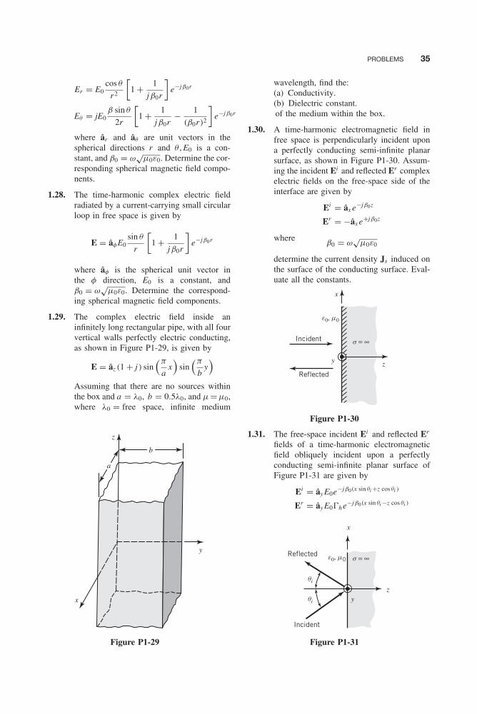
Balanis c01.tex V3 - 11/22/2011 3:03 P.M. Page 35
PROBLEMS 35
Er = E0cos θ
r2
[1 + 1
jβ0r
]e−jβ0r
Eθ = jE0β sin θ
2r
[1 + 1
jβ0r− 1
(β0r)2
]e−jβ0r
where âr and âθ are unit vectors in thespherical directions r and θ , E0 is a con-stant, and β0 = ω
√μ0ε0. Determine the cor-
responding spherical magnetic field compo-nents.
1.28. The time-harmonic complex electric fieldradiated by a current-carrying small circularloop in free space is given by
E = âφE0sin θ
r
[1 + 1
jβ0r
]e−jβ0r
where âφ is the spherical unit vector inthe φ direction, E0 is a constant, andβ0 = ω
√μ0ε0. Determine the correspond-
ing spherical magnetic field components.
1.29. The complex electric field inside aninfinitely long rectangular pipe, with all fourvertical walls perfectly electric conducting,as shown in Figure P1-29, is given by
E = âz (1 + j ) sin(π
ax)
sin(π
by)
Assuming that there are no sources withinthe box and a = λ0, b = 0.5λ0, and μ = μ0,where λ0 = free space, infinite medium
x
y
z
a
b
Figure P1-29
wavelength, find the:(a) Conductivity.(b) Dielectric constant.of the medium within the box.
1.30. A time-harmonic electromagnetic field infree space is perpendicularly incident upona perfectly conducting semi-infinite planarsurface, as shown in Figure P1-30. Assum-ing the incident Ei and reflected Er complexelectric fields on the free-space side of theinterface are given by
Ei = âx e−jβ0z
Er = −âx e+jβ0z
whereβ0 = ω
√μ0ε0
determine the current density Js induced onthe surface of the conducting surface. Eval-uate all the constants.
zy
x
s = ∞Incident
e0, m0
Reflected
Figure P1-30
1.31. The free-space incident Ei and reflected Er
fields of a time-harmonic electromagneticfield obliquely incident upon a perfectlyconducting semi-infinite planar surface ofFigure P1-31 are given by
Ei = ây E0e−jβ0(x sin θi +z cos θi )
Er = ây E0�h e−jβ0(x sin θi −z cos θi )
zy
x
s = ∞
Incident
e0, m0Reflected
qi
qi
Figure P1-31
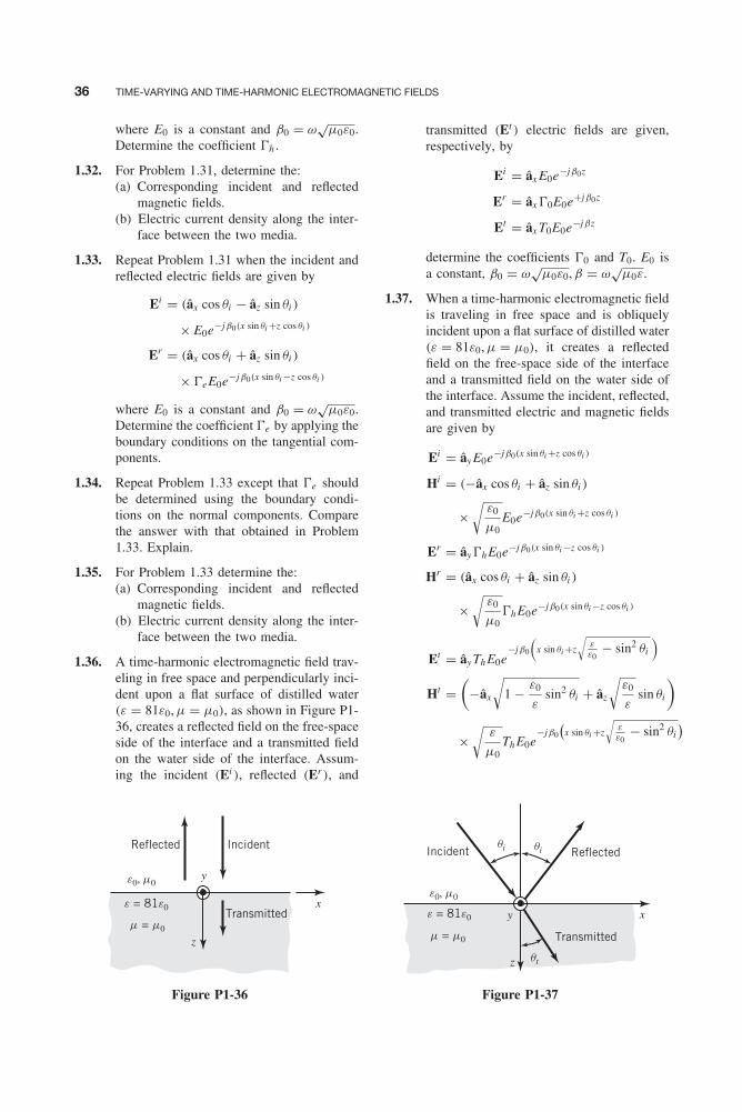
Balanis c01.tex V3 - 11/22/2011 3:03 P.M. Page 36
36 TIME-VARYING AND TIME-HARMONIC ELECTROMAGNETIC FIELDS
where E0 is a constant and β0 = ω√
μ0ε0.Determine the coefficient �h .
1.32. For Problem 1.31, determine the:(a) Corresponding incident and reflected
magnetic fields.(b) Electric current density along the inter-
face between the two media.
1.33. Repeat Problem 1.31 when the incident andreflected electric fields are given by
Ei = (âx cos θi − âz sin θi )
× E0e−jβ0(x sin θi +z cos θi )
Er = (âx cos θi + âz sin θi )
× �eE0e−jβ0(x sin θi −z cos θi )
where E0 is a constant and β0 = ω√
μ0ε0.Determine the coefficient �e by applying theboundary conditions on the tangential com-ponents.
1.34. Repeat Problem 1.33 except that �e shouldbe determined using the boundary condi-tions on the normal components. Comparethe answer with that obtained in Problem1.33. Explain.
1.35. For Problem 1.33 determine the:(a) Corresponding incident and reflected
magnetic fields.(b) Electric current density along the inter-
face between the two media.
1.36. A time-harmonic electromagnetic field trav-eling in free space and perpendicularly inci-dent upon a flat surface of distilled water(ε = 81ε0, μ = μ0), as shown in Figure P1-36, creates a reflected field on the free-spaceside of the interface and a transmitted fieldon the water side of the interface. Assum-ing the incident (Ei ), reflected (Er ), and
x
y
z
Incident
Transmitted
e0, m0
m = m0
e = 81e0
Reflected
Figure P1-36
transmitted (Et ) electric fields are given,respectively, by
Ei = âx E0e−jβ0z
Er = âx �0E0e+jβ0z
Et = âx T0E0e−jβz
determine the coefficients �0 and T0. E0 isa constant, β0 = ω
√μ0ε0, β = ω
√μ0ε.
1.37. When a time-harmonic electromagnetic fieldis traveling in free space and is obliquelyincident upon a flat surface of distilled water(ε = 81ε0, μ = μ0), it creates a reflectedfield on the free-space side of the interfaceand a transmitted field on the water side ofthe interface. Assume the incident, reflected,and transmitted electric and magnetic fieldsare given by
Ei = ây E0e−jβ0(x sin θi +z cos θi )
Hi = (−âx cos θi + âz sin θi )
×√
ε0
μ0E0e−jβ0(x sin θi +z cos θi )
Er = ây�h E0e−jβ0(x sin θi −z cos θi )
Hr = (âx cos θi + âz sin θi )
×√
ε0
μ0�h E0e−jβ0(x sin θi −z cos θi )
Et = ây Th E0e−jβ0
(x sin θi +z
√εε0
− sin2 θi
)
Ht =(
−âx
√1 − ε0
εsin2 θi + âz
√ε0
εsin θi
)
×√
ε
μ0Th E0e
−jβ0
(x sin θi +z
√εε0
− sin2 θi)
xy
z
Incident
Transmitted
e0, m0
m = m0
qt
qiqi
e = 81e0
Reflected
Figure P1-37
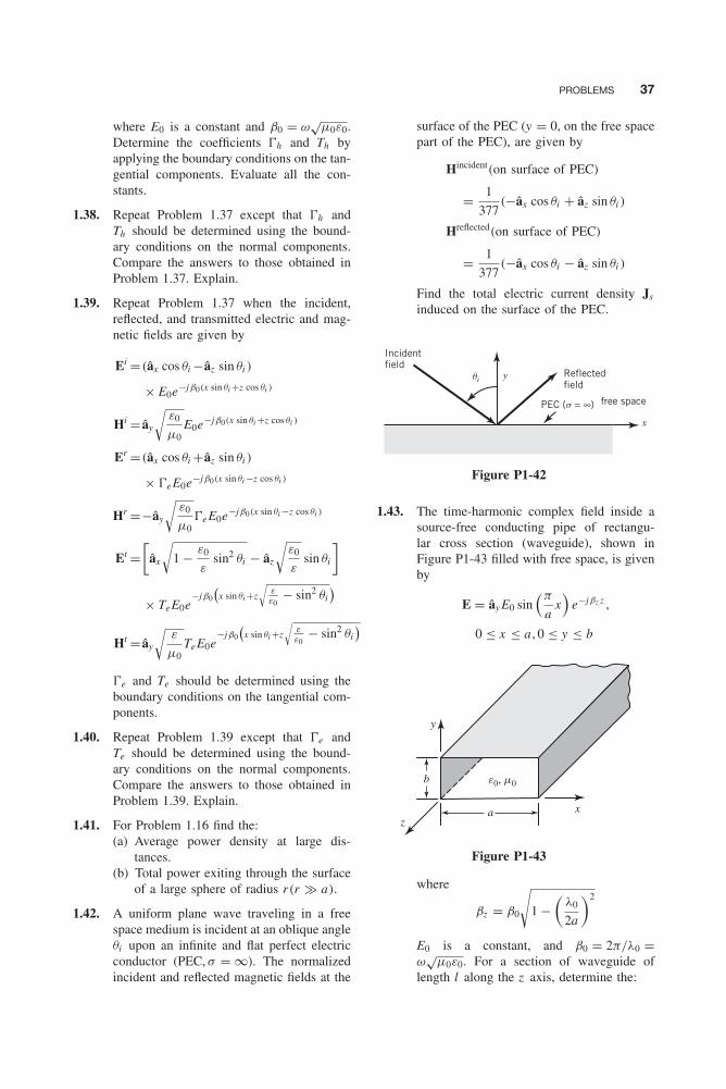
Balanis c01.tex V3 - 11/22/2011 3:03 P.M. Page 37
PROBLEMS 37
where E0 is a constant and β0 = ω√
μ0ε0.Determine the coefficients �h and Th byapplying the boundary conditions on the tan-gential components. Evaluate all the con-stants.
1.38. Repeat Problem 1.37 except that �h andTh should be determined using the bound-ary conditions on the normal components.Compare the answers to those obtained inProblem 1.37. Explain.
1.39. Repeat Problem 1.37 when the incident,reflected, and transmitted electric and mag-netic fields are given by
Ei =(âx cos θi −âz sin θi )
× E0e−jβ0(x sin θi +z cos θi )
Hi = ây
√ε0
μ0E0e−jβ0(x sin θi +z cos θi )
Er =(âx cos θi +âz sin θi )
× �eE0e−jβ0(x sin θi −z cos θi )
Hr =−ây
√ε0
μ0�eE0e−jβ0(x sin θi −z cos θi )
Et =[
âx
√1 − ε0
εsin2 θi − âz
√ε0
εsin θi
]
× TeE0e−jβ0
(x sin θi +z
√εε0
− sin2 θi)
Ht = ây
√ε
μ0TeE0e
−jβ0
(x sin θi +z
√εε0
− sin2 θi)
�e and Te should be determined using theboundary conditions on the tangential com-ponents.
1.40. Repeat Problem 1.39 except that �e andTe should be determined using the bound-ary conditions on the normal components.Compare the answers to those obtained inProblem 1.39. Explain.
1.41. For Problem 1.16 find the:(a) Average power density at large dis-
tances.(b) Total power exiting through the surface
of a large sphere of radius r(r � a).
1.42. A uniform plane wave traveling in a freespace medium is incident at an oblique angleθi upon an infinite and flat perfect electricconductor (PEC, σ = ∞). The normalizedincident and reflected magnetic fields at the
surface of the PEC (y = 0, on the free spacepart of the PEC), are given by
Hincident(on surface of PEC)
= 1
377(−âx cos θi + âz sin θi )
Hreflected(on surface of PEC)
= 1
377(−âx cos θi − âz sin θi )
Find the total electric current density Js
induced on the surface of the PEC.
PEC (s = ∞)
x
yqi
free space
Reflectedfield
Incidentfield
Figure P1-42
1.43. The time-harmonic complex field inside asource-free conducting pipe of rectangu-lar cross section (waveguide), shown inFigure P1-43 filled with free space, is givenby
E = ây E0 sin(π
ax)
e−jβz z ,
0 ≤ x ≤ a , 0 ≤ y ≤ b
xz
y
a
b e0, m0
Figure P1-43
where
βz = β0
√1 −
(λ0
2a
)2
E0 is a constant, and β0 = 2π/λ0 =ω
√μ0ε0. For a section of waveguide of
length l along the z axis, determine the:
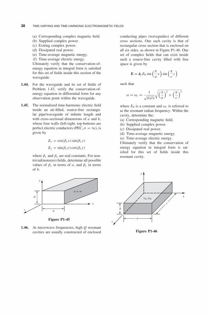
Balanis c01.tex V3 - 11/22/2011 3:03 P.M. Page 38
38 TIME-VARYING AND TIME-HARMONIC ELECTROMAGNETIC FIELDS
(a) Corresponding complex magnetic field.(b) Supplied complex power.(c) Exiting complex power.(d) Dissipated real power.(e) Time-average magnetic energy.(f) Time-average electric energy.Ultimately verify that the conservation-of-energy equation in integral form is satisfiedfor this set of fields inside this section of thewaveguide.
1.44. For the waveguide and its set of fields ofProblem 1.43, verify the conservation-of-energy equation in differential form for anyobservation point within the waveguide.
1.45. The normalized time-harmonic electric fieldinside an air-filled, source-free rectangu-lar pipe/waveguide of infinite length andwith cross-sectional dimensions of a and b,whose four walls (left-right, top-bottom) areperfect electric conductors (PEC, σ = ∞), isgiven by
Ex = cos(βx x) sin(βy y)
Ey = sin(βx x) cos(βy y)
where βx and βy are real constants. For non-trivial(nonzero) fields, determine all possiblevalues of βx in terms of a , and βy in termsof b.
a
b
z
x
y
s = ∞
Figure P1-45
1.46. At microwave frequencies, high Q resonantcavities are usually constructed of enclosed
conducting pipes (waveguides) of differentcross sections. One such cavity is that ofrectangular cross section that is enclosed onall six sides, as shown in Figure P1-46. Oneset of complex fields that can exist insidesuch a source-free cavity filled with freespace is given by
E = ây E0 sin(π
ax)
sin(π
cz)
such that
ω = ωr = 1√μ0ε0
√(π
a
)2 +(π
c
)2
where E0 is a constant and ωr is referred toas the resonant radian frequency. Within thecavity, determine the:(a) Corresponding magnetic field.(b) Supplied complex power.(c) Dissipated real power.(d) Time-average magnetic energy.(e) Time-average electric energy.Ultimately verify that the conservation ofenergy equation in integral form is sat-isfied for this set of fields inside thisresonant cavity.
x
c
z
y
a
b
e0, m0
Figure P1-46
Balanis c02.tex V3 - 11/22/2011 3:07 P.M. Page 39
CHAPTER 2Electrical Properties of Matter
2.1 INTRODUCTION
Since the late 1990s a renewed interest has been spurred in the application, integration, mod-eling, and optimization of materials in a plethora of electromagnetic radiation, guiding, andscattering structures. In particular, material structures whose constitutive parameters (permittiv-ity and permeability) are both negative, often referred to as a Double Negative (DNG), havereceived considerable interest and attention. Artificial magnetic conductors can also be includedin the DNG class of materials. A more inclusive name for all these materials is metamaterials .It is the class of metamaterials that has captivated the interest and imagination of many leadingresearchers and practitioners, scientists, and engineers from academia, industry, and government.When electromagnetic waves interact with such surfaces, they result in some very unique andintriguing characteristics and phenomena that can be used, for example, to optimize the per-formance of antennas, microwave devices, and other electromagnetic wave guiding structures.While the revitalization of metamaterials introduced a welcomed renewed interest in materials forelectromagnetics, especially for applications related to antennas, microwaves, transmission lines,scattering, optics, etc., it also brought along some spirited dialogue that will be discussed in moredetail in Section 5.7. The uniqueness of these materials is characterized and demonstrated bytheir basic constitutive parameters, such as permittivity, permeability, and conductivity. In orderto appreciate the behavior of materials, it is very important that engineers and scientists under-stand the very basics of these constitutive parameters from d.c. to rf frequencies. An in-depthdevelopment of models for these constitutive parameters, from their basic atomic structure totheir interaction with electromagnetic fields, is undertaken in this chapter.
An atom of an element consists of a very small but massive nucleus that is surrounded bya number of negatively charged electrons revolving about the nucleus. The nucleus containsneutrons , which are neutral particles, and protons , which are positively charged particles. Allmatter is made up of one or more of the 118 different elements that are now known to exist.Elements 112 to 118 have been discovered but not confirmed. Of this number, only 92 occurnaturally. If the substance in question is a compound, it is composed of two or more differentelements. The smallest constituent of a compound is a molecule, which is composed of one ormore atoms held together by the short-range forces of their electrical charges.
For a given element, each of its atoms contains the same number of protons in its nucleus.Depending on the element, that number ranges from 1 to 118 and represents the atomic numberof the element. For an atom in its normal state, the number of electrons is also equal to the atomicnumber. The revolving electrons that surround the nucleus exist in various shells, and they exertforces of repulsion on each other and forces of attraction on the positive charges of the nucleus.
39
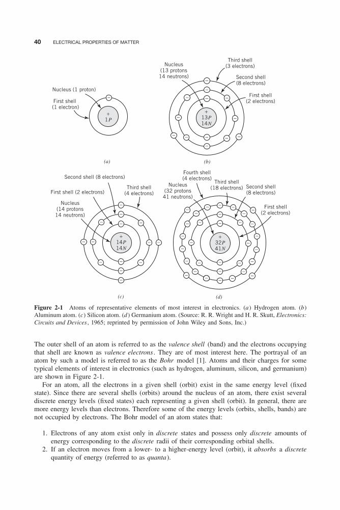
Balanis c02.tex V3 - 11/22/2011 3:07 P.M. Page 40
40 ELECTRICAL PROPERTIES OF MATTER
+1P
+13P14N
+14P14N
+32P41N
Nucleus (1 proton)
Nucleus(32 protons41 neutrons)
Nucleus(14 protons14 neutrons)
Nucleus(13 protons14 neutrons)
Third shell(3 electrons)
Second shell(8 electrons)
First shell(2 electrons)
Fourth shell(4 electrons)
Third shell(18 electrons)Third shell
(4 electrons)Second shell(8 electrons)
Second shell (8 electrons)
First shell(2 electrons)
First shell (2 electrons)
First shell (1 electron)
(a) (b)
(c) (d)
−
−
− −
−−−
−
−
−−
−
−
−
−−
−−
−
−−
−−
−−
−
−
−
−−
−
−
−
−
−− −− −
−
−
−−
− −
−
−
−−
−−−
−
−
−
−
−
− −−
−
Figure 2-1 Atoms of representative elements of most interest in electronics. (a) Hydrogen atom. (b)Aluminum atom. (c) Silicon atom. (d ) Germanium atom. (Source: R. R. Wright and H. R. Skutt, Electronics:Circuits and Devices , 1965; reprinted by permission of John Wiley and Sons, Inc.)
The outer shell of an atom is referred to as the valence shell (band) and the electrons occupyingthat shell are known as valence electrons . They are of most interest here. The portrayal of anatom by such a model is referred to as the Bohr model [1]. Atoms and their charges for sometypical elements of interest in electronics (such as hydrogen, aluminum, silicon, and germanium)are shown in Figure 2-1.
For an atom, all the electrons in a given shell (orbit) exist in the same energy level (fixedstate). Since there are several shells (orbits) around the nucleus of an atom, there exist severaldiscrete energy levels (fixed states) each representing a given shell (orbit). In general, there aremore energy levels than electrons. Therefore some of the energy levels (orbits, shells, bands) arenot occupied by electrons. The Bohr model of an atom states that:
1. Electrons of any atom exist only in discrete states and possess only discrete amounts ofenergy corresponding to the discrete radii of their corresponding orbital shells.
2. If an electron moves from a lower- to a higher-energy level (orbit), it absorbs a discretequantity of energy (referred to as quanta).
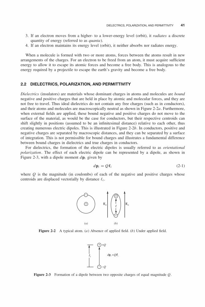
Balanis c02.tex V3 - 11/22/2011 3:07 P.M. Page 41
DIELECTRICS, POLARIZATION, AND PERMITTIVITY 41
3. If an electron moves from a higher- to a lower-energy level (orbit), it radiates a discretequantity of energy (referred to as quanta).
4. If an electron maintains its energy level (orbit), it neither absorbs nor radiates energy.
When a molecule is formed with two or more atoms, forces between the atoms result in newarrangements of the charges. For an electron to be freed from an atom, it must acquire sufficientenergy to allow it to escape its atomic forces and become a free body. This is analogous to theenergy required by a projectile to escape the earth’s gravity and become a free body.
2.2 DIELECTRICS, POLARIZATION, AND PERMITTIVITY
Dielectrics (insulators) are materials whose dominant charges in atoms and molecules are boundnegative and positive charges that are held in place by atomic and molecular forces, and they arenot free to travel. Thus ideal dielectrics do not contain any free charges (such as in conductors),and their atoms and molecules are macroscopically neutral as shown in Figure 2-2a . Furthermore,when external fields are applied, these bound negative and positive charges do not move to thesurface of the material, as would be the case for conductors, but their respective centroids canshift slightly in positions (assumed to be an infinitesimal distance) relative to each other, thuscreating numerous electric dipoles. This is illustrated in Figure 2-2b. In conductors, positive andnegative charges are separated by macroscopic distances, and they can be separated by a surfaceof integration. This is not permissible for bound charges and illustrates a fundamental differencebetween bound charges in dielectrics and true charges in conductors.
For dielectrics, the formation of the electric dipoles is usually referred to as orientationalpolarization . The effect of each electric dipole can be represented by a dipole, as shown inFigure 2-3, with a dipole moment dpi given by
dpi = Q�i (2-1)
where Q is the magnitude (in coulombs) of each of the negative and positive charges whosecentroids are displaced vectorially by distance �i .
−
+
+
−
(a)
Ea Ea
(b)
l
Figure 2-2 A typical atom. (a) Absence of applied field. (b) Under applied field.
−Q
+
−
+Q
dpi =Qlili
Figure 2-3 Formation of a dipole between two opposite charges of equal magnitude Q .
Balanis c02.tex V3 - 11/22/2011 3:07 P.M. Page 42
42 ELECTRICAL PROPERTIES OF MATTER
When a material is subjected to an electric field, the polarization dipoles of the material interactwith the applied electromagnetic field. For dielectric (insulating) material, whether they are solids,liquids, or gases, this interaction provides the material the ability to store electric energy, whichis accomplished by the shift against restraining forces of their bound charges when they aresubjected to external applied forces. This is analogous to stretching a spring or lifting a weight,and it represents potential energy.
The presence of these dipoles can be accounted for by developing a microscopic model inwhich each individual charge and dipole as represented by (2-1) is considered. Such a procedure,although accurate if performed properly, is very impractical if applied to a dielectric slab becausethe spatial position of each atom and molecule of the material must be known. Instead, inpractice, the behavior of these dipoles and bound charges is accounted for in a qualitative way byintroducing an electric polarization vector P using a macroscopic scale model involving thousandsof atoms and molecules.
The total dipole moment pt of a material is obtained by summing the dipole moments of allthe orientational polarization dipoles, each of which is represented by (2-1). For a volume v
where there are Ne electric dipoles per unit volume, or a total of Nev electric dipoles, we canwrite that
pt =Nev∑i=1
dpi (2-2)
The electric polarization vector P can then be defined as the dipole moment per unit volume, or
P = limv→0
[1
vpt
]= lim
v→0
[1
v
Nev∑i=1
dpi
](C/m2) (2-3)
The units of P are coulomb-meters per cubic meter or coulombs per square meter, which is repre-sentative of a surface charge density. It should be noted that this is a bound surface charge density(qsp), and it is not permissible to separate the positive and negative charges by an integrationsurface. Therefore, within a volume, an integral (whole) number of positive and negative pairs(dipoles) with an overall zero net charge must exist. Hence the bound surface charge should notbe included in (1-45a) or (1-46) to determine the boundary conditions on the normal componentsof the electric flux density (or normal components of the electric field intensity).
Assuming an average dipole moment of
dpi = dpav = Q�av (2-4)
per molecule, the electric polarization vector of (2-3) can be written, when all dipoles are alignedin the same direction, as
P = limv→0
[1
v
Nev∑i=1
dpi
]= Nedpav = NeQ�av (2-5)
Electric polarization for dielectrics can be produced by any of the following three mechanisms,as demonstrated in Figure 2-4 [2]. Few materials involve all three of the following mechanisms:
1. Dipole or Orientational Polarization: This polarization is evident in materials that, in theabsence of an applied field and owing to their structure, possess permanent dipole momentsthat are randomly oriented. However when an electric field is applied, the dipoles tend toalign with the applied field. As will be discussed later, such materials are known as polarmaterials; water is a good example.

Balanis c02.tex V3 - 11/22/2011 3:07 P.M. Page 43
DIELECTRICS, POLARIZATION, AND PERMITTIVITY 43
Mechanism No applied field Applied field
Dipole ororientationalpolarization
lonic ormolecularpolarization
Electronicpolarization
Ea
Ea
Ea
+
+
+
+ −
−
−
−
Figure 2-4 Mechanisms producing electric polarization in dielectrics.
2. Ionic or Molecular Polarization: This polarization is evident in materials, such as sodiumchloride (NaCl), that possess positive and negative ions and that tend to displace themselveswhen an electric field is applied.
3. Electronic Polarization: This polarization is evident in most materials, and it exists whenan applied electric field displaces the electric cloud center of an atom relative to the centerof the nucleus.
If the charges in a material, in the absence of an applied electric field Ea , are averaged insuch a way that positive and negative charges cancel each other throughout the entire mate-rial, then there are no individual dipoles formed and the total dipole moment of (2-2) and theelectric polarization vector P of (2-3) are zero. However, when an electric field is applied, itexhibits a net nonzero polarization. Such a material is referred to as nonpolar , and it is illus-trated in Figure 2-5a . Polar materials are those whose charges in the absence of an appliedelectric field Ea are distributed so that there are individual dipoles formed, each with a dipolemoment pi as given by (2-1) but with a net total dipole moment pt = 0 and electric polarizationvector P = 0. This is usually a result of the random orientation of the dipoles as illustrated inFigure 2-5b. Typical dipole moments of polar materials are of the order of 10−30 C-m. Materialsthat, in the absence of an applied electric field Ea , possess nonzero net dipole moment and electricpolarization vector P are referred to as electrets .
There is also a class of dielectric materials that are usually referred to as ferroelectrics [3].They exhibit a hysteresis loop of polarization (P ) versus electric field (E ) that is similar to thehysteresis loop of B versus H for ferromagnetic material, and it possesses a remnant polarizationPr and coercive electric field Ec . At some critical temperature, referred to as ferroelectric Curietemperature, the spontaneous polarization in ferroelectrics disappears. Above the Curie temper-ature the relative permittivity varies according to the Curie–Weiss law; below it the electric fluxdensity D and the polarization P are not linear functions of the electric field E [3]. Bariumtitanate (BaTiO3) is one such material.
When an electric field is applied to a nonpolar or polar dielectric material, as shown inFigures 2-5a and 2-5b, the charges in each medium are aligned in such a way that individualdipoles with nonzero dipole moments are formed within the material. However, when we

Balanis c02.tex V3 - 11/22/2011 3:07 P.M. Page 44
44 ELECTRICAL PROPERTIES OF MATTER
dpi = 0
dpi ≠ 0, P = 0 P ≠ 0
P = N eQl av
P = N eQl av
P
dpi ≠ 0
P ≠ 0dpi ≠ 0
Ea ≠ 0 Ea ≠ 0
P = 0
Ea = 0 Ea = 0
Ea = 0 Ea = 0
Ea ≠ 0 Ea ≠ 0
+++
+
+ ++
++ +
++
+
+ ++
+ ++ −−−
−
−
−−
−−
− − −−
−− −
− − −−
−−
− +
++
+
(a)
(b)
+−
+
+
−
−
+−
+
+
−
−
+−
+
+
−
−
+−
+
+
−
−
+−
+
+
−
−
+−
+
+
−
−
+−
+
+
−
−
+−
+
+
−
−
+−
+
+
−
−
+−
+
+
−
−
Figure 2-5 Macroscopic scale models of materials. (a) Nonpolar. (b) Polar.
examine the material on a microscopic scale, the following items become evident fromFigures 2-5a and 2-5b:
1. On the lower surface there exists a net positive surface charge density q+s (representing
bound charges).2. On the upper surface there exists a net negative surface charge density q−
s (representingbound charges).
3. The volume charge density qv inside the material is zero because the positive and negativecharges of adjacent dipoles cancel each other.
The preceding items can also be illustrated by macroscopically examining Figure 2-6a wherea d.c. voltage source is connected and remains across two parallel plates separated by distances . Half of the space between the two plates is occupied by a dielectric material, whereas theother half is free space. For a better illustration of this point, let us assume that there are fivefree charges on each part of the plates separated by free space. The same number appears on thepart of the plates separated by the dielectric material. Because of the realignment of the boundcharges in the dielectric material and the formation of the electric dipoles and cancellation ofadjacent opposite charges shown circled in Figure 2-6b, a polarization electric vector P is formed

Balanis c02.tex V3 - 11/22/2011 3:07 P.M. Page 45
DIELECTRICS, POLARIZATION, AND PERMITTIVITY 45
−
+ +
− −
+
+ +
++++++
−
++
− − − − −−−− −
−
−
−+
+
−+
EaEaEa
V
q sp (net)
+q sp
(net)
Ea Ea
s
P P
P
(a)
(b)
−
−+
+
−+
− −−
−−
−−
−−
−−
−−
−+
+
−+
Figure 2-6 Dielectric slab subjected to an applied electric field Ea . (a) Total charge. (b) Net charge.
within the dielectric material. Thus the polarization vector P is a result of the bound surfacecharge density −qsp found on the upper and +qsp found on the lower surface of the dielectricslab. Let us assume that there are two pairs of bound charges that form the bound surface chargedensity qsp on the surface of the dielectric slab of Figure 2-6a (negative on top and positive onthe bottom). Because the surfaces of the slab are assumed to be in contact with the plates ofthe capacitor, the two negative bound charges on the top surface will tend to cancel two of thepositive free charges on the upper capacitor plate; a similar phenomenon occurs at the bottom.If this were to happen, the net number of charges on the top and bottom plates of the capacitorwould diminish to three and the electric field intensity in the dielectric material between the plateswould be reduced. Since the d.c. voltage supply is maintained across the plates, the net charge onthe upper and lower parts of the capacitor and the electric field intensity in the dielectric materialbetween the plates are also maintained by the introduction of two additional free charges on eachof the capacitor plates (positive on top and negative on bottom). For identification purposes, thesetwo induced free charges have been circled in each of the two plates in Figure 2-6.
Balanis c02.tex V3 - 11/22/2011 3:07 P.M. Page 46
46 ELECTRICAL PROPERTIES OF MATTER
In each of the situations discussed previously, the net effect is that between the lower andupper surfaces of the dielectric there is a net electric polarization vector P directed from the uppertoward the lower surfaces, in the same direction as the applied electric field Ea , whose amplitudeis given by
P = qsp (2-6)
Whereas the applied electric field Ea maintains its value, the electric flux density inside thedielectric material differs from what would exist were the dielectric material replaced by freespace. In the free-space part of the parallel plate capacitor of Figure 2-6, the electric flux densityD0 is given by
D0 = ε0Ea (2-7)
In the dielectric portion, the electric flux density D is related to that in free space D0 by
D = ε0Ea + P (2-8)
where the magnitude of P is given by (2-6). The electric flux density D of (2-8) can also berelated to the applied electric field intensity Ea by a parameter that we designate here as εs
(farads/meter). Thus we can write thatD = εsEa (2-9)
Comparing (2-8) and (2-9), it is apparent that P is also related to Ea and can be expressed as
P = ε0χeEa (2-10)
or
χe = 1
ε0
P
Ea(2-10a)
where χe is referred to as the electric susceptibility (dimensionless quantity).Substituting (2-10) into (2-8) and equating the result to (2-9), we can write that
D = ε0Ea + ε0χeEa = ε0 (1 + χe) Ea = εsEa (2-11)
or thatεs = ε0 (1 + χe) (2-11a)
In (2-11a) εs is the static permittivity of the medium whose relative value εsr (compared to thatof free space ε0) is given by
εsr = εs
ε0= 1 + χe (2-12)
which is usually referred to as the relative permittivity , better known in practice as the dielectricconstant . Scientists and engineers usually designate the square root of the relative permittivityas the index of refraction . Typical values of dielectric constants at static frequencies of someprominent dielectric materials are listed in Table 2-1.
Thus the dielectric constant of a dielectric material is a parameter that indicates the relative(compared to free space) charge (energy) storage capabilities of a dielectric material; the largerits value, the greater its ability to store charge (energy). Parallel plate capacitors utilize dielectricmaterial between their plates to increase their charge (energy) storage capacity by forcing extrafree charges to be induced on the plates. These free charges neutralize the bound charges on thesurface of the dielectric so that the voltage and electric field intensity are maintained constantbetween the plates.

Balanis c02.tex V3 - 11/22/2011 3:07 P.M. Page 47
DIELECTRICS, POLARIZATION, AND PERMITTIVITY 47
TABLE 2-1 Approximate static dielectric constants (relative permittivities) of dielectricmaterials
Material Static dielectric constant (εr )
Air 1.0006Styrofoam 1.03Paraffin 2.1Teflon 2.1Plywood 2.1RT/duroid 5880 2.20Polyethylene 2.26RT/duroid 5870 2.35Glass-reinforced teflon (microfiber) 2.32–2.40Teflon quartz (woven) 2.47Glass-reinforced teflon (woven) 2.4–2.62Cross-linked polystyrene (unreinforced) 2.56Polyphenelene oxide (PPO) 2.55Glass-reinforced polystyrene 2.62Amber 3Soil (dry) 3Rubber 3Plexiglas 3.4Lucite 3.6Fused silica 3.78Nylon (solid) 3.8Quartz 3.8Sulfur 4Bakelite 4.8Formica 5Lead glass 6Mica 6Beryllium oxide (BeO) 6.8–7.0Marble 8Sapphire εx = εy = 9.4
εz = 11.6Flint glass 10Ferrite (Fe2O3) 12–16Silicon (Si) 12Gallium arsenide (GaAs) 13Ammonia (liquid) 22Glycerin 50Water 81Rutile (TiO2) εx = εy = 89
εz = 173
Example 2-1
The static dielectric constant of water is 81. Assuming the electric field intensity applied to water is1 V/m, determine the magnitudes of the electric flux density and electric polarization vector within thewater.
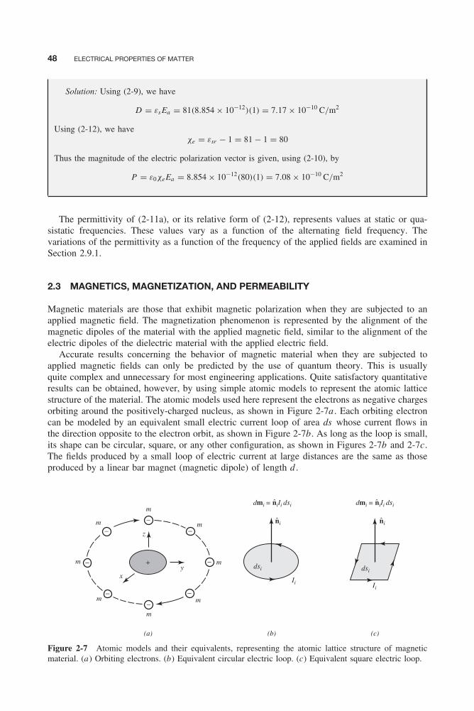
Balanis c02.tex V3 - 11/22/2011 3:07 P.M. Page 48
48 ELECTRICAL PROPERTIES OF MATTER
Solution: Using (2-9), we have
D = εs Ea = 81(8.854 × 10⁻¹²)(1) = 7.17 × 10⁻¹⁰ C/m2
Using (2-12), we haveχe = εsr − 1 = 81 − 1 = 80
Thus the magnitude of the electric polarization vector is given, using (2-10), by
P = ε0χeEa = 8.854 × 10⁻¹²(80)(1) = 7.08 × 10⁻¹⁰ C/m2
The permittivity of (2-11a), or its relative form of (2-12), represents values at static or qua-sistatic frequencies. These values vary as a function of the alternating field frequency. Thevariations of the permittivity as a function of the frequency of the applied fields are examined inSection 2.9.1.
2.3 MAGNETICS, MAGNETIZATION, AND PERMEABILITY
Magnetic materials are those that exhibit magnetic polarization when they are subjected to anapplied magnetic field. The magnetization phenomenon is represented by the alignment of themagnetic dipoles of the material with the applied magnetic field, similar to the alignment of theelectric dipoles of the dielectric material with the applied electric field.
Accurate results concerning the behavior of magnetic material when they are subjected toapplied magnetic fields can only be predicted by the use of quantum theory. This is usuallyquite complex and unnecessary for most engineering applications. Quite satisfactory quantitativeresults can be obtained, however, by using simple atomic models to represent the atomic latticestructure of the material. The atomic models used here represent the electrons as negative chargesorbiting around the positively-charged nucleus, as shown in Figure 2-7a . Each orbiting electroncan be modeled by an equivalent small electric current loop of area ds whose current flows inthe direction opposite to the electron orbit, as shown in Figure 2-7b. As long as the loop is small,its shape can be circular, square, or any other configuration, as shown in Figures 2-7b and 2-7c.The fields produced by a small loop of electric current at large distances are the same as thoseproduced by a linear bar magnet (magnetic dipole) of length d .
Ii Ii
dmi = niIi dsi
dsi
(a)
m
m
m
m
m
m
m
x
z
y
m
(b) (c)
dsi
−−
+−
−−
−
−
−ni
dmi = niIi dsi
ni
Figure 2-7 Atomic models and their equivalents, representing the atomic lattice structure of magneticmaterial. (a) Orbiting electrons. (b) Equivalent circular electric loop. (c) Equivalent square electric loop.
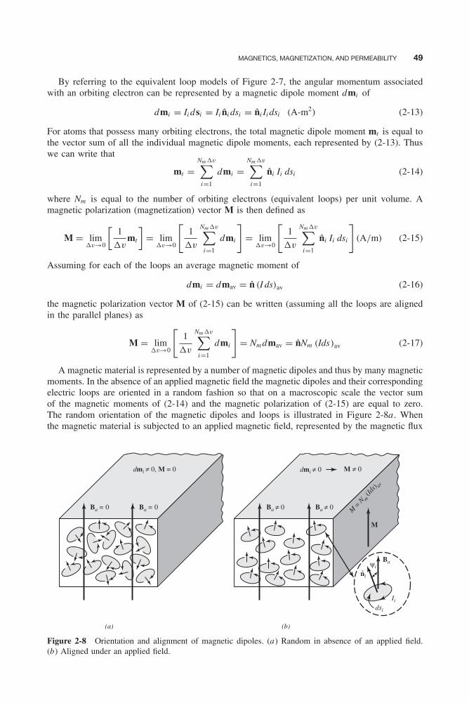
Balanis c02.tex V3 - 11/22/2011 3:07 P.M. Page 49
MAGNETICS, MAGNETIZATION, AND PERMEABILITY 49
By referring to the equivalent loop models of Figure 2-7, the angular momentum associatedwith an orbiting electron can be represented by a magnetic dipole moment dmi of
dmi = Ii dsi = Ii n̂i dsi = n̂i Ii dsi (A-m2) (2-13)
For atoms that possess many orbiting electrons, the total magnetic dipole moment mt is equal tothe vector sum of all the individual magnetic dipole moments, each represented by (2-13). Thuswe can write that
mt =Nmv∑
i=1
dmi =Nmv∑
i=1
n̂i Ii dsi (2-14)
where Nm is equal to the number of orbiting electrons (equivalent loops) per unit volume. Amagnetic polarization (magnetization) vector M is then defined as
M = limv→0
[1
vmt
]= lim
v→0
[1
v
Nmv∑i=1
dmi
]= lim
v→0
[1
v
Nmv∑i=1
n̂i Ii dsi
](A/m) (2-15)
Assuming for each of the loops an average magnetic moment of
dmi = dmav = n̂ (I ds)av (2-16)
the magnetic polarization vector M of (2-15) can be written (assuming all the loops are alignedin the parallel planes) as
M = limv→0
[1
v
Nmv∑i=1
dmi
]= Nmdmav = n̂Nm (Ids)av (2-17)
A magnetic material is represented by a number of magnetic dipoles and thus by many magneticmoments. In the absence of an applied magnetic field the magnetic dipoles and their correspondingelectric loops are oriented in a random fashion so that on a macroscopic scale the vector sumof the magnetic moments of (2-14) and the magnetic polarization of (2-15) are equal to zero.The random orientation of the magnetic dipoles and loops is illustrated in Figure 2-8a . Whenthe magnetic material is subjected to an applied magnetic field, represented by the magnetic flux
ψiBa
Ba = 0 Ba ≠ 0 Ba ≠ 0Ba = 0
dsi
Ii
(a) (b)
dmi ≠ 0, M = 0 M ≠ 0
M
dmi ≠ 0
M =
N m (Ids
) av
ni
Figure 2-8 Orientation and alignment of magnetic dipoles. (a) Random in absence of an applied field.(b) Aligned under an applied field.

Balanis c02.tex V3 - 11/22/2011 3:07 P.M. Page 50
50 ELECTRICAL PROPERTIES OF MATTER
density Ba in Figure 2-8b, the magnetic dipoles of most material will tend to align in the directionof the Ba since a torque given by
|T| = |dmi × Ba | = |dmi ||Ba | sin(ψi ) = |(n̂i Ii dsi ) × Ba | = |Ii dsi Ba sin(ψi )| (2-18)
will be exerted in each of the magnetic dipole moments. This is shown in the inset toFigure 2-8b. Ideally, if there were no other magnetic moments to consider, torque would beexerted. The torque would exist until each of the orbiting electrons shifted in such a way thatthe magnetic field produced by each of its equivalent electric loops (or magnetic moments) wasaligned with the applied field, and its value, represented by (2-18), vanished. Thus the resultantmagnetic field at every point in the material would be greater than its corresponding value at thesame point when the material is absent.
The magnetization vector M resulting from the realignment of the magnetic dipoles is betterillustrated by considering a slab of magnetic material across which a magnetic field Ba is applied,as shown in Figure 2-9. Ideally, on a microscopic scale, for most magnetic material all themagnetic dipoles will align themselves so that their individual magnetic moments are pointed inthe direction of the applied field, as shown in Figure 2-9. In the limit, as the number of magneticdipoles and their corresponding equivalent electric loops become very large, the currents of theloops found in the interior parts of the slab are canceled by those of the neighboring loops.On a macroscopic scale a net nonzero equivalent magnetic current, resulting in an equivalentmagnetic current surface density (A/m), is found on the exterior surface of the slab. This equivalentmagnetic current density Jms is responsible for the introduction of the magnetization vector Min the direction of Ba .
The magnetic flux density across the slab is increased by the presence of M so that the netmagnetic flux density at any interior point of the slab is given by
B = μ0(Ha + M) (2-19)
Jms
M Ba
Figure 2-9 Magnetic slab subjected to an applied magnetic field and the formation of the magnetizationcurrent density Jms .
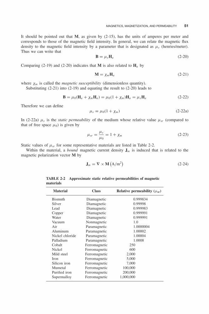
Balanis c02.tex V3 - 11/22/2011 3:07 P.M. Page 51
MAGNETICS, MAGNETIZATION, AND PERMEABILITY 51
It should be pointed out that M, as given by (2-15), has the units of amperes per meter andcorresponds to those of the magnetic field intensity. In general, we can relate the magnetic fluxdensity to the magnetic field intensity by a parameter that is designated as μs (henries/meter).Thus we can write that
B = μs Ha (2-20)
Comparing (2-19) and (2-20) indicates that M is also related to Ha by
M = χmHa (2-21)
where χm is called the magnetic susceptibility (dimensionless quantity).Substituting (2-21) into (2-19) and equating the result to (2-20) leads to
B = μ0(Ha + χmHa) = μ0(1 + χm)Ha = μs Ha (2-22)
Therefore we can defineμs = μ0(1 + χm) (2-22a)
In (2-22a) μs is the static permeability of the medium whose relative value μsr (compared tothat of free space μ0) is given by
μsr = μs
μ0= 1 + χm (2-23)
Static values of μsr for some representative materials are listed in Table 2-2.Within the material, a bound magnetic current density Jm is induced that is related to the
magnetic polarization vector M by
Jm = ∇ × M(A/m2) (2-24)
TABLE 2-2 Approximate static relative permeabilities of magneticmaterials
Material Class Relative permeability (μsr)
Bismuth Diamagnetic 0.999834Silver Diamagnetic 0.99998Lead Diamagnetic 0.999983Copper Diamagnetic 0.999991Water Diamagnetic 0.999991Vacuum Nonmagnetic 1.0Air Paramagnetic 1.0000004Aluminum Paramagnetic 1.00002Nickel chloride Paramagnetic 1.00004Palladium Paramagnetic 1.0008Cobalt Ferromagnetic 250Nickel Ferromagnetic 600Mild steel Ferromagnetic 2,000Iron Ferromagnetic 5,000Silicon iron Ferromagnetic 7,000Mumetal Ferromagnetic 100,000Purified iron Ferromagnetic 200,000Supermalloy Ferromagnetic 1,000,000
Balanis c02.tex V3 - 11/22/2011 3:07 P.M. Page 52
52 ELECTRICAL PROPERTIES OF MATTER
To account for this current density, we modify the Maxwell–Ampere equation 1-71b and writeit as
∇ × H = Ji + Jc + Jm + Jd = Ji + σE + ∇ × M + jωεE (2-24a)
On the surface of the material, the bound magnetization surface current density Jms is related tothe magnetic polarization vector M at the surface by
Jms = M × n̂|surface (A/m) (2-25)
where n̂ is a unit vector normal to the surface of the material. The bound magnetization currentIm flowing through a cross section S0 of the material can be obtained by using
Im =∫∫
S0
Jm • ds =∫∫
S0
(∇ × M) • ds (A) (2-26)
In addition to orbiting, the electrons surrounding the nucleus of an atom also spin about theirown axis. Therefore magnetic moments of the order of ±9 × 10⁻²⁴ A-m2 are also associated withthe spinning of the electrons that aid or oppose the applied magnetic field (the + sign is used foraddition and the − for subtraction). For atoms that have many electrons in their shells, only thespins associated with the electrons found in shells that are not completely filled will contributeto the magnetic moment of the atoms. A third contributor to the total magnetic moment of anatom is that associated with the spinning of the nucleus, which is referred to as nuclear spin .However, this nuclear spin magnetic moment is usually much smaller (typically by a factor ofabout 10−3) than those attributed to the orbiting and the spinning electrons.
Example 2-2
A bar of magnetic material of finite length, which is placed along the z axis, as shown in Figure 2-10,has a cross section of 0.3 m in the x direction (0 ≤ x ≤ 0.3) and 0.2 m in the y direction (0 ≤ y ≤ 0.2).The bar is subjected to a magnetic field so that the magnetization vector inside the bar is given by
M = âz (4y)
az
z
4y
y
M =
M
Jm Jms
Jms
Jm
0.3
0.2
x
Figure 2-10 Magnetic bar of rectangular cross section subjected to a magnetic field.
Balanis c02.tex V3 - 11/22/2011 3:07 P.M. Page 53
MAGNETICS, MAGNETIZATION, AND PERMEABILITY 53
Determine the volumetric current density Jm at any point inside the bar, the surface current density Jms
on the surface of each of the four faces, and the total current Im per unit length flowing through the barface that is parallel to the y axis at x = 0.3 m.
Solution: Using (2-24), we have
Jm = ∇ × M = âx∂Mz
∂y= âx 4
Using (2-25), we haveJms = M × n̂|surface
Therefore at
x = 0 :
Jms = (âz 4y) × (−âx )|x=0 = −ây (4y) for 0 ≤ y ≤ 0.2
y = 0 :
Jms = (âz 4y) × (−ây )|y=0 = âx (4y) = 0 for 0 ≤ x ≤ 0.3
x = 0.3 :
Jms = (âz 4y) × (âx )|x=0.3 = ây (4y) for 0 ≤ y ≤ 0.2
y = 0.2
Jms = (âz 4y) × (ây )|y=0.2 = −âx (4y) = −âx 0.8 for 0 ≤ x ≤ 0.3
According to (2-26), the current (per unit length) flowing through the bar face at x = 0.3 is given by
x = 0.3 :
Im =∫∫
SJm • ds =
∫ 1
0
∫ 0.2
0(âx 4) • (âx dy dz ) = 4(1)(0.2) = 0.8
Consistent with the relative permittivity (dielectric constant), the values of μ, and thus μr ,vary as a function of frequency. These variations will be discussed in Section 2.9.2. The valuesof μr listed in Table 2-2 are representative of frequencies related to static or quasistatic fields.Excluding ferromagnetic material, it is apparent that most relative permeabilities are very nearunity, so that for engineering problems a value of unity is almost always used.
According to the direction in which the net magnetization vector M is pointing (either aidingor opposing the applied magnetic field), material are classified into two groups, Group A andGroup B as shown:
Group A Group B
Diamagnetic ParamagneticFerromagneticAntiferromagneticFerrimagnetic
In general, for material in Group A the net magnetization vector (although small in magnitude)opposes the applied magnetic field, resulting in a relative permeability slightly smaller than unity.Diamagnetic materials fall into that group. For material in Group B the net magnetization vector
Balanis c02.tex V3 - 11/22/2011 3:07 P.M. Page 54
54 ELECTRICAL PROPERTIES OF MATTER
is aiding the applied magnetic field, resulting in relative permeabilities greater than unity. Someof them (paramagnetic and antiferromagnetic) have only slightly greater than unity relative per-meabilities whereas others (ferromagnetic and ferrimagnetic) have relative permeabilities muchgreater than unity.
In the absence of an applied magnetic field, the moments of the electron spins of diamagneticmaterial are opposite to each other as well as to the moments associated with the orbiting elec-trons so that a zero net magnetic moment mt is produced on a macroscopic scale. In the presenceof an external applied magnetic field, each atom has a net nonzero magnetic moment, and on amacroscopic scale there is a net total magnetic moment for all the atoms that results in a mag-netization vector M. For diamagnetic material, this vector M is very small, opposes the appliedmagnetic field, leads to a negative magnetic susceptibility χm , and results in values of relativepermeability that are slightly less than unity. For example, copper is a diamagnetic material witha magnetic susceptibility χm = −9 × 10⁻⁶ and a relative permeability μr = 0.999991.
In paramagnetic material, the magnetic moments associated with the orbiting and spinningelectrons of an atom do not quite cancel each other in the absence of an applied magnetic field.Therefore each atom possesses a small magnetic moment. However, because the orientationof the magnetic moment of each atom is random, the net magnetic moment of a large sample(macroscopic scale) of dipoles, and the magnetization vector M, are zero when there is no appliedfield. When the paramagnetic material is subjected to an applied magnetic field, the magneticdipoles align slightly with the applied field to produce a small nonzero M in its direction and asmall increase in the magnetic flux density within the material. Thus the magnetic susceptibilitieshave small positive values and the relative permeabilities are slightly greater than unity. Forexample, aluminum possesses a susceptibility of χm = 2 × 10⁻⁵ and a relative permeability ofμr = 1.00002.
The individual atoms of ferromagnetic material possess, in the absence of an applied magneticfield, very strong magnetic moments caused primarily by uncompensated electron spin moments.The magnetic moments of many atoms (usually as many as five to six) reinforce one anotherand form regions called domains , which have various sizes and shapes. The dimensions of thedomains depend on the material’s past magnetic state and history, and range from 1 μm to a fewmillimeters. On a macroscopic scale, however, the net magnetization vector M in the absence ofan applied field is zero because the domains are randomly oriented and the magnetic moments ofthe various atoms cancel one another. When a ferromagnetic material is subjected to an appliedfield, there are not only large magnetic moments associated with the individual atoms, but thevector sum of all the magnetic moments and the associated vector magnetization M are verylarge, leading to extreme values of magnetic susceptibility χm and relative permeability. Typicalvalues of μr for some representative ferromagnetic materials are found in Table 2-2. When theapplied field is removed, the magnetic moments of the various atoms do not attain a randomorientation and a net nonzero residual magnetic moment remains. Since the magnetic moment ofa ferromagnetic material on a macroscopic scale is different after the applied field is removed,its magnetic state depends on the material’s past history. Therefore a plot of the magnetic fluxdensity � versus � leads to a double-valued curve known as the hysteresis loop. Material withsuch properties are very desirable in the design of transformers, induction cores, and coatings formagnetic recording tapes.
Materials that possess strong magnetic moments, but whose adjacent atoms are about equal inmagnitude and opposite in direction, with zero net total magnetic moment in the absence of anapplied magnetic field, are called antiferromagnetic. The presence of an applied magnetic fieldhas a minor effect on the material and leads to relative permeabilities slightly greater than unity.
If the adjacent opposing magnetic moments of a material are very large in magnitude but greatlyunequal in the absence of an applied magnetic field, the material is known as ferrimagnetic. Thepresence of an applied magnetic field has a large effect on the material and leads to largepermeabilities (but not as large as those of ferromagnetic material). Ferrites make up a group
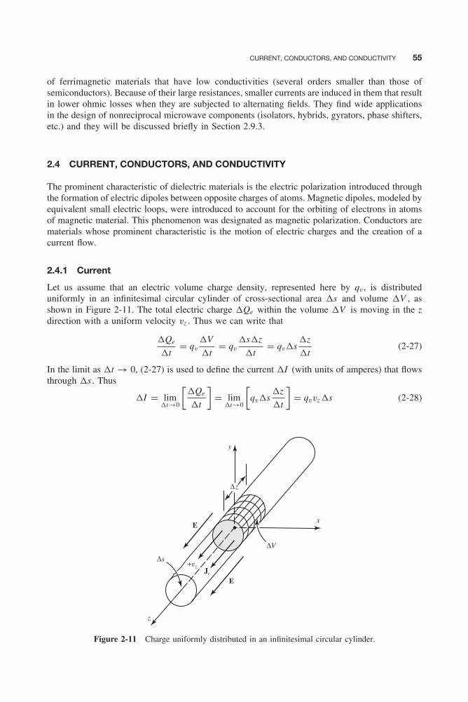
Balanis c02.tex V3 - 11/22/2011 3:07 P.M. Page 55
CURRENT, CONDUCTORS, AND CONDUCTIVITY 55
of ferrimagnetic materials that have low conductivities (several orders smaller than those ofsemiconductors). Because of their large resistances, smaller currents are induced in them that resultin lower ohmic losses when they are subjected to alternating fields. They find wide applicationsin the design of nonreciprocal microwave components (isolators, hybrids, gyrators, phase shifters,etc.) and they will be discussed briefly in Section 2.9.3.
2.4 CURRENT, CONDUCTORS, AND CONDUCTIVITY
The prominent characteristic of dielectric materials is the electric polarization introduced throughthe formation of electric dipoles between opposite charges of atoms. Magnetic dipoles, modeled byequivalent small electric loops, were introduced to account for the orbiting of electrons in atomsof magnetic material. This phenomenon was designated as magnetic polarization. Conductors arematerials whose prominent characteristic is the motion of electric charges and the creation of acurrent flow.
2.4.1 Current
Let us assume that an electric volume charge density, represented here by qv , is distributeduniformly in an infinitesimal circular cylinder of cross-sectional area s and volume V , asshown in Figure 2-11. The total electric charge Qe within the volume V is moving in the zdirection with a uniform velocity vz . Thus we can write that
Qe
t= qv
V
t= qv
sz
t= qvs
z
t(2-27)
In the limit as t → 0, (2-27) is used to define the current I (with units of amperes) that flowsthrough s . Thus
I = limt→0
[Qe
t
]= lim
t→0
[qvs
z
t
]= qvvz s (2-28)
y
Δz
+vzΔs
x
ΔV
z
E
EJc
Figure 2-11 Charge uniformly distributed in an infinitesimal circular cylinder.

Balanis c02.tex V3 - 11/22/2011 3:07 P.M. Page 56
56 ELECTRICAL PROPERTIES OF MATTER
Dividing both sides of (2-28) by s and taking the limit as s → 0, we can define the currentdensity Jz (with units of amperes per square meter) as
Jz = lims→0
[I
s
]= qvvz (2-29)
Using a similar procedure for the x - and y-directed currents, we can write in general that
J = qvv (A/m2) (2-30)
In (2-30), J is defined as the convection current density . The current density between the cathodeand anode of a vacuum tube is a convection current density. It should be noted that for an electricfield intensity of E = âz Ez , a positive charge density +qv will experience a force that will moveit in the +z direction. Thus the current density J will be directed in the +z direction or
J = +qv(+âz vz ) = âz qvvz (2-31)
If the same electric field E = âz Ez is subjected to a negative charge density −qv , the field willforce the negative charge to move in the negative z direction (v = −âz vz ). However, the electriccurrent density J is still directed along the +z direction,
J = −qv(−âz vz ) = âz qvvz (2-32)
since both the charge density and the velocity are negative. If positive (q+v ) and negative (q−
v )
charges are present, (2-30) can be written as
J = q+v v+ + q−
v v− (2-33)
2.4.2 Conductors
Conductors are material whose atomic outer shell (valence) electrons are not held very tightly andcan migrate from one atom to another. These are known as free electrons , and for metal conductorsthey are very large in number. With no applied external field, these free electrons move withdifferent velocities in random directions producing zero net current through the surface of theconductor.
When free charge qv0 is placed inside a conductor that is subjected to a static field, the chargedensity at that point decays exponentially as
qv(t) = qv0e−t/tr = qv0e−(σ/ε)t (2-34)
because the charge migrates toward the surface of the conductor. The time it takes for this to occurdepends on the conductivity of the material; for metals it is equal to a few time constants. Duringthis time, charges move, currents flow, and nonstatic conditions exist. The time tr that it takesfor the free charge density placed inside a conductor to decay to e−1 = 0.368, or 36.8 percent ofits initial value, is known as the relaxation time constant . Mathematically it is represented by
tr = ε
σ(2-35)
whereε = permittivity of conductor (F/m)σ = conductivity of conductor (S/m) (see equation (2-39))

Balanis c02.tex V3 - 11/22/2011 3:07 P.M. Page 57
CURRENT, CONDUCTORS, AND CONDUCTIVITY 57
Example 2-3
Find the relaxation time constant for a metal such as copper (σ = 5.76 × 10⁷ S/m, ε = ε0) and a gooddielectric such as glass (σ � 10−12 S/m, ε = 6ε0).
Solution: For copper
tr = ε
σ= 8.854 × 10⁻¹²
5.76 × 107= 1.54 × 10⁻¹⁹ s
which is very short. For glass
tr = ε
σ= 6
(8.854 × 10⁻¹²
10−12
)= 53.1 s � 1 min
which is comparatively quite long.
The free charges of a very good conductor (σ → ∞), which is subjected to an electric field,migrate very rapidly and distribute themselves as surface charge density qs to the surface of theconductor within an extremely short period of time (several very short relaxation time constants).The surface charge density qs will induce on the conductor an electric field intensity Ei , so thatthe total electric field Et , within the conductor (Ei + Ea = Et , where Ea is the applied field) isessentially zero. This is illustrated in Figure 2-12. For perfect conductors (σ = ∞) the electricfield within the conductors is exactly zero.
2.4.3 Conductivity
When a conductor is subjected to an electric field, the electrons still move in random direc-tions but drift slowly (with a drift velocity ve) in the negative direction of the applied electric
− − − − −
+ + + + + + + +++++
− − − − −−−
+ qs + qs
− qs− qs
Ea
Ei Ei EiEiEa
s = ∞
Ea Ea
Ea Ea
E = E a
+ Ei = 0
s = ∞
s = ∞
s = ∞
Figure 2-12 Electric field applied on a perfect electric conductor.

Balanis c02.tex V3 - 11/22/2011 3:07 P.M. Page 58
58 ELECTRICAL PROPERTIES OF MATTER
TABLE 2-3 Typical conductivities of insulators, semiconductors, and conductors
Material Class Conductivity σ (S/m)
Fused quartz Insulator ∼ 10−17
Ceresin wax Insulator ∼ 10−17
Sulfur Insulator ∼ 10−15
Mica Insulator ∼ 10−15
Paraffin Insulator ∼ 10−15
Hard rubber Insulator ∼ 10−15
Porcelain Insulator ∼ 10−14
Glass Insulator ∼ 10−12
Bakelite Insulator ∼ 10−9
Distilled water Insulator ∼ 10−4
Gallium arsenide (GaAs)∗ Semiconductor ∼ 2.38 × 10⁻⁷
Fused silica∗ Semiconductor ∼ 2.1 × 10⁻⁴
Cross-linked polystyrene (unreinforced)∗ Semiconductor ∼ 3.7 × 10⁻⁴
Beryllium Oxide (BeO)∗ Semiconductor ∼ 3.9 × 10⁻⁴
Intrinsic silicon Semiconductor ∼ 4.39 × 10⁻⁴
Sapphire∗ Semiconductor ∼ 5.5 × 10⁻⁴
Glass-reinforced Teflon (microfiber)∗ Semiconductor ∼ 7.8 × 10⁻⁴
Teflon quartz (woven)∗ Semiconductor ∼ 8.2 × 10⁻⁴
Dry soil Semiconductor ∼ 10−4 − 10−3
Ferrite(Fe2O3)∗ Semiconductor ∼ 1.3 × 10⁻³
Glass-reinforced Polystyrene∗ Semiconductor ∼ 1.45 × 10⁻³
Polyphenelene oxide (PPO)∗ Semiconductor ∼ 2.27 × 10⁻³
Glass-reinforced Teflon (woven)∗ Semiconductor ∼ 2.43 × 10⁻³
Plexiglas∗ Semiconductor ∼ 5.1 × 10⁻³
Wet soil Semiconductor ∼ 10−3 − 10−2
Fresh water Semiconductor ∼ 10−2
Human and animal tissue Semiconductor ∼ 0.2 − 0.7Intrinsic germanium Semiconductor ∼ 2.227Seawater Semiconductor ∼ 4Tellurium Conductor ∼ 5 × 10⁻²
Carbon Conductor ∼ 3 × 10⁻⁴
Graphite Conductor ∼ 3 × 10⁴
Cast iron Conductor ∼ 106
Mercury Conductor 106
Nichrome Conductor 106
Silicon steel Conductor 2 × 10⁶
German silver Conductor 2 × 10⁶
Lead Conductor 5 × 10⁶
Tin Conductor 9 × 10⁶
Iron Conductor 1.03 × 10⁷
Nickel Conductor 1.45 × 10⁷
Zinc Conductor 1.7 × 10⁷
Tungsten Conductor 1.83 × 10⁷
Brass Conductor 2.56 × 10⁷
Aluminum Conductor 3.96 × 10⁷
Gold Conductor 4.1 × 10⁷
Copper Conductor 5.76 × 10⁷
Silver Conductor 6.1 × 10⁷
∗For most semiconductors the conductivities are representative for a frequency of about 10 GHz.

Balanis c02.tex V3 - 11/22/2011 3:07 P.M. Page 59
SEMICONDUCTORS 59
field, thus creating a conduction current in the conductor. The applied electric field E and driftvelocity ve of the electrons are related by
ve = −μeE (2-36)
where μe is defined to be the electron mobility [positive quantity with units of m2/(V-s)]. Sub-stituting (2-36) into (2-30), we can write that
J = qveve = qve(−μeE) = −qveμeE (2-37)
where qve is the electron charge density. Comparing (2-37) with (1-16), or
J = σs E (2-38)
we define the static conductivity of a conductor as
σs = −qveμe (S/m) (2-39)
Its reciprocal value is called the resistivity (ohm-meters).The conductivity σs of a conductor is a parameter that characterizes the free-electron conductive
properties of a conductor. As temperature increases, the increased thermal energy of the conductorlattice structure increases the lattice vibration. Thus the possibility of the moving free electronscolliding increases, which results in a decrease in the conductivity of the conductor. Materialswith a very low value of conductivity are classified as dielectrics (insulators). The conductivityof ideal dielectrics is zero.
The conductivity of (2-39) is referred to as the static or d.c. conductivity; typical values ofseveral materials are listed in Table 2-3. The conductivity varies as a function of frequency. Thesevariations, along with the mechanisms that result in them, will be discussed in Section 2.8.1.
2.5 SEMICONDUCTORS
Materials whose conductivities bridge the gap between dielectrics (insulators) and conductors(typically the conductivity being 10−3 to unity) are referred to as intrinsic (pure) semiconductors.A graph illustrating the range of conductivities, from insulators to conductors, is displayed inFigure 2-13. Two such materials of significant importance to electrical engineering are intrinsicgermanium and intrinsic silicon . In intrinsic (pure) semiconductors there are two common carriers:the free electrons and the bound electrons (referred to as positive holes) [4].
As the temperature rises, the mobilities of semiconducting material decrease but their chargedensities increase more rapidly. The increases in the charge density more than offset the decreasesin mobilities, resulting in a general increase in the conductivity of semiconducting materialwith rises in temperature. This is one of the characteristic differences between intrinsic semi-conductors and metallic conductors: for semiconductors the conductivity increases with risingtemperature whereas for metallic conductors it decreases. Typically the conductivity of germa-nium will increase by a factor of 10 as the temperature increases from 300 to about 360 K, andit will decrease by the same factor of 10 as the temperature decreases from 300 to 255 K. Theconductivity of semiconductors can also be increased by adding impurities to the intrinsic (pure)materials. This process is known as doping . Some impurities (such as phosphorus) are calleddonors because they add more electrons and form n-type semiconductors, with the electronsbeing the major carriers. Impurities (such as boron) are called acceptors because they add moreholes to form p-type semiconductors, with the holes being the predominant carriers. When bothn- and p-type regions exist on a single semiconductor, the junction formed between the tworegions is used to build diodes and transistors.
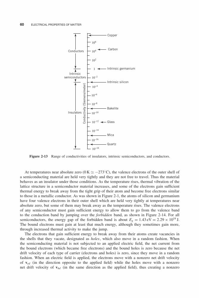
Balanis c02.tex V3 - 11/22/2011 3:07 P.M. Page 60
60 ELECTRICAL PROPERTIES OF MATTER
Copper
106
104
102
10−2
10−4
10−6
10−8
10−10
10−12
10−14
10−16
10−18
1
CarbonConductors
Intrinsicsemiconductors
Insulators
Con
duct
ivit
y (S
iem
ens/
met
er)
Intrinsic germanium
Intrinsic silicon
Bakelite
Glass
Mica
Quartz
Figure 2-13 Range of conductivities of insulators, intrinsic semiconductors, and conductors.
At temperatures near absolute zero (0 K � −273◦C), the valence electrons of the outer shell ofa semiconducting material are held very tightly and they are not free to travel. Thus the materialbehaves as an insulator under those conditions. As the temperature rises, thermal vibration of thelattice structure in a semiconductor material increases, and some of the electrons gain sufficientthermal energy to break away from the tight grip of their atom and become free electrons similarto those in a metallic conductor. As was shown in Figure 2-1, the atoms of silicon and germaniumhave four valence electrons in their outer shell which are held very tightly at temperatures nearabsolute zero, but some of them may break away as the temperature rises. The valence electronsof any semiconductor must gain sufficient energy to allow them to go from the valence bandto the conduction band by jumping over the forbidden band, as shown in Figure 2-14. For allsemiconductors, the energy gap of the forbidden band is about Eg = 1.43 eV = 2.29 × 10¹⁹ J.The bound electrons must gain at least that much energy, although they sometimes gain more,through increased thermal activity to make the jump.
The electrons that gain sufficient energy to break away from their atoms create vacancies inthe shells that they vacate, designated as holes , which also move in a random fashion. Whenthe semiconducting material is not subjected to an applied electric field, the net current fromthe bound electrons (which became free electrons) and the bound holes is zero because the netdrift velocity of each type of carrier (electrons and holes) is zero, since they move in a randomfashion. When an electric field is applied, the electrons move with a nonzero net drift velocityof ved (in the direction opposite to the applied field) while the holes move with a nonzeronet drift velocity of vhd (in the same direction as the applied field), thus creating a nonzero

Balanis c02.tex V3 - 11/22/2011 3:07 P.M. Page 61
SEMICONDUCTORS 61
Conduction band
Conduction band
Conduction band
Forbidden bandForbidden
bandEg 1.43 eV
2.29 × 10⁻¹⁹J
Valence band
Ene
rgy
Leve
l
Valence band Valence band
(a) (b) (c)
∼_∼_
Figure 2-14 Energy levels for: (a) Conductors. (b) Semiconductors. (c) Insulators.
current. Therefore we write the conduction current density for the two carriers (electrons andholes) as
Jc = qevved + qhvvhd = qev(−μeE) + qhv(+μhE)
Jc = (−qevμe + qhvμh)E = (σes + σhs)E = σsE (2-40)
whereμe = mobility of electrons [m2/(V-s)]μh = mobility of holes [m2/(V-s)]σes = static conductivity due to electronsσhs = static conductivity due to holes
The static conductivities of the electrons (σes ) and the holes (σhs ) can also be written as
σes = −qevμe = −Neqeμe = Ne |qe |μe (2-41a)
σhs = +qhvμh = +Nhqhμh = Nh |qh |μh (2-41b)
whereNe = free electron density (electrons per cubic meter)Nh = bound hole density (holes per cubic meter)
|qe | = |qh | = charge of an electron (magnitude) = 1.6 × 10⁻¹⁹ (coulombs)qev = Neqe = −Ne |qe |qhv = Nhqh = +Nh |qh | = Nh |qe |
For comparison, representative values of charge densities, mobilities, and conductivities for intrin-sic silicon, intrinsic germanium, aluminum, copper, silver, and gallium arsenide are given inTable 2-4 [5].
Six different materials were chosen to illustrate the formation of conductivity; their conduc-tivity conditions are shown in Figure 2-15 [6]. These, in order, are representative of a dielectric(insulator), plasma (liquid or gas), conductor (metal), pure semiconductor, n-type semiconductor,and p-type semiconductor. It is observed that positively charged particles (holes) travel in thedirection of the electric field whereas negatively charged particles (electrons) travel opposite tothe electric field. However, both add to the total current.
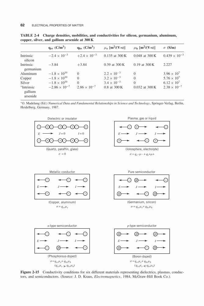
Balanis c02.tex V3 - 11/22/2011 3:07 P.M. Page 62
62 ELECTRICAL PROPERTIES OF MATTER
TABLE 2-4 Charge densities, mobilities, and conductivities for silicon, germanium, aluminum,copper, silver, and gallium arsenide at 300 K
qev (C/m3) qhv (C/m3) μe [m2/(V-s)] μh [m2/(V-s)] σ (S/m)
Intrinsic −2.4 × 10⁻³ +2.4 × 10⁻³ 0.135 at 300 K 0.048 at 300 K 0.439 × 10⁻³
siliconIntrinsic −3.84 +3.84 0.39 at 300 K 0.19 at 300 K 2.227
germaniumAluminum −1.8 × 10¹⁰ 0 2.2 × 10⁻³ 0 3.96 × 10⁷
Copper −1.8 × 10¹⁰ 0 3.2 × 10⁻³ 0 5.76 × 10⁷
Silver −1.8 × 10¹⁰ 0 3.4 × 10⁻³ 0 6.12 × 10⁷
∗Intrinsic −2.86 × 10⁻⁷ 2.86 × 10⁻⁷ 0.8 at 300 K 0.032 at 300 K 2.38 × 10⁻⁷
galliumarsenide
∗O. Madelung (Ed.) Numerical Data and Fundamental Relationships in Science and Technology , Springer-Verlag, Berlin,Heidelberg, Germany, 1987.
Dielectric or insulator
Metallic conductor Pure semiconductor
n-type semiconductor p-type semiconductor
(Boron-doped)(Phosphorous-doped)
(Quartz, paraffin, glass)
(Copper, aluminum) (Germanium, silicon)
(Ionosphere, electrolyte)
Plasma, gas or liquid
− + − + − + − +
−
−
+ − + − + − +
E
H
E
J = 0
J I
I = 0
E J I
E J IE J I
−
− − −
−
H
H
H
H H
H
H
H
−
−
−
−
−
−
E J I
−
−
+
+
+−
−−
−
s = 0 s = qv−m− + qv+m+
s = qevme+ qhvmhs = qevme
s = qevme+ qhvmh
(qevme qhvmh)s= qevme+ qhvmh
(qevme qhvmh)
Figure 2-15 Conductivity conditions for six different materials representing dielectrics, plasmas, conduc-tors, and semiconductors. (Source: J. D. Kraus, Electromagnetics , 1984, McGraw-Hill Book Co.).
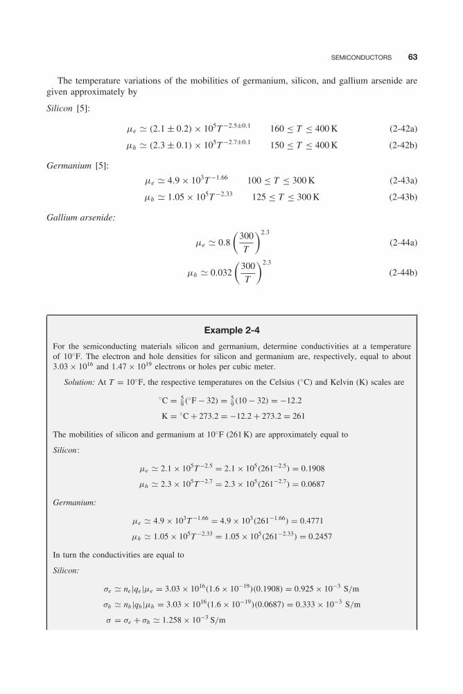
Balanis c02.tex V3 - 11/22/2011 3:07 P.M. Page 63
SEMICONDUCTORS 63
The temperature variations of the mobilities of germanium, silicon, and gallium arsenide aregiven approximately by
Silicon [5]:
μe � (2.1 ± 0.2) × 105T −2.5±0.1 160 ≤ T ≤ 400 K (2-42a)
μh � (2.3 ± 0.1) × 105T −2.7±0.1 150 ≤ T ≤ 400 K (2-42b)
Germanium [5]:
μe � 4.9 × 10³T −1.66 100 ≤ T ≤ 300 K (2-43a)
μh � 1.05 × 10⁵T −2.33 125 ≤ T ≤ 300 K (2-43b)
Gallium arsenide:
μe � 0.8
(300
T
)2.3
(2-44a)
μh � 0.032
(300
T
)2.3
(2-44b)
Example 2-4
For the semiconducting materials silicon and germanium, determine conductivities at a temperatureof 10◦F. The electron and hole densities for silicon and germanium are, respectively, equal to about3.03 × 1016 and 1.47 × 10¹⁹ electrons or holes per cubic meter.
Solution: At T = 10◦F, the respective temperatures on the Celsius (◦C) and Kelvin (K) scales are
◦C = 59 (◦F − 32) = 5
9 (10 − 32) = −12.2
K = ◦C + 273.2 = −12.2 + 273.2 = 261
The mobilities of silicon and germanium at 10◦F (261 K) are approximately equal to
Silicon:
μe � 2.1 × 10⁵T −2.5 = 2.1 × 10⁵(261−2.5) = 0.1908
μh � 2.3 × 10⁵T −2.7 = 2.3 × 10⁵(261−2.7) = 0.0687
Germanium:
μe � 4.9 × 10³T −1.66 = 4.9 × 10³(261−1.66) = 0.4771
μh � 1.05 × 10⁵T −2.33 = 1.05 × 10⁵(261−2.33) = 0.2457
In turn the conductivities are equal to
Silicon:
σe � ne |qe |μe = 3.03 × 10¹⁶(1.6 × 10⁻¹⁹)(0.1908) = 0.925 × 10⁻³ S/m
σh � nh |qh |μh = 3.03 × 10¹⁶(1.6 × 10⁻¹⁹)(0.0687) = 0.333 × 10⁻³ S/m
σ = σe + σh � 1.258 × 10⁻³ S/m
Balanis c02.tex V3 - 11/22/2011 3:07 P.M. Page 64
64 ELECTRICAL PROPERTIES OF MATTER
Germanium:
σe � ne |qe |μe = 1.47 × 10¹⁹(1.6 × 10⁻¹⁹)(0.4771) = 1.122 S/m
σh � nh |qh |μh = 1.47 × 10¹⁹(1.6 × 10⁻¹⁹)(0.2457) = 0.578 S/m
σ = σe + σh � 1.7 S/m
2.6 SUPERCONDUCTORS
Ideal conductors (σ = ∞) are usually understood to be materials within which an electric fieldE cannot exist at any frequency. Through Maxwell’s time-varying equations, this absence of anelectric field also assures that there is no time-varying magnetic field. For static fields, however,the magnetic field should not be affected by the conductivity (including infinity) of the mate-rial. Therefore for static fields (f = 0) a perfect conductor is defined as one that possesses anequipotential on its surface.
In practice no ideal conductors exist. Metallic conductors (such as aluminum, copper, silver,gold, etc.) have very large conductivities (typically 107 − 108 S/m), and the rf fields in themdecrease very rapidly with depth measured from the surface (being essentially zero at a few skindepths). However, the d.c. resistivity of certain metals essentially vanishes (conductivity becomesextremely large, almost infinity) at temperatures near absolute zero (T = 0 K or −273◦C). Suchmaterials are usually called superconductors , and the temperature at which this is achieved isreferred to as the critical temperature (Tc). Superconductivity was discovered in 1911 by Dutchphysicist H. Kamerlingh Onnes, who received the Nobel Prize in 1913. For example, aluminumbecomes superconducting at a critical temperature of 1.2 K, niobium (also called columbium) at9.2 K, and the intermetallic compound niobium-germanium (Nb3Ge) at 23 K. For temperaturesdown to 0.05 K, copper and gold do not superconduct. Even for low frequencies, superconductorsabove 0 K do exhibit a very small level of loss as a result of the presence of two types ofcarriers, lossless Cooper pairs and normal electrons. The ability of superconductors to expelmagnetic fields, now referred to as the Meissner effect , was first observed experimentally in1933 by Meissner and Ochsenfeld [7, 8]. In 1957, Bardeen, Cooper, and Schrieffer developeda theory that was able to accurately simulate the properties of superconductors using only firstprinciples [9].
The electrodynamic response of a superconductor at microwave frequencies above 0 K has asmall, but measurable, loss as a result of the presence of a resistive branch from the dissipativenormal electrons (R) and an inductive branch because of the lossless Cooper pairs. AlthoughCooper pairs do not experience dissipation, they exhibit an inductive component from their finiteinertia from their momentum (i.e., Lk , a kinetic inductance). Because the superconductor inductiveCooper pairs and normal electrons act in parallel, a.c. losses scale as ω2, as would be expectedfrom a parallel R-L circuit. Since the superconductor current density is finite, the microwavefield will penetrate exponentially with a characteristic length called the penetration depth that isfrequency independent and much smaller than the skin depth of a normal metal. Because of thesmaller interaction volume and the small number of normal electrons, a superconductor will havetypically several orders of magnitude smaller surface resistance than a normal metal.
Before 1986, it was accepted that if materials could become superconducting at tempera-tures of 25 K or greater, there would be a major technological breakthrough. The reason for thebreakthrough is that materials can be cooled to these temperatures with relatively inexpensiveliquid hydrogen, whose boiling temperature is about 20.4 K. Some of the potential applicationsof superconductivity would be:
Balanis c02.tex V3 - 11/22/2011 3:07 P.M. Page 65
SUPERCONDUCTORS 65
1. supercomputers becoming smaller, faster, and thus more powerful;2. ultra low-loss microwave communication systems;3. economical, efficient, pollution-free, and safe-generating power plants using fusion or mag-
netohydromagnetic technology;4. virtually loss-free transmission lines and more efficient power transmission;5. high-field magnets for use in MRI instruments, 300 mph trains levitated on a magnet cush-
ion, particle accelerators and laboratory instrumentation; and6. improved electronic instrumentation.
From 1911 to 1986, a span of 75 years, research into superconductivity yielded more thanone thousand superconductive substances, but the increase in critical temperature was moderateand was accomplished at a very slow pace. Prior to January 1986, the record for the highestcritical temperature belonged to niobium-germanium (Nb3Ge), which in 1973 achieved a Tc
of 23 K.In January 1986 a major breakthrough in superconductivity may have provided the spark
for which the scientific community had been waiting. Karl Alex Mueller and Johannes GeorgBednorz, IBM Zurich Research Laboratory scientists, observed that a new class of oxide materialsexhibited superconductivity at a critical temperature much higher than anyone had observedbefore [10, 11]. The material was a ceramic copper oxide containing barium and lanthanum, andit had a critical temperature up to about 35 K, which was substantially higher than the 23 K forniobium-germanium.
Before Mueller and Bednorz’s discovery, the best superconducting materials were intermetalliccompounds, which included niobium-tin, niobium-germanium, and others. However, Mueller andBednorz were convinced that the critical temperature could not be raised much higher usingsuch compounds. Therefore they turned their attention to oxides with which they were familiarand which they believed to be better candidates for higher-temperature superconductors. Forsuperconductivity to occur in a material, either the number of electrons that are available totransport current (i.e., a high density of states at the Fermi level) must be high or the electronpairs that are responsible for superconductivity must exhibit strong attractive forces [10]. Usuallymetals are very good candidates for superconductors because they have many available electrons.Oxides, however, have fewer electrons but it was shown that some metallic oxides of nickeland copper exhibited strong attractive electron-pair forces, and others could be found with evenstronger pairing forces. Mueller and Bednorz became aware that some copper oxides behave likemetals in conducting electricity. This led them to the superconducting copper oxide containingbarium and lanthanum with a critical temperature of 35 K.
Since then many other groups have reported even higher superconductivities, up to about90 K in a number of ternary oxides of rare earth elements [11]. One of the main questions stillto be answered is why are they superconducting at such high temperatures. Paul C. W. Chu,from the University of Houston, found that by pressurizing a superconducting copper oxide,lanthanum, and barium he could observe critical temperatures of up to 70 K. He reasoned thatthe pressure brought the layers of the different elements closer together, leading to the highersuperconductivity temperature. He also found that by replacing barium with strontium, which isa very similar element but has smaller atoms, brought the layers even closer together and led toeven higher temperatures. In February 1987 Dr. Chu also discovered that replacing lanthanumwith yttrium resulted in even higher temperatures, up to 92 K. This was considered another majorbreakthrough because it surpassed the barrier of the boiling point of liquid nitrogen (77 K). Liquidnitrogen is relatively inexpensive (by a factor of 50) compared to liquid helium or hydrogen, whichare used with superconducting material at lower temperatures.
On January 22, 1988 researchers at the National Research Institute for Metals, Tsukaba, Japan,reported that a compound of bismuth, calcium, strontium-copper, and oxygen had achieved a
Balanis c02.tex V3 - 11/22/2011 3:07 P.M. Page 66
66 ELECTRICAL PROPERTIES OF MATTER
critical temperature of 105 K. Three days later Dr. Chu announced an identical compound exceptthat it contained one additional element—aluminum. Dr. Chu has indicated that bismuth containstwo superconducting phases (chemical structures). This two-phase superconducting conditioncauses the resistance to drop drastically between 120 and 110 K, but not to reach zero untilabout 83 K, after a second sudden drop. One of the phases has a transition temperature of about115 K, and the other phase becomes superconducting at 90 K. Efforts are underway to isolatethe two phases, to keep the lower temperature phase from surrounding the higher one. Althoughthe yttrium–copper oxides are very sensitive to oxygen content and a high temperature annealis consequently needed after the material is made superconducting, bismuth compounds do notlose oxygen when heated. In addition, the bismuth compounds appear less brittle than the yttriumcompounds.
To date, the record Tc is 134 K in HgBa2Ca2Cu3O9-δ at ambient and at 164 K under pres-sure. According to the words of Dr. Chu, “The discovery of high temperature superconductivity(HTS) in the non-inter-metallic compounds, La2-xBaxCuO4 at 35 K (1986) and Yba2Cu3O7 at93 K (1987), has been ranked as one of the most exciting advancements in modern physics, withprofound implications for technologies. In the ensuing 15 years, extensive worldwide researchefforts have resulted in great progress in all areas of HTS science and technology. For instance,more than 150 compounds have been discovered with a Tc above 23 K; many anomalous prop-erties have been observed; various models have been proposed to account for the observations;and numerous prototype devices have been made and successfully demonstrated. In spite ofthe impressive progress, the mechanism responsible for HTS has yet to be identified; a com-prehensive theory remains elusive; the highest possible Tc is still to be found, if it exists; andcommercialization of HTS devices is not yet realized” [12].
Now the march is on to try to understand better the physics of superconductivity and to seewhether the critical temperature can be raised even further. It is even reasonable to expect thatsuperconductivity could be achieved at room temperature. Even though practical superconductiv-ity now seems more of a reality, there are many problems that must be overcome. For example,most superconductive materials are difficult to produce consistently. They seem to be stronger insome directions than in others and in general are too brittle to be used for flexible wires. More-over, they exhibit certain crystal anisotropies as current flow can vary by a factor of 30, dependingon the direction. In addition, properties of materials with high critical temperatures appear to begenerally very susceptible to degradation from crystal defects. While critical current densities arehigh in thin films, bulk superconductor values are orders of magnitude smaller. These criticalcurrent densities are believed to be around 105 A/cm2, although values of 1.8 × 10⁶ A/cm2 havebeen reported at Japan’s NTT Ibaragi Telecommunication Laboratory [11]. These current densi-ties are about 10 to 100 times greater than reported previously, and they are also about 1,000times the current density of typical household wiring. These values are reassurance that materialswould sustain superconductivity at current density levels required for power transmission andgeneration, electronic circuits, and electromagnets.
2.7 METAMATERIALS
The decades of the 1990s and 2000s have introduced interest and excitement into the field ofelectromagnetics, especially as they relate to the integration of special types of artificial dielec-tric materials, coined metamaterials . The word meta , in metamaterials , is a Greek word thatmeans beyond/after, and the term has been coined to represent materials that are artificiallyfabricated so that they have electromagnetic properties that go beyond those found readily innature. In fact, the word has been used to represent materials which usually are constructedto exhibit periodic formations whose period is much smaller than the free-space and/or guidedwavelength.
Balanis c02.tex V3 - 11/22/2011 3:07 P.M. Page 67
LINEAR, HOMOGENEOUS, ISOTROPIC, AND NONDISPERSIVE MEDIA 67
Using a “broad brush,” the word metamaterials can encompass engineered textured surfaces,artificial impedance surfaces, artificial magnetic conductors, Electromagnetic Band-Gap (EBG)structures, double negative (DNG) materials, frequency selective surfaces , and even fractals orchirals . Engineered textured surfaces, artificial impedance surfaces, artificial magnetic conductors,and Electromagnetic Band-Gap (EBG) structures are discussed in Section 8.6. Materials whoseconstitutive parameters (permittivity and permeability) are both negative are often referred toas Double Negatives (DNGs). It is the class of DNG materials that has captivated the interestand imagination of many leading researchers and practitioners, scientists, and engineers, fromacademia, industry, and government; it also introduced a spirited dialogue. The properties andcharacteristics of DNG materials are discussed in more detail in Section 5.7.
2.8 LINEAR, HOMOGENEOUS, ISOTROPIC, AND NONDISPERSIVE MEDIA
The electrical behavior of materials when they are subjected to electromagnetic fields is charac-terized by their constitutive parameters (ε, μ, and σ ).
Materials whose constitutive parameters are not functions of the applied field are usuallyknown as linear ; otherwise they are nonlinear . In practice, many materials exhibit almost linearcharacteristics as long as the applied fields are within certain ranges. Beyond those points, thematerial may exhibit a high degree of nonlinearity. For example, air is nearly linear for appliedelectric fields up to about 1 × 10⁶ V/m. Beyond that, air breaks down and exhibits a high degreeof nonlinearity.
When the constitutive parameters of media are not functions of position, the materials arereferred to as homogeneous; otherwise they are inhomogeneous or nonhomogeneous . Almost allmaterials exhibit some degree of nonhomogeneity; however, for most materials used in practicethe nonhomogeneity is so small that the materials are treated as being purely homogeneous.
If the constitutive parameters of a material vary as a function of frequency, they are denotedas being dispersive; otherwise they are nondispersive. All materials used in practice display somedegree of dispersion. The permittivities and the conductivities, especially of dielectric material,and the permeabilities of ferromagnetic material and ferrites exhibit rather pronounced dispersivecharacteristics. These will be discussed in the text two sections.
Anisotropic or nonisotropic materials are those whose constitutive parameters are a functionof the direction of the applied field; otherwise they are known as isotropic. Many materials,especially crystals, exhibit a rather high degree of anisotropy. For example, dielectric materialsin which each component of their electric flux density D depends on more than one componentof the electric field E, are called anisotropic dielectrics . For such material, the permittivities andsusceptibilities cannot be represented by a single value. Instead, for example, [ε̄] takes the formof a 3 × 3 tensor, which is known as the permittivity tensor . The electric flux density D andelectric field intensity E are not parallel to each other, and they are related by the permittivitytensor ε̄ in a form given by
D = ε̄ • E (2-45)
In expanded form (2-45) can be written as⎡⎣ Dx
Dy
Dz
⎤⎦ =⎡⎣ εxx εxy εxz
εyx εyy εyz
εzx εzy εzz
⎤⎦⎡⎣ Ex
Ey
Ez
⎤⎦ (2-46)
which reduces to
Dx = εxx Ex + εxy Ey + εxz Ez
Dy = εyx Ex + εyy Ey + εyz Ez
Dz = εzx Ex + εzy Ey + εzz Ez (2-46a)
Balanis c02.tex V3 - 11/22/2011 3:07 P.M. Page 68
68 ELECTRICAL PROPERTIES OF MATTER
The permittivity tensor ε̄ is written, in general, as a 3 × 3 matrix of the form
[ε̄] =⎡⎣ εxx εxy εxz
εyx εyy εyz
εzx εzy εzz
⎤⎦ (2-47)
where each entry may be complex. For anisotropic material, not all the entries of the permittivitytensor are necessarily nonzero. For some, only the diagonal terms (εxx , εyy , εzz ), referred to as theprincipal permittivities , are nonzero. If that is not the case, for some material a set of new axes(x ′, y ′, z ′) can be selected by rotation of coordinates so that the permittivity tensor referenced tothis set of axes possesses only diagonal entries (principal permittivities). This process is knownas diagonalization , and the new set of axes are referred to as the principal coordinates . Forphysically realizable materials, the entries εij of the permittivity tensor satisfy the relation
εij = ε∗ji (2-48)
Matrices whose entries satisfy (2-48) are referred to as Hermitian . If the material is lossless(imaginary parts of εij are zero) and the entries of the permittivity tensor satisfy (2-48), then thepermittivity tensor is also symmetrical.
2.9 A.C. VARIATIONS IN MATERIALS
It has been shown that when a material is subjected to an applied static electric field, the centroidsof the positive and negative charges (representing, respectively, the positive charges found in thenucleus of an atom and the negative electrons found in the shells surrounding the nucleus) aredisplaced relative to each other forming a linear electric dipole. When a material is examinedmacroscopically, the presence of all the electric dipoles is accounted for by introducing an electricpolarization vector P [see (2-3) and (2-10)]. Ultimately, the static permittivity εs [see (2-11a)]is introduced to account for the presence of P. A similar procedure is used to account for theorbiting and spinning of the electrons of atoms (which are represented electrically by small electriccurrent-carrying loops) when magnetic materials are subjected to applied static magnetic fields.When the material is examined macroscopically, the presence of all the loops is accounted for byintroducing the magnetic polarization (magnetization) vector M [see (2-15) and (2-21)]. In turnthe static permeability μs [see (2-22a)] is introduced to account for the presence of M.
When the applied fields begin to alternate in polarity, the polarization vectors P and M, andin turn the permittivities and permeabilities, are affected and they are functions of the frequencyof the alternating fields. By this action of the alternating fields, there are simultaneous changesimposed upon the static conductivity σs [see (2-39) and (2-40)] of the material. In fact, theincremental changes in the conductivity that are attributable to the reverses in polarity of theapplied fields (frequency) are responsible for the heating of materials using microwaves (forexample, microwave cooking of food) [13, 18].
In the sections that follow, the variations of ε, σ , and μ as a function of frequency of theapplied fields will be examined.
2.9.1 Complex Permittivity
Let us assume that each atom of a material in the absence of an applied electric field (unpolarizedatom) is represented by positive (representing the nucleus) and negative (representing the elec-trons) charges whose respective centroids coincide. The electrical and mechanical equivalents ofa typical atom are shown in Figure 2-16a [6]. The large positive sphere of a mass M representsthe massive nucleus whereas the small negative sphere of mass m and charge −Q representsthe electrons. When an electric field is applied, it is assumed that the positive charge remains
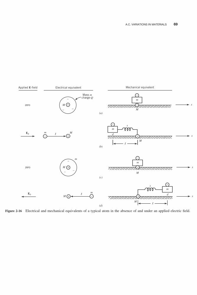
Balanis c02.tex V3 - 11/22/2011 3:07 P.M. Page 68
A.C. VARIATIONS IN MATERIALS 69
−m
s
s
x
x
x
x
−
− +
m
Mass mcharge-Q
zero
zero
Applied E-field
E0
E0
Electrical equivalent Mechanical equivalent
M
M
M
M
M
m
m
m
−
− −
+
+
+
−m
−m
M
+
M
M
d
(a)
(b)
(c)
(d)
d
−
− −
l
l+ −
l
l
+
+
Figure 2-16 Electrical and mechanical equivalents of a typical atom in the absence of and under an applied electric field.

Balanis c02.tex V3 - 11/22/2011 3:07 P.M. Page 70
70 ELECTRICAL PROPERTIES OF MATTER
stationary and the negative charge moves relative to the positive along a platform that exhibitsa friction (damping) coefficient d . In addition, the two charges will be connected with a springwhose spring (tension) coefficient is s . The entire mechanical equivalent of a typical atom thenconsists of the classical mass–spring system moving along a platform with friction.
When an electric field is applied that is directed along the +x direction, the negative chargewill be displaced a distance � in the negative x direction, as shown in Figure 2-16b, forming anelectric dipole. If the material is not permanently polarized (as are the electrets), the atom willachieve its initial normal position when the applied electric field diminishes to zero, as shownin Figure 2-16c. Now if the applied electric field is polarized in the −x direction, the negativecharge will move a distance � in the positive x direction, as shown in Figure 2-16d , formingagain an electric dipole in the direction opposite of that in Figure 2-16b.
When a time-harmonic field of angular frequency ω is applied to an atom, the forces of thesystem that describe the movement of the negative charge of mass m relative to the stationarynucleus and that are opposed by damping (friction) and tension (spring) can be represented by[6, 19]
md2�
dt2+ d
d�
dt+ s� = Q�(t) = QE0ejωt (2-49)
By dividing both sides of (2-49) by m , we can write it as
d2�
dt2+ 2α
d�
dt+ ω2
0� = Q
m�(t) = Q
mE0ejωt (2-50)
where
α = d
2m(2-50a)
ω0 =√
s
m(2-50b)
Q = dipole charge (2-50c)
The terms on the left side of (2-49) represent, in order, the forces associated with mass timesacceleration, damping times velocity, and spring times displacement. The term on the right siderepresents the driving force of the time-harmonic applied field (of peak value QE0). Equations 2-49and 2-50 are second-order differential equations that are also representative of the natural responsesof RLC circuit systems.
For a source-free series RLC network, (2-50) takes the form for the current i (t) of
d2i
dt2+ 2α
di
dt+ ω2
0i = 0 (2-51)
where
α = R
2L(2-51a)
ω0 = 1√LC
(2-51b)
In a similar manner, the voltage v(t) for a parallel source-free RLC network can be obtained bywriting (2-50) as
d2v
dt2+ 2α
dv
dt+ ω2
0v = 0 (2-52)
Balanis c02.tex V3 - 11/22/2011 3:07 P.M. Page 71
A.C. VARIATIONS IN MATERIALS 71
where
α = 1
2RC(2-52a)
ω0 = 1√LC
(2-52b)
Solutions to (2-51) and (2-52) can be classified as overdamped, critically damped , or under-damped according to the values of the α/ω0 ratio. That is, the solution to (2-51) for i (t) or (2-52)for v(t) is considered
Classification of Solution Criterion
overdamped if α > ω0 (2-53a)
critically damped if α = ω0 (2-53b)
underdamped if α < ω0 (2-53c)
The solutions to (2-49) can be obtained by first dividing both of its sides by m . Doing thisreduces (2-49) to
d2�
dt2+ d
m
d�
dt+ s
m� = Q
mE0ejωt (2-54)
The general solution to (2-54) is usually composed of two parts: a complementary solution �c
and a particular solution �p . The complementary solution represents the transient response of thesystem and is obtained by setting the driving force equal to zero. Since (2-54) is a quadratic,the general form of the complementary (transient) solution will be in terms of exponentialswhose values vanish as t → ∞. The particular solution represents the steady-state response ofthe system, and it is of interest here. Thus the particular (steady-state) solution of (2-54) can bewritten as
�p(t) = �0ejωt (2-55)
where �0 is the solution of �p(t) when t = 0.Substituting (2-55) into (2-54) leads to
�0 =Qm E0
(ω20 − ω2) + jω
(d
m
) (2-56)
where
ω0 =√
s
m(2-56a)
Thus (2-55) can be written as
�p(t) = �0ejωt =Q
mE0ejωt
(ω20 − ω2) + jω
(d
m
) (2-57)
and it represents the steady-state displacements of the negative charges (electrons) of an atomrelative to those of the positive charges (nucleus).
Balanis c02.tex V3 - 11/22/2011 3:07 P.M. Page 72
72 ELECTRICAL PROPERTIES OF MATTER
The resonant (natural) angular frequency ωd of the system is obtained by setting E0 = 0 in(2-54). Doing this and assuming an underdamped system (α < ω0 or d < 2
√sm) leads to
ωd =√
ω20 − α2 =
√s
m−
(d
2m
)2
(2-58)
For a frictionless system (d = 0) the resonant angular frequency ωd reduces to
ωd |d=0 = ω0 =√
s
m(2-58a)
Assuming that the oscillating dipoles, which represent the numerous atoms of a material, areall similar and there is no coupling between the dipoles (atoms), the macroscopic steady-stateelectric polarization � of (2-5) can be written using (2-57) as
� = �(t) = NeQ�(t) =Ne
(Q2
m
)E0ejωt
(ω20 − ω2) + jω
(d
m
) =Ne
(Q2
m
)�(t)
(ω20 − ω2) + jω
(d
m
) (2-59)
where Ne represents the number of dipoles per unit volume. Dividing both sides of (2-59) by�(t) = E0ejωt reduces it to
�
�=
Ne
(Q2
m
)(ω2
0 − ω2) + jω
(d
m
) (2-60)
In turn the permittivity ε̇ of the medium can be written, using (2-10a) and (2-11a), as
ε̇ = ε0 + �
�= ε0 +
Ne
(Q2
m
)(ω2
0 − ω2) + jω
(d
m
) = ε′ − jε′′ (2-61)
which is recognized as being complex, as denoted by the dot (with real and imaginary parts,respectively, of ε′ and ε′′). Equation (2-61) is also referred to as the dispersion equation for thecomplex permittivity.
The relative complex permittivity ε̇r of the material is obtained by dividing both sides of(2-61) by ε0 leading to
ε̇r = ε̇
ε0= ε′
r − jε′′r = 1 +
NeQ2
ε0m
(ω20 − ω2) + jω
d
m
(2-62)
The real ε′r and imaginary ε′′
r parts of (2-62) can be written, respectively, as
ε′r = 1 +
NeQ2
ε0m(ω2
0 − ω2)
(ω20 − ω2)2 +
(ω
d
m
)2 (2-63a)

Balanis c02.tex V3 - 11/22/2011 3:07 P.M. Page 73
A.C. VARIATIONS IN MATERIALS 73
ε′′r = NeQ2
ε0m
⎡⎢⎢⎢⎣ ωd
m
(ω20 − ω2)2 +
(ω
d
m
)2
⎤⎥⎥⎥⎦ (2-63b)
For nonmagnetic materialε̇r = ṅ2 (2-64)
where ṅ is the complex index of refraction. For materials with no damping (d/m = 0), (2-63a)and (2-63b) reduce to
ε′r = 1 +
NeQ2
ε0mω2
0 − ω2(2-65a)
ε′′r = 0 (2-65b)
Since the permittivity of a medium as given by (2-61) [or its relative value as given by (2-62)]is in general complex, the Maxwell–Ampere equation can be written as
∇ × H = Ji + Jc + jωε̇E = Ji + σs E + jω(ε′ − jε′′)E
∇ × H = Ji + (σs + ωε′′)E + jωε′E = Ji + σeE + jωε′E (2-66)
where
σe = equivalent conductivity = σs + ωε′′ = σs + σa (2-66a)
σa = alternating field conductivity = ωε′′ (2-66b)
σs = static field conductivity (2-66c)
={
−μeqve for conductors
−μeqve + μhqvh for semiconductors(2-66d)
In (2-66a) σe represents the total (referred to here as the equivalent) conductivity composedof the static portion σs and the alternating part σa caused by the rotation of the dipoles as theyattempt to align with the applied field when its polarity is alternating. The phenomenon (rotationof dipoles) that contributes the alternating conductivity σa is referred to as dielectric hysteresis .
Many dielectric materials (such as glass and plastic) possess very low values of static σs con-ductivities and behave as good insulators. However, when they are subjected to alternating fields,they exhibit very high values of alternating field σa conductivities and they consume considerableenergy. The heat generated by this radio frequency process is used for industrial heating pro-cesses. The best-known process is that of microwave cooking [13–18]. Others include selectiveheating of human tissue for tumor treatment [20–22] and selective heating of certain compoundsin materials that possess conductivities higher than the other constituents. For example, pyrite (aform of sulfur considered to be a pollutant), which exhibits higher conductivities than the otherminerals of coal, can be heated selectively. This technique has been used as a process to cleancoal by extracting, through microwave heating, its sulfur content.
In (2-66), aside from the impressed (source) electric current density Ji , there are two othercomponents: the effective conduction electric current density Jce and the effective displacementelectric current density Jde . Thus we can write the total electric current density Jt as
Jt = Ji + Jce + Jde = Ji + σeE + jωε′E (2-67)
Balanis c02.tex V3 - 11/22/2011 3:07 P.M. Page 74
74 ELECTRICAL PROPERTIES OF MATTER
where
Jt = total electric current density (2-67a)
Ji = impressed (source) electric current density (2-67b)
Jce = effective electric conduction current density
= σeE = (σs + ωε′′)E (2-67c)
Jde = effective displacement electric current density
= jωε′E (2-67d)
The total electric current density of (2-67) can also be written as
Jt = Ji + σeE + jωε′E = Ji + jωε′(
1 − jσe
ωε′)
E = Ji + jωε′(1 − j tan δe)E (2-68)
where
tan δe = effective electric loss tangent = σe
ωε′ = σs + σa
ωε′ = σs
ωε′ + σa
ωε′
tan δe = σs
ωε′ + ε′′
ε′ = tan δs + tan δa = ε′′e
ε′e
(2-68a)
tan δs = static electric loss tangent = σs
ωε′ (2-68b)
tan δa = alternating electric loss tangent = σa
ωε′ = ε′′
ε′ (2-68c)
The manufacturer of any given material usually specifies either the conductivity (S/m) or theelectric loss tangent (tan δ, dimensionless). Although it is usually not stated as such, the specifiedconductivity σe and loss tangent should represent, respectively, the effective conductivity andloss tangent tan δe at a given frequency. Typical values of loss tangent for some materials arelisted in Table 2-5.
The effective conduction Jce and displacement Jde current densities of (2-67) can also bewritten as
Jcd = Jce + Jde = σeE + jωε′E = jωε′(
1 − jσe
ωε′)
E = jωε′(1 − j tan δe)E (2-69)
In phasor form, these can be represented as shown in Figure 2-17. It is evident that theconduction and displacement current densities are orthogonal to each other. Material can also beclassified as good dielectrics or good conductors according to the values of the σe/ωε′ ratio. Thatis
1. Good Dielectrics , (σe/ωε′) � 1
Jcd = jωε′(
1 − jσe
ωε′)
Eσe/ωε′�1� jωε′E (2-70a)
For these materials, the displacement current density is much greater than the conductioncurrent density, and the total current density is approximately equal to the displacementcurrent density.
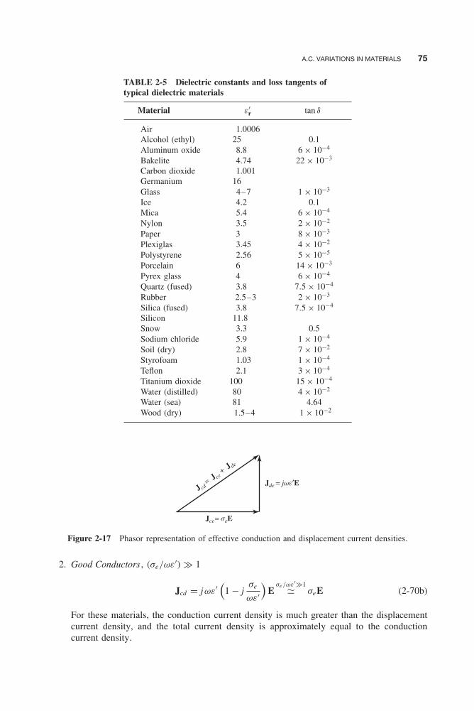
Balanis c02.tex V3 - 11/22/2011 3:07 P.M. Page 75
A.C. VARIATIONS IN MATERIALS 75
TABLE 2-5 Dielectric constants and loss tangents oftypical dielectric materials
Material ε′r tan δ
Air 1.0006Alcohol (ethyl) 25 0.1Aluminum oxide 8.8 6 × 10⁻⁴
Bakelite 4.74 22 × 10−3
Carbon dioxide 1.001Germanium 16Glass 4–7 1 × 10⁻³
Ice 4.2 0.1Mica 5.4 6 × 10⁻⁴
Nylon 3.5 2 × 10⁻²
Paper 3 8 × 10⁻³
Plexiglas 3.45 4 × 10⁻²
Polystyrene 2.56 5 × 10⁻⁵
Porcelain 6 14 × 10−3
Pyrex glass 4 6 × 10⁻⁴
Quartz (fused) 3.8 7.5 × 10⁻⁴
Rubber 2.5–3 2 × 10⁻³
Silica (fused) 3.8 7.5 × 10⁻⁴
Silicon 11.8Snow 3.3 0.5Sodium chloride 5.9 1 × 10⁻⁴
Soil (dry) 2.8 7 × 10⁻²
Styrofoam 1.03 1 × 10⁻⁴
Teflon 2.1 3 × 10⁻⁴
Titanium dioxide 100 15 × 10−4
Water (distilled) 80 4 × 10⁻²
Water (sea) 81 4.64Wood (dry) 1.5–4 1 × 10⁻²
Jce= seE
Jde = jwe′E J cd
= J ce + J de
Figure 2-17 Phasor representation of effective conduction and displacement current densities.
2. Good Conductors , (σe/ωε′) � 1
Jcd = jωε′(
1 − jσe
ωε′)
Eσe/ωε′�1� σeE (2-70b)
For these materials, the conduction current density is much greater than the displacementcurrent density, and the total current density is approximately equal to the conductioncurrent density.
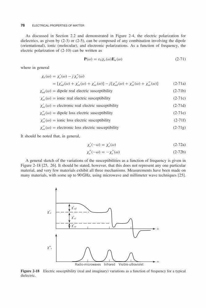
Balanis c02.tex V3 - 11/22/2011 3:07 P.M. Page 76
76 ELECTRICAL PROPERTIES OF MATTER
As discussed in Section 2.2 and demonstrated in Figure 2-4, the electric polarization fordielectrics, as given by (2-3) or (2-5), can be composed of any combination involving the dipole(orientational), ionic (molecular), and electronic polarizations. As a function of frequency, theelectric polarization of (2-10) can be written as
P(ω) = ε0χe(ω)Ea(ω) (2-71)
where in general
χe(ω) = χ ′e(ω) − jχ ′′
e (ω)
= [χ ′ed (ω) + χ ′
ei (ω) + χ ′ee(ω)] − j [χ ′′
ed (ω) + χ ′′ei (ω) + χ ′′
ee(ω)] (2-71a)
χ ′ed (ω) = dipole real electric susceptibility (2-71b)
χ ′ei (ω) = ionic real electric susceptibility (2-71c)
χ ′ee(ω) = electronic real electric susceptibility (2-71d)
χ ′′ed (ω) = dipole loss electric susceptibility (2-71e)
χ ′′ei (ω) = ionic loss electric susceptibility (2-71f)
χ ′′ee(ω) = electronic loss electric susceptibility (2-71g)
It should be noted that, in general,
χ ′e(−ω) = χ ′
e(ω) (2-72a)
χ ′′e (−ω) = −χ ′′
e (ω) (2-72b)
A general sketch of the variations of the susceptibilities as a function of frequency is given inFigure 2-18 [25, 26]. It should be stated, however, that this does not represent any one particularmaterial, and very few materials exhibit all three mechanisms. Measurements have been made onmany materials, with some up to 90 GHz, using microwave and millimeter wave techniques [25].
w
χ′e
Radio-microwaves Infrared Visible-ultravioletw
χ′′e
χ′ed
χ′ei
χ′ee
Figure 2-18 Electric susceptibility (real and imaginary) variations as a function of frequency for a typicaldielectric.
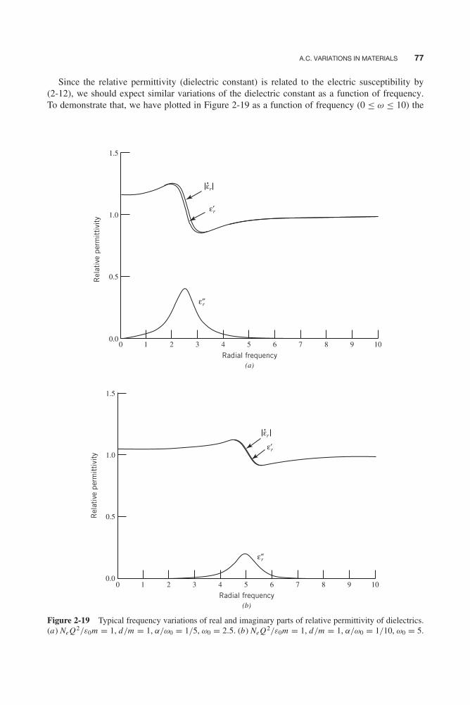
Balanis c02.tex V3 - 11/22/2011 3:07 P.M. Page 77
A.C. VARIATIONS IN MATERIALS 77
Since the relative permittivity (dielectric constant) is related to the electric susceptibility by(2-12), we should expect similar variations of the dielectric constant as a function of frequency.To demonstrate that, we have plotted in Figure 2-19 as a function of frequency (0 ≤ ω ≤ 10) the
1.5
εr
ε′r
ε′r
ε″r
ε″r
1.0
0.5Rel
ativ
e pe
rmit
tivi
tyR
elat
ive
perm
itti
vity
0.0
1.5
1.0
0.5
0.0
0 1 2 3 4
Radial frequency(a)
Radial frequency(b)
5 6 7 8 9 10
0 1 2 3 4 5 6 7 8 9 10
εr
Figure 2-19 Typical frequency variations of real and imaginary parts of relative permittivity of dielectrics.(a) NeQ2/ε0m = 1, d/m = 1, α/ω0 = 1/5, ω0 = 2.5. (b) NeQ2/ε0m = 1, d/m = 1, α/ω0 = 1/10, ω0 = 5.
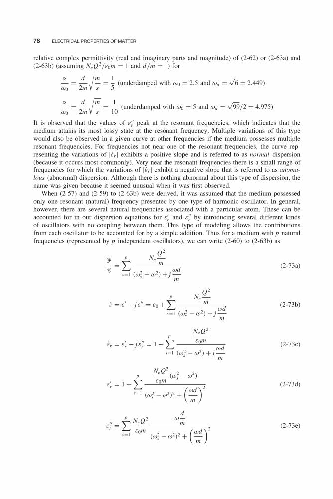
Balanis c02.tex V3 - 11/22/2011 3:07 P.M. Page 78
78 ELECTRICAL PROPERTIES OF MATTER
relative complex permittivity (real and imaginary parts and magnitude) of (2-62) or (2-63a) and(2-63b) (assuming NeQ2/ε0m = 1 and d/m = 1) for
α
ω0= d
2m
√m
s= 1
5(underdamped with ω0 = 2.5 and ωd =
√6 = 2.449)
α
ω0= d
2m
√m
s= 1
10(underdamped with ω0 = 5 and ωd =
√99/2 = 4.975)
It is observed that the values of ε′′r peak at the resonant frequencies, which indicates that the
medium attains its most lossy state at the resonant frequency. Multiple variations of this typewould also be observed in a given curve at other frequencies if the medium possesses multipleresonant frequencies. For frequencies not near one of the resonant frequencies, the curve rep-resenting the variations of |ε̇r | exhibits a positive slope and is referred to as normal dispersion(because it occurs most commonly). Very near the resonant frequencies there is a small range offrequencies for which the variations of |ε̇r | exhibit a negative slope that is referred to as anoma-lous (abnormal) dispersion. Although there is nothing abnormal about this type of dispersion, thename was given because it seemed unusual when it was first observed.
When (2-57) and (2-59) to (2-63b) were derived, it was assumed that the medium possessedonly one resonant (natural) frequency presented by one type of harmonic oscillator. In general,however, there are several natural frequencies associated with a particular atom. These can beaccounted for in our dispersion equations for ε′
r and ε′′r by introducing several different kinds
of oscillators with no coupling between them. This type of modeling allows the contributionsfrom each oscillator to be accounted for by a simple addition. Thus for a medium with p naturalfrequencies (represented by p independent oscillators), we can write (2-60) to (2-63b) as
�
�=
p∑s=1
NeQ2
m
(ω2s − ω2) + j
ωd
m
(2-73a)
ε̇ = ε′ − jε′′ = ε0 +p∑
s=1
NeQ2
m
(ω2s − ω2) + j
ωd
m
(2-73b)
ε̇r = ε′r − jε′′
r = 1 +p∑
s=1
NeQ2
ε0m
(ω2s − ω2) + j
ωd
m
(2-73c)
ε′r = 1 +
p∑s=1
NeQ2
ε0m(ω2
s − ω2)
(ω2s − ω2)2 +
(ωd
m
)2 (2-73d)
ε′′r =
p∑s=1
NeQ2
ε0m
ωd
m
(ω2s − ω2)2 +
(ωd
m
)2 (2-73e)
Balanis c02.tex V3 - 11/22/2011 3:07 P.M. Page 79
A.C. VARIATIONS IN MATERIALS 79
Often the question is asked whether there are any relations between the real and imaginaryparts of the complex permittivity. The answer to that is yes. Known as the Kramers–Kronig[26–28] relations, they are given by
ε′r (ω) = 1 + 2
π
∫ ∞
0
ω′ε′′r (ω′)
(ω′)2 − ω2dω′ (2-74a)
ε′′r (ω) = 2ω
π
∫ ∞
0
1 − ε′r (ω
′)(ω′)2 − ω2
dω′ (2-74b)
and they are very similar to the frequency relations between resistance and reactance in circuittheory [28].
In addition to the Kramers–Kronig relations of (2-74a) and (2-74b), there are simple relationsthat allow the calculation of the real and imaginary parts of the complex relative permittivity formany materials as a function of frequency provided that the real part of the complex permittivityis known at zero frequency (denoted by ε′
rs ) and at very large (ideally infinity) frequency (denotedby ε′
r∞). These relations are obtained from the well-known Debye equation [19, 23, 24] for thecomplex dielectric constant, which states that
ε̇r (ω) = ε′r (ω) − jε′′
r (ω) = ε′r∞ + ε′
rs − ε′r∞
1 + jωτe(2-75)
where τe is a new relaxation time constant related to original relaxation time constant τ by
τe = τε′
rs + 2
ε′r∞ + 2
(2-75a)
The Debye equation of (2-75) is derived using the Clausius–Mosotti equation [23, 24, 29]. Thereal and imaginary parts of (2-75) can be written as
ε′r (ω) = ε′
r∞ + ε′rs − ε′
r∞1 + (ωτe)2
(2-76a)
ε′′r (ω) = (ε′
rs − ε′r∞)ωτe
1 + (ωτe)2(2-76b)
which can be found at any frequency provided ε′rs , ε′
r∞, and τ are known. The relations of(2-76a) and (2-76b) can be used to estimate the real and imaginary parts of the complex relativepermittivity (complex dielectric constant) for many gases, liquids, and solids.
2.9.2 Complex Permeability
As discussed in Section 2.3, the permeability of most dielectric material, including diamagnetic,paramagnetic, and antiferromagnetic material, is nearly the same as that of free space μ0 (μ0 =4π × 10−7 H/m). Ferromagnetic and ferrimagnetic materials exhibit much higher permeabilitythan free space, as is demonstrated by the data of Table 2-2. These classes of materials arealso magnetically lossy, and their magnetic losses are accounted for by introducing a complexpermeability.
In general then, we can write the Maxwell–Faraday equation as
∇ × E = −Mi − jωμ̇H = −Mi − jω(μ′ − jμ′′)H
= −Mi − jωμ′H − ωμ′′H = −Mt (2-77)

Balanis c02.tex V3 - 11/22/2011 3:07 P.M. Page 80
80 ELECTRICAL PROPERTIES OF MATTER
where
Mt = Mi + jωμ′H + ωμ′′H (2-77a)
Mt = total magnetic current density (2-77b)
Mi = impressed (source) magnetic current density (2-77c)
Md = displacement magnetic current density = jωμ′H (2-77d)
Mc = conduction magnetic current density = ωμ′′H (2-77e)
Another form of (2-77a) is to write it as
Mt = Mi + jωμ′(
1 − jμ′′
μ′
)H = Mi + jωμ′(1 − j tan δm)H (2-78)
where
tan δm = alternating magnetic loss tangent = μ′′
μ′ (2-78a)
In addition to being complex, the permeability of ferromagnetic and ferrimagnetic material isoften a function of frequency. Thus it should, in general, be written as
μ̇ = μ′(ω) − jμ′′(ω) (2-79)
or
μ̇r = μ̇
μ0= μ′
r (ω) − jμ′′r (ω) (2-79a)
Most ferromagnetic materials possess very high relative permeabilities (on the order of severalthousand) and good conductivities such that there is a minimum interaction between these materi-als and the electromagnetic waves propagating through them. As such, they will not be discussedfurther here. There is, however, a class of ferrimagnetic material, referred to as ferrites , thatfinds wide applications in the design of nonreciprocal microwave components (such as isolators,hybrids, gyrators, phase shifters, etc.). Ferrites become attractive for these applications becauseat microwave frequencies they exhibit strong magnetic effects that result in anisotropic propertiesand large resistances (good insulators). These resistances limit the current induced in them and inturn result in lower ohmic losses. Because of the appeal of ferrites to microwave circuit design,their magnetic properties will be discussed further in the section that follows.
2.9.3 Ferrites
Ferrites are a class of solid ceramic materials that have crystal structures formed by sintering athigh temperatures (typically 1000–1500◦C) stoichiometric mixtures of certain metal oxides (suchas oxygen and iron, and cadmium, lithium, magnesium, nickel, or zinc, or some combination ofthem). These materials are ferrimagnetic, and they are considered to be good insulators with highpermeabilities, dielectric constants between 10 to 15 or greater, and specific resistivities as much as1014 greater than those of metals. In addition, they possess properties that allow strong interactionbetween the magnetic dipole moment associated with the electron spin, as discussed in Section 2.3,and the microwave electromagnetic fields [30–32]. In contrast to ferromagnetic materials, ferriteshave their magnetic ions distributed over at least two interpenetrating sublattices. Within eachsublattice all magnetic moments are aligned, but the sublattices are oppositely directed.
As a result of these interactions, ferrites exhibit nonreciprocal properties such as different phaseconstants and phase velocities for right- and left-hand circularly polarized waves, transmission
Balanis c02.tex V3 - 11/22/2011 3:07 P.M. Page 81
A.C. VARIATIONS IN MATERIALS 81
coefficients that are functions of direction of travel, and permeabilities that are represented bytensors (in the form of a matrix) rather than by a single scalar. These characteristics becomeimportant in the design of nonreciprocal microwave devices [33–35]. Although all ferrimagneticmaterials possess these properties, it is only in ferrites that they are pronounced and significant.The properties of ferrites will be discussed here by examining the propagation of microwaveelectromagnetic waves in an unbounded ferrite material.
There are two possible models that can be used to understand the technical properties ofmagnetic material: the phenomenological model and the atomic model [32]. For the purposesof this book, the phenomenological model is sufficient to examine the properties of magneticoxides. As discussed in Section 2.3, the magnetic material is replaced by an array of magneticdipoles that are maintained in a permanent and rigid alignment as shown in Figure 2-8a . Whena magnetic field is applied, as shown in Figure 2-8b, the magnetic moments of the dipoles canturn freely in space as long as they turn together. Much of the discussion of this section followsthat of [32] and [35].
Under an applied magnetic field, each single magnetic dipole rotates with a precession fre-quency that is referred to as the Larmor precession frequency . The precession frequency is alteredwhen one or more dipoles are introduced. The dipoles in the array interact with each other andattempt to achieve an alignment that will minimize the interaction energy. The change in pre-cession frequency is equivalent to introducing an additional demagnetizing field. When manydipole arrays are subjected to d.c, rf, or demagnetizing fields, magnetic resonance is introduced.This is a phenomenon that is of fundamental interest to the design of microwave nonreciprocalcomponents. The discussion here will be that of the phenomenological model.
The magnetic dipole moment m of a single magnetic dipole of Figure 2-7a or 2-7b is given by(2-13). When an external magnetic field is applied, as shown in Figure 2-20 for a single dipole,exerted on the dipole is a torque T of
T = μ0m × H0 = m × B0 (2-80)
z
y
f
m
B0
gB0 × P = T
P
w0
x
Figure 2-20 Torque on a single magnetic dipole caused by an applied external magnetic field. (Source:R. E. Collin, Foundations for Microwave Engineering , 2nd Edition, 1992, McGraw-Hill Book Co.).
Balanis c02.tex V3 - 11/22/2011 3:07 P.M. Page 82
82 ELECTRICAL PROPERTIES OF MATTER
where m = n̂ I ds = magnetic dipole moment of a single dipoleH0 = applied magnetic fieldB0 = applied magnetic flux density
The torque will cause the dipole to precess about the z axis, which is parallel to B0, as shown inFigure 2-20.
The interaction energy Wm between the dipole and the applied field can be expressed as
Wm = −μ0mH0 cos φ (2-81)
T = −∂Wm
∂φ(2-81a)
where φ is the angle between the applied magnetic field and the magnetic dipole axis. It isobserved that the energy is minimum (Wm = −μ0mH0) when φ = 0 whereas when φ = π , T iszero and the dipole is in unstable equilibrium.
When electrons of a physically realizable dipole are moving, they create a current whosemotion is associated with a circulation of mass (angular momentum) as well as charge. Thereforethe magnetic dipole moment of a single electron of charge e, which is moving with a velocity vin a circle of radius a , can be also be expressed as
m = I ds = ev
2πa(πa2) = 1
2eva (2-82)
and the angular momentum P can be written as
P = meva (2-83)
where me is the mass of the electron. The ratio of the magnetic moment [as given by (2-82)] tothe angular momentum [as given by (2-83)] is referred to as the gyromagnetic ratio γ , and it isequal to
γ = m
P= e
2me⇒ m = γ P (2-84)
which is negative because of the negative electron charge e. This makes the angular momentumP of the electron antiparallel to the magnetic dipole moment m, as shown in Figure 2-20.
To obtain the equation of motion we set the rate of change (with time) of the angular momentumequal to the torque, that is,
dPdt
= T = μ0m × H0 = −μ0|γ |P × H0 = −P × ω0 = ω0 × P (2-85)
orμ0|γ |PH0 sin φ = ω0P sin φ = −μ0mH0 sin φ (2-85a)
In (2-85) and (2-85a) ω0 is the vector precession angular velocity which is directed along H0,as shown in Figure 2-20. For the free precession of a single dipole, the angular velocity ω0 isreferred to as the Larmor precession frequency , which is given by
ω0 = |γ |μ0H0 = |γ |B0 (2-86)
and it is independent of the angle φ.Let us assume that on the static applied field B0 a small a.c. magnetic field B1 is superimposed.
This additional applied field will impose a forced precession on the magnetic dipole. To examine
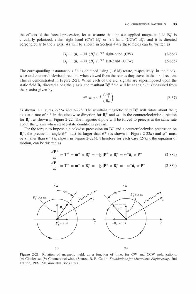
Balanis c02.tex V3 - 11/22/2011 3:07 P.M. Page 83
A.C. VARIATIONS IN MATERIALS 83
the effects of the forced precession, let us assume that the a.c. applied magnetic field B±1 is
circularly polarized, either right hand (CW) B+1 or left hand (CCW) B−
1 , and it is directedperpendicular to the z axis. As will be shown in Section 4.4.2 these fields can be written as
B+1 = (âx − j ây )B
+1 e−jβz right-hand (CW) (2-86a)
B−1 = (âx + j ây )B
−1 e−jβz left-hand (CCW) (2-86b)
The corresponding instantaneous fields obtained using (1-61d) rotate, respectively, in the clock-wise and counterclockwise directions when viewed from the rear as they travel in the +z direction.This is demonstrated in Figure 2-21. When each of the a.c. signals are superimposed upon thestatic field B0 directed along the z axis, the resultant B±
t field will be at angle θ± (measured fromthe z axis) given by
θ± = tan−1
(B±
1
B0
)(2-87)
as shown in Figures 2-22a and 2-22b. The resultant magnetic field B±t will rotate about the z
axis at a rate of ω+ in the clockwise direction for B+t and ω− in the counterclockwise direction
for B−t , as shown in Figure 2-22. The magnetic dipole will be forced to precess at the same rate
about the z axis when steady-state conditions prevail.For the torque to impose a clockwise precession on B+
t and a counterclockwise precession onB−
t , the precession angle φ+ must be larger than θ+ (as shown in Figure 2-22a) and φ− mustbe smaller than θ− (as shown in Figure 2-22b). Therefore for each case (2-85), the equation ofmotion, can be written as
dP+
dt= T+ = m+ × B+
t = −|γ |P+ × B+t = ω+âz × P+ (2-88a)
dP−
dt= T− = m− × B−
t = −|γ |P− × B−t = −ω−âz × P− (2-88b)
x x
z z
y y
(a) (b)
wt
B1 COS wt
wt+
B1 sin wt+ B1 sin wt−
B1 cos wt−
−
B1+
B1−
Figure 2-21 Rotation of magnetic field, as a function of time, for CW and CCW polarizations.(a) Clockwise. (b) Counterclockwise. (Source: R. E. Collin, Foundations for Microwave Engineering , 2ndEdition, 1992, McGraw-Hill Book Co.).
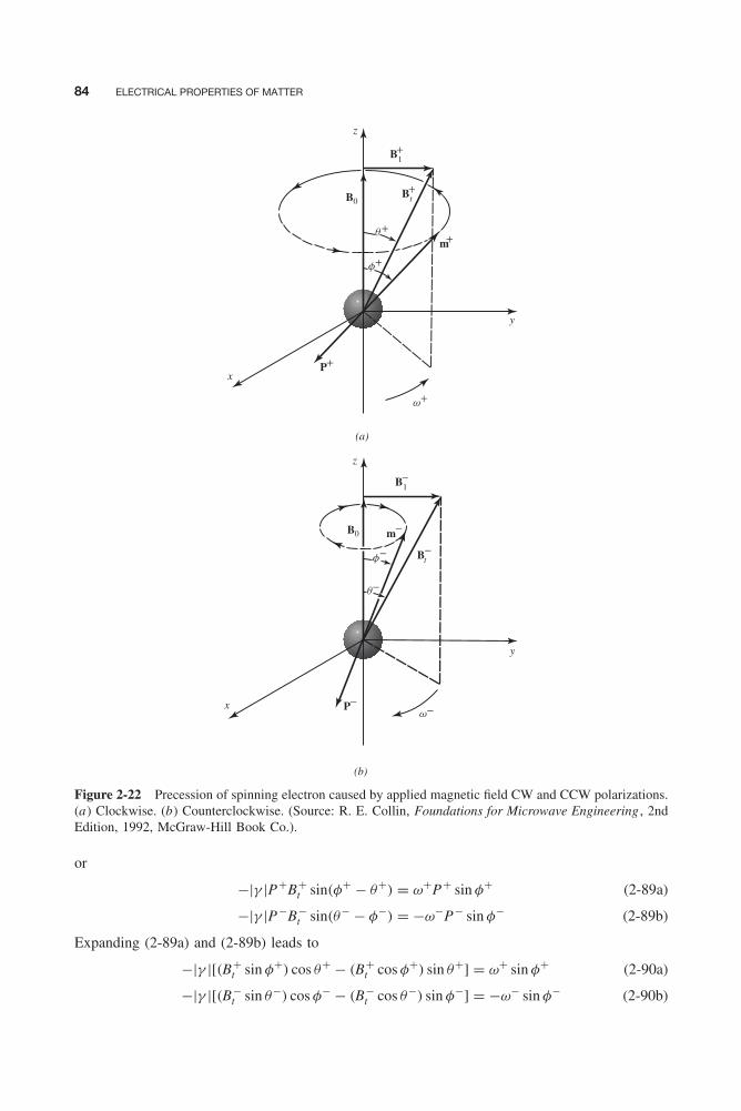
Balanis c02.tex V3 - 11/22/2011 3:07 P.M. Page 84
84 ELECTRICAL PROPERTIES OF MATTER
z
z
y
y
x
x
(a)
(b)
w+
w−
BB0
B0 m
t
t
+
f+
q+
f−
P+
P−
m+
B1+
B1−
−
B−
q−
Figure 2-22 Precession of spinning electron caused by applied magnetic field CW and CCW polarizations.(a) Clockwise. (b) Counterclockwise. (Source: R. E. Collin, Foundations for Microwave Engineering , 2ndEdition, 1992, McGraw-Hill Book Co.).
or
−|γ |P+B+t sin(φ+ − θ+) = ω+P+ sin φ+ (2-89a)
−|γ |P−B−t sin(θ− − φ−) = −ω−P− sin φ− (2-89b)
Expanding (2-89a) and (2-89b) leads to
−|γ |[(B+t sin φ+) cos θ+ − (B+
t cos φ+) sin θ+] = ω+ sin φ+ (2-90a)
−|γ |[(B−t sin θ−) cos φ− − (B−
t cos θ−) sin φ−] = −ω− sin φ− (2-90b)

Balanis c02.tex V3 - 11/22/2011 3:07 P.M. Page 85
A.C. VARIATIONS IN MATERIALS 85
Since
B+t sin θ+ = B+
1 (2-91a)
B+t cos θ+ = B0 (2-91b)
B−t sin θ− = B−
1 (2-91c)
B−t cos θ− = B0 (2-91d)
then (2-90a) and (2-90b) can be reduced, respectively, to
tan φ+ = |γ |B+1
|γ |B0 − ω+ = |γ |B+1
ω0 − ω+ (2-92a)
tan φ− = |γ |B−1
|γ |B0 + ω− = |γ |B−1
ω0 + ω− (2-92b)
According to Figure 2-22 the components m±t of m± that rotate in synchronism with their
respective B±1 , and m±
z that are directed along the z axis, are given, respectively, by
m±t = m± sin φ± = m± cos φ± sin φ±
cos φ± = m± cos φ± tan φ± = m±0 tan φ± (2-93a)
m±z = m± cos φ± = m±
0 (2-93b)
wherem±
0 = m± cos φ± (2-93c)
Using (2-92a) and (2-92b) we can write the components of m± that rotate in synchronism withB±
1 as
m+t = m+
0 tan φ+ = m+0 |γ |B+
1
ω0 − ω+ (2-94a)
m−t = m−
0 tan φ− = m−0 |γ |B−
1
ω0 + ω− (2-94b)
In the previous discussion we considered the essential properties of single spinning electronsin a magnetic field that is a superposition of a static magnetic field along the z axis and an a.c.circularly polarized field perpendicular to it. Let us now examine macroscopically the propertiesof N orbiting electrons per unit volume whose density is uniformly and continuously distributed.Doing this we can represent the total magnetization M of all N electrons as the product of Ntimes that of a single electron (M = N m), as given by (2-17). In addition, the magnetic fluxdensity M will be related to the magnetic field intensity H and magnetization vector M by (2-19). Thus we can write (2-19), using (2-94a) and (2-94b) for the magnetization of the N orbitingelectrons superimposed with the circularly polarized a.c. signal of B±
1 , as
B+ = μ0(H+1 + M+
1 ) = μ0(H+1 + N m+
t ) = μ0
(H+
1 + Nm+0 |γ |B+
1
ω0 − ω+
)= μ0
(1 + Nm+
0 |γ |μ0
ω0 − ω+
)H+
1 = μ0
(1 + μ0|γ |M +
0
ω0 − ω+
)H+
1 = μ+e H+
1 (2-95a)
Balanis c02.tex V3 - 11/22/2011 3:07 P.M. Page 86
86 ELECTRICAL PROPERTIES OF MATTER
B− = μ0(H−1 + M−
1 ) = μ0(H−1 + N m−
t ) = μ0
(H−
1 + Nm−0 |γ |B−
1
ω0 + ω−
)= μ0
(1 + Nm−
0 |γ |μ0
ω0 + ω−
)H−
1 = μ0
(1 + μ0|γ |M −
0
ω0 + ω−
)H−
1 = μ−e H−
1 (2-95b)
where
M +0 = Nm+
0 (2-95c)
M −0 = Nm−
0 (2-95d)
μ+e = μ0
(1 + μ0|γ |M +
0
ω0 − ω+
)
μ−e = μ0
(1 + μ0|γ |M −
0
ω0 + ω−
)(2-95e)
(2-95f)
In (2-95e) and (2-95f) μ+e and μ−
e represent, respectively, the effective permeabilities for clock-wise and counterclockwise circularly polarized waves. It is apparent that the two are not equal,which is a fundamental property utilized in the design of nonreciprocal microwave devices.
If the static magnetic field B0 is much larger than the superimposed a.c. magnetic field B±1
(B0 � B±1 ) so that the magnetization of the ferrite material is saturated by the static field, then
all the spinning dipoles are tightly coupled and the entire material acts as a large single magneticdipole. In that case the magnetization vector M± for the positive (CW) and negative (CCW)circularly polarized fields superimposed on the static field can be approximated by
M± = N m± � Ms � M0 (2-96)
where Ms is the magnetization vector caused by the static field when no time-varying magneticfield is applied. For those cases the effective permeabilities can be approximated by
μ+e � μ0
(1 + μ0|γ |Ms
ω0 − ω+
)
μ−e � μ0
(1 + μ0|γ |Ms
ω0 + ω−
)(2-97a)
(2-97b)
which are not equal. Equations 2-97a and 2-97b are good approximations when the a.c. signalsare small compared to the applied static field.
It can be shown (see Chapter 4) that a time-harmonic transverse electromagnetic (TEM) wavecan be decomposed into a combination of clockwise and counterclockwise circularly polarizedwaves. Therefore the implications of (2-97a) and (2-97b) are that when a TEM wave travelsthrough a ferrite material the clockwise circularly polarized portion of the wave will experiencethe permeability of (2-97a) while the counterclockwise wave will experience that of (2-97b). Sincethe permeability of a material influences the phase velocity and phase constant (see Chapter 4),the phases associated with (2-97a) and (2-97b) will be different. This is one of the fundamentalfeatures of ferrites that is utilized for the design of microwave nonreciprocal devices.

Balanis c02.tex V3 - 11/22/2011 3:07 P.M. Page 87
A.C. VARIATIONS IN MATERIALS 87
When an unbounded ferrite material is subjected to a static magnetic field B0 directed alongthe z axis of
B0 = âz B0 = âz μ0H0 (2-98a)
and a time-harmonic magnetic field � of
� = μ0� (2-98b)
each will induce a magnetization per unit volume vector of Ms , and �, respectively. The scriptis used to indicate time-varying components. Under these conditions, the equation of motion canbe written as
d(Ms + �)
dt= d�
dt= −|γ |[(Ms + �) × (B0 + �)] (2-99)
or in expanded form as
d�
dt= −|γ |μ0[(Ms + �) × (H0 + �)]
d�
dt= −|γ |μ0(Ms × H0 + Ms × � + � × H0 + � × �) (2-99a)
If the time-harmonic field � is small such that
|�| � |Ms | (2-100a)
|�| � |H0| (2-100b)
and since the applied magnetic field B0 is in the same direction as the static saturation magneti-zation vector Ms , or
Ms × H0 = 0 (2-101)
then (2-99a) can be approximated by
d�
dt� −|γ |μ0(Ms × � + � × H0) (2-102)
If each of the time-harmonic components is written in the form described by (1-61a) through(1-61d), then (2-102) ultimately reduces, using (2-86), to
jωM � −|γ |μ0(Ms × H + M × H0)
jωM + |γ |μ0M × H0 � −|γ |μ0Ms × H
jωM + |γ |M × B0 � −|γ |μ0Ms × H
jωM + M × (|γ |B0) � −|γ |μ0Ms × H
jωM + ω0M × âz � −|γ |μ0Ms × H (2-103)
Assuming Ms has only a z component, whereas H has both x and y components, expanding(2-103) leads to
jωMx + ω0My � |γ |μ0Ms Hy (2-104a)
−ω0Mx + jωMy � −|γ |μ0Ms Hx (2-104b)
jωMz � 0 (2-104c)
Balanis c02.tex V3 - 11/22/2011 3:07 P.M. Page 88
88 ELECTRICAL PROPERTIES OF MATTER
Solving (2-104a) through (2-104c) for Mx , My , and Mz leads to
Mx = ω0|γ |μ0Ms Hx + jω|γ |μ0Ms Hy
ω20 − ω2
(2-105a)
My = ω0|γ |μ0Ms Hy − jω|γ |μ0MsHx
ω20 − ω2
(2-105b)
Mz = 0 (2-105c)
By introducing the magnetic susceptibility tensor χ̄, we can write (2-105a) through (2-105c) usingthe forms of (2-21) and (2-22) as
[M ] = [χ][H ] (2-106)
or ⎡⎣ Mx
My
Mz
⎤⎦ =⎡⎣ χxx χxy 0
χyx χyy 00 0 0
⎤⎦⎡⎣ Hx
Hy
Hz
⎤⎦ (2-106a)
[B ] = μ0[[I ] + [χ]][H ] (2-107)
or ⎡⎣ Bx
By
Bz
⎤⎦ = μ0
⎡⎣ 1 + χxx χxy 0χyx 1 + χyy 00 0 1
⎤⎦⎡⎣ Hx
Hy
Hz
⎤⎦ (2-107a)
where
χxx = χyy = ω0|γ |μ0Ms
ω20 − ω2
(2-107b)
χxy = −χyx = jω|γ |μ0Ms
ω20 − ω2
(2-107c)
In (2-106) through (2-107c) χxx , χyy , χxy , and χyx represent the entries of the susceptibility tensorχ̄ for the ferrite material and [I ] is the unit matrix. Equation 2-107a can also be written in amore general form as
B = μ̄ • H (2-108)
where μ̄ is the permeability tensor written, in general, as a 3 × 3 matrix of the form
[μ̄] = μ0
⎡⎣ 1 + χxx χxy 0χyx 1 + χyy 00 0 1
⎤⎦ (2-108a)
which is a more general form of (2-22a).Practical ferrite materials also contain magnetic losses. Therefore the permeability of the mate-
rial will have both real and imaginary parts, as given by (2-79) or (2-79a). A phenomenologicalmodel used to derive the variations as a function of frequency of the real μ′(ω) and imagi-nary μ′′(ω) parts of both (2-95e) and (2-95f) when losses are included is somewhat complexand beyond the treatment presented here for ferrites. However, the development of this can befound in [35] and [36]. A typical plot as a function of ω0/ω is shown in Figure 2-23 whereωm = μ0|γ |Ms . A resonance phenomenon is indicated when ω0/ω = 1.

Balanis c02.tex V3 - 11/22/2011 3:07 P.M. Page 89
MULTIMEDIA 89
m″m0
+
m′
m0
+
m′
m0
−
m″
m0
−
w0w
10
8
6
4
2
0
0 0.5 1.0 1.5 2.0–4
–2
Figure 2-23 Frequency variations of real and imaginary parts of complex permeability for circularlypolarized waves in a ferrite (ω = 20π GHz, ωm = 11.2π GHz, α = 0.05). (Source: R. E. Collin, Foundationsfor Microwave Engineering , 2nd Edition, 1992, McGraw-Hill Book Co.).
2.10 MULTIMEDIA
On the website that accompanies this book, the following multimedia resources are included forthe review, understanding and presentation of the material of this chapter.
• Power Point (PPT) viewgraphs, in multicolor.
REFERENCES
1. R. R. Wright and H. R. Skutt, Electronics: Circuits and Devices , Ronald Press, New York, 1965.
2. S. V. Marshall and G. G. Skitek, Electromagnetic Concepts and Applications , Second Edition, Prentice-Hall, Englewood Cliffs, NJ, 1987.
3. R. M. Rose, L. A. Shepard, and J. Wulff, Electronic Properties , John Wiley & Sons, New York, p. 262,1966.
4. M. F. Uman, Introduction to the Physics of Electronics , Prentice-Hall, Englewood Cliffs, NJ, 1974.
5. E. M. Conwell, “Properties of silicon and germanium: II,” Proc. IRE , vol. 46, pp. 1281–1300, June1958.
6. J. D. Kraus, Electromagnetics , Fourth Edition, McGraw-Hill, New York, 1992.
Balanis c02.tex V3 - 11/22/2011 3:07 P.M. Page 90
90 ELECTRICAL PROPERTIES OF MATTER
7. F. London, Superfluids , vol. 1, Dover, New York, 1961.8. A. C. Rose-Innes and E. H. Rhoderick, Introduction to Superconductivity , Pergamon, Elmsford, NY,
1978.9. J. Bardeen, L. N. Cooper, and J. R. Schrieffer, “Microscopic Theory of Superconductivity,” Physical
Review , vol. 106, pp. 162–164, 1957.10. B. C. Fenton, “Superconductivity breakthroughs,” Radio Electronics , vol. 59, no. 2, pp. 43–45, February
1988.11. A. Khurana, “Superconductivity seen above the boiling point of nitrogen,” Physics Today , vol. 40,
no. 4, pp. 17–23, April 1987.12. P. C. W. Chu, “High Temperature Superconductivity: Past, Present and Future,” APS Colloquium,
Argonne National Laboratory, October 2, 2002.13. G. P. de Loor and F. W. Meijboom, “The dielectric constant of foods and other materials with high
water content at microwave frequencies,” Journal of Food Technology , vol. 1, no. 1, pp. 313–322,1966.
14. W. E. Pace, W. B. Westphal, and S. A. Goldblith, “Dielectric properties of commercial cooking oils,”Journal of Food Science, vol. 33, p. 30, 1968.
15. D. Van Dyke, D. I. C. Wang, and S. A. Goldblith, “Dielectric loss factor of reconstituted ground beef:The effect of chemical composition,” Journal of Food Technology , vol. 23, p. 944, 1969.
16. N. E. Bengtsson and P. O. Risman, “Dielectric properties of foods at 3 GHz as determined by a cavityperturbation technique. II. Measurements on food materials,” Journal of Microwave Power , vol. 6,no. 2, pp. 107–123, 1971.
17. S. S. Stuchly and M. A. K. Hamid, “Physical properties in microwave heating processes,” Journal ofMicrowave Power , vol. 7, no. 2, p. 117, 1972.
18. N. E. Bengtsson and T. Ohlsson, “Microwave heating in the food industry,” Proc. IEEE , vol. 62,no. 1, pp. 44–55, January 1974.
19. P. Debye, Polar Molecules , Chem. Catalog Co., New York, 1929.20. H. F. Cook, “The dielectric behaviour of some types of human tissue at microwave frequencies,” British
Journal of Applied Physics , vol. 2, p. 295, October 1951.21. A. W. Guy, J. F. Lehmann, and J. B. Stonebridge, “Therapeutic applications of electromagnetic power,”
Proc. IEEE , vol. 62, no. 1, pp. 55–75, January 1974.22. “Biological Effects of EM Waves,” Speical Issue, Radio Science, vol. 12, no. 6(S),
November–December 1977.23. A. R. von Hippel, Dielectrics and Waves , MIT Press, Cambridge, MA, 1954.24. A. R. von Hippel, Dielectric Materials and Applications , John Wiley & Sons, New York, pp. 93–252,
1954.25. C. A. Balanis, “Dielectric constant and loss tangent measurements at 60 and 90 GHz using the
Fabry–Perot interferometer,” Microwave Journal , vol. 14, pp. 39–44, March 1971.26. L. D. Landau and E. M. Lifshitz, Electrodynamics of Continuous Media (translated by J. B. Sykes and
J. S. Bell), Pergamon, Elmsford, NY, Chapter IX, pp. 239–268, 1960.27. J. D. Jackson, Classical Electrodynamics , Second Edition, John Wiley & Sons, New York, p. 311, 1975.28. S. Ramo, J. R. Whinnery, and T. Van Duzer, Fields and Waves in Communication , Second Edition,
John Wiley & Sons, New York, pp. 556–558, 671, 1984.29. M. C. Lovell, A. J. Avery, and M. W. Vernon, Physical Properties of Materials , Van Nostrand–Reinhold,
Princeton, NJ, p. 161, 1976.30. J. L. Snoek, “Non-metallic magnetic material for high frequencies,” Philips Technical Review , vol. 8,
no. 12, pp. 353–384, December 1946.31. D. Polder, “On the theory of ferromagnetic resonance,” Philosophical Magazine, vol. 40, pp. 99–115,
January 1949.32. W. H. von Aulock, “Ferrimagnetic materials—phenomenological and atomic models,” Handbook of
Microwave Ferrite Materials (W. H. von Aulock, ed.), Section I, Chapter 1, Academic, New York,1965.

Balanis c02.tex V3 - 11/22/2011 3:07 P.M. Page 91
PROBLEMS 91
33. W. von Aulock and J. H. Rowen, “Measurement of dielectric and magnetic properties of ferromagneticmaterials at microwave frequencies,” The Bell System Technical Journal , vol. 36, pp. 427–448, March1957.
34. W. H. von Aulock, “Selection of ferrite materials for microwave device applications,” IEEE Trans. onMagnetics , vol. MAG-2, no. 3, pp. 251–255, September 1966.
35. R. E. Collin, Foundations for Microwave Engineering , Second Edition, McGraw-Hill, New York,pp. 286–302, 1992.
36. R. F. Soohoo, Theory and Application of Ferrites , Chapter 5, Prentice-Hall, Englewood Cliffs, NJ,1960.
PROBLEMS
2.1. A dielectric slab, shown in Figure P2-1,exhibits an electric polarization vector of
P = ây 2.762 × 10⁻¹¹ C/m2
when it is subjected to an electric field of
E = ây 2 V/m
Determine:(a) The bound surface charge density qsp in
each of its six faces.(b) The net bound charge Qp associated
with the slab.(c) The volume bound charge density qvp
within the dielectric slab.(d) The dielectric constant of the material.
z
6 cm
4 cm
2 cm
y
x
Figure P2-1
2.2. A cylindrical dielectric shell of Figure P2-2with inner and outer radii, respectively, ofa = 2 cm and b = 6 cm, and of length� = 10 cm exhibits an electric polarizationvector of
P = âρ
2
ρ× 10−10 C/m2, a ≤ ρ ≤ b
when it is subjected to an electric field of
E = âρ
7.53
ρV/m, a ≤ ρ ≤ b
Neglecting fringing, find:(a) The bound surface charge density qsp in
each of the surfaces.(b) The net bound charge Qp at the inner,
outer, upper, and lower surfaces.(c) The volume bound charge density qvp
within the dielectric.(d) The dielectric constant of the material.
z
y
x
l
a
b
Figure P2-2
2.3. A spherical dielectric shell of Figure P2-3with inner and outer radii a = 2 cm andb = 4 cm, respectively, exhibits an electricpolarization vector of
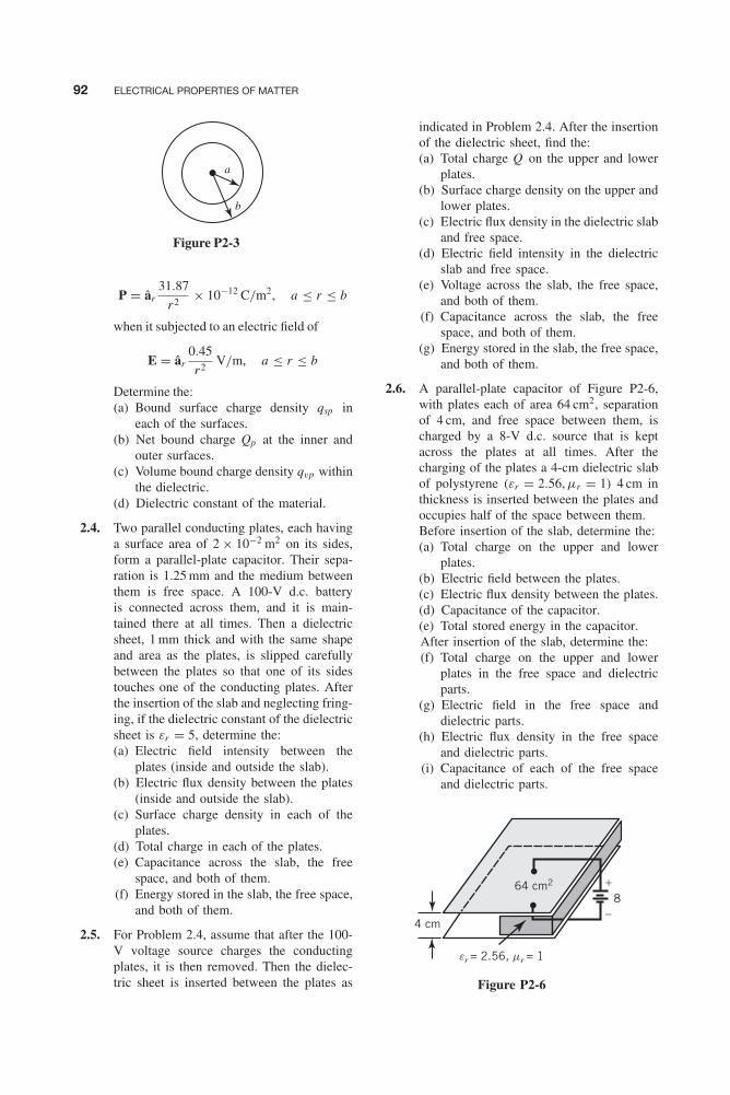
Balanis c02.tex V3 - 11/22/2011 3:07 P.M. Page 92
92 ELECTRICAL PROPERTIES OF MATTER
a
b
Figure P2-3
P = âr31.87
r2× 10−12 C/m2, a ≤ r ≤ b
when it subjected to an electric field of
E = âr0.45
r2V/m, a ≤ r ≤ b
Determine the:(a) Bound surface charge density qsp in
each of the surfaces.(b) Net bound charge Qp at the inner and
outer surfaces.(c) Volume bound charge density qvp within
the dielectric.(d) Dielectric constant of the material.
2.4. Two parallel conducting plates, each havinga surface area of 2 × 10⁻² m2 on its sides,form a parallel-plate capacitor. Their sepa-ration is 1.25 mm and the medium betweenthem is free space. A 100-V d.c. batteryis connected across them, and it is main-tained there at all times. Then a dielectricsheet, 1 mm thick and with the same shapeand area as the plates, is slipped carefullybetween the plates so that one of its sidestouches one of the conducting plates. Afterthe insertion of the slab and neglecting fring-ing, if the dielectric constant of the dielectricsheet is εr = 5, determine the:(a) Electric field intensity between the
plates (inside and outside the slab).(b) Electric flux density between the plates
(inside and outside the slab).(c) Surface charge density in each of the
plates.(d) Total charge in each of the plates.(e) Capacitance across the slab, the free
space, and both of them.(f) Energy stored in the slab, the free space,
and both of them.
2.5. For Problem 2.4, assume that after the 100-V voltage source charges the conductingplates, it is then removed. Then the dielec-tric sheet is inserted between the plates as
indicated in Problem 2.4. After the insertionof the dielectric sheet, find the:(a) Total charge Q on the upper and lower
plates.(b) Surface charge density on the upper and
lower plates.(c) Electric flux density in the dielectric slab
and free space.(d) Electric field intensity in the dielectric
slab and free space.(e) Voltage across the slab, the free space,
and both of them.(f) Capacitance across the slab, the free
space, and both of them.(g) Energy stored in the slab, the free space,
and both of them.
2.6. A parallel-plate capacitor of Figure P2-6,with plates each of area 64 cm2, separationof 4 cm, and free space between them, ischarged by a 8-V d.c. source that is keptacross the plates at all times. After thecharging of the plates a 4-cm dielectric slabof polystyrene (εr = 2.56, μr = 1) 4 cm inthickness is inserted between the plates andoccupies half of the space between them.Before insertion of the slab, determine the:(a) Total charge on the upper and lower
plates.(b) Electric field between the plates.(c) Electric flux density between the plates.(d) Capacitance of the capacitor.(e) Total stored energy in the capacitor.After insertion of the slab, determine the:(f) Total charge on the upper and lower
plates in the free space and dielectricparts.
(g) Electric field in the free space anddielectric parts.
(h) Electric flux density in the free spaceand dielectric parts.
(i) Capacitance of each of the free spaceand dielectric parts.
4 cm
64 cm2
er = 2.56, mr = 1
8+
−
Figure P2-6

Balanis c02.tex V3 - 11/22/2011 3:07 P.M. Page 93
PROBLEMS 93
(j) Total capacitance (combined free spaceand dielectric parts).
(k) Stored energy in each of the free spaceand dielectric parts.
(l) Total stored energy (combined freespace and dielectric parts). Comparewith that of part (e) and if there is adifference, explain why.
2.7. Repeat Problem 2.6 except assume that thevoltage source is removed after the chargingof the plates and before the insertion of theslab.
2.8. Two parallel PEC plates, each having a totalsurface area of 2 cm2, form a parallel platecapacitor. The separation between the PECplates is 1.25 mm and the medium betweenthe plates is initially free space. A 100-Volt battery is attached to the plates, chargesthem, and is then removed. After removalof the battery, a 1 mm thick dielectric slab,with a dielectric constant (relative permittiv-ity) of 5 and an area of 2 cm2 on each of itssides is inserted between the PEC plates andoccupies the lower part of the space betweenthe PEC plates (basically touching the lowerPEC plate), as shown in the figure below.After insertion of the dielectric slab, find the:(a) Total charge Q on the lower and upper
PEC plates (in C).(b) Surface charge density on the upper and
lower PEC plates (in C/m2).(c) Electric flux density in the:
1. Dielectric (in C/m2)2. Free space medium (in C/m2)
(d) Electric field intensity in the:1. Dielectric (in V/m)2. Free space medium (in V/m)
(e) Total voltage in the:1. Dielectric slab (in V)2. Free-space medium (in V)3. Between the PEC plates (dielectric
slab + free space medium) (in V)(f) The capacitance across the:
1. Dielectric slab (in farads)2. Free-space medium (in farads)3. Between the PEC plates (dielectric
slab + free space medium) (in farads)
100+
−
Area (PEC) = 2 cm2
Area (PEC) = 2 cm2
1 mm (er = 5) 1.25 mm
Figure P2-8
2.9. Two different dielectric slabs, with dielectricconstants of 2 and 6, respectively, are placedone on top of the other, between two squareperfectly electric conducting (PEC) plates,each plate with an area of 1 cm2, as shown inthe figure. The thickness of each dielectricslab is 1 cm. A 10-Volt d.c. power supplyis placed between the two plates forminga parallel-plate capacitor, and is maintainedconnected at all times. Find (in terms of ε0
when applicable) the following:(a) Electric field in each slab (in V/meter).(b) Electric flux density in each slab (in
C/m2).(c) Total charge in each of the two PEC
plates (in C).(d) Total capacitance of the parallel-plate
capacitor (in farads) using its definitionbased on the charge and voltage.
(e) Capacitance of each slab (in farads)based on the definition of capacitance(using plate area, separation and permit-tivity of the medium).
(f) Total capacitance (in farads) of theparallel-plate capacitor, using the capac-itances of part (e). How does this capac-itance compares with that of part (d)?Are they the same or different? Explain.
10
+
−
1 cm
1 cm
Area = 1 cm2
Area = 1 cm2
er = 2
er = 6
Figure P2-9
2.10. Two different dielectric slabs, with dielec-tric constants of 2 and 6, respectively, areplaced side-by-side between four rectangu-lar PEC plates. Each dielectric slab is square(1 cm by 1 cm; area = 1 cm2) and each with

Balanis c02.tex V3 - 11/22/2011 3:07 P.M. Page 94
94 ELECTRICAL PROPERTIES OF MATTER
a thickness of 1 cm. Each of the top andbottom PEC plates has dimensions of 1 cmby 1 cm, as shown in the figure. A 10-Voltd.c. power supply is placed between the twoplates forming two separate parallel-platecapacitors.For each capacitor, find the following:(a) Electric field in each slab (E1 and E2)
(in V/meter).(b) Electric flux density in each slab (D1
and D2) (in C/m2).(c) Total charge density in each of the two
PEC plates (q1 and q2) (in C/m2).(d) Total charge in each of the two PEC
plates (Q1 and Q2) (in C).(e) Capacitance in each of the parallel-plate
capacitors (C1 and C2) (in farads) usingthe definition based on the charge andvoltage.
(f) Total capacitance CT (in farads) of theparallel-plate capacitor using the capac-itances from part (e).
(g) Capacitance of each capacitor (infarads) based on the definition of capac-itance for each (using plate area, sepa-ration and permittivity of the medium).
(h) Total capacitance CT (in farads) ofthe parallel plate capacitors, using thecapacitances of part (g).
(i) How do the capacitances of parts (f)and (h) compare? Are they the same ordifferent? Should they be the same ordifferent? Explain.
er1 = 210+
−
1 cm
Area(#1) = 1 cm2
Area(#1) = 1 cm2
Area(#2) = 1 cm2
Area(#2) = 1 cm2
er2 = 6
Figure P2-10
2.11. A 10-Volt d.c. power supply, placed betweenthe two plates as shown in Figure P2-10,with air between the plates which form twoseparate parallel-plate capacitors, chargesthe plates of the two capacitors. The powersupply is then disconnected; the two capac-itors are not connected to each other.After the power supply is disconnected andthe two capacitors are not connected to eachother, two different dielectric slabs with
dielectric constants of 2 and 6, respectively,are inserted side-by-side between the tworectangular PEC plates. Each dielectric slabis square (1 cm by 1 cm; area = 1 cm2) andeach with a thickness of 1 cm. Each of thetop and bottom PEC plates has dimensionsof 1 cm × 1 cm, as shown in the figure.For each capacitor, in the presence of thedielectric slabs but after the removal of thepower supply, find the following:(a) Total electric charge density in each
of the four PEC plates (q1 and q2)(in C/m2).
(b) Electric flux density in each slab (D1
and D2) (in C/m2).(c) Total charge in each of the four PEC
plates (Q1 and Q2) (in C).(d) Electric field in each slab (E1 and E2)
(in V/meter).(e) Voltage across each of the parallel plate
capacitors (V1 and V2) (in V).(f) Capacitance in each of the parallel-plate
capacitors (C1 and C2) (in farads) basedon the geometry of each capacitor (areaof plates, separation of plates, permittiv-ity of medium).
(g) Capacitance in each of the parallel-platecapacitors (C1 and C2) (in farads) basedon the results of parts (c) and (e) (chargeand voltage).
(h) Are the corresponding results/answersin parts (f) and (g) the same or different?Explain.
2.12. A 10-V d.c. voltage source, placed acrossthe inner and outer conductors of a coax-ial cylinder as shown in Figure P2-12, isused to charge the conductors and is thenremoved. The total charge in each conduc-tor is ± Q . The inner conductor has a radiusof a = 2 cm, the radius of the outer conduc-tor is 4 cm, and the length of the cylinderis � = 6 cm. Assuming no field fringing andfree space between the conductors, find the:(a) Electric field intensity between the con-
ductors in terms of Q .(b) Total charge Q on the inner and outer
conductors.(c) Surface charge density on the inner and
outer conductors.(d) Electric flux density between the con-
ductors.

Balanis c02.tex V3 - 11/22/2011 3:07 P.M. Page 95
PROBLEMS 95
(e) Capacitance between the conductors.(f) Energy stored between the conductors.
xa
l
b
y
z
+ 10 V−
Figure P2-12
2.13. For Problem 2.12, assume that after the10-V source charges the conductors and isremoved, a cylindrical dielectric jacket ofpolystyrene (εr = 2.56) of inner radius a =2 cm and outer radius b = 3 cm is insertedover the inner conductor of the coaxialcylinder. After the insertion of the jacket andneglecting fringing, find the:(a) Total charge Q on the inner and outer
conductors.(b) Surface charge density on the inner and
outer conductors.(c) Electric flux density between the con-
ductors in the dielectric and free space.(d) Electric field intensity between the con-
ductors in the dielectric and free space.(e) Voltage between the conductors.(f) Total capacitance between the conduc-
tors.(g) Total energy stored between the conduc-
tors.
2.14. For Problem 2.13 assume that the 10-Vsource that charges the conductors remainsconnected at all times. By neglecting fring-ing, determine the:(a) Electric field intensity between the con-
ductors inside and outside the dielectricjacket.
(b) Electric flux density between the con-ductors inside and outside the dielectricjacket.
(c) Surface charge density in each of theplates.
(d) Total charge in each of the conductors.(e) Total capacitance between the conduc-
tors.(f) Total energy stored between the conduc-
tors.
2.15. A 100-V d.c. voltage source is placed acrosstwo parallel-plate sets that are connected inparallel. Each conductor in each parallel-plate set has a surface area of 2 × 10⁻² m2
on each of its sides which are separated by4 cm. For one parallel-plate set the mediumbetween them is free space, whereas forthe other it is lossless polystyrene (εr =2.56, μr = 1). For each parallel-plate set, byneglecting fringing, determine the:(a) Electric field intensity between the
plates.(b) Electric flux density between the plates.(c) Total charge on the upper and lower
plates.(d) Total energy stored between the plates.For the two-set parallel-plate combination,determine the total:(e) Charge on the two upper and two lower
plates.(f) Capacitance between the upper and
lower plates.(g) Energy stored between the plates.
2.16. For the coaxial cylinder of Problem 2.12assume that once the 10-V voltage sourcecharges the conductors and is removed, acurved dielectric slab of polystyrene (εr =2.56, μr = 1) of thickness equal to thespacing between the conductors is insertedbetween the conductors and occupies halfof the space (π ≤ φ ≤ 2π); the other half,0 ≤ φ ≤ π , is still occupied by free space.By neglecting fringing, determine the:(a) Total charge on the inner and outer con-
ductors in free space and in polystyrene.(b) Surface charge density on inner and
outer conductors in free space and inpolystyrene.
(c) Electric flux density between the con-ductors in free space and in polystyrene.
(d) Electric field intensity between the con-ductors in free space and in polystyrene.
(e) Voltage between the conductors in freespace and in polystyrene.
(f) Capacitance between the conductors infree space, in polystyrene, and total.
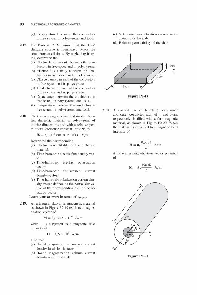
Balanis c02.tex V3 - 11/22/2011 3:07 P.M. Page 96
96 ELECTRICAL PROPERTIES OF MATTER
(g) Energy stored between the conductorsin free space, in polystyrene, and total.
2.17. For Problem 2.16 assume that the 10-Vcharging source is maintained across theconductors at all times. By neglecting fring-ing, determine the:(a) Electric field intensity between the con-
ductors in free space and in polystyrene.(b) Electric flux density between the con-
ductors in free space and in polystyrene.(c) Charge density in each of the conductors
in free space and in polystyrene.(d) Total charge in each of the conductors
in free space and in polystyrene.(e) Capacitance between the conductors in
free space, in polystyrene, and total.(f) Energy stored between the conductors in
free space, in polystyrene, and total.
2.18. The time-varying electric field inside a loss-less dielectric material of polystyrene, ofinfinite dimensions and with a relative per-mittivity (dielectric constant) of 2.56, is
� = âz 10−3 sin(2π × 107t) V/m
Determine the corresponding:(a) Electric susceptibility of the dielectric
material.(b) Time-harmonic electric flux density vec-
tor.(c) Time-harmonic electric polarization
vector.(d) Time-harmonic displacement current
density vector.(e) Time-harmonic polarization current den-
sity vector defined as the partial deriva-tive of the corresponding electric polar-ization vector.
Leave your answers in terms of ε0, μ0.
2.19. A rectangular slab of ferrimagnetic materialas shown in Figure P2-19 exhibits a magne-tization vector of
M = âz 1.245 × 10⁶ A/m
when it is subjected to a magnetic fieldintensity of
H = âz 5 × 10³ A/m
Find the:(a) Bound magnetization surface current
density in all its six faces.(b) Bound magnetization volume current
density within the slab.
(c) Net bound magnetization current asso-ciated with the slab.
(d) Relative permeability of the slab.
x
z
6 cm
1 cm
4 cm
y
Figure P2-19
2.20. A coaxial line of length � with innerand outer conductor radii of 1 and 3 cm,respectively, is filled with a ferromagneticmaterial, as shown in Figure P2-20. Whenthe material is subjected to a magnetic fieldintensity of
H = âφ
0.3183
ρA/m
it induces a magnetization vector potentialof
M = âφ
190.67
ρA/m
xa
r
f
b
y
l
z
Figure P2-20

Balanis c02.tex V3 - 11/22/2011 3:07 P.M. Page 97
PROBLEMS 97
Determine the:(a) Bound magnetization surface current
density in all surfaces.(b) Bound magnetization volume current
density within the material.(c) Net bound magnetization current asso-
ciated with the coaxial line.(d) Relative permeability of the material.
2.21. The magnetization vector inside a cylindri-cal magnetic bar of infinite length and circu-lar cross section of radius a = 1 m, as shownin Figure P2-21, is given by
M = âφ10 A/m
Find the:(a) Magnetic surface current density at the
outside circumferential surface of thebar.
(b) Magnetic volume current density at anypoint inside the bar.
(c) Total current that flows through thecross section of the bar.
f
x
y
a
z
r
Figure P2-21
2.22. The current density through a cylindricalwire of square cross section as shown inFigure P2-22 is given by
J � âz J0e−102[(a−|x |)+(a−|y |)]
where J0 is a constant. Assuming that eachside of the wire is 2 × 10⁻² m, find the cur-rent flow through the cross section of thewire.
x
y
2a
2a
z
Figure P2-22
2.23. A 10-A current is pushed through a circu-lar cross section of wire of infinite lengthas shown in Figure P2-23. Assuming thatthe current density over the cross section of
z
a
x
r
f
y
Figure P2-23
the wire decays from its surface toward itscenter as
J = âz J0e−104(a−ρ) A/m2
where J0 is the current density at thesurface and the wire radius is a = 10−2 m,determine the:(a) Current density at the surface of the
wire.

Balanis c02.tex V3 - 11/22/2011 3:07 P.M. Page 98
98 ELECTRICAL PROPERTIES OF MATTER
(b) Depth from the surface of the wirethrough which the current density hasdecayed to 36.8 percent of its value atthe surface.
2.24. Show that the relaxation time constantfor copper (σ = 5.76 × 10⁷ S/m) is muchsmaller than the period of waves inthe microwave (1–10 GHz) region andis comparable to the period of x-rays[λ � 1 − 10 Å = (1–10) × 10−8 cm]. Con-sequently, conductors cannot maintain acharge configuration long enough to permitpropagation of the wave more than a shortdistance into the conductor at microwavefrequencies. However x-ray propagation is
possible because the relaxation time con-stant is comparable to the period of thewave.
2.25. Aluminum has a static conductivity of aboutσ = 3.96 × 10⁷ S/m and an electron mobil-ity of μe = 2.2 × 10⁻³ m2/(V-s). Assum-ing that an electric field of E = âx 2 V/m isapplied perpendicularly to the square areaof an aluminum wafer with cross-sectionalarea of about 10 cm2, find the:(a) Electron charge density qve .(b) Electron drift velocity ve .(c) Electric current density J.(d) Electric current flowing through the
square cross section of the wafer.(e) Electron density Ne .

CHAPTER 3Wave Equation and its Solutions
3.1 INTRODUCTION
The electromagnetic fields of boundary-value problems are obtained as solutions to Maxwell’sequations, which are first-order partial differential equations. However, Maxwell’s equations arecoupled partial differential equations, which means that each equation has more than one unknownfield. These equations can be uncoupled only at the expense of raising their order. For each of thefields, following such a procedure leads to an uncoupled second-order partial differential equationthat is usually referred to as the wave equation . Therefore electric and magnetic fields for a givenboundary-value problem can be obtained either as solutions to Maxwell’s or the wave equations.The choice of equations is related to individual problems by convenience and ease of use. Inthis chapter we will develop the vector wave equations for each of the fields, and then we willdemonstrate their solutions in the rectangular, cylindrical, and spherical coordinate systems.
3.2 TIME-VARYING ELECTROMAGNETIC FIELDS
The first two of Maxwell’s equations in differential form, as given by (1-1) and (1-2), are first-order, coupled differential equations; that is, both the unknown fields (� and �) appear in eachequation. Usually it is very desirable, for convenience in solving for � and �, to uncouple theseequations. This can be accomplished at the expense of increasing the order of the differentialequations to second order. To do this, we repeat (1-1) and (1-2), that is,
∇ × � = −�i − μ∂�
∂t(3-1)
∇ × � = �i + σ� + ε∂�
∂t(3-2)
where it is understood in the remaining part of the book that σ represents the effective conductivityσε and ε represents ε′. Taking the curl of both sides of each of equations 3-1 and 3-2 and assuminga homogeneous medium, we can write that
∇ × ∇ × � = −∇ × �i − μ∇ ×(
∂�
∂t
)= −∇ × �i − μ
∂
∂t(∇ × �) (3-3)
∇ × ∇ × � = ∇ × �i + σ∇ × � + ε∇ ×(
∂�
∂t
)= ∇ × �i + σ∇ × � + ε
∂
∂t(∇ × �) (3-4)
99

100 WAVE EQUATION AND ITS SOLUTIONS
Substituting (3-2) into the right side of (3-3) and using the vector identity
∇ × ∇ × F = ∇(∇ • F) − ∇2F (3-5)
into the left side, we can rewrite (3-3) as
∇(∇ • �) − ∇2� = −∇ × �i − μ∂
∂t
[�i + σ� + ε
∂�
∂t
]∇(∇ • �) − ∇2� = −∇ × �i − μ
∂�i
∂t− μσ
∂�
∂t− με
∂2�
∂t2(3-6)
Substituting Maxwell’s equation 1-3, or
∇ • � = ε∇ • � = qev
⇒ ∇ • � = qev
ε(3-7)
into (3-6) and rearranging its terms, we have that
∇2� = ∇ × �i + μ∂�i
∂t+ 1
ε∇q
ev+ μσ
∂�
∂t+ με
∂2�
∂t2(3-8)
which is recognized as an uncoupled second-order differential equation for �.In a similar manner, by substituting (3-1) into the right side of (3-4) and using the vector
identity of (3-5) in the left side of (3-4), we can rewrite it as
∇(∇ • �) − ∇2� = ∇ × �i + σ
(−�i − μ
∂�
∂t
)+ ε
∂
∂t
(−�i − μ
∂�
∂t
)∇(∇ • �) − ∇2� = ∇ × �i − σ�i − μσ
∂�
∂t− ε
∂�i
∂t− με
∂2�
∂t2(3-9)
Substituting Maxwell’s equation
∇ • � = μ∇ • � = qmv
⇒ ∇ • � =(
qmv
μ
)(3-10)
into (3-9), we have that
∇2� = −∇ × �i + σ�i + 1
μ∇(q
mv) + ε
∂�i
∂t+ μσ
∂�
∂t+ με
∂2�
∂t2(3-11)
which is recognized as an uncoupled second-order differential equation for �. Thus (3-8) and(3-11) form a pair of uncoupled second-order differential equations that are a by-product ofMaxwell’s equations as given by (1-1) through (1-4).
Equations 3-8 and 3-11 are referred to as the vector wave equations for � and �. For solvingan electromagnetic boundary-value problem, the equations that must be satisfied are Maxwell’sequations as given by (1-1) through (1-4) or the wave equations as given by (3-8) and (3-11).Often, the forms of the wave equations are preferred over those of Maxwell’s equations.
TIME-HARMONIC ELECTROMAGNETIC FIELDS 101
For source-free regions (�i = qev
= 0 and �i = qmv
= 0), the wave equations 3-8 and 3-11reduce, respectively, to
∇2� = μσ∂�
∂t+ με
∂2�
∂t2(3-12)
∇2� = μσ∂�
∂t+ με
∂2�
∂t2(3-13)
For source-free (�i = qev
= 0 and �i = qmv
= 0) and lossless media (σ = 0), the waveequations 3-8 and 3-11 or 3-12 and 3-13 simplify to
∇2� = με∂2�
∂t2(3-14)
∇2� = με∂2�
∂t2(3-15)
Equations 3-14 and 3-15 represent the simplest forms of the vector wave equations.
3.3 TIME-HARMONIC ELECTROMAGNETIC FIELDS
For time-harmonic fields (time variations of the form ejωt ), the wave equations can be derivedusing a similar procedure as in Section 3.2 for the general time-varying fields, starting withMaxwell’s equations as given in Table 1-4. However, instead of going through this process, wefind, by comparing Maxwell’s equations for the general time-varying fields with those for thetime-harmonic fields (both are displayed in Table 1-4), that one set can be obtained from theother by replacing ∂/∂t ≡ jω, ∂2/∂t2 ≡ (jω)2 = −ω2, and the instantaneous fields (�, �, �, �),respectively, with the complex fields (E, H, D, B) and vice versa. Doing this for the wave equations3-8, 3-11, 3-12, and 3-13, we can write each, respectively, as
∇2E = ∇ × Mi + jωμJi + 1
ε∇qev + jωμσE − ω2μεE
∇2H = −∇ × Ji + σMi + jωεMi + 1
μ∇qmv + jωμσH − ω2μεH
(3-16a)
(3-16b)
∇2E = jωμσE − ω2μεE = γ 2E
∇2H = jωμσH − ω2μεH = γ 2H
(3-17a)
(3-17b)
where
γ 2 = jωμσ − ω2με = jωμ(σ + jωε) (3-17c)
γ = α + jβ = propagation constant (3-17d)
α = attenuation constant (Np/m) (3-17e)
β = phase constant (rad/m) (3-17f)
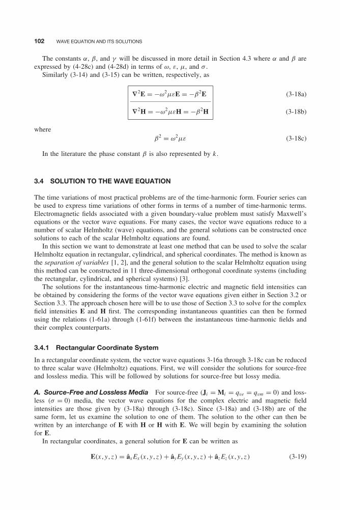
102 WAVE EQUATION AND ITS SOLUTIONS
The constants α, β, and γ will be discussed in more detail in Section 4.3 where α and β areexpressed by (4-28c) and (4-28d) in terms of ω, ε, μ, and σ .
Similarly (3-14) and (3-15) can be written, respectively, as
∇2E = −ω2μεE = −β2E
∇2H = −ω2μεH = −β2H
(3-18a)
(3-18b)
whereβ2 = ω2με (3-18c)
In the literature the phase constant β is also represented by k .
3.4 SOLUTION TO THE WAVE EQUATION
The time variations of most practical problems are of the time-harmonic form. Fourier series canbe used to express time variations of other forms in terms of a number of time-harmonic terms.Electromagnetic fields associated with a given boundary-value problem must satisfy Maxwell’sequations or the vector wave equations. For many cases, the vector wave equations reduce to anumber of scalar Helmholtz (wave) equations, and the general solutions can be constructed oncesolutions to each of the scalar Helmholtz equations are found.
In this section we want to demonstrate at least one method that can be used to solve the scalarHelmholtz equation in rectangular, cylindrical, and spherical coordinates. The method is known asthe separation of variables [1, 2], and the general solution to the scalar Helmholtz equation usingthis method can be constructed in 11 three-dimensional orthogonal coordinate systems (includingthe rectangular, cylindrical, and spherical systems) [3].
The solutions for the instantaneous time-harmonic electric and magnetic field intensities canbe obtained by considering the forms of the vector wave equations given either in Section 3.2 orSection 3.3. The approach chosen here will be to use those of Section 3.3 to solve for the complexfield intensities E and H first. The corresponding instantaneous quantities can then be formedusing the relations (1-61a) through (1-61f) between the instantaneous time-harmonic fields andtheir complex counterparts.
3.4.1 Rectangular Coordinate System
In a rectangular coordinate system, the vector wave equations 3-16a through 3-18c can be reducedto three scalar wave (Helmholtz) equations. First, we will consider the solutions for source-freeand lossless media. This will be followed by solutions for source-free but lossy media.
A. Source-Free and Lossless Media For source-free (Ji = Mi = qve = qvm = 0) and loss-less (σ = 0) media, the vector wave equations for the complex electric and magnetic fieldintensities are those given by (3-18a) through (3-18c). Since (3-18a) and (3-18b) are of thesame form, let us examine the solution to one of them. The solution to the other can then bewritten by an interchange of E with H or H with E. We will begin by examining the solutionfor E.
In rectangular coordinates, a general solution for E can be written as
E(x , y , z ) = âx Ex (x , y , z ) + ây Ey(x , y , z ) + âz Ez (x , y , z ) (3-19)
SOLUTION TO THE WAVE EQUATION 103
a
a y
X
Yx
zz
y
Z
ax
Figure 3-1 Rectangular coordinate system and corresponding unit vectors.
where x , y , z are the rectangular coordinates, as illustrated in Figure 3-1. Substituting (3-19) into(3-18a) we can write that
∇2E + β2E = ∇2(âx Ex + ây Ey + âz Ez) + β2(âx Ex + ây Ey + âz Ez
) = 0 (3-20)
which reduces to three scalar wave equations of
∇2Ex (x , y , z ) + β2Ex (x , y , z ) = 0 (3-20a)
∇2Ey(x , y , z ) + β2Ey(x , y , z ) = 0 (3-20b)
∇2Ez (x , y , z ) + β2Ez (x , y , z ) = 0 (3-20c)
because∇2(âx Ex + ây Ey + âz Ez
) = âx∇2Ex + ây∇2Ey + âz ∇2Ez (3-21)
Equations 3-20a through 3-20c are all of the same form; once a solution of any one of them isobtained, the solutions to the others can be written by inspection. We choose to work first withthat for Ex as given by (3-20a).
In expanded form (3-20a) can be written as
∇2Ex + β2Ex = ∂2Ex
∂x 2+ ∂2Ex
∂y2+ ∂2Ex
∂z 2+ β2Ex = 0 (3-22)
Using the separation-of-variables method , we assume that a solution for Ex (x , y , z ) can be writtenin the form of
Ex (x , y , z ) = f (x)g(y)h(z ) (3-23)
where the x , y , z variations of Ex are separable (hence the name). If any inconsistencies areencountered with assuming such a form of solution, another form must be attempted. This is theprocedure usually followed in solving differential equations. Substituting (3-23) into (3-22), wecan write that
gh∂2f
∂x 2+ fh
∂2g
∂y2+ fg
∂2h
∂z 2+ β2fgh = 0 (3-24)
104 WAVE EQUATION AND ITS SOLUTIONS
Since f (x), g(y), and h(z ) are each a function of only one variable, we can replace the partialsin (3-24) by ordinary derivatives. Doing this and dividing each term by fgh , we can write that
1
f
d2f
dx 2+ 1
g
d2g
dy2+ 1
h
d2h
dz 2+ β2 = 0 (3-25)
or1
f
d2f
dx 2+ 1
g
d2g
dy2+ 1
h
d2h
dz 2= −β2 (3-25a)
Each of the first three terms in (3-25a) is a function of only a single independent variable;hence the sum of these terms can equal −β2 only if each term is a constant. Thus (3-25a) separatesinto three equations of the form
1
f
d2f
dx 2= −β2
x ⇒ d2f
dx 2= −β2
x f (3-26a)
1
g
d2g
dy2= −β2
y ⇒ d2g
dy2= −β2
y g (3-26b)
1
h
d2h
dz 2= −β2
z ⇒ d2h
dz 2= −β2
z h (3-26c)
where, in addition,β2
x + β2y + β2
z = β2 (3-27)
Equation 3-27 is referred to as the constraint (dispersion) equation. In addition βx , βy , βz areknown as the wave constants (numbers) in the x , y , z directions, respectively, that will bedetermined using boundary conditions.
The solution to each of (3-26a), (3-26b), or (3-26c) can take different forms. Some typicalvalid solutions for f (x) of (3-26a) would be
f1(x) = A1e−jβx x + B1e+jβx x (3-28a)
orf2(x) = C1 cos(βx x) + D1 sin(βx x) (3-28b)
Similarly the solutions to (3-26b) and (3-26c) for g(y) and h(z ) can be written, respectively, as
g1(y) = A2e−jβy y + B2e+jβy y (3-29a)
org2(y) = C2 cos(βy y) + D2 sin(βy y) (3-29b)
andh1(z ) = A3e−jβz z + B3e+jβz z (3-30a)
orh2(z ) = C3 cos(βz z ) + D3 sin(βz z ) (3-30b)
Although all the aforementioned solutions are valid for f (x), g(y), and h(z ), the most appro-priate form should be chosen to simplify the complexity of the problem at hand. In general, thesolutions of (3-28a), (3-29a), and (3-30a) in terms of complex exponentials represent travelingwaves and the solutions of (3-28b), (3-29b), and (3-30b) represent standing waves . Wave func-tions representing various wave types in rectangular coordinates are found listed in Table 3-1. In

SOLUTION TO THE WAVE EQUATION 105
TABLE 3-1 Wave functions, zeroes, and infinities of plane wave functions in rectangularcoordinates
Wave Wave Zeroes of Infinities oftype functions wave functions wave functions
Travelingwaves
e−jβx for + x travele+jβx for − x travel
βx → −j∞βx → +j∞
βx → +j∞βx → −j∞
Standingwaves
cos(βx) for ± xsin(βx) for ± x
βx = ±(n + 1
2
)π
βx = ±nπ
n = 0, 1, 2, . . .
βx → ±j∞βx → ±j∞
Evanescentwaves
e−αx for + xe+αx for − xcosh(αx) for ± xsinh(αx) for ± x
αx → +∞αx → −∞αx = ±j
(n + 1
2
)π
αx = ±jnπ
n = 0, 1, 2, . . .
αx → −∞αx → +∞αx → ±∞αx → ±∞
Attenuatingtravelingwaves
e−γ x = e−αx e−jβx for + x travele+γ x = e+αx e+jβx for − x travel
γ x → +∞γ x → −∞
γ x → −∞γ x → +∞
Attenuatingstandingwaves
cos(γ x) = cos(αx) cosh(βx)
− j sin(αx) sinh(βx)
for ± xsin(γ x) = sin(αx) cosh(βx)
+ j cos(αx) sinh(βx)
for ± x
γ x = ±j(n + 1
2
)π
γ x = ±jnπ
n = 0, 1, 2, . . .
γ x → ±j∞
γ x → ±j∞
Chapter 8 we will consider specific examples and the appropriate solution forms for f (x), g(y),and h(z ).
Once the appropriate forms for f (x), g(y), and h(z ) have been decided, the solution for thescalar function Ex (x , y , z ) of (3-22) can be written as the product of fgh as stated by (3-23).To demonstrate that, let us consider a specific example in which it will be assumed that theappropriate solutions for f , g , and h are given, respectively, by (3-28b), (3-29b), and (3-30a).Thus we can write that
Ex (x , y , z ) = [C1 cos(βx x) + D1 sin(βx x)
][C2 cos(βy y) + D2 sin(βy y)
]×[
A3e−jβz z + B3e+jβz z]
(3-31)
This is an appropriate solution for any of the electric or magnetic field components inside arectangular pipe (waveguide), shown in Figure 3-2, that is bounded in the x and y directionsand has its length along the z axis. Because the waveguide is bounded in the x and y directions,standing waves, represented by cosine and sine functions, have been chosen as solutions for f (x)
and g(y) functions. However, because the waveguide is not bounded in the z direction, travelingwaves, represented by complex exponential functions, have been chosen as solutions for h(z ). Acomplete discussion of the fields inside a rectangular waveguide can be found in Chapter 8.
For ejωt time variations, which are assumed throughout this book, the first complex exponentialterm in (3-31) represents a wave that travels in the +z direction; the second exponential representsa wave that travels in the −z direction. To demonstrate this, let us examine the instantaneous form

106 WAVE EQUATION AND ITS SOLUTIONS
z
y
xa
b
Figure 3-2 Rectangular waveguide geometry.
�x (x , y , z ; t) of the scalar complex function Ex (x , y , z ). Since the solution of (3-31) representsthe complex form of Ex , its instantaneous form can be written as
�x (x , y , z ; t) = Re[Ex (x , y , z )ejωt
](3-32)
Considering only the first exponential term of (3-31) and assuming all constants are real, we canwrite the instantaneous form of the �x function for that term as
�+x (x , y , z ; t) = Re
[E+
x (x , y , z )ejωt]
= Re{[
C1 cos(βx x) + D1 sin(βx x)]
×[C2 cos(βy y) + D2 sin(βy y)
]A3ej (ωt−βz z )
}(3-33)
or, if the constants C1, D1, C2, D2, and A3 are real, as
�+x (x , y , z ; t) = [
C1 cos(βx x) + D1 sin(βx x)]
×[C2 cos(βy y) + D2 sin(βy y)
]A3 cos(ωt − βz z ) (3-33a)
where the superscript plus is used to denote a positive traveling wave.A plot of the normalized �+
x (x , y , z ; t) as a function of z for different times(t = t0, t1, . . . , tn , tn+1) is shown in Figure 3-3. It is evident that as time increases (tn+1 > tn),the waveform of �+
x is essentially the same, with the exception of an apparent shift in the +zdirection indicating a wave traveling in the +z direction. This shift in the +z direction can alsobe demonstrated by examining what happens to a given point zp in the waveform of �+
x fort = t0, t1, . . . , tn , tn+1. To follow the point zp for different values of t , we must maintain constantthe amplitude of the last cosine term in (3-33a). This is accomplished by keeping its argumentωt − βz zp constant, that is,
ωt − βz zp = C0 = constant (3-34)
which when differentiated with respect to time reduces to
ω(1) − βzdzp
dt= 0 ⇒ dzp
dt= vp = + ω
βz(3-35)
SOLUTION TO THE WAVE EQUATION 107
1.5
1.0
0.5
0.0
−0.5
0.5 1.0 1.5 2.0
−1.0
−1.5
Mag
nitu
de |F
(z,t)
|F(z,t) = cos(wt − bz)
zp zp zp z (in λ)
Figure 3-3 Variations as a function of distance for different times of positive traveling wave.time t0 = 0; – – – – time t1 = T/8; ---- time t2 = T/4.
The point zp is referred to as an equiphase point and its velocity is denoted as the phasevelocity . A similar procedure can be used to demonstrate that the second complex exponentialterm in (3-31) represents a wave that travels in the −z direction.
B. Source-Free and Lossy Media When the media in which the waves are traveling arelossy (σ �= 0) but source-free (Ji = Mi = qve = qvm = 0), the vector wave equations that thecomplex electric E and magnetic H field intensities must satisfy are (3-17a) and (3-17b). As forthe lossless case, let us examine the solution to one of them; the solution to the other can then bewritten by inspection once the solution to the first has been obtained. We choose to consider thesolution for the electric field intensity E, which must satisfy (3-17a). An extended presentationof electromagnetic wave propagation in lossy media can be found in [4].
In a rectangular coordinate system, the general solution for E(x , y , z ) can be written as
E(x , y , z ) = âx Ex (x , y , z ) + ây Ey(x , y , z ) + âz Ez (x , y , z ) (3-36)
When (3-36) is substituted into (3-17a), we can write that
∇2E − γ 2E = ∇2(âx Ex + ây Ey + âz Ez) − γ 2(âx Ex + ây Ey + âz Ez
) = 0 (3-37)
which reduces to three scalar wave equations of
∇2Ex (x , y , z ) − γ 2Ex (x , y , z ) = 0 (3-37a)
∇2Ey(x , y , z ) − γ 2Ey(x , y , z ) = 0 (3-37b)
∇2Ez (x , y , z ) − γ 2Ez (x , y , z ) = 0 (3-37c)
whereγ 2 = jωμ(σ + jωε) (3-37d)
If we were to allow for positive and negative values of σ
γ = ±√
jωμ(σ + jωε) ={
±(α + jβ) for + σ
±(α − jβ) for − σ(3-37e)
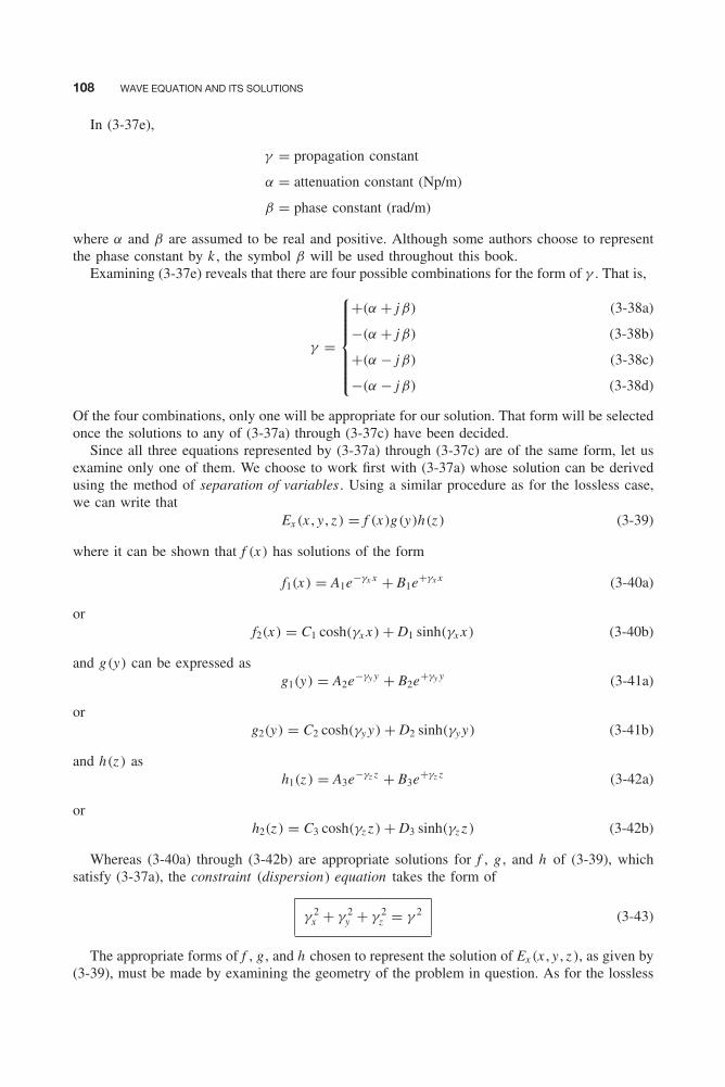
108 WAVE EQUATION AND ITS SOLUTIONS
In (3-37e),
γ = propagation constant
α = attenuation constant (Np/m)
β = phase constant (rad/m)
where α and β are assumed to be real and positive. Although some authors choose to representthe phase constant by k , the symbol β will be used throughout this book.
Examining (3-37e) reveals that there are four possible combinations for the form of γ . That is,
γ =
⎧⎪⎪⎪⎪⎪⎨⎪⎪⎪⎪⎪⎩
+(α + jβ)
−(α + jβ)
+(α − jβ)
−(α − jβ)
(3-38a)
(3-38b)
(3-38c)
(3-38d)
Of the four combinations, only one will be appropriate for our solution. That form will be selectedonce the solutions to any of (3-37a) through (3-37c) have been decided.
Since all three equations represented by (3-37a) through (3-37c) are of the same form, let usexamine only one of them. We choose to work first with (3-37a) whose solution can be derivedusing the method of separation of variables . Using a similar procedure as for the lossless case,we can write that
Ex (x , y , z ) = f (x)g(y)h(z ) (3-39)
where it can be shown that f (x) has solutions of the form
f1(x) = A1e−γx x + B1e+γx x (3-40a)
orf2(x) = C1 cosh(γx x) + D1 sinh(γx x) (3-40b)
and g(y) can be expressed asg1(y) = A2e−γy y + B2e+γy y (3-41a)
org2(y) = C2 cosh(γy y) + D2 sinh(γy y) (3-41b)
and h(z ) ash1(z ) = A3e−γz z + B3e+γz z (3-42a)
orh2(z ) = C3 cosh(γz z ) + D3 sinh(γz z ) (3-42b)
Whereas (3-40a) through (3-42b) are appropriate solutions for f , g , and h of (3-39), whichsatisfy (3-37a), the constraint (dispersion) equation takes the form of
γ 2x + γ 2
y + γ 2z = γ 2 (3-43)
The appropriate forms of f , g , and h chosen to represent the solution of Ex (x , y , z ), as given by(3-39), must be made by examining the geometry of the problem in question. As for the lossless
SOLUTION TO THE WAVE EQUATION 109
case, the exponentials represent attenuating traveling waves and the hyperbolic cosines and sinesrepresent attenuating standing waves. These and other waves types are listed in Table 3-1.
To decide on the appropriate form for any of the γ ’s (whether it be γx , γy , γz , or γ ), let uschoose the form of γz by examining one of the exponentials in (3-42a). We choose to work withthe first one. The four possible combinations for γz , according to (3-38a) through (3-38d) willbe
γz =
⎧⎪⎪⎪⎪⎪⎨⎪⎪⎪⎪⎪⎩
+(αz + jβz )
−(αz + jβz )
+(αz − jβz )
−(αz − jβz )
(3-44a)
(3-44b)
(3-44c)
(3-44d)
If we want the first exponential in (3-42a) to represent a decaying wave which travels in the+z direction, then by substituting (3-44a) through (3-44d) into it we can write that
h+1 (z ) =
⎧⎪⎪⎪⎪⎪⎪⎨⎪⎪⎪⎪⎪⎪⎩
A3e−γz z = A3e−αz z e−jβz z
A3e−γz z = A3e+αz z e+jβz z
A3e−γz z = A3e−αz z e+jβz z
A3e−γz z = A3e+αz z e−jβz z
(3-45a)
(3-45b)
(3-45c)
(3-45d)
By examining (3-45a) through (3-45d) and assuming ejωt time variations, the following state-ments can be made:
1. Equation 3-45a represents a wave that travels in the +z direction, as determined by e−jβz z ,and it decays in that direction, as determined by e−αz z .
2. Equation 3-45b represents a wave that travels in the −z direction, as determined by e+jβz z ,and it decays in that direction, as determined by e+αz z .
3. Equation 3-45c represents a wave that travels in the −z direction, as determined by e+jβz z ,and it is increasing in that direction, as determined by e−αz z .
4. Equation 3-45d represents a wave that travels in the +z direction, as determined by e−jβz z ,and it is increasing in that direction, as determined by e+αz z .
From the preceding statements it is apparent that for e−γz z to represent a wave that travels in the+z direction and that concurrently also decays (to represent propagation in passive lossy media),and to satisfy the conservation of energy laws, the only correct form of γz is that of (3-44a). Thesame conclusion will result if the second exponential of (3-42a) represents a wave that travels inthe −z direction and that concurrently also decays. Thus the general form of any γi (whether itbe γx , γy , γz , or γ ), as given by (3-38a) through (3-38d), is
γi = αi + jβi (3-46)
Whereas the forms of f , g , and h [as given by (3-40a) through (3-42b)] are used to arriveat the solution for the complex form of Ex as given by (3-39), the instantaneous form of �x
can be obtained by using the relation of (3-32). A similar procedure can be used to derive thesolutions of the other components of E (Ey and Ez ), all those of H (Hx , Hy , and Hz ), and of theirinstantaneous counterparts.

110 WAVE EQUATION AND ITS SOLUTIONS
3.4.2 Cylindrical Coordinate System
If the geometry of the system is of a cylindrical configuration, it would be very advisable tosolve the boundary-value problem for the E and H fields using cylindrical coordinates. Maxwell’sequations and the vector wave equations, which the E and H fields must satisfy, should be solvedusing cylindrical coordinates. Let us first consider the solution for E for a source-free and losslessmedium. A similar procedure can be used for H. To maintain some simplicity in the mathematics,we will examine only lossless media.
In cylindrical coordinates a general solution to the vector wave equation for source-free andlossless media, as given by (3-18a), can be written as
E(ρ, φ, z ) = âρEρ(ρ, φ, z ) + âφEφ(ρ, φ, z ) + âz Ez (ρ, φ, z ) (3-47)
where ρ, φ, and z are the cylindrical coordinates as illustrated in Figure 3-4. Substituting (3-47)into (3-18a), we can write that
∇2(âρEρ + âφEφ + âz Ez ) = −β2(âρEρ + âφEφ + âz Ez ) (3-48)
which does not reduce to three simple scalar wave equations, similar to those of (3-20a) through(3-20c) for (3-20), because
∇2(âρEρ) �= âρ∇2Eρ (3-49a)
∇2(âφEφ) �= âφ∇2Eφ (3-49b)
However, because∇2(âz Ez ) = âz ∇2Ez (3-49c)
one of the three scalar equations to which (3-48) reduces is
∇2Ez + β2Ez = 0 (3-50)
The other two are of more complex form and they will be addressed in what follows.Before we derive the other two scalar equations [in addition to (3-50)] to which (3-48) reduces,
let us attempt to give a physical explanation of (3-49a), (3-49b), and (3-49c). By examining twodifferent points (ρ1, φ1, z1) and (ρ2, φ2, z2) and their corresponding unit vectors on a cylindricalsurface (as shown in Figure 3-4), we see that the directions of âρ and âφ have changed from onepoint to another (they are not parallel) and therefore cannot be treated as constants but rather arefunctions of ρ, φ, and z . In contrast, the unit vector âz at the two points is pointed in the samedirection (is parallel). The same is true for the unit vectors âx and ây in Figure 3-1.
Let us now return to the solution of (3-48). Since (3-48) does not reduce to (3-49a) and (3-49b), although it does satisfy (3-49c), how do we solve (3-48)? The procedure that follows canbe used to reduce (3-48) to three scalar partial differential equations.
The form of (3-48) written in general as
∇2E = −β2E (3-51)
was placed in this form by utilizing the vector identity of (3-5) during its derivation. Generallywe are under the impression that we do not know how to perform the Laplacian of a vector(∇2E) as given by the left side of (3-51). However, by utilizing (3-5) we can rewrite the leftside of (3-51) as
∇2E = ∇(∇ • E) − ∇ × ∇ × E (3-52)
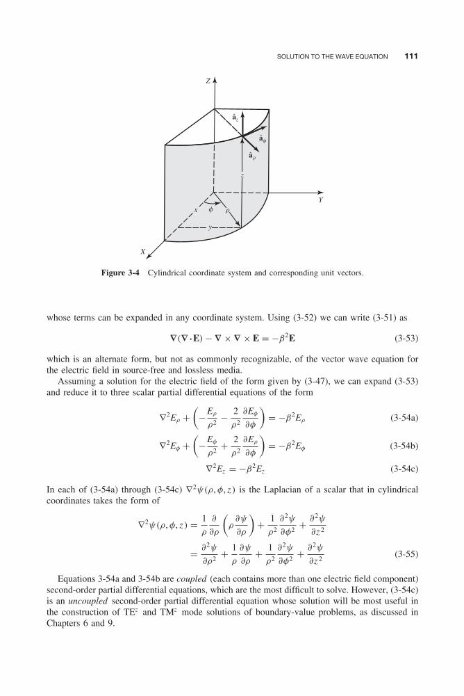
SOLUTION TO THE WAVE EQUATION 111
af
r
X
Z
Y
z
y
x f
az
ar
Figure 3-4 Cylindrical coordinate system and corresponding unit vectors.
whose terms can be expanded in any coordinate system. Using (3-52) we can write (3-51) as
∇(∇ • E) − ∇ × ∇ × E = −β2E (3-53)
which is an alternate form, but not as commonly recognizable, of the vector wave equation forthe electric field in source-free and lossless media.
Assuming a solution for the electric field of the form given by (3-47), we can expand (3-53)and reduce it to three scalar partial differential equations of the form
∇2Eρ +(
−Eρ
ρ2− 2
ρ2
∂Eφ
∂φ
)= −β2Eρ (3-54a)
∇2Eφ +(
−Eφ
ρ2+ 2
ρ2
∂Eρ
∂φ
)= −β2Eφ (3-54b)
∇2Ez = −β2Ez (3-54c)
In each of (3-54a) through (3-54c) ∇2ψ(ρ, φ, z ) is the Laplacian of a scalar that in cylindricalcoordinates takes the form of
∇2ψ(ρ, φ, z ) = 1
ρ
∂
∂ρ
(ρ
∂ψ
∂ρ
)+ 1
ρ2
∂2ψ
∂φ2+ ∂2ψ
∂z 2
= ∂2ψ
∂ρ2+ 1
ρ
∂ψ
∂ρ+ 1
ρ2
∂2ψ
∂φ2+ ∂2ψ
∂z 2(3-55)
Equations 3-54a and 3-54b are coupled (each contains more than one electric field component)second-order partial differential equations, which are the most difficult to solve. However, (3-54c)is an uncoupled second-order partial differential equation whose solution will be most useful inthe construction of TEz and TMz mode solutions of boundary-value problems, as discussed inChapters 6 and 9.

112 WAVE EQUATION AND ITS SOLUTIONS
In expanded form (3-54c) can then be written as
∂2ψ
∂ρ2+ 1
ρ
∂ψ
∂ρ+ 1
ρ2
∂2ψ
∂φ2+ ∂2ψ
∂z 2= −β2ψ (3-56)
where ψ(ρ, φ, z ) is a scalar function that can represent a field or a vector potential component.Assuming a separable solution for ψ(ρ, φ, z ) of the form
ψ(ρ, φ, z ) = f (ρ)g(φ)h(z ) (3-57)
and substituting it into (3-56), we can write that
gh∂2f
∂ρ2+ gh
1
ρ
∂f
∂ρ+ fh
1
ρ2
∂2g
∂φ2+ fg
∂2h
∂z 2= −β2fgh (3-58)
Dividing both sides of (3-58) by fgh and replacing the partials by ordinary derivatives reduces(3-58) to
1
f
d2f
dρ2+ 1
f
1
ρ
df
dρ+ 1
g
1
ρ2
d2g
dφ2+ 1
h
d2h
dz 2= −β2 (3-59)
The last term on the left side of (3-59) is only a function of z . Therefore, using the discussionof Section 3.4.1, we can write that
1
h
d2h
dz 2= −β2
z ⇒ d2h
dz 2= −β2
z h (3-60)
where βz is a constant. Substituting (3-60) into (3-59) and multiplying both sides by ρ2, reducesit to
ρ2
f
d2f
dρ2+ ρ
f
df
dρ+ 1
g
d2g
dφ2+ (β2 − β2
z )ρ2 = 0 (3-61)
Since the third term on the left side of (3-61) is only a function of φ, it can be set equal to aconstant −m2. Thus we can write that
1
g
d2g
dφ2= −m2 ⇒ d2g
dφ2= −m2g (3-62)
Letting
β2 − β2z = β2
ρ ⇒ β2ρ + β2
z = β2 (3-63)
then using (3-62), and multiplying both sides of (3-61) by f , we can reduce (3-61) to
ρ2 d2f
dρ2+ ρ
df
dρ+ [
(βρρ)2 − m2] f = 0 (3-64)
Equation 3-63 is referred to as the constraint (dispersion) equation for the solution to the waveequation in cylindrical coordinates, and (3-64) is recognized as the classic Bessel differentialequation [1–3, 5–10].
In summary then, the partial differential equation 3-56 whose solution was assumed to beseparable of the form given by (3-57) reduces to the three differential equations 3-60, 3-62, 3-64
SOLUTION TO THE WAVE EQUATION 113
and the constraint equation 3-63. Thus
∇2ψ(ρ, φ, z ) = ∂2ψ
∂ρ2+ 1
ρ
∂ψ
∂ρ+ 1
ρ2
∂2ψ
∂φ2+ ∂2ψ
∂z 2= −β2ψ (3-65)
whereψ(ρ, φ, z ) = f (ρ)g(φ)h(z ) (3-65a)
reduces to
ρ2 d2f
dρ2+ ρ
df
dρ+ [
(βρρ)2 − m2] f = 0 (3-66a)
d2g
dφ2= −m2g (3-66b)
d2h
dz 2= −β2
z h (3-66c)
with
β2ρ + β2
z = β2 (3-66d)
Solutions to (3-66a), (3-66b), and (3-66c) take the form, respectively, of
f1(ρ) = A1Jm(βρρ) + B1Ym(βρρ) (3-67a)
orf2(ρ) = C1H (1)
m (βρρ) + D1H (2)m (βρρ) (3-67b)
andg1(φ) = A2e−jmφ + B2e+jmφ (3-68a)
org2(φ) = C2 cos(mφ) + D2 sin(mφ) (3-68b)
andh1(z ) = A3e−jβz z + B3e+jβz z (3-69a)
orh2(z ) = C3 cos(βz z ) + D3 sin(βz z ) (3-69b)
In (3-67a) Jm(βρρ) and Ym(βρρ) represent, respectively, the Bessel functions of the first andsecond kind; H (1)
m (βρρ) and H (2)m (βρρ) in (3-67b) represent, respectively, the Hankel functions
of the first and second kind. A more detailed discussion of Bessel and Hankel functions is foundin Appendix IV.
Although (3-67a) through (3-69b) are valid solutions for f (ρ), g(φ), and h(z ), the most appro-priate form will depend on the problem in question. For example, for the cylindrical waveguide of

114 WAVE EQUATION AND ITS SOLUTIONS
z
a r f
y
x
Figure 3-5 Cylindrical waveguide of the circular cross section.
Figure 3-5 the most convenient solutions for f (ρ), g(φ), and h(z ) are those given, respectively,by (3-67a), (3-68b), and (3-69a). Thus we can write
ψ1(ρ, φ, z ) = f (ρ)g(φ)h(z )
= [A1Jm(βρρ) + B1Ym(βρρ)
]×[C2 cos(mφ) + D2 sin(mφ)]
[A3e−jβz z + B3e+jβz z
](3-70)
These forms for f (ρ), g(φ), and h(z ) were chosen in cylindrical coordinates for the followingreasons.
1. Bessel functions of (3-67a) are used to represent standing waves, whereas Hankel functionsof (3-67b) represent traveling waves.
2. Exponentials of (3-68a) represent traveling waves, whereas the cosines and sines of (3-68b)represent periodic waves.
3. Exponentials of (3-69a) represent traveling waves, whereas the cosines and sines of (3-69b)represent standing waves.
Wave functions representing various radial waves in cylindrical coordinates are found listed inTable 3-2.
Within the circular waveguide of Figure 3-5 standing waves are created in the radial (ρ)
direction, periodic waves in the phi (φ) direction, and traveling waves in the z direction. For thefields to be finite at ρ = 0, where Ym(βρρ) possesses a singularity, (3-70) reduces to
ψ1(ρ, φ, z ) = A1Jm(βρρ)[C2 cos(mφ) + D2 sin(mφ)][A3e−jβz z + B3e+jβz z
](3-70a)
To represent the fields in the region outside the cylinder, like scattering by the cylinder, atypical solution for ψ(ρ, φ, z ) would take the form of
ψ2(ρ, φ, z ) = B1H (2)m (βρρ)[C2 cos(mφ) + D2 sin(mφ)]
[A3e−jβz z + B3e+jβz z
](3-70b)

SOLUTION TO THE WAVE EQUATION 115
TABLE 3-2 Wave functions, zeroes, and infinities for radial wave functions in cylindricalcoordinates
InfinitiesWave Wave Zeroes of of wavetype functions wave functions functions
Travelingwaves
H (1)m (βρ) = Jm(βρ) + jYm(βρ)
for −ρ travelH (2)
m (βρ) = Jm(βρ) − jYm(βρ)
for +ρ travel
βρ → +j∞
βρ → −j∞
βρ = 0βρ → −j∞βρ = 0βρ → +j∞
Standingwaves
Jm(βρ) for ± ρ
Ym(βρ) for ± ρ
Infinite number(see Table 9-2)Infinite number
βρ → ±j∞
βρ = 0βρ → ±j∞
Evanescentwaves
Km(αρ) = π
2(−j )m+1H (2)
m (−jαρ)
for + ρ
Im(αρ) = j m Jm(−jαρ) for − ρ
αρ → +∞ αρ → 0αρ → +∞for integer orders
Attenuatingtravelingwaves
H (1)m (−jγρ) = H (1)
m (−jαρ + βρ)
for − ρ travelH (2)
m (−jγρ) = H (2)m (−jαρ + βρ)
for + ρ travel
γρ → −∞
γρ → +∞
γρ → +∞
γρ → −∞
Attenuatingstandingwaves
Jm(−jγρ) = Jm(−jαρ + βρ) for ±ρ
Ym(−jγρ) = Ym(−jαρ + βρ) for ± ρ
Infinite numberInfinite number
γρ → ±j∞γρ → ±j∞
whereby the Hankel function of the second kind H (2)m (βρρ) has replaced the Bessel function
of the first kind Jm(βρρ) because outward traveling waves are formed outside the cylinder, incontrast to the standing waves inside the cylinder.
More details concerning the application and properties of Bessel and Hankel function can befound in Chapters 9 and 11.
3.4.3 Spherical Coordinate System
Spherical coordinates should be utilized in solving problems that exhibit spherical geometries.As for the rectangular and cylindrical geometries, the electric and magnetic fields of a sphericalgeometry boundary-value problem must satisfy the corresponding vector wave equation, whichis most conveniently solved in spherical coordinates as illustrated in Figure 3-6.
To simplify the problem, let us assume that the space in which the electric and magnetic fieldsmust be solved is source-free and lossless. A general solution for the electric field can then bewritten as
E(r , θ , φ) = âr Er (r , θ , φ) + âθEθ (r , θ , φ) + âφEφ(r , θ , φ) (3-71)
Substituting (3-71) into the vector wave equation of (3-18a), we can write that
∇2(âr Er + âθEθ + âφEφ) = −β2(âr Er + âθEθ + âφEφ) (3-72)
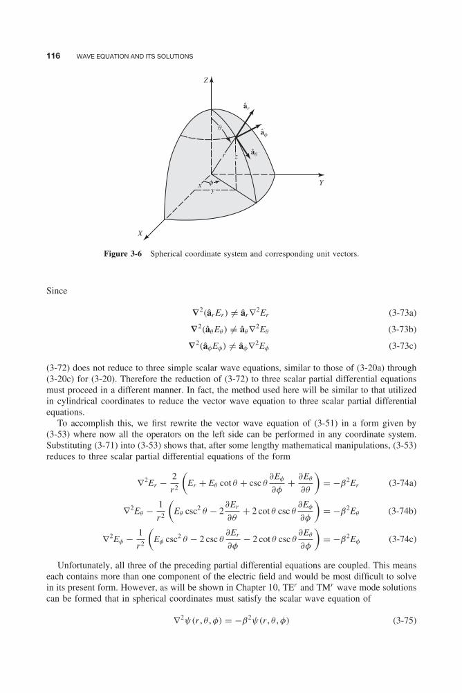
116 WAVE EQUATION AND ITS SOLUTIONS
ar
af
X
Z
Y
aq
f
q
xy
r z
Figure 3-6 Spherical coordinate system and corresponding unit vectors.
Since
∇2(âr Er ) �= âr∇2Er (3-73a)
∇2(âθEθ ) �= âθ∇2Eθ (3-73b)
∇2(âφEφ) �= âφ∇2Eφ (3-73c)
(3-72) does not reduce to three simple scalar wave equations, similar to those of (3-20a) through(3-20c) for (3-20). Therefore the reduction of (3-72) to three scalar partial differential equationsmust proceed in a different manner. In fact, the method used here will be similar to that utilizedin cylindrical coordinates to reduce the vector wave equation to three scalar partial differentialequations.
To accomplish this, we first rewrite the vector wave equation of (3-51) in a form given by(3-53) where now all the operators on the left side can be performed in any coordinate system.Substituting (3-71) into (3-53) shows that, after some lengthy mathematical manipulations, (3-53)reduces to three scalar partial differential equations of the form
∇2Er − 2
r2
(Er + Eθ cot θ + csc θ
∂Eφ
∂φ+ ∂Eθ
∂θ
)= −β2Er (3-74a)
∇2Eθ − 1
r2
(Eθ csc2 θ − 2
∂Er
∂θ+ 2 cot θ csc θ
∂Eφ
∂φ
)= −β2Eθ (3-74b)
∇2Eφ − 1
r2
(Eφ csc2 θ − 2 csc θ
∂Er
∂φ− 2 cot θ csc θ
∂Eθ
∂φ
)= −β2Eφ (3-74c)
Unfortunately, all three of the preceding partial differential equations are coupled. This meanseach contains more than one component of the electric field and would be most difficult to solvein its present form. However, as will be shown in Chapter 10, TEr and TMr wave mode solutionscan be formed that in spherical coordinates must satisfy the scalar wave equation of
∇2ψ(r , θ , φ) = −β2ψ(r , θ , φ) (3-75)

SOLUTION TO THE WAVE EQUATION 117
where ψ(r , θ , φ) is a scalar function that can represent a field or a vector potential compo-nent. Therefore, it would be advisable here to demonstrate the solution to (3-75) in sphericalcoordinates.
Assuming a separable solution for ψ(r , θ , φ) of the form
ψ(r , θ , φ) = f (r)g(θ)h(φ) (3-76)
we can write the expanded form of (3-75)
1
r2
∂
∂r
{r2 ∂ψ
∂r
}+ 1
r2 sin θ
∂
∂θ
{sin θ
∂ψ
∂θ
}+ 1
r2 sin2 θ
∂2ψ
∂φ2= −β2ψ (3-77)
as
gh1
r2
∂
∂r
{r2 ∂f
∂r
}+ fh
1
r2 sin θ
∂
∂θ
{sin θ
∂g
∂θ
}+ fg
1
r2 sin2 θ
∂2h
∂φ2= −β2fgh (3-78)
Dividing both sides by fgh , multiplying by r2 sin2 θ , and replacing the partials by ordinaryderivatives reduces (3-78) to
sin2 θ
f
d
dr
{r2 df
dr
}+ sin θ
g
d
dθ
{sin θ
dg
dθ
}+ 1
h
d2h
dφ2= −(βr sin θ)2 (3-79)
Since the last term on the left side of (3-79) is only a function of φ, it can be set equal to
1
h
d2h
dφ2= −m2 ⇒ d2h
dφ2= −m2h (3-80)
where m is a constant.Substituting (3-80) into (3-79), dividing both sides by sin2 θ , and transposing the term from
the right to the left side reduces (3-79) to
1
f
d
dr
{r2 df
dr
}+ (βr)2 + 1
g sin θ
d
dθ
{sin θ
dg
dθ
}−
{ m
sin θ
}2= 0 (3-81)
Since the last two terms on the left side of (3-81) are only a function of θ , we can set them equalto
1
g sin θ
d
dθ
{sin θ
dg
dθ
}−
{ m
sin θ
}2= −n(n + 1) (3-82)
where n is usually an integer. Equation 3-82 is closely related to the well-known Legendredifferential equation (see Appendix V) [1–3, 6–10].
Substituting (3-82) into (3-81) reduces it to
1
f
d
dr
{r2 df
dr
}+ (βr)2 − n(n + 1) = 0 (3-83)
which is closely related to the Bessel differential equation (see Appendix IV).In summary then, the scalar wave equation 3-75 whose expanded form in spherical coordinates
can be written as
1
r2
∂
∂r
{r2 ∂ψ
∂r
}+ 1
r2 sin θ
∂
∂θ
{sin θ
∂ψ
∂θ
}+ 1
r2 sin2 θ
∂2ψ
∂φ2= −β2ψ (3-84)
118 WAVE EQUATION AND ITS SOLUTIONS
and whose separable solution takes the form of
ψ(r , θ , φ) = f (r)g(θ)h(φ) (3-85)
reduces to the three scalar differential equations
d
dr
{r2 df
dr
}+ [
(βr)2 − n(n + 1)]
f = 0 (3-86a)
1
sin θ
d
dθ
{sin θ
dg
dθ
}+
[n(n + 1) −
{ m
sin θ
}2]
g = 0 (3-86b)
d2h
dφ2= −m2h (3-86c)
where m and n are constants (usually integers).Solutions to (3-86a) through (3-86c) take the forms, respectively, of
f1(r) = A1jn(βr) + B1yn(βr) (3-87a)
orf2(r) = C1h(1)
n (βr) + D1h(2)n (βr) (3-87b)
andg1(θ) = A2Pm
n (cos θ) + B2Pmn (− cos θ) n �= integer (3-88a)
org2(θ) = C2Pm
n (cos θ) + D2Qmn (cos θ) n = integer (3-88b)
andh1(φ) = A3e−jmφ + B3e+jmφ (3-89a)
orh2(φ) = C3 cos(mφ) + D3 sin(mφ) (3-89b)
In (3-87a) jn(βr) and yn(βr) are referred to, respectively, as the spherical Bessel functions ofthe first and second kind. They are used to represent radial standing waves, and they are related,respectively, to the corresponding regular Bessel functions Jn+1/2(βr) and Yn+1/2(βr) by
jn(βr) =√
π
2βrJn+1/2(βr) (3-90a)
yn(βr) =√
π
2βrYn+1/2(βr) (3-90b)
In (3-87b) h(1)n (βr) and h(2)
n (βr) are referred to, respectively, as the spherical Hankel functionsof the first and second kind. They are used to represent radial traveling waves, and they are related,respectively, to the regular Hankel functions H (1)
n+1/2(βr) and H (2)n+1/2(βr) by
h(1)n (βr) =
√π
2βrH (1)
n+1/2(βr) (3-91a)
h(2)n (βr) =
√π
2βrH (2)
n+1/2(βr) (3-91b)
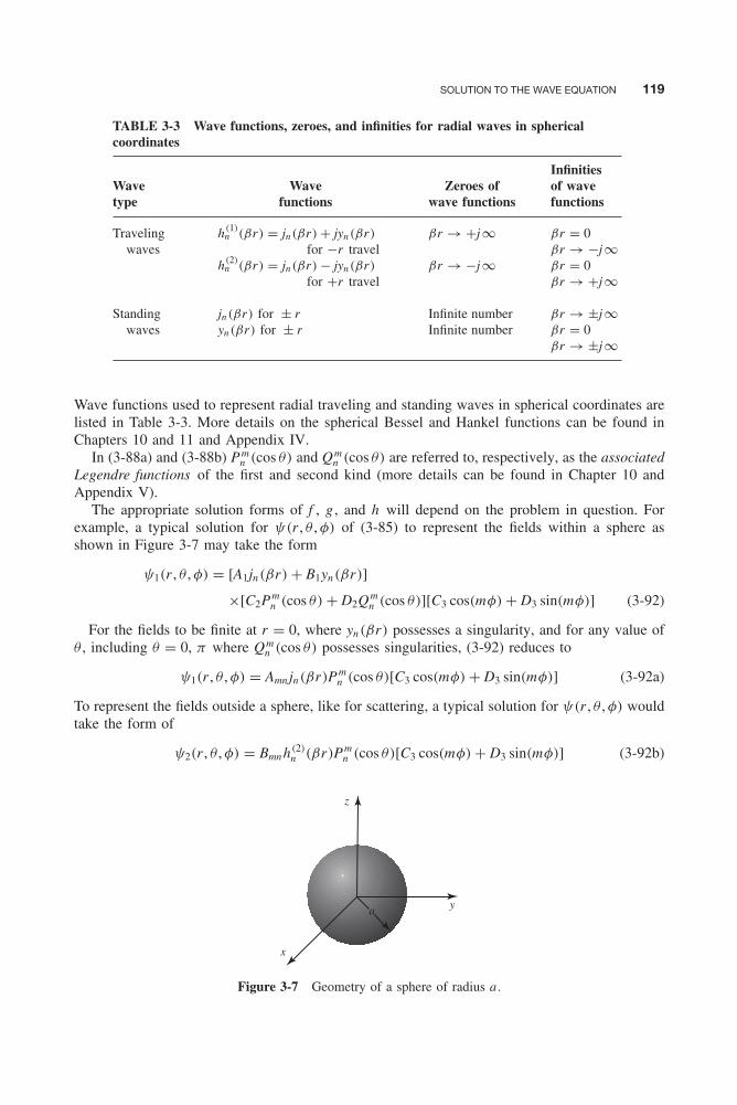
SOLUTION TO THE WAVE EQUATION 119
TABLE 3-3 Wave functions, zeroes, and infinities for radial waves in sphericalcoordinates
InfinitiesWave Wave Zeroes of of wavetype functions wave functions functions
Travelingwaves
h(1)n (βr) = jn(βr) + jyn(βr)
for −r travelh(2)
n (βr) = jn(βr) − jyn(βr)
for +r travel
βr → +j∞
βr → −j∞
βr = 0βr → −j∞βr = 0βr → +j∞
Standingwaves
jn(βr) for ± ryn(βr) for ± r
Infinite numberInfinite number
βr → ±j∞βr = 0βr → ±j∞
Wave functions used to represent radial traveling and standing waves in spherical coordinates arelisted in Table 3-3. More details on the spherical Bessel and Hankel functions can be found inChapters 10 and 11 and Appendix IV.
In (3-88a) and (3-88b) Pmn (cos θ) and Qm
n (cos θ) are referred to, respectively, as the associatedLegendre functions of the first and second kind (more details can be found in Chapter 10 andAppendix V).
The appropriate solution forms of f , g , and h will depend on the problem in question. Forexample, a typical solution for ψ(r , θ , φ) of (3-85) to represent the fields within a sphere asshown in Figure 3-7 may take the form
ψ1(r , θ , φ) = [A1jn(βr) + B1yn(βr)]
×[C2Pmn (cos θ) + D2Qm
n (cos θ)][C3 cos(mφ) + D3 sin(mφ)] (3-92)
For the fields to be finite at r = 0, where yn(βr) possesses a singularity, and for any value ofθ , including θ = 0, π where Qm
n (cos θ) possesses singularities, (3-92) reduces to
ψ1(r , θ , φ) = Amnjn(βr)Pmn (cos θ)[C3 cos(mφ) + D3 sin(mφ)] (3-92a)
To represent the fields outside a sphere, like for scattering, a typical solution for ψ(r , θ , φ) wouldtake the form of
ψ2(r , θ , φ) = Bmnh(2)n (βr)Pm
n (cos θ)[C3 cos(mφ) + D3 sin(mφ)] (3-92b)
z
y
x
a
Figure 3-7 Geometry of a sphere of radius a .

120 WAVE EQUATION AND ITS SOLUTIONS
whereby the spherical Hankel function of the second kind h(2)n (βr) has replaced the spherical
Bessel function of the first kind jn(βr) because outward traveling waves are formed outside thesphere, in contrast to the standing waves inside the sphere.
Other spherical Bessel and Hankel functions that are most often encountered in boundary-value electromagnetic problems are those utilized by Schelkunoff [3, 11]. These spherical Besseland Hankel functions, denoted in general by B̂n(βr) to represent any of them, must satisfy thedifferential equation
d2B̂n
dr2+
[β2 − n(n + 1)
r2
]B̂n = 0 (3-93)
The spherical Bessel and Hankel functions that are solutions to this equation are related to otherspherical Bessel and Hankel functions of (3-90a) through (3-91b), denoted here by bn(βr), andto the regular Bessel and Hankel functions, denoted here by Bn+1/2(βr), by
B̂n(βr) = βr bn(βr) = βr√
π
2βrBn+1/2(βr) =
√πβr
2Bn+1/2(βr) (3-94)
More details concerning the application and properties of the spherical Bessel and Hankelfunctions can be found in Chapter 10.
3.5 MULTIMEDIA
On the website that accompanies this book, the following multimedia resources are included forthe review, understanding and presentation of the material of this chapter.
• Power Point (PPT) viewgraphs, in multicolor.
REFERENCES
1. F. B. Hilderbrand, Advanced Calculus for Applications , Prentice-Hall, Englewood Cliffs, NJ, 1962.
2. C. R. Wylie, Jr., Advanced Engineering Mathematics , McGraw-Hill, New York, 1960.
3. R. F. Harrington, Time-Harmonic Electromagnetic Fields , McGraw-Hill, New York, 1961.
4. R. B. Adler, L. J. Chu, and R. M. Fano, Electromagnetic Energy Transmission and Radiation , Chapter 8,John Wiley & Sons, New York, 1960.
5. G. N. Watson, A Treatise on the Theory of Bessel Functions , Cambridge Univ. Press, London, 1948.
6. W. R. Smythe, Static and Dynamic Electricity , McGraw-Hill, New York, 1941.
7. J. A. Stratton, Electromagnetic Theory , McGraw-Hill, New York, 1960.
8. P. M. Morse and H. Feshbach, Methods of Theoretical Physics , Parts I and II, McGraw-Hill, New York,1953.
9. M. Abramowitz and I. A. Stegun (eds.), Handbook of Mathematical Functions with Formulas, Graphs,and Mathematical Tables , National Bureau of Standards Applied Mathematics Series-55, U.S. Gov.Printing Office, Washington, DC, 1966.
10. M. R. Spiegel, Mathematical Handbook of Formulas and Tables , Schaum’s Outline Series, McGraw-Hill, New York, 1968.
11. S. A. Schelkunoff, Electromagnetic Waves , Van Nostrand, Princeton, NJ, 1943.
PROBLEMS 121
PROBLEMS
3.1. Derive the vector wave equations 3-16a and3-16b for time-harmonic fields using theMaxwell equations of Table 1-4 for time-harmonic fields.
3.2. Verify that (3-28a) and (3-28b) are solutionsto (3-26a).
3.3. Show that the second complex exponentialin (3-31) represents a wave traveling in the−z direction. Determine its phase velocity.
3.4. Using the method of separation of variablesshow that a solution to (3-37a) of the form(3-39) can be represented by (3-40a) through(3-43).
3.5. Show that the vector wave equation of (3-53) reduces, when E has a solution ofthe form (3-47), to the three scalar waveequations 3-54a through 3-54c.
3.6. Reduce (3-51) to (3-54a) through (3-54c) byexpanding ∇2E. Do not use (3-52); ratheruse the scalar Laplacian in cylindrical coor-dinates and treat E as a vector given by(3-47). Use that
∂ âρ
∂ρ= ∂ âφ
∂ρ= ∂ âz
∂ρ= 0 = ∂ âz
∂φ= ∂ âρ
∂z
= ∂ âφ
∂z= ∂ âz
∂z∂ âρ
∂φ= âφ
∂ âφ
∂φ= −âρ
3.7. Using large argument asymptotic forms,show that Bessel and Hankel functions rep-resent, respectively, standing and travelingwaves in the radial direction.
3.8. Using large argument asymptotic forms andassuming ejωt time convention, show thatHankel functions of the first kind representtraveling waves in the −ρ direction whereasHankel functions of the second kind repre-sent traveling waves in the +ρ direction.The opposite would be true were the timevariations of the e−jωt form.
3.9. Using large argument asymptotic forms,show that Bessel functions of complex argu-ment represent attenuating standing waves.
3.10. Assuming time variations of ejωt and usinglarge argument asymptotic forms, show thatHankel functions of the first and second kindwith complex arguments represent, respec-tively, attenuating traveling waves in the −ρ
and +ρ directions.
3.11. Show that when E can be expressed as(3-71), the vector wave equation 3-53 redu-ces to the three scalar wave equations 3-74athrough 3-74c.
3.12. Reduce (3-51) to (3-74a) through (3-74c) byexpanding ∇2E. Do not use (3-52); ratheruse the scalar Laplacian in spherical coordi-nates and treat E as a vector given by (3-71).Use that
∂ âr
∂r= ∂ âθ
∂r= ∂ âφ
∂r= 0
∂ âr
∂θ= âθ
∂ âθ
∂θ= −âr
∂ âφ
∂θ= 0
∂ âr
∂φ= sin θ âφ
∂ âθ
∂φ= cos θ âφ
∂ âφ
∂φ= − sin θ âr − cos θ âθ
3.13. Using large argument asymptotic forms,show that spherical Bessel functions repre-sent standing waves in the radial direction.
3.14. Show that spherical Hankel functions of thefirst and second kind represent, respectively,radial traveling waves in the −r and +rdirections. Assume time variations of ejωt
and large argument asymptotic expansionsfor the spherical Hankel functions.
3.15. Justify that associated Legendre functionsrepresent standing waves in the θ directionof the spherical coordinate system.
3.16. Verify the relation (3-94) between the vari-ous forms of the spherical Bessel and Hankelfunctions and the regular Bessel and Hankelfunctions.

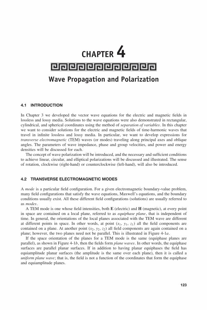
CHAPTER 4Wave Propagation and Polarization
4.1 INTRODUCTION
In Chapter 3 we developed the vector wave equations for the electric and magnetic fields inlossless and lossy media. Solutions to the wave equations were also demonstrated in rectangular,cylindrical, and spherical coordinates using the method of separation of variables . In this chapterwe want to consider solutions for the electric and magnetic fields of time-harmonic waves thattravel in infinite lossless and lossy media. In particular, we want to develop expressions fortransverse electromagnetic (TEM) waves (or modes) traveling along principal axes and obliqueangles. The parameters of wave impedance, phase and group velocities, and power and energydensities will be discussed for each.
The concept of wave polarization will be introduced, and the necessary and sufficient conditionsto achieve linear, circular, and elliptical polarizations will be discussed and illustrated. The senseof rotation, clockwise (right-hand) or counterclockwise (left-hand), will also be introduced.
4.2 TRANSVERSE ELECTROMAGNETIC MODES
A mode is a particular field configuration. For a given electromagnetic boundary-value problem,many field configurations that satisfy the wave equations, Maxwell’s equations, and the boundaryconditions usually exist. All these different field configurations (solutions) are usually referred toas modes .
A TEM mode is one whose field intensities, both E (electric) and H (magnetic), at every pointin space are contained on a local plane, referred to as equiphase plane, that is independent oftime. In general, the orientations of the local planes associated with the TEM wave are differentat different points in space. In other words, at point (x1, y1, z1) all the field components arecontained on a plane. At another point (x2, y2, z2) all field components are again contained on aplane; however, the two planes need not be parallel. This is illustrated in Figure 4-1a .
If the space orientation of the planes for a TEM mode is the same (equiphase planes areparallel), as shown in Figure 4-1b, then the fields form plane waves . In other words, the equiphasesurfaces are parallel planar surfaces. If in addition to having planar equiphases the field hasequiamplitude planar surfaces (the amplitude is the same over each plane), then it is called auniform plane wave; that is, the field is not a function of the coordinates that form the equiphaseand equiamplitude planes.
123
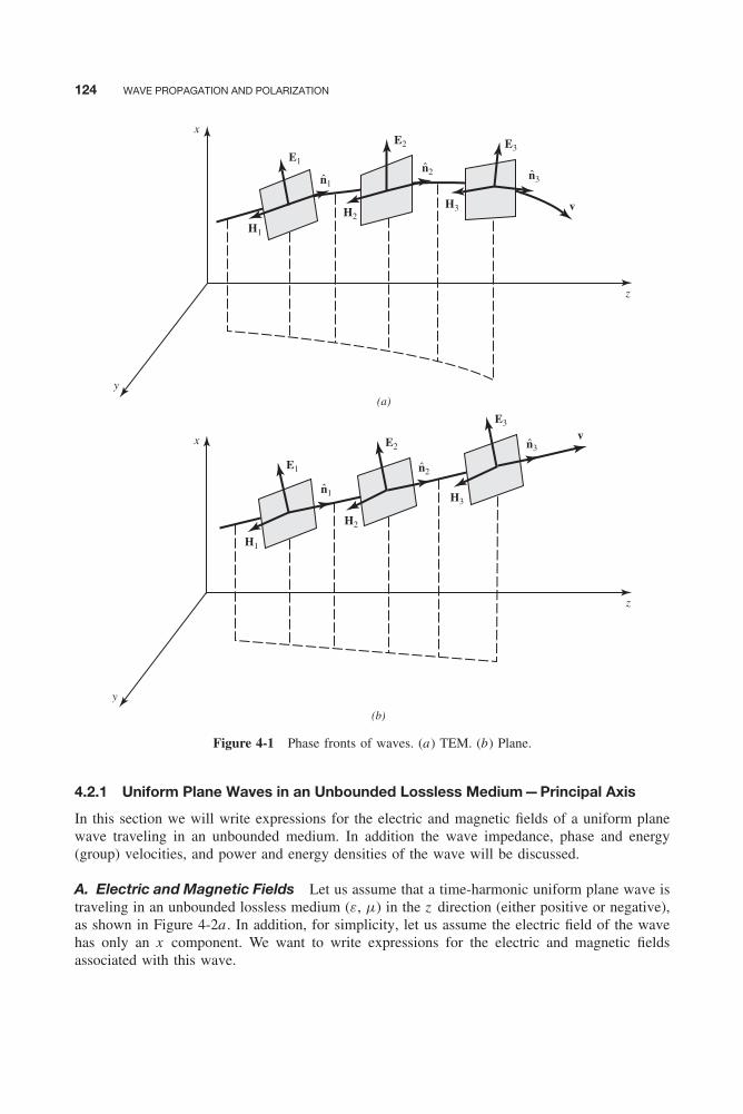
124 WAVE PROPAGATION AND POLARIZATION
(a)
E1
E2 E3
E1
E2
E3
H1
H2H3
H1
H2
H3
v
v
x
x
z
z
y
y
(b)
n1
n1
n2
n2
n3
n3
Figure 4-1 Phase fronts of waves. (a) TEM. (b) Plane.
4.2.1 Uniform Plane Waves in an Unbounded Lossless Medium—Principal Axis
In this section we will write expressions for the electric and magnetic fields of a uniform planewave traveling in an unbounded medium. In addition the wave impedance, phase and energy(group) velocities, and power and energy densities of the wave will be discussed.
A. Electric and Magnetic Fields Let us assume that a time-harmonic uniform plane wave istraveling in an unbounded lossless medium (ε, μ) in the z direction (either positive or negative),as shown in Figure 4-2a . In addition, for simplicity, let us assume the electric field of the wavehas only an x component. We want to write expressions for the electric and magnetic fieldsassociated with this wave.
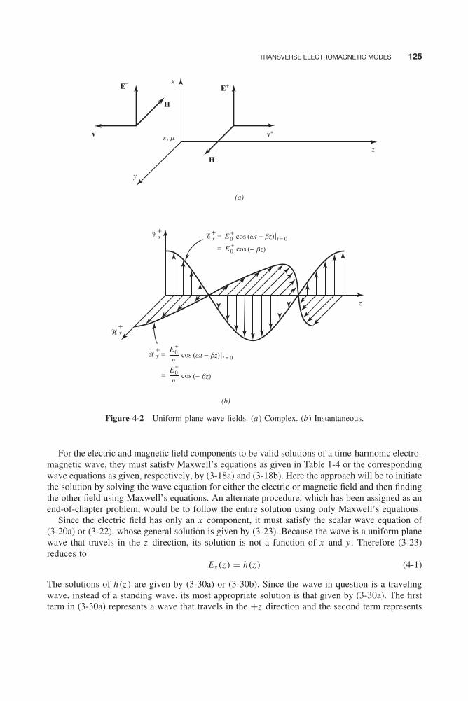
TRANSVERSE ELECTROMAGNETIC MODES 125
(a)
H+
x
z
z
y
e, m
x
(b)
E−
E +
E+
v− v+
H−
+x+
y+
=
=cos0
E + cos0
(wt − bz) | t = 0
(wt − bz) | t = 0
(− bz)
E +
yh
+ =
=
cos
cos
0
(− bz)E +
h0
�
�
� �
Figure 4-2 Uniform plane wave fields. (a) Complex. (b) Instantaneous.
For the electric and magnetic field components to be valid solutions of a time-harmonic electro-magnetic wave, they must satisfy Maxwell’s equations as given in Table 1-4 or the correspondingwave equations as given, respectively, by (3-18a) and (3-18b). Here the approach will be to initiatethe solution by solving the wave equation for either the electric or magnetic field and then findingthe other field using Maxwell’s equations. An alternate procedure, which has been assigned as anend-of-chapter problem, would be to follow the entire solution using only Maxwell’s equations.
Since the electric field has only an x component, it must satisfy the scalar wave equation of(3-20a) or (3-22), whose general solution is given by (3-23). Because the wave is a uniform planewave that travels in the z direction, its solution is not a function of x and y . Therefore (3-23)reduces to
Ex (z ) = h(z ) (4-1)
The solutions of h(z ) are given by (3-30a) or (3-30b). Since the wave in question is a travelingwave, instead of a standing wave, its most appropriate solution is that given by (3-30a). The firstterm in (3-30a) represents a wave that travels in the +z direction and the second term represents
126 WAVE PROPAGATION AND POLARIZATION
a wave that travels in the −z direction. Therefore the solution of (4-1), using (3-30a), can bewritten as
Ex (z ) = A3e−jβz + B3e+jβz = E+x + E−
x (4-2)
or
Ex (z ) = E+0 e−jβz + E−
0 e+jβz = E+x + E−
x (4-2a)
E+x (z ) = E+
0 e−jβz (4-2b)
E−x (z ) = E−
0 e+jβz (4-2c)
since βz = β because βx = βy = 0. E+0 and E−
0 represent, respectively, the amplitudes of thepositive and negative (in the z direction) traveling waves.
The corresponding magnetic field must also be a solution of its wave equation 3-18b, and itsform will be similar to (4-2). However, since we do not know which components of magneticfield coexist with the x component of the electric field, they are most appropriately determinedby using one of Maxwell’s equations as given in Table 1-4. Since the electric field is known, asgiven by (4-2), the magnetic field can best be found using
∇ × E = −jωμH (4-3)
or
H = − 1
jωμ∇ × E = − 1
jωμ
⎡⎢⎢⎣âx ây âz
∂
∂x
∂
∂y
∂
∂zEx 0 0
⎤⎥⎥⎦ (4-3a)
which, using (4-2a), reduces to
H = −ây1
jωμ
{∂Ex
∂z
}= ây
β
ωμ
{E+
0 e−jβz − E−0 e+jβz
}H = ây
1√μ/ε
{E+
0 e−jβz − E−0 e+jβz
} = ây1√μ/ε
{E+
x − E−x
} = ây
{H +
y + H −y
}(4-3b)
where
H +y = 1√
μ/εE+
x (4-3c)
H −y = − 1√
μ/εE−
x (4-3d)
Plots of the instantaneous positive traveling electric and magnetic fields at t = 0 as a functionof z are shown in Figure 4-2b. Similar plots can be drawn for the negative traveling fields.
B. Wave Impedance Since each term for the magnetic field (A/m) in (4-3c) and (4-3d) isindividually identical to the corresponding term for the electric field (V/m) in (4-2a), the factor√
μ/ε in the denominator in (4-3c) and (4-3d) must have units of ohms (V/A). Therefore thefactor
√μ/ε is known as the wave impedance, Zw, denoted by the ratio of the electric to magnetic
field, and it is usually represented by η
Zw = E+x
H +y
= − E−x
H −y
= η =√
μ
ε(4-4)

TRANSVERSE ELECTROMAGNETIC MODES 127
The wave impedance of (4-4) is identical to a quantity that is referred to as the intrinsic impedanceη = √
μ/ε of the medium. In general, this is true not only for uniform plane waves but also forplane and TEM waves; however, it is not true for TE or TM modes.
In (4-3d) it is also observed that a negative sign is found in front of the magnetic fieldcomponent that travels in the −z direction; a positive sign is noted in front of the positive travelingwave. The general procedure that can be followed to find the magnetic field components, giventhe electric field components, or to find the electric field components, given the magnetic fieldcomponents, is the following:
1. Place the fingers of your right hand in the direction of the electric field component.2. Direct your thumb toward the direction of wave travel (power flow).3. Rotate your fingers 90◦ in a direction so that a right-hand screw is formed.4. The new direction of your fingers is the direction of the magnetic field component.5. Divide the electric field component by the wave impedance to obtain the corresponding
magnetic field component.
The foregoing procedure must be followed for each term of each component of an electricor magnetic field. The results are identical to those that would be obtained by using Maxwell’sequations. If the wave impedance is known in advance, as it is for TEM waves, this procedureis simpler and much more rapid than using Maxwell’s equations. By following this procedure,the answers (including the signs) in (4-3c) and (4-3d) given (4-2b) and (4-2c) are obvious.
To illustrate the procedure, let us consider another example.
Example 4-1
The electric field of a uniform plane wave traveling in free space is given by
E = ây(E+
0 e−jβz + E−0 e+jβz ) = ây
(E+
y + E−y
)where E+
0 and E−0 are constants. Find the corresponding magnetic field using the outlined procedure.
Solution: For the electric field component that is traveling in the +z direction, the correspondingmagnetic field component is given by
H+ = −âxE+
0
η0
e−jβz � −âxE+
0
377e−jβz
where
η0 = Zw =√
μ0
ε0� 377 ohms
Similarly, for the wave that is traveling in the −z direction we can write that
H− = âxE−
0
η0
e+jβz � âxE−
0
377e+jβz
Therefore the total magnetic field is equal to
H = H+ + H− = âx1
η0
(−E+0 e−jβz + E−
0 e+jβz )The same answer would be obtained if Maxwell’s equations were used, and it is assigned as an end-of-chapter problem.

128 WAVE PROPAGATION AND POLARIZATION
The term in the expression for the electric field in (4-2a) that identifies the direction of wavetravel can also be written in vector notation. This is usually more convenient to use when dealingwith waves traveling at oblique angles. Equation 4-2a can therefore take the more general form of
Ex (z ) = E+0 e−jβ+ • r + E−
0 e−jβ− • r (4-5)
where
β+ = β̂+β = âxβ+x + âyβ
+y + âz β
+z
∣∣ = âz ββ+
x =β+y =0
β+z =β
(4-5a)
β− = β̂−β = âxβ−x + âyβ
−y − âz β
−z
∣∣= −âz ββ−
x =β−y =0
β−z =β
(4-5b)
r = position vector = âx x + ây y + âz z (4-5c)
In (4-5a) through (4-5c), βx , βy , βz represent, respectively, the phase constants of the wave inthe x , y , z directions, r represents the position vector in rectangular coordinates, and β̂+ and β̂−represent unit vectors in the directions of β+ and β−. The notation used in (4-5) through (4-5c)to represent the wave travel will be most convenient to express wave travel at oblique angles,as will be the case in Section 4.2.2.
C. Phase and Energy (Group) Velocities, Power, and Energy Densities The expressionsfor the electric and magnetic fields, as given by (4-2a) and (4-3b), represent the spatial variationsof the field intensities. The corresponding instantaneous forms of each can be written, using(1-61a) and (1-61b) and assuming E+
0 and E−0 are real constants, as
�x (z ; t) = �+x (z ; t) + �−
x (z ; t) = Re[E+
0 e−jβz ejωt] + Re
[E−
0 e+jβz ejωt]
= E+0 cos (ωt − βz ) + E−
0 cos (ωt + βz ) (4-6a)
�y (z ; t) = �+y (z ; t) + �−
y (z ; t)
= 1√μ/ε
[E+
0 cos (ωt − βz ) − E−0 cos (ωt + βz )
](4-6b)
In each of the fields, as given by (4-6a) and (4-6b), the first term represents, according to(3-34) through (3-35) and Figure 3-3, a wave that travels in the +z direction; the second termrepresents a wave that travels in the −z direction. To maintain a constant phase in the first termof (4-6a), the velocity must be equal, according to (3-35), to
v+p = +dz
dt= ω
β= ω
ω√
με= 1√
με(4-7)
The corresponding velocity of the second term in (4-6a) is identical in magnitude to (4-7) butwith a negative sign to reflect the direction of wave travel. The velocity of (4-7) is referred toas the phase velocity , and it represents the velocity that must be maintained in order to keep instep with a constant phase front of the wave. As will be shown for oblique traveling waves, thephase velocity of such waves can exceed the velocity of light. This is only a hypothetical speed,as will be explained in Section 4.2.2C. Aside of nonuniform plane waves, also referred to asslow surface waves (see Section 5.3.4A), in general the phase velocity can be equal to or even

TRANSVERSE ELECTROMAGNETIC MODES 129
greater than the speed of light. Variations of the instantaneous positive traveling electric �+x (z ; t)
and magnetic �+y (z ; t) fields as a function of z for t = 0 are shown in Figure 4-2b. As time
increases, both curves will shift in the positive z direction. A similar set of curves can be drawnfor the negative traveling electric �−
x (z ; t) and magnetic �−y (z ; t) fields.
The electric and magnetic energies (W-s/m3) and power densities (W/m2) associatedwith the positive traveling waves of (4-6a) and (4-6b) can be written, according to (l-58f) and(l-58e), as
w+e = 1
2ε�+2
x = 1
2εE+2
0 cos2 (ωt − βz ) (4-8a)
w+m = 1
2μ�+2
y = 1
2μ
[(ε/μ) E+2
0 cos2 (ωt − βz )] = 1
2εE+2
0 cos2 (ωt − βz ) (4-8b)
+ = �+ × �+ = âx E+0 cos (ωt − βz ) ×
[ây
(1/
√μ/ε
)E+
0 cos (ωt − βz )]
= âz + = âz
(1/
√μ/ε
)E+2
0 cos2 (ωt − βz ) (4-8c)
The ratio formed by dividing the power density (W/m2) by the total energy density w =we + wm (J/m3 = W-s/m3) is referred to as the energy (group) velocity ve , and it is given by
v+e = +
w+ = +
w+e + w+
m=
(1/
√μ/ε
)E+2
0 cos2 (ωt − βz )
εE+20 cos2 (ωt − βz )
= 1√με
(4-9)
The energy velocity represents the velocity with which the wave energy is transported. It isapparent that (4-9) is identical to (4-7). In general that is not the case. In fact, the energy velocityv+
e can be equal to, but not exceed, the speed of light, and the product of the phase velocity vp
and energy velocity ve must always be equal to
v+p v+
e = (v+)2 = 1
με(4-10)
where v+ = 1/√
με is the speed of light. The same holds for the negative traveling waves.The time-average power density (Poynting vector) associated with the positive traveling wave
can be written, using (l-70) and the first terms of (4-2a) and (4-3b), as
+av = 1
2Re
(E+ × H+∗) = âz
1
2√
μ/ε|E+
x |2 = âz|E+
0 |22√
μ/ε= âz
|E+0 |2
2η(4-11)
A similar expression is derived for the negative traveling wave.
D. Standing Waves Each of the terms in (4-2a) and (4-3b) represents individually travelingwaves, the first traveling in the positive z direction and the second in the negative z direction.The two together form a so-called standing wave, which is comprised of two oppositely travelingwaves.
To examine the characteristics of a standing wave, let us rewrite (4-2a) as
Ex (z ) = E+0 e−jβz + E−
0 e+jβz
= E+0
[cos (βz ) − j sin (βz )
] + E−0
[cos (βz ) + j sin (βz )
]= (
E+0 + E−
0
)cos (βz ) − j
(E+
0 − E−0
)sin (βz )
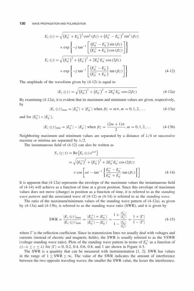
130 WAVE PROPAGATION AND POLARIZATION
Ex (z ) =√(
E+0 + E−
0
)2cos2 (βz ) + (
E+0 − E−
0
)2sin2 (βz )
× exp
{−j tan−1
[ (E+
0 − E−0
)sin (βz )(
E+0 + E−
0
)cos (βz )
]}
Ex (z ) =√(
E+0
)2 + (E−
0
)2 + 2E+0 E−
0 cos (2βz )
× exp
{−j tan−1
[(E+
0 − E−0
)(E+
0 + E−0
) tan (βz )
]}(4-12)
The amplitude of the waveform given by (4-12) is equal to
|Ex (z ) | =√(
E+0
)2 + (E−
0
)2 + 2E+0 E−
0 cos (2βz ) (4-12a)
By examining (4-12a), it is evident that its maximum and minimum values are given, respectively,by
|Ex (z ) |max = |E+0 | + |E−
0 | when βz = mπ , m = 0, 1, 2, . . . (4-13a)
and for |E+0 | > |E−
0 |,
|Ex (z ) |min = |E+0 | − |E−
0 | when βz = (2m + 1)π
2, m = 0, 1, 2, . . . (4-13b)
Neighboring maximum and minimum values are separated by a distance of λ/4 or successivemaxima or minima are separated by λ/2.
The instantaneous field of (4-12) can also be written as
�x (z ; t) = Re[Ex (z ) ejωt
]=
√(E+
0
)2 + (E−
0
)2 + 2E+0 E−
0 cos (2βz )
× cos
[ωt − tan−1
{E+
0 − E−0
E+0 + E−
0
tan (βz )
}](4-14)
It is apparent that (4-12a) represents the envelope of the maximum values the instantaneous fieldof (4-14) will achieve as a function of time at a given position. Since this envelope of maximumvalues does not move (change) in position as a function of time, it is referred to as the standingwave pattern and the associated wave of (4-12) or (4-14) is referred to as the standing wave.
The ratio of the maximum/minimum values of the standing wave pattern of (4-12a), as givenby (4-13a) and (4-13b), is referred to as the standing wave ratio (SWR), and it is given by
SWR = |Ex (z ) |max
|Ex (z ) |min= |E+
0 | + |E−0 |
|E+0 | − |E−
0 | =1 + |E−
0 ||E+
0 |
1 − |E−0 |
|E+0 |
= 1 + |�|1 − |�| (4-15)
where � is the reflection coefficient. Since in transmission lines we usually deal with voltages andcurrents (instead of electric and magnetic fields), the SWR is usually referred to as the VSWR(voltage standing wave ratio). Plots of the standing wave pattern in terms of E+
0 as a function ofz (−λ ≤ z ≤ λ) for |�| = 0, 0.2, 0.4, 0.6, 0.8, and 1 are shown in Figure 4-3.
The SWR is a quantity that can be measured with instrumentation [1, 2]. SWR has valuesin the range of 1 ≤ SWR ≤ ∞. The value of the SWR indicates the amount of interferencebetween the two opposite traveling waves; the smaller the SWR value, the lesser the interference.
TRANSVERSE ELECTROMAGNETIC MODES 131
2E+0
1.6E+0
1.2E+0
0.8E+0
0.4E+0
E+0
0−λ −0.75λ −0.50λ −0.25λ 0.75λ λ0.50λ0.25λ0
|Γ| = 1
|Γ|
|Γ| = 0.8
|Γ| = 0.6
|Γ| = 0.4
|Γ| = 0.2
|Γ| = 0
Figure 4-3 Standing wave pattern as a function of distance for a uniform plane wave with differentreflection coefficients.
The minimum SWR value of unity occurs when |�| = E−0 /E+
0 = 0, and it indicates that nointerference is formed. Thus the standing wave reduces to a pure traveling wave. The maximumSWR of infinity occurs when |�| = E−
0 /E+0 = 1, and it indicates that the negative traveling wave
is of the same intensity as the positive traveling wave. This provides the maximum interference,and the wave forms a pure standing wave pattern given by
|Ex (z ) |E+0 =E−
0= 2E+
0 | cos(βz )| = 2E−0 | cos (βz ) | (4-16)
The pattern of this is a rectified cosine function, and it is represented in Figure 4-3 by the |�| = 1curve. The pattern exhibits pure nulls and peak values of twice the amplitude of the incident wave.
4.2.2 Uniform Plane Waves in an Unbounded Lossless Medium—Oblique Angle
In this section, expressions for the electric and magnetic fields, wave impedance, phase and groupvelocities, and power and energy densities will be written for uniform plane waves traveling atoblique angles in an unbounded medium. All of these will be done for waves that are uniformplane waves to the direction of travel.

132 WAVE PROPAGATION AND POLARIZATION
A. Electric and Magnetic Fields Let us assume that a uniform plane wave is traveling inan unbounded medium in a direction shown in Figure 4-4a . The amplitudes of the positive andnegative traveling electric fields are E+
0 and E−0 , respectively, and the assumed directions of each
are also illustrated in Figure 4-4a . It is desirable to write expressions for the positive and negativetraveling electric and magnetic field components.
β b
y
e, me, m
e, me, m
E+
H−
E−
v −
v+xE+
zE−
xE−
x
H+
zE+
zH+
xH+
xβ +
zβ −
xβ−
xβ−
zβ−zβ+
xβ+
x
z
(a)
(b)
z
z
β +
qi
qi
qi
qiqi
H−
E−
E+
v −
v+
zH−
xH−
H+
qiqi
qi
qi
qi
y
=+ +
β b=− −
β b=− −
ββ b=+ +
β
β
β
Figure 4-4 Transverse electric and magnetic uniform plane waves in an unbounded medium at an obliqueangle. (a) TEy mode. (b) TMy mode.
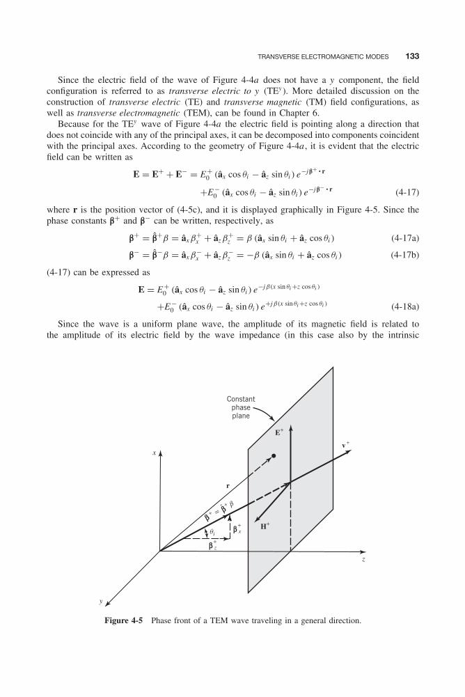
TRANSVERSE ELECTROMAGNETIC MODES 133
Since the electric field of the wave of Figure 4-4a does not have a y component, the fieldconfiguration is referred to as transverse electric to y (TEy ). More detailed discussion on theconstruction of transverse electric (TE) and transverse magnetic (TM) field configurations, aswell as transverse electromagnetic (TEM), can be found in Chapter 6.
Because for the TEy wave of Figure 4-4a the electric field is pointing along a direction thatdoes not coincide with any of the principal axes, it can be decomposed into components coincidentwith the principal axes. According to the geometry of Figure 4-4a , it is evident that the electricfield can be written as
E = E+ + E− = E+0 (âx cos θi − âz sin θi ) e−jβ+ • r
+E−0 (âx cos θi − âz sin θi ) e−jβ− • r (4-17)
where r is the position vector of (4-5c), and it is displayed graphically in Figure 4-5. Since thephase constants β+ and β− can be written, respectively, as
β+ = β̂+β = âxβ+x + âz β
+z = β (âx sin θi + âz cos θi ) (4-17a)
β− = β̂−β = âxβ−x + âz β
−z = −β (âx sin θi + âz cos θi ) (4-17b)
(4-17) can be expressed as
E = E+0 (âx cos θi − âz sin θi ) e−jβ(x sin θi +z cos θi )
+E−0 (âx cos θi − âz sin θi ) e+jβ(x sin θi +z cos θi ) (4-18a)
Since the wave is a uniform plane wave, the amplitude of its magnetic field is related tothe amplitude of its electric field by the wave impedance (in this case also by the intrinsic
β
b=+
+
zβ+
xβ+qi
x
Constantphaseplane
v +
y
z
E+
H+
r
β
Figure 4-5 Phase front of a TEM wave traveling in a general direction.
134 WAVE PROPAGATION AND POLARIZATION
impedance) as given by (4-4). Since the magnetic field is traveling in the same direction as theelectric field, the exponentials used to indicate its directions of travel are the same as those ofthe electric field as given in (4-18a). The directions of the magnetic field can be found using theright-hand procedure outlined in Section 4.2.1 and illustrated graphically in Figure 4-2b for thepositive traveling wave. Using all of the preceding information, it is evident that the magneticfield corresponding to the electric field of (4-18a) can be written as
H = H+ + H− = ây
[E+
0
ηe−jβ(x sin θi +z cos θi ) − E−
0
ηe+jβ(x sin θi +z cos θi )
](4-18b)
In vector form, (4-18b) can also be written as
H = 1
η
[β̂+ × E+ + β̂− × E−
](4-18c)
The same form can be used to relate the E and H for any TEM wave traveling in any direction. Itis apparent that when θi = 0, (4-18a) and (4-18b) reduce to (4-2a) and (4-3b), respectively. Thesame answer for the magnetic field of (4-18b) can be obtained by applying Maxwell’s equation 4-3to the electric field of (4-18a). This is left for the reader as an end-of-the-chapter exercise.
The planes of constant phase at any time t are obtained by setting the phases of (4-18a) or(4-18b) equal to a constant, that is
β+ • r = β+x x + β+
y y + β+z z |y=0 = β (x sin θi + z cos θi ) = C + (4-19a)
β− • r = β−x x + β−
y y + β−z z |y=0 = −β (x sin θi + z cos θi ) = C − (4-19b)
Each of (4-19a) and (4-19b) are equations of a plane in either the spherical or rectangularcoordinates with unit vectors β̂+ and β̂− normal to each of the respective surfaces. The respectivephase velocities in any direction (r , x , or z ) are obtained by letting
β+ • r − ωt = β (x sin θi + z cos θi ) − ωt = C +0 (4-19c)
β− • r − ωt = −β (x sin θi + z cos θi ) − ωt = C −0 (4-19d)
and taking a derivative with respect to time.
Example 4-2
Another exercise of interest is that in which the electric field is directed along the +y direction and thewave is traveling along an oblique angle θi , as shown in Figure 4-4b. This is referred to as a TMy wave.The objective here is again to write expressions for the positive and negative electric and magnetic fieldcomponents, assuming the amplitudes of the positive and negative electric field components are E+
0 andE−
0 , respectively.
Solution: Since this wave only has a y electric field component, and it is traveling in the samedirection as that of Figure 4-4a , we can write the electric field as
E = E+ + E− = ây[E+
0 e−jβ(x sin θi +z cos θi ) + E−0 e+jβ(x sin θi +z cos θi )
]Using the right-hand procedure outlined in Section 4.2.1, the corresponding magnetic field componentsare pointed along directions indicated in Figure 4-4b. Since the magnetic field is not directed along anyof the principal axes, it can be decomposed into components that coincide with the principal axes, as
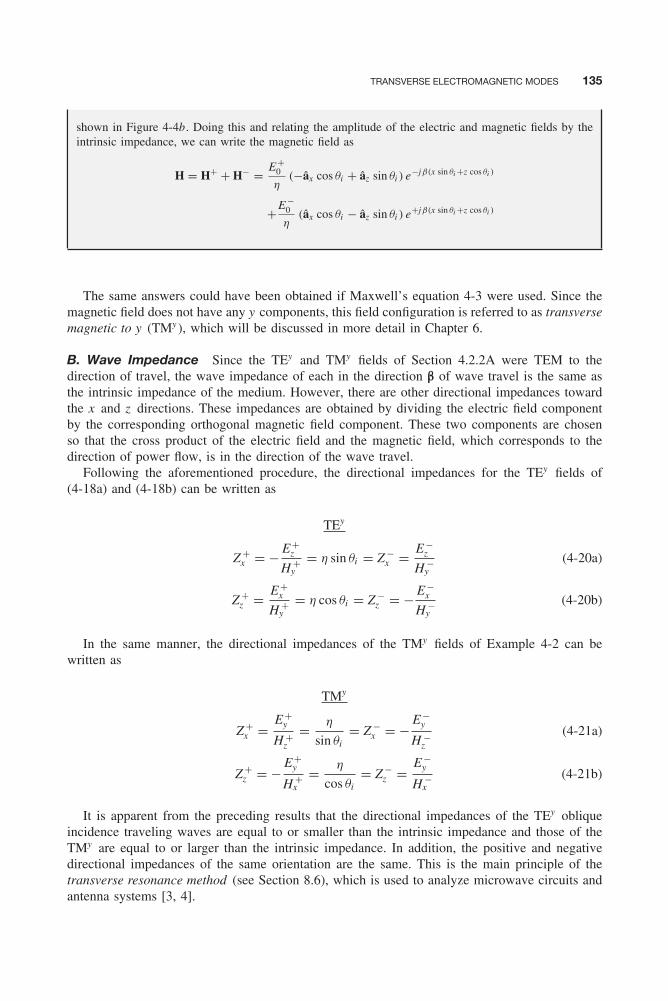
TRANSVERSE ELECTROMAGNETIC MODES 135
shown in Figure 4-4b. Doing this and relating the amplitude of the electric and magnetic fields by theintrinsic impedance, we can write the magnetic field as
H = H+ + H− = E+0
η(−âx cos θi + âz sin θi ) e−jβ(x sin θi +z cos θi )
+E−0
η(âx cos θi − âz sin θi ) e+jβ(x sin θi +z cos θi )
The same answers could have been obtained if Maxwell’s equation 4-3 were used. Since themagnetic field does not have any y components, this field configuration is referred to as transversemagnetic to y (TMy ), which will be discussed in more detail in Chapter 6.
B. Wave Impedance Since the TEy and TMy fields of Section 4.2.2A were TEM to thedirection of travel, the wave impedance of each in the direction β of wave travel is the same asthe intrinsic impedance of the medium. However, there are other directional impedances towardthe x and z directions. These impedances are obtained by dividing the electric field componentby the corresponding orthogonal magnetic field component. These two components are chosenso that the cross product of the electric field and the magnetic field, which corresponds to thedirection of power flow, is in the direction of the wave travel.
Following the aforementioned procedure, the directional impedances for the TEy fields of(4-18a) and (4-18b) can be written as
TEy
Z +x = − E+
z
H +y
= η sin θi = Z −x = E−
z
H −y
(4-20a)
Z +z = E+
x
H +y
= η cos θi = Z −z = − E−
x
H −y
(4-20b)
In the same manner, the directional impedances of the TMy fields of Example 4-2 can bewritten as
TMy
Z +x = E+
y
H +z
= η
sin θi= Z −
x = − E−y
H −z
(4-21a)
Z +z = − E+
y
H +x
= η
cos θi= Z −
z = E−y
H −x
(4-21b)
It is apparent from the preceding results that the directional impedances of the TEy obliqueincidence traveling waves are equal to or smaller than the intrinsic impedance and those of theTMy are equal to or larger than the intrinsic impedance. In addition, the positive and negativedirectional impedances of the same orientation are the same. This is the main principle of thetransverse resonance method (see Section 8.6), which is used to analyze microwave circuits andantenna systems [3, 4].

136 WAVE PROPAGATION AND POLARIZATION
C. Phase and Energy (Group) Velocities The wave velocity vr of the fields given by(4-18a) and (4-18b) in the direction β of travel is equal to the speed of light v. Since the wave isa plane wave to the direction β of travel, the planes over which the phase is constant (constantphase planes) are perpendicular to the direction β of wave travel. This is illustrated graphicallyin Figure 4-6. To maintain a constant phase (or to keep in step with a constant phase plane),a velocity equal to the speed of light must be maintained in the direction β of travel. This isreferred to as the phase velocity vpr along the direction β of travel. Since the energy also is beingtransported with the same speed, the energy velocity ver in the direction β of travel is also equalto the speed of light. Thus
vr = vpr = ver = v = 1√με
(4-22)
wherevr = wave velocity in the direction of wave travel
vpr = phase velocity in the direction of wave travelver = energy (group) velocity in the direction of wave travelv = speed of light
To keep in step with a constant phase plane of the wave of Figure 4-6, a velocity in the zdirection equal to
vpz = v
cos θi= 1√
με cos θi≥ v (4-23)
must be maintained. This is referred to as the phase velocity vpz in the z direction, and it isgreater than the speed of light. Since nothing travels with speeds greater than the speed of light,it must be remembered that this is a hypothetical velocity that must be maintained in order to
β
qi
Constant p
hase plan
es
Constant am
plitude p
lanes
v
y
vez
vpz
x
z
Figure 4-6 Phase and energy (group) velocities of a uniform plane wave.
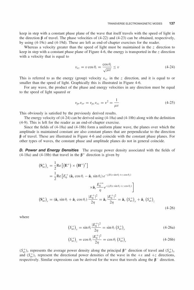
TRANSVERSE ELECTROMAGNETIC MODES 137
keep in step with a constant phase plane of the wave that itself travels with the speed of light inthe direction β of travel. The phase velocities of (4-22) and (4-23) can be obtained, respectively,by using (4-19c) and (4-19d). These are left as end-of-chapter exercises for the reader.
Whereas a velocity greater than the speed of light must be maintained in the z direction tokeep in step with a constant phase plane of Figure 4-6, the energy is transported in the z directionwith a velocity that is equal to
vez = v cos θi = cos θi√με
≤ v (4-24)
This is referred to as the energy (group) velocity vez in the z direction, and it is equal to orsmaller than the speed of light. Graphically this is illustrated in Figure 4-6.
For any wave, the product of the phase and energy velocities in any direction must be equalto the speed of light squared or
vprver = vpz vez = v2 = 1
με(4-25)
This obviously is satisfied by the previously derived results.The energy velocity of (4-24) can be derived using (4-18a) and (4-18b) along with the definition
(4-9). This is left for the reader as an end-of-chapter exercise.Since the fields of (4-18a) and (4-18b) form a uniform plane wave, the planes over which the
amplitude is maintained constant are also constant planes that are perpendicular to the directionβ of travel. These are illustrated in Figure 4-6 and coincide with the constant phase planes. Forother types of waves, the constant phase and amplitude planes do not in general coincide.
D. Power and Energy Densities The average power density associated with the fields of(4-18a) and (4-18b) that travel in the β+ direction is given by
(S+
av
)r = 1
2Re
[(E+) × (
H+)∗]= 1
2Re
[E+
0 (âx cos θi − âz sin θi ) e−jβ(x sin θi +z cos θi )
×âyE+∗
0
ηe+jβ(x sin θi +z cos θi )
](S+
av
)r = (âx sin θi + âz cos θi )
|E+0 |2
2η= âr
|E+0 |2
2η= âx
(S +
av
)x + âz
(S +
av
)z
(4-26)
where
(S +
av
)x = sin θi
|E+0 |2
2η= sin θi
(S +
av
)r (4-26a)
(S +
av
)z = cos θi
|E+0 |2
2η= cos θi
(S +
av
)r (4-26b)
(S +av)r represents the average power density along the principal β+ direction of travel and (S +
av)x
and (S +av)z represent the directional power densities of the wave in the +x and +z directions,
respectively. Similar expressions can be derived for the wave that travels along the β− direction.

138 WAVE PROPAGATION AND POLARIZATION
Example 4-3
For the TMy fields of Example 4-2, derive expressions for the average power density along the principalβ+ direction of travel and for the directional power densities along the +x and +z directions.
Solution: Using the electric and magnetic fields of the solution of Example 4-2 and following theprocedure used to derive (4-26) through (4-26b), it can be shown that(
S+av
)r = 1
2Re
[(E+) × (
H+)∗]= 1
2Re
[ây E+
0 e−jβ(x cos θi +y sin θi )
×(E+
0
)∗
η(−âx cos θi + âz sin θi ) e+jβ(x cos θi +y sin θi )
](S+
av
)r = (âx sin θi + âz cos θi )
|E+0 |22η
= âr|E+
0 |22η
= âx(S +
av
)x + âz
(S +
av
)z
where (S +
av
)x = sin θi
|E+0 |22η
= sin θi(S +
av
)r
(S +
av
)z = cos θi
|E+0 |22η
= cos θi(S +
av
)r
(S +av), (S +
av)x , and (S +av)z of this TMy wave are identical to the corresponding ones of the TEy wave,
given by (4-26) through (4-26b).
4.3 TRANSVERSE ELECTROMAGNETIC MODES IN LOSSY MEDIA
In addition to the accumulation of phase, electromagnetic waves that travel in lossy media undergoattenuation. To account for the attenuation, an attenuation constant is introduced as discussed inChapter 3, Section 3.4.1B. In this section we want to discuss the solution for the electric andmagnetic fields of uniform plane waves as they travel in lossy media [5].
4.3.1 Uniform Plane Waves in an Unbounded Lossy Medium—Principal Axis
As for the electromagnetic wave of Section 4.2.1, let us assume that a uniform plane wave istraveling in a lossy medium. Using the coordinate system of Figure 4-1, the electric field isassumed to have an x component and the wave is traveling in the ±z direction. Since the electricfield must satisfy the wave equation for lossy media, its expression takes, according to (3-42a),the form
E (z ) = âx Ex (z ) = âx(E+
0 e−γ z + E−0 e+γ z
) = âx(E+
0 e−αz e−jβz + E−0 e+αz e+jβz
)(4-27)
where γx = γy = 0 and γz = γ . The first term represents the positive traveling wave and thesecond term represents the negative traveling wave. In (4-27) γ is the propagation constant whose

TRANSVERSE ELECTROMAGNETIC MODES IN LOSSY MEDIA 139
real α and imaginary β parts are defined, respectively, as the attenuation and phase constants.According to (3-37e) and (3-46), γ takes the form
γ = α + jβ =√
jωμ (σ + jωε) =√
−ω2με + jωμσ (4-28)
Squaring (4-28) and equating real and imaginary from both sides reduces it to
α2 − β2 = −ω2με (4-28a)
2αβ = ωμσ (4-28b)
Solving (4-28a) and (4-28b) simultaneously, we can write α and β as
α = ω√
με
{1
2
[√1 +
( σ
ωε
)2− 1
]}1/2
Np/m (4-28c)
β = ω√
με
{1
2
[√1 +
( σ
ωε
)2+ 1
]}1/2
rad/m (4-28d)
In the literature, the phase constant β is also represented by k .The attenuation constant α is often expressed in decibels per meter (dB/m). The conversion
between Nepers per meter and decibels per meter is obtained by examining the real exponentialin (4-27) that represents the attenuation factor of the wave in a lossy medium. Since that factorrepresents the relative attenuation of the electric or magnetic field, its conversion to decibels (dB)is obtained by
dB = 20 log10
(e−αz
) = 20 (−αz ) log10 (e)
= 20 (−αz ) (0.434) = −8.68 (αz ) (4-28e)
or
|α (Np/m) | = 1
8.68|α (dB/m) | (4-28f)
The magnetic field associated with the electric field of (4-27) can be obtained using Maxwell’sequation 4-3 or 4-3a, that is,
H = − 1
jωμ∇ × E = −ây
1
jωμ
∂Ex
∂z(4-29)
Using (4-27) reduces (4-29) to
H = +âyγ
jωμ
(E+
0 e−γ z − E−0 e+γ z
)= ây
√jωμ (σ + jωε)
jωμ
(E+
0 e−γ z − E−0 e+γ z
)= ây
√σ + jωε
jωμ
(E+
0 e−γ z − E−0 e+γ z
)H = ây
1
Zw
(E+
0 e−γ z − E−0 e+yz
)(4-29a)
140 WAVE PROPAGATION AND POLARIZATION
In (4-29a), Zw is the wave impedance of the wave, and it takes the form
Zw =√
jωμ
σ + jωε= ηc (4-30)
which is also equal to the intrinsic impedance ηc of the lossy medium. The equality between thewave and intrinsic impedances for TEM waves in lossy media is identical to that for losslessmedia of Section 4.2.1B.
The average power density associated with the positive traveling fields of (4-27) and (4-29a)can be written as
S+ = 1
2Re
(E+ × H+∗) = 1
2Re
(âx E+
0 e−αz e−jβz × âyE+∗
0
η∗c
e−αz e+jβz
)S+ = âz
|E+0 |22
e−2αz Re
[1
η∗c
](4-31)
Individually each term of (4-27) or (4-29a) represents a traveling wave in its respective direc-tion. The magnitude of each term in (4-27) takes the form
|E+x (z ) | = |E+
0 |e−αz (4-32a)
|E−x (z ) | = |E−
0 |e+αz (4-32b)
which, when plotted for −λ ≤ z ≤ +λ and |�| = 0.2 through 1 (in increments of 0.2), take theform shown in Figure 4-7a .
Collectively, both terms in each of the fields in (4-27) or (4-29a) represent a standing wave.Using the procedure outlined in Section 4.2.1D, (4-27) can also be written as
Ex (z ) =√(
E+0
)2e−2αz + (
E−0
)2e+2αz + 2E+
0 E−0 cos (2βz )
× exp
{−j tan−1
[E+
0 e−αz − E−0 e+αz
E+0 e−αz + E−
0 e+αztan (βz )
]}(4-33)
The standing wave pattern is given by the amplitude term of
|Ex (z )| =√(
E+0
)2e−2αz + (
E−0
)2e+2αz + 2E+
0 E−0 cos (2βz ) (4-33a)
which for |�| = E−0 /E+
0 = 0.2 through 1, in increments of 0.2, is shown plotted in Figure 4-7bin the range −λ ≤ z ≤ λ when f = 100 MHz, εr = 2.56, μr = 1, and σ = 0.03 S/m.
The distance the wave must travel in a lossy medium to reduce its value to e−1 = 0.368 = 36.8%is defined as the skin depth δ. For each of the terms of (4-27) or (4-29a), this distance is
δ = skin depth = 1
α= 1
ω√
με{
12
[√1 + (σ/ωε)2 − 1
]}1/2 m (4-34)
In summary, the attenuation constant α, phase constant β, wave Zw and intrinsic ηc impedances,wavelength λ, velocity v, and skin depth δ for a uniform plane wave traveling in a lossy mediumare listed in the second column of Table 4-1. The same expressions are valid for plane and TEMwaves. Simpler expressions for each can be derived depending upon the value of the (σ/ωε)2
ratio. Media whose (σ/ωε)2 is much less than unity [(σ/ωε)2 � 1] are referred to as gooddielectrics and those whose (σ/ωε)2 is much greater than unity [(σ/ωε)2 � 1] are referred toas good conductors [6]; each will now be discussed.
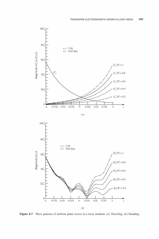
TRANSVERSE ELECTROMAGNETIC MODES IN LOSSY MEDIA 141
8E+0
ers
6E+0
4E+0
E+x
(a)
(b)
2E+0
10E+0
0
8E+0
6E+0
4E+0
2E+0
10E+0
0
−λ −0.75λ −0.5λ −0.25λ 0.25λ 0.5λ λ z0.75λ0
−λ −0.75λ −0.5λ −0.25λ 0.25λ 0.5λ λ z0.75λ0
Ex−
, |Γ| = 1
Mag
nitu
de | E
x+ (z)| ,
| Ex− (z
)|
Ex−
, |Γ| = 0.8
Ex−
, |Γ| = 0.6
Ex−
, |Γ| = 0.4
Ex−
, |Γ| = 0.2
|Ex|, |Γ| = 1
Mag
nitu
de | E
x(z)
|
|Ex|, |Γ| = 0.8
|Ex|, |Γ| = 0.6
|Ex|, |Γ| = 0.4
|Ex|, |Γ| = 0.2
= 2.56= 0.03 S/m
ers
= 2.56= 0.03 S/m
Figure 4-7 Wave patterns of uniform plane waves in a lossy medium. (a) Traveling. (b) Standing.
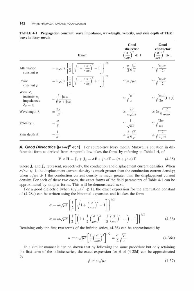
142 WAVE PROPAGATION AND POLARIZATION
TABLE 4-1 Propagation constant, wave impedance, wavelength, velocity, and skin depth of TEMwave in lossy media
Good Gooddielectric conductor
Exact( σ
ωε
)2 � 1( σ
ωε
)2 � 1
Attenuationconstant α
= ω√
με
{1
2
[√1 +
( σ
ωε
)2 − 1
]}1/2
� σ
2
√μ
ε�
√ωμσ
2
Phaseconstant β
= ω√
με
{1
2
[√1 +
( σ
ωε
)2 + 1
]}1/2
� ω√
με �√
ωμσ
2
Wave Zw
intrinsic ηcimpedancesZw = ηc
=√
jωμ
σ + jωε�
√μ
ε�
√ωμ
2σ(1 + j )
Wavelength λ = 2π
β� 2π
ω√
με� 2π
√2
ωμσ
Velocity v = ω
β� 1√
με�
√2ω
μσ
Skin depth δ = 1
α� 2
σ
√ε
μ�
√2
ωμσ
A. Good Dielectrics [(σ/ωε)2 � 1] For source-free lossy media, Maxwell’s equation in dif-ferential form as derived from Ampere’s law takes the form, by referring to Table 1-4, of
∇ × H = Jc + Jd = σE + jωεE = (σ + jωε) E (4-35)
where Jc and Jd represent, respectively, the conduction and displacement current densities. Whenσ/ωε � 1, the displacement current density is much greater than the conduction current density;when σ/ωε � 1 the conduction current density is much greater than the displacement currentdensity. For each of these two cases, the exact forms of the field parameters of Table 4-1 can beapproximated by simpler forms. This will be demonstrated next.
For a good dielectric [when (σ/ωε)2 � 1], the exact expression for the attenuation constantof (4-28c) can be written using the binomial expansion and it takes the form
α = ω√
με
{1
2
[√1 +
( σ
ωε
)2− 1
]}1/2
α = ω√
με
{1
2
[(1 + 1
2
( σ
ωε
)2− 1
8
( σ
ωε
)4· · ·
)− 1
]}1/2
(4-36)
Retaining only the first two terms of the infinite series, (4-36) can be approximated by
α � ω√
με
[1
4
( σ
ωε
)2]1/2
= σ
2
√μ
ε(4-36a)
In a similar manner it can be shown that by following the same procedure but only retainingthe first term of the infinite series, the exact expression for β of (4-28d) can be approximatedby
β � ω√
με (4-37)
TRANSVERSE ELECTROMAGNETIC MODES IN LOSSY MEDIA 143
For good dielectrics, the wave and intrinsic impedances of (4-30) can be approximated by
Zw = ηc =√
jωμ
σ + jωε=
√jωμ/jωε
σ/jωε + 1�
√μ
ε(4-38)
while the skin depth can be represented by
δ = 1
α� 2
σ
√ε
μ(4-39)
These and other approximate forms for the parameters of good dielectrics are summarized on thethird column of Table 4-1.
B. Good Conductors [(σ/ωε)2 � 1] For good conductors, the exact expression for the atten-uation constant of (4-28c) can be written using the binomial expansion and takes the form
α = ω√
με
{1
2
[√( σ
ωε
)2+ 1 − 1
]}1/2
= ω√
με
{1
2
[σ
ωε
(1 + 1
(σ/ωε)2
)1/2
− 1
]}1/2
α = ω√
με
{1
2
[σ
ωε+ 1
2
1
σ/ωε− 1
8
1
(σ/ωε)3+ · · · − 1
]}1/2
(4-40)
Retaining only the first term of the infinite series expansion, (4-40) can be approximated by
α � ω√
με
(1
2
σ
ωε
)1/2
=√
ωμσ
2(4-40a)
Following a similar procedure, the phase constant of (4-28d) can be approximated by
β �√
ωμσ
2(4-41)
which is identical to the approximate expression for the attenuation constant of (4-40a).For good conductors, the wave and intrinsic impedances of (4-30) can be approximated by
Zw = ηc =√
jωμ
σ + jωε=
√jωμ/ωε
σ/ωε + j�
√jωμ
σ=
√ωμ
2σ(1 + j ) (4-42)
whose real and imaginary parts are identical. For the same conditions, the skin depth can beapproximated by
δ = 1
α�
√2
ωμσ(4-43)
This is the most widely recognized form for the skin depth.
4.3.2 Uniform Plane Waves in an Unbounded Lossy Medium—Oblique Angle
For lossy media the difference between principal axes propagation and propagation at obliqueangles is that the propagation constant γr along the direction β of propagation must be decomposedinto its directional components along the principal axes of the coordinate system. In addition,since the propagation constant γ has real (α) and imaginary (β) parts, constant amplitude andconstant phase planes are associated with the wave. As discussed in Section 4.2.2C and illustrated
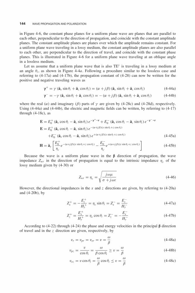
144 WAVE PROPAGATION AND POLARIZATION
in Figure 4-6, the constant phase planes for a uniform plane wave are planes that are parallel toeach other, perpendicular to the direction of propagation, and coincide with the constant amplitudeplanes. The constant amplitude planes are planes over which the amplitude remains constant. Fora uniform plane wave traveling in a lossy medium, the constant amplitude planes are also parallelto each other, are perpendicular to the direction of travel, and coincide with the constant phaseplanes. This is illustrated in Figure 4-6 for a uniform plane wave traveling at an oblique anglein a lossless medium.
Let us assume that a uniform plane wave that is also TEy is traveling in a lossy medium atan angle θi , as shown in Figure 4-4a . Following a procedure similar to the lossless case andreferring to (4-17a) and (4-17b), the propagation constant of (4-28) can now be written for thepositive and negative traveling waves as
γ+ = γ (âx sin θi + âz cos θi ) = (α + jβ) (âx sin θi + âz cos θi ) (4-44a)
γ− = −γ (âx sin θi + âz cos θi ) = − (α + jβ) (âx sin θi + âz cos θi ) (4-44b)
where the real (α) and imaginary (β) parts of γ are given by (4-28c) and (4-28d), respectively.Using (4-44a) and (4-44b), the electric and magnetic fields can be written, by referring to (4-17)through (4-18c), as
E = E+0 (âx cos θi − âz sin θi ) e−γ+ • r + E−
0 (âx cos θi − âz sin θi ) e−γ− • r
E = E+0 (âx cos θi − âz sin θi ) e−(α+jβ)(x sin θi +z cos θi )
+E−0 (âx cos θi − âz sin θi ) e+(α+jβ)(x sin θi +z cos θi ) (4-45a)
H = ây
[E+
0
ηc
e−(α+jβ)(x sin θi +z cos θi ) − E−0
ηc
e+(α+jβ)(x sin θi +z cos θi )
](4-45b)
Because the wave is a uniform plane wave in the β direction of propagation, the waveimpedance Zwr in the direction of propagation is equal to the intrinsic impedance ηc of thelossy medium given by (4-30) or
Zwr = ηc =√
jωμ
σ + jωε(4-46)
However, the directional impedances in the x and z directions are given, by referring to (4-20a)and (4-20b), by
Z +x = − E+
z
H +y
= ηc sin θi = Z −x = E−
z
H −y
(4-47a)
Z +z = E+
x
H +y
= ηc cos θi = Z −z = − E−
x
H −y
(4-47b)
According to (4-22) through (4-24) the phase and energy velocities in the principal β directionof travel and in the z direction are given, respectively, by
vr = vpr = ver = v = ω
β(4-48a)
vpz = v
cos θi= ω
β cos θi≥ v = ω
β(4-48b)
vez = v cos θi = ω
βcos θi ≤ v = ω
β(4-48c)
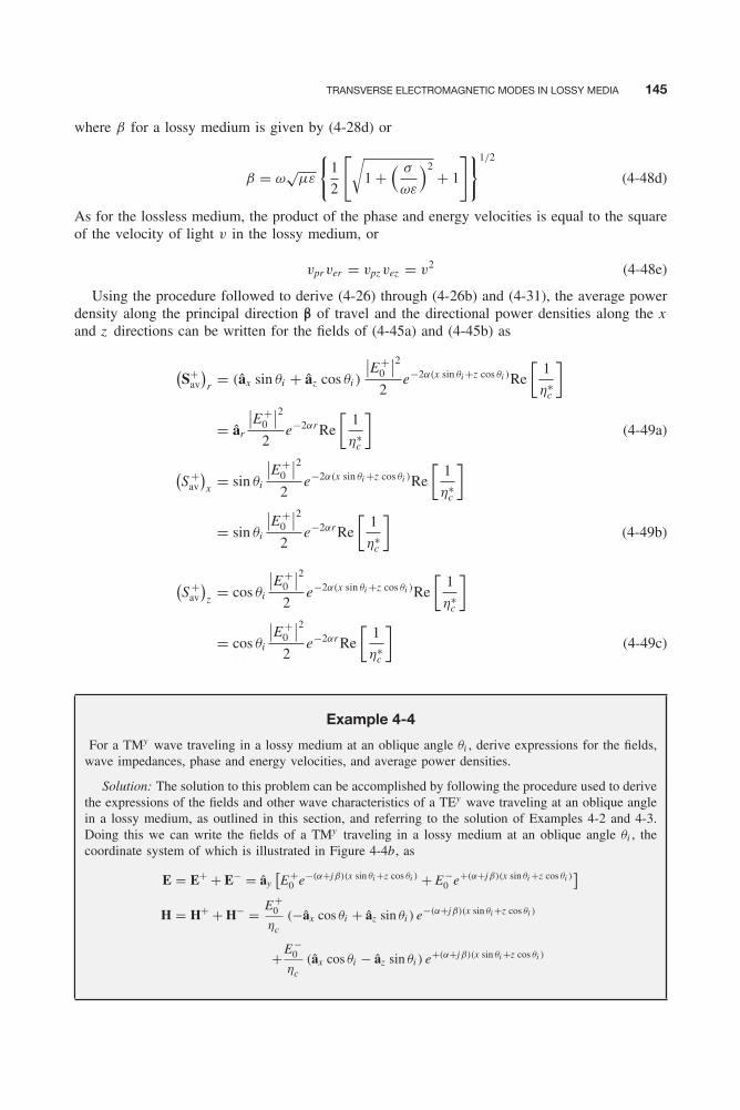
TRANSVERSE ELECTROMAGNETIC MODES IN LOSSY MEDIA 145
where β for a lossy medium is given by (4-28d) or
β = ω√
με
{1
2
[√1 +
( σ
ωε
)2+ 1
]}1/2
(4-48d)
As for the lossless medium, the product of the phase and energy velocities is equal to the squareof the velocity of light v in the lossy medium, or
vprver = vpz vez = v2 (4-48e)
Using the procedure followed to derive (4-26) through (4-26b) and (4-31), the average powerdensity along the principal direction β of travel and the directional power densities along the xand z directions can be written for the fields of (4-45a) and (4-45b) as
(S+
av
)r = (âx sin θi + âz cos θi )
∣∣E+0
∣∣2
2e−2α(x sin θi +z cos θi )Re
[1
η∗c
]
= âr
∣∣E+0
∣∣2
2e−2αr Re
[1
η∗c
](4-49a)
(S +
av
)x = sin θi
∣∣E+0
∣∣2
2e−2α(x sin θi +z cos θi )Re
[1
η∗c
]
= sin θi
∣∣E+0
∣∣2
2e−2αr Re
[1
η∗c
](4-49b)
(S +
av
)z = cos θi
∣∣E+0
∣∣2
2e−2α(x sin θi +z cos θi )Re
[1
η∗c
]
= cos θi
∣∣E+0
∣∣2
2e−2αr Re
[1
η∗c
](4-49c)
Example 4-4
For a TMy wave traveling in a lossy medium at an oblique angle θi , derive expressions for the fields,wave impedances, phase and energy velocities, and average power densities.
Solution: The solution to this problem can be accomplished by following the procedure used to derivethe expressions of the fields and other wave characteristics of a TEy wave traveling at an oblique anglein a lossy medium, as outlined in this section, and referring to the solution of Examples 4-2 and 4-3.Doing this we can write the fields of a TMy traveling in a lossy medium at an oblique angle θi , thecoordinate system of which is illustrated in Figure 4-4b, as
E = E+ + E− = ây[E+
0 e−(α+jβ)(x sin θi +z cos θi ) + E−0 e+(α+jβ)(x sin θi +z cos θi )
]H = H+ + H− = E+
0
ηc(−âx cos θi + âz sin θi ) e−(α+jβ)(x sin θi +z cos θi )
+E−0
ηc(âx cos θi − âz sin θi ) e+(α+jβ)(x sin θi +z cos θi )

146 WAVE PROPAGATION AND POLARIZATION
In addition, the wave impedances are given, by referring to (4-21a) and (4-21b), by
Z +x = E+
y
H +z
= ηc
sin θi= Z −
x = − E−y
H −z
Z +z = − E+
y
H +x
= ηc
cos θi= Z −
z = E−y
H −x
The phase and energy velocities, and their relationships, are the same as those for the TEy wave,as given by (4-48a) through (4-48e). Similarly, the average power densities are those given by(4-49a) through (4-49c).
4.4 POLARIZATION
According to the IEEE Standard Definitions for Antennas [7, 8], the polarization of a radiatedwave is defined as “that property of a radiated electromagnetic wave describing the time-varyingdirection and relative magnitude of the electric field vector; specifically, the figure traced as afunction of time by the extremity of the vector at a fixed location in space, and the sense inwhich it is traced, as observed along the direction of propagation.” In other words, polarizationis the curve traced out, at a given observation point as a function of time, by the end point of thearrow representing the instantaneous electric field. The field must be observed along the directionof propagation. A typical trace as a function of time is shown in Figure 4-8 [8].
0
2p
4p
6p
6p
wt
wt
4p
2p
�y
�x
�x
Figure 4-8 Rotation of a plane electromagnetic wave at z = 0 as a function of time. (Source: C. A.Balanis, Antenna Theory: Analysis and Design . 3rd Edition. Copyright © 2005, John Wiley & Sons, Inc.Reprinted by permission of John Wiley & Sons, Inc.).
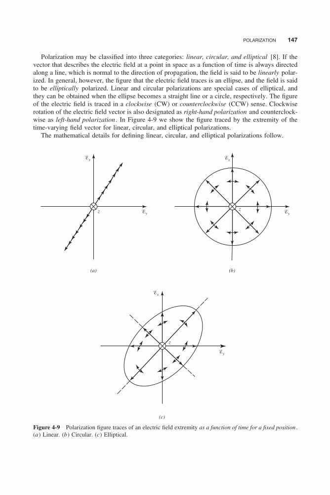
POLARIZATION 147
Polarization may be classified into three categories: linear, circular, and elliptical [8]. If thevector that describes the electric field at a point in space as a function of time is always directedalong a line, which is normal to the direction of propagation, the field is said to be linearly polar-ized. In general, however, the figure that the electric field traces is an ellipse, and the field is saidto be elliptically polarized. Linear and circular polarizations are special cases of elliptical, andthey can be obtained when the ellipse becomes a straight line or a circle, respectively. The figureof the electric field is traced in a clockwise (CW) or counterclockwise (CCW) sense. Clockwiserotation of the electric field vector is also designated as right-hand polarization and counterclock-wise as left-hand polarization . In Figure 4-9 we show the figure traced by the extremity of thetime-varying field vector for linear, circular, and elliptical polarizations.
The mathematical details for defining linear, circular, and elliptical polarizations follow.
(a)
(c)
(b)
�y �y
�x
�y
�x
�x
z
z
z
Figure 4-9 Polarization figure traces of an electric field extremity as a function of time for a fixed position .(a) Linear. (b) Circular. (c) Elliptical.

148 WAVE PROPAGATION AND POLARIZATION
4.4.1 Linear Polarization
Let us consider a harmonic plane wave, with x and y electric field components, traveling in thepositive z direction (into the page), as shown in Figure 4-10 [8]. The instantaneous electric andmagnetic fields are given by
� = âx �x + ây �y = Re[âx E+
x ej (ωt−βz ) + ây E+y ej (ωt−βz )
]= âx E+
x0cos (ωt − βz + φx ) + ây E+
y0cos
(ωt − βz + φy
)(4-50a)
� = ây �y + âx �x = Re
[ây
E+x
ηej (ωt−βz ) − âx
E+y
ηej (ωt−βz )
]
= ây
E+x0
ηcos (ωt − βz + φx ) − âx
E+y0
ηcos
(ωt − βz + φy
)(4-50b)
where E+x , E+
y are complex and E+x0
, E+y0
are real.Let us now examine the variation of the instantaneous electric field vector � as given by
(4-50a) at the z = 0 plane. Other planes may be considered, but the z = 0 plane is chosen forconvenience and simplicity. For the first example, let
E+y0
= 0 (4-51)
in (4-50a). Then
�x = E+x0
cos (ωt + φx )
�y = 0 (4-51a)
The locus of the instantaneous electric field vector is given by
� = âx E+x0
cos (ωt + φx ) (4-51b)
which is a straight line, and it will always be directed along the x axis at all times, as shown inFigure 4-10. The field is said to be linearly polarized in the x direction .
E + cos (wt + fx)0x
z �y
�x
Figure 4-10 Linearly polarized field in the x direction.

POLARIZATION 149
Example 4-5
Determine the polarization of the wave given by (4-50a) when E+x0
= 0.
Solution: SinceE+
x0= 0
then
�x = 0
�y = E+y0
cos(ωt + φy
)The locus of the instantaneous electric field vector is given by
� = ây E+y0
cos(ωt + φy
)which again is a straight line but directed along the y axis at all times, as shown in Figure 4-11. Thefield is said to be linearly polarized in the y direction .
E + cos (wt + fy)y0
�y
�x
Figure 4-11 Linearly polarized field in the y direction.
Example 4-6
Determine the polarization and direction of polarization of the wave given by (4-50a) when φx =φy = φ.
Solution: Sinceφx = φy = φ
then
�x = E+x0
cos (ωt + φ)
�y = E+y0
cos (ωt + φ)

150 WAVE PROPAGATION AND POLARIZATION
The amplitude of the electric field vector is given by
� =√
�2x + �2
y =√(
E+x0
)2 + (E+
y0
)2cos (ωt + φ)
which is a straight line directed at all times along a line that makes an angle ψ with the x axis as shownin Figure 4-12. The angle ψ is given by
ψ = tan−1[
�y
�x
]= tan−1
[E+
y0
E+x0
]The field is said to be linearly polarized in the ψ direction .
E + cos (wt + f)y0
E + cos (wt + f)x0
E ++ cos (wt + f) ( y02E +
x02
z
)
�y
�x
y
Figure 4-12 Linearly polarized field in the ψ direction.
It is evident from the preceding examples that a time-harmonic field is linearly polarized at agiven point in space if the electric field (or magnetic field ) vector at that point is oriented alongthe same straight line at every instant of time. This is accomplished if the field vector (electric ormagnetic) possesses (a) only one component or (b) two orthogonal linearly polarized componentsthat are in time phase or integer multiples of 180◦ out of phase.
4.4.2 Circular Polarization
A wave is said to be circularly polarized if the tip of the electric field vector traces out a circularlocus in space. At various instants of time, the electric field intensity of such a wave always hasthe same amplitude and the orientation in space of the electric field vector changes continuouslywith time in such a manner as to describe a circular locus [8, 9].
A. Right-Hand (Clockwise) Circular Polarization A wave has right-hand circular polar-ization if its electric field vector has a clockwise sense of rotation when it is viewed along theaxis of propagation . In addition, the electric field vector must trace a circular locus if the waveis to have also a circular polarization.
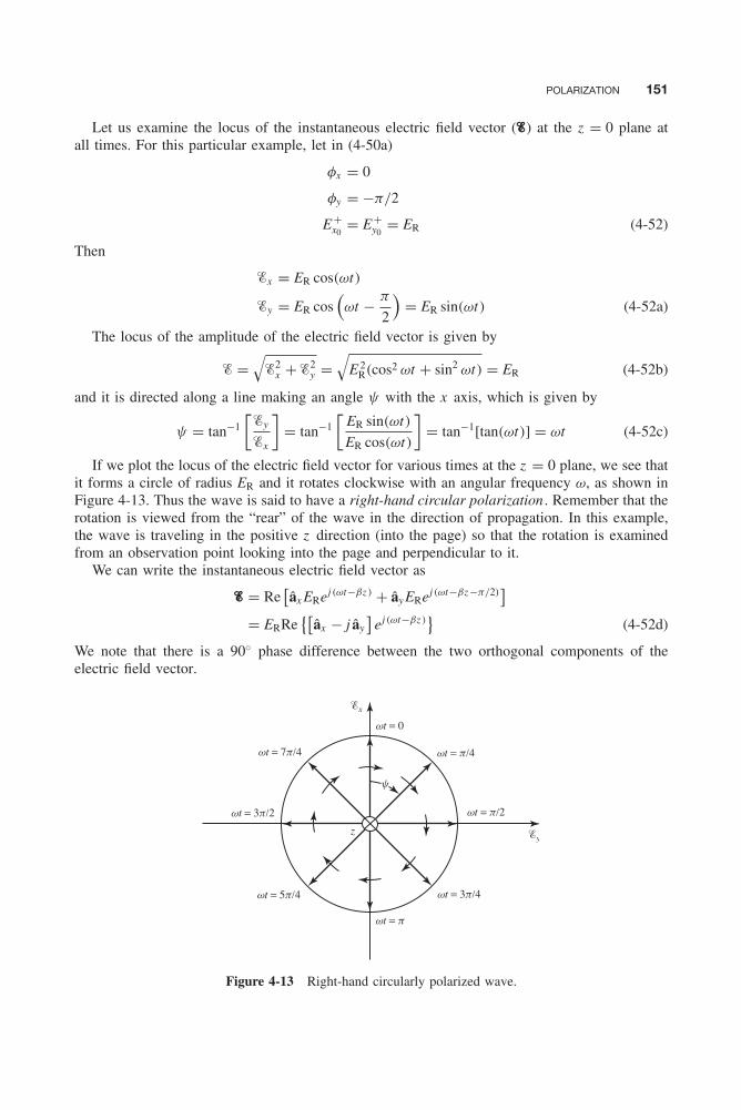
POLARIZATION 151
Let us examine the locus of the instantaneous electric field vector (�) at the z = 0 plane atall times. For this particular example, let in (4-50a)
φx = 0
φy = −π/2
E+x0
= E+y0
= ER (4-52)
Then
�x = ER cos(ωt)
�y = ER cos(ωt − π
2
)= ER sin(ωt) (4-52a)
The locus of the amplitude of the electric field vector is given by
� =√
�2x + �2
y =√
E 2R(cos2 ωt + sin2 ωt) = ER (4-52b)
and it is directed along a line making an angle ψ with the x axis, which is given by
ψ = tan−1
[�y
�x
]= tan−1
[ER sin(ωt)
ER cos(ωt)
]= tan−1[tan(ωt)] = ωt (4-52c)
If we plot the locus of the electric field vector for various times at the z = 0 plane, we see thatit forms a circle of radius ER and it rotates clockwise with an angular frequency ω, as shown inFigure 4-13. Thus the wave is said to have a right-hand circular polarization . Remember that therotation is viewed from the “rear” of the wave in the direction of propagation. In this example,the wave is traveling in the positive z direction (into the page) so that the rotation is examinedfrom an observation point looking into the page and perpendicular to it.
We can write the instantaneous electric field vector as
� = Re[âx ERej (ωt−βz ) + ây ERej (ωt−βz−π/2)
]= ERRe
{[âx − j ây
]ej (ωt−βz )
}(4-52d)
We note that there is a 90◦ phase difference between the two orthogonal components of theelectric field vector.
wt = 0
wt = 5p/4
y
wt = p/2
wt = 7p/4
wt = 3p/2z
wt = p/4
wt = 3p/4
wt = p
�y
�x
Figure 4-13 Right-hand circularly polarized wave.

152 WAVE PROPAGATION AND POLARIZATION
Example 4-7
If φx = +π/2, φy = 0, and E+x0
= E+y0
= ER, determine the polarization and sense of rotation of thewave of (4-50a).
Solution: Since
φx = +π
2φy = 0
E+x0
= E+y0
= ER
then
�x = ER cos(ωt + π
2
)= −ER sin ωt
�y = ER cos(ωt)
and the locus of the amplitude of the electric field vector is given by
� =√
�2x + �2
y =√
E 2R(cos2 ωt + sin2 ωt) = ER
The angle ψ along which the field is directed is given by
ψ = tan−1[
�y
�x
]= tan−1
[−ER cos(ωt)
ER sin(ωt)
]= tan−1 [− cot(ωt)] = ωt + π
2
The locus of the field vector is a circle of radius ER, and it rotates clockwise with an angular frequencyω as shown in Figure 4-14; hence, it is a right-hand circular polarization .
The expression for the instantaneous electric field vector is
� = Re[âx ERej (ωt−βz+π/2) + ây ERej (ωt−βz )
]= ERRe
{[j âx + ây
]ej (ωt−βz )
}
wt = 0
wt = 5p/4
y
wt = p/2
wt = 7p/4
wt = 3p/2
z
wt = p/4wt = 3p/4
wt = p
�y
�x
Figure 4-14 Right-hand circularly polarized wave.
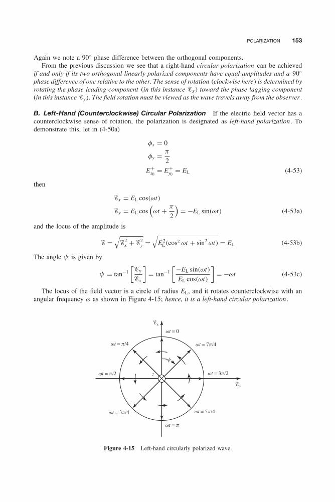
POLARIZATION 153
Again we note a 90◦ phase difference between the orthogonal components.From the previous discussion we see that a right-hand circular polarization can be achieved
if and only if its two orthogonal linearly polarized components have equal amplitudes and a 90◦phase difference of one relative to the other. The sense of rotation (clockwise here) is determined byrotating the phase-leading component (in this instance �x ) toward the phase-lagging component(in this instance �y ). The field rotation must be viewed as the wave travels away from the observer .
B. Left-Hand (Counterclockwise) Circular Polarization If the electric field vector has acounterclockwise sense of rotation, the polarization is designated as left-hand polarization . Todemonstrate this, let in (4-50a)
φx = 0
φy = π
2
E+x0
= E+y0
= EL (4-53)
then
�x = EL cos(ωt)
�y = EL cos(ωt + π
2
)= −EL sin(ωt) (4-53a)
and the locus of the amplitude is
� =√
�2x + �2
y =√
E 2L(cos2 ωt + sin2 ωt) = EL (4-53b)
The angle ψ is given by
ψ = tan−1
[�y
�x
]= tan−1
[−EL sin(ωt)
EL cos(ωt)
]= −ωt (4-53c)
The locus of the field vector is a circle of radius EL, and it rotates counterclockwise with anangular frequency ω as shown in Figure 4-15; hence, it is a left-hand circular polarization .
wt = 0
wt = 5p/4
y
wt = p/2
wt = 7p/4
wt = 3p/2z
wt = p/4
wt = 3p/4
wt = p
�y
�x
Figure 4-15 Left-hand circularly polarized wave.

154 WAVE PROPAGATION AND POLARIZATION
The instantaneous electric field vector can be written as
� = Re[âx ELej (ωt−βz ) + ây ELej (ωt−βz+π/2)
]= ELRe
{[âx + j ây
]ej (ωt−βz )
}(4-53d)
In (4-53d) we note a 90◦ phase advance of the �y component relative to the �x component.
Example 4-8
Determine the polarization and sense of rotation of the wave given by (4-50a) if φx = −π/2, φy = 0,and E+
x0= E+
y0= EL.
Solution: Since
φx = −π
2φy = 0
E+x0
= E+y0
= EL
then
�x = EL cos(ωt − π
2
)= EL sin(ωt)
�y = EL cos(ωt)
and the locus of the amplitude is
� =√
�2x + �2
y =√
E 2L(sin2 ωt + cos2 ωt) = EL
The angle ψ is given by
ψ = tan−1[
�y
�x
]= tan−1
[EL cos(ωt)
EL sin(ωt)
]= tan−1 [cot(ωt)] = π
2− ωt
The locus of the electric field vector is a circle of radius EL, and it rotates counterclockwise with anangular frequency ω as shown in Figure 4-16; hence, it is a left-hand circular polarization . For this casewe can write the electric field as
wt = 0
wt = 5p/4
y
wt = p/2
wt = 7p/4
wt = 3p/2
z
wt = p/4wt = 3p/4
wt = p
�y
�x
Figure 4-16 Left-hand circularly polarized wave.

POLARIZATION 155
� = Re[âx ELej (ωt−βz−π/2) + ây ELej (ωt−βz )
]= ELRe
{[−j âx + ây]
ej (ωt−βz )}
and we note a 90◦ phase delay of the �x component relative to �y .
From the previous discussion we see that left-hand circular polarization can be achieved ifand only if its two orthogonal components have equal amplitudes and odd multiples of 90◦ phasedifference of one component relative to the other. The sense of rotation (counterclockwise here)is determined by rotating the phase-leading component (in this instance �y ) toward the phase-lagging component (in this instance �x ). The field rotation must be viewed as the wave travelsaway from the observer .
The necessary and sufficient conditions for circular polarization are the following:
1. The field must have two orthogonal linearly polarized components.2. The two components must have the same magnitude.3. The two components must have a time-phase difference of odd multiples of 90◦.
The sense of rotation is always determined by rotating the phase-leading component towardthe phase-lagging component and observing the field rotation as the wave is traveling away fromthe observer. The rotation of the phase-leading component toward the phase-lagging componentshould be done along the angular separation between the two components that is less than 180◦.Phases equal to or greater than 0◦ and less than 180◦ should be considered leading whereas thoseequal to or greater than 180◦ and less than 360◦ should be considered lagging .
4.4.3 Elliptical Polarization
A wave is said to be elliptically polarized if the tip of the electric field vector traces, as afunction of time, an elliptical locus in space. At various instants of time the electric field vectorchanges continuously with time in such a manner as to describe an elliptical locus. It is right-handelliptically polarized if the electric field vector of the ellipse rotates clockwise, and it is left-handelliptically polarized if the electric field vector of the ellipse rotates counterclockwise [8, 10–14].
Let us examine the locus of the instantaneous electric field vector (�) at the z = 0 plane atall times. For this particular example, let in (4-50a)
φx = π
2φy = 0
E+x0
= (ER + EL)
E+y0
= (ER − EL) (4-54)
Then,
�x = (ER + EL) cos(ωt + π
2
)= − (ER + EL) sin ωt
�y = (ER − EL) cos(ωt) (4-54a)

156 WAVE PROPAGATION AND POLARIZATION
We can write the locus for the amplitude of the electric field vector as
�2 = �2x + �2
y = (ER + EL)2 sin2 ωt + (ER − EL)2 cos2 ωt
= E 2R sin2 ωt + E 2
L sin2 ωt + 2EREL sin2 ωt
+E 2R cos2 ωt + E 2
L cos2 ωt − 2EREL cos2 ωt
�2x + �2
y = E 2R + E 2
L + 2EREL[sin2 ωt − cos2 ωt
](4-54b)
However,
sin ωt = −�x/(ER + EL)
cos ωt = �y/(ER − EL) (4-54c)
Substituting (4-54c) into (4-54b) reduces to{�x
ER + EL
}2
+{
�y
ER − EL
}2
= 1 (4-54d)
which is the equation for an ellipse with the major axis |�|max = |ER + EL| and the minor axis|�|min = |ER − EL|. As time elapses, the electric vector rotates and its length varies with its tiptracing an ellipse, as shown in Figure 4-17. The maximum and minimum lengths of the electricvector are the major and minor axes, given by
|�|max = |ER + EL|, when ωt = (2n + 1)π
2, n = 0, 1, 2, . . . (4-54e)
|�|min = |ER − EL|, when ωt = nπ , n = 0, 1, 2, . . . (4-54f)
The axial ratio (AR) is defined to be the ratio of the major axis (including its sign) of thepolarization ellipse to the minor axis, or
AR = −�max
�min= −2(ER + EL)
2(ER − EL)= − (ER + EL)
(ER − EL)(4-54g)
where ER and EL are positive real quantities. As defined in (4-54g), the axial ratio AR can takepositive (for left-hand polarization) or negative (for right-hand polarization) values in the range1 ≤ |AR| ≤ ∞. The instantaneous electric field vector can be written as
� = Re{âx [ER + EL] ej (ωt−βz+π/2) + ây [ER − EL] ej (ωt−βz )
}= Re
{[âx j (ER + EL) + ây(ER − EL)
]ej (ωt−βz )
}� = Re
{[ER(j âx + ây) + EL(j âx − ây)
]ej (ωt−βz )
}(4-54h)
From (4-54h) we see that we can represent an elliptical wave as the sum of a right-hand [first termof (4-54h)] and a left-hand [second term of (4-54h)] circularly polarized waves with amplitudesER and EL, respectively. If ER > EL, the axial ratio will be negative and the right-hand circularcomponent will be stronger than the left-hand circular component. Thus, the electric vector rotatein the same direction as that of the right-hand circularly polarized wave, producing a right-handelliptically polarized wave, as shown in Figure 4-17a . If EL > ER, the axial ratio will be positiveand the left-hand circularly polarized component will be stronger than the right-hand circularlypolarized component. The electric field vector will rotate in the same direction as that of theleft-hand circularly polarized component, producing a left-hand elliptically polarized wave, asshown in Figure 4-17b. The sign of the axial ratio carries information on the direction of rotationof the electric field vector.
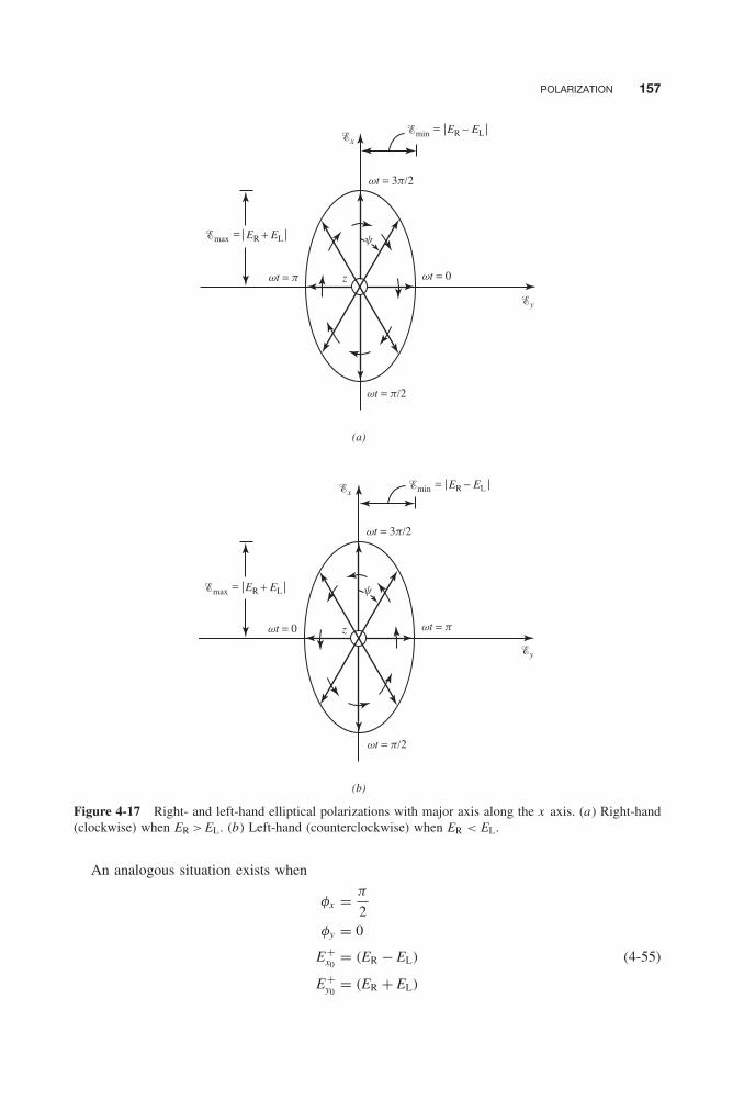
POLARIZATION 157
wt = p
wt = p
wt = 0
wt = 0
wt = p/2
wt = p/2
(a)
(b)
wt = 3p/2
wt = 3p/2
ER + EL
y
z
y
z
ER − EL
ER + EL
�y
�x
�x
�y
�min =
ER − EL�min =
�max =
�max =
Figure 4-17 Right- and left-hand elliptical polarizations with major axis along the x axis. (a) Right-hand(clockwise) when ER > EL. (b) Left-hand (counterclockwise) when ER < EL.
An analogous situation exists when
φx = π
2φy = 0
E+x0
= (ER − EL) (4-55)
E+y0
= (ER + EL)
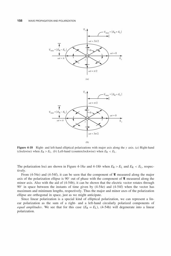
158 WAVE PROPAGATION AND POLARIZATION
wt = p
wt = p
(b)
(a)
wt = 0
wt = 0
wt = p/2
wt = p/2
wt = 3p/2
wt = 3p/2
z
z
y
y
ER + EL�max =
ER + EL�max
�x
�x
�y
�y
=
ER − EL�min =
ER − EL�min =
Figure 4-18 Right- and left-hand elliptical polarizations with major axis along the y axis. (a) Right-hand(clockwise) when ER > EL. (b) Left-hand (counterclockwise) when ER < EL.
The polarization loci are shown in Figure 4-18a and 4-18b when ER > EL and ER < EL, respec-tively.
From (4-54e) and (4-54f), it can be seen that the component of � measured along the majoraxis of the polarization ellipse is 90◦ out of phase with the component of � measured along theminor axis. Also with the aid of (4-54b), it can be shown that the electric vector rotates through90◦ in space between the instants of time given by (4-54e) and (4-54f) when the vector hasmaximum and minimum lengths, respectively. Thus the major and minor axes of the polarizationellipse are orthogonal in space, just as we might anticipate.
Since linear polarization is a special kind of elliptical polarization, we can represent a lin-ear polarization as the sum of a right- and a left-hand circularly polarized components ofequal amplitudes . We see that for this case (ER = EL), (4-54h) will degenerate into a linearpolarization.
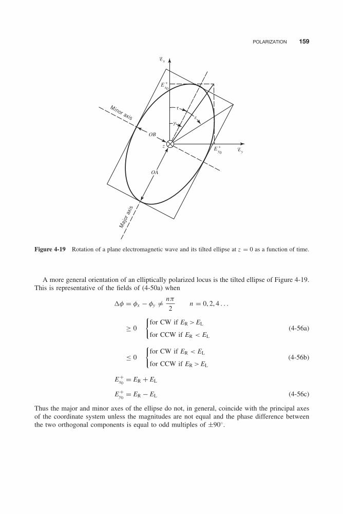
POLARIZATION 159
Minor axisM
ajor
axi
s
OA
OB
z
eg
t
�x
�y
E +x0
E +y0
Figure 4-19 Rotation of a plane electromagnetic wave and its tilted ellipse at z = 0 as a function of time.
A more general orientation of an elliptically polarized locus is the tilted ellipse of Figure 4-19.This is representative of the fields of (4-50a) when
φ = φx − φy �= nπ
2n = 0, 2, 4 . . .
≥ 0
{for CW if ER > EL
for CCW if ER < EL
(4-56a)
≤ 0
{for CW if ER < EL
for CCW if ER > EL
(4-56b)
E+x0
= ER + EL
E+y0
= ER − EL (4-56c)
Thus the major and minor axes of the ellipse do not, in general, coincide with the principal axesof the coordinate system unless the magnitudes are not equal and the phase difference betweenthe two orthogonal components is equal to odd multiples of ±90◦.
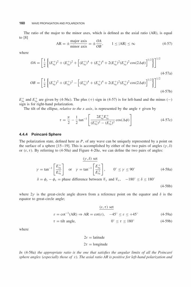
160 WAVE PROPAGATION AND POLARIZATION
The ratio of the major to the minor axes, which is defined as the axial ratio (AR), is equalto [8]
AR = ±major axis
minor axis= ± OA
OB, 1 ≤ |AR| ≤ ∞ (4-57)
where
OA =[
1
2
{(E+
x0)2 + (E+
y0)2 +
[(E+
x0)4 + (E+
y0)4 + 2(E+
x0)2(E+
y0)2 cos(2φ)
]1/2}]1/2
(4-57a)
OB =[
1
2
{(E+
x0)2 + (E+
y0)2 −
[(E+
x0)4 + (E+
y0)4 + 2(E+
x0)2(E+
y0)2 cos(2φ)
]1/2}]1/2
(4-57b)
E+x0
and E+y0
are given by (4-56c). The plus (+) sign in (4-57) is for left-hand and the minus (−)sign is for right-hand polarization.
The tilt of the ellipse, relative to the x axis , is represented by the angle τ given by
τ = π
2− 1
2tan−1
[2E+
x0E+
y0
(E+x0 )
2 − (E+y0 )
2cos(φ)
](4-57c)
4.4.4 Poincaré Sphere
The polarization state, defined here as P , of any wave can be uniquely represented by a point onthe surface of a sphere [15–19]. This is accomplished by either of the two pairs of angles (γ , δ)or (ε, τ). By referring to (4-50a) and Figure 4-20a , we can define the two pairs of angles:
(γ , δ) set
γ = tan−1
[E+
y0
E+x0
]or γ = tan−1
[E+
x0
E+y0
], 0◦ ≤ γ ≤ 90◦ (4-58a)
δ = φy − φx = phase difference between �y and �x , −180◦ ≤ δ ≤ 180◦
(4-58b)
where 2γ is the great-circle angle drawn from a reference point on the equator and δ is theequator to great-circle angle;
(ε, τ) set
ε = cot−1(AR) ⇒ AR = cot(ε), −45◦ ≤ ε ≤ +45◦ (4-59a)
τ = tilt angle, 0◦ ≤ τ ≤ 180◦ (4-59b)
where
2ε = latitude
2τ = longitude
In (4-58a) the appropriate ratio is the one that satisfies the angular limits of all the Poincarésphere angles (especially those of ε). The axial ratio AR is positive for left-hand polarization and
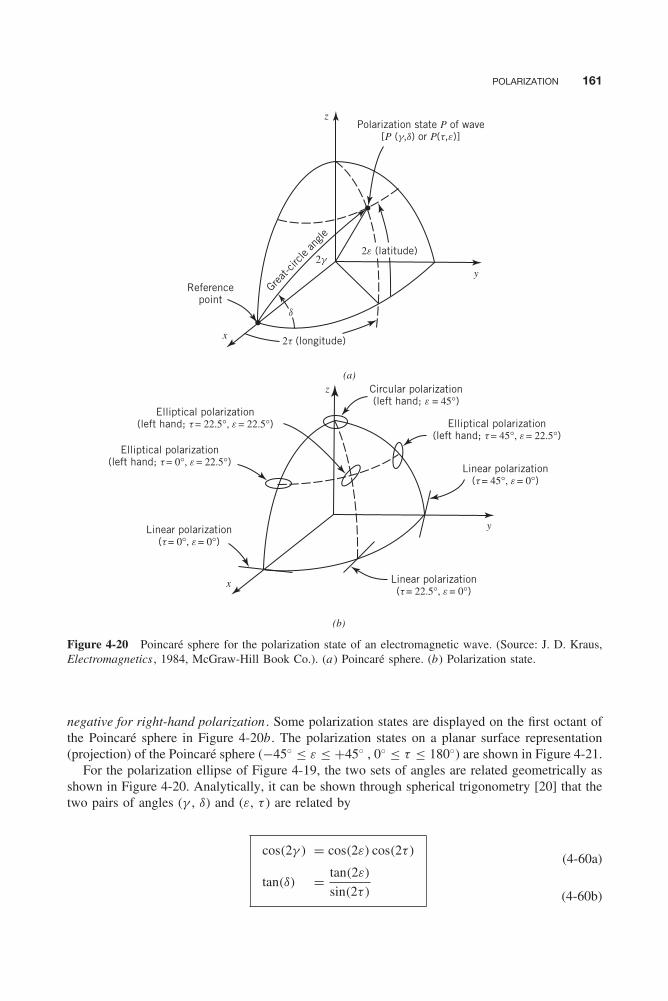
POLARIZATION 161
Referencepoint
2t (longitude)
2e (latitude)
Polarization state P of wave[P (g,d) or P(t,e)]
2gGre
at-circ
le an
glex
d
z
z
x
y
y
(a)
(b)
Elliptical polarization(left hand; t= 22.5°, e= 22.5°)
Elliptical polarization(left hand; t= 0°, e= 22.5°)
Circular polarization(left hand; e = 45°)
Elliptical polarization(left hand; t= 45°, e= 22.5°)
Linear polarization(t= 0°, e= 0°)
Linear polarization(t= 45°, e= 0°)
Linear polarization(t= 22.5°, e= 0°)
Figure 4-20 Poincaré sphere for the polarization state of an electromagnetic wave. (Source: J. D. Kraus,Electromagnetics , 1984, McGraw-Hill Book Co.). (a) Poincaré sphere. (b) Polarization state.
negative for right-hand polarization . Some polarization states are displayed on the first octant ofthe Poincaré sphere in Figure 4-20b. The polarization states on a planar surface representation(projection) of the Poincaré sphere (−45◦ ≤ ε ≤ +45◦ , 0◦ ≤ τ ≤ 180◦) are shown in Figure 4-21.
For the polarization ellipse of Figure 4-19, the two sets of angles are related geometrically asshown in Figure 4-20. Analytically, it can be shown through spherical trigonometry [20] that thetwo pairs of angles (γ , δ) and (ε, τ ) are related by
cos(2γ ) = cos(2ε) cos(2τ)
tan(δ) = tan(2ε)
sin(2τ)
(4-60a)
(4-60b)

162 WAVE PROPAGATION AND POLARIZATION
Right circular polarization
e= −45°
e= 0°
t= 0° t= 45° t= 90° t= 135° t= 180°
e= 45°
e= −22½°
e= 22½°
Right elliptical
polarization
polarization
Linear polarization
Left elliptical
Left circular polarization
Figure 4-21 Polarization states of electromagnetic waves on a planar surface projection of a Poincarésphere. (Source: J. D. Kraus, Electromagnetics , 1984, McGraw-Hill Book Co.).
or
sin(2ε) = sin(2γ ) sin(δ)
tan(2τ) = tan(2γ ) cos(δ)
(4-61a)
(4-61b)
Thus one set can be obtained by knowing the other.It is apparent from Figure 4-20 that the linear polarization is always found along the equator; the
right-hand circular resides along the south pole and the left-hand circular along the north pole.The remaining surface of the sphere is used to represent elliptical polarization with left-handelliptical in the upper hemisphere and right-hand elliptical on the lower hemisphere.
Because the Poincaré sphere parameter pairs (γ , δ) and (ε, τ ) are related by transcendentalfunctions, of (4-60a) and (4-60b), there may be some ambiguity at which quadrant should theangles be chosen. The angles should be selected to each satisfy respectively the range of valuesgiven by (4-58a) and (4-58b), and (4-57c), and each set should represent the same point onthe Poincaré sphere. Also the range of values of the axial ratio (AR) should be 1 ≤ |AR| ≤ ∞,with positive values to represent CCW (left-hand) polarization and negative values to representCW (right-hand) polarization. A MATLAB computer program, Polarization_Propag, has beenwritten and it is part of the website that accompanies this book.
POLARIZATION 163
Example 4-9
Determine the point on the Poincaré sphere of Figure 4-20 when the wave represented by (4-50a) issuch that
�x = E+x0
cos(ωt − βz + φx )
�y = 0
Solution: Using (4-58a) and (4-58b)
γ = tan−1
[E+
y0
E+x0
]= tan−1
[0
E+x0
]= 0◦
and δ could be of any value, i.e., −180◦ ≤ δ ≤ 180◦. The values of ε and τ can now be obtained from(4-61a) and (4-61b), and they are equal to
2ε = sin−1 [sin(2γ ) sin(δ)
] = sin−1(0) = 0◦
2τ = tan−1 [tan(2γ ) cos(δ)
] = tan−1(0) = 0◦
It is apparent that for this wave, which is obviously linearly polarized, the polarization state (point) isat the reference point of Figure 4-20. The axial ratio is obtained from (4-59a), and it is equal to
AR = cot(ε) = cot(0) = ∞An axial ratio of infinity always represents linear polarization.
Example 4-10
Repeat Example 4-9 when the wave of (4-50a) is such that
�x = 0
�y = E+y0
cos(ωt − βz + φy )
Solution: Using (4-58a) and (4-58b),
γ = tan−1
[E+
y0
E+x0
]= tan−1(∞) = 90◦
and δ could be of any value, i.e., −180◦ ≤ δ ≤ 180◦. The values of ε and τ can now be obtained from(4-61a) and (4-61b), and they are equal to
2ε = sin−1 [sin(2γ ) sin(δ)
] = sin−1(0) = 0◦
2τ = tan−1 [tan(2γ ) cos(δ)
] = tan−1(0) = 180◦
The polarization state (point) of this linearly polarized wave is diametrically opposed to that inExample 4-9. The axial ratio is also infinity.
164 WAVE PROPAGATION AND POLARIZATION
Example 4-11
Determine the polarization state (point) on the Poincaré sphere of Figure 4-20 when the wave of (4-50a)is such that
�x = E+x0
cos(ωt − βz + φx ) = 2E0 cos(ωt − βz + π
2
)�y = E+
y0cos(ωt − βz + φy ) = E0 cos(ωt − βz )
Solution: Using (4-58a) and (4-58b),
γ = tan−1
[E+
y0
E+x0
]= tan−1
[E0
2E0
]= 26.56◦
δ = φy − φx = −90◦
The values of ε and τ can now be obtained from (4-61a) and (4-61b), and they are equal to
2ε = sin−1 [sin(2γ ) sin(δ)
] = sin−1 [− sin(2γ )] = −2γ = −53.12◦
2τ = tan−1 [tan(2γ ) cos(δ)
] = tan−1(0) = 0◦
Therefore, this point is situated on the principal xz plane at an angle of 2γ = −2ε = 53.12◦ fromthe reference point of the x axis of Figure 4-20. The axial ratio is obtained using (4-59a), and it isequal to
AR = cot(ε) = cot(−26.56◦) = −2
The negative sign indicates that the wave has a right-hand (clockwise) polarization. Therefore the waveis right-hand elliptically polarized with AR = −2.
In general, points on the principal xz elevation plane, aside from the two intersecting pointson the equator and the north and south poles, are used to represent elliptical polarization whenthe major and minor axes of the polarization ellipse of Figure 4-19 coincide with the principalaxes.
If the polarization state of a wave is defined as Pw and that of an antenna as Pa , then thevoltage response of the antenna due to the wave is obtained by [10, 19]
V = C cos
[Pw Pa
2
](4-62)
whereC = constant that is a function of the antenna size and field strength of the wave
Pw = polarization state of the wavePa = polarization state of the antenna
Pw Pa = angle subtended by a great-circle arc from polarization Pw to Pa
Remember that the polarization of a wave, by IEEE standards [7, 8], is determined as the waveis observed from the rear (is receding). Therefore the polarization of the antenna is determinedby its radiated field in the transmitting mode.
POLARIZATION 165
Example 4-12
If the polarization states of the wave and antenna are given, respectively, by those of Examples 4-9and 4-10, determine the voltage response of the antenna due to that wave.
Solution: Since the polarization state Pw of the wave is at the +x axis and that of the antenna Pa isat the −x axis of Figure 4-20, then the angle Pw Pa subtended by a great-circle arc from Pw to Pa isequal to
Pw Pa = 180◦
Therefore the voltage response of the antenna is, according to (4-62), equal to
V = C cos
[Pw Pa
2
]= C cos(90◦) = 0
This is expected since the fields of the wave and those of the antenna are orthogonal (cross-polarized)to each other.
Example 4-13
The polarization of a wave that impinges upon a left-hand (counterclockwise) circularly polarizedantenna is circularly polarized. Determine the response of the antenna when the sense of rotation of theincident wave is
1. Left-hand (counterclockwise).2. Right-hand (clockwise).
Solution:
1. Since the antenna is left-hand circularly polarized, its polarization state (point) on the Poincarésphere is on the north pole (2γ = δ = 90◦). When the wave is also left-hand circularly polarized,its polarization state (point) is also on the north pole (2γ = δ = 90◦). Therefore, the subtendedangle Pw Pa between the two polarization states is equal to
Pw Pa = 0◦
and the voltage response of the antenna, according to (4-62), is equal to
V = C cos
[Pw Pa
2
]= C cos(0) = C
This represents the maximum response of the antenna, and it occurs when the polarization (includ-ing sense of rotation) of the wave is the same as that of the antenna.
2. When the sense of rotation of the wave is right-hand circularly polarized, its polarization state(point) is on the south pole (2γ = 90◦, δ = −90◦). Therefore, the subtended angle Pw Pa betweenthe two polarization states is equal to
Pw Pa = 180◦
and the response of the antenna, according to (4-62), is equal to

166 WAVE PROPAGATION AND POLARIZATION
V = C cos
[Pw Pa
2
]= C cos
[180◦
2
]= C cos(90◦) = 0
This represents a null response of the antenna, and it occurs when the sense of rotation of thecircularly polarized wave is opposite to that of the circularly polarized antenna. This is onetechnique, in addition to those shown in Example 4-12, that can be used to null the response ofan antenna system.
4.5 MULTIMEDIA
On the website that accompanies this book, the following multimedia resources are included forthe review, understanding and presentation of the material of this chapter.
• MATLAB computer programs:a. Polarization_Diagram_Ellipse_Animation: Animates the 3-D polarization diagram of
a rotating electric field vector (Figure 4-8). It also animates the 2-D polarization ellipse(Figure 4-19) for linear, circular and elliptical polarized waves, and sense of rotation. Italso computes the axial ratio (AR).
b. Polarization_Propag: Computes the Poincaré sphere angles, and thus the polarizationwave traveling in an infinite homogeneous medium.
• Power Point (PPT) viewgraphs, in multicolor.
REFERENCES
1. S. F. Adam, Microwave Theory and Applications , Prentice-Hall, Englewood Cliffs, N.J., 1969.
2. A. L. Lance, Introduction to Microwave Theory and Measurements , McGraw-Hill, New York, 1964.
3. N. Marcuvitz (ed.), Waveguide Handbook , McGraw-Hill, New York, 1951, Chapter 8, pp. 387–413.
4. C. H. Walter, Traveling Wave Antennas , McGraw-Hill, New York, 1965, pp. 172–187.
5. R. B. Adler, L. J. Chu, and R. M. Fano, Electromagnetic Energy Transmission and Radiation , JohnWiley & Sons, New York, 1960, Chapter 8.
6. D. T. Paris and F. K. Hurd, Basic Electromagnetic Theory , McGraw-Hill, New York, 1969.
7. “IEEE Standard 145-1983, IEEE Standard Definitions of Terms for Antennas,” reprinted in IEEE Trans.Antennas Propagat., vol. AP-31, no. 6, part II, pp. 1–29, November 1983.
8. C. A. Balanis, Antenna Theory: Analysis and Design , Third Edition. John Wiley & Sons, New York,2005.
9. W. Sichak and S. Milazzo, “Antennas for circular polarization,” Proc. IEEE , vol. 36, pp. 997–1002,August 1948.
10. G. Sinclair, “The transmission and reception of elliptically polarized waves,” Proc. IRE , vol. 38,pp. 148–151, February 1950.
11. V. H. Rumsey, G. A. Deschamps, M. L. Kales, and J. I. Bohnert, “Techniques for handling ellipticallypolarized waves with special reference to antennas,” Proc. IRE , vol. 39, pp. 533–534, May 1951.
12. V. H. Rumsey, “Part I—Transmission between elliptically polarized antennas,” Proc. IRE , vol. 39,pp. 535–540, May 1951.
13. M. L. Kales, “Part III—Elliptically polarized waves and antennas,” Proc. IRE , vol. 39, pp. 544–549,May 1951.
14. J. I. Bohnert, “Part IV—Measurements on elliptically polarized antennas,” Proc. IRE , vol. 39,pp. 549–552, May 1951.
15. H. Poincaré, Théorie Mathématique de la Limiére, Georges Carré, Paris, France, 1892.
16. G. A. Deschamps, “Part II—Geometrical representation of the polarization of a plane electromagneticwave,” Proc. IRE , vol. 39, pp. 540–544, May 1951.

PROBLEMS 167
17. E. F. Bolinder, “Geometric analysis of partially polarized electromagnetic waves,” IEEE Trans. AntennasPropagat., vol. AP-15, no. 1, pp. 37–40, January 1967.
18. G. A. Deschamps and P. E. Mast, “Poincaré sphere representation of partially polarized fields,” IEEETrans. Antennas Propagat., vol. AP-21, no. 4, pp. 474–478, July 1973.
19. J. D. Kraus, Electromagnetics , Third Edition, McGraw-Hill, New York, 1984.20. M. Born and E. Wolf, Principles of Optics , Macmillan Co., New York, pp. 24–27, 1964.
PROBLEMS
4.1. A uniform plane wave having only an xcomponent of the electric field is travelingin the +z direction in an unbounded loss-less, source-free region. Using Maxwell’sequations write expressions for the electricand corresponding magnetic field intensi-ties. Compare your answers to those of(4-2b) and (4-3c).
4.2. Using Maxwell’s equations, find the mag-netic field components for the wave whoseelectric field is given in Example 4-1.Compare your answer with that obtainedin the solution of Example 4-1.
4.3. The complex H field of a uniform planewave, traveling in an unbounded source-free medium of free space, is given by
H = 1
120π(âx − 2ây )e
−jβ0z
Find the:(a) Corresponding electric field.(b) Instantaneous power density vector.(c) Time-average power density.
4.4. The complex E field of a uniform planewave is given by
E = (âx + j âz )e−jβ0y + (2âx − j âz )e
+jβ0y
Assuming an unbounded source-free, free-space medium, find the:(a) Corresponding magnetic field.(b) Time-average power density flowing in
the +y direction.(c) Time-average power density flowing in
the −y direction.
4.5. The magnetic field of a uniform plane wavein a source-free region is given by
H = 10−6 [−âx (2 + j ) + âz (1 + j 3)]
e+jβy
Assuming that the medium is free space,determine the:
(a) Corresponding electric field.(b) Time-average power density.
4.6. The electric field of a uniform plane wavetraveling in a source-free region of freespace is given by
E = 10−3(âx + j ây ) sin(β0z )
(a) Is this a traveling or a standing wave?(b) Identify the traveling wave(s) of the
electric field and the direction(s) oftravel.
(c) Find the corresponding magnetic field.(d) Determine the time-average power
density of the wave.
4.7. The magnetic field of a uniform plane wavetraveling in a source-free, free-space regionis given by
H = 10−6(ây + j âz ) cos(β0x)
(a) Is this a traveling or a standing wave?(b) Identify the traveling wave(s) of the
magnetic field and the direction(s) oftravel.
(c) Find the corresponding electric field.(d) Determine the time-average power
density of the wave.
4.8. A uniform plane wave is traveling in the−z direction inside an unbounded source-free, free-space region. Assuming that theelectric field has only an Ex component, itsvalue at z = 0 is 4 × 10⁻³ V/m, and itsfrequency of operation is 300 MHz, writeexpressions for the:(a) Complex electric and magnetic fields.(b) Instantaneous electric and magnetic
fields.(c) Time-average and instantaneous pow-
er densities.(d) Time-average and instantaneous elec-
tric and magnetic energy densities.

168 WAVE PROPAGATION AND POLARIZATION
4.9. A uniform plane wave traveling inside anunbounded free-space medium has peakelectric and magnetic fields given by
E = âx E0e−jβ0z
H = ây H0e−jβ0z
where E0 = 1 mV/m.(a) Evaluate H0.(b) Find the corresponding average power
density. Evaluate all the constants.(c) Determine the volume electric and
magnetic energy densities. Evaluate allthe constants.
4.10. The complex electric field of a uniformplane wave traveling in an unbounded non-ferromagnetic dielectric medium is givenby
E = ây 10−3e−j 2πz
where z is measured in meters. Assumingthat the frequency of operation is 100 MHz,find the:(a) Phase velocity of the wave (give units).(b) Dielectric constant of the medium.(c) Wavelength (in meters).(d) Time-average power density.(e) Time-average total energy density.
4.11. The complex electric field of a time-harmonic field in free space is given by
E = âz 10−3(1 + j )e−j (2/3)πx
Assuming the distance x is measured inmeters, find the:(a) Wavelength (in meters).(b) Frequency.(c) Associated magnetic field.
4.12. A uniform plane wave is traveling insidethe earth, which is assumed to be a perfectdielectric infinite in extent. If the relativepermittivity of the earth is 9, find, at a fre-quency of 1 MHz, the:(a) Phase velocity.(b) Wave impedance.(c) Intrinsic impedance.(d) Wavelength of the wave inside the
earth.
4.13. An 11-GHz transmitter radiates its powerisotropically in a free-space medium.Assuming its total radiated power is 50mW, at a distance of 3 km, find the:(a) Time-average power density.
(b) RMS electric and magnetic fields.(c) Total time-average volume energy den-
sities.In all cases, specify the units.
4.14. The electric field of a time-harmonic wavetraveling in free space is given by
E = âx 10−4(1 + j )e−jβ0z
Find the amount of real power crossing arectangular aperture whose cross section isperpendicular to the z axis. The area of theaperture is 20 cm2.
4.15. The following complex electric field of atime-harmonic wave traveling in a source-free, free-space region is given by
E = 5 × 10⁻³(4ây + 3âz )ej (6y−8z )
Assuming y and z represent their respec-tive distances in meters, determine the:(a) Angle of wave travel (relative to the z
axis).(b) Three phase constants of the wave
along its oblique direction of travel, they axis, and the z axis (in radians permeter).
(c) Three wavelengths of the wave alongits oblique direction of travel, the yaxis, and the z axis (in meters).
(d) Three phase velocities of the wavealong the oblique direction of travel,the y axis, and the z axis (in metersper second).
(e) Three energy velocities of the wavealong the oblique direction of travel,the y axis, and the z axis (in metersper second).
(f) Frequency of the wave.(g) Associated magnetic field.
4.16. Using Maxwell’s equations, determine themagnetic field of (4-18b) given the electricfield of (4-18a).
4.17. Given the electric field of Example 4-2 andusing Maxwell’s equations, determine themagnetic field. Compare it with that foundin the solution of Example 4-2.
4.18. Given (4-19a) and (4-19c), determine thephase velocities of (4-22) and (4-23).
4.19. Derive the energy velocity of (4-24) usingthe definition of (4-9), (4-18a), and (4-18b).
PROBLEMS 169
4.20. A uniform plane wave of 3 GHz is incidentupon an unbounded conducting medium ofcopper that has a conductivity of 5.76 ×10⁷ S/m, ε = ε0, and μ = μ0. Find theapproximate:(a) Intrinsic impedance of copper.(b) Skin depth (in meters).
4.21. The magnetic field intensity of a planewave traveling in a lossy earth is given by
H = (ây + j 2âz )H0e−αx e−jβx
where H0 = 1 μA/m. Assuming the lossyearth has a conductivity of 10−4 S/m, adielectric constant of 9, and the frequencyof operation is 1 GHz, find inside the earththe:(a) Corresponding electric field vector.(b) Average power density vector.(c) Phase constant (radians per meter).(d) Phase velocity (meters per second).(e) Wavelength (meters).(f) Attenuation constant (Nepers per
meter).(g) Skin depth (meters).
4.22. Sea water is an important medium incommunication between submerged sub-marines or between submerged submarinesand receiving and transmitting stationslocated above the surface of the sea.Assuming the constitutive electrical param-eters of the sea are σ = 4 S/m, εr = 81,μr = 1, and f = 104 Hz, find the:(a) Complex propagation constant (per
meter).(b) Phase velocity (meters per second).(c) Wavelength (meters).(d) Attenuation constant (Nepers per
meter).(e) Skin depth (meters).
4.23. The electrical constitutive parameters ofmoist earth at a frequency of 1 MHzare σ = 10−1 S/m, εr = 4, and μr = 1.Assuming that the electric field of a uni-form plane wave at the interface (on theside of the earth) is 3 × 10⁻² V/m, findthe:(a) Distance through which the wave
must travel before the magnitude ofthe electric field reduces to 1.104 ×10⁻² V/m.
(b) Attenuation the electric field undergoesin part (a) (in decibels).
(c) Wavelength inside the earth (inmeters).
(d) Phase velocity inside the earth (inmeters per second).
(e) Intrinsic impedance of the earth.
4.24. The complex electric field of a uniformplane wave is given by
E = 10−2[âx
√2 + âz (1 + j )ejπ/4
]e−jβy
(a) Find the polarization of the wave (lin-ear, circular, or elliptical).
(b) Determine the sense of rotation (clock-wise or counterclockwise).
(c) Sketch the figure the electric fieldtraces as a function of ωt .
4.25. The complex magnetic field of a uniformplane wave is given by
H = 10−3
120π(âx − j âz )e
+jβy
(a) Find the polarization of the wave (lin-ear, circular, or elliptical).
(b) State the direction of rotation (clock-wise or counterclockwise). Justify youranswer.
(c) Sketch the polarization curve denotingthe �-field amplitude, and direction ofrotation. Indicate on the curve the vari-ous times for the rotation of the vector.
4.26. In a source-free, free-space region, thecomplex magnetic field of a time-harmonicfield is represented by
H =[̂ax (1 + j )+ âz
√2ejπ/4
] E0
η0
e−jβ0y
where E0 is a constant and η0 is the intrin-sic impedance of free space. Determine the:(a) Polarization of the wave (linear, circu-
lar, or elliptical). Justify your answer.(b) Sense of rotation, if any.(c) Corresponding electric field.
4.27. Show that any linearly polarized wave canbe decomposed into two circularly polar-ized waves (one CW and the other CCW)but both traveling in the same direction asthe linearly polarized wave.
4.28. The electric field of a f = 10 GHz time-harmonic uniform plane wave traveling ina perfect dielectric medium is given by
E = (âx + j 2ây
)e−j 600πz

170 WAVE PROPAGATION AND POLARIZATION
where z is in meters. Determine, assumingthe permeability of the medium is the sameas that of free space, the:(a) Wavelength of the wave (in meters).(b) Velocity of the wave (in meters/sec).(c) Dielectric constant (relative permittiv-
ity) of the medium (dimensionless).(d) Intrinsic impedance of the medium (in
ohms).(e) Wave impedance of the medium (in
ohms).(f) Vector magnetic field of the wave.(g) Polarization of the wave (linear, circu-
lar, elliptical; AR; and sense of rota-tion).
4.29. The spatial variations of the electric fieldof a time-harmonic wave traveling in freespace are given by
E(x) = ây e−j (β0x− π4 ) + âz e−j (β0x− π
2 )
Determine, using the necessary and suffi-cient conditions of the wave, the:(a) Direction of wave travel (+x , −x , +y ,
−y , +z or −z ) based on e+jωt time.(b) Polarization of the wave (linear, circu-
lar or elliptical). Justify your answer.(c) Sense of rotation (CW or CCW), if
any, of the wave. Justify your answer.
4.30. The spatial variations of the electric fieldof a time-harmonic wave traveling in freespace are given by
E(z ) = âx 2e−j (β0z− π4 ) + ây e−j (β0z− 3π
4 )
Determine the:(a) Direction of wave travel (+x , −x , +y ,
−y , +z or −z ) based on e+jωt time.(b) Two pairs of Poincaré sphere polariza-
tion parameters (γ , δ) and (ε, τ ).(c) Based on either one of the two pairs of
parameters from part (b), state the:• Polarization of the wave (linear,
circular or elliptical). Justify youranswer.
• Sense of rotation (CW or CCW) ofthe wave. Justify your answer.
• Axial Ratio. Justify your answer.
4.31. The time-harmonic electric field travelinginside an infinite lossless dielectric mediumis given by
Ei (z ) = (j 2âx + 5ây
)E0e−jβz
where β and Eo are real constants.Assuming a e+jωt time convention,determine the:(a) Polarization of the wave (linear, circu-
lar or elliptical). You must justify youranswer. Be specific.
(b) Sense of rotation (CW or CCW). Youmust justify your answer. Be specific.
(c) Axial Ratio (AR) based on the expres-sion of the electric field. You must jus-tify your answer. Be specific.
(d) Poincaré sphere angles (in degrees):• γ and δ
• ε and τ
Make sure that the polarization pointon the Poincaré sphere based on thepair of angles (γ , δ) is the same as thatbased on the set of angles (ε, τ ).
(e) Axial Ratio (AR) based on thePoincaré sphere angles. Compare withthat in part (c).
4.32. In a source-free, free-space region the com-plex magnetic field is given by
H = j (ây − j âz )E0
η0
e+jβ0x
where E0 is a constant and η0 is the intrin-sic impedance of free space. Find the:(a) Polarization of the wave (linear, circu-
lar, or elliptical). Justify your answer.(b) Sense of rotation, if any (CW or
CCW). Justify your answer.(c) Time-average power density.(d) Polarization of the wave on the
Poincaré sphere.
4.33. The electric field of a time-harmonic waveis given by
E = 2 × 10⁻³(âx + ây )e−j 2z
(a) State the polarization of the wave (lin-ear, circular, or elliptical).
(b) Find the polarization on the Poincarésphere by identifying the angles δ, γ ,τ and ε (in degrees).
(c) Locate the polarization point on thePoincaré sphere.
4.34. For a uniform plane wave represented bythe electric field
E = E0(âx − j 2ây )e−jβz
where E0 is constant, do the following.(a) Determine the longitude angle 2τ ,
latitude angle 2ε, great-circle angle 2γ ,and equator to great-circle angle δ (all
PROBLEMS 171
in degrees) that are used to identify andlocate the polarization of the wave onthe Poincaré sphere.
(b) Using the answers from part (a), statethe polarization of the wave (linear, cir-cular, or elliptical), its sense of rotation(CW or CCW), and its Axial Ratio.
(c) Find the signal loss (in decibels) whenthe wave is received by a right-handcircularly polarized antenna.
4.35. The electric field of (4-50a) has an AxialRatio of infinity and a great-circle angle of2γ = 109.47◦.(a) Find the relative magnitude (ratio) of
E+y0
to E+x0
. Which component is moredominant, Ex or Ey ? Use the first def-inition of γ in (4-58a).
(b) Identify the polarization point on thePoincaré sphere (i.e., find δ, τ , and ε
in degrees).(c) State the polarization of the wave (lin-
ear, circular, or elliptical).
4.36. A uniform plane wave is traveling alongthe +z axis and its electric field is givenby
Ew = (âx + j ây )e−jβz E0
This incident plane wave impinges uponan antenna whose field radiated along thez axis is given by(a) Eaa = (âx + j ây )e+jβz Ea
(b) Eab = (âx − j ây )e+jβz Ea
Determine the:1. Polarization of the incident wave
(linear, circular, elliptical; sense ofrotation; and AR).
2. Polarization of antenna of part (a)(linear, circular, elliptical; sense ofrotation; and AR).
3. Polarization of antenna of part (b)(linear, circular, elliptical; sense ofrotation; and AR).
4. Normalized output voltage when theincident wave impinges upon theantenna whose electric field is thatof part (a).
5. Normalized output voltage when theincident wave impinges upon theantenna whose electric field is thatof part (b).
4.37. The field radiated by an antenna haselectric field components represented by(4-50a) such that E+
x0= E+
y0and its Axial
Ratio is infinity.(a) Identify the polarization point on the
Poincaré sphere (i.e., find γ , δ, τ , andε in degrees).
(b) If this antenna is used to receive thewave of Problem 4.35, find the polar-ization loss (in decibels). To do thispart, use the Poincaré sphere param-eters.


Balanis c05.tex V3 - 11/23/2011 11:47 A.M. Page 173
CHAPTER 5Reflection and Transmission
5.1 INTRODUCTION
In the previous chapter we discussed solutions to TEM waves in unbounded media. In real-worldproblems, however, the fields encounter boundaries, scatterers, and other objects. Therefore thefields must be found by taking into account these discontinuities.
In this chapter we want to discuss TEM field solutions in two semi-infinite lossless and lossymedia bounded by a planar boundary of infinite extent. Reflection and transmission coefficientswill be derived to account for the reflection and transmission of the fields by the boundary. Thesecoefficients will be functions of the constitutive parameters of the two media, the direction ofwave travel (angle of incidence), and the direction of the electric and magnetic fields (wavepolarization).
In general, the reflection and transmission coefficients are complex quantities. It will be demon-strated that their amplitudes and phases can be varied by controlling the direction of wave travel(angle of incidence). In fact, for one wave polarization (parallel polarization) the reflection coef-ficient can be made equal to zero. When this occurs, the angle of incidence is known as theBrewster angle. This principle is used in the design of many instruments (such as binoculars).
The magnitude of the reflection coefficient can also be made equal to unity by properly selectingthe wave incidence angle. This angle is known as the critical angle, and it is independent of wavepolarization; however, in order for this angle to occur, the incident wave must exist in the densermedium. The critical angle concept plays a crucial role in the design of transmission lines (suchas optical fiber, slab wave-guides, and coated conductors; the microstrip is one example).
5.2 NORMAL INCIDENCE—LOSSLESS MEDIA
We begin the discussion of reflection and transmission from planar boundaries of lossless mediaby assuming the wave travels perpendicular (normal incidence) to the planar interface formedby two semi-infinite lossless media, as shown in Figure 5-1, each characterized by the con-stitutive parameters of ε1, μ1 and ε2, μ2. When the incident wave encounters the interface, afraction of the wave intensity will be reflected into medium 1 and part will be transmitted intomedium 2.
Assuming the incident electric field of amplitude E0 is polarized in the x direction, we can writeexpressions for its incident, reflected, and transmitted electric field components, respectively, as
Ei = âx E0e−jβ1z (5-1a)
173

Balanis c05.tex V3 - 11/23/2011 11:47 A.M. Page 174
174 REFLECTION AND TRANSMISSION
e1, m1
e1, m1 e2, m2
e2, m2
x
x
y z
z
y
Ei
Hr Hi
Hi Ht
Ht
Hr
Er
Ei
Et
Et
Er
Figure 5-1 Wave reflection and transmission at normal incidence by a planar interface.
Er = âx�bE0e+jβ1z (5-1b)
Et = âx T bE0e−jβ2z (5-1c)
where �b and T b are used here to represent, respectively, the reflection and transmission coef-ficients at the interface. Presently these coefficients are unknowns and will be determined byapplying boundary conditions on the fields along the interface. Since the incident fields are lin-early polarized and the reflecting surface is planar, the reflected and transmitted fields will alsobe linearly polarized. Because we do not know the direction of polarization (positive or negative)of the reflected and transmitted electric fields, they are assumed here to be in the same direc-tion (positive) as the incident electric fields. If that is not the case, it will be corrected by theappropriate signs on the reflection and transmission coefficients.
Using the right-hand procedure outlined in Section 4.2.1 or Maxwell’s equations 4-3 or 4-3a,the magnetic field components corresponding to (5-1a) through (5-1c) can be written as
Hi = âyE0
η1e−jβ1z (5-2a)
Hr = −ây�bE0
η1e+jβ1z (5-2b)
Ht = âyT bE0
η2e−jβ2z (5-2c)

Balanis c05.tex V3 - 11/23/2011 11:47 A.M. Page 175
NORMAL INCIDENCE—LOSSLESS MEDIA 175
The reflection and transmission coefficients will now be determined by enforcing continuityof the tangential components of the electric and magnetic fields across the interface. Using (5-1a)through (5-2c), continuity of the tangential components of the electric and magnetic fields at theinterface (z = 0) leads, respectively, to
1 + �b = T b (5-3a)
1
η1(1 − �b) = 1
η2T b (5-3b)
Solving these two equations for �b and T b , we can write that
�b = η2 − η1
η2 + η1= E r
E i= −H r
H i(5-4a)
T b = 2η2
η1 + η2= 1 + �b = E t
E i= η2
η1
H t
H i(5-4b)
Therefore the plane wave reflection and transmission coefficients of a planar interface fornormal incidence are functions of the constitutive properties, and they are given by (5-4a) and(5-4b). Since the angle of incidence is fixed at normal, the reflection coefficient cannot be equalto zero unless η2 = η1. For most dielectric material, aside from ferromagnetics, this implies thatε2 = ε1 since for them μ1 � μ2.
Away from the interface the reflection � and transmission T coefficients are related to thoseat the boundary (�b , T b) and can be written, respectively, as
�(z = −�1) = E r (z )
E i (z )
∣∣∣∣z=−�1
= �bE0e+jβ1z
E0e−jβ1z
∣∣∣∣z=−�1
= �be−j 2β1�1 (5-5a)
T
(z2 = �2,z1 = −�1
)= E t (z2)|z2=�2
E i (z1)|z1=−�1
= T bE0e−jβ2�2
E0e+jβ1�1= T be−j (β2�2+β1�1) (5-5b)
where �1 and �2 are positive distances measured from the interface to media 1 and 2, respectively.Associated with the electric and magnetic fields (5-1a) through (5-2c) are corresponding aver-
age power densities that can be written as
Siav = 1
2Re(Ei × Hi∗) = âz
|E0|22η1
(5-6a)
Srav = 1
2Re(Er × Hr∗
) = −âz |�b |2 |E0|22η1
= −âz |�b |2S iav (5-6b)
Stav = 1
2Re(Et × Ht∗) = âz |T b |2 |E0|2
2η2= âz |T b |2 η1
η2
|E0|22η1
= âz |T b |2 η1
η2S i
av = âz(1 − |�b |2) S i
av (5-6c)
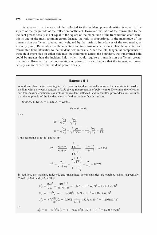
Balanis c05.tex V3 - 11/23/2011 11:47 A.M. Page 176
176 REFLECTION AND TRANSMISSION
It is apparent that the ratio of the reflected to the incident power densities is equal to thesquare of the magnitude of the reflection coefficient. However, the ratio of the transmitted to theincident power density is not equal to the square of the magnitude of the transmission coefficient;this is one of the most common errors. Instead the ratio is proportional to the magnitude of thetransmission coefficient squared and weighted by the intrinsic impedances of the two media, asgiven by (5-6c). Remember that the reflection and transmission coefficients relate the reflected andtransmitted field intensities to the incident field intensity. Since the total tangential components ofthese field intensities on either side must be continuous across the boundary, the transmitted fieldcould be greater than the incident field, which would require a transmission coefficient greaterthan unity. However, by the conservation of power, it is well known that the transmitted powerdensity cannot exceed the incident power density.
Example 5-1
A uniform plane wave traveling in free space is incident normally upon a flat semi-infinite losslessmedium with a dielectric constant of 2.56 (being representative of polystyrene). Determine the reflectionand transmission coefficients as well as the incident, reflected, and transmitted power densities. Assumethat the amplitude of the incident electric field at the interface is 1 mV/m.
Solution: Since ε1 = ε0 and ε2 = 2.56ε0,
μ1 = μ2 = μ0
then
η1 =√
μ1
ε1=
√μ0
ε0
η2 =√
μ2
ε2=
√μ0
2.56ε0= 1
1.6
√μ0
ε0= η1
1.6
Thus according to (5-4a) and (5-4b)
�b = η2 − η1
η2 + η1=
1
1.6− 1
1
1.6+ 1
= 1 − 1.6
1 + 1.6= −0.231
T b = 2η2
η1 + η2=
2
(1
1.6
)1 + 1
1.6
= 2
2.6= 0.769
In addition, the incident, reflected, and transmitted power densities are obtained using, respectively,(5-6a), (5-6b), and (5-6c). Thus
S iav = |E0|2
2η1= (10−3)2
2(376.73)= 1.327 × 10⁻⁹ W/m2 = 1.327 nW/m2
S rav = |�b |2S i
av = | − 0.231|2(1.327) × 10−9 = 0.071 nW/m2
S tav = |T b |2 η1
η2S i
av = |0.769|2 1
1/1.6(1.327) × 10−9 = 1.256 nW/m2
orS t
av = (1 − |�b |2)S iav = (1 − |0.231|2)(1.327) × 10−9 = 1.256 nW/m2
Balanis c05.tex V3 - 11/23/2011 11:47 A.M. Page 177
OBLIQUE INCIDENCE—LOSSLESS MEDIA 177
In medium 1, the total field is equal to the sum of the incident and reflected fields. Thus, for thetotal electric and magnetic fields in medium 1, we can write that
E1 = Ei + Er = âx E0e−jβ1z︸ ︷︷ ︸traveling
wave
(1 + �be+j 2β1z )︸ ︷︷ ︸standing
wave
= âx E0e−jβ1z [1 + �(z )] (5-7a)
H1 = Hi + Hr = ây (E0/η1)e−jβ1z︸ ︷︷ ︸
travelingwave
(1 − �be+j 2β1z )︸ ︷︷ ︸standing
wave
= âyE0
η1e−jβ1z [1 − �(z )] (5-7b)
In each expression the factors outside the parentheses represent the traveling wave part of the waveand those within the parentheses represent the standing wave part . Therefore the total field of two wavesis the product of one of the waves times a factor that in this case is the standing wave pattern. Thisis analogous to the array multiplication rule in antennas where the total field of an array of identicalelements is equal to the product of the field of a single element times a factor that is referred to as thearray factor [1].
As discussed in Section 4.2.1D, the ratio of the maximum value of the electric field magnitude tothat of the minimum is defined as the standing wave ratio (SWR), and it is given here by
SWR = |E1|max
|E1|min= 1 + |�b |
1 − |�b | =1 +
∣∣∣∣η2 − η1
η2 + η1
∣∣∣∣1 −
∣∣∣∣η2 − η1
η2 + η1
∣∣∣∣ (5-8)
For two media with identical permeabilities (μ1 = μ2), the SWR can be written as
SWR =∣∣√ε1 + √
ε2∣∣ + ∣∣√ε1 − √
ε2∣∣∣∣√ε1 + √
ε2∣∣ − ∣∣√ε1 − √
ε2∣∣ =
⎧⎪⎪⎨⎪⎪⎩√
ε1
ε2, ε1 > ε2√
ε2
ε1, ε2 > ε1
(5-9a)
(5-9b)
5.3 OBLIQUE INCIDENCE—LOSSLESS MEDIA
To analyze reflections and transmissions at oblique wave incidence, we need to introduce theplane of incidence, which is defined as the plane formed by a unit vector normal to the reflectinginterface and the vector in the direction of incidence. For a wave whose wave vector is on the xzplane and is incident upon an interface that is parallel to the xy plane, as shown in Figure 5-2,the plane of incidence is the xz plane.
To examine reflections and transmissions at oblique angles of incidence for a general wavepolarization, it is most convenient to decompose the electric field into its perpendicular andparallel components (relative to the plane of incidence) and analyze each one of them individually.The total reflected and transmitted field will be the vector sum of these two polarizations.
When the electric field is perpendicular to the plane of incidence, the polarization of the waveis referred to as perpendicular polarization . Since the electric field is parallel to the interface,it is also known as horizontal or E polarization . When the electric field is parallel to the planeof incidence, the polarization is referred to as parallel polarization . Because a component ofthe electric field is also perpendicular to the interface when the magnetic field is parallel to theinterface, it is also known as vertical or H polarization . Each type of polarization will be furtherexamined.
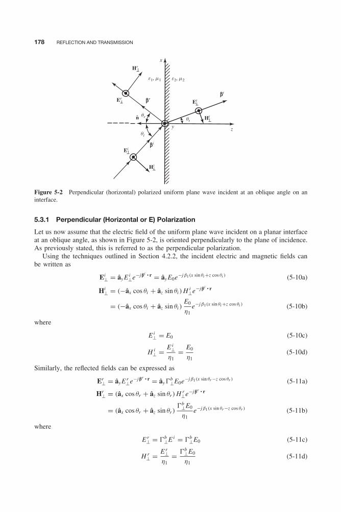
Balanis c05.tex V3 - 11/23/2011 11:47 A.M. Page 178
178 REFLECTION AND TRANSMISSION
y z
x
Er
n
Ei
Hi
Ht
Hr
Et
e1, m1 e2, m2
βrβt
βi
qr
qi
qt
Figure 5-2 Perpendicular (horizontal) polarized uniform plane wave incident at an oblique angle on aninterface.
5.3.1 Perpendicular (Horizontal or E) Polarization
Let us now assume that the electric field of the uniform plane wave incident on a planar interfaceat an oblique angle, as shown in Figure 5-2, is oriented perpendicularly to the plane of incidence.As previously stated, this is referred to as the perpendicular polarization.
Using the techniques outlined in Section 4.2.2, the incident electric and magnetic fields canbe written as
Ei⊥ = ây E i
⊥e−jβi • r = ây E0e−jβ1(x sin θi +z cos θi ) (5-10a)
Hi⊥ = (−âx cos θi + âz sin θi ) H i
⊥e−jβi • r
= (−âx cos θi + âz sin θi )E0
η1e−jβ1(x sin θi +z cos θi ) (5-10b)
where
E i⊥ = E0 (5-10c)
H i⊥ = E i
⊥η1
= E0
η1(5-10d)
Similarly, the reflected fields can be expressed as
Er⊥ = ây E r
⊥e−jβr • r = ây�b⊥E0e−jβ1(x sin θr −z cos θr ) (5-11a)
Hr⊥ = (âx cos θr + âz sin θr ) H r
⊥e−jβr • r
= (âx cos θr + âz sin θr )�b
⊥E0
η1e−jβ1(x sin θr −z cos θr ) (5-11b)
where
E r⊥ = �b
⊥E i = �b⊥E0 (5-11c)
H r⊥ = E r
⊥η1
= �b⊥E0
η1(5-11d)

Balanis c05.tex V3 - 11/23/2011 11:47 A.M. Page 179
OBLIQUE INCIDENCE—LOSSLESS MEDIA 179
Also the transmitted fields can be written as
Et⊥ = ây E t
⊥e−jβt • r = ây T b⊥E0e−jβ2(x sin θt +z cos θt ) (5-12a)
Ht⊥ = (−âx cos θt + âz sin θt ) H t
⊥e−jβt • r
= (−âx cos θt + âz sin θt )T b
⊥E0
η2e−jβ2(x sin θt +z cos θt ) (5-12b)
where
E t⊥ = T b
⊥E i⊥ = T b
⊥E0 (5-12c)
H t⊥ = E t
⊥η2
= T b⊥E0
η2(5-12d)
The reflection �b⊥ and transmission T b
⊥ coefficients, and the relation between the incident θi ,reflected θr , and transmission (refracted) θt angles can be obtained by applying the boundaryconditions on the continuity of the tangential components of the electric and magnetic fields.That is (
Ei⊥ + Er
⊥) ∣∣tan
z=0= (
Et⊥) ∣∣tan
z=0(5-13a)(
Hi⊥ + Hr
⊥) ∣∣tan
z=0= (
Ht⊥) ∣∣tan
z=0(5-13b)
Using the appropriate terms of (5-10a) through (5-12d), (5-13a) and (5-13b) can be written,respectively, as
e−jβ1x sin θi + �b⊥e−jβ1x sin θr = T b
⊥e−jβ2x sin θt (5-14a)
1
η1
(− cos θi e−jβ1x sin θi + �b
⊥ cos θr e−jβ1x sin θr) = −T b
⊥η2
cos θt e−jβ2x sin θt (5-14b)
Whereas (5-14a) and (5-14b) represent two equations with four unknowns (�b⊥, T b
⊥, θr , θt ), itshould be noted that each equation is complex. By equating the corresponding real and imaginaryparts of each side, each can be reduced to two equations (a total of four). If this procedure isutilized, it will be concluded that (5-14a) and (5-14b) lead to the following two relations:
θr = θi (Snell’s law of reflection) (5-15a)
β1 sin θi = β2 sin θt (Snell’s law of refraction) (5-15b)
Using (5-15a) and (5-15b) reduces (5-14a) and (5-14b) to
1 + �b⊥ = T b
⊥ (5-16a)
cos θi
η1
(−1 + �b⊥) = −cos θt
η2T b
⊥ (5-16b)
Solving (5-16a) and (5-16b) simultaneously for �b⊥ and T b
⊥ leads to
�b⊥ = E r
⊥E i
⊥= η2 cos θi − η1 cos θt
η2 cos θi + η1 cos θt=
√μ2
ε2cos θi −
√μ1
ε1cos θt√
μ2
ε2cos θi +
√μ1
ε1cos θt
(5-17a)
Balanis c05.tex V3 - 11/23/2011 11:47 A.M. Page 180
180 REFLECTION AND TRANSMISSION
T b⊥ = E t
⊥E i
⊥= 2η2 cos θi
η2 cos θi + η1 cos θt=
2√
μ2
ε2cos θi√
μ2
ε2cos θi +
√μ1
ε1cos θt
(5-17b)
�b⊥ and T b
⊥ of (5-17a) and (5-17b) are usually referred to as the plane wave Fresnel reflectionand transmission coefficients for perpendicular polarization.
Since for most dielectric media (excluding ferromagnetic material) μ1 � μ2 � μ0, (5-17a) and(5-17b) reduce, by also utilizing (5-15b), to
�b⊥∣∣μ1=μ2
=cos θi −
√ε2
ε1
√1 −
(ε1
ε2
)sin2 θi
cos θi +√
ε2
ε1
√1 −
(ε1
ε2
)sin2 θi
(5-18a)
T b⊥∣∣μ1=μ2
= 2 cos θi
cos θi +√
ε2
ε1
√1 −
(ε1
ε2
)sin2 θi
(5-18b)
Plots of |�b⊥| and |T b
⊥| of (5-18a) and (5-18b) for ε2/ε1 = 2.56, 4, 9, 16, 25, and 81 as afunction of θi are shown in Figure 5-3. It is apparent that as the relative ratio of ε2/ε1 increases,the magnitude of the reflection coefficient increases, whereas that of the transmission coeffi-cient decreases. This is expected since large ratios of ε2/ε1 project larger discontinuities in thedielectric properties of the media along the interface. Also it is observed that for ε2 > ε1 themagnitude of the reflection coefficient never vanishes regardless of the ε2/ε1 ratio or the angle ofincidence.
For ε2/ε1 > 1, both �b⊥ and T b
⊥ are real with �b⊥ being negative and T b
⊥ being positive for allangles of incidence. Therefore, as a function of θi , the phase of �b
⊥ is equal to 180◦ and thatof the transmission coefficient T b
⊥ is zero. When ε2/ε1 = 1 the reflection coefficient vanishesand the transmission coefficient reduces to unity. When ε2/ε1 < 1, both �b
⊥ and T b⊥ are real
when the incidence angle θi ≤ θc ; for θi > θc , they become complex. The angle θi for which|�b
⊥|ε2/ε1<1(θi = θc) = 1 is referred to as the critical angle, and it represents conditions of totalinternal reflection. More discussion on the critical angle (θi = θc) and the wave propagation forθi > θc can be found in Section 5.3.4.
In medium 1 the total electric field can be written as
E1⊥ = Ei
⊥ + Er⊥ = ây E0e−jβ1(x sin θ1+z cos θi )︸ ︷︷ ︸
traveling wave
[1 + �b
⊥e+j 2β1z cos θi]︸ ︷︷ ︸
standing wave
= ây E0e−jβ1(x sin θi +z cos θi ) [1 + �⊥(z )] (5-19)
where
�⊥(z ) = �b⊥e+j 2β1z cos θi (5-19a)

Balanis c05.tex V3 - 11/23/2011 11:47 A.M. Page 181
OBLIQUE INCIDENCE—LOSSLESS MEDIA 181
e2e1
= 81
e2e1
= 25
e2e1
= 16
e2e1
= 9
e2e1
= 4
e2e1
= 2.56
0.00
0.25
15 30 45 60 75 90
0.50
0.75
1.00
0
Incident angle qi (degrees)(a)
Ref
lect
ion
coef
fici
ent
e2e1
= 2.56
e2e1
= 9
e2e1
= 4
e2e1
= 25
e2e1
= 16
e2e1
= 81
0.00
0.25
15 30 45 60 75 90
0.50
0.75
1.00
0
Incident angle qi (degrees)(b)
Tran
smis
sion
coe
ffic
ient
T
b Γb
Figure 5-3 Magnitude of coefficients for perpendicular polarization as a function of incident angle.(a) Reflection. (b) Transmission.
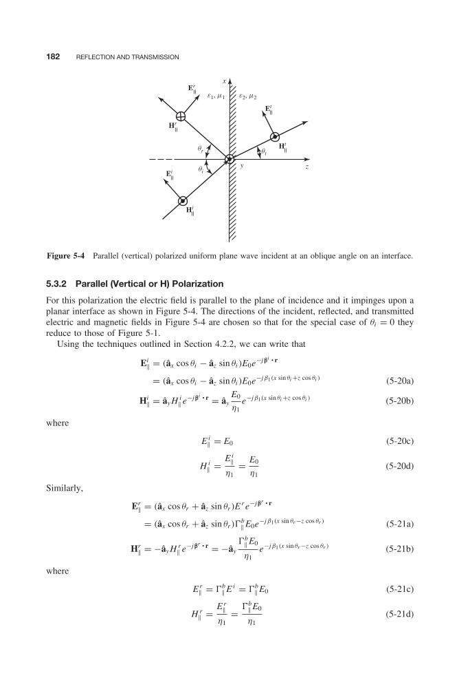
Balanis c05.tex V3 - 11/23/2011 11:47 A.M. Page 182
182 REFLECTION AND TRANSMISSION
y z
x
e1, m1 e2, m2
Ei
Er
Et
Ht
Hi
Hr
qr
qi
qt
Figure 5-4 Parallel (vertical) polarized uniform plane wave incident at an oblique angle on an interface.
5.3.2 Parallel (Vertical or H) Polarization
For this polarization the electric field is parallel to the plane of incidence and it impinges upon aplanar interface as shown in Figure 5-4. The directions of the incident, reflected, and transmittedelectric and magnetic fields in Figure 5-4 are chosen so that for the special case of θi = 0 theyreduce to those of Figure 5-1.
Using the techniques outlined in Section 4.2.2, we can write that
Ei|| = (âx cos θi − âz sin θi )E0e−jβi • r
= (âx cos θi − âz sin θi )E0e−jβ1(x sin θi +z cos θi ) (5-20a)
Hi|| = ây H i
|| e−jβi • r = ây
E0
η1e−jβ1(x sin θi +z cos θi ) (5-20b)
where
E i|| = E0 (5-20c)
H i|| = E i
||η1
= E0
η1(5-20d)
Similarly,
Er|| = (âx cos θr + âz sin θr )E
r e−jβr • r
= (âx cos θr + âz sin θr )�b|| E0e−jβ1(x sin θr −z cos θr ) (5-21a)
Hr|| = −ây H r
|| e−jβr • r = −ây
�b|| E0
η1e−jβ1(x sin θr −z cos θr ) (5-21b)
where
E r|| = �b
|| Ei = �b
|| E0 (5-21c)
H r|| = E r
||η1
= �b|| E0
η1(5-21d)
Balanis c05.tex V3 - 11/23/2011 11:47 A.M. Page 183
OBLIQUE INCIDENCE—LOSSLESS MEDIA 183
Also,
Et|| = (âx cos θt − âz sin θt )E
t||e
−jβt • r
= (âx cos θt − âz sin θt )Tb|| E0e−jβ2(x sin θt +z cos θt ) (5-22a)
Ht|| = ây H t
|| e−jβt • r = ây
T b|| E0
η2e−jβ2(x sin θt +z cos θt ) (5-22b)
where
E t|| = T b
|| E i = T b|| E0 (5-22c)
H t|| = E t
||η2
= T b|| E0
η2(5-22d)
As before, the reflection �b|| and transmission T b
|| coefficients, and the reflection θr and trans-mission (refraction) θt angles are the four unknowns. These can be determined and expressed interms of the incident angle θi and the constitutive parameters of the two media by applying theboundary conditions on the continuity across the interface (z = 0) of the tangential componentsof the electric and magnetic fields as given by (5-13a) and (5-13b) and applied to parallel polar-ization. Using the appropriate terms of (5-20a) through (5-22d), we can write (5-13a) and (5-13b)as applied to parallel polarization, respectively, as
cos θi e−jβ1x sin θi + �b
|| cos θr e−jβ1x sin θr = T b|| cos θt e
−jβ2x sin θt (5-23a)
1
η1
(e−jβ1x sin θi − �b
|| e−jβ1x sin θr
) = 1
η2T b
|| e−jβ2x sin θt (5-23b)
Following the procedure outlined in Section 5.3.1 for the solution of (5-14a) and (5-14b), itcan be shown that (5-23a) and (5-23b) reduce to
θr = θi (Snell’s law of reflection) (5-24a)
β1 sin θi = β2 sin θt (Snell’s law of refraction) (5-24b)
�b|| = −η1 cos θi + η2 cos θt
η1 cos θi + η2 cos θt=
−√
μ1
ε1cos θi +
√μ2
ε2cos θt√
μ1
ε1cos θi +
√μ2
ε2cos θt
(5-24c)
T b|| = 2η2 cos θi
η1 cos θi + η2 cos θt=
2√
μ2
ε2cos θi√
μ1
ε1cos θi +
√μ2
ε2cos θt
(5-24d)
�b|| and T b
|| of (5-24c) and (5-24d) are usually referred to as the plane wave Fresnel reflectionand transmission coefficients for parallel polarization.

Balanis c05.tex V3 - 11/23/2011 11:47 A.M. Page 184
184 REFLECTION AND TRANSMISSION
Excluding ferromagnetic material, (5-24c) and (5-24d) reduce, using also (5-24b), to
�b||∣∣μ1=μ2
=− cos θi +
√ε1
ε2
√1 −
(ε1
ε2
)sin2 θi
cos θi +√
ε1
ε2
√1 −
(ε1
ε2
)sin2 θi
(5-25a)
T b||∣∣μ1=μ2
=2√
ε1
ε2cos θi
cos θi +√
ε1
ε2
√1 −
(ε1
ε2
)sin2 θi
(5-25b)
Plots of |�b|| | and |T b
|| | of (5-25a) and (5-25b) for ε2/ε1 = 2.56, 4, 9, 16, 25, and 81 as a function ofθi are shown in Figure 5-5. It is observed in Figure 5-5a that for this polarization there is an anglewhere the reflection coefficient does vanish. The angle where the reflection coefficient vanishesis referred to as the Brewster angle, θB, and it increases toward 90◦ as the ratio ε2/ε1 becomeslarger. More discussion on the Brewster angle can be found in the next section (Section 5.3.3).
For ε2/ε1 > 1, �b|| and T b
|| are both real. For angles of incidence less than the Brewster angle(θi < θB), �b
|| is negative, indicating a 180◦ phase as a function of the incident angle; forθi > θB, �b
|| is positive, representing a 0◦ phase. The transmission coefficient T b|| is positive for all
values of θi , indicating a 0◦ phase. When ε2/ε1 = 1, the reflection coefficient vanishes and thetransmission coefficient reduces to unity. As for the perpendicular polarization, when ε2/ε1 < 1both �b
|| and T b|| are real when the incident angle θi ≤ θc ; after that, they become complex. The
angle for which |�b|| |ε2/ε1<1(θi = θc) = 1 is again referred to as critical angle, and it represents
conditions of total internal reflection. Further discussion of the critical angle (θi = θc) and thewave propagation for θi > θc can be found in Section 5.3.4. It is evident that the critical angle isnot a function of polarization; it occurs only when the wave propagates from the more dense tothe less dense medium.
The total electric field in medium 1 can be written as
E1|| = Ei
|| + Er|| = âx cos θi E0e−jβ1(x sin θi +z cos θi )︸ ︷︷ ︸
traveling wave
[1 + �b
|| e+j 2β1z cos θi
]︸ ︷︷ ︸standing wave
−âz sin θi E0e−jβ1(x sin θi +z cos θi )︸ ︷︷ ︸traveling wave
[1 − �b
|| e+j 2β1z cos θi
]︸ ︷︷ ︸standing wave
E1|| = E1
x + E1z = âx cos θi E0e−jβ1(x sin θi +z cos θi )
[1 + �|| (z )
]−âz sin θi E0e−jβ1(x sin θi +x cos θi )
[1 − �|| (z )
](5-26)
where
�|| (z ) = �b|| e
+j 2β1z cos θi (5-26a)
5.3.3 Total Transmission–Brewster Angle
The reflection and transmission coefficients for both perpendicular and parallel polarizations arefunctions of the constitutive parameters of the two media forming the interface, the angle ofincidence, and the angle of refraction that is related to the angle of incidence through Snell’s law
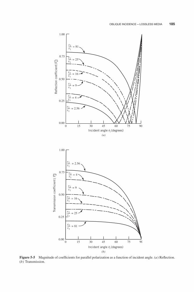
Balanis c05.tex V3 - 11/23/2011 11:47 A.M. Page 185
OBLIQUE INCIDENCE—LOSSLESS MEDIA 185
0.75
0.50
0.25
0.000 15 30 45 60 75 90
1.00
e2e1
= 81
e2e1
= 25
e2e1
= 16
e2e1
= 9
e2e1
= 4
e2e1
= 2.56
Incident angle qi (degrees)(a)
0.75
0.50
0.25
0.000 15 30 45 60 75 90
1.00
Tran
smis
sion
coe
ffic
ient
T
b
e2e1
= 2.56
e2e1
= 16
e2e1
= 25
e2e1
= 81
e2e1
= 9
e2e1
= 4
Incident angle qi (degrees)(b)
Ref
lect
ion
coef
fici
ent
Γb
Figure 5-5 Magnitude of coefficients for parallel polarization as a function of incident angle. (a) Reflection.(b) Transmission.

Balanis c05.tex V3 - 11/23/2011 11:47 A.M. Page 186
186 REFLECTION AND TRANSMISSION
of refraction. One may ask: “For a given set of constitutive parameters of two media formingan interface, is there an incidence angle that allows no reflection, i.e., � = 0?” To answer thiswe need to refer back to the expressions for the reflection coefficients as given by (5-17a) and(5-24c).
A. Perpendicular (Horizontal) Polarization To see the conditions under which the reflectioncoefficient of (5-17a) will vanish, we set it equal to zero, which leads to
�b⊥ =
√μ2
ε2cos θi −
√μ1
ε1cos θt√
μ2
ε2cos θi +
√μ1
ε1cos θt
= 0 (5-27)
or
cos θi =√
μ1
μ2
(ε2
ε1
)cos θt (5-27a)
Using Snell’s law of refraction, as given by (5-15b), (5-27a) can be written as
(1 − sin2 θi ) = μ1
μ2
(ε2
ε1
)(1 − sin2 θt )
(1 − sin2 θi ) = μ1
μ2
(ε2
ε1
)[1 − μ1
μ2
(ε1
ε2
)sin2 θi
](5-28)
or
sin θi =
ε2
ε1−
μ2
μ1μ1
μ2−
μ2
μ1(5-28a)
Since the sine function cannot exceed unity, (5-28a) exists only if
ε2
ε1− μ2
μ1≤ μ1
μ2− μ2
μ1(5-29)
orε2
ε1≤ μ1
μ2(5-29a)
If however μ1 = μ2, (5-28a) indicates that
sin θi |μ1=μ2 = ∞ (5-29b)
Therefore there exists no real angle θi under this condition that will reduce the reflection coeffi-cient to zero. Since the permeability for most dielectric material (aside from ferromagnetics) isalmost the same and equal to that of free space (μ1 � μ2 � μ0), for these materials there existsno real incidence angle that will reduce the reflection coefficient for perpendicular polarizationto zero.

Balanis c05.tex V3 - 11/23/2011 11:47 A.M. Page 187
OBLIQUE INCIDENCE—LOSSLESS MEDIA 187
B. Parallel (Vertical) Polarization To examine the conditions under which the reflectioncoefficient for parallel polarization will vanish, we set (5-24c) equal to zero; that is
�b|| =
−√
μ1
ε1cos θi +
√μ2
ε2cos θt√
μ1
ε1cos θi +
√μ2
ε2cos θt
= 0 (5-30)
or
cos θi =√
μ2
μ1
(ε1
ε2
)cos θt (5-30a)
Using Snell’s law of refraction, as given by (5-24b), (5-30a) can be written as(1 − sin2 θi
) = μ2
μ1
(ε1
ε2
)(1 − sin2 θt )
(1 − sin2 θi ) = μ2
μ1
(ε1
ε2
)[1 − μ1
μ2
(ε1
ε2
)sin2 θi
](5-31)
or
sin θi =
ε2
ε1−
μ2
μ1
−ε2
ε1
ε1
ε2(5-31a)
Since the sine function cannot exceed unity, (5-31a) exists only if
ε2
ε1− μ2
μ1≤ ε2
ε1− ε1
ε2(5-32)
orμ2
μ1≥ ε1
ε2(5-32a)
If, however, μ1 = μ2, (5-31a) reduces to
θi = θB = sin−1
(√ε2
ε1 + ε2
)(5-33)
The incident angle θi , as given by (5-31a) or (5-33), which reduces the reflection coefficientfor parallel polarization to zero, is referred to as the Brewster angle, θB. It should be noted thatwhen μ1 = μ2, the incidence Brewster angle θi = θB of (5-33) exists only if the polarization ofthe wave is parallel (vertical).
Other forms of the Brewster angle, besides that given by (5-33), are
θi = θB = cos−1
(√ε1
ε1 + ε2
)(5-33a)
θi = θB = tan−1
(√ε2
ε1
)(5-33b)
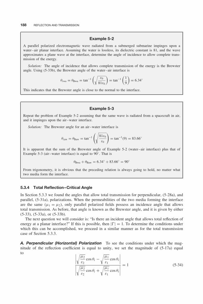
Balanis c05.tex V3 - 11/23/2011 11:47 A.M. Page 188
188 REFLECTION AND TRANSMISSION
Example 5-2
A parallel polarized electromagnetic wave radiated from a submerged submarine impinges upon awater–air planar interface. Assuming the water is lossless, its dielectric constant is 81, and the waveapproximates a plane wave at the interface, determine the angle of incidence to allow complete trans-mission of the energy.
Solution: The angle of incidence that allows complete transmission of the energy is the Brewsterangle. Using (5-33b), the Brewster angle of the water–air interface is
θiwa = θBwa = tan−1(√
ε0
81ε0
)= tan−1
(1
9
)= 6.34◦
This indicates that the Brewster angle is close to the normal to the interface.
Example 5-3
Repeat the problem of Example 5-2 assuming that the same wave is radiated from a spacecraft in air,and it impinges upon the air–water interface.
Solution: The Brewster angle for an air–water interface is
θiaw = θBaw = tan−1
(√81ε0
ε0
)= tan−1(9) = 83.66◦
It is apparent that the sum of the Brewster angle of Example 5-2 (water–air interface) plus that ofExample 5-3 (air–water interface) is equal to 90◦. That is
θBwa + θBaw = 6.34◦ + 83.66◦ = 90◦
From trigonometry, it is obvious that the preceding relation is always going to hold, no matter whattwo media form the interface.
5.3.4 Total Reflection–Critical Angle
In Section 5.3.3 we found the angles that allow total transmission for perpendicular, (5-28a), andparallel, (5-31a), polarizations. When the permeabilities of the two media forming the interfaceare the same (μ1 = μ2), only parallel polarized fields possess an incidence angle that allowstotal transmission. As before, that angle is known as the Brewster angle, and it is given by either(5-33), (5-33a), or (5-33b).
The next question we will consider is: “Is there an incident angle that allows total reflection ofenergy at a planar interface?” If this is possible, then |�| = 1. To determine the conditions underwhich this can be accomplished, we proceed in a similar manner as for the total transmissioncase of Section 5.3.3.
A. Perpendicular (Horizontal) Polarization To see the conditions under which the mag-nitude of the reflection coefficient is equal to unity, we set the magnitude of (5-17a) equalto ∣∣∣∣√μ2
ε2cos θi −
√μ1
ε1cos θt
∣∣∣∣∣∣∣∣√μ2
ε2cos θi +
√μ1
ε1cos θt
∣∣∣∣ = 1 (5-34)

Balanis c05.tex V3 - 11/23/2011 11:47 A.M. Page 189
OBLIQUE INCIDENCE—LOSSLESS MEDIA 189
This is satisfied provided the second term in the numerator and denominator is imaginary. UsingSnell’s law of refraction, as given by (5-15b), the second term in the numerator and denominatorcan be imaginary if
cos θt =√
1 − sin2 θt =√
1 − μ1ε1
μ2ε2sin2 θi = −j
√μ1ε1
μ2ε2sin2 θi − 1 (5-35)
In order for (5-35) to holdμ1ε1
μ2ε2sin2 θi ≥ 1 (5-35a)
or
θi ≥ θc = sin−1
(√μ2ε2
μ1ε1
)(5-35b)
The incident angle θi of (5-35b) that allows total reflection is known as the critical angle. Sincethe argument of the inverse sine function cannot exceed unity, then
μ2ε2 ≤ μ1ε1 (5-35c)
in order for the critical angle (5-35b) to be physically realizable.If the permeabilities of the two media are the same (μ1 = μ2), then (5-35b) reduces to
θi ≥ θc = sin−1
(√ε2
ε1
)(5-36)
which leads to a physically realizable angle provided
ε2 ≤ ε1 (5-36a)
Therefore for two media with identical permeabilities (which is the case for most dielectrics,aside from ferromagnetic material), the critical angle exists only if the wave propagates from amore dense to a less dense medium, as stated by (5-36a).
Example 5-4
A perpendicularly polarized wave radiated from a submerged submarine impinges upon a water–airinterface. Assuming the water is lossless, its dielectric constant is 81, and the wave approximates aplane wave at the interface, determine the angle of incidence that will allow complete reflection of theenergy at the interface.
Solution: The angle of incidence that allows complete reflection of energy is the critical angle. Sincefor water μ2 = μ0, the critical angle is obtained using (5-36), which leads to
θi ≥ θc = sin−1(√
ε0
81ε0
)= 6.38◦
Since there is a large difference between the permittivities of the two media forming the interface, thecritical angle of this example is very nearly the same as the Brewster angle of Example 5-2.

Balanis c05.tex V3 - 11/23/2011 11:47 A.M. Page 190
190 REFLECTION AND TRANSMISSION
The next question we will answer is: “What happens to the angle of refraction and to thepropagation of the wave when the angle of incidence is equal to or greater than the criticalangle?”
When the angle of incidence is equal to the critical angle, the angle of refraction reduces,through Snell’s law of refraction (5-15b) and (5-35b), to
θt = sin−1
(√μ1ε1
μ2ε2sin θi
)∣∣∣∣θi =θc
= sin−1
(√μ1ε1
μ2ε2
√μ2ε2
μ1ε1
)= sin−1(1) = 90◦ (5-37)
In turn the reflection and transmission coefficients reduce to
�b⊥|θi =θc = 1 (5-38a)
T b⊥|θi =θc = 2 (5-38b)
Also the transmitted fields of (5-12a) and (5-12b) can be written as
Et⊥ = ây 2E0e−jβ2x (5-39a)
Ht⊥ = âz
2E0
η2e−jβ2x (5-39b)
which represent a plane wave that travels parallel to the interface in the +x direction as shownin Figure 5-6a . The constant phase planes of the wave are parallel to the z axis. This wave isreferred to as a surface wave [2].
The average power density associated with the transmitted fields is given by
Stav|θi =θc = 1
2Re
(Et
⊥ × Ht∗⊥) ∣∣∣
θi =θc= âx
2|E0|2η2
(5-40)
and it does not contain any component normal to the interface. Therefore, there is no transfer ofreal power across the interface in a direction normal to the boundary; thus, all power must bereflected. This is also evident by examining the magnitude of the incident and reflected averagepower densities associated with the fields (5-10a) through (5-11d) under critical angle incidence.These are obviously identical and are given by
|Siav|θi =θc =
∣∣∣∣1
2Re
(Ei
⊥ × Hi∗⊥)∣∣∣∣
θi =θc
= |E0|22ηi
|âx sin θi + âz cos θi | = |E0|22η1
(5-41a)
|Srav|θi =θc =
∣∣∣∣1
2Re
(Er
⊥ × Hr∗⊥)∣∣∣∣
θi =θc
= |E0|22η1
|âx sin θi − âz cos θi | = |E0|22η1
(5-41b)
When the angle of incidence θi is greater than the critical angle θc(θi > θc), Snell’s law ofrefraction can be written as [3]
sin θt |θi > θc = β1
β2sin θi
∣∣∣∣θi >θc
=√
μ1ε1
μ2ε2sin θi
∣∣∣∣θi > θc
> 1 (5-42a)
which can only be satisfied provided θt is complex, that is, θt = θR + jθX , where θX �= 0. Also
cos θt |θi > θc =√
1 − sin2 θt
∣∣∣θi > θc
=√
1 − μ1ε1
μ2ε2sin2 θi
∣∣∣∣θi >θc
= ±j
√μ1ε1
μ2ε2sin2 θi − 1
∣∣∣∣θi > θc
(5-42b)
which again indicates that θt is complex.

Balanis c05.tex V3 - 11/23/2011 11:47 A.M. Page 191
OBLIQUE INCIDENCE—LOSSLESS MEDIA 191
y z
x
qr qt
qi
Constant phaseplanes
Constant amplitudeplanes
(a)
y z
x
qr
qi
Constantphaseplanes
(b)
Figure 5-6 Constant phase and amplitude planes for incident angles. (a) Critical (θi = θc). (b) Abovecritical (θi >θc).
Therefore when θi > θc , there is no physically realizable angle θt . If not, what really doeshappen to the wave propagation? Since under this condition θt is complex and not physicallyrealizable, this may be a clue that the wave in medium 2 is again a surface wave. To see this, letus examine the field in medium 2, the reflection and transmission coefficients, and the averagepower densities.
When the angle of incidence exceeds the critical angle (θi > θc), the transmitted E field of(5-12a) can be written, using (5-15b) and (5-35b), as
Et⊥|θi > θc = ây T b
⊥E0 exp(−jβ2x sin θt ) exp(−jβ2z cos θt )|θi > θc
= ây T b⊥E0 exp
[−jβ2x
(√μ1ε1
μ2ε2sin θi
)]exp
(−jβ2z
√1 − sin2 θt
)∣∣∣∣θi > θc

Balanis c05.tex V3 - 11/23/2011 11:47 A.M. Page 192
192 REFLECTION AND TRANSMISSION
Et⊥|θi > θc = ây T b
⊥E0 exp
[−jβ2x
(√μ1ε1
μ2ε2sin θi
)]exp
(−jβ2z
√1 − μ1ε1
μ2ε2sin2 θi
)∣∣∣∣θi > θc
= ây T b⊥E0 exp
[−jβ2x
(√μ1ε1
μ2ε2sin θi
)]exp
(−β2z
√μ1ε1
μ2ε2sin2 θi − 1
)∣∣∣∣θi > θc
= ây T b⊥E0 exp
[−β2z
(√μ1ε1
μ2ε2sin2 θi − 1
)]exp
[−jβ2x
(√μ1ε1
μ2ε2sin θi
)]∣∣∣∣θi > θc
Et⊥|θi > θc = ây T b
⊥E0e−αe z e−jβe x (5-43)
where
αe = β2
√μ1ε1
μ2ε2sin2 θi − 1
∣∣∣∣θi > θc
= ω
√μ1ε1 sin2 θi − μ2ε2
∣∣∣∣θi > θc
(5-43a)
βe = β2
√μ1ε1
μ2ε2sin θi
∣∣∣∣θi > θc
= ω√
μ1ε1 sin θi
∣∣θi > θc
(5-43b)
vpe = ω
βe= ω
β2
√μ1ε1
μ2ε2sin θi
∣∣∣∣∣∣∣∣θi >θc
= vp2√μ1ε1
μ2ε2sin θi
∣∣∣∣∣∣∣∣θi >θc
= 1√μ1ε1 sin θi
< vp2 (5-43c)
The wave associated with (5-43) also propagates parallel to the interface with constant phaseplanes that are parallel to the z axis, as shown in Figure 5-6b. The effective phase velocity vpe ofthe wave is given by (5-43c), and it is less than vp2 of an ordinary wave in medium 2. The wavealso possesses constant amplitude planes that are parallel to the x axis, as shown in Figure 5-6b.The effective attenuation constant αe of the wave in the z direction is that given by (5-43a).Its values are such that the wave decays very rapidly, and in a few wavelengths it essentiallyvanishes. This wave is also a surface wave. Since its phase velocity is less than the speed oflight, it is a slow surface wave. Also since it decays very rapidly in a direction normal to theinterface, it is tightly bound to the surface—i.e., it is a tightly bound slow surface wave.
Phase velocities greater than the intrinsic phase velocity of an ordinary plane wave in agiven medium can be achieved by uniform plane waves at real oblique angles of propagation,as illustrated in Section 4.2.2C; phase velocities smaller than the intrinsic velocity can only beachieved by uniform plane waves at complex angles of propagation. Waves traveling at complexangles are nonuniform plane waves oriented so as to provide small phase velocities or large ratesof change of phase in a given direction. The price for such large rates of change of phase orsmall velocities in one direction is associated with large attenuation at perpendicular directions.
Example 5-5
Assume that θi >θc (so the angle of refraction θt = θR + jθX is complex, i.e. θX �= 0). Determine thereal (θR) and imaginary (θX ) parts of θt in terms of the constitutive parameters of the two media andthe angle of incidence.
Solution: Using (5-42a)
sin θt = sin(θR + jθX ) =√
μ1ε1
μ2ε2sin θi

Balanis c05.tex V3 - 11/23/2011 11:47 A.M. Page 193
OBLIQUE INCIDENCE—LOSSLESS MEDIA 193
or
sin(θR) cosh(θX ) + j cos(θR) sinh(θX ) =√
μ1ε1
μ2ε2sin θi
Since the right side is real, then the only solution that exists is for the imaginary part of the left side tovanish and the real part to be equal to the real part of the right side. Thus
cos(θR) sinh(θX ) = 0 ⇒ θR = π
2
sin(θR) cosh(θX ) =√
μ1ε1
μ2ε2sin θi ⇒ θX = cosh−1
(√μ1ε1
μ2ε2sin θi
)In turn cos θt is defined as
cos θt = cos(θR + jθX ) = cos(θR) cosh(θX ) − j sin(θR) sinh(θX )
orcos θt = −j sinh(θX )
which again is shown to be complex as was in (5-42b). When these expressions for sin θt and cos θt areused to represent the fields in medium 2, it will be shown that the fields are nonuniform plane wavesas illustrated by (5-43).
Under the conditions where the angle of incidence is equal to or greater than the critical angle,the reflection �b
⊥ and transmission T b⊥ coefficients of (5-17a) and (5-17b) reduce, respectively, to
[3]
�b⊥|θi ≥θc =
√μ2
ε2cos θi −
√μ1
ε1cos θt√
μ2
ε2cos θi +
√μ1
ε1cos θt
∣∣∣∣∣∣∣∣θi ≥θc
=
√μ2
ε2cos θi −
√μ1
ε1
√1 − sin2 θt√
μ2
ε2cos θi +
√μ1
ε1
√1 − sin2 θt
∣∣∣∣∣∣∣∣θi ≥θc
=
√μ2
ε2cos θi −
√μ1
ε1
√1 − μ1ε1
μ2ε2sin2 θi√
μ2
ε2cos θi +
√μ1
ε1
√1 − μ1ε1
μ2ε2sin2 θi
∣∣∣∣∣∣∣∣θi ≥θc
=
√μ2
ε2cos θi + j
√μ1
ε1
√μ1ε1
μ2ε2sin2 θi − 1√
μ2
ε2cos θi − j
√μ1
ε1
√μ1ε1
μ2ε2sin2 θi − 1
∣∣∣∣∣∣∣∣θi ≥θc
�b⊥|θi ≥θc = |�b
⊥|ej 2ψ⊥ = ej 2ψ⊥ (5-44)
where
|�b⊥| = 1 (5-44a)

Balanis c05.tex V3 - 11/23/2011 11:47 A.M. Page 194
194 REFLECTION AND TRANSMISSION
ψ⊥ = tan−1
[X⊥R⊥
](5-44b)
X⊥ =√
μ1
ε1
√μ1ε1
μ2ε2sin2 θi − 1 (5-44c)
R⊥ =√
μ2
ε2cos θi (5-44d)
T b⊥|θi ≥θc =
2√
μ2
ε2cos θi√
μ2
ε2cos θi +
√μ1
ε1cos θt
∣∣∣∣∣∣∣∣θi ≥θc
=2√
μ2
ε2cos θi√
μ2
ε2cos θi +
√μ1
ε1
√1 − sin2 θt
∣∣∣∣∣∣∣∣θi ≥θc
=2√
μ2
ε2cos θi√
μ2
ε2cos θi +
√μ1
ε1
√1 − μ1ε1
μ2ε2sin2 θi
∣∣∣∣∣∣∣∣θi ≥θc
=2√
μ2
ε2cos θi√
μ2
ε2cos θi − j
√μ1
ε1
√μ1ε1
μ2ε2sin2 θi − 1
∣∣∣∣∣∣∣∣θi ≥θc
T b⊥|θi ≥θc = |T b
⊥|ejψ⊥ (5-45)
where
|T b⊥| = 2R⊥√
R2⊥ + X 2
⊥(5-45a)
In addition, the transmitted average power density can now be written, using (5-12a) through(5-12b) and the modified forms (5-43) through (5-43b) for the fields when the incidence angle isequal to or greater than the critical angle, as
Stav|θi ≥θc = 1
2Re(Et × Ht∗)θi ≥θc
= 1
2Re
[(ây T b
⊥E0e−αe z e−jβe x)×(−âx cos θt +âz sin θt )
∗ (T b⊥)∗E ∗
0
η2e−αe z e+jβe x
]θi ≥θc
= 1
2Re
{[âz (cos θt )
∗ + âx (sin θt )∗] |T b
⊥|2|E0|2η2
e−2αe z
}θi ≥θc
Stav|θi ≥θc = 1
2Re
{[âz
(√1 − sin2 θt
)∗+ âx (sin θt )
∗] |T b
⊥|2|E0|2η2
e−2αe z
}θi ≥θc

Balanis c05.tex V3 - 11/23/2011 11:47 A.M. Page 195
OBLIQUE INCIDENCE—LOSSLESS MEDIA 195
Stav|θi ≥θc = 1
2Re
{[âz
(√1 − μ1ε1
μ2ε2sin2 θi
)∗
+âx
(√μ1ε1
μ2ε2sin θi
)∗] |T b⊥|2|E0|2
η2e−2αe z
}θi ≥θc
= 1
2Re
{[âz
(−j
√μ1ε1
μ2ε2sin2 θi − 1
)+âx
(√μ1ε1
μ2ε2sin θi
)] |T b⊥|2|E0|2
η2e−2αe z
}θi ≥θc
Stav|θi ≥θc = âx
√μ1ε1
μ2ε2sin θi
|T b⊥|2|E0|2
2η2e−2αe z
∣∣∣∣θi ≥θc
(5-46)
Again, from (5-46), it is apparent that there is no real power transfer across the interface ina direction normal to the boundary. Therefore all the power must be reflected into medium 1.This can also be verified by formulating and examining the incident and reflected average powerdensities. Doing this, using the fields (5-10a) through (5-11b) where the reflection coefficient isthat of (5-44), shows that the magnitudes of the incident and reflected average power densitiesare those of (5-41a) and (5-41b), which are identical.
The propagation of a wave from a medium with higher density to one with lower density(ε2 < ε1 when μ1 = μ2) under oblique incidence can be summarized as follows.
1. When the angle of incidence is smaller than the critical angle (θi < θc = sin−1(√
ε2/ε1)),a wave is transmitted into medium 2 at an angle θt , which is greater than the incident angleθi . Real power is transferred into medium 2, and it is directed along angle θt as shown inFigure 5-7a .
2. As the angle of incidence increases and reaches the critical angle θi = θc = sin−1(√
ε2/ε1),the refracted angle θt , which varies more rapidly than the incident angle θi , approaches90◦. Although a wave into medium 2 exists under this condition (which is necessary tosatisfy the boundary conditions), the fields form a surface wave that is directed along thex axis (which is parallel to the interface). There is no real power transfer normal to theboundary into medium 2, and all the power is reflected in medium 1 along reflected angleθr as shown in Figure 5-7b. The constant phase planes are parallel to the z axis.
3. When the incident angle θi exceeds the critical angle θc[θi > θc = sin−1(√
ε2/ε1)], a waveinto medium 2 still exists, which travels along the x axis (which is parallel to the interface)and is heavily attenuated in the z direction (which is normal to the interface). There is noreal power transfer normal to the boundary into medium 2, and all power is reflected intomedium 1 along reflection angle θr , as shown in Figure 5-7c. Although there is no powertransferred into medium 2, a wave exists there that is necessary to satisfy the boundaryconditions on the continuity of the tangential components of the electric and magnetic fields.The wave in medium 2 travels parallel to the interface with a phase velocity that is lessthan that of an ordinary wave in the same medium [as given by (5-43c)], and it is rapidlyattenuated in a direction normal to the interface with an effective attenuation constant givenby (5-43a). This wave is tightly bound to the surface, and it is referred to as a tightly boundslow surface wave.
The critical angle is used to design many practical instruments and transmission lines, such asbinoculars, dielectric covered ground plane (surface wave) transmission lines, fiber optic cables,etc. To see how the critical angle may be utilized, let us consider an example.
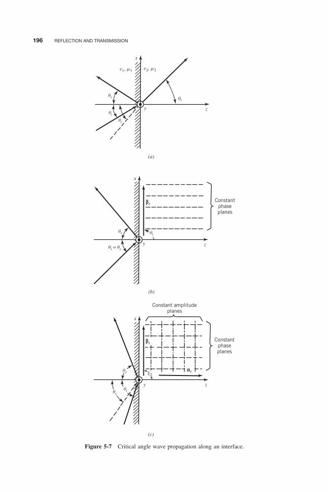
Balanis c05.tex V3 - 11/23/2011 11:47 A.M. Page 196
196 REFLECTION AND TRANSMISSION
y z
x
qr qt
Constantphaseplanes
Constant amplitudeplanes
(b)
y z
x
qr
qcqi
Constant phaseplanes
(c)
qi = qc
βe
y z
x
qtqr
qi
qc
(a)
βe
x2αe
e1, m1 e2, m2
Figure 5-7 Critical angle wave propagation along an interface.
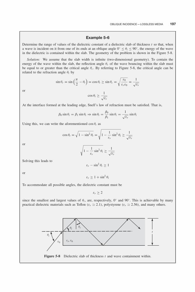
Balanis c05.tex V3 - 11/23/2011 11:47 A.M. Page 197
OBLIQUE INCIDENCE—LOSSLESS MEDIA 197
Example 5-6
Determine the range of values of the dielectric constant of a dielectric slab of thickness t so that, whena wave is incident on it from one of its ends at an oblique angle 0◦ ≤ θi ≤ 90◦, the energy of the wavein the dielectric is contained within the slab. The geometry of the problem is shown in the Figure 5-8.
Solution: We assume that the slab width is infinite (two-dimensional geometry). To contain theenergy of the wave within the slab, the reflection angle θr of the wave bouncing within the slab mustbe equal to or greater than the critical angle θc . By referring to Figure 5-8, the critical angle can berelated to the refraction angle θt by
sin θr = sin(π
2− θt
)= cos θt ≥ sin θc =
√ε0
εrε0= 1√
εr
orcos θt ≥ 1√
εr
At the interface formed at the leading edge, Snell’s law of refraction must be satisfied. That is,
β0 sin θi = β1 sin θt ⇒ sin θt = β0
β1sin θi = 1√
εrsin θi
Using this, we can write the aforementioned cos θt as
cos θt =√
1 − sin2 θt =√
1 − 1
εrsin2 θi ≥ 1√
εr
or √1 − 1
εrsin2 θi ≥ 1√
εr
Solving this leads toεr − sin2 θi ≥ 1
orεr ≥ 1 + sin2 θi
To accommodate all possible angles, the dielectric constant must be
εr ≥ 2
since the smallest and largest values of θi , are, respectively, 0◦ and 90◦. This is achievable by manypractical dielectric materials such as Teflon (εr � 2.1), polystyrene (εr � 2.56), and many others.
er, e0e0
tqi
qtqr
Figure 5-8 Dielectric slab of thickness t and wave containment within.

Balanis c05.tex V3 - 11/23/2011 11:47 A.M. Page 198
198 REFLECTION AND TRANSMISSION
B. Parallel (Vertical) Polarization The procedure used to derive the critical angle and toexamine the properties for perpendicular (horizontal) polarization can be repeated for parallel(vertical) polarization. However, it can be shown that the critical angle is not a function ofpolarization, and that it exists for both parallel and perpendicular polarizations. The only limitationof the critical angle is that the wave propagation be to a less dense medium (μ2ε2 < μ1ε1 orε2 < ε1 when μ1 = μ2).
The expression for the critical angle for parallel polarization is the same as that for perpendic-ular polarization as given by (5-35b) or (5-36). In addition, the wave propagation phenomena thatoccur for perpendicular polarization when the incidence angle is less than, equal to, or greaterthan the critical angle are also identical to those for parallel polarization. Although the formulasfor the reflection and transmission coefficients, �b
|| and T b|| respectively, and transmitted average
power density St|| for parallel polarization are not identical to those of perpendicular polarization
as given by (5-44) through (5-46), the principles stated previously are identical here. The deriva-tion of the specific formulas for the parallel polarization for critical angle propagation are left asan end-of-chapter exercise for the reader.
5.4 LOSSY MEDIA
In the previous sections we examined wave reflection and transmission under normal and obliquewave incidence when both media forming the interface are lossless. Let us now examine thereflection and transmission of waves under normal and oblique incidence when either one or bothmedia are lossy [4]. Although in some cases the formulas will be the same as for the losslesscases, there are differences, especially under oblique wave incidence.
5.4.1 Normal Incidence: Conductor–Conductor Interface
When a uniform plane wave is normally incident upon a planar interface formed by two lossymedia (as shown in Figure 5-1 but allowing for losses in both media through the conductivity σ ),the incident, reflected, and transmitted fields, reflection and transmission coefficients, and averagepower densities are identical to (5-1a) through (5-6c) except that (a) an attenuation constant mustbe included in each field and (b) the intrinsic impedances, and attenuation and phases constantsmust be modified to include the conductivities of the media. Thus we can summarize the resultshere as
Ei = âx E0e−α1z e−jβ1z (5-47a)
Hi = âyE0
η1e−α1z e−jβ1z (5-47b)
Er = âx�bE0e+α1z e+jβ1z (5-48a)
Hr = −ây�bE0
η1e+α1z e+jβ1z (5-48b)
Et = âx T bE0e−α2z e−jβ2z (5-49a)
Ht = âyT bE0
η2e−α2z e−jβ2z (5-49b)
�b = η2 − η1
η2 + η1(5-50a)
Balanis c05.tex V3 - 11/23/2011 11:47 A.M. Page 199
LOSSY MEDIA 199
T b = 2η2
η2 + η1(5-50b)
Siav = âz
|E0|22
e−2α1z Re
(1
η∗1
)(5-51a)
Srav = −âz |�b |2 |E0|2
2e+2α1z Re
(1
η∗1
)(5-51b)
Stav = âz |T b |2 |E0|2
2e−2α2z Re
(1
η∗2
)(5-51c)
For each lossy medium the attenuation constants αi , phase constants βi , and intrinsic impedancesηi are related to the corresponding constitutive parameters εi , μi , and σi , by the expressions inTable 4-1.
The total electric and magnetic fields in medium 1 can be written as
E1 = Ei + Er = âx E0e−α1z e−jβ1z︸ ︷︷ ︸traveling wave
(1 + �be+2α1z e+j 2β1z )︸ ︷︷ ︸standing wave
(5-52a)
H1 = Hi + Hr = ây (E0/η1)e−α1z e−jβ1z︸ ︷︷ ︸
traveling wave
(1 − �be+2α1z e+j 2β1z )︸ ︷︷ ︸standing wave
(5-52b)
In each field the factors outside the parentheses form the traveling wave part of the total wave;those within the parentheses form the standing wave part .
Example 5-7
A uniform plane wave, whose incident electric field has an x component with an amplitude at theinterface of 10−3 V/m, is traveling in a free-space medium and is normally incident upon a lossy flatearth as shown in Figure 5-9. Assuming that the constitutive parameters of the earth are ε2 = 9ε0,μ2 = μ0 and σ2 = 10−1 S/m, determine the variation of the conduction current density in the earth at afrequency of 1 MHz.
Solution: At f = 106 Hz
σ2
ωε2= 10−1
2π × 106(9 × 10⁻⁹/36π)= 2 × 10² � 1
which classifies the material as a very good conductor.On either side of the interface, the total electric field is equal to
Etotal|z=0 = âx × 10−3|1 + �b |where
�b = η2 − η1
η2 + η1= η2 − η0
η2 + η0
η2 �√
ωμ
2σ(1 + j ) =
√2π × 106(4π × 10−7)
2 × 10⁻¹(1 + j ) = 2π(1 + j )

Balanis c05.tex V3 - 11/23/2011 11:47 A.M. Page 200
200 REFLECTION AND TRANSMISSION
Incident
Reflected
Hy
Γb
Ex
y
z
x
Jc
J0
e2 = 9e0, m2 = m0
s2 = 10−1 S/m
d
d
J = J0e−z/d
Figure 5-9 Electric and magnetic field intensities, and electric current density distributions in a lossyearth.
Thus
�b = 2π(1 + j ) − 377
2π(1 + j ) + 377= −370.72 + j 2π
383.28 + j 2π
= 370.77/
179.04◦
383.33/
0.94◦ = 0.967/
178.1◦
and
Etotal|z=0 = âx × 10−3|1 + 0.967/
178.1◦|= âx × 10−3|0.0335 + j 0.0321| = âx (4.64 × 10⁻⁵)
The conduction current density at the surface of the earth is equal to
Jc |z=0 = âx J0 = âx σE total|z=0 = âx × 10−1(4.64 × 10⁻⁵)
= âx (4.64 × 10⁻⁶)
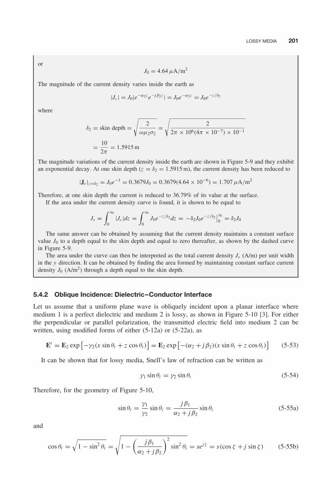
Balanis c05.tex V3 - 11/23/2011 11:47 A.M. Page 201
LOSSY MEDIA 201
orJ0 = 4.64 μA/m2
The magnitude of the current density varies inside the earth as
|Jc | = J0|e−α2z e−jβ2z | = J0e−α2z = J0e−z/δ2
where
δ2 = skin depth =√
2
ωμ2σ2=
√2
2π × 106(4π × 10−7) × 10−1
= 10
2π= 1.5915 m
The magnitude variations of the current density inside the earth are shown in Figure 5-9 and they exhibitan exponential decay. At one skin depth (z = δ2 = 1.5915 m), the current density has been reduced to
|Jc |z=δ2 = J0e−1 = 0.3679J0 = 0.3679(4.64 × 10⁻⁶) = 1.707 μA/m2
Therefore, at one skin depth the current is reduced to 36.79% of its value at the surface.If the area under the current density curve is found, it is shown to be equal to
Js =∫ ∞
0|Jc |dz =
∫ ∞
0J0e−z/δ2 dz = −δ2J0e−z/δ2
∣∣∞0 = δ2J0
The same answer can be obtained by assuming that the current density maintains a constant surfacevalue J0 to a depth equal to the skin depth and equal to zero thereafter, as shown by the dashed curvein Figure 5-9.
The area under the curve can then be interpreted as the total current density Js (A/m) per unit widthin the y direction. It can be obtained by finding the area formed by maintaining constant surface currentdensity J0 (A/m2) through a depth equal to the skin depth.
5.4.2 Oblique Incidence: Dielectric–Conductor Interface
Let us assume that a uniform plane wave is obliquely incident upon a planar interface wheremedium 1 is a perfect dielectric and medium 2 is lossy, as shown in Figure 5-10 [3]. For eitherthe perpendicular or parallel polarization, the transmitted electric field into medium 2 can bewritten, using modified forms of either (5-12a) or (5-22a), as
Et = E2 exp[−γ2(x sin θt + z cos θt )
] = E2 exp[−(α2 + jβ2)(x sin θt + z cos θt )
](5-53)
It can be shown that for lossy media, Snell’s law of refraction can be written as
γ1 sin θi = γ2 sin θt (5-54)
Therefore, for the geometry of Figure 5-10,
sin θt = γ1
γ2sin θi = jβ1
α2 + jβ2sin θi (5-55a)
and
cos θt =√
1 − sin2 θt =√
1 −(
jβ1
α2 + jβ2
)2
sin2 θi = sejζ = s(cos ζ + j sin ζ ) (5-55b)
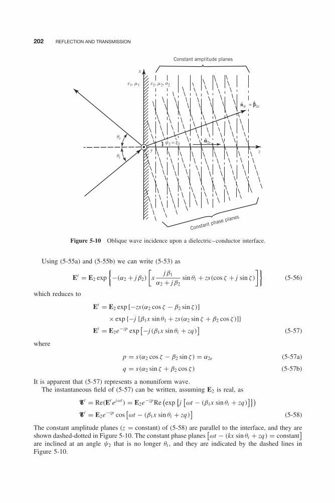
Balanis c05.tex V3 - 11/23/2011 11:47 A.M. Page 202
202 REFLECTION AND TRANSMISSION
e1, m1 e2, m2, s2
y2 = x2α2e
x
zy
Constant phase planes
qi
qr
Constant amplitude planes
ny = β2e
Figure 5-10 Oblique wave incidence upon a dielectric–conductor interface.
Using (5-55a) and (5-55b) we can write (5-53) as
Et = E2 exp
{−(α2 + jβ2)
[x
jβ1
α2 + jβ2sin θi + zs(cos ζ + j sin ζ )
]}(5-56)
which reduces to
Et = E2 exp [−zs(α2 cos ζ − β2 sin ζ )]
× exp {−j [β1x sin θ1 + zs(α2 sin ζ + β2 cos ζ )]}Et = E2e−zp exp
[−j (β1x sin θi + zq)]
(5-57)
where
p = s(α2 cos ζ − β2 sin ζ ) = α2e (5-57a)
q = s(α2 sin ζ + β2 cos ζ ) (5-57b)
It is apparent that (5-57) represents a nonuniform wave.The instantaneous field of (5-57) can be written, assuming E2 is real, as
�t = Re(Et ejωt ) = E2e−zpRe(exp
{j[ωt − (β1x sin θi + zq)
]})�t = E2e−zp cos
[ωt − (β1x sin θi + zq)
](5-58)
The constant amplitude planes (z = constant) of (5-58) are parallel to the interface, and they areshown dashed-dotted in Figure 5-10. The constant phase planes
[ωt − (kx sin θi + zq) = constant
]are inclined at an angle ψ2 that is no longer θt , and they are indicated by the dashed lines inFigure 5-10.
Balanis c05.tex V3 - 11/23/2011 11:47 A.M. Page 203
LOSSY MEDIA 203
To determine the constant phase we write the argument of the exponential or of the cosinefunction in (5-58) as
ωt − (β1x sin θi + zq) = ωt −√
(β1 sin θi )2 + q2
×[
(β1 sin θi )x√(β1 sin θi )2 + q2
+ qz√(β1 sin θi )2 + q2
](5-59)
If we define an angle ψ2 such that
u = β1 sin θi (5-60a)
sin ψ2 = β1 sin θi√(β1 sin θi )2 + q2
= u√u2 + q2
(5-60b)
cos ψ2 = q√(β1 sin θi )2 + q2
= q√u2 + q2
(5-60c)
or
ψ2 = tan−1
(β1 sin θi
q
)= tan−1
(u
q
)(5-60d)
we can write (5-59), and in turn (5-58), as
�t = E2e−zpRe
(exp
{j
[ωt −
√u2 + q2
(ux√
u2 + q2+ qz√
u2 + q2
)]})= E2e−zpRe (exp {j [ωt − β2e(x sin ψ2 + z cos ψ2)]})
�t = E2e−zpRe(exp
{j[ωt − β2e(n̂ψ • r)
]})(5-61)
where
n̂ψ = âx sin ψ2 + âz cos ψ2 (5-61a)
β2e =√
u2 + q2 (5-61b)
It is apparent from (5-60a) through (5-61a) that
1. The true angle of refraction is ψ2 and not θt (θt is complex).2. The wave travels along a direction defined by unit vector n̂ψ .3. The constant phase planes are perpendicular to unit vector n̂ψ , and they are shown as
dashed lines in Figure 5-10.
The phase velocity of the wave in medium 2 is obtained by setting the exponent of (5-61) toa constant and differentiating it with respect to time. Doing this, we can write the phase velocityvp of the wave as
ω(1) −√
u2 + q2
(n̂ψ •
drdt
)= 0
ω(1) −√
u2 + q2
(n̂ψ •
drdt
)= ω − β2e(n̂ψ • vp) = 0 (5-62)
orvpr = ω
β2e= ω√
u2 + q2= ω√
(β1 sin θi )2 + q2(5-62a)
It is evident that the phase velocity is a function of the incidence angle θi and the constitutiveparameters of the two media.

Balanis c05.tex V3 - 11/23/2011 11:47 A.M. Page 204
204 REFLECTION AND TRANSMISSION
Example 5-8
A plane wave of either perpendicular or parallel polarization traveling in air is obliquely incident upona planar interface of copper (σ = 5.76 × 10⁷ S/m). At a frequency of 10 GHz, determine the angle ofrefraction and reflection coefficients for each of the two polarizations.
Solution: For copper
σ2
ωε2= 5.8 × 10⁷(36π)
(2π × 1010) × 10−9= 1.037 × 10⁸ � 1
Therefore according to Table 4-1
α2 � β2 �√
ωμ2σ2
2
Using (5-55a)
sin θt = jβ1
α2 + jβ2sin θi � jβ1√
ωμ2σ2
2(1 + j )
sin θtσ2�1� 0 ⇒ θi � 0
Therefore (5-55b), (5-57a), and (5-57b) reduce to
cos θt = 1 = sejζ ⇒ s = 1 ζ = 0
p = s(α2 cos ζ − β2 sin ζ ) � α2 =√
ωμ2σ2
2
q = s(α2 sin ζ + β2 cos ζ ) � β2 =√
ωμ2σ2
2
Using (5-60d), the true angle of refraction is
ψ2 = tan−1(
u
q
)� tan−1
(β1 sin θi
β2
)= tan−1
⎛⎜⎜⎝ ω√
μ0ε0√ωμ0σ2
2
sin θi
⎞⎟⎟⎠= tan−1
(√2ωε0
σ2sin θi
)≤ tan−1
(√2ωε0
σ2
)= tan−1(0.139 × 10⁻³)
ψ2 = tan−1(0.139 × 10⁻³ sin θi ) ≤ 0.139 × 10⁻³ rad = (7.96 × 10⁻³)◦
Using (5-17a) and (5-24c), the reflection coefficients for perpendicular and parallel polarizations reduceto
�b⊥ = η2 cos θi − η1 cos θt
η2 cos θi + η1 cos θt� η2 cos θi − η1
η2 cos θi + η1= cos θi − η1/η2
cos θi + η1/η2
�b|| = −η1 cos θi + η2 cos θt
η1 cos θi + η2 cos θt� −η1 cos θi + η2
η1 cos θi + η2= − cos θi + η2/η1
cos θi + η2/η1
Since
η1
η2=
√μ1
ε1√jωμ2
σ2 + jωε2
�
√μ0
ε0√jωμ0
σ2
=√
σ2
jωε0

Balanis c05.tex V3 - 11/23/2011 11:47 A.M. Page 205
REFLECTION AND TRANSMISSION OF MULTIPLE INTERFACES 205
η1
η2� 1.02 × 10⁴e−jπ/4 � 1 ≥ cos θi
Then
�b⊥ � cos θi − η1/η2
cos θi + η1/η2� −1
�b|| � − cos θi + η2/η1
cos θi + η2/η1� −1
Thus for a very good conductor, such as copper, the angle of refraction approaches zero and themagnitude of the reflection coefficients for perpendicular and parallel polarizations approach unity, andthey are all essentially independent of the angle of incidence. The same will be true for all other goodconductors.
5.4.3 Oblique Incidence: Conductor–Conductor Interface
In Section 5.3.4 it was shown that when a uniform plane wave is incident upon adielectric–dielectric planar interface at an incidence angle θi equal to or greater than the criticalangle θc , the transmitted wave produced into medium 2 is a nonuniform plane wave. Forthis plane wave, the constant amplitude planes (which are perpendicular to the α2e vector) ofFigure 5-7 are perpendicular to the constant phase planes (which are perpendicular to the β2e
vector), or the angle ξ2 between the α2e and β2e vectors is 90◦.In Section 5.4.2 it was demonstrated that a uniform plane wave traveling in a lossless medium
and obliquely incident upon a lossy medium also produces a nonuniform plane wave where theangle ξ2 between the α2e and β2e vectors in Figure 5-10 is greater than 0◦ but less than 90◦.In fact, for a very good conductor the angle ξ2 between α2e and β2e is almost zero [for copperwith σ = 5.76 × 10⁷ S/m, ξ2 ≤ (8 × 10⁻³)◦]. As the conducting medium becomes less lossy, theangle ξ2 increases and in the limit it approaches 90◦ for a lossless medium. In fact for all losslessmedia, the angle between the effective attenuation constant α2e and phase constant β2e shouldalways be 90◦, with reactive power flowing along α2e and positive real power along β2e [4]. Thisis necessary since there are no real losses associated with the wave propagation along β2e . Thiswas well illustrated in Section 5.3.4 for the nonuniform wave produced in a lossless mediumwhen the incidence angle was equal to or greater than the critical angle.
It is very interesting to investigate the field characteristics of uniform or nonuniform planewaves that are obliquely incident upon interfaces comprised of lossy–lossy interfaces. These typesof waves have been examined [5–6], but, because of the general complexity of the formulations,they will not be repeated here. The reader is referred to the literature. An excellent discussionof uniform and nonuniform plane waves propagating in lossless and lossy media and associatedinterfaces is found in Chapters 7 and 8 of [4].
5.5 REFLECTION AND TRANSMISSION OF MULTIPLE INTERFACES
Many applications require dielectric interfaces that exhibit specific characteristics as a functionof frequency. Accomplishing this often requires multiple interfaces. The objective of this sectionis to analyze the characteristics of multiple layer interfaces. To reduce the complexity of theproblem, we will consider only normal incidence and restrict most of our attention to losslessmedia. A general formulation for lossy media will also be stated.

Balanis c05.tex V3 - 11/23/2011 11:47 A.M. Page 206
206 REFLECTION AND TRANSMISSION
5.5.1 Reflection Coefficient of a Single Slab Layer
Section 5.2 showed that for normal incidence the reflection coefficient �b at the boundary of asingle planar interface is given by (5-4a) or
�b = η2 − η1
η2 + η1(5-63)
and at a distance z = −� from the boundary it is given by (5-5a) or
�in(z = −�) = �be−j 2β1� (5-64)
Just to the right of the boundary the input impedance in the +z direction is equal to theintrinsic impedance η2 of medium 2, that is,
Zin(z = 0+) = η2 =√
μ2
ε2(5-65)
The input impedance at z = −� can be found by using the field expressions (5-1a) through (5-2c).By definition Zin(z = −�) is equal to
Zin|z=−� = E total|z=−�
H total|z=−�
(5-66)
where
E total|z=−� = (E i + E r )|z=−� = E0e+jβ1�(1 + �be−j 2β1�) = E0e+jβ1� [1 + �in(�)]
(5-66a)
H total|z=−� = (H i − H r )|z=−� = E0
η1e+jβ1�(1 − �be−j 2β1�) = E0
η1e+jβ1� [1 − �in(�)]
(5-66b)
Therefore
Zin|z=−� = η1
(1 + �be−j 2β1�
1 − �be−jβ1�
)= η1
(1 + �in(�)
1 − �in(�)
)(5-66c)
which by using (5-63) can also be written as
Zin|z=−� = η1
(1 + �be−j 2β1�
1 − �be−j 2β1�
)= η1
(1 + �in(�)
1 − �in(�)
)= η1
(η2 + jη1 tan(β1�)
η1 + jη2 tan(β1�)
)(5-66d)
Equation 5-66d is analogous to the well-known impedance transfer equation that is widely usedin transmission line theory [7].
Using the foregoing procedure for normal wave incidence, we can derive expressions formultiple layer interfaces [8]. Referring to Figure 5-11a the input impedance at z = 0+ is equalto the intrinsic impedance η3 of medium 3, that is
Zin(z = 0+) = η3 (5-67)
In turn, the input reflection coefficient at the same interface can be written as
�in(z = 0−) = Zin(0+) − η2
Zin(0+) + η2= η3 − η2
η3 + η2(5-67a)
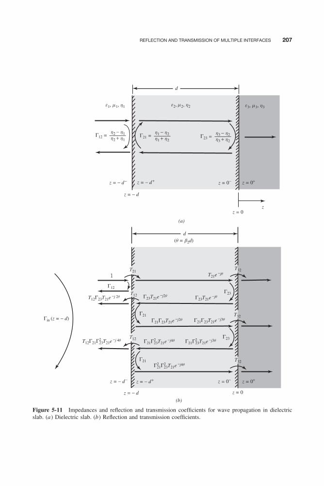
Balanis c05.tex V3 - 11/23/2011 11:47 A.M. Page 207
REFLECTION AND TRANSMISSION OF MULTIPLE INTERFACES 207
z = − d−
z = − d
z = − d+
z = − d−
z = − d
z = − d+
z = 0+z = 0−
z = 0+z = 0−
z = 0
z = 0
(q = b2d)
z
d
Γ12 =
e1, m1, h1 e2, m2, h2 e3, m3, h3
h2 − h1 h2 + h1 Γ21 =
h1 − h2h1 + h2
Γ23 = h3 − h2 h3 + h2
(a)
1
d
(b)
T12Γ23T21e −j 2q
T12Γ21Γ223T21e −j 4q
Γ12
T21e −jq
Γ23T21e −jqΓ23T21e −j2q
Γin (z = − d) Γ21Γ23T21e −j2q Γ21Γ23T21e −j3q
Γ21
Γ21Γ223T21e −j3qΓ21Γ2
23T21e −j4q
Γ221Γ2
23T21e −j4q
Γ21
Γ23
Γ23
T12
T32
T32
T32
T12
T21
Figure 5-11 Impedances and reflection and transmission coefficients for wave propagation in dielectricslab. (a) Dielectric slab. (b) Reflection and transmission coefficients.
Balanis c05.tex V3 - 11/23/2011 11:47 A.M. Page 208
208 REFLECTION AND TRANSMISSION
At z = −d+ the input impedance can be written using (5-66d) as
Zin(z = −d+) = η2
(1 + �in(z = 0−)e−j 2β2d
1 − �in(z = 0−)e−j 2β2d
)= η2
((η3 + η2) + (η3 − η2)e−j 2β2d
(η3 + η2) − (η3 − η2)e−j 2β2d
)(5-67b)
and the input reflection coefficient at z = −d− can be expressed as
�in(z = −d−) = Zin(z = −d+) − η1
Zin(z = −d+) + η1
= η2[(η3 + η2) + (η3 − η2)e−j 2β2d
] − η1[(η3 + η2) − (η3 − η2)e−j 2β2d
]η2
[(η3 + η2) + (η3 − η2)e−j 2β2d
] + η1[(η3 + η2) − (η3 − η2)e−j 2β2d
](5-67c)
In Figure 5-11a we have defined individual reflection coefficients at each of the boundaries.Here these coefficients are referred to as intrinsic reflection coefficients, and they would exist ateach boundary if two semi-infinite media form each of the boundaries (neglecting the presenceof the other boundaries). Using the intrinsic reflection coefficients defined in Figure 5-11a , theinput reflection coefficient of (5-67c) can also be written as
�in(z = −d−) = �12 + �23e−j 2β2d
1 + �12�23e−j 2β2d(5-67d)
Equation 5-67d can also be derived using the ray-tracing model of Figure 5-11b. At the leadinginterface of Figure 5-11b, �12 represents the intrinsic reflection coefficient of the initial reflectionand T12�23T21e−j 2θ , etc., are the contributions to the input reflection due to the multiple bounceswithin the medium 2 slab. The total input reflection coefficient can be written as a geometricseries that takes the form
�in(z = −d−) = �12 + T12�23T21e−j 2θ + T12�21�223T21e−j 4θ + . . .
�in(z = −d−) = �12 + T12�23T21e−j 2θ [1 + �21�23e−j 2θ + (�21�23e−j 2θ )2 + . . .]
�in(z = −d−) = �12 + T12T21�23e−j 2θ
1 − �21�23e−j 2θ(5-68)
whereθ = β2d (5-68a)
Since according to (5-4a) and (5-4b)
�21 = −�12 (5-69a)
T12 = 1 + �21 = 1 − �12 (5-69b)
T21 = 1 + �12 (5-69c)
(5-68) can be rewritten and reduced to the form of (5-67d).If the magnitudes of the intrinsic reflection coefficients |�12| and |�23| are low compared to
unity, (5-67d) can be approximated by the numerator
�in(z = −d−) = �12 + �23e−j 2β2d
1 + �12�23e−j 2β2d
|�12|�1�|�23|�1
�12 + �23e−j 2β2d (5-70)

Balanis c05.tex V3 - 11/23/2011 11:47 A.M. Page 209
REFLECTION AND TRANSMISSION OF MULTIPLE INTERFACES 209
The approximate form of (5-70) yields good results if the individual intrinsic reflection coefficientsare low. Typically when |�12| = |�23| ≤ 0.2, the error of the approximate form of (5-70) isequal to or less than about 4 percent. The approximate form of (5-70) will be very convenientfor representing the input reflection coefficient of multiple interfaces (> 2) when the individualintrinsic reflection coefficients at each interface are low compared to unity.
Example 5-9
A uniform plane wave at a frequency of 10 GHz is incident normally on a dielectric slab of thicknessd and bounded on both sides by air. Assume that the dielectric constant of the slab is 2.56.
1. Determine the thickness of the slab so that the input reflection coefficient at 10 GHz is zero.2. Plot the magnitude of the reflection coefficient as a function of frequency between
5 GHz ≤ f ≤ 15 GHz when the dielectric slab has a thickness of 0.9375 cm.
Solution:
1. For the input reflection coefficient to be equal to zero, the reflection coefficient of (5-70) must beset equal to zero. This can be accomplished if
|�12 + �23e−j 2β2d | = 0
Since�23 = −�12 = η1 − η2
η1 + η2
then|�12||1 − e−j 2β2d | = 0 ⇒ 2β2d = 2nπ n = 0, 1, 2, . . .
For nontrivial solutions, the thickness must be
d = nπ
β2= η
2λ2 n = 1, 2, 3, . . .
where λ2 is the wavelength inside the dielectric slab. Thus the thickness of the slab must be anintegral number of half wavelengths inside the dielectric. At a frequency of 10 GHz and a dielectricconstant of 2.56, the wavelength inside the dielectric is
λ2 = 30 × 109
10 × 109√
2.56= 1.875 cm
2. At a frequency of 5 GHz, the dielectric slab of thickness 0.9375 cm is equal to
d = 0.9375√
2.56λ2
30 × 109/5 × 109= 0.25λ2 ⇒ 2β2d = 4π
λ2
(λ2
4
)= π
and at 15 GHz it is equal to
d = 0.9375√
2.56λ2
30 × 109/15 × 109= 0.75λ2 ⇒ 2β2d = 4π
λ2
(3λ2
4
)= 3π
Since
�12 = −�23 = η2 − η1
η2 + η1= η2/η1 − 1
η2/η1 + 1= 1 − √
εr
1 + √εr
= −0.6
2.6= −0.231

Balanis c05.tex V3 - 11/23/2011 11:47 A.M. Page 210
210 REFLECTION AND TRANSMISSION
the input reflection coefficient of (5-70), at f = 5 and 15 GHz, achieves the maximum magnitudeof
|�in(z = −d−)| =∣∣∣∣ −0.231 − 0.231
1 − (−0.231)(0.231)
∣∣∣∣ = 2(0.231)
1 + (0.231)2= 0.438
A complete plot of |�in(z = −d−)| for 5 GHz ≤ f ≤ 15 GHz is shown in the Figure 5-12.Using the approximate form of (5-70), the magnitude of the input reflection coefficient is equal
to|�in(z = −d−)| f =5,
15 GHz� | − 0.231 − (0.231)| = 0.462
The percent error of this is
percent error =(−0.438 + 0.462
0.438
)× 100 = 5.48
0.5
0.4
0.3
0.2
0.1
05 7 9 11 13 15
Inpu
t re
flec
tion
coe
ffic
ient
Γ i
n
Frequency (GHz)
Figure 5-12 Input reflection coefficient, as a function of frequency, for wave propagation through adielectric slab.
Example 5-10
A uniform plane wave is incident normally upon a dielectric slab whose thickness at f0 = 10 GHz isλ20/4 where λ20 is the wavelength in the dielectric slab. The slab is bounded on the left side by air andon the right side by a semi-infinite medium of dielectric constant εr3 = 4.
1. Determine the intrinsic impedance η2 and dielectric constant εr2 of the sandwiched slab so thatthe input reflection coefficient at f0 = 10 GHz is zero.
2. Plot the magnitude response of the input reflection coefficient for 0 ≤ f ≤ 20 GHz when theintrinsic impedance and physical thickness of the slab are those found in part 1.
3. Using the ray-tracing model of Figure 5-11b, at f0 = 10 GHz determine the first and next twohigher-order terms that contribute to the overall input reflection coefficient. What is the inputreflection coefficient using these three terms?
Solution:
1. In order for the input reflection coefficient to vanish, the magnitude of (5-70) must be equal tozero, that is
|�12 + �23e−j 2β2d | = 0
Balanis c05.tex V3 - 11/23/2011 11:47 A.M. Page 211
REFLECTION AND TRANSMISSION OF MULTIPLE INTERFACES 211
Since at f0 = 10 GHz, d = λ20/4, then
2β2d |f =10 GHz = 2
(2π
λ20
)(λ20
4
)= π
Also�12 = η2 − η1
η2 + η1
and�23 = η3 − η2
η3 + η2
Thus ∣∣�12 + �23e−j 2β2d∣∣d=λ20 /4f =10 GHz
=∣∣∣∣η2 − η1
η2 + η1− η3 − η2
η3 + η2
∣∣∣∣=
∣∣∣∣ (η2 − η1)(η3 + η2) − (η3 − η2)(η2 + η1)
(η2 + η1)(η3 + η2)
∣∣∣∣ = 0
or2|η2
2 − η1η3| = 0 ⇒ η2 = √η1η3
Since η1 =√
μ0
ε0= 377 ohms and η3 =
√μ0
4ε0= 1
2η1 = 188.5 ohms then
η2 = √η1η3 = η1√
2= 0.707η1 = 0.707(377) = 266.5 ohms
The dielectric constant of the slab must be equal to
εr2 = 2
whereas the physical thickness of the dielectric is
d = λ20
4= 30 × 109
4(10 × 109)√
2= 0.53 cm
It is apparent then that whenever the dielectric is bounded by two semi-infinite media and itsthickness is a quarter of a wavelength in the dielectric, its intrinsic impedance must always be equalto the square root of the product of the intrinsic impedances of the two media on each of its sidesin order for the input reflection coefficient to vanish. This is referred to as the quarter-wavelengthtransformer that is so popular in transmission line design .
2. Since at f0 = 10 GHz, d = λ20/4 = 0.53 cm, then in the frequency range 0 ≤ f ≤ 20 GHz
2β2d = 2
(2π
λ2
)(λ20
4
)= π
(f
f0
)also
�12 = η2 − η1
η2 + η1= η2/η1 − 1
η2/η1 + 1= 1 − √
2
1 + √2
�23 = η3 − η2
η3 + η2= η3/η2 − 1
η3/η2 + 1= 1 − √
2
1 + √2
= �12
Therefore, the magnitude of the input reflection coefficient of (5-70) can be written now as
|�in(z = −d−)| =∣∣∣∣ �12(1 + e−jπ f /f0)
1 + (�12)2e−jπ f /f0
∣∣∣∣

Balanis c05.tex V3 - 11/23/2011 11:47 A.M. Page 212
212 REFLECTION AND TRANSMISSION
Relative frequency ( f / f0)
One section
Two-section binomial
Two-section Tschebyscheff
0.0146
0.05
0.10
0.15
0.20
0.25
0.30
0.350.333
0 0.5 1.0 1.5 2.0
Inpu
t re
flec
tion
coe
ffic
ient
(Γ i
n)
hL = 188.5, h0 = 377
Figure 5-13 Responses of single-section, two-section binomial, and two-section Tschebyscheff quarter-wavelength transformers. (Source: C. A. Balanis, Antenna Theory: Analysis and Design , 3rd Edition.Copyright © 2005, John Wiley & Sons, Inc. Reprinted by permission of John Wiley & Sons, Inc.)
whose maximum value, which occurs when f = 0 and 2f0 = 20 GHz, is approximately equal to
|�in(z = −d−)|max = 2|�12|(1 + |�12|2) = |�13| =
∣∣∣∣η3 − η1
η3 + η1
∣∣∣∣= 0.333 � 2|�12| = 0.3431
A complete plot of |�in(z = −d−)|d=λ20 /4 when 0 ≤ f ≤ 20 GHz is shown in the Figure 5-13.It is interesting to note that the magnitude of the input reflection coefficient monotonically
decreases from f = 0 to f0, and it monotonically increases from f0 to 2f0. It can also be noted thatthe bandwidth of the response curve near f0 is very small, and any deviations of the frequencyfrom f0 will cause the reflection coefficient to rise sharply.
3. According to Figure 5-11b, the first-order term of the input reflection coefficient is
�12 = η2 − η1
η2 + η1= 266.5 − 377
266.5 + 377= −0.1717
The next two higher terms are equal to
T12�23T21e−j 2β2d = 2η1
η1 + η2
(η3 − η2
η3 + η2
)(2η2
η1 + η2
)e−jπ
= − 2(377)
377 + 266.5
(188.5 − 266.5
188.5 + 266.5
)2(266.5)
377 + 266.5= +0.1664
T12�21�223T21e−j 4β2d = 2η1
η1 + η2
(η1 − η2
η1 + η2
)(η3 − η2
η3 + η2
)2 (2η2
η1 + η2
)e−j 2π
Balanis c05.tex V3 - 11/23/2011 11:47 A.M. Page 213
REFLECTION AND TRANSMISSION OF MULTIPLE INTERFACES 213
T12�21�223T21e−j 4β2d = 2(337)
377 + 266.5
(377 − 266.5
377 + 266.5
)(188.5 − 266.5
188.5 + 266.5
)2 2(266.5)
377 + 266.5
= 0.0049
�in � �12 + T12�23�21e−j 2β2d + T12�21�223T21e−j 4β2d
= −0.1717 + 0.1664 + 0.0049
�in � −4 × 10⁻⁴ � 0
Thus, the first three terms, or even the first two terms, provide an excellent approximation to theexact value of zero.
The bandwidth of the response curve can be increased by flattening the curve near f0. Thiscan be accomplished by increasing the number of layers bounded between the two semi-infinitemedia. The analysis of such a configuration will be discussed in Section 5.5.2.
If the three media of Figure 5-11 are lossy, then it can be shown that the overall reflectionand transmission coefficients can be written as [3]
�in = E r
E i= (1 − Z12)(1 + Z23) + (1 + Z12)(1 − Z23)e−2γ2d
(1 + Z12)(1 + Z23) + (1 − Z12)(1 − Z23)e−2γ2d(5-71a)
T = E t
Ei= 4
(1 − Z12)(1 − Z23)e−γ2d + (1 + Z12)(1 + Z23)eγ2d(5-71b)
where
Zij = μi γj
μj γii , j = 1, 2, 3 (5-71c)
γk = ±√
jωμk (σk + jωεk ) (5-71d)
The preceding equations are valid for lossless, lossy, or any combination of lossless and lossymedia.
5.5.2 Reflection Coefficient of Multiple Layers
The results of Example 5-10 indicate that for normal wave incidence the response of a singledielectric layer sandwiched between two semi-infinite media did not exhibit very broad charac-teristics around the center frequency f0, and its overall response was very sensitive to frequencychanges. The characteristics of such a response are very similar to the bandstop characteristicsof a single section filter or single section quarter-wavelength impedance transformer. To increasethe bandwidth of the system under normal wave incidence, multiple layers of dielectric slabs,each with different dielectric constant, must be inserted between the two semi-infinite media.Multiple section dielectric layers can be used to design dielectric filters [9]. Coating radar targetswith multilayer slabs can also be used to reduce or enhance their scattering characteristics.
When N layers, each with its own thickness and constitutive parameters, are sandwichedbetween two semi-infinite media as shown in Figure 5-14, the analysis for the overall reflectionand transmission coefficients is quite cumbersome, although it is straightforward. However, anapproximate form of the input reflection coefficient for the entire system under normal waveincidence can be obtained by utilizing the approximation first introduced to represent (5-70).With this in mind, the input reflection coefficient under normal wave incidence for the system of
Balanis c05.tex V3 - 11/23/2011 11:47 A.M. Page 214
214 REFLECTION AND TRANSMISSION
Ei, Hi
Er, Hr Γin
Γ0 Γ1 Γ2
d1 dNd2 d3
m0
e0
h0
m1
e1
h1
m2
e2
h2
m3
e3
h3
mN
eN
hN
mL
eL
hL
Γ3 ΓN
Figure 5-14 Normal wave propagation through N layers sandwiched between two media.
Figure 5-14, referenced at the boundary of the leading interface, can be written approximately as[1, 8]
�in � �0 + �1e−j 2β1d1 + �2e−j 2(β1d1+β2d2) + · · · + �N e−j 2(β1d1+β2d2+ ··· +βN dN ) (5-72)
where
�0 = η1 − η0
η1 + η0(5-72a)
�1 = η2 − η1
η2 + η1(5-72b)
�2 = η3 − η2
η3 + η2(5-72c)
...
�N = ηL − ηN
ηL + ηN(5-72d)
Expression 5-72 is accurate provided that at each boundary the intrinsic reflection coefficients of(5-72a) through (5-72d) are small in comparison to unity.
A. Quarter-Wavelength Transformer Example 5-10 demonstrated that when a losslessdielectric slab of thickness λ20/4 at a frequency f0 is sandwiched between two losslesssemi-infinite dielectric media, the input reflection coefficient at f0 is zero provided its intrinsicimpedance η1 is equal to
η1 = √η0ηL (5-73)
whereη1 = intrinsic impedance of dielectric slab.η0 = intrinsic impedance of the input semi-infinite medium.ηL = intrinsic impedance of the load semi-infinite medium.
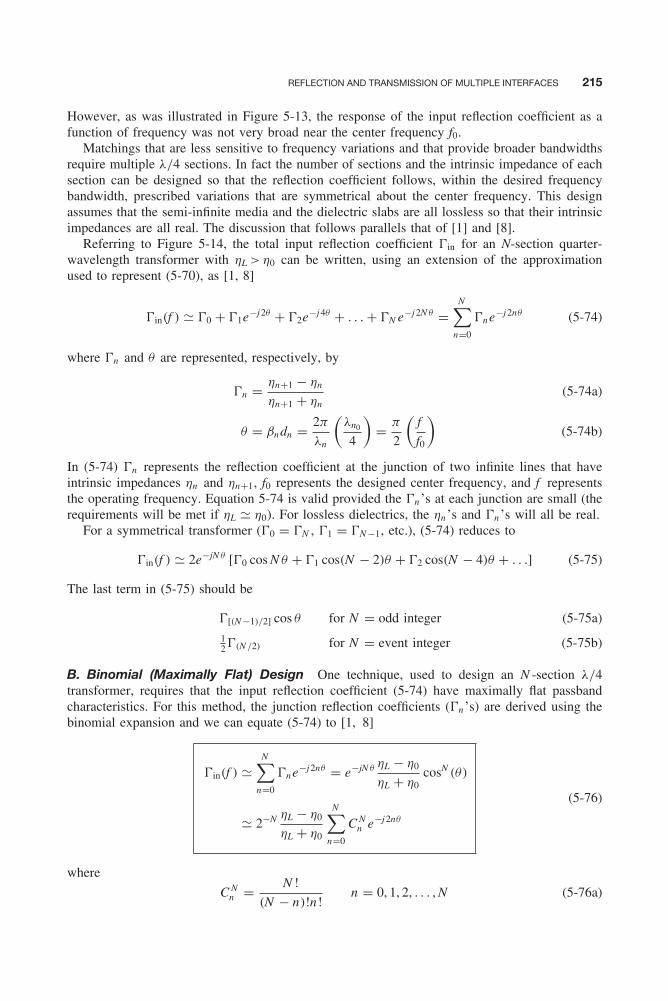
Balanis c05.tex V3 - 11/23/2011 11:47 A.M. Page 215
REFLECTION AND TRANSMISSION OF MULTIPLE INTERFACES 215
However, as was illustrated in Figure 5-13, the response of the input reflection coefficient as afunction of frequency was not very broad near the center frequency f0.
Matchings that are less sensitive to frequency variations and that provide broader bandwidthsrequire multiple λ/4 sections. In fact the number of sections and the intrinsic impedance of eachsection can be designed so that the reflection coefficient follows, within the desired frequencybandwidth, prescribed variations that are symmetrical about the center frequency. This designassumes that the semi-infinite media and the dielectric slabs are all lossless so that their intrinsicimpedances are all real. The discussion that follows parallels that of [1] and [8].
Referring to Figure 5-14, the total input reflection coefficient �in for an N-section quarter-wavelength transformer with ηL > η0 can be written, using an extension of the approximationused to represent (5-70), as [1, 8]
�in(f ) � �0 + �1e−j 2θ + �2e−j 4θ + . . . + �N e−j 2N θ =N∑
n=0
�ne−j 2nθ (5-74)
where �n and θ are represented, respectively, by
�n = ηn+1 − ηn
ηn+1 + ηn(5-74a)
θ = βndn = 2π
λn
(λn0
4
)= π
2
(f
f0
)(5-74b)
In (5-74) �n represents the reflection coefficient at the junction of two infinite lines that haveintrinsic impedances ηn and ηn+1, f0 represents the designed center frequency, and f representsthe operating frequency. Equation 5-74 is valid provided the �n ’s at each junction are small (therequirements will be met if ηL � η0). For lossless dielectrics, the ηn ’s and �n ’s will all be real.
For a symmetrical transformer (�0 = �N , �1 = �N −1, etc.), (5-74) reduces to
�in(f ) � 2e−jN θ [�0 cos N θ + �1 cos(N − 2)θ + �2 cos(N − 4)θ + . . .] (5-75)
The last term in (5-75) should be
�[(N −1)/2] cos θ for N = odd integer (5-75a)
12�(N /2) for N = event integer (5-75b)
B. Binomial (Maximally Flat) Design One technique, used to design an N -section λ/4transformer, requires that the input reflection coefficient (5-74) have maximally flat passbandcharacteristics. For this method, the junction reflection coefficients (�n ’s) are derived using thebinomial expansion and we can equate (5-74) to [1, 8]
�in(f ) �N∑
n=0
�ne−j 2nθ = e−jN θ ηL − η0
ηL + η0cosN (θ)
� 2−N ηL − η0
ηL + η0
N∑n=0
C Nn e−j 2nθ
(5-76)
where
C Nn = N !
(N − n)!n!n = 0, 1, 2, . . . , N (5-76a)
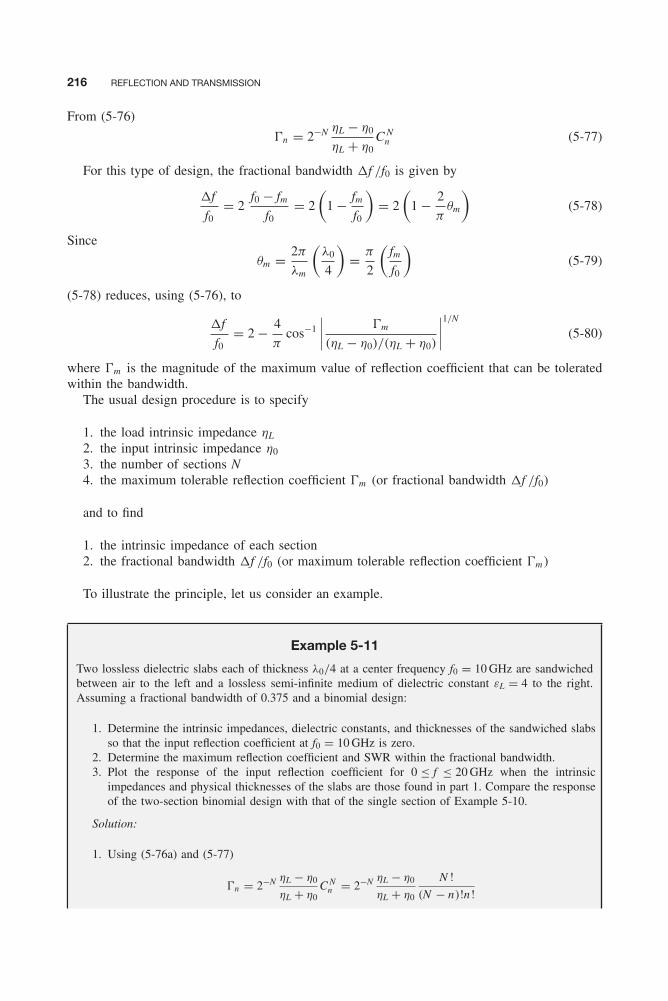
Balanis c05.tex V3 - 11/23/2011 11:47 A.M. Page 216
216 REFLECTION AND TRANSMISSION
From (5-76)
�n = 2−N ηL − η0
ηL + η0C N
n (5-77)
For this type of design, the fractional bandwidth f /f0 is given by
f
f0= 2
f0 − fmf0
= 2
(1 − fm
f0
)= 2
(1 − 2
πθm
)(5-78)
Since
θm = 2π
λm
(λ0
4
)= π
2
(fmf0
)(5-79)
(5-78) reduces, using (5-76), to
f
f0= 2 − 4
πcos−1
∣∣∣∣ �m
(ηL − η0)/(ηL + η0)
∣∣∣∣1/N
(5-80)
where �m is the magnitude of the maximum value of reflection coefficient that can be toleratedwithin the bandwidth.
The usual design procedure is to specify
1. the load intrinsic impedance ηL
2. the input intrinsic impedance η0
3. the number of sections N4. the maximum tolerable reflection coefficient �m (or fractional bandwidth f /f0)
and to find
1. the intrinsic impedance of each section2. the fractional bandwidth f /f0 (or maximum tolerable reflection coefficient �m )
To illustrate the principle, let us consider an example.
Example 5-11
Two lossless dielectric slabs each of thickness λ0/4 at a center frequency f0 = 10 GHz are sandwichedbetween air to the left and a lossless semi-infinite medium of dielectric constant εL = 4 to the right.Assuming a fractional bandwidth of 0.375 and a binomial design:
1. Determine the intrinsic impedances, dielectric constants, and thicknesses of the sandwiched slabsso that the input reflection coefficient at f0 = 10 GHz is zero.
2. Determine the maximum reflection coefficient and SWR within the fractional bandwidth.3. Plot the response of the input reflection coefficient for 0 ≤ f ≤ 20 GHz when the intrinsic
impedances and physical thicknesses of the slabs are those found in part 1. Compare the responseof the two-section binomial design with that of the single section of Example 5-10.
Solution:
1. Using (5-76a) and (5-77)
�n = 2−N ηL − η0
ηL + η0C N
n = 2−N ηL − η0
ηL + η0
N !
(N − n)!n!

Balanis c05.tex V3 - 11/23/2011 11:47 A.M. Page 217
REFLECTION AND TRANSMISSION OF MULTIPLE INTERFACES 217
Since the input dielectric is air and the load dielectric has a dielectric constant εL = 4, then
η0 = 377
ηL =√
μ0
εLε0= 377
2= 188.5
Therefore,
n = 0 : �0 = η1 − η0
η1 + η0= 2−2
(188.5 − 377
188.5 + 377
)2!
2!0!= − 1
12
⇒ η1 = η0
(1 − 1/12
1 + 1/12
)= 0.846η0 = 318.94 ohms
⇒ εr1 = 1.40 d1 = λ10
4= 0.634 cm
n = 1 : �1 = η2 − η1
η2 + η1= 2−2
(188.5 − 377
188.5 + 377
)2!
1!1!= −1
6
⇒ η2 = η1
(1 − 1/6
1 + 1/6
)= 0.714η1 = 227.72 ohms
⇒ εr2 = 2.74 d2 = λ20/4 = 0.453 cm
2. For a fractional bandwidth of 0.375, the magnitude of the maximum reflection coefficient �m isobtained using (5-80) or
f
f0= 0.375 = 2 − 4
πcos−1
∣∣∣∣ �m
(ηL − η0)/(ηL + η0)
∣∣∣∣1/2
which for ηL = 188.5 and η0 = 377 leads to
�m = 0.028
The maximum standing wave ratio is
SWRm = 1 + �m
1 − �m= 1 + 0.028
1 − 0.028= 1.058
3. The magnitude of the input reflection coefficient is given by (5-76) as
|�in| =∣∣∣∣ηL − η0
ηL + η0
∣∣∣∣ cos2 θ = 1
3cos2 θ = 1
3cos2
[π
2
(f
f0
)]which is shown plotted in Figure 5-13 where it is also compared with that of the one- andtwo-section Tschebyscheff design to be discussed next.
C. Tschebyscheff (Equal-Ripple) Design The reflection coefficient can be made to varywithin the bandwidth in an oscillatory manner and have equal-ripple characteristics [10–12]. Thiscan be accomplished by making �in vary similarly as a Tschebyscheff (Chebyshev) polynomial.For the Tschebyscheff design, the equation that corresponds to (5-76) is [1, 8]
�in(f ) = e−jN θ ηL − η0
ηL + η0
TN (sec θm cos θ)
TN (sec θm)(5-81)
where TN (z ) is the Tschebyscheff polynomial of order N .

Balanis c05.tex V3 - 11/23/2011 11:47 A.M. Page 218
218 REFLECTION AND TRANSMISSION
The maximum allowable reflection coefficient occurs at the edges of the passband whereθ = θm and |TN (sec θm cos θ)|θ=θm = 1. Thus,
ρm =∣∣∣∣ηL − η0
ηL + η0
1
TN (sec θm)
∣∣∣∣ (5-82)
or
|TN (sec θm)| =∣∣∣∣ 1
ρm
ηL − η0
ηL + η0
∣∣∣∣ (5-82a)
Using (5-82), we can write (5-81) as
�in (f ) = e−jN θρmTN (sec θm cos θ) (5-83)
and its magnitude as|�in (f )| = ρin(f ) = |ρmTN (sec θm cos θ)| (5-83a)
For this type of a design, the fractional bandwidth f /fo is also given by (5-78).To be physical, ρm must be smaller than the reflection coefficient when there are no matching
layers. Therefore, from (5-82),
ρm =∣∣∣∣ηL − η0
ηL + η0
1
TN (sec θm)
∣∣∣∣ <
∣∣∣∣ηL − η0
ηL + η0
∣∣∣∣ (5-84)
or|TN (sec θm)|> 1 (5-84a)
The Tschebyscheff polynomial can be expressed by either (6-71a) or (6-71b) of [1], or
Tm(z ) = cos[mcos−1(z )] − 1 ≤ z ≤ +1 (5-85a)
Tm(z ) = cosh[mcosh−1(z )] z < −1, z > +1 (5-85b)
Since |TN (sec θm)| > 1, using (5-85b) we can express TN (sec θm) as
TN (sec θm) = cosh[N cosh−1 (sec θm)
](5-86)
or by using (5-82a), as
|TN (sec θm)| = ∣∣cosh[N cosh−1 (sec θm)
]∣∣ =∣∣∣∣ 1
ρm
ηL − η0
ηL + η0
∣∣∣∣ (5-86a)
Thus,
sec θm = cosh
[1
Ncosh−1
(∣∣∣∣ 1
ρm
ηL − η0
ηL + η0
∣∣∣∣)](5-87)
or
θm = sec−1
{cosh
[1
Ncosh−1
(∣∣∣∣ 1
ρm
ηL − η0
ηL + η0
∣∣∣∣)]}(5-87a)
Using (5-83) we can write the reflection coefficient of (5-75) as
�in (θ) = 2e−jN θ {ρ0 cos (N θ) + ρ1 cos [(N − 2) θ ] + . . .}= e−jN θρmTN (sec θm cos θ) (5-88)
For a given N , replace TN (sec θm cos θ) in (5-88) by its polynomial series of (6-69) of [1] andthen match terms . This will allow you to determine the intrinsic reflection coefficients ρ ′
ns andsubsequently the η′
ns . The design procedure for the Tschebyscheff design is the same as that ofthe binomial design, as outlined previously.
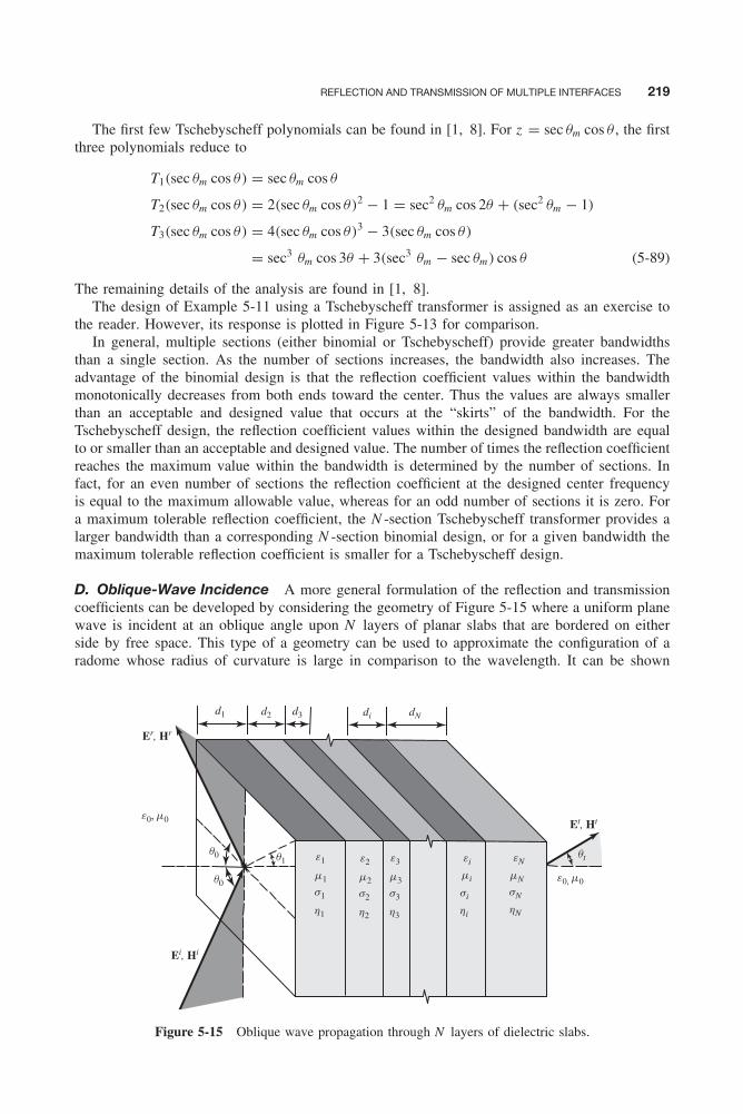
Balanis c05.tex V3 - 11/23/2011 11:47 A.M. Page 219
REFLECTION AND TRANSMISSION OF MULTIPLE INTERFACES 219
The first few Tschebyscheff polynomials can be found in [1, 8]. For z = sec θm cos θ , the firstthree polynomials reduce to
T1(sec θm cos θ) = sec θm cos θ
T2(sec θm cos θ) = 2(sec θm cos θ)2 − 1 = sec2 θm cos 2θ + (sec2 θm − 1)
T3(sec θm cos θ) = 4(sec θm cos θ)3 − 3(sec θm cos θ)
= sec3 θm cos 3θ + 3(sec3 θm − sec θm) cos θ (5-89)
The remaining details of the analysis are found in [1, 8].The design of Example 5-11 using a Tschebyscheff transformer is assigned as an exercise to
the reader. However, its response is plotted in Figure 5-13 for comparison.In general, multiple sections (either binomial or Tschebyscheff) provide greater bandwidths
than a single section. As the number of sections increases, the bandwidth also increases. Theadvantage of the binomial design is that the reflection coefficient values within the bandwidthmonotonically decreases from both ends toward the center. Thus the values are always smallerthan an acceptable and designed value that occurs at the “skirts” of the bandwidth. For theTschebyscheff design, the reflection coefficient values within the designed bandwidth are equalto or smaller than an acceptable and designed value. The number of times the reflection coefficientreaches the maximum value within the bandwidth is determined by the number of sections. Infact, for an even number of sections the reflection coefficient at the designed center frequencyis equal to the maximum allowable value, whereas for an odd number of sections it is zero. Fora maximum tolerable reflection coefficient, the N -section Tschebyscheff transformer provides alarger bandwidth than a corresponding N -section binomial design, or for a given bandwidth themaximum tolerable reflection coefficient is smaller for a Tschebyscheff design.
D. Oblique-Wave Incidence A more general formulation of the reflection and transmissioncoefficients can be developed by considering the geometry of Figure 5-15 where a uniform planewave is incident at an oblique angle upon N layers of planar slabs that are bordered on eitherside by free space. This type of a geometry can be used to approximate the configuration of aradome whose radius of curvature is large in comparison to the wavelength. It can be shown
Ei, Hi
Et, Ht
Er, Hr
d1 dNd2 did3
m1
e1
s1
h1
m2
e2
s2
h2
m3
e3
s3
h3
mi
ei
si
hi
mN e0, m0
e0, m0
eN
sN
hN
q1
q0
q0 qt
Figure 5-15 Oblique wave propagation through N layers of dielectric slabs.

Balanis c05.tex V3 - 11/23/2011 11:47 A.M. Page 220
220 REFLECTION AND TRANSMISSION
that the overall reflection and transmission coefficients for perpendicular (horizontal) and parallel(vertical) polarizations can be written as [3]
Perpendicular (Horizontal)
�⊥ = E r⊥
E i⊥
= B0
A0(5-90a)
T⊥ = E t⊥
E i⊥
= 1
A0(5-90b)
Parallel (Vertical)
�|| = E r||
E i||
= C0
D0(5-91a)
T|| = E t||
E i||
= 1
D0(5-91b)
The functions A0, B0, C0, and D0 are found using the recursive formulas
Aj = eψj
2[Aj+1(1 + Yj+1) + Bj+1(1 − Yj+1)] (5-92a)
Bj = e−ψj
2[Aj+1(1 − Yj+1) + Bj+1(1 + Yj+1)] (5-92b)
Cj = eψj
2[Cj+1(1 + Zj+1) + Dj+1(1 − Zj+1)] (5-92c)
Dj = e−ψj
2[Cj+1(1 − Zj+1) + Dj+1(1 + Zj+1)] (5-92d)
where
AN +1 = CN +1 = 1 (5-92e)
BN +1 = DN +1 = 0 (5-92f)
Yj+1 = cos θj+1
cos θj
√εj+1(1 − j tan δj+1)μj
εj (1 − j tan δj )μj+1(5-92g)
Zj+1 = cos θj+1
cos θj
√εj (1 − j tan δj )μj+1
εj+1(1 − j tan δj+1)μj(5-92h)
ψj = dj γj cos θj (5-92i)
γj = ±√jωμj (σj + jωεj ) (5-92j)
θj = complex angle of refraction in the j th layer (5-92k)
where d0 is the distance from the leading interface, which serves as the reference for the reflectionand transmission coefficients [see (5-5a) and (5-5b)].
5.6 POLARIZATION CHARACTERISTICS ON REFLECTION
When linearly polarized fields are reflected from smooth flat surfaces, the reflected fields main-tain their linear polarization characteristics. However, when the reflected surfaces are curved orrough, a linearly polarized component orthogonal to that of the incident field is introduced during
Balanis c05.tex V3 - 11/23/2011 11:47 A.M. Page 221
POLARIZATION CHARACTERISTICS ON REFLECTION 221
reflection. Therefore, the total field exhibits two components: one with the same polarization asthe incident field (main polarization) and one orthogonal to it (cross polarization). During thisprocess, the field is depolarized due to reflection.
Circularly polarized fields in free space incident upon flat surfaces:
1. Maintain their circular polarization but reverse their sense of rotation when the reflectingsurface is perfectly conducting.
2. Are transformed to elliptically polarized fields of opposite sense of rotation when the flatsurface is a lossless dielectric and the angle of incidence is smaller than the Brewsterangle.
Similarly, elliptically polarized fields in free space upon reflection from flat surfaces
1. Maintain their elliptical polarization and magnitude of axial ratio but reverse their sense ofrotation when reflected from a perfectly conducting surface.
2. Maintain their elliptical polarization but change their axial ratio and sense of rotation whenthe reflecting surface is a dielectric and the angle of incidence is smaller than the Brewsterangle.
To analyze the polarization properties of a wave when it is reflected by a surface, let us assumethat an elliptically polarized wave is obliquely incident upon a flat surface of infinite extent asshown in Figure 5-16 [7]. Using the localized coordinate system (x ′, y , z ′) of Figure 5-16, theincident electric field components can be written as
Ei|| = âx ′E i
||e−jβi • r = âx ′E 0
|| e−jβi • r (5-93a)
Ei⊥ = ây E i
⊥e−jβi • r = ây E 0⊥e−j (βi • r−φi
⊥) (5-93b)
where E 0|| and E 0
⊥ are assumed to be real.For this set of field components, the Poincaré sphere angles (4-58a) through (4-59b) can be
written [assuming that the ratio in (4-58a), selected here to demonstrate the procedure, satisfiesthe angular limits of all the Poincaré sphere angles] as
γ i = tan−1
(|E 0
⊥||E 0
|| |
)
δi = φi⊥ − φi
|| = φi⊥
(5-94a)
(5-94b)
εi = cot−1(ARi )
τ i = tilt angle of incident wave
(5-94c)
(5-94d)
where δi is the phase angle by which the perpendicular component of the incident field leadsthe parallel component. It is assumed that (ARi ) is positive for left-hand and negative for right-hand polarized fields. These two sets of angles are related to each other by (4-60a) through(4-61b), or
cos(2γ i ) = cos(2εi ) cos(2τ i ) (5-95a)
tan(δi ) = tan(2εi )
sin(2τ i )(5-95b)
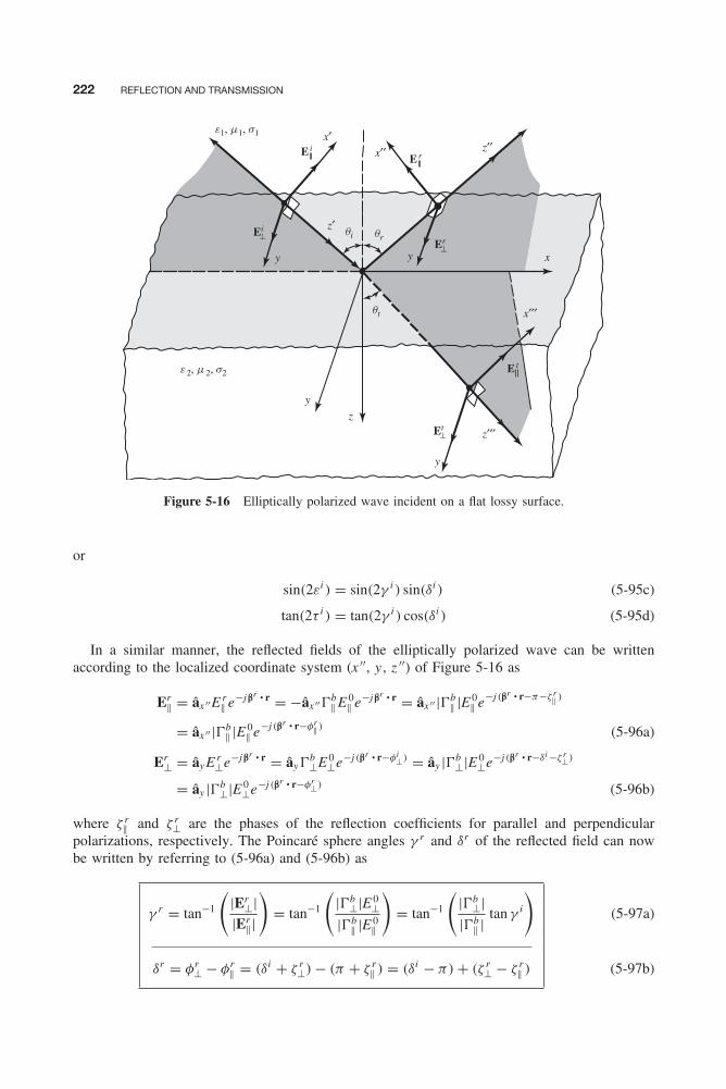
Balanis c05.tex V3 - 11/23/2011 11:47 A.M. Page 222
222 REFLECTION AND TRANSMISSION
x′x′′
x′′′
z′′′
x
y
y
z
z′′
z′
e1, m1, s1
e2, m2, s2
E i
qi qr
qt
E r
Et⊥
Ei⊥
E t
Er⊥
yy
Figure 5-16 Elliptically polarized wave incident on a flat lossy surface.
or
sin(2εi ) = sin(2γ i ) sin(δi ) (5-95c)
tan(2τ i ) = tan(2γ i ) cos(δi ) (5-95d)
In a similar manner, the reflected fields of the elliptically polarized wave can be writtenaccording to the localized coordinate system (x ′′, y , z ′′) of Figure 5-16 as
Er|| = âx ′′E r
|| e−jβr • r = −âx ′′�b|| E
0|| e−jβr • r = âx ′′ |�b
|| |E 0|| e−j (βr • r−π−ζ r
|| )
= âx ′′ |�b|| |E 0
|| e−j (βr • r−φr|| ) (5-96a)
Er⊥ = ây E r
⊥e−jβr • r = ây�b⊥E 0
⊥e−j (βr • r−φi⊥) = ây |�b
⊥|E 0⊥e−j (βr • r−δi −ζ r
⊥)
= ây |�b⊥|E 0
⊥e−j (βr • r−φr⊥) (5-96b)
where ζ r|| and ζ r
⊥ are the phases of the reflection coefficients for parallel and perpendicularpolarizations, respectively. The Poincaré sphere angles γ r and δr of the reflected field can nowbe written by referring to (5-96a) and (5-96b) as
γ r = tan−1
(|Er
⊥||Er
|||
)= tan−1
(|�b
⊥|E 0⊥
|�b|| |E 0
||
)= tan−1
(|�b
⊥||�b
|| |tan γ i
)
δr = φr⊥ − φr
|| = (δi + ζ r⊥) − (π + ζ r
|| ) = (δi − π) + (ζ r⊥ − ζ r
|| )
(5-97a)
(5-97b)

Balanis c05.tex V3 - 11/23/2011 11:47 A.M. Page 223
POLARIZATION CHARACTERISTICS ON REFLECTION 223
where δr is the phase angle by which the perpendicular (y) component leads the parallel (x ′′)component of the reflected field. Using the angles γ r and δr of (5-97a) and (5-97b), the corre-sponding Poincaré sphere angles εr , τ r (tilt angle of ellipse) and axial ratio (AR)r of the reflectedfield can be found using the relations
sin(2εr ) = sin(2γ r ) sin(δr )
tan(2τ r ) = tan(2γ r ) cos(δr )
(AR)r = cot(εr )
(5-98a)
(5-98b)
(5-98c)
Following a similar procedure, the transmitted fields can be expressed as
Et|| = âx ′′′E t
||e−jβt • r = âx ′′′T b
|| E 0|| e−jβt • r = âx ′′′ |T b
|| |E 0|| e−j (βt • r−ξ t
||)
= âx ′′′ |T b|| |E 0
|| e−j (βt • r−φt||) (5-99a)
Et⊥ = ây E t
⊥e−jβt • r = ây T b⊥E 0
⊥e−j (βt • r−φt⊥) = ây |T b
⊥|E 0⊥e−j (βt • r−δi −ξ r
⊥)
= ây |T b⊥|E 0
⊥e−j (βt • r−φt⊥) (5-99b)
where ξ t|| , and ξ t
⊥ are the phases of the transmission coefficients for parallel and perpendicularpolarizations, respectively. The Poincaré sphere angles δt and γ t can now be written by referringto (5-99a) and (5-99b) as
γ t = tan−1
(|Et
⊥||Et
|||
)= tan−1
(|T b
⊥|E 0⊥
|T b|| |E 0
||
)= tan−1
(|T b
⊥||T b
|| |tanγ i
)
δt = φt⊥ − φt
|| = (δi + ξ t⊥) − ξ t
|| = δi + (ξ t⊥ − ξ t
||)
(5-100a)
(5-100b)
where δt is the phase angle by which the perpendicular (y) component of the transmitted fieldleads the parallel (x ′′′) component of the transmitted field. Using the angles γ t and δt of (5-100a)and (5-100b), the corresponding Poincaré sphere angles εt , τ t (tilt angle of ellipse) and axialratio (AR)t of the transmitted field can be found using the relations
sin(2εt ) = sin(2γ t ) sin(δt )
tan(2τ t ) = tan(2γ t ) cos(δt )
(AR)t = cot(εt )
(5-101a)
(5-101b)
(5-101c)
The set of (5-96a) through (5-98c) and (5-99a) through (5-101c) can be used to find, respec-tively, the polarization of the reflected and transmitted fields once the polarization of the incidentfields of (5-93a) through (5-94d) has been stated. A block diagram of the relations between theincident, reflected, and transmitted fields is shown in Figure 5-17. The parallel component of theincident field is taken as the reference for the phase of all of the other components.

Balanis c05.tex V3 - 11/23/2011 11:47 A.M. Page 224
224 REFLECTION AND TRANSMISSION
Ei
E r E t
fi =
f ix′
= 0
g i = tan−1
=
+ di
=E i E0 E0
E0
E0
E i
E tE r
f i =
f iy = d i
Γb =
E i
−Γb =
Γb e j(π + ζr)
E0 Γb=E r E r E0 Γb= =E t E0 TbE0 Tb=
===
= = ===
E t
Γ b e jζr
Tb = Tb e jxt
Tb = Tb e jxt
fr
π + ζr
f rx′′ ft
x tf t
x′′′ fr
+ zrf r
y
d ift
+ x tf t
y
d i
Figure 5-17 Block diagram for polarization analysis of reflected and transmitted waves.
Example 5-12
A left-hand (CCW) circularly polarized field traveling in free space at an angle of θi = 30◦ is incidenton a flat perfect electric conductor of infinite extent. Find the polarization of the reflected wave.
Solution: A circularly polarized wave is made of two orthogonal linearly polarized componentswith a 90◦ phase difference between them. Therefore we can assume that these two orthogonal linearlypolarized components represent the perpendicular and parallel polarizations. Since the reflecting surfaceis perfectly conducting (η2 = 0), the reflection coefficients of (5-17a) and (5-24c) reduce to
�b⊥ = −1 = 1
/π ⇒ |�b
⊥| = 1 ζ r⊥ = π
�b|| = −1 = 1
/π ⇒ |�b
|| | = 1 ζ r|| = π
Since the incident field is left-hand circularly polarized, then according to (5-93a) through (5-94b)
E 0|| = E 0
⊥
δi = φi⊥ = π
2
γ i = tan−1
(E 0
⊥E 0
||
)= π
4⇒ tan γ i = 1
Thus according to (5-97a) and (5-97b)
γ r = tan−1
(|�b
⊥||�b
|| |tan γ i
)= π
4
δr = δi − π + (ζ r⊥ − ζ r
|| ) = π
2− π + (π − π) = −π
2
On the Poincaré sphere of Figure 4-20 the angles γ r = π/4 and δr = −π/2 define the south pole,which represents right-hand (CW) circular polarization. Therefore, the reflected field is right-hand (CW)circularly polarized, and it is opposite in rotation to that of the incident field as shown in Figure 5-18a .
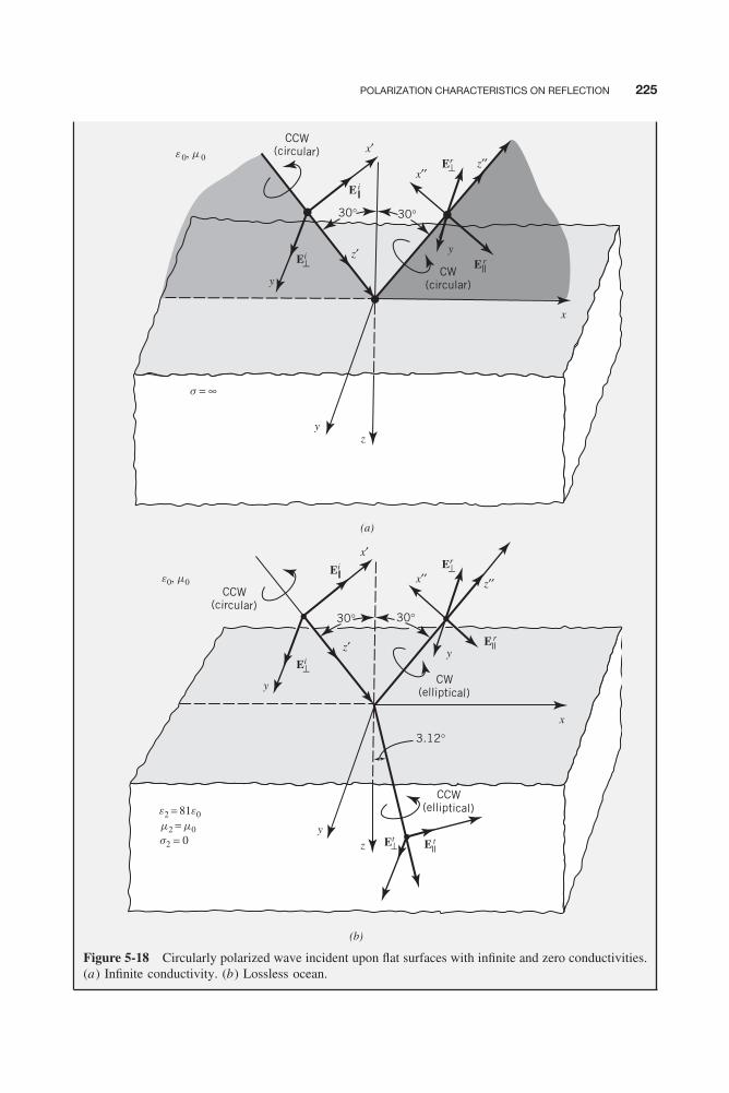
Balanis c05.tex V3 - 11/23/2011 11:47 A.M. Page 225
POLARIZATION CHARACTERISTICS ON REFLECTION 225
30°
30° 30°
3.12°
30°
y
y
yz
y
z
(a)
(b)
x′
x′′
x′′
z′′
z′′CCW
(circular)
CW(elliptical)
CCW(elliptical)
e0, m0
e2 = 81e0
m2 = m0
s = ∞
s2 = 0
E i
x′
x
z′
Ei
E r
E t
Er⊥
Er⊥
Ei⊥
Et⊥
x
z′
CCW(circular)e0, m0
yCW
(circular)
E r y
Ei⊥
Figure 5-18 Circularly polarized wave incident upon flat surfaces with infinite and zero conductivities.(a) Infinite conductivity. (b) Lossless ocean.
Balanis c05.tex V3 - 11/23/2011 11:47 A.M. Page 226
226 REFLECTION AND TRANSMISSION
Example 5-13
A left-hand (CCW) circularly polarized field traveling in free space at an angle of θi = 30◦ is incidenton a flat lossless (σ2 = 0) ocean (ε2 = 81ε0, μ2 = μ0) of infinite extent. Find the polarization of thereflected and transmitted fields.
Solution: Since the incident field is left-hand circularly polarized, then according to (5-93a) through(5-94b)
E 0|| = E 0
⊥
δi = φi⊥ = π
2
γ i = tan−1
(E 0
⊥E 0
||
)= π
4⇒ tan γ i = 1
To find the polarization of the reflected field, we proceed as follows. Using (5-18a)
�b⊥ =
cos(30◦) − √81
√1 − ( 1
81
)sin2(30◦)
cos(30◦) + √81
√1 − ( 1
81
)sin2(30◦)
=0.866 − 9
√1 − 1
81
( 14
)0.866 + 9
√1 − 1
81
( 14
)= 0.866 − 8.986
0.866 + 8.986
�b⊥ = −0.824 ⇒ |�b
⊥| = 0.824 ζ r⊥ = π
Using (5-25a)
�b|| =
− cos(30◦) +√
181
√1 − ( 1
81
)sin2(30◦)
cos(30◦) +√
181
√1 − ( 1
81
)sin2(30◦)
=−0.866 + 1
9
√1 − 1
81
( 14
)0.866 + 1
9
√1 − 1
81
( 14
)= −0.866 + 0.111
0.866 + 0.111
�b|| = −0.773 ⇒ |�b
|| | = 0.773 ζ r|| = π
According to (5-97a) and (5-97b)
γ r = tan−1
(|�b
⊥||�b
|| |tan γ i
)= tan−1
(0.824
0.773
)= 46.83◦ = 0.817 rad
δr = δi − π + (ζ r⊥ − ζ r
|| ) = π
2− π + (π − π) = −π
2
Using (5-98a) through (5-98c)
2εr = sin−1[sin(2γ r ) sin(δr )]
= sin−1[sin(93.66◦) sin
(−π
2
)]= −86.34◦
⇒ εr = −43.17◦
2τ r = tan−1[tan(2γ r ) cos(δr )]
= tan−1[tan(93.66◦) cos
(−π
2
)]= 180◦
⇒ τ r = 90◦
Balanis c05.tex V3 - 11/23/2011 11:47 A.M. Page 227
METAMATERIALS 227
(AR)r = cot(εr ) = cot(−43.17◦) = −1.066
On the Poincaré sphere of Figure 4-20 the angles γ r = 0.817 and δr = −π/2 locate a point on thelower hemisphere on the principal xz plane. Therefore the reflected field is right-hand (CW) ellipticallypolarized, and it has an opposite sense of rotation compared to the left-hand (CCW) circularly polarizedincident field as shown in Figure 5-18b. Its axial ratio is −1.066.
To find the polarization of the transmitted field we proceed as follows. Using (5-18b)
T b⊥ = 2 cos(30◦)
cos(30◦) + √81
√1 − ( 1
81
)sin2(30◦)
= 2(0.866)
0.866 + 8.986
= 0.1758 ⇒ |T b⊥| = 0.1758 ξ t
⊥ = 0
Using (5-25b)
T b|| =
2√
181 cos(30◦)
cos(30◦) +√
181
√1 − ( 1
81
)sin2(30◦)
= 2( 1
9
)0.866
0.866 + 0.111
= 0.197 ⇒ |T b|| | = 0.197 ξ t
|| = 0
According to (5-100a) and (5-100b)
γ t = tan−1
(|T b
⊥||T b
|| |tan γ i
)= tan−1
(0.1758
0.197
)= 41.75◦ = 0.729 rad
δt = δi + (ξ t⊥ − ξ t
||) = π
2+ (0 − 0) = π
2
Using (5-101a) through (5-101c)
2εt = sin−1[sin(2γ t ) sin(δt )] = sin−1[sin(83.5◦) sin(90◦)] = 83.5◦
⇒ εt = 41.75◦
2τ t = tan−1[tan(2γ t ) cos(δt )] = tan−1[tan(83.5◦) cos(90◦)] = 0
⇒ τ t = 0◦
(AR)t = cot(εt ) = cot(41.75◦) = 1.12
On the Poincaré sphere of Figure 4-20 the angles γ t = 0.729 and δt = π/2 locate a point on the upperhemisphere on the principal xz plane. Therefore the transmitted field is left-hand (CCW) ellipticallypolarized, and it is of the same sense of rotation as the left-hand (CCW) circularly polarized incidentfield as shown in Figure 5-18b. Its axial ratio is 1.12.
5.7 METAMATERIALS
The decades of the 1990s and 2000s had renewed interest and excitement into the field ofelectromagnetics, especially as they relate to the integration of a special type of artificial dielec-tric materials, coined metamaterials [13–18]. Using a ‘broad brush,’ the word metamaterialscan encompass engineered textured surfaces, artificial impedance surfaces, artificial magneticconductors, double negative materials, frequency selective surfaces, Photonic Band-Gap (PBG)surfaces, Electromagnetic Band-Gap (EBG) surfaces/structures , and even fractals or chirals .Artificial impedance surfaces are discussed in Section 8.8. In this section we want to focus
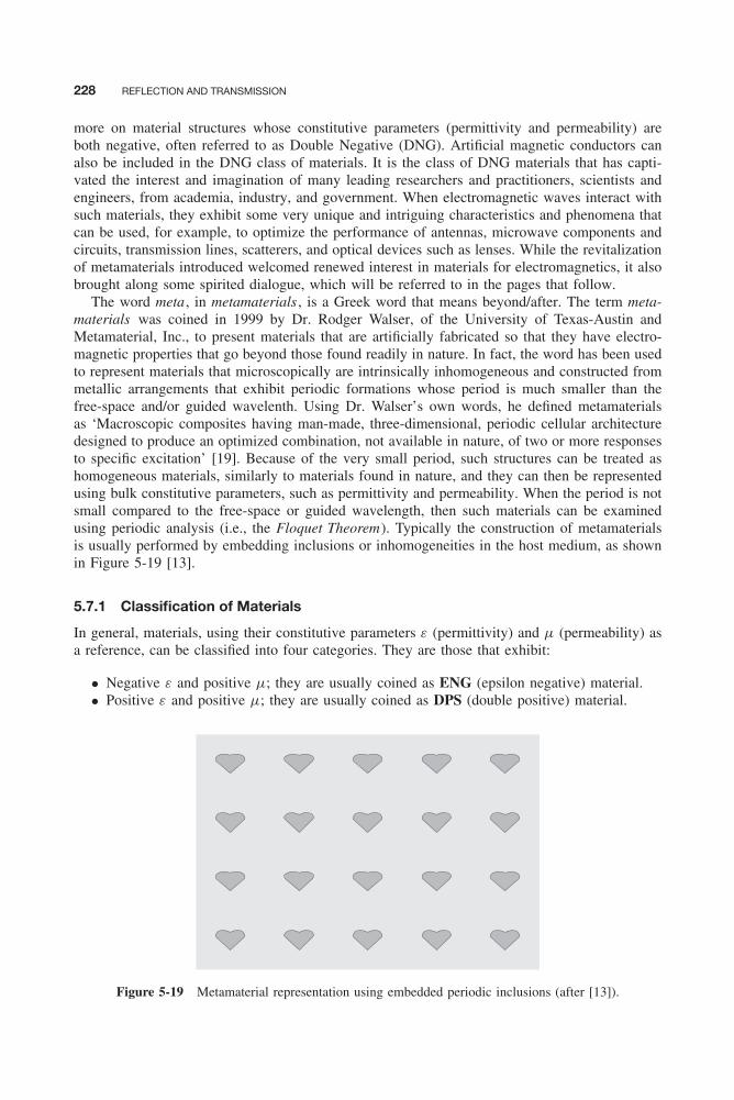
Balanis c05.tex V3 - 11/23/2011 11:47 A.M. Page 228
228 REFLECTION AND TRANSMISSION
more on material structures whose constitutive parameters (permittivity and permeability) areboth negative, often referred to as Double Negative (DNG). Artificial magnetic conductors canalso be included in the DNG class of materials. It is the class of DNG materials that has capti-vated the interest and imagination of many leading researchers and practitioners, scientists andengineers, from academia, industry, and government. When electromagnetic waves interact withsuch materials, they exhibit some very unique and intriguing characteristics and phenomena thatcan be used, for example, to optimize the performance of antennas, microwave components andcircuits, transmission lines, scatterers, and optical devices such as lenses. While the revitalizationof metamaterials introduced welcomed renewed interest in materials for electromagnetics, it alsobrought along some spirited dialogue, which will be referred to in the pages that follow.
The word meta , in metamaterials , is a Greek word that means beyond/after. The term meta-materials was coined in 1999 by Dr. Rodger Walser, of the University of Texas-Austin andMetamaterial, Inc., to present materials that are artificially fabricated so that they have electro-magnetic properties that go beyond those found readily in nature. In fact, the word has been usedto represent materials that microscopically are intrinsically inhomogeneous and constructed frommetallic arrangements that exhibit periodic formations whose period is much smaller than thefree-space and/or guided wavelenth. Using Dr. Walser’s own words, he defined metamaterialsas ‘Macroscopic composites having man-made, three-dimensional, periodic cellular architecturedesigned to produce an optimized combination, not available in nature, of two or more responsesto specific excitation’ [19]. Because of the very small period, such structures can be treated ashomogeneous materials, similarly to materials found in nature, and they can then be representedusing bulk constitutive parameters, such as permittivity and permeability. When the period is notsmall compared to the free-space or guided wavelength, then such materials can be examinedusing periodic analysis (i.e., the Floquet Theorem). Typically the construction of metamaterialsis usually performed by embedding inclusions or inhomogeneities in the host medium, as shownin Figure 5-19 [13].
5.7.1 Classification of Materials
In general, materials, using their constitutive parameters ε (permittivity) and μ (permeability) asa reference, can be classified into four categories. They are those that exhibit:
• Negative ε and positive μ; they are usually coined as ENG (epsilon negative) material.• Positive ε and positive μ; they are usually coined as DPS (double positive) material.
Figure 5-19 Metamaterial representation using embedded periodic inclusions (after [13]).
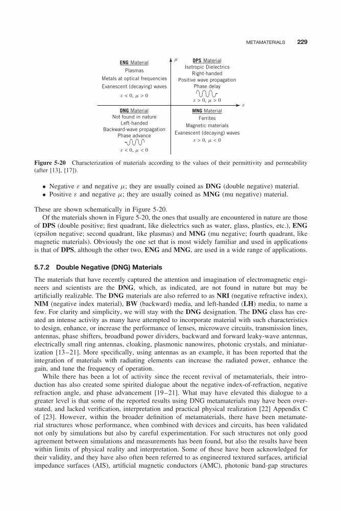
Balanis c05.tex V3 - 11/23/2011 11:47 A.M. Page 229
METAMATERIALS 229
Isotropic DielectricsRight-handed
Positive wave propagationPhase delay
DPS Material
FerritesMagnetic materials
Evanescent (decaying) waves
MNG MaterialNot found in nature
Left-handedBackward-wave propagation
Phase advance
DNG Material
Plasmas
Metals at optical frequencies
Evanescent (decaying) waves
e < 0, m > 0e > 0, m > 0
e > 0, m < 0
e < 0, m < 0
ENG Materialm
e
Figure 5-20 Characterization of materials according to the values of their permittivity and permeability(after [13], [17]).
• Negative ε and negative μ; they are usually coined as DNG (double negative) material.• Positive ε and negative μ; they are usually coined as MNG (mu negative) material.
These are shown schematically in Figure 5-20.Of the materials shown in Figure 5-20, the ones that usually are encountered in nature are those
of DPS (double positive; first quadrant, like dielectrics such as water, glass, plastics, etc.), ENG(epsilon negative; second quadrant, like plasmas) and MNG (mu negative; fourth quadrant, likemagnetic materials). Obviously the one set that is most widely familiar and used in applicationsis that of DPS, although the other two, ENG and MNG, are used in a wide range of applications.
5.7.2 Double Negative (DNG) Materials
The materials that have recently captured the attention and imagination of electromagnetic engi-neers and scientists are the DNG, which, as indicated, are not found in nature but may beartificially realizable. The DNG materials are also referred to as NRI (negative refractive index),NIM (negative index material), BW (backward) media, and left-handed (LH) media, to name afew. For clarity and simplicity, we will stay with the DNG designation. The DNG class has cre-ated an intense activity as many have attempted to incorporate material with such characteristicsto design, enhance, or increase the performance of lenses, microwave circuits, transmission lines,antennas, phase shifters, broadband power dividers, backward and forward leaky-wave antennas,electrically small ring antennas, cloaking, plasmonic nanowires, photonic crystals, and miniatur-ization [13–21]. More specifically, using antennas as an example, it has been reported that theintegration of materials with radiating elements can increase the radiated power, enhance thegain, and tune the frequency of operation.
While there has been a lot of activity since the recent revival of metamaterials, their intro-duction has also created some spirited dialogue about the negative index-of-refraction, negativerefraction angle, and phase advancement [19–21]. What may have elevated this dialogue to agreater level is that some of the reported results using DNG metamaterials may have been over-stated, and lacked verification, interpretation and practical physical realization [22] Appendix Cof [23]. However, within the broader definition of metamaterials, there have been metamate-rial structures whose performance, when combined with devices and circuits, has been validatednot only by simulations but also by careful experimentation. For such structures not only goodagreement between simulations and measurements has been found, but also the results have beenwithin limits of physical reality and interpretation. Some of these have been acknowledged fortheir validity, and they have also often been referred to as engineered textured surfaces, artificialimpedance surfaces (AIS), artificial magnetic conductors (AMC), photonic band-gap structures

Balanis c05.tex V3 - 11/23/2011 11:47 A.M. Page 230
230 REFLECTION AND TRANSMISSION
(PBG), and electromagnetic band-gap structures (EBG). This class of metamaterials is discussedin Section 8.8, and the reader is referred to that section for details and references.
Because of the interest in the electromagnetic community, it is important that the topic ofmetamaterials be introduced to graduate students, and maybe even to undergraduates, but pre-sented in the proper context. Because of space limitations, only an introductory overview of thesubject is included in this book. A succinct chronological sequence of the basic events that led tothis immense interest in metamaterials is also presented. The reader is referred to the literaturefor an in-depth presentation of the topic and its applications.
5.7.3 Historical Perspective
The origins of metamaterials can be traced back to the end of the 19th century, and they areoutlined in many publications. Since metamaterials is a rather new designation, it is a branch ofartificial dielectrics. In fact, it was indicated in 1898 that Jajadis Chunder Bose may have emulatedchiral media by using man-made twisted fibers to rotate the polarization of electromagnetic waves[24]. In 1914, Lindman examined artificial chiral media when he attempted to embed into thematerial an ensemble of randomly oriented small wire helices [25]. In 1948, Winston E. Kockof Bell Laboratories introduced the basic principles of artificial dielectrics to design lightweightlenses in the microwave frequency range (around 3–5 GHz) [26]. His attempt was to replaceat these frequencies, where the wavelength is 10-6 centimeters, heavy and bulky lenses madeof natural dielectric materials. He realized his concept of artificial dielectrics by controlling theeffective index-of-refraction of the materials by embedding into them, and arranging periodically,metallic disks and spheres in a concave lens shape.
The paper that revived the interest in the special class of artificial materials, now coinedmetamaterials and not found in nature, was that of Victor Veselago in 1968 who analyzedthe propagation of uniform waves in materials that exhibited, simultaneously, both negativepermittivity and permeability (DNG; double negative) [27]. Although Veselago may not havebeen interested in dielectric materials, he examined analytically the wave propagation throughmaterials that exhibited, simultaneously, negative ε and negative μ. One of the materials that canbe created in nature is plasma, which can exhibit negative permittivity. Plasma is an ionized gas ofwhich a significant number of its charged particles interact strongly with electromagnetic fields andmake it electrically conductive. For those that lived through the birth of the U.S. space programin the mid-1960s, led by NASA, there was a lot of interest and research in plasmas, formedbeneath and around the nose of the spacecraft during re-entry that caused loss of communicationwith the astronauts during the final 10–15 minutes of landing. To attempt to alleviate this loss ofcommunication (referred to then as blackout), due to the formed plasma sheath near the nose andbelly of the spacecraft, NASA initiated and carried out an intense research program on plasma.The plasma was modeled with a negative dielectric constant (negative permittivity), and it wasverified through many experiments.
Although Veselago may have known that negative ε can be obtained by plasma-type materials,he did not speculate, at least in [27], how and what kind of materials may exhibit DNG properties.However, he was able to show and conclude, through analytical formulation, that for wavepropagation through DNG type of materials, the direction of the power density flow (Poyntingvector) is opposite to the wave propagation (phase vector). He referred to such materials asleft-handed . Based on his conclusions, the directions of power density flow and phase velocity forDPS materials (double positive, which are conventional dielectrics) and DNG materials (doublenegative, not found in nature) are illustrated graphically in Figure 5-21, where a uniform planewave propagates in DPS (Figure 5-21a) and DNG (Figure 5-21b) materials. The DPS materialsare also dubbed Right-Handed Materials (RHM) while the DNG materials are dubbed asLeft-Handed Materials (LHM). The solid arrows represent the directions of wave vectors (phasevelocities) while the dashed arrows represent power flow (Poynting vectors). While the arrows
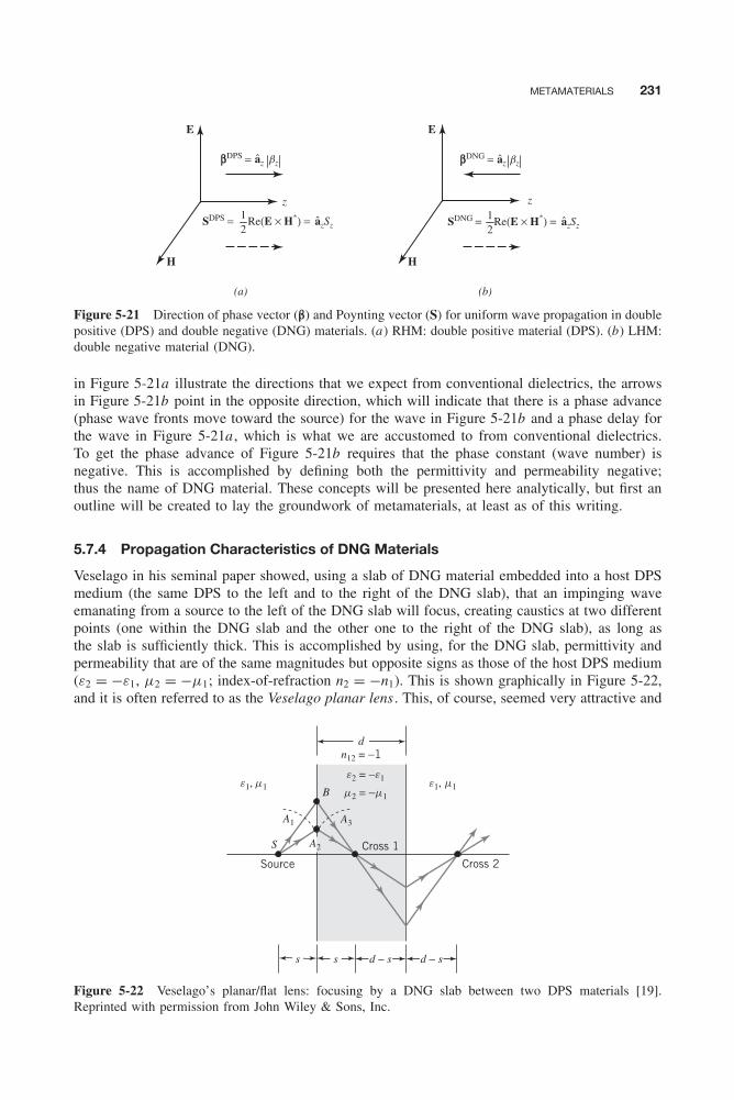
Balanis c05.tex V3 - 11/23/2011 11:47 A.M. Page 231
METAMATERIALS 231
(a) (b)
E
H
azSz
βDPS = az bz βDNG = az bz
z1
Re(E × H*) =2
SDPS = azSz1
Re(E × H*) =2
SDNG =
H
E
z
Figure 5-21 Direction of phase vector (β) and Poynting vector (S) for uniform wave propagation in doublepositive (DPS) and double negative (DNG) materials. (a) RHM: double positive material (DPS). (b) LHM:double negative material (DNG).
in Figure 5-21a illustrate the directions that we expect from conventional dielectrics, the arrowsin Figure 5-21b point in the opposite direction, which will indicate that there is a phase advance(phase wave fronts move toward the source) for the wave in Figure 5-21b and a phase delay forthe wave in Figure 5-21a , which is what we are accustomed to from conventional dielectrics.To get the phase advance of Figure 5-21b requires that the phase constant (wave number) isnegative. This is accomplished by defining both the permittivity and permeability negative;thus the name of DNG material. These concepts will be presented here analytically, but first anoutline will be created to lay the groundwork of metamaterials, at least as of this writing.
5.7.4 Propagation Characteristics of DNG Materials
Veselago in his seminal paper showed, using a slab of DNG material embedded into a host DPSmedium (the same DPS to the left and to the right of the DNG slab), that an impinging waveemanating from a source to the left of the DNG slab will focus, creating caustics at two differentpoints (one within the DNG slab and the other one to the right of the DNG slab), as long asthe slab is sufficiently thick. This is accomplished by using, for the DNG slab, permittivity andpermeability that are of the same magnitudes but opposite signs as those of the host DPS medium(ε2 = −ε1, μ2 = −μ1; index-of-refraction n2 = −n1). This is shown graphically in Figure 5-22,and it is often referred to as the Veselago planar lens . This, of course, seemed very attractive and
s
S
B
A1 A3
s d − s d − s
Cross 2
Cross 1
Source
d
e1, m1 e1, m1m2 = −m1
e2 = −e1
n12 = −1
A2
Figure 5-22 Veselago’s planar/flat lens: focusing by a DNG slab between two DPS materials [19].Reprinted with permission from John Wiley & Sons, Inc.
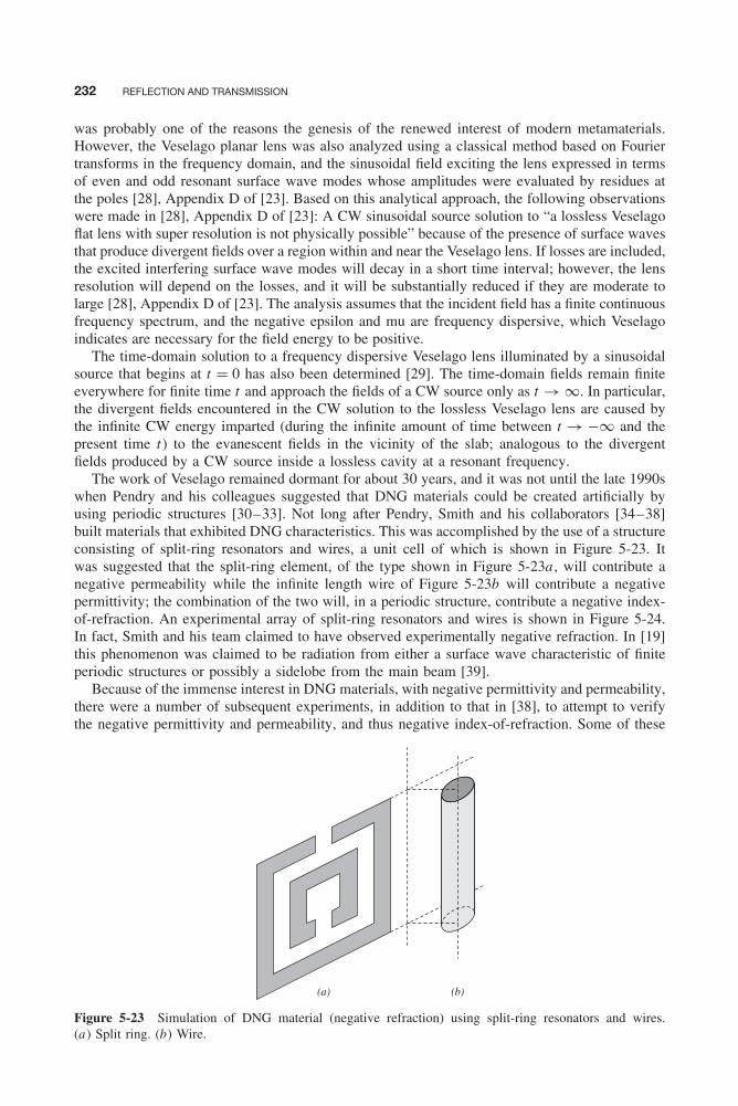
Balanis c05.tex V3 - 11/23/2011 11:47 A.M. Page 232
232 REFLECTION AND TRANSMISSION
was probably one of the reasons the genesis of the renewed interest of modern metamaterials.However, the Veselago planar lens was also analyzed using a classical method based on Fouriertransforms in the frequency domain, and the sinusoidal field exciting the lens expressed in termsof even and odd resonant surface wave modes whose amplitudes were evaluated by residues atthe poles [28], Appendix D of [23]. Based on this analytical approach, the following observationswere made in [28], Appendix D of [23]: A CW sinusoidal source solution to “a lossless Veselagoflat lens with super resolution is not physically possible” because of the presence of surface wavesthat produce divergent fields over a region within and near the Veselago lens. If losses are included,the excited interfering surface wave modes will decay in a short time interval; however, the lensresolution will depend on the losses, and it will be substantially reduced if they are moderate tolarge [28], Appendix D of [23]. The analysis assumes that the incident field has a finite continuousfrequency spectrum, and the negative epsilon and mu are frequency dispersive, which Veselagoindicates are necessary for the field energy to be positive.
The time-domain solution to a frequency dispersive Veselago lens illuminated by a sinusoidalsource that begins at t = 0 has also been determined [29]. The time-domain fields remain finiteeverywhere for finite time t and approach the fields of a CW source only as t → ∞. In particular,the divergent fields encountered in the CW solution to the lossless Veselago lens are caused bythe infinite CW energy imparted (during the infinite amount of time between t → −∞ and thepresent time t) to the evanescent fields in the vicinity of the slab; analogous to the divergentfields produced by a CW source inside a lossless cavity at a resonant frequency.
The work of Veselago remained dormant for about 30 years, and it was not until the late 1990swhen Pendry and his colleagues suggested that DNG materials could be created artificially byusing periodic structures [30–33]. Not long after Pendry, Smith and his collaborators [34–38]built materials that exhibited DNG characteristics. This was accomplished by the use of a structureconsisting of split-ring resonators and wires, a unit cell of which is shown in Figure 5-23. Itwas suggested that the split-ring element, of the type shown in Figure 5-23a , will contribute anegative permeability while the infinite length wire of Figure 5-23b will contribute a negativepermittivity; the combination of the two will, in a periodic structure, contribute a negative index-of-refraction. An experimental array of split-ring resonators and wires is shown in Figure 5-24.In fact, Smith and his team claimed to have observed experimentally negative refraction. In [19]this phenomenon was claimed to be radiation from either a surface wave characteristic of finiteperiodic structures or possibly a sidelobe from the main beam [39].
Because of the immense interest in DNG materials, with negative permittivity and permeability,there were a number of subsequent experiments, in addition to that in [38], to attempt to verifythe negative permittivity and permeability, and thus negative index-of-refraction. Some of these
(a) (b)
Figure 5-23 Simulation of DNG material (negative refraction) using split-ring resonators and wires.(a) Split ring. (b) Wire.
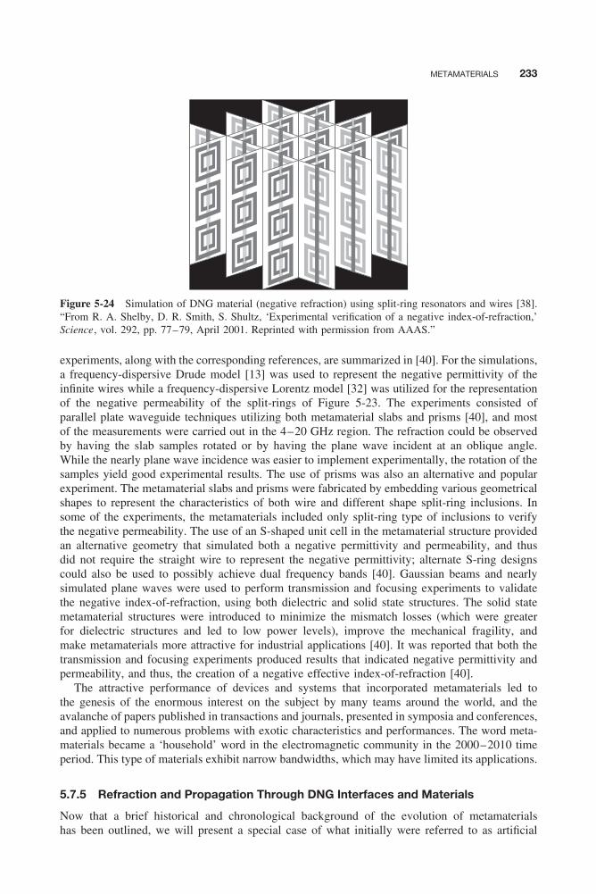
Balanis c05.tex V3 - 11/23/2011 11:47 A.M. Page 233
METAMATERIALS 233
Figure 5-24 Simulation of DNG material (negative refraction) using split-ring resonators and wires [38].“From R. A. Shelby, D. R. Smith, S. Shultz, ‘Experimental verification of a negative index-of-refraction,’Science, vol. 292, pp. 77–79, April 2001. Reprinted with permission from AAAS.”
experiments, along with the corresponding references, are summarized in [40]. For the simulations,a frequency-dispersive Drude model [13] was used to represent the negative permittivity of theinfinite wires while a frequency-dispersive Lorentz model [32] was utilized for the representationof the negative permeability of the split-rings of Figure 5-23. The experiments consisted ofparallel plate waveguide techniques utilizing both metamaterial slabs and prisms [40], and mostof the measurements were carried out in the 4–20 GHz region. The refraction could be observedby having the slab samples rotated or by having the plane wave incident at an oblique angle.While the nearly plane wave incidence was easier to implement experimentally, the rotation of thesamples yield good experimental results. The use of prisms was also an alternative and popularexperiment. The metamaterial slabs and prisms were fabricated by embedding various geometricalshapes to represent the characteristics of both wire and different shape split-ring inclusions. Insome of the experiments, the metamaterials included only split-ring type of inclusions to verifythe negative permeability. The use of an S-shaped unit cell in the metamaterial structure providedan alternative geometry that simulated both a negative permittivity and permeability, and thusdid not require the straight wire to represent the negative permittivity; alternate S-ring designscould also be used to possibly achieve dual frequency bands [40]. Gaussian beams and nearlysimulated plane waves were used to perform transmission and focusing experiments to validatethe negative index-of-refraction, using both dielectric and solid state structures. The solid statemetamaterial structures were introduced to minimize the mismatch losses (which were greaterfor dielectric structures and led to low power levels), improve the mechanical fragility, andmake metamaterials more attractive for industrial applications [40]. It was reported that both thetransmission and focusing experiments produced results that indicated negative permittivity andpermeability, and thus, the creation of a negative effective index-of-refraction [40].
The attractive performance of devices and systems that incorporated metamaterials led tothe genesis of the enormous interest on the subject by many teams around the world, and theavalanche of papers published in transactions and journals, presented in symposia and conferences,and applied to numerous problems with exotic characteristics and performances. The word meta-materials became a ‘household’ word in the electromagnetic community in the 2000–2010 timeperiod. This type of materials exhibit narrow bandwidths, which may have limited its applications.
5.7.5 Refraction and Propagation Through DNG Interfaces and Materials
Now that a brief historical and chronological background of the evolution of metamaterialshas been outlined, we will present a special case of what initially were referred to as artificial
Balanis c05.tex V3 - 11/23/2011 11:47 A.M. Page 234
234 REFLECTION AND TRANSMISSION
dielectrics, the basics from the analytical point of view as well as from a sample of simulations,and experiments. It should be pointed out, however, that what ensued after the work by Pendryand Smith was a plethora of publications which are too numerous to include here. Up to thispoint an attempt was made to reference some of the most basic books and papers. The readeris referred to the technical transactions, journals, and letters where most of these ensuing paperswere published or presented at leading international conferences and symposia. Most of thesecan be found in references [41–46].
The greatest potential of the DNG materials is the creation of a structure with a negativeindex-of-refraction n defined as
n2 = εrμr ⇒ n = ±√εrμr = ±√−|εr |(−|μr |) = ±(j
√|εr |)(j√|μr |) = ±j 2√|εrμr |
n = ∓√|εrμr | (5-102)
Which sign of n should be chosen for DNG materials (with both εr and μr negative)? It seemsfrom (5-102) that there are two basic choices; either negative or positive n . If a positive n isselected, that resorts back to the DPS representation. If the negative value of n in (5-102) isselected, then that is the basis of DNG materials.
Materials with negative index-of-refraction have some interesting properties, some of whichhave been mentioned and illustrated in Figure 5-21. Now let us examine two interface optionsusing Snell’s law of refraction which is the manifest of phase match across the interface. Ofparticular interest are materials with negative index-of-refraction.
• Snell’s law of refraction, represented by (5-15b) and (5-24b), or
β1 sin θi = ω√
μ1ε1 sin θi ≡ β2 sin θt = ω√
μ2ε2 sin θt (5-103)
can also be written asn1 sin θi = n2 sin θt (5-104)
When the index-of-refraction of both materials forming the interface is positive, then therefracted ray (transmitted wave) will be, as expected for conventional materials, on thesame side (relative to the normal to the interface) as the reflected ray, as illustrated inFigure 5-25a . However, when the index-of-refraction of one material is positive while thatof the other is negative, the refracted ray (transmitted wave) will be in the opposite directionof the reflected ray, as illustrated in Figure 5-25b.
• For DNG materials with a negative index-of-refraction the phase constant (wave number) ofthe wave traveling in the DNG material is negative, or based on the definition of (5-103)
β2 = ω√
μ2ε2 = −ω√
|μ2| |ε2| (5-105)
This implies that, for positive time, there will be a phase advance (phase wavefronts movetoward the source), instead of a phase delay that we have been accustomed to. This is aninteresting phenomenon, which has been part of the spirited dialogue.
So, based on the above, a negative index-of-refraction leads to:
• A refracted angle that is on the same side, relative to the normal to the interface, as theincident angle, and the power flow (Poynting vector) is outward (as expected); however, thephase vector in inward (opposite to the Poynting vector).
• Phase advance, instead of phase delay that is typical of DPS materials.
Based on the above, let us examine through an example a more general case of the planar lensthat was illustrated in Figure 5-22.
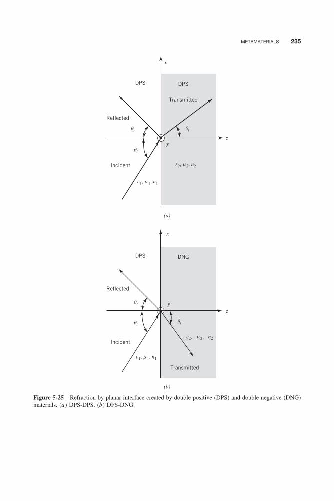
Balanis c05.tex V3 - 11/23/2011 11:47 A.M. Page 235
METAMATERIALS 235
(a)
(b)
DPS DPS
qi
qr qt
e2, m2, n2
Reflected
Incident
Transmitted
z
x
y
e1, m1, n1
DPS DNG
qi
qr
qt
Reflected
Incident
Transmitted
z
x
y
−e2, −m2, −n2
e1, m1, n1
Figure 5-25 Refraction by planar interface created by double positive (DPS) and double negative (DNG)materials. (a) DPS-DPS. (b) DPS-DNG.

Balanis c05.tex V3 - 11/23/2011 11:47 A.M. Page 236
236 REFLECTION AND TRANSMISSION
Example 5-14
Figure 5-22 displays Veselago’s planar/flat lens. A more general one is the one of Figure 5-26 where aDNG slab is sandwiched within free space. Given the dimensions of the DNG slab of thickness d andthe source position s , as shown in the Figure 5-26, determine the location of the foci (caustics) f0 and f1(one within the DNG slab and one outside it) in terms of the incidence angle θi , position of the source s ,and thickness d and index-of-refraction n1 of the DNG slab. Assume the DNG slab possesses negativepermittivity −ε1, negative permeability −μ1, and negative index-of-refraction −n1. Furthermore, let usassume that we are looking for a solution based on geometrical optics.
Solution: Using (5-103) through (5-105), we can write for the leading interface between free spaceand the DNG slab that
θ1 = sin−1(
1
|n1| sin θi
)Also from Figure 5-26
tan θi = h1
s⇒ h1 = s tan θi
tan θ1 = h1
f0⇒ h1 = f0 tan θ1
Equating the two previous equations leads to
s tan θi = f0 tan θ1 ⇒ f0 = stan θi
tan θ1⇒ tan θ1 = s
f0tan θi
From Figure 5-26
tan θ0 = h2
f1⇒ h2 = f1 tan θ0
tan θ1 = h2
d − f0⇒ h2 = (d − f0) tan θ1
Equating the last two equations leads to
f1 tan θ0 = (d − f0) tan θ1 ⇒ f1 = (d − f0)tan θ1
tan θ0
which can also be expressed, assuming d > f0, as
f1 = (d − f0)tan θ1
tan θ0= (d − f0)
s
f0
tan θi
tan θ0
Since θ0 = θi , the above equation reduces to
f1 = (d − f0)s
f0
As the magnitude of −ε1 approaches that of free space (that is |−ε1| → |ε0| ⇒ |−n1| → |n0| = 1),the focal distance f0 approaches s(f0 → s) and f1 approaches d − s(f1 → d − s). Then Figure 5-26reduces, in this limiting case, to Figure 5-22. When s becomes very large (approaching infinity), theincident wave reduces to near normal incidence. In this case the focusing moves toward infinity (ideallyno focusing).

Balanis c05.tex V3 - 11/23/2011 11:47 A.M. Page 237
METAMATERIALS 237
s d
e0, m0, n0 = 1 e0, m0, n0 = 1
qi q1h1
q0
h2
−e1, −m1, −n1
q1 = q2
f1
f0
Figure 5-26 DNG dielectric slab bounded on both sides by free space.
n = +1 n = +1
d
Figure 5-27 Negative refraction from a DNG slab [48]. Copyright © by The Optical Society of America.Permission and courtesy of R. W. Ziolkowski.
To illustrate the DNG refraction, a simulation has been performed, using the Finite-DifferenceTime-Domain method, of a 30 GHz perpendicularly polarized CW Gaussian beam incident at20◦ on a DNG slab bordered from the left and right by free space, as shown in Figure 5-27 [48].Because the incident wave is a plane wave, there is no focusing. The index-of-refraction of the
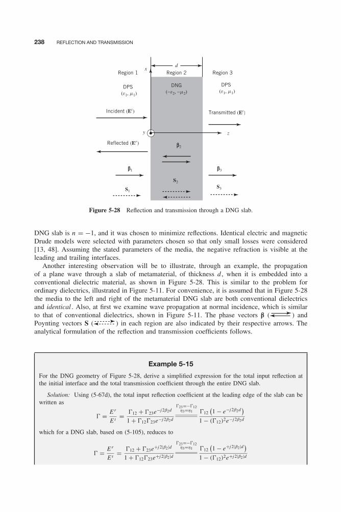
Balanis c05.tex V3 - 11/23/2011 11:47 A.M. Page 238
238 REFLECTION AND TRANSMISSION
DPS(e1, m1)
DNG
Region 2Region 1x
Region 3
(−e2, −m2)
Reflected (Er)
Incident (Ei) Transmitted (Et)
z
DPS(e1, m1)
d
β1 β3
β2
S1
S2S3
y
Figure 5-28 Reflection and transmission through a DNG slab.
DNG slab is n = −1, and it was chosen to minimize reflections. Identical electric and magneticDrude models were selected with parameters chosen so that only small losses were considered[13, 48]. Assuming the stated parameters of the media, the negative refraction is visible at theleading and trailing interfaces.
Another interesting observation will be to illustrate, through an example, the propagationof a plane wave through a slab of metamaterial, of thickness d , when it is embedded into aconventional dielectric material, as shown in Figure 5-28. This is similar to the problem forordinary dielectrics, illustrated in Figure 5-11. For convenience, it is assumed that in Figure 5-28the media to the left and right of the metamaterial DNG slab are both conventional dielectricsand identical . Also, at first we examine wave propagation at normal incidence, which is similarto that of conventional dielectrics, shown in Figure 5-11. The phase vectors β ( ) andPoynting vectors S ( ) in each region are also indicated by their respective arrows. Theanalytical formulation of the reflection and transmission coefficients follows.
Example 5-15
For the DNG geometry of Figure 5-28, derive a simplified expression for the total input reflection atthe initial interface and the total transmission coefficient through the entire DNG slab.
Solution: Using (5-67d), the total input reflection coefficient at the leading edge of the slab can bewritten as
� = E r
E t= �12 + �23e−j 2β2d
1 + �12�23e−j 2β2d
�23=−�12η3=η1 �12
(1 − e−j 2β2d
)1 − (�12)2e−j 2β2d
which for a DNG slab, based on (5-105), reduces to
� = E r
E t= �12 + �23e+j 2|β2|d
1 + �12�23e+j 2|β2|d
�23=−�12η3=η1 �12
(1 − e+j 2|β2|d )
1 − (�12)2e+j 2|β2|d
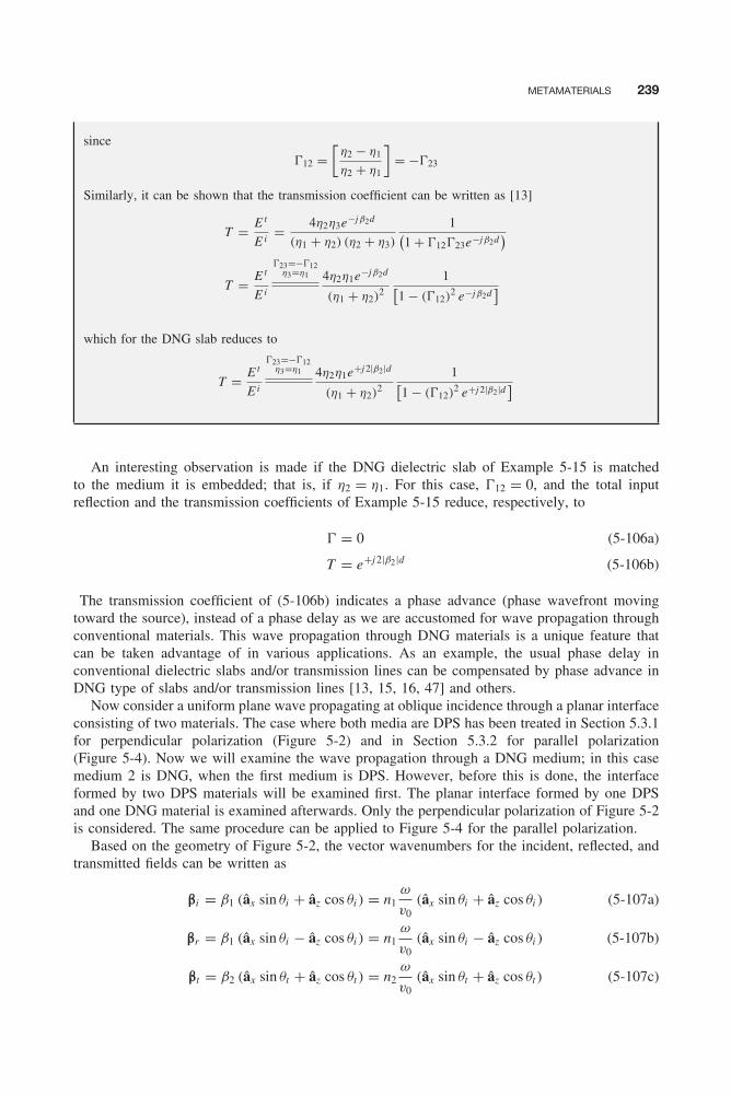
Balanis c05.tex V3 - 11/23/2011 11:47 A.M. Page 239
METAMATERIALS 239
since
�12 =[
η2 − η1
η2 + η1
]= −�23
Similarly, it can be shown that the transmission coefficient can be written as [13]
T = E t
E i= 4η2η3e−jβ2d
(η1 + η2) (η2 + η3)
1(1 + �12�23e−jβ2d
)T = E t
E i
�23=−�12η3=η1 4η2η1e−jβ2d
(η1 + η2)2
1[1 − (�12)
2 e−jβ2d]
which for the DNG slab reduces to
T = E t
E i
�23=−�12η3=η1 4η2η1e+j 2|β2|d
(η1 + η2)2
1[1 − (�12)
2 e+j 2|β2|d ]
An interesting observation is made if the DNG dielectric slab of Example 5-15 is matchedto the medium it is embedded; that is, if η2 = η1. For this case, �12 = 0, and the total inputreflection and the transmission coefficients of Example 5-15 reduce, respectively, to
� = 0 (5-106a)
T = e+j 2|β2|d (5-106b)
The transmission coefficient of (5-106b) indicates a phase advance (phase wavefront movingtoward the source), instead of a phase delay as we are accustomed for wave propagation throughconventional materials. This wave propagation through DNG materials is a unique feature thatcan be taken advantage of in various applications. As an example, the usual phase delay inconventional dielectric slabs and/or transmission lines can be compensated by phase advance inDNG type of slabs and/or transmission lines [13, 15, 16, 47] and others.
Now consider a uniform plane wave propagating at oblique incidence through a planar interfaceconsisting of two materials. The case where both media are DPS has been treated in Section 5.3.1for perpendicular polarization (Figure 5-2) and in Section 5.3.2 for parallel polarization(Figure 5-4). Now we will examine the wave propagation through a DNG medium; in this casemedium 2 is DNG, when the first medium is DPS. However, before this is done, the interfaceformed by two DPS materials will be examined first. The planar interface formed by one DPSand one DNG material is examined afterwards. Only the perpendicular polarization of Figure 5-2is considered. The same procedure can be applied to Figure 5-4 for the parallel polarization.
Based on the geometry of Figure 5-2, the vector wavenumbers for the incident, reflected, andtransmitted fields can be written as
βi = β1 (âx sin θi + âz cos θi ) = n1ω
v0(âx sin θi + âz cos θi ) (5-107a)
βr = β1 (âx sin θi − âz cos θi ) = n1ω
v0(âx sin θi − âz cos θi ) (5-107b)
βt = β2 (âx sin θt + âz cos θt ) = n2ω
v0(âx sin θt + âz cos θt ) (5-107c)
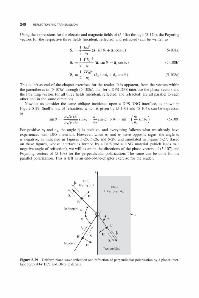
Balanis c05.tex V3 - 11/23/2011 11:47 A.M. Page 240
240 REFLECTION AND TRANSMISSION
Using the expressions for the electric and magnetic fields of (5-10a) through (5-12b), the Poyntingvectors for the respective three fields (incident, reflected, and refracted) can be written as
Si = 1
2
|E0|2η1
(âx sin θi + âz cos θi ) (5-108a)
Sr = 1
2
|�E0|2η1
(âx sin θi − âz cos θi ) (5-108b)
St = 1
2
|TE0|2η2
(âx sin θt + âz cos θt ) (5-108c)
This is left as end-of-the-chapter exercises for the reader. It is apparent, from the vectors withinthe parentheses in (5-107a) through (5-108c), that for a DPS-DPS interface the phase vectors andthe Poynting vectors for all three fields (incident, reflected, and refracted) are all parallel to eachother and in the same directions.
Now let us consider the same oblique incidence upon a DPS-DNG interface, as shown inFigure 5-29. Snell’s law of refraction, which is given by (5-103) and (5-104), can be expressedas
sin θt = ω√
μ1ε1
ω√
μ2ε2sin θi = n1
n2sin θi ⇒ θt = sin−1
(n1
n2sin θi
)(5-109)
For positive n1 and n2, the angle θt is positive, and everything follows what we already haveexperienced with DPS materials. However, when n1 and n2 have opposite signs, the angle θt
is negative, as indicated in Figures 5-25, 5-26, and 5-29, and simulated in Figure 5-27. Basedon these figures, whose interface is formed by a DPS and a DNG material (which leads to anegative angle of refraction), we will examine the directions of the phase vectors of (5-107) andPoynting vectors of (5-108) for the perpendicular polarization. The same can be done for theparallel polarization. This is left as an end-of-the-chapter exercise for the reader.
DPS (e1, m1, n1)
DNG (−e2, −m2, −n2)
qi
qr
βt
St
βi
βr
Si
Sr
qt
Reflected
Incident
Transmitted
zy
Ei
Hi
Et
Ht
Hr
Er
x
Figure 5-29 Uniform plane wave reflection and refraction of perpendicular polarization by a planar inter-face formed by DPS and DNG materials.

Balanis c05.tex V3 - 11/23/2011 11:47 A.M. Page 241
METAMATERIALS 241
Since for the interface of Figure 5-29 the index-of-refraction of medium 2 is negative andthe wavenumber is also negative, as expressed by (5-105), the wave vectors of (5-107a) and thePoynting vectors of (5-108a) can now be written, respectively, as
βi = β1 (âx sin θi + âz cos θi ) = n1ω
v0(âx sin θi + âz cos θi ) (5-110a)
βr = β1 (âx sin θi − âz cos θi ) = n1ω
v0(âx sin θi − âz cos θi ) (5-110b)
βt = |β2| (âx sin |θt | − âz cos |θt |) = |n2| ω
v0(âx sin |θt | − âz cos |θt |) (5-110c)
Si = 1
2
|E0|2η1
(âx sin θi + âz cos θi ) (5-111a)
Sr = 1
2
|�E0|2η1
(âx sin θi − âz cos θi ) (5-111b)
St = 1
2
|TE0|2η2
(−âx sin |θt | + âz cos |θt |) (5-111c)
While the wave and Poynting vectors of the incident and reflected fields are unaffected by thepresence of the DNG material forming the interface in Figure 5-29 [they are the same as in(5-107) and (5-108)], those of the transmitted fields, as represented by (5-110c) and (5-111c) aredifferent from the corresponding ones of (5-107c) and (5-108c) in two ways.
The first difference is that the wave vector of (5-110c) is antiparallel to the Poynting vectorof (5-111c), whereas they were parallel for (5-107c) and (5-108c). Also, for positive time, thewavenumber of (5-107c) leads to a phase delay, but the wavenumber of (5-110c) leads to a phaseadvance. In addition, while the phase vector of (5-107c) and the Poynting vector of (5-108c)are both directed away from the source (point of refraction in the first quadrant), the Poyntingvector of (5-111c) is also directed away from the source, but in the fourth quadrant. These arealso illustrated graphically in Figures 5-21a and 5-21b. These are some of the similarities anddifferences in the transmitted fields for DPS-DPS and DPS-DNG interfaces.
5.7.6 Negative-Refractive-Index (NRI) Transmission Lines
Another application of the DNG material is the design of Negative-Refractive-Index TransmissionLines (NRI-TL) [15, 16, 47]. This concept can be used to design:
• nonradiating phase-shifting lines that can produce either positive or negative phase shift• broadband series power dividers• forward leaky-wave antennas
and other applications [16]. When a wave propagates through a DPS medium, like in a conven-tional dielectric slab of thickness d1, it will accumulate phase lag |φ1| of β1d1(φ1 = −β1d1), alsoreferred to as negative phase shift, where β1 is the phase constant (wave number). This negativephase shift can be compensated by a positive phase shift φ2 (φ2 = +|β2|d2) through a DNGslab that follows the DPS slab. In fact, ideally, the negative phase shift accumulated throughpropagation in the DPS slab (φ1 = −β1d1) can be totally eliminated if the positive phase φ2
(φ2 = +|β2|d2) can be created by propagation through the DNG slab such that |φ1| = |φ2| so thatthe total phase φ by wave propagation through both slabs is equal to zero (φ = φ1 + φ2 = 0).Such an arrangement is shown graphically in Figure 5-30 where the arrows are used to designate
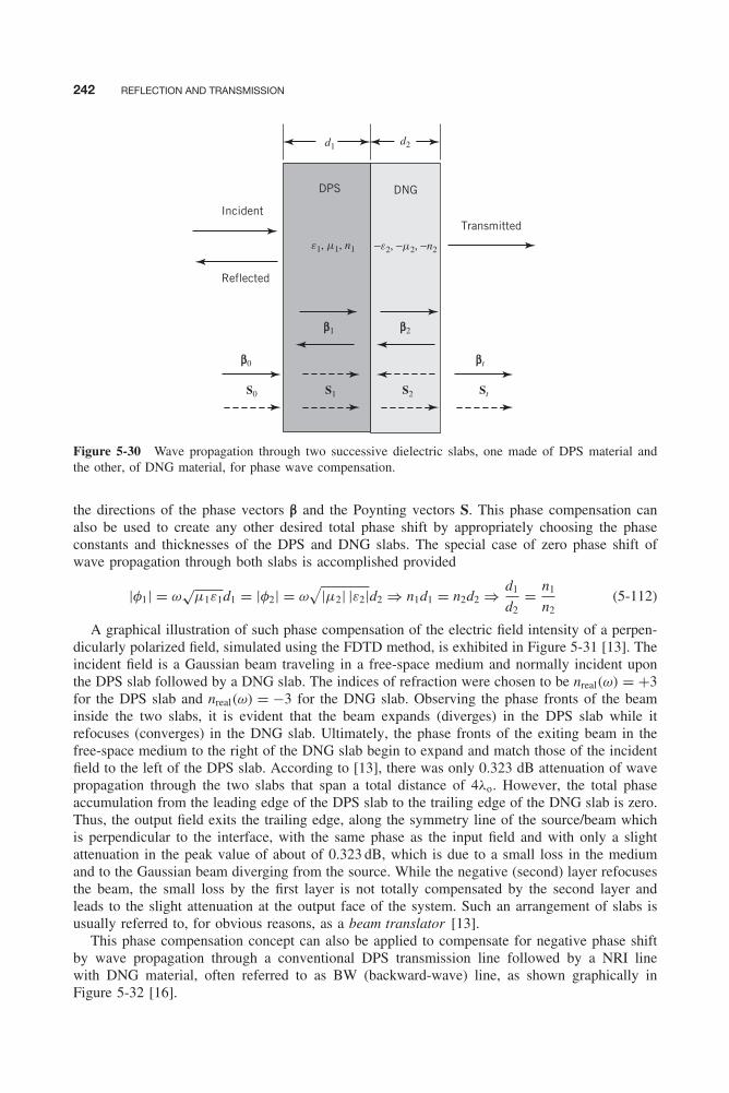
Balanis c05.tex V3 - 11/23/2011 11:47 A.M. Page 242
242 REFLECTION AND TRANSMISSION
DPS DNG
Incident
Reflected
Transmitted
d1 d2
e1, m1, n1 −e2, −m2, −n2
S0 S1 S2 St
β0
β1 β2
βt
Figure 5-30 Wave propagation through two successive dielectric slabs, one made of DPS material andthe other, of DNG material, for phase wave compensation.
the directions of the phase vectors β and the Poynting vectors S. This phase compensation canalso be used to create any other desired total phase shift by appropriately choosing the phaseconstants and thicknesses of the DPS and DNG slabs. The special case of zero phase shift ofwave propagation through both slabs is accomplished provided
|φ1| = ω√
μ1ε1d1 = |φ2| = ω√
|μ2| |ε2|d2 ⇒ n1d1 = n2d2 ⇒ d1
d2= n1
n2(5-112)
A graphical illustration of such phase compensation of the electric field intensity of a perpen-dicularly polarized field, simulated using the FDTD method, is exhibited in Figure 5-31 [13]. Theincident field is a Gaussian beam traveling in a free-space medium and normally incident uponthe DPS slab followed by a DNG slab. The indices of refraction were chosen to be nreal(ω) = +3for the DPS slab and nreal(ω) = −3 for the DNG slab. Observing the phase fronts of the beaminside the two slabs, it is evident that the beam expands (diverges) in the DPS slab while itrefocuses (converges) in the DNG slab. Ultimately, the phase fronts of the exiting beam in thefree-space medium to the right of the DNG slab begin to expand and match those of the incidentfield to the left of the DPS slab. According to [13], there was only 0.323 dB attenuation of wavepropagation through the two slabs that span a total distance of 4λo. However, the total phaseaccumulation from the leading edge of the DPS slab to the trailing edge of the DNG slab is zero.Thus, the output field exits the trailing edge, along the symmetry line of the source/beam whichis perpendicular to the interface, with the same phase as the input field and with only a slightattenuation in the peak value of about of 0.323 dB, which is due to a small loss in the mediumand to the Gaussian beam diverging from the source. While the negative (second) layer refocusesthe beam, the small loss by the first layer is not totally compensated by the second layer andleads to the slight attenuation at the output face of the system. Such an arrangement of slabs isusually referred to, for obvious reasons, as a beam translator [13].
This phase compensation concept can also be applied to compensate for negative phase shiftby wave propagation through a conventional DPS transmission line followed by a NRI linewith DNG material, often referred to as BW (backward-wave) line, as shown graphically inFigure 5-32 [16].
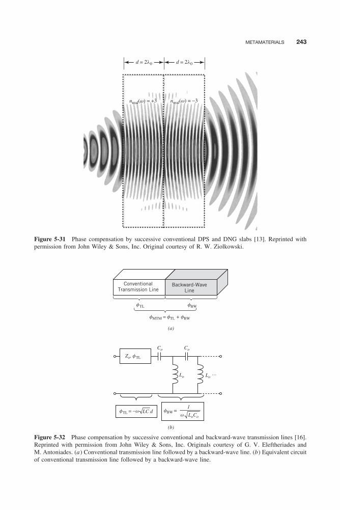
Balanis c05.tex V3 - 11/23/2011 11:47 A.M. Page 243
METAMATERIALS 243
d = 2l0d = 2l0
nreal(w) = +3 nreal(w) = −3
Figure 5-31 Phase compensation by successive conventional DPS and DNG slabs [13]. Reprinted withpermission from John Wiley & Sons, Inc. Original courtesy of R. W. Ziolkowski.
(a)
ConventionalTransmission Line
Backward-WaveLine
(b)
Co
Zo, fTL
Lo
LoCo
1
w
Lo
LC dfTL = −w fBW =
Co
…
fTL
fMTM = fTL + fBW
fBW
Figure 5-32 Phase compensation by successive conventional and backward-wave transmission lines [16].Reprinted with permission from John Wiley & Sons, Inc. Originals courtesy of G. V. Eleftheriades andM. Antoniades. (a) Conventional transmission line followed by a backward-wave line. (b) Equivalent circuitof conventional transmission line followed by a backward-wave line.
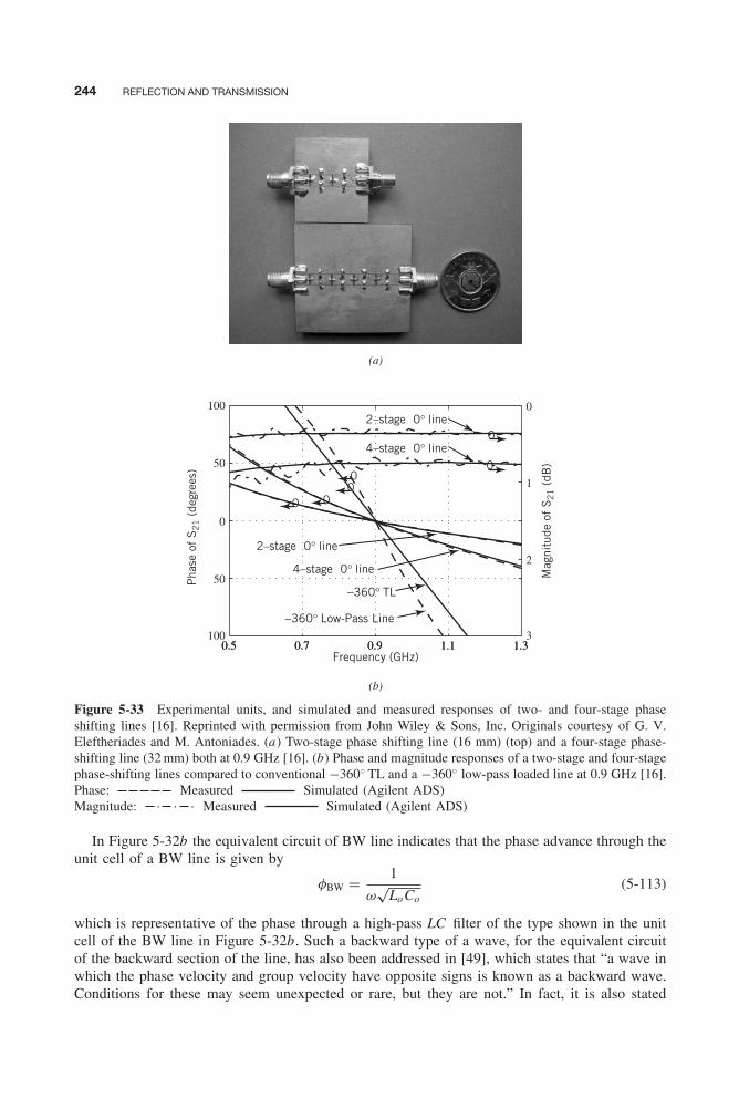
Balanis c05.tex V3 - 11/23/2011 11:47 A.M. Page 244
244 REFLECTION AND TRANSMISSION
(a)
0.5 0.7 0.9 1.1 1.3100
50
0
50
100
Frequency (GHz)
Pha
se o
f S
21 (
degr
ees)
2–stage 0° line
4–stage 0° line
4–stage 0° line
2–stage 0° line
−360° TL
0.5 0.7 0.9 1.1 1.3 3
2
1
0
Mag
nitu
de o
f S
21 (
dB)
0
0
0000
−360° Low-Pass Line
(b)
Figure 5-33 Experimental units, and simulated and measured responses of two- and four-stage phaseshifting lines [16]. Reprinted with permission from John Wiley & Sons, Inc. Originals courtesy of G. V.Eleftheriades and M. Antoniades. (a) Two-stage phase shifting line (16 mm) (top) and a four-stage phase-shifting line (32 mm) both at 0.9 GHz [16]. (b) Phase and magnitude responses of a two-stage and four-stagephase-shifting lines compared to conventional −360◦ TL and a −360◦ low-pass loaded line at 0.9 GHz [16].Phase: Measured Simulated (Agilent ADS)Magnitude: . . . Measured Simulated (Agilent ADS)
In Figure 5-32b the equivalent circuit of BW line indicates that the phase advance through theunit cell of a BW line is given by
φBW = 1
ω√
LoCo(5-113)
which is representative of the phase through a high-pass LC filter of the type shown in the unitcell of the BW line in Figure 5-32b. Such a backward type of a wave, for the equivalent circuitof the backward section of the line, has also been addressed in [49], which states that “a wave inwhich the phase velocity and group velocity have opposite signs is known as a backward wave.Conditions for these may seem unexpected or rare, but they are not.” In fact, it is also stated
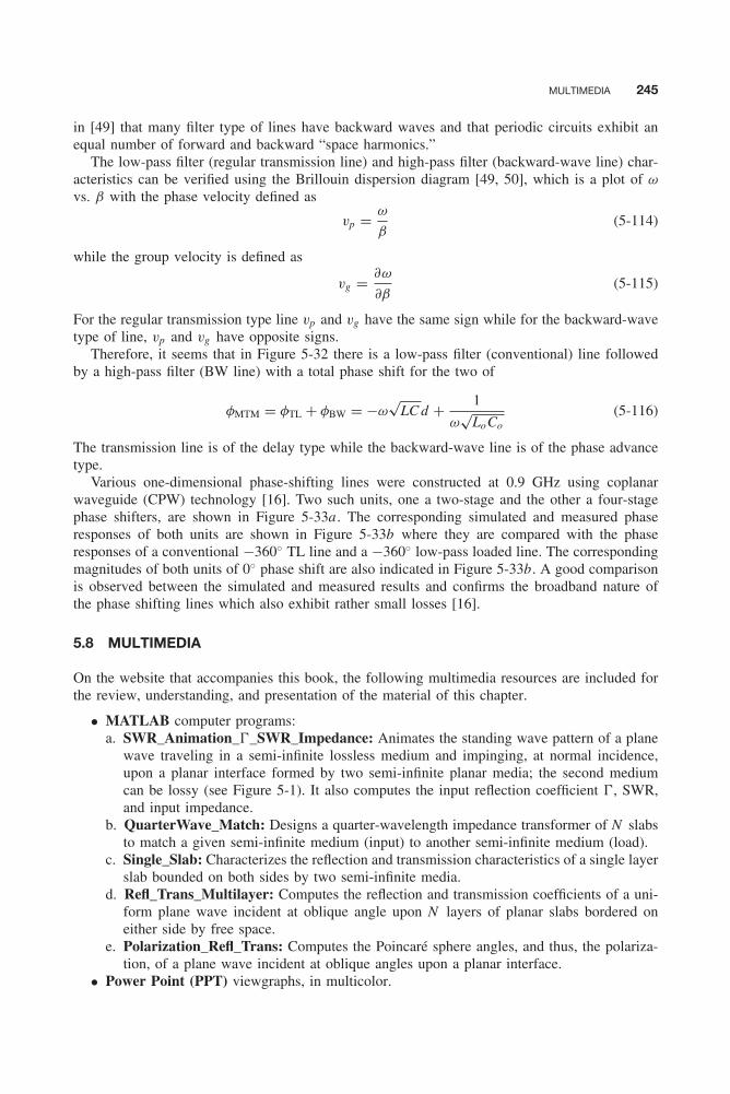
Balanis c05.tex V3 - 11/23/2011 11:47 A.M. Page 245
MULTIMEDIA 245
in [49] that many filter type of lines have backward waves and that periodic circuits exhibit anequal number of forward and backward “space harmonics.”
The low-pass filter (regular transmission line) and high-pass filter (backward-wave line) char-acteristics can be verified using the Brillouin dispersion diagram [49, 50], which is a plot of ω
vs. β with the phase velocity defined as
vp = ω
β(5-114)
while the group velocity is defined as
vg = ∂ω
∂β(5-115)
For the regular transmission type line vp and vg have the same sign while for the backward-wavetype of line, vp and vg have opposite signs.
Therefore, it seems that in Figure 5-32 there is a low-pass filter (conventional) line followedby a high-pass filter (BW line) with a total phase shift for the two of
φMTM = φTL + φBW = −ω√
LC d + 1
ω√
LoCo(5-116)
The transmission line is of the delay type while the backward-wave line is of the phase advancetype.
Various one-dimensional phase-shifting lines were constructed at 0.9 GHz using coplanarwaveguide (CPW) technology [16]. Two such units, one a two-stage and the other a four-stagephase shifters, are shown in Figure 5-33a . The corresponding simulated and measured phaseresponses of both units are shown in Figure 5-33b where they are compared with the phaseresponses of a conventional −360◦ TL line and a −360◦ low-pass loaded line. The correspondingmagnitudes of both units of 0◦ phase shift are also indicated in Figure 5-33b. A good comparisonis observed between the simulated and measured results and confirms the broadband nature ofthe phase shifting lines which also exhibit rather small losses [16].
5.8 MULTIMEDIA
On the website that accompanies this book, the following multimedia resources are included forthe review, understanding, and presentation of the material of this chapter.
• MATLAB computer programs:a. SWR_Animation_�_SWR_Impedance: Animates the standing wave pattern of a plane
wave traveling in a semi-infinite lossless medium and impinging, at normal incidence,upon a planar interface formed by two semi-infinite planar media; the second mediumcan be lossy (see Figure 5-1). It also computes the input reflection coefficient �, SWR,and input impedance.
b. QuarterWave_Match: Designs a quarter-wavelength impedance transformer of N slabsto match a given semi-infinite medium (input) to another semi-infinite medium (load).
c. Single_Slab: Characterizes the reflection and transmission characteristics of a single layerslab bounded on both sides by two semi-infinite media.
d. Refl_Trans_Multilayer: Computes the reflection and transmission coefficients of a uni-form plane wave incident at oblique angle upon N layers of planar slabs bordered oneither side by free space.
e. Polarization_Refl_Trans: Computes the Poincaré sphere angles, and thus, the polariza-tion, of a plane wave incident at oblique angles upon a planar interface.
• Power Point (PPT) viewgraphs, in multicolor.

Balanis c05.tex V3 - 11/23/2011 11:47 A.M. Page 246
246 REFLECTION AND TRANSMISSION
REFERENCES
1. C. A. Balanis, Antenna Theory: Analysis and Design , Third Edition, John Wiley & Sons, New York,2005.
2. M. A. Plonus, Applied Electromagnetics , McGraw-Hill, New York, 1978.3. D. T. Paris and F. K. Hurd, Basic Electromagnetic Theory , McGraw-Hill, New York, 1969.4. R. B. Adler, L. J. Chu, and R. M. Fano, Electromagnetic Energy Transmission and Radiation , Chapters
7 and 8, John Wiley & Sons, New York, 1960.5. J. J. Holmes and C. A. Balanis, “Refraction of a uniform plane wave incident on a plane boundary
between two lossy media,” IEEE Trans. Antennas Propagat., vol. AP-26, no. 5, pp. 738–741, September1978.
6. R. D. Radcliff and C. A. Balanis, “Modified propagation constants for nonuniform plane wave trans-mission through conducting media,” IEEE Trans. Geoscience Remote Sensing, vol. GE-20, no. 3, pp.408–411, July 1982.
7. J. D. Kraus, Electromagnetics , Fourth Edition, McGraw-Hill, New York, 1992.8. R. E. Collin, Foundations for Microwave Engineering , Second Edition, McGraw-Hill, New York, 1992.9. R. E. Collin and J. Brown, “The design of quarter-wave matching layers for dielectric surfaces,” Proc.
IEE , vol. 103, Part C, pp. 153–158, March 1956.10. S. B. Cohn, “Optimum design of stepped transmission line transformers,” IRE Trans. Microwave Theory
Tech., vol. MTT-3, pp. 16–21, April 1955.11. L. Young, “Optimum quarter-wave transformers,” IRE Trans. Microwave Theory Tech., vol. MTT-8, pp.
478–482, September 1960.12. G. L. Matthaei, L. Young, and E. M. T. Jones, Microwave Filters, Impedance-Matching Networks and
Coupling Structures , McGraw-Hill, New York, 1964.13. N. Engheta and R. W. Ziolkowski (editors), Metamaterials: Physics and Engineering Explorations , N.
Engheta, R. W. Ziolkowski, Editors, IEEE Press, Wiley Inter-Science, New York, 2006.14. IEEE Transactions on Antennas and Propagation , Special Issue on Metamaterials, vol. 51, no. 10,
October 2003.15. G. V. Eleftheriades and K. G. Balmain (editors), Negative-Refraction Metamaterials: Fundamental
Principles and Applications , John Wiley & Sons, New York, 2005.16. G.V. Eleftheriades and M. A. Antoniades, “Antenna Application of Negative Refractive Index Trans-
mission Line (NRI-TL) Metamaterials,” Chapter 14, in Modern Antenna Handbook , C. A. Balanis(editor), John Wiley & Sons, pp. 677–736, 2008.
17. C. Caloz and T. Itoh, Electromagnetic Metamaterials: Transmission Line Theory and Microwave Appli-cations , John Wiley & Sons, New York, 2006.
18. R. Marques, F. Martin, and M. Sorolla, Metamaterials with Negative Parameters: Theory, Design andMicrowave Applications , John Wiley & Sons, New York, 2008.
19. B. A. Munk, Metamaterials: Critique and Alternatives , John Wiley & Sons, New York, 2009.20. B. E. Spielman, S. Amari, C. Caloz, G. V. Eleftheriades, T. Itoh, D. R. Jackson, R. Levy, J. D. Rhodes
and R. V. Snyder, “Metamaterials face-off. Metamaterials: A rich opportunity for discovery or anoverhyped gravy train!,” IEEE Microwave Magazine, pp. 8–10, 12, 14, 16–17, 22, 26, 28, 30, 32, 34,36, 38, 42, May 2009.
21. P. M. Valanju, R. M. Walser, and A. P. Valanju, “Wave refraction in negative-index media: alwayspositive and very inhomogeneous,” Phys. Rev. Lett ., vol. 88, no. 18, 187401:1–4, May 2002.
22. G. K. Karawas and R. E. Collin, “Spherical shell of ENG metamaterial surrounding a dipole,” MilitaryCommunications Conference 2008 (MILCOM 2008), pp. 1–7, San Diego, CA, November 2008.
23. R. C. Hansen and R. E. Collin, Small Antenna Handbook , John Wiley & Sons, Hoboken, NJ, 2011.24. J. C. Bose, “On the rotation of plane of polarization of electric wave by a twisted structure,” Proc. Roy.
Soc., vol. 63, pp. 146–152, 1898.25. I. V. Lindell, A. H. Sihvola and J. Kurkijarvi, “Karl F. Lindman: The last Hertzian and a Harbinger of
electromagnetic chirality,” IEEE Antennas Propagat. Magazine, vol. 34, no. 3, pp. 24–30, 1992.26. W. E Kock, “Metallic delay lines,” Bell Sys. Tech. J., Vol. 27, pp. 58–82, 1948.
Balanis c05.tex V3 - 11/23/2011 11:47 A.M. Page 247
PROBLEMS 247
27. V. G. Veselago, “The electrodynamics of substances with simultaneous negative values of ε and μ,”Sov. Phys.-Usp., vol. 47, pp. 509–514, Jan.–Feb. 1968.
28. R. E. Collin, “Frequency dispersion limits resolution in Veselago lens,” Progress in ElectromagneticResearch , vol. 19, pp. 233–261, 2010.
29. A.D. Yaghjian and T.B. Hansen, “Plane-wave solutions to frequency-domain and time-domain scatteringfrom magnetodielectric slabs,” Phys. Rev. E , 73, 046608, April 2006; erratum, 76, 049903, October2007.
30. J. B. Pendry, A. J. Holden, W. J. Stewart and I. Youngs, “Extremely, low-frequency plasmons inmetallic mesostructure,” Phys. Rev. Letters., vol. 76, pp. 4773–4776, June 1996.
31. J. B. Pendry, A. J. Holden, D. J. Robbins, and W. J. Stewart, “Low-frequency plasmons in thin wirestructures,” J. Phys., Condens. Matter , vol. 10, pp. 4785–4809, 1998.
32. J. B. Pendry, A. J. Holden, D. J. Robbins, and W. J. Stewart, “Magnetism from conductors and enhancednonlinear phenomena,” IEEE Trans. Microwave Theory Tech., vol. 47, no. 11, pp. 2075–2081, Nov.1999.
33. J. B. Pendry, “Negative refraction makes a perfect lens,” Phys. Rev. Lett ., vol. 85, pp. 3966–3969, Oct.2000.
34. D. R. Smith, W. J. Padilla, D. C. Vier, S.C. Nemat-Nasser, and S. Schultz, “Composite medium withsimultaneously negative permeability and permittivity,” Phys. Rev. Lett., vol. 84, pp. 4184–4187, May2000.
35. D. R. Smith, D. C. Vier, N. Kroll, and S. Schultz, “Direct calculation of the permeability and permittivityfor left-handed metamaterials,” Appl. Phys. Lett., vol. 77, pp. 2246–2248, Oct. 2000.
36. D. R. Smith and N. Kroll, “Negative refractive index in left-handed materials,” Phys. Rev. Lett., vol.85, pp. 2933–2936, Oct. 2000.
37. R. A. Shelby, D. R. Smith, S. C. Nemat-Nasser, and S. Schultz, “Microwave transmissionthrough a two-dimensional, isotropic, left-handed metamaterial,” Appl. Phys. Lett., 78, pp. 489–491,Jan. 2001.
38. A. Shelby, D. R. Smith, and S. Schultz, “Experimental verification of a negative index-of-refraction,”Science, vol. 292, pp. 77–79, April 2001.
39. B. A. Munk, Finite Antenna Arrays and FSS , John Wiley & Sons, Hoboken, NJ, 2003.40. T. M. Grzegorczyk, J. A. Kong, and R. Lixin, “Refraction experiments in waveguide environments,”
Chapter 4 in Metamaterials: Physics and Engineering Explorations N. Engeta and R. W. Ziolkowski(editors), Wiley-Interscience, 2006.
41. IEEE Transactions on Antennas and Propagation .42. IEEE Transactions on Microwave Theory and Techniques .43. IEEE Antennas and Wireless Propagation Letters .44. IEEE Microwave and Wireless Components Letters .45. Physical Review Letters .46. Journal of Applied Physics .47. G. V. Eleftheriades, “EM transmission-line metamaterials,” Materials Today , vol. 12, no. 3, pp. 30–41,
March 2009.48. R. W. Ziolkowski, “Pulsed and CW Gaussian beam interactions with double negative material slabs,”
Opt. Express , Vol. 11, pp. 662–681, April 2003.49. S. Ramo, J. R. Whinnery and T. Van Duzer, Fields and Waves in Communication Electronics , Third
Edition, John Wiley & Sons, New York, 1994.50. D. M. Pozar, Microwave Engineering , Second Edition, John Wiley & Sons, New York, 2004.
PROBLEMS
5.1. A uniform plane wave traveling in a dielec-tric medium with εr = 4 and μr = 1 is inci-dent normally upon a free-space medium. Ifthe incident electric field is given by
Ei = ây 2 × 10⁻³e−jβz V/m
write the:
(a) Corresponding incident magnetic field.(b) Reflection and transmission coefficients.

Balanis c05.tex V3 - 11/23/2011 11:47 A.M. Page 248
248 REFLECTION AND TRANSMISSION
(c) Reflected and transmitted electric andmagnetic fields.
(d) Incident, reflected, and transmitted po-wer densities.
zy
x
e0, m0er = 4
mr = 1
Figure P5-1
5.2. The dielectric constant of water is 81.Calculate the percentage of power densityreflected and transmitted when a uniformplane wave traveling in air is incident nor-mally upon a calm lake. Assume that thewater in the lake is lossless.
5.3. A uniform plane wave propagating in a me-dium with relative permittivity of 4 is inci-dent normally upon a dielectric medium withdielectric constant of 9. Assuming both mediaare nonferromagnetic and lossless, determinethe:(a) Reflection and transmission coefficients.(b) Percentage of incident power density
that is reflected and transmitted.
5.4. A vertical interface is formed by havingfree space to its left and a lossless dielec-tric medium to its right with ε = 4ε0 andμ = μ0, as shown in Figure P5-4. The inci-dent electric field of a uniform plane wavetraveling in the free-space medium and inci-dent normally upon the interface has a value
x
z
e0, m0 4e0, m0
y
Figure P5-4
of 2 × 10⁻³ V/m right before it strikes theboundary. At a frequency of 3 GHz, find the:(a) Reflection coefficient.(b) SWR in the free-space medium.(c) Positions (in meters) in the free-space
medium where the electric field maximaand minima occur.
(d) Maximum and minimum values of theelectric field in the free-space medium.
5.5. A uniform plane wave traveling in air isincident upon a flat, lossless, and infinite inextent dielectric interface with a dielectricconstant of 4. In the air medium, a standingwave is formed. If the normalized magnitudeof the incident E-field is Eo = 1, determinethe:(a) Maximum value of the E-field standing
wave pattern in air.(b) Shortest distance l (in λo) from the
interface where the first maximum in theE- field standing wave pattern will occur(normalized to the incident field).
(c) Minimum value of the E-field standingwave pattern in air (normalized to theincident field).
(d) Shortest distance l (in λo) in air fromthe interface where the first minimumin the E-field standing wave pattern willoccur (normalized to the incident field).
(e) Standing Wave Ratio (SWR) measuredin the air medium.
(f) Input wave impedance inside the airmedium where the:1. First maximum in the E-field stand-
ing wave pattern occurs.2. First minimum in the E-field standing
wave pattern occurs.
5.6. A CW circularly-polarized wave of f =100 MHz of the form
Ei (z ) = (âx − j ây
)e−j 6πz
where z is in meters, is traveling inside alossless dielectric medium and is normallyincident upon a flat planar interface formedby the dielectric medium and air. The inter-face is on the xy-plane. Assuming the per-meability of the dielectric medium is thesame as free space, determine the:(a) Dielectric constant (relative permittiv-
ity) of the dielectric medium.(b) Reflection coefficients for the âx and ây
components.
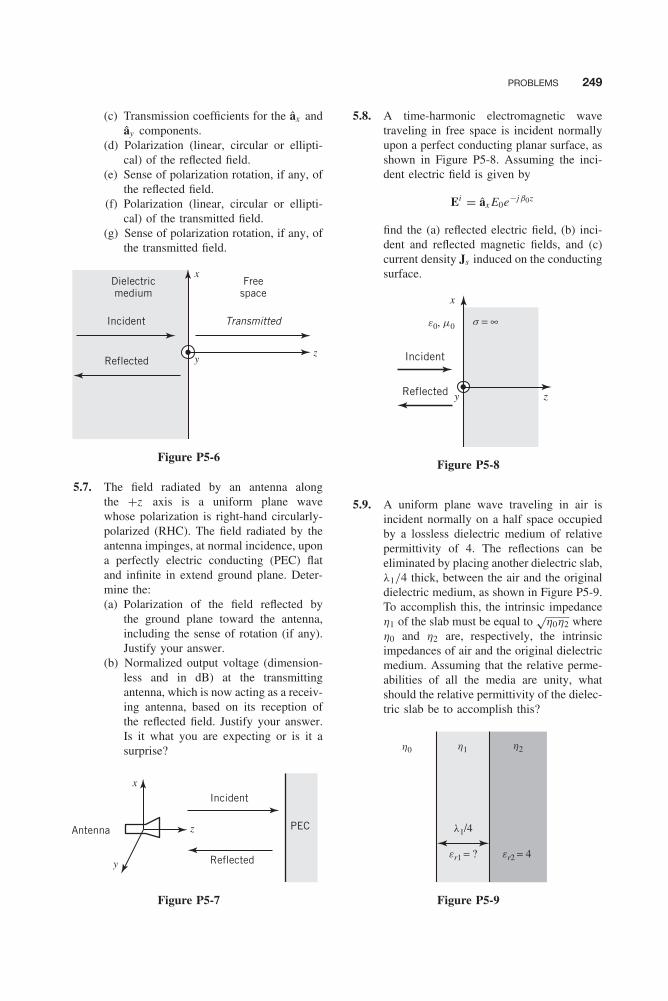
Balanis c05.tex V3 - 11/23/2011 11:47 A.M. Page 249
PROBLEMS 249
(c) Transmission coefficients for the âx andây components.
(d) Polarization (linear, circular or ellipti-cal) of the reflected field.
(e) Sense of polarization rotation, if any, ofthe reflected field.
(f) Polarization (linear, circular or ellipti-cal) of the transmitted field.
(g) Sense of polarization rotation, if any, ofthe transmitted field.
x
zy
Freespace
Dielectricmedium
Incident
Reflected
Transmitted
Figure P5-6
5.7. The field radiated by an antenna alongthe +z axis is a uniform plane wavewhose polarization is right-hand circularly-polarized (RHC). The field radiated by theantenna impinges, at normal incidence, upona perfectly electric conducting (PEC) flatand infinite in extend ground plane. Deter-mine the:(a) Polarization of the field reflected by
the ground plane toward the antenna,including the sense of rotation (if any).Justify your answer.
(b) Normalized output voltage (dimension-less and in dB) at the transmittingantenna, which is now acting as a receiv-ing antenna, based on its reception ofthe reflected field. Justify your answer.Is it what you are expecting or is it asurprise?
PECAntenna z
Incident
Reflectedy
x
Figure P5-7
5.8. A time-harmonic electromagnetic wavetraveling in free space is incident normallyupon a perfect conducting planar surface, asshown in Figure P5-8. Assuming the inci-dent electric field is given by
Ei = âx E0e−jβ0z
find the (a) reflected electric field, (b) inci-dent and reflected magnetic fields, and (c)current density Js induced on the conductingsurface.
x
z
e0, m0 s = ∞
y
Incident
Reflected
Figure P5-8
5.9. A uniform plane wave traveling in air isincident normally on a half space occupiedby a lossless dielectric medium of relativepermittivity of 4. The reflections can beeliminated by placing another dielectric slab,λ1/4 thick, between the air and the originaldielectric medium, as shown in Figure P5-9.To accomplish this, the intrinsic impedanceη1 of the slab must be equal to
√η0η2 where
η0 and η2 are, respectively, the intrinsicimpedances of air and the original dielectricmedium. Assuming that the relative perme-abilities of all the media are unity, whatshould the relative permittivity of the dielec-tric slab be to accomplish this?
h0 h1 h2
er1 = ? er2 = 4
l1/4
Figure P5-9

Balanis c05.tex V3 - 11/23/2011 11:47 A.M. Page 250
250 REFLECTION AND TRANSMISSION
5.10. A uniform plane wave traveling in freespace is incident normally upon a losslessdielectric slab of thickness t , as shown inFigure P5-10. Free space is found on theother side of the slab. Derive expressionsfor the total reflection and transmission coef-ficients in terms of the media constitutiveelectrical parameters and thickness of theslab.
t
x
zy
e0, m0 e0, m0e1, m1
Figure P5-10
5.11. The vertical height from the ground to a per-son’s eyes is h , and from his eyes to the topof his head is h . A flat mirror of height yis hung vertically at a distance x from theperson. The top of the mirror is at a heightof h + (h/2) from the ground, as shown inFigure P5-11. What is the minimum lengthof the mirror in the vertical direction so thatthe person only sees his entire image in themirror?
Δh
Δh2
Mirror
h
x
h
y
+
Figure P5-11
5.12. A linearly polarized wave is incident on anisosceles right triangle (prism) of glass, andit exits as shown in Figure P5-12. Assum-ing that the dielectric constant of the prismis 2.25, find the ratio of the exited averagepower density Se to that of the incident Si .
er = 2.25
45°
45°
Figure P5-12
5.13. A uniform plane wave is obliquely incidentat an angle of 30◦ on a dielectric slab ofthickness d with ε = 4ε0 and μ = μ0 thatis embedded in free space, as shown inFigure P5-13. Find the angles θ2 and θ3 (indegrees).
d
q3
q2
30°
q3
Figure P5-13
5.14. A perpendicularly polarized uniform planewave traveling in free space is obliquelyincident on a dielectric with a relative per-mittivity of 4, as shown in Figure 5-2. Whatshould the incident angle be so that thereflected power density is 25% of the inci-dent power density?
5.15. Repeat Problem 5-14 for a parallel polarizeduniform plane wave.
5.16. Find the Brewster angles for the interfaceswhose reflection coefficients are plotted inFigure 5-5.
5.17. A parallel-polarized uniform plane waveis incident obliquely on a lossless dielec-tric slab that is embedded in a free-spacemedium, as shown in Figure P5-17. Derive
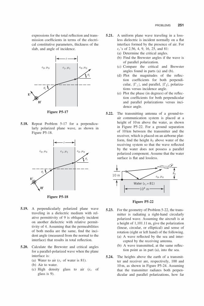
Balanis c05.tex V3 - 11/23/2011 11:47 A.M. Page 251
PROBLEMS 251
expressions for the total reflection and trans-mission coefficients in terms of the electri-cal constitutive parameters, thickness of theslab, and angle of incidence.
e0, m0
t
qt
qi
Ei
Hi
e0, m0e1, m1
Figure P5-17
5.18. Repeat Problem 5-17 for a perpendicu-larly polarized plane wave, as shown inFigure P5-18.
e0, m0
qt
qi
Ei
Hi
e0, m0e1, m1
t
Figure P5-18
5.19. A perpendicularly polarized plane wavetraveling in a dielectric medium with rel-ative permittivity of 9 is obliquely incidenton another dielectric with relative permit-tivity of 4. Assuming that the permeabilitiesof both media are the same, find the inci-dent angle (measured from the normal to theinterface) that results in total reflection.
5.20. Calculate the Brewster and critical anglesfor a parallel-polarized wave when the planeinterface is:(a) Water to air (εr of water is 81).(b) Air to water.(c) High density glass to air (εr of
glass is 9).
5.21. A uniform plane wave traveling in a loss-less dielectric is incident normally on a flatinterface formed by the presence of air. Forεr ’s of 2.56, 4, 9, 16, 25, and 81:(a) Determine the critical angles.(b) Find the Brewster angles if the wave is
of parallel polarization.(c) Compare the critical and Brewster
angles found in parts (a) and (b).(d) Plot the magnitudes of the reflec-
tion coefficients for both perpendi-cular, |�⊥|, and parallel, |�|||, polariza-tions versus incidence angle.
(e) Plot the phase (in degrees) of the reflec-tion coefficients for both perpendicularand parallel polarizations versus inci-dence angle.
5.22. The transmitting antenna of a ground-to-air communication system is placed at aheight of 10 m above the water, as shownin Figure P5-22. For a ground separationof 10 km between the transmitter and thereceiver, which is placed on an airborne plat-form, find the height h2 above water of thereceiving system so that the wave reflectedby the water does not possess a parallelpolarized component. Assume that the watersurface is flat and lossless.
10 m
104 m
h2
Water (er = 81)
e0, m0
Figure P5-22
5.23. For the geometry of Problem 5-22, the trans-mitter is radiating a right-hand circularlypolarized wave. Assuming the aircraft is ata height of 1,101.11 m, give the polarization(linear, circular, or elliptical) and sense ofrotation (right or left hand) of the following.(a) A wave reflected by the sea and inter-
cepted by the receiving antenna.(b) A wave transmitted, at the same reflec-
tion point as in part (a), into the sea.
5.24. The heights above the earth of a transmit-ter and receiver are, respectively, 100 and10 m, as shown in Figure P5-24. Assumingthat the transmitter radiates both perpen-dicular and parallel polarizations, how far
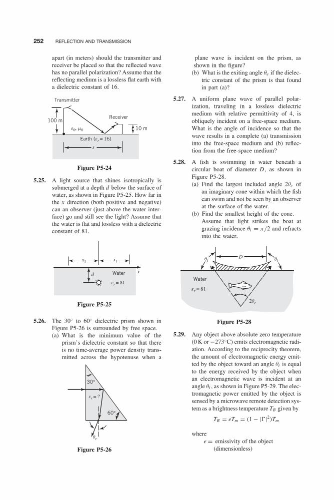
Balanis c05.tex V3 - 11/23/2011 11:47 A.M. Page 252
252 REFLECTION AND TRANSMISSION
apart (in meters) should the transmitter andreceiver be placed so that the reflected wavehas no parallel polarization? Assume that thereflecting medium is a lossless flat earth witha dielectric constant of 16.
Transmitter
100 mReceiver
Earth (er = 16)
10 m
s
e0, m0
Figure P5-24
5.25. A light source that shines isotropically issubmerged at a depth d below the surface ofwater, as shown in Figure P5-25. How far inthe x direction (both positive and negative)can an observer (just above the water inter-face) go and still see the light? Assume thatthe water is flat and lossless with a dielectricconstant of 81.
Water
er = 81
d
x1 x1
x
Figure P5-25
5.26. The 30◦ to 60◦ dielectric prism shown inFigure P5-26 is surrounded by free space.(a) What is the minimum value of the
prism’s dielectric constant so that thereis no time-average power density trans-mitted across the hypotenuse when a
30°
60°
er = ?
qe
Figure P5-26
plane wave is incident on the prism, asshown in the figure?
(b) What is the exiting angle θe if the dielec-tric constant of the prism is that foundin part (a)?
5.27. A uniform plane wave of parallel polar-ization, traveling in a lossless dielectricmedium with relative permittivity of 4, isobliquely incident on a free-space medium.What is the angle of incidence so that thewave results in a complete (a) transmissioninto the free-space medium and (b) reflec-tion from the free-space medium?
5.28. A fish is swimming in water beneath acircular boat of diameter D , as shown inFigure P5-28.(a) Find the largest included angle 2θc of
an imaginary cone within which the fishcan swim and not be seen by an observerat the surface of the water.
(b) Find the smallest height of the cone.Assume that light strikes the boat atgrazing incidence θi = π/2 and refractsinto the water.
Water
2qc
D
er = 81
qi qi
Figure P5-28
5.29. Any object above absolute zero temperature(0 K or −273◦C) emits electromagnetic radi-ation. According to the reciprocity theorem,the amount of electromagnetic energy emit-ted by the object toward an angle θi is equalto the energy received by the object whenan electromagnetic wave is incident at anangle θi , as shown in Figure P5-29. The elec-tromagnetic power emitted by the object issensed by a microwave remote detection sys-tem as a brightness temperature TB given by
TB = eTm = (1 − |�|2)Tm
wheree = emissivity of the object
(dimensionless)

Balanis c05.tex V3 - 11/23/2011 11:47 A.M. Page 253
PROBLEMS 253
Water
er = 81, s = 0
e0, m0
qi
qt
Figure P5-29
� = reflection coefficient for theinterface
Tm = thermal (molecular) temperatureof object (water)
It is desired to make the brightness temper-ature TB equal to the thermal (molecular)temperature Tm .(a) State the polarization (perpendicular,
parallel, or both) that will accomplishthis.
(b) At what angle θi (in degrees) will thisoccur when the object is a flat water sur-face?
5.30. A uniform plane wave at a frequency of104 Hz is traveling in air, and it is incidentnormally on a large body of salt water withconstants of σ = 3 S/m and εr = 81. If themagnitude of the electric field on the saltwater side of the interface is 10−3 V/m, findthe depth (in meters) inside the salt water atwhich the magnitude of the electric field hasbeen reduced to 0.368 × 10⁻³ V/m.
5.31. At large observation distances, the field radi-ated by a satellite antenna that is attempt-ing to communicate with a submergedsubmarine is locally TEM (also assume uni-form plane wave), as shown in Figure P5-31.Assuming the incident electric field before
er = 81
e0, m0
s = 1 S/m Submarine
Satellite
d
Figure P5-31
it impinges on the water is 1 mV/m and thesubmarine is directly below the satellite, findat 1 MHz the:(a) Intensity of the reflected E field.(b) SWR created in air.(c) Incident and reflected power densities.(d) Intensity of the transmitted E field.(e) Intensity of the transmitted power den-
sity.(f) Depth d (in meters) of the submarine
where the intensity of the transmittedelectric field is 0.368 of its value imme-diately after it enters the water.
(g) Depth (in meters) of the submarine sothat the distance from the surface ofthe ocean to the submarine is 20λ (λin water).
(h) Time (in seconds) it takes the wave totravel from the surface of the ocean tothe submarine at a depth of 100 m.
(i) Ratio of velocity of the wave in waterto that in air (v/v0).
5.32. A uniform plane wave traveling inside agood conductor with conductivity σ1 is inci-dent normally on another good conductorwith conductivity σ2, where σ1 >σ2. Deter-mine the ratio of σ1/σ2 so that the SWRinside medium 1 near the interface is 1.5.
5.33. A right-hand circularly polarized uniformplane wave traveling in air is incident nor-mally on a flat and smooth water surfacewith εr = 81 and σ = 0.1 S/m, as shownin Figure P5-33. Assuming a frequency of1 GHz and an incident electric field of
Water er = 81
s = 0.1 S/m
z
y
x
Reflected lncident
Figure P5-33
Ei = (ây + âz ejψ)E0ejβ0x
do the following.(a) Determine the value of ψ .(b) Write an expression for the correspond-
ing incident magnetic field.

Balanis c05.tex V3 - 11/23/2011 11:47 A.M. Page 254
254 REFLECTION AND TRANSMISSION
(c) Write expressions for the reflected elec-tric and magnetic fields.
(d) Determine the polarization (includingsense of rotation) of the reflected wave.
(e) Write expressions for the transmittedelectric and magnetic fields.
(f) Determine the polarization (includingsense of rotation) of the transmittedwave.
(g) Determine the percentage (compared tothe incident) of the reflected and trans-mitted power densities.
5.34. A right-hand circularly polarized wave isincident normally on a perfect conductingflat surface (σ = ∞).(a) What is the polarization and sense of
rotation of the reflected field?(b) What is the normalized (maximum
unity) output voltage if the reflectedwave is received by a right-hand circu-larly polarized antenna?
(c) Repeat part b if the receiving antenna isleft-hand circularly polarized.
5.35. Repeat Problem 5.34 if the reflecting sur-face is water (f = 10 MHz, εr = 81 andσ = 4 S/m).
5.36. A parallel polarized plane wave travelingin a dielectric medium with ε1, μ1 is inci-dent obliquely on a planar interface formedby the dielectric medium with ε2, μ2 suchthat ε2μ2 < ε1μ1. Assuming that the inci-dent angle θi is equal to or greater than thecritical angle θc of (5-35b), derive expres-sions for the reflection coefficient �b
|| andtransmission coefficient T b
|| , and the incidentSi
||, reflected Sr||, and transmitted St
|| averagepower densities respectively.
5.37. A perpendicularly polarized uniform planewave traveling inside a free-space mediumis obliquely incident, at an incident angleθi = 60◦, upon a planar dielectric mediumwith constitutive parameters of ε2 = 4ε0,μ2 = μ0. Using Figure 5-2 as a referencegeometry, determine the:(a) Wave impedance of the:
• Incident wave• Reflected wave• Transmitted wave
(b) Directional impedance in the +z and+x directions, respectively, of the:• Incident wave Z +z
to , Z +xto
• Transmitted wave Z +zt2 , Z +x
t2
(c) Reflection coefficient �+zin in the +z
direction (magnitude and phase) insidethe free-space medium based on:• The directional impedances• An alternate equation• Compare the two answers. Are the
answers the same or different in bothmagnitude and phase? Should they bethe same or different in magnitudeand phase?
(d) SWR inside the free-space medium.
5.38. A uniform plane wave of either parallel orperpendicular polarization, as shown respec-tively in Figures 5-2 and 5-4, travelingin free space is incident upon a dielec-tric/magnetic material such that the productof the relative permittivity and permeabilityof the dielectric/magnetic material is muchgreater than unity; that is
εrμr � 1
The intrinsic impedances of the two mediaare, respectively, η0 (free space) and η
(dielectric/magnetic material).(a) Determine an approximate value of the
refraction angle θt (in degrees) for:1. Perpendicular polarization.2. Parallel polarization.
(b) Obtain simplified expressions, in termsη0 and η, of the Brewster angle θi = θB
for:1. Perpendicular polarization.2. Parallel polarization.
5.39. A dielectric slab of polystyrene (εr = 2.56),of any thickness, is bounded on both of itssides by air. In order to eliminate reflectionson each of its interfaces, the slab is cov-ered on each of its faces with a dielectricmaterial.At a frequency of 10 GHz, determine, foreach dielectric material that must cover eachof the faces of the slab, the:(a) Thickness (in λi ; wavelength in the cor-
responding dielectric).(b) Thickness (in cm).(c) Dielectric constant.(d) Intrinsic impedance of its medium.(e) SWR created in air when a plane wave
impinges at normal incidence from oneof its sides when the slab is covered withthe selected cover material.
5.40. For Example 5-10, determine the bandwidth,and the lower and upper frequencies of the
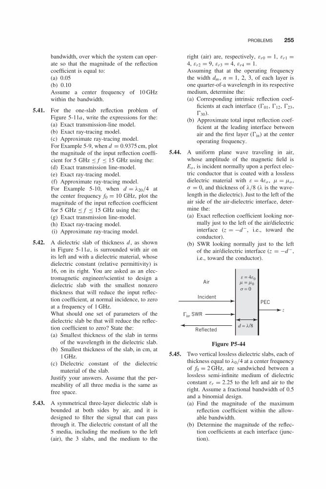
Balanis c05.tex V3 - 11/23/2011 11:47 A.M. Page 255
PROBLEMS 255
bandwidth, over which the system can oper-ate so that the magnitude of the reflectioncoefficient is equal to:(a) 0.05(b) 0.10Assume a center frequency of 10 GHzwithin the bandwidth.
5.41. For the one-slab reflection problem ofFigure 5-11a , write the expressions for the:(a) Exact transmission-line model.(b) Exact ray-tracing model.(c) Approximate ray-tracing model.For Example 5-9, when d = 0.9375 cm, plotthe magnitude of the input reflection coeffi-cient for 5 GHz ≤ f ≤ 15 GHz using the:(d) Exact transmission line-model.(e) Exact ray-tracing model.(f) Approximate ray-tracing model.For Example 5-10, when d = λ20/4 atthe center frequency f0 = 10 GHz, plot themagnitude of the input reflection coefficientfor 5 GHz ≤ f ≤ 15 GHz using the:(g) Exact transmission line-model.(h) Exact ray-tracing model.(i) Approximate ray-tracing model.
5.42. A dielectric slab of thickness d , as shownin Figure 5-11a , is surrounded with air onits left and with a dielectric material, whosedielectric constant (relative permittivity) is16, on its right. You are asked as an elec-tromagnetic engineer/scientist to design adielectric slab with the smallest nonzerothickness that will reduce the input reflec-tion coefficient, at normal incidence, to zeroat a frequency of 1 GHz.What should one set of parameters of thedielectric slab be that will reduce the reflec-tion coefficient to zero? State the:(a) Smallest thickness of the slab in terms
of the wavelength in the dielectric slab.(b) Smallest thickness of the slab, in cm, at
1 GHz.(c) Dielectric constant of the dielectric
material of the slab.Justify your answers. Assume that the per-meability of all three media is the same asfree space.
5.43. A symmetrical three-layer dielectric slab isbounded at both sides by air, and it isdesigned to filter the signal that can passthrough it. The dielectric constant of all the5 media, including the medium to the left(air), the 3 slabs, and the medium to the
right (air) are, respectively, εr0 = 1, εr1 =4, εr2 = 9, εr3 = 4, εr4 = 1.Assuming that at the operating frequencythe width dm , n = 1, 2, 3, of each layer isone quarter-of-a wavelength in its respectivemedium, determine the:(a) Corresponding intrinsic reflection coef-
ficients at each interface (�01, �12, �23,�30).
(b) Approximate total input reflection coef-ficient at the leading interface betweenair and the first layer (�in) at the centeroperating frequency.
5.44. A uniform plane wave traveling in air,whose amplitude of the magnetic field isEo , is incident normally upon a perfect elec-tric conductor that is coated with a losslessdielectric material with ε = 4εo , μ = μo ,σ = 0, and thickness of λ/8 (λ is the wave-length in the dielectric). Just to the left of theair side of the air-dielectric interface, deter-mine the:(a) Exact reflection coefficient looking nor-
mally just to the left of the air/dielectricinterface (z = −d−, i.e., toward theconductor).
(b) SWR looking normally just to the leftof the air/dielectric interface (z = −d−,i.e., toward the conductor).
Aire = 4e0m = m0s = 0
z
IncidentPEC
Γin, SWR
Reflectedd = l/8
Figure P5-44
5.45. Two vertical lossless dielectric slabs, each ofthickness equal to λ0/4 at a center frequencyof f0 = 2 GHz, are sandwiched between alossless semi-infinite medium of dielectricconstant εr = 2.25 to the left and air to theright. Assume a fractional bandwidth of 0.5and a binomial design.(a) Find the magnitude of the maximum
reflection coefficient within the allow-able bandwidth.
(b) Determine the magnitude of the reflec-tion coefficients at each interface (junc-tion).

Balanis c05.tex V3 - 11/23/2011 11:47 A.M. Page 256
256 REFLECTION AND TRANSMISSION
(c) Compute the intrinsic impedances,dielectric constants, and thickness (incentimeters) of each dielectric slab.
(d) Determine the lower and upper frequen-cies of the bandwidth.
(e) Plot the magnitude of the reflectioncoefficient inside the dielectric mediumwith εr = 2.25 as a function of fre-quency (within 0 ≤ f /f0 ≤ 2).
5.46. It is desired to design a three-layer (eachlayer of λ0/4 thickness) impedance trans-former to match a semi-infinite dielectricmedium of εr = 9 on one of its sides andone with εr = 2.25 on the other side. Themaximum SWR that can be tolerated insidethe dielectric medium with εr = 9 is 1.1.Assume a center frequency of f0 = 3 GHzand a binomial design.(a) Determine the allowable fractional
bandwidth and the lower and upper fre-quencies of the bandwidth.
(b) Find the magnitude of reflection coeffi-cients at each junction.
(c) Compute the magnitude of the max-imum reflection coefficient within thebandwidth.
(d) Determine the intrinsic impedances,dielectric constants, and thicknesses (incentimeters) of each dielectric slab.
(e) Plot the magnitude of the reflectioncoefficient inside the dielectric mediumwith εr = 9 as a function of frequency(within 0 ≤ f /f0 ≤ 2).
5.47. Repeat Example 5-11 using a Tschebyscheffdesign.
5.48. Repeat Problem 5.45 using a Tschebyscheffdesign.
5.49. Repeat Problem 5.46 using a Tschebyscheffdesign.
5.50. A right-hand (CW) elliptically polarizedwave traveling in free space is obliquelyincident at an angle θi = 30◦, measuredfrom the normal, on a flat perfect electricconductor of infinite extent. If the incidentfield has an axial ratio of −2, determine thepolarization of the reflected field. This is toinclude the axial ratio as well as its sense ofrotation. Assume that the time-phase differ-ence between the components of the incidentfield is 90◦.
5.51. Repeat Problem 5.50 if the reflecting surfaceis a flat lossless (σ2 = 0) ocean (ε2 = 81ε0
and μ2 = μ0) of infinite extent. Also findthe polarization of the wave transmitted intothe water.
5.52. A uniform plane wave is normally inci-dent upon a Perfect Electric Conductor(PEC) medium. The incident electric field isgiven by
Ei (z ) = (âz + j 2ây
)Eoe−jβo x
where βo and Eo are real constants. Assum-ing a e+jωt time convention:(a) Write an expression for the reflected
electric field.(b) For the incident wave, determine the:
• Polarization (linear, circular, or ellip-tical). Justify your answer.
• Sense of rotation of the incident wave(CW or CCW). Justify your answer.
• Axial Ratio (AR). Justify youranswer.
(c) For the reflected wave, determine the:• Polarization (linear, circular or ellip-
tical). Justify your answer.• Sense of rotation of the incident wave
(CW or CCW). Justify your answer.• Axial Ratio (AR). Justify your
answer.For all of the above, be sure to justifyyour answers. Verify with the MATLABcomputer program Polarization_Refl_-Trans.
5.53. A uniform plane wave is normally incidentupon a Perfect Magnetic Conductor (PMC).The incident electric field is given by
Ei (z ) = (2âx − j âz ) Eoe−jβo y
where βo and Eo are real constants. Assum-ing a e+jωt time convention:(a) Write an expression for the reflected
electric field.(b) For the incident wave, determine the:
• Polarization (linear, circular, or ellip-tical). Justify your answer.
• Sense of rotation of the incident wave(CW or CCW). Justify your answer.
• Axial Ratio (AR). Justify youranswer.
(c) For the reflected wave, determine the:• Polarization (linear, circular, or ellip-
tical). Justify your answer.

Balanis c05.tex V3 - 11/23/2011 11:47 A.M. Page 257
PROBLEMS 257
• Sense of rotation of the incident wave(CW or CCW). Justify your answer.
• Axial Ratio (AR). Justify youranswer.
For all of the above, be sure to jus-tify your answers. Also verify withMATLAB computer program Polariza-tion_Refl_Trans.
5.54. A left-hand (CCW) circularly polarizedwave traveling inside a lossless earth, witha dielectric constant of 9, is incident upon aplanar interface formed by the earth and air.The angle of incidence is 18.43495◦. Deter-mine the:(a) Polarization of the reflected wave (lin-
ear, circular, elliptical).(b) Sense of rotation of the reflected wave;
(CW or CCW), if appropriate.(c) Polarization of the transmitted wave
(linear, circular, elliptical).(d) Sense of rotation of the transmitted
wave; (CW, CCW), if appropriate.As an option, you do not have to use toomany analytical equations as long as you can
justify the correct answers using words/text(you can keep the formulations minimal).
Airz
Incident
18.43495°
Earthe = 9e0
m = m0s = 0
yx
Figure P5-54
5.55. Repeat Problem 5.54 when the incidentwave is right-hand (CW) circularly polar-ized.
5.56. Derive the transmission coefficient for thedielectric slab of Example 5-15.
5.57. For a planar interface formed by DPS-DNG materials and assuming parallel polar-ization wave incidence, write expressionsfor the wavenumbers and Poynting vectors,similar in form to the ones of Figure 5-29, (5-110a) through (5-110c) and (5-111a)through (5-111c). Examine the directionsof the wavenumbers and Poynting vectorsof the transmitted wave and compare withthose for a DPS-DPS interface.

Balanis c05.tex V3 - 11/23/2011 11:47 A.M. Page 258
Balanis c06.tex V2 - 11/22/2011 3:14 P.M. Page 259
CHAPTER 6Auxiliary Vector Potentials, Construction of
Solutions, and Radiation andScattering Equations
6.1 INTRODUCTION
It is common practice in the analysis of electromagnetic boundary-value problems to use auxiliaryvector potentials as aids in obtaining solutions for the electric (E) and magnetic (H) fields. Themost common vector potential functions are the A, magnetic vector potential, and F, electricvector potential. They are the same pair that were introduced and used extensively in the solutionof antenna radiation problems [1]. Although the electric and magnetic field intensities (E and H)represent physically measurable quantities, for most engineers the vector potentials are strictlymathematical tools . The introduction of the potentials often simplifies the solution, even thoughit may require determination of additional functions. Much of the discussion in this chapter isborrowed from [1].
The Hertz vector potentials �e and �h make up another pair. The Hertz vector potential�e is analogous to A and �h is analogous to F. The functional relation between them is aproportionality constant that is a function of the frequency and the constitutive parameters of themedium. In the solution of a problem, only one set, A and F or �e and �h , is required. Theauthor prefers A and F, and they will be used throughout this book.
The main objective of this book is to obtain electromagnetic field configurations (modes)of boundary-value propagation, radiation, and scattering problems. These field configurationsmust satisfy Maxwell’s equations or the wave equation, as well as the appropriate boundaryconditions. The procedure is to specify the electromagnetic boundary-value problem, which mayor may not contain sources, and to obtain the field configurations that can exist within the regionof the boundary-value problem. This can be accomplished in either of two ways, as shown inFigure 6-1.
One procedure for obtaining the electric and magnetic fields of a desired boundary-valueproblem is to use Maxwell’s or the wave equations. This is accomplished essentially in one step,and it is represented in Figure 6-1 by path 1. The formulation using such a procedure is assignedto the reader as an end-of-chapter problem.
The other procedure requires two steps. In the first step, the vector potentials A and F (or�e and �h ) are found, once the boundary-value problem is specified. In the second step, theelectric and magnetic fields are found, after the vector potentials are determined. The electric andmagnetic fields are functions of the vector potentials. This procedure is represented by path 2of Figure 6-1, and, although it requires two steps, it is often simpler and more straightforward;hence it is often preferred. The mathematical equations of this procedure will be developed next,
259
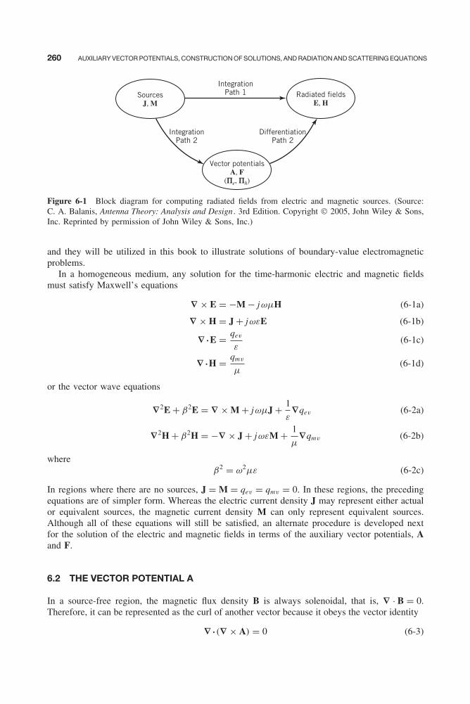
Balanis c06.tex V2 - 11/22/2011 3:14 P.M. Page 260
260 AUXILIARY VECTOR POTENTIALS, CONSTRUCTION OF SOLUTIONS, AND RADIATION AND SCATTERING EQUATIONS
IntegrationPath 1 Radiated fields
E, HSources
J, M
IntegrationPath 2
Vector potentialsA, F
(Πe, Πh)
DifferentiationPath 2
Figure 6-1 Block diagram for computing radiated fields from electric and magnetic sources. (Source:C. A. Balanis, Antenna Theory: Analysis and Design . 3rd Edition. Copyright © 2005, John Wiley & Sons,Inc. Reprinted by permission of John Wiley & Sons, Inc.)
and they will be utilized in this book to illustrate solutions of boundary-value electromagneticproblems.
In a homogeneous medium, any solution for the time-harmonic electric and magnetic fieldsmust satisfy Maxwell’s equations
∇ × E = −M − jωμH (6-1a)
∇ × H = J + jωεE (6-1b)
∇ • E = qev
ε(6-1c)
∇ • H = qmv
μ(6-1d)
or the vector wave equations
∇2E + β2E = ∇ × M + jωμJ + 1
ε∇qev (6-2a)
∇2H + β2H = −∇ × J + jωεM + 1
μ∇qmv (6-2b)
whereβ2 = ω2με (6-2c)
In regions where there are no sources, J = M = qev = qmv = 0. In these regions, the precedingequations are of simpler form. Whereas the electric current density J may represent either actualor equivalent sources, the magnetic current density M can only represent equivalent sources.Although all of these equations will still be satisfied, an alternate procedure is developed nextfor the solution of the electric and magnetic fields in terms of the auxiliary vector potentials, Aand F.
6.2 THE VECTOR POTENTIAL A
In a source-free region, the magnetic flux density B is always solenoidal, that is, ∇ · B = 0.Therefore, it can be represented as the curl of another vector because it obeys the vector identity
∇ • (∇ × A) = 0 (6-3)
Balanis c06.tex V2 - 11/22/2011 3:14 P.M. Page 261
THE VECTOR POTENTIAL A 261
where A is an arbitrary vector. Thus, we define
BA = μHA = ∇ × A (6-4)
or
HA = 1
μ∇ × A (6-4a)
where subscript a indicates the fields due to the A potential. Substituting (6-4a) into Maxwell’scurl equation
∇ × EA = −jωμHA (6-5)
reduces it to∇ × EA = −jωμHA = −jω∇ × A (6-6)
which can also be written as∇ × [EA + jωA] = 0 (6-7)
From the vector identity∇ × (−∇φe) = 0 (6-8)
and (6-7), it follows thatEA + jωA = −∇φe (6-9)
or
EA = −∇φe − jωA (6-9a)
φe represents an arbitrary electric scalar potential that is a function of position.Taking the curl of both sides of (6-4) and using the vector identity
∇ × ∇ × A = ∇(∇ • A) − ∇2A (6-10)
leads to∇ × (μHA) = ∇(∇ • A) − ∇2A (6-10a)
For a homogeneous medium, (6-10a) reduces to
μ∇ × HA = ∇(∇ • A) − ∇2A (6-11)
Equating Maxwell’s equation
∇ × HA = J + jωεEA (6-12)
to (6-11) leads toμJ + jωμεEA = ∇(∇ • A) − ∇2A (6-13)
Substituting (6-9a) into (6-13) reduces it to
∇2A + β2A = −μJ + ∇(∇ • A) + ∇(jωμεφe) = −μJ + ∇(∇ • A + jωμεφe) (6-14)
where β2 = ω2με.
Balanis c06.tex V2 - 11/22/2011 3:14 P.M. Page 262
262 AUXILIARY VECTOR POTENTIALS, CONSTRUCTION OF SOLUTIONS, AND RADIATION AND SCATTERING EQUATIONS
In (6-4), the curl of A was defined. Now we are at liberty to define the divergence of A, whichis independent of its curl. Both are required to uniquely define A. In order to simplify (6-14),let
∇ • A = −jωεμφe ⇒ φe = − 1
jωμε∇ • A (6-15)
which is known as the Lorenz condition (or gauge). Other gauges may be defined. Substituting(6-15) into (6-14) leads to
∇2A + β2A = −μJ (6-16)
In addition, (6-9a) reduces to
EA = −∇φe − jωA = −jωA − j1
ωμε∇(∇ • A) (6-17)
Once A is known, HA can be found from (6-4a) and EA from (6-17). EA can just as easily befound from Maxwell’s equation 6-12 by setting J = 0. Since (6-16) is a vector wave equation,solutions for A in rectangular, cylindrical, and spherical coordinate systems are similar to thosefor E in Sections 3.4.1A, 3.4.2, and 3.4.3, respectively.
6.3 THE VECTOR POTENTIAL F
In a source-free region, the electric flux density D is always solenoidal, that is, ∇ · D = 0.Therefore, it can be represented as the curl of another vector because it obeys the vector identity
∇ • (−∇ × F) = 0 (6-18)
where F is an arbitrary vector. Thus we can define DF by
DF = −∇ × F (6-19)
or
EF = −1
ε∇ × F (6-19a)
where the subscript f indicates the fields due to the F potential. Substituting (6-19a) intoMaxwell’s curl equation
∇ × HF = jωεEF (6-20)
reduces it to∇ × (HF + jωF) = 0 (6-21)
From the vector identity (6-8), it follows that
HF = −∇φm − jωF (6-22)
where φm represents an arbitrary magnetic scalar potential that is a function of position. Takingthe curl of (6-19a)
∇ × EF = −1
ε∇ × ∇ × F = −1
ε[∇(∇ • F) − ∇2F] (6-23)

Balanis c06.tex V2 - 11/22/2011 3:14 P.M. Page 263
THE VECTOR POTENTIALS A AND F 263
and equating it to Maxwell’s equation
∇ × EF = −M − jωμHF (6-24)
lead to∇2F + jωμεHF = ∇(∇ • F) − εM (6-25)
Substituting (6-22) into (6-25) reduces it to
∇2F + β2F = −εM + ∇(∇ • F + jωμεφm) (6-26)
Letting
∇ • F = −jωμεφm ⇒ φm = − 1
jωμε∇ • F (6-27)
reduces (6-26) to
∇2F + β2F = −εM (6-28)
and (6-22) to
HF = −jωF − j
ωμε∇(∇ • F) (6-29)
Once F is known, EF can be found from (6-19a) and HF from (6-29) or (6-24) by setting M = 0.Since (6-28) is a vector wave equation, solutions for F in rectangular, cylindrical, and sphericalcoordinate systems are similar to those for E in Sections 3.4.1A, 3.4.2, and 3.4.3, respectively.
6.4 THE VECTOR POTENTIALS A AND F
In the previous two sections, we derived expressions for the E and H fields in terms of the vectorpotentials A (EA, HA) and F (EF, HF). In addition, expressions that A and F must satisfy werealso derived. The total E and H fields are obtained by the superposition of the individual fieldsdue to A and F.
The procedure that can be used to find the fields of path 2 of Figure 6-1 is as follows.
SUMMARY
1. Specify the electromagnetic boundary-value problem, which may or may not contain anysources within its boundaries, and its desired field configurations (modes).
2. a. Solve for A using (6-16),
∇2A + β2A = −μJ where β2 = ω2με (6-30)
Depending on the problem, solutions for A in rectangular, cylindrical, and sphericalcoordinate systems take the forms found in Sections 3.4.1A, 3.4.2, and 3.4.3, respec-tively.
Balanis c06.tex V2 - 11/22/2011 3:14 P.M. Page 264
264 AUXILIARY VECTOR POTENTIALS, CONSTRUCTION OF SOLUTIONS, AND RADIATION AND SCATTERING EQUATIONS
b. Solve for F using (6-28),
∇2F + β2F = −εM where β2 = ω2με (6-31)
Depending on the problem, solutions for F in rectangular, cylindrical, and sphericalcoordinate systems take the forms found in Sections 3.4.1A, 3.4.2, and 3.4.3, respec-tively.
3. a. Find HA using (6-4a) and EA using (6-17). EA can also be found using (6-12) by lettingJ = 0.
HA = 1
μ∇ × A (6-32a)
EA = −jωA − j1
ωμε∇(∇ • A) (6-32b)
or
EA = 1
jωε∇ × HA (6-32c)
b. Find EF using (6-19a) and HF using (6-29). HF can also be found using (6-24) by lettingM = 0.
EF = −1
ε∇ × F (6-33a)
HF = −jωF − j1
ωμε∇(∇ • F) (6-33b)
or
HF = − 1
jωμ∇ × EF (6-33c)
4. The total fields are then found by the superposition of those given in step 3, that is,
E = EA + EF = −jωA − j1
ωμε∇(∇ • A) − 1
ε∇ × F (6-34)
or
E = EA + EF = 1
jωε∇ × HA − 1
ε∇ × F (6-34a)
and
H = HA + HF = 1
μ∇ × A − jωF − j
1
ωμε∇(∇ • F) (6-35)
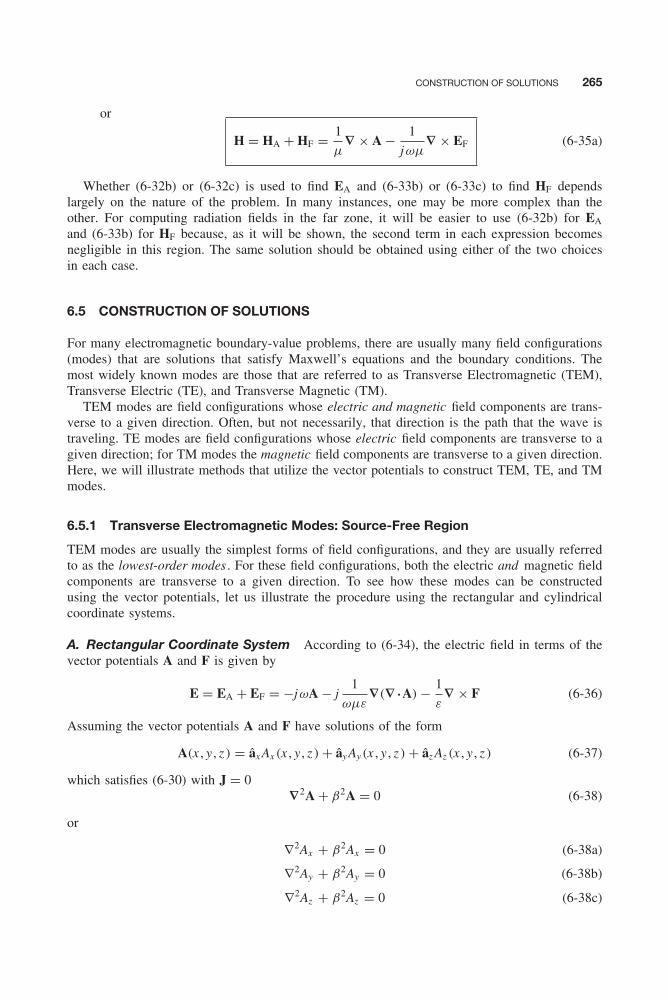
Balanis c06.tex V2 - 11/22/2011 3:14 P.M. Page 265
CONSTRUCTION OF SOLUTIONS 265
or
H = HA + HF = 1
μ∇ × A − 1
jωμ∇ × EF (6-35a)
Whether (6-32b) or (6-32c) is used to find EA and (6-33b) or (6-33c) to find HF dependslargely on the nature of the problem. In many instances, one may be more complex than theother. For computing radiation fields in the far zone, it will be easier to use (6-32b) for EA
and (6-33b) for HF because, as it will be shown, the second term in each expression becomesnegligible in this region. The same solution should be obtained using either of the two choicesin each case.
6.5 CONSTRUCTION OF SOLUTIONS
For many electromagnetic boundary-value problems, there are usually many field configurations(modes) that are solutions that satisfy Maxwell’s equations and the boundary conditions. Themost widely known modes are those that are referred to as Transverse Electromagnetic (TEM),Transverse Electric (TE), and Transverse Magnetic (TM).
TEM modes are field configurations whose electric and magnetic field components are trans-verse to a given direction. Often, but not necessarily, that direction is the path that the wave istraveling. TE modes are field configurations whose electric field components are transverse to agiven direction; for TM modes the magnetic field components are transverse to a given direction.Here, we will illustrate methods that utilize the vector potentials to construct TEM, TE, and TMmodes.
6.5.1 Transverse Electromagnetic Modes: Source-Free Region
TEM modes are usually the simplest forms of field configurations, and they are usually referredto as the lowest-order modes . For these field configurations, both the electric and magnetic fieldcomponents are transverse to a given direction. To see how these modes can be constructedusing the vector potentials, let us illustrate the procedure using the rectangular and cylindricalcoordinate systems.
A. Rectangular Coordinate System According to (6-34), the electric field in terms of thevector potentials A and F is given by
E = EA + EF = −jωA − j1
ωμε∇(∇ • A) − 1
ε∇ × F (6-36)
Assuming the vector potentials A and F have solutions of the form
A(x , y , z ) = âx Ax (x , y , z ) + ây Ay(x , y , z ) + âz Az (x , y , z ) (6-37)
which satisfies (6-30) with J = 0∇2A + β2A = 0 (6-38)
or
∇2Ax + β2Ax = 0 (6-38a)
∇2Ay + β2Ay = 0 (6-38b)
∇2Az + β2Az = 0 (6-38c)

Balanis c06.tex V2 - 11/22/2011 3:14 P.M. Page 266
266 AUXILIARY VECTOR POTENTIALS, CONSTRUCTION OF SOLUTIONS, AND RADIATION AND SCATTERING EQUATIONS
andF(x , y , z ) = âx Fx (x , y , z ) + ây Fy(x , y , z ) + âz Fz (x , y , z ) (6-39)
which satisfies (6-31) with M = 0∇2F + β2F = 0 (6-40)
or
∇2Fx + β2Fx = 0 (6-40a)
∇2Fy + β2Fy = 0 (6-40b)
∇2Fz + β2Fz = 0 (6-40c)
(6-36), when expanded, can be written as
E = âx
[−jωAx − j
1
ωμε
(∂2Ax
∂x 2+ ∂2Ay
∂x ∂y+ ∂2Az
∂x ∂z
)− 1
ε
(∂Fz
∂y− ∂Fy
∂z
)]+ ây
[−jωAy − j
1
ωμε
(∂2Ax
∂x ∂y+ ∂2Ay
∂y2+ ∂2Az
∂y ∂z
)− 1
ε
(∂Fx
∂z− ∂Fz
∂x
)]+ âz
[−jωAz − j
1
ωμε
(∂2Ax
∂x ∂z+ ∂2Ay
∂y ∂z+ ∂2Az
∂z 2
)− 1
ε
(∂Fy
∂x− ∂Fx
∂y
)](6-41)
Similarly, (6-35)
H = HA + HF = 1
μ∇ × A − jωF − j
1
ωμε∇(∇ • F) (6-42)
when expanded using (6-37) and (6-39) can be written as
H = âx
[−jωFx − j
1
ωμε
(∂2Fx
∂x 2+ ∂2Fy
∂x ∂y+ ∂2Fz
∂x ∂z
)+ 1
μ
(∂Az
∂y− ∂Ay
∂z
)]+ ây
[−jωFy − j
1
ωμε
(∂2Fx
∂x ∂y+ ∂2Fy
∂y2+ ∂2Fz
∂y ∂z
)+ 1
μ
(∂Ax
∂z− ∂Az
∂x
)]+ âz
[−jωFz − j
1
ωμε
(∂2Fx
∂x ∂z+ ∂2Fy
∂y ∂z+ ∂2Fz
∂z 2
)+ 1
μ
(∂Ay
∂x− ∂Ax
∂y
)](6-43)
Example 6-1
Using (6-41) and (6-43) derive expressions for the E and H fields, in terms of the components of theA and F potentials, that are TEM to the z direction (TEMz ).
Solution: It is apparent by examining (6-41) and (6-43) that TEMz (Ez = Hz = 0) modes can beobtained by any of the following three combinations.
1. Letting
Ax = Ay = Fx = Fy = 0 Az �= 0 Fz �= 0 ∂/∂x �= 0 ∂/∂y �= 0
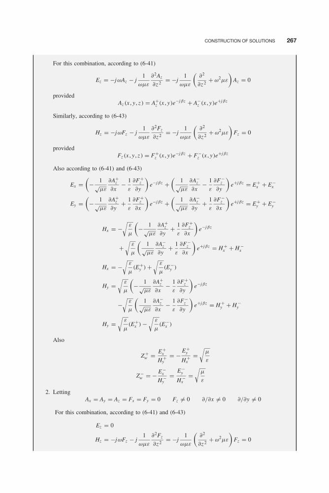
Balanis c06.tex V2 - 11/22/2011 3:14 P.M. Page 267
CONSTRUCTION OF SOLUTIONS 267
For this combination, according to (6-41)
Ez = −jωAz − j1
ωμε
∂2Az
∂z 2= −j
1
ωμε
(∂2
∂z 2+ ω2με
)Az = 0
providedAz (x , y , z ) = A+
z (x , y)e−jβz + A−z (x , y)e+jβz
Similarly, according to (6-43)
Hz = −jωFz − j1
ωμε
∂2Fz
∂z 2= −j
1
ωμε
(∂2
∂z 2+ ω2με
)Fz = 0
providedFz (x , y , z ) = F+
z (x , y)e−jβz + F−z (x , y)e+jβz
Also according to (6-41) and (6-43)
Ex =(
− 1√με
∂A+z
∂x− 1
ε
∂F+z
∂y
)e−jβz +
(1√με
∂A−z
∂x− 1
ε
∂F−z
∂y
)e+jβz = E+
x + E−x
Ey =(
− 1√με
∂A+z
∂y+ 1
ε
∂F+z
∂x
)e−jβz +
(1√με
∂A−z
∂y+ 1
ε
∂F−z
∂x
)e+jβz = E+
y + E−y
Hx = −√
ε
μ
(− 1√
με
∂A+z
∂y+ 1
ε
∂F+z
∂x
)e−jβz
+√
ε
μ
(1√με
∂A−z
∂y+ 1
ε
∂F−z
∂x
)e+jβz = H +
x + H −x
Hx = −√
ε
μ(E+
y ) +√
ε
μ(E−
y )
Hy =√
ε
μ
(− 1√
με
∂A+z
∂x− 1
ε
∂F+z
∂y
)e−jβz
−√
ε
μ
(1√με
∂A−z
∂x− 1
ε
∂F−z
∂y
)e+jβz = H +
y + H −y
Hy =√
ε
μ(E+
x ) −√
ε
μ(E−
x )
Also
Z +w = E+
x
H +y
= − E+y
H +x
=√
μ
ε
Z −w = − E−
x
H −y
= E−y
H −x
=√
μ
ε
2. LettingAx = Ay = Az = Fx = Fy = 0 Fz �= 0 ∂/∂x �= 0 ∂/∂y �= 0
For this combination, according to (6-41) and (6-43)
Ez = 0
Hz = −jωFz − j1
ωμε
∂2Fz
∂z 2= −j
1
ωμε
(∂2
∂z 2+ ω2με
)Fz = 0
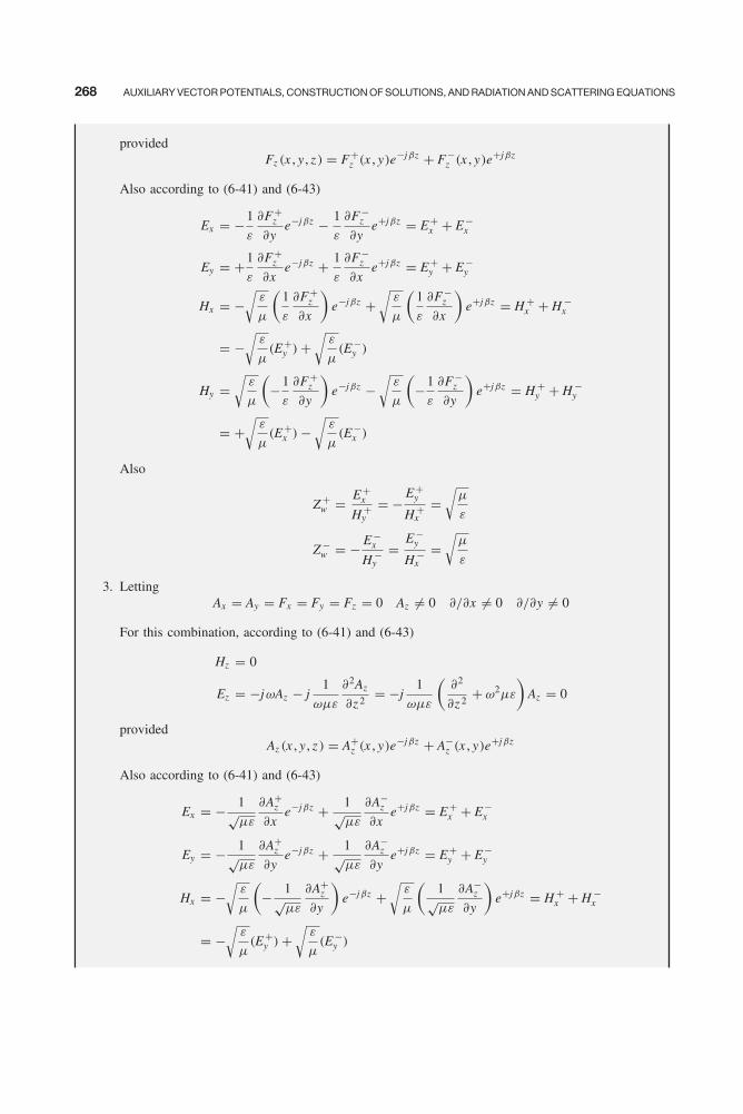
Balanis c06.tex V2 - 11/22/2011 3:14 P.M. Page 268
268 AUXILIARY VECTOR POTENTIALS, CONSTRUCTION OF SOLUTIONS, AND RADIATION AND SCATTERING EQUATIONS
providedFz (x , y , z ) = F+
z (x , y)e−jβz + F−z (x , y)e+jβz
Also according to (6-41) and (6-43)
Ex = −1
ε
∂F+z
∂ye−jβz − 1
ε
∂F−z
∂ye+jβz = E+
x + E−x
Ey = +1
ε
∂F+z
∂xe−jβz + 1
ε
∂F−z
∂xe+jβz = E+
y + E−y
Hx = −√
ε
μ
(1
ε
∂F+z
∂x
)e−jβz +
√ε
μ
(1
ε
∂F−z
∂x
)e+jβz = H +
x + H −x
= −√
ε
μ(E+
y ) +√
ε
μ(E−
y )
Hy =√
ε
μ
(−1
ε
∂F+z
∂y
)e−jβz −
√ε
μ
(−1
ε
∂F−z
∂y
)e+jβz = H +
y + H −y
= +√
ε
μ(E+
x ) −√
ε
μ(E−
x )
Also
Z +w = E+
x
H +y
= − E+y
H +x
=√
μ
ε
Z −w = − E−
x
H −y
= E−y
H −x
=√
μ
ε
3. LettingAx = Ay = Fx = Fy = Fz = 0 Az �= 0 ∂/∂x �= 0 ∂/∂y �= 0
For this combination, according to (6-41) and (6-43)
Hz = 0
Ez = −jωAz − j1
ωμε
∂2Az
∂z 2= −j
1
ωμε
(∂2
∂z 2+ ω2με
)Az = 0
providedAz (x , y , z ) = A+
z (x , y)e−jβz + A−z (x , y)e+jβz
Also according to (6-41) and (6-43)
Ex = − 1√με
∂A+z
∂xe−jβz + 1√
με
∂A−z
∂xe+jβz = E+
x + E−x
Ey = − 1√με
∂A+z
∂ye−jβz + 1√
με
∂A−z
∂ye+jβz = E+
y + E−y
Hx = −√
ε
μ
(− 1√
με
∂A+z
∂y
)e−jβz +
√ε
μ
(1√με
∂A−z
∂y
)e+jβz = H +
x + H −x
= −√
ε
μ(E+
y ) +√
ε
μ(E−
y )
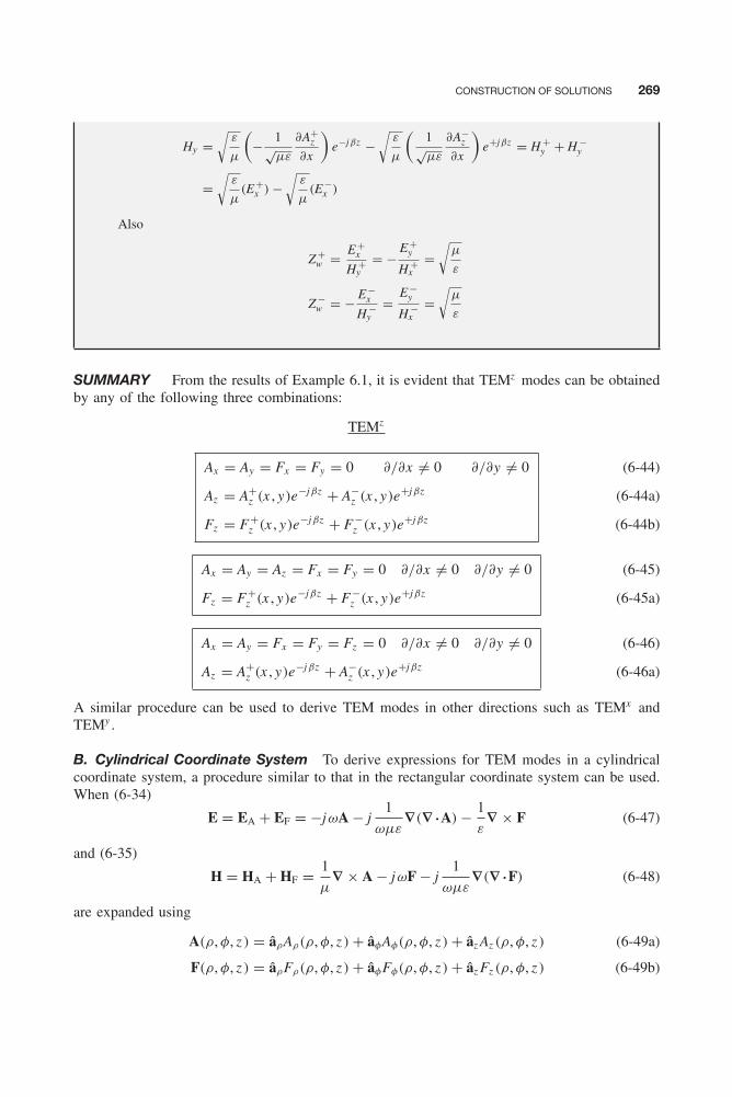
Balanis c06.tex V2 - 11/22/2011 3:14 P.M. Page 269
CONSTRUCTION OF SOLUTIONS 269
Hy =√
ε
μ
(− 1√
με
∂A+z
∂x
)e−jβz −
√ε
μ
(1√με
∂A−z
∂x
)e+jβz = H +
y + H −y
=√
ε
μ(E+
x ) −√
ε
μ(E−
x )
Also
Z +w = E+
x
H +y
= − E+y
H +x
=√
μ
ε
Z −w = − E−
x
H −y
= E−y
H −x
=√
μ
ε
SUMMARY From the results of Example 6.1, it is evident that TEMz modes can be obtainedby any of the following three combinations:
TEMz
Ax = Ay = Fx = Fy = 0 ∂/∂x �= 0 ∂/∂y �= 0
Az = A+z (x , y)e−jβz + A−
z (x , y)e+jβz
Fz = F+z (x , y)e−jβz + F−
z (x , y)e+jβz
(6-44)
(6-44a)
(6-44b)
Ax = Ay = Az = Fx = Fy = 0 ∂/∂x �= 0 ∂/∂y �= 0
Fz = F+z (x , y)e−jβz + F−
z (x , y)e+jβz
(6-45)
(6-45a)
Ax = Ay = Fx = Fy = Fz = 0 ∂/∂x �= 0 ∂/∂y �= 0
Az = A+z (x , y)e−jβz + A−
z (x , y)e+jβz
(6-46)
(6-46a)
A similar procedure can be used to derive TEM modes in other directions such as TEMx andTEMy .
B. Cylindrical Coordinate System To derive expressions for TEM modes in a cylindricalcoordinate system, a procedure similar to that in the rectangular coordinate system can be used.When (6-34)
E = EA + EF = −jωA − j1
ωμε∇(∇ • A) − 1
ε∇ × F (6-47)
and (6-35)
H = HA + HF = 1
μ∇ × A − jωF − j
1
ωμε∇(∇ • F) (6-48)
are expanded using
A(ρ, φ, z ) = âρAρ(ρ, φ, z ) + âφAφ(ρ, φ, z ) + âz Az (ρ, φ, z ) (6-49a)
F(ρ, φ, z ) = âρFρ(ρ, φ, z ) + âφFφ(ρ, φ, z ) + âz Fz (ρ, φ, z ) (6-49b)
Balanis c06.tex V2 - 11/22/2011 3:14 P.M. Page 270
270 AUXILIARY VECTOR POTENTIALS, CONSTRUCTION OF SOLUTIONS, AND RADIATION AND SCATTERING EQUATIONS
as solutions, they can be written as
E = âρ
{−jωAρ − j
1
ωμε
∂
∂ρ
[1
ρ
∂
∂ρ(ρAρ) + 1
ρ
∂Aφ
∂φ+ ∂Az
∂z
]− 1
ε
(1
ρ
∂Fz
∂φ− ∂Fφ
∂z
)}
+ âφ
{−jωAφ − j
1
ωμε
1
ρ
∂
∂φ
[1
ρ
∂
∂ρ(ρAρ) + 1
ρ
∂Aφ
∂φ+ ∂Az
∂z
]− 1
ε
(∂Fρ
∂z− ∂Fz
∂ρ
)}
+ âz
{−jωAz − j
1
ωμε
∂
∂z
[1
ρ
∂
∂ρ(ρAρ) + 1
ρ
∂Aφ
∂φ+ ∂Az
∂z
]− 1
ερ
[∂
∂ρ(ρFφ) − ∂Fρ
∂φ
]}(6-50)
H = âρ
{−jωFρ − j
1
ωμε
∂
∂ρ
[1
ρ
∂
∂ρ(ρFρ) + 1
ρ
∂Fφ
∂φ+ ∂Fz
∂z
]+ 1
μ
(1
ρ
∂Az
∂φ− ∂Aφ
∂z
)}
+ âφ
{−jωFφ − j
1
ωμε
1
ρ
∂
∂φ
[1
ρ
∂
∂ρ(ρFρ) + 1
ρ
∂Fφ
∂φ+ ∂Fz
∂z
]+ 1
μ
(∂Aρ
∂z− ∂Az
∂ρ
)}
+ âz
{−jωFz − j
1
ωμε
∂
∂z
[1
ρ
∂
∂ρ(ρFρ) + 1
ρ
∂Fφ
∂φ+ ∂Fz
∂z
]+ 1
μρ
[∂
∂ρ(ρAφ) − ∂Aρ
∂φ
]}(6-51)
Example 6-2
Using (6-50) and (6-51), derive expressions for the E and H fields, in terms of the components of theA and F potentials, that are TEM to the ρ direction (TEMρ).
Solution: It is apparent by examining (6-50) and (6-51) that TEMρ (Eρ = Hρ = 0) modes can beobtained by any of the following three combinations:
1. LettingAφ = Az = Fφ = Fz = 0 Aρ �= 0 Fρ �= 0 ∂/∂φ �= 0 ∂/∂z �= 0
For this combination, according to (6-50) and (6-51)
Eρ = −jωAρ − j1
ωμε
∂
∂ρ
[1
ρ
∂
∂ρ(ρAρ)
]= −j
1
ωμε
{∂
∂ρ
[1
ρ
∂
∂ρ(ρAρ)
]+ ω2μεAρ
}= −j
1
ωμε
[∂
∂ρ
(∂Aρ
∂ρ+ Aρ
ρ
)+ ω2μεAρ
]= −j
1
ωμε
(∂2Aρ
∂ρ2+ 1
ρ
∂Aρ
∂ρ− Aρ
ρ2+ ω2μεAρ
)Eρ = −j
1
ωμε
(∂2
∂ρ2+ 1
ρ
∂
∂ρ− 1
ρ2+ β2
)Aρ = 0
providedAρ(ρ, φ, z ) = A+
ρ (φ, z )H (2)1 (βρ) + A−
ρ (φ, z )H (1)1 (βρ)
Balanis c06.tex V2 - 11/22/2011 3:14 P.M. Page 271
CONSTRUCTION OF SOLUTIONS 271
Also
Hρ = −jωFρ − j1
ωμε
∂
∂ρ
[1
ρ
∂
∂ρ(ρFρ)
]= −j
1
ωμε
(∂2
∂ρ2+ 1
ρ
∂
∂ρ+ 1
ρ2+ β2
)Fρ = 0
providedFρ(ρ, φ, z ) = F+
ρ (φ, z )H (2)1 (βρ) + F−
ρ (φ, z )H (1)1 (βρ)
In addition,
Eφ = −j1
ωμε
1
ρ
∂
∂φ
[1
ρ
∂
∂ρ(ρAρ)
]− 1
ε
∂Fρ
∂z
Ez = −j1
ωμε
∂
∂z
[1
ρ
∂
∂ρ(ρAρ)
]− 1
ε
(− 1
ρ
∂Fρ
∂φ
)Hφ = −j
1
ωμε
1
ρ
∂
∂φ
[1
ρ
∂
∂ρ(ρFρ)
]+ 1
μ
∂Aρ
∂z
Hz = −j1
ωμε
∂
∂z
[1
ρ
∂
∂ρ(ρFρ)
]+ 1
μ
(− 1
ρ
∂Aρ
∂φ
)2. Letting
Aρ = Aφ = Az = Fφ = Fz = 0 Fρ �= 0 ∂/∂φ �= 0 ∂/∂z �= 0
For this combination, according to (6-50) and (6-51)
Eρ = 0
Hρ = −jωFρ − j1
ωμε
∂
∂ρ
[1
ρ
∂
∂ρ(ρFρ)
]= −j
1
ωμε
(∂2
∂ρ2+ 1
ρ
∂
∂ρ− 1
ρ2+ β2
)Fρ = 0
providedFρ(ρ, φ, z ) = F+
ρ (φ, z )H (2)1 (βρ) + F−
ρ (φ, z )H (1)1 (βρ)
In addition,
Eφ = −1
ε
∂Fρ
∂z
Ez = −1
ε
(− 1
ρ
∂Fρ
∂φ
)Hφ = −j
1
ωμε
1
ρ
∂
∂φ
[1
ρ
∂
∂ρ(ρFρ)
]Hz = −j
1
ωμε
∂
∂z
[1
ρ
∂
∂ρ(ρFρ)
]3. Letting
Aφ = Az = Fρ = Fφ = Fz = 0 Aρ �= 0 ∂/∂φ �= 0 ∂/∂z �= 0
Balanis c06.tex V2 - 11/22/2011 3:14 P.M. Page 272
272 AUXILIARY VECTOR POTENTIALS, CONSTRUCTION OF SOLUTIONS, AND RADIATION AND SCATTERING EQUATIONS
For this combination, according to (6-50) and (6-51)
Hρ = 0
Eρ = −jωAρ − j1
ωμε
∂
∂ρ
[1
ρ
∂
∂ρ(ρAρ)
]= −j
1
ωμε
(∂2
∂ρ2+ 1
ρ
∂
∂ρ− 1
ρ2+ β2
)Aρ = 0
providedAρ(ρ, φ, z ) = A+
ρ (φ, z )H (2)1 (βρ) + A−
ρ (φ, z )H (1)1 (βρ)
In addition,
Eφ = −j1
ωμε
1
ρ
∂
∂φ
[1
ρ
∂
∂ρ(ρAρ)
]Ez = −j
1
ωμε
∂
∂z
[1
ρ
∂
∂ρ(ρAρ)
]Hφ = 1
μ
(∂Aρ
∂z
)Hz = 1
μ
(− 1
ρ
∂Aρ
∂φ
)
SUMMARY From the results of Example 6-2, it is evident that TEMρ modes can be obtainedby any of the following three combinations:
Aφ = Az = Fφ = Fz = 0 ∂/∂φ �= 0 ∂/∂z �= 0
Aρ(ρ, φ, z ) = A+ρ (φ, z )H (2)
1 (βρ) + A−ρ (φ, z )H (1)
1 (βρ)
Fρ(ρ, φ, z ) = F+ρ (φ, z )H (2)
1 (βρ) + F−ρ (φ, z )H (1)
1 (βρ)
(6-52)
(6-52a)
(6-52b)
Aρ = Aφ = Az = Fφ = Fz = 0 ∂/∂φ �= 0 ∂/∂z �= 0
Fρ(ρ, φ, z ) = F+ρ (φ, z )H (2)
1 (βρ) + F−ρ (φ, z )H (1)
1 (βρ)
(6-53)
(6-53a)
Aφ = Az = Fρ = Fφ = Fz = 0 ∂/∂φ �= 0 ∂/∂z �= 0
Aρ(ρ, φ, z ) = A+ρ (φ, z )H (2)
1 (βρ) + A−ρ (φ, z )H (1)
1 (βρ)
(6-54)
(6-54a)
A similar procedure can be used to derive TEM modes in other directions such as TEMφ andTEMz .
6.5.2 Transverse Magnetic Modes: Source-Free Region
Often we seek solutions of higher-order modes, other than transverse electromagnetic (TEM).Some of the higher-order modes, often required to satisfy boundary conditions, are designated as
Balanis c06.tex V2 - 11/22/2011 3:14 P.M. Page 273
CONSTRUCTION OF SOLUTIONS 273
transverse magnetic (TM) and transverse electric (TE). Classical examples of the need for TMand TE modes are modes of propagation in waveguides [2].
Transverse magnetic modes (often also known as transverse magnetic fields) are field config-urations whose magnetic field components lie in a plane that is transverse to a given direction.That direction is often chosen to be the path of wave propagation. For example, if the desiredfields are TM to z (TMz ), this implies that Hz = 0. Each of the other two magnetic field com-ponents (Hx and Hy ) and three electric field components (Ex , Ey , and Ez ) may or may notexist.
By examining (6-43) and (6-51) it is evident that to derive the field expressions that are TM toa given direction, independent of the coordinate system, it is sufficient to let the vector potentialA have only a component in the direction in which the fields are desired to be TM. The remainingcomponents of A as well as all of F are set equal to zero.
A. Rectangular Coordinate System
TMz
To demonstrate the aforementioned procedure, let us assume that we wish to derive field expres-sions that are TM to z (TMz ). To accomplish this, we let
A = âz Az (x , y , z )
F = 0
(6-55a)
(6-55b)
The vector potential A must satisfy (6-30), which reduces from a vector wave equation to ascalar wave equation
∇2Az (x , y , z ) + β2Az (x , y , z ) = 0 (6-56)
Since (6-56) is of the same form as (3-20a), its solution using the separation-of-variables methodcan be written, according to (3-23), as
Az (x , y , z ) = f (x)g(y)h(z ) (6-57)
The solutions of f (x), g(y), and h(z ) take the forms given by (3-28a) through (3-30b). The mostappropriate forms for f (x), g(y), and h(z ) must be chosen judiciously to reduce the complexityof the problem, and they will depend on the configuration of the problem. For the rectangularwaveguide of Figure 3-2, for example, the most appropriate forms for f (x), g(y), and h(z ) arethose given, respectively, by (3-28b), (3-29b), and (3-30a). Thus, for the rectangular waveguide,(6-57) can be written as
Az (x , y , z ) = [C1 cos(βx x) + D1 sin(βx x)][C2 cos(βy y) + D2 sin(βy y)]
×(A3e−jβz z + B3e+jβz z ) (6-58)
where
β2x + β2
y + β2z = β2 = ω2με (6-58a)
Once Az is found, the next step is to use (6-41) and (6-43) to find the E and H field components.Doing this, it can be shown that by using (6-55a) and (6-55b) we can reduce (6-41) and (6-43)

Balanis c06.tex V2 - 11/22/2011 3:14 P.M. Page 274
274 AUXILIARY VECTOR POTENTIALS, CONSTRUCTION OF SOLUTIONS, AND RADIATION AND SCATTERING EQUATIONS
to
TMz Rectangular Coordinate System
Ex = −j1
ωμε
∂2Az
∂x ∂zHx = 1
μ
∂Az
∂y
Ey = −j1
ωμε
∂2Az
∂y ∂zHy = − 1
μ
∂Az
∂x
Ez = −j1
ωμε
(∂2
∂z 2+ β2
)Az Hz = 0
(6-59)
which satisfy the definition of TMz (i.e., Hz = 0).For the specific example for which the solution of Az as given by (6-58) is applicable, the
unknown constants C1, D1, C2, D2, A3, B3, βx , βy , and βz can be evaluated by substituting Az of (6-58) into the expressions for E and H in (6-59) and enforcing the appropriate boundary conditionson the E and H field components. This will be demonstrated in Chapter 8, and elsewhere, wherespecific problem configurations are attempted. Following these or similar procedures should leadto the solution of the problem in question.
Expressions for the E and H field components that are TMx and TMy are given, respectively,by
TMx Rectangular Coordinate System
Let
A = âx Ax (x , y , z )
F = 0
(6-60a)
(6-60b)
Then
Ex = −j1
ωμε
(∂2
∂x 2+ β2
)Ax Hx = 0
Ey = −j1
ωμε
∂2Ax
∂x ∂yHy = 1
μ
∂Ax
∂z
Ez = −j1
ωμε
∂2Ax
∂x ∂zHz = − 1
μ
∂Ax
∂y
(6-61)
where Ax must satisfy the scalar wave equation
∇2Ax (x , y , z ) + β2Ax (x , y , z ) = 0 (6-62)
TMy Rectangular Coordinate System
Let
A = ây Ay(x , y , z )
F = 0
(6-63a)
(6-63b)
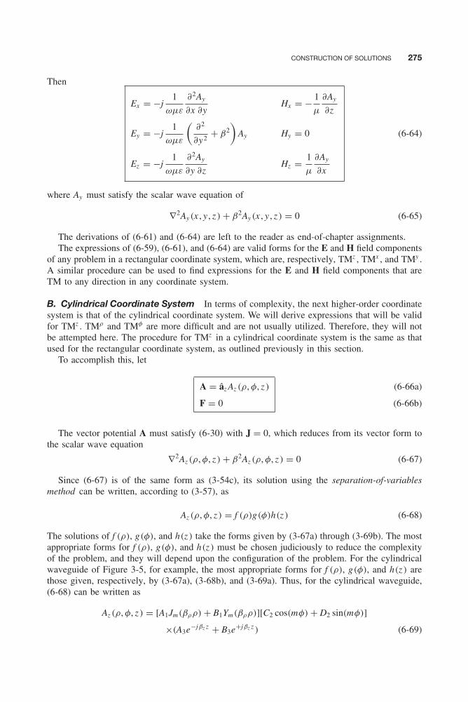
Balanis c06.tex V2 - 11/22/2011 3:14 P.M. Page 275
CONSTRUCTION OF SOLUTIONS 275
Then
Ex = −j1
ωμε
∂2Ay
∂x ∂yHx = − 1
μ
∂Ay
∂z
Ey = −j1
ωμε
(∂2
∂y2+ β2
)Ay Hy = 0
Ez = −j1
ωμε
∂2Ay
∂y ∂zHz = 1
μ
∂Ay
∂x
(6-64)
where Ay must satisfy the scalar wave equation of
∇2Ay(x , y , z ) + β2Ay(x , y , z ) = 0 (6-65)
The derivations of (6-61) and (6-64) are left to the reader as end-of-chapter assignments.The expressions of (6-59), (6-61), and (6-64) are valid forms for the E and H field components
of any problem in a rectangular coordinate system, which are, respectively, TMz , TMx , and TMy .A similar procedure can be used to find expressions for the E and H field components that areTM to any direction in any coordinate system.
B. Cylindrical Coordinate System In terms of complexity, the next higher-order coordinatesystem is that of the cylindrical coordinate system. We will derive expressions that will be validfor TMz . TMρ and TMφ are more difficult and are not usually utilized. Therefore, they will notbe attempted here. The procedure for TMz in a cylindrical coordinate system is the same as thatused for the rectangular coordinate system, as outlined previously in this section.
To accomplish this, let
A = âz Az (ρ, φ, z )
F = 0
(6-66a)
(6-66b)
The vector potential A must satisfy (6-30) with J = 0, which reduces from its vector form tothe scalar wave equation
∇2Az (ρ, φ, z ) + β2Az (ρ, φ, z ) = 0 (6-67)
Since (6-67) is of the same form as (3-54c), its solution using the separation-of-variablesmethod can be written, according to (3-57), as
Az (ρ, φ, z ) = f (ρ)g(φ)h(z ) (6-68)
The solutions of f (ρ), g(φ), and h(z ) take the forms given by (3-67a) through (3-69b). The mostappropriate forms for f (ρ), g(φ), and h(z ) must be chosen judiciously to reduce the complexityof the problem, and they will depend upon the configuration of the problem. For the cylindricalwaveguide of Figure 3-5, for example, the most appropriate forms for f (ρ), g(φ), and h(z ) arethose given, respectively, by (3-67a), (3-68b), and (3-69a). Thus, for the cylindrical waveguide,(6-68) can be written as
Az (ρ, φ, z ) = [A1Jm(βρρ) + B1Ym(βρρ)][C2 cos(mφ) + D2 sin(mφ)]
×(A3e−jβz z + B3e+jβz z ) (6-69)
Balanis c06.tex V2 - 11/22/2011 3:14 P.M. Page 276
276 AUXILIARY VECTOR POTENTIALS, CONSTRUCTION OF SOLUTIONS, AND RADIATION AND SCATTERING EQUATIONS
where
β2ρ + β2
z = β2 (6-69a)
Once Az is found, the next step is to use (6-50) and (6-51) to find the E and H field components.Then we can show that by using (6-66a) and (6-66b), (6-50) and (6-51) can be reduced to
TMz Cylindrical Coordinate System
Eρ = −j1
ωμε
∂2Az
∂ρ ∂zHρ = 1
μ
1
ρ
∂Az
∂φ
Eφ = −j1
ωμε
1
ρ
∂2Az
∂φ ∂zHφ = − 1
μ
∂Az
∂ρ
Ez = −j1
ωμε
(∂2
∂z 2+ β2
)Az Hz = 0
(6-70)
which also satisfies the TMz definition (i.e., Hz = 0).For the specific example for which the solution of Az as given by (6-69) is applicable, the
unknown constants A1, B1, C2, D2, A3, B3, βρ , and βz can be evaluated by substituting Az of (6-69)into the expressions for E and H in (6-70) and enforcing the appropriate boundary conditions onthe E and H field components. This will be demonstrated in Chapter 9, and elsewhere, wherespecific problem configurations are attempted. Following these or similar procedures should leadto the solution of the problem in question.
It should be stated that the same TM mode field constructions can be obtained by initiatingthe procedure with a solution to the scalar wave equation for the electric field component in thedirection in which TM mode fields are desired. For example, if TMz modes are desired, assumea solution for Ez of the same form as the vector potential component Az . It can then be shownthrough Maxwell’s equations that all the remaining electric and magnetic field components (withHz = 0) can be expressed in terms of Ez . The same can be done for other TMi modes by beginningwith a solution for Ei having the same form as the vector potential component Ai . The onlydifference between the two formulations, one of which uses the vector potentials adopted in thisbook and the other that uses the fields themselves, is a normalization constant. For TMz modes,for example, this normalization constant according to (6-59) is equal to −j (∂2/∂z 2 + β2)/ωμε =−j (β2 − β2
z )/ωμε. The preceding procedure is a very popular method used by many authors,and it is assigned to the reader as end-of-chapter exercises.
6.5.3 Transverse Electric Modes: Source-Free Region
Transverse electric (TE) modes can be derived in a fashion similar to the TM fields ofSection 6.5.2. This time, however, we let the F vector potential have a nonvanishing componentin the direction in which the TE fields are desired, and all the remaining components of F andA are set equal to zero. Without going through any of the details, we will list the expressionsfor the E and H field components for TEz , TEx , and TEy in rectangular coordinates and TEz incylindrical coordinates. The details are left as exercises for the reader.
A. Rectangular Coordinate System Modes that are TEz , TEx , and TEy are obtained asfollows.
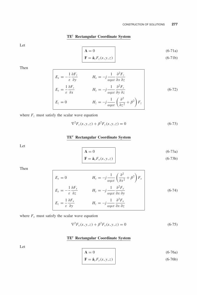
Balanis c06.tex V2 - 11/22/2011 3:14 P.M. Page 277
CONSTRUCTION OF SOLUTIONS 277
TEz Rectangular Coordinate System
LetA = 0
F = âz Fz (x , y , z )
(6-71a)
(6-71b)
Then
Ex = −1
ε
∂Fz
∂yHx = −j
1
ωμε
∂2Fz
∂x ∂z
Ey = 1
ε
∂Fz
∂xHy = −j
1
ωμε
∂2Fz
∂y ∂z
Ez = 0 Hz = −j1
ωμε
(∂2
∂z 2+ β2
)Fz
(6-72)
where Fz must satisfy the scalar wave equation
∇2Fz (x , y , z ) + β2Fz (x , y , z ) = 0 (6-73)
TEx Rectangular Coordinate System
LetA = 0
F = âx Fx (x , y , z )
(6-73a)
(6-73b)
Then
Ex = 0 Hx = −j1
ωμε
(∂2
∂x 2+ β2
)Fx
Ey = −1
ε
∂Fx
∂zHy = −j
1
ωμε
∂2Fx
∂x ∂y
Ez = 1
ε
∂Fx
∂yHz = −j
1
ωμε
∂2Fx
∂x ∂z
(6-74)
where Fx must satisfy the scalar wave equation
∇2Fx (x , y , z ) + β2Fx (x , y , z ) = 0 (6-75)
TEy Rectangular Coordinate System
LetA = 0
F = ây Fy(x , y , z )
(6-76a)
(6-76b)

Balanis c06.tex V2 - 11/22/2011 3:14 P.M. Page 278
278 AUXILIARY VECTOR POTENTIALS, CONSTRUCTION OF SOLUTIONS, AND RADIATION AND SCATTERING EQUATIONS
Then
Ex = 1
ε
∂Fy
∂zHx = −j
1
ωμε
∂2Fy
∂x ∂y
Ey = 0 Hy = −j1
ωμε
(∂2
∂y2+ β2
)Fy
Ez = −1
ε
∂Fy
∂xHz = −j
1
ωμε
∂2Fy
∂y∂z
(6-77)
where Fy must satisfy the scalar wave equation
∇2Fy(x , y , z ) + β2Fy(x , y , z ) = 0 (6-78)
B. Cylindrical Coordinate System Modes that are TEz are obtained as follows.
TEz Cylindrical Coordinate System
Let
A = 0
F = âz Fz (ρ, φ, z )
(6-79a)
(6-79b)
Then
Eρ = − 1
ερ
∂Fz
∂φHρ = −j
1
ωμε
∂2Fz
∂ρ ∂z
Eφ = 1
ε
∂Fz
∂ρHφ = −j
1
ωμερ
∂2Fz
∂φ ∂z
Ez = 0 Hz = −j1
ωμε
(∂2
∂z 2+ β2
)Fz
(6-80)
where Fz must satisfy the scalar wave equation
∇2Fz (ρ, φ, z ) + β2Fz (ρ, φ, z ) = 0 (6-81)
As was suggested earlier for the TM modes, an alternate procedure for construction of TEi
field configurations will be to initiate the procedure with a solution for the Hi component withthe same form as the vector potential component Fi . For example, if TEz modes are desired,assume a solution for Hz of the same form as the vector potential component Fz . It can thenbe shown through Maxwell’s equations that all the remaining electric and magnetic fields (withEz = 0) can be expressed in terms of Hz . The only difference between the two formulations, onethat uses the vector potentials adopted in this book and the other that uses the fields themselves,is a normalization. For TEz modes, for example, this normalization constant according to (6-72)is equal to −j (∂2/∂z 2 + β2)/ωμε = −j (β2 − β2
z )/ωμε. The preceding procedure is also a verypopular method used by many authors, and it is assigned to the reader as end-of-chapter exercises.
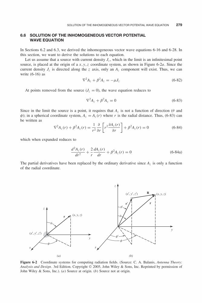
Balanis c06.tex V2 - 11/22/2011 3:14 P.M. Page 279
SOLUTION OF THE INHOMOGENEOUS VECTOR POTENTIAL WAVE EQUATION 279
6.6 SOLUTION OF THE INHOMOGENEOUS VECTOR POTENTIALWAVE EQUATION
In Sections 6.2 and 6.3, we derived the inhomogeneous vector wave equations 6-16 and 6-28. Inthis section, we want to derive the solutions to each equation.
Let us assume that a source with current density Jz , which in the limit is an infinitesimal pointsource, is placed at the origin of a x , y , z coordinate system, as shown in Figure 6-2a . Since thecurrent density Jz is directed along the z axis, only an Az component will exist. Thus, we canwrite (6-16) as
∇2Az + β2Az = −μJz (6-82)
At points removed from the source (Jz = 0), the wave equation reduces to
∇2Az + β2Az = 0 (6-83)
Since in the limit the source is a point, it requires that Az is not a function of direction (θ andφ); in a spherical coordinate system, Az = Az (r) where r is the radial distance. Thus, (6-83) canbe written as
∇2Az (r) + β2Az (r) = 1
r2
∂
∂r
[r2 ∂Az (r)
∂r
]+ β2Az (r) = 0 (6-84)
which when expanded reduces to
d2Az (r)
dr2+ 2
r
dAz (r)
dr+ β2Az (r) = 0 (6-84a)
The partial derivatives have been replaced by the ordinary derivative since Az is only a functionof the radial coordinate.
(x, y, z)
(x, y, z)
(x′, y′, z′)
r
r′ r
R
x x
y
y
z
(a) (b)
z
ff
f′
q
q
q′
(x′, y′, z′)
Figure 6-2 Coordinate systems for computing radiation fields. (Source: C. A. Balanis, Antenna Theory:Analysis and Design . 3rd Edition. Copyright © 2005, John Wiley & Sons, Inc. Reprinted by permission ofJohn Wiley & Sons, Inc.). (a) Source at origin. (b) Source not at origin.

Balanis c06.tex V2 - 11/22/2011 3:14 P.M. Page 280
280 AUXILIARY VECTOR POTENTIALS, CONSTRUCTION OF SOLUTIONS, AND RADIATION AND SCATTERING EQUATIONS
The differential equation 6-84a has two independent solutions
Az1 = C1e−jβr
r(6-85a)
Az2 = C2e+jβr
r(6-85b)
Equation 6-85a represents an outwardly (in the radial direction) traveling wave and (6-85b)describes an inwardly traveling wave, assuming ejωt time variations. For this problem, the sourceis placed at the origin with the radiated fields traveling in the outward radial direction. Therefore,we choose the solution of (6-85a), or
Az = Az1 = C1e−jβr
r(6-86)
In the static case, ω = 0, β = 0, so (6-86) simplifies to
Az = C1
r(6-86a)
which is a solution to the wave equation 6-83, 6-84, or 6-84a when β = 0. Thus, at pointsremoved from the source, the time-varying and the static solutions of (6-86) and (6-86a) differonly by the e−jβr factor, or the time-varying solution of (6-86) can be obtained by multiplyingthe static solution of (6-86a) by e−jβr .
In the presence of the source (Jz �= 0) and with β = 0, the wave equation 6-82 reduces to
∇2Az = −μJz (6-87)
This equation is recognized as Poisson’s equation whose solution is widely documented. Themost familiar equation with Poisson form is that relating the scalar electric potential φ to theelectric charge density q . This is given by
∇2φ = −q
ε(6-88)
whose solution isφ = 1
4πε
∫∫∫V
q
rdv′ (6-89)
where r is the distance from any point on the charge density to the observation point. Since(6-87) is similar in form to (6-88), its solution is similar to (6-89), or
Az = μ
4π
∫∫∫V
Jz
rdv′ (6-90)
Equation 6-90 represents the solution to (6-82) when β = 0, the static case. Using the comparativeanalogy between (6-86) and (6-86a), the time-varying solution of (6-82) can be obtained bymultiplying the static solution of (6-90) by e−jβr . Thus,
Az = μ
4π
∫∫∫V
Jze−jβr
rdv′ (6-91)
which is a solution to (6-82).If the current densities were in the x and y directions (Jx and Jy ), the wave equation for each
would reduce to
∇2Ax + β2Ax = −μJx (6-92a)
Balanis c06.tex V2 - 11/22/2011 3:14 P.M. Page 281
SOLUTION OF THE INHOMOGENEOUS VECTOR POTENTIAL WAVE EQUATION 281
∇2Ay + β2Ay = −μJy (6-92b)
with corresponding solutions similar in form to (6-91), or
Ax = μ
4π
∫∫∫V
Jxe−jβr
rdv′ (6-93a)
Ay = μ
4π
∫∫∫V
Jye−jβr
rdv′ (6-93b)
The solutions of (6-91), (6-93a), and (6-93b) allow us to write the solution to the vector waveequation 6-16 as
A = μ
4π
∫∫∫V
Je−jβr
rdv′ (6-94)
If the source is removed from the origin and placed at a position represented by the primedcoordinates (x ′, y ′, z ′), as shown in Figure 6-2b, (6-94) can be written as
A(x , y , z ) = μ
4π
∫∫∫V
J(x ′, y ′, z ′)e−jβR
Rdv′ (6-95a)
where the primed coordinates represent the source, the unprimed coordinates represent the obser-vation point, and R represents the distance from any point in the source to the observation point.In a similar fashion, we can show that the solution of (6-28) is given by
F(x , y , z ) = ε
4π
∫∫∫V
M(x ′, y ′, z ′)e−jβR
Rdv′ (6-95b)
If J and M represent linear densities (m−1), (6-95a) and (6-95b) reduce, respectively, to thefollowing surface integrals.
A = μ
4π
∫∫S
Js(x′, y ′, z ′)
e−jβR
Rds ′ (6-96a)
F = ε
4π
∫∫S
Ms(x′, y ′, z ′)
e−jβR
Rds ′ (6-96b)
For electric and magnetic currents Ie and Im , they in turn reduce to line integrals of the form
A = μ
4π
∫C
Ie(x′, y ′, z ′)
e−jβR
Rdl ′ (6-97a)
F = ε
4π
∫C
Im(x ′, y ′, z ′)e−jβR
Rdl ′ (6-97b)

Balanis c06.tex V2 - 11/22/2011 3:14 P.M. Page 282
282 AUXILIARY VECTOR POTENTIALS, CONSTRUCTION OF SOLUTIONS, AND RADIATION AND SCATTERING EQUATIONS
Example 6-3
A very thin linear electric current element of very short length (� � λ) and with a constant current
Ie(z′) = âz Ie
such that Ie� = constant, is positioned symmetrically at the origin and oriented along the z axis, asshown in Figure 6-2a . Such an element is usually referred to as an infinitesimal dipole [1]. Determinethe electric and magnetic fields radiated by the dipole.
Solution: The solution will be obtained using the procedure summarized in Section 6.4. Since theelement (source) carries only an electric current Ie , the magnetic current Im and the vector potential Fof (6-97b) are both zero. The vector potential A of (6-97a) is then written as
A(x , y , z ) = μ
4π
∫ +�/2
−�/2âz Ie
e−jβR
Rdz ′
where R is the distance from any point on the element, −�/2 ≤ z ′ ≤ �/2, to the observation point. Sincein the limit as � → 0 (� � λ),
R = r
then
A(x , y , z ) = âzμIee−jβr
4πr
∫ +�/2
−�/2dz ′ = âz
μIe�
4πre−jβr
Transforming the vector potential A from rectangular to spherical components using the inverse (in thiscase also transpose) transformation of (II-9) from Appendix II, we can write
Ar = Az cos θ = μIe�e−jβr
4πrcos θ
Aθ = −Az sin θ = −μIe�e−jβr
4πrsin θ
Aφ = 0
Using the symmetry of the problem, that is, no variations in φ, (6-32a) can be expanded in sphericalcoordinates and written in simplified form as
H = âφ
1
μr
[∂
∂r(rAθ ) − ∂Ar
∂θ
]which reduces to
Hr = Hθ = 0
Hφ = jβIe� sin θ
4πr
(1 + 1
jβr
)e−jβr
The electric field E can be found using either (6-32b) or (6-32c), that is,
E = −jωA − j1
ωμε∇(∇ • A) = 1
jωε∇ × H
and either leads to
Er = ηIe� cos θ
2πr2
(1 + 1
jβr
)e−jβr
Eθ = jηβIe� sin θ
4πr
[1 + 1
jβr− 1
(βr)2
]e−jβr
Eφ = 0
The E- and H-field components are valid everywhere except on the source itself.
Balanis c06.tex V2 - 11/22/2011 3:14 P.M. Page 283
FAR-FIELD RADIATION 283
6.7 FAR-FIELD RADIATION
The fields radiated by antennas of finite dimensions are spherical waves. For these radiators, ageneral solution to the vector wave equation 6-16 in spherical components, each as a function ofr , θ , and φ, takes the general form
A = âr Ar (r , θ , φ) + âθAθ (r , θ , φ) + âφAφ(r , θ , φ) (6-98)
The amplitude variations of r in each component of (6-98) are of the form 1/rn , n = 1, 2, . . .[1]. Neglecting higher-order terms of 1/rn (1/rn = 0, n = 2, 3, . . .) reduces (6-98) to
A � [âr A′r (θ , φ) + âθA′
θ (θ , φ) + âφA′φ(θ , φ)]
e−jβr
rr → ∞ (6-99)
The r variations are separable from those of θ and φ. This will be demonstrated by many examplesin the chapters that follow.
Substituting (6-99) into (6-17) reduces it to
E = 1
r{−jωe−jβr [âr (0) + âθA′
θ (θ , φ) + âφA′φ(θ , φ)]} + 1
r2{· · · } + · · · (6-100a)
The radial E -field component has no 1/r terms because its contributions from the first and secondterms of (6-17) cancel each other.
Similarly, by using (6-99), we can write (6-4a) as
H = 1
r
{−j
ω
ηe−jβr [âr (0) + âθA′
θ (θ , φ) − âφA′θ (θ , φ)]
}+ 1
r2{· · · } + · · · (6-100b)
where η = √μ/ε is the intrinsic impedance of the medium.
Neglecting higher-order terms of 1/rn , the radiated E and H fields have only θ and φ com-ponents. They can be expressed as
Far-Field Region
Er � 0Eθ � −jωAθ
Eφ � −jωAφ
⎫⎬⎭ ⇒EA � −jωA
(for the θ and φ componentsonly since Er � 0)
(6-101a)
Hr � 0
Hθ � +jω
ηAφ = −Eφ
η
Hφ � −jω
ηAθ = +Eθ
η
⎫⎪⎪⎪⎬⎪⎪⎪⎭ ⇒HA � âr
η× EA = −j
ω
ηâr × A
(for the θ and φ componentsonly since Hr � 0)
(6-101b)
Radial field components exist only for higher-order terms of 1/rn .

Balanis c06.tex V2 - 11/22/2011 3:14 P.M. Page 284
284 AUXILIARY VECTOR POTENTIALS, CONSTRUCTION OF SOLUTIONS, AND RADIATION AND SCATTERING EQUATIONS
In a similar manner, the far-zone fields that are due to a magnetic source M (potential F) canbe written as
Far-Field Region
Hr � 0Hθ � −jωFθ
Hφ � −jωFφ
⎫⎬⎭ ⇒HF � −jωF
(for the θ and φ componentsonly since Hr � 0)
(6-102a)
Er � 0Eθ � −jωηFφ = +ηHφ
Eφ � +jωηFθ = −ηHθ
⎫⎬⎭ ⇒EF = −ηâr × HF = jωηâr × F
(for the θ and φ componentsonly since Er � 0)
(6-102b)
Simply stated, the corresponding far-zone E- and H-field components are orthogonal to eachother and form TEM (to r) mode fields. This is a very useful relation, and it will be adoptedin the following chapters for the solution of the far-zone radiated fields. The far-zone (far-field)region for a radiator is defined as the region whose smallest radial distance is 2D2/λ where Dis the largest dimension of the radiator (provided D is large compared to the wavelength) [1].
6.8 RADIATION AND SCATTERING EQUATIONS
In Sections 6.4 and 6.6, it was stated that the fields radiated by sources represented by J and M inan unbounded medium can be computed using (6-32a) through (6-35a), where A and F are foundusing (6-95a) and (6-95b). For (6-95a) and (6-95b), the integration is performed over the entirespace occupied by J and M of Figure 6-2b [or Js and Ms of (6-96a) and (6-96b), or Ie and Im of(6-97a) and (6-97b)]. These equations yield valid solutions for all observation points. For mostproblems, the main difficulty is the inability to perform the integrations in (6-95a) and (6-95b),(6-96a) and (6-96b), or (6-97a) and (6-97b). However, for far-field observations the complexityof the formulation can be reduced.
6.8.1 Near Field
According to Figure 6-2b and equation 6-95a, the vector potential A that is due to current densityJ is given by
A(x , y , z ) = μ
4π
∫∫∫V
J(x ′, y ′, z ′)e−jβR
Rdv′ (6-103)
where the primed coordinates (x ′, y ′, z ′) represent the source and the unprimed coordinates (x ,y , z ) represent the observation point. Here, we intend to write expressions for the E and H fieldsthat are due to the potential of (6-103), which would be valid everywhere [3, 4], The equationswill not be in closed form, but will be convenient for computational purposes. The developmentwill be restricted to the rectangular coordinate system.
The magnetic field due to the potential of (6-103) is given by (6-32a) as
HA = 1
μ∇ × A = 1
4π∇ ×
∫∫∫V
J(x ′, y ′, z ′)e−jβR
Rdv′ (6-104)
Interchanging integration and differentiation, we can write (6-104) as
HA = 1
4π
∫∫∫V
∇ ×[
J(x ′, y ′, z ′)e−jβR
R
]dv′ (6-104a)
Balanis c06.tex V2 - 11/22/2011 3:14 P.M. Page 285
RADIATION AND SCATTERING EQUATIONS 285
Using the vector identity∇ × (gF) = (∇g) × F + g(∇ × F) (6-105)
we can write
∇ ×[
e−jβR
RJ(x ′, y ′, z ′)
]= ∇
(e−jβR
R
)× J(x ′, y ′, z ′) + e−jβR
R∇ × J(x ′, y ′, z ′) (6-106)
Since J is only a function of the primed coordinates and ∇ is a function of the unprimedcoordinates,
∇ × J(x ′, y ′, z ′) = 0 (6-106a)
Also
∇(
e−jβR
R
)= −R̂
(1 + jβR
R2
)e−jβR (6-106b)
where R̂ is a unit vector directed along the line joining any point of the source and the observationpoint. Using (6-106) through (6-106b), we can write (6-104a) as
HA(x , y , z ) = − 1
4π
∫∫∫V(R̂ × J)
1 + jβR
R2e−jβRdx ′dy ′dz ′ (6-107)
which can be expanded in its three rectangular components [3, 4]
HAx = 1
4π
∫∫∫V
[(z − z ′)Jy − (y − y ′)Jz
] 1 + jβR
R3e−jβRdx ′ dy ′ dz ′ (6-107a)
HAy = 1
4π
∫∫∫V
[(x − x ′)Jz − (z − z ′)Jx
] 1 + jβR
R3e−jβRdx ′ dy ′ dz ′ (6-107b)
HAz = 1
4π
∫∫∫V
[(y − y ′)Jx − (x − x ′)Jy
] 1 + jβR
R3e−jβRdx ′ dy ′ dz ′ (6-107c)
Using (6-32b) or Maxwell’s equation 6-32c, we can write the corresponding electric fieldcomponents as
EA = âx EAx + ây EAy + âz EAz = −jωA − j1
ωμε∇(∇ • A) = 1
jωε∇ × HA (6-108)
which with the aid of (6-107a) through (6-107c) reduce to
EAx = − jη
4πβ
∫∫∫V
{G1Jx + (x − x ′)G2
×[(x − x ′)Jx + (y − y ′)Jy + (z − z ′)Jz ]}
e−jβRdx ′ dy ′ dz ′ (6-108a)
EAy = − jη
4πβ
∫∫∫V
{G1Jy + (y − y ′)G2
×[(x − x ′)Jx + (y − y ′)Jy + (z − z ′)Jz ]}
e−jβRdx ′ dy ′ dz ′ (6-108b)
EAz = − jη
4πβ
∫∫∫V
{G1Jz + (z − z ′)G2
×[(x − x ′)Jx + (y − y ′)Jy + (z − z ′)Jz ]}
e−jβRdx ′ dy ′ dz ′ (6-108c)
Balanis c06.tex V2 - 11/22/2011 3:14 P.M. Page 286
286 AUXILIARY VECTOR POTENTIALS, CONSTRUCTION OF SOLUTIONS, AND RADIATION AND SCATTERING EQUATIONS
where
G1 = −1 − jβR + β2R2
R3(6-108d)
G2 = 3 + j 3βR − β2R2
R5(6-108e)
In the same manner, we can write for the vector potential of (6-95b)
F(x , y , z ) = ε
4π
∫∫∫V
M(x ′, y ′, z ′)e−jβR
Rdv′ (6-109)
the electric field components using (6-33a),
EF = −1
ε∇ × F (6-110)
as
EFx = − 1
4π
∫∫∫V
[(z − z ′)My − (y − y ′)Mz
] 1 + jβR
R3e−jβRdx ′dy ′dz ′ (6-110a)
EFy = − 1
4π
∫∫∫V
[(x − x ′)Mz − (z − z ′)Mx
] 1 + jβR
R3e−jβRdx ′dy ′dz ′ (6-110b)
EFz = − 1
4π
∫∫∫V
[(y − y ′)Mx − (x − x ′)My
] 1 + jβR
R3e−jβRdx ′dy ′dz ′ (6-110c)
Similarly, the corresponding magnetic field components can be written using (6-33b) or (6-33c)
HF = −jωF − j1
ωμε∇(∇ • F) = − 1
jωμ∇ × EF (6-111)
as
HFx = − j
4πβη
∫∫∫V
{G1Mx + (x − x ′)G2
×[(x − x ′)Mx + (y − y ′)My + (z − z ′)Mz ]}
e−jβRdx ′ dy ′ dz ′ (6-111a)
HFy = − j
4πβη
∫∫∫V
{G1My + (y − y ′)G2
×[(x − x ′)Mx + (y − y ′)My + (z − z ′)Mz ]}
e−jβRdx ′ dy ′ dz ′ (6-111b)
HFz = − j
4πβη
∫∫∫V
{G1Mz + (z − z ′)G2
×[(x − x ′)Mx + (y − y ′)My + (z − z ′)Mz ]}
e−jβRdx ′ dy ′ dz ′ (6-111c)
where G1 and G2 are given by (6-108d) and (6-108e).
6.8.2 Far Field
It was shown in Section 6.7 that the field equations for far-field (βr � 1) observations simplifyconsiderably. Also in the far zone the E- and H-field components are orthogonal to each other andform TEM (to r) mode fields. Although the field equations in the far zone simplify, integrationsstill need to be performed to find the vector potentials of A and F given, respectively, by (6-95a)
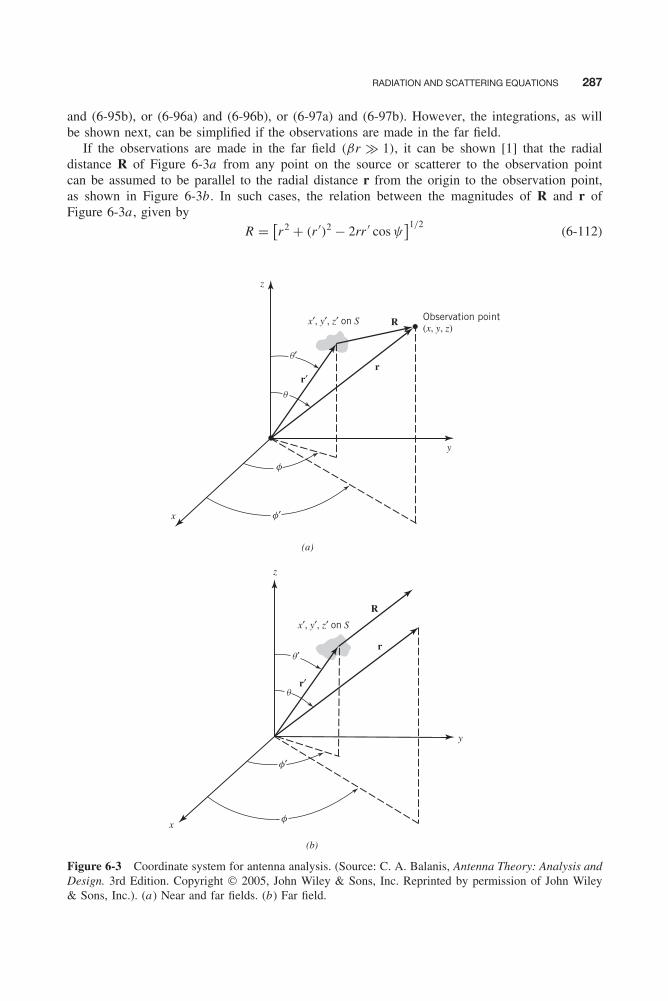
Balanis c06.tex V2 - 11/22/2011 3:14 P.M. Page 287
RADIATION AND SCATTERING EQUATIONS 287
and (6-95b), or (6-96a) and (6-96b), or (6-97a) and (6-97b). However, the integrations, as willbe shown next, can be simplified if the observations are made in the far field.
If the observations are made in the far field (βr � 1), it can be shown [1] that the radialdistance R of Figure 6-3a from any point on the source or scatterer to the observation pointcan be assumed to be parallel to the radial distance r from the origin to the observation point,as shown in Figure 6-3b. In such cases, the relation between the magnitudes of R and r ofFigure 6-3a , given by
R = [r2 + (r ′)2 − 2rr ′ cos ψ
]1/2(6-112)
r′r
R
x
x
y
y
z
z
(a)
(b)
f
f
f′
f′
q
q′
r′
r
R
q
q′
x′, y′, z′ on S
x′, y′, z′ on S
Observation point(x, y, z)
Figure 6-3 Coordinate system for antenna analysis. (Source: C. A. Balanis, Antenna Theory: Analysis andDesign. 3rd Edition. Copyright © 2005, John Wiley & Sons, Inc. Reprinted by permission of John Wiley& Sons, Inc.). (a) Near and far fields. (b) Far field.
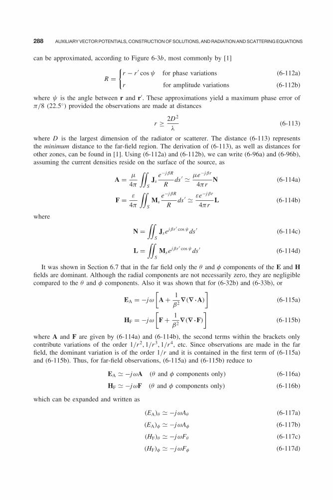
Balanis c06.tex V2 - 11/22/2011 3:14 P.M. Page 288
288 AUXILIARY VECTOR POTENTIALS, CONSTRUCTION OF SOLUTIONS, AND RADIATION AND SCATTERING EQUATIONS
can be approximated, according to Figure 6-3b, most commonly by [1]
R ={
r − r ′ cos ψ for phase variations
r for amplitude variations
(6-112a)
(6-112b)
where ψ is the angle between r and r′. These approximations yield a maximum phase error ofπ/8 (22.5◦) provided the observations are made at distances
r ≥ 2D2
λ(6-113)
where D is the largest dimension of the radiator or scatterer. The distance (6-113) representsthe minimum distance to the far-field region. The derivation of (6-113), as well as distances forother zones, can be found in [1]. Using (6-112a) and (6-112b), we can write (6-96a) and (6-96b),assuming the current densities reside on the surface of the source, as
A = μ
4π
∫∫S
Jse−jβR
Rds ′ � μe−jβr
4πrN (6-114a)
F = ε
4π
∫∫S
Mse−jβR
Rds ′ � εe−jβr
4πrL (6-114b)
where
N =∫∫
SJs ejβr ′ cos ψds ′ (6-114c)
L =∫∫
SMs ejβr ′ cos ψds ′ (6-114d)
It was shown in Section 6.7 that in the far field only the θ and φ components of the E and Hfields are dominant. Although the radial components are not necessarily zero, they are negligiblecompared to the θ and φ components. Also it was shown that for (6-32b) and (6-33b), or
EA = −jω
[A + 1
β2∇(∇ • A)
](6-115a)
HF = −jω
[F + 1
β2∇(∇ • F)
](6-115b)
where A and F are given by (6-114a) and (6-114b), the second terms within the brackets onlycontribute variations of the order 1/r2, 1/r3, 1/r4, etc. Since observations are made in the farfield, the dominant variation is of the order 1/r and it is contained in the first term of (6-115a)and (6-115b). Thus, for far-field observations, (6-115a) and (6-115b) reduce to
EA � −jωA (θ and φ components only) (6-116a)
HF � −jωF (θ and φ components only) (6-116b)
which can be expanded and written as
(EA)θ � −jωAθ (6-117a)
(EA)φ � −jωAφ (6-117b)
(HF)θ � −jωFθ (6-117c)
(HF)φ � −jωFφ (6-117d)

Balanis c06.tex V2 - 11/22/2011 3:14 P.M. Page 289
RADIATION AND SCATTERING EQUATIONS 289
The radial components are neglected because they are very small compared to the θ and φ
components.To find the remaining E and H fields contributed by the F and A potentials, that is EF and
HA, we can use (6-33a) and (6-32a), or
EF = −1
ε∇ × F (6-118a)
HA = 1
μ∇ × A (6-118b)
However, we resort instead to (6-117a) through (6-117d). Since the observations are made in thefar field and we know that the E- and H-field components are orthogonal to each other and tothe radial direction (plane waves) and are related by the intrinsic impedance of the medium, wecan write, using (6-117a) through (6-117d),
(EF)θ � +η(HF)φ = −jωηFφ (6-119a)
(EF)φ � −η(HF)θ = +jωηFθ (6-119b)
(HA)θ � − (EA)φ
η= +jω
Aφ
η(6-119c)
(HA)φ � + (EA)θ
η= −jω
Aθ
η(6-119d)
Combining (6-117a) through (6-117d) with (6-119a) through (6-119d) and remembering that theradial components are negligible, we can write the E- and H-field components in the far fieldas
Er � 0 (6-120a)
Eθ � (EA)θ + (EF)θ = −jω[Aθ + ηFφ
](6-120b)
Eφ � (EA)φ + (EF)φ = −jω[Aφ − ηFθ
](6-120c)
Hr � 0 (6-120d)
Hθ � (HA)θ + (HF)θ = + jω
η
[Aφ − ηFθ
](6-120e)
Hφ � (HA)φ + (HF)φ = − jω
η
[Aθ + ηFφ
](6-120f)
Using Aθ , Aφ , Fθ , and Fφ from (6-114a) through (6-114d), that is,
Aθ = μe−jβr
4πrNθ (6-121a)
Aφ = μe−jβr
4πrNφ (6-121b)
Fθ = εe−jβr
4πrLθ (6-121c)
Fφ = εe−jβr
4πrLφ (6-121d)

Balanis c06.tex V2 - 11/22/2011 3:14 P.M. Page 290
290 AUXILIARY VECTOR POTENTIALS, CONSTRUCTION OF SOLUTIONS, AND RADIATION AND SCATTERING EQUATIONS
we can reduce (6-120a) through (6-120f) to
Er � 0
Eθ � − jβe−jβr
4πr(Lφ + ηNθ )
Eφ � + jβe−jβr
4πr(Lθ − ηNφ)
Hr � 0
Hθ � + jβe−jβr
4πr
(Nφ − Lθ
η
)
Hφ � − jβe−jβr
4πr
(Nθ + Lφ
η
)
(6-122a)
(6-122b)
(6-122c)
(6-122d)
(6-122e)
(6-122f)
A. Rectangular Coordinate System To find the fields of (6-122a) through (6-122f), thefunctions Nθ , Nφ , Lθ , and Lφ must be evaluated from (6-114c) and (6-114d). The evaluationof (6-114c) and (6-114d) can best be accomplished if the most convenient coordinate system ischosen.
For radiators or scatterers whose geometries are most conveniently represented by rectangularcoordinates, (6-114c) and (6-114d) can best be expressed as
N =∫∫
SJse+jβr ′ cos ψds ′ =
∫∫S(âx Jx + ây Jy + âz Jz )e
+jβr ′ cos ψds ′ (6-123a)
L =∫∫
SMse+jβr ′ cos ψds ′ =
∫∫S(âx Mx + ây My + âz Mz )e
+jβr ′ cos ψds ′ (6-123b)
Using the rectangular-to-spherical component transformation of (II-13a)⎡⎣ âx
ây
âz
⎤⎦ =⎡⎣ sin θ cos φ cos θ cos φ − sin φ
sin θ sin φ cos θ sin φ cos φ
cos θ − sin θ 0
⎤⎦⎡⎣ âr
âθ
âφ
⎤⎦ (6-124)
we can reduce (6-123a) and (6-123b) for the θ and φ components to
Nθ =∫∫
S(Jx cos θ cos φ + Jy cos θ sin φ − Jz sin θ)e+jβr ′ cos ψds ′
Nφ =∫∫
S(−Jx sin φ + Jy cos φ)e+jβr ′ cos ψds ′
Lθ =∫∫
S(Mx cos θ cos φ + My cos θ sin φ − Mz sin θ)e+jβr ′ cos ψds ′
Lφ =∫∫
S(−Mx sin φ + My cos φ)e+jβr ′ cos ψds ′
(6-125a)
(6-125b)
(6-125c)
(6-125d)
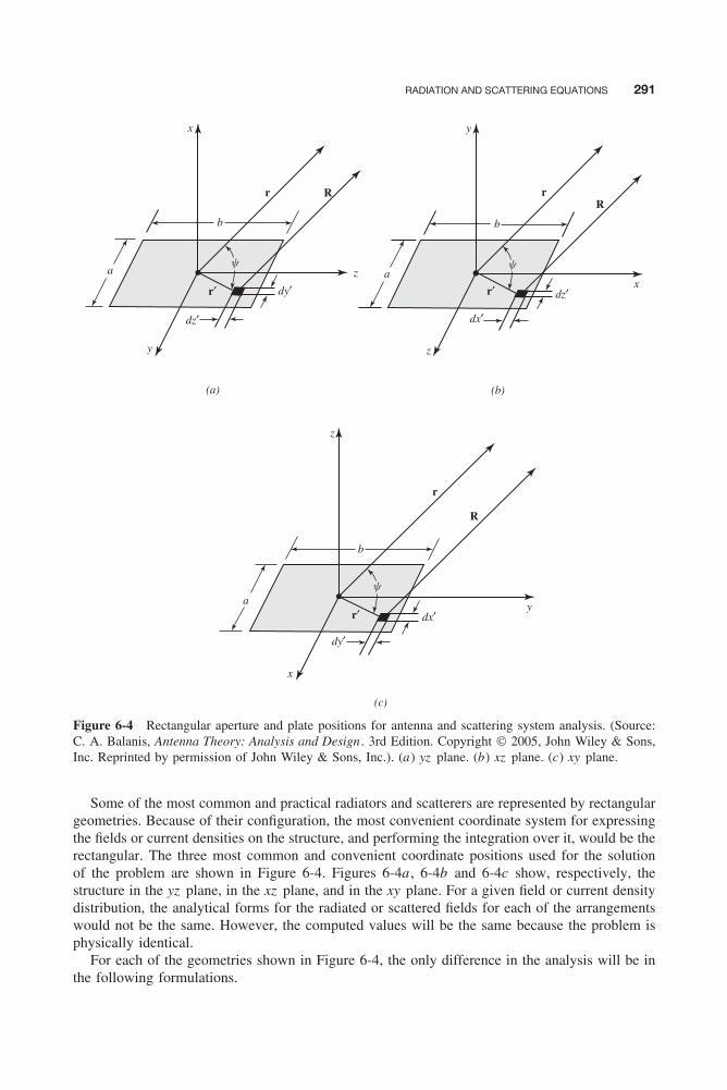
Balanis c06.tex V2 - 11/22/2011 3:14 P.M. Page 291
RADIATION AND SCATTERING EQUATIONS 291
r
r
rR
R
R
x y
b
b
b
a
a
a
dz′
dx′
dx′
dy′
dy′
dz′
y
x
z
z
z
x
y
r′
r′
r′
(a) (b)
(c)
y
y
y
Figure 6-4 Rectangular aperture and plate positions for antenna and scattering system analysis. (Source:C. A. Balanis, Antenna Theory: Analysis and Design . 3rd Edition. Copyright © 2005, John Wiley & Sons,Inc. Reprinted by permission of John Wiley & Sons, Inc.). (a) yz plane. (b) xz plane. (c) xy plane.
Some of the most common and practical radiators and scatterers are represented by rectangulargeometries. Because of their configuration, the most convenient coordinate system for expressingthe fields or current densities on the structure, and performing the integration over it, would be therectangular. The three most common and convenient coordinate positions used for the solutionof the problem are shown in Figure 6-4. Figures 6-4a , 6-4b and 6-4c show, respectively, thestructure in the yz plane, in the xz plane, and in the xy plane. For a given field or current densitydistribution, the analytical forms for the radiated or scattered fields for each of the arrangementswould not be the same. However, the computed values will be the same because the problem isphysically identical.
For each of the geometries shown in Figure 6-4, the only difference in the analysis will be inthe following formulations.

Balanis c06.tex V2 - 11/22/2011 3:14 P.M. Page 292
292 AUXILIARY VECTOR POTENTIALS, CONSTRUCTION OF SOLUTIONS, AND RADIATION AND SCATTERING EQUATIONS
1. The components of the equivalent currents, Jx , Jy , Jz , Mx , My , and Mz .2. The difference in paths from the source to the observation point, r ′ cos ψ .3. The differential area ds ′.
In general, the nonzero components of Js and Ms will be
Jy , Jz , My , and Mz (Fig. 6-4a) (6-126a)
Jx , Jz , Mx , and Mz (Fig. 6-4b) (6-126b)
Jx , Jy , Mx , and My (Fig. 6-4c) (6-126c)
The differential paths will be of the form
r ′ cos ψ = r′ • âr = (ây y ′ + âz z ′) • (âx sin θ cos φ + ây sin θ sin φ + âz cos θ)
= y ′ sin θ sin φ + z ′ cos θ (Fig. 6-4a) (6-127a)
r ′ cos ψ = r′ • âr = (âx x ′ + âz z ′) • (âx sin θ cos φ + ây sin θ sin φ + âz cos θ)
= x ′ sin θ cos φ + z ′ cos θ (Fig. 6-4b) (6-127b)
r ′ cos ψ = r′ • âr = (âx x ′ + ây y ′) • (âx sin θ cos φ + ây sin θ sin φ + âz cos θ)
= x ′ sin θ cos φ + y ′ sin θ sin φ (Fig. 6-4c) (6-127c)
and the differential areas of
ds ′ = dy ′dz ′ (Fig. 6-4a) (6-128a)
ds ′ = dx ′dz ′ (Fig. 6-4b) (6-128b)
ds ′ = dx ′dy ′ (Fig. 6-4c) (6-128c)
SUMMARY To summarize the results, we will outline the procedure that must be followedto solve a problem using the radiation or scattering integrals. Figure 6-3 is used to indicate thegeometry.
1. Select a closed surface over which the actual current density Js or the equivalent currentdensities Js and Ms exist.
2. Specify the actual current density Js or form the equivalent currents Js and Ms over Susing [1, 3, 5]
Js = n̂ × Ha (6-129a)
Ms = −n̂ × Ea (6-129b)
where n̂ = unit vector normal to the surface SEa = total electric field over the surface SHa = total magnetic field over the surface S
3. (Optional ) Determine the potentials A and F using, respectively, (6-103) and (6-109) wherethe integration is over the surface S of the sources.
4. Determine the corresponding E- and H-field components that are due to Js and Ms using(6-107a) through (6-107c), (6-108a) through (6-108e), (6-110a) through (6-110c), and (6-111a) through (6-111c). Combine the E- and H-field components that are due to both Js
and Ms to find the total E and H fields.

Balanis c06.tex V2 - 11/22/2011 3:14 P.M. Page 293
RADIATION AND SCATTERING EQUATIONS 293
These steps are valid for all regions (near field and far field) outside the surface S. If, however,the observation point is in the far field, steps 3 and 4 can be replaced by 3′ and 4′.
3′. Determine Nθ , Nφ , Lθ , and Lφ using (6-125a) through (6-125d).4′. Determine the radiated E and H fields using (6-122a) through (6-122f).
This procedure can be used to analyze radiation and scattering problems. The radiation prob-lems most conducive to this procedure are aperture antennas, such as waveguides, horns, reflectors,and others. These aperture antennas are usually best represented by specifying their fields overtheir apertures.
Example 6-4
The tangential E and H fields over a rectangular aperture of dimensions a and b, shown in Figure 6-5,are given by
Ea = ây E0
Ha = −âxE0
η
⎫⎪⎬⎪⎭−a
2≤ x ′ ≤ a
2
−b
2≤ y ′ ≤ b
2
Ea � Ha � 0 elsewhere
Find the far-zone fields radiated by the aperture, and plot the three-dimensional pattern when a = 3λ andb = 2λ. The fields over the aperture and elsewhere have been simplified in order to reduce the complexityof the problem and to avoid having the analytical formulations obscure the analysis procedure.
Solution:
1. The surface of the radiator is defined by −a/2 ≤ x ≤ a/2 and −b/2 ≤ y ≤ b/2.2. Since the electric and magnetic fields exist only over the bounds of the aperture, the equivalent
current densities Js and Ms representing the aperture exist only over the bounds of the aperture aswell. This is a good approximation, and it is derived by the equivalence principle in Chapter 7 [1,3, 5]. Using (6-129a) and (6-129b) the current densities Js and Ms can be written, by referringto Figure 6-5, as
Js = n̂ × Ha = âz ×(
−âxE0
η
)= −ây
E0
η⇒ Jx = Jz = 0 Jy = −E0
η
Ms = −n̂ × Ea = −âz × ây E0 = âx E0 ⇒ Mx = E0 My = Mz = 0
3. Using (6-125a), (6-127c), and (6-128c), we can reduce Nθ to
Nθ =∫∫
S
[Jx cos θ cos φ + Jy cos θ sin φ − Jz sin θ
]ejβr ′ cos ψds ′
= −E0
ηcos θ sin φ
∫ b/2
−b/2
∫ a/2
−a/2ejβ(x ′ sin θ cos φ+y ′ sin θ sin φ)dx ′dy ′
Using the integral ∫ c/2
−c/2ejαz dz = c
⎡⎢⎣ sin(α
2c)
α
2c
⎤⎥⎦
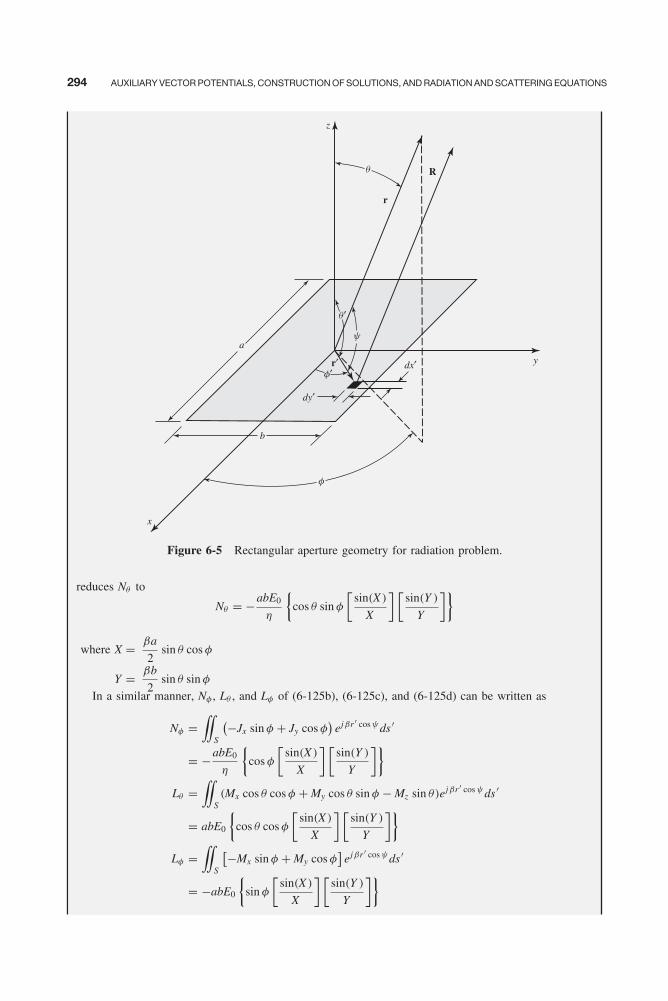
Balanis c06.tex V2 - 11/22/2011 3:14 P.M. Page 294
294 AUXILIARY VECTOR POTENTIALS, CONSTRUCTION OF SOLUTIONS, AND RADIATION AND SCATTERING EQUATIONS
x
b
a
dy′
dx′ y
z
r
R
r′
y
q′
q
f′
f
Figure 6-5 Rectangular aperture geometry for radiation problem.
reduces Nθ to
Nθ = −abE0
η
{cos θ sin φ
[sin(X )
X
] [sin(Y )
Y
]}
where X = βa
2sin θ cos φ
Y = βb
2sin θ sin φ
In a similar manner, Nφ , Lθ , and Lφ of (6-125b), (6-125c), and (6-125d) can be written as
Nφ =∫∫
S
(−Jx sin φ + Jy cos φ)
ejβr ′ cos ψds ′
= −abE0
η
{cos φ
[sin(X )
X
] [sin(Y )
Y
]}Lθ =
∫∫S(Mx cos θ cos φ + My cos θ sin φ − Mz sin θ)ejβr ′ cos ψds ′
= abE0
{cos θ cos φ
[sin(X )
X
] [sin(Y )
Y
]}Lφ =
∫∫S
[−Mx sin φ + My cos φ]
ejβr ′ cos ψds ′
= −abE0
{sin φ
[sin(X )
X
] [sin(Y )
Y
]}

Balanis c06.tex V2 - 11/22/2011 3:14 P.M. Page 295
RADIATION AND SCATTERING EQUATIONS 295
The corresponding far-zone E- and H-field components radiated by the aperture are obtained using(6-122a) through (6-122f), and they can be written as
Er � Hr � 0
Eθ � C
2sin φ(1 + cos θ)
[sin(X )
X
] [sin(Y )
Y
]Eφ � C
2cos φ(1 + cos θ)
[sin(X )
X
] [sin(Y )
Y
]Hθ � −Eφ
η
Hφ � +Eθ
η
C = jabβE0e−jβr
2πr
Relativemagnitude
1.0
180°180°qq
H-plane (x−z, f = 0°) E-plane (y−z, f = 90°)
Figure 6-6 Three-dimensional field pattern of a constant field rectangular aperture (a = 3λ and b =2λ). (Source: C. A. Balanis, Antenna Theory: Analysis and Design . 3rd Edition. Copyright © 2005, JohnWiley & Sons, Inc. Reprinted by permission of John Wiley & Sons, Inc.).
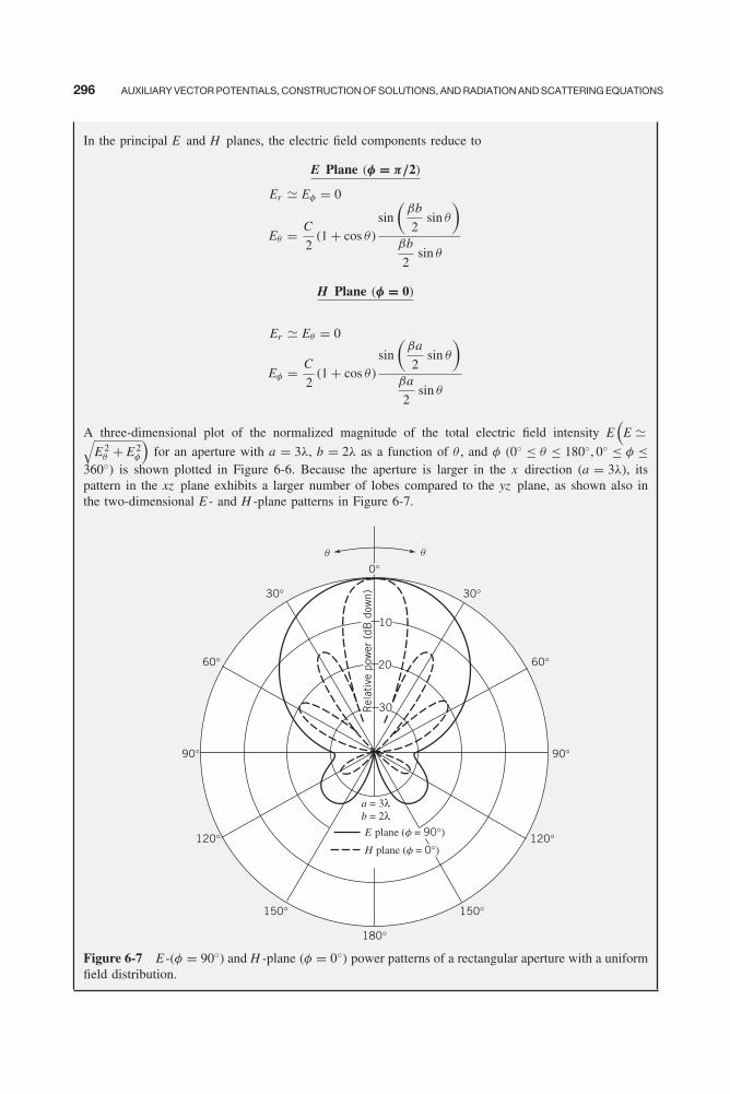
Balanis c06.tex V2 - 11/22/2011 3:14 P.M. Page 296
296 AUXILIARY VECTOR POTENTIALS, CONSTRUCTION OF SOLUTIONS, AND RADIATION AND SCATTERING EQUATIONS
In the principal E and H planes, the electric field components reduce to
E Plane (φ = π/2)
Er � Eφ = 0
Eθ = C
2(1 + cos θ)
sin
(βb
2sin θ
)βb
2sin θ
H Plane (φ = 0)
Er � Eθ = 0
Eφ = C
2(1 + cos θ)
sin
(βa
2sin θ
)βa
2sin θ
A three-dimensional plot of the normalized magnitude of the total electric field intensity E(
E �√E 2
θ + E 2φ
)for an aperture with a = 3λ, b = 2λ as a function of θ , and φ (0◦ ≤ θ ≤ 180◦, 0◦ ≤ φ ≤
360◦) is shown plotted in Figure 6-6. Because the aperture is larger in the x direction (a = 3λ), itspattern in the xz plane exhibits a larger number of lobes compared to the yz plane, as shown also inthe two-dimensional E - and H -plane patterns in Figure 6-7.
30°
10
Rel
ativ
e po
wer
(dB
dow
n)
20
30
60°
90°
120°
150°
180°
150°
120°
90°
60°
30°
0°
E plane (f = 90°) H plane (f = 0°)
a = 3λb = 2λ
q q
Figure 6-7 E -(φ = 90◦) and H -plane (φ = 0◦) power patterns of a rectangular aperture with a uniformfield distribution.
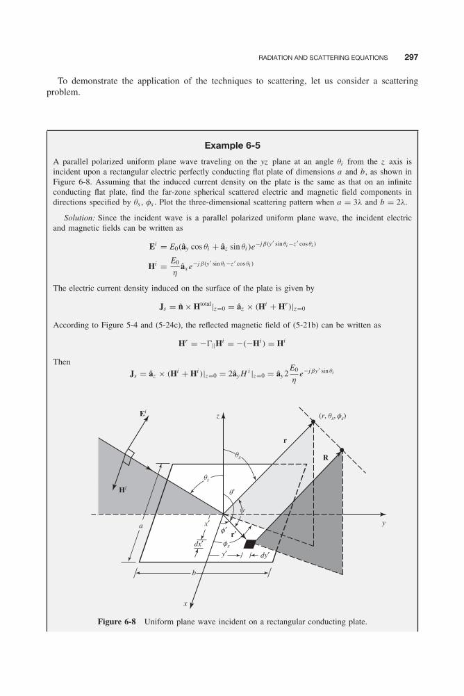
Balanis c06.tex V2 - 11/22/2011 3:14 P.M. Page 297
RADIATION AND SCATTERING EQUATIONS 297
To demonstrate the application of the techniques to scattering, let us consider a scatteringproblem.
Example 6-5
A parallel polarized uniform plane wave traveling on the yz plane at an angle θi from the z axis isincident upon a rectangular electric perfectly conducting flat plate of dimensions a and b, as shown inFigure 6-8. Assuming that the induced current density on the plate is the same as that on an infiniteconducting flat plate, find the far-zone spherical scattered electric and magnetic field components indirections specified by θs , φs . Plot the three-dimensional scattering pattern when a = 3λ and b = 2λ.
Solution: Since the incident wave is a parallel polarized uniform plane wave, the incident electricand magnetic fields can be written as
Ei = E0(ây cos θi + âz sin θi )e−jβ(y ′ sin θi −z ′ cos θi )
Hi = E0
ηâx e−jβ(y ′ sin θi −z ′ cos θi )
The electric current density induced on the surface of the plate is given by
Js = n̂ × Htotal|z=0 = âz × (Hi + Hr )|z=0
According to Figure 5-4 and (5-24c), the reflected magnetic field of (5-21b) can be written as
Hr = −�‖Hi = −(−Hi ) = Hi
ThenJs = âz × (Hi + Hi )|z=0 = 2ây H i |z=0 = ây 2
E0
ηe−jβy ′ sin θi
dx′dy′y′
x′
x
z
y
b
(r, qs, fs)
a
Hi
Ei
r′
r
R
y
q′
f′
fs
qs
qi
Figure 6-8 Uniform plane wave incident on a rectangular conducting plate.
Balanis c06.tex V2 - 11/22/2011 3:14 P.M. Page 298
298 AUXILIARY VECTOR POTENTIALS, CONSTRUCTION OF SOLUTIONS, AND RADIATION AND SCATTERING EQUATIONS
orJx = Jz = 0 everywhere
Jy = 2E0
ηe−jβy ′ sin θi for
{−a/2 ≤ x ′ ≤ a/2
−b/2 ≤ y ′ ≤ b/2and zero elsewhere
Because the geometry of the plate corresponds to the coordinate system of Figure 6-4c, equation 6-125acan be written using (6-127c) and (6-128c) as
Nθ =∫∫
S
[Jx cos θs cos φs + Jy cos θs sin φs − Jz sin θs
]ejβr ′ cos ψds ′
= 2E0
ηcos θs sin φs
∫ b/2
−b/2
∫ a/2
−a/2ejβx ′ sin θs cos φs ejβy ′(sin θs sin φs −sin θi )dx ′dy ′
Using the integral ∫ c/2
−c/2ejαz dz = c
⎡⎢⎣ sin(α
2c)
α
2c
⎤⎥⎦reduces Nθ to
Nθ = 2abE0
η
{cos θs sin φs
[sin(X )
X
] [sin(Y )
Y
]}
where X = βa
2sin θs cos φs
Y = βb
2(sin θs sin φs − sin θi )
Similarly, according to (6-125b), Nφ can be written as
Nφ =∫∫
S
(−Jx sin φs + Jy cos φs)
ejβr ′ cos ψds ′
= 2abE0
η
{cos φs
[sin(X )
X
] [sin(Y )
Y
]}Because the plate is a perfect electric conductor,
Mx = My = Mz = 0 everywhere
Therefore, according to (6-125c) and (6-125d),
Lθ = Lφ = 0
Thus the scattered electric and magnetic field components can be reduced according to (6-122a) through(6-122f) to
E sr � H s
r � 0
E sθ � −jab
βE0e−jβr
2πr
{cos θs sin φs
[sin(X )
X
] [sin(Y )
Y
]}E s
φ � −jabβE0e−jβr
2πr
{cos φs
[sin(X )
X
] [sin(Y )
Y
]}H s
θ � −E sφ
η
H sφ � +E s
θ
η
Balanis c06.tex V2 - 11/22/2011 3:14 P.M. Page 299
RADIATION AND SCATTERING EQUATIONS 299
In the principal E and H planes, the electric field components reduce, respectively, as follows.
E Plane (φs = π/2, 3π/2)
E sr � E s
φ � 0
E sθ � −jab
βE0e−jβr
2πrcos θs
sin
[βb
2(± sin θs − sin θi )
]βb
2(± sin θs − sin θi )
+for φs = π/2−for φs = 3π/2
H Plane (φs = 0, π)
E sr � E s
θ � 0
E sφ � −jab
βE0e−jβr
2πr
sin
(βa
2sin θs
)βa
2sin θs
sin
(βb
2sin θi
)βb
2sin θi
A three-dimensional plot of the normalized magnitude of the total electric field E s[E s =√
(E sθ )2 + (E s
φ)2]
for a plate of dimensions a = 3λ and b = 2λ when the incidence angle θi = 30◦
is shown in Figure 6-9. Its corresponding two-dimensional pattern in the yz plane (φs = 90◦, 270◦)is exhibited in Figure 6-10. It can be observed that the maximum scattered field is directed nearθs = 30◦, which is near the direction of specular reflection (defined as the direction along whichthe angle of reflection is equal to the angle of incidence). For more details see Section 11.3.
By using such a procedure for plates of finite size, the scattering fields are accurate at andnear the specular direction. The angular extent over which the accuracy is acceptable increasesas the size of the scatterer increases. Other techniques, such as those discussed in Chapters 12and 13, can be used to improve the accuracy everywhere.
B. Cylindrical Coordinate System When the radiating or scattering structure is of circulargeometry, the radiation or scattering fields can still be found using (6-122a) through (6-122f).The Nθ , Nφ , Lθ , and Lφ functions must still be obtained from (6-114c) and (6-114d) but must beexpressed in a form that is convenient for cylindrical geometries. Although the general procedureof analysis for circular geometry is identical to that of the rectangular, as outlined in the previoussection, the primary differences lie in the following.
1. The formulation of the equivalent currents, Jx , Jy , Jz , Mx , My , and Mz .2. The differential paths from the source to the observation point, r ′ cos ψ .3. The differential area ds ′.
Before we consider an example, we will reformulate these differences for the circular aperture.Because of the circular profile of the aperture, it is often convenient and desirable to adopt
cylindrical coordinates for the solution of the fields. In most cases, therefore, the radiated orscattered electric and magnetic field components over the circular geometry will be known incylindrical form, that is, Eρ , Eφ , Ez , Hρ , Hφ , and Hz . Thus, the components of the equivalentcurrents Ms and Js would also be conveniently expressed in cylindrical form, Mρ , Mφ , Mz , Jρ ,
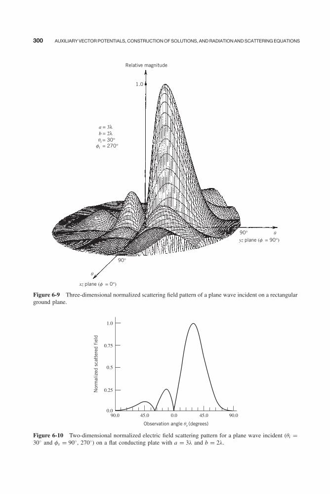
Balanis c06.tex V2 - 11/22/2011 3:14 P.M. Page 300
300 AUXILIARY VECTOR POTENTIALS, CONSTRUCTION OF SOLUTIONS, AND RADIATION AND SCATTERING EQUATIONS
Relative magnitude
1.0
a = 3λb = 2λqi = 30°fi = 270°
90°
90°
xz plane (f = 0°)
yz plane (f = 90°)
q
q
Figure 6-9 Three-dimensional normalized scattering field pattern of a plane wave incident on a rectangularground plane.
90.00.0
0.25
0.5
0.75
1.0
90.045.0 45.0
Observation angle qs (degrees)
Nor
mal
ized
sca
tter
ed f
ield
0.0
Figure 6-10 Two-dimensional normalized electric field scattering pattern for a plane wave incident (θi =30◦ and φs = 90◦, 270◦) on a flat conducting plate with a = 3λ and b = 2λ.
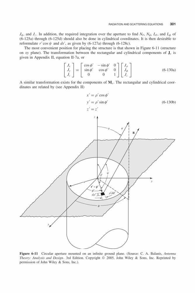
Balanis c06.tex V2 - 11/22/2011 3:14 P.M. Page 301
RADIATION AND SCATTERING EQUATIONS 301
Jφ , and Jz . In addition, the required integration over the aperture to find Nθ , Nφ , Lθ , and Lφ of(6-125a) through (6-125d) should also be done in cylindrical coordinates. It is then desirable toreformulate r ′ cos ψ and ds ′, as given by (6-127a) through (6-128c).
The most convenient position for placing the structure is that shown in Figure 6-11 (structureon xy plane). The transformation between the rectangular and cylindrical components of Js isgiven in Appendix II, equation II-7a, or⎡⎣ Jx
Jy
Jz
⎤⎦ =⎡⎣ cos φ′ − sin φ′ 0
sin φ′ cos φ′ 00 0 1
⎤⎦⎡⎣ Jρ
Jφ
Jz
⎤⎦ (6-130a)
A similar transformation exists for the components of Ms . The rectangular and cylindrical coor-dinates are related by (see Appendix II)
x ′ = ρ ′ cos φ′
y ′ = ρ ′ sin φ′ (6-130b)
z ′ = z ′
x
z
r
R
a
r′ = ρ′
dr′ r′df′
y
f′
f
q′
q
y
Figure 6-11 Circular aperture mounted on an infinite ground plane. (Source: C. A. Balanis, AntennaTheory: Analysis and Design . 3rd Edition. Copyright © 2005, John Wiley & Sons, Inc. Reprinted bypermission of John Wiley & Sons, Inc.).
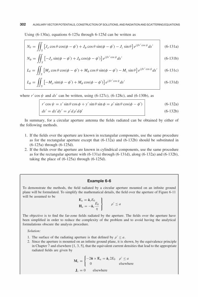
Balanis c06.tex V2 - 11/22/2011 3:14 P.M. Page 302
302 AUXILIARY VECTOR POTENTIALS, CONSTRUCTION OF SOLUTIONS, AND RADIATION AND SCATTERING EQUATIONS
Using (6-130a), equations 6-125a through 6-125d can be written as
Nθ =∫∫
S
[Jρ cos θ cos(φ − φ′) + Jφ cos θ sin(φ − φ′) − Jz sin θ
]ejβr ′ cos ψds ′
Nφ =∫∫
S
[−Jρ sin(φ − φ′) + Jφ cos(φ − φ′)]
ejβr ′ cos ψds ′
Lθ =∫∫
S
[Mρ cos θ cos(φ − φ′) + Mφ cos θ sin(φ − φ′) − Mz sin θ
]ejβr ′ cos ψds ′
Lφ =∫∫
S
[−Mρ sin(φ − φ′) + Mφ cos(φ − φ′)]
ejβr ′ cos ψds ′
(6-131a)
(6-131b)
(6-131c)
(6-131d)
where r ′ cos ψ and ds ′ can be written, using (6-127c), (6-128c), and (6-130b), as
r ′ cos ψ = x ′ sin θ cos φ + y ′ sin θ sin φ = ρ ′ sin θ cos(φ − φ′)
ds ′ = dx ′dy ′ = ρ ′dρ ′dφ′(6-132a)
(6-132b)
In summary, for a circular aperture antenna the fields radiated can be obtained by either ofthe following methods.
1. If the fields over the aperture are known in rectangular components, use the same procedureas for the rectangular aperture except that (6-132a) and (6-132b) should be substituted in(6-125a) through (6-125d).
2. If the fields over the aperture are known in cylindrical components, use the same procedureas for the rectangular aperture with (6-131a) through (6-131d), along (6-132a) and (6-132b),taking the place of (6-125a) through (6-125d).
Example 6-6
To demonstrate the methods, the field radiated by a circular aperture mounted on an infinite groundplane will be formulated. To simplify the mathematical details, the field over the aperture of Figure 6-11will be assumed to be
Ea = ây E0
Ha = −âxE0
η
⎫⎬⎭ ρ ′ ≤ a
The objective is to find the far-zone fields radiated by the aperture. The fields over the aperture havebeen simplified in order to reduce the complexity of the problem and to avoid having the analyticalformulations obscure the analysis procedure.
Solution:
1. The surface of the radiating aperture is that defined by ρ ′ ≤ a .2. Since the aperture is mounted on an infinite ground plane, it is shown, by the equivalence principle
in Chapter 7 and elsewhere [1, 3, 5], that the equivalent current densities that lead to the appropriateradiated fields are given by
Ms ={
−2n̂ × Ea = âx 2E0 ρ ′ ≤ a
0 elsewhere
Js = 0 elsewhere
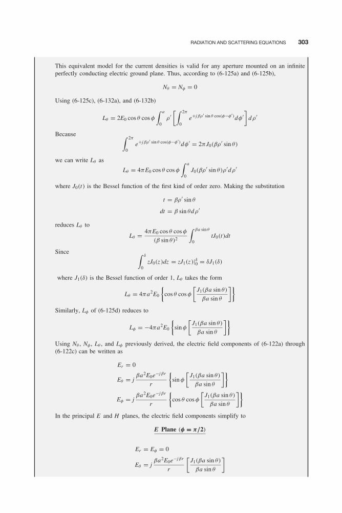
Balanis c06.tex V2 - 11/22/2011 3:14 P.M. Page 303
RADIATION AND SCATTERING EQUATIONS 303
This equivalent model for the current densities is valid for any aperture mounted on an infiniteperfectly conducting electric ground plane. Thus, according to (6-125a) and (6-125b),
Nθ = Nφ = 0
Using (6-125c), (6-132a), and (6-132b)
Lθ = 2E0 cos θ cos φ
∫ a
0ρ ′
[∫ 2π
0e+jβρ′ sin θ cos(φ−φ′)dφ′
]dρ ′
Because ∫ 2π
0e+jβρ′ sin θ cos(φ−φ′)dφ′ = 2πJ0(βρ ′ sin θ)
we can write Lθ as
Lθ = 4πE0 cos θ cos φ
∫ a
0J0(βρ ′ sin θ)ρ ′dρ ′
where J0(t) is the Bessel function of the first kind of order zero. Making the substitution
t = βρ ′ sin θ
dt = β sin θdρ ′
reduces Lθ to
Lθ = 4πE0 cos θ cos φ
(β sin θ)2
∫ βa sin θ
0tJ0(t)dt
Since ∫ δ
0zJ0(z )dz = zJ1(z )|δ0 = δJ1(δ)
where J1(δ) is the Bessel function of order 1, Lθ takes the form
Lθ = 4πa2E0
{cos θ cos φ
[J1(βa sin θ)
βa sin θ
]}Similarly, Lφ of (6-125d) reduces to
Lφ = −4πa2E0
{sin φ
[J1(βa sin θ)
βa sin θ
]}Using Nθ , Nφ , Lθ , and Lφ previously derived, the electric field components of (6-122a) through(6-122c) can be written as
Er = 0
Eθ = jβa2E0e−jβr
r
{sin φ
[J1(βa sin θ)
βa sin θ
]}Eφ = j
βa2E0e−jβr
r
{cos θ cos φ
[J1(βa sin θ)
βa sin θ
]}In the principal E and H planes, the electric field components simplify to
E Plane (φ = π/2)
Er = Eφ = 0
Eθ = jβa2E0e−jβr
r
[J1(βa sin θ)
βa sin θ
]
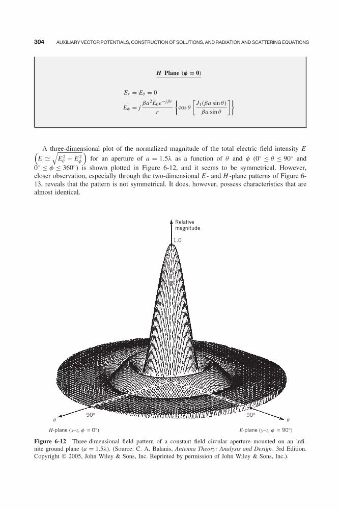
Balanis c06.tex V2 - 11/22/2011 3:14 P.M. Page 304
304 AUXILIARY VECTOR POTENTIALS, CONSTRUCTION OF SOLUTIONS, AND RADIATION AND SCATTERING EQUATIONS
H Plane (φ = 0)
Er = Eθ = 0
Eφ = jβa2E0e−jβr
r
{cos θ
[J1(βa sin θ)
βa sin θ
]}
A three-dimensional plot of the normalized magnitude of the total electric field intensity E(E �
√E 2
θ + E 2φ
)for an aperture of a = 1.5λ as a function of θ and φ (0◦ ≤ θ ≤ 90◦ and
0◦ ≤ φ ≤ 360◦) is shown plotted in Figure 6-12, and it seems to be symmetrical. However,closer observation, especially through the two-dimensional E - and H -plane patterns of Figure 6-13, reveals that the pattern is not symmetrical. It does, however, possess characteristics that arealmost identical.
Relativemagnitude
1.0
90°90°qq
H-plane (x−z, f = 0°) E-plane (y−z, f = 90°)
Figure 6-12 Three-dimensional field pattern of a constant field circular aperture mounted on an infi-nite ground plane (a = 1.5λ). (Source: C. A. Balanis, Antenna Theory: Analysis and Design . 3rd Edition.Copyright © 2005, John Wiley & Sons, Inc. Reprinted by permission of John Wiley & Sons, Inc.).
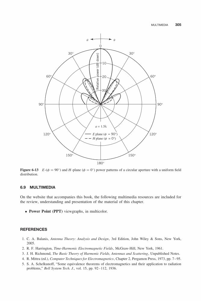
Balanis c06.tex V2 - 11/22/2011 3:14 P.M. Page 305
MULTIMEDIA 305
30°
10
20
30
60°
90°
120°
150°
180°
150°
120°
90°
60°
30°
0
Rel
ativ
e po
wer
(dB
dow
n)
E plane (f = 90°) H plane (f = 0°)
a = 1.5λ
q q
Figure 6-13 E -(φ = 90◦) and H -plane (φ = 0◦) power patterns of a circular aperture with a uniform fielddistribution.
6.9 MULTIMEDIA
On the website that accompanies this book, the following multimedia resources are included forthe review, understanding and presentation of the material of this chapter.
• Power Point (PPT) viewgraphs, in multicolor.
REFERENCES
1. C. A. Balanis, Antenna Theory: Analysis and Design , 3rd Edition, John Wiley & Sons, New York,2005.
2. R. F. Harrington, Time-Harmonic Electromagnetic Fields , McGraw-Hill, New York, 1961.
3. J. H. Richmond, The Basic Theory of Harmonic Fields, Antennas and Scattering , Unpublished Notes.
4. R. Mittra (ed.), Computer Techniques for Electromagnetics , Chapter 2, Pergamon Press, 1973, pp. 7–95.
5. S. A. Schelkunoff, “Some equivalence theorems of electromagnetics and their application to radiationproblems,” Bell System Tech. J., vol. 15, pp. 92–112, 1936.
Balanis c06.tex V2 - 11/22/2011 3:14 P.M. Page 306
306 AUXILIARY VECTOR POTENTIALS, CONSTRUCTION OF SOLUTIONS, AND RADIATION AND SCATTERING EQUATIONS
PROBLEMS
6.1. If He = jωε∇ × �e , where �e is the elec-tric Hertzian potential, show that(a) ∇2�e + β2�e = j (1/ωε)J.(b) Ee = β2�e + ∇(∇ · �e).(c) �e = −j (1/ωμε)A.
6.2. If Eh = −jωμ∇ × �h , where �h is themagnetic Hertzian potential, show that(a) ∇2�h + β2�h = j (1/ωμ)M.(b) Hh = β2�h + ∇(∇ · �h).(c) �h = −j (1/ωμε)F.
6.3. Develop expressions for EA and HA in termsof J using the path-1 procedure of Figure 6-1. These expressions should be valid every-where.
6.4. Develop expressions for EF and HF in termsof M using the path-1 procedure of Figure 6-1. These expressions should be valid every-where.
6.5. In rectangular coordinates derive expres-sions for E and H, in terms of the com-ponents of the A and F potentials, that areTEMx and TEMy . The procedure should besimilar to that of Example 6.1, and it shouldstate all the combinations that lead to thedesired modes.
6.6. In cylindrical coordinates derive expressionsfor E and H, in terms of the componentsof the A and F potentials, that are TEMφ
and TEMz . The procedure should be similarto that of Example 6-2, and it should stateall the combinations that lead to the desiredmodes.
6.7. Derive the expressions for the componentsof E and H of (6-61) and (6-64), in termsof the components of A and F, so that thefields are TMx and TMy .
6.8. Select one component of E and write theother components of E and all of H in termsof the initial component of E so that thefields are TMx , TMy , and TMz . Do this inrectangular coordinates.
6.9. For the TEz modes (Ez = 0) in rectan-gular coordinates, with z variations ofthe form e−jβz z , derive expressions forthe E- and H-field rectangular componentsin terms of Hz = f (x)g(y)e−jβz z , where∇2Hz (x , y , z ) + β2Hz (x , y , z ) = 0. In otherwords, instead of expressing the electric and
magnetic field components for TEz modes(Ez = 0) in terms of Fz [as is done in (6-72)], this time you start with Hz not beingequal to zero and express all the electricand magnetic field components, except Hz,in terms of Hz. This is an alternate way offinding the TEz modes. Simplify the expres-sions. They should be in a form similar tothose of (6-72).Hint: You should use Maxwell’s equationsback and forth.
6.10. For the TMz modes (Hz = 0) in rect-angular coordinates, with z variations ofthe form e−jβz z , derive expressions forthe E- and H-field rectangular componentsin terms of Ez = f (x)g(y)e−jβz z , where∇2Ez (x , y , z ) + β2Ez (x , y , z ) = 0. In otherwords, instead of expressing the electric andmagnetic field components for TMz modes(Hz = 0) in terms of Az [as is done in (6-59)], this time you start with Ez not beingequal to zero and express all the electricand magnetic field components, except Ez,in terms of Ez. This is an alternate way offinding the TMz modes. Simplify the expres-sions. They should be in a form similar tothose of (6-59).Hint : You should use Maxwell’s equationsback and forth.
6.11. In cylindrical coordinates, select one com-ponent of E and write the other componentsof E and all of H in terms of the initialcomponent of E so that the fields are TMz .
6.12. In rectangular coordinates, derive theexpressions for the components of E and Has given by (6-72), (6-74), and (6-77) thatare TEz , TEx , and TEy .
6.13. In cylindrical coordinates, derive the expres-sions for E and H as given by (6-80), whichare TEz .
6.14. Select one component of H and write theother components of H and all of E in termsof the initial component of H so that thefields are TEx , TEy , and TEz . Do this inrectangular coordinates.
6.15. In cylindrical coordinates, select one compo-nent of H and write the other componentsof H and all of E in terms of the initialcomponent of H so that the fields are TEz .

Balanis c06.tex V2 - 11/22/2011 3:14 P.M. Page 307
PROBLEMS 307
6.16. Verify that (6-85a) and (6-85b) are solutionsto (6-84a).
6.17. Show that (6-90) is a solution to (6-87) andthat (6-91) is a solution to (6-82).
6.18. For Example 6-3 derive the components ofE, given the components of H.
6.19. Show that for observations made at verylarge distance (βr � 1) the electric andmagnetic fields of Example 6-3 reduce to
Eθ = jηβIe�e−jβr
4πrsin θ
Hφ � Eθ
η
Er � 0
Eφ = Hr = Hθ = 0
6.20. For Problem 6.19, show that the:• Time-average power density is
Sav = 1
2Re
[E × H∗] = âr Wav = âr Wr
= ârη
8
∣∣∣∣ Io�
λ
∣∣∣∣2 sin2 θ
r2
• Radiation intensity is
U = r2Sav = η
8
∣∣∣∣ Io�
λ
∣∣∣∣2 sin2 θ
• Radiated power is
Prad =2π∫
0
π∫0
U (θ , φ)
× sin θdθdφ = η(π
3
) ∣∣∣∣ I0�
λ
∣∣∣∣2
• Directivity is Do = 4πUmax (θ , φ)
Prad
= 3
2(dimensionless) = 1.761 dB
• Radiation resistance is
Rr = 2Prad
|Io |2 = 80π2(
�
λ
)2
6.21. An infinitesimal electric dipole of length �
and constant current Io is placed symmet-rically about the origin and it is directedalong the x axis. Using the procedure out-lined in Section 6.7, derive the followingexpressions for the far zone:• Magnetic vector potential components
(Ar , Aθ , Aφ).• Electric field components (Er , Eθ , Eφ).• Magnetic field components (Hr , Hθ , Hφ).
• Time-average power density as defined inProblem 6.20.
• Radiation intensity as defined in Prob-lem 6.20.
• Directivity as defined in Problem 6.20.• Radiation resistance as defined in Prob-
lem 6.20.
6.22. Repeat the procedure of Problem 6.21 whenthe electric dipole is directed along the yaxis.
6.23. Verify (6-100a) and (6-100b).
6.24. Show that (6-112) reduces to (6-112a) pro-vided r ≥ 2D2/λ, where D is the largestdimension of the radiator or scatterer. Suchan approximation leads to a phase error thatis equal to or smaller than 22.5◦.
6.25. The current distribution on a very thin wiredipole antenna of overall length � is givenby
Ie =
⎧⎪⎪⎪⎨⎪⎪⎪⎩âz I0 sin
[β
(�
2−z ′
)]0≤z ′ ≤ �
2
âz I0 sin
[β
(�
2+z ′
)]− �
2≤z ′ ≤0
where I0 is a constant. Representing the dis-tance R of (6-112) by the far-field approx-imations of (6-112a) through (6-112b),derive the far-zone electric and magneticfields radiated by the dipole using (6-97a)and the far-field formulations of Section 6.7.
6.26. Show that the radiated far-zone electric andmagnetic fields derived in Problem 6.25reduce for a half-wavelength dipole (� =λ/2) to
Eθ � jηI0e−jβr
2πr
⎡⎢⎣cos(π
2cos θ
)sin θ
⎤⎥⎦Hφ � Eθ
η
Er � Eφ � Hr � Hθ � 0
6.27. Simplify the expressions of Problem 6.3, ifthe observations are made in the far field.
6.28. Simplify the expressions of Problem 6.4, ifthe observations are made in the far field.

Balanis c06.tex V2 - 11/22/2011 3:14 P.M. Page 308
308 AUXILIARY VECTOR POTENTIALS, CONSTRUCTION OF SOLUTIONS, AND RADIATION AND SCATTERING EQUATIONS
6.29. The rectangular aperture of Figure 6-4a ismounted on an infinite ground plane thatcoincides with the yz plane. Assuming thatthe tangential field over the aperture is givenby
Ea = âz E0, for − a/2 ≤ y ′ ≤ a/2− b/2 ≤ z ′ ≤ b/2
and the equivalent currents are
Ms =
⎧⎪⎨⎪⎩−2n̂×Ea , for −a/2≤y ′ ≤a/2
−b/2≤z ′ ≤b/2
0 elsewhere
Js =0 everywhere
find the far-zone spherical electric and mag-netic field components radiated by the aper-ture.
6.30. Repeat Problem 6.29 when the same aper-ture is not mounted on an infinite PECground plane. For this problem, use bothelectric and magnetic current densities overthe aperture, as was done for Example 6-4. The E- and H-fields at the aperture arerelated by the intrinsic impedance, as inExample 6-4, such that E × H is in the +xdirection.Hint : You should use Maxwell’s equationsback and forth.
6.31. Repeat Problem 6.29 when the same aper-ture is analyzed using the coordinate systemof Figure 6-4b. The tangential aperture fielddistribution is given by
Ea = âx E0 for − b/2 ≤ x ′ ≤ b/2− a/2 ≤ z ′ ≤ a/2
and the equivalent currents are
Ms =
⎧⎪⎨⎪⎩−2n̂×Ea , for −b/2≤x ′ ≤b/2
−a/2 ≤ z ′ ≤a/2
0 elsewhere
Js =0 everywhere
6.32. Repeat Problem 6.29 when the same aper-ture is analyzed using the coordinate systemof Figure 6-4c. The tangential aperture fielddistribution is given by
Ea = ây E0, for − a/2 ≤ x ′ ≤ a/2 and− b/2 ≤ y ′ ≤ b/2
and the equivalent currents are
Ms =
⎧⎪⎨⎪⎩−2n̂×Ea , −a/2≤x ′ ≤a/2
−b/2≤y ′ ≤b/2
0 elsewhere
Js =0 everywhere
6.33. Repeat Problem 6.29 when the aperture fielddistribution is given by
Ea = âz E0 cos(π
ay ′)
, − a/2≤y ′ ≤a/2
− b/2≤z ′ ≤b/2
6.34. Repeat Problem 6.31 when the aperture fielddistribution is given by
Ea = âx E0 cos(π
az ′)
, − b/2 ≤ x ′ ≤ b/2
− a/2 ≤ z ′ ≤ a/2
6.35. Repeat Problem 6.32 when the aperture fielddistribution is given by
Ea = ây E0 cos(π
ax ′
), − a/2 ≤ x ′ ≤ a/2
− b/2 ≤ y ′ ≤ b/2
6.36. For the aperture of Example 6-4, find theangular separation (in degrees) betweentwo points whose radiated electric fieldvalue is 0.707 of the maximum (half-powerbeamwidth). Do this for the radiated fields inthe (a) E plane (φ = π/2) and (b) H plane(φ = 0). Assume the aperture has dimen-sions a = 4λ and b = 3λ.
6.37. For the circular aperture of Figure 6-11,derive expressions for the far-zone radiatedspherical fields when the aperture field dis-tribution is given by(a) Ea = ây E0[1 − (ρ ′/a)2], ρ ′ ≤ a .(b) Ea = ây E0[1 − (ρ ′/a)2]2, ρ ′ ≤ a .For both cases use equivalent currents Ms
and Js such that
Ms ={
−2n̂ × Ea , ρ ′ ≤ a ,
0 elsewhere
Js = 0 everywhere
6.38. A coaxial line of inner and outer radii aand b, respectively, is mounted on an infiniteconducting ground plane. Assuming that theelectric field over the aperture of the coax is
Ea = −âρ
V
ε ln(b/a)
1
ρ ′ , a ≤ ρ ′ ≤ b
where V is the applied voltage and ε isthe permittivity of medium in the coax, find

Balanis c06.tex V2 - 11/22/2011 3:14 P.M. Page 309
PROBLEMS 309
the far-zone spherical electric and magneticfield components radiated by the aperture.
z
ya
b
x
e
s = ∞
Figure P6-38
Use equivalent currents Ms and Js suchthat
Ms ={
−2n̂ × Ea , a ≤ ρ ′ ≤ b
0 elsewhere
Js = 0 everywhere
6.39. For the aperture of Example 6-6, find theangular separation (in degrees) betweentwo points whose radiated electric fieldvalue is 0.707 of the maximum (half-powerbeamwidth). Do this for the radiated fields inthe (a) E plane (φ = π/2) and (b) H plane(φ = 0). Assume that the radius of the aper-ture is 3λ.

Balanis c06.tex V2 - 11/22/2011 3:14 P.M. Page 310
CHAPTER 7Electromagnetic Theorems and Principles
7.1 INTRODUCTION
In electromagnetics there are a number of theorems and principles that are fundamental to theunderstanding of electromagnetic generation, radiation, propagation, scattering, and reception.Many of these are often used to facilitate the solution of interrelated problems. Those that willbe discussed here are the theorems of duality, uniqueness, image, reciprocity, reaction, volumeequivalence, surface equivalence, induction , and physical equivalent (physical optics). Whenappropriate, examples will be given to illustrate the principles.
7.2 DUALITY THEOREM
When two equations that describe the behavior of two different variables are of the same math-ematical form, their solutions will also be identical. The variables in the two equations thatoccupy identical positions are known as dual quantities, and a solution for one can be formed bya systematic interchange of symbols with the other. This concept is known as the duality theorem.
Comparison of (6-30), (6-32a), (6-32b), (6-32c), and (6-95a), respectively, to (6-31), (6-33a),(6-33b), (6-33c), and (6-95b), shows that they are dual equations and their variables are dualquantities. Thus, if we know the solutions to one set (J �= 0, M = 0), the solutions to the otherset (J = 0, M �= 0) can be formed by a proper interchange of quantities. The dual equationsand their dual quantities are listed in Tables 7-1 and 7-2 for electric and magnetic sources,respectively. Duality only serves as a guide to forming mathematical solutions. It can be used inan abstract manner to explain the motion of magnetic charges giving rise to magnetic currents,when compared to their dual quantities of moving electric charges creating electric currents [1].It must, however, be emphasized that this is purely mathematical in nature since at present thereare no known magnetic charges or currents in nature.
Example 7-1
A very thin linear magnetic current element of very small length (� � λ), although nonphysicallyrealizable, is often used to represent the fields of a very small electric loop radiator. It can be shownthat the fields radiated by a small linear magnetic current element are identical to those radiated by a
311
312 ELECTROMAGNETIC THEOREMS AND PRINCIPLES
small loop whose area is perpendicular to the length of the dipole [2]. Assume that the magnetic dipoleis placed at the origin and is symmetric along the z axis with a constant magnetic current of
Im = âz Im
Find the fields radiated by the dipole using duality.
Solution: Since the linear magnetic dipole is the dual of the linear electric dipole of Example 6-3,the fields radiated by the magnetic dipole can be written, using the dual quantities of Table 7-2 and thesolution of Example 6-3, as
Er = Eθ = 0
Eφ = −jβIm� sin θ
4πr
(1 + 1
jβr
)e−jβr
Hr = 1
η
Im� cos θ
2πr2
(1 + 1
jβr
)e−jβr
Hθ = j1
η
βIm� sin θ
4πr
[1 + 1
jβr− 1
(βr)2
]e−jβr
Hφ = 0
TABLE 7-1 Dual equations for electric (J) and magnetic (M) current sources
Electric sources (J �= 0, M = 0) Magnetic sources (J = 0, M �= 0)
∇ × EA = −jωμHA ∇ × HF = jωεEF
∇ × HA = J + jωεEA −∇ × EF = M + jωμHF
∇2A + β2A = −μJ ∇2F + β2F = −εM
A = μ
4π
∫∫∫V
Je−jβR
Rdv′ F = ε
4π
∫∫∫V
Me−jβR
Rdv′
HA = 1
μ∇ × A EF = −1
ε∇ × F
HA = −jωA − j1
ωμε∇(∇ · A) HF = −jωF − j
1
ωμε∇(∇ · F)
TABLE 7-2 Dual quantities for electric (J) and magnetic (M) current sources
Electric sources (J �= 0, M = 0) Magnetic sources (J = 0, M �= 0)
EA HF
HA −EF
J MA Fε μ
μ ε
β β
η 1/η
1/η η
UNIQUENESS THEOREM 313
7.3 UNIQUENESS THEOREM
Whenever a problem is solved, it is always gratifying to know that the obtained solution isunique, that is, it is the only solution. If so, we would like to know under what conditions orwhat information is needed to obtain such solutions.
Given the electric and magnetic sources Ji and Mi , let us assume that the fields generated ina lossy medium of complex constitutive parameters ε̇ and μ̇ within a surface S are (Ea , Ha ) and(Eb , Hb). Each set must satisfy Maxwell’s equations
−∇ × E = Mi + jωμH ∇ × H = Ji + Jc + jωεE (7-1)
or
−∇ × Ea = Mi + jωμ̇Ha ∇ × Ha = Ji + Jac + jωε̇Ea (7-1a)
−∇ × Eb = Mi + jωμ̇Hb ∇ × Hb = Ji + Jbc + jωε̇Eb (7-1b)
Subtracting (7-1b) from (7-1a), we have that
−∇ × (Ea − Eb) = jωμ̇(Ha − Hb) ∇ × (Ha − Hb) = (σ + jωε̇)(Ea − Eb) (7-2)
or−∇ × δE = jωμ̇δH = δMt
+∇ × δH = (σ + jωε̇)δE = δJt
}within S (7-2a)
Thus, the difference fields satisfy the source-free field equations within S. The conditions foruniqueness are those for which δE = δH = 0 or Ea = Eb and Ha = Hb .
Let us now apply the conservation-of-energy equation 1-55a using S as the boundary and δE,δH, δJt , and δMt , as the sources [1]. For a time-harmonic field, (1-55a) can be written as
#SE × H∗ • ds +
∫∫∫V(E • Jt
∗ + H∗ • Mt ) dv′ = 0 (7-3)
which for our case must be
#S(δE × δH∗) • ds +
∫∫∫V
[δE • (σ + jωε̇)∗δE∗ + δH∗ • ( jωμ̇)δH] dv′ = 0 (7-4)
or
#S(δE × δH∗) • ds +
∫∫∫V
[(σ + jωε̇)∗|δE|2 + ( jωμ̇)|δH|2] dv′ = 0 (7-4a)
where
(σ + jωε̇)∗ = [σ + jω(ε′ − jε′′)]∗ = [(σ + ωε′′) + jωε′]∗ = (σ + ωε′′) − jωε′ (7-4b)
jωμ̇ = jω(μ′ − jμ′′) = ωμ′′ + jωμ′ (7-4c)
If we can show that
#S(δE × δH∗) • ds = 0 (7-5)
314 ELECTROMAGNETIC THEOREMS AND PRINCIPLES
then the volume integral must also be zero, or∫∫∫V
[(σ + jωε̇)∗|δE|2 + ( jωμ̇)|δH|2] dv′
= Re∫∫∫
V
[(σ + jωε̇)∗|δE|2 + ( jωμ̇)|δH|2] dv′
+Im∫∫∫
V
[(σ + jωε̇)∗|δE|2 + ( jωμ̇)|δH|2] dv′ = 0 (7-6)
Using (7-4b) and (7-4c), reduce (7-6) to∫∫∫V
[(σ + ωε′′)|δE|2 + ωμ′′|δH|2] dv′ = 0 (7-6a)∫∫∫V
[−ωε′|δE|2 + ωμ′|δH|2] dv′ = 0 (7-6b)
Since σ + ωε′′ and ωμ′′ are positive for dissipative media, the only way for (7-6a) to be zerowould be for |δE|2 = |δH|2 = 0 or δE = δH = 0. Therefore, we have proved uniqueness. How-ever, all these were based upon the premise that (7-5) applies [1]. Using the vector identity
A • B × C = B • C × A = C • A × B (7-7)
we can write (7-5) as
#S(δE × δH∗) • n̂ da =#S
(n̂ × δE) • δH∗ da =#S(δH∗ × n̂) • δE da = 0 (7-8)
If we can state the conditions under which (7-8) is satisfied, then will we have proved uniqueness.This, however, will only be applicable for dissipative media. We can treat lossless media as specialcases of dissipative media as the losses diminish.
Let us examine some of the important cases where (7-8) is satisfied and uniqueness is obtainedin lossy media.
1. A field (E, H) is unique when n̂ × E is specified on S ; then n̂ × δE = 0 over S . This resultsfrom exact specification of the tangential components of E and satisfaction of (7-8). Nospecification of the normal components is necessary.
2. A field (E, H) is unique when n̂ × H is specified on S ; then n̂ × δH = 0 over S . Thisresults from exact specification of the tangential components of H and satisfaction of (7-8).No specification of the normal components is necessary.
3. A field (E, H) is unique when n̂ × E is specified over part of S and n̂ × H is specified overthe rest of S . No specification on the normal components is necessary.
SUMMARY A field in a lossy region, created by sources Ji and Mi , is unique within the regionwhen one of the following alternatives is specified.
1. The tangential components of E over the boundary.2. The tangential components of H over the boundary.3. The former over part of the boundary and the latter over the rest of the boundary.

IMAGE THEORY 315
Note: In general, the uniqueness theorem breaks down for lossless media. To justify uniqueness inthis case, the fields in a lossless medium, as the dissipation approaches zero, can be consideredto be the limit of the corresponding fields in a lossy medium . In some cases, however, uniquesolutions for lossless problems can be obtained on their own merits without treating them asspecial cases of lossy solutions.
7.4 IMAGE THEORY
The presence of an obstacle, especially when it is near the radiating element, can significantlyalter the overall radiation properties of the radiating system, as illustrated in Chapter 5. In practice,the most common obstacle that is always present, even in the absence of anything else, is theground. Any energy from the radiating element directed toward the ground undergoes reflection.The amount of reflected energy and its direction are controlled by the geometry and constitutiveparameters of the ground.
In general, the ground is a lossy medium (σ �= 0) whose effective conductivity increaseswith frequency. Therefore, it should be expected to act as a very good conductor above a certainfrequency, depending primarily upon its moisture content. To simplify the analysis, we will assumethat the ground is a perfect electric conductor, flat, and infinite in extent. The same procedurecan also be used to investigate the characteristics of any radiating element near any other infinite,flat, perfect electric conductor. In practice, it is impossible to have infinite dimensions but wecan simulate (electrically) very large obstacles. The effects that finite dimensions have on theradiation properties of a radiating element will be discussed in Chapters 12 through 14.
To analyze the performance of a radiating element near an infinite plane conductor, we willintroduce virtual sources (images) that account for the reflections. The discussion here follows thatof [2]. As the name implies, these are not real sources but imaginary ones that, in combinationwith the real sources, form an equivalent system that replaces the actual system for analysispurposes only and gives the same radiated field above the conductor as the actual system itself.Below the conductor the equivalent system does not give the correct field; however, the fieldthere is zero and the equivalent model is not necessary.
To begin our discussion, let us assume that a vertical electric dipole is placed a distance habove an infinite, flat, perfect electric conductor, as shown in Figure 7-1a . Assuming that thereis no mutual coupling, energy from the actual source is radiated in all directions in a mannerdetermined by its unbounded medium directional properties. For an observation point P1, there isa direct wave. In addition, a wave from the actual source radiated toward point QR1 of the interfacewill undergo reflection with a direction determined by the law of reflection, θ r
1 = θ i1. This follows
from the fact that energy in homogeneous media travels in straight lines along the shortest paths.The wave will pass through the observation point P1 and, by extending its actual path belowthe interface, it will seem to originate from a virtual source positioned a distance h below theboundary. For another observation point P2, the point of reflection is QR2 but the virtual source isthe same as before. The same conclusions can be drawn for all other points above the interface.
The amount of reflection is generally determined by the constitutive parameters of the mediumbelow the interface relative to those above. For a perfect electric conductor below the interface,the incident wave is completely reflected with zero fields below the boundary. According to theboundary conditions, the tangential components of the electric field must vanish at all pointsalong the interface. This condition is used to determine the polarization of the reflected field,compared to the direct wave, as shown in Figure 7-1b. To excite the polarization of the reflectedwaves, the virtual source must also be vertical and have polarity in the same direction as theactual source. Thus, a reflection coefficient of +1 is required. Since the boundary conditions on
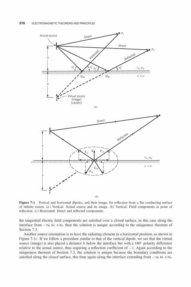
316 ELECTROMAGNETIC THEOREMS AND PRINCIPLES
h
hEq1
s = ∞
s = ∞
e m00 ,
e m00 ,
h
h
Eq2
q2rq1
rq1
iq2
i
Er2Er1
QR2QR1
P1
P2
Reflect
ed
Direct
Virtual source(image)(caustic)
Reflec
ted
Reflecte
d
Actual sourceDirect
Direct
(a)
(b)
n
Figure 7-1 Vertical and horizontal dipoles, and their image, for reflection from a flat conducting surfaceof infinite extent. (a) Vertical: Actual source and its image. (b) Vertical: Field components at point ofreflection. (c) Horizontal: Direct and reflected components.
the tangential electric field components are satisfied over a closed surface, in this case along theinterface from −∞ to +∞, then the solution is unique according to the uniqueness theorem ofSection 7.3.
Another source orientation is to have the radiating element in a horizontal position, as shown inFigure 7-1c. If we follow a procedure similar to that of the vertical dipole, we see that the virtualsource (image) is also placed a distance h below the interface but with a 180◦ polarity differencerelative to the actual source, thus requiring a reflection coefficient of −1. Again according to theuniqueness theorem of Section 7.3, the solution is unique because the boundary conditions aresatisfied along the closed surface, this time again along the interface extending from −∞ to +∞.

IMAGE THEORY 317
h
h
q2rq1
rq1i
q2i
s = ∞
e m00 ,
QR2QR1
P1
P2
Virtual source(image)(caustic)
Reflec
ted
Reflecte
d
Actual sourceDirect
Direct
(c)
Figure 7-1 (Continued )
In addition to electric sources, we have equivalent “magnetic” sources and magnetic con-ductors, such that tangential components of the magnetic field vanish next to their surface. InFigure 7-2a , we have sketched the sources and their images for an electric plane conductor [2].The single arrow indicates an electric element and the double arrow signifies a magnetic element.The direction of the arrow identifies the polarity. Since many problems can be solved usingduality, in Figure 7-2b, we have sketched the sources and their images when the obstacle is aninfinite, flat, perfect “magnetic” conductor.
7.4.1 Vertical Electric Dipole
In the previous section we graphically illustrated the analysis procedure, using image theory, forvertical and horizontal electric and magnetic elements near infinite electric and magnetic planeconductors. In this section, we want to derive the mathematical expressions for the fields of avertical linear element near a perfect electric conductor, and the derivation will be based on theimage solution of Figure 7-1a . For simplicity, only far-field [2] observations will be considered.
Let us refer now to the geometry of Figure 7-3a . The far-zone direct component of the electricfield, of the infinitesimal dipole of length �, constant current I0, and observation point P1, is givenaccording to the dominant terms (βr � 1) of the fields in Example 6-3 by
E dθ
r�λ� jηβIo�e−jβr1
4πr1sin θ1 (7-9)
The reflected component can be accounted for by the introduction of the virtual source (image),as shown in Figure 7-3a , and we can write it as
E rθ
r�λ� jRvηβI0�e−jβr2
4πr2sin θ2
E rθ
r�λ� jηβI0�e−jβr2
4πr2sin θ2 (7-10)
since the reflection coefficient Rv is equal to unity.
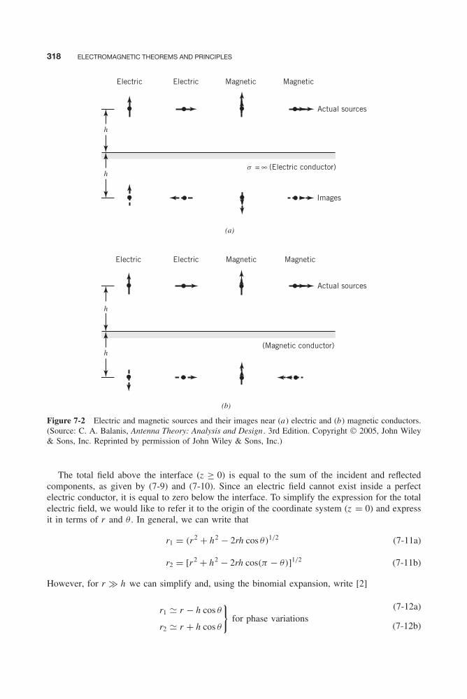
318 ELECTROMAGNETIC THEOREMS AND PRINCIPLES
h
h
Electric Electric Magnetic Magnetic
Actual sources
Images
(Electric conductor)s = ∞
h
h
Electric Electric Magnetic Magnetic
Actual sources
(Magnetic conductor)
(a)
(b)
Figure 7-2 Electric and magnetic sources and their images near (a) electric and (b) magnetic conductors.(Source: C. A. Balanis, Antenna Theory: Analysis and Design . 3rd Edition. Copyright © 2005, John Wiley& Sons, Inc. Reprinted by permission of John Wiley & Sons, Inc.)
The total field above the interface (z ≥ 0) is equal to the sum of the incident and reflectedcomponents, as given by (7-9) and (7-10). Since an electric field cannot exist inside a perfectelectric conductor, it is equal to zero below the interface. To simplify the expression for the totalelectric field, we would like to refer it to the origin of the coordinate system (z = 0) and expressit in terms of r and θ . In general, we can write that
r1 = (r2 + h2 − 2rh cos θ)1/2 (7-11a)
r2 = [r2 + h2 − 2rh cos(π − θ)]1/2 (7-11b)
However, for r � h we can simplify and, using the binomial expansion, write [2]
r1 � r − h cos θ
r2 � r + h cos θ
}for phase variations
(7-12a)
(7-12b)
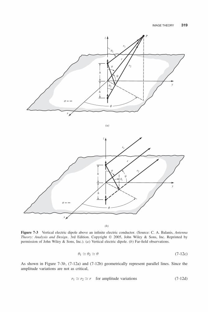
IMAGE THEORY 319
x
h
h
r
P
y
z
r2
q2
q1
r1
s = ∞f
y
q
(a)
x
h
h
r
y
z
r2
qi
r1
s = ∞f
y
q
(b)
Figure 7-3 Vertical electric dipole above an infinite electric conductor. (Source: C. A. Balanis, AntennaTheory: Analysis and Design . 3rd Edition. Copyright © 2005, John Wiley & Sons, Inc. Reprinted bypermission of John Wiley & Sons, Inc.). (a) Vertical electric dipole. (b) Far-field observations.
θ1 � θ2 � θ (7-12c)
As shown in Figure 7-3b, (7-12a) and (7-12b) geometrically represent parallel lines. Since theamplitude variations are not as critical,
r1 � r2 � r for amplitude variations (7-12d)
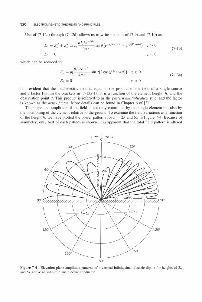
320 ELECTROMAGNETIC THEOREMS AND PRINCIPLES
Use of (7-12a) through (7-12d) allows us to write the sum of (7-9) and (7-10) as
Eθ = E dθ + E r
θ � jηβI0�e−jβr
4πrsin θ
(e+jβh cos θ + e−jβh cos θ
)z ≥ 0
Eθ = 0 z < 0
(7-13)
which can be reduced to
Eθ = jηβI0�e−jβr
4πrsin θ[2 cos(βh cos θ)] z ≥ 0
Eθ = 0 z < 0
(7-13a)
It is evident that the total electric field is equal to the product of the field of a single sourceand a factor [within the brackets in (7-13a)] that is a function of the element height, h , and theobservation point θ . This product is referred to as the pattern multiplication rule, and the factoris known as the array factor . More details can be found in Chapter 6 of [2].
The shape and amplitude of the field is not only controlled by the single element but also bythe positioning of the element relative to the ground. To examine the field variations as a functionof the height h , we have plotted the power patterns for h = 2λ and 5λ in Figure 7-4. Because ofsymmetry, only half of each pattern is shown. It is apparent that the total field pattern is altered
30°
60°
90°
120°
150°
180°
150°
120°
0°
30°
60°
90°−10−20
Rel
ativ
e po
wer
(dB
dow
n)
−30
30
20
10
h = 2l h = 5l
Figure 7-4 Elevation plane amplitude patterns of a vertical infinitesimal electric dipole for heights of 2λ
and 5λ above an infinite plane electric conductor.
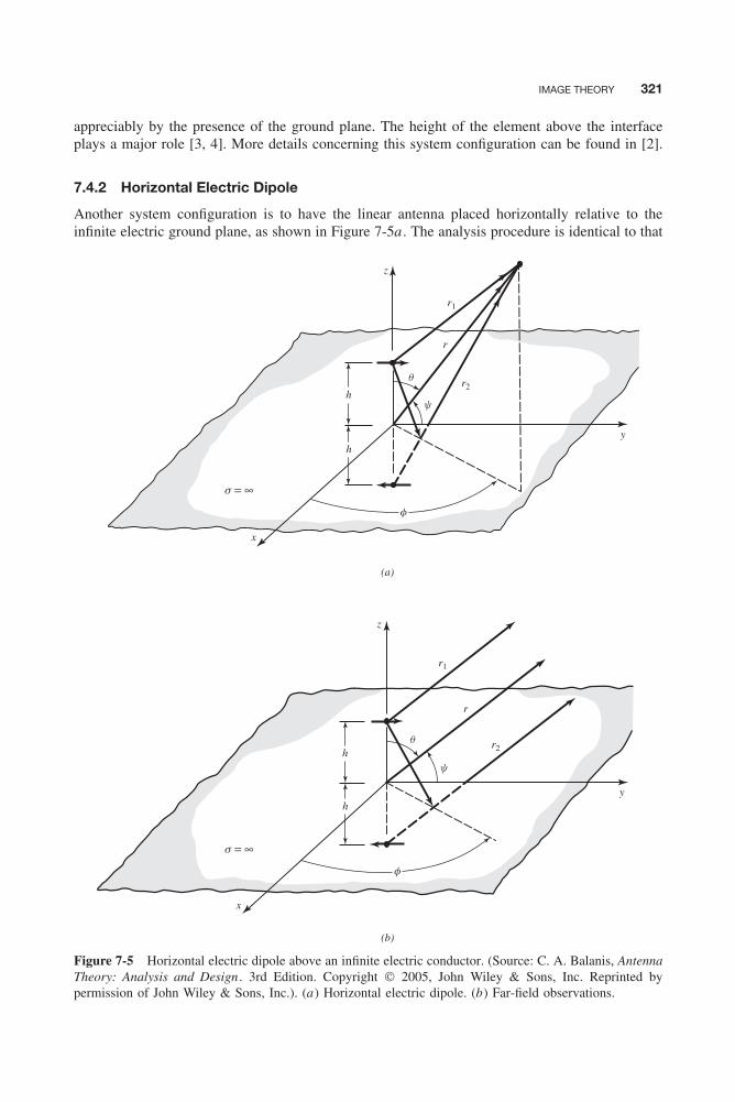
IMAGE THEORY 321
appreciably by the presence of the ground plane. The height of the element above the interfaceplays a major role [3, 4]. More details concerning this system configuration can be found in [2].
7.4.2 Horizontal Electric Dipole
Another system configuration is to have the linear antenna placed horizontally relative to theinfinite electric ground plane, as shown in Figure 7-5a . The analysis procedure is identical to that
x
h
h
r
y
z
r2
r1
f
y
q
(b)
x
h
h
r
y
z
r2
r1
f
y
q
(a)
s = ∞
s = ∞
Figure 7-5 Horizontal electric dipole above an infinite electric conductor. (Source: C. A. Balanis, AntennaTheory: Analysis and Design . 3rd Edition. Copyright © 2005, John Wiley & Sons, Inc. Reprinted bypermission of John Wiley & Sons, Inc.). (a) Horizontal electric dipole. (b) Far-field observations.

322 ELECTROMAGNETIC THEOREMS AND PRINCIPLES
of the vertical dipole. By introducing an image and assuming far-field observations, as shown inFigure 7-5b, we can write that the dominant terms of the direct component are given by [2]
E dψ
r�λ� jηβI0�e−jβr1
4πr1sin ψ (7-14)
and the reflected terms by
E rψ
r�λ� jRhηβI0�e−jβr2
4πr2sin ψ
E rψ
r�λ� − jηβI0�e−jβr2
4πr2sin ψ (7-15)
since the reflection coefficient is equal to Rh = −1.To find the angle ψ , which is measured from the y axis toward the observation point, we first
form
cos ψ = ây • âr = ây • (âx sin θ cos φ + ây sin θ sin φ + âz cos θ)
cos ψ = sin θ sin φ (7-16)
from which we find
sin ψ =√
1 − cos2 ψ =√
1 − sin2 θ sin2 φ (7-16a)
Since for far-field observations
r1 � r − h cos θ
r2 � r + h cos θ
}for phase variations (7-16b)
θ1 � θ2 � θ (7-16c)
r1 � r2 � r for amplitude variations (7-16d)
we can write the total field, which is valid only above the ground plane (z ≥ 0, 0 ≤ θ ≤ π/2,0 ≤ φ ≤ 2π), as
Eψ = E dψ + E r
ψ = jηβI0�e−jβr
4πr
√1 − sin2 θ sin2 φ [2j sin(βh cos θ)] (7-17)
Equation 7-17 again is recognized to consist of the product of the field of a single isolated elementplaced at the origin and a factor (within the brackets) known as the array factor. This, again, isthe pattern multiplication rule.
To examine the variations of the total field as a function of the element height above the groundplane, in Figure 7-6 we have plotted two-dimensional elevation plane patterns for φ = 90◦ (yzplane) when h = 2λ and 5λ. Again, we see that the height of the element above the interfaceplays a significant role in the radiation pattern formation of the radiating system.
Problems that require multiple images, such as corner reflectors, are assigned as exercises atthe end of the chapter.
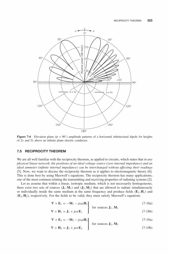
RECIPROCITY THEOREM 323
30°
60°
90°
120°
150°
180°
150°
120°
0°
30°
60°
90°−10−20
Rel
ativ
e po
wer
(dB
dow
n)−30
30
20
10
h = 2l h = 5l
Figure 7-6 Elevation plane (φ = 90◦) amplitude patterns of a horizontal infinitesimal dipole for heightsof 2λ and 5λ above an infinite plane electric conductor.
7.5 RECIPROCITY THEOREM
We are all well familiar with the reciprocity theorem, as applied to circuits, which states that in anyphysical linear network, the positions of an ideal voltage source (zero internal impedance) and anideal ammeter (infinite internal impedance) can be interchanged without affecting their readings[5]. Now, we want to discuss the reciprocity theorem as it applies to electromagnetic theory [6].This is done best by using Maxwell’s equations. The reciprocity theorem has many applications;one of the most common relating the transmitting and receiving properties of radiating systems [2].
Let us assume that within a linear, isotropic medium, which is not necessarily homogeneous,there exist two sets of sources (J1, M1) and (J2, M2) that are allowed to radiate simultaneouslyor individually inside the same medium at the same frequency and produce fields (E1, H1) and(E2, H2), respectively. For the fields to be valid, they must satisfy Maxwell’s equations
∇ × E1 = −M1 − jωμH1
∇ × H1 = J1 + jωεE1
⎫⎬⎭ for sources J1, M1
(7-18a)
(7-18b)
∇ × E2 = −M2 − jωμH2
∇ × H2 = J2 + jωεE2
⎫⎬⎭ for sources J2, M2
(7-19a)
(7-19b)
324 ELECTROMAGNETIC THEOREMS AND PRINCIPLES
If we dot multiply (7-18a) by H2 and (7-19b) by E1, we can write that
H2 • ∇ × E1 = −H2 • M1 − jωμH2 • H1 (7-20a)
E1 • ∇ × H2 = E1 • J2 + jωεE1 • E2 (7-20b)
Subtracting (7-20a) from (7-20b) yields
E1 • ∇ × H2 − H2 • ∇ × E1 = E1 • J2 + H2 • M1 + jωεE1 • E2 + jωμH2 • H1 (7-21)
which by use of the vector identity
∇ • (A × B) = B • (∇ × A) − A • (∇ × B) (7-22)
can be written as
∇ • (H2 × E1) = −∇ • (E1 × H2)
= E1 • J2 + H2 • M1 + jωεE1 • E2 + jωμH2 • H1 (7-23)
In a similar manner, if we dot multiply (7-18b) by E2 and (7-19a) by H1, we can write
E2 • ∇ × H1 = E2 • J1 + jωεE2 • E1 (7-24a)
H1 • ∇ × E2 = −H1 • M2 − jωμH1 • H2 (7-24b)
Subtraction of (7-24b) from (7-24a) leads to
E2 • ∇ × H1 − H1 • ∇ × E2 = E2 • J1 + H1 • M2 + jωεE2 • E1 + jωμH1 • H2 (7-25)
which by use of (7-22) can be written as
∇ • (H1 × E2) = −∇ • (E2 × H1)
= E2 • J1 + H1 • M2 + jωE2 • E1 + jωμH1 • H2 (7-26)
Subtraction of (7-26) from (7-23) leads to
−∇ • (E1 × H2 − E2 × H1) = E1 • J2 + H2 • M1 − E2 • J1 − H1 • M2 (7-27)
which is called the Lorentz reciprocity theorem in differential form [7].By taking a volume integral of both sides of (7-27) and using the divergence theorem on the
left side, we can write (7-27) as
−#S(E1 × H2 − E2 × H1) • ds′
=∫∫∫
V(E1 • J2 + H2 • M1 − E2 • J1 − H1 • M2) dv′
(7-28)
which is known as the Lorentz reciprocity theorem in integral form.For a source-free (J1 = J2 = M1 = M2 = 0) region, (7-27) and (7-28) reduce, respectively, to
∇ • (E1 × H2 − E2 × H1) = 0 (7-29)
#S(E1 × H2 − E2 × H1) • ds′ = 0 (7-30)
REACTION THEOREM 325
Equations 7-29 and 7-30 are special cases of the Lorentz reciprocity theorem and must be satisfiedin source-free regions.
As an example of where (7-29) and (7-30) may be applied and what they would represent,consider a section of a waveguide where two different modes exist with fields (E1, H1) and(E2, H2). For the expressions of the fields for the two modes to be valid, they must satisfy (7-29)and/or (7-30).
Another useful form of (7-28) is to consider that the fields (E1, H1, E2, H2) and the sources(J1, M1, J2, M2) are within a medium that is enclosed by a sphere of infinite radius. Assumethat the sources are positioned within a finite region and that the fields are observed in the farfield (ideally at infinity). Then the left side of (7-28) is equal to zero, or
#S(E1 × H2 − E2 × H1) • ds′ = 0 (7-31)
which reduces (7-28) to∫∫∫V(E1 • J2 + H2 • M1 − E2 • J1 − H1 • M2) dv′ = 0 (7-32)
Equation 7-32 can also be written as∫∫∫V(E1 • J2 − H1 • M2) dv′ =
∫∫∫V(E2 • J1 − H2 • M1) dv′ (7-32a)
The reciprocity theorem, as expressed by (7-32a), is the most useful form.
7.6 REACTION THEOREM
Close observation of (7-28) reveals that it does not, in general, represent relations of powerbecause no conjugates appear. The same is true for (7-30) and (7-32a). Each of the integralsin (7-32a) can be interpreted as a coupling between a set of fields and a set of sources, whichproduce another set of fields. This coupling has been defined as reaction [8, 9] and each of theintegrals in (7-32a) has been denoted by
〈1, 2〉 =∫∫∫
V(E1 • J2 − H1 • M2) dv′ (7-33a)
〈2, 1〉 =∫∫∫
V(E2 • J1 − H2 • M1) dv′ (7-33b)
The relation 〈1, 2〉 relates the reaction (coupling) of the fields (E1, H1), which are producedby sources (J1, M1), to the sources (J2, M2), which produce fields (E2, H2); 〈2, 1〉 relates thereaction (coupling) of the fields (E2, H2) to the sources (J1, M1). A requirement for reciprocityto hold is that the reactions (couplings) of the sources with their corresponding fields must beequal. In equation form
〈1, 2〉 = 〈2, 1〉 (7-34)
The reaction theorem can also be expressed in terms of the voltages and currents induced inone antenna by another [9]. In a general form, it can be written as
〈i , j 〉 = Vj Iji = 〈j , i 〉 = Vi Iij (7-34a)
where Vi = voltage of source i(j)Iij = current through source j due to source at i
326 ELECTROMAGNETIC THEOREMS AND PRINCIPLES
The reactions forms of (7-34) and (7-34a) are most convenient to calculate the mutual impedanceand admittance between aperture antennas.
Example 7-2
Derive an expression for the mutual admittance between two aperture antennas. The expression shouldbe in terms of the electric and magnetic fields on the apertures and radiated by the apertures.
Solution: In a multiport network, the Y-parameter matrix can be written as
[Ii ] = [Yij ][Vj ]
Assuming that the voltages at all ports other than port j are zero, we can write that the current Iij atport i due to the voltage at port j can be written as
Iij = Yij Vj ⇒ Yij = Iij
Vj
Using (7-34a), we can write that
Iij = 〈i , j 〉Vi
This allows us to write the mutual admittance as
Yij = Iij
Vj= 〈i , j 〉
Vi Vj
which by using (7-33a) or (7-33b) can be expressed as
Yij = 〈i , j 〉Vi Vj
= 1
Vi Vj
∫∫∫V(Ei • Jj − Hi • Mj ) dv′
Since aperture antennas can be represented by magnetic equivalent currents, then
Jj = 0
Mj = −n̂ × Ej
Using these and reducing the volume integral to a surface integral over the aperture of the antenna, wecan write the mutual admittance as
Yij = − 1
Vi Vj
∫∫Sa
(Hi • Mj ) ds ′ = − 1
Vi Vj
∫∫Sa
[Hi • (−n̂ × Ej )] ds ′
Yij = 1
Vi Vj
∫∫Sa
(Ej × Hi ) • n̂ ds ′
where Ej = electric field in aperture j with aperture i shortedHi = magnetic field at shorted aperture i due to excitation of aperture j
Vi (j ) = voltage amplitudes at each aperture in the absence of the other
7.7 VOLUME EQUIVALENCE THEOREM
Through use of the equivalent electric and magnetic current sources, the volume equivalencetheorem can be used to determine the scattered fields when a material obstacle is introducedin a free-space environment where fields (E0, H0) were previously generated by sources(Ji , Mi ) [7, 10].

VOLUME EQUIVALENCE THEOREM 327
To derive the volume equivalence theorem, let us assume that in the free-space environ-ment sources (Ji , Mi ) generate fields (E0, H0). These sources and fields must satisfy Maxwell’sequations
∇ × E0 = −Mi − jωμ0H0 (7-35a)
∇ × H0 = Ji + jωε0E0 (7-35b)
When the same sources (Ji , Mi ) radiate in a medium represented by (ε, μ), they generate fields(E, H) that satisfy Maxwell’s equations
∇ × E = −Mi − jωμH (7-36a)
∇ × H = Ji + jωεE (7-36b)
Subtraction of (7-35a) from (7-36a) and (7-35b) from (7-36b), allows us to write that
∇ × (E − E0) = −jω(μH − μ0H0) (7-37a)
∇ × (H − H0) = jω(εE − ε0E0) (7-37b)
Let us define the difference between the fields E and E0, and H and H0 as the scattered (distur-bance) fields Es and Hs , that is,
Es = E − E0 ⇒ E0 = E − Es (7-38a)
Hs = H − H0 ⇒ H0 = H − Hs (7-38b)
By using the definitions for the scattered fields of (7-38a) and (7-38b), we can write (7-37a) and(7-37b) as
∇ × Es = −jω[μH − μ0(H − Hs)] = −jω(μ − μ0)H − jωμ0Hs (7-39a)
∇ × Hs = jω[εE − ε0(E − Es)] = jω(ε − ε0)E + jωε0Es (7-39b)
By defining volume equivalent electric Jeq and magnetic Meq current densities
Jeq = jω(ε − ε0)E (7-40a)
Meq = jω(μ − μ0)H (7-40b)
which exist only in the region where ε �= ε0 and μ �= μ0 (only in the material itself), we canexpress (7-39a) and (7-39b) as
∇ × Es = −Meq − jωμ0Hs (7-41a)
∇ × Hs = Jeq + jωε0Es (7-41b)
Equations 7-41a and 7-41b state that the electric Es and magnetic Hs fields scattered by a mate-rial obstacle can be generated by using equivalent electric Jeq (A/m2) and magnetic Meq (V/m2)volume current densities, that are given by (7-40a) and (7-40b), that exist only within the materialand radiate in a free-space environment. Although, in principle, the formulation of the problemseems to have been simplified, it is still very difficult to solve because the equivalent currentdensities are in terms of E and H, which are unknown. However, the formulation does provide

328 ELECTROMAGNETIC THEOREMS AND PRINCIPLES
some physical interpretation of scattering and lends itself to development of integral equationsfor the solution of Es and Hs , which are discussed in Chapter 12. The volume equivalent currentdensities are most useful for finding the fields scattered by dielectric obstacles. The fields scat-tered by perfectly conducting surfaces can best be determined using surface equivalent densities,especially those discussed in Sections 7.9 and 7.10. The surface equivalence theorem that followsis, usually, best utilized for analysis of antenna aperture radiation.
7.8 SURFACE EQUIVALENCE THEOREM: HUYGENS’S PRINCIPLE
The surface equivalence theorem is a principle by which actual sources, such as an antenna andtransmitter, are replaced by equivalent sources. The fictitious sources are said to be equivalentwithin a region because they produce within that region the same fields as the actual sources.The formulations of scattering and diffraction problems by the surface equivalence theorem aremore suggestive of approximations.
The surface equivalence was introduced in 1936 by Schelkunoff [11], and it is a more rigorousformulation of Huygens’s principle [12], which states [13] that “each point on a primary wavefrontcan be considered to be a new source of a secondary spherical wave and that a secondarywavefront can be constructed as the envelope of these secondary spherical waves.” The surfaceequivalence theorem is based on the uniqueness theorem of Section 7.3, which states [1] that “afield in a lossy region is uniquely specified by the sources within the region plus the tangentialcomponents of the electric field over the boundary, or the tangential components of the magneticfield over the boundary, or the former over part of the boundary and the latter over the rest of theboundary.” The fields in a lossless medium are considered to be the limit, as the losses go to zero,of the corresponding fields in a lossy medium. Thus, if the tangential electric and magnetic fieldsare completely known over a closed surface, the fields in the source-free region can be determined.
By the surface equivalence theorem, the fields outside an imaginary closed surface are obtainedby placing, over the closed surface, suitable electric and magnetic current densities that satisfy theboundary conditions. The current densities are selected so that the fields inside the closed surfaceare zero and outside are equal to the radiation produced by the actual sources. Thus, the techniquecan be used to obtain the fields radiated outside a closed surface by sources enclosed within it.The formulation is exact but requires integration over the closed surface. The degree of accuracydepends on the knowledge of the tangential components of the fields over the closed surface.
In the majority of applications, the closed surface is selected so that most of it coincides withthe conducting parts of the physical structure. This is preferred because the tangential electricfield components vanish over the conducting parts of the surface, which results in reduction ofthe physical limits of integration.
The surface equivalence theorem is developed by considering an actual radiating source, whichis represented electrically by current densities J1 and M1, as shown in Figure 7-7a . The sourceradiates fields E1 and H1 everywhere. However, we wish to develop a method that will yieldthe fields outside a closed surface. To accomplish this, a closed surface S is chosen, showndashed in Figure 7-7a , which encloses the current densities J1 and M1. The volume within S isdenoted by V1 and outside S by V2. The primary task is to replace the original problem, shownin Figure 7-7a , with an equivalent that will yield the same fields E1 and H1 outside S (withinV2). The formulation of the problem can be aided immensely if the closed surface is chosenjudiciously so that fields over most, if not the entire surface, are known a priori .
An equivalent problem to Figure 7-7a is shown in Figure 7-7b. The original sources J1 andM1 are removed, and we assume that there exist fields (E, H) inside S and fields (E1, H1) outsideS . For these fields to exist within and outside S , they must satisfy the boundary conditions on thetangential electric and magnetic field components of Table 1-5. Thus, on the imaginary surface

SURFACE EQUIVALENCE THEOREM: HUYGENS’S PRINCIPLE 329
V2 V2
S S
E1, H1
E1, H1
E1, H1
E, H
Js = n × (H1 – H)
Ms = –n × (E1 – E)
J1M1
V1V1
m1, e1 m1, e1m1, e1
m1, e1
(a) (b)
n̂
Figure 7-7 (a) Actual and (b) equivalent problem models. (Source: C. A. Balanis, Antenna Theory:Analysis and Design . 3rd Edition. Copyright © 2005, John Wiley & Sons, Inc. Reprinted with permissionof John Wiley & Sons, Inc.)
S there must exist the equivalent sources
Js = n̂ × (H1 − H) (7-42a)
Ms = −n̂ × (E1 − E) (7-42b)
which radiate into an unbounded space (same medium everywhere). The current densities of(7-42a) and (7-42b) are said to be equivalent only within V2, because they will produce theoriginal field (E1, H1) only outside S. A field (E, H), different from the original (E1, H1), willresult within V1. Since the currents of (7-42a) and (7-42b) radiate in an unbounded space, thefields can be determined using (6-30) through (6-35a) and the geometry of Figure 6-3a . In Figure6-3a , R is the distance from any point on the surface S , where Js and Ms exist, to the observationpoint.
So far, the tangential components of both E and H have been used to set up the equivalentproblem. From electromagnetic uniqueness concepts, we know that the tangential components ofonly E or H are needed to determine the field. It will be demonstrated that equivalent problemsthat require only magnetic currents (tangential E) or only electric currents (tangential H) can befound. This will require modifications to the equivalent problem of Figure 7-7b.
Since the fields (E, H) within S , which is not the region of interest, can be anything, it canbe assumed that they are zero. Then the equivalent problem of Figure 7-7b reduces to that ofFigure 7-8a with equivalent current densities equal to
Js = n̂ × (H1 − H)|H=0 = n̂ × H1 (7-43a)
Ms = −n̂ × (E1 − E)|E=0 = −n̂ × E1 (7-43b)
This form of the field equivalence principle is known as Love’s equivalence principle [7, 14].Since the current densities of (7-43a) and (7-43b) radiate in an unbounded medium, that is, havethe same μ1, ε1 everywhere, they can be used in conjunction with (6-30) through (6-35a) to findthe fields everywhere.
Love’s equivalence principle in Figure 7-8a produces a null field within the imaginary surfaceS . Since the value of the E = H = 0 within S cannot be disturbed if the properties of themedium within it are changed, let us assume that it is replaced by a perfect electric conductor(PEC, σ = ∞). The introduction of the perfect conductor will have an effect on the equivalent
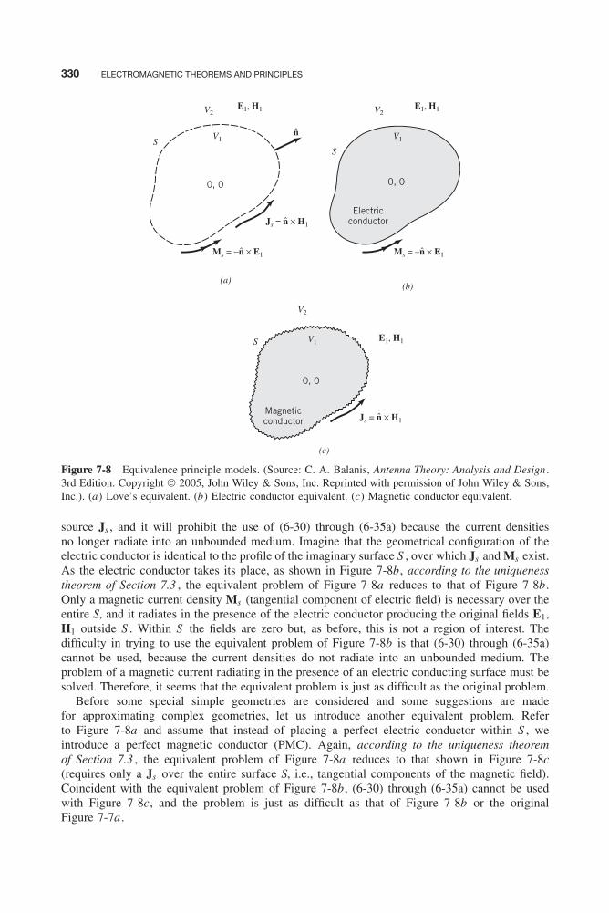
330 ELECTROMAGNETIC THEOREMS AND PRINCIPLES
V2 V2
SS
V2
S
E1, H1 E1, H1
E1, H1
0, 00, 0
Electricconductor
Magneticconductor
0, 0
V1 V1
V1
Ms = –n × E1Ms = −n × E1
Js = n × H1
Js = n × H1
(b)(a)
(c)
n
Figure 7-8 Equivalence principle models. (Source: C. A. Balanis, Antenna Theory: Analysis and Design .3rd Edition. Copyright © 2005, John Wiley & Sons, Inc. Reprinted with permission of John Wiley & Sons,Inc.). (a) Love’s equivalent. (b) Electric conductor equivalent. (c) Magnetic conductor equivalent.
source Js , and it will prohibit the use of (6-30) through (6-35a) because the current densitiesno longer radiate into an unbounded medium. Imagine that the geometrical configuration of theelectric conductor is identical to the profile of the imaginary surface S , over which Js and Ms exist.As the electric conductor takes its place, as shown in Figure 7-8b, according to the uniquenesstheorem of Section 7.3 , the equivalent problem of Figure 7-8a reduces to that of Figure 7-8b.Only a magnetic current density Ms (tangential component of electric field) is necessary over theentire S, and it radiates in the presence of the electric conductor producing the original fields E1,H1 outside S . Within S the fields are zero but, as before, this is not a region of interest. Thedifficulty in trying to use the equivalent problem of Figure 7-8b is that (6-30) through (6-35a)cannot be used, because the current densities do not radiate into an unbounded medium. Theproblem of a magnetic current radiating in the presence of an electric conducting surface must besolved. Therefore, it seems that the equivalent problem is just as difficult as the original problem.
Before some special simple geometries are considered and some suggestions are madefor approximating complex geometries, let us introduce another equivalent problem. Referto Figure 7-8a and assume that instead of placing a perfect electric conductor within S , weintroduce a perfect magnetic conductor (PMC). Again, according to the uniqueness theoremof Section 7.3 , the equivalent problem of Figure 7-8a reduces to that shown in Figure 7-8c(requires only a Js over the entire surface S, i.e., tangential components of the magnetic field).Coincident with the equivalent problem of Figure 7-8b, (6-30) through (6-35a) cannot be usedwith Figure 7-8c, and the problem is just as difficult as that of Figure 7-8b or the originalFigure 7-7a .
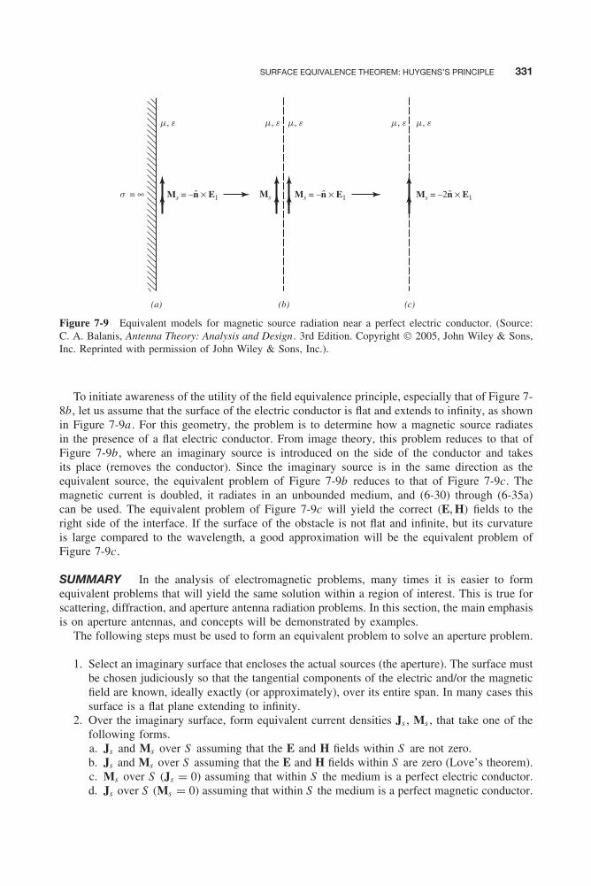
SURFACE EQUIVALENCE THEOREM: HUYGENS’S PRINCIPLE 331
m, e m, e m, e m, e m, e
Ms = –n × E1 Ms Ms = –n × E1 Ms = –2n × E1s = ∞
(a) (b) (c)
Figure 7-9 Equivalent models for magnetic source radiation near a perfect electric conductor. (Source:C. A. Balanis, Antenna Theory: Analysis and Design . 3rd Edition. Copyright © 2005, John Wiley & Sons,Inc. Reprinted with permission of John Wiley & Sons, Inc.).
To initiate awareness of the utility of the field equivalence principle, especially that of Figure 7-8b, let us assume that the surface of the electric conductor is flat and extends to infinity, as shownin Figure 7-9a . For this geometry, the problem is to determine how a magnetic source radiatesin the presence of a flat electric conductor. From image theory, this problem reduces to that ofFigure 7-9b, where an imaginary source is introduced on the side of the conductor and takesits place (removes the conductor). Since the imaginary source is in the same direction as theequivalent source, the equivalent problem of Figure 7-9b reduces to that of Figure 7-9c. Themagnetic current is doubled, it radiates in an unbounded medium, and (6-30) through (6-35a)can be used. The equivalent problem of Figure 7-9c will yield the correct (E, H) fields to theright side of the interface. If the surface of the obstacle is not flat and infinite, but its curvatureis large compared to the wavelength, a good approximation will be the equivalent problem ofFigure 7-9c.
SUMMARY In the analysis of electromagnetic problems, many times it is easier to formequivalent problems that will yield the same solution within a region of interest. This is true forscattering, diffraction, and aperture antenna radiation problems. In this section, the main emphasisis on aperture antennas, and concepts will be demonstrated by examples.
The following steps must be used to form an equivalent problem to solve an aperture problem.
1. Select an imaginary surface that encloses the actual sources (the aperture). The surface mustbe chosen judiciously so that the tangential components of the electric and/or the magneticfield are known, ideally exactly (or approximately), over its entire span. In many cases thissurface is a flat plane extending to infinity.
2. Over the imaginary surface, form equivalent current densities Js , Ms , that take one of thefollowing forms.a. Js and Ms over S assuming that the E and H fields within S are not zero.b. Js and Ms over S assuming that the E and H fields within S are zero (Love’s theorem).c. Ms over S (Js = 0) assuming that within S the medium is a perfect electric conductor.d. Js over S (Ms = 0) assuming that within S the medium is a perfect magnetic conductor.
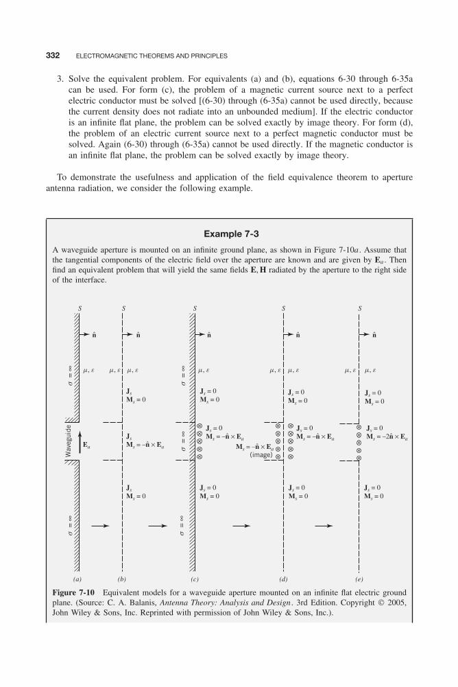
332 ELECTROMAGNETIC THEOREMS AND PRINCIPLES
3. Solve the equivalent problem. For equivalents (a) and (b), equations 6-30 through 6-35acan be used. For form (c), the problem of a magnetic current source next to a perfectelectric conductor must be solved [(6-30) through (6-35a) cannot be used directly, becausethe current density does not radiate into an unbounded medium]. If the electric conductoris an infinite flat plane, the problem can be solved exactly by image theory. For form (d),the problem of an electric current source next to a perfect magnetic conductor must besolved. Again (6-30) through (6-35a) cannot be used directly. If the magnetic conductor isan infinite flat plane, the problem can be solved exactly by image theory.
To demonstrate the usefulness and application of the field equivalence theorem to apertureantenna radiation, we consider the following example.
Example 7-3
A waveguide aperture is mounted on an infinite ground plane, as shown in Figure 7-10a . Assume thatthe tangential components of the electric field over the aperture are known and are given by Ea . Thenfind an equivalent problem that will yield the same fields E, H radiated by the aperture to the right sideof the interface.
Ms = 0Js
Ms = 0Js = 0
Ms = 0Js = 0
Js = 0
Ms = 0Js = 0
Ms = 0Js
Ms = 0Js = 0
Ms = 0Js = 0
Ms = 0Js = 0
Ms = –n × Ea
Js = 0Ms = –n × Ea
Ms = –n × Ea(image)W
aveg
uide
JsMs = –n × EaEa
Js = 0Ms = –2n × Ea
m, e m, e m, e m, e m, e m, e m, e m, e
S S S SS
s =
∞s
= ∞
s
= ∞
s =
∞s =
∞
(a) (b) (c) (d) (e)
nnnnn
Figure 7-10 Equivalent models for a waveguide aperture mounted on an infinite flat electric groundplane. (Source: C. A. Balanis, Antenna Theory: Analysis and Design . 3rd Edition. Copyright © 2005,John Wiley & Sons, Inc. Reprinted with permission of John Wiley & Sons, Inc.).
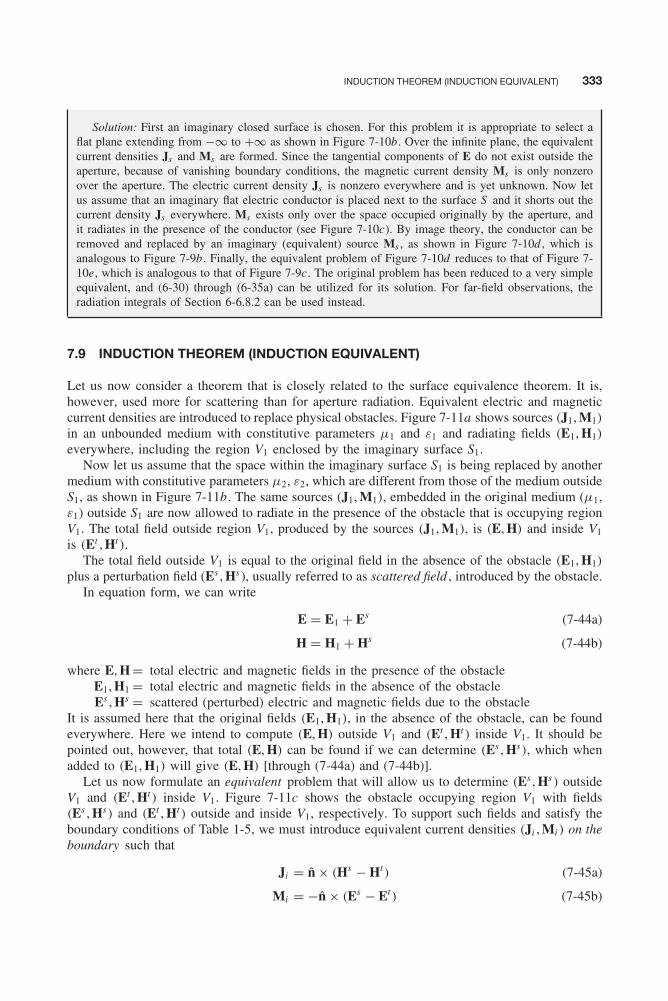
INDUCTION THEOREM (INDUCTION EQUIVALENT) 333
Solution: First an imaginary closed surface is chosen. For this problem it is appropriate to select aflat plane extending from −∞ to +∞ as shown in Figure 7-10b. Over the infinite plane, the equivalentcurrent densities Js and Ms are formed. Since the tangential components of E do not exist outside theaperture, because of vanishing boundary conditions, the magnetic current density Ms is only nonzeroover the aperture. The electric current density Js is nonzero everywhere and is yet unknown. Now letus assume that an imaginary flat electric conductor is placed next to the surface S and it shorts out thecurrent density Js everywhere. Ms exists only over the space occupied originally by the aperture, andit radiates in the presence of the conductor (see Figure 7-10c). By image theory, the conductor can beremoved and replaced by an imaginary (equivalent) source Ms , as shown in Figure 7-10d , which isanalogous to Figure 7-9b. Finally, the equivalent problem of Figure 7-10d reduces to that of Figure 7-10e, which is analogous to that of Figure 7-9c. The original problem has been reduced to a very simpleequivalent, and (6-30) through (6-35a) can be utilized for its solution. For far-field observations, theradiation integrals of Section 6-6.8.2 can be used instead.
7.9 INDUCTION THEOREM (INDUCTION EQUIVALENT)
Let us now consider a theorem that is closely related to the surface equivalence theorem. It is,however, used more for scattering than for aperture radiation. Equivalent electric and magneticcurrent densities are introduced to replace physical obstacles. Figure 7-11a shows sources (J1, M1)
in an unbounded medium with constitutive parameters μ1 and ε1 and radiating fields (E1, H1)
everywhere, including the region V1 enclosed by the imaginary surface S1.Now let us assume that the space within the imaginary surface S1 is being replaced by another
medium with constitutive parameters μ2, ε2, which are different from those of the medium outsideS1, as shown in Figure 7-11b. The same sources (J1, M1), embedded in the original medium (μ1,ε1) outside S1 are now allowed to radiate in the presence of the obstacle that is occupying regionV1. The total field outside region V1, produced by the sources (J1, M1), is (E, H) and inside V1
is (Et , Ht ).The total field outside V1 is equal to the original field in the absence of the obstacle (E1, H1)
plus a perturbation field (Es , Hs ), usually referred to as scattered field , introduced by the obstacle.In equation form, we can write
E = E1 + Es (7-44a)
H = H1 + Hs (7-44b)
where E, H = total electric and magnetic fields in the presence of the obstacleE1, H1 = total electric and magnetic fields in the absence of the obstacleEs , Hs = scattered (perturbed) electric and magnetic fields due to the obstacle
It is assumed here that the original fields (E1, H1), in the absence of the obstacle, can be foundeverywhere. Here we intend to compute (E, H) outside V1 and (Et , Ht ) inside V1. It should bepointed out, however, that total (E, H) can be found if we can determine (Es , Hs), which whenadded to (E1, H1) will give (E, H) [through (7-44a) and (7-44b)].
Let us now formulate an equivalent problem that will allow us to determine (Es , Hs) outsideV1 and (Et , Ht ) inside V1. Figure 7-11c shows the obstacle occupying region V1 with fields(Es , Hs) and (Et , Ht ) outside and inside V1, respectively. To support such fields and satisfy theboundary conditions of Table 1-5, we must introduce equivalent current densities (Ji , Mi ) on theboundary such that
Ji = n̂ × (Hs − Ht ) (7-45a)
Mi = −n̂ × (Es − Et ) (7-45b)
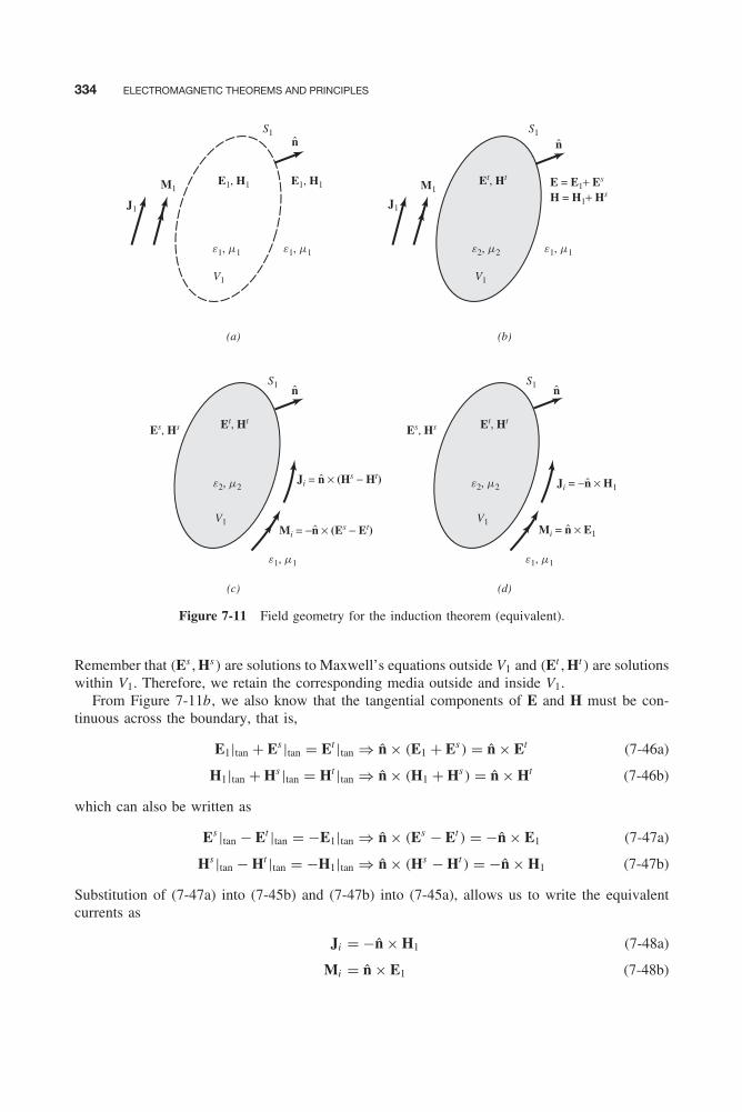
334 ELECTROMAGNETIC THEOREMS AND PRINCIPLES
E1, H1E1, H1M1
J1 J1
M1E = E1+ Es
H = H1+ Hs
Et, Ht
Et, Ht Et, Ht
Ji = −n × H1
Es, HsEs, Hs
S1S1
V1 V1
V1V1
S1 S1
e1, m1e1, m1
e1, m1e1, m1
e1, m1e2, m2
e2, m2 e2, m2
Mi = n × E1Mi = −n × (Es − Et)
Ji = n × (Hs − Ht)
(a) (b)
(c) (d)
nn
n n
Figure 7-11 Field geometry for the induction theorem (equivalent).
Remember that (Es , Hs) are solutions to Maxwell’s equations outside V1 and (Et , Ht ) are solutionswithin V1. Therefore, we retain the corresponding media outside and inside V1.
From Figure 7-11b, we also know that the tangential components of E and H must be con-tinuous across the boundary, that is,
E1|tan + Es |tan = Et |tan ⇒ n̂ × (E1 + Es) = n̂ × Et (7-46a)
H1|tan + Hs |tan = Ht |tan ⇒ n̂ × (H1 + Hs) = n̂ × Ht (7-46b)
which can also be written as
Es |tan − Et |tan = −E1|tan ⇒ n̂ × (Es − Et ) = −n̂ × E1 (7-47a)
Hs |tan − Ht |tan = −H1|tan ⇒ n̂ × (Hs − Ht ) = −n̂ × H1 (7-47b)
Substitution of (7-47a) into (7-45b) and (7-47b) into (7-45a), allows us to write the equivalentcurrents as
Ji = −n̂ × H1 (7-48a)
Mi = n̂ × E1 (7-48b)
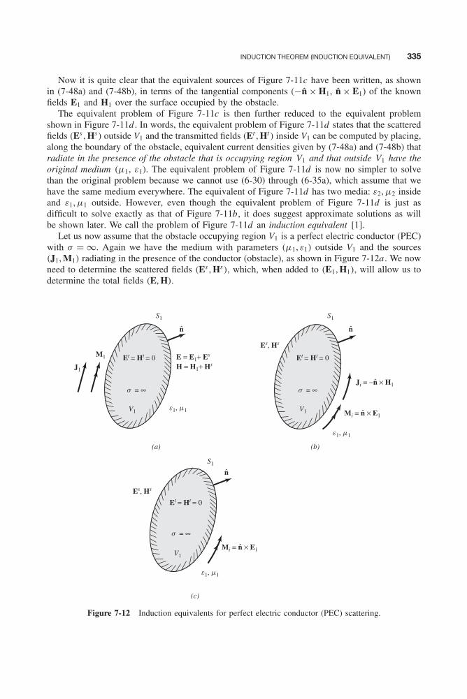
INDUCTION THEOREM (INDUCTION EQUIVALENT) 335
Now it is quite clear that the equivalent sources of Figure 7-11c have been written, as shownin (7-48a) and (7-48b), in terms of the tangential components (−n̂ × H1, n̂ × E1) of the knownfields E1 and H1 over the surface occupied by the obstacle.
The equivalent problem of Figure 7-11c is then further reduced to the equivalent problemshown in Figure 7-11d . In words, the equivalent problem of Figure 7-11d states that the scatteredfields (Es , Hs) outside V1 and the transmitted fields (Et , Ht ) inside V1 can be computed by placing,along the boundary of the obstacle, equivalent current densities given by (7-48a) and (7-48b) thatradiate in the presence of the obstacle that is occupying region V1 and that outside V1 have theoriginal medium (μ1, ε1). The equivalent problem of Figure 7-11d is now no simpler to solvethan the original problem because we cannot use (6-30) through (6-35a), which assume that wehave the same medium everywhere. The equivalent of Figure 7-11d has two media: ε2, μ2 insideand ε1, μ1 outside. However, even though the equivalent problem of Figure 7-11d is just asdifficult to solve exactly as that of Figure 7-11b, it does suggest approximate solutions as willbe shown later. We call the problem of Figure 7-11d an induction equivalent [1].
Let us now assume that the obstacle occupying region V1 is a perfect electric conductor (PEC)with σ = ∞. Again we have the medium with parameters (μ1, ε1) outside V1 and the sources(J1, M1) radiating in the presence of the conductor (obstacle), as shown in Figure 7-12a . We nowneed to determine the scattered fields (Es , Hs), which, when added to (E1, H1), will allow us todetermine the total fields (E, H).
M1
J1
E = E1+ Es
H = H1+ HsEt = Ht = 0
Et = Ht = 0
Et = Ht = 0
s = ∞
s = ∞
s = ∞
V1
V1
V1
S1
S1
S1
Es, Hs
Es, Hs
e1, m1
e1, m1
e1, m1
Mi = n × E1
Mi = n × E1
Ji = −n × H1
(a) (b)
(c)
n n
n
Figure 7-12 Induction equivalents for perfect electric conductor (PEC) scattering.
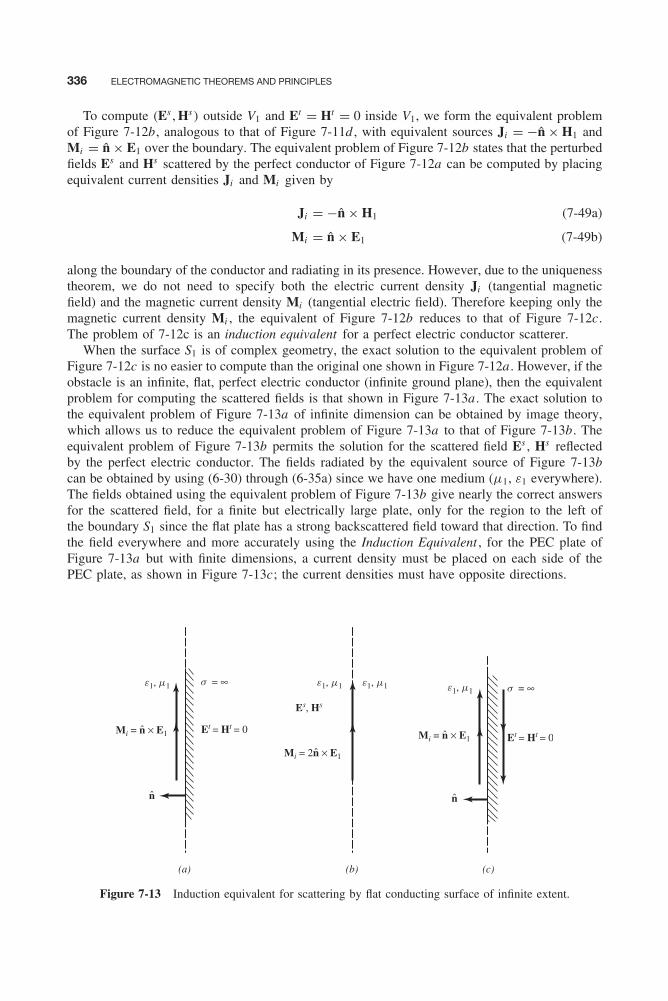
336 ELECTROMAGNETIC THEOREMS AND PRINCIPLES
To compute (Es , Hs) outside V1 and Et = Ht = 0 inside V1, we form the equivalent problemof Figure 7-12b, analogous to that of Figure 7-11d , with equivalent sources Ji = −n̂ × H1 andMi = n̂ × E1 over the boundary. The equivalent problem of Figure 7-12b states that the perturbedfields Es and Hs scattered by the perfect conductor of Figure 7-12a can be computed by placingequivalent current densities Ji and Mi given by
Ji = −n̂ × H1 (7-49a)
Mi = n̂ × E1 (7-49b)
along the boundary of the conductor and radiating in its presence. However, due to the uniquenesstheorem, we do not need to specify both the electric current density Ji (tangential magneticfield) and the magnetic current density Mi (tangential electric field). Therefore keeping only themagnetic current density Mi , the equivalent of Figure 7-12b reduces to that of Figure 7-12c.The problem of 7-12c is an induction equivalent for a perfect electric conductor scatterer.
When the surface S1 is of complex geometry, the exact solution to the equivalent problem ofFigure 7-12c is no easier to compute than the original one shown in Figure 7-12a . However, if theobstacle is an infinite, flat, perfect electric conductor (infinite ground plane), then the equivalentproblem for computing the scattered fields is that shown in Figure 7-13a . The exact solution tothe equivalent problem of Figure 7-13a of infinite dimension can be obtained by image theory,which allows us to reduce the equivalent problem of Figure 7-13a to that of Figure 7-13b. Theequivalent problem of Figure 7-13b permits the solution for the scattered field Es , Hs reflectedby the perfect electric conductor. The fields radiated by the equivalent source of Figure 7-13bcan be obtained by using (6-30) through (6-35a) since we have one medium (μ1, ε1 everywhere).The fields obtained using the equivalent problem of Figure 7-13b give nearly the correct answersfor the scattered field, for a finite but electrically large plate, only for the region to the left ofthe boundary S1 since the flat plate has a strong backscattered field toward that direction. To findthe field everywhere and more accurately using the Induction Equivalent , for the PEC plate ofFigure 7-13a but with finite dimensions, a current density must be placed on each side of thePEC plate, as shown in Figure 7-13c; the current densities must have opposite directions.
Mi = 2n × E1
Mi = n × E1Mi = n × E1 Et = Ht = 0
Et = Ht = 0
e1, m1 e1, m1 e1, m1 e1, m1s = ∞
s = ∞
Es, Hs
(a) (b) (c)
n n
Figure 7-13 Induction equivalent for scattering by flat conducting surface of infinite extent.
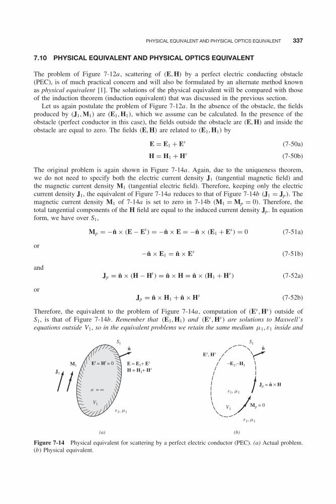
PHYSICAL EQUIVALENT AND PHYSICAL OPTICS EQUIVALENT 337
7.10 PHYSICAL EQUIVALENT AND PHYSICAL OPTICS EQUIVALENT
The problem of Figure 7-12a , scattering of (E, H) by a perfect electric conducting obstacle(PEC), is of much practical concern and will also be formulated by an alternate method knownas physical equivalent [1]. The solutions of the physical equivalent will be compared with thoseof the induction theorem (induction equivalent) that was discussed in the previous section.
Let us again postulate the problem of Figure 7-12a . In the absence of the obstacle, the fieldsproduced by (J1, M1) are (E1, H1), which we assume can be calculated. In the presence of theobstacle (perfect conductor in this case), the fields outside the obstacle are (E, H) and inside theobstacle are equal to zero. The fields (E, H) are related to (E1, H1) by
E = E1 + Es (7-50a)
H = H1 + Hs (7-50b)
The original problem is again shown in Figure 7-14a . Again, due to the uniqueness theorem,we do not need to specify both the electric current density J1 (tangential magnetic field) andthe magnetic current density M1 (tangential electric field). Therefore, keeping only the electriccurrent density J1, the equivalent of Figure 7-14a reduces to that of Figure 7-14b (J1 = Jp). Themagnetic current density M1 of 7-14a is set to zero in 7-14b (M1 = Mp = 0). Therefore, thetotal tangential components of the H field are equal to the induced current density Jp . In equationform, we have over S1,
Mp = −n̂ × (E − Et ) = −n̂ × E = −n̂ × (E1 + Es) = 0 (7-51a)
or−n̂ × E1 = n̂ × Es (7-51b)
andJp = n̂ × (H − Ht ) = n̂ × H = n̂ × (H1 + Hs) (7-52a)
orJp = n̂ × H1 + n̂ × Hs (7-52b)
Therefore, the equivalent to the problem of Figure 7-14a , computation of (Es , Hs) outside ofS1, is that of Figure 7-14b. Remember that (E1, H1) and (Es , Hs) are solutions to Maxwell’sequations outside V1, so in the equivalent problems we retain the same medium μ1, ε1 inside and
M1
J1
Et = Ht = 0 −E1,−H1
S1S1
Es, Hs
E = E1+ Es
H = H1+ Hs
e1, m1
e1, m1
e1, m1
Jp = n × H
Mp = 0V1
V1
(a) (b)
s = ∞
n n
Figure 7-14 Physical equivalent for scattering by a perfect electric conductor (PEC). (a) Actual problem.(b) Physical equivalent.
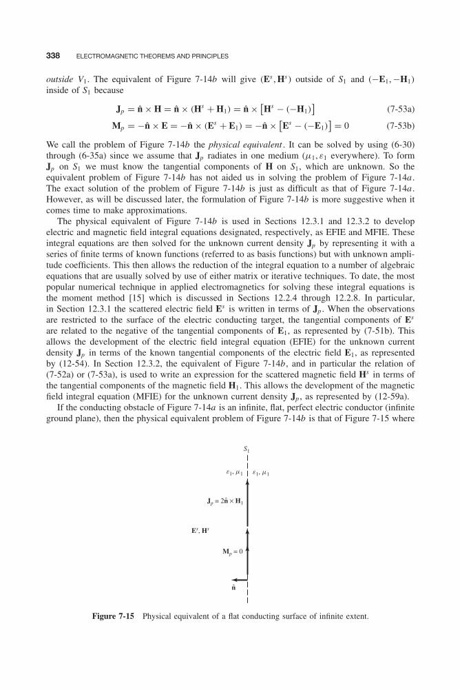
338 ELECTROMAGNETIC THEOREMS AND PRINCIPLES
outside V1. The equivalent of Figure 7-14b will give (Es , Hs) outside of S1 and (−E1, −H1)
inside of S1 because
Jp = n̂ × H = n̂ × (Hs + H1) = n̂ × [Hs − (−H1)
](7-53a)
Mp = −n̂ × E = −n̂ × (Es + E1) = −n̂ × [Es − (−E1)
] = 0 (7-53b)
We call the problem of Figure 7-14b the physical equivalent . It can be solved by using (6-30)through (6-35a) since we assume that Jp radiates in one medium (μ1, ε1 everywhere). To formJp on S1 we must know the tangential components of H on S1, which are unknown. So theequivalent problem of Figure 7-14b has not aided us in solving the problem of Figure 7-14a .The exact solution of the problem of Figure 7-14b is just as difficult as that of Figure 7-14a .However, as will be discussed later, the formulation of Figure 7-14b is more suggestive when itcomes time to make approximations.
The physical equivalent of Figure 7-14b is used in Sections 12.3.1 and 12.3.2 to developelectric and magnetic field integral equations designated, respectively, as EFIE and MFIE. Theseintegral equations are then solved for the unknown current density Jp by representing it with aseries of finite terms of known functions (referred to as basis functions) but with unknown ampli-tude coefficients. This then allows the reduction of the integral equation to a number of algebraicequations that are usually solved by use of either matrix or iterative techniques. To date, the mostpopular numerical technique in applied electromagnetics for solving these integral equations isthe moment method [15] which is discussed in Sections 12.2.4 through 12.2.8. In particular,in Section 12.3.1 the scattered electric field Es is written in terms of Jp . When the observationsare restricted to the surface of the electric conducting target, the tangential components of Es
are related to the negative of the tangential components of E1, as represented by (7-51b). Thisallows the development of the electric field integral equation (EFIE) for the unknown currentdensity Jp in terms of the known tangential components of the electric field E1, as representedby (12-54). In Section 12.3.2, the equivalent of Figure 7-14b, and in particular the relation of(7-52a) or (7-53a), is used to write an expression for the scattered magnetic field Hs in terms ofthe tangential components of the magnetic field H1. This allows the development of the magneticfield integral equation (MFIE) for the unknown current density Jp , as represented by (12-59a).
If the conducting obstacle of Figure 7-14a is an infinite, flat, perfect electric conductor (infiniteground plane), then the physical equivalent problem of Figure 7-14b is that of Figure 7-15 where
S1
e1, m1 e1, m1
Es, Hs
Mp = 0
Jp = 2n × H1
n
Figure 7-15 Physical equivalent of a flat conducting surface of infinite extent.
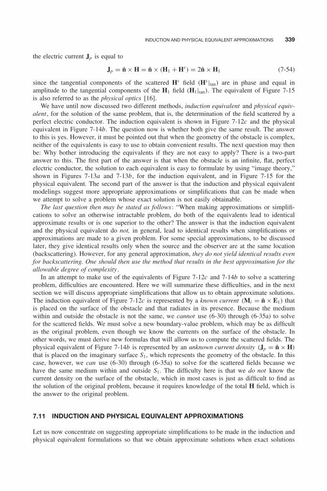
INDUCTION AND PHYSICAL EQUIVALENT APPROXIMATIONS 339
the electric current Jp is equal to
Jp = n̂ × H = n̂ × (H1 + Hs) = 2n̂ × H1 (7-54)
since the tangential components of the scattered Hs field (Hs |tan) are in phase and equal inamplitude to the tangential components of the H1 field (H1|tan). The equivalent of Figure 7-15is also referred to as the physical optics [16].
We have until now discussed two different methods, induction equivalent and physical equiv-alent , for the solution of the same problem, that is, the determination of the field scattered by aperfect electric conductor. The induction equivalent is shown in Figure 7-12c and the physicalequivalent in Figure 7-14b. The question now is whether both give the same result. The answerto this is yes. However, it must be pointed out that when the geometry of the obstacle is complex,neither of the equivalents is easy to use to obtain convenient results. The next question may thenbe: Why bother introducing the equivalents if they are not easy to apply? There is a two-partanswer to this. The first part of the answer is that when the obstacle is an infinite, flat, perfectelectric conductor, the solution to each equivalent is easy to formulate by using “image theory,”shown in Figures 7-13a and 7-13b, for the induction equivalent, and in Figure 7-15 for thephysical equivalent. The second part of the answer is that the induction and physical equivalentmodelings suggest more appropriate approximations or simplifications that can be made whenwe attempt to solve a problem whose exact solution is not easily obtainable.
The last question then may be stated as follows: “When making approximations or simplifi-cations to solve an otherwise intractable problem, do both of the equivalents lead to identicalapproximate results or is one superior to the other? The answer is that the induction equivalentand the physical equivalent do not, in general, lead to identical results when simplifications orapproximations are made to a given problem. For some special approximations, to be discussedlater, they give identical results only when the source and the observer are at the same location(backscattering). However, for any general approximation, they do not yield identical results evenfor backscattering. One should then use the method that results in the best approximation for theallowable degree of complexity .
In an attempt to make use of the equivalents of Figure 7-12c and 7-14b to solve a scatteringproblem, difficulties are encountered. Here we will summarize these difficulties, and in the nextsection we will discuss appropriate simplifications that allow us to obtain approximate solutions.The induction equivalent of Figure 7-12c is represented by a known current (Mi = n̂ × E1) thatis placed on the surface of the obstacle and that radiates in its presence. Because the mediumwithin and outside the obstacle is not the same, we cannot use (6-30) through (6-35a) to solvefor the scattered fields. We must solve a new boundary-value problem, which may be as difficultas the original problem, even though we know the currents on the surface of the obstacle. Inother words, we must derive new formulas that will allow us to compute the scattered fields. Thephysical equivalent of Figure 7-14b is represented by an unknown current density (Jp = n̂ × H)
that is placed on the imaginary surface S1, which represents the geometry of the obstacle. In thiscase, however, we can use (6-30) through (6-35a) to solve for the scattered fields because wehave the same medium within and outside S1. The difficulty here is that we do not know thecurrent density on the surface of the obstacle, which in most cases is just as difficult to find asthe solution of the original problem, because it requires knowledge of the total H field, which isthe answer to the original problem.
7.11 INDUCTION AND PHYSICAL EQUIVALENT APPROXIMATIONS
Let us now concentrate on suggesting appropriate simplifications to be made in the induction andphysical equivalent formulations so that we obtain approximate solutions when exact solutions

340 ELECTROMAGNETIC THEOREMS AND PRINCIPLES
S1
Es, Hs
e1, m1e1, m1
Mi = 2n × E1V1
n
Figure 7-16 Approximate induction equivalent for scattering from a perfect electric conductor (PEC).
are not feasible. In many cases the approximate solutions will lead to results that are well withinmeasuring accuracies of laboratory experiments.
In the induction equivalent form, the difficulty in obtaining a solution arises from the lackof equations that can be used with the known current density. The crudest approximation tothe problem is the assumption that the obstacle is large electrically and so we can use imagetheory to solve the problem. This assumes that locally on the surface of the obstacle each pointand its immediate neighbors form a flat surface. The best results with this simplification will befor scatterers whose electrical dimensions are large in comparison to the wavelength. Thus, theinduction equivalent of Figure 7-12c can be approximated by that in Figure 7-16. Now (6-30)through (6-35a) can be used to compute the scattered fields because we have the same mediuminside and outside S1.
In many cases, even this approximation may not be amenable to a closed-form solution becauseof the inability to integrate over the entire closed surface. To simplify this even further, we mayrestrict our integration over only part of the surface where the current density is more intense andwill provide the major contributions to the scattered field. This surface is usually the part that is“visible” by the transmitter (sources J1 and M1).
In the physical equivalent, the difficulty in solving the problem arises because we do not knowthe current density Jp (Jp = n̂ × H) that must be placed along the surface S1 (see Figure 7-14b).Once we decide on an approximation for the current density, the solution can be carried outbecause we can use (6-30) through (6-35a). The crudest approximation for this problem is theassumption that the total tangential H field on the surface of the conductor of Figure 7-14a isequal to twice that of the tangential H1. Thus, the current density to be placed on the surface ofthe physical equivalent of Figure 7-14b is
Jp � 2n̂ × H1 (7-55)
which is a good approximation provided that the scatterer is large electrically (in the limit infinite,flat, perfect conductor). In the shadow region of the scatterer, the physical equivalent currentdensity Jp is set to zero. We can then approximate the physical equivalent of Figure 7-14b bythat of Figure 7-17. This is usually referred to as the physical optics approximation [16], becauseit is similar to the formulation of the infinite, flat, ground plane. Thus, physical optics approximatethe boundary conditions that concern only the fields on the closed surface S1. If a closed-formsolution still cannot be obtained because of the inability to integrate over the entire surface,then integration over a part of the scattering surface may be sufficient, as was discussed for theinduction equivalent.
It should be pointed out that making the aforementioned crude approximations (image theoryfor the induction equivalent and physical optics for the physical equivalent), the two methods lead
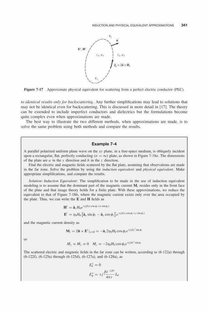
INDUCTION AND PHYSICAL EQUIVALENT APPROXIMATIONS 341
S1
Es, Hs
e1, m1 e1, m1
V1
Jp = 2n × H1
n
Figure 7-17 Approximate physical equivalent for scattering from a perfect electric conductor (PEC).
to identical results only for backscattering . Any further simplifications may lead to solutions thatmay not be identical even for backscattering. This is discussed in more detail in [17]. The theorycan be extended to include imperfect conductors and dielectrics but the formulations becomequite complex even when approximations are made.
The best way to illustrate the two different methods, when approximations are made, is tosolve the same problem using both methods and compare the results.
Example 7-4
A parallel polarized uniform plane wave on the xy plane, in a free-space medium, is obliquely incidentupon a rectangular, flat, perfectly conducting (σ = ∞) plate, as shown in Figure 7-18a . The dimensionsof the plate are a in the y direction and b in the z direction.
Find the electric and magnetic fields scattered by the flat plate, assuming that observations are madein the far zone. Solve the problem by using the induction equivalent and physical equivalent . Makeappropriate simplifications, and compare the results.
Solution: Induction Equivalent : The simplification to be made in the use of induction equivalentmodeling is to assume that the dominant part of the magnetic current Mi resides only in the front faceof the plate and that image theory holds for a finite plate. With these approximations, we reduce theequivalent to that of Figure 7-18b, where the magnetic current exists only over the area occupied bythe plate. Thus, we can write the E and H fields as
Hi = âz H0e+jβ(x cos φi +y sin φi )
Ei = η0H0[âx sin φi − ây cos φi
]e+jβ(x cos φi +y sin φi )
and the magnetic current density as
Mi = 2n̂ × Ei |x=0 = −âz 2η0H0 cos φi e+jβy ′ sin φi
orMx = My = 0 Mz = −2η0H0 cos φi e
+jβy ′ sin φi
The scattered electric and magnetic fields in the far zone can be written, according to (6-122a) through(6-122f), (6-125a) through (6-125d), (6-127a), and (6-128a), as
E sθ = 0
E sφ = +j
βe−jβr
4πrLθ

342 ELECTROMAGNETIC THEOREMS AND PRINCIPLES
a
a
a
yy
x
z
yy
x
z
yy
x
z
qs
fs fi
Ei
Hi
Es,Hs
b
b
b
Jp = 2n × Hi
Mi = 2n × Ei
(a) (b)
(c)
n
n
Figure 7-18 Plane wave scattering from a flat rectangular conducting plate. (a) Actual problem. (b)Induction equivalent. (c) Physical equivalent.
where
Lθ =∫ +a/2
−a/2
∫ +b/2
−b/2−Mz sin θs e+jβ(y ′ sin θs sin φs +z ′ cos θs )dz ′dy ′
Lθ = 2abη0H0 cos φi sin θs
(sin Y
Y
)(sin Z
Z
)Y = βa
2(sin θs sin φs + sin φi )
Z = βb
2cos θs
In summary,
E sθ = 0
E sφ = j
abβη0H0e−jβr
2πr
[cos φi sin θx
(sin Y
Y
)(sin Z
Z
)]H s
θ = −E sφ
η0
H sφ = E s
θ
η0= 0
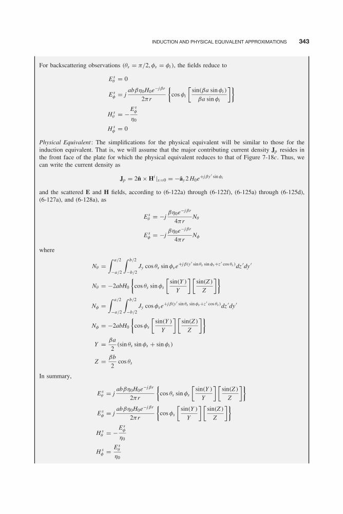
INDUCTION AND PHYSICAL EQUIVALENT APPROXIMATIONS 343
For backscattering observations (θs = π/2, φs = φi ), the fields reduce to
E sθ = 0
E sφ = j
abβη0H0e−jβr
2πr
{cos φi
[sin(βa sin φi )
βa sin φi
]}H s
θ = −E sφ
η0
H sφ = 0
Physical Equivalent : The simplifications for the physical equivalent will be similar to those for theinduction equivalent. That is, we will assume that the major contributing current density Jp resides inthe front face of the plate for which the physical equivalent reduces to that of Figure 7-18c. Thus, wecan write the current density as
Jp = 2n̂ × Hi |x=0 = −ây 2 H0e+jβy ′ sin φi
and the scattered E and H fields, according to (6-122a) through (6-122f), (6-125a) through (6-125d),(6-127a), and (6-128a), as
E sθ = −j
βη0e−jβr
4πrNθ
E sφ = −j
βη0e−jβr
4πrNφ
where
Nθ =∫ a/2
−a/2
∫ b/2
−b/2Jy cos θs sin φs e+jβ(y ′ sin θs sin φs +z ′ cos θs )dz ′dy ′
Nθ = −2abH0
{cos θs sin φs
[sin(Y )
Y
] [sin(Z )
Z
]}Nφ =
∫ a/2
−a/2
∫ b/2
−b/2Jy cos φs e+jβ(y ′ sin θs sin φs +z ′ cos θs )dz ′dy ′
Nφ = −2abH0
{cos φs
[sin(Y )
Y
] [sin(Z )
Z
]}Y = βa
2(sin θs sin φs + sin φi )
Z = βb
2cos θs
In summary,
E sθ = j
abβη0H0e−jβr
2πr
{cos θs sin φs
[sin(Y )
Y
] [sin(Z )
Z
]}E s
φ = jabβη0H0e−jβr
2πr
{cos φs
[sin(Y )
Y
] [sin(Z )
Z
]}H s
θ = −E sφ
η0
H sφ = E s
θ
η0
344 ELECTROMAGNETIC THEOREMS AND PRINCIPLES
For backscattering observations (θs = π/2, φs = φi ), the fields reduce to
E sθ = 0
E sφ = j
abβη0H0e−jβr
2πr
{cos φi
[sin(βa sin φi )
βa sin φi
]}H s
θ = −E sφ
η0
H sφ = 0
It is quite clear that the solutions of the two different methods do not lead to identical resultsexcept for backscatter observations. It seems that the physical equivalent solution gives the bestresults for general observations because it requires the least simplification in the formulation.
7.12 MULTIMEDIA
On the website that accompanies this book, the following multimedia resources are included forthe review, understanding and presentation of the material of this chapter.
• Power Point (PPT) viewgraphs, in multicolor.
REFERENCES
1. R. F. Harrington, Time-Harmonic Electromagnetic Fields , McGraw-Hill, New York, 1961.2. C. A. Balanis, Antenna Theory: Analysis and Design , Third Edition, John Wiley & Sons, New York,
2005.3. J. R. Wait, “Characteristics of antennas over lossy earth,” in Antenna Theory Part 2 , Chapter 23, R. E.
Collin and F. J. Zucker, eds., McGraw-Hill, New York, 1969.4. L. E. Vogler and J. L. Noble, “Curves of input impedance change due to ground for dipole antennas,”
U.S. National Bureau of Standards, Monograph 72, January 31, 1964.5. W. H. Hayt, Jr., and J. E. Kimmerly, Engineering Circuit Analysis , Third Edition, McGraw-Hill, New
York, 1978.6. J. R. Carson, “Reciprocal theorems in radio communication,” Proc. IRE , vol. 17, pp. 952–956, June
1929.7. J. H. Richmond, The Basic Theory of Harmonic Fields, Antennas and Scattering , Unpublished Notes.8. V. H. Rumsey, “Reaction concept in electromagnetic theory,” Physical Review , vol. 94, no. 6, pp.
1483–1491, June 15, 1954.9. J. H. Richmond, “A reaction theorem and its application to antenna impedance calculations,” IRE Trans.
Antennas Propagat ., vol. AP-9, no. 6, pp. 515–520, November 1961.10. R. Mittra (ed.), Computer Techniques for Electromagnetics , Chapter 2, Pergamon, Elmsford, NY, 1973.11. S. A. Schelkunoff, “Some equivalence theorems of electromagnetics and their application to radiation
problems,” Bell System Tech. J ., vol. 15, pp. 92–112, 1936.12. C. Huygens, Traite de la Lumiere, Leyeden, 1690. Translated into English by S. P. Thompson, London,
1912 and reprinted by the University of Chicago Press.13. J. D. Kraus and K. R. Carver, Electromagnetics , Second Edition, McGraw-Hill, New York, 1973, pp.
464–467.14. A. E. H. Love, “The integration of the equations of propagation of electric waves,” Phil. Trans. Roy.
Soc. London, Ser. A, vol. 197, pp. 1–45, 1901.

PROBLEMS 345
15. R. F. Harrington, Field Computation by Moment Methods , Macmillan, New York, 1968.
16. P. Beckmann, The Depolarization of Electromagnetic Waves , The Golem Press, Boulder, CO, 1968, pp.76–92.
17. R. F. Harrington, “On scattering by large conducting bodies,” IRE Trans. Antennas Propagat., vol.AP-7, no. 2, pp. 150–153, April 1959.
PROBLEMS
7.1. For the infinitesimal vertical electric dipolewhose far-zone electric field is given by(7-13a):(a) Find the corresponding magnetic field.(b) Determine the corresponding time-
average power density.(c) Show that the radiated power, obtained
by integrating the power density of part(b) over a sphere of radius r , can bewritten as
Prad = πη
∣∣∣∣ I0�
λ
∣∣∣∣2×
[1
3− cos(2βh)
(2βh)2+ sin(2βh)
(2βh)3
]7.2. For Problem 7.1, show the following:
(a) The radiation intensity U, defined in thefar field as U ≈ r2Sav, where Sav isthe far-field time-average power density,can be written as
U = η
2
∣∣∣∣ I0�
λ
∣∣∣∣2
sin2 θ cos2(βh cos θ)
(b) The maximum directivity D0 of the ele-ment, defined as
D0 = 4πUmax
Prad
where Umax is the maximum radiationintensity, can be written as
D0 = 2
F (βh)
F (βh) =[
1
3− cos(2βh)
(2βh)2+ sin(2βh)
(2βh)3
](c) The radiation resistance, defined as
Rr = 2Prad
|I0|2can be expressed as
Rr = 2πη
(�
λ
)2
F (βh)
where F (βh) is that given in part (b).
7.3. An infinitesimal vertical magnetic dipole oflength l and constant current Im is placedsymmetrically about the origin and it isdirected along the z axis, as shown inFigure 6-2a . Derive expressions valid every-where, near and far field, for the:• Electric vector potential components
(Fr , Fθ , Fφ).• Electric field components (Er , Eθ , Eφ).• Magnetic field components (Hr , Hθ , Hφ).• Time-average power density, defined as
Sav = 1
2Re
[E × H∗].
• Radiation intensity, defined in the far fieldas U ≈ r2Sav .
• Power radiated, defined asPrad = ∫ 2π
0
∫ π
0 U (θ , φ) sin θdθdφ.• Maximum directivity, defined as
D0 = 4πUmax (θ , φ)
Prad• Radiation resistance, defined as
Rr = 2Prad
|Im |2You can minimize the derivations as long asyou justify the procedure.
7.4. For the infinitesimal vertical magneticdipole of Problem 7.3, simplify the expres-sions for the electric vector potential, andelectric and magnetic fields, when the obser-vations are made in the far field.
7.5. An infinitesimal magnetic dipole of length land constant current Im is placed symmetri-cally about the origin and it is directed alongthe x axis. Derive the following expressionsfor the far zone:• Electric vector potential components
(Fr , Fθ , Fφ).
• Electric field components (Er , Eθ , Eφ).• Magnetic field components (Hr , Hθ , Hφ).• Time-average power density as defined in
Problem 7.3.• Radiation intensity as defined in Prob-
lem 7.3.
346 ELECTROMAGNETIC THEOREMS AND PRINCIPLES
• Directivity as defined in Problem 7.3.• Radiation resistance as defined in Prob-
lem 7.3.
7.6. Repeat Problem 7.4 for an infinitesimalmagnetic dipole of length l and constant cur-rent Im but directed along the y axis.
7.7. Repeat Problem 7.1 for the horizontalinfinitesimal electric dipole of Section 7.4.2and Figure 7-5, and show that the:• Radiation intensity is
U (θ , φ) = η
2|I0|2
(l
λ
)2
× (cos2 θ sin2 φ + cos2 φ
)× sin2(βh cos θ) , 0 ≤ θ ≤ π
2
• Power radiated is
Prad =2π∫
0
π/2∫0
U (θ , φ) sin θdθdφ
= ηπ
2|I0|2
(l
λ
)2 [2
3− sin (2βh)
2βh
− cos (2βh)
(2βh)2 + sin (2βh)
(2βh)3
]• Maximum directivity is
D0 = 4πUmax
Prad
=
⎧⎪⎪⎨⎪⎪⎩4 sin2(βh)
R(βh)βh ≤π/2 (h ≤ λ/4)
4
R(βh)βh >π/2 (h > λ/4)
R(βh) =[
2
3− sin (2βh)
2βh− cos (2βh)
(2βh)2
+ sin (2βh)
(2βh)3
]• Radiation resistance is
Rr = 2Prad
|I0|2= ηπ
(l
λ
)2 [2
3− sin (2βh)
2βh
− cos (2βh)
(2βh)2 + sin (2βh)
(2βh)3
]7.8. Using the electric field of (7-13a), where r is
fixed, plot the normalized radiation pattern(in dB) versus the angle θ when the height
h of the element above the ground is h = 0,λ/8, λ/4, 3λ/8, λ/2, and λ.
7.9. A quarter-wavelength (�/2 = λ/4) wireradiator is placed vertically above an infi-nite electric ground plane and it is fed at itsbase, as shown in Figure P7-9. This is usu-ally referred to as a λ/4 monopole. Assumethat the current on the wire is representedby
I = âz I0 sin
[β
(�
2− z ′
)], 0 ≤ z ′ ≤ �/2
where z ′ is any point on the monopoleand show, using image theory, (6-97a),(6-112a) and (6-112b), and the formulationsof Section 6.7, that the far-zone electricand magnetic fields radiated by the elementabove the ground plane are given by
Er � Eφ � Hr � Hθ � 0
Eθ � jηI0e−jβr
2πr
⎡⎢⎣cos(π
2cos θ
)sin θ
⎤⎥⎦Hφ � Eφ
η
These expressions are identical to those ofProblem 6.26.
l/2 = l/4
s = ∞
Figure P7-9
7.10. A very small (� � λ) linear radiating cur-rent element is placed between two infi-nite plates forming a 90◦ corner reflector.Assume that the length of the element isplaced parallel to the plates of the cornerreflector.(a) Determine the number of images, their
polarizations, and their positions that arenecessary to account for all the reflec-tions from the plates of the reflector

PROBLEMS 347
and to find the radiated fields within theinternal space of the reflector.
(b) Show that the total far-zone radiatedfields within the internal region of thereflector can be written as
E tθ = E 0
θ F (βs)
E 0θ = jη
βI0�e−jβr
4πrsin θ
F (βs) = 2[cos (βs sin θ cos φ)
− cos (βs sin θ sin φ)]
0◦ ≤ θ ≤ 180◦
315◦ ≤ φ ≤ 360◦, 0 ≤ φ ≤ 45◦
where θ is measured from the z axistoward the observation point. E 0
θ is thefar-zone field radiated by a very small(� � λ) linear element radiating in anunbounded medium (see Example 6-3)and F (βs) is referred to as the arrayfactor representing the array of elementsthat includes the actual radiating ele-ment and its associated images.
y
xz s
fa
Figure P7-10
7.11. For Problem 7.10 plot the magnitude ofF (βs) as a function of s (0 ≤ s ≤ 10λ)when θ = 90◦ and φ = 0◦. What is the max-imum value of |F (βs)|? Is the function peri-odic? If so, what is the period?
7.12. For Problem 7.10 plot the normalized valueof the magnitude of F (βs) (in dB) as a func-tion of φ (315◦ ≤ φ ≤ 360◦, 0 ≤ φ ≤ 45◦)when θ = 90◦. Do this when s = 0.1λ, s =0.7λ, s = 0.8λ, s = 0.9λ, and s = 1.0λ.
7.13. Repeat Problem 7.10 when the includedangle α of the corner reflector is 60◦, 45◦,
and 30◦, and show that F (βs) takes the fol-lowing forms.(a) α = 60◦
F (βs) = 4 sin
(X
2
)×
[cos
(X
2
)− cos
(√3
Y
2
)](b) α = 45◦
F (βs) = 2 [cos(X ) + cos(Y )−
2 cos
(X√
2
)cos
(Y√
2
)](c) α = 30◦
F (βs)=2
[cos(X )−2 cos
(√3
X
2
)cos
(Y
2
)− cos(Y )+2 cos
(X
2
)cos
(√3
X
2
)]where X =βs sin θ cos φ, Y =βs sin θ sin φ
7.14. For Problem 7.13 and the three values (α =60◦, 45◦, and 30◦), plot the magnitude ofF (βs) as a function of s (0 ≤ s ≤ 10λ)when θ = 90◦ and φ = 0◦. What is the max-imum value |F (βs) will ever achieve ifplotted as a function of s? Is the functionperiodic? If so, what is the period?
7.15. An infinitesimal electric dipole is placedat an angle of 30◦ at a height h above aperfectly conducting electric ground plane.Determine the location and orientation of itsimage. Do this by sketching the image.
h
s = ∞
30°
Figure P7-15
7.16. A small circular loop of radius a is placedvertically at a height h above a perfectlyconducting electric ground plane. Determine

348 ELECTROMAGNETIC THEOREMS AND PRINCIPLES
the location and direction of current flow ofits image. Do this by sketching the image.
h
s = ∞
Figure P7-16
7.17. A small electric circular loop antenna, ofradius a and constant electric current I0, isplaced in parallel (parallel to xy-plane) aheight h above a perfect magnetic (PMC),flat and infinite in extent, horizontal groundplane. The electric current flowing in theloop antenna is in the counterclockwise(CCW) direction, as viewed from the top(looking from the top downwards, i.e., -zdirection).(a) To account for the direct field, and the
reflected one from the PMC, determinethe equivalent problem that will accountfor the total field (direct and reflected)on and above the PMC ground plane.State, in words, the magnitude (equal orunequal ) and relative phase (in degrees)of the image loop compared to those ofthe actual loop.
(b) In what direction, as viewed again fromthe top (looking downwards), is the elec-tric current flowing in the image electricloop? CCW or CW?
PMC
I0
View
Loop Antenna
x
z
h
y
Figure P7-17
7.18. A horizontal magnetic dipole is placedabove a planar Perfect Electric Conductor(PEC) of infinite extent, as shown in FiguresP7-18 and 7-2.
In order to maintain the maximum total radi-ation, due to the magnetic dipole itself andits image (to account for reflections), towardthe z-axis (perpendicular to the interface),what is the smallest nonzero height h thatthe magnetic dipole should be placed abovethe PEC:
• In wavelengths.• In cm, for a frequency of 10 GHz.
PEC
Magneticdipole
y
z
h
Figure P7-18
7.19. Repeat Problem 7.18 when the element is amagnetic dipole and the ground plane is aPMC.
7.20. Repeat Problem 7.18 when the element isan electric dipole and the ground plane is aPEC.
7.21. Repeat Problem 7.18 when the element isan electric dipole and the ground plane is aPMC.
7.22. A linearly polarized uniform plane wavetraveling in free space is incident normallyupon a flat dielectric surface. Assume thatthe incident electric field is given by
E = âx E0e−jβ0z
x
y z
e0, m0 e, m0
Figure P7-22
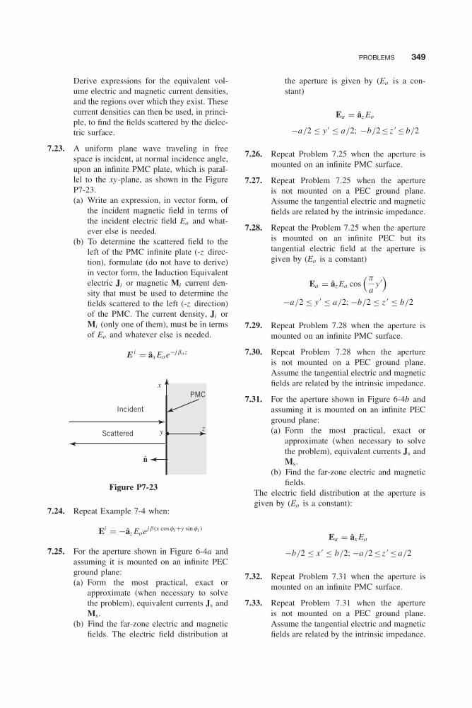
PROBLEMS 349
Derive expressions for the equivalent vol-ume electric and magnetic current densities,and the regions over which they exist. Thesecurrent densities can then be used, in princi-ple, to find the fields scattered by the dielec-tric surface.
7.23. A uniform plane wave traveling in freespace is incident, at normal incidence angle,upon an infinite PMC plate, which is paral-lel to the xy-plane, as shown in the FigureP7-23.(a) Write an expression, in vector form, of
the incident magnetic field in terms ofthe incident electric field Eo and what-ever else is needed.
(b) To determine the scattered field to theleft of the PMC infinite plate (-z direc-tion), formulate (do not have to derive)in vector form, the Induction Equivalentelectric Ji or magnetic Mi current den-sity that must be used to determine thefields scattered to the left (-z direction)of the PMC. The current density, Ji orMi (only one of them), must be in termsof Eo and whatever else is needed.
E i = âx Eoe−jβo z
Incident
Scattered
PMCx
y z
n
Figure P7-23
7.24. Repeat Example 7-4 when:
Ei = −âz Eoejβ(x cos φi +y sin φi )
7.25. For the aperture shown in Figure 6-4a andassuming it is mounted on an infinite PECground plane:(a) Form the most practical, exact or
approximate (when necessary to solvethe problem), equivalent currents Js andMs.
(b) Find the far-zone electric and magneticfields. The electric field distribution at
the aperture is given by (Eo is a con-stant)
Ea = âz Eo
−a/2 ≤ y ′ ≤ a/2; −b/2 ≤ z ′ ≤ b/2
7.26. Repeat Problem 7.25 when the aperture ismounted on an infinite PMC surface.
7.27. Repeat Problem 7.25 when the apertureis not mounted on a PEC ground plane.Assume the tangential electric and magneticfields are related by the intrinsic impedance.
7.28. Repeat the Problem 7.25 when the apertureis mounted on an infinite PEC but itstangential electric field at the aperture isgiven by (Eo is a constant)
Ea = âz Eo cos(π
ay ′)
−a/2 ≤ y ′ ≤ a/2;−b/2 ≤ z ′ ≤ b/2
7.29. Repeat Problem 7.28 when the aperture ismounted on an infinite PMC surface.
7.30. Repeat Problem 7.28 when the apertureis not mounted on a PEC ground plane.Assume the tangential electric and magneticfields are related by the intrinsic impedance.
7.31. For the aperture shown in Figure 6-4b andassuming it is mounted on an infinite PECground plane:(a) Form the most practical, exact or
approximate (when necessary to solvethe problem), equivalent currents Js andMs.
(b) Find the far-zone electric and magneticfields.
The electric field distribution at the aperture isgiven by (Eo is a constant):
Ea = âx Eo
−b/2 ≤ x ′ ≤ b/2;−a/2 ≤ z ′ ≤ a/2
7.32. Repeat Problem 7.31 when the aperture ismounted on an infinite PMC surface.
7.33. Repeat Problem 7.31 when the apertureis not mounted on a PEC ground plane.Assume the tangential electric and magneticfields are related by the intrinsic impedance.
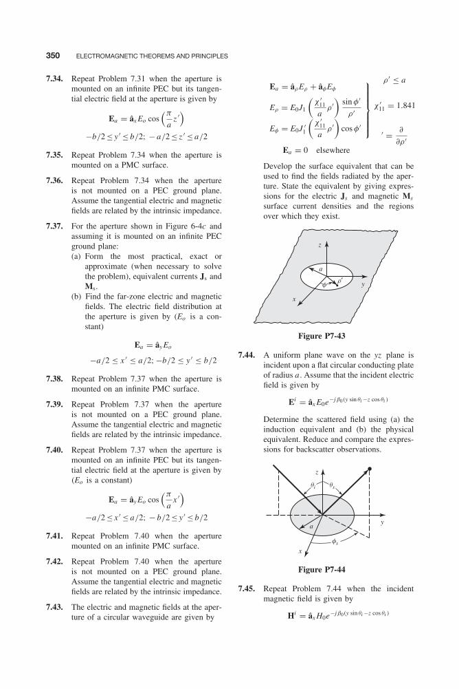
350 ELECTROMAGNETIC THEOREMS AND PRINCIPLES
7.34. Repeat Problem 7.31 when the aperture ismounted on an infinite PEC but its tangen-tial electric field at the aperture is given by
Ea = âx Eo cos(π
az ′)
−b/2 ≤ y ′ ≤ b/2; − a/2 ≤ z ′ ≤ a/2
7.35. Repeat Problem 7.34 when the aperture ismounted on a PMC surface.
7.36. Repeat Problem 7.34 when the apertureis not mounted on a PEC ground plane.Assume the tangential electric and magneticfields are related by the intrinsic impedance.
7.37. For the aperture shown in Figure 6-4c andassuming it is mounted on an infinite PECground plane:(a) Form the most practical, exact or
approximate (when necessary to solvethe problem), equivalent currents Js andMs.
(b) Find the far-zone electric and magneticfields. The electric field distribution atthe aperture is given by (Eo is a con-stant)
Ea = ây Eo
−a/2 ≤ x ′ ≤ a/2;−b/2 ≤ y ′ ≤ b/2
7.38. Repeat Problem 7.37 when the aperture ismounted on an infinite PMC surface.
7.39. Repeat Problem 7.37 when the apertureis not mounted on a PEC ground plane.Assume the tangential electric and magneticfields are related by the intrinsic impedance.
7.40. Repeat Problem 7.37 when the aperture ismounted on an infinite PEC but its tangen-tial electric field at the aperture is given by(Eo is a constant)
Ea = ây Eo cos(π
ax ′
)−a/2 ≤ x ′ ≤ a/2; − b/2 ≤ y ′ ≤ b/2
7.41. Repeat Problem 7.40 when the aperturemounted on an infinite PMC surface.
7.42. Repeat Problem 7.40 when the apertureis not mounted on a PEC ground plane.Assume the tangential electric and magneticfields are related by the intrinsic impedance.
7.43. The electric and magnetic fields at the aper-ture of a circular waveguide are given by
Ea = âρEρ + âφEφ
Eρ = E0J1
(χ ′
11
aρ ′
)sin φ′
ρ ′
Eφ = E0J ′1
(χ ′
11
aρ ′
)cos φ′
⎫⎪⎪⎪⎪⎪⎬⎪⎪⎪⎪⎪⎭
ρ ′ ≤ a
χ ′11 = 1.841
′ = ∂
∂ρ ′Ea = 0 elsewhere
Develop the surface equivalent that can beused to find the fields radiated by the aper-ture. State the equivalent by giving expres-sions for the electric Js and magnetic Ms
surface current densities and the regionsover which they exist.
x
z
y
a
fr′
Figure P7-43
7.44. A uniform plane wave on the yz plane isincident upon a flat circular conducting plateof radius a . Assume that the incident electricfield is given by
Ei = âx E0e−jβ0(y sin θi −z cos θi )
Determine the scattered field using (a) theinduction equivalent and (b) the physicalequivalent. Reduce and compare the expres-sions for backscatter observations.
x
y
z
a
fs
qi qs
Figure P7-44
7.45. Repeat Problem 7.44 when the incidentmagnetic field is given by
Hi = âx H0e−jβ0(y sin θi −z cos θi )
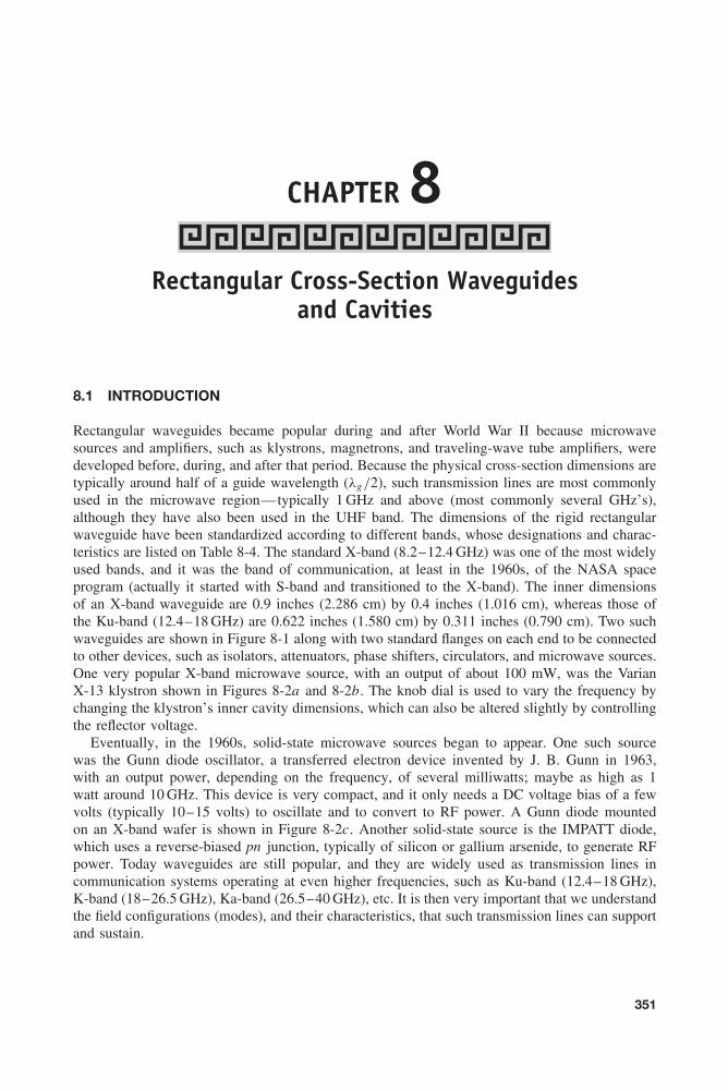
Balanis c08.tex V3 - 11/22/2011 3:32 P.M. Page 351
CHAPTER 8Rectangular Cross-Section Waveguides
and Cavities
8.1 INTRODUCTION
Rectangular waveguides became popular during and after World War II because microwavesources and amplifiers, such as klystrons, magnetrons, and traveling-wave tube amplifiers, weredeveloped before, during, and after that period. Because the physical cross-section dimensions aretypically around half of a guide wavelength (λg/2), such transmission lines are most commonlyused in the microwave region—typically 1 GHz and above (most commonly several GHz’s),although they have also been used in the UHF band. The dimensions of the rigid rectangularwaveguide have been standardized according to different bands, whose designations and charac-teristics are listed on Table 8-4. The standard X-band (8.2–12.4 GHz) was one of the most widelyused bands, and it was the band of communication, at least in the 1960s, of the NASA spaceprogram (actually it started with S-band and transitioned to the X-band). The inner dimensionsof an X-band waveguide are 0.9 inches (2.286 cm) by 0.4 inches (1.016 cm), whereas those ofthe Ku-band (12.4–18 GHz) are 0.622 inches (1.580 cm) by 0.311 inches (0.790 cm). Two suchwaveguides are shown in Figure 8-1 along with two standard flanges on each end to be connectedto other devices, such as isolators, attenuators, phase shifters, circulators, and microwave sources.One very popular X-band microwave source, with an output of about 100 mW, was the VarianX-13 klystron shown in Figures 8-2a and 8-2b. The knob dial is used to vary the frequency bychanging the klystron’s inner cavity dimensions, which can also be altered slightly by controllingthe reflector voltage.
Eventually, in the 1960s, solid-state microwave sources began to appear. One such sourcewas the Gunn diode oscillator, a transferred electron device invented by J. B. Gunn in 1963,with an output power, depending on the frequency, of several milliwatts; maybe as high as 1watt around 10 GHz. This device is very compact, and it only needs a DC voltage bias of a fewvolts (typically 10–15 volts) to oscillate and to convert to RF power. A Gunn diode mountedon an X-band wafer is shown in Figure 8-2c. Another solid-state source is the IMPATT diode,which uses a reverse-biased pn junction, typically of silicon or gallium arsenide, to generate RFpower. Today waveguides are still popular, and they are widely used as transmission lines incommunication systems operating at even higher frequencies, such as Ku-band (12.4–18 GHz),K-band (18–26.5 GHz), Ka-band (26.5–40 GHz), etc. It is then very important that we understandthe field configurations (modes), and their characteristics, that such transmission lines can supportand sustain.
351

Balanis c08.tex V3 - 11/22/2011 3:32 P.M. Page 352
352 RECTANGULAR CROSS-SECTION WAVEGUIDES AND CAVITIES
Figure 8-1 Two rectangular waveguides (Ku-band and X-band) with flanges.
(a) (b) (c)
Figure 8-2 X-band microwave sources: X-13 klystron and Gunn diode wafer. (a) Rear view of X-13. (b)Front view of X-13. (c) Gunn diode wafer.
Rectangular transmission lines (such as rectangular waveguides, dielectric slab lines, striplines,and microstrips) and their corresponding cavities represent a significant section of lines used inmany practical radio-frequency systems. The objective in this chapter is to introduce and analyzesome of them, and to present some data on their propagation characteristics. The parameters ofinterest include field configurations (modes) that can be supported by such structures and theircorresponding cutoff frequencies, guide wavelengths, wave impedances, phase and attenuationconstants, and quality factors Q . Because of their general rectilinear geometrical shapes, it is mostconvenient to use the rectangular coordinate system for the analyses. The field configurations thatcan be supported by these structures must satisfy Maxwell’s equations or the wave equation, andthe corresponding boundary conditions.
8.2 RECTANGULAR WAVEGUIDE
Let us consider a rectangular waveguide of lateral dimensions a and b, as shown in Figure 8-3. Initially assume that the waveguide is of infinite length and is empty. It is our purpose todetermine the various field configurations (modes) that can exist inside the guide. Although aTEMz field configuration is of the simplest structure, it cannot satisfy the boundary conditionson the waveguide walls. Therefore, it is not a valid solution. It can be shown that modes TEx ,TMx , TEy , TMy , TEz , and TMz satisfy the boundary conditions and are therefore appropriatemodes (field configurations) for the rectangular waveguide. We will initially consider TEz andTMz ; others will follow.
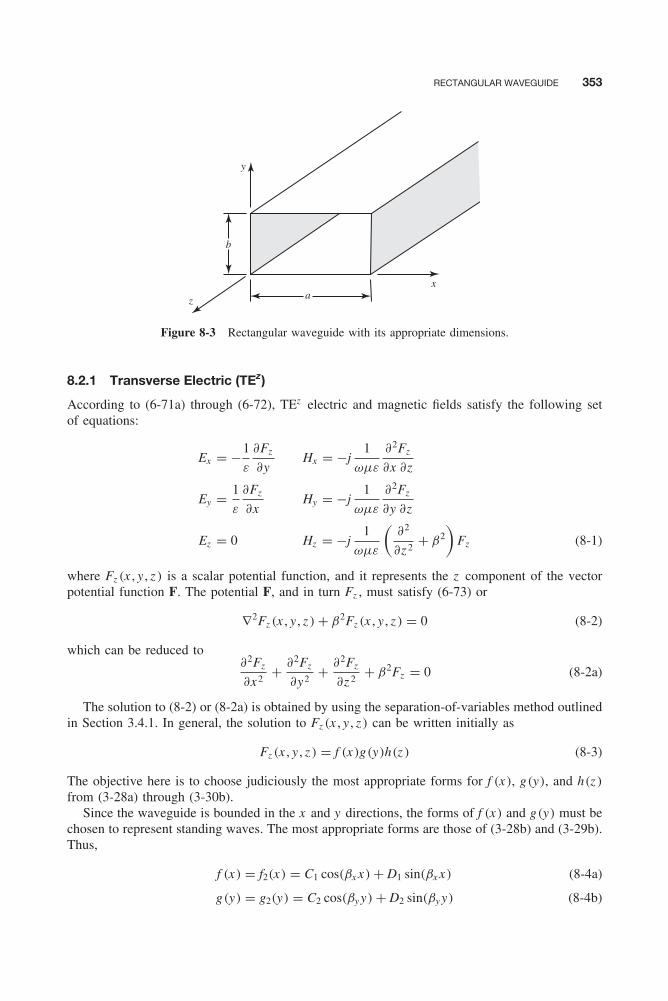
Balanis c08.tex V3 - 11/22/2011 3:32 P.M. Page 353
RECTANGULAR WAVEGUIDE 353
y
xa
b
z
Figure 8-3 Rectangular waveguide with its appropriate dimensions.
8.2.1 Transverse Electric (TEz)
According to (6-71a) through (6-72), TEz electric and magnetic fields satisfy the following setof equations:
Ex = −1
ε
∂Fz
∂yHx = −j
1
ωμε
∂2Fz
∂x ∂z
Ey = 1
ε
∂Fz
∂xHy = −j
1
ωμε
∂2Fz
∂y ∂z
Ez = 0 Hz = −j1
ωμε
(∂2
∂z 2+ β2
)Fz (8-1)
where Fz (x , y , z ) is a scalar potential function, and it represents the z component of the vectorpotential function F. The potential F, and in turn Fz , must satisfy (6-73) or
∇2Fz (x , y , z ) + β2Fz (x , y , z ) = 0 (8-2)
which can be reduced to∂2Fz
∂x 2+ ∂2Fz
∂y2+ ∂2Fz
∂z 2+ β2Fz = 0 (8-2a)
The solution to (8-2) or (8-2a) is obtained by using the separation-of-variables method outlinedin Section 3.4.1. In general, the solution to Fz (x , y , z ) can be written initially as
Fz (x , y , z ) = f (x)g(y)h(z ) (8-3)
The objective here is to choose judiciously the most appropriate forms for f (x), g(y), and h(z )
from (3-28a) through (3-30b).Since the waveguide is bounded in the x and y directions, the forms of f (x) and g(y) must be
chosen to represent standing waves. The most appropriate forms are those of (3-28b) and (3-29b).Thus,
f (x) = f2(x) = C1 cos(βx x) + D1 sin(βx x) (8-4a)
g(y) = g2(y) = C2 cos(βy y) + D2 sin(βy y) (8-4b)
Balanis c08.tex V3 - 11/22/2011 3:32 P.M. Page 354
354 RECTANGULAR CROSS-SECTION WAVEGUIDES AND CAVITIES
Because the waveguide is infinite in length, the variations of the fields in the z direction mustrepresent traveling waves as given by (3-30a). Thus,
h(z ) = h1(z ) = A3e−jβz z + B3e+jβz z (8-5)
Substituting (8-4a) through (8-5) into (8-3), we can write that
Fz (x , y , z ) = [C1 cos(βx x) + D1 sin(βx x)][C2 cos(βy y) + D2 sin(βy y)
]× [
A3e−jβz z + B3e+jβz z]
(8-6)
The first exponential in (8-6) represents waves traveling in the +z direction (assuming an ejωt
time variation) and the second term designates waves traveling in the −z direction. To simplifythe notation, assume that the source is located such that the waves are traveling only in the+z direction. Then the second term is not present, so B3 = 0. If the waves are traveling in the−z direction, then the second exponential in (8-6) is appropriate and A3 = 0. If the waves aretraveling in both directions, superposition can be used to sum the field expressions for the +zand −z traveling waves.
For +z traveling waves, Fz of (8-6) reduces with B3 = 0 to
F+z (x , y , z ) = [C1 cos(βx x) + D1 sin(βx x)]
× [C2 cos(βy y) + D2 sin(βy y)
]A3e−jβz z (8-7)
where, according to (3-27), the constraint (dispersion) equation is
β2x + β2
y + β2z = β2 = ω2με (8-7a)
C1, D1, C2, D2, A3, βx , βy , and βz are constants that will be evaluated by substituting (8-7) into(8-1) and applying the appropriate boundary conditions on the walls of the waveguide.
For the waveguide structure of Figure 8-3, the necessary and sufficient boundary conditionsare those that require the tangential components of the electric field to vanish on the walls of thewaveguide. Thus, in general, on the bottom and top walls
Ex (0 ≤ x ≤ a , y = 0, z ) = Ex (0 ≤ x ≤ a , y = b, z ) = 0 (8-8a)
Ez (0 ≤ x ≤ a , y = 0, z ) = Ez (0 ≤ x ≤ a , y = b, z ) = 0 (8-8b)
and on the left and right walls
Ey(x = 0, 0 ≤ y ≤ b, z ) = Ey(x = a , 0 ≤ y ≤ b, z ) = 0 (8-8c)
Ez (x = 0, 0 ≤ y ≤ b, z ) = Ez (x = a , 0 ≤ y ≤ b, z ) = 0 (8-8d)
For the TEz modes, Ez = 0, and the boundary conditions of (8-8b) and (8-8d) are automaticallysatisfied. However, in general, the boundary conditions of (8-8b) and (8-8d) are not independent,but they represent the same conditions as given, respectively, by (8-8a) and (8-8c). Therefore, thenecessary and sufficient independent boundary conditions, in general, will be to enforce either(8-8a) or (8-8b) and either (8-8c) or (8-8d).
Substituting (8-7) into (8-1), we can write the x component of the electric field as
E+x (x , y , z ) = −A3
βy
ε[C1 cos(βx x) + D1 sin(βx x)]
× [−C2 sin(βy y) + D2 cos(βy y)]
e−jβz z (8-9)
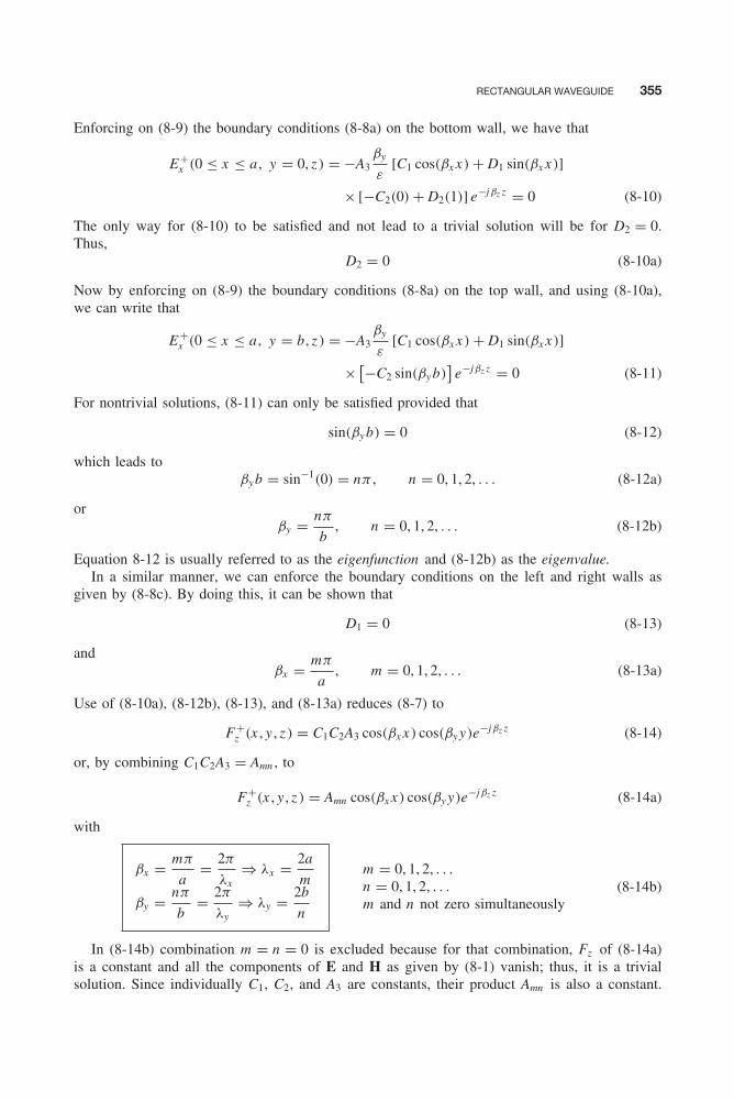
Balanis c08.tex V3 - 11/22/2011 3:32 P.M. Page 355
RECTANGULAR WAVEGUIDE 355
Enforcing on (8-9) the boundary conditions (8-8a) on the bottom wall, we have that
E+x (0 ≤ x ≤ a , y = 0, z ) = −A3
βy
ε[C1 cos(βx x) + D1 sin(βx x)]
× [−C2(0) + D2(1)] e−jβz z = 0 (8-10)
The only way for (8-10) to be satisfied and not lead to a trivial solution will be for D2 = 0.Thus,
D2 = 0 (8-10a)
Now by enforcing on (8-9) the boundary conditions (8-8a) on the top wall, and using (8-10a),we can write that
E+x (0 ≤ x ≤ a , y = b, z ) = −A3
βy
ε[C1 cos(βx x) + D1 sin(βx x)]
× [−C2 sin(βy b)]
e−jβz z = 0 (8-11)
For nontrivial solutions, (8-11) can only be satisfied provided that
sin(βy b) = 0 (8-12)
which leads toβy b = sin−1(0) = nπ , n = 0, 1, 2, . . . (8-12a)
orβy = nπ
b, n = 0, 1, 2, . . . (8-12b)
Equation 8-12 is usually referred to as the eigenfunction and (8-12b) as the eigenvalue.In a similar manner, we can enforce the boundary conditions on the left and right walls as
given by (8-8c). By doing this, it can be shown that
D1 = 0 (8-13)
andβx = mπ
a, m = 0, 1, 2, . . . (8-13a)
Use of (8-10a), (8-12b), (8-13), and (8-13a) reduces (8-7) to
F+z (x , y , z ) = C1C2A3 cos(βx x) cos(βy y)e−jβz z (8-14)
or, by combining C1C2A3 = Amn , to
F+z (x , y , z ) = Amn cos(βx x) cos(βy y)e−jβz z (8-14a)
with
βx = mπ
a= 2π
λx⇒ λx = 2a
m
βy = nπ
b= 2π
λy⇒ λy = 2b
n
m = 0, 1, 2, . . .n = 0, 1, 2, . . .m and n not zero simultaneously
(8-14b)
In (8-14b) combination m = n = 0 is excluded because for that combination, Fz of (8-14a)is a constant and all the components of E and H as given by (8-1) vanish; thus, it is a trivialsolution. Since individually C1, C2, and A3 are constants, their product Amn is also a constant.
Balanis c08.tex V3 - 11/22/2011 3:32 P.M. Page 356
356 RECTANGULAR CROSS-SECTION WAVEGUIDES AND CAVITIES
The subscripts m and n are used to designate the eigenvalues of βx and βy and in turn the fieldconfigurations (modes). Thus, a given combination of m and n in (8-14b) designates a givenTEz
mn mode. Since there are infinite combinations of m and n , there are an infinite number ofTEz
mn modes.In (8-14b), βx and βy represent the mode wave numbers (eigenvalues) in the x and y directions,
respectively. These are related to the wave number in the z direction (βz ) and to that of theunbounded medium (β) by (8-7a). In (8-14b), λx and λy represent, respectively, the wavelengthsof the wave inside the guide in the x and y directions. These are related to the wavelength in thez direction (λz = λg ) and to that in an unbounded medium (λ), according to (8-7a), by
1
λ2x
+ 1
λ2y
+ 1
λ2z
= 1
λ2(8-14c)
In summary then, the appropriate expressions for the TEzmn modes are, according to (8-1),
(8-14a), and (8-14b),TE+z
mn
E+x = Amn
βy
εcos(βx x) sin(βy y)e−jβz z (8-15a)
E+y = −Amn
βx
εsin(βx x) cos(βy y)e−jβz z (8-15b)
E+z = 0 (8-15c)
H +x = Amn
βxβz
ωμεsin(βx x) cos(βy y)e−jβz z (8-15d)
H +y = Amn
βyβz
ωμεcos(βx x) sin(βy y)e−jβz z (8-15e)
H +z = −jAmn
β2c
ωμεcos(βx x) cos(βy y)e−jβz z (8-15f)
where
β2c ≡
(2π
λc
)2
= β2 − β2z = β2
x + β2y =
(mπ
a
)2+
(nπ
b
)2(8-15g)
The constant βc is the value of β when βz = 0, and it will be referred to as the cutoff wavenumber . Thus,
βc = β|βz =0 = ω√
με|βz =0 = ωc√
με = 2π fc√
με =√(mπ
a
)2+
(nπ
b
)2
or
(fc)mn = 1
2π√
με
√(mπ
a
)2+
(nπ
b
)2 m = 0, 1, 2, . . .n = 0, 1, 2, . . .m and n not zero simultaneously
(8-16)
where (fc)mn represents the cutoff frequency of a given mn mode. Modes that have the samecutoff frequency are called degenerate.
Balanis c08.tex V3 - 11/22/2011 3:32 P.M. Page 357
RECTANGULAR WAVEGUIDE 357
To determine the significance of the cutoff frequency, let us examine the values of βz . Using(8-15g), we can write that
β2z = β2 − β2
c = β2 −[(mπ
a
)2+
(nπ
b
)2]
(8-17)
or
(βz )mn =
⎧⎪⎪⎪⎪⎪⎪⎪⎪⎪⎪⎪⎪⎪⎪⎪⎪⎪⎪⎪⎪⎪⎨⎪⎪⎪⎪⎪⎪⎪⎪⎪⎪⎪⎪⎪⎪⎪⎪⎪⎪⎪⎪⎪⎩
±√
β2 − β2c = ±β
√1 −
(βc
β
)2
= ±β
√1 −
(λ
λc
)2
= ±β
√1 −
(fcf
)2
for β > βc , f > fc
0 for β = βc , f = fc
± j√
β2c − β2 = ±jβ
√(βc
β
)2
− 1
= ±jβ
√(λ
λc
)2
− 1 = ±jβ
√(fcf
)2
− 1 for β < βc , f < fc
(8-17a)
(8-17b)
(8-17c)
In order for the waves to be traveling in the +z direction, the expressions for βz as given by(8-17a) through (8-17c) reduce to
(βz )mn =
⎧⎪⎪⎪⎪⎪⎪⎪⎪⎪⎨⎪⎪⎪⎪⎪⎪⎪⎪⎪⎩
β
√1 −
(λ
λc
)2
= β
√1 −
(fcc
)2
for f > fc
0 for f = fc
− jβ
√(λ
λc
)2
− 1 = −jβ
√(fcf
)2
− 1 for f < fc
(8-18a)
(8-18b)
(8-18c)
Substituting the expressions for βz as given by (8-18a) through (8-18c) in the expressions forE and H as given by (8-15a) through (8-15f), it is evident that (8-18a) leads to propagatingwaves, (8-18b) to standing waves, and (8-18c) to evanescent (reactive) or nonpropagating waves.Evanescent fields are exponentially decaying fields that do not possess real power. Thus, (8-18b)serves as the boundary between propagating and nonpropagating waves, and it is usually referredto as the cutoff, which occurs when βz = 0. When the frequency of operation is selected to behigher than the value of (fc)mn for a given mn mode, as given by (8-16), then the fields propagateunattenuated. If, however, f is selected to be smaller then (fc)mn , then the fields are attenuated.Thus, the waveguide serves as a high pass filter.
The ratios of Ex/Hy and −Ey/Hx have the units of impedance. Use of (8-15a) through (8-15f)shows that
Z +zw (TEz
mn) ≡ Ex
Hy= − Ey
Hx= ωμ
βz(8-19)

Balanis c08.tex V3 - 11/22/2011 3:32 P.M. Page 358
358 RECTANGULAR CROSS-SECTION WAVEGUIDES AND CAVITIES
which can be written by using (8-18a) through (8-18c) as
Z +zw (TEz
mn) =
⎧⎪⎪⎪⎪⎪⎪⎪⎪⎪⎪⎪⎪⎪⎪⎪⎪⎪⎪⎪⎪⎪⎪⎪⎪⎨⎪⎪⎪⎪⎪⎪⎪⎪⎪⎪⎪⎪⎪⎪⎪⎪⎪⎪⎪⎪⎪⎪⎪⎪⎩
ωμ
β
√1 −
(fcf
)2=
√μ
ε√1 −
(fcf
)2= η√
1 −(
fcf
)2
for f > fc
∞ for f = fc
+ jωμ
β
√(fcf
)2
− 1
= +j
√μ
ε√(fcf
)2
− 1
= +jη√(
fcf
)2
− 1
for f < fc
(8-20a)
(8-20b)
(8-20c)
Z +zw in (8-20a) through (8-20c) is referred to as the wave impedance in the +z direction, which
is real and greater than the intrinsic impedance η of the medium inside the guide for valuesof f > fc , infinity at f = fc , and reactively inductive for f < fc . Thus, the waveguide for TEz
mnmodes behaves as an inductive storage element for f < fc . A plot of Z +z
w for any TEmn mode inthe range of 0 ≤ f /fc ≤ 3 is shown in Figure 8-4.
The expressions of (8-18a) through (8-18c) for βz can also be used to define a wavelengthalong the axis of the guide. Thus, we can write that
βz ≡ 2π
λz⇒ λz = λg = 2π
βz(8-21)
R
1500
1250
1000
750
500
250
00.0 1.0 2.0 3.0
Normalized frequency f /fc
TE
TM
Impe
danc
e (o
hms)
R
+XL
−Xc
Figure 8-4 Wave impedance for a rectangular waveguide.
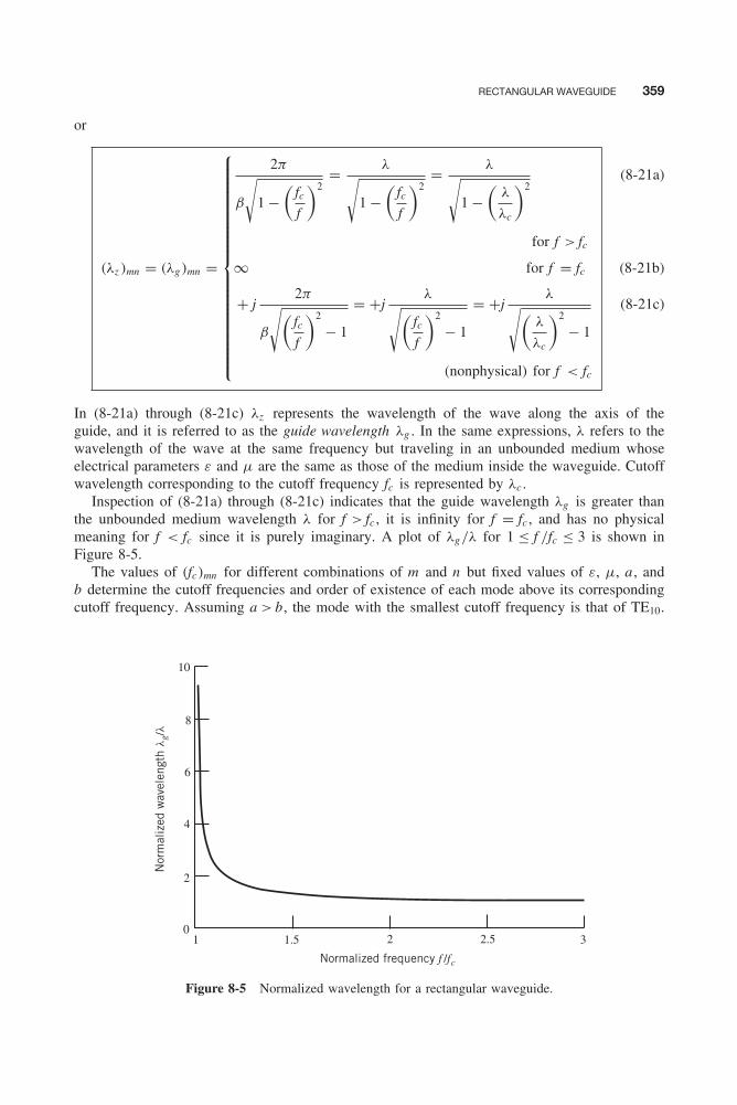
Balanis c08.tex V3 - 11/22/2011 3:32 P.M. Page 359
RECTANGULAR WAVEGUIDE 359
or
(λz )mn = (λg)mn =
⎧⎪⎪⎪⎪⎪⎪⎪⎪⎪⎪⎪⎪⎪⎪⎪⎪⎪⎪⎪⎨⎪⎪⎪⎪⎪⎪⎪⎪⎪⎪⎪⎪⎪⎪⎪⎪⎪⎪⎪⎩
2π
β
√1 −
(fcf
)2= λ√
1 −(
fcf
)2= λ√
1 −(
λ
λc
)2
for f > fc
∞ for f = fc
+ j2π
β
√(fcf
)2
− 1
= +jλ√(
fcf
)2
− 1
= +jλ√(
λ
λc
)2
− 1
(nonphysical) for f < fc
(8-21a)
(8-21b)
(8-21c)
In (8-21a) through (8-21c) λz represents the wavelength of the wave along the axis of theguide, and it is referred to as the guide wavelength λg . In the same expressions, λ refers to thewavelength of the wave at the same frequency but traveling in an unbounded medium whoseelectrical parameters ε and μ are the same as those of the medium inside the waveguide. Cutoffwavelength corresponding to the cutoff frequency fc is represented by λc .
Inspection of (8-21a) through (8-21c) indicates that the guide wavelength λg is greater thanthe unbounded medium wavelength λ for f > fc , it is infinity for f = fc , and has no physicalmeaning for f < fc since it is purely imaginary. A plot of λg/λ for 1 ≤ f /fc ≤ 3 is shown inFigure 8-5.
The values of (fc)mn for different combinations of m and n but fixed values of ε, μ, a , andb determine the cutoff frequencies and order of existence of each mode above its correspondingcutoff frequency. Assuming a > b, the mode with the smallest cutoff frequency is that of TE10.
10
8
6
4
2
01 1.5 2 2.5 3
Nor
mal
ized
wav
elen
gth l
g/l
Normalized frequency f /fc
Figure 8-5 Normalized wavelength for a rectangular waveguide.
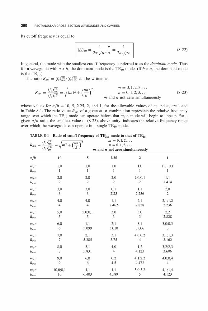
Balanis c08.tex V3 - 11/22/2011 3:32 P.M. Page 360
360 RECTANGULAR CROSS-SECTION WAVEGUIDES AND CAVITIES
Its cutoff frequency is equal to
(fc)10 = 1
2π√
με
π
a= 1
2a√
με(8-22)
In general, the mode with the smallest cutoff frequency is referred to as the dominant mode. Thusfor a waveguide with a > b, the dominant mode is the TE10 mode. (If b > a , the dominant modeis the TE01.)
The ratio Rmn = (fc)TEmn/(fc)
TE10 can be written as
Rmn = (fc)TEmn
(fc)TE10
=√
(m)2 +(na
b
)2 m = 0, 1, 2, 3, . . .n = 0, 1, 2, 3, . . .
m and n not zero simultaneously(8-23)
whose values for a/b = 10, 5, 2.25, 2, and 1, for the allowable values of m and n , are listedin Table 8-1. The ratio value Rmn of a given m , n combination represents the relative frequencyrange over which the TE10 mode can operate before that m , n mode will begin to appear. For agiven a/b ratio, the smallest value of (8-23), above unity, indicates the relative frequency rangeover which the waveguide can operate in a single TE10 mode.
TABLE 8-1 Ratio of cutoff frequency of TEzmn mode to that of TEz
10
Rmn = (fc)TEz
mn
(fc)TEz
10
=√
m2 +(na
b
)2 m = 0, 1, 2, . . .n = 0, 1, 2, . . .
m and n not zero simultaneously
a/b 10 5 2.25 2 1
m , n 1,0 1,0 1,0 1,0 1,0; 0,1Rmn 1 1 1 1 1
m , n 2,0 2,0 2,0 2,0;0,1 1,1Rmn 2 2 2 2 1.414
m , n 3,0 3,0 0,1 1,1 2,0Rmn 3 3 2.25 2.236 2
m , n 4,0 4,0 1,1 2,1 2,1;1,2Rmn 4 4 2.462 2.828 2.236
m , n 5,0 5,0;0,1 3,0 3,0 2,2Rmn 5 5 3 3 2.828
m , n 6,0 1,1 2,1 3,1 3,0;0,3Rmn 6 5.099 3.010 3.606 3
m , n 7,0 2,1 3,1 4,0;0,2 3,1;1,3Rmn 7 5.385 3.75 4 3.162
m , n 8,0 3,1 4,0 1,2 3,2;2,3Rmn 8 5.831 4 4.123 3.606
m , n 9,0 6,0 0,2 4,1;2,2 4,0;0,4Rmn 9 6 4.5 4.472 4
m , n 10,0;0,1 4,1 4,1 5,0;3,2 4,1;1,4Rmn 10 6.403 4.589 5 4.123
Balanis c08.tex V3 - 11/22/2011 3:32 P.M. Page 361
RECTANGULAR WAVEGUIDE 361
Example 8-1
A rectangular waveguide of dimensions a and b (a > b), as shown in Figure 8-3, is to be operated in asingle mode. Determine the smallest ratio of the a/b dimensions that will allow the largest bandwidth ofthe single-mode operation. State the dominant mode and its largest bandwidth of single-mode operation.
Solution: According to (8-16), the dominant mode for a > b is the TE10 whose cutoff frequency isgiven by (8-22), i.e.,
(fc)10 = 1
2a√
με
The mode with the next higher cutoff frequency would be either the TE20 or TE01 mode whose cutofffrequencies are given, respectively, by
(fc)20 = 1
a√
με= 2(fc)10
(fc)01 = 1
2b√
με
It is apparent that the largest bandwidth of single TE10 mode operation would be
(fc)10 ≤ f ≤ 2(fc)10 = (fc)20 ≤ (fc)01
and would occur provided2b ≤ a ⇒ 2 ≤ a/b
8.2.2 Transverse Magnetic (TMz)
A procedure similar to that used for the TEz modes can be used to derive the TMz fields and theother appropriate parameters for a rectangular waveguide of the geometry shown in Figure 8-3.According to (6-55a) and (6-55b) these can be obtained by letting A = âz Az (x , y , z ) and F = 0.Without repeating the entire procedure, the most important equations 6-59, 6-56, and 6-58 aresummarized:
Ex = −j1
ωμε
∂2Az
∂x ∂zHx = 1
μ
∂Az
∂y
Ey = −j1
ωμε
∂2Az
∂y ∂zHy = − 1
μ
∂Az
∂x
Ez = −j1
ωμε
(∂2
∂z 2+ β2
)Az Hz = 0
⎫⎪⎪⎪⎪⎪⎪⎬⎪⎪⎪⎪⎪⎪⎭(8-24)
∇2Az + β2Az = ∂2Az
∂x 2+ ∂2Az
∂y2+ ∂2Az
∂z 2+ β2Az = 0 (8-25)
Az (x , y , z ) = [C1 cos(βx x) + D1 sin(βx x)][C2 cos(βy y) + D2 sin(βy y)]
×[A3e−jβz z + B3e+jβz z ] (8-26)
For waves that travel in the +z direction and satisfy the boundary conditions of Figure 8-3, asoutlined by (8-8a) through (8-8d), (8-26) reduces to
A+z (x , y , z ) = D1D2A3 sin(βx x) sin(βy y)e−jβz z
= Bmn sin(βx x) sin(βy y)e−jβz z (8-26a)
Balanis c08.tex V3 - 11/22/2011 3:32 P.M. Page 362
362 RECTANGULAR CROSS-SECTION WAVEGUIDES AND CAVITIES
where
βx ≡ 2π
λx= mπ
a⇒ λx = 2a
m, m = 1, 2, 3, . . . (8-27a)
βy ≡ 2π
λy= nπ
b⇒ λy = 2b
n, n = 1, 2, 3, . . . (8-27b)
m = 0 and n = 0 are not allowable eigenvalues; they are needed as trivial solutions.Use of (8-26) allows the fields of (8-24) to be written as
E+x = −Bmn
βxβz
ωμεcos(βx x) sin(βy y)e−jβz z (8-28a)
E+y = −Bmn
βyβz
ωμεsin(βx x) cos(βy y)e−jβz z (8-28b)
E+z = −jBmn
β2c
ωμεsin(βx x) sin(βy y)e−jβz z (8-28c)
H +x = Bmn
βy
μsin(βx x) cos(βy y)e−jβz z (8-28d)
H +y = −Bmn
βx
μcos(βx x) sin(βy y)e−jβz z (8-28e)
H +z = 0 (8-28f)
In turn, the wave impedance, propagation constant, cutoff frequency, and guide wavelength canbe expressed as
Z +zw (TMz
mn) ≡ E+x
H +y
= − E+y
H +x
= βz
ωε=
⎧⎪⎪⎪⎪⎪⎪⎪⎪⎪⎨⎪⎪⎪⎪⎪⎪⎪⎪⎪⎩
+ η
√1 −
(fcf
)2
for f > fc
0 for f = fc
− jη
√(fcf
)2
− 1 for f < fc
(8-29a)
(8-29b)
(8-29c)
(βz )mn ≡ 2π
λz=
⎧⎪⎪⎪⎪⎪⎪⎪⎪⎪⎨⎪⎪⎪⎪⎪⎪⎪⎪⎪⎩
β
√1 −
(fcf
)2
for f > fc
0 for f = fc
− jβ
√(fcf
)2
− 1 for f < fc
(8-30a)
(8-30b)
(8-30c)
β2c ≡
(2π
λc
)2
= β2 − β2z = β2
x + β2y =
(mπ
a
)2+
(nπ
b
)2(8-31)
(fc)mn = 1
2π√
με
√(mπ
a
)2+
(nπ
b
)2 m = 1, 2, 3, . . .n = 1, 2, 3, . . .
(8-32)

Balanis c08.tex V3 - 11/22/2011 3:32 P.M. Page 363
RECTANGULAR WAVEGUIDE 363
(λz )mn = (λg)mn =
⎧⎪⎪⎪⎪⎪⎪⎪⎪⎪⎪⎪⎪⎪⎪⎪⎪⎨⎪⎪⎪⎪⎪⎪⎪⎪⎪⎪⎪⎪⎪⎪⎪⎪⎩
λ√1 −
(fcf
)2= λ√
1 −(
λ
λc
)2for f > fc
∞ for f = fc
jλ√(
fcf
)2
− 1
= jλ√(
λ
λc
)2
− 1
(nonphysical) for f < fc
(8-33a)
(8-33b)
(8-33c)
It is apparent from (8-29c) that below cutoff (f < fc) the waveguide for TMzmn modes behaves
as a capacitive storage element. A plot of Z +zw for any TMz
mn mode in the range of 0 ≤ f /fc ≤ 3is shown in Figure 8-4.
For TMz , we can classify the modes according to the order of their cutoff frequency. TheTMz mode with the smallest cutoff frequency, according to (8-32), is the TMz
11 whose cutofffrequency is equal to
(fc)11 = 1
2√
με
√(1
a
)2
+(
1
b
)2
= 1
2a√
με
√1 +
(a
b
)2>
1
2a√
με(8-34)
Since the cutoff frequency of the TMz11 mode, as given by (8-34), is greater than the cutoff
frequency of the TEz10, as given by (8-22), then the TEz
10 mode is always the dominant mode ifa > b. If a = b, the dominant modes are the TEz
10 and TEz01 modes (degenerate), and if a < b
the dominant mode is the TEz01 mode.
The order in which the TMzmn modes occur, relative to the TEz
10 mode, can be determined byforming the ratio Tmn of the cutoff frequency of any TMz
mn mode to the cutoff frequency of theTEz
10 mode. Then we use (8-32) and (8-22) to write that
Tmn = (fc)TMmn
(fc)TE10
=√
m2 +(na
b
)2 m = 1, 2, 3, . . .n = 1, 2, 3, . . .
(8-35)
The values of Tmn for a/b = 10, 5, 2.25, 2, and 1, for the allowable values of m and n , are listedin Table 8-2. Each value of Tmn in Table 8-2 represents the relative frequency range over whichthe TE10 mode can operate before that m , n mode will begin to appear.
For a given ratio of a/b, the values of Rmn of (8-23) and Table 8-1, and those of Tmn of (8-35)and Table 8-2 represent the order, in terms of ascending cutoff frequencies, in which the TEz
mnand TMz
mn modes occur relative to the dominant TEz10 mode.
The xy cross-section field distributions for the first 18 modes [1] of a rectangular waveguidewith cross-sectional dimensions a/b = 2 are plotted in Figure 8-6. Field configurations of another18 modes plus the first 30 for a square waveguide (a/b = 1) can be found in [1].
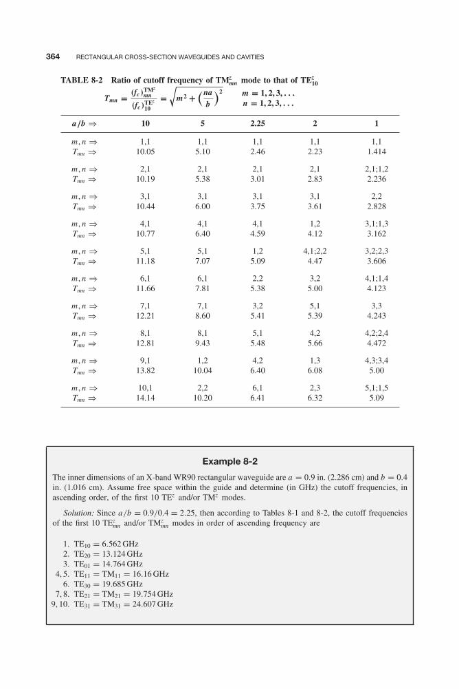
Balanis c08.tex V3 - 11/22/2011 3:32 P.M. Page 364
364 RECTANGULAR CROSS-SECTION WAVEGUIDES AND CAVITIES
TABLE 8-2 Ratio of cutoff frequency of TMzmn mode to that of TEz
10
Tmn = (fc)TMz
mn
(fc)TEz
10
=√
m2 +(na
b
)2 m = 1, 2, 3, . . .n = 1, 2, 3, . . .
a/b ⇒ 10 5 2.25 2 1
m , n ⇒ 1,1 1,1 1,1 1,1 1,1Tmn ⇒ 10.05 5.10 2.46 2.23 1.414
m , n ⇒ 2,1 2,1 2,1 2,1 2,1;1,2Tmn ⇒ 10.19 5.38 3.01 2.83 2.236
m , n ⇒ 3,1 3,1 3,1 3,1 2,2Tmn ⇒ 10.44 6.00 3.75 3.61 2.828
m , n ⇒ 4,1 4,1 4,1 1,2 3,1;1,3Tmn ⇒ 10.77 6.40 4.59 4.12 3.162
m , n ⇒ 5,1 5,1 1,2 4,1;2,2 3,2;2,3Tmn ⇒ 11.18 7.07 5.09 4.47 3.606
m , n ⇒ 6,1 6,1 2,2 3,2 4,1;1,4Tmn ⇒ 11.66 7.81 5.38 5.00 4.123
m , n ⇒ 7,1 7,1 3,2 5,1 3,3Tmn ⇒ 12.21 8.60 5.41 5.39 4.243
m , n ⇒ 8,1 8,1 5,1 4,2 4,2;2,4Tmn ⇒ 12.81 9.43 5.48 5.66 4.472
m , n ⇒ 9,1 1,2 4,2 1,3 4,3;3,4Tmn ⇒ 13.82 10.04 6.40 6.08 5.00
m , n ⇒ 10,1 2,2 6,1 2,3 5,1;1,5Tmn ⇒ 14.14 10.20 6.41 6.32 5.09
Example 8-2
The inner dimensions of an X-band WR90 rectangular waveguide are a = 0.9 in. (2.286 cm) and b = 0.4in. (1.016 cm). Assume free space within the guide and determine (in GHz) the cutoff frequencies, inascending order, of the first 10 TEz and/or TMz modes.
Solution: Since a/b = 0.9/0.4 = 2.25, then according to Tables 8-1 and 8-2, the cutoff frequenciesof the first 10 TEz
mn and/or TMzmn modes in order of ascending frequency are
1. TE10 = 6.562 GHz2. TE20 = 13.124 GHz3. TE01 = 14.764 GHz
4, 5. TE11 = TM11 = 16.16 GHz6. TE30 = 19.685 GHz
7, 8. TE21 = TM21 = 19.754 GHz9, 10. TE31 = TM31 = 24.607 GHz
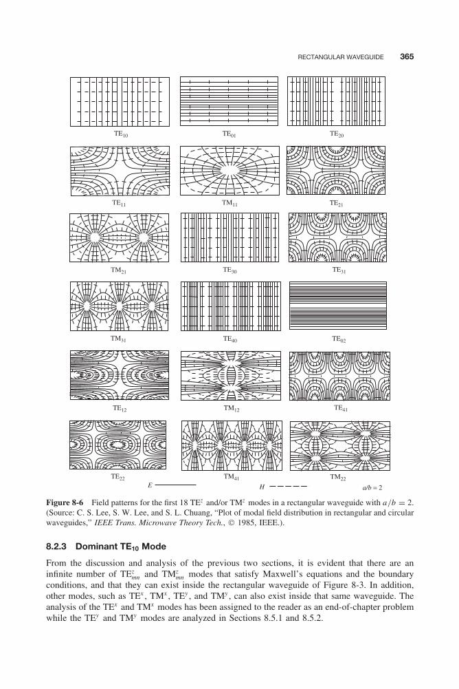
Balanis c08.tex V3 - 11/22/2011 3:32 P.M. Page 365
RECTANGULAR WAVEGUIDE 365
E H
TE10
TE11
TM21
TM31
TE12
TE22
TE01
TM11
TE30
TE40
TM12
TM41
TE20
TE21
TE31
TE02
TE41
TM22
a/b = 2
Figure 8-6 Field patterns for the first 18 TEz and/or TMz modes in a rectangular waveguide with a/b = 2.(Source: C. S. Lee, S. W. Lee, and S. L. Chuang, “Plot of modal field distribution in rectangular and circularwaveguides,” IEEE Trans. Microwave Theory Tech., © 1985, IEEE.).
8.2.3 Dominant TE10 Mode
From the discussion and analysis of the previous two sections, it is evident that there are aninfinite number of TEz
mn and TMzmn modes that satisfy Maxwell’s equations and the boundary
conditions, and that they can exist inside the rectangular waveguide of Figure 8-3. In addition,other modes, such as TEx , TMx , TEy , and TMy , can also exist inside that same waveguide. Theanalysis of the TEx and TMx modes has been assigned to the reader as an end-of-chapter problemwhile the TEy and TMy modes are analyzed in Sections 8.5.1 and 8.5.2.
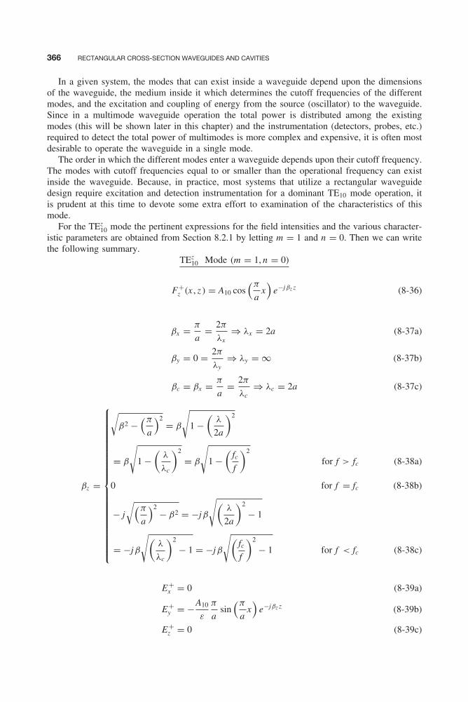
Balanis c08.tex V3 - 11/22/2011 3:32 P.M. Page 366
366 RECTANGULAR CROSS-SECTION WAVEGUIDES AND CAVITIES
In a given system, the modes that can exist inside a waveguide depend upon the dimensionsof the waveguide, the medium inside it which determines the cutoff frequencies of the differentmodes, and the excitation and coupling of energy from the source (oscillator) to the waveguide.Since in a multimode waveguide operation the total power is distributed among the existingmodes (this will be shown later in this chapter) and the instrumentation (detectors, probes, etc.)required to detect the total power of multimodes is more complex and expensive, it is often mostdesirable to operate the waveguide in a single mode.
The order in which the different modes enter a waveguide depends upon their cutoff frequency.The modes with cutoff frequencies equal to or smaller than the operational frequency can existinside the waveguide. Because, in practice, most systems that utilize a rectangular waveguidedesign require excitation and detection instrumentation for a dominant TE10 mode operation, itis prudent at this time to devote some extra effort to examination of the characteristics of thismode.
For the TEz10 mode the pertinent expressions for the field intensities and the various character-
istic parameters are obtained from Section 8.2.1 by letting m = 1 and n = 0. Then we can writethe following summary.
TEz10 Mode (m = 1, n = 0)
F+z (x , z ) = A10 cos
(π
ax)
e−jβz z (8-36)
βx = π
a= 2π
λx⇒ λx = 2a (8-37a)
βy = 0 = 2π
λy⇒ λy = ∞ (8-37b)
βc = βx = π
a= 2π
λc⇒ λc = 2a (8-37c)
βz =
⎧⎪⎪⎪⎪⎪⎪⎪⎪⎪⎪⎪⎪⎪⎪⎪⎪⎪⎪⎪⎪⎪⎨⎪⎪⎪⎪⎪⎪⎪⎪⎪⎪⎪⎪⎪⎪⎪⎪⎪⎪⎪⎪⎪⎩
√β2 −
(π
a
)2= β
√1 −
(λ
2a
)2
= β
√1 −
(λ
λc
)2
= β
√1 −
(fcf
)2
for f > fc
0 for f = fc
− j
√(π
a
)2− β2 = −jβ
√(λ
2a
)2
− 1
= −jβ
√(λ
λc
)2
− 1 = −jβ
√(fcf
)2
− 1 for f < fc
(8-38a)
(8-38b)
(8-38c)
E+x = 0 (8-39a)
E+y = −A10
ε
π
asin
(π
ax)
e−jβz z (8-39b)
E+z = 0 (8-39c)
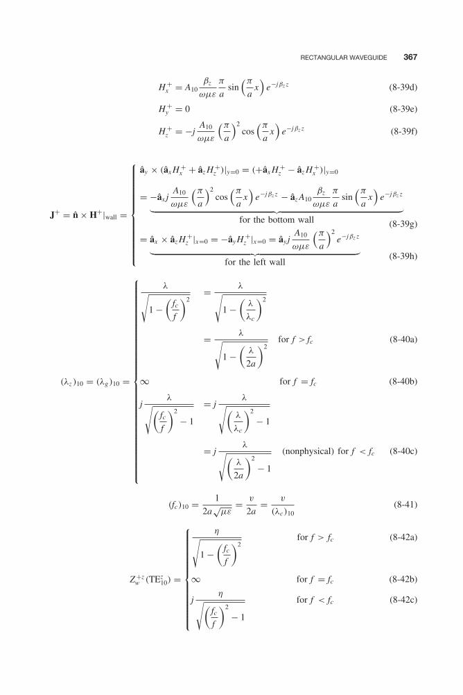
Balanis c08.tex V3 - 11/22/2011 3:32 P.M. Page 367
RECTANGULAR WAVEGUIDE 367
H +x = A10
βz
ωμε
π
asin
(π
ax)
e−jβz z (8-39d)
H +y = 0 (8-39e)
H +z = −j
A10
ωμε
(π
a
)2cos
(π
ax)
e−jβz z (8-39f)
J+ = n̂ × H+|wall =
⎧⎪⎪⎪⎪⎪⎪⎪⎪⎪⎪⎪⎪⎨⎪⎪⎪⎪⎪⎪⎪⎪⎪⎪⎪⎪⎩
ây × (âx H +x + âz H +
z )|y=0 = (+âx H +z − âz H +
x )|y=0
= −âx jA10
ωμε
(π
a
)2cos
(π
ax)
e−jβz z − âz A10βz
ωμε
π
asin
(π
ax)
e−jβz z︸ ︷︷ ︸for the bottom wall
= âx × âz H +z |x=0 = −ây H +
z |x=0 = ây jA10
ωμε
(π
a
)2e−jβz z︸ ︷︷ ︸
for the left wall
(8-39g)
(8-39h)
(λz )10 = (λg)10 =
⎧⎪⎪⎪⎪⎪⎪⎪⎪⎪⎪⎪⎪⎪⎪⎪⎪⎪⎪⎪⎪⎪⎪⎪⎪⎪⎪⎪⎪⎪⎪⎨⎪⎪⎪⎪⎪⎪⎪⎪⎪⎪⎪⎪⎪⎪⎪⎪⎪⎪⎪⎪⎪⎪⎪⎪⎪⎪⎪⎪⎪⎪⎩
λ√1 −
(fcf
)2= λ√
1 −(
λ
λc
)2
= λ√1 −
(λ
2a
)2for f > fc
∞ for f = fc
jλ√(
fcf
)2
− 1
= jλ√(
λ
λc
)2
− 1
= jλ√(
λ
2a
)2
− 1
(nonphysical) for f < fc
(8-40a)
(8-40b)
(8-40c)
(fc)10 = 1
2a√
με= v
2a= v
(λc)10(8-41)
Z +zw (TEz
10) =
⎧⎪⎪⎪⎪⎪⎪⎪⎪⎪⎪⎪⎪⎨⎪⎪⎪⎪⎪⎪⎪⎪⎪⎪⎪⎪⎩
η√1 −
(fcf
)2for f > fc
∞ for f = fc
jη√(
fcf
)2
− 1
for f < fc
(8-42a)
(8-42b)
(8-42c)
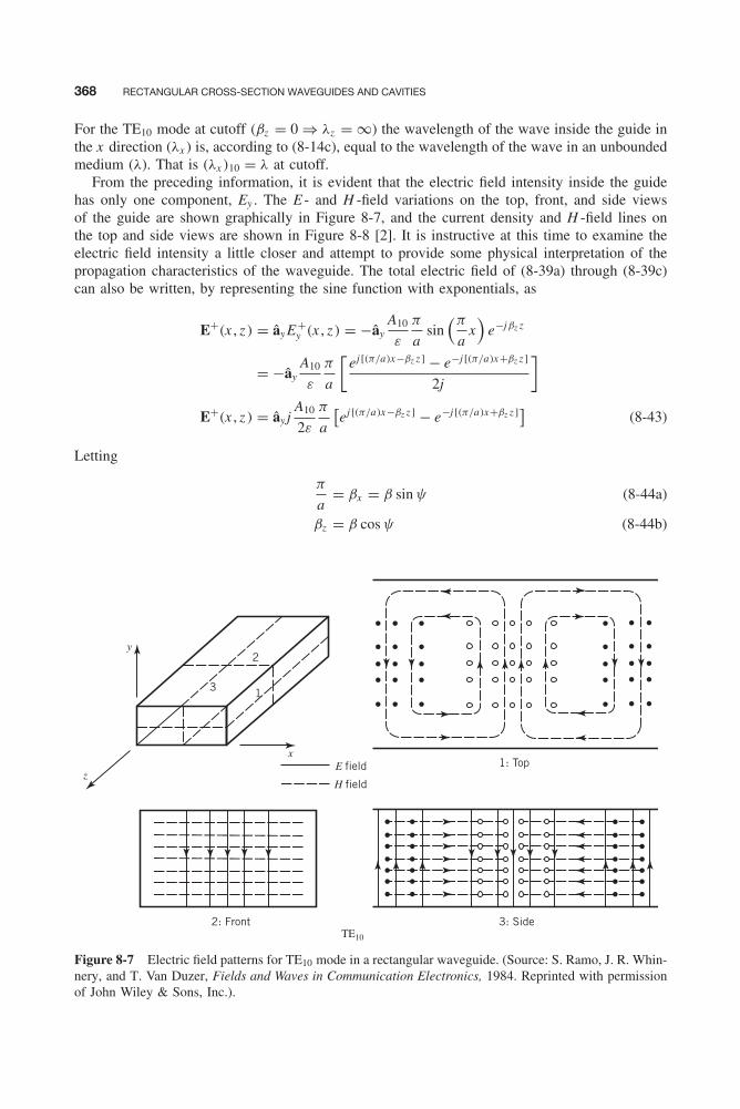
Balanis c08.tex V3 - 11/22/2011 3:32 P.M. Page 368
368 RECTANGULAR CROSS-SECTION WAVEGUIDES AND CAVITIES
For the TE10 mode at cutoff (βz = 0 ⇒ λz = ∞) the wavelength of the wave inside the guide inthe x direction (λx ) is, according to (8-14c), equal to the wavelength of the wave in an unboundedmedium (λ). That is (λx )10 = λ at cutoff.
From the preceding information, it is evident that the electric field intensity inside the guidehas only one component, Ey . The E - and H -field variations on the top, front, and side viewsof the guide are shown graphically in Figure 8-7, and the current density and H -field lines onthe top and side views are shown in Figure 8-8 [2]. It is instructive at this time to examine theelectric field intensity a little closer and attempt to provide some physical interpretation of thepropagation characteristics of the waveguide. The total electric field of (8-39a) through (8-39c)can also be written, by representing the sine function with exponentials, as
E+(x , z ) = ây E+y (x , z ) = −ây
A10
ε
π
asin
(π
ax)
e−jβz z
= −âyA10
ε
π
a
[ej [(π/a)x−βz z ] − e−j [(π/a)x+βz z ]
2j
]E+(x , z ) = ây j
A10
2ε
π
a
[ej [(π/a)x−βz z ] − e−j [(π/a)x+βz z ]] (8-43)
Letting
π
a= βx = β sin ψ (8-44a)
βz = β cos ψ (8-44b)
y
z
3
E field
H field
TE10
2: Front 3: Side
1: Top
2
1
x
Figure 8-7 Electric field patterns for TE10 mode in a rectangular waveguide. (Source: S. Ramo, J. R. Whin-nery, and T. Van Duzer, Fields and Waves in Communication Electronics, 1984. Reprinted with permissionof John Wiley & Sons, Inc.).
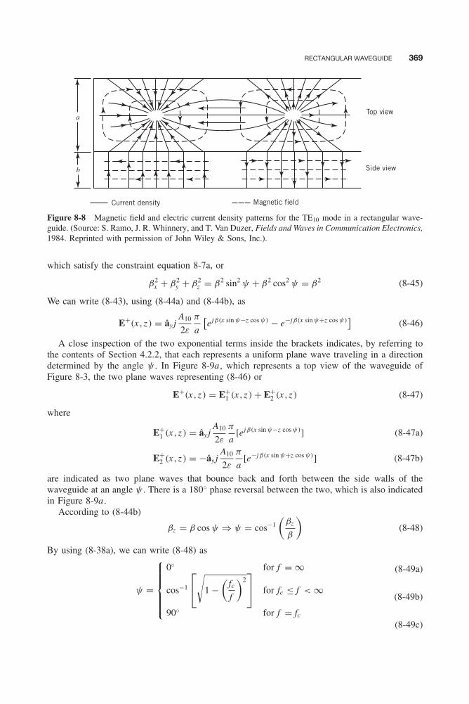
Balanis c08.tex V3 - 11/22/2011 3:32 P.M. Page 369
RECTANGULAR WAVEGUIDE 369
Current density
a
b
Magnetic field
Top view
Side view
Figure 8-8 Magnetic field and electric current density patterns for the TE10 mode in a rectangular wave-guide. (Source: S. Ramo, J. R. Whinnery, and T. Van Duzer, Fields and Waves in Communication Electronics,1984. Reprinted with permission of John Wiley & Sons, Inc.).
which satisfy the constraint equation 8-7a, or
β2x + β2
y + β2z = β2 sin2 ψ + β2 cos2 ψ = β2 (8-45)
We can write (8-43), using (8-44a) and (8-44b), as
E+(x , z ) = ây jA10
2ε
π
a
[ejβ(x sin ψ−z cos ψ) − e−jβ(x sin ψ+z cos ψ)
](8-46)
A close inspection of the two exponential terms inside the brackets indicates, by referring tothe contents of Section 4.2.2, that each represents a uniform plane wave traveling in a directiondetermined by the angle ψ . In Figure 8-9a , which represents a top view of the waveguide ofFigure 8-3, the two plane waves representing (8-46) or
E+(x , z ) = E+1 (x , z ) + E+
2 (x , z ) (8-47)
where
E+1 (x , z ) = ây j
A10
2ε
π
a[ejβ(x sin ψ−z cos ψ)] (8-47a)
E+2 (x , z ) = −ây j
A10
2ε
π
a[e−jβ(x sin ψ+z cos ψ)] (8-47b)
are indicated as two plane waves that bounce back and forth between the side walls of thewaveguide at an angle ψ . There is a 180◦ phase reversal between the two, which is also indicatedin Figure 8-9a .
According to (8-44b)
βz = β cos ψ ⇒ ψ = cos−1
(βz
β
)(8-48)
By using (8-38a), we can write (8-48) as
ψ =
⎧⎪⎪⎪⎪⎨⎪⎪⎪⎪⎩0◦ for f = ∞
cos−1
⎡⎣√1 −
(fcf
)2⎤⎦ for fc ≤ f < ∞
90◦ for f = fc
(8-49a)
(8-49b)
(8-49c)
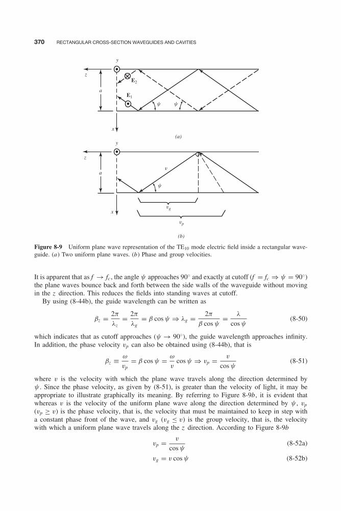
Balanis c08.tex V3 - 11/22/2011 3:32 P.M. Page 370
370 RECTANGULAR CROSS-SECTION WAVEGUIDES AND CAVITIES
E2
E1
y
(a)
(b)
yy
y
z
x
a
y
vg
vp
z
x
av
Figure 8-9 Uniform plane wave representation of the TE10 mode electric field inside a rectangular wave-guide. (a) Two uniform plane waves. (b) Phase and group velocities.
It is apparent that as f → fc , the angle ψ approaches 90◦ and exactly at cutoff (f = fc ⇒ ψ = 90◦)the plane waves bounce back and forth between the side walls of the waveguide without movingin the z direction. This reduces the fields into standing waves at cutoff.
By using (8-44b), the guide wavelength can be written as
βz = 2π
λz= 2π
λg= β cos ψ ⇒ λg = 2π
β cos ψ= λ
cos ψ(8-50)
which indicates that as cutoff approaches (ψ → 90◦), the guide wavelength approaches infinity.In addition, the phase velocity vp can also be obtained using (8-44b), that is
βz ≡ ω
vp= β cos ψ = ω
vcos ψ ⇒ vp = v
cos ψ(8-51)
where v is the velocity with which the plane wave travels along the direction determined byψ . Since the phase velocity, as given by (8-51), is greater than the velocity of light, it may beappropriate to illustrate graphically its meaning. By referring to Figure 8-9b, it is evident thatwhereas v is the velocity of the uniform plane wave along the direction determined by ψ , vp
(vp ≥ v) is the phase velocity, that is, the velocity that must be maintained to keep in step witha constant phase front of the wave, and vg (vg ≤ v) is the group velocity, that is, the velocitywith which a uniform plane wave travels along the z direction. According to Figure 8-9b
vp = v
cos ψ(8-52a)
vg = v cos ψ (8-52b)
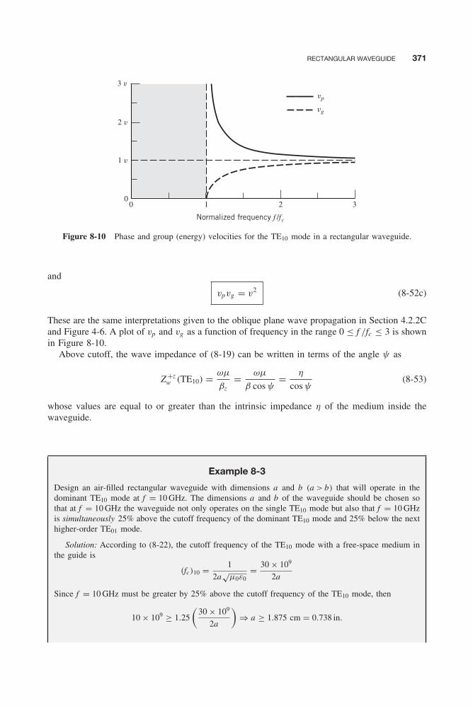
Balanis c08.tex V3 - 11/22/2011 3:32 P.M. Page 371
RECTANGULAR WAVEGUIDE 371
00
1 v
2 v
3 v
vp
vg
1 2 3
Normalized frequency f /fc
Figure 8-10 Phase and group (energy) velocities for the TE10 mode in a rectangular waveguide.
and
vpvg = v2 (8-52c)
These are the same interpretations given to the oblique plane wave propagation in Section 4.2.2Cand Figure 4-6. A plot of vp and vg as a function of frequency in the range 0 ≤ f /fc ≤ 3 is shownin Figure 8-10.
Above cutoff, the wave impedance of (8-19) can be written in terms of the angle ψ as
Z +zw (TE10) = ωμ
βz= ωμ
β cos ψ= η
cos ψ(8-53)
whose values are equal to or greater than the intrinsic impedance η of the medium inside thewaveguide.
Example 8-3
Design an air-filled rectangular waveguide with dimensions a and b (a > b) that will operate in thedominant TE10 mode at f = 10 GHz. The dimensions a and b of the waveguide should be chosen sothat at f = 10 GHz the waveguide not only operates on the single TE10 mode but also that f = 10 GHzis simultaneously 25% above the cutoff frequency of the dominant TE10 mode and 25% below the nexthigher-order TE01 mode.
Solution: According to (8-22), the cutoff frequency of the TE10 mode with a free-space medium inthe guide is
(fc)10 = 1
2a√
μ0ε0= 30 × 109
2a
Since f = 10 GHz must be greater by 25% above the cutoff frequency of the TE10 mode, then
10 × 109 ≥ 1.25
(30 × 109
2a
)⇒ a ≥ 1.875 cm = 0.738 in.
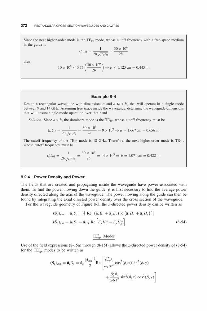
Balanis c08.tex V3 - 11/22/2011 3:32 P.M. Page 372
372 RECTANGULAR CROSS-SECTION WAVEGUIDES AND CAVITIES
Since the next higher-order mode is the TE01 mode, whose cutoff frequency with a free-space mediumin the guide is
(fc)01 = 1
2b√
μ0ε0= 30 × 109
2b
then
10 × 109 ≤ 0.75
(30 × 109
2b
)⇒ b ≤ 1.125 cm = 0.443 in.
Example 8-4
Design a rectangular waveguide with dimensions a and b (a > b) that will operate in a single modebetween 9 and 14 GHz. Assuming free space inside the waveguide, determine the waveguide dimensionsthat will ensure single-mode operation over that band.
Solution: Since a > b, the dominant mode is the TE10, whose cutoff frequency must be
(fc)10 = 1
2a√
μ0ε0= 30 × 109
2a= 9 × 10⁹ ⇒ a = 1.667 cm = 0.656 in.
The cutoff frequency of the TE20 mode is 18 GHz. Therefore, the next higher-order mode is TE01,whose cutoff frequency must be
(fc)01 = 1
2b√
μ0ε0= 30 × 109
2b= 14 × 109 ⇒ b = 1.071 cm = 0.422 in.
8.2.4 Power Density and Power
The fields that are created and propagating inside the waveguide have power associated withthem. To find the power flowing down the guide, it is first necessary to find the average powerdensity directed along the axis of the waveguide. The power flowing along the guide can then befound by integrating the axial directed power density over the cross section of the waveguide.
For the waveguide geometry of Figure 8-3, the z -directed power density can be written as
(Sz )mn = âz Sz = 12 Re
[(âx Ex + ây Ey
) × (âx Hx + ây Hy
)∗](Sz )mn = âz Sz = âz
12 Re
[Ex H ∗
y − Ey H ∗x
](8-54)
TEzmn Modes
Use of the field expressions (8-15a) through (8-15f) allows the z -directed power density of (8-54)for the TEz
mn modes to be written as
(Sz )mn = âz Sz = âz|Amn |2
2Re
[β2
y βz
ωμε2cos2(βx x) sin2(βy y)
+ β2x βz
ωμε2sin2(βx x) cos2(βy y)
]

Balanis c08.tex V3 - 11/22/2011 3:32 P.M. Page 373
RECTANGULAR WAVEGUIDE 373
(Sz )mn = âz Sz = âz |Amn |2 βz
2ωμε2
[β2
y cos2(βx x) sin2(βy y)
+β2x sin2(βx x) cos2(βy y)
](8-55)
The associated power is obtained by integrating (8-55) over a cross section A0 of the guide, or
Pmn =∫∫
A0
(Sz )mn • ds =∫ b
0
∫ a
0(âz Sz ) • (âz dx dy) =
∫ b
0
∫ a
0Sz dx dy (8-56)
Since ∫ a
0cos2
(mπ
ax)
dx ={
a/2 m �= 0a m = 0
(8-56a)∫ a
0sin2
(mπ
ax)
dx ={
a/2 m �= 00 m = 0
(8-56b)
and similar equalities exist for the y variations, (8-56) reduces by using (8-55), (8-56a), and(8-56b) to
PTEz
mn = |Amn |2 βz
2ωμε2
[β2
y
(a
ε0m
)(b
ε0n
)+ β2
x
(a
ε0m
)(b
ε0n
)]= |Amn |2 βz
2ωμε2
(a
ε0m
)(b
ε0n
)(β2
x + β2y )
PTEz
mn = |Amn |2 βz β2c
2ωμε2
(a
ε0m
)(b
ε0n
)= |Amn |2 β2
c
2ηε2
(a
ε0m
)(b
ε0n
)√1 −
(fc,mn
f
)2
(8-57)where
ε0q ={
1 q = 02 q �= 0
(8-57a)
TMzmn Modes
Use of a similar procedure, with (8-28a) through (8-28f), allows us to write that for the TMzmn
modes
(Sz )mn = âz Sz = âz |Bmn |2 βz
2ωεμ2
[β2
x cos2(βx x) sin2(βy y)
+β2y sin2(βx x) cos2(βy y)
](8-58)
PTMz
mn = |Bmn |2 β2c η
2μ2
(a
2
)(b
2
)√1 −
(fc,mn
f
)2
(8-59)
By the use of superposition, the total power associated with a wave is equal to the sum of allthe power components associated with each mode that exists inside the waveguide. Thus
Ptotal =∑m ,n
PTEz
mn +∑m ,n
PTMz
mn (8-60)
where PTEz
mn and PTMz
mn are given, respectively, by (8-57) and (8-59).
Balanis c08.tex V3 - 11/22/2011 3:32 P.M. Page 374
374 RECTANGULAR CROSS-SECTION WAVEGUIDES AND CAVITIES
Example 8-5
The inside dimensions of an X-band WR90 waveguide are a = 0.9 in. (2.286 cm) and b = 0.4 in. (1.016cm). Assume that the waveguide is air-filled and operates in the dominant TE10 mode, and that the airwill break down when the maximum electric field intensity is 3 × 10⁶ V/m. Find the maximum powerthat can be transmitted at f = 9 GHz in the waveguide before air breakdown occurs.
Solution: Since air will break down when the maximum electric field intensity in the waveguidereaches 3 × 10⁶ V/m, then according to (8-39b)∣∣Ey
∣∣max = |A10|
ε0
π
a
∣∣∣sin(π
ax)∣∣∣
max= A10
ε0
π
a= 3 × 10⁶ ⇒ A10 = 1.933 × 10⁻⁷
By using (8-57)
PTE10 = |A10|2
(βc)210
2η0ε20
(a
ε01
)(b
ε00
)√1 −
[(fc)10
f
]2
Since the cutoff frequency of the dominant TE10 mode is
(fc)10 = 1
2a√
μ0ε0= 30 × 109
2(2.286)= 6.562 GHz
and(βc)10 = π
a
then
PTE10 = (1.933 × 10⁻⁷)2 (π/2.286 × 10−2)2
2(377)(8.854 × 10⁻¹²)2
(2.286 × 10⁻²
2
)
×(
1.016 × 10⁻²
1
)√1 −
(6.562
9
)2
PTE10 = 948.9 × 10³ W = 948.9 kW
8.2.5 Attenuation
Ideally, if the waveguide were made out of a perfect conductor, there would not be any atten-uation associated with the guide above cutoff. Below cutoff, the fields reduce to evanescent(nonpropagating) waves that are highly attenuated. In practice, however, no perfect conductorsexist, although many (such as metals) are very good conductors, with conductivities on the orderof 107 –108 S/m. For waveguides made out of such conductors (metals), there must be some atten-uation due to the conduction (ohmic) losses in the waveguides themselves. This is accountedfor by introducing an attenuation coefficient αc . Another factor that contributes to the waveguideattenuation is the losses associated with lossy dielectric materials that are inserted inside theguide. These losses are referred to as dielectric losses and are accounted for by introducing anattenuation coefficient αd .
A. Conduction (Ohmic) Losses To find the losses associated with a waveguide whose wallsare not perfectly conducting, a new boundary-value problem must be solved. That problem wouldbe the same one shown in Figure 8-3 but with nonperfectly conducting walls. To solve such aproblem exactly is an ambitious and complicated task. Instead an alternate procedure is almostalways used whereby the solution is obtained using a perturbational method. With that method,

Balanis c08.tex V3 - 11/22/2011 3:32 P.M. Page 375
RECTANGULAR WAVEGUIDE 375
it is assumed that the fields inside the waveguide with lossy walls, but of very high conductivity,are slightly perturbed from those of perfectly conducting walls. The differences between the twosets of fields are so small that the fields are usually assumed to be essentially the same. However,the walls themselves are considered as lossy surfaces represented by a surface impedance Zs
given by (4-42), or
Zs = Rs + jXs =√
jωμ
σ + jωε
σ�ωε�√
jωμ
σ=
√ωμ
2σ(1 + j ) (8-61)
The power Pc absorbed and dissipated as heat by each surface (wall) Am of the waveguide isobtained using an expression analogous to I 2R/2 used in lumped-circuit theory, that is
Pc = Rs
2
∫∫Am
Js • J∗s ds (8-62)
whereJs � n̂ × H|surface (8-62a)
In (8-62a), Js represents the linear current density in (A/m) induced on the surface of a lossyconductor, as discussed in Example 5-7, and illustrated graphically in Figure 5-11.
Once the total conduction power Pc dissipated as heat on the waveguide has been found byapplying (8-62) on all four walls of the guide, the next step is to define and derive an expressionfor the attenuation coefficient αc . This can be accomplished by referring to Figure 8-11, whichrepresents the lossy waveguide in its axial direction. If P0 represents the power at some referencepoint (e.g., z = 0), then the power Pmn at some other point z is related to P0 (Pmn at z = 0) by
Pmn(z ) = Pmn |z=0e−2αc z = P0e−2αc z (8-63)
The negative rate of change (with respect to z ) of Pmn represents the dissipated power perunit length. Thus, for a length � of a waveguide, the total dissipated power Pc is found using
Pc = −zdPmn
dz
∣∣∣∣z=�
= −zd
dz
(P0e−2αc z
)∣∣∣∣z=�
= 2αczP0e−2αc z∣∣z=�
Pc = 2αc�Pmn (8-64)
b
a
z
y
x
z = 0
P0Pmn = P0 e−2acz
z = ll
Figure 8-11 Rectangular waveguide geometry for attenuation constant derivation.
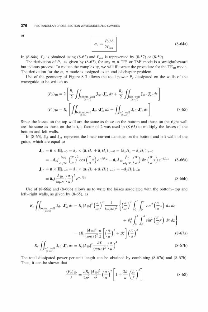
Balanis c08.tex V3 - 11/22/2011 3:32 P.M. Page 376
376 RECTANGULAR CROSS-SECTION WAVEGUIDES AND CAVITIES
or
αc = Pc/�
2Pmn(8-64a)
In (8-64a), Pc is obtained using (8-62) and Pmn is represented by (8-57) or (8-59).The derivation of Pc , as given by (8-62), for any m , n TEz or TMz mode is a straightforward
but tedious process. To reduce the complexity, we will illustrate the procedure for the TE10 mode.The derivation for the m, n mode is assigned as an end-of-chapter problem.
Use of the geometry of Figure 8-3 allows the total power Pc dissipated on the walls of thewaveguide to be written as
(Pc)10 = 2
[Rs
2
∫∫bottom wall
(y=0)
Jsb • J∗sb ds + Rs
2
∫∫left wall(x=0)
Js� • J∗s� ds
]
(Pc)10 = Rs
[∫∫bottom wall
(y=0)
Jsb • J∗sb ds +
∫∫left wall(x=0)
Js� • J∗s� ds
](8-65)
Since the losses on the top wall are the same as those on the bottom and those on the right wallare the same as those on the left, a factor of 2 was used in (8-65) to multiply the losses of thebottom and left walls.
In (8-65), Jsb and Js� represent the linear current densities on the bottom and left walls of theguide, which are equal to
Jsb = n̂ × H|y=0 = ây × (âx Hx + âz Hz )|y=0 = (âx Hz − âz Hx )|y=0
= −âx jA10
ωμε
(π
a
)2cos
(π
ax)
e−jβz z − âz A10βz
ωμε
(π
a
)sin
(π
ax)
e−jβz z (8-66a)
Js� = n̂ × H|x=0 = âx × (âx Hx + âz Hz )|x=0 = −ây Hz |x=0
= ây jA10
ωμε
(π
a
)2e−jβz z (8-66b)
Use of (8-66a) and (8-66b) allows us to write the losses associated with the bottom–top andleft–right walls, as given by (8-65), as
Rs
∫∫bottom wall
(y=0)
Jsb • J∗sb ds = Rs |A10|2
(π
a
)2 1
(ωμε)2
{(π
a
)2∫ �
0
∫ a
0cos2
(π
ax)
dx dz
+ β2z
∫ �
0
∫ a
0sin2
(π
ax)
dx dz
}= �Rs
|A10|2(ωμε)2
a
2
[(π
a
)2+ β2
z
] (π
a
)2(8-67a)
Rs
∫∫left wall(x=0)
Js� • J∗s� ds = Rs |A10|2 b�
(ωμε)2
(π
a
)4(8-67b)
The total dissipated power per unit length can be obtained by combining (8-67a) and (8-67b).Thus, it can be shown that
(Pc)10
�= aRs
2η2
|A10|2ε2
(π
a
)2[
1 + 2b
a
(fcf
)2]
(8-68)

Balanis c08.tex V3 - 11/22/2011 3:32 P.M. Page 377
RECTANGULAR WAVEGUIDE 377
By using (8-57) for m = 1 and n = 0, and (8-68), the attenuation coefficient of (8-64a) forthe TE10 mode can be written as
(αc)10 =[(Pc)10/�
2Pmn
]m=1n=0
=
aRs
2η2
|A10|2ε2
(π
a
)2[
1 + 2b
a
(fcf
)2]
|A10|2 β2c
ηε2
(a
2
)(b)
√1 −
(fcf
)2(8-69)
which reduces to
(αc)10 = Rs
ηb
[1 + 2b
a
(fcf
)2]
√1 −
(fcf
)2(in Np/m) (8-69a)
For an X-band WR waveguide with inner dimensions a = 0.9 in. (2.286 cm) and b = 0.4 in.(1.016 cm), made of copper (σ = 5.7 × 10⁷S/m) and filled with a lossless dielectric, we can plotthe attenuation coefficient (αc)10 (in Np/m and dB/m) for ε = ε0, 2.56ε0, and 4ε0 as shown inFigure 8-12. The attenuation coefficient for any mode (TEmn or TMmn ) is given by
TEzmn
(αc)mn = 2Rs
εmεnbη
√1 −
(fc,mn
f
)2
{(εm + εn
b
a
)(fc,mn
f
)2
+b
a
[1 −
(fc,mn
f
)2]
m2ab + (na)2
(mb)2 + (na)2
} (8-70a)
0.06
0.05
0.04
0.03
0.02
0.01
00 4 8 12 16 20 24 28 32
0
0.1
0.2
0.3
0.4
0.5
Frequency (GHz)
a = 0.9 in. (2.286 cm)b = 0.4 in. (1.016 cm)s = 5.7 × 10⁷ S/m
e = 4ε0
ε = ε0e = 2.56ε0
ac
(Np/
m)
ac
(dB
/m)
Figure 8-12 TE10 mode attenuation constant for the X-band rectangular waveguide.

Balanis c08.tex V3 - 11/22/2011 3:32 P.M. Page 378
378 RECTANGULAR CROSS-SECTION WAVEGUIDES AND CAVITIES
where
εp ={
2 p = 0
1 p �= 0(8-70b)
TMzmn
(αc)mn = 2Rs
abη
√1 −
(fc,mn
f
)2
m2b3 + n2a3
(mb)2 + (na)2(8-70c)
The most pertinent equations used to describe the characteristics of TEmn and TMmn modesinside a rectangular waveguide are summarized in Table 8-3.
B. Dielectric Losses When waveguides are filled with lossy dielectric material, an additionalattenuation constant must be introduced to account for losses in the dielectric material and areusually designated as dielectric losses . Thus, the total attenuation constant αt for the waveguideabove cutoff is given by
αt = αc + αd (8-71)
where αt = total attenuation constantαc = ohmic losses attenuation constant [(8-70a) and (8-70c)]αd = dielectric losses attenuation constant
To derive αd , let us refer to the constraint equation (8-7a), which, for a lossy medium (β = β̇e),can be written for the complex β̇z as
β̇2z = β̇2
e − (β2x + β2
y ) = β̇2e − β2
c (8-72)
or
β̇z =√
β̇2e − β2
c =√
ω2με̇e − β2c =
√ω2μ(ε′
e − jε′′e ) − β2
c
=√
(ω2με′e − β2
c ) − jω2με′′e =
√(β ′2
e − β2c ) − jωμσe
β̇z =√
β ′2e − β2
c
[1 − j
ωμσe
β ′2e − β2
c
]1/2
(8-72a)
whereβ ′
e = ω√
με′e (8-72b)
By using the binomial expansion, (8-72a) can be approximated by
β̇z �√
β ′2e − β2
c
[1 − j
ωμσe
2(β ′2e − β2
c )
]=
√β ′2
e − β2c − j
ωμσe
2√
β ′2e − β2
c
� β ′e
√1 −
(fcf
)2
− jωμσe
2β ′e
√1 −
(fcf
)2
Balanis c08.tex V3 - 11/22/2011 3:32 P.M. Page 379
RECTANGULAR WAVEGUIDE 379
TABLE 8-3 Summary of TEzmn and TMz
mn mode characteristics of rectangular waveguide
TEzmn
⎛⎝ m = 0, 1, 2, . . .
n = 0, 1, 2, . . .m and n not both zero simultaneously
⎞⎠ TMz
mn
(m = 1, 2, 3, . . .n = 1, 2, 3, . . .
)
E+x Amn
nπ
bεcos
(mπ
ax)
sin(nπ
by)
e−jβz z −Bmnmπβz
aωμεcos
(mπ
ax)
sin(nπ
by)
e−jβz z
E+y −Amn
mπ
aεsin
(mπ
ax)
cos(nπ
by)
e−jβz z −Bmnnπβz
bωμεsin
(mπ
ax)
cos(nπ
by)
e−jβz z
E+z 0 −jBmn
β2c
ωμεsin
(mπ
ax)
sin(nπ
by)
e−jβz z
H +x Amn
mπβz
aωμεsin
(mπ
ax)
cos(nπ
by)
e−jβz z Bmnnπ
bμsin
(mπ
ax)
cos(nπ
by)
e−jβz z
H +y Amn
nπβz
bωμεcos
(mπ
ax)
sin(nπ
by)
e−jβz z −Bmnmπ
aμcos
(mπ
ax)
sin(nπ
by)
e−jβz z
H +z −jAmn
β2c
ωμεcos
(mπ
ax)
cos(nπ
by)
e−jβz z 0
βc
√β2
x + β2y =
√(mπ
a
)2 +(nπ
b
)2
fc1
2π√
με
√(mπ
a
)2 +(nπ
b
)2
λc2π√(mπ
a
)2 +(nπ
b
)2
βz (f ≥ fc) β
√1 −
(fcf
)2
λg (f ≥ fc)λ√
1 −(
fcf
)2= λ√
1 −(
λ
λc
)2
vp(f ≥ fc)v√
1 −(
fcf
)2= v√
1 −(
λ
λc
)2
Zw(f ≥ fc)η√
1 −(
fcf
)2= η√
1 −(
λ
λc
)2η
√1 −
(fcf
)2
= η
√1 −
(λ
λc
)2
Zw(f ≤ fc) jη√(
fcf
)2
− 1
= jη√(
λ
λc
)2
− 1
−jη
√(fcf
)2
− 1 = −jη
√(λ
λc
)2
− 1
(αc)mn2Rs
bη
√1 −
(fc,mn
f
)2
{(εm + εn
b
a
)(fc,mn
f
)2 2Rs
abη
√1 −
(fc,mn
f
)2
m2b3 + n2a3
(mb)2 + (na)2
+b
a
[1 −
(fc,mn
f
)2]
m2ab + (na)2
(mb)2 + (na)2
}
where εp ={
2 p = 01 p �= 0
Balanis c08.tex V3 - 11/22/2011 3:32 P.M. Page 380
380 RECTANGULAR CROSS-SECTION WAVEGUIDES AND CAVITIES
β̇z � ω√
με′e
√1 −
(fcf
)2
− jωμσe
2ω√
με′e
√1 −
(fcf
)2
β̇z � ω√
με′e
√1 −
(fcf
)2
− jη′
e
2
σe√1 −
(fcf
)2(8-73)
where
η′e =
√μ
ε′e
(8-73a)
Let us define the complex β̇z as
β̇z ≡ βd − jαd � β ′e
√1 −
(fcf
)2
− jη′
e
2
σe√1 −
(fcf
)2(8-74)
or
αd ≡ attenuation constant � η′e
2
σe√1 −
(fcf
)2(8-74a)
βd ≡ phase constant � β ′e
√1 −
(fcf
)2
(8-74b)
Another form of (8-74a) would be to write it as
αd � η′e
2
σe√1 −
(fcf
)2= 1
2
√μ
ε′e
ωε′′e√
1 −(
fcf
)2
� 1
2
ε′′e
ε′e
ω√
με′e√
1 −(
fcf
)2= 1
2
ε′′e
ε′e
β ′e√
1 −(
fcf
)2
� 1
2
ε′′e
ε′e
2π
λ
√1 −
(fcf
)2= π
λ
ε′′e
ε′e
1√1 −
(fcf
)2
αd � ε′′e
ε′e
π
λ2
λ√1 −
(fcf
)2= ε′′
e
ε′e
π
λ
(λg
λ
), in Np/m (λ in meters) (8-75)
where λ is the wavelength inside an unbounded infinite lossy dielectric medium and λg is theguide wavelength filled with the lossy dielectric material. In decibels, αd of (8-75) can be writtenas
αd � 8.68
(ε′′
e
ε′e
)π
λ
(λg
λ
)= 27.27
λ
(ε′′
e
ε′e
)(λg
λ
), in dB/m (λ in meters) (8-75a)
Balanis c08.tex V3 - 11/22/2011 3:32 P.M. Page 381
RECTANGULAR WAVEGUIDE 381
Example 8-6
An X-band (8.2–12.4 GHz) rectangular waveguide is filled with polystyrene whose electrical propertiesat 6 GHz are εr = 2.56 and tan δe = 2.55 × 10⁻⁴. Determine the dielectric attenuation at a frequencyof f = 6 GHz when the inside dimensions of the waveguide are a = 0.9 in. (2.286 cm) and b = 0.4 in.(1.016 cm). Assume TE10 mode propagation.
Solution: According to (2-68a)
tan δe = ε′′e
ε′e
= 2.55 × 10⁻⁴
At f = 6 GHz,
λ0 = 30 × 109
6 × 109= 5 cm λ = λ0√
εr= 5√
2.56= 3.125 cm
(fc)10 = 1
2a√
με= 30 × 109
2(2.286)(1.6)= 4.10 GHz
λg = λ√1 −
(fcf
)2= 3.125√
1 − ( 4.106
)2= 4.280 cm
Thus, the dielectric attenuation of (8-75) is equal to
αd = ε′′e
ε′e
π
λ
(λg
λ
)= 2.55 × 10⁻⁴
( π
3.125
)(4.280
3.125
)= 3.511 × 10⁻⁴ Np/cm
= 3.511 × 10⁻² Np/m = 30.476 × 10⁻² dB/m
C. Coupling Whenever a given mode is to be excited or detected, the excitation or detectionscheme must be such that it maximizes the energy exchange or transfer between the source andthe guide or the guide and the receiver. Typically, there are a number of techniques that can beused to accomplish this. Some suggested methods that are popular in practice are the following.
1. If the energy exchange is from one waveguide to another, use an iris or hole placed in alocation and orientation so that the field distribution of both guides over the extent of thehole or iris are almost identical.
2. If the energy exchange is from a transmission line, such as a coaxial line, to a waveguide, orvice versa, use a linear probe or antenna oriented so that its length is parallel to the electricfield lines in the waveguide and placed near the maximum of the electric field mode pattern,as shown in Figure 8-13a . This is usually referred to as electric field coupling . Sometimesthe position is varied slightly to achieve better impedance matching.
3. If the energy transfer is from a transmission line, such as a coaxial line, to a waveguide,or vice versa, use a loop antenna oriented so that the plane of the loop is perpendicular tothe magnetic field lines, as shown in Figure 8-13c. This is usually referred to as magneticfield coupling .
4. If the energy transfer is from a transmission line, such as a two-conductor line, or othersources to a waveguide, or vice versa, use the transmission line or other sources so thatthey excite currents on the waveguide that match those of the desired modes in the guide.
5. A number of probes, antennas, or transmission lines properly phased can also be used toexcite or detect any mode, especially higher-order modes. Shown in Figure 8-13 are some

Balanis c08.tex V3 - 11/22/2011 3:32 P.M. Page 382
382 RECTANGULAR CROSS-SECTION WAVEGUIDES AND CAVITIES
b
a
(b)
(d)
(f)
(a)
(c)
(e)
4
λg
b
b
b
b
b
4
λg 4a
2a 4
a
a
a
Figure 8-13 Coaxial transmission line to rectangular waveguide coupling. (a) The side and (b) theend views of the coax to waveguide electric field coupling for the TE10 mode. (c) The side and (d ) the endview for the coax to waveguide magnetic field coupling for the TE10 mode. (e) The side and (f ) theend view for the coax to waveguide electric field coupling for the TE20 mode.
typical arrangements for coupling energy from a transmission line, such as a coax, to arectangular waveguide to excite or detect the TE10 and TE20 modes.
The sizes, flanges, frequency bands, and other parameters pertaining to rectangular waveguideshave been standardized so that uniformity is maintained throughout the industry. Standardizedreference data on rectangular waveguides are displayed in Table 8-4.
8.3 RECTANGULAR RESONANT CAVITIES
Waveguide cavities represent a very important class of microwave components. Their applicationsare numerous and range from use as frequency meters to cavities for measuring the electricalproperties of material. The attractive characteristics of waveguide cavities are their very highquality factors Q , typically on the order of 5,000–10,000, and their simplicity of constructionand use. The most common geometries of cavities are rectangular, cylindrical, and spherical. Therectangular geometry will be discussed in this chapter, whereas the cylindrical will be examinedin Chapter 9, and the spherical will be analyzed in Chapter 10.
A rectangular waveguide cavity is formed by taking a section of a waveguide and enclosing itsfront and back faces with conducting plates, as shown in Figure 8-14. Coupling into and out ofthe cavities is done through coupling probes or holes. The coupling probes may be either electricor magnetic, as shown in Figures 8-13a and 8-13c, whereas coupling holes may also be usedeither on the front, back, top, or bottom walls.
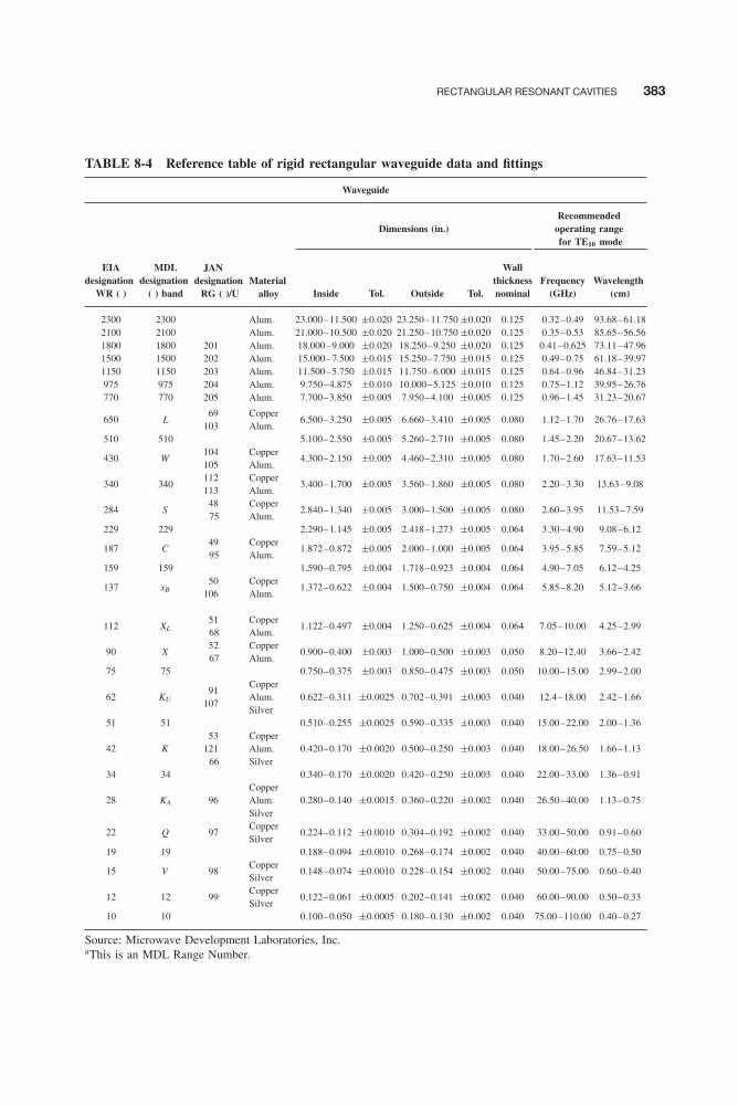
Balanis c08.tex V3 - 11/22/2011 3:32 P.M. Page 383
RECTANGULAR RESONANT CAVITIES 383
TABLE 8-4 Reference table of rigid rectangular waveguide data and fittings
Waveguide
RecommendedDimensions (in.) operating range
for TE10 mode
EIA MDL JAN Walldesignation designation designation Material thickness Frequency Wavelength
WR ( ) ( ) band RG ( )/U alloy Inside Tol. Outside Tol. nominal (GHz) (cm)
2300 2300 Alum. 23.000–11.500 ±0.020 23.250–11.750 ±0.020 0.125 0.32–0.49 93.68–61.182100 2100 Alum. 21.000–10.500 ±0.020 21.250–10.750 ±0.020 0.125 0.35–0.53 85.65–56.561800 1800 201 Alum. 18.000–9.000 ±0.020 18.250–9.250 ±0.020 0.125 0.41–0.625 73.11–47.961500 1500 202 Alum. 15.000–7.500 ±0.015 15.250–7.750 ±0.015 0.125 0.49–0.75 61.18–39.971150 1150 203 Alum. 11.500–5.750 ±0.015 11.750–6.000 ±0.015 0.125 0.64–0.96 46.84–31.23975 975 204 Alum. 9.750–4.875 ±0.010 10.000–5.125 ±0.010 0.125 0.75–1.12 39.95–26.76770 770 205 Alum. 7.700–3.850 ±0.005 7.950–4.100 ±0.005 0.125 0.96–1.45 31.23–20.67
650 L69
103CopperAlum.
6.500–3.250 ±0.005 6.660–3.410 ±0.005 0.080 1.12–1.70 26.76–17.63
510 510 5.100–2.550 ±0.005 5.260–2.710 ±0.005 0.080 1.45–2.20 20.67–13.62
430 W104105
CopperAlum.
4.300–2.150 ±0.005 4.460–2.310 ±0.005 0.080 1.70–2.60 17.63–11.53
340 340112113
CopperAlum.
3.400–1.700 ±0.005 3.560–1.860 ±0.005 0.080 2.20–3.30 13.63–9.08
284 S4875
CopperAlum.
2.840–1.340 ±0.005 3.000–1.500 ±0.005 0.080 2.60–3.95 11.53–7.59
229 229 2.290–1.145 ±0.005 2.418–1.273 ±0.005 0.064 3.30–4.90 9.08–6.12
187 C4995
CopperAlum.
1.872–0.872 ±0.005 2.000–1.000 ±0.005 0.064 3.95–5.85 7.59–5.12
159 159 1.590–0.795 ±0.004 1.718–0.923 ±0.004 0.064 4.90–7.05 6.12–4.25
137 xB50
106CopperAlum.
1.372–0.622 ±0.004 1.500–0.750 ±0.004 0.064 5.85–8.20 5.12–3.66
112 XL5168
CopperAlum.
1.122–0.497 ±0.004 1.250–0.625 ±0.004 0.064 7.05–10.00 4.25–2.99
90 X5267
CopperAlum.
0.900–0.400 ±0.003 1.000–0.500 ±0.003 0.050 8.20–12.40 3.66–2.42
75 75 0.750–0.375 ±0.003 0.850–0.475 ±0.003 0.050 10.00–15.00 2.99–2.00
62 KU91
107
CopperAlum.Silver
0.622–0.311 ±0.0025 0.702–0.391 ±0.003 0.040 12.4–18.00 2.42–1.66
51 51 0.510–0.255 ±0.0025 0.590–0.335 ±0.003 0.040 15.00–22.00 2.00–1.36
42 K53
12166
CopperAlum.Silver
0.420–0.170 ±0.0020 0.500–0.250 ±0.003 0.040 18.00–26.50 1.66–1.13
34 34 0.340–0.170 ±0.0020 0.420–0.250 ±0.003 0.040 22.00–33.00 1.36–0.91
28 KA 96CopperAlum.Silver
0.280–0.140 ±0.0015 0.360–0.220 ±0.002 0.040 26.50–40.00 1.13–0.75
22 Q 97CopperSilver
0.224–0.112 ±0.0010 0.304–0.192 ±0.002 0.040 33.00–50.00 0.91–0.60
19 19 0.188–0.094 ±0.0010 0.268–0.174 ±0.002 0.040 40.00–60.00 0.75–0.50
15 V 98CopperSilver
0.148–0.074 ±0.0010 0.228–0.154 ±0.002 0.040 50.00–75.00 0.60–0.40
12 12 99CopperSilver
0.122–0.061 ±0.0005 0.202–0.141 ±0.002 0.040 60.00–90.00 0.50–0.33
10 10 0.100–0.050 ±0.0005 0.180–0.130 ±0.002 0.040 75.00–110.00 0.40–0.27
Source: Microwave Development Laboratories, Inc.aThis is an MDL Range Number.

Balanis c08.tex V3 - 11/22/2011 3:32 P.M. Page 384
384 RECTANGULAR CROSS-SECTION WAVEGUIDES AND CAVITIES
Waveguide Fittings
Theoretical Theoretical
Cutoff for attenuation C/W power
TE10 mode lowest to rating Flange
highest lowest to EJA
Frequency Wavelength Range in Range in frequency highest Choke Cover designation
(GHz) (cm) 2λλc
λgλ (dB/100 ft) frequency (MW) UG( )/U UG( )/U WR ( )
0.256 116.84 1.60–1.05 1.68–1.17 0.051–0.031 153.0–212.0 2300
0.281 106.68 1.62–1.06 1.68–1.18 0.054–0.034 120.0–173.0 FA168Aa 2100
0.328 91.44 1.60–1.05 1.67–1.18 0.056–0.038 93.4–131.9 1800
0.393 76.20 1.61–1.05 1.62–1.17 0.069–0.050 67.6–93.3 1500
0.513 58.42 1.60–1.07 1.82–1.18 0.128–0.075 35.0–53.8 1150
0.605 49.53 1.61–1.08 1.70–1.19 0.137–0.095 27.0–38.5 975
0.766 39.12 1.60–1.06 1.66–1.18 0.201–0.136 17.2–24.1 770
0.908 33.02 1.62–1.07 1.70–1.180.317–0.212
0.269–0.17811.9–17.2
417A
418A650
1.157 25.91 1.60–1.05 1.67–1.18 510
1.372 21.84 1.61–1.06 1.70–1.180.588–0.385
0.501–0.3305.2–7.5
435A
437A430
1.736 17.27 1.58–1.05 1.78–1.220.877–0.572
0.751–0.4923.1–4.5
553
554340
2.078 14.43 1.60–1.05 1.67–1.171.102–0.752
0940–0.6412.2–3.2
54A
585
53
584284
2.577 11.63 1.56–1.05 1.62–1.17 229
3.152 9.510 1.60–1.08 1.67–1.192.08–1.44
1.77–1.121.4–2.0
148B
406A
149A
407187
3.711 8.078 1.51–1.05 1.52–1.19 159
4.301 6.970 1.47–1.05 1.48–1.172.87–2.30
2.45–1.940.56–0.71
343A
440A
344
441137
5.259 5.700 1.49–1.05 1.51–1.174.12–3.21
3.50–2.740.35–0.46
52A
137A
51
138112
6.557 4.572 1.60–1.06 1.68–1.186.45–4.48
5.49–3.830.20–0.29
40A
136A
39
13590
7.868 3.810 1.57–1.05 1.64–1.17 75
9.51–8.31 541 419
9.486 3.160 1.53–1.05 1.55–1.18 0.12–0.16 FA190Aa FA191Aa 62
6.14–5.36
11.574 2.590 1.54–1.05 1.58–1.18 51
14.047 2.134 1.56–1.06 1.60–1.1820.7–14.8
17.6–12.6
13.3–9.5
0.043–0.058596
598
595
59742
17.328 1.730 1.57–1.05 1.62–1.18 34
600 599
21.081 1.422 1.59–1.05 1.65–1.17 0.022–0.031 FA1241Aa FA1242Aa 28
21.9–15.0
26.342 1.138 1.60–1.05 1.67–1.17 0.014–0.020 383 22
31.0–20.9
31.357 0.956 1.57–1.05 1.63–1.16 19
385
39.863 0.752 1.60–1.06 1.67–1.17 0.0063–0.0090 15
52.9–39.1
48.350 0.620 1.61–1.06 1.68–1.18 0.0042–0.060 387 12
93.3–52.2
59.010 0.508 1.57–1.06 1.61–1.18 10
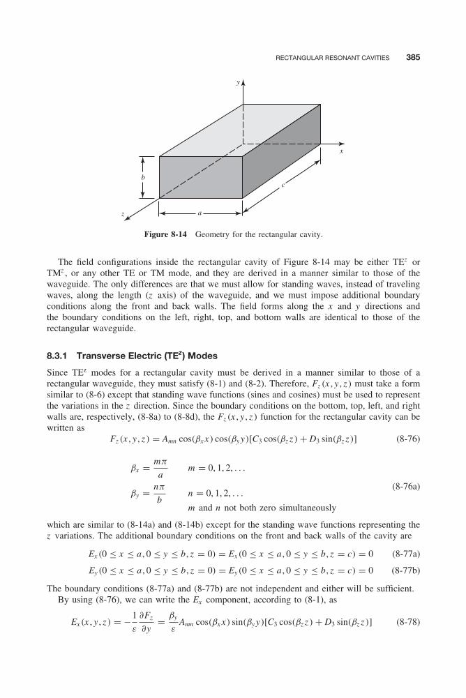
Balanis c08.tex V3 - 11/22/2011 3:32 P.M. Page 385
RECTANGULAR RESONANT CAVITIES 385
b
z
y
x
a
c
Figure 8-14 Geometry for the rectangular cavity.
The field configurations inside the rectangular cavity of Figure 8-14 may be either TEz orTMz , or any other TE or TM mode, and they are derived in a manner similar to those of thewaveguide. The only differences are that we must allow for standing waves, instead of travelingwaves, along the length (z axis) of the waveguide, and we must impose additional boundaryconditions along the front and back walls. The field forms along the x and y directions andthe boundary conditions on the left, right, top, and bottom walls are identical to those of therectangular waveguide.
8.3.1 Transverse Electric (TEz) Modes
Since TEz modes for a rectangular cavity must be derived in a manner similar to those of arectangular waveguide, they must satisfy (8-1) and (8-2). Therefore, Fz (x , y , z ) must take a formsimilar to (8-6) except that standing wave functions (sines and cosines) must be used to representthe variations in the z direction. Since the boundary conditions on the bottom, top, left, and rightwalls are, respectively, (8-8a) to (8-8d), the Fz (x , y , z ) function for the rectangular cavity can bewritten as
Fz (x , y , z ) = Amn cos(βx x) cos(βy y)[C3 cos(βz z ) + D3 sin(βz z )] (8-76)
βx = mπ
am = 0, 1, 2, . . .
βy = nπ
bn = 0, 1, 2, . . .
m and n not both zero simultaneously
(8-76a)
which are similar to (8-14a) and (8-14b) except for the standing wave functions representing thez variations. The additional boundary conditions on the front and back walls of the cavity are
Ex (0 ≤ x ≤ a , 0 ≤ y ≤ b, z = 0) = Ex (0 ≤ x ≤ a , 0 ≤ y ≤ b, z = c) = 0 (8-77a)
Ey(0 ≤ x ≤ a , 0 ≤ y ≤ b, z = 0) = Ey(0 ≤ x ≤ a , 0 ≤ y ≤ b, z = c) = 0 (8-77b)
The boundary conditions (8-77a) and (8-77b) are not independent and either will be sufficient.By using (8-76), we can write the Ex component, according to (8-1), as
Ex (x , y , z ) = −1
ε
∂Fz
∂y= βy
εAmn cos(βx x) sin(βy y)[C3 cos(βz z ) + D3 sin(βz z )] (8-78)
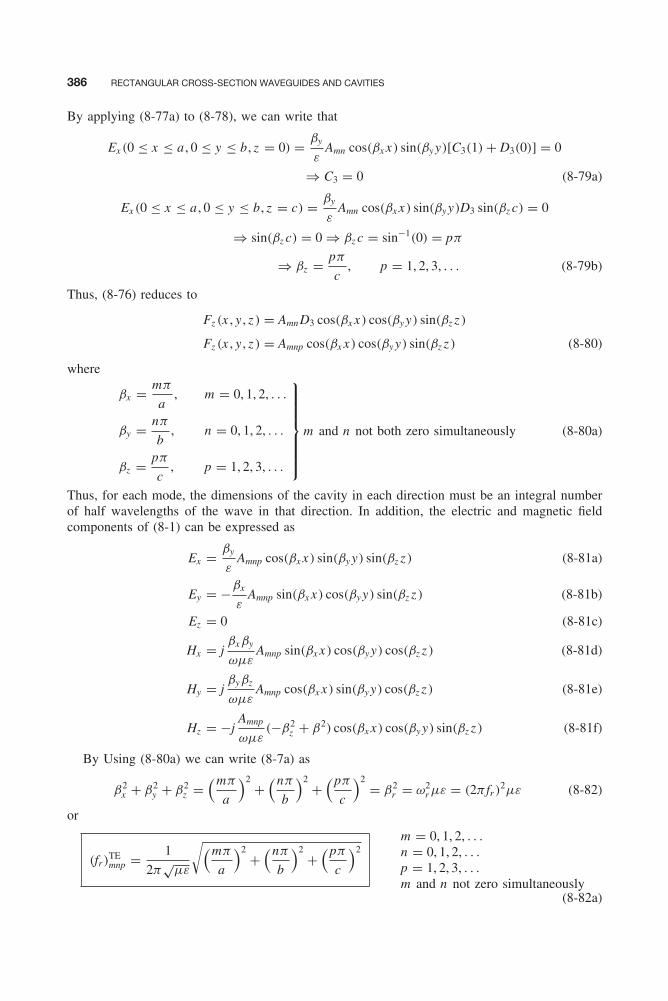
Balanis c08.tex V3 - 11/22/2011 3:32 P.M. Page 386
386 RECTANGULAR CROSS-SECTION WAVEGUIDES AND CAVITIES
By applying (8-77a) to (8-78), we can write that
Ex (0 ≤ x ≤ a , 0 ≤ y ≤ b, z = 0) = βy
εAmn cos(βx x) sin(βy y)[C3(1) + D3(0)] = 0
⇒ C3 = 0 (8-79a)
Ex (0 ≤ x ≤ a , 0 ≤ y ≤ b, z = c) = βy
εAmn cos(βx x) sin(βy y)D3 sin(βz c) = 0
⇒ sin(βz c) = 0 ⇒ βz c = sin−1(0) = pπ
⇒ βz = pπ
c, p = 1, 2, 3, . . . (8-79b)
Thus, (8-76) reduces to
Fz (x , y , z ) = AmnD3 cos(βx x) cos(βy y) sin(βz z )
Fz (x , y , z ) = Amnp cos(βx x) cos(βy y) sin(βz z ) (8-80)
where
βx = mπ
a, m = 0, 1, 2, . . .
βy = nπ
b, n = 0, 1, 2, . . .
βz = pπ
c, p = 1, 2, 3, . . .
⎫⎪⎪⎪⎪⎪⎪⎬⎪⎪⎪⎪⎪⎪⎭m and n not both zero simultaneously (8-80a)
Thus, for each mode, the dimensions of the cavity in each direction must be an integral numberof half wavelengths of the wave in that direction. In addition, the electric and magnetic fieldcomponents of (8-1) can be expressed as
Ex = βy
εAmnp cos(βx x) sin(βy y) sin(βz z ) (8-81a)
Ey = −βx
εAmnp sin(βx x) cos(βy y) sin(βz z ) (8-81b)
Ez = 0 (8-81c)
Hx = jβxβy
ωμεAmnp sin(βx x) cos(βy y) cos(βz z ) (8-81d)
Hy = jβyβz
ωμεAmnp cos(βx x) sin(βy y) cos(βz z ) (8-81e)
Hz = −jAmnp
ωμε(−β2
z + β2) cos(βx x) cos(βy y) sin(βz z ) (8-81f)
By Using (8-80a) we can write (8-7a) as
β2x + β2
y + β2z =
(mπ
a
)2+
(nπ
b
)2+
(pπ
c
)2= β2
r = ω2r με = (2π fr )
2με (8-82)
or
(fr )TEmnp = 1
2π√
με
√(mπ
a
)2+
(nπ
b
)2+
(pπ
c
)2m = 0, 1, 2, . . .n = 0, 1, 2, . . .p = 1, 2, 3, . . .m and n not zero simultaneously
(8-82a)

Balanis c08.tex V3 - 11/22/2011 3:32 P.M. Page 387
RECTANGULAR RESONANT CAVITIES 387
In (8-82a), (fr )mnp represents the resonant frequency for the TEzmnp mode. If c > a > b, the mode
with the lowest-order is the TEz101 mode, whose resonant frequency is represented by
(fr )TE101 = 1
2√
με
√(1
a
)2
+(
1
c
)2
(8-83)
In addition to its resonant frequency, one of the most important parameters of a resonant cavityis its quality factor Q defined as
Q ≡ ωstored energy
dissipated power= ω
Wt
Pd= ω
We + Wm
Pd= ω
2We
Pd= ω
2Wm
Pd(8-84)
which is proportional to volume and inversely proportional to surface. By using the field expres-sions of (8-81a) through (8-81f) for the m = 1, n = 0, and p = 1 (101) mode, the total storedenergy can be written as
W = 2We = 2
[ε
4
∫∫∫V
|E|2 dv
]= ε
2
[ |A101|ε
π
a
]2 ∫ c
0
∫ b
0
∫ a
0sin2
(π
ax)
sin2(π
cz)
dx dy dz
W = |A101|2ε
(π
a
)2 abc
8(8-85)
The total dissipated power is found by adding the power that is dissipated in each of the sixwalls of the cylinder. Since the dissipated power on the top wall is the same as that on the bottom,that on the right wall is the same as that on the left, and that on the back is the same as that onthe front, we can write the total dissipated power as
Pd = Rs
2
{2∫∫
bottomJb • J∗
b ds + 2∫∫
leftJ� • J∗
� ds + 2∫∫
frontJf • J∗
f ds
}= Rs
{∫∫bottom
Jb • J∗b ds +
∫∫left
J� • J∗� ds +
∫∫front
Jf • J∗f ds
}Pd = Pb + P� + Pf (8-86)
where
Pb = Rs
∫∫bottom
Jb • J∗b ds = Rs
∫ c
0
∫ a
0|Jb |2 dx dz (8-86a)
P� = Rs
∫∫left
J� • J∗� ds = Rs
∫ c
0
∫ b
0|J�|2 dy dz (8-86b)
Pf = Rs
∫∫front
Jf • J∗f ds = Rs
∫ b
0
∫ a
0|Jf |2 dx dy (8-86c)
Jb = n̂ × H|y=0 = −âz jπ
a
π
c
A101
ωμεsin
(π
ax)
cos(π
cz)
−âx j(π
a
)2 A101
ωμεcos
(π
ax)
sin(π
cz)
(8-86d)
J� = n̂ × H|x=0 = ây jA101
ωμε
(π
a
)2sin
(π
cz)
(8-86e)
Jf = n̂ × H|z=c = −ây jπ
a
π
c
A101
ωμεsin
(π
ax)
(8-86f)
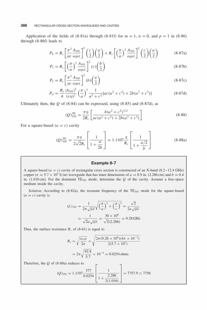
Balanis c08.tex V3 - 11/22/2011 3:32 P.M. Page 388
388 RECTANGULAR CROSS-SECTION WAVEGUIDES AND CAVITIES
Application of the fields of (8-81a) through (8-81f) for m = 1, n = 0, and p = 1 in (8-86)through (8-86f) leads to
Pb = Rs
[π2
ac
A101
ωμε
]2 (c
2
)(a
2
)+ Rs
[(π
a
)2 A101
ωμε
]2 (c
2
)(a
2
)(8-87a)
P� = Rs
[(π
a
)2 A101
ωμε
]2
(c)
(b
2
)(8-87b)
Pf = Rs
[π2
ac
A101
ωμε
]2
(b)
(a
2
)(8-87c)
Pd = Rs
4
|A101|2(εη)2
(π
a
)2 1
a2 + c2[ac(a2 + c2) + 2b(a3 + c3)] (8-87d)
Ultimately then, the Q of (8-84) can be expressed, using (8-85) and (8-87d), as
(Q)TE101 = πη
2Rs
[b(a2 + c2)3/2
ac(a2 + c2) + 2b(a3 + c3)
](8-88)
For a square-based (a = c) cavity
(Q)TE101 = πη
2√
2Rs
⎡⎢⎣ 1
1 + a
2b
⎤⎥⎦ = 1.1107η
Rs
⎡⎢⎣ 1
1 + a/2
b
⎤⎥⎦ (8-88a)
Example 8-7
A square-based (a = c) cavity of rectangular cross section is constructed of an X-band (8.2–12.4 GHz)copper (σ = 5.7 × 10⁷ S/m) waveguide that has inner dimensions of a = 0.9 in. (2.286 cm) and b = 0.4in. (1.016 cm). For the dominant TE101 mode, determine the Q of the cavity. Assume a free-spacemedium inside the cavity.
Solution: According to (8-82a), the resonant frequency of the TE101 mode for the square-based(a = c) cavity is
(fr )101 = 1
2π√
με
√(π
a
)2 +(π
c
)2 =√
2
2a√
με
= 1√2a
√με
= 30 × 109
√2(2.286)
= 9.28 GHz
Thus, the surface resistance Rs of (8-61) is equal to
Rs =√
ωrμ
2σ=
√2π(9.28 × 10⁹)(4π × 10−7)
2(5.7 × 10⁷)
= 2π
√92.8
5.7× 10−3 = 0.0254 ohms
Therefore, the Q of (8-88a) reduces to
(Q)101 = 1.1107377
0.0254
⎡⎢⎢⎣ 1
1 + 2.286
2(1.016)
⎤⎥⎥⎦ = 7757.9 � 7758
Balanis c08.tex V3 - 11/22/2011 3:32 P.M. Page 389
RECTANGULAR RESONANT CAVITIES 389
8.3.2 Transverse Magnetic (TMz) Modes
In addition to TEzmnp modes inside a rectangular cavity, TMz
mnp modes can also be supported bysuch a structure. These modes can be derived in a manner similar to the TEz
mnp field configurations.Using the results of Section 8.2.2, we can write the vector potential component Az (x , y , z ) of
(8-26a) for the TMzmnp modes of Figure 8-14 without applying the boundary conditions on the
front and back walls, as
Az (x , y , z ) = Bmn sin(βx x) sin(βy y)[C3 cos(βz z ) + D3 sin(βz z )] (8-89)
whereβx = mπ
a, m = 1, 2, 3, . . . (8-89a)
βy = nπ
b, n = 1, 2, 3, . . . (8-89b)
The boundary conditions that have not yet been applied on (8-24) are (8-77a) or (8-77b). Using(8-89), we can write the Ex component of (8-24) as
Ex (x , y , z ) = −j1
ωμε
∂2Az
∂x ∂z
= −jβxβz
ωμεBmn cos(βx x) sin(βy y)[−C3 sin(βz z ) + D3 cos(βz z )] (8-90)
Applying the boundary conditions (8-77a), we can write that
Ex (0 ≤ x ≤ a , 0 ≤ y ≤ b, z = 0) = −jβxβz
ωμεBmn cos(βx x) sin(βy y)
×[−C3(0) + D3(1)] = 0 ⇒ D3 = 0 (8-91a)
Ex (0 ≤ x ≤ a , 0 ≤ y ≤ b, z = c) = −jβxβz
ωμεBmn cos(βx x) sin(βy y)
×[−C3 sin(βz c)] = 0
⇒ sin(βz c) = 0 ⇒ βz c = sin−1(0) = pπ
βz = pπ
c, p = 0, 1, 2, 3, . . . (8-91b)
Thus, (8-89) reduces toAz (x , y , z ) = BmnC3 sin(βx x) sin(βy y) cos(βz z )
Az (x , y , z ) = Bmnp sin(βx x) sin(βy y) cos(βz z ) (8-92)where
βx = mπ
a, m = 1, 2, 3, . . .
βy = nπ
b, n = 1, 2, 3, . . . (8-92a)
βz = pπ
c, p = 0, 1, 2, . . .
Using (8-7a) and (8-92a), the corresponding resonant frequency can be written as
(fr )TMmnp = 1
2π√
με
√(mπ
a
)2+
(nπ
b
)2+
(pπ
c
)2 m = 1, 2, 3, . . .n = 1, 2, 3, . . .p = 0, 1, 2, . . .
(8-93)
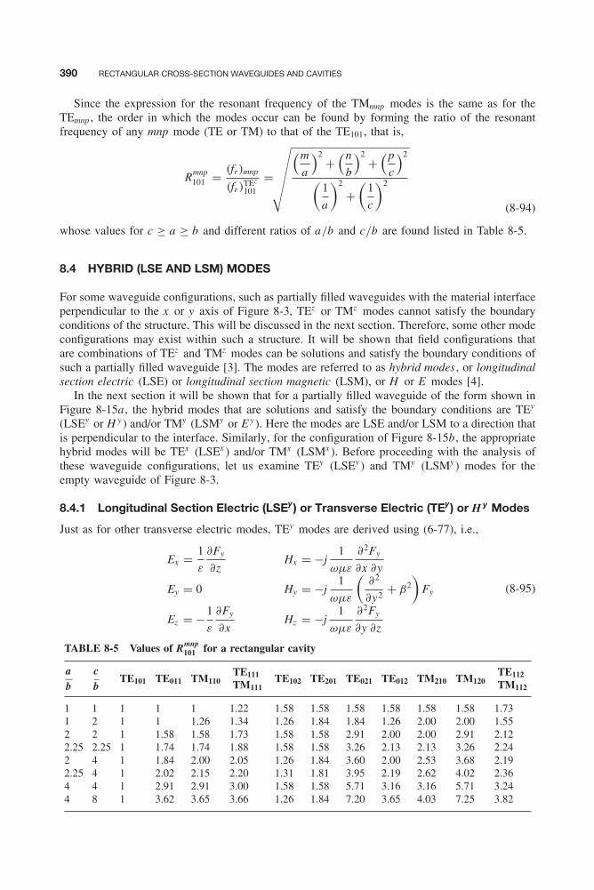
Balanis c08.tex V3 - 11/22/2011 3:32 P.M. Page 390
390 RECTANGULAR CROSS-SECTION WAVEGUIDES AND CAVITIES
Since the expression for the resonant frequency of the TMmnp modes is the same as for theTEmnp , the order in which the modes occur can be found by forming the ratio of the resonantfrequency of any mnp mode (TE or TM) to that of the TE101, that is,
Rmnp101 = (fr )mnp
(fr )TEz
101
=m
a
2+ n
b
2+ p
c
2
1
a
2
+ 1
c
2
(8-94)
whose values for c ≥ a ≥ b and different ratios of a/b and c/b are found listed in Table 8-5.
8.4 HYBRID (LSE AND LSM) MODES
For some waveguide configurations, such as partially filled waveguides with the material interfaceperpendicular to the x or y axis of Figure 8-3, TEz or TMz modes cannot satisfy the boundaryconditions of the structure. This will be discussed in the next section. Therefore, some other modeconfigurations may exist within such a structure. It will be shown that field configurations thatare combinations of TEz and TMz modes can be solutions and satisfy the boundary conditions ofsuch a partially filled waveguide [3]. The modes are referred to as hybrid modes , or longitudinalsection electric (LSE) or longitudinal section magnetic (LSM), or H or E modes [4].
In the next section it will be shown that for a partially filled waveguide of the form shown inFigure 8-15a , the hybrid modes that are solutions and satisfy the boundary conditions are TEy
(LSEy or H y ) and/or TMy (LSMy or E y ). Here the modes are LSE and/or LSM to a direction thatis perpendicular to the interface. Similarly, for the configuration of Figure 8-15b, the appropriatehybrid modes will be TEx (LSEx ) and/or TMx (LSMx ). Before proceeding with the analysis ofthese waveguide configurations, let us examine TEy (LSEy ) and TMy (LSMy ) modes for theempty waveguide of Figure 8-3.
8.4.1 Longitudinal Section Electric (LSEy) or Transverse Electric (TEy) or H y Modes
Just as for other transverse electric modes, TEy modes are derived using (6-77), i.e.,
Ex = 1
ε
∂Fy
∂zHx = −j
1
ωμε
∂2Fy
∂x ∂y
Ey = 0 Hy = −j1
ωμε
(∂2
∂y2+ β2
)Fy
Ez = −1
ε
∂Fy
∂xHz = −j
1
ωμε
∂2Fy
∂y ∂z
(8-95)
TABLE 8-5 Values of Rmnp101 for a rectangular cavity
ab
cb
TE101 TE011 TM110TE111TM111
TE102 TE201 TE021 TE012 TM210 TM120TE112TM112
1 1 1 1 1 1.22 1.58 1.58 1.58 1.58 1.58 1.58 1.731 2 1 1 1.26 1.34 1.26 1.84 1.84 1.26 2.00 2.00 1.552 2 1 1.58 1.58 1.73 1.58 1.58 2.91 2.00 2.00 2.91 2.122.25 2.25 1 1.74 1.74 1.88 1.58 1.58 3.26 2.13 2.13 3.26 2.242 4 1 1.84 2.00 2.05 1.26 1.84 3.60 2.00 2.53 3.68 2.192.25 4 1 2.02 2.15 2.20 1.31 1.81 3.95 2.19 2.62 4.02 2.364 4 1 2.91 2.91 3.00 1.58 1.58 5.71 3.16 3.16 5.71 3.244 8 1 3.62 3.65 3.66 1.26 1.84 7.20 3.65 4.03 7.25 3.82
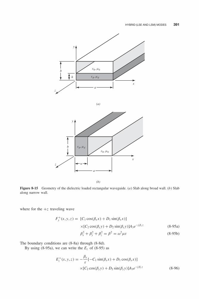
Balanis c08.tex V3 - 11/22/2011 3:32 P.M. Page 391
HYBRID (LSE AND LSM) MODES 391
y
z
y
z
x
x
b
a
(a)
(b)
h
e0, m0
ed, md
e0, m0
ed, mdb
a
w
Figure 8-15 Geometry of the dielectric loaded rectangular waveguide. (a) Slab along broad wall. (b) Slabalong narrow wall.
where for the +z traveling wave
F+y (x , y , z ) = [C1 cos(βx x) + D1 sin(βx x)]
×[C2 cos(βy y) + D2 sin(βy y)]A3e−jβz z (8-95a)
β2x + β2
y + β2z = β2 = ω2με (8-95b)
The boundary conditions are (8-8a) through (8-8d).By using (8-95a), we can write the Ez of (8-95) as
E+z (x , y , z ) = −βx
ε[−C1 sin(βx x) + D1 cos(βx x)]
×[C2 cos(βy y) + D2 sin(βy y)]A3e−jβz z (8-96)

Balanis c08.tex V3 - 11/22/2011 3:32 P.M. Page 392
392 RECTANGULAR CROSS-SECTION WAVEGUIDES AND CAVITIES
Application of the boundary condition (8-8b) on (8-96) gives
E+z (0 ≤ x ≤ a , y = 0, z )
= −βx
ε[−C1 sin(βx x) + D1 cos(βx x)][C2(1) + D2(0)]A3e−jβz z = 0
⇒ C2 = 0 (8-97a)
E+z (0 ≤ x ≤ a , y = b, z )
= −βx
ε[−C1 sin(βx x) + D1 cos(βx x)]D2 sin(βy b)A3e−jβz z = 0
⇒ sin(βy b) = 0 ⇒ βy b = sin−1(0) = nπ
βy = nπ
b, n = 1, 2, 3, . . . (8-97b)
By following the same procedure, the boundary condition (8-8d) leads to
E+z (x = 0, 0 ≤ y ≤ b, z )
= −βx
ε[−C1(0) + D1(1)]D2A3 sin(βy y)e−jβz z = 0 ⇒ D1 = 0 (8-98a)
E+z (x = a , 0 ≤ y ≤ b, z ) = −βx
ε[−C1 sin(βx a)]D2A3e−jβz z = 0
⇒ sin(βx a) = 0 ⇒ βx = mπ
a, m = 0, 1, 2, . . . (8-98b)
Therefore, (8-95a) reduces to
F+y (x , y , z ) = C1D2A3 cos(βx x) sin(βy y)e−jβz z = Amn cos(βx x) sin(βy y)e−jβz z (8-99)
where
βx = mπ
a, m = 0, 1, 2, . . . (8-99a)
βy = nπ
b, n = 1, 2, 3, . . . (8-99b)
By using (8-95b),
βz = ±√
β2 − (β2x + β2
y ) = ±√
β2 − β2c (8-100)
where
β2c = ω2
cμε = (2π fc)2με = β2
x + β2y =
(mπ
a
)2+
(nπ
b
)2
or
(fc)TEy
mn = 1
2π√
με
√(mπ
a
)2+
(nπ
b
)2 m = 0, 1, 2, . . .n = 1, 2, 3, . . .
(8-100a)
The dominant mode is the TEy01 whose cutoff frequency is
(fc)TEy
01 = 1
2b√
με(8-100b)

Balanis c08.tex V3 - 11/22/2011 3:32 P.M. Page 393
PARTIALLY FILLED WAVEGUIDE 393
8.4.2 Longitudinal Section Magnetic (LSMy) or Transverse Magnetic (TMy) or E y
Modes
By following a procedure similar to that for the TEy modes of the previous section, it can beshown that for the TMy modes of Figure 8-3 the field components of (6-64), i.e.,
Ex = −j1
ωμε
∂2Ay
∂x ∂yHx = − 1
μ
∂Ay
∂z
Ey = −j1
ωμε
(∂2
∂y2+ β2
)Ay Hy = 0
Ez = −j1
ωμε
∂2Ay
∂y ∂zHz = 1
μ
∂Ay
∂x
(8-101)
and the boundary conditions (8-8a) through (8-8d) lead to
Ay(x , y , z ) = Bmn sin(βx x) cos(βy y)e−jβz z (8-101a)
βx = mπ
a, m = 1, 2, 3, . . . (8-101b)
βy = nπ
b, n = 0, 1, 2, . . . (8-101c)
(fc)TMy
mn = 1
2π√
με
√(mπ
a
)2+
(nπ
b
)2(8-101d)
The dominant mode is the TMy10 whose cutoff frequency is
(fc)TMy
10 = 1
2a√
με(8-101e)
8.5 PARTIALLY FILLED WAVEGUIDE
Let us now consider in detail the analysis of the field configurations in the partially filled waveg-uide of Figure 8-15a . The analysis of the configuration of Figure 8-15b is left as an end-of-chapterexercise. It can be shown that for either waveguide configuration, neither TEz nor TMz modesindividually can satisfy the boundary conditions. In fact, for the configuration of Figure 8-15a ,TEy(LSEy) or TMy(LSMy) are the appropriate modes, whereas TEx (LSEx ) or TMx (LSMx ) sat-isfy the boundary conditions of Figure 8-15b. For either configuration, the appropriate modes areLSE or LSM to a direction that is perpendicular to the material interface.
8.5.1 Longitudinal Section Electric (LSEy) or Transverse Electric (TEy)
For the configuration of Figure 8-15a , there are two sets of fields: one for the dielectric region(0 ≤ x ≤ a , 0 ≤ y ≤ h , z ), designated by superscript d , and the other for the free-space region(0 ≤ x ≤ a , h ≤ y ≤ b, z ), designated by superscript 0. For each region, the TEy field componentsare those of (8-95) and the corresponding potential functions are
F dy (x , 0 ≤ y ≤ h , z ) = [
C d1 cos(βxd x) + Dd
1 sin(βxd x)]
× [C d
2 cos(βyd y) + Dd2 sin(βyd y)
]Ad
3 e−jβz z (8-102)
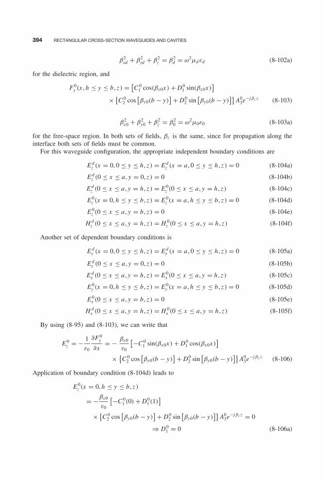
Balanis c08.tex V3 - 11/22/2011 3:32 P.M. Page 394
394 RECTANGULAR CROSS-SECTION WAVEGUIDES AND CAVITIES
β2xd + β2
yd + β2z = β2
d = ω2μdεd (8-102a)
for the dielectric region, and
F 0y (x , h ≤ y ≤ b, z ) = [
C 01 cos(βx0x) + D0
1 sin(βx0x)]
× {C 0
2 cos[βy0(b − y)
] + D02 sin
[βy0(b − y)
]}A0
3e−jβz z (8-103)
β2x0 + β2
y0 + β2z = β2
0 = ω2μ0ε0 (8-103a)
for the free-space region. In both sets of fields, βz is the same, since for propagation along theinterface both sets of fields must be common.
For this waveguide configuration, the appropriate independent boundary conditions are
E dz (x = 0, 0 ≤ y ≤ h , z ) = E d
z (x = a , 0 ≤ y ≤ h , z ) = 0 (8-104a)
E dz (0 ≤ x ≤ a , y = 0, z ) = 0 (8-104b)
E dz (0 ≤ x ≤ a , y = h , z ) = E 0
z (0 ≤ x ≤ a , y = h , z ) (8-104c)
E 0z (x = 0, h ≤ y ≤ b, z ) = E 0
z (x = a , h ≤ y ≤ b, z ) = 0 (8-104d)
E 0z (0 ≤ x ≤ a , y = b, z ) = 0 (8-104e)
H dz (0 ≤ x ≤ a , y = h , z ) = H 0
z (0 ≤ x ≤ a , y = h , z ) (8-104f)
Another set of dependent boundary conditions is
E dy (x = 0, 0 ≤ y ≤ h , z ) = E d
y (x = a , 0 ≤ y ≤ h , z ) = 0 (8-105a)
E dx (0 ≤ x ≤ a , y = 0, z ) = 0 (8-105b)
E dx (0 ≤ x ≤ a , y = h , z ) = E 0
x (0 ≤ x ≤ a , y = h , z ) (8-105c)
E 0y (x = 0, h ≤ y ≤ b, z ) = E 0
y (x = a , h ≤ y ≤ b, z ) = 0 (8-105d)
E 0x (0 ≤ x ≤ a , y = b, z ) = 0 (8-105e)
H dx (0 ≤ x ≤ a , y = h , z ) = H 0
x (0 ≤ x ≤ a , y = h , z ) (8-105f)
By using (8-95) and (8-103), we can write that
E 0z = − 1
ε0
∂F 0y
∂x= − βx0
ε0
[−C 01 sin(βx0x) + D0
1 cos(βx0x)]
× {C 0
2 cos[βy0(b − y)
] + D02 sin
[βy0(b − y)
]}A0
3e−jβz z (8-106)
Application of boundary condition (8-104d) leads to
E 0z (x = 0, h ≤ y ≤ b, z )
= −βx0
ε0
[−C 01 (0) + D0
1 (1)]
× {C 0
2 cos[βy0(b − y)
] + D02 sin
[βy0(b − y)
]}A0
3e−jβz z = 0
⇒ D01 = 0 (8-106a)
Balanis c08.tex V3 - 11/22/2011 3:32 P.M. Page 395
PARTIALLY FILLED WAVEGUIDE 395
E 0z (x = a , h ≤ y ≤ b, z )
= −βx0
ε0
[−C 01 sin(βx0a)
]× {
C 02 cos
[βy0(b − y)
] + D02 sin
[βy0(b − y)
]}A0
3e−jβz z = 0
⇒ sin(βx0a) = 0 ⇒ βx0 = mπ
a, m = 0, 1, 2, . . . (8-106b)
Application of (8-104e) leads to
E 0z (0 ≤ x ≤ a , y = b, z )
= −βx0
ε0
[−C 01 sin(βx0x)
] {C 0
2 (1) + D02 (0)
}A0
3e−jβz z = 0
⇒ C 02 = 0 (8-106c)
Thus, (8-103) reduces to
F 0y = A0
mn cos(βx0x) sin[βy0(b − y)
]e−jβz z
βx0 = mπ
a, m = 0, 1, 2, . . .
β2x0 + β2
y0 + β2z =
(mπ
a
)2+ β2
y0 + β2z = β2
0 = ω2μ0ε0
(8-107)
(8-107a)
(8-107b)
with
E 0z = − 1
ε0
∂F 0y
∂x= βx0
ε0A0
mn sin(βx0x) sin[βy0(b − y)
]e−jβz z (8-108)
Use of (8-95) and (8-102) gives
E dz = − 1
εd
∂F dy
∂x= − βxd
εd
[−C d1 sin(βxd x) + Dd
1 cos(βxd x)]
× [C d
2 cos(βyd y) + Dd2 sin(βyd y)
]Ad
3 e−jβz z (8-109)
Application of boundary condition (8-104a) leads to
E dz (x = 0, 0 ≤ y ≤ h , z )
= −βxd
εd
[−C d1 (0) + Dd
1 (1)] [
C d2 cos(βyd y) + Dd
2 sin(βyd y)]
Ad3 e−jβz z = 0
⇒ Dd1 = 0 (8-109a)
E dz (x = a , 0 ≤ y ≤ h , z )
= −βxd
εd
[−C d1 sin(βxd a)
] [C d
2 cos(βyd y) + Dd2 sin(βyd y)
]Ad
3 e−jβz z = 0
⇒ sin(βxd a) = 0 ⇒ βxd = mπ
a, m = 0, 1, 2, . . . (8-109b)
Balanis c08.tex V3 - 11/22/2011 3:32 P.M. Page 396
396 RECTANGULAR CROSS-SECTION WAVEGUIDES AND CAVITIES
Application of (8-104b) leads to
E dz (0 ≤ x ≤ a , y = 0, z ) = −βxd
εd
[−C d1 sin(βxd x)
] [C d
2 (1) + Dd2 (0)
]Ad
3 e−jβz z = 0
⇒ C d2 = 0 (8-109c)
Thus, (8-102) reduces to
F dy = Ad
mn cos(βxd x) sin(βyd y)e−jβz z
βxd = mπ
a= βx0, m = 0, 1, 2, . . .
β2xd + β2
yd + β2z =
(mπ
a
)2+ β2
yd + β2z = β2
d = ω2μdεd
(8-110)
(8-110a)
(8-110b)
with
E dz = − 1
εd
∂F dy
∂x= βxd
εdAd
mn sin(βxd x) sin(βyd y)e−jβz z
= βx0
εdAd
mn sin(βx0x) sin(βyd y)e−jβz z (8-111)
Application of boundary condition (8-104c) and use of (8-108) and (8-111) leads to
βx0
ε0A0
mn sin(βx0x) sin[βy0(b − h)
]e−jβz z = βx0
εdAd
mn sin(βxd x) sin(βyd h)e−jβz z
1
ε0A0
mn sin[βy0(b − h)
] = 1
εdAd
mn sin(βyd h) (8-112)
By using (8-107) and (8-110), the z component of the H field from (8-95) can be written as
H 0z = −j
1
ωμ0ε0
∂2F 0y
∂y ∂z= βy0βz
ωμ0ε0A0
mn cos(βx0x) cos[βy0(b − y)
]e−jβz z (8-113a)
H dz = −j
1
ωμdεd
∂2F dy
∂y ∂z= − βydβz
ωμdεdAd
mn cos(βxd x) cos(βyd y)e−jβz z (8-113b)
Application of the boundary condition of (8-104f) reduces, with βxd = βx0, to
βy0βz
ωμ0ε0A0
mn cos(βx0x) cos[βy0(b − h)
]e−jβz z
= − βydβz
ωμdεdAd
mn cos(βxd x) cos(βyd h)e−jβz z
βy0
μ0ε0A0
mn cos[βy0(b − h)
] = − βyd
μdεdAd
mn cos(βyd h) (8-114)

Balanis c08.tex V3 - 11/22/2011 3:32 P.M. Page 397
PARTIALLY FILLED WAVEGUIDE 397
Division of (8-114) by (8-112) leads to
βy0
μ0cot
[βy0(b − h)
] = −βyd
μdcot(βyd h)
β2x0 + β2
y0 + β2z =
(mπ
a
)2+ β2
y0 + β2z = β2
0 = ω2μ0ε0 m = 0, 1, 2, . . .
β2xd + β2
yd + β2z =
(mπ
a
)2+ β2
yd + β2z = β2
d = ω2μdεd m = 0, 1, 2, . . .
(8-115)
(8-115a)
(8-115b)
Whereas βx0 = βxd = mπ/a , m = 0, 1, 2, . . ., have been determined, βy0, βyd , and βz have notyet been found. They can be determined for each mode using (8-115) through (8-115b), and theirvalues vary as a function of frequency. Thus, for each frequency a new set of values for βy0, βyd ,and βz must be found that satisfy (8-115) through (8-115b). One procedure that can be used toaccomplish this will be to solve (8-115a) for βy0 (as a function of βz and β0) and (8-115b) forβyd (as a function of βz and βd ), and then substitute these expressions in (8-115) for βy0 andβyd . The new form of (8-115) will be a function of βz , β0, and βd . Thus, for a given mode,determined by the value of m , at a given frequency, a particular value of βz will satisfy the newform of the transcendental equation 8-115; that value of βz can be found iteratively. The rangeof βz will be β0
z < βz < βdz where β0
z represents the values of the same mode of an air-filledwaveguide and βd
z represents the values of the same mode of a waveguide completely filled withthe dielectric. Once βz has been found at a given frequency for a given mode, the correspondingvalues of βy0 and βyd for the same mode at the same frequency can be determined by using,respectively, (8-115a) and (8-115b). It must be remembered that for each value of m there areinfinite values of n (n = 1, 2, 3, . . .). Thus, the dominant mode is the one for which m = 0 andn = 1, i.e., TEy
01.For m = 0, the modes will be denoted as TE0n . For these modes, (8-115a) and (8-115b) reduce
to
β2y0 + β2
z = ω2μ0ε0 ⇒ βz = ±√
ω2μ0ε0 − β2y0 (8-116a)
β2yd + β2
z = ω2μdεd ⇒ βz = ±√
ω2μdεd − β2yd (8-116b)
Cutoff occurs when βz = 0. Thus, at cutoff (8-116a) and (8-116b) reduce to
βz = 0 = ±√
ω2μ0ε0 − β2y0|ω=ωc ⇒ ω2
cμ0ε0 = β2y0 ⇒ βy0 = ωc
√μ0ε0 (8-117a)
βz = 0 = ±√
ω2μdεd − β2yd |ω=ωc ⇒ ω2
cμdεd = β2yd ⇒ βyd = ωc
√μdεd (8-117b)
which can be used to find βy0 and βyd at cutoff (actually slightly above), once the cutoff frequencyhas been determined. By using (8-117a) and (8-117b), we can write (8-115) as
ωc√
μ0ε0
μ0cot
[ωc
√μ0ε0(b − h)
] = −ωc√
μdεd
μdcot
(ωc
√μdεd h
)or √
ε0
μ0cot
[ωc
√μ0ε0(b − h)
] = −√
εd
μdcot
(ωc
√μdεd h
)(8-118)
which can be used to find the cutoff frequencies of the TEy0n modes in a partially filled waveguide.
A similar expression must be written for the other modes.
Balanis c08.tex V3 - 11/22/2011 3:32 P.M. Page 398
398 RECTANGULAR CROSS-SECTION WAVEGUIDES AND CAVITIES
For a rectangular waveguide filled completely either with free space or with a dielectric materialwith εd , μd , the cutoff frequency of the TEy
01 mode is given, respectively, according to (8-100b),by
(f 0c
)TEy
01 = 1
2b√
μ0ε0(8-119a)
(f dc
)TEy
01 = 1
2b√
μdεd(8-119b)
Use of perturbational techniques shows that, in general, the cutoff frequency of the partially filledwaveguide (part free space and part dielectric) is greater than the cutoff frequency of the samemode in the same waveguide filled with a dielectric material with εd , μd and is smaller than thecutoff frequency of the same waveguide filled with free space. Thus, the cutoff frequency of theTEy
01 mode of a partially filled waveguide (part free space and part dielectric) is greater than(8-119b) and smaller than (8-119a), that is,
1
2b√
μdεd≤ (fc)
TEy
01 ≤ 1
2b√
μ0ε0(8-120)
orπ
b√
μdεd≤ (ωc)
TEy
01 ≤ π
b√
μ0ε0(8-120a)
With this permissible range, the exact values can be found using (8-118). The propagation constantβz must be solved at each frequency on an individual basis using (8-116a) or (8-116b).
Example 8-8
A WR90 X-band (8.2–12.4 GHz) waveguide of Figure 8-15a with inner dimensions of a = 0.9 in.(2.286 cm), b = 0.4 in. (1.016 cm), and a/b = 2.25, is partially filled with free space and polystyrene(εd = 2.56ε0, μd = μ0, and h = b/3). For m = 0 determine the following.
1. The cutoff frequencies of the hybrid TEy0n (LSEy
0n ) modes for n = 1, 2, 3.2. The values of βy0 and βyd for each mode at sightly above their corresponding cutoff frequencies.3. The corresponding values of βy0, βyd , and βz for the TEy
01 mode in the frequency range (fc)01 ≤f ≤ 2(fc)01.
How do the cutoff frequencies of the first three TEy0n modes (n = 1, 2, 3) of the partially filled
waveguide compare with those of the TEy0n modes of the empty waveguide?
Solution:
1. The cutoff frequencies of the partially filled waveguide are found using (8-118). According to(8-120) and (8-100a), the cutoff frequencies for each of the desired modes must fall in the ranges
9.23 GHz ≤ (fc)01 ≤ 14.76 GHz
18.45 GHz ≤ (fc)02 ≤ 29.53 GHz
27.68 GHz ≤ (fc)03 ≤ 44.29 GHz
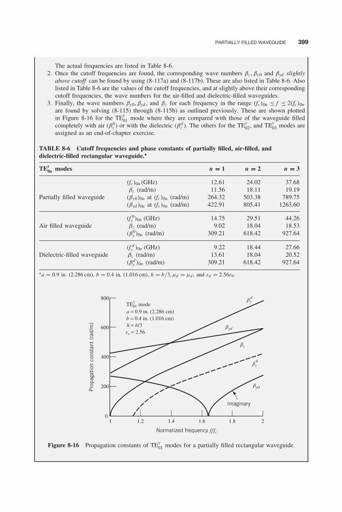
Balanis c08.tex V3 - 11/22/2011 3:32 P.M. Page 399
PARTIALLY FILLED WAVEGUIDE 399
The actual frequencies are listed in Table 8-6.2. Once the cutoff frequencies are found, the corresponding wave numbers βz , βy0 and βyd slightly
above cutoff can be found by using (8-117a) and (8-117b). These are also listed in Table 8-6. Alsolisted in Table 8-6 are the values of the cutoff frequencies, and at slightly above their correspondingcutoff frequencies, the wave numbers for the air-filled and dielectric-filled waveguides.
3. Finally, the wave numbers βy0, βyd , and βz for each frequency in the range (fc)0n ≤ f ≤ 2(fc)0n
are found by solving (8-115) through (8-115b) as outlined previously. These are shown plottedin Figure 8-16 for the TEy
01 mode where they are compared with those of the waveguide filledcompletely with air (β0
z ) or with the dielectric (βdz ). The others for the TEy
02, and TEy03 modes are
assigned as an end-of-chapter exercise.
TABLE 8-6 Cutoff frequencies and phase constants of partially filled, air-filled, anddielectric-filled rectangular waveguide.∗
TEy0n modes n = 1 n = 2 n = 3
(fc)0n(GHz) 12.61 24.02 37.68βz (rad/m) 11.56 18.11 19.19
Partially filled waveguide (βy0)0n at (fc)0n (rad/m) 264.32 503.38 789.75(βyd )0n at (fc)0n (rad/m) 422.91 805.41 1263.60
(f 0c )0n (GHz) 14.75 29.51 44.26
Air filled waveguide βz (rad/m) 9.02 18.04 18.53(β0
y )0n (rad/m) 309.21 618.42 927.64
(f dc )0n (GHz) 9.22 18.44 27.66
Dielectric-filled waveguide βz (rad/m) 13.61 18.04 20.52(βd
y )0n (rad/m) 309.21 618.42 927.64
∗a = 0.9 in. (2.286 cm), b = 0.4 in. (1.016 cm), h = b/3, μd = μd , and εd = 2.56ε0.
Pro
paga
tion
con
stan
t (r
ad/m
)
a = 0.9 in. (2.286 cm)b = 0.4 in. (1.016 cm)h = b/3 byd
bz
bz0
by0
800
600
400
200
01 1.2 1.4 1.6 1.8 2
er = 2.56
TE01 modey
Normalized frequency f/fc
Imaginary
bzd
Figure 8-16 Propagation constants of TEy01 modes for a partially filled rectangular waveguide.
Balanis c08.tex V3 - 11/22/2011 3:32 P.M. Page 400
400 RECTANGULAR CROSS-SECTION WAVEGUIDES AND CAVITIES
8.5.2 Longitudinal Section Magnetic (LSMy) or Transverse Magnetic (TMy)
For the waveguide configuration of Figure 8-15a , the TMy field components are those of (8-101),where the corresponding vector potentials in the dielectric and free space regions for the wavestraveling in the +z direction are given, respectively, by
Ady = [
C d1 cos(βxd x) + Dd
1 sin(βxd x)] [
C d2 cos(βyd y) + Dd
2 sin(βyd y)]
Ad3 e−jβz z (8-121)
β2xd + β2
yd + β2z = β2
d = ω2μdεd (8-121a)
A0y = [
C 01 cos(βx0x) + D0
1 sin(βx0x)]
× {C 0
2 cos[βy0(b − y)
] + D02 sin
[βy0(b − y)
]}A0
3e−jβz z (8-122)
β2x0 + β2
y0 + β2z = β2
0 = ω2μ0ε0 (8-122a)
The appropriate boundary conditions are (8-104a) through (8-105f).Application of the boundary conditions (8-104a) through (8-105f) shows that the following
relations follow:
A0y = B0
mn sin(βx0x) cos[βy0(b − y)
]e−jβz z
βx0 = mπ
a, m = 1, 2, 3, . . .
β2x0 + β2
y0 + β2z =
(mπ
a
)2+ β2
y0 + β2z = β2
0 = ω2μ0ε0
(8-123)
(8-123a)
(8-123b)
Ady = Bd
mn sin(βxd x) cos(βyd y)e−jβz z
βxd = mπ
a, m = 1, 2, 3, . . .
β2xd + β2
yd + β2z =
(mπ
a
)2+ β2
yd + β2z = β2
d = ω2μdεd
(8-124)
(8-124a)
(8-124b)
− βy0
μ0ε0B0
mn sin[βy0(b − h)
] = βyd
μdεdBd
mn sin(βyd h)
1
μ0B0
mn cos[βy0(b − h)
] = 1
μdBd
mn cos(βyd h)
(8-125)
(8-126)
βy0
ε0tan
[βy0(b − h)
] = −βyd
εdtan(βyd h)
β2x0 + β2
y0 + β2z =
(mπ
a
)2+ β2
y0 + β2z = β2
0 = ω2μ0ε0 m = 1, 2, 3, . . .
β2xd + β2
yd + β2z =
(mπ
a
)2+ β2
yd + β2z = β2
d = ω2μdεd m = 1, 2, 3, . . .
(8-127)
(8-127a)
(8-127b)
Balanis c08.tex V3 - 11/22/2011 3:32 P.M. Page 401
PARTIALLY FILLED WAVEGUIDE 401
Whereas βx0 = βxd = mπ/a , m = 1, 2, 3, . . ., have been determined, βy0, βyd , and βz have notyet been found. They can be determined by using (8-127) through (8-127b) and following aprocedure similar to that outlined in the previous section for the TEy modes. For each valueof m , there are infinite values of n (n = 0, 1, 2, . . .). Thus the dominant mode is that for whichm = 1 and n = 0, i.e., the dominant mode is the TMy
10.For m = 1, the modes will be denoted as TMy
1n . For these modes, (8-127a) and (8-127b)reduce to (π
a
)2+ β2
y0 + β2z = ω2μ0ε0 ⇒ βz = ±
√ω2μ0ε0 −
[β2
y0 +(π
a
)2]
(8-128a)
(π
a
)2+ β2
yd + β2z = ω2μdεd ⇒ βz = ±
√ω2μdεd −
[β2
yd +(π
a
)2]
(8-128b)
Cutoff occurs when βz = 0. Thus, at cutoff, (8-128a) and (8-128b) reduce to
ω2cμ0ε0 = β2
y0 +(π
a
)2⇒ βy0 =
√ω2
cμ0ε0 −(π
a
)2(8-129a)
ω2cμdεd = β2
yd +(π
a
)2⇒ βyd =
√ω2
cμdεd −(π
a
)2(8-129b)
which can be used to find βy0 and βyd slightly above cutoff , once the cutoff frequency has beendetermined. By using (8-129a) and (8-129b), we can write (8-127) as
1
ε0
√ω2
cμ0ε0 −(π
a
)2tan
[√ω2
cμ0ε0 −(π
a
)2(b − h)
]
= − 1
εd
√ω2
cμdεd −(π
a
)2tan
[h
√ω2
cμdεd −(π
a
)2]
or
εd
ε0
√ω2
cμ0ε0 −(π
a
)2tan
[√ω2
cμ0ε0 −(π
a
)2(b − h)
]
= −√
ω2cμdεd −
(π
a
)2tan
[h
√ω2
cμdεd −(π
a
)2] (8-130)
which can be used to find the cutoff frequencies of the TMy1n modes in a partially filled waveguide.
For a rectangular waveguide filled completely either with free space (μ0, ε0) or with a dielectricmaterial (εd , μd ), the cutoff frequency of the hybrid TMy
10 mode is given, respectively, accordingto (8-101d) by (
f 0c
)TMy
10 = 1
2a√
μ0ε0(8-131a)
(f dc
)TMy
10 = 1
2a√
μdεd(8-131b)
By using perturbational techniques, it can be shown that, in general, the cutoff frequency of thepartially filled waveguide (part free space and part dielectric) is greater than the cutoff frequencyof the same mode in the same waveguide filled with a dielectric material with εd , μd and smaller
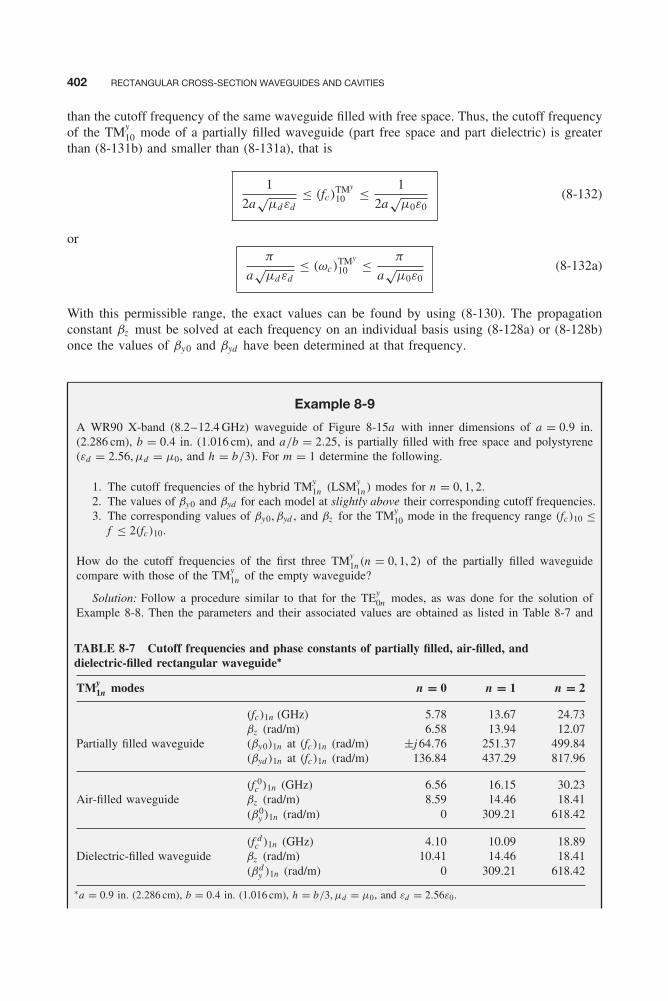
Balanis c08.tex V3 - 11/22/2011 3:32 P.M. Page 402
402 RECTANGULAR CROSS-SECTION WAVEGUIDES AND CAVITIES
than the cutoff frequency of the same waveguide filled with free space. Thus, the cutoff frequencyof the TMy
10 mode of a partially filled waveguide (part free space and part dielectric) is greaterthan (8-131b) and smaller than (8-131a), that is
1
2a√
μdεd≤ (fc)
TMy
10 ≤ 1
2a√
μ0ε0(8-132)
orπ
a√
μdεd≤ (ωc)
TMy
10 ≤ π
a√
μ0ε0(8-132a)
With this permissible range, the exact values can be found by using (8-130). The propagationconstant βz must be solved at each frequency on an individual basis using (8-128a) or (8-128b)once the values of βy0 and βyd have been determined at that frequency.
Example 8-9
A WR90 X-band (8.2–12.4 GHz) waveguide of Figure 8-15a with inner dimensions of a = 0.9 in.(2.286 cm), b = 0.4 in. (1.016 cm), and a/b = 2.25, is partially filled with free space and polystyrene(εd = 2.56, μd = μ0, and h = b/3). For m = 1 determine the following.
1. The cutoff frequencies of the hybrid TMy1n (LSMy
1n) modes for n = 0, 1, 2.2. The values of βy0 and βyd for each model at slightly above their corresponding cutoff frequencies.3. The corresponding values of βy0, βyd , and βz for the TMy
10 mode in the frequency range (fc)10 ≤f ≤ 2(fc)10.
How do the cutoff frequencies of the first three TMy1n(n = 0, 1, 2) of the partially filled waveguide
compare with those of the TMy1n of the empty waveguide?
Solution: Follow a procedure similar to that for the TEy0n modes, as was done for the solution of
Example 8-8. Then the parameters and their associated values are obtained as listed in Table 8-7 and
TABLE 8-7 Cutoff frequencies and phase constants of partially filled, air-filled, anddielectric-filled rectangular waveguide∗
TMy1n modes n = 0 n = 1 n = 2
(fc)1n (GHz) 5.78 13.67 24.73βz (rad/m) 6.58 13.94 12.07
Partially filled waveguide (βy0)1n at (fc)1n (rad/m) ±j 64.76 251.37 499.84(βyd )1n at (fc)1n (rad/m) 136.84 437.29 817.96
(f 0c )1n (GHz) 6.56 16.15 30.23
Air-filled waveguide βz (rad/m) 8.59 14.46 18.41(β0
y )1n (rad/m) 0 309.21 618.42
(f dc )1n (GHz) 4.10 10.09 18.89
Dielectric-filled waveguide βz (rad/m) 10.41 14.46 18.41(βd
y )1n (rad/m) 0 309.21 618.42
∗a = 0.9 in. (2.286 cm), b = 0.4 in. (1.016 cm), h = b/3, μd = μ0, and εd = 2.56ε0.

Balanis c08.tex V3 - 11/22/2011 3:32 P.M. Page 403
PARTIALLY FILLED WAVEGUIDE 403
Pro
paga
tion
con
stan
t (r
ad/m
)
byd
bz
bz0
by0
400
300
200
100
01 1.2 1.4 1.6 1.8 2
a = 0.9 in. (2.286 cm)b = 0.4 in. (1.016 cm)h = b/3er = 2.56
TM10 modey
Normalized frequency f/fc
Imaginary
bzd
Figure 8-17 Propagation constants of TMy10 modes for a partially filled rectangular waveguide.
shown Figure 8-17. The parameters versus frequency for the TMy11 and TMy
12 modes are assigned as anend-of-chapter exercise. The cutoff frequencies of the partially filled waveguide are found using (8-130).According to (8-132) and (8-101d), the cutoff frequencies for each of the desired modes must fall inthe ranges
4.101 GHz ≤ (fc)10 ≤ 6.56 GHz
10.098 GHz ≤ (fc)11 ≤ 16.16 GHz
18.905 GHz ≤ (fc)12 ≤ 30.25 GHz
The actual frequencies, as well as the other desired parameters of this problem, are listed in Table 8-7.
When the dielectric properties of the dielectric material inserted into the waveguide are suchthat εd � ε0 and μd � μ0, the wave constants of the TMmn modes of the partially filled waveguideare approximately equal to the corresponding wave constants of the TMy
mn modes of the totallyfilled waveguide. Thus, according to (8-101c)
(βy0)m0 � (βyd )m0 � small � 0 (8-133)
Therefore, (8-127) can be approximated by
βy0
ε0tan
[βy0(b − h)
] � βy0
ε0
[βy0(b − h)
] = −βyd
εdtan(βyd h) � −βyd
εd(βyd h)
β2y0
ε0(b − h) � −β2
yd
εdh
εd
ε0β2
y0(b − h) � −β2yd h (8-134)

Balanis c08.tex V3 - 11/22/2011 3:32 P.M. Page 404
404 RECTANGULAR CROSS-SECTION WAVEGUIDES AND CAVITIES
At cutoff, βz = 0. Therefore, using (8-129a) and (8-129b), we can write (8-134) as
εd
ε0
[ω2
cμ0ε0 −(π
2
)2]
(b − h) � −[ω2
cμdεd −(π
a
)2]
h (8-134a)
which reduces to
(ωc)TMy
10 � π
a√
εrμ0ε0
√h + εr (b − h)
(b − h) + μr h(8-135)
where
εr = εd
ε0(8-135a)
μr = μd
μ0(8-135b)
Example 8-10
By using the approximate expression of (8-135), determine the cutoff frequency of the dominant TMy10
hybrid mode for the following cases.
1. εr = 1 and μr = 1.2. h = 0.3. h = b.4. εr = 2.56, μr = 1, a = 0.9 in. (2.286 cm), b = 0.4 in. (1.016 cm), a/b = 2.25, and h = b/3.
Solution:
1. When εr = 1 and μr = 1, (8-135) reduces to
(ωc)TMy
10 � π
a√
μ0ε0
which is equal to the exact value as predicted by (8-101d).2. When h = 0, (8-135) reduces to
(ωc)TMy
10 � π
a√
μ0ε0
which again is equal to the exact value predicted by (8-101d).3. When h = b, (8-135) reduces to
(ωc)TMy
10 � π
a√
μ0μrε0εr= π
a√
μd εd
which again is equal to the exact value predicted by (8-101d).4. When εr = 2.56, μr = 1, a = 2.286 cm, b = 1.016 cm, and h = b/3, (8-135) reduces to
(ωc)TMy
10 � π
a√
εrμ0ε0
√b/3 + 2.56(b − b/3)
(b − b/3) + b/3
=√
2.04
2.56
π
a√
μ0ε0= 0.8927
π
a√
μ0ε0
(fc)TMy
10 � 5.8576 GHz
Balanis c08.tex V3 - 11/22/2011 3:32 P.M. Page 405
TRANSVERSE RESONANCE METHOD 405
whose exact value, according to Example 8-9, is equal to 5.786 GHz. It should be noted that thepreceding approximate expression for (ωc)10 of
(ωc)10 � 0.8927π
a√
μ0ε0
falls in the permissible range of
π
a√
μ0εrε0= π√
2.56 a√
μ0ε0= 0.6250
π
a√
μ0ε0≤ (ωc)
TMy
10 ≤ π
a√
μ0ε0
as given by (8-132a).
8.6 TRANSVERSE RESONANCE METHOD
The transverse resonance method (TRM) is a technique that can be used to find the propagationconstant of many practical composite waveguide structures [5, 6], as well as many traveling waveantenna systems [6–8]. By using this method, the cross section of the waveguide or traveling waveantenna structure is represented as a transmission line system. The fields of such a structure mustsatisfy the transverse wave equation, and the resonances of this transverse network will yieldexpressions for the propagation constants of the waveguide or antenna structure. Whereas theformulations of this method are much simpler when applied to finding the propagation constants,they do not contain the details for finding other parameters of interest (such as field distributions,wave impedances, etc.).
The objective here is to analyze the waveguide geometry of Figure 8-15a using the trans-verse resonance method. Although the method will not yield all the details of the analysis ofSections 8.5.1 and 8.5.2, it will lead to the same characteristic equations 8-115 and 8-127. Theproblem will be modeled as a two-dimensional structure represented by two transmission lines;one dielectric-filled (0 ≤ y ≤ h) with characteristic impedance Zcd and wave number βtd and theother air-filled (h ≤ y ≤ b) with characteristic impedance Zc0 and wave number βt0, as shown inFigure 8-18. Each line is considered shorted at its load, that is, ZL = 0 at y = 0 and y = b.
It was shown in Section 3.4.1A that the solution to the scalar wave equation for any of theelectric field components, for example, that for Ex of (3-22) as given by (3-23), takes the generalform of
∇2ψ + β2ψ = ∂2ψ
∂x 2+ ∂2ψ
∂y2+ ∂2ψ
∂z 2+ β2ψ = 0 (8-136)
whereψ(x , y , z ) = f (x)g(y)h(z ) (8-136a)
The scalar function ψ represents any of the electric or magnetic field components. For wavestraveling in the z direction, the variations of h(z ) are represented by exponentials of the forme±jβz z . Therefore, for such waves, (8-136) reduces to
∇2ψ + β2ψ =(
∇2t + ∂2
∂z 2
)ψ + β2ψ = (∇2
t − β2z )ψ + β2ψ = 0
∇2t ψ + (β2 − β2
z )ψ = 0 (8-137)
where
∇2t = ∂2
∂x 2+ ∂2
∂y2(8-137a)

Balanis c08.tex V3 - 11/22/2011 3:32 P.M. Page 406
406 RECTANGULAR CROSS-SECTION WAVEGUIDES AND CAVITIES
y
ZL = 0 ZL = 0
ZL = 0ZL = 0
Zc0
Zcd
bt0Zc0, bt0
btd
b
b − h b − h
z
ax
hh
(a) (b)
e0, m0
Z in+y Z in
+y
Z in−y
Z in−y
Zcd, btd
ed, md
Figure 8-18 (a) Cross section of rectangular waveguide. (b) Transmission line equivalent for transverseresonance method (TRM).
The wave numbers associated with (8-137) are related by(β2
x + β2y
)+ β2
z = β2t + β2
z = β2 (8-138)
whereβ2
t = β2x + β2
y (8-138a)
The constant βt is referred to as the transverse direction wave number and (8-137) is referred toas the transverse wave equation .
Each of the electric and magnetic field components in the dielectric- and air-filled sectionsof the two-dimensional structure of Figure 8-18 must satisfy the transverse wave equation 8-137with corresponding transverse wave numbers of βtd and βt0, where
β2td + β2
z = β2d = ω2μdεd (8-139a)
β2t0 + β2
z = β20 = ω2μ0ε0 (8-139b)
In Section 4.2.2B it was shown by (4-20a) through (4-21b) that the wave impedances of thewaves in the positive and negative directions are equal. However, the ratios of the correspondingelectric/magnetic field component magnitudes were equal but opposite in direction. Since theinput impedance of a line is defined as the ratio of the electric/magnetic field components (orvoltage/current), then at any point along the transverse direction of the waveguide structure, theinput impedance of the transmission line network looking in the positive y direction is equalin magnitude but opposite in phase to that looking in the negative y direction. This followsfrom the boundary conditions that require continuous tangential components of the electric (E)and magnetic (H) fields at any point on a plane orthogonal to the transverse structure of thewaveguide.
For the transmission line model of Figure 8-18b, the input impedance at the interface lookingin the +y direction of the air-filled portion toward the shorted load is given, according to the

Balanis c08.tex V3 - 11/22/2011 3:32 P.M. Page 407
TRANSVERSE RESONANCE METHOD 407
impedance transfer equation 5-66d, as
Z +yin = Zc0
[ZL + jZc0 tan[βt0(b − h)]
Zc0 + jZL tan[βt0(b − h)]
]ZL=0
= jZc0 tan [βt0(b − h)] (8-140a)
In a similar manner, the input impedance at the interface looking in the −y direction of thedielectric-filled portion toward the shorted load is given by
Z −yin = jZcd tan (βtd h) (8-140b)
Since these two impedances must be equal in magnitude but of opposite signs, then
Z +yin = −Z −y
in = jZc0 tan [βt0(b − h)] = −jZcd tan (βtd h)
Zc0 tan [βt0(b − h)] = −Zcd tan (βtd h) (8-141)
The preceding equation is applicable for both TE and TM modes. It will be applied in the next twosections to examine the TEy and TMy modes of the partially filled waveguide of Figure 8-18a .
8.6.1 Transverse Electric (TEy) or Longitudinal Section Electric (LSEy) or Hy
The characteristic equation 8-141 will now be applied to examine the TEy modes of the partiallyfilled waveguide of Figure 8-18a . It was shown in Section 8.2.1 that the wave impedance of theTEz
mn modes is given by (8-19), i.e.,
Z TEz
w = ωμ
βz(8-142)
Allow the characteristic impedances for the TEy modes of the dielectric- and air-filled sectionsof the waveguide, represented by the two-section transmission line of Figure 8-18b, to be of thesame form as (8-142), or
Zcd = Z hd = ωμd
βyd(8-143a)
Zc0 = Z h0 = ωμ0
βy0(8-143b)
βtd = βyd (8-143c)
βt0 = βy0 (8-143d)
Then (8-141) reduces to
ωμ0
βy0tan
[βy0(b − h)
] = −ωμd
βydtan(βyd h)
or
βy0
μ0cot[βy0(b − h)] = −βyd
μdcot(βyd h) (8-144)
Equation 8-144 is identical to (8-115), and it can be solved using the same procedures used inSection 8.5.1 to solve (8-115).
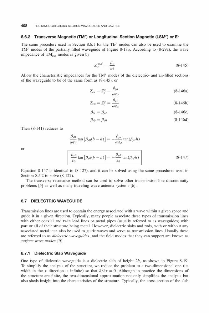
Balanis c08.tex V3 - 11/22/2011 3:32 P.M. Page 408
408 RECTANGULAR CROSS-SECTION WAVEGUIDES AND CAVITIES
8.6.2 Transverse Magnetic (TMy) or Longitudinal Section Magnetic (LSMy) or Ey
The same procedure used in Section 8.6.1 for the TEy modes can also be used to examine theTMy modes of the partially filled waveguide of Figure 8-18a . According to (8-29a), the waveimpedance of TMz
mn modes is given by
Z TMz
w = βz
ωε(8-145)
Allow the characteristic impedances for the TMy modes of the dielectric- and air-filled sectionsof the waveguide to be of the same form as (8-145), or
Zcd = Z ed = βyd
ωεd(8-146a)
Zc0 = Z e0 = βy0
ωε0(8-146b)
βtd = βyd (8-146c)
βt0 = βy0 (8-146d)
Then (8-141) reduces to
βy0
ωε0tan
[βy0(b − h)
] = − βyd
ωεdtan(βyd h)
orβy0
ε0tan
[βy0(b − h)
] = −βyd
εdtan(βyd h) (8-147)
Equation 8-147 is identical to (8-127), and it can be solved using the same procedures used inSection 8.5.2 to solve (8-127).
The transverse resonance method can be used to solve other transmission line discontinuityproblems [5] as well as many traveling wave antenna systems [6].
8.7 DIELECTRIC WAVEGUIDE
Transmission lines are used to contain the energy associated with a wave within a given space andguide it in a given direction. Typically, many people associate these types of transmission lineswith either coaxial and twin lead lines or metal pipes (usually referred to as waveguides) withpart or all of their structure being metal. However, dielectric slabs and rods, with or without anyassociated metal, can also be used to guide waves and serve as transmission lines. Usually theseare referred to as dielectric waveguides , and the field modes that they can support are known assurface wave modes [9].
8.7.1 Dielectric Slab Waveguide
One type of dielectric waveguide is a dielectric slab of height 2h , as shown in Figure 8-19.To simplify the analysis of the structure, we reduce the problem to a two-dimensional one (itswidth in the x direction is infinite) so that ∂/∂x = 0. Although in practice the dimensions ofthe structure are finite, the two-dimensional approximation not only simplifies the analysis butalso sheds insight into the characteristics of the structure. Typically, the cross section of the slab

Balanis c08.tex V3 - 11/22/2011 3:32 P.M. Page 409
DIELECTRIC WAVEGUIDE 409
y
y
xz
x
z
2h
2h
(a)
(b)
ed, md
ed, md
Figure 8-19 Geometry for dielectric slab waveguide. (a) Perspective. (b) Side view.
in Figure 8-19a would be rectangular with height 2h and finite width a . We also assume thatthe waves are traveling in the ±z directions, and the structure is infinite in that direction, asillustrated in Figure 8-19b.
Another practical configuration for a dielectric transmission line is a dielectric rod of circularcross section. Because of the cylindrical geometry of the structure, the field solutions will be interms of Bessel functions. Therefore, the discussion of this line will be postponed until Chapter 9.
A very popular dielectric rod waveguide is the fiber optics cable. Typically, this cable is madeof two different materials, one that occupies the center core and the other that serves as a claddingto the center core. This configuration is usually referred to as the step index , and the index ofrefraction of the center core is slightly greater than that of the cladding. Another configurationhas the index of refraction distribution along the cross section of the line graded so that there isa smooth variation in the radial direction from the larger values at the center toward the smallervalues at the periphery. This is referred to as the graded index . This line is discussed in moredetail in Section 9.5.3.
The objective in a dielectric slab waveguide, or any type of waveguide, is to contain the energywithin the structure and direct it toward a given direction. For the dielectric slab waveguide this isaccomplished by having the wave bounce back and forth between its upper and lower interfacesat an incidence angle greater than the critical angle. When this is accomplished, the refractedfields outside the dielectric form evanescent (decaying) waves and all the real energy is reflectedand contained within the structure. The characteristics of this line can be analyzed by treatingthe structure as a boundary-value problem whose modal solution is obtained by solving thewave equation and enforcing the boundary conditions. The other approach is to examine thecharacteristics of the line using ray-tracing (geometrical optics) techniques. This approach issimpler and sheds more physical insight onto the propagation characteristics of the line but does
Balanis c08.tex V3 - 11/22/2011 3:32 P.M. Page 410
410 RECTANGULAR CROSS-SECTION WAVEGUIDES AND CAVITIES
not provide the details of the more cumbersome modal solution. Both methods will be examinedhere. We will begin with the modal solution approach.
It can be shown that the waveguide structure of Figure 8-19 can support TEz , TMz , TEy , andTMy modes. We will examine here both the TMz and TEz modes. We will treat TMz in detailand then summarize the TEz .
8.7.2 Transverse Magnetic (TMz) Modes
The TMz mode fields that can exist within and outside the dielectric slab of Figure 8-19 mustsatisfy (8-24), where Az is the potential function representing the fields either within or outsidethe dielectric slab. Inside and outside the dielectric region, the fields can be represented by acombination of even and odd modes, as shown in Figure 8-20 [10].
For the fields within the dielectric slab, the potential function Az takes the following form:
−h ≤ y ≤ h
Adz = [
C d2 cos(βyd y) + Dd
2 sin (βyd y)]
Ad3 e−jβz z = Ad
ze + Adzo (8-148)
where
Adze = C d
2 Ad3 cos (βyd y)e−jβz z = Ad
me cos (βyd y)e−jβz z (8-148a)
Adzo = Dd
2 Ad3 sin (βyd y)e−jβz z = Ad
mo sin (βyd y)e−jβz z (8-148b)
β2yd + β2
z = β2d = ω2μdεd (8-148c)
In (8-148), Adze and Ad
zo represent, respectively, the even and odd modes. For the slab to functionas a waveguide, the fields outside the dielectric slab must be of evanescent form. Therefore, the
y
z2h
+h
Even mode Odd mode
sin (bydy)cos (bydy)
e−a(y−h)
ea(y−h)
−h
ed, md
e0, m0
e0, m0
Figure 8-20 Even and odd mode field distributions in a dielectric slab waveguide. (Source: M. Zahn,Electromagnetic Field Theory , 1979. Reprinted with permission of John Wiley & Sons, Inc.)
Balanis c08.tex V3 - 11/22/2011 3:32 P.M. Page 411
DIELECTRIC WAVEGUIDE 411
potential function Az takes the following form:
y ≥ h
A0+z = (
A0+2e e−jβy0 y + B0+
2o e−jβy0y)
A0+3o e−jβz z = A0+
ze + A0+zo (8-149)
where
A0+ze = A0+
2e A0+3o e−jβy0y e−jβz z = A0+
me e−αy0y e−jβz z (8-149a)
A0+zo = B0+
2o A0+3o e−jβy0y e−jβz z = B0+
mo e−αy0y e−jβz z (8-149b)
β2y0 + β2
z = −α2y0 + β2
z = β20 = ω2μ0ε0 (8-149c)
y ≤ −h
A0−z = (
A0−2e e+jβy0 y + B0−
2o e+jβy0y)
A0−3o e−jβz z = A0−
ze + A0−zo (8-150)
where
A0−ze = A0−
2e A0−3o e+jβy0y e−jβz z = A0−
me e+αy0y e−jβz z (8-150a)
A0−zo = B0−
2o A0−3o e+jβy0y e−jβz z = B0−
me e+αy0y e−jβz z (8-150b)
β2y0 + β2
z = −α2y0 + β2
z = β20 = ω2μ0ε0 (8-150c)
For the fields of (8-149) through (8-150c) to be of evanescent form, αy0 must be real and positive.Since the fields within and outside the slab have been separated into even and odd modes,
we can examine them separately and then apply superposition. We will examine the even modesfirst and then the odd. For each mode (even or odd), a number of dependent and independentboundary conditions must be satisfied. A sufficient set of independent boundary conditions chosenhere are
E dz (y = h , z ) = E 0+
z (y = h , z ) (8-151a)
E dz (y = −h , z ) = E 0−
z (y = −h , z ) (8-151b)
H dx (y = h , z ) = H 0+
x (y = h , z ) (8-151c)
H dx (y = −h , z ) = H 0−
x (y = −h , z ) (8-151d)
A. TMz (Even) By using (8-24) along with the appropriate potential function of (8-148) through(8-150c), we can write the field components as follows.
−h ≤ y ≤ h
E dxe = −j
1
ωμdεd
∂2Adze
∂x ∂z= 0 (8-152a)
E dye = −j
1
ωμdεd
∂2Adze
∂y ∂z= βydβz
ωμdεdAd
me sin(βyd y)e−jβz z (8-152b)
E dze = −j
1
ωμdεd
(∂2
∂z 2+ β2
d
)Ad
ze = −jβ2
d − β2z
ωμdεdAd
me cos(βyd y)e−jβz z (8-152c)

Balanis c08.tex V3 - 11/22/2011 3:32 P.M. Page 412
412 RECTANGULAR CROSS-SECTION WAVEGUIDES AND CAVITIES
H dxe = 1
μd
∂Adze
∂y= −βyd
μdAd
me sin(βyd y)e−jβz z (8-152d)
H dye = − 1
μd
∂Adze
∂x= 0 (8-152e)
H dze = 0 (8-152f)
y ≥ +h
E 0+xe = −j
1
ωμ0ε0
∂2A0+ze
∂x ∂z= 0 (8-153a)
E 0+ye = −j
1
ωμ0ε0
∂2A0+ze
∂y ∂z= αy0βz
ωμ0ε0A0+
me e−αy0y e−jβz z (8-153b)
E 0+ze = −j
1
ωμ0ε0
(∂2
∂z 2+ β2
0
)A0+
ze = −jβ2
0 − β2z
ωμ0ε0A0+
me e−αy0y e−jβz z (8-153c)
H 0+xe = 1
μ0
∂A0+ze
∂y= −αy0
μ0A0+
me e−αy0y e−jβz z (8-153d)
H 0+ye = − 1
μ0
∂A0+ze
∂x= 0 (8-153e)
H 0+ze = 0 (8-153f)
y ≤ −h
E 0−xe = −j
1
ωμ0ε0
∂2A0−ze
∂x ∂z= 0 (8-154a)
E 0−ye = −j
1
ωμ0ε0
∂2A0−ze
∂y ∂z= − αy0βz
ωμ0ε0A0−
me e+αy0y e−jβz z (8-154b)
E 0−ze = −j
1
ωμ0ε0
(∂2
∂z 2+ β2
0
)A0−
ze = −jβ2
0 − β2z
ωμ0ε0A0−
me e+αy0y e−jβz z (8-154c)
H 0−xe = 1
μ0
∂A0−ze
∂y= αy0
μ0A0−
me e+αy0y e−jβz z (8-154d)
H 0−ye = − 1
μ0
∂A0−ze
∂x= 0 (8-154e)
H 0−ze = 0 (8-154f)
Applying the boundary condition (8-151a) and using (8-148c) and (8-149c) yields
−jβ2
d − β2z
ωμdεdAd
me cos (βyd h)e−jβz z = −jβ2
0 − β2z
ωμ0ε0A0+
me e−αy0he−jβz z
β2d − β2
z
μdεdAd
me cos (βyd h) = β20 − β2
z
μ0ε0A0+
me e−αy0h
β2yd
μdεdAd
me cos (βyd h) = − α2y0
μ0ε0A0+
me e−αy0h (8-155a)

Balanis c08.tex V3 - 11/22/2011 3:32 P.M. Page 413
DIELECTRIC WAVEGUIDE 413
In a similar manner, enforcing (8-151b) and using (8-148c) and (8-149c) yields
β2yd
μdεdAd
me cos (βyd h) = − α2y0
μ0ε0A0−
me e−αy0h (8-155b)
Comparison of (8-155a) and (8-155b) makes it apparent that
A0+me = A0−
me = A0me (8-155c)
Thus, (8-155a) and (8-155b) are the same and both can be represented by
β2yd
μdεdAd
me cos (βyd h) = − α2y0
μ0ε0A0
mee−αy0h (8-156)
Follow a similar procedure by applying (8-151c) and (8-151d) and using (8-155c). Then we arriveat
βyd
μdAd
me sin (βyd h) = αy0
μ0A0
mee−αy0h (8-157)
Division of (8-157) by (8-156) allows us to write that
εd
βydtan (βyd h) = − ε0
αy0
βyd cot (βyd h) = −εd
ε0αy0
− ε0
εd(βyd h) cot (βyd h) = αy0h (8-158)
where according to (8-148c) and (8-149c)
β2yd + β2
z = β2d = ω2μdεd ⇒ β2
yd = β2d − β2
z = ω2μdεd − β2z (8-158a)
−α2y0 + β2
z = β20 = ω2μ0ε0 ⇒ α2
y0 = β2z − β2
0 = β2z − ω2μ0ε0 (8-158b)
From the free space looking down the slab we can define an impedance, which, by using(8-153a) through (8-153f) and (8-158b), can be written as
Z −y0w = − E 0+
ze
H 0+xe
= E 0−ze
H 0−xe
= −jβ2
0 − β2z
ωε0αy0= j
αy0
ωε0(8-158c)
which is inductive, and it indicates that TM mode surface waves are supported by inductivesurfaces . In fact, surfaces with inductive impedance characteristics, such as dielectric slabs,dielectric-covered ground planes, and corrugated surfaces with certain heights and constitutiveparameters, are designed to support TM surface waves.

Balanis c08.tex V3 - 11/22/2011 3:32 P.M. Page 414
414 RECTANGULAR CROSS-SECTION WAVEGUIDES AND CAVITIES
B. TMz (Odd) By following a procedure similar to that used for the TMz (even), utilizing theodd mode TMz potential functions (8-148) through (8-150c), it can be shown that the expressioncorresponding to (8-158) is
ε0
εd(βyd h) tan (βyd h) = αy0h (8-159)
where (8-158a) and (8-158b) also apply for the TMz odd modes.
C. Summary of TMz (Even) and TMz (Odd) Modes The most important expressions thatare applicable for TMz even and odd modes for a dielectric slab waveguide are (8-158) through(8-159), which are summarized here.
− ε0
εd(βyd h) cot(βyd h) = αy0h TMz (even) (8-160a)
ε0
εd(βyd h) tan(βyd h) = αy0h TMz (odd) (8-160b)
β2yd + β2
z = β2d = ω2μdεd ⇒ β2
yd = β2d − β2
z = ω2μdεd − β2z
TMz (even and odd) (8-160c)
−α2y0 + β2
z = β20 = ω2μ0ε0 ⇒ α2
y0 = β2z − β2
0 = β2z − ω2μ0ε0
TMz (even and odd) (8-160d)
Z −y0w = − E 0+
z
H 0+x
= E 0−z
H 0−x
= jαy0
ωε0TMz (even and odd) (8-160e)
The objective here is to determine which modes can be supported by the dielectric slab whenit is used as a waveguide, and to solve for βyd , αy0, βz , and the cutoff frequencies for each ofthese modes by using (8-160a) through (8-160d). We will begin by determining the modes andtheir corresponding frequencies.
It is apparent from (8-160c) and (8-160d) that if βz is real, then
1. βz < β0 < βd :
βyd = ±√
β2d − β2
z = real (8-161a)
αy0 = ±j√
β20 − β2
z = imaginary (8-161b)
2. βz > βd > β0:
βyd = ±j√
β2z − β2
d = imaginary (8-162a)
αy0 = ±√
β2z − β2
0 = real (8-162b)
Balanis c08.tex V3 - 11/22/2011 3:32 P.M. Page 415
DIELECTRIC WAVEGUIDE 415
3. β0 < βz < βd :
βyd = ±√
β2d − β2
z = real (8-163a)
αy0 = ±√
β2z − β2
0 = real (8-163b)
For the dielectric slab to perform as a lossless transmission line, βyd , αy0, and βz must all bereal . Therefore, for this to occur,
ω√
μ0ε0 = β0 < βz < βd = ω√
μdεd (8-164)
The lowest frequency for which unattenuated propagation occurs is called the cutoff frequency .For the dielectric slab this occurs when βz = β0. Thus, at cutoff, βz = β0, and (8-158a) and(8-158b) reduce to
βyd |βz =β0 = ±√
ω2μdεd − β2z |βz =β0 = ±ωc
√μdεd − μ0ε0 = ±ωc
√μ0ε0
√μrεr − 1 (8-165a)
αy0|βz =β0 = ±√
β2z − ω2μ0ε0|βz =β0 = 0 (8-165b)
Through the use of (8-165a) and (8-165b), the nonlinear transcendental equations 8-160a and8-160b are satisfied, respectively, when the following equations hold.
TMzm (even)
cot(βyd h) = 0 ⇒ βyd h = ωch√
μdεd − μ0ε0 = mπ
2
(fc)m = m
4h√
μdεd − μ0ε0, m = 1, 3, 5, . . . (8-166a)
TMzm (odd)
tan(βyd h) = 0 ⇒ βyd h = ωch√
μdεd − μ0ε0 = mπ
2
(fc)m = m
4h√
μdεd − μ0ε0, m = 0, 2, 4, . . . (8-166b)
It is apparent that the cutoff frequency of a given mode is a function of the electrical constitutiveparameters of the dielectric slab and its height. The modes are referred to as odd TMz
m (whenm = 0, 2, 4, . . .), and even TMz
m (when m = 1, 3, 5, . . .). The dominant mode is the TM0, whichis an odd mode and its cutoff frequency is zero. This means that the TM0 mode will alwayspropagate unattenuated no matter what the frequency of operation. Other higher-order modes canbe cut off by selecting a frequency of operation smaller than their cutoff frequencies.
Now that the TMzm (even) and TMz
m (odd) modes and their corresponding cutoff frequencieshave been determined, the next step is to find βyd , ay0, and βz for any TMz even or odd modeat any frequency above its corresponding cutoff frequency. This is accomplished by solving thetranscendental equations 8-160a and 8-160b.
Assume that ε0/εd , h , and the frequency of operation f are specified. Then (8-160a) and(8-160b) can be solved numerically through the use of iterative techniques by selecting values of
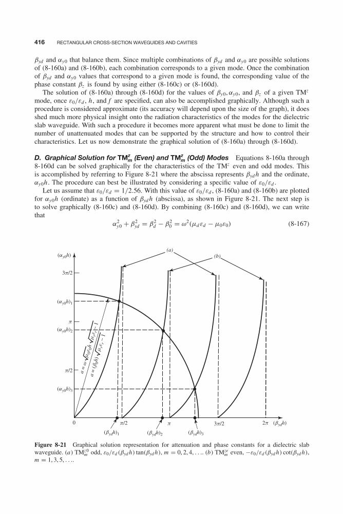
Balanis c08.tex V3 - 11/22/2011 3:32 P.M. Page 416
416 RECTANGULAR CROSS-SECTION WAVEGUIDES AND CAVITIES
βyd and αy0 that balance them. Since multiple combinations of βyd and αy0 are possible solutionsof (8-160a) and (8-160b), each combination corresponds to a given mode. Once the combinationof βyd and αy0 values that correspond to a given mode is found, the corresponding value of thephase constant βz is found by using either (8-160c) or (8-160d).
The solution of (8-160a) through (8-160d) for the values of βy0, αy0, and βz of a given TMz
mode, once ε0/εd , h , and f are specified, can also be accomplished graphically. Although such aprocedure is considered approximate (its accuracy will depend upon the size of the graph), it doesshed much more physical insight onto the radiation characteristics of the modes for the dielectricslab waveguide. With such a procedure it becomes more apparent what must be done to limit thenumber of unattenuated modes that can be supported by the structure and how to control theircharacteristics. Let us now demonstrate the graphical solution of (8-160a) through (8-160d).
D. Graphical Solution for TMzm (Even) and TMz
m (Odd) Modes Equations 8-160a through8-160d can be solved graphically for the characteristics of the TMz even and odd modes. Thisis accomplished by referring to Figure 8-21 where the abscissa represents βyd h and the ordinate,αy0h . The procedure can best be illustrated by considering a specific value of ε0/εd .
Let us assume that ε0/εd = 1/2.56. With this value of ε0/εd , (8-160a) and (8-160b) are plottedfor αy0h (ordinate) as a function of βyd h (abscissa), as shown in Figure 8-21. The next step isto solve graphically (8-160c) and (8-160d). By combining (8-160c) and (8-160d), we can writethat
α2y0 + β2
yd = β2d − β2
0 = ω2(μdεd − μ0ε0) (8-167)
(bydh)1 (bydh)2 (bydh)3
(bydh)
(ay0h)
(ay0h)1
(a)(b)
(ay0h)2
a = w
m0e 0
hm
rer
− 1
(ay0h)3
a =
(b0h)
p/2
p/2 p0
p
3p/2
3p/2 2p
mre
r −
1
Figure 8-21 Graphical solution representation for attenuation and phase constants for a dielectric slabwaveguide. (a) TMz0
m odd, ε0/εd (βyd h) tan(βyd h), m = 0, 2, 4, . . .. (b) TMzem even, −ε0/εd (βyd h) cot(βyd h),
m = 1, 3, 5, . . ..
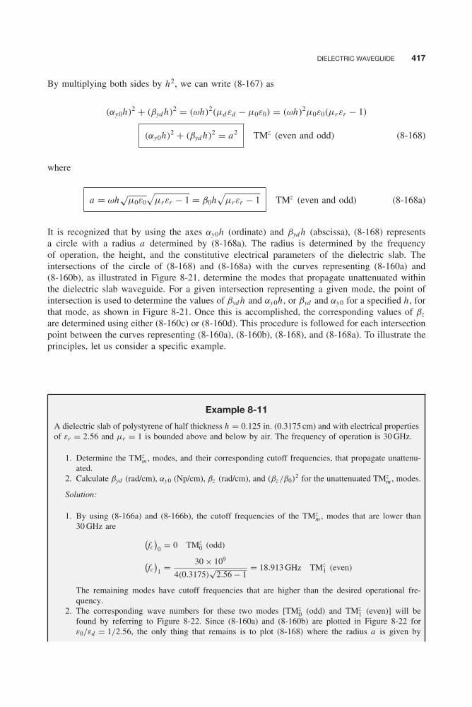
Balanis c08.tex V3 - 11/22/2011 3:32 P.M. Page 417
DIELECTRIC WAVEGUIDE 417
By multiplying both sides by h2, we can write (8-167) as
(αy0h)2 + (βyd h)2 = (ωh)2(μdεd − μ0ε0) = (ωh)2μ0ε0(μrεr − 1)
(αy0h)2 + (βyd h)2 = a2 TMz (even and odd) (8-168)
where
a = ωh√
μ0ε0
√μrεr − 1 = β0h
√μrεr − 1 TMz (even and odd) (8-168a)
It is recognized that by using the axes αy0h (ordinate) and βyd h (abscissa), (8-168) representsa circle with a radius a determined by (8-168a). The radius is determined by the frequencyof operation, the height, and the constitutive electrical parameters of the dielectric slab. Theintersections of the circle of (8-168) and (8-168a) with the curves representing (8-160a) and(8-160b), as illustrated in Figure 8-21, determine the modes that propagate unattenuated withinthe dielectric slab waveguide. For a given intersection representing a given mode, the point ofintersection is used to determine the values of βyd h and αy0h , or βyd and αy0 for a specified h , forthat mode, as shown in Figure 8-21. Once this is accomplished, the corresponding values of βz
are determined using either (8-160c) or (8-160d). This procedure is followed for each intersectionpoint between the curves representing (8-160a), (8-160b), (8-168), and (8-168a). To illustrate theprinciples, let us consider a specific example.
Example 8-11
A dielectric slab of polystyrene of half thickness h = 0.125 in. (0.3175 cm) and with electrical propertiesof εr = 2.56 and μr = 1 is bounded above and below by air. The frequency of operation is 30 GHz.
1. Determine the TMzm , modes, and their corresponding cutoff frequencies, that propagate unattenu-
ated.2. Calculate βyd (rad/cm), αy0 (Np/cm), βz (rad/cm), and (βz /β0)
2 for the unattenuated TMzm , modes.
Solution:
1. By using (8-166a) and (8-166b), the cutoff frequencies of the TMzm , modes that are lower than
30 GHz are (fc)
0 = 0 TMz0 (odd)(
fc)
1 = 30 × 109
4(0.3175)√
2.56 − 1= 18.913 GHz TMz
1 (even)
The remaining modes have cutoff frequencies that are higher than the desired operational fre-quency.
2. The corresponding wave numbers for these two modes [TMz0 (odd) and TMz
1 (even)] will befound by referring to Figure 8-22. Since (8-160a) and (8-160b) are plotted in Figure 8-22 forε0/εd = 1/2.56, the only thing that remains is to plot (8-168) where the radius a is given by
Balanis c08.tex V3 - 11/22/2011 3:32 P.M. Page 418
418 RECTANGULAR CROSS-SECTION WAVEGUIDES AND CAVITIES
(bydh)0
(bydh)1
bydh
(ay0h)0
(ay0h)1
ay0h
5
4
3
2.492
2.108
0.872
1.329
2.334
2.492
2
1
00 1 2 3 4 5
TM1 (even)
TM0 (odd)z
z
Figure 8-22 Graphical solution for attenuation and phase constants of TMzm modes in a dielectric slab
waveguide (εr = 2.56, μr = 1, h = 0.3175 cm, f = 30 GHz).
(8-168a). For f = 30 GHz, the radius of (8-168a) the circle (8-168) is equal to
a = 2π(30 × 109)(0.3175)
30 × 109
√2.56 − 1 = 2.492
This is also plotted in Figure 8-22. The projections from each intersection point to the abscissa(βyd h axis) and ordinate (αy0h axis) allow the determination of the corresponding wave numbers.From Figure 8-22
TMz0 (odd)
(βyd h)0 = 1.329 ⇒ βyd = 4.186 rad/cm
(αy0h)0 = 2.108 ⇒ αy0 = 6.639 Np/cm
When these values are substituted in (8-160c) or (8-160d), they lead to
βz = 9.140 rad/cm (βz /β0)2 = 2.116
TMz1 (even)
(βyd h)1 = 2.334 ⇒ βyd = 7.351 rad/cm
(αy0h)1 = 0.872 ⇒ αy0 = 2.747 Np/cm
When these values are substituted in (8-160c) or (8-160d), they lead to
βz = 6.857 rad/cm (βz /β0)2 = 1.191
Balanis c08.tex V3 - 11/22/2011 3:32 P.M. Page 419
DIELECTRIC WAVEGUIDE 419
Equations 8-160a through 8-160d can also be solved simultaneously and analytically for αy0,βyd , and βz through use of a procedure very similar to that outlined in Section 8.5.1 for theTEy modes of a partially filled rectangular waveguide. The results are shown, respectively, inFigures 8-23a and 8-23b for the TMz
0 and TMz1 modes of Example 8-11 in the frequency range
0 ≤ f ≤ 2(fc)1, where (fc)1 is the cutoff frequency of the TMz1 mode.
Curves similar to those of Figures 8-21 and 8-22 were generated for εr = 1, 2.56, 4, 9, 16, and25 and are shown in Figure 8-24. These can be used for the solution of TMz
m , problems wherethe values in the curves will be representing μr ’s instead of εr ’s. This will be seen in the nextsection.
8.7.3 Transverse Electric (TEz) Modes
By following a procedure similar to that for the TMz modes, it can be shown (by leaving outthe details) that the critical expressions for the TEz modes that correspond to those of the TMz
modes of (8-160a) through (8-160d), (8-166a) through (8-166b), (8-168), (8-168a), and (8-160e)are
TEz (even) and TEz (odd)
−μ0
μd(βyd h) cot(βyd h) = αy0h TEz (even) (8-169a)
μ0
μd(βyd h) tan(βyd h) = αy0h TEz (odd) (8-169b)
β2yd + β2
z = β2d = ω2μdεd ⇒ β2
yd = β2d − β2
z = ω2μdεd − β2z
TEz (even and odd) (8-169c)
−α2y0 + β2
z = β20 = ω2μ0ε0 ⇒ α2
y0 = β2z − β2
0 = β2z − ω2μ0ε0
TEz (even and odd) (8-169d)
(fc)m = m
4h√
μdεd − μ0ε0
m = 1, 3, 5, . . . , TEz (even)
m = 0, 2, 4, . . . , TEz (odd)(8-169e)
(8-169f)
(αy0h)2 + (βyd h)2 = a2 TEz (even and odd) (8-169g)
a = ωh√
μ0ε0
√μrεr − 1 = β0h
√μrεr − 1 TEz (even and odd) (8-169h)
Z −y0w = E 0+
x
H 0+z
= − E 0−x
H 0−z
= −jωμ0
αy0TEz (even and odd) (8-169i)
Therefore, TE surface waves are capacitive and are supported by capacitive surfaces , whetherthey are dielectric slabs, dielectric covered ground planes, or corrugated surfaces.
The solution of these proceeds in the same manner as before. The curves shown in Figure 8-24must be used and the appropriate value of μr = μd/μ0 must be selected.
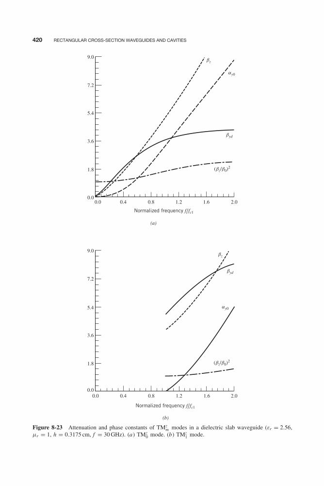
Balanis c08.tex V3 - 11/22/2011 3:32 P.M. Page 420
420 RECTANGULAR CROSS-SECTION WAVEGUIDES AND CAVITIES
(bz/b0)2
byd
ay0
bz
byd
bz
(bz/b0)2
ay0
9.0
7.2
5.4
3.6
1.8
0.0
9.0
7.2
5.4
3.6
1.8
0.00.0 0.4 0.8 1.2 1.6 2.0
0.0 0.4 0.8
(a)
(b)
1.2 1.6 2.0
Normalized frequency f/fc1
Normalized frequency f/fc1
Figure 8-23 Attenuation and phase constants of TMzm modes in a dielectric slab waveguide (εr = 2.56,
μr = 1, h = 0.3175 cm, f = 30 GHz). (a) TMz0 mode. (b) TMz
1 mode.
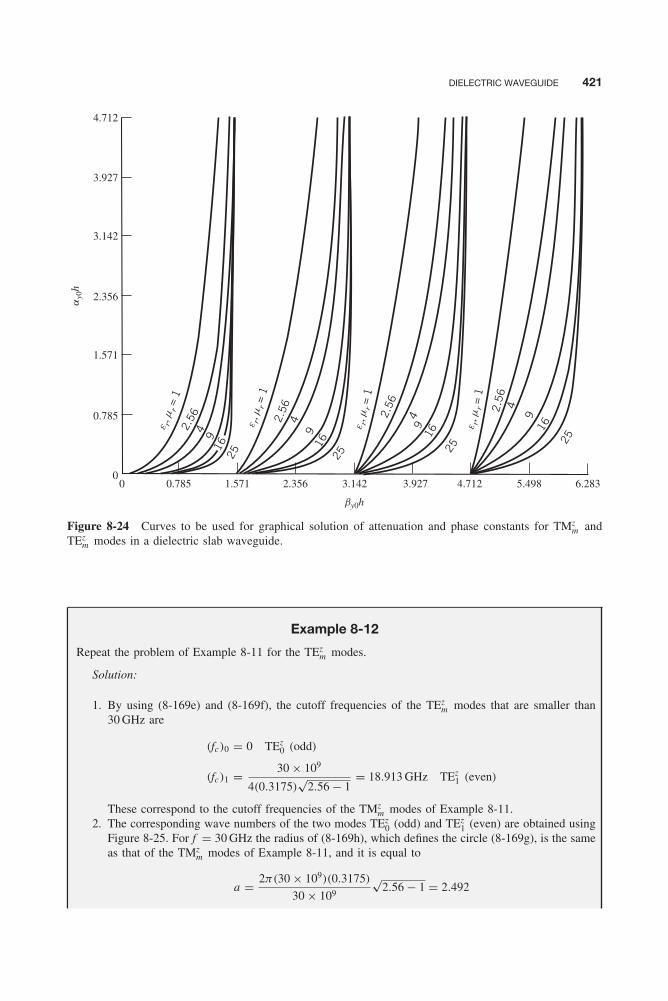
Balanis c08.tex V3 - 11/22/2011 3:32 P.M. Page 421
DIELECTRIC WAVEGUIDE 421
by0h
ay0
h
4.712
3.927
3.142
2.356
1.571
0.785
2.56 2.
56 2.56 2.56
4
916
25
49
16
25
4
4
9 9
16 16
25 25
00 0.785 1.571 2.356 3.142 3.927 4.712 5.498 6.283
e r, mr
= 1
e r, mr
= 1
e r, mr
= 1
e r, m
r =
1
Figure 8-24 Curves to be used for graphical solution of attenuation and phase constants for TMzm and
TEzm modes in a dielectric slab waveguide.
Example 8-12
Repeat the problem of Example 8-11 for the TEzm modes.
Solution:
1. By using (8-169e) and (8-169f), the cutoff frequencies of the TEzm modes that are smaller than
30 GHz are
(fc)0 = 0 TEz0 (odd)
(fc)1 = 30 × 109
4(0.3175)√
2.56 − 1= 18.913 GHz TEz
1 (even)
These correspond to the cutoff frequencies of the TMzm modes of Example 8-11.
2. The corresponding wave numbers of the two modes TEz0 (odd) and TEz
1 (even) are obtained usingFigure 8-25. For f = 30 GHz the radius of (8-169h), which defines the circle (8-169g), is the sameas that of the TMz
m modes of Example 8-11, and it is equal to
a = 2π(30 × 109)(0.3175)
30 × 109
√2.56 − 1 = 2.492

Balanis c08.tex V3 - 11/22/2011 3:32 P.M. Page 422
422 RECTANGULAR CROSS-SECTION WAVEGUIDES AND CAVITIES
This is plotted in Figure 8-25. The projections from each intersection point on the abscissa (βyd haxis) and ordinate (ay0h axis) allows the determination of the corresponding wave numbers. FromFigure 8-25:
TEz0 (odd)
(βyd h)0 = 1.109 ⇒ βyd = 3.494 rad/cm
(αy0h)0 = 2.231 ⇒ αy0 = 7.027 Np/cm
When these are substituted in (8-169c) or (8-169d),
βz = 9.426 rad/cm (βz /β0)2 = 2.251
TEz1 (even)
(βyd h)1 = 2.122 ⇒ βyd = 6.684 rad/cm
(αy0h)1 = 1.306 ⇒ αy0 = 4.113 Np/cm
When these are substituted in (8-169c) or (8-169d),
βz = 7.510 rad/cm (βz /β0)2 = 1.428
bydh
(bydh)1
(ay0h)1
(bydh)0
(ay0h)0
ay0h
1.109
2.122
1.306
2.231
2.492
2.492
0
1
2
3
4
5
0 1 2 3 4 5
TE0 (odd)z
TE1 (even)z
Figure 8-25 Graphical solution for attenuation and phase constants of TEzm modes in a dielectric slab
waveguide (εr = 2.56, μr = 1, h = 0.3175 cm, f = 30 GHz).
Balanis c08.tex V3 - 11/22/2011 3:32 P.M. Page 423
DIELECTRIC WAVEGUIDE 423
For the TEz modes, (8-169a) through (8-169d) can be solved simultaneously and analyticallyfor αy0, βyd , and βz using a procedure very similar to that outlined in Section 8.5.1 for theTEy modes of a partially filled rectangular waveguide. The results are shown in Figures 8-26aand 8-26b for the TEz
0 and TEz1 modes, respectively, of Example 8-12 in the frequency range
0 ≤ f ≤ 2(fc)1 where (fc)1 is the cutoff frequency of the TEz1 mode.
8.7.4 Ray-Tracing Method
In Sections 8.7.2, and 8.7.3 we analyzed the dielectric slab waveguide as a boundary-valueproblem using modal techniques. In this section we want to repeat the analysis of both TEz andTMz modes by using a ray-tracing method that sheds more physical insight onto the propagationcharacteristics of the dielectric slab waveguide but is not as detailed.
A wave beam that is fed into the dielectric slab can propagate into three possible modes [11].Let us assume that the slab is bounded above by air and below by another dielectric slab, asshown in Figure 8-27, such that ε1 > ε2 > ε0. Mathematically the problem involves a solution ofMaxwell’s equations and the appropriate boundary conditions at the two interfaces, as was donein Sections 8.7.2 and 8.7.3. The wave beam has the following properties.
1. It can radiate from the slab into both air and substrate, referred to as the air-substratemodes, as shown in Figure 8-27a .
2. It can radiate from the slab only into the substrate, referred to as the substrate modes , asshown in Figure 8-27b.
3. It can be bounded and be guided by the slab, referred to as the waveguide modes , as shownin Figure 8-27c.
To demonstrate these properties, let us assume that a wave enters the slab, which is boundedabove by air and below by a substrate such that ε1 > ε2 > ε0.
1. Air-Substrate Modes: Referring to Figure 8-27a , let us increase θ1 gradually starting atθ1 = 0. When θ1 is small, a wave that enters the slab will be refracted and will exit into theair and the substrate provided that θ1 < (θc)10 = sin−1(
√ε0/ε1) < (θc)12 = sin−1(
√ε2/ε1).
The angles (θc)10 and (θc)12 represent, respectively, the critical angles at the slab–air andslab–substrate interfaces. In this situation, wave energy can propagate freely in all threemedia (air, slab, and substrate) and can create radiation fields (air–substrate modes).
2. Substrate Modes: When θ1 increases such that it passes the critical angle (θc)10 of theslab–air interface but is smaller than the critical angle (θc)12 of the slab–substrate interface[(θc)12 = sin−1(
√ε2/ε1)> θ1 >(θc)10 = sin−1(
√ε0/ε1)], sin θ0 > 1, which indicates that the
wave is totally reflected at the slab–air interface. This describes a solution that wave energyin the slab radiates only in the substrate, as shown in Figure 8-27b. These are referred toas substrate modes.
3. Waveguide Modes: Finally when θ1 is larger than the critical angle (θc)12 of theslab–substrate interface [θ1 >(θc)12 = sin−1(
√ε2/ε1)>(θc)10 = sin−1(
√ε0/ε1)], then
sin θ0 > 1 and sin θ2 > 1, which indicate that the wave is totally reflected at both interfaces.These are referred to as waveguide modes , as shown in Figure 8-27c. For these modesthe energy is trapped inside the slab, and the waves follow the wave motion patternrepresented by two wave vectors A1 and B1 as shown in Figure 8-28a . These two vectorsare decomposed into their horizontal and vertical components (A1z , A1y ) and (B1z , B1y ).
The horizontal wave vector components are equal, which indicates that the waves propagatewith a constant velocity in the z direction. However, the vertical components of A1 and B1

Balanis c08.tex V3 - 11/22/2011 3:32 P.M. Page 424
424 RECTANGULAR CROSS-SECTION WAVEGUIDES AND CAVITIES
9.0
7.2
5.4
3.6
1.8
0.0
2.59
0.5 1.0 1.5 2.00
5.19
7.78
10.37
0
0.0 0.4 0.8 1.2 1.6 2.0
(bz/b0)2
bz
(bz/b0)2
bz
(b)
Normalized frequency f/fc1
(a)
Normalized frequency f/fc1
byd
byd
ay0
ay0
Figure 8-26 Attenuation and phase constants of TEzm modes in a dielectric slab waveguide (εr = 2.56,
μr = 1, h = 0.3175 cm, f = 30 GHz). (a) TEz0 mode. (b) TEz
1 mode.
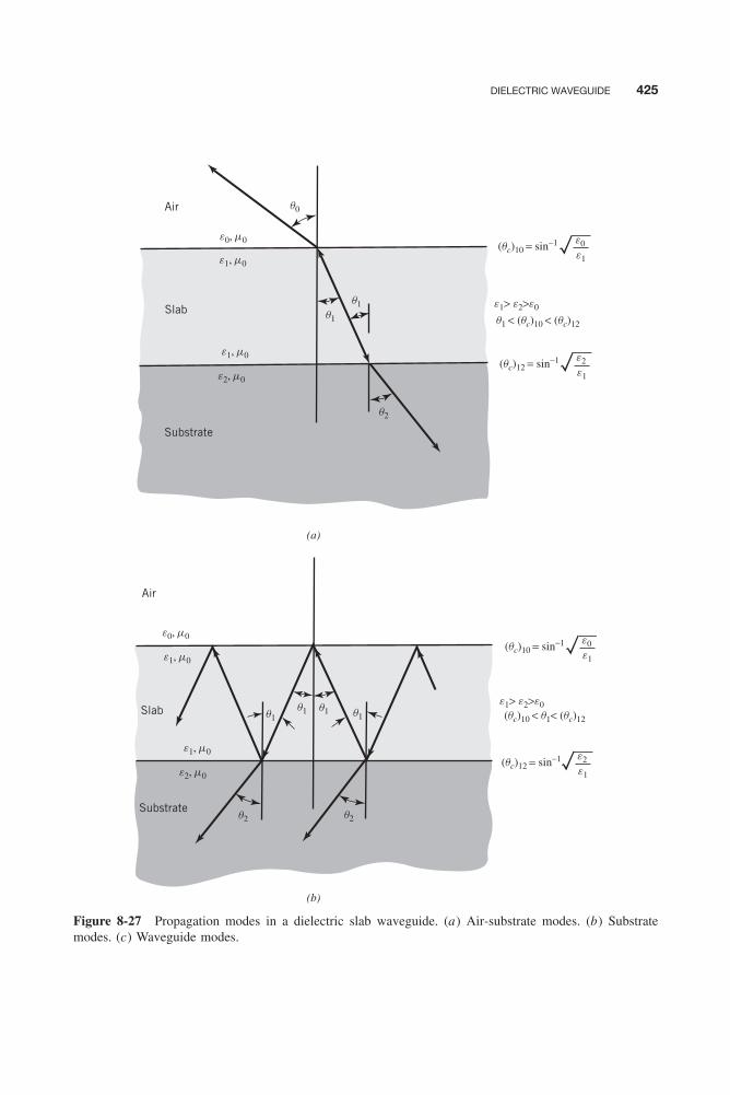
Balanis c08.tex V3 - 11/22/2011 3:32 P.M. Page 425
DIELECTRIC WAVEGUIDE 425
e1, m0
e0, m0
e1, m0
e1, m0
e1, m0
e2, m0
e1> e2>e0
e1> e2>e0
e2, m0
q1
q0
q1q1
q2
q2 q2
q1 q1 q1
Substrate
Slab
Substrate
Slab
Air
e0, m0
Air
(a)
(b)
e0
e1(qc)10 = sin−1
e0
e1(qc)10 = sin−1
e2
e1(qc)12 = sin−1
e2
e1(qc)12 = sin−1
(qc)10 < q1< (qc)12
q1 < (qc)10 < (qc)12
Figure 8-27 Propagation modes in a dielectric slab waveguide. (a) Air-substrate modes. (b) Substratemodes. (c) Waveguide modes.

Balanis c08.tex V3 - 11/22/2011 3:32 P.M. Page 426
426 RECTANGULAR CROSS-SECTION WAVEGUIDES AND CAVITIES
e1, m0
e1, m0
e2, m0
q1
q1q1
q1
Slab
e0, m0
Air
(c)
e1> e2>e0
e0
e1(qc)10 = sin−1
e2
e1(qc)12 = sin−1
(qc)10 < (qc)12< q1
Substrate
Figure 8-27 (Continued)
represent opposite traveling waves, which when combined form a standing wave. By changingthe angle θ1, we change the direction of A1 and B1. This results in changes in the horizontal andvertical components of A1 and B1, in the wave velocity in the z direction, and in the standingwave pattern across the slab.
The wave vectors A1 and B1 can be thought to represent a plane wave, which bounces backand forth inside the slab. The phase fronts of this plane wave are dashed in Figure 8-28b. Anobserver who moves in a direction parallel to the z axis does not see the horizontal components ofthe wave vectors. He does, however, observe a plane wave that bounces upward and downward,which folds one directly on top of the other. In order for the standing wave pattern across theslab to remain the same as the observer travels along the z axis, all multiple reflected wavesmust add in phase. This is accomplished by having the plane wave that makes one round trip,up and down across the slab, experience a phase shift equal to 2mπ , where m is an integer [11].Otherwise if after the first round trip the wave experiences a small differential phase shift of δ
away from 2mπ , it will experience differential phase shifts 2δ, 3δ, . . . after the second, third, . . .
trips. Therefore, these higher-order reflected waves will experience larger differential phase shiftswhich when added will eventually equal zero and the broadside wave pattern of Figure 8-28cwill be a function of the axial position.
A one round-trip phase shift must include not only the phase change that is due to the distancetraveled by the wave but also the changes in the wave phase that are due to reflections from theupper and lower interfaces. If the phase constant of the plane wave along wave vectors A1 andB1 is β1, then the wave constant along the vertical direction y is β1 cos θ1. Therefore, the totalphase shift to one round trip (up and down) of wave travel, including the phase changes due toreflection, must be equal to
4β1h cos θ1 − φ10 − φ12 = 2mπ m = 0, 1, 2, . . . (8-170)
where φ10 = phase of reflection coefficient at slab–air interfaceφ12 = phase of reflection coefficient at slab–substrate interface
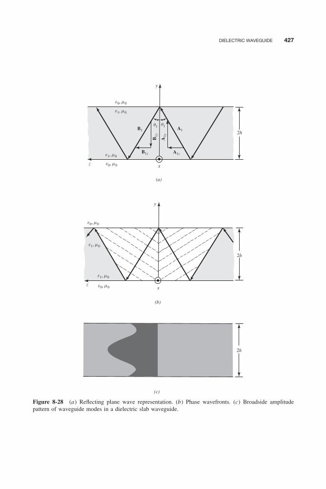
Balanis c08.tex V3 - 11/22/2011 3:32 P.M. Page 427
DIELECTRIC WAVEGUIDE 427
e1, m0
e1, m0
e1, m0
e1, m0
e0, m0
e0, m0
e0, m0
e0, m0
(a)
(b)
(c)
x
y
y
x
z
z
B1z
2h
2h
2h
A1z
A1B1
B1y
A1y
q1 q1
Figure 8-28 (a) Reflecting plane wave representation. (b) Phase wavefronts. (c) Broadside amplitudepattern of waveguide modes in a dielectric slab waveguide.

Balanis c08.tex V3 - 11/22/2011 3:32 P.M. Page 428
428 RECTANGULAR CROSS-SECTION WAVEGUIDES AND CAVITIES
The phases of the reflection coefficients are assumed to be leading. Assume that the media aboveand below the slab are the same. Then φ10 = φ12 = φ. Thus, (8-170) reduces to
4β1h cos θ1 − 2φ = 2mπ m = 0, 1, 2, . . . (8-170a)
The preceding equations will now be applied to both TMz and TEz modes.
A. Transverse Magnetic ( TMz) Modes (Parallel Polarization) Let us assume that thebouncing plane wave of Figure 8-28a is such that its polarization is TMz (or parallel polarization),as shown in Figure 8-29a , where the slab is bounded on both sides by air. For the orientation ofthe fields taken as shown in Figure 8-29a , the reflected electric field Er
|| is related to the incident
e0, m0z
y
x
y
xz
(b)
(a)
e1, m0
Er
Et
Et
Ei
Hi
2h
Hr
Er Ei
Hr Hi
e0, m0
e1, m0
e0, m0
e1, m0
e1, m0
e0, m0
2h
θ1
θ1 θ1
θ0
θ0
θ1
Figure 8-29 Modes in a dielectric slab waveguide. (a) TMz (parallel polarization). (b) TEz (perpendicularpolarization).
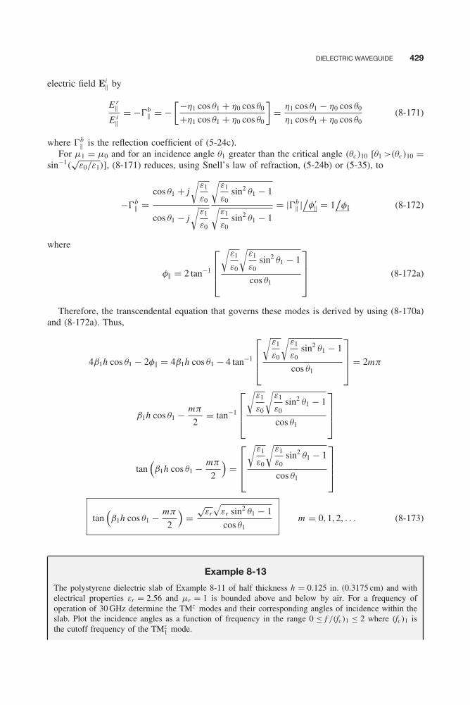
Balanis c08.tex V3 - 11/22/2011 3:32 P.M. Page 429
DIELECTRIC WAVEGUIDE 429
electric field Ei|| by
E r||
E i||
= −�b|| = −
[−η1 cos θ1 + η0 cos θ0
+η1 cos θ1 + η0 cos θ0
]= η1 cos θ1 − η0 cos θ0
η1 cos θ1 + η0 cos θ0(8-171)
where �b|| is the reflection coefficient of (5-24c).
For μ1 = μ0 and for an incidence angle θ1 greater than the critical angle (θc)10 [θ1 >(θc)10 =sin−1(
√ε0/ε1)], (8-171) reduces, using Snell’s law of refraction, (5-24b) or (5-35), to
−�b|| =
cos θ1 + j√
ε1
ε0
cos θ1 − j√
ε1
ε0
√ε1
ε0sin2 θ1 − 1√
ε1
ε0sin2 θ1 − 1
= |�b|| |/φ′
|| = 1/φ|| (8-172)
where
φ|| = 2 tan−1
⎡⎢⎢⎣√
ε1
ε0
√ε1
ε0sin2 θ1 − 1
cos θ1
⎤⎥⎥⎦ (8-172a)
Therefore, the transcendental equation that governs these modes is derived by using (8-170a)and (8-172a). Thus,
4β1h cos θ1 − 2φ|| = 4β1h cos θ1 − 4 tan−1
⎡⎢⎢⎣√
ε1
ε0
√ε1
ε0sin2 θ1 − 1
cos θ1
⎤⎥⎥⎦ = 2mπ
β1h cos θ1 − mπ
2= tan−1
⎡⎢⎢⎣√
ε1
ε0
√ε1
ε0sin2 θ1 − 1
cos θ1
⎤⎥⎥⎦
tan(β1h cos θ1 − mπ
2
)=
⎡⎢⎢⎣√
ε1
ε0
√ε1
ε0sin2 θ1 − 1
cos θ1
⎤⎥⎥⎦
tan(β1h cos θ1 − mπ
2
)=
√εr
√εr sin2 θ1 − 1
cos θ1m = 0, 1, 2, . . . (8-173)
Example 8-13
The polystyrene dielectric slab of Example 8-11 of half thickness h = 0.125 in. (0.3175 cm) and withelectrical properties εr = 2.56 and μr = 1 is bounded above and below by air. For a frequency ofoperation of 30 GHz determine the TMz modes and their corresponding angles of incidence within theslab. Plot the incidence angles as a function of frequency in the range 0 ≤ f /(fc)1 ≤ 2 where (fc)1 isthe cutoff frequency of the TMz
1 mode.

Balanis c08.tex V3 - 11/22/2011 3:32 P.M. Page 430
430 RECTANGULAR CROSS-SECTION WAVEGUIDES AND CAVITIES
5
4
3
2
1
00 10 20 30 40 50 60 70 80 90
Angle (degrees)
Mag
nitu
de
tan (3.1919 cos q1 − )| m = 0mπ2
tan (3.1919 cos q1 − )| m = 1mπ2
2.56 sin2 q1 − 11.6 cos q1
TEm:
2.56 sin2 q1 − 1cos q1
TMm:1.6
q1 = 48.3° (TE1)z
q1 = 69.65° (TE0)z
q1 = 43° (TM1)z q1 = 65.4° (TM0)z
z
z
Figure 8-30 Graphical solution for angles of incidence of TMzm and TEz
m modes in a dielectric slabwaveguide.
Solution: The solution for this set of modes is governed by (8-173). For εr = 2.56 the right side of(8-173) is plotted in Figure 8-30. For f = 30 GHz, the height h of the slab is equal to
λ1 = 30 × 109
√2.56 30 × 109
= 0.6250 cm ⇒ h = 0.3175
0.6250λ1 = 0.5080λ1
Thus, (8-173) reduces to
tan(β1h cos θ1 − mπ
2
)= tan
[2π
λ1(0.5080λ1) cos θ1 − mπ
2
]
= tan(
3.1919 cos θ1 − mπ
2
)= 1.6
√2.56 sin2 θ1 − 1
cos θ1
The left side is plotted for m = 0, 1 in Figure 8-30, and the solutions are intersections of these curves withthe curve representing the right side of (8-173). From Figure 8-30, there are two intersections that occurat θ1 = 65.4◦ and 43◦, which represent, respectively, the modes TMz
0 (θ1 = 65.4◦) and TMz1 (θ1 = 43◦).
They agree with the modes of Example 8-11. No other modes are present because curves of the leftside of (8-173) for higher orders of m (m = 2, 3, . . .) do not intersect with the curve that represents theright side of (8-173). Remember also that the critical angle for the slab–air interface is equal to
(θc)10 = sin−1(√
ε0/ε1) = sin−1(√
1/2.56) = 38.68◦
and the curve that represents the right side of (8-173) does not exist in Figure 8-30 below 38.68◦.
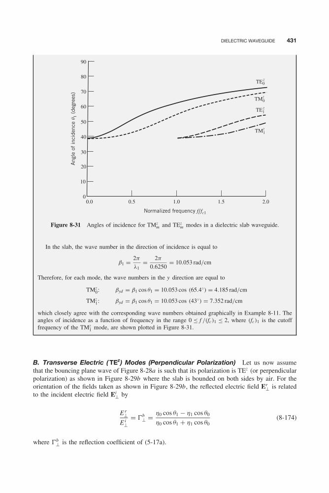
Balanis c08.tex V3 - 11/22/2011 3:32 P.M. Page 431
DIELECTRIC WAVEGUIDE 431
90
80
70
60
50
40
30
20
10
00.0 0.5 1.0 1.5 2.0
Normalized frequency f/fc1
Ang
le o
f in
cide
nce q 1
(de
gree
s)
TE0z
TE1z
TM0z
TM1z
Figure 8-31 Angles of incidence for TMzm and TEz
m modes in a dielectric slab waveguide.
In the slab, the wave number in the direction of incidence is equal to
β1 = 2π
λ1= 2π
0.6250= 10.053 rad/cm
Therefore, for each mode, the wave numbers in the y direction are equal to
TMz0: βyd = β1 cos θ1 = 10.053 cos (65.4◦) = 4.185 rad/cm
TMz1: βyd = β1 cos θ1 = 10.053 cos (43◦) = 7.352 rad/cm
which closely agree with the corresponding wave numbers obtained graphically in Example 8-11. Theangles of incidence as a function of frequency in the range 0 ≤ f /(fc)1 ≤ 2, where (fc)1 is the cutofffrequency of the TMz
1 mode, are shown plotted in Figure 8-31.
B. Transverse Electric ( TEz) Modes (Perpendicular Polarization) Let us now assumethat the bouncing plane wave of Figure 8-28a is such that its polarization is TEz (or perpendicularpolarization) as shown in Figure 8-29b where the slab is bounded on both sides by air. For theorientation of the fields taken as shown in Figure 8-29b, the reflected electric field Er
⊥ is relatedto the incident electric field Ei
⊥ by
E r⊥
E i⊥
= �b⊥ = η0 cos θ1 − η1 cos θ0
η0 cos θ1 + η1 cos θ0(8-174)
where �b⊥ is the reflection coefficient of (5-17a).

Balanis c08.tex V3 - 11/22/2011 3:32 P.M. Page 432
432 RECTANGULAR CROSS-SECTION WAVEGUIDES AND CAVITIES
For μ1 = μ0 and for an incidence angle θ1 greater than the critical angle (θc)10 [θ1 >(θc)10 =sin−1(
√ε0/ε1)], (8-174) reduces, using Snell’s law of refraction, (5-15b) or (5-35) to
�b⊥ =
cos θ1 + j√
sin2 θ1 − ε0
ε1
cos θ1 − j√
sin2 θ1 − ε0
ε1
= |�b⊥|/φ⊥ = 1
/φ⊥ (8-175)
where
φ⊥ = 2 tan−1
⎡⎢⎢⎣√
sin2 θ1 − ε0
ε1
cos θ1
⎤⎥⎥⎦ (8-175a)
Therefore, the transcendental equation that governs these modes is derived by using (8-170a)and (8-175a). Thus,
4β1h cos θ1 − 2φ⊥ = 4β1h cos θ1 − 4 tan−1
⎛⎜⎜⎝√
sin2 θ1 − ε0
ε1
cos θ1
⎞⎟⎟⎠ = 2mπ
β1h cos θ1 − mπ
2= tan−1
⎛⎜⎜⎝√
sin2 θ1 − ε0
ε1
cos θ1
⎞⎟⎟⎠
tan(β1h cos θ1 − mπ
2
)=
√sin2 θ1 − ε0
ε1
cos θ1
tan(β1h cos θ1 − mπ
2
)=
√sin2 θ1 − 1
εr
cos θ1
tan(β1h cos θ1 − mπ
2
)=
√εr sin2 θ1 − 1√
εr cos θ1m = 0, 1, 2, . . . (8-176)
Example 8-14
For the polystyrene slab of Examples 8-12 and 8-13, determine the TEzm modes and their corresponding
angles of incidence within the slab. Plot the angles of incidence as a function of frequency in the range0 ≤ f /(fc)1 ≤ 2 where (fc)1 is the cutoff frequency of the TEz
1 mode.
Solution: The solution for this set of modes is governed by (8-176). From the solution ofExample 8-13
h = 0.5080λ1
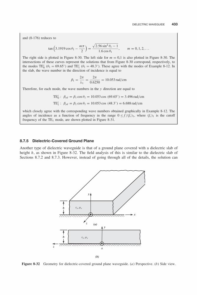
Balanis c08.tex V3 - 11/22/2011 3:32 P.M. Page 433
DIELECTRIC WAVEGUIDE 433
and (8-176) reduces to
tan(
3.1919 cos θ1 − mπ
2
)=
√2.56 sin2 θ1 − 1
1.6 cos θ1, m = 0, 1, 2, . . .
The right side is plotted in Figure 8-30. The left side for m = 0,1 is also plotted in Figure 8-30. Theintersections of these curves represent the solutions that from Figure 8-30 correspond, respectively, tothe modes TEz
0 (θ1 = 69.65◦) and TEz1 (θ1 = 48.3◦). These agree with the modes of Example 8-12. In
the slab, the wave number in the direction of incidence is equal to
β1 = 2π
λ1= 2π
0.6250= 10.053 rad/cm
Therefore, for each mode, the wave numbers in the y direction are equal to
TEz0 : βyd = β1 cos θ1 = 10.053 cos (69.65◦) = 3.496 rad/cm
TEz1 : βyd = β1 cos θ1 = 10.053 cos (48.3◦) = 6.688 rad/cm
which closely agree with the corresponding wave numbers obtained graphically in Example 8-12. Theangles of incidence as a function of frequency in the range 0 ≤ f /(fc)1, where (fc)1 is the cutofffrequency of the TE1 mode, are shown plotted in Figure 8-31.
8.7.5 Dielectric-Covered Ground Plane
Another type of dielectric waveguide is that of a ground plane covered with a dielectric slab ofheight h , as shown in Figure 8-32. The field analysis of this is similar to the dielectric slab ofSections 8.7.2 and 8.7.3. However, instead of going through all of the details, the solution can
er, mr
er, mr
(a)(a)
yy
xx
zz
zz
hh
hh
(b)(b)
yy
xx
Figure 8-32 Geometry for dielectric-covered ground plane waveguide. (a) Perspective. (b) Side view.
Balanis c08.tex V3 - 11/22/2011 3:32 P.M. Page 434
434 RECTANGULAR CROSS-SECTION WAVEGUIDES AND CAVITIES
be obtained by examining the solutions for the dielectric slab as applied to the dielectric coveredground plane. For y ≥ h , the main differences between the two geometries are the additionalboundary conditions at y = 0 for the dielectric-covered ground plane.
For the dielectric slab of Figure 8-19, the electric field components within the dielectric slabfor the TMz and TEz modes (even and odd) of Figure 8-20 can be written from Sections 8.7.2and 8.7.3 as
TMz (even)
E dxe = 0
E dye = βydβz
ωμdεdAd
me sin(βyd y)e−jβz z
E dze = −j
β2d − β2
z
ωμdεdAd
me cos(βyd y)e−jβz z
⎫⎪⎪⎪⎪⎪⎪⎪⎬⎪⎪⎪⎪⎪⎪⎪⎭|y | ≤ h (8-177a)
TMz (odd)
E dxo = 0
E dyo = − βydβz
ωμdεdAd
mo cos(βyd y)e−jβz z
E dzo = −j
β2d − β2
z
ωμdεdAd
mo sin(βyd y)e−jβz z
⎫⎪⎪⎪⎪⎪⎪⎪⎬⎪⎪⎪⎪⎪⎪⎪⎭|y | ≤ h (8-177b)
TEz (even)
E dxe = βyd
εdBd
me sin(βyd y)e−jβz z
E dye = 0
E dze = 0
⎫⎪⎪⎪⎪⎬⎪⎪⎪⎪⎭ |y | ≤ h (8-177c)
TEz (odd)
E dxo = −βyd
εdBd
mo cos(βyd y)e−jβz z
E dyo = 0
E dzo = 0
⎫⎪⎪⎪⎪⎬⎪⎪⎪⎪⎭ |y | ≤ h (8-177d)
By examining (8-177a) through (8-177d), it is apparent that the tangential electric field com-ponents TMz (odd) of (8-177b) and TEz (even) of (8-177c) do satisfy the boundary conditionsof Figure 8-32 at y = 0 (vanishing tangential electric components at y = 0). However, thoseTMz (even) of (8-177a) and TEz (odd) of (8-177d) do not satisfy the boundary conditions ofthe tangential electric field components at y = 0. Therefore, the geometry of Figure 8-32 supports

Balanis c08.tex V3 - 11/22/2011 3:32 P.M. Page 435
DIELECTRIC WAVEGUIDE 435
only modes that are TMz (odd ) and TEz (even). From Sections 8.7.2 and 8.7.3, the governingequations for the geometry of Figure 8-32 for TMz (odd) and TEz (even) modes are
ε0
εd(βyd h) tan(βyd h) = (αy0h) TMz (odd) (8-178a)
−μ0
μd(βyd h) cot(βyd h) = (αy0h) TEz (even) (8-178b)
β2yd + β2
z = β2d = ω2μdεd TMz (odd), TEz (even) (8-178c)
−α2y0 + β2
z = β20 = ω2μ0ε0 TMz (odd), TEz (even) (8-178d)
(fc)m = m
4h√
μdεd − μ0ε0
m = 0, 2, 4, . . . , TMz (odd)
m = 1, 3, 5, . . . , TEz (even)
(8-178e)
(8-178f)
Thus, the dominant mode is the TMz0 with a zero cutoff frequency. All the modes in a dielectric-
covered ground plane are usually referred to as surface wave modes , and their solutions areobtained in the same manner as outlined in Sections 8.7.2, 8.7.3, and 8.7.4 for the dielectric slabwaveguide. The only difference is that for the dielectric covered ground plane we only have TMz
m(odd) and TEz
m (even) modes. The structure cannot support TMzm (even) and TEz
m (odd) modes.The attenuation rate of the evanescent fields in air above the dielectric cover is determined by
the value of αy0, which is found using (8-178d). Above cutoff, it is expressed as
αy0 =√
β2z − β2
0 =√
β2z − ω2μ0ε0 (8-179)
For very thick dielectrics (h → large) the phase constant βz approaches βd (βz → βd ).Thus,
αy0|h→large =√
β2z − ω2μ0ε0 � ω
√μdεd − μ0ε0 = ω
√μ0ε0
√μdεd
μ0ε0− 1 (8-180)
which is usually very large.For very thin dielectrics (h → small), the phase constant βz approaches β0 (βz → β0). Thus,
from (8-178c) and (8-178d),
β2yd |h→small = β2
d − β2z � β2
d − β20 = ω2(μdεd − μ0ε0) = ω2μ0ε0
(μdεd
μ0ε0− 1
)(8-181a)
α2y0|h→small = β2
z − β20 � small (8-181b)
For small values of h , (8-178a) reduces for αy0 to
αy0
∣∣h→small = βyd
ε0
εdtan(βyd h)
h→0� hε0
εd(βyd )2 (8-182)
Balanis c08.tex V3 - 11/22/2011 3:32 P.M. Page 436
436 RECTANGULAR CROSS-SECTION WAVEGUIDES AND CAVITIES
Substituting (8-181a) into (8-182) reduced it to
αy0
∣∣h→small � h
ε0
εd
[ω2μ0ε0
(μdεd
μ0ε0− 1
)]= hβ2
0
(μd
μ0− ε0
εd
)= 2πβ0
(μd
μ0− ε0
εd
)h
λ0(8-182a)
which is usually very small.
Example 8-15
A ground plane is covered with a dielectric sheet of polystyrene of height h . Determine the distance δ
(skin depth) above the dielectric–air interface so that the evanescent fields above the sheet will decayto e−1 = 0.368 of their value at the interface, when h is very large and h is very small (= 10−3λ0).
Solution: The distance the wave travels and decays to 36.84% of its value is referred to as the skindepth.
For h very large, according to (8-180),
δ = 1
αy0� 1
β0
√μd εd
μ0ε0− 1
= λ0
2π√
2.56 − 1= 0.126λ0
and the wave is said to be “tightly bound” to the thick dielectric sheet.For h very small (h = 10−3λ0), according to (8-182a),
δ = 1
αy0� λ0
2πβ0
(μd
μ0− ε0
εd
)h
= λ0
(2π)2
(1 − 1
2.56
)× 10−3
= 41.6λ0
and this wave is said to be “loosely bound” to the thin dielectric sheet.
8.8 ARTIFICIAL IMPEDANCE SURFACES
Artificial impedance surfaces, also referred to as engineered electromagnetic surfaces , have beendeveloped over the last few decades to alter the impedance boundary conditions of the surface ofa structure and thus control the radiation characteristics, such as radiation efficiency and pattern,of antenna elements placed at or near them, or the scattering of impinging electromagnetic waves[12–17]. When electromagnetic waves interact with surfaces that exhibit geometrical periodicity,they result in some interesting and exciting characteristics, which typically have numerous appli-cations that have captured the attention and imagination of engineers and scientists. Using a ‘broadbrush’ designation, these surfaces can also be referred to as metamaterials , which were discussedin Section 5.7. Since metamaterials may be used to designate double negative (DNG) type mate-rials, there have been other designations of artificial impedance or engineered electromagneticsurfaces. These designations began initially as Photonic Band-Gap (PBG) structures [18, 19],which targeted primarily optics type of structures and frequencies. PBG structures are 1-D, 2-D,and 3-D periodic configurations, both dielectric and conducting, which have the ability to manip-ulate the electromagnetic radiation so as to not allow it to propagate within certain frequencyranges, or band-gaps. Most of the focus of PBG has been devoted to dielectric structures, althoughthe applications have expanded to metallic structures, such as waveguides, resonators, filters, andantennas, which usually exhibit metallic losses that are more dominant at higher frequencies,compared to dielectric losses. The PBG structures are analogous to semiconductor materials thatmanipulate the electrons to exhibit electronic band-gaps. The PBG designation was expanded to

Balanis c08.tex V3 - 11/22/2011 3:32 P.M. Page 437
ARTIFICIAL IMPEDANCE SURFACES 437
include other type of structures and frequencies, such as Electromagnetic Band-Gap (EBG) struc-tures, Frequency Selective Surfaces (FSS), High Impedance Surfaces (HIS), Artificial MagneticConductors (AMC), Perfect Magnetic Conductors [PMC], etc. A comprehensive list of variousEBG designations and references, organized by topics, can be found in the appendix of [17]. In[14] the EBG designation was introduced as a more broad classification to encompass the others.
Artificial impedance surfaces can be used for, but are not limited to:
• Change the surface impedance• Control the phase of the reflection coefficient• Manipulate the propagation of surface waves• Control the frequency band (stop band, pass band, band gaps)• Control the edge diffractions, especially of horns and reflectors• Design new boundary conditions to control the radiation pattern of small antennas• Provide detailed control over the scattering properties• Design tunable impedance surfaces to be used as:
a. Steerable reflectorsb. Steerable leaky-wave antennas
This is accomplished by altering the surface of a structure, by modifying its geometry and/oradding other layers, so that the surface waves and/or the phase of the reflection coefficient ofthe modified surface can be controlled. Although the magnitude of the reflection coefficient willalso be affected, it is the phase that primarily has the most significant impact. While an idealPMC surface introduces, through its image, a zero-phase shift in the reflected field, in contrastto a PEC, which presents a 180◦ phase shift, the reflection phase of an EBG surface can, ingeneral, vary from −180◦ to +180◦, which makes the EBG more versatile and unique [12, 13].This will be demonstrated in section 8.8.2. While, in general, PEC, PMC, and EBG surfaces pos-sess individually attractive characteristics, they also exhibit shortcomings when electromagneticradiating elements are mounted on such structures, especially when the designs are judged usingaerodynamic, stealth, and conformal criteria. For example, when an electric element is mountedvertically on a PEC surface, its image reinforces its radiation and system efficiency; however, itsgeometry is not low-profile, an undesirable characteristic for aerodynamic, stealth, and conformaldesigns. However, when the same electric radiating element is placed horizontally on a PECsurface, its radiation efficiency suffers because its image possesses a 180◦ phase shift and itsradiation cancels that of the actual element; however, the design exhibits low profile character-istics usually desirable for aerodynamic, stealth, and conformal applications. In contrast, whenthe same electric radiating element is placed horizontally on a PMC surface, its image possessesa 0◦ phase and reinforces the radiation of the actual element, in addition to having low-profilecharacteristics. The characteristics of vertical and horizontal electric elements placed verticallyand horizontally on PEC and PMC surfaces are based on image theory of Figure 7-2, and theyare visually contrasted in Figure 8-33 [20].
While EBG surfaces exhibit similar characteristics as PMCs when radiating elements aremounted on them, they also have the ability to suppress surface waves of low-profile antennadesigns, such as microstrip arrays. Surface waves are introduced in microstrip arrays, whichprimarily travel within the substrate and are instrumental in developing coupling between thearray elements. This can limit the beam scanning capabilities of the microstrip arrays; ultimately,surface waves and coupling may even lead to scan blindness, discussed in Section 8.8.3.
An EBG surface emulates a nearly PMC surface and suppresses surface waves only over afrequency range; thus, it is usually referred to as a band-gap structure. In general, the frequencyrange (band-gap) over which an EBG structure operates more efficiently depends upon the appli-cation. For example, the frequency range over which a radiating element in the presence of anEBG possesses a good impedance match, which in [16] is referred to as the input-matchfrequency band , may not be the same frequency range over which a microstrip array suppresses
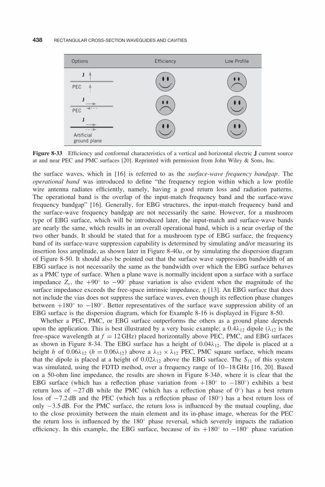
Balanis c08.tex V3 - 11/22/2011 3:32 P.M. Page 438
438 RECTANGULAR CROSS-SECTION WAVEGUIDES AND CAVITIES
Options
J
J
J
PEC
PEC
Artificialground plane
Efficiency Low Profile
Figure 8-33 Efficiency and conformal characteristics of a vertical and horizontal electric J current sourceat and near PEC and PMC surfaces [20]. Reprinted with permission from John Wiley & Sons, Inc.
the surface waves, which in [16] is referred to as the surface-wave frequency bandgap. Theoperational band was introduced to define “the frequency region within which a low profilewire antenna radiates efficiently, namely, having a good return loss and radiation patterns.The operational band is the overlap of the input-match frequency band and the surface-wavefrequency bandgap” [16]. Generally, for EBG structures, the input-match frequency band andthe surface-wave frequency bandgap are not necessarily the same. However, for a mushroomtype of EBG surface, which will be introduced later, the input-match and surface-wave bandsare nearly the same, which results in an overall operational band, which is a near overlap of thetwo other bands. It should be stated that for a mushroom type of EBG surface, the frequencyband of its surface-wave suppression capability is determined by simulating and/or measuring itsinsertion loss amplitude, as shown later in Figure 8-40a , or by simulating the dispersion diagramof Figure 8-50. It should also be pointed out that the surface wave suppression bandwidth of anEBG surface is not necessarily the same as the bandwidth over which the EBG surface behavesas a PMC type of surface. When a plane wave is normally incident upon a surface with a surfaceimpedance Zs , the +90◦ to −90◦ phase variation is also evident when the magnitude of thesurface impedance exceeds the free-space intrinsic impedance, η [13]. An EBG surface that doesnot include the vias does not suppress the surface waves, even though its reflection phase changesbetween +180◦ to −180◦. Better representatives of the surface wave suppression ability of anEBG surface is the dispersion diagram, which for Example 8-16 is displayed in Figure 8-50.
Whether a PEC, PMC, or EBG surface outperforms the others as a ground plane dependsupon the application. This is best illustrated by a very basic example; a 0.4λ12 dipole (λ12 is thefree-space wavelength at f = 12 GHz) placed horizontally above PEC, PMC, and EBG surfacesas shown in Figure 8-34. The EBG surface has a height of 0.04λ12. The dipole is placed at aheight h of 0.06λ12 (h = 0.06λ12) above a λ12 × λ12 PEC, PMC square surface, which meansthat the dipole is placed at a height of 0.02λ12 above the EBG surface. The S11 of this systemwas simulated, using the FDTD method, over a frequency range of 10–18 GHz [16, 20]. Basedon a 50-ohm line impedance, the results are shown in Figure 8-34b, where it is clear that theEBG surface (which has a reflection phase variation from +180◦ to −180◦) exhibits a bestreturn loss of −27 dB while the PMC (which has a reflection phase of 0◦) has a best returnloss of −7.2 dB and the PEC (which has a reflection phase of 180◦) has a best return loss ofonly −3.5 dB. For the PMC surface, the return loss is influenced by the mutual coupling, dueto the close proximity between the main element and its in-phase image, whereas for the PECthe return loss is influenced by the 180◦ phase reversal, which severely impacts the radiationefficiency. In this example, the EBG surface, because of its +180◦ to −180◦ phase variation

Balanis c08.tex V3 - 11/22/2011 3:32 P.M. Page 439
ARTIFICIAL IMPEDANCE SURFACES 439
h2 = 0.02 l12
h1 = 0.04l12
(a)
0
S1
1 (
dB)
−5
−10
10 12 14
Frequency (GHz)
EBG
PMC
PEC
16 18
−15
−20
−25
−30
(b)
Figure 8-34 Geometry and S11 of horizontal dipole above PEC, PMC and EBG surfaces [20]. Reprintedwith permission from John Wiley & Sons, Inc. (a) Geometry. (b) Reflection coefficient.
over the frequency band-gap of the EBG design, outperforms the PEC and PMC and servesas a good ground plane. The other two, the PEC and PMC, possess constant out-of-phase andin-phase phase characteristics, respectively, over the entire frequency range.
Now that we have introduced some of the basic definitions of artificial impedance surfaces,we examine some basic structures—corrugations in Section 8.8.1 and mushroom EBG surfacein Section 8.8.2—that exhibit such characteristics. Application of mushroom EBG surfaces toantenna technology is discussed in Section 8.8.3. A semi-empirical procedure for the design ofmushroom EBG surfaces is outlined in Section 8.8.4. The design leads, in some cases, to ratherexcellent results when compared to simulations based on a full-wave electromagnetic solver. Thelimitations of the design are summarized in Section 8.8.6.
8.8.1 Corrugations
There are a number of surfaces that have been developed over the years whose surface impedancehas been altered by introducing changes on the surface of the structure. One such surface alter-ation, which has been in use for many decades, is the introduction of grooves, usually referredto as corrugations , with a depth at or near quarter of a wavelength, as shown in Figure 8-35.Since the width of the corrugations, w , is usually equal or less than about λ/10 (w ≤ λ/10 andthe thickness t is also about 1/10 of the width, or t ≤ w/10 ≤ λ/100), each corrugation can betreated as a shorted transmission line. Since the input impedance of a shorted transmission lineof length � is
Zin = jZc tan(β�) (8-183)
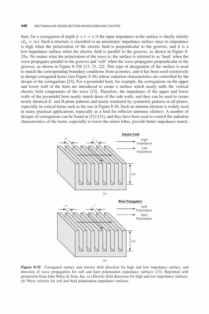
Balanis c08.tex V3 - 11/22/2011 3:32 P.M. Page 440
440 RECTANGULAR CROSS-SECTION WAVEGUIDES AND CAVITIES
then, for a corrugation of depth d = � = λ/4 the input impedance at the surface is ideally infinity(Zin = ∞). Such a structure is classified as an anisotropic impedance surface since its impedanceis high when the polarization of the electric field is perpendicular to the grooves, and it is alow-impedance surface when the electric field is parallel to the grooves, as shown in Figure 8-35a . No matter what the polarization of the wave is, the surface is referred to as ‘hard’ when thewave propagates parallel to the grooves and ‘soft’ when the wave propagates perpendicular to thegrooves, as shown in Figure 8-35b [13, 21, 22]. This type of designation of the surface is usedto match the corresponding boundary conditions from acoustics, and it has been used extensivelyto design corrugated horns (see Figure 8-36) whose radiation characteristics are controlled by thedesign of the corrugations [23]. For a pyramidal horn, for example, the corrugations on the upperand lower wall of the horn are introduced to create a surface which nearly nulls the verticalelectric field components of the wave [23]. Therefore, the impedance of the upper and lowerwalls of the pyramidal horn nearly match those of the side walls, and they can be used to createnearly identical E- and H-plane patterns and nearly rotational by symmetric patterns in all planes,especially in conical horns such as the one in Figure 8-36. Such an antenna element is widely usedin many practical applications, especially as a feed for reflector antennas (dishes). A number ofdesigns of corrugations can be found in [21]-[31], and they have been used to control the radiationcharacteristics of the horns, especially to lower the minor lobes, provide better impedance match,
(a)
(b)
l/4
Wave Propagation
SoftPolarization
w
HardPolarization
t
Electric Field
l/4
HighImpedance
w
LowImpedance
t
Figure 8-35 Corrugated surface and electric field direction for high and low impedance surface, anddirection of wave propagation for soft and hard polarization impedance surfaces [13]. Reprinted withpermission from John Wiley & Sons, Inc. (a) Electric field directions for high and low impedance surfaces.(b) Wave velocity for soft and hard polarization impedance surfaces.

Balanis c08.tex V3 - 11/22/2011 3:32 P.M. Page 441
ARTIFICIAL IMPEDANCE SURFACES 441
Figure 8-36 Conical corrugated horn antenna [23]. Reprinted with permission from John Wiley & Sons,Inc.
minimize the diffractions from the edges at the aperture of the horn, and attempt to synthesize anearly symmetrical amplitude pattern by equalizing those of the E- and H-planes.
Just like corrugations/grooves have been introduced on PEC surfaces, conducting strips havealso been placed circumferentially (T-strips) and axially (L-strips) on the surface of dielectriccircular cylinders to create anisotropic boundary conditions and polarization selective surfaces tocontrol the scattering from cylinders [32]. Electric fields that are perpendicular to the length of thestrips are ideally transmitted while those parallel to the length of the strips are ideally reflected.This procedure creates an impedance surface that can perform as dichroic polarization-sensitivefilter for electromagnetic waves.
8.8.2 Artificial Magnetic Conductors (AMC), Electromagnetic Band-Gap (EBG), andPhotonic Band-Gap (PBG) Surfaces
While perfect electric conductors (PECs) exist in nature, perfect magnetic conductors (PMCs) donot. However, it will be of benefit to fabricate PMCs, even artificially. From the electromagneticboundary conditions, PEC surfaces are those over which the tangential components of electricfields vanish. Therefore, this precludes the placement at, or even near, their surfaces of radiat-ing elements such as tangential electric dipoles, spirals, etc., because their radiated fields overthem will be shorted out, or nearly so. This of course is obvious from image theory where theactual source and its image are next to each other but are oriented in opposite directions. This isillustrated in Figure 7-2. Such arrangements even exhibit low radiation efficiency for low heightsbecause of the 180◦ phase reversal of its image. In fact, when locating a horizontal electric ele-ment, such as a horizontal dipole, next to a PEC, it must be placed at a height h = λ/4 above it inorder for the radiation, in a direction normal to the surface, to be maximum. Such an arrangementis usually not desired, especially when the elements are placed on spaceborne platforms, becauseof aerodynamic considerations. Also, for stealth type of targets, such configurations are quitevisible and create large radar cross section (RCS) signature. Therefore, it is quite beneficial ifPMC surfaces can be created, even artificially.
Within recent years, PMC surfaces have been synthesized and fabricated artificially and exhibitPMC-type properties within a frequency range; therefore, these surfaces often are referred to asband-gap or band-limited surfaces. There have been many such surfaces—too numerous to
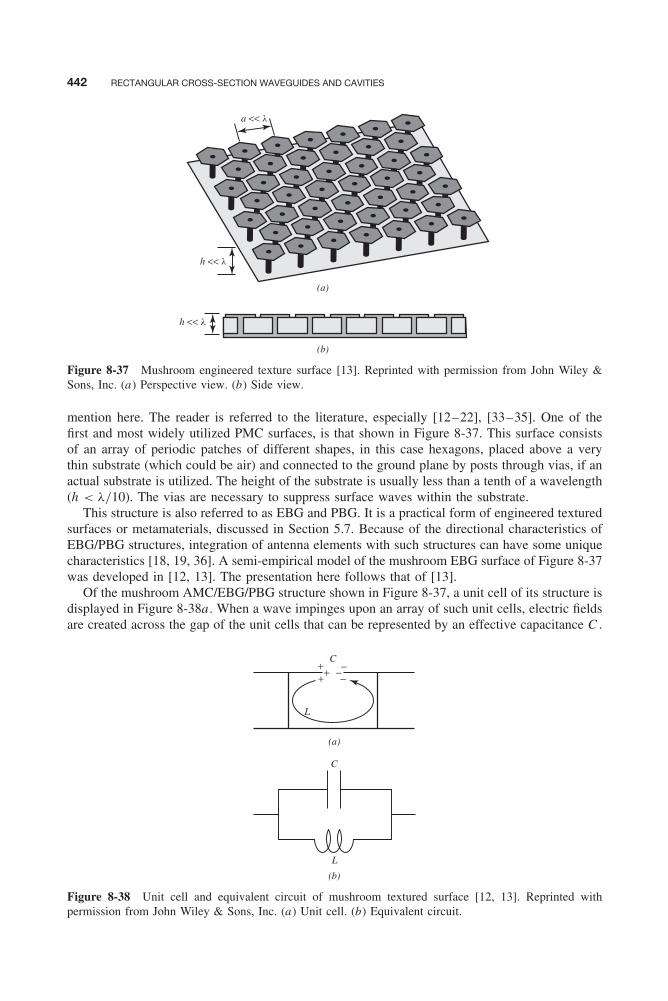
Balanis c08.tex V3 - 11/22/2011 3:32 P.M. Page 442
442 RECTANGULAR CROSS-SECTION WAVEGUIDES AND CAVITIES
(a)
(b)
h << l
a << l
h << l
Figure 8-37 Mushroom engineered texture surface [13]. Reprinted with permission from John Wiley &Sons, Inc. (a) Perspective view. (b) Side view.
mention here. The reader is referred to the literature, especially [12–22], [33–35]. One of thefirst and most widely utilized PMC surfaces, is that shown in Figure 8-37. This surface consistsof an array of periodic patches of different shapes, in this case hexagons, placed above a verythin substrate (which could be air) and connected to the ground plane by posts through vias, if anactual substrate is utilized. The height of the substrate is usually less than a tenth of a wavelength(h < λ/10). The vias are necessary to suppress surface waves within the substrate.
This structure is also referred to as EBG and PBG. It is a practical form of engineered texturedsurfaces or metamaterials, discussed in Section 5.7. Because of the directional characteristics ofEBG/PBG structures, integration of antenna elements with such structures can have some uniquecharacteristics [18, 19, 36]. A semi-empirical model of the mushroom EBG surface of Figure 8-37was developed in [12, 13]. The presentation here follows that of [13].
Of the mushroom AMC/EBG/PBG structure shown in Figure 8-37, a unit cell of its structure isdisplayed in Figure 8-38a . When a wave impinges upon an array of such unit cells, electric fieldsare created across the gap of the unit cells that can be represented by an effective capacitance C .
(a)
(b)
L
C
C
L
−−−+++
Figure 8-38 Unit cell and equivalent circuit of mushroom textured surface [12, 13]. Reprinted withpermission from John Wiley & Sons, Inc. (a) Unit cell. (b) Equivalent circuit.

Balanis c08.tex V3 - 11/22/2011 3:32 P.M. Page 443
ARTIFICIAL IMPEDANCE SURFACES 443
Also, such impinging fields create currents that circulate between adjacent unit cells. The effectsof these current paths through the neighboring walls or vias, can be represented by an equivalentinductance L. Therefore, the equivalent circuit of the unit cell of Figure 8-38a is shown inFigure 8-38b, which consists of a capacitance C in parallel with an inductance L [13].
The surface impedance of the individual unit cell of Figure 8-38 is given by
Zs = jωL
1 − ω2LC(8-184)
while its resonant frequency is represented by
ωo = 1√LC
(8-185)
However, for design purposes, as it will be shown in section 8.8.4, sheet inductance Ls andsheet capacitance Cs must be used to define the resonant frequency. The sheet inductance andcapacitance take into account not only the geometry of the individual unit cells but also thegeometrical arrangement of the unit cells [13]. It is apparent from (8-184) that the surface ofthe unit cell is inductive below the resonant frequency, capacitive above the resonant frequency,infinity at resonance, and very high near resonance. Based on (8-158c) of Section 8.7.2, inductivesurfaces support TM types of surface waves while based on (8-169i) of Section 8.7.3, capacitivesurfaces support TE type of surface waves.
The support of either TE or TM surface wave modes, or both, was verified by measuringthe transmission between a pair of coaxial probes placed near the surface of a fabricated 12-cmhigh impedance surface reported in [13]. The artificially fabricated PMC surface consisted ofa triangular lattice of metallic hexagons placed on the surface of a grounded substrate with adielectric constant of 2.2, as shown in Figure 8-39. The excitation of the surface waves, TE orTM modes, is controlled by the orientation of the probes. The amplitude of the transmissionbetween the probes is shown in Figure 8-40a while the phase, based on a plane wave normalincidence, is displayed in Figure 8-40b [13]. It is apparent from Figure 8-40a that the fabricatedand tested surface exhibits high impedance between approximately 11-16 GHz (band-gap) whileit supports TM surface waves (inductive surface) below the band gap and TE surface waves(capacitive surface) above the band gap. By examining the plane wave incidence phase responseof the mushroom surface in Figure 8-40b, it is apparent that the edges of the band-gap occurwhere the phase varies nearly from +90◦ to −90◦, and it is basically zero at resonance. Whilethe transmission amplitude and phase characteristics shown in Figures 8-40a and 8-40b are thoseof a mushroom type of high impedance surface, they may be different for other type of surfaces,particularly those that may not include vertical vias [13]. A semi-empirical design procedure forhigh impedance surfaces can be found in [13], and it will be presented here in Section 8.8.4.
w = 0.7794 mm
a = 1.5 mm
h
g = 0.15 mm
1.6 mm
Figure 8-39 Triangular lattice of hexagons, built on a grounded substrate with a relative dielectric constantof 2.2 [13]. Reprinted with permission from John Wiley & Sons, Inc.
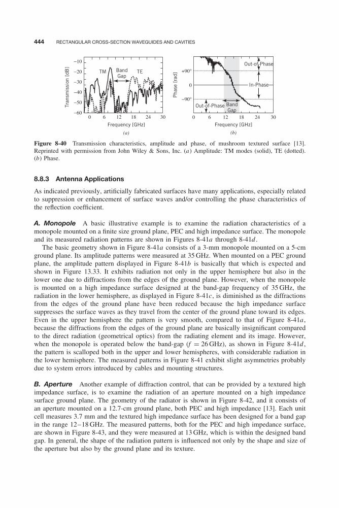
Balanis c08.tex V3 - 11/22/2011 3:32 P.M. Page 444
444 RECTANGULAR CROSS-SECTION WAVEGUIDES AND CAVITIES
(a) (b)
BandGap
0 6
Tran
smis
sion
[dB
]
−60
−50
−40
−30
−20
−10
12
Frequency [GHz] Frequency [GHz]
18 24
Out-of-Phase
Out-of-Phase
In-Phase
30 0
0
−90°
+90°
Pha
se [
rad]
6 12 18 24 30
TM TEBandGap
Figure 8-40 Transmission characteristics, amplitude and phase, of mushroom textured surface [13].Reprinted with permission from John Wiley & Sons, Inc. (a) Amplitude: TM modes (solid), TE (dotted).(b) Phase.
8.8.3 Antenna Applications
As indicated previously, artificially fabricated surfaces have many applications, especially relatedto suppression or enhancement of surface waves and/or controlling the phase characteristics ofthe reflection coefficient.
A. Monopole A basic illustrative example is to examine the radiation characteristics of amonopole mounted on a finite size ground plane, PEC and high impedance surface. The monopoleand its measured radiation patterns are shown in Figures 8-41a through 8-41d .
The basic geometry shown in Figure 8-41a consists of a 3-mm monopole mounted on a 5-cmground plane. Its amplitude patterns were measured at 35 GHz. When mounted on a PEC groundplane, the amplitude pattern displayed in Figure 8-41b is basically that which is expected andshown in Figure 13.33. It exhibits radiation not only in the upper hemisphere but also in thelower one due to diffractions from the edges of the ground plane. However, when the monopoleis mounted on a high impedance surface designed at the band-gap frequency of 35 GHz, theradiation in the lower hemisphere, as displayed in Figure 8-41c, is diminished as the diffractionsfrom the edges of the ground plane have been reduced because the high impedance surfacesuppresses the surface waves as they travel from the center of the ground plane toward its edges.Even in the upper hemisphere the pattern is very smooth, compared to that of Figure 8-41a ,because the diffractions from the edges of the ground plane are basically insignificant comparedto the direct radiation (geometrical optics) from the radiating element and its image. However,when the monopole is operated below the band-gap (f = 26 GHz), as shown in Figure 8-41d ,the pattern is scalloped both in the upper and lower hemispheres, with considerable radiation inthe lower hemisphere. The measured patterns in Figure 8-41 exhibit slight asymmetries probablydue to system errors introduced by cables and mounting structures.
B. Aperture Another example of diffraction control, that can be provided by a textured highimpedance surface, is to examine the radiation of an aperture mounted on a high impedancesurface ground plane. The geometry of the radiator is shown in Figure 8-42, and it consists ofan aperture mounted on a 12.7-cm ground plane, both PEC and high impedance [13]. Each unitcell measures 3.7 mm and the textured high impedance surface has been designed for a band gapin the range 12–18 GHz. The measured patterns, both for the PEC and high impedance surface,are shown in Figure 8-43, and they were measured at 13 GHz, which is within the designed bandgap. In general, the shape of the radiation pattern is influenced not only by the shape and size ofthe aperture but also by the ground plane and its texture.

Balanis c08.tex V3 - 11/22/2011 3:32 P.M. Page 445
ARTIFICIAL IMPEDANCE SURFACES 445
(a) (b)
0°
45°
90°
135°
180°
225°
270°
315°
0°
45°
90°
135°
180°
225°
270°
315°
(c) (d)
10dB
10dB
0°
45°
90°
135°
180°
225°
270°
315°
10dB
Figure 8-41 Monopole and its patterns on a ground plane; PEC and PMC [13]. Reprinted with permissionfrom John Wiley & Sons, Inc. (a) Monopole geometry (3 mm monopole, 5 cm ground plane). (b) PECground plane (f = 35 GHz). (c) PMC ground plane (f = 35 GHz). (d ) PMC ground plane (f = 26 GHz).
(a) (b)
Figure 8-42 Aperture antenna in a high-impedance surface. The unit cells of the high-impedance surfacemeasure 3.7 mm, and the size of the ground plane (not shown to scale) is 12.7 cm. The aperture is fed bya coax to Ku-band rectangular waveguide transition [13]. Reprinted with permission from John Wiley &Sons, Inc. (a) Side view. (b) Front view.
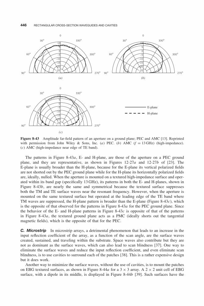
Balanis c08.tex V3 - 11/22/2011 3:32 P.M. Page 446
446 RECTANGULAR CROSS-SECTION WAVEGUIDES AND CAVITIES
E-plane
H-plane
(a) (b)
(c)
90°
60°
30°0
0
10
5
0
−5
−10
−15
−20
330°
300°
270° 90°
60°
30°0
10
5
0
−5
−10
−15
−20
330°
300°
270°
90°
60°
30°10
5
0
−5
−10
−15
−20
330°
300°
270°
−25
−25
−25
Figure 8-43 Amplitude far-field pattern of an aperture on a ground plane; PEC and AMC [13]. Reprintedwith permission from John Wiley & Sons, Inc. (a) PEC. (b) AMC (f = 13 GHz) (high-impedance).(c) AMC (high-impedance near edge of TE band).
The patterns in Figure 8-43a , E- and H-plane, are those of the aperture on a PEC groundplane, and they are representative, as shown in Figures 12-27a and 12-27b of [23]. TheE-plane is usually broader than the H-plane, because for the E-plane its vertical polarized fieldsare not shorted out by the PEC ground plane while for the H-plane its horizontally polarized fieldsare, ideally, nulled. When the aperture is mounted on a textured high-impedance surface and oper-ated within its band gap (specifically 13 GHz), its patterns in both the E- and H-planes, shown inFigure 8-43b, are nearly the same and symmetrical because the textured surface suppressesboth the TM and TE surface waves near the resonant frequency. However, when the aperture ismounted on the same textured surface but operated at the leading edge of the TE band whereTM waves are suppressed, the H-plane pattern is broader than the E-plane (Figure 8-43c), whichis the opposite of that observed for the patterns in Figure 8-43a for the PEC ground plane. Sincethe behavior of the E- and H-plane patterns in Figure 8-43c is opposite of that of the patternsin Figure 8-43a , the textured ground plane acts as a PMC (ideally shorts out the tangentialmagnetic fields), which is the opposite of that for the PEC.
C. Microstrip In microstrip arrays, a detrimental phenomenon that leads to an increase in theinput reflection coefficient of the array, as a function of the scan angle, are the surface wavescreated, sustained, and traveling within the substrate. Space waves also contribute but they arenot as dominant as the surface waves, which can also lead to scan blindness [37]. One way toeliminate the surface waves and reduce the input reflection coefficient, and even eliminate scanblindness, is to use cavities to surround each of the patches [38]. This is a rather expensive designbut it does work.
Another way to minimize the surface waves, without the use of cavities, is to mount the patcheson EBG textured surfaces, as shown in Figure 8-44a for a 3 × 3 array. A 2 × 2 unit cell of EBGsurface, with a dipole in its middle, is displayed in Figure 8-44b [39]. Such surfaces have the
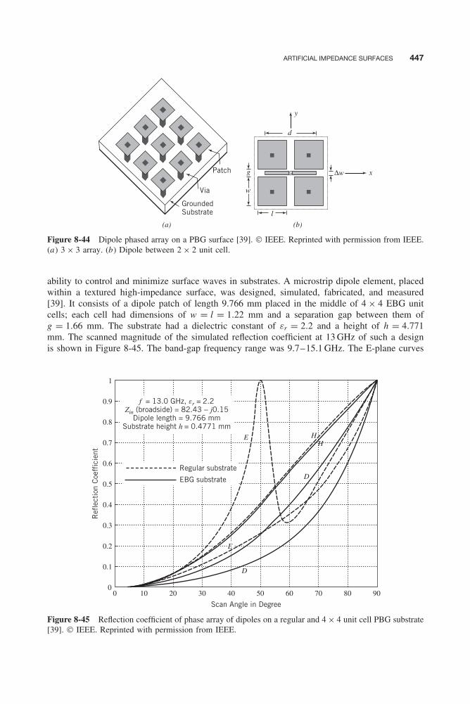
Balanis c08.tex V3 - 11/22/2011 3:32 P.M. Page 447
ARTIFICIAL IMPEDANCE SURFACES 447
(a)
Patch
Via
GroundedSubstrate
y
d
xg
w
l
Δw
(b)
Figure 8-44 Dipole phased array on a PBG surface [39]. © IEEE. Reprinted with permission from IEEE.(a) 3 × 3 array. (b) Dipole between 2 × 2 unit cell.
ability to control and minimize surface waves in substrates. A microstrip dipole element, placedwithin a textured high-impedance surface, was designed, simulated, fabricated, and measured[39]. It consists of a dipole patch of length 9.766 mm placed in the middle of 4 × 4 EBG unitcells; each cell had dimensions of w = l = 1.22 mm and a separation gap between them ofg = 1.66 mm. The substrate had a dielectric constant of εr = 2.2 and a height of h = 4.771mm. The scanned magnitude of the simulated reflection coefficient at 13 GHz of such a designis shown in Figure 8-45. The band-gap frequency range was 9.7–15.1 GHz. The E-plane curves
E
Ref
lect
ion
Coe
ffic
ient
1
0.9
0.8
0.7
0.6
0.5
0.4
0.3
0.2
0.1
00 10 20 30 40
Scan Angle in Degree
E
D
D
HH
50 60 70 80 90
f = 13.0 GHz, er = 2.2Zin (broadside) = 82.43 − j0.15
Dipole length = 9.766 mmSubstrate height h = 0.4771 mm
Regular substrate
EBG substrate
Figure 8-45 Reflection coefficient of phase array of dipoles on a regular and 4 × 4 unit cell PBG substrate[39]. © IEEE. Reprinted with permission from IEEE.
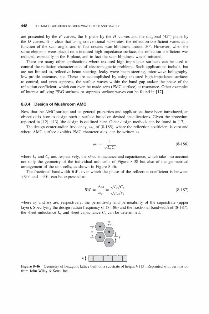
Balanis c08.tex V3 - 11/22/2011 3:32 P.M. Page 448
448 RECTANGULAR CROSS-SECTION WAVEGUIDES AND CAVITIES
are presented by the E curves, the H-plane by the H curves and the diagonal (45◦) plane bythe D curves. It is clear that using conventional substrates, the reflection coefficient varies as afunction of the scan angle, and in fact creates scan blindness around 50◦. However, when thesame elements were placed on a textured high-impedance surface, the reflection coefficient wasreduced, especially in the E-plane, and in fact the scan blindness was eliminated.
There are many other applications where textured high-impedance surfaces can be used tocontrol the radiation characteristics of electromagnetic problems. Such applications include, butare not limited to, reflective beam steering, leaky wave beam steering, microwave holography,low-profile antennas, etc. These are accomplished by using textured high-impedance surfacesto control, and even suppress, the surface waves within the band gap and/or the phase of thereflection coefficient, which can even be made zero (PMC surface) at resonance. Other examplesof interest utilizing EBG surfaces to suppress surface waves can be found in [17].
8.8.4 Design of Mushroom AMC
Now that the AMC surface and its general properties and applications have been introduced, anobjective is how to design such a surface based on desired specifications. Given the procedurereported in [12]–[13], the design is outlined here. Other design methods can be found in [17].
The design center-radian frequency, ωo , of (8-185), where the reflection coefficient is zero andwhere AMC surface exhibits PMC characteristics, can be written as
ωo = 1√LsCs
(8-186)
where Ls and Cs are, respectively, the sheet inductance and capacitance, which take into accountnot only the geometry of the individual unit cells of Figure 8-38 but also of the geometricalarrangement of the unit cells, as shown in Figure 8-46.
The fractional bandwidth BW , over which the phase of the reflection coefficient is between+90◦ and −90◦, can be expressed as
BW = ω
ωo=
√Ls/Cs√μ2/ε2
(8-187)
where ε2 and μ2 are, respectively, the permittivity and permeability of the superstrate (upperlayer). Specifying the design radian frequency of (8-186) and the fractional bandwidth of (8-187),the sheet inductance Ls and sheet capacitance Cs can be determined.
h
a
g
w
Figure 8-46 Geometry of hexagons lattice built on a substrate of height h [13]. Reprinted with permissionfrom John Wiley & Sons, Inc.

Balanis c08.tex V3 - 11/22/2011 3:32 P.M. Page 449
ARTIFICIAL IMPEDANCE SURFACES 449
Equations (8-186) and (8-187) can be solved for Ls and Cs in terms of ωo and ω/ωo , thatis
Ls = f (ωo , ω/ωo) = BW
ωo
√μ2/ε2 (8-188a)
Cs = g(ωo , ω/ωo) = 1
ωoBW√
μ2/ε2(8-188b)
The sheet inductance Ls can also be written as
Ls = μ1h (8-189)
Equating (8-188a) to (8-189), it can be shown that the fractional bandwidth can be written interms of the height h of the substrate, or
BW = ω
ωo= β2h = ωo
√μ2ε2h ⇒ h = BW
ωo√
μ2ε2(8-190)
Substituting (8-190) for the height in (8-189), the sheet inductance can be written as
Ls = μ1h = μ1BW
ωo√
μ2ε2= μ1√
μ2ε2
(BW
ωo
) μ1=μ2︷︸︸︷= η2
(BW
ωo
)(8-191)
In turn, substituting (8-191) into (8-186), the sheet capacitance can be expressed as
Cs = 1
(ωo)2 Ls
= 1
ωoη2 • BW(8-192)
To design each unit cell of Figure 8-46 (i.e., find its dimensions), the capacitance C of eachunit cell is related to the sheet capacitance Cs by
Cs = C × F (8-193)
where F is a geometrical correction factor given by [12, 13]
Geometry Geometrical correction Factor (F )
Square 1Triangle
√3
Hexagon 1/√
3
Once the individual capacitance C of each unit cell is determined using (8-193) and thegeometrical correction factor of the desired unit geometry, then the dimensions of the unit cell ofFigure 8-46, for a two-layer design (superstrate with permittivity ε2 and substrate with permittivityε1), can be determined using [12, 13]
C = w(ε1 + ε2)
πcosh−1
(a
g
)(8-194)
If the upper layer (superstrate) of the two-layer structure is free space (ε2 = εo), then (8-194)reduces to
C = wεo(εr + 1)
πcosh−1
(a
g
)(8-195)
Balanis c08.tex V3 - 11/22/2011 3:32 P.M. Page 450
450 RECTANGULAR CROSS-SECTION WAVEGUIDES AND CAVITIES
where εr is the dielectric constant of the substrate. Using Figure 8-46, the designer chooses oneof the three dimensions (a , g , w ) and determines the other two using either (8-194) or (8-195)and one of the two following relationships:
For square patch: a = w + g (8-196a)
For hexagonal patch: a =√
3w + g (8-196b)
According to [12, 13], the thickness of the substrate is usually chosen to be much smaller thanthe operating wavelength, which reduces the bandwidth since the inductance is related by (8-191)to the thickness and inversely proportional to the capacitance for a constant center frequency.Because the thickness of a two-layer structure is very small, large inductance values cannot beachieved. Thus, low frequencies are achieved by loading the structure with large capacitances. Onthe other hand, large capacitances usually cannot be achieved by two-layer structures. Therefore,the designer is encouraged to use three-layer structures, with overlapping plates/patches, for low-frequency applications [12, 13]. The trade-off in designs is between thickness and bandwidth.By selecting different geometries and materials with dielectric constants in the range of 2-10, itis possible to obtain capacitances on the order of 0.01–1 pf. With conventional printed circuitfabrication facilities and techniques, minimum gap separations between metallic regions shouldbe around 100–200 μm (microns).
Example 8-16
Design a two-layer mushroom textured surface with square patches and air as the upper layer (ε2 =εo , μ2 = μo), as shown in Figure 8-47, to exhibit PMC characteristics between 10–14 GHz with a centerfrequency of fo = 12 GHz. Use a Rogers RT/Duroid 5880 with a dielectric constant of εr = 2.2. Thesquare patches are supported by metallic circular posts that connect the patches to the bottom groundplane through vias in the substrate.
Solution: Based on the specifications with air as the upper layer and a fractional bandwidth of
BW = f
fo= (14 − 10)109
12 × 109= 1
3, εr = 2.2 and using (8-190), the height of the substrate is
h = BW
ωo√
μ2ε2= BW
ωo√
μoεo= 3 × 10⁸
3(2π × 12 × 109)= 1.3263 × 10−3 = 1.3263 mm
The sheet inductance and sheet capacitance based, respectively, on (8-191) and (8-192) are
Ls = μ1h = μoh = 4π × 10−7(1.3263 × 10⁻³
) = 16.6668 × 10−10 = 1.66668 nh
Cs = 1
ωoη2 • BW= 1
ωoηo • BW= 3
2π × 12 × 109(377)= 0.10554 × 10−12 = 0.10554 pf
Since we are using square patches, the geometrical factor F is unity and, according to (8-193), thecapacitance of each unit cell C is equal to the sheet capacitance Cs , i.e., C = Cs .
A suitable value for the gap spacing g for integrated circuit technology between patches is 100 μm org = 100 μm. Using the previously obtained values and the geometrical relation of (8-196a), a = w + gfor a square patch, the nonlinear design equation 8-195
C = wεo(εr + 1)
πcosh−1
(a
g
)= wεo(2.2 + 1)
πcosh−1
(w + 0.1 × 10⁻³
0.1 × 10⁻³
)

Balanis c08.tex V3 - 11/22/2011 3:32 P.M. Page 451
ARTIFICIAL IMPEDANCE SURFACES 451
can be solved, using a nonlinear solver, for w of the PMC surface. Doing this leads to
w = 2.85 mm, and then a = w + g = 2.95 mm
e1
a
g
w
h
(a)
(b)
(c)
e1
w
a
g
h
Figure 8-47 Geometry of PMC textured surface of square patches. (a) Perspective view. (b) Top view.(c) Side view.
To verify the performance of the mushroom PMC surface based on the specified and obtainedgeometrical dimensions, the commercial software HFSS [40] was used to simulate it. The planewave normal incidence reflection phase variations of S11 of the mushroom textured surface ofsquare patches of Figure 8-47 between +90◦ and −90◦, similar to those of Figure 8-40b, areshown in Figure 8-48 where they are compared with the results based on the design equations ofSection 8.4.4. A very good agreement is indicated between the two. The simulated data indicatea bandwidth of 3.9 GHz (fl = 10.35 GHz and fh = 14.25 GHz), compared to the specified one of4 GHz (fl = 10 GHz and fh = 14 GHz), a center frequency of 12.15 GHz (compared to 12 GHz),and a fractional bandwidth of 0.321 (compared to 0.333). Overall, the performance indicates avery favorable design.
8.8.5 Surface Wave Dispersion Characteristics
The plane wave normal-incidence-reflection phase characteristics of the mushroom surface ofFigure 8-47, as displayed in Figure 8-48, can be simulated by using the geometrical arrangementillustrated in Figure 8-49a . Since the structure is periodic, the problem can be solved byconsidering only a unit cell and by assigning the proper boundary conditions. To emulateperiodicity based on the polarization of the plane wave incidence indicated in Figure 8-49a , withthe electric field E parallel to the yz -plane and the magnetic field H parallel to the xy-plane, PEC

Balanis c08.tex V3 - 11/22/2011 3:32 P.M. Page 452
452 RECTANGULAR CROSS-SECTION WAVEGUIDES AND CAVITIES
4 6 8 10 12 14 16 18 20–150
–100
0
50
100
150
200
Frequency (GHz)
Pha
se o
f S
11 (
degr
ees)
Δf
14.25 GHz10.35 GHz–50
HFSS SimulationDesign Equations
Figure 8-48 Phase of reflection coefficient S11 of PMC textured surface with square patches simulatedusing HFSS and design equations.
boundary conditions are assigned on the front and rear walls of the unit cell, and PMC boundaryconditions are assigned on the left and right walls of the unit cell. The assignment of theboundary conditions should be based on the polarization of the incident electric (E) and magnetic(H) fields. The images of E and H fields should be in the same direction as the actual field.
(a) (b)
a
a
y
z
x
PEC
PEC
E
H
β PMCPMC
y
Γ
XMfz = p
a
a
x
24
1
3
PML
fz = –p
f x =
–p
f x = p
z
Figure 8-49 Unit cells for reflection phase and dispersion diagram simulations. (a) Reflection phase.(b) Dispersion diagram.
Balanis c08.tex V3 - 11/22/2011 3:32 P.M. Page 453
ARTIFICIAL IMPEDANCE SURFACES 453
In addition to their unique plane wave normal-incidence-reflection phase characteristics, mush-room surfaces generate forbidden band gaps within which the propagation of surface waves issuppressed. These forbidden bands can be observed via dispersion diagrams or directly by theamplitude variation of surface waves. A dispersion diagram is a plot that displays the relationbetween the frequency of the propagating modes and the wave vector. The dispersion diagram ofa mushroom surface can be obtained by computing the allowable frequencies of different modesfor certain values of the amplitude of the wave vector. This can be achieved by computing theeigenmodes of the periodic structure.
To understand the numerical approach, let us consider the vector wave equation for the electricfield ∇2E = −ω2μεE as a starting point, where −ω2με are the eigenvalues and the solutionsto the wave equation are the corresponding eigenvectors. For the case of an infinite medium,the eigenvalues, as well as the ω’s, have a continuous spectrum on the complex plane. On theother hand, in the case of a periodic structure, particularly a mushroom surface and because ofthe translational symmetry of the geometry, the solutions to the wave equation can be written inthe form E = Enejφ where En is a periodic function, which is referred to as Bloch mode [41].The periodic function En is a solution to another problem referred to as the reduced Hermitianeigen problem [42]. Again due to the periodicity of the structure, the wave vectors in the x andz directions can be written, respectively, as βn
x = βx + m(
2πa
)and βm
z = βz + n(
2πa
). The wave
vectors can also be obtained by the spatial harmonic expansion of E [43]. Since En is periodic, wecan solve the eigen problem only over the finite domain referred to as the Brillouin zone, in whichβx and βz take values between −π/a and +π/a . As a consequence of the finite nature of thisproblem, the eigenvalues would have a discrete spectrum generating some bands. Furthermore,due to the other types of symmetries including rotation, mirror reflection, and inversion, thedomain of the problem can be reduced into a smaller one that is called the irreducible Brillouinzone [41]. Figure 8-49b shows the Brillouin and irreducible Brillouin zones of a unit cell of amushroom EBG structure. Surface 1 represents the rear wall, surface 2 the front wall, surface3 the left wall, and surface 4 the right wall of the unit cell. The unit cell is truncated in the ydirection by a PML design. To be able to plot the band structure in a regular two-dimensionaldiagram, it is sufficient to consider only the extrema of the frequency bands. This can be obtainedby solving the problem on the boundary of the irreducible Brillouin zone.
For numerical computation of the eigenvalues, surfaces 1 (rear) and 2 (front) of Figure 8-49b should be connected to each other through the relation E2 = E1ejφz . Similarly, surfaces3 (left) and 4 (right) can be related by E4 = E3ejφx . This is accomplished by assigning Blochboundary conditions [sometimes referred to as linked boundary conditions (LBC)] to each pair. Incontrast to the PEC or PMC boundary conditions, LBC supports both tangential and perpendicularcomponents of the electric (E) and magnetic (H) fields, over the surface where they are defined.For Figure 8-49b, φx and φz should take values between −π and π , which is a direct consequenceof the periodicity of the structure, within the Brillouin zone. Since the wave vector is also relatedto the phase of the fields, the inputs of the numerical simulation can be these phase terms. Inthe path from to X, φz should be varied from 0 to π , while φx is maintained constant at 0.Similarly, in the path from X to M, φx should be varied from 0 to π , while φz is kept constantat π . Finally, from M back to both φx and φz should be varied from π to 0, simultaneously.Using the HFSS software for simulations, surface 1 is referred to as the master and surface 2as the slave for the z variations. Similarly, for the x variations, surface 3 is referred to as themaster and surface 4 as the slave.
The dispersion diagram, obtained by HFSS [40] simulation for the geometry of Example 8-16,is illustrated in Figure 8-50. It is evident that the band-gap for the surface wave suppression isapproximately between 9.5 and 13.5 GHz, which nearly matches that based on the phase diagramof Figure 8-48. That is, the bandwidth over which the mushroom EBG structure of Figure 8-47 and Example 8-16 behaves nearly as a PMC, which is based on the phase diagram of a
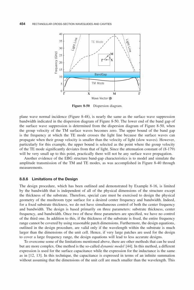
Balanis c08.tex V3 - 11/22/2011 3:32 P.M. Page 454
454 RECTANGULAR CROSS-SECTION WAVEGUIDES AND CAVITIES
0
5
10
15
20
25
30
35
40
Wave Vector |β|
Freq
uenc
y (G
Hz)
TM Mode
TE Mode
Light Line
BandGap
Γ MX Γ
Ligh
t Li
ne
M
XΓ
Figure 8-50 Dispersion diagram.
plane wave normal incidence (Figure 8-48), is nearly the same as the surface wave suppressionbandwidth indicated in the dispersion diagram of Figure 8-50. The lower end of the band gap ofthe surface wave suppression is determined from the dispersion diagram of Figure 8-50, whenthe group velocity of the TM surface waves becomes zero. The upper bound of the band gapis the frequency at which the TE mode crosses the light line because the surface waves canpropagate when their group velocity is smaller than the velocity of light (slow waves). However,particularly for this example, the upper bound is selected as the point where the group velocityof the TE mode significantly deviates from that of light. Since the attenuation constant of (8-179)will be very small up to this point, practically there will not be any surface wave propagation.
Another evidence of the EBG structure band-gap characteristics is to model and simulate theamplitude transmission of the TM and TE modes, as was accomplished in Figure 8-40 throughmeasurements.
8.8.6 Limitations of the Design
The design procedure, which has been outlined and demonstrated by Example 8-16, is limitedby the bandwidth that is independent of all of the physical dimensions of the structure exceptthe thickness of the substrate. Therefore, special care must be exercised to design the physicalgeometry of the mushroom type surface for a desired center frequency and bandwidth. Indeed,for a fixed substrate thickness, we do not have simultaneous control of both the center frequencyand bandwidth. The design is based primarily on three parameters: substrate thickness, centerfrequency, and bandwidth. Once two of these three parameters are specified, we have no controlof the third one. In addition to this, if the thickness of the substrate is fixed, the entire frequencyrange cannot be covered by using reasonable patch dimensions. Furthermore, the design equations,outlined in the design procedure, are valid only if the wavelength within the substrate is muchlarger than the dimensions of the unit cell. Hence, if very large patches are used for the designto cover a large frequency range, the design equations will lead to less accurate designs.
To overcome some of the limitations mentioned above, there are other methods that can be usedbut are more complex. One method is the so-called dynamic model [44]. In this method, a differentexpression is used for the surface capacitance while the expression for the inductance is the sameas in [12, 13]. In this technique, the capacitance is expressed in terms of an infinite summationwithout assuming that the dimensions of the unit cell are much smaller than the wavelength. This

Balanis c08.tex V3 - 11/22/2011 3:32 P.M. Page 455
STRIPLINE AND MICROSTRIP LINES 455
model can also take into account the influence of the higher-order modes generated within thehigh-impedance surface. If the dimensions of the unit cell are much smaller than the wavelength,the dynamic model reduces to a simpler expression for the surface capacitance, which leads tosimilar results as [12, 13]. However, because of its complexity and limitations in space, it willnot be presented here. The reader is directed to [44] for the details.
8.9 STRIPLINE AND MICROSTRIP LINES
Microwave printed circuit technology has advanced considerably with the introduction of thestripline and microstrip transmission lines [45–60]. These lines are shown, respectively, inFigures 8-51a and 8-51b. The stripline consists of a center conductor embedded in a dielec-tric material that is sandwiched between two conducting plates. The microstrip consists of a thinconducting strip placed above a dielectric material, usually referred to as the substrate, which issupported on its bottom by a conducting plate. Both of these lines have evolved from the coaxialline in stages illustrated in Figure 8-52. In general the stripline and microstrip are lightweight,miniature, easy to fabricate with integrated circuit techniques, and cost effective. Their principalmode of operation is that of the quasi-TEM mode, although higher-order modes, including surfacewaves, are evident at higher frequencies. In comparison to other popular transmission lines, suchas the coax and the waveguide, the stripline and microstrip possess characteristics that are shown
E
H
E
H
H
E
h
er, m0
er, m0
e0, m0
b
w
(a)
w
(b)
h
t
h
t
Figure 8-51 Geometries for stripline and microstrip transmission lines. (a) Stripline. (b) Microstrip.

Balanis c08.tex V3 - 11/22/2011 3:32 P.M. Page 456
456 RECTANGULAR CROSS-SECTION WAVEGUIDES AND CAVITIES
h b∞ ∞h
E
H
E
H
E
H
H
E
E
H
H
E
D
D
w w
D
s b
w
w
w
w
Figure 8-52 Evolution of stripline and microstrip transmission lines.
TABLE 8-8 Characteristic comparison of popular transmission lines
Characteristic Coaxial Waveguide Stripline Microstrip
Line losses Medium Low High HighUnloaded Q Medium High Low LowPower Capability Medium High Low LowBandwidth Large Small Large LargeMiniaturization Poor Poor Very good ExcellentVolume and weight Large Large Medium SmallIsolation between
neighboring circuitsVery good Very good Fair Poor
Realization of passivecircuits
Easy Easy Very easy Very easy
Integration with chipdevices
Poor Poor Fair Very good

Balanis c08.tex V3 - 11/22/2011 3:32 P.M. Page 457
STRIPLINE AND MICROSTRIP LINES 457
listed in Table 8-8. Each of the lines will be discussed by using the most elementary approachto their basic operation. More advanced techniques of analysis can be found in the literature.
8.9.1 Stripline
Two of the most important parameters of any transmission line are its characteristic impedanceand phase velocity. Since the basic mode of operation is the TEM, its characteristic impedanceZc and phase velocity vp can be written, respectively, as
Zc =√
L
C(8-197a)
vp = 1√LC
= 1√με
⇒√
L = 1
vp
√C
=√
με√C
(8-197b)
where L = inductance of line per unit lengthC = capacitance of line per unit length
Substituting (8-197b) into (8-197a) reduces it to
Zc =√
L
C= 1
vpC=
√με
C=
√μ0ε0
√μrεr
C=
√μrεr
v0C(8-198)
where v0 is the speed of light in free space. Therefore, the characteristic impedance can bedetermined if the capacitance of the line is known.
The total capacitance Ct of a stripline can be modeled as shown in Figure 8-53, and it is givenby
Ct = 2Cp + 4Cf (8-199)
where
Ct = total capacitance per unit length (8-199a)
Cp = parallel plate capacitance per unit length
(in the absence of fringing)
Cp
Cp
Cf
CfCf
Cfh
w
t b
h
Figure 8-53 Capacitance model for stripline transmission line.
Balanis c08.tex V3 - 11/22/2011 3:32 P.M. Page 458
458 RECTANGULAR CROSS-SECTION WAVEGUIDES AND CAVITIES
Cp = ε2w
b − t= 2εrε0
w
b
1 − t
b
(8-199b)
Cf = fringing capacitance per unit length (8-199c)
Assume that the dielectric medium between the plates is not ferromagnetic. Then the charac-teristic impedance of (8-198) can also be written by using (8-199) and (8-199b) as
Zc =√
με
Ct= ε
Ct
√μ
ε= ε√
εr Ct
√μ0
ε0= 120πε√
εr Ct(8-200)
orZc
√εr = 120π
1
εCt
= 120π
1
ε(2Cp + 4Cf )
= 30π
w/b
1 − t/b+ Cf
ε
(8-200a)
The fringing capacitance of the stripline can be approximated by using
Cf
ε� 1
π
⎧⎪⎪⎪⎨⎪⎪⎪⎩2
1 − t
b
ln
⎛⎜⎝1 + 1
1 − t
b
⎞⎟⎠ −
⎛⎜⎝ 1
1 − t
b
− 1
⎞⎟⎠ ln
⎡⎢⎢⎢⎣ 1(1 − t
b
)2 − 1
⎤⎥⎥⎥⎦⎫⎪⎪⎪⎬⎪⎪⎪⎭ (8-201)
which for zero-thickness center conductor (t = 0), reduces to
Cf
ε� 1
π[2 ln(2)] = 0.4413 (8-201a)
For zero-thickness center conductor (t = 0), an exact solution based on conformal mappingrepresents the characteristic impedance of (8-200a) by [51]
Zc√
εr = 30π
K (k)/K (k ′)= 30π
[K (k ′)K (k)
](8-202)
where K (k) is an elliptic function of the first kind and it is given by
K (k) =∫ 1
0
1√1 − q2
1√1 − kq2
dq =∫ π/2
0
1√1 − k sin2 ψ
dψ (8-202a)
k = tanh(π
2
w
b
)(8-202b)
k ′ =√
1 − k 2 =√
1 − tanh2(π
2
w
b
)= sech
(π
2
w
b
)(8-202c)
It can be shown that the ratio of the elliptic functions in (8-202) can be approximated by
K (k)
K (k ′)�
⎧⎪⎪⎪⎪⎪⎪⎪⎪⎨⎪⎪⎪⎪⎪⎪⎪⎪⎩
1
πln
(2
1 + √k
1 − √k
)when
1√2
≤ k = tanh(π
2
w
b
)≤ 1
π
ln
(2
1 + √k ′
1 − √k ′
) when 0 ≤ k = tanh(π
2
w
b
)≤ 1√
2
(8-203a)
(8-203b)
Other forms to represent the characteristic impedance of the stripline are available, but thepreceding are considered to be sufficiently simple, practical, and accurate.

Balanis c08.tex V3 - 11/22/2011 3:32 P.M. Page 459
STRIPLINE AND MICROSTRIP LINES 459
Example 8-17
Determine the characteristic impedance of a zero-thickness center conductor stripline whose dielectricconstant is 2.20 and w/b ratio is w/b = 1 and 0.1.
Solution: The solution for the characteristic impedance will be based on the more accurate formulationof (8-202) through (8-203b).
Since w/b = 1, then according to (8-202b)
k = tanh(π
2
)= 0.91715 < 1
Thus, by using (8-203a),
K (k)
K (k ′)= 1
πln
(2
1 + √0.91715
1 − √0.91715
)= 1.4411
Therefore, the characteristic impedance of (8-202) is equal to
Zc = 30π
1.4411√
2.2= 44.09 ohms
For w/b = 0.1, according to (8-202b),
k = tanh[π
2(0.1)
]= 0.1558
and from (8-202c),k ′ =
√1 − (0.1558)2 = 0.98779
Thus, by using (8-203b),K (k)
K (k ′)= π
ln
(2
1 + √0.98779
1 − √0.98779
) = 0.4849
Therefore, the characteristic impedance of (8-202) is equal to
Zc = 30π
0.4849√
2.2= 131.04 ohms
8.9.2 Microstrip
The early investigations of the microstrip line in the early 1950s did not stimulate its widespreadacceptance because of the excitation of radiation and undesired modes caused by lines with dis-continuities. However, the rapid rise in miniature microwave circuits, which are usually planarin structure, caused renewed interest in microstrip circuit design. Also the development of highdielectric-constant material began to bind the fringing fields more tightly to the center conduc-tor, thus decreasing radiation losses, and simultaneously shrinking the overall circuit dimensions.These developments, plus the advantages of convenient and economical integrated circuit fabri-cation techniques, tended to lessen the previous concerns and finally allowed microstrip designmethods to achieve widespread application.
Because the upper part of the microstrip is usually exposed, some of the fringing field lineswill be in air while others will reside within the substrate. Therefore, overall, the microstrip canbe thought of as being a line composed of a homogeneous dielectric whose overall dielectricconstant is greater than air but smaller than that of the substrate. The overall dielectric constant isusually referred to as the effective dielectric constant . Because most of the field lines reside within
Balanis c08.tex V3 - 11/22/2011 3:32 P.M. Page 460
460 RECTANGULAR CROSS-SECTION WAVEGUIDES AND CAVITIES
the substrate, the effective dielectric constant is usually closer in value to that of the substratethan to that of air; this becomes even more pronounced as the dielectric constant of the substrateincreases. Since the microstrip is composed of two different dielectric materials (nonhomogeneousline), it cannot support pure TEM modes. The lowest order modes are quasi-TEM.
There have been numerous investigations of the microstrip ([52–60], and many others).Because of the plethora of information on the microstrip, we will summarize some of theformulations for the characteristic impedance and effective dielectric constant that are simple,accurate, and practical.
At low frequencies, the characteristic parameters of the microstrip can be found by using thefollowing expressions:
w eff(0)
h≤ 1
Zc(0) = Zc(f = 0) = 60√εr ,eff(0)
ln
[8h
weff(0)+ weff(0)
4h
](8-204a)
εr ,eff(0) = εr ,eff(f = 0) = εr + 1
2+ εr − 1
2
×{[
1 + 12h
weff(0)
]−1/2
+ 0.04[1 − weff(0)
h
]2}
(8-204b)
w eff(0)
h> 1
Zc(0) = Zc(f = 0) =
120π√εr ,eff(0)
weff(0)
h+ 1.393 + 0.667 ln
[weff(0)
h+ 1.444
] (8-205a)
εr ,eff(0) = εr ,eff(f = 0) = εr + 1
2+ εr − 1
2
[1 + 12
h
weff(0)
]−1/2
(8-205b)
whereweff(0)
h= weff(f = 0)
h= w
h+ 1.25
π
t
h
[1 + ln
(2h
t
)]for
w
h≥ 1
2π(8-206a)
weff(0)
h= weff(f = 0)
h= w
h+ 1.25
π
t
h
[1 + ln
(4πw
t
)]for
w
h<
1
2π(8-206b)
εr ,eff and weff represent the effective dielectric constant and width of the line, respectively. Plotsof the characteristic impedance of (8-204a) or (8-205a) and the effective dielectric constant of(8-204b) or (8-205b) as a function of w/h for three different dielectric constants (εr = 2.33, 6.80,and 10.2) are shown, respectively, in Figures 8-54 and 8-55 [61]. These dielectric constants arerepresentative of common substrates such as RT/Duroid (� 2.33), beryllium oxide (� 6.8), andalumina (� 10.2) used for microstrips. It is evident that the effective dielectric constant is notvery sensitive to the thickness of the center strip.
Example 8-18
For a microstrip line with w/h = 1, εr = 10, and t/h = 0, calculate at f = 0 the effective width,effective dielectric constant, and characteristic impedance of the line.
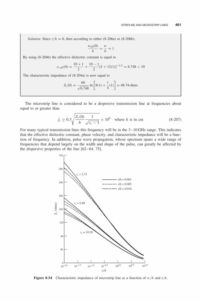
Balanis c08.tex V3 - 11/22/2011 3:32 P.M. Page 461
STRIPLINE AND MICROSTRIP LINES 461
Solution: Since t/h = 0, then according to either (8-206a) or (8-206b),
weff(0)
h= w
h= 1
By using (8-204b) the effective dielectric constant is equal to
εr ,eff(0) = 10 + 1
2+ 10 − 1
2[1 + 12(1)]−1/2 = 6.748 < 10
The characteristic impedance of (8-204a) is now equal to
Zc(0) = 60√6.748
ln
[8(1) + 1
4(1)
]= 48.74 ohms
The microstrip line is considered to be a dispersive transmission line at frequencies aboutequal to or greater than
fc ≥ 0.3
√Zc(0)
h
1√εr − 1
× 109 where h is in cm (8-207)
For many typical transmission lines this frequency will be in the 3–10 GHz range. This indicatesthat the effective dielectric constant, phase velocity, and characteristic impedance will be a func-tion of frequency. In addition, pulse wave propagation, whose spectrum spans a wide range offrequencies that depend largely on the width and shape of the pulse, can greatly be affected bythe dispersive properties of the line [62–64, 75].
320
280
240
200
160
120
80
40
010−2.0 10−1.5 10−1.0 10−0.5 100.0 100.5 101.0
w/h
t/h = 0.001
t/h = 0.005
t/h = 0.010
er = 2.33
er = 6.80
er = 10.20
Zc
(ohm
s)
Figure 8-54 Characteristic impedance of microstrip line as a function of w/h and t/h .
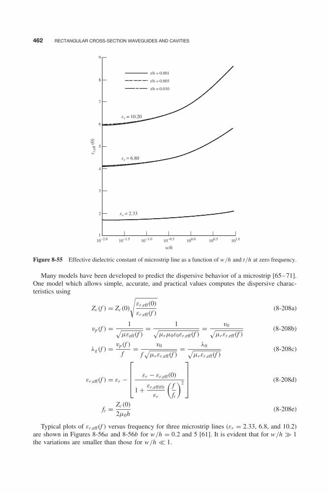
Balanis c08.tex V3 - 11/22/2011 3:32 P.M. Page 462
462 RECTANGULAR CROSS-SECTION WAVEGUIDES AND CAVITIES
10−2.0 10−1.5 10−1.0 10−0.5 100.0 100.5 101.0
w/h
t/h = 0.001
t/h = 0.005
t/h = 0.010
er = 10.20
er = 2.33
er = 6.80
er,
eff (
0)
1
2
3
4
5
6
7
8
9
Figure 8-55 Effective dielectric constant of microstrip line as a function of w/h and t/h at zero frequency.
Many models have been developed to predict the dispersive behavior of a microstrip [65–71].One model which allows simple, accurate, and practical values computes the dispersive charac-teristics using
Zc(f ) = Zc(0)
√εr ,eff(0)
εr ,eff(f )(8-208a)
vp(f ) = 1√μεeff(f )
= 1√μrμ0ε0εr ,eff(f )
= v0√μrεr ,eff(f )
(8-208b)
λg(f ) = vp(f )
f= v0
f√
μrεr ,eff(f )= λ0√
μrεr ,eff(f )(8-208c)
εr ,eff(f ) = εr −
⎡⎢⎢⎢⎣ εr − εr ,eff(0)
1 + εr ,eff(0)
εr
(f
ft
)2
⎤⎥⎥⎥⎦ (8-208d)
ft = Zc(0)
2μ0h(8-208e)
Typical plots of εr ,eff(f ) versus frequency for three microstrip lines (εr = 2.33, 6.8, and 10.2)are shown in Figures 8-56a and 8-56b for w/h = 0.2 and 5 [61]. It is evident that for w/h � 1the variations are smaller than those for w/h � 1.
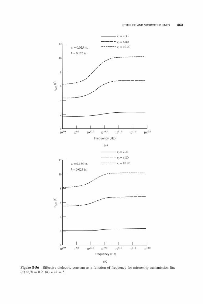
Balanis c08.tex V3 - 11/22/2011 3:32 P.M. Page 463
STRIPLINE AND MICROSTRIP LINES 463
109.0 109.5 1010.51010.0 1011.0 1011.5 1012.0
er = 2.33
w = 0.025 in.
h = 0.125 in.
er = 6.80
er = 10.20
Frequency (Hz)
(a)
12
10
8
6
4
2
0
109.0 109.5 1010.51010.0 1011.0 1011.5 1012.0
er = 2.33
w = 0.125 in.
h = 0.025 in.
er = 6.80
er = 10.20
Frequency (Hz)
(b)
ε r,e
ff (f
)ε r
,eff (
f)
12
10
8
6
4
2
0
Figure 8-56 Effective dielectric constant as a function of frequency for microstrip transmission line.(a) w/h = 0.2. (b) w/h = 5.
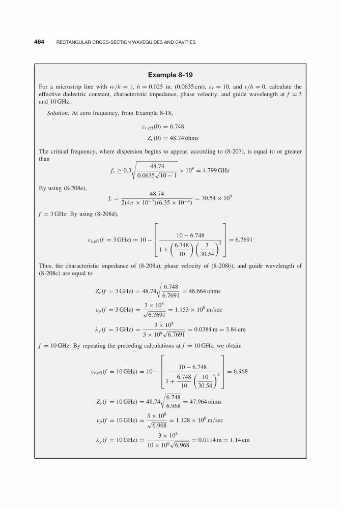
Balanis c08.tex V3 - 11/22/2011 3:32 P.M. Page 464
464 RECTANGULAR CROSS-SECTION WAVEGUIDES AND CAVITIES
Example 8-19
For a microstrip line with w/h = 1, h = 0.025 in. (0.0635 cm), εr = 10, and t/h = 0, calculate theeffective dielectric constant, characteristic impedance, phase velocity, and guide wavelength at f = 3and 10 GHz.
Solution: At zero frequency, from Example 8-18,
εr ,eff(0) = 6.748
Zc(0) = 48.74 ohms
The critical frequency, where dispersion begins to appear, according to (8-207), is equal to or greaterthan
fc ≥ 0.3
√48.74
0.0635√
10 − 1× 109 = 4.799 GHz
By using (8-208e),
ft = 48.74
2(4π × 10−7)(6.35 × 10⁻⁴)= 30.54 × 10⁹
f = 3 GHz: By using (8-208d),
εr ,eff(f = 3 GHz) = 10 −
⎡⎢⎢⎢⎣ 10 − 6.748
1 +(
6.748
10
)(3
30.54
)2
⎤⎥⎥⎥⎦ = 6.7691
Thus, the characteristic impedance of (8-208a), phase velocity of (8-208b), and guide wavelength of(8-208c) are equal to
Zc(f = 3 GHz) = 48.74
√6.748
6.7691= 48.664 ohms
vp(f = 3 GHz) = 3 × 10⁸
√6.7691
= 1.153 × 10⁸ m/sec
λg (f = 3 GHz) = 3 × 10⁸
3 × 10⁹√
6.7691= 0.0384 m = 3.84 cm
f = 10 GHz: By repeating the preceding calculations at f = 10 GHz, we obtain
εr ,eff(f = 10 GHz) = 10 −
⎡⎢⎢⎢⎣ 10 − 6.748
1 + 6.748
10
(10
30.54
)2
⎤⎥⎥⎥⎦ = 6.968
Zc(f = 10 GHz) = 48.74
√6.748
6.968= 47.964 ohms
vp(f = 10 GHz) = 3 × 10⁸
√6.968
= 1.128 × 10⁸ m/sec
λg (f = 10 GHz) = 3 × 10⁸
10 × 109√
6.968= 0.0114 m = 1.14 cm
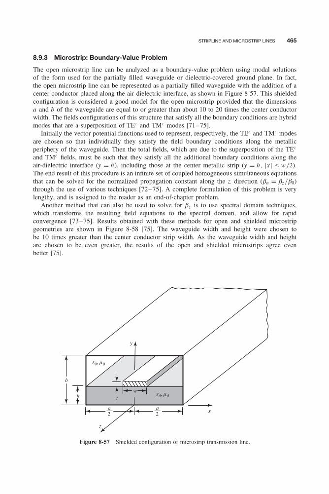
Balanis c08.tex V3 - 11/22/2011 3:32 P.M. Page 465
STRIPLINE AND MICROSTRIP LINES 465
8.9.3 Microstrip: Boundary-Value Problem
The open microstrip line can be analyzed as a boundary-value problem using modal solutionsof the form used for the partially filled waveguide or dielectric-covered ground plane. In fact,the open microstrip line can be represented as a partially filled waveguide with the addition of acenter conductor placed along the air-dielectric interface, as shown in Figure 8-57. This shieldedconfiguration is considered a good model for the open microstrip provided that the dimensionsa and b of the waveguide are equal to or greater than about 10 to 20 times the center conductorwidth. The fields configurations of this structure that satisfy all the boundary conditions are hybridmodes that are a superposition of TEz and TMz modes [71–75].
Initially the vector potential functions used to represent, respectively, the TEz and TMz modesare chosen so that individually they satisfy the field boundary conditions along the metallicperiphery of the waveguide. Then the total fields, which are due to the superposition of the TEz
and TMz fields, must be such that they satisfy all the additional boundary conditions along theair-dielectric interface (y = h), including those at the center metallic strip (y = h , |x | ≤ w/2).The end result of this procedure is an infinite set of coupled homogeneous simultaneous equationsthat can be solved for the normalized propagation constant along the z direction (βn = βz /β0)through the use of various techniques [72–75]. A complete formulation of this problem is verylengthy, and is assigned to the reader as an end-of-chapter problem.
Another method that can also be used to solve for βz is to use spectral domain techniques,which transforms the resulting field equations to the spectral domain, and allow for rapidconvergence [73–75]. Results obtained with these methods for open and shielded microstripgeometries are shown in Figure 8-58 [75]. The waveguide width and height were chosen tobe 10 times greater than the center conductor strip width. As the waveguide width and heightare chosen to be even greater, the results of the open and shielded microstrips agree evenbetter [75].
e0, m0
ed, mdw
b
h t
z
x
y
2a
2a
Figure 8-57 Shielded configuration of microstrip transmission line.
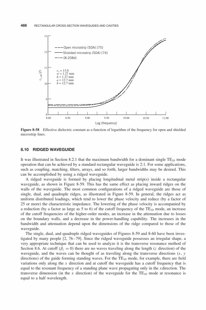
Balanis c08.tex V3 - 11/22/2011 3:32 P.M. Page 466
466 RECTANGULAR CROSS-SECTION WAVEGUIDES AND CAVITIES
13
12
11
10
9
88.00 8.50 9.00 9.50
Log (frequency)
10.00 10.50 11.00
w = 1.27 mmer = 13.0
h = 1.27 mma = 12.7 mmb = 12.7 mm
Open microstrip (SDA) [75]
Shielded microstrip (SDA) [74]
(8-208d)
er,
eff (
f)
Figure 8-58 Effective dielectric constant as a function of logarithm of the frequency for open and shieldedmicrostrip lines.
8.10 RIDGED WAVEGUIDE
It was illustrated in Section 8.2.1 that the maximum bandwidth for a dominant single TE10 modeoperation that can be achieved by a standard rectangular waveguide is 2:1. For some applications,such as coupling, matching, filters, arrays, and so forth, larger bandwidths may be desired. Thiscan be accomplished by using a ridged waveguide.
A ridged waveguide is formed by placing longitudinal metal strip(s) inside a rectangularwaveguide, as shown in Figure 8-59. This has the same effect as placing inward ridges on thewalls of the waveguide. The most common configurations of a ridged waveguide are those ofsingle, dual, and quadruple ridges, as illustrated in Figure 8-59. In general, the ridges act asuniform distributed loadings, which tend to lower the phase velocity and reduce (by a factor of25 or more) the characteristic impedance. The lowering of the phase velocity is accompanied bya reduction (by a factor as large as 5 to 6) of the cutoff frequency of the TE10 mode, an increaseof the cutoff frequencies of the higher-order modes, an increase in the attenuation due to losseson the boundary walls, and a decrease in the power-handling capability. The increases in thebandwidth and attenuation depend upon the dimensions of the ridge compared to those of thewaveguide.
The single, dual, and quadruple ridged waveguides of Figures 8-59 and 8-60 have been inves-tigated by many people [2, 76–79]. Since the ridged waveguide possesses an irregular shape, avery appropriate technique that can be used to analyze it is the transverse resonance method ofSection 8.6. At cutoff (βz = 0) there are no waves traveling along the length (z direction) of thewaveguide, and the waves can be thought of as traveling along the transverse directions (x , ydirections) of the guide forming standing waves. For the TE10 mode, for example, there are fieldvariations only along the x direction and at cutoff the waveguide has a cutoff frequency that isequal to the resonant frequency of a standing plane wave propagating only in the xdirection. Thetransverse dimension (in the x direction) of the waveguide for the TE10 mode at resonance isequal to a half wavelength.

Balanis c08.tex V3 - 11/22/2011 3:32 P.M. Page 467
RIDGED WAVEGUIDE 467
(a)
(b)
(c)
Figure 8-59 Various cross sections of a ridged waveguide. (a) Single. (b) Dual. (c) Quadruple.
b0
a0
b
a
b0
a0
b
a
(b)
(a)
L LC
Figure 8-60 Geometry for ridged waveguides. (a) Single. (b) Dual.
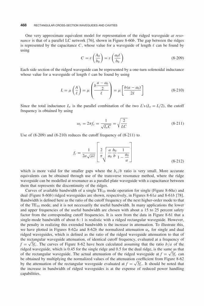
Balanis c08.tex V3 - 11/22/2011 3:32 P.M. Page 468
468 RECTANGULAR CROSS-SECTION WAVEGUIDES AND CAVITIES
One very approximate equivalent model for representation of the ridged waveguide at reso-nance is that of a parallel LC network [76], shown in Figure 8-60b. The gap between the ridgesis represented by the capacitance C , whose value for a waveguide of length � can be found byusing
C = ε
(A0
b0
)= ε
(a0�
b0
)(8-209)
Each side section of the ridged waveguide can be represented by a one-turn solenoidal inductancewhose value for a waveguide of length � can be found by using
L = μ
(A
�
)= μ
⎛⎜⎝ba − a0
2�
⎞⎟⎠ = μ
[b(a − a0)
2�
](8-210)
Since the total inductance Lt is the parallel combination of the two L′s (Lt = L/2), the cutofffrequency is obtained by using
ωc = 2π fc = 1√Lt C
=√
2
LC(8-211)
Use of (8-209) and (8-210) reduces the cutoff frequency of (8-211) to
fc = 1
2a√
με
2
π
a
a0
b0
b
1
1 − a0
a (8-212)
which is more valid for the smaller gaps where the bo/b ratio is very small. More accurateequivalents can be obtained through use of the transverse resonance method, where the ridgewaveguide can be modelled at resonance as a parallel plate waveguide with a capacitance betweenthem that represents the discontinuity of the ridges.
Curves of available bandwidth of a single TE10 mode operation for single (Figure 8-60a) anddual (Figure 8-60b) ridged waveguides are shown, respectively, in Figures 8-61a and 8-61b [78].Bandwidth is defined here as the ratio of the cutoff frequency of the next higher-order mode to thatof the TE10 mode, and it is not necessarily the useful bandwidth. In many applications the lowerand upper frequencies of the useful bandwidth are chosen with about a 15 to 25 percent safetyfactor from the corresponding cutoff frequencies. It is seen from the data in Figure 8-61 that asingle-mode bandwidth of about 6 : 1 is realistic with a ridged rectangular waveguide. However,the penalty in realizing this extended bandwidth is the increase in attenuation. To illustrate this,we have plotted in Figures 8-62a and 8-62b the normalized attenuation αn for single and dualridged waveguides, which is defined as the ratio of the ridged waveguide attenuation to that ofthe rectangular waveguide attenuation, of identical cutoff frequency, evaluated at a frequency off = √
3fc . The curves of Figure 8-62 have been calculated assuming that the ratio b/a of theridged waveguide, which is 0.45 for the single ridge and 0.5 for the dual ridge, is the same as thatof the rectangular waveguide. The actual attenuation of the ridged waveguide at f = √
3fc canbe obtained by multiplying the normalized values of the attenuation coefficient from Figure 8-62by the attenuation of the rectangular waveguide evaluated at f = √
3fc . It should be noted thatthe increase in bandwidth of ridged waveguides is at the expense of reduced power handlingcapabilities.
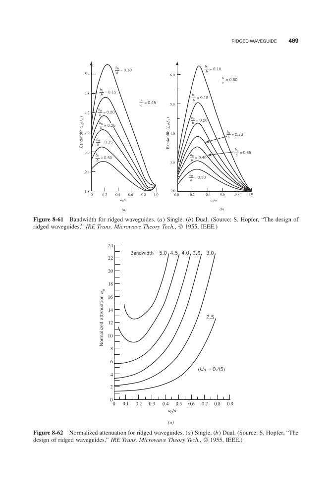
Balanis c08.tex V3 - 11/22/2011 3:32 P.M. Page 469
RIDGED WAVEGUIDE 469
Ban
dwid
th (
f c2/
f c1)
Ban
dwid
th (
f c2/
f c1)
4.8
4.2
3.6
3.0
2.4
1.80 0.2 0.4 0.6 0.8 1.0
5.4 6.0
5.0
4.0
3.0
2.00.0 0.2 0.4 0.6 0.8 1.0
(a) (b)
= 0.15b
b0
= 0.10b
b0 = 0.10b
b0
= 0.15b
b0
= 0.20b
b0
= 0.30b
b0
= 0.35b
b0
= 0.40b
b0
= 0.50b
b0
= 0.20b
b0
= 0.45ab
= 0.50ab
= 0.25b
b0
= 0.35b
b0
= 0.50b
b0
a0/a a0/a
Figure 8-61 Bandwidth for ridged waveguides. (a) Single. (b) Dual. (Source: S. Hopfer, “The design ofridged waveguides,” IRE Trans. Microwave Theory Tech., © 1955, IEEE.)
a0/a
(a)
0
24
22
20
18
16
14
12
10
8
6
4
2
00.1 0.2 0.3 0.4 0.5 0.6 0.7 0.8 0.9
Nor
mal
ized
att
enua
tion
an
Bandwidth = 5.0 4.5 4.0 3.5 3.0
2.5
(b/a = 0.45)
Figure 8-62 Normalized attenuation for ridged waveguides. (a) Single. (b) Dual. (Source: S. Hopfer, “Thedesign of ridged waveguides,” IRE Trans. Microwave Theory Tech., © 1955, IEEE.)
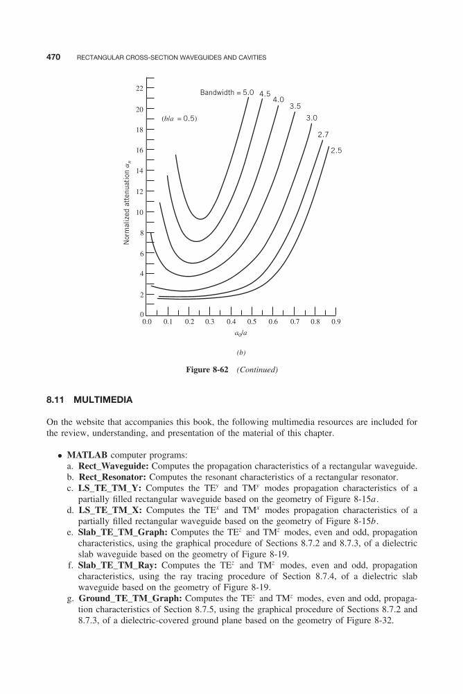
Balanis c08.tex V3 - 11/22/2011 3:32 P.M. Page 470
470 RECTANGULAR CROSS-SECTION WAVEGUIDES AND CAVITIES
a0/a
(b)
0.0
22
20
18
16
14
12
10
8
6
4
2
00.1 0.2 0.3 0.4 0.5 0.6 0.7 0.8 0.9
Nor
mal
ized
att
enua
tion
an
Bandwidth = 5.0 4.54.0
3.5
3.0
2.7
2.5
(b/a = 0.5)
Figure 8-62 (Continued)
8.11 MULTIMEDIA
On the website that accompanies this book, the following multimedia resources are included forthe review, understanding, and presentation of the material of this chapter.
• MATLAB computer programs:a. Rect_Waveguide: Computes the propagation characteristics of a rectangular waveguide.b. Rect_Resonator: Computes the resonant characteristics of a rectangular resonator.c. LS_TE_TM_Y: Computes the TEy and TMy modes propagation characteristics of a
partially filled rectangular waveguide based on the geometry of Figure 8-15a .d. LS_TE_TM_X: Computes the TEx and TMx modes propagation characteristics of a
partially filled rectangular waveguide based on the geometry of Figure 8-15b.e. Slab_TE_TM_Graph: Computes the TEz and TMz modes, even and odd, propagation
characteristics, using the graphical procedure of Sections 8.7.2 and 8.7.3, of a dielectricslab waveguide based on the geometry of Figure 8-19.
f. Slab_TE_TM_Ray: Computes the TEz and TMz modes, even and odd, propagationcharacteristics, using the ray tracing procedure of Section 8.7.4, of a dielectric slabwaveguide based on the geometry of Figure 8-19.
g. Ground_TE_TM_Graph: Computes the TEz and TMz modes, even and odd, propaga-tion characteristics of Section 8.7.5, using the graphical procedure of Sections 8.7.2 and8.7.3, of a dielectric-covered ground plane based on the geometry of Figure 8-32.
Balanis c08.tex V3 - 11/22/2011 3:32 P.M. Page 471
REFERENCES 471
h. Ground_TE_TM_Ray: Computes the TEz and TMz modes, even and odd, propagationcharacteristics of Section 8.7.5, using the ray tracing procedure of Section 8.7.4, of adielectric slab waveguide based on the geometry of Figure 8-32.
i. HIS_Mush: Designs and computes the characteristics of a high-impedance surface (HIS)of Figures 8-37 and 8-47 based on the procedure, and designs closed-form equations ofSection 8.8.4.
• Power Point (PPT) viewgraphs, in multicolor.
REFERENCES
1. C. S. Lee, S. W. Lee, and S. L. Chuang, “Plot of modal field distribution in rectangular and circularwaveguides,” IEEE Trans. Microwave Theory Tech., vol. MTT-33, pp. 271–274, March 1985.
2. S. Ramo, J. R. Whinnery, and T. Van Duzer, Fields and Waves in Communication Electronics , SecondEdition, John Wiley & Sons, New York, 1984.
3. R. F. Harrington, Time-Harmonic Electromagnetic Fields , McGraw-Hill, New York, 1961.
4. R. E. Collin, Field Theory of Guided Waves , McGraw-Hill, New York, 1960.
5. N. Marcuvitz (Ed.), Waveguide Handbook , Chapter 8, McGraw-Hill, New York, 1951, pp. 387–413.
6. C. H. Walter, Traveling Wave Antennas , McGraw-Hill, New York, 1965, pp. 172–187.
7. L. O. Goldstone and A. A. Oliner, “Leaky wave antennas I: Rectangular waveguides,” IRE Trans.Antennas Propagat., vol. AP-7, pp. 307–309, October 1959.
8. L. O. Goldstone and A. A. Oliner, “Leaky wave antennas II: Circular waveguides,” IRE Trans. AntennasPropagat., vol. AP-9, pp. 280–290, May 1961.
9. J. H. Richmond, Reciprocity Theorems and Plane Surface Waves , Engineering Experiment Station Bul-letin, Ohio State University, vol. XXVIII, no. 4, July 1959.
10. M. Zahn, Electromagnetic Field Theory , John Wiley & Sons, New York, 1979.
11. P. K. Tien, “Light waves in thin films and integrated optics,” Applied Optics , vol. 10, no. 11,pp. 2395–2413, November 1971.
12. D. Sievenpiper, High-Impedance Electromagnetic Surfaces, Ph.D. dissertation, Department of ElectricalEngineering, UCLA, 1999.
13. D. Sievenpiper, “Artificial Impedance Surfaces,” Chapter 15, in Modern Antenna Handbook , C. A.Balanis (editor), John Wiley & Sons, pp. 737–777, 2008.
14. Y. Rahmat-Samii and H. Mosallaei, “Electromagnetic Band-Gap Structures: Classification, Character-ization, and Applications,” 11th International Conference on Antennas and Propagation (ICAP 2001),Manchester, UK, pp. 564, April 17–20, 2001.
15. H. Mosallaei and Y. Rahmat-Samii, “Periodic bandgap and effective materials in electromagnetics:characterization and applications in nanocavities and waveguides,” IEEE Trans. Antennas Propagat .,vol. 51, no. 3, pp. 549–563, March 2003.
16. F. Yang and Y. Rahmat-Samii, “Reflection phase characterization of the EBG ground plane for lowprofile wire antenna applications,” IEEE Trans. Antennas Propagat ., vol. 51, no. 10, pp. 2691–2703,Oct. 2003.
17. F. Yang and Y. Rahmat-Samii, Electromagnetic Band Gap Structures in Antenna Engineering ,Cambridge University Press, UK, 2008.
18. E. Yablonovitch, “Photonic band-gap structures,” J. Opt. Soc. Amer. B , vol. 10, no. 2, pp. 283–294,Feb. 1993.
19. E. R. Brown, D. D. Parker and E. Yablonovitch, “Radiation properties of a planar antenna on a photonic-crystal substrate,” J. Opt. Soc. Amer., B , vol. 10, no. 2, pp. 404–407, Feb. 1993.
20. Y. Rahmat-Samii and F. Yang, “Development of complex artificial ground planes in antenna engineer-ing,” Chapter 12 in N. Engheta and R. W. Ziolkowski (editors), Metamaterials: Physics and EngineeringExplorations , N. Engheta, R. W. Ziolkowski, Editors, IEEE Press, Wiley Inter-Science, New York, 2006.

Balanis c08.tex V3 - 11/22/2011 3:32 P.M. Page 472
472 RECTANGULAR CROSS-SECTION WAVEGUIDES AND CAVITIES
21. P.-S. Kildal, “Artificially soft and hard surfaces in electromagnetics,” IEEE Trans. Antennas Propagat .vol. 38, no. 10, pp. 1537–1544, October 1990.
22. IEEE Trans. Antennas Propagat., Special Issue on Artificial Magnetic Conductors, Soft/Hard Surfaces,and Other Complex Surfaces , vol. 53, no. 1, Jan. 2005.
23. C. A. Balanis, Antenna Theory: Analysis and Design , 3rd edition, John Wiley & Sons, New York,2005.
24. J. K. M. Jansen and M. E. J. Jeuken, “Surface waves in corrugated conical horn,” Electronic Letters ,vol. 8, pp. 342–344, 1972.
25. C. A. Mentzer and L. Peters, Jr., “Properties of cutoff corrugated surfaces for corrugated horn design,”IEEE Trans. Antennas Propagat ., vol. AP-22, no. 2, pp. 191–196, March 1974.
26. C. A. Mentzer and L. Peters, Jr., “Pattern analysis of corrugated horn antennas,” IEEE Trans. AntennasPropagat ., vol. AP-22, no. 3, pp. 304–309, May 1976.
27. B. MacA. Thomas, “Design of corrugated conical horns,” IEEE Trans. Antennas Propagat ., AP-26, no.2, pp. 367–372, March 1978.
28. W. D. Burnside and C. W. Chuang, “An aperture-matched horn design,” IEEE Trans. Antennas Prop-agat ., AP-30, no. 4, pp. 790–796, July 1982.
29. G. L. James, “TE11-to-HE11 mode converters for small-angle corrugated horns,” IEEE Trans. AntennasPropagat ., AP-30, No. 6, pp. 1057–1062, November 1982.
30. B. MacA. Thomas and K. J. Greene, “A curved-aperture corrugated horn having a very low cross-polarperformance,” IEEE Trans. Antennas Propagat ., AP-30, no. 6, pp. 1068–1072, November 1982.
31. B. MacA. Thomas, G. L. James and K. J. Greene, “Design of wide-band Corrugated conical horns forCassegrain antennas,” IEEE Trans. Antennas Propagat ., AP-34, no. 6, pp. 750–757, June 1986.
32. A. A. Kishk and P.-S. Kildal, “Asymptotic boundary conditions for strip-loaded scatterers appliedto circular dielectric cylinders under oblique incidence,” IEEE Antennas Propagat., vol. 45, no. 1,pp. 51–56, January 1997.
33. A. Monorchio, G. Manara and L. Lanuaza, “Synthesis of artificial magnetic conductors by usingmultilayered frequency selective surfaces,” IEEE Antennas Wireless Propagat. Lett ., vol. 1, no. 11,pp. 196–2098, 2002.
34. D. J. Kern, D. H. Werner, A. Monorchio, L. Lanuzza and M. J. Wilhelm, “The design synthesis ofmultiband artificial magnetic conductors using high impedance frequency selective surfaces,” IEEETrans. Antennas Propagat ., vol. 53, no. 1, pp. 8–17, January 2005.
35. D. Sievenpiper, “Forward and backward leaky wave radiation with large effective aperture from anelectronically tunable textured surface,” IEEE Trans. Antennas Propagat ., vol. 53, no. 1, pp. 236–247,January 2005.
36. T. Suzuki and P. L. Yu, Experimental and theoretical study of dipole emission in the two-dimensionalphotonic band structures of the square lattice with dielectric cylinders,” J. Appl. Phys ., vol. 49, no. 2,pp. 582–594, Jan. 1996.
37. D. M. Pozar and D. H. Schaubert, “Scan blindness in infinite phased arrays of printed dipoles,” IEEETrans. Antennas Propagat ., vol. AP-32, no. 6, pp. 602–610, June 1984.
38. F. Zavosh and J. T. Aberle, “Infinite phased arrays of cavity-backed patches,” IEEE Trans. AntennasPropagat ., vol. AP-42, no. 3, pp. 390–398, March 1994.
39. L. Zhang, J. A. Castaneda and N. G. Alexopoulos, “Scan blindness free phased array design using PBGmaterials,” IEEE Trans. Antennas Propagat., vol. 52, no. 8, pp. 2000–2007, Aug. 2004.
40. http://www.ansoft.com/products/hf/hfss/.
41. J. D. Joannopoulos, R. D. Meade and J. N. Winn, Photonic Crystals Molding the Flow of Light, PrincetonUniversity Press, New Jersey, 1995.
42. S. G. Johnson and J. D. Joannopoulos, Photonic Crystals: the Road from Theory to Practice, KluwerAcademic Publishers, Boston, 2002.
43. R. E. Collin, Foundations for Microwave Engineering , McGraw-Hill, New York, 1992.
Balanis c08.tex V3 - 11/22/2011 3:32 P.M. Page 473
REFERENCES 473
44. S. A. Tretyakov, C. R. Simovski, “Dynamic Model of Artificial Reactive Impedance Surfaces,” J. ofEM Waves and Applications ,” vol. 17, no. 1, pp. 131–145, 2003.
45. R. M. Barrett, “Microwave printed circuits—a historical survey,” IRE Trans. Microwave Theory Tech.,vol. MTT-3, no. 2, p. 9, March 1955.
46. Special issue on Microwave Strip Circuits, IRE Trans. Microwave Theory Tech., vol. MTT-3, no. 2,March 1955.
47. H. Howe Jr., Stripline Circuit Design , Artech House, Dedham, MA, 1974.
48. G. L. Matthaei, L. Young, and E. M. T. Jones, Microwave Filters Impedance-Matching Networks andCoupling Structures , McGraw-Hill, New York, 1964.
49. S. B. Cohn, “Characteristic impedance of a shielded-strip transmission line,” IRE Trans. MicrowaveTheory Tech., MTT-2, pp. 52–57, July 1954.
50. S. B. Cohn, “Characteristic impedances of broadside-coupled strip transmission lines,” IRE Trans.Microwave Theory Tech., vol. MTT-8, pp. 633–637, November 1960.
51. H. A. Wheeler, “Transmission-line properties of parallel wide strips by a conformal-map- ping approx-imation,” IEEE Trans. Microwave Theory Tech., vol. MTT-12, no. 3, pp. 280–289, May 1964.
52. H. A. Wheeler, “Transmission-line properties of parallel strips separated by a dielectric sheet,” IEEETrans. Microwave Theory Tech., vol. MTT-13, no. 2, pp. 172–185, March 1965.
53. T. G. Bryant and J. A. Weiss, “Parameters of microstrip transmission lines and coupled pairs ofmicrostrip lines,” IEEE Trans. Microwave Theory Tech., vol. MTT-16, no. 12, pp. 1021–1027, December1968.
54. M. V. Schneider, “Microstrip lines for microwave integrated circuits,” Bell System Tech. J., vol. 48,pp. 1421–1444, May-June 1969.
55. E. O. Hammerstad, “Equations for microstrip circuit design,” Proc. European Microwave Conference,pp. 268–272, September 1975.
56. H. A. Wheeler, “Transmission-line properties of a strip on a dielectric sheet on a plane,” IEEE Trans.Microwave Theory Tech., vol. MTT-25, no. 8, pp. 631–647, August 1977.
57. K. C. Gupta, R. Garg, and I. J. Bahl, Microstrip Lines and Slotlines , Artech House, Dedham, MA,1979.
58. M. V. Schneider, “Dielectric loss in integrated microwave circuits,” Bell System Tech. J., vol. 50,pp. 2325–2332, September 1969.
59. R. A. Pucel, D. J. Masse, and C. D. Hartwig, “Losses in microstrip,” IEEE Trans. Microwave TheoryTech., vol. MTT-16, pp. 342–350, June 1968; correction vol. MTT-16, p. 1064, December 1968.
60. I. J. Bahl and D. K. Trivedi, “A designer’s guide to microstrip line,” Microwaves , vol. 16, pp. 174–182,May 1977.
61. T. Leung, “Pulse signal distortions in microstrips,” MS(EE) Thesis, Department of Electrical and Com-puter Engineering, Arizona State University, December 1987.
62. R. L. Veghte and C. A. Balanis, “Dispersion of transient signals in microstrip transmission lines,” IEEETrans. Microwave Theory Tech., vol. MTT-34, pp. 1427–1436, December 1986.
63. T. Leung and C. A. Balanis, “Attenuation distortion in microstrips,” IEEE Trans. Microwave TheoryTech., vol. MTT-36, no. 4, pp. 765–769, April 1988.
64. E. F. Kuester and D. C. Chang, “An appraisal of methods for computation of the dispersion charac-teristics of open microstrips,” IEEE Trans. Microwave Theory Tech., vol. MTT-27, pp. 691–694, July1979.
65. M. V. Schneider, “Microstrip dispersion,” IEEE Trans. Microwave Theory Tech., vol. MTT-20,pp. 144–146, January 1972.
66. E. J. Denlinger, “A frequency dependent solution for microstrip transmission lines,” IEEE Trans.Microwave Theory Tech., vol. MTT-19, no. 1, pp. 30–39, January 1971.
67. W. J. Getsinger, “Microstrip dispersion model,” IEEE Trans. Microwave Theory Tech., vol. MTT-22,pp. 34–39, January 1973.
Balanis c08.tex V3 - 11/22/2011 3:32 P.M. Page 474
474 RECTANGULAR CROSS-SECTION WAVEGUIDES AND CAVITIES
68. H. T. Carlin, “A simplified circuit model for microstrip,” IEEE Trans. Microwave Theory Tech.,vol. MTT-21, pp. 589–591, September 1973.
69. M. Kobayashi, “Important role of inflection frequency in the dispersive properties of microstrip lines,”IEEE Trans. Microwave Theory Tech., vol. MTT-30, pp. 2057–2059, November 1982.
70. P. Pramanick and P. Bhartia, “An accurate description of dispersion in microstrip,” Microwave Journal ,vol. 26, pp. 89–96, December 1983.
71. E. Yamashita, K. Atsuki, and T. Veda, “An approximate dispersion formula of microstrip linesfor computer-aided design of microwave integrated circuits,” IEEE Trans. Microwave Theory Tech.,vol. MTT-27, pp. 1036–1038, December 1979.
72. R. Mittra and T. Itoh, “A new technique for the analysis of the dispersion characteristics of microstriplines,” IEEE Trans. Microwave Theory Tech., vol. MTT-19, no. 1, pp. 47–56, January 1971.
73. T. Itoh and R. Mittra, “Spectral-domain approach for calculating the dispersion characteris-tics of microstrip lines,” IEEE Trans. Microwave Theory Tech., vol. MTT-21, pp. 496–499,July 1973.
74. T. Itoh and R. Mittra, “A technique for computing dispersion characteristics of shielded microstriplines,” IEEE Trans. Microwave Theory Tech., vol. MTT-22, pp. 896–898, October 1974.
75. T. Leung and C. A. Balanis, “Pulse dispersion in open and shielded lines using the spectral-domainmethod,” IEEE Trans. Microwave Theory Tech., vol. MTT-36, no. 7, pp. 1223–1226, July 1988.
76. S. B. Cohn, “Properties of ridge wave guide,” Proc. IRE , vol. 35, pp. 783–788, August 1947.
77. S. Hopfer, “The design of ridged waveguides,” IRE Trans. Microwave Theory Tech., vol. MTT-3,pp. 20–29, October 1955.
78. J. P. Montgomery, “Ridged waveguide phased array elements,” IEEE Trans. Antennas Propagat.,vol. AP-24, no. 1, pp. 46–53, January 1976.
79. Y. Utsumi, “Variational analysis of ridged waveguide modes,” IEEE Trans. Microwave Theory Tech.,vol. MTT-33, no. 2, pp. 111–120, February 1985.
PROBLEMS
8.1. An air-filled section of an X-band(8.2–12.4 GHz) rectangular waveguide oflength � is used as a delay line. Assumethat the inside dimensions of the waveguideare 0.9 in. (2.286 cm) by 0.4 in. (1.016 cm)and that it operates at its dominant mode.Determine its length so that the delay at10 GHz is 2 μs.
8.2. A standard X-band (8.2–12.4 GHz) rectan-gular waveguide with inner dimensions of0.9 in. (2.286 cm) by 0.4 in. (1.016 cm) isfilled with lossless polystyrene (εr = 2.56).For the lowest-order mode of the waveguide,determine at 10 GHz the following values.(a) Cutoff frequency (in GHz).(b) Guide wavelength (in cm).(c) Wave impedance.(d) Phase velocity (in m/s).(e) Group velocity (in m/s).
8.3. A Ku-band (12.4–18 GHz) lossless rectan-gular waveguide, operating at the dominant
TE10 mode, with inner dimensions 0.622in. by 0.311 in. is used as a customizedphase shifter for a particular application. Thelength of the waveguide is chosen so thatthe total phase, introduced by the insertionof the section of the waveguide, meets therequired specifications of the system designoperating at 15 GHz.(a) For an air-filled waveguide, what is the
length (in cm) of the waveguide sectionsif the total phase, at 15 GHz, intro-duced by the insertion of this waveguidesection is 300◦?
(b) For the waveguide section, whose lengthis equal to that found in part a , whatis the total phase shift (in degrees),at 15 GHz, if the waveguide section istotally filled with a lossless dielectricmaterial with a dielectric constant of 4?
8.4. Design an X-band rectangular waveguide,with dimensions 2.286 cm and 1.026 cm and

Balanis c08.tex V3 - 11/22/2011 3:32 P.M. Page 475
PROBLEMS 475
filled with a dielectric material with a dielec-tric constant of 2.25, which is to be usedas a delay line. What should the length (inmeters) of the waveguide be so that the totaldelay it presents by its insertion at 10 GHzis 2 μs?
8.5. An empty X-band (8.2–12.4 GHz) rectangu-lar waveguide, with dimensions of 2.286 cmby 1.016 cm, is to be connected to anX-band waveguide of the same dimen-sions but filled with lossless polystyrene(εr = 2.56). To avoid reflections, an X-band waveguide (of the same dimensions)quarter-wavelength long section is insertedbetween the two. Assume dominant-modepropagation and that matching is to be madeat 10 GHz. Determine the:(a) Wave impedance of the quarter-
wavelength section waveguide.(b) Dielectric constant of the loss-
less medium that must be used tofill the quarter-wavelength sectionwaveguide.
(c) Length (in cm) of the quarter-wavelength section waveguide.
8.6. Design a two-section binomial impedancetransformer to match an empty (εr = 1) X-band waveguide to a dielectric-filled (εr =2.56) X-band waveguide. Use two inter-mediate X-band waveguide sections, eachquarter-wavelength long. Assume dominantmode excitation, fo = 10 GHz, and waveg-uide dimensions of 2.286 cm by 1.016 cm.Determine the:(a) Wave impedances of each section.(b) Dielectric constants of the lossless
media that must be used to fill the inter-mediate waveguide sections.
(c) Length (in cm) of each interme-diate quarter-wavelength waveguidesection.
er = 1 e = 256er1 er2
4
λg1
4
λg2
Figure P8-6
8.7. Derive expressions for the attenuation coef-ficient αc above cutoff for the rectangularwaveguide of Figure 8-3, assuming TEz
mnmodes and TMz
mn modes. Compare theanswers with those found in Table 8-3.
8.8. A parallel-plate waveguide is formed byplacing two infinite planar conductors aty = 0 and y = b.(a) Show that the electric field
Ex = E0 sin(βy y
)e−γ z
defines a set of TEn modes where
γ =√
β2y − β2
0 β0 = ω√
μ0ε0
(b) For the modes of part (a), find theallowable eigenvalues, cutoff frequen-cies, and power transmitted, per unitwidth in the x direction.
8.9. A rectangular waveguide with dimensionsa = 2.25 cm and b = 1.125 cm, as shownin Figure 8-3, is operating in the dominantmode.(a) Assume that the medium inside the
guide is free space. Then find the cutofffrequency of the dominant mode.
(b) Assume that the physical dimensions ofthe guide stay the same (as stated) andthat we want to reduce the cutoff fre-quency of the dominant mode of theguide by a factor of 3. Then find thedielectric constant of the medium thatmust be used to fill the guide to accom-plish this.
8.10. If the dielectric constant of the materialthat is used to construct a dielectric rodwaveguide is very large (typically 30 orgreater), a good approximation to the bound-ary conditions is to represent the surface asa perfect magnetic conductor (PMC); seeSection 9.5.2. For a PMC surface, the tan-gential components of the magnetic fieldvanish. Based on such a model for a rect-angular cross-section cylindrical dielectricwaveguide and TEz modes, perform the fol-lowing tasks.(a) Write all the boundary conditions on the
electric and magnetic fields that must beenforced.
(b) Derive simplified expressions for thevector potential component, the electricand magnetic fields, and the cutoff fre-quencies.
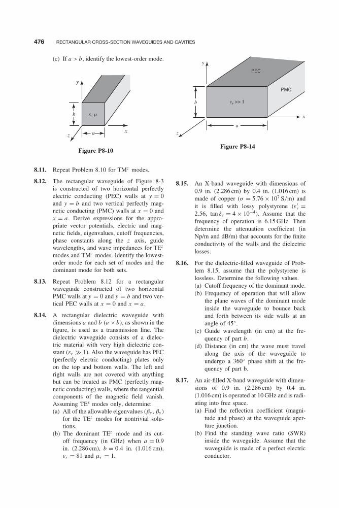
Balanis c08.tex V3 - 11/22/2011 3:32 P.M. Page 476
476 RECTANGULAR CROSS-SECTION WAVEGUIDES AND CAVITIES
(c) If a > b, identify the lowest-order mode.
y
b
azx
e, m
Figure P8-10
8.11. Repeat Problem 8.10 for TMz modes.
8.12. The rectangular waveguide of Figure 8-3is constructed of two horizontal perfectlyelectric conducting (PEC) walls at y = 0and y = b and two vertical perfectly mag-netic conducting (PMC) walls at x = 0 andx = a . Derive expressions for the appro-priate vector potentials, electric and mag-netic fields, eigenvalues, cutoff frequencies,phase constants along the z axis, guidewavelengths, and wave impedances for TEz
modes and TMz modes. Identify the lowest-order mode for each set of modes and thedominant mode for both sets.
8.13. Repeat Problem 8.12 for a rectangularwaveguide constructed of two horizontalPMC walls at y = 0 and y = b and two ver-tical PEC walls at x = 0 and x = a .
8.14. A rectangular dielectric waveguide withdimensions a and b (a > b), as shown in thefigure, is used as a transmission line. Thedielectric waveguide consists of a dielec-tric material with very high dielectric con-stant (εr � 1). Also the waveguide has PEC(perfectly electric conducting) plates onlyon the top and bottom walls. The left andright walls are not covered with anythingbut can be treated as PMC (perfectly mag-netic conducting) walls, where the tangentialcomponents of the magnetic field vanish.Assuming TEz modes only, determine:(a) All of the allowable eigenvalues (βx , βy )
for the TEz modes for nontrivial solu-tions.
(b) The dominant TEz mode and its cut-off frequency (in GHz) when a = 0.9in. (2.286 cm), b = 0.4 in. (1.016 cm),εr = 81 and μr = 1.
er >> 1
PEC
PMC
z
x
a
b
y
Figure P8-14
8.15. An X-band waveguide with dimensions of0.9 in. (2.286 cm) by 0.4 in. (1.016 cm) ismade of copper (σ = 5.76 × 10⁷ S/m) andit is filled with lossy polystyrene (ε′
r =2.56, tan δe = 4 × 10⁻⁴). Assume that thefrequency of operation is 6.15 GHz. Thendetermine the attenuation coefficient (inNp/m and dB/m) that accounts for the finiteconductivity of the walls and the dielectriclosses.
8.16. For the dielectric-filled waveguide of Prob-lem 8.15, assume that the polystyrene islossless. Determine the following values.(a) Cutoff frequency of the dominant mode.(b) Frequency of operation that will allow
the plane waves of the dominant modeinside the waveguide to bounce backand forth between its side walls at anangle of 45◦.
(c) Guide wavelength (in cm) at the fre-quency of part b.
(d) Distance (in cm) the wave must travelalong the axis of the waveguide toundergo a 360◦ phase shift at the fre-quency of part b.
8.17. An air-filled X-band waveguide with dimen-sions of 0.9 in. (2.286 cm) by 0.4 in.(1.016 cm) is operated at 10 GHz and is radi-ating into free space.(a) Find the reflection coefficient (magni-
tude and phase) at the waveguide aper-ture junction.
(b) Find the standing wave ratio (SWR)inside the waveguide. Assume that thewaveguide is made of a perfect electricconductor.
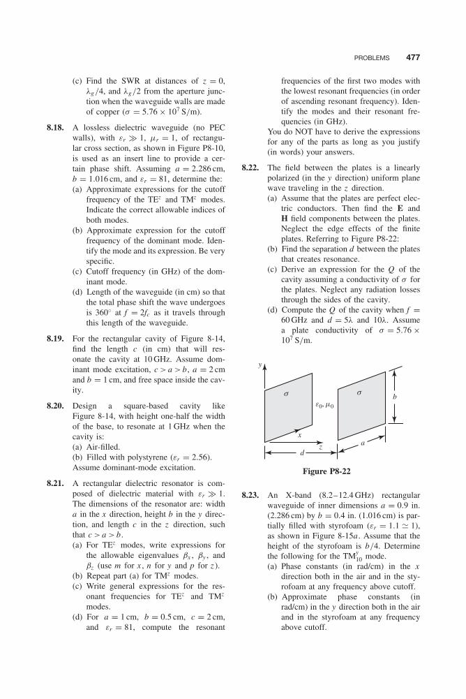
Balanis c08.tex V3 - 11/22/2011 3:32 P.M. Page 477
PROBLEMS 477
(c) Find the SWR at distances of z = 0,λg/4, and λg/2 from the aperture junc-tion when the waveguide walls are madeof copper (σ = 5.76 × 10⁷ S/m).
8.18. A lossless dielectric waveguide (no PECwalls), with εr � 1, μr = 1, of rectangu-lar cross section, as shown in Figure P8-10,is used as an insert line to provide a cer-tain phase shift. Assuming a = 2.286 cm,b = 1.016 cm, and εr = 81, determine the:(a) Approximate expressions for the cutoff
frequency of the TEz and TMz modes.Indicate the correct allowable indices ofboth modes.
(b) Approximate expression for the cutofffrequency of the dominant mode. Iden-tify the mode and its expression. Be veryspecific.
(c) Cutoff frequency (in GHz) of the dom-inant mode.
(d) Length of the waveguide (in cm) so thatthe total phase shift the wave undergoesis 360◦ at f = 2fc as it travels throughthis length of the waveguide.
8.19. For the rectangular cavity of Figure 8-14,find the length c (in cm) that will res-onate the cavity at 10 GHz. Assume dom-inant mode excitation, c > a > b, a = 2 cmand b = 1 cm, and free space inside the cav-ity.
8.20. Design a square-based cavity likeFigure 8-14, with height one-half the widthof the base, to resonate at 1 GHz when thecavity is:(a) Air-filled.(b) Filled with polystyrene (εr = 2.56).Assume dominant-mode excitation.
8.21. A rectangular dielectric resonator is com-posed of dielectric material with εr � 1.The dimensions of the resonator are: widtha in the x direction, height b in the y direc-tion, and length c in the z direction, suchthat c > a > b.(a) For TEz modes, write expressions for
the allowable eigenvalues βx , βy , andβz (use m for x , n for y and p for z ).
(b) Repeat part (a) for TMz modes.(c) Write general expressions for the res-
onant frequencies for TEz and TMz
modes.(d) For a = 1 cm, b = 0.5 cm, c = 2 cm,
and εr = 81, compute the resonant
frequencies of the first two modes withthe lowest resonant frequencies (in orderof ascending resonant frequency). Iden-tify the modes and their resonant fre-quencies (in GHz).
You do NOT have to derive the expressionsfor any of the parts as long as you justify(in words) your answers.
8.22. The field between the plates is a linearlypolarized (in the y direction) uniform planewave traveling in the z direction.(a) Assume that the plates are perfect elec-
tric conductors. Then find the E andH field components between the plates.Neglect the edge effects of the finiteplates. Referring to Figure P8-22:
(b) Find the separation d between the platesthat creates resonance.
(c) Derive an expression for the Q of thecavity assuming a conductivity of σ forthe plates. Neglect any radiation lossesthrough the sides of the cavity.
(d) Compute the Q of the cavity when f =60 GHz and d = 5λ and 10λ. Assumea plate conductivity of σ = 5.76 ×10⁷ S/m.
e0, m0
y
d
x
z a
bs s
Figure P8-22
8.23. An X-band (8.2–12.4 GHz) rectangularwaveguide of inner dimensions a = 0.9 in.(2.286 cm) by b = 0.4 in. (1.016 cm) is par-tially filled with styrofoam (εr = 1.1 � 1),as shown in Figure 8-15a . Assume that theheight of the styrofoam is b/4. Determinethe following for the TMy
10 mode.(a) Phase constants (in rad/cm) in the x
direction both in the air and in the sty-rofoam at any frequency above cutoff.
(b) Approximate phase constants (inrad/cm) in the y direction both in the airand in the styrofoam at any frequencyabove cutoff.

Balanis c08.tex V3 - 11/22/2011 3:32 P.M. Page 478
478 RECTANGULAR CROSS-SECTION WAVEGUIDES AND CAVITIES
(c) The approximate value of its cutoff fre-quency.
(d) The phase constant (in rad/cm) in thez direction at a frequency of f =1.25(fc)TM
10 .8.24. For the rectangular waveguide of Figure 8-
3, derive expressions for the E and H fields,eigenvalues, and cutoff frequencies for:(a) TEx (LSEx ) modes.(b) TMx (LSMx ) modes.Identify the lowest-order mode for each setof modes and the dominant mode for bothsets.
8.25. For the partially filled waveguide ofFigure 8-15b, derive expressions similar to(8-115) through (8-115b) or (8-127) through(8-127b) for:(a) LSEx (TEx ) modes.(b) LSMx (TMx ) modes.
8.26. For a metallic rectangular waveguide filledwith air and with dimensions a and b(b > a), as shown in Figure 8-3, andwith a = 0.4 in. (1.016 cm) and b = 0.9 in.(2.286 cm):(a) Identify the dominant TEz or TMz mode
and its cutoff frequency (in GHz).(b) Identify the dominant TEy or TMy mode
and its cutoff frequency (in GHz).(c) What is the second mode(s) after the
dominant TEz or TMz mode? Identifyit/them.
(d) To lower the cutoff frequency of thedominant TEz or TMz mode to 4 GHzby completely filling the inside of thewaveguide with a dielectric material,what should the dielectric constant ofthe dielectric material be?
8.27. For the partially filled waveguide ofFigure 8-15a , plot on a single figure βy0,βyd , βz , βz0, and βzd , all in rad/m, ver-sus frequency [(fc)0n ≤ f ≤ 2(fc)0n , where(fc)0n is the cutoff frequency for the TEy
0nmode] for the:(a) TEy
02 mode.
(b) TEy03 mode.
Assume a = 0.9 in. (2.286 cm), b = 0.4 in.(1.016 cm), h = b/3, and εr = 2.56.
8.28. For the partially filled waveguide ofFigure 8-15a , plot on a single figure βy0,βyd , βz , βz0, and βzd , all in rad/m, versusfrequency [(fc)1n ≤ f ≤ 2(fc)1n , where
(fc)1n is the cutoff frequency for the TMy1n ,
mode] for the:(a) TMy
11 mode.(b) TMy
12 mode.Assume a = 0.9 in. (2.286 cm), b = 0.4 in.(1.016 cm), h = b/3, and εr = 2.56.
8.29. Use the Transverse Resonance Method(TRM) to derive the basic transcenden-tal eigenvalue and impedance equations ofProblem 8.25.
8.30. A metallic rectangular waveguide withdimensions a and b (a > b) of Figure 8-15a ,with a = 0.9 in. (2.286 cm) and b = 0.4in. (1.016 cm), is partially filled with air(ε0, μ0) and a ferromagnetic material withεd = 4ε0 and μd = 4μ0. The height of theferromagnetic material is h = b/3. For eachof the cases below:(a) Identify the dominant TEy
mn mode (forparts 1, 2 and 3 below)
(b) Write an analytical expression (notgraphical or MATLAB solutions) for itscutoff frequency (for parts 1, 2, 3 below)
(c) Compute, based on the analyticalexpression only, the cutoff frequency(for parts 1, 2, 3) when the waveguide is:1. Completely filled with air (in GHz).2. Completely filled with ferromag-
netic material with εd = 4ε0 andμd = 4μ0 (in GHz).
3. Partially-filled with air (ε0, μ0) andferromagnetic material with εd = 4ε0
and μd = 4μ0, as shown in theFigure 8-15 (in GHz). Not graph-ical or MATLAB solutions; onlysolutions based on the analyticalexpression.
(d) Compare the cutoff frequency of thepartially filled waveguide with the othertwo cutoff frequencies (completely filledwith air and completely filled with theferromagnetic material); i.e., is it higher,lower, or in between the other two? Is itin the correct frequency range?
8.31. A X-band waveguide is partially filledwith a dielectric material, as shown inFigure 8-15b. Assuming TMx (LSMx )modes and a = 2.286 cm, b = 1.016 cm,εr = 1.1, μr = 1, and w = a/2, determine,for the dominant mode, the:(a) Cutoff frequency (in GHz) when the
waveguide is totally filled with freespace.
Balanis c08.tex V3 - 11/22/2011 3:32 P.M. Page 479
PROBLEMS 479
(b) Cutoff frequency (in GHz) when thewaveguide is totally filled with thestated dielectric (εr = 1.1).
(c) Approximate cutoff frequency (in GHz)for the partially filled waveguide.
(d) Ascending order (lowest, middle, andhighest) of the above three cutoff fre-quencies.
You do not have to derive the equations aslong as you justify them.
8.32. A dielectric slab waveguide, as shown inFigure 8-19, is used to guide electromag-netic energy along its axis. Assume that theslab is 1 cm in height, its dielectric constantis 5, and μ = μ0.(a) Find the modes that can propagate unat-
tenuated at a frequency of 8 GHz. Statetheir cutoff frequencies.
(b) Find the respective attenuation (inNp/m) and phase (in rad/m) constantsat 8 GHz for the unattenuated modes.
(c) Find the incidence angles, measuredfrom the normal to the interface, ofthe bouncing waves within the slab at8 GHz.
8.33. A ground plane is covered with a dielectricmaterial with a dielectric constant of 4. Thetotal height of the dielectric material, of thedielectric cover, is 1.25 cm.(a) Identify the first two modes with the
lowest cutoff frequencies, and determinetheir corresponding cutoff frequencies.
(b) Determine for both modes of part (a)the phase constant in the dielectric(in rad/cm) in the direction normal tothe interface when the incidence angle(measured from the normal to the inter-face) is twice the critical angle.
8.34. Design a nonferromagnetic lossless dielec-tric slab of total height 0.5 in. (1.27 cm)bounded above and below by air so that atf = 10 GHz the TEz
1 mode operates at 10%above its cutoff frequency. Determine thedielectric constant of the slab and the atten-uation αy0 (in Np/cm) and βyd (in rad/cm)for the TEz
1 mode at its cutoff frequency.
8.35. A planar perfect electric conductor of infi-nite dimensions is coated with a dielec-tric medium of thickness h , as shown inFigure 8-32. Assume that the dielectricconstant of the coating is 5, its relative
permeability is unity, and its thickness is5.625 cm.(a) Find the cutoff frequencies of the first
four TEz and/or TMz modes and specifyto which group each one belongs.
(b) For an operating frequency of 1 GHz,find the TEz modes that can propagateinside the slab unattenuated.
(c) For each of the TEz modes found inpart b, find the corresponding propaga-tion constant βz .
The medium above the coating is free space.
8.36. Coupling between distributive microwaveand millimeter-wave microstrip circuit ele-ments (such as filters, couplers, antennas,etc.), that are etched on the surface ofa grounded dielectric slab—referred to assubstrate and considered as a dielectric-covered ground plane—is either throughspace or surface waves. Space waves arethose radiated by the elements and travelthrough air, while surface waves are thoseexcited and travelling within the substrate.It is desired to design the system so that itwill eliminate all the surface-wave modes,other than the dominant mode (static mode)with zero cutoff frequency. The maximumheight of the substrate is 0.113 cm.(a) Determine the dominant surface-wave
mode and its cutoff frequency.(b) Determine the dielectric constant of
the substrate so that the designed cir-cuits will operate in a single, dominantsurface-wave mode up to 20 GHz.
(c) Identify the next higher-order surface-wave mode and its cutoff frequency.
(d) For the mode of part (c), determine atits cutoff frequency the:• Attenuation constant αyo (in dB/cm)• Phase constant βyd (in degrees/cm)
(e) For the mode of part (c), determine at25 GHz the approximate:• Attenuation constant αyo (in dB/cm)• Phase constant βyd (in degrees/cm)
8.37. A transmission line is composed of adielectric-covered ground plane immersedinto a homogeneous unbounded medium, asshown in Figure P8-37. The dielectric con-stant of the dielectric cover is εr1 = 2.56while its height is 2 cm. It is desired to oper-ate this transmission line in a single, domi-nant mode over a bandwidth of 3.1 GHz.

Balanis c08.tex V3 - 11/22/2011 3:32 P.M. Page 480
480 RECTANGULAR CROSS-SECTION WAVEGUIDES AND CAVITIES
(a) Identify the dominant mode that can besupported by the line and its cutoff fre-quency.
(b) State which mode has the next highestcutoff frequency.
(c) What should the dielectric constantof the second (unbounded) mediumbe to meet the desired bandwidthrequirements of the dominant-modeoperation?
(d) For the second mode, determine at3.1 GHz the phase constant βyd (inrad/cm) in the dielectric cover and theattenuation constant αyo (in Nepers/cm)in the unbounded medium.
y
zx
2 cm
er2 = ?
er1 = 2.56
Figure P8-37
8.38. A infinite PMC ground plane is covered witha losseless dielectric slab (εr , μr = 1). Theslab is of height h in the y direction, infinitein the x and z directions, and the wave istraveling in the +z direction. The geometryis the same as that of Figure 8-32 except thatthe ground plane is PMC instead of PEC.Determine, assuming the dielectric-coveredPMC ground plane is used as a waveguide(not as an antenna), the:(a) Allowable TMz
m modes (even and/orodd).
(b) Expression for the cutoff frequencies ofthe allowable TMz (even and/or odd)modes.
(c) Cutoff frequency (in GHz) of the domi-nant TMz mode (even and/or odd) whenεr = 4 and h = 0.125 cm.
8.39. Repeat ALL parts of Problem 8.38 for TEzm
modes.
8.40. For the stripline of Example 8-17, findthe characteristic impedances based onthe approximate formulas of (8-200a), (8-201), and (8-201a). Compare the answerswith the more accurate values obtained inExample 8-17, and comment on the com-parisons.
8.41. Design a stripline with a characteristicimpedance of 30 ohms whose dielectric con-stant is 4. Assume the thickness of the centerconductor is zero (t/b = 0).
8.42. A parallel plate transmission line (waveg-uide) is formed by two finite width platesplaced at y = 0 and y = h , and it is used toapproximate a microstrip. Assume that theelectric field between the plates is given by
E � ây E0e−jβz provided w/h � 1
where E0 is a constant. Derive, for the con-duction losses, an expression for the attenu-ation constant αc (in Np/m) in terms of theplate surface resistance Rs , w , h , ε, and μ.The plates are made of metal with conduc-tivity σ , and the medium between the platesis a lossless dielectric.
e, m
w
y
h
xs = ∞
Figure P8-42
8.43. A TEM line is composed of a ground planeand a center conductor of width w andthickness t placed at a height h above theground plane. Assume that the center con-ductor thickness t is very small. Then thecenter conductor can be approximated elec-trically by a wire whose effective radius is
ae � 0.25w
e0, m0
t
h w
2ae
Figure P8-43

Balanis c08.tex V3 - 11/22/2011 3:32 P.M. Page 481
PROBLEMS 481
Based upon this approximation, derive anapproximate expression for the capacitanceand for the characteristic impedance of theline.
8.44. A microstrip line, whose center conductorhas zero thickness (t = 0), has a dielec-tric constant of 6 and height of 1 mm. Itis desired to design a λ/4 impedance trans-former to match two lines, one input (#1)and the other output (#2), whose center stripwidths are, respectively w1 = 1.505 mm,w3 = 0.549 mm, determine the:
(a) Effective dielectric constant of bothlines.
(b) Characteristic impedance of the input(#1) and output (#2) lines.
(c) Characteristic impedance of the line thatis to perform as a λ/4 impedance trans-former.
(d) Length (in cm), at 2 GHz, of the λ/4impedance transformer.
8.45. Assume that the fields supported by themicrostrip line of Figure 8-51b are a combi-nation of TEz and TMz modes. Then derive
expressions for the electric and magneticfields and their associated wave functionsand wave numbers by treating the geometryas a boundary-value problem. Do this in thespace domain.
8.46. A microstrip transmission line of berylliumoxide (εr = 6.8) has a width-to-height ratioof w/h = 1.5. Assume that the thickness-to-height ratio is t/h = 0.01 and determine thefollowing parameters.(a) Effective width-to-height ratio at zero
frequency.(b) Effective dielectric constant at zero fre-
quency.(c) Characteristic impedance at zero fre-
quency.(d) Approximate frequency where disper-
sion will begin when h = 0.05 cm.(e) Effective dielectric constant at 15 GHz(f) Characteristic impedance at 15 GHz.
Compare with the value if dispersion isneglected.
(g) Phase velocity at 15 GHz. Compare withthe value if dispersion is neglected.
(h) Guide wavelength at 15 GHz.

Balanis c08.tex V3 - 11/22/2011 3:32 P.M. Page 482

CHAPTER 9Circular Cross-Section Waveguides and Cavities
9.1 INTRODUCTION
Cylindrical transmission lines and cavities are very popular geometrical configurations. Cylindri-cal structures are those that maintain a uniform cross section along their length. Typical crosssections are rectangular, square, triangular, circular, elliptical, and others. Whereas the rectangu-lar and square cross sections were analyzed in Chapter 8, the circular cross-section geometrieswill be discussed in this chapter. This will include transmission lines and cavities (resonators) ofconducting walls and dielectric material.
9.2 CIRCULAR WAVEGUIDE
A popular waveguide configuration, in addition to the rectangular one discussed in Chapter 8,is the circular waveguide shown in Figure 9-1. This waveguide is very attractive because ofits ease in manufacturing and low attenuation of the TE0n modes. An apparent drawback is itsfixed bandwidth between modes. Field configurations (modes) that can be supported inside sucha structure are TEz and TMz .
9.2.1 Transverse Electric (TEz) Modes
The transverse electric to z (TEz ) modes can be derived by letting the vector potentials A and Fbe equal to
A = 0 (9-1a)
F = âz Fz (ρ, φ, z ) (9-1b)
The vector potential F must satisfy the vector wave equation 3-48, which reduces for the F of(9-1b) to
∇2Fz (ρ, φ, z ) + β2Fz (ρ, φ, z ) = 0 (9-2)
When expanded in cylindrical coordinates, (9-2) reduces to
∂2Fz
∂ρ2+ 1
ρ
∂Fz
∂ρ+ 1
ρ2
∂2Fz
∂φ2+ ∂2Fz
∂z 2+ β2Fz = 0 (9-3)
whose solution for the geometry of Figure 9-1, according to (3-70), is of the form
Fz (ρ, φ, z ) = [A1Jm(βρρ) + B1Ym(βρρ)]
×[C2 cos(mφ) + D2 sin(mφ)][A3e−jβz z + B3e+jβz z
](9-4)
483
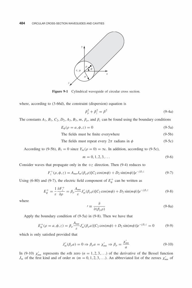
484 CIRCULAR CROSS-SECTION WAVEGUIDES AND CAVITIES
z
xa
y
r
e, m f
Figure 9-1 Cylindrical waveguide of circular cross section.
where, according to (3-66d), the constraint (dispersion) equation is
β2ρ + β2
z = β2 (9-4a)
The constants A1, B1, C2, D2, A3, B3, m , βρ , and βz can be found using the boundary conditions
Eφ(ρ = a , φ, z ) = 0 (9-5a)
The fields must be finite everywhere (9-5b)
The fields must repeat every 2π radians in φ (9-5c)
According to (9-5b), B1 = 0 since Ym(ρ = 0) = ∞. In addition, according to (9-5c),
m = 0, 1, 2, 3, . . . (9-6)
Consider waves that propagate only in the +z direction. Then (9-4) reduces to
F+z (ρ, φ, z ) = AmnJm(βρρ)[C2 cos(mφ) + D2 sin(mφ)]e−jβz z (9-7)
Using (6-80) and (9-7), the electric field component of E+φ can be written as
E+φ = 1
ε
∂F+z
∂ρ= βρ
Amn
εJ ′
m(βρρ)[C2 cos(mφ) + D2 sin(mφ)]e−jβz z (9-8)
where′ ≡ ∂
∂(βρρ)(9-8a)
Apply the boundary condition of (9-5a) in (9-8). Then we have that
E+φ (ρ = a , φ, z ) = βρ
Amn
εJ ′
m(βρa)[C2 cos(mφ) + D2 sin(mφ)]e−jβz z = 0 (9-9)
which is only satisfied provided that
J ′m(βρa) = 0 ⇒ βρa = χ ′
mn ⇒ βρ = χ ′mn
a(9-10)
In (9-10) χ ′mn represents the nth zero (n = 1, 2, 3, . . .) of the derivative of the Bessel function
Jm of the first kind and of order m (m = 0, 1, 2, 3, . . .). An abbreviated list of the zeroes χ ′mn of
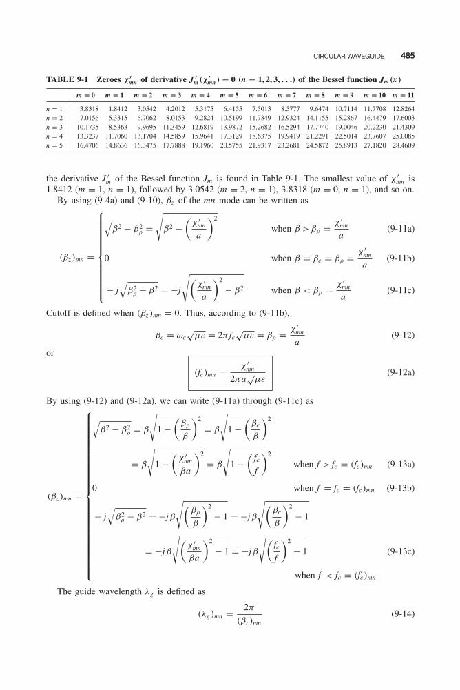
CIRCULAR WAVEGUIDE 485
TABLE 9-1 Zeroes χ ′mn of derivative J ′
m(χ ′mn) = 0 (n = 1, 2, 3, . . .) of the Bessel function Jm(x)
m = 0 m = 1 m = 2 m = 3 m = 4 m = 5 m = 6 m = 7 m = 8 m = 9 m = 10 m = 11
n = 1 3.8318 1.8412 3.0542 4.2012 5.3175 6.4155 7.5013 8.5777 9.6474 10.7114 11.7708 12.8264n = 2 7.0156 5.3315 6.7062 8.0153 9.2824 10.5199 11.7349 12.9324 14.1155 15.2867 16.4479 17.6003n = 3 10.1735 8.5363 9.9695 11.3459 12.6819 13.9872 15.2682 16.5294 17.7740 19.0046 20.2230 21.4309n = 4 13.3237 11.7060 13.1704 14.5859 15.9641 17.3129 18.6375 19.9419 21.2291 22.5014 23.7607 25.0085n = 5 16.4706 14.8636 16.3475 17.7888 19.1960 20.5755 21.9317 23.2681 24.5872 25.8913 27.1820 28.4609
the derivative J ′m of the Bessel function Jm is found in Table 9-1. The smallest value of χ ′
mn is1.8412 (m = 1, n = 1), followed by 3.0542 (m = 2, n = 1), 3.8318 (m = 0, n = 1), and so on.
By using (9-4a) and (9-10), βz of the mn mode can be written as
(βz )mn =
⎧⎪⎪⎪⎪⎪⎪⎪⎪⎪⎪⎨⎪⎪⎪⎪⎪⎪⎪⎪⎪⎪⎩
√β2 − β2
ρ =√
β2 −(
χ ′mn
a
)2
when β > βρ = χ ′mn
a
0 when β = βc = βρ = χ ′mn
a
− j√
β2ρ − β2 = −j
√(χ ′
mn
a
)2
− β2 when β < βρ = χ ′mn
a
(9-11a)
(9-11b)
(9-11c)
Cutoff is defined when (βz )mn = 0. Thus, according to (9-11b),
βc = ωc√
με = 2π fc√
με = βρ = χ ′mn
a(9-12)
or
(fc)mn = χ ′mn
2πa√
με(9-12a)
By using (9-12) and (9-12a), we can write (9-11a) through (9-11c) as
(βz )mn =
⎧⎪⎪⎪⎪⎪⎪⎪⎪⎪⎪⎪⎪⎪⎪⎪⎪⎪⎪⎪⎪⎪⎪⎪⎪⎨⎪⎪⎪⎪⎪⎪⎪⎪⎪⎪⎪⎪⎪⎪⎪⎪⎪⎪⎪⎪⎪⎪⎪⎪⎩
√β2 − β2
ρ = β
√1 −
(βρ
β
)2
= β
√1 −
(βc
β
)2
= β
√1 −
(χ ′
mn
βa
)2
= β
√1 −
(fcf
)2
when f > fc = (fc)mn
0 when f = fc = (fc)mn
− j√
β2ρ − β2 = −jβ
√(βρ
β
)2
− 1 = −jβ
√(βc
β
)2
− 1
= −jβ
√(χ ′
mn
βa
)2
− 1 = −jβ
√(fcf
)2
− 1
when f < fc = (fc)mn
(9-13a)
(9-13b)
(9-13c)
The guide wavelength λg is defined as
(λg)mn = 2π
(βz )mn(9-14)

486 CIRCULAR CROSS-SECTION WAVEGUIDES AND CAVITIES
which according to (9-13a) and (9-13b) can be written as
(λg)mn =
⎧⎪⎪⎪⎪⎨⎪⎪⎪⎪⎩2π
β
√1 −
(fcf
)2= λ√
1 −(
fcf
)2when f > fc = (fc)mn
∞ when f = (fc)mn
(9-14a)
(9-14b)
In (9-14a), λ is the wavelength of the wave in an infinite medium of the kind that exists inside thewaveguide. There is no definition of the wavelength below cutoff since the wave is exponentiallydecaying and there is no repetition of its waveform.
According to (9-12a) and the values of χ ′mn in Table 9-1, the order (lower to higher cutoff
frequencies) in which the TEzmn modes occur is TEz
11, TEz21, TEz
01, etc. It should be noted that for acircular waveguide the order in which the TEz
mn modes occur does not change, and the bandwidthbetween modes is also fixed. For example, the bandwidth of the first single-mode TEz
11 operationis 3.0542/1.8412 = 1.6588 : 1 which is less than 2 : 1. This bandwidth is fixed and cannot bevaried, as was the case for the rectangular waveguide where the bandwidth between modes wasa function of the a/b ratio. In fact, for a rectangular waveguide the maximum bandwidth of asingle dominant mode operation was 2 : 1 and it occurred when a/b ≥ 2; otherwise, for a/b < 2,the bandwidth of a single dominant mode operation was less than 2 : 1. The reason is that in arectangular waveguide there are two dimensions a and b (2 degrees of freedom) whose relativevalues can vary; in the circular waveguide there is only one dimension (the radius a) that canvary. A change in the radius only varies, by the same amount, the absolute values of the cutofffrequencies of all the modes, so it does not alter their order or relative bandwidth.
The electric and magnetic field components can be written, using (6-80) and (9-7), as
E+ρ = − 1
ερ
∂F+z
∂φ= −Amn
m
ερJm(βρρ)[−C2 sin(mφ) + D2 cos(mφ)]e−jβz z
(9-15a)
E+φ = 1
ε
∂F+z
∂ρ= Amn
βρ
εJ ′
m(βρρ)[C2 cos(mφ) + D2 sin(mφ)]e−jβz z (9-15b)
E+z = 0 (9-15c)
H +ρ = −j
1
ωμε
∂2F+z
∂ρ ∂z= −Amn
βρβz
ωμεJ ′
m(βρρ)[C2 cos(mφ) + D2 sin(mφ)]e−jβz z (9-15d)
H +φ = −j
1
ωμε
1
ρ
∂2F+z
∂φ ∂z= −Amn
mβz
ωμε
1
ρJm(βρρ)
×[−C2 sin(mφ) + D2 cos(mφ)]e−jβz z (9-15e)
H +z = −j
1
ωμε
(∂2
∂z 2+ β2
)F+
z = −jAmnβ2
ρ
ωμεJm(βρρ)
×[C2 cos(mφ) + D2 sin(mφ)]e−jβz z (9-15f)
where
′ ≡ ∂
∂(βρρ)(9-15g)

CIRCULAR WAVEGUIDE 487
By using (9-15a) through (9-15f), the wave impedance (Z +zw )TE
mn of the TEzmn (H z
mn) modes inthe +z direction can be written as
(Z +zw )TE
mn = E+ρ
H +φ
= − E+φ
H +ρ
= ωμ
(βz )mn(9-16)
With the aid of (9-13a) through (9-13c), the wave impedance of (9-16) reduces to
(Z +zw )TE
mn =
⎧⎪⎪⎪⎪⎪⎪⎪⎪⎪⎪⎪⎪⎪⎪⎪⎪⎪⎪⎪⎪⎪⎪⎪⎪⎪⎨⎪⎪⎪⎪⎪⎪⎪⎪⎪⎪⎪⎪⎪⎪⎪⎪⎪⎪⎪⎪⎪⎪⎪⎪⎪⎩
ωμ
β
√1 −
(fcf
)2=
√μ
ε√1 −
(fcf
)2= η√
1 −(
fcf
)2
when f > fc = (fc)mn
ωμ
0= ∞ when f = fc = (fc)mn
ωμ
−jβ
√(fcf
)2
− 1
= +j
√μ
ε√(fcf
)2
− 1
= +jη√(
fcf
)2
− 1
when f < fc = (fc)mn
(9-16a)
(9-16b)
(9-16c)
By examining (9-16a) through (9-16c), we can make the following statements about theimpedance.
1. Above cutoff it is real and greater than the intrinsic impedance of the medium inside thewaveguide.
2. At cutoff it is infinity.3. Below cutoff it is imaginary and inductive. This indicates that the waveguide below cutoff
behaves as an inductor that is an energy storage element.
The form of Z +zw , as given by (9-16a) through (9-16c), as a function of fc/f , and where fc is
the cutoff frequency of that mode, is the same as the Z +zw for the TEz modes of a rectangular
waveguide, as given by (8-20a) through (8-20c). A plot of (9-16a) through (9-16c) for any oneTEz
mn mode as a function of fc/f , is shown in Figure 8-2.
Example 9-1
A circular waveguide of radius a = 3 cm that is filled with polystyrene (εr = 2.56) is used at a frequencyof 2 GHz. For the dominant TEz
mn mode, determine the following:
a. Cutoff frequency.b. Guide wavelength (in cm). Compare it to the infinite medium wavelength λ.c. Phase constant βz (in rad/cm).d. Wave impedance.e. Bandwidth over single-mode operation (assuming only TEz modes).
488 CIRCULAR CROSS-SECTION WAVEGUIDES AND CAVITIES
Solution:
a. The dominant mode is the TE11 mode whose cutoff frequency is, according to (9-12a),
(fc)TEz
11 = 1.8412
2πa√
με= 1.8412(30 × 109)
2π(3)√
2.56= 1.8315 GHz
b. Since the frequency of operation is 2 GHz, which is greater than the cutoff frequency of1.8315 GHz, the guide wavelength of (9-14a) for the TE11 mode is
λg = λ√1 −
(fcf
)2
where
λ = λ0√εr
= 30 × 109
2 × 10⁹√
2.56= 9.375 cm√
1 −(
fcf
)2
=√
1 −(
1.8315
2
)2
= 0.4017
Thus,
λg = 9.375
0.4017= 23.34 cm where λ = 9.375 cm
c. The phase constant βz of the TE11 mode is found using (9-13a), or
βz = β
√1 −
(fcf
)2
= 2π
λ
√1 −
(fcf
)2
= 2π
9.375(0.4017) = 0.2692 rad/cm
which can also be obtained using
βz = 2π
λg= 2π
23.34= 0.2692 rad/cm
d. According to (9-16a), the wave impedance of the TE11 mode is equal to
Z h11 = η√
1 −(
fcf
)2= 120π/
√2.56
0.4017= 586.56 ohms
e. Since the next higher-order TEmn mode is the TE21, the bandwidth of single TE11 mode operationis
BW = 3.0542/1.8412 : 1 = 1.6588 : 1
9.2.2 Transverse Magnetic (TMz) Modes
The transverse magnetic to z (TMz ) modes can be derived in a similar manner as the TEz modesof Section 9.2.1 by letting
A = âz Az (ρ, φ, z ) (9-17a)
F = 0 (9-17b)
CIRCULAR WAVEGUIDE 489
The vector potential A must satisfy the vector wave equation of (3-48), which reduces for the Aof (9-17a) to
∇2Az (ρ, φ, z ) + β2Az (ρ, φ, z ) = 0 (9-18)
The solution of (9-18) is obtained in a manner similar to that of (9-2), as given by (9-4), and itcan be written as
Az (ρ, φ, z ) = [A1Jm(βρρ) + B1Ym(βρρ)]
×[C2 cos(mφ) + D2 sin(mφ)][A3e−jβz z + B3e+jβz z
](9-19)
with the constraint (dispersion) equation expressed as
β2ρ + β2
z = β2 (9-19a)
The constants A1, B1, C2, D2, A3, B3, m , βρ , and βz can be found using the following boundaryconditions
Eφ(ρ = a , φ, z ) = 0 (9-20a)
orEz (ρ = a , φ, z ) = 0 (9-20b)
The fields must be finite everywhere (9-20c)
The fields must repeat every 2π radians in φ (9-20d)
According to (9-20c), B1 = 0 since Ym(ρ = 0) = ∞. In addition, according to (9-20d),
m = 0, 1, 2, 3, . . . (9-21)
Considering waves that propagate only in the +z direction, (9-19) reduces to
A+z (ρ, φ, z ) = BmnJm(βρρ)[C2 cos(mφ) + D2 sin(mφ)]e−jβz z (9-22)
The eigenvalues of βρ can be obtained by applying either (9-20a) or (9-20b). Use of (6-70) and(9-22) allows us to write the electric field component E+
z as
E+z = −j
1
ωμε
(∂2
∂z 2+ β2
)A+
z
= −jBmnβ2
ρ
ωμεJm(βρρ)[C2 cos(mφ) + D2 sin(mφ)]e−jβz z (9-23)
Application of the boundary condition (9-20b) and use of (9-23) gives
E+z (ρ = a , φ, z ) = −jBmn
β2ρ
ωμεJm(βρa)[C2 cos(mφ) + D2 sin(mφ)]e−jβz z = 0 (9-24)
which is only satisfied provided that
Jm(βρa) = 0 ⇒ βρa = χmn ⇒ βρ = χmn
a(9-25)
In (9-25), χmn represents the nth zero (n = 1, 2, 3, . . .) of the Bessel function Jm of the first kindand of order m (m = 0, 1, 2, 3, . . .). An abbreviated list of the zeroes χmn of the Bessel functionJm is found in Table 9-2. The smallest value of χmn is 2.4049 (m = 0, n = 1), followed by 3.8318(m = 1, n = 1), 5.1357 (m = 2, n = 1), etc.
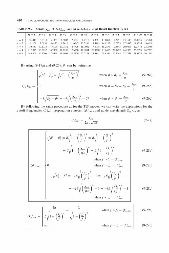
490 CIRCULAR CROSS-SECTION WAVEGUIDES AND CAVITIES
TABLE 9-2 Zeroes χmn of Jm(χmn) = 0 (n = 1, 2, 3, . . .) of Bessel function Jm(x)
m = 0 m = 1 m = 2 m = 3 m = 4 m = 5 m = 6 m = 7 m = 8 m = 9 m = 10 m = 11
n = 1 2.4049 3.8318 5.1357 6.3802 7.5884 8.7715 9.9361 11.0864 12.2251 13.3543 14.4755 15.5898n = 2 5.5201 7.0156 8.4173 9.7610 11.0647 12.3386 13.5893 14.8213 16.0378 17.2412 18.4335 19.6160n = 3 8.6537 10.1735 11.6199 13.0152 14.3726 15.7002 17.0038 18.2876 19.5545 20.8071 22.0470 23.2759n = 4 11.7915 13.3237 14.7960 16.2235 17.6160 18.9801 20.3208 21.6415 22.9452 24.2339 25.5095 26.7733n = 5 14.9309 16.4706 17.9598 19.4094 20.8269 22.2178 23.5861 24.9349 26.2668 27.5838 28.8874 30.1791
By using (9-19a) and (9-25), βz can be written as
(βz )mn =
⎧⎪⎪⎪⎪⎪⎪⎪⎪⎪⎪⎨⎪⎪⎪⎪⎪⎪⎪⎪⎪⎪⎩
√β2 − β2
ρ =√
β2 −(χmn
a
)2when β > βρ = χmn
a
0 when β = βc = βρ = χmn
a
− j√
β2ρ − β2 = −j
√(χmn
a
)2− β2 when β < βρ = χmn
a
(9-26a)
(9-26b)
(9-26c)
By following the same procedure as for the TEz modes, we can write the expressions for thecutoff frequencies (fc)mn , propagation constant (βz )mn , and guide wavelength (λg)mn as
(fc)mn = χmn
2πa√
με(9-27)
(βz )mn =
⎧⎪⎪⎪⎪⎪⎪⎪⎪⎪⎪⎪⎪⎪⎪⎪⎪⎪⎪⎪⎪⎪⎪⎪⎪⎪⎪⎪⎨⎪⎪⎪⎪⎪⎪⎪⎪⎪⎪⎪⎪⎪⎪⎪⎪⎪⎪⎪⎪⎪⎪⎪⎪⎪⎪⎪⎩
√β2 − β2
ρ = β
√1 −
(βρ
β
)2
= β
√1 −
(βc
β
)2
= β
√1 −
(χmn
βa
)2
= β
√1 −
(fcf
)2
when f > fc = (fc)mn
0 when f = fc = (fc)mn
− j√
β2ρ − β2 = −jβ
√(βρ
β
)2
− 1 = −jβ
√(βc
β
)2
− 1
= −jβ
√(χmn
βa
)2
− 1 = −jβ
√(fcf
)2
− 1
when f < fc = (fc)mn
(9-28a)
(9-28b)
(9-28c)
(λg)mn =
⎧⎪⎪⎪⎪⎨⎪⎪⎪⎪⎩2π
β
√1 −
(fcf
)2= λ√
1 −(
fcf
)2when f > fc = (fc)mn
∞ when f = fc = (fc)mn
(9-29a)
(9-29b)
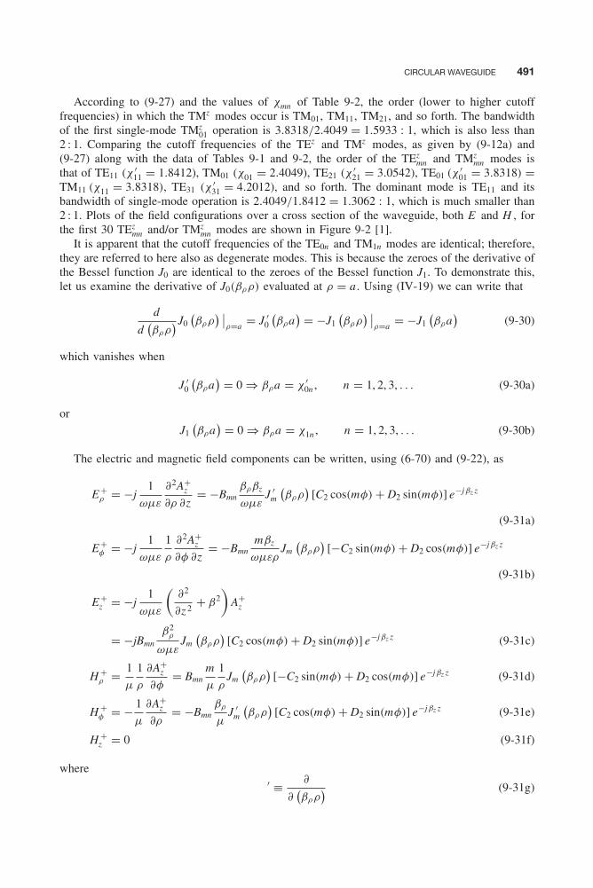
CIRCULAR WAVEGUIDE 491
According to (9-27) and the values of χmn of Table 9-2, the order (lower to higher cutofffrequencies) in which the TMz modes occur is TM01, TM11, TM21, and so forth. The bandwidthof the first single-mode TMz
01 operation is 3.8318/2.4049 = 1.5933 : 1, which is also less than2 : 1. Comparing the cutoff frequencies of the TEz and TMz modes, as given by (9-12a) and(9-27) along with the data of Tables 9-1 and 9-2, the order of the TEz
mn and TMzmn modes is
that of TE11 (χ ′11 = 1.8412), TM01 (χ01 = 2.4049), TE21 (χ ′
21 = 3.0542), TE01 (χ ′01 = 3.8318) =
TM11 (χ11 = 3.8318), TE31 (χ ′31 = 4.2012), and so forth. The dominant mode is TE11 and its
bandwidth of single-mode operation is 2.4049/1.8412 = 1.3062 : 1, which is much smaller than2 : 1. Plots of the field configurations over a cross section of the waveguide, both E and H , forthe first 30 TEz
mn and/or TMzmn modes are shown in Figure 9-2 [1].
It is apparent that the cutoff frequencies of the TE0n and TM1n modes are identical; therefore,they are referred to here also as degenerate modes. This is because the zeroes of the derivative ofthe Bessel function J0 are identical to the zeroes of the Bessel function J1. To demonstrate this,let us examine the derivative of J0(βρρ) evaluated at ρ = a . Using (IV-19) we can write that
d
d(βρρ
)J0(βρρ
) ∣∣ρ=a = J ′
0
(βρa
) = −J1(βρρ
) ∣∣ρ=a = −J1
(βρa
)(9-30)
which vanishes when
J ′0
(βρa
) = 0 ⇒ βρa = χ ′0n , n = 1, 2, 3, . . . (9-30a)
orJ1
(βρa
) = 0 ⇒ βρa = χ1n , n = 1, 2, 3, . . . (9-30b)
The electric and magnetic field components can be written, using (6-70) and (9-22), as
E+ρ = −j
1
ωμε
∂2A+z
∂ρ ∂z= −Bmn
βρβz
ωμεJ ′
m
(βρρ
)[C2 cos(mφ) + D2 sin(mφ)] e−jβz z
(9-31a)
E+φ = −j
1
ωμε
1
ρ
∂2A+z
∂φ ∂z= −Bmn
mβz
ωμερJm
(βρρ
)[−C2 sin(mφ) + D2 cos(mφ)] e−jβz z
(9-31b)
E+z = −j
1
ωμε
(∂2
∂z 2+ β2
)A+
z
= −jBmnβ2
ρ
ωμεJm
(βρρ
)[C2 cos(mφ) + D2 sin(mφ)] e−jβz z (9-31c)
H +ρ = 1
μ
1
ρ
∂A+z
∂φ= Bmn
m
μ
1
ρJm
(βρρ
)[−C2 sin(mφ) + D2 cos(mφ)] e−jβz z (9-31d)
H +φ = − 1
μ
∂A+z
∂ρ= −Bmn
βρ
μJ ′
m
(βρρ
)[C2 cos(mφ) + D2 sin(mφ)] e−jβz z (9-31e)
H +z = 0 (9-31f)
where′ ≡ ∂
∂(βρρ
) (9-31g)
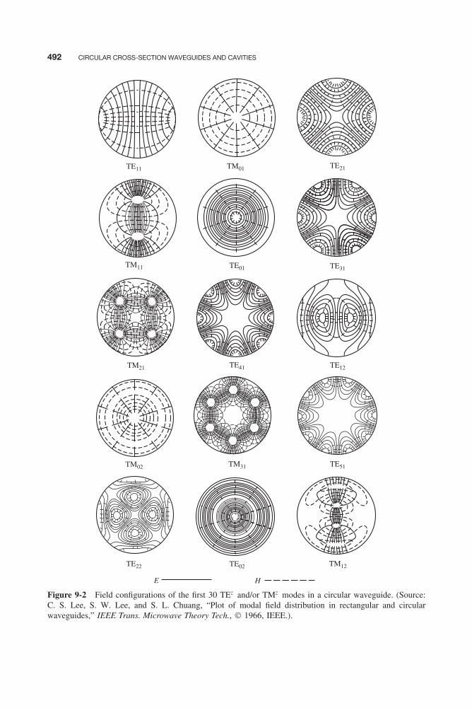
492 CIRCULAR CROSS-SECTION WAVEGUIDES AND CAVITIES
TE11
TM11
TM21
TM02
TE22 TE02 TM12
TE51TM31
TE41 TE12
TE31TE01
TM01 TE21
E H
Figure 9-2 Field configurations of the first 30 TEz and/or TMz modes in a circular waveguide. (Source:C. S. Lee, S. W. Lee, and S. L. Chuang, “Plot of modal field distribution in rectangular and circularwaveguides,” IEEE Trans. Microwave Theory Tech., © 1966, IEEE.).

CIRCULAR WAVEGUIDE 493
TE61
TM22
TM03
TE81
TE23 TM13 TE03
TM61TM32
TM51 TE42
TE17TE13
TM41 TE32
E H
Figure 9-2 (Continued ).
494 CIRCULAR CROSS-SECTION WAVEGUIDES AND CAVITIES
By using (9-31a) through (9-31f), the wave impedance in the +z direction can be written as
(Z +z
w
)TMmn = E+
ρ
H +φ
= − E+φ
H +ρ
= (βz )mn
ωε(9-32)
With the aid of (9-28a) through (9-28c), the wave impedance of (9-32) reduces to
(Z +z
w
)TMmn =
⎧⎪⎪⎪⎪⎪⎪⎪⎪⎪⎪⎪⎪⎪⎪⎪⎪⎪⎪⎪⎪⎪⎨⎪⎪⎪⎪⎪⎪⎪⎪⎪⎪⎪⎪⎪⎪⎪⎪⎪⎪⎪⎪⎪⎩
β
√1 −
(fcf
)2
ωε=
√μ
ε
√1 −
(fcf
)2
= η
√1 −
(fcf
)2
when f > fc = (fc)mn
0
ωε= 0 when f = fc = (fc)mn
−jβ
√(fcf
)2
− 1
ωε= −j
√μ
ε
√(fcf
)2
− 1 = −jη
√(fcf
)2
− 1
when f < fc = (fc)mn
(9-32a)
(9-32b)
(9-32c)
Examining (9-32a) through (9-32c), we can make the following statements about the waveimpedance for the TMz modes.
1. Above cutoff it is real and smaller than the intrinsic impedance of the medium inside thewaveguide.
2. At cutoff it is zero.3. Below cutoff it is imaginary and capacitive. This indicates that the waveguide below cutoff
behaves as a capacitor that is an energy storage element.
The form of (Z +zw )TM
mn , as given by (9-32a) through (9-32c), and as a function of fc/f , wherefc is the cutoff frequency of that mode, is the same as the (Z +z
w )TMmn for the TMz
mn modes of arectangular waveguide, as given by (8-29a) through (8-29c). A plot of (9-32a) through (9-32c)for any one TMz
mn mode as a function of fc/f , is shown in Figure 8-2.
Example 9-2
Design a circular waveguide filled with a lossless dielectric medium of dielectric constant 4. Thewaveguide must operate in a single dominant mode over a bandwidth of 1 GHz.
1. Find its radius (in cm).2. Determine the lower, center, and upper frequencies of the bandwidth.
Solution:
a. The dominant mode is the TE11 mode whose cutoff frequency according to (9-12a) is
(fc)TEz
11 = χ ′11
2πa√
με= 1.8412(30 × 109)
2π(a)√
4

CIRCULAR WAVEGUIDE 495
The next higher-order mode is the TM01 mode whose cutoff frequency according to (9-27) is
(fc)TMz
01 = χ01
2πa√
με= 2.4049(30 × 109)
2π(a)√
4
The difference between the two must be 1 GHz. To accomplish this, the radius of the waveguidemust be equal to
(2.4049 − 1.8412)30 × 109
2π(a)√
4= 1 × 10⁹ ⇒ a = 1.3457 cm
b. The lower, upper, and center frequencies of the bandwidth are equal to
f� = (fc)TEz
11 = 1.8412(30 × 109)
2π(1.3457)2= 3.2664 × 109 = 3.2664 GHz
fu = (fc)TMz
01 = 2.4049(30 × 109)
2π(1.3457)2= 4.2664 × 109 = 4.2664 GHz
f0 = f� + 0.5 × 109 = fu − 0.5 × 109 = 3.7664 × 109 = 3.7664 GHz
Whenever a given mode is desired, it is necessary to design the proper feed to excite thefields within the waveguide and detect the energy associated with such a mode. Maximizationof the energy exchange or transfer is accomplished by designing the feed, which is usually aprobe or antenna, so that its field pattern matches that of the field configuration of the desiredmode. Usually the probe is placed near the maximum of the field pattern of the desired mode;however, that position may be varied somewhat in order to achieve some desired matching inthe excitation and detection systems. Shown in Figure 9-3 are suggested designs to excite and/ordetect the TE11 and TM01 modes in a circular waveguide, to transition between the TE10 of arectangular waveguide and the TE11 mode of a circular waveguide, and to couple between theTE10 of a rectangular waveguide and TM01 mode of a circular waveguide.
9.2.3 Attenuation
The attenuation in a circular waveguide can be obtained by using techniques similar to thosefor the rectangular waveguide, as outlined and applied in Section 8.2.5. The basic equation is(8-64a), or
(αc)mn = Pc/�
2Pmn= P�
2Pmn(9-33)
which is based on the configuration of Figure 8-9.It has been shown that the attenuation coefficients of the TE0n (n = 1, 2, . . .) modes in a circular
waveguide monotonically decrease as a function of frequency [2, 3]. This is a very desirablecharacteristic, and because of this the excitation, propagation, and detection of TE0n modes ina circular waveguide have received considerable attention. It can be shown that the attenuationcoefficients for the TEz
mn and TMzmn modes inside a circular waveguide are given, respectively, by
TEzmn
(αc)TEz
mn = Rs
aη
√1 −
(fcf
)2
[(fcf
)2
+ m2
(χ ′mn)
2 − m2
]Np/m (9-34a)

496 CIRCULAR CROSS-SECTION WAVEGUIDES AND CAVITIES
(a)
(c) (d)
(b)
Figure 9-3 Excitation of TEmn and TMmn modes in a circular waveguide. (a) TE11 mode. (b) TM01 mode.(c) TE10 (rectangular)-TE11 (circular). (d ) TE10 (rectangular)-TM01 (circular).
TMzmn
(αc)TMz
mn = Rs
aη
1√1 −
(fcf
)2Np/m (9-34b)
Plots of the attenuation coeficient versus the normalized frequency f /fc , where fc is the cutofffrequency of the dominant TE11 mode, are shown for six modes in Figures 9-4a and 9-4b forwaveguide radii of 1.5 and 3 cm, respectively. Within the waveguide is free space and its wallsare made of copper (σ = 5.7 × 10⁷ S/m).
Example 9-3
Derive the attenuation coefficient for the TE01 mode inside a circular waveguide of radius a .
Solution: According to (9-15a) through (9-15g), the electric and magnetic field components for theTE01 (m = 0, n = 1) mode reduce to
E+ρ = E+
z = H +φ = 0
E+φ = βρ
A01
εJ ′
0
(βρρ
)e−jβz z
H +ρ = −A01
βρβz
ωμεJ ′
0
(βρρ
)e−jβz z
H +z = −jA01
β2ρ
ωμεJ0
(βρρ
)e−jβz z
CIRCULAR WAVEGUIDE 497
where
βρ = χ ′01
a= 3.8318
a
Using these equations, the power through a cross section of the waveguide is equal to
P01 = 1
2
∫∫A0
Re[(E × H∗) • ds
]= 1
2
∫∫A0
Re[âφEφ × (
âρHρ + âz Hz)∗]
• âz ds
P01 = −1
2Re
∫ 2π
0
∫ a
0
(EφH ∗
ρ
)ρ dρ dφ = |A01|2
πβz β2ρ
ωμε2
∫ a
0
[J ′
0
(χ ′
01
aρ
)]2
ρ dρ
SincedJp (cx)
d (cx)= −Jp+1 (cx) + p
cxJp (cx)
then
J ′0
(χ ′
01
aρ
)= d
d(χ ′01ρ/a)
J0
(χ ′
01
aρ
)= −J1
(χ ′
01
aρ
)Thus
P01 = |A01|2 πβz
ωμε2
(χ ′
01
a
)2 ∫ a
0J 2
1
(χ ′
01
aρ
)ρ dρ
Since ∫ c
bxJ 2
p (cx) dx = x2
2
[J 2
p (cx) − Jp−1 (cx) Jp+1 (cx)]∣∣∣c
b
then ∫ a
0ρJ 2
1
(χ ′
01
aρ
)dρ = a2
2
[J 2
1
(χ ′
01
) − J0(χ ′
01
)J2
(χ ′
01
)]= −a2
2J0
(χ ′
01
)J2
(χ ′
01
) = a2
2J 2
0
(χ ′
01
)because
J 21
(χ ′
01
) = J 21 (3.8318) = 0
J2(χ ′
01
) = −J0(χ ′
01
)Therefore, the power of the TE01 can be written as
P01 = |A01|2 πβz
2ωμε2
(χ ′
01
)2J 2
0
(χ ′
01
)The power dissipated on the walls of the waveguide is obtained using
Pc = Rs
2
∫∫Sw
(Js • J∗s )ρ=a ds = Rs
2
∫ �
0
∫ 2π
0|Js |2ρ=a a dφ dz
where
Js |ρ=a = n̂ × H+|ρ=a = âφH +z |ρ=a = −âφ j
β2ρ
ωμεA01J0
(βρa
)e−jβz z
498 CIRCULAR CROSS-SECTION WAVEGUIDES AND CAVITIES
Thus,
Pc = |A01|2 Rs
2
(β2
ρ
ωμε
)2
aJ 20
(χ ′
01
) ∫ �
0
∫ 2π
0dφ dz
orPc
�= P� = |A01|2 πRs
a3
[(χ ′
01
)2
ωμε
]2
J 20
(χ ′
01
)Therefore, the attenuation coefficient of (9-33) for the TE01 mode can now be written as
α01 (TEz ) = Rs
aη
(fcf
)2
√1 −
(fcf
)2Np/m
It is evident from the results of the preceding example that as fc/f becomes smaller, theattenuation coefficient decreases monotonically (as shown in Figure 9-4), which is a desirablecharacteristic. It should be noted that similar monotonically decreasing variations in the attenu-ation coefficient are evident in all TE0n modes (n = 1, 2, 3, . . .). According to (9-15a) through(9-15f), the only tangential magnetic field components to the conducting surface of the waveguidefor all these TE0n (m = 0) modes is the Hz component, while the electric field lines are circular.Therefore, these modes are usually referred to as circular electric modes. For a constant powerin the wave, the Hz component decreases as the frequency increases and approaches zero at infi-nite frequency. Simultaneously, the current density and conductor losses on the waveguide wallsalso decrease and approach zero. Because of this attractive feature, these modes have receivedconsiderable attention for long distance propagation of energy, especially at millimeter wave fre-quencies. Typically, attenuations as low as 1.25 dB/km (2 dB/mi) have been attained [2]. This isto be compared with attenuations of 120 dB/km for WR90 copper rectangular waveguides, and3 dB/km at 0.85 μm, and less than 0.5 dB/km at 1.3 μm for fiber optics cables.
Although the TE0n modes are very attractive from the attenuation point of view, there are anumber of problems associated with their excitation and retention. One of the problems is thatthe TE01 mode, which is the first of the TE0n modes, is not the dominant mode. Therefore, inorder for this mode to be above its cutoff frequency and propagate in the waveguide, a numberof other modes (such as the TE11, TM01, TE21, and TM11) with lower cutoff frequencies canalso exist. Additional modes can also be present if the operating frequency is chosen well abovethe cutoff frequency of the TE01 mode in order to provide a margin of safety from being tooclose to its cutoff frequency.
To support the TE01 mode, the waveguide must be oversized and it can support a numberof other modes. One of the problems faced with such a guide is how to excite the desiredTE01 mode with sufficient purity and suppress the others. Another problem is how to preventcoupling between the TE01 mode and undesired modes that can exist since the guide is oversized.The presence of the undesired modes causes not only higher losses but dispersion and attenuationdistortion to the signal since each exhibits different phase velocities and attenuation. Irregularitiesin the inner geometry, surface, and direction (such as bends, nonuniform cross sections, etc.) ofthe waveguide are the main contributors to the coupling to the undesired modes. However, forthe guide to be of any practical use, it must be able to sustain and propagate the desired TE01 andother TE0n modes efficiently over bends of reasonable curvature. One technique that has been

CIRCULAR WAVEGUIDE 499
(a)
Att
enua
tion
(N
p ×
103 /m
)
Normalized frequency (f/fTE )
Att
enua
tion
(dB
× 1
03 /m)
0.000.00
2.50
5.00
7.50
10.00 86.86
65.14
43.43
21.71
0.005.00 10.00 15.00
TE01
TE02
20.00
TE11
TE21
TM01
TM11
s = 5.7 × 10⁷ S/m
Att
enua
tion
(N
p ×
103 /m
)
Normalized frequency ( f/ fc11 )
(b)
Att
enua
tion
(dB
× 1
03 /m)
0.000.00
2.50
5.00
7.50
10.00 86.86
65.14
43.43
21.71
0.005.00 10.00 15.00
TE01
TE02
20.00
TE11
TE21
TM01
TM11
s = 5.7 × 10⁷ S/m
c11
TE
Figure 9-4 Attenuation for TEzmn and TMz
mn modes in a circular waveguide. (a) a = 1.5 cm. (b) a = 3 cm.
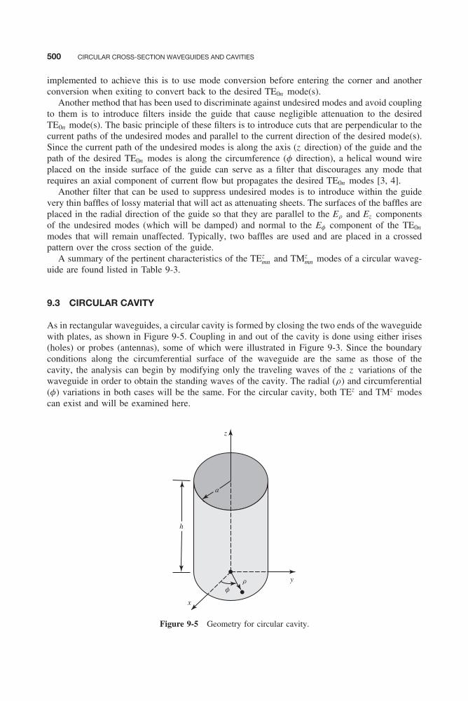
500 CIRCULAR CROSS-SECTION WAVEGUIDES AND CAVITIES
implemented to achieve this is to use mode conversion before entering the corner and anotherconversion when exiting to convert back to the desired TE0n mode(s).
Another method that has been used to discriminate against undesired modes and avoid couplingto them is to introduce filters inside the guide that cause negligible attenuation to the desiredTE0n mode(s). The basic principle of these filters is to introduce cuts that are perpendicular to thecurrent paths of the undesired modes and parallel to the current direction of the desired mode(s).Since the current path of the undesired modes is along the axis (z direction) of the guide and thepath of the desired TE0n modes is along the circumference (φ direction), a helical wound wireplaced on the inside surface of the guide can serve as a filter that discourages any mode thatrequires an axial component of current flow but propagates the desired TE0n modes [3, 4].
Another filter that can be used to suppress undesired modes is to introduce within the guidevery thin baffles of lossy material that will act as attenuating sheets. The surfaces of the baffles areplaced in the radial direction of the guide so that they are parallel to the Eρ and Ez componentsof the undesired modes (which will be damped) and normal to the Eφ component of the TE0n
modes that will remain unaffected. Typically, two baffles are used and are placed in a crossedpattern over the cross section of the guide.
A summary of the pertinent characteristics of the TEzmn and TMz
mn modes of a circular waveg-uide are found listed in Table 9-3.
9.3 CIRCULAR CAVITY
As in rectangular waveguides, a circular cavity is formed by closing the two ends of the waveguidewith plates, as shown in Figure 9-5. Coupling in and out of the cavity is done using either irises(holes) or probes (antennas), some of which were illustrated in Figure 9-3. Since the boundaryconditions along the circumferential surface of the waveguide are the same as those of thecavity, the analysis can begin by modifying only the traveling waves of the z variations of thewaveguide in order to obtain the standing waves of the cavity. The radial (ρ) and circumferential(φ) variations in both cases will be the same. For the circular cavity, both TEz and TMz modescan exist and will be examined here.
x
y
h
z
f
r
a
Figure 9-5 Geometry for circular cavity.

CIRCULAR CAVITY 501
TA
BL
E9-
3Su
mm
ary
ofT
Ez m
nan
dT
Mz m
nm
ode
char
acte
rist
ics
ofci
rcul
arw
aveg
uide
TE
z mn
( m=
0,1,
2,...,
n=
1,2,
3,...
)T
Mz m
n
( m=
0,1,
2,...,
n=
1,2,
3,...
)E
+ ρ−A
mn
m ερJ m
(βρρ)[
−C2
sin(
mφ)+
D2
cos(
mφ)]
e−jβ
zz
−Bm
nβ
ρβ
z
ωμ
εJ
′ m(β
ρρ)[
C2
cos(
mφ)+
D2
sin(
mφ)]
e−jβ
zz
E+ φ
Am
nβ
ρ εJ
′ m(β
ρρ)[
C2
cos(
mφ)+
D2
sin(
mφ)]
e−jβ
zz
−Bm
nm
βz
ωμ
ε
1 ρJ m
(βρρ)[
−C2
sin(
mφ)+
D2
cos(
mφ)]
e−jβ
zz
E+ z
0−j
Bm
nβ
2 ρ
ωμ
εJ m
(βρρ)[
C2
cos(
mφ)+
D2
sin(
mφ)]
e−jβ
zz
H+ ρ
−Am
nβ
ρβ
z
ωμ
εJ
′ m(β
ρρ)[
C2
cos(
mφ)+
D2
sin(
mφ)]
e−jβ
zz
Bm
nm μ
1 ρJ m
(βρρ)[
−C2
sin(
mφ)+
D2
cos(
mφ)]
e−jβ
zz
H+ φ
−Am
nm
βz
ωμ
ε
1 ρJ m
(βρρ)[
−C2
sin(
mφ)+
D2
cos(
mφ)]
e−jβ
zz
−Bm
nβ
ρ μJ
′ m(β
ρρ)[
C2
cos(
mφ)+
D2
sin(
mφ)]
e−jβ
zz
H+ z
−jA
mn
β2 ρ
ωμ
εJ m
(βρρ)[
C2
cos(
mφ)+
D2
sin(
mφ)]
e−jβ
zz
0
′∂
∂(β
ρρ)
βc
=β
ρ
χ′ m
n
a
χm
n
a
f cχ
′ mn
2πa√ μ
ε
χm
n
2πa√ μ
ε
λc
2πa
χ′ m
n
2πa
χm
n
(con
tinu
edov
erle
af)

502 CIRCULAR CROSS-SECTION WAVEGUIDES AND CAVITIES
TA
BL
E9-
3(C
ontin
ued
)
TE
z mn
( m=
0,1,
2,...,
n=
1,2,
3,...
)T
Mz m
n
( m=
0,1,
2,...,
n=
1,2,
3,...
)
βz(f
≥f c
)β
√ 1−
( f c f
) 2 =β
√ 1−
( λ λc
) 2λ
g(f
≥f c
)λ
√ 1−
( f c f
) 2=λ
√ 1−
( λ λc
) 2v
p(f
≥f c
)v
√ 1−
( f c f
) 2=v
√ 1−
( λ λc
) 2Z
w(f
≥f c
)η
√ 1−
( f c f
) 2=η
√ 1−
( λ λc
) 2η
√ 1−
( f c f
) 2 =η
√ 1−
( λ λc
) 2
Zw(f
≤f c
)j
η√ ( f c f
) 2 −1
=j
η√ ( λ λ
c
) 2 −1
−jη
√ ( f c f
) 2 −1
=−j
η
√ ( λ λc
) 2 −1
αc
Rs
aη
√ 1−
( f c f
) 2[ ( f c f
) 2 +m
2
(χ′ m
n)2
−m
2
]R
s
aη
1√ 1
−( f c f
) 2
CIRCULAR CAVITY 503
9.3.1 Transverse Electric (TEz) Modes
We begin the analysis of the TEz modes by assuming the vector potential Fz is that of (9-7)modified so that the z variations are standing waves instead of traveling waves. Thus, using(9-7), we can write that
Fz (ρ, φ, z ) = AmnJm(βρρ)[C2 cos(mφ) + D2 sin(mφ)]
×[C3 cos(βz z ) + D3 sin(βz z )] (9-35)
where
βρ = χ ′mn
a(9-35a)
m = 0, 1, 2, 3, . . . (9-35b)
To determine the permissible values of βz , we must apply the additional boundary conditionsintroduced by the presence of the end plates. These additional boundary conditions are
Eρ(0 ≤ ρ ≤ a , 0 ≤ φ ≤ 2π , z = 0) = Eρ(0 ≤ ρ ≤ a , 0 ≤ φ ≤ 2π , z = h) = 0 (9-36a)
Eφ(0 ≤ ρ ≤ a , 0 ≤ φ ≤ 2π , z = 0) = Eφ(0 ≤ ρ ≤ a , 0 ≤ φ ≤ 2π , z = h) = 0 (9-36b)
Since both boundary conditions are not independent, using either of the two leads to the sameresults.
Using (6-80) and (9-35), we can write the Eφ component as
Eφ = 1
ε
∂Fz
∂ρ
= βρ
Amn
εJ ′
m(βρρ)[C2 cos(mφ) + D2 sin(mφ)][C3 cos(βz z ) + D3 sin(βz z )] (9-37)
where′ ≡ ∂
∂(βρρ)(9-37a)
Applying (9-36b) leads to
Eφ(0 ≤ ρ ≤ a , 0 ≤ φ ≤ 2π , z = 0)
= βρ
Amn
εJ ′
m(βρρ)[C2 cos(mφ) + D2 sin(mφ)][C3(1) + D3(0)] = 0
⇒ C3 = 0 (9-38a)
Eφ(0 ≤ ρ ≤ a , 0 ≤ φ ≤ 2π , z = h)
= βρ
Amn
εJ ′
m(βρρ)[C2 cos(mφ) + D2 sin(mφ)]D3 sin(βz h) = 0
sin(βz h) = 0 ⇒ βz h = sin−1(0) = pπ
βz = pπ
h, p = 1, 2, 3, . . . (9-38b)

504 CIRCULAR CROSS-SECTION WAVEGUIDES AND CAVITIES
Thus, the resonant frequency is obtained using
β2ρ + β2
z =(
χ ′mn
a
)2
+(pπ
h
)2= β2
r = ω2r με (9-39)
or
(fr )TEz
mnp = 1
2π√
με
√(χ ′
mn
a
)2
+(pπ
h
)2 m = 0, 1, 2, 3, . . .n = 1, 2, 3, . . .p = 1, 2, 3, . . .
(9-39a)
The values of χ ′mn are found listed in Table 9-1. The final form of Fz of (9-35) is
Fz (ρ, φ, z ) = AmnpJm(βρρ)[C2 cos(mφ) + D2 sin(mφ)] sin(βz z ) (9-40)
9.3.2 Transverse Magnetic (TMz) Modes
The analysis for the TMz modes in a circular cavity proceeds in the same manner as for the TEz
modes of the previous section. Using (9-22), we can write that
Az (ρ, φ, z ) = BmnJm(βρρ)[C2 cos(mφ) + D2 sin(mφ)] × [C3 cos(βz z ) + D3 sin(βz z )] (9-41)
where
βρ = χmn
a(9-41a)
m = 0, 1, 2, . . . (9-41b)
Using (6-70) and (9-41), we can write the Eφ component as
Eφ(ρ, φ, z ) = −j1
ωμε
1
ρ
∂2Az
∂φ ∂z
= −jBmnmβz
ωμε
1
ρJm(βρρ)[−C2 sin(mφ) + D2 cos(mφ)]
×[−C3 sin(βz z ) + D3 cos(βz z )] (9-42)
Applying the boundary conditions of (9-36b) leads to
Eφ(0 ≤ ρ ≤ a , 0 ≤ φ ≤ 2π , z = 0)
= −jBmnmβz
ωμε
1
ρJm(βρρ)[−C2 sin(mφ) + D2 cos(mφ)]
×[−C3(0) + D3(1)] = 0 ⇒ D3 = 0 (9-43a)
Eφ(0 ≤ ρ ≤ a , 0 ≤ φ ≤ 2π , z = h)
= jBmnmβz
ωμε
1
ρJm(βρρ)[−C2 sin(mφ) + D2 cos(mφ)][C3 sin(βz h)] = 0
sin(βz h) = 0 ⇒ βz h = sin−1(0) = pπ
βz = pπ
hp = 0, 1, 2, 3, . . . (9-43b)

CIRCULAR CAVITY 505
Thus, the resonant frequency is obtained using
β2ρ + β2
z =(χmn
a
)2+
(pπ
h
)2= β2
r = ω2r με (9-44)
or
(fr )TMz
mnp = 1
2π√
με
√(χmn
a
)2+
(pπ
h
)2 m = 0, 1, 2, 3, . . .n = 1, 2, 3, . . .p = 0, 1, 2, 3, . . .
(9-45)
The values of χmn are found listed in Table 9-2. The final form of Az of (9-41) is
Az (ρ, φ, z ) = BmnpJm(βρρ)[C2 cos(mφ) + D2 sin(mφ)] cos(βz z ) (9-46)
The resonant frequencies of the TEzmnp and TMz
mnp modes, as given respectively by (9-39a)and (9-45), are functions of the h/a ratio and they are listed in Table 9-4.
The TEzmnp mode with the smallest resonant frequency is the TE111, and its cutoff frequency
is given by
(fr )TEz
111 = 1
2π√
με
√(1.8412
a
)2
+(π
h
)2(9-47a)
Similarly, the TMzmnp mode with the smallest resonant frequency is the TM010, and its cutoff
frequency is given by
(fr )TMz
010 = 1
2π√
με
√(2.4049
a
)2
(9-47b)
Equating (9-47a) to (9-47b) indicates that the two are identical (degenerate modes) when
h
a= 2.03 � 2 (9-48)
When h/a < 2.03 the dominant mode is the TM010, whereas for h/a > 2.03 the dominant modeis the TE111 mode.
9.3.3 Quality Factor Q
One of the most important parameters of a cavity is its quality factor, better known as the Q ,which is defined by (8-84). The Q of the TM010 mode, which is the dominant mode whenh/a < 2.03, is of particular interest and it will be derived here.
For the TM010 mode, the potential function of (9-46) reduces to
Az = B010J0(βρρ) (9-49)
where
βρ = χ01
a= 2.4049
a(9-49a)
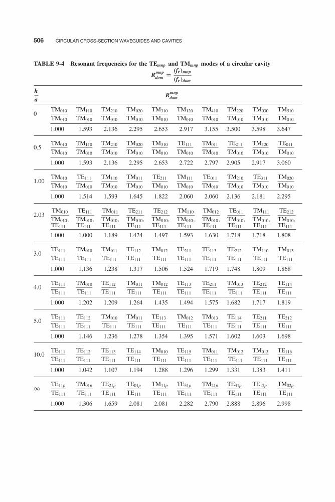
506 CIRCULAR CROSS-SECTION WAVEGUIDES AND CAVITIES
TABLE 9-4 Resonant frequencies for the TEmnp and TMmnp modes of a circular cavity
Rmnpdom = (fr )mnp
(fr )dom
ha
Rmnpdom
0TM010
TM010
TM110
TM010
TM210
TM010
TM020
TM010
TM310
TM010
TM120
TM010
TM410
TM010
TM220
TM010
TM030
TM010
TM510
TM010
1.000 1.593 2.136 2.295 2.653 2.917 3.155 3.500 3.598 3.647
0.5TM010
TM010
TM110
TM010
TM210
TM010
TM020
TM010
TM310
TM010
TE111
TM010
TM011
TM010
TE211
TM010
TM120
TM010
TE011
TM010
1.000 1.593 2.136 2.295 2.653 2.722 2.797 2.905 2.917 3.060
1.00TM010
TM010
TE111
TM010
TM110
TM010
TM011
TM010
TE211
TM010
TM111
TM010
TE011
TM010
TM210
TM010
TE311
TM010
TM020
TM010
1.000 1.514 1.593 1.645 1.822 2.060 2.060 2.136 2.181 2.295
2.03TM010
TM010,
TE111
TM010,
TM011
TM010,
TE211
TM010,
TE212
TM010,
TM110
TM010,
TM012
TM010,
TE011
TM010,
TM111
TM010,
TE212
TM010,TE111 TE111 TE111 TE111 TE111 TE111 TE111 TE111 TE111 TE111
1.000 1.000 1.189 1.424 1.497 1.593 1.630 1.718 1.718 1.808
3.0TE111
TE111
TM010
TE111
TM011
TE111
TE112
TE111
TM012
TE111
TE211
TE111
TE113
TE111
TE212
TE111
TM110
TE111
TM013
TE111
1.000 1.136 1.238 1.317 1.506 1.524 1.719 1.748 1.809 1.868
4.0TE111
TE111
TM010
TE111
TE112
TE111
TM011
TE111
TM012
TE111
TE113
TE111
TE211
TE111
TM013
TE111
TE212
TE111
TE114
TE111
1.000 1.202 1.209 1.264 1.435 1.494 1.575 1.682 1.717 1.819
5.0TE111
TE111
TE112
TE111
TM010
TE111
TM011
TE111
TE113
TE111
TM012
TE111
TM013
TE111
TE114
TE111
TE211
TE111
TE212
TE111
1.000 1.146 1.236 1.278 1.354 1.395 1.571 1.602 1.603 1.698
10.0TE111
TE111
TE112
TE111
TE113
TE111
TE114
TE111
TM010
TE111
TE115
TE111
TM011
TE111
TM012
TE111
TM013
TE111
TE116
TE111
1.000 1.042 1.107 1.194 1.288 1.296 1.299 1.331 1.383 1.411
∞ TE11p
TE111
TM01p
TE111
TE21p
TE111
TE01p
TE111
TM11p
TE111
TE31p
TE111
TM21p
TE111
TE41p
TE111
TE12p
TE111
TM02p
TE111
1.000 1.306 1.659 2.081 2.081 2.282 2.790 2.888 2.896 2.998
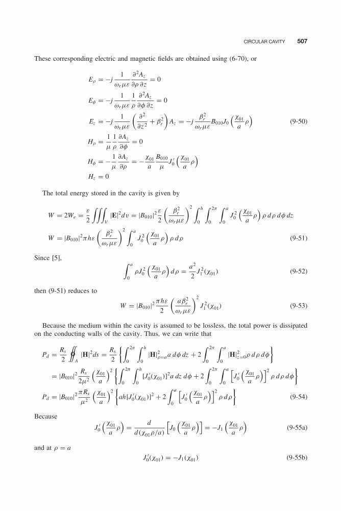
CIRCULAR CAVITY 507
These corresponding electric and magnetic fields are obtained using (6-70), or
Eρ = −j1
ωrμε
∂2Az
∂ρ ∂z= 0
Eφ = −j1
ωrμε
1
ρ
∂2Az
∂φ ∂z= 0
Ez = −j1
ωrμε
(∂2
∂z 2+ β2
r
)Az = −j
β2r
ωrμεB010J0
(χ01
aρ)
(9-50)
Hρ = 1
μ
1
ρ
∂Az
∂φ= 0
Hφ = − 1
μ
∂Az
∂ρ= −χ01
a
B010
μJ ′
0
(χ01
aρ)
Hz = 0
The total energy stored in the cavity is given by
W = 2We = ε
2
∫∫∫V
|E|2dv = |B010|2 ε
2
(β2
r
ωrμε
)2 ∫ h
0
∫ 2π
0
∫ a
0J 2
0
(χ01
aρ)
ρ dρ dφ dz
W = |B010|2πhε
(β2
r
ωrμε
)2 ∫ a
0J 2
0
(χ01
aρ)
ρ dρ (9-51)
Since [5], ∫ a
0ρJ 2
0
(χ01
aρ)
dρ = a2
2J 2
1 (χ01) (9-52)
then (9-51) reduces to
W = |B010|2 πhε
2
(aβ2
r
ωrμε
)2
J 21 (χ01) (9-53)
Because the medium within the cavity is assumed to be lossless, the total power is dissipatedon the conducting walls of the cavity. Thus, we can write that
Pd = Rs
2 #A|H|2ds = Rs
2
{∫ 2π
0
∫ h
0|H|2ρ=aa dφ dz + 2
∫ 2π
0
∫ a
0|H|2z=0ρ dρ dφ
}= |B010|2 Rs
2μ2
(χ01
a
)2{∫ 2π
0
∫ h
0[J ′
0(χ01)]2a dz dφ + 2
∫ 2π
0
∫ a
0
[J ′
0
(χ01
aρ)]2
ρ dρ dφ
}Pd = |B010|2 πRs
μ2
(χ01
a
)2{
ah[J ′0(χ01)]
2 + 2∫ a
0
[J ′
0
(χ01
aρ)]2
ρ dρ
}(9-54)
Because
J ′0
(χ01
aρ)
= d
d(χ01ρ/a)
[J0
(χ01
aρ)]
= −J1
(χ01
aρ)
(9-55a)
and at ρ = a
J ′0(χ01) = −J1(χ01) (9-55b)
508 CIRCULAR CROSS-SECTION WAVEGUIDES AND CAVITIES
(9-54) reduces to
Pd = |B010|2 πRs
μ2
(χ01
a
)2{
ahJ 21 (χ01) + 2
∫ a
0J 2
1
(χ01
aρ)
ρ dρ
}= |B010|2 πRs
μ2
(χ01
a
)2{
ahJ 21 (χ01) + 2
[a2
2J 2
1 (χ01)
]}Pd = |B010|2 πRs
μ2
(χ01
a
)2a(h + a)J 2
1 (χ01) (9-56)
Using the Q definition of (8-84) along with (9-53) and (9-56), we can write that
Q = ωr W
Pd= β4
r ha3
2ωrε(h + a)Rsχ201
=χ01
√μ
ε
2(
1 + a
h
)Rs
= 1.2025η
Rs
(1 + a
h
) (9-57)
since for the TM010 mode (m = 0, n = 1, and p = 0)
β2ρ + β2
z =(χ01
a
)2= β2
r ⇒ χ01 = βr a (9-57a)
Example 9-4
Compare the Q values of a circular cavity operating in the TM010 mode to those of a square-basedrectangular cavity. The dimensions of each are such that the circular cavity is circumscribed by thesquare-based rectangular cavity.
Solution: According to (9-57) the Q of a circular cavity of radius a (or diameter d ) and height h isgiven by
Q = 1.2025η
Rs
(1 + a
h
) = 1.2025η
Rs
(1 + d/2
h
)For a square-based rectangular cavity to circumscribe a circular cavity, one of the sides of its base mustbe equal to the diameter and their heights must be equal. Therefore, with a base of a = c = d on eachof its sides and a height b = h , its Q is equal according to (8-88a) to
Q = 1.1107η
Rs
⎡⎢⎢⎣ 1(1 + a/2
b
)⎤⎥⎥⎦ = 1.1107η
Rs
⎡⎢⎢⎣ 1(1 + d/2
h
)⎤⎥⎥⎦
Compare these two expressions and it is evident that the Q of the circular cavity is greater than that ofthe square-based cavity by (
1.2025 − 1.1107
1.1107
)× 100 = 8.26%
This is expected since the circular cavity does not possess as many sharp corners and edges as the square-based cavity whose volume and surface area are not as well utilized by the interior fields. It should beremembered that the Q of a cavity is proportional to volume and inversely proportional to area.
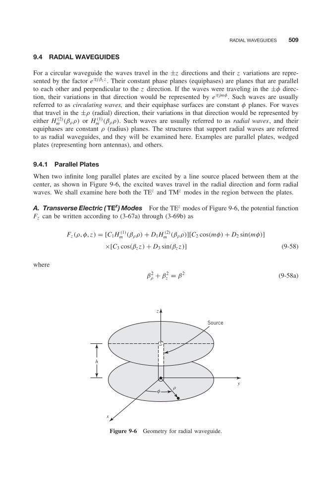
RADIAL WAVEGUIDES 509
9.4 RADIAL WAVEGUIDES
For a circular waveguide the waves travel in the ±z directions and their z variations are repre-sented by the factor e∓jβz z . Their constant phase planes (equiphases) are planes that are parallelto each other and perpendicular to the z direction. If the waves were traveling in the ±φ direc-tion, their variations in that direction would be represented by e∓jmφ . Such waves are usuallyreferred to as circulating waves, and their equiphase surfaces are constant φ planes. For wavesthat travel in the ±ρ (radial) direction, their variations in that direction would be represented byeither H (2)
m (βρρ) or H (1)m (βρρ). Such waves are usually referred to as radial waves , and their
equiphases are constant ρ (radius) planes. The structures that support radial waves are referredto as radial waveguides, and they will be examined here. Examples are parallel plates, wedgedplates (representing horn antennas), and others.
9.4.1 Parallel Plates
When two infinite long parallel plates are excited by a line source placed between them at thecenter, as shown in Figure 9-6, the excited waves travel in the radial direction and form radialwaves. We shall examine here both the TEz and TMz modes in the region between the plates.
A. Transverse Electric ( TEz) Modes For the TEz modes of Figure 9-6, the potential functionFz can be written according to (3-67a) through (3-69b) as
Fz (ρ, φ, z ) = [C1H (1)m (βρρ) + D1H (2)
m (βρρ)][C2 cos(mφ) + D2 sin(mφ)]
×[C3 cos(βz z ) + D3 sin(βz z )] (9-58)
where
β2ρ + β2
z = β2 (9-58a)
Source
z
h
x
yr
f
Figure 9-6 Geometry for radial waveguide.

510 CIRCULAR CROSS-SECTION WAVEGUIDES AND CAVITIES
The boundary conditions are
Eρ(0 ≤ ρ ≤ ∞, 0 ≤ φ ≤ 2π , z = 0) = Eρ(0 ≤ ρ ≤ ∞, 0 ≤ φ ≤ 2π , z = h) = 0 (9-59a)
Eφ(0 ≤ ρ ≤ ∞, 0 ≤ φ ≤ 2π , z = 0) = Eφ(0 ≤ ρ ≤ ∞, 0 ≤ φ ≤ 2π , z = h) = 0 (9-59b)
Since both of the preceding boundary conditions are not independent, either of the two leads tothe same results.
Using (6-80) and (9-58), the Eφ component can be written as
Eφ(ρ, φ, z ) = 1
ε
∂Fz
∂ρ
= βρ
ε[C1H (1)′
m (βρρ) + D1H (2)′m (βρρ)][C2 cos(mφ) + D2 sin(mφ)]
×[C3 cos(βz z ) + D3 sin(βz z )] (9-60)
Applying (9-59b) leads to
Eφ(0 ≤ ρ ≤ ∞, 0 ≤ φ ≤ 2π , z = 0) = βρ
ε[C1H (1)′
m (βρρ) + D1H (2)′m (βρρ)]
× [C2 cos(mφ) + D2 sin(mφ)][C3(1) + D3(0)] = 0
⇒ C3 = 0 (9-61a)
Eφ(0 ≤ ρ ≤ a , 0 ≤ φ ≤ 2π , z = h) = βρ
ε[C1H (1)′
m (βρρ) + D1H (2)′m (βρρ)]
× [C2 cos(mφ) + D2 sin(mφ)]D3 sin(βz h) = 0
⇒ sin(βz h) = 0 ⇒ βz h sin−1(0) = nπ
βz = nπ
h, n = 1, 2, 3, . . . (9-61b)
Thus, Fz of (9-58) reduces to
Fz (ρ, φ, z ) = [C1H (1)m (βρρ) + D1H (2)
m (βρρ)]
×[C2 cos(mφ) + D2 sin(mφ)]D3 sin(βz z ) (9-62)
where
β2ρ + β2
z = β2 ⇒ βρ = ±√
β2 − β2z = ±
√β2 −
(nπ
h
)2(9-62a)
βz = nπ
h, n = 1, 2, 3, . . . (9-62b)
m = 0, 1, 2, . . . (because of periodicity of the fields in φ) (9-62c)
Cutoff is defined when βρ = 0. Thus, using (9-62a)
βρ = ±√
β2 −(nπ
h
)2∣∣∣∣∣ f =fcβ=βc
= 0 ⇒ βc = nπ
h(9-63)
or
(fc)TEz
n = n
2h√
μεn = 1, 2, 3, . . . (9-63a)
RADIAL WAVEGUIDES 511
Therefore, using (9-63a), βρ of (9-62a) takes the following forms above, at, and below cutoff.
βρ =
⎧⎪⎪⎪⎪⎪⎪⎪⎪⎪⎨⎪⎪⎪⎪⎪⎪⎪⎪⎪⎩
√β2 −
(nπ
h
)2= β
√1 −
(fcf
)2
f > fc
0 f = fc
− j
√(nπ
h
)2− β2 = −jβ
√(fcf
)2
− 1 = −jα f < fc
(9-64a)
(9-64b)
(9-64c)
Let us now examine the outward (+ρ) traveling waves represented by H (2)m (βρρ) and those
represented simultaneously by the cos(mφ) variations of (9-62). In that case, (9-62) reduces to
F+z (ρ, φ, z ) = AmnH (2)
m (βρρ) cos(mφ) sin(nπ
hz)
(9-65)
The corresponding electric and magnetic fields can be written using (6-80) as
E+ρ = − 1
ερ
∂F+z
∂φ= Amn
m
ερH (2)
m (βρρ) sin(mφ) sin(nπ
hz)
(9-65a)
E+φ = 1
ε
∂F+z
∂ρ= βρ
Amn
εH (2)′
m (βρρ) cos(mφ) sin(nπ
hz)
(9-65b)
E+z = 0 (9-65c)
H +ρ = −j
1
ωμε
∂2F+z
∂ρ∂z= −jAmnβρ
nπ/h
ωμεH (2)′
m (βρρ) cos(mφ) cos(nπ
hz)
(9-65d)
H +φ = −j
1
ωμε
1
ρ
∂2F+z
∂φ∂z= jAmn
mnπ/h
ωμερH (2)
m (βρρ) sin(mφ) cos(nπ
hz)
(9-65e)
H +z = −j
1
ωμε
(∂2
∂z 2+ β2
)F+
z = −jAmnβ2
ρ
ωμεH (2)
m (βρρ) cos(mφ) sin(nπ
hz)
(9-65f)
′ ≡ ∂
∂(βρρ)(9-65g)
The impedance of the wave in the +ρ direction is defined and given by
Z +ρw (TEz
n) = Eφ
Hz= j
ωμ
βρ
H (2)′m (βρρ)
H (2)m (βρρ)
(9-66)
Since
H (2)′m (βρρ) = ∂
∂(βρρ)
[H (2)
m (βρρ)]
(9-67)
(9-66) can be written as
Z +ρw (TEz
n) = jωμ
βρ
∂
∂(βρρ)
[H (2)
m (βρρ)]
H (2)m (βρρ)
(9-68)
512 CIRCULAR CROSS-SECTION WAVEGUIDES AND CAVITIES
Below cutoff (f < fc) βρ is imaginary, and it is given by (9-64c). Therefore, for f < fc
H (2)m (βρρ) = H (2)
m (−jαρ) (9-69a)
d
d(βρρ)
[H (2)
m (βρρ)] = d
d(−jαρ)
[H (2)
m (−jαρ)] = j
d
d(αρ)
[H (2)
m (−jαρ)]
(9-69b)
For complex arguments, the Hankel function H (2)m of the second kind is related to the modified
Bessel function Km of the second kind by
H (2)m (−jαρ) = 2
πj m+1Km(αρ) (9-70a)
d
d(αρ)
[H (2)
m (−jαρ)] = 2
πj m+1 d
d(αρ)[Km(αρ)] (9-70b)
Thus, below cutoff (f < fc), the wave impedance reduces to
Z +ρw (TEz
n)|f <fc = jωμ
−jα
jd
d(αρ)[Km(αρ)]
Km(αρ)
= −jωμ
α
d
d(αρ)[Km(αρ)]
Km(αρ)(9-71)
which is always inductive (for f < fc) since Km(αρ)> 0 and d/d(αρ)[Km(αρ)] < 0. Therefore,below cutoff the modes are nonpropagating (evanescent) since the waveguide is behaving as aninductive storage element.
B. Transverse Magnetic ( TMz) Modes The TMz modes of the radial waveguide structure ofFigure 9-6 with the source at the center are derived in a similar manner. Using such a procedureleads to the following results:
Az (ρ, φ, z ) = [C ′
1H (1)m (βρρ) + D ′
1H (2)m (βρρ)
]× [
C ′2 cos(mφ) + D ′
2 sin(mφ)]
C ′3 cos(βz z ) (9-72)
β2ρ + β2
z = β2 ⇒ βρ = ±√
β2 − β2z = ±
√β2 −
(nπ
h
)2(9-72a)
βz = nπ
h, n = 0, 1, 2, . . . (9-72b)
m = 0, 1, 2, . . . (because of periodicity of the fields in φ) (9-72c)
(fc)TMz
n = n
2h√
με, n = 0, 1, 2, . . . (9-73)
RADIAL WAVEGUIDES 513
βρ =
⎧⎪⎪⎪⎪⎪⎪⎪⎪⎪⎨⎪⎪⎪⎪⎪⎪⎪⎪⎪⎩
√β2 −
(nπ
h
)2= β
√1 −
(fcf
)2
f > fc
0 f = fc
− j
√(nπ
h
)2− β2 = −jβ
√(fcf
)2
− 1 = −jα f < fc
(9-74a)
(9-74b)
(9-74c)
For outward (+ρ) traveling waves and only cos(mφ) variations
A+z (ρ, φ, z ) = BmnH (2)
m (βρρ) cos(mφ) cos(nπ
hz)
(9-75)
E+ρ = −j
1
ωμε
∂2A+z
∂ρ ∂z= jBmnβρ
nπ/h
ωμεH (2)′
m (βρρ) cos(mφ) sin(nπ
hz)
(9-75a)
E+φ = −j
1
ωμε
1
ρ
∂2A+z
∂φ ∂z= −jBmn
mnπ/h
ωμερH (2)
m (βρρ) sin(mφ) sin(nπ
hz)
(9-75b)
E+z = −j
1
ωμε
(∂2
∂z 2+ β2
)A+
z = −jBmnβ2
ρ
ωμεH (2)
m (βρρ) cos(mφ) cos(nπ
hz)
(9-75c)
H +ρ = 1
μ
1
ρ
∂A+z
∂φ= −Bmn
m
μ
1
ρH (2)
m (βρρ) sin(mφ) cos(nπ
hz)
(9-75d)
H +φ = − 1
μ
∂A+z
∂ρ= −βρ
Bmn
μH (2)′
m (βρρ) cos(mφ) cos(nπ
hz)
(9-75e)
Hz = 0 (9-75f)
′ ≡ ∂
∂(βρρ)(9-75g)
Z +ρw (TMz
n) = E+z
−H +φ
= −jβρ
ωε
H (2)m (βρρ)
H (2)′m (βρρ)
(9-76)
Z +ρw (TMz
n)|f <fc = jα
ωε
Km(αρ)
d
d(αρ)[Km(αρ)]
(9-76a)
which is always capacitive (for f < fc) since Km(αρ)> 0 and d/d(αρ)[Km(αρ)] < 0. There-fore, below cutoff the modes are nonpropagating (evanescent) since the waveguide behaves as acapacitive storage element.
9.4.2 Wedged Plates
Another radial type of waveguide structure is the wedged-plate geometry of Figure 9-7 withplates along z = 0, h , and φ = 0, φ0. This type of a configuration resembles and can be used torepresent the structures of E - and H -plane sectoral horns [6]. In fact, the fields within the hornsare found using the procedure outlined here. In general, both TEz and TMz modes can exist in

514 CIRCULAR CROSS-SECTION WAVEGUIDES AND CAVITIES
h
z
y
xf0
f
r
Figure 9-7 Geometry of wedged plate radial waveguide.
the space between the plates. The independent sets of boundary conditions of this structure thatcan be used to solve for the TEz
pn and TMzpn modes are
Eρ(0 ≤ ρ ≤ ∞, 0 ≤ φ ≤ φ0, z = 0) = Eρ(0 ≤ ρ ≤ ∞, 0 ≤ φ ≤ φ0, z = h) = 0 (9-77a)
Eρ(0 ≤ ρ ≤ ∞, φ = 0, 0 ≤ z ≤ h) = Eρ(0 ≤ ρ ≤ ∞, φ = φ0, 0 ≤ z ≤ h) = 0 (9-77b)
or
Eφ(0 ≤ ρ ≤ ∞, 0 ≤ φ ≤ φ0, z = 0) = Eφ(0 ≤ ρ ≤ ∞, 0 ≤ φ ≤ φ0, z = h) = 0 (9-78a)
Ez (0 ≤ ρ ≤ ∞, φ = 0, 0 ≤ z ≤ h) = Ez (0 ≤ ρ ≤ ∞, φ = φ0, 0 ≤ z ≤ h) = 0 (9-78b)
or appropriate combinations of these. Whichever combination of independent boundary conditionsis used, leads to the same results.
A. Transverse Electric ( TEz) Modes Since the procedure used to derive this set of TEz
fields is the same as any other TEz procedure used previously, the results of this set of TEzpn
modes will be summarized here; the details are left as an end-of-chapter exercise to the reader.Only the outward radial (+ρ) parts will be included here.
F+z (ρ, φ, z ) = ApnH (2)
m (βρρ) cos(mφ) sin(βz z ) (9-79)
β2ρ + β2
z = β2
βz = nπ
hn = 1, 2, 3, . . .
m = pπ
φ0p = 0, 1, 2, . . .
(9-79a)
(9-79b)
(9-79c)

RADIAL WAVEGUIDES 515
E+ρ = −1
ε
1
ρ
∂F+z
∂φ= Apn
pπ/φ0
ερH (2)
m (βρρ) sin
(pπ
φ0φ
)sin
(nπ
hz)
(9-79d)
E+φ = 1
ε
∂F+z
∂ρ= βρ
Apn
εH (2)′
m (βρρ) cos
(pπ
φ0φ
)sin
(nπ
hz)
(9-79e)
E+z = 0 (9-79f)
H +ρ = −j
1
ωμε
∂2F+z
∂ρ ∂z= −jApn
βρβz
ωμεH (2)′
m (βρρ) cos
(pπ
φ0φ
)cos
(nπ
hz)
(9-79g)
H +φ = −j
1
ωμε
1
ρ
∂2F+z
∂φ ∂z= jApn
βz pπ/φ0
ωμε
1
ρH (2)
m (βρρ) sin
(pπ
φ0φ
)cos
(nπ
hz)
(9-79h)
H +z = −j
1
ωμε
(∂2
∂z 2+ β2
)F+
z = −jApnβ2
ρ
ωμεH (2)
m (βρρ) cos
(pπ
φ0φ
)sin
(nπ
hz)
(9-79i)
Z +ρw (TEz
pn) = E+φ
H +z
= jωμ
βρ
H (2)′m (βρρ)
H (2)m (βρρ)
; ′ ≡ ∂
∂(βρρ)(9-79j)
B. Transverse Magnetic ( TMz) Modes As for the TEzpn modes, the procedure for deriving
the TMzpn for the wedged plate radial waveguide is the same as that used for TMz modes of other
waveguide configurations. Therefore, the results will be summarized here, and the details left asan end-of-chapter exercise for the reader. Only the outward radial (+ρ) parts will be includedhere.
A+z (ρ, φ, z ) = BpnH (2)
m
(βρρ
)sin(mφ) cos (βz z ) (9-80)
β2ρ + β2
z = β2
βz = nπ
h, n = 0, 1, 2, . . .
m = pπ
φ0, p = 1, 2, 3, . . .
(9-80a)
(9-80b)
(9-80c)
E+ρ = −j
1
ωμε
∂2A+z
∂ρ ∂z= jBpn
βz βρ
ωμεH (2)′
m
(βρρ
)sin
(pπ
φ0φ
)sin
(nπ
hz)
(9-80d)
E+φ = −j
1
ωμε
1
ρ
∂2A+z
∂φ ∂z= jBpn
βz pπ/φ0
ωμε
1
ρH (2)
m
(βρρ
)cos
(pπ
φ0φ
)sin
(nπ
hz)
(9-80e)
E+z = −j
1
ωμε
(∂2
∂z 2+ β2
)A+
z = −jBpnβ2
ρ
ωμεH (2)
m
(βρρ
)sin
(pπ
φ0φ
)cos
(nπ
hz)
(9-80f)
H +ρ = 1
μ
1
ρ
∂A+z
∂φ= Bpn
pπ/φ0
μρH (2)
m
(βρρ
)cos
(pπ
φ0φ
)cos
(nπ
hz)
(9-80g)
H +φ = − 1
μ
∂A+z
∂ρ= −βρ
Bpn
μH (2)′
m
(βρρ
)sin
(pπ
φ0φ
)cos
(nπ
hz)
(9-80h)
H +z = 0 (9-80i)
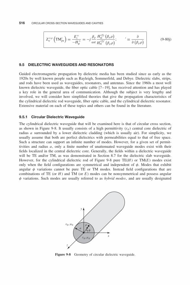
516 CIRCULAR CROSS-SECTION WAVEGUIDES AND CAVITIES
Z +ρw
(TMz
pn
)= E+
z
−H +φ
= −jβρ
ωε
H (2)m
(βρρ
)H (2)′
m(βρρ
) ; ′ ≡ ∂
∂(βρρ
) (9-80j)
9.5 DIELECTRIC WAVEGUIDES AND RESONATORS
Guided electromagnetic propagation by dielectric media has been studied since as early as the1920s by well known people such as Rayleigh, Sommerfeld, and Debye. Dielectric slabs, strips,and rods have been used as waveguides, resonators, and antennas. Since the 1960s a most wellknown dielectric waveguide, the fiber optic cable [7–19], has received attention and has playeda key role in the general area of communication. Although the subject is very lengthy andinvolved, we will consider here simplified theories that give the propagation characterisitcs ofthe cylindrical dielectric rod waveguide, fiber optic cable, and the cylindrical dielectric resonator.Extensive material on each of these topics and others can be found in the literature.
9.5.1 Circular Dielectric Waveguide
The cylindrical dielectric waveguide that will be examined here is that of circular cross section,as shown in Figure 9-8. It usually consists of a high permittivity (εd ) central core dielectric ofradius a surrounded by a lower dielectric cladding (which is usually air). For simplicity, weusually assume that both are perfect dielectrics with permeabilities equal to that of free space.Such a structure can support an infinite number of modes. However, for a given set of permit-tivities and radius a , only a finite number of unattenuated waveguide modes exist with theirfields localized in the central dielectric core. Generally, the fields within a dielectric waveguidewill be TE and/or TM, as was demonstrated in Section 8.7 for the dielectric slab waveguide.However, for the cylindrical dielectric rod of Figure 9-8 pure TE(H ) or TM(E ) modes existonly when the field configurations are symmetrical and independent of φ. Modes that exhibitangular φ variations cannot be pure TE or TM modes. Instead field configurations that arecombinations of TE (or H ) and TM (or E ) modes can be nonsymmetrical and possess angularφ variations. Such modes are usually referred to as hybrid modes , and are usually designated
y
z
x
e0, m0
ar
f
ed, md
Figure 9-8 Geometry of circular dielectric waveguide.
DIELECTRIC WAVEGUIDES AND RESONATORS 517
by IEEE (formerly IRE) Standards [20] as HEMmn . In general, mode nomenclature for circu-lar dielectric waveguides and resonators is not well defined, and it is quite confusing. Anotherdesignation of the hybrid modes is to denote them as HE [when the TE(H ) modes predom-inate] or EH [when the TM(E ) modes predominate]. Pure TE or TM, or hybrid HEM (HEor EH) modes exhibit cutoff frequencies, below which unattenuating modes cannot propagate.The cutoff frequency is determined by the minimum electrical radius (a/λ) of the dielectricrod; for small values of a/λ the modes cannot propagate unattenuated within the rod. Thereis, however, one hybrid mode, namely the HEM11 (HE11), which does not have a cutoff fre-quency. Because of its zero cutoff frequency, it is referred to as the dominant mode and is mostwidely used in dielectric rod waveguides and end-fire antennas. This HE11 mode is also popularlyreferred to as the dipole mode. An excellent reference on dielectric waveguides and resonators isthat of [21].
The TEzmn and TMz
mn electric and magnetic field components in a cylindrical waveguide aregiven, respectively, by (9-15a) through (9-15g) and (9-31a) through (9-31g). These expressionsinclude both the cos(mφ) and sin(mφ) angular variations which, in general, both exist. The HEMmodes that have only cos(mφ) symmetry are combinations of the TEz and TMz modes which alsoexhibit cos(mφ) symmetry. Use of the expressions (9-15a) through (9-15g) and (9-31a) through(9-31g) and selection of only the terms that possess simultaneously cos(mφ) variations in the Ez
component and sin(mφ) variations in the Hz component, allows us to write that
HEM Modes (ρ ≤ a)
E dρ = −j
1(βd
ρ
)2
[mωμd Am
1
ρJm
(βd
ρ ρ) + βz β
dρ BmJ ′
m
(βd
ρ ρ)]
cos(mφ)e−jβz z (9-81a)
E dφ = j
1(βd
ρ
)2
[ωμdβd
ρ AmJ ′m
(βd
ρ ρ) + mβz Bm
1
ρJm
(βd
ρ ρ)]
sin(mφ)e−jβz z (9-81b)
E dz = BmJm
(βd
ρ ρ)
cos(mφ)e−jβz z (9-81c)
H dρ = −j
1(βd
ρ
)2
[βz β
dρ AmJ ′
m
(βd
ρ ρ) + mωεd Bm
1
ρJm
(βd
ρ ρ)]
sin(mφ)e−jβz z (9-81d)
H dφ = −j
1(βd
ρ
)2
[mβz Am
1
ρJm
(βd
ρ ρ) + ωεdβd
ρ BmJ ′m
(βd
ρ ρ)]
cos(mφ)e−jβz z (9-81e)
H dz = AmJm
(βd
ρ ρ)
sin(mφ)e−jβz z (9-81f)
where (βd
ρ
)2 + β2z = β2
d = ω2μdεd = ω2μ0ε0εrμr (9-81g)
Am = −j
(βd
ρ
)2
ωμdεdAmnD2 (9-81h)
Bm = −j
(βd
ρ
)2
ωμdεdBmnC2 (9-81i)
′ ≡ ∂
∂(βd
ρ ρ) (9-81j)
The coefficients Am and Bm are not independent of each other, and their relationship can be foundby applying the appropriate boundary conditions.

518 CIRCULAR CROSS-SECTION WAVEGUIDES AND CAVITIES
For the dielectric rod to act as a waveguide, the fields outside the rod (ρ ≥ a) must be of theevanescent type that exhibit a decay in the radial direction. The rate of attenuation is a functionof the diameter of the rod. As the diameter of the rod decreases, the following changes occur.
1. The attenuation lessens.2. The distance to which the fields outside the rod can extend is greater.3. The propagation constant βz is only slightly greater than β0.
As the diameter of the rod increases, the following changes occur.
1. The rate of attenuation also increases.2. The fields are confined closer to the rod.3. The propagation constant βz approaches βd .
Since in all cases βz is greater than β0, the phase velocity is smaller than the velocity of lightin free space. For small diameter rods, the surface waves are said to be loosely bound to thedielectric surface, whereas for the larger diameters, it is said to be tightly bound to the dielectricsurface. Therefore, the cylindrical functions that are chosen to represent the radial variations ofthe fields outside the rod must be cylindrical decaying functions. These functions can be eitherHankel functions of order m of the first kind (H (1)
m ) or second kind (H (2)m ) and of imaginary
argument, or modified Bessel functions Km of the second kind of order m . We choose here to usethe modified Bessel functions Km of the second kind, which are related to the Hankel functionsof the first and second kind by
Km(α) =
⎧⎪⎨⎪⎩j m+1 π
2H (1)
m (jα)
− j m+1 π
2H (2)
m (−jα)
(9-82a)
(9-82b)
With (9-81a) through (9-81j), and (9-82a) and (9-82b) as a guide, we can represent the corre-sponding electric and magnetic field components for the HEM modes outside the dielectric rod(ρ ≥ a) by
HEM Modes (ρ ≥ a)
E 0ρ = j
1(α0
ρ
)2
[mωμ0Cm
1
ρKm
(α0
ρρ) + βz α
0ρDmK ′
m
(α0
ρρ)]
cos(mφ)e−jβz z (9-83a)
E 0φ = −j
1(α0
ρ
)2
[ωμ0α
0ρCmK ′
m
(α0
ρρ) + mβz Dm
1
ρKm
(α0
ρρ)]
sin(mφ)e−jβz z (9-83b)
E 0z = DmKm
(α0
ρρ)
cos(mφ)e−jβz z (9-83c)
H 0ρ = j
1(α0
ρ
)2
[βz α
0ρCmK ′
m
(α0
ρρ) + mωε0Dm
1
ρKm
(α0
ρρ)]
sin(mφ)e−jβz z (9-83d)
H 0φ = j
1(α0
ρ
)2
[mβz Cm
1
ρKm
(α0
ρρ) + ωε0α
0ρDmK ′
m
(α0
ρρ)]
cos(mφ)e−jβz z (9-83e)
H 0z = CmKm
(α0
ρρ)
sin(mφ)e−jβz z (9-83f)
DIELECTRIC WAVEGUIDES AND RESONATORS 519
where (jα0
ρ
)2 + β2z = − (
α0ρ
)2 + β2z = β2
0 = ω2μ0ε0 (9-83g)
′ ≡ ∂
∂(α0
ρρ) (9-83h)
The coefficients Cm and Dm are not independent of each other or from Am and Bm , and theirrelations can be found by applying the appropriate boundary conditions.
The relations between the constants Am , Bm , Cm , and Dm and equation 9-91, which is referredto as the eigenvalue equation , can be used to determine the modes that can be supported by thedielectric rod waveguide. These are obtained by applying the following boundary conditions
E dφ (ρ = a , 0 ≤ φ ≤ 2π , z ) = E 0
φ(ρ = a , 0 ≤ φ ≤ 2π , z ) (9-84a)
E dz (ρ = a , 0 ≤ φ ≤ 2π , z ) = E 0
z (ρ = a , 0 ≤ φ ≤ 2π , z ) (9-84b)
H dφ (ρ = a , 0 ≤ φ ≤ 2π , z ) = H 0
φ (ρ = a , 0 ≤ φ ≤ 2π , z ) (9-84c)
H dz (ρ = a , 0 ≤ φ ≤ 2π , z ) = H 0
z (ρ = a , 0 ≤ φ ≤ 2π , z ) (9-84d)
Doing this leads to
1(βd
ρ
)2
[ωμdβd
ρ AmJ ′m
(βd
ρ a) + mβz Bm
1
aJm
(βd
ρ a)]
= − 1(α0
ρ
)2
[ωμ0α
0ρCmK ′
m
(α0
ρa) + mβz Dm
1
aKm
(α0
ρa)]
(9-85a)
BmJm(βd
ρ a) = DmKm
(α0
ρa)
(9-85b)
− 1(βd
ρ
)2
[mβz Am
1
aJm
(βd
ρ a) + ωεdβd
ρ BmJ ′m
(βd
ρ a)]
= 1(α0
ρ
)2
[mβz Cm
1
aKm
(α0
ρa) + ωε0α
0ρDmK ′
m
(α0
ρa)]
(9-85c)
AmJm(βd
ρ a) = CmKm
(α0
ρa)
(9-85d)
where according to (9-81g) and (9-83g)
(βd
ρ
)2 + β2z = β2
d ⇒ (βd
ρ a)2 + (βz a)2 = (βd a)2 ⇒ βz a =
√(βd a)2 − (
βdρ a
)2(9-85e)
− (α0
ρ
)2 + β2z = β2
0 ⇒ − (α0
ρa)2 + (βz a)2 = (β0a)2 (9-85f)
Subtracting (9-85f) from (9-85e) we get that
(βd
ρ a)2 + (
α0ρa
)2 = (βd a)2 − (β0a)2 ⇒ α0ρa =
√(βd a)2 − (β0a)2 − (
βdρ a
)2
=√
(β0a)2(εrμr − 1) − (βd
ρ a)2
(9-86)
520 CIRCULAR CROSS-SECTION WAVEGUIDES AND CAVITIES
Using the abbreviated notation of
χ = βdρ a (9-87a)
ξ = α0ρa (9-87b)
ζ = βz a (9-87c)
βd = β0√
εrμr (9-87d)
we can rewrite (9-85e) and (9-86) as
ζ =√
(β0a)2εrμr − χ2 (9-88a)
ξ =√
(β0a)2(εrμr − 1) − χ2 (9-88b)
With the preceding abbreviated notation and with μd = μ0, (9-85a) through (9-85d) can bewritten in matrix form as
Fg = 0 (9-89)
where F is a 4 × 4 matrix and g is a column matrix. Each is given by
F =
⎡⎢⎢⎢⎢⎢⎢⎣
ωμ0a
χJ ′
m (χ)mζ
χ2Jm (χ)
ωμ0a
ξK ′
m (ξ)mζ
ξ 2Km (ξ)
0 Jm (χ) 0 −Km (ξ)
mζ
χ2Jm (χ)
ωεd a
χJ ′
m (χ)mζ
ξ 2Km (ξ)
ωε0a
ξK ′
m (ξ)
Jm (χ) 0 −Km (ξ) 0
⎤⎥⎥⎥⎥⎥⎥⎦ (9-89a)
g =
⎡⎢⎢⎣Am
Bm
Cm
Dm
⎤⎥⎥⎦ (9-89b)
Equation 9-89 has a nontrivial solution provided that the determinant of F of (9-89a) is equalto zero [i.e., det(F ) = 0]. Applying this to (9-89a), it can be shown that it leads to [21]
|F | = ω2μ0εd a2
χ2[J ′
m(χ)]2[Km(ξ)]2 + ω2μ0ε0a2
χξJm(χ)J ′
m(χ)Km(ξ)K ′m(ξ)
− (mζ )2
χ4[Jm(χ)]2[Km(ξ)]2 − (mζ )2
χ2ξ 2[Jm(χ)]2[Km(ξ)]2
+ ω2μ0εd a2
χξJm(χ)J ′
m(χ)Km(ξ)K ′m(ξ) + ω2μ0ε0a2
ξ 2[Jm(χ)]2[K ′
m(ξ)]2
− (mζ )2
χ2ξ 2[Jm(χ)]2[Km(ξ)]2 − (mζ )2
ξ 4[Jm(χ)]2[Km(ξ)]2 = 0 (9-90)
Dividing all the terms of (9-90) by ω2μ0εd a2[Km(ξ)]2 and regrouping, it can be shown that(9-90) can be placed in the form of [21]
G1 (χ) G2 (χ) − G23 (χ) = 0 (9-91)
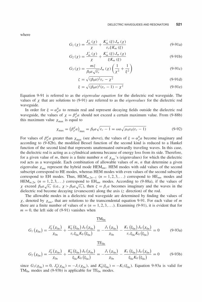
DIELECTRIC WAVEGUIDES AND RESONATORS 521
where
G1 (χ) = J ′m (χ)
χ+ K ′
m (ξ) Jm (χ)
εrξKm (ξ)(9-91a)
G2 (χ) = J ′m (χ)
χ+ K ′
m (ξ) Jm (χ)
ξKm (ξ)(9-91b)
G3 (χ) = mζ
β0a√
εrJm (χ)
(1
χ2+ 1
ξ 2
)(9-91c)
ζ =√
(β0a)2εr − χ2 (9-91d)
ξ =√
(β0a)2(εr − 1) − χ2 (9-91e)
Equation 9-91 is referred to as the eigenvalue equation for the dielectric rod waveguide. Thevalues of χ that are solutions to (9-91) are referred to as the eigenvalues for the dielectric rodwaveguide.
In order for ξ = α0pa to remain real and represent decaying fields outside the dielectric rod
waveguide, the values of χ = βdρ a should not exceed a certain maximum value. From (9-88b)
this maximum value χmax is equal to
χmax = (βd
ρ a)
max= β0a
√εr − 1 = ωa
√μ0ε0(εr − 1) (9-92)
For values of βdρ a greater than χmax (see above), the values of ξ = α0
ρa become imaginary andaccording to (9-82b), the modified Bessel function of the second kind is reduced to a Hankelfunction of the second kind that represents unattenuated outwardly traveling waves. In this case,the dielectric rod is acting as a cylindrical antenna because of energy loss from its side. Therefore,for a given value of m , there is a finite number n of χmn ’s (eigenvalues) for which the dielectricrod acts as a waveguide. Each combination of allowable values of m , n that determine a giveneigenvalue χmn represent the hybrid mode HEMmn . HEM modes with odd values of the secondsubscript correspond to HE modes, whereas HEM modes with even values of the second subscriptcorrespond to EH modes. Thus, HEMm ,2n−1 (n = 1, 2, 3, . . .) correspond to HEmn modes andHEMm ,2n (n = 1, 2, 3, . . .) correspond to EHmn modes. According to (9-88a), if the values ofχ exceed β0a
√εr (i.e., χ > β0a
√εr ), then ζ = βz a becomes imaginary and the waves in the
dielectric rod become decaying (evanescent) along the axis (z direction) of the rod.The allowable modes in a dielectric rod waveguide are determined by finding the values of
χ , denoted by χmn , that are solutions to the transcendental equation 9-91. For each value of mthere are a finite number of values of n (n = 1, 2, 3, . . .). Examining (9-91), it is evident that form = 0, the left side of (9-91) vanishes when
TM0n
G1(χ0n
) = J ′0
(χ0n
)χ0n
+ K ′0
(ξ0n
)J0
(χ0n
)εrξ0nK0
(ξ0n
) = −J1(χ0n
)χ0n
− K1(ξ0n
)J0
(χ0n
)εrξ0nK0
(ξ0n
) = 0 (9-93a)
TE0n
G2(χ0n
) = J ′0
(χ0n
)χ0n
+ K ′0
(ξ0n
)J0
(χ0n
)ξ0nK0
(ξ0n
) = −J1(χ0n
)χ0n
− K1(ξ0n
)J0
(χ0n
)ξ0nK0
(ξ0n
) = 0 (9-93b)
since G3(χ0n) = 0, J ′0(χ0n) = −J1(χ0n), and K ′
0(ξ0n) = −K1(ξ0n). Equation 9-93a is valid forTM0n modes and (9-93b) is applicable for TE0n modes.
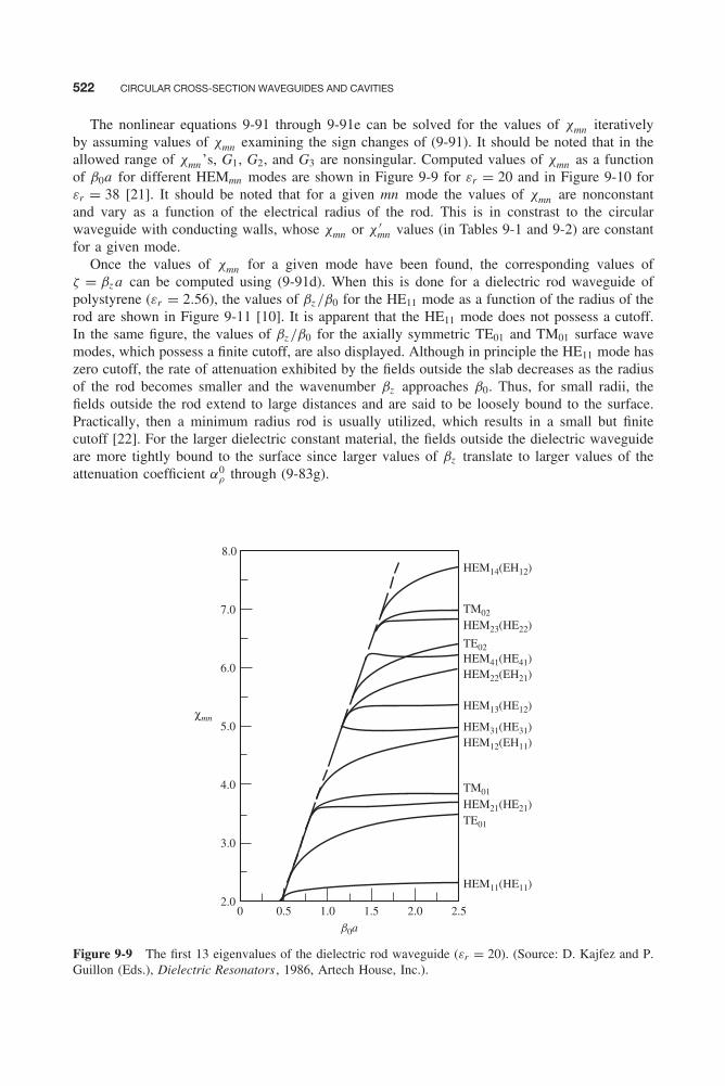
522 CIRCULAR CROSS-SECTION WAVEGUIDES AND CAVITIES
The nonlinear equations 9-91 through 9-91e can be solved for the values of χmn iterativelyby assuming values of χmn examining the sign changes of (9-91). It should be noted that in theallowed range of χmn ’s, G1, G2, and G3 are nonsingular. Computed values of χmn as a functionof β0a for different HEMmn modes are shown in Figure 9-9 for εr = 20 and in Figure 9-10 forεr = 38 [21]. It should be noted that for a given mn mode the values of χmn are nonconstantand vary as a function of the electrical radius of the rod. This is in constrast to the circularwaveguide with conducting walls, whose χmn or χ ′
mn values (in Tables 9-1 and 9-2) are constantfor a given mode.
Once the values of χmn for a given mode have been found, the corresponding values ofζ = βz a can be computed using (9-91d). When this is done for a dielectric rod waveguide ofpolystyrene (εr = 2.56), the values of βz /β0 for the HE11 mode as a function of the radius of therod are shown in Figure 9-11 [10]. It is apparent that the HE11 mode does not possess a cutoff.In the same figure, the values of βz /β0 for the axially symmetric TE01 and TM01 surface wavemodes, which possess a finite cutoff, are also displayed. Although in principle the HE11 mode haszero cutoff, the rate of attenuation exhibited by the fields outside the slab decreases as the radiusof the rod becomes smaller and the wavenumber βz approaches β0. Thus, for small radii, thefields outside the rod extend to large distances and are said to be loosely bound to the surface.Practically, then a minimum radius rod is usually utilized, which results in a small but finitecutoff [22]. For the larger dielectric constant material, the fields outside the dielectric waveguideare more tightly bound to the surface since larger values of βz translate to larger values of theattenuation coefficient α0
ρ through (9-83g).
8.0
7.0
6.0
5.0
4.0
3.0
2.00 0.5 1.0
b0a
1.5 2.0 2.5
HEM11(HE11)
HEM21(HE21)
HEM12(EH11)HEM31(HE31)
HEM13(HE12)
HEM22(EH21)HEM41(HE41)
HEM23(HE22)
HEM14(EH12)
TE01
TM01
TE02
TM02
χmn
Figure 9-9 The first 13 eigenvalues of the dielectric rod waveguide (εr = 20). (Source: D. Kajfez and P.Guillon (Eds.), Dielectric Resonators , 1986, Artech House, Inc.).
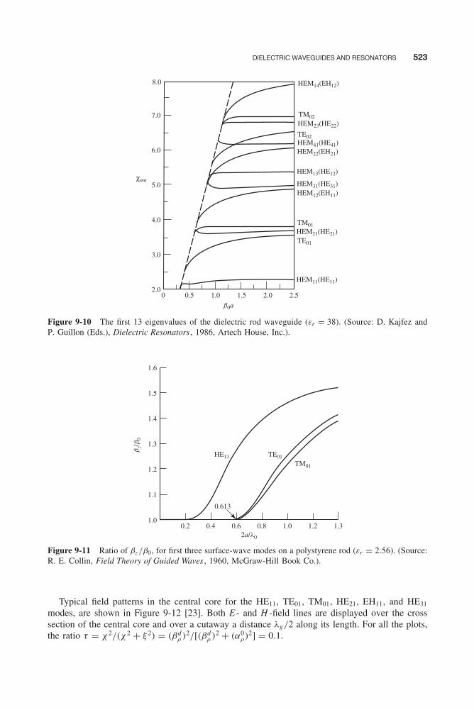
DIELECTRIC WAVEGUIDES AND RESONATORS 523
8.0
7.0
6.0
5.0
4.0
3.0
2.00 0.5 1.0
b0a
1.5 2.0 2.5
HEM11(HE11)
HEM21(HE21)
HEM12(EH11)HEM31(HE31)
HEM13(HE12)
HEM22(EH21)HEM41(HE41)
HEM23(HE22)
HEM14(EH12)
TE01
TM01
TE02
TM02
χmn
Figure 9-10 The first 13 eigenvalues of the dielectric rod waveguide (εr = 38). (Source: D. Kajfez andP. Guillon (Eds.), Dielectric Resonators , 1986, Artech House, Inc.).
2a/l0
bz/b
0
0.21.0
1.1
1.2
1.3
1.4
1.5
1.6
0.4
HE11 TE01TM01
0.6
0.613
0.8 1.0 1.2 1.3
Figure 9-11 Ratio of βz /β0, for first three surface-wave modes on a polystyrene rod (εr = 2.56). (Source:R. E. Collin, Field Theory of Guided Waves , 1960, McGraw-Hill Book Co.).
Typical field patterns in the central core for the HE11, TE01, TM01, HE21, EH11, and HE31
modes, are shown in Figure 9-12 [23]. Both E - and H -field lines are displayed over the crosssection of the central core and over a cutaway a distance λg/2 along its length. For all the plots,the ratio τ = χ2/(χ2 + ξ 2) = (βd
ρ )2/[(βdρ )2 + (α0
ρ)2] = 0.1.

524 CIRCULAR CROSS-SECTION WAVEGUIDES AND CAVITIES
For all modes the sum of χ2 + ξ 2 should be a constant, which will be a function of the radiusof the dielectric rod and its dielectric constant. Thus, according to (9-88b),
χ2 + ξ 2 = (β0a)2 (εr − 1) = constant (9-94)
For all modes, excluding the dominant HE11, this constant should always be equal to or greaterthan (2.4049)2 = 5.7835; that is, excluding the HE11 mode,
V 2 = χ2 + ξ 2 = (β0a)2(εr − 1) ≥ (2.4049)2 (9-94a)
−λg/4
λg/4
(a) (b)
z0
−λg/4
λg/4z
0
(c)
−λg/4
λg/4z
0
Figure 9-12 Field patterns in the central core of a dielectric rod waveguide (in all cases τ = 0.1; E:——,H: ----). (Source: T. Okoshi, Optical Fibers , 1982, Academic Press.). (a) HEM11 (HE11) mode. (b) TE01
mode. (c) TM01 mode.
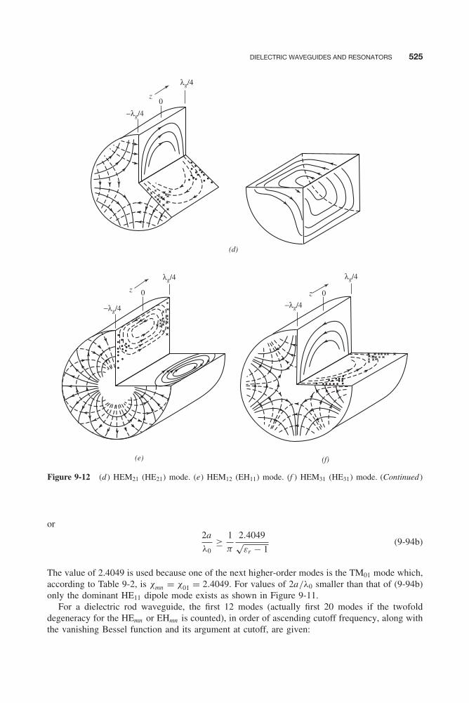
DIELECTRIC WAVEGUIDES AND RESONATORS 525
(d)
(e) (f)
−λg/4
λg/4
z0
−λg/4
λg/4
z 0
−λg/4
λg/4
z 0
Figure 9-12 (d) HEM21 (HE21) mode. (e) HEM12 (EH11) mode. (f ) HEM31 (HE31) mode. (Continued )
or2a
λ0≥ 1
π
2.4049√εr − 1
(9-94b)
The value of 2.4049 is used because one of the next higher-order modes is the TM01 mode which,according to Table 9-2, is χmn = χ01 = 2.4049. For values of 2a/λ0 smaller than that of (9-94b)only the dominant HE11 dipole mode exists as shown in Figure 9-11.
For a dielectric rod waveguide, the first 12 modes (actually first 20 modes if the twofolddegeneracy for the HEmn or EHmn is counted), in order of ascending cutoff frequency, along withthe vanishing Bessel function and its argument at cutoff, are given:

526 CIRCULAR CROSS-SECTION WAVEGUIDES AND CAVITIES
Totalnumber of
χmn propagatingMode(s) Jm(χmn) = 0 at cutoff modes
HE11 (HEM11) J1(χ10) = 0 χ10 = 0 2TE01, TM01, HE21 (HEM21) J0(χ01) = 0 χ01 = 2.4049 6HE12 (HEM13), EH11 (HEM12), HE31 (HEM31) J1(χ11) = 0 χ11 = 3.8318 12EH21 (HEM22), HE41 (HEM41) J2(χ21) = 0 χ21 = 5.1357 16TE02, TM02, HE22 (HEM23) J0(χ02) = 0 χ02 = 5.5201 20
According to (9-94a), a single dominant HE11 mode can be maintained within the rod providedthe normalized central core radius V < 2.4049. This can be accomplished by making the radiusa of the central core small and/or choosing, between the central core and the cladding, a smalldielectric constant εr . However, the smaller the size of the central core, the smaller the rateof attenuation and the less tightly the field outside it is attached to its surface. The normalizeddiameter over which the e−1 = 0.3679 = 36.79% field point outside the central core extends isshown plotted in Figure 9-13 [16]. Although the fundamental HE11 mode does not cutoff as thecore diameter shrinks, the fields spread out beyond the physical core and become loosely bound.
9.5.2 Circular Dielectric Resonator
Dielectric resonators are unmetalized dielectric objects (spheres, disks, parallelepipeds, etc.) ofhigh dielectric constant (usually ceramic) and high quality factor Q that can function as energy
Normalized core size [V2 = (b0a)2(εr − 1)]
Nor
mal
ized
mod
al d
iam
eter
Single HE11 mode region
01 2 3
1
2
3
Figure 9-13 Normalized modal diameter as a function of normalized core size for dielectric rod waveguide.(Source: T. G. Giallorenzi, “Optical communications research and technology: Fiber optics,” Proc. IEEE ,© 1978, IEEE.).
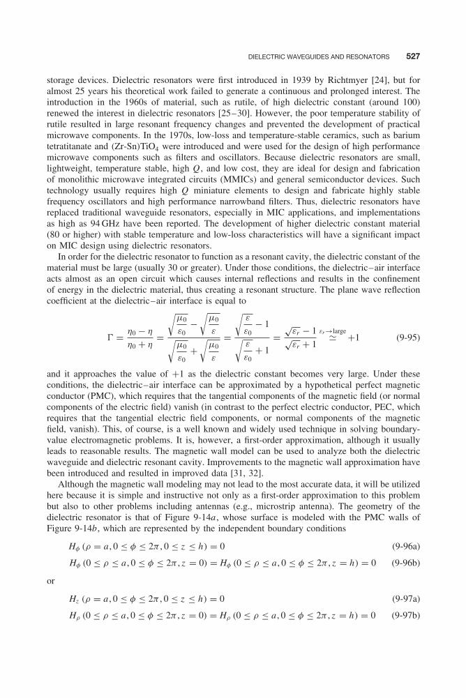
DIELECTRIC WAVEGUIDES AND RESONATORS 527
storage devices. Dielectric resonators were first introduced in 1939 by Richtmyer [24], but foralmost 25 years his theoretical work failed to generate a continuous and prolonged interest. Theintroduction in the 1960s of material, such as rutile, of high dielectric constant (around 100)renewed the interest in dielectric resonators [25–30]. However, the poor temperature stability ofrutile resulted in large resonant frequency changes and prevented the development of practicalmicrowave components. In the 1970s, low-loss and temperature-stable ceramics, such as bariumtetratitanate and (Zr-Sn)TiO4 were introduced and were used for the design of high performancemicrowave components such as filters and oscillators. Because dielectric resonators are small,lightweight, temperature stable, high Q , and low cost, they are ideal for design and fabricationof monolithic microwave integrated circuits (MMICs) and general semiconductor devices. Suchtechnology usually requires high Q miniature elements to design and fabricate highly stablefrequency oscillators and high performance narrowband filters. Thus, dielectric resonators havereplaced traditional waveguide resonators, especially in MIC applications, and implementationsas high as 94 GHz have been reported. The development of higher dielectric constant material(80 or higher) with stable temperature and low-loss characteristics will have a significant impacton MIC design using dielectric resonators.
In order for the dielectric resonator to function as a resonant cavity, the dielectric constant of thematerial must be large (usually 30 or greater). Under those conditions, the dielectric–air interfaceacts almost as an open circuit which causes internal reflections and results in the confinementof energy in the dielectric material, thus creating a resonant structure. The plane wave reflectioncoefficient at the dielectric–air interface is equal to
� = η0 − η
η0 + η=
√μ0
ε0−
√μ0
ε√μ0
ε0+
√μ0
ε
=
√ε
ε0− 1√
ε
ε0+ 1
=√
εr − 1√εr + 1
εr →large� +1 (9-95)
and it approaches the value of +1 as the dielectric constant becomes very large. Under theseconditions, the dielectric–air interface can be approximated by a hypothetical perfect magneticconductor (PMC), which requires that the tangential components of the magnetic field (or normalcomponents of the electric field) vanish (in contrast to the perfect electric conductor, PEC, whichrequires that the tangential electric field components, or normal components of the magneticfield, vanish). This, of course, is a well known and widely used technique in solving boundary-value electromagnetic problems. It is, however, a first-order approximation, although it usuallyleads to reasonable results. The magnetic wall model can be used to analyze both the dielectricwaveguide and dielectric resonant cavity. Improvements to the magnetic wall approximation havebeen introduced and resulted in improved data [31, 32].
Although the magnetic wall modeling may not lead to the most accurate data, it will be utilizedhere because it is simple and instructive not only as a first-order approximation to this problembut also to other problems including antennas (e.g., microstrip antenna). The geometry of thedielectric resonator is that of Figure 9-14a , whose surface is modeled with the PMC walls ofFigure 9-14b, which are represented by the independent boundary conditions
Hφ (ρ = a , 0 ≤ φ ≤ 2π , 0 ≤ z ≤ h) = 0 (9-96a)
Hφ (0 ≤ ρ ≤ a , 0 ≤ φ ≤ 2π , z = 0) = Hφ (0 ≤ ρ ≤ a , 0 ≤ φ ≤ 2π , z = h) = 0 (9-96b)
or
Hz (ρ = a , 0 ≤ φ ≤ 2π , 0 ≤ z ≤ h) = 0 (9-97a)
Hρ (0 ≤ ρ ≤ a , 0 ≤ φ ≤ 2π , z = 0) = Hρ (0 ≤ ρ ≤ a , 0 ≤ φ ≤ 2π , z = h) = 0 (9-97b)
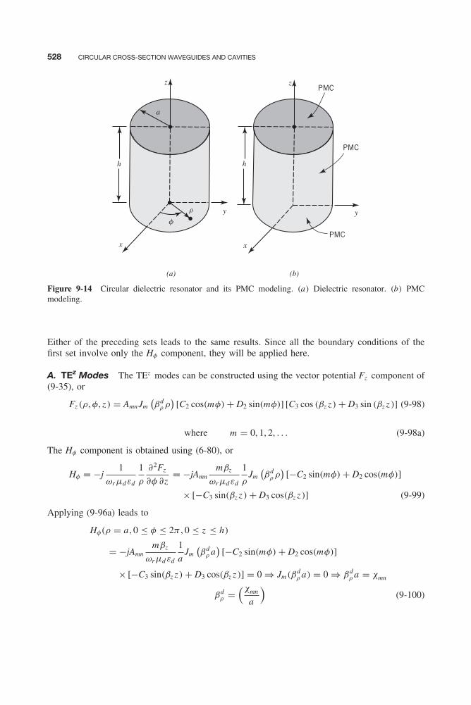
528 CIRCULAR CROSS-SECTION WAVEGUIDES AND CAVITIES
y
x x
y
PMC
PMC
PMCz z
(a) (b)
h h
f
r
a
Figure 9-14 Circular dielectric resonator and its PMC modeling. (a) Dielectric resonator. (b) PMCmodeling.
Either of the preceding sets leads to the same results. Since all the boundary conditions of thefirst set involve only the Hφ component, they will be applied here.
A. TEz Modes The TEz modes can be constructed using the vector potential Fz component of(9-35), or
Fz (ρ, φ, z ) = AmnJm(βd
ρ ρ)
[C2 cos(mφ) + D2 sin(mφ)] [C3 cos (βz z ) + D3 sin (βz z )] (9-98)
where m = 0, 1, 2, . . . (9-98a)
The Hφ component is obtained using (6-80), or
Hφ = −j1
ωrμdεd
1
ρ
∂2Fz
∂φ ∂z= −jAmn
mβz
ωrμdεd
1
ρJm
(βd
ρ ρ)
[−C2 sin(mφ) + D2 cos(mφ)]
× [−C3 sin(βz z ) + D3 cos(βz z )] (9-99)
Applying (9-96a) leads to
Hφ(ρ = a , 0 ≤ φ ≤ 2π , 0 ≤ z ≤ h)
= −jAmnmβz
ωrμdεd
1
aJm
(βd
ρ a)
[−C2 sin(mφ) + D2 cos(mφ)]
× [−C3 sin(βz z ) + D3 cos(βz z )] = 0 ⇒ Jm(βdρ a) = 0 ⇒ βd
ρ a = χmn
βdρ =
(χmn
a
)(9-100)
DIELECTRIC WAVEGUIDES AND RESONATORS 529
where χmn represents the zeroes of the Bessel function of order m , many of which are found inTable 9-2. In a similar manner, the first boundary condition of (9-96b) leads to
Hφ(0 ≤ ρ ≤ a , 0 ≤ φ ≤ 2π , z = 0)
= −jAmnmβz
ωrμdεd
1
ρJm(βd
ρ ρ) [−C2 sin(mφ) + D2 cos(mφ)]
× [−C3(0) + D3(1)] = 0 ⇒ D3 = 0 (9-100a)
while the second boundary condition of (9-96b) leads to
Hφ(0 ≤ ρ ≤ a , 0 ≤ φ ≤ 2π , z = h)
= −jAmnmβz
ωrμdεd
1
ρJm(βd
ρ ρ)
× [−C2 sin(mφ) + D2 cos(mφ)] [−C3 sin(βz h)] = 0
⇒ sin(βz h) = 0 ⇒ βz h = pπ
βz = pπ
h, p = 0, 1, 2, . . . (9-100b)
Using (9-100) and (9-100b), the resonant frequency is obtained by applying (9-4a) at resonance,that is,
βr = ωr√
μdεd = 2π fr√
μdεd =√(χmn
a
)2+
(pπ
h
)2
or
(fr )TEz
mnp = 1
2π√
μdεd
√(χmn
a
)2+
(pπ
h
)2 m = 0, 1, 2, . . .n = 1, 2, 3, . . .p = 0, 1, 2, . . .
(9-101)
The dominant TEzmnp mode is the TEz
010 whose resonant frequency is equal to
(fr )TEz
010 = χ01
2πa√
μdεd= 2.4049
2πa√
μdεd(9-101a)
B. TMz Modes The TMz modes are obtained using a similar procedure as for the TEz modes,but starting with the vector potential of (9-41). Doing this leads to the resonant frequency of
(fr )TMz
mnp = 1
2π√
μdεd
√(χ ′
mn
a
)2
+(pπ
h
)2 m = 0, 1, 2, . . .n = 1, 2, 3, . . .p = 1, 2, 3, . . .
(9-102)

530 CIRCULAR CROSS-SECTION WAVEGUIDES AND CAVITIES
where χ ′mn are the zeroes of the derivative of the Bessel function of order m , a partial list of
which is found on Table 9-1. The dominant TMzmnp mode is the TMz
111 mode whose resonantfrequency is equal to
(fr )TMz
111 = 1
2π√
μdεd
√(χ ′
11
a
)2
+(π
h
)2= 1
2π√
μdεd
√(1.8412
a
)2
+(π
h
)2(9-102a)
A comparison of the resonant frequencies of (9-101) and (9-102) of the circular dielectricresonator modeled by the PMC surface with those of (9-39a) and (9-45) for the circular waveguideresonator with PEC surface, shows that the TEz
mnp of one are the TMzmnp of the other, and vice
versa.
C. TE01δ Mode Although the dominant mode of the circular dielectric resonator as predictedby the PMC modeling is the TE010 mode (provided h/a < 2.03), in practice the mode most oftenused is the TE01δ where δ is a noninteger value less than 1. This mode can be modeled usingFigure 9-15. For resonators with PEC or PMC walls, the third subscript is always an integer(including zero), and it represents the number of half-wavelength variations the field undergoesin the z direction. Since δ is a noninteger less than unity, the dielectric resonator field of aTE01δ mode undergoes less than one half-wavelength variation along its length h . More accuratemodelings of the dielectric resonator [31, 33, 34] indicate that βz h of (9-100b) is
βz h � ψ1
2+ ψ2
2+ qπ , q = 0, 1, 2, . . . (9-103)
where
ψ1
2= tan−1
[α1
βzcoth(α1h1)
](9-103a)
ψ2
2= tan−1
[α2
βzcoth(α2h2)
](9-103b)
α1 =√(χ01
a
)2− β2
0εr1 (9-103c)
α2 =√(χ01
a
)2− β2
0εr2 (9-103d)
When q = 0 in (9-103), the mode is the TE01δ where δ is a noninteger less than unity given by
δ = 1
π
(ψ1
2+ ψ2
2
)(9-104)
and it signifies the variations of the field between the ends of the dielectric resonator at z = 0 andz = h . The preceding equations have been derived by modeling the dielectric resonator as shownin Figure 9-15 where PEC plates have been placed at z = −h2 and z = h + h1 [21]. The mediumin regions 1–5 is usually taken to be air. Thus, the dielectric resonator has been sandwichedbetween two PEC plates, each placed at distances h1 and h2 from each of its ends. The distancesh1 and h2 can be chosen to be 0 ≤ h1, h2 ≤ ∞.

DIELECTRIC WAVEGUIDES AND RESONATORS 531
PEC
PEC
1
h2
h
h1
er, mr
33
4 4
552
a
Figure 9-15 Modeling of circular dielectric rod resonator. (Source: D. Kajfez and P. Guillon (Eds.),Dielectric Resonators , 1986, Artech House, Inc.).
Example 9-5
Find the resonant TE01δ mode and its resonant frequency when the distances h1 and h2 of Figure 9-15are both zero (h1 = h2 = 0); that is, the dielectric resonator has been sandwiched between two PECplates, each plate touching each of the ends of the dielectric resonator. Assume the resonator has radiusof 5.25 mm, height of 4.6 mm, and dielectric constant of εr = 38.
Solution: Since h1 = h2 = 0, then according to (9-103a) and (9-103b)
ψ1
2= ψ2
2= tan−1(∞) = π
2
Thus, δ of (9-104) is equal to
δ = 1
π
(π
2+ π
2
)= 1
and the resonant TE01δ mode is the TE011. For this mode βz h is, according to (9-103) with p = 0, equalto
βz h = π ⇒ βz = π
h
Its resonant frequency is identical to (9-101) of the PMC modeling, which reduces to
(fr )TEz
011 = 1
2π√
μd εd
√(2.4049
a
)2
+(π
h
)2
= 3 × 10¹¹
2π√
38
√(2.4049
5.25
)2
+( π
4.6
)2 = 6.37 GHz
When compared to the exact value of 4.82 GHz for a dielectric resonator immersed in free space, thepreceding value has an error of +32%. A more accurate result of 4.60 GHz (error of −4.8%) can beobtained using (9-103)–(9-104) by placing the two PECs at infinity (h1 = h2 = ∞); then the resonatoris isolated in free space.
532 CIRCULAR CROSS-SECTION WAVEGUIDES AND CAVITIES
9.5.3 Optical Fiber Cable
Optical communications, which initially started as a speculative research activity, has evolvedinto a very practical technique that has brought new dimensions to miniaturization, data handlingcapabilities, and signal processing methods. This success has been primarily attributed to thedevelopment of fiber optics cables, which in 1970 exhibited attenuations of 20 dB/km and in theearly 1980s reduced to less than 1 dB/km. The development of suitable solid state diode sourcesand detectors has certainly eliminated any remaining insurmountable technological barriers andpaved the way for widespread implementation of optical communication techniques for com-mercial and military applications. This technology has spread to the development of integratedoptics which provide even greater miniaturization of optical systems, rigid alignment of opticalcomponents, and reduced space and weight.
A fiber optics cable is a dielectric waveguide, usually of circular cross section, that guidesthe electromagnetic wave in discrete modes through internal reflections whose incidence angleat the interface is equal to or greater than the critical angle. The confinement of the energywithin the dielectric structure is described analytically by Maxwell’s equations and the boundaryconditions at dielectric–dielectric boundaries, in contrast to the traditional metallic–dielectricboundaries in metallic waveguides. Such analyses have already been discussed in Section 8.7 forplanar structures and Section 9.5.1 for circular geometries.
The most common geometries of fiber cables are those shown in Figure 9-16. They areclassified as step-index multimode, graded-index multimode, and single-mode step-index [14, 16].Typical dimensions, index-of-refraction distributions, optical ray paths, and pulse spreading byeach type of cable are also illustrated in Figure 9-16. Therefore, fiber optics cables can beclassified into two cases: single-mode and multimode fibers.
Single-mode fibers permit wave propagation at a single resolvable angle, whereas multimodecables transmit waves that travel at many resolvable angles all within the central core of thefiber. Both single- and multimode fibers are fabricated with a central core with a high index ofrefraction (dielectric constant) surrounded by a cladding with a lower index of refraction. Thewave is guided in the core by total internal reflection at the core-cladding interface. Single-modecables usually have a step-index where the diameter of the center core is very small (typically2–16 μm) and not much larger than the wavelength of the wave it carries. Structurally, theyare the simplest and exhibit abrupt index-of-refraction discontinuities along the core-claddinginterface. Usually, the index of refraction of the central core is about 1.471 and that of thecladding is 1.457.
Step-index multimode cables also exhibt a well defined central core with a constant index ofrefraction surrounded by a cladding with a lower index of refraction. In contrast to the single-mode step-index, the multimode step-index possesses a central core whose diameter is about25–150 μm. When the wavelength of light is of the order of 10 μm (near infrared region) andthe central core diameter is 100 μm, such a cable can support as many as 25,000 modes (usuallythere are about 200 modes). However, as the central core diameter approaches 10 μm (onewavelength), the number of modes is reduced to one and the cable becomes a single-mode fiber.Because of its multimode field structure, such a cable is very dispersive and provides severesignal distortion to waveforms with broad spectral frequency content. Typically, the index ofrefraction of the central core is about 1.527 and that of the cladding is about 1.517.
Graded-index multimode cables also possess a relatively large central core (typical diametersof 20–150 μm) whose index of refraction continuously decreases from the core center toward thecore-cladding interface at which point the core and cladding indexes are identical. For this cable,the waves are still contained within the central core and they are continuously refocused towardthe central axis of the core by its continuous lensing action. The number of modes supported bysuch a cable is usually about 2,000, and such a multimode structure provides waveform distortionespecially to transient signals. All cables possess an outside cladding that adds mechanical strength

Balanis c02.tex V3 - 11/22/2011 3:07 P.M. Page 68
DIELECTRIC WAVEGUIDES AND RESONATORS 533
qmax
Cross-sectional view
Step indexmultimodea ~ 25-150 mm
Single modestep indexa ~ 1.5-8 mm
Graded indexmultimodea ~ 20-150 mm
Index profile
Radial distance
Radial distance
Radial distance
eslup tuptuOeslup tupnI Light paths
a
n
n
T
T
T
T
T
T
n
2a
a
Figure 9-16 Common types and geometries of fiber cables. (Source: T. G. Giallorenzi, “Optical communications research andtechnology: Fiber optics,” Proc. IEEE , 1978, IEEE.).

534 CIRCULAR CROSS-SECTION WAVEGUIDES AND CAVITIES
to the fiber, reduces scattering loss that is due to dielectric discontinuities, and protects the guidingcentral core from absorbing surface contaminants that the cable may come in contact with.
For the graded-index multimode fiber, the index of refraction n(ρ) = √εr (ρ) of the central
core exhibits a nearly parabolic variation in the radial direction from the center of the core towardthe cladding. This variation can be represented by [16]
nc(ρ) = n
[1 +
(a − ρ
a
)α]0 ≤ ρ ≤ a (9-105)
where nc(ρ) = index of refraction of the central core (usually � 1.562 on axis)n = index of refraction of the cladding (usually � 1.540)a = radius of the central core = parameter usually much less than unity (usually 0.01 < < 0.02)α = parameter whose value is close to 2 for maximum fiber bandwidth
It has been shown by Example 5-6 that for the dielectric–dielectric interface of the fiber cableto internally reflect the waves of all incidence angles, the ratio of the index of refraction of thecentral core at the interface to that of the cladding must be equal to or greater than
√2, that is,
nc(a)/n ≥ √2. However, this is not necessary if the angles of incidence of the waves are not
small.The modes that can be supported by the step-index cable (either single mode or multimode) can
be found using techniques outlined in Section 9.5.1 for the dielectric rod waveguide. These modesare, in general, HEM (HE or EH) hybrid modes. The applicable equations are (9-81a) through(9-94b), where εr should represent the square of the ratio of the index of refraction of the centralcore to that of the cladding [i.e., εr = (nc/n)2]. The field configurations of the graded-index cablecan be analyzed in terms of Hermite-Gaussian functions [35]. Because of the complexity, theanalysis will not be presented here. The interested reader is referred to the literature [11, 16].
9.5.4 Dielectric-Covered Conducting Rod
Let us consider the field analysis of a dielectric-covered conducting circular rod, as shown inFigure 9-17 [36–38]. The radius of the conducting rod is a while that of the dielectric coveris b. The thickness of the dielectric sleeving is denoted by t (t = b − a). When the radius ofthe conducting rod is small, the rod will be representative of a dielectric-covered wire. In thissection we will consider the TMz and TEz modes, which, in general, must co-exist to satisfythe boundary conditions. We will conduct an extended discussion of the modes with azimuthalsymmetry—no φ variations—will be conducted.
A. TMz Modes The fields in the radial direction inside the dielectric sleeving must be repre-sented by standing wave functions while those outside the dielectric cover must be decaying inorder for the rod to act as a waveguide. In general, for the TMz
mn modes, the potential functionAz can be written as
Adz = [
Ad1 Jm
(βd
ρ ρ) + Bd
1 Ym(βd
ρ ρ)] [
C d2 cos(mφ) + Dd
2 sin(mφ)]
× [Ad
3 e−jβz z + Bd3 e+jβz z
], for a ≤ ρ ≤ b (9-106a)
A0z = A0
1Km(α0
ρρ) [
C 02 cos(mφ) + D0
2 sin(mφ)]
× [A0
3e−jβz z + B03 e+jβz z
], for b ≤ ρ ≤ ∞ (9-106b)

DIELECTRIC WAVEGUIDES AND RESONATORS 535
b
a
y
x
z
s = ∞
ed , md
f
r
e0 , m0
Figure 9-17 Geometry of dielectric covered conducting rod.
However, the geometry of Figure 9-17 can only support modes with azimuthal symmetry,(m = 0). Therefore, for the positive traveling waves of the lowest-order mode (m = 0), thevector potentials reduce to
Adz = [
Ad0 J0
(βd
ρ ρ) + Bd
0 Y0(βd
ρ ρ)]
e−jβz z , for a ≤ ρ ≤ b (9-107)
where (βd
ρ
)2 + β2z = β2
d = μrεrβ20 (9-107a)
and
A0z = A0
0K0(α0
ρρ)
e−jβz z , for b ≤ ρ ≤ ∞ (9-108)
where
− (α0
ρ
)2 + β2z = β2
0 (9-108a)
The corresponding electric and magnetic fields can be written as
For a ≤ ρ ≤ b,
E dρ = −j
1
ωμdεd
∂2Adz
∂ρ ∂z= − βz β
dρ
ωμdεd
[Ad
0 J ′0
(βd
ρ ρ) + Bd
0 Y ′0
(βd
ρ ρ)]
e−jβz z (9-109a)
E dφ = −j
1
ωμdεd
∂2Adz
∂φ ∂z= 0 (9-109b)

536 CIRCULAR CROSS-SECTION WAVEGUIDES AND CAVITIES
E dz = −j
1
ωμdεd
(∂2
∂z 2+ β2
d
)Ad
z = −j
(βd
ρ
)2
ωμdεd
[Ad
0 J0(βd
ρ ρ) + Bd
0 Y0(βd
ρ ρ)]
e−jβz z (9-109c)
H dρ = 1
μd
1
ρ
∂Adz
∂φ= 0 (9-109d)
H dφ = − 1
μd
∂Adz
∂ρ= −βd
ρ
μd
[Ad
0 J ′0
(βd
ρ ρ) + Bd
0 Y ′0
(βd
ρ ρ)]
e−jβz z (9-109e)
H dz = 0 (9-109f)
′ ≡ ∂
∂(βd
ρ ρ) (9-109g)
And for b ≤ ρ ≤ ∞,
E 0ρ = −j
1
ωμ0ε0
∂2A0z
∂ρ ∂z= α0
ρβz
ωμ0ε0A0
0K ′0
(α0
ρρ)
e−jβz z (9-110a)
E 0φ = −j
1
ωμ0ε0
1
ρ
∂2A0z
∂φ ∂z= 0 (9-110b)
E 0z = −j
1
ωμ0ε0
(∂2
∂z 2+ β2
0
)A0
z = +j
(α0
ρ
)2
ωμ0ε0A0
0K0(α0
ρρ)
e−jβz z (9-110c)
H 0ρ = 1
μ0
1
ρ
∂A0z
∂φ= 0 (9-110d)
H 0φ = − 1
μ0
∂A0z
∂ρ= −α0
ρ
μ0A0
0K ′0
(α0
ρρ)
e−jβz z (9-110e)
H 0z = 0 (9-110f)
′ ≡ ∂
∂(α0
ρρ) (9-110g)
The vanishing of the tangential electric fields at ρ = a and the continuity of the tangentialcomponents of the electric and magnetic fields at ρ = b requires that
E dz (ρ = a , 0 ≤ φ ≤ 2π , z ) = 0 (9-111a)
E dz (ρ = b, 0 ≤ φ ≤ 2π , z ) = E 0
z (ρ = b, 0 ≤ φ ≤ 2π , z ) (9-111b)
H dφ (ρ = b, 0 ≤ φ ≤ 2π , z ) = H 0
φ (ρ = b, 0 ≤ φ ≤ 2π , z ) (9-111c)
Applying (9-111a) leads to
Ad0 J0
(βd
ρ a) + Bd
0 Y0(βd
ρ a) = 0 (9-112)
or
Bd0 = −Ad
0
J0(βd
ρ a)
Y0(βd
ρ a) (9-112a)
DIELECTRIC WAVEGUIDES AND RESONATORS 537
whereas (9-111b) leads to
−(βd
ρ
)2
ωμdεd
[Ad
0 J0(βd
ρ b) + Bd
0 Y0(βd
ρ b)] =
(α0
ρ
)2
ωμ0ε0A0
0K0(α0
ρb)
(9-113)
which by using (9-112a) can be written as
A00K0
(α0
ρb) = −Ad
0μ0
μd
ε0
εd
(βd
ρ
α0ρ
)2 [J0
(βd
ρ b) − J0
(βd
ρ a)
Y0(βd
ρ b)
Y0(βd
ρ a) ]
(9-113a)
The continuity of the tangential magnetic field at ρ = b, as stated by (9-111c), leads to
−βdρ
μd
[Ad
0 J ′0
(βd
ρ b) + Bd
0 Y ′0
(βd
ρ b)] = −α0
ρ
μ0A0
0K ′0
(α0
ρb)
(9-114)
which by using (9-112a) can be written as
A00K ′
0
(α0
ρb) = Ad
0μ0
μd
βdρ
α0ρ
[J ′
0
(βd
ρ b) − J0
(βd
ρ a)
Y ′0
(βd
ρ b)
Y0(βd
ρ a) ]
(9-114a)
Dividing (9-114a) by (9-113a) leads to
K ′0
(α0
ρb)
K0(α0
ρb) = −εd
ε0
(α0
ρ
βdρ
) [J ′
0
(βd
ρ b)
Y0(βd
ρ a) − J0
(βd
ρ a)
Y ′0
(βd
ρ b)][
J0(βd
ρ b)
Y0(βd
ρ a) − J0
(βd
ρ a)
Y0(βd
ρ b)] (9-115a)
Subtracting (9-108a) from (9-107a) leads to
(βd
ρ
)2 + (α0
ρ
)2 = β20 (μrεr − 1) (9-115b)
which, along with the transcendental equation 9-115a, can be used to solve for βdρ and α0
ρ . Thiscan be accomplished using graphical or numerical techniques similar to the ones utilized inSection 8.7 for planar structures.
The technique outlined and implemented in Section 8.7 to solve the wave numbers for planardielectric waveguides is straightforward but complicated when utilized to solve for the wavenumbers βd
ρ and α0ρ of (9-115a) and (9-115b). An approximate solution can be used to solve
(9-115a) and (9-115b) simultaneously when the thickness of the dielectric cladding t = b − a issmall. Under these conditions the Bessel functions J0(β
dρ b) and Y0(β
dρ b) can be expanded in a
538 CIRCULAR CROSS-SECTION WAVEGUIDES AND CAVITIES
Taylor series about the point βdρ a , that is
J0(βd
ρ b) � J0
(βd
ρ a) + dJ0
(βd
ρ b)
d(βd
ρ b) ∣∣∣∣∣
βdρ b=βd
ρ a
βdρ (b − a)
� J0(βd
ρ a) − βd
ρ (b − a)J1(βd
ρ a)
(9-116a)
Y0(βd
ρ b) � Y0
(βd
ρ a) + dY0
(βd
ρ b)
d(βd
ρ b) ∣∣∣∣∣
βdρ b=βd
ρ a
βdρ (b − a)
� Y0(βd
ρ a) − βd
ρ (b − a)Y1(βd
ρ a)
(9-116b)
J ′0
(βd
ρ b) = dJ0
(βd
ρ ρ)
d(βd
ρ ρ) ∣∣∣∣∣
ρ=b
= −J1(βd
ρ b) � −
⎡⎣J1(βd
ρ a) + dJ1
(βd
ρ b)
d(βd
ρ b) ∣∣∣∣∣
βdρ b=βd
ρ a
βdρ (b − a)
⎤⎦� −
{J1
(βd
ρ a) + βd
ρ (b − a)
[J0
(βd
ρ a) − 1
βdρ a
J1(βd
ρ a)]}
J ′0
(βd
ρ b) � −
[J1
(βd
ρ a) (
1 − b − a
a
)+ βd
ρ (b − a)J0(βd
ρ a)]
(9-116c)
Y ′0
(βd
ρ b) � −
[Y1
(βd
ρ a) (
1 − b − a
a
)+ βd
ρ (b − a)Y0(βd
ρ a)]
(9-116d)
Therefore, the numerator and denominator of (9-115a) can be written, respectively, as
J ′0
(βd
ρ b)
Y0(βd
ρ a) − J0
(βd
ρ a)
Y ′0
(βd
ρ b)
� −Y0(βd
ρ a) [
J1(βd
ρ a) (
1 − b − a
a
)+ βd
ρ (b − a)J0(βd
ρ a)]
+J0(βd
ρ a) [
Y1(βd
ρ a) (
1 − b − a
a
)+ βd
ρ (b − a)Y0(βd
ρ a)]
�(
1 − b − a
a
) [J0
(βd
ρ a)
Y1(βd
ρ a) − Y0
(βd
ρ a)
J1(βd
ρ a)]
(9-117a)
J0(βd
ρ b)
Y0(βd
ρ a) − J0
(βd
ρ a)
Y0(βd
ρ b)
� Y0(βd
ρ a) [
J0(βd
ρ a) − βd
ρ (b − a)J1(βd
ρ a)]
−J0(βd
ρ a) [
Y0(βd
ρ a) − βd
ρ (b − a)Y1(βd
ρ a)]
� βdρ (b − a)
[J0
(βd
ρ a)
Y1(βd
ρ a) − Y0
(βd
ρ a)
J1(βd
ρ a)]
(9-117b)
Substituting (9-117a) and (9-117b) into (9-115a) leads to
K ′0
(α0
ρb)
K0(α0
ρb) � −εd
ε0
(α0
ρ
βdρ
) (1 − b − a
a
)βd
ρ (b − a)= −εd
ε0
α0ρ(
βdρ
)2
⎛⎜⎝1 − b − a
ab − a
⎞⎟⎠ (9-118)

DIELECTRIC WAVEGUIDES AND RESONATORS 539
For small values of a (i.e., a � λ0) the attenuation constant α0ρ is of the same order of
magnitude as β0 and the wave is loosely bound to the surface so that α0ρb is small for small
values of b − a . Under these conditions
K ′0
(α0
ρb) = dK0
(α0
ρρ)
d(α0
ρρ) ∣∣∣∣∣
ρ=b
= −K1(α0
ρb) � − 1
α0ρb
= − 1
bα0ρ
(9-119a)
K0(α0
ρb) � − ln
(0.89α0
ρb)
(9-119b)
so that (9-118) reduces for εd = εrε0 to
1
b ln(0.89α0
ρb) � −εr
(α0
ρ
βdρ
)2⎛⎜⎝1 − b − a
ab − a
⎞⎟⎠(βd
ρ
)2(b − a) � −εr b
(1 − b − a
a
) (α0
ρ
)2ln
(0.89α0
ρb)
(9-120)
Substituting (9-115b) into (9-120) for (βdρ )2 leads for t = b − a � a to[
β20 (εr − 1) − (
α0ρ
)2](b − a) � −εr b
(1 − b − a
a
) (α0
ρ
)2ln
(0.89α0
ρb)
(9-121)
or
εr b(α0
ρ
)2ln
(0.89α0
ρb) �
[−β2
0 (εr − 1) + (α0
ρ
)2](b − a) (9-121a)
Example 9-6
A perfectly conducting wire of radius a = 0.09 cm is covered with a dielectric sleeving of polystyrene(εr = 2.56) of radius b = 0.10 cm. At a frequency of 9.55 GHz, determine the attenuation constants α0
ρ ,βz , and βd
ρ and the relative field strength at ρ = 2λ0 compared to that at the outside surface of thedielectric sleeving (ρ = b).
Solution: At f = 9.55 GHz,
λ0 = 30 × 109
9.55 × 109= 3.1414 cm ⇒ β0 = 2π
λ0= 2 rad/cm
λd = λ0√εr
= 3.1414√2.56
= 1.9634 cm ⇒ βd = 2π
λ= 2π
1.9634= 3.2 rad/cm
Since the thickness t of the dielectric sleeving is much smaller than the wavelength,
t = b − a = 0.10 − 0.09 = 0.01 cm < λd = 1.9634 cm < λ0 = 3.1414 cm
then the approximate relation of (9-121a) is applicable. Using an iterative procedure, it can be shownthat
α0ρ = 0.252 Np/cm
is a solution to (9-121a). Using (9-108a),
βz =√
β20 + (
α0ρ
)2 =√
(2)2 + (0.252)2 =√
4.0635 = 2.0158 rad/cm
540 CIRCULAR CROSS-SECTION WAVEGUIDES AND CAVITIES
and βdρ is found using (9-107a) as
βdρ =
√β2
d − β2z =
√(3.2)2 − (2.0158)2 =
√6.1765 = 2.485 rad/cm
The field outside the sleeving is of decaying form represented by the modified Bessel functionK0(α
0ρρ) of (9-108). Thus,
E (ρ = 2λ0)
E (ρ = b)= E (ρ = 2π cm)
E (ρ = 0.10 cm)= K0(ρ = 2π cm)
K0(ρ = 0.10 cm)
=
C0e−α0ρρ√
α0ρρ
∣∣∣∣∣∣∣ρ=2π cm
C0e−α0ρρ√
α0ρρ
∣∣∣∣∣∣∣ρ=0.10 cm
= 0.1631
6.1426= 0.0266 = 2.66%
Therefore, at a distance of ρ = 2λ0 the relative field has been reduced to a very small value; at pointsfurther away, the field intensity is even smaller.
For the dielectric-covered wire and the dielectric rod waveguide, we can define an effectiveradius as the radial distance at which point and beyond the relative field intensity is of very lowvalue. If we use the 2.66% value of Example 9-6 as the field value with which we can define theeffective radius, then the effective radius for the wire of Example 9-6 is ae = 2λ0 = 2π cm.
The rate of attenuation α0ρ can be increased and the wave can be made more tightly bound to
the surface by increasing the dielectric constant and/or thickness of the dielectric sleeving. This,however, results in greater attenuation and larger losses of the wave along the direction of wavetravel (axis of the wire) because of the greater field concentration near the conducting boundary.
B. TEz Modes Following a procedure similar to that used for the TMzmn modes, it can be
shown that for the dielectric-covered conducting rod of Figure 9-17, the TEzmn positive traveling
waves of the lowest-order mode (m = 0) also possess azimuthal symmetry (no φ variations,m = 0) and can exist individually. Therefore, for the m = 0 mode, the vector potentials can bewritten as
F dz = [
Ad0 J0
(βd
ρ ρ) + Bd
0 Y0(βd
ρ ρ)]
e−jβz z , for a ≤ ρ ≤ b (9-122)
where (βd
ρ
)2 + β2z = β2
d = μrεrβ20 (9-122a)
F 0z = A0
0K0(α0
ρρ)
e−jβz z , for b ≤ ρ ≤ ∞ (9-123)
where
− (α0
ρ
)2 + β2z = β2
0 (9-123a)
Leaving the details for the reader as an end-of-chapter exercise, the equations for the TEz0n
modes corresponding to (9-113a), (9-114a), (9-115a), (9-115b), and (9-121a) for the TMz0n modes,

MULTIMEDIA 541
are given by
A00K ′
0(α0ρb) = Ad
0ε0
εd
βdρ
α0ρ
[J ′
0(βdρ b) − J ′
0(βdρ a)Y ′
0(βdρ b)
Y ′0(β
dρ a)
](9-124a)
A0K0(α0ρb) = −Ad
0μ0
μd
ε0
εd
(βd
ρ
α0ρ
)2 [J0(β
dρ b) − J ′
0(βdρ a)Y0(β
dρ b)
Y ′0(β
dρ a)
](9-124b)
K ′0(α
0ρb)
K0(α0ρb)
= −μd
μ0
(α0
ρ
βdρ
) [J ′
0(βdρ b)Y ′
0(βdρ a) − J ′
0(βdρ a)Y ′
0(βdρ b)
][J0(βd
ρ b)Y ′0(β
dρ a) − J ′
0(βdρ a)Y0(βd
ρ b)] (9-124c)
(βdρ )2 + (α0
ρ)2 = β20 (μrεr − 1) (9-124d)
μr b(b − a)(α0ρ)21n(0.89α0
ρb) � 1 (9-124e)
9.6 MULTIMEDIA
On the website that accompanies this book, the following multimedia resources are included forthe review, understanding, and presentation of the material of this chapter.
• MATLAB computer programs:a. Cyl_Waveguide: Computes the propagation characteristics of a cylindrical waveguide.b. Cyl_Resonator: Computes the resonant characteristics of a cylindrical resonator.c. CircDielGuide: Computes the propagation characteristics of a circular dielectric waveg-
uide based on the solution of the eigenvalue equation 9-91.• Power Point (PPT) viewgraphs, in multicolor.
REFERENCES
1. C. S. Lee, S. W. Lee, and S. L. Chuang, “Plot of modal field distribution in rectangular and circularwaveguides,” IEEE Trans. Microwave Theory Tech., vol. MTT-33, no. 3, pp. 271–274, March 1985.
2. S. E. Miller, “Waveguide as a communication medium,” Bell System Tech. J., vol. 35, pp. 1347–1384,November 1956.
3. S. P. Morgan and J. A. Young, “Helix waveguide,” Bell System Tech. J., vol. 35, pp. 1347–1384,November 1956.
4. S. Ramo, J. R. Whinnery, and T. Van Duzer, Fields and Waves in Communication Electronics , JohnWiley & Sons, New York, 1965, pp. 429–439.
5. M. R. Spiegel, Mathematical Handbook, Schaum’s Outline Series , McGraw-Hill, New York, 1968.
6. C. A. Balanis, Antenna Theory: Analysis and Design (3rd edition), John Wiley & Sons, New York,2005.
542 CIRCULAR CROSS-SECTION WAVEGUIDES AND CAVITIES
7. C. H. Chandler, “An investigation of dielectric rod as waveguide,” J. Appl. Phys., vol. 20,pp. 1188–1192, December 1949.
8. W. M. Elasser, “Attenuation in a dielectric circular rod,” J. Appl. Phys., vol. 20, pp. 1193–1196,December 1949.
9. J. W. Duncan and R. H. DuHamel, “A technique for controlling the radiation from dielectric rodwaveguides,” IRE Trans. Antennas Propagat., vol. AP-5, no. 4, pp. 284–289, July 1957.
10. R. E. Collin, Field Theory of Guided Waves , Second Edition, McGraw-Hill, New York, 1991.
11. E. Snitzer, “Cylindrical electric waveguide modes,” J. Optical Soc. America , vol. 51, no. 5, pp. 491–498,May 1961.
12. A. W. Snyder, “Asymptotic expressions for eigenfunctions and eigenvalues of a dielectric or opticalwaveguide,” IEEE Trans. Microwave Theory Tech., vol. MTT-17, pp. 1130–1138, December 1969.
13. A. W. Snyder, “Excitation and scattering of modes on a dielectric or optical fiber,” IEEE Trans.Microwave Theory Tech., vol. MTT-17, pp. 1138–1144, December 1969.
14. S. E. Miller, E. A. J. Marcatili, and T. Li, “Research toward optical-fiber transmission systems. Part I:The transmission medium,” Proc. IEEE , vol. 61, no. 12, pp. 1703–1726, December 1973.
15. D. Marcuse, Theory of Dielectric Optical Waveguide, Academic, New York, 1974.
16. T. G. Giallorenzi, “Optical communications research and technology: Fiber Optics,” Proc. IEEE , vol. 66,no. 7, pp. 744–780, July 1978.
17. J. Kane, “Fiber optic cables compete with mw relays and coax,” Microwave J., vol. 26, pp. 16, 61,January 1979.
18. C. Yeh, “Guided-wave modes in cylindrical optical fibers,” IEEE Trans. Education , vol. E-30, no. 1,February 1987.
19. R. J. Pieper, “A heuristic approach to fiber optics,” IEEE Trans. Education , vol. E-30, no. 2, pp. 77–82,May 1987.
20. “IRE standards on antennas and waveguides: definitions of terms, 1953,” Proc. IRE , vol. 41,pp. 1721–1728, December 1953.
21. D. Kajfez and P. Guillon (Eds.), Dielectric Resonators , Artech House, Inc., Dedham, MA, 1986.
22. R. F. Harrington, Time-Harmonic Electromagnetic Fields , McGraw-Hill, New York, 1961.
23. T. Okoshi, Optical Fibers , Academic, New York, 1982.
24. R. D. Richtmyer, “Dielectric resonator,” J. Appl. Phys., vol. 10, pp. 391–398, June 1939.
25. A. Okaya, “The rutile microwave resonator,” Proc. IRE , vol. 48, p. 1921, November 1960.
26. A. Okaya and L. F. Barash, “The dielectric microwave resonator,” Proc. IRE , vol. 50, pp. 2081–2092,October 1962.
27. H. Y. Yee, “Natural resonant frequencies of microwave dielectric resonators,” IEEE Trans. MicrowaveTheory Tech., vol. MTT-13, p. 256, March 1965.
28. S. J. Fiedziuszko, “Microwave dielectric resonators,” Microwave J., pp. 189–200, September 1980.
29. M. W. Pospieszalski, “Cylindrical dielectric resonators and their applications in TEM line microwavecircuits,” IEEE Trans. Microwave Theory Tech., vol. MTT-27, no. 3, pp. 233–238, March 1979.
30. K. A. Zaki and C. Chen, “Loss mechanisms in dielectric-loaded resonators,” IEEE Trans. MicrowaveTheory Tech., vol. MTT-33, no. 12, pp. 1448–1452, December 1985.
31. S. B. Cohn, “Microwave bandpass filters containing high-Q dielectric resonators,” IEEE Trans.Microwave Theory Tech., vol. MTT-16, pp. 218–227, April 1968.
32. T. Itoh and R. S. Rudokas, “New method for computing the resonant frequencies of dielectric res-onators,” IEEE Trans. Microwave Theory Tech., vol. MTT-25, pp. 52–54, January 1977.
33. A. W. Glisson, D. Kajfez, and J. James, “Evaluation of modes in dielectric resonators using a surfaceintegral equation formulation,” IEEE Trans. Microwave Theory Tech., vol. MTT-31, pp. 1023–1029,December 1983.
34. Y. Kobayashi and S. Tanaka, “Resonant modes of a dielectric rod resonator short-circuited at bothends by parallel conducting plates,” IEEE Trans. Microwave Theory Tech., vol. MTT-28, no. 10,pp. 1077–1085, October 1970.
PROBLEMS 543
35. R. D. Maurer, “Introduction to optical fiber waveguides,” in Introduction to Integrated Optics , M.Barnoski (Ed.), Plenum, New York, Chapter 8, 1974.
36. G. Goubau, “Surface waves and their application to transmission lines,” J. Appl. Phys., vol. 21,pp. 1119–1128, November 1950.
37. G. Goubau, “Single-conductor surface-wave transmission lines,” Proc. IRE , vol. 39, pp. 619–624, June1951.
38. R. E. Collin, Foundations for Microwave Engineering , McGraw-Hill, New York, 1966.
PROBLEMS
9.1. Design a circular waveguide filled with alossless dielectric medium whose relativepermeability is unity. The waveguide mustoperate in a single dominant mode overa bandwidth of 1.5 GHz. Assume that theradius of the guide is 1.12 cm. Find the(a) Dielectric constant of the medium that
must fill the cavity to meet the desireddesign specifications.
(b) Lower and upper frequencies of opera-tion.
9.2. A dielectric waveguide, with a dielectricconstant of 2.56, is inserted inside a sectionof a circular waveguide of radius a andlength L. This section of the circular waveg-uide is inserted and designed to be used asa phase shifter. Assuming:
• Dominant mode propagation• Radius a = 2 cm• Length L = 5 cm• Frequency = 6 GHz
determine the additional phase shift (indegrees), from what it would have been ifthe waveguide was filled with air, providedby the presence of the dielectric material inthis section of the circular waveguide.
9.3. Design a circular waveguide, with radius of2 cm and filled with a dielectric materialwith dielectric constant of 2.25, to be usedas a delay line. What should the length (inmeters) of the waveguide be so that the totaldelay it presents by its insertion at 3.5 GHzis 2 microseconds?
9.4. Design a waveguide phase shifter using acircular waveguide with a 2 cm radius, oper-ating at 6 GHz in its dominant mode, andcompletely filled with a dielectric materialwith a dielectric constant of 2.25. Determinethe length (in cm) of the waveguide section
so that the total phase shift introduced by itsinsertion is 180◦.
9.5. An air-filled circular waveguide of radiusa has a conducting baffle placed along itslength at φ = 0 extending from ρ = 0 toρ = a , as shown in Figure P9-5. For TEz
modes, derive simplified expressions for thevector potential component, the electric andmagnetic fields, and the cutoff frequencies,eigenvalues, phase constant along the axisof the guide, guide wavelength, and waveimpedance.Also determine the following.(a) The cutoff frequencies of the three
lowest-order propagating modes in orderof ascending cutoff frequency when theradius of the cylinder is 1 cm.
(b) The wave impedance and guide wave-length (in cm) for the lowest-order modeat f = 1.5fc where fc is the cutoff fre-quency of the lowest-order mode.
Hint:
J ′1/2(x) = 0 for x = 1.1655, 4.6042
J ′3/2(x) = 0 for x = 2.4605, 6.0293
J ′5/2(x) = 0 for x = 3.6328
z
y
a
f
r
x
Figure P9-5

544 CIRCULAR CROSS-SECTION WAVEGUIDES AND CAVITIES
9.6. Repeat Problem 9.5 for TMz modes.Hint:
J1/2(x) = 0 for x = 3.1416, 6.2832
J3/2(x) = 0 for x = 4.4934
J5/2(x) = 0 for x = 5.7635
9.7. The cross section of a cylindrical waveguideis a half circle, as shown in Figure P9-7.Derive simplified expressions for the vectorpotential component, electric and magneticfields, eigenvalues, and cutoff frequenciesfor TEz modes and TMz modes.
x
z
a
y
Figure P9-7
9.8. Repeat Problem 9.7 for the waveguide crosssection of Figure P9-8.
x
y
z
a
Figure P9-8
9.9. Repeat Problem 9.7 when the waveguidecross section is an angular sector as shownin Figure P9-9. Show that the zeroes of βρaare obtained using
(a) TEz : J ′m(βρa) = 0 βρ = χ ′
mn
a
m = p
(π
φ0
), p = 0, 1, 2, . . .
(b) TMz : Jm(βρa)= 0 βρ = χmn
a
m = p
(π
φ0
), p = 1, 2, 3, . . .
x
y
z
a
f
r
f0
Figure P9-9
9.10. The cross section of a cylindrical waveguideis that of a coaxial line with inner radius aand outer radius b, as shown in Figure P9-10. Assume TEz modes within the waveg-uide.(a) Derive simplified expressions for the
vector potential component, and theelectric and magnetic fields.
(b) Show that the eigenvalues are obtainedas solutions to
J ′m(βρa)Y ′
m(βρb)− Y ′m(βρa)J ′
m(βρb)= 0
where m = 0, 1, 2, . . ..
x
y
ab
z
e, m
Figure P9-10
9.11. Repeat Problem 9.10 for TMz and show thatthe eigenvalues are obtained as solutions to
Jm(βρa)Ym(βρb) − Ym(βρa)Jm(βρb) = 0
where m = 0, 1, 2, . . ..
9.12. The cross section of a cylindrical waveg-uide is an annular sector with inner and outerradii of a and b, as shown in Figure P9-12.Assume TEz modes within the waveguide.
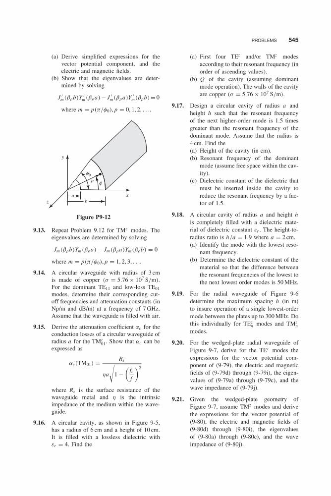
PROBLEMS 545
(a) Derive simplified expressions for thevector potential component, and theelectric and magnetic fields.
(b) Show that the eigenvalues are deter-mined by solving
J ′m(βρb)Y ′
m(βρa)− J ′m(βρa)Y ′
m(βρb) = 0
where m = p(π/φ0), p = 0, 1, 2, . . ..
xb
az
y
fr
f0
Figure P9-12
9.13. Repeat Problem 9.12 for TMz modes. Theeigenvalues are determined by solving
Jm(βρb)Ym(βρa) − Jm(βρa)Ym(βρb) = 0
where m = p(π/φ0), p = 1, 2, 3, . . ..
9.14. A circular waveguide with radius of 3 cmis made of copper (σ = 5.76 × 10⁷ S/m).For the dominant TE11 and low-loss TE01
modes, determine their corresponding cut-off frequencies and attenuation constants (inNp/m and dB/m) at a frequency of 7 GHz.Assume that the waveguide is filled with air.
9.15. Derive the attenuation coefficient αc for theconduction losses of a circular waveguide ofradius a for the TMz
01. Show that αc can beexpressed as
αc(TM01) = Rs
ηa
√1 −
(fcf
)2
where Rs is the surface resistance of thewaveguide metal and η is the intrinsicimpedance of the medium within the wave-guide.
9.16. A circular cavity, as shown in Figure 9-5,has a radius of 6 cm and a height of 10 cm.It is filled with a lossless dielectric withεr = 4. Find the
(a) First four TEz and/or TMz modesaccording to their resonant frequency (inorder of ascending values).
(b) Q of the cavity (assuming dominantmode operation). The walls of the cavityare copper (σ = 5.76 × 10⁷ S/m).
9.17. Design a circular cavity of radius a andheight h such that the resonant frequencyof the next higher-order mode is 1.5 timesgreater than the resonant frequency of thedominant mode. Assume that the radius is4 cm. Find the(a) Height of the cavity (in cm).(b) Resonant frequency of the dominant
mode (assume free space within the cav-ity).
(c) Dielectric constant of the dielectric thatmust be inserted inside the cavity toreduce the resonant frequency by a fac-tor of 1.5.
9.18. A circular cavity of radius a and height his completely filled with a dielectric mate-rial of dielectric constant εr . The height-to-radius ratio is h/a = 1.9 where a = 2 cm.(a) Identify the mode with the lowest reso-
nant frequency.(b) Determine the dielectric constant of the
material so that the difference betweenthe resonant frequencies of the lowest tothe next lowest order modes is 50 MHz.
9.19. For the radial waveguide of Figure 9-6determine the maximum spacing h (in m)to insure operation of a single lowest-ordermode between the plates up to 300 MHz. Dothis individually for TEz
n modes and TMzn
modes.
9.20. For the wedged-plate radial waveguide ofFigure 9-7, derive for the TEz modes theexpressions for the vector potential com-ponent of (9-79), the electric and magneticfields of (9-79d) through (9-79i), the eigen-values of (9-79a) through (9-79c), and thewave impedance of (9-79j).
9.21. Given the wedged-plate geometry ofFigure 9-7, assume TMz modes and derivethe expressions for the vector potential of(9-80), the electric and magnetic fields of(9-80d) through (9-80i), the eigenvaluesof (9-80a) through (9-80c), and the waveimpedance of (9-80j).
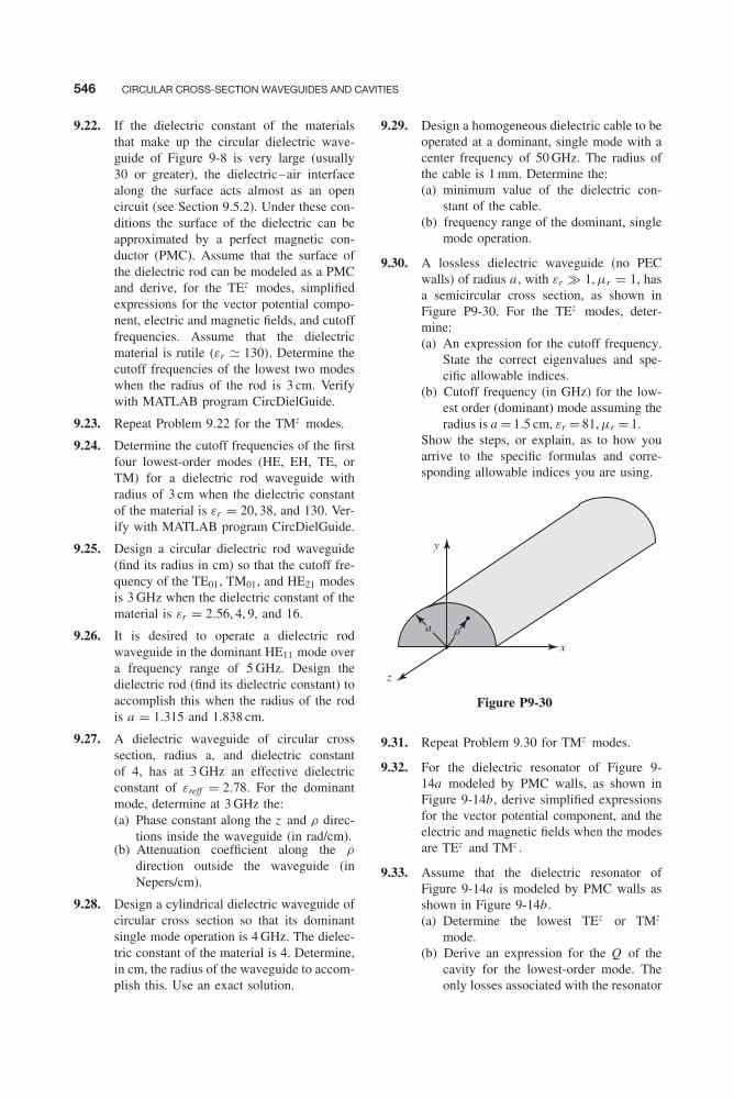
546 CIRCULAR CROSS-SECTION WAVEGUIDES AND CAVITIES
9.22. If the dielectric constant of the materialsthat make up the circular dielectric wave-guide of Figure 9-8 is very large (usually30 or greater), the dielectric–air interfacealong the surface acts almost as an opencircuit (see Section 9.5.2). Under these con-ditions the surface of the dielectric can beapproximated by a perfect magnetic con-ductor (PMC). Assume that the surface ofthe dielectric rod can be modeled as a PMCand derive, for the TEz modes, simplifiedexpressions for the vector potential compo-nent, electric and magnetic fields, and cutofffrequencies. Assume that the dielectricmaterial is rutile (εr � 130). Determine thecutoff frequencies of the lowest two modeswhen the radius of the rod is 3 cm. Verifywith MATLAB program CircDielGuide.
9.23. Repeat Problem 9.22 for the TMz modes.
9.24. Determine the cutoff frequencies of the firstfour lowest-order modes (HE, EH, TE, orTM) for a dielectric rod waveguide withradius of 3 cm when the dielectric constantof the material is εr = 20, 38, and 130. Ver-ify with MATLAB program CircDielGuide.
9.25. Design a circular dielectric rod waveguide(find its radius in cm) so that the cutoff fre-quency of the TE01, TM01, and HE21 modesis 3 GHz when the dielectric constant of thematerial is εr = 2.56, 4, 9, and 16.
9.26. It is desired to operate a dielectric rodwaveguide in the dominant HE11 mode overa frequency range of 5 GHz. Design thedielectric rod (find its dielectric constant) toaccomplish this when the radius of the rodis a = 1.315 and 1.838 cm.
9.27. A dielectric waveguide of circular crosssection, radius a, and dielectric constantof 4, has at 3 GHz an effective dielectricconstant of εreff = 2.78. For the dominantmode, determine at 3 GHz the:(a) Phase constant along the z and ρ direc-
tions inside the waveguide (in rad/cm).(b) Attenuation coefficient along the ρ
direction outside the waveguide (inNepers/cm).
9.28. Design a cylindrical dielectric waveguide ofcircular cross section so that its dominantsingle mode operation is 4 GHz. The dielec-tric constant of the material is 4. Determine,in cm, the radius of the waveguide to accom-plish this. Use an exact solution.
9.29. Design a homogeneous dielectric cable to beoperated at a dominant, single mode with acenter frequency of 50 GHz. The radius ofthe cable is 1 mm. Determine the:(a) minimum value of the dielectric con-
stant of the cable.(b) frequency range of the dominant, single
mode operation.
9.30. A lossless dielectric waveguide (no PECwalls) of radius a , with εr � 1, μr = 1, hasa semicircular cross section, as shown inFigure P9-30. For the TEz modes, deter-mine:(a) An expression for the cutoff frequency.
State the correct eigenvalues and spe-cific allowable indices.
(b) Cutoff frequency (in GHz) for the low-est order (dominant) mode assuming theradius is a = 1.5 cm, εr = 81, μr = 1.
Show the steps, or explain, as to how youarrive to the specific formulas and corre-sponding allowable indices you are using.
y
z
ra
x
Figure P9-30
9.31. Repeat Problem 9.30 for TMz modes.
9.32. For the dielectric resonator of Figure 9-14a modeled by PMC walls, as shown inFigure 9-14b, derive simplified expressionsfor the vector potential component, and theelectric and magnetic fields when the modesare TEz and TMz .
9.33. Assume that the dielectric resonator ofFigure 9-14a is modeled by PMC walls asshown in Figure 9-14b.(a) Determine the lowest TEz or TMz
mode.(b) Derive an expression for the Q of the
cavity for the lowest-order mode. Theonly losses associated with the resonator
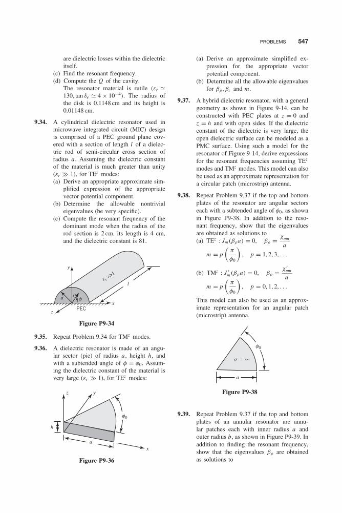
PROBLEMS 547
are dielectric losses within the dielectricitself.
(c) Find the resonant frequency.(d) Compute the Q of the cavity.
The resonator material is rutile (εr �130, tan δe � 4 × 10⁻⁴). The radius ofthe disk is 0.1148 cm and its height is0.01148 cm.
9.34. A cylindrical dielectric resonator used inmicrowave integrated circuit (MIC) designis comprised of a PEC ground plane cov-ered with a section of length l of a dielec-tric rod of semi-circular cross section ofradius a . Assuming the dielectric constantof the material is much greater than unity(εr � 1), for TEz modes:(a) Derive an appropriate approximate sim-
plified expression of the appropriatevector potential component.
(b) Determine the allowable nontrivialeigenvalues (be very specific).
(c) Compute the resonant frequency of thedominant mode when the radius of therod section is 2 cm, its length is 4 cm,and the dielectric constant is 81.
xPEC
z
ar
f
e r >>1
l
y
Figure P9-34
9.35. Repeat Problem 9.34 for TMz modes.
9.36. A dielectric resonator is made of an angu-lar sector (pie) of radius a , height h , andwith a subtended angle of φ = φ0. Assum-ing the dielectric constant of the material isvery large (εr � 1), for TEz modes:
a
h
z
x
y
f0
Figure P9-36
(a) Derive an approximate simplified ex-pression for the appropriate vectorpotential component.
(b) Determine all the allowable eigenvaluesfor βρ , βz and m .
9.37. A hybrid dielectric resonator, with a generalgeometry as shown in Figure 9-14, can beconstructed with PEC plates at z = 0 andz = h and with open sides. If the dielectricconstant of the dielectric is very large, theopen dielectric surface can be modeled as aPMC surface. Using such a model for theresonator of Figure 9-14, derive expressionsfor the resonant frequencies assuming TEz
modes and TMz modes. This model can alsobe used as an approximate representation fora circular patch (microstrip) antenna.
9.38. Repeat Problem 9.37 if the top and bottomplates of the resonator are angular sectorseach with a subtended angle of φ0, as shownin Figure P9-38. In addition to the reso-nant frequency, show that the eigenvaluesare obtained as solutions to(a) TEz : Jm(βρa) = 0, βρ = χmn
a
m = p
(π
φ0
), p = 1, 2, 3, . . .
(b) TMz : J ′m(βρa) = 0, βρ = χ ′
mn
a
m = p
(π
φ0
), p = 0, 1, 2, . . .
This model can also be used as an approx-imate representation for an angular patch(microstrip) antenna.
a
f0
s = ∞
Figure P9-38
9.39. Repeat Problem 9.37 if the top and bottomplates of an annular resonator are annu-lar patches each with inner radius a andouter radius b, as shown in Figure P9-39. Inaddition to finding the resonant frequency,show that the eigenvalues βρ are obtainedas solutions to
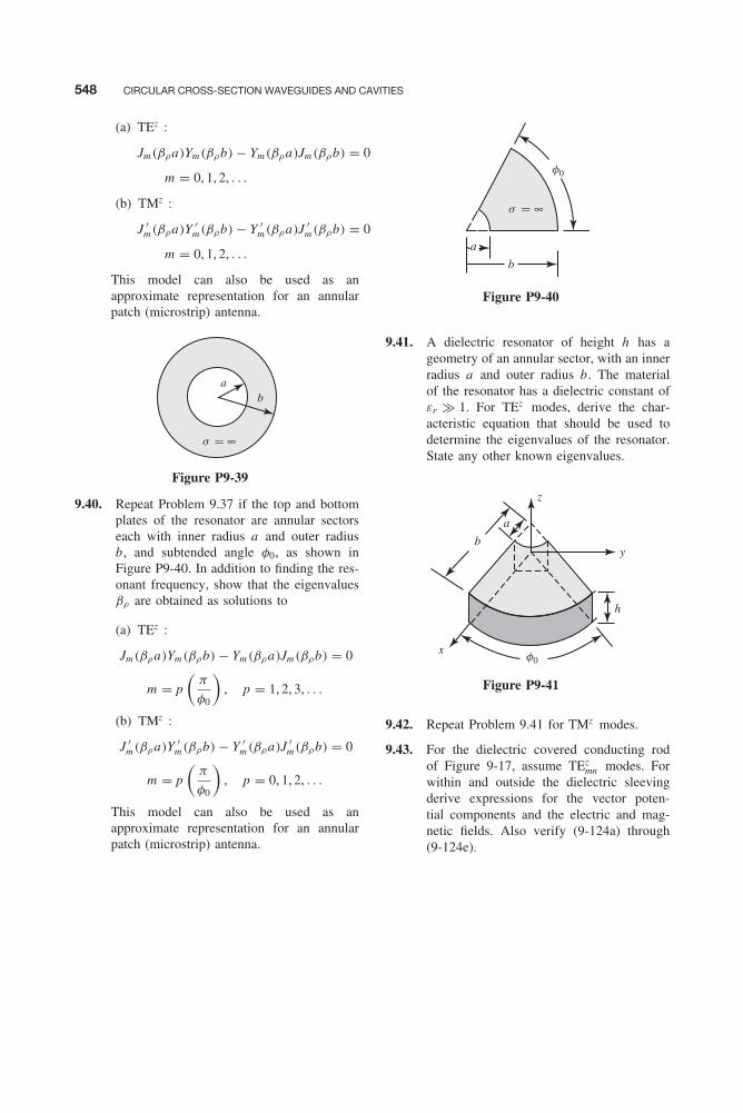
548 CIRCULAR CROSS-SECTION WAVEGUIDES AND CAVITIES
(a) TEz :
Jm(βρa)Ym(βρb) − Ym(βρa)Jm(βρb) = 0
m = 0, 1, 2, . . .
(b) TMz :
J ′m(βρa)Y ′
m(βρb) − Y ′m(βρa)J ′
m(βρb) = 0
m = 0, 1, 2, . . .
This model can also be used as anapproximate representation for an annularpatch (microstrip) antenna.
ab
s = ∞
Figure P9-39
9.40. Repeat Problem 9.37 if the top and bottomplates of the resonator are annular sectorseach with inner radius a and outer radiusb, and subtended angle φ0, as shown inFigure P9-40. In addition to finding the res-onant frequency, show that the eigenvaluesβρ are obtained as solutions to
(a) TEz :
Jm(βρa)Ym(βρb) − Ym(βρa)Jm(βρb) = 0
m = p
(π
φ0
), p = 1, 2, 3, . . .
(b) TMz :
J ′m(βρa)Y ′
m(βρb) − Y ′m(βρa)J ′
m(βρb) = 0
m = p
(π
φ0
), p = 0, 1, 2, . . .
This model can also be used as anapproximate representation for an annularpatch (microstrip) antenna.
b
a
f0
s = ∞
Figure P9-40
9.41. A dielectric resonator of height h has ageometry of an annular sector, with an innerradius a and outer radius b. The materialof the resonator has a dielectric constant ofεr � 1. For TEz modes, derive the char-acteristic equation that should be used todetermine the eigenvalues of the resonator.State any other known eigenvalues.
b
h
y
xf0
a
z
Figure P9-41
9.42. Repeat Problem 9.41 for TMz modes.
9.43. For the dielectric covered conducting rodof Figure 9-17, assume TEz
mn modes. Forwithin and outside the dielectric sleevingderive expressions for the vector poten-tial components and the electric and mag-netic fields. Also verify (9-124a) through(9-124e).

CHAPTER 10Spherical Transmission Lines and Cavities
10.1 INTRODUCTION
Problems involving spherical geometries constitute an important class of electromagneticboundary-value problems that are used to design transmission lines, cavities, antennas, andscatterers. Some of these may be constructed of metallic walls and others may be of dielectricmaterial. In either case, the field configurations that can be supported by the structure can beobtained by analyzing the structure as a boundary-value problem. We will concern ourselveshere with spherical transmission lines and cavities. Scattering by spherical structures will beexamined in Chapter 11.
10.2 CONSTRUCTION OF SOLUTIONS
In Chapter 3, Section 3.4.3, we examined the solution of the scalar wave equation in sphericalcoordinates. It was found that the solution is that of (3-76) where the r , θ , and φ variations takethe following forms.
1. Radial (r) variations of f (r) can be represented by either:a. spherical Bessel functions of the first [jn(βr)] and second [yn(βr)] kind, as given by
(3-87a) [these functions are used to represent standing waves and are related to theregular Bessel functions by (3-90a) and (3-90b)],
b. or spherical Hankel functions of the first [h(1)n (βr)] and second [h(2)
n (βr)] kind, as givenby (3-87b) [these are related to the regular Hankel functions by (3-91a) and (3-91b)].
2. θ variations of g(θ) can be represented by associated Legendre functions of the firstPm
n (cos θ) or second Qmn (cos θ) kind, as given by either (3-88a) or (3-88b).
3. φ variations of h(φ) can be represented by either complex exponentials or cosinusoids asgiven, respectively, by (3-89a) and (3-89b).
It must be remembered, however, that the vector wave equation in spherical coordinates, asgiven by (3-72), does not reduce to three uncoupled scalar Helmholtz wave equations as stated by(3-73a) through (3-73c). Therefore, using the basic approach outlined in Chapter 6, Section 6.5,we cannot construct field solutions that are TEr and/or TMr . Hence, we must look for otherapproaches for finding field configurations that are supported by spherical structures.
549
550 SPHERICAL TRANSMISSION LINES AND CAVITIES
One approach that can be used to find field configurations that are TEz and/or TMz will be torepresent the potential functions by [1]
TEz
A = 0 (10-1a)
F = âz Fz = (âr cos θ − âθ sin θ)Fz (10-1b)
TMz
A = âz Az = (âr cos θ − âθ sin θ)Az (10-2a)
F = 0 (10-2b)
where Fz (r , θ , φ) and Az (r , θ , φ) are solutions to the scalar Helmholtz equation in the sphericalcoordinate system. Other field configurations can be formed as superpositions of TEz and TMz
modes. Although this is a valid approach to the problem, it will not be pursued here; it is assignedto the reader as an end-of-chapter exercise. Instead, an alternate procedure will be outlined forconstruction of TEr and TMr modes.
The procedure outlined in Chapter 6, Sections 6.5.2 and 6.5.3, for the construction, respectively,of TM and TE field configurations was based on the vector potentials A and F, as derived inSections 6.2 and 6.3, respectively, and summarized in Section 6.4. The final forms, which aresummarized in Section 6.4, were based on the selection of the Lorenz conditions of (6-15) and(6-27), or
ψe = − 1
jωμε∇ • A (10-3a)
ψm = − 1
jωμε∇ • F (10-3b)
to represent, respectively, the scalar potential functions ψe and ψm . If that choice was not made,then the relations of the E and H fields to the potentials A and F would take a slightly differentform. These forms will be outlined here.
10.2.1 The Vector Potential F (J = 0, M �= 0)
According to (6-19), the electric field is related to the potential F by
EF = −1
ε∇ × F (10-4)
Away from the source M, the electric and magnetic fields are related by Maxwell’s equation
∇ × EF = −jωμHF (10-5)
or
HF = − 1
jωμ∇ × EF = 1
jωμε∇ × ∇ × F (10-5a)
Therefore, if the potential F can be related to the source (M), then EF and HF can be found using(10-4) and (10-5a). We will attempt to do this next.
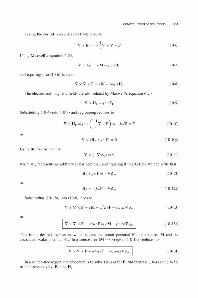
CONSTRUCTION OF SOLUTIONS 551
Taking the curl of both sides of (10-4) leads to
∇ × EF = −1
ε∇ × ∇ × F (10-6)
Using Maxwell’s equation 6-24,
∇ × EF = −M − jωμHF (10-7)
and equating it to (10-6) leads to
∇ × ∇ × F = εM + jωμεHF (10-8)
The electric and magnetic fields are also related by Maxwell’s equation 6-20,
∇ × HF = jωεEF (10-9)
Substituting (10-4) into (10-9) and regrouping reduces to
∇ × HF = jωε
(−1
ε∇ × F
)= −jω∇ × F (10-10)
or∇ × (HF + jωF) = 0 (10-10a)
Using the vector identity∇ × (−∇ψm) = 0 (10-11)
where ψm represents an arbitrary scalar potential, and equating it to (10-10a), we can write that
HF + jωF = −∇ψm (10-12)
orHF = −jωF − ∇ψm (10-12a)
Substituting (10-12a) into (10-8) leads to
∇ × ∇ × F = εM + ω2μεF − jωμε∇ψm (10-13)
or
∇ × ∇ × F − ω2μεF = εM − jωμε∇ψm (10-13a)
This is the desired expression, which relates the vector potential F to the source M and theassociated scalar potential ψm . In a source-free (M = 0) region, (10-13a) reduces to
∇ × ∇ × F − ω2μεF = −jωμε∇ψm (10-14)
In a source-free region, the procedure is to solve (10-14) for F, and then use (10-4) and (10-5a)to find, respectively, EF and HF.
552 SPHERICAL TRANSMISSION LINES AND CAVITIES
10.2.2 The Vector Potential A (J �= 0, M = 0)
Following a procedure similar to the one outlined in Section 10.2.1 for the vector potential F,it can be shown, by referring also to Section 6.2, that the equations for the vector potential Aanalogous to (10-4), (10-5a), and (10-13a), are
HA = 1
μ∇ × A (10-15a)
EA = 1
jωε∇ × HA = 1
jωμε∇ × ∇ × A (10-15b)
∇ × ∇ × A − ω2μεA = μJ − jωμε∇ψe (10-15c)
In a source-free region, (10-15c) reduces to
∇ × ∇ × A − ω2μεA = −jωμε∇ψe (10-15d)
The details are left as end-of-chapter exercises for the reader.In a source-free region, the procedure is to solve (10-15d) for A, and then use (10-15a) and
(10-15b) to find, respectively, HA and EA.
10.2.3 The Vector Potentials F and A
The total fields that are due to both potentials F and A are found as superpositions of the fieldsof Sections 10.2.1 and 10.2.2. Doing this, we have that the total fields are obtained using
E = EF + EA = −1
ε∇ × F + 1
jωε∇ × HA = −1
ε∇ × F + 1
jωμε∇ × ∇ × A (10-16a)
H = HF + HA = − 1
jωμ∇ × EF + 1
μ∇ × A = 1
jωμε∇ × ∇ × F + 1
μ∇ × A (10-16b)
where F and A are, respectively, solutions to
∇ × ∇ × F − ω2μεF = εM − jωμε∇ψm (10-16c)
∇ × ∇ × A − ω2μεA = μJ − jωμε∇ψe (10-16d)
which for a source-free region (M = J = 0) reduce to
∇ × ∇ × F − ω2μεF = −jωμε∇ψm (10-16e)
∇ × ∇ × A − ω2μεA = −jωμε∇ψe (10-16f)
We will attempt now to form TEr and TMr mode field solutions using (10-16a) through (10-16f).
CONSTRUCTION OF SOLUTIONS 553
10.2.4 Transverse Electric (TE) Modes: Source-Free Region
It was stated previously in Section 6.5.3 that TE modes to any direction in any coordinate systemcan be obtained by selecting the vector potential F to have only a nonvanishing component in thatdirection while simultaneously letting A = 0. The nonvanishing component of F was obtained asa solution to the scalar wave equation 6-31. The same procedure will be used here except thatinstead of the nonvanishing component of F being a solution to (6-31), which does not reduce inspherical coordinates to three scalar noncoupled wave equations, it will be a solution to (10-16e).The nonvanishing component of F will be the one that coincides with the direction along whichthe TE modes are desired. Let us construct solutions that are TEr in a spherical coordinate system.
TEr field configurations are constructed by letting the vector potentials F and A be equal to
F = âr Fr (r , θ , φ) (10-17a)
A = 0 (10-17b)
Since Fr is not a solution to the scalar Hemlholtz equation
∇2F = ∇2(âr Fr ) �= âr∇2Fr (10-18)
we will resort, for a source-free region, to (10-16e).Expanding (10-16e) using (10-17a) leads to
∇ × F = ∇ × (âr Fr ) = âθ
1
r sin θ
∂Fr
∂φ− âφ
1
r
∂Fr
∂θ(10-19a)
∇ × ∇ × F = âr
{1
r sin θ
[∂
∂θ
(− sin θ
r
∂Fr
∂θ
)− ∂
∂φ
(1
r sin θ
∂Fr
∂φ
)]}+ âθ
[1
r
(∂2Fr
∂r ∂θ
)]+ âφ
(1
r sin θ
∂2Fr
∂r ∂φ
)(10-19b)
∇ψm = âr∂ψm
∂r+ âθ
1
r
∂ψm
∂θ+ âφ
1
r sin θ
∂ψm
∂φ(10-19c)
Thus for the r , θ , and φ components, (10-16e) reduces to
1
r sin θ
[− ∂
∂θ
(sin θ
r
∂Fr
∂θ
)− ∂
∂φ
(1
r sin θ
∂Fr
∂φ
)]− β2Fr = −jωμε
∂ψm
∂r(10-20a)
1
r
∂2Fr
∂r ∂θ= −j
ωμε
r
∂ψm
∂θ⇒ ∂2Fr
∂r ∂θ= ∂
∂θ
(∂Fr
∂r
)= ∂
∂θ(−jωμεψm) (10-20b)
1
r sin θ
∂2Fr
∂r ∂φ= −j
ωμε
r sin θ
∂ψm
∂φ⇒ ∂2Fr
∂r ∂φ= ∂
∂φ
(∂Fr
∂r
)= ∂
∂φ(−jωμεψm) (10-20c)
where β2 = ω2με. The last two equations, (10-20b) and (10-20c), are satisfied simultaneouslyif
∂Fr
∂r= −jωμεψm ⇒ ψm = − 1
jωμε
∂Fr
∂r(10-21)

554 SPHERICAL TRANSMISSION LINES AND CAVITIES
With the preceding relation for the scalar potential ψm , we need to find an uncoupled differ-ential equation for Fr . To do this, we substitute (10-21) into (10-20a), which leads to
− 1
r2 sin θ
∂
∂θ
(sin θ
∂Fr
∂θ
)− 1
r2 sin2 θ
∂2Fr
∂φ2− β2Fr = ∂2Fr
∂r2(10-22)
or∂2Fr
∂r2+ 1
r2 sin θ
∂
∂θ
(sin θ
∂Fr
∂θ
)+ 1
r2 sin2 θ
∂2Fr
∂φ2+ β2Fr = 0 (10-22a)
which can also be written in succinct form as
(∇2 + β2)Fr
r= 0 (10-22b)
Therefore, using this procedure, the ratio Fr/r satisfies the scalar Helmholtz wave equation butnot Fr itself. A solution of Fr using (10-22b) allows us to find EF and HF using, respectively,(10-4) and (10-5a).
The solution of (10-22b) will be pursued in Section 10.2.6. In the meantime, the electric andmagnetic field components can be written in terms of Fr by expanding (10-4) and (10-5a):
TEr (F = âr Fr , A = 0)
EF = −1
ε∇ × F (10-23)
or
Er = 0 (10-23a)
Eθ = −1
ε
1
r sin θ
∂Fr
∂φ(10-23b)
Eφ = 1
ε
1
r
∂Fr
∂θ(10-23c)
HF = 1
jωμε∇ × ∇ × F (10-24)
or
Hr = 1
jωμε
(∂2
∂r2+ β2
)Fr (10-24a)
Hθ = 1
jωμε
1
r
∂2Fr
∂r ∂θ(10-24b)
Hφ = 1
jωμε
1
r sin θ
∂2Fr
∂r ∂φ(10-24c)
where Fr/r is a solution to (10-22b).
CONSTRUCTION OF SOLUTIONS 555
10.2.5 Transverse Magnetic (TM) Modes: Source-Free Region
Following a procedure similar to the one outlined in the previous section for the TEr modes, itcan be shown that the TMr fields in spherical coordinates can be constructed by letting the vectorpotentials F and A be equal to
F = 0 (10-25a)
A = âr Ar (r , θ , φ) (10-25b)
where the ratio Ar/r , and not Ar , is a solution to the scalar Helmholtz wave equation
(∇2 + β2)Ar
r= 0 (10-26)
The solution of (10-26) will be pursued in Section 10.2.6. In the meantime, the electric andmagnetic field components can be written in terms of Ar , by expanding (10-15b) and (10-15a),as
TMr (F = 0, A = âr Ar )
EA = 1
jωμε∇ × ∇ × A (10-27)
or
Er = 1
jωμε
(∂2
∂r2+ β2
)Ar (10-27a)
Eθ = 1
jωμε
1
r
∂2Ar
∂r ∂θ(10-27b)
Eφ = 1
jωμε
1
r sin θ
∂2Ar
∂r ∂φ(10-27c)
HA = 1
μ∇ × A (10-28)
or
Hr = 0 (10-28a)
Hθ = 1
μ
1
r sin θ
∂Ar
∂φ(10-28b)
Hφ = − 1
μ
1
r
∂Ar
∂θ(10-28c)
where Ar/r is a solution to (10-26).
556 SPHERICAL TRANSMISSION LINES AND CAVITIES
10.2.6 Solution of the Scalar Helmholtz Wave Equation
To find the TEr and/or TMr field of Sections 10.2.4 and 10.2.5 as given, respectively, by(10-23) through (10-24c) and (10-27) through (10-28c), solutions to the scalar Helmholtz waveequations 10-22b and 10-26 must be obtained for Fr/r and Ar/r (and thus, Fr and Ar ). Bothsolutions are of the same form
(∇2 + β2)ψ = 0 (10-29)
where
ψ =
⎧⎪⎪⎨⎪⎪⎩Fr
rfor TEr modes
Ar
rfor TMr modes
(10-29a)
(10-29b)
Since the solution of ψ from (10-29) must be multiplied by r to obtain solutions for Fr or Ar ,then appropriate solutions for Fr and Ar must be equal to the product of rψ . The solution for Fr
or Ar of (10-29) through (10-29b) must take the separable form of
Fr (r , θ , φ)
Ar (r , θ , φ)
}= f (r)g(θ)h(φ) (10-30)
where f (r), g(θ), and h(φ) must be represented by appropriate wave functions that satisfy thewave equation in spherical coordinates. According to (3-88a) or (3-88b), g(θ) can be representedby associated Legendre functions of the first kind Pm
n (cos θ), or second kind Qmn (cos θ), whereas
h(φ) can be represented by either complex exponentials or cosinusoids as given, respectively, by(3-89a) and (3-89b).
Since the solution of ψ as given by (10-29) must be multiplied by r in order to obtain solutionsto Fr and Ar as given by (10-30), it is most convenient to represent f (r) not by spherical Bessel[jn(βr), yn(βr)] or Hankel [h(1)
n (βr), h(2)n (βr)] functions, but by another form of spherical Bessel
and Hankel functions denoted by B̂n(βr) [for either Ĵn(βr), Ŷn(βr), Ĥ (1)n (βr) or Ĥ (2)
n (βr)]. Theseare related to the regular spherical Bessel and Hankel functions denoted by bn(βr) [for eitherjn(βr), yn(βr), h(1)
n (βr) or h(2)n (βr)] by
B̂n(βr) = βr bn(βr) = βr√
π
2βrBn+1/2(βr) =
√πβr
2Bn+1/2(βr) (10-31)
where Bn+1/2(βr) is used to represent the regular cylindrical Bessel or Hankel functions ofJn+1/2(βr), Yn+1/2(βr), H (1)
n+1/2(βr) and H (2)n+1/2(βr). These new spherical Bessel and Hankel
functions were introduced by Schelkunoff [2] and satisfy the differential equation[d2
dr2+ β2 − n(n + 1)
r2
]B̂n = 0 (10-32)
which is obtained by substituting bn(βr) = B̂n(βr)/βr in
d
dr
(r2 dbn
dr
)+ [(βr)2 − n(n + 1)]bn = 0 (10-33)
Therefore, the solutions for f (r) of (10-30) are of the new form of spherical Bessel or Hankelfunctions denoted by
f1(r) = A1Ĵn(βr) + B1Ŷn(βr) (10-34a)
orf2(r) = C1Ĥ (1)
n (βr) + D1Ĥ (2)n (βr) (10-34b)
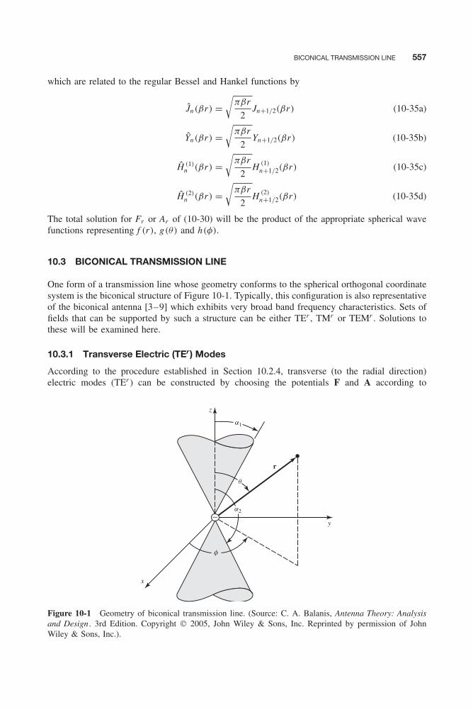
BICONICAL TRANSMISSION LINE 557
which are related to the regular Bessel and Hankel functions by
Ĵn(βr) =√
πβr
2Jn+1/2(βr) (10-35a)
Ŷn(βr) =√
πβr
2Yn+1/2(βr) (10-35b)
Ĥ (1)n (βr) =
√πβr
2H (1)
n+1/2(βr) (10-35c)
Ĥ (2)n (βr) =
√πβr
2H (2)
n+1/2(βr) (10-35d)
The total solution for Fr or Ar of (10-30) will be the product of the appropriate spherical wavefunctions representing f (r), g(θ) and h(φ).
10.3 BICONICAL TRANSMISSION LINE
One form of a transmission line whose geometry conforms to the spherical orthogonal coordinatesystem is the biconical structure of Figure 10-1. Typically, this configuration is also representativeof the biconical antenna [3–9] which exhibits very broad band frequency characteristics. Sets offields that can be supported by such a structure can be either TEr , TMr or TEMr . Solutions tothese will be examined here.
10.3.1 Transverse Electric (TEr) Modes
According to the procedure established in Section 10.2.4, transverse (to the radial direction)electric modes (TEr ) can be constructed by choosing the potentials F and A according to
a1
a2
q
z
y
x
r
f
Figure 10-1 Geometry of biconical transmission line. (Source: C. A. Balanis, Antenna Theory: Analysisand Design . 3rd Edition. Copyright © 2005, John Wiley & Sons, Inc. Reprinted by permission of JohnWiley & Sons, Inc.).
558 SPHERICAL TRANSMISSION LINES AND CAVITIES
(10-17a) and (10-17b). The scalar component Fr of the vector potential must satisfy the vectorwave equation (10-22b), whose solution takes the form of (3-85), or
Fr (r , θ , φ) = f (r)g(θ)h(φ) (10-36)
where
f (r) = a solution to (10-32) as given by either (10-34a) or (10-34b) [the form (10-34b) ischosen here]
g(θ) = a solution of (3-86b) as given by either (3-88a) or (3-88b) [the form (3-88a) is chosenhere]
h(φ) = is a solution to (3-86c) as given by (3-89a) or (3-89b) [the form (3-89b) is chosenhere to represent standing waves]
Therefore, Fr of (10-36) can be written, assuming the source is placed at the apex and is generatingoutwardly traveling waves [C1 = 0 in (10-34b)], as
[Fr (r , θ , φ)]mn = D1Ĥ (2)n (βr)[A2Pm
n (cos θ) + B2Pmn (− cos θ)]
×[C3 cos(mφ) + D3 sin(mφ)] (10-37)
where m = nonnegative integer (m = 0, 1, 2, . . .).The corresponding electric and magnetic fields can be found using (10-23) through (10-24c)
and the eigenvalues of n can be determined by applying the boundary conditions
Eφ(0 ≤ r ≤ ∞, θ = α1, 0 ≤ φ ≤ 2π) = Eφ(0 ≤ r ≤ ∞, θ = α2, 0 ≤ φ ≤ 2π) = 0 (10-38)
According to (10-23c),
Eφ = 1
ε
1
r
∂Fr
∂θ= D1
ε
1
rĤ (2)
n (βr)
[A2
dPmn (cos θ)
dθ+ B2
dPmn (− cos θ)
dθ
]×[C3 cos(mφ) + D3 sin(mφ)] (10-39)
Applying the first boundary condition of (10-38) leads to
Eφ(0 ≤ r ≤ ∞, θ = α1, 0 ≤ φ ≤ 2π)
= D1
ε
1
rĤ (2)
n (βr)
[A2
dPmn (cos θ)
dθ+ B2
dPmn (− cos θ)
dθ
]θ=α1
×[C3 cos(mφ) + D3 sin(mφ)] = 0
Eφ(0 ≤ r ≤ ∞, θ = α1, 0 ≤ φ ≤ 2π)
= D1
ε
1
rĤ (2)
n (βr)
[A2
dPmn (cos α1)
dα1+ B2
dPmn (− cos α1)
dα1
]×[C3 cos(mφ) + D3 sin(mφ)] = 0 (10-40a)
and the second boundary condition of (10-38) leads to
Eφ(0 ≤ r ≤ ∞, θ = α2, 0 ≤ φ ≤ 2π)
= D1
ε
1
rĤ (2)
n (βr)
[A2
dPmn (cos α2)
dα2+ B2
dPmn (− cos α2)
dα2
]×[C3 cos(mφ) + D3 sin(mφ)] = 0 (10-40b)

BICONICAL TRANSMISSION LINE 559
Equations 10-40a and 10-40b reduce to
A2dPm
n (cos α1)
dα1+ B2
dPmn (− cos α1)
dα1= 0 (10-41a)
A2dPm
n (cos α2)
dα2+ B2
dPmn (− cos α2)
dα2= 0 (10-41b)
which are satisfied provided the determinant of (10-41a) and (10-41b) vanishes, that is
dPmn (cos α1)
dα1
dPmn (− cos α2)
dα2− dPm
n (− cos α1)
dα1
dPmn (cos α2)
dα2= 0 (10-42)
Therefore, the eigenvalues of n are found as solutions to (10-42), which usually is not necessarilya very easy task.
10.3.2 Transverse Magnetic (TMr) Modes
Following a procedure similar to that of the previous section and using the formulations ofSection 10.2.5, it can be shown that for TMr modes the potential component Ar of (10-26)reduces to
[Ar (r , θ , φ)]mn = D1Ĥ (2)n (βr)[A2Pm
n (cos θ) + B2Pmn (− cos θ)]
×[C3 cos(mφ) + D3 sin(mφ)] (10-43)
where m = integer (m = 0, 1, 2, . . .). The values of n are determined by applying the boundaryconditions.
The corresponding electric and magnetic fields are obtained using (10-27) through (10-28c).By applying the boundary conditions
Er (0 ≤ r ≤ ∞, θ = α1, 0 ≤ φ ≤ 2π) = Er (0 ≤ r ≤ ∞, θ = α2, 0 ≤ φ ≤ 2π) = 0 (10-44a)
or
Eφ(0 ≤ r ≤ ∞, θ = α1, 0 ≤ φ ≤ 2π) = Eφ(0 ≤ r ≤ ∞, θ = α2, 0 ≤ φ ≤ 2π) = 0 (10-44b)
it can be shown that the eigenvalues of n are obtained as solutions to
Pmn (cos α1)P
mn (− cos α2) − Pm
n (− cos α1)Pmn (cos α2) = 0 (10-45)
This usually is not necessarily a very easy task.
10.3.3 Transverse Electromagnetic (TEMr) Modes
The lowest-order (dominant) mode of the biconical transmission line is the one for which m = 0and n = 0. For this mode both (10-42) and (10-45) are satisfied and the potential componentsof (10-37) and (10-43) vanish. However, for m = n = 0, (10-43) could be redefined as the limitas n → 0. Instead, it is usually more convenient to alternately represent the TEM mode by theTM00 which is defined, using (3-88b) to represent g(θ), by [1]
(Ar )00 = B00Ĥ (2)0 (βr)Q0(cos θ) (10-46)
560 SPHERICAL TRANSMISSION LINES AND CAVITIES
since P00 (cos θ) = P0(cos θ) = 1. The Legendre polynomial Q0(cos θ) can also be represented
by
Q0(cos θ) = ln
[cot
(θ
2
)](10-47a)
and the spherical Hankel function Ĥ (2)0 (βr) can be replaced by its asymptotic form for large
arguments of
Ĥ (2)0 (βr)
βr→large� je−jβr (10-47b)
Using (10-47a) and (10-47b) reduces (10-46), for large observational distances (βr → large), to
(Ar )00 � jB00 ln
[cot
(θ
2
)]e−jβr (10-48)
The corresponding electric and magnetic field components are given, according to (10-27)through (10-28c), by [3]
Er = 1
jωμε
(∂2
∂r2+ β2
)Ar � 0 (10-49a)
Eθ = 1
jωμε
1
r
∂2Ar
∂r ∂θ= jB00
β
ωμε
1
r
1
sin θe−jβr (10-49b)
Eφ = 1
jωμε
1
r sin θ
∂2Ar
∂r ∂φ= 0 (10-49c)
Hr = 0 (10-49d)
Hθ = 1
μ
1
r sin θ
∂Ar
∂φ= 0 (10-49e)
Hφ = − 1
μ
1
r
∂Ar
∂θ= jB00
1
μr sin θe−jβr (10-49f)
Using these equations, we can write the wave impedance in the radial direction as
Z +rw = Eθ
Hφ
= β
ωε=
√μ
ε= η (10-50)
which is the same as the intrinsic impedance of the medium.An impedance of greater interest is the characteristic impedance that is defined in terms of
voltages and currents. The voltage between two corresponding points on the cones, a distance rfrom the origin, is found by
V (r) =∫ α2
α1
E • d� =∫ α2
α1
(âθEθ ) • (âθ r dθ)
=∫ α2
α1
Eθ rdθ = jB00βe−jβr
ωμε
∫ α2
α1
dθ
sin(θ)
V (r) = jB00βe−jβr
ωμεln
⎡⎢⎣cot(α1
2
)cot
(α2
2
)⎤⎥⎦ (10-51a)
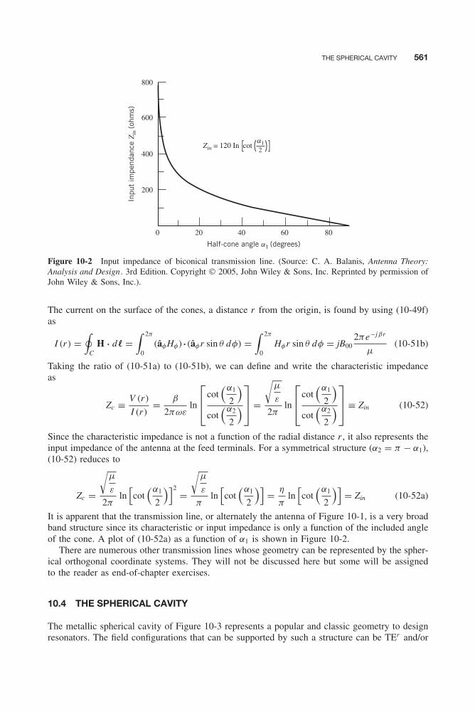
THE SPHERICAL CAVITY 561
a1
Inpu
t im
pend
ance
Zin
(ohm
s)
Half-cone angle a1 (degrees)
Zin = 120 In cot
800
600
400
200
20 40 60 800
2
Figure 10-2 Input impedance of biconical transmission line. (Source: C. A. Balanis, Antenna Theory:Analysis and Design . 3rd Edition. Copyright © 2005, John Wiley & Sons, Inc. Reprinted by permission ofJohn Wiley & Sons, Inc.).
The current on the surface of the cones, a distance r from the origin, is found by using (10-49f)as
I (r) =∮
CH • d� =
∫ 2π
0(âφHφ) • (âφr sin θ dφ) =
∫ 2π
0Hφr sin θ dφ = jB00
2πe−jβr
μ(10-51b)
Taking the ratio of (10-51a) to (10-51b), we can define and write the characteristic impedanceas
Zc ≡ V (r)
I (r)= β
2πωεln
⎡⎢⎣cot(α1
2
)cot
(α2
2
)⎤⎥⎦ =
√μ
ε
2πln
⎡⎢⎣cot(α1
2
)cot
(α2
2
)⎤⎥⎦ ≡ Zin (10-52)
Since the characteristic impedance is not a function of the radial distance r , it also represents theinput impedance of the antenna at the feed terminals. For a symmetrical structure (α2 = π − α1),(10-52) reduces to
Zc =
√μ
ε
2πln
[cot
(α1
2
)]2=
√μ
ε
πln
[cot
(α1
2
)]= η
πln
[cot
(α1
2
)]= Zin (10-52a)
It is apparent that the transmission line, or alternately the antenna of Figure 10-1, is a very broadband structure since its characteristic or input impedance is only a function of the included angleof the cone. A plot of (10-52a) as a function of α1 is shown in Figure 10-2.
There are numerous other transmission lines whose geometry can be represented by the spher-ical orthogonal coordinate systems. They will not be discussed here but some will be assignedto the reader as end-of-chapter exercises.
10.4 THE SPHERICAL CAVITY
The metallic spherical cavity of Figure 10-3 represents a popular and classic geometry to designresonators. The field configurations that can be supported by such a structure can be TEr and/or
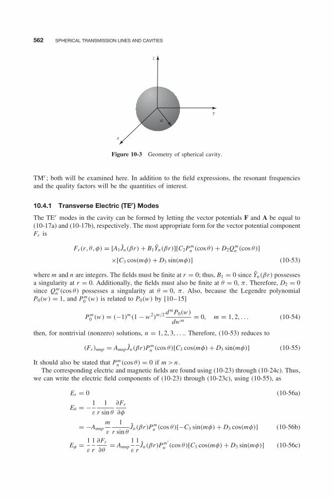
562 SPHERICAL TRANSMISSION LINES AND CAVITIES
x
z
y
a
Figure 10-3 Geometry of spherical cavity.
TMr ; both will be examined here. In addition to the field expressions, the resonant frequenciesand the quality factors will be the quantities of interest.
10.4.1 Transverse Electric (TEr) Modes
The TEr modes in the cavity can be formed by letting the vector potentials F and A be equal to(10-17a) and (10-17b), respectively. The most appropriate form for the vector potential componentFr is
Fr (r , θ , φ) = [A1Ĵn(βr) + B1Ŷn(βr)][C2Pmn (cos θ) + D2Qm
n (cos θ)]
×[C3 cos(mφ) + D3 sin(mφ)] (10-53)
where m and n are integers. The fields must be finite at r = 0; thus, B1 = 0 since Ŷn(βr) possessesa singularity at r = 0. Additionally, the fields must also be finite at θ = 0, π . Therefore, D2 = 0since Qm
n (cos θ) possesses a singularity at θ = 0, π . Also, because the Legendre polynomialP0(w) = 1, and Pm
0 (w) is related to P0(w) by [10–15]
Pm0 (w) = (−1)m(1 − w 2)m/2 dmP0(w)
dw m= 0, m = 1, 2, . . . (10-54)
then, for nontrivial (nonzero) solutions, n = 1, 2, 3, . . .. Therefore, (10-53) reduces to
(Fr )mnp = Amnp Ĵn(βr)Pmn (cos θ)[C3 cos(mφ) + D3 sin(mφ)] (10-55)
It should also be stated that Pmn (cos θ) = 0 if m > n .
The corresponding electric and magnetic fields are found using (10-23) through (10-24c). Thus,we can write the electric field components of (10-23) through (10-23c), using (10-55), as
Er = 0 (10-56a)
Eθ = −1
ε
1
r sin θ
∂Fr
∂φ
= −Amnpm
ε
1
r sin θĴn(βr)Pm
n (cos θ)[−C3 sin(mφ) + D3 cos(mφ)] (10-56b)
Eφ = 1
ε
1
r
∂Fr
∂θ= Amnp
1
ε
1
rĴn(βr)Pm ′
n (cos θ)[C3 cos(mφ) + D3 sin(mφ)] (10-56c)
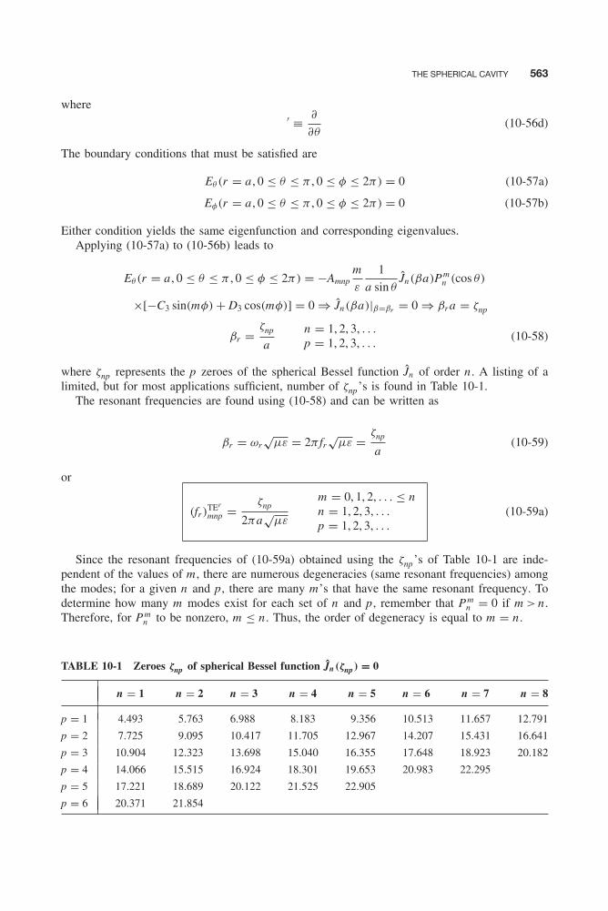
THE SPHERICAL CAVITY 563
where′ ≡ ∂
∂θ(10-56d)
The boundary conditions that must be satisfied are
Eθ (r = a , 0 ≤ θ ≤ π , 0 ≤ φ ≤ 2π) = 0 (10-57a)
Eφ(r = a , 0 ≤ θ ≤ π , 0 ≤ φ ≤ 2π) = 0 (10-57b)
Either condition yields the same eigenfunction and corresponding eigenvalues.Applying (10-57a) to (10-56b) leads to
Eθ (r = a , 0 ≤ θ ≤ π , 0 ≤ φ ≤ 2π) = −Amnpm
ε
1
a sin θĴn(βa)Pm
n (cos θ)
×[−C3 sin(mφ) + D3 cos(mφ)] = 0 ⇒ Ĵn(βa)|β=βr = 0 ⇒ βr a = ζnp
βr = ζnp
an = 1, 2, 3, . . .p = 1, 2, 3, . . .
(10-58)
where ζnp represents the p zeroes of the spherical Bessel function Ĵn of order n . A listing of alimited, but for most applications sufficient, number of ζnp’s is found in Table 10-1.
The resonant frequencies are found using (10-58) and can be written as
βr = ωr√
με = 2π fr√
με = ζnp
a(10-59)
or
(fr )TEr
mnp = ζnp
2πa√
με
m = 0, 1, 2, . . . ≤ nn = 1, 2, 3, . . .p = 1, 2, 3, . . .
(10-59a)
Since the resonant frequencies of (10-59a) obtained using the ζnp’s of Table 10-1 are inde-pendent of the values of m , there are numerous degeneracies (same resonant frequencies) amongthe modes; for a given n and p, there are many m’s that have the same resonant frequency. Todetermine how many m modes exist for each set of n and p, remember that Pm
n = 0 if m > n .Therefore, for Pm
n to be nonzero, m ≤ n . Thus, the order of degeneracy is equal to m = n .
TABLE 10-1 Zeroes ζnp of spherical Bessel function Ĵn(ζnp) = 0
n = 1 n = 2 n = 3 n = 4 n = 5 n = 6 n = 7 n = 8
p = 1 4.493 5.763 6.988 8.183 9.356 10.513 11.657 12.791
p = 2 7.725 9.095 10.417 11.705 12.967 14.207 15.431 16.641
p = 3 10.904 12.323 13.698 15.040 16.355 17.648 18.923 20.182
p = 4 14.066 15.515 16.924 18.301 19.653 20.983 22.295
p = 5 17.221 18.689 20.122 21.525 22.905
p = 6 20.371 21.854
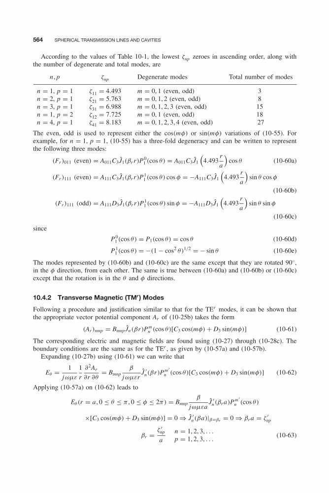
564 SPHERICAL TRANSMISSION LINES AND CAVITIES
According to the values of Table 10-1, the lowest ζnp zeroes in ascending order, along withthe number of degenerate and total modes, are
n , p ζnp Degenerate modes Total number of modes
n = 1, p = 1 ζ11 = 4.493 m = 0, 1 (even, odd) 3n = 2, p = 1 ζ21 = 5.763 m = 0, 1, 2 (even, odd) 8n = 3, p = 1 ζ31 = 6.988 m = 0, 1, 2, 3 (even, odd) 15n = 1, p = 2 ζ12 = 7.725 m = 0, 1 (even, odd) 18n = 4, p = 1 ζ41 = 8.183 m = 0, 1, 2, 3, 4 (even, odd) 27
The even, odd is used to represent either the cos(mφ) or sin(mφ) variations of (10-55). Forexample, for n = 1, p = 1, (10-55) has a three-fold degeneracy and can be written to representthe following three modes:
(Fr )011 (even) = A011C3Ĵ1(βr r)P01 (cos θ) = A011C3Ĵ1
(4.493
r
a
)cos θ (10-60a)
(Fr )111 (even) = A111C3Ĵ1(βr r)P11 (cos θ) cos φ = −A111C3Ĵ1
(4.493
r
a
)sin θ cos φ
(10-60b)
(Fr )111 (odd) = A111D3Ĵ1(βr r)P11 (cos θ) sin φ = −A111D3Ĵ1
(4.493
r
a
)sin θ sin φ
(10-60c)
since
P01 (cos θ) = P1(cos θ) = cos θ (10-60d)
P11 (cos θ) = −(1 − cos2 θ)1/2 = − sin θ (10-60e)
The modes represented by (10-60b) and (10-60c) are the same except that they are rotated 90◦,in the φ direction, from each other. The same is true between (10-60a) and (10-60b) or (10-60c)except that the rotation is in the θ and φ directions.
10.4.2 Transverse Magnetic (TMr) Modes
Following a procedure and justification similar to that for the TEr modes, it can be shown thatthe appropriate vector potential component Ar of (10-25b) takes the form
(Ar )mnp = Bmnp Ĵn(βr)Pmn (cos θ)[C3 cos(mφ) + D3 sin(mφ)] (10-61)
The corresponding electric and magnetic fields are found using (10-27) through (10-28c). Theboundary conditions are the same as for the TEr , as given by (10-57a) and (10-57b).
Expanding (10-27b) using (10-61) we can write that
Eθ = 1
jωμε
1
r
∂2Ar
∂r ∂θ= Bmnp
β
jωμεrĴ ′
n(βr)Pm ′n (cos θ)[C3 cos(mφ) + D3 sin(mφ)] (10-62)
Applying (10-57a) on (10-62) leads to
Eθ (r = a , 0 ≤ θ ≤ π , 0 ≤ φ ≤ 2π) = Bmnpβ
jωμεaĴ ′
n(βr a)Pm ′n (cos θ)
×[C3 cos(mφ) + D3 sin(mφ)] = 0 ⇒ Ĵ ′n(βa)|β=βr = 0 ⇒ βr a = ζ ′
np
βr = ζ ′np
an = 1, 2, 3, . . .p = 1, 2, 3, . . .
(10-63)
THE SPHERICAL CAVITY 565
TABLE 10-2 Zeroes ζ ′np of derivative of spherical Bessel function Ĵ ′
n(ζ ′np) = 0
n = 1 n = 2 n = 3 n = 4 n = 5 n = 6 n = 7 n = 8
p = 1 2.744 3.870 4.973 6.062 7.140 8.211 9.275 10.335
p = 2 6.117 7.443 8.722 9.968 11.189 12.391 13.579 14.753
p = 3 9.317 10.713 12.064 13.380 14.670 15.939 17.190 18.425
p = 4 12.486 13.921 15.314 16.674 18.009 19.321 20.615 21.894
p = 5 15.644 17.103 18.524 19.915 21.281 22.626
p = 6 18.796 20.272 21.714 23.128
p = 7 21.946
where ζ ′np represents the p zeroes of the derivative of the spherical Bessel function Ĵ ′
n of order n .A listing of a limited, but for most applications sufficient, number of ζ ′
np’s is found in Table 10-2.The resonant frequencies are found using (10-63) and can be written as
(fr )TMr
mnp = ζ ′np
2πa√
με
m = 0, 1, 2, . . . ≤ nn = 1, 2, 3, . . .p = 1, 2, 3, . . .
(10-64)
As with the TEr modes, there are numerous degeneracies among the modes since the resonantfrequencies determined by (10-64) are independent of m . For a given n , the order of degeneracyis m = n .
According to the values of Table 10-2, the lowest ζ ′np zeroes in ascending order, along with
the number of degenerate and total modes, are
n , p ζ ′np Degenerate modes Total number of modes
n = 1, p = 1 ζ ′11 = 2.744 m = 0, 1 (even, odd) 3
n = 2, p = 1 ζ ′21 = 3.870 m = 0, 1, 2 (even, odd) 8
n = 3, p = 1 ζ ′31 = 4.973 m = 0, 1, 2, 3 (even, odd) 15
n = 4, p = 1 ζ ′41 = 6.062 m = 0, 1, 2, 3, 4 (even, odd) 24
n = 1, p = 2 ζ ′12 = 6.117 m = 0, 1 (even, odd) 27
The lowest-order mode is the one found using n = 1, p = 1, and it has a three-fold degeneracy[m = 0 (even), m = 1 (even), and m = 1 (odd)]. For these, (10-61) reduces to
(Ar )011 (even) = B011C3Ĵ1(βr r)P01 (cos θ) = B011C3Ĵ1
(2.744
r
a
)cos θ (10-65a)
(Ar )111 (even) = B111C3Ĵ1(βr r)P11 (cos θ) cos φ = −B111C3Ĵ1
(2.744
r
a
)sin θ cos φ
(10-65b)
(Ar )111 (odd) = B111D3Ĵ1(βr r)P11 (cos θ) sin φ = −B111D3Ĵ1
(2.744
r
a
)sin θ sin φ
(10-65c)
566 SPHERICAL TRANSMISSION LINES AND CAVITIES
Example 10-1
For a spherical cavity of a 3-cm radius and filled with air, determine the resonant frequencies (inascending order) of the first 11 modes (including degenerate modes).
Solution: According to (10-59a) and (10-64), using the values of ζnp and ζ ′np from Tables 10-1 and
10-2, and taking into account the degeneracy of the modes in m as well as the even and odd forms inφ, we can write the resonant frequencies of the first 11 modes as
1, 2, 3:(fr )
TM011 (even) = (fr )
TM111 (even) = (fr )
TM111 (odd)
= 2.744(30 × 109)
2π(3)= 4.367 × 10⁹ Hz
4, 5, 6, 7, 8:(fr )
TM021 (even) = (fr )
TM121 (even) = (fr )
TM121 (odd) = (fr )
TM221 (even)
= (fr )TM221 (odd) = 3.870(30 × 109)
2π(3)= 6.1593 × 10⁹ Hz
9, 10, 11:(fr )
TE011 (even) = (fr )
TE111 (even) = (fr )
TE111 (odd)
= 4.493(30 × 109)
2π(3)= 7.1508 × 10⁹ Hz
10.4.3 Quality Factor Q
As has already been pointed, the Q of the cavity is probably one of its most important parameters,and it is defined by (8-84). To derive the equation for the Q of any mode of a spherical cavity isa most difficult task. However, it is instructive to consider that of the lowest (dominant) mode,which here is any one of the three-fold degenerate modes TM011 (even), TM111 (even) or TM111
(odd). Let us consider the TM011 (even) mode.For the TM011 (even) mode the potential function of (10-61) reduces to that of (10-65a), which
can be written as(Ar )011 = B ′
011Ĵ1
(2.744
r
a
)cos θ (10-66)
Since the Q of the cavity is defined by (8-84), it is most convenient to find the stored energyand dissipated power by using the magnetic field, since it has only one nonzero component (theelectric field has two).
The magnetic field components of the TM011 mode can be written using (10-28a) through(10-28c) and (10-66) as
Hr = 0 (10-67a)
Hθ = 1
μ
1
r sin θ
∂Ar
∂φ= 0 (10-67b)
Hφ = − 1
μ
1
r
∂Ar
∂θ= B ′
0111
μ
1
rĴ1
(2.744
r
a
)sin θ (10-67c)
Therefore, at resonance, the total stored energy can be found using
W = 2We = 2Wm = 2
[μ
4
∫∫∫V
|H|2 dv
]= μ
2
∫ 2π
0
∫ π
0
∫ a
0|Hφ|2r2 sin θ dr dθ dφ (10-68)
THE SPHERICAL CAVITY 567
which, by substituting (10-67c), reduces to
W = |B ′011|22μ
∫ 2π
0
∫ π
0
∫ a
0Ĵ 2
1
(2.744
r
a
)sin3 θ dr dθ dφ
= |B ′011|22μ
(2π)4
3
∫ a
0Ĵ 2
1
(2.744
r
a
)dr (10-68a)
The integral can be evaluated using the formula∫ a
0Ĵ 2
1
(2.744
r
a
)dr = a
2
[Ĵ 2
1 (2.744) − Ĵ0(2.744) Ĵ2(2.744)]
(10-69)
where according to (3-94) or (10-31)
Ĵ1(2.744) = 2.744j1(2.744) = 2.744(0.3878) = 1.0640 (10-69a)
Ĵ0(2.744) = 2.744j0(2.744) = 2.744(0.1428) = 0.3919 (10-69b)
Ĵ2(2.744) = 2.744j2(2.744) = 2.744(0.2820) = 0.7738 (10-69c)
Thus, (10-69) reduces, using that βr = 2.744/a , to∫ a
0Ĵ 2
1
(2.744
r
a
)dr = a
2[(1.0640)2 + 0.3919(0.7738)] = a
2(0.8288)
= a
2.744
(2.744)(0.8288)
2= 1.137
βr
and (10-68a) to
W = |B ′011|22μ
(2π)4
3
1.137
βr(10-70)
The power dissipated on the walls of the cavity can be found using
Pd = Rs
2
∫∫©
SJs • J∗
s ds (10-71)
where
Js = n̂ × H|r=a = −âr × âφHφ|r=a = âθHφ(r = a) = âθB ′011
1
μ
1
aĴ1(2.744) sin θ (10-71a)
Thus, (10-71) can be written as
Pd = Rs
2
∫ 2π
0
∫ π
0|Hφ(r = a)|2a2 sin θ dθ dφ
= Rs
2μ2|B ′
011|2Ĵ 21 (2.744)
∫ 2π
0
∫ π
0sin3 θ dθ dφ
= |B ′011|2
Rs
2μ2(2π)
(4
3
)Ĵ 2
1 (2.744) = |B ′011|2
Rs
2μ2(2π)
(4
3
)(1.0640)2
Pd = |B ′011|2
2μ21.132(2π)
(4
3
)Rs (10-72)
568 SPHERICAL TRANSMISSION LINES AND CAVITIES
Using (10-70) and (10-72), the Q of the cavity for the TMr011 mode reduces to
Q = ωrW
Pd= ωr
|B ′011|22μ
(2π)4
3
1.137
βr
|B ′011|2
2μ2(2π)
4
31.132 Rs
= 1.137ωrμ
1.132βr Rs= 1.004
ωrμ
ωr√
μεRs
Q = 1.004
√μ
ε
Rs= 1.004
η
Rs(10-73)
Example 10-2
Compare the Q values of a spherical cavity operating in the dominant TM011 (even) mode with thoseof a circular cylinder and cubical cavities. The dimensions of each are such that the cylindrical andspherical cavities are circumscribed by the cubical cavity.
Solution: According to (10-73), the Q of a spherical cavity of radius a operating in the dominantTM011 (even) mode is given by
Q = 1.004η
Rs
while that of a circular cavity of diameter d and height h operating in the dominant TM010 mode (forh = d ) is given by (9-57), which reduces to
Q = 1.2025η
Rs
1(1 + d/2
h
) = 0.8017η
Rs
For a rectangular cavity operating in the dominant TE101 mode the Q is given by (8-88), which for acubical geometry (a = b = c) reduces, according to (8-88a), to
Q = 1.1107η
Rs
1(1 + a/2
b
) = 1.1107
1.5
η
Rs= 0.7405
η
Rs
Comparing these three expressions, it is evident that the Q of the spherical cavity is greater than thatof the circular cavity with h = d by
1.004 − 0.8017
0.8017× 100% = 25.23%
and greater than that of the cubical cavity by
1.004 − 0.7405
0.7405× 100% = 35.58%
This is expected since the spherical cavity does not possess any sharp corners and edges, which areevident in the circular cavity and even more in the cubical cavity. Thus, the volume and surface areaof the spherical cavity are better utilized by the interior fields. It should be remembered that the Q ofa cavity is proportional to its volume and inversely proportional to its area.
PROBLEMS 569
10.5 MULTIMEDIA
On the website that accompanies this book, the following multimedia resources are included forthe review, understanding, and presentation of the material of this chapter.
• MATLAB computer program Sphere_Resonator: Computes the resonant characteristics ofa spherical resonator.
• Power Point (PPT) viewgraphs, in multicolor.
REFERENCES
1. R. F. Harrington, Time-Harmonic Electromagnetic Fields , McGraw-Hill, New York, 1961.
2. S. A. Schelkunoff, Electromagnetic Waves , Van Nostrand, Princeton, NJ, 1943, pp. 51–52.
3. C. A. Balanis, Antenna Theory: Analysis and Design , 3rd edition, John Wiley & Sons, New York, 2005.
4. S. A. Schelkunoff, “Theory of antennas of arbitrary size and shape,” Proc. IRE , vol. 29, no. 9,pp. 493–521, September 1941.
5. S. A. Schelkunoff and C. B. Feldman, “On radiation from antennas,” Proc. IRE , vol. 30, no. 11,pp. 512–516, November 1942.
6. S. A. Schelkunoff and H. T. Friis, Antennas: Theory and Practice, John Wiley & Sons, New York,1952.
7. C. T. Tai, “Application of a variational principle to biconical antennas,” J. Appl. Phys., vol. 20, no. 11,pp. 1076–1084, November 1949.
8. P. D. Smith, “The conical dipole of wide angle,” J. Appl. Phys., vol. 19, no. 1, pp. 11–23, January1948.
9. L. Bailin and S. Silver, “Exterior electromagnetic boundary value problems for spheres and cones,”IRE Trans. Antennas Propagat., vol. AP-4, no. 1, pp. 5–15, January 1956.
10. W. R. Smythe, Static and Dynamic Electricity , McGraw-Hill, New York, 1941.
11. J. A. Stratton, Electromagnetic Theory, McGraw-Hill, New York, 1960.
12. P. M. Morse and H. Feshbach, Methods of Theoretical Physics , Parts I and II, McGraw-Hill, New York,1953.
13. M. Abramowitz and I. A. Stegun (Eds.), Handbook of Mathematical Functions with Formulas, Graphs,and Mathematical Tables , National Bureau of Standards Applied Mathematical Series-55, U.S. Gov-ernment Printing Office, Washington, D.C., 1966.
14. E. Jahnke and F. Emde, Tables of Functions , Dover, New York, 1945.
15. M. R. Spiegel, Mathematical Handbook of Formulas and Tables, Schaum’s Outline Series , McGraw-Hill,New York, 1968.
PROBLEMS
10.1. In Section 11.7.1 it is shown that themagnetic vector potential for an infinites-imal electric dipole of Figure 11-23a andExample 6-3 is given by (11-209)
A(1)z = −âz j
μβIe�
4πh(2)
0 (βr)
where h(2)0 (βr) is the spherical Hankel func-
tion of order zero. Assuming that two such
dipoles of equal amplitude, but 180◦ out ofphase, are displaced along the x axis a dis-tance s apart, as shown in Figure P10-1. Thetotal magnetic potential can be written fol-lowing a procedure outlined in [1] as
Atz = A(1)
z
(x − s
2, y , z
)−A(1)
z
(x + s
2, y , z
) s→0� −s∂A(1)
z
∂x
570 SPHERICAL TRANSMISSION LINES AND CAVITIES
z
s/2
–Ie
Ie
s/2
y
x
q
f
#2
#1
Figure P10-1
Show that the total magnetic potential Atz
can be reduced to
Atz
s→0� jμβ2sIe�
4πh(2)′
0 (βr) sin θ cos φ
� +jμβ2sIe�
4πh(2)
1 (βr)P11 (cos θ) cos φ
where ′ ≡ ∂/∂(βr).
10.2. Following the procedure of Problem 10.1,show that when the infinitesimal dipolesare displaced along the y axis, as shown inFigure P10-2, the total magnetic potentialcan be written as
Atz
s→0� jμβ2sIe�
4πh(2)
1 (βr)P1(cos θ) sin φ
q
z
y
x
f
s/2s/2
Figure P10-2
10.3. Following the procedure of Problem 10.1,show that when the infinitesimal dipolesare displaced along the z axis, as shown inFigure P10-3, the total magnetic potentialcan be written as
Atz
s→0� jμβ2sIe�
4πh(2)
1 (βr)P1(cos θ)
z
y
x
s/2
s/2
Figure P10-3
10.4. Derive expressions for the electric andmagnetic field components, in terms of Fz
of (10-1b), that are TEz . Fz should rep-resent a solution to the scalar Helmholtzequation in spherical coordinates.
10.5. Derive expressions for the electric andmagnetic field components, in terms of Az
of (10-2a), that are TMz . Az should rep-resent a solution to the scalar Helmholtzequation in spherical coordinates.
10.6. For problems with sources of J �= 0 andM = 0, show that the electric and magneticfields and the vector potential A should sat-isfy (10-15a) through (10-15d).
10.7. Show that using (10-25a) and (10-25b)for TMr modes in spherical coordinatesreduces (10-16f) to (10-26).
10.8. By applying the boundary conditions of(10-44a) or (10-44b) on the electric fieldcomponents of (10-27a) or (10-27c), wherethe vector potential Ar is given by (10-43),show that the eigenvalues of n are obtainedas solutions to (10-45).
10.9. Use Maxwell’s equations
∇ × E = −jωμH
∇ × H = jωεE
and assume TEM modes for the biconicalantenna of Figure 10-1, these two equationsreduce to only Eθ and Hφ components,each independent of φ. Then show that theHφ component must satisfy the partial dif-ferential equation
∂2
∂r2(rHφ) = −β2(rHφ)
whose solution must take the form
Hφ = H0
sin θ
e−jβr
r
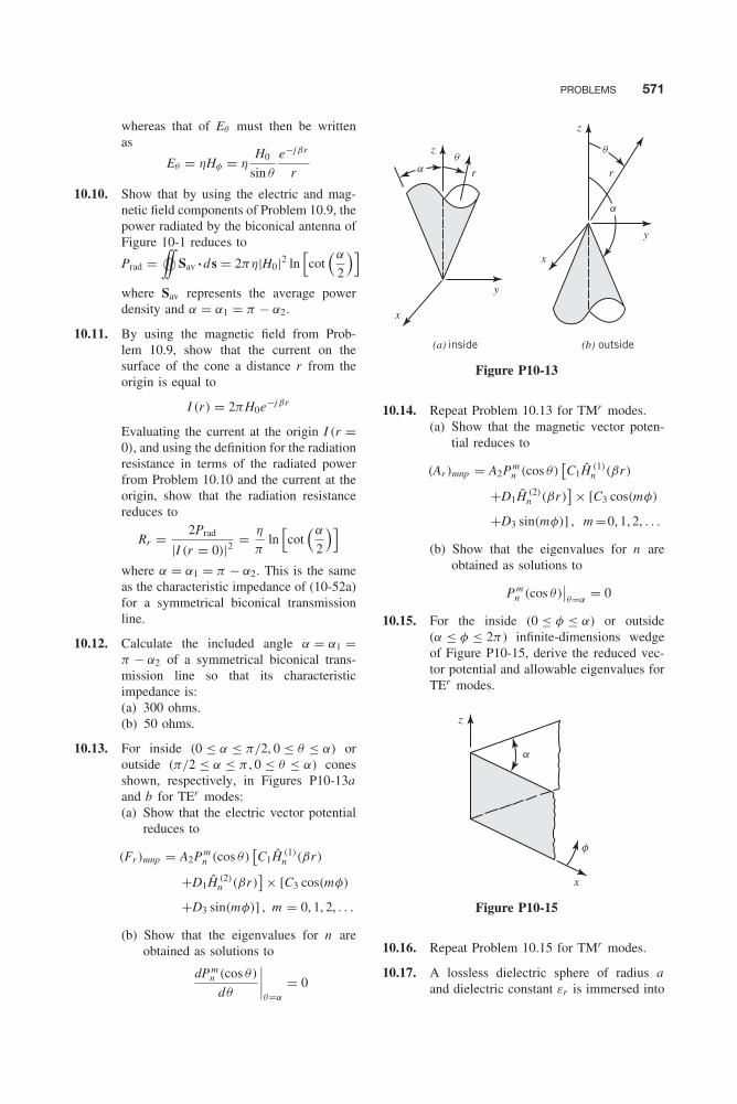
PROBLEMS 571
whereas that of Eθ must then be writtenas
Eθ = ηHφ = ηH0
sin θ
e−jβr
r
10.10. Show that by using the electric and mag-netic field components of Problem 10.9, thepower radiated by the biconical antenna ofFigure 10-1 reduces to
Prad =∫∫© Sav • ds = 2πη|H0|2 ln
[cot
(α
2
)]where Sav represents the average powerdensity and α = α1 = π − α2.
10.11. By using the magnetic field from Prob-lem 10.9, show that the current on thesurface of the cone a distance r from theorigin is equal to
I (r) = 2πH0e−jβr
Evaluating the current at the origin I (r =0), and using the definition for the radiationresistance in terms of the radiated powerfrom Problem 10.10 and the current at theorigin, show that the radiation resistancereduces to
Rr = 2Prad
|I (r = 0)|2 = η
πln
[cot
(α
2
)]where α = α1 = π − α2. This is the sameas the characteristic impedance of (10-52a)for a symmetrical biconical transmissionline.
10.12. Calculate the included angle α = α1 =π − α2 of a symmetrical biconical trans-mission line so that its characteristicimpedance is:(a) 300 ohms.(b) 50 ohms.
10.13. For inside (0 ≤ α ≤ π/2, 0 ≤ θ ≤ α) oroutside (π/2 ≤ α ≤ π , 0 ≤ θ ≤ α) conesshown, respectively, in Figures P10-13aand b for TEr modes:(a) Show that the electric vector potential
reduces to
(Fr )mnp = A2Pmn (cos θ)
[C1Ĥ (1)
n (βr)
+D1Ĥ (2)n (βr)
] × [C3 cos(mφ)
+D3 sin(mφ)] , m = 0, 1, 2, . . .
(b) Show that the eigenvalues for n areobtained as solutions to
dPmn (cos θ)
dθ
∣∣∣∣θ=α
= 0
a
a
qqz
z
y
y
x
x
(a) inside (b) outside
rr
Figure P10-13
10.14. Repeat Problem 10.13 for TMr modes.(a) Show that the magnetic vector poten-
tial reduces to
(Ar )mnp = A2Pmn (cos θ)
[C1Ĥ (1)
n (βr)
+D1Ĥ (2)n (βr)
] × [C3 cos(mφ)
+D3 sin(mφ)] , m =0, 1, 2, . . .
(b) Show that the eigenvalues for n areobtained as solutions to
Pmn (cos θ)
∣∣θ=α
= 0
10.15. For the inside (0 ≤ φ ≤ α) or outside(α ≤ φ ≤ 2π) infinite-dimensions wedgeof Figure P10-15, derive the reduced vec-tor potential and allowable eigenvalues forTEr modes.
z
x
f
a
Figure P10-15
10.16. Repeat Problem 10.15 for TMr modes.
10.17. A lossless dielectric sphere of radius aand dielectric constant εr is immersed into
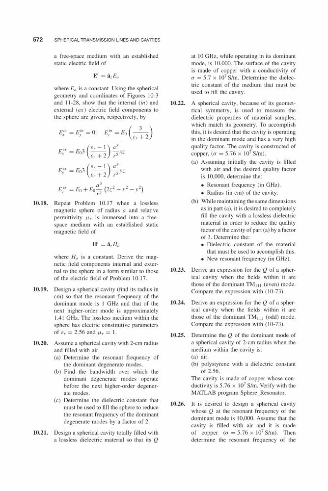
572 SPHERICAL TRANSMISSION LINES AND CAVITIES
a free-space medium with an establishedstatic electric field of
Ei = âz Eo
where Eo is a constant. Using the sphericalgeometry and coordinates of Figures 10-3and 11-28, show that the internal (in) andexternal (ex ) electric field components tothe sphere are given, respectively, by
E inx = E in
y = 0; E inz = E0
(3
εr + 2
)E ex
x = E03
(εr − 1
εr + 2
)a3
r5xz
E exy = E03
(εr − 1
εr + 2
)a3
r5yz
E exz = E0 + E0
a3
r5
(2z 2 − x2 − y2)
10.18. Repeat Problem 10.17 when a losslessmagnetic sphere of radius a and relativepermittivity μr is immersed into a free-space medium with an established staticmagnetic field of
Hi = âz Ho
where Ho is a constant. Derive the mag-netic field components internal and exter-nal to the sphere in a form similar to thoseof the electric field of Problem 10.17.
10.19. Design a spherical cavity (find its radius incm) so that the resonant frequency of thedominant mode is 1 GHz and that of thenext higher-order mode is approximately1.41 GHz. The lossless medium within thesphere has electric constitutive parametersof εr = 2.56 and μr = 1.
10.20. Assume a spherical cavity with 2-cm radiusand filled with air.(a) Determine the resonant frequency of
the dominant degenerate modes.(b) Find the bandwidth over which the
dominant degenerate modes operatebefore the next higher-order degener-ate modes.
(c) Determine the dielectric constant thatmust be used to fill the sphere to reducethe resonant frequency of the dominantdegenerate modes by a factor of 2.
10.21. Design a spherical cavity totally filled witha lossless dielectric material so that its Q
at 10 GHz, while operating in its dominantmode, is 10,000. The surface of the cavityis made of copper with a conductivity ofσ = 5.7 × 10⁷ S/m. Determine the dielec-tric constant of the medium that must beused to fill the cavity.
10.22. A spherical cavity, because of its geomet-rical symmetry, is used to measure thedielectric properties of material samples,which match its geometry. To accomplishthis, it is desired that the cavity is operatingin the dominant mode and has a very highquality factor. The cavity is constructed ofcopper, (σ = 5.76 × 10⁷ S/m).
(a) Assuming initially the cavity is filledwith air and the desired quality factoris 10,000, determine the:
• Resonant frequency (in GHz).• Radius (in cm) of the cavity.
(b) While maintaining the same dimensionsas in part (a), it is desired to completelyfill the cavity with a lossless dielectricmaterial in order to reduce the qualityfactor of the cavity of part (a) by a factorof 3. Determine the:• Dielectric constant of the material
that must be used to accomplish this.• New resonant frequency (in GHz).
10.23. Derive an expression for the Q of a spher-ical cavity when the fields within it arethose of the dominant TM111 (even) mode.Compare the expression with (10-73).
10.24. Derive an expression for the Q of a spher-ical cavity when the fields within it arethose of the dominant TM111 (odd) mode.Compare the expression with (10-73).
10.25. Determine the Q of the dominant mode ofa spherical cavity of 2-cm radius when themedium within the cavity is:(a) air.(b) polystyrene with a dielectric constant
of 2.56.The cavity is made of copper whose con-ductivity is 5.76 × 10⁷ S/m. Verify with theMATLAB program Sphere_Resonator.
10.26. It is desired to design a spherical cavitywhose Q at the resonant frequency of thedominant mode is 10,000. Assume that thecavity is filled with air and it is madeof copper (σ = 5.76 × 10⁷ S/m). Thendetermine the resonant frequency of the

PROBLEMS 573
dominant mode and the radius (in cm) ofthe cavity. Also find the dielectric con-stant of the medium that must be used tofill the cavity to reduce its Q by a factorof 3. Verify with the MATLAB programSphere_Resonator.
10.27. A spherical cavity of radius a , as shown inFigure 10-3, is filled with air. Its surface ismade of a very thin layer of Perfect Mag-netic Conductor (PMC). Determine the:(a) Dominant TEr modes. Identify them
properly by indicating the appropriateindices (mnp). Must make a statementto justify the answer(s).
(b) Resonant frequency of the dominantTEr mode of the cavity.
10.28. Repeat Problem 10.27 for dominant TMr
modes.
10.29. A dielectric spherical cavity, of a geom-etry shown in Figure 10-3, is made of adielectric material with εr � 1.(a) Identify the approximate dominant
TErmnp .
(b) Compute the resonant frequency fora = 3 cm and εr = 81.
10.30. Repeat Problem 10.29 for TMrmnp .
10.31. Assume a hemi-spherical cavity of FigureP10-31 with radius a .(a) Determine the dominant mode and the
expression for its resonant frequency.(b) Show that the Q of the dominant mode
isQ = 0.574
η
Rs
(c) Compare the Q of part (b) with thatof the spherical cavity, and those ofcylindrical and square-based rectangu-lar cavities with the same height-to-diameter ratios.
a r
z
q
Figure P10-31
10.32. For a hemi-spherical PEC, air-filled cavityof radius a , as shown in Figure P10-32,determine the:(a) Dominant TMr
mnp mode(s); identifythem properly.
(b) Reduced/simplified vector potential.Justify it.
(c) Lowest resonant frequency (in GHz)when a = 3 cm.
ar
z
q
Figure P10-32
10.33. Repeat Problem 10.32 for TErmnp modes.
10.34. A hemi-spherical dielectric resonator, usedin microwave integrated circuit (MIC)design, is comprised of a PEC groundplane covered with a dielectric half sphereof radius a , as shown in Figure P10-34.Assuming the dielectric constant of thematerial is much greater than unity (εr �1):(a) Identify all the approximate TEr
mnpmode(s) with the lowest resonant fre-quency.
(b) Compute the resonant frequencies (inGHz) when a = 3 cm and εr = 81.
a r
z
er >>1
q
PEC
Figure P10-34
10.35. Repeat Problem 10.34 for TMrmnp .
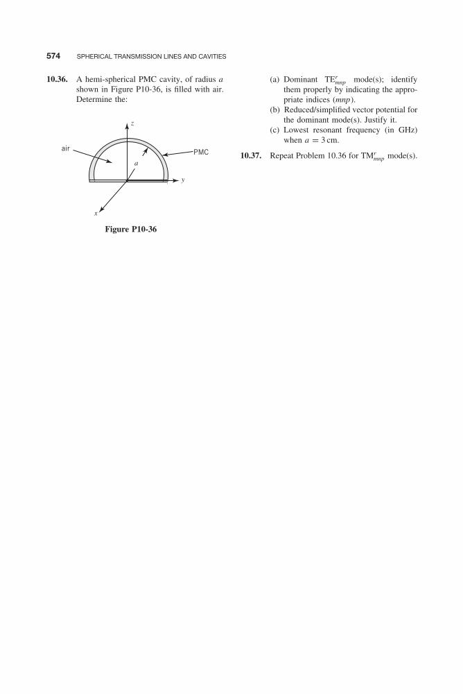
574 SPHERICAL TRANSMISSION LINES AND CAVITIES
10.36. A hemi-spherical PMC cavity, of radius ashown in Figure P10-36, is filled with air.Determine the:
PMCair
x
y
z
a
Figure P10-36
(a) Dominant TErmnp mode(s); identify
them properly by indicating the appro-priate indices (mnp).
(b) Reduced/simplified vector potential forthe dominant mode(s). Justify it.
(c) Lowest resonant frequency (in GHz)when a = 3 cm.
10.37. Repeat Problem 10.36 for TMrmnp mode(s).
Balanis c11.tex V2 - 11/22/2011 3:50 P.M. Page 575
CHAPTER 11Scattering
11.1 INTRODUCTION
Previously, we have considered wave propagation in unbounded media, semi-infinite mediaforming planar interfaces, and conducting, dielectric, and surface waveguides. Although wavepropagation in unbounded media is somewhat idealistic, it serves as a basic model for examiningwave behavior while minimizing mathematical complexities. In general, however, wave propaga-tion must be analyzed when it accounts for the presence of other structures (scatterers), especiallywhen they are in proximity to the wave source and/or receiver.
In this chapter we want to examine wave propagation in the presence of scatterers of variousgeometries (planar, cylindrical, spherical). This is accomplished by introducing to the total fieldan additional component, referred to here as the scattered field , due to the presence of scatterers.The scattered field (Es , Hs) must be such that when it is added, through superposition, to theincident (direct) field (Ei , Hi ), the sum represents the total (Et , Ht ) field, that is,
Et = Ei + Es (11-1a)
Ht = Hi + Hs (11-1b)
The incident (direct) field Ei , Hi will represent the total field produced by the sources in theabsence of any scatterers.
The direct, scattered, and total fields will be obtained using various techniques. In general,geometrical optics (GO), physical optics (PO), modal techniques (MT), integral equations (IE),and diffraction theory [such as the geometrical theory of diffraction (GTD) and physical theory ofdiffraction (PTD)] can be used to analyze such problems. Typically, some of the problems are moreconveniently analyzed using particular method(s). The fundamentals of physical optics were intro-duced in Chapter 7 and modal techniques were utilized in Chapters 8, 9, and 10 to analyze waveg-uide wave propagation. Integral equations are very popular, and they are introduced in Chapter 12.Geometrical optics and diffraction techniques are introduced and applied in Chapter 13.
In this chapter we want to examine scattering primarily by conducting objects. Each scatteringproblem will be analyzed using image theory, physical optics, or modal techniques. The con-veniences and limitations of the applied method to each problem, as well as those of the othermethods, will be stated.
11.2 INFINITE LINE-SOURCE CYLINDRICAL WAVE RADIATION
Before we examine the radiation and scattering of sources placed in the presence of scatterers, itis instructive to obtain the fields radiated by an infinite line source (both electric and magnetic)in an unbounded medium. The reason for doing this is that the infinite line source will serve as
575
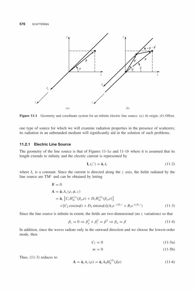
Balanis c11.tex V2 - 11/22/2011 3:50 P.M. Page 576
576 SCATTERING
y y
x x
f f′ f
ρ′
R = ρ − ρ′
ρρ
Ie
Ie
z
(a) (b)
z
Figure 11-1 Geometry and coordinate system for an infinite electric line source. (a) At origin. (b) Offset.
one type of source for which we will examine radiation properties in the presence of scatterers;its radiation in an unbounded medium will significantly aid in the solution of such problems.
11.2.1 Electric Line Source
The geometry of the line source is that of Figures 11-1a and 11-1b where it is assumed that itslength extends to infinity and the electric current is represented by
Ie(z′) = âz Ie (11-2)
where Ie is a constant. Since the current is directed along the z axis, the fields radiated by theline source are TMz and can be obtained by letting
F = 0
A = âz Az (ρ, φ, z )
= âz[C1H (1)
m (βρρ) + D1H (2)m (βρρ)
]×[C2 cos(mφ) + D2 sin(mφ)](A3e−jβz z + B3e+jβz z ) (11-3)
Since the line source is infinite in extent, the fields are two-dimensional (no z variations) so that
βz = 0 ⇒ β2ρ + β2
z = β2 ⇒ βρ = β (11-4)
In addition, since the waves radiate only in the outward direction and we choose the lowest-ordermode, then
C1 = 0 (11-5a)
m = 0 (11-5b)
Thus, (11-3) reduces toA = âz Az (ρ) = âz A0H (2)
0 (βρ) (11-6)

Balanis c11.tex V2 - 11/22/2011 3:50 P.M. Page 577
INFINITE LINE-SOURCE CYLINDRICAL WAVE RADIATION 577
whose corresponding electric and magnetic fields can be written using (6-70) as
Eρ = −j1
ωμε
∂2Az
∂ρ∂z= 0 (11-6a)
Eφ = −j1
ωμε
1
ρ
∂2Az
∂φ∂z= 0 (11-6b)
Ez = −j1
ωμε
(∂2
∂z 2+ β2
)Az = −jωA0H (2)
0 (βρ) (11-6c)
Hρ = 1
μ
1
ρ
∂Az
∂φ= 0 (11-6d)
Hφ = − 1
μ
∂Az
∂ρ= −A0
μH (2)′
0 (βρ) = A0β
μH (2)
1 (βρ) (11-6e)
Hz = 0 (11-6f)
where ′ ≡ ∂/∂ρ.The constant A0 can be obtained by using
Ie = limρ→0
∮C
H • dl = limρ→0
∫ 2π
0(âφHφ) • (âφρ dφ) = lim
ρ→0
∫ 2π
0Hφρ dφ (11-7)
Since the integration of (11-7) must be performed in the limit as ρ → 0, it is convenient torepresent the Hankel function of (11-6e) by its asymptotic expansion for small arguments. Using(IV-12), we can write that
H (2)1 (βρ) = J1(βρ) − jY1(βρ)
βρ→0� βρ
2+ j
2
π
(1
βρ
)βρ→0� j
2
π
(1
βρ
)(11-8)
Therefore, (11-7) reduces, using (11-6e) and (11-8), to
Ie = limρ→0
∫ 2π
0
[A0
β
μH (2)
1 (βρ)
]ρ dφ � jA0
2
πμ
∫ 2π
0
1
ρρ dφ = jA0
4
μ(11-9)
orA0 = −j
μ
4Ie (11-9a)
Thus, the nonzero electric and magnetic fields of the electric line source reduce to
Ez = −Ieωμ
4H (2)
0 (βρ) = −Ieβ2
4ωεH (2)
0 (βρ) (11-10a)
Hφ = −jIeβ
4H (2)
1 (βρ) (11-10b)
Each of the field components is proportional to a Hankel function of the second kind whoseargument is proportional to the distance from the source to the observation point. If the source isremoved from the origin and it is placed as shown in Figure 11-1b, (11-10a) and (11-10b) canbe written as
Ez = −Ieβ2
4ωεH (2)
0 (βR) = −Ieβ2
4ωεH (2)
0 (β|ρ − ρ′|) (11-11a)
Hψ = −j Ieβ
4H (2)
1 (βR) = −j Ieβ
4H (2)
1 (β|ρ − ρ′|) (11-11b)
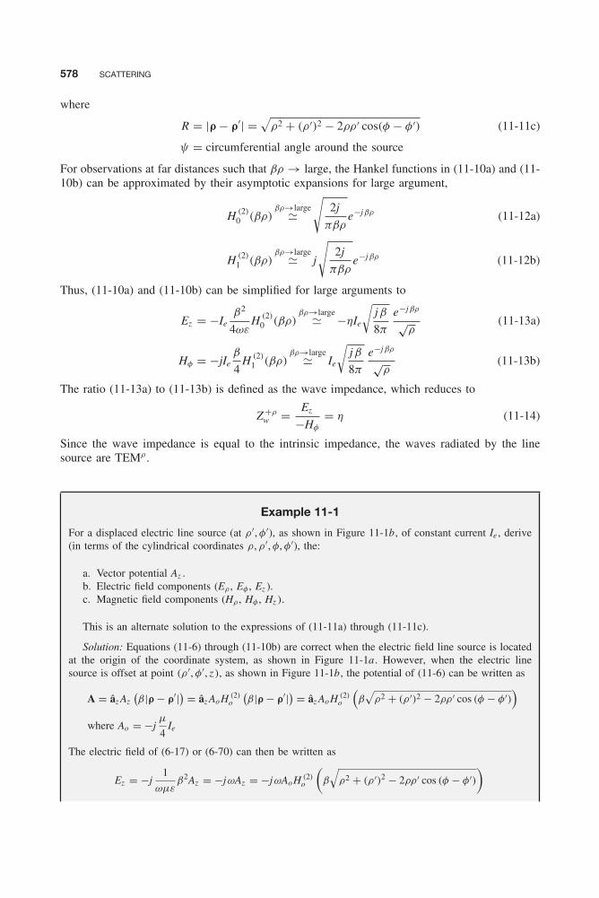
Balanis c11.tex V2 - 11/22/2011 3:50 P.M. Page 578
578 SCATTERING
where
R = |ρ − ρ′| =√
ρ2 + (ρ ′)2 − 2ρρ ′ cos(φ − φ′) (11-11c)
ψ = circumferential angle around the source
For observations at far distances such that βρ → large, the Hankel functions in (11-10a) and (11-10b) can be approximated by their asymptotic expansions for large argument,
H (2)0 (βρ)
βρ→large�√
2j
πβρe−jβρ (11-12a)
H (2)1 (βρ)
βρ→large� j
√2j
πβρe−jβρ (11-12b)
Thus, (11-10a) and (11-10b) can be simplified for large arguments to
Ez = −Ieβ2
4ωεH (2)
0 (βρ)βρ→large� −ηIe
√jβ
8π
e−jβρ
√ρ
(11-13a)
Hφ = −jIeβ
4H (2)
1 (βρ)βρ→large� Ie
√jβ
8π
e−jβρ
√ρ
(11-13b)
The ratio (11-13a) to (11-13b) is defined as the wave impedance, which reduces to
Z +ρw = Ez
−Hφ
= η (11-14)
Since the wave impedance is equal to the intrinsic impedance, the waves radiated by the linesource are TEMρ .
Example 11-1
For a displaced electric line source (at ρ ′, φ′), as shown in Figure 11-1b, of constant current Ie , derive(in terms of the cylindrical coordinates ρ, ρ ′, φ, φ′), the:
a. Vector potential Az .
b. Electric field components (Eρ , Eφ , Ez ).c. Magnetic field components (Hρ , Hφ , Hz ).
This is an alternate solution to the expressions of (11-11a) through (11-11c).
Solution: Equations (11-6) through (11-10b) are correct when the electric field line source is locatedat the origin of the coordinate system, as shown in Figure 11-1a . However, when the electric linesource is offset at point (ρ ′, φ′, z ), as shown in Figure 11-1b, the potential of (11-6) can be written as
A = âz Az(β|ρ − ρ′|) = âz AoH (2)
o
(β|ρ − ρ′|) = âz AoH (2)
o
(β√
ρ2 + (ρ ′)2 − 2ρρ ′ cos (φ − φ′))
where Ao = −jμ
4Ie
The electric field of (6-17) or (6-70) can then be written as
Ez = −j1
ωμεβ2Az = −jωAz = −jωAoH (2)
o
(β
√ρ2 + (ρ ′)2 − 2ρρ ′ cos (φ − φ′)
)
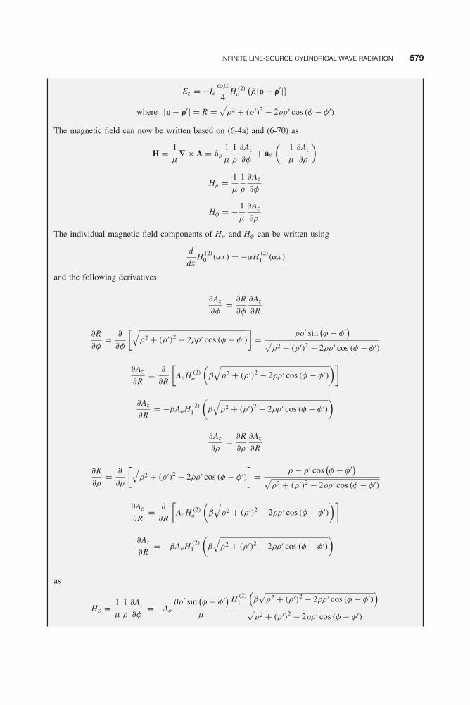
Balanis c11.tex V2 - 11/22/2011 3:50 P.M. Page 579
INFINITE LINE-SOURCE CYLINDRICAL WAVE RADIATION 579
Ez = −Ieωμ
4H (2)
o
(β|ρ − ρ′|)
where |ρ − ρ′| = R =√
ρ2 + (ρ ′)2 − 2ρρ ′ cos (φ − φ′)
The magnetic field can now be written based on (6-4a) and (6-70) as
H = 1
μ∇ × A = âρ
1
μ
1
ρ
∂Az
∂φ+ âφ
(− 1
μ
∂Az
∂ρ
)
Hρ = 1
μ
1
ρ
∂Az
∂φ
Hφ = − 1
μ
∂Az
∂ρ
The individual magnetic field components of Hρ and Hφ can be written using
d
dxH (2)
0 (αx) = −αH (2)1 (αx)
and the following derivatives
∂Az
∂φ= ∂R
∂φ
∂Az
∂R
∂R
∂φ= ∂
∂φ
[√ρ2 + (ρ ′)2 − 2ρρ ′ cos (φ − φ′)
]= ρρ ′ sin
(φ − φ′)√
ρ2 + (ρ ′)2 − 2ρρ ′ cos (φ − φ′)
∂Az
∂R= ∂
∂R
[AoH (2)
o
(β
√ρ2 + (ρ ′)2 − 2ρρ ′ cos (φ − φ′)
)]∂Az
∂R= −βAoH (2)
1
(β
√ρ2 + (ρ ′)2 − 2ρρ ′ cos (φ − φ′)
)∂Az
∂ρ= ∂R
∂ρ
∂Az
∂R
∂R
∂ρ= ∂
∂ρ
[√ρ2 + (ρ ′)2 − 2ρρ ′ cos (φ − φ′)
]= ρ − ρ ′ cos
(φ − φ′)√
ρ2 + (ρ ′)2 − 2ρρ ′ cos (φ − φ′)
∂Az
∂R= ∂
∂R
[AoH (2)
o
(β
√ρ2 + (ρ ′)2 − 2ρρ ′ cos (φ − φ′)
)]∂Az
∂R= −βAoH (2)
1
(β
√ρ2 + (ρ ′)2 − 2ρρ ′ cos (φ − φ′)
)
as
Hρ = 1
μ
1
ρ
∂Az
∂φ= −Ao
βρ ′ sin(φ − φ′)
μ
H (2)1
(β√
ρ2 + (ρ ′)2 − 2ρρ ′ cos (φ − φ′))
√ρ2 + (ρ ′)2 − 2ρρ ′ cos (φ − φ′)

Balanis c11.tex V2 - 11/22/2011 3:50 P.M. Page 580
580 SCATTERING
Hρ = jIeβρ ′ sin
(φ − φ′)
4
H (2)1
(β
∣∣ρ − ρ′∣∣)|ρ − ρ′|
Hφ = − 1
μ
∂Az
∂ρ= −Ao
β[ρ − ρ ′ cos
(φ − φ′)]
μ
H (2)1
(β√
ρ2 + (ρ ′)2 − 2ρρ ′ cos (φ − φ′))
√ρ2 + (ρ ′)2 − 2ρρ ′ cos (φ − φ′)
Hφ = − 1
μ
∂Az
∂ρ= jIe
β[ρ − ρ ′ cos
(φ − φ′)]
4
H (2)1
(β
∣∣ρ − ρ′∣∣)|ρ − ρ′|
11.2.2 Magnetic Line Source
Although magnetic sources as presently known are not physically realizable, they are often usedto represent virtual sources in equivalent models. This was demonstrated in Chapter 7, Sections7.7 and 7.8, where the volume and surface fields equivalence theorems were introduced. Magneticsources can be used to represent radiating apertures.
The fields generated by magnetic sources can be obtained by solutions to Maxwell’s equationsor the wave equation (subject to the appropriate boundary conditions), or by using the dualitytheorem of Chapter 7, Section 7.2, once the solution to the same problem but with an electricsource excitation is known.
Then, using the duality theorem of Section 7.2, the field generated by an infinite magneticline source of constant current Im can be obtained using Tables 7-1 and 7-2, (11-10a) through(11-10b), and (11-13a) through (11-13b). These can then be written as
Eφ = +jImβ
4H (2)
1 (βρ)βρ→large� −Im
√jβ
8π
e−jβρ
√ρ
(11-15a)
Hz = −Imβ2
4ωμH (2)
0 (βρ)βρ→large� −1
ηIm
√jβ
8π
e−jβρ
√ρ
(11-15b)
which, when the sources are displaced from the origin, can also be expressed according to (11-11a)and (11-11b) as
EΨ = +j Imβ
4H (2)
1 (β|ρ − ρ′|) (11-16a)
Hz = −Imβ2
4ωμH (2)
0 (β|ρ − ρ′|) (11-16b)
11.2.3 Electric Line Source Above Infinite Plane Electric Conductor
When an infinite electric line source is placed at a height h above an infinite flat electric conductor,as shown in Figure 11-2a , the solution for the field components must include the presence of theconducting plane. This can be accomplished by using Maxwell’s equations or the wave equationsubject to the radiation conditions at infinity and boundary condition along the air-conductorinterface. Instead of doing this, the same solution is obtained by introducing an equivalent modelwhich leads to the same fields in the region of interest. Since the fields below the interface (in theelectric conductor, y < 0) are known (they are zero), the equivalent model should be valid and
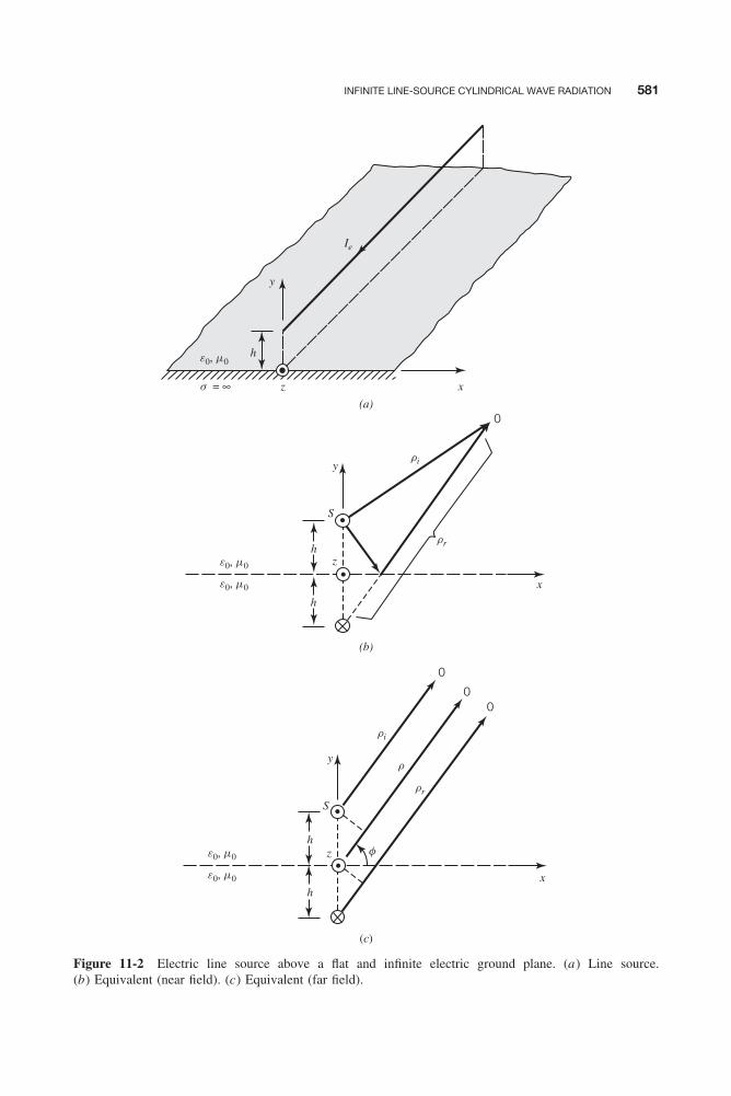
Balanis c11.tex V2 - 11/22/2011 3:50 P.M. Page 581
INFINITE LINE-SOURCE CYLINDRICAL WAVE RADIATION 581
(a)
e0, m0
e0, m0
ri
rrh
h
z
S
y
0
x
e0, m0
e0, m0
ri
r
f
rr
h
h
z
S
y
0
00
x
e0, m0h
z xs = ∞
y
Ie
(b)
(c)
Figure 11-2 Electric line source above a flat and infinite electric ground plane. (a) Line source.(b) Equivalent (near field). (c) Equivalent (far field).

Balanis c11.tex V2 - 11/22/2011 3:50 P.M. Page 582
582 SCATTERING
leads to the same fields as the actual physical problem on or above the interface (y ≥ 0). In thiscase, as long as the equivalent model satisfies the same boundary conditions as the actual physicalproblem along a closed surface, according to the uniqueness theorem of Section 7.3, the solutionof the equivalent model will be unique and be the same as that of the physical problem. Forthis problem, the closed surface that will be chosen is that of the air-conductor interface (y = 0),which extends on the range −∞ ≤ x ≤ +∞.
The equivalent problem of Figure 11-2a is that of Figure 11-2b where the ground planehas been replaced by an equivalent source (usually referred to as image or virtual source orcaustic). According to the theory of Section 7.4, the image source is introduced to accountfor the reflections from the surface of the ground plane. The magnitude, phase, polarization,and position of the image source must be such that the boundary conditions of the equivalentproblem of Figure 11-2b along −∞ ≤ x ≤ +∞ are the same as those of the physical problem ofFigure 11-2a . In this situation the image must have: the same magnitude as the actual source, itsphase must be 180◦ out of phase from the actual source, it must be placed below the interfaceat a depth h(y = −h) along a line perpendicular to the interface and passing through the actualsource, and its length must also be parallel to the z axis. Such a system configuration, as shown inFigure 11-2b, does lead to zero tangential electric field along −∞ ≤ x ≤ +∞, which is identicalto that of Figure 11-2a along the air-conductor interface.
Therefore, according to Figures 11-2a and 11-2b and (11-13a), the total electric field is equalto
Et = Ei + Er =⎧⎨⎩ − âz
β2Ie
4ωε
[H (2)
0 (βρi ) − H (2)0 (βρr )
], y ≥ 0
0, y < 0
(11-17a)
(11-17b)
which, for observations at large distances, as shown by Figure 11-2c, reduces using the asymptoticexpansion (11-12a) to
Et = Ei + Er =
⎧⎪⎨⎪⎩ − âz ηIe
(e−jβρi
√ρi
− e−jβρr
√ρr
)√jβ
8π, y ≥ 0
0, y < 0
(11-18a)
(11-18b)
According to Figure 11-2c, for observations made at large distances (ρ � h)
ρi � ρ − h cos(π
2− φ
)= ρ − h sin(φ)
ρr � ρ + h cos(π
2− φ
)= ρ + h sin(φ)
⎫⎪⎬⎪⎭ for phase variations (11-19a)
ρi � ρr � ρ for amplitude variations (11-19b)
These approximations are usually referred to in antenna and scattering theory as the far-fieldapproximations [1]. Using (11-19a) and (11-19b), we can reduce (11-18a) and (11-18b) to
Et = Ei + Er =
⎧⎪⎪⎪⎪⎪⎪⎨⎪⎪⎪⎪⎪⎪⎩
− âz ηIe
√jβ
8π
(e+jβh sin φ − e−jβh sin φ
) e−jβρ
√ρ
= −âz jηIe
√jβ
2πsin (βh sin φ)
e−jβρ
√ρ
y ≥ 0
0 y < 0
(11-20a)
(11-20b)
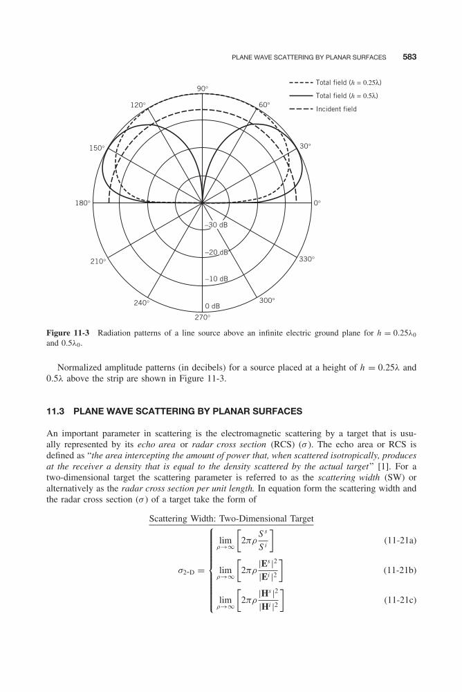
Balanis c11.tex V2 - 11/22/2011 3:50 P.M. Page 583
PLANE WAVE SCATTERING BY PLANAR SURFACES 583
270°
300°
330°
0°
30°
90°
60°120°
150°
180°
210°
240° 0 dB
−10 dB
−20 dB
Total field (h = 0.25λ)
Total field (h = 0.5λ)
Incident field
−30 dB
Figure 11-3 Radiation patterns of a line source above an infinite electric ground plane for h = 0.25λ0
and 0.5λ0.
Normalized amplitude patterns (in decibels) for a source placed at a height of h = 0.25λ and0.5λ above the strip are shown in Figure 11-3.
11.3 PLANE WAVE SCATTERING BY PLANAR SURFACES
An important parameter in scattering is the electromagnetic scattering by a target that is usu-ally represented by its echo area or radar cross section (RCS) (σ ). The echo area or RCS isdefined as “the area intercepting the amount of power that, when scattered isotropically, producesat the receiver a density that is equal to the density scattered by the actual target” [1]. For atwo-dimensional target the scattering parameter is referred to as the scattering width (SW) oralternatively as the radar cross section per unit length. In equation form the scattering width andthe radar cross section (σ ) of a target take the form of
Scattering Width: Two-Dimensional Target
σ2-D =
⎧⎪⎪⎪⎪⎪⎪⎪⎪⎪⎨⎪⎪⎪⎪⎪⎪⎪⎪⎪⎩
limρ→∞
[2πρ
S s
S i
]lim
ρ→∞
[2πρ
|Es |2|Ei |2
]lim
ρ→∞
[2πρ
|Hs |2|Hi |2
]
(11-21a)
(11-21b)
(11-21c)
Balanis c11.tex V2 - 11/22/2011 3:50 P.M. Page 584
584 SCATTERING
Radar Cross Section: Three-Dimensional Target
σ3-D =
⎧⎪⎪⎪⎪⎪⎪⎪⎪⎪⎨⎪⎪⎪⎪⎪⎪⎪⎪⎪⎩
limr→∞
[4πr2 S s
S i
]lim
r→∞
[4πr2 |Es |2
|Ei |2]
limr→∞
[4πr2 |Hs |2
|Hi |2]
(11-22a)
(11-22b)
(11-22c)
where ρ, r = distance from target to observation pointS s , S i = scattered, incident power densitiesEs , Ei = scattered, incident electric fieldsHs , Hi = scattered, incident magnetic fields
For normal incidence, the two- and three-dimensional fields, and scattering width and radar crosssections for a target of length � are related by [2-4]
E3-D �(
E2-D�ejπ/4
√λρ
)ρ=r
(11-22d)
σ3-D � σ2-D2�2
λ(11-22e)
The unit of the two-dimensional SW is length (meters in the MKS system), whereas that of thethree-dimensional RCS is area (meters squared in the MKS system). A most common referenceis one meter for the two-dimensional SW and one meter squared for the three-dimensional RCS.Therefore, a most common designation is dB/m (or dBm) for the two-dimensional SW anddB/(square meter) (or dBsm) for the three-dimensional RCS.
When the transmitter and receiver are at the same location, the RCS is usually referred toas monostatic (or backscattered ), and it is referred to as bistatic when the two are at differentlocations. Observations made toward directions that satisfy Snell’s law of reflection are usuallyreferred to as specular. Therefore, the RCS of a target is a very important parameter whichcharacterizes its scattering properties. A plot of the RCS as a function of the space coordinatesis usually referred to as the RCS pattern. The definitions (11-21a) through (11-22c) all indicatethat the SW and RCS of targets are defined under plane wave, that in practice can only beapproximated when the target is placed in the far field of the source (at least 2D2/λ) where D isthe largest dimension of the target [1].
In this section, physical optics (PO) techniques will be used to analyze the scattering fromconducting strips and plates of finite width, neglecting edge effects. The edge effects will beconsidered in Chapters 12 to 14, where, respectively, moment method and geometrical theory ofdiffraction techniques will be utilized. Physical optics techniques are most accurate at speculardirections [5].
11.3.1 TMz Plane Wave Scattering from a Strip
Let us assume that a TMz uniform plane wave is incident upon an electric conducting strip ofwidth w and infinite length, as shown in Figures 11-4a and 11-4b. The incident electric andmagnetic fields can be written as
Ei = âz E0ejβ(x cos φi +y sin φi ) (11-23a)
Hi = E0
η(−âx sin φi + ây cos φi )e
jβ(x cos φi +y sin φi ) (11-23b)

Balanis c11.tex V2 - 11/22/2011 3:50 P.M. Page 585
PLANE WAVE SCATTERING BY PLANAR SURFACES 585
Ei, Hi
y
z
xw
(a)
(b)
Ei y
z xw
Hi
Es
Hs
fs
fi
(c)
Ei
y
z xw
HiHs
Es
fs
fi
Figure 11-4 Uniform plane wave incident on a finite width strip. (a) Finite width strip. (b) TMz polar-ization. (c) TEz polarization.
where E0 is a constant, and it represents the magnitude of the incident electric field. InFigures 11-4a and 11-4b the angle φi , is shown to be greater than 90◦. The reflected fields canbe expressed as
Er = âz �⊥E0e−jβ(x cos φr +y sin φr ) (11-24a)
Hr = �⊥E0
η(âx sin φr − ây cos φr )e
−jβ(x cos φr +y sin φr ) (11-24b)
where φr is the reflection angle as determined by enforcing the boundary conditions along theinterface, assuming an interface of infinite extent. For the finite-width strip the reflection angleφr is not the same as the scattering angle φs(φr �= φs). The two coincide for an infinite-width
Balanis c11.tex V2 - 11/22/2011 3:50 P.M. Page 586
586 SCATTERING
strip when geometrical optics and physical optics reduce to each other. Thus, we use geometricaloptics to determine the reflection coefficient on the surface of the finite-width strip, andthen apply physical optics to find the scattered fields. According to (5-17a) and (5-15a), thereflection coefficient for a perfectly conducting surface is equal to �⊥ = −1 and φr = π − φi .Thus, (11-24a) and (11-24b) reduce to
Er = −âz E0ejβ(x cos φi −y sin φi ) (11-25a)
Hr = E0
η(−âx sin φi − ây cos φi )e
jβ(x cos φi −y sin φi ) (11-25b)
Using physical optics techniques of (7-54), the current density induced on the surface of thestrip can be written as
Js = n̂ × Ht | y=0x=x ′
= n̂ × (Hi + Hr ) | y=0x=x ′
= 2n̂ × Hi | y=0x=x ′
= ây2E0
η× (−âx sin φi + ây cos φi )e
jβx ′ cos φi
Js = âz2E0
ηsin φi e
jβx ′ cos φi (11-26)
and the far-zone scattered field can be found using (6-96a), (6-101a), and (6-101b) or
A = μ
4π
∫ ∫S
Js(x′, y ′, z ′)
e−jβR
Rds ′ (11-27a)
EA � −jωA (for θ and φ components only) (11-27b)
HA � 1
ηâr × EA = −j
ω
ηâr × A (for θ and φ components only) (11-27c)
where
R =√
(x − x ′)2 − (y + y ′)2 + (z − z ′)2 =√
(|ρ − ρ′|)2 + (z − z ′)2 (11-27d)
Substituting (11-26) into (11-27a) and using (11-27d), we can write that
A = âzμE0
2πηsin φi
∫ w
0
⎧⎨⎩∫ +∞
−∞
exp[−jβ
√(|ρ − ρ′|)2 + (z − z ′)2
]√
(|ρ − ρ′|)2 + (z − z ′)2dz ′
⎫⎬⎭ ejβx ′ cos φi dx ′
(11-28)
Since the integral with the infinite limits can be represented by a Hankel function of the secondkind of zero order ∫ +∞
−∞
e−jα√
x2+t2
√x 2 + t2
dt = −jπH (2)0 (αx) (11-28a)
(11-28) can be reduced to
A = −âz jμE0
2ηsin φi
∫ w
0H (2)
0 (β|ρ − ρ′|)ejβx ′ cos φi dx ′ (11-28b)
For far-zone observations
|ρ − ρ′| =√
ρ2 + (ρ ′)2 − 2ρρ ′ cos(φs − φ′)ρ � ρ ′
�√
ρ2 − 2ρρ ′ cos(φs − φ′)
Balanis c11.tex V2 - 11/22/2011 3:50 P.M. Page 587
PLANE WAVE SCATTERING BY PLANAR SURFACES 587
|ρ − ρ′| ρ�ρ′� ρ
√1 − 2
(ρ ′
ρ
)cos(φs − φ′)
ρ�ρ′� ρ
[1 −
(ρ ′
ρ
)cos(φs − φ′)
]|ρ − ρ′| ρ�ρ′
� ρ − ρ ′ cos(φs − φ′) (11-29)
Since the source (here the current density) exists only over the width of the strip that accordingto Figure 11-4 lies along the x axis, then ρ ′ = x ′ and φ′ = 0. Thus, for far-field observations(11-29) reduces to
|ρ − ρ′| �{
ρ − ρ ′ cos(φs − φ′) = ρ − x ′ cos φs for phase terms
ρ for amplitude terms
(11-29a)
(11-29b)
In turn the Hankel function in the integrand of (11-28b) can be expressed, using (11-29a) and(11-29b), as
H (2)0 (β|ρ − ρ′|) ρ�ρ′
�√
2j
πβρe−jβ(ρ−x ′ cos φs ) =
√2j
πβ
e−jβρ
√ρ
ejβx ′ cos φs (11-30)
Substituting (11-30) into (11-28b) reduces it to
A � − âz jμE0
2η
√2j
πβ
e−jβρ
√ρ
sin φi
∫ w
0ejβx ′(cos φs +cos φi )dx ′
A � − âz jμwE0
η
√j
2πβej (βw/2)(cos φs +cos φi )
×
⎧⎪⎪⎨⎪⎪⎩sin φi
⎡⎢⎢⎣ sin
[βw
2(cos φs + cos φi )
]βw
2(cos φs + cos φi )
⎤⎥⎥⎦ e−jβρ
√ρ
⎫⎪⎪⎬⎪⎪⎭ (11-31)
Therefore, the far-zone scattered spherical components of the electric and magnetic fields of(11-27b) and (11-27c) can be written, using (11-31) and (II-12), as
E sθ � jωAz sin θs = ωE0
√jβ
2πej (βw/2)(cos φs +cos φi )
×
⎧⎪⎪⎨⎪⎪⎩sin θs sin φi
⎡⎢⎢⎣ sin
[βw
2(cos φs + cos φi )
]βw
2(cos φs + cos φi )
⎤⎥⎥⎦ e−jβρ
√ρ
⎫⎪⎪⎬⎪⎪⎭(11-32a)
H sφ � E s
θ
η= wE0
η
√jβ
2πej (βw/2)(cos φs +cos φi )
×
⎧⎪⎪⎨⎪⎪⎩sin θs sin φi
⎡⎢⎢⎣ sin
[βw
2(cos φs + cos φi )
]βw
2(cos φs + cos φi )
⎤⎥⎥⎦ e−jβρ
√ρ
⎫⎪⎪⎬⎪⎪⎭(11-32b)
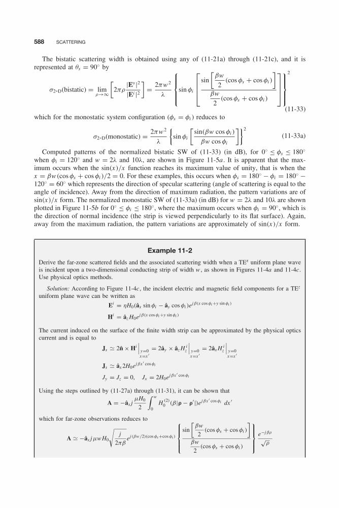
Balanis c11.tex V2 - 11/22/2011 3:50 P.M. Page 588
588 SCATTERING
The bistatic scattering width is obtained using any of (11-21a) through (11-21c), and it isrepresented at θs = 90◦ by
σ2-D(bistatic) = limρ→∞
[2πρ
|Es |2|Ei |2
]= 2πw 2
λ
⎧⎪⎪⎨⎪⎪⎩sin φi
⎡⎢⎢⎣ sin
[βw
2(cos φs + cos φi )
]βw
2(cos φs + cos φi )
⎤⎥⎥⎦⎫⎪⎪⎬⎪⎪⎭
2
(11-33)which for the monostatic system configuration (φs = φi ) reduces to
σ2-D(monostatic) = 2πw 2
λ
{sin φi
[sin(βw cos φi )
βw cos φi
]}2
(11-33a)
Computed patterns of the normalized bistatic SW of (11-33) (in dB), for 0◦ ≤ φs ≤ 180◦when φi = 120◦ and w = 2λ and 10λ, are shown in Figure 11-5a . It is apparent that the max-imum occurs when the sin(x)/x function reaches its maximum value of unity, that is when thex = βw(cos φs + cos φi )/2 = 0. For these examples, this occurs when φs = 180◦ − φi = 180◦ −120◦ = 60◦ which represents the direction of specular scattering (angle of scattering is equal to theangle of incidence). Away from the direction of maximum radiation, the pattern variations are ofsin(x)/x form. The normalized monostatic SW of (11-33a) (in dB) for w = 2λ and 10λ are shownplotted in Figure 11-5b for 0◦ ≤ φi ≤ 180◦, where the maximum occurs when φi = 90◦, which isthe direction of normal incidence (the strip is viewed perpendicularly to its flat surface). Again,away from the maximum radiation, the pattern variations are approximately of sin(x)/x form.
Example 11-2
Derive the far-zone scattered fields and the associated scattering width when a TEz uniform plane waveis incident upon a two-dimensional conducting strip of width w , as shown in Figures 11-4a and 11-4c.Use physical optics methods.
Solution: According to Figure 11-4c, the incident electric and magnetic field components for a TEz
uniform plane wave can be written as
Ei = ηH0(âx sin φi − ây cos φi )ejβ(x cos φi +y sin φi )
Hi = âz H0ejβ(x cos φi +y sin φi )
The current induced on the surface of the finite width strip can be approximated by the physical opticscurrent and is equal to
Js � 2n̂ × Hi∣∣∣ y=0x=x ′
= 2ây × âz H iz
∣∣∣ y=0x=x ′
= 2âx H iz
∣∣∣ y=0x=x ′
Js � âx 2H0ejβx ′ cos φi
Jy = Jz = 0, Jx = 2H0ejβx ′ cos φi
Using the steps outlined by (11-27a) through (11-31), it can be shown that
A = −âx jμH0
2
∫ w
0H (2)
0 (β|ρ − ρ′|)ejβx ′ cos φi dx ′
which for far-zone observations reduces to
A � −âx jμwH0
√j
2πβej (βw/2)(cos φs +cos φi )
⎧⎪⎪⎨⎪⎪⎩sin
[βw
2(cos φs + cos φi )
]βw
2(cos φs + cos φi )
⎫⎪⎪⎬⎪⎪⎭e−jβρ
√ρ
Balanis c11.tex V2 - 11/22/2011 3:50 P.M. Page 589
PLANE WAVE SCATTERING BY PLANAR SURFACES 589
In spherical components this can be written, according to (II-12), as
Ar = Ax sin θs cos φs
Aθ = Ax cos θs cos φs
Aφ = −Ax sin φs
which for θs = 90◦ reduce to
Ar = Ax cos φs
Aθ = 0
Aφ = −Ax sin φs
Thus, the far-zone electric and magnetic field components in the θs = 90◦ plane can be written as
E sr � E s
θ � H sr � H s
φ � 0
E sφ � −jωAφ = jωAx sin φs
E sφ � −ηwH0
√jβ
2πej (βw/2)(cos φs +cos φi )
×
⎧⎪⎪⎨⎪⎪⎩sin φs
⎡⎢⎢⎣ sin
[βw
2(cos φs + cos φi )
]βw
2(cos φs + cos φi )
⎤⎥⎥⎦ e−jβρ
√ρ
⎫⎪⎪⎬⎪⎪⎭H s
θ � −E sφ
η= wH0
√jβ
2πej (βw/2)(cos φs +cos φi )
×
⎧⎪⎪⎨⎪⎪⎩sin φs
⎡⎢⎢⎣ sin
[βw
2(cos φs + cos φi )
]βw
2(cos φs + cos φi )
⎤⎥⎥⎦ e−jβρ
√ρ
⎫⎪⎪⎬⎪⎪⎭The bistatic and monostatic (backscattering) scattering widths are given by
σ2-D(bistatic) = limρ→∞
[2πρ
|H s |2|Hi |2
]
= 2πw2
λ
⎧⎪⎪⎨⎪⎪⎩sin φs
⎡⎢⎢⎣ sin
[βw
2(cos φs + cos φi )
]βw
2(cos φs + cos φi )
⎤⎥⎥⎦⎫⎪⎪⎬⎪⎪⎭
2
σ2-D(monostatic) = 2πw2
λ
{sin φi
[sin(βw cos φi )
βw cos φi
]}2
The monostatic SW for the TEz polarization is identical to that of the TMz as given by (11-33a), andit is shown plotted in Figure 11-5b for w = 2λ and 10λ. The bistatic SW, however, differs from thatof (11-33) in that the sin2 φi term is replaced by sin2 φs . Therefore, the computed normalized bistaticpatterns (in dB) for 0◦ ≤ φs ≤ 180◦ when φi = 120◦ and w = 2λ, 10λ are shown, respectively, inFigure 11-6. It is evident that the larger the width of the strip, the larger the maximum value of the SWand the larger the number of minor lobes in its pattern.

Balanis c11.tex V2 - 11/22/2011 3:50 P.M. Page 590
590 SCATTERING
w = 2l
w = 10l
30
20
10
0
−10
−20
−300 45
Observation angle fs (degrees)
(a)
90 135 180
SW
(s
2-D
/λ)
(dB
)
w = 2l
w = 10l
30
20
10
0
−10
−20
−300 45
Observation angle fi (degrees)
(b)
90 135 180
SW
(s
2-D
/λ)
(dB
)
Figure 11-5 Bistatic and monostatic scattering width (SW) for a finite width strip. (a) Bistatic (φi = 120◦):TMz . (b) Monostatic: TMz and TEz .
Balanis c11.tex V2 - 11/22/2011 3:50 P.M. Page 591
PLANE WAVE SCATTERING BY PLANAR SURFACES 591
w = 2λ
w = 10λ
30
20
10
0
−10
−20
−300 45
Observation angle fs (degrees)
90 135 180
SW
(s
2-D
/λ)
(dB
)
Figure 11-6 Bistatic TEz scattering width (SW) for a finite width strip (φi = 120◦).
To see that indeed the bistatic SW patterns of the TMz and TEz polarizations are different,we have plotted in Figure 11-7a the two for w = 2λ when the incidence angle is φi = 120◦.It is evident that the two are similar but not identical because the sin2 φi term is replaced bysin2 φs , and vice versa. In addition, whereas the maximum for the TMz occurs at the speculardirection (φs = 60◦ for this example), that of the TEz occurs at an angle slightly larger than thespecular direction. However, as the size of the target becomes very large, the maximum of theTEz SW moves closer toward the specular direction and matches that of the TMz , which alwaysoccurs at the specular direction [6]. This is illustrated in Figure 11-7b where the bistatic RCS ofthe two polarizations has been plotted for w = 10λ and φi = 120◦. When the size of the targetis very large electrically, the [sin(x)/x ]2 in the bistatic RCS expression of Example 11-1 variesvery rapidly as a function of φs so that the slowly varying sin2 φs is essentially a constant nearthe maximum of the [sin(x)/x ]2 function. This is not true when the size of the target is smallelectrically, as was demonstrated by the results of Figure 11-7a .
11.3.2 TEx Plane Wave Scattering from a Flat Rectangular Plate
Let us now consider scattering from a three-dimensional scatterer, specifically uniform plane-wave scattering from a rectangular plate, as shown in Figure 11-8a . To simplify the details, letus assume that the uniform plane wave is TEx , and that it lies on the yz plane, as shown inFigure 11-8b. The electric and magnetic fields can now be written as
Ei = ηH0(ây cos θi + âz sin θi )e−jβ(y sin θi −z sin θi ) (11-34a)
Hi = âx H0e−jβ(y sin θi −z cos θi ) (11-34b)
where H0 is a constant that represents the magnitude of the incident magnetic field.

Balanis c11.tex V2 - 11/22/2011 3:50 P.M. Page 592
592 SCATTERING
TEz
TMz
TEz
TMz
30
20
10
0
−10
−20
−300 45
Observation angle fs (degrees)
(a)
90 135 180
SW
(s
2-D
/λ)
(dB
)
30
20
10
0
−10
−20
−300 45
Observation angle fs (degrees)
(b)
90 135 180
SW
(s
2-D
/λ)
(dB
)
Figure 11-7 TEz and TMz bistatic scattering widths (SW) for a finite width strip (φi = 120◦). (a) w = 2λ.(b) w = 10λ.
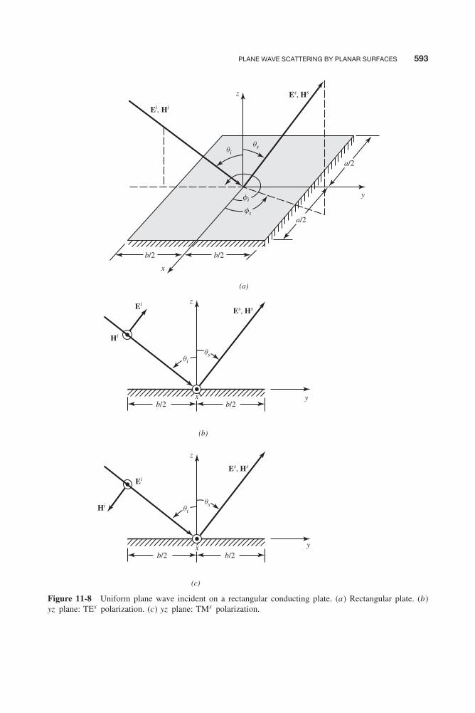
Balanis c11.tex V2 - 11/22/2011 3:50 P.M. Page 593
PLANE WAVE SCATTERING BY PLANAR SURFACES 593
Ei, Hi
y
x
(a)
(b)
(c)
Ei
z
x yb/2b/2
Hi
Es, Hs
Es, Hs
qsqi
Ei z
z
x yb/2b/2
Hi
Es, Hs
qsqi
qs
fs
qi
fi
b/2 b/2
a/2
a/2
Figure 11-8 Uniform plane wave incident on a rectangular conducting plate. (a) Rectangular plate. (b)yz plane: TEx polarization. (c) yz plane: TMx polarization.

Balanis c11.tex V2 - 11/22/2011 3:50 P.M. Page 594
594 SCATTERING
The scattered field can be found, by neglecting edge effects, using physical optics techniquesof Section 7.10, where the current density induced at the surface of the plate is represented onthe plate by
Js � 2n̂ × H′| z=0y=y ′
= 2âz × âx Hx | z=0y=y ′
= ây 2H0e−jβy ′ sin θi (11-35)
Thus,Jx = Jz = 0 and Jy = 2H0e−jβy ′ sin θi (11-35a)
For an infinite plate, the current density of (11-35) or (11-35a) yields exact field solutions.However, for finite-size plates it is approximate, and the corresponding scattered fields obtainedusing it are more accurate toward the specular direction, where Snell’s law of reflection issatisfied. The solutions become less accurate as the observation points are removed further fromthe specular directions.
The scattered fields are obtained using (6-122a) through (6-122f) and (6-125a) through(6-125b), where the electric current density components are those given by (11-35a).Using (6-125a), (6-127c), (6-128c), and (11-35a), we can write that
Nθ =∫∫
S
[Jx cos θs cos φs + Jy cos θs sin φs − Jz sin θs
]Jx =Jz =0
×ejβ(x ′ sin θs cos φs +y ′ sin θs sin φs ) dx ′ dy ′
= 2H0 cos θs sin φs
∫ +b/2
−b/2ejβy ′(sin θs sin φs −sin θi ) dy ′
∫ +a/2
−a/2ejβx ′ sin θs cos φs dx ′
(11-36)
Since ∫ +c/2
−c/2ejαz dz = c
⎡⎢⎣ sin(α
2c)
α
2c
⎤⎥⎦ (11-37)
(11-36) reduces to
Nθ = 2abH0
{cos θs sin φs
[sin(X )
X
] [sin(Y )
Y
]}(11-38)
where
X = βa
2sin θs cos φs (11-38a)
Y = βb
2(sin θs sin φs − sin θi ) (11-38b)
In the same manner, (6-125b) can be written as
Nφ =∫∫
S
[−Jx sin φs + Jy cos φs]
Jx =0 ejβ(x ′ sin θs cos φs +y ′ sin θs sin φs ) dx ′ dy ′
= 2abH0
{cos φs
[sin(X )
X
] [sin(Y )
Y
]}(11-39)
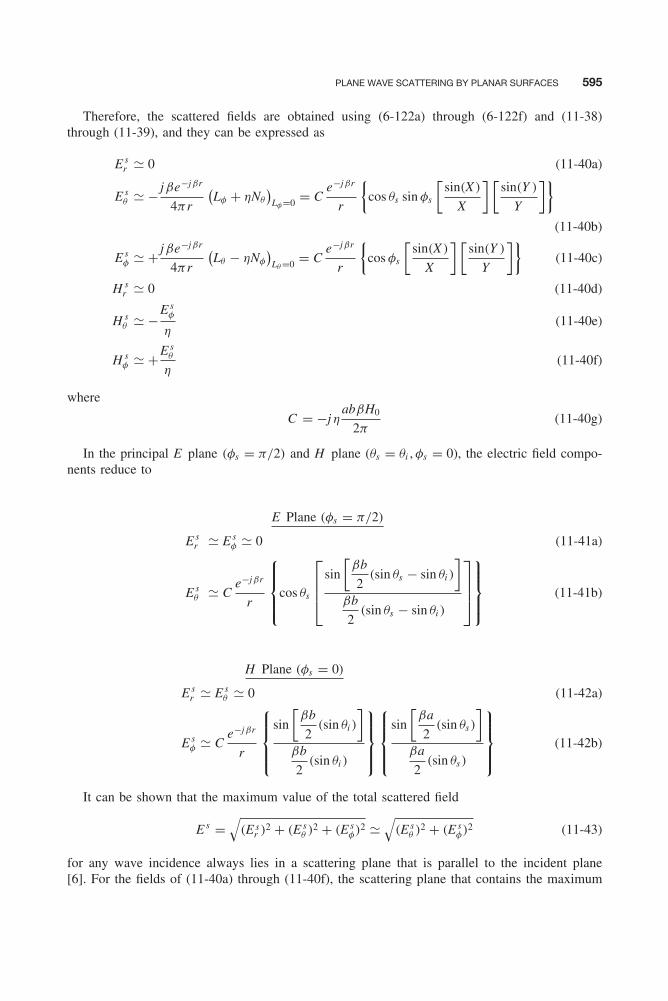
Balanis c11.tex V2 - 11/22/2011 3:50 P.M. Page 595
PLANE WAVE SCATTERING BY PLANAR SURFACES 595
Therefore, the scattered fields are obtained using (6-122a) through (6-122f) and (11-38)through (11-39), and they can be expressed as
E sr � 0 (11-40a)
E sθ � − jβe−jβr
4πr
(Lφ + ηNθ
)Lφ=0 = C
e−jβr
r
{cos θs sin φs
[sin(X )
X
] [sin(Y )
Y
]}(11-40b)
E sφ � + jβe−jβr
4πr
(Lθ − ηNφ
)Lθ=0 = C
e−jβr
r
{cos φs
[sin(X )
X
] [sin(Y )
Y
]}(11-40c)
H sr � 0 (11-40d)
H sθ � −E s
φ
η(11-40e)
H sφ � +E s
θ
η(11-40f)
where
C = −jηabβH0
2π(11-40g)
In the principal E plane (φs = π/2) and H plane (θs = θi , φs = 0), the electric field compo-nents reduce to
E Plane (φs = π/2)
E sr � E s
φ � 0 (11-41a)
E sθ � C
e−jβr
r
⎧⎪⎪⎨⎪⎪⎩cos θs
⎡⎢⎢⎣ sin
[βb
2(sin θs − sin θi )
]βb
2(sin θs − sin θi )
⎤⎥⎥⎦⎫⎪⎪⎬⎪⎪⎭ (11-41b)
H Plane (φs = 0)
E sr � E s
θ � 0 (11-42a)
E sφ � C
e−jβr
r
⎧⎪⎪⎨⎪⎪⎩sin
[βb
2(sin θi )
]βb
2(sin θi )
⎫⎪⎪⎬⎪⎪⎭⎧⎪⎪⎨⎪⎪⎩
sin
[βa
2(sin θs)
]βa
2(sin θs)
⎫⎪⎪⎬⎪⎪⎭ (11-42b)
It can be shown that the maximum value of the total scattered field
E s =√
(E sr )2 + (E s
θ )2 + (E sφ)2 �
√(E s
θ )2 + (E sφ)2 (11-43)
for any wave incidence always lies in a scattering plane that is parallel to the incident plane[6]. For the fields of (11-40a) through (11-40f), the scattering plane that contains the maximum
Balanis c11.tex V2 - 11/22/2011 3:50 P.M. Page 596
596 SCATTERING
scattered field is that defined by φs = π/2, 3π/2 and 0 ≤ θs ≤ π/2, since the incident plane isthat defined by φi = 3π/2, 0 ≤ θi ≤ π/2. The electric field components in the plane that whichcontains the maximum reduce to those of (11-41a) and (11-41b) whose maximum value, whenb � λ, occurs approximately when θs = θi (specular reflection). For large values of b(b � λ)
the sin(z )/z function in (11-41b) varies very rapidly compared to the cos θs such that the cos θs
function is essentially constant near the maximum of the sin(z )/z function. For small values ofb, the maximum value of (11-41b) can be found iteratively. Thus, for the TEx polarization, themaximum of the scattered field from a flat plate does not occur exactly at the specular direction butit approaches that value as the dimensions of the plate become large compared to the wavelength.This is analogous to the TEz polarization of the strip of Example 11-1. It will be shown in theexample that follows that for the TMx polarization, the maximum of the scattered field from aflat plate always occurs at the specular direction no matter what the size of the plate. This isanalogous to the TMz polarization of the strip of Section 11.3.1.
For the fields of (11-40a) through (11-40g), the radar cross section is obtained using (11-22b)or (11-22c) and can be written as
σ3-D = limr→∞
[4πr2 |Es |2
|Ei |2]
= limr→∞
[4πr2 |Hs |2
|Hi |2]
= 4π
(ab
λ
)2
(cos2 θs sin2 φs + cos2 φs)
[sin(X )
X
]2 [sin(Y )
Y
]2
(11-44)
which in the plane that contains the maximum (φs = π/2) reduces to
Principal Bistatic (φs = π/2)
σ3-D = 4π
(ab
λ
)2
cos2 θs
⎡⎢⎢⎣ sin
[βb
2(sin θs ∓ sin θi )
]βb
2(sin θs ∓ sin θi
⎤⎥⎥⎦2
−for φs = π
2, 0 ≤ θs ≤ π/2
+for φs = 3π
2, 0 ≤ θs ≤ π/2
(11-44a)
while in the backscattering direction (φs = φi = 3π/2, θs = θi ) it can be written as
Backscattered
σ3-D = 4π
(ab
λ
)2
cos2 θi
[sin(βb sin θi )
βb sin θi
]2
(11-44b)
Plots of (11-44a) for a = b = 5λ and θi = 30◦ (φs = 90◦, 270◦ with 0◦ ≤ θs ≤ 90◦) and of(11-44b) for a = b = 5λ (0◦ ≤ θi , ≤ 90◦) are shown, respectively, in Figures 11-9a and 11-9b.It is observed that for Figure 11-9a the maximum occurs when φs = 90◦ and near θs � θi = 30◦while for Figure 11-9b the maximum occurs when θi = 0◦ (normal incidence).
The monostatic RCS of plates using physical optics techniques is insensitive to polarization,i.e., it is the same for both polarizations [7-10], as has been demonstrated for the strip and therectangular plate. Measurements, however, have shown that the monostatic RCS is slightly dif-ferent for the two polarizations. This is one of the drawbacks of physical optics methods. Inaddition, the predicted RCSs using physical optics are most accurate at and near the speculardirections. However, they begin to become less valid away from the specular directions, espe-cially toward grazing incidences. This will be demonstrated in Example 12-3, and Figures 12-13and 12-14.
Balanis c11.tex V2 - 11/22/2011 3:50 P.M. Page 597
PLANE WAVE SCATTERING BY PLANAR SURFACES 597
TMx
a = b = 5λ
TEx
40
30
20
10
0
−10
−2090 45
Observation angle qs (degrees)
(a)
0 45 90
RC
S (s
3-D
/λ2 )
(dB
)
qi = 30°
fs = 270° fs = 90°
a = b = 5λTEx, TMx
40
30
20
10
0
−10
−2090 45
Observation angle qi (degrees)
(b)
0 45 90
RC
S (s
3-D
/λ2 )
(dB
)
fs = 270° fs = 90°
Figure 11-9 Principal plane monostatic and bistatic radar cross sections of a rectangular plate. (a) Bistatic(θi = 30◦, φi = 270◦, φs = 90◦, 270◦). (b) Monostatic (φs = 90◦, 270◦).

Balanis c11.tex V2 - 11/22/2011 3:50 P.M. Page 598
598 SCATTERING
Example 11-3
Using physical optics techniques, find the scattered fields and radar cross section when a TMx uniformplane wave is incident upon a flat rectangular plate of dimensions a and b. Assume the incident fieldlies on the yz plane, as shown in Figure 11-8c.
Solution: According to the geometry of Figure 11-8c, the electric and magnetic field components ofthe incident uniform plane wave can be written as
Ei = âx E0e−jβ(y sin θi −z cos θi )
Hi = −E0
η
(ây cos θ i + âz sin θ i
)e−jβ(y sin θi −z cos θi )
Using physical optics techniques, the current density induced on the plate can be approximated by
Js � 2n̂ × Hi∣∣∣ z=0y=y ′
= 2âz × (ây Hy + âz Hz
) ∣∣∣ z=0y=y ′
= −2âx Hy
∣∣∣ z=0y=y ′
= âx2E0
ηcos θi e
−jβy ′ sin θi
orJy = Jz = 0 Jx = 2E0
ηcos θi e
−jβy ′ sin θi
Using (6-125a) and (6-125b), we can write that
Nθ =∫∫
SJx cos θs cos φs ejβ(x ′ sin θs cos φs +y ′ sin θs sin φs ) dx ′ dy ′
= 2E0
ηab
{cos θi cos θs cos φs
[sin(X )
X
] [sin(Y )
Y
]}Nφ = −
∫∫S
Jx sin φs ejβ(x ′ sin θs cos φs +y ′ sin θs sin φs ) dx ′ dy ′
= −2E0
ηab
{cos θi sin θs
[sin(X )
X
] [sin(Y )
Y
]}where
X = βa
2sin θs cos φs
Y = βb
2(sin θs sin φs − sin θi )
The scattered fields are obtained using (6-122a) through (6-122f) and can be written as
E sr � H s
r � 0
E sθ � C1
e−jβr
r
{cos θi cos θs cos φs
[sin(X )
X
] [sin(Y )
Y
]}E s
φ � C1e−jβr
r
{cos θi sin φs
[sin(X )
X
] [sin(Y )
Y
]}H s
θ � −E sφ
ηH s
φ � +E sθ
η
C1 = abβE0
2π
Balanis c11.tex V2 - 11/22/2011 3:50 P.M. Page 599
CYLINDRICAL WAVE TRANSFORMATIONS AND THEOREMS 599
In the principal H plane (φs = π/2), on which the maximum also lies, the electric field componentsreduce to
E sr � E s
θ � 0
E sφ � C1
e−jβr
r
⎧⎪⎪⎨⎪⎪⎩cos θi
⎡⎢⎢⎣ sin
[βb
2(sin θs − sin θi )
]βb
2(sin θs − sin θi )
⎤⎥⎥⎦⎫⎪⎪⎬⎪⎪⎭
whose maximum value always occurs when θs = θi (no matter what the size of the ground plane).The bistatic and monostatic RCSs can be expressed, respectively, as
σ3-D(bistatic) = 4π
(ab
λ
)2
[cos2 θi (cos2 θs cos2 φs + sin2 φs )]
×[
sin(X )
X
]2 [sin(Y )
Y
]2
σ3-D(monostatic) = 4π
(ab
λ
)2
cos2 θi
[sin(βb sin θi )
βb sin θi
]2
They are shown plotted, respectively, in Figures 11-9a and 11-9b for a square plate of a = b = 5λ.
11.4 CYLINDRICAL WAVE TRANSFORMATIONS AND THEOREMS
In scattering, it is often most convenient to express wave functions of one coordinate systemin terms of wave functions of another coordinate system. An example is a uniform plane wavethat can be written in a very simple form in terms of rectilinear wave functions. However, whenscattering of plane waves by cylindrical structures is considered, it is most desirable to transformthe rectilinear form of the uniform plane wave into terms of cylindrical wave functions. This isdesirable because the surface of the cylindrical structure is most conveniently defined using cylin-drical coordinates. This and other such transformations are referred to as wave transformations[11]. Along with these transformations, certain theorems concerning cylindrical wave functionsare very desirable in describing the scattering by cylindrical structures.
11.4.1 Plane Waves in Terms of Cylindrical Wave Functions
The scattering of plane waves by cylindrical structures is considered a fundamental problem inscattering theory. To accomplish this, it is first necessary and convenient to express the planewaves by cylindrical wave functions. To demonstrate that, let us assume that a normalized uniformplane wave traveling in the +x direction, as shown in Figure 11-10, can be written as
E = âz E+z = âz E0e−jβx = âz e−jβx (11-45)
The plane wave can be represented by an infinite sum of cylindrical wave functions of the form
E+z = e−jβx = e−jβρ cos φ =
+∞∑n=−∞
anJn(βρ)ejnφ (11-45a)
since it must be periodic in φ and finite at ρ = 0. The next step is to determine the amplitudecoefficients, an .
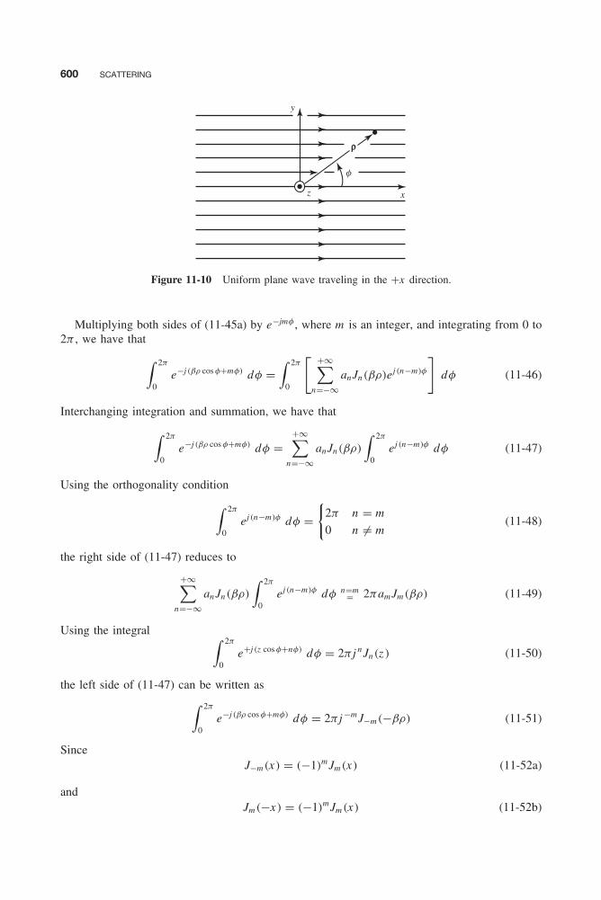
Balanis c11.tex V2 - 11/22/2011 3:50 P.M. Page 600
600 SCATTERING
xz
y
ρ
f
Figure 11-10 Uniform plane wave traveling in the +x direction.
Multiplying both sides of (11-45a) by e−jmφ , where m is an integer, and integrating from 0 to2π , we have that∫ 2π
0e−j (βρ cos φ+mφ) dφ =
∫ 2π
0
[ +∞∑n=−∞
anJn(βρ)ej (n−m)φ
]dφ (11-46)
Interchanging integration and summation, we have that∫ 2π
0e−j (βρ cos φ+mφ) dφ =
+∞∑n=−∞
anJn(βρ)
∫ 2π
0ej (n−m)φ dφ (11-47)
Using the orthogonality condition∫ 2π
0ej (n−m)φ dφ =
{2π n = m
0 n �= m(11-48)
the right side of (11-47) reduces to
+∞∑n=−∞
anJn(βρ)
∫ 2π
0ej (n−m)φ dφ n=m= 2πamJm(βρ) (11-49)
Using the integral ∫ 2π
0e+j (z cos φ+nφ) dφ = 2π j nJn(z ) (11-50)
the left side of (11-47) can be written as∫ 2π
0e−j (βρ cos φ+mφ) dφ = 2π j −mJ−m(−βρ) (11-51)
SinceJ−m(x) = (−1)mJm(x) (11-52a)
andJm(−x) = (−1)mJm(x) (11-52b)

Balanis c11.tex V2 - 11/22/2011 3:50 P.M. Page 601
CYLINDRICAL WAVE TRANSFORMATIONS AND THEOREMS 601
(11-51) can be written as∫ 2π
0e−j (βρ cos φ+mφ) dφ = 2π j −mJ−m(−βρ) = 2π j −m(−1)mJm(−βρ)
= 2π j −m(−1)m(−1)mJm(βρ) = 2π j −m(−1)2mJm(βρ)∫ 2π
0e−j (βρ cos φ+mφ) dφ = 2π j −mJ−m(−βρ) = 2π j −mJm(βρ) (11-53)
Using (11-49) and (11-53), reduce (11-47) to2π j −mJm(βρ) = 2πamJm(βρ) (11-54)
Thus,am = j −m (11-54a)
Therefore, (11-45a) can be written as
E+z = e−jβx = e−jβρ cos φ =
+∞∑n=−∞
anJn(βρ)ejnφ =+∞∑
n=−∞j −nJn(βρ)ejnφ (11-55a)
In a similar manner it can be shown that
E−z = e+jβx = e+jβρ cos φ =
+∞∑n=−∞
j +nJn(βρ)ejnφ (11-55b)
11.4.2 Addition Theorem of Hankel Functions
A transformation that is often convenient and necessary in scattering problems is the additiontheorem of Hankel functions [11]. Basically, it expresses the fields of a cylindrical line sourcelocated away from the origin at a radial distance ρ ′, which are represented by cylindrical wavefunctions originating at the source, in terms of cylindrical wave functions originating at the origin(ρ = 0) of the coordinate system.
To derive this, let us assume that a line source of electric current I0 is located at ρ = ρ ′ and φ =φ′, as shown in Figure 11-11. According to (11-11a), the fields by the line source are given by
Ez (ρ, φ) = −β2I0
4ωεH (2)
0 (β|ρ − ρ′|) (11-56)
y
zx
Line source 0
R = ρ − ρ′
ρ′
f′ f
ρ
Figure 11-11 Geometry for displaced line source.
Balanis c11.tex V2 - 11/22/2011 3:50 P.M. Page 602
602 SCATTERING
where |ρ − ρ′| is the radial distance from the source to the observation point. Using Figure 11-11and the law of cosines, (11-56) can also be written as
Ez (ρ, φ) = −β2I0
4ωεH (2)
0 (β|ρ − ρ′|)
= −β2I0
4ωεH (2)
0
[β√
ρ2 + (ρ ′)2 − 2ρρ ′ cos(φ − φ′)]
(11-56a)
Equations 11-56 and 11-56a express the electric field in terms of a Hankel function whose radialdistance originates at the source (|ρ − ρ′| = 0). For scattering problems, it is very convenient toexpress the field in terms of cylindrical wave functions, such as Bessel and Hankel functions,whose radial distance originates at the origin (ρ = 0). Based upon that and because of reciprocity,the field must be symmetric in terms of the primed and unprimed coordinates. Therefore, thepermissible wave functions, whose radial distance originates at the origin of the coordinate system,to represent the Hankel function of (11-56a) are of the form
ρ ≤ ρ ′
f (βρ ′)Jn(βρ)ejn(φ−φ′)
where n is an integer, because they must be finite at ρ = 0 and be periodic with period 2π .
ρ ≥ ρ ′
g(βρ ′)H (2)n (βρ)ejn(φ−φ′)
where n is an integer, because they must represent outward traveling waves and they must beperiodic with period 2π .
Thus, the Hankel function of (11-56a) can be written as
H (2)0 (β|ρ − ρ′|) =
⎧⎪⎪⎪⎪⎪⎪⎨⎪⎪⎪⎪⎪⎪⎩
+∞∑n=−∞
cn f (βρ ′)Jn(βρ)ejn(φ−φ′) for ρ ≤ ρ ′
+∞∑n=−∞
dng(βρ ′)H (2)n (βρ)ejn(φ−φ′) for ρ ≥ ρ ′
(11-57a)
(11-57b)
Since at ρ = ρ ′ the fields of the two regions must be continuous, then from (11-57a) and(11-57b)
cn f (βρ ′)Jn(βρ ′) = dng(βρ ′)H (2)n (βρ ′) (11-58)
which can be satisfied provided
cn = dn = bn (11-59a)
f (βρ ′) = H (2)n (βρ ′) (11-59b)
g(βρ ′) = Jn(βρ ′) (11-59c)
Using (11-59a) through (11-59c), we can write (11-57a) and (11-57b) as
H (2)0 (β|ρ − ρ′|) =
⎧⎪⎪⎪⎪⎪⎪⎨⎪⎪⎪⎪⎪⎪⎩
+∞∑n=−∞
bnJn(βρ)H (2)n (βρ ′)ejn(φ−φ′) for ρ ≤ ρ ′
+∞∑n=−∞
bnJn(βρ ′)H (2)n (βρ)ejn(φ−φ′) for ρ ≥ ρ ′
(11-60a)
(11-60b)
Balanis c11.tex V2 - 11/22/2011 3:50 P.M. Page 603
CYLINDRICAL WAVE TRANSFORMATIONS AND THEOREMS 603
The only remaining part is to evaluate bn . This can be accomplished by returning to (11-56a),according to which
H (2)0 (β|ρ − ρ′|) = H (2)
0
[β√
ρ2 + (ρ ′)2 − 2ρρ ′ cos(φ − φ′)]
(11-61)
Moving the source toward infinity (ρ ′ → ∞) along φ′ = 0, the radial distance in (11-61), asrepresented by the square root, can be approximated using the binomial expansion
√ρ2 + (ρ ′)2 − 2ρρ ′ cos(φ − φ′)
φ′=0�ρ′→∞
√(ρ ′)2 − 2ρρ ′ cos φ = ρ ′
√1 − 2
(ρ
ρ ′
)cos φ
� ρ ′(
1 − ρ
ρ ′ cos φ
)= ρ ′ − ρ cos φ (11-62)
Using (11-62) allows us to write (11-61) as
H (2)0 (β|ρ − ρ′|) = H (2)
0
[β√
ρ2 + (ρ ′)2 − 2ρρ ′ cos(φ − φ′)]
φ′=0�ρ′→∞
H (2)0
[β(ρ ′ − ρ cos φ)
](11-63)
With the aid of the asymptotic form of the Hankel function for large argument
H (2)0 (αx)
αx→∞�√
2j
παxj ne−jαx (11-64)
(11-63) reduces to
H (2)0 (β|ρ − ρ′|) φ′=0�
ρ′→∞H (2)
0
[β(ρ ′ − ρ cos φ)
] �√
2j
πβ(ρ ′ − ρ cos φ)e−jβ(ρ′−ρ cos φ)
�√
2j
πβρ ′ e−jβρ′
e+jβρ cos φ (11-65)
Using (11-55b) allows us to write (11-65) as
H (2)0 (β|ρ − ρ′|) φ′=0�
ρ′→∞
√2j
πβρ ′ e−jβρ′
+∞∑n=−∞
j nJn(βρ)ejnφ (11-66)
Applying (11-64) to (11-60a) for φ′ = 0 and ρ ′ → ∞, reduces it to
H (2)0 (β|ρ − ρ′|) φ′=0=
+∞∑n=−∞
bnJn(βρ)H (2)n (βρ ′)ejnφ
φ′=0�ρ′→∞
√2j
πβρ ′ e−jβρ′
+∞∑n=−∞
bnj nJn(βρ)ejnφ (11-67)
Comparing (11-66) and (11-67) leads to
bn = 1 (11-68)
Balanis c11.tex V2 - 11/22/2011 3:50 P.M. Page 604
604 SCATTERING
Thus, the final form of (11-60a) and (11-60b) is
H (2)0 (β|ρ − ρ′|) =
⎧⎪⎪⎪⎪⎪⎪⎨⎪⎪⎪⎪⎪⎪⎩
+∞∑n=−∞
Jn(βρ)H (2)n (βρ ′)ejn(φ−φ′) for ρ ≤ ρ ′
+∞∑n=−∞
Jn(βρ ′)H (2)n (βρ)ejn(φ−φ′) for ρ ≥ ρ ′
(11-69a)
(11-69b)
which can be used to write (11-56) as
Ez (ρ, φ) = −β2I0
4ωεH (2)
0 (β|ρ − ρ′|)
= −β2I0
4ωε
⎧⎪⎪⎪⎪⎨⎪⎪⎪⎪⎩
+∞∑n=−∞
Jn(βρ)H (2)n (βρ ′)ejn(φ−φ′) for ρ ≤ ρ ′
+∞∑n=−∞
Jn(βρ ′)H (2)n (βρ)ejn(φ−φ′) for ρ ≥ ρ ′
(11-70a)
(11-70b)
The procedure can be repeated to expand H (1)0 (β|ρ − ρ′|). However, it is obvious from the
results of (11-69a) and (11-69b) that
H (1)0 (β|ρ − ρ′|) =
⎧⎪⎪⎪⎪⎨⎪⎪⎪⎪⎩
+∞∑n=−∞
Jn(βρ)H (1)n (βρ ′)ejn(φ−φ′) for ρ ≤ ρ ′
+∞∑n=−∞
Jn(βρ ′)H (1)n (βρ)ejn(φ−φ′) for ρ ≥ ρ ′
(11-71a)
(11-71b)
11.4.3 Addition Theorem for Bessel Functions
Another theorem that is often useful represents Bessel functions originating at the source, whichis located away from the origin, in terms of cylindrical wave functions originating at the originof the coordinate system. This is usually referred to as the addition theorem for Bessel functions[11].
We know that the Hankel functions of the first and second kinds can be written, in terms ofthe Bessel functions, as
H (1)0 (βρ) = J0(βρ) + jY0(βρ) (11-72a)
H (2)0 (βρ) = J0(βρ) − jY0(βρ) (11-72b)
Adding the two, we can write that
J0(βρ) = 12 [H (1)
0 (βρ) + H (2)0 (βρ)] (11-73)
Therefore,
J0(β|ρ − ρ′|) = 12 [H (1)
0 (β|ρ − ρ′|) + H (2)0 (β|ρ − ρ′|)] (11-74)

Balanis c11.tex V2 - 11/22/2011 3:50 P.M. Page 605
CYLINDRICAL WAVE TRANSFORMATIONS AND THEOREMS 605
With the aid of (11-69a), (11-69b) and (11-71a), (11-71b) we can write (11-74) as
J0(β|ρ − ρ′|) =
⎧⎪⎪⎪⎪⎪⎪⎨⎪⎪⎪⎪⎪⎪⎩
+∞∑n=−∞
12 [H (1)
n (βρ ′) + H (2)n (βρ ′)]Jn(βρ)ejn(φ−φ′) for ρ ≤ ρ ′
+∞∑n=−∞
12 [H (1)
n (βρ) + H (2)n (βρ)]Jn(βρ ′)ejn(φ−φ′) for ρ ≥ ρ ′
(11-75a)
(11-75b)
Using the forms of (11-72a) and (11-72b) for nth order Bessel and Hankel functions, we canwrite (11-75a) and (11-75b) as
J0(β|ρ − ρ′|) =
⎧⎪⎪⎪⎪⎪⎪⎨⎪⎪⎪⎪⎪⎪⎩
+∞∑n=−∞
Jn(βρ ′)Jn(βρ)ejn(φ−φ′) for ρ ≤ ρ ′
+∞∑n=−∞
Jn(βρ)Jn(βρ ′)ejn(φ−φ′) for ρ ≥ ρ ′
(11-76a)
(11-76b)
or that
J0(β|ρ − ρ′|) =+∞∑
n=−∞Jn(βρ)Jn(βρ ′)ejn(φ−φ′) for ρ � ρ ′ (11-77)
Subtracting (11-72b) from (11-72a), we can write that
H (1)0 (βρ) − H (2)
0 (βρ) = 2jY0(βρ)
Y0(βρ) = 1
2j
[H (1)
0 (βρ) − H (2)0 (βρ)
](11-78a)
or
Y0(β|ρ − ρ′|) = 1
2j
[H (1)
0 (β|ρ − ρ′|) − H (2)0 (β|ρ − ρ′|)
](11-78b)
Using (11-69a), (11-69b), (11-71a), and (11-71b), we can write (11-78b) as
Y0(β|ρ − ρ′|) =
⎧⎪⎪⎪⎪⎪⎪⎨⎪⎪⎪⎪⎪⎪⎩
∞∑n=−∞
12 [H (1)
n (βρ ′) − H (2)n (βρ ′)]Jn(βρ)ejn(φ−φ′) for ρ ≤ ρ ′
+∞∑n=−∞
12 [H (1)
n (βρ) − H (2)n (βρ)]Jn(βρ ′)ejn(φ−φ′) for ρ ≥ ρ ′
(11-79a)
(11-79b)

Balanis c11.tex V2 - 11/22/2011 3:50 P.M. Page 606
606 SCATTERING
Using the forms (11-72a) and (11-72b) for nth order Hankel functions, we can write (11-79a)and (11-79b) as
Y0(β|ρ − ρ′|) =
⎧⎪⎪⎪⎪⎪⎪⎪⎪⎪⎪⎪⎪⎪⎪⎪⎪⎪⎪⎪⎨⎪⎪⎪⎪⎪⎪⎪⎪⎪⎪⎪⎪⎪⎪⎪⎪⎪⎪⎪⎩
+∞∑n=−∞
1
2j
[Jn(βρ ′) + jYn(βρ ′) − Jn(βρ ′) + jYn(βρ ′)
]Jn(βρ ′)ejn(φ−φ′)
=+∞∑
n=−∞Yn(βρ ′)Jn(βρ)ejn(φ−φ′) for ρ ≤ ρ ′
+∞∑n=−∞
1
2j
[Jn(βρ) + jYn(βρ) − Jn(βρ) + jYn(βρ)
]Jn(βρ ′)ejn(φ−φ′)
=+∞∑
n=−∞Yn(βρ)Jn(βρ ′)ejn(φ−φ′) for ρ ≥ ρ ′
(11-80a)
(11-80b)
11.4.4 Summary of Cylindrical Wave Transformations and Theorems
The following are the most prominent cylindrical wave transformations and theorems that arevery convenient for scattering from cylindrical scatterers:
e−jβx = e−jβρ cos φ =+∞∑
n=−∞j −nJn(βρ)ejnφ
e+jβx = e+jβρ cos φ =+∞∑
n=−∞j +nJn(βρ)ejnφ
(11-81a)
(11-81b)
H (1, 2)0 (β|ρ − ρ′|) =
⎧⎪⎪⎪⎪⎪⎪⎨⎪⎪⎪⎪⎪⎪⎩
+∞∑n=−∞
Jn(βρ)H (1, 2)n (βρ ′)ejn(φ−φ′) ρ ≤ ρ ′
+∞∑n=−∞
Jn(βρ ′)H (1, 2)n (βρ)ejn(φ−φ′) ρ ≥ ρ ′
(11-82a)
(11-82b)
J0(β|ρ − ρ′|) =+∞∑
n=−∞Jn(βρ ′)Jn(βρ)ejn(φ−φ′) ρ�ρ′
(11-83)
Y0(β|ρ − ρ′|) =
⎧⎪⎪⎪⎪⎪⎪⎨⎪⎪⎪⎪⎪⎪⎩
+∞∑n=−∞
Yn(βρ ′)Jn(βρ)ejn(φ−φ′) ρ ≤ ρ ′
+∞∑n=−∞
Yn(βρ)Jn(βρ ′)ejn(φ−φ′) ρ ≥ ρ ′
(11-84a)
(11-84b)
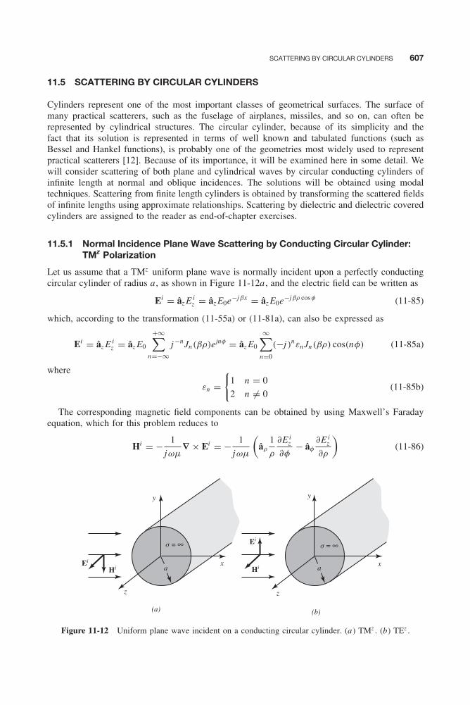
Balanis c11.tex V2 - 11/22/2011 3:50 P.M. Page 607
SCATTERING BY CIRCULAR CYLINDERS 607
11.5 SCATTERING BY CIRCULAR CYLINDERS
Cylinders represent one of the most important classes of geometrical surfaces. The surface ofmany practical scatterers, such as the fuselage of airplanes, missiles, and so on, can often berepresented by cylindrical structures. The circular cylinder, because of its simplicity and thefact that its solution is represented in terms of well known and tabulated functions (such asBessel and Hankel functions), is probably one of the geometries most widely used to representpractical scatterers [12]. Because of its importance, it will be examined here in some detail. Wewill consider scattering of both plane and cylindrical waves by circular conducting cylinders ofinfinite length at normal and oblique incidences. The solutions will be obtained using modaltechniques. Scattering from finite length cylinders is obtained by transforming the scattered fieldsof infinite lengths using approximate relationships. Scattering by dielectric and dielectric coveredcylinders are assigned to the reader as end-of-chapter exercises.
11.5.1 Normal Incidence Plane Wave Scattering by Conducting Circular Cylinder:TMz Polarization
Let us assume that a TMz uniform plane wave is normally incident upon a perfectly conductingcircular cylinder of radius a , as shown in Figure 11-12a , and the electric field can be written as
Ei = âz E iz = âz E0e−jβx = âz E0e−jβρ cos φ (11-85)
which, according to the transformation (11-55a) or (11-81a), can also be expressed as
Ei = âz E iz = âz E0
+∞∑n=−∞
j −nJn(βρ)ejnφ = âz E0
∞∑n=0
(−j )nεnJn(βρ) cos(nφ) (11-85a)
where
εn ={
1 n = 0
2 n �= 0(11-85b)
The corresponding magnetic field components can be obtained by using Maxwell’s Faradayequation, which for this problem reduces to
Hi = − 1
jωμ∇ × Ei = − 1
jωμ
(âρ
1
ρ
∂E iz
∂φ− âφ
∂E iz
∂ρ
)(11-86)
y
xa
z
(a)
Ei Hi
s = ∞
y
xa
z
(b)
Ei
Hi
s = ∞
Figure 11-12 Uniform plane wave incident on a conducting circular cylinder. (a) TMz . (b) TEz .
Balanis c11.tex V2 - 11/22/2011 3:50 P.M. Page 608
608 SCATTERING
or
H iρ = − 1
jωμ
1
ρ
∂E iz
∂φ= − E0
jωμ
1
ρ
+∞∑n=−∞
nj −n+1Jn(βρ)ejnφ (11-86a)
H iφ = 1
jωμ
∂E iz
∂ρ= − βE0
jωμ
+∞∑n=−∞
j −nJ ′n(βρ)ejnφ (11-86b)
′ ≡ ∂
∂(βρ)(11-86c)
It should be noted here that throughout this chapter the prime indicates partial derivative withrespect to the entire argument of the Bessel or Hankel function.
In the presence of the conducting cylinder, the total field E tz according to (11-1a) can be
written as
Et = Ei + Es (11-87)
where Es is the scattered field. Since the scattered fields travel in the outward direction, theymust be represented by cylindrical traveling wave functions. Thus, we choose to represent Es
by
Es = âz E sz = âz E0
+∞∑n=−∞
cnH (2)n (βρ) (11-88)
where cn represents the yet unknown amplitude coefficients. Equation 11-88 is chosen to be ofsimilar form to (11-85a) since the two together will be used to represent the total field. Thisbecomes convenient when we attempt to solve for the amplitude coefficients cn .
The unknown amplitude coefficients cn can be found by applying the boundary condition
Et = âz E tz (ρ = a , 0 ≤ φ ≤ 2π , z ) = 0 (11-89)
Using (11-85a), (11-88), and (11-89) we can write that
E tz (ρ = a , 0 ≤ φ ≤ 2π , z ) = E0
∞∑n=−∞
[j −nJn(βa)ejnφ + cnH (2)
n (βa)] = 0 (11-90)
or
cn = −j −n Jn(βa)
H (2)n (βa)
ejnφ (11-90a)
Thus, the scattered field of (11-88) reduces to
E sz = −E0
+∞∑n=−∞
j −n Jn(βa)
H (2)n (βa)
H (2)n (βρ)ejnφ
= −E0
+∞∑n=0
(−j )nεnJn(βa)
H (2)n (βa)
H (2)n (βρ) cos(nφ) (11-91)
where εn is defined by (11-85b).
Balanis c11.tex V2 - 11/22/2011 3:50 P.M. Page 609
SCATTERING BY CIRCULAR CYLINDERS 609
The corresponding scattered magnetic field components can be obtained by using Maxwell’sequation 11-86, which leads to
H sρ = − 1
jωμ
1
ρ
∂E sz
∂φ= E0
jωμ
1
ρ
+∞∑n=−∞
nj −n+1 Jn(βa)
H (2)n (βa)
H (2)n (βρ)ejnφ (11-92a)
H sφ = 1
jωμ
∂E sz
∂ρ= − βE0
jωμ
+∞∑n=−∞
j −n Jn(βa)
H (2)n (βa)
H (2)′n (βρ)ejnφ (11-92b)
Thus, the total electric and magnetic field components can be written as
E tρ = E t
φ = H tz = 0
E tz = E0
+∞∑n=−∞
j −n
[Jn(βρ) − Jn(βa)
H (2)n (βa)
H (2)n (βρ)
]ejnφ
H tρ = − E0
jωμ
1
ρ
+∞∑n=−∞
nj −n+1
[Jn(βρ) − Jn(βa)
H (2)n (βa)
H (2)n (βρ)
]ejnφ
H tφ = βE0
jωμ
+∞∑n=−∞
j −n
[J ′
n(βρ) − Jn(βa)
H (2)n (βa)
H (2)′n (βρ)
]ejnφ
(11-93a)
(11-93b)
(11-93c)
(11-93d)
On the surface of the cylinder (ρ = a), the total tangential magnetic field can be written as
H tφ(ρ = a) = βE0
jωμ
+∞∑n=−∞
j −n
[J ′
n(βa) − Jn(βa)
H (2)n (βa)
H (2)′n (βa)
]ejnφ
= βE0
ωμ
+∞∑n=−∞
j −n
[Jn(βa)Y ′
n(βa) − J ′n(βa)Yn(βa)
H (2)n (βa)
]ejnφ (11-94)
Using the Wronskian of Bessel functions
Jn(αρ)Y ′n(αρ) − Yn(αρ)J ′
n(αρ) = 2
παρ(11-95)
reduces (11-94) to
H tφ(ρ = a) = 2E0
πaωμ
+∞∑n=−∞
j −n ejnφ
H (2)n (βa)
(11-96)
Thus, the current induced on the surface of the cylinder can be written as
Js = n̂ × Ht |ρ=a = âρ × (âρH t
ρ + âφH tρ
) |ρ=a = âz H tφ(ρ = a)
= âz2E0
πaωμ
+∞∑n=−∞
j −n ejnφ
H (2)n (βa)
(11-97)

Balanis c11.tex V2 - 11/22/2011 3:50 P.M. Page 610
610 SCATTERING
A. Small Radius Approximation As the radius of the cylinder increases, more terms in theinfinite series of (11-97) are needed to obtain convergence. However, for very small cylinders,like a very thin wire (a � λ), the first term (n = 0) in (11-97) is dominant and is often sufficientto represent the induced current. Thus, for a very thin wire (11-97) can be approximated by
Jsa�λ� âz
2E0
πaωμ
1
H (2)0 (βa)
(11-98)
where
H (2)0 (βa) = J0(βa) − jY0(βa)
a�λ� 1 − j2
πln
(γβa
2
)= 1 − j
2
πln
(1.781βa
2
)a�λ� −j
2
πln
(1.781βa
2
)(11-98a)
Thus, for a very thin wire the current density (11-98) can be approximated by
Jsa�λ� âz j
E0
aωμ
1
ln
(1.781βa
2
) (11-98b)
B. Far-Zone Scattered Field One of the most important parameters in scattering is thescattering width, which is obtained by knowing the scattered field in the far zone. For thisproblem, it can be accomplished by first reducing the scattered fields for far-zone observations(βρ → large). Referring to (11-91), the Hankel function can be approximated for observationsmade in the far field by
H (2)n (βρ)
βρ→large�√
2j
πβρj ne−jβρ (11-99)
which, when substituted in (11-91), reduces it to
E sz
βρ→∞� −E0
√2j
πβ
e−jβρ
√ρ
+∞∑n=−∞
Jn(βa)
H (2)n (βa)
ejnφ (11-100)
The ratio of the far-zone scattered electric field to the incident field can then be written as
|E sz |
|E iz |
βρ→large�
∣∣∣ − E0
√2j
πβ
e−jβρ
√ρ
+∞∑n=−∞
Jn(βa)
H (2)n (βa)
ejnφ∣∣∣
|E0e−jβx |
=√
2
πβρ
∣∣∣ +∞∑n=−∞
Jn(βa)
H (2)n (βa)
ejnφ∣∣∣ (11-101)
Thus, the scattering width of (11-21b) can be expressed as
σ2-D = limρ→∞
[2πρ
|E sz |2
|E iz |2
]= 4
β
∣∣∣ +∞∑n=−∞
Jn(βa)
H (2)n (βa)
ejnφ∣∣∣2
= 2λ
π
∣∣∣ +∞∑n=−∞
εnJn(βa)
H (2)n (βa)
cos(nφ)
∣∣∣2 (11-102)

Balanis c11.tex V2 - 11/22/2011 3:50 P.M. Page 611
SCATTERING BY CIRCULAR CYLINDERS 611
0°0.2
0.3
0.5
1.0
2
3
5
10
15
TMz
Hi
Ei
40° 80° 120° 160°
f
f
s = ∞
l = ∞
x
y
a
a = 0.6λ
0.4λ
0.2λ
0.1λ
0.05λ
z
SW
(s
2-D
/λ)
Figure 11-13 Two-dimensional TMz bistatic scattering width (SW) of a circular conducting cylinder.(Courtesy of J. H. Richmond, Ohio State University.)
where
εn ={
1 n = 0
2 n �= 0(11-102a)
Plots of the bistatic σ2-D/λ computed using (11-102) are shown in Figure 11-13 for cylinderradii of a = 0.05λ, 0.1λ, 0.2λ, 0.4λ, and 0.6λ [13]. The backscattered (φ = 180◦) patterns ofσ2-D/λ, as a function of the cylinder radius, are displayed in Figure 11-14 [13].
00
1
2
3
4
5
0.2 0.4 0.6 0.8
Radius a/λ
TMz TEz
s = ∞l = ∞
1 1.2 1.4
SW
(s
2-D
/λ)
Figure 11-14 Two-dimensional monostatic (backscattered) scattering width for a circular conducting cylin-der as a function of its radius. (Courtesy of J. H. Richmond, Ohio State University.)
Balanis c11.tex V2 - 11/22/2011 3:50 P.M. Page 612
612 SCATTERING
For small radii (a � λ), the first term (n = 0) in (11-102) is the dominant term, and it issufficient to represent the scattered field. Thus, for small radii, the ratio of the Bessel to theHankel function for n = 0 can be approximated using (11-98a) by
J0(βa)
H (2)0 (βa)
a�λ� 1
−j2
πln(0.89βa)
= jπ
2
1
ln (0.89βa)(11-103)
and (11-102) can then be reduced to
σ2-Da�λ� 2λ
π
(π2
4
) ∣∣∣∣ 1
ln(0.89βa)
∣∣∣∣2
= πλ
2
∣∣∣∣ 1
ln(0.89βa)
∣∣∣∣2
(11-103a)
This is independent of φ, which becomes evident in Figure 11-13 by the curves for the smallervalues of a.
For a cylinder of finite length � the three-dimensional radar cross section for normal incidence isrelated to the two-dimensional scattering width by (11-22e). Thus, using (11-102) and (11-103a),we can write the three-dimensional RCS (11-22e) as
σ3-D � 4�2
π
∣∣∣∣∣+∞∑
n=−∞
Jn(βa)
H (2)n (βa)
ejnφ
∣∣∣∣∣2
(11-104a)
σ3-Da�λ� π�2
∣∣∣∣ 1
ln(0.89βa)
∣∣∣∣2
(11-104b)
11.5.2 Normal Incidence Plane Wave Scattering by Conducting Circular Cylinder:TEz Polarization
Now let us assume that a TEz uniform plane wave traveling in the +x direction is normallyincident upon a perfectly conducting circular cylinder of radius a , as shown in Figure 11-12b.The incident magnetic field can be written as
Hi = âz H0e−jβx = âz H0e−jβρ cos φ = âz H0
+∞∑n=−∞
j −nJn(βρ)ejnφ
= âz H0
∞∑n=0
(−j )nεnJn(βρ) cos(nφ) (11-105)
where εn is defined by (11-85b). The corresponding incident electric field can be obtained byusing Maxwell’s Ampere equation, which for this problem reduces to
Ei = 1
jωε∇ × Hi = + 1
jωε
[âρ
1
ρ
∂H iz
∂φ− âφ
∂H iz
∂ρ
](11-106)
and by using (11-105) leads to
E iρ = 1
jωε
1
ρ
∂H iz
∂φ= H0
jωε
1
ρ
+∞∑n=−∞
nj −n+1Jn(βρ)ejnφ (11-106a)
Balanis c11.tex V2 - 11/22/2011 3:50 P.M. Page 613
SCATTERING BY CIRCULAR CYLINDERS 613
E iφ = − 1
jωε
∂H iz
∂ρ= −βH0
jωε
+∞∑n=−∞
j −nJ ′n(βρ)ejnφ (11-106b)
The scattered magnetic field takes a form very similar to that of the scattered electric fieldof (11-88) for the TMz polarization, and it can be written as
Hs = âz H sz = âz H0
+∞∑n=−∞
dnH (2)n (βρ) (11-107)
where dn represents the yet unknown amplitude coefficients that will be found by applying theappropriate boundary conditions.
Before the boundary conditions on the vanishing of the total tangential electric field on thesurface of the cylinder can be applied, it is necessary to first find the corresponding electric fields.This can be accomplished by using Maxwell’s equation 11-106, that for the scattered magneticfield of (11-107), leads to
E sρ = 1
jωε
1
ρ
∂H sz
∂φ= H0
jωε
1
ρ
+∞∑n=−∞
H (2)n (βρ)
∂dn
∂φ(11-108a)
E sφ = − 1
jωε
∂H sz
∂ρ= −βH0
jωε
+∞∑n=−∞
dnH (2)′n (βρ) (11-108b)
where ′ indicates a partial derivate with respect to the entire argument of the Hankel function.Since the cylinder is perfectly electric conducting, the tangential components of the total
electric field must vanish on its surface (ρ = a). Thus, using (11-106b) and (11-108b), we canwrite that
E tφ(ρ = a , 0 ≤ φ ≤ 2π , z ) = −βH0
jωε
+∞∑n=−∞
[j −nJ ′
n(βa)ejnφ + dnH (2)′n (βa)
] = 0 (11-109)
which is satisfied provided
dn = −j −n J ′n(βa)
H (2)′n (βa)
ejnφ (11-109a)
Thus, the scattered electric and magnetic fields can be written, using (11-107) and (11-109a),as
E sz = H s
ρ = H sφ = 0 (11-110a)
E sρ = − H0
jωε
1
ρ
+∞∑n=−∞
nj −n+1 J ′n(βa)
H (2)′n (βa)
H (2)n (βρ)ejnφ (11-110b)
E sφ = βH0
jωε
+∞∑n=−∞
j −n J ′n(βa)
H (2)′n (βa)
H (2)′n (βρ)ejnφ (11-110c)
H sz = −H0
+∞∑n=−∞
j −n J ′n(βa)
H (2)′n (βa)
H (2)n (βρ)ejnφ (11-110d)

Balanis c11.tex V2 - 11/22/2011 3:50 P.M. Page 614
614 SCATTERING
The total electric and magnetic fields can now be expressed [using (11-105), (11-106a), (11-106b), and (11-110a) through (11-110d)] as
E tz = H t
ρ = H tφ = 0
E tρ = H0
jωε
1
ρ
+∞∑n=−∞
nj −n+1
[Jn(βρ) − J ′
n(βa)
H (2)′n (βa)
H (2)n (βρ)
]ejnφ
E tφ = −βH0
jωε
+∞∑n=−∞
j −n
[J ′
n(βρ) − J ′n(βa)
H (2)′n (βa)
H (2)′n (βρ)
]ejnφ
H tz = H0
+∞∑n=−∞
j −n
[Jn(βρ) − J ′
n(βa)
H (2)′n (βa)
H (2)n (βρ)
]ejnφ
(11-111a)
(11-111b)
(11-111c)
(11-111d)
On the surface of the cylinder (ρ = a), the total tangential magnetic field can be written as
H tz (ρ = a) = H0
+∞∑n=−∞
j −n
[Jn(βa) − J ′
n(βa)
H (2)′n (βa)
H (2)n (βa)
]ejnφ
= −H0
+∞∑n=−∞
j −n+1
[Jn(βa)Y ′
n(βa) − J ′n(βa)Yn(βa)
H (2)′n (βρ)
]ejnφ (11-112)
which reduces, using the Wronskian of (11-95), to
H tz (ρ = a) = −jH0
2
πβa
+∞∑n=−∞
j −n ejnφ
H (2)′n (βa)
(11-112a)
Thus, the current induced on the surface of the cylinder can be written as
Js = n̂ × Ht |ρ=a = âρ × âz H tz |ρ=a = −âφH t
z (ρ − a)
= âφ j2H0
πβa
+∞∑n=−∞
j −n ejnφ
H (2)′n (βa)
(11-113)
A. Small Radius Approximation As the radius of the cylinder increases, more terms in theinfinite series of (11-113) are needed to obtain convergence. However, for very small cylinders,like very thin wires where a � λ, the first three terms (n = 0, n = ±1) in (11-113) are dominantand are sufficient to represent the induced current. Thus, for a very thin wire, (11-113) can beapproximated by
Jsa�λ� âφ j
2H0
πβa
[1
H (2)′0 (βa)
+ j −1 ejφ
H (2)′1 (βa)
+ j +1 e−jφ
H (2)′−1 (βa)
](11-114)
where
H (2)′0 (βa) = −H (2)
1 (βa) = − [J1(βa) − jY1(βa)
]a�λ� −
[βa
2+ j
1
π
(2
βa
)]= −j
2
πβa(11-114a)

Balanis c11.tex V2 - 11/22/2011 3:50 P.M. Page 615
SCATTERING BY CIRCULAR CYLINDERS 615
H (2)′1 (βa) = −H (2)
2 (βa) + 1
βaH (2)
1 (βa)
= − [J2(βa) − jY2(βa)
] + 1
βa
[J1(βa) − jY1(βa)
]a�λ� −
[1
2
(βa
2
)2
+ j1
π
(2
βa
)2]
+ 1
βa
[βa
2+ j
1
π
(2
βa
)]a�λ� −
[j
1
π
(2
βa
)2]
+ 1
βa
[j
1
π
(2
βa
)]= −j
2
π
1
(βa)2(11-114b)
H (2)′−1 (βa) = −H (2)′
1 (βa)a�λ� +j
2
π
1
(βa)2(11-114c)
Therefore, (11-114) reduces to
Jsa�λ� âφJ
2H0
πβa
[−πβa
j 2+ j
π
j 2(βa)2ejφ + j
π
j 2(βa)2e−jφ
]a�λ� âφH0
[−1 + jβa(ejφ + e−jφ)] = âφH0
[−1 + j 2(βa) cos(φ)]
(11-114d)
B. Far-Zone Scattered Field Since the scattered field, as given by (11-110a), through(11-110d), has two non-vanishing electric field components and only one magnetic field compo-nent, it is most convenient to use the magnetic field to find the far-zone scattered field patternand the radar cross section. However, the same answer can be obtained using the electric fieldcomponents.
For far-field observations, the scattered magnetic field (11-110d) can be approximated, usingthe Hankel function approximation (11-99), by
H sz
βρ→∞� −H0
√2j
πβ
e−jβρ
√ρ
+∞∑n=−∞
J ′n(βa)
H (2)′n (βa)
ejnφ (11-115)
The ratio of the far-zone scattered magnetic field to the incident field can then be written as
|H sz |
|H iz |
βρ→∞�
∣∣∣∣∣−H0
√2j
πβ
e−jβρ
√ρ
+∞∑n=−∞
J ′n(βa)
H (2)′n (βa)
ejnφ
∣∣∣∣∣|H0e−jβx |
=√
2
πβρ
∣∣∣∣∣+∞∑
n=−∞
J ′n(βa)
H (2)′n (βa)
ejnφ
∣∣∣∣∣ (11-116)
Thus, the scattering width of (11-21c) can be expressed as
σ2-D = limρ→∞
[2πρ
|H sz |2
|H iz |2
]= 4
β
∣∣∣∣∣+∞∑
n=−∞
J ′n(βa)
H (2)′n (βa)
ejnφ
∣∣∣∣∣2
= 2λ
π
∣∣∣∣∣+∞∑n=0
εnJ ′
n(βa)
H (2)′n (βa)
cos(nφ)
∣∣∣∣∣2
(11-117)
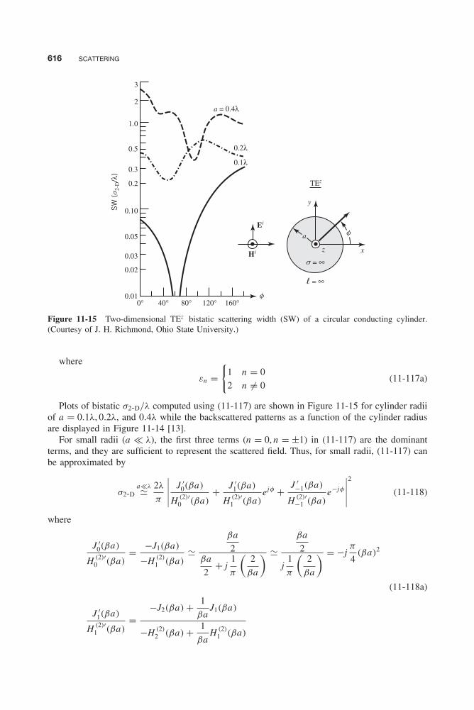
Balanis c11.tex V2 - 11/22/2011 3:50 P.M. Page 616
616 SCATTERING
0°0.01
0.02
0.03
0.05
0.10
0.2
0.3
0.5
1.0
2
3
TEz
Hi
Ei
40° 80° 120° 160°
f
f
s = ∞
l = ∞
x
y
a
a = 0.4λ
0.1λ
0.2λ
z
SW
(s
2-D
/λ)
Figure 11-15 Two-dimensional TEz bistatic scattering width (SW) of a circular conducting cylinder.(Courtesy of J. H. Richmond, Ohio State University.)
where
εn ={
1 n = 0
2 n �= 0(11-117a)
Plots of bistatic σ2-D/λ computed using (11-117) are shown in Figure 11-15 for cylinder radiiof a = 0.1λ, 0.2λ, and 0.4λ while the backscattered patterns as a function of the cylinder radiusare displayed in Figure 11-14 [13].
For small radii (a � λ), the first three terms (n = 0, n = ±1) in (11-117) are the dominantterms, and they are sufficient to represent the scattered field. Thus, for small radii, (11-117) canbe approximated by
σ2-Da�λ� 2λ
π
∣∣∣∣∣ J ′0(βa)
H (2)′0 (βa)
+ J ′1(βa)
H (2)′1 (βa)
ejφ + J ′−1(βa)
H (2)′−1 (βa)
e−jφ
∣∣∣∣∣2
(11-118)
where
J ′0(βa)
H (2)′0 (βa)
= −J1(βa)
−H (2)1 (βa)
�βa
2βa
2+ j
1
π
(2
βa
) �βa
2
j1
π
(2
βa
) = −jπ
4(βa)2
(11-118a)
J ′1(βa)
H (2)′1 (βa)
=−J2(βa) + 1
βaJ1(βa)
−H (2)2 (βa) + 1
βaH (2)
1 (βa)
Balanis c11.tex V2 - 11/22/2011 3:50 P.M. Page 617
SCATTERING BY CIRCULAR CYLINDERS 617
J ′1(βa)
H (2)′1 (βa)
�−1
2
(βa
2
)2
+ 1
βa
(βa
2
)−
[1
2
(βa
2
)2
+ j1
π
(2
βa
)2]
+ 1
βa
[(βa
2
)+ j
1
π
(2
βa
)]
�−1
2
(βa
2
)2
+ 1
2
−j1
π
(2
βa
)2
+ 1
βa
[j
1
π
(2
βa
)] �1
2
−j2
π
(1
βa
)2 = jπ
4(βa)2
(11-118b)
J ′−1(βa)
H (2)−1 ′(βa)
= J ′1(βa)
H (2)′1 (βa)
� jπ
4(βa)2 (11-118c)
Thus, (11-118) reduces to
σ2-Da�λ� 2λ
π
∣∣∣−jπ
4(βa)2 + j
π
4(βa)2ejφ + j
π
4(βa)2e−jφ
∣∣∣2
= πλ
8(βa)4 [1 − 2 cos(φ)]2 (11-118d)
Even for small radii (a � λ), σ is a function of φ, as is evident in Figure 11-15 by the curvesfor small values of a.
For a cylinder of finite length �, the three-dimensional radar cross section for normal incidenceis related to the two-dimensional scattering width by (11-22e). Thus, using (11-117) and (11-118d), we can write the three-dimensional RCS (11-22e) as
σ3-D � 4�2
π
∣∣∣∣∣+∞∑
n=−∞
J ′n(βa)
H (2)′n (βa)
ejnφ
∣∣∣∣∣2
= 4�2
π
∣∣∣∣∣+∞∑n=0
εnJ ′
n(βa)
H (2)′n (βa)
cos(nφ)
∣∣∣∣∣2
(11-119a)
σ3-Da�λ� π�2
4(βa)4[1 − 2 cos(φ)]2 (11-119b)
11.5.3 Oblique Incidence Plane Wave Scattering by Conducting Circular Cylinder:TMz Polarization
In the previous two sections we analyzed scattering by a conducting cylinder at normal incidence.Scattering at oblique incidence will be considered here. Let us assume that a TMz plane wavetraveling parallel to the xz plane is incident upon a circular cylinder of radius a , as shown inFigure 11-16. The incident electric field can be written as
Ei = E0(âx cos θi + âz sin θi )e−jβx sin θi e+jβz cos θi (11-120)
Using the transformation (11-81a), the z component of (11-120) can be expressed as
E iz = E0 sin θi e
+jβz cos θi
+∞∑n=−∞
j −nJn(βρ sin θi )ejnφ (11-120a)
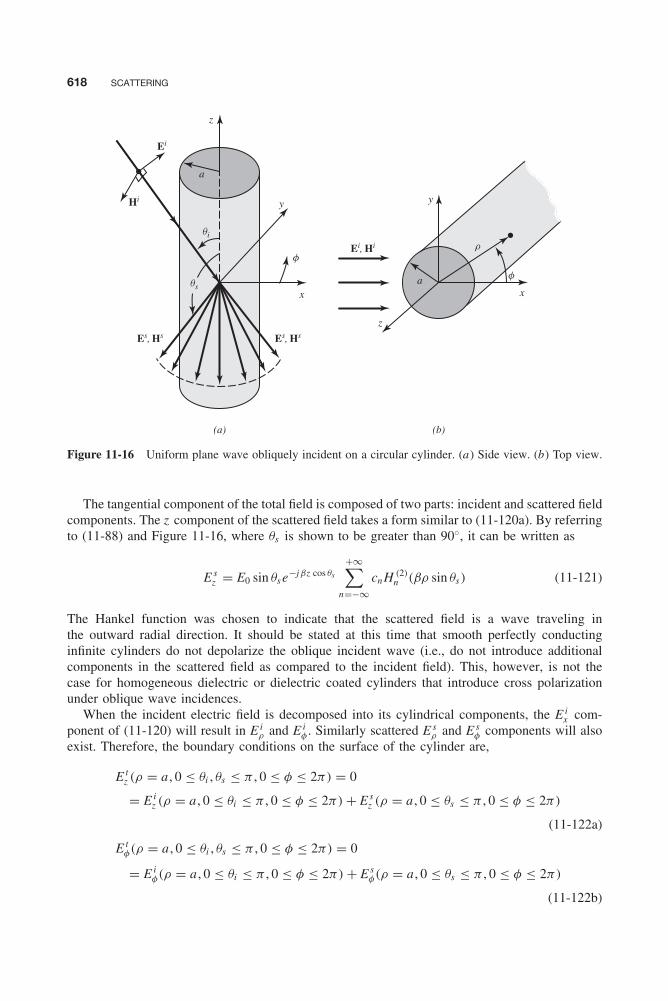
Balanis c11.tex V2 - 11/22/2011 3:50 P.M. Page 618
618 SCATTERING
qi
f
f
qs
y
xa
a
z
z
y
x
Hi
Ei
Es, Hs Es, Hs
Ei, Hi r
(a) (b)
Figure 11-16 Uniform plane wave obliquely incident on a circular cylinder. (a) Side view. (b) Top view.
The tangential component of the total field is composed of two parts: incident and scattered fieldcomponents. The z component of the scattered field takes a form similar to (11-120a). By referringto (11-88) and Figure 11-16, where θs is shown to be greater than 90◦, it can be written as
E sz = E0 sin θs e−jβz cos θs
+∞∑n=−∞
cnH (2)n (βρ sin θs) (11-121)
The Hankel function was chosen to indicate that the scattered field is a wave traveling inthe outward radial direction. It should be stated at this time that smooth perfectly conductinginfinite cylinders do not depolarize the oblique incident wave (i.e., do not introduce additionalcomponents in the scattered field as compared to the incident field). This, however, is not thecase for homogeneous dielectric or dielectric coated cylinders that introduce cross polarizationunder oblique wave incidences.
When the incident electric field is decomposed into its cylindrical components, the E ix com-
ponent of (11-120) will result in E iρ and E i
φ . Similarly scattered E sρ and E s
φ components will alsoexist. Therefore, the boundary conditions on the surface of the cylinder are,
E tz (ρ = a , 0 ≤ θi , θs ≤ π , 0 ≤ φ ≤ 2π) = 0
= E iz (ρ = a , 0 ≤ θi ≤ π , 0 ≤ φ ≤ 2π) + E s
z (ρ = a , 0 ≤ θs ≤ π , 0 ≤ φ ≤ 2π)
(11-122a)
E tφ(ρ = a , 0 ≤ θi , θs ≤ π , 0 ≤ φ ≤ 2π) = 0
= E iφ(ρ = a , 0 ≤ θi ≤ π , 0 ≤ φ ≤ 2π) + E s
φ(ρ = a , 0 ≤ θs ≤ π , 0 ≤ φ ≤ 2π)
(11-122b)
Balanis c11.tex V2 - 11/22/2011 3:50 P.M. Page 619
SCATTERING BY CIRCULAR CYLINDERS 619
Since each is not independent of the other, either one can be used to find the unknown coefficients.Applying (11-122a) leads to
E0
[sin θi e
+jβz cos θi
+∞∑n=−∞
j −nJn(βa sin θi )ejnφ
+ sin θs e−jβz cos θs
+∞∑n=−∞
cnH (2)n (βa sin θs)
]= 0 (11-123a)
which is satisfied provided
θs = π − θi (11-123b)
cn = −j −n Jn(βa sin θi )
H (2)n (βa sin θi )
ejnφ = j −nanejnφ (11-123c)
an = − Jn(βa sin θi )
H (2)n (βa sin θi )
(11-123d)
Thus, the scattered component E sz of (11-121) reduces to
E sz = E0 sin θi e
+jβz cos θi
+∞∑n=−∞
j −nanH (2)n (βρ sin θi )e
jnφ (11-124)
It is apparent that the scattered field exists for all values of angle φ (measured from the x axis)along a cone in the forward direction whose half-angle from the z axis is equal to θs = π − θi .
To find the remaining Es and Hs scattered field components, we expand Maxwell’s curlequations as
∇ × Es = −jωμHs ⇒ Hs = − 1
jωμ∇ × Es (11-125)
or
H sρ = − 1
jωμ
(1
ρ
∂E sz
∂φ− ∂E s
φ
∂z
)(11-125a)
H sφ = − 1
jωμ
(∂E s
ρ
∂z− ∂E s
z
∂ρ
)(11-125b)
H sz = − 1
jωμρ
(∂
∂ρ(ρE s
φ) − ∂E sρ
∂φ
)(11-125c)
and
∇ × Hs = jωεEs ⇒ Es = 1
jωε∇ × Hs (11-126)
or
E sρ = 1
jωε
(1
ρ
∂H sz
∂φ− ∂H s
φ
∂z
)(11-126a)
E sφ = 1
jωε
(∂H s
ρ
∂z− ∂H s
z
∂ρ
)(11-126b)
E sz = 1
jωερ
(∂
∂ρ(ρH s
φ ) − ∂H sρ
∂φ
)(11-126c)
Balanis c11.tex V2 - 11/22/2011 3:50 P.M. Page 620
620 SCATTERING
Since for the TMz solution H sz = 0, (11-126a) reduces to
E sρ = − 1
jωε
∂H sφ
∂z(11-127)
When substituted into (11-125b), we can write that
H sφ = − 1
jωμ
[∂
∂z
(− 1
jωε
∂H sφ
∂z
)− ∂E s
z
∂ρ
]= − 1
ω2με
∂2H sφ
∂z 2+ 1
jωμ
∂E sz
∂ρ(11-128)
The z variations of all field components are of the same form as in (11-124) (i.e., e+jβz cos θi ).Thus, (11-128) reduces to
H sφ = − (jβ cos θi )
2
ω2μεH s
φ + 1
jωμ
∂E sz
∂ρ= cos2 θi H
sφ + 1
jωμ
∂E sz
∂ρ(11-129)
or
H sφ (1 − cos2 θi ) = sin2 θi H
sφ = 1
jωμ
∂E sz
∂ρ(11-129a)
H sφ = 1
jωμ
1
sin2 θi
∂E sz
∂ρ= β
jωμ
1
sin θi
∂E sz
∂(βρ sin θi )
= −jE0
√ε
μe+jβz cos θi
+∞∑n=−∞
j −nanH (2)′n (βρ sin θi )e
jnφ (11-129b)
where
′ ≡ ∂
∂(βρ sin θi )(11-129c)
In a similar manner we can solve for H sρ by first reducing (11-126b) to
E sφ = 1
jωε
(∂H s
ρ
∂z− ∂H s
z
∂ρ
)H s
z =0= 1
jωε
∂H sρ
∂z(11-130)
and then substituting it into (11-125a). Thus
H sρ = − 1
jωμ
[1
ρ
∂E sz
∂φ− ∂
∂z
(1
jωε
∂H sρ
∂z
)]= − 1
jωμ
1
ρ
∂E sz
∂φ− 1
ω2με
∂2H sρ
∂z 2
= − 1
jωμ
1
ρ
∂E sz
∂φ− (jβ cos θi )
2
ω2μεH s
ρ = − 1
jωμ
1
ρ
∂E sz
∂φ+ cos2 θi H
sρ (11-131)
or
(1 − cos2 θi )H sρ = sin2 θi H s
ρ = − 1
jωμ
1
ρ
∂E sz
∂φ(11-131a)
H sρ = − 1
jωμρ sin2 θi
∂E sz
∂φ= j
E0e+jβz cos θi
ωμρ sin θi
+∞∑n=−∞
nj −n+1anH (2)n (βρ sin θi )e
jnφ
(11-131b)
Balanis c11.tex V2 - 11/22/2011 3:50 P.M. Page 621
SCATTERING BY CIRCULAR CYLINDERS 621
Expressions for E sρ and E s
φ can be written using (11-126a), (11-126b), (11-129b), and (11-131b). Thus
E sρ = − 1
jωε
∂H sφ
∂z= jE0 cos θi e
+jβz cos θi
+∞∑n=−∞
j −nanH (2)′n (βρ sin θi )e
jnφ (11-132)
E sφ = 1
jωε
∂H sρ
∂z= jE0
cot θi
βρe+jβz cos θi
+∞∑n=−∞
nj −n+1anH (2)n (βρ sin θi )e
jnφ
(11-133)
In summary, the scattered fields can be written as
TMz
E sρ = jE0 cos θi e
+jβz cos θi
+∞∑n=−∞
j −nanH (2)′n (βρ sin θi )e
jnφ
E sφ = jE0
cot θi
βρe+jβz cos θi
+∞∑n=−∞
nj −n+1anH (2)n (βρ sin θi )e
jnφ
E sz = E0 sin θi e
+jβz cos θi
+∞∑n=−∞
j −nanH (2)n (βρ sin θi )e
jnφ
(11-134a)
(11-134b)
(11-134c)
H sρ = jE0
e+jβz cos θi
ωμρ sin θi
+∞∑n=−∞
nj −n+1anH (2)n (βρ sin θi )e
jnφ
H sφ = −jE0
√ε
μe+jβz cos θi
+∞∑n=−∞
j −nanH (2)′n (βρ sin θi )e
jnφ
H sz = 0
an = − Jn(βa sin θi )
H (2)n (βa sin θi )
′ = ∂
∂(βρ sin θi )
(11-134d)
(11-134e)
(11-134f)
(11-134g)
(11-134h)
A. Far-Zone Scattered Field Often it is desired to know the scattered fields at large distances.This can be accomplished by approximating in (11-134a) through (11-134f) the Hankel functionand its derivative by their corresponding asymptotic expressions for large distances, as given by
H (2)n (αx)
αx→∞�√
2j
παxj ne−jαx (11-135a)
H (2)′n (αx) = dH (2)
n (αx)
d(αx)
αx→∞� −√
2j
παxj n+1e−jαx (11-135b)
Balanis c11.tex V2 - 11/22/2011 3:50 P.M. Page 622
622 SCATTERING
Thus, we can reduce the scattered magnetic field expressions of (11-134d) and (11-134e) by
H sρ
ρ→∞� jE01
ωμ
1
ρ sin θi
√2j
πβρ sin θie+jβ(z cos θi −ρ sin θi )
+∞∑n=−∞
nanejnφ
ρ→∞� jE01
ωμ
1
ρ sin θi
√2j
πβρ sin θie+jβ(z cos θi −ρ sin θi )
+∞∑n=0
nεnan cos(nφ) (11-136a)
H sφ
ρ→∞� −E0
√ε
μ
√2j
πβρ sin θie+jβ(z cos θi −ρ sin θi )
+∞∑n=−∞
anejnφ
ρ→∞� −E0
√ε
μ
√2j
πβρ sin θie+jβ(z cos θi −ρ sin θi )
+∞∑n=0
εnan cos(nφ) (11-136b)
where εn is defined in (11-102a). A comparison of (11-136a) and (11-136b) indicates that at largedistances H s
ρ is small compared to H sφ since H s
ρ varies inversely proportional to ρ3/2 while H sφ
is inversely proportional to ρ1/2.The scattering width of (11-21c) can now be expressed as
σ2-D = limρ→∞
(2πρ
|H sφ |2
|Hi |2)
= limρ→∞
⎡⎢⎢⎢⎣2πρ
|E0|2η2
(2
πβρ sin θi
)|E0|2η2
∣∣∣∣∣+∞∑
n=−∞anejnφ
∣∣∣∣∣2
⎤⎥⎥⎥⎦
σ2-D = 4
β
1
sin θi
∣∣∣∣∣+∞∑
n=−∞anejnφ
∣∣∣∣∣2
= 2λ
π
1
sin θi
∣∣∣∣∣+∞∑n=0
εnan cos(nφ)
∣∣∣∣∣2
(11-137)
where
an = − Jn(βa sin θi )
H (2)n (βa sin θi )
εn ={
1 n = 02 n �= 0
(11-137a)
(11-137b)
which is similar to (11-102) except that β in (11-102) is replaced by β sin θi .From the results of the normal incidence case of Section 11.5.1B we can write, by referring
to (11-103a), that for small radii the scattering width of (11-137) reduces to
σ2-Da�λ� πλ
2 sin θi
∣∣∣∣ 1
ln(0.89βa sin θi )
∣∣∣∣2
(11-138)
which is independent of φ.For a cylinder of finite length �, the scattered fields of oblique incidence propagate in all
directions, in contrast to the infinitely long cylinder where all the energy is along a conicalsurface formed in the forward direction whose half-angle is equal to θi . However, as the lengthof the cylinder becomes much larger than its radius (� � a), then the scattered fields alongθs = π − θi will be much greater than those in other directions. When the length of the cylinder
Balanis c11.tex V2 - 11/22/2011 3:50 P.M. Page 623
SCATTERING BY CIRCULAR CYLINDERS 623
is a multiple of half a wavelength, resonance phenomena are exhibited in the scattered fields[12]. However, as the length increases beyond several wavelengths, the resonance phenomenadisappear. For both TMz and TEz polarizations, the three-dimensional radar cross section foroblique wave incidence is related approximately to the two-dimensional scattering width, byreferring to the geometry of Figure 11-16, by [12, 14]
σ3-D = σ2-D
⎧⎪⎪⎪⎨⎪⎪⎪⎩2�2
λsin2 θs ,i
⎡⎢⎢⎣ sin
[β�
2(cos θi + cos θs)
]β�
2(cos θi + cos θs)
⎤⎥⎥⎦2⎫⎪⎪⎪⎬⎪⎪⎪⎭ � � a (11-139)
where sin2 θs , is used for TMz and sin2 θi , is used for TEz . This is analogous to the rectangularplate scattering of Section 11.3.2 and Example 11-2. This indicates that the maximum RCS occursalong the specular direction (θs = π − θi ) and away from it follows the variations exhibited from aflat plate, as given by (11-44a). Equation 11-139 yields reasonable good results even for cylinderswith lengths near one wavelength (� � λ). Thus, using (11-139) converts (11-137) and (11-138)for three-dimensional scatterers to
σ3-D � 4�2
π
sin2 θs
sin θi
∣∣∣∣∣∞∑
n=0
εnan cos(nφ)
∣∣∣∣∣2
⎧⎪⎪⎨⎪⎪⎩sin
[β�
2(cos θi + cos θs)
]β�
2(cos θi + cos θs)
⎫⎪⎪⎬⎪⎪⎭2
(11-140a)
σ3-Da�λ� π�2
sin θi
∣∣∣∣ sin θs
ln(0.89βa sin θi )
∣∣∣∣2
⎧⎪⎪⎨⎪⎪⎩sin
[β�
2(cos θi + cos θs)
]β�
2(cos θi + cos θs)
⎫⎪⎪⎬⎪⎪⎭2
(11-140b)
11.5.4 Oblique Incidence Plane Wave Scattering by Conducting Circular Cylinder:TEz Polarization
TEz scattering by a cylinder at oblique incidence can be analyzed following a procedure similar tothat of TMz scattering as discussed in the previous section. Using the geometry of Figure 11-16,we can write the incident magnetic field, for a plane wave traveling parallel to the xz plane, as
Hi = H0(âx cos θi + âz sin θi )e−jβx sin θi e+jβz cos θi (11-141)
Using the transformation (11-81a), it can also be expressed as
Hi = H0(âx cos θi + âz sin θi )e+jβz cos θi
+∞∑n=−∞
j −nJn(βρ sin θi )ejnφ (11-141a)
Using the transformation from rectangular to cylindrical components (II-6), or
Hρ = Hx cos φ + Hy sin φ = Hx cos φ (11-142a)
Hφ = −Hx sin φ + Hy cos φ = −Hx sin φ (11-142b)
Hz = Hz (11-142c)

Balanis c11.tex V2 - 11/22/2011 3:50 P.M. Page 624
624 SCATTERING
reduces (11-141a) to
H iρ = H0 cos θi cos φe+jβz cos θi
+∞∑n=−∞
j −nJn(βρ sin θi )ejnφ (11-143a)
H iφ = −H0 cos θi sin φe+jβz cos θi
+∞∑n=−∞
j −nJn(βρ sin θi )ejnφ (11-143b)
H iz = H0 sin θi e
+jβz cos θi
+∞∑n=−∞
j −nJn(βρ sin θi )ejnφ (11-143c)
In the source-free region, the corresponding electric field components can be obtained usingMaxwell’s curl equation
∇ × Hi = jωεEi ⇒ Ei = 1
jωε∇ × Hi (11-144)
or
E iρ = 1
jωε
(1
ρ
∂H iz
∂φ− ∂H i
φ
∂z
)(11-144a)
E iφ = 1
jωε
(∂H i
ρ
∂z− ∂H i
z
∂ρ
)(11-144b)
E iz = 1
jωε
1
ρ
[∂(ρH i
φ)
∂ρ− ∂H i
ρ
∂φ
](11-144c)
To aid in doing this, we also utilize Maxwell’s curl equation
∇ × Ei = −jωμHi ⇒ Hi = − 1
jωμ∇ × Ei (11-145)
which when expanded takes the form, for a TEz polarization (E iz = 0), of
H iρ = − 1
jωμ
(1
ρ
∂E iz
∂φ− ∂E i
φ
∂z
)E i
z =0
= 1
jωμ
∂E iφ
∂z(11-145a)
H iφ = − 1
jωμ
(∂E i
ρ
∂z− ∂E i
z
∂ρ
)E i
z =0
= − 1
jωμ
∂E iρ
∂z(11-145b)
H iz = − 1
jωμ
1
ρ
[∂(ρE i
φ)
∂ρ− ∂E i
ρ
∂φ
](11-145c)
Substituting (11-145a) into (11-144b), we can write that
E iφ = 1
jωε
[1
jωμ
∂2E iφ
∂z 2− ∂H i
z
∂ρ
]= − 1
ω2με
∂2E iφ
∂z 2− 1
jωε
∂H iz
∂ρ(11-146)
Since the z variations of all the field components are of the same form (i.e., e+jβz cos θi ), as givenby (11-141), then (11-146) reduces to
E iφ = β2
ω2μεcos2 θi E
iφ − 1
jωε
∂H iz
∂ρ= cos2 θi E
iφ − 1
jωε
∂H iz
∂ρ(11-147)
Balanis c11.tex V2 - 11/22/2011 3:50 P.M. Page 625
SCATTERING BY CIRCULAR CYLINDERS 625
or
(1 − cos2 θi )Eiφ = sin2 θi E
iφ = − 1
jωε
∂H iz
∂ρ
E iφ = − 1
jωε
1
sin2 θi
∂H iz
∂ρ= − β
jωε
1
sin θi
∂H iz
∂(βρ sin θi )
= j
√μ
εH0e+jβz cos θi
+∞∑n=−∞
j −nJ ′n(βρ sin θi )e
jnφ (11-147a)
In a similar manner, we can solve for E iρ by substituting (11-145b) into (11-144a). Thus,
E iρ = 1
jωε
[1
ρ
∂H iz
∂φ−
(− 1
jωμ
∂2E iρ
∂z 2
)]= 1
jωε
1
ρ
∂H iz
∂φ− 1
ω2με
∂2E iρ
∂z 2
= 1
jωε
1
ρ
∂H iz
∂φ− (jβ cos θi )
2
ω2μεE i
ρ = 1
jωε
1
ρ
∂H iz
∂φ+ cos2 θi E
iρ (11-148)
or
(1 − cos2 θi )E iρ = sin2 θi E i
ρ = 1
jωε
1
ρ
∂H iz
∂φ
E iρ = 1
jωερ
1
sin2 θi
∂H iz
∂φ= −j
H0e+jβz cos θi
ωερ sin θi
+∞∑n=−∞
nj −n+1Jn(βρ sin θi )ejnφ (11-148a)
Since the z component of the incident H field is given by (11-143c), its scattered field can bewritten in a form similar to (11-121) or
H sz = H0 sin θs e−jβz cos θs
+∞∑n=−∞
dnH (2)n (βρ sin θs) (11-149)
where dn represents unknown coefficients to be determined by boundary conditions. Accordingto (11-147a), the φ component of the scattered field can be written using (11-149) as
E sφ = − 1
jωε
1
sin2 θs
∂H sz
∂ρ= − β
jωε
1
sin θs
∂H sz
∂(βρ sin θs)
= jH0
√μ
εe−jβz cos θs
+∞∑n=−∞
dnH (2)′n (βρ sin θs) (11-150)
Applying the boundary condition
E tφ(ρ = a , 0 ≤ θi , θs ≤ π , 0 ≤ φ ≤ 2π) = 0
= E iφ(ρ = a , 0 ≤ θi ≤ π , 0 ≤ φ ≤ 2π) + E s
φ(ρ = a , 0 ≤ θs ≤ π , 0 ≤ φ ≤ 2π)
(11-151)
leads to
jH0
√μ
ε
[e+jβz cos θi
+∞∑n=−∞
j −nJ ′n(βa sin θi )e
jnφ
+e−jβz cos θs
+∞∑n=−∞
dnH (2)′n (βa sin θs)
]= 0 (11-151a)

Balanis c11.tex V2 - 11/22/2011 3:50 P.M. Page 626
626 SCATTERING
which is satisfied provided
θs = π − θi (11-151b)
dn = −j −n J ′n(βa sin θi )
H (2)′n (βa sin θi )
ejnφ = j −nbnejnφ (11-151c)
bn = − J ′n(βa sin θi )
H (2)′n (βa sin θi )
(11-151d)
Thus, the scattered H sz component of (11-149) reduces to
H sz = H0 sin θi e
+jβz cos θi
+∞∑n=−∞
j −nbnH (2)n (βρ sin θi )e
jnφ (11-152)
Knowing H sz , the remaining electric and magnetic field components can be found using
(11-148a), (11-147a), and (11-145a) through (11-145c).In summary, the scattered fields can be written as
TEz
E sρ = 1
jωερ
1
sin2 θi
∂H sz
∂φ= −j
H0
ωερ
e+jβz cos θi
sin θi
×+∞∑
n=−∞nj −n+1bnH (2)
n (βρ sin θi )ejnφ
E sφ = − 1
jωε
1
sin2 θi
∂H sz
∂ρ= j H0
√μ
εe+jβz cos θi
×+∞∑
n=−∞j −nbnH (2)′
n (βρ sin θi )ejnφ
E sz = 0
H sρ = 1
jωμ
∂E sφ
∂z= jH0 cos θi e
+jβz cos θi
×+∞∑
n=−∞j −nbnH (2)′
n (βρ sin θi )ejnφ
H sφ = − 1
jωμ
∂E sρ
∂z= jH0
cot θi
βρe+jβz cos θi
×+∞∑
n=−∞nj −n+1bnH (2)
n (βρ sin θi )ejnφ
H sz = H0 sin θi e
+jβz cos θi
+∞∑n=−∞
j −nbnH (2)n (βρ sin θi )e
jnφ
bn = − J ′n(βa sin θi )
H (2)′n (βa sin θi )
′ ≡ ∂
∂(βρ sin θi )
(11-153a)
(11-153b)
(11-153c)
(11-153d)
(11-153e)
(11-153f)
(11-153g)
(11-153h)
Balanis c11.tex V2 - 11/22/2011 3:50 P.M. Page 627
SCATTERING BY CIRCULAR CYLINDERS 627
A. Far-Zone Scattered Field The scattered electric fields of (11-153a) through (11-153c)can be approximated in the far zone by replacing the Hankel function and its derivative by theirasymptotic forms, as given by (11-135a) and (11-135b). Thus,
E sρ � H0
1
ωε
1
ρ sin θi
√2j
πβρ sin θie+jβ(z cos θi −ρ sin θi )
+∞∑n=−∞
nbnejnφ
� H01
ωε
1
ρ sin θi
√2j
πβρ sin θie+jβ(z cos θi −ρ sin θi )
+∞∑n=0
nεnbn cos(nφ) (11-154a)
E sφ � H0
√μ
ε
√2j
πβρ sin θie+jβ(z cos θi −ρ sin θi )
+∞∑n=−∞
bnejnφ
� H0
√μ
ε
√2j
πβρ sin θie+jβ(z cos θi −ρ sin θi )
+∞∑n=−∞
εnbn cos(nφ) (11-154b)
where εn is defined in (11-102a). A comparison of (11-154a) and (11-154b) indicates that at largedistances E s
ρ is small compared to E sφ since E s
ρ is inversely proportional to ρ3/2, whereas E sφ is
inversely proportional to ρ1/2.The scattering width of (11-21b) can now be expressed using (11-154b) and the incident
electric field corresponding to (11-141) as
σ2-D = limρ→∞
[2πρ
|E sφ |2
|Ei |2]
= limρ→∞
⎡⎢⎢⎣2πρ
|H0|2 μ
ε
(2
πβρ sin θi
)|H0|2 μ
ε
∣∣∣∣∣+∞∑
n=−∞bnejnφ
∣∣∣∣∣2
⎤⎥⎥⎦
σ2-D = 4
β
1
sin θi
∣∣∣∣∣+∞∑
n=−∞bnejnφ
∣∣∣∣∣2
= 2λ
π
1
sin θi
∣∣∣∣∣+∞∑n=0
εnbn cos(nφ)
∣∣∣∣∣2
(11-155)
where
bn = − J ′n(βa sin θi )
H (2)′n (βa sin θi )
εn ={
1 n = 02 n �= 0
(11-155a)
(11-155b)
which is similar to (11-117) except that β in (11-117) has been replaced by β sin θi .From the results of the normal incidence case of Section 11.5.2B we can write by referring
to (11-118d) that for small radii the scattering width of (11-155) reduces to
σ2-Da�λ� πλ
8
(βa sin θi )4
sin θi[1 − 2 cos(φ)]2 (11-156)
which is dependent on φ, even for small radii cylinders.
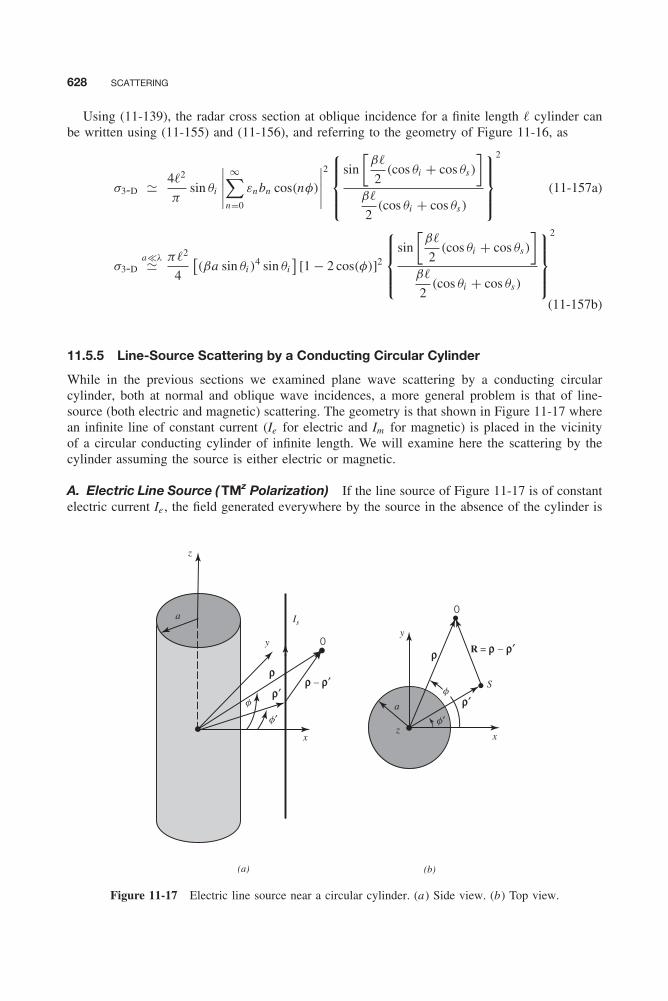
Balanis c11.tex V2 - 11/22/2011 3:50 P.M. Page 628
628 SCATTERING
Using (11-139), the radar cross section at oblique incidence for a finite length � cylinder canbe written using (11-155) and (11-156), and referring to the geometry of Figure 11-16, as
σ3-D � 4�2
πsin θi
∣∣∣∣∣∞∑
n=0
εnbn cos(nφ)
∣∣∣∣∣2
⎧⎪⎪⎨⎪⎪⎩sin
[β�
2(cos θi + cos θs)
]β�
2(cos θi + cos θs)
⎫⎪⎪⎬⎪⎪⎭2
(11-157a)
σ3-Da�λ� π�2
4
[(βa sin θi )
4 sin θi]
[1 − 2 cos(φ)]2
⎧⎪⎪⎨⎪⎪⎩sin
[β�
2(cos θi + cos θs)
]β�
2(cos θi + cos θs)
⎫⎪⎪⎬⎪⎪⎭2
(11-157b)
11.5.5 Line-Source Scattering by a Conducting Circular Cylinder
While in the previous sections we examined plane wave scattering by a conducting circularcylinder, both at normal and oblique wave incidences, a more general problem is that of line-source (both electric and magnetic) scattering. The geometry is that shown in Figure 11-17 wherean infinite line of constant current (Ie for electric and Im for magnetic) is placed in the vicinityof a circular conducting cylinder of infinite length. We will examine here the scattering by thecylinder assuming the source is either electric or magnetic.
A. Electric Line Source ( TMz Polarization) If the line source of Figure 11-17 is of constantelectric current Ie , the field generated everywhere by the source in the absence of the cylinder is
f
f
f′f′
y
0
0
Is
x
a
a
z
z
y
x
ρρ
R = ρ − ρ′
ρ − ρ′
ρ′ρ′
S
(a) (b)
Figure 11-17 Electric line source near a circular cylinder. (a) Side view. (b) Top view.

Balanis c11.tex V2 - 11/22/2011 3:50 P.M. Page 629
SCATTERING BY CIRCULAR CYLINDERS 629
given, according to (11-11a), by
E iz = −β2Ie
4ωεH (2)
0 (β|ρ − ρ′|) (11-158)
which is referred to here as the incident field. By the addition theorem for Hankel functions(11-69a) and (11-69b), we can write (11-158) as
E iz = −β2Ie
4ωε
⎧⎪⎪⎪⎪⎪⎪⎨⎪⎪⎪⎪⎪⎪⎩
∞∑n=−∞
Jn(βρ)H (2)n (βρ ′)ejn(φ−φ′), ρ ≤ ρ ′
+∞∑n=−∞
Jn(βρ ′)H (2)n (βρ)ejn(φ−φ′), ρ ≤ ρ ′
(11-158a)
(11-158b)
Bessel functions Jn(βρ) were selected to represent the fields for ρ < ρ ′ because the field mustbe finite everywhere (including ρ = 0) and Hankel functions were chosen for ρ ≥ ρ ′ to representthe traveling nature of the wave.
In the presence of the cylinder, the total field is composed of two parts: incident and scatteredfields. The scattered field is produced by the current induced on the surface of the cylinder thatacts as a secondary radiator. The scattered field also has only an Ez component (no cross polarizedcomponents are produced), and it can be expressed as
E sz = −β2Ie
4ωε
+∞∑n=−∞
cnH (2)n (βρ), a ≤ ρ ≤ ρ ′, ρ ≥ ρ ′ (11-159)
The same expression is valid for ρ ≤ ρ ′ and ρ ≥ ρ ′ because the scattered field exists only whenthe cylinder is present, and it is nonzero only when ρ ≥ a . Since the scattered field emanatesfrom the surface of the cylinder, the Hankel function of the second kind in (11-159) is chosen torepresent the traveling wave nature of the radiation.
The coefficients represented by cn in (11-159) can be found by applying the boundarycondition
E tz (ρ = a , 0 ≤ φ, φ′ ≤ 2π , z )
= E iz (ρ = a , 0 ≤ φ, φ′ ≤ 2π , z ) + E s
z (ρ = a , 0 ≤ φ, φ′ ≤ 2π , z ) = 0 (11-160)
which, by using (11-158a) and (11-159), leads to
−β2Ie
4ωε
+∞∑n=−∞
[H (2)
n (βρ ′)Jn(βa)ejn(φ−φ′) + cnH (2)n (βa)
]= 0 (11-161)
which is satisfied provided
cn = −H (2)n (βρ ′)
Jn(βa)
H (2)n (βa)
ejn(φ−φ′) (11-161a)
Thus, (11-159) can be expressed as
E sz = +β2Ie
4ωε
+∞∑n=−∞
H (2)n (βρ ′)
Jn(βa)
H (2)n (βa)
H (2)n (βρ)ejn(φ−φ′), a ≤ ρ ≤ ρ ′, ρ ≥ ρ ′
(11-162)
Balanis c11.tex V2 - 11/22/2011 3:50 P.M. Page 630
630 SCATTERING
The total electric field can then be written as
E tρ = E t
φ = 0 (11-163)
E tz = −β2Ie
4ωε
⎧⎪⎪⎪⎪⎪⎪⎪⎪⎪⎪⎨⎪⎪⎪⎪⎪⎪⎪⎪⎪⎪⎩
+∞∑n=−∞
H (2)n (βρ ′)
[Jn(βρ) − Jn(βa)
H (2)n (βa)
H (2)n (βρ)
]×ejn(φ−φ′) a ≤ ρ ≤ ρ ′
+∞∑n=−∞
H (2)n (βρ)
[Jn(βρ ′) − Jn(βa)
H (2)n (βa)
H (2)n (βρ ′)
]×ejn(φ−φ′) ρ ≥ ρ ′
(11-164a)
(11-164b)
where the first terms within the summations and brackets represent the incident fields and thesecond terms represent the scattered fields. The corresponding magnetic components can be foundusing Maxwell’s equations 11-86 through 11-86c, which can be written as
H tρ = − 1
jωμ
1
ρ
∂E tz
∂φ
= −jIe
4ρ
⎧⎪⎪⎪⎪⎪⎪⎪⎪⎨⎪⎪⎪⎪⎪⎪⎪⎪⎩
+∞∑n=−∞
jnH (2)n (βρ ′)
[Jn(βρ) − Jn(βa)
H (2)n (βa)
H (2)n (βρ)
]×ejn(φ−φ′) a ≤ ρ ≤ ρ ′
+∞∑n=−∞
jnH (2)n (βρ)
[Jn(βρ ′) − Jn(βa)
H (2)n (βa)
H (2)n (βρ ′)
]×ejn(φ−φ′) ρ ≥ ρ ′
(11-165a)
(11-165b)
H tφ = 1
jωμ
∂E tz
∂ρ
= jβIe
4
⎧⎪⎪⎪⎪⎪⎪⎪⎪⎪⎨⎪⎪⎪⎪⎪⎪⎪⎪⎪⎩
+∞∑n=−∞
H (2)n (βρ ′)
[J ′
n(βρ) − Jn(βa)
H (2)n (βa)
H (2)′n (βρ)
]×ejn(φ−φ′) a ≤ ρ ≤ ρ ′
+∞∑n=−∞
H (2)′n (βρ)
[Jn(βρ ′) − Jn(βa)
H (2)n (βa)
H (2)n (βρ ′)
]×ejn(φ−φ′) ρ ≥ ρ ′
(11-166a)
(11-166b)
H tz = 0
On the surface of the cylinder, the current density can be found to be
Js = n̂ × Ht∣∣ρ=a = âρ × (âρH t
ρ + âφH tφ)
∣∣ρ=a
= âz H tφ
∣∣ρ=a
= âz jβIe
4
+∞∑n=−∞
H (2)n (βρ ′)
[J ′
n(βa) − Jn(βa)
H (2)n (βa)
H (2)′n (βa)
]ejn(φ−φ′) (11-167)
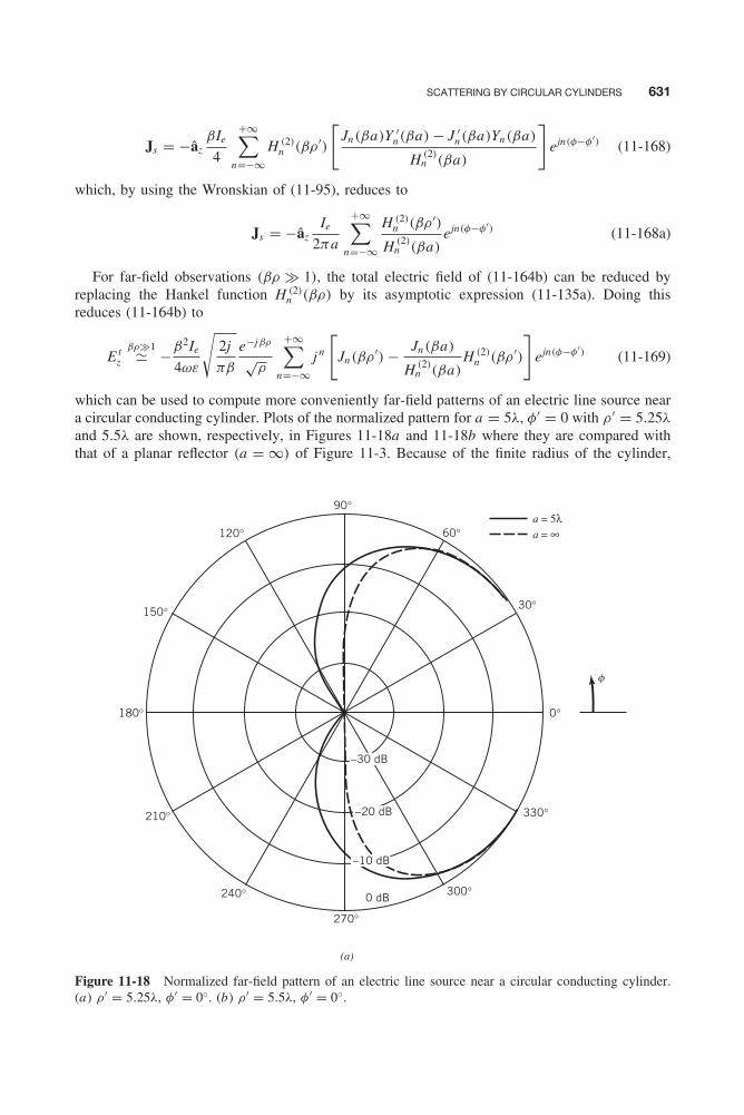
Balanis c11.tex V2 - 11/22/2011 3:50 P.M. Page 631
SCATTERING BY CIRCULAR CYLINDERS 631
Js = −âzβIe
4
+∞∑n=−∞
H (2)n (βρ ′)
[Jn(βa)Y ′
n(βa) − J ′n(βa)Yn(βa)
H (2)n (βa)
]ejn(φ−φ′) (11-168)
which, by using the Wronskian of (11-95), reduces to
Js = −âzIe
2πa
+∞∑n=−∞
H (2)n (βρ ′)
H (2)n (βa)
ejn(φ−φ′) (11-168a)
For far-field observations (βρ � 1), the total electric field of (11-164b) can be reduced byreplacing the Hankel function H (2)
n (βρ) by its asymptotic expression (11-135a). Doing thisreduces (11-164b) to
E tz
βρ�1� −β2Ie
4ωε
√2j
πβ
e−jβρ
√ρ
+∞∑n=−∞
j n
[Jn(βρ ′) − Jn(βa)
H (2)n (βa)
H (2)n (βρ ′)
]ejn(φ−φ′) (11-169)
which can be used to compute more conveniently far-field patterns of an electric line source neara circular conducting cylinder. Plots of the normalized pattern for a = 5λ, φ′ = 0 with ρ ′ = 5.25λ
and 5.5λ are shown, respectively, in Figures 11-18a and 11-18b where they are compared withthat of a planar reflector (a = ∞) of Figure 11-3. Because of the finite radius of the cylinder,
270°
300°
330°
0°
30°
90°
60°120°
150°
180°
210°
240° 0 dB
−10 dB
−20 dB
a = 5λ
(a)
f
a = ∞
−30 dB
Figure 11-18 Normalized far-field pattern of an electric line source near a circular conducting cylinder.(a) ρ ′ = 5.25λ, φ′ = 0◦. (b) ρ ′ = 5.5λ, φ′ = 0◦.

Balanis c11.tex V2 - 11/22/2011 3:50 P.M. Page 632
632 SCATTERING
270°
300°
330°
0°
30°
90°
60°120°
150°
180°
210°
240°
a = 5λ
(b)
f
a = ∞
−30 dB
−20 dB
0 dB
−10 dB
Figure 11-18 (Continued )
radiation is allowed to “leak” around the cylinder in terms of “creeping” waves [15–17]; this isnot the case for the planar reflector.
B. Magnetic Line Source ( TEz Polarization) Magnetic sources, although not physicallyrealizable, are often used as equivalent sources to analyze aperture antennas [1, 18]. If the linesource of Figure 11-17 is magnetic and it is allowed to recede to the surface of the cylinder(ρ ′ = a), the total field of the line source in the presence of the cylinder would be representativeof a very thin infinite axial slot on the cylinder. Finite-width slots can be represented by a numberof line sources with some amplitude and phase distribution across the width. Therefore, knowingthe radiation and scattering by a magnetic line source near a cylinder allows us to solve otherphysical problems by using it as an equivalent.
If the line of Figure 11-17 is magnetic with a current of Im , the fields that it radiates in theabsence of the cylinder can be obtained from those of an electric line source by the use of duality(Section 7.2). Doing this, we can write the incident magnetic field, by referring to (11-158)through (11-158b), as
H iz = −β2Im
4ωμH (2)
0 (β|ρ − ρ′|) (11-170)

Balanis c11.tex V2 - 11/22/2011 3:50 P.M. Page 633
SCATTERING BY CIRCULAR CYLINDERS 633
which can also be expressed as
H iz = −β2Im
4ωμ
⎧⎪⎪⎪⎪⎨⎪⎪⎪⎪⎩
∞∑n=−∞
Jn(βρ)H (2)n (βρ ′)ejn(φ−φ), ρ ≤ ρ ′
+∞∑n=−∞
Jn(βρ ′)H (2)n (βρ)ejn(φ−φ′), ρ ≥ ρ ′
(11-170a)
(11-170b)
The scattered magnetic field takes a form similar to that of (11-159) and can be written as
H sz = −β2Im
4ωμ
+∞∑n=−∞
dnH (2)n (βρ), a ≤ ρ ≤ ρ ′, ρ ≥ ρ ′ (11-171)
where dn is used to represent the coefficients of the scattered field. Thus, the total magnetic fieldcan be expressed, by combining (11-170a) through (11-171), as
H tz = −β2Im
4ωμ
⎧⎪⎪⎪⎪⎪⎪⎪⎪⎨⎪⎪⎪⎪⎪⎪⎪⎪⎩
+∞∑n=−∞
[H (2)
n (βρ ′)Jn(βρ)ejn(φ−φ′) + dnH (2)n (βρ)
]a ≤ ρ ≤ ρ ′
+∞∑n=−∞
[Jn(βρ ′)ejn(φ−φ′) + dn
]H (2)
n (βρ)
ρ ≥ ρ ′
(11-172a)
(11-172b)
The corresponding electric field components can be found using Maxwell’s equations 11-106or 11-106a and 11-106b. Doing this, and utilizing (11-172a) and (11-172b), we can write that
E tρ = 1
jωε
1
ρ
∂H tz
∂φ
= jIm
4ρ
⎧⎪⎪⎪⎪⎪⎪⎪⎪⎨⎪⎪⎪⎪⎪⎪⎪⎪⎩
+∞∑n=−∞
[jnH (2)
n (βρ ′)Jn(βρ)ejn(φ−φ′) + H (2)n (βρ)
∂dn
∂φ
]a ≤ ρ ≤ ρ ′
+∞∑n=−∞
[jnJn(βρ ′)ejn(φ−φ′) + ∂dn
∂φ
]H (2)
n (βρ)
ρ ≥ ρ ′
(11-173a)
(11-173b)
E tφ = − 1
jωε
∂H tz
∂ρ
= −jβIm
4
⎧⎪⎪⎪⎪⎪⎪⎪⎪⎪⎨⎪⎪⎪⎪⎪⎪⎪⎪⎪⎩
+∞∑n=−∞
[H (2)
n (βρ ′)J ′n(βρ)ejn(φ−φ′) + dnH (2)′
n (βρ)]
a ≤ ρ ≤ ρ ′
+∞∑n=−∞
[Jn(βρ ′)ejn(φ−φ′) + dn
]H (2)′
n (βρ)
ρ ≥ ρ ′
(11-174a)
(11-174b)
Balanis c11.tex V2 - 11/22/2011 3:50 P.M. Page 634
634 SCATTERING
Applying the boundary condition
E tφ(ρ = a , 0 ≤ φ, φ′ ≤ 2π , z )
= E tφ(ρ = a , 0 ≤ φ, φ′ ≤ 2π , z ) + E s
φ(ρ = a , 0 ≤ φ, φ′ ≤ 2π , z ) = 0 (11-175)
on (11-174a) leads to
dn = −H (2)n (βρ ′)
J ′n(βa)
H (2)′n (βa)
ejn(φ−φ′) (11-175a)
Thus, the total electric and magnetic field components can be written as
TEz
E tz = H t
ρ = H tφ = 0
E tρ = − Im
4ρ
⎧⎪⎪⎪⎪⎪⎪⎪⎪⎨⎪⎪⎪⎪⎪⎪⎪⎪⎩
+∞∑n=−∞
nH (2)n (βρ ′)
[Jn(βρ) − J ′
n(βa)
H (2)′n (βa)
H (2)n (βρ)
]×ejn(φ−φ′) a ≤ ρ ≤ ρ ′
+∞∑n=−∞
nH (2)n (βρ)
[Jn(βρ ′) − J ′
n(βa)
H (2)′n (βa)
H (2)n (βρ ′)
]×ejn(φ−φ′) ρ ≥ ρ ′
(11-176a)
(11-176b)
(11-176c)
E tφ = −j
βIm
4=
⎧⎪⎪⎪⎪⎪⎪⎪⎪⎪⎪⎪⎪⎨⎪⎪⎪⎪⎪⎪⎪⎪⎪⎪⎪⎪⎩
+∞∑n=−∞
H (2)n (βρ ′)
[J ′
n(βρ) − J ′n(βa)
H (2)′n (βa)
H (2)′n (βρ)
]
× ejn(φ−φ′) a ≤ ρ ≤ ρ ′
+∞∑n=−∞
H (2)′n (βρ)
[Jn(βρ ′) − J ′
n(βa)
H (2)′n (βa)
H (2)n (βρ ′)
]
× ejn(φ−φ′) ρ ≥ ρ ′
(11-176d)
(11-176e)
H tz = −β2Im
4ωμ=
⎧⎪⎪⎪⎪⎪⎪⎪⎪⎪⎪⎪⎪⎨⎪⎪⎪⎪⎪⎪⎪⎪⎪⎪⎪⎪⎩
+∞∑n=−∞
H (2)n (βρ ′)
[Jn(βρ) − J ′
n(βa)
H (2)′n (βa)
H (2)n (βρ)
]
× ejn(φ−φ′) a ≤ ρ ≤ ρ ′
+∞∑n=−∞
H (2)n (βρ)
[Jn(βρ ′) − J ′
n(βa)
H (2)′n (βa)
H (2)n (βρ ′)
]
× ejn(φ−φ′) ρ ≥ ρ ′
(11-176f)
(11-176g)
where the first terms within the summation and brackets represent the incident fields and thesecond terms represent the scattered fields.
Balanis c11.tex V2 - 11/22/2011 3:50 P.M. Page 635
SCATTERING BY CIRCULAR CYLINDERS 635
On the surface of the cylinder, the current density can be found to be
Js = n̂ × Ht∣∣ρ=a = âρ × âz H t
z
∣∣ρ=a = −âφH t
z
∣∣ρ=a
= âφ
β2Im
4ωμ
+∞∑n=−∞
H (2)n (βρ ′)
[Jn(βa) − J ′
n(βa)
H (2)′n (βa)
H (2)n (βa)
]ejn(φ−φ′)
Js = −j âφ
β2Im
4ωμ
+∞∑n=−∞
H (2)n (βρ ′)
[Jn(βa)Y ′
n(βa) − J ′n(βa)Yn(βa)
H (2)′n (βa)
]ejn(φ−φ′)
(11-177)
which, by using the Wronskian (11-95), reduces to
Js = −j âφ
Im
2ηπa
+∞∑n=−∞
H (2)n (βρ ′)
H (2)′n (βa)
ejn(φ−φ′) (11-177a)
For far-field observations (βρ � 1), the total magnetic field (11-176g) can be reduced in formby replacing the Hankel function H (2)
n (βρ) by its asymptotic expression (11-135a). Doing thisreduces (11-176g) to
H tz
βρ�1� −β2Im
4ωμ
√2j
πβ
e−jβρ
√ρ
+∞∑n=−∞
j n
[Jn(βρ ′) − J ′
n(βa)
H (2)′n (βa)
H (2)n (βρ ′)
]ejn(φ−φ′)
(11-178)
which can be used to compute, more conveniently, far-field patterns of a magnetic line sourcenear a circular electric conducting cylinder. When the line source is moved to the surface of thecylinder (ρ ′ = a), (11-178) reduces, with the aid of the Wronskian (11-95), to
H tz
βρ�1� jβ2Im
4ωμ
√2j
πβ
e−jβρ
√ρ
+∞∑n=−∞
j n
[Jn(βa)Y ′
n(βa) − J ′n(βa)Yn(βa)
H (2)′n (βa)
]ejn(φ−φ′)
H tz
βρ�1� jIm
π
1
a
√ε
μ
√j
2πβ
e−jβρ
√ρ
+∞∑n=−∞
j n ejn(φ−φ′)
H (2)′n (βa)
(11-178a)
The pattern of (11-178a) is representative of a very thin (ideally zero width) infinite-length axialslot on a circular conducting cylinder, and its normalized form is shown plotted in Figure 11-19for a = 2λ and 5λ. Because of the larger radius of curvature for the a = 5λ radius, which resultsin larger attenuation, less energy is allowed to “creep” around the cylinder compared to that ofa = 2λ.
Scattering by cylinders of other cross sections, and by dielectric and dielectric-covered cylin-ders, can be found in the literature [12, 19–31].
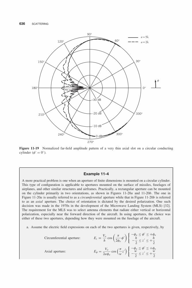
Balanis c11.tex V2 - 11/22/2011 3:50 P.M. Page 636
636 SCATTERING
270°
300°
330°
0°
30°
90°
60°120°
150°
180°
210°
240° 0 dB
−10 dB
−20 dB
a = 5λ
f
a = 2λ
−30 dB
Figure 11-19 Normalized far-field amplitude pattern of a very thin axial slot on a circular conductingcylinder (φ′ = 0◦).
Example 11-4
A more practical problem is one when an aperture of finite dimensions is mounted on a circular cylinder.This type of configuration is applicable to apertures mounted on the surface of missiles, fuselages ofairplanes, and other similar structures and airframes. Practically, a rectangular aperture can be mountedon the cylinder primarily in two orientations, as shown in Figures 11-20a and 11-20b. The one inFigure 11-20a is usually referred to as a circumferential aperture while that in Figure 11-20b is referredto as an axial aperture. The choice of orientation is dictated by the desired polarization. One suchdecision was made in the 1970s in the development of the Microwave Landing System (MLS) [32].The requirement for the MLS was to select antenna elements that radiate either vertical or horizontalpolarization, especially near the forward direction of the aircraft. In using apertures, the choice waseither of these two apertures, depending how they were mounted on the fuselage of the aircraft.
a. Assume the electric field expressions on each of the two apertures is given, respectively, by
Circumferential aperture: Ez = Vo
hcos
(π
2φoφ′
){ −φo ≤ φ′ ≤ +φo
−h
2≤ z ′ ≤ +h
2
Axial aperture: Eφ = Vo
2aφocos
(π
wz ′){ −φo ≤ φ′ ≤ +φo
−w
2≤ z ′ ≤ +w
2

Balanis c11.tex V2 - 11/22/2011 3:50 P.M. Page 637
SCATTERING BY CIRCULAR CYLINDERS 637
2f0
−f0 +f0
y
z
x
w
h
a
w/2
y
z
x
w/2
h
a
(a) (b)
2f0
−f0 +f0
Figure 11-20 Aperture on the surface of a circular cylinder. (a) Circumferential. (b) Axial.
Write expressions for the electric field spherical components of the far-zone fields radiated bythese two apertures.
b. Assuming f = 10 GHz, w = 2.286 cm, h = 1.016 cm (X-band waveguide), compute and plot the:• H-plane normalized amplitude patterns for the circumferential aperture of Figure 11-20a when
it is on a circular cylinder with radii a = 2λ and 5λ. Compare them when the same aperture ismounted on an infinite PEC flat ground plane. Compare the results and assess the effect of thecylinder curvature on the H-plane radiation patterns.
• Repeat the previous computations and plots for the E-plane of the axial aperture ofFigure 11-20b.
Solution: The fields radiated by the two apertures can be determined by replacing the apertures withequivalent currents densities Js and Ms and then using integration over the aperture and surface ofthe cylinder. Since Js is not known outside the aperture, an approximate equivalent will be to eitherassume Js is small outside the aperture; however, this is not an exact equivalent. Another equivalent isto assume Ms only over the aperture, as is done for apertures mounted on ground planes [1]. However,for the cylinder, this also is not exact because the surface to which the aperture is mounted is not flat.
Another procedure is to use transform techniques, as it was done in [11, 33–34] where the fieldsexternal to the cylinder are expressed as the sum of TEz and TMz modes. This is accomplished bywriting the corresponding vector potentials Fz and Az in the transform domain and then the fields areobtained using (6-34) and (6-35). Using such a procedure, it is shown that the far-zone fields radiatedby the respective apertures are:
Circumferential Aperture (circular cylinder)
Eθ = −jVo
π2
e−jβr
r
⎧⎪⎪⎨⎪⎪⎩βa
sin θ
n=+∞∑n=0
cos
(nπ
2βa
)[(βa)2 − n2
] εn j n cos(nφ)
H (2)n (βa sin θ)
⎫⎪⎪⎬⎪⎪⎭

Balanis c11.tex V2 - 11/22/2011 3:50 P.M. Page 638
638 SCATTERING
Eφ = −jVo
π2
e−jβr
r
⎧⎪⎪⎨⎪⎪⎩cot θ
sin θ
n=+∞∑n=1
cos
(nπ
2βa
)[(βa)2 − n2
] 2nj n sin(nφ)
H (2)′n (βa sin θ)
⎫⎪⎪⎬⎪⎪⎭εn =
{1 n = 02 n > 0
; H (2)′n (βρ) = ∂
∂ρH (2)
n (βρ)
When
{θ=π /2: Eφ = 0φ=0: Eφ = 0
as it is should be.
Axial Aperture (circular cylinder)
Eφ = Voλ
2aπ3
e−jβr
r
⎧⎪⎪⎪⎨⎪⎪⎪⎩⎡⎢⎢⎢⎣
cos
(βw
2cos θ
)1 −
(βw
πcos θ
)2
⎤⎥⎥⎥⎦n=+∞∑
n=0
εn j n cos(nφ)
H (2)′n (βa sin θ)
⎫⎪⎪⎪⎬⎪⎪⎪⎭H (2)′
n (βρ) = ∂
∂ρH (2)
n (βρ)
Eθ = 0 in all planes, as it should be.
Using the surface equivalence theorem outlined in Section 7.8 (Chapter 7), we can derive the fieldswhen the respective apertures are mounted on infinite ground planes. The same procedure is outlined inSection 12.1 of [1]. Some of these apertures, when mounted on flat ground planes, have been assignedas end-of-the-chapter problems in Chapters 6 and 7. Following such a procedure, it is shown that thefields in the principle H- and E- planes, radiated by these two apertures when mounted on infinite flatPEC ground planes are:
Circumferential Aperture (flat PEC ground plane)
H-Plane (θ = 90◦)Eφ = 0
Eθ = +π
2C
⎡⎢⎢⎢⎣cos φ
cos
(βa
2sin φ
)(
βa
2sin φ
)2
−(π
2
)2
⎤⎥⎥⎥⎦Axial Aperture (flat PEC ground plane)
E-Plane (θ = 90◦)Eθ = 0
Eφ = + 2
πC
⎡⎢⎢⎣ sin
(βb
2sin φ
)βb
2sin φ
⎤⎥⎥⎦where C = jabβVoe−jβr/2πr . The expressions for the fields radiated in all space are found in theend-of-chapter exercises of Chapters 6 and 7.
To compute the pattern in the H-plane of the circumferential aperture and E-plane of the axialslot, for both the circular cylinder and flat infinite ground plane, a MATLAB computer program,referred to as PEC_Cyl_Plate_Rect, was written and it is included in the multimedia folder

Balanis c11.tex V2 - 11/22/2011 3:50 P.M. Page 639
SCATTERING BY A CONDUCTING WEDGE 639
associated with this book. The respective patterns are shown in Figure 11-21a for the H-planeof the circumferential aperture and in Figure 11-21b for the E-plane of the axial aperture, wherethey are compared with those of the flat ground plane. It is apparent, as expected, that the:
• Cylinder allows radiation on the rear region, whereas the PEC flat ground plane does not.• Larger radius cylinder diminishes more the radiation in the rear region because the creeping
waves that travel around the surface of the cylinder attenuate faster.• Number of lobes in the rear region is greater for the larger cylinder because the two creeping
waves that travel in opposite directions around the surface of the cylinder, and radiatetangentially [15–17], have a greater space separation, which allows the formation of a greaternumber of constructive and destructive interferences, leading to greater number of lobes.
Although the E-plane patterns of the circumferential aperture and the H-plane of the axial apertureare not computed or shown here, those of the cylinder are basically identical to those of the flatground plane, if both are assumed to be of infinite extent.
11.6 SCATTERING BY A CONDUCTING WEDGE
Scattering of electromagnetic waves by a two-dimensional conducting wedge has received consid-erable attention since about the middle 1950s. Because the wedge is a canonical problem that canbe used to represent locally (near the edge) the scattering of more complex structures, asymptoticforms of its solution have been utilized to solve numerous practical problems. The asymptoticforms of its solution are obtained by taking the infinite series modal solution and first transform-ing it into an integral by the so-called Watson transformation [19, 35, 36]. The integral is thenevaluated by the method of steepest descent (saddle point method ) (see Appendix VI) [37]. Theresulting terms of the integral evaluation can be recognized to represent the geometrical opticsfields, both incident and reflected geometrical optics fields, and the diffracted fields, both incidentand reflected diffracted fields [38, 39]. These forms of the solution have received considerableattention in the geometrical theory of diffraction (GTD), which has become a generic name inthe area of antennas and scattering [40–42].
First, we will present the modal solution of the scattering by the wedge. In Chapter 13 wewill briefly outline its asymptotic solution, whose form represents the geometrical optics anddiffracted fields, and apply it to antenna and scattering problems.
11.6.1 Electric Line-Source Scattering by a Conducting Wedge: TMz Polarization
Let us assume that an infinite electric line source of electric current Ie is placed near a conductingwedge whose total inner wedge angle is WA = 2α, as shown in Figure 11-22a . The incident fieldproduced everywhere by the source, in the absence of the wedge, can be written according to(11-158a) and (11-158b) as
E iz = −β2Ie
4ωε=
⎧⎪⎪⎪⎪⎪⎪⎨⎪⎪⎪⎪⎪⎪⎩
+∞∑m=−∞
Jm(βρ)H (2)m (βρ ′)ejm(φ−φ′), ρ ≤ ρ ′
+∞∑m=−∞
Jm(βρ ′)H (2)m (βρ)ejm(φ−φ′), ρ ≥ ρ ′
(11-179a)
(11-179b)
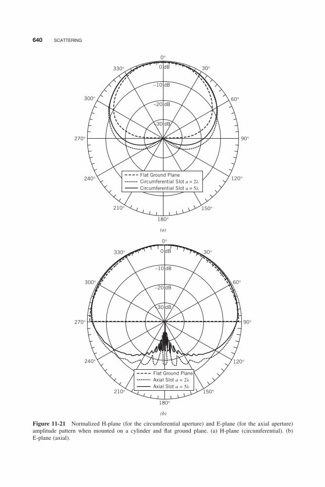
Balanis c11.tex V2 - 11/22/2011 3:50 P.M. Page 640
640 SCATTERING
(a)
0°
0 dB
−10 dB
−20 dB
−30 dB
30°
60°
90°
120°
330°
300°
270°
240°
150°
Flat Ground PlaneCircumferential Slot a = 2lCircumferential Slot a = 5l
180°
210°
(b)
0°
0 dB
−10 dB
−20 dB
−30 dB
30°
60°
90°
120°
330°
300°
270°
240°
150°
Flat Ground PlaneAxial Slot a = 2lAxial Slot a = 5l
180°
210°
Figure 11-21 Normalized H-plane (for the circumferential aperture) and E-plane (for the axial aperture)amplitude pattern when mounted on a cylinder and flat ground plane. (a) H-plane (circumferential). (b)E-plane (axial).
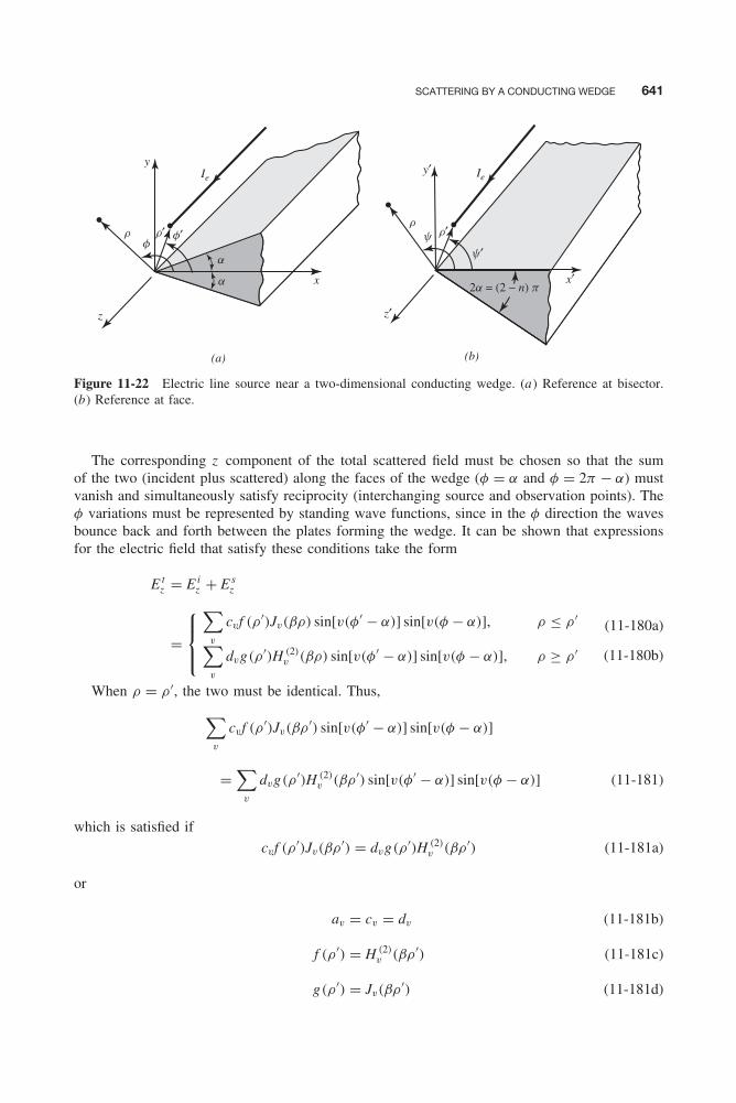
Balanis c11.tex V2 - 11/22/2011 3:50 P.M. Page 641
SCATTERING BY A CONDUCTING WEDGE 641
y
(a)
Ie
z
x
a
a
f′f
r′r
y′
(b)
Ie
z′
x′
y′y r′
r
2a = (2 − n) p
Figure 11-22 Electric line source near a two-dimensional conducting wedge. (a) Reference at bisector.(b) Reference at face.
The corresponding z component of the total scattered field must be chosen so that the sumof the two (incident plus scattered) along the faces of the wedge (φ = α and φ = 2π − α) mustvanish and simultaneously satisfy reciprocity (interchanging source and observation points). Theφ variations must be represented by standing wave functions, since in the φ direction the wavesbounce back and forth between the plates forming the wedge. It can be shown that expressionsfor the electric field that satisfy these conditions take the form
E tz = E i
z + E sz
=
⎧⎪⎨⎪⎩∑
v
cvf (ρ ′)Jv(βρ) sin[v(φ′ − α)] sin[v(φ − α)], ρ ≤ ρ ′∑v
dvg(ρ ′)H (2)v (βρ) sin[v(φ′ − α)] sin[v(φ − α)], ρ ≥ ρ ′
(11-180a)
(11-180b)
When ρ = ρ ′, the two must be identical. Thus,∑v
cvf (ρ ′)Jv(βρ ′) sin[v(φ′ − α)] sin[v(φ − α)]
=∑
v
dvg(ρ ′)H (2)v (βρ ′) sin[v(φ′ − α)] sin[v(φ − α)] (11-181)
which is satisfied if
cvf (ρ ′)Jv(βρ ′) = dvg(ρ ′)H (2)v (βρ ′) (11-181a)
or
av = cv = dv (11-181b)
f (ρ ′) = H (2)v (βρ ′) (11-181c)
g(ρ ′) = Jv(βρ ′) (11-181d)
Balanis c11.tex V2 - 11/22/2011 3:50 P.M. Page 642
642 SCATTERING
Therefore, the total electric field (11-180a) and (11-180b) can be written as
E tz = E i
z + E sz =
⎧⎪⎪⎪⎪⎪⎪⎪⎪⎪⎪⎨⎪⎪⎪⎪⎪⎪⎪⎪⎪⎪⎩
∑v
avJv(βρ)H (2)v (βρ ′) sin[v(φ′ − α)]
× sin[v(φ − α)] ρ ≤ ρ ′
∑v
avJv(βρ ′)H (2)v (βρ) sin[v(φ′ − α)]
× sin[v(φ − α)] ρ ≥ ρ ′
(11-182a)
(11-182b)
It is evident from (11-182a) and (11-182b) that, when φ = α, the total tangential electric fieldvanishes. However, when φ = 2π − α, the electric field (11-182a) and (11-182b) vanishes when
sin[v(φ − α)]φ=2π−α = sin[v(2π − 2α)] = sin[2v(π − α)] = 0 (11-183)
or
2v(π − α) = sin−1(0) = mπ
v = mπ
2(π − α), m = 1, 2, 3 . . . (11-183a)
Thus, in (11-182a) and (11-182b), the allowable values of v are those of (11-183a). The valuesof av depend on the type of source.
The magnetic field components can be obtained by using Maxwell’s equations 11-86 through11-86b, so that we can write that
H tρ = − 1
jωμ
1
ρ
∂E tz
∂φ
= − 1
jωμ
1
ρ
⎧⎪⎪⎪⎪⎪⎪⎨⎪⎪⎪⎪⎪⎪⎩
∑v
vavJv(βρ)H (2)v (βρ ′)
× sin[v(φ′ − α)] cos[v(φ − α)] ρ ≤ ρ ′∑v
vavJv(βρ ′)H (2)v (βρ)
× sin[v(φ′ − α)] cos[v(φ − α)] ρ ≥ ρ ′
(11-184a)
(11-184b)
H tφ = 1
jωμ
∂E tz
∂ρ
= β
jωμ
⎧⎪⎪⎪⎪⎪⎪⎨⎪⎪⎪⎪⎪⎪⎩
∑v
avJ ′v(βρ)H (2)
v (βρ ′)
× sin[v(φ′ − α)] sin[v(φ − α)] ρ ≤ ρ ′∑v
avJv(βρ ′)H (2)′v (βρ)
× sin[v(φ′ − α)] sin[v(φ − α)] ρ ≥ ρ ′
(11-185a)
(11-185b)
where′ ≡ ∂
∂(βρ)(11-185c)

Balanis c11.tex V2 - 11/22/2011 3:50 P.M. Page 643
SCATTERING BY A CONDUCTING WEDGE 643
At the source, the current density is obtained using
Js = n̂ × Ht = âρ × (âρH tρ + âφH t
φ)ρ=ρ′+,ρ′−
= âz H tφ|ρ=ρ′+,ρ′− = âz
[H t
φ(ρ ′+) − H t
φ(ρ ′−)
]= âz
β
jωμ
∑v
av[Jv(βρ ′)H (2)′v (βρ ′) − H (2)
v (βρ ′)J ′v(βρ ′)]
× sin[v(φ′ − α)] sin[v(φ − α)]
Js = âzβ
jωμ
∑v
av(−j )[Jv(βρ ′)Y ′v(βρ ′) − J ′
v(βρ ′)Yv(βρ ′)]
× sin[v(φ′ − α)] sin[v(φ − α)] (11-186)
which, by using the Wronskian (11-95), reduces to
Js = −âz2
πωμρ ′∑
v
av sin[v(φ′ − α)] sin[v(φ − α)] (11-186a)
Since the Fourier series for a current impulse of amplitude Ie located at ρ = ρ ′ and φ = φ′ is[11]
Jz = Ie
(π − α)ρ ′∑
v
sin[v(φ′ − α)] sin[v(φ − α)] (11-187)
then comparing (11-186a) and (11-187) leads to
− 2
πωμav = Ie
π − α⇒ av = − πωμIe
2(π − α)(11-188)
A. Far-Zone Field When the observations are made in the far zone (βρ � 1, ρ > ρ ′) thetotal electric field (11-182b) can be written, by replacing the Hankel function H (2)
v (βρ) by itsasymptotic expression (11-135a), as
E tz
βρ→∞�√
2j
πβρe−jβρ
∑v
avj vJv(βρ ′) sin[v(φ′ − α)] sin[v(φ − α)]
βρ→∞� −Ie
√π j
2β
ωμ
π − α
e−jβρ
√ρ
∑v
j vJv(βρ ′) sin[v(φ′ − α)] sin[v(φ − α)]
E tz
βρ→∞� fe(ρ)∑
v
j vJv(βρ ′) sin[v(φ′ − α)] sin[v(φ − α)] (11-189)
where
fe(ρ) = −Ie
√π j
2β
ωμ
π − α
e−jβρ
√ρ
(11-189a)
Therefore, (11-189) represents the total electric field created in the far-zone region by anelectric source of strength Ie located at ρ ′, φ′.
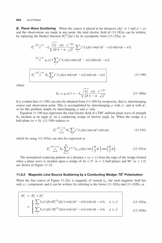
Balanis c11.tex V2 - 11/22/2011 3:50 P.M. Page 644
644 SCATTERING
B. Plane Wave Scattering When the source is placed at far distances (βρ ′ � 1 and ρ ′ > ρ)and the observations are made at any point, the total electric field of (11-182a) can be written,by replacing the Hankel function H (2)
v (βρ ′) by its asymptotic form (11-135a), as
E tz
βρ′→∞� −Ie
√π j
2β
ωμ
π − α
e−jβρ′
√ρ ′
∑v
j vJv(βρ) sin[v(φ′ − α)] sin[v(φ − α)]
βρ′→∞� ge(ρ′)∑
v
j vJv(βρ) sin[v(φ′ − α)] sin[v(φ − α)]
E tz
βρ′→∞� E0
∑v
j vJv(βρ) sin[v(φ′ − α)] sin[v(φ − α)] (11-190)
where
E0 = ge(ρ′) = −Ie
√π j
2β
ωμ
π − α
e−jβρ′
√ρ ′ (11-190a)
It is evident that (11-190) can also be obtained from (11-189) by reciprocity, that is, interchangingsource and observation point. This is accomplished by interchanging ρ with ρ ′, and φ with φ′,or for this problem simply by interchanging ρ and ρ ′ only.
Equation 11-190 also represents the total electric field of a TMz uniform plane wave of strengthE0 incident at an angle φ′ on a conducting wedge of interior angle 2α. When the wedge is ahalf-plane (α = 0), (11-190) reduces to
E tz
βρ′→∞�α=0
E0
∑v
j vJv(βρ) sin(vφ′) sin(vφ) (11-191)
which by using (11-183a) can also be expressed as
E tz
βρ′→∞�α=0
E0
∞∑m=1
j m/2Jm/2(βρ) sin(m
2φ′
)sin
(m
2φ)
(11-191a)
The normalized scattering patterns at a distance λ (ρ = λ) from the edge of the wedge formedwhen a plane wave is incident upon a wedge of 2α = 0◦ (n = 2; half-plane) and 90◦ (n = 1.5)
are shown in Figure 11-23.
11.6.2 Magnetic Line-Source Scattering by a Conducting Wedge: TEz Polarization
When the line source of Figure 11-22a is magnetic of current Im , the total magnetic field hasonly a z component, and it can be written, by referring to the forms (11-182a) and (11-182b), as
H tz = H i
z + H sz
=
⎧⎪⎨⎪⎩∑
s
bsJs(βρ)H (2)s (βρ ′) cos[s(φ′ − α)] cos[s(φ − α)], ρ ≤ ρ ′∑
s
bsJs(βρ ′)H (2)s (βρ) cos[s(φ′ − α)] cos[s(φ − α)], ρ ≥ ρ ′
(11-192a)
(11-192b)
Balanis c11.tex V2 - 11/22/2011 3:50 P.M. Page 645
SCATTERING BY A CONDUCTING WEDGE 645
270°
300°
330°
0°
30°
90°
Rel
ativ
e po
wer
(dB
dow
n) 60°120°
150°
180°
210°
240°
n = 2
n = 1.5
y
r = λ
y′ = 30°
30
20
10
Figure 11-23 Normalized amplitude pattern of a TMz (soft polarization) plane wave incident on a two-dimensional conducting wedge.
The allowable values of s are obtained by applying the boundary conditions, and the coefficientsbs are determined by the type of source.
To apply the boundary conditions, we first need to find the corresponding electric field compo-nents (especially the tangential components). This is accomplished by using Maxwell’s equations11-106 through 11-106b. Thus, the total radial component of the electric field can be written as
E tρ = 1
jωε
1
ρ
∂H tz
∂φ
= − 1
jωε
1
ρ
⎧⎪⎪⎪⎪⎪⎨⎪⎪⎪⎪⎪⎩
∑s
sbs Js(βρ)H (2)s (βρ ′)
× cos[s(φ′ − α)] sin[s(φ − α)], ρ ≤ ρ ′∑s
sbs Js(βρ ′)H (2)s (βρ)
× cos[s(φ′ − α)] sin[s(φ − α)], ρ ≥ ρ ′
(11-193a)
(11-193b)
The boundary conditions that must be satisfied are
E tρ(0 ≤ ρ, ρ ′ ≤ ∞, φ = α, 0 ≤ φ′ ≤ 2π)
= E tρ(0 ≤ ρ, ρ ′ ≤ ∞, φ = 2π − α, 0 ≤ φ′ ≤ 2π) = 0 (11-194)
Balanis c11.tex V2 - 11/22/2011 3:50 P.M. Page 646
646 SCATTERING
The first boundary condition of (11-194) is always satisfied regardless of the values of s . Applyingthe second boundary condition leads to
E tρ(0 ≤ ρ, ρ ′ ≤ ∞, φ = 2π − α, 0 ≤ φ′ ≤ 2π) = 0
= − 1
jωερ
∑s
sbs Js(βρ)H (2)s (βρ ′) cos[s(φ′ − α)] sin[2s(π − α)]
= − 1
jωερ
∑s
sbs Js(βρ ′)H (2)s (βρ) cos[s(φ′ − α)] sin[2s(π − α)] (11-195)
which is satisfied provided
sin[2s(π − α)] = 0 ⇒ 2s(π − α) = sin−1(0) = mπ
s = mπ
2(π − α), m = 0, 1, 2, . . . (11-195a)
Since the source is magnetic, the coefficients bs take the form of
bs = εs
[πωεIm
4(π − α)
](11-196)
where
εs ={
1 s = 02 s �= 0
(11-196a)
In the far zone (βρ � 1), the total field of (11-192b) reduces, by replacing the Hankel functionH (2)
s (βρ) with its asymptotic form (11-135a), to
H tz
βρ→∞� Im
√π j
8β
ωε
π − α
e−jβρ
√ρ
∑s
εs j s Js(βρ ′) cos[s(φ′ − α)] cos[s(φ − α)]
H tz
βρ→∞� fh(ρ)∑
s
εs j s Js(βρ ′) cos[s(φ′ − α)] cos[s(φ − α)] (11-197)
where
fh(ρ) = Im
√π j
8β
ωε
π − α
e−jβρ
√ρ
(11-197a)
When the source is removed at far distances (βρ ′ � 1 and ρ ′ > ρ), (11-192a) reduces to
H tz
βρ′→∞� gh(ρ′)∑
s
εs j s Js(βρ) cos[s(φ′ − α)] cos[s(φ − α)]
H tz
βρ′→∞� H0
∑s
εs j s Js(βρ) cos[s(φ′ − α)] cos[s(φ − α)] (11-198)
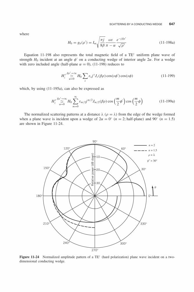
Balanis c11.tex V2 - 11/22/2011 3:50 P.M. Page 647
SCATTERING BY A CONDUCTING WEDGE 647
where
H0 = gh(ρ′) = Im
√π j
8β
ωε
π − α
e−jβρ′
√ρ ′ (11-198a)
Equation 11-198 also represents the total magnetic field of a TEz uniform plane wave ofstrength H0 incident at an angle φ′ on a conducting wedge of interior angle 2α. For a wedgewith zero included angle (half-plane α = 0), (11-198) reduces to
H tz
βρ′→∞�α=0
H0
∑s
εs j s Js(βρ) cos(sφ′) cos(sφ) (11-199)
which, by using (11-195a), can also be expressed as
H tz
βρ′→∞�α=0
H0
∞∑m=0
εm/2j m/2Jm/2(βρ) cos(m
2φ′
)cos
(m
2φ)
(11-199a)
The normalized scattering patterns at a distance λ (ρ = λ) from the edge of the wedge formedwhen a plane wave is incident upon a wedge of 2α = 0◦ (n = 2; half-plane) and 90◦ (n = 1.5)
are shown in Figure 11-24.
270°
300°
330°
0°
30°
90°
Rel
ativ
e po
wer
(dB
dow
n)
60°120°
150°
180°
210°
240°
n = 2
n = 1.5
y
r = λ
y′ = 30°
30
20
10
Figure 11-24 Normalized amplitude pattern of a TEz (hard polarization) plane wave incident on a two-dimensional conducting wedge.

Balanis c11.tex V2 - 11/22/2011 3:50 P.M. Page 648
648 SCATTERING
11.6.3 Electric and Magnetic Line-Source Scattering by a Conducting Wedge
The total electric field of an electric line source near a conducting wedge, as given by (11-182a)and (11-182b), and the total magnetic field of a magnetic line source near a conducting wedge, asgiven by (11-192a) and (11-192b), can both be represented by the same expression by adoptingthe coordinate system (x ′, y ′, z ′) of Figure 11-22b, instead of the (x , y , z ), which is referenced tothe side of the wedge that is illuminated by the source. This is usually more convenient becausesimilar forms of the expression can represent either polarization. Also the interior angle of thewedge will be represented by
2α = (2 − n)π ⇒ n = 2 − 2α
π(11-200)
Thus, a given value of n represents a wedge with a specific included angle: values of n > 1represent wedges with included angles less than 180◦ (referred to as exterior wedges) and valuesof n < 1 represent wedges with included angles greater than 180◦ (referred to as interior wedges).Thus the allowable values of v, as given by (11-183a), and those of s , as given by (11-195a),can now be represented by
v = mπ
2(π − α)
∣∣∣∣α=(1−n/2)π
= m
n, m = 1, 2, 3, . . . (11-201a)
s = mπ
2(π − α)
∣∣∣∣α=(1−n/2)π
= m
n, m = 0, 1, 2, . . . (11-201b)
In addition, the amplitude coefficients av , as given by (11-188), and bs , as given by (11-196),can now be expressed as
av = − πωμIe
2(π − α)
∣∣∣∣α=(1−n/2)π
= −ωμIe
2
(2
n
)(11-202a)
bs = εs
[πωεIm
4(π − α)
]α=(1−n/2)π
= ωεIm
2
(εs
n
)(11-202b)
Using the new coordinate system (x ′, y ′, z ′) of Figure 11-22b, we can write that
φ′ = ψ ′ + α (11-203a)
φ = ψ + α (11-203b)
Therefore, the sine functions of (11-182a) and (11-182b) and the cosine functions of (11-192a)and (11-192b) can be written as
sin[v(φ′ − α)] sin[v(φ − α)] = sin[m
n(ψ ′ + α − α)
]sin
[m
n(ψ + α − α)
]= sin
(m
nψ ′
)sin
(m
nψ
)= 1
2
{cos
[m
n(ψ − ψ ′)
]− cos
[m
n(ψ + ψ ′)
]}(11-204a)
Balanis c11.tex V2 - 11/22/2011 3:50 P.M. Page 649
SCATTERING BY A CONDUCTING WEDGE 649
cos[s(φ′ − α)] cos[s(φ − α)] = cos[m
n(ψ ′ + α − α)
]cos
[m
n(ψ + α − α)
]= cos
(m
nψ ′
)cos
(m
nψ
)= 1
2
{cos
[m
n(ψ − ψ ′)
]− cos
[m
n(ψ + ψ ′)
]}(11-204b)
Using all these new notations, we can write for the TMz polarization the total electric field of(11-182a) and (11-182b) and for the TEz polarization the total magnetic field of (11-192a) and(11-192b) as
TMz
E tz = −ωμIe
4
1
n
⎧⎪⎪⎪⎪⎪⎪⎪⎪⎪⎪⎪⎪⎪⎪⎪⎪⎪⎨⎪⎪⎪⎪⎪⎪⎪⎪⎪⎪⎪⎪⎪⎪⎪⎪⎪⎩
∞∑m=0,1,...
2Jm/n(βρ)H (2)m/n(βρ ′)
×{
cos[m
n(ψ − ψ ′)
]− cos
[m
n(ψ + ψ ′)
]}, ρ ≤ ρ ′
∞∑m=0,1,...
2Jm/n(βρ ′)H (2)m/n(βρ)
×{
cos[m
n(ψ − ψ ′)
]− cos
[m
n(ψ + ψ ′)
]}, ρ ≥ ρ ′
(11-205a)
(11-205b)
TEz
H tz = ωεIm
4
1
n
⎧⎪⎪⎪⎪⎪⎪⎪⎪⎪⎪⎨⎪⎪⎪⎪⎪⎪⎪⎪⎪⎪⎩
∞∑m=0,1,...
εmJm/n(βρ)H (2)m/n(βρ ′)
×{
cos[m
n(ψ − ψ ′)
]+ cos
[m
n(ψ + ψ ′)
]}, ρ ≤ ρ ′
∞∑m=0,1,...
εmJm/n(βρ ′)H (2)m/n(βρ)
×{
cos[m
n(ψ − ψ ′)
]+ cos
[m
n(ψ + ψ ′)
]}, ρ ≥ ρ ′
(11-206a)
(11-206b)
To make the summations in (11-205a) through (11-206b) uniform, the summations of (11-205a) and (11-205b) are noted to begin with m = 0, even though the allowable values of m asgiven by (11-201a) begin with m = 1. However, it should be noted that m = 0 in (11-205a) and(11-205b) does not contribute, and the expressions are correct as stated.
It is apparent, by comparing (11-205a) and (11-205b) with (11-206a) and (11-206b), that theyare of similar forms. Therefore, we can write both as
E tz = −ωμIe
4G(ρ, ρ ′, ψ , ψ ′, n) for TMz (11-207a)
H tz = +ωεIm
4G(ρ, ρ ′, ψ , ψ ′, n) for TEz (11-207b)
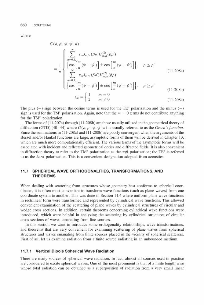
Balanis c11.tex V2 - 11/22/2011 3:50 P.M. Page 650
650 SCATTERING
where
G(ρ, ρ ′, ψ , ψ ′, n)
= 1
n
⎧⎪⎪⎪⎪⎪⎪⎪⎪⎪⎪⎨⎪⎪⎪⎪⎪⎪⎪⎪⎪⎪⎩
∞∑m=0,1,...
εmJm/n(βρ)H (2)m/n(βρ ′){
cos[m
n(ψ − ψ ′)
]± cos
[m
n(ψ + ψ ′)
]}, ρ ≤ ρ ′
∞∑m=0,1,...
εmJm/n(βρ ′)H (2)m/n(βρ){
cos[m
n(ψ − ψ ′)
]± cos
[m
n(ψ + ψ ′)
]}, ρ ≥ ρ ′
εm ={
1 m = 02 m �= 0
(11-208a)
(11-208b)
(11-208c)
The plus (+) sign between the cosine terms is used for the TEz polarization and the minus (−)
sign is used for the TMz polarization. Again, note that the m = 0 terms do not contribute anythingfor the TMz polarization.
The forms of (11-207a) through (11-208b) are those usually utilized in the geometrical theory ofdiffraction (GTD) [40–44] where G(ρ, ρ ′, ψ , ψ ′, n) is usually referred to as the Green’s function.Since the summations in (11-208a) and (11-208b) are poorly convergent when the arguments of theBessel and/or Hankel functions are large, asymptotic forms of them will be derived in Chapter 13,which are much more computationally efficient. The various terms of the asymptotic forms will beassociated with incident and reflected geometrical optics and diffracted fields. It is also convenientin diffraction theory to refer to the TMz polarization as the soft polarization; the TEz is referredto as the hard polarization. This is a convenient designation adopted from acoustics.
11.7 SPHERICAL WAVE ORTHOGONALITIES, TRANSFORMATIONS, ANDTHEOREMS
When dealing with scattering from structures whose geometry best conforms to spherical coor-dinates, it is often most convenient to transform wave functions (such as plane waves) from onecoordinate system to another. This was done in Section 11.4 where uniform plane wave functionsin rectilinear form were transformed and represented by cylindrical wave functions. This allowedconvenient examination of the scattering of plane waves by cylindrical structures of circular andwedge cross sections. In addition, certain theorems concerning cylindrical wave functions wereintroduced, which were helpful in analyzing the scattering by cylindrical structures of circularcross sections of waves emanating from line sources.
In this section we want to introduce some orthogonality relationships, wave transformations,and theorems that are very convenient for examining scattering of plane waves from sphericalstructures and waves emanating from finite sources placed in the vicinity of spherical scatterers.First of all, let us examine radiation from a finite source radiating in an unbounded medium.
11.7.1 Vertical Dipole Spherical Wave Radiation
There are many sources of spherical wave radiation. In fact, almost all sources used in practiceare considered to excite spherical waves. One of the most prominent is that of a finite length wirewhose total radiation can be obtained as a superposition of radiation from a very small linear
Balanis c11.tex V2 - 11/22/2011 3:50 P.M. Page 651
SPHERICAL WAVE ORTHOGONALITIES, TRANSFORMATIONS, AND THEOREMS 651
current element of length � and constant electric current Ie = âz Ie . This is usually referredto as an infinitesimal dipole [1]. The radiation of other sources can be obtained by knowingthe radiation from an infinitesimal dipole. Therefore, it is important that we briefly examine theradiation from such a source.
It is usually most convenient to place the linear element at the origin of the coordinate systemand have its length and current flow along the z axis, as shown in Figure 11-25a . To find thefields radiated by this source, we resort to the techniques of Chapter 6, Sections 6.4 and 6.6,where we first specify the currents Ie and Im of the source. Then we find the potentials A and F[using (6-97a) and (6-97b)], and determine the radiated E and H [using (6-34) and (6-35)].
Following such a procedure, the electric and magnetic fields radiated by the infinitesimal dipoleof Figure 11-25 were derived in Example 6-3. In terms of spherical wave functions, the vectorpotential A can also be written as
A = âzμIe�
4π
e−jβr
r= −âz j
μβIe�
4πh(2)
0 (βr) (11-209)
where h(2)0 (βr) is the spherical Hankel function of order zero, given by
h(2)0 (βr) = e−jβr
−jβr(11-209a)
For the dual problem of the linear magnetic current element of current Im , the vector potentialfunction F takes the form of
F = âzεIm�
4π
e−jβr
r= −âz j
εβIm�
4πh(2)
0 (βr) (11-210)
If the source is removed from the origin, as shown in Figure 11-25b, then the potentials A andF of (11-209) and (11-210) take the form of
A = −âz jμβIe�
4πh(2)
0 (β|r − r′|) (11-211a)
y
(a) (b)
R
r
0 0
x
z
f
q
y
R = r − r′
r′
r
x
z
f
f′
qq′
Figure 11-25 Geometry and coordinate system for vertical dipole radiation. (a) At origin. (b) Offset.

Balanis c11.tex V2 - 11/22/2011 3:50 P.M. Page 652
652 SCATTERING
F = −âz jεβIm�
4πh(2)
0 (β|r − r′|) (11-211b)
where
h(2)0 (β|r − r′|) = e−jβ|r−r′|
−jβ|r − r′| (11-211c)
11.7.2 Orthogonality Relationships
When solving electromagnetic wave problems dealing with spherical structures (either waveg-uides, cavities, or scatterers), the θ variations are represented, as illustrated in Chapters 3 (Section3.4.3) and 10, by Legendre polynomials Pn(cos θ) and associated Legendre functions Pm
n (cos θ)
(see Appendix V).The Legendre polynomials Pn(cos θ) are often called zonal harmonics [45, 46], and they form
a complete orthogonal set in the interval 0 ≤ θ ≤ π . Therefore, in this interval any arbitrary wavefunction can be represented by a series of Legendre polynomials. This is similar to the representa-tion of any periodic function by a series of sines and cosines (Fourier series), since Legendre poly-nomials are very similar in form to cosinusoidal functions. In addition, the products of associatedLegendre functions Pm
n (cos θ) with sines and cosines [Pmn (cos θ) cos(mφ) and Pm
n (cos θ) sin(mφ)]are often referred to as tesseral harmonics [45, 46], and they form a complete orthogonal seton the surface of a sphere. Therefore, any wave function that is defined over a sphere can beexpressed by a series of tesseral harmonics.
Some of the most important and necessary orthogonality relationships that are necessary tosolve wave scattering by spheres will be stated here. The interested reader is referred to [11,45–48] for more details and derivations.
In the interval 0 ≤ θ ≤ π , the integral of the product of Legendre polynomials is equal to∫ π
0Pn(cos θ)Pm(cos θ) sin θ dθ =
⎧⎨⎩ 0, n �= m2
2n + 1, n = m
(11-212a)
(11-212b)
Any function f (θ) defined in the interval of 0 ≤ θ ≤ π can be represented by a series ofLegendre polynomials
f (θ) =∞∑
n=0
anPn(cos θ), 0 ≤ θ ≤ π (11-213)
where
an = 2n + 1
2
∫ π
0f (θ)Pn(cos θ) sin θ dθ (11-213a)
which is known as the Fourier–Legendre series.Defining the tesseral harmonics by
T emn(θ , φ) = Pm
n (cos θ) cos(mφ) (11-214a)
T omn(θ , φ) = Pm
n (cos θ) sin(mφ) (11-214b)
and because ∫ 2π
0sin(pφ) sin(qφ)dφ =
∫ 2π
0cos(pφ) cos(qφ)dφ
={
0, p �= qπ , p = q �= 0
(11-215a)
(11-215b)
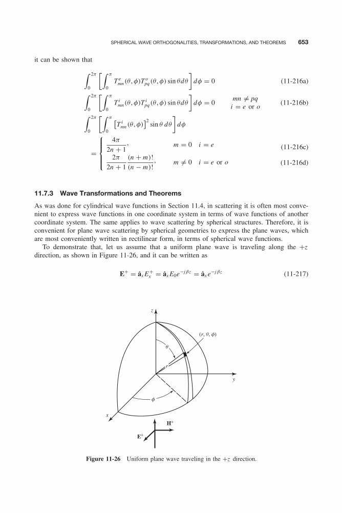
Balanis c11.tex V2 - 11/22/2011 3:50 P.M. Page 653
SPHERICAL WAVE ORTHOGONALITIES, TRANSFORMATIONS, AND THEOREMS 653
it can be shown that∫ 2π
0
[∫ π
0T e
mn(θ , φ)T opq(θ , φ) sin θdθ
]dφ = 0 (11-216a)∫ 2π
0
[∫ π
0T i
mn(θ , φ)T ipq(θ , φ) sin θdθ
]dφ = 0
mn �= pqi = e or o
(11-216b)∫ 2π
0
[∫ π
0
[T i
mn(θ , φ)]2
sin θ dθ
]dφ
=
⎧⎪⎪⎨⎪⎪⎩4π
2n + 1, m = 0 i = e
2π
2n + 1
(n + m)!
(n − m)!, m �= 0 i = e or o
(11-216c)
(11-216d)
11.7.3 Wave Transformations and Theorems
As was done for cylindrical wave functions in Section 11.4, in scattering it is often most conve-nient to express wave functions in one coordinate system in terms of wave functions of anothercoordinate system. The same applies to wave scattering by spherical structures. Therefore, it isconvenient for plane wave scattering by spherical geometries to express the plane waves, whichare most conveniently written in rectilinear form, in terms of spherical wave functions.
To demonstrate that, let us assume that a uniform plane wave is traveling along the +zdirection, as shown in Figure 11-26, and it can be written as
E+ = âx E+x = âx E0e−jβz = âx e−jβz (11-217)
E+
H+
r
(r, q, f)
z
y
x
f
q
Figure 11-26 Uniform plane wave traveling in the +z direction.

Balanis c11.tex V2 - 11/22/2011 3:50 P.M. Page 654
654 SCATTERING
The plane wave can be represented by an infinite sum of spherical wave functions of the form
E+x = e−jβz = e−jβr cos θ =
∞∑n=0
anjn(βr)Pn(cos θ) (11-217a)
since it must be independent of φ and be finite at the origin (r = 0). The next step is to determinethe amplitude coefficients an . This can be accomplished as follows.
Multiplying both sides of (11-217a) by Pm(cos θ) sin θ and integrating in θ from 0 to π , wehave that∫ π
0e−jβr cos θPm(cos θ) sin θdθ =
∫ π
0
[ ∞∑n=0
anjn(βr)Pn(cos θ)Pm(cos θ) sin θ
]dθ
(11-218)Interchanging integration and summation, we have that∫ π
0e−jβr cos θPm(cos θ) sin θdθ =
∞∑n=0
anjn(βr)
∫ π
0Pn(cos θ)Pm(cos θ) sin θdθ
(11-218a)
Using the orthogonality (11-212b) reduces (11-218a) to∫ π
0e−jβr cos θPm(cos θ) sin θdθ = 2am
2m + 1jm(βr) (11-219)
Since the integral of the left side of (11-219) is equal to∫ π
0e−jβr cos θPm(cos θ) sin θdθ = 2j −mjm(βr) (11-219a)
equating (11-219) and (11-219a) leads to
2am
2m + 1jm(βr) = 2j −mjm(βr) ⇒ am = j −m(2m + 1) (11-220)
Thus, (11-217a) reduces to
E+x = e−jβz = e−jβr cos θ =
∞∑n=0
anjn(βr)Pn(cos θ) (11-221)
where
an = j −n(2n + 1) (11-221a)
In a similar manner, it can be shown that
E−x = e+jβz = e+jβr cos θ =
∞∑n=0
bnjn(βr)Pn(cos θ) (11-222)
wherebn = j n(2n + 1) (11-222a)

Balanis c11.tex V2 - 11/22/2011 3:50 P.M. Page 655
SCATTERING BY A SPHERE 655
When dealing with spherical wave scattering of waves generated by linear dipole radiators, it isconvenient to express their radiation, determined using (11-211a) through (11-211c), in terms ofspherical wave functions. This can be accomplished using the addition theorem [11] of sphericalwave functions, which states that (11-211c) can be expressed by referring to the geometry ofFigure 11-25b as
h(2)0 (β|r − r′|) =
⎧⎪⎪⎪⎪⎨⎪⎪⎪⎪⎩
∞∑n=0
(2n + 1) h(2)n (βr ′)jn(βr)Pn(cos ξ), r < r ′
∞∑n=0
(2n + 1) h(2)n (βr)jn(βr ′)Pn(cos ξ), r > r ′
where
cos ξ = cos θ cos θ ′ + sin θ sin θ ′ cos(φ − φ′)
(11-223a)
(11-223b)
(11-223c)
Similarly,
h(1)0 (β|r − r′|) =
⎧⎪⎪⎪⎪⎪⎪⎨⎪⎪⎪⎪⎪⎪⎩
∞∑n=0
(2n + 1) h(1)n (βr ′)jn(βr)Pn(cos ξ), r < r ′
∞∑n=0
(2n + 1) h(1)n (βr)jn(βr ′)Pn(cos ξ), r > r ′
(11-224a)
(11-224b)
11.8 SCATTERING BY A SPHERE
Plane wave scattering by a sphere is a classic problem in scattering and has been addressed bymany authors [11, 14, 20, 45, 46, 49–54]. Here we will outline one that parallels that of [11].Scattering by other sources of excitation such as dipoles, both radial and tangential to the surfaceof the sphere, has also been addressed. Because of its symmetry, a PEC sphere is often used as areference scatterer to calibrate and measure the scattering properties (such as RCS) of other radartargets (missiles, airplanes, helicopters, etc.). A set of five aluminum RCS calibration spheres isshown in Figure 11-27. Apart from its symmetry, the RCS of a sphere can be calculated, whichallows the user to set on the display, during measurements, a baseline to compare the RCS ofother targets to that of the sphere. It is therefore very important that we know and understand thescattering characteristics of a sphere. We will consider both PEC and lossy dielectric spheres.
11.8.1 Perfect Electric Conducting (PEC) Sphere
Let us assume that the electric field of a uniform plane wave is polarized in the x direction, andit is traveling along the z axis, as shown in Figure 11-28. The electric field of the incident waveupon a PEC sphere can then be expressed as
Ei = âx E ix = âx E0e−jβz = âx E0e−jβr cos θ (11-225)
Using the transformation (II-12), the x component of (11-225) can be transformed in sphericalcomponents to
Ei = âr E ir + âθE i
θ + âφE iφ (11-226)
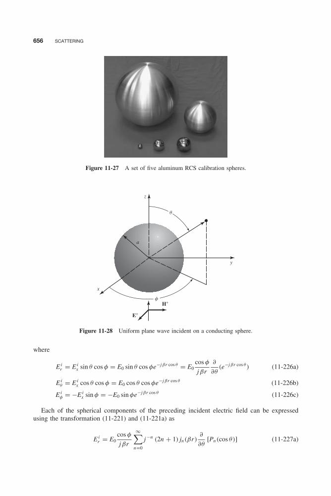
Balanis c11.tex V2 - 11/22/2011 3:50 P.M. Page 656
656 SCATTERING
Figure 11-27 A set of five aluminum RCS calibration spheres.
a
z
y
x
E+
H+f
q
Figure 11-28 Uniform plane wave incident on a conducting sphere.
where
E ir = E i
x sin θ cos φ = E0 sin θ cos φe−jβr cos θ = E0cos φ
jβr
∂
∂θ(e−jβr cos θ ) (11-226a)
E iθ = E i
x cos θ cos φ = E0 cos θ cos φe−jβr cos θ (11-226b)
E iφ = −E i
x sin φ = −E0 sin φe−jβr cos θ (11-226c)
Each of the spherical components of the preceding incident electric field can be expressedusing the transformation (11-221) and (11-221a) as
E ir = E0
cos φ
jβr
∞∑n=0
j −n (2n + 1) jn(βr)∂
∂θ[Pn(cos θ)] (11-227a)

Balanis c11.tex V2 - 11/22/2011 3:50 P.M. Page 657
SCATTERING BY A SPHERE 657
E iθ = E0 cos θ cos φ
∞∑n=0
j −n (2n + 1) jn(βr)Pn(cos θ) (11-227b)
E iφ = −E0 sin φ
∞∑n=0
j −n (2n + 1) jn(βr)Pn(cos θ) (11-227c)
Since according to (10-31),
jn(βr) = 1
βrĴn(βr) (11-228a)
and
∂Pn
∂θ= P1
n (cos θ) (11-228b)
P10 = 0 (11-228c)
we can rewrite (11-227a) through (11-227c) as
E ir = −jE0
cos φ
(βr)2
∞∑n=1
j −n (2n + 1) Ĵn(βr)P1n (cos θ) (11-229a)
E iθ = E0
cos θ cos φ
βr
∞∑n=0
j −n (2n + 1) Ĵn(βr)P0n (cos θ) (11-229b)
E iφ = −E0
sin φ
βr
∞∑n=0
j −n (2n + 1) Ĵn(βr)P0n (cos θ) (11-229c)
The incident and scattered fields by the sphere can be expressed as a superposition of TEr andTMr as outlined, respectively, in Sections 10.2.4 and 10.2.5. The TEr fields are constructed byletting the vector potentials A and F be equal to A = 0 and F = âr Fr (r , θ , φ). The TMr fieldsare constructed when A = âr Ar (r , θ , φ) and F = 0. For example, the incident radial electric fieldcomponent E i
r can be obtained by expressing it in terms of TMr modes or Air . Thus, using Ai
r ,we can write, according to (10-27a), the incident electric field as
E ir = 1
jωμε
(∂2
∂r2+ β2
)Ai
r (11-230)
Equating (11-230) to (11-229a), it can be shown that Air takes the form
Air = E0
cos φ
ω
∞∑n=1
an Ĵn(βr)P1n (cos θ) (11-231)
where
an = j −n (2n + 1)
n(n + 1)(11-231a)
This potential component Air will give the correct value of E i
r , and it will lead to H ir = 0.
The correct expression for the radial component of the incident magnetic field can be obtainedby following a similar procedure but using TEr modes or F i
r of Section 10.2.4. This allows usto show that
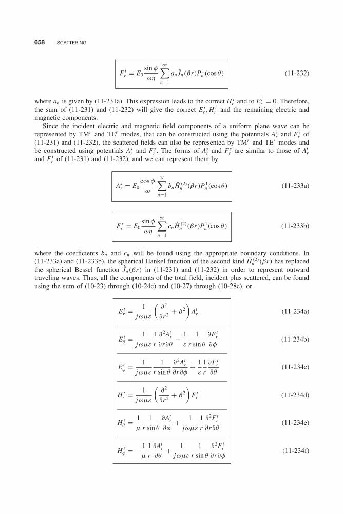
Balanis c11.tex V2 - 11/22/2011 3:50 P.M. Page 658
658 SCATTERING
F ir = E0
sin φ
ωη
∞∑n=1
an Ĵn(βr)P1n (cos θ) (11-232)
where an is given by (11-231a). This expression leads to the correct H ir and to E i
r = 0. Therefore,the sum of (11-231) and (11-232) will give the correct E i
r , H ir and the remaining electric and
magnetic components.Since the incident electric and magnetic field components of a uniform plane wave can be
represented by TMr and TEr modes, that can be constructed using the potentials Air and F i
r of(11-231) and (11-232), the scattered fields can also be represented by TMr and TEr modes andbe constructed using potentials As
r and F sr . The forms of As
r and F sr are similar to those of Ai
rand F i
r of (11-231) and (11-232), and we can represent them by
Asr = E0
cos φ
ω
∞∑n=1
bnĤ (2)n (βr)P1
n (cos θ) (11-233a)
F sr = E0
sin φ
ωη
∞∑n=1
cnĤ (2)n (βr)P1
n (cos θ) (11-233b)
where the coefficients bn and cn will be found using the appropriate boundary conditions. In(11-233a) and (11-233b), the spherical Hankel function of the second kind Ĥ (2)
n (βr) has replacedthe spherical Bessel function Ĵn(βr) in (11-231) and (11-232) in order to represent outwardtraveling waves. Thus, all the components of the total field, incident plus scattered, can be foundusing the sum of (10-23) through (10-24c) and (10-27) through (10-28c), or
E tr = 1
jωμε
(∂2
∂r2+ β2
)At
r
E tθ = 1
jωμε
1
r
∂2Atr
∂r∂θ− 1
ε
1
r sin θ
∂F tr
∂φ
E tφ = 1
jωμε
1
r sin θ
∂2Atr
∂r∂φ+ 1
ε
1
r
∂F tr
∂θ
H tr = 1
jωμε
(∂2
∂r2+ β2
)F t
r
H tθ = 1
μ
1
r sin θ
∂Atr
∂φ+ 1
jωμε
1
r
∂2F tr
∂r∂θ
H tφ = − 1
μ
1
r
∂Atr
∂θ+ 1
jωμε
1
r sin θ
∂2F tr
∂r∂φ
(11-234a)
(11-234b)
(11-234c)
(11-234d)
(11-234e)
(11-234f)
Balanis c11.tex V2 - 11/22/2011 3:50 P.M. Page 659
SCATTERING BY A SPHERE 659
where Atr and F t
r are each equal to the sum of (11-231), (11-232), (11-233a), and (11-233b), or
Atr = Ai
r + Asr = E0
cos φ
ω
∞∑n=1
[an Ĵn(βr) + bnĤ (2)
n (βr)]
P1n (cos θ)
F tr = F i
r + F sr = E0
sin φ
ωη
∞∑n−1
[an Ĵn(βr) + cnĤ (2)
n (βr)]
P1n (cos θ)
an = j −n 2n + 1
n(n + 1)
(11-235a)
(11-235b)
(11-235c)
To determine the coefficients bn and cn , the boundary conditions
E tθ (r = a , 0 ≤ θ ≤ π , 0 ≤ φ ≤ 2π) = 0 (11-236a)
E tφ (r = a , 0 ≤ θ ≤ π , 0 ≤ φ ≤ 2π) = 0 (11-236b)
must be applied. Using (11-235a) and (11-235b), we can write (11-234b) as
E tθ = +j
E0
ωμεr sin θ
{β
ωcos φ
∞∑n=1
[an Ĵ ′
n(βr) + bnĤ (2)′n (βr)
]P ′1
n (cos θ)
}
− E0
εr sin θ
{1
ωηcos φ
∞∑n=1
[an Ĵn(βr) + cnĤ (2)
n (βr)]
P1n (cos θ)
}(11-237)
where in (11-237)
′ ≡ ∂
∂(βr)for the spherical Bessel or Hankel function (11-237a)
′ ≡ ∂
∂(cos θ)= − 1
sin θ
∂
∂θfor the associated Legendre functions (11-237b)
Using (11-237), the boundary condition of (11-236a) is satisfied provided that
an Ĵ ′n(βa) + bnĤ (2)′
n (βa) = 0 ⇒ bn = −anĴ ′
n(βa)
Ĥ (2)′n (βa)
(11-238a)
an Ĵn(βa) + cnĤ (2)n (βa) = 0 ⇒ cn = −an
Ĵn(βa)
Ĥ (2)n (βa)
(11-238b)
The scattered electric field components can be written, using (11-233a) and (11-233b), as
E sr = −jE0 cos φ
∞∑n=1
bn
[Ĥ (2)′′
n (βr) + Ĥ (2)n (βr)
]P1
n (cos θ) (11-239a)
E sθ = E0
βrcos φ
∞∑n=1
[jbnĤ (2)′
n (βr) sin θP ′1n (cos θ) − cnĤ (2)
n (βr)P1
n (cos θ)
sin θ
](11-239b)
E sφ = E0
βrsin φ
∞∑n=1
[jbnĤ (2)′
n (βr)P1
n (cos θ)
sin θ− cnĤ (2)
n (βr) sin θP ′1n (cos θ)
](11-239c)

Balanis c11.tex V2 - 11/22/2011 3:50 P.M. Page 660
660 SCATTERING
where in (11-239a) through (11-239c)
′ ≡ ∂
∂(βr)for the spherical Hankel functions (11-239d)
′′ ≡ ∂2
∂(βr)2for the spherical Hankel functions (11-239e)
′ ≡ ∂
∂(cos θ)= − 1
sin θ
∂
∂θfor the associated Legendre functions (11-239f)
The spherical Hankel function is related to the regular Hankel function by (10-31) or
Ĥ (2)n (βr) =
√πβr
2H (2)
n+1/2(βr) (11-240)
Since for large values of βr the regular Hankel function can be represented by
H (2)n+1/2(βr)
βr→∞�√
2j
πβrj n+1/2e−jβr = j
√2
πβrj ne−jβr (11-241)
then the spherical Hankel function of (11-240) and its partial derivatives can be approximatedby
Ĥ (2)n (βr)
βr→∞� j n+1e−jβr (11-241a)
Ĥ (2)′n (βr) = ∂Ĥ (2)
n (βr)
∂(βr)
βr→∞� −j 2j ne−jβr = j ne−jβr (11-241b)
Ĥ (2)′′n (βr) = ∂2H (2)
n (βr)
∂(βr)2
βr→∞� −j n+1e−jβr (11-241c)
For far-field observations (βr → large), the electric field components of (11-239a) through(11-239c) can be simplified using the approximations (11-241a) through (11-241c). Since theradial component E s
r of (11-239a) reduces with the approximations of (11-241a) through (11-241c) to zero, then in the far zone (11-239a) through (11-239c) can be approximated by
Far-Field Observations (βr → large)
E sr � 0 (11-242a)
E sθ � jE0
e−jβr
βrcos φ
∞∑n=1
j n
[bn sin θP ′1
n (cos θ) − cnP1
n (cos θ)
sin θ
](11-242b)
E sφ � jE0
e−jβr
βrsin φ
∞∑n=1
j n
[bn
P1n (cos θ)
sin θ− cn sin θP ′1
n (cos θ)
](11-242c)
where bn and cn are given by (11-238a) and (11-238b), respectively.The bistatic radar cross section is obtained using (11-22b), and it can be written, using (11-225)
and (11-242a) through (11-242c), as
σ (bistatic) = limr→∞
[4πr2 |Es |2
|Ei |2]
= λ2
π
[cos2 φ|Aθ |2 + sin2 φ|Aφ|2] (11-243)

Balanis c11.tex V2 - 11/22/2011 3:50 P.M. Page 661
SCATTERING BY A SPHERE 661
where
|Aθ |2 =∣∣∣∣∣
∞∑n=1
j n
[bn sin θP ′1
n (cos θ) − cnP1
n (cos θ)
sin θ
]∣∣∣∣∣2
(11-243a)
|Aφ|2 =∣∣∣∣∣
∞∑n=1
j n
[bn
P1n (cos θ)
sin θ− cn sin θP ′1
n (cos θ)
]∣∣∣∣∣2
(11-243b)
The monostatic radar cross section can be found by first reducing the field expressions forobservations toward θ = π . In that direction the scattered electric field of interest is the copolarcomponent, E s
x , and it can be found using (11-242a) through (11-242c) and the transformation(11-13b), by evaluating either
E sx = E s
θ cos θ cos φ∣∣θ=πφ=π
= E sθ
∣∣θ=πφ=π
(11-244a)
orE s
x = −E sφ sin φ
∣∣θ=πφ=3π/2
= E sφ
∣∣θ=πφ=3π/2
(11-244b)
To accomplish either (11-244a) or (11-244b), we need to first evaluate the associated Legendrefunction and its derivative when θ = π . It can be shown that [11, 45]
P1n (cos θ)
sin θ
∣∣∣∣θ=π
= (−1)n n(n + 1)
2(11-245a)
sin θP ′1n (cos θ)
∣∣θ=π
= sin θdP1
n
d(cos θ)= −dP1
n (cos θ)
dθ= (−1)n n(n + 1)
2(11-245b)
Thus, (11-242b) can be expressed using (11-235c), (11-238a), (11-238b), (11-245a), and(11-245b), as
E sθ
∣∣θ=πφ=π
= jE0e−jβr
βr
∞∑n=1
j n(−1)n n(n + 1)
2[bn − cn ]
= −jE0e−jβr
βr
∞∑n=1
j n(−1)n n(n + 1)
2an
[Ĵ ′
n(βa)
Ĥ (2)′n (βa)
− Ĵn(βa)
Ĥ (2)n (βa)
]
E sθ
∣∣θ=πφ=π
= −jE0e−jβr
βr
∞∑n=1
(−1)n (2n + 1)
2
[Ĵ ′
n(βa)Ĥ (2)n (βa) − Ĵn(βa)Ĥ (2)′
n (βa)
Ĥ (2)′n (βa)Ĥ (2)
n (βa)
](11-246)
which reduces, using the Wronskian for spherical Bessel functions
Ĵ ′n(βa)Ĥ (2)
n (βa) − Ĵn(βa)Ĥ (2)′n (βa) = j [Ĵn(βa)Ŷ ′
n(βa) − Ĵ ′n(βa)Ŷn(βa)] = j (11-246a)
to
E sθ
∣∣θ=πφ=π
= E0e−jβr
2βr
∞∑n=1
(−1)n(2n + 1)
Ĥ (2)′n (βa)Ĥ (2)
n (βa)(11-246b)
Thus, the monostatic radar cross section of (11-22b) can be expressed, using (11-246b), by
σ3-D(monostatic) = limr→∞
[4πr2 |Es |2
|Ei |2]
= λ2
4π
∣∣∣∣∣∞∑
n=1
(−1)n(2n + 1)
Ĥ (2)′n (βa)Ĥ (2)
n (βa)
∣∣∣∣∣2
(11-247)
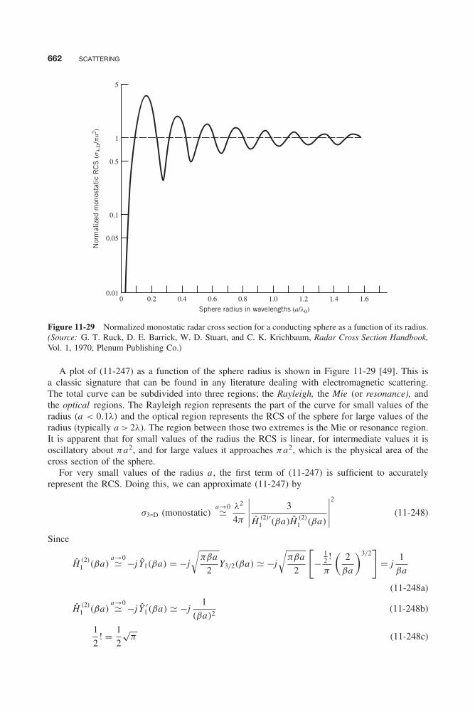
Balanis c11.tex V2 - 11/22/2011 3:50 P.M. Page 662
662 SCATTERING
5
1
0.5
0.1
Nor
mal
ized
mon
osta
tic
RC
S (s
3-D
/pa2 )
0.05
0.010 0.2 0.4 0.6 0.8
Sphere radius in wavelengths (a/l0)
1.0 1.2 1.4 1.6
Figure 11-29 Normalized monostatic radar cross section for a conducting sphere as a function of its radius.(Source: G. T. Ruck, D. E. Barrick, W. D. Stuart, and C. K. Krichbaum, Radar Cross Section Handbook,Vol. 1, 1970, Plenum Publishing Co.)
A plot of (11-247) as a function of the sphere radius is shown in Figure 11-29 [49]. This isa classic signature that can be found in any literature dealing with electromagnetic scattering.The total curve can be subdivided into three regions; the Rayleigh, the Mie (or resonance), andthe optical regions. The Rayleigh region represents the part of the curve for small values of theradius (a < 0.1λ) and the optical region represents the RCS of the sphere for large values of theradius (typically a > 2λ). The region between those two extremes is the Mie or resonance region.It is apparent that for small values of the radius the RCS is linear, for intermediate values it isoscillatory about πa2, and for large values it approaches πa2, which is the physical area of thecross section of the sphere.
For very small values of the radius a , the first term of (11-247) is sufficient to accuratelyrepresent the RCS. Doing this, we can approximate (11-247) by
σ3-D (monostatic)a→0� λ2
4π
∣∣∣∣∣ 3
Ĥ (2)′1 (βa)Ĥ (2)
1 (βa)
∣∣∣∣∣2
(11-248)
Since
Ĥ (2)1 (βa)
a→0� −j Ŷ1(βa) = −j
√πβa
2Y3/2(βa) � −j
√πβa
2
[−
12 !
π
(2
βa
)3/2]
= j1
βa
(11-248a)
Ĥ (2)1 (βa)
a→0� −j Ŷ ′1(βa) � −j
1
(βa)2(11-248b)
1
2! = 1
2
√π (11-248c)
Balanis c11.tex V2 - 11/22/2011 3:50 P.M. Page 663
SCATTERING BY A SPHERE 663
(11-248) reduces to
σ3-D(monostatic)a→0� 9λ2
4π(βa)6 (11-248d)
which is representative of the Rayleigh region scattering.For very large values of the radius a , we can approximate the spherical Hankel function and
its derivative in (11-247) by their asymptotic forms (11-241a) and (11-241b), or
Ĥ (2)n (βa)
βa→∞� e−j [βa(sin α−α cos α)−π/4]
√sin α
(11-249a)
Ĥ (2)′n (βa)
βa→∞�√
sin αe−j [βa(sin α−α cos α)+π/4] (11-249b)
cos α = (n + 1/2)/βa (11-249c)
Thus, (11-247) reduces for very large values of the radius a to
σ3-D(monostatic) = λ2
4π
∣∣∣∣∣∞∑
n=1
(−1)n(2n + 1)
Ĥ (2)′n (βa)Ĥ (2)
n (βa)
∣∣∣∣∣2
a→∞� πa2 (11-250)
which is representative of the optical region scattering, and is also equal to the physical area ofthe cross section of the sphere.
11.8.2 Lossy Dielectric Sphere
The development of the scattering by a lossy dielectric sphere follows that of a PEC sphere, whichwas outlined in the previous section. The major difference is that now electric and magnetic fieldspenetrate the sphere, and we need to write expressions to properly represent them. The expressionsfor the fields outside the sphere will be of similar forms as those of the PEC sphere. To relatethe fields outside and inside the sphere, the appropriate boundary conditions must be applied onthe surface of the sphere; continuity of the tangential electric and magnetic fields, in contrast tothe vanishing of the tangential electric fields on the surface of the sphere for the PEC case.
To start the development, we will use the geometry of Figure 11-28 and assume that themedium outside the sphere is free space (wave number βo) and inside is a lossy dielectric(wave number β̇d ) represented by a relative complex permittivity ε̇r (ε̇r = ε′
r − jε′′r ) and rela-
tive complex permeability μ̇r (μ̇r = μ′r − jμ′′
r ). The total, incident, and scattered fields outsidethe sphere can be represented by the vector potentials, (11-235a) through (11-235c) and the cor-responding electric and magnetic fields by (11-234a) through (11-234f). Inside the sphere thevector potentials should be similar to those outside the sphere, but chosen to represent standingwaves in the radial direction, instead of traveling waves. This is accomplished by choosing thevector potentials for the total fields inside the sphere to be similar to the first terms of (11-235a)and (11-235b), and written as
At−r = Eo
cos φ
ω
∞∑n=1
dn Ĵn(β̇d r
)P (1)
n (cos θ) (11-251a)
F t−r = Eo
sin φ
ωη̇
∞∑n=1
en Ĵn(β̇d r
)P (1)
n (cos θ) (11-251b)
Balanis c11.tex V2 - 11/22/2011 3:50 P.M. Page 664
664 SCATTERING
The modal coefficients, bn and cn (for the fields outside the sphere) and dn and en (for the fieldsinside the sphere), can be determined by application of the boundary conditions. The superscriptminus (−) is used to identify the vector potentials and associated fields on and within the sphere(r ≤ a), while the plus (+) is used to identify those on and outside the sphere (r ≥ a).
Based on the fields of (11-234a) through (11-234f), there exist two tangential electric (Eθ , Eφ)and two tangential magnetic (Hθ , Hφ) field components. For the PEC sphere of the previoussection, the boundary conditions were (11-236a) and (11-236b). However, the appropriate bound-ary conditions for the lossy dielectric sphere require the continuity of the tangential electric andmagnetic fields on the surface of the sphere, which can be written as
E t−θ (r = a , 0 ≤ θ ≤ π , 0 ≤ φ ≤ 2π) = E t+
θ (r = a , 0 ≤ θ ≤ π , 0 ≤ φ ≤ 2π) (11-252a)
E t−φ (r = a , 0 ≤ θ ≤ π , 0 ≤ φ ≤ 2π) = E t+
φ (r = a , 0 ≤ θ ≤ π , 0 ≤ φ ≤ 2π) (11-252b)
H t−θ (r = a , 0 ≤ θ ≤ π , 0 ≤ φ ≤ 2π) = H t+
θ (r = a , 0 ≤ θ ≤ π , 0 ≤ φ ≤ 2π) (11-252c)
H t−φ (r = a , 0 ≤ θ ≤ π , 0 ≤ φ ≤ 2π) = H t+
φ (r = a , 0 ≤ θ ≤ π , 0 ≤ φ ≤ 2π) (11-252d)
The modal coefficients, bn and cn (for the fields outside the sphere), and dn and en (for the fieldsinside the sphere), can be determined by enforcing this set of boundary conditions. To accomplishthis, the two tangential electric (Eθ , Eφ) and two tangential magnetic (Hθ , Hφ) field components,both inside and outside the sphere, must first be written using (11-234b)–(11-234c) and (11-234e)–(11-234f) with the vector potentials of (11-235a)–(11-235b) for outside the sphere and(11-251a)–(11-251b) for inside the sphere.
The enforcement of the boundary conditions (11-252a) through (11-252d) is straight forwardbut cumbersome. Because of space limitations, and as a practice to the reader, the procedure willnot be detailed here but left as an end-of-chapter exercise. Following the procedure outlined here,it can be shown that bn , cn , dn and en can be written and related to an by
bn = −√ε̇r Ĵ ′
n(βoa) Ĵn(β̇d a) + √μ̇r Ĵn(βoa) Ĵ ′
n(β̇d a)√ε̇r H (2)′
n (βoa) Ĵn(β̇d a) − √μ̇r H (2)
n (βoa) Ĵ ′n(β̇d a)
an (11-253a)
cn = −√ε̇r Ĵn(βoa) Ĵ ′
n(β̇d a) + √μ̇r Ĵ ′
n(βoa) Ĵn(β̇d a)√ε̇r H (2)
n (βoa) Ĵ ′n(β̇d a) − √
μ̇r H (2)′n (βoa) Ĵn(β̇d a)
an (11-253b)
dn = −jμ̇r
√ε̇r√
ε̇r H (2)′n (βoa) Ĵn(β̇d a) − √
μ̇r H (2)n (βoa) Ĵ ′
n(β̇d a)an (11-253c)
en = +jμ̇r
√ε̇r√
ε̇r H (2)n (βoa) Ĵ ′
n(β̇d a) − √μ̇r H (2)′
n (βoa) Ĵn(β̇d a)an (11-253d)
where an is given by (11-231a). For a dielectric sphere of small radius, the first term (n = 1) maybe sufficient to represent the fields. It can be shown that for n = 1, (11-253a) through (11-253d)reduce to
b1
βo a→0︷︸︸︷≈ − (βoa)3 ε̇r − 1
ε̇r + 2(11-254a)
c1
βo a→0︷︸︸︷≈ − (βoa)3 μ̇r − 1
μ̇r + 2(11-254b)
d1
βo a→0︷︸︸︷≈ 9
j 2(ε̇r + 2)(11-254c)

Balanis c11.tex V2 - 11/22/2011 3:50 P.M. Page 665
MULTIMEDIA 665
e1
βo a→0︷︸︸︷≈ 9√
μ̇r
j 2√
ε̇r (μ̇r + 2)(11-254d)
Two MATLAB computer programs, PEC_DIEL_Sphere_Fields and Sphere_RCS, have beenwritten. The first one, PEC_DIEL_Sphere_Fields, allows the visualization of the total fields,within and outside the sphere, for both PEC and lossy dielectric spheres. For static fields, a PECsphere can be represented solely by letting ε̇r → very large (ideally infinity). However, at rf , thePEC sphere must be represented as a special case of the lossy dielectric sphere by allowing bothε̇r → very large (ideally infinity) and μ̇r → very small (ideally zero) so that βd remains finite.The second computer program, Sphere_RCS, is based on the formulation of Section 11.8.2.It computes and plots the normalized amplitude scattering pattern, and bistatic and monostaticRCSs of a plane wave scattered by PEC and lossy dielectric spheres based on the geometry ofFigure 11-28.
11.9 MULTIMEDIA
On the website that accompanies this book, the following multimedia resources are included forthe review, understanding, visualization, and presentation of the material of this chapter.
• MATLAB computer programs:a. PEC_Strip_SW: Computes, using PO, the TMz and TEz 2D scattering width (SW),
monostatic and bistatic, of a PEC strip of Figure 11-4.b. PEC_Rect_Plate_RCS: Computes, using PO, the TEx and TMx 3D radar cross section
(RCS), monostatic and bistatic, of a PEC rectangular plate of Figure 11-8.c. PEC_Circ_Plate_RCS: Computes, using PO, the TEx and TMx 3D radar cross section
(RCS), monostatic and bistatic, of a PEC circular plate of Figure P11-7.d. PEC_Cyl_Normal_Fields: Visualizes the TMz and TEz scattered fields of a uniform
plane wave incident, at normal incidence angles, upon the PEC cylinder of circular crosssection of Figure 11-12.
e. PEC_Cyl_Normal_SW: Computes the 2D scattering width (SW) of a uniform planeTMz and TEz wave incident, at normal incidence angles, upon the PEC cylinder ofcircular cross section of Figure 11-12.
f. PEC_Cyl_Oblique_Fields: Visualizes the TMz and TEz scattered fields of a uniformplane wave incident, at oblique incidence angles, upon the PEC cylinder of circular crosssection of Figure 11-16.
g. PEC_Cyl_Oblique_SW: Computes the 2D scattering width (SW) of a uniform planeTMz and TEz wave incident, at oblique incidence angles, upon the PEC cylinder ofcircular cross section of Figure 11-16.
h. PEC_Cyl_Oblique_RCS: Computes and plots the 2D and 3D RCS of a uniform planeTMz and TEz wave incident, at oblique incidence angles, upon the PEC cylinder ofcircular cross section and finite length of Figure 11-16.
i. Cylinder_RCS: It computes and plots the normalized amplitude scattering pattern, andbistatic and monostatic RCSs of a TMz and TEz plane wave scattered by a:• PEC 2-D cylinder, based on geometry of Figures 11-22a and 11-22b and formulations
of Sections 11.5.1 and 11.5.2, respectively.• Lossy 2-D dielectric cylinder based on the end-of-chapter problems 11.58 and 11.60
and associated Figures P11-58 and P11-62, respectively.j. PEC_DIEL_Sphere_Fields: Visualizes the scattered fields of a uniform plane wave by
a lossy dielectric sphere of Figure 11-25.
Balanis c11.tex V2 - 11/22/2011 3:50 P.M. Page 666
666 SCATTERING
k. Sphere_RCS: It computes and plots the normalized amplitude scattering pattern, andbistatic and monostatic RCSs of a uniform plane wave scattered by a:• PEC sphere, based on the geometry of Figure 11-28 and formulations of Section 11.8.1.• Lossy dielectric sphere based on the geometry of Figure 11-28 and formulations of
Section 11.82.l. Power Point (PPT) viewgraphs, in multicolor.
REFERENCES
1. C. A. Balanis, Antenna Theory: Analysis and Design , 3rd edition, Wiley, New York, 2005.
2. K. M. Siegel, “Far field scattering from bodies of revolution,” Appl. Sci. Res., Sec. B , vol. 7,pp. 293–328, 1958.
3. E. F. Knott, V. V. Liepa, and T. B. A. Senior, “Non-specular radar cross section study,” TechnicalReport AFAL-TR-73-70, University of Michigan, April 1973.
4. T. Griesser and C. A. Balanis, “Dihedral corner reflector backscatter using higher-order reflections anddiffractions,” IEEE Trans. Antennas Propagat., vol. AP-35, no. 11, pp. 1235–1247, November 1987.
5. J. S. Asvestas, “The physical optics method in electromagnetic scattering,” Math. Phys., vol. 21,pp. 290–299, 1980.
6. J. S. Asvestas, “Physical optics and the direction of maximization of the far-field average power,” IEEETrans. Antennas Propagat., vol. AP-34, no. 12, pp. 1459–1460, December 1986.
7. E. F. Knott, “RCS reduction of dihedral corners,” IEEE Trans. Antennas Propagat., vol. AP-25, no. 3,pp. 406–409, May 1977.
8. R. A. Ross, “Radar cross section of rectangular plates as a function of aspect angle,” IEEE Trans.Antennas Propagat., vol. AP-14, no. 3, pp. 329–335, May 1966.
9. T. Griesser and C. A. Balanis, “Backscatter analysis of dihedral corner reflectors using physicaloptics and the physical theory of diffraction,” IEEE Trans. Antennas Propagat., vol. AP-35, no. 10,pp. 1137–1147, October 1987.
10. D. P. Marsland, C. A. Balanis, and S. Brumley, “Higher order diffractions from a circular disk,” IEEETrans. Antennas Propagat., vol. AP-35, no. 12, pp. 1436–1444, December 1987.
11. R. F. Harrington, Time-Harmonic Electromagnetic Fields , McGraw-Hill, New York, 1961.
12. D. E. Barrick, “Cylinders,” in Radar Cross Section Handbook , vol. 1, G. T. Ruck, D. E. Barrick, W.D. Stuart, and C. K. Krichbaum (Eds.), Plenum, New York, 1970, Chapter 4, pp. 205–339.
13. J. H. Richmond, The Basic Theory of Harmonic Fields, Antennas and Scattering , Ohio State University,unpublished notes.
14. H. C. Van de Hulst, Light Scattering by Small Particles , Wiley, New York, 1957, pp. 304–307.
15. C. A. Balanis and L. Peters, Jr., “Analysis of aperture radiation from an axially slotted circular con-ducting cylinder using geometrical theory of diffraction,” IEEE Trans. Antennas Propagat., vol. AP-17,no. 1, pp. 93–97, January 1969.
16. C. A. Balanis and L. Peters, Jr., “Aperture radiation from an axially slotted elliptical conduct-ing cylinder using geometrical theory of diffraction,” IEEE Trans. Antennas Propagat., vol. AP-17,no. 4, pp. 507–513, July 1969.
17. P. H. Pathak and R. G. Kouyoumjian, “An analysis of the radiation from apertures in curved surfacesby the geometrical theory of diffraction,” Proc. IEEE , vol. 62, no. 11, pp. 1438–1447, November 1974.
18. S. A. Schelkunoff, “Some equivalence theorems of electromagnetics and their application to radiationproblems,” Bell Syst. Tech. J., vol. 15, pp. 92–112, 1936.
19. J. R. Wait, Electromagnetic Radiation from Cylindrical Structures , Pergamon, New York, 1959.
20. J. J. Bowman, T. B. A. Senior, and P. L. E. Uslenghi (Eds.), Electromagnetic and Acoustic Scatteringby Simple Shapes , North-Holland, Amsterdam, 1969.

Balanis c11.tex V2 - 11/22/2011 3:50 P.M. Page 667
MULTIMEDIA 667
21. A. W. Adey, “Scattering of electromagnetic waves by coaxial cylinders,” Can. J. Phys., vol. 34,pp. 510–520, May 1956.
22. C. C. H. Tang, “Backscattering from dielectric-coated infinite cylindrical obstacles, J. Appl. Phys.,vol. 28, pp. 628–633, May 1957.
23. B. R. Levy, “Diffraction by an elliptic cylinder,” J. Math. Mech., vol. 9, pp. 147–165, 1960.
24. R. D. Kodis, “The scattering cross section of a composite cylinder, geometrical optics,” IEEE Trans.Antennas Propagat., vol. AP-11, no. 1, pp. 86–93, January 1963.
25. K. Mei and J. Van Bladel, “Low-frequency scattering by a rectangular cylinder,” IEEE Trans. AntennasPropagat., vol. AP-11, no. 1, pp. 52–56, January 1963.
26. R. D. Kodis and T. T. Wu, “The optical model of scattering by a composite cylinder,” IEEE Trans.Antennas Propagat., vol. AP-11, no. 6, pp. 703–705, November 1963.
27. J. H. Richmond, “Scattering by a dielectric cylinder of arbitrary cross section shape,” IEEE Trans.Antennas Propagat., vol. AP-13, no. 3, pp. 334–341, May 1965.
28. W. V. T. Rusch and C. Yeh, “Scattering by an infinite cylinder coated with an inhomogeneous andanisotropic plasma sheath,” IEEE Trans. Antennas Propagat., vol. AP-15, no. 3, pp. 452–457, May1967.
29. J.-C. Sureau, “Reduction of scattering cross section of dielectric cylinder by metallic core loading,”IEEE Trans. Antennas Propagat., vol. AP-15, no. 5, pp. 657–662, September 1967.
30. H. E. Bussey and J. H. Richmond, “Scattering by a lossy dielectric circular cylindrical multilayer,numerical values,” IEEE Trans. Antennas Propagat., vol. AP-23, no. 5, pp. 723–725, September 1975.
31. R. E. Eaves, “Electromagnetic scattering from a conducting circular cylinder covered with a circumfer-entially magnetized ferrite,” IEEE Trans. Antennas Propagat., vol. AP-24, no. 2, pp. 190–197, March1976.
32. C. A. Balanis and Y. B. Cheng, “Antenna radiation and modeling for microwave landing system,” IEEETrans. Antennas Propagat ., vol. AP-24, pp. 490–497, July 1976.
33. S. Silver and W. K. Saunders, “The external field produced by a slot in an infinite circular cylinder,”J. Appl. Phy., vol. 21, pp. 153–158, February 1950.
34. L. L. Bailin, “The radiation field produced by a slot in a large circular cylinder,” IRE Trans. AntennasPropagat ., vol. AP-3, pp. 128–137, July 1955.
35. G. N. Watson, “The diffraction of electrical waves by the earth,” Proc. Roy. Soc. (London), vol. A95,pp. 83–99, 1918.
36. R. G. Kouyoumjian, “Asymptotic high-frequency methods,” Proc. IEEE, vol. 53, pp. 864–876, August1965.
37. L. B. Felsen and N. Marcuvitz, Radiation and Scattering of Waves , Prentice-Hall, Englewood Cliffs,N.J., 1973.
38. W. Pauli, “On asymptotic series for functions in the theory of diffraction of light,” Phys. Rev., vol. 34,pp. 924–931, December 1938.
39. F. Oberhettinger, “On asymptotic series occurring in the theory of diffraction of waves by a wedge,”Math. Phys., vol. 34, pp. 245–255, 1956.
40. J. B. Keller, “Geometrical theory of diffraction,” J. Opt. Soc. Amer., vol. 52, no. 2, pp. 116–130,February 1962.
41. R. G. Kouyoumjian and P. H. Pathak, “A uniform geometrical theory of diffraction for an edge in aperfectly conducting surface,” Proc. IEEE, vol. 62, no. 11, pp. 1448–1461, November 1974.
42. G. L. James, Geometrical Theory of Diffraction for Electromagnetic Waves , Third Edition Revised,Peregrinus, London, 1986.
43. D. L. Hutchins, “Asymptotic series describing the diffraction of a plane wave by a two-dimensionalwedge of arbitrary angle,” Ph.D. dissertation, Dept. of Electrical Engineering, Ohio State University,1967.
44. P. H. Pathak and R. G. Kouyoumjian, “The dyadic diffraction coefficient for a perfectly conductingwedge,” Technical Report 2183-4 (AFCRL-69-0546), ElectroScience Laboratory, Ohio State University,June 5, 1970.
Balanis c11.tex V2 - 11/22/2011 3:50 P.M. Page 668
668 SCATTERING
45. J. A. Stratton, Electromagnetic Theory , McGraw-Hill, New York, 1941.46. P. M. Morse and H. Feshbach, Methods of Theoretical Physics , Part II, McGraw-Hill, New York, 1953.47. W. R. Smythe, Static and Dynamic Electricity , McGraw-Hill, New York, 1939.48. M. R. Spiegel, Mathematical Handbook of Formulas and Tables, Schaum’s Outline Series , McGraw-Hill,
New York, 1968.49. A. L. Aden, “Scattering from spheres with sizes comparable to the wavelength,” J. Appl. Phys., vol. 12,
1951.50. S. I. Rubinow and T. T. Wu, “First correction to the geometrical-optics scattering cross section from
cylinders and spheres,” J. Appl. Phys., vol. 27, pp. 1032–1039, 1956.51. J. Rheinstein, “Scattering of electromagnetic waves from dielectric coated conducting spheres,” IEEE
Trans. Antennas Propagat., vol. AP-12, no. 3, pp. 334–340, May 1964.52. R. G. Kouyoumjian, L. Peters, Jr., and D. T. Thomas, “A modified geometrical optics method for
scattering by dielectric bodies,” IEEE Trans. Antennas Propagat., vol. AP-11, no. 6, pp. 690–703,November 1963.
53. D. E. Barrick, “Spheres,” in Radar Cross Section Handbook , vol. 1, G. T. Ruck, D. E. Barrick, W. D.Stuart, and C. K. Krichbaum (Eds.), Plenum, New York, 1970, Chapter 3, pp. 141–204.
54. D. E. Kerr and H. Goldstein, “Radar targets and echoes,” in Propagation of Short Radio Waves , D. E.Kerr (Ed.), McGraw-Hill, 1951, Chapter 6, pp. 445–469.
PROBLEMS
11.1. Repeat Example 11-1 for a displacedmagnetic line source of constant current Im
at ρ ′, φ′.
11.2. A magnetic line source of infinite lengthand constant magnetic current Im is placedparallel to the z axis at a height h abovea PEC ground plane of infinite extent, asshown in Figure 11-2 except that we nowhave a magnetic line source.(a) Determine the total magnetic field at
ρ, φ for 0 ≤ φ ≤ 180◦.(b) Simplify the expressions when the
observations are made at very largedistances (far field).
(c) Determine the smallest height h (in λ)that will introduce a null in the far fieldamplitude pattern at:• φ = 30◦
• φ = 90◦
11.3. Repeat Problem 11.2 for the electric fieldof an electric line source of infinite lengthand constant electric current Ie placed par-allel to the z axis at a height h abovea perfect magnetic conducting (PMC)ground plane of infinite extent, as shownin Figure 11-2, except that we now have aPMC ground plane.
11.4. Repeat Problem 11.3 for the magnetic fieldof a magnetic line source of constant cur-rent Im above a PMC.
11.5. For the problem of Figure 11-2, where theelectric line source is placed at a heighth � λ, and observations are made at anypoint (including near field):(a) Show that the corresponding magnetic
vector potential of the line source atz = h in the absence of the groundplane is given by
A(1)z = A(0)
z (x , y − h)
where A(0)z is the magnetic vector
potential of an isolated line source atz = 0.
(b) Write a simplified closed-form expres-sion for the total magnetic vectorpotential of the line source above theground plane valid for 0 ≤ φ ≤ 180◦.
(c) Determine the angles φ(0 ≤ φ
≤ 180◦) where the total far-zone elec-tric field, at a constant observationdistance ρ, vanishes.
11.6. Repeat Problem 11.5 for a magnetic linesource, and corresponding electric vectorpotential Fz and electric field, above aPMC ground plane.

Balanis c11.tex V2 - 11/22/2011 3:50 P.M. Page 669
PROBLEMS 669
11.7. Two constant current, infinite length elec-tric line sources, are displaced along thex axis a distance s apart, as shownin Figure P11-7. Use superposition andneglect mutual coupling between the lines.
y
x
z +I−I
r
f
#2 #1s2
s2
Figure P11-7
(a) Show that the magnetic vector poten-tial for the two lines can be written as
Atz = A(1)
z
(x − s
2, y)
− A(2)z
(x + s
2, y)
(b) Show that for small spacings (in thelimit as s → 0), the vector potential ofpart (a) reduces to
Atz
s→0� μβIs
4jH (2)
1 (βρ) cos φ
(c) Determine the electric and magneticfield components associated with thetwo line sources when s → 0.
11.8. Repeat Problem 11.7 for the electric vec-tor potential, and the electric and magneticfields, when the two sources are magneticline sources displaced symmetrically alongthe x axis a distance s apart, as shown inFigure P11-7.
11.9. Two electric line sources, of infinite lengthand constant current Ie , are displaced alongthe y axis a distance s apart, as shown inFigure P11-9.(a) Show that the total magnetic vector
potential Atz for the two line sources
can be written as
Atz = A(1)
z
(y − s
2, x
)− A(2)
z
(y + s
2, x
)(b) Show that, for s → 0, the total mag-
netic vector potential can be written insimplified form as the product of oneHankel function and cosine/sine func-tions.
(c) Determine the total electric and mag-netic field components for the twosources for s → 0.
#1
#2
y
xz
r
fs2
s2
Figure P11-9
11.10. Repeat Problem 11.9 for the electric vec-tor potential F t
z , and electric and magneticfields for two magnetic line sources dis-placed along the y axis a distance s apart.
11.11. Four constant current, infinite length elec-tric line sources, of phase as indicated, aredisplaced along the x axis, as shown inFigure P11-11. Assume that the spacingss1 and s2 are very small.(a) Find an approximate closed-form ex-
pression for the magnetic vector poten-tial for the entire array by using theprocedure of Problem 11.7. First con-sider the pairs on each side as individ-ual arrays and then combine the resultsto form a new array.
y
x
z +I+I −I−I
r
f
s1s1
s2
Figure P11-11
(b) Determine in terms of ρ and φ theelectric and magnetic field componentsassociated with the four line sourceswhen ρ � s1 and ρ � s2.
11.12. Four constant current, infinite length elec-tric line sources, of phase as indicated,are displaced along the x and y axes, asshown in Figure P11-12. Assume that the

Balanis c11.tex V2 - 11/22/2011 3:50 P.M. Page 670
670 SCATTERING
spacings s and h are very small and neglectany mutual coupling between the lines.(a) Show, by using the procedure of Prob-
lem 11.7, that the magnetic vectorpotential for the entire array can bewritten as
Azs→0�h→0
− μβshI
4j
∂
∂y[H (2)
1 (βρ) cos φ]
= μβ2shI
8jH (2)
2 (βρ) sin(2φ)
(b) Determine in terms of ρ and φ theelectric and magnetic field componentsassociated with the four line sourceswhen ρ � s and ρ � h .
y
h/2
h/2
s2
x
z
+I−I
−I+I
r
f
s2
Figure P11-12
11.13. Two constant current, infinite length elec-tric line sources are placed above an infi-nite electric ground plane, as shown inFigure P11-13. Assume that the spacingss1 and s2 are very small and neglect anymutual coupling between the lines.(a) Show, by using the procedure of Prob-
lem 11.17, that the magnetic vectorpotential for the entire array can bewritten as
Azs→0�h→0
− μβshI
4j
∂
∂y[H (2)
1 (βρ) cos φ]
= μβ2shI
8jH (2)
2 (βρ) sin(2φ)
(b) Determine in terms of ρ and φ theelectric and magnetic field compo-nents associated with the two line
sources and ground plane when ρ � sand ρ � h .
y
h/2
s/2 s/2
x
z
+I−I
r
f
s = ∞
Figure P11-13
11.14. An infinite length and constant currentelectric line source is placed parallel to theplates of a 90◦ conducting corner reflec-tor, as shown in Figure P11-14. Assumethat the plates of the wedge are infinite inextent and the distance s from the apex tothe source is very small (s � λ).(a) Show that the magnetic vector poten-
tial for the line source and cornerreflector can be written, using the pro-cedure of Problem 11.7, as
Az = μβ2s2I
4jH (2)
2 (βρ) sin (2φ)
y
x
s90°
45°
+I
r
s = ∞
Figure P11-14
(b) Determine the electric and magneticfield components.
(c) Find the angles φ of observation (for aconstant value of ρ) where the electricfield vanishes.
11.15. Two parallel slots, identical, very thin(w → 0), of infinite length and uniform
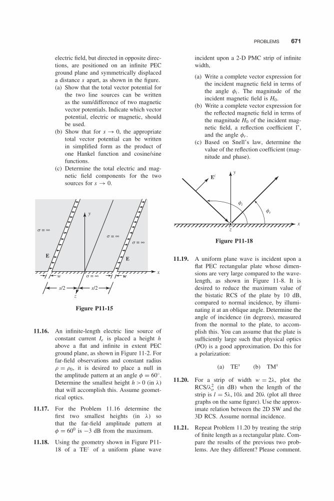
Balanis c11.tex V2 - 11/22/2011 3:50 P.M. Page 671
PROBLEMS 671
electric field, but directed in opposite direc-tions, are positioned on an infinite PECground plane and symmetrically displaceda distance s apart, as shown in the figure.(a) Show that the total vector potential for
the two line sources can be writtenas the sum/difference of two magneticvector potentials. Indicate which vectorpotential, electric or magnetic, shouldbe used.
(b) Show that for s → 0, the appropriatetotal vector potential can be writtenin simplified form as the product ofone Hankel function and cosine/sinefunctions.
(c) Determine the total electric and mag-netic field components for the twosources for s → 0.
z
w wx
y
EE
s = ∞s = ∞
s = ∞
s = ∞
s/2 s/2
w
Figure P11-15
11.16. An infinite-length electric line source ofconstant current Ie is placed a height habove a flat and infinite in extent PECground plane, as shown in Figure 11-2. Forfar-field observations and constant radiusρ = ρ0, it is desired to place a null inthe amplitude pattern at an angle φ = 60◦.Determine the smallest height h > 0 (in λ)that will accomplish this. Assume geomet-rical optics.
11.17. For the Problem 11.16 determine thefirst two smallest heights (in λ) sothat the far-field amplitude pattern atφ = 600 is −3 dB from the maximum.
11.18. Using the geometry shown in Figure P11-18 of a TEz of a uniform plane wave
incident upon a 2-D PMC strip of infinitewidth,
(a) Write a complete vector expression forthe incident magnetic field in terms ofthe angle φi . The magnitude of theincident magnetic field is H0.
(b) Write a complete vector expression forthe reflected magnetic field in terms ofthe magnitude H0 of the incident mag-netic field, a reflection coefficient �,and the angle φr .
(c) Based on Snell’s law, determine thevalue of the reflection coefficient (mag-nitude and phase).
yEi
xz
fr
fi
Figure P11-18
11.19. A uniform plane wave is incident upon aflat PEC rectangular plate whose dimen-sions are very large compared to the wave-length, as shown in Figure 11-8. It isdesired to reduce the maximum value ofthe bistatic RCS of the plate by 10 dB,compared to normal incidence, by illumi-nating it at an oblique angle. Determine theangle of incidence (in degrees), measuredfrom the normal to the plate, to accom-plish this. You can assume that the plate issufficiently large such that physical optics(PO) is a good approximation. Do this fora polarization:
(a) TEx (b) TMx
11.20. For a strip of width w = 2λ, plot theRCS/λ2
o (in dB) when the length of thestrip is l = 5λ, 10λ and 20λ (plot all threegraphs on the same figure). Use the approx-imate relation between the 2D SW and the3D RCS. Assume normal incidence.
11.21. Repeat Problem 11.20 by treating the stripof finite length as a rectangular plate. Com-pare the results of the previous two prob-lems. Are they different? Please comment.
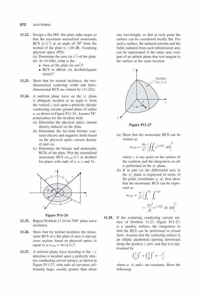
Balanis c11.tex V2 - 11/22/2011 3:50 P.M. Page 672
672 SCATTERING
11.22. Design a flat PEC flat plate radar target sothat the maximum normalized monostaticRCS (σ/λ2) at an angle of 300 from thenormal of the plate is +20 dB. Assumingphysical optics (PO):(a) Determine the area (in λ2) of the plate.(b) At 10 GHz, what is the:
• Area of the plate (in cm2)?• RCS in dB/sm (in decibels/square
meter)?
11.23. Show that for normal incidence, the two-dimensional scattering width and three-dimensional RCS are related by (11-22e).
11.24. A uniform plane wave on the yz planeis obliquely incident at an angle θi fromthe vertical z axis upon a perfectly electricconducting circular ground plane of radiusa , as shown in Figure P11-24. Assume TEx
polarization for the incident field.(a) Determine the physical optics current
density induced on the plate.(b) Determine the far-zone bistatic scat-
tered electric and magnetic fields basedon the physical optics current densityof part (a).
(c) Determine the bistatic and monostaticRCSs of the plate. Plot the normalizedmonostatic RCS (σ3-D/λ2) in decibelsfor plates with radii of a = λ and 5λ.
z
r
x
a
fi
fs
qi qs
y
Figure P11-24
11.25. Repeat Problem 11.24 for TMx plane waveincidence.
11.26. Show that for normal incidence the mono-static RCS of a flat plate of area A and anycross section, based on physical optics, isequal to a σ3-D = 4π(A/λ)2.
11.27. A uniform plane wave traveling in the −zdirection is incident upon a perfectly elec-tric conducting curved surface, as shown inFigure P11-27, with radii of curvature suf-ficiently large, usually greater than about
one wavelength, so that at each point thesurface can be considered locally flat. Forsuch a surface, the induced currents and thefields radiated from each infinitesimal areacan be represented if the same area werepart of an infinite plane that was tangent tothe surface at the same location.
z
Surfacef (x, y, z)
x
yr
f
Figure P11-27
(a) Show that the monostatic RCS can bewritten as
σ3-D = 4π
λ2
∣∣∣∣∫∫A
e+j 2βz dA
∣∣∣∣2
where z is any point on the surface ofthe scatterer and the integration on dAis performed in the xy plane.
(b) If in part (a) the differential area inthe xy plane is expressed in terms ofthe polar coordinates ρ, φ, then showthat the monostatic RCS can be expre-ssed as
σ3-D = π
λ2
∣∣∣∣∫ 2π
0
∫ z (φ)
0
× dρ2
dze+j 2βz dz dφ
∣∣∣∣2
11.28. If the scattering conducting curved sur-face of Problem 11.27, Figure P11-27,is a quadric surface, the integration tofind the RCS can be performed in closedform. Assume that the scattering surface isan elliptic paraboloid opening downwardalong the positive z axis, and that it is rep-resented by( x
a
)2 +( y
b
)2 = − z
c
where a , b, and c are constants. Show thefollowing.
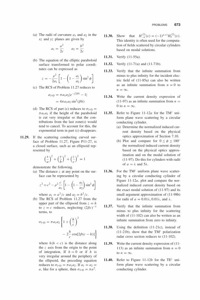
Balanis c11.tex V2 - 11/22/2011 3:50 P.M. Page 673
PROBLEMS 673
(a) The radii of curvature a1 and a2 in thexz and yz planes are given by
a1 = a2
2ca2 = b2
2c
(b) The equation of the elliptic paraboloidsurface transformed to polar coordi-nates can be expressed as
z = − ρ2
2a1
[1 −
(1 − a1
a2
)sin2 φ
](c) The RCS of Problem 11.27 reduces to
a3-D = πa1a2|e−j 2βh − 1|= 4πa1a2 sin2(βh)
(d) The RCS of part (c) reduces to σ3-D =πa1a2 if the height of the paraboloidis cut very irregular so that the con-tributions from the last zone(s) wouldtend to cancel. To account for this, theexponential term in part (c) disappears.
11.29. If the scattering conducting curved sur-face of Problem 11.27, Figure P11-27, isa closed surface, such as an ellipsoid rep-resented by( x
a
)2 +( y
b
)2 +( z
c
)2 = 1
demonstrate the following.(a) The distance z at any point on the sur-
face can be represented by
z 2 = c2 − ρ2 c
a1
[1 −
(1 − a1
a2
)sin2 φ
]where a1 = a2/c and a2 = b2/c.
(b) The RCS of Problem 11.27 from theupper part of the ellipsoid from z = hto z = c reduces, neglecting (2βc)−1
terms, to
σ3-D = πa1a2
{1 +
(h
c
)2
− 2h
ccos[2β(c − h)]
}where h(h < c) is the distance alongthe z axis from the origin to the pointof integration. If h = 0 or if h isvery irregular around the periphery ofthe ellipsoid, the preceding equationreduces to σ3-D = πa1a2. If a1 = a2 =a , like for a sphere, then σ3-D = πa2.
11.30. Show that H (2)−n (x) = (−1)n+1H (2)
n (x).This identity is often used for the computa-tion of fields scattered by circular cylindersbased on modal solutions.
11.31. Verify (11-55a).
11.32. Verify (11-71a) and (11-71b).
11.33. Verify that the infinite summation fromminus to plus infinity for the incident elec-tric field of (11-85a) can also be writtenas an infinite summation from n = 0 ton = ∞.
11.34. Write the current density expression of(11-97) as an infinite summation from n =0 to n = ∞.
11.35. Refer to Figure 11-12a for the TMz uni-form plane wave scattering by a circularconducting cylinder.(a) Determine the normalized induced cur-
rent density based on the physicaloptics approximation of Section 7.10.
(b) Plot and compare for 0 ≤ φ ≤ 180◦
the normalized induced current densitybased on the physical optics approx-imation and on the modal solution of(11-97). Do this for cylinders with radiiof a = λ and 5λ.
11.36. For the TMz uniform plane wave scatter-ing by a circular conducting cylinder ofFigure 11-12a , plot and compare the nor-malized induced current density based onthe exact modal solution of (11-97) and itssmall argument approximation of (11-98b)for radii of a = 0.01λ, 0.01λ, and λ.
11.37. Verify that the infinite summation fromminus to plus infinity for the scatteringwidth of (11-102) can also be written as aninfinite summation from zero to infinity.
11.38. Using the definition (11-21c), instead of(11-21b), show that the TMz polarizationradar cross section reduces to (11-102).
11.39. Write the current density expression of (11-113) as an infinite summation from n = 0to n = ∞.
11.40. Refer to Figure 11-12b for the TEz uni-form plane wave scattering by a circularconducting cylinder.
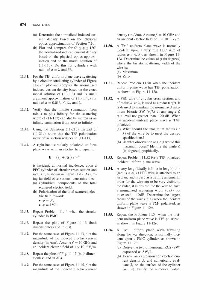
Balanis c11.tex V2 - 11/22/2011 3:50 P.M. Page 674
674 SCATTERING
(a) Determine the normalized induced cur-rent density based on the physicaloptics approximation of Section 7.10.
(b) Plot and compare for 0◦ ≤ φ ≤ 180◦the normalized induced current densitybased on the physical optics approxi-mation and on the modal solution of(11-113). Do this for cylinders withradii of a = λ and 5λ.
11.41. For the TEz uniform plane wave scatteringby a circular conducting cylinder of Figure11-12b, plot and compare the normalizedinduced current density based on the exactmodal solution of (11-113) and its smallargument approximation of (11-114d) forradii of a = 0.01λ, 0.1λ, and λ.
11.42. Verify that the infinite summation fromminus to plus infinity for the scatteringwidth of (11-117) can also be written as aninfinite summation from zero to infinity.
11.43. Using the definition (11-21b), instead of(11-21c), show that the TEz polarizationradar cross section reduces to (11-117).
11.44. A right-hand circularly polarized uniformplane wave with an electric field equal to
E = (ây + j âz
)e−jβx
is incident, at normal incidence, upon aPEC cylinder of circular cross section andradius a , as shown in Figure 11-12. Assum-ing far-field observations, determine the:(a) Cylindrical components of the total
scattered electric field.(b) Polarization of the total scattered elec-
tric field toward:• φ = 0◦.• φ = 180◦.
11.45. Repeat Problem 11.44 when the circularcylinder is PMC.
11.46. Repeat the plots of Figure 11-13 (bothdimensionless and in dB).
11.47. For the same cases of Figure 11-13, plot themagnitude of the induced electric currentdensity (in A/m). Assume f = 10 GHz andan incident electric field of 1 × 10⁻³ V/m.
11.48. Repeat the plots of Fig. 11-15 (both dimen-sionless and in dB).
11.49. For the same cases of Figure 11-15, plot themagnitude of the induced electric current
density (in A/m). Assume f = 10 GHz andan incident electric field of 1 × 10⁻³ V/m.
11.50. A TMz uniform plane wave is normallyincident, upon a very thin PEC wire ofradius a(a � λ), as shown in Figure 11-12a . Determine the values of φ (in degrees)where the bistatic scattering width of thewire is:(a) Maximum.(b) Zero.
11.51. Repeat Problem 11.50 when the incidentuniform plane wave has TEz polarization,as shown in Figure 11-12b.
11.52. A PEC wire of circular cross section, andof radius a � λ, is used as a radar target. Itis desired to maintain the normalized max-imum bistatic SW (σ/λ) at any angle φ
at a level not greater than −20 dB. Whenthe incident uniform plane wave is TMz
polarized:(a) What should the maximum radius (in
λ) of the wire be to meet the desiredspecifications?
(b) At what observation angle φ would thismaximum occur? Identify the angle φ
(in degrees) graphically.
11.53. Repeat Problem 11.52 for a TEz polarizedincident uniform plane wave.
11.54. A very long (ideally infinite in length) thin(radius a � λ) PEC wire is attached to anairplane and is used as a trailing antenna. Inorder for the wire not to be very visible tothe radar, it is desired for the wire to havea normalized scattering width (σ/λ) notto exceed −10 dB. Determine the largestradius of the wire (in λ) when the incidentuniform plane wave is TMz polarized, asshown in Figure 11-12a .
11.55. Repeat the Problem 11.54 when the inci-dent uniform plane wave is TEz polarized,as shown in Figure 11-12b.
11.56. A TMz uniform plane wave travelingalong the +x direction, is normally inci-dent upon a PMC cylinder, as shown inFigure 11.12a .(a) Derive the two-dimensional RCS (SW)
expressed as SW/λ.(b) Derive an expression for electric cur-
rent density Js and numerically eval-uate Js on the surface of the cylinder(ρ = a). Justify the numerical value;
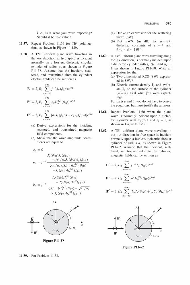
Balanis c11.tex V2 - 11/22/2011 3:50 P.M. Page 675
PROBLEMS 675
i. e., is it what you were expecting?Should it be that value?
11.57. Repeat Problem 11.56 for TEz polariza-tion, as shown in Figure 11.12b.
11.58. A TMz uniform plane wave traveling inthe +x direction in free space is incidentnormally on a lossless dielectric circularcylinder of radius a , as shown in FigureP11-58. Assume that the incident, scat-tered, and transmitted (into the cylinder)electric fields can be written as
Ei = âz E0
+∞∑n=−∞
j −n Jn(β0ρ)ejnφ
Es = âz E0
+∞∑n=−∞
an H (2)n (β0ρ)ejnφ
Ed = âz E0
+∞∑n=−∞
[bn Jn(β1ρ) + cn Yn(β1ρ)]ejnφ
(a) Derive expressions for the incident,scattered, and transmitted magneticfield components.
(b) Show that the wave amplitude coeffi-cients are equal to
cn = 0
an = j −n
J ′n(β0a)Jn(β1a)
−√εr/μr Jn(β0a)J ′
n(β1a)√
εr/μr J ′n(β1a)H (2)
n (β0a)
−Jn(β1a)H (2)′n (β0a)
bn = j −n
Jn(β0a)H (2)n (β0a)
− J ′n(β0a)H (2)
n (β0a)
Jn(β1a)H (2)′n (β0a)− √
εr/μr
× J ′n(β1a)H (2)′
n (β0a)
z
aEi
Hier, mr
e0, m0
x
r
f
y
Figure P11-58
11.59. For Problem 11.58,
(a) Derive an expression for the scatteringwidth (SW).
(b) Plot SW/λ (in dB) for a = 2λ,dielectric constants of εr = 4 and9 (0 ≤ φ ≤ 180◦).
11.60. A TMz uniform plane wave traveling alongthe +x direction, is normally incident upona dielectric cylinder with εr � 1 and μr =1, as shown in Figure P11-58. Write anexpression for the:(a) Two-dimensional RCS (SW) express-
ed in SW/λ.(b) Electric current density Js and evalu-
ate Js on the surface of the cylinder(ρ = a). Is it what you were expect-ing?
For parts a and b, you do not have to derivethe equations, but must justify the answers.
11.61. Repeat Problem 11.60 when the planewave is normally incident upon a dielec-tric cylinder with μr � 1 and εr = 1, asshown in Figure P11-58.
11.62. A TEz uniform plane wave traveling inthe +x direction in free space is incidentnormally upon a lossless dielectric circularcylinder of radius a , as shown in FigureP11-62. Assume that the incident, scat-tered, and transmitted (into the cylinder)magnetic fields can be written as
Hi = âz H0
+∞∑n=−∞
j −n Jn(β0ρ)ejnφ
Hs = âz H0
+∞∑n=−∞
an H (2)n (β0ρ)ejnφ
Hd = âz H0
+∞∑n=−∞
[bn Jn(β1ρ) + cn Yn(β1ρ)]ejnφ
z
a
Ei
Hier, mr e0, m0
x
r
f
y
Figure P11-62

Balanis c11.tex V2 - 11/22/2011 3:50 P.M. Page 676
676 SCATTERING
(a) Derive expressions for the incident,scattered, and transmitted electric fieldcomponents.
(b) Show that the wave amplitude coeffi-cients are equal to
cn = 0
an = j −n
J ′n(β0a)Jn(β1a)
−√μr/εr Jn(β0a)J ′
n(β1a)√
μr/εr J ′n(β1a)H (2)
n (β0a)
−Jn(β1a)H (2)′n (β0a)
bn = j −n
Jn(β0a)H (2)′n (β0a)
−J ′n(β0a)H (2)
n (β0a)
Jn(β1a)H (2)′n (β0a)
−√μr/εr J ′
n(β1a)H (2)n (β0a)
11.63. A TEz uniform plane wave traveling alongthe +x direction, is normally incidentupon a dielectric cylinder with εr � 1 andμr = 1, as shown in Figure P11-62. Writean expression for the:(a) Two-dimensional RCS (SW) express-
ed in SW/λ.(b) Electric current density Js and evalu-
ate Js on the surface of the cylinder(ρ = a). Is it what you were expect-ing?
For parts a and b, you do not have to derivethe equations, but must justify the answers.
11.64. Repeat Problem 11.63 when the planewave is normally incident upon a dielectriccylinder with μ � 1 and εr = 1, as shownin Figure P11-62.
11.65. A TMz uniform plane wave traveling in the+x direction in free space is incident nor-mally upon a dielectric-coated conductingcircular cylinder of radius a as shown inFigure P11-65. The thickness of the loss-less dielectric coating is b − a . Assumethat the incident, reflected, and transmit-ted (into the coating) electric fields can bewritten as shown in Problem 11.58.(a) Write expressions for the incident,
scattered, and transmitted magneticfield components.
(b) Determine the wave amplitude coef-ficients an , bn , and cn . Write them intheier simplest forms.
z ab
Ei
Hier, mr
e0, m0
x
r
f
y
s = ∞
Figure P11-65
11.66. Repeat Problem 11.65 for a TEz uniformplane wave incidence. Assume that theincident, scattered, and transmitted (intothe coating) magnetic fields can be writtenas shown in Problem 11.62.
11.67. Using the definition of (11-21b), insteadof (11-21c), show that the TMz polariza-tion scattering width reduces to (11-137)through (11-137b).
11.68. Using the definition of (11-21c), insteadof (11-21b), show that the TEz polariza-tion scattering width reduces to (11-155)through (11-155b).
11.69. An electric line source of constant currentis placed above a circular PEC cylinder ofinfinite length, as shown in Figure 11-17where φ′ = 90◦. The radius of the cylin-der is a = 50λ. Determine the approximatesmallest height (in number of λ) of the linesource above the cylinder that will allowthe normalized total amplitude pattern tobe at φ = 90◦:(a) Maximum.(b) Minimum.(c) −3 dB.Indicate how you arrive at your answers.
11.70. Two infinite length line sources of constantcurrent I and of the same phase are placednear a conducting cylinder along the x axis(one on each side) a distance s from thecenter of the cylinder, as shown in FigureP11-70.(a) Neglecting coupling between the
sources, write an expression for thetotal electric field for both sources(assume ρ > s).
(b) Assuming the observations are madeat large distances from the cylinder(ρ � s) and the radius of the cylinder
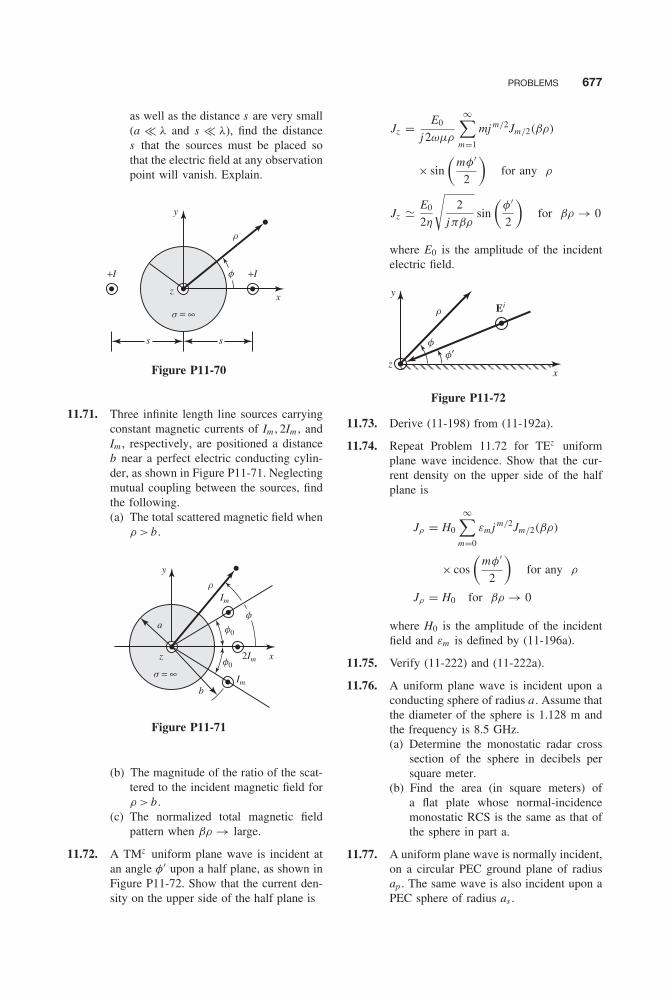
Balanis c11.tex V2 - 11/22/2011 3:50 P.M. Page 677
PROBLEMS 677
as well as the distance s are very small(a � λ and s � λ), find the distances that the sources must be placed sothat the electric field at any observationpoint will vanish. Explain.
s
+I+I
zx
r
f
y
s
s = ∞
Figure P11-70
11.71. Three infinite length line sources carryingconstant magnetic currents of Im , 2Im , andIm , respectively, are positioned a distanceb near a perfect electric conducting cylin-der, as shown in Figure P11-71. Neglectingmutual coupling between the sources, findthe following.(a) The total scattered magnetic field when
ρ > b.
Im
Imb
a
z 2Im x
r
f
s = ∞
f0
f0
y
Figure P11-71
(b) The magnitude of the ratio of the scat-tered to the incident magnetic field forρ > b.
(c) The normalized total magnetic fieldpattern when βρ → large.
11.72. A TMz uniform plane wave is incident atan angle φ′ upon a half plane, as shown inFigure P11-72. Show that the current den-sity on the upper side of the half plane is
Jz = E0
j 2ωμρ
∞∑m=1
mj m/2Jm/2(βρ)
× sin
(mφ′
2
)for any ρ
Jz � E0
2η
√2
jπβρsin
(φ′
2
)for βρ → 0
where E0 is the amplitude of the incidentelectric field.
zx
r
f
f′
y
Ei
Figure P11-72
11.73. Derive (11-198) from (11-192a).
11.74. Repeat Problem 11.72 for TEz uniformplane wave incidence. Show that the cur-rent density on the upper side of the halfplane is
Jρ = H0
∞∑m=0
εm j m/2Jm/2(βρ)
× cos
(mφ′
2
)for any ρ
Jρ = H0 for βρ → 0
where H0 is the amplitude of the incidentfield and εm is defined by (11-196a).
11.75. Verify (11-222) and (11-222a).
11.76. A uniform plane wave is incident upon aconducting sphere of radius a . Assume thatthe diameter of the sphere is 1.128 m andthe frequency is 8.5 GHz.(a) Determine the monostatic radar cross
section of the sphere in decibels persquare meter.
(b) Find the area (in square meters) ofa flat plate whose normal-incidencemonostatic RCS is the same as that ofthe sphere in part a.
11.77. A uniform plane wave is normally incident,on a circular PEC ground plane of radiusap . The same wave is also incident upon aPEC sphere of radius as .
Balanis c11.tex V2 - 11/22/2011 3:50 P.M. Page 678
678 SCATTERING
(a) Determine the radius of the sphere as ,in terms of the radius ap of the circularplate, so that the RCS of the plate andsphere are identical.
(b) If the radius of the plate is 3λ, deter-mine the radius of the sphere so thatthe plate and sphere will have equalRCS.Assume that the radii of the plate andsphere are sufficiently large, comparedto the wavelength, so that both geo-metrical and physical optics are goodapproximations.
11.78. A uniform plane wave is incident, at nor-mal incidence, upon a flat PEC plate ofarea 25λ2. Determine:(a) The 3-D monostatic RCS (in dBsm) of
the plate at f = 10 GHz based on phys-ical optics.
(b) The radius (in λ) of a sphere so thatit has equal backscattered RCS as theplate. Assume the radius of the sphereis large compared to the wavelength.Assume the radius of the sphere islarge compared to the wavelength.
11.79. Repeat the calculations of Figure 11-29 byplotting the normalized RCS [σ/(πa2)]:(a) Dimensionless.(b) In dB.
11.80. For the scattering of a plane wave by a PECsphere of radius a , with the incident elec-tric field with only one component (E i
x ), asoutlined in Section 11.8:(a) Derive an expression, in simplified
form, for the cross-polarized compo-nent (Ey ) of the far-zone scattered elec-tric field in the monostatic directiononly.
(b) Derive an expression, in simplifiedform, of the 3D monostatic RCS forthe cross-polarized field.
(c) Plot the normalized RCS [σ/(πa2)] ofthe cross-polarized component Ey for0 ≤ a ≤ 2λ (λ is the free-space wave-length); similar to Figure 11-29:• Dimensionless.• In dB.
If you have any comments to make con-cerning the monostatic cross-polarized fieldand associated RCS, please do so.
11.81. Applying the boundary conditions (11-252a) through (11-252d) on the internaland external fields of a dielectric sphere,show that the modal coefficients of thevector potential and fields are those of(11-253a) through (11-253d).
11.82. Show that for n = 1, (11-253a) through(11-253d) reduce to (11-254a) through(11-254d).

Balanis c12.tex V2 - 11/22/2011 3:54 P.M. Page 679
CHAPTER 12Integral Equations and the Moment Method
12.1 INTRODUCTION
In Chapter 11 we discussed scattering from conducting objects, such as plates, circular cylinders,and spheres, using geometrical optics, physical optics, and modal solutions. For the plates andcylinders, we assumed that their dimensions were of infinite extent. In practice, however, thedimensions of the objects are always finite, although some of them may be very large. Expressionsfor the radar cross section of finite size scatterers were introduced in the previous chapter. These,however, represent approximate forms, and more accurate expressions are sometimes desired.
The physical optics method of Chapter 7, Section 7.10, was used in the previous chapterto approximate the current induced on the surface of a finite size target, such as the strip andrectangular plate. Radiation integrals were then used to find the field scattered by the target. Toderive a more accurate representation of the current induced on the surface of the finite sizetarget, and thus, of the scattered fields, two methods will be examined in this book.
One method, referred to here as the integral equation (IE) technique, casts the solution for theinduced current in the form of an integral equation (hence its name) where the unknown inducedcurrent density is part of the integrand. Numerical techniques, such as the moment method (MM)[1–6], can then be used to solve for the current density. Once this is accomplished, the fieldsscattered by the target can be found using the traditional radiation integrals. The total inducedcurrent density will be the sum of the physical optics current density and a fringe wave currentdensity [7–13], which can be thought of as a perturbation current density introduced by the edgediffractions of the finite size structure. This method will be introduced and applied in this chapter.
The other method, referred to here as the geometrical theory of diffraction (GTD) [14–17], isan extension of geometrical optics and accounts for the contributions from the edges of the finitestructure using diffraction theory. This method will be introduced and applied in Chapters 13 and14. More extensive discussions of each can be found in the open literature.
12.2 INTEGRAL EQUATION METHOD
The objective of the integral equation (IE) method for scattering is to cast the solution forthe unknown current density, which is induced on the surface of the scatterer, in the form of anintegral equation where the unknown induced current density is part of the integrand. The integralequation is then solved for the unknown induced current density using numerical techniques suchas the moment method (MM). To demonstrate the technique, we will initially consider somespecific problems. We will start with an electrostatics problem and follow it with time-harmonicproblems.
679
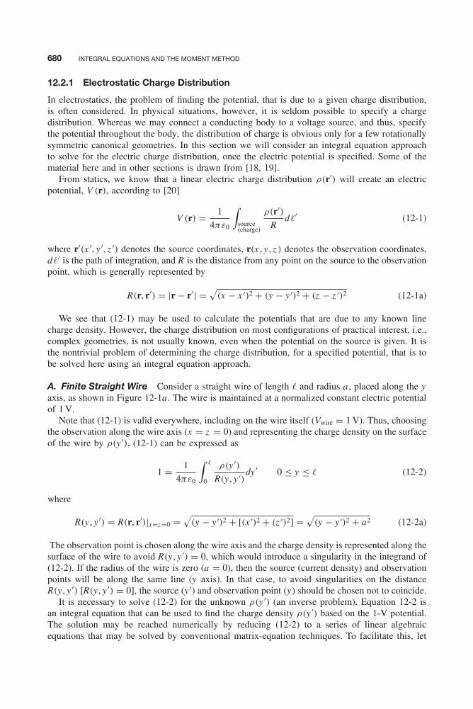
Balanis c12.tex V2 - 11/22/2011 3:54 P.M. Page 680
680 INTEGRAL EQUATIONS AND THE MOMENT METHOD
12.2.1 Electrostatic Charge Distribution
In electrostatics, the problem of finding the potential, that is due to a given charge distribution,is often considered. In physical situations, however, it is seldom possible to specify a chargedistribution. Whereas we may connect a conducting body to a voltage source, and thus, specifythe potential throughout the body, the distribution of charge is obvious only for a few rotationallysymmetric canonical geometries. In this section we will consider an integral equation approachto solve for the electric charge distribution, once the electric potential is specified. Some of thematerial here and in other sections is drawn from [18, 19].
From statics, we know that a linear electric charge distribution ρ(r′) will create an electricpotential, V (r), according to [20]
V (r) = 1
4πε0
∫source(charge)
ρ(r′)R
d�′ (12-1)
where r′(x ′, y ′, z ′) denotes the source coordinates, r(x , y , z ) denotes the observation coordinates,d�′ is the path of integration, and R is the distance from any point on the source to the observationpoint, which is generally represented by
R(r, r′) = |r − r′| =√
(x − x ′)2 + (y − y ′)2 + (z − z ′)2 (12-1a)
We see that (12-1) may be used to calculate the potentials that are due to any known linecharge density. However, the charge distribution on most configurations of practical interest, i.e.,complex geometries, is not usually known, even when the potential on the source is given. It isthe nontrivial problem of determining the charge distribution, for a specified potential, that is tobe solved here using an integral equation approach.
A. Finite Straight Wire Consider a straight wire of length � and radius a , placed along the yaxis, as shown in Figure 12-1a . The wire is maintained at a normalized constant electric potentialof 1 V.
Note that (12-1) is valid everywhere, including on the wire itself (Vwire = 1 V). Thus, choosingthe observation along the wire axis (x = z = 0) and representing the charge density on the surfaceof the wire by ρ(y ′), (12-1) can be expressed as
1 = 1
4πε0
∫ �
0
ρ(y ′)R(y , y ′)
dy ′ 0 ≤ y ≤ � (12-2)
where
R(y , y ′) = R(r, r′)|x=z=0 =√
(y − y ′)2 + [(x ′)2 + (z ′)2] =√
(y − y ′)2 + a2 (12-2a)
The observation point is chosen along the wire axis and the charge density is represented along thesurface of the wire to avoid R(y , y ′) = 0, which would introduce a singularity in the integrand of(12-2). If the radius of the wire is zero (a = 0), then the source (current density) and observationpoints will be along the same line (y axis). In that case, to avoid singularities on the distanceR(y , y ′) [R(y , y ′) = 0], the source (y ′) and observation point (y) should be chosen not to coincide.
It is necessary to solve (12-2) for the unknown ρ(y ′) (an inverse problem). Equation 12-2 isan integral equation that can be used to find the charge density ρ(y ′) based on the 1-V potential.The solution may be reached numerically by reducing (12-2) to a series of linear algebraicequations that may be solved by conventional matrix-equation techniques. To facilitate this, let

Balanis c12.tex V2 - 11/22/2011 3:54 P.M. Page 681
INTEGRAL EQUATION METHOD 681
z
z
Δ
x
ly
y
y1 y2 ym
Rm
rm
r′
yN − 1 yN
x
(a)
(b)
2a
V = 1 V
Figure 12-1 (a) Straight wire of constant potential. (b) Its segmentation.
us approximate the unknown charge distribution ρ(y ′) by an expansion of N known terms withconstant, but unknown, coefficients; that is
ρ(y ′) =N∑
n=1
angn(y′) (12-3)
Thus, (12-2) may be written, using (12-3), as
4πε0 =∫ �
0
1
R(y , y ′)
[N∑
n=1
angn(y′)
]dy ′ (12-4)
Because (12-4) is a nonsingular integral, its integration and summation can be interchanged andit can be written as
4πε0 =N∑
n=1
an
∫ �
0
gn(y ′)√(y − y ′)2 + a2
dy ′ (12-4a)
The wire is now divided into N uniform segments, each of length = �/N , as illustratedin Figure 12-1b. The gn(y ′) functions in the expansion (12-3) are chosen for their ability toaccurately model the unknown quantity, while minimizing computation. They are often referredto as basis (or expansion) functions, and they will be discussed further in Section 12.2.5. Toavoid complexity in this solution, subdomain piecewise constant (or “pulse”) functions will be
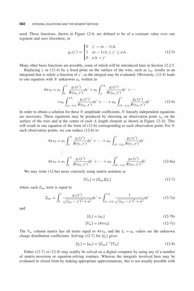
Balanis c12.tex V2 - 11/22/2011 3:54 P.M. Page 682
682 INTEGRAL EQUATIONS AND THE MOMENT METHOD
used. These functions, shown in Figure 12-6, are defined to be of a constant value over onesegment and zero elsewhere, or
gn(y′) =
⎧⎪⎨⎪⎩0 y ′ < (n − 1)
1 (n − 1) ≤ y ′ ≤ n
0 n < y ′(12-5)
Many other basis functions are possible, some of which will be introduced later in Section 12.2.5.Replacing y in (12-4) by a fixed point on the surface of the wire, such as ym , results in an
integrand that is solely a function of y ′, so the integral may be evaluated. Obviously, (12-4) leadsto one equation with N unknowns an written as
4πε0 = a1
∫
0
g1(y ′)R(ym , y ′)
dy ′ + a2
∫ 2
g2(y ′)R(ym , y ′)
dy ′ + · · ·
+an
∫ n
(n−1)
gn(y ′)R(ym , y ′)
dy ′ + · · · + aN
∫ �
(N −1)
gN (y ′)R(ym , y ′)
dy ′ (12-6)
In order to obtain a solution for these N amplitude coefficients, N linearly independent equationsare necessary. These equations may be produced by choosing an observation point ym on thesurface of the wire and at the center of each length element as shown in Figure 12-1b. Thiswill result in one equation of the form of (12-6) corresponding to each observation point. For Nsuch observation points, we can reduce (12-6) to
4πε0 = a1
∫
0
g1(y ′)R(y1, y ′)
dy ′ + · · · + aN
∫ �
(N −1)
gN (y ′)R(y1, y ′)
dy ′
...
4πε0 = a1
∫
0
g1(y ′)R(yN , y ′)
dy ′ + · · · + aN
∫ �
(N −1)
gN (y ′)R(yN , y ′)
dy ′ (12-6a)
We may write (12-6a) more concisely using matrix notation as
[Vm ] = [Zmn ][In ] (12-7)
where each Zmn term is equal to
Zmn =∫ �
0
gn(y ′)√(ym − y ′)2 + a2
dy ′ =∫ n
(n−1)
1√(ym − y ′)2 + a2
dy ′ (12-7a)
and
[In ] = [an ] (12-7b)
[Vm ] = [4πε0] (12-7c)
The Vm column matrix has all terms equal to 4πε0, and the In = an values are the unknowncharge distribution coefficients. Solving (12-7) for [In ] gives
[In ] = [an ] = [Zmn ]−1[Vm ] (12-8)
Either (12-7) or (12-8) may readily be solved on a digital computer by using any of a numberof matrix-inversion or equation-solving routines. Whereas the integrals involved here may beevaluated in closed form by making appropriate approximations, this is not usually possible with

Balanis c12.tex V2 - 11/22/2011 3:54 P.M. Page 683
INTEGRAL EQUATION METHOD 683
more complicated problems. Efficient numerical integration computer subroutines are commonlyavailable in easy-to-use forms.
One closed form evaluation of (12-7a) is to reduce the integral and represent it by
Zmn =
⎧⎪⎪⎪⎪⎪⎪⎪⎪⎪⎪⎪⎪⎪⎪⎪⎨⎪⎪⎪⎪⎪⎪⎪⎪⎪⎪⎪⎪⎪⎪⎪⎩
2 ln
⎛⎜⎜⎜⎜⎝
2+
√a2 +
(
2
)2
a
⎞⎟⎟⎟⎟⎠ m = n
ln
{d+
mn + [(d+mn)
2 + a2]1/2
d−mn + [(d−
mn)2 + a2]1/2
}m �= n but |m − n| ≤ 2
ln
(d+
mn
d−mn
)|m − n| > 2
(12-9a)
(12-9b)
(12-9c)
whered+
mn = �m +
2(12-9d)
d−mn = �m −
2(12-9e)
�m is the distance between the mth matching point and the center of the nth source point.In summary, the solution of (12-2) for the charge distribution on a wire has been accomplished
by approximating the unknown with some basis functions, dividing the wire into segments, andthen sequentially enforcing (12-2) at the center of each segment to form a set of linear equations.
Even for the relatively simple straight wire geometry we have discussed, the exact form ofthe charge distribution is not intuitively apparent. To illustrate the principles of the numericalsolution, an example is now presented.
Example 12-1
A 1-m long straight wire of radius a = 0.001 m is maintained at a constant potential of 1 V. Determinethe linear charge distribution on the wire by dividing the length into 5 and 20 uniform segments. Assumesubdomain pulse basis functions.
Solution:
1. N = 5. When the 1-m long wire is divided into five uniform segments each of length = 0.2 m,(12-7) reduces to⎡⎢⎢⎢⎢⎣
10.60 1.10 0.51 0.34 0.251.10 10.60 1.10 0.51 0.340.51 1.10 10.60 1.10 0.510.34 0.51 1.10 10.60 1.100.25 0.34 0.51 1.10 10.60
⎤⎥⎥⎥⎥⎦⎡⎢⎢⎢⎢⎣
a1
a2
a3
a4
a5
⎤⎥⎥⎥⎥⎦ =
⎡⎢⎢⎢⎣1.11 × 10⁻¹⁰
1.11 × 10⁻¹⁰
...
1.11 × 10⁻¹⁰
⎤⎥⎥⎥⎦Inverting this matrix leads to the amplitude coefficients and subsequent charge distribution of
a1 = 8.81 pC/m
a2 = 8.09 pC/m
a3 = 7.97 pC/m
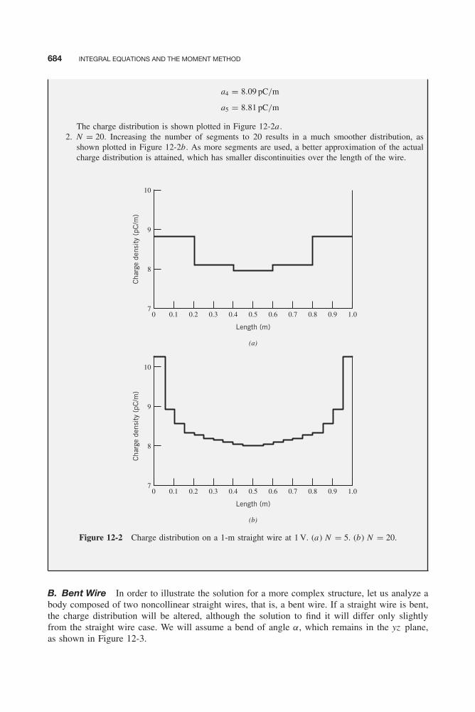
Balanis c12.tex V2 - 11/22/2011 3:54 P.M. Page 684
684 INTEGRAL EQUATIONS AND THE MOMENT METHOD
a4 = 8.09 pC/m
a5 = 8.81 pC/m
The charge distribution is shown plotted in Figure 12-2a .2. N = 20. Increasing the number of segments to 20 results in a much smoother distribution, as
shown plotted in Figure 12-2b. As more segments are used, a better approximation of the actualcharge distribution is attained, which has smaller discontinuities over the length of the wire.
10
Cha
rge
dens
ity
(pC
/m)
9
8
0 0.1 0.2 0.3 0.4 0.5 0.6
Length (m)
0.7 0.8 0.9 1.07
(a)
10
Cha
rge
dens
ity
(pC
/m)
9
8
0 0.1 0.2 0.3 0.4 0.5 0.6
Length (m)
0.7 0.8 0.9 1.07
(b)
Figure 12-2 Charge distribution on a 1-m straight wire at 1 V. (a) N = 5. (b) N = 20.
B. Bent Wire In order to illustrate the solution for a more complex structure, let us analyze abody composed of two noncollinear straight wires, that is, a bent wire. If a straight wire is bent,the charge distribution will be altered, although the solution to find it will differ only slightlyfrom the straight wire case. We will assume a bend of angle α, which remains in the yz plane,as shown in Figure 12-3.
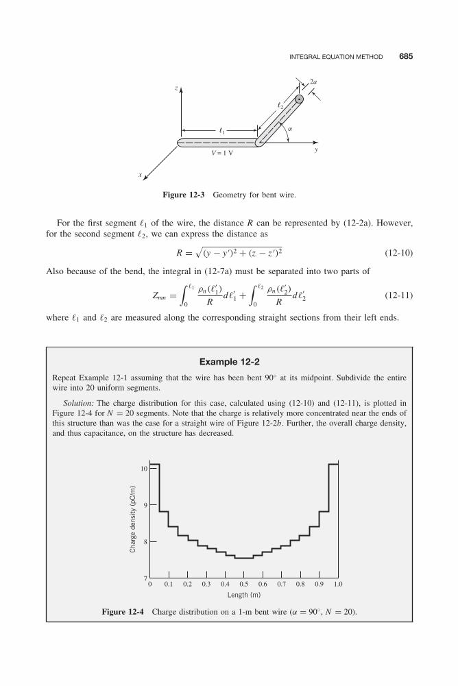
Balanis c12.tex V2 - 11/22/2011 3:54 P.M. Page 685
INTEGRAL EQUATION METHOD 685
y
2a
l2
l1
V = 1 V
x
z
a
Figure 12-3 Geometry for bent wire.
For the first segment �1 of the wire, the distance R can be represented by (12-2a). However,for the second segment �2, we can express the distance as
R =√
(y − y ′)2 + (z − z ′)2 (12-10)
Also because of the bend, the integral in (12-7a) must be separated into two parts of
Zmn =∫ �1
0
ρn(�′1)
Rd�′
1 +∫ �2
0
ρn(�′2)
Rd�′
2 (12-11)
where �1 and �2 are measured along the corresponding straight sections from their left ends.
Example 12-2
Repeat Example 12-1 assuming that the wire has been bent 90◦ at its midpoint. Subdivide the entirewire into 20 uniform segments.
Solution: The charge distribution for this case, calculated using (12-10) and (12-11), is plotted inFigure 12-4 for N = 20 segments. Note that the charge is relatively more concentrated near the ends ofthis structure than was the case for a straight wire of Figure 12-2b. Further, the overall charge density,and thus capacitance, on the structure has decreased.
10
Cha
rge
dens
ity
(pC
/m)
9
8
0 0.1 0.2 0.3 0.4 0.5 0.6
Length (m)
0.7 0.8 0.9 1.07
Figure 12-4 Charge distribution on a 1-m bent wire (α = 90◦, N = 20).
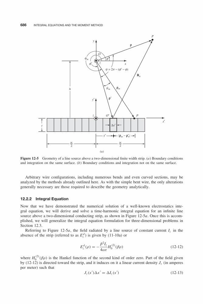
Balanis c12.tex V2 - 11/22/2011 3:54 P.M. Page 686
686 INTEGRAL EQUATIONS AND THE MOMENT METHOD
(a)
w2
w2
x′
y′
y
xz
O
P
h
x′Δx′
O′ Pz
t
f
ρ
f′
ρ′
fm
ym ρm
|ρm − ρ′n|
Rn
y = 2p − (f′ − f)
Figure 12-5 Geometry of a line source above a two-dimensional finite width strip. (a) Boundary conditionsand integration on the same surface. (b) Boundary conditions and integration not on the same surface.
Arbitrary wire configurations, including numerous bends and even curved sections, may beanalyzed by the methods already outlined here. As with the simple bent wire, the only alterationsgenerally necessary are those required to describe the geometry analytically.
12.2.2 Integral Equation
Now that we have demonstrated the numerical solution of a well-known electrostatics inte-gral equation, we will derive and solve a time-harmonic integral equation for an infinite linesource above a two-dimensional conducting strip, as shown in Figure 12-5a . Once this is accom-plished, we will generalize the integral equation formulation for three-dimensional problems inSection 12.3.
Referring to Figure 12-5a , the field radiated by a line source of constant current Iz in theabsence of the strip (referred to as E d
z ) is given by (11-10a) or
E dz (ρ) = −β2Iz
4ωεH (2)
0 (βρ) (12-12)
where H (2)0 (βρ) is the Hankel function of the second kind of order zero. Part of the field given
by (12-12) is directed toward the strip, and it induces on it a linear current density Jz (in amperesper meter) such that
Jz (x′)x ′ = Iz (x
′) (12-13)

Balanis c12.tex V2 - 11/22/2011 3:54 P.M. Page 687
INTEGRAL EQUATION METHOD 687
w2
w2
(b)
x′
y′
y
xz
O
P
h
x′
Δx′
O′
P
z
t
f
ρ
f′
ρ′
fm
ρm
Rn
ρm − ρ′ t/2
Figure 12-5 (Continued ).
which, as x ′ → 0, can be written as
Jz (x′)dx ′ = dIz (x
′) (12-13a)
The induced current of (12-13a) reradiates and produces an electric field component that willbe referred to as reflected (or scattered ) and designated as E r
z (ρ) [or E sz (ρ)]. If the strip is
subdivided into N segments, each of width x ′n as shown in Figure 12-5b, the scattered field
can be written, according to (12-12), as
E sz (ρ) = − β2
4ωε
N∑n=1
H (2)0 (βRn)Iz (x
′n) = − β2
4ωε
N∑n=1
H (2)0 (βRn)Jz (x
′n)x ′
n (12-14)
where x ′n is the position of the nth segment. In the limit, as each segment becomes very small
(xn → 0), (12-14) can be written as
E sz (ρ) = − β2
4ωε
∫strip
H (2)0 (βR)dIz = − β2
4ωε
∫ w/2
−w/2Jz (x
′)H (2)0 (β|ρ − ρ′|)dx ′ (12-15)
since
R = |ρ − ρ′| =√
ρ2 + (ρ ′)2 − 2ρρ ′ cos(φ − φ′) (12-15a)
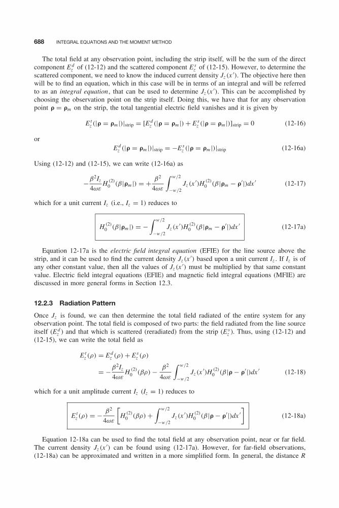
Balanis c12.tex V2 - 11/22/2011 3:54 P.M. Page 688
688 INTEGRAL EQUATIONS AND THE MOMENT METHOD
The total field at any observation point, including the strip itself, will be the sum of the directcomponent E d
z of (12-12) and the scattered component E sz of (12-15). However, to determine the
scattered component, we need to know the induced current density Jz (x ′). The objective here thenwill be to find an equation, which in this case will be in terms of an integral and will be referredto as an integral equation , that can be used to determine Jz (x ′). This can be accomplished bychoosing the observation point on the strip itself. Doing this, we have that for any observationpoint ρ = ρm on the strip, the total tangential electric field vanishes and it is given by
E tz (|ρ = ρm |)|strip = [E d
z (|ρ = ρm |) + E sz (|ρ = ρm |)]strip = 0 (12-16)
orE d
z (|ρ = ρm |)|strip = −E sz (|ρ = ρm |)|strip (12-16a)
Using (12-12) and (12-15), we can write (12-16a) as
−β2Iz
4ωεH (2)
0 (β|ρm |) = + β2
4ωε
∫ w/2
−w/2Jz (x
′)H (2)0 (β|ρm − ρ′|)dx ′ (12-17)
which for a unit current Iz (i.e., Iz = 1) reduces to
H (2)0 (β|ρm |) = −
∫ w/2
−w/2Jz (x
′)H (2)0 (β|ρm − ρ′|)dx ′ (12-17a)
Equation 12-17a is the electric field integral equation (EFIE) for the line source above thestrip, and it can be used to find the current density Jz (x ′) based upon a unit current Iz . If Iz is ofany other constant value, then all the values of Jz (x ′) must be multiplied by that same constantvalue. Electric field integral equations (EFIE) and magnetic field integral equations (MFIE) arediscussed in more general forms in Section 12.3.
12.2.3 Radiation Pattern
Once Jz is found, we can then determine the total field radiated of the entire system for anyobservation point. The total field is composed of two parts: the field radiated from the line sourceitself (E d
z ) and that which is scattered (reradiated) from the strip (E sz ). Thus, using (12-12) and
(12-15), we can write the total field as
E tz (ρ) = E d
z (ρ) + E sz (ρ)
= −β2Iz
4ωεH (2)
0 (βρ) − β2
4ωε
∫ w/2
−w/2Jz (x
′)H (2)0 (β|ρ − ρ′|)dx ′ (12-18)
which for a unit amplitude current Iz (Iz = 1) reduces to
E tz (ρ) = − β2
4ωε
[H (2)
0 (βρ) +∫ w/2
−w/2Jz (x
′)H (2)0 (β|ρ − ρ′|)dx ′
](12-18a)
Equation 12-18a can be used to find the total field at any observation point, near or far field.The current density Jz (x ′) can be found using (12-17a). However, for far-field observations,(12-18a) can be approximated and written in a more simplified form. In general, the distance R

Balanis c12.tex V2 - 11/22/2011 3:54 P.M. Page 689
INTEGRAL EQUATION METHOD 689
is given by (12-15a). However, for far-field observations (ρ � ρ ′), (12-15a) reduces, using thebinomial expansion, to
R �{
ρ − ρ ′ cos(φ − φ′) for phase terms
ρ for amplitude terms
(12-19a)
(12-19b)
For large arguments, the Hankel functions in (12-18a) can be replaced by their asymptoticform
H (2)n (βz )
βz→∞�√
2j
πβzj ne−jβz (12-20)
For n = 0, (12-20) reduces to
H (2)0 (βz ) �
√2j
πβze−jβz (12-20a)
Using (12-19a) through (12-20a), we can write the Hankel functions in (12-18a) as
H (2)0 (βρ) �
√2j
πβρe−jβρ (12-21a)
H (2)0 (β|ρ − ρ′|) �
√2j
πβρe−jβ[ρ−ρ′ cos(φ−φ′)]
�√
2j
πβρe−jβρ+jβρ′ cos(φ−φ′) (12-21b)
When (12-21a) and (12-21b) are substituted into (12-18a), they reduce it to
E tz (ρ) � − β2
4ωε
√2j
πβρe−jβρ
[1 +
∫ +w/2
−w/2Jz (x
′)ejβρ′ cos(φ−φ′)dx ′]
(12-22)
which in normalized form can be written as
E tz (normalized) � 1 +
∫ w/2
−w/2Jz (x
′)ejβρ′ cos(φ−φ′)dx ′ (12-22a)
Equation 12-22a represents the normalized pattern of the line above the strip. It is based on thelinear current density Jz (x ′) that is induced by the source on the strip. The current density can befound using approximate methods or, more accurately, using the electric field integral equation12-17a.
12.2.4 Point-Matching (Collocation) Method
The next step will be to use a numerical technique to solve the electric field integral equation 12-17a for the unknown current density Jz (x ′). We first expand Jz (x ′) into a finite series of theform
Jz (x′) �
N∑n=1
angn(x′) (12-23)
Balanis c12.tex V2 - 11/22/2011 3:54 P.M. Page 690
690 INTEGRAL EQUATIONS AND THE MOMENT METHOD
where gn(x ′) represents basis (expansion) functions [1,2]. When (12-23) is substituted into (12-17a), we can write it as
H (2)0 (β|ρm |) = −
∫ w/2
−w/2
N∑n=1
angn(x′)H (2)
0 (β|ρm − ρ′n |)dx ′
H (2)0 (β|ρm |) = −
N∑n=1
an
∫ w/2
−w/2gn(x
′)H (2)0 (β|ρm − ρ′
n |)dx ′ (12-24)
which takes the general form
h =N∑
n=1
anF (gn) (12-25)
where
h = H (2)0 (β|ρm |) (12-25a)
F (gn) = −∫ w/2
−w/2gn(x
′)H (2)0 (β|ρm − ρ′
n |)dx ′ (12-25b)
In (12-25), F is referred to as a linear integral operator , gn represents the response function, andh is the known excitation function.
Equation 12-17a is an electric field integral equation derived by enforcing the boundary condi-tions of vanishing total tangential electric field on the surface of the conducting strip. A numericalsolution of (12-17a) is (12-24) or (12-25) through (12-25b), which, for a given observation pointρ = ρm , leads to one equation with N unknowns. This can be repeated N times by choosingN observation points. Such a procedure leads to a system of N linear equations each with Nunknowns of the form
H (2)0 (β|ρm |) =
N∑n=1
an
[−
∫ w/2
−w/2gn(x
′)H (2)0 (β|ρm − ρ′
n |)dx ′]
m = 1, 2, . . . , N (12-26)
which can also be written as
Vm =N∑
n=1
InZmn (12-27)
where
Vm = H (2)0 (β|ρm |) (12-27a)
In = an (12-27b)
Zmn = −∫ w/2
−w/2gn(x
′)H (2)0 (β|ρm − ρ′
n |)dx ′ (12-27c)
Balanis c12.tex V2 - 11/22/2011 3:54 P.M. Page 691
INTEGRAL EQUATION METHOD 691
In matrix form, (12-27) can be expressed as
[Vm ] = [Zmn ][In ] (12-28)
where the unknown is [In ] and can be found by solving (12-28), or
[In ] = [Zmn ]−1[Vm ] (12-28a)
Since the system of N linear equations with N unknowns—as given by (12-26), (12-27), or(12-28)—was derived by applying the boundary conditions at N discrete points, the techniqueis referred to as the point-matching (or collocation) method [1, 2].
Thus, by finding the elements of the [V ] and [Z ], and then the inverse [Z ]−1, we can determinethe elements an of the [I ] matrix. This in turn allows us to approximate Jz (x ′) using (12-23),which can then be used in (12-18a) to find the total field everywhere. However, for far-fieldobservations, the total field can be found more easily using (12-22) or, in normalized form,(12-22a).
12.2.5 Basis Functions
One very important step in any numerical solution is the choice of basis functions. In general,one chooses as basis functions the set that has the ability to accurately represent and resemblethe anticipated unknown function, while minimizing the computational effort required to employit [21–23]. Do not choose basis functions with smoother properties than the unknown beingrepresented.
Theoretically, there are many possible basis sets. However, only a limited number are discussedhere. These sets may be divided into two general classes. The first class consists of subdomainfunctions, which are nonzero only over a part of the domain of the function g(x ′); its domain isthe surface of the structure. The second class contains entire domain functions that exist over theentire domain of the unknown function. The entire domain basis function expansion is analogousto the well-known Fourier series expansion method.
A. Subdomain Functions Of the two types of basis functions, subdomain functions are themost common. Unlike entire domain bases, they may be used without prior knowledge of thenature of the function that they must represent.
The subdomain approach involves subdivision of the structure into N nonoverlapping seg-ments, as illustrated on the axis in Figure 12-6a . For clarity, the segments are shown here to becollinear and of equal length, although neither condition is necessary. The basis functions aredefined in conjunction with the limits of one or more of the segments.
Perhaps the most common of these basis functions is the conceptually basic piecewise constant,or “pulse” function, shown in Figure 12-6a . It is defined by
Piecewise Constant
gn(x′) =
{1 x ′
n−1 ≤ x ′ ≤ x ′n
0 elsewhere(12-29)
Once the associated coefficients are determined, this function will produce a staircase represen-tation of the unknown function, similar to that in Figures 12-6b and 12-6c.

Balanis c12.tex V2 - 11/22/2011 3:54 P.M. Page 692
692 INTEGRAL EQUATIONS AND THE MOMENT METHOD
x′0 x′1
1
x′2 x′3
g2(x′)
x′N x′
(a)
x′0 x′1 x′2 x′3
a2 g2(x′)a1 g1(x′)
a3 g3(x′)
x′N x′
(b)
x′0 x′1 x′2 x′3
Σan gn(x′)n
a2 g2(x′)a1 g1(x′)a3 g3(x′)
x′N x′
(c)
Figure 12-6 Piecewise constant subdomain functions. (a) Single. (b) Multiple. (c) Function representation.
Another common basis set is the piecewise linear, or “triangle,” functions seen in Figure 12-7a .These are defined by
Piecewise Linear
gn(x′) =
⎧⎪⎪⎪⎪⎪⎨⎪⎪⎪⎪⎪⎩
x ′ − x ′n−1
x ′n − x ′
n−1
x ′n−1 ≤ x ′ ≤ x ′
n
x ′n+1 − x ′
x ′n+1 − x ′
n
x ′n ≤ x ′ ≤ x ′
n+1
0 elsewhere
(12-30)
and are seen to cover two segments, and overlap adjacent functions (Figure 12-7b). The resultingrepresentation (Figures 12-7b and 12-7c) is smoother than that for “pulses,” but at the cost ofsomewhat increased computational complexity.
Increasing the sophistication of subdomain basis functions beyond the level of the “triangle”may not be warranted by the possible improvement in accuracy. However, there are cases wheremore specialized functions are useful for other reasons. For example, some integral operators maybe evaluated without numerical integration when their integrands are multiplied by a sin(kx ′)or cos(kx ′) function, where x ′ is the variable of integration. In such examples, considerableadvantages in computation time and resistance to errors can be gained by using basis functions

Balanis c12.tex V2 - 11/22/2011 3:54 P.M. Page 693
INTEGRAL EQUATION METHOD 693
x′0 x′1
1
x′2 x′3
g2(x′)
x′N x′
(a)
a2 g2(x′)a1 g1(x′)
a3 g3(x′)
(b)
Σan gn(x′)n
(c)
x′0 x′1 x′2 x′3 x′N x′
x′0 x′1 x′2 x′3 x′N x′
Figure 12-7 Piecewise linear subdomain functions. (a) Single. (b) Multiple. (c) Function representation.
like the piecewise sinusoid of Figure 12-8 or truncated cosine of Figure 12-9. These functionsare defined by
Piecewise Sinusoid
gn(x′) =
⎧⎪⎪⎪⎪⎪⎨⎪⎪⎪⎪⎪⎩
sin[β(x ′ − x ′n−1)]
sin[β(x ′n − x ′
n−1)]x ′
n−1 ≤ x ′ ≤ x ′n
sin[β(x ′n+1 − x ′)]
sin[β(x ′n+1 − x ′
n)]x ′
n ≤ x ′ ≤ x ′n+1
0 elsewhere
(12-31)
Truncated Cosine
gn(x′) =
⎧⎨⎩cos
[β
(x ′ − x ′
n − x ′n−1
2
)]x ′
n−1 ≤ x ′ ≤ x ′n
0 elsewhere(12-32)
B. Entire-Domain Functions Entire domain basis functions, as their name implies, aredefined and are nonzero over the entire length of the structure being considered. Thus, no seg-mentation is involved in their use.
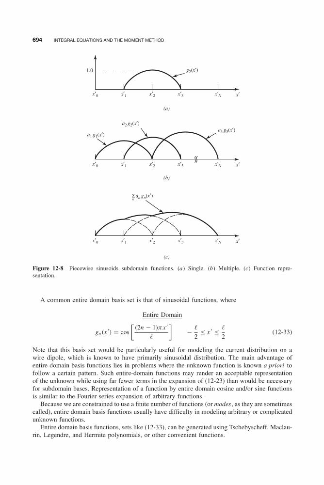
Balanis c12.tex V2 - 11/22/2011 3:54 P.M. Page 694
694 INTEGRAL EQUATIONS AND THE MOMENT METHOD
x′0 x′1
1.0
x′2 x′3
g2(x′)
x′N x′
(a)
a2 g2(x′)
a1 g1(x′)a3 g3(x′)
(b)
Σan gn(x′)n
(c)
x′0 x′1 x′2 x′3 x′N x′
x′0 x′1 x′2 x′3 x′N x′
Figure 12-8 Piecewise sinusoids subdomain functions. (a) Single. (b) Multiple. (c) Function repre-sentation.
A common entire domain basis set is that of sinusoidal functions, where
Entire Domain
gn(x′) = cos
[(2n − 1)πx ′
�
]− �
2≤ x ′ ≤ �
2(12-33)
Note that this basis set would be particularly useful for modeling the current distribution on awire dipole, which is known to have primarily sinusoidal distribution. The main advantage ofentire domain basis functions lies in problems where the unknown function is known a priori tofollow a certain pattern. Such entire-domain functions may render an acceptable representationof the unknown while using far fewer terms in the expansion of (12-23) than would be necessaryfor subdomain bases. Representation of a function by entire domain cosine and/or sine functionsis similar to the Fourier series expansion of arbitrary functions.
Because we are constrained to use a finite number of functions (or modes , as they are sometimescalled), entire domain basis functions usually have difficulty in modeling arbitrary or complicatedunknown functions.
Entire domain basis functions, sets like (12-33), can be generated using Tschebyscheff, Maclau-rin, Legendre, and Hermite polynomials, or other convenient functions.

Balanis c12.tex V2 - 11/22/2011 3:54 P.M. Page 695
INTEGRAL EQUATION METHOD 695
x′0 x′1
1.0
x′2 x′3
g2(x′)
x′N x′
(a)
a2 g2(x′)a1 g1(x′)
a3 g3(x′)
(b)
Σan gn(x′)n
(c)
x′0 x′1 x′2 x′3 x′N x′
x′0 x′1 x′2 x′3 x′N x′
Figure 12-9 Truncated cosines subdomain functions. (a) Single. (b) Multiple. (c) Function representation.
12.2.6 Application of Point Matching
If each of the expansion functions gn(x ′) in (12-23) is of the subdomain type, where each existsonly over one segment of the structure, then Zmn of (12-27c) reduces to
Zmn = −∫ xn+1
xn
gn(x′)H (2)
0 (β|ρm − ρ′n |)dx ′ (12-34)
where xn and xn+1 represent, respectively, the lower and upper limits of the segment over whicheach of the subdomain expansion functions gn(x ′) exists. If, in addition, the gn are subdomainpulse expansion functions of the form
gn(x′) =
{1 xn ≤ x ′ ≤ xn+1
0 elsewhere(12-35)
then (12-34) reduces to
Zmn = −∫ xn+1
xn
H (2)0 (β|ρm − ρ′
n |)dx ′ (12-36)
The preceding integral cannot be evaluated exactly in closed form. However, there exist variousapproximations for its evaluation.
In solving (12-17a) using (12-24) or (12-26), there are few problems that must be addressed.Before we do that, let us first state in words what (12-24) and (12-26) represent. Each equation
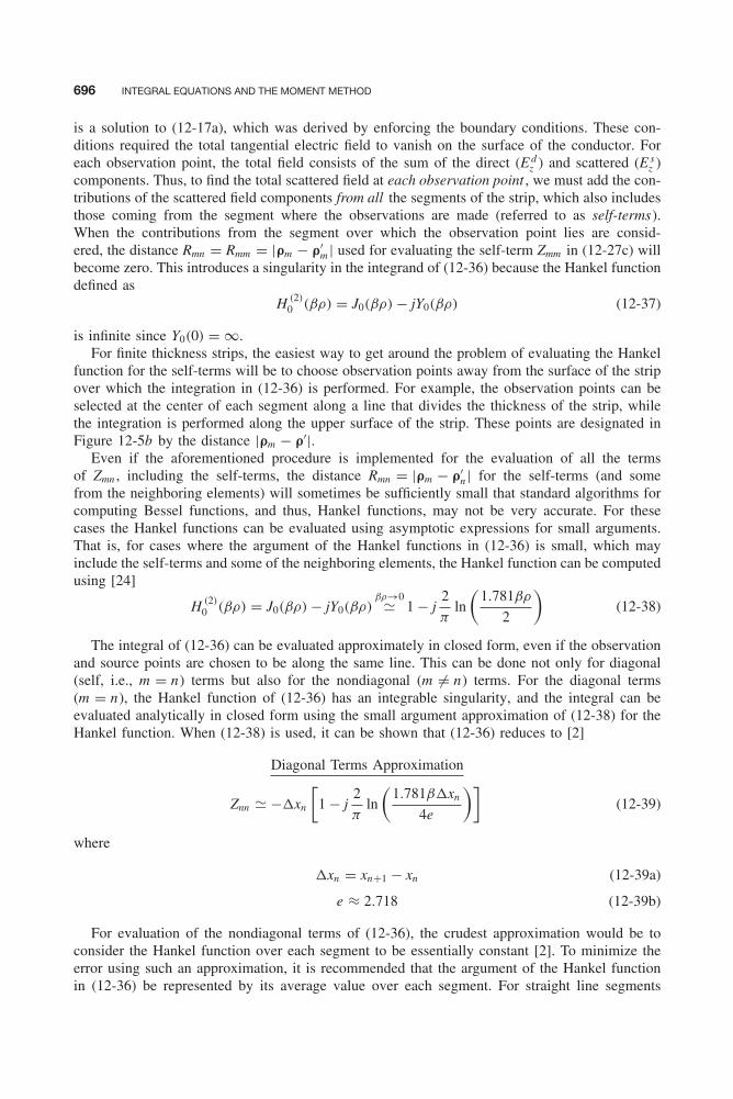
Balanis c12.tex V2 - 11/22/2011 3:54 P.M. Page 696
696 INTEGRAL EQUATIONS AND THE MOMENT METHOD
is a solution to (12-17a), which was derived by enforcing the boundary conditions. These con-ditions required the total tangential electric field to vanish on the surface of the conductor. Foreach observation point, the total field consists of the sum of the direct (E d
z ) and scattered (E sz )
components. Thus, to find the total scattered field at each observation point , we must add the con-tributions of the scattered field components from all the segments of the strip, which also includesthose coming from the segment where the observations are made (referred to as self-terms).When the contributions from the segment over which the observation point lies are consid-ered, the distance Rmn = Rmm = |ρm − ρ′
m | used for evaluating the self-term Zmm in (12-27c) willbecome zero. This introduces a singularity in the integrand of (12-36) because the Hankel functiondefined as
H (2)0 (βρ) = J0(βρ) − jY0(βρ) (12-37)
is infinite since Y0(0) = ∞.For finite thickness strips, the easiest way to get around the problem of evaluating the Hankel
function for the self-terms will be to choose observation points away from the surface of the stripover which the integration in (12-36) is performed. For example, the observation points can beselected at the center of each segment along a line that divides the thickness of the strip, whilethe integration is performed along the upper surface of the strip. These points are designated inFigure 12-5b by the distance |ρm − ρ′|.
Even if the aforementioned procedure is implemented for the evaluation of all the termsof Zmn , including the self-terms, the distance Rmn = |ρm − ρ′
n | for the self-terms (and somefrom the neighboring elements) will sometimes be sufficiently small that standard algorithms forcomputing Bessel functions, and thus, Hankel functions, may not be very accurate. For thesecases the Hankel functions can be evaluated using asymptotic expressions for small arguments.That is, for cases where the argument of the Hankel functions in (12-36) is small, which mayinclude the self-terms and some of the neighboring elements, the Hankel function can be computedusing [24]
H (2)0 (βρ) = J0(βρ) − jY0(βρ)
βρ→0� 1 − j2
πln
(1.781βρ
2
)(12-38)
The integral of (12-36) can be evaluated approximately in closed form, even if the observationand source points are chosen to be along the same line. This can be done not only for diagonal(self, i.e., m = n) terms but also for the nondiagonal (m �= n) terms. For the diagonal terms(m = n), the Hankel function of (12-36) has an integrable singularity, and the integral can beevaluated analytically in closed form using the small argument approximation of (12-38) for theHankel function. When (12-38) is used, it can be shown that (12-36) reduces to [2]
Diagonal Terms Approximation
Znn � −xn
[1 − j
2
πln
(1.781βxn
4e
)](12-39)
where
xn = xn+1 − xn (12-39a)
e ≈ 2.718 (12-39b)
For evaluation of the nondiagonal terms of (12-36), the crudest approximation would be toconsider the Hankel function over each segment to be essentially constant [2]. To minimize theerror using such an approximation, it is recommended that the argument of the Hankel functionin (12-36) be represented by its average value over each segment. For straight line segments
Balanis c12.tex V2 - 11/22/2011 3:54 P.M. Page 697
INTEGRAL EQUATION METHOD 697
that average value will be representative of the distance from the center of the segment to theobservation point. Thus, for the nondiagonal terms, (12-36) can be approximated by
Nondiagonal Terms Approximation
Zmn � −xnH (2)0 (β|Rmn |av) = −xnH (2)
0 (β|ρm − ρ′n |av) m �= n (12-40)
The average-value approximation for the distance Rmn in the Hankel function evaluation of (12-36) can also be used for curved surface scattering by approximating each curved segment by astraight line segment. Crude as it may seem, the average-value approximation for the distanceyields good results.
12.2.7 Weighting (Testing) Functions
Application of (12-24) for one observation point leads to one equation with N unknowns. It aloneis not sufficient to determine the N unknown an (n = 1, 2, . . . , N ) constants. To resolve the Nconstants, it is necessary to have N linearly independent equations. This can be accomplished byevaluating (12-24) (i.e., applying boundary conditions) at N different points, as represented by(12-26). To improve the point-matching solution, an inner product 〈w , g〉 can be defined, whichis a scalar operation satisfying the laws of
〈w , g〉 = 〈g , w〉〈bf + cg , w〉 = b〈f , w〉 + c〈g , w〉〈g∗, g〉 > 0 if g �= 0
〈g∗, g〉 = 0 if g = 0
(12-41a)
(12-41b)
(12-41c)
(12-41d)
where b and c are scalars and the asterisk (∗) indicates complex conjugation. Note that thefunctions w and g can be vectors. A typical, but not unique, inner product is
〈w, g〉 =∫∫
Sw∗ • g ds (12-42)
where the w ’s are the weighting (testing) functions and S is the surface of the structure beinganalyzed. This technique is known better as the moment method or method of moments (MM,MoM) [1, 2].
12.2.8 Moment Method
The collocation (point-matching) method is a numerical technique whose solutions satisfythe electromagnetic boundary conditions (e.g., vanishing tangential electric fields on thesurface of an electric conductor) only at discrete points. Between these points the boundaryconditions may not be satisfied, and we define the deviation as a residual [e.g., residual= E |tan = E (scattered)|tan + E (incident)|tan �= 0 on the surface of an electric conductor]. For
a half-wavelength dipole, a typical residual is shown in Figure 12-10a for pulse-basis functionsand point matching and Figure 12-10b exhibits the residual for piecewise sinusoidal Galerkin’smethod [25]. As expected, the pulse-basis point matching exhibits the most ill-behaved residualand the piecewise sinusoidal Galerkin’s method indicates an improved residual. To minimizethe residual in such a way that its overall average over the entire structure approaches zero, themethod of weighted residuals is utilized in conjunction with the inner product of (12-42). This
Balanis c12.tex V2 - 11/22/2011 3:54 P.M. Page 698
698 INTEGRAL EQUATIONS AND THE MOMENT METHOD
0.0
End Centerz/l
10−4
10−3
10−2
10−1
Tang
enti
al E
-fie
ld (
V/m
)
100
101
102
103
104
0.1 0.2 0.3 0.4 0.5
(a)
0.0
End Centerz/l
10−4
10−3
10−2
10−1
Tang
enti
al E
-fie
ld (
V/m
)
100
101
102
103
104
0.1 0.2 0.3 0.4 0.5
(b)
Figure 12-10 Tangential electric field on the conducting surface of the λ/2 dipole. (Source: E. K. Millerand F. J. Deadrick, “Some computational aspects of thin-wire modeling” in Numerical and AsymptoticTechniques in Electromagnetics , 1975, Springer-Verlag.) (a) Pulse basis-point matching. (b) Piecewisesinusoidal-Galerkin’s method.
Balanis c12.tex V2 - 11/22/2011 3:54 P.M. Page 699
INTEGRAL EQUATION METHOD 699
technique, referred as moment method (MM), does not lead to a vanishing residual at everypoint on the surface of a conductor, but it forces the boundary conditions to be satisfied in anaverage sense over the entire surface.
To accomplish this, we define a set of N weighting (or testing) functions {wm}(m =1, 2, . . . , N ) in the domain of the operator F. Forming the inner product between each of thesefunctions and the excitation function h , (12-25) reduces to
〈wm , h〉 =N∑
n=1
an〈wm , F (gn)〉 m = 1, 2, . . . , N (12-43)
This set of N equations may be written in matrix form as
[hm ] = [Fmn ][an ] (12-44)
where
[Fmn ] =
⎡⎢⎣ 〈w1, F (g1)〉 〈w1, F (g2)〉 · · ·〈w2, F (g1)〉 〈w2, F (g2)〉
......
⎤⎥⎦
[an ] =
⎡⎢⎢⎢⎣a1
a2...
aN
⎤⎥⎥⎥⎦ hm =
⎡⎢⎢⎢⎣〈w1, h〉〈w2, h〉
...
〈wN , h〉
⎤⎥⎥⎥⎦
(12-44a)
(12-44b)
The matrix of (12-44) may be solved for the an by inversion, and it can be written as
[an ] = [Fmn ]−1[hm ] (12-45)
The choice of weighting functions is important in that the elements of {wn} must be linearlyindependent, so that the N equations in (12-43) will be linearly independent [1–3, 22, 23]. Further,it will generally be advantageous to choose weighting functions that minimize the computationsrequired to evaluate the inner products.
The condition of linear independence between elements and the advantage of computationalsimplicity are also important characteristics of basis functions. Because of this, similar types offunctions are often used for both weighting and expansion. A particular choice of functions maybe to let the weighting and basis function be the same, that is, wn = gn . This technique is knownas Galerkin’s method [26].
It should be noted that there are N 2 terms to be evaluated in (12-44a). Each term usuallyrequires two or more integrations; at least one to evaluate each F (gn), and one to perform theinner product of (12-42). When these integrations are to be done numerically, as is often the case,vast amounts of computation time may be necessary.
There is, however, a unique set of weighting functions that reduce the number of requiredintegrations. This is the set of Dirac delta weighting functions
{wm} = {δ(p − pm)} = {δ(p − p1), δ(p − p2), . . . , δ(p − pN )} (12-46)

Balanis c12.tex V2 - 11/22/2011 3:54 P.M. Page 700
700 INTEGRAL EQUATIONS AND THE MOMENT METHOD
where p specifies a position with respect to some reference (origin), and pm represents a point atwhich the boundary condition is enforced. Using (12-42) and (12-46) reduces (12-43) to
〈δ(p − pm), h〉 =∑
n
an〈δ(p − pm), F (gn)〉, m = 1, 2, . . . , N∫∫S
δ(p − pm)h ds =∑
n
an
∫∫S
δ(p − pm)F (gn) ds , m = 1, 2, . . . , N
h|p=pm =∑
n
anF (gn)|p=pm , m = 1, 2, . . . , N (12-47)
Hence, the only remaining integrations are those specified by F (gn). This simplification may makeit possible to obtain some solutions that would be unattainable if other weighting functions wereused. Physically, the use of Dirac delta weighting functions is seen as a relaxation of boundaryconditions so that they are enforced only at discrete points on the surface of the structure, hencethe name point matching .
An important consideration when using point matching is the positioning of the N points (pm).While equally spaced points often yield good results, much depends on the basis functions used.When using subsectional basis functions in conjunction with point matching, one match pointshould be placed on each segment to maintain linear independence. Placing the points at thecenter of the segments usually produces the best results. It is important that a match point doesnot coincide with the “peak” of a triangle or any other point, where the basis function is notdifferentiable. Ignoring this would cause errors in some situations.
Because it provides acceptable accuracy along with obvious computational advantages, pointmatching is the most popular testing technique for moment-method solutions to electromagneticsproblems. The analysis presented here, along with most problems considered in the literature,proceed via point matching.
For the strip problem, a convenient inner product of the form (12-42) is
〈wm , gn〉 =∫ w/2
−w/2w∗
m(x)gn(x)dx (12-48)
Taking the inner product (12-48) with w∗m(x) on both sides of (12-26), we can write it as
V ′m =
N∑n=1
InZ ′mn , m = 1, 2, . . . , N (12-49)
where
V ′m =
∫ w/2
−w/2w∗
m(x)H (2)0 (βρm) dx (12-49a)
Z ′mn = −
∫ w/2
−w/2w∗
m(x)
[∫ w/2
−w/2gn(x
′)H (2)0 (β|ρm − ρ′
n |)dx ′]
dx (12-49b)
or in matrix form as[V ′
m ] = [Z ′mn ][In ] (12-50)
If the wm weighting functions are Dirac delta functions [i.e., wm(y) = δ(y − ym)], then (12-49)reduces to (12-27) or
V ′m = Vm (12-51a)

Balanis c12.tex V2 - 11/22/2011 3:54 P.M. Page 701
INTEGRAL EQUATION METHOD 701
and
Z ′mn = Zmn (12-51b)
The method of weighted residuals (moment method) was introduced to minimize the averagedeviation from the actual values of the boundary conditions over the entire structure. However,it is evident that it has complicated the formulation by requiring an integration in the evaluationof the elements of the V ′ matrix [as given by (12-49a)] and an additional integration in theevaluation of the elements of the Z ′
mn matrix [as given by (12-49b)]. Therein lies the penalty thatis paid to improve the solution.
If both the expansion gn and the weighting wm functions are of the subdomain type, each ofwhich exists only over one of the strip segments, then (12-49b) can be written as
Z ′mn = −
∫ xm+1
xm
w∗m(x)
[∫ x ′n+1
x ′n
gn(x′)H (2)
0 (β|ρm − ρ′|)dx ′]
dx (12-52)
where (xm , xm+1) and (x ′n , x ′
n+1) represent, respectively, the lower and upper limits of the stripsegments over which the weighting wm and expansion gn functions exist. To evaluate the mnthelement of Z ′
mn from (12-49b) or (12-52), we first choose the weighting function wm , and theregion of the segment over which it exists, and weigh the contributions from the gn expan-sion function over the region in which it exists. To find the next element Z ′
m(n+1), we maintainthe same weighting function wm , and the region over which it exists, and weigh the contribu-tions from the gn+1 expansion function. We repeat this until the individual contributions fromall the N expansion functions (gn) are weighted by the wm weighting function. Then we choosethe wm+1 weighting function, and the region over which it exists, and we weigh individually thecontributions from each of the N expansion functions (gn). We repeat this until all the N weight-ing functions (wm), and the regions of the strip over which they exist, are individually weightedby the N expansion functions (gn). This procedure allows us to form N linear equations, eachwith N unknowns, that can be solved using matrix inversion methods.
Example 12-3
For the electric line source of Figure 12-5 with w = 2λ, t = 0.001λ, and h = 0.5λ perform the following:
1. Compute the equivalent current density induced on the open surface of the strip. This equivalentcurrent density is representative of the vector sum of the current densities that flow on the oppositesides of the strip. Use subdomain pulse expansion functions and point matching. Subdivide thestrip into 150 segments.
2. Compare the current density of part 1 with the physical optics current density.3. Compute the normalized far-field amplitude pattern of (12-22a) using the current densities of parts
1 and 2. Compare these patterns with those obtained using a combination of geometrical optics(GO) and geometrical theory of diffraction (GTD) techniques of Chapter 13 and physical optics(PO) and physical theory of diffraction (PTD) techniques of [13].
Solution:
1. Utilizing (12-27) through (12-27b) and (12-36), the current density of (12-23) is computed using(12-28a). It is plotted in Figure 12-11. It is observed that the current density exhibits singularitiestoward the edges of the strip.
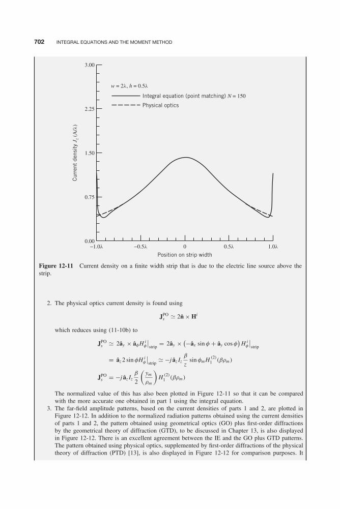
Balanis c12.tex V2 - 11/22/2011 3:54 P.M. Page 702
702 INTEGRAL EQUATIONS AND THE MOMENT METHOD
3.00
2.25
Integral equation (point matching) N = 150
Physical optics
w = 2l, h = 0.5l
1.50
0.75
−1.0l −0.5l 1.0l0.5l0
Position on strip width
Cur
rent
den
sity
Jz (
A/l
)
0.00
Figure 12-11 Current density on a finite width strip that is due to the electric line source above thestrip.
2. The physical optics current density is found using
JPOs � 2n̂ × Hi
which reduces using (11-10b) to
JPOs � 2ây × âφH i
φ
∣∣strip
= 2ây × (−âx sin φ + ây cos φ)
H iφ
∣∣strip
= âz 2 sin φH iφ
∣∣strip
� −j âz Izβ
zsin φm H (2)
1 (βρm)
JPOs = −j âz Iz
β
2
(ym
ρm
)H (2)
1 (βρm)
The normalized value of this has also been plotted in Figure 12-11 so that it can be comparedwith the more accurate one obtained in part 1 using the integral equation.
3. The far-field amplitude patterns, based on the current densities of parts 1 and 2, are plotted inFigure 12-12. In addition to the normalized radiation patterns obtained using the current densitiesof parts 1 and 2, the pattern obtained using geometrical optics (GO) plus first-order diffractionsby the geometrical theory of diffraction (GTD), to be discussed in Chapter 13, is also displayedin Figure 12-12. There is an excellent agreement between the IE and the GO plus GTD patterns.The pattern obtained using physical optics, supplemented by first-order diffractions of the physicaltheory of diffraction (PTD) [13], is also displayed in Figure 12-12 for comparison purposes. It

Balanis c12.tex V2 - 11/22/2011 3:54 P.M. Page 703
ELECTRIC AND MAGNETIC FIELD INTEGRAL EQUATIONS 703
also compares extremely well with the others. As expected, the only one that does not comparewell with the others is that of PO. Its largest differences are in the back lobes.
90°
60°
30°
0°
330°
0dB
−10dB
−20dB
−30dB
GO + GTD
PO
PO + PTD
IE
f
300°
270°
240°
210°
180°
150°
120°
Figure 12-12 Normalized amplitude pattern of the line source above the finite width strip (w = 2λ,h = 0.5λ).
12.3 ELECTRIC AND MAGNETIC FIELD INTEGRAL EQUATIONS
The key to the solution of any antenna or scattering problem is a knowledge of the physicalor equivalent current density distributions on the volume or surface of the antenna or scatterer.Once these are known, the radiated or scattered fields can be found using the standard radiationintegrals of Chapter 6. A main objective then of any solution method is to be able to predictaccurately the current densities over the antenna or scatterer. This can be accomplished by theintegral-equation (IE) method. One form of IE, for a two-dimensional structure, was discussedin Section 12.2.2 and represented by the integral equation 12-17a.
In general, there are many forms of integral equations. Two of the most popular forms for time-harmonic electromagnetics are the electric field integral equation (EFIE) and the magnetic fieldintegral equation (MFIE). The EFIE enforces the boundary condition on the tangential electricfield while the MFIE enforces the boundary condition on the tangential components of the mag-netic field. Both of these will be discussed here as they apply to perfectly conducting structures.
Balanis c12.tex V2 - 11/22/2011 3:54 P.M. Page 704
704 INTEGRAL EQUATIONS AND THE MOMENT METHOD
12.3.1 Electric Field Integral Equation
The electric field integral equation (EFIE) is based on the boundary condition that the totaltangential electric field on a perfectly electric conducting (PEC) surface of an antenna or scattereris zero. This can be expressed as
Ett (r = rs) = Ei
t (r = rs) + Est (r = rs) = 0 on S (12-53)
orEs
t (r = rs) = −Eit (r = rs) on S (12-53a)
where S is the conducting surface of the antenna or scatterer and r = rs is the distance from theorigin to any point on the surface of the antenna or scatterer. The subscript t indicates tangentialcomponents.
The incident field that impinges on the surface S of the antenna or scatterer induces on it anelectric current density Js which in turn radiates the scattered field. If Js is known, the scatteredfield everywhere, that is due to Js , can be found using (6-32b), or
Es(r) = −jωA − j1
ωμε∇(∇ • A) = −j
1
ωμε
[ω2μεA + ∇(∇ • A)
](12-54)
where, according to (6-96a),
A(r) = μ
4π
∫∫S
Js(r′)
e−jβR
Rds ′ = μ
∫∫S
Js(r′)
e−jβR
4πRds ′ (12-54a)
Equations 12-54 and 12-54a can also be expressed, by referring to Figure 6-2b, as
Es(r) = −jη
β
[β2
∫∫S
Js(r′)G(r, r′)ds ′ + ∇
∫∫S
∇′ • Js(r′)G(r, r′)ds ′
](12-55)
where
G(r, r′) = e−jβR
4πR= e−jβ|r−r′|
4π |r − r′| (12-55a)
R = |r − r′| (12-55b)
In (12-55) ∇ and ∇′ are, respectively, the gradients with respect to the observation (unprimed)and source (primed) coordinates and G(r, r′) is referred to as the Green’s function for a three-dimensional radiator or scatterer.
If the observations are restricted on the surface of the antenna or scatterer (r = rs), then(12-55) and (12-55b) can be expressed, using (12-53a), as
jη
β
[β2
∫∫S
Js(r′)G(rs , r′)ds ′ + ∇
∫∫S
∇′ • Js(r′)G(rs , r′)ds ′
]t
= Eit (r = rs) (12-56)
Because the right side of (12-56) is expressed in terms of the known incident electric field, it isreferred to as the electric field integral equation (EFIE). It can be used to find the current densityJs(r ′) at any point r = r ′ on the antenna or scatterer. It should be noted that (12-56) is actuallyan integro-differential equation, but usually it is referred to as an integral equation.
Equation 12-56 can be used for closed or open surfaces. Once Js is determined, the scatteredfield is found using (6-32b) and (6-96a) or (12-54) and (12-54a), which assume that Js radiatesin one medium. Because of this, Js in (12-56) represents the physical equivalent electric current
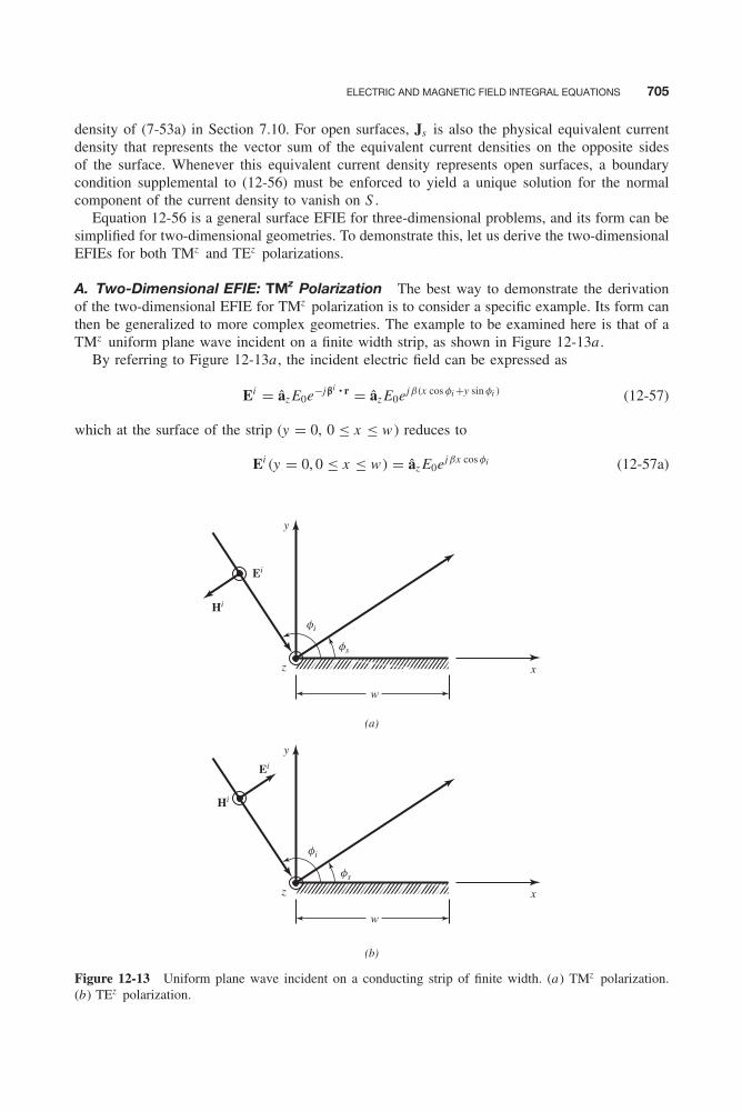
Balanis c12.tex V2 - 11/22/2011 3:54 P.M. Page 705
ELECTRIC AND MAGNETIC FIELD INTEGRAL EQUATIONS 705
density of (7-53a) in Section 7.10. For open surfaces, Js is also the physical equivalent currentdensity that represents the vector sum of the equivalent current densities on the opposite sidesof the surface. Whenever this equivalent current density represents open surfaces, a boundarycondition supplemental to (12-56) must be enforced to yield a unique solution for the normalcomponent of the current density to vanish on S .
Equation 12-56 is a general surface EFIE for three-dimensional problems, and its form can besimplified for two-dimensional geometries. To demonstrate this, let us derive the two-dimensionalEFIEs for both TMz and TEz polarizations.
A. Two-Dimensional EFIE: TMz Polarization The best way to demonstrate the derivationof the two-dimensional EFIE for TMz polarization is to consider a specific example. Its form canthen be generalized to more complex geometries. The example to be examined here is that of aTMz uniform plane wave incident on a finite width strip, as shown in Figure 12-13a .
By referring to Figure 12-13a , the incident electric field can be expressed as
Ei = âz E0e−jβi • r = âz E0ejβ(x cos φi +y sin φi ) (12-57)
which at the surface of the strip (y = 0, 0 ≤ x ≤ w ) reduces to
Ei (y = 0, 0 ≤ x ≤ w) = âz E0ejβx cos φi (12-57a)
y
Ei
Hi
z
w
x
fi
fs
(a)
y
Ei
Hi
z
w
x
fi
fs
(b)
Figure 12-13 Uniform plane wave incident on a conducting strip of finite width. (a) TMz polarization.(b) TEz polarization.
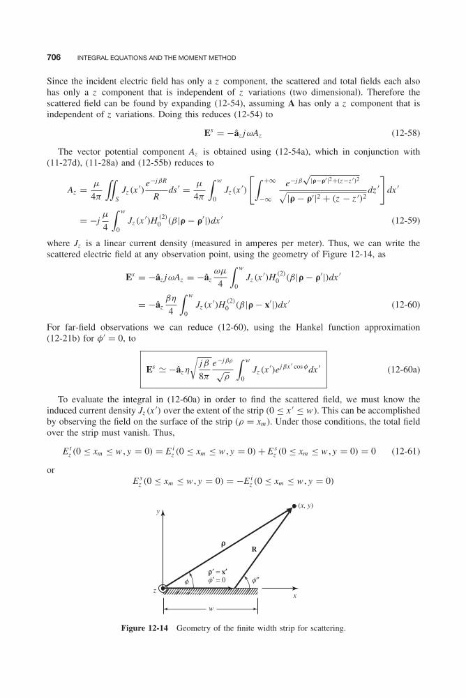
Balanis c12.tex V2 - 11/22/2011 3:54 P.M. Page 706
706 INTEGRAL EQUATIONS AND THE MOMENT METHOD
Since the incident electric field has only a z component, the scattered and total fields each alsohas only a z component that is independent of z variations (two dimensional). Therefore thescattered field can be found by expanding (12-54), assuming A has only a z component that isindependent of z variations. Doing this reduces (12-54) to
Es = −âz jωAz (12-58)
The vector potential component Az is obtained using (12-54a), which in conjunction with(11-27d), (11-28a) and (12-55b) reduces to
Az = μ
4π
∫∫S
Jz (x′)
e−jβR
Rds ′ = μ
4π
∫ w
0Jz (x
′)
[∫ +∞
−∞
e−jβ√
|ρ−ρ′|2+(z−z ′)2√|ρ − ρ′|2 + (z − z ′)2
dz ′]
dx ′
= −jμ
4
∫ w
0Jz (x
′)H (2)0 (β|ρ − ρ′|)dx ′ (12-59)
where Jz is a linear current density (measured in amperes per meter). Thus, we can write thescattered electric field at any observation point, using the geometry of Figure 12-14, as
Es = −âz jωAz = −âzωμ
4
∫ w
0Jz (x
′)H (2)0 (β|ρ − ρ′|)dx ′
= −âzβη
4
∫ w
0Jz (x
′)H (2)0 (β|ρ − x′|)dx ′ (12-60)
For far-field observations we can reduce (12-60), using the Hankel function approximation(12-21b) for φ′ = 0, to
Es � −âz η
√jβ
8π
e−jβρ
√ρ
∫ w
0Jz (x
′)ejβx ′ cos φdx ′ (12-60a)
To evaluate the integral in (12-60a) in order to find the scattered field, we must know theinduced current density Jz (x ′) over the extent of the strip (0 ≤ x ′ ≤ w ). This can be accomplishedby observing the field on the surface of the strip (ρ = xm ). Under those conditions, the total fieldover the strip must vanish. Thus,
E tz (0 ≤ xm ≤ w , y = 0) = E i
z (0 ≤ xm ≤ w , y = 0) + E sz (0 ≤ xm ≤ w , y = 0) = 0 (12-61)
orE s
z (0 ≤ xm ≤ w , y = 0) = −E iz (0 ≤ xm ≤ w , y = 0)
(x, y)y
z
w
x
Rρ
f″f
ρ′ = x′f′ = 0
Figure 12-14 Geometry of the finite width strip for scattering.
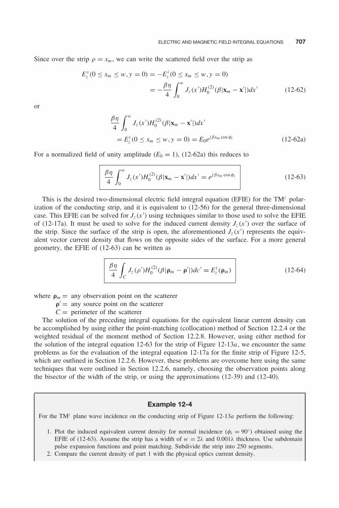
Balanis c12.tex V2 - 11/22/2011 3:54 P.M. Page 707
ELECTRIC AND MAGNETIC FIELD INTEGRAL EQUATIONS 707
Since over the strip ρ = xm , we can write the scattered field over the strip as
E sz (0 ≤ xm ≤ w , y = 0) = −E i
z (0 ≤ xm ≤ w , y = 0)
= −βη
4
∫ w
0Jz (x
′)H (2)0 (β|xm − x′|)dx ′ (12-62)
or
βη
4
∫ w
0Jz (x
′)H (2)0 (β|xm − x′|)dx ′
= E iz (0 ≤ xm ≤ w , y = 0) = E0ejβxm cos φi (12-62a)
For a normalized field of unity amplitude (E0 = 1), (12-62a) this reduces to
βη
4
∫ w
0Jz (x
′)H (2)0 (β|xm − x′|)dx ′ = ejβxm cos φi (12-63)
This is the desired two-dimensional electric field integral equation (EFIE) for the TMz polar-ization of the conducting strip, and it is equivalent to (12-56) for the general three-dimensionalcase. This EFIE can be solved for Jz (x ′) using techniques similar to those used to solve the EFIEof (12-17a). It must be used to solve for the induced current density Jz (x ′) over the surface ofthe strip. Since the surface of the strip is open, the aforementioned Jz (x ′) represents the equiv-alent vector current density that flows on the opposite sides of the surface. For a more generalgeometry, the EFIE of (12-63) can be written as
βη
4
∫C
Jz (ρ′)H (2)
0 (β|ρm − ρ′|)dc′ = E iz (ρm) (12-64)
where ρm = any observation point on the scattererρ′ = any source point on the scattererC = perimeter of the scatterer
The solution of the preceding integral equations for the equivalent linear current density canbe accomplished by using either the point-matching (collocation) method of Section 12.2.4 or theweighted residual of the moment method of Section 12.2.8. However, using either method forthe solution of the integral equation 12-63 for the strip of Figure 12-13a , we encounter the sameproblems as for the evaluation of the integral equation 12-17a for the finite strip of Figure 12-5,which are outlined in Section 12.2.6. However, these problems are overcome here using the sametechniques that were outlined in Section 12.2.6, namely, choosing the observation points alongthe bisector of the width of the strip, or using the approximations (12-39) and (12-40).
Example 12-4
For the TMz plane wave incidence on the conducting strip of Figure 12-13a perform the following:
1. Plot the induced equivalent current density for normal incidence (φi = 90◦) obtained using theEFIE of (12-63). Assume the strip has a width of w = 2λ and 0.001λ thickness. Use subdomainpulse expansion functions and point matching. Subdivide the strip into 250 segments.
2. Compare the current density of part 1 with the physical optics current density.

Balanis c12.tex V2 - 11/22/2011 3:54 P.M. Page 708
708 INTEGRAL EQUATIONS AND THE MOMENT METHOD
3. Compute the monostatic scattering width pattern for 0 ≤ φi ≤ 180◦ using current density obtainedusing the EFIE of (12-63). Compare this pattern with those obtained with physical optics (PO),geometrical theory of diffraction (GTD) of Chapter 13, and physical optics (PO) plus physicaltheory of diffraction (PTD) techniques [13].
Solution:
1. Using the EFIE of (12-63) and applying point-matching methods with subdomain pulse expansionfunctions, the current density of Figure 12-15 for φi = 90◦ is obtained for a strip of w = 2λ. It isobserved that the current density exhibits singularities toward the edges of the strip.
2. The physical optics current density is represented by
JPOs � 2n̂ × Hi |strip = 2ây ×
(âx H i
x + ây H iy
)|strip
= −âz 2H ix |strip = âz 2
E0
ηsin φi e
jβx cos φi
which is shown plotted in Figure 12-15 for φi = 90◦. It is apparent that the PO current densitydoes not compare well with that obtained using the IE, especially toward the edges of the strip.Therefore, it does not provide a good representation of the equivalent current density induced onthe strip. In Figure 12-15 we also display the equivalent current density for TEz polarization whichwill be discussed in the next section and in Example 12-5.
3. The monostatic scattering width patterns for 0◦ ≤ φi ≤ 180◦ obtained using the methods of IE,PO, GTD, and PO plus PTD are all shown in Figure 12-16. As expected, the only one that differsfrom the others is that due to the PO; the other three are indistinguishable from each other andare represented by the solid curve. The pattern for the TEz polarization for the IE method is alsodisplayed in Figure 12-16. This will be discussed in the next section and in Example 12-5.
Width, w
0.0300
0.0225
0.0150
0.0075
0−1.0l −0.5l 0 0.5l 1.0l
Cur
rent
den
sity
Jz (
A/m
)
w = 2l, fi = 90°
Jz(IE), N = 250
Jx(IE), N = 250
Jz, Jx(PO)
Figure 12-15 Current density induced on a finite width strip by a plane wave at normal incidence.
Balanis c12.tex V2 - 11/22/2011 3:54 P.M. Page 709
ELECTRIC AND MAGNETIC FIELD INTEGRAL EQUATIONS 709
TMz MM
TEz MM
TEz UTD (1-3rd order diffractions)
GTD, PTD (1st order diffractions)
PO
0−30
−15
0
15
30
45 90
Backscattering angle fi (degrees)
SW
(s
2-D/λ
) dB
135 180
Figure 12-16 Monostatic scattering width of a finite width strip (w = 2λ).
B. Two-Dimensional EFIE: TEz Polarization As in the previous section, the derivation ofthe EFIE for TEz polarization is best demonstrated by considering a uniform plane wave incidenton the strip, as shown in Figure 12-13b. Its form can then be generalized to more complexgeometries.
By referring to Figure 12-13b, the incident electric field can be expressed as
Ei = E0(âx sin φi − ây cos φi )e−jβ i • r = E0(âx sin φi − ây cos φi )e
jβ(x cos φi +y sin φi ) (12-65)
which on the surface of the strip (y = 0, 0 ≤ x ≤ w) reduces to
Ei = E0(âx sin φi − ây cos φi )ejβx cos φi (12-65a)
On the surface of the strip (0 ≤ x ≤ w , y = 0) the tangential components of the total field,incident plus scattered, must vanish. This can be written as
n̂ × Et |strip = n̂ × (Ei + Es)|strip
= ây ×[(
âx E ix + ây E i
y
)+
(âx E s
x + ây E sy
)]strip
= 0 (12-66)

Balanis c12.tex V2 - 11/22/2011 3:54 P.M. Page 710
710 INTEGRAL EQUATIONS AND THE MOMENT METHOD
which leads to
−âz (Eix + E s
x )|strip = 0 ⇒ E sx (0 ≤ x ≤ w , y = 0) = −E i
x (0 ≤ x ≤ w , y = 0) (12-66a)
orE s
x (0 ≤ x ≤ w , y = 0) = −E ix (0 ≤ x ≤ w , y = 0) = −E0 sin φi e
jβx cos φi (12-66b)
The x and y components of the scattered electric field, which are independent of z variations,are obtained using (12-54), which when expanded reduce to
E sx = −jωAx − j
1
ωμε
∂2Ax
∂x 2= −j
1
ωμε
[β2Ax + ∂2Ax
∂x 2
]= −j
1
ωμε
(β2 + ∂2
∂x 2
)Ax (12-67a)
E sy = −j
1
ωμε
∂2Ax
∂x∂y(12-67b)
The vector potential Ax is obtained using (12-54a), which, in conjunction with (11-27d) and(11-28a), reduces to
Ax = −jμ
4
∫ w
0Jx (x
′)H (2)0 (β|ρ − ρ′|)dx ′ (12-68)
Thus, we can write that the x and y components of the scattered field can be expressed as
E sx = −j
1
ωμε
(−j
μ
4
)(β2 + ∂2
∂x 2
)∫ w
0Jx (x
′)H (2)0 (β|ρ − ρ′|)dx ′
= − η
4β
(β2 + ∂2
∂x 2
)∫ w
0Jx (x
′)H (2)0 (β|ρ − ρ′|)dx ′ (12-69a)
E sy = − η
4β
∂2
∂x∂y
∫ w
0Jx (x
′)H (2)0 (β|ρ − ρ′|)dx ′ (12-69b)
Interchanging integration and differentiation and letting ρ ′ = x ′, we can rewrite the x and ycomponents as
E sx = − η
4β
∫ w
0Jx (x
′)[(
∂2
∂x 2+ β2
)H (2)
0 (βR)
]dx ′ (12-70a)
E sy = − η
4β
∫ w
0Jx (x
′)[
∂2
∂x∂yH (2)
0 (βR)
]dx ′ (12-70b)
whereR = |ρ − x′| (12-70c)
It can be shown, using the geometry of Figure 12-14, that[∂2
∂x 2+ β2
]H (2)
0 (βR) = β2
2
[H (2)
0 (βR) + H (2)2 (βR) cos(2φ′′)
](12-71a)
∂2
∂x∂yH (2)
0 (βR) = β2
2H (2)
2 (βR) sin(2φ′′) (12-71b)
Balanis c12.tex V2 - 11/22/2011 3:54 P.M. Page 711
ELECTRIC AND MAGNETIC FIELD INTEGRAL EQUATIONS 711
Thus, the x and y components of the electric field reduce to
E sx = −βη
8
∫ w
0Jx (x
′)[H (2)
0 (βR) + H (2)2 (βR) cos(2φ′′)
]dx ′ (12-72a)
E sy = −βη
8
∫ w
0Jx (x
′)H (2)2 (βR) sin(2φ′′)dx ′ (12-72b)
The next objective is to solve for the induced current density, that can then be used to findthe scattered field. This can be accomplished by applying the boundary conditions on the xcomponent of the electric field. When the observations are restricted to the surface of the strip(ρ = xm ), the x component of the scattered field over the strip can be written as
E sx (0 ≤ xm ≤ w , y = 0)
= −E ix (0 ≤ xm ≤ w , y = 0) = −E0 sin φi e
jβxm cos φi
= −βη
8
∫ w
0Jx (x
′)[H (2)
0 (βRm) + H (2)2 (βRm) cos(2φ′′
m)]
dx ′ (12-73)
or
βη
8
∫ w
0Jx (x
′)[H (2)
0 (βRm) + H (2)2 (βRm) cos(2φ′′
m)]
dx ′ = E0 sin φi ejβxm cos φi (12-73a)
For a normalized field of unity amplitude (E0 = 1), (12-73a) reduces to
βη
8
∫ w
0Jx (x
′)[H (2)
0 (βRm) + H (2)2 (βRm) cos(2φ′′
m)]
dx ′ = sin φi ejβxm cos φi (12-74)
whereRm = |ρm − x′| (12-74a)
This is the desired two-dimensional electric field integral equation (EFIE) for the TEz polar-ization of the conducting strip, and it is equivalent to (12-56) for the general three-dimensionalcase. This EFIE must be used to solve for the induced current density Jx (x ′) over the surface ofthe strip using techniques similar to those used to solve the EFIE of (12-17a). For a more generalgeometry, the EFIE can be written as
η
4β
{β2
∫C
Jc(ρ′)[ĉm • ĉ′H (2)
0 (β|ρm − ρ′|)]
dc′
+ d
dc
[∇ •
∫C
Jc(ρ′)[ĉ′H (2)
0 (β|ρm − ρ′|)]
dc′]}
= −E ic (ρm)
(12-75)
where ρm = any observation point on the scattererρ′ = any source point on the scattererC = perimeter of the scatterer
ĉm , ĉ′ = unit vector tangent to scatterer perimeter at observation, source points
The linear current density Jx is obtained by solving the integral equation 12-74 using either thepoint-matching (collocation) method of Section 12.2.4 or the weighted residual moment methodof Section 12.2.8. Using either method, the solution of the preceding integral equation for Jx
is more difficult than that of the TMz polarization of the previous example. There exist variousapproaches (either exact or approximate) that can be used to accomplish this.
Balanis c12.tex V2 - 11/22/2011 3:54 P.M. Page 712
712 INTEGRAL EQUATIONS AND THE MOMENT METHOD
To demonstrate this, we will discuss one method that can be used to solve the integralequation 12-74. Let us assume that the current density Jx (x ′) is expanded into a finite seriessimilar to (12-23). Then the integral equation can be written as
sin φi ejβxm cos φi = βη
8
N∑n=1
an
∫ w
0gn(x
′)[H (2)
0 (βRm) + H (2)2 (βRm) cos(2φ′′
m)]
dx ′ (12-76)
If, in addition, the basis functions are subdomain pulse functions, as defined by (12-35), then(12-76) using point matching reduces for each observation point to
sin φi ejβxm cos φi = βη
8
N∑n=1
an
∫ xn+1
xn
[H (2)
0 (βRmn) + H (2)2 (βRmn) cos(2φ′′
mn)]
dx ′ (12-77)
If N observations are selected, then we can write (12-77) as
[sin φi ejβxm cos φi ] =
N∑n=1
an
{βη
8
∫ xn+1
xn
[H (2)
0 (βRmn) + H (2)2 (βRmn) cos(2φ′′
mn)]
dx ′}
m = 1, 2, . . . , N (12-78)
or, in matrix form,[Vm ] = [Zmn ][In ] (12-78a)
where
Vm = sin φi ejβxm cos φi (12-78b)
In = an (12-78c)
Zmn = βη
8
∫ xn+1
xn
[H (2)
0 (βRmn) + H (2)2 (βRmn) cos(2φ′′
mn)]
dx ′ (12-78d)
One of the tasks here will be the evaluation of the integral for Zmn . We will examine one tech-nique that requires Zmn to be evaluated using three different expressions depending upon the posi-tion of the segment relative to the observation point. We propose here that Zmn is evaluated using
Zmn =
⎧⎪⎪⎪⎪⎪⎪⎪⎪⎪⎪⎪⎪⎪⎪⎪⎪⎪⎪⎪⎪⎪⎪⎨⎪⎪⎪⎪⎪⎪⎪⎪⎪⎪⎪⎪⎪⎪⎪⎪⎪⎪⎪⎪⎪⎪⎩
βηxn
8
{1 − j
1
π
[3 + 2 ln
(1.781βxn
4e
)+ 16
(βxn)2
]}e ≈ 2.718 m = n
βηxn
8
⎧⎪⎪⎨⎪⎪⎩1 + j4
πβ2
1
|xm − xn |2 − (xn)2
4
⎫⎪⎪⎬⎪⎪⎭|m − n| ≤ 2, m �= n
βη
4
∫ xn/2
−xn/2
H (2)1
[β(|xm − xn | + x ′)
]β(|xm − xn | + x ′)
dx ′
|m − n| > 2
(12-79a)
(12-79b)
(12-79c)
where xm and xn are measured from the center of their respective segments.The current density Jx obtained from the preceding integral equation also represents the total
current density Js induced on the strip. This is evident from the induced current density equation
Js = n̂ × Ht = ây × âz H tz = âx H t
z = âx (Hiz + H s
z ) (12-80)
Balanis c12.tex V2 - 11/22/2011 3:54 P.M. Page 713
ELECTRIC AND MAGNETIC FIELD INTEGRAL EQUATIONS 713
Example 12-5
For the TEz plane wave incident on the conducting strip of Figure 12-13b, perform the followingtasks.
1. Plot the induced equivalent current density for normal incidence (φi = 90◦) obtained using theEFIE of (12-74) or (12-78) through (12-78d). Assume a width of w = 2λ and thickness equal to0.001λ. Use subdomain pulse expansion functions and point matching. Subdivide the strip into250 segments.
2. Compare the current density of part 1 with the physical optics current density.3. Compute the monostatic scattering width pattern for 0◦ ≤ φi ≤ 180◦ using the current density
obtained using the EFIE of (12-78) through (12-78d). Compare this pattern with those obtainedwith physical optics (PO), geometrical theory of diffraction (GTD) of Chapter 13, and physicaloptics (PO) plus physical theory of diffraction (PTD) techniques [13].
Solution:
1. Using the EFIE of (12-78) through (12-78d), the current density of Figure 12-15 for φi = 90◦ isobtained for a strip of w = 2λ. It is observed that the current density vanishes toward the edgesof the strip.
2. The physical optics current density is represented by
JPOs � 2n̂ × Hi |strip = 2ây × âz H i
z |strip = âx 2H iz |strip = âx 2
E0
ηejβx cos φi
which for normal incidence (φi = 90◦) is identical to that for the TMz polarization, and it is shownplotted in Figure 12-15. As for the TMz polarization, the PO TEz polarization current density doesnot compare well with that obtained using the IE method. Therefore, it does not provide a goodrepresentation of the equivalent current density induced on the strip. In Figure 12-15 the TEz
polarization current density is compared with that of the TMz polarization using the differentmethods.
3. The monostatic scattering width pattern for 0◦ ≤ φi ≤ 180◦ obtained using the IE method is shownplotted in Figure 12-16 where it is compared to those obtained by PO, PO plus PTD (first-orderdiffractions), and GTD (first-order diffractions) techniques. It is observed that the patterns ofPO, PO plus PTD, and GTD (using first-order diffractions only) are insensitive to polarizationwhereas those of the integral equation with moment method solution vary with polarization. TheSW patterns should vary with polarization. Therefore, those obtained using the integral-equationmethod are more accurate. It can be shown that if higher-order diffractions are included, thepatterns of the PO plus PTD, and GTD will also vary with polarization. Higher-order diffractionsare greater contributors to the overall scattering pattern for the TEz polarization than for theTMz . This is demonstrated by including in Figure 12-16 the monostatic SW for TEz polarizationobtained using higher-order GTD (UTD) diffractions [27]. It is apparent that this pattern agreesquite well with that of the IE method.
12.3.2 Magnetic Field Integral Equation
The magnetic field integral equation (MFIE) is expressed in terms of the known incident magneticfield. It is based on the boundary condition that expresses the total electric current density inducedat any point r = r ′ on a conducting surface S
Js(r′) = Js(r = r ′) = n̂ × Ht (r = r ′) = n̂ × [Hi (r = r ′) + Hs(r = r ′)] (12-81)

Balanis c12.tex V2 - 11/22/2011 3:54 P.M. Page 714
714 INTEGRAL EQUATIONS AND THE MOMENT METHOD
Once the current density is known or determined, the scattered magnetic field can be obtainedusing (6-32a) and (6-96a), or
Hs(r) = 1
μ∇ × A = ∇ ×
∫∫S
Js(r′)
e−jβR
4πRds ′ = ∇ ×
∫∫S
Js(r′)G(r, r′)ds ′ (12-82)
where G(r, r′) is the Green’s function of (12-55a). Interchanging differentiation with integrationand using the vector identity
∇ × (Js G) = G∇ × Js − Js × ∇G (12-83)
where ∇ × Js(r′) = 0 (12-83a)
∇G = −∇′G (12-83b)
(12-82) reduces to
Hs(r) =∫∫
SJs(r
′) × [∇′G(r, r′)]ds ′ (12-84)
On the surface S of the conductor, the tangential magnetic field is discontinuous by the amountof the current density induced on the surface of the conductor. Therefore, the current density isdetermined by (12-81) but with Hs found using (12-84). Thus, we can write that
Js(r′) = n̂ × Hi (r = r ′) + lim
r→S[n̂ × Hs(r = r ′)]
= n̂ × Hi (r = r ′) + limr→S
{n̂ ×
∫∫S
Js(r′) × [∇′G(r, r′)]ds ′
}(12-85)
or
Js(r′) − lim
r→S
{n̂ ×
∫∫S
Js(r′) × [∇′G(r, r′)]ds ′
}= n̂ × Hi (r = r ′) (12-85a)
Since in (12-85a)
limr→S
{n̂ ×
∫∫S
Js(r′) × [∇′G(r, r′)]ds ′
}= Js(r ′)
2+ n̂ ×
∫∫S
Js(r′) × [∇′G(r, r′)]ds ′ (12-85b)
then (12-85a) can be written, in a more useful form, as
Js(r′) = 2n̂ × Hi (r = r ′) + 2n̂ ×
∫∫S
Js(r′) × [∇′G(r, r′)]ds ′ (12-85c)
where r → S indicates that S is approached by r from the outside.Equation 12-85a is referred to as the magnetic field integral equation (MFIE) because its right
side is in terms of the incident magnetic field, and it is valid only for closed surfaces. Once thecurrent density distribution can be found using (12-85a)–(12-85c), then the scattered fields can befound using standard radiation integrals. It should be noted that the integral of (12-85a) or (12-85b)must be carefully evaluated. The MFIE is the most popular for TEz polarizations, although it canbe used for both TEz and TMz cases. Since (12-85a)–(12-85c) are only valid for closed surfaces,the current density obtained using (12-85a)–(12-85b) is the actual current density induced on thesurface of the conducting obstacle. Usually, the MFIE is well posed while the EFIE is ill posed.
At this point, before proceeding any further, it may be appropriate to comment as to why theEFIE is valid for open and closed surfaces while the MFIE is valid only for closed surfaces [28].
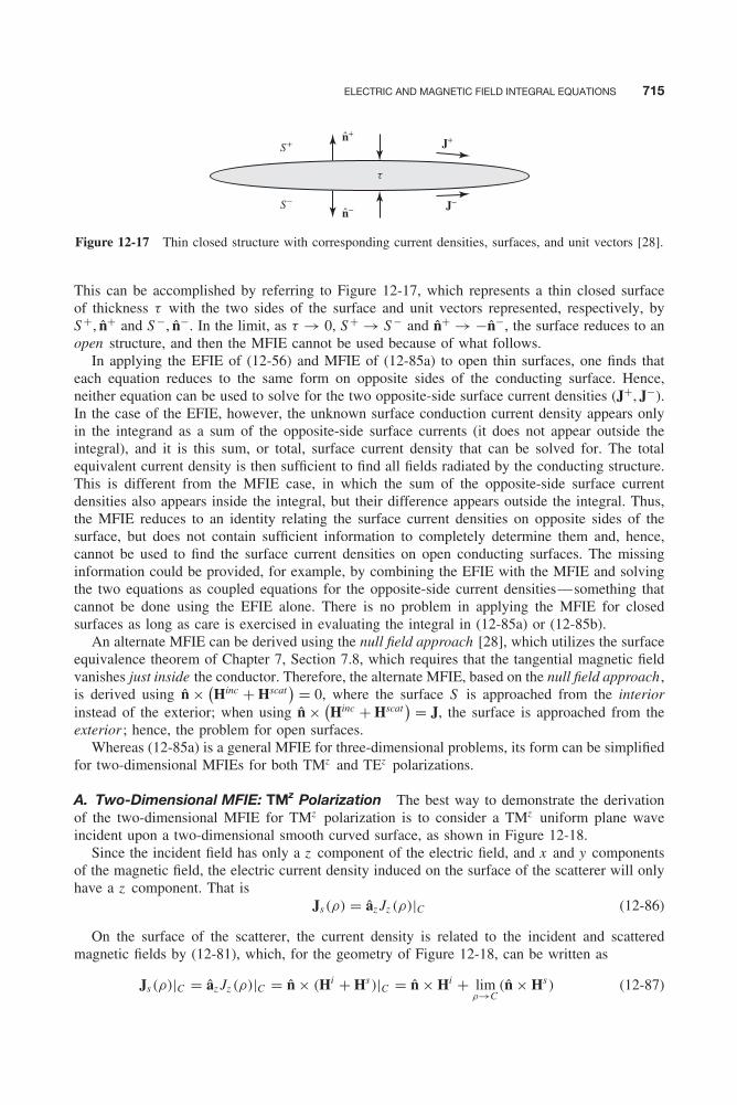
Balanis c12.tex V2 - 11/22/2011 3:54 P.M. Page 715
ELECTRIC AND MAGNETIC FIELD INTEGRAL EQUATIONS 715
S−
S+
J−
J+
t
n+
n−
Figure 12-17 Thin closed structure with corresponding current densities, surfaces, and unit vectors [28].
This can be accomplished by referring to Figure 12-17, which represents a thin closed surfaceof thickness τ with the two sides of the surface and unit vectors represented, respectively, byS +, n̂+ and S −, n̂−. In the limit, as τ → 0, S + → S − and n̂+ → −n̂−, the surface reduces to anopen structure, and then the MFIE cannot be used because of what follows.
In applying the EFIE of (12-56) and MFIE of (12-85a) to open thin surfaces, one finds thateach equation reduces to the same form on opposite sides of the conducting surface. Hence,neither equation can be used to solve for the two opposite-side surface current densities (J+, J−).In the case of the EFIE, however, the unknown surface conduction current density appears onlyin the integrand as a sum of the opposite-side surface currents (it does not appear outside theintegral), and it is this sum, or total, surface current density that can be solved for. The totalequivalent current density is then sufficient to find all fields radiated by the conducting structure.This is different from the MFIE case, in which the sum of the opposite-side surface currentdensities also appears inside the integral, but their difference appears outside the integral. Thus,the MFIE reduces to an identity relating the surface current densities on opposite sides of thesurface, but does not contain sufficient information to completely determine them and, hence,cannot be used to find the surface current densities on open conducting surfaces. The missinginformation could be provided, for example, by combining the EFIE with the MFIE and solvingthe two equations as coupled equations for the opposite-side current densities—something thatcannot be done using the EFIE alone. There is no problem in applying the MFIE for closedsurfaces as long as care is exercised in evaluating the integral in (12-85a) or (12-85b).
An alternate MFIE can be derived using the null field approach [28], which utilizes the surfaceequivalence theorem of Chapter 7, Section 7.8, which requires that the tangential magnetic fieldvanishes just inside the conductor. Therefore, the alternate MFIE, based on the null field approach ,is derived using n̂ × (
Hinc + Hscat) = 0, where the surface S is approached from the interior
instead of the exterior; when using n̂ × (Hinc + Hscat
) = J, the surface is approached from theexterior ; hence, the problem for open surfaces.
Whereas (12-85a) is a general MFIE for three-dimensional problems, its form can be simplifiedfor two-dimensional MFIEs for both TMz and TEz polarizations.
A. Two-Dimensional MFIE: TMz Polarization The best way to demonstrate the derivationof the two-dimensional MFIE for TMz polarization is to consider a TMz uniform plane waveincident upon a two-dimensional smooth curved surface, as shown in Figure 12-18.
Since the incident field has only a z component of the electric field, and x and y componentsof the magnetic field, the electric current density induced on the surface of the scatterer will onlyhave a z component. That is
Js(ρ) = âz Jz (ρ)|C (12-86)
On the surface of the scatterer, the current density is related to the incident and scatteredmagnetic fields by (12-81), which, for the geometry of Figure 12-18, can be written as
Js(ρ)|C = âz Jz (ρ)|C = n̂ × (Hi + Hs)|C = n̂ × Hi + limρ→C
(n̂ × Hs) (12-87)
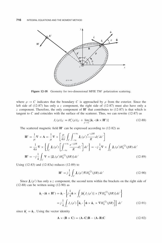
Balanis c12.tex V2 - 11/22/2011 3:54 P.M. Page 716
716 INTEGRAL EQUATIONS AND THE MOMENT METHOD
s = ∞
f′f
fi
R
Hi
Ei
y
ρρ′
x
Raz
z
yn
c
Figure 12-18 Geometry for two-dimensional MFIE TMz polarization scattering.
where ρ → C indicates that the boundary C is approached by ρ from the exterior. Since theleft side of (12-87) has only a z component, the right side of (12-87) must also have only az component. Therefore, the only component of Hi that contributes to (12-87) is that which istangent to C and coincides with the surface of the scatterer. Thus, we can rewrite (12-87) as
Jz (ρ)|C = H ic (ρ)|C + lim
ρ→C[âz • (n̂ × Hs)] (12-88)
The scattered magnetic field Hs can be expressed according to (12-82) as
Hs = 1
μ∇ × A = 1
μ∇ ×
[μ
4π
∫C
∫ +∞
−∞Js(ρ
′)e−jβR
Rdz ′dc′
]= 1
4π∇ ×
{∫C
Js(ρ′)[∫ +∞
−∞
e−jβR
Rdz ′
]dc′
}= −j
1
4∇ ×
∫C
Js(ρ′)H (2)
0 (βR) dc′
Hs = −j1
4
∫C
∇ × [Js(ρ′)H (2)
0 (βR)] dc′ (12-89)
Using (12-83) and (12-83a) reduces (12-89) to
Hs = j1
4
∫C
Js(ρ′)∇H (2)
0 (βR) dc′ (12-90)
Since Js(ρ′) has only a z component, the second term within the brackets on the right side of
(12-88) can be written using (12-90) as
âz • (n̂ × Hs) = âz •
{j
1
4n̂ ×
∫C
[â′z Jz (ρ
′)] × [∇H (2)0 (βR)] dc′
}= j
1
4
∫c
Jz (ρ′){
âz •
[n̂ × âz × ∇H (2)
0 (βR)]}
dc′ (12-91)
since â′z = âz . Using the vector identity
A × (B × C) = (A • C)B − (A • B)C (12-92)

Balanis c12.tex V2 - 11/22/2011 3:54 P.M. Page 717
ELECTRIC AND MAGNETIC FIELD INTEGRAL EQUATIONS 717
we can write that
n̂ ×[âz × ∇H (2)
0 (βR)]
= âz
[n̂ • ∇H (2)
0 (βR)]
− (n̂ • âz )∇H (2)0 (βR)
= âz
[n̂ • ∇H (2)
0 (βR)]
(12-93)
since n̂ · âz = 0. Substituting (12-93) into (12-91) reduces it to
âz • (n̂ × Hs) = j1
4
∫C
Jz (ρ′)[n̂ • ∇H (2)
0 (βR)]
dc′
= j1
4
∫C
Jz (ρ′)[−β cos ψH (2)
1 (βR)]
dc′
âz • (n̂ × Hs) = −jβ
4
∫C
Jz (ρ′) cos ψH (2)
1 (βR) dc′ (12-94)
where the angle ψ is defined in Figure 12-18. Thus, we can write (12-88), using (12-94), as
Jz (ρ)∣∣C = H i
c (ρ)∣∣C + lim
ρ→C
[−j
β
4
∫C
Jz (ρ′) cos ψH (2)
1 (βR)dc′]
(12-95)
or
Jz (ρ)∣∣C + j
β
4limρ→C
[∫C
Jz (ρ′) cos ψH (2)
1 (βR)dc′]
= H ic (ρ)
∣∣C (12-95a)
B. Two-Dimensional MFIE: TEz Polarization To derive the MFIE for the TEz polarization,let us consider a TEz uniform plane wave incident upon a two-dimensional curved surface, asshown in Figure 12-19. Since the incident field has only a z component of the magnetic field,the current induced on the surface of the scatterer will have only a component that is tangent toC and it will coincide with the surface of the scatterer. That is
Js = ĉJc(ρ) (12-96)
s = ∞
R
Hi
Ei
y′
ρρ′
x
R
n′
c′
z
y
az
Figure 12-19 Geometry for two-dimensional MFIE TEz polarization scattering.
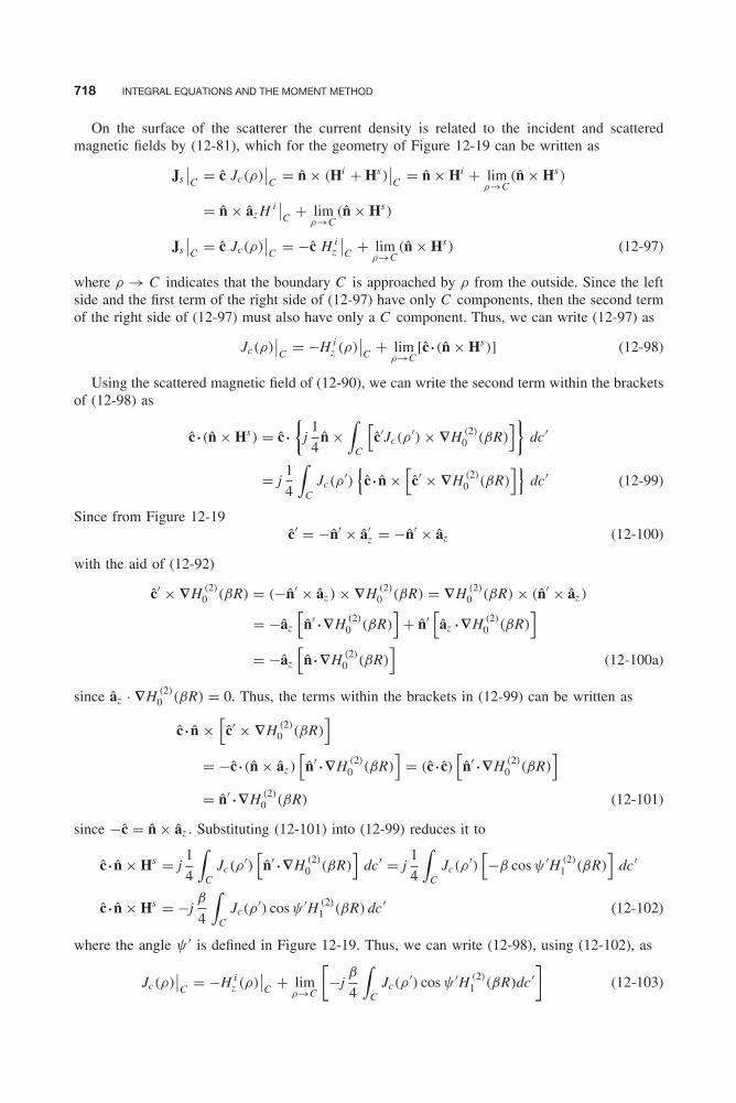
Balanis c12.tex V2 - 11/22/2011 3:54 P.M. Page 718
718 INTEGRAL EQUATIONS AND THE MOMENT METHOD
On the surface of the scatterer the current density is related to the incident and scatteredmagnetic fields by (12-81), which for the geometry of Figure 12-19 can be written as
Js
∣∣C = ĉ Jc(ρ)
∣∣C = n̂ × (Hi + Hs)
∣∣C = n̂ × Hi + lim
ρ→C(n̂ × Hs)
= n̂ × âz H i∣∣C + lim
ρ→C(n̂ × Hs)
Js
∣∣C = ĉ Jc(ρ)
∣∣C = −ĉ H i
z
∣∣C + lim
ρ→C(n̂ × Hs) (12-97)
where ρ → C indicates that the boundary C is approached by ρ from the outside. Since the leftside and the first term of the right side of (12-97) have only C components, then the second termof the right side of (12-97) must also have only a C component. Thus, we can write (12-97) as
Jc(ρ)∣∣C = −H i
z (ρ)∣∣C + lim
ρ→C[ĉ • (n̂ × Hs)] (12-98)
Using the scattered magnetic field of (12-90), we can write the second term within the bracketsof (12-98) as
ĉ • (n̂ × Hs) = ĉ •
{j
1
4n̂ ×
∫C
[ĉ′Jc(ρ
′) × ∇H (2)0 (βR)
]}dc′
= j1
4
∫C
Jc(ρ′){
ĉ • n̂ ×[ĉ′ × ∇H (2)
0 (βR)]}
dc′ (12-99)
Since from Figure 12-19ĉ′ = −n̂′ × â′
z = −n̂′ × âz (12-100)
with the aid of (12-92)
ĉ′ × ∇H (2)0 (βR) = (−n̂′ × âz ) × ∇H (2)
0 (βR) = ∇H (2)0 (βR) × (n̂′ × âz )
= −âz
[n̂′ • ∇H (2)
0 (βR)]
+ n̂′[âz • ∇H (2)
0 (βR)]
= −âz
[n̂ • ∇H (2)
0 (βR)]
(12-100a)
since âz · ∇H (2)0 (βR) = 0. Thus, the terms within the brackets in (12-99) can be written as
ĉ • n̂ ×[ĉ′ × ∇H (2)
0 (βR)]
= −ĉ • (n̂ × âz )[n̂′ • ∇H (2)
0 (βR)]
= (ĉ • ĉ)[n̂′ • ∇H (2)
0 (βR)]
= n̂′ • ∇H (2)0 (βR) (12-101)
since −ĉ = n̂ × âz . Substituting (12-101) into (12-99) reduces it to
ĉ • n̂ × Hs = j1
4
∫C
Jc(ρ′)[n̂′ • ∇H (2)
0 (βR)]
dc′ = j1
4
∫C
Jc(ρ′)[−β cos ψ ′H (2)
1 (βR)]
dc′
ĉ • n̂ × Hs = −jβ
4
∫C
Jc(ρ′) cos ψ ′H (2)
1 (βR) dc′ (12-102)
where the angle ψ ′ is defined in Figure 12-19. Thus, we can write (12-98), using (12-102), as
Jc(ρ)∣∣C = −H i
z (ρ)∣∣C + lim
ρ→C
[−j
β
4
∫C
Jc(ρ′) cos ψ ′H (2)
1 (βR)dc′]
(12-103)
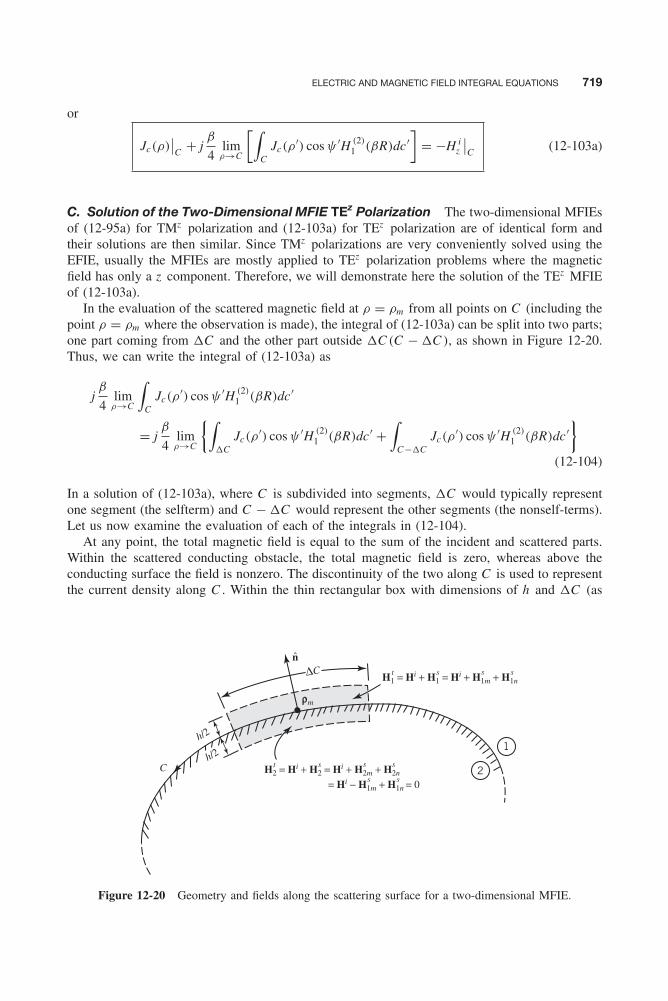
Balanis c12.tex V2 - 11/22/2011 3:54 P.M. Page 719
ELECTRIC AND MAGNETIC FIELD INTEGRAL EQUATIONS 719
or
Jc(ρ)∣∣C + j
β
4limρ→C
[∫C
Jc(ρ′) cos ψ ′H (2)
1 (βR)dc′]
= −H iz
∣∣C (12-103a)
C. Solution of the Two-Dimensional MFIE TEz Polarization The two-dimensional MFIEsof (12-95a) for TMz polarization and (12-103a) for TEz polarization are of identical form andtheir solutions are then similar. Since TMz polarizations are very conveniently solved using theEFIE, usually the MFIEs are mostly applied to TEz polarization problems where the magneticfield has only a z component. Therefore, we will demonstrate here the solution of the TEz MFIEof (12-103a).
In the evaluation of the scattered magnetic field at ρ = ρm from all points on C (including thepoint ρ = ρm where the observation is made), the integral of (12-103a) can be split into two parts;one part coming from C and the other part outside C (C − C ), as shown in Figure 12-20.Thus, we can write the integral of (12-103a) as
jβ
4limρ→C
∫C
Jc(ρ′) cos ψ ′H (2)
1 (βR)dc′
= jβ
4limρ→C
{∫C
Jc(ρ′) cos ψ ′H (2)
1 (βR)dc′ +∫
C−CJc(ρ
′) cos ψ ′H (2)1 (βR)dc′
}(12-104)
In a solution of (12-103a), where C is subdivided into segments, C would typically representone segment (the selfterm) and C − C would represent the other segments (the nonself-terms).Let us now examine the evaluation of each of the integrals in (12-104).
At any point, the total magnetic field is equal to the sum of the incident and scattered parts.Within the scattered conducting obstacle, the total magnetic field is zero, whereas above theconducting surface the field is nonzero. The discontinuity of the two along C is used to representthe current density along C . Within the thin rectangular box with dimensions of h and C (as
n
C
h/2
h/2
ρm
ΔC
2
1
H2 = Hi + H2 = Hi + H2m + H2nt s s s
H1 = Hi + H1 = Hi + H1m + H1nt s s s
= Hi − H1m + H1n = 0ss
Figure 12-20 Geometry and fields along the scattering surface for a two-dimensional MFIE.

Balanis c12.tex V2 - 11/22/2011 3:54 P.M. Page 720
720 INTEGRAL EQUATIONS AND THE MOMENT METHOD
h → 0), the total magnetic field, (Ht1) above and (Ht
2) below the interface, can be written as
Ht1 = Hi + Hs
1 = Hi + (Hs1m + Hs
1n) (12-105a)
Ht2 = Hi + Hs
2 = Hi + (Hs2m + Hs
2n) = Hi + (−Hs1m + Hs
1n) = 0 (12-105b)
or Hs1n = Hs
1m − Hi (12-105c)
where Hs1m (Hs
2m ) = scattered field in region 1 (2) within the box that is due to C (selfterm),which is discontinuous across the boundary along C
Hs1n (Hs
2n ) = scattered field in region 1 (2) within the box that is due to C − C(nonself-terms), which is continuous across the boundary along C
It is assumed here that C along C becomes a straight line as the segment becomes small. Thecurrent density along C can then be represented using (12-105a) and (12-105b) by
Jc(ρ)∣∣C = n̂ × (Ht
1 − Ht2)∣∣C = n̂ × (Hs
1m + Hs1m) = 2n̂ × Hs
1m = −2ĉH s1m (12-106)
or
Jc(ρm) = −2H s1m(ρm) ⇒ H s
1m(ρm) = −Jc(ρm)
2(12-106a)
Therefore, the integral along C in (12-104), which can be used to represent the scatteredmagnetic field at ρ = ρm that is due to the C , can be replaced by (12-106a). The nonself-termscan be found using the integral along C − C in (12-104). Thus, using (12-104) and (12-106a),we can reduce (12-103a) for ρ = ρm to
Jc(ρm) − Jc(ρm)
2+ j
β
4
∫C−C
Jc(ρ′) cos ψ ′
mH (2)1 (βRm)dc′ = −H i
z (ρm) (12-107)
or
Jc(ρm)
2+ j
β
4
∫C−C
Jc(ρ′) cos ψ ′
mH (2)1 (βRm)dc′ = −H i
z (ρm) (12-107a)
An analogous procedure can be used to reduce (12-95a) to a form similar to that of (12-107a).Let us now represent the current density Jc(ρ) of (12-107a) by the finite series of (12-23)
Jc(ρ) �N∑
n=1
angn(ρ) (12-108)
where gn(ρ) represents the basis (expansion) functions. Substituting (12-108) into (12-107a) andinterchanging integration and summation, we can write that, at any point ρ = ρm on C , (12-107a)can be written as
−H iz (ρm) = 1
2
N∑n=1
angn(ρm) + jβ
4
N∑n=1
an
∫C−C
gn(ρ′) cos ψ ′
mH (2)1 (βRm)dc′ (12-109)
If the gn ’s are subdomain piecewise constant pulse functions with each basis function existingonly over its own segment, then (12-109) reduces to
−H iz (ρm) = δmn
2an + j
β
4
N∑n=1n �=m
an
∫ ρn+1
ρn
cos ψ ′mnH (2)
1 (βRmn)dc′ (12-110)
Balanis c12.tex V2 - 11/22/2011 3:54 P.M. Page 721
ELECTRIC AND MAGNETIC FIELD INTEGRAL EQUATIONS 721
or
−H iz (ρm) =
N∑n=1
an
[δmn
2+ j
β
4
∫ ρn+1
ρnn �=m
cos ψ ′mnH (2)
1 (βRmn)dc′]
(12-110a)
where δmn is the Kronecker delta function, defined by
δmn ={
1 m = n0 m �= n
(12-110b)
The Kronecker delta function is used to indicate that for a given observation point m only thesegment itself (n = m) contributes to the first term on the right side of (12-110a).
If (12-110a) is applied to m points on C , it can be written as
[−H iz (ρm)
] =N∑
n=1
an
[δmn
2+ j
β
4
∫ ρn+1
ρnn �=m
cos ψ ′mnH (2)
1 (βRmn)dc′]
m = 1, 2, . . . , N
(12-111)
In general matrix notation, (12-111) can be expressed as
[Vm ] = [Zmn ][In ] (12-112)
where
Vm = −H iz (ρm) (12-112a)
Zmn =[δmn
2+ j
β
4
∫ ρn+1
ρn
cos ψ ′mnH (2)
1 (βRmn)dc′]
(12-112b)
In = an (12-112c)
To demonstrate the applicability of (12-111), let us consider an example.
Example 12-6
A TEz uniform plane wave is normally incident upon a circular conducting cylinder of radius a , asshown in Figure 12-21.
1. Using the MFIE of (12-107a), determine and plot the current density induced on the surface of thecylinder when a = 2λ. Assume the incident magnetic field is of unity amplitude. Use subdomainpiecewise constant pulse functions. Subdivide the circumference into 540 segments. Compare thecurrent density obtained using the IE with the exact modal solution of (11-113).
2. Based on the electric current density, derive and then plot the normalized (σ2−D/λ) bistatic scatter-ing width (in decibels) for 0◦ ≤ φ ≤ 360◦ when a = 2λ. Compare these values with those obtainedusing the exact modal solution of (11-117).
Solution:
1. Since for subdomain piecewise constant pulse functions (12-103a) or (12-107a) reduces to(12-111) or (12-112) through (12-112c), then a solution of (12-112) for In leads to the currentdensity shown in Figure 12-22. In the same figure we have plotted the current density of (11-113)based on the modal solution, and we can see an excellent agreement between the two. We also have
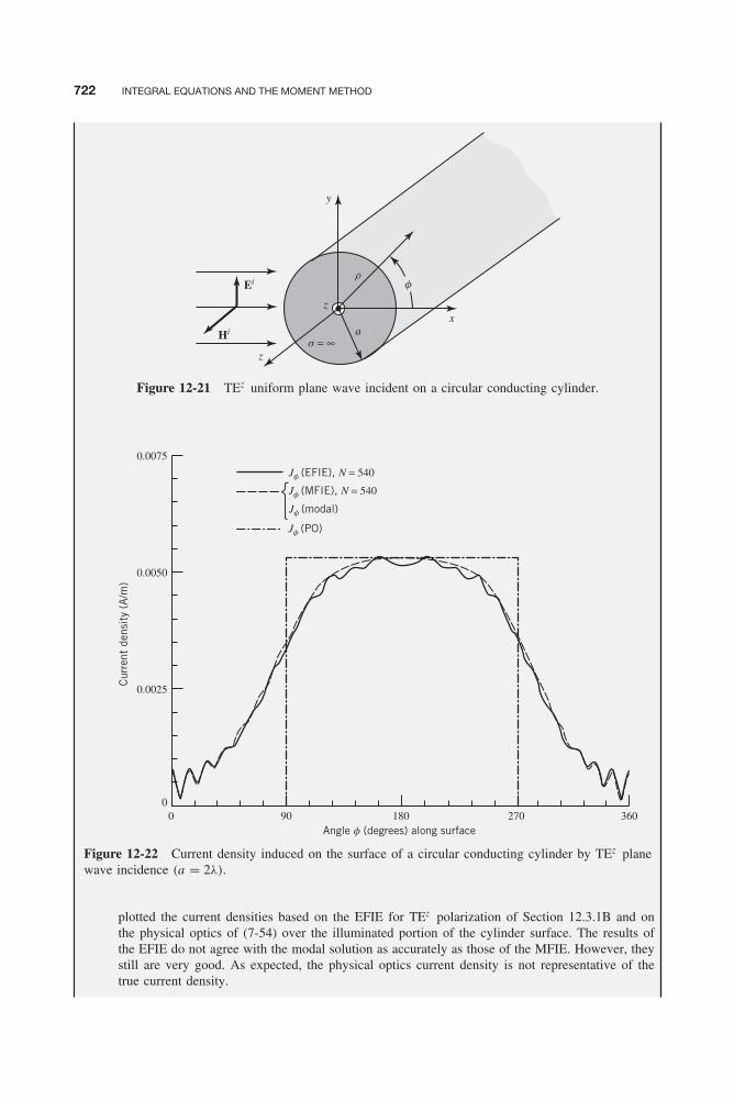
Balanis c12.tex V2 - 11/22/2011 3:54 P.M. Page 722
722 INTEGRAL EQUATIONS AND THE MOMENT METHOD
y
xa
z
z
Ei
Hi
s = ∞
rf
Figure 12-21 TEz uniform plane wave incident on a circular conducting cylinder.
Angle f (degrees) along surface
0.0075
0.0050
0.0025
00 90 180 360270
Cur
rent
den
sity
(A
/m)
Jf (EFIE), N = 540
Jf (MFIE), N = 540
Jf (modal)
Jf (PO)
Figure 12-22 Current density induced on the surface of a circular conducting cylinder by TEz planewave incidence (a = 2λ).
plotted the current densities based on the EFIE for TEz polarization of Section 12.3.1B and onthe physical optics of (7-54) over the illuminated portion of the cylinder surface. The results ofthe EFIE do not agree with the modal solution as accurately as those of the MFIE. However, theystill are very good. As expected, the physical optics current density is not representative of thetrue current density.

Balanis c12.tex V2 - 11/22/2011 3:54 P.M. Page 723
FINITE DIAMETER WIRES 723
EFIE (N = 540)
MFIE (N = 540)
PO
Modal
180−30
−15
0
15
30
90 0/360Angle f (degrees)
SW
(s
2-D
/λ)
dB
270 180
Figure 12-23 TEz bistatic scattering width of a circular conducting cylinder (a = 2λ).
2. Based on the current densities obtained in part 1, the far-zone scattered field was derived and thecorresponding bistatic scattering width was formulated. The computed SW results are shown inFigure 12-23. Besides the results based on the physical optics approximation, the other three (MFIE,EFIE, and modal solution) give almost indistinguishable data and are indicated in Figure 12-23by basically one curve.
12.4 FINITE DIAMETER WIRES
In this section we want to derive and apply two classic three-dimensional integral equations,referred to as Pocklington’s integro-differential equation and Hallen’s integral equation [29–37],that can be used most conveniently to find the current distribution on conducting wires. Hallén’sequation is usually restricted to the use of a delta-gap voltage source model at the feed of awire antenna. Pocklington’s equation, however, is more general and it is adaptable to many typesof feed sources (through alteration of its excitation function or excitation matrix), including a
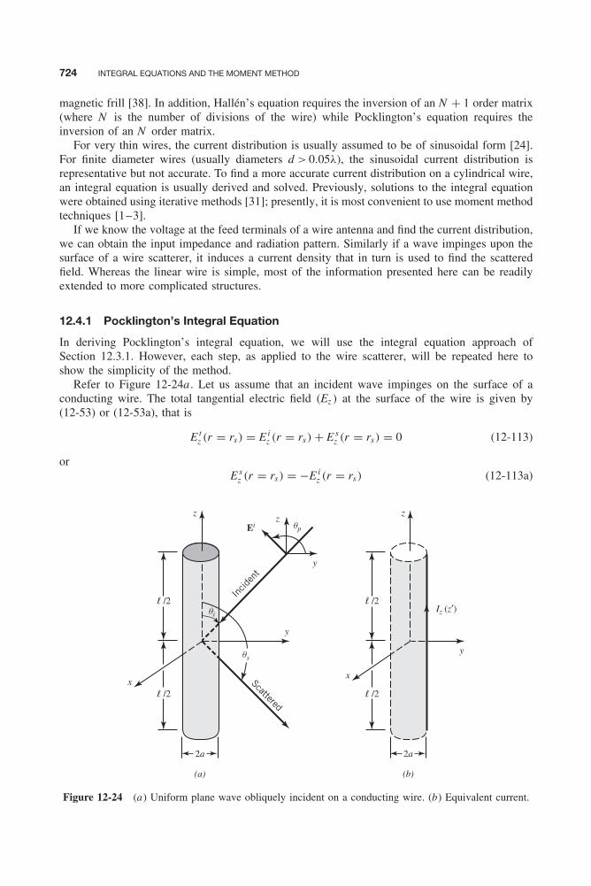
Balanis c12.tex V2 - 11/22/2011 3:54 P.M. Page 724
724 INTEGRAL EQUATIONS AND THE MOMENT METHOD
magnetic frill [38]. In addition, Hallén’s equation requires the inversion of an N + 1 order matrix(where N is the number of divisions of the wire) while Pocklington’s equation requires theinversion of an N order matrix.
For very thin wires, the current distribution is usually assumed to be of sinusoidal form [24].For finite diameter wires (usually diameters d > 0.05λ), the sinusoidal current distribution isrepresentative but not accurate. To find a more accurate current distribution on a cylindrical wire,an integral equation is usually derived and solved. Previously, solutions to the integral equationwere obtained using iterative methods [31]; presently, it is most convenient to use moment methodtechniques [1–3].
If we know the voltage at the feed terminals of a wire antenna and find the current distribution,we can obtain the input impedance and radiation pattern. Similarly if a wave impinges upon thesurface of a wire scatterer, it induces a current density that in turn is used to find the scatteredfield. Whereas the linear wire is simple, most of the information presented here can be readilyextended to more complicated structures.
12.4.1 Pocklington’s Integral Equation
In deriving Pocklington’s integral equation, we will use the integral equation approach ofSection 12.3.1. However, each step, as applied to the wire scatterer, will be repeated here toshow the simplicity of the method.
Refer to Figure 12-24a . Let us assume that an incident wave impinges on the surface of aconducting wire. The total tangential electric field (Ez ) at the surface of the wire is given by(12-53) or (12-53a), that is
E tz (r = rs) = E i
z (r = rs) + E sz (r = rs) = 0 (12-113)
orE s
z (r = rs) = −E iz (r = rs) (12-113a)
qi
qs
qpEiz
x
z
l /2
l /2
y
y
2a
Scattered
Incid
ent
(a)
x
z
Iz (z′)l /2
l /2
y
2a
(b)
Figure 12-24 (a) Uniform plane wave obliquely incident on a conducting wire. (b) Equivalent current.
Balanis c12.tex V2 - 11/22/2011 3:54 P.M. Page 725
FINITE DIAMETER WIRES 725
At any observation point, the field scattered by the induced current density on the surface ofthe wire is given by (12-54). However, for observations at the wire surface, only the z componentof (12-54) is needed, and we can write it as
E sz (r) = −j
1
ωμε
(β2Az + ∂2Az
∂z 2
)(12-114)
According to (12-54a) and neglecting edge effects
Az = μ
4π
∫∫S
Jze−jβR
Rds ′ = μ
4π
∫ +�/2
−�/2
∫ 2π
0Jz
e−jβR
Ra dφ′ dz ′ (12-115)
If the wire is very thin, the current density Jz is not a function of the azimuthal angle φ, andwe can write it as
2πaJz = Iz (z′) ⇒ Jz = 1
2πaIz (z
′) (12-116)
where Iz (z ′) is assumed to be an equivalent filament line-source current located a radial distanceρ = a from the z axis, as shown in Figure 12-24b. Thus, (12-115) reduces to
Az = μ
4π
∫ +�/2
−�/2
[1
2πa
∫ 2π
0Iz (z
′)e−jβR
Ra dφ′
]dz ′ (12-117)
R =√
(x − x ′)2 + (y − y ′)2 + (z − z ′)2
=√
ρ2 + a2 − 2ρa cos(φ − φ′) + (z − z ′)2 (12-117a)
where ρ is the radial distance to the observation point and a is the radius.Because of the symmetry of the scatterer, the observations are not a function of φ. For
simplicity, let us then choose φ = 0. For observations at the surface (ρ = a) of the scatterer,(12-117) and (12-117a) reduce to
Az (ρ = a) = μ
∫ +�/2
−�/2Iz (z
′)(
1
2π
∫ 2π
0
e−jβR
4πRdφ′
)dz ′ = μ
∫ +�/2
−�/2Iz (z
′)G(z , z ′) dz ′ (12-118)
G(z , z ′) = 1
2π
∫ 2π
0
e−jβR
4πRdφ′ (12-118a)
R(ρ = a) =√
4a2 sin2
(φ′
2
)+ (z − z ′)2 (12-118b)
Thus, for observations at the surface (ρ = a) of the scatterer, the z component of the scatteredelectric field can be expressed as
E sz (ρ = a) = −j
1
ωε
(β2 + d2
dz 2
)∫ +�/2
−�/2Iz (z
′)G(z , z ′) dz ′ (12-119)
which by using (12-113a) reduces to
−j1
ωε
(d2
dz 2+ β2
)∫ +�/2
−�/2Iz (z
′)G(z , z ′)dz ′ = −E iz (ρ = a) (12-120)

Balanis c12.tex V2 - 11/22/2011 3:54 P.M. Page 726
726 INTEGRAL EQUATIONS AND THE MOMENT METHOD
or (d2
dz 2+ β2
)∫ +�/2
−�/2Iz (z
′)G(z , z ′)dz ′ = −jωεE iz (ρ = a) (12-120a)
Interchanging integration with differentiation, we can rewrite (12-120a) as∫ +�/2
−�/2Iz (z
′)[(
∂2
∂z 2+ β2
)G(z , z ′)
]dz ′ = −jωεE i
z (ρ = a) (12-121)
where G(z , z ′) is given by (12-118a).Equation 12-121 is referred to as Pocklington’s integro-differential equation [29], and it can
be used to determine the equivalent filamentary line-source current of the wire, and thus currentdensity on the wire, by knowing the incident field on the surface of the wire. It is a simplifiedform of (12-56) as applied to a wire scatterer, and it could have been derived directly from(12-56).
If we assume that the wire is very thin (a � λ), such that (12-118a) reduces to
G(z , z ′) = G(R) = e−jβR
4πR(12-122)
(12-121) can also be expressed in a more convenient form as [33]∫ +�/2
−�/2Iz (z
′)e−jβR
4πR5
[(1 + jβR)(2R2 − 3a2) + (βaR)2] dz ′ = −jωεE i
z (ρ = a) (12-123)
where, for observations along the center of the wire (ρ = 0),
R =√
a2 + (z − z ′)2 (12-123a)
In (12-121) or (12-123) I (z ′) represents the equivalent filamentary line-source current locatedon the surface of the wire, as shown in Figure 12-24b, and it is obtained by knowing theincident electric field at the surface of the wire. By point-matching techniques, this is solvedby matching the boundary conditions at discrete points on the surface of the wire. Often it iseasier to choose the matching points to be at the interior of the wire, especially along the axis,as shown in Figure 12-25a , where Iz (z ′) is located on the surface of the wire. By reciprocity,the configuration of Figure 12-25a is analogous to that of Figure 12-25b, where the equivalentfilamentary line-source current is assumed to be located along the center axis of the wire and thematching points are selected on the surface of the wire. Either of the two configurations can beused to determine the equivalent filamentary line-source current Iz (z ′); the choice is left to theindividual.
Pocklington’s integral equation of (12-121) is derived methodically based on (12-114). Eventu-ally (12-121), using (12-122), reduces to (12-123). While the derivation of (12-121) and (12-123)is straightforward, their numerical evaluation may be more difficult because it involves doubledifferentiation of the kernel, which leads to a non-integrable singularity, especially of the 1/R5
order. However, choosing the observation point along the axis of the wire while the current ison its surface or vice versa, as illustrated in Figure 12-25, mitigates the problem to some extent.Another way to derive such an integral equation, although it may not be as straightforward,will be to represent the electric field as a combination of both the vector A and scalar φ poten-tials, as given by (6-9a) (E = −jωA − ∇φ), instead of (12-114), and use the continuity equation∇ · J = −jωq to relate the charge q within φ as the divergence of J [28]. Using such a procedure,the resulting singularity in the kernel for both the vector A and scalar φ potentials is no moresingular than 1/R, which can be evaluated numerically more accurately.

Balanis c12.tex V2 - 11/22/2011 3:54 P.M. Page 727
FINITE DIAMETER WIRES 727
zm
z′n
l /2
l /2
Gap
2a
(a)
zm
z′n
l /2
l /2
Gap
2a
(b)
Figure 12-25 Dipole segmentation and its equivalent current. (a) On the surface. (b) Along its center.
12.4.2 Hallén’s Integral Equation
Referring again to Figure 12-24a , let us assume that the length of the cylinder is much largerthan its radius (� � a) and its radius is much smaller than the wavelength (a � λ), so that theeffects of the end faces of the cylinder can be neglected. Therefore, the boundary conditions fora wire with infinite conductivity are those of vanishing total tangential E fields on the surface ofthe cylinder and vanishing current at the ends of the cylinder [Iz (z ′ = ±�/2) = 0].
Since only an electric current density flows on the cylinder and it is directed along the z axis(J = âz Jz ), according to (6-30) and (6-96a), A = âz Az (z ′), which for small radii is assumed tobe only a function of z ′. Thus, (6-34) reduces for F = 0 to
E tz = −jωAz − j
1
ωμε
∂2Az
∂z 2= −j
1
ωμε
[d2Az
dz 2+ ω2μεAz
](12-124)
Since the total tangential electric field E tz vanishes on the surface of the cylinder, (12-124)
reduces tod2Az
dz 2+ β2Az = 0 (12-124a)
Because the current density on the cylinder is symmetrical [Jz (z ′) = Jz (−z ′)], the potentialAz is also symmetrical [i.e., Az (z ′) = Az (−z ′)]. Thus, the solution of (12-124a) is given by
Az (z ) = −j√
με[B1 cos(βz ) + C1 sin(β|z |)] (12-125)

Balanis c12.tex V2 - 11/22/2011 3:54 P.M. Page 728
728 INTEGRAL EQUATIONS AND THE MOMENT METHOD
where B1 and C1 are constants. For a current-carrying wire, its potential is also given by (6-97a).Equating (12-125) to (6-97a) leads to
∫ +�/2
−�/2Iz (z
′)e−jβR
4πRdz ′ = −j
√ε
μ[B1 cos(βz ) + C1 sin(β|z |)] (12-126)
If a voltage Vi is applied at the input terminals of the wire, it can be shown that the constantC1 = Vi /2. The constant B1 is determined from the boundary condition that requires the currentto vanish at the end points of the wire.
Equation 12-126 is referred to as Hallén’s integral equation for a perfectly conducting wire.It was derived by solving the differential equation 6-34 or 12-124a with the enforcement of theappropriate boundary conditions.
x
z
dz′
z′
y
q
f
r
Δ
l /2
l /2
r
R
Mi
2a
(a)
x
b
Magneticfrill
z
y
l /2
l /2
2a
(b)
Figure 12-26 Cylindrical dipole, its segmentation, and gap modeling. (Source: C. A. Balanis, Antenna The-ory: Analysis and Design , 3rd edition, copyright © 2005, John Wiley & Sons, Inc. Reprinted by permissionof John Wiley & Sons, Inc.) (a) Cylindrical dipole. (b) Segmented dipole.
Balanis c12.tex V2 - 11/22/2011 3:54 P.M. Page 729
FINITE DIAMETER WIRES 729
12.4.3 Source Modeling
Let us assume that the wire of Figure 12-24 is symmetrically fed by a voltage source, as shownin Figure 12-26a , and the element is acting as a dipole antenna. To use, for example, Pockling-ton’s integro-differential equation 12-121 or 12-123, we need to know how to express E i
z (ρ =a). Traditionally, there have been two methods used to model the excitation to represent E i
z(ρ = a , 0 ≤ φ ≤ 2π , −�/2 ≤ z ≤ +�/2) at all points on the surface of the dipole: one is referredto as the delta-gap excitation and the other as the equivalent magnetic ring current (better knownas magnetic frill generator) [38].
A. Delta Gap The delta-gap source modeling is the simplest and most widely used of thetwo, but it is also the least accurate, especially for impedances. Usually it is most accurate forsmaller width gaps. Using the delta gap, it is assumed that the excitation voltage at the feedterminals is of a constant Vi value, and zero elsewhere. Therefore, the incident electric fieldE i
z (ρ = a , 0 ≤ φ ≤ 2π , −�/2 ≤ z ≤ +�/2) is also a constant (Vi / where is the gap width)over the feed gap and zero elsewhere, hence the name delta gap. For the delta-gap model, the feedgap of Figure 12-26a is replaced by a narrow band of strips of equivalent magnetic currentdensity of
Mi = −n̂ × Ei = −âρ × âzVi
= âφ
Vi
, −
2≤ z ′ ≤
2(12-127)
The magnetic current density Mi is sketched in Figure 12-26a .
B. Magnetic Frill Generator The magnetic frill generator was introduced to calculate thenear- as well as the far-zone fields from coaxial apertures [38]. To use this model, the feed gapis replaced with a circumferentially directed magnetic current density that exists over an annularaperture with inner radius a , which is usually chosen to be the radius of the inner wire, and anouter radius b, as shown in Figure 12-26b. Since the dipole is usually fed by transmission lines,the outer radius b of the equivalent annular aperture of the magnetic frill generator is found usingthe expression for the characteristic impedance of the transmission line.
Over the annular aperture of the magnetic frill generator, the electric field is represented bythe TEM mode field distribution of a coaxial transmission line given by
Ef = âρ
Vi
2ρ ′ ln(b/a)(12-128)
Therefore, the corresponding equivalent magnetic current density Mf for the magnetic frill gen-erator, used to represent the aperture, is equal to
Mf = −2n̂ × Ef = −2âz × âρEρ = −âφ
Vi
ρ ′ ln(b/a)(12-129)
The fields generated by the magnetic frill generator of (12-129) on the surface of the wire arefound using [38]
E iz
(ρ = a , 0 ≤ φ ≤ 2π , −�
2≤ z ≤ �
2
)� −Vi
(β(b2 − a2)e−jβR0
8 ln(b/a)r20
{2
[1
βR0+ j
(1 − b2 − a2
2R20
)]+a2
R0
[(1
βR0+ j
(1− (b2 + a2)
2R20
))(−jβ− 2
R0
)+
(− 1
βR20
+ jb2 + a2
R30
)]})(12-130)
Balanis c12.tex V2 - 11/22/2011 3:54 P.M. Page 730
730 INTEGRAL EQUATIONS AND THE MOMENT METHOD
whereR0 =
√z 2 + a2 (12-130a)
The fields generated on the surface of the wire computed using (12-130) can be approximatedby those found along the axis (ρ = 0). Doing this leads to a simpler expression of the form [38]
E iz
(ρ = 0, −�
2≤ z ≤ �
2
)= − Vi
2 ln(b/a)
[e−jβR1
R1− e−jβR2
R2
](12-131)
where
R1 =√
z 2 + a2 (12-131a)
R2 =√
z 2 + b2 (12-131b)
The following example compares the results obtained using the two source modelings (deltagap and magnetic frill generator).
Example 12-7
Assume a center-fed linear dipole of � = 0.47λ and a = 0.005λ.
1. Determine the voltage and normalized current distribution over the length of the dipole usingN = 21 segments to subdivide the length. Plot the current distribution.
2. Determine the input impedance using segments of N = 7, 11, 21, 29, 41, 51, 61, 71, and 79.
Use Pocklington’s integro-differential equation 12-123 with piecewise constant subdomain basis func-tions and point matching to solve the problem, model the gap with one segment, and use both the deltagap and magnetic frill generator to model the excitation. Use (12-131) for the magnetic frill generator.Because the current at the ends of the wire vanishes, the piecewise constant subdomain basis functionsare not the most judicious choices. However, because of their simplicity, they are chosen here to illus-trate the principles, even though the results are not the most accurate. Assume that the characteristicimpedance of the annular aperture is 50 ohms and the excitation voltage Vi is 1 V.
Solution:
1. Since the characteristic impedance of the annular aperture (coaxial line) is 50 ohms, then
Zc =√
μ0
ε0
ln(b/a)
2π= 50 ⇒ b
a= 2.3
Subdividing the total length (� = 0.47λ) of the dipole into 21 segments makes the gap and eachsegment equal to
= 0.47λ
21= 0.0224λ
Using (12-131) to compute E iz , the corresponding induced voltages, obtained by multiplying
the value of –E tz at each segment by the length of the segment, are found listed in Table 12-1,
where they are compared with those of the delta gap. N = 1 represents the outermost segmentand N = 11 represents the center segment. Because of the symmetry, only values for the centersegment and half of the other segments are shown. Although the two distributions are not identical,the magnetic frill distribution voltages decay quite rapidly away from the center segment, and theyvery quickly reach almost vanishing values.

Balanis c12.tex V2 - 11/22/2011 3:54 P.M. Page 731
FINITE DIAMETER WIRES 731
TABLE 12-1 Unnormalized and normalized dipole induced voltagea differences for delta gapand magnetic frill generator (� = 0.47λ, a = 0.005λ, N = 21)
Delta gap voltage Magnetic frill generator voltage
Segment number n Unnormalized Normalized Unnormalized Normalized
1 0 0 1.11 × 10⁻⁴/−26.03◦ 7.30 × 10⁻⁵
/−26.03◦
2 0 0 1.42 × 10⁻⁴/−20.87◦ 9.34 × 10⁻⁵
/−20.87◦
3 0 0 1.89 × 10⁻⁴/−16.13◦ 1.24 × 10⁻⁴
/−16.13◦
4 0 0 2.62 × 10⁻⁴/−11.90◦ 1.72 × 10⁻⁴
/−11.90◦
5 0 0 3.88 × 10⁻⁴/−8.23◦ 2.55 × 10⁻⁴
/−8.23◦
6 0 0 6.23 × 10⁻⁴/−5.22◦ 4.10 × 10⁻⁴
/−5.22◦
7 0 0 1.14 × 10⁻³/−2.91◦ 7.5 × 10⁻⁴
/−2.91◦
8 0 0 2.52 × 10⁻³/−1.33◦ 1.66 × 10⁻³
/−1.33◦
9 0 0 7.89 × 10⁻³/−0.43◦ 5.19 × 10⁻³
/−0.43◦
10 0 0 5.25 × 10⁻²/−0.06◦ 3.46 × 10⁻²
/−0.06◦
11 1 1 1.52/
0◦ 1.0/
0◦
aVoltage differences as defined here represent the product of the incident electric field at the center of each segmentand the corresponding segment length.
The corresponding unnormalized and normalized currents, obtained using (12-123) with piece-wise constant pulse functions and the point-matching technique for both the delta gap and magneticfrill generator, are listed on Table 12-1. The normalized magnitudes of these currents are shownplotted in Figure 12-27. It is apparent that the two distributions are almost identical in shape, andthey resemble that of the ideal sinusoidal current distribution which is more valid for very thinwires and very small gaps. The distributions obtained using Pocklington’s integral equation donot vanish at the ends because of the use of piecewise constant subdomain basis functions, whichmake the dipole look longer by either a half or full subdomain length depending whether the ref-erence of each subdomain function is taken at its middle or end point. A more accurate modelingwill be to use higher-order subdomain basic functions, such as the piecewise linear function ofFigure 12-7 or piecewise sinusoids of Figure 12-8.
l/2 l/2
0.25
1 2 3 4 5 6 7 8 9 10 11 10 9 8 7 6 5 4 3 2 1
0.50
0.75
1.0
In
l = 0.47λN = 21a = 0.005λHallén (delta gap)
Sinusoid
Pocklington (magnetic frill)
Pocklington (delta gap)
Figure 12-27 Current distribution along a dipole antenna.

Balanis c12.tex V2 - 11/22/2011 3:54 P.M. Page 732
732 INTEGRAL EQUATIONS AND THE MOMENT METHOD
2. The input impedances, computed using both the delta gap and the magnetic frill generator, areshown listed in Table 12-2. It is evident that the values begin to stabilize and compare favorablyto each other once 61 or more segments are used.
TABLE 12-2 Dipole input impedance for delta gap and magnetic frillgenerator using Pocklington’s integral equation (� = 0.47λ, a = 0.005λ)
N Delta gap Magnetic frill
7 122.8 + j 113.9 26.8 + j 24.911 94.2 + j 49.0 32.0 + j 16.721 77.7 − j 0.8 47.1 − j 0.229 75.4 − j 6.6 57.4 − j 4.541 75.9 − j 2.4 68.0 − j 1.051 77.2 + j 2.4 73.1 + j 4.061 78.6 + j 6.1 76.2 + j 8.571 79.9 + j 7.9 77.9 + j 11.279 80.4 + j 8.8 78.8 + j 12.9
12.5 COMPUTER CODES
With the advent of the computer there has been a proliferation of computer program develop-ment. Many of these programs are based on algorithms that are suitable for efficient computerprogramming for the analysis and synthesis of electromagnetic boundary-value problems. Someof these computer programs are very sophisticated and can be used to solve complex radiationand scattering problems. Others are much simpler and have limited applications. Many programsare public domain; others are restricted.
Five computer programs based on integral equation formulations and moment method solutionswill be described here. The first computes the radiation or scattering by a two-dimensional perfectlyelectric conducting (PEC) body. It is referred to here as TDRS (two-dimensional radiation andscattering), and it is based on the two-dimensional formulations of the electric field integral equation(EFIE) of Section 12.3.1. It can be used for both electric and magnetic line-source excitation orTMz and TEz plane wave incidence. The second program, referred to here as PWRS (Pocklington’swire radiation and scattering) is based on Pocklington’s integral equation of Section 12.4.1, and itis used for both radiation and scattering by a perfect electric conducting (PEC) wire.
The remaining three programs are more general, public domain moment method programs. Avery brief description of these programs is given here. Information as to where these programscan be obtained is also included. It should be stated, however, that there are numerous othercodes, public domain and restricted, that utilize moment method and other techniques, suchas geometrical optics, geometrical theory of diffraction, physical optics, and physical theory ofdiffraction, which are too numerous to mention here.
Both the TDRS and PWRS codes are part of the Multimedia for this chapter. These two codeswere initially developed in Fortran and have been translated to MATLAB for this edition. Bothversions of each are included in this edition.
12.5.1 Two-Dimensional Radiation and Scattering
The two-dimensional radiation and scattering (TDRS) program is used to analyze four differenttwo-dimensional perfectly electric conducting problems: the strip, and the circular, elliptical,and rectangular cylinders. The algorithm is based on the electric field integral equation of
Balanis c12.tex V2 - 11/22/2011 3:54 P.M. Page 733
COMPUTER CODES 733
Section 12.3.1, and it is used for both electric and magnetic line-source excitation, or plane waveincidence of arbitrary polarization. For simplicity, piecewise constant pulse expansion functionsand point-matching techniques have been adopted.
A. Strip For the strip problem, the program can analyze either of the following:
1. A line source (electric or magnetic). It computes the electric current density over the widthof the strip and the normalized radiation amplitude pattern (in decibels) for 0◦ ≤ φ ≤ 360◦.The user must specify the width of the strip (in wavelengths), the type of line source (eitherelectric or magnetic), and the location xs , ys of the source (in wavelengths).
2. Plane wave incidence of arbitrary polarization. The program can analyze either monostaticor bistatic scattering.
For monostatic scattering, the program computes the two-dimensional normalized (with respectto λ) monostatic SW σ2-D/λ (in decibels) for all angles of incidence (0◦ ≤ φ ≤ 360◦). Theprogram starts at φ = 0◦ and then completes the entire 360◦ monostatic scattering pattern. Theuser must specify the width w of the strip (in wavelengths) and the polarization angle θp (indegrees) of the incident plane wave. The polarization of the incident wave is specified by thedirection θp of the incident electric field relative to the z axis (θp = 0◦ implies TMz ; θp = 90◦implies TEz ; other values of θp represent an arbitrary polarization). The polarization angle θp
needs to be specified only when the polarization is neither TMz nor TEz .For bistatic scattering, the program computes for the specified incidence angle the current
density over the width of the strip and the two-dimensional normalized (with respect to λ)bistatic SW σ2-D/λ (in decibels) for all angles of observation (0◦ ≤ φs ≤ 360◦). The user mustspecify the width w of the strip (in wavelengths), the angle of incidence φi (in degrees), andthe polarization angle θp (in degrees) of the incident plane wave. The polarization angle of theincident wave is specified in the same manner as for the monostatic case.
B. Circular, Elliptical, or Rectangular Cylinder For the cylinder program, the program cananalyze either a line source (electric or magnetic) or plane wave scattering of arbitrary polarizationby a two-dimensional circular, elliptical or rectangular cylinder.
1. For the line source excitation, the program computes the current distribution over the entiresurface of the cylinder and the normalized radiation amplitude pattern (in decibels). Theuser must specify, for each cylinder, the type of line source (electric or magnetic), thelocation xs , ys of the line source, and the size of the cylinder. For the circular cylinder,the size is specified by its radius a (in wavelengths) and for the elliptical and rectangularcylinders by the principal semiaxes lengths a and b (in wavelengths), with a measuredalong the x axis and b along the y axis.
2. For the plane wave incidence, the program computes monostatic or bistatic scattering ofarbitrary polarization by a circular, elliptical, or rectangular cylinder.
For monostatic scattering, the program computes the two-dimensional normalized (with respectto λ) monostatic SW σ2-D/λ (in decibels) for all angles of incidence (0◦ ≤ φ ≤ 360◦). The programstarts at φ = 0◦ and then computes the entire 360◦ monostatic scattering pattern. The user mustspecify the size of the cylinder, as was done for the line-source excitation, and the polarizationangle θp (in degrees) of the incident plane wave. The polarization of the incident wave is specifiedby the direction θp of the incident electric field relative to the z axis (θp = 0◦ implies TMz ;θp = 90◦ implies TEz ; other values of θp represent an arbitrary polarization). The polarizationangle θp needs to be specified only when the polarization is neither TMz nor TEz .

Balanis c12.tex V2 - 11/22/2011 3:54 P.M. Page 734
734 INTEGRAL EQUATIONS AND THE MOMENT METHOD
For bistatic scattering, the program computes for the specified incidence angle the currentdensity over the entire surface of the cylinder and the two-dimensional normalized (with respectto λ) bistatic SW σ2−D/λ (in decibels) for all angles of observation (0◦ ≤ φs ≤ 360◦). The usermust specify the size of the cylinder, as was done for the line-source excitation, the incidenceangle φi (in degrees), and the polarization angle θp (in degrees) of the incident plane wave. Thepolarization angle of the incident wave is specified in the same manner as for the monostatic case.
12.5.2 Pocklington’s Wire Radiation and Scattering
Pocklington’s wire radiation and scattering (PWRS) program computes the radiation charac-teristics of a center-fed wire antenna and the scattering characteristics of a perfectly electricconducting (PEC) wire, each of radius a and length �. Both are based on Pocklington’s integralequation 12-123.
A. Radiation For the wire antenna of Figure 12-26, the excitation is modeled by either adelta gap or a magnetic frill feed modeling, and it computes the current distribution, normalizedamplitude radiation pattern, and the input impedance. The user must specify the length of thewire, its radius (both in wavelengths), and the type of feed modeling (delta gap or magnetic frill).A computer program based on Hallén’s integral equation can be found in [24].
B. Scattering The geometry for the plane wave scattering by the wire is shown in Figure 12-24(a). The program computes the monostatic or bistatic scattering of arbitrary polarization.
For monostatic scattering the program computes the normalized (with respect to m2) RCSσ3−D/m2 (in dBsm) for all angles of incidence (0◦ ≤ θi ≤ 180◦). The program starts at θi = 0◦
and then computes the entire 180◦ monostatic scattering pattern. The user must specify the lengthand radius of the wire (both in wavelengths) and the polarization angle θp (in degrees) of theincident plane wave. The polarization of the incident wave is specified by the direction θp ofthe incident electric field relative to the plane of incidence, where the plane of incidence isdefined as the plane that contains the vector of the incident wave and the wire scatterer (θ = 0◦
implies that the electric field is on the plane of incidence; θ = 90◦ implies that the electric fieldis perpendicular to the plane of incidence and to the wire; thus no scattering occurs for this case).
For bistatic scattering, the program computes for the specified incidence angle the currentdistribution over the length of the wire and the normalized (with respect to m2) bistatic RCSσ3−D/m2 (in dBsm) for all angle of observation (0◦ ≤ θs ≤ 180◦). The user must specify thelength and radius of the wire (both in wavelengths), the angle of incidence θi (in degrees), andthe polarization angle θp of the incident plane wave. The polarization angle is specified in thesame manner as for the monostatic case.
12.5.3 Numerical Electromagnetics Code
Over the years there have been a number of computational electromagnetic codes developed,both personal and commercial, based on the Integral Equation/Method of Moments method. Anattempt is made here to indicate the genesis of EM code development. The process started withthe development of the Numerical Electromagnetic Code (NEC) [39] and the Mini-NumericalElectromagnetic Code (MININEC) [40, 41]. The NEC code analyzes the interaction of electro-magnetic waves with arbitrary structures consisting of conducting wires and surfaces. It usesthe EFIE for thin wires and the MFIE for surfaces. The initial MININEC was a user-orientedcompact version of the NEC, and it was coded in BASIC. Since the initial introduction of thesetwo codes, there have been various versions of them.
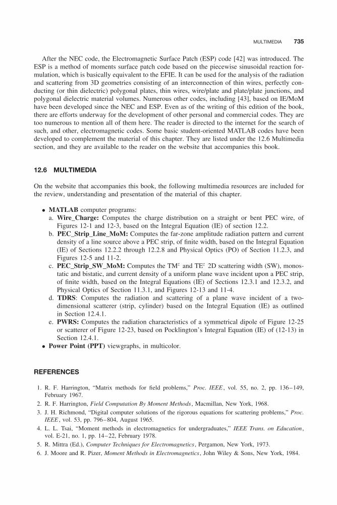
Balanis c12.tex V2 - 11/22/2011 3:54 P.M. Page 735
MULTIMEDIA 735
After the NEC code, the Electromagnetic Surface Patch (ESP) code [42] was introduced. TheESP is a method of moments surface patch code based on the piecewise sinusoidal reaction for-mulation, which is basically equivalent to the EFIE. It can be used for the analysis of the radiationand scattering from 3D geometries consisting of an interconnection of thin wires, perfectly con-ducting (or thin dielectric) polygonal plates, thin wires, wire/plate and plate/plate junctions, andpolygonal dielectric material volumes. Numerous other codes, including [43], based on IE/MoMhave been developed since the NEC and ESP. Even as of the writing of this edition of the book,there are efforts underway for the development of other personal and commercial codes. They aretoo numerous to mention all of them here. The reader is directed to the internet for the search ofsuch, and other, electromagnetic codes. Some basic student-oriented MATLAB codes have beendeveloped to complement the material of this chapter. They are listed under the 12.6 Multimediasection, and they are available to the reader on the website that accompanies this book.
12.6 MULTIMEDIA
On the website that accompanies this book, the following multimedia resources are included forthe review, understanding and presentation of the material of this chapter.
• MATLAB computer programs:a. Wire_Charge: Computes the charge distribution on a straight or bent PEC wire, of
Figures 12-1 and 12-3, based on the Integral Equation (IE) of section 12.2.b. PEC_Strip_Line_MoM: Computes the far-zone amplitude radiation pattern and current
density of a line source above a PEC strip, of finite width, based on the Integral Equation(IE) of Sections 12.2.2 through 12.2.8 and Physical Optics (PO) of Section 11.2.3, andFigures 12-5 and 11-2.
c. PEC_Strip_SW_MoM: Computes the TMz and TEz 2D scattering width (SW), monos-tatic and bistatic, and current density of a uniform plane wave incident upon a PEC strip,of finite width, based on the Integral Equations (IE) of Sections 12.3.1 and 12.3.2, andPhysical Optics of Section 11.3.1, and Figures 12-13 and 11-4.
d. TDRS: Computes the radiation and scattering of a plane wave incident of a two-dimensional scatterer (strip, cylinder) based on the Integral Equation (IE) as outlinedin Section 12.4.1.
e. PWRS: Computes the radiation characteristics of a symmetrical dipole of Figure 12-25or scatterer of Figure 12-23, based on Pocklington’s Integral Equation (IE) of (12-13) inSection 12.4.1.
• Power Point (PPT) viewgraphs, in multicolor.
REFERENCES
1. R. F. Harrington, “Matrix methods for field problems,” Proc. IEEE , vol. 55, no. 2, pp. 136–149,February 1967.
2. R. F. Harrington, Field Computation By Moment Methods , Macmillan, New York, 1968.
3. J. H. Richmond, “Digital computer solutions of the rigorous equations for scattering problems,” Proc.IEEE , vol. 53, pp. 796–804, August 1965.
4. L. L. Tsai, “Moment methods in electromagnetics for undergraduates,” IEEE Trans. on Education ,vol. E-21, no. 1, pp. 14–22, February 1978.
5. R. Mittra (Ed.), Computer Techniques for Electromagnetics , Pergamon, New York, 1973.
6. J. Moore and R. Pizer, Moment Methods in Electromagnetics , John Wiley & Sons, New York, 1984.
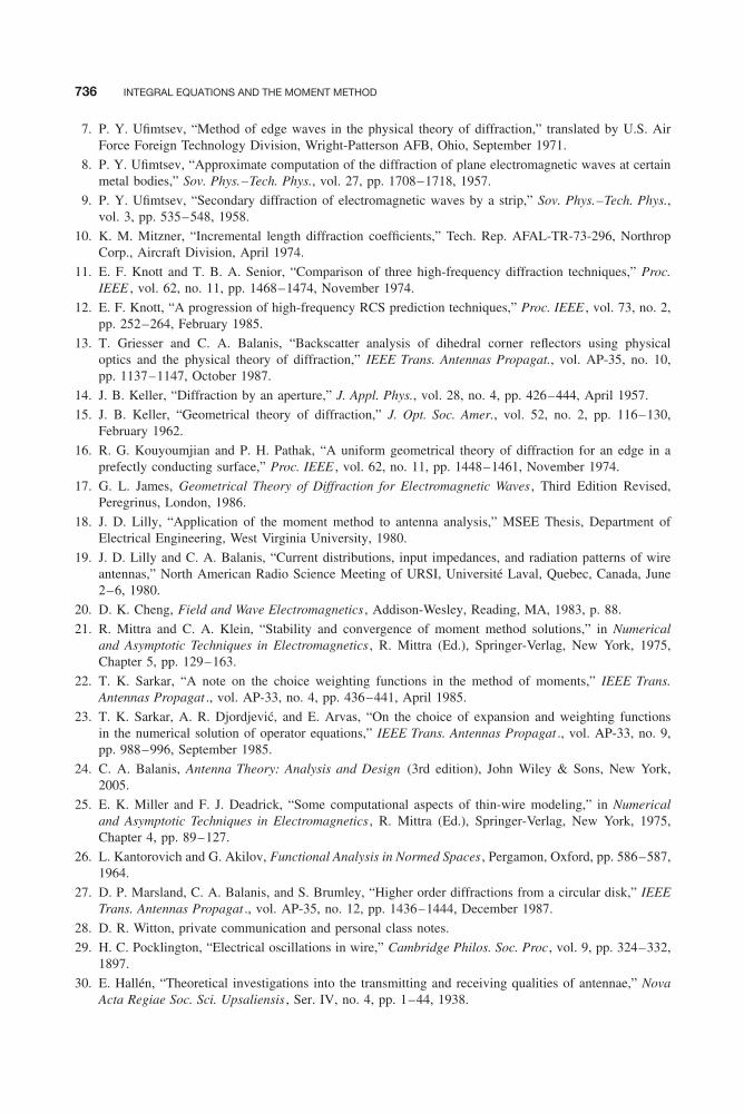
Balanis c12.tex V2 - 11/22/2011 3:54 P.M. Page 736
736 INTEGRAL EQUATIONS AND THE MOMENT METHOD
7. P. Y. Ufimtsev, “Method of edge waves in the physical theory of diffraction,” translated by U.S. AirForce Foreign Technology Division, Wright-Patterson AFB, Ohio, September 1971.
8. P. Y. Ufimtsev, “Approximate computation of the diffraction of plane electromagnetic waves at certainmetal bodies,” Sov. Phys.–Tech. Phys., vol. 27, pp. 1708–1718, 1957.
9. P. Y. Ufimtsev, “Secondary diffraction of electromagnetic waves by a strip,” Sov. Phys.–Tech. Phys.,vol. 3, pp. 535–548, 1958.
10. K. M. Mitzner, “Incremental length diffraction coefficients,” Tech. Rep. AFAL-TR-73-296, NorthropCorp., Aircraft Division, April 1974.
11. E. F. Knott and T. B. A. Senior, “Comparison of three high-frequency diffraction techniques,” Proc.IEEE , vol. 62, no. 11, pp. 1468–1474, November 1974.
12. E. F. Knott, “A progression of high-frequency RCS prediction techniques,” Proc. IEEE , vol. 73, no. 2,pp. 252–264, February 1985.
13. T. Griesser and C. A. Balanis, “Backscatter analysis of dihedral corner reflectors using physicaloptics and the physical theory of diffraction,” IEEE Trans. Antennas Propagat., vol. AP-35, no. 10,pp. 1137–1147, October 1987.
14. J. B. Keller, “Diffraction by an aperture,” J. Appl. Phys., vol. 28, no. 4, pp. 426–444, April 1957.
15. J. B. Keller, “Geometrical theory of diffraction,” J. Opt. Soc. Amer., vol. 52, no. 2, pp. 116–130,February 1962.
16. R. G. Kouyoumjian and P. H. Pathak, “A uniform geometrical theory of diffraction for an edge in aprefectly conducting surface,” Proc. IEEE , vol. 62, no. 11, pp. 1448–1461, November 1974.
17. G. L. James, Geometrical Theory of Diffraction for Electromagnetic Waves , Third Edition Revised,Peregrinus, London, 1986.
18. J. D. Lilly, “Application of the moment method to antenna analysis,” MSEE Thesis, Department ofElectrical Engineering, West Virginia University, 1980.
19. J. D. Lilly and C. A. Balanis, “Current distributions, input impedances, and radiation patterns of wireantennas,” North American Radio Science Meeting of URSI, Université Laval, Quebec, Canada, June2–6, 1980.
20. D. K. Cheng, Field and Wave Electromagnetics , Addison-Wesley, Reading, MA, 1983, p. 88.
21. R. Mittra and C. A. Klein, “Stability and convergence of moment method solutions,” in Numericaland Asymptotic Techniques in Electromagnetics , R. Mittra (Ed.), Springer-Verlag, New York, 1975,Chapter 5, pp. 129–163.
22. T. K. Sarkar, “A note on the choice weighting functions in the method of moments,” IEEE Trans.Antennas Propagat ., vol. AP-33, no. 4, pp. 436–441, April 1985.
23. T. K. Sarkar, A. R. Djordjević, and E. Arvas, “On the choice of expansion and weighting functionsin the numerical solution of operator equations,” IEEE Trans. Antennas Propagat ., vol. AP-33, no. 9,pp. 988–996, September 1985.
24. C. A. Balanis, Antenna Theory: Analysis and Design (3rd edition), John Wiley & Sons, New York,2005.
25. E. K. Miller and F. J. Deadrick, “Some computational aspects of thin-wire modeling,” in Numericaland Asymptotic Techniques in Electromagnetics , R. Mittra (Ed.), Springer-Verlag, New York, 1975,Chapter 4, pp. 89–127.
26. L. Kantorovich and G. Akilov, Functional Analysis in Normed Spaces , Pergamon, Oxford, pp. 586–587,1964.
27. D. P. Marsland, C. A. Balanis, and S. Brumley, “Higher order diffractions from a circular disk,” IEEETrans. Antennas Propagat ., vol. AP-35, no. 12, pp. 1436–1444, December 1987.
28. D. R. Witton, private communication and personal class notes.
29. H. C. Pocklington, “Electrical oscillations in wire,” Cambridge Philos. Soc. Proc, vol. 9, pp. 324–332,1897.
30. E. Hallén, “Theoretical investigations into the transmitting and receiving qualities of antennae,” NovaActa Regiae Soc. Sci. Upsaliensis , Ser. IV, no. 4, pp. 1–44, 1938.

Balanis c12.tex V2 - 11/22/2011 3:54 P.M. Page 737
PROBLEMS 737
31. R. King and C. W. Harrison, Jr., “The distribution of current along a symmetrical center-driven antenna,”Proc. IRE , vol. 31, pp. 548–567, October 1943.
32. J. H. Richmond, “A wire-grid model for scattering by conducting bodies,” IEEE Trans. AntennasPropagat ., vol. AP-14, no. 6, pp. 782–786, November 1966.
33. G. A. Thiele, “Wire antennas,” in Computer Techniques for Electromagnetics , R. Mittra (Ed.), Pergamon,New York, Chapter 2, pp. 7–70, 1973.
34. C. M. Butler and D. R. Wilton, “Evaluation of potential integral at singularity of exact kernel inthin-wire calculations,” IEEE Trans. Antennas Propagat ., vol. AP-23, no. 2, pp. 293–295, March 1975.
35. L. W. Pearson and C. M. Butler, “Inadequacies of collocation solutions to Pocklington-type models ofthin-wire structures,” IEEE Trans. Antennas Propagat ., vol. AP-23, no. 2, pp. 293–298, March 1975.
36. C. M. Butler and D. R. Wilton, “Analysis of various numerical techniques applied to thin-wire scatter-ers,” IEEE Trans. Antennas Propagat ., vol. AP-23, no. 4, pp. 534–540, July 1975.
37. D. R. Wilton and C. M. Butler, “Efficient numerical techniques for solving Pocklington’s equation andtheir relationships to other methods,” IEEE Trans. Antennas Propagat ., vol. AP-24, no. 1, pp. 83–86,January 1976.
38. L. L. Tsai, “A numerical solution for the near and far fields of an annular ring of magnetic current,”IEEE Trans. Antennas Propagat ., vol. AP-20, no. 5, pp. 569–576, September 1972.
39. G. J. Burke and A. J. Poggio, “Numerical electromagnetics code (NEC)-method of moments,” TechnicalDocument 116, Naval Ocean Systems Center, San Diego, CA, January 1981.
40. A. J. Julian, J. M. Logan, and J. W. Rockway, “MININEC: A mini-numerical electro magnetics code,”Technical Document 516, Naval Ocean Systems Center, San Diego, CA, September 6, 1982.
41. J. Rockway, J. Logan, D. Tarn, and S. Li, The MININEC SYSTEM: Microcomputer Analysis of WireAntennas , Artech House, Inc., 1988.
42. E. H. Newman and D. L. Dilsavor, “A user’s manual for the electromagnetic surface patch code: ESPversion III,” Technical Report No. 716148–19, ElectroScience Laboratory, The Ohio State University,May 1987.
43. http://www.wipl-d.com.
PROBLEMS
12.1. A circular loop of radius a = 0.2 m isconstructed out of a wire of radius b =10−3 m, as shown in Figure P12-1. Theentire loop is maintained at a constantpotential of 1 V. Using integral equationtechniques, determine and plot for 0◦ ≤φ ≤ 360◦ the surface charge density on thewire. Assume that at any given angle thecharge is uniformly distributed along thecircumference of the wire.
y
x
rq
f
z
a2b
Figure P12-1
12.2. Repeat Problem 12.1 when the loop is splitinto two parts; one part (from 0 to 180◦)is maintained at a constant potential of 1 Vand the other part (from 180 to 360◦) ismaintained at a constant potential of 2 V.
12.3. A linear charge ρc is distributed along avery thin wire circular loop of radius awhich is discontinuous (open) for 355◦ ≤φ ≤ 360◦ and 0◦ ≤ φ ≤ 5◦. The staticpotential Vz produced by this charge distri-bution on a very thin line along the z axis,passing through the origin of the circularloop is given by
Vz = 10a√a2 + z 2
, 0 ≤ z ≤ 7 meters
(a) Subdivide the line for 0 ≤ z ≤ 7meters in 70 segments and compute thepotential Vz at the center of each ofthe 70 segments when the radius of theloop is a = 1 meter.

Balanis c12.tex V2 - 11/22/2011 3:54 P.M. Page 738
738 INTEGRAL EQUATIONS AND THE MOMENT METHOD
(b) Plot the potential Vz of part (a) on alinear plot for 0 ≤ z ≤ 7 meters.
(c) Write an integral equation based onPoisson’s differential equation to solvethis problem.
(d) For a loop of radius a = 1 meter,determine the linear charge ρc that pro-duces the stated potential along 0 ≤z ≤ 7 meters that is computed in part(a) and plotted in part (b).
(e) Plot the linear charge distribution ofpart (d) on a linear plot of 5◦ ≤ φ ≤355◦.
a
f
x
y
z
7 meters
Figure P12-3
Use pulse expansion functions and N = 70segments along the circumference of theloop.
12.4. Repeat Example 12-3 for a strip with w =2λ, h = 0.25λ, and t = 0.01λ.
12.5. A magnetic line source of constant currentIm is placed a height h above a PerfectMagnetic Conducting (PMC) strip of widthw . The geometry is the same as that ofFigure 12-5. Write a normalized IntegralEquation (IE) that can be used to solve forthe linear magnetic current density Mz onthe strip. You do not have to derive it aslong as you justify it.
12.6. A TEz uniform plane wave of the formshown in Figure 12-13b, with a normal-ized z component of the incident magneticfield of magnitude Ho is incident upon aPerfect Magnetic Conducting (PMC) stripof finite width w . Write a normalized Inte-gral Equation (IE) which can be used tosolve for the magnetic current Mz whichis induced on the PMC strip. You do nothave to derive it as long as you justify it.
12.7. Derive (12-71a) and (12-71b).
12.8. Instead of using the electric field compo-nents of (12-72a) and (12-72b) to formulatethe two-dimensional SW of a PEC strip forTEz polarization, derive an integral expres-sion for H s
z in terms of Jx and then use thedefinition for SW of (11-21c). This requiresonly one component of the scattered H-field while using the definition of (11-21b)requires two scattered electric field compo-nents as given by (12-71a) and (12-71b).
12.9. An infinite electric line source of constantcurrent Ie is placed next to a circular con-ducting cylinder of radius a , as shown inFigure P12-9. The line source is positioneda distance b (b > a) from the center ofthe cylinder. Use the EFIE, piecewise con-stant subdomain basis functions, and point-matching techniques.(a) Formulate the current density induced
on the surface of the cylinder.(b) Compute the induced current density
when a = 5λ and b = 5.25λ. Assumea unity line-source current. Comparewith the modal solution current densityof (11-168a).
(c) For part (b), compute the normalizedfar-zone amplitude pattern (in deci-bels). Normalize so that the maximumis 0 dB.
y
z
a
bx
Ie
r
f
s = ∞
Figure P12-9
12.10. Repeat Problem 12.9 for a = 5λ andb = 5.5λ.
12.11. An infinite electric line source of constantcurrent Ie is placed next to a rectangularcylinder of dimensions a and b, as shownin the Figure P12-11. The line source ispositioned a distance c (c > a) from thecenter of the cylinder along the x axis. Usethe EFIE and piecewise subdomain basisfunctions and point-matching techniques,and do the following.
Balanis c12.tex V2 - 11/22/2011 3:54 P.M. Page 739
PROBLEMS 739
(a) Compute the induced current on thesurface of the cylinder when a = 5λ,b = 2.5, and c = 5.25λ. Assume aunity line-source current.
(b) Compute for part (a) the normalizedfar-zone amplitude pattern (in deci-bels). Normalize so that the maximumis 0 dB.
y
z
2a
2bc
x
Ie
r
f
Figure P12-11
12.12. Repeat Problem 12.11 for an electric linesource near an elliptic cylinder with a =5λ, b = 2.5λ, and c = 5.25λ.
y
z
b
a
c
x
Ie
r
f
Figure P12-12
12.13. A TMz uniform plane wave traveling in the+x direction is normally incident upon aconducting circular cylinder of radius a , asshown in Figure P12-13. Using the EFIE,piecewise constant subdomain basis func-tions, and point-matching techniques, writeyour own program, and do the following.(a) Plot the current density induced on the
surface of the cylinder when a = 2λ.Assume the incident field is of unityamplitude. Compare with the modalsolution current density of (11-97).
(b) Plot the normalized σ2-D/λ bistaticscattering width (in decibels) for 0◦ ≤φ ≤ 360◦ when a = 2λ. Compare withthe modal solution of (11-102).
y
z
aEi
Hi
x
r
f
s = ∞
Figure P12-13
12.14. A TMz uniform plane wave traveling in the+x direction is normally incident upon aconducting rectangular cylinder of dimen-sions a and b, as shown in Figure P12-14.Using the EFIE, piecewise constant sub-domain basis functions and point-matchingtechniques, write your own program, anddo the following.(a) Compute the induced current density
on the surface of the cylinder whena = 5λ and b = 2.5λ. Assume a unityline-source current.
(b) For part (a), compute and plot thetwo-dimensional normalized σ2-D/λ
bistatic scattering width (in decibels)for 0◦ ≤ φ ≤ 360◦.
y
z
2a
2bx
r
f
s = ∞
Ei
Hi
Figure P12-14
12.15. Repeat Problem 12.14 for a TMz uni-form plane wave impinging upon an ellip-tic conducting cylinder with a = 5λ andb = 2.5λ.
Ei
Hi
y
zb
a x
r
f
Figure P12-15
Balanis c12.tex V2 - 11/22/2011 3:54 P.M. Page 740
740 INTEGRAL EQUATIONS AND THE MOMENT METHOD
12.16. Using the geometry of Figure 12-14, ver-ify (12-71a) and (12-71b), and that (12-70a) reduces to (12-72a) and (12-70b) to(12-72b).
12.17. Show that the integral of (12-78d) can beevaluated using (12-79a) through (12-79c).
12.18. Repeat Problem 12.9 for a magnetic linesource of constant current Im = 1 whena = b = 5λ. This problem is representa-tive of a very thin axial slot on the surfaceof the cylinder. Compare the current den-sity on the surface of the cylinder from part(b) with that of the modal solution of (11-177a).
12.19. Repeat Problem 12.11 for a magnetic linesource of constant current Im = 1 whena = 5λ, b = 2.5λ, and c = 5λ. This prob-lem is representative of a very thin axialslot on the surface of the cylinder.
12.20. Repeat Problem 12.12 for a magnetic linesource of constant current Im = 1 whena = 5λ, b = 2.5λ, and c = 5λ. This prob-lem is representative of a very thin axialslot on the surface of the cylinder.
12.21. Repeat Problem 12.13 for a TEz uniformplane wave of unity amplitude. Comparethe current density with the modal solu-tion of (11-113) and the normalized σ2-D/λ
bistatic scattering width with the modalsolution of (11-117).
12.22. Repeat Problem 12.14 for a TEz uniformplane wave at unity amplitude.
12.23. Repeat Problem 12.15 for a TEz uniformplane wave of unity amplitude.
12.24. Using the geometry of Figure 12-17, showthat
n̂ • ∇H (2)0 (βR) = −β cos ψH (2)
1 (βR)
12.25. Repeat Problem 12.9 using the MFIE.
12.26. Repeat Problem 12.13 using the MFIE.You must write your own computer pro-gram to solve this problem.
12.27. Using the geometry of Figure 12-18, showthat
n̂′ • ∇H (2)0 (βR) = −β cos ψ ′H (2)
1 (βR)
12.28. Repeat Problem 12.18 using the MFIE.
12.29. Derive Pocklington’s integral equation12-123 using (12-121) and (12-122).
12.30. Derive the solution of (12-125) to thedifferential equation (12-124a). Show thatHallén’s integral equation can be writtenas (12-126).
12.31. Show that the incident tangential electricfield (E i
z ) generated on the surface of awire of radius a by a magnetic field gen-erator of (12-129) is given by (12-130).
12.32. Reduce (12-130) to (12-131) valid onlyalong the z axis (ρ = 0).
12.33. For the center-fed dipole of Example12-7, write the [Z ] matrix for N = 21using for the gap the delta-gap generatorand the magnetic frill generator.
12.34. For an infinitesimal center fed dipole of� = λ/50 and radius a = 0.005λ, derivethe input impedance using Pocklington’sintegral equation with piecewise con-stant subdomain basis functions and pointmatching. Use N = 21 and model the gapas a delta-gap generator and as a magnetic-frill generator. Use the PWRS computerprogram at the end of the chapter.
12.35. A conducting wire of length � = 0.47λ andradius a = 0.005λ is placed symmetricallyalong the z axis. Assuming a TMz uniformplane wave is incident on the wire at anangle θi = 30◦ from the z axis, do the fol-lowing.(a) Compute and plot the current induced
on the surface of the wire.(b) Compute and plot the bistatic RCS for
0◦ ≤ θs ≤ 180◦.(c) Compute and plot the monostatic RCS
for 0◦ ≤ θi = θs ≤ 180◦.The amplitude of the incident electric fieldis 10−3 V/m. Use Pocklington’s integralequation and the PWRS computer program.Determine the number of segments thatleads to a stable solution.
12.36. Repeat Problem 12.35 for a TEz uniformplane wave incidence.
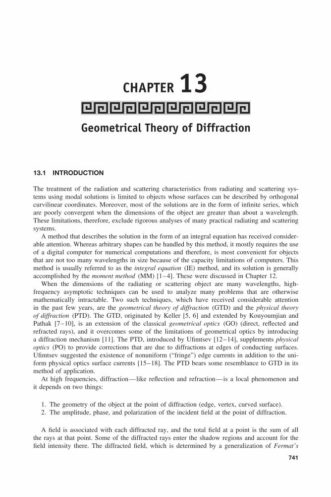
Balanis c13.tex V2 - 11/24/2011 12:45 A.M. Page 741
CHAPTER 13Geometrical Theory of Diffraction
13.1 INTRODUCTION
The treatment of the radiation and scattering characteristics from radiating and scattering sys-tems using modal solutions is limited to objects whose surfaces can be described by orthogonalcurvilinear coordinates. Moreover, most of the solutions are in the form of infinite series, whichare poorly convergent when the dimensions of the object are greater than about a wavelength.These limitations, therefore, exclude rigorous analyses of many practical radiating and scatteringsystems.
A method that describes the solution in the form of an integral equation has received consider-able attention. Whereas arbitrary shapes can be handled by this method, it mostly requires the useof a digital computer for numerical computations and therefore, is most convenient for objectsthat are not too many wavelengths in size because of the capacity limitations of computers. Thismethod is usually referred to as the integral equation (IE) method, and its solution is generallyaccomplished by the moment method (MM) [1–4]. These were discussed in Chapter 12.
When the dimensions of the radiating or scattering object are many wavelengths, high-frequency asymptotic techniques can be used to analyze many problems that are otherwisemathematically intractable. Two such techniques, which have received considerable attentionin the past few years, are the geometrical theory of diffraction (GTD) and the physical theoryof diffraction (PTD). The GTD, originated by Keller [5, 6] and extended by Kouyoumjian andPathak [7–10], is an extension of the classical geometrical optics (GO) (direct, reflected andrefracted rays), and it overcomes some of the limitations of geometrical optics by introducinga diffraction mechanism [11]. The PTD, introduced by Ufimtsev [12–14], supplements physicaloptics (PO) to provide corrections that are due to diffractions at edges of conducting surfaces.Ufimtsev suggested the existence of nonuniform (“fringe”) edge currents in addition to the uni-form physical optics surface currents [15–18]. The PTD bears some resemblance to GTD in itsmethod of application.
At high frequencies, diffraction—like reflection and refraction—is a local phenomenon andit depends on two things:
1. The geometry of the object at the point of diffraction (edge, vertex, curved surface).2. The amplitude, phase, and polarization of the incident field at the point of diffraction.
A field is associated with each diffracted ray, and the total field at a point is the sum of allthe rays at that point. Some of the diffracted rays enter the shadow regions and account for thefield intensity there. The diffracted field, which is determined by a generalization of Fermat’s
741

Balanis c13.tex V2 - 11/24/2011 12:45 A.M. Page 742
742 GEOMETRICAL THEORY OF DIFFRACTION
principle [6, 7], is initiated at points on the surface of the object that create a discontinuity inthe incident GO field (incident and reflected shadow boundaries).
The phase of the field on a ray is assumed to be equal to the product of the optical lengthof the ray from some reference point and the wave number of the medium. Appropriate phasejumps must be added as rays pass through caustics (defined in Section 13.2.1). The amplitude isassumed to vary in accordance with the principle of conservation of energy in a narrow tube ofrays.
The initial value of the field on a diffracted ray is determined from the incident field with theaid of an appropriate diffraction coefficient that is a dyadic for electromagnetic fields. This is anal-ogous to the manner reflected fields are determined using the reflection coefficient. The rays alsofollow paths that make the optical distance from the source to the observation point an extremum(usually a minimum). This leads to straight-line propagation within homogeneous media and alonggeodesics (surface extrema) on smooth surfaces. The field intensity also attenuates exponentiallyas it travels along surface geodesics.
The diffraction and attenuation coefficients are usually determined from the asymptotic solu-tions of the simplest boundary-value problems, which have the same local geometry at the pointsof diffraction as the object at the points of interest. Geometries of this type are referred to ascanonical problems. One of the simplest geometries that will be discussed in this chapter is aconducting wedge. The primary objective in using the GTD is to resolve each problem to smallercomponents [19–25], each representing a canonical geometry with a known solution. The ultimatesolution is a superposition of the contributions from each canonical problem.
Some of the advantages of GTD are given in the following list.
1. It is simple to apply.2. It can be used to solve complicated problems that do not have exact solutions.3. It provides physical insight into the radiation and scattering mechanisms from the various
parts of the structure.4. It yields accurate results that compare quite well with experiments and other methods.5. It can be combined with other techniques such as the moment method [26–28].
One of the main interests of diffraction by wedges is that engineers and scientists have inves-tigated how the shape and material properties of complex structures affect their backscatteringcharacteristics. The attraction in this area is primarily aimed toward designs of low-profile (stealth)technology by using appropriate shaping along with lossy or coated materials to reduce the radarvisibility, as represented by radar cross section (RCS), of complex radar targets, such as aircraft,spacecraft, and missiles. A good example is the F-117 shown in Figure 13-1, whose surface is pri-marily structured by a number of faceted flat plates and wedges because, as will become evidentfrom the developments, formulations, examples and problems of this chapter (see also Problem13.50), the backscatter from exterior wedges is lower than that of convex curved surfaces. Inaddition, the plates are oriented judiciously so that the maximum scattered field is toward thespecular direction and away from the source of detection. While in this chapter we will focus onthe diffraction by PEC wedges, the diffraction by wedges with impedance surfaces, to representlossy and composite wedge surfaces, is the subject of Chapter 14.
13.2 GEOMETRICAL OPTICS
Geometrical optics (GO) is an approximate high-frequency method for determining wave propa-gation for incident, reflected, and refracted fields. Because it uses ray concepts, it is often referredto as ray optics. Originally, geometrical optics was developed to analyze the propagation of lightat sufficiently high frequencies where it was not necessary to consider the wave nature of light.

Balanis c13.tex V2 - 11/24/2011 12:45 A.M. Page 743
GEOMETRICAL OPTICS 743
Figure 13-1 F-117 Nighthawk. (Printed with permission of Lockheed Martin Corporation © 2010).
Instead, the transport of energy from one point to another in an isotropic lossless medium isaccomplished using the conservation of energy flux in a tube of rays. For reflection problems,geometrical optics approximates the scattered fields only toward specular directions as deter-mined by Snell’s law of reflection: the angle of reflection is equal to the angle of incidence. Forsufficiently high frequencies, geometrical optics fields may dominate the scattering phenomenaand may not require any corrections. This is more evident for backscattering from smooth curvedsurfaces whose curvature is large compared to the wavelength.
According to classical geometrical optics, the rays between any two points P1 and P2 follow apath that makes the optical distance between them an extremum (usually a minimum). In equationform, this is expressed as
δ
∫ P2
P1
n(s) ds = 0 (13-1)
where δ represents what is referred to in the calculus of variations as the variational differentialand n(s) is the index of refraction of the medium, β(s)/β0 = n(s). If the medium is homogeneous,n(s) = n = constant, the paths are straight lines. Equation 13-1 is a mathematical representationof Fermat’s principle. In addition, the light intensity, power per unit solid angle, between anytwo points is also governed by the conservation of energy flux in a tube of rays.
To demonstrate the principles of geometrical optics, let us consider a primary wave frontsurface ψ0, as shown in Figure 13-2, formed at t = t0 by the motion of light propagating in anisotropic lossless medium. The objectives here are:
1. To determine the secondary wave front surfaces ψn formed at t = tn+1 > tn , n = 0,1, 2, 3 . . . .
2. To relate the power density and field intensity on the secondary wave fronts to those of theprimary or previous wave fronts.
The secondary wave fronts can be determined by first selecting a number of discrete points onthe primary wave front. If the medium of wave propagation is also assumed to be homogeneous,ray paths from the primary to the secondary wave front are drawn as straight lines that at eachpoint are normal to the surface of the primary wave front.
Since the wave travels in the medium with the speed of light given by v = c/n , where c isthe speed of light in free space and n is the index of refraction, then at t = t1 − t0 (t1 > t0)the wave would have traveled a distance � = vt . Along each of the normal rays a distance
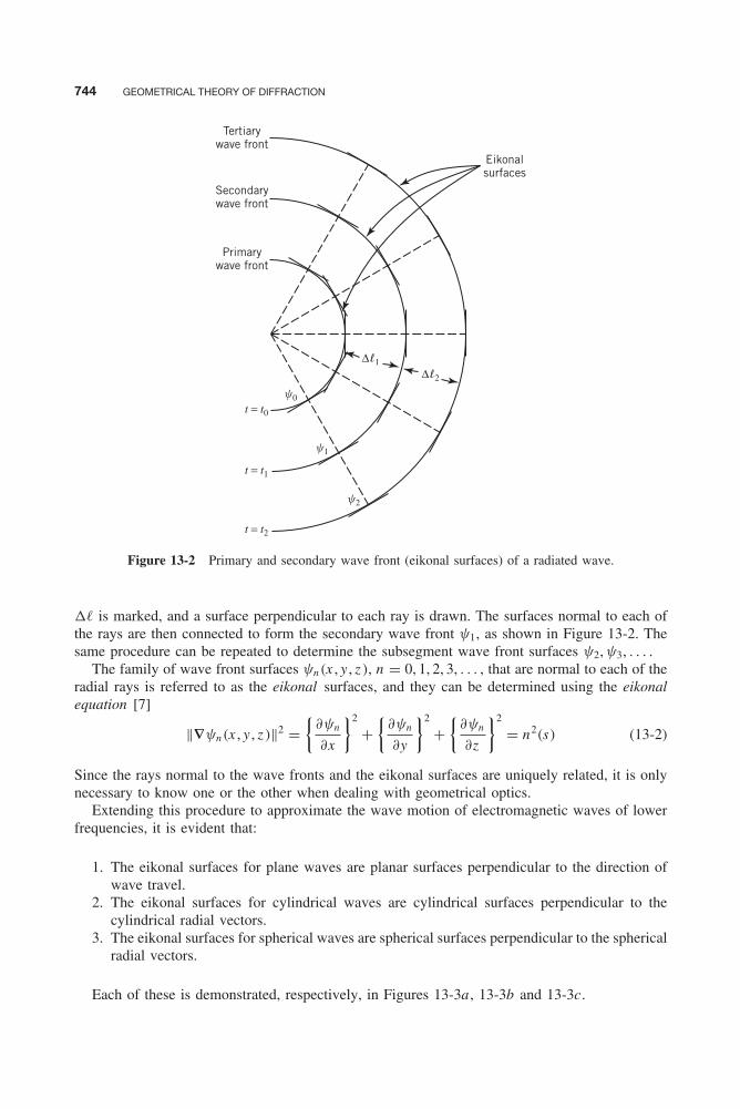
Balanis c13.tex V2 - 11/24/2011 12:45 A.M. Page 744
744 GEOMETRICAL THEORY OF DIFFRACTION
Tertiarywave front
Eikonalsurfaces
Secondarywave front
Primarywave front
Δl1
y0
y1
y2
Δl2
t = t0
t = t1
t = t2
Figure 13-2 Primary and secondary wave front (eikonal surfaces) of a radiated wave.
� is marked, and a surface perpendicular to each ray is drawn. The surfaces normal to each ofthe rays are then connected to form the secondary wave front ψ1, as shown in Figure 13-2. Thesame procedure can be repeated to determine the subsegment wave front surfaces ψ2, ψ3, . . . .
The family of wave front surfaces ψn(x , y , z ), n = 0, 1, 2, 3, . . . , that are normal to each of theradial rays is referred to as the eikonal surfaces, and they can be determined using the eikonalequation [7]
‖∇ψn(x , y , z )‖2 ={
∂ψn
∂x
}2
+{
∂ψn
∂y
}2
+{
∂ψn
∂z
}2
= n2(s) (13-2)
Since the rays normal to the wave fronts and the eikonal surfaces are uniquely related, it is onlynecessary to know one or the other when dealing with geometrical optics.
Extending this procedure to approximate the wave motion of electromagnetic waves of lowerfrequencies, it is evident that:
1. The eikonal surfaces for plane waves are planar surfaces perpendicular to the direction ofwave travel.
2. The eikonal surfaces for cylindrical waves are cylindrical surfaces perpendicular to thecylindrical radial vectors.
3. The eikonal surfaces for spherical waves are spherical surfaces perpendicular to the sphericalradial vectors.
Each of these is demonstrated, respectively, in Figures 13-3a , 13-3b and 13-3c.
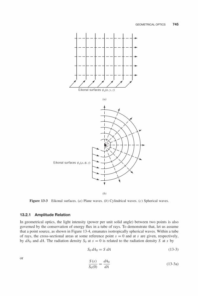
Balanis c13.tex V2 - 11/24/2011 12:45 A.M. Page 745
GEOMETRICAL OPTICS 745
Eikonal surfaces yn(r, f, z)
Eikonal surfaces yn(x, y, z)
(a)
(b)
Figure 13-3 Eikonal surfaces. (a) Plane waves. (b) Cylindrical waves. (c) Spherical waves.
13.2.1 Amplitude Relation
In geometrical optics, the light intensity (power per unit solid angle) between two points is alsogoverned by the conservation of energy flux in a tube of rays. To demonstrate that, let us assumethat a point source, as shown in Figure 13-4, emanates isotropically spherical waves. Within a tubeof rays, the cross-sectional areas at some reference point s = 0 and at s are given, respectively,by dA0 and dA. The radiation density S0 at s = 0 is related to the radiation density S at s by
S0 dA0 = S dA (13-3)
orS (s)
S0(0)= dA0
dA(13-3a)
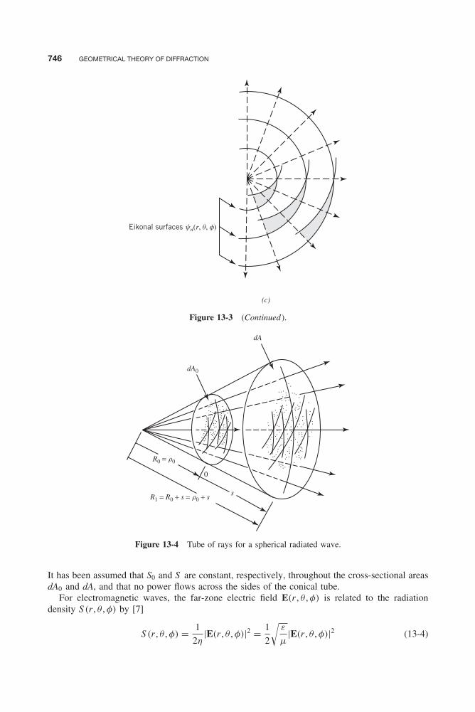
Balanis c13.tex V2 - 11/24/2011 12:45 A.M. Page 746
746 GEOMETRICAL THEORY OF DIFFRACTION
Eikonal surfaces yn(r, q, f)
(c)
Figure 13-3 (Continued ).
R1 = R0 + s = r0 + s
R0 = r0
0
s
dA0
dA
Figure 13-4 Tube of rays for a spherical radiated wave.
It has been assumed that S0 and S are constant, respectively, throughout the cross-sectional areasdA0 and dA, and that no power flows across the sides of the conical tube.
For electromagnetic waves, the far-zone electric field E(r , θ , φ) is related to the radiationdensity S (r , θ , φ) by [7]
S (r , θ , φ) = 1
2η|E(r , θ , φ)|2 = 1
2
√ε
μ|E(r , θ , φ)|2 (13-4)
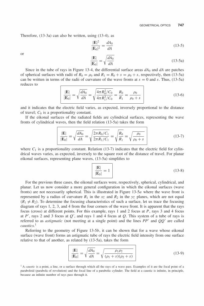
Balanis c13.tex V2 - 11/24/2011 12:45 A.M. Page 747
GEOMETRICAL OPTICS 747
Therefore, (13-3a) can also be written, using (13-4), as
|E|2|E0|2 = dA0
dA(13-5)
or|E||E0| =
√dA0
dA(13-5a)
Since in the tube of rays in Figure 13-4, the differential surface areas dA0 and dA are patchesof spherical surfaces with radii of R0 = ρ0 and R1 = R0 + s = ρ0 + s , respectively, then (13-5a)can be written in terms of the radii of curvature of the wave fronts at s = 0 and s . Thus, (13-5a)reduces to
|E||E0| =
√dA0
dA=
√4πR2
0/C0
4πR21/C0
= R0
R1= ρ0
ρ0 + s(13-6)
and it indicates that the electric field varies, as expected, inversely proportional to the distanceof travel; C0 is a proportionality constant.
If the eikonal surfaces of the radiated fields are cylindrical surfaces, representing the wavefronts of cylindrical waves, then the field relation (13-5a) takes the form
|E||E0| =
√dA0
dA=
√2πR0/C1
2πR1/C1=
√R0
R1=
√ρ0
ρ0 + s(13-7)
where C1 is a proportionality constant. Relation (13-7) indicates that the electric field for cylin-drical waves varies, as expected, inversely to the square root of the distance of travel. For planareikonal surfaces, representing plane waves, (13-5a) simplifies to
|E||E0| = 1 (13-8)
For the previous three cases, the eikonal surfaces were, respectively, spherical, cylindrical, andplanar. Let us now consider a more general configuration in which the eikonal surfaces (wavefronts) are not necessarily spherical. This is illustrated in Figure 13-5a where the wave front isrepresented by a radius of curvature R1 in the xz and R2 in the yz planes, which are not equal(R1 �= R2). To determine the focusing characteristics of such a surface, let us trace the focusingdiagram of rays 1, 2, 3, and 4 from the four corners of the wave front. It is apparent that the raysfocus (cross) at different points. For this example, rays 1 and 2 focus at P , rays 3 and 4 focusat P ′, rays 2 and 3 focus at Q ′, and rays 1 and 4 focus at Q . This system of a tube of rays isreferred to as astigmatic (not meeting at a single point) and the lines PP ′ and QQ ′ are calledcaustics.1
Referring to the geometry of Figure 13-5b, it can be shown that for a wave whose eikonalsurface (wave front) forms an astigmatic tube of rays the electric field intensity from one surfacerelative to that of another, as related by (13-5a), takes the form
|E||E0| =
√dA0
dA=
√ρ1ρ2
(ρ1 + s)(ρ2 + s)(13-9)
1 A caustic is a point, a line, or a surface through which all the rays of a wave pass. Examples of it are the focal point of aparaboloid (parabola of revolution) and the focal line of a parabolic cylinder. The field at a caustic is infinite, in principle,because an infinite number of rays pass through it.
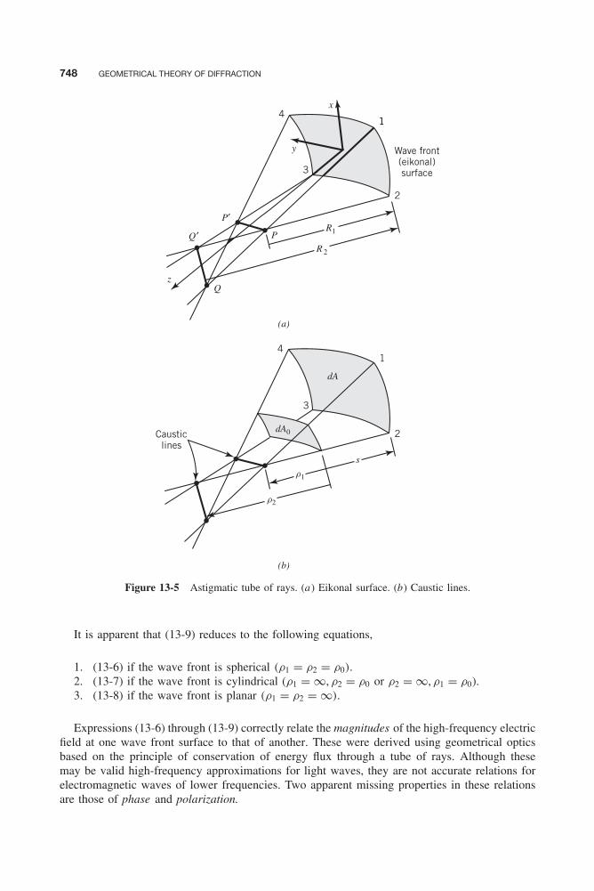
Balanis c13.tex V2 - 11/24/2011 12:45 A.M. Page 748
748 GEOMETRICAL THEORY OF DIFFRACTION
s
r1
r2
dA
P′
P
R 2
2
3
114
R1Q′
z
(a)
y
x
Q
Wave front(eikonal)surface
2
3
14
(b)
Causticlines
dA0
Figure 13-5 Astigmatic tube of rays. (a) Eikonal surface. (b) Caustic lines.
It is apparent that (13-9) reduces to the following equations,
1. (13-6) if the wave front is spherical (ρ1 = ρ2 = ρ0).2. (13-7) if the wave front is cylindrical (ρ1 = ∞, ρ2 = ρ0 or ρ2 = ∞, ρ1 = ρ0).3. (13-8) if the wave front is planar (ρ1 = ρ2 = ∞).
Expressions (13-6) through (13-9) correctly relate the magnitudes of the high-frequency electricfield at one wave front surface to that of another. These were derived using geometrical opticsbased on the principle of conservation of energy flux through a tube of rays. Although thesemay be valid high-frequency approximations for light waves, they are not accurate relations forelectromagnetic waves of lower frequencies. Two apparent missing properties in these relationsare those of phase and polarization.
Balanis c13.tex V2 - 11/24/2011 12:45 A.M. Page 749
GEOMETRICAL OPTICS 749
13.2.2 Phase and Polarization Relations
Phase and polarization information can be introduced to the relations (13-6) through (13-9)by examining the approach introduced by Luneberg [29] and Kline [30, 31] to develop high-frequency solutions of electromagnetic problems. The works of Luneberg and Kline, referred toas the Luneberg–Kline high-frequency expansion, best bridge the gap between geometrical (ray)optics and wave propagation phenomena.
The Luneberg–Kline series expansion solution begins by assuming that the electric field forlarge ω can be written as a series
E(R, ω) = e−jβ0ψ(R)
∞∑m=0
Em(R)
(jω)m(13-10)
where R = position vectorβ0 = phase constant for free-space
Substituting (13-10) into the wave equation
∇2E + β2E = 0 (13-11)
subject to Maxwell’s equation∇ • E = 0 (13-12)
it can be shown, by equating like powers of ω, that one obtains the following.
1. The eikonal equation 13-2 or‖∇ψ‖2 = n2 (13-13a)
where ψ = eikonal (wave front) surfacen = index of refraction
2. The transport equations
∂E0
∂s+ 1
2
{∇2ψ
n
}E0 = 0 for first-order terms (13-13b)
∂Em
∂s+ 1
2
{∇2ψ
n
}Em = vp
2∇2Em−1 for higher-order terms (13-13c)
where m = 1,2,3 . . .
vp = speed of light in medium
3. The conditional equations
ŝ • E0 = 0 for first-order terms (13-13d)
ŝ • Em = vp∇ • Em−1 for higher-order terms (13-13e)
m = 1, 2, 3 . . .
where
ŝ = ∇ψ
n= unit vector in the direction path (normal to the wave front ψ) (13-13f)
s = distance along the ray path
Balanis c13.tex V2 - 11/24/2011 12:45 A.M. Page 750
750 GEOMETRICAL THEORY OF DIFFRACTION
At the present time we are interested mainly in first-order solutions for the electric fieldof (13-10) that can be approximated and take the form of
E(s) � e−jβ0ψ(s)E0(s = 0) (13-14)
Integrating the first-order transport equation 13-13b along s and referring to the geometry ofFigure 13-5a , it can be shown that (13-14) can be written as [30, 31]
E(s) � E0(0)e−jβ0ψ(0)
√ρ1ρ2
(ρ1 + s)(ρ2 + s)e−jβs (13-15)
where s = 0 is taken as a reference point. Since E0(0) is complex, the phase term e−jβ0ψ(0) canbe combined with E0(0) and (13-15) rewritten as
E(s) = E′0(0)ejφ0(0)︸ ︷︷ ︸
√ρ1ρ2
(ρ1 + s)(ρ2 + s)︸ ︷︷ ︸ e−jβs︸ ︷︷ ︸Field at reference Spatial attenuation Phase
point (s = 0) (divergence, spreading) factorfactor
(13-15a)
where E′0(0) = field amplitude at reference point (s = 0)
φ0(0) = field phase at reference point (s = 0)
Comparing (13-15a) to (13-9), it is evident that the leading term of the Luneberg–Kline seriesexpansion solution for large ω predicts the spatial attenuation relation between the electric fieldsof two points as obtained by classical geometrical optics, as given by (13-9), which ignores boththe polarization and the wave motion (phase) of electromagnetic fields. It also predicts their phaseand polarization relations, as given by (13-15a). Obviously, (13-15a) could have been obtainedfrom (13-9) by artificially converting the magnitudes of the fields to vectors (to account forpolarization) and by introducing a complex exponential to account for the phase delay of thefield from s = 0 to s . This was not necessary since (13-15a) was derived here rigorously usingthe leading term of the Luneberg–Kline expansion series for large ω subject to the wave andMaxwell’s equations. It should be pointed out, however, that (13-15a) is only a high-frequencyapproximation and it becomes more accurate as the frequency approaches infinity. However, formany practical engineering problems, it does predict quite accurate results that compare well withmeasurements.
In principle, more accurate expressions to the geometrical optics approximation can be obtainedby retaining higher-order terms E1(R1), E2(R2), . . . in the Luneberg–Kline series expansion(13-10), and in the transport (13-13c) and conditional (13-13e) equations. However, such a proce-dure is very difficult. In addition, the resulting terms do not remove the discontinuities introducedby geometrical optics fields along the incident and reflection boundaries, and the method doesnot lend itself to other improvements in the geometrical optics, such as those of diffraction.Therefore, no such procedure will be pursued here.
It should be noted that when the observation point is chosen so that s = −ρ1 or s = −ρ2,(13-15a) possesses singularities representing the congruence of the rays at the caustic lines PP ′and QQ ′. Therefore, (13-15a) is not valid along the caustics and not very accurate near them,and it should not be used in those regions. Other methods should be utilized to find the fieldsat and near caustics [32–36]. In addition, it is observed that when −ρ2 < s < −ρ1 the sign inthe (ρ1 + s) term of the denominator of (13-15a) changes. Similar changes of sign occur in the
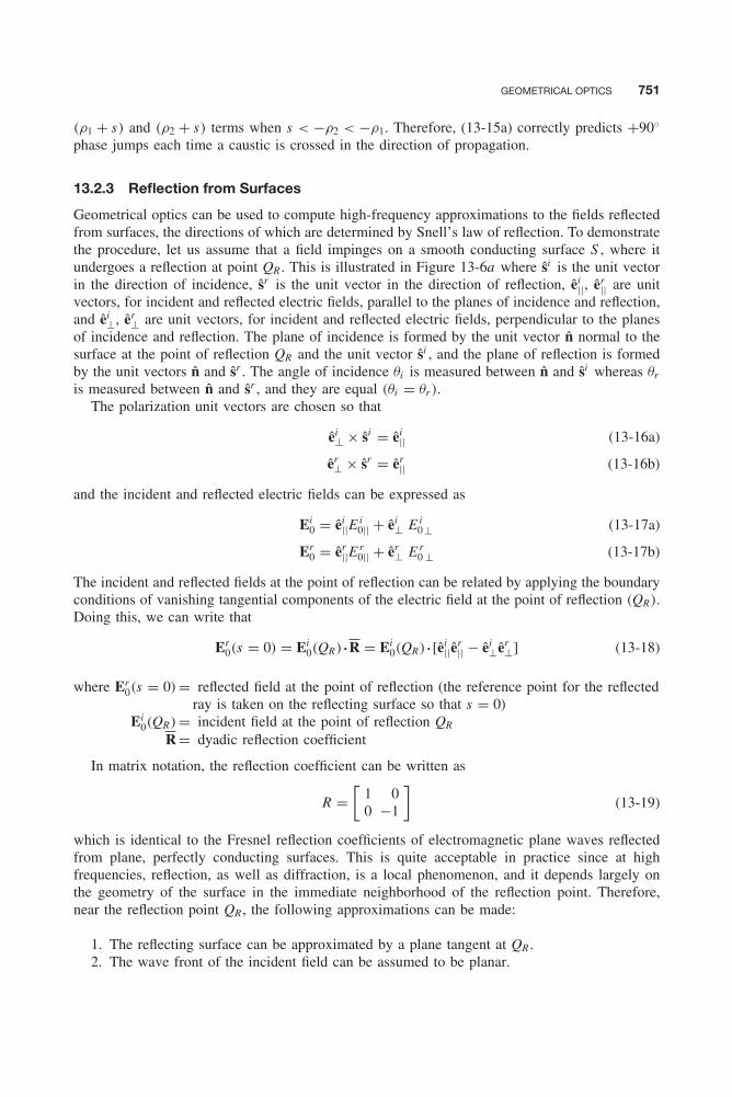
Balanis c13.tex V2 - 11/24/2011 12:45 A.M. Page 751
GEOMETRICAL OPTICS 751
(ρ1 + s) and (ρ2 + s) terms when s < −ρ2 < −ρ1. Therefore, (13-15a) correctly predicts +90◦phase jumps each time a caustic is crossed in the direction of propagation.
13.2.3 Reflection from Surfaces
Geometrical optics can be used to compute high-frequency approximations to the fields reflectedfrom surfaces, the directions of which are determined by Snell’s law of reflection. To demonstratethe procedure, let us assume that a field impinges on a smooth conducting surface S , where itundergoes a reflection at point QR . This is illustrated in Figure 13-6a where ŝi is the unit vectorin the direction of incidence, ŝr is the unit vector in the direction of reflection, êi
||, êr|| are unit
vectors, for incident and reflected electric fields, parallel to the planes of incidence and reflection,and êi
⊥, êr⊥ are unit vectors, for incident and reflected electric fields, perpendicular to the planes
of incidence and reflection. The plane of incidence is formed by the unit vector n̂ normal to thesurface at the point of reflection QR and the unit vector ŝi , and the plane of reflection is formedby the unit vectors n̂ and ŝr . The angle of incidence θi is measured between n̂ and ŝi whereas θr
is measured between n̂ and ŝr , and they are equal (θi = θr ).The polarization unit vectors are chosen so that
êi⊥ × ŝi = êi
|| (13-16a)
êr⊥ × ŝr = êr
|| (13-16b)
and the incident and reflected electric fields can be expressed as
Ei0 = êi
||Ei0|| + êi
⊥ E i0⊥ (13-17a)
Er0 = êr
||Er0|| + êr
⊥ E r0 ⊥ (13-17b)
The incident and reflected fields at the point of reflection can be related by applying the boundaryconditions of vanishing tangential components of the electric field at the point of reflection (QR).Doing this, we can write that
Er0(s = 0) = Ei
0(QR) • R = Ei0(QR) • [êi
||êr|| − êi
⊥êr⊥] (13-18)
where Er0(s = 0) = reflected field at the point of reflection (the reference point for the reflected
ray is taken on the reflecting surface so that s = 0)Ei
0(QR) = incident field at the point of reflection QR
R = dyadic reflection coefficient
In matrix notation, the reflection coefficient can be written as
R =[
1 00 −1
](13-19)
which is identical to the Fresnel reflection coefficients of electromagnetic plane waves reflectedfrom plane, perfectly conducting surfaces. This is quite acceptable in practice since at highfrequencies, reflection, as well as diffraction, is a local phenomenon, and it depends largely onthe geometry of the surface in the immediate neighborhood of the reflection point. Therefore,near the reflection point QR , the following approximations can be made:
1. The reflecting surface can be approximated by a plane tangent at QR .2. The wave front of the incident field can be assumed to be planar.

Balanis c13.tex V2 - 11/24/2011 12:45 A.M. Page 752
752 GEOMETRICAL THEORY OF DIFFRACTION
(a)
ei
qi qr
QR
S
si
⊥⊥
ir1
ir2
(b)
1
34
2
s
QR
P′
Q′
P
S
rr1
rr2
Q
er
ei
er
si
sr
sr
n
n
Figure 13-6 Reflection from a curved surface. (a) Reflection point. (b) Astigmatic tube of rays.
With the aid of (13-15a) and (13-18), it follows that the reflected field Er (s) at a distance sfrom the point of reflection QR can be written as
Er(s) = Ei (QR)︸ ︷︷ ︸ • R︸ ︷︷ ︸√
ρr1ρ
r2
(ρr1 + s)(ρr
2 + s)︸ ︷︷ ︸ e−jβs︸︷︷︸Field at Reflection Spatial attenuation Phase
reference coefficient (divergence, spreading) factorpoint (Qr ) factor
(13-20)
where ρr1 , ρr
2 = principal radii of curvature of the reflected wave front at the point of reflection

Balanis c13.tex V2 - 11/24/2011 12:45 A.M. Page 753
GEOMETRICAL OPTICS 753
The astigmatic tube of rays for the reflected fields are shown in Figure 13-6b where the referencesurface is taken at the reflecting surface.
The principal radii of curvature of the reflected wave front, ρr1 and ρr
2 , are related to theprincipal radii of curvature of the incident wave front, ρ i
1 and ρ i2, the aspect of wave incidence,
and the curvature of the reflecting surface at QR . It can be shown that ρr1 and ρr
2 can be expressedas [10]
1
ρr1
= 1
2
{1
ρ i1
+ 1
ρ i2
}+ 1
f1(13-21a)
1
ρr2
= 1
2
{1
ρ i1
+ 1
ρ i2
}+ 1
f2(13-21b)
where ρ i1, ρ i
2 = principal radii of curvature of incident wave front (ρ i1 = ρ i
2 = s ′ for sphericalincident wave front; ρ i
1 = ρ ′, ρ i2 = ∞ or ρ i
1 = ∞, ρ i2 = ρ ′ for cylindrical
incident wave front, and ρ i1 = ρ ′
2 = ∞ for planar incident wave front)
Equations 13-21a and 13-21b are similar in form to the simple lens and mirror formulas ofelementary physics. In fact, when the incident ray is spherical (ρ i
1 = ρ i2 = s ′), f1 and f2 represent
focal distances that are independent of the source range that is creating the spherical wave.When the incident field has a spherical wave front, ρ i
1 = ρ i2 = s ′, then f1 and f2 simplify to
1
f1= 1
cos θi
{sin2 θ2
R1+ sin2 θ1
R2
}+
√√√√ 1
cos2 θi
{sin2 θ2
R1+ sin2 θ1
R2
}2
− 4
R1R2(13-22a)
1
f2= 1
cos θi
{sin2 θ2
R1+ sin2 θ1
R2
}−
√√√√ 1
cos2 θi
{sin2 θ2
R1+ sin2 θ1
R2
}2
− 4
R1R2(13-22b)
where R1, R2 = radii of curvature of the reflecting surfaceθ1 = angle between the direction of the incident ray ŝi and û1
θ2 = angle between the direction of the incident ray ŝi and û2
û1 = unit vector in the principal direction of S at QR with principal radius ofcurvature R1
û2 = unit vector in the principal direction of S at QR with principal radius ofcurvature R2
The geometrical arrangement of these is exhibited in Figure 13-7.If the incident wave form is a plane wave, then ρ i
1 = ρ i2 = ∞ and according to (13-21a)
and (13-21b)1
ρr1ρ
r2
= 1
f1f2= 4
R1R2(13-23)
or
ρr1ρ
r2 = R1R2
4(13-23a)
The relation of (13-23a) is very useful to calculate the far-zone reflected fields. Now if either R1
and/or R2 becomes infinite, as is the case for flat plates or cylindrical scatterers, the geometricaloptics field fails to predict the scattered field when the incident field is a plane wave.

Balanis c13.tex V2 - 11/24/2011 12:45 A.M. Page 754
754 GEOMETRICAL THEORY OF DIFFRACTION
To give some physical insight into the principal radii of curvature R1 and R2 of a reflectingsurface, let us assume that the reflecting surface is well behaved (continuous and smooth). Ateach point on the surface there exists a unit normal vector. If through that point a plane intersectsthe reflecting surface, it generates on the reflecting surface a curve as shown in Figure 13-7b.If in addition the intersecting plane contains the unit normal to the surface at that point, thecurve generated on the reflecting surface by the intersecting plane is known as the normal sectioncurve, as shown in Figure 13-7b. If the intersecting plane is rotated about the surface normalat that point, a number of unique normal sections are generated, one on each orientation of theintersecting plane. Associated with each normal section curve, there is a radius of curvature. Itcan be shown that for each point on an arbitrary well behaved curved reflecting surface, there isone intersecting plane that maximizes the radius of curvature of its corresponding normal sectioncurve while there is another intersecting plane at the same point that minimizes the radius ofcurvature of its corresponding normal section curve. For each point on the reflecting surface thereare two normal section radii of curvature, denoted here as R1 and R2 and referred to as principalradii of curvature, and the two corresponding planes are known as the principal planes. For anarbitrary surface, the two principal planes are perpendicular to each other. Also for each principalplane we can define unit vectors û1 and û2 that are tangent to each normal section curve generated
Normalsectioncurve
Normalsectioncurve
(a)
(b)
qi qr
S
S
q1
q2QR
R1
R2
Principalplane
Principalplane
sr
si
u1
u2
n
n
u1
u2
Figure 13-7 Geometry for reflection from a three-dimensional curved surface. (a) Principal radii of cur-vature. (b) Normal section curves and principal planes.
Balanis c13.tex V2 - 11/24/2011 12:45 A.M. Page 755
GEOMETRICAL OPTICS 755
by each intersecting principal plane. Also the unit vectors û1 and û2, which lie in the principalplane, point along the principal directions whose normal section curves have radii of curvatureR1 and R2, respectively. Expressions for determining the principal unit vectors û1, û2 and theprincipal radii of curvature R1, R2 of arbitrary surfaces of revolution are given in Problem 13.2at the end of the chapter.
In general, however, f1 and f2 can be obtained using [10]
1
f1(2)
= cos θi
|θ |2(
θ222 + θ2
12
R1+ θ2
21 + θ211
R2
)
±1
2
{(1
ρ i1
− 1
ρ i2
)2
+(
1
ρ i1
− 1
ρ i2
)4 cos θi
|θ |2(
θ222 − θ2
12
R1+ θ2
21 − θ211
R2
)
+4 cos2 θi
|θ |4[(
θ222 + θ2
12
R1+ θ2
21 + θ211
R2
)2
− 4|θ |2R1R2
]}1/2
(13-24)
where the plus sign is used for f1 and the minus for f2. In (13-24), |θ | is the determinant of
[θ] =[
X̂i1
• û1 X̂i1
• û2
X̂i2
• û1 X̂i2
• û2
](13-24a)
or
|θ | = (X̂i1
• û1)(X̂i2
• û2) − (X̂i2
• û1)(X̂i1
• û2) (13-24b)
and
θjk = X̂ij
• ûk (13-24c)
The vectors X̂i1 and X̂i
2 represent the principal directions of the incident wave front at the reflectionpoint QR with principal radii of curvature ρ i
1 and ρ i2.
Equations 13-24 through 13-24c can be used to find single, first-order reflections by a reflectingsurface. The process, using basically the same set of equations, must be repeated if second- andhigher-order reflections are required. However, to accomplish this the principal plane directionsX̂r
1 and X̂r2 of the reflected fields from the previous reflection must be known. For example,
second-order reflections can be found provided the principal plane directions X̂r1 and X̂r
2 of thefirst-order reflected field are found. To do this, we first introduce
Q r =[
Qr11 Qr
12Qr
12 Qr22
](13-25)
where Q r is defined as the curvature matrix for the reflected wave front whose entries are
Qr11 = 1
ρ i1
+ 2 cos θi
|θ |2(
θ222
R1+ θ2
21
R2
)(13-26a)
Qr12 = −2 cos θi
|θ |2(
θ22θ12
R1+ θ11θ21
R2
)(13-26b)
Qr22 = 1
ρ i2
+ 2 cos θi
|θ |2(
θ212
R1+ θ2
11
R2
)(13-26c)
Balanis c13.tex V2 - 11/24/2011 12:45 A.M. Page 756
756 GEOMETRICAL THEORY OF DIFFRACTION
Then the principal directions X̂r1 and X̂r
2 of the reflected wave front, with respect to the x r1 and
x r2 coordinates, can be written as
X̂r1 =
(Qr
22 − 1
ρr1
)x̂r
1 − Qr12x̂r
2√(Qr
22 − 1
ρr1
)2
+ (Qr12)
2
(13-27a)
X̂r2 = −ŝr × X̂r
1 (13-27b)
where x̂r1 and x̂r
2 are unit vectors perpendicular to the reflected ray, and they are determinedusing
x̂r1 = X̂i
1 − 2(n̂ • X̂i1)n̂ (13-28a)
x̂r2 = X̂i
2 − 2(n̂ • X̂i2)n̂ (13-28b)
with n̂ being a unit vector normal to the surface at the reflection point.To demonstrate the application of these formulations, let us consider a problem that is classified
as a classic example in scattering.
Example 13-1
A linearly polarized uniform plane wave of amplitude E0 is incident on a conducting sphere of radiusa , as shown in Figures 11-26 and 11-28. Using geometrical optics methods, determine the:
1. Far-zone (s � ρr1 and ρr
2) fields that are reflected from the surface of the sphere.2. Backscatter radar cross section.
Solution: For a linearly polarized uniform plane wave incident upon a conducting sphere, (13-20)reduces in the far zone to
E r (s) = E0(−1)
√ρr
1ρr2
(ρr1 + s)(ρr
2 + s)e−jβs
s�ρr1 ,ρr
2� − E0
√ρr
1ρr2
se−jβs
According to (13-23a)
ρr1ρr
2 = a2
4
Thus,
E r (s) = −E0a
2se−jβs = −E0
2
(a
s
)e−jβs
In turn, the backscatter radar cross section, according to (11-22b), can be written as
σ = lims→∞
[4πs2 |E r (s)|2
|E i (QR)|2]
� 4πs2
∣∣∣∣−E0
2
(a
s
)e−jβs
∣∣∣∣2|E0|2 = πa2
It is recognized that the geometrical optics radar cross section of a sphere is equal to its physical cross-sectional area [see Figure 11.29 and (11-250)]. This is a well known relation, and it is valid when theradius of the sphere is large compared to the wavelength.

Balanis c13.tex V2 - 11/24/2011 12:45 A.M. Page 757
GEOMETRICAL OPTICS 757
The variation of the normalized radar cross section of a sphere as a function of its radius isdisplayed in Figure 11-29, and it is obtained by solving the wave equation in exact form. TheRayleigh, Mie (resonance), and geometrical optics regions represent three regimes in the figure.
For a cylindrical reflected field with radii of curvature ρr1 = ρr and ρr
2 = ∞, the reflected fieldof (13-20) reduces to
Er (s) = Ei (QR) • R
√ρr
ρr + se−jβs (13-29)
where ρr is the radius of curvature of the reflected field wave front.An expression for ρr can be derived [37] by assuming a cylindrical wave, radiated by a line
source at ρ0, incident upon a two-dimensional curved surface S with positive radius of curvatureρa , as shown in Figure 13-8a . The rays that are reflected from the surface S diverge for positivevalues of ρa , as shown in Figure 13-8b, and appear to be emanating from a caustic a distanceρr from the reflecting surface S . It can be shown that the wave front curvature of the reflectedfield can be determined using
1
ρr= 1
ρ0+ 2
ρa cos θi(13-30)
This is left as an end-of-chapter exercise for the reader.The expression for ρr has been developed for a cylindrical wave incident on a two-dimensional
convex scattering surface corresponding to positive values of ρa . For this arrangement, thecaustic resides within the reflecting surface, and the rays seem to emanate from a virtual source(image) located at the caustic. This is equivalent to the Cassegrain reflector arrangement wherethe virtual feed focal point for the main reflector is behind the convex subreflector as shown inFigures 15-30 and 15-31 of [38]. If the curved scattering surface is concave, corresponding tonegative values of ρa , the value of ρr is obtained by making ρa negative. In this case the causticresides outside the reflecting surface, and the rays seem to emanate from that location. This isanalogous to the Gregorian reflector arrangement where the effective focal point of the mainreflector is between the concave subreflector and main reflector, as shown in Figure 15-31 of
(a) (b)
SR
QR
s
(2-D)
Line source
Center ofsurface
curvature
r0qi qr
ra
QR QR
ss
SR
(2-D)
Line source
CausticCenter ofsurface
curvature
r0
r0
ra
rr
rr ra
n
Figure 13-8 Line source near a two-dimensional curved surface. (a) Reflection point. (b) Caustic.
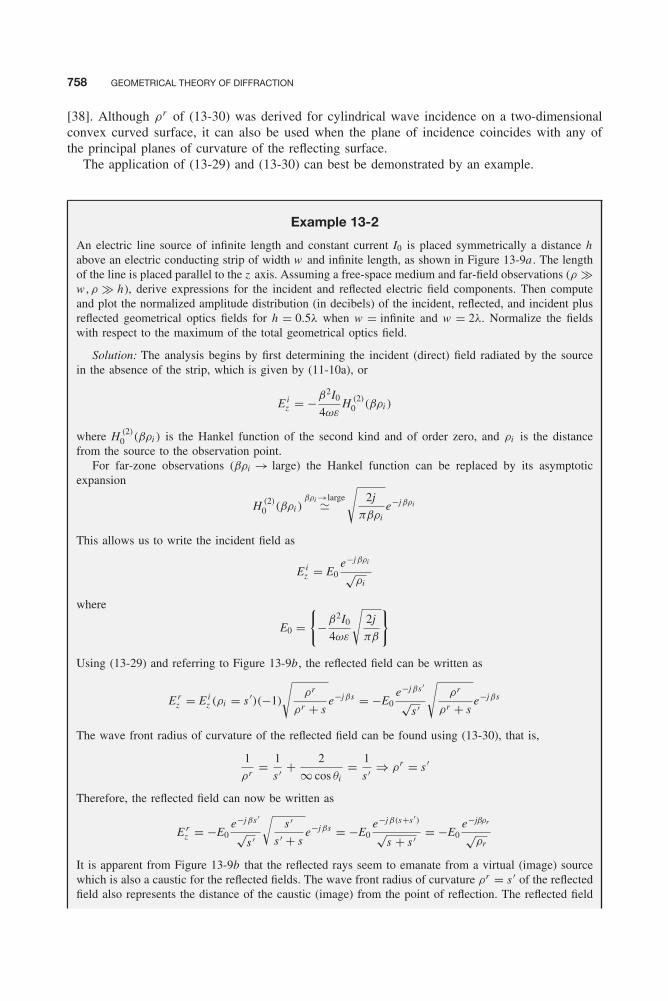
Balanis c13.tex V2 - 11/24/2011 12:45 A.M. Page 758
758 GEOMETRICAL THEORY OF DIFFRACTION
[38]. Although ρr of (13-30) was derived for cylindrical wave incidence on a two-dimensionalconvex curved surface, it can also be used when the plane of incidence coincides with any ofthe principal planes of curvature of the reflecting surface.
The application of (13-29) and (13-30) can best be demonstrated by an example.
Example 13-2
An electric line source of infinite length and constant current I0 is placed symmetrically a distance habove an electric conducting strip of width w and infinite length, as shown in Figure 13-9a . The lengthof the line is placed parallel to the z axis. Assuming a free-space medium and far-field observations (ρ �w , ρ � h), derive expressions for the incident and reflected electric field components. Then computeand plot the normalized amplitude distribution (in decibels) of the incident, reflected, and incident plusreflected geometrical optics fields for h = 0.5λ when w = infinite and w = 2λ. Normalize the fieldswith respect to the maximum of the total geometrical optics field.
Solution: The analysis begins by first determining the incident (direct) field radiated by the sourcein the absence of the strip, which is given by (11-10a), or
E iz = −β2I0
4ωεH (2)
0 (βρi )
where H (2)0 (βρi ) is the Hankel function of the second kind and of order zero, and ρi is the distance
from the source to the observation point.For far-zone observations (βρi → large) the Hankel function can be replaced by its asymptotic
expansion
H (2)0 (βρi )
βρi →large�√
2j
πβρie−jβρi
This allows us to write the incident field as
E iz = E0
e−jβρi
√ρi
where
E0 ={
−β2I0
4ωε
√2j
πβ
}Using (13-29) and referring to Figure 13-9b, the reflected field can be written as
E rz = E i
z (ρi = s ′)(−1)
√ρr
ρr + se−jβs = −E0
e−jβs ′
√s ′
√ρr
ρr + se−jβs
The wave front radius of curvature of the reflected field can be found using (13-30), that is,
1
ρr= 1
s ′ + 2
∞ cos θi= 1
s ′ ⇒ ρr = s ′
Therefore, the reflected field can now be written as
E rz = −E0
e−jβs ′
√s ′
√s ′
s ′ + se−jβs = −E0
e−jβ(s+s ′)√
s + s ′ = −E0e−jβρr
√ρr
It is apparent from Figure 13-9b that the reflected rays seem to emanate from a virtual (image) sourcewhich is also a caustic for the reflected fields. The wave front radius of curvature ρr = s ′ of the reflectedfield also represents the distance of the caustic (image) from the point of reflection. The reflected field

Balanis c13.tex V2 - 11/24/2011 12:45 A.M. Page 759
GEOMETRICAL OPTICS 759
(a)
(b)
hz
y
x
Line sourcer
ri
f
w2
w2
s′
s′
s
qi qr
a
ri
r
f
rr
rr
h
x
z
y
w2
n
Figure 13-9 Line source above a finite width strip. (a) Coordinate system. (b) Reflection geometry.
could also have been obtained very simply by using image theory. However, we chose to use theequations of geometrical optics to demonstrate the principles and applications of geometrical optics.
For far-field observations (ρi � w , ρi � h)
ρi = ρ − h cos(π
2− φ
)= ρ − h sin φ
ρr = ρ + h cos(π
2− φ
)= ρ + h sin φ
⎫⎪⎬⎪⎭ for phase variations
ρi � ρr � ρ for amplitude variations
Therefore, the incident (direct) and reflected fields can be reduced to
E iz = E0e+jβh sin φ e−jβρ
√ρ
, 0 ≤ φ ≤ π + α, 2π − α ≤ φ ≤ 2π
E rz = −E0e−jβh sin φ e−jβρ
√ρ
, α ≤ φ ≤ π − α

Balanis c13.tex V2 - 11/24/2011 12:45 A.M. Page 760
760 GEOMETRICAL THEORY OF DIFFRACTION
and the total field can be written as
E tz =
⎧⎪⎪⎪⎪⎪⎪⎪⎪⎪⎨⎪⎪⎪⎪⎪⎪⎪⎪⎪⎩
0 ≤ φ ≤ α,
E iz = E0e+jβh sin φ
e−jβρ
√ρ
π − α ≤ φ ≤ π + α,
2π − α ≤ φ ≤ 2π
E iz + E r
z = 2jE0 sin(βh sin φ)e−jβρ
√ρ
α ≤ φ ≤ π − α
0 π + α ≤ φ ≤ 2π − α
Normalized amplitude patterns for w = 2λ and h = 0.5λ computed using the preceding geometricaloptics fields in their respective regions, are plotted (in decibels) in Figure 13-10 where discontinuitiescreated along the incident and reflected shadow boundaries by the geometrical optics fields are apparent.The total amplitude pattern assuming an infinite ground plane is also displayed in Figure 13-10.
90°
Total field
Incident field
Reflected field
Total field (w = ∞)
w = 2λ, h = 0.5λ
60°
30°
330°
300°
270°
240°
−30 dB
−20 dB
−10 dB
0 dB
210°
180°
150°
120°
0°
f
Figure 13-10 Amplitude radiation pattern of an electric line source above a finite width strip.
In summary, geometrical optics methods approximate the fields by the leading term of theLuneberg–Kline expansion for large ω, but they fail along caustics. Improvements can be incorpo-rated into the solutions by finding higher-order terms E1(R1), E(R2), . . . in the Luneberg–Klineseries expansion. Higher-order Luneberg–Kline expansions have been derived for fields
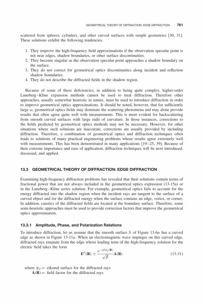
Balanis c13.tex V2 - 11/24/2011 12:45 A.M. Page 761
GEOMETRICAL THEORY OF DIFFRACTION: EDGE DIFFRACTION 761
scattered from spheres, cylinders, and other curved surfaces with simple geometries [30, 31].These solutions exhibit the following tendencies.
1. They improve the high-frequency field approximations if the observation specular point isnot near edges, shadow boundaries, or other surface discontinuities.
2. They become singular as the observation specular point approaches a shadow boundary onthe surface.
3. They do not correct for geometrical optics discontinuities along incident and reflectionshadow boundaries.
4. They do not describe the diffracted fields in the shadow region.
Because of some of these deficiencies, in addition to being quite complex, higher-orderLuneberg–Kline expansion methods cannot be used to treat diffraction. Therefore otherapproaches, usually somewhat heuristic in nature, must be used to introduce diffraction in orderto improve geometrical optics approximations. It should be noted, however, that for sufficientlylarge ω, geometrical optics fields may dominate the scattering phenomena and may alone provideresults that often agree quite well with measurements. This is more evident for backscatteringfrom smooth curved surfaces with large radii of curvature. In those instances, corrections tothe fields predicted by geometrical optics methods may not be necessary. However, for othersituations where such solutions are inaccurate, corrections are usually provided by includingdiffraction. Therefore, a combination of geometrical optics and diffraction techniques oftenleads to solutions of many practical engineering problems whose results agree extremely wellwith measurements. This has been demonstrated in many applications [19–25, 39]. Because oftheir extreme importance and ease of application, diffraction techniques will be next introduced,discussed, and applied.
13.3 GEOMETRICAL THEORY OF DIFFRACTION: EDGE DIFFRACTION
Examining high-frequency diffraction problems has revealed that their solutions contain terms offractional power that are not always included in the geometrical optics expression (13-15a) orin the Luneberg–Kline series solution. For example, geometrical optics fails to account for theenergy diffracted into the shadow region when the incident rays are tangent to the surface of acurved object and for the diffracted energy when the surface contains an edge, vertex, or corner.In addition, caustics of the diffracted fields are located at the boundary surface. Therefore, somesemi-heuristic approaches must be used to provide correction factors that improve the geometricaloptics approximation.
13.3.1 Amplitude, Phase, and Polarization Relations
To introduce diffraction, let us assume that the smooth surface S of Figure 13-6a has a curvededge as shown in Figure 13-11a . When an electromagnetic wave impinges on this curved edge,diffracted rays emanate from the edge whose leading term of the high-frequency solution for theelectric field takes the form
Ed (R) � e−jβψd (R)
√β
A(R) (13-31)
where ψd = eikonal surface for the diffracted raysA(R) = field factor for the diffracted rays
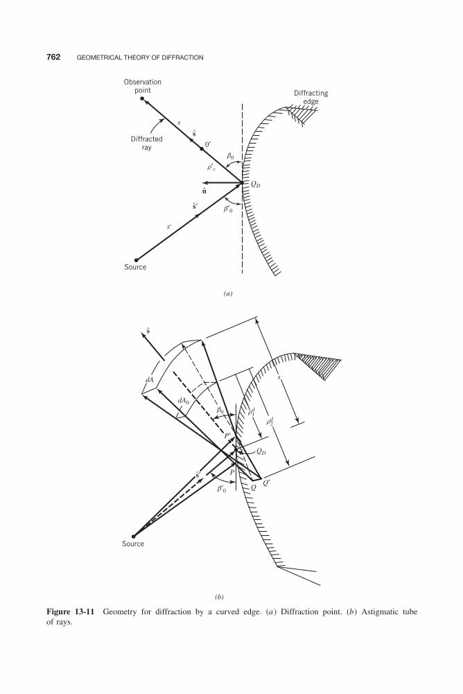
Balanis c13.tex V2 - 11/24/2011 12:45 A.M. Page 762
762 GEOMETRICAL THEORY OF DIFFRACTION
(a)
(b)
QD
Source
Diffractedray
Observationpoint Diffracting
edge
r′c
0′
s
s′
b0
b′0
QD
Q
P
s′
s
P′
dA
dA0
Q′
Source
rd1
rd2
s
b0
b′0
n
s
s′
Figure 13-11 Geometry for diffraction by a curved edge. (a) Diffraction point. (b) Astigmatic tubeof rays.
Balanis c13.tex V2 - 11/24/2011 12:45 A.M. Page 763
GEOMETRICAL THEORY OF DIFFRACTION: EDGE DIFFRACTION 763
Substituting (13-31) into (13-11) and (13-12), and referring to the geometry of Figure 13-11a ,it can be shown that the diffracted field can be written as
Ed (s) =[
A(0′)√β
e−jβψd (0′)]√
ρ ′cρc
(ρ ′c + s)(ρc + s)
e−jβs
Ed (s) = [Ed (0′)]
√ρ ′
cρc
(ρ ′c + s)(ρc + s)
e−jβs (13-32)
where Ed (0′) = diffracted field at the reference point 0′s = distance along the diffracted ray from the reference point 0′
ρ ′c = distance from diffraction point QD (first caustic of diffracted field) to reference
point 0′ρc = distance between the second caustic of diffracted field and reference point 0′
It would have been more convenient to choose the reference point 0′ to coincide with thediffraction point QD , located on the diffracting edge. However, like the geometrical optics rays,the diffracted rays form an astigmatic tube of the form shown in Figure 13-11b where thecaustic line PP ′ coincides with the diffracting edge. Because the diffraction point is a causticof the diffracted field, it is initially more straightforward to choose the reference point away fromthe edge diffraction caustic QD . However, the diffracted field of (13-32) should be independent ofthe location of the reference point 0′, including ρ ′
c = 0. Therefore, the diffracted field of (13-32)must be such that
limρ′
c→0Ed (0′)
√ρ ′
c = finite (13-33)
and must be equal to
limρ′
c→0Ed (0′)
√ρ ′
c = Ei (QD ) • D (13-33a)
where Ei (QD )= incident field at the point of diffractionD = dyadic diffraction coefficient (analogous to dyadic reflection coefficient)
Using (13-33a), the diffracted field of (13-32) reduces to
Ed (s) = limρ′
c→0
{[Ed (0′)
√ρ ′
c]√
ρc
(ρ ′c + s)(ρc + s)
e−jβs
}Ed (s) = Ei (QD ) • D
√ρc
s(ρc + s)e−jβs (13-34)
which has the form
Ed(s) = Ei (QD )︸ ︷︷ ︸ • D︸ ︷︷ ︸ A(ρc , s)︸ ︷︷ ︸ e−jβs︸ ︷︷ ︸Field at Diffraction Spatial Phase
reference coefficient attenuation factorpoint (usually a (spreading,
dyadic) divergence)factor
(13-34a)
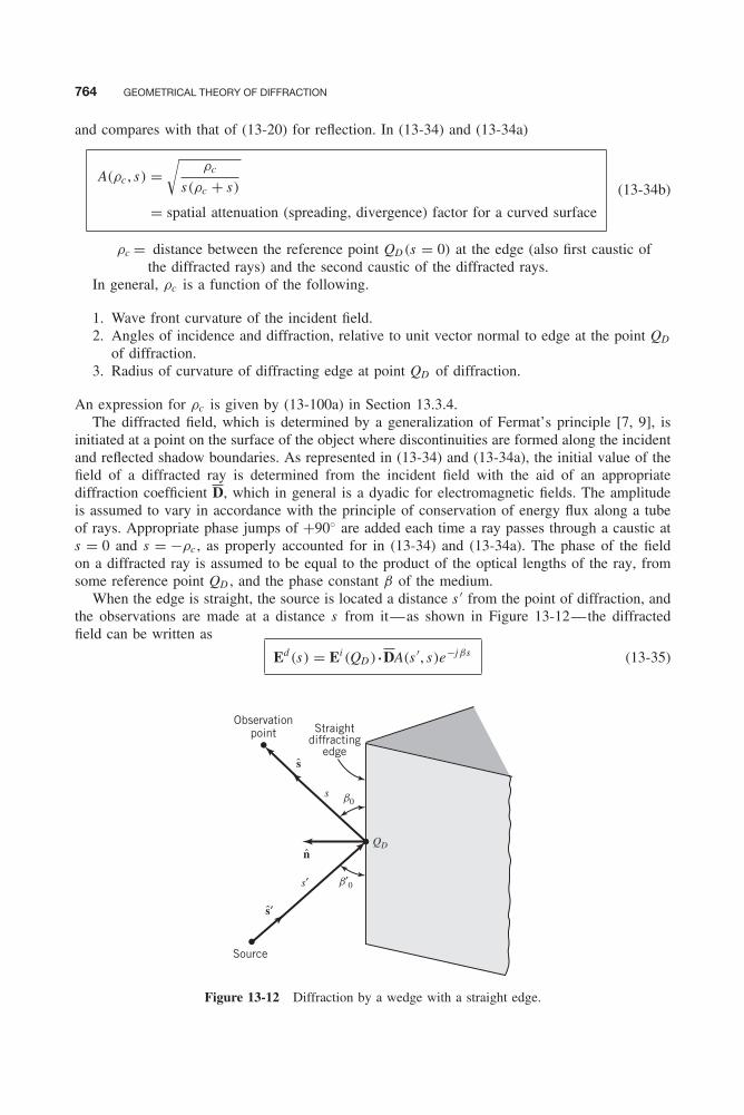
Balanis c13.tex V2 - 11/24/2011 12:45 A.M. Page 764
764 GEOMETRICAL THEORY OF DIFFRACTION
and compares with that of (13-20) for reflection. In (13-34) and (13-34a)
A(ρc , s) =√
ρc
s(ρc + s)
= spatial attenuation (spreading, divergence) factor for a curved surface
(13-34b)
ρc = distance between the reference point QD (s = 0) at the edge (also first caustic ofthe diffracted rays) and the second caustic of the diffracted rays.
In general, ρc is a function of the following.
1. Wave front curvature of the incident field.2. Angles of incidence and diffraction, relative to unit vector normal to edge at the point QD
of diffraction.3. Radius of curvature of diffracting edge at point QD of diffraction.
An expression for ρc is given by (13-100a) in Section 13.3.4.The diffracted field, which is determined by a generalization of Fermat’s principle [7, 9], is
initiated at a point on the surface of the object where discontinuities are formed along the incidentand reflected shadow boundaries. As represented in (13-34) and (13-34a), the initial value of thefield of a diffracted ray is determined from the incident field with the aid of an appropriatediffraction coefficient D, which in general is a dyadic for electromagnetic fields. The amplitudeis assumed to vary in accordance with the principle of conservation of energy flux along a tubeof rays. Appropriate phase jumps of +90◦ are added each time a ray passes through a caustic ats = 0 and s = −ρc , as properly accounted for in (13-34) and (13-34a). The phase of the fieldon a diffracted ray is assumed to be equal to the product of the optical lengths of the ray, fromsome reference point QD , and the phase constant β of the medium.
When the edge is straight, the source is located a distance s ′ from the point of diffraction, andthe observations are made at a distance s from it—as shown in Figure 13-12—the diffractedfield can be written as
Ed (s) = Ei (QD ) • DA(s ′, s)e−jβs (13-35)
Observationpoint
Source
Straightdiffracting
edges
s
s′
s′
b0
b′0
QDn
Figure 13-12 Diffraction by a wedge with a straight edge.
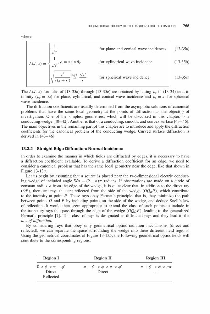
Balanis c13.tex V2 - 11/24/2011 12:45 A.M. Page 765
GEOMETRICAL THEORY OF DIFFRACTION: EDGE DIFFRACTION 765
where
A(s ′, s) =
⎧⎪⎪⎪⎪⎪⎪⎪⎪⎪⎪⎨⎪⎪⎪⎪⎪⎪⎪⎪⎪⎪⎩
1√s
for plane and conical wave incidences
1√ρ
, ρ = s sin β0 for cylindrical wave incidence√s ′
s(s + s ′)s�s ′�
√s ′
sfor spherical wave incidence
(13-35a)
(13-35b)
(13-35c)
The A(s ′, s) formulas of (13-35a) through (13-35c) are obtained by letting ρc in (13-34) tend toinfinity (ρc = ∞) for plane, cylindrical, and conical wave incidence and ρc = s ′ for sphericalwave incidence.
The diffraction coefficients are usually determined from the asymptotic solutions of canonicalproblems that have the same local geometry at the points of diffraction as the object(s) ofinvestigation. One of the simplest geometries, which will be discussed in this chapter, is aconducting wedge [40–42]. Another is that of a conducting, smooth, and convex surface [43–46].The main objectives in the remaining part of this chapter are to introduce and apply the diffractioncoefficients for the canonical problem of the conducting wedge. Curved surface diffraction isderived in [43–46].
13.3.2 Straight Edge Diffraction: Normal Incidence
In order to examine the manner in which fields are diffracted by edges, it is necessary to havea diffraction coefficient available. To derive a diffraction coefficient for an edge, we need toconsider a canonical problem that has the same local geometry near the edge, like that shown inFigure 13-13a .
Let us begin by assuming that a source is placed near the two-dimensional electric conduct-ing wedge of included angle WA = (2 − n)π radians. If observations are made on a circle ofconstant radius ρ from the edge of the wedge, it is quite clear that, in addition to the direct ray(OP ), there are rays that are reflected from the side of the wedge (OQRP), which contributeto the intensity at point P . These rays obey Fermat’s principle, that is, they minimize the pathbetween points O and P by including points on the side of the wedge, and deduce Snell’s lawof reflection. It would then seem appropriate to extend the class of such points to include inthe trajectory rays that pass through the edge of the wedge (OQD P), leading to the generalizedFermat’s principle [7]. This class of rays is designated as diffracted rays and they lead to thelaw of diffraction.
By considering rays that obey only geometrical optics radiation mechanisms (direct andreflected), we can separate the space surrounding the wedge into three different field regions.Using the geometrical coordinates of Figure 13-13b, the following geometrical optics fields willcontribute to the corresponding regions:
Region I Region II Region III
0 < φ < π − φ′ π − φ′ < φ < π < φ′ π + φ′ < φ < nπ
Direct Direct · · ·Reflected
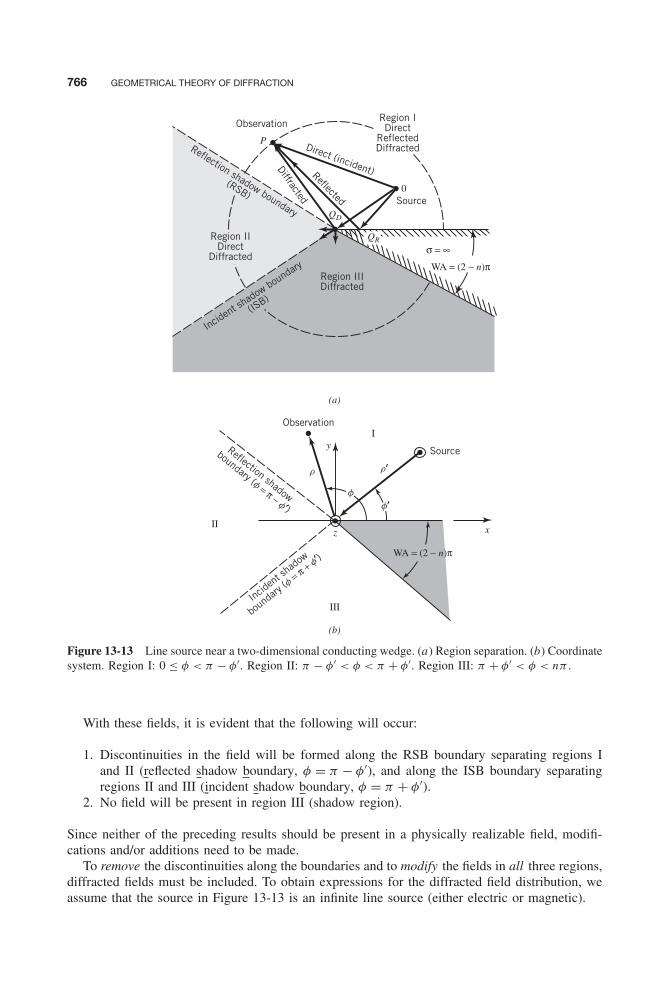
Balanis c13.tex V2 - 11/24/2011 12:45 A.M. Page 766
766 GEOMETRICAL THEORY OF DIFFRACTION
Observation
II
III
I
Reflection shadow
boundary (f = π − f′)
Incide
nt sh
adow
boun
dary
(f = π + f′)
Source
x
y
z
r r′
WA = (2 − n)π
f
f′
(a)
(b)
Region IDirect
ReflectedDiffracted
Source
Observation
Reflection shadow boundary
(RSB)
Direct (incident)Reflected
Diffracted
QD
P
0
WA = (2 − n)π
σ = ∞ Region II
DirectDiffracted
Region IIIDiffracted
Incident s
hadow boundary
(ISB)
QR
Figure 13-13 Line source near a two-dimensional conducting wedge. (a) Region separation. (b) Coordinatesystem. Region I: 0 ≤ φ < π − φ′. Region II: π − φ′ < φ < π + φ′. Region III: π + φ′ < φ < nπ .
With these fields, it is evident that the following will occur:
1. Discontinuities in the field will be formed along the RSB boundary separating regions Iand II (reflected shadow boundary, φ = π − φ′), and along the ISB boundary separatingregions II and III (incident shadow boundary, φ = π + φ′).
2. No field will be present in region III (shadow region).
Since neither of the preceding results should be present in a physically realizable field, modifi-cations and/or additions need to be made.
To remove the discontinuities along the boundaries and to modify the fields in all three regions,diffracted fields must be included. To obtain expressions for the diffracted field distribution, weassume that the source in Figure 13-13 is an infinite line source (either electric or magnetic).

Balanis c13.tex V2 - 11/24/2011 12:45 A.M. Page 767
GEOMETRICAL THEORY OF DIFFRACTION: EDGE DIFFRACTION 767
The fields of an electric line source satisfy the homogeneous Dirichlet boundary conditionsEz = 0 on both faces of the wedge and the fields of the magnetic line source satisfy the homoge-neous Neumann boundary condition ∂Ez /∂φ = 0 or Hz = 0 on both faces of the wedge. The facesof the wedge are formed by two semi-infinite intersecting planes. The infinitely long line sourceis parallel to the edge of the wedge, and its position is described by the coordinate (ρ ′, φ′). Thetypical field point is denoted by (ρ, φ), as shown in Figure 13-13b. The line source is assumedto have constant current.
Initially, we will consider only normal incidence diffraction by a straight edge, as shown inFigure 13-14. For this situation, the plane of diffraction is perpendicular to the edge of the wedge.Oblique incidence diffraction (Figure 13-31) and curved-edge diffraction (Figure 13-35) will bediscussed, respectively, in Sections 13.3.3 and 13.3.4.
The diffraction coefficient for the geometries of Figures 13-13 and 13-14 is obtained by [42]:
1. Finding the Green’s function solution in the form of an infinite series using modal techniquesand then approximating it for large values of βρ (far-field observations).
2. Converting the infinite series Green’s function solution into an integral.3. Performing, on the integral Green’s function, a high-frequency asymptotic expansion (in
inverse powers of βρ) using standard techniques, such as the method of steepest descent.
An abbreviated derivation of this procedure will now be presented.
A. Modal Solution Using modal techniques, the total radiation electric field for an electricline source of current Ie was found in Chapter 11, Section 11.6.3, to be that of (11-207a), or
E ez = −ωμIe
4G ⇒ He = − 1
jωμ∇ × E (13-36)
and the total magnetic field for a magnetic line source of current Im to be that of (11-207b), or
H mz = ωεIm
4G ⇒ Em = + 1
jωε∇ × H (13-37)
Incidentray
Plane ofdiffracted
rays
Edge
Wedge
s′
QD
WA = (2 − n)π
Figure 13-14 Wedge plane of diffraction for normal incidence.
Balanis c13.tex V2 - 11/24/2011 12:45 A.M. Page 768
768 GEOMETRICAL THEORY OF DIFFRACTION
where G is referred to as the Green’s function, and it is given by (11-208a) as
G = 1
n
∞∑m=0
εmJm/n(βρ)H (2)m/n(βρ ′)
[cos
m
n(φ − φ′) ± cos
m
n(φ + φ′)
]for ρ ≤ ρ ′ (13-38)
εm ={
1 m = 0
2 m �= 0(13-38a)
For the case ρ ≥ ρ ′, ρ and ρ ′ are interchanged. The plus sign between the two cosine termsis used if the boundary condition is of the homogeneous Neumann type, ∂G/∂φ = 0, on bothfaces of the wedge. For the homogeneous Dirichlet boundary condition, G = 0, on both facesof the wedge, the minus sign is used. In acoustic terminology, the Neumann boundary conditionis referred to as hard polarization and the Dirichlet boundary condition is referred to as the softpolarization. This series is an exact solution to the time-harmonic, inhomogeneous wave equationof a radiating line source and wedge embedded in a linear, isotropic, homogeneous, losslessmedium.
B. High-Frequency Asymptotic Solution Many times it is necessary to determine the totalradiation field when the line source is far removed from the vertex of the wedge. In such cases,(13-38) can be simplified by replacing the Hankel function by the first term of its asymptoticexpansion, that is, by
H (2)m/n(βρ ′)
βρ′→∞�√
2
πβρ ′ e−j [βρ′−π/4−(m/n)(π/2)] (13-39)
This substitution reduces G to
G =√
2
πβρ ′ e−j (βρ′−π/4) 1
n
∞∑m=0
εmJm/n(βρ)e+j (m/n)(π/2)
×[cos
m
n(φ − φ′) ± cos
m
n(φ + φ′)
]G =
√2
πβρ ′ e−j (βρ′−π/4)F (βρ) (13-40)
where
F (βρ) = 1
n
∞∑m=0
εmJm/n(βρ)e+j (m/n)(π/2)[cos
m
n(φ − φ′) ± cos
m
n(φ + φ′)
](13-40a)
F (βρ) is used to represent either the normalized total E ez , when the source is an electric line (soft
polarization), or H mz , when the source is a magnetic line (hard polarization).
The infinite series of (13-40a) converges rapidly for small values of βρ. For example, ifβρ is less than 1, less than 15 terms are required to achieve a five-significant-figure accuracy.However, at least 40 terms should be included when βρ is 10 to achieve the five-significant-figureaccuracy. To demonstrate the variations of (13-40a), the patterns of a unit amplitude plane waveof hard polarization incident upon a half plane (n = 2) and 90◦ wedge (n = 3/2), computedusing (13-40a), are shown in Figure 13-15. Computed patterns for the soft polarization are shownin Figure 13-16.
Whereas (13-40a) represents the normalized total field, in the space around a wedge of includedangle WA = (2 − n)π , of a unity amplitude plane wave incident upon the wedge, the field of a
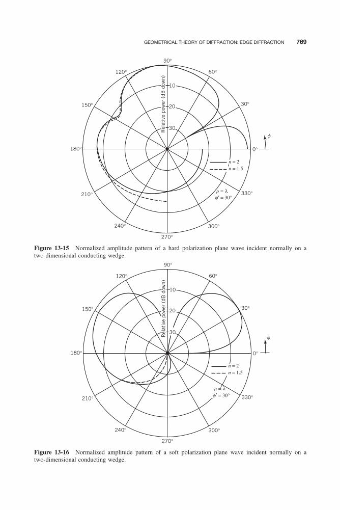
Balanis c13.tex V2 - 11/24/2011 12:45 A.M. Page 769
GEOMETRICAL THEORY OF DIFFRACTION: EDGE DIFFRACTION 769
Rel
ativ
e po
wer
(dB
dow
n)
120°
90°
60°
10
20
30
30°
0°
330°
300°
270°
240°
210°
180°
150°
f′ = 30°
n = 1.5n = 2
r = λ
f
Figure 13-15 Normalized amplitude pattern of a hard polarization plane wave incident normally on atwo-dimensional conducting wedge.
fRel
ativ
e po
wer
(dB
dow
n)
120°
90°
60°
10
20
30
30°
0°
330°
300°
270°
240°
210°
180°
150°
f′ = 30°r = λ
n = 1.5n = 2
Figure 13-16 Normalized amplitude pattern of a soft polarization plane wave incident normally on atwo-dimensional conducting wedge.
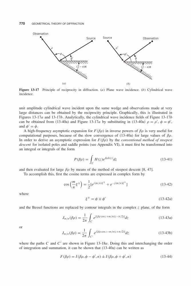
Balanis c13.tex V2 - 11/24/2011 12:45 A.M. Page 770
770 GEOMETRICAL THEORY OF DIFFRACTION
(a)
Source
Observation
(2 − n)π (2 − n)π
r
f′f
(b)
Source Observation
r′
f
f′
Figure 13-17 Principle of reciprocity in diffraction. (a) Plane wave incidence. (b) Cylindrical waveincidence.
unit amplitude cylindrical wave incident upon the same wedge and observations made at verylarge distances can be obtained by the reciprocity principle. Graphically, this is illustrated inFigures 13-17a and 13-17b. Analytically, the cylindrical wave incidence fields of Figure 13-17bcan be obtained from (13-40a) and Figure 13-17a by substituting in (13-40a) ρ = ρ ′, φ = φ′,and φ′ = φ.
A high-frequency asymptotic expansion for F (βρ) in inverse powers of βρ is very useful forcomputational purposes, because of the slow convergence of (13-40a) for large values of βρ.In order to derive an asymptotic expression for F (βρ) by the conventional method of steepestdescent for isolated poles and saddle points (see Appendix VI), it must first be transformed intoan integral or integrals of the form
P(βρ) =∫
CH (z )eβρh(z )dz (13-41)
and then evaluated for large βρ by means of the method of steepest descent [8, 47].To accomplish this, first the cosine terms are expressed in complex form by
cos(m
nξ∓
)= 1
2[ej (m/n)ξ∓ + e−j (m/n)ξ∓
] (13-42)
whereξ∓ = φ ∓ φ′ (13-42a)
and the Bessel functions are replaced by contour integrals in the complex z plane, of the form
Jm/n(βρ) = 1
2π
∫C
ej [βρ cos z+m/n(z−π/2)]dz (13-43a)
or
Jm/n(βρ) = 1
2π
∫C ′
ej [βρ cos z−m/n(z+π/2)]dz (13-43b)
where the paths C and C ′ are shown in Figure 13-18a . Doing this and interchanging the orderof integration and summation, it can be shown that (13-40a) can be written as
F (βρ) = I (βρ, φ − φ′, n) ± I (βρ, φ + φ′, n) (13-44)
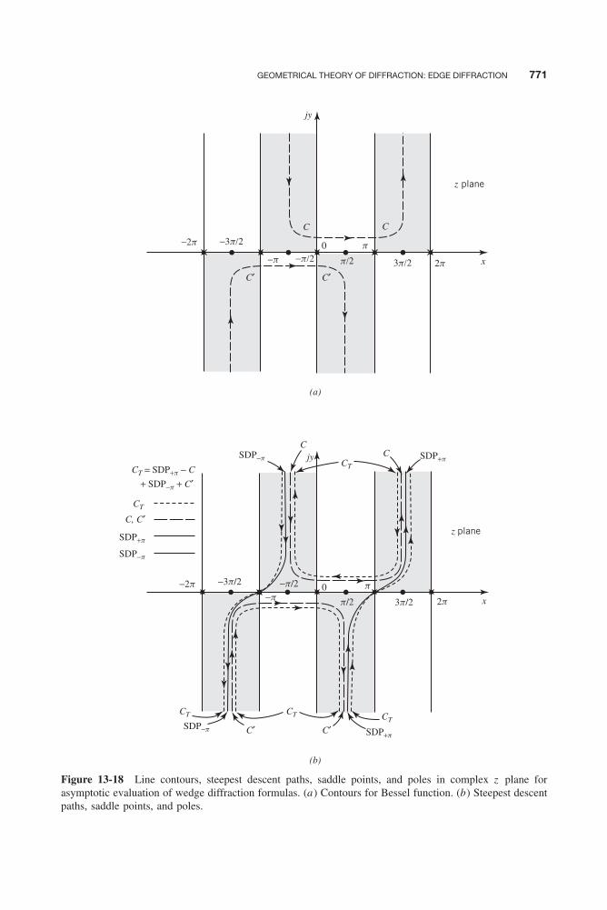
Balanis c13.tex V2 - 11/24/2011 12:45 A.M. Page 771
GEOMETRICAL THEORY OF DIFFRACTION: EDGE DIFFRACTION 771
(a)
(b)
z plane
x
jy
0−2p
2p
−3p/2
3p/2−p/2p
−p
C C
p/2
C′ C′
2p
z plane
−3p/2
SDP−p
SDP−p
SDP+p
SDP+p
C
C′
CT CTCT
C′
CTCT = SDP+p − C
SDP+p
SDP−p
CT
+ SDP−p + C′
C, C′
C
0−p
−2p p
3p/2 x
jy
−p/2
p/2
Figure 13-18 Line contours, steepest descent paths, saddle points, and poles in complex z plane forasymptotic evaluation of wedge diffraction formulas. (a) Contours for Bessel function. (b) Steepest descentpaths, saddle points, and poles.
Balanis c13.tex V2 - 11/24/2011 12:45 A.M. Page 772
772 GEOMETRICAL THEORY OF DIFFRACTION
where
I (βρ, ξ∓, n) = 1
2πn
∫C
ejβρ cos z∞∑
m=1
e+j (m/n)(ξ∓+z )dz
+ 1
2πn
∫C ′
ejβρ cos z∞∑
m=0
e−j (m/n)(ξ∓+z )dz (13-44a)
with ξ∓ = φ ∓ φ′.Using the series expansions of
− 1
1 − x−1= x(1 + x + x 2 + x 3 + · · · ) =
∞∑m=1
x m (13-45a)
1
1 − x−1= 1 + x−1 + x−2 + x−3 + · · · =
∞∑m=0
x−m (13-45b)
and that
1
1 − e−j (ξ∓+z )/n= ej (ξ∓+z )/2n
ej (ξ∓+z )/2n − e−j (ξ∓+z )/2n= 1
2+ 1
2jcot
(ξ∓ + z
2n
)(13-46)
we can ultimately write (13-44) or (13-40a) as
F (βρ) = 1
4π jn
∫(C ′−C )
cot
(φ − φ′ + z
2n
)ejβρ cos z dz
± 1
4π jn
∫(C ′−C )
cot
(φ + φ′ + z
2n
)ejβρ cos z dz (13-47)
where the negative sign before C indicates that this integration path is to be traversed in thedirection opposite to that shown in Figure 13-18a . It is now clear that F (βρ) has been written inan integral of the form of (13-41), which can be evaluated asymptotically by contour integrationand by the method of steepest descent.
C. Method of Steepest Descent Equation 13-47 can also be written as
F (βρ) = F1(βρ) ± F2(βρ) (13-48)
F1(βρ) = 1
4π jn
∫(C ′−C )
H1(z )eβρh1(z )dz (13-48a)
F2(βρ) = 1
4π jn
∫(C ′−C )
H2(z )eβρh2(z )dz (13-48b)
H1(z ) = cot
[(φ − φ′) + z
2n
]= cot
(ξ− + z
2n
)(13-48c)
H2(z ) = cot
[(φ + φ′) + z
2n
]= cot
(ξ+ + z
2n
)(13-48d)
h1(z ) = h2(z ) = j cos(z ) (13-48e)
The evaluation of (13-48) can be accomplished by evaluating separately (13-48a) and (13-48b)and summing the results. Let us examine first the evaluation of (13-48a) in detail. A similarprocedure can be used for (13-48b).
Balanis c13.tex V2 - 11/24/2011 12:45 A.M. Page 773
GEOMETRICAL THEORY OF DIFFRACTION: EDGE DIFFRACTION 773
Using the complex z -plane closed contour CT , we can write by referring to Figure 13-18bthat
1
4π jn
∮CT
H1(z )eβρh1(z )dz = 1
4π jn
∫(C ′−C )
H1(z )eβρh1(z )dz
+ 1
4π jn
∫SDP+π
H1(z )eβρh1(z )dz
+ 1
4π jn
∫SDP−π
H1(z )eβρh1(z )dz (13-49)
The closed contour CT is equal to the sum of
CT = C ′ + SDP+π − C + SDP−π (13-49a)
where SDP±π is used to represent the steepest descent paths passing through the saddle points±π . We can rewrite (13-49) as
F1(βρ) = 1
4π jn
∫(C ′−C )
H1(z )eβρh1(z )dz = 1
4π jn
∮CT
H1(z )eβρh1(z )dz
− 1
4π jn
∫SDP+π
H1(z )eβρh1(z )dz − 1
4π jn
∫SDP−π
H1(z )eβρh1(z )dz (13-50)
which is the same as (13-48a). Therefore, (13-48a) can be integrated by evaluating the three termson the right side of (13-50). The closed contour of the first term on the right side of (13-50)is evaluated using residue calculus and the other two terms are evaluated using the method ofsteepest descent. When evaluated, it will be shown that the first term on the right side of (13-50)will represent the incident geometrical optics and the other two terms will represent what will bereferred to as the incident diffracted field. A similar interpretation will be given when (13-48b)is evaluated; it represents the reflected geometrical optics and reflected diffracted fields.
Using residue calculus, we can write the first term on the right side of (13-50) as [48]
1
4π jn
∮CT
H1(z )eβρh1(z )dz = 2π j∑
p
Res(z = zp)
= 2π j∑
p
(residues of the poles enclosed by CT ) (13-51)
To evaluate (13-51), we first rewrite it as
1
4π jn
∮CT
H1(z )eβρh1(z )dz
= 1
4π jn
∮CT
cot
[(φ − φ′) + z
2n
]ejβρ cos(z )dz
=∮
CT
1
4π jncot
[(φ − φ′) + z
2n
]ejβρ cos(z )dz =
∮CT
N (z )
D(z )dz (13-52)

Balanis c13.tex V2 - 11/24/2011 12:45 A.M. Page 774
774 GEOMETRICAL THEORY OF DIFFRACTION
where
N (z )
D(z )=
cos[
(φ−φ′)+z2n
]ejβρ cos(z )
4π jn sin[
(φ−φ′)+z2n
] (13-52a)
N (z ) = cos
[(φ − φ′) + z
2n
]ejβρ cos(z ) (13-52b)
D(z ) = 4π jn sin
[(φ − φ′) + z
2n
](13-52c)
Equation 13-52 has simple poles that occur when[(φ − φ′) + z
2n
]z=zp
= πN N = 0, ±1, ±2, . . . (13-53)
orzp = −(φ − φ′) + 2πnN (13-53a)
provided that−π ≤ zp = −(φ − φ′) + 2πnN ≤ +π (13-53b)
Using residue calculus, the residues of (13-51) or (13-52) for simple poles (no branch points,etc.) can be found using [48]
Res(z = zp) = N (z )
dD(z )dz
z=zp
= N (z )
D ′(z )
∣∣∣∣z=zp
(13-54)
where
N (z )|z=zp = cos
[(φ − φ′) + z
2n
]ejβρ cos(z )
∣∣∣∣z=−(φ−φ′)+2πnN
= cos(πN )ejβρ cos[−(φ−φ′)+2πnN ] (13-54a)
D ′(z )|z=zp = 2π j cos
[(φ − φ′) + z
2n
]∣∣∣∣z=−(φ−φ′)+2πnN
= 2π j cos(πN ) (13-54b)
Thus, (13-54) and (13-51) can be written, respectively, as
Res(z = zp) = 1
2π jejβρ cos[−(φ−φ′)+2πnN ] (13-55a)
1
4π jn
∮CT
H1(z )eβρh1(z )dz = ejβρ cos[−(φ−φ′)+2πnN ]U [π − | − (φ − φ′) + 2πnN |] (13-55b)
The U (t − t0) function in (13-55b) is a unit step function defined as
U (t − t0) =
⎧⎪⎨⎪⎩1 t > t012 t = t00 t < t0
(13-56)
The unit step function is introduced in (13-55b) so that (13-53b) is satisfied. When z = ±π ,(13-53b) is expressed as
2πnN + − (φ − φ′) = +π (13-57a)
Balanis c13.tex V2 - 11/24/2011 12:45 A.M. Page 775
GEOMETRICAL THEORY OF DIFFRACTION: EDGE DIFFRACTION 775
for zp = +π and
2πnN − − (φ − φ′) = −π (13-57b)
for zp = −π . For the principal value of N (N ± = 0), (13-55b) reduces to
F1(βρ)|CT = 1
4π jn
∮CT
H1(z )eβρh1(z )dz = ejβρ cos(φ−φ′)U [π − | − (φ − φ′|] (13-58)
This is referred to as the incident geometrical optics field, and it exists provided |φ − φ′| < π .This completes the evaluation of (13-51). Let us now evaluate the other two terms on the rightside of (13-50).
In evaluating the last two terms on the right side of (13-50), the contributions from all thesaddle points along the steepest descent paths must be accounted for. In this situation, however,only saddle points at z = zs = ±π occur. These are found by taking the derivative of (13-48e)and setting it equal to zero. Doing this leads to
h ′1(z )|z=zs = −j sin(z )|z=zs = 0 ⇒ zs = ±π (13-59)
The form used to evaluate the last two terms on the right side of (13-50) depends on whether thepoles of (13-53a), which contribute to the geometrical optics field, are near or far removed fromthe saddle points at z = zs = ±π . Let us first evaluate each of the last two terms on the rightside of (13-50) when the poles of (13-53a) are far removed from the saddle point of (13-59).
When the poles of (13-53a) are far removed from the saddle points of (13-59), then the last twoterms on the right side of (13-50) are evaluated using the conventional steepest descent methodfor isolated poles and saddle points. Doing this, we can write the last two terms on the right sideof (13-50), using the saddle points of (13-59), as [8, 47]
1
4π jn
∫SDP+π
H1(z )eβρh1(z )dzβρ→large� 1
4π jn
∣∣∣∣∣√
2π
−βρh ′′1 (zs = +π)
∣∣∣∣∣ ejπ/4
× H1(zs = +π)eβρh1(zs =π) = e−jπ/4
2n√
2πβcot
[π + (φ − φ′)
2n
]e−jβρ
√ρ
(13-60a)
1
4π jn
∫SDP−π
H1(z )eβρh1(z )dzβρ→large� 1
4π jn
∣∣∣∣∣√
2π
−βρh ′′1 (zs = −π)
∣∣∣∣∣ e−j 3π/4
× H1(zs = −π)eβρh1(zs =−π) = e−jπ/4
2n√
2πβcot
[π − (φ − φ′)
2n
]e−jβρ
√ρ
(13-60b)
Combining (13-60a) and (13-60b), it can be shown that the sum of the two can be written as
F1(βρ)|SDP±π= − 1
4π jn
∫SDP+π
H1(z )eβρh1(z )dz − 1
4π jn
∫SDP−π
H1(z )eβρh1(z )dz
� e−jπ/4
√2πβ
1
nsin
(π
n
)cos
(π
n
)− cos
(φ − φ′
n
) e−jβρ
√p
(13-61)
Balanis c13.tex V2 - 11/24/2011 12:45 A.M. Page 776
776 GEOMETRICAL THEORY OF DIFFRACTION
This is referred to as the incident diffracted field, and its form, as given by (13-61), is validprovided that the poles of (13-53a) are not near the saddle points of (13-59). Another way to saythis is that (13-61) is valid provided that the observations are not made at or near the incidentshadow boundary of Figure 13-13. When the observations are made at the incident shadowboundary φ − φ′ = π , (13-61) becomes infinite. Therefore, another form must be used for suchsituations.
Following a similar procedure for the evaluation of (13-48b), it can be shown that its contribu-tions along CT and the saddle points can be written in forms corresponding to (13-58) and (13-61)for the evaluation of (13-48a). Thus, we can write that
F2(βρ)|CT = 1
4π jn
∮CT
H2(z )eβρh2(z )dz
= ejβρ cos(φ+φ′)U [π − (φ + φ′)]
(13-62a)
F2(βρ)|SDP±π = − 1
4π jn
∫SDP+π
H2(z )eβρh2(z )dz − 1
4π jn
∫SDP−π
H2(z )eβρh2(z )dz
� e−jπ/4
√2πβ
1
nsin
(π
n
)cos
(π
n
)− cos
(φ + φ′
n
) e−jβρ
√ρ
(13-62b)
Equation 13-62b is valid provided the observations are not made at or near the reflection shadowboundary of Figure 13-13. When the observations are made at the reflection shadow boundaryφ + φ′ = π , (13-62b) becomes infinite. Another form must be used for such cases.
If the poles of (13-53a) are near the saddle points of (13-59), then the conventional steepestdescent method of (13-60a) and (13-60b) cannot be used for the evaluation of the last two termsof (13-50) for F1(βρ), and similarly for F2(βρ) of (13-48b). One method that can be used forsuch cases is the so-called Pauli-Clemmow modified method of steepest descent [8, 47]. Themain difference between the two methods is that the solution provided by the Pauli-Clemmowmodified method of steepest descent has an additional discontinuous function that compensatesfor the singularity along the corresponding shadow boundaries introduced by the conventionalsteepest-descent method for isolated poles and saddle points. This factor is usually referred to asthe transition function, and it is proportional to a Fresnel integral. Away from the correspondingshadow boundaries these transition functions are nearly unity, and the Pauli-Clemmow modifiedmethod of steepest descent reduces to the conventional method of steepest descent.
It can be shown that by using the Pauli-Clemmow modified method of steepest descent,(13-60a) and (13-60b) are evaluated using
1
4π jn
∫SDP+π
H1(z )eβρh1(z )dzβρ→large� 1
4π jn
∣∣∣∣∣√
2π
−βρh ′′1 (zs = +π)
∣∣∣∣∣× ejπ/4H1(zs = +π)eβρh1(zs =π)F [βρg+(ξ−)]
= e−jπ/4
2n√
2πβcot
[π + (φ − φ′)
2n
]× F [βρg+(φ − φ′)]
e−jβρ
√ρ
(13-63a)

Balanis c13.tex V2 - 11/24/2011 12:45 A.M. Page 777
GEOMETRICAL THEORY OF DIFFRACTION: EDGE DIFFRACTION 777
1
4π jn
∫SDP−π
H1(z )eβρh1(z )dzβρ→large� 1
4π jn
∣∣∣∣∣√
2π
−βρh ′′1 (zs = −π)
∣∣∣∣∣× e−j 3π/4H1(zs = −π)eβρh1(zs =−π)F [βρg−(ξ−)]
= e−jπ/4
2n√
2πβcot
[π − (φ − φ′)
2n
]× F [βρg−(φ − φ′)]
e−jβρ
√ρ
(13-63b)
where
F [βρg±(φ − φ′)] ≡ j [h1(zs) − h1(zp)]
≡ measure of separation between saddle points and poles
= 2j∣∣∣√βρg±(φ − φ′)
∣∣∣e+jβρg±∫ ∞√
βρg±(φ−φ′)e−jτ2
dτ (13-63c)
g±(φ − φ′) = 1 + cos[(φ − φ′) − 2πnN ±] (13-63d)
2πnN + − (φ − φ′) = +π (13-63e)
2πnN − − (φ − φ′) = −π (13-63f)
Similar forms are used for the evaluation of F2(βρ) along the steepest descent path using thePauli–Clemmow modified method of steepest descent. In (13-63e) and (13-63f), N ± representsinteger values that most closely satisfy the equalities. Such a procedure accounts for the polesthat are nearest to the saddle point at x = ±π , either from outside or within −π ≤ x ≤ +π , ofFigure 13-18b. In general, there are two such poles associated with F1(βρ) and two with F2(βρ).More details about the transition function will follow.
D. Geometrical Optics and Diffracted Fields After the contour integration and the methodof steepest descent have been applied in the evaluation of (13-47), as discussed in the previoussection, it can be shown that for large values of βρ, (13-47) is separated into
F (βρ) = FG(βρ) + FD (βρ) (13-64)
where FG(βρ) and FD (βρ) represent, respectively, the total geometrical optics and total diffractedfields created by the incidence of a unit amplitude plane wave upon a two-dimensional wedge,as shown in Figure 13-13.
In summary, then, the geometrical optics fields (FG) and the diffracted fields (FD ) are repre-sented, respectively, by
Geometrical Optics Fields
Incident GO Reflected GO Region
FG(βρ) =⎧⎨⎩ ejβρ cos(φ−φ′) ± ejβρ cos(φ+φ′) 0 < φ < π − φ′
ejβρ cos(φ−φ′) π − φ′ < φ < π + φ′0 π + φ′ < φ < nπ
(13-65)
Balanis c13.tex V2 - 11/24/2011 12:45 A.M. Page 778
778 GEOMETRICAL THEORY OF DIFFRACTION
Diffracted Fields
Total diffracted field = Incident diffracted ± Reflected diffracted︷ ︸︸ ︷FD (βρ) = FD (ρ, φ, φ′, n) = VB (ρ, φ, φ′, n) =
︷ ︸︸ ︷V i
B (ρ, φ − φ′, n) ±︷ ︸︸ ︷V r
B (ρ, φ + φ′, n)
(13-66)
where
V i ,rB (ρ, φ ∓ φ′, n) = I−π(ρ, φ ∓ φ′, n) + I+π(ρ, φ ∓ φ′, n) (13-66a)
I±π(ρ, φ ∓ φ′, n) � e−j (βρ+π/4)
jn√
2π
√g± cot
[π ± (φ ∓ φ′)
2n
]× e+jβρg±
∫ ∞√
βρg±e−jτ2
dτ + (higher-order terms) (13-66b)
g+ = 1 + cos[(φ ∓ φ′) − 2nπN +] (13-66c)
g− = 1 + cos[(φ ∓ φ′) − 2nπN −] (13-66d)
with N + or N − being a positive or negative integer or zero that most closely satisfies the equation
2nπN + − (φ ∓ φ′) = +π for g+ (13-66e)
2nπN − − (φ ∓ φ′) = −π for g− (13-66f)
Each of the diffracted fields (incident and reflected) exists in all space surrounding the wedge.Equation 13-66b contains the leading term of the diffracted field plus higher-order terms that arenegligible for large values of βρ. The integral in (13-66b) is a Fresnel integral (see Appendix III).In (13-65) and (13-66), the plus (+) sign is used for the hard polarization and the minus sign isused for the soft polarization.
If observations are made away from each of the shadow boundaries so that βρg± � 1, (13-66a)and (13-66b) reduce, according to (13-61) and (13-62b), to
V h ,sB (ρ, φ ∓ φ′, n) = V i
B (ρ, φ − φ′, n) ± V rB (ρ, φ + φ′, n)
= e−jπ/4
√2πβ
1
nsin
(π
n
)⎡⎢⎢⎣ 1
cos(π
n
)− cos
(φ − φ′
n
) ± 1
cos(π
n
)− cos
(φ + φ′
n
)⎤⎥⎥⎦ e−jβρ
√ρ
(13-67)
which is an expression of much simpler form, even for computational purposes. It is quite evidentthat when the observations are made at the incident shadow boundary (ISB, where φ = π + φ′),V i
B (ρ, φ − φ′, n) of (13-67) becomes infinite because φ − φ′ is equal to π and the two cosine termsin the denominator of (13-67) are identical. Similarly, V r
B (ρ, φ + φ′, n) of (13-67) becomes infinitewhen observations are made at the reflected shadow boundary (RSB, where φ = π − φ′). Theincident and reflected diffraction functions of the form in equation 13-67 are referred to as Keller’sdiffraction functions and possess singularities along the incident and reflection shadow boundaries.The diffraction functions of (13-66a) through (13-66f) are representatives of the uniform theoryof diffraction (UTD). The regions in the neighborhood of the incident and reflection shadowboundaries are referred to as the transition regions, and in these regions the fields undergo theirmost rapid changes.

Balanis c13.tex V2 - 11/24/2011 12:45 A.M. Page 779
GEOMETRICAL THEORY OF DIFFRACTION: EDGE DIFFRACTION 779
The functions g+ and g− of (13-66c) and (13-66d) are representative of the angular separationbetween the observation point and the incident or reflection shadow boundary. In fact, whenobservations are made along the shadow boundaries, the g± functions are equal to zero. Forexterior wedges (1 ≤ n ≤ 2), the values of N + and N − in (13-66e) and (13-66f) are equal toN + = 0 or 1 and N − = −1, 0, or 1. The values of n are plotted, as a function of ξ , where−2π ≤ ξ± = φ ± φ′ ≤ 4π ; in Figure 13-19a for N − = −1, 0, 1 and in Figure 13-19b for N + =0, 1. These integral values of N ± are particularly important along the shadow boundaries whichare represented by the dotted lines. The variations of N ± as a function of φ near the shadowboundaries are not abrupt, and this is a desirable property. The permissible values of ξ± = φ ± φ′for 0 ≤ φ, φ′ ≤ nπ when 1 ≤ n ≤ 2 are those bounded by the trapezoids formed by the solidstraight lines in Figures 13-19a and 13-19b.
In order for (13-67) to be valid, βρg± � 1. This can be achieved by having one of thefollowing conditions:
1. βρ and g± large. This is satisfied if the distance ρ to the observation point is large and theobservation angle φ is far away from either of the two shadow boundaries.
2. βρ large and g± small. This is satisfied if the distance ρ to the observation point is largeand the observation angle φ is near either one or both of the shadow boundaries.
3. βρ small and g± large. This is satisfied if the distance ρ to the observation point is smalland the observation angle φ is far away from either of the two shadow boundaries.
(a)
(b)
−2p 0
1
1.5
2
ISB: f = p + f′ RSB: f = p − f′
2p
n
N− = 0
3p 4p
ξ
−p p
N− = −1 N− = 1
1
1.5
2
ISB: f = f′ − p
RSB:f = (2n − 1) p − f′
n
N+ = 1
ξ
−2p 0 2p 3p 4p−p p
N+ = 0
Figure 13-19 Graphical representation of (a) N − and (b) N + as a function of ξ and n . (Source: R. G.Kouyoumjian and P. H. Pathak, “A uniform geometrical theory of diffraction for an edge in a perfectlyconducting surface,” Proc. IEEE, © 1974, IEEE.)
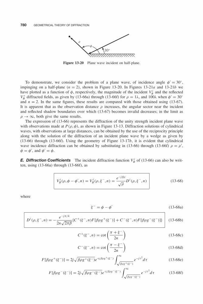
Balanis c13.tex V2 - 11/24/2011 12:45 A.M. Page 780
780 GEOMETRICAL THEORY OF DIFFRACTION
30°
r
f
Figure 13-20 Plane wave incident on half-plane.
To demonstrate, we consider the problem of a plane wave, of incidence angle φ′ = 30◦,impinging on a half-plane (n = 2), shown in Figure 13-20. In Figures 13-21a and 13-21b wehave plotted as a function of φ, respectively, the magnitude of the incident V i
B and the reflectedV r
B diffracted fields, as given by (13-66a) through (13-66f) for ρ = 1λ, and 100λ when φ′ = 30◦and n = 2. In the same figures, these results are compared with those obtained using (13-67).It is apparent that as the observation distance ρ increases, the angular sector near the incidentand reflected shadow boundaries over which (13-67) becomes invalid decreases; in the limit asρ → ∞, both give the same results.
The expression of (13-66) represents the diffraction of the unity strength incident plane wavewith observations made at P(ρ, φ), as shown in Figure 13-13. Diffraction solutions of cylindricalwaves, with observations at large distances, can be obtained by the use of the reciprocity principlealong with the solution of the diffraction of an incident plane wave by a wedge as given by(13-66) through (13-66f). Using the geometry of Figure 13-17b, it is evident that cylindricalwave incidence diffraction can be obtained by substituting in (13-66) through (13-66f) ρ = ρ ′,φ = φ′, and φ′ = φ.
E. Diffraction Coefficients The incident diffraction function V iB of (13-66) can also be writ-
ten, using (13-66a) through (13-66f), as
V iB (ρ, φ − φ′, n) = V i
B (ρ, ξ−, n) = e−jβρ
√ρ
Di (ρ, ξ−, n) (13-68)
where
ξ− = φ − φ′ (13-68a)
Di (ρ, ξ−, n) = − e−jπ/4
2n√
2πβ{C +(ξ−, n)F [βρg+(ξ−)] + C −(ξ−, n)F [βρg−(ξ−)]} (13-68b)
C +(ξ−, n) = cot
(π + ξ−
2n
)(13-68c)
C −(ξ−, n) = cot
(π − ξ−
2n
)(13-68d)
F [βρg+(ξ−)] = 2j√
βρg+(ξ−)e+jβρg+(ξ−)
∫ ∞√
βρg+(ξ−)
e−jτ2dτ (13-68e)
F [βρg−(ξ−)] = 2j√
βρg−(ξ−)e+jβρg−(ξ−)
∫ ∞√
βρg−(ξ−)
e−jτ2dτ (13-68f)
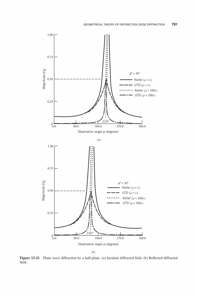
Balanis c13.tex V2 - 11/24/2011 12:45 A.M. Page 781
GEOMETRICAL THEORY OF DIFFRACTION: EDGE DIFFRACTION 781
(a)
f′ = 30°
0.0 90.0 180.0
210°
Keller (r = l)
Keller (r = 100l)
UTD (r = l)
UTD (r = 100l)
Observation angle f (degrees)
Mag
nitu
de |V
i B|
Mag
nitu
de |V
r B|
270.0 360.00
0.25
0.50
0.75
1.00
(b)
150°
f′ = 30°Keller (r = l)
Keller (r = 100l)
UTD (r = l)
UTD (r = 100l)
0.0 90.0 180.0
Observation angle f (degrees)
270.0 360.00
0.25
0.50
0.75
1.00
Figure 13-21 Plane wave diffraction by a half-plane. (a) Incident diffracted field. (b) Reflected diffractedfield.
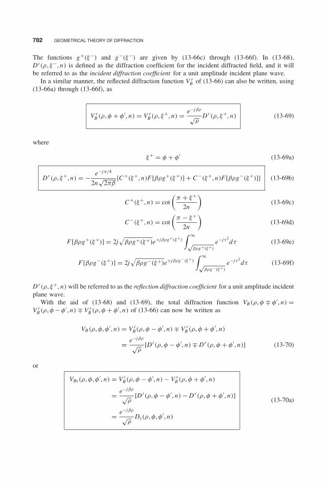
Balanis c13.tex V2 - 11/24/2011 12:45 A.M. Page 782
782 GEOMETRICAL THEORY OF DIFFRACTION
The functions g+(ξ−) and g−(ξ−) are given by (13-66c) through (13-66f). In (13-68),Di (ρ, ξ−, n) is defined as the diffraction coefficient for the incident diffracted field, and it willbe referred to as the incident diffraction coefficient for a unit amplitude incident plane wave.
In a similar manner, the reflected diffraction function V rB of (13-66) can also be written, using
(13-66a) through (13-66f), as
V rB (ρ, φ + φ′, n) = V r
B (ρ, ξ+, n) = e−jβρ
√ρ
Dr (ρ, ξ+, n) (13-69)
where
ξ+ = φ + φ′ (13-69a)
Dr (ρ, ξ+, n) = − e−jπ/4
2n√
2πβ{C +(ξ+, n)F [βρg+(ξ+)] + C −(ξ+, n)F [βρg−(ξ+)]} (13-69b)
C +(ξ+, n) = cot
(π + ξ+
2n
)(13-69c)
C −(ξ+, n) = cot
(π − ξ+
2n
)(13-69d)
F [βρg+(ξ+)] = 2j√
βρg+(ξ+)e+jβρg+(ξ+)
∫ ∞√
βρg+(ξ+)
e−jτ2dτ (13-69e)
F [βρg−(ξ+)] = 2j√
βρg−(ξ+)e+jβρg−(ξ+)
∫ ∞√
βρg−(ξ+)
e−jτ2dτ (13-69f)
Dr (ρ, ξ+, n) will be referred to as the reflection diffraction coefficient for a unit amplitude incidentplane wave.
With the aid of (13-68) and (13-69), the total diffraction function VB (ρ, φ ∓ φ′, n) =V i
B (ρ, φ − φ′, n) ∓ V rB (ρ, φ + φ′, n) of (13-66) can now be written as
VB (ρ, φ, φ′, n) = V iB (ρ, φ − φ′, n) ∓ V r
B (ρ, φ + φ′, n)
= e−jβρ
√ρ
[Di (ρ, φ − φ′, n) ∓ Dr (ρ, φ + φ′, n)] (13-70)
or
VBs(ρ, φ, φ′, n) = V iB (ρ, φ − φ′, n) − V r
B (ρ, φ + φ′, n)
= e−jβρ
√ρ
[Di (ρ, φ − φ′, n) − Dr (ρ, φ + φ′, n)]
= e−jβρ
√ρ
Ds(ρ, φ, φ′, n)
(13-70a)
Balanis c13.tex V2 - 11/24/2011 12:45 A.M. Page 783
GEOMETRICAL THEORY OF DIFFRACTION: EDGE DIFFRACTION 783
VBh(ρ, φ, φ′, n) = V iB (ρ, φ − φ′, n) + V r
B (ρ, φ + φ′, n)
= e−jβρ
√ρ
[Di (ρ, φ − φ′, n) + Dr (ρ, φ + φ′, n)]
= e−jβρ
√ρ
Dh(ρ, φ, φ′, n)
(13-70b)
Ds(ρ, φ, φ′, n) = Di (ρ, φ − φ′, n) − Dr (ρ, φ + φ′, n) (13-70c)
Dh(ρ, φ, φ′, n) = Di (ρ, φ − φ′, n) + Dr (ρ, φ + φ′, n) (13-70d)
where VBs = V iB − V r
B = soft (polarization) diffraction functionVBh = V i
B + V rB = hard (polarization) diffraction function
V iB = incident diffraction function
V rB = reflection diffraction function
Ds = Di − Dr = soft (polarization) diffraction coefficientDh = Di + Dr = hard (polarization) diffraction coefficientDi = incident diffraction coefficientDr = reflection diffraction coefficient
Using (13-68b) and (13-69b) in expanded form, the soft (Ds ) and hard (Dh ) diffraction coef-ficients can ultimately be written, respectively, as
Ds(ρ, φ, φ′, n) = − e−jπ/4
2n√
2πβ
×({
cot
[π + (φ − φ′)
2n
]F [βρg+(φ − φ′)] + cot
[π − (φ − φ′)
2n
]F [βρg−(φ − φ′)]
}−
{cot
[π + (φ + φ′)
2n
]F [βρg+(φ + φ′)] + cot
[π − (φ + φ′)
2n
]F [βρg−(φ + φ′)]
})(13-71a)
Dh(ρ, φ, φ′, n) = − e−jπ/4
2n√
2πβ
×({
cot
[π + (φ − φ′)
2n
]F [βρg+(φ − φ′)] + cot
[π − (φ − φ′)
2n
]F [βρg−(φ − φ′)]
}+
{cot
[π + (φ + φ′)
2n
]F [βρg+(φ + φ′)] + cot
[π − (φ + φ′)
2n
]F [βρg−(φ + φ′)]
})(13-71b)
where
φ − φ′ = ξ− (13-71c)
φ + φ′ = ξ+ (13-71d)

Balanis c13.tex V2 - 11/24/2011 12:45 A.M. Page 784
784 GEOMETRICAL THEORY OF DIFFRACTION
The formulations of (13-68) through (13-71d) are part of the often referred to uniform theoryof diffraction (UTD) [10], which are extended to include oblique incidence and curved edgediffraction. These will be discussed in Sections 13.3.3 and 13.3.4, respectively.
A Fortran and MATLAB computer program designated WDC, Wedge Diffraction Coefficients,computes the soft and hard polarization diffraction coefficients of (13-71a) and (13-71b) (actuallythe diffraction coefficients normalized by
√λ). The Fortran program was initially developed and
reported in [53]. The program also accounts for oblique wave incidence, and it is based on themore general formulation of (13-89a) through (13-90b). The main difference in the two sets ofequations is the sin β ′
0 function found in the denominator of (13-90a) and (13-90b); it has beenintroduced to account for the oblique wave incidence. In (13-90a) and (13-90b), L is used as thedistance parameter and ρ is used in (13-71a) and (13-71b).
Therefore, to use the subroutine WDC to compute (13-71a) and (13-71b) let the obliqueincidence angle β ′
0, referred to as BTD, be 90◦. The distance parameter R should represent ρ
(in wavelengths). This program uses the complex function FTF (Fresnel transition function) tocomplete its computations. The FTF program computes (13-68e), (13-68f), (13-69e), and (13-69f) based on the asymptotic expressions of (13-74a), (13-74b), and a linear interpolation forintermediate arguments. Computations of the Fresnel integral can also be made on an algorithmreported in [49] as well as on approximate expressions of [50].
To use the WDC subroutine, the user must specify R = ρ (in wavelengths), PHID = φ
(in degrees), PHIPD = φ′ (in degrees), BTD = β ′0 (in degrees), and FN = n (dimensionless).
The program subroutine computes the normalized (with respect to√
λ) diffraction coefficientsCDCS = Ds and CDCH = Dh . The angles represented by φ and φ′ should be referenced from theface of the wedge, as shown in Figure 13-13b. For normal incidence, β ′
0 = 90◦. This computersubroutine has been used successfully in a multitude of problems; it is very efficient, and the useris encouraged to utilize it effectively.
Following a similar procedure, the incident and reflected diffraction functions and the incident,reflected, soft, and hard diffraction coefficients using Keller’s diffraction functions of (13-67) canbe written, respectively, as
V iB (ρ, φ − φ′, n) = V i
B (ρ, ξ−, n) = e−jβρ
√ρ
Di (ρ, φ − φ′, n) = e−jβρ
√ρ
Di (ρ, ξ−, n) (13-72a)
V rB (ρ, φ + φ′, n) = V r
B (ρ, ξ+, n) = e−jβρ
√ρ
Dr (ρ, φ + φ′, n) = e−jβρ
√ρ
Dr (ρ, ξ+, n) (13-72b)
Di (ρ, φ − φ′, n) = e−jπ/4
√2πβ
1
nsin
(π
n
)cos
(π
n
)− cos
(φ − φ′
n
) (13-72c)
Dr (ρ, φ + φ′, n) = e−jπ/4
√2πβ
1
nsin
(π
n
)cos
(π
n
)− cos
(φ + φ′
n
) (13-72d)
Balanis c13.tex V2 - 11/24/2011 12:45 A.M. Page 785
GEOMETRICAL THEORY OF DIFFRACTION: EDGE DIFFRACTION 785
Ds(ρ, φ, φ′, n) = Di (ρ, φ − φ′, n) − Dr (ρ, φ + φ′, n)
=e−jπ/4 1
nsin
(π
n
)√
2πβ
⎡⎢⎢⎣ 1
cos(π
n
)− cos
(φ − φ′
n
) − 1
cos(π
n
)− cos
(φ + φ′
n
)⎤⎥⎥⎦(13-72e)
Dh(ρ, φ, φ′, n) = Di (ρ, φ − φ′, n) + Dr (ρ, φ + φ′, n)
=e−jπ/4 1
nsin
(π
n
)√
2πβ
⎡⎢⎢⎣ 1
cos(π
n
)− cos
(φ − φ′
n
) + 1
cos(π
n
)− cos
(φ + φ′
n
)⎤⎥⎥⎦(13-72f)
The diffraction coefficients of (13-72c) through (13-72f) are referred to as Keller’s diffractioncoefficients , and they possess singularities along the incident and reflection shadow boundaries.
The wedge diffraction coefficients described previously assume that the orientational directionfor the incident and diffracted electric and magnetic field components of the soft and hard polar-ized fields are those shown, respectively, in Figures 13-22a and 13-22b. A negative value in thediffraction coefficients will reverse the directions of the appropriate fields.
The function F (X ) of (13-63c), (13-68e), (13-68f), (13-69e), and (13-69f) is known as a Fresneltransition function and it involves a Fresnel integral. Its magnitude and phase for 0.001 ≤ X ≤ 10are shown plotted in Figure 13-23. It is evident that
|F (X )| ≤ 10 ≤ Phase of F (X ) ≤ π/4
}, for 0.001 ≤ X ≤ 10 (13-73a)
andF (X ) � 1, for X > 10 (13-73b)
Thus, if the argument X of the transition function exceeds 10, it can be replaced by unity. Then theexpressions for the diffraction coefficients of (13-68b), (13-69b), (13-71a), and (13-71b) reduce,respectively, to those of (13-72c) through (13-72f). Asymptotic expressions for the transitionfunction F (X ) are [53]:
For small X (X < 0.3)
F (X ) �[√
πX − 2Xejπ/4 − 2
3X 2e−jπ/4
]ej (π/4 + X ) (13-74a)
For large X (X > 5.5)
F (X ) �[
1 + j1
2X− 3
4
1
X 2− j
15
8
1
X 3+ 75
16
1
X 4
](13-74b)
To facilitate the reader in the computations, a Fortran and Matlab computer function pro-gram designated as FTF, for Fresnel transition function, computes the wedge transition functionF (X ) of (13-68e), (13-68f), (13-69e), or (13-69f). The algorithm is based on the approximationsof (13-74a) for small arguments (X < 0.3) and on (13-74b) for large arguments (X > 5.5). For
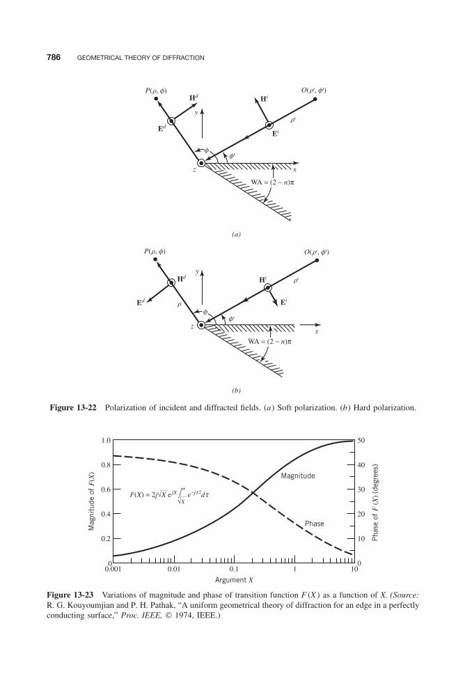
Balanis c13.tex V2 - 11/24/2011 12:45 A.M. Page 786
786 GEOMETRICAL THEORY OF DIFFRACTION
(a)
(b)
z x
y
Ed
HdP(r, f) O(r′, f′)
Hi
Ei
r′
ff′
zx
y
Ed
Hd
P(r, f) O(r′, f′)
Hi
Ei
r′
rf
f′
WA = (2 − n)π
WA = (2 − n)π
Figure 13-22 Polarization of incident and diffracted fields. (a) Soft polarization. (b) Hard polarization.
0.001
0.2
0
0.4
Mag
nitu
de o
f F
(X)
Argument X
Pha
se o
f F
(X
) (d
egre
es)
0.6
0.8
1.0
0.01 0.1 1 100
10
20
30
40
50
Magnitude
Phase
F(X) = 2j√X e jX ∫∞
e−jτ 2dτ√X
Figure 13-23 Variations of magnitude and phase of transition function F (X ) as a function of X. (Source:R. G. Kouyoumjian and P. H. Pathak, “A uniform geometrical theory of diffraction for an edge in a perfectlyconducting surface,” Proc. IEEE, © 1974, IEEE.)
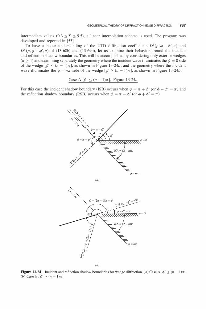
Balanis c13.tex V2 - 11/24/2011 12:45 A.M. Page 787
GEOMETRICAL THEORY OF DIFFRACTION: EDGE DIFFRACTION 787
intermediate values (0.3 ≤ X ≤ 5.5), a linear interpolation scheme is used. The program wasdeveloped and reported in [53].
To have a better understanding of the UTD diffraction coefficients Di (ρ, φ − φ′, n) andDr (ρ, φ + φ′, n) of (13-68b) and (13-69b), let us examine their behavior around the incidentand reflection shadow boundaries. This will be accomplished by considering only exterior wedges(n ≥ 1) and examining separately the geometry where the incident wave illuminates the φ = 0 sideof the wedge [φ′ ≤ (n − 1)π], as shown in Figure 13-24a , and the geometry where the incidentwave illuminates the φ = nπ side of the wedge [φ′ ≥ (n − 1)π], as shown in Figure 13-24b.
Case A [φ′ ≤ (n − 1)π], Figure 13-24a
For this case the incident shadow boundary (ISB) occurs when φ = π + φ′ (or φ − φ′ = π) andthe reflection shadow boundary (RSB) occurs when φ = π − φ′ (or φ + φ′ = π).
(b)
(a)
RSB (f + f′ = p)
ISB (f
− f′ =
p)
(n − 1)pf = p − f′
f = 0
f = np
f = p + f′f′
RSB
[f
+ f
′ = (
2n −
1)p
]
ISB (f − f′ = −p)
(n − 1)p
f = f′ − pf = 0
f = np
f = (2n − 1)p − f′
f′
WA = (2 − n)π
WA = (2 − n)π
Figure 13-24 Incident and reflection shadow boundaries for wedge diffraction. (a) Case A: φ′ ≤ (n − 1)π .(b) Case B: φ′ ≥ (n − 1)π .
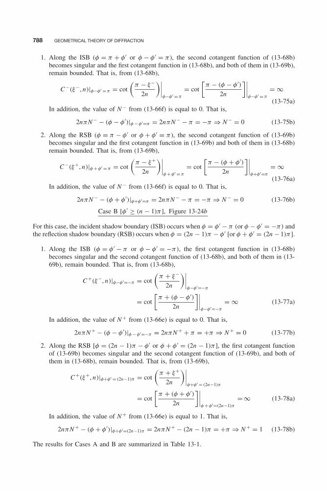
Balanis c13.tex V2 - 11/24/2011 12:45 A.M. Page 788
788 GEOMETRICAL THEORY OF DIFFRACTION
1. Along the ISB (φ = π + φ′ or φ − φ′ = π), the second cotangent function of (13-68b)becomes singular and the first cotangent function in (13-68b), and both of them in (13-69b),remain bounded. That is, from (13-68b),
C −(ξ−, n)|φ−φ′ = π = cot
(π − ξ−
2n
)∣∣∣∣φ−φ′ =π
= cot
[π − (φ − φ′)
2n
]∣∣∣∣φ−φ′ = π
= ∞(13-75a)
In addition, the value of N − from (13-66f) is equal to 0. That is,
2nπN − − (φ − φ′)|φ − φ′=π = 2nπN − − π = −π ⇒ N − = 0 (13-75b)
2. Along the RSB (φ = π − φ′ or φ + φ′ = π), the second cotangent function of (13-69b)becomes singular and the first cotangent function in (13-69b) and both of them in (13-68b)remain bounded. That is, from (13-69b),
C −(ξ+, n)|φ + φ′ =π = cot
(π − ξ+
2n
)∣∣∣∣φ + φ′ = π
= cot
[π − (φ + φ′)
2n
]∣∣∣∣φ+φ′=π
= ∞(13-76a)
In addition, the value of N − from (13-66f) is equal to 0. That is,
2nπN − − (φ + φ′)|φ+φ′=π = 2nπN − − π = −π ⇒ N − = 0 (13-76b)
Case B [φ′ ≥ (n − 1)π], Figure 13-24b
For this case, the incident shadow boundary (ISB) occurs when φ = φ′ − π (or φ − φ′ = −π) andthe reflection shadow boundary (RSB) occurs when φ = (2n − 1)π − φ′ [or φ + φ′ = (2n − 1)π].
1. Along the ISB (φ = φ′ − π or φ − φ′ = −π), the first cotangent function in (13-68b)becomes singular and the second cotangent function of (13-68b), and both of them in (13-69b), remain bounded. That is, from (13-68b),
C +(ξ−, n)|φ−φ′=−π = cot
(π + ξ−
2n
)∣∣∣∣φ−φ′=−π
= cot
[π + (φ − φ′)
2n
]∣∣∣∣φ−φ′=−π
= ∞ (13-77a)
In addition, the value of N + from (13-66e) is equal to 0. That is,
2nπN + − (φ − φ′)|φ − φ′=−π = 2nπN + + π = +π ⇒ N + = 0 (13-77b)
2. Along the RSB [φ = (2n − 1)π − φ′ or φ + φ′ = (2n − 1)π], the first cotangent functionof (13-69b) becomes singular and the second cotangent function of (13-69b), and both ofthem in (13-68b), remain bounded. That is, from (13-69b),
C +(ξ+, n)|φ+φ′ = (2n−1)π = cot
(π + ξ+
2n
)∣∣∣∣φ+φ′ = (2n−1)π
= cot
[π + (φ + φ′)
2n
]∣∣∣∣φ + φ′=(2n−1)π
= ∞ (13-78a)
In addition, the value of N + from (13-66e) is equal to 1. That is,
2nπN + − (φ + φ′)|φ+φ′=(2n−1)π = 2nπN + − (2n − 1)π = +π ⇒ N + = 1 (13-78b)
The results for Cases A and B are summarized in Table 13-1.
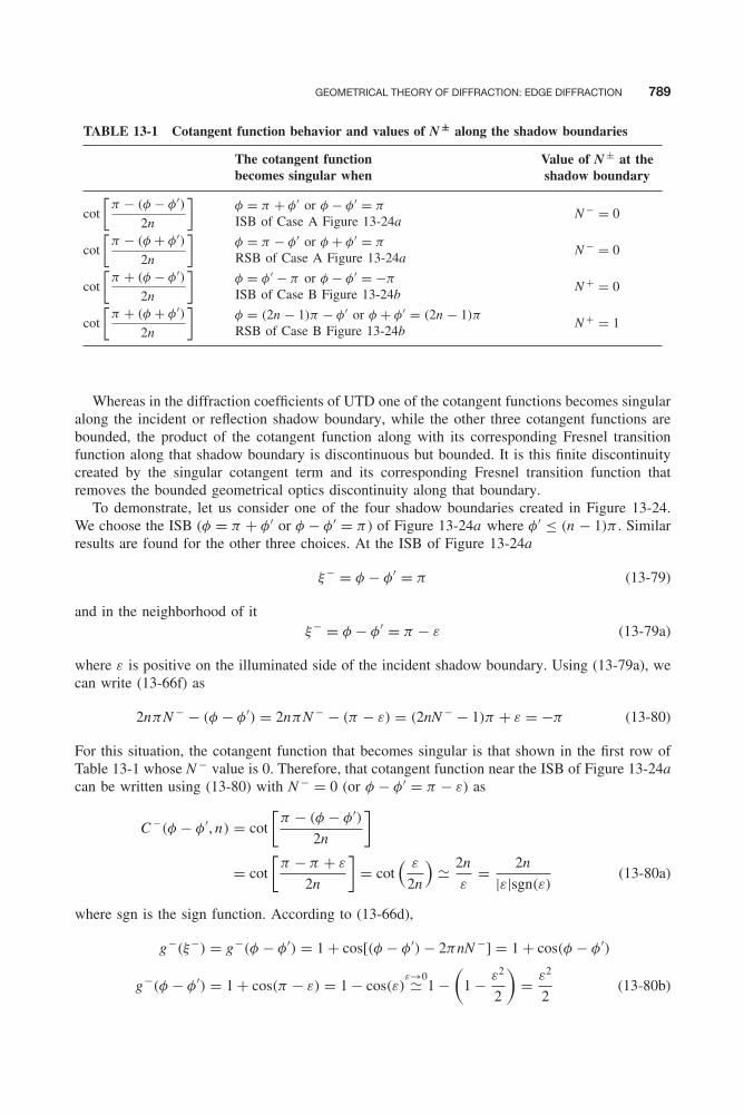
Balanis c13.tex V2 - 11/24/2011 12:45 A.M. Page 789
GEOMETRICAL THEORY OF DIFFRACTION: EDGE DIFFRACTION 789
TABLE 13-1 Cotangent function behavior and values of N ± along the shadow boundaries
The cotangent function Value of N ± at thebecomes singular when shadow boundary
cot
[π − (φ − φ′)
2n
]φ = π + φ′ or φ − φ′ = π
ISB of Case A Figure 13-24aN − = 0
cot
[π − (φ + φ′)
2n
]φ = π − φ′ or φ + φ′ = π
RSB of Case A Figure 13-24aN − = 0
cot
[π + (φ − φ′)
2n
]φ = φ′ − π or φ − φ′ = −π
ISB of Case B Figure 13-24bN + = 0
cot
[π + (φ + φ′)
2n
]φ = (2n − 1)π − φ′ or φ + φ′ = (2n − 1)π
RSB of Case B Figure 13-24bN + = 1
Whereas in the diffraction coefficients of UTD one of the cotangent functions becomes singularalong the incident or reflection shadow boundary, while the other three cotangent functions arebounded, the product of the cotangent function along with its corresponding Fresnel transitionfunction along that shadow boundary is discontinuous but bounded. It is this finite discontinuitycreated by the singular cotangent term and its corresponding Fresnel transition function thatremoves the bounded geometrical optics discontinuity along that boundary.
To demonstrate, let us consider one of the four shadow boundaries created in Figure 13-24.We choose the ISB (φ = π + φ′ or φ − φ′ = π) of Figure 13-24a where φ′ ≤ (n − 1)π . Similarresults are found for the other three choices. At the ISB of Figure 13-24a
ξ− = φ − φ′ = π (13-79)
and in the neighborhood of itξ− = φ − φ′ = π − ε (13-79a)
where ε is positive on the illuminated side of the incident shadow boundary. Using (13-79a), wecan write (13-66f) as
2nπN − − (φ − φ′) = 2nπN − − (π − ε) = (2nN − − 1)π + ε = −π (13-80)
For this situation, the cotangent function that becomes singular is that shown in the first row ofTable 13-1 whose N − value is 0. Therefore, that cotangent function near the ISB of Figure 13-24acan be written using (13-80) with N − = 0 (or φ − φ′ = π − ε) as
C −(φ − φ′, n) = cot
[π − (φ − φ′)
2n
]= cot
[π − π + ε
2n
]= cot
( ε
2n
)� 2n
ε= 2n
|ε|sgn(ε)(13-80a)
where sgn is the sign function. According to (13-66d),
g−(ξ−) = g−(φ − φ′) = 1 + cos[(φ − φ′) − 2πnN −] = 1 + cos(φ − φ′)
g−(φ − φ′) = 1 + cos(π − ε) = 1 − cos(ε)ε→0� 1 −
(1 − ε2
2
)= ε2
2(13-80b)

Balanis c13.tex V2 - 11/24/2011 12:45 A.M. Page 790
790 GEOMETRICAL THEORY OF DIFFRACTION
The transition function of (13-68f) can also be written using (13-80b) as
F [βρg−(ξ−)] = F [βρg−(φ − φ′)] = F
[βρ
(ε2
2
)](13-80c)
which for small values of its argument can be approximated by the first term of its small-argumentasymptotic form (13-74a). That is,
F
(βρε2
2
)�
√πβρε2
2ejπ/4 = |ε|
√πβρ
2ejπ/4 (13-81)
Thus, the product of C −(φ − φ′, n)F [βρg−(φ − φ′)], as each is given by (13-80a) and (13-81),can be approximated by
cot
[π − (φ − φ′)
2n
]F [βρg−(φ − φ′)] = n
√2πβρ sgn(ε)ejπ/4 (13-82)
It is apparent that (13-82) exhibits a finite discontinuity that is positive along the illuminatedside of the incident shadow boundary and negative on the other side.
The corresponding incident diffracted field (13-68) along the incident shadow boundary canbe approximated, using (13-82) and only the second term within the brackets in (13-68b), as
V iB (ρ, φ − φ′ = π − ε, n) � e−jβρ
√ρ
[− e−jπ/4
2n√
2πβn√
2πβρ sgn(ε)ejπ/4
]= −e−jβρ
2sgn(ε)
(13-83)
Apart from the phase factor, this function is equal to −0.5, on the illuminated side of the incidentshadow boundary and +0.5 on the other side. Clearly, such a bounded discontinuity possessesthe proper magnitude and polarity to compensate for the discontinuity created by the geometricaloptics field. A similar procedure can be used to demonstrate the discontinuous nature of thediffracted field along the other shadow boundaries of Figure 13-24.
To illustrate the principles of geometrical optics (GO) and geometrical theory of diffraction(GTD), an example will be considered next.
Example 13-3
A plane wave of unity amplitude is incident upon a half-plane (n = 2) at an incidence angle of φ′ = 30◦,as shown in the Figure 13-20. At a distance of one wavelength (ρ = λ) from the edge of the wedge,compute and plot the amplitude and phase of the following:
1. Total (incident plus reflected) geometrical optics field.2. Incident diffracted field.3. Reflected diffracted field.4. Total field (geometrical optics plus diffracted).
Do these for both soft and hard polarizations.
Solution: The geometrical optics field components are computed using (13-65); incident and reflecteddiffracted fields are computed using (13-68) through (13-69f). These are plotted in Figure 13-25a and13-25b for soft and hard polarizations, respectively.

Balanis c13.tex V2 - 11/24/2011 12:45 A.M. Page 791
GEOMETRICAL THEORY OF DIFFRACTION: EDGE DIFFRACTION 791
2.5
2.0
1.5
1.0
Mag
nitu
de
Observation angle f (degrees)
Total
Geometrical optics (GO)
Incident diffracted (ID)
Reflected diffracted (RD)
Half-plane (n = 2)
Observation distance (r) = l
Incidence angle (f′) = 30°
0.5
00 50 100 150 200 250 300 350
210
Total
Geometrical optics (GO)
Incident diffracted (ID)
Reflected diffracted (RD)
(a)
2.5
2.0
1.5
1.0
Mag
nitu
de
Observation angle f (degrees)
Half-plane (n = 2)
Observation distance (r) = l
Incidence angle (f′) = 30°
0.5
00 50 100 150 200 250 300 350
210
(b)
Figure 13-25 Field distribution of various components of a plane wave incident normally on a con-ducting half-plane. (a) Soft polarization. (b) Hard polarization. (Source: C. A. Balanis, Antenna Theory:Analysis and Design , copyright © 1982, John Wiley & Sons, Inc. Reprinted by permission of John Wiley& Sons, Inc.).

Balanis c13.tex V2 - 11/24/2011 12:45 A.M. Page 792
792 GEOMETRICAL THEORY OF DIFFRACTION
In Figure 13-25a the amplitude patterns of the geometrical optics and diffracted fields for the softpolarization are displayed as follows. The
1. Dashed curve (----) represents the total geometrical optics field (incident and reflected) computedusing (13-65).
2. Dash-dot curve (−·−·−) represents the amplitude of the incident diffracted (ID) field V iB computed
using (13-68) through (13-68f).3. Dotted curve (· · · · ) represents the amplitude of the reflected diffracted (RD) field V r
B computedusing (13-69) through (13-69f).
4. Solid curve (—) represents the total amplitude pattern for soft polarization computed using resultsfrom parts 1 through 3.
Observing the data of Figure 13-25a it is evident that the
1. GO field is discontinuous at the reflection shadow boundary (RSB) (φ = 180◦ − φ′ = 180◦ −30◦ = 150◦) and at the incident shadow boundary (ISB) (φ = 180◦ + φ′ = 180◦ + 30◦ = 210◦).
2. GO field in the shadow region (210◦ < φ < 360◦) is zero.3. Reflected diffracted (RD) field, although it exists everywhere, predominates around the reflection
shadow boundary (φ = 150◦) with values of −0.5 for φ = (150◦)− and +0.5 for φ = (150)+.The total discontinuity at φ = 150◦ occurs because the phase undergoes a phase jump of 180◦.
4. Incident diffracted (ID) field also exists everywhere but it predominates around the incident shadowboundary (φ = 210◦) with values of −0.5 for φ = (210◦)− and +0.5 for φ = (210◦)+. The totaldiscontinuity at φ = 210◦ occurs because the phase undergoes a phase jump of 180◦.
5. Total amplitude field pattern is continuous everywhere with the discontinuities of the GO fieldcompensated with the inclusion of the diffracted fields. It should be emphasized that the GOdiscontinuity at the RSB was removed by the inclusion of the reflected diffracted (RD) field andthat at the ISB was compensated by the incident diffracted (ID) field. The GO field was alsomodified in all space with the addition of the diffracted fields, and radiation intensity is present inthe shadow region (210◦ < φ < 360◦).
Computations for the same geometry were also carried out for the hard polarization and the amplitudeis shown in Figure 13-25b. The same phenomena observed for soft polarization are also evident for thehard polarization.
The geometrical optics fields of Example 13-2 and Figure 13-9, displayed in Figure 13-10,exhibit discontinuities. To remove the discontinuities, diffracted fields must be included. This canbe accomplished using the formulations for diffracted fields that have been developed up to thispoint.
Example 13-4
For the geometry of Figure 13-9, repeat the formulations of Example 13-2, including the fields diffractedfrom the edges of the strip.
Solution: According to the solution of Example 13-2, the normalized incident (direct) and reflectedfields of the line source above an infinite width strip are given, respectively, by
E iz = E0
e−jβρi
√ρi
Balanis c13.tex V2 - 11/24/2011 12:45 A.M. Page 793
GEOMETRICAL THEORY OF DIFFRACTION: EDGE DIFFRACTION 793
and
E rz = −E0
e−jβρr
√ρr
where ρi and ρr are, respectively, the distances from the source and image (caustic) to the observationpoint, as shown in Figure 13-26a .
To take into account the finite width of the strip, we assume that the far-zone geometrical optics fieldcomponents (direct and reflected) are the same as for the infinite width strip and the field intensity atthe edges of the strip is the same as for the infinite width strip.
These assumptions, which become more valid for larger width strips, allow us to determine thediffraction contributions from each of the edges. Because of the geometrical symmetry, we can separatethe space surrounding the strip only into four regions, as shown in Figure 13-26a . The angular boundsand the components that contribute to each are as follows:
Region Angular space Components
I α ≤ φ ≤ π − α Direct, reflected, diffracted (1 & 2)II 2π − α ≤ φ ≤ 2π , 0 ≤ φ ≤ α Direct, diffracted (1 & 2)III π + α ≤ φ ≤ 2π − α Diffracted (1 & 2)IV π − α ≤ φ ≤ π + α Direct, diffracted (1 & 2)
Because of symmetry, we need only consider half of the total space for computations.To determine the first-order diffractions from each of the edges, we also assume that each forms a
wedge (in this case a half space) that initially is isolated from the other. This allows us to use for eachthe diffraction properties of the canonical problem (wedge) discussed in the previous section. Thus, thefield diffracted from wedge 1 is equal to the product of:
1. The direct (incident) field Ez evaluated at the point of diffraction.2. The diffraction coefficient as given by (13-70c).3. The spatial attenuation factor as given by (13-35b).4. The phase factor as given by (13-34a).
In equation form, it is similar to (13-34a), and it is written as
E dz1(ρ1, φ) = E i
z (ρd = s ′)Ds (s′, ψ1, α, 2)A1(ρ1)e
−jβρ1
where
E iz (ρd , s ′) = E0
e−jβs ′
√s ′
Ds (s′, ψ1, α, 2) = Di (s ′, ψ1 − α, 2) − Dr (s ′, ψ1 + α, 2)
A1(ρ1) = 1√ρ1
Using the preceding equations, we can write that
E dz1(ρ1, φ) = E0
{e−jβs ′
√s ′ [Di (s ′, ψ1 − α, 2) − Dr (s ′, ψ1 + α, 2)]
}e−jβρ1
√ρ1
E dz1(ρ1, φ) = E0[V i
B (s ′, ψ1 − α, 2) − V rB (s ′, ψ1 + α, 2)]
e−jβρ1
√ρ1

Balanis c13.tex V2 - 11/24/2011 12:45 A.M. Page 794
794 GEOMETRICAL THEORY OF DIFFRACTION
w2
w2
w2
w2
w2
w2
s′
zh
y
s′
α
ρi
ρr
ρ1
s′
y
h
x
x
s′
s′
ρ2
ρ1
ρ1
ρ
ρ2
α
Line sourceRSB
ISB Image
Region III
Region I
Region IV 2a
RSB
ISB
Region IIα
α
x
(a)
(b)
(c)
y2 = f y1
y1
y2 = a′
y1 = a′
y1 = a′ f
f
#2 #1
#1
h
Figure 13-26 Line source above a finite width strip. (a) Region separation. (b) Diffraction by edges1 and 2. (c) Diffraction by edge 1 in region III.

Balanis c13.tex V2 - 11/24/2011 12:45 A.M. Page 795
GEOMETRICAL THEORY OF DIFFRACTION: EDGE DIFFRACTION 795
where V iB and V r
B are the diffraction functions of (13-68) and (13-69). According to the geometry ofFigures 13-26b and 13-26c
ψ1 ={
π − φ 0 ≤ φ ≤ π (Figure 13-26b)
3π − φ π ≤ φ ≤ 2π (Figure 13-26c)
In a similar manner, it can be shown that the field diffracted by wedge 2 is given by
E dz2 = E0[V i
B (s ′, ψ2 − α, 2) − V rB (s ′, ψ2 + α, 2)]
e−jβρ2
√ρ2
ψ2 = φ for 0 < φ < 2π (Figure 13-26b)
For far-field observations
ρi � ρ − h sin φ
ρr � ρ + h sin φ
ρ1 � ρ − w
2cos φ
ρ2 � ρ + w
2cos φ
⎫⎪⎪⎪⎪⎪⎬⎪⎪⎪⎪⎪⎭for phase variations
ρi � ρr � ρ1 � ρ2 � ρ for amplitude variations
which allow the fields to be written as
E iz = E0e+jβh sin φ 0 < φ < π + α, 2π − α < φ < 2π (direct)
E rz = −E0e−jβh sin φ α < φ < π − α (reflected)
E dz1 = E0[V i
B (s ′, ψ1 − α, 2) − V rB (s ′, ψ1 + α, 2)]e+j (βw/2) cos φ (diffracted from wedge # 1)
ψ1 ={
π − φ 0 < φ < π
3π − φ π < φ < 2π
E dz2 = E0[V i
B (s ′, ψ2 − α, 2) − V rB (s ′, ψ2 + α, 2)]e−j (βw/2) cos φ (diffracted from wedge #2)
ψ2 = φ 0 < φ < 2π
where the e−jβρ/√
ρ factor has been suppressed.It should be stated that the preceding equations represent only first-order diffractions, which usually
provide sufficient accuracy for many high-frequency applications. Multiple diffractions between theedges occur and should be included when the strip is electrically small and when more accurate resultsare required.
For a strip of width w = 2λ and with the source at a height of h = 0.5λ, the normalizedpattern computed using these equations is shown in Figure 13-27, where it is compared withGO patterns for infinite and finite width strips. It is evident that there is a significant dif-ference between the three, especially in the lower hemisphere, where for the most part theGO pattern exhibits no radiation, and in the regions where there are discontinuities in the GOpattern.
In addition to antenna pattern prediction, diffraction techniques are extremely well suited forscattering problems. To demonstrate the applicability and versatility of diffraction techniques toscattering, let us consider such an example.
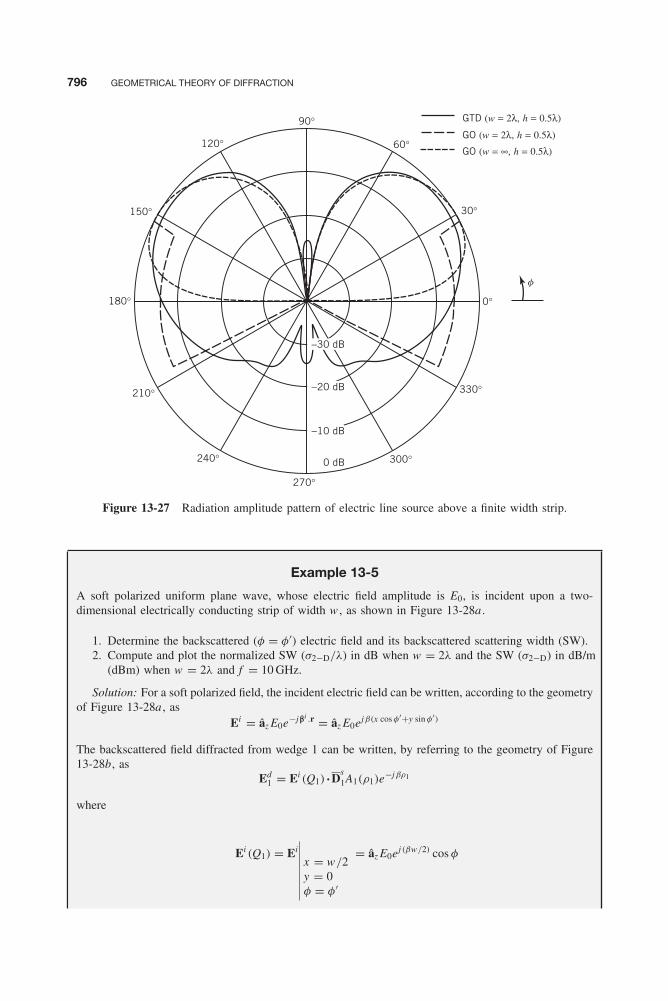
Balanis c13.tex V2 - 11/24/2011 12:45 A.M. Page 796
796 GEOMETRICAL THEORY OF DIFFRACTION
f
0°
330°
0 dB 300°
270°
240°
210°
180°
150°
120°
90°
60°
GTD (w = 2λ, h = 0.5λ)
GO (w = 2λ, h = 0.5λ)
GO (w = ∞, h = 0.5λ)
30°
−30 dB
−20 dB
−10 dB
Figure 13-27 Radiation amplitude pattern of electric line source above a finite width strip.
Example 13-5
A soft polarized uniform plane wave, whose electric field amplitude is E0, is incident upon a two-dimensional electrically conducting strip of width w , as shown in Figure 13-28a .
1. Determine the backscattered (φ = φ′) electric field and its backscattered scattering width (SW).2. Compute and plot the normalized SW (σ2−D/λ) in dB when w = 2λ and the SW (σ2−D) in dB/m
(dBm) when w = 2λ and f = 10 GHz.
Solution: For a soft polarized field, the incident electric field can be written, according to the geometryof Figure 13-28a , as
Ei = âz E0e−jβi .r = âz E0ejβ(x cos φ′+y sin φ′)
The backscattered field diffracted from wedge 1 can be written, by referring to the geometry of Figure13-28b, as
Ed1 = Ei (Q1) • D
s1A1(ρ1)e
−jβρ1
where
Ei (Q1) = Ei
x = w/2y = 0φ = φ′
= âz E0ej (βw/2) cos φ

Balanis c13.tex V2 - 11/24/2011 12:45 A.M. Page 797
GEOMETRICAL THEORY OF DIFFRACTION: EDGE DIFFRACTION 797
(a)
(b)
x
y
z
y
z
x
Ei
βiβr βr
βi
Ei
Es Es
Hs HsHi
#2
#2 #1
#1
Hi
f′
f = f′ = ψ2
ρ1
ρ2ρ
ψ1 f = f′
f′
ff
f
w2
w2
w2
w2
Figure 13-28 Wave diffraction by a finite width strip. (a) Plane wave incidence. (b) Plane wavediffraction.
Ds1 = âz âz
e−jπ/4 sin(
πn
)n√
2πβ
⎡⎢⎢⎣ 1
cos(π
n
)− cos
(ψ1 − ψ ′
1
n
)
− 1
cos(π
n
)− cos
(ψ1 + ψ ′
1
n
)⎤⎥⎥⎦
n = 2ψ1 = ψ ′
1 = π − φ
= −âz âze−jπ/4
2√
2πβ
(1 + 1
cos φ
)
A1(ρ1) = 1√ρ1
Keller’s diffraction form has been used because, at very large distances (ideally infinity), the UTDformulations reduce to those of Keller. Thus, the backscattered field diffracted from wedge 1 reduces to
Ed1 = −âz E0
e−jπ/4ej (βw/2) cos φ
2√
2πβ
(1 + 1
cos φ
)e−jβρ1
√ρ1
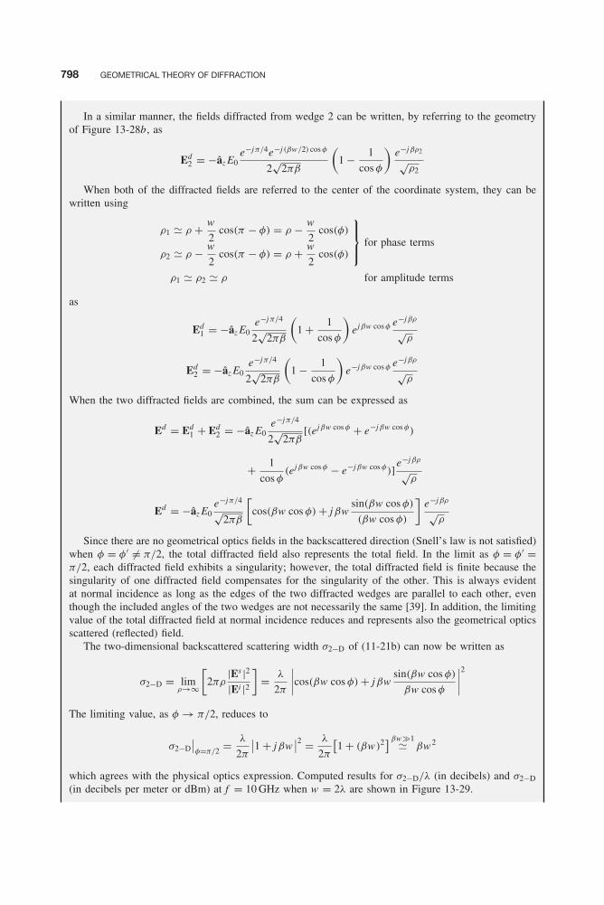
Balanis c13.tex V2 - 11/24/2011 12:45 A.M. Page 798
798 GEOMETRICAL THEORY OF DIFFRACTION
In a similar manner, the fields diffracted from wedge 2 can be written, by referring to the geometryof Figure 13-28b, as
Ed2 = −âz E0
e−jπ/4e−j (βw/2) cos φ
2√
2πβ
(1 − 1
cos φ
)e−jβρ2
√ρ2
When both of the diffracted fields are referred to the center of the coordinate system, they can bewritten using
ρ1 � ρ + w
2cos(π − φ) = ρ − w
2cos(φ)
ρ2 � ρ − w
2cos(π − φ) = ρ + w
2cos(φ)
⎫⎪⎬⎪⎭ for phase terms
ρ1 � ρ2 � ρ for amplitude terms
as
Ed1 = −âz E0
e−jπ/4
2√
2πβ
(1 + 1
cos φ
)ejβw cos φ e−jβρ
√ρ
Ed2 = −âz E0
e−jπ/4
2√
2πβ
(1 − 1
cos φ
)e−jβw cos φ e−jβρ
√ρ
When the two diffracted fields are combined, the sum can be expressed as
Ed = Ed1 + Ed
2 = −âz E0e−jπ/4
2√
2πβ[(ejβw cos φ + e−jβw cos φ)
+ 1
cos φ(ejβw cos φ − e−jβw cos φ)]
e−jβρ
√ρ
Ed = −âz E0e−jπ/4
√2πβ
[cos(βw cos φ) + jβw
sin(βw cos φ)
(βw cos φ)
]e−jβρ
√ρ
Since there are no geometrical optics fields in the backscattered direction (Snell’s law is not satisfied)when φ = φ′ �= π/2, the total diffracted field also represents the total field. In the limit as φ = φ′ =π/2, each diffracted field exhibits a singularity; however, the total diffracted field is finite because thesingularity of one diffracted field compensates for the singularity of the other. This is always evidentat normal incidence as long as the edges of the two diffracted wedges are parallel to each other, eventhough the included angles of the two wedges are not necessarily the same [39]. In addition, the limitingvalue of the total diffracted field at normal incidence reduces and represents also the geometrical opticsscattered (reflected) field.
The two-dimensional backscattered scattering width σ2−D of (11-21b) can now be written as
σ2−D = limρ→∞
[2πρ
|Es |2|Ei |2
]= λ
2π
∣∣∣∣cos(βw cos φ) + jβwsin(βw cos φ)
βw cos φ
∣∣∣∣2
The limiting value, as φ → π/2, reduces to
σ2−D∣∣φ=π/2 = λ
2π
∣∣1 + jβw∣∣2 = λ
2π
[1 + (βw)2] βw�1� βw2
which agrees with the physical optics expression. Computed results for σ2−D/λ (in decibels) and σ2−D
(in decibels per meter or dBm) at f = 10 GHz when w = 2λ are shown in Figure 13-29.

Balanis c13.tex V2 - 11/24/2011 12:45 A.M. Page 799
GEOMETRICAL THEORY OF DIFFRACTION: EDGE DIFFRACTION 799
s/l (dB)
s (dBm)
0
−20
−10
0
10
20
30 60 90 120 150 180
Observation angle f (degrees)
SW
(dB
or
dBm
)
Figure 13-29 Two-dimensional monostatic scattering width for soft polarization of a finite width stripof w = 2λ at f = 10 GHz.
Before proceeding to discuss other topics in diffraction, such as oblique incidence, curvededge diffraction, equivalent currents, slope diffraction, and multiple diffraction, let us completeour two-dimensional diffraction by addressing some modifications and extensions to the conceptscovered in this section.
For a plane wave incidence, ρ in (13-68) through (13-68f) and in (13-69) through (13-69f)represents the distance from the edge of the wedge to the observation point. According to theprinciple of reciprocity illustrated in Figure 13-17, ρ in (13-68) through (13-69f) must be replacedby ρ ′ to represent the diffraction of a cylindrical wave whose source is located a distance ρ ′from the edge of the wedge and the observations made in the far zone (ideally at infinity). Ifboth the source and observation point are located at finite distances from the edge of the wedge,represented, respectively, by ρ ′ and ρ, then a better estimate of the distance would be to introducea so-called distance parameter L, which in this case takes the form of
L = ρρ ′
ρ + ρ ′
{ρ′→∞� ρρ→∞� ρ ′
(13-84)
Thus, the incident and reflected diffracted fields and coefficients of (13-68) and (13-69) can bewritten as
V iB (L, φ − φ′, n) = V i
B (L, ξ−, n) = e−jβρ
√ρ
Di (L, ξ−, n) (13-84a)
V rB (L, φ + φ′, n) = V r
B (L, ξ+, n) = e−jβρ
√ρ
Dr (L, ξ+, n) (13-84b)
It is observed in (13-68) and (13-69) that for grazing angle incidence, φ′ = 0 or φ′ = nπ
of Figure 13-24 (where n represents the wedge angle), then ξ− = ξ+ = φ − φ′ = φ + φ′ andV i
B = V rB , Di = Dr . Therefore, here Ds of (13-70c) or (13-72e) is equal to zero (Ds = 0) and Dh
of (13-70d) or (13-72f) is equal to twice Di or twice Dr (Dh = 2Di = 2Dr ). Since grazing is alimiting situation, the incident and reflected fields combine to make the total geometrical opticsfield effectively incident at the observation point. Therefore, one-half of the total field propagatingalong the face of the wedge toward the edge is the incident field and the other one-half represents

Balanis c13.tex V2 - 11/24/2011 12:45 A.M. Page 800
800 GEOMETRICAL THEORY OF DIFFRACTION
the reflected field. The diffracted fields for this case can properly be accounted for by doing eitherof the following:
1. Let the total GO field represent the incident GO field but multiply the diffraction coefficientsby a factor of 1
2 .2. Multiply the total GO field by a factor of 1
2 and let the product represent the incident field.The diffraction coefficients should not be modified.
Either procedure produces the same results, and the choice is left to the reader.For grazing incidence, the diffraction coefficient of (13-70c) or (13-72e) are equal to zero.
These diffraction coefficients, as well as those of (13-70d) and (13-72f), account for the diffractedfields based on the value of the field at the point of diffraction. This is formulated using (13-34a).There are other higher-order diffraction coefficients that account for the diffracted fields based onthe rate of change (slope) of the field at the point of diffraction. These diffraction coefficients arereferred to as the slope diffraction coefficients [52], and they yield nonzero (even though small)fields for soft polarization at grazing incidence. The slope diffraction coefficients exist also forhard polarization, but they are not as dominant as they are for soft polarization.
Up to now, we have restricted our attention to exterior wedge (1 < n ≤ 2) diffraction. How-ever, the theory of diffraction can be applied also to interior wedge diffraction (0 ≤ n ≤ 1). Whenn = 1, the wedge reduces to an infinite flat plate and the diffraction coefficients reduce to zero [asseen better by examining (13-72e) and (13-72f)] since sin(π/n) = 0. The incident and reflectedfields for n = 1 (half plane), n = 1
2 (90◦ interior wedge), and n = 1/M , M = 3, 4, . . . (acute inte-rior wedges) can be found exactly by image theory. In each of these, the number of finite imagesis determined by the included angle of the interior wedge [38]. As n → 0 the geometrical optics(incident and reflected) fields become more dominant compared to the nonvanishing diffractedfields.
13.3.3 Straight Edge Diffraction: Oblique Incidence
The normal incidence and diffraction formulations of the previous section are convenient toanalyze radiation characteristics of antennas and structures primarily in principal planes. However,a complete analysis of an antenna or scatterer requires examination not only in principal planesbut also in nonprincipal planes, as shown in Figure 13-30 for an aperture and a horn antennaeach mounted on a finite size ground plane.
Whereas the diffraction of a normally incident wave discussed in the previous section led toscalar diffraction coefficients, the diffraction of an obliquely incident wave by a two-dimensionalwedge can be derived using the geometry of Figure 13-31. To accomplish this, it is most con-venient to define ray-fixed coordinate systems (s ′, β ′
0, φ′) for the source and (s , β0, φ) for theobservation point [8, 10], in contrast to the edge-fixed coordinate system (ρ ′, φ′, z ′; ρ, φ, z ). Bydoing this, it can be shown that the diffracted field, in a general form, can be written as
Ed (s) = Ei (QD ) • D(L; φ, φ′; n;β ′0)
√s ′
s(s ′ + s)e−jβs (13-85)
where D(L;φ, φ′; n; β ′0) is the dyadic edge diffraction coefficient for illumination of the wedge
by plane, cylindrical, conical, or spherical waves.Introducing an edge-fixed plane of incidence with the unit vectors β̂′
0 and φ̂′ parallel andperpendicular to it, and a plane of diffraction with the unit vectors β̂0 and φ̂ parallel and
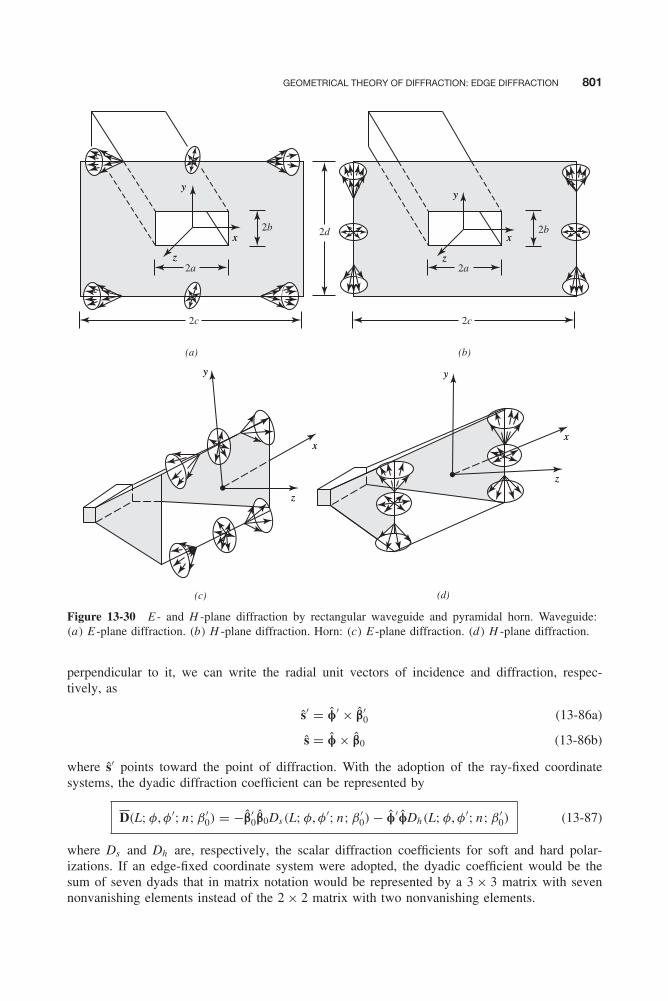
Balanis c13.tex V2 - 11/24/2011 12:45 A.M. Page 801
GEOMETRICAL THEORY OF DIFFRACTION: EDGE DIFFRACTION 801
(a)
(c)
(b)
(d)
2d
yy
zz
xx
yy
xx
zz
2c
yy
zz
xx2b
2a
2c
yy
zz
2b
2a
xx
Figure 13-30 E - and H -plane diffraction by rectangular waveguide and pyramidal horn. Waveguide:(a) E -plane diffraction. (b) H -plane diffraction. Horn: (c) E -plane diffraction. (d) H -plane diffraction.
perpendicular to it, we can write the radial unit vectors of incidence and diffraction, respec-tively, as
ŝ′ = φ̂′ × β̂′0 (13-86a)
ŝ = φ̂ × β̂0 (13-86b)
where ŝ′ points toward the point of diffraction. With the adoption of the ray-fixed coordinatesystems, the dyadic diffraction coefficient can be represented by
D(L; φ, φ′; n; β ′0) = −β̂′
0β̂0Ds(L;φ, φ′; n;β ′0) − φ̂′φ̂Dh(L;φ, φ′; n;β ′
0) (13-87)
where Ds and Dh are, respectively, the scalar diffraction coefficients for soft and hard polar-izations. If an edge-fixed coordinate system were adopted, the dyadic coefficient would be thesum of seven dyads that in matrix notation would be represented by a 3 × 3 matrix with sevennonvanishing elements instead of the 2 × 2 matrix with two nonvanishing elements.

Balanis c13.tex V2 - 11/24/2011 12:45 A.M. Page 802
802 GEOMETRICAL THEORY OF DIFFRACTION
Observation Observation
Diffraction plane
Incidence plane
Source
Source
(2 − n )π
r′
r
s′
s
s
s′
neQD
x
x
z
z
y
y
e
β′0
β ′0
β0
b0
(2 − n )π
(a) (b)
φ′
f′f
φ
0r′ = s′ sin b′
0r = s sin b
s′ = φ′ × β′0
s = φ × β0
(s′ × e)
(s × e)
φ′
φ
Figure 13-31 Oblique incidence wedge diffraction. (a) Oblique incidence. (b) Top view.
For the diffraction shown in Figure 13-31, we can write in matrix form the diffracted E -fieldcomponents that are parallel (E d
β0) and perpendicular (E d
φ ) to the plane of diffraction as
[E d
β0(s)
E dφ (s)
]= −
[Ds 00 Dh
][E i
β ′0(QD )
E iφ′(QD )
]A(s ′, s)e−jβs (13-88)
where
E iβ ′
0(QD ) = β̂′
0• Ei
= component of the incident E field parallel to the (13-88a)plane of incidence at the point of diffraction QD
E iφ′(QD ) = φ̂′ • Ei
= component of the incident E field perpendicular to the (13-88b)plane of incidence at the point of diffraction QD
Ds and Dh are the scalar diffraction coefficients that take the form
Ds(L;φ, φ′; n;β ′0) = Di (L, φ − φ′, n , β ′
0) − Dr (L, φ + φ′, n , β ′0) (13-89a)
Dh(L;φ, φ′; n;β ′0) = Di (L, φ − φ′, n , β ′
0) + Dr (L, φ + φ′, n , β ′0) (13-89b)

Balanis c13.tex V2 - 11/24/2011 12:45 A.M. Page 803
GEOMETRICAL THEORY OF DIFFRACTION: EDGE DIFFRACTION 803
where
Di (L, φ − φ′, n , β ′0)
= − e−jπ/4
2n√
2πβ sin β ′0
{cot
[π + (φ − φ′)
2n
]F [βLg+(φ − φ′)]
+ cot
[π + (φ − φ′)
2n
]F [βLg−(φ − φ′)]
} (13-90a)
Dr (L, φ + φ′, n , β ′0)
= − e−jπ/4
2n√
2πβ sin β ′0
{cot
[π + (φ + φ′)
2n
]F [βLg+(φ + φ′)]
+ cot
[π − (φ + φ′)
2n
]F [βLg−(φ + φ′)]
} (13-90b)
To facilitate the reader in the computations a Fortran and MATLAB computer subroutinedesignated WDC, Wedge Diffraction Coefficient, computes the normalized (with respect to
√λ)
wedge diffraction coefficients based on (13-89a) through (13-90b). The subroutine utilizes theFresnel transition function program FTF. Both programs were developed and reported in [53].
In general, L is a distance parameter that can be found by satisfying the condition that the totalfield (the sum of the geometrical optics and the diffracted fields) must be continuous along theincident and reflection shadow boundaries. Doing this, it can be shown that a general form of L is
L = s(ρ ie + s)ρ i
1ρi2 sin2 β ′
0
ρ ie(ρ
i1 + s)(ρ i
2 + s)(13-91)
where ρ i1, ρ i
2 = radii of curvature of the incident wave front at QD
ρ ie = radius of curvature of the incident wave front in the edge-fixed plane of
incidence
For oblique incidence upon a wedge, as shown in Figure 13-31, the distance parameter can beexpressed in the ray-fixed coordinate system as
L =
⎧⎪⎪⎪⎪⎨⎪⎪⎪⎪⎩s sin2 β ′
0 plane wave incidenceρρ ′
ρ + ρ ′cylindrical wave incidence(ρ = s sin β0, ρ ′ = s ′ sin β ′
0)
ss ′ sin2 β ′0
s + s ′ conical and spherical wave incidences
(13-92)
The spatial attenuation factor A(s ′, s) which describes how the field intensity varies along thediffracted ray, is given by
A(s ′, s) =
⎧⎪⎪⎪⎪⎪⎪⎪⎨⎪⎪⎪⎪⎪⎪⎪⎩
1√s
plane and conical wave incidences
1√ρ
ρ = s sin β0; cylindrical wave incidence√s ′
s(s ′ + s)spherical wave incidence
(13-93)
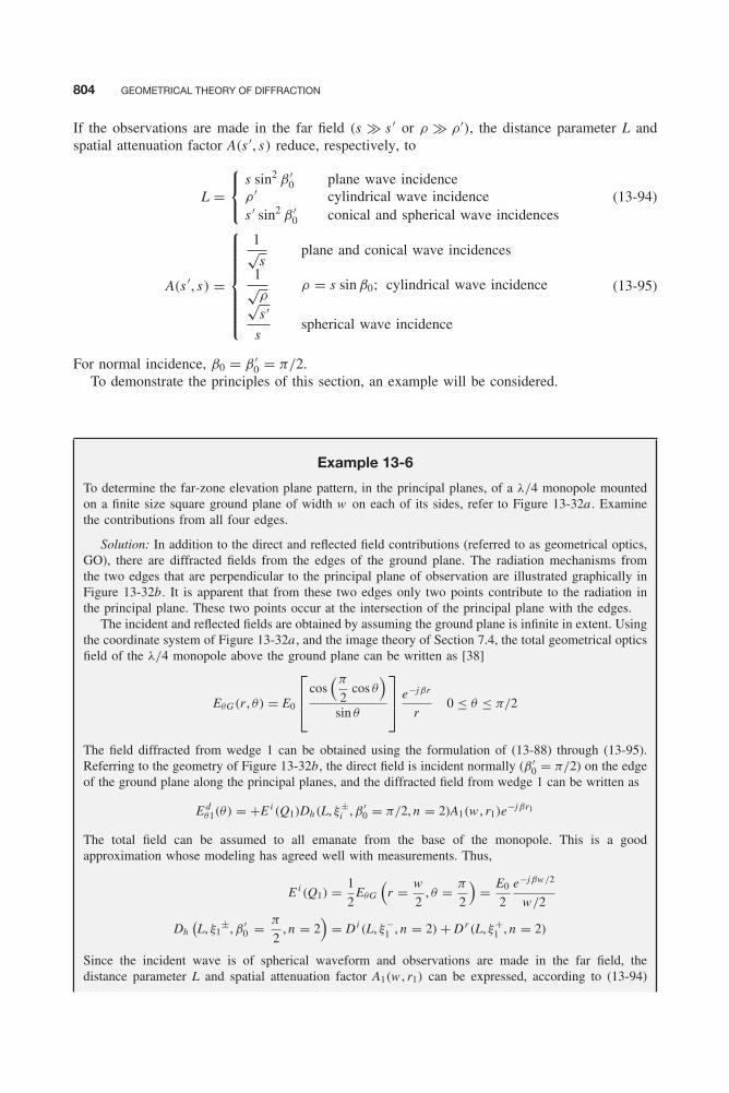
Balanis c13.tex V2 - 11/24/2011 12:45 A.M. Page 804
804 GEOMETRICAL THEORY OF DIFFRACTION
If the observations are made in the far field (s � s ′ or ρ � ρ ′), the distance parameter L andspatial attenuation factor A(s ′, s) reduce, respectively, to
L =⎧⎨⎩ s sin2 β ′
0 plane wave incidenceρ ′ cylindrical wave incidences ′ sin2 β ′
0 conical and spherical wave incidences(13-94)
A(s ′, s) =
⎧⎪⎪⎪⎪⎪⎪⎨⎪⎪⎪⎪⎪⎪⎩
1√s
plane and conical wave incidences
1√ρ
ρ = s sin β0; cylindrical wave incidence√
s ′
sspherical wave incidence
(13-95)
For normal incidence, β0 = β ′0 = π/2.
To demonstrate the principles of this section, an example will be considered.
Example 13-6
To determine the far-zone elevation plane pattern, in the principal planes, of a λ/4 monopole mountedon a finite size square ground plane of width w on each of its sides, refer to Figure 13-32a . Examinethe contributions from all four edges.
Solution: In addition to the direct and reflected field contributions (referred to as geometrical optics,GO), there are diffracted fields from the edges of the ground plane. The radiation mechanisms fromthe two edges that are perpendicular to the principal plane of observation are illustrated graphically inFigure 13-32b. It is apparent that from these two edges only two points contribute to the radiation inthe principal plane. These two points occur at the intersection of the principal plane with the edges.
The incident and reflected fields are obtained by assuming the ground plane is infinite in extent. Usingthe coordinate system of Figure 13-32a , and the image theory of Section 7.4, the total geometrical opticsfield of the λ/4 monopole above the ground plane can be written as [38]
EθG (r , θ) = E0
⎡⎢⎣cos(π
2cos θ
)sin θ
⎤⎥⎦ e−jβr
r0 ≤ θ ≤ π/2
The field diffracted from wedge 1 can be obtained using the formulation of (13-88) through (13-95).Referring to the geometry of Figure 13-32b, the direct field is incident normally (β ′
0 = π/2) on the edgeof the ground plane along the principal planes, and the diffracted field from wedge 1 can be written as
E dθ1(θ) = +E i (Q1)Dh(L, ξ±
i , β ′0 = π/2, n = 2)A1(w , r1)e
−jβr1
The total field can be assumed to all emanate from the base of the monopole. This is a goodapproximation whose modeling has agreed well with measurements. Thus,
E i (Q1) = 1
2EθG
(r = w
2, θ = π
2
)= E0
2
e−jβw/2
w/2
Dh(L, ξ1
±, β ′0 = π
2, n = 2
)= Di (L, ξ−
1 , n = 2) + Dr (L, ξ+1 , n = 2)
Since the incident wave is of spherical waveform and observations are made in the far field, thedistance parameter L and spatial attenuation factor A1(w , r1) can be expressed, according to (13-94)

Balanis c13.tex V2 - 11/24/2011 12:45 A.M. Page 805
GEOMETRICAL THEORY OF DIFFRACTION: EDGE DIFFRACTION 805
and (13-95) for β ′0 = π/2, as
L = s ′ sin2 β ′0
s ′ = w/2β ′
0 = π/2
= w
2
A1(w , r1) =√
s ′
s
∣∣∣∣s ′=w/2s=r1
=√
w/2
r1
w
q
q
f
x
z
y
(a)
(b)
b′0
λ/4
λ/4
λ/4
r
r1
r2r
Diffr
acte
d
Diffr
acte
dDire
ctRe
flect
ed
#2 #1
y2y1
w2
w2
w2
w2
Figure 13-32 Vertical monopole on a square ground plane, and reflection and diffraction mechanisms.(a) Monopole on ground plane. (b) Reflection and diffraction mechanisms.
Balanis c13.tex V2 - 11/24/2011 12:45 A.M. Page 806
806 GEOMETRICAL THEORY OF DIFFRACTION
Since the angle of incidence ψ0 from the main source toward the point of diffraction Q1 is zero degrees(ψ0 = 0), then
ξ−1 = ψ1 − ψ0 = ψ1 = θ + π
2= ξ1
ξ+1 = ψ1 + ψ0 = ψ1 = θ + π
2= ξ1
Therefore,
Dh(L, ξ±
1 , β ′0 = π
2, n = 2
)= 2Di
(w
2, θ + π
2, n = 2
)= 2Dr
(w
2, θ + π
2, n = 2
)The total diffracted field can now be written as
E dθ1(θ) = E0
2
e−jβw/2
w/22Di ,r
(w
2, θ + π
2, n = 2
) √w/2
r1e−jβr1
= E0
[e−jβw/2
√w/2
Di ,r(w
2, θ + π
2, n = 2
)] e−jβr1
r1
E dθ1(θ) = E0V i ,r
B
(w
2, θ + π
2, n = 2
) e−jβr1
r1
Using a similar procedure, the field diffracted from wedge 2 can be written, by referring to the geometryof Figure 13-32b, as
E dθ2(θ) = −E0
[e−jβw/2
√w/2
Di ,r(w
2, ξ2, n = 2
)] e−jβr2
r2
E dθ2(θ) = −E0V i ,r
B
(w
2, ξ2, n = 2
) e−jβr2
r2
where
ξ2 = ψ2 =
⎧⎪⎨⎪⎩π
2− θ , 0 ≤ θ ≤ π
25π
2− θ ,
π
2< θ < π
For far-field observations
r1 � r − w
2cos
(π
2− θ
)= r − w
2sin θ
r2 � r + w
2cos
(π
2− θ
)= r + w
2sin θ
⎫⎪⎬⎪⎭ for phase terms
r1 � r2 � r for amplitude terms
Therefore, the diffracted fields from wedges 1 and 2 reduce to
E dθ1(θ) = + E0V i ,r
B
(w
2, θ + π
2, n = 2
)ej (βw/2) sin θ e−jβr
r
E dθ2(θ) = −E0V i ,r
B
(w
2, ξ2, n = 2
)e−j (βw/2) sin θ e−jβr
r
It should be noted that there are oblique incidence diffractions from the other two edges of the groundplane that are parallel to the principal plane of observation. However, the diffracted field from theseedges is primarily cross-polarized (Eφ component) to the incident Eθ field and to the Eθ field produced
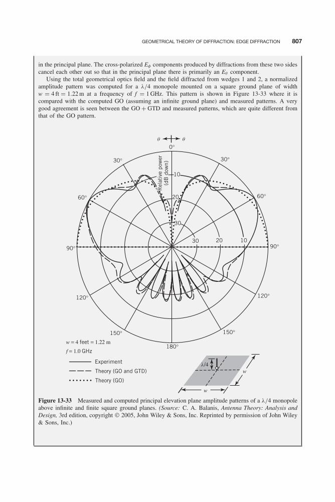
Balanis c13.tex V2 - 11/24/2011 12:45 A.M. Page 807
GEOMETRICAL THEORY OF DIFFRACTION: EDGE DIFFRACTION 807
in the principal plane. The cross-polarized Eφ components produced by diffractions from these two sidescancel each other out so that in the principal plane there is primarily an Eθ component.
Using the total geometrical optics field and the field diffracted from wedges 1 and 2, a normalizedamplitude pattern was computed for a λ/4 monopole mounted on a square ground plane of widthw = 4 ft = 1.22 m at a frequency of f = 1 GHz. This pattern is shown in Figure 13-33 where it iscompared with the computed GO (assuming an infinite ground plane) and measured patterns. A verygood agreement is seen between the GO + GTD and measured patterns, which are quite different fromthat of the GO pattern.
f = 1.0 GHz
w = 4 feet = 1.22 m
w
wTheory (GO and GTD)
Experiment
Theory (GO)
150°
180°
150°
120°
90°90°
60° 60°
30°
10
10
20
20
30
30
30°
0°
120°
l/4
Rel
ativ
e po
wer
(dB
dow
n)
q q
Figure 13-33 Measured and computed principal elevation plane amplitude patterns of a λ/4 monopoleabove infinite and finite square ground planes. (Source: C. A. Balanis, Antenna Theory: Analysis andDesign, 3rd edition, copyright © 2005, John Wiley & Sons, Inc. Reprinted by permission of John Wiley& Sons, Inc.)

Balanis c13.tex V2 - 11/24/2011 12:45 A.M. Page 808
808 GEOMETRICAL THEORY OF DIFFRACTION
13.3.4 Curved Edge Diffraction: Oblique Incidence
The edges of many practical antenna or scattering structures are not straight, as demonstrated inFigure 13-34 by the edges of a circular ground plane, a paraboloidal reflector, and a conical horn.In order to account for the diffraction phenomenon from the edges of these structures, even intheir principal planes, curved edge diffraction must be utilized.
Curved edge diffraction can be derived by assuming an oblique wave incidence (at an angleβ ′
0) on a curved edge, as shown in Figure 13-35, where the surfaces (sides) forming the curvededge in general may be convex, concave, or plane. Since diffraction is a local phenomenon, thecurved edge geometry can be approximated at the point of diffraction QD by a wedge whosestraight edge is tangent to the curved edge at that point and whose plane surfaces are tangent tothe curved surfaces forming the curved edge. This allows wedge diffraction theory to be applieddirectly to curved edge diffraction by simply representing the curved edge by an equivalentwedge. Analytically, this is accomplished simply by generalizing the expressions for the distanceparameter L that appear in the arguments of the transition functions.
The general form of oblique incidence curved edge diffraction can be expressed in matrix formas in (13-88). However, the diffraction coefficients, distance parameters, and spatial spreadingfactor must be modified to account for the curvature of the edge and its curved surfaces (sides).
The diffraction coefficients Ds and Dh are those of (13-89a) and (13-89b), where Di and Dr
can be found by imposing the continuity conditions on the total field across the incident andreflection shadow boundaries. Doing this, we can show that Di and Dr of (13-90a) and (13-90b)take the form of [10]
Di (Li , φ − φ′, n)
= − e−jπ/4
2n√
2πβ sin β ′0
{cot
[π + (φ − φ′)
2n
]F [βLi g+(φ − φ′)]
+ cot
[π − (φ − φ′)
2n
]F [βLi g−(φ − φ′)]
} (13-96a)
Dr (Lr , φ + φ′, n)
= − e−jπ/4
2n√
2πβ sin β ′0
{cot
[π + (φ + φ′)
2n
]F [βLrng+(φ + φ′)]
+ cot
[π − (φ + φ′)
2n
]F [βLrog+(φ + φ′)]
} (13-96b)
where
Li = s(ρ ie + s)ρ i
1ρi2 sin2 β ′
0
ρ ie(ρ
i1 + s)(ρ i
2 + s)(13-97a)
Lro,rn = s(ρre + s)ρr
1ρr2 sin2 β ′
0
ρre (ρ
r1 + s)(ρr
2 + s)(13-97b)
ρ i1, ρ i
2 = radii of curvature of the incident wave front at QD
ρ ie = radius of curvature of the incident wave front in the edge fixed plane of
incidence

Balanis c13.tex V2 - 11/24/2011 12:45 A.M. Page 809
GEOMETRICAL THEORY OF DIFFRACTION: EDGE DIFFRACTION 809
(a)
(b)
(c)
Feed
x
y
z
a
Figure 13-34 Diffraction by curved-edge structures. (a) Circular ground plane. (b) Paraboloidal reflector.(c) Conical horn.
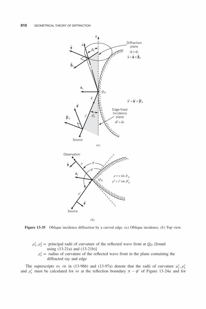
Balanis c13.tex V2 - 11/24/2011 12:45 A.M. Page 810
810 GEOMETRICAL THEORY OF DIFFRACTION
s
QD
QD
b′0s′
f′
f
0r′ = s′ sin b′
r′
r
0r = s sin b
β0
Diffraction plane
Observation
Source
Source
Edge-fixed Incidence
plane
(b)
(a)
sφ
φ
e
β0
ne
ne
s = φ × β0
(s × e)
s′ = φ′ × β′0s′
φ′
φ′
β′0 (s′ × e)
Figure 13-35 Oblique incidence diffraction by a curved edge. (a) Oblique incidence. (b) Top view.
ρr1 , ρr
2 = principal radii of curvature of the reflected wave front at QD [foundusing (13-21a) and (13-21b)]
ρre = radius of curvature of the reflected wave front in the plane containing the
diffracted ray and edge
The superscripts ro, rn in (13-96b) and (13-97a) denote that the radii of curvature ρr1 , ρr
2and ρr
e must be calculated for ro at the reflection boundary π − φ′ of Figure 13-24a and for

Balanis c13.tex V2 - 11/24/2011 12:45 A.M. Page 811
GEOMETRICAL THEORY OF DIFFRACTION: EDGE DIFFRACTION 811
rn at the reflection boundary (2n − 1)π − φ′ of Figure 13-24b. For far-field observation, wheres � ρ i
e , ρ i1, ρ i
2, ρre , ρr
1 , ρr2 (13-97a), (13-97b) simplify to
Li = ρ i1ρ
i2
ρ ie
sin2 β ′0 (13-98a)
Lro,rn = ρr1ρ
r2
ρre
sin2 β ′0 (13-98b)
If the intersecting curved surfaces forming the curved edge in Figure 13-35 are plane surfacesthat form an ordinary wedge, then the distance parameters in (13-97a) and (13-97b) or (13-98a)and (13-98b) are equal, that is,
Lro = Lrn = Li (13-99)
Using the geometries of Figure 13-36, it can be shown that the spatial spreading factor A(ρc , s)of (13-35) for the curved edge diffraction takes the form
A(ρc , s) =√
ρc
s(ρc + s)
s�ρc� 1
s
√ρc (13-100)
1
ρc= 1
ρe− n̂e • (ŝ′ − ŝ)
ρg sin2 β ′0
(13-100a)
where ρc = distance between caustic at edge and second caustic of diffracted ray
ρe = radius of curvature of incidence wave front in the edge-fixed plane of incidencewhich contains unit vectors ŝ′ and ê (infinity for plane, cylindrical, and conicalwaves; ρe = s ′ for spherical waves)
ρg = radius of curvature of the edge at the diffraction point
n̂e = unit vector normal to the edge at QD and directed away from the center of curvature
ŝ′ = unit vector in the direction of incidence
ŝ = unit vector in the direction of diffraction
β ′0 = angle between ŝ′ and tangent to the edge at the point of diffraction
ê = unit vector tangent to the edge at the point of diffraction
For normal incidence, β ′0 = π/2.
The spatial attenuation factor (13-100) creates additional caustics, other than the ones thatoccur at the points of diffraction. Each caustic occurs at a distance ρc from the one at thediffraction point. Diffracted fields in the regions of the caustics must be corrected to remove thediscontinuities and inaccuracies from them.
To demonstrate the principles of curved edge diffraction, let us consider Example 13-7.
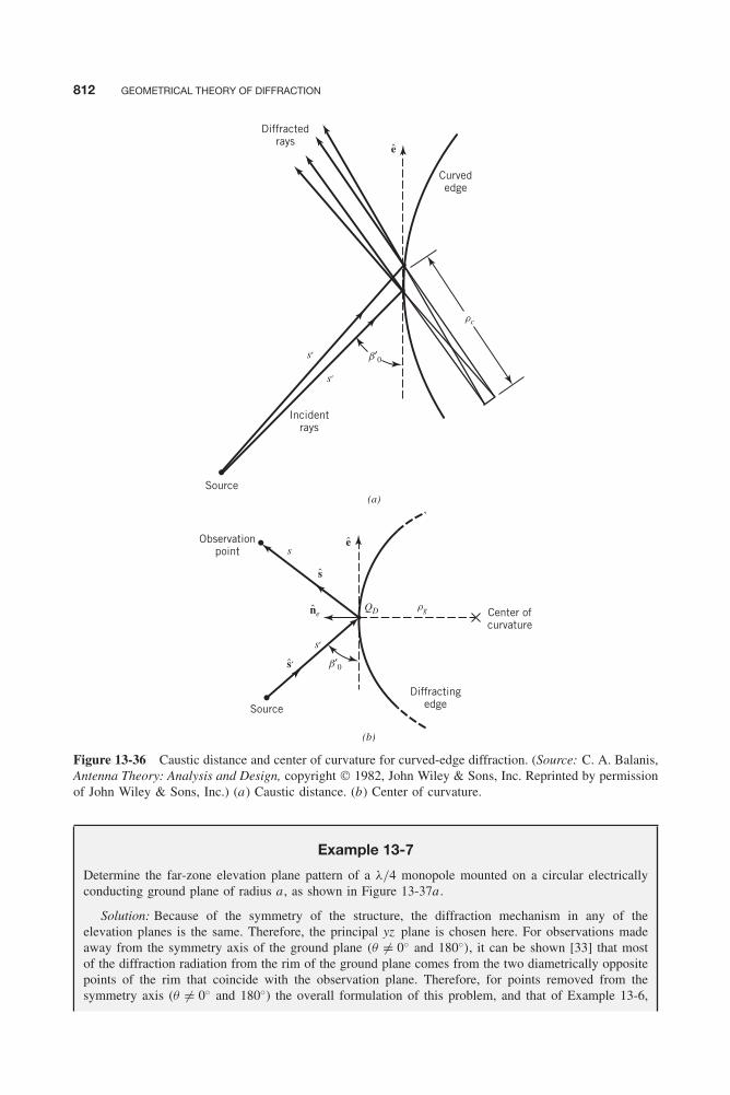
Balanis c13.tex V2 - 11/24/2011 12:45 A.M. Page 812
812 GEOMETRICAL THEORY OF DIFFRACTION
(a)
(b)
Diffractedrays
Curvededge
Incidentrays
Source
Observationpoint
Source
Diffractingedge
Center ofcurvature
QD rg
rc
s′
s′
s′
s′
ne
s
s
b′0
b′0
e
e
Figure 13-36 Caustic distance and center of curvature for curved-edge diffraction. (Source: C. A. Balanis,Antenna Theory: Analysis and Design, copyright © 1982, John Wiley & Sons, Inc. Reprinted by permissionof John Wiley & Sons, Inc.) (a) Caustic distance. (b) Center of curvature.
Example 13-7
Determine the far-zone elevation plane pattern of a λ/4 monopole mounted on a circular electricallyconducting ground plane of radius a , as shown in Figure 13-37a .
Solution: Because of the symmetry of the structure, the diffraction mechanism in any of theelevation planes is the same. Therefore, the principal yz plane is chosen here. For observations madeaway from the symmetry axis of the ground plane (θ �= 0◦ and 180◦), it can be shown [33] that mostof the diffraction radiation from the rim of the ground plane comes from the two diametrically oppositepoints of the rim that coincide with the observation plane. Therefore, for points removed from thesymmetry axis (θ �= 0◦ and 180◦) the overall formulation of this problem, and that of Example 13-6,
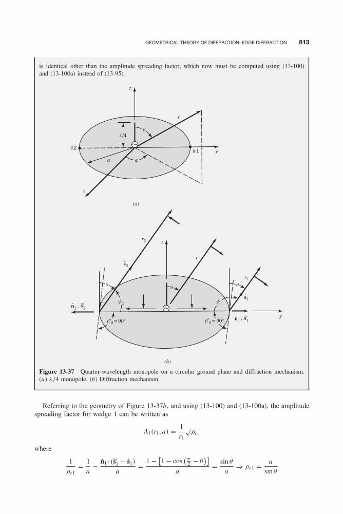
Balanis c13.tex V2 - 11/24/2011 12:45 A.M. Page 813
GEOMETRICAL THEORY OF DIFFRACTION: EDGE DIFFRACTION 813
is identical other than the amplitude spreading factor, which now must be computed using (13-100)and (13-100a) instead of (13-95).
q q
l/4
#2 #1
z
r
(a)
(b)
x
r2
r1
z
y
rs2
1
n , s′2 2
y
q
fa
q
y2 y1
b′0 = 90° b′0 = 90°
s
n , s′1 1
Figure 13-37 Quarter-wavelength monopole on a circular ground plane and diffraction mechanism.(a) λ/4 monopole. (b) Diffraction mechanism.
Referring to the geometry of Figure 13-37b, and using (13-100) and (13-100a), the amplitudespreading factor for wedge 1 can be written as
A1(r1, a) = 1
r1
√ρc1
where
1
ρc1= 1
a− n̂1 • (ŝ′
1 − ŝ1)
a= 1 − [
1 − cos(
π2 − θ
)]a
= sin θ
a⇒ ρc1 = a
sin θ

Balanis c13.tex V2 - 11/24/2011 12:45 A.M. Page 814
814 GEOMETRICAL THEORY OF DIFFRACTION
Therefore,
A1(r1, a) = 1
r1
√a
sin θ� 1
r
√a
sin θ
In a similar manner, the amplitude spreading factor for wedge 2 can be expressed as
A2(r2, a) = 1
r2
√ρc2
where
1
ρc2= 1
a− n̂2 • (ŝ′
2 − ŝ2)
a=
1 −[1 − cos
(π
2+ θ
)]a
= − sin θ
a⇒ ρc2 = − a
sin θ
This reduces the amplitude spreading factor to
A2(r2, a) = 1
r2
√− a
sin θ� 1
r
√− a
sin θ
Using the results from Example 13-6, the fields for this problem can be written as
EθG(r , θ) = E0
⎡⎢⎣cos(π
2cos θ
)sin θ
⎤⎥⎦ e−jβr
r, 0 ≤ θ ≤ π/2
E dθ1(r , θ) = E0V i ,r
B
(a , θ + π
2, n = 2
) ejβa sin θ
√sin θ
e−jβr
r, θ0 ≤ θ ≤ π − θ0
E dθ2(r , θ) = −E0V i ,r
B (a , ξ2, n = 2)e−jβa sin θ
√− sin θ
e−jβr
r, θ0 ≤ θ ≤ π − θ0
where
ξ2 = ψ2 =
⎧⎪⎨⎪⎩π
2− θ , θ0 ≤ θ ≤ π
25π
2− θ ,
π
2< θ ≤ π − θ0
It is noted that at θ = 0◦ or 180◦, the diffracted fields become singular because along thesedirections there are caustics for the diffracted fields. The rim of the ground plane acts as a ringradiator , which is illustrated graphically in Figure 13-38. The ring radiator can be formulatedanalytically (see Problem 13.49) as a continuous symmetrical and constant source of diffractionaround the rim of the circular ground plane. This can be cast as an integral with uniform excitation
z
x
y#2 #1
Figure 13-38 Uniform ring radiator representing diffractions around the rim of the circular ground plane.

Balanis c13.tex V2 - 11/24/2011 12:45 A.M. Page 815
GEOMETRICAL THEORY OF DIFFRACTION: EDGE DIFFRACTION 815
around the rim of the circular ground plane, and it can be treated similarly as a circular loop ofuniform current [38]. Toward and near θ = 0◦ and 180◦, the integral reduces to a Bessel functionof the first kind of order one. However, it can be shown, using the method of steepest descent(saddle point method), that the integral representing the continuous ring radiator radiator reducesto a two-point diffraction for angles away from θ = 0◦ and 180◦ [33]. Due to the ring radiatorcharacteristics, the radiation of the monopole toward and near θ = 0◦ and 180◦ is much moreintense for this geometry compared to when the monopole is mounted on a rectangular/squareground plane, as shown in Figure 13-33. Similarly, the scattering from circular ground planes andapertures is much more intense toward and near θ = 0◦ and 180◦ than that from rectangular/squareground planes and apertures. Therefore, to reduce the radar signature/visibility of the engineinlets (apertures) of the F-117, they may have been chosen to be rectangular/square, as shownin Figure 13-1. Toward θ = 0◦ and 180◦ the infinite number of diffracted rays from the rim areidentical in amplitude and phase and lead to the caustics. Therefore, the diffracted fields from theaforementioned two points of the rim are invalid within a cone of half included angle θ0, which isprimarily a function of the radius of curvature of the rim. For most moderate size ground planes,θ0 is in the range of 10◦ < θ0 < 30◦.
To make corrections for the diffracted field singularity and inaccuracy at and near the symmetryaxis (θ = 0◦ and 180◦), due to axial caustics, the rim of the ground plane must be modeled asa ring radiator [32, 33]. This can be accomplished by using “equivalent” current concepts indiffraction, that will be discussed in the next section.
A pattern based on the formulations of the preceding two-point diffraction was computed for aground plane of 4.064λ diameter. This pattern is shown in Figure 13-39 where it is compared withmeasurements. It should be noted that this pattern was computed using the two-point diffractionfor 10◦ � θ � 170◦ (θ0 � 10◦); the remaining parts were computed using equivalent currentconcepts that will be discussed next.
13.3.5 Equivalent Currents in Diffraction
In contrast to diffraction by straight edges, diffraction by curved edges creates caustics. If obser-vations are not made at or near caustics, ordinary diffraction techniques can be applied; otherwise,corrections must be made.
One technique that can be used to correct for caustic discontinuities and inaccuracies is theconcept of the equivalent currents [32–36, 54–61]. To apply this principle, the two-dimensionalwedge of Figure 13-13 is replaced by one of the following two forms:
1. An equivalent two-dimensional electric line source of equivalent electric current I e , for softpolarization diffraction.
2. An equivalent two-dimensional magnetic line source of equivalent magnetic current I m , forhard polarization diffraction.
This is illustrated in Figure 13-40. The equivalent currents I e and I m are adjusted so that thefield radiated by each of the line sources is equal to the diffracted field of the correspondingpolarization.
The electric field radiated by a two-dimensional electric line source placed along the z axiswith a constant current I e
z is given by (11-10a), or
Ez = −β2I ez
4ωεH (2)
0 (βρ)βρ→∞� −I e
zηβ
2
√j
2πβ
e−jβρ
√ρ
(13-101a)
where H (2)0 (βρ) is the Hankel function of the second kind of order zero. The approximate form
of (13-101a) is valid for large distances of observation (far field), and it is obtained by replacing
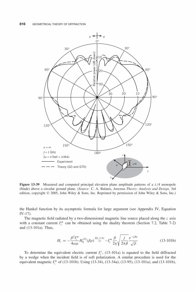
Balanis c13.tex V2 - 11/24/2011 12:45 A.M. Page 816
816 GEOMETRICAL THEORY OF DIFFRACTION
f = 1 GHz
s = ∞
2a = 4 feet = 4.064l
Theory (GO and GTD)
Experiment
150°
180°
150°
120°
90°90°
60° 60°
30°
10
10
20
20
30
30
30°
0°
120°
l/4
q q
y
x
a
z
Rel
ativ
e po
wer
(dB
dow
n)
Figure 13-39 Measured and computed principal elevation plane amplitude patterns of a λ/4 monopole(blade) above a circular ground plane. (Source: C. A. Balanis, Antenna Theory: Analysis and Design, 3rdedition, copyright © 2005, John Wiley & Sons, Inc. Reprinted by permission of John Wiley & Sons, Inc.)
the Hankel function by its asymptotic formula for large argument (see Appendix IV, EquationIV-17).
The magnetic field radiated by a two-dimensional magnetic line source placed along the z axiswith a constant current I m
z can be obtained using the duality theorem (Section 7.2, Table 7-2)and (13-101a). Thus,
Hz = −β2I mz
4ωμH (2)
0 (βρ)βρ→∞� −I m
zβ
2η
√j
2πβ
e−jβρ
√ρ
(13-101b)
To determine the equivalent electric current I ez , (13-101a) is equated to the field diffracted
by a wedge when the incident field is of soft polarization. A similar procedure is used for theequivalent magnetic I m
z of (13-101b). Using (13-34), (13-34a), (13-95), (13-101a), and (13-101b),
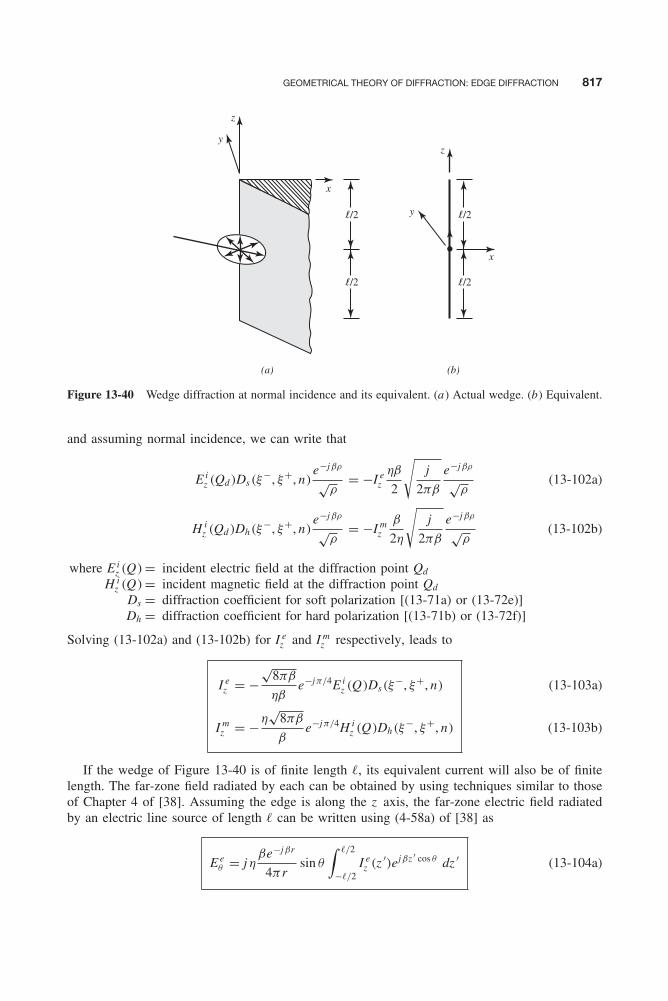
Balanis c13.tex V2 - 11/24/2011 12:45 A.M. Page 817
GEOMETRICAL THEORY OF DIFFRACTION: EDGE DIFFRACTION 817
(b)(a)
x
y
x
zy
z
l/2
l/2
l/2
l/2
Figure 13-40 Wedge diffraction at normal incidence and its equivalent. (a) Actual wedge. (b) Equivalent.
and assuming normal incidence, we can write that
E iz (Qd )Ds(ξ
−, ξ+, n)e−jβρ
√ρ
= −I ez
ηβ
2
√j
2πβ
e−jβρ
√ρ
(13-102a)
H iz (Qd )Dh(ξ
−, ξ+, n)e−jβρ
√ρ
= −I mz
β
2η
√j
2πβ
e−jβρ
√ρ
(13-102b)
where E iz (Q) = incident electric field at the diffraction point Qd
H iz (Q) = incident magnetic field at the diffraction point Qd
Ds = diffraction coefficient for soft polarization [(13-71a) or (13-72e)]Dh = diffraction coefficient for hard polarization [(13-71b) or (13-72f)]
Solving (13-102a) and (13-102b) for I ez and I m
z respectively, leads to
I ez = −
√8πβ
ηβe−jπ/4E i
z (Q)Ds(ξ−, ξ+, n)
I mz = −η
√8πβ
βe−jπ/4H i
z (Q)Dh(ξ−, ξ+, n)
(13-103a)
(13-103b)
If the wedge of Figure 13-40 is of finite length �, its equivalent current will also be of finitelength. The far-zone field radiated by each can be obtained by using techniques similar to thoseof Chapter 4 of [38]. Assuming the edge is along the z axis, the far-zone electric field radiatedby an electric line source of length � can be written using (4-58a) of [38] as
E eθ = jη
βe−jβr
4πrsin θ
∫ �/2
−�/2I ez (z ′)ejβz ′ cos θ dz ′ (13-104a)
Balanis c13.tex V2 - 11/24/2011 12:45 A.M. Page 818
818 GEOMETRICAL THEORY OF DIFFRACTION
Using duality, the magnetic field of a magnetic line source can be written as
H mθ = j
βe−jβr
4πηrsin θ
∫ �/2
−�/2I mz (z ′)ejβz ′ cos θ dz ′ (13-104b)
For a constant equivalent current, the integrals in (13-104a) and (13-104b) reduce to a sin(ζ )/ζ
form.If the equivalent current is distributed along a circular loop of radius a and it is parallel to
the xy plane, the field radiated by each of the equivalent currents can be obtained using thetechniques of Chapter 5, Section 5.3, of [38]. Thus,
E eφ = −jωμae−jβr
4πr
∫ 2π
0I eφ (φ′) cos(φ − φ′)ejβa sin θ cos(φ−φ′)dφ′
H mφ = −jωεae−jβr
4πr
∫ 2π
0I mφ (φ′) cos(φ − φ′)ejβa sin θ cos(φ−φ′)dφ′
(13-105a)
(13-105b)
If the equivalent currents are constant, the field is not a function of the azimuthal observationangle φ, and (13-105a) and (13-105b) reduce to
E eφ = aωμe−jβr
2rI eφ J1(βa sin θ) (13-106a)
H mφ = aωεe−jβr
2rI mφ J1(βa sin θ) (13-106b)
where J1(x) is the Bessel function of the first kind of order 1.For diffraction by an edge of finite length, the equivalent current concept for diffraction
assumes that each incremental segment of the edge radiates as would a corresponding segmentof a two-dimensional edge of infinite length. Similar assumptions are used for diffraction fromfinite length curved edges. The concepts, although approximate, have been shown to yield verygood results.
For oblique plane wave incidence diffraction by a wedge of finite length �, as shown inFigure 13-41, the equivalent currents of (13-103a) and (13-103b) take the form
I ez = −
√8πβ
ηβe−jπ/4E i
z (QD )Ds(ξ−, ξ+, n; β ′
0)
s ′�z ′� −
√8πβ
ηβe−jπ/4E i
z (0)Ds(ξ−, ξ+, n; β ′
0)e−jβz ′ cos β ′
0
(13-107a)
I mz = −η
√8πβ
βe−jπ/4H i
z (QD )Dh(ξ−, ξ+, n;β ′
0)
s ′�z ′� −η
√8πβ
βe−jπ/4H i
z (0)Dh(ξ−, ξ+, n; β ′
0)e−jβz ′ cos β ′
0
(13-107b)
where −�/2 ≤ z ′ ≤ �/2 (� = length of wedge) and Ds and Dh are formed by (13-96a) and(13-96b). The far-zone fields associated with the equivalent currents of (13-107a) and (13-107b)can be found using, respectively, (13-104a) and (13-104b).

Balanis c13.tex V2 - 11/24/2011 12:45 A.M. Page 819
GEOMETRICAL THEORY OF DIFFRACTION: EDGE DIFFRACTION 819
z
s
r
s′
r′
′
QD l/2
l/2
β0
β0
θz′
dz′
0
Source
Observation
y
x
s′
s
Figure 13-41 Oblique incidence diffraction by a finite length wedge.
To demonstrate the technique of curved edge diffraction and the equivalent current concept,the radiation of a λ/4 monopole (blade) mounted on a circular ground plane was modeled. Theanalytical formulation is assigned as a problem at the end of the chapter. The computed patternis shown in Figure 13-39 where it is compared with measurements.
To make corrections for the diffracted field discontinuity and inaccuracy at and near thesymmetry axis (θ = 0◦ and 180◦), due to axial caustics, the rim of the ground plane was modeledas a ring radiator [32, 33]. Equivalent currents were used to compute the pattern in the regiongiven by 0◦ ≤ θ ≤ θ0 and 180◦ − θ0 ≤ θ ≤ 180◦. In the other space, a two-point diffraction wasused. The two points were taken diametrically opposite to each other, and they were containedin the plane of observation. The value of θ0 depends upon the curvature of the ground plane. Formost ground planes of moderate size, θ0 is in the range 10◦ < θ0 < 30◦.
A very good agreement between theory and experiment is exhibited in Figure 13-39. Fora ground plane of this size, the blending of the two-point diffraction pattern and the patternfrom the ring source radiator was performed at θ0 � 10◦. It should be noted that the minor lobesnear the symmetry axis (θ � 0◦ and θ � 180◦) for the circular ground plane are more intensethan the corresponding ones for the square plane of Figure 13-33. In addition, the back lobenearest θ = 180◦ is of greater magnitude than the one next to it. These effects are due to the ringsource radiation by the rim [33] of the circular ground plane toward the symmetry axis.
13.3.6 Slope Diffraction
Until now the field diffracted by an edge has been found based on (13-34a), (13-85), or (13-88)where Ei (QD ) represents the incident field at the point of diffraction. This type of formulationindicates that if the incident field Ei (QD ) at the point of diffraction QD is zero, then the diffractedfield will be zero. In addition to this type of diffraction, there is an additional diffraction term

Balanis c13.tex V2 - 11/24/2011 12:45 A.M. Page 820
820 GEOMETRICAL THEORY OF DIFFRACTION
that is based not on the magnitude of the incident field at the point of diffraction but rather onthe slope (rate of change, or directional derivative) of the incident field at the point of diffraction.This is a higher-order diffraction, and it becomes more significant when the incident field at thepoint of diffraction vanishes. It is referred to as slope diffraction, and it creates currents on thewedge surface that result in a diffracted field [52].
By referring to the geometry of Figure 13-42, the slope diffracted field can be computed using
Soft Polarization
E d = 1
jβ
[∂E i (QD )
∂n
](∂Ds
∂φ′
)√ρc
s(ρc + s)e−jβs
∂E i (QD )
∂n= 1
s ′∂E i
∂φ′
∣∣∣∣QD
= slope of the incident field
∂Ds
∂φ′ = slope diffraction coefficient
(13-108)
(13-108a)
(13-108b)
Hard Polarization
H d = 1
jβ
[∂H i (QD )
∂n
](∂Dh
∂φ′
)√ρc
s(ρc + s)e−jβs
∂H i (QD )
∂n= 1
s ′∂H i
∂φ′
∣∣∣∣QD
= slope of the incident field
∂Dh
∂φ′ = slope diffraction coefficient
(13-109)
(13-109a)
(13-109b)
Therefore, in general, the total diffracted field can be found using
U d =[
U i (QD )Ds , h + 1
jβ
∂U i (QD )
∂n
∂Ds , h
∂φ′
]√ρc
s(ρc + s)e−jβs (13-110)
ObservationSource
f
f′
n = s ′ f′
s′
y
s
zx
∂∂n
∂∂f′
1s′=
n
WA = (2 − n)p
Figure 13-42 Wedge geometry for slope diffraction.

Balanis c13.tex V2 - 11/24/2011 12:45 A.M. Page 821
GEOMETRICAL THEORY OF DIFFRACTION: EDGE DIFFRACTION 821
where the first term represents the contribution to the total diffracted field due to the magnitudeof the incident field and the second accounts for the contribution due to the slope (rate of change)of the incident field. In (13-110), U represents the electric field for soft polarization and themagnetic field for hard polarization. Similarly Ds , h is used to represent Ds for soft polarizationand Dh for hard polarization.
The slope diffraction coefficients for soft and hard polarizations can be written, respectively,as [52]
∂Ds(φ, φ′, n; β ′0)
∂φ′
= − e−jπ/4
4n2√
2πβ sin β ′0
({csc2
[π + (φ − φ′)
2n
]Fs [βLg+(φ − φ′)]
− csc2
[π − (φ − φ′)
2n
]Fs [βLg−(φ − φ′)]
}+
{csc2
[π + (φ + φ′)
2n
]Fs [βLg+(φ + φ′)]
− csc2
[π − (φ + φ′)
2n
]Fs [βLg−(φ + φ′)]
})(13-111a)
∂Dh(φ, φ′, n; β ′0)
∂φ′
= − e−jπ/4
4n2√
2πβ sin β ′0
({csc2
[π + (φ − φ′)
2n
]Fs [βLg+(φ − φ′)]
− csc2
[π − (φ − φ′)
2n
]Fs [βLg−(φ − φ′)]
}−
{csc2
[π + (φ + φ′)
2n
]Fs [βLg+(φ + φ′)]
− csc2
[π − (φ + φ′)
2n
]Fs [βLg−(φ + φ′)]
})(13-111b)
where
Fs(X ) = 2jX
[1 − j 2
√X ejX
∫ ∞√
Xe−jτ2
dτ
]= 2jX [1 − F (X )] (13-111c)
A Fortran and MATLAB computer subroutine designated as SWDC, for Slope Wedge DiffractionCoefficients, computes the normalized (with respect to
√λ) slope diffraction coefficients based
on (13-111a) through (13-111c). It was developed and reported in [53]. This program uses thecomplex function FTF (Fresnel transition function) to complete its computations.
To use the subroutine, the user must specify R = L (in wavelengths), PHID = φ (in degrees),PHIPD = φ′ (in degrees), BTD = β ′
0 (in degrees), and FN = n (dimensionless) and the subroutinecomputes the normalized (with respect to
√λ) slope diffraction coefficients CSDCS = ∂Ds/∂φ′
and CSDCH = ∂Dh/∂φ′.
13.3.7 Multiple Diffractions
Until now we have considered single-order diffractions from each of the edges of a structure. Ifthe structure is composed of multiple edges (as is the case for infinitely thin strips, rectangular

Balanis c13.tex V2 - 11/24/2011 12:45 A.M. Page 822
822 GEOMETRICAL THEORY OF DIFFRACTION
and circular ground planes, etc.), then coupling between the edges will take place. For finitethickness ground planes coupling is evident not only between diametrically opposite edges butalso between edges on the same side of the ground plane. Coupling plays a bigger role when theseparation between the edges is small, and it should then be taken into account.
A. Higher-Order Diffractions For structures with multiple edges, coupling is introduced inthe form of higher-order diffractions. To illustrate this point, let us refer to Figure 13-43a , wherea plane wave of hard polarization, represented by a magnetic field parallel to the edge of thewedges, is incident upon a two-dimensional PEC structure composed of three wedges.
The diffraction mechanism of this system can be outlined as follows: The plane wave incidenton wedge 1, represented by wedge angle WA1, will be diffracted as shown in the Figure 13-43a .This is referred to as first-order diffraction . The field diffracted by wedge 1 in the direction ofwedge 2 (WA2) will be diffracted again, as shown in Figures 13-43a and 13-43b. This is referredto as second-order diffraction , because it is the result of diffraction from diffraction. In turn, thefield diffracted from wedge 2 toward wedges 1 and 3 will be diffracted again. The same procedurecan be followed for second-order diffractions from wedge 3 due to first-order diffractions fromwedge 1. Second- and higher-order diffractions are all referred to as higher-order diffractions , andthey account for coupling between the edges and are more important for bistatic than monostaticscattering.
Following the procedures that have been outlined for diffractions from two-dimensional PECwedges, the first-order diffractions from wedge 1, first-order diffractions from wedge 1 toward
(a)
(b)
Uniformplanewave
#1
#3
#2
S3
S1
S2
Q3
Q1 Q2
r2
r1Hi
z
y
x
q
y2 = p + q2
y1 = 2
y1 = 0y2
y1y1′
y2′ = 0
Plane wave incidence
WA1 WA2
WA3
p − q
Figure 13-43 Higher-order diffractions from a two-dimensional wedged geometry. (a) Plane wave inci-dence and diffraction by wedges. (b) Second-order diffraction by wedge 2 due to diffractions from wedge 1.
Balanis c13.tex V2 - 11/24/2011 12:45 A.M. Page 823
GEOMETRICAL THEORY OF DIFFRACTION: EDGE DIFFRACTION 823
wedge 2, and second-order diffractions from wedge 2 due to first-order diffractions from wedge1, can be written, using the geometries of Figures 13-43a and 13-43b, as:
First-order diffractions from Wedge 1
Hd1y1 = Hi
1(Q1) •[ây ây Dh
1 (r1, ψ1, ψ ′1, n1)
] 1√r1
e−jβr1
Hd1y1 = ây H i
1 (Q1) •
[ây ây
{Di
1(r1, ψ1 − ψ ′1, n1)
+Dr1 (r1, ψ1 + ψ ′
1, n1)
}]1√r1
e−jβr1
Hd1y1 = +ây H i
1 (Q1)
{Di
1(r1, ψ1 − ψ ′1, n1)
+Dr1 (r1, ψ1 + ψ ′
1, n1)
}e−jβr1
√r1
(13-112a)
First-order diffractions from Wedge 1 toward Wedge 2
Hd1y1(r1 = s1, ψ1 = 0, n1)
∣∣∣r1=s1,ψ1=0
= + ây H i1 (Q1)
{Di
1(s1, −ψ ′1, n1)
+Dr1 (s1, ψ ′
1, n1)
}e−jβs1
√s1
Hd1y1(r1 = s1, ψ1 = 0, n1)
∣∣∣r1=s1,ψ1=0
= +ây H i1 (Q1)
{V i
1 (s1, −ψ ′1, n1)
+V r1 (s1, ψ ′
1, n1)
}(13-112b)
Equation 13-112b represents the total diffracted field; half of it is the incident diffracted field andthe other half is the reflected diffracted field.
Second-order diffractions from Wedge 2 due to first-order diffractions from Wedge 1
Hd2y2 = Hi
21(Q2) • ây ây Dh2 (s2, ψ2, ψ ′
2, n2)1√r2
e−jβr2
∣∣∣∣ψ ′
2=0, ψ2= π2 +θ
Hd2y2 = Hd1
y1(r1 = s1, ψ1 = 0, n1)
2•[ây ây Dh
2 (s2, ψ2, ψ ′2, n2)
] e−jβr2
√r2
Hd2y2 = +ây
H i1 (Q1)
2
{V i
B1(s1, −ψ ′1, n1) + V r
B (s1, ψ ′1, n1)
}• ây ây
[Di
2(s2, ψ2, n2) + Dr2 (s2, ψ2, n2)
] e−jβr2
√r2
Hd2y2 = +ây
H i1 (Q1)
2[V i
B1(s1, −ψ ′1, n1) + V r
B (s1, ψ ′1, n1)]
• [Di2(s2, ψ2, n2) + Dr
2 (s2, ψ2, n2)]e−jβr2
√r2
Hd2y2 = +ây
1
2H i
1 (Q1)[Vi
B1(s1, −ψ ′1, n1) + V r
B (s1, ψ ′1, n1)]
•[2Di
2(s2, ψ2, n2)] e−jβr2
√r2
Hd2y2 = +ây H i
1 (Q1)[V i
B (s1, −ψ ′1, n1) + V r
B (s1, ψ ′1, n1)
]• Di
2(s2, ψ2, n2)e−jβr2
√r2
(13-112c)
Balanis c13.tex V2 - 11/24/2011 12:45 A.M. Page 824
824 GEOMETRICAL THEORY OF DIFFRACTION
The 1/2 factor in the development of (13-112c) is used to represent the incident diffracted fieldof (13-112b) from wedge 1 toward wedge 2.
The procedure needs to the repeated for first- and second-order diffractions due to direct waveincidence to wedge 2. The method was developed for hard polarization as there are no higher-order diffractions for soft polarization, based on regular diffraction, since the diffracted fieldfrom any of the wedges toward the others will be zero due to the vanishing of the tangentialelectric field along the PEC surface of the structure.
B. Self-Consistent Method It becomes apparent that the procedure for accounting for higher-order diffractions, especially for third and higher orders, can be very tedious, although straight-forward. It is recommened that when third- and even higher-order diffractions are of interest, aprocedure be adopted that accounts for all (infinite) orders of diffraction. This procedure is knownas the self-consistent method [62], which is used in scattering theory [63]. It can be shown thatthe interactions between the edges can also be expressed in terms of a geometrical progression,which in scattering theory is known as the successive scattering procedure [63].
Let us now illustrate the self-consistent method as applied to the diffractions of Figure13-43a . According to Figures 13-43a and 13-43b diffractions by wedge 1 that are due to radiationfrom the source and that are due to all orders of diffraction from wedge 2 can be written as
U s ,h1 (r1, φ) = U s ,h
0 (Q1)Ds ,h10
(L10, ψ10 = π
2+ φ, ψ ′
10 = δ, n1
)A10(r1)e
−jβr1
+ 1
2[U s ,h
2 (r2 = d , φ = 0)]Ds ,h12 (L12, ψ12 = π − φ, ψ ′
12 = 0, n1)
× A12(r1)e−jβr1 (13-113a)
where U s , h is used to represent here the electric field for soft polarization and the magneticfield for hard polarization. In (13-113a),
U s , h1 (r1, φ)= total diffracted field by wedge 1
U s , h0 (Q1)= field from source at wedge 1
U s , h2 (r2 = d , φ = 0) = total diffracted field (including all orders of diffraction) by wedge 2
toward wedge 1
Ds , h10 = diffraction coefficient (for soft or hard polarization) of wedge 1 that is
due to radiation from the source
Ds , h12 = diffraction coefficient (for soft or hard polarization) of wedge 1 that is
due to radiation from wedge 2
A10 = amplitude spreading factor of wedge 1 that is due to radiation from thesource
A12 = amplitude spreading factor of wedge 1 that is due to radiation fromwedge 2
The unknown part in (13-113a) is U s , h2 (r2 = d , φ = 0), and the self-consistent method will be
used to determine it.Using a similar procedure and referring to Figure 13-44c, the total diffracted field by wedge
2 that is due to all orders of diffraction from wedge 1 can be written as
U s , h2 (r2, φ) = 1
2[U s , h
1 (r1 = d , φ = π)]
× Ds , h21 (L21, ψ21 = φ, ψ ′
21 = 0, n2)A21(r2)e−jβr2 (13-113b)
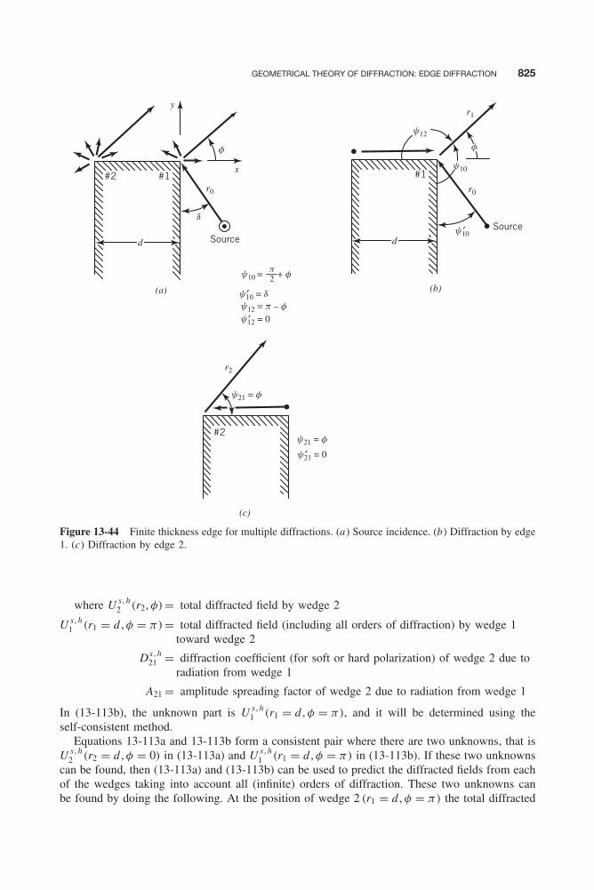
Balanis c13.tex V2 - 11/24/2011 12:45 A.M. Page 825
GEOMETRICAL THEORY OF DIFFRACTION: EDGE DIFFRACTION 825
Source
x
y
r0
d
#2 #1
(a)
f
dSource
r0
r1
d
#1
(b)
f
y10
y12
y10′
2y10 = + f
y10 = dy12 = p – f
′
y12 = 0′
p
r2
#2
(c)
y21 = f
y21 = f
y21 = 0′
Figure 13-44 Finite thickness edge for multiple diffractions. (a) Source incidence. (b) Diffraction by edge1. (c) Diffraction by edge 2.
where U s , h2 (r2, φ)= total diffracted field by wedge 2
U s , h1 (r1 = d , φ = π) = total diffracted field (including all orders of diffraction) by wedge 1
toward wedge 2
Ds , h21 = diffraction coefficient (for soft or hard polarization) of wedge 2 due to
radiation from wedge 1
A21 = amplitude spreading factor of wedge 2 due to radiation from wedge 1
In (13-113b), the unknown part is U s , h1 (r1 = d , φ = π), and it will be determined using the
self-consistent method.Equations 13-113a and 13-113b form a consistent pair where there are two unknowns, that is
U s , h2 (r2 = d , φ = 0) in (13-113a) and U s , h
1 (r1 = d , φ = π) in (13-113b). If these two unknownscan be found, then (13-113a) and (13-113b) can be used to predict the diffracted fields from eachof the wedges taking into account all (infinite) orders of diffraction. These two unknowns canbe found by doing the following. At the position of wedge 2 (r1 = d , φ = π) the total diffracted
Balanis c13.tex V2 - 11/24/2011 12:45 A.M. Page 826
826 GEOMETRICAL THEORY OF DIFFRACTION
field by wedge 1, as given by (13-113a), can be reduced to
[U s , h1 (r1 = d , φ = π)]
= U s , h0 (Q1)
{Ds , h
10
(L10, ψ10 = 3π
2, ψ ′
10 = δ, n1
)A10(r1 = d)e−jβd
}+ [U s , h
2 (r2 = d , φ = 0)]
{1
2Ds , h
12 (L12, ψ12 = 0, ψ ′12 = 0, n1)A12(r1 = d)e−jβd
}(13-114a)
In a similar manner, at the position of wedge 1 (r2 = d , φ = 0) the total diffracted field by wedge2, as given by (13-113b), can be reduced to
[U s , h2 (r2 = d , φ = 0)] = U s , h
1 (r1 = d , φ = π)
×{
12 Ds , h
21 (L21, ψ21 = 0, ψ ′21 = 0, n2)A21(r2 = d)e−βd
}(13-114b)
Equations 13-114a and 13-114b can be rewritten, respectively, in simplified form as
[U s , h1 (r1 = d , φ = π)] = U s , h
0 (Q1)Ts , h10 + [U s , h
2 (r2 = d , φ = 0)]Rs , h12 (13-115a)
[U s , h2 (r2 = d , φ = 0)] = [U s , h
1 (r1 = d , φ = π)]Rs , h12 (13-115b)
where
T s , h10 = Ds , h
10
(L10, ψ10 = 3π
2, ψ ′
10 = δ, n1
)A10(r1 = d)e−jβd
= transmission coefficient from wedge 1 towardwedge 2 due to radiation from main source
(13-115c)
Rs , h12 = 1
2 Ds , h12 (L12, ψ12 = 0, ψ ′
12 = 0, n1)A12(r1 = d)e−jβd
= reflection coefficient from wedge 1 towardwedge 2 due to diffractions from wedge 2
(13-115d)
Rs , h21 = 1
2 Ds , h21 (L21, ψ21 = 0, ψ ′
21 = 0, n2)A21(r2 = d)e−jβd
= reflection coefficient from wedge 2 towardwedge 1 due to diffractions from wedge 1
(13-115e)
The self-consistent pair of (13-115a) and (13-115b) contains the two unknowns that are neededto predict the total diffracted field as given by (13-113a) and (13-113b). Solving (13-115a)and (13-115b) for U s , h
1 (r1 = d , φ = π) and U s , h2 (r2 = d , φ = 0), we can show that
U s , h1 (r1 = d , φ = π) = U s , h
0 (Q1)T s , h
10
1 − Rs , h21 Rs , h
12
(13-116a)
U s , h2 (r2 = d , φ = 0) = U s , h
0 (Q1)T s , h
10 Rs , h21
1 − Rs , h21 Rs , h
12
(13-116b)
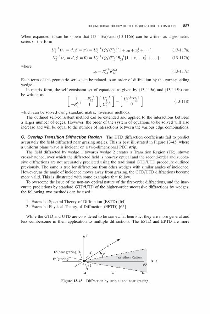
Balanis c13.tex V2 - 11/24/2011 12:45 A.M. Page 827
GEOMETRICAL THEORY OF DIFFRACTION: EDGE DIFFRACTION 827
When expanded, it can be shown that (13-116a) and (13-116b) can be written as a geometricseries of the form
U s , h1 (r1 = d , φ = π) = U s , h
0 (Q1)Ts , h10 [1 + x0 + x 2
0 + · · · ] (13-117a)
U s , h2 (r2 = d , φ = 0) = U s , h
0 (Q1)Ts , h10 Rs , h
21 [1 + x0 + x 20 + · · · ] (13-117b)
wherex0 = Rs , h
21 Rs , h12 (13-117c)
Each term of the geometric series can be related to an order of diffraction by the correspondingwedge.
In matrix form, the self-consistent set of equations as given by (13-115a) and (13-115b) canbe written as [
1 −Rs , h12
−Rs , h21 1
] [U s , h
1
U s , h2
]=
[U s , h
0 T s , h10
0
](13-118)
which can be solved using standard matrix inversion methods.The outlined self-consistent method can be extended and applied to the interactions between
a larger number of edges. However, the order of the system of equations to be solved will alsoincrease and will be equal to the number of interactions between the various edge combinations.
C. Overlap Transition Diffraction Region The UTD diffraction coefficients fail to predictaccurately the field diffracted near grazing angles. This is best illustrated in Figure 13-45, wherea uniform plane wave is incident on a two-dimensional PEC strip.
The field diffracted by wedge 1 towards wedge 2 creates a Transition Region (TR), showncross-hatched, over which the diffracted field is non-ray optical and the second-order and succes-sive diffractions are not accurately predicted using the traditional GTD/UTD procedure outlinedpreviously. The same is true for diffractions from other wedges with similar angles of incidence.However, as the angle of incidence moves away from grazing, the GTD/UTD diffractions becomemore valid. This is illustrated with some examples that follow.
To overcome the issue of the non-ray optical nature of the first-order diffractions, and the inac-curate predictions by standard GTD/UTD of the higher-order successive diffractions by wedges,the following two methods can be used.
1. Extended Spectral Theory of Diffraction (ESTD) [64]2. Extended Physical Theory of Diffraction (EPTD) [65]
While the GTD and UTD are considered to be somewhat heuristic, they are more general andless cumbersome in their application to multiple diffractions. The ESTD and EPTD are more
Ei (grazing)
Ei (near grazing)
Transition Regionx
y
z
w
r
f
#2#1
Figure 13-45 Diffraction by strip at and near grazing.

Balanis c13.tex V2 - 11/24/2011 12:45 A.M. Page 828
828 GEOMETRICAL THEORY OF DIFFRACTION
rigorous and more accurate but less general and more complex. The ESTD is an extension ofthe STD method [66]. Using the ESTD, the current density induced on the scatter of interestis transformed in the spectral domain. The radiation integral is then asymptotically evaluatedin the spectral domain, after the induced current density is multiplied by a spectral diffractioncoefficient. The original STD was limited to a half-plane and aperture scattering for plane waveincidence. The ESTD extends the STD to general double-wedge configuration, and it can be usedfor plane, cylindrical, and spherical wave incidence for both normal and oblique incidences.
The EPTD is an alternative transition-region method based upon a different evaluation of thesurface radiation integral. The induced current density is approximated using the PTD fringecurrents [67], whereas the ESTD uses the UTD diffraction coefficients. The resulting radiationintegral is evaluated asymptotically to obtain the second-order field diffracted by the doublewedge structure. The EPTD formulation is limited to plane-wave incidence, far-field observationin the plane of the structure. As with the ESTD, the EPTD doubly-diffracted field expression canbe greatly simplified for certain geometries, such as the strip.
To demonstrate the concepts of near grazing-angle-incidence diffraction, a numbers ofexamples are considered for monostatic and bistatic scattering for both soft (TMz) andhard (TEz) polarizations [68, 69]. For monostatic scattering, the patterns are illustrated inFigures 13-46a and 13-46b for a strip of width w = 2λ. A width of 2λ is chosen for all casesso that the GTD/UTD diffraction coefficients are valid. For the soft polarization, only first-order
(b)
(a)
0
Moment MethodEPTDUTD(1 − 4)
Mon
osta
tic
RC
S s
/l (
dB)
Mon
osta
tic
RC
S s
/l (
dB)
−20
−10
0
10
20
−45
−30
−15
0
15
45
Observation angle (degrees)90 135 180
0 45Observation angle (degrees)
90 135 180
Moment MethodEPTDUTD(1)
Figure 13-46 Monostatic RCS by a two-dimensional strip of width w = 2λ [68, 69]. (a) Soft (TMz )polarization. (b) Hard (TEz ) polarization.
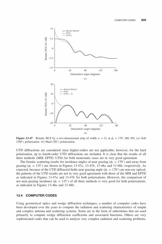
Balanis c13.tex V2 - 11/24/2011 12:45 A.M. Page 829
COMPUTER CODES 829
0
Bis
tati
c R
CS
s/l
(dB
)
−15
−7.5
0
7.5
15
45
Observation angle (degrees)
90 135 180
(b)
(a)
Moment MethodEPTDUTD(1 − 4)
Bis
tati
c R
CS
s/l
(dB
)
−20
−10
0
10
20
0 45
Observation angle (degrees)90 135 180
Moment MethodEPTDUTD(1)
Figure 13-47 Bistatic RCS by a two-dimensional strip of width w = 2λ at φi = 170◦ [68, 69]. (a) Soft(TMz ) polarization. (b) Hard (TEz ) polarization.
UTD diffractions are considered since higher-orders are not applicable; however, for the hardpolarization, up to fourth-order UTD diffractions are included. It is clear that the results of allthree methods (MM, EPTD, UTD) for both monostatic cases are in very good agreement.
The bistatic scattering results for incidence angles of near grazing (φi = 170◦) and away fromgrazing (φi = 135◦) are shown in Figures 13-47a , 13-47b, 13-48a and 13-48b, respectively. Asexpected, because of the UTD diffracted fields near grazing angle (φi = 170◦) are non-ray optical,the patterns of the UTD results are not in very good agreement with those of the MM and EPTDas indicated in Figures 13-47a and 13-47b for both polarizations. However, the comparison ofnot near-grazing incidence (φi = 135◦) of all three methods is very good for both polarizations,as indicated in Figures 13-48a and 13-48b.
13.4 COMPUTER CODES
Using geometrical optics and wedge diffraction techniques, a number of computer codes havebeen developed over the years to compute the radiation and scattering characteristics of simpleand complex antenna and scattering systems. Some are in the form of subroutines that are usedprimarily to compute wedge diffraction coefficients and associated functions. Others are verysophisticated codes that can be used to analyze very complex radiation and scattering problems.
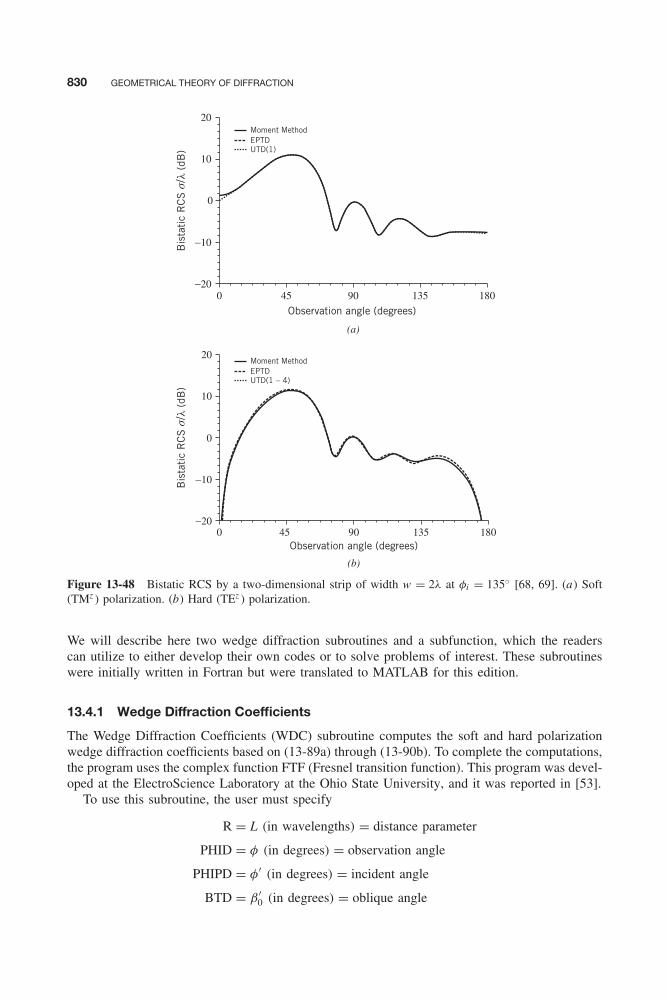
Balanis c13.tex V2 - 11/24/2011 12:45 A.M. Page 830
830 GEOMETRICAL THEORY OF DIFFRACTION
(b)
(a)
0
Moment MethodEPTDUTD(1 − 4)
Bis
tati
c R
CS
s/l
(dB
)B
ista
tic
RC
S s
/l (d
B)
−20
−10
0
10
20
−20
−10
0
10
20
45
Observation angle (degrees)90 135 180
0 45Observation angle (degrees)
90 135 180
Moment MethodEPTDUTD(1)
Figure 13-48 Bistatic RCS by a two-dimensional strip of width w = 2λ at φi = 135◦ [68, 69]. (a) Soft(TMz ) polarization. (b) Hard (TEz ) polarization.
We will describe here two wedge diffraction subroutines and a subfunction, which the readerscan utilize to either develop their own codes or to solve problems of interest. These subroutineswere initially written in Fortran but were translated to MATLAB for this edition.
13.4.1 Wedge Diffraction Coefficients
The Wedge Diffraction Coefficients (WDC) subroutine computes the soft and hard polarizationwedge diffraction coefficients based on (13-89a) through (13-90b). To complete the computations,the program uses the complex function FTF (Fresnel transition function). This program was devel-oped at the ElectroScience Laboratory at the Ohio State University, and it was reported in [53].
To use this subroutine, the user must specify
R = L (in wavelengths) = distance parameter
PHID = φ (in degrees) = observation angle
PHIPD = φ′ (in degrees) = incident angle
BTD = β ′0 (in degrees) = oblique angle

Balanis c13.tex V2 - 11/24/2011 12:45 A.M. Page 831
MULTIMEDIA 831
FN = n (dimensionless) = wedge angle factor
and the program computes the complex diffraction coefficients
CDCS = Ds = complex diffraction coefficient (soft polarization)
CDCH = Dh = complex diffraction coefficient (hard polarization)
13.4.2 Fresnel Transition Function
The Fresnel transition function (FTF) computes the Fresnel transition functions F (X ) of (13-68e),(13-68f), and (13-69e), (13-69f). The program is based on the asymptotic expression of (13-74a)for small arguments (X < 0.3) and on (13-74b) for large arguments (X > 5.5). For interme-diate values (0.3 ≤ X ≤ 5.5), linear interpolation is used. The program was developed at theElectroScience Laboratory of the Ohio State University, and it was reported in [53].
13.4.3 Slope Wedge Diffraction Coefficients
The Slope Wedge Diffraction Coefficients (SWDC) subroutine computes the soft and hard polar-ization wedge diffraction coefficients based on (13-111a) through (13-111c). To complete thecomputations, the program uses the complex function FTF (Fresnel transition function) of Section13.4.2. This program was developed at the ElectroScience Laboratory at the Ohio State University,and it was reported in [53].
To use this subroutine, the user must specify
R = L (in wavelengths) = distance parameter
PHID = φ (in degrees) = observation angle
PHIPD = φ′ (in degrees) = incident angle
BTD = β ′0 (in degrees) = oblique angle
FN = n (dimensionless) = wedge angle factor
and the program computes the complex slope diffraction coefficients
CSDCS = ∂Ds
∂φ′ = complex slope diffraction coefficient (soft polarization)
CSDCH = ∂Dh
∂φ′ = complex slope diffraction coefficient (hard polarization)
13.5 MULTIMEDIA
On the website that accompanies this book, the following multimedia resources are included forthe review, understanding, and presentation of the material of this chapter.
• MATLAB computer programs (the first two also in Fortran):a. WDC: (Both Matlab and Fortran). Computes the first-order wedge diffraction coefficient
based on (13-89a) through (13-90b). The initial Fortran algorithm was developed andreported in [53].

Balanis c13.tex V2 - 11/24/2011 12:45 A.M. Page 832
832 GEOMETRICAL THEORY OF DIFFRACTION
b. SWDC: (Both MATLAB and Fortran). Computes the first slope wedge diffraction coeffi-cient based on (13-111a) through (13-111c). The initial Fortran algorithm was developedand reported in [53].
c. PEC_Wedge: Computes, based on the exact solution of (13-40a), the normalized ampli-tude pattern of a uniform plane wave incident upon a two-dimensional PEC wedge, asshown in Figure 13-12.
d. PEC_Strip_Line_UTD: Computes, using UTD, the normalized amplitude radiation pat-tern of a line source based on the UTD of Example 13-4. It is compared with that basedof the Integral Equation (IE) of Sections 12.2.2 through 12.2.8 and Physical Optics (PO)of Section 11.2.3.
e. PEC_Strip_SW_UTD: Computes, using UTD, the TMz and TEz 2D-scattering width(SW), monostatic and bistatic, of a PEC strip of finite width, based on the UTD ofExample 13-5. It is compared with that of the Integral Equation (IE) of Section 12.3.1and Physical Optics of Section 11.3.1, and Figures 12-13 and 11-4.
f. Monopole_GP_UTD: Computes, using UTD, the normalized amplitude radiation pat-tern of a λ/4 monopole on a rectangular or circular ground plane based on UTD andFigures 13-31 and 13-36.
g. Aperture_GP_UTD: Computes, using UTD, the normalized amplitude radiation patternof a rectangular or circular aperture, with either a uniform or dominant mode aperturefield distribution, on a rectangular ground plane based on UTD and Figure 13-31, wherethe monopole is replaced by an aperture, as shown in Figure P13-29.
h. PEC_Rect_RCS_UTD: Computes, using UTD, the TEx and TMx bistatic and monostaticRCS of a PEC rectangular plate using UTD. It is compared with the Physical Optics (PO)of Section 11.2.3.
i. PEC_Circ_RCS_UTD: Computes the TEx and TMx monostatic RCS of a PEC circu-lar plate using UTD. It is compared with the Physical Optics (PO) of Chapter 11 andProblem 11.7.
j. PEC_Square_Circ_RCS_UTD. Computes, using UTD, the TEx and TMx monostaticRCS of PEC square and circular plates, which have the same area and equal maximummonostatic RCS at normal incidence. The UTD patterns of the two plates, square andcircular, are compared with the Physical Optics (PO) of Chapter 11.
• Power Point (PPT) viewgraphs, in multicolor.
REFERENCES
1. R. F. Harrington, “Matrix methods for field problems,” Proc. IEEE , vol. 55, no. 2, pp. 136–149,February 1967.
2. R. F. Harrington, Field Computation by Moment Methods , Macmillan, New York, 1968.
3. J. H. Richmond, “Digital computer solutions of the rigorous equations for scattering problems,” Proc.IEEE , vol. 53, pp. 796–804, August 1965.
4. J. Moore and R. Pizer, Moment Methods in Electromagnetics , Wiley, New York, 1984.
5. J. B. Keller, “Diffraction by an aperture,” J. Appl. Phys., vol. 28, no. 4, pp. 426–444, April 1957.
6. J. B. Keller, “Geometrical theory of diffraction,” J. Opt. Soc. Amer., vol. 52, no. 2, pp. 116–130,February 1962.
7. R. G. Kouyoumjian, “Asymptotic high-frequency methods,” Proc. IEEE , vol. 53, pp. 864–876, August1965.
8. P. H. Pathak and R. G. Kouyoumjian, “The dyadic diffraction coefficient for a perfectly conductingwedge,” Technical Report 2183-4 (AFCRL-69-0546), Ohio State University ElectroScience Lab., June5, 1970.
Balanis c13.tex V2 - 11/24/2011 12:45 A.M. Page 833
MULTIMEDIA 833
9. P. H. Pathak and R. G. Kouyoumjian, “An analysis of the radiation from apertures on curved surfacesby the geometrical theory of diffraction,” Proc. IEEE , vol. 62, no. 11, pp. 1438–1447, November 1974.
10. R. G. Kouyoumjian and P. H. Pathak, “A uniform geometrical theory of diffraction for an edge ina perfectly conducting surface,” Proc. IEEE , vol. 62, no. 11, pp. 1448–1461, November 1974.
11. G. L. James, Geometrical Theory of Diffraction for Electromagnetic Waves , Third Edition Revised,Peregrinus, London, 1986.
12. P. Y. Ufimtsev, “Method of edge waves in the physical theory of diffraction,” translated by U.S. AirForce Foreign Technology Division, Wright-Patterson AFB, OH, September 1971.
13. P. Y. Ufimtsev, “Approximate computation of the diffraction of plane electromagnetic waves at certainmetal bodies,” Sov. Phys.—Tech. Phys., pp. 1708–1718, 1957.
14. P. Y. Ufimtsev, “Secondary diffraction of electromagnetic waves by a disk,” Sov. Phys.—Tech. Phys.,vol. 3, pp. 549–556, 1958.
15. K. M. Mitzner, “Incremental length diffraction coefficients,” Technical Report AFAL-TR-73-296,Northrop Corp., Aircraft Division, April 1974.
16. E. F. Knott and T. B. A. Senior, “Comparison of three high-frequency, diffraction techniques,” Proc.IEEE , vol. 62, no. 11, pp. 1468–1474, November 1974.
17. E. F. Knott, “A progression of high-frequency RCS prediction techniques,” Proc. IEEE , vol. 73, no. 2,pp. 252–264, February 1985.
18. T. Griesser and C. A. Balanis, “Backscatter analysis of dihedral corner reflectors using physical opticsand physical theory of diffraction,” IEEE Trans. Antennas Propagat., vol. AP-35, no. 10, pp. 1137–1147,October 1987.
19. P. M. Russo, R. C. Rudduck, and L. Peters, Jr., “A method for computing E -plane patterns of hornantennas,” IEEE Trans. Antennas Propagat., vol. AP-13, no. 2, pp. 219–224, 1965.
20. R. C. Rudduck and L. L. Tsai, “Aperture reflection coefficient of TEM and TE01 mode parallel-platewaveguide,” IEEE Trans. Antennas Propagat., vol. AP-16, no. 1, pp. 83–89, January 1968.
21. C. A. Balanis and L. Peters, Jr., “Analysis of aperture radiation from an axially slotted circular con-ducting cylinder using geometrical theory of diffraction,” IEEE Trans. Antennas Propagat., vol. AP-17,no. 1, pp. 93–97, January 1969.
22. C. A. Balanis and L. Peters, Jr., “Equatorial plane pattern of an axial-TEM slot on a finite size groundplane,” IEEE Trans. Antennas Propagat., vol. AP-17, no. 3, pp. 351–353, May 1969.
23. C. A. Balanis, “Radiation characteristics of current elements near a finite length cylinder,” IEEE Trans.Antennas Propagat., vol. AP-18, no. 3, pp. 352–359, May 1970.
24. C. A. Balanis, “Analysis of an array of line sources above a finite ground plane,” IEEE Trans. AntennasPropagat., vol. AP-19, no. 2, pp. 181–185, March 1971.
25. C. L. Yu, W. D. Burnside, and M. C. Gilreath, “Volumetric pattern analysis of airborne antennas,” IEEETrans. Antennas Propagat., vol. AP-26, no. 5, pp. 636–641, September 1978.
26. G. A. Thiele and T. H. Newhouse, “A hybrid technique for combining moment methods with thegeometrical theory of diffraction,” IEEE Trans. Antennas Propagat., vol. AP-23, no. 1, pp. 62–69,1975.
27. W. D. Burnside, C. L. Yu, and R. J. Marhefka, “A technique to combine the geometrical theory ofdiffraction and the moment method,” IEEE Trans. Antennas Propagat., vol. AP-23, no. 4, pp. 551–558,July 1975.
28. J. N. Sahalos and G. A. Thiele, “On the application of the GTD-MM technique and its limitations,”IEEE Trans. Antennas Propagat., vol. AP-29, no. 5, pp. 780–786, September 1981.
29. R. K. Luneberg, “Mathematical theory of optics,” Brown University Notes, Providence, RI, 1944.
30. M. Kline, “An asymptotic solution of Maxwell’s equations,” in The Theory of Electromagnetic Waves ,Interscience, New York, 1951.
31. M. Kline and I. Kay, Electromagnetic Theory and Geometrical Optics , Interscience, New York, 1965.
32. C. E. Ryan, Jr., and L. Peters, Jr., “Evaluation of edge-diffracted fields including equivalent currents forthe caustic regions,” IEEE Trans. Antennas Propagat., vol. AP-17, pp. 292–299, May 1969; erratum,vol. AP-18, p. 275, March 1970.
Balanis c13.tex V2 - 11/24/2011 12:45 A.M. Page 834
834 GEOMETRICAL THEORY OF DIFFRACTION
33. C. A. Balanis, “Radiation from conical surfaces used for high-speed spacecraft,” Radio Science, vol. 7,pp. 339–343, February 1972.
34. E. F. Knott, T. B. A. Senior, and P. L. E. Uslenghi, “High-frequency backscattering from a metallicdisc,” Proc. IEEE , vol. 118, no. 12, pp. 1736–1742, December 1971.
35. W. D. Burnside and L. Peters, Jr., “Edge diffracted caustic fields,” IEEE Trans. Antennas Propagat.,vol. AP-22, no. 4, pp. 620–623, July 1974.
36. D. P. Marsland, C. A. Balanis, and S. Brumley, “Higher order diffractions from a circular disk,” IEEETrans. Antennas Propagat., vol. AP-35, no. 12, pp. 1436–1444, December 1987.
37. R. G. Kouyoumjian, L. Peters, Jr., and D. T. Thomas, “A modified geometrical optics method for scat-tering by dielectric bodies,” IRE Trans. Antennas Propagat., vol. AP-11, no. 6, pp. 690–703, November1963.
38. C. A. Balanis, Antenna Theory: Analysis and Design , 3rd edition, Wiley, New York, 2005.
39. T. Griesser and C. A. Balanis, “Dihedral corner reflector backscatter using higher-order reflections anddiffractions,” IEEE Trans. Antennas Propagat., vol. AP-35, no. 11, pp. 1235–1247, November 1987.
40. W. Pauli, “On asymptotic series for functions in the theory of diffraction of light,” Physical Review ,vol. 34, pp. 924–931, December 1938.
41. F. Oberhettinger, “On asymptotic series occurring in the theory of diffraction of waves by a wedge,”J. Math. Phys., vol. 34, pp. 245–255, 1956.
42. D. L. Hutchins, “Asymptotic series describing the diffraction of a plane wave by a two-dimensionalwedge of arbitrary angle,” Ph.D. dissertation, Dept. of EE, Ohio State University, 1967.
43. W. Franz and K. Deppermann, “Theorie der beugung am zylinder unter berücksichti gung der kriech-welle,” Ann. Phys., 6 Folge, Bd. 10, Heft 6–7, pp. 361–373, 1952.
44. B. R. Levy and J. B. Keller, “Diffraction by a smooth object,” Commun. Pure Appl. Math., vol. XII,no.l, pp. 159–209, February 1959.
45. J. B. Keller and B. R. Levy, “Decay exponents and diffraction coefficients for surface waves of noncon-stant curvature,” IRE Trans. Antennas Propagat., vol. AP-7 (special suppl.), pp. S52–S61, December1959.
46. D. R. Voltmer, “Diffraction by doubly curved convex surfaces,” Ph.D. dissertation, Dept. of EE, OhioState University, 1970.
47. L. B. Felsen and N. Marcuvitz, Radiation and Scattering of Waves , Prentice-Hall, Englewood Cliffs,NJ, 1973.
48. F. B. Hildebrand, Advanced Calculus for Applications , Prentice-Hall, Englewood Cliffs, NJ, 1962.
49. J. Boersma, “Computation of Fresnel integrals,” J. Math. Comp., vol. 14, p. 380, 1960.
50. G. L. James, “An approximation to the Fresnel integral,” Proc. IEEE , vol. 67, no. 4, pp. 677–678,April 1979.
51. P. C. Clemmow, The Plane Wave Spectrum Representation of Electromagnetic Fields , Pergamon,Elmsford, NY, 1966.
52. R. G. Kouyoumjian, “The geometrical theory of diffraction and its application,” in Numerical andAsymptotic Techniques in Electromagnetics , R. Mittra (Ed.), Springer, New York, 1975, Chapter 6.
53. “The modern geometrical theory of diffraction,” vol. 1, Short Course Notes , ElectroScience Lab., OhioState University.
54. R. F. Millar, “An approximate theory of the diffraction of an electromagnetic wave by an aperture ina plane screen,” Proc. IEE , Monograph No. 152R, vol. 103 (pt. C), pp. 117–185, October 1955.
55. R. F. Millar, “The diffraction of an electromagnetic wave by a circular aperture,” Proc. IEE , MonographNo. 196R, vol. 104 (pt. C), pp. 87–95, September 1956.
56. R. F. Millar, “The diffraction of an electromagnetic wave by a large aperture,” Proc. IEE , MonographNo. 213R (pt. C), pp. 240–250, December 1956.
57. W. D. Burnside and L. Peters, Jr., “Axial-radar cross section of finite cones by the equivalent-currentconcept with higher-order diffraction,” Radio Science, vol. 7, no. 10, pp. 943–948, October 1982.

Balanis c13.tex V2 - 11/24/2011 12:45 A.M. Page 835
PROBLEMS 835
58. E. F. Knott, “The relationship between Mitzner’s ILDC and Michaeli’s equivalent currents,” IEEETrans. Antennas Propagat., vol. AP-33, no. 1, pp. 112–114, January 1985.
59. A. Michaeli, “Equivalent edge currents for arbitrary aspects of observation,” IEEE Trans. AntennasPropagat., vol. AP-32, no. 3, pp. 252–258, March 1984; erratum, vol. AP-33, no. 2, p. 227, February1985.
60. A. Michaeli, “Elimination of infinities in equivalent edge currents, Part I: Fringe current components,”IEEE Trans. Antennas Propagat., vol. AP-34, no. 7, pp. 912–918, July 1986.
61. A. Michaeli, “Elimination of infinities in equivalent edge currents, Part II: Physical optics components,”IEEE Trans. Antennas Propagat., vol. AP-34, no. 8, pp. 1034–1037, August 1986.
62. R. C. Rudduck and J. S. Yu, “Higher-order diffraction concept applied to parallel-plate waveguidepatterns,” Report No. 1691–16, The Antenna Lab. (now ElectroScience Lab.), Ohio State University,October 15, 1965.
63. V. Twersky, “Multiple scattering of waves and optical phenomena,” J. Opt. Soc. Amer., vol. 52, no. 2,pp. 145–171, February 1962.
64. R. Tiberio and R. G. Kouyoumjian, “A uniform GTD solution for the diffraction by strips illuminatedat grazing incidence,” Radio Science, vol. 14, pp. 933–941, November–December, 1979.
65. A. Michaeli, “A closed form physical theory of diffraction solution for electromagnetic scattering bystrips and 90◦ dihedrals,” Radio Science, vol. 19, pp. 609–616, March–April, 1984.
66. Rahmat-Samii, Y., and R. Mittra, “Spectral domain interpretation of high frequency diffraction phe-nomena,” IEEE Trans. Antennas Propagat., vol. AP-25, pp. 676–687, 1977.
67. Ufimtsev, P. I., “Secondary diffraction of electromagnetic waves by a strip,” Sov. Phys.-Tech. Phys.,vol. 28, pp. 535–548, 1958.
68. Lesley A. Polka, “Radar cross section prediction of strips and flat plates for grazing and nonprincipal-plane incidence,” MS Thesis, Arizona State University, Aug. 1989.
69. L. A. Polka, C. A. Balanis and A. C. Polycarpou, “High-frequency methods for multiple diffrac-tion modeling: application and comparison,” Journal of EM Waves and Applications , vol. 8, no. 9/10,pp. 1223–1246, 1994.
PROBLEMS
13.1. Using the geometry of Figure 13-5,derive (13-9).
13.2. An arbitrary surface of revolution can berepresented by
z = g(u) where u = x2 + y2
2Define
K 2 = 1 + 2u
[dg(u)
du
]2
Then the unit vectors û1 and û2 ofFigure 13-7 in the directions of the prin-cipal radii of curvature R1 and R2, respec-tively, can be determined using
û1 = âx y − ây x√x2 + y2
û2 =âx x + ây y + âz
[(x2 + y2)
dg(u)
du
]K
√x2 + y2
and the R1 and R2 can be found using
1
R1= 1
K
dg(u)
du
1
R2= 1
K 3
[dg(u)
du+ 2u
d2g(u)
du2
]
For a paraboloidal reflector (parabola ofrevolution), widely used as a microwavereflector antenna, whose surface can berepresented by
z = f − x2 + y2
4f
where f is the focal distance, show that theprincipal radii of curvature are given by
1
R1= − 1
2f
1[1 + x2 + y2
4f 2
]1/2

Balanis c13.tex V2 - 11/24/2011 12:45 A.M. Page 836
836 GEOMETRICAL THEORY OF DIFFRACTION
1
R2= − 1
2f
1[1 + x2 + y2
4f 2
]3/2
13.3. The intensity radiated by an electromag-netic source is contained within a coneof total included angle α = 60◦. Assum-ing that the radiation density at a radialdistance of 5 meters from the vertex ofthe cone is uniformly distributed overthe spherical cap of the cone and it is10 milliwatts/cm2, determine, using classi-cal geometrical optics and conservation ofenergy within a tube of rays, the:(a) Total power radiated by the source(b) Radiation density (in milliwatts/cm2)
over the spherical cap of the cone ata radial distance of 50 meters from thevertex of the cone.
50 m
a = 60°
5 m
Figure P13-3
13.4. Derive (13-30) using the geometry ofFigure 13-8.
13.5. An electric line source is placed in frontof a 30◦ convex segment of an infinitelength conducting circular arc, as shownin Figure P13-5. Assume the line sourceis placed symmetrically about the arc, itsposition coincides with the origin of thecoordinate system, and it is parallel to thelength of the arc. Using geometrical opticsdetermine the following:
r
f
xa
y
30°Apex
5l
Figure P13-5
(a) The location of the caustic for fieldsreflected by the surface of the cap.
(b) The far-zone backscattered electricfield at a distance of 50λ from the cen-ter of the apex of the arc.Assume that the radius of the arc is5λ and the incident electric field at theapex of the arc is
Ei (ρ = 5λ, φ = 0◦) = âz 10−3 V/m
13.6. Repeat Problem 13.5 for a 30◦ concavesegment of an infinite length conductingcircular arc, as shown in Figure P13-6.
r
f
x
y
30°
Apexa = 5l
Figure P13-6
13.7. A uniform plane wave traveling in freespace with an incident electric field givenby
Ei = âx e−jβz
is incident upon a smooth curved conduct-ing surface as shown in Figure P13-7.
Ei
Ei
Hi Hi
y
x
z
Figure P13-7
Assuming the radii of curvature in the twoprincipal planes are: xz -plane = 10λ andyz -plane = 19.6λ, utilize the simplest andsufficiently accurate method to:(a) Write an expression, in vector form, of
the backscattered electric field.
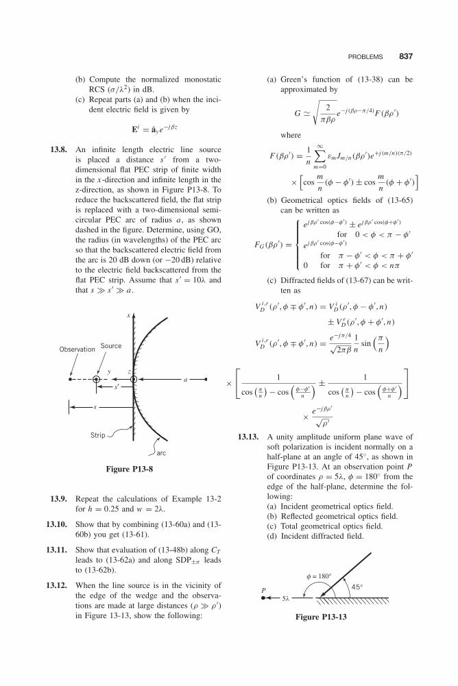
Balanis c13.tex V2 - 11/24/2011 12:45 A.M. Page 837
PROBLEMS 837
(b) Compute the normalized monostaticRCS (σ/λ2) in dB.
(c) Repeat parts (a) and (b) when the inci-dent electric field is given by
Ei = ây e−jβz
13.8. An infinite length electric line sourceis placed a distance s ′ from a two-dimensional flat PEC strip of finite widthin the x -direction and infinite length in thez-direction, as shown in Figure P13-8. Toreduce the backscattered field, the flat stripis replaced with a two-dimensional semi-circular PEC arc of radius a , as showndashed in the figure. Determine, using GO,the radius (in wavelengths) of the PEC arcso that the backscattered electric field fromthe arc is 20 dB down (or −20 dB) relativeto the electric field backscattered from theflat PEC strip. Assume that s ′ = 10λ andthat s � s ′ � a .
Observation Source
y
s′
s
Strip
arc
az
x
Figure P13-8
13.9. Repeat the calculations of Example 13-2for h = 0.25 and w = 2λ.
13.10. Show that by combining (13-60a) and (13-60b) you get (13-61).
13.11. Show that evaluation of (13-48b) along CT
leads to (13-62a) and along SDP±π leadsto (13-62b).
13.12. When the line source is in the vicinity ofthe edge of the wedge and the observa-tions are made at large distances (ρ � ρ ′)in Figure 13-13, show the following:
(a) Green’s function of (13-38) can beapproximated by
G �√
2
πβρe−j (βρ−π/4)F (βρ ′)
where
F (βρ ′) = 1
n
∞∑m=0
εm Jm/n(βρ ′)e+j (m/n)(π/2)
×[cos
m
n(φ − φ′) ± cos
m
n(φ + φ′)
](b) Geometrical optics fields of (13-65)
can be written as
FG (βρ ′) =
⎧⎪⎪⎪⎪⎨⎪⎪⎪⎪⎩ejβρ′ cos(φ−φ′) ± ejβρ′ cos(φ+φ′)
for 0 < φ < π − φ′
ejβρ′ cos(φ−φ′)
for π − φ′ < φ < π + φ′0 for π + φ′ < φ < nπ
(c) Diffracted fields of (13-67) can be writ-ten as
V i ,rD (ρ ′, φ ∓ φ′, n) = V i
D (ρ ′, φ − φ′, n)
± V rD (ρ ′, φ + φ′, n)
V i ,rD (ρ ′, φ ∓ φ′, n) = e−jπ/4
√2πβ
1
nsin
(π
n
)
×⎡⎣ 1
cos(
πn
) − cos(
φ−φ′n
) ± 1
cos(
πn
) − cos(
φ+φ′n
)⎤⎦
× e−jβρ′
√ρ ′
13.13. A unity amplitude uniform plane wave ofsoft polarization is incident normally on ahalf-plane at an angle of 45◦, as shown inFigure P13-13. At an observation point Pof coordinates ρ = 5λ, φ = 180◦ from theedge of the half-plane, determine the fol-lowing:(a) Incident geometrical optics field.(b) Reflected geometrical optics field.(c) Total geometrical optics field.(d) Incident diffracted field.
5l
f = 180°45°P
Figure P13-13

Balanis c13.tex V2 - 11/24/2011 12:45 A.M. Page 838
838 GEOMETRICAL THEORY OF DIFFRACTION
(e) Reflected diffracted field.(f) Total diffracted field.(g) Total field (geometrical optics plus
diffracted).
13.14. Repeat Problem 13.13 for a hard polariza-tion uniform plane wave.
13.15. An electric line source, whose normal-ized electric field at the origin is unity, isplaced at a distance of ρ ′ = 5λ, φ′ = 180◦from the edge of a half-plane, as shownin Figure P13-15. Using the reciprocityprinciple of Figure 13-17 and the resultsof Problem 13.12, determine at large dis-tances the following:(a) Incident geometrical optics electric
field.(b) Reflected geometrical optics electric
field.(c) Total geometrical optics electric field.(d) Incident diffracted electric field.(e) Reflected diffracted electric field.(f) Total diffracted electric field.(g) Total electric field (geometrical optics
plus diffracted).
5l
f′ = 180°
f = 45°
Figure P13-15
13.16. Repeat Problem 13.15 for a magnetic linesource whose normalized magnetic field atthe origin is unity. At each observationdetermine the magnetic field.
13.17. A uniform plane wave of soft polarization(E = âz E i
), whose electric field normal-
ized amplitude at the diffraction edge is 2,is incident upon a half plane at an incidenceangle of 60◦. When ρ = 5.5λ, determine(in vector form) approximate values forthe:(a) Incident GO electric field at φ = 120◦−
and φ = 120◦+.(b) Reflected GO electric field at φ =
120◦− and φ = 120◦+.(c) Incident diffracted electric field at φ =
120◦− and φ = 120◦+.(d) Reflected diffracted electric field at
φ = 120◦− and φ = 120◦+.
(e) Total electric field at φ = 120◦− andφ = 120◦+.
x60°
y
z
120°
Figure P13-17
13.18. A uniform plane wave, of unity amplitude,is incident upon a PEC 90◦ wedge at anangle of φ′ = 60◦. At an observation dis-tance of ρ = 81λ from the edge of thewedge and observation angle of 180◦, com-pute the:(a) Incident diffracted field using GTD.(b) Approximate incident diffracted field
using UTD.(c) Reflected diffracted field using GTD.(d) Approximate reflected diffracted field
using UTD.
180°
r
60°
Figure P13-18
If you make any approximations, state as towhy you think they are valid. Compare thecorresponding answers of parts (a) through(d). Should they be approximately the sameor different, and why?
13.19. A hard-polarized uniform plane wave, withthe magnetic field directed in the +z direc-tion and traveling in the +x direction, isincident upon a half-plane (knife edge),as shown in Figure P13-19. Assume anobservation distance s from the edge of the
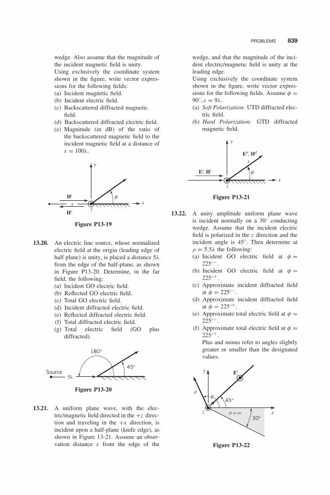
Balanis c13.tex V2 - 11/24/2011 12:45 A.M. Page 839
PROBLEMS 839
wedge. Also assume that the magnitude ofthe incident magnetic field is unity.Using exclusively the coordinate systemshown in the figure, write vector expres-sions for the following fields:(a) Incident magnetic field.(b) Incident electric field.(c) Backscattered diffracted magnetic
field.(d) Backscattered diffracted electric field.(e) Magnitude (in dB) of the ratio of
the backscattered magnetic field to theincident magnetic field at a distance ofs = 100λ.
f
xz
s
y
Hi
Hr
Figure P13-19
13.20. An electric line source, whose normalizedelectric field at the origin (leading edge ofhalf plane) is unity, is placed a distance 5λ
from the edge of the half-plane, as shownin Figure P13-20. Determine, in the farfield, the following:(a) Incident GO electric field.(b) Reflected GO electric field.(c) Total GO electric field.(d) Incident diffracted electric field.(e) Reflected diffracted electric field.(f) Total diffracted electric field.(g) Total electric field (GO plus
diffracted).
180°
5lSource
45°
Figure P13-20
13.21. A uniform plane wave, with the elec-tric/magnetic field directed in the +z direc-tion and traveling in the +x direction, isincident upon a half-plane (knife edge), asshown in Figure 13-21. Assume an obser-vation distance s from the edge of the
wedge, and that the magnitude of the inci-dent electric/magnetic field is unity at theleading edge.Using exclusively the coordinate systemshown in the figure, write vector expres-sions for the following fields. Assume φ =90◦, s = 9λ.(a) Soft Polarization: UTD diffracted elec-
tric field.(b) Hard Polarization: GTD diffracted
magnetic field.
f
xz
y
s
Ei, Hi
Ed, Hd
Figure P13-21
13.22. A unity amplitude uniform plane waveis incident normally on a 30◦ conductingwedge. Assume that the incident electricfield is polarized in the z direction and theincident angle is 45◦. Then determine atρ = 5.5λ the following:(a) Incident GO electric field at φ =
225◦−.(b) Incident GO electric field at φ =
225◦+.(c) Approximate incident diffracted field
at φ = 225◦−.(d) Approximate incident diffracted field
at φ = 225◦+.(e) Approximate total electric field at φ =
225◦−.(f) Approximate total electric field at φ =
225◦+.Plus and minus refer to angles slightlygreater or smaller than the designatedvalues.
xz
y Ei
45°
30°
rf
s = ∞
Figure P13-22

Balanis c13.tex V2 - 11/24/2011 12:45 A.M. Page 840
840 GEOMETRICAL THEORY OF DIFFRACTION
13.23. Repeat Problem 13.22 when the incidentmagnetic field of the unity amplitude uni-form plane wave is polarized in the z direc-tion. At each point determine the corre-sponding GO, diffracted, or total magneticfield.
13.24. A unity amplitude uniform plane wave ofsoft polarization is incident upon a half-plane, as shown in Figure P13-24. At aplane parallel and behind the half-planeperform the following tasks.(a) Formulate expressions for the incident
and reflected geometrical optics fields,incident and reflected diffracted fields,and total field.
(b) Plot along the observation planethe total field (geometrical opticsplus diffracted fields) when y0 = 5λ,−5λ ≤ x0 ≤ 5λ.
(c) Determine the total field at y0 = 5λ andx0 = 0. Explain the result.
x
y0
x0
∞
f
r
Figure P13-24
13.25. Repeat Problem 13.24 for a hard polarizeduniform plane wave.
13.26. A unity amplitude uniform planewave is incident normally on a two-dimensional conducting wedge, as shownin Figure P13-26.(a) Formulate expressions that can be used
to determine the incident, reflected, andtotal diffracted fields away from theincident and reflected shadow bound-aries.
(b) Plot the soft and hard polariza-tion normalized diffraction coefficients(Ds , h/
√λ) as a function of φ for n =
1.5 and n = 2.
(c) Simplify the expressions of part (a)when n = 2 (half-plane).
(d) Formulate expressions for the two-dimensional scattering width of thehalf-plane (n = 2) for soft and hardpolarizations.
(e) Simplify the expressions of part (d) forbackscattering observations (φ = φ′).How can the results of this part be usedto design low-observable radar targets?
f′
r
f
(2 − n)p
Figure P13-26
13.27. For the geometry of Problem 13.26 plotat φ = φ′ the normalized diffraction coeffi-cient (Ds , h/
√λ) as a function of the wedge
angle (1 ≤ n ≤ 2) when the polarization ofthe wave is (a) soft and (b) hard.
13.28. Repeat Problem 13.27 when the observa-tions are made along the surface of thewedge (φ = 0◦).
13.29. By approximating the integrand of theFresnel integral of (13-63c) with a trun-cated Taylor series
e−jτ2 �M∑
n=0
(−jτ 2)n
n!
derive the small argument approximationof (13-74a) for the transition function.
13.30. By repeatedly integrating by parts theFresnel integral of (13-63c), derive thelarge argument approximation of (13-74b)for the transition function.
13.31. Show that there is a finite discontinuityof unity amplitude with the proper polar-ity, similar to (13-83), along the followingboundaries.(a) RSB of Figure 13-24a .(b) ISB of Figure 13-24b.(c) RSB of Figure 13-24b.
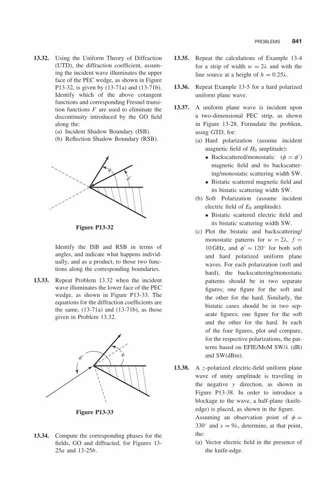
Balanis c13.tex V2 - 11/24/2011 12:45 A.M. Page 841
PROBLEMS 841
13.32. Using the Uniform Theory of Diffraction(UTD), the diffraction coefficient, assum-ing the incident wave illuminates the upperface of the PEC wedge, as shown in FigureP13-32, is given by (13-71a) and (13-71b).Identify which of the above cotangentfunctions and corresponding Fresnel transi-tion functions F are used to eliminate thediscontinuity introduced by the GO fieldalong the:(a) Incident Shadow Boundary (ISB).(b) Reflection Shadow Boundary (RSB).
f
f′
Figure P13-32
Identify the ISB and RSB in terms ofangles, and indicate what happens individ-ually, and as a product, to those two func-tions along the corresponding boundaries.
13.33. Repeat Problem 13.32 when the incidentwave illuminates the lower face of the PECwedge, as shown in Figure P13-33. Theequations for the diffraction coefficients arethe same, (13-71a) and (13-71b), as thosegiven in Problem 13.32.
ff′
Figure P13-33
13.34. Compute the corresponding phases for thefields, GO and diffracted, for Figures 13-25a and 13-25b.
13.35. Repeat the calculations of Example 13-4for a strip of width w = 2λ and with theline source at a height of h = 0.25λ.
13.36. Repeat Example 13-5 for a hard polarizeduniform plane wave.
13.37. A uniform plane wave is incident upona two-dimensional PEC strip, as shownin Figure 13-28. Formulate the problem,using GTD, for:(a) Hard polarization (assume incident
magnetic field of H0 amplitude):• Backscattered/monostatic (φ = φ′)
magnetic field and its backscatter-ing/monostatic scattering width SW.
• Bistatic scattered magnetic field andits bistatic scattering width SW.
(b) Soft Polarization (assume incidentelectric field of E0 amplitude).• Bistatic scattered electric field and
its bistatic scattering width SW.(c) Plot the bistatic and backscattering/
monostatic patterns for w = 2λ, f =10 GHz, and φ′ = 120◦ for both softand hard polarized uniform planewaves. For each polarization (soft andhard), the backscattering/monostaticpatterns should be in two separatefigures; one figure for the soft andthe other for the hard. Similarly, thebistatic cases should be in two sep-arate figures; one figure for the softand the other for the hard. In eachof the four figures, plot and compare,for the respective polarizations, the pat-terns based on EFIE/MoM SW/λ (dB)and SW(dBm).
13.38. A z -polarized electric-field uniform planewave of unity amplitude is traveling inthe negative y direction, as shown inFigure P13-38. In order to introduce ablockage to the wave, a half-plane (knife-edge) is placed, as shown in the figure.Assuming an observation point of φ =330◦ and s = 9λ, determine, at that point,the:(a) Vector electric field in the presence of
the knife-edge.

Balanis c13.tex V2 - 11/24/2011 12:45 A.M. Page 842
842 GEOMETRICAL THEORY OF DIFFRACTION
(b) Blockage (in dB) introduced to thewave by the knife-edge.
f
s
z
y90°
x
Figure P13-38
13.39. A unity amplitude uniform plane wave isincident normally on a two-dimensionalstrip of width w as shown in Figure P13-39.(a) Formulate expressions for the fields
when the observations are made belowthe strip along its axis of symmetry.
(b) Compute the field when w = 3λ andd = 5λ for soft and hard polarizations.
z
x
y
d
w2
w2
#2 #1f
r
Figure P13-39
13.40. A transmitter and a receiver are placed oneither side of a mountain that can be mod-eled as a perfectly conducting half-plane,as shown in Figure P13-40. Assume thatthe transmitting source is isotropic.(a) Derive an expression for the field at the
receiver that is diffracted from the topof the mountain. Assume the field issoft or hard polarized.
(b) Compute the power loss (in deci-bels) at the receiver that is due tothe presence of the mountain whenh = 5λ and d = 5λ. Do this when the
transmitter and receiver are both, foreach case, either soft or hard polarized.
ReceiverTransmitter
dd
h
Figure P13-40
13.41. A rectangular waveguide of dimensions aand b, operating in the dominant TE10
mode, is mounted on a square ground planewith dimensions w on each of its sides, asshown in Figure P13-41. Using the geom-etry of Example 13-6 and assuming thatthe total geometrical optics field above theground plane in the principal yz plane isgiven by
EθG (θ) = E0
⎡⎢⎢⎣ sin
(βb
2sin θ
)βb
2sin θ
⎤⎥⎥⎦ e−jβr
r
0 ≤ θ ≤ π
2
(a) Show that the fields diffracted fromedges 1 and 2 in the principal yz planeare given by
E dθ1(θ) = E0
sin
(βb
2
)βb
2
× V iB
(w
2, ψ1, n1 = 2
)e
+j (βw/2) sin θe−jβr
r
ψ1 = π
2+ θ , 0 ≤ θ ≤ π
E dθ2(θ) = E0
sin
(βb
2
)βb
2
× V iB
(w
2, ψ2, n2 = 2
)e
−j (βw/2) sin θe−jβr
r
ψ2 =
⎧⎪⎨⎪⎩π
2− θ 0 ≤ θ ≤ π
25π
2− θ
π
2≤ θ ≤ π
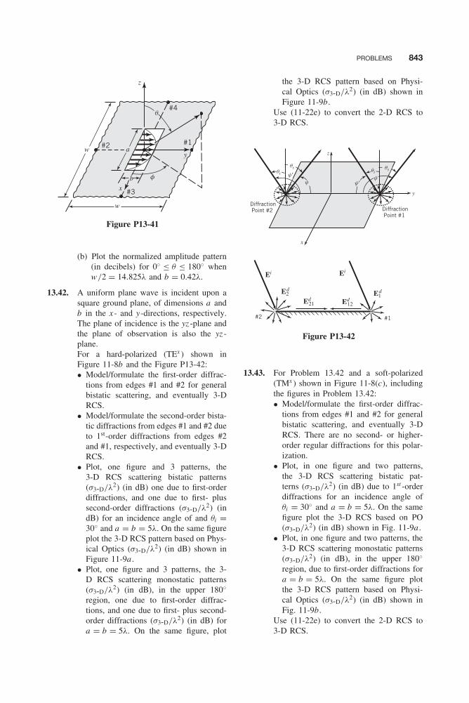
Balanis c13.tex V2 - 11/24/2011 12:45 A.M. Page 843
PROBLEMS 843
w
x
b
w ay
z
f
q
#2
#3
#1
#4
Figure P13-41
(b) Plot the normalized amplitude pattern(in decibels) for 0◦ ≤ θ ≤ 180◦ whenw/2 = 14.825λ and b = 0.42λ.
13.42. A uniform plane wave is incident upon asquare ground plane, of dimensions a andb in the x - and y-directions, respectively.The plane of incidence is the yz -plane andthe plane of observation is also the yz -plane.For a hard-polarized (TEx ) shown inFigure 11-8b and the Figure P13-42:• Model/formulate the first-order diffrac-
tions from edges #1 and #2 for generalbistatic scattering, and eventually 3-DRCS.
• Model/formulate the second-order bista-tic diffractions from edges #1 and #2 dueto 1st-order diffractions from edges #2and #1, respectively, and eventually 3-DRCS.
• Plot, one figure and 3 patterns, the3-D RCS scattering bistatic patterns(σ3-D/λ2) (in dB) one due to first-orderdiffractions, and one due to first- plussecond-order diffractions (σ3-D/λ2) (indB) for an incidence angle of and θi =30◦ and a = b = 5λ. On the same figureplot the 3-D RCS pattern based on Phys-ical Optics (σ3-D/λ2) (in dB) shown inFigure 11-9a .
• Plot, one figure and 3 patterns, the 3-D RCS scattering monostatic patterns(σ3-D/λ2) (in dB), in the upper 180◦region, one due to first-order diffrac-tions, and one due to first- plus second-order diffractions (σ3-D/λ2) (in dB) fora = b = 5λ. On the same figure, plot
the 3-D RCS pattern based on Physi-cal Optics (σ3-D/λ2) (in dB) shown inFigure 11-9b.
Use (11-22e) to convert the 2-D RCS to3-D RCS.
x
y
z
i
DiffractionPoint #1
i
DiffractionPoint #2
y′
#2 #1
Ei Ei
E2d
E1d
Ed21 Ed
12
qi qs qi
qs
y y′y
Figure P13-42
13.43. For Problem 13.42 and a soft-polarized(TMx ) shown in Figure 11-8(c), includingthe figures in Problem 13.42:• Model/formulate the first-order diffrac-
tions from edges #1 and #2 for generalbistatic scattering, and eventually 3-DRCS. There are no second- or higher-order regular diffractions for this polar-ization.
• Plot, in one figure and two patterns,the 3-D RCS scattering bistatic pat-terns (σ3-D/λ2) (in dB) due to 1st -orderdiffractions for an incidence angle ofθi = 30◦ and a = b = 5λ. On the samefigure plot the 3-D RCS based on PO(σ3-D/λ2) (in dB) shown in Fig. 11-9a .
• Plot, in one figure and two patterns, the3-D RCS scattering monostatic patterns(σ3-D/λ2) (in dB), in the upper 180◦region, due to first-order diffractions fora = b = 5λ. On the same figure plotthe 3-D RCS pattern based on Physi-cal Optics (σ3-D/λ2) (in dB) shown inFig. 11-9b.
Use (11-22e) to convert the 2-D RCS to3-D RCS.

Balanis c13.tex V2 - 11/24/2011 12:45 A.M. Page 844
844 GEOMETRICAL THEORY OF DIFFRACTION
13.44. A soft-polarized spherical wave is inci-dent, at a normal incidence angle, upon ahalf plane with a straight edge. The waveemanates from a source a distance s ′ fromthe edge of the half plane. In order toreduce the diffracted field, the straight edgeis replaced with a curved edge of radius a .(a) Derive a simplified expression for the
ratio of amplitude spreading factorreduction for the backscattered field,by a curved edge relative to that bythe straight edge, at a large distance sfrom the edge of the half plane.
(b) Determine, in dB, the relative ampli-tude reduction of the backscattereddiffracted field by a curved edge ofradius a = 25λ and a source distanceof s ′ = 100λ.
s′ a
diffractedfield
Straightedge
Curvededge
Figure P13-44
13.45. A uniform plane wave with an electric fieldgiven by
Ei = âz e−jβx
is incident upon a flat conducting squareplate, as shown in Figure P13-45. Toreduce the backscattered diffractions fromthe leading edge, the square plate isreplaced by a circular plate. Determine theradius of curvature a of the square plate so
x
y
a
zHiEi
Figure P13-45
that the backscattered diffractions at a dis-tance of 50λ from the leading edge diffrac-tion point of the curved edge are −20 dBthan those of the leading straight edge.
13.46. A unity amplitude uniform plane wave isincident at a grazing angle on a circularground plane of radius a , as shown inFigure P13-46.(a) Formulate expressions for the field
diffracted from the leading edge (# 2)of the ground plane along the principalyz plane for both soft and hard polar-izations.
(b) Locate the position of the caustic forthe leading edge.
(c) Assuming the incident electric fieldamplitude at the leading edge of theplate is 10−3 V/m and its phase iszero, compute for each polarization atr = 50λ when a = 2λ the backscat-tered electric field that is due to theleading edge of the plate.
x
y
a
z
r
#2 #1
Ei(soft)
Ei(hard)
f
q
Figure P13-46
13.47. Show that the fields radiated by a circu-lar loop with nonuniform equivalent elec-tric and magnetic current I e
φ and I mφ are
given, respectively, by (13-105a) and (13-105b). If the equivalent currents I e
φ and I mφ
are uniform, show that (13-105a) and (13-105b) reduce, respectively, to (13-106a)and (13-106b).
13.48. An infinitesimal dipole is placed on the tipof a finite cone, as shown in Figure P13-48. The total geometrical optics magneticfield radiated by the source in the presenceof the cone, referred to the center of thebase of the cone, is given by
HφG = R(θ)ejβs cos θ cos(α/2)

Balanis c13.tex V2 - 11/24/2011 12:45 A.M. Page 845
PROBLEMS 845
where R(θ) is the field distribution whenthe cone is infinite in length (s = ∞).For the finite length cone there is also adiffracted field forming a ring source at thebase of the cone.(a) Using (13-105b), show that the di-
ffracted magnetic field is given by
H dφ = b R
(θ = π − α
2
)V i
B (s , ψ , n)
×∫ 2π
0cos φej (βb) sin θ cos φdφ, ψ = α
2+ θ
where V iB (s , ψ , n) is the incident
diffraction function and φ is theazimuthal observation angle.
#2 #1
q
a
s
b
Figure P13-48
(b) Assuming that the base of the coneis large (b � λ) and the observationsare made away from the symmetryaxis so that sin θ > 0, show that byusing the method of steepest descentof Appendix VI the integral formed bythe ring source diffracted field fromthe rim of the cone reduces to thefield diffracted from two diametricallyopposite points on the rim (i.e., points#1 and #2 of Figure P13-48).
13.49. For the λ/4 monopole on the circularground plane of Example 13-7, model therim of the ground plane as a ring sourceradiator using equivalent current conceptsof Section 13.3.5 to correct for the caus-tic formed when the observations are madenear the axis (θ � 0◦ and 180◦) of theground plane.(a) Derive expressions for the diffracted
field from the rim using the ring radi-ator of Figure 13-38.
(b) Show, using the method of steepestdescent (saddle point method), that thering radiator radiation of part a reducesto a two-point diffraction away fromthe symmetry axis.
(c) Compute and plot the pattern near theaxis (θ � 0◦ and 180◦) of the groundplane when the diameter of the groundplane is d = 4.064λ. Use this part ofthe pattern to complement that com-puted using the two-point diffraction ofExample 13-7.
13.50. We all have seen the general geometricalshapes of the stealth bomber and fighter(see Figure 13-1); most of the fuselageconsists of wedge-type shapes. There mustbe a reason for that. To answer some ofthe questions, formulate the problem andshow why a wedge-type of geometry isdesired, assume that a uniform plane wave,of either soft or hard polarization, impingeseither upon a 2-D PEC wedge of includedangle WA or a 2-D PEC cylinder of circu-lar cross section and radius a , as shown inFigure P13-50:
WA
y
x
af
Figure P13-50
(a) In one figure with two curves, plot thenormalized 2-D monostatic scatteringwidth SW[σ2-D/λ(dB)] of the wedgevs. wedge angle WA (in degrees) [0 ≤WA ≤ 60◦] for both hard and softpolarization.
(b) In one figure with 2 curves, plot thenormalized 2-D monostatic scatteringwidth SW[σ2-D/λ(dB)] of the cylin-der vs. cylinder radius a wavelengths)
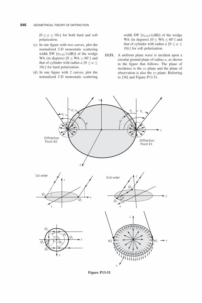
Balanis c13.tex V2 - 11/24/2011 12:45 A.M. Page 846
846 GEOMETRICAL THEORY OF DIFFRACTION
[0 ≤ a ≤ 10λ] for both hard and softpolarization.
(c) In one figure with two curves, plot thenormalized 2-D monostatic scatteringwidth SW [σ2-D/λ(dB)] of the wedgeWA (in degrees) [0 ≤ WA ≤ 60◦] andthat of cylinder with radius a [0 ≤ a ≤10λ] for hard polarization.
(d) In one figure with 2 curves, plot thenormalized 2-D monostatic scattering
z
b
b
2nd order1st order
z
Q1
Q2 Q3
Q4
x
y
z
x
Q3
Q2
Q4
x
z Q1
f4
f3
y
y
x
y#2 #1
x
z
DiffractionPoint #1
y
DiffractionPoint #2
qi qsqi
qs
y y′ yy′
Figure P13-51
width SW [σ2-D/λ(dB)] of the wedgeWA (in degrees) [0 ≤ WA ≤ 60◦] andthat of cylinder with radius a [0 ≤ a ≤10λ] for soft polarization.
13.51. A uniform plane wave is incident upon acircular ground plane of radius a , as shownin the figure that follows. The plane ofincidence is the yz -plane and the plane ofobservation is also the yz -plane. Referringto [36] and Figure P13-51.
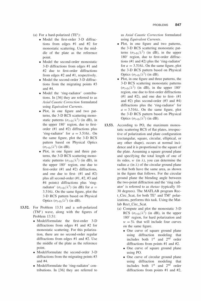
Balanis c13.tex V2 - 11/24/2011 12:45 A.M. Page 847
PROBLEMS 847
(a) For a hard-polarized (TEx):• Model the first-order 3-D diffrac-
tions from edges #1 and #2 formonostatic scattering. Use the mid-dle of the plate as the referencepoint.
• Model the second-order monostatic3-D diffractions from edges #1 and#2 due to first-order diffractionsfrom edges #2 and #1, respectively.
• Model the second-order 3-D diffrac-tions from the migrating points #3and #4.
• Model the ‘ring-radiator’ contribu-tions. In [36] they are referred to asAxial Caustic Correction formulatedusing Equivalent Currents .
• Plot, in one figure and two pat-terns, the 3-D RCS scattering mono-static patterns (σ3-D/λ2) (in dB), inthe upper 180◦ region, due to first-order (#1 and #2) diffractions plus‘ring-radiator’ for a = 3.516λ. Onthe same figure, plot the 3-D RCSpattern based on Physical Optics(σ3-D/λ2) (in dB).
• Plot, in one figure and three pat-terns, the 3-D RCS scattering mono-static patterns (σ3-D/λ2) (in dB), inthe upper 180◦ region, one due tofirst-order (#1 and #2) diffractions,and one due to first- (#1 and #2)plus all second-order (#1, #2, #3 and#4 points) diffractions plus ‘ring-radiator’ (σ3-D/λ2) (in dB) for a =3.516λ. On the same figure, plot the3-D RCS pattern based on PhysicalOptics (σ3-D/λ2) (in dB).
13.52. For Problem 13.51 and a soft-polarized(TMx ) wave, along with the figures ofProblem 13.51:• Model/formulate the first-order 3-D
diffractions from edges #1 and #2 formonostatic scattering. For this polariza-tion, there are no second-order regulardiffractions from edges #1 and #2. Usethe middle of the plate as the referencepoint.
• Model/formulate the second-order 3-Ddiffractions from the migrating points #3and #4.
• Model/formulate the ‘ring-radiator’ con-tributions. In [36] they are referred to
as Axial Caustic Correction formulatedusing Equivalent Currents .
• Plot, in one figure and two patterns,the 3-D RCS scattering monostatic pat-terns (σ3-D/λ2) (in dB), in the upper180◦ region, due to first-order diffrac-tions (#1 and #2) plus the ‘ring-radiator’for a = 3.516λ. On the same figure, plotthe 3-D RCS pattern based on PhysicalOptics (σ3-D/λ2) (in dB).
• Plot, in one figure and three patterns, the3-D RCS scattering monostatic patterns(σ3-D/λ2) (in dB), in the upper 180◦region, one due to first-order diffractions(#1 and #2), and one due to first- (#1and #2) plus second-order (#3 and #4)diffractions plus the ‘ring-radiator’ fora = 3.516λ. On the same figure, plotthe 3-D RCS pattern based on PhysicalOptics (σ3-D/λ2) (in dB).
13.53. According to PO, the maximum monos-tatic scattering RCS of flat plates, irrespec-tive of polarization and plate configuration(rectangular, square, circular, elliptical, orany other shape), occurs at normal inci-dence and it is proportional to the square ofthe plate. Assuming a square ground planeand specifying the total length of one ofits sides, w (in λ), you can determine theradius a (in λ) of the circular ground planeso that both have the same area, as shownin the figure that follows. For the circularground plane the blending angle betweenthe two-point diffraction and the ‘ring radi-ator’ is referred to as thetao (typically 10-30 degrees). The MATLAB program Rec-t_Circ_Scat, for both TEx and TMx polar-izations, performs this task. Using the Mat-lab Rect_Circ_Scat.(a) Compute and plot the monostatic 3-D
RCS (σ3-D/λ2) (in dB), in the upper180◦ region, for hard polarization andw = 5λ that will include four curveson the same figure.• One curve of square ground plane
using diffraction modeling thatincludes both 1st and 2nd orderdiffractions from points #1 and #2.
• One curve of square ground planeusing PO.
• One curve of circular ground planeusing diffraction modeling thatincludes both 1st and 2nd orderdiffractions from points #1 and #2,
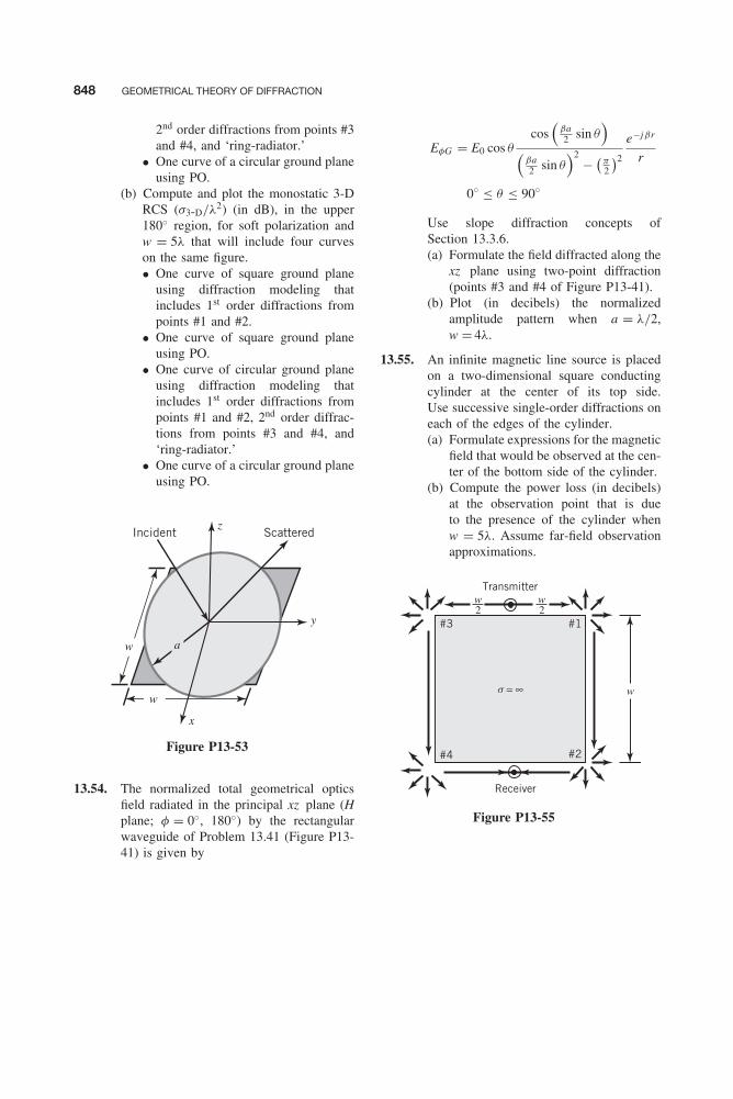
Balanis c13.tex V2 - 11/24/2011 12:45 A.M. Page 848
848 GEOMETRICAL THEORY OF DIFFRACTION
2nd order diffractions from points #3and #4, and ‘ring-radiator.’
• One curve of a circular ground planeusing PO.
(b) Compute and plot the monostatic 3-DRCS (σ3-D/λ2) (in dB), in the upper180◦ region, for soft polarization andw = 5λ that will include four curveson the same figure.• One curve of square ground plane
using diffraction modeling thatincludes 1st order diffractions frompoints #1 and #2.
• One curve of square ground planeusing PO.
• One curve of circular ground planeusing diffraction modeling thatincludes 1st order diffractions frompoints #1 and #2, 2nd order diffrac-tions from points #3 and #4, and‘ring-radiator.’
• One curve of a circular ground planeusing PO.
x
y
zIncident Scattered
a
w
w
Figure P13-53
13.54. The normalized total geometrical opticsfield radiated in the principal xz plane (Hplane; φ = 0◦, 180◦) by the rectangularwaveguide of Problem 13.41 (Figure P13-41) is given by
EφG = E0 cos θcos
(βa2 sin θ
)(
βa2 sin θ
)2 − (π2
)2
e−jβr
r
0◦ ≤ θ ≤ 90◦
Use slope diffraction concepts ofSection 13.3.6.(a) Formulate the field diffracted along the
xz plane using two-point diffraction(points #3 and #4 of Figure P13-41).
(b) Plot (in decibels) the normalizedamplitude pattern when a = λ/2,w = 4λ.
13.55. An infinite magnetic line source is placedon a two-dimensional square conductingcylinder at the center of its top side.Use successive single-order diffractions oneach of the edges of the cylinder.(a) Formulate expressions for the magnetic
field that would be observed at the cen-ter of the bottom side of the cylinder.
(b) Compute the power loss (in decibels)at the observation point that is dueto the presence of the cylinder whenw = 5λ. Assume far-field observationapproximations.
#4
#3 #1
Receiver
Transmitter
#2
w2
w2
ws = ∞
Figure P13-55
Balanis c14.tex V2 - 11/22/2011 4:00 P.M. Page 849
CHAPTER 14Diffraction by Wedge with Impedance Surfaces
14.1 INTRODUCTION
In Chapter 11 we introduced the exact solution of wave scattering by a perfectly conductingwedge while in Chapter 13 we examined its asymptotic high-frequency solution and reducedit to geometrical optics (GO) fields, incident and reflected, and diffracted fields (GTD andUTD) (incident and reflected diffracted fields). The solution of electromagnetic scatteringfrom a penetrable or lossy wedge has not been solved using exact boundary conditions basedon Maxwell’s equations. It has always been necessary to use some approximate boundaryconditions from which the exact solution can be obtained. Hence, it is important to recognizethat when an exact solution is discussed, it is for a boundary condition that in reality can onlybe approximated by physical materials or structures.
In recent years great interest has been generated, because of the design of low-profile (stealth)radar targets and the modeling of wave propagation for wireless communication in the presenceof penetrable structures (such as buildings, ridges, hills, and various other structures), to extendthe theories of perfectly conducting materials to include materials with penetrable characteristics.Many aircraft are now built with composite materials which, with appropriate shaping andintegration of materials, can reduce the radar echo, RCS, and thus minimize the probabilityof detection. See Figure 13-1 of the F-117 Nighthawk whose surface is composed primarilyof faceted flat plates and wedges judiously oriented so that the maximum scattered field istoward specular direction and away from source of detection. In wireless communication, thewave propagation, direct and indirect (multipath), plays a pivotal role in the performance of thewireless mobile communication system using, for example, the Bit Error Ratio (BER) as a metric.
The most common of these boundary conditions is the impedance boundary condition, whichrelates the tangential components of the electric and magnetic fields by a surface impedance. Theimpedance surface boundary condition was first used in electromagnetic scattering by a numberof Russian authors in the early 1940s [1], and it is generally attributed to Leontovich [2, 3], andcommonly referred to as the Leontovich boundary condition . It was initially used to describewave propagation over the earth’s surface by specifying an impedance boundary for the groundsurface. It was later used for other electromagnetics problems and was an effort to simplify verycomplex electromagnetics boundary-value problems, which were difficult to solve exactly. It isespecially useful for surfaces that support surface waves.
The solution of a half-plane with impedance boundary conditions has been examined andreported in [4–8]. The more general problem of plane wave incidence on a wedge of arbitraryinterior angle was solved by Maliuzhinets [9, 10]. The wedge was permitted to have differentimpedances on each face but only normal incidence was considered. No solution for obliqueincidence on a general wedge has been obtained, except for a very few special cases. Maliuzhinets’exact solution of the wedge was accompanied by a steepest-descent analysis, very similar toKeller’s theory for the PEC wedge, which decomposed the exact solution into incident, reflected,
849

Balanis c14.tex V2 - 11/22/2011 4:00 P.M. Page 850
850 DIFFRACTION BY WEDGE WITH IMPEDANCE SURFACES
(a)
ay
(b)
n0
h0
h0
hn
hn
r
r
f = 0
f = 0
f = np
f = np
0 face
0 face
n fa
ce
ay
ax
axn0
nn
nn
WA = (2 − n)p
f
f
Figure 14-1 Exterior and interior wedges with impedance surfaces [28]. (a) Exterior wedge. (b) Interiorwedge.
diffracted, and surface wave components. These Keller-type diffraction terms are not valid nearthe shadow boundaries and do not eliminate the discontinuities in the GO and surface waveterms; they had to be extended to include UTD type of formulations. There have been numerouspublications [11–61] addressing various special cases of the diffraction by an impedance wedge,including that of the half plane. This chapter follows the presentation of [28, 30].
The impedance wedge, shown in Figure 14-1, is a canonical geometry whose faces can berepresented by surface impedances. The exact solution for this geometry for the fields both interiorand exterior to the wedge, similar to that of the PEC wedge of Chapter 11, does not exist becauseappropriate eigenfunctions and eigenvalues that satisfy Maxwell’s equations and the boundaryconditions cannot be found. However, an exact solution for the fields exterior to the wedge, fornormal plane wave incidence and assuming uniform, but not identical surface impedances to thefaces of the wedge, does exist and it was first presented by Maliuzhinets [9, 10]. The wedge,with wedge angle WA = (2 − n)π and 0 < n ≤ 2, has two faces located at φ = 0 and φ = nπ
with normalized uniform surface impedances of η0 and ηn , respectively. An exterior wedge(Figure 14-1a) has values of n in the range of 1 ≤ n ≤ 2 while for an interior wedge (Figure 14-1b) 0 < n < 1. Maliuzhinets’ solution can be used to extract geometrical optics, diffracted fields,and surface waves, as was done for the PEC wedge in Chapter 13.
14.2 IMPEDANCE SURFACE BOUNDARY CONDITIONS
The impedance surface boundary condition is simply a statement that the tangential electric andmagnetic field vectors are related by a constant impedance that is related only to the propertiesand configurations of the material and is independent of the source illumination. Mathematically,
Balanis c14.tex V2 - 11/22/2011 4:00 P.M. Page 851
IMPEDANCE SURFACE REFLECTION COEFFICIENTS 851
it is essentially a boundary condition of the third kind, as it relates a function and its derivativeat the surface through some constant. As such, it is only an approximation to the actual boundaryconditions, developed through Maxwell’s equations, which exist on complex structures. Theaccuracy of the approximation depends on the composition, geometry, and illumination of theactual surface of interest. The impedance boundary condition has been applied in the past tohomogeneous and inhomogeneous materials, layered structures, lossy materials, and randomlyrough surfaces.
Physically, it is easy to understand where a concept, like the impedance boundary condition,originates. For plane, cylindrical, and spherical waves in inhomogeneous media and sufficientlyfar from the source, the electric and magnetic field vectors are mutually orthogonal and arerelated to each other by the intrinsic impedance of the homogeneous media through which theypropagate. For free space, this impedance is Zo = 377 ohms. In vector form, this statement isexpressed as
E = −Zo âr × H (14-1)
where E and H are the electric and magnetic field vectors, Zo is the intrinsic impedance of freespace (377 ohms), and âr is a unit vector in the direction of wave propagation.
The impedance boundary condition simply extends this wave property to surface interfaces withwhich the wave interacts. The boundary condition requires that the tangential electric and magneticfield vectors at the interface be mutually orthogonal and can be related by the impedance Z of thesurface. The normalized impedance η, relative to the free-space value Zo , is commonly specified,and is given by η = Z /Zo . This notation can cause confusion because many electromagneticstexts, as this one in previous chapters, use both η and Z as the total intrinsic impedance of themedium. Nonetheless, this notation has been utilized for surface impedances as early as 1959 [6]and has been used consistently since. Hence, in this chapter, η refers to a normalized impedanceand Z refers to the total impedance, Z = ηZo . For passive materials, the real part of η must benonnegative.
In a vector equation form, the impedance surface boundary condition, referred to also as theLeontovich Boundary Condition , can be written as [1, 6]
E − (n̂ • E)n̂ = Z n̂ × H = ηZo(n̂ × H) (14-2)
whereE = the electric field vectorH = the magnetic field vectorn̂ = the outward unit normal to the surface
It is noted that (n̂ · E)n̂ is simply the normal component of E; hence, the left side of (14-2)represents the tangential electric field. The term n̂ × H is a vector whose magnitude equals thetangential magnetic field; however, its direction is perpendicular to both the tangential magneticfield and the unit normal. Hence, n̂ × H is also tangential to the surface. The tangential electricand magnetic fields are then related by the constant of proportionality Z , the surface impedanceZ = ηZo . In words, the tangential electric and magnetic fields are related by the surface impedanceof the material.
14.3 IMPEDANCE SURFACE REFLECTION COEFFICIENTS
To determine the reflection coefficients appropriate for an impedance surface, the reflection of aplane wave at a planar interface is examined. At high frequencies, these reflection coefficientsare also appropriate for curved boundaries for which the radius of curvature is relatively large
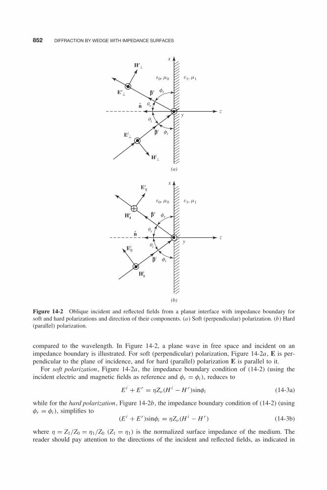
Balanis c14.tex V2 - 11/22/2011 4:00 P.M. Page 852
852 DIFFRACTION BY WEDGE WITH IMPEDANCE SURFACES
e0, m0
e1, m1e0, m0
e1, m1
fr
fr
fi
qr
qi
fi
y
(a)
(b)
Hr⊥
Hi⊥
Er⊥
Ei⊥
qr
qi
βi
βi
βr
βr
Er
Hr
Hi
Ei
x
y
x
z
zn̂
n̂
Figure 14-2 Oblique incident and reflected fields from a planar interface with impedance boundary forsoft and hard polarizations and direction of their components. (a) Soft (perpendicular) polarization. (b) Hard(parallel) polarization.
compared to the wavelength. In Figure 14-2, a plane wave in free space and incident on animpedance boundary is illustrated. For soft (perpendicular) polarization, Figure 14-2a , E is per-pendicular to the plane of incidence, and for hard (parallel) polarization E is parallel to it.
For soft polarization , Figure 14-2a , the impedance boundary condition of (14-2) (using theincident electric and magnetic fields as reference and φr = φi ), reduces to
E i + E r = ηZo(Hi − H r )sinφi (14-3a)
while for the hard polarization , Figure 14-2b, the impedance boundary condition of (14-2) (usingφr = φi ), simplifies to
(E i + E r )sinφi = ηZo(Hi − H r ) (14-3b)
where η = Z1/Z0 = η1/Z0 (Z1 = η1) is the normalized surface impedance of the medium. Thereader should pay attention to the directions of the incident and reflected fields, as indicated in
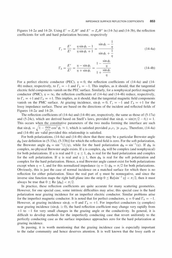
Balanis c14.tex V2 - 11/22/2011 4:00 P.M. Page 853
IMPEDANCE SURFACE REFLECTION COEFFICIENTS 853
Figures 14-2a and 14-2b. Using E i = ZoH i and E r = ZoH r in (14-3a) and (14-3b), the reflectioncoefficients for soft and hard polarization become, respectively
�s = E r
E i= η sin φi − 1
η sin φi + 1=
sin φi − 1
η
sin φi + 1
η
(14-4a)
�h = E r
E i= η − sin φi
η + sin φi=
1 − sin φi
η
1 + sin φi
η
(14-4b)
For a perfect electric conductor (PEC), η = 0, the reflection coefficients of (14-4a) and (14-4b) reduce, respectively, to �s = −1 and �h = −1. This implies, as it should, that the tangentialelectric field components vanish on the PEC surface. Similarly, for a nonphysical perfect magneticconductor (PMC), η = ∞, the reflection coefficients of (14-4a) and (14-4b) reduce, respectively,to �s = +1 and �h = +1. This implies, as it should, that the tangential magnetic field componentsvanish on the PMC surface. At grazing incidence, sin φi = 0, �s = −1 and �h = +1 for thelossy impedance surface. These are based on the directions of the incident and reflected fields ofFigures 14-2a and 14-2b.
The reflection coefficients of (14-4a) and (14-4b) are, respectively, the same as those of (5-17a)and (5-24c), which are derived based on Snell’s laws, provided that sin φt = sin(π/2 − θt ) = 1.This occurs when the constitutive parameters of the two media forming the interface are suchthat sin φt =
√1 − μ0ε0
μ1ε1cos2 φi ≈ 1, which is satisfied provided μ1ε1 � μ0ε0. Therefore, (14-4a)
and (14-4b) are valid provided this relationship is satisfied.For both polarizations, (14-4a) and (14-4b) show that there may be a particular Brewster angle
φB [see definition in (5-33a), (5-33b)] for which the reflected field is zero. For the soft polarization,the Brewster angle φB = sin−1(1/η), while for the hard polarization φB = sin−1(η). If φB iscomplex, no physical Brewster angle exists. If η is complex, φB will be complex (and nonphysical)for both polarizations. If η is real and 0 ≤ η ≤ 1, φB is real for the hard polarization and complexfor the soft polarization. If η is real and η ≥ 1, then φB is real for the soft polarization andcomplex for the hard polarization. Hence, a real Brewster angle cannot exist for both polarizationsexcept when η = 1, and for this normalized impedance (η = 1) φB = π/2 for both polarizations.Obviously, this is just the case of normal incidence on a matched surface for which there is noreflection for either polarization. Since the real part of η must be nonnegative, and since theinverse sine function maps the right half-plane into the strip 0 ≤ Re[sin−1 η] < π/2, then it mustalways be true that 0 ≤ Re [φB] < π/2.
In practice, these reflection coefficients are quite accurate for many scattering geometries.However, for one special case, some intrinsic difficulties may arise; this special case is the hardpolarization near grazing incidence for an imperfect electric conductor. Similar problems arisefor the imperfect magnetic conductor. It is noted that for perfect conductors, η = 0 and �h = −1.However, at grazing incidence sin φi = 0 and �h = +1. For imperfect conductors (η complex)near grazing incidence (sin φi � 0), the hard reflection coefficient may change very rapidly from+1 to −1 for very small changes in the grazing angle or the conductivity. In general, it isdifficult to develop methods for the imperfectly conducting case that revert uniformly to theperfectly conducting case as the surface impedance approaches zero for the hard polarization atgrazing incidence.
In passing, it is worth mentioning that the grazing incidence case is especially importantto the radar community and hence deserves attention. It is well known that the lossy earth or

Balanis c14.tex V2 - 11/22/2011 4:00 P.M. Page 854
854 DIFFRACTION BY WEDGE WITH IMPEDANCE SURFACES
sea surface near grazing incidence (sin φi � 0) has reflection coefficients of �s = −1 [i.e., theincident and reflected electric fields are in opposite directions using the direction designation ofFigure 14-2a and definition of (14-4a)], and �h = +1 [i.e., the incident and reflected electricfields are also in opposite directions using the direction designation of Figure 14-2b and definitionof (14-4b)]. This implies that radar targets flying very near the ground or sea surface (sin φi � 0)are especially difficult to detect because, at grazing incidence, the incident reflected electric fieldsare nearly equal in magnitude and opposite in phase. Hence, these two components effectivelycancel each other, giving no radar echo/return, which makes low-flying radar targets difficult totrack [62]. This physical phenomenon is exploited in many sea skimming missiles that fly withina few meters of the ocean surface.
14.4 THE MALIUZHINETS IMPEDANCE WEDGE SOLUTION
An exact solution for the fields exterior to the wedge, for normal plane wave incidence andassuming uniform, but not identical, surface impedances on the faces of the wedge, does existand it was first presented by Maliuzhinets [9, 10]. The wedge has two faces located at φ =0 and φ = nπ , with normalized uniform surface impedances of ηo and ηn , respectively. Aninterior wedge has values of n in the range of 0 < n < 1 while for an exterior wedge 1 ≤ n ≤ 2.Maliuzhinets’ solution can be used to extract geometrical optics, diffracted fields, as was donefor the PEC wedge, and surface waves.
Let us assume that a plane wave is incident from φ′ and the observation point P is at a distanceρ from the edge of the wedge at an angle φ, where φ′ and φ are both measured from the 0 face,as shown in Figure 14-3. Assuming a field of amplitude Uo , the exact solution for the total fieldUt , including the incident and reflected fields is [9]
Ut (ρ, φ) = jUo1
2nπ
∫γ
�(
z + nπ
2− φ
)�
(nπ
2− φ′
) sin
(φ′
n
)cos
(z − φ
n
)− cos
(φ′
n
)ejβρ cos z dz (14-5)
where γ is the contour shown in Figure 14-4. It should be remembered that this is an exactsolution for an approximate boundary condition (i.e., the impedance boundary condition), and itis not an exact solution for the exact boundary conditions derived from Maxwell’s equations. Alsoin order to match the notation of Chapter 13 for the PEC wedge, the complex plane is representedby z , instead of α used in the corresponding published literature.
r
f = np
f = 0
n face
hn
h0
P
0 face
ff'
Figure 14-3 Interior wedge with impedance surfaces.
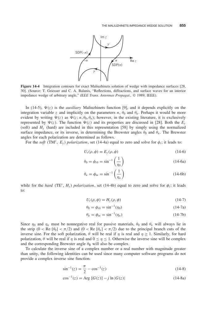
Balanis c14.tex V2 - 11/22/2011 4:00 P.M. Page 855
THE MALIUZHINETS IMPEDANCE WEDGE SOLUTION 855
g
g
Im z
SDP(p)
SDP(−p)
Re z−p p
Figure 14-4 Integration contours for exact Maliuzhinets solution of wedge with impedance surfaces [28,30]. (Source: T. Griesser and C. A. Balanis, “Reflections, diffractions, and surface waves for an interiorimpedance wedge of arbitrary angle,” IEEE Trans. Antennas Propagat., © 1989, IEEE).
In (14-5), �(z ) is the auxiliary Maliuzhinets function [9], and it depends explicitly on theintegration variable z and implicitly on the parameters n , θ0 and θn . Perhaps it would be moreevident by writing �(z ) as �(z ; n , θ0, θn); however, in the existing literature, it is exclusivelyrepresented by �(z ). The function �(z ) and its properties are discussed in [28]. Both the Ey
(soft) and Hy (hard) are included in this representation [58] by simply using the normalizedsurface impedance, or its inverse, in determining the Brewster angles θ0 and θn . The Brewsterangles for each polarization are determined as follows.
For the soft (TMy , Ey ) polarization , set (14-4a) equal to zero and solve for φi ; it leads to:
Ut (ρ, φ) = Ey(ρ, φ) (14-6)
θ0 = φi0 = sin−1
(1
η0
)(14-6a)
θn = φin = sin−1
(1
ηn
)(14-6b)
while for the hard (TEy , Hy ) polarization , set (14-4b) equal to zero and solve for φi ; it leadsto:
Ut (ρ, φ) = Hy(ρ, φ) (14-7)
θ0 = φi0 = sin−1(η0) (14-7a)
θn = φin = sin−1(ηn) (14-7b)
Since η0 and ηn must be nonnegative real for passive materials, θ0 and θn will always lie inthe strip (0 < Re [θ0] < π/2) and (0 < Re [θn ] < π/2) due to the principal branch cuts of theinverse sine. For the soft polarization, θ will be real if η is real and η ≥ 1. Similarly, for hardpolarization, θ will be real if η is real and 0 ≤ η ≤ 1. Otherwise the inverse sine will be complexand the corresponding Brewster angle θB will also be complex.
To calculate the inverse sine of a complex number or a real number with magnitude greaterthan unity, the following identities can be used since many computer software programs do notprovide a complex inverse sine function.
sin−1(z ) = π
2− cos−1(z ) (14-8)
cos−1(z ) = Arg [G(z )] − j ln |G(z )| (14-8a)

Balanis c14.tex V2 - 11/22/2011 4:00 P.M. Page 856
856 DIFFRACTION BY WEDGE WITH IMPEDANCE SURFACES
G(z ) =⎧⎨⎩z − √
z 2 − 1 (Re [z ])(Im [z ]) < 0
z + √z 2 − 1 (Re [z ])(Im [z ]) ≥ 0
(14-8b)
(14-8c)
−π < Arg G(z ) ≤ π (14-8d)
−π
2< Arg
[√z 2 − 1
]≤ π
2(14-8e)
The exact wedge solution in its integral form of (14-5) cannot be easily evaluated. The integrandcontains a ratio of auxiliary Maliuzhinets functions , each of which can be written as a product offour Maliuzhinets functions . Each Maliuzhinets function can only be written in a complex integralform or as an infinite product, and hence the Maliuzhinets function is not easily evaluated forarbitrary argument and wedge angle. Finally, the very complicated integrand must be integratedalong the complex contour γ of Figure 14-4. Overall, the integral of (14-5) is difficult to evaluateefficiently.
To construct a more useful high-frequency asymptotic expansion of the integral, the Methodof Steepest Descent (also known as the Saddle Point Method ) of Chapter 13 will be used in thischapter. The steepest descent paths must first be located, and then the exact solution must betransformed to an integral along the steepest descent paths, as was done in Chapter 13 for thePEC wedge. Once the steepest descent paths are identified, the contour can then be closed toevaluate the exact solution. The sum of the integrals along the exact solution contour γ , plusalong the steepest descent paths, must equal the sum of the residues enclosed. That is∫
γ
(integrand) dz +∫
SDPs(integrand) dz =
∫closed path
(integrand) dz =N∑
p=1
Residues (14-9a)
where SDPs = SDP(+π) + SDP(−π). Alternatively, the integral along the exact solution con-tour γ of (14-9a) can be written as the sum of the residues minus the contributions along thesteepest descent paths, or∫
γ
(integrand) dz =N∑
p=1
Residues −∫
SDPs(integrand) dz (14-9b)
Therefore, the exact solution of (14-5) can now be written as
Ut (ρ, φ) = jUo1
2nπ
∫γ
�(
z + nπ
2− φ
)�
(nπ
2− φ′
) sin
(φ′
n
)cos
(z − φ
n
)− cos
(φ′
n
)ejβρ cos z dz
= Uo
n
N∑p=1
Res
⎡⎢⎢⎣�(
z + nπ
2− φ
)�
(nπ
2− φ′
) sin
(φ′
n
)cos
(z − φ
n
)− cos
(φ′
n
)ejβρ cos a , zp
⎤⎥⎥⎦ (14-10)
− jUo1
2nπ
∫SDPs
�(
z + nπ
2− φ
)�
(nπ
2− φ′
) sin
(φ′
n
)cos
(z − φ
n
)− cos
(φ′
n
)ejβρ cos z dz
where zp are the poles of the integrand enclosed by the steepest descents paths while the notationRes [f (z ), zp] represents the residue of f (z ) at the pole zp .
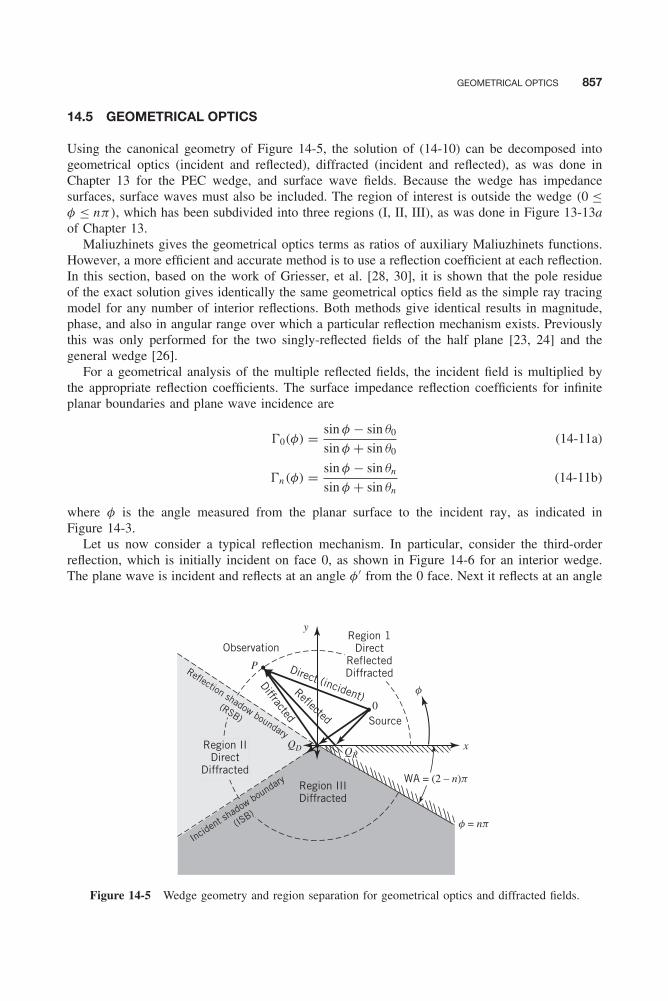
Balanis c14.tex V2 - 11/22/2011 4:00 P.M. Page 857
GEOMETRICAL OPTICS 857
14.5 GEOMETRICAL OPTICS
Using the canonical geometry of Figure 14-5, the solution of (14-10) can be decomposed intogeometrical optics (incident and reflected), diffracted (incident and reflected), as was done inChapter 13 for the PEC wedge, and surface wave fields. Because the wedge has impedancesurfaces, surface waves must also be included. The region of interest is outside the wedge (0 ≤φ ≤ nπ), which has been subdivided into three regions (I, II, III), as was done in Figure 13-13aof Chapter 13.
Maliuzhinets gives the geometrical optics terms as ratios of auxiliary Maliuzhinets functions.However, a more efficient and accurate method is to use a reflection coefficient at each reflection.In this section, based on the work of Griesser, et al. [28, 30], it is shown that the pole residueof the exact solution gives identically the same geometrical optics field as the simple ray tracingmodel for any number of interior reflections. Both methods give identical results in magnitude,phase, and also in angular range over which a particular reflection mechanism exists. Previouslythis was only performed for the two singly-reflected fields of the half plane [23, 24] and thegeneral wedge [26].
For a geometrical analysis of the multiple reflected fields, the incident field is multiplied bythe appropriate reflection coefficients. The surface impedance reflection coefficients for infiniteplanar boundaries and plane wave incidence are
�0(φ) = sin φ − sin θ0
sin φ + sin θ0(14-11a)
�n(φ) = sin φ − sin θn
sin φ + sin θn(14-11b)
where φ is the angle measured from the planar surface to the incident ray, as indicated inFigure 14-3.
Let us now consider a typical reflection mechanism. In particular, consider the third-orderreflection, which is initially incident on face 0, as shown in Figure 14-6 for an interior wedge.The plane wave is incident and reflects at an angle φ′ from the 0 face. Next it reflects at an angle
x
WA = (2 – n)p
f = np
Observation
P Direct (incident)Reflected
Diffracted
y
0
QD QR
f
Region IIIDiffracted
Region IIDirect
Diffracted
Region IIDirect
Diffracted
Incident s
hadow boundary
(ISB)
Reflection shadow boundary
(RSB) Source
Region 1Direct
ReflectedDiffracted
Figure 14-5 Wedge geometry and region separation for geometrical optics and diffracted fields.
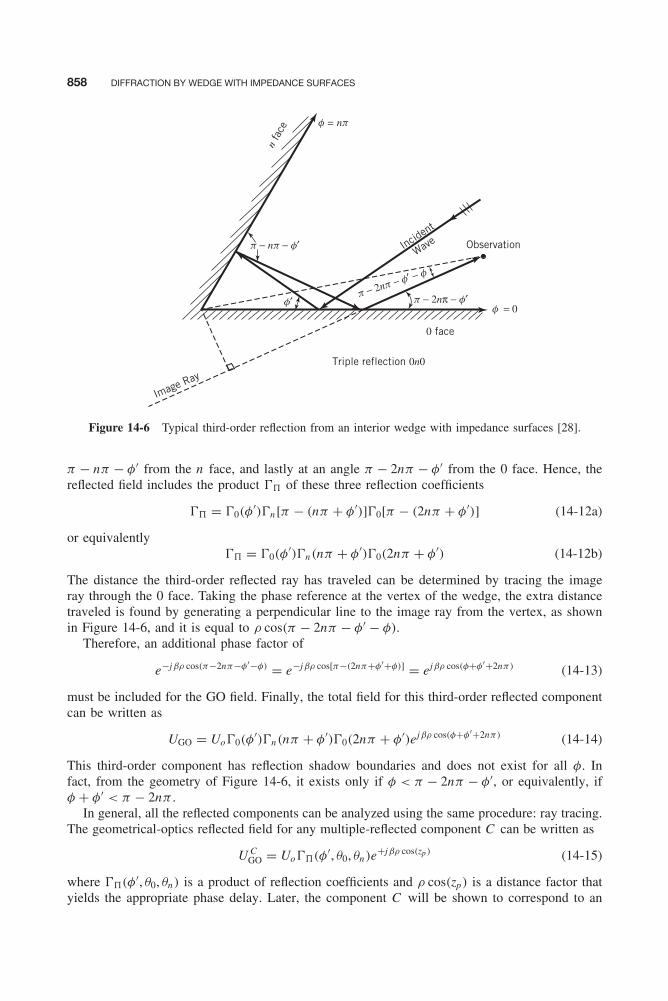
Balanis c14.tex V2 - 11/22/2011 4:00 P.M. Page 858
858 DIFFRACTION BY WEDGE WITH IMPEDANCE SURFACES
n fa
ce
f = np
p − np − f′
p − 2np − f′ − f
p − 2nπ − f′f′f = 0
0 face
Triple reflection 0n0
Image Ray
Incident
Wave Observation
Figure 14-6 Typical third-order reflection from an interior wedge with impedance surfaces [28].
π − nπ − φ′ from the n face, and lastly at an angle π − 2nπ − φ′ from the 0 face. Hence, thereflected field includes the product �� of these three reflection coefficients
�� = �0(φ′)�n [π − (nπ + φ′)]�0[π − (2nπ + φ′)] (14-12a)
or equivalently�� = �0(φ
′)�n(nπ + φ′)�0(2nπ + φ′) (14-12b)
The distance the third-order reflected ray has traveled can be determined by tracing the imageray through the 0 face. Taking the phase reference at the vertex of the wedge, the extra distancetraveled is found by generating a perpendicular line to the image ray from the vertex, as shownin Figure 14-6, and it is equal to ρ cos(π − 2nπ − φ′ − φ).
Therefore, an additional phase factor of
e−jβρ cos(π−2nπ−φ′−φ) = e−jβρ cos[π−(2nπ+φ′+φ)] = ejβρ cos(φ+φ′+2nπ) (14-13)
must be included for the GO field. Finally, the total field for this third-order reflected componentcan be written as
UGO = Uo�0(φ′)�n(nπ + φ′)�0(2nπ + φ′)ejβρ cos(φ+φ′+2nπ) (14-14)
This third-order component has reflection shadow boundaries and does not exist for all φ. Infact, from the geometry of Figure 14-6, it exists only if φ < π − 2nπ − φ′, or equivalently, ifφ + φ′ < π − 2nπ .
In general, all the reflected components can be analyzed using the same procedure: ray tracing.The geometrical-optics reflected field for any multiple-reflected component C can be written as
U CGO = Uo��(φ′, θ0, θn)e
+jβρ cos(zp ) (14-15)
where ��(φ′, θ0, θn) is a product of reflection coefficients and ρ cos(zp) is a distance factor thatyields the appropriate phase delay. Later, the component C will be shown to correspond to an

Balanis c14.tex V2 - 11/22/2011 4:00 P.M. Page 859
GEOMETRICAL OPTICS 859
TABLE 14-1 Geometrical optics reflection coefficients and associated pole residues [28, 30]
Comp Pole �π(φ′, θ0, θn ) zp Existence
0n0n β−, m = −2 �0(φ′)�n (nπ + φ′)�0(2nπ + φ′)�n (3nπ + φ′) φ − φ′ − 4nπ φ − φ′ > 4nπ − π
n0n β+, m = −2 �n (nπ − φ′)�0(2nπ − φ′)�n (3nπ − φ′) φ + φ′ − 4nπ φ + φ′ > 4nπ − π
0n β−, m = −1 �0(φ′)�n (nπ + φ′) φ − φ′ − 2nπ φ − φ′ > 2nπ − π
n β+, m = −1 �n (nπ − φ′) φ + φ′ − 2nπ φ + φ′ > 2nπ − π
Inc β−, m = 0 1 φ − φ′ −π < φ − φ′ < π
0 β+, m = 0 �0(φ′) φ + φ′ φ + φ′ < π
n0 β−, m = 1 �n (nπ − φ′)�0(2nπ + φ′) φ − φ′ + 2nπ φ − φ′ < π − 2nπ
0n0 β+, m = 1 �0(φ′)�n (nπ + φ′)�0(2nπ + φ′) φ + φ′ + 2nπ φ + φ′ < π − 2nπ
n0n0 β−, m = 2 �n (nπ − φ′)�0(2nπ − φ′)�n (3nπ − φ′)�0(4nπ − φ′) φ − φ′ + 4nπ φ − φ′ < π − 4nπ
(Source: T. Griesser and C. A. Balanis, “Reflections, diffractions, and surface waves for an interior impedance wedgeof arbitrary angle,” IEEE Trans. Antennas Propagat., © 1989, IEEE).
angle ξ± and an integer m , and will be written as U m ,ξGO . The multiple-reflected field is identified
by a sequence of 0’s and n’s indicating the order of reflection. As an example, component 0n0nis a quadruple-reflected field incident on face 0 which, in sequence, reflects from face 0 to n to0 to n .
In Table 14-1, the term ��(φ′, θ0, θn) and zp are listed for all reflection mechanisms up tofourth-order. In addition, the range over which these terms exist is listed, with the impliedconditions that 0 ≤ φ ≤ nπ and 0 ≤ φ′ ≤ nπ . The number of terms presented is sufficient toidentify the pattern by which the table can be expanded. The ordering of this table has beenselected to correspond to the positions of the poles of the exact solution.
When considering the exact solution of (14-5) for the impedance wedge, the geometrical opticspoles must be identified. The GO poles of (14-5) are those for which
cos
(zp − φ
n
)= cos
(φ′
n
)(14-16)
This equation can be inverted to solve for zp by considering every value of the multi-valuedinverse cosine. The GO poles are represented by
zp = φ ± φ′ + 2mnπ = ξ± + 2mnπ , ξ± = φ ± φ′ (14-17)
where m is an integer, and n is real and depends on the wedge angle. The notation ξ± = φ ± φ′is also conveniently used in the PEC wedge of Chapter 13. The choice of the notation zp in thisequation and in the GO phase factor will become evident when the pole residues are evaluated.
The geometrical optics poles of (14-17) appear in two sets of equally spaced poles correspond-ing to the upper and lower sign. For each set, the spacing between poles is 2nπ , or twice theexterior wedge angle nπ . If φ′ is considered to be fixed and φ varies from 0 to nπ , then theGO poles move from ±φ′ + 2mnπ to ±φ′ + 2mnπ + nπ . These pole loci are located along thereal axis of the complex z plane and are plotted in Figure 14-7 for φ′ = 30◦ and an 85◦ interiorwedge. The movement of the poles with increasing φ is indicated by the arrows, and it is notedthat a given pole can only move half the distance to the next pole of the same set. In addition,the surface wave poles for η0 = ηn = 0.2 + j 0.8, although they have not yet been discussed, areindicated in Figure 14-7.
A particular pole contributes to the exact integral solution of (14-10) only if it lies betweenthe steepest descent paths. Hence, it is possible to identify each pole with a specific reflectionmechanism by the angular ranges of existence listed in Table 14-1. The example of the 0n0 term
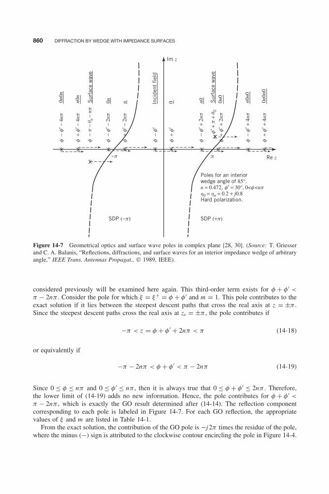
Balanis c14.tex V2 - 11/22/2011 4:00 P.M. Page 860
860 DIFFRACTION BY WEDGE WITH IMPEDANCE SURFACES
Re z
Im z
Poles for an interiorwedge angle of 85°.n = 0.472, f′ = 30°, 0<f<nph0 = hn = 0.2 + j0.8Hard polarization.
SDP (+p)SDP (−p)
p−p
f − f
′ − 4
np
f + f
′ − 4
np
f − p
− q
n −
np
f − f
′ − 2
np0n n In
cide
nt f
ield
Sur
face
wav
e
f + f
′ − 2
np
f − f
′
f + f
′
f − f
′ + 2
np
f′ +
p +
q0
f + f
′ + 2
np
f − f
′ + 4
np
f + f
′ + 4
np
0n0n
n0n
0 n0 0n0
n0n0
0n0n
0
Sur
face
wav
e
Figure 14-7 Geometrical optics and surface wave poles in complex plane [28, 30]. (Source: T. Griesserand C. A. Balanis, “Reflections, diffractions, and surface waves for an interior impedance wedge of arbitraryangle,” IEEE Trans. Antennas Propagat., © 1989, IEEE).
considered previously will be examined here again. This third-order term exists for φ + φ′ <
π − 2nπ . Consider the pole for which ξ = ξ+ = φ + φ′ and m = 1. This pole contributes to theexact solution if it lies between the steepest descent paths that cross the real axis at z = ±π .Since the steepest descent paths cross the real axis at zs = ±π , the pole contributes if
−π < z = φ + φ′ + 2nπ < π (14-18)
or equivalently if
−π − 2nπ < φ + φ′ < π − 2nπ (14-19)
Since 0 ≤ φ ≤ nπ and 0 ≤ φ′ ≤ nπ , then it is always true that 0 ≤ φ + φ′ ≤ 2nπ . Therefore,the lower limit of (14-19) adds no new information. Hence, the pole contributes for φ + φ′ <
π − 2nπ , which is exactly the GO result determined after (14-14). The reflection componentcorresponding to each pole is labeled in Figure 14-7. For each GO reflection, the appropriatevalues of ξ and m are listed in Table 14-1.
From the exact solution, the contribution of the GO pole is −j 2π times the residue of the pole,where the minus (−) sign is attributed to the clockwise contour encircling the pole in Figure 14-4.
Balanis c14.tex V2 - 11/22/2011 4:00 P.M. Page 861
GEOMETRICAL OPTICS 861
For the pole zp = φ ± φ′ + 2mnπ , the residue is
U CGO = Uo
nRes
⎡⎢⎢⎣�(
z + nπ
2− φ
)�
(nπ
2− φ′
) sin
(φ′
n
)cos
(z − φ
n
)− cos
(φ′
n
)ejβρ cos z , zp
⎤⎥⎥⎦ (14-20)
Assuming that no poles of the Maliuzhinets function coincide with the GO poles, and since theexponential has no finite poles, the residue can be determined by
U CGO = Uo
nlim
z→zp
⎧⎪⎪⎨⎪⎪⎩(z − zp)
⎡⎢⎢⎣�(
z + nπ
2− φ
)�
(nπ
2− φ′
) sin
(φ′
n
)cos
(z − φ
n
)− cos
(φ′
n
)ejβρ cos z
⎤⎥⎥⎦⎫⎪⎪⎬⎪⎪⎭
= Uo
n
�(
z + nπ
2− φ
)�
(nπ
2− φ′
) sin
(φ′
n
)ejβρ cos z lim
z→zpRes
⎡⎢⎢⎣ (z − zp)
cos
(z − φ
n
)− cos
(φ′
n
)⎤⎥⎥⎦(14-21)
From (14-16) and (14-17)
limz→zp
Res
⎡⎢⎢⎣ (z − zp)
cos
(z − φ
n
)− cos
(φ′
n
)⎤⎥⎥⎦ = lim
z→ξ±+2mnπRes
⎡⎢⎢⎣ [z − (ξ± + 2mnπ)]
cos
(z − φ
n
)− cos
(φ′
n
)⎤⎥⎥⎦(14-22)
This is an indeterminate form that can the evaluated by L′ Hopital’s Rule. Then
limz→zp
⎡⎢⎢⎣ (z − zp)
cos
(z − φ
n
)− cos
(φ′
n
)⎤⎥⎥⎦ = lim
z→ξ±+2mnπ
⎡⎢⎢⎣ 1
− 1
nsin
(z − φ
n
)⎤⎥⎥⎦
= −n
sin
(±φ′
n
) = ∓n
sin
(φ′
n
) (14-23)
where the upper sign represents ξ+ poles and the lower sign represents ξ− poles.Finally (14-21) becomes
U CGO = ∓Uo
�(
zp + nπ
2− φ
)�
(nπ
2− φ′
) ejβρ cos z
= ∓Uo
�(±φ′ + 2mnπ + nπ
2
)�
(nπ
2− φ′
) ejβρ cos(φ±φ′+2mnπ) (14-24)
corresponding to the poles zp = (φ ± φ′) + 2mnπ . By comparison with Table 14-1, it is clearthat the phase factor matches the geometrical-optics phase term. However, it remains to be shownthat the ratio of auxiliary Maliuzhinets functions in (14-24) is a product of reflection coefficients,

Balanis c14.tex V2 - 11/22/2011 4:00 P.M. Page 862
862 DIFFRACTION BY WEDGE WITH IMPEDANCE SURFACES
as in the geometrical analysis of (14-15). For the incident GO field, which corresponds toξ = ξ− = φ − φ′ and m = 0, the ratio is
�(±φ′ + 2mnπ + nπ
2
)�
(nπ
2− φ′
) =�
(−φ′ + nπ
2
)�
(nπ
2− φ′
) = 1 (14-25)
So the incident field from the exact solution matches the GO incident field as expected, and nofurther consideration is necessary for m = 0.
To consider the many possible multiple reflections, the ratio of auxiliary Maliuzhinets functions(and leading sign) of (14-24) is denoted by ��(φ′, θ0, θn), since it is shown next that the ratioindeed reduces to the products of reflection coefficients of Table 14-1
��(φ′, θ0, θn) = ∓�
(zp + nπ
2− φ
)�
(nπ
2− φ′
) (14-26)
where zp = (φ ± φ′) + 2mnπ . The numerator and denominator are expanded using [9, 26]
�(z ) = �n
(z + nπ
2+ π
2− θ0
)�n
(z + nπ
2− π
2+ θ0
)• �n
(z − nπ
2+ π
2− θn
)�n
(z − nπ
2− π
2+ θn
)(14-27)
and (14-26) takes two forms depending on whether φ + φ′ or φ − φ′ is selected.
For ξ = ξ− = φ − φ′ :
��(φ′, θ0, θn) =�n
(−φ′ + nπ + π
2− θ0 + 2mnπ
)�n
(−φ′ + nπ + π
2− θ0
) �n
(−φ′ + nπ − π
2+ θ0 + 2mnπ
)�n
(−φ′ + nπ − π
2+ θ0
)•
�n
(−φ′ + π
2− θn + 2mnπ
)�n
(−φ′ − π
2− θn
) �n
(−φ′ − π
2+ θn + 2mnπ
)�n
(−φ′ − π
2+ θn
) (14-28a)
For ξ = ξ+ = φ + φ′ :
��(φ′, θ0, θn) = −�n
(−φ′ + nπ + π
2− θ0 + 2mnπ
)�n
(φ′ − nπ + π
2− θ0
) �n
(φ′ + nπ − π
2+ θ0 + 2mnπ
)�n
(φ′ − nπ − π
2+ θ0
)•
�n
(φ′ + π
2− θn + 2mnπ
)�n
(φ′ + π
2− θn
) �n
(φ′ − π
2+ θn + 2mnπ
)�n
(φ′ − π
2+ θn
) (14-28b)
The fact that �n(z ) is an even function of z has also been utilized here. Next, (14-28a) and(14-28b) are shown to reduce to products of reflection coefficients for multiple reflected rays.

Balanis c14.tex V2 - 11/22/2011 4:00 P.M. Page 863
GEOMETRICAL OPTICS 863
The two single reflections are considered first, since both are exceptional cases. Each can bereduced to a single reflection coefficient using the trigonometric identity
tan
[1
2(x − y)
]cot
[1
2(x + y)
]= sin x − sin y
sin x + sin y(14-29)
and the Maliuzhinets identity [15]
�n(z + nπ)
�n(z − nπ)= cot
[1
2
(z + π
2
)](14-30)
For the reflection from face 0 (ξ = ξ+, m = 0), the last two terms in (14-28b) reduce to unitysince m = 0. Then, using (14-30) in (14-28b), the ratio of Maliuzhinets functions can be reducedto the single reflection coefficient ��(φ′, θ0, θn) = �0(φ
′) from the 0 face by applying (14-29) and(14-11a), in that order. Similarly, for the single-reflected field from face n(ξ = ξ+, m = −1), thefirst two terms in (14-28b) reduce to unity since m = −1. Again, using (14-30) in (14-28b), theratio of Maliuzhinets functions can be reduced to the single reflection coefficient ��(φ′, θ0, θn) =�n(nπ − φ′) from the n face by applying (14-29) and (14-11b), in that order.
By comparing with Table 14-1, it is evident that the ratio of auxiliary Maliuzhinets functionsreduces to the two single reflection coefficients for the (ξ = ξ+, m = 0) and (ξ = ξ+, m = −1)
poles. This equality of the ratios of Maliuzhinets functions with the single reflection coefficientshas been demonstrated in [23, 24, 26], but it is more difficult and less accurate for calculationpurposes. The higher-order reflection coefficients were not considered elsewhere, and it wasdemonstrated in [28, 30] that they can be reduced to products of reflection coefficients for anyorder of reflections. The products appear in four forms, depending on whether the number ofreflections is even or odd and whether the 0 and n face is initially illuminated for the multiple-reflected fields.
To obtain the appropriate products of reflection coefficients in (14-28a) and (14-28b) for thehigher-order reflections, the following identities are utilized:
�n(x + 2mnπ)
�n(x)= m
�p=1
�n [x + (2p − 1)nπ + nπ ]
�n [x + (2p − 1)nπ − nπ ], m > 0 (14-31a)
�n(x + 2mnπ)
�n(x)= |m|
�p=1
�n [x + (1 − 2p)nπ − nπ ]
�n [x + (1 − 2p)nπ + nπ ], m < 0 (14-31b)
These are algebraic identities, valid for any function, which can be verified by expanding theproduct. Their value lies in the fact that they correctly separate the Maliuzhinets function intoappropriate forms so that the recursion relations can be applied to reduce the Maliuzhinets ratiosto products of reflection coefficients.
Using (14-29) through (14-31b) in (14-28a) and (14-28b), the GO residues are reduced toproducts of reflection coefficients. Four different forms are possible, depending on the choicesof ξ and m . Consider first ξ = ξ− = φ − φ′ and m > 0. Then (14-28a) can be written, using(14-31a), as
��(φ′, θ0, θn) = m�
p=1
�n
[−φ′ + nπ + π
2− θ0 + (2p − 1)nπ + nπ
]�n
[−φ′ + nπ + π
2− θ0 + (2p − 1)nπ − nπ
]•
m�
p=1
�n
[−φ′ + nπ − π
2+ θ0 + (2p − 1)nπ + nπ
]�n
[−φ′ + nπ − π
2+ θ0 + (2p − 1)nπ − nπ
]
Balanis c14.tex V2 - 11/22/2011 4:00 P.M. Page 864
864 DIFFRACTION BY WEDGE WITH IMPEDANCE SURFACES
•m�
p=1
�n
[−φ′ + π
2− θn + (2p − 1)nπ + nπ
]�n
[−φ′ + π
2− θn + (2p − 1)nπ − nπ
]•
m�
p=1
�n
[−φ′ − π
2+ θn + (2p − 1)nπ + nπ
]�n
[−φ′ − π
2+ θn + (2p − 1)nπ − nπ
] (14-32)
Now using (14-30), (14-32) can be expressed as
��(φ′, θ0, θn) = m�
p=1cot
{1
2[−φ′ + nπ + π − θ0 + (2p − 1)nπ ]
}•
m�
p=1cot
{1
2[−φ′ + nπ + θ0 + (2p − 1)nπ ]
}•
m�
p=1cot
{1
2[−φ′ + π − θn + (2p − 1)nπ ]
}•
m�
p=1cot
{1
2[−φ′ + θn + (2p − 1)nπ ]
}(14-33)
Next, some of the cotangents are changed to tangents by trigonometric identities, and (14-33)can be written as
��(φ′, θ0, θn) = m�
p=1− tan
{1
2[−φ′ + nπ − θ0 + (2p − 1)nπ ]
}•
m�
p=1cot
{1
2[−φ′ + nπ + θ0 + (2p − 1)nπ ]
}•
m�
p=1− tan
{1
2[−φ′ − θn + (2p − 1)nπ ]
}•
m�
p=1cot
{1
2[−φ′ + θn + (2p − 1)nπ ]
}(14-34)
Using (14-29), all the terms in (14-34) can be combined, and (14-34) can then be expressed as
��(φ′, θ0, θn) = (−1)2m m�
p=1
sin(2pnπ − φ′) − sin θ0
sin(2pnπ − φ′) + sin θ0
m�
p=1
sin[(2p − 1)nπ − φ′] − sin θn
sin[(2p − 1)nπ − φ′] + sin θn
(14-35)
Finally, using (14-11a) and (14-11b), the two ratios of (14-35) reduce to products of reflectioncoefficients for the 0 and n faces, or
��(φ′, θ0, θn) = m�
p=1�0(2pnπ − φ′)
m�
p=1�n [(2p − 1)nπ − φ′] (14-36)
Again, (14-36) is only valid for ξ = ξ− = φ − φ′ and m > 0. There are still three more cases toconsider. However, all three cases reduce to similar products of reflection coefficients, and the

Balanis c14.tex V2 - 11/22/2011 4:00 P.M. Page 865
SURFACE WAVE TERMS 865
final forms obtained from the GO pole residues can be written as:
For ξ = ξ− = φ − φ′ and m > 0 :
��(φ′, θ0, θn) = m�
p=1�0(2pnπ − φ′)
m�
p=1�n [(2p − 1)nπ − φ′] (14-37)
For ξ = ξ− = φ − φ′ and m<0 :
��(φ′, θ0, θn) = |m|�
p=1�0[φ′ + 2(p − 1)nπ ]
|m|�
p=1�n [φ′ + (2p − 1)nπ ] (14-38)
For ξ = ξ+ = φ + φ′ and m > 0 :
��(φ′, θ0, θn) = |m|�
p=1�0[φ′ + 2(p − 1)nπ ]
m�
p=1�n [φ′ + (2p − 1)nπ ] (14-39)
For ξ = ξ+ = φ + φ′ and m < −1 :
��(φ′, θ0, θn) = |m+1|�
p=1�0(2pnπ − φ′)
|m|�
p=1�n [2(p − 1)nπ − φ′] (14-40)
The cases (ξ−, m = 0), (ξ+, m = 0), and (ξ+, m = −1) are the incident and single reflectedterms, which have already been considered. By comparison with Table 14-1, it is evident that(14-37) through (14-40) are identical to the geometrical ray-tracing analysis.
14.6 SURFACE WAVE TERMS
The surface wave is a wave that propagates along one face of the wedge and typically decaysexponentially in a vertical direction away from the face. It is confined to a particular angularrange from the wedge face, whenever it exists. Since the wave may decay slowly along the face,its contribution may be more dominant than other scattering mechanisms near the wedge surface.Hence, it is often important to include this contribution for reactive surfaces.
The surface wave is determined by considering the contributions of the residues of enclosedcomplex poles of the Maliuzhinets function between the steepest descent paths. The surface wavepoles were identified by Maliuzhinets, and they are located at [9, 27]
z0 = φ + π + θ0 (14-41a)
zn = φ − nπ − π − θn (14-41b)
for the 0 and n faces, respectively. If φ is allowed to vary from 0 to nπ , the z0 pole movesfrom π + θ0 to nπ + π + θ0 and the zn pole moves from −nπ − π − θn to −π − θn . The lociare shown in Figure 14-7 for φ′ = 30◦ for a wedge with an 85◦ interior angle and normalizedsurface impedances of ηo = ηn = 0.2 + j 0.8. The z0 pole can only lie within the steepest descentpaths for φ less than some maximum value. Similarly, the zn pole can only lie within the steepestdescent paths for φ greater than some minimum value. Hence, the surface wave term is boundedto a finite angular range near the corresponding face.
Balanis c14.tex V2 - 11/22/2011 4:00 P.M. Page 866
866 DIFFRACTION BY WEDGE WITH IMPEDANCE SURFACES
In general, the surface wave component corresponding to the pole z exists if it lies within thesteepest descent paths of (14-18). Then
−π < zr − cos−1
(1
cosh zi
)sgn(zi ) < π (14-42)
where z = zr + jzi . To determine the pole residue, the following Maliuzhinets function identityis utilized [15, 18]
�n
[z ±
(nπ + 3π
2
)]= ± sin
(π ± z
2n
)csc
( z
2n
)�n
(nπ − π
2± z
)(14-43)
This expression isolates the singular part of the pole in the cosecant function, and hence the
residue is readily calculated. The cosecant is singular at z = 0 and therefore �
[±
(nπ + 3π
2
)]is also singular. The example of the z0 pole is presented next, and the calculations for the zn poleare similar.
Example 14-1
Evaluate the surface wave residue of U 0SW.
Solution: The surface wave residue for the z0 pole is given by
U 0SW = Uo
nRes
⎡⎢⎢⎣�(
z + nπ
2− φ
)�
(nπ
2− φ′
) sin
(φ′
n
)cos
(z − φ
n
)− cos
(φ′
n
)ejβρ cos z , z0
⎤⎥⎥⎦Assuming that no GO poles coincide with the surface wave pole, and since the exponential has no finitepoles, the residue can be determined as
U 0SW = Uo
nlim
z→z0
⎡⎢⎢⎣(z − z0)
�(
z + nπ
2− φ
)�
(nπ
2− φ′
) sin
(φ′
n
)cos
(z − φ
n
)− cos
(φ′
n
)ejβρ cos z
⎤⎥⎥⎦In the limit, (z − z0) has a zero and �
(z + nπ
2− φ
)contains the complex pole. All the other terms
can be brought outside the limit. Thus,
U 0SW = Uo
n
⎡⎢⎢⎣ejβρ cos(φ+π+θ0)
�(nπ
2− φ′
) sin
(φ′
n
)cos
(π + θ0
n
)− cos
(φ′
n
)⎤⎥⎥⎦ lim
z→z0
[(z − z0)�
(z + nπ
2− φ
)]
Next, the auxiliary Maliuzhinets function within the limit is decomposed into four Maliuzhinetsfunctions using (14-27). That is
�(
z + nπ
2− φ
)= �n
(z + nπ − φ + π
2− θ0
)�n
(z + nπ − φ − π
2+ θ0
)• �n
(z − φ + π
2− θn
)�n
(z − φ − π
2+ θn
)
Balanis c14.tex V2 - 11/22/2011 4:00 P.M. Page 867
SURFACE WAVE TERMS 867
As z → z0 = φ + π + θ0, it is evident that the first Maliuzhinets function becomes �n
(nπ + 3π
2
),
which was shown to be singular in (14-43). Since only the first Maliuzhinets function contains thecomplex pole, the other three can be moved outside the limit. Thus
U 0SW = Uo
n
⎡⎢⎢⎣ e−jβρ cos(φ+θ0)
�(nπ
2− φ′
) sin
(φ′
n
)cos
(π + θ0
n
)− cos
(φ′
n
)⎤⎥⎥⎦�n
(nπ + π
2+ 2θ0
)• �n
(3π
2+ θ0 − θn
)
• �n
(π
2+ θ0 + θn
)lim
z→z0
[(z − z0)�n
(z + nπ − φ + π
2− θ0
)]The limit of the above equation can be determined using (14-43). Thus, replacing Z − Z0 = α
limz→z0
[(z − z0)�n
(z + nπ − φ + π
2− θ0
)]= lim
z→z0
[(z − z0)�n
(z − z0 + nπ + 3π
2
)]
= limα→0
[α�n
(α + nπ + 3π
2
)]= sin
( π
2n
)�n
(nπ − π
2
)limα→0
[α csc
( α
2n
)]= 2n sin
( π
2n
)�n
(nπ − π
2
)which, when substituted into the previous equation, leads to the surface wave contribution.
The final form of the surface waves from face 0 is
U 0SW = Uo
⎡⎢⎢⎣ 2 sin( π
2n
)�
(nπ
2− φ′
) sin
(φ′
n
)e−jβρ cos(φ+θ0)
cos
(π + θ0
n
)− cos
(φ′
n
)⎤⎥⎥⎦�n
(nπ − π
2
)�n
(nπ + π
2+ 2θ0
)
• �n
(3π
2+ θ0 − θn
)�n
(π
2+ θ0 + θn
)
In a similar manner, based on the procedure used in Example 14-1, the surface wave contri-bution U n
SW from face n can be written as
U nSW = Uo
⎡⎢⎢⎣ −2 sin( π
2n
)�
(nπ
2− φ′
) sin
(φ′
n
)e−jβρ cos(φ−nπ−θn )
cos
(nπ + π + θn
n
)− cos
(φ′
n
)⎤⎥⎥⎦�n
(nπ − π
2
)�n
(π
2+ nπ + 2θn
)
• �n
(3π
2+ θn − θ0
)�n
(π
2+ θn + θ0
)(14-44)
By the symmetry of the wedge geometry, it is noted that (14-44) can be obtained from the U 0SW
of Example 14-1 by replacing φ by nπ − φ, φ′ by nπ − φ′, θ0 by θn , and θn by θ0. The angularranges over which U 0
SW and U nSW exist are given by (14-41a) through (14-42).

Balanis c14.tex V2 - 11/22/2011 4:00 P.M. Page 868
868 DIFFRACTION BY WEDGE WITH IMPEDANCE SURFACES
The GO component of (14-21) and the surface wave U 0SW of Example 14-1 were obtained
assuming the GO poles and surface wave poles did not coincide. This is a valid assumptionbecause the GO poles are always real, and if a surface wave pole coincides with a GO pole, itmust necessarily be real. However, from (14-41a) and (14-41b), it is evident that real surfacewave poles always lie outside the steepest descent paths since 0 < φ < nπ . Therefore, if a surfacewave pole and a GO pole coincide, they must lie outside the steepest descent paths, and theirresidues do not contribute to the exact solution.
14.7 DIFFRACTED FIELDS
In the previous sections, Maliuzhinets’ exact solution was examined for both interior and exteriorimpedance wedges. It was shown that the exact solution can be written as a sum of residues fromthe GO and surface wave poles plus contribution along the steepest descent paths. In this section,the steepest descent paths contribution is examined thoroughly using high-frequency asymptoticexpansions. The high-frequency asymptotic expansion gives the diffracted field and the surfacewave transition field. The diffracted field is similar in form to the diffraction coefficients for thePEC theory, with a suitable multiplying factor which include ratios of auxiliary Maliuzhinetsfunctions.
14.7.1 Diffraction Terms
Maliuzhinets’ exact integral solution of (14-5) has been manipulated in (14-10) to follow thesteepest descent paths through the saddle points at z = ±π . The exact solution from (14-10) canbe written as
Ut (ρ, φ) = jUo1
2nπ
∫γ
�(
z + nπ
2− φ
)�
(nπ
2− φ′
) sin
(φ′
n
)cos
(z − φ
n
)− cos
(φ′
n
)ejβρ cos z dz
= Uo
n
N∑p=1
Res
⎡⎢⎢⎣�(
z + nπ
2− φ
)�
(nπ
2− φ′
) sin
(φ′
n
)cos
(z − φ
n
)− cos
(φ′
n
)ejβρ cos z , zp
⎤⎥⎥⎦
− jUo1
2nπ
∫SDPs
�(
z + nπ
2− φ
)�
(nπ
2− φ′
) sin
(φ′
n
)cos
(z − φ
n
)− cos
(φ′
n
)ejβρ cos z dz (14-45)
Ut (ρ, φ) =∑[
U m ,ξGO + U 0
SW + U nSW
]
− jUo1
2nπ
∫SDPs
�(
z + nπ
2− φ
)�
(nπ
2− φ′
) sin
(φ′
n
)cos
(z − φ
n
)− cos
(φ′
n
)ejβρ cos z dz (14-45a)
Ut (ρ, φ) =∑[
U m ,ξGO + U 0
SW + U nSW + USDP
]=
∑[U m ,ξ
GO + U 0SW + U n
SW + UD + U 0SWTR + U n
SWTR
](14-45b)
Balanis c14.tex V2 - 11/22/2011 4:00 P.M. Page 869
DIFFRACTED FIELDS 869
whereU m ,ξ
GO = GO incident or reflected field corresponding to integer m and ξ = ξ+or ξ = ξ− as given by (14-15) and in Table 14-1
U 0SW, U n
SW = surface wave contributions, as given by Example 14-1 and (14-44)UD = diffracted field, examined asymptotically in Section 14.7.2
U 0SWTR, U n
SWTR = surface wave transition field terms
The canonical wedge geometry of Figures 14-1a and 14-5 illustrate the shadow boundaries of theGO field for the exterior wedge. Similar shadow boundaries exist for multiple reflected fields forthe interior wedge of Figures 14-1b and 14-6. All the GO shadow boundaries are compensatedby the diffracted field. Similarly, the surface wave transition field compensates for discontinuitiesat the surface wave boundary.
14.7.2 Asymptotic Expansions
To determine an asymptotic expansion of a steepest descent integral, such as that of (14-45a),or
USDP(ρ, φ) = −jUo1
2nπ
∫SDPs
�(
z + nπ
2− φ
)�
(nπ
2− φ′
) sin
(φ′
n
)cos
(z − φ
n
)− cos
(φ′
n
)ejβρ cos z dz
= −jUo1
2nπ
sin
(φ′
n
)�
(nπ
2− φ′
) ∫SDPs
�(
z + nπ
2− φ
)cos
(z − φ
n
)− cos
(φ′
n
)ejβρ cos z dz (14-46)
requires careful consideration of poles which may lie close to the steepest descent paths. Thecontribution of the steepest descent integral should be discontinuous as a pole crosses the pathto compensate for the addition or loss of the pole residue that corresponds to a GO or surfacewave component. In this way, the total solution, which is the sum of the residues plus the integralcontribution, is always continuous.
Two asymptotic expansions are used: the Modified Pauli-Clemmow method [63–67] for the GOpoles and the Felsen-Marcuvitz method [68, 69] for the surface wave poles. The Modified Pauli-Clemmow method yields a diffracted field which is analogous to the PEC case for the real GO poles.A diffraction coefficient is formulated, which is similar to the UTD diffraction coefficient withmultiplying factors that include suitable ratios of auxiliary Maliuzhinets functions. The method ofFelsen-Marcuvitz is used for the complex surface wave poles to construct a surface wave transitionfield that yields the proper continuity. The method of Felsen-Marcuvitz [68] or that of [70] could beused for all the poles. However, there would be two disadvantages. First, the method would not beanalogous to the PEC UTD, which is a powerful tool in modern diffraction. Second, the formulationwould require that the contributions of all the poles for all the multiple reflections be added together.This is the approach used in [27], and the equations become very complicated after adding only thepoles of the incident field, the two single-reflected fields, and the two surface waves. For an interiorwedge with many multiple reflections, the Felsen-Marcuvitz method is more cumbersome than theModified-Clemmow method for the GO poles.
The two methods of asymptotic approximation have been shown to be the same [70, 71],provided that the asymptotic expansions are complete; that is, they contain an infinite number ofhigher-order terms. In practice, this is usually not the case because only the first and second termsare retained and all others are omitted. Consequently, one or the other may be more appropriate fora given problem. However, either will give the correct discontinuity as the pole crosses the saddlepoint, and both reduce to the same expression when no pole is near the steepest descent path.
Balanis c14.tex V2 - 11/22/2011 4:00 P.M. Page 870
870 DIFFRACTION BY WEDGE WITH IMPEDANCE SURFACES
The Modified Pauli-Clemmow method of steepest descent was introduced in Chapter 13 toevaluate an integral of the (13-41) form, or
P(βρ) =∫
CH (z )eβρh(z ) dz
βρ→large︷︸︸︷≈ eβρh(zs )H (zs)ejφs
√−2π
βρh ′′(zs)F [βρg(ξ)] (14-47)
F [βρg(ξ)] ≡ j [h(zs) − h(zp)] = 2j√
βρg(ξ)
∫ ∞√
βρg(ξ)
e−jτ2dτ
≡ a measure of separation between saddle points and poles (14-47a)
and to reduce (13-60a)–(13-60b) to (13-63a)–(13-63b), and eventually to the UTD diffractioncoefficients.
The Felsen-Marcuvitz method is used to evaluate an integral of the (13-41) or (14-47) form,and it is expressed as
P(βρ) =∫
CH (z )eβρh(z ) dz
βρ→large︷︸︸︷≈ eβρh(zs )H (zs)ejφs
√−2π
βρh ′′(zs)
+ h1√
πeβρh(zs )√βρ[h(zs) − h(zp)]
{F [βρg(ξ)] − 1} (14-48)
where h1 is the residue of H (z ) at z = zp ; all other quantities are the same as for the ModifiedPauli-Clemmow method.
14.7.3 Diffracted Field
Using a procedure similar to that of Section 13.3.2, it can be shown, through some trigonometricidentities, that the integral of (14-46) can be written in a more convenient form as
USDP(ρ, φ) = −jUo1
2nπ
∫SDPs
�(
z + nπ
2− φ
)�
(nπ
2− φ′
) sin
(φ′
n
)cos
(z − φ
n
)− cos
(φ′
n
)ejβρ cos z dz
= −jUo1
4nπ
∫SDPs
�(
z + nπ
2− φ
)�
(nπ
2− φ′
) {cot
[(φ + φ′) − z
2n
]− cot
[(φ − φ′) − z
2n
]}ejβρ cos z dz
(14-49)where the following substitution, through trigonometric identities, has been used.
sin
(φ′
n
)cos
(z − φ
n
)− cos
(φ′
n
) = 1
2
{cot
[(φ + φ′) − z
2n
]− cot
[(φ − φ′) − z
2n
]}(14-50)
By the convention of the PEC wedge formulation, ξ+ = (φ + φ′) and ξ− = (φ − φ′). The polesof the first cotangent occur at
z = (φ + φ′) − 2πNn = ξ+ − 2πNn (14-51a)
and correspond to the GO components that include an odd number of reflections (i.e., singlereflections, triple reflections, etc.). The poles of the second cotangent occur at
z = (φ − φ′) − 2πNn = ξ− − 2πNn (14-51b)
Balanis c14.tex V2 - 11/22/2011 4:00 P.M. Page 871
DIFFRACTED FIELDS 871
and correspond to the GO terms that include an even number of reflections (i.e., incident, doublereflected, etc.). In (14-51a) and (14-51b), N can be any integer, and hence there are an infinitenumber of poles of the integrand for both ξ+ and ξ−.
The PEC UTD diffraction considers only the four dominant poles of the integrand of (14-49).These four are the poles corresponding to ξ+ that are the closest to the saddle points at ±π , andthe poles corresponding to ξ− that are closest to the same saddle points. Hence, four values ofN are chosen, where the N ’s are the integers that most closely satisfy
2πnN +− − ξ− = +π (14-52a)
2πnN −− − ξ− = −π (14-52b)
2πnN ++ − ξ+ = +π (14-52c)
2πnN −+ − ξ+ = −π (14-52d)
where the subscript in N indicates the choice of ξ . The superscript of N corresponds to thesign of ±π on the right side of (14-52). Therefore, based on (14-52a)–(14-52b), (14-49) can bedecomposed into four integrals corresponding to the four selected poles; that is
USDP(ρ, φ) = +jUo1
4nπ
∫SDP(−π)
�(
z + nπ
2− φ
)�
(nπ
2− φ′
) {cot
(ξ− − z
2n
)}ejβρ cos z dz
+ jUo1
4nπ
∫SDP(+π)
�(
z + nπ
2− φ
)�
(nπ
2− φ′
) {cot
[ξ− − z
2n
]}ejβρ cos z dz
− jUo1
4nπ
∫SDP(−π)
�(
z + nπ
2− φ
)�
(nπ
2− φ′
) {cot
[ξ+ − z
2n
]}ejβρ cos z dz
− jUo1
4nπ
∫SDP(+π)
�(
z + nπ
2− φ
)�
(nπ
2− φ′
) {cot
[ξ+ − z
2n
]}ejβρ cos z dz (14-53)
where the order of the terms of (14-53) corresponds to the order of the N ’s in (14-52). Each termis individually evaluated asymptotically using (14-47).
Example 14-2
To demonstrate the asymptotic procedure, evaluate the first term of (14-53).
Solution:
H1(α) =�
(z + nπ
2− φ
)�
(nπ
2− φ′
) cot
(ξ− − z
2n
)h1(z ) = j cos z
zs = −π
zp = ξ− − 2πN +− n
a = j [−jρ − jρ cos(ξ− − 2πN +− n)] = ρ[1 + ρ cos(ξ− − 2πN +
− n)]
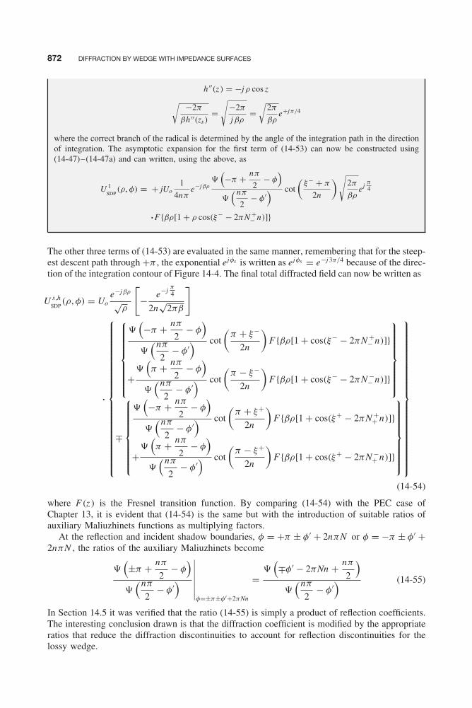
Balanis c14.tex V2 - 11/22/2011 4:00 P.M. Page 872
872 DIFFRACTION BY WEDGE WITH IMPEDANCE SURFACES
h ′′(z ) = −jρ cos z√ −2π
βh ′′(zs )=
√−2π
jβρ=
√2π
βρe+jπ/4
where the correct branch of the radical is determined by the angle of the integration path in the directionof integration. The asymptotic expansion for the first term of (14-53) can now be constructed using(14-47)–(14-47a) and can written, using the above, as
U 1SDP
(ρ, φ) = + jUo1
4nπe−jβρ
�(−π + nπ
2− φ
)�
(nπ
2− φ′
) cot
(ξ− + π
2n
)√2π
βρej
π4
• F {βρ[1 + ρ cos(ξ− − 2πN +− n)]}
The other three terms of (14-53) are evaluated in the same manner, remembering that for the steep-est descent path through +π , the exponential ejφs is written as ejφs = e−j 3π/4 because of the direc-tion of the integration contour of Figure 14-4. The final total diffracted field can now be written as
U s ,hSDP
(ρ, φ) = Uoe−jβρ
√ρ
[− e−j
π4
2n√
2πβ
]
•
⎧⎪⎪⎪⎪⎪⎪⎪⎪⎪⎪⎪⎪⎪⎪⎪⎪⎪⎪⎪⎪⎪⎨⎪⎪⎪⎪⎪⎪⎪⎪⎪⎪⎪⎪⎪⎪⎪⎪⎪⎪⎪⎪⎪⎩
⎧⎪⎪⎪⎪⎪⎪⎪⎨⎪⎪⎪⎪⎪⎪⎪⎩
�(−π + nπ
2− φ
)�
(nπ
2− φ′
) cot
(π + ξ−
2n
)F {βρ[1 + cos(ξ− − 2πN +
− n)]}
+�
(π + nπ
2− φ
)�
(nπ
2− φ′
) cot
(π − ξ−
2n
)F {βρ[1 + cos(ξ− − 2πN −
− n)]}
⎫⎪⎪⎪⎪⎪⎪⎪⎬⎪⎪⎪⎪⎪⎪⎪⎭
∓
⎧⎪⎪⎪⎪⎪⎪⎪⎨⎪⎪⎪⎪⎪⎪⎪⎩
�(−π + nπ
2− φ
)�
(nπ
2− φ′
) cot
(π + ξ+
2n
)F {βρ[1 + cos(ξ+ − 2πN +
+ n)]}
+�
(π + nπ
2− φ
)�
(nπ
2− φ′
) cot
(π − ξ+
2n
)F {βρ[1 + cos(ξ+ − 2πN −
+ n)]}
⎫⎪⎪⎪⎪⎪⎪⎪⎬⎪⎪⎪⎪⎪⎪⎪⎭
⎫⎪⎪⎪⎪⎪⎪⎪⎪⎪⎪⎪⎪⎪⎪⎪⎪⎪⎪⎪⎪⎪⎬⎪⎪⎪⎪⎪⎪⎪⎪⎪⎪⎪⎪⎪⎪⎪⎪⎪⎪⎪⎪⎪⎭(14-54)
where F (z ) is the Fresnel transition function. By comparing (14-54) with the PEC case ofChapter 13, it is evident that (14-54) is the same but with the introduction of suitable ratios ofauxiliary Maliuzhinets functions as multiplying factors.
At the reflection and incident shadow boundaries, φ = +π ± φ′ + 2nπN or φ = −π ± φ′ +2nπN , the ratios of the auxiliary Maliuzhinets become
�(±π + nπ
2− φ
)�
(nπ
2− φ′
)∣∣∣∣∣∣∣φ=±π±φ′+2πNn
=�
(∓φ′ − 2πNn + nπ
2
)�
(nπ
2− φ′
) (14-55)
In Section 14.5 it was verified that the ratio (14-55) is simply a product of reflection coefficients.The interesting conclusion drawn is that the diffraction coefficient is modified by the appropriateratios that reduce the diffraction discontinuities to account for reflection discontinuities for thelossy wedge.
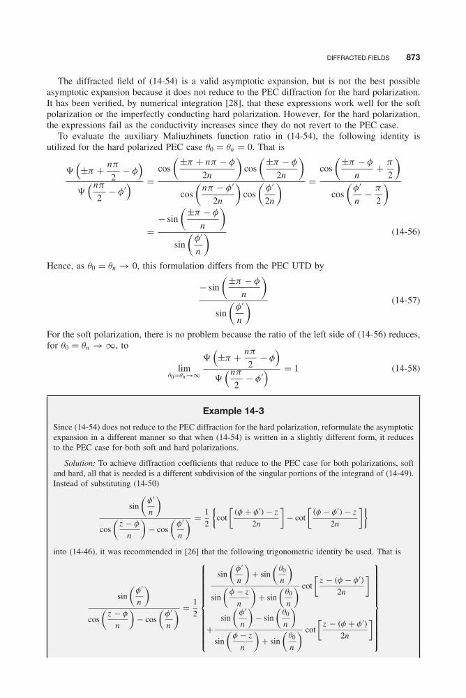
Balanis c14.tex V2 - 11/22/2011 4:00 P.M. Page 873
DIFFRACTED FIELDS 873
The diffracted field of (14-54) is a valid asymptotic expansion, but is not the best possibleasymptotic expansion because it does not reduce to the PEC diffraction for the hard polarization.It has been verified, by numerical integration [28], that these expressions work well for the softpolarization or the imperfectly conducting hard polarization. However, for the hard polarization,the expressions fail as the conductivity increases since they do not revert to the PEC case.
To evaluate the auxiliary Maliuzhinets function ratio in (14-54), the following identity isutilized for the hard polarized PEC case θ0 = θn = 0. That is
�(±π + nπ
2− φ
)�
(nπ
2− φ′
) =cos
(±π + nπ − φ
2n
)cos
(±π − φ
2n
)cos
(nπ − φ′
2n
)cos
(φ′
2n
) =cos
(±π − φ
n+ π
2
)cos
(φ′
n− π
2
)
=− sin
(±π − φ
n
)sin
(φ′
n
) (14-56)
Hence, as θ0 = θn → 0, this formulation differs from the PEC UTD by
− sin
(±π − φ
n
)sin
(φ′
n
) (14-57)
For the soft polarization, there is no problem because the ratio of the left side of (14-56) reduces,for θ0 = θn → ∞, to
limθ0=θn→∞
�(±π + nπ
2− φ
)�
(nπ
2− φ′
) = 1 (14-58)
Example 14-3
Since (14-54) does not reduce to the PEC diffraction for the hard polarization, reformulate the asymptoticexpansion in a different manner so that when (14-54) is written in a slightly different form, it reducesto the PEC case for both soft and hard polarizations.
Solution: To achieve diffraction coefficients that reduce to the PEC case for both polarizations, softand hard, all that is needed is a different subdivision of the singular portions of the integrand of (14-49).Instead of substituting (14-50)
sin
(φ′
n
)cos
(z − φ
n
)− cos
(φ′
n
) = 1
2
{cot
[(φ + φ′) − z
2n
]− cot
[(φ − φ′) − z
2n
]}
into (14-46), it was recommended in [26] that the following trigonometric identity be used. That is
sin
(φ′
n
)cos
(z − φ
n
)− cos
(φ′
n
) = 1
2
⎧⎪⎪⎪⎪⎪⎪⎪⎪⎪⎪⎪⎨⎪⎪⎪⎪⎪⎪⎪⎪⎪⎪⎪⎩
sin
(φ′
n
)+ sin
(θ0
n
)sin
(φ − z
n
)+ sin
(θ0
n
) cot
[z − (φ − φ′)
2n
]
+sin
(φ′
n
)− sin
(θ0
n
)sin
(φ − z
n
)+ sin
(θ0
n
) cot
[z − (φ + φ′)
2n
]
⎫⎪⎪⎪⎪⎪⎪⎪⎪⎪⎪⎪⎬⎪⎪⎪⎪⎪⎪⎪⎪⎪⎪⎪⎭
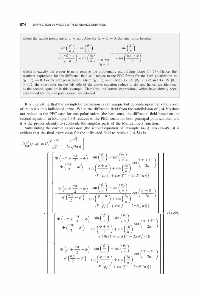
Balanis c14.tex V2 - 11/22/2011 4:00 P.M. Page 874
874 DIFFRACTION BY WEDGE WITH IMPEDANCE SURFACES
where the saddle points are at zs = ±π . Also for θ0 = θn = 0, the sine ratios become
sin
(φ′
n
)± sin
(θ0
n
)sin
(φ − z
n
)+ sin
(θ0
n
)∣∣∣∣∣∣∣∣z = ±π
θ0 = 0
=sin
(φ′
n
)− sin
(±π − φ
n
)
which is exactly the proper term to remove the problematic multiplying factor (14-57). Hence, theresultant expression for the diffracted field will reduce to the PEC forms for the hard polarization asθ0 = θn → 0. For the soft polarization, where θ0 = θn → ∞ with 0 < Re [θ0] < π/2 and 0 < Re [θn ]< π/2, the sine ratios on the left side of the above equation reduce to ±1 and hence, are identicalto the second equation in this example. Therefore, the correct expressions, which have already beenestablished for the soft polarization, are retained.
It is interesting that the asymptotic expansion is not unique but depends upon the subdivisionof the poles into individual terms. While the diffracted field from the subdivision of (14-50) doesnot reduce to the PEC case for one polarization (the hard one), the diffracted field based on thesecond equation in Example 14-3 reduces to the PEC forms for both principal polarizations, andit is the proper identity to subdivide the singular parts of the Maliuzhinets function.
Substituting the correct expression (the second equation of Example 14-3) into (14-49), it isevident that the final expression for the diffracted field to replace (14-54) is
U s ,hSDP
(ρ, φ) = Uoe−jβρ
√ρ
[− e−j
π4
2n√
2πβ
]
•
⎧⎪⎪⎪⎪⎪⎪⎪⎪⎪⎪⎪⎪⎪⎪⎪⎪⎪⎪⎪⎪⎪⎪⎪⎪⎪⎪⎪⎪⎪⎪⎪⎪⎪⎪⎪⎪⎪⎪⎪⎪⎪⎪⎪⎪⎨⎪⎪⎪⎪⎪⎪⎪⎪⎪⎪⎪⎪⎪⎪⎪⎪⎪⎪⎪⎪⎪⎪⎪⎪⎪⎪⎪⎪⎪⎪⎪⎪⎪⎪⎪⎪⎪⎪⎪⎪⎪⎪⎪⎪⎩
⎧⎪⎪⎪⎪⎪⎪⎪⎪⎪⎪⎪⎪⎪⎪⎪⎪⎪⎪⎪⎨⎪⎪⎪⎪⎪⎪⎪⎪⎪⎪⎪⎪⎪⎪⎪⎪⎪⎪⎪⎩
�(−π + nπ
2− φ
)�
(nπ
2− φ′
) sin
(φ′
n
)+ sin
(θ0
n
)sin
(φ + π
n
)+ sin
(θ0
n
) cot
(π + ξ−
2n
)• F
{βρ[1 + cos(ξ− − 2πN +
− n)]}
+�
(π + nπ
2− φ
)�
(nπ
2− φ′
) sin
(φ′
n
)+ sin
(θ0
n
)sin
(φ − π
n
)+ sin
(θ0
n
) cot
(π − ξ−
2n
)• F
{βρ[1 + cos(ξ− − 2πN −
− n)]}
⎫⎪⎪⎪⎪⎪⎪⎪⎪⎪⎪⎪⎪⎪⎪⎪⎪⎪⎪⎪⎬⎪⎪⎪⎪⎪⎪⎪⎪⎪⎪⎪⎪⎪⎪⎪⎪⎪⎪⎪⎭
∓
⎧⎪⎪⎪⎪⎪⎪⎪⎪⎪⎪⎪⎪⎪⎪⎪⎪⎪⎪⎪⎨⎪⎪⎪⎪⎪⎪⎪⎪⎪⎪⎪⎪⎪⎪⎪⎪⎪⎪⎪⎩
�(−π + nπ
2− φ
)�
(nπ
2− φ′
) sin
(φ′
n
)− sin
(θ0
n
)sin
(φ + π
n
)+ sin
(θ0
n
) cot
(π + ξ+
2n
)• F {βρ[1 + cos(ξ+ − 2πN +
+ n)]}
+�
(π + nπ
2− φ
)�
(nπ
2− φ′
) sin
(φ′
n
)− sin
(θ0
n
)sin
(φ − π
n
)+ sin
(θ0
n
) cot
(π − ξ+
2n
)• F
{βρ[1 + cos(ξ+ − 2πN −
+ n)]}
⎫⎪⎪⎪⎪⎪⎪⎪⎪⎪⎪⎪⎪⎪⎪⎪⎪⎪⎪⎪⎬⎪⎪⎪⎪⎪⎪⎪⎪⎪⎪⎪⎪⎪⎪⎪⎪⎪⎪⎪⎭
⎫⎪⎪⎪⎪⎪⎪⎪⎪⎪⎪⎪⎪⎪⎪⎪⎪⎪⎪⎪⎪⎪⎪⎪⎪⎪⎪⎪⎪⎪⎪⎪⎪⎪⎪⎪⎪⎪⎪⎪⎪⎪⎪⎪⎪⎬⎪⎪⎪⎪⎪⎪⎪⎪⎪⎪⎪⎪⎪⎪⎪⎪⎪⎪⎪⎪⎪⎪⎪⎪⎪⎪⎪⎪⎪⎪⎪⎪⎪⎪⎪⎪⎪⎪⎪⎪⎪⎪⎪⎪⎭
(14-59)
Balanis c14.tex V2 - 11/22/2011 4:00 P.M. Page 875
SURFACE WAVE TRANSITION FIELD 875
Equation (14-59), although cast in a different form, is identical to those in [26]. However,in [26], a great deal of effort was focused on manipulating these expressions to a form that wassymmetric with respect to θ0 and θn , and to reduce the number of times the Maliuzhinets functionneeded to be calculated. The formulation of (14-59) does not appear explicitly symmetric withrespect to θ0 and θn , but it is symmetric because the �(z ) auxiliary Maliuzhinets function includesθ0 and θn implicitly. There are twelve Maliuzhinets functions that need to be calculated. Four arenecessary for each auxiliary Maliuzhinets function, and there are three auxiliary functions:
�(nπ
2− φ′
), �
(π + nπ
2− φ′
)and �
(−π + nπ
2− φ′
)In [26], it was shown that the Maliuzhinets functions reduce to a double-nested integra-
tion; however, this double-nested integral is exceedingly difficult to evaluate, even numerically.Hence, [26] only demonstrated results for three special wedge angles, corresponding to the half-plane (WA = 0◦), the exterior right angle (WA = 90◦) and the planar interface discontinuity(WA = 180◦). It is shown in [28] that this double-nested integral can be written as eight Mali-uzhinets functions, all of which are readily available for an arbitrary wedge angle by methods inAppendix B of [28].
For the integral of [26], which is denoted Mn(φ, φ′; θ0, θn), the simpler expression is
Mn(φ, φ′; θ0, θn) =�n
(nπ − φ′ + π
2+ θn
)�n
(φ′ + π
2+ θn
)�n
(nπ − φ′ + π
2− θ0
)�n
(φ′ + π
2− θn
)•
�n
(nπ − φ − π
2− θ0
)�n
(φ − π
2− θn
)�n
(nπ − φ − π
2+ θ0
)�n
(φ′ − π
2+ θn
) (14-60)
In this manner, the necessary evaluations of Maliuzhinets functions are reduced from twelve toeight, and the results are obtainable for arbitrary interior and exterior wedge angles rather thanfor only the three specific wedge angles [half plane (WA = 0◦), exterior right angle (WA = 90◦),and planar interface discontinuity (WA = 180◦)]. This allows for the modeling of more generalstructures.
The Keller-type diffraction coefficients, which are the nonuniform versions, are obtained from(14-59) by setting every Fresnel transition function to unity.
14.8 SURFACE WAVE TRANSITION FIELD
The surface waves of the exact impedance wedge solution exist only for a limited angular rangenear the associated wedge face. It was shown in Section 14.6 that this angular range was deter-mined by the position of the surface wave pole relative to the steepest descent path. As the polemoves outside the region between the steepest descent paths, the surface wave term vanishes.This is completely analogous to the GO shadow boundaries that arise when a pole crosses asteepest descent path. The major difference is that the surface wave poles are generally complex,whereas the GO poles are always real.
The surface wave transition field provides continuity across the surface wave boundary byuniformly accounting for the complex pole in the vicinity of the steepest descent path. It performsthe same function as the diffracted field in providing continuity for the GO field. This componentof the exact solution has also been referred to as surface ray field [27].
To determine the contribution of the complex surface wave pole in the steepest descent inte-gral, the method of Felsen-Marcuvitz [68] is utilized. In (14-48), the integral was shown to be
Balanis c14.tex V2 - 11/22/2011 4:00 P.M. Page 876
876 DIFFRACTION BY WEDGE WITH IMPEDANCE SURFACES
asymptotically approximated by the sum of two terms; the first corresponding to a first-ordersaddle point evaluation with no pole, and the second corresponding to the pole contribution. In(14-47), the modified Pauli-Clemmow method was shown to reduce precisely to the first term of(14-48) when the GO pole was not near the steepest descent path. Hence, a method to includethe surface wave transition field is to use the second term of (14-48) added to the diffractioncontribution of Section 14.7. This is valid provided the poles approach the steepest descent pathindividually.
The contribution of the surface wave transition field is then given by [28]
U 0SWTR
(ρ, φ) = Uoe−jβρ
√ρ
⎡⎢⎢⎣−√
j
πsin
( π
2n
)�
(nπ
2− φ′
) sin
(φ′
n
)cos
(π + θ0
n
)− cos
(φ′
n
)⎤⎥⎥⎦
• �n
(nπ − π
2
)�n
(nπ + π
2+ 2θ0
)�n
(3π
2+ θ0 − θn
)�n
(π
2+ θ0 + θn
)•F {βρ[1 − cos(φ + θ0)]} − 1
√β[cos(φ + θ0) − 1]
(14-61a)
U nSWTR
(ρ, φ) = Uoe−jβρ
√ρ
⎡⎢⎢⎣√
j
πsin
( π
2n
)�
(nπ
2− φ′
) sin
(φ′
n
)cos
(nπ + π + θn
n
)− cos
(φ′
n
)⎤⎥⎥⎦
• �n
(nπ − π
2
)�n
(nπ + π
2+ 2θn
)�n
(3π
2+ θn − θ0
)�n
(π
2+ θ0 + θn
)•F {βρ[1 − cos(φ − nπ − θn)]} − 1√
β[cos(φ − nπ − θn) − 1](14-61b)
The pole residue has been determined as in (14-43) and Example 14-1. By the symmetry of thewedge geometry, it is noted that (14-61b) can be determined from (14-61a) by replacing φ bynπ − φ, φ′ by nπ − φ′, θ0 by θn , and θn by θ0. This Fresnel transition function is as defined in [66]but extended for complex arguments. The
√z in the definition of F (z ) should have a branch
cut along the positive imaginary axis so that −3π/4 < [Arg√
z ] < π/4. It is the discontinuity inF (z ) at the branch cut that provides the discontinuity in the integral contribution. When the poleis far from the steepest descent path, the Fresnel transition function is approximately unity, andhence, the surface wave transition field contribution is zero.
A troublesome case occurs when the surface wave pole coincides with a GO pole. Sincethe GO poles are always real, this can only occur for real surface impedances. Real surfaceimpedances, however, cannot support surface waves, as the surface wave pole will never liewithin the steepest descent paths. However, if the surface wave transition field is calculated byblindly applying (14-61a) and (14-61b), erroneous results will occur whenever the surface wavepole is far from the steepest descent path, yet near a GO pole. Indeed, the surface wave transitionfield should be zero when the surface wave pole is far from the steepest descent paths. Hence,(14-61a) and (14-61b) should only be used when the surface wave pole is closer to a steepestdescent path than to a GO pole. When the surface wave pole is near both a GO pole and thesteepest descent path, then (16) of [26] should be used. When the surface wave pole is far fromthe steepest descent path, the surface wave transition field is taken as zero.
A complete asymptotic expansion, which uniformly accounts for coalescing GO and surfacewave poles, can be found in [70]. However, this type of formulation would not retain the form

Balanis c14.tex V2 - 11/22/2011 4:00 P.M. Page 877
COMPUTATIONS 877
of the PEC UTD diffraction coefficient [26, 66], in which the four dominant poles are accountedfor in four cotangent-Fresnel products. Retaining only the four dominant poles is sufficient forall shadow boundaries of all the multiple reflected fields.
14.9 COMPUTATIONS
Based on the analytical formulations developed in the previous sections, a number of computationswere performed and a sample of them are presented here. Some of the others will be assignedas end-of-chapter problems.
The amplitude radiation patterns of an infinitesimal dipole placed at a height of 6λ above asquare ground plane (10.6λ on each side) with impedance surface are shown in Figure 14-8. Wesee that the pattern variations are not severely affected by the changes in the normalized surfaceimpedance, ranging from 0.001 − 0.5 (unnormalized impedances of 0.377 − 188.5 ohms). Mostof the variations occur above the ground plane within θ = ±60◦, where the field intensity isweaker. The amplitude radiation patterns, predicted [28] and measured [49], of a λ/4 monopoleabove a square graphite ground plane [normalized surface impedance of 0.001668(1 + j )] areexhibited in Figure 14-9. It is evident that there is a very good agreement between simulationsand measurements.
0°
30°
60°
90°
120°
150°
180°
150°
h = 0.001h = 0.25h = 0.5
120°
90°
–30 dB
–20 dB
–10 dB
0 dB
60°
x
z
10.6l
6l
30°
q
q
Figure 14-8 Amplitude radiation patterns of infinitesimal vertical dipole above square ground plane withnormalized impedance surface [28].

Balanis c14.tex V2 - 11/22/2011 4:00 P.M. Page 878
878 DIFFRACTION BY WEDGE WITH IMPEDANCE SURFACES
l/4
z
30°30°
0°
60°
wx
90°
−30 dB
−20 dB
−10 dB
0 dB
90°
60°
120°
er = 3, s = 104 S/mw = 1.22 m = 4.064lh = 0.001668(1 + j)
120°
150°
Theory
Graphite Ground Plane
Experimental
150°
180°
q
q
Figure 14-9 Amplitude radiation patterns of λ/4 vertical monopole above square graphite groundplane [28, 49]. (Source: C. A. Balanis and D. DeCarlo, “Monopole antenna patterns on finite size compositeground planes,” IEEE Trans. Antennas Propagat ., © 1982, IEEE).
A dihedral corner reflector is often used as a reference for RCS measurements. The geometryof a dihedral corner reflector, and its dimensions, are shown in Figure 14-10. A very thoroughexamination of PEC dihedral corner reflector can be found in [72–74]. To reduce the RCS, theinterior faces of the dihedral corner reflector can be coated with Radio Absorbing Material (RAM)
2a
Plate 1Plate 2
A1
B
y
f
A2
x
z
Figure 14-10 Geometry of dihedral corner reflector.

Balanis c14.tex V2 - 11/22/2011 4:00 P.M. Page 879
MULTIMEDIA 879
−180−40
−30
−20
−10
0
−10
2090° dihedral corner reflector
A1 = A2 = B = 5.06088 lVertical Polarization
Surface Coating:er = 7.8 − j1.6,mr = 1.5 − j0.7,
t = 0.065 l
UTD – Perfect ConductorMM – Perfect ConductorUTD – Coated ConductorMM – Coated Conductor
s (
dBsm
)
180−120 120−60 600
f (degrees)
Figure 14-11 RCS of PEC and coated 90◦ corner reflector [28, 29]. (Source: T. Griesser, C. A. Balanis,and K. Liu, “RCS analysis and reduction for lossy dihedral corner reflectors,” Proceedings of the IEEE, ©1989, IEEE).
with complex permittivity and permeability. This is a procedure used in practice to reduce the RCSof radar targets and make them more stealthy. The RCS patterns of a 90◦ corner reflector, PECand coated, are shown in Figure 14-11 and are based on computations using the Uniform Theoryof Diffraction (UTD) and Method of Moments (MoM). A 90◦ dihedral corner reflector possessesa very high RCS near its axis primarily because of the second reflection, which is directed towardthe incident direction when the interior angle of the dihedral corner reflector is 90◦. This is notthe case for interior angles other than 90◦. This can be verified by simply using Snell’s law ofreflection. It is also apparent from the patterns in Figure 14-11 that there is a very good agreementbetween the two methods, and both predict reductions of nearly 10 dB at the flare spots (directionswhere the RCS is the most intense; along the axis of the 90◦ corner reflector and in directionsperpendicular to its faces; both interior and exterior). The RCS of 77◦ and 98◦ dihedral cornerreflectors were also performed, and they are left as end-of-chapter exercises. We should expectthat for these two dihedral corner reflectors (77◦ and 98◦) the RCS at and near the axis is notvery intense because the second reflection is not directed toward the direction of incidence.
14.10 MULTIMEDIA
On the website that accompanies this book, the following multimedia resources are included forthe review, understanding, and presentation of the material of this chapter.
• MATLAB computer programs:a. Monopole: Computes the normalized amplitude pattern of a monopole on a rectan-
gular ground plane with an impedance surface. The geometry is the same as that ofFigure 13-32, where the PEC ground plane is replaced by one with an equivalent surfaceimpedance. The pattern is computed using the UTD formulation of Chapter 14.
b. Dipole_Vertical: Computes the normalized amplitude pattern of a vertical dipole placedat a height h above a rectangular ground plane with an equivalent surface impedance.The pattern is computed using the UTD formulation of Chapter 14.

Balanis c14.tex V2 - 11/22/2011 4:00 P.M. Page 880
880 DIFFRACTION BY WEDGE WITH IMPEDANCE SURFACES
c. Dipole_Horizontal_H_Plane: Computes the normalized H-plane amplitude pattern of ahorizontal dipole placed at a height h above a rectangular ground plane with an equivalentsurface impedance. The pattern is computed using the UTD formulation of Chapter 14.
• Power Point (PPT) viewgraphs, in multicolor.
REFERENCES
1. T. B. A. Senior, “Impedance boundary conditions for imperfectly conducting surfaces,” Appl. Sci. Res.,sec. B, vol. 8, nos. 5–6, pp. 418–436, 1960.
2. M. A. Leontovich, Investigations of Propagation of Radio Waves , Par II, Moscow, 1948.
3. M. A. Lentovich, Diffraction, Refraction and Reflection of Radio Waves (edited by V. A. Fock, N.Logan, and P. Blacksmith, U.S. GPO, Washington, DC, 1957), Appendix.
4. T. B. A. Senior, “Diffractions by a semi-infinite metallic sheet,” Proc. Roy. Soc. (London), vol. 213,pp. 436–458, July 22, 1952.
5. B. Noble, Methods Based on the Wiener-Hopf Technique, New York: Pergamon, 1958.
6. T. B. A. Senior, “Diffraction by an imperfectly conducting half-plane at oblique incidence,” Appl. Sci.Res., sec. B, vol. 8, no. 1, pp. 35–61, 1959.
7. W. E. Williams, “Diffractions of an electromagnetic plane wave by a metallic sheet,” Proc. Roy. Soc.(London), vol. 257, pp. 413–419, Sept. 20, 1960.
8. P. C. Clemmow, “A method for the exact solution of a class of two-dimensional diffraction problems,”Proc. Roy. Soc. (London), vol. 205, pp. 286–308, Feb. 7, 1951.
9. G. D. Maliuzhinets, “Excitation, reflection and emission of surface waves from a wedge with a givenface impedances,” Soviet Physics, Doklady , vol. 3, pp. 752–755, 1958.
10. G. D. Malyughinets (Maliuzhinets), “Das Sommerfeldsche integral und die losung von Beugungsauf-gaben in Winkelgebieten,” Annalen der Physik , Folge 7, Band 6, Heft 1–2, pp. 107–112, 1960.
11. T. B. A. Senior, “Diffraction by an imperfectly conducting wedge,” Comm. Pure Appl. Math., vol. 12,no. 2, pp. 337–372, May 1959.
12. W. E. Williams, Proc. Roy. Soc. (London), ser. A., vol. 252, p. 376, 1959.
13. R. A. Hurd and S. Przezdziecki, “Diffraction by a half-plane with different face impedances—a re-examination,” Canadian J. Physics , vol. 59, pp. 1337–1347, 1981.
14. E. Lüneburg and R. A. Hurd, “On the diffraction problem of a half plane with different face impedances,”Canadian J. Physics , vol. 62, pp. 853–860, 1984.
15. J. Shmoys, “Diffraction by a half-plane with a special impedance variation,” IRE Trans. AntennasPropagat., pp. S88–S90, Dec. 1959.
16. T. R. Faulkner, “Diffraction of an electromagnetic plane-wave by a metallic strip,” J. Inst. Maths.Applics., vol. 1, no. 2, pp. 149–163, June 1965.
17. T. B. A. Senior, “Skew incidence on a right-angled impedance wedge,” Radio Science, vol. 13, no. 4,pp. 639–647, July-Aug. 1978.
18. T. B. A. Senior, “Solution of a class of imperfect wedge problems for skew incidence,” Radio Science,vol. 21, no. 2, pp. 185–191, Mar.-Apr. 1986.
19. T. B. A Senior and J. L. Volakis, “Scattering by an imperfect right-angled wedge,” IEEE Trans. AntennasPropagat., vol. AP-34, no. 5, pp. 681–689, May 1986.
20. R. G. Rojas, “Wiener-Hopf analysis of the EM diffraction by an impedance discontinuity in a planarsurface and by an impedance half plane,” IEEE Trans. Antennas Propagat., vol. AP-36, no. 1, pp. 71–83,Jan. 1988.
21. R. G. Rojas, “Electromagnetic diffraction of an obliquely incident plane wave field by a wedge withimpedance faces,” IEEE Trans. Antenna Propagat., vol. 36, pp. 956–970, July 1988.
22. V. G. Vaccaro, “The generalized reflection method in electromagnetism,” Arch. Elektron and Ueber-taragungstech (Germany), vol. 34, no. 12, pp. 493–500, 1980.
Balanis c14.tex V2 - 11/22/2011 4:00 P.M. Page 881
MULTIMEDIA 881
23. J. J. Bowman, “High-frequency backscattering from an absorbing infinite strip with arbitrary faceimpedances,” Canadian J. Physics , vol. 45, pp. 2409–2430, 1967.
24. O. M. Bucci and G. Franceschetti, “Electromagnetic scattering by a half plane with two faceimpedances,” Radio Science, vol. 11, no. 1, pp. 49–59, Jan. 1976.
25. S. Sanyal and A. K. Bhattacharyya, “Diffraction by a half-plane with two face impedances, uniformasymptotic expansion for plane wave and arbitrary line source incidence,” IEEE Trans. Antennas Prop-agat., vol. AP-34, no. 5, pp. 718–723, May 1986. Corrections vol. AP-35, no. 12, p. 1499, Dec.1987.
26. R. Tiberio, G. Pelosi and G. Manara, “A uniform GTD formulation for the diffraction by a wedge withimpedance faces,” IEEE Trans. Antennas Propagat., vol. AP-33, no. 8, pp. 867–873, Aug. 1985.
27. M. I. Herman and J. L. Volakis, “High frequency scattering from canonical impedance structures,”University of Michigan Radiation Lab Technical Report 389271-T, Ann Arbor, MI, May 1987.
28. Timothy Griesser, “High-frequency electromagnetic scattering from imperfectly conducting surfaces,”PhD dissertation, Arizona State University, August 1988.
29. T. Griesser, C. A. Balanis, and K. Liu, “RCS analysis and reduction for lossy dihedral corner reflectors,”Proceedings of the IEEE, Vol. 77, No. 5, pp. 806–814, May 1989.
30. T. Griesser and C. A. Balanis, “Reflections, diffractions, and surface waves for an interior impedancewedge of arbitrary angle,” IEEE Trans. Antennas Propagat., vol. 37, no. 7, pp. 927–935, July 1989.
31. J. L. Volakis, “A uniform geometrical theory of diffraction for an imperfectly conducting half-plane,”IEEE Trans. Antennas Propagat., vol. AP-34, no. 2, pp. 172–180, Feb. 1986. Corrections vol. AP-35,no. 6, pp. 742–744, June 1987.
32. T. B. A. Senior, “Half plane edge diffraction,” Radio Science, vol. 10, no. 6, pp. 645–650, June 1975.
33. T. B. A. Senior, “Diffraction tensors for imperfectly conducting edges,” Radio Science, vol. 10, no. 10,pp. 911–919, Oct. 1975.
34. T. B. A. Senior, “Some problems involving imperfect half planes,” in Electromagnetic Scattering , editedby P. L. E. Uslenghi, New York: Academic, pp. 185–219, 1978.
35. T. B. A. Senior, “The current induced in a resistive half plane,” Radio Science, vol. 16, no. 6,pp. 1249–1254, Nov.-Dec. 1981.
36. T. B. A. Senior, “Combined resistive and conducting sheets,” IEEE Trans. Antennas Propagat.,vol. AP-33, no. 5, pp. 57;7–579, May 1985.
37. J. L. Volakis and T. B. A. Senior, “Diffraction by a thin dielectric half-plane,” IEEE Trans. AntennasPropagat., vol. AP-35, no. 12, pp. 1483–1487, Dec. 1987.
38. R. Tiberio and R. G. Kouyoumjian, “A uniform GTD solution for the diffraction by strips illuminatedat grazing incidence,” Radio Science, vol. 14, no. 6, pp. 933–941, Nov. 1979.
39. R. Tiberio, F. Bessi, G. Manara and G. Pelosi, “Scattering by a strip with two face impedances atedge-on incidence,” Radio Science, vol. 17, no. 5, pp. 1199–1210, Sept.-Oct. 1982.
40. R. Tiberio, “A spectral extended ray method for edge diffraction,” in Hybrid Formulation of WavePropagation and Scattering , L. B. Felsen, Ed., NATO ASI Series, Aug. 1983, pp. 109–130.
41. R. Tiberio and G. Pelosi, “High-frequency scattering from the edges of impedance discontinuities on aflat plane,” IEEE Trans. Antennas Propagat., vol. AP-31, no. 4, pp. 590–596, July 1983.
42. M. I. Herman and J. L. Volakis, “High frequency scattering by a double impedance wedge,” IEEETrans. Antennas Propagat., vol. 36, no. 5, pp. 664–678, May 1988.
43. M. I. Herman and J. L. Volakis, “High frequency scattering from polygonal impedance cylinders andstrips,” IEEE Trans. Antennas Propagat., vol. AP-36, no. 5, pp. 679–689, May 1988.
44. T. B. A. Senior, “Scattering by resistive strips,” Radio Science, vol. 14, no. 5, pp. 911–924, Sept.-Oct.1979.
45. T. B. A. Senior, “Backscattering from resistive strips,” IEEE Trans. Antennas Propagat., vol. AP-27,no. 6, pp. 808–813, Nov. 1979.
46. M. I. Herman and J. L. Volakis, “High-frequency scattering by a resistive strip and extensions toconductive and impedance strips,” Radio Science, vol. 22, no. 3, pp. 335–349, May-June 1987.
Balanis c14.tex V2 - 11/22/2011 4:00 P.M. Page 882
882 DIFFRACTION BY WEDGE WITH IMPEDANCE SURFACES
47. T. B. A. Senior and V. V. Liepa, “Backscattering from tapered resistive strips,” IEEE Trans. AntennasPropagat., vol. AP-32, no. 7, pp. 747–751, July 1984.
48. A. K. Bhattacharyya and S. K. Tandon, “Radar cross section of a finite planar structure coated with alossy dielectric,” IEEE Trans. Antennas Propagat., vol. AP-32, no. 9, pp. 1003–1007, Sept. 1984.
49. C. A. Balanis and D. DeCarlo, “Monopole antenna patterns on finite size composite ground planes,”IEEE Trans. Antennas Propagat., vol. AP-30, no. 4, pp. 764–768, July 1982.
50. J. L. Volakis, “Simple expressions for a function occurring in diffraction theory,” IEEE Trans. AntennasPropagat., vol. AP-33, no. 6, pp. 678–680, June 1985.
51. P. Corona, G. Ferrara and C. Gennarelli, “Backscattering by loaded and unloaded dihedral corners,”IEEE Trans. Antennas Propagat., vol. AP-35, no. 10, pp. 1148–1153, Oct. 1987.
52. V. Y. Zavadskii and M. P. Sakharora, “Application of the special function ��(z ) in problems of wavediffraction in wedge shaped regions,” Soviet Physics-Acoustics , vol. 13, no. 1, pp. 48–54, July-Sept.1967.
53. O. M. Bucci, “On a function occurring in the theory of scattering from an impedance half-plane,” Rep.75-1, Instituto Universitario Navale, via Acton 38, Napole, Italy, 1974.
54. J. L. Volakis and T. B. A. Senior, “Simple expressions for a function occurring in diffraction theory,”IEEE Trans. Antennas Propagat., vol. AP-33, no. 6, pp. 678–680, June 1985.
55. K. Hongo and E. Najajima, “Polynomial approximation of Maliuzhinets’ function,” IEEE Trans. Anten-nas Propagat., AP-34, no. 7, pp. 942–947, July 1986.
56. M. I. Herman, J. L. Volakis and T. B. A. Senior, “Analytic expressions for a function occurring indiffraction theory,” IEEE Trans. Antennas Propagat., vol. AP35, no. 9, pp. 1083–1086, Sept. 1987.
57. T. B. A. Senior and J. L. Volakis, Approximate Boundary Conditions in Electromagnetics , IEE Press:New York and London, 1995.
58. T. B. A. Senior, “A note on impedance boundary conditions,” Canadian J. Physics , vol. 40, no. 5,pp. 663–665, May 1962.
59. N. G. Alexopoulos and G. A. Tadler, “Accuracy of the Lentovich boundary condition for continuousand discontinuous surface impedances,” Journal of Applied Physics , vol. 46, no. 8, pp. 3326–3332,Aug. 1975.
60. D. S. Wang, “Limits and validity of the impedance boundary condition on penetrable surfaces,” IEEETrans. Antennas Propagat., vol. AP-35, no. 4, pp. 453–457, April 1987.
61. S. W. Lee and W. Gee, “How good is the impedance boundary condition?,” IEEE Trans. AntennasPropagat., vol. AP-35, no. 11, pp. 1313–1315, Nov. 1987.
62. T. Griesser and C. A. Balanis, “Oceanic low-angle monopulse radar tracking errors,” IEEE Journal ofOceanic Engineering , Vol. OE-12, pp. 289–295, January 1987.
63. W. Pauli, “On asymptotic series for functions in the theory of diffraction of light,” Physical Review ,vol. 54, pp. 924–931, Dec. 1938.
64. P. C. Clemmow, “Some extensions to the method of integration by steepest descents,” Quart. J. Mech.Appl. Math., vol. 3, pp. 241–256, 1950.
65. P. C. Clemmow, The Plane Wave Spectrum Representation of Electromagnetic Fields , Oxford: PergamonPress, 1966, pp. 43–58.
66. R. G. Kouyoumjian and P. H. Pathak, “A uniform geometrical theory of diffraction for an edge in aperfectly conducting surface,” Proc. IEEE , vol. 62, no. 11, pp. 1448–1461, Nov. 1974.
67. R. G. Kouyoumjian, “Asymptotic high-frequency methods,” Proc. IEEE , vol. 53, no. 8, pp. 864–876,Aug. 1965.
68. L. B. Felsen and N. Marcuvitz, Radiation and Scattering of Waves , New Jersey: Prentice-Hall, 1973,p. 399.
69. L. B. Felsen, “Asymptotic methods in high-frequency propagation and scattering,” in ElectromagneticScattering , P. L. E. Uslenghi, Ed., New York: Academic Press, 1978, pp. 29–65.
70. R. G. Rojas, “Comparison between two asymptotic methods,” IEEE Trans. Antennas Propagat., vol. AP-35, no. 12, pp. 1489–1492, Dec. 1987.
Balanis c14.tex V2 - 11/22/2011 4:00 P.M. Page 883
PROBLEMS 883
71. E. L. Yip and R. J. Chiavetta, “Comparison of uniform asymptotic expansions of diffraction integrals,”IEEE Trans. Antennas Propagat., vol. AP-35, no. 10, pp. 1179–1180, July 1986.
72. T. Griesser and C. A. Balanis, “Backscatter analysis of dihedral corner reflectors using physicaloptics and the physical theory of diffraction,” IEEE Trans. Antennas Propagat., vol. AP-35, no. 10,pp. 1137–1147, Oct. 1987.
73. T. Griesser and C. A. Balanis, “Dihedral corner reflector backscatter using higher order reflections anddiffractions,” IEEE Trans. Antennas Propagat., vol. AP-35, no. 11, pp. 1235–1247, Nov. 1987.
74. Timothy Griesser, “Backscatter cross sections of a dihedral corner reflector using GTD and PTD,” MSThesis, Arizona State University, December 1985.
PROBLEMS
14.1. Using duality, derive the dual of (14-2) forthe other polarization. Show that that theimpedance boundary condition has the sameduality as Maxwell’s equations.
14.2. The impedance boundary condition can bewritten in a different form than the vec-tor form of (14-2) to conveniently solvethe wedge scattering problem. For a wedge,in which the wedge vertex is along thezaxis in a cylindrical coordinate system,the wedge faces are located at φ = 0 andφ = nπ . This wedge geometry is illustratedin Figure 14-1, for both the exterior and inte-rior wedges. For the soft polarization (TMz ),the impedance boundary conditions are
Ez = −ηoZoHρ for φ = 0
Ez = +ηn ZoHρ for φ = nπ
on the faces 0 and n , respectively.Rewrite/reduce each of these equations interms of the Ez and its partial derivative onthe respective faces.
14.3. Repeat problem 14.2 for the hard polar-ization polarization (TEz ) for which, usingFigure 14-1, the impedance boundary con-ditions are
Eρ = +ηoZoHz for φ = 0
Eρ = −ηn ZoHz for φ = nπ
on the faces 0 and n , respectively. Rewrite/reduce each of these equations in termsof the Hz and its partial derivative on therespective faces, usually referred to as aboundary condition of the third kind.
14.4. For the soft (perpendicular) polarization ofFigure 14-2a , derive an expression for thereflection coefficient for oblique incidenceassuming the reflecting planar surface is a
PEC ground plane covered with a losslessdielectric slab of thickness t and constitu-tive parameters ε1 and μ1. Use transmissionline theory to represent the normalizedequivalent surface impedance at the lead-ing interface formed by free space and thedielectric slab.
14.5. Repeat Problem 14.4 for the hard (parallel)polarization of Figure 14-2b.
14.6. For the method of steepest descent (saddlepoint method), the saddle point zs (assum-ing only one saddle point) is the point inthe complex plane at which |eβρh(zs )| is amaximum of |eβρh(z )| along one directionand a minimum of |eβρh(z )| along a perpen-dicular direction in the complex plane. Inthree-dimensions, a plot of |eβρh(zs )| wouldlook like a saddle with zs at the centerof the saddle. Assuming H (z ) in (14-47)is smoothly varying near the saddle point,the integrand achieves its maximum at thesaddle point, and it is basically negligibleelsewhere. The steepest descent and ascentpaths can be found using that the relation-ship Im [h(z )] = Im [h(zs )] is a constant.Derive equations for the steepest descentand ascent paths in the complex z -plane.
14.7. In contrast to the steepest descent andascent paths of Problem 14-6, the stationaryphase paths are those for which Re[h(z )] =Re[h(zs )] is a constant. Derive equations forthe stationary paths in the complex z plane.
14.8. A uniform plane wave of unity amplitudeis incident upon a 90◦ dielectric wedge atan angle of φ′ = 60◦. At an observationdistance of ρ = 81λ from the edge of thewedge and an observation angle of 180◦,compute for hard polarization the approx-imate:
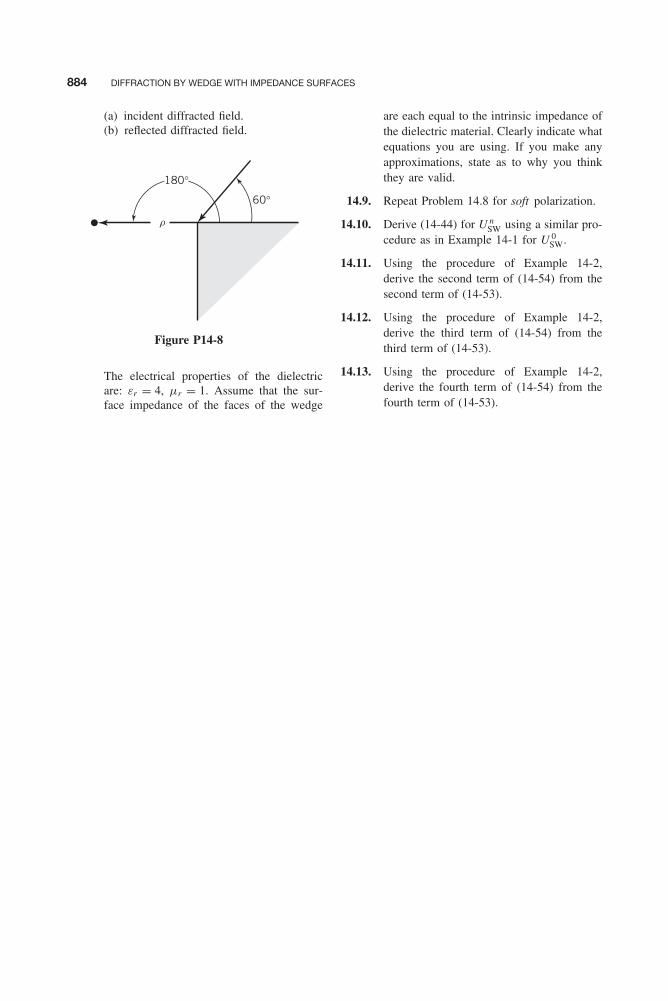
Balanis c14.tex V2 - 11/22/2011 4:00 P.M. Page 884
884 DIFFRACTION BY WEDGE WITH IMPEDANCE SURFACES
(a) incident diffracted field.(b) reflected diffracted field.
r
60°
180°
Figure P14-8
The electrical properties of the dielectricare: εr = 4, μr = 1. Assume that the sur-face impedance of the faces of the wedge
are each equal to the intrinsic impedance ofthe dielectric material. Clearly indicate whatequations you are using. If you make anyapproximations, state as to why you thinkthey are valid.
14.9. Repeat Problem 14.8 for soft polarization.
14.10. Derive (14-44) for U nSW using a similar pro-
cedure as in Example 14-1 for U 0SW.
14.11. Using the procedure of Example 14-2,derive the second term of (14-54) from thesecond term of (14-53).
14.12. Using the procedure of Example 14-2,derive the third term of (14-54) from thethird term of (14-53).
14.13. Using the procedure of Example 14-2,derive the fourth term of (14-54) from thefourth term of (14-53).

Balanis c15.tex V2 - 11/22/2011 4:04 P.M. Page 885
CHAPTER 15Green’s Functions
15.1 INTRODUCTION
In the area of electromagnetics, solutions to many problems are obtained using a second-order,uncoupled partial differential equation, derived from Maxwell’s equations, and the appropriateboundary conditions. The form of most solutions of this type is an infinite series, provided the par-tial differential equation and the boundary conditions representing the problems are separable inthe chosen coordinate system. The difficulty in using these types of solutions to obtain an insightinto the behavior of the function is that they are usually slowly convergent, especially at regionswhere rapid changes occur. It would then seem appropriate, at least for some problems and associ-ated regions, that closed-form solutions would be desirable. Even solutions in the form of integralswould be acceptable. The technique known as the Green’s function accomplishes this goal.
Before proceeding with the presentation of the Green’s function solution, let us brieflydescribe what the Green’s functions represent and how they are used to obtain the overallsolution to the problem.
With the Green’s function technique, a solution to the partial differential equation is obtainedusing a unit source (impulse, Dirac delta) as the driving function. This is known as the Green’sfunction . The solution to the actual driving function is written as a superposition of the impulseresponse solutions (Green’s function) with the Dirac delta source at different locations, which inthe limit reduces to an integral. The contributions to the overall solution from the general sourcemay be greater or smaller than that of the impulse response depending on the strength of the sourceat that given location. In engineering terminology, then, the Green’s function is nothing more butthe impulse response of a system; in system theory, this is better known as the transfer function.
For a given problem, the Green’s function can take various forms. One form of its solution canbe expressed in terms of finite explicit functions, and it is obtained based on a procedure that willbe outlined later. This procedure for developing the Green’s function can be used only if the solu-tion to the homogeneous differential equation is known. Another form of the Green’s function isto construct its solution by an infinite series of suitably chosen orthonormal functions. The bound-ary conditions determine the eigenvalues of the eigenfunctions, and the strength of the sourcesinfluences the coefficients of these eigenfunctions. Integral forms can also be used to represent theGreen’s function, especially when the eigenvalue spectrum is continuous. All solutions, althoughdifferent in form, give the same results. The form of the Green’s function that is most appropriatewill depend on the problem in question. The representation of the actual source plays a significantrole as to which form of the Green’s function may be most convenient for a given problem.
Usually, there is as much work involved in finding the Green’s function as there is in obtainingthe infinite-series solution. However, the major advantages of the Green’s function techniquebecome evident when the same problem is to be solved for a variety of driving sources and whenthe sources are in the presence of boundaries [1–8].
885
Balanis c15.tex V2 - 11/22/2011 4:04 P.M. Page 886
886 GREEN’S FUNCTIONS
In this chapter we shall initially study the one-dimensional differential equation
[L + λr(x)]y(x) = f (x) (15-1)
where L is the Sturm-Liouville operator and λ is a constant. It is hoped that an understanding ofthe Green’s function method for this equation will lead to a better understanding of the equationsthat occur in electromagnetic field theory applied to homogeneous media such as
∇2φ(R) + β2φ(R) = p(R) (scalar wave equation) (15-2a)
∇ × ∇ × ψ(R) + β2ψ(R) = F(R) (vector wave equation) (15-2b)
particularly since (15-2a) and (15-2b) can often be reduced to several equations similar to (15-1)by the separation of variables technique. Before proceeding to the actual solution of (15-1) by theGreen’s function method, we shall first consider several examples of Green’s functions in otherareas of electrical and general engineering. These will be followed by some topics associatedwith the Sturm-Liouville operator L before we embark on the solution of (15-2a).
15.2 GREEN’S FUNCTIONS IN ENGINEERING
The Green’s function approach to solution of differential equations has been used in many areas ofengineering, physics, and elsewhere [9–18]. Before we embark on constructing Green’s functionsolutions to electromagnetic boundary-value problems, let us consider two other problems, onedealing with electric circuit theory and the other with mechanics. This will give the reader abetter appreciation of the Green’s function concept.
15.2.1 Circuit Theory
Analysis of lumped electric element circuits is a fundamental method of electrical engineering.Therefore, we will relate the Green’s function to the solution of a very simple lumped-elementcircuit problem.
Let us assume that a voltage source v(t) is connected to a resistor R and inductor L, as shownin Figure 15-1a . The equation that governs the solution to that circuit can be written as
Ldi
dt+ Ri = v(t) (15-3)
where v(t) is the excitation voltage source that is turned on at t = t ′. Initially, (t < t ′) the circuitis at rest and at t = t ′ the voltage is suddenly turned on by an impulse V0 of a very short durationt ′. For t > t ′ + t ′, when v(t) = 0, the circuit performance is governed by the homogeneousequation
Ldi
dt+ Ri (t) = 0 for t > t ′ + t ′ (15-4)
whose solution for i (t) can be written as
i (t) = I0e−(R/L)t for t > t ′ + t ′ (15-4a)
where I0 is a constant and L/R is referred to as the time constant τ of the circuit.Since the voltage excitation v(t) during t ′ was an impulse V0, then∫ t ′+t ′
t ′v(t)dt = V0 (15-5)
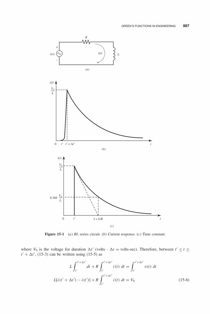
Balanis c15.tex V2 - 11/22/2011 4:04 P.M. Page 887
GREEN’S FUNCTIONS IN ENGINEERING 887
R
(a)
Lv(t) i(t)
+
−
(b)
t ′ t ′ + Δt ′
i(t)
V0
L
0 t
(c)
i(t)
V0
L
V0
L
t ′ tτ = L/R0
0.368
Figure 15-1 (a) RL series circuit. (b) Current response. (c) Time constant.
where V0 is the voltage for duration t ′ (volts · t = volts-sec). Therefore, between t ′ ≤ t ≤t ′ + t ′, (15-3) can be written using (15-5) as
L∫ t ′+t ′
t ′di + R
∫ t ′+t ′
t ′i (t) dt =
∫ t ′+t ′
t ′v(t) dt
L[i (t ′ + t ′) − i (t ′)] + R∫ t ′+t ′
t ′i (t) dt = V0 (15-6)
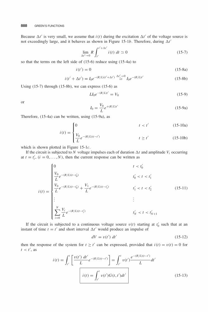
Balanis c15.tex V2 - 11/22/2011 4:04 P.M. Page 888
888 GREEN’S FUNCTIONS
Because t ′ is very small, we assume that i (t) during the excitation t ′ of the voltage source isnot exceedingly large, and it behaves as shown in Figure 15-1b. Therefore, during t ′
limt ′→0
R∫ t ′+t ′
t ′i (t) dt � 0 (15-7)
so that the terms on the left side of (15-6) reduce using (15-4a) to
i (t ′) = 0 (15-8a)
i (t ′ + t ′) = I0e−(R/L)(t ′+t ′) t ′→0� I0e−(R/L)t ′ (15-8b)
Using (15-7) through (15-8b), we can express (15-6) as
LI0e−(R/L)t ′ = V0 (15-9)
orI0 = V0
Le+(R/L)t ′ (15-9a)
Therefore, (15-4a) can be written, using (15-9a), as
i (t) =
⎧⎪⎪⎨⎪⎪⎩0 t < t ′
V0
Le−(R/L)(t−t ′) t ≥ t ′
(15-10a)
(15-10b)
which is shown plotted in Figure 15-1c.If the circuit is subjected to N voltage impulses each of duration t and amplitude Vi occurring
at t = t ′i , (i = 0, . . . , N ), then the current response can be written as
i (t) =
⎧⎪⎪⎪⎪⎪⎪⎪⎪⎪⎪⎪⎪⎪⎪⎪⎪⎨⎪⎪⎪⎪⎪⎪⎪⎪⎪⎪⎪⎪⎪⎪⎪⎪⎩
0 t < t ′0
V0
Le−(R/L)(t−t ′0) t ′
0 < t < t ′1
V0
Le−(R/L)(t−t ′0) + V1
Le−(R/L)(t−t ′1) t ′
1 < t < t ′2
......
N∑i=0
Vi
Le−(R/L)(t−t ′i ) t ′
N < t < t ′N +1
(15-11)
If the circuit is subjected to a continuous voltage source v(t) starting at t ′0 such that at an
instant of time t = t ′ and short interval t ′ would produce an impulse of
dV = v(t ′) dt ′ (15-12)
then the response of the system for t ≥ t ′ can be expressed, provided that i (t) = v(t) = 0 fort < t ′, as
i (t) =∫ t
t ′
[v(t ′) dt ′
Le−(R/L)(t−t ′)
]=
∫ t
t ′v(t ′)
e−(R/L)(t−t ′)
Ldt ′
i (t) =∫ t
t ′v(t ′)G(t , t ′)dt ′ (15-13)

Balanis c15.tex V2 - 11/22/2011 4:04 P.M. Page 889
GREEN’S FUNCTIONS IN ENGINEERING 889
where
G(t , t ′) = e−(R/L)(t−t ′)
Lfor t > t ′ (15-13a)
In (15-13), G(t , t ′) of (15-13a), is referred to as the Green’s function, and it represents theresponse of the system for t > t ′ when an excitation voltage v(t) at t = t ′ is an impulse (Diracdelta) function. Knowing the response of the system to an impulse function, represented by theGreen’s function of (15-13a), the response i (t) to any voltage source v(t) can then be obtainedby convolving the voltage source excitation with the Green’s function according to (15-13).
15.2.2 Mechanics
Another problem that the reader may be familiar with is that of a string of length � that isconnected at the two ends and is subjected to external force per unit length (load) of F (x). Theobjective is to find the displacement u(x) of the string. If the load F (x) is assumed to be actingdown (negative direction), the displacement u(x) of the string is governed by the differentialequation
Td2u
dx 2= F (x) (15-14)
ord2u
dx 2= 1
TF (x) = f (x) (15-14a)
where T is the uniform tensile force of the string. If the string is stationary at the two ends, thenthe displacement function u(x) satisfies the boundary conditions
u(x = 0) = u(x = �) = 0 (15-15)
Initially, instead of solving the displacement u(x) of the string subject to the load F (x), letus assume that the load to which the string is subjected is a concentrated load (impulse) ofF (x = x ′) = δ(x − x ′) at a point x = x ′, as shown in Figure 15-2. For the impulse load, thedifferential equation 15-14a can be written as
d2G(x , x ′)dx 2
= 1
Tδ(x − x ′) (15-16)
G (x, x′)
F (x′)
x′ x
l
Figure 15-2 Attached string subjected by a load force.
Balanis c15.tex V2 - 11/22/2011 4:04 P.M. Page 890
890 GREEN’S FUNCTIONS
subject to the boundary conditions
G(x = 0, x ′) = G(0, x ′) = 0 (15-16a)
G(x = �, x ′) = G(�, x ′) = 0 (15-16b)
In (15-16), G(x , x ′) represents the displacement of the string when it is subject to an impulse loadof 1/T at x = x ′, and it is referred to as the Green’s function for the string. Once this is found,the displacement u(x) of the string subjected to the load F (x) can be determined by convolvingthe load F (x) with the Green’s function G(x , x ′), as was done for the circuit problem by (15-13).
The solution to (15-16) is accomplished by following the procedure outlined here. Away fromthe load at x = x ′, the differential equation 15-16 reduces to the homogeneous form
d2G(x , x ′)dx 2
= 0 (15-17)
which has solutions of the form
G(x , x ′) ={
A1x + B1 0 ≤ x ≤ x ′
A2x + B2 x ′ ≤ x ≤ �
(15-17a)
(15-17b)
Applying the boundary conditions (15-16a) and (15-16b) leads to
G(x = 0, x ′) = A1(0) + B1 = 0 ⇒ B1 = 0 (15-18a)
G(x = �, x ′) = A2� + B2 = 0 ⇒ B2 = −A2� (15-18b)
Thus, (15-17a) and (15-17b) reduce to
G(x , x ′) ={
A1x 0 ≤ x ≤ x ′
A2(x − �) x ′ ≤ x ≤ �
(15-19a)
(15-19b)
where A1 and A2 have not been determined yet.At x = x ′ the displacement u(x) of the string must be continuous. Therefore, the Green’s
function of (15-19a) and (15-19b) must also be continuous at x = x ′. Thus,
A1x ′ = A2(x′ − �) ⇒ A2 = A1
x ′
x ′ − �(15-20)
According to (15-16), the second derivative of G(x , x ′) is equal to an impulse function. There-fore, the first derivative of G(x , x ′), obtained by integrating (15-16), must be discontinuous byan amount equal to 1/T . Thus,
limε→0
[dG(x ′ + ε, x ′)
dx− dG(x ′ − ε, x ′)
dx
]= 1
T(15-21)
ordG(x ′
+, x ′)dx
− dG(x ′−, x ′)
dx= 1
T(15-21a)
Using (15-19a), (15-19b), and (15-20), we can write that
dG(x ′−, x ′)
dx= A1 (15-22a)
dG(x ′+, x ′)
dx= A2 = A1
x ′
x ′ − �(15-22b)

Balanis c15.tex V2 - 11/22/2011 4:04 P.M. Page 891
STURM-LIOUVILLE PROBLEMS 891
Thus, using (15-22a) and (15-22b), (15-21a) leads to
A1x ′
x ′ − �− A1 = 1
T⇒ A1
�
x ′ − �= 1
T⇒ A1 = 1
T
x ′ − �
�(15-23)
Therefore, the Green’s function of (15-19a) and (15-19b) can be written, using (15-20) and(15-23), as
G(x , x ′) =
⎧⎪⎪⎪⎨⎪⎪⎪⎩1
T
(x ′ − �
�
)x 0 ≤ x ≤ x ′
1
T
(x − �
�
)x ′ x ′ ≤ x ≤ �
(15-24a)
(15-24b)
The displacement u(x) subject to the load F (x), governed by (15-14a), can now be writtenas
u(x) =∫ �
0F (x ′) G(x , x ′) dx ′
= 1
T
∫ x
0F (x ′)
(x − �
�
)x ′ dx ′
+ 1
T
∫ �
xF (x ′)
(x ′ − �
�
)x dx ′
(15-25)
15.3 STURM-LIOUVILLE PROBLEMS
Now that we illustrated the Green’s function development for two specific problems, one foran RL electrical circuit and the other for a stretched string, let us consider the construction ofGreen’s functions for more general differential equations subject to appropriate boundary condi-tions. Specifically in this section we want to consider Green’s functions for the one-dimensionaldifferential equation of the Sturm-Liouville form [1, 7, 13].
A one-dimensional differential equation of the form
d
dx
[p(x)
dy
dx
]− q(x)y = f (x) (15-26)
subject to homogeneous boundary conditions, is a Sturm-Liouville problem. This equation canalso be written as
Ly = f (x) (15-27)
where L is the Sturm-Liouville operator
L ≡{
d
dx
[p(x)
d
dx
]− q(x)
}(15-27a)
Every general one-dimensional, source-excited, second-order differential equation of the form
A(x)d2y
dx 2+ B(x)
dy
dx+ C (x)y = S (x) (15-28)
Balanis c15.tex V2 - 11/22/2011 4:04 P.M. Page 892
892 GREEN’S FUNCTIONS
orDy = S (x) (15-28a)
where
D ≡[
A(x)d2
dx 2+ B(x)
d
dx+ C (x)
](15-28b)
can be converted to a Sturm-Liouville form. This can be accomplished by following the procedureoutlined here.
First, expand (15-26) and write it as
p(x)d2y
dx 2+ dp
dx
dy
dx− q(x)y = f (x) (15-29)
Dividing (15-28) by A(x) and (15-29) by p(x), we have that
d2y
dx 2+ B(x)
A(x)
dy
dx+ C (x)
A(x)y = S (x)
A(x)(15-30a)
d2y
dx 2+ 1
p(x)
dp
dx
dy
dx− q(x)
p(x)y = f (x)
p(x)(15-30b)
Comparing (15-30a) and (15-30b), we see that
B(x)
A(x)= 1
p(x)
dp(x)
dx(15-31a)
C (x)
A(x)= −q(x)
p(x)(15-31b)
S (x)
A(x)= f (x)
p(x)(15-31c)
From (15-31a) we have thatdp(x)
dx= p(x)
B(x)
A(x)(15-32)
which is a linear first-order differential equation, a particular solution of which is
p(x) = exp
[∫ x B(t)
A(t)dt
](15-32a)
From (15-31b)
q(x) = −p(x)C (x)
A(x)= −C (x)
A(x)exp
[∫ x B(x)
A(t)dt
](15-32b)
and from (15-31c)
f (x) = p(x)S (x)
A(x)= S (x)
A(x)exp
[∫ x B(t)
A(t)dt
](15-32c)
In summary then, a one-dimensional, source-excited, second-order differential equation of theform (15-28) is converted to a Sturm-Liouville form (15-26) by letting p(x) be that of (15-32a),q(x) that of (15-32b), and f (x) that of (15-32c).
To demonstrate, let us consider an example.
Balanis c15.tex V2 - 11/22/2011 4:04 P.M. Page 893
STURM-LIOUVILLE PROBLEMS 893
Example 15-1
Convert the Bessel differential equation
x2 d2y
dx 2+ x
dy
dx+ (x2 − λ2)y = 0
to a Sturm-Liouville form.
Solution: Since
A(x) = x2
B(x) = x
C (x) = x2 − λ2
S (x) = 0
and according to (15-32a), (15-32b), and (15-32c)
p(x) = exp
[∫ x B(t)
A(t)dt
]= exp
[∫ x t
t2dt
]= exp
[∫ x dt
t
]= eln(x) = x
q(x) = −p(x)C (x)
A(x)= −x
(x2 − λ2)
x2= −
(x 2 − λ2
x
)f (x) = p(x)
S (x)
A(x)= 0
Thus, using (15-26), Bessel’s differential equation takes the Sturm-Liouville form
d
dx
(x
dy
dx
)+
(x 2 − λ2
x
)y = 0
As a check, when the preceding equation is expanded and is multiplied by x , it reduces to the usualform of Bessel’s differential equation.
15.3.1 Green’s Function in Closed Form
Now that we have shown that each general second-order, source-excited differential equationcan be converted to a Sturm-Liouville form, let us develop a procedure to construct the Green’sfunction of a Sturm-Liouville differential equation represented by (15-26) or more generally by{
d
dx
[p(x)
dy
dx
]− q(x)y
}+ λr(x)y = f (x) (15-33)
which can be written as [{d
dx
[p(x)
d
dx
]− q(x)
}+ λr(x)
]y = f (x) (15-33a)
or simply
[L + λr(x)] y = f (x) (15-33b)
where L is the Sturm-Liouville operator of (15-27a). In (15-33), r(x) and f (x) are assumed to bepiecewise continuous in the region of interest (a ≤ x ≤ b) and λ is a parameter to be determined
Balanis c15.tex V2 - 11/22/2011 4:04 P.M. Page 894
894 GREEN’S FUNCTIONS
by the nature and boundary of the region of interest. It should be noted that throughout this chapterλ is used to represent eigenvalues, and it should not be confused with wavelength. The use of λ
to represent eigenvalues is a very common practice in Green’s function theory. The differentialequations 15-33 through 15-33b possess a Green’s function for all values of λ except those thatare eigenvalues of the homogeneous equation
[L + λr(x)]y = 0 (15-34)
For values of λ for which (15-34) has nontrivial solutions, a Green’s function will not exist. Thisis analogous to a system of linear equations represented by
Dy = f (15-35)
which has a solution of
y = D−1f (15-35a)
provided D−1 exists (i.e., D nonsingular). If D is singular (so D−1 does not exist), then (15-35)does not possess a solution. This occurs when Dy = 0, which has a nontrivial solution when thedeterminant of D is zero [so D is written det(D) = 0].
According to (15-25), the solution of (15-33b) can be written as
y(x) =∫ b
af (x)G(x , x ′) dx ′ (15-36)
where G(x , x ′) is the Green’s function of (15-33) or (15-33b). Since (15-35a) is a solution to(15-35), and it exists only if D is nonsingular, then (15-36) is a solution to (15-33b) if the inverseof the operator [L + λr(x)] exists. Then (15-33b) can be written as
y(x) = [L + λr(x)]−1f (15-36a)
By comparing (15-36) to (15-36a), then G(x , x ′) is analogous to the inverse of the operator[L + λr(x)].
Whenever λ is equal to an eigenvalue of the operator [L + λr(x)], obtained by setting thedeterminant of (15-34) equal to zero, i.e.,
det [L + λr(x)] = 0 (15-37)
then the inverse of [L + λr(x)] does not exist, and (15-36) and (15-36a) are not valid. Thus, forvalues of λ equal to the eigenvalues of the operator [L + λr(x)], the Green’s function does notexist.
For a unit impulse driving function, the Sturm-Liouville equation 15-33 can be written as
d
dx
[p(x)
dG
dx
]− q(x)G + λr(x)G = δ(x − x ′) (15-38)
where G is the Green’s function. At points removed from the impulse driving function, (15-38)reduces to {
d
dx
[p(x)
dG
dx
]− q(x)G
}+ λr(x)G = 0 (15-38a)

Balanis c15.tex V2 - 11/22/2011 4:04 P.M. Page 895
STURM-LIOUVILLE PROBLEMS 895
As can be verified by the Green’s function (15-24a) and (15-24b) of the mechanics problemsin Section 15.2.2, the Green’s functions of (15-38a), in general, exhibit the following properties:
Properties of Green’s Functions
1. G(x , x ′) satisfies the homogeneous differential equation except at x = x ′.2. G(x , x ′) is symmetrical with respect to x and x ′.3. G(x , x ′) satisfies certain homogeneous boundary conditions.4. G(x , x ′) is continuous at x = x ′.5. [dG(x , x ′)]/dx has a discontinuity of 1/[p(x ′)] at x = x ′.
The discontinuity of the derivative of G(x , x ′) at x = x ′([dG(x ′, x ′)]/dx = 1/[p(x ′)]) can bederived by first integrating the differential equation 15-38 between x = x ′ − ε and x = x ′ + ε.Doing this leads to
limε→0
{∫ x ′+ε
x ′−ε
d
dx
[p(x)
dG(x , x ′)dx
]dx +
∫ x ′+ε
x ′−ε
[−q(x) + λr(x)]
G(x , x ′)dx
}
=∫ x ′+ε
x ′−ε
δ(x − x ′)dx
limε→0
{p(x)
dG(x , x ′)dx
∣∣∣∣x ′+ε
x ′−ε
+∫ x ′+ε
x ′−ε
[−q(x) + λr(x)]
G(x , x ′)dx
}= 1 (15-39)
Since q(x), r(x), and G(x , x ′) are continuous at x = x ′, then
limε→0
∫ x ′+ε
x ′−ε
[−q(x) + λr(x)]G(x , x ′)dx = 0 (15-40)
Using (15-40) reduces (15-39) to
limε→0
{p(x)
[dG(x ′ + ε, x ′)
dx− dG(x ′ − ε, x ′)
dx
]}= 1
p(x)
[dG(x ′
+, x ′)dx
− dG(x ′−, x ′)
dx
]= 1 (15-41)
ordG(x ′
+, x ′)dx
− dG(x ′−, x ′)
dx= 1
p(x)(15-41a)
which proves the discontinuity of the derivative of G(x , x ′) at x = x ′.The Green’s function must satisfy the differential equation 15-38a, the five general properties
listed previously, and the appropriate boundary conditions. We propose to construct the Green’sfunction solution in two parts: one that is valid for a ≤ x ≤ x ′ and the other for x ′ ≤ x ≤ b wherea and b are the limits of the region of interest. For the homogeneous equation 15-33, valid at allpoints except x = x ′:
1. Let y1(x) represent a nontrivial solution of the homogeneous differential equation 15-33 inthe interval a ≤ x < x ′ satisfying the boundary conditions at x = a . Since both y1(x) andG(x , x ′) satisfy the same differential equation in the interval a ≤ x < x ′, they are relatedto each other by a constant, that is,
G(x , x ′) = A1y1(x), a ≤ x < x ′ (15-42a)
Balanis c15.tex V2 - 11/22/2011 4:04 P.M. Page 896
896 GREEN’S FUNCTIONS
2. Let y2(x) represent a nontrivial solution of the homogeneous differential equation of 15-33in the interval x ′ < x ≤ b satisfying the boundary conditions at x = b. Since both y2(x) andG(x , x ′) satisfy the same differential equation in the interval x ′ < x ≤ b, they are relatedto each other by a constant, that is
G(x , x ′) = A2y2(x), x ′ < x ≤ b (15-42b)
Since one of the general properties of the Green’s function is that it must be continuous atx = x ′, then using (15-42a) and (15-42b)
A1y1(x′) = A2y2(x
′) ⇒ −A1y1(x′) + A2y2(x
′) = 0 (15-43a)
Also one of the properties of the derivative of the Green’s function is that it must be discontinuousat x = x ′ by an amount of 1/p(x ′). Thus applying (15-42a) and (15-42b) into (15-41a) leads to
−A1y ′1(x
′) + A2y ′2(x
′) = 1
p(x ′)(15-43b)
Solving (15-43a) and (15-43b) simultaneously leads to
A1 = y2(x ′)p(x ′)W (x ′)
(15-44a)
A2 = y1(x ′)p(x ′)W (x ′)
(15-44b)
where W (x ′) is the Wronskian of y1 and y2 at x = x ′, defined as
W (x ′) ≡ y1(x′)y ′
2(x′) − y2(x
′)y ′1(x
′) (15-44c)
Using (15-44a) through (15-44c), the closed form Green’s function of (15-42a) and (15-42b)for the differential equation 15-33 or (15-38) can be written as
G(x , x ′) =
⎧⎪⎪⎪⎨⎪⎪⎪⎩y2(x ′)
p(x ′)W (x ′)y1(x), a ≤ x ≤ x ′
y1(x ′)p(x ′)W (x ′)
y2(x), x ′ ≤ x ≤ b
(15-45a)
(15-45b)
where y1(x) and y2(x) are two independent solutions of the homogeneous form of the differentialequation 15-33 each satisfying, respectively, the boundary conditions at x = a and x = b.
The preceding recipe can be used to construct in closed form the Green’s function of adifferential equation of the form (15-33). It is convenient to use this procedure when the followingconditions are satisfied.
1. The solution to the homogeneous differential equation is known.2. The Green’s function is desired in closed form, instead of an infinite series of orthonormal
functions, which will be shown in the next section.
If this procedure is used for the mechanics problem of (15-14a), Section 15.2.2, the sameanswer [as given by (15-24a) and (15-24b)] will be obtained. In the next section we want topresent an alternate procedure for constructing the Green’s function. By this other method, theGreen’s function will be represented by an infinite series of orthonormal functions. Whether

Balanis c15.tex V2 - 11/22/2011 4:04 P.M. Page 897
STURM-LIOUVILLE PROBLEMS 897
one form of the Green’s function is more suitable than the other will depend on the problemin question. Remember, however, that the closed-form procedure just derived can only be usedprovided the solution to the homogeneous differential equation is known.
Before we proceed, let us illustrate that the Sturm-Liouville operator L exhibits Hermitian (orsymmetrical ) properties [1]. These are very important, and they establish the relationships thatare used in the construction of the Green’s function.
Example 15-2
Show that the Sturm-Liouville operator L of (15-27a) or (15-33) through (15-33b) exhibits Hermitian(symmetrical) properties. Assume that in the interval a ≤ x ≤ b any solution yi (x) to (15-33b) satisfiesthe boundary conditions (where i = 1, 2, . . . , n)
α1yi (x = a) + α2dyi (x = a)
dx= α1yi (a) + α2y ′
i (a) = 0
β1yi (x = b) + β2dyi (x = b)
dx= β1yi (b) + β2y ′
i (b) = 0
Solution: Let us assume that y1(x) and y2(x) are two solutions to (15-33) through (15-33b) eachsatisfying the boundary conditions. Then, according to (15-27a)
Ly1(x) = d
dx
[p(x)
dy1(x)
dx
]− q(x)y1(x)
Ly2(x) = d
dx
[p(x)
dy2(x)
dx
]− q(x)y2(x)
Multiplying the first by y2(x) and the second by y1(x), we can write each using a shorthand notationas
y2Ly1 = y2(py ′1)
′ − y2qy1
y1Ly2 = y1(py ′2)
′ − y1qy2
where ′ indicates d/dx . Subtracting the two and integrating between a and b leads to∫ b
a(y2Ly1 − y1Ly2) dx =
∫ b
a[y2(py ′
1)′ − y1(py ′
2)′] dx
Since
(y2py ′1)
′ = y2(py ′1)
′ + y ′2py ′
1
and
(y1py ′2)
′ = y1(py ′2)
′ + y ′1py ′
2
then by subtracting the two,
(y2py ′1)
′ − (y1py ′2)
′ = y2(py ′1)
′ − y1(py ′2)
′
Thus, the integral reduces to∫ b
a(y2Ly1 − y1Ly2) dx =
∫ b
a
[(y2py ′
1)′ − (y1py ′
2)′] dx = [
p(y2y ′1 − y1y ′
2)]b
a
Each of the solutions, y1(x) and y2(x), satisfy the same boundary conditions that can be written as
α1y1(a) + α2y ′1(a) = 0 ⇒ α1y1(α) = −α2y ′
1(a)

Balanis c15.tex V2 - 11/22/2011 4:04 P.M. Page 898
898 GREEN’S FUNCTIONS
β1y1(b) + β2y ′1(b) = 0 ⇒ β1y1(b) = −β2y ′
1(b)
α1y2(a) + α2y ′2(a) = 0 ⇒ α1y2(a) = −α2y ′
2(a)
β1y2(b) + β2y ′2(b) = 0 ⇒ β1y2(b) = −β2y ′
2(b)
Dividing the first by the third and the second by the fourth, we can write that
y1(a)
y2(a)= y ′
1(a)
y ′2(a)
⇒ y1(a)y ′2(a) = y2(a)y ′
1(a)
y1(b)
y2(b)= y ′
1(b)
y ′2(b)
⇒ y1(b)y ′2(b) = y2(b)y ′
1(b)
Using these relations, it is apparent that the right side of the previous integral equation vanishes, so wecan write it as ∫ b
a(y2Ly1 − y1Ly2) dx = [
p(y2y ′1 − y1y ′
2)]b
a = 0
or ∫ b
a(y2Ly1) dx =
∫ b
a(y1Ly2) dx
This illustrates that the operator L exhibits Hermitian (symmetrical) properties with respect to thesolutions y1(x) and y2(x).
15.3.2 Green’s Function in Series
The procedure outlined in the previous section can only be used to derive in closed form theGreen’s function for differential equations whose homogeneous form solution is known. Other-wise, other techniques must be used. Even for equations whose homogeneous form solution isknown, the closed-form representation of the Green’s function may not be the most convenientone. Therefore, an alternate representation may be attractive even for those cases.
An alternate form of the Green’s function is to represent it as a series of orthonormal functions.The most appropriate orthonormal functions would be those that satisfy the boundary conditions.To demonstrate the procedure, let us initially rederive the Green’s function of the mechanicsproblem of Section 15.2.2 but this time represented as a series of orthonormal functions. We willthen generalize the method to (15-33) through (15-33b).
A. Vibrating String For the differential equation 15-14a, subject to the boundary conditions(15-15), its Green’s function must satisfy (15-16) subject to the boundary conditions (15-16a)and (15-16b). Since the Green’s function G(x , x ′) must vanish at x = 0 and �, it is most convenientto represent G(x , x ′) as an infinite series of sin(nπx/�) orthonormal functions, that is
G(x , x ′) =∞∑
n=1
an(x′) sin
(nπ
�x)
(15-46)
where an(x ′) represent the amplitude expansion coefficients that will be a function of the positionx ′ of the excitation source.
Substituting (15-46) into (15-16), multiplying both sides by sin(mπx/�), and then integratingin x from 0 to � leads to
−∑(nπ
�
)2an(x
′)∫ �
0sin
(nπ
�x)
sin(mπ
�x)
dx = 1
T
∫ �
0δ(x − x ′) sin
(mπ
�x)
dx (15-47)

Balanis c15.tex V2 - 11/22/2011 4:04 P.M. Page 899
STURM-LIOUVILLE PROBLEMS 899
Because the orthogonality conditions of sine functions state that
∫ �
0sin
(nπ
�x
)sin
(mπ
�x
)dx =
⎧⎪⎨⎪⎩�
2m = n
0 m �= n
(15-48a)
(15-48b)
then (15-47) reduces to
−(nπ
�
)2 �
2an(x
′) = 1
Tsin
(nπ
�x ′
)(15-49)
i.e.,
an(x′) = − 2�
π2T
1
n2sin
(nπ
�x ′
)(15-49a)
Thus, the Green’s function (15-46) can be expressed, using (15-49a), as
G(x , x ′) = − 2�
π2T
∞∑n=1
1
n2sin
(nπ
�x ′
)sin
(nπ
�x)
(15-50)
This is an alternate form to (15-24a) and (15-24b), but one that leads to the same results, eventhough its form looks quite different. The displacement u(x) subject to the load F (x), governedby (15-14a), can now be written as
u(x) =∫ �
0F (x ′) G(x , x ′) dx ′ = − 2�
π2T
∞∑n=1
1
n2sin
(nπ
�x) ∫ �
0F (x ′) sin
(nπ
�x ′
)dx ′
(15-51)
B. Sturm-Liouville Operator Let us now generalize the Green’s function series expansionmethod of the vibrating string, as given by (15-50) and (15-51), to (15-33b) where L is a Sturm-Liouville operator and λ is an arbitrary parameter to be determined by the nature and boundaryof the region of interest. We seek a solution to solve the differential equation 15-33b
[L + λr(x)]y(x) = f (x) (15-52)
in the interval a ≤ x ≤ b subject to the general boundary conditions
α1y(x)|x=a + α2dy(x)
dx
∣∣∣∣x=a
= α1y(a) + α2dy(a)
dx= 0 (15-52a)
β1y(x)|x=b + β2dy(x)
dx
∣∣∣∣x=b
= β1y(b) + β2dy(b)
dx= 0 (15-52b)
which are usually referred to as the mixed boundary conditions. In (15-52a) at least one of theconstants α1 or α2, if not both of them, are nonzero. The same is true for (15-52b). The Green’sfunction G(x , x ′), if it exists, will satisfy the differential equation
[L + λr(x)]G(x , x ′) = δ(x − x ′) (15-53)
Balanis c15.tex V2 - 11/22/2011 4:04 P.M. Page 900
900 GREEN’S FUNCTIONS
subject to the boundary conditions
α1G(a , x ′) + α2dG(a , x ′)
dx= 0 (15-53a)
β1G(b, x ′) + β2dG(b, x ′)
dx= 0 (15-53b)
If {ψn(x)} represents a complete set of orthonormal eigenfunctions for the Sturm-Liouvilleoperator L, then it must satisfy the differential equation
[L + λnr(x)] ψn(x) = 0 (15-54)
subject to the same boundary conditions of (15-52a) or (15-52b) for the Green’s function (15-53),i.e.,
α1ψn(a) + α2dψn(a)
dx= 0 (15-54a)
β1ψn(b) + β2dψn(b)
dx= 0 (15-54b)
The boundary conditions (15-54a) and (15-54b) of ψn(x) are also used to determine the eigenval-ues λn . In the finite interval a ≤ x ≤ b the complete set of orthonormal eigenfunctions {ψn(x)},and their amplitude coefficients, must satisfy the orthogonality condition of
∫ b
aψm(x)ψn(x)r(x) dx = δmn =
{1 m = n
0 m �= n(15-55)
where δmn is the Kronecker delta function.If the Green’s function exists, it can be represented in series form in terms of the orthonormal
eigenfunctions {ψn(x)} as
G(x , x ′) =∑
n
an(x′)ψn(x) (15-56)
where an(x ′) are the amplitude coefficients. These can be obtained by multiplying both sidesof (15-56) by ψm(x)r(x), integrating from a to b, and then using (15-55). It can be shown that
an(x′) =
∫ b
aG(x , x ′)ψn(x)r(x) dx (15-56a)
Since G(x , x ′) satisfies (15-53) and ψn(x) satisfies (15-54), then we can rewrite each as
LG(x , x ′) = −λr(x)G(x , x ′) + δ(x − x ′) (15-57a)
Lψn(x) = −λnr(x)ψn(x , x ′) (15-57b)
Multiplying (15-57a) by ψn(x), (15-57b) by G(x , x ′), and then subtracting the two equationsleads to
ψn(x)LG(x , x ′) − G(x , x ′)Lψn(x) = −(λ − λn)G(x , x ′)ψn(x)r(x) + δ(x − x ′)ψn(x) (15-58)

Balanis c15.tex V2 - 11/22/2011 4:04 P.M. Page 901
STURM-LIOUVILLE PROBLEMS 901
Integrating (15-58) between a and b, we can write that∫ b
a[ψn(x)LG(x , x ′) − G(x , x ′)Lψn(x)] dx
= −(λ − λn)
∫ b
aG(x , x ′)ψn(x)r(x) dx +
∫ b
aδ(x − x ′)ψn(x) dx (15-59)
which by using (15-56a) reduces to∫ b
a[ψn(x)LG(x , x ′) − G(x , x ′)Lψn(x)] dx = −(λ − λn)an(x
′) + ψn(x′) (15-59a)
By the symmetrical (Hermitian) property of the operator L, as derived in Example 15-2, withrespect to the functions y1 = G(x , x ′) and y2 = ψn(x), the left side of (15-59) or (15-59a) van-ishes. Therefore, (15-59) and (15-59a) reduce to
−(λ − λn)an(x′) + ψn(x
′) = 0 (15-60)
and therefore,
an(x′) = ψn(x ′)
λ − λn, where λ �= λn (15-60a)
Thus, the series form of the Green’s function (15-56) can ultimately be expressed as
G(x , x ′) =∑
n
ψn(x ′)ψn(x)
(λ − λn)(15-61)
where {ψn(z )} represents a complete set of orthonormal eigenfunctions for the Sturm-Liouvilleoperator L, which satisfies the differential equation 15-54 subject to the boundary conditions(15-54a) and (15-54b). This is also referred to as the bilinear formula, and it represents, asidefrom (15-45a) and (15-45b) , the second form that can be used to derive the Green’s function forthe differential equation 15-33 or 15-33b as a series solution in the finite interval a ≤ x ≤ b. Itshould be noted that at λ = λn the Green’s function of (15-61) possesses singularities. Usually,these singularities are simple poles although in some cases the λn ’s are branch points whosebranch cuts represent a continuous spectrum of eigenvalues. In those cases the Green’s functionmay involve a summation, for the discrete spectrum of eigenvalues, and an integral, for thecontinuous spectrum of eigenvalues.
Example 15-3
A very common differential equation in solutions of transmission-line and antenna problems (such asmetallic waveguides, microstrip antennas, etc.) that exhibit rectangular configurations is
d2ϕ(x)
dx 2+ β2ϕ(x) = f (x)
subject to the boundary conditionsϕ(0) = ϕ(�) = 0
where β2 = ω2με. Derive in closed and series forms the Green’s functions for the given equation.
Balanis c15.tex V2 - 11/22/2011 4:04 P.M. Page 902
902 GREEN’S FUNCTIONS
Solution: For the given equation, the Green’s function must satisfy the differential equation
d2G(x , x ′)dx 2
+ β2G(x , x ′) = δ(x − x ′)
subject to the boundary conditions
G(0) = G(�) = 0
The differential equation is of the Sturm-Liouville form (15-33) with
p(x) = 1
q(x) = 0
r(x) = 1
λ = β2
y(x) = ϕ(x)
L = d2
dx 2
⎫⎪⎪⎪⎪⎪⎪⎪⎪⎪⎬⎪⎪⎪⎪⎪⎪⎪⎪⎪⎭⇒ d2ϕ
dx 2+ β2ϕ = f (x)
A. Closed-Form Solution: This form of the solution will be obtained using the recipe of (15-45a)and (15-45b) along with (15-44c). The homogeneous differential equation for ϕ(x) reduces to
d2ϕ
dx 2+ β2ϕ = 0
Two independent solutions, one φ1(x) valid in the interval 0 ≤ x ≤ x ′ and that vanishes at x = 0, andthe other φ2(x) valid in the interval x ′ ≤ x ≤ � and that vanishes at x = �, take the form
φ1(x) = sin(βx)
φ2(x) = sin[β(� − x)]
According to (15-44c), the Wronskian can be written as
W (x ′) = −β{sin(βx ′) cos[β(� − x ′)] + sin[β(� − x ′)] cos(βx ′)}
W (x ′) = −β sin(βx ′ + β� − βx ′) = −β sin(β�)
Thus, the Green’s function in closed form can be expressed, using (15-45a) and (15-45b), as
G(x , x ′) =
⎧⎪⎪⎪⎨⎪⎪⎪⎩− sin[β(� − x ′)]
β sin(β�)sin(βx), 0 ≤ x ≤ x ′
− sin(βx ′)β sin(β�)
sin[β(� − x)], x ′ ≤ x ≤ �
This form of the Green’s function indicates that it possesses singularities (poles) when
β� = βr� = nπ ⇒ βr = ωr√
με = 2π fr√
με = nπ
�
i.e.,
fr = n
2�√
μεn = 1, 2, 3, . . .

Balanis c15.tex V2 - 11/22/2011 4:04 P.M. Page 903
STURM-LIOUVILLE PROBLEMS 903
B. Series-Form Solution: This form of the solution will be obtained using (15-61). The complete set ofeigenfunctions {ψn(x)} must satisfy the differential equation 15-54, or
d2ψn(x)
dx 2+ β2
nψn(x) = 0
subject to the boundary conditionsψn(0) = ψn(�) = 0
The most appropriate solution of ψn(x) is to represent it in terms of standing wave eigenfunctionswhich in a rectangular coordinate system are sine and cosine functions, as discussed in Chapters 3 and8, Sections 3.4.1 and 8.2.1.
Thus, according to (3-28b) and (8-4a), we can write that
ψn(x) = A cos(βn x) + B sin(βn x)
The allowable eigenvalues of βn are found by applying the boundary conditions. Since ψn(0) = 0, then
ψn(0) = A + B(0) = 0 ⇒ A = 0
Also since ψn(�) = 0, then
ψn(�) = B sin(βn�) = 0 ⇒ βn� = sin−1(0) = nπ
i.e.,βn = nπ
�, n = 1, 2, 3, . . . (for nontrivial solutions)
Thus,ψn(x) = B sin(βn x) = B sin
(nπ
�x)
The amplitude constant B is such that (15-55) is satisfied. Therefore,
B2∫ �
0sin2
(nπ
�x)
dx = 1
B2
2
∫ �
0
[1 − cos
(2nπ
�x
)]dx = B2
(�
2
)= 1 ⇒ B =
√2
�
Thus, the complete set of the orthonormal eigenfunctions of {ψn(x)} is represented by
ψn(x) =√
2
�sin
(nπ
�x)
, n = 1, 2, 3, . . .
with
λ = β2 = ω2με
λn = β2n =
(nπ
�
)2, n = 1, 2, 3, . . .
In series-form, the Green’s function (15-61) can then be written as
G(x , x ′) = 2
�
∞∑n=1
sin(nπ
�x ′
)sin
(nπ
�x)
β2 −(nπ
�
)2
Balanis c15.tex V2 - 11/22/2011 4:04 P.M. Page 904
904 GREEN’S FUNCTIONS
which yields the same results as the closed-form solution of part A even though it looks quite differentanalytically. It is apparent that the Green’s function is symmetrical. Also it possesses a singularity, andit fails to exist when
β = βr = ωr√
με = 2π fr√
με = nπ
�
i.e.,
fr = nπ/�
2π√
με= n
2�√
με
which is identical to the condition obtained by the closed-form solution in part A.This is in accordance with (15-34), which states that the Green’s function (15-33b) exists for all values
of λ, in this case λ = β2 = ω2με, except those that are eigenvalues of the homogeneous equation 15-34.For our case, (15-34) reduces to
d2ϕ(x)
dx 2+ β2ϕ(x) = 0
whose nontrivial solution takes the form
ϕ(x) = C sin(nπ
�x)
with eigenvalues β = nπ/�, n = 1, 2, 3, . . ..It should be noted that when
β = βr = ωr√
με = 2π fr√
με = nπ
�= fr = n
2�√
με
the Green’s function singularity consists of simple poles. At those frequencies the external frequencies ofthe source match the natural (characteristic) frequencies of the system, in this instance the transmissionline. This is referred to as resonance. When this occurs, the field of the mode whose natural frequencymatches the source excitation frequency (resonance condition) will continuously increase without anybounds, in the limit reaching values of infinity. For those situations, no steady-state solutions can exist.One way to contain the field amplitude is to introduce damping.
15.3.3 Green’s Function in Integral Form
In the previous two sections we outlined procedures that can be used to derive the Green’sfunction in closed and series forms. The bilinear formula (15-61) of Section 15.3.2 is used toderive the Green’s function (15-33) through (15-33b) when the eigenvalue spectrum, representedby the λn ’s in (15-61), is discrete. However, often the eigenvalue spectrum is continuous, and itcan be represented in (15-61) by an integral. In the limit, the infinite summation of the bilinearformula reduces to an integral. This form is usually desirable when at least one of the boundaryconditions is at infinity. This would be true when a source placed at the origin is radiating in anunbounded medium.
To demonstrate the derivation, let us construct the Green’s function of the one-dimensionalscalar Helmholtz equation
d2ϕ
dx 2+ β2
0ϕ = f (x) (15-62)
subject to the boundary (radiation) conditions of
ϕ(+∞) = ϕ(−∞) = 0 (15-62a)
The Sommerfield radiation condition [19] could also be used instead of (15-62a).
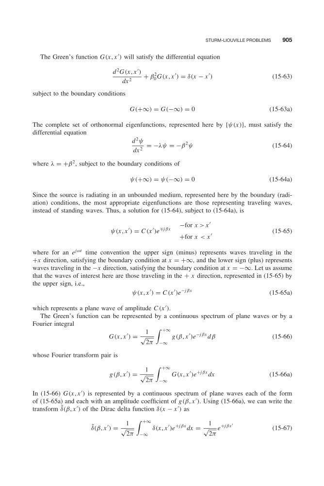
Balanis c15.tex V2 - 11/22/2011 4:04 P.M. Page 905
STURM-LIOUVILLE PROBLEMS 905
The Green’s function G(x , x ′) will satisfy the differential equation
d2G(x , x ′)dx 2
+ β20 G(x , x ′) = δ(x − x ′) (15-63)
subject to the boundary conditions
G(+∞) = G(−∞) = 0 (15-63a)
The complete set of orthonormal eigenfunctions, represented here by {ψ(x)}, must satisfy thedifferential equation
d2ψ
dx 2= −λψ = −β2ψ (15-64)
where λ = +β2, subject to the boundary conditions of
ψ(+∞) = ψ(−∞) = 0 (15-64a)
Since the source is radiating in an unbounded medium, represented here by the boundary (radi-ation) conditions, the most appropriate eigenfunctions are those representing traveling waves,instead of standing waves. Thus, a solution for (15-64), subject to (15-64a), is
ψ(x , x ′) = C (x ′)e∓jβx−for x > x ′
+for x < x ′ (15-65)
where for an ejωt time convention the upper sign (minus) represents waves traveling in the+x direction, satisfying the boundary condition at x = +∞, and the lower sign (plus) representswaves traveling in the −x direction, satisfying the boundary condition at x = −∞. Let us assumethat the waves of interest here are those traveling in the + x direction, represented in (15-65) bythe upper sign, i.e.,
ψ(x , x ′) = C (x ′)e−jβx (15-65a)
which represents a plane wave of amplitude C (x ′).The Green’s function can be represented by a continuous spectrum of plane waves or by a
Fourier integral
G(x , x ′) = 1√2π
∫ +∞
−∞g(β, x ′)e−jβx dβ (15-66)
whose Fourier transform pair is
g(β, x ′) = 1√2π
∫ +∞
−∞G(x , x ′)e+jβx dx (15-66a)
In (15-66) G(x , x ′) is represented by a continuous spectrum of plane waves each of the formof (15-65a) and each with an amplitude coefficient of g(β, x ′). Using (15-66a), we can write thetransform δ̃(β, x ′) of the Dirac delta function δ(x − x ′) as
δ̃(β, x ′) = 1√2π
∫ +∞
−∞δ(x , x ′)e+jβx dx = 1√
2πe+jβx ′
(15-67)
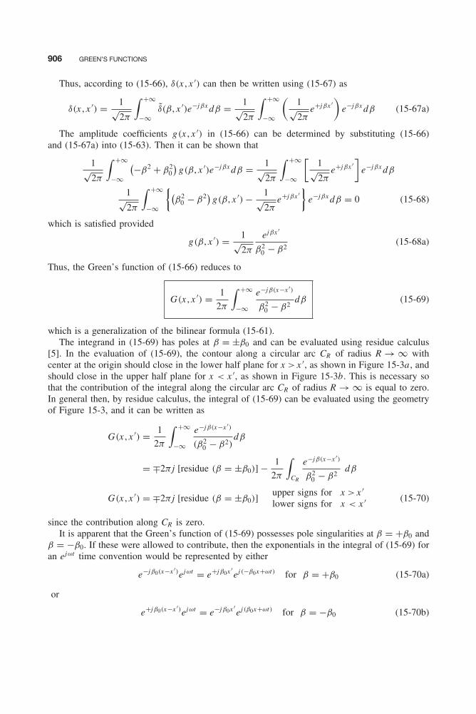
Balanis c15.tex V2 - 11/22/2011 4:04 P.M. Page 906
906 GREEN’S FUNCTIONS
Thus, according to (15-66), δ(x , x ′) can then be written using (15-67) as
δ(x , x ′) = 1√2π
∫ +∞
−∞δ̃(β, x ′)e−jβx dβ = 1√
2π
∫ +∞
−∞
(1√2π
e+jβx ′)
e−jβx dβ (15-67a)
The amplitude coefficients g(x , x ′) in (15-66) can be determined by substituting (15-66)and (15-67a) into (15-63). Then it can be shown that
1√2π
∫ +∞
−∞
(−β2 + β20
)g(β, x ′)e−jβx dβ = 1√
2π
∫ +∞
−∞
[1√2π
e+jβx ′]
e−jβx dβ
1√2π
∫ +∞
−∞
{(β2
0 − β2) g(β, x ′) − 1√2π
e+jβx ′}
e−jβx dβ = 0 (15-68)
which is satisfied provided
g(β, x ′) = 1√2π
ejβx ′
β20 − β2
(15-68a)
Thus, the Green’s function of (15-66) reduces to
G(x , x ′) = 1
2π
∫ +∞
−∞
e−jβ(x−x ′)
β20 − β2
dβ (15-69)
which is a generalization of the bilinear formula (15-61).The integrand in (15-69) has poles at β = ±β0 and can be evaluated using residue calculus
[5]. In the evaluation of (15-69), the contour along a circular arc CR of radius R → ∞ withcenter at the origin should close in the lower half plane for x > x ′, as shown in Figure 15-3a , andshould close in the upper half plane for x < x ′, as shown in Figure 15-3b. This is necessary sothat the contribution of the integral along the circular arc CR of radius R → ∞ is equal to zero.In general then, by residue calculus, the integral of (15-69) can be evaluated using the geometryof Figure 15-3, and it can be written as
G(x , x ′) = 1
2π
∫ +∞
−∞
e−jβ(x−x ′)
(β20 − β2)
dβ
= ∓2π j [residue (β = ±β0)] − 1
2π
∫CR
e−jβ(x−x ′)
β20 − β2
dβ
G(x , x ′) = ∓2π j [residue (β = ±β0)]upper signs for x > x ′lower signs for x < x ′ (15-70)
since the contribution along CR is zero.It is apparent that the Green’s function of (15-69) possesses pole singularities at β = +β0 and
β = −β0. If these were allowed to contribute, then the exponentials in the integral of (15-69) foran ejωt time convention would be represented by either
e−jβ0(x−x ′)ejωt = e+jβ0x ′ej (−β0x+ωt) for β = +β0 (15-70a)
or
e+jβ0(x−x ′)ejωt = e−jβ0x ′ej (β0x+ωt) for β = −β0 (15-70b)
Balanis c15.tex V2 - 11/22/2011 4:04 P.M. Page 907
STURM-LIOUVILLE PROBLEMS 907
Thus, (15-70a) represents waves traveling in the +x direction and (15-70b) represents wavestraveling in the −x direction. In the contour evaluation of (15-69), the contour should do thefollowing:
1. For x > x ′, pass the pole at β = −β0 from below, the one at β = +β0 from above, andthen close down so that only the latter contributes, as shown in Figure 15-3a .
2. For x < x ′, pass the pole β = −β0 from below, the one at β = +β0 from above, and thenclose up so that only the former contributes, as shown in Figure 15-3b.
Sometimes an integral Green’s function can be used to represent both discrete and continuousspectra whereby part of the integral would represent the discrete spectrum and the remainderwould represent the continuous spectrum. Typically, the discrete spectrum would represent afinite number of propagating modes and an infinite number of evanescent modes in the closedregions, and the continuous spectrum would represent radiation in open regions.
Im
Im
Re
Re
××
××
R
R
(a)
(b)
CR
CR
+b0
+b0
−b0
−b0
Figure 15-3 Residue calculus for contour integration (a) x > x ′. (b) x < x ′.

Balanis c15.tex V2 - 11/22/2011 4:04 P.M. Page 908
908 GREEN’S FUNCTIONS
15.4 TWO-DIMENSIONAL GREEN’S FUNCTION IN RECTANGULAR COORDINATES
Until now we have considered the construction of Green’s functions for problems involving asingle space variable. Let us now consider problems involving two space variables, both for staticand time-varying fields.
15.4.1 Static Fields
A two-dimensional partial differential equation often encountered in static electromagnetics isPoisson’s equation
∂2V
∂x 2+ ∂2V
∂y2= f (x , y) = − 1
ε0q(x , y) (15-71)
subject to the boundary conditions
V (x = 0, 0 ≤ y ≤ b) = V (x = a , 0 ≤ y ≤ b) = 0 (15-71a)
V (0 ≤ x ≤ a , y = 0) = V (0 ≤ x ≤ a , y = b) = 0 (15-71b)
In (15-71), V can represent the electric potential distribution on a rectangular structure of dimen-sions a along the x direction and b along the y direction and f (x , y) = q(x , y) can representthe electric charge distribution along the structure. The objective here is to obtain the Green’sfunction and ultimately the potential distribution. The Green’s function G(x , y; x ′, y ′) will satisfythe partial differential equation
∂2G
∂x 2+ ∂2G
∂y2= δ(x − x ′)δ(y − y ′) (15-72)
subject to the boundary conditions
G(x = 0, 0 ≤ y ≤ b) = G(x = a , 0 ≤ y ≤ b) = 0 (15-72a)
G(0 ≤ x ≤ a , y = 0) = G(0 ≤ x ≤ a , y = b) = 0 (15-72b)
and the potential distribution V (x , y) will be represented by
V (x , y) = − 1
ε0
∫ b
0
∫ a
0q(x ′, y ′)G(x , y; x ′, y ′) dx ′dy ′ (15-73)
We will derive the Green’s function here in two forms.
1. Closed form , similar to that of Section 15.3.1 but utilizing (15-44c) and (15-45a)through (15-45b) for a two space variable problem.
2. Series form , similar to that of Section 15.3.2 but using basically two-dimensional expres-sions for (15-54), (15-55), and (15-61).
A. Closed Form The Green’s function of (15-72) for the closed-form solution can be for-mulated by choosing functions that initially satisfy the boundary conditions either along the xdirection, at x = 0 and x = a , or along the y direction, at y = 0 and y = b. Let us begin here
Balanis c15.tex V2 - 11/22/2011 4:04 P.M. Page 909
TWO-DIMENSIONAL GREEN’S FUNCTION IN RECTANGULAR COORDINATES 909
the development of the Green’s function of (15-72) by choosing functions that initially satisfythe boundary conditions along the x direction. This is accomplished by initially representing theGreen’s function by a normalized single function Fourier series of sine functions that satisfy theboundary conditions at x = 0 and x = a , that is
G(x , y; x ′, y ′) =∞∑
m=1
gm(y; x ′, y ′) sin(mπ
ax)
(15-74)
The coefficients gm(y; x ′, y ′) of the Fourier series will be determined by first substitut-ing (15-74) into (15-72). This leads to
∞∑m=1,2,...
[−
(mπ
a
)2gm(y; x ′, y ′) sin
(mπ
ax)
+ sin(mπ
ax) d2gm(y; x ′, y ′)
dy2
]= δ(x − x ′)δ(y − y ′) (15-75)
Multiplying both sides of (15-75) by sin(nπx/a), integrating with respect to x from 0 to a , andusing (15-48a) and (15-48b), we can write that
d2gm(y; x ′, y ′)dy2
−(mπ
a
)2gm(y; x ′, y ′) = 2
asin
(mπ
ax ′
)δ(y − y ′) (15-76)
Equation 15-76 is recognized as a one-dimensional differential equation for gm(y; x ′, y ′), whichcan be solved using the recipe of Section 15.3.1 as provided by (15-44c) and (15-45a) through(15-45b).
For the homogeneous form of (15-76), or
d2gm(y; x ′, y ′)dy2
−(mπ
a
)2gm(y; x ′, y ′) = 0 (15-77)
two solutions that satisfy, respectively, the boundary conditions at y = 0 and y = b are
g (1)m (y; x ′, y ′) = Am(x ′, y ′) sinh
(mπ
ay)
for y ≤ y ′ (15-78a)
g (2)m (y; x ′, y ′) = Bm(x ′, y ′) sinh
[mπ
a(b − y)
]for y ≥ y ′ (15-78b)
The hyperbolic functions were chosen as solutions to (15-77), instead of real exponentials, sothat (15-78a) satisfies the boundary condition of (15-71b) at y = 0 and (15-78b) satisfies theboundary condition of (15-71b) at y = b.
Using (15-44c) where y1 = g (1)m and y2 = g (2)
m , we can write the Wronskian as
W (y; x ′, y ′) = −(mπ
a
)AmBm
{sinh
(mπ
ay ′)
cosh[mπ
a(b − y ′)
]+ cosh
(mπ
ay ′)
sinh[mπ
a(b − y ′)
]}W (y; x ′, y ′) = −
(mπ
a
)AmBm sinh
(mπb
a
)(15-79)
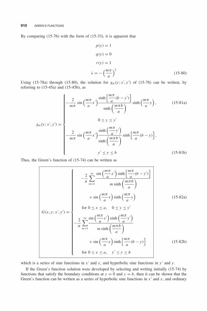
Balanis c15.tex V2 - 11/22/2011 4:04 P.M. Page 910
910 GREEN’S FUNCTIONS
By comparing (15-76) with the form of (15-33), it is apparent that
p(y) = 1
q(y) = 0
r(y) = 1
λ = −(mπ
a
)2(15-80)
Using (15-78a) through (15-80), the solution for gm(y; x ′, y ′) of (15-76) can be written, byreferring to (15-45a) and (15-45b), as
gm(y; x ′, y ′) =
⎧⎪⎪⎪⎪⎪⎪⎪⎪⎪⎪⎪⎪⎪⎪⎪⎪⎪⎪⎨⎪⎪⎪⎪⎪⎪⎪⎪⎪⎪⎪⎪⎪⎪⎪⎪⎪⎪⎩
− 2
mπsin
(mπ
ax ′
) sinh[mπ
a(b − y ′)
]sinh
(mπb
a
) sinh(mπ
ay)
,
0 ≤ y ≤ y ′
− 2
mπsin
(mπ
ax ′
) sinh(mπ
ay ′)
sinh
(mπb
a
) sinh[mπ
a(b − y)
],
y ′ ≤ y ≤ b
(15-81a)
(15-81b)
Thus, the Green’s function of (15-74) can be written as
G(x , y; x ′, y ′) =
⎧⎪⎪⎪⎪⎪⎪⎪⎪⎪⎪⎪⎪⎪⎪⎪⎪⎪⎪⎪⎪⎪⎪⎪⎪⎪⎪⎪⎪⎨⎪⎪⎪⎪⎪⎪⎪⎪⎪⎪⎪⎪⎪⎪⎪⎪⎪⎪⎪⎪⎪⎪⎪⎪⎪⎪⎪⎪⎩
− 2
π
∞∑m=1
sin(mπ
ax ′
)sinh
[mπ
a(b − y ′)
]m sinh
(mπb
a
)× sin
(mπ
ax)
sinh(mπ
ay)
for 0 ≤ x ≤ a , 0 ≤ y ≤ y ′
− 2
π
∞∑m=1
sin(mπ
ax ′
)sinh
(mπ
ay ′)
m sinh
(mπb
a
)× sin
(mπ
ax)
sinh[mπ
a(b − y)
]for 0 ≤ x ≤ a , y ′ ≤ y ≤ b
(15-82a)
(15-82b)
which is a series of sine functions in x ′ and x , and hyperbolic sine functions in y ′ and y .
If the Green’s function solution were developed by selecting and writing initially (15-74) byfunctions that satisfy the boundary conditions at y = 0 and y = b, then it can be shown that theGreen’s function can be written as a series of hyperbolic sine functions in x ′ and x , and ordinary
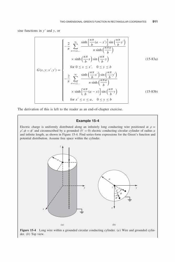
Balanis c15.tex V2 - 11/22/2011 4:04 P.M. Page 911
TWO-DIMENSIONAL GREEN’S FUNCTION IN RECTANGULAR COORDINATES 911
sine functions in y ′ and y , or
G(x , y; x ′, y ′) =
⎧⎪⎪⎪⎪⎪⎪⎪⎪⎪⎪⎪⎪⎪⎪⎪⎪⎪⎪⎪⎪⎪⎪⎪⎨⎪⎪⎪⎪⎪⎪⎪⎪⎪⎪⎪⎪⎪⎪⎪⎪⎪⎪⎪⎪⎪⎪⎪⎩
− 2
π
∞∑n=1,2,...
sinh[nπ
b(a − x ′)
]sin
(nπ
by ′)
n sinh(nπa
b
)× sinh
(nπ
bx)
sin(nπ
by)
for 0 ≤ x ≤ x ′, 0 ≤ y ≤ b
− 2
π
∞∑n=1,2,...
sinh(nπ
bx ′
)sin
(nπ
by ′)
n sinh(nπa
b
)× sinh
[nπ
b(a − x)
]sin
(nπ
by)
for x ′ ≤ x ≤ a , 0 ≤ y ≤ b
(15-83a)
(15-83b)
The derivation of this is left to the reader as an end-of-chapter exercise.
Example 15-4
Electric charge is uniformly distributed along an infinitely long conducting wire positioned at ρ =ρ ′, φ = φ′ and circumscribed by a grounded (V = 0) electric conducting circular cylinder of radius aand infinite length, as shown in Figure 15-4. Find series-form expressions for the Green’s function andpotential distribution. Assume free space within the cylinder.
a
a
z
z rr′
f′
f
y y
xx
(a) (b)
Figure 15-4 Long wire within a grounded circular conducting cylinder. (a) Wire and grounded cylin-der. (b) Top view.
Balanis c15.tex V2 - 11/22/2011 4:04 P.M. Page 912
912 GREEN’S FUNCTIONS
Solution: The potential distribution V (p, φ, z ) must satisfy Poisson’s equation
∇2V (ρ, φ, z ) = − 1
ε0q(ρ, φ, z )
subject to the boundary condition
V (ρ = a , 0 ≤ φ ≤ 2π , z ) = 0
Since the wire is infinitely long, the solutions for the potential will not be functions of z . Thus, anexpanded form of Poisson’s equation reduces to
1
ρ
∂
∂ρ
(ρ
∂V
∂ρ
)+ 1
ρ2
∂2V
∂φ2= − 1
ε0q(ρ, φ)
The Green’s function G(ρ, φ; ρ ′, φ′) must satisfy the partial differential equation
∇2G(ρ, φ; ρ ′, φ′) = δ(ρ − ρ ′)
which in expanded form reduces for this problem to
1
ρ
∂
∂ρ
(ρ
∂G
∂ρ
)+ 1
ρ2
∂2G
∂φ2= δ(ρ − ρ ′)
For the series solution of the Green’s function, the complete set of orthonormal eigenfunctions{ψmn(ρ, φ)} can be obtained by considering the homogeneous form of Poisson’s equation, or
1
ρ
∂
∂ρ
(ρ
∂ψmn
∂ρ
)+ 1
ρ2
∂2ψmn
∂φ2= −λmnψmn
subject to the boundary condition
ψmn(ρ = a , 0 ≤ φ ≤ 2π , z ) = 0
Using the separation-of-variables method of Section 3.4.2, we can express ψmn(ρ, φ) by
ψmn(ρ, φ) = f (ρ)g(φ)
Following the method outlined in Section 3.4.2, the functions f (ρ) and g(φ) satisfy, respectively, thedifferential equations (3-66a) and (3-66b), i.e.,
ρ2 d2f
dρ2+ p
df
dρ+ (λmnρ2 − m2)f = 0 and
d2g
dφ2= −m2g
whose appropriate solutions for this problem, according to (3-67a) and (3-68b), are, respectively,
f = AJm
(√λmnρ
)+ BYm
(√λmnρ
)g = C cos(mφ) + D sin(mφ)
Since ψmn must be periodic in φ, then m must take integer values, m = 0, 1, 2, . . . , and both thecos(mφ) and sin(mφ) variations (modes) exist simultaneously; see Chapter 9. Also since ψmn must befinite everywhere, including ρ = 0, then B = 0. Thus, the eigenfunctions are reduced to either of twoforms, that is,
ψ(1)mn = Amn Jm
(√λmnρ
)cos(mφ)

Balanis c15.tex V2 - 11/22/2011 4:04 P.M. Page 913
TWO-DIMENSIONAL GREEN’S FUNCTION IN RECTANGULAR COORDINATES 913
orψ(2)
mn = Amn Jm
(√λmnρ
)sin(mφ)
The eigenvalues λmn are found by applying the boundary condition at ρ = a , that is
ψmn(ρ = a , 0 ≤ φ ≤ 2π) = Amn Jm
(√λmn a
)= 0
or √λmn a = χmn ⇒ λmn =
(χmn
a
)2
where χmn represents the n zeroes of the Bessel function Jm of the first kind of order m . These arelisted in Table 9-2.
The complete set of orthonormal eigenfunctions must be normalized so that∫ 2π
0
∫ a
0ψ(1)
mn (ρ, φ)ψ(1)mp (ρ, φ)ρ dρ dφ =
∫ 2π
0
∫ a
0ψ(2)
mn (ρ, φ)ψ(2)mp (ρ, φ)ρ dρ dφ = 1
Thus,
A2mn
∫ 2π
0
∫ a
0ρJm
(√λmnρ
)Jm
(√λmpρ
)cos2(mφ) dρ dφ = 1
or
A2mn
∫ 2π
0
∫ a
0ρJm
(√λmnρ
)Jm
(√λmpρ
)sin2(mφ) dρ dφ = 1
Since ∫ 2π
0cos2(mφ) dφ =
{2π m = 0
π m �= 0∫ 2π
0sin2(mφ) dφ =
{0 m = 0
π m �= 0
and ∫ a
0ρJm
(√λmnρ
)Jm
(√λmpρ
)dρ =
⎧⎨⎩a2
2
[J ′
m
(√λmn a
)]2p = n
0 p �= n
then
A2mnεm
πa2
2
[J ′
m
(√λmpa
)]2 = 1
hence,
Amn =√
2
εmπ
1
aJ ′m
(√λmn a
)where
εm ={
2 m = 0
1 m �= 0
Thus, the complete set of orthonormal eigenfunctions can be written as
ψ(1)mn =
√2εm
π
1
aJ ′m
(√λmn a
)Jm
(√λmpρ
)cos(mφ)
Balanis c15.tex V2 - 11/22/2011 4:04 P.M. Page 914
914 GREEN’S FUNCTIONS
or
ψ(2)mn =
√2εm
π
1
aJ ′m
(√λmn a
)Jm
(√λmpρ
)sin(mφ)
The Green’s function can now be written using the bilinear formula (15-94) with λ = 0 as
G(ρ, φ; ρ ′, φ′) = − 2
πεm
1
a2[J ′
m
(√λmn a
)]2
∞∑m=0
∞∑n=1
Jm(√
λmnρ ′) Jm(√
λmnρ)
λmn
× [cos(mφ) cos(mφ′) + sin(mφ) sin(mφ′)
]G(ρ, φ; ρ ′, φ′) = − 2
πεm
1
a2[J ′
m
(√λmn a
)]2
∞∑m=0
∞∑n=1
Jm(√
λmnρ ′) Jm(√
λmnρ)
λmn
× cos[m(φ − φ′)
]where
λmn =(χmn
a
)2
Both the cos(mφ) and sin(mφ) field variations were included in the final expression for the Green’sfunction.
Finally, the potential distribution V (ρ, z ) can be written as
V (ρ, φ) = − 1
ε0
∫ 2π
0
∫ a
0q(ρ ′, φ′)G(ρ, φ; ρ ′, φ′)ρ ′dρ ′dφ′
where G(ρ, φ; ρ ′, φ′) is the Green’s function and q(ρ ′, φ′) is the linear charge distribution.
The Green’s function of Example 15-4 can also be developed in closed form. This is donein Section 15.6.2 for a time-harmonic electric line source inside a circular cylinder. The staticssolution is obtained by letting β0 = 0.
B. Series Form For the series solution of the Green’s function of (15-72), the complete set oforthonormal eigenfunctions {ψmn(x , y)} can be obtained by considering the homogeneous formof (15-71), i.e.,
∂2ψmn
∂x 2+ ∂2ψmn
∂y2= −λmnψmn (15-84)
subject to the boundary conditions
ψmn(x = 0, 0 ≤ y ≤ b) = ψmn(x = a , 0 ≤ y ≤ b) = 0 (15-84a)
ψmn(0 ≤ x ≤ a , y = 0) = ψmn(0 ≤ x ≤ a , y = b) = 0 (15-84b)
Using the method of separation of variables of Section 3.4.1, we can represent ψmn(x , y) by
ψmn(x , y) = f (x)g(y) (15-85)
Substituting (15-85) into (15-84) reduces to
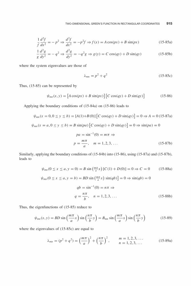
Balanis c15.tex V2 - 11/22/2011 4:04 P.M. Page 915
TWO-DIMENSIONAL GREEN’S FUNCTION IN RECTANGULAR COORDINATES 915
1
f
d2f
dx 2= − p2 ⇒ d2f
dx 2= −p2f ⇒ f (x) = A cos(px) + B sin(px) (15-85a)
1
g
d2g
dy2= − q2 ⇒ d2g
dy2= −q2g ⇒ g(y) = C cos(qy) + D sin(qy) (15-85b)
where the system eigenvalues are those of
λmn = p2 + q2 (15-85c)
Thus, (15-85) can be represented by
ψmn(x , y) = [A cos(px) + B sin(px)
] [C cos(qy) + D sin(qy)
](15-86)
Applying the boundary conditions of (15-84a) on (15-86) leads to
ψmn(x = 0, 0 ≤ y ≤ b) = [A(1)+B(0)][C cos(qy) + D sin(qy)
] = 0 ⇒ A = 0 (15-87a)
ψmn(x = a , 0 ≤ y ≤ b) = B sin(pa)[C cos(qy) + D sin(qy)
] = 0 ⇒ sin(pa) = 0
pa = sin−1(0) = mπ ⇒
p = mπ
a, m = 1, 2, 3, . . . (15-87b)
Similarly, applying the boundary conditions of (15-84b) into (15-86), using (15-87a) and (15-87b),leads to
ψmn(0 ≤ x ≤ a , y = 0) = B sin(
mπa x
)[C (1) + D(0)] = 0 ⇒ C = 0 (15-88a)
ψmn(0 ≤ x ≤ a , y = b) = BD sin(
mπa x
)sin(qb)
] = 0 ⇒ sin(qb) = 0
qb = sin−1(0) = nπ ⇒
q = nπ
b, n = 1, 2, 3, . . . (15-88b)
Thus, the eigenfunctions of (15-85) reduce to
ψmn(x , y) = BD sin(mπ
ax)
sin(nπ
by)
= Bmn sin(mπ
ax)
sin(nπ
by)
(15-89)
where the eigenvalues of (15-85c) are equal to
λmn = (p2 + q2) =(mπ
a
)2+
(nπ
b
)2,
m = 1, 2, 3, . . .
n = 1, 2, 3, . . .(15-89a)
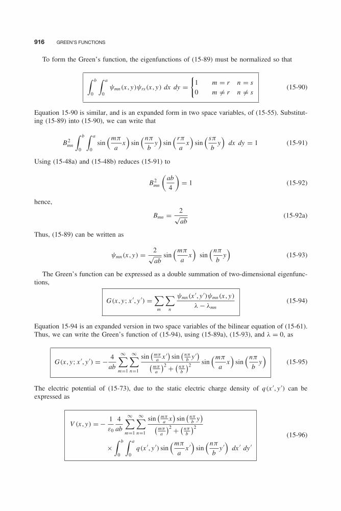
Balanis c15.tex V2 - 11/22/2011 4:04 P.M. Page 916
916 GREEN’S FUNCTIONS
To form the Green’s function, the eigenfunctions of (15-89) must be normalized so that
∫ b
0
∫ a
0ψmn(x , y)ψrs(x , y) dx dy =
{1 m = r n = s
0 m �= r n �= s(15-90)
Equation 15-90 is similar, and is an expanded form in two space variables, of (15-55). Substitut-ing (15-89) into (15-90), we can write that
B2mn
∫ b
0
∫ a
0sin
(mπ
ax)
sin(nπ
by)
sin( rπ
ax)
sin( sπ
by)
dx dy = 1 (15-91)
Using (15-48a) and (15-48b) reduces (15-91) to
B2mn
(ab
4
)= 1 (15-92)
hence,
Bmn = 2√ab
(15-92a)
Thus, (15-89) can be written as
ψmn(x , y) = 2√ab
sin(mπ
ax)
sin(nπ
by)
(15-93)
The Green’s function can be expressed as a double summation of two-dimensional eigenfunc-tions,
G(x , y; x ′, y ′) =∑
m
∑n
ψmn(x ′, y ′)ψmn(x , y)
λ − λmn(15-94)
Equation 15-94 is an expanded version in two space variables of the bilinear equation of (15-61).Thus, we can write the Green’s function of (15-94), using (15-89a), (15-93), and λ = 0, as
G(x , y; x ′, y ′) = − 4
ab
∞∑m=1
∞∑n=1
sin(
mπa x ′) sin
(nπb y ′)(
mπa
)2 + (nπb
)2 sin(mπ
ax)
sin(nπ
by)
(15-95)
The electric potential of (15-73), due to the static electric charge density of q(x ′, y ′) can beexpressed as
V (x , y) = − 1
ε0
4
ab
∞∑m=1
∞∑n=1
sin(
mπa x
)sin
(nπb y
)(mπa
)2 + (nπb
)2
×∫ b
0
∫ a
0q(x ′, y ′) sin
(mπ
ax ′
)sin
(nπ
by ′)
dx ′ dy ′(15-96)

Balanis c15.tex V2 - 11/22/2011 4:04 P.M. Page 917
TWO-DIMENSIONAL GREEN’S FUNCTION IN RECTANGULAR COORDINATES 917
15.4.2 Time-Harmonic Fields
For time-harmonic fields, a popular partial differential equation is
∂2Ez
∂x 2+ ∂2Ez
∂y2+ β2Ez = f (x , y) = jωμJz (x , y) (15-97)
subject to the boundary conditions
Ez (x = 0, 0 ≤ y ≤ b) = Ez (x = a , 0 ≤ y ≤ b) = 0 (15-97a)
Ez (0 ≤ x ≤ a , y = 0) = Ez (0 ≤ x ≤ a , y = b) = 0 (15-97b)
In (15-97), Ez can represent the electric field component of a TMz field configuration (mode) withno z variations inside a rectangular metallic cavity of dimensions a , b, c in the x , y , z directions,respectively, as shown in Figure 15-5. The function f (x , y) = jωμJz can represent the normalizedelectric current density component of the feed probe that is used to excite the fields within themetallic cavity. The objective here is to obtain the Green’s function of the problem and ultimatelythe electric field component represented in (15-97) by Ez (x , y).
The Green’s function G(x , y; x ′, y ′) will satisfy the partial differential equation
∂2G
∂x 2+ ∂2G
∂y2+ β2G = δ(x − x ′)δ(y − y ′) (15-98)
subject to the boundary conditions
G(x = 0, 0 ≤ y ≤ b) = G(x = a , 0 ≤ y ≤ b) = 0 (15-98a)
G(0 ≤ x ≤ a , y = 0) = G(0 ≤ x ≤ a , y = b) = 0 (15-98b)
and the electric field distribution Ez (x , y) will be represented by
Ez (x , y) = jωμ
∫ b
0
∫ a
0Jz (x
′, y ′)G(x , y; x ′, y ′) dx ′dy ′ (15-99)
The Green’s function of (15-98) can be derived either in closed form, as was done in Section15.4.1A for the statics problem, or in series form, as was done in Section 15.4.1B for the statics
y
x
c
a
b
z
Figure 15-5 Rectangular waveguide cavity geometry.

Balanis c15.tex V2 - 11/22/2011 4:04 P.M. Page 918
918 GREEN’S FUNCTIONS
problem. We will derive the Green’s function here by a series form. The closed form is left asan end-of-chapter exercise for the reader.
For the solution of the Green’s function, the complete set of eigenfunctions {ψmn(x , y)} canbe obtained by considering the homogeneous form of (15-97),
∂2ψmn
∂x 2+ ∂2ψmn
∂y2+ β2
mnψmn = 0 (15-100)
subject to the boundary conditions
ψmn(x = 0, 0 ≤ y ≤ b) = ψmn(x = a , 0 ≤ y ≤ b) = 0 (15-100a)
ψmn(0 ≤ x ≤ a , y = 0) = ψmn(0 ≤ x ≤ a , y = b) = 0 (15-100b)
Using the separation of variables of Section 3.4.1, we can represent ψmn(x , y) by
ψmn(x , y) = f (x)g(y) (15-101)
Substituting (15-101) into (15-100) and applying the boundary conditions of (15-100a) and (15-100b), it can be shown that ψmn(x , y) reduces to
ψmn(x , y) = Bmn sin(βx x) sin(βy y) = Bmn sin(mπ
ax)
sin(nπ
by)
(15-102)
where
βx = mπ
a, m = 1, 2, 3, . . . (15-102a)
βy = nπ
b, n = 1, 2, 3, . . . (15-102b)
The eigenvalues of the system are equal to
λmn = β2mn = (βx )
2 + (βy)2 =
(mπ
a
)2+
(nπ
b
)2(15-103a)
and
λ = β2 (15-103b)
The eigenfunctions of (15-102) must satisfy an equation similar to (15-90) but over a volumeintegral. That is∫ c
0
∫ b
0
∫ a
0ψmn(x , y , z ) ψrs(x , y , z ) dx dy dz =
{1, m = r n = s
0, m �= r n �= s(15-104)
which leads to
Bmn = 2√abc
(15-104a)
Thus,
ψmn(x , y) = 2√abc
sin(mπ
ax)
sin(nπ
by)
(15-105)

Balanis c15.tex V2 - 11/22/2011 4:04 P.M. Page 919
GREEN’S IDENTITIES AND METHODS 919
The Green’s function is obtained using (15-94), (15-103a), (15-103b), and (15-105). Doingthis, we can write that
G(x , y; x ′, y ′) = 4
abc
∞∑m=1
∞∑n=1
sin(mπ
ax ′
)sin
(nπ
by ′)
β2 −[(mπ
a
)2+
(nπ
b
)2]
× sin(mπ
ax)
sin(nπ
by) (15-106)
and the electric field component of (15-99), due to the normalized electric current density repre-sented by Jn(x ′, y ′), can be written as
Ez (x , y) = 4
abc
∞∑m=1
∞∑n=1
sin(mπ
ax)
sin(nπ
by)
β2 −[(mπ
a
)2+
(nπ
b
)2]
×∫ b
0
∫ a
0Jz (x
′, y ′) sin(mπ
ax ′
)sin
(nπ
by ′)
dx ′ dy ′
(15-107)
It is apparent that the Green’s function possesses a singularity, and it fails when
β = βr = ωr√
με = 2π fr√
με =√(mπ
a
)2+
(nπ
b
)2(15-108)
i.e., when
fr = 1
2π√
με
√(mπ
a
)2+
(nπ
b
)2(15-108a)
This is in accordance with (15-34), which states that the Green’s function of (15-33b) exists forall values of λ (here λ = β2 = ω2με) except those that are eigenvalues λmn of the homogeneousequation 15-34 [here λmn given by (15-103a)]. At those eigenvalues for which (15-106) and(15-107) possess singularities (simple poles here), the frequencies of the excitation source matchthe natural (characteristic) frequencies of the system. As explained in Section 1.3.2, this is referredto as resonance, and the field will continuously increase without any bounds (in the limit reachinginfinity). For these cases, no steady-state solutions exist. One way to contain the field is tointroduce damping. In practice, for metallic cavities, damping is introduced by the losses due tononperfectly conducting walls.
15.5 GREEN’S IDENTITIES AND METHODS
Now that we have derived Green’s functions, both for single and two space variables in rectangularcoordinates for the general Sturm-Liouville self-adjoint operator L, let us generalize the procedurefor the development of the Green’s function for the three-dimensional scalar Helmholtz partialdifferential equation
∇2ϕ(r) + β2ϕ(r) = f (r) (15-109)

Balanis c15.tex V2 - 11/22/2011 4:04 P.M. Page 920
920 GREEN’S FUNCTIONS
subject to the generalized homogeneous boundary conditions
α1ϕ(rs) + α2∂ϕ(rs)
∂ns= 0, s = 1, 2, . . . , N (15-109a)
where rs is on S and n̂ is an outward directed unit vector. In electromagnetics these are referredto not only as the mixed boundary conditions [7] but also as the impedance boundary conditions.The Green’s function G(r, r′) of (15-109) must satisfy the partial differential equation
∇2G(r, r′) + β2G(r, r′) = δ(r − r′) (15-110)
subject to the generalized homogeneous boundary conditions
α1G(rs , r′) + α2∂G(rs , r′)
∂ns= 0, s = 1, 2, . . . , N (15-110a)
To accomplish this, we will need two identities from vector calculus that are usually referredto as Green’s first and second identities. We will state them first before proceeding with thedevelopment of the generalized Green’s function.
15.5.1 Green’s First and Second Identities
Within a volume V , conducting bodies with surfaces S1, S2, S3, . . . , Sn are contained, as shownin Figure 15-6. By introducing appropriate cuts, the volume V is bounded by a regular surfaceS that consists of surfaces S1 − Sn , the surfaces along the cuts, and the surface Sa of an infiniteradius sphere that encloses all the conducting bodies. A unit vector n̂ normal to S is directedinward to the volume V , as shown in Figure 15-6.
Let us introduce within V two scalar functions φ and ψ , which, along with their first andsecond derivatives, are continuous within V and on the surface S . To the vector φ∇ψ , we apply
S1
S2
S3
Sa
n
nn
Figure 15-6 Conducting surfaces and appropriate cuts for application of Green’s theorem.
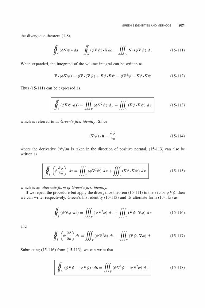
Balanis c15.tex V2 - 11/22/2011 4:04 P.M. Page 921
GREEN’S IDENTITIES AND METHODS 921
the divergence theorem (1-8),
#S(φ∇ψ) • ds =#S
(φ∇ψ) • n̂ da =∫∫∫
V∇ • (φ∇ψ) dv (15-111)
When expanded, the integrand of the volume integral can be written as
∇ • (φ∇ψ) = φ∇ • (∇ψ) + ∇φ • ∇ψ = φ∇2ψ + ∇φ • ∇ψ (15-112)
Thus (15-111) can be expressed as
#S(φ∇ψ • ds) =
∫∫∫V(φ∇2ψ) dv +
∫∫∫V(∇φ • ∇ψ) dv (15-113)
which is referred to as Green’s first identity . Since
(∇ψ) • n̂ = ∂ψ
∂n(15-114)
where the derivative ∂ψ/∂n is taken in the direction of positive normal, (15-113) can also bewritten as
#S
(φ
∂ψ
∂n
)ds =
∫∫∫V(φ∇2ψ) dv +
∫∫∫V(∇φ • ∇ψ) dv (15-115)
which is an alternate form of Green’s first identity.If we repeat the procedure but apply the divergence theorem (15-111) to the vector ψ∇φ, then
we can write, respectively, Green’s first identity (15-113) and its alternate form (15-115) as
#S(ψ∇φ • ds) =
∫∫∫V(ψ∇2φ) dv +
∫∫∫V(∇ψ • ∇φ) dv (15-116)
and
#S
(ψ
∂φ
∂n
)ds =
∫∫∫V(ψ∇2φ) dv +
∫∫∫V(∇ψ • ∇φ) dv (15-117)
Subtracting (15-116) from (15-113), we can write that
#S(φ∇ψ − ψ∇φ) • ds =
∫∫∫V(φ∇2ψ − ψ∇2φ) dv (15-118)
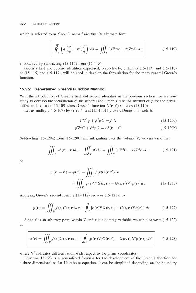
Balanis c15.tex V2 - 11/22/2011 4:04 P.M. Page 922
922 GREEN’S FUNCTIONS
which is referred to as Green’s second identity . Its alternate form
#S
(φ
∂ψ
∂n− ψ
∂φ
∂n
)ds =
∫∫∫V(φ∇2ψ − ψ∇2φ) dv (15-119)
is obtained by subtracting (15-117) from (15-115).Green’s first and second identities expressed, respectively, either as (15-113) and (15-118)
or (15-115) and (15-119), will be used to develop the formulation for the more general Green’sfunction.
15.5.2 Generalized Green’s Function Method
With the introduction of Green’s first and second identities in the previous section, we are nowready to develop the formulation of the generalized Green’s function method of ϕ for the partialdifferential equation 15-109 whose Green’s function G(r, r′) satisfies (15-110).
Let us multiply (15-109) by G(r, r′) and (15-110) by ϕ(r). Doing this leads to
G∇2ϕ + β2ϕG = f G (15-120a)
ϕ∇2G + β2ϕG = ϕδ(r − r′) (15-120b)
Subtracting (15-120a) from (15-120b) and integrating over the volume V, we can write that∫∫∫V
ϕδ(r − r′)dv −∫∫∫
VfGdv =
∫∫∫V(ϕ∇2G − G∇2ϕ)dv (15-121)
or
ϕ(r = r′) = ϕ(r′) =∫∫∫
Vf (r)G(r, r′)dv
+∫∫∫
V[ϕ(r)∇2G(r, r′) − G(r, r′)∇2ϕ(r)] dv (15-121a)
Applying Green’s second identity (15-118) reduces (15-121a) to
ϕ(r′) =∫∫∫
Vf (r)G(r, r′)dv +#S
[ϕ(r)∇G(r, r′) − G(r, r′)∇ϕ(r)] • ds (15-122)
Since r′ is an arbitrary point within V and r is a dummy variable, we can also write (15-122)as
ϕ(r) =∫∫∫
Vf (r′)G(r, r′)dv′ +#S
[ϕ(r′)∇′G(r, r′) − G(r, r′)∇′ϕ(r′)] • ds′ (15-123)
where ∇′ indicates differentiation with respect to the prime coordinates.Equation 15-123 is a generalized formula for the development of the Green’s function for
a three-dimensional scalar Helmholtz equation. It can be simplified depending on the boundary
Balanis c15.tex V2 - 11/22/2011 4:04 P.M. Page 923
GREEN’S IDENTITIES AND METHODS 923
conditions of ϕ and G , and their derivatives on S . The objective then will be to judiciouslychoose the boundary conditions on the development of G , once the boundary conditions on ϕ
are stated, so as to simplify, if not completely eliminate, the surface integral contribution in(15-123). We will demonstrate here some combinations of boundary conditions on ϕ and G , andthe simplifications of (15-123), based on those boundary conditions.
A. Nonhomogeneous Partial Differential Equation with Homogeneous DirichletBoundary Conditions If the nonhomogeneous form of the partial differential equationof 15-109 satisfies the homogeneous Dirichlet boundary condition
ϕ(rs) = 0, where rs is on S (15-124a)
then it is reasonable to construct a Green’s function with the same boundary condition
G(rs , r′) = 0, where rs is on S (15-124b)
so as to simplify the surface integral contributions in (15-123).For these boundary conditions on ϕ and G , both terms in the surface integral of (15-123)
vanish, so that (15-123) reduces to
ϕ(r) =∫∫∫
Vf (r′)G(r, r′)dv′ (15-125)
The Green’s function G(r, r′) needed in (15-125) can be obtained using any of the previousmethods developed in Sections 15.3.1 through 15.3.2. In many cases, the bilinear form (15-61)or (15-94) or its equivalent, in the desired coordinate system and number of space variables, isappropriate for forming the Green’s function. Its existence will depend upon the eigenvalues ofthe homogeneous partial differential equation, as discussed in Section 15.3.1.
B. Nonhomogeneous Partial Differential Equation with Nonhomogeneous DirichletBoundary Conditions If the nonhomogeneous partial differential equation 15-109 satisfiesthe nonhomogeneous Dirichlet boundary condition
ϕ(rs) = g(rs), where rs is on S (15-126a)
then we can still construct a Green’s function that satisfies the boundary condition
G(rs , r′) = 0, where rs is on S (15-126b)
For these boundary conditions on ϕ and G , the second term in the surface integral of (15-123)vanishes, so that (15-123) reduces to
ϕ(r) =∫∫∫
Vf (r′) G(r, r′)dv′ +#S
ϕ(r′)∇′G(rs , r′) • ds′ (15-127)
The Green’s function G(r, r′) needed in (15-127) can be determined using any of the previousmethods developed in Sections 15.3.1 through 15.3.2.
Balanis c15.tex V2 - 11/22/2011 4:04 P.M. Page 924
924 GREEN’S FUNCTIONS
C. Nonhomogeneous Partial Differential Equation with Homogeneous NeumannBoundary Conditions When Neumann boundary conditions are involved, the solutionsbecome more complicated primarily because the normal gradients of ϕ(r) are not independentof the partial differential equation. If the nonhomogeneous form of the partial differentialequation 15-109 satisfies the homogeneous Neumann boundary condition[∇′ϕ(rs)
]• n̂ = ∂ϕ(rs)
∂n= 0 where rs is on S (15-128)
then we cannot , in general, construct a Green’s function with a boundary condition [∇′G(rs , r′)] ·n̂ = [∂G(rs , r′)/∂n] = 0. This is evident from what follows.
If we apply the divergence theorem (1-8) to the vector ∇G(r, r′), we can write that
#S∇G(r, r′) • ds =
∫∫∫V
∇ • ∇G(r, r′)dv =∫∫∫
V∇2G(r, r′)dv (15-129)
Taking the volume integral of (15-110), we can express it as∫∫∫V
∇2G(r, r′)dv + β2∫∫∫
VG(r, r′)dv =
∫∫∫V
δ(r − r′)dv (15-130)
Using (15-129) reduces (15-130) to
#S∇G(r, r′) • ds + β2
∫∫∫V
G(r, r′)dv = 1 (15-131)
If we choose [∇G(r, r′)|r=rs
]• n̂ = [∇G(rs , r′)
]• n̂ = ∂G(rs , r′)
∂n= 0 (15-132)
as a boundary condition for G(r, r′), then (15-131) reduces to
β2∫∫∫
VG(r, r′)dv = 1 (15-133)
which cannot be satisfied if β = 0. When β = 0, (15-131) reduces to
#S∇G(r, r′) • ds = 1 (15-134)
or|∇G(rs , r′)|S0 = 1 (15-134a)
where S0 is the area of the surface. This implies that a consistent boundary condition for thenormal gradient of G(r, r′) on S to satisfy (15-134) or (15-134a) would be
∇′G(r, r′)|r=rs = 1
S0= ∇′G(rs, r′) (15-135)
Substituting (15-128) and (15-135) into (15-123) leads to
ϕ(r) =∫∫∫
Vf (r′)G(r, r′)dv′ + 1
S0 #Sϕ(r′)ds ′ (15-136)

Balanis c15.tex V2 - 11/22/2011 4:04 P.M. Page 925
GREEN’S FUNCTIONS OF THE SCALAR HELMHOLTZ EQUATION 925
The second term on the right side of (15-136) is a constant, and it can be dropped since ϕ(r) isundetermined by the boundary conditions up to an additive constant.
D. Nonhomogeneous Partial Differential Equation with Mixed Boundary ConditionsWhen the boundary conditions on ϕ(r) are such that ϕ(rs) is specified in part of the surfaceS and [∇′φ(rs)] · n̂ = ∂φ(rs)/∂n is specified over the remaining part of S , it is referred to ashaving mixed boundary conditions. Then it is desirable to construct a Green’s function so that itvanishes on that part of S over which ϕ(rs) is specified, and its normal derivative [∂G(rs , r′)/∂n]vanishes over the remaining part of S over which ∂ψ(rs)/∂n is specified. Although this is a morecomplex procedure, it does provide a method to derive the Green’s function even under thosemixed boundary conditions.
15.6 GREEN’S FUNCTIONS OF THE SCALAR HELMHOLTZ EQUATION
Now that we have derived the development of the generalized Green’s function, let us applythe formulation to the scalar Helmholtz equation in three-dimensional problems of rectangular,cylindrical, and spherical coordinates.
15.6.1 Rectangular Coordinates
The development of Green’s functions in rectangular coordinates has already been applied forone and two space variables in almost all of the previous sections. In this section we want toderive it for a three-dimensional problem. Specifically, let us derive the Green’s function for theelectric field component Ey that satisfies the partial differential equation
∇2Ey + β20 Ey =
(∂2
∂x 2+ ∂2
∂y2+ ∂2
∂z 2
)Ey + β2
0 Ey = jωμJy(x , y , z ) (15-137)
subject to the boundary conditions
Ey(x = 0, 0 ≤ y ≤ b, −∞ ≤ z ≤ +∞) = Ey(x = a , 0 ≤ y ≤ b, −∞ ≤ z ≤ +∞) = 0(15-137a)
In (15-137), Ey represents the electric field component of a TMz field configuration (subject to∇ · J = 0) inside a metallic waveguide of dimensions a , b in the x , y directions, respectively, asshown in Figure 15-7. Also Jy(x , y , z ) represents the electric current density of the feed probethat is used to excite the fields within the metallic waveguide. It is assumed that the wave istraveling in the z direction. The time-harmonic variations are of e+jωt , and they are suppressed.
The Green’s function must satisfy the partial differential equation
∇2G(x , y , z ; x ′, y ′, z ′) + β20 G(x , y , z ; x ′, y ′, z ′) = δ(x − x ′)δ(y − y ′)δ(z − z ′) (15-138)
subject to the boundary conditions
G(x = 0, 0 ≤ y ≤ b, −∞ ≤ z ≤ +∞)
= G(x = a , 0 ≤ y ≤ b, −∞ ≤ z ≤ +∞) = 0 (15-138a)
Since the electric field and Green’s function satisfy, respectively, the Dirichlet boundary con-ditions (15-124a) and (15-124b), then, according to (15-123) or (15-125), the electric field isobtained using
Ey(x , y , z ) = jωμ
∫∫∫V
Jy(x′, y ′, z ′) G(x , y , z ; x ′, y ′, z ′)dx ′dy ′dz ′ (15-139)
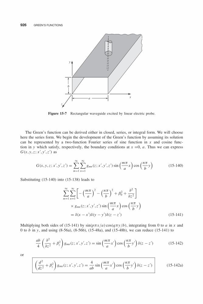
Balanis c15.tex V2 - 11/22/2011 4:04 P.M. Page 926
926 GREEN’S FUNCTIONS
y
b
z
a x
Figure 15-7 Rectangular waveguide excited by linear electric probe.
The Green’s function can be derived either in closed, series, or integral form. We will choosehere the series form. We begin the development of the Green’s function by assuming its solutioncan be represented by a two-function Fourier series of sine function in x and cosine func-tion in y which satisfy, respectively, the boundary conditions at x =0, a . Thus we can expressG(x , y , z ; x ′, y ′, z ′) as
G(x , y , z ; x ′, y ′, z ′) =∞∑
m=1
∞∑n=1
gmn(z ; x ′, y ′, z ′) sin(mπ
ax)
cos(nπ
by)
(15-140)
Substituting (15-140) into (15-138) leads to
∞∑m=1
∞∑n=1
[−
(mπ
a
)2−
(nπ
b
)2+ β2
0 + ∂2
∂z 2
]× gmn(z ; x ′, y ′, z ′) sin
(mπ
ax)
cos(nπ
by)
= δ(x − x ′)δ(y − y ′)δ(z − z ′) (15-141)
Multiplying both sides of (15-141) by sin(pπx/a) cos(qπy/b), integrating from 0 to a in x and0 to b in y , and using (8-56a), (8-56b), (15-48a), and (15-48b), we can reduce (15-141) to
ab
4
(∂2
∂z 2+ β2
z
)gmn(z ; x ′, y ′, z ′) = sin
(mπ
ax ′
)cos
(nπ
by ′)
δ(z − z ′) (15-142)
or (d2
dz 2+ β2
z
)gmn(z ; x ′, y ′, z ′) = 4
absin
(mπ
ax ′
)cos
(nπ
by ′)
δ(z − z ′) (15-142a)

Balanis c15.tex V2 - 11/22/2011 4:04 P.M. Page 927
GREEN’S FUNCTIONS OF THE SCALAR HELMHOLTZ EQUATION 927
where
β2z = β2
0 −[(mπ
a
)2+
(nπ
b
)2]
= β20 − (β2
x + β2y ) (15-142b)
βx = mπ
am = 1, 2, 3, . . . (15-142c)
βy = nπ
bn = 1, 2, 3, . . . (15-142d)
The function gmn(z ; x ′, y ′, z ′) satisfies the single variable differential equation 15-142a, andit can be found by using the recipe of Section 15.3.1 as represented by (15-44c), (15-45a),and (15-45b). Two solutions of the homogeneous differential equation(
d2
dz 2+ β2
z
)gmn(z ; x ′, y ′, z ′) = 0 (15-143)
of (15-142a) are
g (1)mn = Amne+jβz z for z < z ′ (15-143a)
g (2)mn = Bmne−jβz z for z > z ′ (15-143b)
Using (15-44c) where y1 = g (1)mn and y2 = g (2)
mn , we can write the Wronskian as
W (z ′) = AmnBmn(−jβz )ejβz z ′
e−jβz z ′ − AmnBmn(jβz )e−jβz z ′
e+jβz z ′
W (z ′) = −j 2βz AmnBmn (15-144)
By comparing (15-142a) to (15-33), it is apparent that
p(z ) = 1
q(z ) = 0 (15-145)
r(z ) = 1
λ = β2z
Using (15-143a) through (15-145), the solution for gmn(z ; x ′, y ′, z ′) of (15-142a) can be written,by referring to (15-45a) and (15-45b), as
gmn(z ; x ′, y ′, z ′) =
⎧⎪⎪⎪⎪⎪⎪⎨⎪⎪⎪⎪⎪⎪⎩j
2
ab
sin(mπ
ax ′
)cos
(nπ
by ′)
βze−jβz (z ′−z ) for z < z ′
j2
ab
sin(mπ
ax ′
)cos
(nπ
by ′)
βze−jβz (z−z ′) for z > z ′
(15-146a)
(15-146b)
or
gmn(z ; x ′, y ′, z ′) = j2
ab
sin(mπ
ax ′
)cos
(nπ
by ′)
βze−jβz |z−z ′| for z < z ′, z > z ′ (15-146c)
Balanis c15.tex V2 - 11/22/2011 4:04 P.M. Page 928
928 GREEN’S FUNCTIONS
Thus, the Green’s function of (15-140) can now be expressed as
G(x , y , z ; x ′, y ′, z ′) = j2
ab
∞∑m=1,2,...
∞∑n=1,2,...
sin(mπ
ax ′
)cos
(nπ
by ′)
βz
× sin(mπ
ax)
cos(nπ
by)
e−jβz |z−z ′| for z < z ′, z > z ′ (15-147)
where
βz =
⎧⎪⎨⎪⎩√
β20 − (β2
x + β2y ) for β2
0 >(β2x + β2
y )
−j√
(β2x + β2
y ) − β20 for β2
0 < (β2x + β2
y )
(15-147a)
(15-147b)
It is evident from (15-147) through (15-147b) that when β20 >(β2
x + β2y ) the modes are propagating
and when β20 < (β2
x + β2y ) the modes are not propagating (evanescent). The nonpropagating modes
converge very rapidly when |z − z ′| is very large.Once the Green’s function is formulated as in (15-147), the electric field can be found using
(15-139).
15.6.2 Cylindrical Coordinates
Until now we have concentrated on developing primarily Green’s functions of problems dealingwith rectangular coordinates. This was done to maintain simplicity in the mathematics so that theanalytical formulations would not obscure the fundamental concepts. Now we are ready to dealwith problems expressed by other coordinate systems, such as cylindrical and spherical.
Let us assume that an infinite electric line source of constant current Iz is placed at ρ = ρ ′, φ =φ′ inside a circular waveguide of radius a , as shown in Figure 15-8. The electric field componentEz satisfies the partial differential equation
∇2Ez + β20 Ez = f (ρ, φ) = jωμIz (15-148)
subject to the boundary condition
Ez (ρ = a , 0 ≤ φ ≤ 2π , z ) = 0 (15-148a)
The Green’s function of this problem will satisfy the partial differential equation
∇2G + β20 G = δ(ρ − ρ′) (15-149)
The boundary condition for the Green’s function can be chosen so that
G(ρ = a , 0 ≤ φ ≤ 2π , z ) = 0 (15-149a)
Since the boundary conditions (15-148a) and (15-149a) on Ez and G , respectively, are of theDirichlet type, then according to (15-123) or (15-125)
Ez (ρ, φ) =∫∫
Sf (ρ ′, φ′)G(ρ, φ; ρ ′, φ′) ds ′ = jωμ
∫∫S
Iz (ρ′, φ′)G(ρ, φ; ρ ′, φ′) ds ′ (15-150)
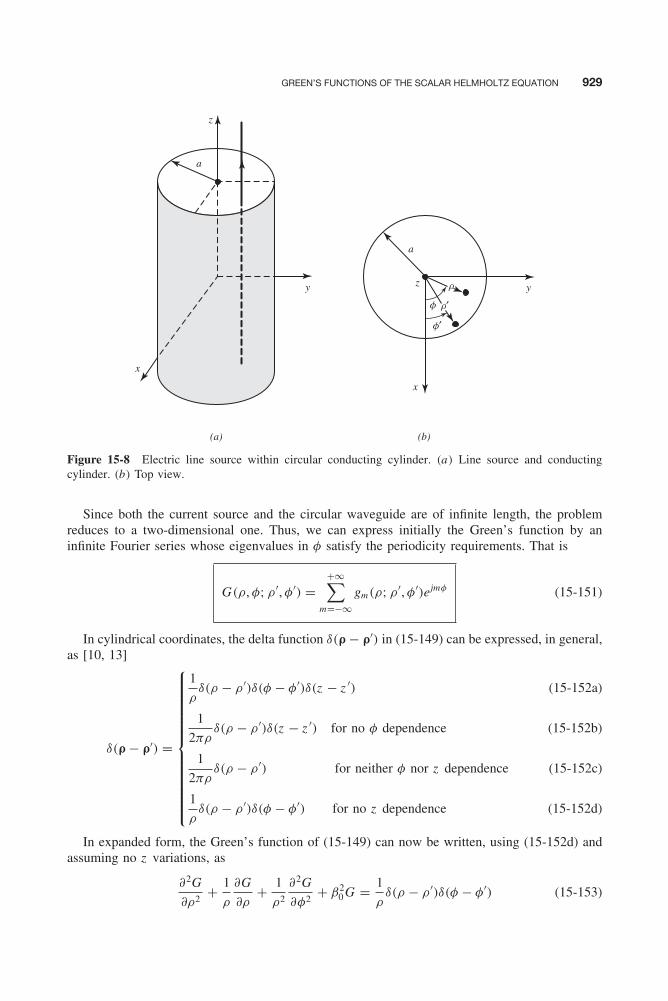
Balanis c15.tex V2 - 11/22/2011 4:04 P.M. Page 929
GREEN’S FUNCTIONS OF THE SCALAR HELMHOLTZ EQUATION 929
x
y y
a
z
x
a
z
(b)(a)
f
r
f′
r′
Figure 15-8 Electric line source within circular conducting cylinder. (a) Line source and conductingcylinder. (b) Top view.
Since both the current source and the circular waveguide are of infinite length, the problemreduces to a two-dimensional one. Thus, we can express initially the Green’s function by aninfinite Fourier series whose eigenvalues in φ satisfy the periodicity requirements. That is
G(ρ, φ; ρ ′, φ′) =+∞∑
m=−∞gm(ρ; ρ ′, φ′)ejmφ (15-151)
In cylindrical coordinates, the delta function δ(ρ − ρ′) in (15-149) can be expressed, in general,as [10, 13]
δ(ρ − ρ′) =
⎧⎪⎪⎪⎪⎪⎪⎪⎪⎪⎪⎪⎪⎪⎨⎪⎪⎪⎪⎪⎪⎪⎪⎪⎪⎪⎪⎪⎩
1
ρδ(ρ − ρ ′)δ(φ − φ′)δ(z − z ′)
1
2πρδ(ρ − ρ ′)δ(z − z ′) for no φ dependence
1
2πρδ(ρ − ρ ′) for neither φ nor z dependence
1
ρδ(ρ − ρ ′)δ(φ − φ′) for no z dependence
(15-152a)
(15-152b)
(15-152c)
(15-152d)
In expanded form, the Green’s function of (15-149) can now be written, using (15-152d) andassuming no z variations, as
∂2G
∂ρ2+ 1
ρ
∂G
∂ρ+ 1
ρ2
∂2G
∂φ2+ β2
0 G = 1
ρδ(ρ − ρ ′)δ(φ − φ′) (15-153)
Balanis c15.tex V2 - 11/22/2011 4:04 P.M. Page 930
930 GREEN’S FUNCTIONS
Substituting (15-151) into (15-153) leads to
+∞∑m=−∞
[∂2
∂ρ2+ 1
ρ
∂
∂ρ− m2
ρ2+ β2
0
]gm(ρ; ρ ′, φ′)ejmφ = 1
ρδ(ρ − ρ ′)δ(φ − φ′) (15-154)
Multiplying both sides of (15-154) by e−jnφ , integrating both sides from 0 to 2π in φ, and usingthe orthogonality condition ∫ 2π
0ej (m−n)φdφ =
{2π m = n
0 m �= n(15-155a)
(15-155b)
reduces (15-154) to
2π
[∂2gm
∂ρ2+ 1
ρ
∂gm
∂ρ+
(β2
0 − m2
ρ2
)gm
]= 1
ρe−jmφ′
δ(ρ − ρ ′)
or
ρd2gm
dρ2+ dgm
dρ+
(ρβ2
0 − m2
ρ
)gm = e−jmφ′
2πδ(ρ − ρ ′) (15-156)
where the partial derivatives have been replaced by ordinary derivatives.The function gm(ρ; ρ ′, φ′) satisfies the differential equation 15-156, and its solution can be
obtained using the closed-form recipe of Section 15.3.1 represented by (15-44c) and (15-45a)through (15-45b). The homogeneous equation 15-156 can be written, by multiplying through byρ, as
ρ2 d2gm
dρ2+ ρ
dgm
dρ+ (
β20ρ2 − m2) gm = 0 (15-157)
or
ρd2gm
dρ2+ dgm
dρ+
(β2
0ρ − m2
ρ
)gm = 0 (15-157a)
which is of the one-dimensional Sturm-Liouville form of (15-26) or (15-33) (see Example 15-1)where
p(ρ) = ρ
q(ρ) = m2
ρ
r(ρ) = ρ
λ = β20
(15-158)
Equation 15-157 is recognized as being Bessel’s differential equation 3-64 whose two solutionscan be written according to (3-67a) as
g (1)m = AmJm(β0ρ) + BmYm(β0ρ) for ρ < ρ ′ (15-159a)
g (2)m = CmJm(β0ρ) + DmYm(β0ρ) for ρ > ρ ′ (15-159b)
These two solutions were chosen because the fields within the waveguide form standing wavesinstead of traveling waves.
Since the Green’s function of (15-151) must represent, according to (15-150), the field every-where, including the origin, then Bm = 0 in (15-159a) since Ym(β0ρ) possesses a singularity at

Balanis c15.tex V2 - 11/22/2011 4:04 P.M. Page 931
GREEN’S FUNCTIONS OF THE SCALAR HELMHOLTZ EQUATION 931
ρ = 0. Also since the Green’s function must satisfy the boundary condition (15-149a), then thesolution of g (2)
m of (15-159b) must also satisfy (15-149a). Thus,
g (2)m (ρ = a) = CmJm(β0a) + DmYm(β0a) = 0
hence,
Dm = −CmJm(β0a)
Ym(β0a)(15-160)
Thus, (15-159a) and (15-159b) can be reduced to
g (1)m = AmJm(β0ρ) for ρ < ρ ′ (15-161a)
g (2)m = Cm
[Jm(β0ρ) − Jm(β0a)
Ym(β0a)Ym(β0ρ)
]for ρ > ρ ′ (15-161b)
Using (15-44c) where y1 = g (1)m and y2 = g (2)
m , we can write the Wronskian as
W (ρ ′) = β0AmCmJm(β0a)
Ym(β0a)
[J ′
m(β0ρ′)Ym(β0ρ
′) − Jm(β0ρ′)Y ′
m(β0ρ′)]
(15-162)
where the prime indicates partial with respect to the entire argument [′≡ ∂/∂(β0ρ′)]. Using the
Wronskian for Bessel functions of (11-95), we can reduce (15-162) to
W (ρ ′) = − 2
πAmCm
Jm(β0a)
Ym(β0a)
1
ρ ′ (15-162a)
Finally, gm(ρ; ρ ′, φ′) of (15-156) can be written using (15-158), (15-161a) through (15-161b),and (15-162a), by referring to (15-45a) and (15-45b), as
gm(ρ; ρ ′, φ′) =
⎧⎪⎪⎪⎪⎪⎪⎪⎪⎪⎨⎪⎪⎪⎪⎪⎪⎪⎪⎪⎩
−1
4
[Jm(β0ρ
′)Ym(β0a) − Jm(β0a)Ym(β0ρ′)]Jm(β0ρ)
Jm(β0a)e−jmφ′
for ρ < ρ ′
−1
4
[Jm(β0ρ)Ym(β0a) − Jm(β0a)Ym(β0ρ)
]Jm(β0ρ′)
Jm(β0a)e−jmφ′
for ρ > ρ ′
(15-163a)
(15-163b)
Thus, the Green’s function (15-151) can then be written as
G(ρ, φ; ρ ′, φ′) = −1
4
⎧⎪⎪⎪⎪⎪⎪⎪⎪⎪⎪⎪⎪⎪⎪⎪⎪⎨⎪⎪⎪⎪⎪⎪⎪⎪⎪⎪⎪⎪⎪⎪⎪⎪⎩
+∞∑m=−∞
[Jm(β0ρ′)Ym(β0a) − Jm(β0a)Ym(β0ρ
′)]
×Jm(β0ρ)
Jm(β0a)ejm(φ−φ′) for ρ < ρ ′
+∞∑m=−∞
[Jm(β0ρ)Ym(β0a) − Jm(β0a)Ym(β0ρ)]
×Jm(β0ρ′)
Jm(β0a)ejm(φ−φ′) for ρ > ρ ′
(15-164a)
(15-164b)

Balanis c15.tex V2 - 11/22/2011 4:04 P.M. Page 932
932 GREEN’S FUNCTIONS
or in terms of cosine terms as
G(ρ, φ; ρ ′, φ′) = −1
2
⎧⎪⎪⎪⎪⎪⎪⎪⎪⎪⎪⎪⎪⎪⎪⎪⎪⎨⎪⎪⎪⎪⎪⎪⎪⎪⎪⎪⎪⎪⎪⎪⎪⎪⎩
+∞∑m=−∞
[Jm(β0ρ′)Ym(β0a) − Jm(β0a)Ym(β0ρ
′)]εm
×Jm(β0ρ)
Jm(β0a)cos[m(φ − φ′)] for ρ < ρ ′
+∞∑m=−∞
[Jm(β0ρ)Ym(β0a) − Jm(β0a)Ym(β0ρ)]
εm
×Jm(β0ρ′)
Jm(β0a)cos[m(φ − φ′)] for ρ > ρ ′
(15-165a)
(15-165b)
where
εm ={
2 m = 0
1 m �= 0
(15-165c)
(15-165d)
The Green’s function for this problem can also be derived using the two space variable seriesexpansion method whereby it is represented by orthonormal expansion functions. This is left tothe reader as an end-of-chapter exercise.
Example 15-5
An infinite electric line source of constant current Iz is located at ρ = ρ ′, φ = φ′, as shown inFigure 15-9, and it is radiating in an unbounded free-space medium. Derive its Green’s function inclosed form.
z
z
yy
xx
(a) (b)
f′
r′
f′r′
r
f
Iz
Iz
Figure 15-9 Electric line source displaced from the origin. (a) Perspective view. (b) Top view.
Solution: Since the line source is removed from the origin, its Green’s function will be a function of φ
and φ′. Thus, it takes the form of (15-151), and it satisfies the differential equations 15-153 through 15-157. However, since the Green’s function must satisfy the radiation conditions at infinity (G →0 as ρ → ∞), the two solutions to the homogeneous differential equation 15-157 can be written as
g (1)m = Am Jm(β0ρ) + Bm Ym(β0ρ) for ρ < ρ ′
g (2)m = Cm H (1)
m (β0ρ) + Dm H (2)m (β0ρ) for ρ >ρ ′
Balanis c15.tex V2 - 11/22/2011 4:04 P.M. Page 933
GREEN’S FUNCTIONS OF THE SCALAR HELMHOLTZ EQUATION 933
Because the fields must be finite everywhere, including ρ = 0, g (1)m reduces to
g (1)m = Am Jm(β0ρ) for ρ < ρ ′
In addition, for ρ > ρ ′ the wave functions must represent outwardly traveling waves. Thus, for ejωt timevariations, g (2)
m reduces tog (2)
m = Dm H (2)m (β0ρ) for ρ >ρ ′
Using (15-44c) where y1 = g (1)m and y2 = g (2)
m , we can write the Wronskian as
W (ρ ′) = β0Am Dm[Jm(β0ρ
′)H (2)′m (β0ρ
′) − H (2)m (β0ρ
′)J ′m(β0ρ
′)]
= −jβ0Am Dm[Jm(β0ρ
′)Y ′m(β0ρ
′) − J ′m(β0ρ
′)Ym(β0ρ′)]
which by using the Wronskian of (11-95) for Bessel functions can be expressed as
W (ρ ′) = −j2
πρ ′ Am Dm
Thus, gm(ρ; ρ ′, φ′) of (15-156) can be written, using (15-45a) through (15-45b) and (15-158) along withthe preceding expressions for g (1)
m , g (2)m , and W (ρ ′), as
gm(ρ; ρ ′, φ′) ={
Jm(β0ρ)H (2)m (β0ρ
′)e−jmφ′for ρ < ρ ′
Jm(β0ρ′)H (2)
m (β0ρ)e−jmφ′for ρ > ρ ′
Thus, the Green’s function of (15-151) can be written as
G(ρ, φ; ρ ′, φ′) = − 1
4j
⎧⎪⎪⎨⎪⎪⎩+∞∑
m=−∞Jm(β0ρ)H (2)
m (β0ρ′)ejm(φ−φ′) for ρ < ρ ′
+∞∑m=−∞
Jm(β0ρ′)H (2)
m (β0ρ)ejm(φ−φ′) for ρ > ρ ′
which, by the addition theorem for Hankel functions of (11-69a) through (11-69b) or (11-82a) through(11-82b), can be expressed in succinct form as
G(ρ, φ; ρ ′, φ′) = − 1
4jH (2)
0 (β0|ρ − ρ′|)
This is the well known two-dimensional Green’s function for cylindrical waves.
15.6.3 Spherical Coordinates
The development of the Green’s function for problems represented by spherical coordinates ismore complex, and it must be expressed, in general, in terms of spherical Bessel and Hankelfunctions, Legendre functions, and complex exponentials or cosinusoids (see Chapter 10). Inorder to minimize the mathematical complexities here, we will develop the Green’s function ofa source positioned at r ′, θ ′, φ′, inside a sphere of radius a and with free-space, as shown inFigure 15-10.
The Green’s function must satisfy the partial differential equation
∇2G + β20 G = δ(r − r′) (15-166)
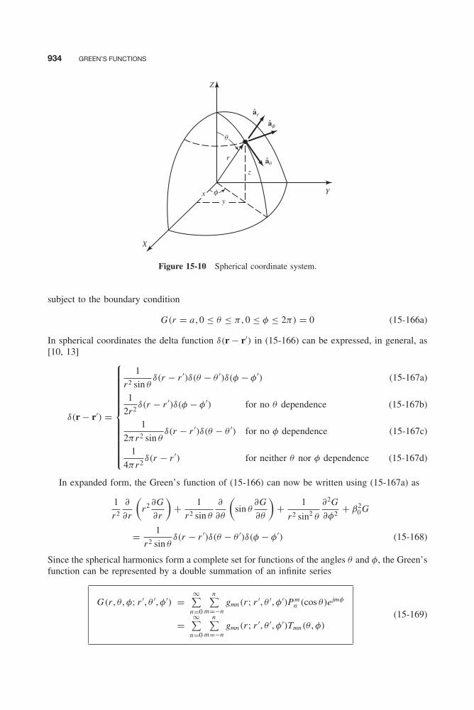
Balanis c15.tex V2 - 11/22/2011 4:04 P.M. Page 934
934 GREEN’S FUNCTIONS
x
X
yY
Z
z
r
f
q
ar
af
aq
Figure 15-10 Spherical coordinate system.
subject to the boundary condition
G(r = a , 0 ≤ θ ≤ π , 0 ≤ φ ≤ 2π) = 0 (15-166a)
In spherical coordinates the delta function δ(r − r′) in (15-166) can be expressed, in general, as[10, 13]
δ(r − r′) =
⎧⎪⎪⎪⎪⎪⎪⎪⎪⎪⎪⎪⎪⎨⎪⎪⎪⎪⎪⎪⎪⎪⎪⎪⎪⎪⎩
1
r2 sin θδ(r − r ′)δ(θ − θ ′)δ(φ − φ′)
1
2r2δ(r − r ′)δ(φ − φ′) for no θ dependence
1
2πr2 sin θδ(r − r ′)δ(θ − θ ′) for no φ dependence
1
4πr2δ(r − r ′) for neither θ nor φ dependence
(15-167a)
(15-167b)
(15-167c)
(15-167d)
In expanded form, the Green’s function of (15-166) can now be written using (15-167a) as
1
r2
∂
∂r
(r2 ∂G
∂r
)+ 1
r2 sin θ
∂
∂θ
(sin θ
∂G
∂θ
)+ 1
r2 sin2 θ
∂2G
∂φ2+ β2
0 G
= 1
r2 sin θδ(r − r ′)δ(θ − θ ′)δ(φ − φ′) (15-168)
Since the spherical harmonics form a complete set for functions of the angles θ and φ, the Green’sfunction can be represented by a double summation of an infinite series
G(r , θ , φ; r ′, θ ′, φ′) =∞∑
n=0
n∑m=−n
gmn(r; r ′, θ ′, φ′)Pmn (cos θ)ejmφ
=∞∑
n=0
n∑m=−n
gmn(r; r ′, θ ′, φ′)Tmn(θ , φ)
(15-169)

Balanis c15.tex V2 - 11/22/2011 4:04 P.M. Page 935
GREEN’S FUNCTIONS OF THE SCALAR HELMHOLTZ EQUATION 935
where Tmn(θ , φ) represents the tesseral harmonics of (11-214a) and (11-214b), or
Tmn(θ , φ) = CmnPmn (cos θ)ejmφ (15-169a)
where
Cmn =√
(2n + 1)(n − m)!
4π(n + m)!(15-169b)
Multiplying (15-168) by r2 and then substituting (15-169) into (15-168), we can write that
∞∑n=0
∞∑m=−n
[Tmn
∂
∂r
(r2 ∂gmn
∂r
)+ gmn
sin θ
∂
∂θ
(sin θ
∂Tmn
∂θ
)− m2
sin2 θgmnTmn + (β0r)2gmnTmn
]
= 1
sin θδ(r − r ′)δ(θ − θ ′)δ(φ − φ′) (15-170)
Dividing both sides of (15-170) by gmnTmn , we can write that
∞∑n=0
∞∑m=−n
[1
gmn
∂
∂r
(r2 ∂gmn
∂r
)+ 1
Tmn sin θ
∂
∂θ
(sin θ
∂Tmn
∂θ
)− m2
sin2 θ+ (β0r)2
]
= 1
gmnTmn sin θδ(r − r ′)δ(θ − θ ′)δ(φ − φ′) (15-170a)
Using (3-86b), we can write that
1
Tmn sin θ
∂
∂θ
(sin θ
∂Tmn
∂θ
)− m2
sin2 θ= −n(n + 1) (15-171)
hence,
1
sin θ
∂
∂θ
(sin θ
∂Tmn
∂θ
)+
[n(n + 1) −
( m
sin θ
)2]
Tmn = 0 (15-171a)
Thus, (15-170a) reduces, by substituting (15-171) into it and then multiplying through by gmnTmn ,to
∞∑n=0
n∑m=−n
{∂
∂r
(r2 ∂gmn
∂r
)+ [
(β0r)2 + n(n + 1)]
gmn
}Tmn
= 1
sin θδ(r − r ′)δ(θ − θ ′)δ(φ − φ′) (15-172)
From (11-214a) through (11-216d) and the definitions of the tesseral harmonics and Legendrefunctions, it can be shown that the orthogonality conditions of the tesseral harmonics are [20]∫ 2π
0
∫ π
0Tmn(θ , φ)T ∗
pq(θ , φ) sin θdθdφ = δmpδnq (15-173)

Balanis c15.tex V2 - 11/22/2011 4:04 P.M. Page 936
936 GREEN’S FUNCTIONS
where
T ∗pq(θ , φ) = (−1)pT(−p)q(θ , φ) (15-173a)
δrs ={
1 r = s0 r �= s
(15-173b)
Let
gmn(r; r ′, θ ′, φ′) = hmn(r , r ′)T∗(θ ′, φ′) (15-173c)
Multiplying both sides of (15-172) by T ∗pq(θ , φ) sin θ , integrating from 0 to π in θ and 0 to 2π
in φ, and using the orthogonality condition of (15-173), it can be shown that (15-172) reducesto
d
dr
(r2 dhmn
dr
)+ [
(β0r)2 − n(n + 1)]
hmn = δ(r − r ′) (15-174)
where the partial derivative ∂/∂r has been replaced by ordinary derivatives.The function hmn(r , r ′) satisfies the differential equation 15-174, and its solution can be
obtained using the closed-form recipe of Section 15.3.1 represented by (15-44c) and (15-45a)through (15-45b). The homogeneous equation 15-174 can be written as
d
dr
(r2 dhmn
dr
)+ [
(β0r)2 − n(n + 1)]
hmn = 0 (15-175)
which is of the one-dimensional Sturm-Liouville form of (15-26) or (15-33) where
p(r) = r2
q(r) = −n(n + 1)
r(x) = r2
λ = β2
(15-176)
Equation 15-175 is recognized as being (3-83) or (3-86a) whose solution can be representedby either (3-87a) or (3-87b). We choose here the form of (3-87a) since we need to representthe Green’s function within the sphere by standing wave functions. Thus, the two solutions of(15-175) can be written as
h(1)mn = Amjn(β0r) + Bmyn(β0r) for r < r ′ (15-177a)
h(2)mn = Cmjn(β0r) + Dmyn(β0r) for r > r ′ (15-177b)
where jn(β0r) and yn(β0r) are, respectively, spherical Bessel functions of the first and secondkind.
Since the Green’s function of (15-169) must be finite everywhere, including the origin, thenBm = 0 since yn(β0r) possesses a singularity at r = 0. Also the Green’s function must satisfythe boundary condition (15-166a). Therefore, h(2)
mn of (15-177b) at r = a reduces to
h(2)mn (r = a) = Cmjn(β0a) + Dmyn(β0a) = 0 (15-178)
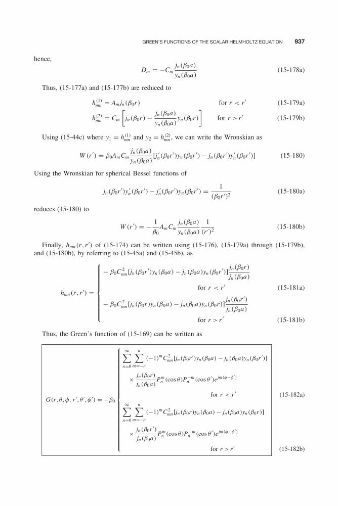
Balanis c15.tex V2 - 11/22/2011 4:04 P.M. Page 937
GREEN’S FUNCTIONS OF THE SCALAR HELMHOLTZ EQUATION 937
hence,
Dm = −Cmjn(β0a)
yn(β0a)(15-178a)
Thus, (15-177a) and (15-177b) are reduced to
h(1)mn = Amjn(β0r) for r < r ′ (15-179a)
h(2)mn = Cm
[jn(β0r) − jn(β0a)
yn(β0a)yn(β0r)
]for r > r ′ (15-179b)
Using (15-44c) where y1 = h(1)mn and y2 = h(2)
mn , we can write the Wronskian as
W (r ′) = β0AmCmjn(β0a)
yn(β0a)[j ′
n(β0r ′)yn(β0r ′) − jn(β0r ′)y ′n(β0r ′)] (15-180)
Using the Wronskian for spherical Bessel functions of
jn(β0r ′)y ′n(β0r ′) − j ′
n(β0r ′)yn(β0r ′) = 1
(β0r ′)2(15-180a)
reduces (15-180) to
W (r ′) = − 1
β0AmCm
jn(β0a)
yn(β0a)
1
(r ′)2(15-180b)
Finally, hmn(r , r ′) of (15-174) can be written using (15-176), (15-179a) through (15-179b),and (15-180b), by referring to (15-45a) and (15-45b), as
hmn(r , r ′) =
⎧⎪⎪⎪⎪⎪⎪⎪⎪⎨⎪⎪⎪⎪⎪⎪⎪⎪⎩
− β0C 2mn [jn(β0r ′)yn(β0a) − jn(β0a)yn(β0r ′)]
jn(β0r)
jn(β0a)
for r < r ′
− β0C 2mn [jn(β0r)yn(β0a) − jn(β0a)yn(β0r)]
jn(β0r ′)jn(β0a)
for r > r ′
(15-181a)
(15-181b)
Thus, the Green’s function of (15-169) can be written as
G(r , θ , φ; r ′, θ ′, φ′) = −β0
⎧⎪⎪⎪⎪⎪⎪⎪⎪⎪⎪⎪⎪⎪⎪⎪⎪⎪⎪⎪⎪⎪⎨⎪⎪⎪⎪⎪⎪⎪⎪⎪⎪⎪⎪⎪⎪⎪⎪⎪⎪⎪⎪⎪⎩
∞∑n=0
n∑m=−n
(−1)m C 2mn [jn(β0r ′)yn(β0a) − jn(β0a)yn(β0r ′)]
× jn(β0r)
jn(β0a)Pm
n (cos θ)P−mn (cos θ ′)ejm(φ−φ′)
for r < r ′
∞∑n=0
n∑m=−n
(−1)m C 2mn [jn(β0r)yn(β0a) − jn(β0a)yn(β0r)]
× jn(β0r ′)jn(β0a)
Pmn (cos θ)P−m
n (cos θ ′)ejm(φ−φ′)
for r > r ′
(15-182a)
(15-182b)

Balanis c15.tex V2 - 11/22/2011 4:04 P.M. Page 938
938 GREEN’S FUNCTIONS
15.7 DYADIC GREEN’S FUNCTIONS
The Green’s function development of the previous sections can be used for the solution ofelectromagnetic problems that satisfy the scalar wave equation. The most general Green’s func-tion development and electromagnetic field solution, for problems that satisfy the vector waveequation, will be to use vectors and dyadics [14–18]. Before we briefly discuss such a procedure,let us first introduce and define dyadics.
15.7.1 Dyadics
Vectors and dyadics are used, in general, to describe linear transformations within a given orthog-onal coordinate system, and they simplify the manipulations of mathematical relations, comparedto using tensors. For electromagnetic problems, where linear transformations between sourcesand fields within a given orthogonal coordinate system are often necessary, vectors and dyadicsare very convenient to use.
A dyad is defined by the juxtaposition AB of the vectors A and B, with no dot or cross productbetween them. In general, a dyad has nine terms and in matrix form can be represented by
(AB) =⎛⎝ A1B1 A1B2 A1B3
A2B1 A2B2 A2B3
A3B1 A3B2 A3B3
⎞⎠ (15-183)
A dyadic D can be defined by the sum of N dyads. That is
D =N∑
n=1
AnBn (15-184)
In general, no more than three dyads are required to represent a dyadic, that is Nmax = 3.Let us now define the vectors A, C, D1, D2, and D3 in a general coordinate system with unit
vectors â1, â2, and â3. That is,
A = â1A1 + â2A2 + â3A3 (15-185a)
C = â1C1 + â2C2 + â3C3 (15-185b)
D1 = â1D11 + â2D12 + â3D13 (15-185c)
D2 = â1D21 + â2D22 + â3D23 (15-185d)
D3 = â1D31 + â2D32 + â3D33 (15-185e)
Let us now write that
C = (A • â1)D1 + (A • â2)D2 + (A • â3)D3
= A • (â1D1) + A • (â2D2) + A • (â3D3)
C = A • (â1D1 + â2D2 + â3D3) (15-186)
or
C = A • D (15-186a)
where
D = â1D1 + â2D2 + â3D3 (15-186b)

Balanis c15.tex V2 - 11/22/2011 4:04 P.M. Page 939
DYADIC GREEN’S FUNCTIONS 939
In (15-186) through (15-186b) D is a dyadic, and it is defined by the sum of the three dyadsânDn , n = 1, 2, 3. In matrix form, (15-186) or (15-186a) can be written as
(C1 C2 C3) = (A1 A2 A3)
⎛⎝ D11 D12 D13
D21 D22 D23
D31 D32 D33
⎞⎠ (15-187)
where the dyadic D has nine elements.Just like vectors, dyadics satisfy a number of identities involving dot and cross products,
differentiations, and integrations. The uninformed reader should refer to the literature [10–13]for such relations.
15.7.2 Green’s Functions
In electromagnetics it is often desirable to solve, using the Green’s functions approach, the linearvector problem of
�h = f (15-188)
where � is a differential operator. Equation 15-188 is a more general and vector representa-tion of (15-27). It should be noted here that the solution of (15-188) cannot, in general, berepresented by
h(r) �=∫∫∫
Vf(r′)G(r, r′)dv′ (15-189)
where G(r, r′) is a single scalar Green’s function. The relation (15-189) would imply that acomponent of the source f parallel to a given axis produces a response (field) h parallel to thesame axis. This, in general, is not true.
A more appropriate representation of the solution of (15-188), in a rectangular coordinatesystem, will be
hx (r) =∫∫∫
V[fx (r′)Gxx (r, r′) + fy(r′)Gxy(r, r′) + fz (r′)Gxz (r, r′)]dv′ (15-190a)
hy(r) =∫∫∫
V[fx (r′)Gyx (r, r′) + fy(r′)Gyy(r, r′) + fz (r′)Gyz (r, r′)]dv′ (15-190b)
hz (r) =∫∫∫
V[fx (r′)Gzx (r, r′) + fy(r′)Gzy(r, r′) + fz (r′)Gzz (r, r′)]dv′ (15-190c)
which, in a more compact form, can be written as
h(r) =∫∫∫
V[fx (r′)Gx (r, r′) + fy(r′)Gy(r, r′) + fz (r′)Gz (r, r′)]dv′ (15-191)

Balanis c15.tex V2 - 11/22/2011 4:04 P.M. Page 940
940 GREEN’S FUNCTIONS
where, as in (15-185c) through (15-185e)
Gx (r, r′) = âx Gxx (r, r′) + ây Gyx (r, r′) + âz Gzx (r, r′) (15-191a)
Gy(r, r′) = âx Gxy (r, r′) + ây Gyy(r, r′) + âz Gzy(r, r′) (15-191b)
Gz (r, r′) = âx Gxz (r, r′) + ây Gyz (r, r′) + âz Gzz (r, r′) (15-191c)
In (15-190a) through (15-191c), the Gij (r, r′)’s are the elements of the dyadic G(r, r′), which isreferred to here as the dyadic Green’s function . In (15-191) through (15-191c), the Gi (r, r′)’s arethe column vectors of the dyadic Green’s function G(r, r′).
Using the notation of (15-186) through (15-186b), the solution of (15-191) can also be writtenas
h(r) =∫∫∫
V
{[f(r′) • âx
]Gx (r, r′) + [
f(r′) • ây]
Gy(r, r′) + [f(r′) • âz
]Gz (r, r′)
}dv′
=∫∫∫
Vf(r′) •
[âx Gx (r, r′) + ây Gy(r, r′) + âz Gz (r, r′)
]dv′
h(r) =∫∫∫
Vf(r) • G(r, r′)dv′ (15-192)
where G(r, r′) is the dyadic Green’s function
G(r, r′) = âx Gx (r, r′) + ây Gy(r, r′) + âz Gz (r, r′) (15-192a)
The dyadic Green’s function G(r, r′) can be found by first finding the vectors Gx (r, r′),Gy(r, r′), and Gz (r, r′) each satisfying the homogeneous form of the partial differential equation15-188, i.e.,
�Gx (r, r′) = âxδ(r − r′) (15-193a)
�Gy(r, r′) = âyδ(r − r′) (15-193b)
�Gz (r, r′) = âz δ(r − r′) (15-193c)
and the appropriate boundary conditions, and then using (15-192a) to form the dyadic Green’sfunction. Any of the methods of the previous sections can be used to find the Green’s functionof (15-193a) through (15-193c).
An example for the potential use of the dyadic Green’s function is the solution for the electricand magnetic fields due to a source represented by the electric current density J. Accordingto (6-32a) and (6-32b), the electric and magnetic fields can be written as
H(r) = 1
μ∇ × A (15-194a)
E(r) = −jωA − j1
ωμε∇(∇ • A) (15-194b)

Balanis c15.tex V2 - 11/22/2011 4:04 P.M. Page 941
MULTIMEDIA 941
where the vector potential A satisfies the partial differential equation 6-30 or
∇2A + β2A = −μJ (15-195)
Using the dyadic Green’s function approach, the vector potential A can be found using
A = −μ
∫∫∫V
J(r′) • G(r, r′)dv′ (15-196)
where the dyadic Green’s function must satisfy the partial differential equation
∇2G + β2G = δ̄(r − r′) (15-197)
and the appropriate boundary conditions.Because of the complexity for the development of the dyadic Green’s function, it will not
be pursued any further here. The interested reader is referred to the literature [10–18] for moredetails.
15.8 MULTIMEDIA
On the website that accompanies this book, the following multimedia resources are included forthe review, understanding and presentation of the material of this chapter.
• Power Point (PPT) viewgraphs, in multicolor.
REFERENCES
1. R. Courant and D. Hilbert, Methods of Mathematical Physics, vol. I, Wiley, New York, 1937.
2. A. Wester, Partial Differential Equations of Mathematical Physics , S. Plimpton (Ed.), Second Edition,Hafner, New York, 1947.
3. P. M. Morse and H. Feshbach, Methods of Theoretical Physics , vols. I and II, McGraw-Hill, New York,1953.
4. B. Friedman, Principles and Techniques of Applied Mathematics , Wiley, New York, 1956.
5. J. Dettman, Mathematical Methods in Physics and Engineering , McGraw-Hill, New York, 1962.
6. J. D. Jackson, Classical Electrodynamics , 3rd Edition, Wiley, New York, 1999.
7. H. W. Wyld, Mathematical Methods for Physics , Benjamin/Cummings, Menlo Park, CA, 1976.
8. I. Stakgold, Green’s Functions and Boundary Value Problems , Wiley, New York, 1979.
9. R. E. Collin, Field Theory of Guided Waves , McGraw-Hill, New York, 1960.
10. J. Van Bladel, Electromagnetic Fields , 2nd Edition, IEEE Press, Wiley Interscience, Hoboken, NJ, 2007.
11. C.-T. Tai, Dyadic Green’s Functions in Electromagnetic Theory , Intext Educational Publishers, Scranton,PA, 1971.
12. L. B. Felsen and N. Marcuvitz, Radiation and Scatering of Waves , Prentice-Hall, Englewood Cliffs, NJ,1973.
13. D. C. Stinson, Intermediate Mathematics of Electromagnetics , Prentice-Hall, Englewood Cliffs, NJ,1976.
14. C.-T. Tai, “On the eigenfunction expansion of dyadic Green’s functions,” Proc. IEEE , vol. 61,pp. 480–481, April 1973.
15. C.-T. Tai and P. Rozenfeld, “Different representations of dyadic Green’s functions for a rectangularcavity,” IEEE Trans. Microwave Theory Tech., vol. MTT-24, pp. 597–601, September 1976.

Balanis c15.tex V2 - 11/22/2011 4:04 P.M. Page 942
942 GREEN’S FUNCTIONS
16. A. Q. Howard, Jr., “On the longitudinal component of the Green’s function dyadic,” Proc. IEEE , vol.62, pp. 1704–1705, December 1974.
17. A. D. Yaghjian, “Electric dyadic Green’s functions in the source region,” Proc. IEEE , vol. 68, no. 2,pp. 248–263, February 1980.
18. P. H. Pathak, “On the eigenfunction expansion of electromagnetic dyadic Green’s functions,” IEEETrans. Antennas Propagat., vol. AP-31, pp. 837–846, November 1983.
19. I. Orlanski, “A simple boundary condition for unbounded hyperbolic flows,” J. Computational Physics ,21, pages 251–269, 1976.
20. R. F. Harrington, Time-Harmonic Electromagnetic Fields , McGraw-Hill, New York, 1961.
PROBLEMS
15.1. Using the procedure of Section 15.3.1,as represented by (15-44c) and (15-45a)through (15-45b), derive the Green’s func-tion of the mechanics problem of Section15.2.2 as given by (15-24a) and (15-24b).
15.2. The displacement u(x) of a string of length� subjected to a cosinusoidal force
f (x , t) = f (x)e+jωt
is determined by
u(x , t) = u(x)e+jωt
where u(x) satisfies the differentialequation
d2u(x)
dx 2+ β2u(x) = f (x), β2 = ω/c
Assuming the ends of the string are fixed
u(x = 0) = u(x = �) = 0
determine in closed form the Green’s func-tion of the system.
15.3. Two PEC semi-infinite plates, which bothare grounded (V = 0), are separated by adistance w in the x direction, as shownin the figure below. A d. c. infinite linesource of constant charge density q(x ′) ispositioned at x ′ between the two platesand extends to infinity in the y direction.Assume the plates are infinite in the ydirection and free space exists between thetwo plates. For this problem:(a) Specify the appropriate boundary con-
ditions for the potential and the asso-ciated Green’s function.
(b) Derive the Green’s function in thex -y plane in series form, including anexpression for the eigenvalues with theappropriate indices.
(c) Based on this Green’s function andstated charge distribution, write anexpression for the potential V(x)
between the plates. Show all the steps.
x
y
V = 0 V = 0
q(x′)
x′
w
Figure P15-3
15.4. Derive in series form the Green’s functionof Problem 15.3.
15.5. Two infinite radial plates with an interiorangle of α, as shown in Figure P15-5, are
x
z
y
fa
Figure P15-5
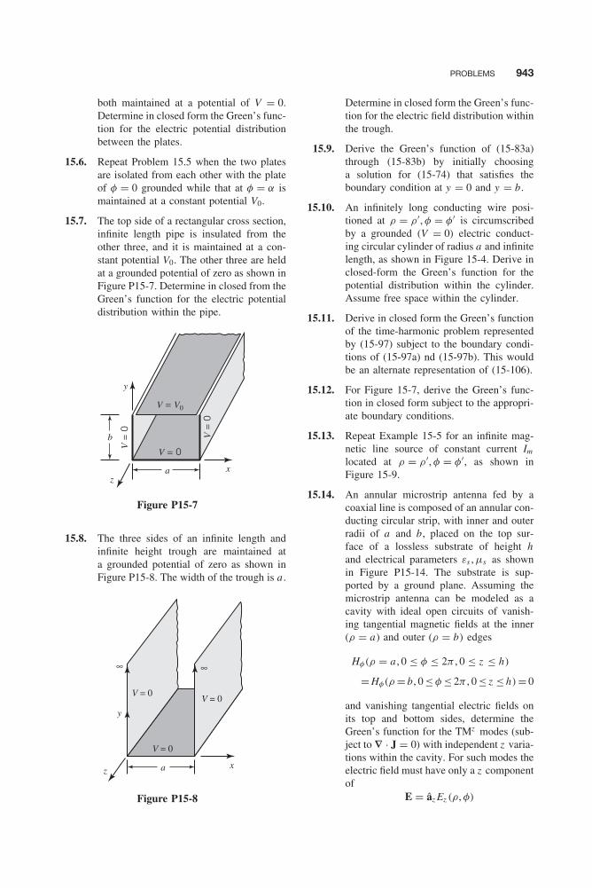
Balanis c15.tex V2 - 11/22/2011 4:04 P.M. Page 943
PROBLEMS 943
both maintained at a potential of V = 0.Determine in closed form the Green’s func-tion for the electric potential distributionbetween the plates.
15.6. Repeat Problem 15.5 when the two platesare isolated from each other with the plateof φ = 0 grounded while that at φ = α ismaintained at a constant potential V0.
15.7. The top side of a rectangular cross section,infinite length pipe is insulated from theother three, and it is maintained at a con-stant potential V0. The other three are heldat a grounded potential of zero as shown inFigure P15-7. Determine in closed from theGreen’s function for the electric potentialdistribution within the pipe.
xz
y
a
V =
0 V =
0
V = 0
b
V = V0
Figure P15-7
15.8. The three sides of an infinite length andinfinite height trough are maintained ata grounded potential of zero as shown inFigure P15-8. The width of the trough is a .
x
y
∞ ∞
z a
V = 0
V = 0V = 0
Figure P15-8
Determine in closed form the Green’s func-tion for the electric field distribution withinthe trough.
15.9. Derive the Green’s function of (15-83a)through (15-83b) by initially choosinga solution for (15-74) that satisfies theboundary condition at y = 0 and y = b.
15.10. An infinitely long conducting wire posi-tioned at ρ = ρ ′, φ = φ′ is circumscribedby a grounded (V = 0) electric conduct-ing circular cylinder of radius a and infinitelength, as shown in Figure 15-4. Derive inclosed-form the Green’s function for thepotential distribution within the cylinder.Assume free space within the cylinder.
15.11. Derive in closed form the Green’s functionof the time-harmonic problem representedby (15-97) subject to the boundary condi-tions of (15-97a) nd (15-97b). This wouldbe an alternate representation of (15-106).
15.12. For Figure 15-7, derive the Green’s func-tion in closed form subject to the appropri-ate boundary conditions.
15.13. Repeat Example 15-5 for an infinite mag-netic line source of constant current Im
located at ρ = ρ ′, φ = φ′, as shown inFigure 15-9.
15.14. An annular microstrip antenna fed by acoaxial line is composed of an annular con-ducting circular strip, with inner and outerradii of a and b, placed on the top sur-face of a lossless substrate of height hand electrical parameters εs , μs as shownin Figure P15-14. The substrate is sup-ported by a ground plane. Assuming themicrostrip antenna can be modeled as acavity with ideal open circuits of vanish-ing tangential magnetic fields at the inner(ρ = a) and outer (ρ = b) edges
Hφ(ρ = a , 0 ≤ φ ≤ 2π , 0 ≤ z ≤ h)
= Hφ(ρ = b, 0 ≤ φ ≤ 2π , 0 ≤ z ≤ h)= 0
and vanishing tangential electric fields onits top and bottom sides, determine theGreen’s function for the TMz modes (sub-ject to ∇ · J = 0) with independent z varia-tions within the cavity. For such modes theelectric field must have only a z componentof
E = âz Ez (ρ, φ)
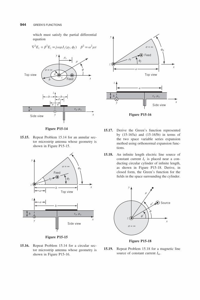
Balanis c15.tex V2 - 11/22/2011 4:04 P.M. Page 944
944 GREEN’S FUNCTIONS
which must satisfy the partial differentialequation
∇2Ez +β2Ez = jωμJz (ρf , φf ) β2 =ω2με
y
z
zb
a a
y
h
b
b Feed
Side view
Top view
s = ∞a
x
x
r
rs
rs
f
es, ms
Figure P15-14
15.15. Repeat Problem 15.14 for an annular sec-tor microstrip antenna whose geometry isshown in Figure P15-15.
y
z
z
b
a
y
h
b
Feed
Side view
Top view
s = ∞
ax
x
ffrf
f0
es, ms
Figure P15-15
15.16. Repeat Problem 15.14 for a circular sec-tor microstrip antenna whose geometry isshown in Figure P15-16.
y
z
z
a
h
Feed
Side view
Top view
s = ∞
ax
x
ffrf
es, ms
f0
y
Figure P15-16
15.17. Derive the Green’s function representedby (15-165a) and (15-165b) in terms ofthe two space variable series expansionmethod using orthonormal expansion func-tions.
15.18. An infinite length electric line source ofconstant current Ie is placed near a con-ducting circular cylinder of infinite length,as shown in Figure P15-18. Derive, inclosed form, the Green’s function for thefields in the space surrounding the cylinder.
zx
r
f
f′
r′
y
Source
s = ∞
Figure P15-18
15.19. Repeat Problem 15.18 for a magnetic linesource of constant current Im .
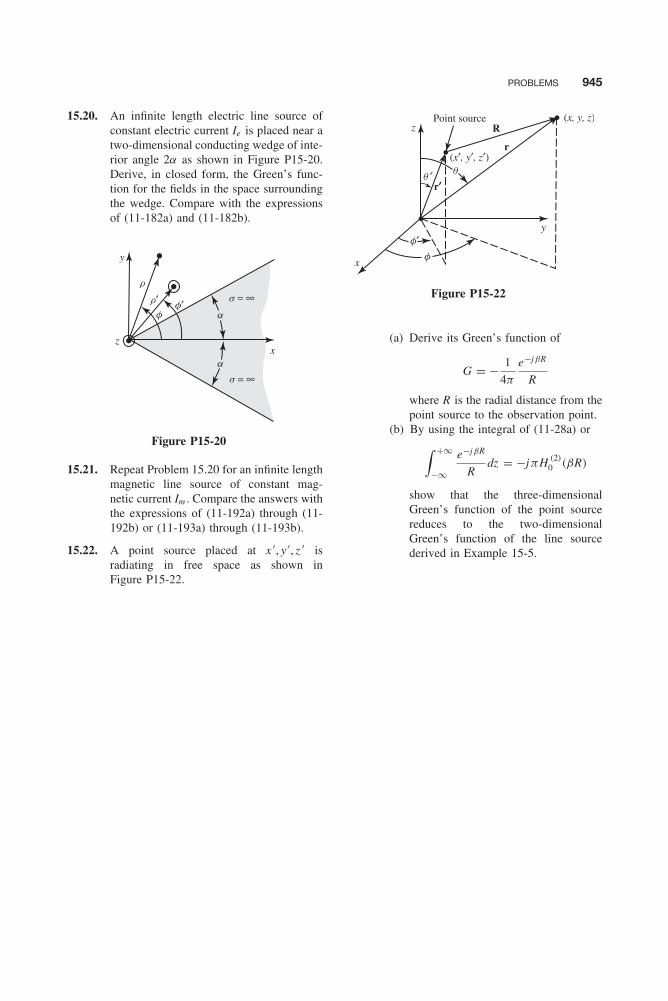
Balanis c15.tex V2 - 11/22/2011 4:04 P.M. Page 945
PROBLEMS 945
15.20. An infinite length electric line source ofconstant electric current Ie is placed near atwo-dimensional conducting wedge of inte-rior angle 2α as shown in Figure P15-20.Derive, in closed form, the Green’s func-tion for the fields in the space surroundingthe wedge. Compare with the expressionsof (11-182a) and (11-182b).
y
zx
r
r′f
s = ∞
s = ∞a
af′
Figure P15-20
15.21. Repeat Problem 15.20 for an infinite lengthmagnetic line source of constant mag-netic current Im . Compare the answers withthe expressions of (11-192a) through (11-192b) or (11-193a) through (11-193b).
15.22. A point source placed at x ′, y ′, z ′ isradiating in free space as shown inFigure P15-22.
y
z RPoint source
r(x′, y′, z′)
(x, y, z)
r′
xf
f′
q′ q
Figure P15-22
(a) Derive its Green’s function of
G = − 1
4π
e−jβR
R
where R is the radial distance from thepoint source to the observation point.
(b) By using the integral of (11-28a) or∫ +∞
−∞
e−jβR
Rdz = −jπH (2)
0 (βR)
show that the three-dimensionalGreen’s function of the point sourcereduces to the two-dimensionalGreen’s function of the line sourcederived in Example 15-5.

Balanis c15.tex V2 - 11/22/2011 4:04 P.M. Page 946

Balanis b01.tex V2 - 11/22/2011 4:26 P.M. Page 947
APPENDIX IIdentities
I.1 TRIGONOMETRIC
1. Sum or difference:a. sin(x + y) = sin x cos y + cos x sin yb. sin(x − y) = sin x cos y − cos x sin yc. cos(x + y) = cos x cos y − sin x sin yd. cos(x − y) = cos x cos y + sin x sin y
e. tan(x + y) = tan x + tan y
1 − tan x tan y
f. tan(x − y) = tan x − tan y
1 + tan x tan y
g. sin2 x + cos2 x = 1h. tan2 x − sec2 x = −1i. cot2 x − csc2 x = −1
2. Sum or difference into products:
a. sin x + sin y = 2 sin 12 (x + y) cos 1
2 (x − y)
b. sin x − sin y = 2 cos 12 (x + y) sin 1
2 (x − y)
c. cos x + cos y = 2 cos 12 (x + y) cos 1
2 (x − y)
d. cos x − cos y = −2 sin 12 (x + y) sin 1
2 (x − y)
3. Products into sum or difference:a. 2 sin x cos y = sin(x + y) + sin(x − y)
b. 2 cos x sin y = sin(x + y) − sin(x − y)
c. 2 cos x cos y = cos(x + y) + cos(x − y)
d. 2 sin x sin y = − cos(x + y) + cos(x − y)
4. Double and half-angles:a. sin 2x = 2 sin x cos xb. cos 2x = cos2 x − sin2 x = 2 cos2 x − 1 = 1 − 2 sin2 x
c. tan 2x = 2 tan x
1 − tan2 x
d. sin1
2x = ±
√1 − cos x
2or 2 sin2 θ = 1 − cos 2θ
947

Balanis b01.tex V2 - 11/22/2011 4:26 P.M. Page 948
948 APPENDIX I
e. cos1
2x = ±
√1 + cos x
2or 2 cos2 θ = 1 + cos 2θ
f. tan1
2x = ±
√1 − cos x
1 + cos x= sin x
1 + cos x= 1 − cos x
sin x5. Series:
a. sin x = ejx − e−jx
2j= x − x 3
3!+ x 5
5!− x 7
7!+ . . .
b. cos x = ejx + e−jx
2= 1 − x 2
2!+ x 4
4!− x 6
6!+ . . .
c. tan x = ejx − e−jx
j (ejx + e−jx )= x + x 3
3+ 2x 5
15+ 17x 7
315+ . . .
I.2 HYPERBOLIC
1. Definitions:a. Hyperbolic sine: sinh x = 1
2 (ex − e−x )
b. Hyperbolic cosine: cosh x = 12 (ex + e−x )
c. Hyperbolic tangent: tanh x = sinh x
cosh x
d. Hyperbolic cotangent: coth x = 1
tanh x= cosh x
sinh x
e. Hyperbolic secant: sech x = 1
cosh x
f. Hyperbolic cosecant: csch x = 1
sinh x2. Sum or difference:
a. cosh (x + y) = cosh x cosh y + sinh x sinh yb. sinh (x − y) = sinh x cosh y − cosh x sinh yc. cosh (x − y) = cosh x cosh y − sinh x sinh y
d. tanh (x + y) = tanh x + tanh y
1 + tanh x tanh y
e. tanh (x − y) = tanh x − tanh y
1 − tanh x tanh y
f. cosh2x − sinh2x = 1
g. tanh2x + sech2x = 1
h. coth2x − csch2x = 1
i. cosh (x ± jy) = cosh x cos y ± j sinh x sin y
j. sinh (x ± jy) = sinh x cos y ± j cosh x sin y
3. Series:
a. sinh x = ex − e−x
2= x + x 3
3!+ x 5
5!+ x 7
7!+ . . .
b. cosh x = ex + e−x
2= 1 + x 2
2!+ x 4
4!+ x 6
6!+ . . .
c. ex = 1 + x + x 2
2!+ x 3
3!+ x 4
4!+ . . .

Balanis b01.tex V2 - 11/22/2011 4:26 P.M. Page 949
APPENDIX I 949
I.3 LOGARITHMIC
1. logb(MN ) = logb M + logb N2. logb(M /N ) = logb M − logb N3. logb(1/N ) = − logb N4. logb(M
n) = n logb M
5. logb(M1/n) = 1
nlogb M
6. loga N = logb N · loga b = logb N / logb a
7. loge N = log10 N · loge 10 = 2.302585 log10 N
8. log10 N = loge N · log10 e = 0.434294 loge N

Balanis b01.tex V2 - 11/22/2011 4:26 P.M. Page 950

Balanis b02.tex V2 - 11/22/2011 4:26 P.M. Page 951
APPENDIX IIVector Analysis
II.1 VECTOR TRANSFORMATIONS
In this appendix we will indicate the vector transformations from rectangular to cylindrical (andvice versa), from cylindrical to spherical (and vice versa), and from rectangular to spherical (andvice versa). The three coordinate systems are shown in Figure II-1.
II.1.1 Rectangular to Cylindrical (and Vice Versa)
The coordinate transformation from rectangular (x , y , z ) to cylindrical (ρ, φ, z ) is given, referringto Figure II-1(b), by:
x = ρ cos φ
y = ρ sin φ
z = z (II-1)
In the rectangular coordinate system, we express a vector A as
A = âx Ax + ây Ay + âz Az (II-2)
where âx , ây , âz are the unit vectors and Ax , Ay , Az are the components of the vector A in therectangular coordinate system. We wish to write A as
A = âρAρ + âφAφ + âz Az (II-3)
where âρ , âφ , âz are the unit vectors and Aρ , Aφ , Az are the vector components in the cylindricalcoordinate system. The z axis is common to both of them.
Referring to Figure II-2, we can write
âx = âρ cos φ − âφ sin φ
ây = âρ sin φ + âφ cos φ
âz = âz (II-4)
951

Balanis b02.tex V2 - 11/22/2011 4:26 P.M. Page 952
952 APPENDIX II
X
x z
yY
axay
az
Z
(a)
X
x
z
y
Y
af
ar
az
Z
(b)
rf
X
x
z
y
Y
af
aq
ar
Z
(c)
r
q
f
Figure II-1 Coordinate Systems. (a) Rectangular. (b) Cylindrical. (c) Spherical. (Source: C. A. Balanis,Antenna Theory: Analysis and Design; Third Edition, copyright © 2005, John Wiley & Sons, Inc.; reprintedby permission of John Wiley & Sons, Inc.).
Using (II-4) reduces (II-2) to
A = (âρ cos φ − âφ sin φ)Ax + (âρ sin φ + âφ cos φ)Ay + âz Az
A = âρ(Ax cos φ + Ay sin φ) + âφ(−Ax sin φ + Ay cos φ) + âz Az (II-5)
which when compared with (II-3) leads to
Aρ = Ax cos φ + Ay sin φ
Aφ = −Ax sin φ + Ay cos φ
Az = Az (II-6)

Balanis b02.tex V2 - 11/22/2011 4:26 P.M. Page 953
APPENDIX II 953
(a)
(b)
x
x
z
z
y
y
az
ay
az
ax
ar
ar
af
−af sin far cos f
af cos f
ar sin f
af
f
f
f
f
Figure II-2 Geometrical representation of transformation between unit vectors of rectangular and cylin-drical coordinate systems. (Source: C. A. Balanis, Antenna Theory: Analysis and Design; Third Edition,copyright © 2005, John Wiley & Sons, Inc.; reprinted by permission of John Wiley & Sons, Inc.)(a) Geometry for unit vector âx . (b) Geometry for unit vector ây .
In matrix form, (II-6) can be written as⎛⎝Aρ
Aφ
Az
⎞⎠ =⎛⎝ cos φ sin φ 0
− sin φ cos φ 00 0 1
⎞⎠⎛⎝Ax
Ay
Az
⎞⎠ (II-6a)
where
[A]rc =⎡⎣ cos φ sin φ 0
− sin φ cos φ 00 0 1
⎤⎦ (II-6b)
is the transformation matrix for rectangular-to-cylindrical components.
Balanis b02.tex V2 - 11/22/2011 4:26 P.M. Page 954
954 APPENDIX II
Since [A]rc is an orthonormal matrix (its inverse is equal to its transpose), we can write thetransformation matrix for cylindrical-to-rectangular components as
[A]cr = [A]−1rc = [A]t
rc =⎡⎣cos φ − sin φ 0
sin φ cos φ 00 0 1
⎤⎦ (II-7)
or ⎛⎝Ax
Ay
Az
⎞⎠ =⎛⎝cos φ − sin φ 0
sin φ cos φ 00 0 1
⎞⎠ =⎛⎝Aρ
Aφ
Az
⎞⎠ (II-7a)
or
Ax = Aρ cos φ − Aφ sin φ
Ay = Aρ sin φ + Aφ cos φ
Az = Az (II-7b)
II.1.2 Cylindrical to Spherical (and Vice Versa)
Referring to Figure II-1c, we can write that the cylindrical and spherical coordinates are relatedby
ρ = r sin θ
z = r cos θ (II-8)
In a geometrical approach, similar to the one employed in the previous section, we can show thatthe cylindrical-to-spherical transformation of vector components is given by
Ar = Aρ sin θ + Az cos θ
Aθ = Aρ cos θ − Az sin θ
Aφ = Aφ (II-9)
or in matrix form by ⎛⎝Ar
Aθ
Aφ
⎞⎠ =⎛⎝sin θ 0 cos θ
cos θ 0 − sin θ
0 1 0
⎞⎠⎛⎝Aρ
Aφ
Az
⎞⎠ (II-9a)
Thus, the cylindrical-to-spherical transformation matrix can be written as
[A]cs =⎡⎣sin θ 0 cos θ
cos θ 0 − sin θ
0 1 0
⎤⎦ (II-9b)
The [A]cs matrix is also orthonormal so that its inverse is given by
[A]sc = [A]−1cs = [A]t
cs =⎡⎣sin θ cos θ 0
0 0 1cos θ − sin θ 0
⎤⎦ (II-10)
Balanis b02.tex V2 - 11/22/2011 4:26 P.M. Page 955
APPENDIX II 955
and the spherical-to-cylindrical transformation is accomplished by⎛⎝Aρ
Aφ
Az
⎞⎠ =⎛⎝sin θ cos θ 0
0 0 1cos θ − sin θ 0
⎞⎠⎛⎝Ar
Aθ
Aφ
⎞⎠ (II-10a)
or
Aρ = Ar sin θ + Aθ cos θ
Aφ = Aφ
Az = Ar cos θ − Aθ sin θ (II-10b)
This time the component Aφ and coordinate φ are the same in both systems.
II.1.3 Rectangular to Spherical (and Vice Versa)
Many times it may be required that a transformation be performed directly from rectangular tospherical components. By referring to Figure II-1c, we can write that the rectangular and sphericalcoordinates are related by
x = r sin θ cos φ
y = r sin θ sin φ
z = r cos θ (II-11)
and the rectangular and spherical components by
Ar = Ax sin θ cos φ + Ay sin θ sin φ + Az cos θ
Aθ = Ax cos θ cos φ + Ay cos θ sin φ − Az sin θ
Aφ = −Ax sin φ + Ay cos φ (II-12)
which can also be obtained by substituting (II-6) into (II-9). In matrix form, (II-12) can be writtenas ⎛⎝Ar
Aθ
Aφ
⎞⎠ =⎛⎝sin θ cos φ sin θ sin φ cos θ
cos θ cos φ cos θ sin φ − sin θ
− sin φ cos φ 0
⎞⎠⎛⎝Ax
Ay
Az
⎞⎠ (II-12a)
with the rectangular-to-spherical transformation matrix being
[A]rs =⎡⎣sin θ cos φ sin θ sin φ cos θ
cos θ cos φ cos θ sin φ − sin θ
− sin φ cos φ 0
⎤⎦ (II-12b)
The transformation matrix of (II-12b) is also orthonormal so that its inverse can be writtenas
[A]sr = [A]−1rs = [A]t
rs =⎡⎣sin θ cos φ cos θ cos φ − sin φ
sin θ sin φ cos θ sin φ cos φ
cos θ − sin θ 0
⎤⎦ (II-13)
and the spherical to rectangular transformation is accomplished by⎛⎝Ax
Ay
Az
⎞⎠ =⎛⎝sin θ cos φ cos θ cos φ − sin φ
sin θ sin φ cos θ sin φ cos φ
cos θ − sin θ 0
⎞⎠⎛⎝Ar
Aθ
Aφ
⎞⎠ (II-13a)
Balanis b02.tex V2 - 11/22/2011 4:26 P.M. Page 956
956 APPENDIX II
or
Ax = Ar sin θ cos φ + Aθ cos θ cos φ − Aφ sin φ
Ay = Ar sin θ sin φ + Aθ cos θ sin φ + Aφ cos φ
Az = Ar cos θ − Aθ sin θ (II-13b)
II.2 VECTOR DIFFERENTIAL OPERATORS
The differential operators of gradient of a scalar (∇ψ), divergence of a vector (∇ · A), curl ofa vector (∇ × A), Laplacian of a scalar (∇2ψ), and Laplacian of a vector (∇2A), frequentlyencountered in electromagnetic field analysis, will be listed in the rectangular, cylindrical, andspherical coordinate systems.
II.2.1 Rectangular Coordinates
∇ψ = âx∂ψ
∂x+ ây
∂ψ
∂y+ âz
∂ψ
∂z(II-14)
∇ • A = ∂Ax
∂x+ ∂Ay
∂y+ ∂Az
∂z(II-15)
∇ × A = âx
(∂Az
∂y− ∂Ay
∂z
)+ ây
(∂Ax
∂z− ∂Az
∂x
)+ âz
(∂Ay
∂x− ∂Ax
∂y
)(II-16)
∇ • ∇ψ = ∇2ψ = ∂2ψ
∂x 2+ ∂2ψ
∂y2+ ∂2ψ
∂z 2(II-17)
∇2A = âx∇2Ax + ây∇2Ay + âz ∇2Az (II-18)
II.2.2 Cylindrical Coordinates
∇ψ = âρ
∂ψ
∂ρ+ âφ
1
ρ
∂ψ
∂φ+ âz
∂ψ
∂z(II-19)
∇ • A = 1
ρ
∂
∂ρ(ρAρ) + 1
ρ
∂Aφ
∂φ+ ∂Az
∂z(II-20)
∇ × A = âρ
(1
ρ
∂Az
∂φ− ∂Aφ
∂z
)+ âφ
(∂Aρ
∂z− ∂Az
∂ρ
)
+ âz
(1
ρ
∂(ρAφ)
∂ρ− 1
ρ
∂Aρ
∂φ
)(II-21)
∇2ψ = 1
ρ
∂
∂ρ
(ρ
∂ψ
∂ρ
)+ 1
ρ2
∂2ψ
∂φ2+ ∂2ψ
∂z 2(II-22)
∇2A = ∇(∇ • A) − ∇ × ∇ × A (II-23)

Balanis b02.tex V2 - 11/22/2011 4:26 P.M. Page 957
APPENDIX II 957
or in an expanded form
∇2A = âρ
(∂2Aρ
∂ρ2+ 1
ρ
∂Aρ
∂ρ− Aρ
ρ2+ 1
ρ2
∂2Aρ
∂φ2− 2
ρ2
∂Aφ
∂φ+ ∂2Aρ
∂z 2
)+ âφ
(∂2Aφ
∂ρ2+ 1
ρ
∂Aφ
∂ρ− Aφ
ρ2+ 1
ρ2
∂2Aφ
∂φ2+ 2
ρ2
∂Aρ
∂φ+ ∂2Aφ
∂z 2
)+ âz
(∂2Az
∂ρ2+ 1
ρ
∂Az
∂ρ+ 1
ρ2
∂2Az
∂φ2+ ∂2Az
∂z 2
)(II-23a)
In the cylindrical coordinate system ∇2A �= âρ∇2Aρ + âφ∇2Aφ + âz ∇2Az because the orientationof the unit vectors âρ and âφ varies with the ρ and φ coordinates.
II.2.3 Spherical Coordinates
∇ψ = âr∂ψ
∂r+ âθ
1
r
∂ψ
∂θ+ âφ
1
r sin θ
∂ψ
∂φ(II-24)
∇ • A = 1
r2
∂
∂r(r2Ar ) + 1
r sin θ
∂
∂θ(sin θAθ ) + 1
r sin θ
∂Aφ
∂φ(II-25)
∇ × A = âr
r sin θ
[∂
∂θ(Aφ sin θ) − ∂Aθ
∂φ
]+ âθ
r
[1
sin θ
∂Ar
∂φ− ∂
∂r(rAφ)
]+ âφ
r
[∂
∂r(rAθ ) − ∂Ar
∂θ
](II-26)
∇2ψ = 1
r2
∂
∂r
(r2 ∂ψ
∂r
)+ 1
r2 sin θ
∂
∂θ
(sin θ
∂ψ
∂θ
)+ 1
r2 sin2 θ
∂2ψ
∂φ2(II-27)
∇2A = ∇(∇ • A) − ∇ × ∇ × A (II-28)
or in an expanded form
∇2A = âr
(∂2Ar
∂r2+ 2
r
∂Ar
∂r− 2
r2Ar + 1
r2
∂2Ar
∂θ2+ cot θ
r2
∂Ar
∂θ+ 1
r2 sin2 θ
∂2Ar
∂φ2
− 2
r2
∂Aθ
∂θ− 2 cot θ
r2Aθ − 2
r2 sin θ
∂Aφ
∂φ
)+ âθ
(∂2Aθ
∂r2+ 2
r
∂Aθ
∂r− Aθ
r2 sin2 θ+ 1
r2
∂2Aθ
∂θ2+ cot θ
r2
∂Aθ
∂θ
+ 1
r2 sin2 θ
∂2Aθ
∂φ2+ 2
r2
∂Ar
∂θ− 2 cot θ
r2 sin θ
∂Aφ
∂φ
)+ âφ
(∂2Aφ
∂r2+ 2
r
∂Aφ
∂r− 1
r2 sin2 θAφ + 1
r2
∂2Aφ
∂θ2
+ cot θ
r2
∂Aφ
∂θ+ 1
r2 sin2 θ
∂2Aφ
∂φ2+ 2
r2 sin θ
∂Ar
∂φ+ 2 cot θ
r2 sin θ
∂Aθ
∂φ
)(II-28a)
Again note that ∇2A �= âr∇2Ar + âθ∇2Aθ + âφ∇2Aφ since the orientation of the unit vectorsâr , âθ , and âφ varies with the r , θ , and φ coordinates.
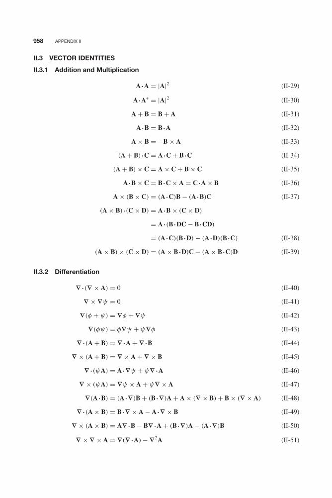
Balanis b02.tex V2 - 11/22/2011 4:26 P.M. Page 958
958 APPENDIX II
II.3 VECTOR IDENTITIES
II.3.1 Addition and Multiplication
A • A = |A|2 (II-29)
A • A∗ = |A|2 (II-30)
A + B = B + A (II-31)
A • B = B • A (II-32)
A × B = −B × A (II-33)
(A + B) • C = A • C + B • C (II-34)
(A + B) × C = A × C + B × C (II-35)
A • B × C = B • C × A = C • A × B (II-36)
A × (B × C) = (A • C)B − (A • B)C (II-37)
(A × B) • (C × D) = A • B × (C × D)
= A • (B • DC − B • CD)
= (A • C)(B • D) − (A • D)(B • C) (II-38)
(A × B) × (C × D) = (A × B • D)C − (A × B • C)D (II-39)
II.3.2 Differentiation
∇ • (∇ × A) = 0 (II-40)
∇ × ∇ψ = 0 (II-41)
∇(φ + ψ) = ∇φ + ∇ψ (II-42)
∇(φψ) = φ∇ψ + ψ∇φ (II-43)
∇ • (A + B) = ∇ • A + ∇ • B (II-44)
∇ × (A + B) = ∇ × A + ∇ × B (II-45)
∇ • (ψA) = A • ∇ψ + ψ∇ • A (II-46)
∇ × (ψA) = ∇ψ × A + ψ∇ × A (II-47)
∇(A • B) = (A • ∇)B + (B • ∇)A + A × (∇ × B) + B × (∇ × A) (II-48)
∇ • (A × B) = B • ∇ × A − A • ∇ × B (II-49)
∇ × (A × B) = A∇ • B − B∇ • A + (B • ∇)A − (A • ∇)B (II-50)
∇ × ∇ × A = ∇(∇ • A) − ∇2A (II-51)

Balanis b02.tex V2 - 11/22/2011 4:26 P.M. Page 959
APPENDIX II 959
II.3.3 Integration ∮C
A • d l =∫∫
S(∇ × A) • ds Stokes’ theorem (II-52)
#SA • ds =
∫∫∫V(∇ • A) dv divergence theorem (II-53)
#S(n̂ × A) ds =
∫∫∫V(∇ × A) dv (II-54)
#Sψ ds =
∫∫∫V
∇ψ dv (II-55)∮C
ψ dl =∫∫
Sn̂ × ∇ψ ds (II-56)

Balanis b02.tex V2 - 11/22/2011 4:26 P.M. Page 960

Balanis b03.tex V2 - 11/22/2011 4:28 P.M. Page 961
APPENDIX IIIFresnel Integrals
C0(x) =∫ x
0
cos(τ )√2πτ
dτ (III-1)
S0(x) =∫ x
0
sin(τ )√2πτ
dτ (III-2)
C (x) =∫ x
0cos
(π
2τ 2
)dτ (III-3)
S (x) =∫ x
0sin
(π
2τ 2
)dτ (III-4)
C1(x) =∫ ∞
xcos(τ 2) dτ (III-5)
S1(x) =∫ ∞
xsin(τ 2) dτ (III-6)
C (x) − jS (x) =∫ x
0e−j (π/2)τ2
dτ =∫ (π/2)x2
0
e−jτ
√2πτ
dτ
C (x) − jS (x) = C0
(π
2x 2
)− jS0
(π
2x 2
)(III-7)
C1(x) − jS1(x) =∫ ∞
xe−jτ2
dτ =√
π
2
∫ ∞
x2
e−jτ
√2πτ
dτ
C1(x) − jS1(x) =√
π
2
{∫ ∞
0
e−jτ
√2πτ
dτ −∫ x2
0
e−jτ
√2πτ
dτ
}
C1(x) − jS1(x) =√
π
2
{[1
2− j
1
2
]− [C0(x
2) − jS0(x2)]
}
C1(x) − jS1(x) =√
π
2
{[1
2− C0(x
2)
]− j
[1
2− S0(x
2)
]}(III-8)
961
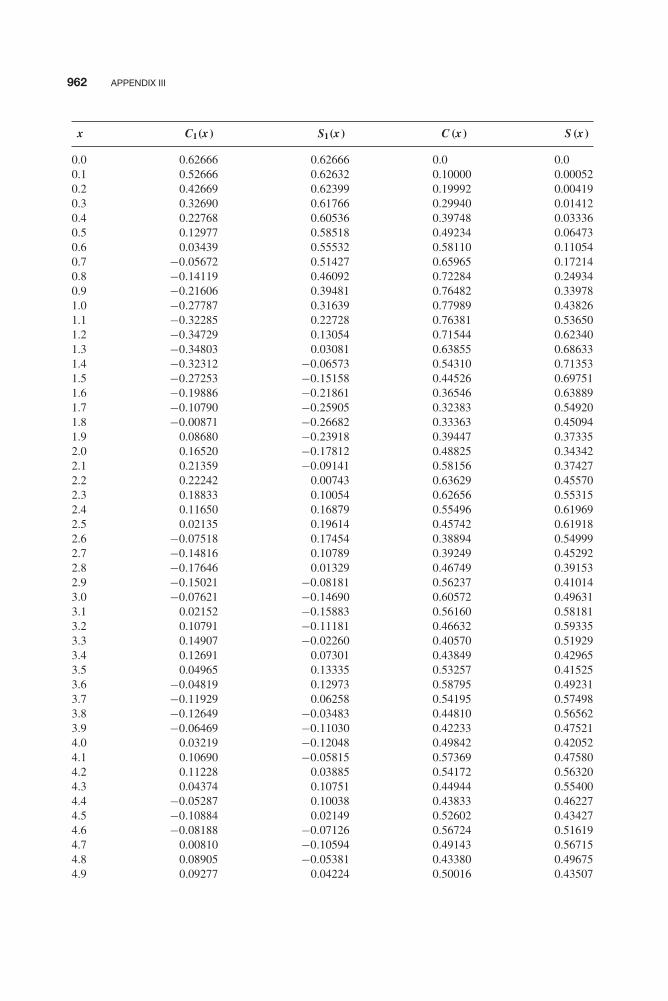
Balanis b03.tex V2 - 11/22/2011 4:28 P.M. Page 962
962 APPENDIX III
x C1(x) S1(x) C (x) S (x)
0.0 0.62666 0.62666 0.0 0.00.1 0.52666 0.62632 0.10000 0.000520.2 0.42669 0.62399 0.19992 0.004190.3 0.32690 0.61766 0.29940 0.014120.4 0.22768 0.60536 0.39748 0.033360.5 0.12977 0.58518 0.49234 0.064730.6 0.03439 0.55532 0.58110 0.110540.7 −0.05672 0.51427 0.65965 0.172140.8 −0.14119 0.46092 0.72284 0.249340.9 −0.21606 0.39481 0.76482 0.339781.0 −0.27787 0.31639 0.77989 0.438261.1 −0.32285 0.22728 0.76381 0.536501.2 −0.34729 0.13054 0.71544 0.623401.3 −0.34803 0.03081 0.63855 0.686331.4 −0.32312 −0.06573 0.54310 0.713531.5 −0.27253 −0.15158 0.44526 0.697511.6 −0.19886 −0.21861 0.36546 0.638891.7 −0.10790 −0.25905 0.32383 0.549201.8 −0.00871 −0.26682 0.33363 0.450941.9 0.08680 −0.23918 0.39447 0.373352.0 0.16520 −0.17812 0.48825 0.343422.1 0.21359 −0.09141 0.58156 0.374272.2 0.22242 0.00743 0.63629 0.455702.3 0.18833 0.10054 0.62656 0.553152.4 0.11650 0.16879 0.55496 0.619692.5 0.02135 0.19614 0.45742 0.619182.6 −0.07518 0.17454 0.38894 0.549992.7 −0.14816 0.10789 0.39249 0.452922.8 −0.17646 0.01329 0.46749 0.391532.9 −0.15021 −0.08181 0.56237 0.410143.0 −0.07621 −0.14690 0.60572 0.496313.1 0.02152 −0.15883 0.56160 0.581813.2 0.10791 −0.11181 0.46632 0.593353.3 0.14907 −0.02260 0.40570 0.519293.4 0.12691 0.07301 0.43849 0.429653.5 0.04965 0.13335 0.53257 0.415253.6 −0.04819 0.12973 0.58795 0.492313.7 −0.11929 0.06258 0.54195 0.574983.8 −0.12649 −0.03483 0.44810 0.565623.9 −0.06469 −0.11030 0.42233 0.475214.0 0.03219 −0.12048 0.49842 0.420524.1 0.10690 −0.05815 0.57369 0.475804.2 0.11228 0.03885 0.54172 0.563204.3 0.04374 0.10751 0.44944 0.554004.4 −0.05287 0.10038 0.43833 0.462274.5 −0.10884 0.02149 0.52602 0.434274.6 −0.08188 −0.07126 0.56724 0.516194.7 0.00810 −0.10594 0.49143 0.567154.8 0.08905 −0.05381 0.43380 0.496754.9 0.09277 0.04224 0.50016 0.43507
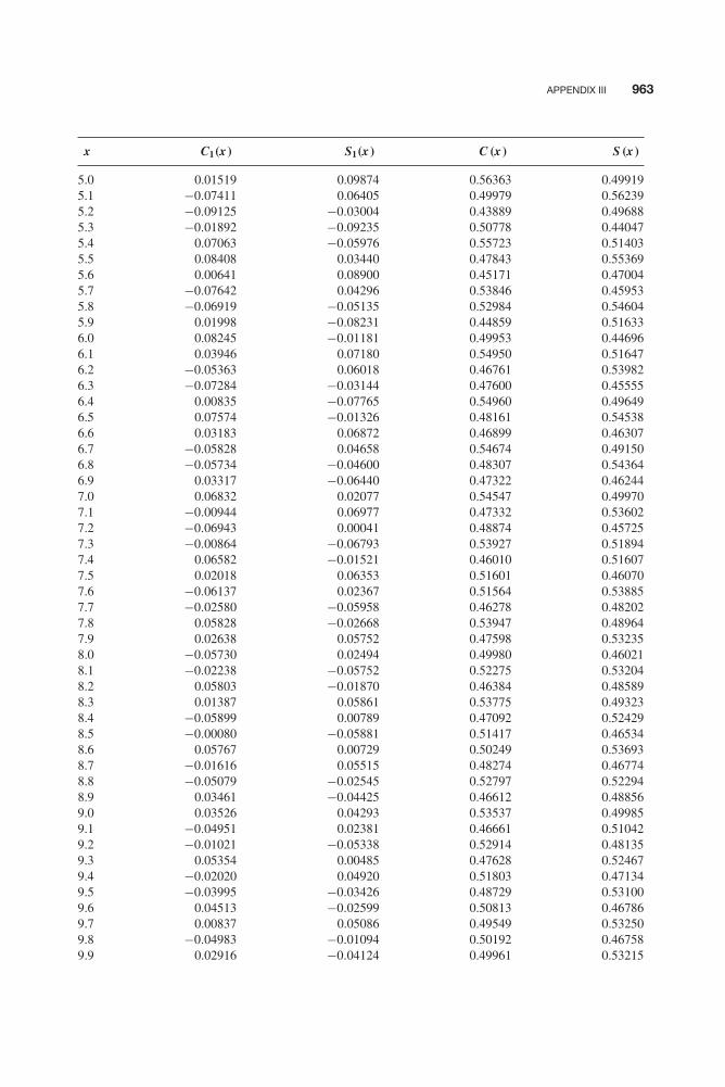
Balanis b03.tex V2 - 11/22/2011 4:28 P.M. Page 963
APPENDIX III 963
x C1(x) S1(x) C (x) S (x)
5.0 0.01519 0.09874 0.56363 0.499195.1 −0.07411 0.06405 0.49979 0.562395.2 −0.09125 −0.03004 0.43889 0.496885.3 −0.01892 −0.09235 0.50778 0.440475.4 0.07063 −0.05976 0.55723 0.514035.5 0.08408 0.03440 0.47843 0.553695.6 0.00641 0.08900 0.45171 0.470045.7 −0.07642 0.04296 0.53846 0.459535.8 −0.06919 −0.05135 0.52984 0.546045.9 0.01998 −0.08231 0.44859 0.516336.0 0.08245 −0.01181 0.49953 0.446966.1 0.03946 0.07180 0.54950 0.516476.2 −0.05363 0.06018 0.46761 0.539826.3 −0.07284 −0.03144 0.47600 0.455556.4 0.00835 −0.07765 0.54960 0.496496.5 0.07574 −0.01326 0.48161 0.545386.6 0.03183 0.06872 0.46899 0.463076.7 −0.05828 0.04658 0.54674 0.491506.8 −0.05734 −0.04600 0.48307 0.543646.9 0.03317 −0.06440 0.47322 0.462447.0 0.06832 0.02077 0.54547 0.499707.1 −0.00944 0.06977 0.47332 0.536027.2 −0.06943 0.00041 0.48874 0.457257.3 −0.00864 −0.06793 0.53927 0.518947.4 0.06582 −0.01521 0.46010 0.516077.5 0.02018 0.06353 0.51601 0.460707.6 −0.06137 0.02367 0.51564 0.538857.7 −0.02580 −0.05958 0.46278 0.482027.8 0.05828 −0.02668 0.53947 0.489647.9 0.02638 0.05752 0.47598 0.532358.0 −0.05730 0.02494 0.49980 0.460218.1 −0.02238 −0.05752 0.52275 0.532048.2 0.05803 −0.01870 0.46384 0.485898.3 0.01387 0.05861 0.53775 0.493238.4 −0.05899 0.00789 0.47092 0.524298.5 −0.00080 −0.05881 0.51417 0.465348.6 0.05767 0.00729 0.50249 0.536938.7 −0.01616 0.05515 0.48274 0.467748.8 −0.05079 −0.02545 0.52797 0.522948.9 0.03461 −0.04425 0.46612 0.488569.0 0.03526 0.04293 0.53537 0.499859.1 −0.04951 0.02381 0.46661 0.510429.2 −0.01021 −0.05338 0.52914 0.481359.3 0.05354 0.00485 0.47628 0.524679.4 −0.02020 0.04920 0.51803 0.471349.5 −0.03995 −0.03426 0.48729 0.531009.6 0.04513 −0.02599 0.50813 0.467869.7 0.00837 0.05086 0.49549 0.532509.8 −0.04983 −0.01094 0.50192 0.467589.9 0.02916 −0.04124 0.49961 0.53215

Balanis b03.tex V2 - 11/22/2011 4:28 P.M. Page 964
964 APPENDIX III
x C1(x) S1(x) C (x) S (x)
10.0 0.02554 0.04298 0.49989 0.4681710.1 −0.04927 0.00478 0.49961 0.5315110.2 0.01738 −0.04583 0.50186 0.4688510.3 0.03233 0.03621 0.49575 0.5306110.4 −0.04681 0.01094 0.50751 0.4703310.5 0.01360 −0.04563 0.48849 0.5280410.6 0.03187 0.03477 0.51601 0.4746010.7 −0.04595 0.00848 0.47936 0.5214310.8 0.01789 −0.04270 0.52484 0.4841310.9 0.02494 0.03850 0.47211 0.5086711.0 −0.04541 −0.00202 0.52894 0.4999111.1 0.02845 −0.03492 0.47284 0.4907911.2 0.01008 0.04349 0.52195 0.5180511.3 −0.03981 −0.01930 0.48675 0.4751411.4 0.04005 −0.01789 0.50183 0.5278611.5 −0.01282 0.04155 0.51052 0.4744011.6 −0.02188 −0.03714 0.47890 0.5175511.7 0.04164 0.00962 0.52679 0.4952511.8 −0.03580 0.02267 0.47489 0.4901311.9 0.00977 −0.04086 0.51544 0.5218412.0 0.02059 0.03622 0.49993 0.4734712.1 −0.03919 −0.01309 0.48426 0.5210812.2 0.03792 −0.01555 0.52525 0.4934512.3 −0.01914 0.03586 0.47673 0.4886712.4 −0.00728 −0.03966 0.50951 0.5238412.5 0.02960 0.02691 0.50969 0.4764512.6 −0.03946 −0.00421 0.47653 0.5093612.7 0.03445 −0.01906 0.52253 0.5109712.8 −0.01783 0.03475 0.49376 0.4759312.9 −0.00377 −0.03857 0.48523 0.5197713.0 0.02325 0.03064 0.52449 0.4999413.1 −0.03530 −0.01452 0.48598 0.4801513.2 0.03760 −0.00459 0.49117 0.5224413.3 −0.03075 0.02163 0.52357 0.4958313.4 0.01744 −0.03299 0.48482 0.4817313.5 −0.00129 0.03701 0.49103 0.5218013.6 −0.01421 −0.03391 0.52336 0.4984813.7 0.02639 0.02521 0.48908 0.4794913.8 −0.03377 −0.01313 0.48534 0.5178113.9 0.03597 −0.00002 0.52168 0.5073714.0 −0.03352 0.01232 0.49996 0.4772614.1 0.02749 −0.02240 0.47844 0.5066814.2 −0.01916 0.02954 0.51205 0.5189014.3 0.00979 −0.03357 0.51546 0.4839814.4 −0.00043 0.03472 0.48131 0.4881914.5 −0.00817 −0.03350 0.49164 0.5203014.6 0.01553 0.03052 0.52113 0.5053814.7 −0.02145 −0.02640 0.50301 0.4785614.8 0.02591 0.02168 0.47853 0.4986914.9 −0.02903 −0.01683 0.49971 0.5213615.0 0.03103 0.01217 0.52122 0.49926

Balanis b03.tex V2 - 11/22/2011 4:28 P.M. Page 965
APPENDIX III 965
2 3 4 5 6 7 8 9 1010
0.2
0.4
0.6
0.8
x
C(x)
S(x)
Figure III-1 Plots of C (x ) and S (x ) Fresnel integrals. (Source: C. A. Balanis, Antenna Theory: Analysisand Design , Third Edition, copyright © 2005, John Wiley & Sons, Inc. Reprinted by permission of JohnWiley & Sons, Inc.).
2 3 4 5 6 7 8 9 1010
0.2
0
0.4
0.6
−0.2
−0.4
x
C1(x)
S1(x)
Figure III-2 Plots of C1(x) and S1(x) Fresnel integrals. (Source: C. A. Balanis, Antenna Theory: Analysisand Design , Third Edition, copyright © 2005, John Wiley & Sons, Inc. Reprinted by permission of JohnWiley & Sons, Inc.).

Balanis b03.tex V2 - 11/22/2011 4:28 P.M. Page 966
Balanis b04.tex V2 - 11/22/2011 4:29 P.M. Page 967
APPENDIX IVBessel Functions
IV.1 BESSEL AND HANKEL FUNCTIONS
Bessel’s equation can be written as
x 2 d2y
dx 2+ x
dy
dx+ (x 2 − p2)y = 0 (IV-1)
Using the method of Frobenius, we can write its solutions as
y(x) = A1Jp(x) + B1J−p(x) p not an integer (IV-2)
ory(x) = A2Jn(x) + B2Yn(x) n an integer (IV-3)
where
Jp(x) =∞∑
m=0
(−1)m(x/2)2m+p
m!(m + p)!(IV-4)
J−p(x) =∞∑
m=0
(−1)m(x/2)2m−p
m!(m − p)!(IV-5)
Yp(x) = Jp(x) cos(pπ) − J−p(x)
sin(pπ)(IV-6)
m! = �(m + 1) (IV-7)
Jp(x) is referred to as the Bessel function of the first kind of order p, Yp(x) as the Bessel functionof the second kind of order p, and �(x) as the gamma function.
When p = n = integer, using (IV-5) and (IV-7), it can be shown that
J−n(x) = (−1)nJn(x) (IV-8)
967
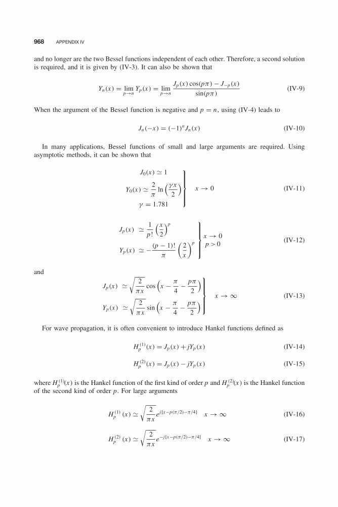
Balanis b04.tex V2 - 11/22/2011 4:29 P.M. Page 968
968 APPENDIX IV
and no longer are the two Bessel functions independent of each other. Therefore, a second solutionis required, and it is given by (IV-3). It can also be shown that
Yn(x) = limp→n
Yp(x) = limp→n
Jp(x) cos(pπ) − J−p(x)
sin(pπ)(IV-9)
When the argument of the Bessel function is negative and p = n , using (IV-4) leads to
Jn(−x) = (−1)nJn(x) (IV-10)
In many applications, Bessel functions of small and large arguments are required. Usingasymptotic methods, it can be shown that
J0(x) � 1
Y0(x) � 2
πln
(γ x
2
)γ = 1.781
⎫⎪⎪⎪⎬⎪⎪⎪⎭ x → 0 (IV-11)
Jp(x) � 1
p!
(x
2
)p
Yp(x) � − (p − 1)!
π
(2
x
)p
⎫⎪⎪⎪⎬⎪⎪⎪⎭x → 0p > 0
(IV-12)
and
Jp(x) �√
2
πxcos
(x − π
4− pπ
2
)Yp(x) �
√2
πxsin
(x − π
4− pπ
2
)⎫⎪⎪⎪⎬⎪⎪⎪⎭ x → ∞ (IV-13)
For wave propagation, it is often convenient to introduce Hankel functions defined as
H (1)p (x) = Jp(x) + jYp(x) (IV-14)
H (2)p (x) = Jp(x) − jYp(x) (IV-15)
where H (1)p (x) is the Hankel function of the first kind of order p and H (2)
p (x) is the Hankel functionof the second kind of order p. For large arguments
H (1)p (x) �
√2
πxej [x−p(π/2)−π/4] x → ∞ (IV-16)
H (2)p (x) �
√2
πxe−j [x−p(π/2)−π/4] x → ∞ (IV-17)
Balanis b04.tex V2 - 11/22/2011 4:29 P.M. Page 969
APPENDIX IV 969
A derivative can be taken using either
d
dx[Zp(αx)] = αZp−1(αx) − p
xZp(αx) (IV-18)
ord
dx[Zp(αx)] = −αZp+1(αx) + p
xZp(αx) (IV-19)
where Zp can be a Bessel function (Jp , Yp) or a Hankel function (H (1)p or H (2)
p ).A useful identity, relating Bessel functions and their derivatives, is given by
Jp(x)Y ′p(x) − Yp(x)J ′
p(x) = 2
πx(IV-20)
and it is referred to as the Wronskian. The prime (′) indicates a derivative. Also
Jp(x)J ′−p(x) − J−p(x)J ′
p(x) = − 2
πxsin(pπ) (IV-21)
Some useful integrals of Bessel functions are
∫x p+1Jp(αx) dx = 1
αx p+1Jp+1(αx) + C (IV-22)∫
x 1−pJp(αx) dx = − 1
αx 1−pJp−1(αx) + C (IV-23)∫
x 3J0(x) dx = x 3J1(x) − 2x 2J2(x) + C (IV-24)∫x 6J1(x) dx = x 6J2(x) − 4x 5J3(x) + 8x 4J4(x) + C (IV-25)∫
J3(x) dx = −J2(x) − 2
xJ1(x) + C (IV-26)∫
xJ1(x) dx = −xJ0(x) +∫
J0(x) dx + C (IV-27)∫x−1J1(x) dx = −J1(x) +
∫J0(x) dx + C (IV-28)∫
J2(x) dx = −2J1(x) +∫
J0(x) dx + C (IV-29)∫x mJn(x) dx = x mJn+1(x) − (m − n − 1)
∫x m−1Jn+1(x) dx (IV-30)∫
x mJn(x) dx = −x mJn−1(x) + (m + n − 1)
∫x m−1Jn−1(x) dx (IV-31)
Balanis b04.tex V2 - 11/22/2011 4:29 P.M. Page 970
970 APPENDIX IV
J1(x) = 2
π
∫ π/2
0sin(x sin θ) sin θ dθ (IV-32)
1
xJ1(x) = 2
π
∫ π/2
0cos(x sin θ) cos2 θ dθ (IV-33)
J2(x) = 2
π
∫ π/2
0cos(x sin θ) cos 2θ dθ (IV-34)
Jn(x) = j −n
2π
∫ 2π
0ejx cos φejnφ dφ (IV-35)
Jn(x) = j −n
π
∫ π
0cos(nφ)ejx cos φ dφ (IV-36)
Jn(x) = 1
π
∫ π
0cos(x sin φ − nφ) dφ (IV-37)
J2n(x) = 2
π
∫ π/2
0cos(x sin φ) cos(2nφ) dφ (IV-38)
J2n(x) = (−1)n 2
π
∫ π/2
0cos(x cos φ) cos(2nφ) dφ (IV-39)
The integrals ∫ x
0J0(τ ) dτ and
∫ x
0Y0(τ ) dτ (IV-40)
often appear in solutions of problems but cannot be integrated in closed form. Graphs and tablesfor each, obtained using numerical techniques, are included.
IV.2 MODIFIED BESSEL FUNCTIONS
In addition to the regular cylindrical Bessel functions of the first and second kind, there existsanother set of cylindrical Bessel functions that are referred to as the modified Bessel functionsof the first and second kind, denoted respectively by Ip(x) and Kp(x). These modified cylindricalBessel functions exhibit ascending and descending variations for increasing argument as shown,respectively, in Figures IV-5 and IV-6. For real values of the argument, the modified Besselfunctions exhibit real values.
The modified Bessel functions are related to the regular Bessel and Hankel functions by
Ip(x) = j −pJp(jx) = j pJ−p(jx) = j pJp(−jx) (IV-41)
Kp(x) = π
2j p+1H (1)
p (jx) = π
2(−j )p+1H (2)
p (−jx) (IV-42)
Some of the identities involving modified Bessel functions are
I−p(x) = j pJ−p(jx) (IV-43)
I−n(x) = In(x) n = 0, 1, 2, 3, . . . (IV-44)
K−n(x) = Kn(x) n = 0, 1, 2, 3, . . . (IV-45)
Balanis b04.tex V2 - 11/22/2011 4:29 P.M. Page 971
APPENDIX IV 971
For large arguments, the modified Bessel functions can be computed using the asymptoticformulas
Ip(x) � ex
√2πx
Kp(x) �√
π
2xe−x
⎫⎪⎪⎪⎪⎪⎬⎪⎪⎪⎪⎪⎭x → ∞
(IV-46a)
(IV-46b)
Derivatives of both modified Bessel functions can be found using the same expressions, (IV-18)and (IV-19), as for the regular Bessel functions.
IV.3 SPHERICAL BESSEL AND HANKEL FUNCTIONS
There is another set of Bessel and Hankel functions, that are usually referred to as the sphericalBessel and Hankel functions. These spherical Bessel and Hankel functions of order n are related,respectively, to the regular cylindrical Bessel and Hankel of order n + 1/2 by
jn(x) =√
π
2xJn+1/2(x) (IV-47a)
yn(x) =√
π
2xYn+1/2(x) (IV-47b)
h(1)n (x) =
√π
2xH (1)
n+1/2(x) (IV-47c)
h(2)n (x) =
√π
2xH (2)
n+1/2(x) (IV-47d)
where jn , yn , h(1)n , and h(2)
n are the spherical Bessel and Hankel functions. These spherical Besseland Hankel functions are used as solutions to electromagnetic problems solved using sphericalcoordinates.
For small arguments
jn(x) � x n
1 • 3 • 5 · · · (2n + 1)
yn(x) � −1 • 3 • 5 · · · (2n − 1)x−(n+1)
⎫⎪⎬⎪⎭n = 0, 1, 2, . . .
x → 0
(IV-48a)
(IV-48b)
Another set of spherical Bessel and Hankel functions, that appear in solutions of electromag-netic problems, is that denoted by B̂n(x) where B̂n can be used to represent Ĵn , Ŷn , Ĥ (1)
n , or Ĥ (2)n .
These are related to the preceding spherical Bessel and Hankel functions [denoted by bn to rep-resent jn , yn , h(1)
n , or h(2)n ] and to the regular cylindrical Bessel and Hankel functions [denoted by
Bn+1/2 to represent Jn+1/2, Yn+1/2, H (1)n+1/2, or H (2)
n+1/2] by
B̂n(x) = xbn(x) =√
πx
2Bn+1/2(x) (IV-49)

Balanis b04.tex V2 - 11/22/2011 4:29 P.M. Page 972
972 APPENDIX IV
x J0(x) J1(x) Y0(x) Y1(x)
0.0 1.00000 0.00000 −∞ −∞0.1 0.99750 0.04994 −1.53424 −6.458950.2 0.99003 0.09950 −1.08110 −3.323820.3 0.97763 0.14832 −0.80727 −2.293100.4 0.96040 0.19603 −0.60602 −1.780870.5 0.93847 0.24227 −0.44452 −1.471470.6 0.91201 0.28670 −0.30851 −1.260390.7 0.88120 0.32900 −0.19066 −1.103250.8 0.84629 0.36884 −0.08680 −0.978140.9 0.80752 0.40595 0.00563 −0.873131.0 0.76520 0.44005 0.08826 −0.781211.1 0.71962 0.47090 0.16216 −0.698121.2 0.67113 0.49829 0.22808 −0.621141.3 0.62009 0.52202 0.28654 −0.548521.4 0.56686 0.54195 0.33789 −0.479151.5 0.51183 0.55794 0.38245 −0.412311.6 0.45540 0.56990 0.42043 −0.347581.7 0.39799 0.57777 0.45203 −0.284731.8 0.33999 0.58152 0.47743 −0.223661.9 0.28182 0.58116 0.49682 −0.164412.0 0.22389 0.57673 0.51038 −0.107032.1 0.16661 0.56829 0.51829 −0.051682.2 0.11036 0.55596 0.52078 0.001492.3 0.05554 0.53987 0.51807 0.052282.4 0.00251 0.52019 0.51041 0.100492.5 −0.04838 0.49710 0.49807 0.145922.6 −0.09681 0.47082 0.48133 0.188362.7 −0.14245 0.44161 0.46050 0.227632.8 −0.18504 0.40972 0.43592 0.263542.9 −0.22432 0.37544 0.40791 0.295943.0 −0.26005 0.33906 0.37686 0.324673.1 −0.29206 0.30092 0.34310 0.349633.2 −0.32019 0.26134 0.30705 0.370713.3 −0.34430 0.22066 0.26909 0.387853.4 −0.36430 0.17923 0.22962 0.401013.5 −0.38013 0.13738 0.18902 0.410193.6 −0.39177 0.09547 0.14771 0.415393.7 −0.39923 0.05383 0.10607 0.416673.8 −0.40256 0.01282 0.06450 0.414113.9 −0.40183 −0.02724 0.02338 0.407824.0 −0.39715 −0.06604 −0.01694 0.397934.1 −0.38868 −0.10328 −0.05609 0.384594.2 −0.37657 −0.13865 −0.09375 0.368014.3 −0.36102 −0.17190 −0.12960 0.348394.4 −0.34226 −0.20278 −0.16334 0.325974.5 −0.32054 −0.23106 −0.19471 0.301004.6 −0.29614 −0.25655 −0.22346 0.273754.7 −0.26933 −0.27908 −0.24939 0.244504.8 −0.24043 −0.29850 −0.27230 0.213564.9 −0.20974 −0.31470 −0.29205 0.18125
Balanis b04.tex V2 - 11/22/2011 4:29 P.M. Page 973
APPENDIX IV 973
x J0(x) J1(x) Y0(x) Y1(x)
5.0 −0.17760 −0.32758 −0.30852 0.147865.1 −0.14434 −0.33710 −0.32160 0.113745.2 −0.11029 −0.34322 −0.33125 0.079195.3 −0.07580 −0.34596 −0.33744 0.044555.4 −0.04121 −0.34534 −0.34017 0.010135.5 −0.00684 −0.34144 −0.33948 −0.023765.6 0.02697 −0.33433 −0.33544 −0.056815.7 0.05992 −0.32415 −0.32816 −0.088725.8 0.09170 −0.31103 −0.31775 −0.119235.9 0.12203 −0.29514 −0.30437 −0.148086.0 0.15065 −0.27668 −0.28819 −0.175016.1 0.17729 −0.25587 −0.26943 −0.199816.2 0.20175 −0.23292 −0.24831 −0.222286.3 0.22381 −0.20809 −0.22506 −0.242256.4 0.24331 −0.18164 −0.19995 −0.259566.5 0.26009 −0.15384 −0.17324 −0.274096.6 0.27404 −0.12498 −0.14523 −0.285756.7 0.28506 −0.09534 −0.11619 −0.294466.8 0.29310 −0.06522 −0.08643 −0.300196.9 0.29810 −0.03490 −0.05625 −0.302927.0 0.30008 −0.00468 −0.02595 −0.302677.1 0.29905 0.02515 0.00418 −0.299487.2 0.29507 0.05433 0.03385 −0.293427.3 0.28822 0.08257 0.06277 −0.284597.4 0.27860 0.10962 0.09068 −0.273117.5 0.26634 0.13525 0.11731 −0.259137.6 0.25160 0.15921 0.14243 −0.242807.7 0.23456 0.18131 0.16580 −0.224327.8 0.21541 0.20136 0.18723 −0.203887.9 0.19436 0.21918 0.20652 −0.181728.0 0.17165 0.23464 0.22352 −0.158068.1 0.14752 0.24761 0.23809 −0.133158.2 0.12222 0.25800 0.25012 −0.107248.3 0.09601 0.26574 0.25951 −0.080608.4 0.06916 0.27079 0.26622 −0.053488.5 0.04194 0.27312 0.27021 −0.026178.6 0.01462 0.27276 0.27146 0.001088.7 −0.01252 0.26972 0.27000 0.028018.8 −0.03923 0.26407 0.26587 0.054368.9 −0.06525 0.25590 0.25916 0.079879.0 −0.09033 0.24531 0.24994 0.104319.1 −0.11424 0.23243 0.23834 0.127479.2 −0.13675 0.21741 0.22449 0.149119.3 −0.15765 0.20041 0.20857 0.169069.4 −0.17677 0.18163 0.19074 0.187149.5 −0.19393 0.16126 0.17121 0.203189.6 −0.20898 0.13952 0.15018 0.217069.7 −0.22180 0.11664 0.12787 0.228669.8 −0.23228 0.09284 0.10453 0.237899.9 −0.24034 0.06837 0.08038 0.24469
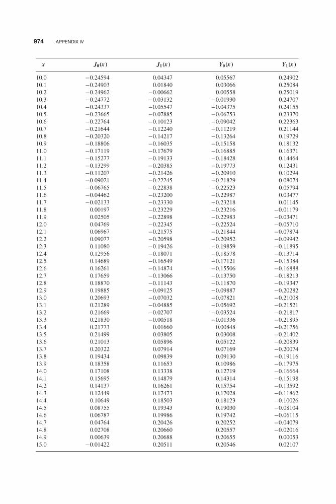
Balanis b04.tex V2 - 11/22/2011 4:29 P.M. Page 974
974 APPENDIX IV
x J0(x) J1(x) Y0(x) Y1(x)
10.0 −0.24594 0.04347 0.05567 0.2490210.1 −0.24903 0.01840 0.03066 0.2508410.2 −0.24962 −0.00662 0.00558 0.2501910.3 −0.24772 −0.03132 −0.01930 0.2470710.4 −0.24337 −0.05547 −0.04375 0.2415510.5 −0.23665 −0.07885 −0.06753 0.2337010.6 −0.22764 −0.10123 −0.09042 0.2236310.7 −0.21644 −0.12240 −0.11219 0.2114410.8 −0.20320 −0.14217 −0.13264 0.1972910.9 −0.18806 −0.16035 −0.15158 0.1813211.0 −0.17119 −0.17679 −0.16885 0.1637111.1 −0.15277 −0.19133 −0.18428 0.1446411.2 −0.13299 −0.20385 −0.19773 0.1243111.3 −0.11207 −0.21426 −0.20910 0.1029411.4 −0.09021 −0.22245 −0.21829 0.0807411.5 −0.06765 −0.22838 −0.22523 0.0579411.6 −0.04462 −0.23200 −0.22987 0.0347711.7 −0.02133 −0.23330 −0.23218 0.0114511.8 0.00197 −0.23229 −0.23216 −0.0117911.9 0.02505 −0.22898 −0.22983 −0.0347112.0 0.04769 −0.22345 −0.22524 −0.0571012.1 0.06967 −0.21575 −0.21844 −0.0787412.2 0.09077 −0.20598 −0.20952 −0.0994212.3 0.11080 −0.19426 −0.19859 −0.1189512.4 0.12956 −0.18071 −0.18578 −0.1371412.5 0.14689 −0.16549 −0.17121 −0.1538412.6 0.16261 −0.14874 −0.15506 −0.1688812.7 0.17659 −0.13066 −0.13750 −0.1821312.8 0.18870 −0.11143 −0.11870 −0.1934712.9 0.19885 −0.09125 −0.09887 −0.2028213.0 0.20693 −0.07032 −0.07821 −0.2100813.1 0.21289 −0.04885 −0.05692 −0.2152113.2 0.21669 −0.02707 −0.03524 −0.2181713.3 0.21830 −0.00518 −0.01336 −0.2189513.4 0.21773 0.01660 0.00848 −0.2175613.5 0.21499 0.03805 0.03008 −0.2140213.6 0.21013 0.05896 0.05122 −0.2083913.7 0.20322 0.07914 0.07169 −0.2007413.8 0.19434 0.09839 0.09130 −0.1911613.9 0.18358 0.11653 0.10986 −0.1797514.0 0.17108 0.13338 0.12719 −0.1666414.1 0.15695 0.14879 0.14314 −0.1519814.2 0.14137 0.16261 0.15754 −0.1359214.3 0.12449 0.17473 0.17028 −0.1186214.4 0.10649 0.18503 0.18123 −0.1002614.5 0.08755 0.19343 0.19030 −0.0810414.6 0.06787 0.19986 0.19742 −0.0611514.7 0.04764 0.20426 0.20252 −0.0407914.8 0.02708 0.20660 0.20557 −0.0201614.9 0.00639 0.20688 0.20655 0.0005315.0 −0.01422 0.20511 0.20546 0.02107

Balanis b04.tex V2 - 11/22/2011 4:29 P.M. Page 975
APPENDIX IV 975
0
0
0.5
−0.5
1.0
5 10 15 20 25 30 35 40 45 50
x
J0(x)
J1(x)
J2(x)
J3(x)
Figure IV-1 Bessel functions of the first kind [J0(x), J1(x), J2(x), and J3(x)]. (Source: C. A. Balanis,Antenna Theory: Analysis and Design , Third Edition, copyright © 2005, John Wiley & Sons, Inc. Reprintedby permission of John Wiley & Sons, Inc.).
0
0
0.5
−0.5
−1.0
−1.5
1.0
5 10 15 20 25 30 35 40 45 50
x
Y0(x)
Y1(x)
Y2(x)
Y3(x)
Figure IV-2 Bessel functions of the second kind [Y0(x), Y1(x), Y2(x), and Y3(x)]. (Source: C. A. Balanis,Antenna Theory: Analysis and Design , Third Edition, copyright © 2005, John Wiley & Sons, Inc. Reprintedby permission of John Wiley & Sons, Inc.).
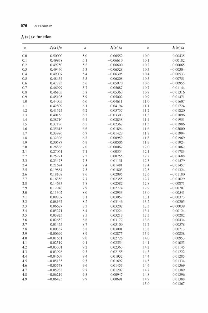
Balanis b04.tex V2 - 11/22/2011 4:29 P.M. Page 976
976 APPENDIX IV
J1(x)/x function
x J1(x)/x x J1(x)/x x J1(x)/x
0.0 0.50000 5.0 −0.06552 10.0 0.004350.1 0.49938 5.1 −0.06610 10.1 0.001820.2 0.49750 5.2 −0.06600 10.2 −0.000650.3 0.49440 5.3 −0.06528 10.3 −0.003040.4 0.49007 5.4 −0.06395 10.4 −0.005330.5 0.48454 5.5 −0.06208 10.5 −0.007510.6 0.47783 5.6 −0.05970 10.6 −0.009550.7 0.46999 5.7 −0.05687 10.7 −0.011440.8 0.46105 5.8 −0.05363 10.8 −0.013160.9 0.45105 5.9 −0.05002 10.9 −0.014711.0 0.44005 6.0 −0.04611 11.0 −0.016071.1 0.42809 6.1 −0.04194 11.1 −0.017241.2 0.41524 6.2 −0.03757 11.2 −0.018201.3 0.40156 6.3 −0.03303 11.3 −0.018961.4 0.38710 6.4 −0.02838 11.4 −0.019511.5 0.37196 6.5 −0.02367 11.5 −0.019861.6 0.35618 6.6 −0.01894 11.6 −0.020001.7 0.33986 6.7 −0.01423 11.7 −0.019941.8 0.32306 6.8 −0.00959 11.8 −0.019691.9 0.30587 6.9 −0.00506 11.9 −0.019242.0 0.28836 7.0 −0.00067 12.0 −0.018622.1 0.27061 7.1 0.00354 12.1 −0.017832.2 0.25271 7.2 0.00755 12.2 −0.016882.3 0.23473 7.3 0.01131 12.3 −0.015792.4 0.21674 7.4 0.01481 12.4 −0.014572.5 0.19884 7.5 0.01803 12.5 −0.013242.6 0.18108 7.6 0.02095 12.6 −0.011802.7 0.16356 7.7 0.02355 12.7 −0.010292.8 0.14633 7.8 0.02582 12.8 −0.008712.9 0.12946 7.9 0.02774 12.9 −0.007073.0 0.11302 8.0 0.02933 13.0 −0.005413.1 0.09707 8.1 0.03057 13.1 −0.003733.2 0.08167 8.2 0.03146 13.2 −0.002053.3 0.06687 8.3 0.03202 13.3 −0.000393.4 0.05271 8.4 0.03224 13.4 0.001243.5 0.03925 8.5 0.03213 13.5 0.002823.6 0.02652 8.6 0.03172 13.6 0.004343.7 0.01455 8.7 0.03100 13.7 0.005783.8 0.00337 8.8 0.03001 13.8 0.007133.9 −0.00699 8.9 0.02875 13.9 0.008384.0 −0.01651 9.0 0.02726 14.0 0.009534.1 −0.02519 9.1 0.02554 14.1 0.010554.2 −0.03301 9.2 0.02363 14.2 0.011454.3 −0.03998 9.3 0.02155 14.3 0.012224.4 −0.04609 9.4 0.01932 14.4 0.012854.5 −0.05135 9.5 0.01697 14.5 0.013344.6 −0.05578 9.6 0.01453 14.6 0.013694.7 −0.05938 9.7 0.01202 14.7 0.013894.8 −0.06219 9.8 0.00947 14.8 0.013964.9 −0.06423 9.9 0.00691 14.9 0.01388
15.0 0.01367
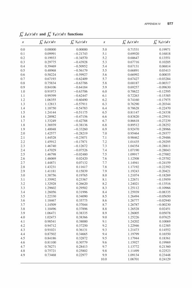
Balanis b04.tex V2 - 11/22/2011 4:29 P.M. Page 977
APPENDIX IV 977
∫ x0 J0(τ)dτ and
∫ x0 Y0(τ)dτ functions
x∫ x
0 J0(τ)dτ∫ x
0 Y0(τ)dτ x∫ x
0 J0(τ)dτ∫ x
0 Y0(τ)dτ
0.0 0.00000 0.00000 5.0 0.71531 0.199710.1 0.09991 −0.21743 5.1 0.69920 0.168180.2 0.19933 −0.34570 5.2 0.68647 0.135510.3 0.29775 −0.43928 5.3 0.67716 0.102050.4 0.39469 −0.50952 5.4 0.67131 0.068140.5 0.48968 −0.56179 5.5 0.66891 0.034130.6 0.58224 −0.59927 5.6 0.66992 0.000350.7 0.67193 −0.62409 5.7 0.67427 −0.032840.8 0.75834 −0.63786 5.8 0.68187 −0.065170.9 0.84106 −0.64184 5.9 0.69257 −0.096301.0 0.91973 −0.63706 6.0 0.70622 −0.125951.1 0.99399 −0.62447 6.1 0.72263 −0.153851.2 1.06355 −0.60490 6.2 0.74160 −0.179751.3 1.12813 −0.57911 6.3 0.76290 −0.203441.4 1.18750 −0.54783 6.4 0.78628 −0.224701.5 1.24144 −0.51175 6.5 0.81147 −0.243381.6 1.28982 −0.47156 6.6 0.83820 −0.259311.7 1.33249 −0.42788 6.7 0.86618 −0.272391.8 1.36939 −0.38136 6.8 0.89512 −0.282521.9 1.40048 −0.33260 6.9 0.92470 −0.289662.0 1.42577 −0.28219 7.0 0.95464 −0.293772.1 1.44528 −0.23071 7.1 0.98462 −0.294862.2 1.45912 −0.17871 7.2 1.01435 −0.292952.3 1.46740 −0.12672 7.3 1.04354 −0.288112.4 1.47029 −0.07526 7.4 1.07190 −0.280432.5 1.46798 −0.02480 7.5 1.09917 −0.270022.6 1.46069 0.02420 7.6 1.12508 −0.257022.7 1.44871 0.07132 7.7 1.14941 −0.241592.8 1.43231 0.11617 7.8 1.17192 −0.223922.9 1.41181 0.15839 7.9 1.19243 −0.204213.0 1.38756 0.19765 8.0 1.21074 −0.182693.1 1.35992 0.23367 8.1 1.22671 −0.159593.2 1.32928 0.26620 8.2 1.24021 −0.135163.3 1.29602 0.29502 8.3 1.25112 −0.109663.4 1.26056 0.31996 8.4 1.25939 −0.083353.5 1.22330 0.34090 8.5 1.26494 −0.056503.6 1.18467 0.35775 8.6 1.26777 −0.029403.7 1.14509 0.37044 8.7 1.26787 −0.002303.8 1.10496 0.37896 8.8 1.26528 0.024513.9 1.06471 0.38335 8.9 1.26005 0.050784.0 1.02473 0.38366 9.0 1.25226 0.076254.1 0.98541 0.38000 9.1 1.24202 0.100694.2 0.94712 0.37250 9.2 1.22946 0.123854.3 0.91021 0.36131 9.3 1.21473 0.145524.4 0.87502 0.34665 9.4 1.19799 0.165504.5 0.84186 0.32872 9.5 1.17944 0.183614.6 0.81100 0.30779 9.6 1.15927 0.199694.7 0.78271 0.28413 9.7 1.13772 0.213604.8 0.75721 0.25802 9.8 1.11499 0.225234.9 0.73468 0.22977 9.9 1.09134 0.23448
10.0 1.06701 0.24129

Balanis b04.tex V2 - 11/22/2011 4:29 P.M. Page 978
978 APPENDIX IV
0
0
0.1
−0.1
0.2
0.3
0.4
0.5
5 10 15 20 25 30 35 40 45 50
x
x
J1(x)
Figure IV-3 Plot of J1(x)/x function. (Source: C. A. Balanis, Antenna Theory: Analysis and Design ,Third Edition, copyright © 2005, John Wiley & Sons, Inc. Reprinted by permission of John Wiley & Sons,Inc.).
210
0
0.5
1.0
1.5 x
0∫ J0(t) dr
x
0∫ Y0(t) dt−0.5
−1.03 4 5
Upper limit x6 7 8 9 10
Figure IV-4 Plots of∫ x
0 J0(τ )dτ and∫ x
0 Y0(τ )dτ functions. (Source: C. A. Balanis, Antenna Theory:Analysis and Design , Third Edition, copyright © 2005, John Wiley & Sons, Inc. Reprinted by permissionof John Wiley & Sons, Inc.).
0 1
1
2
3
4
5
6
2 3 4x
I0(x)
I1(x)
Figure IV-5 Modified Bessel functions of the first kind [I0(x) and I1(x)].

Balanis b04.tex V2 - 11/22/2011 4:29 P.M. Page 979
APPENDIX IV 979
0 1
1
2
3
2
K0(x)
x
K1(x)
Figure IV-6 Modified Bessel functions of the second kind [K0(x) and K1(x)].

Balanis b04.tex V2 - 11/22/2011 4:29 P.M. Page 980

Balanis b05.tex V2 - 11/22/2011 4:33 P.M. Page 981
APPENDIX VLegendre Polynomials and Functions
V.1 LEGENDRE POLYNOMIALS AND FUNCTIONS
The ordinary Legendre differential equation can be written as
(1 − x 2)d2y
dx 2− 2x
dy
dx+ p(p + 1)y = 0 (V-1)
Its solution can be written as
y(x) = A1Pp(x) + B1Pp(−x) p not an integer (V-2)
where Pp(x) is referred to as the Legendre function of the first kind . If p is an integer (p = n),then Pn(x) and Pn(−x) are not two independent solutions because
Pn(−x) = (−1)nPn(x) (V-3)
Therefore, two independent solutions to (V-1) for p = n , an integer, are
y(x) = A2Pn(x) + B2Qn(x) (V-4)
where Qn(x) is referred to as the Legendre function of the second kind .When p = n , an integer, Pn(x) are also referred to as the Legendre polynomials of order n ,
and are defined by
Pn(x) =M∑
m=0
(−1)m(2n − 2m)!(x)n−2m
2nm!(n − m)!(n − 2m)!(V-5)
where M = n/2 or (n − 1)/2, whichever is an integer.
981

Balanis b05.tex V2 - 11/22/2011 4:33 P.M. Page 982
982 APPENDIX V
The Legendre functions Qn(x) of the second kind are defined by
Qn(x) = limp→n
Qp(x) = limp→n
π
2
Pp(x) cos(pπ) − Pp(−x)
sin(pπ)(V-6)
The Legendre polynomials (or Legendre functions of the first kind) Pn(x) can also be obtainedmore conveniently using Rodrigues’ formula
Pn(x) = 1
2nn!
dn
dx n(x 2 − 1)n (V-7)
which when expanded leads (for n = 0, 1, 2, . . . , 7) to
P0(x) = 1
P1(x) = x
P2(x) = 12 (3x 2 − 1)
P3(x) = 12 (5x 3 − 3x)
P4(x) = 18 (35x 4 − 30x 2 + 3) (V-8)
P5(x) = 18 (63x 5 − 70x 3 + 15x)
P6(x) = 116 (231x 6 − 315x 4 + 105x 2 − 5)
P7(x) = 116 (429x 7 − 693x 5 + 315x 3 − 35x)
If x = cos θ , the Legendre polynomials (or Legendre functions of the first kind) of (V-8) can bewritten as
P0(cos θ) = 1
P1(cos θ) = cos θ
P2(cos θ) = 14 (3 cos 2θ + 1)
P3(cos θ) = 18 (5 cos 3θ + 3 cos θ)
P4(cos θ) = 164 (35 cos 4θ + 20 cos 2θ + 9) (V-9)
P5(cos θ) = 1128 (63 cos 5θ + 35 cos 3θ + 30 cos θ)
P6(cos θ) = 1512 (231 cos 6θ + 126 cos 4θ + 105 cos 2θ + 50)
P7(cos θ) = 11024 (429 cos 7θ + 231 cos 5θ + 189 cos 3θ + 175 cos θ)
The Legendre functions Qn(x) of the second kind exhibit singularities at x = ±1 or θ = 0, πand can be obtained from the Legendre functions Pn(x) of the first kind using the formula of
Qn(x) = Pn(x)
{1
2ln
(1 + x
1 − x
)− ψ(n)
}+
n∑m=1
(−1)m(n + m)!
(m!)2(n − m)!ψ(m)
(1 − x
2
)m
(V-10)
where
ψ(n) = 1 + 1
2+ 1
3+ · · · + 1
n(V-10a)

Balanis b05.tex V2 - 11/22/2011 4:33 P.M. Page 983
APPENDIX V 983
When (V-10) is expanded, it leads (for n = 0, 1, 2, 3) to
Q0(x) = 1
2ln
(1 + x
1 − x
)Q1(x) = x
2ln
(1 + x
1 − x
)− 1
Q2(x) = 3x 2 − 1
4ln
(1 + x
1 − x
)− 3x
2(V-11)
Q3(x) = 5x 3 − 3x
4ln
(1 + x
1 − x
)− 5x 2
2+ 2
3
or for x = cos θ to
Q0(cos θ) = ln
(cot
θ
2
)Q1(cos θ) = cos θ ln
(cot
θ
2
)− 1
Q2(cos θ) = 1
4(1 + 3 cos 2θ)ln
(cot
θ
2
)− 3
2cos θ (V-12)
Q3(cos θ) = 1
8(3 cos θ + 5 cos 3θ)ln
(cot
θ
2
)− 5
4cos 2θ − 7
12
The Legendre functions of the first Pn(x) and second Qn(x) kind obey the following recurrencerelations:
(n + 1)Rn+1(x) − (2n + 1)xRn(x) + nRn−1(x) = 0 (V-13a)
dRn+1(x)
dx− x
dRn(x)
dx= (n + 1)Rn(x) (V-13b)
xdRn(x)
dx− dRn−1(x)
dx= nRn(x) (V-13c)
dRn+1(x)
dx− dRn−1(x)
dx= (2n + 1)Rn(x) (V-13d)
(x 2 − 1)dRn(x)
dx= nxRn(x) − nRn−1(x) = −(n + 1)(xRn − Rn+1) (V-13e)
where Rn(x) can be either Pn(x) or Qn(x).Some other useful formulas involving Legendre polynomials Pn(x) and Qn(x) are∫ 1
−1Pm(x)Pn(x) dx = 0 m �= n (V-14a)∫ 1
−1[Pn(x)]2 dx = 2
2n + 1(V-14b)∫ 1
0[Qn(x)]2 dx = 1
2n + 1
[π2
4− 1
(n + 1)2− 1
(n + 2)2− · · ·
](V-14c)
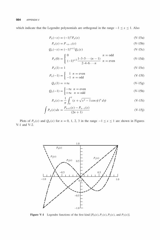
Balanis b05.tex V2 - 11/22/2011 4:33 P.M. Page 984
984 APPENDIX V
which indicate that the Legendre polynomials are orthogonal in the range −1 ≤ x ≤ 1. Also
Pn(−x) = (−1)nPn(x) (V-15a)
Pn(x) = P−n−1(x) (V-15b)
Qn(−x) = (−1)n+1Qn(x) (V-15c)
Pn(0) ={
0 n = odd
(−1)n/2 1 • 3 • 5 · · · (n − 1)
2 • 4 • 6 · · · nn = even
(V-15d)
Pn(1) = 1 (V-15e)
Pn(−1) ={
1 n = even−1 n = odd
(V-15f)
Qn(1) = +∞ (V-15g)
Qn(−1) ={−∞ n = even+∞ n = odd
(V-15h)
Pn(x) = 1
π
∫ π
0(x +
√x 2 − 1 cos ψ)n dψ (V-15i)∫
Pn(x) dx = Pn+1(x) − Pn−1(x)
(2n + 1)(V-15j)
Plots of Pn(x) and Qn(x) for n = 0, 1, 2, 3 in the range −1 ≤ x ≤ 1 are shown in FiguresV-1 and V-2.
P0(x)
P2(x)
P3(x)P1(x)
−1.0
−0.5 0.5
0.5
1.0
−0.5
−1.0
1.00.0
Figure V-1 Legendre functions of the first kind [P0(x), P1(x), P2(x), and P3(x)].
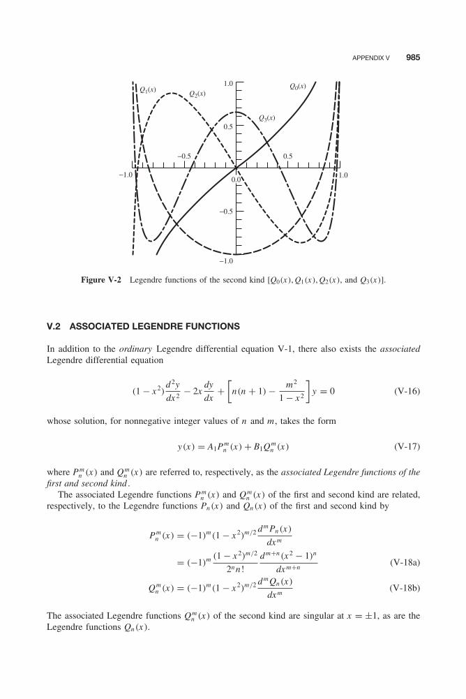
Balanis b05.tex V2 - 11/22/2011 4:33 P.M. Page 985
APPENDIX V 985
Q0(x)
Q3(x)
Q2(x)Q1(x)
−1.0
−0.5 0.5
0.5
1.0
−0.5
−1.0
1.00.0
Figure V-2 Legendre functions of the second kind [Q0(x), Q1(x), Q2(x), and Q3(x)].
V.2 ASSOCIATED LEGENDRE FUNCTIONS
In addition to the ordinary Legendre differential equation V-1, there also exists the associatedLegendre differential equation
(1 − x 2)d2y
dx 2− 2x
dy
dx+
[n(n + 1) − m2
1 − x 2
]y = 0 (V-16)
whose solution, for nonnegative integer values of n and m , takes the form
y(x) = A1Pmn (x) + B1Qm
n (x) (V-17)
where Pmn (x) and Qm
n (x) are referred to, respectively, as the associated Legendre functions of thefirst and second kind .
The associated Legendre functions Pmn (x) and Qm
n (x) of the first and second kind are related,respectively, to the Legendre functions Pn(x) and Qn(x) of the first and second kind by
Pmn (x) = (−1)m(1 − x 2)m/2 dmPn(x)
dx m
= (−1)m (1 − x 2)m/2
2nn!
dm+n(x 2 − 1)n
dx m+n(V-18a)
Qmn (x) = (−1)m(1 − x 2)m/2 dmQn(x)
dx m(V-18b)
The associated Legendre functions Qmn (x) of the second kind are singular at x = ±1, as are the
Legendre functions Qn(x).
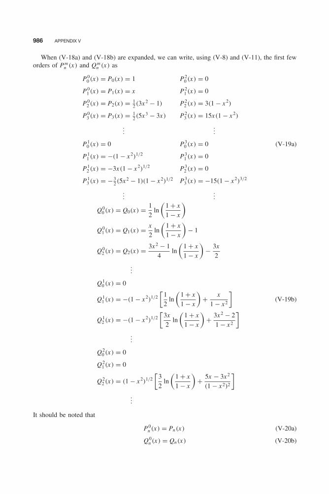
Balanis b05.tex V2 - 11/22/2011 4:33 P.M. Page 986
986 APPENDIX V
When (V-18a) and (V-18b) are expanded, we can write, using (V-8) and (V-11), the first feworders of Pm
n (x) and Qmn (x) as
P00 (x) = P0(x) = 1 P2
0 (x) = 0
P01 (x) = P1(x) = x P2
1 (x) = 0
P02 (x) = P2(x) = 1
2 (3x 2 − 1) P22 (x) = 3(1 − x 2)
P03 (x) = P3(x) = 1
2 (5x 3 − 3x) P23 (x) = 15x(1 − x 2)
......
P10 (x) = 0 P3
0 (x) = 0 (V-19a)
P11 (x) = −(1 − x 2)1/2 P3
1 (x) = 0
P12 (x) = −3x(1 − x 2)1/2 P3
2 (x) = 0
P13 (x) = − 3
2 (5x 2 − 1)(1 − x 2)1/2 P33 (x) = −15(1 − x 2)3/2
......
Q00 (x) = Q0(x) = 1
2ln
(1 + x
1 − x
)Q0
1 (x) = Q1(x) = x
2ln
(1 + x
1 − x
)− 1
Q02 (x) = Q2(x) = 3x 2 − 1
4ln
(1 + x
1 − x
)− 3x
2
...
Q10 (x) = 0
Q11 (x) = −(1 − x 2)1/2
[1
2ln
(1 + x
1 − x
)+ x
1 − x 2
](V-19b)
Q12 (x) = −(1 − x 2)1/2
[3x
2ln
(1 + x
1 − x
)+ 3x 2 − 2
1 − x 2
]...
Q20 (x) = 0
Q21 (x) = 0
Q22 (x) = (1 − x 2)1/2
[3
2ln
(1 + x
1 − x
)+ 5x − 3x 2
(1 − x 2)2
]...
It should be noted that
P0n (x) = Pn(x) (V-20a)
Q0n (x) = Qn(x) (V-20b)

Balanis b05.tex V2 - 11/22/2011 4:33 P.M. Page 987
APPENDIX V 987
Pmn (x) = 0 m > n (V-20c)
Qmn (x) = 0 m > n (V-20d)
Pmn (−x) = (−1)n−mPm
n (x) (V-20e)
Pmn (x) = Pm
−n−1(x) (V-20f)
Qmn (−x) = (−1)n+m+1Qn(x) (V-20g)
Pmn (1) =
{1 m = 0
0 m > 0(V-20h)
Pmn (0) =
⎧⎨⎩ (−1)(n+m)/2 1 • 3 • 5 · · · (n + m − 1)
2 • 4 • 6 · · · (n − m)n + m = even
0 n + m = odd(V-20i)
Qmn (0) =
⎧⎨⎩ 0 n + m = even
(−1)(n+m+1)/2 2 • 4 • 6 · · · (n + m − 1)
1 • 3 • 5 · · · (n − m)n + m = odd
(V-20j)
dq Pmn (x)
dx q
∣∣∣∣x=0
= (−1)q Pm+qn (0) (V-20k)
dq Qmn (x)
dx q
∣∣∣∣x=0
= (−1)q Qm+qn (0) (V-20l)
Orthogonality relations of Pmn (x) in the range of −1 ≤ x ≤ 1 are∫ 1
−1Pm
n (x)Pml (x) dx = 0 n �= l (V-21a)
∫ 1
−1[Pm
n (x)]2 dx = 2
2n + 1
(n + m)!
(n − m)!(V-21b)
∫ 1
−1
[dPn(x)
dx
]2
dx = n(n + 1) (V-21c)
and useful recurrence formulas are
(n + 1 − m)Rmn+1(x) − (2n + 1)xRm
n (x) + (n + m)Rmn−1(x) = 0 (V-22a)
Rm+2n (x) + 2(m + 1)x
(1 − x 2)1/2Rm+1
n (x) + (n − m)(n + m + 1)Rmn (x) = 0 (V-22b)
where Rmn (x) can be either Pm
n (x) or Qmn (x).
When m is not an integer in the associated Legendre differential equation V-16, the solutionsbecome more complex and can be expressed in terms of hypergeometric functions . These solutionsare beyond this book, and the reader is referred to the literature.
Balanis b05.tex V2 - 11/22/2011 4:33 P.M. Page 988
988 APPENDIX V
x P0(x) P1(x) P2(x) P3(x)
−1.00 1.00000 −1.00000 1.00000 −1.00000−0.99 1.00000 −0.99000 0.97015 −0.94075−0.98 1.00000 −0.98000 0.94060 −0.88298−0.97 1.00000 −0.97000 0.91135 −0.82668−0.96 1.00000 −0.96000 0.88240 −0.77184−0.95 1.00000 −0.95000 0.85375 −0.71844−0.94 1.00000 −0.94000 0.82540 −0.66646−0.93 1.00000 −0.93000 0.79735 −0.61589−0.92 1.00000 −0.92000 0.76960 −0.56672−0.91 1.00000 −0.91000 0.74215 −0.51893−0.90 1.00000 −0.90000 0.71500 −0.47250−0.89 1.00000 −0.89000 0.68815 −0.42742−0.88 1.00000 −0.88000 0.66160 −0.38368−0.87 1.00000 −0.87000 0.63535 −0.34126−0.86 1.00000 −0.86000 0.60940 −0.30014−0.85 1.00000 −0.85000 0.58375 −0.26031−0.84 1.00000 −0.84000 0.55840 −0.22176−0.83 1.00000 −0.83000 0.53335 −0.18447−0.82 1.00000 −0.82000 0.50860 −0.14842−0.81 1.00000 −0.81000 0.48415 −0.11360−0.80 1.00000 −0.80000 0.46000 −0.08000−0.79 1.00000 −0.79000 0.43615 −0.04760−0.78 1.00000 −0.78000 0.41260 −0.01638−0.77 1.00000 −0.77000 0.38935 0.01367−0.76 1.00000 −0.76000 0.36640 0.04256−0.75 1.00000 −0.75000 0.34375 0.07031−0.74 1.00000 −0.74000 0.32140 0.09694−0.73 1.00000 −0.73000 0.29935 0.12246−0.72 1.00000 −0.72000 0.27760 0.14688−0.71 1.00000 −0.71000 0.25615 0.17022−0.70 1.00000 −0.70000 0.23500 0.19250−0.69 1.00000 −0.69000 0.21415 0.21373−0.68 1.00000 −0.68000 0.19360 0.23392−0.67 1.00000 −0.67000 0.17335 0.25309−0.66 1.00000 −0.66000 0.15340 0.27126−0.65 1.00000 −0.65000 0.13375 0.28844−0.64 1.00000 −0.64000 0.11440 0.30464−0.63 1.00000 −0.63000 0.09535 0.31988−0.62 1.00000 −0.62000 0.07660 0.33418−0.61 1.00000 −0.61000 0.05815 0.34755−0.60 1.00000 −0.60000 0.04000 0.36000−0.59 1.00000 −0.59000 0.02215 0.37155−0.58 1.00000 −0.58000 0.00460 0.38222−0.57 1.00000 −0.57000 −0.01265 0.39202−0.56 1.00000 −0.56000 −0.02960 0.40096−0.55 1.00000 −0.55000 −0.04625 0.40906−0.54 1.00000 −0.54000 −0.06260 0.41634−0.53 1.00000 −0.53000 −0.07865 0.42281−0.52 1.00000 −0.52000 −0.09440 0.42848−0.51 1.00000 −0.51000 −0.10985 0.43337
Balanis b05.tex V2 - 11/22/2011 4:33 P.M. Page 989
APPENDIX V 989
x P0(x) P1(x) P2(x) P3(x)
−0.50 1.00000 −0.50000 −0.12500 0.43750−0.49 1.00000 −0.49000 −0.13985 0.44088−0.48 1.00000 −0.48000 −0.15440 0.44352−0.47 1.00000 −0.47000 −0.16865 0.44544−0.46 1.00000 −0.46000 −0.18260 0.44666−0.45 1.00000 −0.45000 −0.19625 0.44719−0.44 1.00000 −0.44000 −0.20960 0.44704−0.43 1.00000 −0.43000 −0.22265 0.44623−0.42 1.00000 −0.42000 −0.23540 0.44478−0.41 1.00000 −0.41000 −0.24785 0.44270−0.40 1.00000 −0.40000 −0.26000 0.44000−0.39 1.00000 −0.39000 −0.27185 0.43670−0.38 1.00000 −0.38000 −0.28340 0.43282−0.37 1.00000 −0.37000 −0.29465 0.42837−0.36 1.00000 −0.36000 −0.30560 0.42336−0.35 1.00000 −0.35000 −0.31625 0.41781−0.34 1.00000 −0.34000 −0.32660 0.41174−0.33 1.00000 −0.33000 −0.33665 0.40516−0.32 1.00000 −0.32000 −0.34640 0.39808−0.31 1.00000 −0.31000 −0.35585 0.39052−0.30 1.00000 −0.30000 −0.36500 0.38250−0.29 1.00000 −0.29000 −0.37385 0.37403−0.28 1.00000 −0.28000 −0.38240 0.36512−0.27 1.00000 −0.27000 −0.39065 0.35579−0.26 1.00000 −0.26000 −0.39860 0.34606−0.25 1.00000 −0.25000 −0.40625 0.33594−0.24 1.00000 −0.24000 −0.41360 0.32544−0.23 1.00000 −0.23000 −0.42065 0.31458−0.22 1.00000 −0.22000 −0.42740 0.30338−0.21 1.00000 −0.21000 −0.43385 0.29185−0.20 1.00000 −0.20000 −0.44000 0.28000−0.19 1.00000 −0.19000 −0.44585 0.26785−0.18 1.00000 −0.18000 −0.45140 0.25542−0.17 1.00000 −0.17000 −0.45665 0.24272−0.16 1.00000 −0.16000 −0.46160 0.22976−0.15 1.00000 −0.15000 −0.46625 0.21656−0.14 1.00000 −0.14000 −0.47060 0.20314−0.13 1.00000 −0.13000 −0.47465 0.18951−0.12 1.00000 −0.12000 −0.47840 0.17568−0.11 1.00000 −0.11000 −0.48185 0.16167−0.10 1.00000 −0.10000 −0.48500 0.14750−0.09 1.00000 −0.09000 −0.48785 0.13318−0.08 1.00000 −0.08000 −0.49040 0.11872−0.07 1.00000 −0.07000 −0.49265 0.10414−0.06 1.00000 −0.06000 −0.49460 0.08946−0.05 1.00000 −0.05000 −0.49625 0.07469−0.04 1.00000 −0.04000 −0.49760 0.05984−0.03 1.00000 −0.03000 −0.49865 0.04493−0.02 1.00000 −0.02000 −0.49940 0.02998−0.01 1.00000 −0.01000 −0.49985 0.01500
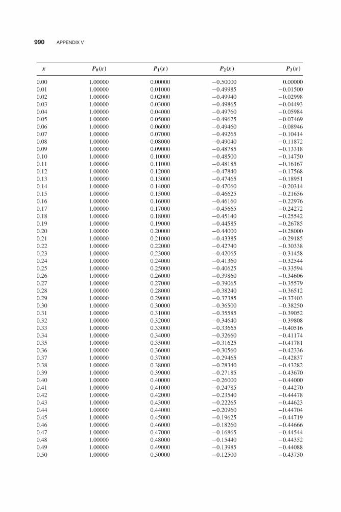
Balanis b05.tex V2 - 11/22/2011 4:33 P.M. Page 990
990 APPENDIX V
x P0(x) P1(x) P2(x) P3(x)
0.00 1.00000 0.00000 −0.50000 0.000000.01 1.00000 0.01000 −0.49985 −0.015000.02 1.00000 0.02000 −0.49940 −0.029980.03 1.00000 0.03000 −0.49865 −0.044930.04 1.00000 0.04000 −0.49760 −0.059840.05 1.00000 0.05000 −0.49625 −0.074690.06 1.00000 0.06000 −0.49460 −0.089460.07 1.00000 0.07000 −0.49265 −0.104140.08 1.00000 0.08000 −0.49040 −0.118720.09 1.00000 0.09000 −0.48785 −0.133180.10 1.00000 0.10000 −0.48500 −0.147500.11 1.00000 0.11000 −0.48185 −0.161670.12 1.00000 0.12000 −0.47840 −0.175680.13 1.00000 0.13000 −0.47465 −0.189510.14 1.00000 0.14000 −0.47060 −0.203140.15 1.00000 0.15000 −0.46625 −0.216560.16 1.00000 0.16000 −0.46160 −0.229760.17 1.00000 0.17000 −0.45665 −0.242720.18 1.00000 0.18000 −0.45140 −0.255420.19 1.00000 0.19000 −0.44585 −0.267850.20 1.00000 0.20000 −0.44000 −0.280000.21 1.00000 0.21000 −0.43385 −0.291850.22 1.00000 0.22000 −0.42740 −0.303380.23 1.00000 0.23000 −0.42065 −0.314580.24 1.00000 0.24000 −0.41360 −0.325440.25 1.00000 0.25000 −0.40625 −0.335940.26 1.00000 0.26000 −0.39860 −0.346060.27 1.00000 0.27000 −0.39065 −0.355790.28 1.00000 0.28000 −0.38240 −0.365120.29 1.00000 0.29000 −0.37385 −0.374030.30 1.00000 0.30000 −0.36500 −0.382500.31 1.00000 0.31000 −0.35585 −0.390520.32 1.00000 0.32000 −0.34640 −0.398080.33 1.00000 0.33000 −0.33665 −0.405160.34 1.00000 0.34000 −0.32660 −0.411740.35 1.00000 0.35000 −0.31625 −0.417810.36 1.00000 0.36000 −0.30560 −0.423360.37 1.00000 0.37000 −0.29465 −0.428370.38 1.00000 0.38000 −0.28340 −0.432820.39 1.00000 0.39000 −0.27185 −0.436700.40 1.00000 0.40000 −0.26000 −0.440000.41 1.00000 0.41000 −0.24785 −0.442700.42 1.00000 0.42000 −0.23540 −0.444780.43 1.00000 0.43000 −0.22265 −0.446230.44 1.00000 0.44000 −0.20960 −0.447040.45 1.00000 0.45000 −0.19625 −0.447190.46 1.00000 0.46000 −0.18260 −0.446660.47 1.00000 0.47000 −0.16865 −0.445440.48 1.00000 0.48000 −0.15440 −0.443520.49 1.00000 0.49000 −0.13985 −0.440880.50 1.00000 0.50000 −0.12500 −0.43750

Balanis b05.tex V2 - 11/22/2011 4:33 P.M. Page 991
APPENDIX V 991
x P0(x) P1(x) P2(x) P3(x)
0.51 1.00000 0.51000 −0.10985 −0.433370.52 1.00000 0.52000 −0.09440 −0.428480.53 1.00000 0.53000 −0.07865 −0.422810.54 1.00000 0.54000 −0.06260 −0.416340.55 1.00000 0.55000 −0.04625 −0.409060.56 1.00000 0.56000 −0.02960 −0.400960.57 1.00000 0.57000 −0.01265 −0.392020.58 1.00000 0.58000 0.00460 −0.382220.59 1.00000 0.59000 0.02215 −0.371550.60 1.00000 0.60000 0.04000 −0.360000.61 1.00000 0.61000 0.05815 −0.347550.62 1.00000 0.62000 0.07660 −0.334180.63 1.00000 0.63000 0.09535 −0.319880.64 1.00000 0.64000 0.11440 −0.304640.65 1.00000 0.65000 0.13375 −0.288440.66 1.00000 0.66000 0.15340 −0.271260.67 1.00000 0.67000 0.17335 −0.253090.68 1.00000 0.68000 0.19360 −0.233920.69 1.00000 0.69000 0.21415 −0.213730.70 1.00000 0.70000 0.23500 −0.192500.71 1.00000 0.71000 0.25615 −0.170220.72 1.00000 0.72000 0.27760 −0.146880.73 1.00000 0.73000 0.29935 −0.122460.74 1.00000 0.74000 0.32140 −0.096940.75 1.00000 0.75000 0.34375 −0.070310.76 1.00000 0.76000 0.36640 −0.042560.77 1.00000 0.77000 0.38935 −0.013670.78 1.00000 0.78000 0.41260 0.016380.79 1.00000 0.79000 0.43615 0.047600.80 1.00000 0.80000 0.46000 0.080000.81 1.00000 0.81000 0.48415 0.113600.82 1.00000 0.82000 0.50860 0.148420.83 1.00000 0.83000 0.53335 0.184470.84 1.00000 0.84000 0.55840 0.221760.85 1.00000 0.85000 0.58375 0.260310.86 1.00000 0.86000 0.60940 0.300140.87 1.00000 0.87000 0.63535 0.341260.88 1.00000 0.88000 0.66160 0.383680.89 1.00000 0.89000 0.68815 0.427420.90 1.00000 0.90000 0.71500 0.472500.91 1.00000 0.91000 0.74215 0.518930.92 1.00000 0.92000 0.76960 0.566720.93 1.00000 0.93000 0.79735 0.615890.94 1.00000 0.94000 0.82540 0.666460.95 1.00000 0.95000 0.85375 0.718440.96 1.00000 0.96000 0.88240 0.771840.97 1.00000 0.97000 0.91135 0.826680.98 1.00000 0.98000 0.94060 0.882980.99 1.00000 0.99000 0.97015 0.940751.00 1.00000 1.00000 1.00000 1.00000
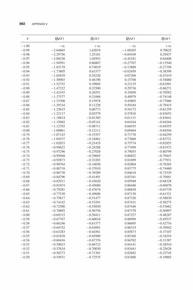
Balanis b05.tex V2 - 11/22/2011 4:33 P.M. Page 992
992 APPENDIX V
x Q0(x) Q1(x) Q2(x) Q3(x)
−1.00 −∞ +∞ −∞ +∞−0.99 −2.64665 1.62019 −1.08265 0.70625−0.98 −2.29756 1.25161 −0.69109 0.29437−0.97 −2.09230 1.02953 −0.45181 0.04408−0.96 −1.94591 0.86807 −0.27707 −0.13540−0.95 −1.83178 0.74019 −0.13888 −0.27356−0.94 −1.73805 0.63377 −0.02459 −0.38399−0.93 −1.65839 0.54230 0.07268 −0.47419−0.92 −1.58903 0.46190 0.15708 −0.54880−0.91 −1.52752 0.39005 0.23135 −0.61091−0.90 −1.47222 0.32500 0.29736 −0.66271−0.89 −1.42193 0.26551 0.35650 −0.70582−0.88 −1.37577 0.21068 0.40979 −0.74148−0.87 −1.33308 0.15978 0.45803 −0.77066−0.86 −1.29334 0.11228 0.50184 −0.79415−0.85 −1.25615 0.06773 0.54172 −0.81259−0.84 −1.22117 0.02579 0.57810 −0.82653−0.83 −1.18814 −0.01385 0.61131 −0.83641−0.82 −1.15682 −0.05141 0.64164 −0.84264−0.81 −1.12703 −0.08711 0.66935 −0.84555−0.80 −1.09861 −0.12111 0.69464 −0.84544−0.79 −1.07143 −0.15357 0.71770 −0.84259−0.78 −1.04537 −0.18461 0.73868 −0.83721−0.77 −1.02033 −0.21435 0.75774 −0.82953−0.76 −0.99622 −0.24288 0.77499 −0.81973−0.75 −0.97296 −0.27028 0.79055 −0.80799−0.74 −0.95048 −0.29665 0.80452 −0.79447−0.73 −0.92873 −0.32203 0.81699 −0.77931−0.72 −0.90764 −0.34650 0.82804 −0.76265−0.71 −0.88718 −0.37010 0.83775 −0.74460−0.70 −0.86730 −0.39289 0.84618 −0.72529−0.69 −0.84796 −0.41491 0.85341 −0.70481−0.68 −0.82911 −0.43620 0.85948 −0.68328−0.67 −0.81074 −0.45680 0.86446 −0.66078−0.66 −0.79281 −0.47674 0.86838 −0.63739−0.65 −0.77530 −0.49606 0.87130 −0.61321−0.64 −0.75817 −0.51477 0.87326 −0.58830−0.63 −0.74142 −0.53291 0.87431 −0.56275−0.62 −0.72500 −0.55050 0.87446 −0.53662−0.61 −0.70892 −0.56756 0.87378 −0.50997−0.60 −0.69315 −0.58411 0.87227 −0.48287−0.59 −0.67767 −0.60018 0.86999 −0.45537−0.58 −0.66246 −0.61577 0.86695 −0.42754−0.57 −0.64752 −0.63091 0.86319 −0.39942−0.56 −0.63283 −0.64561 0.85873 −0.37107−0.55 −0.61838 −0.65989 0.85360 −0.34254−0.54 −0.60416 −0.67376 0.84782 −0.31387−0.53 −0.59015 −0.68722 0.84141 −0.28510−0.52 −0.57634 −0.70030 0.83441 −0.25628−0.51 −0.56273 −0.71301 0.82682 −0.22745−0.50 −0.54931 −0.72535 0.81866 −0.19865

Balanis b05.tex V2 - 11/22/2011 4:33 P.M. Page 993
APPENDIX V 993
x Q0(x) Q1(x) Q2(x) Q3(x)
−0.49 −0.53606 −0.73733 0.80997 −0.16992−0.48 −0.52298 −0.74897 0.80075 −0.14129−0.47 −0.51007 −0.76027 0.79102 −0.11279−0.46 −0.49731 −0.77124 0.78081 −0.08446−0.45 −0.48470 −0.78188 0.77012 −0.05634−0.44 −0.47223 −0.79222 0.75898 −0.02844−0.43 −0.45990 −0.80224 0.74740 −0.00080−0.42 −0.44769 −0.81197 0.73539 0.02654−0.41 −0.43561 −0.82140 0.72297 0.05357−0.40 −0.42365 −0.83054 0.71015 0.08026−0.39 −0.41180 −0.83940 0.69695 0.10658−0.38 −0.40006 −0.84798 0.68338 0.13251−0.37 −0.38842 −0.85628 0.66945 0.15803−0.36 −0.37689 −0.86432 0.65518 0.18311−0.35 −0.36544 −0.87209 0.64057 0.20773−0.34 −0.35409 −0.87961 0.62565 0.23187−0.33 −0.34283 −0.88687 0.61041 0.25552−0.32 −0.33165 −0.89387 0.59488 0.27864−0.31 −0.32055 −0.90063 0.57907 0.30124−0.30 −0.30952 −0.90714 0.56297 0.32328−0.29 −0.29857 −0.91342 0.54662 0.34474−0.28 −0.28768 −0.91945 0.53001 0.36563−0.27 −0.27686 −0.92525 0.51316 0.38591−0.26 −0.26611 −0.93081 0.49607 0.40558−0.25 −0.25541 −0.93615 0.47876 0.42461−0.24 −0.24477 −0.94125 0.46124 0.44301−0.23 −0.23419 −0.94614 0.44351 0.46074−0.22 −0.22366 −0.95080 0.42559 0.47781−0.21 −0.21317 −0.95523 0.40748 0.49420−0.20 −0.20273 −0.95945 0.38920 0.50990−0.19 −0.19234 −0.96346 0.37075 0.52490−0.18 −0.18198 −0.96724 0.35215 0.53918−0.17 −0.17167 −0.97082 0.33339 0.55275−0.16 −0.16139 −0.97418 0.31450 0.56559−0.15 −0.15114 −0.97733 0.29547 0.57769−0.14 −0.14093 −0.98027 0.27632 0.58904−0.13 −0.13074 −0.98300 0.25706 0.59964−0.12 −0.12058 −0.98553 0.23769 0.60948−0.11 −0.11045 −0.98785 0.21822 0.61856−0.10 −0.10034 −0.98997 0.19866 0.62687−0.09 −0.09024 −0.99188 0.17903 0.63440−0.08 −0.08017 −0.99359 0.15932 0.64115−0.07 −0.07011 −0.99509 0.13954 0.64711−0.06 −0.06007 −0.99640 0.11971 0.65229−0.05 −0.05004 −0.99750 0.09983 0.65668−0.04 −0.04002 −0.99840 0.07991 0.66027−0.03 −0.03001 −0.99910 0.05996 0.66307−0.02 −0.02000 −0.99960 0.03999 0.66507−0.01 −0.01000 −0.99990 0.02000 0.66627
0.00 0.00000 −1.00000 0.00000 0.66667

Balanis b05.tex V2 - 11/22/2011 4:33 P.M. Page 994
994 APPENDIX V
x Q0(x) Q1(x) Q2(x) Q3(x)
0.01 0.01000 −0.99990 −0.02000 0.666270.02 0.02000 −0.99960 −0.03999 0.665070.03 0.03001 −0.99910 −0.05996 0.663070.04 0.04002 −0.99840 −0.07991 0.660270.05 0.05004 −0.99750 −0.09983 0.656680.06 0.06007 −0.99640 −0.11971 0.652290.07 0.07011 −0.99509 −0.13954 0.647110.08 0.08017 −0.99359 −0.15932 0.641150.09 0.09024 −0.99188 −0.17903 0.634400.10 0.10033 −0.98997 −0.19866 0.626870.11 0.11045 −0.98785 −0.21822 0.618560.12 0.12058 −0.98553 −0.23769 0.609480.13 0.13074 −0.98300 −0.25706 0.599640.14 0.14092 −0.98027 −0.27632 0.589040.15 0.15114 −0.97733 −0.29547 0.577690.16 0.16139 −0.97418 −0.31450 0.565590.17 0.17167 −0.97082 −0.33339 0.552750.18 0.18198 −0.96724 −0.35215 0.539190.19 0.19234 −0.96346 −0.37075 0.524900.20 0.20273 −0.95945 −0.38920 0.509900.21 0.21317 −0.95523 −0.40748 0.494200.22 0.22366 −0.95080 −0.42559 0.477820.23 0.23419 −0.94614 −0.44351 0.460750.24 0.24477 −0.94125 −0.46124 0.443010.25 0.25541 −0.93615 −0.47876 0.424610.26 0.26611 −0.93081 −0.49607 0.405580.27 0.27686 −0.92525 −0.51316 0.385910.28 0.28768 −0.91945 −0.53001 0.365630.29 0.29857 −0.91342 −0.54662 0.344740.30 0.30952 −0.90714 −0.56297 0.323280.31 0.32054 −0.90063 −0.57907 0.301240.32 0.33165 −0.89387 −0.59488 0.278650.33 0.34283 −0.88687 −0.61041 0.255520.34 0.35409 −0.87961 −0.62565 0.231870.35 0.36544 −0.87210 −0.64057 0.207730.36 0.37689 −0.86432 −0.65518 0.183110.37 0.38842 −0.85628 −0.66945 0.158030.38 0.40006 −0.84798 −0.68338 0.132510.39 0.41180 −0.83940 −0.69695 0.106580.40 0.42365 −0.83054 −0.71015 0.080260.41 0.43561 −0.82140 −0.72297 0.053570.42 0.44769 −0.81197 −0.73539 0.026540.43 0.45990 −0.80225 −0.74740 −0.000800.44 0.47223 −0.79222 −0.75898 −0.028440.45 0.48470 −0.78189 −0.77012 −0.056330.46 0.49731 −0.77124 −0.78081 −0.084460.47 0.51007 −0.76027 −0.79102 −0.112790.48 0.52298 −0.74897 −0.80075 −0.141290.49 0.53606 −0.73733 −0.80997 −0.169920.50 0.54931 −0.72535 −0.81866 −0.198650.51 0.56273 −0.71301 −0.82682 −0.22746

Balanis b05.tex V2 - 11/22/2011 4:33 P.M. Page 995
APPENDIX V 995
x Q0(x) Q1(x) Q2(x) Q3(x)
0.52 0.57634 −0.70030 −0.83441 −0.256280.53 0.59014 −0.68722 −0.84141 −0.285100.54 0.60416 −0.67376 −0.84782 −0.313870.55 0.61838 −0.65989 −0.85360 −0.342540.56 0.63283 −0.64561 −0.85873 −0.371070.57 0.64752 −0.63091 −0.86319 −0.399420.58 0.66246 −0.61577 −0.86695 −0.427540.59 0.67767 −0.60018 −0.86999 −0.455370.60 0.69315 −0.58411 −0.87227 −0.482860.61 0.70892 −0.56756 −0.87378 −0.509970.62 0.72500 −0.55050 −0.87446 −0.536620.63 0.74142 −0.53291 −0.87431 −0.562750.64 0.75817 −0.51477 −0.87327 −0.588300.65 0.77530 −0.49606 −0.87130 −0.613210.66 0.79281 −0.47674 −0.86838 −0.637390.67 0.81074 −0.45680 −0.86446 −0.660780.68 0.82911 −0.43620 −0.85948 −0.683280.69 0.84795 −0.41491 −0.85341 −0.704810.70 0.86730 −0.39289 −0.84618 −0.725290.71 0.88718 −0.37010 −0.83775 −0.744600.72 0.90765 −0.34649 −0.82804 −0.762650.73 0.92873 −0.32203 −0.81699 −0.779310.74 0.95048 −0.29665 −0.80452 −0.794470.75 0.97296 −0.27028 −0.79055 −0.807990.76 0.99622 −0.24288 −0.77499 −0.819730.77 1.02033 −0.21435 −0.75774 −0.829530.78 1.04537 −0.18461 −0.73868 −0.837210.79 1.07143 −0.15357 −0.71770 −0.842590.80 1.09861 −0.12111 −0.69464 −0.845440.81 1.12703 −0.08711 −0.66935 −0.845550.82 1.15682 −0.05141 −0.64164 −0.842640.83 1.18814 −0.01385 −0.61131 −0.836410.84 1.22117 0.02579 −0.57810 −0.826530.85 1.25615 0.06773 −0.54172 −0.812590.86 1.29334 0.11227 −0.50184 −0.794150.87 1.33308 0.15978 −0.45803 −0.770660.88 1.37577 0.21068 −0.40979 −0.741480.89 1.42192 0.26551 −0.35651 −0.705820.90 1.47222 0.32500 −0.29737 −0.662710.91 1.52752 0.39005 −0.23135 −0.610910.92 1.58903 0.46191 −0.15708 −0.548800.93 1.65839 0.54231 −0.07268 −0.474190.94 1.73805 0.63376 0.02458 −0.384000.95 1.83178 0.74019 0.13888 −0.273570.96 1.94591 0.86807 0.27707 −0.135400.97 2.09230 1.02953 0.45182 0.044090.98 2.29755 1.25160 0.69107 0.294350.99 2.64664 1.62017 1.08264 0.706241.00 +∞ +∞ +∞ +∞

Balanis b05.tex V2 - 11/22/2011 4:33 P.M. Page 996
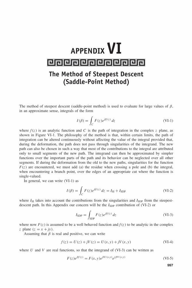
Balanis b06.tex V2 - 11/22/2011 4:35 P.M. Page 997
APPENDIX VIThe Method of Steepest Descent
(Saddle-Point Method)
The method of steepest descent (saddle-point method) is used to evaluate for large values of β,in an approximate sense, integrals of the form
I (β) =∫
CF (z )eβf (z ) dz (VI-1)
where f (z ) is an analytic function and C is the path of integration in the complex z plane, asshown in Figure VI-1. The philosophy of the method is that, within certain limits, the path ofintegration can be altered continuously without affecting the value of the integral provided that,during the deformation, the path does not pass through singularities of the integrand. The newpath can also be chosen in such a way that most of the contributions to the integral are attributedonly to small segments of the new path. The integrand can then be approximated by simplerfunctions over the important parts of the path and its behavior can be neglected over all othersegments. If during the deformation from the old to the new paths, singularities for the functionF (z ) are encountered, we must add (a) the residue when crossing a pole and (b) the integral,when encountering a branch point, over the edges of an appropriate cut where the function issingle-valued.
In general, we can write (VI-1) as
I (β) =∫
CF (z )eβf (z ) dz = ISI + ISDP (VI-2)
where ISI takes into account the contributions from the singularities and ISDP from the steepest-descent path. In this Appendix our concern will be the ISDP contribution of (VI-2) or
ISDP =∫
SDPF (z )eβf (z ) dz (VI-3)
where now F (z ) is assumed to be a well behaved function and f (z ) to be analytic in the complexz plane (z = x + jy).
Assuming that β is real and positive, we can write
f (z ) = U (z ) + jV (z ) = U (x , y) + jV (x , y) (VI-4)
where U and V are real functions, so that the integrand of (VI-3) can be written as
F (z )eβf (z ) = F (x , y)eβU (x ,y)ejβV (x ,y) (VI-5)
997
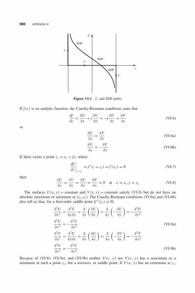
Balanis b06.tex V2 - 11/22/2011 4:35 P.M. Page 998
998 APPENDIX VI
SDP
SDP
SDP
jy
x
C
C
C
Figure VI-1 C and SDP paths.
If f (z ) is an analytic function, the Cauchy-Riemann conditions state that
df
dz= ∂U
∂x+ j
∂V
∂x= −j
∂U
∂y+ ∂V
∂y(VI-6)
or
∂U
∂x= ∂V
∂y(VI-6a)
∂U
∂y= −∂V
∂x(VI-6b)
If there exists a point zs = xs + jys where
df
dz
∣∣∣∣z=zs
≡ f ′(z = zs) = f ′(zs) = 0 (VI-7)
then∂U
∂x= ∂V
∂y= ∂U
∂y= ∂V
∂x= 0 at x = xs , y = ys (VI-8)
The surfaces U (x , y) = constant and V (x , y) = constant satisfy (VI-8) but do not have anabsolute maximum or minimum at (xs , ys). The Cauchy-Riemann conditions (VI-6a) and (VI-6b)also tell us that, for a first-order saddle point [f ′′(zs) �= 0]
∂2U
∂x 2= ∂2V
∂x∂y= ∂
∂y
(∂V
∂x
)= ∂
∂y
(−∂U
∂y
)= −∂2U
∂y2
∂2U
∂x 2= −∂2U
∂y2(VI-9a)
∂2V
∂y2= ∂2U
∂y∂x= ∂
∂x
(∂U
∂y
)= ∂
∂x
(−∂V
∂x
)= −∂2V
∂x 2
∂2V
∂y2= −∂2V
∂x 2(VI-9b)
Because of (VI-8), (VI-9a), and (VI-9b) neither U (x , y) nor V (x , y) has a maximum or aminimum at such a point zs , but a minimax or saddle point. If U (x , y) has an extremum at zs ,
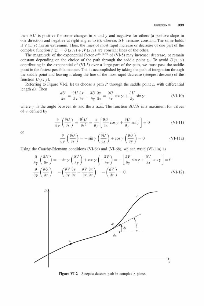
Balanis b06.tex V2 - 11/22/2011 4:35 P.M. Page 999
APPENDIX VI 999
then U is positive for some changes in x and y and negative for others (a positive slope inone direction and negative at right angles to it), whereas V remains constant. The same holdsif V (x , y) has an extremum. Thus, the lines of most rapid increase or decrease of one part of thecomplex function f (z ) = U (x , y) + jV (x , y) are constant lines of the other.
The magnitude of the exponential factor eβU (x ,y) of (VI-5) may increase, decrease, or remainconstant depending on the choice of the path through the saddle point zs . To avoid U (x , y)contributing in the exponential of (VI-5) over a large part of the path, we must pass the saddlepoint in the fastest possible manner. This is accomplished by taking the path of integration throughthe saddle point and leaving it along the line of the most rapid decrease (steepest descent) of thefunction U (x , y).
Referring to Figure VI-2, let us choose a path P through the saddle point zs with differentiallength ds . Then
dU
ds= ∂U
∂x
∂x
∂s+ ∂U
∂y
∂y
∂s= ∂U
∂xcos γ + ∂U
∂ysin γ (VI-10)
where γ is the angle between ds and the x axis. The function dU /ds is a maximum for valuesof γ defined by
∂
∂γ
(∂U
∂s
)= ∂2U
∂s2= ∂
∂γ
[∂U
∂xcos γ + ∂U
∂γsin γ
]= 0 (VI-11)
or∂
∂γ
(∂U
∂s
)= − sin γ
(∂U
∂x
)+ cos γ
(∂U
∂y
)= 0 (VI-11a)
Using the Cauchy-Riemann conditions (VI-6a) and (VI-6b), we can write (VI-11a) as
∂
∂γ
(∂U
∂s
)= − sin γ
(∂V
∂y
)+ cos γ
(−∂V
∂x
)= −
[∂V
∂ysin γ + ∂V
∂xcos γ
]= 0
∂
∂γ
(∂U
∂s
)= −
(∂V
∂y
∂y
∂s+ ∂V
∂x
∂x
∂s
)= −
(dV
ds
)= 0 (VI-12)
jy
dy
dx
x
ds
P
g
zs
Figure VI-2 Steepest descent path in complex z plane.
Balanis b06.tex V2 - 11/22/2011 4:35 P.M. Page 1000
1000 APPENDIX VI
Thus V = constant for paths along which U (x , y) changes most rapidly (and vice versa), so thesteepest amplitude path is a constant phase path . These are known as steepest ascent or descentpaths. We choose the steepest descent path, thus the name method of steepest descent . Since β
is real and positive, the exponential exp[βU (x , y)] of (VI-5) will decrease rapidly with distancefrom the saddle point and only a small portion of the integration path, including the saddle point,will make any significant contributions to the value of the entire integral.
To find the path of steepest descent, we form a function
f (z ) = f (zs) − s2 (VI-13)
where zs is the saddle point and s is real (−∞ ≤ s ≤ +∞). The saddle point corresponds tos = 0. Using (VI-4), we can write (VI-13) as
U (z ) = U (zs) − s2 (VI-13a)
V (z ) = V (zs) steepest descent path (VI-13b)
Since the imaginary part remains constant, while the real part attains maximum at s = 0 anddecreases for other values, the path of steepest descent is described by (VI-13b).
To evaluate the integral of (VI-3), we first find the saddle point zs by (VI-7). Next, we expressf (z ), around the saddle point zs , by a truncated Taylor series
f (z ) � f (zs) + 12 (z − zs)
2f ′′(zs) (VI-14)
since f ′(zs) = 0. The double prime indicates a second derivative with respect to z . Substitutionof (VI-14) into (VI-3) leads to
I (β) =∫
SDPF (z )eβf (z ) dz � eβf (zs )
∫SDP
F (z )e(β/2)(z−zs )2f ′′(zs ) dz (VI-15)
Letting
− β(z − zs)2f ′′(zs) = ξ 2 (VI-15a)
dz = dξ√−βf ′′(zs)(VI-15b)
we can write (VI-15), by extending the limits to infinity, as
I (β) � eβf (zs )√−βf ′′(zs)
∫ +∞
−∞F (z )e−ξ2/2 dξ (VI-16)
Assuming that F (z ) is a slow varying function in the neighborhood of the saddle point, we canwrite (VI-16), by replacing F (z ) by F (zs), as
I (β) � eβf (zs )√−βf ′′(zs)2F (zs)
∫ ∞
0e−ξ2/2 dξ
I (β) � eβf (zs )√−βf ′′(zs)F (zs)2
√π
2=
√2π
−βf ′′(zs)F (zs)e
βf (zs ) (VI-17)
If more than one saddle point exists, then (VI-16) can be written as
I (β) �√
2π
β
N∑s=1
F (zs)√−f ′′(zs)eβf (zs ) (VI-18)

Balanis b06.tex V2 - 11/22/2011 4:35 P.M. Page 1001
APPENDIX VI 1001
where N is equal to the number of saddle points. The summation assumes, through the principleof superposition, that the contribution of each saddle point is not affected by the presence of theothers.
Equation VI-18 accounts for the contribution to the integral (VI-3) from first-order saddlepoints [f ′(zs) = 0 but f ′′(zs) �= 0]. For second-order saddle points [f ′(zs) = 0 and f ′′(zs) = 0],the expression is different. For general forms of f (z ), the determination of all the steepest descentpaths may be too complicated.
If a constant level path is chosen such that | exp[βU (x , y)]| remains constant everywhere andexp[jβV (x , y)] varies most rapidly away from the saddle points, the evaluation of the integralcan be carried out from contributions near the saddle points. Since the phase factor exp(jβV )
is stationary at and near the saddle points, and oscillates very rapidly in the remaining parts ofthe path, it makes the net contributions from the other parts, excluding the saddle points, verynegligible. This is known as the method of stationary phase, and it may not yield the same resultas the method of steepest descent because their corresponding paths are different. The two willlead to identical results if the constant level path can be continuously deformed to the steepestdescent path. This is accomplished if the two paths have identical terminations and there are nosingularities of f (z ) in the region between the two paths. The Method of Stationary Phase isdescribed in detail in Appendix VIII of Antenna Theory: Analysis and Design by C.A. Balanis,Third Edition, copyright © 2005, John Wiley & Sons, Inc.

Balanis b06.tex V2 - 11/22/2011 4:35 P.M. Page 1002

Balanis bindex.tex V1 - 11/22/2011 4:37 P.M. Page 1003
Index
AAcceptors, 59A.C. variations in materials, 68–69
complex permittivity, 68–79Addition theorem, 655
Bessel functions, 604–606Hankel functions, 601–604
Air-substrate modes, 423Aluminum
atom, 40charge density, 62conductivity, 58mobility, 59
Ampere’s law, 3, 5, 142Amplitude relation, 745–748Angular frequency, 70, 153
natural, 72resonant, 72
Anisotropic dielectrics, 67Anomalous (abnormal) dispersion,
78Antenna applications, 444–448
aperture, 444–445, 447microstrip, 445–448monopole, 444
Antiferromagnetic material, 54Aperture antenna analysis, coordinate system
for, 287Aperture_GP_UTD program, 832Array factor, 320, 322Array multiplication rule, 177Artificial impedance surfaces (AIS), 436–455
antenna applications, 444–448corrugations, 439–441mushroom engineering texture surface, 442surface wave dispersion characteristics,
451–454uses, 437
Artificial magnetic conductors (AMC),441–444
mushroom AMC design, 448–451Associated Legendre functions, 119Astigmatic rays, 747–748, 752–753, 762–763Asymptotic expansions, 869–870Atom, 39–40
aluminium, 40Bohr model of, 40germanium, 40hydrogen, 40silicon, 40
Atomic modelsequivalent circular electric loop, 48equivalent square electric loop, 48orbiting electrons, 48
Atomic number, 39Attenuation, 374–382
circular waveguides, 495–500rectangular waveguide
Auxiliary vector potentials, 259–305inhomogeneous vector potential wave
equation, solution of, 279–282vector potential A, 260–262vector potential F, 262–263vector potentials A and F, 263–265
Axial ratio (AR), 160
BBackscattering, 339, 341, 584, 596, 743Band-gap structure, 437Basis functions, 338, 682, 691–695
entire domain, 693–695subdomain, 691–693
Beam translator, 242Bednorz, J. G., 65Bent wire, 684–686

Balanis bindex.tex V1 - 11/22/2011 4:37 P.M. Page 1004
1004 INDEX
Bessel functions, 112–114, 518, 537,604–606, 967–979
asymptotic forms, 968derivative, 969differential equation, 112, 934first kind, 967–968graphs, 942, 945integrals, 969–970modified, 518, 970–971, 978–979second kind, 113, 118, 975spherical, 118, 549, 561, 971zeroes, 491
Biconical transmission line, 557–561characteristic impedance, 560–561TEMr mode, 559–561TEr mode, 557–559TMr mode, 559
Bilinear formula, 901Binomial (maximally flat) design,
215–217Binomial impedance transformer, 213Bistatic/Bistatic scattering width,
584, 587circular cylinder, 607–639rectangular plate, 591–599sphere, 652–665strip, 584–597
Bit Error Ratio (BER), 849Bloch mode, 453Bound electrons, 59Boundary conditions, 2, 12–18
finite conductivity media, 12–14geometry for, 13infinite conductivity media, 15–17sources along boundaries, 17–18time-harmonic electromagnetic field,
22–25Brewster angle, 173, 184–188
total transmission, 184–188Brillouin zone, 453
CCanonical problem, 742Capacitor, 8–11, 28Cauchy–Riemann conditions, 998–999Caustic, 316–317, 582, 747Cavities, 483–548, 549–574 (see also
Circular cavity; Rectangular resonantcavities; Spherical cavity)
Charge densityelectric, 2, 11, 15, 280magnetic, 2–3, 28, 82–85
Charge distribution, 680–677bent wire, 684–686electrostatic, 680–686straight wire, 680–684
Chebyshev (see Tschebyscheff (equal-ripple)design)
Chu, P. C. W., 65–66CircDielGuide program, 541Circuit equations, 7Circuit-field relations, 7–11
element laws, 10–11Kirchhoff node current law, 9Kirchhoff’s current Law, 8–10Kirchhoff’s voltage Law, 7–8
Circuit theoryfield theory and, relations between, 11Green’s functions in, 886–889
Circular cavity, 500–508coupling, 500dissipated power, 507dominant mode, 505modes, 500–505quality factor, 505–508resonant frequency, 504–505stored energy, 507
Circular cylinders, scattering by, 607–639normal incidence plane wave scattering,
607–617oblique incidence plane wave scattering,
617–626Circular dielectric resonator, 526–531
optical fiber cable, 532–534TE01δ mode, 530–531TEz modes, 528–529
Circular dielectric waveguide, 516–526Circular polarization, 147, 150–155
left-hand (counterclockwise) circularpolarization, 153–155
necessary and sufficient conditionsfor, 155
right-hand (clockwise) polarization, 147,150–153
Circular waveguide, 483–500attenuation, 495–500TEz mode, 483–488TMz mode, 488–495
Clausius–Mosotti equation, 79

Balanis bindex.tex V1 - 11/22/2011 4:37 P.M. Page 1005
INDEX 1005
Closed form, Green’s function in, 893–898Coercive electric field, 43Complex angles, 192, 220Complex permeability, 79–80Computer codes, 732–735, 829
electromagnetic surface patch (ESP), 735geometrical theory of diffraction (GTD),
829–832mini–numerical electromagnetics code
(MININEC), 734Numerical Electromagnetic Code (NEC),
734–736Pocklington’s wire radiation and scattering
(PWRS), 732, 734two-dimensional radiation and scattering
(TDRS), 732–734Conducting circular cylinder
line-source scattering by, 626–639Conducting wedge, scattering by, 639–650
electric line-source scattering, 648–650magnetic line-source scattering, 648–650
Conduction band, 60–61Conduction (ohmic) losses, 374Conductivity, 57–59
finite conductivity media, 12–14infinite conductivity media, 15–17
Conductors, 56–57, 140conductivity conditions for, 62energy levels for, 61good conductors, 75, 140, 143
Conservation of energy, 19Conservation of power law, 21Conservation-of-energy equation, 26Constitutive parameters, 6Constitutive relations, 5–6Constraint (dispersion) equation, 104, 108,
112Construction of solutions, 265–278, 549–557
scalar Helmholtz wave equation, solutionof, 556–557
TE mode, source-free region, 276–278,553–554
TEM modes, source-free region, 265–272TM mode, source-free region, 265,
272–276, 555vector potential A(J �= 0, M = 0), 552vector potential F(J = 0, M �= 0), 550–551vector potentials F and A, 552
Continuity equation, 3differential form, 6, 22–23
integral form, 6, 22–25Continuous derivatives, 2Convection current density, 56Conventional method of steepest descent,
770, 775Copper
charge density, 62mobility, 62
Corrugations, 439–441Coupled equation, 111Coupling, 381–382
coaxial transmission line to rectangularwaveguide coupling, 382
electric field, 381magnetic field, 381
Critical angle, 173, 180, 189parallel (vertical) polarization, 198total reflection, 188–198wave propagation along an interface, 198
Critical temperature (Tc), 64–66Critically damped solution, 71Curie temperature, 43Curie–Weiss law, 43Current density, 4, 56
conduction electric, 2, 73conduction magnetic, 80convection, 56displacement electric, 2, 72–73displacement magnetic, 2–3, 80impressed electric, 2–3, 73–74impressed magnetic, 2–5, 12, 80
Curved edge diffraction, 808–815oblique incidence, 808–815
Cutoff, 485Cutoff frequency, 415Cutoff wave number, 356Cyl_Resonator program, 541Cyl_Waveguide program, 541Cylinder_RCS program, 665Cylindrical coordinate system, 110–115
infinities of wave functions, 115wave functions, 115zeroes of wave functions, 115
Cylindrical coordinate system, 269–272,275–276, 278, 299–305, 928–933
Cylindrical waveaddition theorem ofplane waves in terms of, 599–601transformations and theorems,
599–606
Balanis bindex.tex V1 - 11/22/2011 4:37 P.M. Page 1006
1006 INDEX
DDamped
critically, 71over, 71, 78under, 71, 78
Debye equation, 79Delta–gap source, 723, 729Diagonalization, 68Diamagnetic materials, 53–54Dielectric circular waveguide,
516–526eigenvalue equation, 519, 521
Dielectric constant, 46–47, 75Dielectric-covered conducting rod,
534–541geometry of, 535TEz modes, 540–541TMz modes, 534–540
Dielectric covered ground plane, 433–436Dielectric hysteresis, 73Dielectric losses, 378–381Dielectric resonator, circular (see Circular
dielectric resonator)Dielectrics, 41–48, 59, 140
anisotropic, 67conductivity conditions for, 62dielectric slab subjected to applied electric
fieldgood dielectrics, 74, 140, 142–143isotropic, 229
Dielectric waveguides, 408–436, 516–541(see also Ray-tracing method)
circular dielectric waveguide, 516–526dielectric-covered ground plane,
433–436geometry for, 409transverse electric (TEz ) modes, 419–423transverse magnetic (TMz ) modes,
410–419Differential equation
coupled, 99–111, 116uncoupled, 100–111, 554
Differential form of Maxwell’s equations, 2–3Diffracted field, 778, 868–875
asymptotic expansions, 869–870diffraction terms, 868–869incident, 776, 781, 790reflected, 773, 781
Diffraction, 741–832 (see also Geometricaltheory of diffraction (GTD) techniques)
Diffraction by wedge with impedancesurfaces, 849–879
computations, 877–879diffracted fields, 868–875geometrical optics, 857–865impedance surface boundary conditions,
850–851impedance surface reflection coefficients,
851–854Maliuzhinets impedance wedge solution,
854–856surface wave terms, 865–868surface wave transition field, 875–877
Diffraction coefficients, 780–800hard polarization, 783–784incident, 776Keller’s, 785reflection, 782–783soft polarization, 783–784
Diffraction plane, 801Dipole
electric, 41–42, 44, 55, 68, 70magnetic, 48–50, 55, 80–83moment, 41–43torque, 81–82
Dipole_Horizontal_H_Plane program,880
Dipole_Vertical program, 879Dirac delta weighting functions, 699–700Dispersion equation, 72, 104Dispersive materials, 7Distance parameter (L), 799, 803–804, 808,
830Divergence theorem, 3–5, 921, 924Domains, 54Dominant mode, 360–363, 435, 517,
559, 566Donors, 59Doping, 59Double Negative (DNG) materials, 39,
228–243propagation characteristics of, 231–233propagation through, 233–241refraction through, 233–241
Double positive (DPS) material, 228–243Duality theorem, 311–312, 580Dyadic Green’s functions, 938–941
dyadics, 938–939Dyadic reflection coefficient, 751, 763Dynamic model, 454–455

Balanis bindex.tex V1 - 11/22/2011 4:37 P.M. Page 1007
INDEX 1007
EEcho area, 583Edge diffraction, 761–829 (see also Curved
edge diffraction; Multiple diffractions;Straight edge diffraction)
amplitude, phase and polarizationrelations, 761–765
equivalent currents in diffraction, 815–819slope diffraction, 819–821
Effective dielectric constant, 459–466microstrip transmission line, 462–463
Effective radius, 540Eigenfunction, 355, 850, 900–905, 914–918Eigenvalue equation, 519, 521Eigenvalues, 355, 521–523, 558–563, 894Eikonal equation, 744Eikonal surface, 744–749, 761
cylindrical, 745plane, 745spherical, 745
Electrets, 43Electric current density, 3–4Electric field coupling, 381Electric field integral equations (EFIE), 338,
688, 703–713perfectly electric conducting (PEC)
surface, 704two-dimensional EFIE, 706–713
Electric line source, 576–580above infinite plane electric conductor,
580–583scattering by conducting wedge, 648–650
Electric polarization vector P, 42Electric potential, 680, 908, 916Electric susceptibility, 46Electrical properties of matter, 39–89Electromagnetic band-gap (EBG), 441–444Electromagnetic Surface Patch (ESP) code,
735Electromagnetic theorems and principles,
311–344duality theorem, 311–312image theory, 315–323induction equivalent approximations,
339–344induction theorem (induction equivalent),
333–336physical equivalent method, 337–344physical optics equivalent method,
337–339
reaction theorem, 325–326reciprocity theorem, 323–325surface equivalence theorem, 328–333uniqueness theorem, 313–315volume equivalence theorem, 326–328
Electron mobility, 59Electronic polarization, 43Electrons
bound, 59–60free, 56, 59–60
Electrostatic charge distribution,680–686
Element laws, 10–11Elliptical polarization, 147, 155–166
electromagnetic waves, polarization statesof, 162
left-hand elliptically polarized wave, 156right-hand elliptically polarized wave, 156
Energy, 18–21, 25–29conservation of, 3, 19, 21, 25–27, 29,
742–745, 748, 764densityelectric, 21, 129inductor, 11magnetic, 21, 129velocity, 129, 136–137, 144–146
Engineered electromagnetic surfaces (seeArtificial impedance surfaces)
Entire-domain functions, 693–695Epsilon negative (ENG) material, 228–229Equal amplitudes, 153, 155, 158Equiphase plane, 123Equiphase point, 107Equivalence principle models, 330 (see also
Surface equivalence theorem)Equivalent currents
in diffraction, 815–819Equivalents, 3, 332, 335–339Expansion functions, 681, 690, 695, 701, 720Extended Physical Theory of Diffraction
(EPTD), 827–830Extended Spectral Theory of Diffraction
(ESTD), 827–828Exterior wedges, 648, 779, 850
FFaraday’s law, 5Far-field approximations, 582Far-field radiation, 283–284

Balanis bindex.tex V1 - 11/22/2011 4:37 P.M. Page 1008
1008 INDEX
Far-zone field, 610–612, 615–617, 621–623,643
Felsen-Marcuvitz method, 869–870, 875Fermat’s principle, 742–743Ferrites, 54, 80–89Ferroelectric Curie temperature, 43Ferromagnetic material, 54Fiber optics cable, 409, 498, 532–534
attenuation, 532discrete modes, 532graded–index, 532–534multimode, 532–534normalized diameter, 526single–mode, 532step–index, 532, 534
Field equations, 7Field intensity
electric, 2, 6, 14, 17–18, 24, 45–46,259
magnetic, 2, 6, 14, 17, 25, 28, 259Field relations (see Circuit-field relations)Field theory, circuit theory and, relations
between, 11Finite conductivity media, 12–14Finite diameter wires, 723–732Finite straight wire, 680–684Floquet Theorem, 228Forbidden band, 60–61Fourier–Legendre series, 652Free electrons, 56, 59Fresnel integrals, 776, 778, 784–785,
961–965graphs, 965tables, 962–964
Fresnel reflection coefficient, 180, 183Fresnel transmission coefficient, 180, 183Fresnel transition function (FTF), 784–785,
789, 803, 821, 830–831large argument, 831small argument, 831
Fringe wave, 679
GGalerkin’s method, 697–699Gallium arsenide, 63
charge density, 62conductivity, 62mobility, 62–63
Gauss’s law, 5
Generalized Green’s function method,922–925
nonhomogeneous partial differentialequation
Geometrical optics (GO), 701, 742–761, 777,857–865
amplitude relation, 745–748astigmatic rays, 747, 748, 752, 762caustic, 747, 748, 757conservation of energy flux, 743, 764divergence factor, 763, 764dyadic reflection coefficient, 751eikonal surface, 744–748Luneberg–Kline series, 749–750, 760–761normal section, 754–755phase, 761–765primary wave front, 743–744principal radii of curvature, 752–755ray optics, 742reflection from surfaces, 751–761region, 765–778secondary wave front, 743–744spatial attenuation, 750, 752spreading factor, 750, 752variational differential, 743
Geometrical theory of diffraction (GTD)techniques, 639, 650, 679, 701,741–832 (see also Edge diffraction;Geometrical optics (GO))
Germanium, 59, 63Good conductors, 24, 75–79, 140, 143Good dielectrics, 74–75, 140, 142–143Graded index, 409
multimode cables, 532–534Green’s functions, 650, 885–945 (see also
Dyadic Green’s functions; GeneralizedGreen’s function method)
Green’s identities and methods, 919–925in closed form, 893–898in engineering, 886–907in integral form, 904–907of scalar Helmholtz equation, 925–937in series, 898–904two-dimensional, in rectangular
coordinates, 908–919Group velocity, 124, 128–129, 136–137, 370,
454Guide wavelength (λg), 359, 370, 485Gunn Diode oscillator, 351Gyromagnetic ratio, 82

Balanis bindex.tex V1 - 11/22/2011 4:37 P.M. Page 1009
INDEX 1009
HHallén’s integral equation, 723, 727–729
source modeling, 729Hankel functions, 113–115, 118–120, 512,
518, 556–557, 577–578, 601, 607–615,643, 686, 689, 696, 768, 933, 966–970
addition theorem of, 601–604derivative, 608, 971spherical, 118, 120, 549, 560, 651, 658,
660, 971–979Hard polarization, 440, 650, 768–769,
820–825, 852–855Helmholtz equation, 102, 549–550, 554–557,
904 (see also Scalar Helmholtzequation)
cylindrical, 928–933rectangular, 925–928spherical, 933–937
Hermite-Gaussian functions, 534Hermitian properties, 68, 897High-frequency asymptotic solution,
768–772High temperature superconductivity (HTS),
66Holes, 60Homogeneous materials, 7, 67–68Horizontal electric dipole, 321–323Horizontal polarization (see Perpendicular
(horizontal) polarization)Huygens’s principle, 328–333Hybrid modes, 390–393, 516–517 (see also
Longitudinal section electric (LSE)modes; Longitudinal section magnetic(LSM) modes)
dielectric circular waveguide, 516–526Hydrogen atom, 40Hyperbolic identity, 948–949Hysteresis loop, 43, 54
IIdentities, 947–949
hyperbolic, 948–949logarithmic, 949trigonometric, 947–948
Image theory, 315–323IMPATT diode, 351Impedance
boundary condition, 849directional, 135, 144
intrinsic, 127, 133, 135, 140, 143–144,214–216, 283, 289, 438
surface boundary conditions, 850–851surface reflection coefficients, 851–854wave, 123, 126–128, 135, 142, 358, 371,
578Incident diffracted field, 776, 780Incident diffraction coefficient, 782–783Incident geometrical optics, 775Index of refraction, 46, 73, 229–230,
232–234, 237, 409, 532–534, 743Induction theorem (induction equivalent),
333–336approximations, 339–344field geometry for, 334
Inductor, 8–11, 28, 487, 886Infinite conductivity media, 15–17Infinite line-source cylindrical wave radiation,
575–583electric line source, 576–580magnetic line source, 580
Infinitesimal dipole, 282, 651Inhomogeneous vector potential wave
equation solution, 279–282Input-match frequency band, 437–438Insulators
conductivity conditions for, 62energy levels for, 61
Integral equation (IE) technique, 679–703(see also Electric field integralequations (EFIE); Magnetic fieldintegral equation (MFIE))
application of point matching, 695–697basis functions, 691–695 (see also
individual entry)electrostatic charge distribution, 680–686integral equation, 686–688moment method, 697–703 (see also
individual entry)point-matching (collocation) method,
689–691radiation pattern, 688–689weighting (testing) functions, 697
Integral formGreen’s function in, 904–907of Maxwell’s equations, 3–5
Interior wedges, 648, 850, 854–855Intrinsic (pure) semiconductor, 59Intrinsic impedance, 127, 198–99, 206,
214–216, 283, 851
Balanis bindex.tex V1 - 11/22/2011 4:37 P.M. Page 1010
1010 INDEX
Intrinsic reflection coefficients,208–209
Ionic or molecular polarization, 43Irreducible Brillouin zone, 453Isolated poles, 770, 775–776Isotropic materials, 7, 67–68
KKeller’s diffraction coefficients/functions,
778, 785Kirchhoff’s current Law, 8–10Kirchhoff’s voltage Law, 7–8Kramers–Kronig relations, 79Kronecker delta function, 721, 900
LLarmor precession frequency, 81–82Law of diffraction, 765Left-hand polarization, 147, 153–155Legendre differential equation, 117Legendre polynomials, 652, 933, 935,
981–996associated functions, 119, 549, 556, 652,
659–660, 985–997differential equation, 117, 981functions, 652, 981–985Legendre function of first kind, 556,
981–982Legendre function of second kind, 981ordinary Legendre differential equation,
981Leontovich boundary condition, 849, 851Line source (see also Infinite line-source
cylindrical wave radiation)electric, 576–583, 628–632, 639–643magnetic, 580, 632–639, 644–647strip, 733
Linear integral operator, 690Linear materials, 7, 67–68Linear polarization, 148–150, 161–162Linked boundary conditions (LBC), 453Logarithmic identity, 949Longitudinal section electric (LSE) modes,
390–399, 407filled rectangular waveguide, 398partially filled waveguide, 393–399
Longitudinal section magnetic (LSM) modes,390, 393, 400–405, 408, 410–416
filled rectangular waveguide, 397partially filled waveguide, 400–405
Lorentz reciprocity theorem, 324–325Lorenz conditions, 262, 550Loss tangent
electric, 74–75magnetic, 80
Lossless media, 102–107, 110–111, 173–197Lossy dielectric sphere, 663–665Lossy media, 107–109, 198–205
normal incidence, conductor–conductorinterface, 198–201
oblique incidence, 201–205TEM in, 138–146
Love’s equivalence principle, 329–330Lowest-order modes, 265, 535, 540, 565, 576Lumped-circuit theory, 375Luneberg–Kline high-frequency expansion,
749–750, 760–761conditional equation, 749eikonal equation, 749transport equation, 749
MMacroscopic scale models of materials, 44
nonpolar, 44polar, 44
Magnetic current density, 3–5, 7, 11, 328,330, 336–337, 729
Magnetic field coupling, 381Magnetic field integral equation (MFIE), 338,
713–723 (see also Finite diameterwires)
two-dimensional MFIEMagnetic flux density, 6, 14, 28, 50Magnetic frill generator, 729–732Magnetic line source, 580, 632–639
scattering by conducting wedge, 648–650Magnetic materials, 81
atomic model, 81phenomenological model, 81
Magnetic susceptibility, 51, 54Magnetics, 3–28, 48–68
anisotropic, 7, 67antiferromagnetic, 53–54diamagnetic, 51, 53–54dispersive, 7, 67ferrimagnetic, 53–55, 79–81ferromagnetic, 43, 51, 53–54, 67, 79–80

Balanis bindex.tex V1 - 11/22/2011 4:37 P.M. Page 1011
INDEX 1011
homogeneous, 7, 10, 67–68inhomogeneous, 7, 67isotropic, 7, 67–68linear, 7, 15, 43, 48, 67–68nondispersive, 7–8, 71nonhomogeneous, 7, 67nonisotropic, 7, 67nonlinear, 7, 67–68paramagnetic, 51, 53–54, 79torque, 50, 81–83
Magnetization, 7, 48–55current, 48–50current density, 49–50, 52–53magnetization vector, 50
Maliuzhinets impedance wedge solution,854–856
Master surface, 453Maxwell’s equations, 1–5
time-harmonic electromagnetic field, 22time-varying electromagnetic field
Maxwell–Ampere equation, 52Meissner effect, 64Metamaterials, 39, 66–67, 227–245, 436
classification of, 228–229double negative (DNG) material, 229–230double positive (DPS) material, 228ENG (epsilon negative) material, 228historical perspective, 230–231mu negative (MNG) material, 229
Method of steepest descent, 639, 767,770–777, 856, 997–1001
Cauchy–Riemann conditions, 998–999constant phase path, 1000conventional, 770, 775–776Pauli–Clemmow, 776–777, 869–870steepest amplitude path, 1000steepest descent path, 771, 773, 775, 777,
999–1001Method of weighted residuals, 697, 701Microstrip transmission line, 455, 459–464
boundary-value problem, 465–466effective dielectric constant of, 462–463evolution of, 456geometry, 455shielded configuration of, 465
Microwave cooking, 73Mie region, 662, 757Mini-Numerical Electromagnetic Code
(MININEC), 734Mobility
electron, 59hole, 59–61
Modal solution, 767–768Modes, 123
plane waves, 123 (see also Uniform planewaves)
transverse electric (TE), 133 (see alsoTransverse electric (TE) mode)
transverse electromagnetic (TEM), 123(see also Transverse electromagnetic(TEM) modes)
transverse magnetic (TM), 133 (see alsoTransverse magnetic (TM) mode)
Modified Pauli-Clemmow method, 869–870Molecule, 39Moment method (MM), 697–735, 741
basis functions, 682, 691–695 (see alsoBasis functions)
collocation, 683, 689–691, 695–697, 707,711, 733
delta–gap, 723, 729diagonal terms, 696expansion functions, 681, 695, 701, 733Galerkin’s method, 697linear integral operator, 690magnetic frill generator, 724, 729–732nondiagonal terms, 697point–matching (see collocation above)self terms, 696testing functions, 697weighted residual, 697, 701weighting functions, 697
Monolithic microwave integrated circuits(MMICs), 527
Monopole program, 879Monopole_GP_UTD program, 832Monostatic scattering width, 590, 733
circular cylinder, 733–734rectangular cylinder, 733–734strip, 733
Mu negative (MNG) material, 229Mueller, K. A., 65Multimode fibers, 532Multiple diffractions, 821–829
first-order diffraction, 822higher-order diffractions, 822overlap transition diffraction region,
827–829second-order diffraction, 822self-consistent method, 824–827

Balanis bindex.tex V1 - 11/22/2011 4:37 P.M. Page 1012
1012 INDEX
Multiple interfaces, 205–220binomial (maximally flat) design, 215–217oblique-wave incidence, 219–220quarter-wavelength transformer, 214–215reflection coefficientreflection of, 205–220transmission of, 205–220
Multiple layers, reflection coefficient of,213–220
Mushroom AMC design, 448–451
NNegative-Refractive-Index-Transmission
Lines (NRI-TL), 241–245Neutrons, 39Nondispersive media, 67–68Nonhomogeneous materials, 7, 67Nonisotropic materials, 7, 67Nonlinear materials, 7, 67Nonpolar materials, 43–44Normal dispersion, 78Normal incidence, lossless media, 173–177
reflection in, 174transmission in, 174
Normal section, 754–755N-type semiconductors, 59Nuclear spin, 52Null field approach, 715Numerical Electromagnetic Code (NEC),
734–736
OOblique-wave incidence, 219–220
lossless media, 177–198Ohm’s law, 10–11, 28Onnes, H. K., 64Optical fiber cable (see Fiber optics cable)Orientational polarization, 41–43Orthogonality relationships, 650, 652–653Orthonormal eigenfunctions, 900–901, 903,
905, 912–914Overdamped solution, 71Overlap transition diffraction region, 827–829
PParallel (vertical) polarization, 177, 182–184,
187Parallel plates, 509–513 (see also under
Radial waveguides)
Paramagnetic material, 51–54Partially filled waveguide, 393–405
longitudinal section electric(LSEy)/transverse electric (TEy),393–399
longitudinal section magnetic(LSMy)/transverse magnetic (TMy),400–405
Pattern multiplication rule, 320Pauli-Clemmow modified method of steepest
descent, 776PEC_Circ_Plate_RCS program, 665PEC_Circ_RCS_UTD program, 832PEC_Cyl_Normal_Fields program, 665PEC_Cyl_Normal_SW program, 665PEC_Cyl_Oblique_Fields program, 665PEC_Cyl_Oblique_RCS program, 665PEC_Cyl_Oblique_SW program, 665PEC_DIEL_Sphere_Fields program, 665PEC_Rect_Plate_RCS program, 665PEC_Rect_RCS_UTD program, 832PEC_Square_Circ_RCS_UTD program, 832PEC_Strip_Line_MoM program, 735PEC_Strip_SW program, 665PEC_Strip_SW_MoM program, 735PEC_Strip_SW_UTD program, 832PEC_Wedge program, 832Penetration depth, 64Perfect electric conductor (PEC), 329, 335,
655–663Perfect magnetic conductor (PMC), 15, 18,
330–332, 437–453, 527, 853Permeability, 48–55
complex, 79–80effective, 86relative, 51–54static, 51, 68tensor, 88
Permittivity, 41–48complex, 68–79principal, 68relative, 46–47, 77–80static, 46tensor, 67–68
Perpendicular (horizontal) polarization, 177,178–182, 186
Phase constant, 101–102, 108, 128, 133,139–143, 199, 205, 231, 234, 380
Phase velocity, 107, 128, 136–137, 192–195,203, 245, 370

Balanis bindex.tex V1 - 11/22/2011 4:37 P.M. Page 1013
INDEX 1013
Photonic band-gap (PBG) surfaces, 227, 230,436, 441–444
dipole phased array on, 447Physical equivalent approximations, 339–344
for scattering from PEC, 340Physical optics (PO) technique, 337–339,
584, 594, 596, 701, 741Physical theory of diffraction (PTD), 575, 741Plane of incidence, 177–178, 734, 751Plane waves, 123, 599–601, 745 (see also
Uniform plane waves)Plane wave scattering, 644
by planar surfaces, 583–606Plasma, 61–62, 229–230Pocklington’s integro-differential equation,
723, 724–732Pocklington’s wire radiation and scattering
(PWRS), 734–735radiation, 734scattering, 734
Poincaré sphere, 160–166, 221–224Point matching method, 689–691, 695–697Polarization, 41–48, 146–166
characteristics, 220–227 (see also underReflection)
circular, 147, 150–155dipole or orientational polarization, 42electric polarization vector P, 42electronic polarization, 43elliptical, 147, 155–166ionic or molecular polarization, 43left-hand polarization, 147linear, 147–150orientational polarization, 41right-hand polarization, 147, 150–153
Polarization_Propag program, 162, 166Polarization_Refl_Trans program, 245Polar materials, 42–44Power, 18–21, 25–29, 372–374
conservation of, 21density, 20–21, 372–374dissipated, 20–21, 27, 375–376exiting, 21, 27supplied, 21
Poynting vector, 20, 25–26, 129, 230–231,234, 238, 240–242
Precession frequency, 81–82Primary wave front surface ψ0, 743Principal coordinates, 68Principal permittivities, 68
Principal planes, 754–755, 758, 800, 804–807Principal radii of curvature, 752–755, 810
incident wave front, 753, 755, 803, 808reflected wave front, 752–753, 755–756,
810Propagation, 123–166
constant, 101, 108, 142–144, 398, 405lossless media, 124–138, 177–198lossy media, 138–146, 198–205oblique axis, 138–145, 177–198principal axis, 124–138, 138–146
Protons, 39–40P-type semiconductors, 59PWRS program, 735
Q
Quality factor (Q), 352, 382, 387, 505–508,566–568
circular cavity, 508, 568rectangular cavity, 508spherical cavity, 566–568
Quanta, 40–41Quarter-wavelength transformer, 214–215QuarterWave_Match program, 245
RRadar cross section (RCS), 441, 583–584,
591, 596–599, 665, 662, 742, 828–831,878
conversion to two–dimensionalRadial waveguides, 509–516
parallel plates, 509–513wedged plates, 513–516
Radiation equation, 284–305far field, 286–305near field, 284–286
Radiation pattern, 583, 688–689Radio Absorbing Material (RAM), 878Rate of change (slope), 800Rayleigh region scattering, 662–663Ray optics (see Geometrical optics (GO))Ray-tracing method, 423–433
reflecting plane wave representation, 427TEz mode (perpendicular polarization),
428, 431–433TMz mode (parallel polarization), 428–431wave beam properties, 423
Reaction theorem, 325–326

Balanis bindex.tex V1 - 11/22/2011 4:37 P.M. Page 1014
1014 INDEX
Reciprocity theorem, 323–325Lorentz reciprocity theorem, 324–325
Rectangular coordinate system, 102–109,265–269, 273–275, 276–278, 290–299,925
infinities of, 105source-free and lossy media, 107–109source-free media and lossless media,
102–107two-dimensional Green’s function in,
908–919wave functions of, 105zeroes of, 105
Rectangular plate scattering, 591–599backscattered, 596bistatic, 592, 596–599monostatic, 597–599
Rectangular resonant cavities, 382–390geometry for, 385transverse electric (TEz ) modes,
385–388transverse magnetic (TMz ) modes,
389–390Rectangular waveguide, 352–382 (see also
Attenuation)coupling, 381–382cutoff frequency, 356, 359–364cutoff wave number, 356degenerate modes, 356dielectric loaded rectangular waveguide,
geometry of, 391dominant TE10 mode, 365–372 (see also
TE10 mode)eigenfunction, 355eigenvalue, 355evanescent waves, 357guide wavelength, 359, 362hybrid modes, 390–393lossesnormalized wavelength for, 359phase constant, 380power density, 372–374reference table, 383–384transverse electric (TEz ), 353–361transverse magnetic (TMz ), 361–365wave impedance for, 358
Reduced Hermitian eigen problem, 453Reflection, 173–257
coefficient, 174–188, 193, 198
diffraction coefficient, 782lossless media, 173–198lossy media, 198–205multiple interfaces, 205–220parallel (vertical ) polarization, 177,
182–184, 187–188perpendicular (horizontal) polarization,
186, 188–197polarization characteristics on, 220–227total reflection, 188–198 (see also Critical
angle)Refl_Trans_Multilayer, 245Relative permittivity, 46–47, 51, 53, 77Relaxation time constant, 56, 79Remnant polarization, 43Residue calculus, 773–774, 906–907Resistivity, 59Resistor, 3, 10–11, 28Resonance, 88, 566, 623, 662, 757, 904, 919
(see also Transverse resonance method(TRM))
Resonators, 516–541 (see also Cavities)circular dielectric resonator, 526–531
Ridged waveguide, 466–470bandwidth for, 469cross sections of, 467geometry for, 467normalized attenuation for, 469
Right-hand polarization, 147, 150–153Ring radiator, 814–815, 819Rodrigues’ formula, 982
SSaddle points, 770, 772–773, 775–777,
868–871, 998–999 (see also Method ofsteepest descent)
Scalar Helmholtz equation, 102, 549Green’s functions of, 925–937solution of, 556–557
Scattering, 575–678 (see also Conductingwedge, scattering by)
backscattering, 339, 341, 584, 596, 743bistatic, 584, 588, 591, 596, 733–734circular cylinder, 609–639 (see also
Circular cylinders, scattering by)equation, 284–305field, 333, 575, 608, 687, 696,
704–707

Balanis bindex.tex V1 - 11/22/2011 4:37 P.M. Page 1015
INDEX 1015
infinite line-source cylindrical waveradiation, 575–583 (see also individualentry)
monostatic (backscattering), 339, 341, 584,596, 733, 743, 828–829
plane wave scattering by planar surfaces,583–606 (see also individual entry)
radar cross section (RCS), 583–584rectangular plate, 591–599 (see also
Rectangular plate scattering)scattering width (SW), 583–584specular, 584by a sphere, 655–665 (see also Sphere,
scattering by)strip, 583–591 (see also Strip scattering)wedge, 639–650 (see also Wedge
scattering)Schelkunoff, S. A., 120, 328, 556Secondary wave front surfaces ψn , 743Self-consistent method, 824–827Semiconductors, 59–64
acceptors, 59bound electrons, 59conductivity conditions for, 62donors, 59doping, 59energy levels for, 61forbidden band, 60free electrons, 59germanium, 59holes, 60intrinsic (pure), 59n-type semiconductors, 59p-type semiconductors, 59silicon, 59
Separation of variables method, 102–123,273, 275, 353
cylindrical coordinate system, 110–115rectangular coordinate system, 102–109spherical coordinate system, 115–120
Series, Green’s function in, 898–904Shadow boundary
incident, 766, 776, 778, 787–790reflected, 766, 778
Silicon, 40, 59atom, 40charge density, 62conductivity, 60–62mobility, 61
Silvercharge density, 62conductivity, 58mobility, 61
Single-mode step-index, 532Single_Slab program, 245Single slab layer, reflection coefficient of,
206–213Skin depth, 64, 140–143, 201, 436Slave surface, 453Slope diffraction, 799, 819–821
coefficients, 800, 820–821hard, 820soft, 820
Slope wedge diffraction coefficient (SWDC),821, 831, 832
Small radius approximation, 610, 614–615Snell’s law of reflection, 179, 183Snell’s law of refraction, 179, 183, 429, 432Soft polarization, 852, 855Solid-state microwave sources, 351Sphere, scattering by, 655–665
lossy dielectric sphere, 663–665Mie region, 662monostatic, 661–665perfect electric conducting (PEC) sphere,
655–663plane wave incidence, 656radar cross section, 660–662Rayleigh region, 662–663resonance region, 662
Sphere_RCS program, 666Spherical Bessel functions, 118, 549, 563,
565, 936–937Spherical cavity, 561–568
degenerate modes, 563–566dissipated power, 566dominant mode, 566quality factor (Q), 566–568resonant frequency, 562–566stored energy, 566transverse electric (TEr ) modes,
562–564transverse magnetic (TMr ) modes,
564–566Spherical coordinate system, 115–120,
933–937Spherical Hankel functions, 118, 651, 658,
660, 663

Balanis bindex.tex V1 - 11/22/2011 4:37 P.M. Page 1016
1016 INDEX
Spherical transmission lines, 549–574 (seealso under Construction of solutions)
Spherical wave orthogonalities,transformations, and theorems, 650–655
orthogonality relationships, 652–653vertical dipole spherical wave radiation,
650–652wave transformations and theorems,
653–655Standing waves, 104–105, 114–115, 118–119,
129–131, 177, 549standing wave ratio (SWR), 130
Static fields, 56, 64, 83, 86, 908–916closed form, 908–914series form, 914–918
Static (d.c.) conductivity, 59Static permeability, 51Static permittivity, 46Stationary phase, 1001Steepest descent path, 771, 773, 856–860,
868–872, 875–876, 999–1001Step index, 409
multimode, 532single-mode, 532–533
Stokes’ theorem, 3–4Straight edge diffraction, 765–780
normal incidence, 765–800oblique incidence, 800–808
Stray capacitance, 9Stray inductance, 8Stripline transmission line, 455–466
capacitance model for, 457evolution of, 456geometry, 455
Strip scattering, 733TMz plane wave scattering from, 584–591
Sturm-Liouville problems/operator, 891–907equation, 866, 891–893Hermitian properties, 897symmetrical properties, 897, 898
Subdomain functions, 691–695Substrate modes, 423, 425Successive scattering procedure, 824Superconductors, 64–66Surface equivalence theorem, 328–331
electric current density, 329equivalence principle models, 330Love’s equivalence principle, 329magnetic current density, 328, 330
Surface ray field, 875
Surface wave, 190–192, 413, 419, 435–438,443, 445, 849
dispersion characteristics, 451–454frequency bandgap, 438modes, 408terms, 865–868tightly bound slow surface wave, 192, 195transition field, 875–877
Susceptibilityelectric, 46, 76electronic, 76ionic, 76magnetic, 51tensor, 88
SWDC program, 832
TTDRS program, 735TE10 mode, 365–372
electric current density patterns for, 369electric field patterns for, 368group (energy) velocity for, 371magnetic field patterns for, 369phase velocity for, 371uniform plane wave representation of, 370
Tesseral harmonics, 652, 935Testing functions, 697Time constant τ , 886–887Time-harmonic electromagnetic field, 21–29,
101–102, 917–919boundary conditions, 22–25energy, 25–29Maxwell’s equations, 22power, 25–29
Time-varying electromagnetic field, 1–29,99–101
constitutive parameters and relations, 5–7circuit-field relations, 7–11boundary conditions, 12–18 (see also
individual entry)Transfer function, 885Transition function, 776–777 (see also
Fresnel transition function (FTF))Transition region (TR), 778, 827–829Transmission, 173–257
coefficient, 173–176, 180–185, 198, 207,213, 219, 220, 223, 239
lossless media, 173–198lossy media, 198–205
Balanis bindex.tex V1 - 11/22/2011 4:37 P.M. Page 1017
INDEX 1017
multiple interfaces, 205–220parallel (vertical) polarization, 182–184,
187–188, 198perpendicular (horizontal) polarization,
178–182, 186, 188–198quarter–wavelength transformer, 211–215total transmission, 184–188 (see also
Brewster angle)Tschebyscheff impedance transformer,
217–219Transverse direction wave number, 406Transverse electric (TE) mode, 133 (see also
under Construction of solutions)TEr modeTEx modeTEy mode, 390–392TEz mode
Transverse electromagnetic (TEM) modes,123–138, 265–272, 559–561 (see alsounder Construction of solutions)
equiphase plane, 123in lossy media, 138–146 (see also Lossy
media: TEM in)modes, 123plane waves, 123standing waves, 129–131 (see also
individual entry)TEMr mode, 559–561uniform plane wave, 123–129 (see also
individual entry)Transverse magnetic (TM) mode, 265,
272–276 (see also under Constructionof solutions)
TMr mode, 559TMy mode, 393, 400–405TMz mode
Transverse resonance method (TRM),405–408
equation, 406modes, 407–408wave number, 405–406
Transverse wave equation, 406Traveling waves, 104, 115, 119, 126, 177
attenuating, 105, 109, 115cylindrical coordinate system, 110–115rectangular coordinate system, 102–109spherical coordinate system, 115–120
Trigonometric identity, 863–864, 870,947–948
Tschebyscheff (equal-ripple) design, 217–219
Two-dimensional EFIETEz polarization, 706–713TMz polarization, 706–709
Two-dimensional MFIETEz polarization, 717–719TMz polarization, 715–717
Two-dimensional radiation and scattering(TDRS), 732–734
circular, elliptical, or rectangular cylinder,733–734
strip, 733
UUncoupled equation, 100, 111, 554Underdamped solution, 71–72, 78Uniform plane waves, 123–146
complex field, 125instantaneous fields, 125in unbounded lossless medium oblique
angle, 131–138in unbounded lossless medium principal
axis, 124–131Uniform theory of diffraction (UTD), 778,
784, 879 (see also Geometrical theoryof diffraction)
Uniqueness theorem, 313–315Unknown current density, 339, 689
VValence
band, 40electrons, 40, 60–61shell, 40
Variational differential, 743Vector analysis, 951–959
vector transformations, 951–956Vector differential operators, 956–959
cylindrical coordinates, 956–957rectangular coordinates, 956spherical coordinates, 957vector identities, 958–959
Vector identities, 958–959addition, 958differentiation, 958integration, 959multiplication, 958
Vector potential A, 260–262, 552Vector potential F, 262–263, 550–551

Balanis bindex.tex V1 - 11/22/2011 4:37 P.M. Page 1018
1018 INDEX
Vector potentials A and F, 263–265Vector wave equations, 100Vertical dipole spherical wave radiation,
650–652Vertical electric dipole, 317–321Vertical polarization (see Parallel (vertical)
polarization)Veselago planar lens, 232Vibrating string, 898–899Virtual source, 315–317, 580, 582Voltage, 7–8, 11Voltage standing wave ratio (VSWR),
130Volume equivalence theorem, 326–328
WWatson transformation, 639Wave equation
lossless media, 102, 110lossy media, 107–109solutiontime–harmonic fields, 101–102time–varying fields, 99–101transverse wave equation, 406vector wave equations, 100
Wave impedance, 126–128, 135, 358Wave propagation and polarization, 123–171
(see also Propagation)Wave transformations, 599–600, 653–655
cylindrical, 599–606
Waveguides (see also Circular waveguides;Radial waveguides)
modes, 423rectangular cross-section, 351–481 (see
also Dielectric waveguides; Partiallyfilled waveguide; Rectangularwaveguide; Ridged waveguide)
WDC program, 831Wedge
conducting wedge, scattering by, 639–650(see also individual entry)
diffraction, 741–831 (see also Diffractionby wedge with impedance surfaces;Geometrical theory of diffraction)
exterior, 648, 742interior, 648slope wedge diffraction coefficients
(SWDC), 831wedged plates, 513–516
Weighting (testing) functions, 697Wire_Charge program, 735Wronskian of Bessel functions, 609
XX-band microwave sources
Gunn diode wafer, 352X-13 klystron, 352
ZZonal harmonics, 652

Balanis bindex.tex V1 - 11/22/2011 4:37 P.M. Page 1019

Balanis bindex.tex V1 - 11/22/2011 4:37 P.M. Page 1020

Balanis b07.tex V1 - 11/22/2011 4:38 P.M. Page 1
Glossary of Symbols, Units and Names (continued at back)
Symbol Unit Name
A Wb/m Magnetic vector potentialA(s , s ′) —— Amplitude spreading factor
AR —— Axial ratio(
major axis of ellipseminor axis of ellipse ; +for CCW, - for CW
)B Siemens Susceptance�, B Wb/m2 Magnetic flux densitybn(βr) —— Spherical Bessel [jn(βr)] and Hankel [h(1,2)
n (βr)] functionsB̂n(βr) —— Schelkunoff spherical Bessel [Ĵn(βr)] and Hankel [Ĥ (1,2)
n (βr)] functionsC F CapacitanceCo(x), So(x)
C (x), S (x)
C1(x), S1(x)
—— Fresnel integrals
cm centimeter DistanceCP —— Circular polarizationCW —— ClockwiseCCW —— Counterclockwise�, D C/m2 Electric flux densityD, D̃ —— Dyadic diffraction coefficient (tensor)�, E V/m Electric field intensity, F Q/m Electric vector potentialF (X ) —— Fresnel transition functionf Hz Frequencyfc Hz Cutoff frequencyfr Hz Resonant frequencyG Siemens ConductanceG(x , x ′) —— Green’s function�, H A/m Magnetic field intensityH (1)
n (x) —— Hankel function of first kind of order nH (2)
n (x) —— Hankel function of second kind of order nIe A Electric currentIm V Magnetic currentIn(x) —— Modified Bessel function of first kind of order n�, J A/m2 Volume electric current density�c , Jc A/m2 Conduction electric current density�d , Jd A/m2 Displacement electric current density�s , Js A/m Surface electric current densityJn (x) —— Bessel function of first kind of order nKn(x) —— Modified Bessel function of second kind of order nL H InductanceLH —— Left handLSE —— Longitudinal Section ElectricLSM —— Longitudinal Section Magnetic� A/m Magnetic polarization vector�, M V/m2 Volume magnetic current density�i , Mi V/m2 Impressed magnetic current density�d , Md V/m2 Displacement magnetic current densitym meters Distancem A-m2 Magnetic vector dipole moment
Balanis b07.tex V1 - 11/22/2011 4:38 P.M. Page 2
Ne Electrons/m3 Free electron densityNh Holes/m3 Bound hole densityp C-m Electric vector dipole moment�, P C/m2 Electric polarization vectorPm
n (cos θ) —— Associated Legendre function of first kindPn(cos θ) —— Legendre polynomial/function of first kindp
d, pd W/m3 Dissipated power density (σ�2, 1
2 σ |E|2)�d , Pd W Dissipated power (
∫∫∫V σ�2dv, 1
2
∫∫∫V σ |E|2dv)
�e , Pe W Exiting powerp
s, ps W/m3 Supplied power density[−(� · �i + � · �i ), − 1
2 (H∗ · Mi + E · Ji )]�s , Ps W Supplied power[−(
∫∫∫V (� · �i + � · �i )dv), −( 1
2
∫∫∫V (H∗ · Mi + E · Ji )dv)]
�, Q C Electric charge
Q —— Quality factor(ω
stored energydissipated power
)Qm
n (cos θ) —— Associated Legendre function of second kindQn(cos θ) —— Legendre polynomial/function of second kindq
ev, qev C/m3 Electric volume charge density
qes
, qes C/m2 Electric surface charge densityq
mv, qmv W/m3 Magnetic volume charge density
qms
, qms W/m2 Magnetic surface charge densityR ohms ResistanceRH —— Right handsec seconds Time W/m2 Poynting vector ( = � × �)
S, Save W/m2 Time-average Poynting vector [Sav = S = 12 Re(E × H∗)]
SW m Scattering width (two-dimensional RCS)Tc K Critical temperatureTn(z ) —— Tschebyscheff polynomial of order ntr sec Relaxation time
tanδ —— Total electric loss tangent
(σe
ωε′ = σs + σa
ωε′ = σs
ωε′ + σa
ωε′
)tanδa —— Alternating electric loss tangent
( σa
ωε′)
tanδs —— Static electric loss tangent( σs
ωε′)
T —— Transmission coefficientTE —— Transverse ElectricTM —— Transverse MagneticTEM —— Transverse ElectroMagneticTRM —— Transverse Resonance Method
SWR —— Standing Wave Ratio
( |E |max
|E |min= 1 + |�|
1 − |�|)
v, v m/sec Speed/velocity of wavewe , we Joules/m3 Electric energy density
( 12 ε|�2|, 1
4 ε|E|2)wm , wm Joules/m3 Magnetic energy density
( 12 μ|�2|, 1
4 μ|H|2)e , W e Joules Electric energy
[∫∫∫V
12 ε|�2|dv; ∫∫∫V
14 ε|E|2dv
]m , W m Joules Magnetic Energy
[∫∫∫V
12 μ|�2|dv; ∫∫∫V
14 μ|H|2dv;
]X ohms InductanceY Siemens AdmittanceYn(x) —— Bessel function of second kind of order nZ ohms ImpedanceZc , Zo ohms Characteristic impedance
Balanis b07.tex V1 - 11/22/2011 4:38 P.M. Page 3
Glossary of Symbols, Units and Names (continued from front)
Symbol Unit Name
α Np/m Attenuation constantβ Rad/m Phase constant(β = ω
√με = 2π/λ)
γ —— Propagation constant(γ = α + jβ)
γ —— Gyromagnetic ratio
(m
P= magnetic dipole moment
angular momentum
)� —— Reflection coefficient
(Zin − Zc
Zin + Zc; η2 − η1
η2 + η1
)δ m Skin depthε F/m Permittivityε̇ F/m Complex permittivity (ε̇ = ε′ − jε′′)εr —— Relative permittivity (dielectric constant) (ε/εo)
η ohms Intrinsic impedance
[η =
√jωμ
σ + jωε
σ=0︷︸︸︷=√
μ
ε
]θc rads Critical angleθB rads Brewster angleθi rads Angle of incidenceθr rads Angle of reflectionθt rads Angle of refraction/transmissionλ m Wavelengthμ H/m Permeabilityμ̇ H/m Complex permeability (μ̇ = μ′ − jμ′′)μe m2/(V-s) Mobility of electronμh m2/(V-s) Mobility of holeμr —— Relative permeability (μ/μo)
σ S/m Electric conductivityσ m2 Radar cross section (RCS)χe —— Electric susceptibilityχm —— Magnetic susceptibilityω rad/s Angular (radian) frequencyωc rad/s Angular (radian) cutoff frequencyωr rad/s Angular (radian) resonant frequency(x , y , z ) m Rectangular coordinates(ρ, θ , z ) m Cylindrical coordinates(r , θ , φ) m Spherical coordinatesâx , ây , âz —— Rectangular unit vectorsâρ , âφ , âz —— Cylindrical unit vectorsâr , âθ , âφ —— Spherical unit vectorsAx , Ay , Az —— Rectangular vector componentsAρ , Aφ , Az —— Cylindrical vector componentsAr , Aθ , Aφ —— Spherical vector components
Balanis b07.tex V1 - 11/22/2011 4:38 P.M. Page 4
Constants
Symbol Unit Name (value)
εo F/m Permittivity of free space (≈ 8.854 × 10⁻¹²)
ηo , Zo ohms Intrinsic impedance of free space (≈377)
μo H/m Permeability of free space (4π × 10−7)
π —— pi (3.1415927)e C Electron charge (1.60217646 × 10⁻¹⁹)
G 109 Gigak 103 KiloM 106 Megame kg Mass of electron at rest (9.10938188×10⁻³¹)
p 10−12 Picorad degrees Radian (180/π◦ = 57.296◦)sr (degrees)2 Square radian [(180/π)2 = (57.296)2 = 3, 282.806]vo , c m/sec Velocity of light in free space (2.9979 × 10⁸ ≈ 3 × 10⁸)


