Embed Size (px)
Citation preview
sensors
Review
A Review of Thin-Film Magnetoelastic Materials forMagnetoelectric Applications
Xianfeng Liang 1,†, Cunzheng Dong 1,† , Huaihao Chen 1, Jiawei Wang 1,2, Yuyi Wei 1,Mohsen Zaeimbashi 1, Yifan He 1, Alexei Matyushov 1, Changxing Sun 1 and Nianxiang Sun 1,*
1 Department of Electrical and Computer Engineering, Northeastern University, Boston, MA 02115, USA;[email protected] (X.L.); [email protected] (C.D.); [email protected] (H.C.);[email protected] (J.W.); [email protected] (Y.W.); [email protected] (M.Z.);[email protected] (Y.H.); [email protected] (A.M.); [email protected] (C.S.)
2 College of Science, Zhejiang University of Technology, Hangzhou 310023, China* Correspondence: [email protected]; Tel.: +1-(617)-373-3351† Xianfeng Liang and Cunzheng Dong contributed equally to this work.
Received: 26 January 2020; Accepted: 7 March 2020; Published: 10 March 2020�����������������
Abstract: Since the revival of multiferroic laminates with giant magnetoelectric (ME) coefficients,a variety of multifunctional ME devices, such as sensor, inductor, filter, antenna etc. have beendeveloped. Magnetoelastic materials, which couple the magnetization and strain together, haverecently attracted ever-increasing attention due to their key roles in ME applications. This reviewstarts with a brief introduction to the early research efforts in the field of multiferroic materials andmoves to the recent work on magnetoelectric coupling and their applications based on both bulkand thin-film materials. This is followed by sections summarizing historical works and solving thechallenges specific to the fabrication and characterization of magnetoelastic materials with largemagnetostriction constants. After presenting the magnetostrictive thin films and their static anddynamic properties, we review micro-electromechanical systems (MEMS) and bulk devices utilizingME effect. Finally, some open questions and future application directions where the community couldhead for magnetoelastic materials will be discussed.
Keywords: magnetoelastic materials; magnetostriction; magnetoelectric devices; thin films
1. Introduction
1.1. Multiferroic Materials
Multiferroic materials are the materials that inherently exhibit two or more ferroic properties, suchas ferroelectricity, ferromagnetism and ferroelasticity, etc. More recently, both single phase multiferroicmaterials and multiferroic composites have attracted intense interests due to the realization of strongmagnetoelectric (ME) coupling, i.e., the control of electric polarization (P) by applying magnetic field(H) (direct ME effect), or the manipulation of magnetization (M) through electric field (E) (converseME effect) [1–8]. Exciting progress has been made on novel multiferroic materials and multifunctionaldevices because of their high-performance ME coupling [9–14]. Based on the operating mechanismsfor controlling different orders, multiferroic devices can be classified as the following groups listed inTable 1. Applications, such as sensors, energy harvesters, etc. [15–25] have been developed according tothe direct ME coupling, while converse ME coupling has been utilized to design voltage tunable devicesincluding ME random access memory (MERAM), inductors, etc. [26–36]. Besides, another promisingtopic that has received the significant research interests during recent years is mechanically actuatedME antennas, which exploit both direct and converse ME couplings [37–46]. The combined high
Sensors 2020, 20, 1532; doi:10.3390/s20051532 www.mdpi.com/journal/sensors

Sensors 2020, 20, 1532 2 of 27
permeability µ and permittivity ε offer great beneficial in compact RF/microwave devices, for example,miniaturized antennas, etc. [47,48]. Compared to conventional magnetic devices, these electric fieldtunable multiferroic devices have the advantages of lightweight, low power-consuming, compact, etc.For example, an integrated magnetic inductor based on solenoid structure with FeGaB/Al2O3 multilayerfilms was reported by Gao et al. [35]. A high quality factor and >100% inductance enhancementcompared with that of the same size air core inductor across a wide frequency band of DC-2.5 GHzwere achieved. Nan et al. [44] proposed the acoustically actuated ME antennas with a releasedferromagnetic/piezoelectric thin-film heterostructures, which could miniaturize the antenna size in 1-2orders without performance degradation over conventional compact antennas.
Table 1. Categories of various multiferroic devices. Adapted from [4].
ME Coupling Physical Mechanisms ME Devices References
Direct ME coupling H control of PMagnetic/current sensors,
energy harvesters, gyrators,transformers
[15–25]
Converse ME coupling E control of M switching MERAM [26–28]
E control of µ Voltage tunable inductors,filters, phase shifters [29–36]
Direct and converseME coupling
Interaction between electricand magnetic phases
VLF mechanical antennasNanomechanical antennas
[37–42][43–46]
No ME coupling High µ and ε Compact antennas, etc. [47,48]
Note: E/H, electric/magnetic field; P/M, polarization/magnetization; µ/ε, permeability/permittivity; MERAM, MErandom access memory; VLF, very low frequency.
In order to achieve large tunability in multiferroic devices, strong ME coupling is required in theheterostructures. The strength of ME coupling can be described by two coefficients: αDirect = ∂P/∂H(direct ME effect) and αConverse = ∂M/∂E (converse ME effect). Therefore, multiferroic materials are ofgreat importance in determining the performance of these multiferroic devices listed in Table 1. TheME effect was proposed by Curie in 1894 [49] and was proved by Landau and Lifshitz on the basis ofthe crystal symmetry more than 60 years later [50]. Dzyaloshinskii experimentally demonstrated theME effect in single-phase multiferroic material Cr2O3 and intense research efforts have been made toexplore the possibility of achieving ferroelectric and magnetic orders in a single-phase material sincethen. However, the single-phase materials, such as BiFeO3, BiMnO3, etc. are still suffering from thelow Curie temperature and weak ME coupling coefficients [51]. By means of utilizing strain-mediatedME composites, which are composted of ferroelectric and magnetoelectric phases, a giant ME couplingeven above room temperature can be obtained. The first work on combining piezoelectric andmagnetostrictive effects was presented by Van Suchtelen in 1972 [52]. The reported ME voltagecoefficient of BaTiO3/CoFe2O4 is 1-2 orders higher than single-phase multiferroic materials. Laterthen, a massive research work was carried out on ME composites including both bulk and thin-filmmaterials due to their great potential for multifunctional RF/microwave devices. In comparison withbulk materials, thin-film ME composites have some distinctive advantages such as low interface losses,complementary metal–oxide–semiconductor (CMOS)-compatible fabrication process, etc. Therefore,they are more promising candidates for integrated RF/microwave ME devices.
1.2. Magnetoelastic Materials
Owing to the renaissance of multiferroic materials, research works on magnetoelastic materials areincreasing year by year as well. The year number of papers published on multiferroic, magnetoelectricand magnetoelastic is shown in Figure 1, the data of which is recorded from GOOGLE SCHOLAR. It isclear that the number of papers on multiferroic and magnetoelectric keeps rising since 21st century,which means researchers become more interested in this topic. The number of papers published onmagnetoelastic also increases slowly in recent years result from the revival interest in ME effect. The

Sensors 2020, 20, 1532 3 of 27
selection of appropriate materials plays a key role in fabricating ME devices with good performance.The properties of different typical piezoelectric and magnetostrictive materials used for ME devicesare listed in Table 2. Pb(Zr,Ti)O3 (PZT)-based ceramics are well-known piezoelectric materials thathave been widely employed in ME devices due to their high piezoelectric coefficients and low cost.For the magnetostrictive phase, Galfenol (FeGa) and FeCoSiB with large magnetostriction constantsand piezomagnetic coefficients have been mostly used in thin-film ME devices. There are a variety ofproperties for both piezoelectric and magnetic phases that need to be considered when developingnovel ME applications, such as dielectric loss, polarization, piezoelectric constant, electromechanicalcoupling factor, magnetization, coercive magnetic field, magnetostriction, etc.
Sensors 2020, 20, x FOR PEER REVIEW 2 of 29
magnetoelastic is shown in Figure 1, the data of which is recorded from GOOGLE SCHOLAR. It is clear
that the number of papers on multiferroic and magnetoelectric keeps rising since 21st century, which means
researchers become more interested in this topic. The number of papers published on magnetoelastic also
increases slowly in recent years result from the revival interest in ME effect. The selection of appropriate
materials plays a key role in fabricating ME devices with good performance. The properties of different
typical piezoelectric and magnetostrictive materials used for ME devices are listed in Table 2. Pb(Zr,Ti)O3
(PZT)-based ceramics are well-known piezoelectric materials that have been widely employed in ME
devices due to their high piezoelectric coefficients and low cost. For the magnetostrictive phase, Galfenol
(FeGa) and FeCoSiB with large magnetostriction constants and piezomagnetic coefficients have been
mostly used in thin-film ME devices. There are a variety of properties for both piezoelectric and magnetic
phases that need to be considered when developing novel ME applications, such as dielectric loss,
polarization, piezoelectric constant, electromechanical coupling factor, magnetization, coercive magnetic
field, magnetostriction, etc.
Figure 1. The year number of papers published on the multiferroic, magnetoelectric and magnetoelastic.
Table 2. Parameters of typical piezoelectric and magnetostrictive materials.
Parameters
Piezoelectric phase Magnetostrictive phase
PZT-
5H
PZT-
8
PMN-
0.33PT LiNbO3
AlN
film Metaglas
Terfenol-
D FeGaC FeGaB FeCoSiB
d31,p(pC
N−1) −265 −37 −1330 −1 −2
d33,p(pC
N−1) 585 225 2820 21
~3.5–
4
𝜺𝒓 3400 1000 8200 30 ~10
Qm 65 1000 100 100000 500
𝝀𝒔(ppm) ~30 2000 81.2 70 158*
annealed
d33,m(nm
A−1) 50.3 25 121.3 ~88
𝝁𝒓 45000 10 ~400
TC (℃) 193 300 135 1200 >2000 395 650
References [53] [54] [55] [56] [57–
59] [60] [8] [61] [62] [63]
Note: d31,p/d33,p, transverse/longitudinal piezoelectric constant; d33,m, longitudinal piezomagentic constant;
λs, saturated magnetostriction coefficient; Ɛr, relative dielectric constant; µ r, relative permeability; Tc, curie
Figure 1. The year number of papers published on the multiferroic, magnetoelectric and magnetoelastic.
Table 2. Parameters of typical piezoelectric and magnetostrictive materials.
ParametersPiezoelectric Phase Magnetostrictive Phase
PZT-5H PZT-8 PMN-0.33PT LiNbO3 AlN film Metaglas Terfenol-D FeGaC FeGaB FeCoSiB
d31,p(pC N−1) −265 −37 −1330 −1 −2d33,p(pC N−1) 585 225 2820 21 ~3.5–4
εr 3400 1000 8200 30 ~10Qm 65 1000 100 100000 500
λs(ppm) ~30 2000 81.2 70 158 *annealed
d33,m(nm A−1) 50.3 25 121.3 ~88µr 45000 10 ~400
TC (◦C) 193 300 135 1200 >2000 395 650References [53] [54] [55] [56] [57–59] [60] [8] [61] [62] [63]
Note: d31,p/d33,p, transverse/longitudinal piezoelectric constant; d33,m, longitudinal piezomagentic constant; λs,saturated magnetostriction coefficient; εr, relative dielectric constant; µr, relative permeability; Tc, curie temperature;Qm, mechanical quality factor; * The value is estimated using Young’s modulus and Poisson ratio of the film being100 GPa and 0.3, respectively.
Magnetoelastic effects refer to the couplings between magnetic and elastic properties of amaterial, which can be divided into two categories: direct and inverse effects. The best-knowndirect magnetoelastic effects are magnetostriction and ∆E effects while some of the inverse effects aredescribed by special terms such as Villari effect and Matteuci effect in the literature. The detaileddescription of magnetoelastic effects are listed in Table 3. Magnetostrictive materials have been playingan important role in applications ranging from actuators, sensors and energy harvesters. Here, wefocus on the magnetostriction of magnetoelastic effects. By definition, magnetostriction means thechange of shape or dimensions of a material during the process of magnetization. The magnetostrictionwas first identified by James Joule in 1842 when observing a sample of iron [64]. It can be categorizedinto spontaneous and forced magnetostriction, which are called volume and Joule magnetostriction.The illustration of volume and Joule magnetostriction of a spherical sample is shown in Figure 2. Theisotropic expansion of the sample near Curie temperature under zero magnetic field is due to thespontaneous magnetostriction, while the Joule magnetostriction results in the elongation of the sample

Sensors 2020, 20, 1532 4 of 27
in the direction of magnetic field. The deformation in the orthogonal direction to the field with theopposite sign and half the amplitude is called transverse magnetostriction. There are many otherfactors that can lead to Joule magnetostriction such as the stress, volume change at high magneticfields, etc. which are out of the scope of this review. Figure 3 shows the magnetostriction curves forvolume and Joule magnetostriction. As shown in Figure 3a, a high volume magnetostriction of 0.82%in FeRh was discovered above room temperature by Ibarra and Algarabel [65], which experimentallydemonstrated the predicted metastable ferromagnetic high-volume state within the antiferromagneticphase by applying magnetic field. Dong et al. [66] reported the Joule magnetostriction values of sometypical magnetostrictive thin films including Ni, Co, FeGaB, and FeCoSiB as shown in Figure 3b.
Table 3. Classifications of magnetoelastic effects.
Magnetoelastic Effects
Direct Effects Inverse Effects
Joule magnetostrictionChange of dimensions in the direction of applied
magnetic field
Villari effectChange of magnetization due to applied stress
Volume magnetostrictionChange of volume due to spontaneous magnetization
Nagaoka-Honda effectChange of magnetization due to volume change
∆E effectDependence of Young’s modulus on the state of
magnetizationMagnetically induced changes in the elasticity
Wiedemann effectTorque induced by helical anisotropy
Matteuci effectHelical anisotropy and electric and magnetic fields
induced by a torque
Sensors 2020, 20, x FOR PEER REVIEW 3 of 29
temperature; Qm, mechanical quality factor; * The value is estimated using Young’s modulus and
Poisson ratio of the film being 100 GPa and 0.3, respectively.
Magnetoelastic effects refer to the couplings between magnetic and elastic properties of a material,
which can be divided into two categories: direct and inverse effects. The best-known direct magnetoelastic
effects are magnetostriction and ∆𝐸 effects while some of the inverse effects are described by special terms
such as Villari effect and Matteuci effect in the literature. The detailed description of magnetoelastic effects
are listed in Table 3. Magnetostrictive materials have been playing an important role in applications
ranging from actuators, sensors and energy harvesters. Here, we focus on the magnetostriction of
magnetoelastic effects. By definition, magnetostriction means the change of shape or dimensions of a
material during the process of magnetization. The magnetostriction was first identified by James Joule in
1842 when observing a sample of iron [64]. It can be categorized into spontaneous and forced
magnetostriction, which are called volume and Joule magnetostriction. The illustration of volume and Joule
magnetostriction of a spherical sample is shown in Figure 2. The isotropic expansion of the sample near
Curie temperature under zero magnetic field is due to the spontaneous magnetostriction, while the Joule
magnetostriction results in the elongation of the sample in the direction of magnetic field. The deformation
in the orthogonal direction to the field with the opposite sign and half the amplitude is called transverse
magnetostriction. There are many other factors that can lead to Joule magnetostriction such as the stress,
volume change at high magnetic fields, etc. which are out of the scope of this review. Figure 3 shows the
magnetostriction curves for volume and Joule magnetostriction. As shown in Figure 3a, a high volume
magnetostriction of 0.82% in FeRh was discovered above room temperature by Ibarra and Algarabel [65],
which experimentally demonstrated the predicted metastable ferromagnetic high-volume state within the
antiferromagnetic phase by applying magnetic field. Dong et al. [66] reported the Joule magnetostriction
values of some typical magnetostrictive thin films including Ni, Co, FeGaB, and FeCoSiB as shown in
Figure 3b.
Figure 2. Illustration of volume and Joule magnetostriction of a spherical sample.
Table 3. Classifications of magnetoelastic effects.
Magnetoelastic effects
Direct effects Inverse effects
Joule magnetostriction
Change of dimensions in the direction of applied
magnetic field
Villari effect
Change of magnetization due to applied stress
Volume magnetostriction Nagaoka-Honda effect
Change of magnetization due to volume change
Figure 2. Illustration of volume and Joule magnetostriction of a spherical sample.

Sensors 2020, 20, 1532 5 of 27
Sensors 2020, 20, x FOR PEER REVIEW 4 of 29
Change of volume due to spontaneous
magnetization
∆𝑬 effect
Dependence of Young’s modulus on the state of
magnetization
Magnetically induced changes in the elasticity
Wiedemann effect
Torque induced by helical anisotropy
Matteuci effect
Helical anisotropy and electric and magnetic fields
induced by a torque
Figure 3. (a) Thermal dependence of the volume magnetostriction at 14.2 T for FeRh (the line is a visual
guide). Reprinted with permission from [65]. Copyright [1994], American Physical Society. (b) Measurement
results of the magnetostriction constant in the absolute value of different magnetic thin films (the line is a
visual guide).
1.3. Magnetoelectric Applications
Due to the advantages of thin-film devices such as lightweight, low cost, high spatial resolution and
CMOS-compatible fabrication process, thin-film ME heterostructures are preferred in specific applications
where miniaturization of the device is crucial. Therefore, we focus on the recent progress on thin-film
magnetostrictive materials in this article. Several types of integrated multiferroic devices based on thin-
film ME heterostructures including ME sensors [18,63,67–71], inductors [35], filters [32] and antennas
[43,72,73] are presented in this section. Based on the direct ME effect, a giant ME coefficient (αME) as high as
5kV/cm Oe was obtained by the direct deposition of FeCoSiB on Si substrate with a Si/SiO2/Pt/ AlN/FeCoSiB
layer stack [71]. The high quality of AlN and FeCoSiB films allows the enhancement of limit of detection
(LoD) to be an extremely low value of 400 𝑓𝑇/𝐻𝑧1/2 at the mechanical resonance frequency of 867 Hz. Here,
LoD is also frequently referred to as equivalent magnetic noise floor and given in the equation: LoD = √𝑃
𝑆2,
where P is the power spectral density of the arbitrary quantity in units of au2/Hz, such as V2/Hz and rad2/Hz;
S is the magnetic field sensitivity of the arbitrary quantity in units of au/T, such as V/T and rad/T. Therefore,
the unit for LoD is T/√𝐻𝑧. The single cantilevers were cut from wafers with a width of 2.2 mm and a length
of 25.2 mm as shown in Figure 4a. These cantilevers were mounted on printed circuit boards (PCBs), and
the top-bottom electrode connections were established manually. Operating at the working point with a
bias dc field of 2.1 × 10⁻⁴𝑇 and a constant ac driving field of 1 × 10⁻⁷𝑇, the ME coefficients of the sensor
with respect to frequency were measured and pictured in Figure 4b. The electromechanical resonance
frequency and quality factor fitted to Lorentzian equation were observed as 867 Hz and 310. By performing
15 consecutive sensitivity measurements and averaging them, an estimation of the LoD of the sensor was
determined as 400 ± 37 𝑓𝑇/𝐻𝑧1/2 and shown in Figure 4c. The influences of different noise regimes on the
Figure 3. (a) Thermal dependence of the volume magnetostriction at 14.2 T for FeRh (the line is avisual guide). Reprinted with permission from [65]. Copyright [1994], American Physical Society.(b) Measurement results of the magnetostriction constant in the absolute value of different magneticthin films (the line is a visual guide).
1.3. Magnetoelectric Applications
Due to the advantages of thin-film devices such as lightweight, low cost, high spatial resolutionand CMOS-compatible fabrication process, thin-film ME heterostructures are preferred in specificapplications where miniaturization of the device is crucial. Therefore, we focus on the recent progresson thin-film magnetostrictive materials in this article. Several types of integrated multiferroic devicesbased on thin-film ME heterostructures including ME sensors [18,63,67–71], inductors [35], filters [32]and antennas [43,72,73] are presented in this section. Based on the direct ME effect, a giant MEcoefficient (αME) as high as 5kV/cm Oe was obtained by the direct deposition of FeCoSiB on Si substratewith a Si/SiO2/Pt/ AlN/FeCoSiB layer stack [71]. The high quality of AlN and FeCoSiB films allowsthe enhancement of limit of detection (LoD) to be an extremely low value of 400 f T/Hz1/2 at themechanical resonance frequency of 867 Hz. Here, LoD is also frequently referred to as equivalent
magnetic noise floor and given in the equation: LoD =√
PS2 , where P is the power spectral density of
the arbitrary quantity in units of au2/Hz, such as V2/Hz and rad2/Hz; S is the magnetic field sensitivityof the arbitrary quantity in units of au/T, such as V/T and rad/T. Therefore, the unit for LoD is T/
√Hz.
The single cantilevers were cut from wafers with a width of 2.2 mm and a length of 25.2 mm as shownin Figure 4a. These cantilevers were mounted on printed circuit boards (PCBs), and the top-bottomelectrode connections were established manually. Operating at the working point with a bias dc fieldof 2.1× 10⁻⁴T and a constant ac driving field of 1× 10⁻⁷T, the ME coefficients of the sensor with respectto frequency were measured and pictured in Figure 4b. The electromechanical resonance frequencyand quality factor fitted to Lorentzian equation were observed as 867 Hz and 310. By performing 15consecutive sensitivity measurements and averaging them, an estimation of the LoD of the sensor wasdetermined as 400± 37 f T/Hz1/2 and shown in Figure 4c. The influences of different noise regimes onthe LOD of a ME sensor were investigated by measuring LoD at various frequencies, which is depictedin Figure 4d. Based on the converse ME effect, a voltage tunable inductor and bandpass filter weresuccessfully demonstrated by Lin and Gao et al. [32,35] The schematics and SEM images are presentedin Figure 5. The solenoid structure using FeGaB/Al2O3 multilayer was bonded to a lead magnesiumniobate-lead titanate (PMN-PT) piezoelectric slab to fabricate the tunable inductor. Figure 5b shows themeasured inductance under different E-field applied across the thickness of the PMN-PT slab, in whichthe inset shows the SEM picture of the inductor. A high tunable inductance of >100% is obtainedover a large frequency range from 0 to 2 GHz and a peak inductance tunability of 191% at 1.5 GHzis obtained. The quality factor is also enhanced more than 100% over the frequency range from 0 to1.5 GHz. Two coupled elliptic-shape nano-mechanical resonators consisting of FeGaB/Al2O3 multilayer

Sensors 2020, 20, 1532 6 of 27
and AlN film are excited in in-plane contour mode to realize the electromagnetic (EM) transduction.The dependence of the measured resonant frequency on the applied magnetic field was measuredand shown in Figure 5d. Both E-field and H-field tunability were also measured and the frequencydependence on DC voltage across the thickness of AlN film is shown in ref. [13]. The H-field frequencytunability of 5 kHz/Oe and E-field frequency tunability of 2.3 kHz/Oe were observed in same device.
Sensors 2020, 20, x FOR PEER REVIEW 5 of 29
LOD of a ME sensor were investigated by measuring LoD at various frequencies, which is depicted in
Figure 4d. Based on the converse ME effect, a voltage tunable inductor and bandpass filter were
successfully demonstrated by Lin and Gao et al. [32,35] The schematics and SEM images are presented in
Figure 5. The solenoid structure using FeGaB/Al2O3 multilayer was bonded to a lead magnesium niobate-
lead titanate (PMN-PT) piezoelectric slab to fabricate the tunable inductor. Figure 5b shows the measured
inductance under different E-field applied across the thickness of the PMN-PT slab, in which the inset
shows the SEM picture of the inductor. A high tunable inductance of >100% is obtained over a large
frequency range from 0 to 2 GHz and a peak inductance tunability of 191% at 1.5 GHz is obtained. The
quality factor is also enhanced more than 100% over the frequency range from 0 to 1.5 GHz. Two coupled
elliptic-shape nano-mechanical resonators consisting of FeGaB/Al2O3 multilayer and AlN film are excited
in in-plane contour mode to realize the electromagnetic (EM) transduction. The dependence of the
measured resonant frequency on the applied magnetic field was measured and shown in Figure 5d. Both
E-field and H-field tunability were also measured and the frequency dependence on DC voltage across the
thickness of AlN film is shown in ref. [13]. The H-field frequency tunability of 5 kHz/Oe and E-field
frequency tunability of 2.3 kHz/Oe were observed in same device.
Figure 4. (a) Schematic illustration of the cantilever-based thin-film magnetic sensor using inversed bilayer
ME heterostructures. (b) ME coefficient as a function of frequency (𝐻𝑎𝑐 = 1 × 10⁻⁷𝑇 and 𝐻𝑏𝑖𝑎𝑠 = ±2.1 ×
10−4𝑇). The electromechanical resonance frequency was measured to be 867 Hz and the quality factor is
determined as 310 from the applied Lorentzian fit. (c) Averaged LoD plot with error bars that indicate
standard deviation. (d) The measured ME sensor’s LoD with respect to frequency. Reproduced with
permission from [71]. Copyright [2016], American Institute of Physics.
Figure 4. (a) Schematic illustration of the cantilever-based thin-film magnetic sensor using inversedbilayer ME heterostructures. (b) ME coefficient as a function of frequency (Hac = 1 × 10⁻⁷T andHbias = ±2.1× 10⁻⁴T). The electromechanical resonance frequency was measured to be 867 Hz and thequality factor is determined as 310 from the applied Lorentzian fit. (c) Averaged LoD plot with errorbars that indicate standard deviation. (d) The measured ME sensor’s LoD with respect to frequency.Reproduced with permission from [71]. Copyright [2016], American Institute of Physics.
Sensors 2020, 20, x FOR PEER REVIEW 6 of 29
Figure 5. (a) Structure model of the voltage tunable inductor based on FeGaB/PMN-PT heterostructures. (b)
Measured inductance under different E-field applied across the thickness of the PMN-PT slab (inset shows
the SEM picture of the inductor). (c) Schematic of the voltage tunable filter based on FeGaB/AlN multilayers.
(d) Dependence of the measured resonant frequency on the applied magnetic field (inset shows the SEM
picture of the filter). Reproduced with permission from [32]. Copyright [2016], IEEE.
Utilizing both direct and converse ME effects, the unprecedented demonstration of ultra-compact ME
NEMS antennas was proposed by us in 2017 [43] and was expected to have great impacts on our future
antennas and communication systems. Two structures were designed to demonstrate the novel receiving
and transmitting mechanism: nano-plate resonator (NPR) and thin-film bulk acoustic resonator (FBAR).
The mechanism of the new antenna is explained as follow: from the receiving aspect, the magnetostrictive
layer can detect the RF magnetic field component of the EM wave and induce an acoustic wave on the
ferromagnetic layer. When this acoustic wave transfer to the piezoelectric thin-film, the dynamic
voltage/charge would be generated due to the direct piezoelectric coupling; Reciprocally, from the
transmitting aspect, the mechanical resonance, which is generated by applying RF electric field to the
MEMS resonator, would induce acoustic wave that can be directly transfer to the upper ferromagnetic thin
film. Then a dynamic change of the magnetization induced by acoustic wave due to the strong
magnetostriction constant would generate magnetic current for radiation. As shown in Figure 6a,b, the
antenna measurement setup is consisted of a horn antenna and our ME antenna whose radiative element
is the suspended FeGaB/AlN circular disk. The electromechanical resonance frequency (fr,FBAR) of the ME
FBAR is defined by the thickness of the circular resonating disk and can be expressed by 𝑓𝑟,𝐹𝐵𝐴𝑅~1
2𝑇√
𝐸
𝜌,
where T is the total thickness, E is the effective Young’s modulus, and 𝜌 is the effective density of the ME
disk. The performance of ME FBAR was measured and presented in Figure 6c,d,a resonance frequency of
2.53 GHz and calculated gain of -18 dBi were achieved from the results of return loss (S11), transmission
and receiving (S12 and S21) curves. A non-magnetic aluminum (Al) FBAR structure was fabricated as a
control device to demonstrate that the source of radiation is from the ME coupling. A similar
electromechanical properties of the control device is shown in Figure 6e, however, the much lower gain in
Figure 6f suggests that the ME coupling dominates the radiation of FBAR antennas.
Figure 5. (a) Structure model of the voltage tunable inductor based on FeGaB/PMN-PT heterostructures.(b) Measured inductance under different E-field applied across the thickness of the PMN-PT slab (insetshows the SEM picture of the inductor). (c) Schematic of the voltage tunable filter based on FeGaB/AlNmultilayers. (d) Dependence of the measured resonant frequency on the applied magnetic field (insetshows the SEM picture of the filter). Reproduced with permission from [32]. Copyright [2016], IEEE.

Sensors 2020, 20, 1532 7 of 27
Utilizing both direct and converse ME effects, the unprecedented demonstration of ultra-compactME NEMS antennas was proposed by us in 2017 [43] and was expected to have great impacts onour future antennas and communication systems. Two structures were designed to demonstrate thenovel receiving and transmitting mechanism: nano-plate resonator (NPR) and thin-film bulk acousticresonator (FBAR). The mechanism of the new antenna is explained as follow: from the receiving aspect,the magnetostrictive layer can detect the RF magnetic field component of the EM wave and inducean acoustic wave on the ferromagnetic layer. When this acoustic wave transfer to the piezoelectricthin-film, the dynamic voltage/charge would be generated due to the direct piezoelectric coupling;Reciprocally, from the transmitting aspect, the mechanical resonance, which is generated by applyingRF electric field to the MEMS resonator, would induce acoustic wave that can be directly transfer to theupper ferromagnetic thin film. Then a dynamic change of the magnetization induced by acoustic wavedue to the strong magnetostriction constant would generate magnetic current for radiation. As shownin Figure 6a,b, the antenna measurement setup is consisted of a horn antenna and our ME antennawhose radiative element is the suspended FeGaB/AlN circular disk. The electromechanical resonancefrequency (fr,FBAR) of the ME FBAR is defined by the thickness of the circular resonating disk and can be
expressed by fr, FBAR ∼1
2T
√Eρ , where T is the total thickness, E is the effective Young’s modulus, and
ρ is the effective density of the ME disk. The performance of ME FBAR was measured and presented inFigure 6c,d,a resonance frequency of 2.53 GHz and calculated gain of −18 dBi were achieved from theresults of return loss (S11), transmission and receiving (S12 and S21) curves. A non-magnetic aluminum(Al) FBAR structure was fabricated as a control device to demonstrate that the source of radiationis from the ME coupling. A similar electromechanical properties of the control device is shown inFigure 6e, however, the much lower gain in Figure 6f suggests that the ME coupling dominates theradiation of FBAR antennas.
Sensors 2020, 20, x FOR PEER REVIEW 7 of 29
Figure 6. Thin-film based ME FBAR antennas. (a) Illustration of the antenna measurement setup. (b) SEM
image of the fabricated the ME FBAR. (c) Return loss curve (S22) of ME FBAR. The inset shows the out-of-
plane displacement of the circular disk at resonance peak position. (d) Transmission and receiving behavior
(S12 and S21) of ME FBAR. (e) Return loss (S22) curve of the non-magnetic Al/AlN control FBAR. (f)
Transmission and receiving behavior (S12 and S21) of the non-magnetic Al/AlN control FBAR. Reprinted with
permission from [43]. Copyright [2017], Springer Nature.
2. Fabrication and Characterization Methods
2.1. Fabrication Techniques of Thin Films
Due to the advantages of thin films, there are a variety of thin-film preparation techniques that have
been developed such as physical vapor deposition (PVD) [74,75], chemical vapor deposition (CVD) [76,77],
atomic layer deposition (ALD) [78,79], and sol-gel [80] etc. Here, we focus on the description of PVD process
which is the most commonly used method for thin film deposition. PVD is a thin-film deposition process
in a vacuum and plasma environment in which films with thickness in the range of a few nanometers to a
few micrometers are produced. The source materials are vaporized and nucleated onto a substrate surface
in a vacuum environment to fabricate the thin films. The vapor phase is usually consisted of plasma or ions.
There are three major PVD process: evaporation, ion plating and sputtering, where the mechanisms for
creating vapor phase are thermal effect, ion bombardment and gaseous ions, respectively. Tungsten wire
coils are normally utilized as the source for heating the target materials and the deposition rate of the
thermal evaporation is high compared to other PVD processes. Different configurations of evaporation
such as molecular beam epitaxy (MBE) and activated reactive evaporation (ARE) are exploited to improve
the films’ qualities as well. Based on the sources of sputtering deposition, various sputtering processes were
developed such as diode sputtering, reactive sputtering and magnetron sputtering etc. Our PVD system is
magnetron sputtering which is able to do both DC and radio frequency (RF) sputtering. DC voltage is
provided between the anode and cathode, which are used to place substrate and target material, to sustain
the glow discharge. The target material for DC sputtering is usually metallic so that the glow discharge can
Figure 6. Thin-film based ME FBAR antennas. (a) Illustration of the antenna measurement setup.(b) SEM image of the fabricated the ME FBAR. (c) Return loss curve (S22) of ME FBAR. The inset showsthe out-of-plane displacement of the circular disk at resonance peak position. (d) Transmission andreceiving behavior (S12 and S21) of ME FBAR. (e) Return loss (S22) curve of the non-magnetic Al/AlNcontrol FBAR. (f) Transmission and receiving behavior (S12 and S21) of the non-magnetic Al/AlN controlFBAR. Reprinted with permission from [43]. Copyright [2017], Springer Nature.
Sensors 2020, 20, 1532 8 of 27
2. Fabrication and Characterization Methods
2.1. Fabrication Techniques of Thin Films
Due to the advantages of thin films, there are a variety of thin-film preparation techniques thathave been developed such as physical vapor deposition (PVD) [74,75], chemical vapor deposition(CVD) [76,77], atomic layer deposition (ALD) [78,79], and sol-gel [80] etc. Here, we focus on thedescription of PVD process which is the most commonly used method for thin film deposition. PVD isa thin-film deposition process in a vacuum and plasma environment in which films with thickness inthe range of a few nanometers to a few micrometers are produced. The source materials are vaporizedand nucleated onto a substrate surface in a vacuum environment to fabricate the thin films. Thevapor phase is usually consisted of plasma or ions. There are three major PVD process: evaporation,ion plating and sputtering, where the mechanisms for creating vapor phase are thermal effect, ionbombardment and gaseous ions, respectively. Tungsten wire coils are normally utilized as the sourcefor heating the target materials and the deposition rate of the thermal evaporation is high compared toother PVD processes. Different configurations of evaporation such as molecular beam epitaxy (MBE)and activated reactive evaporation (ARE) are exploited to improve the films’ qualities as well. Basedon the sources of sputtering deposition, various sputtering processes were developed such as diodesputtering, reactive sputtering and magnetron sputtering etc. Our PVD system is magnetron sputteringwhich is able to do both DC and radio frequency (RF) sputtering. DC voltage is provided betweenthe anode and cathode, which are used to place substrate and target material, to sustain the glowdischarge. The target material for DC sputtering is usually metallic so that the glow discharge can bemaintained. RF sputtering is specifically designed to avoid charge building up on the surface of targetmaterials, such as insulators. The magnetic field is exploited to restrict the movement of the secondaryelectrons emitted from the target surface and therefore efficiently increase the deposition rate.
2.2. Characterization Methods of Thin Films
The properties of magnetic and piezoelectric phases are crucial on achieving large ME couplingstrength, in which piezomagnetic and piezoelectric coefficients play significant roles among a variety ofthin film properties. Given that ME heterostructures are widely applied in RF devices, extensive workshave been carried out to develop the characterization methods for thin film materials. Some well-knowntechniques have been developed for decades, such as X-ray photoelectron spectroscopy (XPS) andX-ray diffraction (XRD), which are utilized to measure the compositions and crystal structures of thinfilms. Magnetic properties including hysteresis loops and ferromagnetic resonance (FMR) curves canbe measured using vibrating sample magnetometers (VSM), superconducting quantum interferencedevices (SQUID), and FMR tester. A waveguide and vector network analyzer (VNA) are utilized toextract the permeability, loss tangent and FMR linewidth of magnetic thin films from the measured Sparameters [81]. With regard to characterization of magnetostriction constants, both direct and indirectmethods were proposed with different mechanisms [82–87]. Since the deflection of a cantilever structurewith the magnetic film on the upper side is proportional to the magnetostriction, an instrument wasdevised to measure the magnetostriction as a function of applied field by measuring the change ofmechanical resonance frequency [83]. By utilizing a continuous laser beam system, a non-contactmethod was developed to measure the saturation magnetostriction of a thin soft-magnetic filmdeposited on a thin glass substrate under a rotating magnetic field [84].
In addition to the increased interest in magnetostriction, ∆E effect that represents the changeof Young’s modulus as a function of magnetic field has drawn a great amount of attention to buildultra-sensitive ME sensors. Based on the non-contact optical technique, a simple, compact, andsensitive system to measure the magnetostriction and ∆E effect of magnetic thin films was developedby us recently [66]. The schematic of the proposed magnetostriction tester is shown in Figure 7a.A rotating adjustable AC magnetic field with a maximum value of 300 Oe is generated by two pairs ofmutually perpendicular set Helmholtz coils with equivalent amplitude and 90◦ phase shift current.
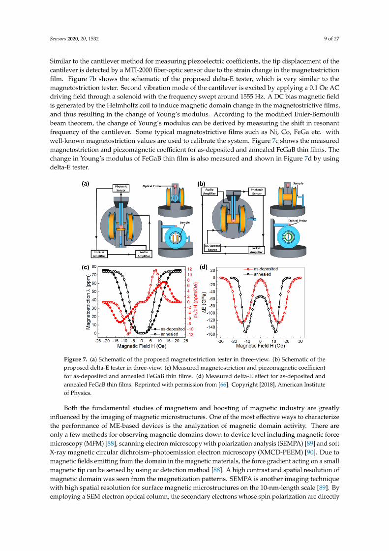
Sensors 2020, 20, 1532 9 of 27
Similar to the cantilever method for measuring piezoelectric coefficients, the tip displacement of thecantilever is detected by a MTI-2000 fiber-optic sensor due to the strain change in the magnetostrictionfilm. Figure 7b shows the schematic of the proposed delta-E tester, which is very similar to themagnetostriction tester. Second vibration mode of the cantilever is excited by applying a 0.1 Oe ACdriving field through a solenoid with the frequency swept around 1555 Hz. A DC bias magnetic fieldis generated by the Helmholtz coil to induce magnetic domain change in the magnetostrictive films,and thus resulting in the change of Young’s modulus. According to the modified Euler-Bernoullibeam theorem, the change of Young’s modulus can be derived by measuring the shift in resonantfrequency of the cantilever. Some typical magnetostrictive films such as Ni, Co, FeGa etc. withwell-known magnetostriction values are used to calibrate the system. Figure 7c shows the measuredmagnetostriction and piezomagnetic coefficient for as-deposited and annealed FeGaB thin films. Thechange in Young’s modulus of FeGaB thin film is also measured and shown in Figure 7d by usingdelta-E tester.
Sensors 2020, 20, x FOR PEER REVIEW 9 of 29
Figure 7. (a) Schematic of the proposed magnetostriction tester in three-view. (b) Schematic of the proposed
delta-E tester in three-view. (c) Measured magnetostriction and piezomagnetic coefficient for as-deposited
and annealed FeGaB thin films. (d) Measured delta-E effect for as-deposited and annealed FeGaB thin films.
Reprinted with permission from [66]. Copyright [2018], American Institute of Physics.
Both the fundamental studies of magnetism and boosting of magnetic industry are greatly influenced
by the imaging of magnetic microstructures. One of the most effective ways to characterize the performance
of ME-based devices is the analyzation of magnetic domain activity. There are only a few methods for
observing magnetic domains down to device level including magnetic force microscopy (MFM) [88],
scanning electron microscopy with polarization analysis (SEMPA) [89] and soft X-ray magnetic circular
dichroism–photoemission electron microscopy (XMCD-PEEM) [90]. Due to magnetic fields emitting from
the domain in the magnetic materials, the force gradient acting on a small magnetic tip can be sensed by
using ac detection method [88]. A high contrast and spatial resolution of magnetic domain was seen from
the magnetization patterns. SEMPA is another imaging technique with high spatial resolution for surface
magnetic microstructures on the 10-nm-length scale [89]. By employing a SEM electron optical column, the
secondary electrons whose spin polarization are directly related to the local magnetization orientation are
excited and emitted from the ferromagnetic sample surface. Therefore, the surface magnetization map can
be generated when the spin polarization of secondary electrons is analyzed across the sample surface. A
very large average velocity of 600 m/s was detected for domain-wall motion in the NiFe layer by using
XMCD-PEEM [90]. In particular, magnetic domain imaging by magneto-optical Kerr effect (MOKE)
microscopy offers direct access to the behavior of local magnetization [91–94]. MOKE microscopy based on
the Kerr and the Faraday effects is one of the most prominent techniques for observing magnetic domain
and is able to visualize the magnetic dynamics on fast time-scales. Allowing for the direct imaging under
a continuous field excitation, a picosecond wide-field MOKE microscopy for imaging magnetization
dynamics is demonstrated in [92]. An example of nanosecond domain wall displacements and spin-wave
generation are observed and displayed in Figure 8 [93]. Figure 8a shows the precessional domain wall
motion with out-of-plane magnetization components of a (Fe90Co10)78Si12B10 sample. The spin waves, which
origin from the domain wall precession within the central magnetic domains shown in Figure 8b, propagate
Figure 7. (a) Schematic of the proposed magnetostriction tester in three-view. (b) Schematic of theproposed delta-E tester in three-view. (c) Measured magnetostriction and piezomagnetic coefficientfor as-deposited and annealed FeGaB thin films. (d) Measured delta-E effect for as-deposited andannealed FeGaB thin films. Reprinted with permission from [66]. Copyright [2018], American Instituteof Physics.
Both the fundamental studies of magnetism and boosting of magnetic industry are greatlyinfluenced by the imaging of magnetic microstructures. One of the most effective ways to characterizethe performance of ME-based devices is the analyzation of magnetic domain activity. There areonly a few methods for observing magnetic domains down to device level including magnetic forcemicroscopy (MFM) [88], scanning electron microscopy with polarization analysis (SEMPA) [89] and softX-ray magnetic circular dichroism–photoemission electron microscopy (XMCD-PEEM) [90]. Due tomagnetic fields emitting from the domain in the magnetic materials, the force gradient acting on a smallmagnetic tip can be sensed by using ac detection method [88]. A high contrast and spatial resolution ofmagnetic domain was seen from the magnetization patterns. SEMPA is another imaging techniquewith high spatial resolution for surface magnetic microstructures on the 10-nm-length scale [89]. Byemploying a SEM electron optical column, the secondary electrons whose spin polarization are directly
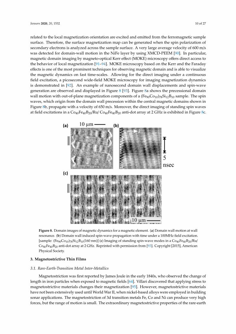
Sensors 2020, 20, 1532 10 of 27
related to the local magnetization orientation are excited and emitted from the ferromagnetic samplesurface. Therefore, the surface magnetization map can be generated when the spin polarization ofsecondary electrons is analyzed across the sample surface. A very large average velocity of 600 m/swas detected for domain-wall motion in the NiFe layer by using XMCD-PEEM [90]. In particular,magnetic domain imaging by magneto-optical Kerr effect (MOKE) microscopy offers direct access tothe behavior of local magnetization [91–94]. MOKE microscopy based on the Kerr and the Faradayeffects is one of the most prominent techniques for observing magnetic domain and is able to visualizethe magnetic dynamics on fast time-scales. Allowing for the direct imaging under a continuousfield excitation, a picosecond wide-field MOKE microscopy for imaging magnetization dynamicsis demonstrated in [92]. An example of nanosecond domain wall displacements and spin-wavegeneration are observed and displayed in Figure 8 [93]. Figure 8a shows the precessional domainwall motion with out-of-plane magnetization components of a (Fe90Co10)78Si12B10 sample. The spinwaves, which origin from the domain wall precession within the central magnetic domains shown inFigure 8b, propagate with a velocity of 650 m/s. Moreover, the direct imaging of standing spin wavesat field excitations in a Co40Fe40B20/Ru/ Co40Fe40B20 anti-dot array at 2 GHz is exhibited in Figure 8c.
Sensors 2020, 20, x FOR PEER REVIEW 10 of 29
with a velocity of 650 m/s. Moreover, the direct imaging of standing spin waves at field excitations in a
Co40Fe40B20/Ru/ Co40Fe40B20 anti-dot array at 2 GHz is exhibited in Figure 8c.
Figure 8. Domain images of magnetic dynamics for a magnetic element. (a) Domain wall motion at wall
resonance. (b) Domain wall induced spin-wave propagation with time under a 100MHz field excitation.
[sample: (Fe90Co10)78Si12B10(160 nm)] (c) Imaging of standing spin-wave modes in a Co40Fe40B20/Ru/
Co40Fe40B20 anti-dot array at 2 GHz. Reprinted with permission from [93]. Copyright [2015], American
Physical Society.
3. Magnetostrictive Thin Films
3.1. Rare-Earth-Transition Metal Inter-Metallics
Magnetostriction was first reported by James Joule in the early 1840s, who observed the change of
length in iron particles when exposed to magnetic fields [64]. Villari discovered that applying stress to
magnetostrictive materials changes their magnetization [95]. However, magnetostrictive materials have not
been extensively used until World War II, when nickel-based alloys were employed in building sonar
applications. The magnetostriction of 3d transition metals Fe, Co and Ni can produce very high forces, but
the range of motion is small. The extraordinary magnetostrictive properties of the rare-earth elements such
as terbium and dysprosium were first recognized in the early 1960’s, which can achieve magnetostriction
of up to 10000 ppm at low temperatures [96]. However, they do not demonstrate significant
magnetostriction at room temperature where practical devices must operate due to the low Curie
temperature. The solution to this problem was pointed out by Callen in 1969, who suggested there was
great promise that strong magnetism of the transition metals such as iron, which exhibit higher Curie
temperatures, could increase the rare-earth magnetic order at high temperatures [97]. In attempt to produce
large magnetostriction at room temperature, rare-earth elements were alloyed with 3d transition elements
as rare-earth-transition metal inter-metallics.
3.1.1. TbDyFe
Figure 8. Domain images of magnetic dynamics for a magnetic element. (a) Domain wall motion at wallresonance. (b) Domain wall induced spin-wave propagation with time under a 100MHz field excitation.[sample: (Fe90Co10)78Si12B10(160 nm)] (c) Imaging of standing spin-wave modes in a Co40Fe40B20/Ru/
Co40Fe40B20 anti-dot array at 2 GHz. Reprinted with permission from [93]. Copyright [2015], AmericanPhysical Society.
3. Magnetostrictive Thin Films
3.1. Rare-Earth-Transition Metal Inter-Metallics
Magnetostriction was first reported by James Joule in the early 1840s, who observed the change oflength in iron particles when exposed to magnetic fields [64]. Villari discovered that applying stress tomagnetostrictive materials changes their magnetization [95]. However, magnetostrictive materialshave not been extensively used until World War II, when nickel-based alloys were employed in buildingsonar applications. The magnetostriction of 3d transition metals Fe, Co and Ni can produce very highforces, but the range of motion is small. The extraordinary magnetostrictive properties of the rare-earth

Sensors 2020, 20, 1532 11 of 27
elements such as terbium and dysprosium were first recognized in the early 1960’s, which can achievemagnetostriction of up to 10000 ppm at low temperatures [96]. However, they do not demonstratesignificant magnetostriction at room temperature where practical devices must operate due to the lowCurie temperature. The solution to this problem was pointed out by Callen in 1969, who suggestedthere was great promise that strong magnetism of the transition metals such as iron, which exhibithigher Curie temperatures, could increase the rare-earth magnetic order at high temperatures [97].In attempt to produce large magnetostriction at room temperature, rare-earth elements were alloyedwith 3d transition elements as rare-earth-transition metal inter-metallics.
3.1.1. TbDyFe
In 1979, the magnetic materials group at Carderock which was funded by the Office of NavalResearch (ONR) discovered that the magnetocrystalline anisotropy of rare-earth-transition metalinter-metallics can be significantly reduced by adding Tb and Dy in certain proportion into iron. Thisled to the development of the Terfenol-D alloy (Tb0.3Dy0.7Fe2), which exhibits giant magnetostrictionof about 2000 ppm at room temperature [98]. The large strain produced by Terfenol-D is useful inapplications as production of high amplitude, low frequency sound wavs in water, certain typesof strain gages, vibration compensation and compensation for temperature induced strains in largelaser mirrors. One of the draw backs of Terfenol-D is its brittleness in withstanding tensile stress,which limits its ability to withstand shock loads or operate in tension.
In terms of Terfenol-D thin films, several efforts on the fabrication techniques and characterizationstudies have been conducted during the last two decades [98,99]. Terfenol-D thin films are commonlyprepared by magnetron sputtering with a single alloy target or by co-sputtering with multiple targets.However, the as-deposited films are always amorphous and their magnetoelastic behaviors andmagnetic properties are inferior than their bulk counterpart. To overcome these drawbacks andenhance their mechanical and magnetic properties, the thin films must be crystallized either bypost-annealing or by depositing the film on a heating substrate. In 1994, Williams P. I. et. al. observedin-plane magnetostriction coefficient of 500 ppm in Tb0.3Dy0.7Fe2 polycrystalline thin film as shownin Figure 9 [100]. However, the saturation field achieved at 4 kOe was still too high, which made itimpractical for the usage in MEMS applications, as it would be very difficult to apply such a high biasmagnetic field on chip.
Sensors 2020, 20, x FOR PEER REVIEW 11 of 29
In 1979, the magnetic materials group at Carderock which was funded by the Office of Naval Research
(ONR) discovered that the magnetocrystalline anisotropy of rare-earth-transition metal inter-metallics can
be significantly reduced by adding Tb and Dy in certain proportion into iron. This led to the development
of the Terfenol-D alloy (Tb0.3Dy0.7Fe2), which exhibits giant magnetostriction of about 2000 ppm at room
temperature [98]. The large strain produced by Terfenol-D is useful in applications as production of high
amplitude, low frequency sound wavs in water, certain types of strain gages, vibration compensation and
compensation for temperature induced strains in large laser mirrors. One of the draw backs of Terfenol-D
is its brittleness in withstanding tensile stress, which limits its ability to withstand shock loads or operate
in tension.
In terms of Terfenol-D thin films, several efforts on the fabrication techniques and characterization
studies have been conducted during the last two decades [98,99]. Terfenol-D thin films are commonly
prepared by magnetron sputtering with a single alloy target or by co-sputtering with multiple targets.
However, the as-deposited films are always amorphous and their magnetoelastic behaviors and magnetic
properties are inferior than their bulk counterpart. To overcome these drawbacks and enhance their
mechanical and magnetic properties, the thin films must be crystallized either by post-annealing or by
depositing the film on a heating substrate. In 1994, Williams P. I. et. al. observed in-plane magnetostriction
coefficient of 500 ppm in Tb0.3Dy0.7Fe2 polycrystalline thin film as shown in Figure 9 [100]. However, the
saturation field achieved at 4 kOe was still too high, which made it impractical for the usage in MEMS
applications, as it would be very difficult to apply such a high bias magnetic field on chip.
Figure 9. (a) In-plane, longitudinal magnetostriction λ‖ loop for a polycrystalline Tb0.3Dy0.7Fe2 film and (b)
λ‖ and λ⊥ as a function of x for TbxDy1-xFe2 films. Reprinted with permission from [100]. Copyright [1994],
American Physical Society.
3.1.2. SmFe and SmFeB
In addition to Terfenol-D alloys, samarium-based alloys have also been of great research interests due
to their high Curie temperature. Unlike Terfenol-D alloys, which start to degrade their magnetostrictive
performance at 200 C°, Samarium-based alloys can be applied to much higher temperature environment
without losing their magnetic properties [101]. One special character of Sm-Fe alloy is their negative sign
of giant magnetostriction, which lies in the relationship between the magnetoelastic behaviors and the
stress state of the magnetostrictive materials. Specifically, the compressive stress can increase the strain for
magnetostrictive materials with positive sign, whereas decrease the strain for materials with negative sign.
Therefore, in device applications using bulk magnetostrictive materials, usually they are intentionally
applied with compressive stress rather than tensile stress for convenience to achieve the largest strain.
However, in thin film applications, it is not necessary to apply any stress on the thin films, therefore, Sm-
Figure 9. (a) In-plane, longitudinal magnetostriction λ‖ loop for a polycrystalline Tb0.3Dy0.7Fe2 filmand (b) λ‖ and λ⊥ as a function of x for TbxDy1-xFe2 films. Reprinted with permission from [100].Copyright [1994], American Physical Society.
3.1.2. SmFe and SmFeB
In addition to Terfenol-D alloys, samarium-based alloys have also been of great researchinterests due to their high Curie temperature. Unlike Terfenol-D alloys, which start to degrade

Sensors 2020, 20, 1532 12 of 27
their magnetostrictive performance at 200 ◦C, Samarium-based alloys can be applied to much highertemperature environment without losing their magnetic properties [101]. One special character ofSm-Fe alloy is their negative sign of giant magnetostriction, which lies in the relationship betweenthe magnetoelastic behaviors and the stress state of the magnetostrictive materials. Specifically, thecompressive stress can increase the strain for magnetostrictive materials with positive sign, whereasdecrease the strain for materials with negative sign. Therefore, in device applications using bulkmagnetostrictive materials, usually they are intentionally applied with compressive stress rather thantensile stress for convenience to achieve the largest strain. However, in thin film applications, it isnot necessary to apply any stress on the thin films, therefore, Sm-Fe based alloys do not suffer fromthe problem related to the reduction of strain due to the applied stress on negative magnetostrictivematerials. Another advantage is that the light rare-earth element samarium is more abundant thanthe heavy rare-earth element terbium. Therefore, Sm-Fe based alloys have a price advantage overTerfenol-D alloys. These advantages lead to the investigation and development of Sm-Fe based thinfilms with good magnetostrictive characteristics.
In 1998, Kim et al. conducted a systematic investigation on the magnetostrictive behavior of Sm-Feand Sm-Fe-B thin films over a wide composition range from 14.1 to 71.7 at% Sm [102]. As displayed inFigure 10, good magnetostrictive characteristics has been found at low magnetic fields in both Sm-Feand Sm-Fe-B thin films. At 100 Oe, magnetostriction of −350 ppm and −470 ppm have been achievedfor Sm-Fe with 25% Sm and for Sm-Fe-B with 27–31% Sm respectively. The addition of B has formedan amorphous phase in Sm-Fe-B thin films, which effectively modified the microstructure and therebyimproved the magnetic properties. At the same time, a very high λs of −1200 ppm has been achievedwith an optimum Sm content at 36.8% for Sm-Fe-B thin films, which is three times larger than Tb-Febased thin films. The excellent magnetostrictive characters of Sm-Fe and Sm-Fe-B thin films madethem good candidates for the applications in MEMS device.
Sensors 2020, 20, x FOR PEER REVIEW 12 of 29
Fe based alloys do not suffer from the problem related to the reduction of strain due to the applied stress
on negative magnetostrictive materials. Another advantage is that the light rare-earth element samarium
is more abundant than the heavy rare-earth element terbium. Therefore, Sm-Fe based alloys have a price
advantage over Terfenol-D alloys. These advantages lead to the investigation and development of Sm-Fe
based thin films with good magnetostrictive characteristics.
In 1998, Kim et al. conducted a systematic investigation on the magnetostrictive behavior of Sm-Fe
and Sm-Fe-B thin films over a wide composition range from 14.1 to 71.7 at% Sm [102]. As displayed in
Figure 10, good magnetostrictive characteristics has been found at low magnetic fields in both Sm-Fe and
Sm-Fe-B thin films. At 100 Oe, magnetostriction of -350 ppm and -470 ppm have been achieved for Sm-Fe
with 25% Sm and for Sm-Fe-B with 27-31% Sm respectively. The addition of B has formed an amorphous
phase in Sm-Fe-B thin films, which effectively modified the microstructure and thereby improved the
magnetic properties. At the same time, a very high 𝜆𝑠 of -1200 ppm has been achieved with an optimum
Sm content at 36.8% for Sm-Fe-B thin films, which is three times larger than Tb-Fe based thin films. The
excellent magnetostrictive characters of Sm-Fe and Sm-Fe-B thin films made them good candidates for the
applications in MEMS device.
Figure 10. (a) The λ-H plots for some Sm-Fe-B thin films. The numbers at the curves indicate the Sm content
in at% (b) The value of λ as a function of the Sm content at fixed magnetic fields of 5 kOe. The results of Sm-
Fe thin films are indicated by filled circles while those of Sm-Fe-B thin films are denoted by open circles.
Reprinted with permission from [102]. Copyright [1998], North Holland (Elsevier).
3.2. Rear-Earth-Free Alloys
The well-known problem of the magnetostrictive rear-earth-transition metal films is that a large bias
magnetic field is usually required to achieve giant magnetostriction due to the large magnetocrystalline
anisotropy induced from the rear-earth elements, which is particularly impractical for these
magnetostrictive thin films to be applied on MEMS devices. Also, at RF and microwave frequencies, even
small amount of rear-earth elements can result in a very lossy magnetic film. Recently, strong
magnetostrictive behaviors have been observed in FeGa and FeAl alloys, which exhibit large
magnetostriction of more than 400 ppm for Fe81.3Ga18.7 and 200 ppm for Fe83.4Al16.6 respectively [103,104]. In
these alloys, it has been found that the giant magnetostriction always occurred in the vicinity of ordered
D03 and disordered A2 phase boundaries. In addition, since the first report on the magnetostrictive
properties of Fe-Co alloy by Masiyama, much efforts have also been devoted in developing giant
magnetostrictive FeCo alloys [105].
3.2.1. FeGa Based Alloy
Figure 10. (a) The λ-H plots for some Sm-Fe-B thin films. The numbers at the curves indicate the Smcontent in at% (b) The value of λ as a function of the Sm content at fixed magnetic fields of 5 kOe. Theresults of Sm-Fe thin films are indicated by filled circles while those of Sm-Fe-B thin films are denotedby open circles. Reprinted with permission from [102]. Copyright [1998], North Holland (Elsevier).
3.2. Rear-Earth-Free Alloys
The well-known problem of the magnetostrictive rear-earth-transition metal films is that alarge bias magnetic field is usually required to achieve giant magnetostriction due to the largemagnetocrystalline anisotropy induced from the rear-earth elements, which is particularly impracticalfor these magnetostrictive thin films to be applied on MEMS devices. Also, at RF and microwavefrequencies, even small amount of rear-earth elements can result in a very lossy magnetic film.Recently, strong magnetostrictive behaviors have been observed in Fe-Ga and Fe-Al alloys, whichexhibit large magnetostriction of more than 400 ppm for Fe81.3Ga18.7 and 200 ppm for Fe83.4Al16.6
Sensors 2020, 20, 1532 13 of 27
respectively [103,104]. In these alloys, it has been found that the giant magnetostriction always occurredin the vicinity of ordered D03 and disordered A2 phase boundaries. In addition, since the first reporton the magnetostrictive properties of Fe-Co alloy by Masiyama, much efforts have also been devotedin developing giant magnetostrictive Fe-Co alloys [105].
3.2.1. FeGa Based Alloy
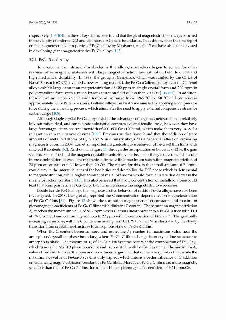
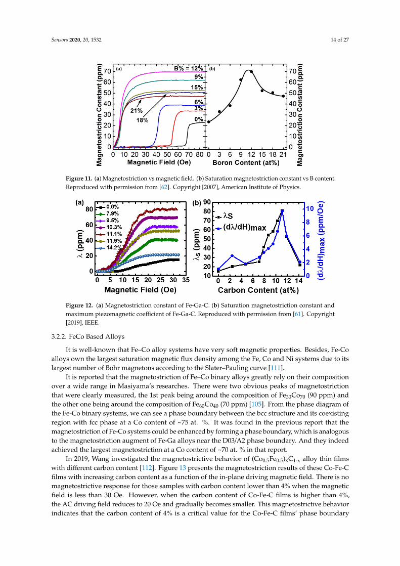
To overcome the intrinsic drawbacks in RFe alloys, researchers began to search for otherrear-earth-free magnetic materials with large magnetostriction, low saturation field, low cost andhigh mechanical durability. In 1999, the group at Carderock which was funded by the Office ofNaval Research (ONR) invented a new exciting material, the Fe-Ga (Galfenol) alloy system. Galfenolalloys exhibit large saturation magnetostriction of 400 ppm in single crystal form and 300 ppm inpolycrystalline form with a much lower saturation field of less than 200 Oe [106,107]. In addition,these alloys are stable over a wide temperature range from −265 ◦C to 150 ◦C and can sustainapproximately 350 MPa tensile stress. Galfenol alloys can be stress-annealed by applying a compressiveforce during the annealing process, which eliminates the need to apply external compressive stress forcertain usage [108].
Although single crystal Fe-Ga alloys exhibit the advantage of large magnetostriction at relativelylow saturation field, and can tolerate substantial compressive and tensile stress, however, they havelarge ferromagnetic resonance linewidth of 400–600 Oe at X band, which make them very lossy forintegration into microwave devices [109]. Previous studies have found that the addition of traceamounts of metalloid atoms of C, B, and N into binary alloys has a beneficial effect on increasingmagnetostriction. In 2007, Lou et al. reported magnetostrictive behavior of Fe-Ga-B thin films withdifferent B contents [62]. As shown in Figure 11, through the incorporation of boron at 9–12 %, the gainsize has been refined and the magnetocrystalline anisotropy has been effectively reduced, which resultsin the combination of excellent magnetic softness with a maximum saturation magnetostriction of70 ppm at saturation field lower than 20 Oe. The reason for this, is that small amount of B atomswould stay in the interstitial sites of the bcc lattice and destabilize the D03 phase which is detrimentalto magnetostriction, while higher amount of metalloid atoms would form clusters that decrease themagnetostriction constant [110]. It is also believed that a low concentration of metalloid atoms couldlead to atomic pairs such as Ga–Ga or B–B, which enhance the magnetostrictive behavior.
Beside boride Fe-Ga alloys, the magnetostrictive behavior of carbide Fe-Ga alloys have also beeninvestigated. In 2018, Liang et al., reported the C-concentration dependence on magnetostrictionof Fe-Ga-C films [61]. Figure 12 shows the saturation magnetostriction constants and maximumpiezomagnetic coefficients of Fe-Ga-C films with different C content. The saturation magnetostrictionλS reaches the maximum value of 81.2 ppm when C atoms incorporate into a Fe-Ga lattice with 11.1at. % C content and continually reduces to 22 ppm with C composition of 14.2 at. %. The graduallyincreasing value of λS with the C content increasing from 0 at. % to 7.1 at. % is illustrated by the slowlytransition from crystalline structures to amorphous state of Fe-Ga-C films.
When the C content becomes more and more, the λS reaches its maximum value near theamorphous/crystalline phase boundary, where Fe-Ga-C films change from crystalline structure toamorphous phase. The maximum λS of Fe-Ga alloy systems occurs at the composition of Fe80Ga20,which is near the A2/D03 phase boundary and is consistent with Fe-Ga-C systems. The maximum λSvalue of Fe-Ga-C films is 81.2 ppm and is six times larger than that of the binary Fe-Ga film, while themaximum λS value of Fe-Ga-B systems only tripled, which means a better influence of C additionon enhancing magnetostriction constant of Fe-Ga films. Moreover, Fe-Ga-C films are more magneticsensitive than that of Fe-Ga-B films due to their higher piezomagnetic coefficient of 9.71 ppm/Oe.
Sensors 2020, 20, 1532 14 of 27
Sensors 2020, 20, x FOR PEER REVIEW 13 of 29
To overcome the intrinsic drawbacks in RFe alloys, researchers began to search for other rear-earth-
free magnetic materials with large magnetostriction, low saturation field, low cost and high mechanical
durability. In 1999, the group at Carderock which was funded by the Office of Naval Research (ONR)
invented a new exciting material, the Fe-Ga (Galfenol) alloy system. Galfenol alloys exhibit large saturation
magnetostriction of 400 ppm in single crystal form and 300 ppm in polycrystalline form with a much lower
saturation field of less than 200 Oe [106,107]. In addition, these alloys are stable over a wide temperature
range from -265 °C to 150 °C and can sustain approximately 350 MPa tensile stress. Galfenol alloys can be
stress-annealed by applying a compressive force during the annealing process, which eliminates the need
to apply external compressive stress for certain usage [108].
Although single crystal Fe-Ga alloys exhibit the advantage of large magnetostriction at relatively low
saturation field, and can tolerate substantial compressive and tensile stress, however, they have large
ferromagnetic resonance linewidth of 400-6 00 Oe at X band, which make them very lossy for integration
into microwave devices [109]. Previous studies have found that the addition of trace amounts of metalloid
atoms of C, B, and N into binary alloys has a beneficial effect on increasing magnetostriction. In 2007, Lou
et al. reported magnetostrictive behavior of Fe-Ga-B thin films with different B contents [62]. As shown in
Figure 11, through the incorporation of boron at 9-12 %, the gain size has been refined and the
magnetocrystalline anisotropy has been effectively reduced, which results in the combination of excellent
magnetic softness with a maximum saturation magnetostriction of 70 ppm at saturation field lower than
20 Oe. The reason for this, is that small amount of B atoms would stay in the interstitial sites of the bcc
lattice and destabilize the D03 phase which is detrimental to magnetostriction, while higher amount of
metalloid atoms would form clusters that decrease the magnetostriction constant [110]. It is also believed
that a low concentration of metalloid atoms could lead to atomic pairs such as Ga–Ga or B–B, which
enhance the magnetostrictive behavior.
Figure 11. (a) Magnetostriction vs magnetic field. (b) Saturation magnetostriction constant vs B content.
Reproduced with permission from [62]. Copyright [2007], American Institute of Physics.
Beside boride Fe-Ga alloys, the magnetostrictive behavior of carbide Fe-Ga alloys have also been
investigated. In 2018, Liang et al., reported the C-concentration dependence on magnetostriction of Fe-Ga-
C films [61]. Figure 12 shows the saturation magnetostriction constants and maximum piezomagnetic
coefficients of Fe-Ga-C films with different C content. The saturation magnetostriction 𝜆𝑆 reaches the
maximum value of 81.2 ppm when C atoms incorporate into a Fe-Ga lattice with 11.1 at. % C content and
continually reduces to 22 ppm with C composition of 14.2 at. %. The gradually increasing value of 𝜆𝑆 with
the C content increasing from 0 at. % to 7.1 at. % is illustrated by the slowly transition from crystalline
structures to amorphous state of Fe-Ga-C films.
Figure 11. (a) Magnetostriction vs magnetic field. (b) Saturation magnetostriction constant vs B content.Reproduced with permission from [62]. Copyright [2007], American Institute of Physics.
Sensors 2020, 20, x FOR PEER REVIEW 14 of 29
Figure 12. (a) Magnetostriction constant of Fe-Ga-C. (b) Saturation magnetostriction constant and maximum
piezomagnetic coefficient of Fe-Ga-C. Reproduced with permission from [61]. Copyright [2019], IEEE.
When the C content becomes more and more, the 𝜆𝑆 reaches its maximum value near the
amorphous/crystalline phase boundary, where Fe-Ga-C films change from crystalline structure to
amorphous phase. The maximum 𝜆𝑆 of Fe-Ga alloy systems occurs at the composition of Fe80Ga20, which is
near the A2/D03 phase boundary and is consistent with Fe-Ga-C systems. The maximum 𝜆𝑆 value of Fe-
Ga-C films is 81.2 ppm and is six times larger than that of the binary Fe-Ga film, while the maximum 𝜆𝑆
value of Fe-Ga-B systems only tripled, which means a better influence of C addition on enhancing
magnetostriction constant of Fe-Ga films. Moreover, Fe-Ga-C films are more magnetic sensitive than that
of Fe-Ga-B films due to their higher piezomagnetic coefficient of 9.71 ppm/Oe.
3.2.2. FeCo Based Alloys
It is well-known that Fe–Co alloy systems have very soft magnetic properties. Besides, Fe-Co alloys
own the largest saturation magnetic flux density among the Fe, Co and Ni systems due to its largest number
of Bohr magnetons according to the Slater–Pauling curve [111].
It is reported that the magnetostriction of Fe–Co binary alloys greatly rely on their composition over
a wide range in Masiyama’s researches. There were two obvious peaks of magnetostriction that were
clearly measured, the 1st peak being around the composition of Fe30Co70 (90 ppm) and the other one being
around the composition of Fe60Co40 (70 ppm) [105]. From the phase diagram of the Fe-Co binary systems,
we can see a phase boundary between the bcc structure and its coexisting region with fcc phase at a Co
content of ~ 75 at. %. It was found in the previous report that the magnetostriction of Fe-Co systems could
be enhanced by forming a phase boundary, which is analogous to the magnetostriction augment of Fe-Ga
alloys near the D03/A2 phase boundary. And they indeed achieved the largest magnetostriction at a Co
content of ~ 70 at. % in that report.
In 2019, Wang investigated the magnetostrictive behavior of (Co0.5Fe0.5)xC1-x alloy thin films with
different carbon content [112]. Figure 13 presents the magnetostriction results of these Co-Fe-C films with
increasing carbon content as a function of the in-plane driving magnetic field. There is no magnetostrictive
response for those samples with carbon content lower than 4% when the magnetic field is less than 30 Oe.
However, when the carbon content of Co-Fe-C films is higher than 4%, the AC driving field reduces to 20
Oe and gradually becomes smaller. This magnetostrictive behavior indicates that the carbon content of 4%
is a critical value for the Co-Fe-C films’ phase boundary between nanocrystalline and amorphous
structures. As shown in Figure 13b, black squares denote the magnetostriction constants of Co-Fe-C films.
The saturation magnetostriction 𝜆𝑆 reaches a maximum value of 75ppm when carbon atoms are added to
a Fe-Co lattice with 5.2 at. % carbon content, and then gradually reduces to 10 ppm at carbon content of
15.8 at. %.
Figure 12. (a) Magnetostriction constant of Fe-Ga-C. (b) Saturation magnetostriction constant andmaximum piezomagnetic coefficient of Fe-Ga-C. Reproduced with permission from [61]. Copyright[2019], IEEE.
3.2.2. FeCo Based Alloys
It is well-known that Fe–Co alloy systems have very soft magnetic properties. Besides, Fe-Coalloys own the largest saturation magnetic flux density among the Fe, Co and Ni systems due to itslargest number of Bohr magnetons according to the Slater–Pauling curve [111].
It is reported that the magnetostriction of Fe–Co binary alloys greatly rely on their compositionover a wide range in Masiyama’s researches. There were two obvious peaks of magnetostrictionthat were clearly measured, the 1st peak being around the composition of Fe30Co70 (90 ppm) andthe other one being around the composition of Fe60Co40 (70 ppm) [105]. From the phase diagram ofthe Fe-Co binary systems, we can see a phase boundary between the bcc structure and its coexistingregion with fcc phase at a Co content of ~75 at. %. It was found in the previous report that themagnetostriction of Fe-Co systems could be enhanced by forming a phase boundary, which is analogousto the magnetostriction augment of Fe-Ga alloys near the D03/A2 phase boundary. And they indeedachieved the largest magnetostriction at a Co content of ~70 at. % in that report.
In 2019, Wang investigated the magnetostrictive behavior of (Co0.5Fe0.5)xC1-x alloy thin filmswith different carbon content [112]. Figure 13 presents the magnetostriction results of these Co-Fe-Cfilms with increasing carbon content as a function of the in-plane driving magnetic field. There is nomagnetostrictive response for those samples with carbon content lower than 4% when the magneticfield is less than 30 Oe. However, when the carbon content of Co-Fe-C films is higher than 4%,the AC driving field reduces to 20 Oe and gradually becomes smaller. This magnetostrictive behaviorindicates that the carbon content of 4% is a critical value for the Co-Fe-C films’ phase boundary

Sensors 2020, 20, 1532 15 of 27
between nanocrystalline and amorphous structures. As shown in Figure 13b, black squares denote themagnetostriction constants of Co-Fe-C films. The saturation magnetostriction λS reaches a maximumvalue of 75ppm when carbon atoms are added to a Fe-Co lattice with 5.2 at. % carbon content, and thengradually reduces to 10 ppm at carbon content of 15.8 at. %.
Sensors 2020, 20, x FOR PEER REVIEW 15 of 29
Figure 13. (a) Magnetostriction constant of (Co0.5Fe0.5)xC1−x films with x=0 to 15.8%. (b) The saturated
magnetostriction constant (black) and piezomagnetic coefficient (red) with different carbon content. The
structural boundaries of the alloy are marked with light orange and green dotted lines. (c) Piezomagnetic
coefficient versus corresponding driving magnetic field for (Co0.5Fe0.5)xC1−x films with x=0 to 13.2%. (d) The
Ms (black) and Hc (red) versus carbon content. The blue open triangles are the fitted Ms from broadband
FMR measurement. Reproduced with permission from [112]. Copyright [2019], American Physical Society.
The piezomagnetic coefficient of the Co-Fe-C films was shown by the red cycles in Figure 13b. The
curve can be divided into three regions: When the carbon content is less than 4 at. %, the Co-Fe-C films
remain to be bcc nanocrystalline phase; as the carbon content increases and is less than 6 at. %, there is a
coexistence region of both nanocrystalline and amorphous phase and the phase boundaries are labelled as
the dotted orange and green lines; when the carbon content goes beyond 6 at. %, they transition to
amorphous structure. A clear peak is obtained in the coexistence region and the largest value of
piezomagnetic coefficient is achieved of 10.3 ppm/Oe at 4.8 at. %. They also confirmed the coexistence
region by analyzing FFT results of the HRTEM images, which are shown in Figure 14. The formation of
atom pairs or clusters during the doping of metalloid atoms also destabilize the D03 phase. Therefore, the
magnetostriction constants and piezomagnetic coefficients of Co-Fe-C films are optimized with the carbon
content ranging from 4% to 6%. Compared to the reported value of magnetostriction constants for Ga-Fe-
B and the widely used Co-Fe-B films, the values measured in this paper are much higher. Moreover, the
maximum piezomagnetic coefficient dλ/dH of Co-Fe-C films is much larger than other well-known
magnetostrictive materials such as Metglas and Terfenol-D.
Figure 13. (a) Magnetostriction constant of (Co0.5Fe0.5)xC1−x films with x = 0 to 15.8%. (b) Thesaturated magnetostriction constant (black) and piezomagnetic coefficient (red) with different carboncontent. The structural boundaries of the alloy are marked with light orange and green dotted lines.(c) Piezomagnetic coefficient versus corresponding driving magnetic field for (Co0.5Fe0.5)xC1−x filmswith x = 0 to 13.2%. (d) The Ms (black) and Hc (red) versus carbon content. The blue open triangles arethe fitted Ms from broadband FMR measurement. Reproduced with permission from [112]. Copyright[2019], American Physical Society.
The piezomagnetic coefficient of the Co-Fe-C films was shown by the red cycles in Figure 13b.The curve can be divided into three regions: When the carbon content is less than 4 at. %, the Co-Fe-Cfilms remain to be bcc nanocrystalline phase; as the carbon content increases and is less than 6 at. %,there is a coexistence region of both nanocrystalline and amorphous phase and the phase boundariesare labelled as the dotted orange and green lines; when the carbon content goes beyond 6 at. %,they transition to amorphous structure. A clear peak is obtained in the coexistence region and thelargest value of piezomagnetic coefficient is achieved of 10.3 ppm/Oe at 4.8 at. %. They also confirmedthe coexistence region by analyzing FFT results of the HRTEM images, which are shown in Figure 14.The formation of atom pairs or clusters during the doping of metalloid atoms also destabilize theD03 phase. Therefore, the magnetostriction constants and piezomagnetic coefficients of Co-Fe-C filmsare optimized with the carbon content ranging from 4% to 6%. Compared to the reported value ofmagnetostriction constants for Ga-Fe-B and the widely used Co-Fe-B films, the values measured in thispaper are much higher. Moreover, the maximum piezomagnetic coefficient dλ/dH of Co-Fe-C films ismuch larger than other well-known magnetostrictive materials such as Metglas and Terfenol-D.

Sensors 2020, 20, 1532 16 of 27Sensors 2020, 20, x FOR PEER REVIEW 16 of 29
Figure 14. (a) A bright-field STEM image of Ta/(Co,Fe)C/Ta/SiO2/Si (001) substrate. (b) The corresponding
energy-dispersive x-ray spectroscopy mappings for Fe, Co, and Ta elements, respectively. (c) Cross sections
of lowresolution TEM with white solid rectangle displaying the corresponding location of HRTEM. (d)–(f)
HRTEM images of Co-Fe-C alloy films with carbon content 0%, 4.4%, and 13.2%, respectively. The FFT of
selected zones (yellow dotted squares) are inserted at the bottom left corner. Reproduced with permission
from [112]. Copyright [2019], American Physical Society.
3.3. Exchange Coupling in Multilayers
In addition to the state-of-the-art magnetostrictive single layer materials, the combination of different
materials in multilayer structure has recently been proposed as an alternative approach to develop giant
magnetostrictive thin films with low loss and low saturation field. In multilayer thin films, the magnetic
properties in different layers can be synthesized through the process of exchange coupling, which arises
when the thickness in each layer is smaller than the length of magnetic exchange [113]. Through exchange
coupling, spin information can be transmitted between two different magnetic materials, and the overall
magnetic properties are determined by the average value of each layer. By combining two different
materials with excellent softness and giant magnetostriction, exchange coupling can be used to reduce the
saturation field and improve the piezomagnetic coefficient.
3.3.1. FeGa/NiFe Multilayers
In 2019, Shi et al. studied the effect of exchange coupling between Fe83Ga17 and Fe50Ni50 multilayer films
for enhancement of the ME effect [114]. As shown in Figure 15, all of the magnetic domain structures are
stripe domain. However, with the total film thickness fixed at 480 nm, as the thickness in each layer of Fe-
Ga and Fe-Ni become thinner, the stripe width become narrower. This means the domain density has been
increased, which intensified the domain rotation and domain wall motion, thereby enlarged the
magnetostriction. It is believed that stripe domain structure indicates the films have weak out-of-plane
anisotropy [115], and the magnetic moments on the surface of the films rotate upward and downward
alternatively. With the Fe-Ni layers, the permeability increased and the total magnetocrystalline anisotropy
reduced, which in turn make the 90-degree domain wall motion easier. For the (8 nm Fe-Ga/8 nm Fe-Ni)30
multilayers, the small magnetic anisotropy resulting from the exchange coupling makes the domains rotate
more easily under low magnetic field. The rotation of the magnetic domains in the Fe-Ni layers also drive
the rotation of the magnetic domains in the Fe-Ga layers, which makes the Fe-Ni layers act like a lubricant.
As shown in Figure 16b, the d33,m of the (8 nm Fe-Ga/8 nm Fe-Ni)30 multilayers achieved to 8.1 ppm/Oe.
Figure 14. (a) A bright-field STEM image of Ta/(Co,Fe)C/Ta/SiO2/Si (001) substrate. (b) Thecorresponding energy-dispersive x-ray spectroscopy mappings for Fe, Co, and Ta elements, respectively.(c) Cross sections of lowresolution TEM with white solid rectangle displaying the correspondinglocation of HRTEM. (d–f) HRTEM images of Co-Fe-C alloy films with carbon content 0%, 4.4%, and13.2%, respectively. The FFT of selected zones (yellow dotted squares) are inserted at the bottom leftcorner. Reproduced with permission from [112]. Copyright [2019], American Physical Society.
3.3. Exchange Coupling in Multilayers
In addition to the state-of-the-art magnetostrictive single layer materials, the combination ofdifferent materials in multilayer structure has recently been proposed as an alternative approach todevelop giant magnetostrictive thin films with low loss and low saturation field. In multilayer thin films,the magnetic properties in different layers can be synthesized through the process of exchange coupling,which arises when the thickness in each layer is smaller than the length of magnetic exchange [113].Through exchange coupling, spin information can be transmitted between two different magneticmaterials, and the overall magnetic properties are determined by the average value of each layer.By combining two different materials with excellent softness and giant magnetostriction, exchangecoupling can be used to reduce the saturation field and improve the piezomagnetic coefficient.
3.3.1. FeGa/NiFe Multilayers
In 2019, Shi et al. studied the effect of exchange coupling between Fe83Ga17 and Fe50Ni50 multilayerfilms for enhancement of the ME effect [114]. As shown in Figure 15, all of the magnetic domainstructures are stripe domain. However, with the total film thickness fixed at 480 nm, as the thicknessin each layer of Fe-Ga and Fe-Ni become thinner, the stripe width become narrower. This means thedomain density has been increased, which intensified the domain rotation and domain wall motion,thereby enlarged the magnetostriction. It is believed that stripe domain structure indicates the filmshave weak out-of-plane anisotropy [115], and the magnetic moments on the surface of the films rotateupward and downward alternatively. With the Fe-Ni layers, the permeability increased and the totalmagnetocrystalline anisotropy reduced, which in turn make the 90-degree domain wall motion easier.For the (8 nm Fe-Ga/8 nm Fe-Ni)30 multilayers, the small magnetic anisotropy resulting from theexchange coupling makes the domains rotate more easily under low magnetic field. The rotationof the magnetic domains in the Fe-Ni layers also drive the rotation of the magnetic domains in theFe-Ga layers, which makes the Fe-Ni layers act like a lubricant. As shown in Figure 16b, the d33,m ofthe (8 nm Fe-Ga/8 nm Fe-Ni)30 multilayers achieved to 8.1 ppm/Oe. Compared to the Fe-Ga-B film,the piezomagnetic coefficient of the multilayer film has an increment of about 14%.
Sensors 2020, 20, 1532 17 of 27
Sensors 2020, 20, x FOR PEER REVIEW 17 of 29
Compared to the Fe-Ga-B film, the piezomagnetic coefficient of the multilayer film has an increment of
about 14%.
Figure 15. (a), (b), (c) and (d) are the surface magnetic domains of (480 nm Fe-Ga), (30 nm Fe-Ga/30 nm Fe-
Ni)8, (16 nm Fe-Ga/16 nm Fe-Ni)15 and (8 nm Fe-Ga/8 nm Fe-Ni)30 films. Reprinted with permission from
[114]. Copyright [2019], Elsevier.
Figure 16. (a) and (b) are λ-H and dλ/dH-H curves of the samples, λs of the other samples are 137 ppm, 108
ppm,115 ppm and 97 ppm, d33,m of the (8 nm Fe-Ga/8 nm Fe-Ni)30 reaches 8.1ppm/Oe. Reprinted with
permission from [114]. Copyright [2019], Elsevier.
3.3.2. TbFe/FeCo Multilayers
In 1999, Quandt et at. reported exchange coupled Tb40Fe60/Fe50Co50 multilayers which exhibits high
saturation magnetoelastic coupling coefficients in combination with low saturation field of 20 mT [116,117].
It has been found that the saturation magnetostriction was strongly depended on the layer thickness ratio
and the post annealing treatment, as shown in Figure 17c,d.
Figure 15. (a–d) are the surface magnetic domains of (480 nm Fe-Ga), (30 nm Fe-Ga/30 nm Fe-Ni)8, (16nm Fe-Ga/16 nm Fe-Ni)15 and (8 nm Fe-Ga/8 nm Fe-Ni)30 films. Reprinted with permission from [114].Copyright [2019], Elsevier.
Sensors 2020, 20, x FOR PEER REVIEW 17 of 29
Compared to the Fe-Ga-B film, the piezomagnetic coefficient of the multilayer film has an increment of
about 14%.
Figure 15. (a), (b), (c) and (d) are the surface magnetic domains of (480 nm Fe-Ga), (30 nm Fe-Ga/30 nm Fe-
Ni)8, (16 nm Fe-Ga/16 nm Fe-Ni)15 and (8 nm Fe-Ga/8 nm Fe-Ni)30 films. Reprinted with permission from
[114]. Copyright [2019], Elsevier.
Figure 16. (a) and (b) are λ-H and dλ/dH-H curves of the samples, λs of the other samples are 137 ppm, 108
ppm,115 ppm and 97 ppm, d33,m of the (8 nm Fe-Ga/8 nm Fe-Ni)30 reaches 8.1ppm/Oe. Reprinted with
permission from [114]. Copyright [2019], Elsevier.
3.3.2. TbFe/FeCo Multilayers
In 1999, Quandt et at. reported exchange coupled Tb40Fe60/Fe50Co50 multilayers which exhibits high
saturation magnetoelastic coupling coefficients in combination with low saturation field of 20 mT [116,117].
It has been found that the saturation magnetostriction was strongly depended on the layer thickness ratio
and the post annealing treatment, as shown in Figure 17c,d.
Figure 16. (a,b) are λ-H and dλ/dH-H curves of the samples, λs of the other samples are 137 ppm, 108ppm,115 ppm and 97 ppm, d33,m of the (8 nm Fe-Ga/8 nm Fe-Ni)30 reaches 8.1ppm/Oe. Reprinted withpermission from [114]. Copyright [2019], Elsevier.
3.3.2. TbFe/FeCo Multilayers
In 1999, Quandt et at. reported exchange coupled Tb40Fe60/Fe50Co50 multilayers which exhibitshigh saturation magnetoelastic coupling coefficients in combination with low saturation field of20 mT [116,117]. It has been found that the saturation magnetostriction was strongly depended on thelayer thickness ratio and the post annealing treatment, as shown in Figure 17c,d.
The optimum data of the TbFe/FeCo multilayers show that post annealing at 250◦C improves themagnetoelastic behavior, and the coercivity has been reduced from 10 mT to 2 mT, which reflects thatpost annealing can release almost all stress induced anisotropies, leading to a stress-free state of thesemultilayers. It is also believed that under these conditions any significant diffusion does not exist andnanocrystallization begin to appear in the TbFe layers, which leads to the enhancement of the saturationmagnetoelastic coupling coefficient by 15%. At the same time, the overall temperature behavior isalso compromised by the exchange coupled multilayers, and it is expected that the strong Fe50Co50
moments can help stabilized the Tb40Fe60 moments, resulting in an increment of the Curie temperature.
Sensors 2020, 20, 1532 18 of 27Sensors 2020, 20, x FOR PEER REVIEW 18 of 29
Figure 17. (a) Comparison of the magnetoelastic coupling coefficient of 250 °C annealed (7 nmTb40Fe60/9
nmFe50Co50) × 70 multilayer with an optimized Tb40Fe60 and a SmFeB film. (b) Comparison of the
magnetoelastic coupling coefficients of (Tb40Fe60/Fe50Co50), (Tb18Co82 /Fe75Co25), (TbDyFe/ FeSiCuNbB) and
(Tb33Fe67 /Fe80B20) multilayer films. (c) Saturation magnetoelastic coupling coefficient of TbFe/FeCo
multilayers as a function of the soft magnetic layer thickness. (d) ∆E effect of as-deposited and at 250 °C
annealed (7 nm TbFe/8 nm FeCo) multilayers. There figures are reproduced with the permission from
[116,117]. Copyright [1999] and [2000], American Physical Society.
The optimum data of the TbFe/FeCo multilayers show that post annealing at 250°C improves the
magnetoelastic behavior, and the coercivity has been reduced from 10 mT to 2 mT, which reflects that post
annealing can release almost all stress induced anisotropies, leading to a stress-free state of these
multilayers. It is also believed that under these conditions any significant diffusion does not exist and
nanocrystallization begin to appear in the TbFe layers, which leads to the enhancement of the saturation
magnetoelastic coupling coefficient by 15%. At the same time, the overall temperature behavior is also
compromised by the exchange coupled multilayers, and it is expected that the strong Fe50Co50 moments can
help stabilized the Tb40Fe60 moments, resulting in an increment of the Curie temperature.
3.4. Heat Treatment on Magnetostrictive Thin Films
3.4.1. Stress Release by Post Annealing
As a highly magnetostrictive material, FeCoSiB is one of the most commonly used composition in
Metglas foils. In 2002, Quandt et al. investigated the optimization of the ∆E effect and the magnetostriction
of amorphous (Fe90Co10)78Si12B10 thin films by magnetic field annealing [118]. They discovered a strong
correlation between the magnetostrictive susceptibility and the stress state, which can be controlled by the
annealing temperature. As shown in Figure 18c, the as-deposited FeCoSiB film was initially in compressive
stress state before the annealing temperature reach to 170 °C. However, as the annealing temperature
continue to increase, the stress state gradually switched to tensile stress. After annealing treatment, the
compressive stress in the film has been effectively reduced, leading to the reduction of anisotropy energy.
The change of the Young’s modulus with applied magnetic field has been shown in Figure 18d. After
magnetic annealing, a distinguished Young’s modulus reduction of 50 GPa has been observed, which
Figure 17. (a) Comparison of the magnetoelastic coupling coefficient of 250 ◦C annealed (7 nmTb40Fe60/9nmFe50Co50) × 70 multilayer with an optimized Tb40Fe60 and a SmFeB film. (b) Comparison of themagnetoelastic coupling coefficients of (Tb40Fe60/Fe50Co50), (Tb18Co82/Fe75Co25), (TbDyFe/FeSiCuNbB)and (Tb33Fe67 /Fe80B20) multilayer films. (c) Saturation magnetoelastic coupling coefficient of TbFe/FeComultilayers as a function of the soft magnetic layer thickness. (d) ∆E effect of as-deposited and at 250◦C annealed (7 nm TbFe/8 nm FeCo) multilayers. There figures are reproduced with the permissionfrom [116,117]. Copyright [1999] and [2000], American Physical Society.
3.4. Heat Treatment on Magnetostrictive Thin Films
3.4.1. Stress Release by Post Annealing
As a highly magnetostrictive material, FeCoSiB is one of the most commonly used compositionin Metglas foils. In 2002, Quandt et al. investigated the optimization of the ∆E effect and themagnetostriction of amorphous (Fe90Co10)78Si12B10 thin films by magnetic field annealing [118]. Theydiscovered a strong correlation between the magnetostrictive susceptibility and the stress state, whichcan be controlled by the annealing temperature. As shown in Figure 18c, the as-deposited FeCoSiB filmwas initially in compressive stress state before the annealing temperature reach to 170 ◦C. However, asthe annealing temperature continue to increase, the stress state gradually switched to tensile stress.After annealing treatment, the compressive stress in the film has been effectively reduced, leading to thereduction of anisotropy energy. The change of the Young’s modulus with applied magnetic field hasbeen shown in Figure 18d. After magnetic annealing, a distinguished Young’s modulus reduction of50 GPa has been observed, which contributed to 30% change of the Young’s modulus at saturation state,assuming the Young’s modulus of FeCoSiB thin film at saturation is 150 GPa. In Figure 18a,b, we cansee the magnitude and the field dependency of the magnetostrictive susceptibility are highly dependson the stress state and the corresponding annealing temperature. To achieve high magnetostriction atlow magnetic fields, a precise control of film stress has to be executed. For positive magnetostrictivethin films, usually tensile stress state is favorable to obtain the optimum performance.

Sensors 2020, 20, 1532 19 of 27
Sensors 2020, 20, x FOR PEER REVIEW 19 of 29
FeCoSiB thin film at saturation is 150 GPa. In Figure 18 a,b, we can see the magnitude and the field
dependency of the magnetostrictive susceptibility are highly depends on the stress state and the
corresponding annealing temperature. To achieve high magnetostriction at low magnetic fields, a precise
control of film stress has to be executed. For positive magnetostrictive thin films, usually tensile stress state
is favorable to obtain the optimum performance.
Figure 18. (a) Magnetoelastic coupling coefficient (b) negative absolute value of the first derivative of the
magnetostrictive hysteresis (c) stress as a function of annealing temperature (d) ∆E effect of an optimized
annealed (Fe90Co10)78Si12B10 thin film. Reproduced with permission from [118]. Copyright [2002], IEEE.
3.4.2. Phase Boundary Changes by Cooling Processes
In 2011, Hunter et al. investigated the magnetostrictive behavior and microstructural properties of Co-
Fe alloy thin films in relation to the composition and thermal process [119]. Strong dependence of
magnetostriction on the cooling process has been found. The analysis of the microstructure through
synchrotron X-ray micro-diffraction shows that the maximum magnetostriction occurs at the (fcc+bcc)/bcc
phase boundary. As shown in Figure 19 a,b, after annealing, the peak of magnetostriction shifts to lower
Co composition by the same amount as the (fcc + bcc)/bcc phase boundary shifts, indicating that the peak
magnetostriction is linked to this phase interface. At the temperature/composition close to the (fcc + bcc)/bcc
phase boundary, a remarkable giant magnetostriction has been yield after annealing followed by
quenching, which is more than three times of its asdeposited state.
Figure 18. (a) Magnetoelastic coupling coefficient (b) negative absolute value of the first derivativeof the magnetostrictive hysteresis (c) stress as a function of annealing temperature (d) ∆E effect of anoptimized annealed (Fe90Co10)78Si12B10 thin film. Reproduced with permission from [118]. Copyright[2002], IEEE.
3.4.2. Phase Boundary Changes by Cooling Processes
In 2011, Hunter et al. investigated the magnetostrictive behavior and microstructural propertiesof Co-Fe alloy thin films in relation to the composition and thermal process [119]. Strong dependenceof magnetostriction on the cooling process has been found. The analysis of the microstructurethrough synchrotron X-ray micro-diffraction shows that the maximum magnetostriction occursat the (fcc+bcc)/bcc phase boundary. As shown in Figure 19a,b, after annealing, the peak ofmagnetostriction shifts to lower Co composition by the same amount as the (fcc + bcc)/bccphase boundary shifts, indicating that the peak magnetostriction is linked to this phase interface.At the temperature/composition close to the (fcc + bcc)/bcc phase boundary, a remarkable giantmagnetostriction has been yield after annealing followed by quenching, which is more than three timesof its as-deposited state.
The Co-Fe phase diagrams in Figure 19 b show that the bcc phase intersects with a mixed phaseregion of fcc Co and bcc Fe phases at temperatures lower than 912 ◦C and Co concentrations greaterthan 50%. The coexistence of the predominant bcc phase and a secondary fcc phase has also beenconfirmed by the TEM data shown in Figure 20c,d. It is believed that the precipitation of the fcc Co-richgrains into the bcc α-Fe matrix is the cause of the enhancement in magnetostriction, which function inthe same way as the D03 precipitates in the Fe–Ga alloys.

Sensors 2020, 20, 1532 20 of 27Sensors 2020, 20, x FOR PEER REVIEW 20 of 29
Figure 19. (a) Magnetostriction variation versus atomic percent cobalt for three differently prepared Co1−xFex
composition spreads, as-deposited (black dots), slow-cooled (blue dots), quenched (red dots). (b) Co–Fe-
phase diagram. The red curve highlights the approximate phase boundary between (fcc Co + bcc Fe) and
bcc Fe. (c)-(e) Intensity plots of the synchrotron microdiffraction of Co1−xFex thin films. (c) as-deposited, (d)
annealed and slow-cooled, (e) annealed and water-quenched composition spread samples. The black line
marked λmax in each spread indicates the approximate composition of the (fcc + bcc)/bcc phase boundary.
Reprinted with permission from [119]. Copyright [2011], Springer Nature.
The Co-Fe phase diagrams in Figure 19 b show that the bcc phase intersects with a mixed phase region
of fcc Co and bcc Fe phases at temperatures lower than 912 °C and Co concentrations greater than 50%. The
coexistence of the predominant bcc phase and a secondary fcc phase has also been confirmed by the TEM
data shown in Figure 20c,d. It is believed that the precipitation of the fcc Corich grains into the bcc αFe
matrix is the cause of the enhancement in magnetostriction, which function in the same way as the D03
precipitates in the Fe–Ga alloys.
Figure 20. TEM images of Co0.73Fe0.27 of (a) (110) dark field image of as-deposited sample, the scale bar is
50 nm. (b) corresponding SAED pattern of the as-deposited, (c) bright field image of annealed sample, the
Figure 19. (a) Magnetostriction variation versus atomic percent cobalt for three differently preparedCo1−xFex composition spreads, as-deposited (black dots), slow-cooled (blue dots), quenched (red dots).(b) Co–Fe-phase diagram. The red curve highlights the approximate phase boundary between (fcc Co+ bcc Fe) and bcc Fe. (c–e) Intensity plots of the synchrotron microdiffraction of Co1−xFex thin films.(c) as-deposited, (d) annealed and slow-cooled, (e) annealed and water-quenched composition spreadsamples. The black line marked λmax in each spread indicates the approximate composition of the (fcc+ bcc)/bcc phase boundary. Reprinted with permission from [119]. Copyright [2011], Springer Nature.
Sensors 2020, 20, x FOR PEER REVIEW 20 of 29
Figure 19. (a) Magnetostriction variation versus atomic percent cobalt for three differently prepared Co1−xFex
composition spreads, as-deposited (black dots), slow-cooled (blue dots), quenched (red dots). (b) Co–Fe-
phase diagram. The red curve highlights the approximate phase boundary between (fcc Co + bcc Fe) and
bcc Fe. (c)-(e) Intensity plots of the synchrotron microdiffraction of Co1−xFex thin films. (c) as-deposited, (d)
annealed and slow-cooled, (e) annealed and water-quenched composition spread samples. The black line
marked λmax in each spread indicates the approximate composition of the (fcc + bcc)/bcc phase boundary.
Reprinted with permission from [119]. Copyright [2011], Springer Nature.
The Co-Fe phase diagrams in Figure 19 b show that the bcc phase intersects with a mixed phase region
of fcc Co and bcc Fe phases at temperatures lower than 912 °C and Co concentrations greater than 50%. The
coexistence of the predominant bcc phase and a secondary fcc phase has also been confirmed by the TEM
data shown in Figure 20c,d. It is believed that the precipitation of the fcc Corich grains into the bcc αFe
matrix is the cause of the enhancement in magnetostriction, which function in the same way as the D03
precipitates in the Fe–Ga alloys.
Figure 20. TEM images of Co0.73Fe0.27 of (a) (110) dark field image of as-deposited sample, the scale bar is
50 nm. (b) corresponding SAED pattern of the as-deposited, (c) bright field image of annealed sample, the Figure 20. TEM images of Co0.73Fe0.27 of (a) (110) dark field image of as-deposited sample, the scalebar is 50 nm. (b) corresponding SAED pattern of the as-deposited, (c) bright field image of annealedsample, the scale bar is 200 nm. (d) SAED pattern of the same sample as (c) using ~1.5-µm-diameteraperture showing the mixture structure of bcc and fcc phases, (e) [11] bcc diffraction pattern fromgrain marked ‘A’ in (c), and (f) [11] fcc diffraction pattern from grain marked ‘B’ in (c). Reprinted withpermission from [119]. Copyright [2011], Springer Nature.
4. Summary and Conclusions
Although lots of studies have been done on the magnetostrictive thin films, there are still manychallenges and opportunities need to be addressed in the coming years. The essential figure of meritsin developing thin film magnetoelastic materials are the piezomagnetic coefficient, coercivity, and FMR

Sensors 2020, 20, 1532 21 of 27
linewidth. Figure 21 summarizes the current status of the developed magnetostrictive materials interms of these figure of merits. The direction of developing desired magnetostrictive materials goes tohigh saturation magnetostriction, high piezomagnetic coefficient with low coercivity and narrow FMRlinewidth. The light rare-earth-based alloys, such as SmFe, tend to be the focus of researches in rareearth magnetostrictive materials due to the lack of heavy rare earth sources. As for rare-earth-freemagnetostrictive materials, Fe-Ga and Co-Fe systems with large magnetostriction and low saturationfield are found to be the most promising. New structures such as multilayers that combine propertiesof high magnetostriction and low anisotropy are promising for developing magnetoelastic materialswith both softness and large magnetostriction constants. The stress state and the phase boundary canalso be tuned to achieve the optimal magnetostrictive thin films through heat treatment process.
Sensors 2020, 20, x FOR PEER REVIEW 21 of 29
scale bar is 200 nm. (d) SAED pattern of the same sample as (c) using ~1.5-µm-diameter aperture showing
the mixture structure of bcc and fcc phases, (e) [011] bcc diffraction pattern from grain marked ‘A’ in (c), and
(f) [011] fcc diffraction pattern from grain marked ‘B’ in (c). Reprinted with permission from [119]. Copyright
[2011], Springer Nature.
4. Summary and Conclusions
Although lots of studies have been done on the magnetostrictive thin films, there are still many
challenges and opportunities need to be addressed in the coming years. The essential figure of merits in
developing thin film magnetoelastic materials are the piezomagnetic coefficient, coercivity, and FMR
linewidth. Figure 21 summarizes the current status of the developed magnetostrictive materials in terms
of these figure of merits. The direction of developing desired magnetostrictive materials goes to high
saturation magnetostriction, high piezomagnetic coefficient with low coercivity and narrow FMR
linewidth. The light rare-earth-based alloys, such as SmFe, tend to be the focus of researches in rare earth
magnetostrictive materials due to the lack of heavy rare earth sources. As for rare-earth-free
magnetostrictive materials, Fe-Ga and Co-Fe systems with large magnetostriction and low saturation field
are found to be the most promising. New structures such as multilayers that combine properties of high
magnetostriction and low anisotropy are promising for developing magnetoelastic materials with both
softness and large magnetostriction constants. The stress state and the phase boundary can also be tuned
to achieve the optimal magnetostrictive thin films through heat treatment process.
Figure 21. Magnetostrictive materials in summary of (a) maximum piezomagnetic coefficient d33,m vs
coercive field Hc (b) saturation magnetostriction λs vs FMR linewidth.
In summary, during last decades, extensive progress has been made for achieving high-performance
magnetostrictive materials and different kinds of thin film based integrated multiferroic devices. In this
review paper, we primarily devoted our efforts on the thin film types of magnetostrictive materials and
their applications of RF MEMS devices based on strain-mediated ME coupling, which have drawn a great
deal of interests in the past years. The performance of these RF MEMS devices was greatly benefited from
the large piezomagnetic coefficients of the magnetostrictive materials, which leads to a strong ME coupling.
From the science point of view, understanding, modelling and characterizing of thin film magnetostrictive
materials are of great importance for the multiferroic society. From the materials point of view, new
magnetostrictive materials with higher piezomagnetic coefficients are always more than welcome. From
the perspective of engineering applications, integration and scale-up with existing silicon processing flows
and electronics are in particularly valuable. Low-temperature process methods are desired for fabricating
RF multiferroic devices with low loss as well. In addition, magnetic sensors have been introduced long ago
Figure 21. Magnetostrictive materials in summary of (a) maximum piezomagnetic coefficient d33,m vscoercive field Hc (b) saturation magnetostriction λs vs FMR linewidth.
In summary, during last decades, extensive progress has been made for achieving high-performancemagnetostrictive materials and different kinds of thin film based integrated multiferroic devices. In thisreview paper, we primarily devoted our efforts on the thin film types of magnetostrictive materialsand their applications of RF MEMS devices based on strain-mediated ME coupling, which have drawna great deal of interests in the past years. The performance of these RF MEMS devices was greatlybenefited from the large piezomagnetic coefficients of the magnetostrictive materials, which leads to astrong ME coupling. From the science point of view, understanding, modelling and characterizingof thin film magnetostrictive materials are of great importance for the multiferroic society. From thematerials point of view, new magnetostrictive materials with higher piezomagnetic coefficients arealways more than welcome. From the perspective of engineering applications, integration and scale-upwith existing silicon processing flows and electronics are in particularly valuable. Low-temperatureprocess methods are desired for fabricating RF multiferroic devices with low loss as well. In addition,magnetic sensors have been introduced long ago to electrical and biomedical research areas and varioustypes of magnetic field sensors are proposed [120]. Recently, flexible magnetic sensors that based onvarious mechanisms, such as anisotropic magnetoresistance (AMR) [121], giant magnetoimpedance(GMI) [122], etc. have received significant research interests because of their applications in wearableand portable devices. Magnetic field sensors that are fabricated on flexible substrates, which can beattached or transferred into the human body, grant us more freedom to design different healthcaredevices. Therefore, flexible thin film magnetoelastic materials that can be compatible with wearableelectronics are also significant for developing functional device applications. Through the betterunderstanding in the origination of magnetostriction and the loss mechanism of magnetostrictivethin films, there exist a bright future and great challenges for thin film magnetoelastic materials.These materials will very likely facilitate the development of novel integrated RF multiferroic devices,which are compact, lightweight, and power efficient and will have huge influences on our daily life.

Sensors 2020, 20, 1532 22 of 27
Funding: This research was funded by the NSF TANMS ERC Award 1160504 and the material is based uponwork supported by the U.S. Army Small Business Innovation Research Program Office and the Army ResearchOffice under Contract No. W911NF-18-C-0095.
Acknowledgments: Microfabrication was performed in the George J. Kostas Nanoscale Technology andManufacturing Research Center. The authors would like to thank the staff of the George J. Kostas NanoscaleTechnology and Manufacturing Research Center at Northeastern University.
Conflicts of Interest: The authors declare no conflict of interest. The founding sponsors had no role in the designof the study; in the collection, analyses, or interpretation of data; in the writing of the manuscript, and in thedecision to publish the results.
References
1. Nan, C.-W.; Bichurin, M.; Dong, S.; Viehland, D.; Srinivasan, G. Multiferroic magnetoelectric composites:Historical perspective, status, and future directions. J. Appl. Phys. 2008, 103, 1. [CrossRef]
2. Ma, J.; Hu, J.; Li, Z.; Nan, C.W. Recent progress in multiferroic magnetoelectric composites: From bulk tothin films. Adv. Mater. 2011, 23, 1062–1087. [CrossRef] [PubMed]
3. Srinivasan, G. Magnetoelectric composites. Annu. Rev. Mater. Res. 2010, 40, 153–178. [CrossRef]4. Sun, N.X.; Srinivasan, G. Voltage Control of Magnetism in Multiferroic Heterostructures and Devices; World
Scientific Publishing Company: Singapore, 2013; Volume 2, p. 1240004. [CrossRef]5. Ramesh, R.; Spaldin, N.A. Multiferroics: Progress and prospects in thin films. Nat. Mater. 2007, 6, 21.
[CrossRef] [PubMed]6. Spaldin, N.; Ramesh, R. Advances in magnetoelectric multiferroics. Nat. Mater. 2019, 18, 203. [CrossRef]7. Palneedi, H.; Annapureddy, V.; Priya, S.; Ryu, J. Status and perspectives of multiferroic magnetoelectric
composite materials and applications. Actuators 2016, 5, 9. [CrossRef]8. Chu, Z.; PourhosseiniAsl, M.; Dong, S. Review of multi-layered magnetoelectric composite materials and
devices applications. J. Phys. D: Appl. Phys. 2018, 51, 243001. [CrossRef]9. Eerenstein, W.; Mathur, N.; Scott, J.F. Multiferroic and magnetoelectric materials. Nature 2006, 442, 759.
[CrossRef]10. Fiebig, M. Revival of the magnetoelectric effect. J. Phys. D: Appl. Phys. 2005, 38, R123. [CrossRef]11. Spaldin, N.A.; Fiebig, M. The renaissance of magnetoelectric multiferroics. Science 2005, 309, 391–392.
[CrossRef]12. Martin, L.; Chu, Y.-H.; Ramesh, R. Advances in the growth and characterization of magnetic, ferroelectric,
and multiferroic oxide thin films. Mater. Sci. Eng.: R: Rep. 2010, 68, 89–133. [CrossRef]13. Tu, C.; Chu, Z.-Q.; Spetzler, B.; Hayes, P.; Dong, C.-Z.; Liang, X.-F.; Chen, H.-H.; He, Y.-F.;
Wei, Y.-Y.; Lisenkov, I. Mechanical-Resonance-Enhanced Thin-Film Magnetoelectric Heterostructures forMagnetometers, Mechanical Antennas, Tunable RF Inductors, and Filters. Materials 2019, 12, 2259. [CrossRef][PubMed]
14. Wang, Y.; Li, J.; Viehland, D. Magnetoelectrics for magnetic sensor applications: Status, challenges andperspectives. Mater. Today 2014, 17, 269–275. [CrossRef]
15. Zhai, J.; Xing, Z.; Dong, S.; Li, J.; Viehland, D. Detection of pico-Tesla magnetic fields using magneto-electricsensors at room temperature. Appl. Phys. Lett. 2006, 88, 062510. [CrossRef]
16. Dong, S.; Li, J.-F.; Viehland, D. Ultrahigh magnetic field sensitivity in laminates of TERFENOL-D and Pb (Mg1/3 Nb 2/3) O 3–PbTiO 3 crystals. Appl. Phys. Lett. 2003, 83, 2265–2267. [CrossRef]
17. Sreenivasulu, G.; Laletin, U.; Petrov, V.; Petrov, V.; Srinivasan, G. A permendur-piezoelectric multiferroiccomposite for low-noise ultrasensitive magnetic field sensors. Appl. Phys. Lett. 2012, 100, 173506. [CrossRef]
18. Nan, T.; Hui, Y.; Rinaldi, M.; Sun, N.X. Self-biased 215MHz magnetoelectric NEMS resonator for ultra-sensitiveDC magnetic field detection. Sci. Rep. 2013, 3. [CrossRef]
19. Li, M.; Dong, C.; Zhou, H.; Wang, Z.; Wang, X.; Liang, X.; Lin, Y.; Sun, N.X. Highly sensitive DC magneticfield sensor based on nonlinear ME effect. IEEE Sens. Lett. 2017, 1, 1–4. [CrossRef]
20. Dong, C.; He, Y.; Liang, X.; Chen, H.; Wei, Y.; Sun, N.X. Highly Sensitive Magnetic Sensor based onMagnetoelectric Effect and Cross-Modulation Technique. In Proceedings of the APS March Meeting 2019,Boston, MA, USA, 4–8 March 2019.
21. Tu, C.; Dong, C.; Chu, Z.; Chen, H.; Liang, X.; Sun, N.X. A passive isolator realized by magnetoelectriclaminate composites. Appl. Phys. Lett. 2018, 113, 262904. [CrossRef]

Sensors 2020, 20, 1532 23 of 27
22. Dong, S.; Zhai, J.; Li, J.; Viehland, D.; Priya, S. Multimodal system for harvesting magnetic and mechanicalenergy. Appl. Phys. Lett. 2008, 93, 103511. [CrossRef]
23. Onuta, T.-D.; Wang, Y.; Long, C.J.; Takeuchi, I. Energy harvesting properties of all-thin-film multiferroiccantilevers. Appl. Phys. Lett. 2011, 99, 203506. [CrossRef]
24. Zhai, J.; Gao, J.; De Vreugd, C.; Li, J.; Viehland, D.; Filippov, A.; Bichurin, M.; Drozdov, D.; Semenov, G.;Dong, S. Magnetoelectric gyrator. Eur. Phys. J. B 2009, 71, 383. [CrossRef]
25. Jia, Y.; Luo, H.; Zhao, X.; Wang, F. Giant magnetoelectric response from a piezoelectric/magnetostrictivelaminated composite combined with a piezoelectric transformer. Adv. Mater. 2008, 20, 4776–4779. [CrossRef]
26. Kosub, T.; Kopte, M.; Hühne, R.; Appel, P.; Shields, B.; Maletinsky, P.; Hübner, R.; Liedke, M.O.; Fassbender, J.;Schmidt, O.G. Purely antiferromagnetic magnetoelectric random access memory. Nat. Commun. 2017, 8,13985. [CrossRef]
27. Bibes, M.; Barthélémy, A. Multiferroics: Towards a magnetoelectric memory. Nat. Mater. 2008, 7, 425.[CrossRef]
28. Scott, J. Data storage: Multiferroic memories. Nat. Mater. 2007, 6, 256. [CrossRef]29. Lou, J.; Reed, D.; Liu, M.; Sun, N. Electrostatically tunable magnetoelectric inductors with large inductance
tunability. Appl. Phys. Lett. 2009, 94, 112508. [CrossRef]30. Liu, G.; Cui, X.; Dong, S. A tunable ring-type magnetoelectric inductor. J. Appl. Phys. 2010, 108, 094106.
[CrossRef]31. Tatarenko, A.; Gheevarughese, V.; Srinivasan, G. Magnetoelectric microwave bandpass filter. Electron. Lett.
2006, 42, 540–541. [CrossRef]32. Lin, H.; Nan, T.; Qian, Z.; Gao, Y.; Hui, Y.; Wang, X.; Guo, R.; Belkessam, A.; Shi, W.; Rinaldi, M. Tunable RF
band-pass filters based on NEMS magnetoelectric resonators. Proceedings of 2016 IEEE MTT-S InternationalMicrowave Symposium (IMS), San Francisco, CA, USA, 22–27 May 2016; pp. 1–4. [CrossRef]
33. Tatarenko, A.; Srinivasan, G.; Bichurin, M. Magnetoelectric microwave phase shifter. Appl. Phys. Lett. 2006,88, 183507. [CrossRef]
34. Ustinov, A.; Srinivasan, G.; Kalinikos, B. Ferrite-ferroelectric hybrid wave phase shifters. Appl. Phys. Lett.2007, 90, 031913. [CrossRef]
35. Gao, Y.; Zare, S.; Onabajo, M.; Li, M.; Zhou, Z.; Nan, T.; Yang, X.; Liu, M.; Mahalingam, K.; Howe, B.M.Power-efficient voltage tunable RF integrated magnetoelectric inductors with FeGaB/Al 2 O 3 multilayerfilms. Proceedings of 2014 IEEE MTT-S International Microwave Symposium (IMS2014), Tampa, FL, USA,1–6 June 2014; pp. 1–4.
36. Gao, Y.; Zardareh, S.Z.; Yang, X.; Nan, T.X.; Zhou, Z.Y.; Onabajo, M.; Liu, M.; Aronow, A.; Mahalingam, K.;Howe, B.M. Significantly Enhanced Inductance and Quality Factor of GHz Integrated Magnetic SolenoidInductors With FeGaB/Al2O3 Multilayer Films. IEEE Trans. Electron Devices 2014, 61, 1470–1476. [CrossRef]
37. Bickford, J.A.; McNabb, R.S.; Ward, P.A.; Freeman, D.K.; Weinberg, M.S. Low frequency mechanical antennas:Electrically short transmitters from mechanically-actuated dielectrics. Proceedings of 2017 IEEE InternationalSymposium on Antennas and Propagation & USNC/URSI National Radio Science Meeting, San Diego, CA,USA, 9–14 July 2017; pp. 1475–1476. [CrossRef]
38. Bickford, J.A.; Duwel, A.E.; Weinberg, M.S.; McNabb, R.C.; Freeman, D.K.; Ward, P.A. Performance ofElectrically Small Conventional and Mechanical Antennas. IEEE Trans. Antennas Propag. 2019. [CrossRef]
39. Fawole, O.C.; Tabib-Azar, M. An Electromechanically Modulated Permanent Magnet Antenna for WirelessCommunication in Harsh Electromagnetic Environments. IEEE Trans. Antennas Propag. 2017, 65, 6927–6936.[CrossRef]
40. Kemp, M.A.; Franzi, M.; Haase, A.; Jongewaard, E.; Whittaker, M.T.; Kirkpatrick, M.; Sparr, R. A high Qpiezoelectric resonator as a portable VLF transmitter. Nat. Commun. 2019, 10, 1715. [CrossRef]
41. Dong, C.; He, Y.; Li, M.; Tu, C.; Chu, Z.; Liang, X.; Chen, H.; Wei, Y.; Zaeimbashi, M.; Wang, X.; et al. A PortableVery Low Frequency (VLF) Communication System Based on Acoustically Actuated MagnetoelectricAntennas. IEEE Antennas Wirel. Propag. Lett. 2020. [CrossRef]
42. Chen, H.; Wang, X.; Gao, Y.; Shi, X.; Wang, Z.; Sun, N.; Zaeimbashi, M.; Liang, X.; He, Y.; Dong, C.; et al.Integrated Tunable Magnetoelectric RF Inductors. IEEE Trans. Microw. Theory Tech. 2020. [CrossRef]
43. Weldon, J.; Jensen, K.; Zettl, A. Nanomechanical radio transmitter. Physica Status Solidi b 2008, 245, 2323–2325.[CrossRef]

Sensors 2020, 20, 1532 24 of 27
44. Nan, T.; Lin, H.; Gao, Y.; Matyushov, A.; Yu, G.; Chen, H.; Sun, N.; Wei, S.; Wang, Z.; Li, M.; et al. Acousticallyactuated ultra-compact NEMS magnetoelectric antennas. Nat. Commun. 2017, 8, 296. [CrossRef]
45. Liang, X.; Chen, H.; Sun, N.; Lin, H.; Sun, N.X. Novel Acoustically Actuated Magnetoelectric Antennas.Proceedings of 2018 IEEE International Symposium on Antennas and Propagation & USNC/URSI NationalRadio Science Meeting, Boston, MA, USA, 8–13 July 2018; pp. 2189–2190. [CrossRef]
46. Lin, H.; Zaeimbashi, M.; Sun, N.; Liang, X.; Chen, H.; Dong, C.; Matyushov, A.; Wang, X.; Guo, Y.; Gao, Y.Future Antenna Miniaturization Mechanism: Magnetoelectric Antennas. Proceedings of 2018 IEEE/MTT-SInternational Microwave Symposium-IMS, Philadelphia, PA, USA, 10–15 June 2018; pp. 220–223. [CrossRef]
47. Yang, G.-M.; Xing, X.; Daigle, A.; Liu, M.; Obi, O.; Stoute, S.; Naishadham, K.; Sun, N.X. Tunable miniaturizedpatch antennas with self-biased multilayer magnetic films. IEEE Trans. Antennas Propag. 2009, 57, 2190–2193.[CrossRef]
48. Yang, G.-M.; Xing, X.; Daigle, A.; Obi, O.; Liu, M.; Lou, J.; Stoute, S.; Naishadham, K.; Sun, N.X. Planarannular ring antennas with multilayer self-biased NiCo-ferrite films loading. IEEE Trans. Antennas Propag.2010, 58, 648–655. [CrossRef]
49. Curie, P. Sur la symétrie dans les phénomènes physiques, symétrie d’un champ électrique et d’un champmagnétique. J. Phys. Theor. Appl. 1894, 3, 393–415. [CrossRef]
50. Landau, L.D.; Bell, J.; Kearsley, M.; Pitaevskii, L.; Lifshitz, E.; Sykes, J. Electrodynamics of Continuous Media;Elsevier: Amsterdam, The Netherlands, 2013; Volume 8.
51. Catalan, G.; Scott, J.F. Physics and applications of bismuth ferrite. Adv. Mater. 2009, 21, 2463–2485. [CrossRef]52. Van Suchtelen, J. Product properties: A new application of composite materials. Philips Res. Rep. 1972, 27,
28–37.53. Hooker, M.W. Properties of PZT-based piezoelectric ceramics between-150 and 250 C; Technical Report,
NASA/CR-1998-208708; NASA: Washington, DC, USA, 1998.54. Berlincourt, D.; Krueger, H.; Near, C. Properties of Morgan Electro Ceramic Ceramics. Available online:
http://www.ultrasonic-resonators.org/misc/references/articles/Berlincourt__\T1\textquoterightProperties_of_Morgan_Electro_Ceramic_Ceramics\T1\textquoteright_(Morgan_Technical_Publication_TP-226).pdf(accessed on 10 March 2020).
55. Li, F.; Zhang, S.; Xu, Z.; Wei, X.; Luo, J.; Shrout, T.R. Composition and phase dependence of the intrinsicand extrinsic piezoelectric activity of domain engineered (1− x) Pb (Mg 1/3 Nb 2/3) O 3− x PbTiO 3 crystals.J. Appl. Phys. 2010, 108, 034106. [CrossRef]
56. Wu, J.; Gao, X.; Chen, J.; Wang, C.M.; Zhang, S.; Dong, S. Review of high temperature piezoelectric materials,devices, and applications. Acta Phys. Sinica 2018, 67, 207701.
57. Tsubouchi, K.; Sugai, K.; Mikoshiba, N. AlN material constants evaluation and SAW properties on AlN/Al2O3
and AlN/Si. In Proceedings of the 1981 Ultrasonics Symposium, Chicago, IL, USA, USA, 14–16 October 1981;pp. 375–380. [CrossRef]
58. Dubois, M.-A.; Muralt, P. Properties of aluminum nitride thin films for piezoelectric transducers andmicrowave filter applications. Appl. Phys. Lett. 1999, 74, 3032–3034. [CrossRef]
59. Sanchez-Rojas, J.-L.; Hernando, J.; Ababneh, A.; Schmid, U.; Olivares, J.; Clement, M.; Iborra, E. Advanceddetermination of piezoelectric properties of AlN thin films on silicon substrates. In Proceedings of the 2008IEEE Ultrasonics Symposium, Beijing, China, 2–5 November 2008; pp. 903–906. [CrossRef]
60. Chu, Z.; Shi, H.; Shi, W.; Liu, G.; Wu, J.; Yang, J.; Dong, S. Enhanced resonance magnetoelectric coupling in(1-1) connectivity composites. Adv. Mater. 2017, 29, 1606022. [CrossRef]
61. Liang, X.; Dong, C.; Celestin, S.J.; Wang, X.; Chen, H.; Ziemer, K.S.; Page, M.; Mcconney, M.; Jones, J.G.;Howe, B.M. Soft Magnetism, Magnetostriction and Microwave Properties of Fe-Ga-C Alloy Films.IEEE Magn. Lett. 2018. [CrossRef]
62. Lou, J.; Insignares, R.; Cai, Z.; Ziemer, K.S.; Liu, M.; Sun, N.X. Soft magnetism, magnetostriction, andmicrowave properties of FeGaB thin films. Appl. Phys. Lett. 2007, 91, 182504. [CrossRef]
63. Greve, H.; Woltermann, E.; Quenzer, H.-J.; Wagner, B.; Quandt, E. Giant magnetoelectric coefficients in (Fe 90Co 10) 78 Si 12 B 10-AlN thin film composites. Appl. Phys. Lett. 2010, 96, 182501. [CrossRef]
64. Joule, J.P., XVII. On the effects of magnetism upon the dimensions of iron and steel bars. Lond. Edinb. DublinPhilos. Mag. J. Sci. 1847, 30, 76–87. [CrossRef]
65. Ibarra, M.; Algarabel, P. Giant volume magnetostriction in the FeRh alloy. Phys. Rev. B 1994, 50, 4196.[CrossRef] [PubMed]

Sensors 2020, 20, 1532 25 of 27
66. Dong, C.; Li, M.; Liang, X.; Chen, H.; Zhou, H.; Wang, X.; Gao, Y.; McConney, M.E.; Jones, J.G.; Brown, G.J.Characterization of magnetomechanical properties in FeGaB thin films. Appl. Phys. Lett. 2018, 113, 262401.[CrossRef]
67. Zhao, P.; Zhao, Z.; Hunter, D.; Suchoski, R.; Gao, C.; Mathews, S.; Wuttig, M.; Takeuchi, I. Fabrication andcharacterization of all-thin-film magnetoelectric sensors. Appl. Phys. Lett. 2009, 94, 243507. [CrossRef]
68. Kirchhof, C.; Krantz, M.; Teliban, I.; Jahns, R.; Marauska, S.; Wagner, B.; Knöchel, R.; Gerken, M.; Meyners, D.;Quandt, E. Giant magnetoelectric effect in vacuum. Appl. Phys. Lett. 2013, 102, 232905. [CrossRef]
69. Piorra, A.; Jahns, R.; Teliban, I.; Gugat, J.; Gerken, M.; Knöchel, R.; Quandt, E. Magnetoelectric thin filmcomposites with interdigital electrodes. Appl. Phys. Lett. 2013, 103, 032902. [CrossRef]
70. Salzer, S.; Jahns, R.; Piorra, A.; Teliban, I.; Reermann, J.; Höft, M.; Quandt, E.; Knöchel, R. Tuning fork fornoise suppression in magnetoelectric sensors. Sens. Actuators A Phys. 2016, 237, 91–95. [CrossRef]
71. Yarar, E.; Salzer, S.; Hrkac, V.; Piorra, A.; Höft, M.; Knöchel, R.; Kienle, L.; Quandt, E. Inverse bilayermagnetoelectric thin film sensor. Appl. Phys. Lett. 2016, 109, 022901. [CrossRef]
72. Lin, H.; Zaeimbashi, M.; Sun, N.; Liang, X.; Chen, H.; Dong, C.; Matyushov, A.; Wang, X.; Guo, Y.; Gao, Y.NEMS Magnetoelectric Antennas for Biomedical Application. In Proceedings of the 2018 IEEE InternationalMicrowave Biomedical Conference (IMBioC), Philadelphia, PA, USA, 14–15 June 2018; pp. 13–15. [CrossRef]
73. Zaeimbashi, M.; Lin, H.; Dong, C.; Liang, X.; Nasrollahpour, M.; Chen, H.; Sun, N.; Matyushov, A.; He, Y.;Wang, X. NanoNeuroRFID: A Wireless Implantable Device Based on Magnetoelectric Antennas. IEEE J.Electromagn. RF Microw. Med. Biol. 2019. [CrossRef]
74. Sproul, W.D. Physical vapor deposition tool coatings. Surf. Coat. Technol. 1996, 81, 1–7. [CrossRef]75. Mattox, D.M. Handbook of Physical Vapor Deposition (PVD) Processing; Elsevier: Oxford, UK, 2010. [CrossRef]76. Wang, D.N.; White, J.M.; Law, K.S.; Leung, C.; Umotoy, S.P.; Collins, K.S.; Adamik, J.A.; Perlov, I.; Maydan, D.
Thermal CVD/PECVD reactor and use for thermal chemical vapor deposition of silicon dioxide and in-situmulti-step planarized process. U.S. Patent No. 5,000,113, 19 March 1991.
77. Obraztsov, A.; Obraztsova, E.; Tyurnina, A.; Zolotukhin, A. Chemical vapor deposition of thin graphite filmsof nanometer thickness. Carbon 2007, 45, 2017–2021. [CrossRef]
78. Leskelä, M.; Ritala, M. Atomic layer deposition (ALD): From precursors to thin film structures. Thin Solid Film.2002, 409, 138–146. [CrossRef]
79. Sneh, O.; Clark-Phelps, R.B.; Londergan, A.R.; Winkler, J.; Seidel, T.E. Thin film atomic layer depositionequipment for semiconductor processing. Thin Solid Film. 2002, 402, 248–261. [CrossRef]
80. Brinker, C.; Hurd, A.; Schunk, P.; Frye, G.; Ashley, C. Review of sol-gel thin film formation. J. Non·Cryst.Solids 1992, 147, 424–436. [CrossRef]
81. Kalarickal, S.S.; Krivosik, P.; Wu, M.; Patton, C.E.; Schneider, M.L.; Kabos, P.; Silva, T.J.; Nibarger, J.P.Ferromagnetic resonance linewidth in metallic thin films: Comparison of measurement methods. J. Appl.Phys. 2006, 99, 093909. [CrossRef]
82. Berry, B.; Pritchet, W. Vibrating reed internal friction apparatus for films and foils. IBM J. Res. Dev. 1975, 19,334–343. [CrossRef]
83. Klokholm, E. The measurement of magnetostriction in ferromagnetic thin films. IEEE Trans. Magn. 1976, 12,819–821. [CrossRef]
84. Tam, A.C.; Schroeder, H. A new high-precision optical technique to measure magnetostriction of a thinmagnetic film deposited on a substrate. IEEE Trans. Magn. 1989, 25, 2629–2638. [CrossRef]
85. Shima, T.; Fujimori, H. An accurate measurement of magnetostriction of thin films by using nano-indentationsystem. IEEE Trans. Magn. 1999, 35, 3832–3834. [CrossRef]
86. Ekreem, N.; Olabi, A.; Prescott, T.; Rafferty, A.; Hashmi, M. An overview of magnetostriction, its use andmethods to measure these properties. J. Mater. Process. Technol. 2007, 191, 96–101. [CrossRef]
87. Jahns, R.; Zabel, S.; Marauska, S.; Gojdka, B.; Wagner, B.; Knöchel, R.; Adelung, R.; Faupel, F.Microelectromechanical magnetic field sensor based on ∆E effect. Appl. Phys. Lett. 2014, 105, 052414.[CrossRef]
88. Rugar, D.; Mamin, H.; Guethner, P.; Lambert, S.; Stern, J.; McFadyen, I.; Yogi, T. Magnetic force microscopy:General principles and application to longitudinal recording media. J. Appl. Phys. 1990, 68, 1169–1183.[CrossRef]
89. Scheinfein, M.; Unguris, J.; Kelley, M.H.; Pierce, D.T.; Celotta, R. Scanning electron microscopy withpolarization analysis (SEMPA). Rev. Sci. Instrum. 1990, 61, 2501–2527. [CrossRef]

Sensors 2020, 20, 1532 26 of 27
90. Uhlír, V.; Pizzini, S.; Rougemaille, N.; Novotný, J.; Cros, V.; Jiménez, E.; Faini, G.; Heyne, L.; Sirotti, F.; Tieg, C.Current-induced motion and pinning of domain walls in spin-valve nanowires studied by XMCD-PEEM.Phys. Rev. B 2010, 81, 224418. [CrossRef]
91. Hiebert, W.; Stankiewicz, A.; Freeman, M. Direct observation of magnetic relaxation in a small permalloydisk by time-resolved scanning Kerr microscopy. Phys. Rev. Lett. 1997, 79, 1134. [CrossRef]
92. Mozooni, B.; von Hofe, T.; McCord, J. Picosecond wide-field magneto-optical imaging of magnetizationdynamics of amorphous film elements. Phys. Rev. B 2014, 90, 054410. [CrossRef]
93. McCord, J. Progress in magnetic domain observation by advanced magneto-optical microscopy. J. Phys. D:Appl. Phys. 2015, 48, 333001. [CrossRef]
94. Urs, N.O.; Mozooni, B.; Mazalski, P.; Kustov, M.; Hayes, P.; Deldar, S.; Quandt, E.; McCord, J. Advancedmagneto-optical microscopy: Imaging from picoseconds to centimeters-imaging spin waves and temperaturedistributions. AIP Adv. 2016, 6, 055605. [CrossRef]
95. Villari, E. Ueber die Aenderungen des magnetischen Moments, welche der Zug und das Hindurchleiteneines galvanischen Stroms in einem Stabe von Stahl oder Eisen hervorbringen. Ann. Der Phys. 1865, 202,87–122. [CrossRef]
96. Clark, A.E.; DeSavage, B.F.; Bozorth, R. Anomalous Thermal Expansion and Magnetostriction of Single-CrystalDysprosium. Phys. Rev. 1965, 138, A216–A224. [CrossRef]
97. Koon, N.C.; Williams, C.M.; Das, B.N. Giant magnetostriction materials. J. Magn. Magn. Mater. 1991, 100,173–185. [CrossRef]
98. Olabi, A.G.; Grunwald, A. Design and application of magnetostrictive materials. Mater. Des. 2008, 29,469–483. [CrossRef]
99. Snodgrass, J.D.; McMasters, O. Optimized TERFENOL-D manufacturing processes. J. Alloy. Compd. 1997,258, 24–29. [CrossRef]
100. Williams, P.I.; Lord, D.G.; Grundy, P.J. Magnetostriction in polycrystalline sputter-deposited TbDyFe films.J. Appl. Phys. 1994, 75, 5257–5261. [CrossRef]
101. Chen, C.H.; Walmer, M.S.; Walmer, M.H.; Liu, S.; Kuhl, E.; Simon, G. Sm2(Co,Fe,Cu,Zr)17 magnets for use attemperature ≥400 ◦C. J. Appl. Phys. 1998, 83, 6706–6708. [CrossRef]
102. Lim, S.H.; Choi, Y.S.; Han, S.H.; Kim, H.J.; Shima, T.; Fujimori, H. Magnetostriction of Sm–Fe and Sm–Fe–Bthin films fabricated by RF magnetron sputtering. J. Magn. Magn. Mater. 1998, 189, 1–7. [CrossRef]
103. Clark, A.E.; Hathaway, K.B.; Wun-Fogle, M.; Restorff, J.; Lograsso, T.A.; Keppens, V.; Petculescu, G.; Taylor, R.Extraordinary magnetoelasticity and lattice softening in bcc Fe-Ga alloys. J. Appl. Phys. 2003, 93, 8621–8623.[CrossRef]
104. Cullen, J.; Clark, A.; Wun-Fogle, M.; Restorff, J.; Lograsso, T.A. Magnetoelasticity of fe–ga and fe–al alloys.J. Magn. Magn. Mater. 2001, 226, 948–949. [CrossRef]
105. Masiyama, Y. Magnetostriction in CobaltIron alloys. Sci. Rep. Res. Tohoku A 1932, 21, 394.106. Clark, A.E.; Wun-Fogle, M.; Restorff, J.B.; Lograsso, T.A. Magnetostrictive properties of Galfenol alloys under
compressive stress. Mater. Trans. 2002, 43, 881–886. [CrossRef]107. Srisukhumbowornchai, N.; Guruswamy, S. Large magnetostriction in directionally solidified FeGa and
FeGaAl alloys. J. Appl. Phys. 2001, 90, 5680–5688. [CrossRef]108. Clark, A.E.; Restorff, J.B.; Wun-Fogle, M.; Summers, E. Effect of stress annealing on Galfenol and Alfenol
magnetostrictive alloys; SPIE: Bellingham, WA, USA; Volume 6170. [CrossRef]109. Butera, A.; Gómez, J.; Weston, J.; Barnard, J. Growth and magnetic characterization of epitaxial Fe 81 Ga 19/
MgO (100) thin films. J. Appl. Phys. 2005, 98, 033901. [CrossRef]110. Clark, A.; Restorff, J.; Wun-Fogle, M.; Hathaway, K.; Lograsso, T.A.; Huang, M.; Summers, E. Magnetostriction
of ternary Fe–Ga–X (X= C, V, Cr, Mn, Co, Rh) alloys. J. Appl. Phys. 2007, 101, 09C507. [CrossRef]111. Kakehashi, Y. Systematic Variations of Magnetic Properties in 3d Transition Metal Alloys. Prog. Theor. Phys.
Suppl. 1990, 101, 105–117. [CrossRef]112. Wang, J.; Dong, C.; Wei, Y.; Lin, X.; Athey, B.; Chen, Y.; Winter, A.; Stephen, G.M.; Heiman, D.; He, Y.; et al.
Magnetostriction, Soft Magnetism, and Microwave Properties in Co-Fe-C Alloy Films. Phys. Rev. Appl. 2019,12, 034011. [CrossRef]
113. Betz, J.; Mackay, K.; Peuzin, J.-C.; Givord, D.; Halstrup, B. Giant Magnetostrictive, Spring Magnet TypeMultilayers and Torsion Based Microactuators. Mrs Online Proc. Libr. Arch. 1996, 459. [CrossRef]

Sensors 2020, 20, 1532 27 of 27
114. Shi, J.; Wu, M.; Hu, W.; Lu, C.; Mu, X.; Zhu, J. A study of high piezomagnetic (Fe-Ga/Fe-Ni) multilayers formagnetoelectric device. J. Alloy. Compd. 2019, 806, 1465–1468. [CrossRef]
115. Hubert, A.; Schäfer, R. Magnetic Domains: The Analysis of Magnetic Microstructures; Springer Science &Business Media: Berlin/Heidelberg, Germany, 2008.
116. Quandt, E.; Ludwig, A. Giant magnetostrictive multilayers. J. Appl. Phys. 1999, 85, 6232–6237. [CrossRef]117. Ludwig, A.; Quandt, E. Giant magnetostrictive thin films for applications in microelectromechanical systems.
J. Appl. Phys. 2000, 87, 4691–4695. [CrossRef]118. Ludwig, A.; Quandt, E. Optimization of the /spl Delta/E-effect in thin films and multilayers by magnetic field
annealing. IEEE Trans. Magn. 2002, 38, 2829–2831. [CrossRef]119. Hunter, D.; Osborn, W.; Wang, K.; Kazantseva, N.; Hattrick-Simpers, J.; Suchoski, R.; Takahashi, R.;
Young, M.L.; Mehta, A.; Bendersky, L.A.; et al. Giant magnetostriction in annealed Co1−xFex thin-films. Nat.Commun. 2011, 2, 518. [CrossRef] [PubMed]
120. García-Arribas, A.; Gutiérrez, J.; Kurlyandskaya, G.V.; Barandiarán, J.M.; Svalov, A.; Fernández, E.;Lasheras, A.; De Cos, D.; Bravo-Imaz, I. Sensor applications of soft magnetic materials based onmagneto-impedance, magneto-elastic resonance and magneto-electricity. Sensors 2014, 14, 7602–7624.[CrossRef] [PubMed]
121. Wang, Z.; Wang, X.; Li, M.; Gao, Y.; Hu, Z.; Nan, T.; Liang, X.; Chen, H.; Yang, J.; Cash, S. Highly sensitiveflexible magnetic sensor based on anisotropic magnetoresistance effect. Adv. Mater. 2016, 28, 9370–9377.[CrossRef] [PubMed]
122. García-Arribas, A.; Combarro, L.; Goiriena-Goikoetxea, M.; Kurlyandskaya, G.V.; Svalov, A.V.; Fernández, E.;Orue, I.; Feuchtwanger, J. Thin-film magnetoimpedance structures onto flexible substrates as deformationsensors. IEEE Trans. Magn. 2016, 53, 1–5. [CrossRef]
© 2020 by the authors. Licensee MDPI, Basel, Switzerland. This article is an open accessarticle distributed under the terms and conditions of the Creative Commons Attribution(CC BY) license (http://creativecommons.org/licenses/by/4.0/).


