Embed Size (px)
Citation preview
IGBT MODULE Spec.No.IGBT-SP-16020 R0 P1
MBN1800FH33FSilicon N-channel IGBT 3300V F version
FEATURES
Soft switching behavior, low switching loss & low conduction loss : Soft low-injection punch-throughAdvanced Trench High conductivity IGBT.
Low driving power due to low input capacitance with trench MOS gate.
Low noise recovery: Ultra soft fast recovery diode.
High Current rate Package.
Low Rth(j-c) & low stray inductance.
RoHS
ABSOLUTE MAXIMUM RATINGS (Tc=25oC)
Item Symbol Unit MBN1800FH33F
Collector Emitter Voltage VCES V 3,300
Gate Emitter Voltage VGES V 20
Collector Current DC IC A 1,800
1ms ICRM 3,600
Forward Current DC IF A 1,800
1ms IFRM 3,600
Junction Temperature TjoC -50 ~ +150
Storage Temperature TstgoC -50 ~ +150
Isolation Voltage VISO VRMS 10,200(AC 1 minute)
Screw Torque Terminals (M4/M8) - N·m 2/10 (1)
Mounting (M6) - 6 (2)
Notes: (1) Recommended Value 1.80.2/91N·m (2) Recommended Value 5.50.5N·m
ELECTRICAL CHARACTERISTICS
Item Symbol Unit Min. Typ. Max. Test Conditions
Collector Emitter Cut-Off Current ICES mA - - 0.6 VCE=3,300V, VGE=0V, Tj=25oC
- 40 100 VCE=3,300V, VGE=0V, Tj=150oC
Gate Emitter Leakage Current IGES nA -500 - +500 VGE=20V, VCE=0V, Tj=25oC
Collector Emitter Saturation Voltage VCEsat V 2.5 2.85 3.5 IC=1800A, VGE=15V, Tj=150oC
Gate Emitter Threshold Voltage VGE(th) V 5.5 6.5 7.5 VCE=10V, IC=1800mA, Tj=25oC
Input Capacitance Cies nF - 132 - VCE=10V, VGE=0V, f=100kHz, Tj=25oC
Internal Gate Resistance rg Ω - 1.3 - VCE=10V, VGE=0V, f=100kHz, Tj=25oC
Switching Times
Rise Time tr
s
- 0.3 - VCC=1,800V, Ic=1800A Ls=100nHRG(on/off)=4.7Ω/5.6Ω (3) VGE=15V, Tj=150oC
Turn On Time ton - 1.1 -
Fall Time tf - 1.8 -
Turn Off Time toff - 4.0 -
Peak Forward Voltage Drop VF V 2.2 2.6 2.9 IF=1800A, VGE=0V, Tj=150oC
Reverse Recovery Time trr s - 0.7 - VCC=1,800V, IF=1800A, Ls =100nH Tj=150oC
Turn On Loss Eon J/P - 3.7 - VCC=1,800V, Ic=1800A, Ls =100nH
RG(on/off)=4.7Ω/5.6Ω (3) VGE=15V, Tj=150oC
Turn Off Loss Eoff J/P - 3.3 -
Reverse Recovery Loss Err J/P - 2.4 -
Stray inductance module LSCE nH - 12 -
Thermal Impedance IGBT Rth(j-c) K/W - - 0.0075 Junction to caseFWD Rth(j-c) - - 0.0125
Contact Thermal Impedance Rth(c-f) K/W - 0.005 - Case to fin
I2t value I2t kA2s 1000 - - Tj,start=150oC, 10ms, VR=0V, half-sinewave
Notes: (3) RG value is a test condition value for evaluation, not recommended value. Please, determine the suitable RG value by measuring switching behaviors.
* Please contact our representatives at order.
* For improvement, specifications are subject to change without notice.
* For actual application, please confirm this spec sheet is the newest revision.
* ELECTRICAL CHARACTERISTIC values according to IEC 60747–2 IEC 60747–9
DWN. H.Koguchi ’16.04.15
CHKD. T.Kushima ’16.04.15
APPD. Y.Toyoda ’16.04.15
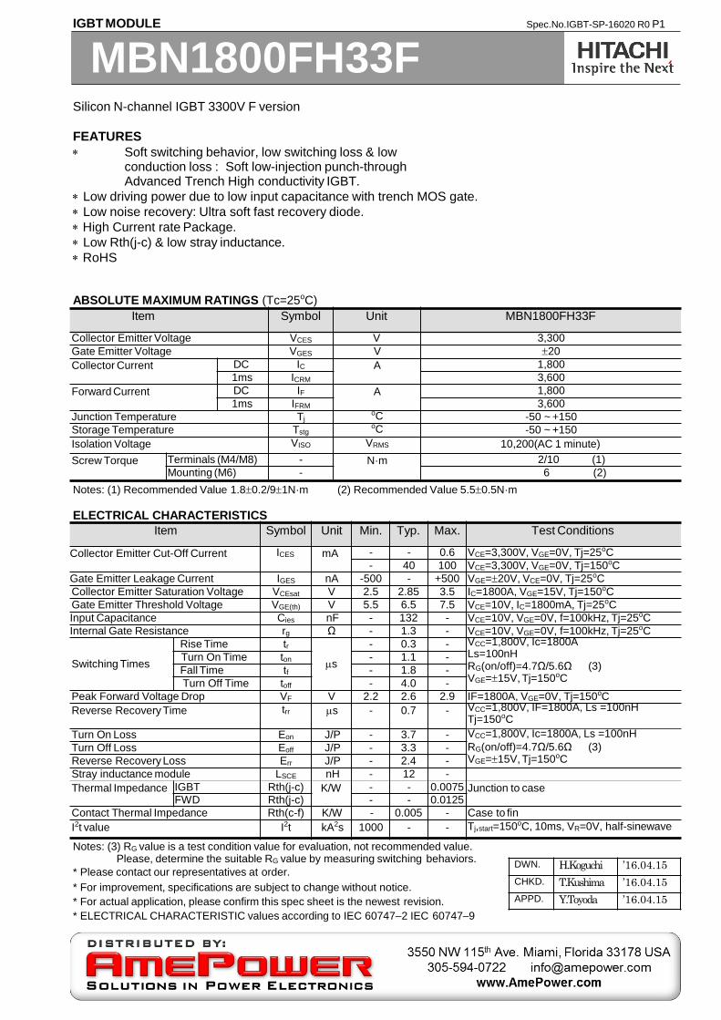
STATIC CHARACTERISTICS
0
600
1200
1800
2400
3000
3600
0 2 4 6
Coll
ecto
rC
urren
t,Ic
(A)
VGE=15V
9V
Tj=25oC 13V
Collector to Emitter Voltage, VCE(V)
Collector Current vs.Collector to Emitter Voltage
TYPICAL
0
600
1200
1800
2400
3000
3600
0 2 4 6
Coll
ecto
rC
urren
t,Ic
(A)
VGE=15V
9V
7V
7V
Tj=125oC 13V
11V
11V
Collector to Emitter Voltage, VCE(V)
Collector Current vs.Collector to Emitter Voltage
TYPICAL
0
600
1200
1800
2400
3000
3600
0 2 4 6
Coll
ecto
rC
urren
t,Ic
(A)
VGE=15V
9V
7V
Tj=150oC 13V
11V
Collector to Emitter Voltage, VCE(V)
Collector Current vs.Collector to Emitter Voltage
TYPICAL
0
600
1200
1800
2400
3000
3600
0 5
Fo
rw
ard
Cu
ren
t,IF
(A)
VGE=0V
Tj=25oC
1 2 3 4
Tj=150oC
Tj=125oC
TYPICAL
IGBT MODULE Spec.No.IGBT-SP-16020 R0 P1
MBN1800FH33F
Forward Voltage, VF(V)
Forward Voltage of free-wheeling diode
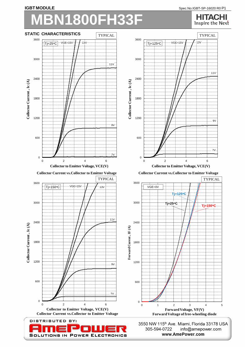
DYNAMIC CHARACTERISTICS
0
0 3,600
Tu
rn
-on
Lo
ss,
Eo
n(J
/pu
lse)
600 1,200 1,800 2,400 3,000
Collector Current , Ic(A)
Turn-on Loss vs.Collector Current
0
8In ducti
ve Load 8
Tj=150oC
7 7
6 6
5
4
3
2
1
Tj=125oC
5
4
3
2
1
0 3,600
Tu
rn
-off
Lo
ss,
Eo
ff (
J/p
uls
e)
600 1,200 1,800 2,400 3,000
Collector Current, Ic (A)
Turn-off Loss vs.Collector Current
InductiveLoad
Tj=150oC
Tj=125oC
TYPICAL TYPICAL
10 10
Conditions Conditions
Vcc=1800V Vcc=1800V9 RG(on)=4.7Ω 9 RG(off)=5.6Ω
VG= 15V VG= 15V
Ls=100nH Ls=100nH
0
1
2
3
4
5
0 3,600
Reverse
Reco
very
Lo
ss, E
rr
(J/p
uls
e)
TYPICAL
Conditions
Vcc=1800V
RG(on)=4.7Ω VG= 15V
Ls=100nHInductiveLoad
Tj=150oC
Tj=125oC
600 1,200 1,800 2,400 3,000
Collector Current , IF (-Ic) (A)
Recovery Loss vs.Collector Current
IGBT MODULE Spec.No.IGBT-SP-16020 R0 P1
MBN1800FH33F
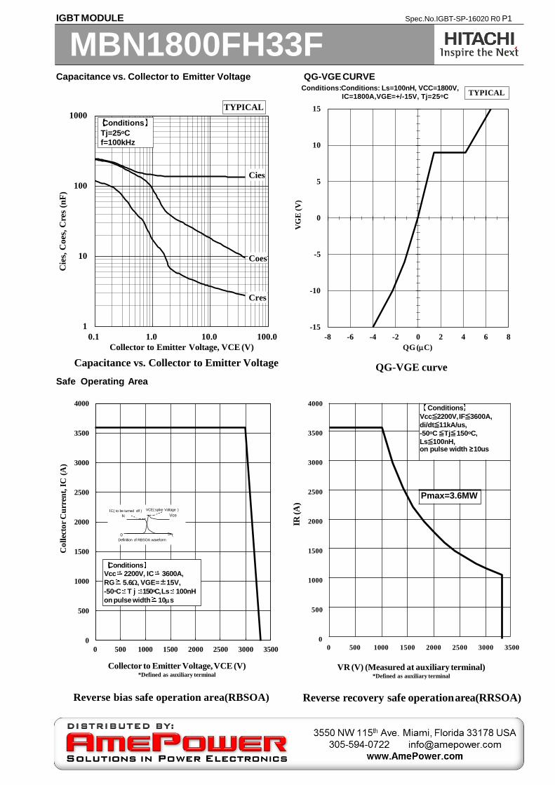
Capacitance vs. Collector to Emitter Voltage QG-VGE CURVE
1
10
100
1000
0.1 1.0 10.0 100.0
Cie
s,C
oes
,C
res
(nF
)
Collector to Emitter Voltage, VCE (V)
Capacitance vs. Collector to Emitter Voltage
Conditions
Tj=25oC
f=100kHz
TYPICAL
Cies
Coes
Cres
QG-VGE curve
-15
-10
-5
0
5
10
15
-8 -6 -4 -2 4 6 8
VG
E(V
)
0 2
QG (C)
:Ls=80nH, VCC=1800V,
IC=1800A,VGE=+/-15V, Tj=25oCTYPICAL
Safe Operating Area
Reverse bias safe operation area(RBSOA)
0
500
1000
1500
2000
2500
3000
3500
4000
3500
Co
llec
tor
Cu
rren
t,IC
(A)
0 500 1000 1500 2000 2500 3000
Collector to Emitter Voltage,VCE (V)*Defined as auxiliary terminal
Conditions
Vcc 2200V, IC 3600A,
RG 5.6, VGE= 15V,
-50oC T 150oC,Ls 100nH
on pulse width 10s
0Definition of RBSOA waveform
IC( to be turned off ) VCE( spike Voltage )
Ic Vce
t
0
500
1000
1500
2000
2500
3000
3500
4000
0 3500
IR(A
)
500 1000 1500 2000 2500 3000
VR (V) (Measured at auxiliary terminal)*Defined as auxiliary terminal
Reverse recovery safe operationarea(RRSOA)
Conditions
Vcc≦2200V,IF≦3600A,
di/dt≦11kA/us,
-50oC ≦Tj≦150oC,
Ls≦100nH,on pulse width ≥10us
Pmax=3.6MW
Conditions Conditions: Ls=100nH, VCC=1800V,
IGBT MODULE Spec.No.IGBT-SP-16020 R0 P1
MBN1800FH33F
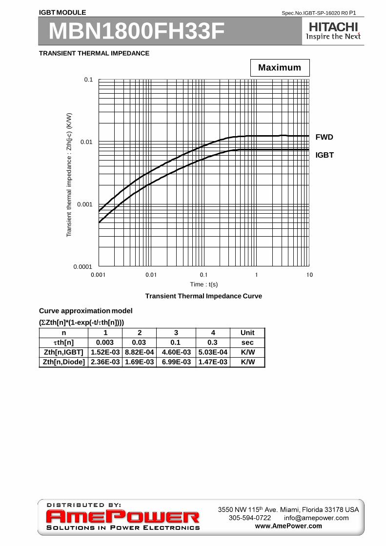
TRANSIENT THERMAL IMPEDANCE
0.0001
0.001
0.01
0.1
0.001 0.01 1 10
Tra
nsie
nt
therm
al
imp
ed
ance
:Z
th(j-c
)(K
/W)
0.1
Time : t(s)
FWD
IGBT
Maximum
Transient Thermal Impedance Curve
Curve approximation model
(Zth[n]*(1-exp(-t/th[n])))
n 1 2 3 4 Unit
th[n] 0.003 0.03 0.1 0.3 sec
Zth[n,IGBT] 1.52E-03 8.82E-04 4.60E-03 5.03E-04 K/W
Zth[n,Diode] 2.36E-03 1.69E-03 6.99E-03 1.47E-03 K/W
IGBT MODULE Spec.No.IGBT-SP-16020 R0 P1
MBN1800FH33F
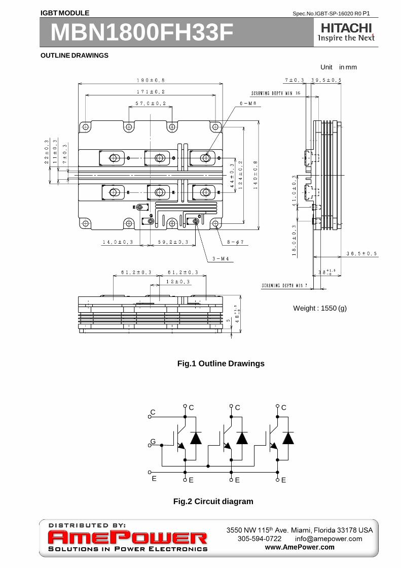
OUTLINE DRAWINGS
8
16
8
Fig.1 Outline Drawings
EE
G
CC C C
E E
Fig.2 Circuit diagram
Unit in mm
Weight : 1550 (g)
IGBT MODULE Spec.No.IGBT-SP-16020 R0 P1
MBN1800FH33F

For inquiries relating to the products, please contact nearest overseas representatives that is located
“Inquiry” portion on the top page of a home page.
Hitachi power semiconductor home page address http://www.hitachi-power-semiconductor-device.co.jp/en/
HITACHI POWER SEMICONDUCTORS
Notices
1.The information given herein, including the specifications and dimensions, is subject to
change without prior notice to improve product characteristics. Before ordering,
purchasers are advised to contact Hitachi sales department for the latest version of this
data sheets.
2.Please be sure to read "Precautions for Safe Use and Notices" in the individual brochure
before use.
3.In cases where extremely high reliability is required (such as use in nuclear power
control, aerospace and aviation, traffic equipment, life-support-related medical
equipment, fuel control equipment and various kinds of safety equipment), safety should
be ensured by using semiconductor devices that feature assured safety or by means of
users’ fail-safe precautions or other arrangement. Or consult Hitachi’s sales department
staff.
4. In no event shall Hitachi be liable for any damages that may result from an accident or
any other cause during operation of the user’s units according to this data sheets. Hitachi
assumes no responsibility for any intellectual property claims or any other problems that
may result from applications of information, products or circuits described in this data
sheets.
5.In no event shall Hitachi be liable for any failure in a semiconductor device or any
secondary damage resulting from use at a value exceeding the absolute maximum rating.
6.No license is granted by this data sheets under any patents or other rights of any third
party or Hitachi Power Semiconductor Device, Ltd.
7.This data sheets may not be reproduced or duplicated, in any form, in whole or in part,
without the expressed written permission of Hitachi Power Semiconductor Device, Ltd.
8.The products (technologies) described in this data sheets are not to be provided to any
party whose purpose in their application will hinder maintenance of international peace
and safety not are they to be applied to that purpose by their direct purchasers or any
third party. When exporting these products (technologies), the necessary procedures are
to be taken in accordance with related laws and regulations.
IGBT MODULE Spec.No.IGBT-SP-16020 R0 P1
MBN1800FH33F