www.elsevier.com/locate/corsci
Corrosion Science 46 (2004) 1479–1499
The electronic properties of sputteredchromium and iron oxide films
G. Goodlet a, S. Faty a,1, S. Cardoso b, P.P. Freitas b,c,A.M.P. Sim~oes a, M.G.S. Ferreira a,d,*, M. Da Cunha Belo a
a Department of Chemical Engineering, Instituto Superior T�ecnico, Av. Rovisco Pais,
Lisboa 1049-001, Portugalb INESC Microsystems and Nanotechnologies, R. Alves Redol 9, Lisboa 1000 , Portugalc Department of Physics, Instituto Superior Tecnico, Av. Rovisco Pais, Lisboa 1049-001,
Portugald Department of Ceramics and Glass Engineering, University of Aveiro, Campus de Santiago,
Aveiro 3810-193, Portugal
Received 31 March 2003; accepted 16 September 2003
Abstract
The semiconducting properties and electrochemical behaviour of thin chromium and iron
oxide films produced by sputtering were investigated by capacitance and photoelectrochemical
measurements. The films were deposited onto various substrates and submitted in some cases,
to a thermal treatment. It appears that sputtered chromium oxide on iron substrate reveals
both types of semiconductivity (p and n) and that the thermal treatment enhances the n-type
character. Finally, a study is developed using a duplex film formed by sputtered layers of
chromium and iron oxides. This system allows for the discussion of the problem of the
electronic structure of the heterojunction created by the two kinds of oxides. Comparison is
made with the case of passive films on stainless steel.
� 2003 Elsevier Ltd. All rights reserved.
Keywords: A. Sputtered films; B. Capacitance and photoelectrochemistry; C. Passivity
* Corresponding author. Address: Department of Chemical Engineering, Instituto Superior T�ecnico,
Av. Rovisco Pais, Lisboa 1049-001, Portugal. Tel.: +351-234370354; fax: +351-218404589.
E-mail address: [email protected] (M.G.S. Ferreira).1 Permanent address: Facult�e des Sciences et Techniques, UCAD, Dakar, Senegal.
0010-938X/$ - see front matter � 2003 Elsevier Ltd. All rights reserved.
doi:10.1016/j.corsci.2003.09.022
1480 G. Goodlet et al. / Corrosion Science 46 (2004) 1479–1499
1. Introduction
Although the presence of chromium oxides in the passive films formed on Fe–Cr
stainless steels play the major role on corrosion resistance of these materials, the
electrochemical properties of the films are also strongly influenced by the presence of
iron oxides. There are in fact, throughout the film thickness, regions of approxi-mately pure chromium oxide, pure iron oxide and transition regions of mixed oxides.
Chromium oxides are generally considered to have p-type behaviour [1]. Possible
doping species are cationic and anionic vacancies or cationic interstitials. When
chromium interstitials or oxygen vacancies are the predominating defects, the
chromium oxide is an n-type semiconductor and when chromium vacancies are
the predominating defects the chromium oxide is a p-type semiconductor. For
the electronic characterization of chromium oxides, no well defined values of the
band gap exist, but instead several values have been reported and assumed to berelated to the different degrees of hydration [2–4]. On the other hand, because
chromium and iron oxides reveal distinct semiconducting properties, an important
characteristic of the electronic structure of passive films on stainless steels is the
development of an interface, inside the film, with a distribution of charge carriers
similar to that of a p–n heterojunction [5,6]. Simultaneous ionic and electronic
transport and high doping levels make the study of the passive films very complex.
The study of well-defined oxide layers could help in interpreting results concerning
passivation.In this work the electronic properties of chromium and iron oxide films produced
by sputtering were investigated in borate buffer solution. The central part of the
research concerns the possible effects of the applied potential on the electronic
structure of the n–p junction formed by sputtered chromium and iron oxide layers.
In this junction only electronic processes take place when submitted to external
polarization. In fact, ionic transport throughout the junction during electrochemical
and photoelectrochemical measurements can be excluded. Only dissolution processes
at film-electrolyte interface may occur.The methods used in this study are the photocurrent spectroscopy in order to
obtain band gap values and the Mott–Schottky approach based on capacitance
measurements. Both methods have been used in semiconductor electrochemistry and
can also be considered as good tools for characterization of semiconducting passive
films. Capacitance measurements have been carried out in the present investigation
using the frequency values equivalent to that used in previous research on passive
films. This procedure helps in making the results comparable.
2. Experimental
Chromium and iron oxide films were sputtered onto various substrates (glassycarbon, tantalum and iron). They were fabricated by reactive ion beam sputter-
ing from Cr and Fe metallic targets, respectively, in the presence of a mixed Ar–O2
beam coming from the 20 cm diameter assist gun (15.02% O2 in Ar). A dual source
G. Goodlet et al. / Corrosion Science 46 (2004) 1479–1499 1481
Nordiko 3000 ion beam system was used [7,8]. The substrate holder was water
cooled. The deposition source was running with the standard conditions for
the metallic film deposition (acceleration voltage of +1450 V, deceleration voltage
of )300 V, 33 mA Xe beam, 1 sccm Xe, 100 W RF plasma), while an Ar-O2 beam
was created by accelerating the plasma inside the assist gun with +200 V (18 mA
beam, 10 sccm Ar–O2, 60W RF plasma) and using a deceleration voltage of )100 V.A deficient content of O2 (low acceleration voltage) would cause the film to be
metallic, instead of oxide. Also, too high acceleration voltages will reduce the
deposition rate, since the deposited material would be sputtered by the Ar–O2
beam, instead of reacting with metallic ions coming from the target. The pressure
during the process is 1.2 · 10�4 Torr. A filamentless neutraliser (40 mA, 3 sccm Ar–
O2) beside to assist the ion source avoids surface charging during the dielectric
deposition. During the oxide deposition the substrate table is at 80�, and rotates at
15 rpm.A thermal treatment at 300 �C for 8 h, was applied to some of the films. The film
on pure chromium and pure iron (Goodfellow 99.9%) were grown at 450 �C for 2 h
in a furnace. Prior to growth the chromium was polished with silicon carbide paper
of various grades and finished with 1 lm aluminium oxide. Structural information
on the films was obtained by glancing XRD measurements, using a Siemens X-ray D
500 diffractometer.
Atomic force microscopy (AFM) was carried out by using a Topometrix 2010
‘‘Discover’’ working in non-contact mode with a silicon nitride tip.In the photoelectrochemical study the working electrode was illuminated through
a quartz window with monochromatic light (beam area¼ 0.12 cm2). The optical
instrumentation consisted of a 150 W Xe lamp, a 250 mm f18 monochromator, a
stepper motor to control the wavelength and a mechanical chopper. The grating was
changed at 340 nm for maximum flux and a filter was used above 450 nm to elim-
inate any second order effects. All photocurrent measurements were normalized with
respect to the flux recorded by a silicon photodiode. The photocurrent was obtained
by connecting the current output of the potentiostat (EG&G 273) to a lock-inamplifier (Brookdeal EG&G 5210) and recording the voltage output due to the
signal at 19 Hz (the chopping frequency). The recorded values were then worked out
to calculate the photocurrent and the quantum efficiency values using a spreadsheet
software package.
For the capacitance–potential measurements the lock-in was used to produce a
sinusoidal signal, 10 mV peak-to-peak at 1 kHz, which was superimposed on the
potential applied by the potentiostat. The output of the potentiostat was then fed to
the lock-in.A three-electrode cell was used, consisting of a Pt wire counter electrode, a sat-
urated calomel reference electrode and the oxide film on the substrate was the
working electrode.
All measurements were carried out in sodium borate/boric acid buffer solution
(pH 9.1). The effect of pH was observed by using 0.5 M sulfuric acid and a 0.01 M
solution of the same acid was prepared for the profiling experiments. All the reagents
were of an analytical grade.

1482 G. Goodlet et al. / Corrosion Science 46 (2004) 1479–1499
3. Results
3.1. AFM observations and XRD measurements
The AFM images obtained with sputtered iron and chromium oxide films on
tantalum are shown in Fig. 1. Both films can be considered compact but theroughness morphology of the iron oxide film (Fig. 1a) is very different from that of
the chromium oxide film (Fig. 1b). It is known that the AFM technique allows us to
observe surface morphology but does not give, in the experimental conditions used,
direct information about the crystallographic structure. Nevertheless, nucleation
aspects of the film growth may relate to a larger grain size of the chromium oxide
relatively to that of the iron oxide. This analysis is supported by XRD results, which
show that the annealed chromium oxide (8 h at 300 �C) depicted any Cr2O3 peaks,
where a peak corresponding to the (1 1 0) plane was observed. Although the otherfilms appeared to be amorphous or nanocrystalline due to a lack of peaks, the
spectrum of the 1000 �A film sputtered onto Ta displayed an increased response in the
30–40� region compared to the 50 �A film. This response may be caused by nano-
crystalline material. There is, thus, evidence to suggest that the films are not com-
pletely amorphous. Marcus et al. [9] have reported the presence of nanocrystallites
Fig. 1. AFM images of sputtered: (a) chromium and (b) iron oxide films of 500 �A on tantalum.
G. Goodlet et al. / Corrosion Science 46 (2004) 1479–1499 1483
(<3 nm) of Cr2O3-like oxide anodically grown on chromium. Therefore some short-
range order can be considered within these films.
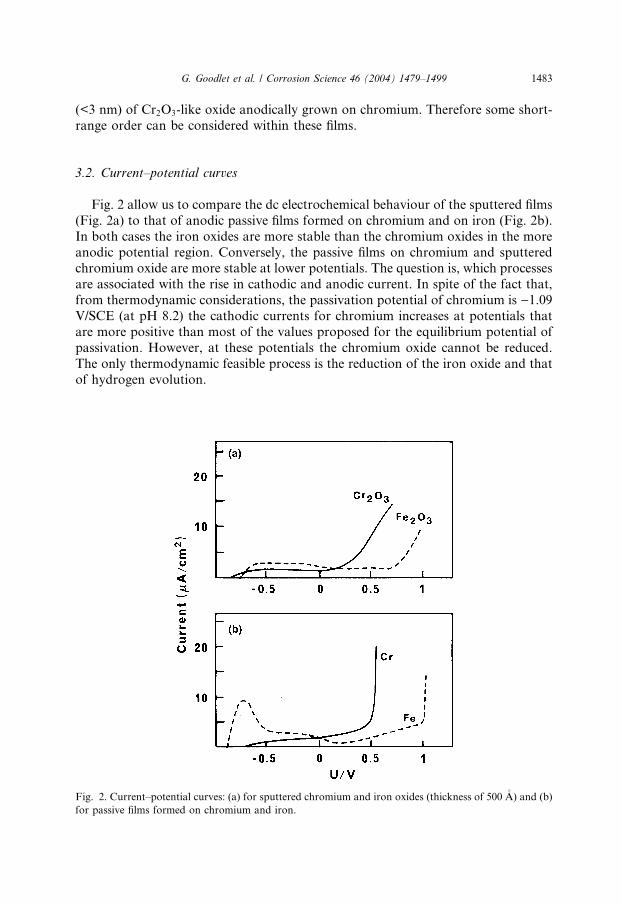
3.2. Current–potential curves
Fig. 2 allow us to compare the dc electrochemical behaviour of the sputtered films
(Fig. 2a) to that of anodic passive films formed on chromium and on iron (Fig. 2b).
In both cases the iron oxides are more stable than the chromium oxides in the more
anodic potential region. Conversely, the passive films on chromium and sputteredchromium oxide are more stable at lower potentials. The question is, which processes
are associated with the rise in cathodic and anodic current. In spite of the fact that,
from thermodynamic considerations, the passivation potential of chromium is )1.09V/SCE (at pH 8.2) the cathodic currents for chromium increases at potentials that
are more positive than most of the values proposed for the equilibrium potential of
passivation. However, at these potentials the chromium oxide cannot be reduced.
The only thermodynamic feasible process is the reduction of the iron oxide and that
of hydrogen evolution.
Fig. 2. Current–potential curves: (a) for sputtered chromium and iron oxides (thickness of 500 �A) and (b)
for passive films formed on chromium and iron.
1484 G. Goodlet et al. / Corrosion Science 46 (2004) 1479–1499
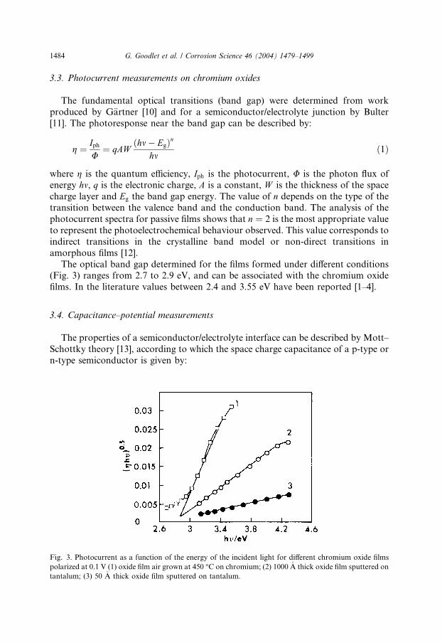
3.3. Photocurrent measurements on chromium oxides
The fundamental optical transitions (band gap) were determined from work
produced by G€artner [10] and for a semiconductor/electrolyte junction by Bulter
[11]. The photoresponse near the band gap can be described by:
Fig. 3
polariz
tantalu
g ¼ IphU
¼ qAWðhm � EgÞn
hmð1Þ
where g is the quantum efficiency, Iph is the photocurrent, U is the photon flux ofenergy hm, q is the electronic charge, A is a constant, W is the thickness of the space
charge layer and Eg the band gap energy. The value of n depends on the type of the
transition between the valence band and the conduction band. The analysis of the
photocurrent spectra for passive films shows that n ¼ 2 is the most appropriate value
to represent the photoelectrochemical behaviour observed. This value corresponds to
indirect transitions in the crystalline band model or non-direct transitions in
amorphous films [12].
The optical band gap determined for the films formed under different conditions(Fig. 3) ranges from 2.7 to 2.9 eV, and can be associated with the chromium oxide
films. In the literature values between 2.4 and 3.55 eV have been reported [1–4].
3.4. Capacitance–potential measurements
The properties of a semiconductor/electrolyte interface can be described by Mott–
Schottky theory [13], according to which the space charge capacitance of a p-type or
n-type semiconductor is given by:
. Photocurrent as a function of the energy of the incident light for different chromium oxide films
ed at 0.1 V (1) oxide film air grown at 450 �C on chromium; (2) 1000 �A thick oxide film sputtered on
m; (3) 50 �A thick oxide film sputtered on tantalum.
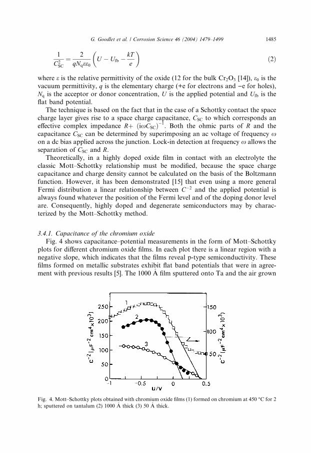
Fig. 4
h; sput
G. Goodlet et al. / Corrosion Science 46 (2004) 1479–1499 1485
1
C2SC
¼ 2
qNqee0U
�� Ufb �
kTe
�ð2Þ
where e is the relative permittivity of the oxide (12 for the bulk Cr2O3 [14]), e0 is thevacuum permittivity, q is the elementary charge (+e for electrons and )e for holes),
Nq is the acceptor or donor concentration, U is the applied potential and Ufb is the
flat band potential.
The technique is based on the fact that in the case of a Schottky contact the space
charge layer gives rise to a space charge capacitance, CSC to which corresponds an
effective complex impedance Rþ ðixCSCÞ�1. Both the ohmic parts of R and the
capacitance CSC can be determined by superimposing an ac voltage of frequency xon a dc bias applied across the junction. Lock-in detection at frequency x allows the
separation of CSC and R.Theoretically, in a highly doped oxide film in contact with an electrolyte the
classic Mott–Schottky relationship must be modified, because the space charge
capacitance and charge density cannot be calculated on the basis of the Boltzmann
function. However, it has been demonstrated [15] that even using a more general
Fermi distribution a linear relationship between C�2 and the applied potential isalways found whatever the position of the Fermi level and of the doping donor level
are. Consequently, highly doped and degenerate semiconductors may by charac-
terized by the Mott–Schottky method.
3.4.1. Capacitance of the chromium oxide
Fig. 4 shows capacitance–potential measurements in the form of Mott–Schottky
plots for different chromium oxide films. In each plot there is a linear region with a
negative slope, which indicates that the films reveal p-type semiconductivity. These
films formed on metallic substrates exhibit flat band potentials that were in agree-
ment with previous results [5]. The 1000 �A film sputtered onto Ta and the air grown
. Mott–Schottky plots obtained with chromium oxide films (1) formed on chromium at 450 �C for 2
tered on tantalum (2) 1000 �A thick (3) 50 �A thick.

Table 1
The effect of pH on the electronic properties of chromium oxide films
Film type pH Band gap/eV Ufb vs. SCE/V Na � 1019 atoms/cm3
Air grown 9.2 2.87 0.46 13
0.6 2.94 0.95 31
1000 �A CrOx on Ta 9.2 2.76 0.54 6
0.6 2.84 1.25 3
1486 G. Goodlet et al. / Corrosion Science 46 (2004) 1479–1499
film showed an increase in capacitance (decrease in 1=C2) for potentials below )0.5V. Particularly relevant are the high doping densities, especially those exhibited by
the 50 �A sputtered films. According to this high doping the thickness of the space
charge region extends across a relatively short distance into the film. For example,
for the 1000 �A film on Ta, the doping density leads to a calculated space charge
thickness of 40 �A. The doping densities obtained in this work are approximately one
order of magnitude below those reported by B€ohni [16].Table 1 summarizes the results of measurements made in both alkaline basic
(borate buffer) and acidic (0.5 M sulphuric acid) conditions for the air grown film
and a sputtered film. The band gaps are practically unchanged whereas the flat band
potentials change practically in accordance with the Nernst equation (approximately
0.060 V per pH unit).
It should be noted that the straight lines in the Mott–Schottky representation are
relatively short. This can be interpreted as a consequence of the low thickness of the
films. Note that, highly doped bulk crystalline semiconductors also exhibit the same
feature [17].
3.4.2. Capacitance of the iron oxide
In the case of the iron oxide film sputtered on tantalum (Fig. 5a) the Mott–
Schottky plot displays a positive slope in the region from 0 to )0.5 V vs. SCE, in the
same way as the film formed on pure iron by air oxidation (Fig. 5b). This can be
attributed to the n-semiconductive behaviour of Fe2O3. The capacitance behaviour
of iron oxide films sputtered onto the various substrates was also similar. The doping
densities were all very high (�1021 cm�3) and the photocurrent was much lower thanthat in air grown films on pure iron and on stainless steel. In the XRD analysis only
the 500 �A iron oxide film on silicon displayed any peaks and these could not be
clearly identified as Fe2O3 or Fe3O4.
The change in slope of the C�2 ¼ f ðUÞ plot observed at about 0 V (Fig. 5) may be
explained assuming that a deep donor level is localized in the octahedral sites of the
spinel oxide [18,19].
3.4.3. Chromium oxide sputtered on iron substrate (effect of annealing)
The capacitance behaviour of both thermally and anodically grown films (passive
films) on stainless steel gives Mott–Schottky plots with positive (n-type) and negative
(p-type) slopes [5]. This same type of behaviour is observed in as-deposited sputtered
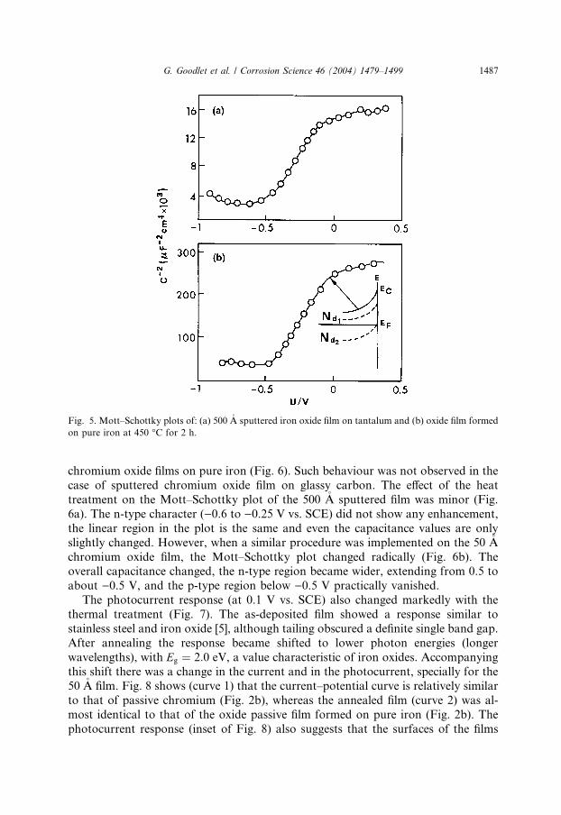
Fig. 5. Mott–Schottky plots of: (a) 500 �A sputtered iron oxide film on tantalum and (b) oxide film formed
on pure iron at 450 �C for 2 h.
G. Goodlet et al. / Corrosion Science 46 (2004) 1479–1499 1487
chromium oxide films on pure iron (Fig. 6). Such behaviour was not observed in the
case of sputtered chromium oxide film on glassy carbon. The effect of the heat
treatment on the Mott–Schottky plot of the 500 �A sputtered film was minor (Fig.
6a). The n-type character ()0.6 to )0.25 V vs. SCE) did not show any enhancement,
the linear region in the plot is the same and even the capacitance values are only
slightly changed. However, when a similar procedure was implemented on the 50 �Achromium oxide film, the Mott–Schottky plot changed radically (Fig. 6b). Theoverall capacitance changed, the n-type region became wider, extending from 0.5 to
about )0.5 V, and the p-type region below )0.5 V practically vanished.
The photocurrent response (at 0.1 V vs. SCE) also changed markedly with the
thermal treatment (Fig. 7). The as-deposited film showed a response similar to
stainless steel and iron oxide [5], although tailing obscured a definite single band gap.
After annealing the response became shifted to lower photon energies (longer
wavelengths), with Eg ¼ 2:0 eV, a value characteristic of iron oxides. Accompanying
this shift there was a change in the current and in the photocurrent, specially for the50 �A film. Fig. 8 shows (curve 1) that the current–potential curve is relatively similar
to that of passive chromium (Fig. 2b), whereas the annealed film (curve 2) was al-
most identical to that of the oxide passive film formed on pure iron (Fig. 2b). The
photocurrent response (inset of Fig. 8) also suggests that the surfaces of the films

Fig. 6. Mott–Schottky plots of chromium oxide films sputtered on iron (1) as deposited and (2) after
heating at 300 �C for 8 h. (a) 500 �A; thick (b) 50 �A thick.
1488 G. Goodlet et al. / Corrosion Science 46 (2004) 1479–1499
behave as chromium oxide and iron oxide-like for the as-deposited and annealed
films, respectively.
3.4.4. Chemical profiling on duplex film formed by chromium and iron sputtered oxides
Chemical profiling was used to assess the way in which the Mott–Schottky plots
change when the surface layer of iron oxide was removed. This technique is based on
the commonly used doping density profiling technique used in the semiconductor
industry. A sample of 500 �A iron oxide on 500 �A chromium oxide sputtered onto Ta
was immersed in a solution 1 M H2SO4. Capacitance-potential measurements were
then obtained at several time intervals (Fig. 9a) and show a transition. Immediately
after immersion there is a sharp increase of 1=C2 in the region below )0.5 V. As
the chemical etching proceeds, the positive slope (characteristic of n-type semi-
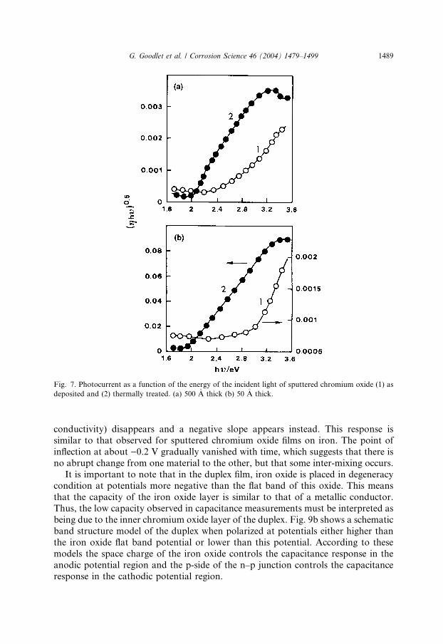
Fig. 7. Photocurrent as a function of the energy of the incident light of sputtered chromium oxide (1) as
deposited and (2) thermally treated. (a) 500 �A thick (b) 50 �A thick.
G. Goodlet et al. / Corrosion Science 46 (2004) 1479–1499 1489
conductivity) disappears and a negative slope appears instead. This response is
similar to that observed for sputtered chromium oxide films on iron. The point of
inflection at about )0.2 V gradually vanished with time, which suggests that there is
no abrupt change from one material to the other, but that some inter-mixing occurs.
It is important to note that in the duplex film, iron oxide is placed in degeneracycondition at potentials more negative than the flat band of this oxide. This means
that the capacity of the iron oxide layer is similar to that of a metallic conductor.
Thus, the low capacity observed in capacitance measurements must be interpreted as
being due to the inner chromium oxide layer of the duplex. Fig. 9b shows a schematic
band structure model of the duplex when polarized at potentials either higher than
the iron oxide flat band potential or lower than this potential. According to these
models the space charge of the iron oxide controls the capacitance response in the
anodic potential region and the p-side of the n–p junction controls the capacitanceresponse in the cathodic potential region.
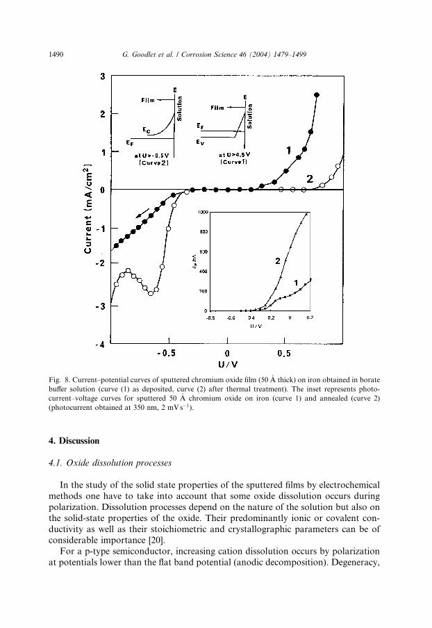
Fig. 8. Current–potential curves of sputtered chromium oxide film (50 �A thick) on iron obtained in borate
buffer solution (curve (1) as deposited, curve (2) after thermal treatment). The inset represents photo-
current–voltage curves for sputtered 50 �A chromium oxide on iron (curve 1) and annealed (curve 2)
(photocurrent obtained at 350 nm, 2 mVs�1).
1490 G. Goodlet et al. / Corrosion Science 46 (2004) 1479–1499
4. Discussion
4.1. Oxide dissolution processes
In the study of the solid state properties of the sputtered films by electrochemical
methods one have to take into account that some oxide dissolution occurs during
polarization. Dissolution processes depend on the nature of the solution but also on
the solid-state properties of the oxide. Their predominantly ionic or covalent con-
ductivity as well as their stoichiometric and crystallographic parameters can be ofconsiderable importance [20].
For a p-type semiconductor, increasing cation dissolution occurs by polarization
at potentials lower than the flat band potential (anodic decomposition). Degeneracy,
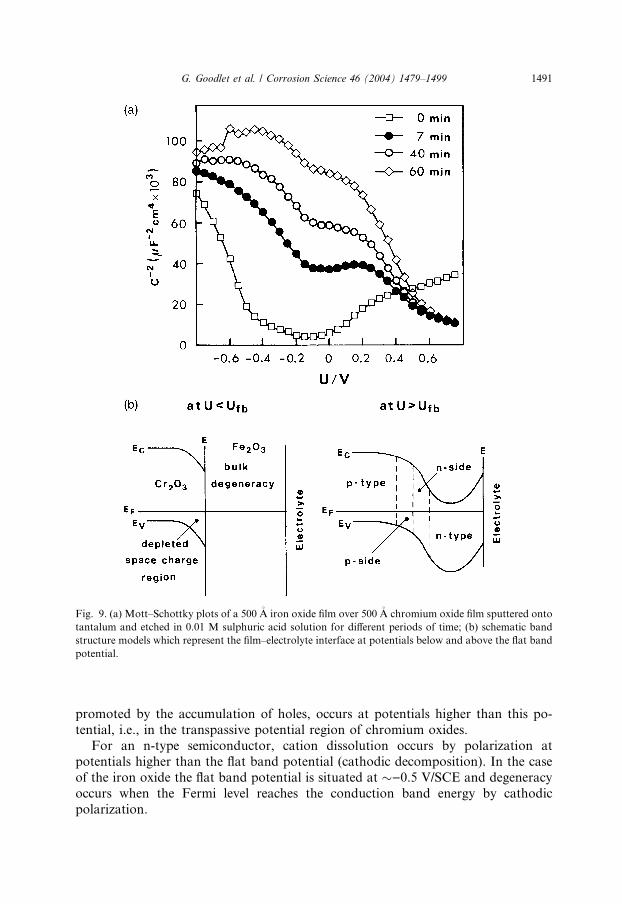
Fig. 9. (a) Mott–Schottky plots of a 500 �A iron oxide film over 500 �A chromium oxide film sputtered onto
tantalum and etched in 0.01 M sulphuric acid solution for different periods of time; (b) schematic band
structure models which represent the film–electrolyte interface at potentials below and above the flat band
potential.
G. Goodlet et al. / Corrosion Science 46 (2004) 1479–1499 1491
promoted by the accumulation of holes, occurs at potentials higher than this po-
tential, i.e., in the transpassive potential region of chromium oxides.
For an n-type semiconductor, cation dissolution occurs by polarization atpotentials higher than the flat band potential (cathodic decomposition). In the case
of the iron oxide the flat band potential is situated at �)0.5 V/SCE and degeneracy
occurs when the Fermi level reaches the conduction band energy by cathodic
polarization.
1492 G. Goodlet et al. / Corrosion Science 46 (2004) 1479–1499
The situation, which may be controversial, is that of the capacitance measure-
ments made in the cathodic potential region where the dissolution current of the iron
oxide may be relatively high, i.e., at potentials lower than the flat band potential of
the iron oxide (�)0.5 V).
Based on electrochemical concepts, the removal rate for each ion of an oxide
electrode is given by [21]:
i ¼ nk expazFWRT
ð3Þ
in which n is the number of ions/cm2, a the transfer coefficient, z the ionic charge, k a
constant and W the double layer potential. Eq. (3) indicates that a small change in
the double layer potential corresponds to a rather large change in the composition
of the contacting phase. A corollary of this large change of surface composition
with potential is that of a possible change of the capacitance. It is important to think
about this capacitance by taking into account the influence of the applied poten-tial on both the double layer potential and the space charge potential in the oxide
film.
Strong changes in the double layer potential only become important at potentials
situated in the cathodic potential region where the hydrogen discharge takes place
and the capacitance of the double layer increases with decreasing potential [22]. It is
likely that most of the applied potential is developed in the space charge layer in the
semiconducting oxides and band structure changes are predominantly responsible
for the observed changes in capacitance.
4.1.1. Thermodynamic considerations
The Mott–Schottky plots of the sputtered chromium oxides onto Ta appear
similar to that of the chromium oxide obtained by direct oxidation of chromium. In
both cases the films behave as p-type semiconductors. However, interpretation of the
capacitance behaviour of the sputtered thin chromium oxide film onto iron requires
consideration of regions of distinct semiconductivity in the films. This may occur iffor instance both chromium vacancies and oxygen vacancies exist in the oxide and if
close to the surface the number of oxygen vacancies is higher than that of the
chromium vacancies. In this case the oxide film can become n-type at the surface
with a p–n junction between the surface layer and the p-type bulk.
The transport processes across the oxide is regulated by the gradient of electric
potential as well as by the gradient of the chemical potential. For a species denoted
as i, the chemical potential is given by:
li ¼ l0i þ RT ln½Xi ð4Þ
where li, l0i and [Xi] are the actual chemical potential, the standard chemical po-
tential and the activity of the species, respectively. Since the electrochemical potential
g of each ionic species is constant throughout the system metal–film–electrolyte, the
following relationship holds [23]:
G. Goodlet et al. / Corrosion Science 46 (2004) 1479–1499 1493
giðsÞ ¼ giðbÞ ð5Þ
in which, the subscripts s and b denote surface and bulk, respectively. On the otherhand g and l for each species are related by:
gi ¼ li þ ziqW ð6Þ
where zi is the valence of the species, q the elementary charge and W the electricpotential at the location of the species in the system. So, taking into account Eqs. (4)and (5), it comes:
liðsÞ þ ziqWs ¼ liðbÞ þ ziqWb ð7Þ
l0i þ RT ln½Xis þ ziqWs ¼ l0
i þ RT ln½xib þ ziqWb ð8Þ
which gives
RT ln½Xis½Xib
¼ ziqðWb � WsÞ ð9Þ
Wb � Ws ¼ u is the potential difference between the bulk and the surface, then it
follows:
½Xis ¼ ½Xib expðziqu=kT Þ ð10Þ
Applying this equation to the defect concentrations the following relationship is
found for divalent cation vacancies VM (negatively charged zi ¼ �2) and oxygen
vacancies V0 (positively charged zi ¼ þ2):
½VMs ¼ ½VMb exp�2uqkT
� �ð11Þ
and
½V0s ¼ ½V0b expþ2uqkT
� �ð12Þ
Inside the film, ½VMb ¼ ½V0b and, as a consequence of the Schottky equilibrium,
the concentration of the two types of vacancies vary in a symmetrical way [24].
According to capacitance results the transition from n-type to p-type behaviouroccurs at potential of )0.2 V (Fig. 6). Thus, it can be assumed that at lower
potentials the concentration of oxygen vacancies is higher than that of chromium
vacancies and the film behaves as an n-type semiconductor (positive slopes of the
Mott–Schottky plots). At potentials higher than �)0.2 V, the film behaves as a p-
type semiconductor (negative slopes of the Mott–Schottky plots).
The thermal treatment does not have a marked influence on the capacitance
behaviour of the chromium oxide film with 500 �A (Fig. 6a). However, when this
treatment is applied to the very thin film of 50 �A (Fig. 6b) its capacitance behaviouris strongly modified. The film manifests only n-type semiconductivity at potentials
higher than the flat band potential situated at about )0.5 V. Because the latter is the
flat band potential of the iron oxide it can be assumed that the thermal treatment
1494 G. Goodlet et al. / Corrosion Science 46 (2004) 1479–1499
promotes iron diffusion across the very thin chromium oxide film. This interpretation
is also supported by photoelectrochemical results, which can be related to the for-
mation of oxide layers close to the surface with band gap energy close to 2.3 eV,
which is the band gap value of the iron oxide. This chemical evolution is illustrated
by the current–potential curves obtained in a borate buffer solution of pH 9.2. In-
deed, the electrochemical behaviour of the sputtered chromium oxide is similar tothat of the passive film formed on chromium. After thermal treatment the chromium
oxide becomes more stable at anodic potential, resembling more the behaviour of the
iron oxide film. In the solution used the stability of the passive film formed on pure
chromium goes down to lower potentials than that of the iron passive film.
Fig. 9 represents the capacitance behaviour of a duplex film obtained by sput-
tering and composed of two oxides i.e. an inner chromium oxide layer and an outer
iron oxide layer. Mott–Schottky plots reveal the existence of straight lines of neg-
ative and positive slopes separated by a potential situated at about )0.5 V, whichcorresponds to the flat band potential of the iron oxide for the pH used in this study.
These results support the electronic band structure model proposed for passive films
(�30 �A thick) formed on stainless steel in borate buffer solution [5]. This model
assumes that the capacitance response of a film composed of an inner chromium
oxide layer and an outer iron oxide layer behaves as a p-type and n-type semicon-
ductor at potentials lower and higher than about )0.5 V, respectively. Further, to
interpret the evolution of the capacitance when the iron oxide is progressively re-
moved by dissolution in the solution of 0.01 M H2SO4, it is useful to introduce thethermodynamic concepts relative to the equilibrium potential between two phases. It
is assumed that when two phases are in equilibrium, the potential will not depend on
the ratio of the quantities of the phases and remain constant until one of the phases is
consumed. In this system the potential is now defined by the ratio of difference
between the free enthalpies of formation of each phase to the difference between the
degree of oxidation of each phase [24].
4.2. The properties of the sputtered oxide films as compared to that of passive films
When the electrochemical properties of the passive films formed on stainless steelsare discussed the fact that the ionic and electronic structure results from reactions at
metal/film and film/electrolyte interfaces has to be taken into account. The migration
of the various species occurs under the combined influence of the concentration
gradient and the electric field. Under an applied potential, the total electric potential
results not only from the charge at the surface but also from the space charge
contribution. The driving force is now mainly dependent of the electric field, E,developed in this part of the film, which according to the Mott–Schottky approach
is given by:
E ¼ 2qNq
e � e0
� �1=2U
�� Ufb �
KTe
�1=2ð13Þ
where Nq is the doping density (donor or acceptor concentrations).
G. Goodlet et al. / Corrosion Science 46 (2004) 1479–1499 1495
The particle transport in the case of the sputtered oxide films is essentially elec-
tronic. Ionic transport throughout the film must be assumed to be completely
inhibited. Because the film is not formed on its parent metal, there is also electronic
transfer of charge at the interface metal/film. At the film/electrolyte interface the
reaction O2� +2Hþ fiH2O is however possible. This means that for both passive
films and sputtered films the electrode potential depends in a similar way of thethermodynamic properties of the outermost oxide layer situated at the oxide/elec-
trolyte interface. This explains why the flat band potential of the mixed iron/chro-
mium oxides is always situated at )0.5 V.
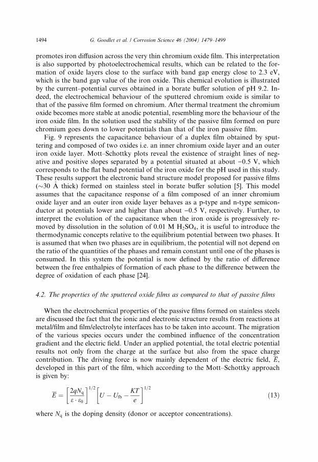
A characteristic feature of the electronic structure of the passive films formed on
stainless steels is the presence of the heterojunction developed inside the film [5,25].
Fig. 10a shows the schematic band structure model proposed to explain the capac-
itance behaviour of the passive film formed on 18Cr–10Ni stainless steel in the borate
buffer solution of pH 9.2. The heterojunction is situated between the p-type chro-mium oxide inner layer and the n-type iron oxide outer layer. Assuming that the
Fermi energy is maintained constant across the film, then the electronic equilibrium
is reached when the doping densities of the n-side and p-side of the heterojunction
become equivalents (Na � Nd). Such equilibrium is obtained in an ionic transport
during film growth.
The situation is very different when the heterojunction is formed by sputtered
deposition (Fig. 10b). The development of the heterojunction results in this case
from the displacement of the Fermi level in order to establish the electronic equi-librium. There is in this case only electronic transfer. Further, the doping density of
the chromium and iron constitutive oxides of the heterojunction formed by sput-
tering may be very different. In fact, as in the case of a classical heterojunction the
electronic properties depend on the band gap and the doping densities of the p-type
and n-type regions among other factors. If the changes in both sides of the junction
resulting from the donor Nd and acceptor Na doping levels are equated one has at
equilibrium:
Nd � Wn ¼ Na � Wp ð14Þ
where Wn and Wp are the lengths of the depletion regions in the n-side and p-side
respectively.At this point of the discussion it is important to remark that the Mott–
Schottky method used gives direct information concerning only the capacitance of
the film–solution interface. However, it can be assumed that the charge concen-
tration at this interface will equilibrate the charge concentration generated at the
metal–film interface. This means that the charge concentration inside the film
is related to the exchange processes at both interfaces. When the influence of
polarization on the electronic structure of passive films and sputtered films is
examined, one has to consider that the capacitance response can be related to thecapacitance of the film–electrolyte interface and also to that of the n-side or p-side
of the heterojunction at potentials higher or lower than the flat band potential,
respectively.
Fig. 10. Schematic band structure models which represent the metal–film and film–electrolyte interface
and the p–n heterojunction: (a) case of the passive film formed on Fe–Cr stainless steel and (b) case of the
duplex oxide film obtained by sputtering.
1496 G. Goodlet et al. / Corrosion Science 46 (2004) 1479–1499
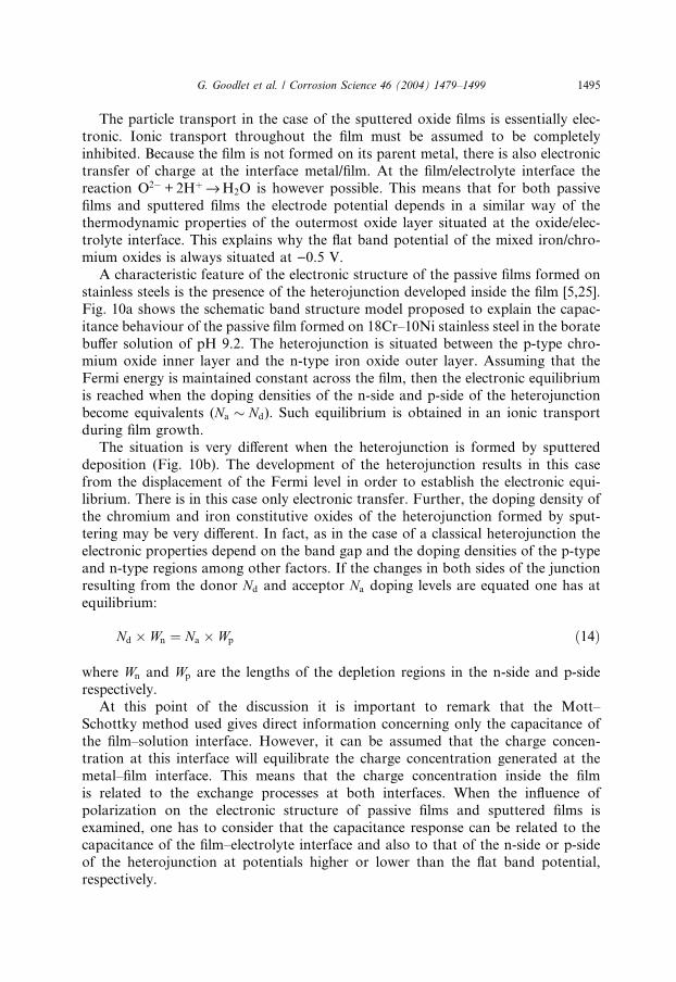
In the schematic representation of the variation of the capacitance with potential
(C�2 vs. U ) the existence of two important potentials has to be considered (Fig. 11);
the flat band potential Ufb situated at )0.5 V where predominant electronic defects
establish the transition between p-type and n-type semiconductivity, and the
Fig. 11. Schematic representation of the electronic structure of the interface film–electrolyte at potential
below and above the flat band potential Ufb. The variation with the distance to the interface film–elec-
trolyte of the electrostatic potential below and above the transition potential Uo is also indicated.
G. Goodlet et al. / Corrosion Science 46 (2004) 1479–1499 1497
potential situated at about )0.2 V where the transition from positive to negative
slopes can be related to the change in the predominant ionic defects.
5. Conclusions
The present investigation shows that the electronic structure of chromium oxide
films obtained by sputtering on an iron-containing substrate may be strongly
modified close to the surface where the neutrality of charges is not maintained. It
appears that the capacitance behaviour (Mott–Schottky representation) of this kind
of films is qualitatively similar to that of passive films formed by direct oxidation of
Fe–Cr alloys or stainless steels. In both cases the capacitance study reveals the
existence of p-type and n-type semiconductivity.
Annealing treatment of the films raises the n-type semiconductor character. Theeffect of this treatment could be two folds. It could cause the iron, used as a support,
to diffuse into the chromium oxide and it could also cause the chromium oxide to
become n-type semiconductor in the outer most atomic layers of the film.
1498 G. Goodlet et al. / Corrosion Science 46 (2004) 1479–1499
The electronic band structure model proposed previously for passive films formed
on stainless steels can describe the results. Furthermore, the potential regions situ-
ated between Mott–Schottky plots of negative and positive slopes can be interpreted
as transitions potential regions where either electronic or ionic predominant trans-
port of charges takes place.
Finally the use of a duplex film composed of a chromium oxide inner layer and aniron oxide outer layer gives valuable information about the heterojunction formed in
the bulk of the film. By examining the electronic properties of the sputtered films,
information can be obtained relating to the electronic properties of passive films
formed by direct oxidation of the metallic substrate.
Acknowledgements
The authors would like to thank PRAXIS for proving funds for Dr. G. Goodlet.
Also the authors would like to express their gratitude to Dr. M.L. Parames for her
help with the X-Ray diffraction technique and to Dr. P. Brogueira for useful dis-
cussion.
References
[1] C. Sunseri, S. Piazza, F. Di Quarto, J. Electrochem. Soc. 137 (1990) 2411.
[2] J.-S. Kim, H.-S. Kwon, in: The Eighth International Symposium on Passivity of Metals and
Semiconductors, Canada, 1998.
[3] S. Fujimoto, O. Chihara, T. Shibata, Materials Science Forum 289–292 (1998) 989.
[4] P.C. Searson, R.M. Latanision, Electrochim. Acta 35 (1990) 445.
[5] N.E. Hakiki, S. Boundin, B. Rondot, M. Da Cunha Belo, Corros. Sci. 37 (1995) 1809.
[6] N.E. Hakiki, B. Rondot, M. Da Cunha Belo, C. R. Acad. Sci. Ser. II, Paris 317 (1993) 457.
[7] S. Cardoso, V. Gehanno, R. Ferreira, P.P. Freitas, IEEE Trans. Magn. 35 (1999) 2952.
[8] M. Fraune, U. Rudiger, G. Guntherodt, S. Cardoso, P.P. Freitas, Appl. Phys. Lett. 77 (2000) 3815.
[9] P. Marcus, V. Maurice, W.P. Young, J. Electrochem. Soc. 141 (1994) 3017.
[10] W.W. G€artner, Physc. Rev. 116 (1959) 84.
[11] M.A. Bulter, J. Appl. Phys. 48 (1977) 1914.
[12] N.F. Mott, E.A. Davies, Electronic Processes in Non-Crystalline Materials, Clarendon, Oxford, 1971.
[13] S.R. Morrisson, Electrochemistry at Semiconductor and Oxidized Metal Electrodes, Plenum Press,
London, 1980 (Chapter 4).
[14] B. Lovrecek, J. Sefaja, Electrochim. Acta 17 (1972) 1151.
[15] N.E. Hakiki, M. Da Cunha Belo, C. R. Acad. Sci. Ser. II, Paris T320 (1995) 463.
[16] H. Bohni, P. Schmuki, S. Virtanen, P. Vuoristo, T. Mantyla, J. Electrochem. Soc. 142 (1995) 3967.
[17] F. Cardon, W.P. Gomes, J. Phys. 11 (1978) L63.
[18] A.M.P. Sim~oes, M.G.S. Ferreira, G. Lorang, M. Da Cunha Belo, Electrochim. Acta 36 (1991) 315.
[19] J.H. Kennedy, K.W. Frese, J. Electrochem. Soc. 125 (1978) 723.
[20] S.M. Ahamed, in: John W. Diggle (Ed.), Oxides and Oxide Films, vol. I, Marcel Dekker, New York,
1972, p. 319.
[21] D.A. Vermilyea, J. Electrochem. Soc. 113 (1966) 1067.
[22] L.D. Locker, P.L. de Bruyn, J. Electrochem. Soc. 116 (1969) 1659.
[23] F.A. Kroger, The Chemistry of Imperfect Crystals, vol. 2, North-Holland Publishing Company,
New York, 1974.
G. Goodlet et al. / Corrosion Science 46 (2004) 1479–1499 1499
[24] K.J. Vetter, J. Electrochem. Soc. 110 (1963) 597.
[25] N.E. Hakiki, M. Da Cunha Belo, A.M.P. Sim~oes, M.G.S. Ferreira, J. Electrochem. Soc. 145 (1998)
3821;
N.E. Hakiki, M. Da Cunha Belo, A.M.P. Sim~oes, M.G.S. Ferreira, J. Electrochem. Soc. 146 (1999)
807.
Recommended


