
SECONDPROGRESSREPORT
13 – 07 - 2011
ELECTRICAL AND OPTICAL CHARACTERIZATION OF CdxZn1-xS AND PbS THIN FILMS FOR
PHOTOVOLTAIC APPLICATIONS
Mosiori Cliff Orori (B.Ed (Sc))
Reg. No. I56/12236/2009
Supervisors:
Dr. W.K. NJOROGE & Prof. J. OKUMU Kenyatta University Kenyatta University

OUTLINE OF PRESENTATION
• INTRODUCTION• OBJECTIVES• METHODS AND MATERIALS• RESULTS AND DISCUSSION• REMAINING WORK (5 %)
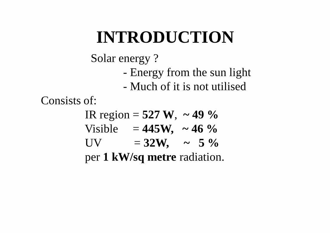
INTRODUCTIONSolar energy ?
- Energy from the sun light- Much of it is not utilised
Consists of:IR region = 527 W, ~ 49 %Visible = 445W, ~ 46 %UV = 32W, ~ 5 %per 1 kW/sq metre radiation.
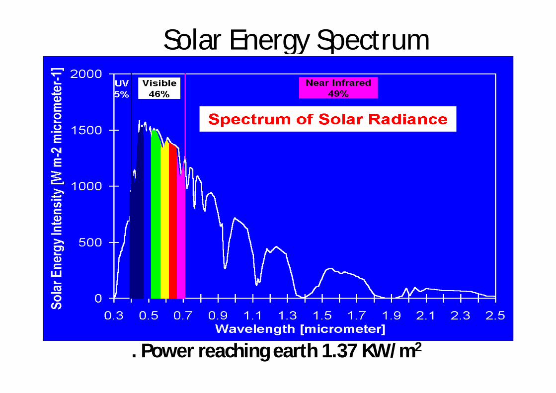
Solar Energy Spectrum
. Power reaching earth 1.37 KW/m2
INTRO. (cont.)
• Doping CdS with zinc show possibility;- increase transmittance- increase conductivity- tune resistivity- lower reflectivity- lower absorption- increase band gap
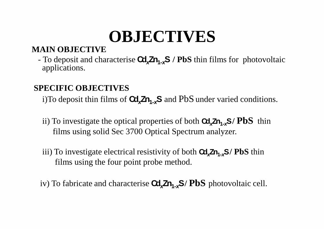
OBJECTIVESMAIN OBJECTIVE
- To deposit and characterise CdxZn1-xS / PbS thin films for photovoltaic applications.
SPECIFIC OBJECTIVESi)To deposit thin films of CdxZn1-xS and PbS under varied conditions.
ii) To investigate the optical properties of both CdxZn1-xS / PbS thin films using solid Sec 3700 Optical Spectrum analyzer.
iii) To investigate electrical resistivity of both CdxZn1-xS / PbS thin films using the four point probe method.
iv) To fabricate and characterise CdxZn1-xS / PbS photovoltaic cell.
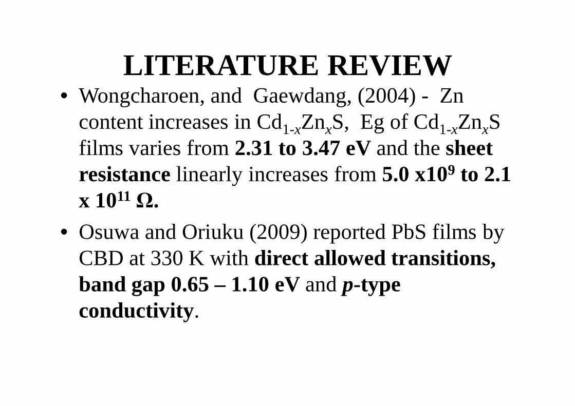
LITERATURE REVIEW• Wongcharoen, and Gaewdang, (2004) - Zn
content increases in Cd1-xZnxS, Eg of Cd1-xZnxS films varies from 2.31 to 3.47 eV and the sheet resistance linearly increases from 5.0 x10⁹ to 2.1 x 10¹¹ Ω.
• Osuwa and Oriuku (2009) reported PbS films by CBD at 330 K with direct allowed transitions, band gap 0.65 – 1.10 eV and p-type conductivity.
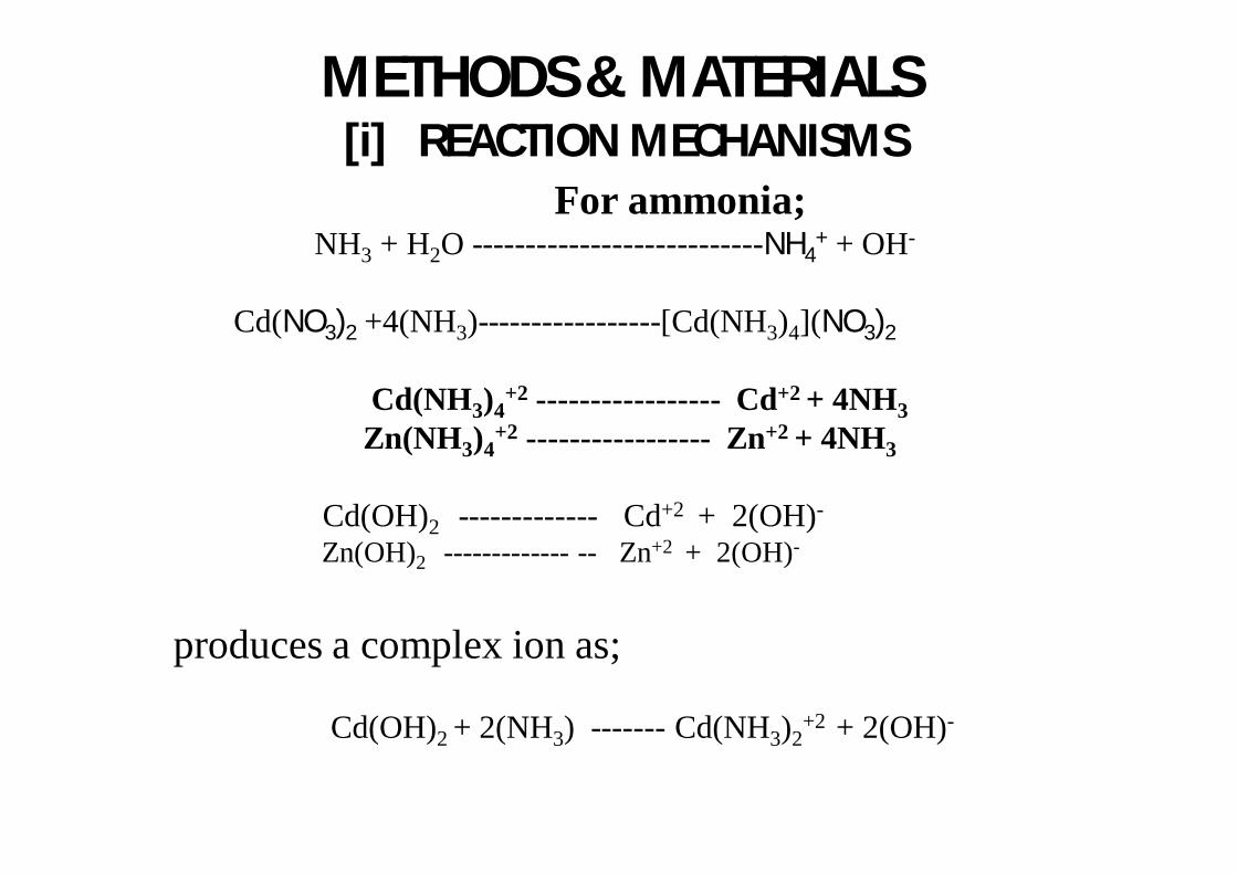
METHODS & MATERIALS [i] REACTION MECHANISMS
For ammonia;NH3 + H2O ---------------------------NH4
+ + OH-
Cd(NO3)2 +4(NH3)-----------------[Cd(NH3)4](NO3)2
Cd(NH3)4+2 ----------------- Cd+2 + 4NH3
Zn(NH3)4+2 ----------------- Zn+2 + 4NH3
Cd(OH)2 ------------- Cd+2 + 2(OH)-
Zn(OH)2 ------------- -- Zn+2 + 2(OH)-
produces a complex ion as;
Cd(OH)2 + 2(NH3) ------- Cd(NH3)2+2 + 2(OH)-
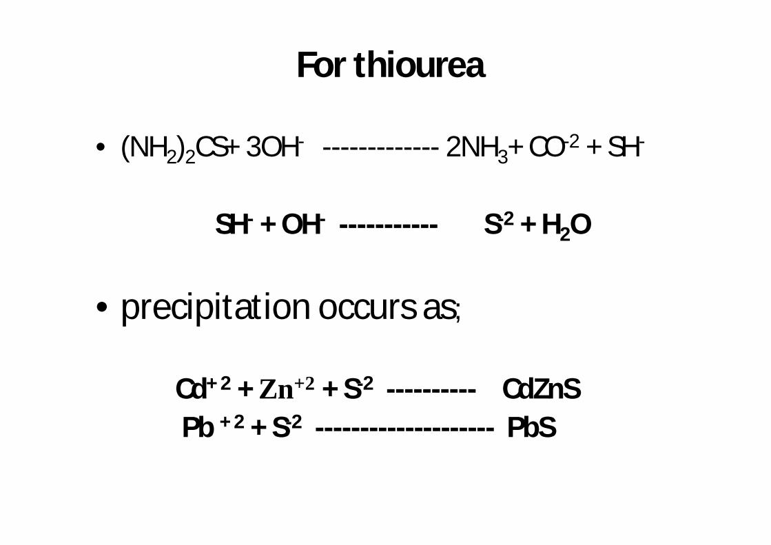
For thiourea
• (NH2)2CS+ 3OH- ------------- 2NH3+ CO-2 + SH-
SH- + OH- ----------- S-2 + H2O
• precipitation occurs as;
Cd+ 2 + Zn+2 + S-2 ---------- CdZnSPb + 2 + S-2 -------------------- PbS
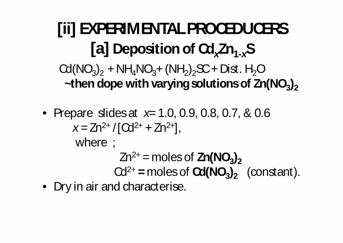
[ii] EXPERIMENTAL PROCEDUCERS[a] Deposition of CdxZn1-xS
Cd(NO3)2 + NH4NO3+ (NH2)2SC + Dist. H2O ~then dope with varying solutions of Zn(NO3)2
• Prepare slides at x= 1.0, 0.9, 0.8, 0.7, & 0.6x = Zn2+ /[Cd2+ + Zn2+], where ;
Zn2+ = moles of Zn(NO3)2
Cd2+ = moles of Cd(NO3)2 (constant).• Dry in air and characterise.
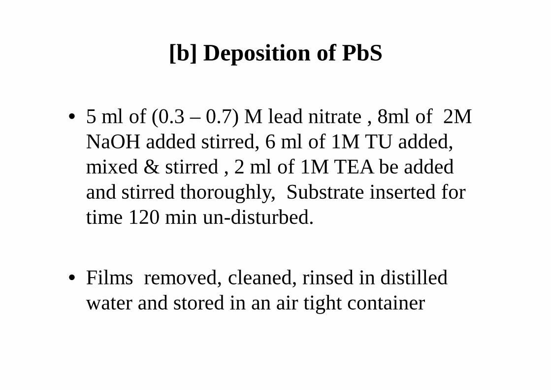
[b] Deposition of PbS
• 5 ml of (0.3 – 0.7) M lead nitrate , 8ml of 2M NaOH added stirred, 6 ml of 1M TU added, mixed & stirred , 2 ml of 1M TEA be added and stirred thoroughly, Substrate inserted for time 120 min un-disturbed.
• Films removed, cleaned, rinsed in distilled water and stored in an air tight container
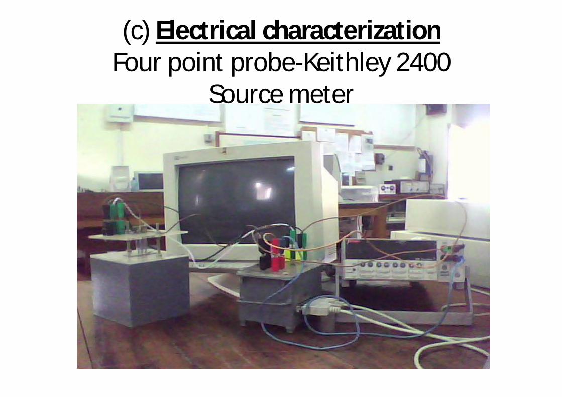
(c) Electrical characterizationFour point probe-Keithley 2400
Source meter.

Rs= [πR14,23 R23,14] x f /2ln2ρ= Rs X t

RESULTS
(A) Electrical properties
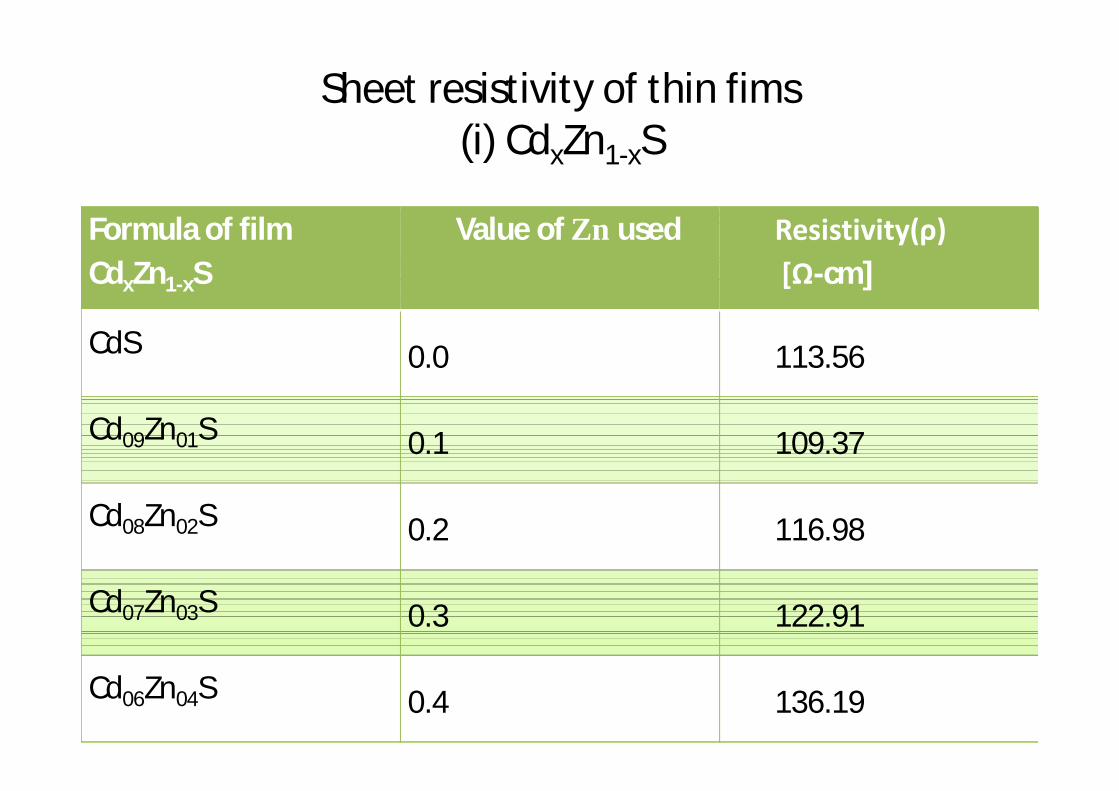
Sheet resistivity of thin fims(i) CdxZn1-xS
Formula of filmCdxZn1-xS
Value of Zn used Resistivity(ρ)[Ω-cm]
CdS 0.0 113.56
Cd09Zn01S 0.1 109.37
Cd08Zn02S 0.2 116.98
Cd07Zn03S 0.3 122.91
Cd06Zn04S 0.4 136.19
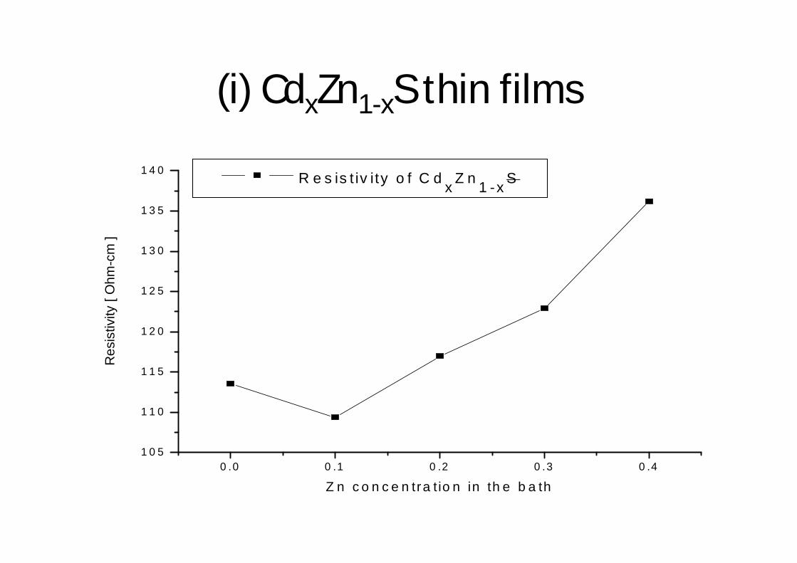
(i) CdxZn1-xS thin films
0 .0 0 .1 0 .2 0 .3 0 .41 0 5
1 1 0
1 1 5
1 2 0
1 2 5
1 3 0
1 3 5
1 4 0
Res
istiv
ity [
Ohm
-cm
]
Z n c o n c e n tra t io n in th e b a th
R e s is t iv ity o f C d x Z n 1 -x S
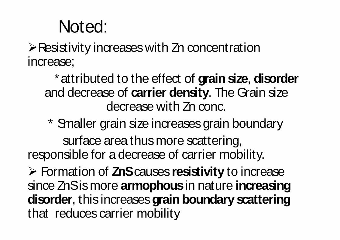
Noted:Resistivity increases with Zn concentration increase;
*attributed to the effect of grain size, disorderand decrease of carrier density. The Grain size
decrease with Zn conc.* Smaller grain size increases grain boundary
surface area thus more scattering, responsible for a decrease of carrier mobility. Formation of ZnS causes resistivity to increase since ZnS is more armophous in nature increasing disorder, this increases grain boundary scattering that reduces carrier mobility
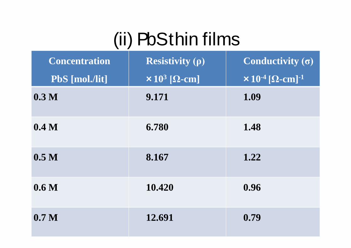
(ii) PbS thin filmsConcentration
PbS [mol./lit]
Resistivity (ρ)
× 103 [Ω-cm]
Conductivity (σ)
× 10-4 [Ω-cm]-1
0.3 M 9.171 1.09
0.4 M 6.780 1.48
0.5 M 8.167 1.22
0.6 M 10.420 0.96
0.7 M 12.691 0.79
(ii) PbS thin films
0 .3 0 .4 0 .5 0 .6 0 .76
7
8
9
10
11
12
13
Res
istiv
ity x
103 [o
hm-c
m]
C o n cen tra tion o f in m o les p e r litre
S h e e t re s is tiv ity o f P bS th in f ilm s
Noted: Resistivity increases with concentration… It isattributed to an increase in closeness of the grainsof PbS deposited that are more closure producingmore scattering centres
It means that the mean free path is reduced
REMAINING WORK ( 5 %)Fabrication of photovoltaic cell
Characterization of the cell
Thesis writing, submission and defence

THANK YOU
ALL
Recommended


