Embed Size (px)
Citation preview
Digital Design 2eCopyright © 2010 Frank Vahid
1
Digital Design
Chapter 4:
Datapath Components
Copyright © 2010 Frank Vahid
Instructors of courses requiring Vahid's Digital Design textbook (published by John Wiley and Sons) have permission to modify and use these slides for customary course-related activities, subject to keeping this copyright notice in place and unmodified. These slides may be posted as unanimated pdf versions on publicly-accessible course websites.. PowerPoint source (or pdf with animations) may not be posted to publicly-accessible websites, but may be posted for students on internal protected sites or distributed directly to students by other electronic means. Instructors may make printouts of the slides available to students for a reasonable photocopying charge, without incurring royalties. Any other use requires explicit permission. Instructors may obtain PowerPoint source or obtain special use permissions from Wiley – see http://www.ddvahid.com for information.
Slides to accompany the textbook Digital Design, with RTL Design, VHDL, and Verilog, 2nd Edition,
by Frank Vahid, John Wiley and Sons Publishers, 2010. http://www.ddvahid.com
Digital Design 2eCopyright © 2010 Frank Vahid
2
Introduction• Chpts 2 & 3: Introduced increasingly complex digital building
blocks– Gates, multiplexors, decoders, basic registers, and controllers
• Controllers good for systems with control inputs/outputs– Control input: Single bit (or a few), representing environment
event or state• Ex: 1 bit representing button pressed
– Data input: Multiple bits representing single entity• Ex: 7 bits representing temperature in binary
• Need appropiate building blocks for data– Datapath components (register-transfer-level, or RTL)
components: store/transform data• Combine datapath components to form a datapath
• Chpt 4 introduces some datapath components and simple datapaths– Next chapter will combine controllers and datapaths into
“processors”
4.1
Note: Slides with animation are denoted with a small red "a" near the animated items
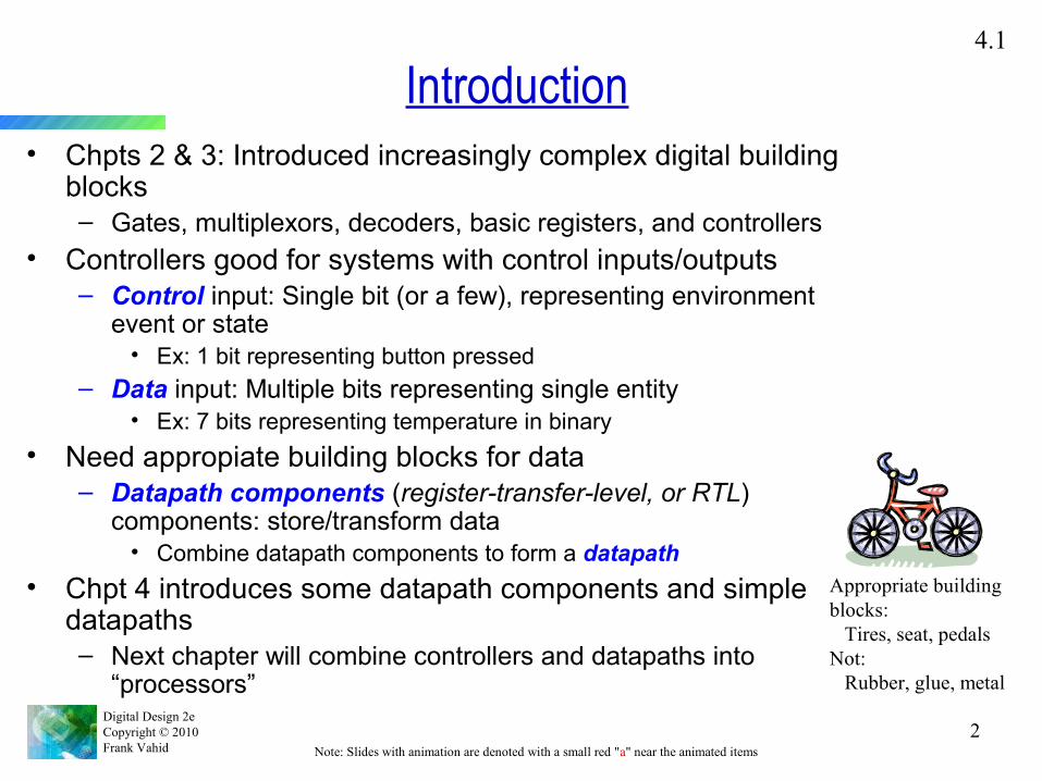
Appropriate building blocks: Tires, seat, pedalsNot: Rubber, glue, metal
Digital Design 2eCopyright © 2010 Frank Vahid
3
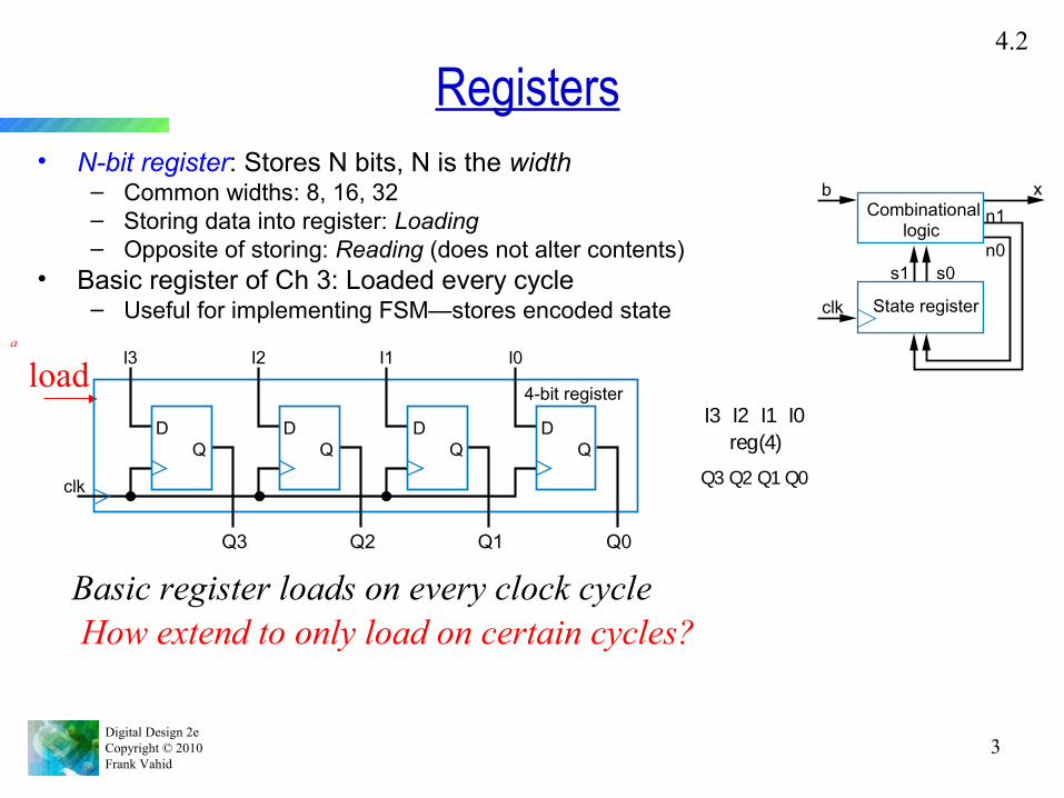
Registers• N-bit register: Stores N bits, N is the width
– Common widths: 8, 16, 32– Storing data into register: Loading– Opposite of storing: Reading (does not alter contents)
• Basic register of Ch 3: Loaded every cycle– Useful for implementing FSM—stores encoded state
4.2
Combinationallogic
State register
s1 s0
n1
n0
xb
clk
I3 I2 I1 I0
Q3 Q2 Q1 Q0
reg(4)
Basic register loads on every clock cycle
load
How extend to only load on certain cycles?
a
DQ
DQ
DQ
DQ
I2I3
Q2Q3 Q1 Q0
I1 I0
clk
4-bit register
Digital Design 2eCopyright © 2010 Frank Vahid
4
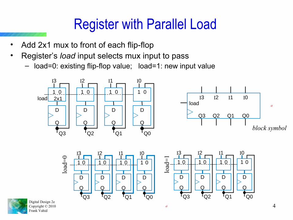
Register with Parallel Load• Add 2x1 mux to front of each flip-flop• Register’s load input selects mux input to pass
– load=0: existing flip-flop value; load=1: new input value
D
Q
Q3
I3
D
Q
Q2
I2
D
Q
Q1
I1
D
Q
Q0
I0
1 02x1load
1 0 1 0 1 0
a
a
1 0
D
Q
Q3
I3
1 0
D
Q
Q2
I2
1 0
Q
Q1
I1
1 0
D
Q
Q0
I0
D
load
=0
1 0
D
Q
Q3
I3
1 0
D
Q
Q2
I2
1 0
D
Q
Q1
I1
1 0
D
Q
Q0
I0
load
=1
loadI3 I2 I1 I0
Q3 Q2 Q1 Q0
block symbol
Digital Design 2eCopyright © 2010 Frank Vahid
5
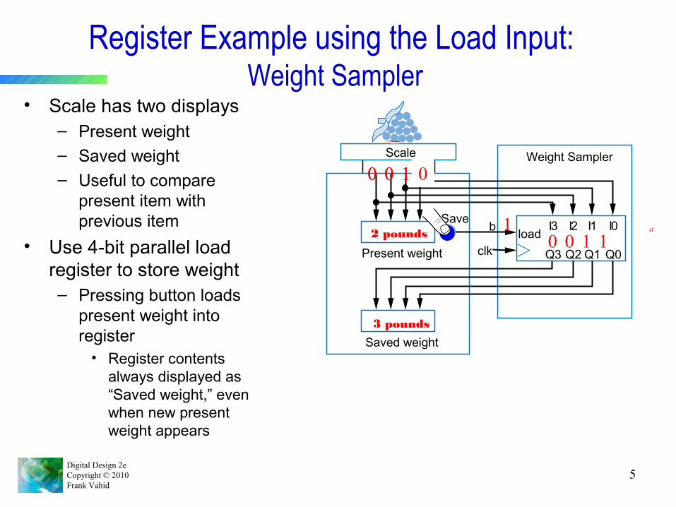
Register Example using the Load Input: Weight Sampler
• Scale has two displays– Present weight– Saved weight– Useful to compare
present item with previous item
• Use 4-bit parallel load register to store weight– Pressing button loads
present weight into register
• Register contents always displayed as “Saved weight,” even when new present weight appears
Scale
Saved weight
Weight Sampler
Present weight clk
bSave I3 I2 I1 I0
Q3 Q2 Q1 Q0
load3 pounds
0 0 1 1
0 0 1 1
3 pounds
0 0 1 0
2 pounds 1 a
Digital Design 2eCopyright © 2010 Frank Vahid
6
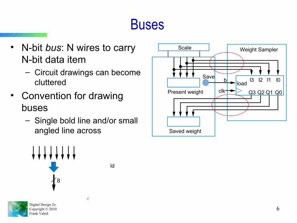
Buses
• N-bit bus: N wires to carry N-bit data item– Circuit drawings can become
cluttered
• Convention for drawing buses– Single bold line and/or small
angled line across
Scale
Saved weight
Weight Sampler
Present weight clk
bSave I3 I2 I1 I0
Q3 Q2 Q1 Q0
load
8
ld
a
Digital Design 2eCopyright © 2010 Frank Vahid
7
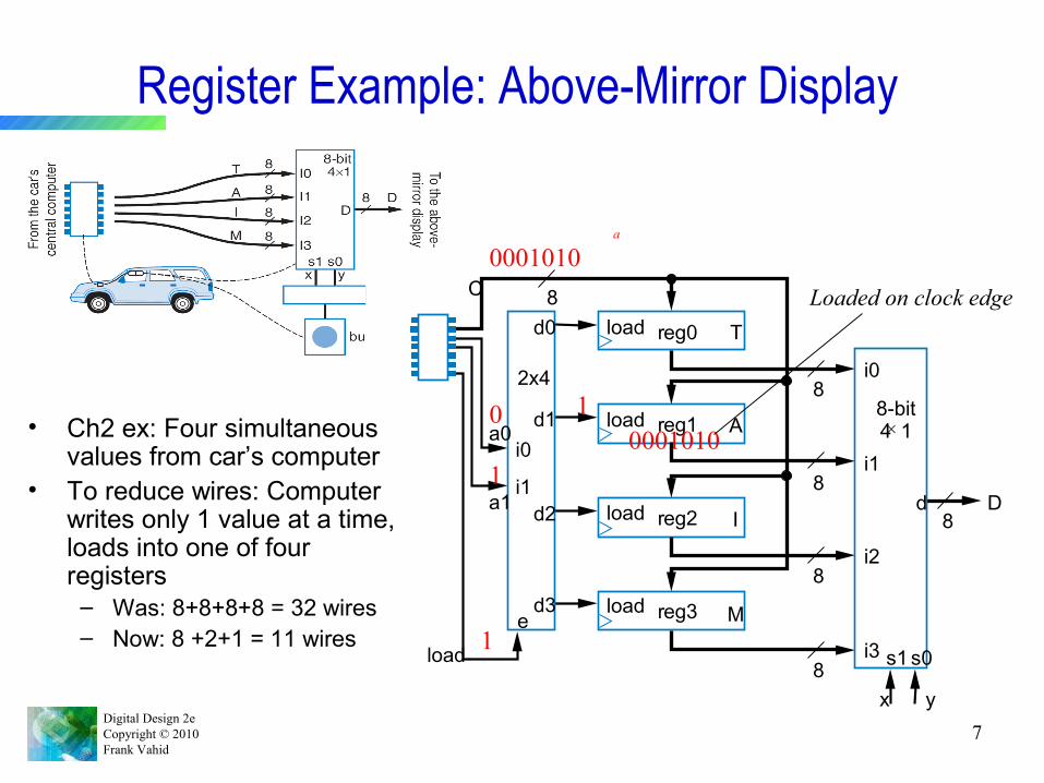
Register Example: Above-Mirror Display
C
d0
d1
d2
d3e
i0
i0
i1
i2
i3
a0
a1
load
i1
2x4 8
8
8
8
8Dd
8x y
s1 s0
8-bit4× 1
load
load
load
load
reg0
reg1
reg2
reg3
T
A
I
M
• Ch2 ex: Four simultaneous values from car’s computer
• To reduce wires: Computer writes only 1 value at a time, loads into one of four registers
– Was: 8+8+8+8 = 32 wires– Now: 8 +2+1 = 11 wires
0
1
0001010
1
1
0001010
Loaded on clock edge
a
Digital Design 2eCopyright © 2010 Frank Vahid
8
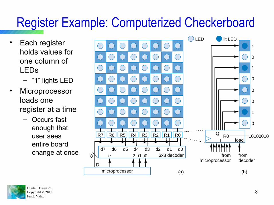
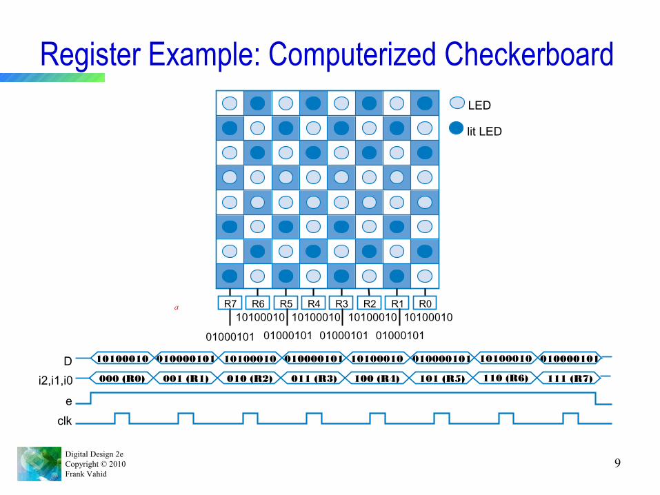
Register Example: Computerized Checkerboard• Each register
holds values for one column of LEDs– “1” lights LED
• Microprocessor loads one register at a time– Occurs fast
enough that user sees entire board change at once
LED
R7 R6
d6 d5 d4 d3 d2 d1 d0d7
8
D
R5 R4 R3 R2 R1 R0
e i2 i1 i0 3x8 decoder
microprocessor
lit LED
1
1
0
0
0
0
0
1
Q
IR0
load10100010
fromdecoder
frommicroprocessor
(b)(a)
Digital Design 2eCopyright © 2010 Frank Vahid
9
Register Example: Computerized Checkerboard
010000101 101000101010001010100010 10100010010000101 010000101 010000101
001 (R1) 100 (R4)010 (R2)000 (R0) 110 (R6)011 (R3) 101 (R5) 111 (R7)
clke
i2,i1,i0D
LED
lit LED
10100010 10100010 10100010 10100010
01000101 01000101 01000101 01000101
R7 R6 R5 R4 R3 R2 R1 R0a
Digital Design 2eCopyright © 2010 Frank Vahid
10
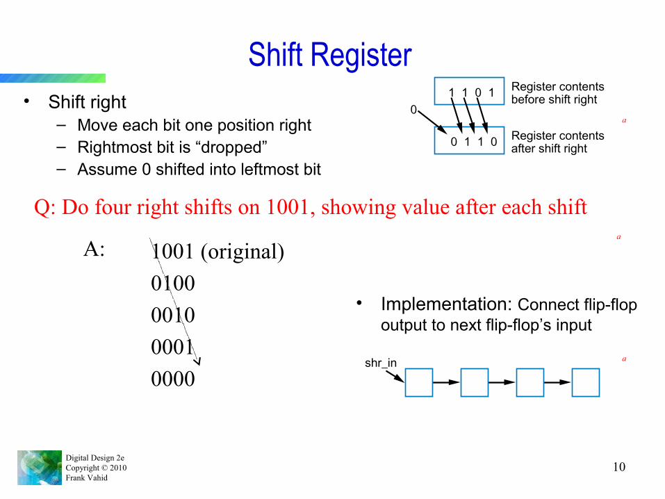
Shift Register• Shift right
– Move each bit one position right– Rightmost bit is “dropped”– Assume 0 shifted into leftmost bit
1 1 0 1 Register contentsbefore shift right
0 1 1 0
0
Register contentsafter shift right
a
Q: Do four right shifts on 1001, showing value after each shifta
A: 1001 (original)
0100
0010
0001
0000 shr_in
• Implementation: Connect flip-flop output to next flip-flop’s input
a
Digital Design 2eCopyright © 2010 Frank Vahid
11
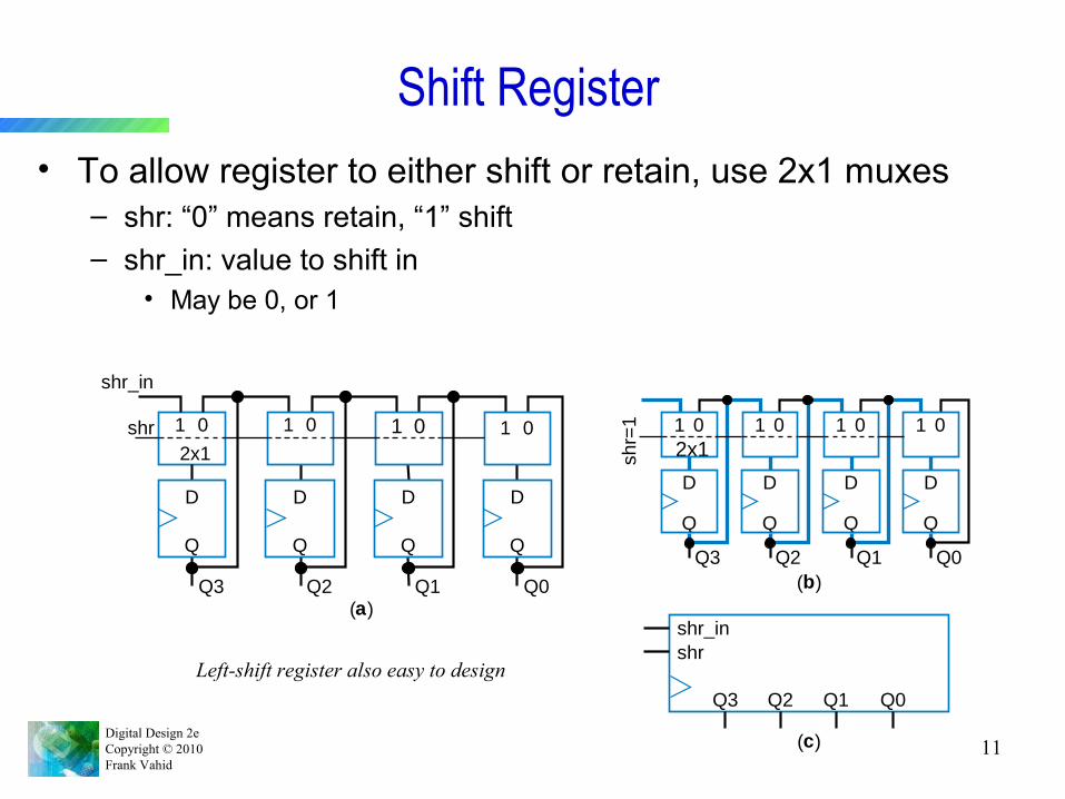
Shift Register
• To allow register to either shift or retain, use 2x1 muxes– shr: “0” means retain, “1” shift– shr_in: value to shift in
• May be 0, or 1
1 02x1
D
Q
Q3
1 0
D
Q
Q2
1 0
D
Q
Q1
1 0
D
Q
Q0
1 0
2x1
D
Q
Q3
shr
shr_in
shrshr_in
1 0
D
Q
Q2
1 0
D
Q
Q1 (b)
(c)
(a)
1 0
D
Q
Q0
Q3 Q2 Q1 Q0
Left-shift register also easy to design
shr=
1

Digital Design 2eCopyright © 2010 Frank Vahid
12
Rotate Register
• Rotate right: Like shift right, but leftmost bit comes from rightmost bit
1 1 0 1
1 1 1 0
Register contentsbefore shift right
Register contentsafter shift right
Digital Design 2eCopyright © 2010 Frank Vahid
13
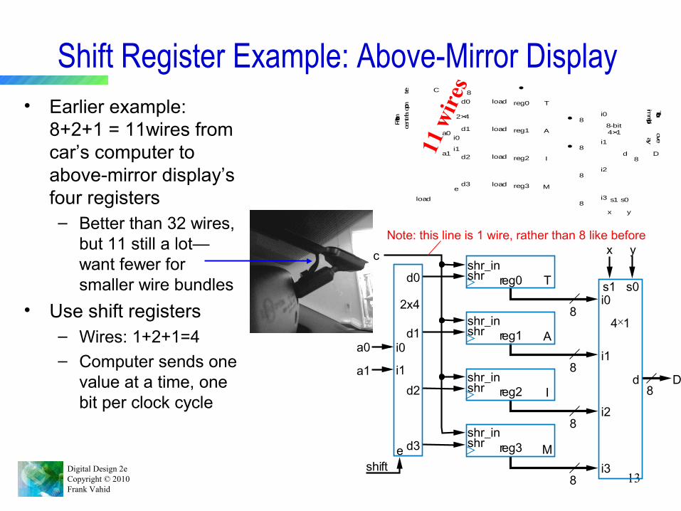
Shift Register Example: Above-Mirror Display• Earlier example:
8+2+1 = 11wires from car’s computer to above-mirror display’s four registers– Better than 32 wires,
but 11 still a lot—want fewer for smaller wire bundles
• Use shift registers– Wires: 1+2+1=4– Computer sends one
value at a time, one bit per clock cycle
C
d0
d1
d2
d3e
i0
i0
i1
i2
i3
a0
a1
load
i1
2×4
From the car's
cent
ralcompu
ter
8
8
8
8
8Dd
8
x y
s1 s0
8-bit4×1
To the above
mirror displ
ay
load
load
load
load
reg0
reg1
reg2
reg3
T
A
I
M
11 w
ires
c
d0
d1
d2
d3e
i0
i0s1 s0
x y
i1
i2
i3
a0
a1
shift
i1
2x4 8
8
8
8Dd
8
4×1
shrshr_in
shrshr_in
shrshr_in
shrshr_in
reg0
reg1
reg2
reg3
T
A
I
M
Note: this line is 1 wire, rather than 8 like before
Digital Design 2eCopyright © 2010 Frank Vahid
14
Multifunction Registers• Many registers have multiple functions
– Load, shift, clear (load all 0s)– And retain present value, of course
• Easily designed using muxes– Just connect each mux input to achieve
desired function
Functions:OperationMaintain present valueParallel loadShift right(unused - let's load 0s)
s00101
s10011
s1
shr_in
s0
3 2 1
I3
0
D
Q
Q3
Q2 Q1 Q0Q3
I2 I1 I0I3
Q2
03 2 1
I2
0
D
Q
0
Q1
3 2 1
I1
0
D
Q
0
Q0
3 2 1
I0
0
D
Q
0
4x1 shr_ins1s0
(a)
(b)

Digital Design 2eCopyright © 2010 Frank Vahid
15
Multifunction Registers
OperationMaintain present valueParallel loadShift rightShift left
s00101
s10011
shr_inshl_in
3 2 1
I3
0
D
Q
Q3
Q2 Q1 Q0Q3
I2 I1 I0I3
Q2
3 2 1
I2
0
D
Q
Q1
3 2 1
I1
0
D
Q
Q0
3 2 1
I0
0
D
Q
shl_inshr_ins1s0
(a) (b)
Digital Design 2eCopyright © 2010 Frank Vahid
16
Maintain valueShift leftShift rightShift rightParallel loadParallel loadParallel loadParallel load
NoteOperations0s1
01110000
01001111
OutputsInputs
01010101
00110011
00001111
ld shr shl
Truth table for combinational circuit
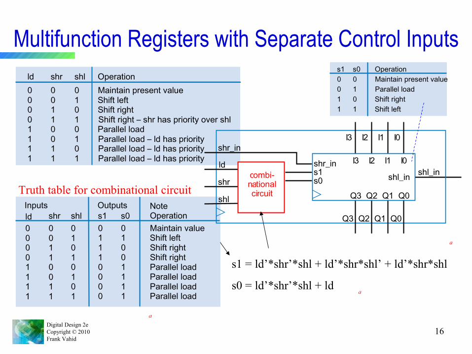
Multifunction Registers with Separate Control Inputs
Maintain present valueShift leftShift rightShift right – shr has priority over shlParallel loadParallel load – ld has priorityParallel load – ld has priorityParallel load – ld has priority
Operationshlshrld00001111
00110011
01010101
Q2 Q1 Q0Q3
Q2 Q1 Q0Q3
I2 I1 I0I3
I2 I1 I0I3
s1shr_in
shr_in
shr
shl
ld
s0shl_inshl_in
a
a
?combi-nationalcircuit
a
s1 = ld’*shr’*shl + ld’*shr*shl’ + ld’*shr*shl
s0 = ld’*shr’*shl + ld
OperationMaintain present valueParallel loadShift rightShift left
s00101
s10011
Digital Design 2eCopyright © 2010 Frank Vahid
17
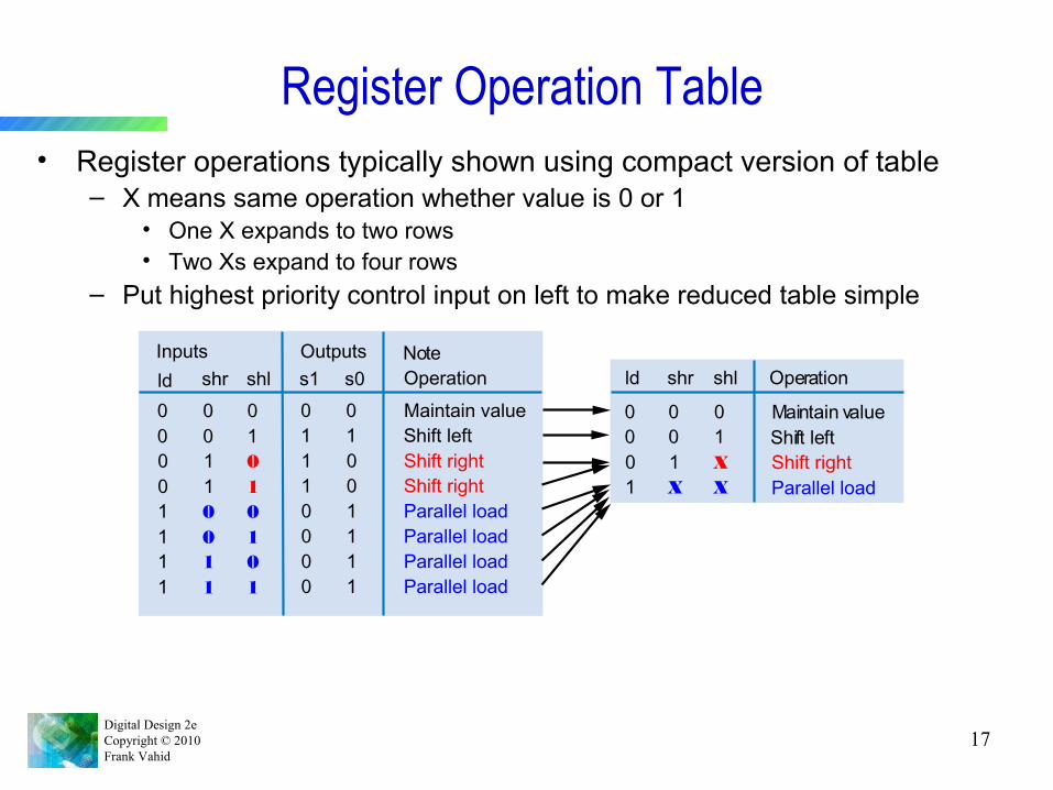
Register Operation Table• Register operations typically shown using compact version of table
– X means same operation whether value is 0 or 1• One X expands to two rows• Two Xs expand to four rows
– Put highest priority control input on left to make reduced table simple
Maintain valueShift left
NoteOperations0s1
01
01
OutputsInputs
01
00
00
Shift rightShift right
11
00
01
11
00
Parallel loadParallel loadParallel loadParallel load
0000
1111
0101
0011
1111
ld shr shl
Maintain valueShift left
Operationld shr shl
01
00
00
Parallel loadXX1Shift rightX10
Digital Design 2eCopyright © 2010 Frank Vahid
18
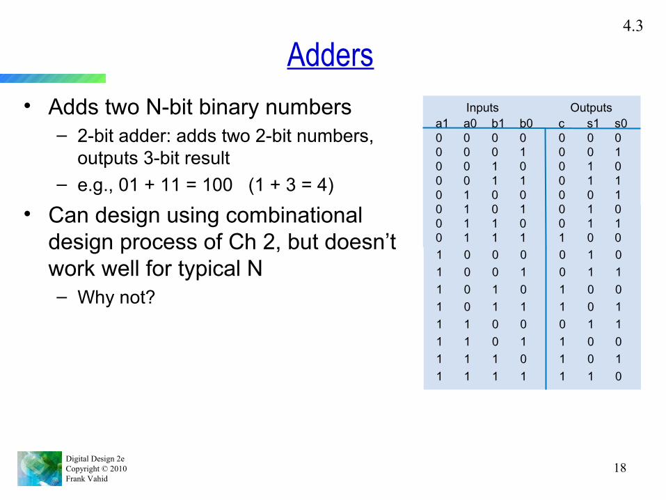
Adders
• Adds two N-bit binary numbers– 2-bit adder: adds two 2-bit numbers,
outputs 3-bit result– e.g., 01 + 11 = 100 (1 + 3 = 4)
• Can design using combinational design process of Ch 2, but doesn’t work well for typical N– Why not?
4.3
01011010
11001001
00110111
01010101
00110011
11111111
00001111
s001011010
s100110110
c00000001
b001010101
b100110011
a100000000
Inputs Outputsa000001111
Digital Design 2eCopyright © 2010 Frank Vahid
19
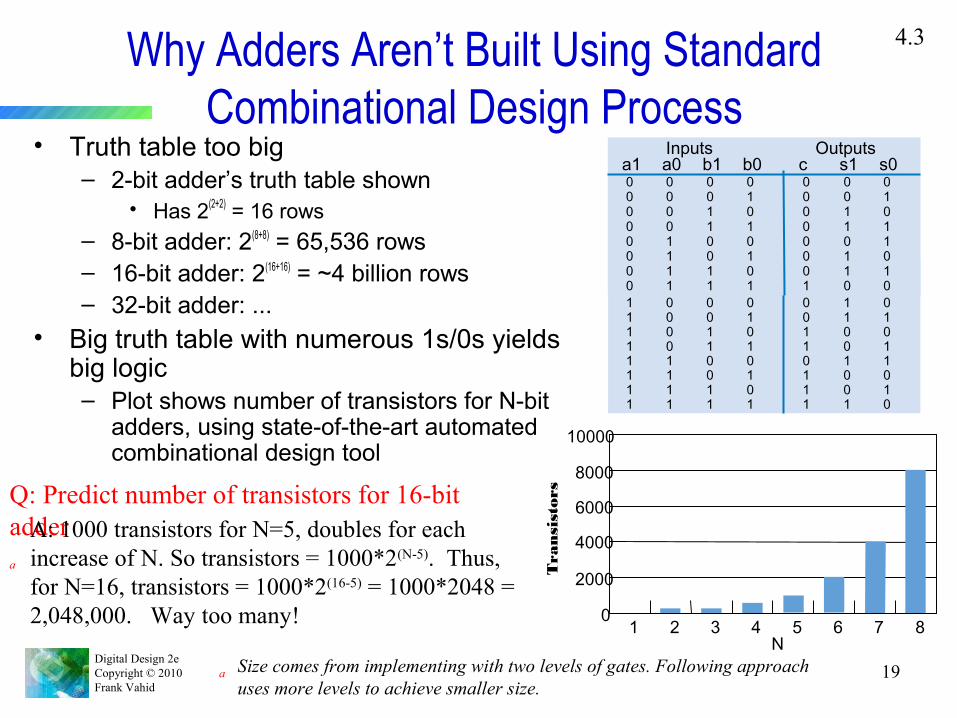
Why Adders Aren’t Built Using Standard Combinational Design Process
• Truth table too big– 2-bit adder’s truth table shown
• Has 2(2+2) = 16 rows
– 8-bit adder: 2(8+8) = 65,536 rows– 16-bit adder: 2(16+16) = ~4 billion rows– 32-bit adder: ...
• Big truth table with numerous 1s/0s yields big logic– Plot shows number of transistors for N-bit
adders, using state-of-the-art automated combinational design tool
4.3
01011010
11001001
00110111
01010101
00110011
11111111
00001111
s001011010
s100110110
c00000001
b001010101
b100110011
a100000000
Inputs Outputsa000001111
Q: Predict number of transistors for 16-bit adderA: 1000 transistors for N=5, doubles for each
increase of N. So transistors = 1000*2(N-5). Thus, for N=16, transistors = 1000*2(16-5) = 1000*2048 = 2,048,000. Way too many!
a
10000
8000
6000
4000
2000
01 2 3 4 5
N6 7 8
Tra
nsi
stors
Size comes from implementing with two levels of gates. Following approach uses more levels to achieve smaller size.
a
Digital Design 2eCopyright © 2010 Frank Vahid
20
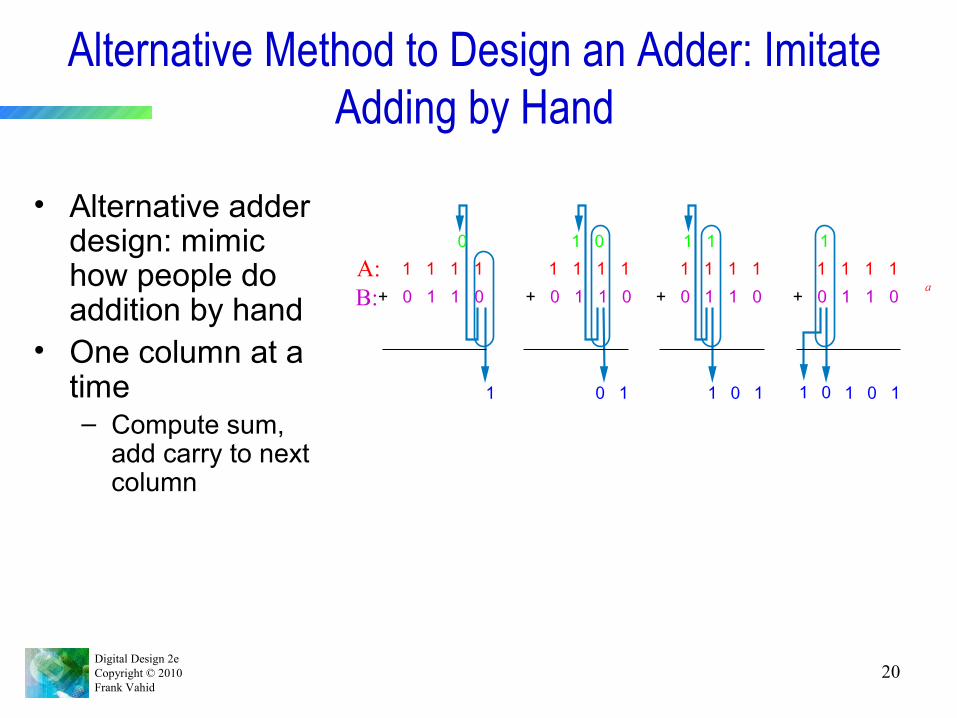
Alternative Method to Design an Adder: Imitate Adding by Hand
• Alternative adder design: mimic how people do addition by hand
• One column at a time– Compute sum,
add carry to next column
1 1 1 1+ 0 1 1 0
0
1
1 1 1 1
10
+ 0 1 1 0
011 1 1 1
101
+ 0 1 1 0
111 1 1 1
101
+ 0 1 1 0
1
01
A:B:
a
Digital Design 2eCopyright © 2010 Frank Vahid
21
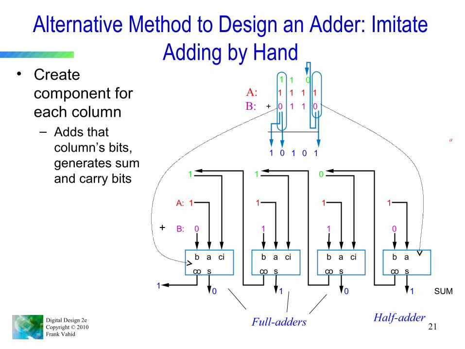
Alternative Method to Design an Adder: Imitate Adding by Hand
• Create component for each column– Adds that
column’s bits, generates sum and carry bits
01 1 1 1
+ 0 1 1 0
1
10101
b
co s
0
a ci
A:
B:+ 0
1 1 1 1
1
b
co s
1
a ci
1
b
co s
0
a ci
1
1 1 0
b
co s
1 SUM
a
0
A:B:
1
Half-adderFull-adders
a
Digital Design 2eCopyright © 2010 Frank Vahid
22
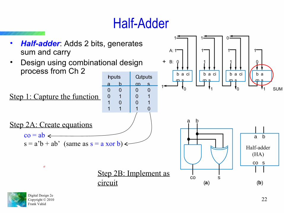
Half-Adder• Half-adder: Adds 2 bits, generates
sum and carry• Design using combinational design
process from Ch 2 bco s
0
a ci
A:
B:+ 0
1 1 1 1
1
1
bco s
1
a ci
1
1
bco s
0
a ci
1
0
bco s
1 SUM
a
0
s0110
co0001
b0101
a0011
Inputs Outputs
Step 1: Capture the function
Step 2A: Create equations
Step 2B: Implement as circuit
co = ab s = a’b + ab’ (same as s = a xor b)
a b
co
co s
a b
s(a) (b)
Half-adder (HA)
a
Digital Design 2eCopyright © 2010 Frank Vahid
23
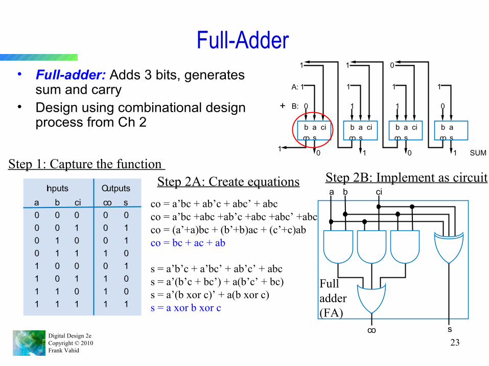
Full-Adder• Full-adder: Adds 3 bits, generates
sum and carry• Design using combinational design
process from Ch 2 bco s
0
a ci
A:
B:+ 0
1 1 1 1
1
1
bco s
1
a ci
1
1
bco s
0
a ci
1
0
bco s
1 SUM
a
0
Step 1: Capture the function
s01101001
co00010111
ci01010101
b00110011
a00001111
Inputs Outputs Step 2A: Create equations
co = a’bc + ab’c + abc’ + abcco = a’bc +abc +ab’c +abc +abc’ +abcco = (a’+a)bc + (b’+b)ac + (c’+c)abco = bc + ac + ab
s = a’b’c + a’bc’ + ab’c’ + abcs = a’(b’c + bc’) + a(b’c’ + bc)s = a’(b xor c)’ + a(b xor c)s = a xor b xor c
Step 2B: Implement as circuit
co
ciba
s
Full adder (FA)
Digital Design 2eCopyright © 2010 Frank Vahid
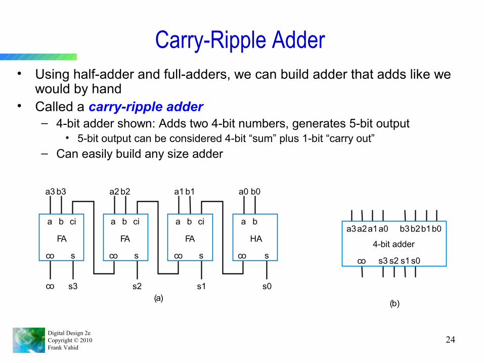
24
Carry-Ripple Adder• Using half-adder and full-adders, we can build adder that adds like we
would by hand• Called a carry-ripple adder
– 4-bit adder shown: Adds two 4-bit numbers, generates 5-bit output• 5-bit output can be considered 4-bit “sum” plus 1-bit “carry out”
– Can easily build any size adder
a3
co s
FA
co
b3 a2 b2
s3 s2 s1
ciba
co s
FA
ciba
a1 b1
co s
FA
ciba
s0
a0 b0
co s
HA
ba
(a)
a3a2a1a0 b3
s3 s2 s1 s0co
b2b1b0
(b)
4-bit adder
Digital Design 2eCopyright © 2010 Frank Vahid
25
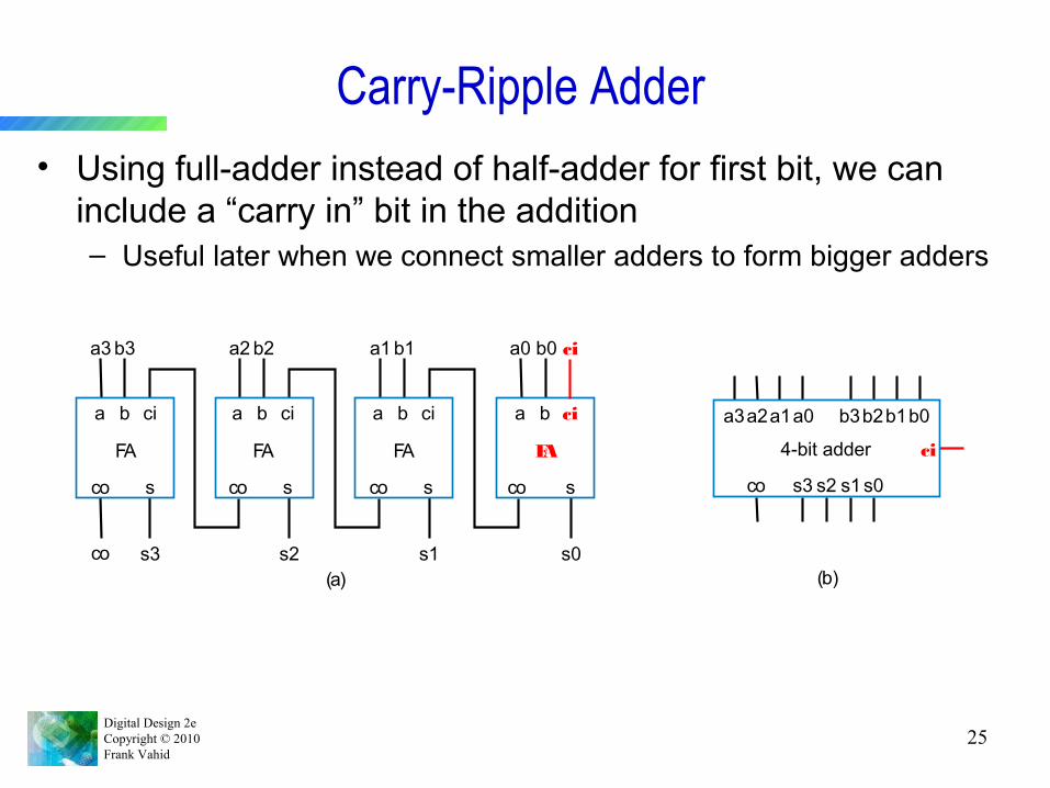
Carry-Ripple Adder
• Using full-adder instead of half-adder for first bit, we can include a “carry in” bit in the addition– Useful later when we connect smaller adders to form bigger adders
a3
co s
FA
co
b3 a2 b2
s3 s2 s1
ciba
co s
FA
ciba
a1 b1
co s
FA
ciba
s0
a0 b0 ci
co s
FA
ciba
(a)
a3a2a1a0 b3
s3 s2 s1 s0co
ci
b2b1b0
(b)
4-bit adder
Digital Design 2eCopyright © 2010 Frank Vahid
26
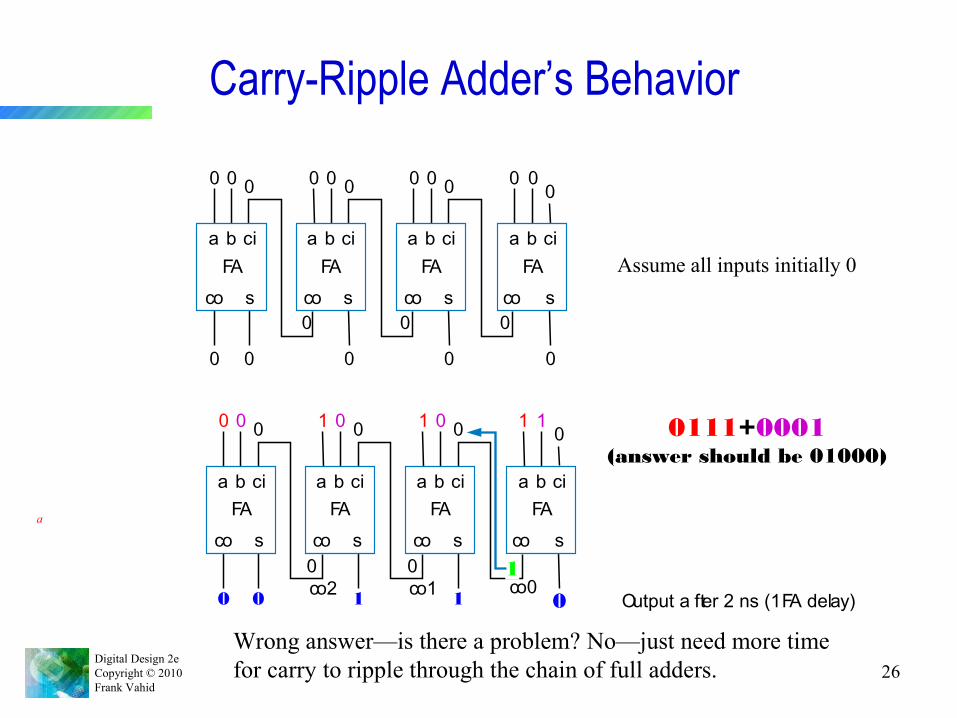
Carry-Ripple Adder’s Behavior
0 1 1 10 0 0 1 0111+0001(answer should be 01000)
0
co sFA
0 0
0 0 0
0 0 00 0 0
0 0
ciba
co sFA
ciba
0 0
co sFA
ciba
0
0 0
co sFA
ciba
0
Assume all inputs initially 0
Output a fter 2 ns (1FA delay)0 0 1 1 0
co s
FA
0 0
0 0 0
co2 co1 co0
ciba
co s
FAciba
co s
FAciba
co s
FAciba
0
01
Wrong answer—is there a problem? No—just need more time for carry to ripple through the chain of full adders.
a
Digital Design 2eCopyright © 2010 Frank Vahid
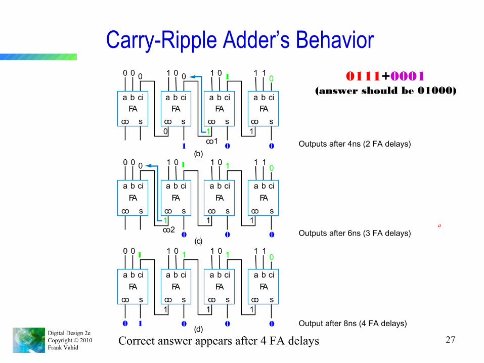
27
0 00
co sFA
1 1 1
1 10 1 0
ciba
co sFA
ciba
1 0
co sFA
ciba
0 0 0
1 1
co sFA
ciba
(d)Output after 8ns (4 FA delays)
Carry-Ripple Adder’s Behavior0
co sFA
0 0 1
co1
0 1 0
ciba
co sFA
ciba
1 0
co sFA
ciba
1 0 0
1 1
co sFA
ciba
(b)
10 1
0
0
1
0 1
1
Outputs after 4ns (2 FA delays)
00
co sFA
1 1
0 1
co2
0 1 0
ciba
co sFA
ciba
1 0
co sFA
ciba
0 0
1 10
co sFA
ciba
(c)Outputs after 6ns (3 FA delays)
a
0111+0001(answer should be 01000)
1
Correct answer appears after 4 FA delays
Digital Design 2eCopyright © 2010 Frank Vahid
28
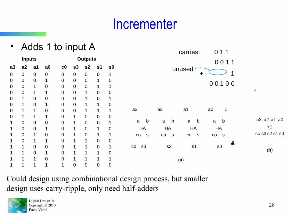
Incrementer
• Adds 1 to input A
s2
0001111000011110
s1
0110011001100110
s0
1010101010101010
s3
0000000111111110
c0
0000000000000001
a0
0101010101010101
a1
0011001100110011
a3
0000000011111111
Inputs Outputs
a2
0000111100001111
0 0 1 1
0 1 1
1+
carries:
unused
0000 1
(a)
(b)
a3 a2 a1 a0 1
s0s1s2s3co
a b
co sHA
a b
co sHA
a b
co sHA
a b
co sHA
Incrementer (+1)
a3
co s3 s2+1
s1 s0
a2 a1 a0
a
Could design using combinational design process, but smaller design uses carry-ripple, only need half-adders
Digital Design 2eCopyright © 2010 Frank Vahid
29
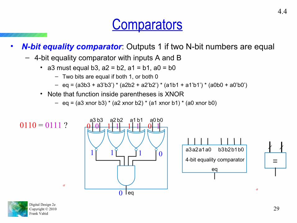
Comparators• N-bit equality comparator: Outputs 1 if two N-bit numbers are equal
– 4-bit equality comparator with inputs A and B• a3 must equal b3, a2 = b2, a1 = b1, a0 = b0
– Two bits are equal if both 1, or both 0
– eq = (a3b3 + a3’b3’) * (a2b2 + a2’b2’) * (a1b1 + a1’b1’) * (a0b0 + a0’b0’)
• Note that function inside parentheses is XNOR– eq = (a3 xnor b3) * (a2 xnor b2) * (a1 xnor b1) * (a0 xnor b0)
4.4
a3 b3 a2 b2 a1 b1 a0 b0
eq
a3a2a1a0 b3
eq
b2b1b0
4-bit equality comparator
a
0110 = 0111 ? 0 1 1 00 1 1 1
01 1 1
0
=
a
Digital Design 2eCopyright © 2010 Frank Vahid
30
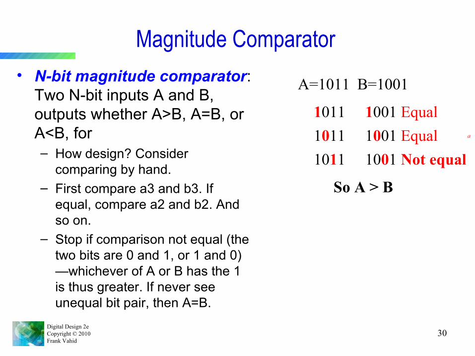
Magnitude Comparator
• N-bit magnitude comparator: Two N-bit inputs A and B, outputs whether A>B, A=B, or A<B, for– How design? Consider
comparing by hand.
– First compare a3 and b3. If equal, compare a2 and b2. And so on.
– Stop if comparison not equal (the two bits are 0 and 1, or 1 and 0)—whichever of A or B has the 1 is thus greater. If never see unequal bit pair, then A=B.
A=1011 B=1001
1011 1001a
Equal
1011 1001 Equal
1011 1001 Not equal
So A > B
Digital Design 2eCopyright © 2010 Frank Vahid
31
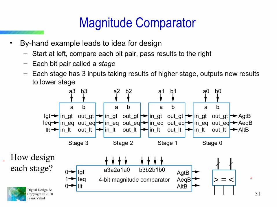
Magnitude Comparator• By-hand example leads to idea for design
– Start at left, compare each bit pair, pass results to the right– Each bit pair called a stage– Each stage has 3 inputs taking results of higher stage, outputs new results
to lower stage
in_gtin_eqin_lt
out_gtout_eqout_lt
IgtIeqIlt
Stage 3
a3 b3
a bin_gtin_eqin_lt
out_gtout_eqout_lt
Stage 2
a2 b2
a bin_gtin_eqin_lt
out_gtout_eqout_lt
Stage 1
a1 b1
a bin_gtin_eqin_lt
out_gtout_eqout_lt
AgtBAeqBAltB
Stage 0
a0 b0
a b
IgtIeqIlt
a3a2a1a0 b3b2b1b0 AgtBAeqBAltB
0
01 4-bit magnitude comparator > = < a
How design each stage?
a
Digital Design 2eCopyright © 2010 Frank Vahid
32
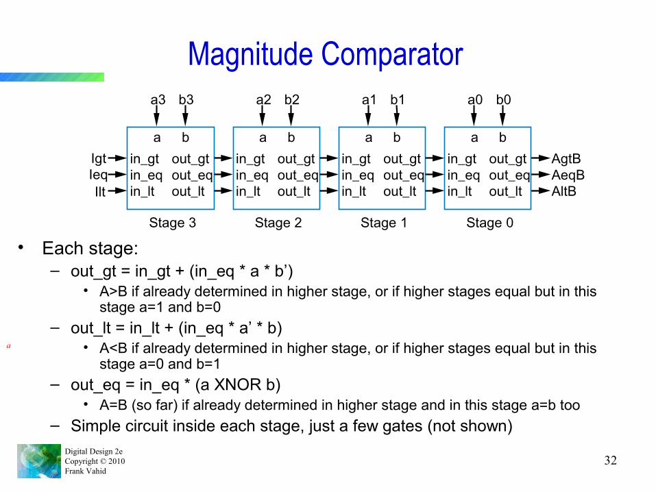
Magnitude Comparator
• Each stage:– out_gt = in_gt + (in_eq * a * b’)
• A>B if already determined in higher stage, or if higher stages equal but in this stage a=1 and b=0
– out_lt = in_lt + (in_eq * a’ * b)• A<B if already determined in higher stage, or if higher stages equal but in this
stage a=0 and b=1
– out_eq = in_eq * (a XNOR b)• A=B (so far) if already determined in higher stage and in this stage a=b too
– Simple circuit inside each stage, just a few gates (not shown)
in_gtin_eqin_lt
out_gtout_eqout_lt
IgtIeqIlt
Stage 3
a3 b3
a bin_gtin_eqin_lt
out_gtout_eqout_lt
Stage 2
a2 b2
a bin_gtin_eqin_lt
out_gtout_eqout_lt
Stage 1
a1 b1
a bin_gtin_eqin_lt
out_gtout_eqout_lt
AgtBAeqBAltB
Stage 0
a0 b0
a b
a
Digital Design 2eCopyright © 2010 Frank Vahid
33
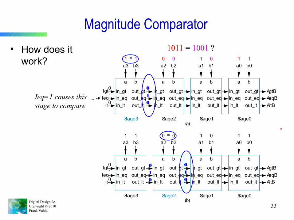
Magnitude Comparator
• How does it work?
in_gtin_eqin_lt
out_gtout_eqout_lt
IgtIeqIlt
Stage3
a3 b3
a b
in_gtin_eqin_lt
out_gtout_eqout_lt
Stage2
a2 b2
a b
in_gtin_eqin_lt
out_gtout_eqout_lt
Stage1
a1 b1
a b
in_gtin_eqin_lt
out_gtout_eqout_lt
AgtBAeqBAltB
Stage0
a0 b01 1 0 0 1 0 1 1
a b
(a)
=
0
1
0
in_gtin_eqin_lt
out_gtout_eqout_lt
IgtIeqIlt
Stage3
a3 b3
a b
in_gtin_eqin_lt
out_gtout_eqout_lt
Stage2
a2 b2
a b
in_gtin_eqin_lt
out_gtout_eqout_lt
Stage1
a1 b1
a b
in_gtin_eqin_lt
out_gtout_eqout_lt
AgtBAeqBAltB
Stage0
a0 b01 1 0 0 1 0 1 1
a b
(b)
010
=
0
1
0
1011 = 1001 ?
010
Ieq=1 causes this stage to compare
a
0
1
0
Digital Design 2eCopyright © 2010 Frank Vahid
34
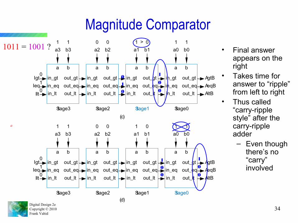
Magnitude Comparator
• Final answer appears on the right
• Takes time for answer to “ripple” from left to right
• Thus called “carry-ripple style” after the carry-ripple adder– Even though
there’s no “carry” involved
1011 = 1001 ?
in_gtin_eqin_lt
out_gtout_eqout_lt
IgtIeqIlt
Stage3
a3 b3
a b
in_gtin_eqin_lt
out_gtout_eqout_lt
Stage2
a2 b2
a b
in_gtin_eqin_lt
out_gtout_eqout_lt
Stage1
a1 b1
a b
in_gtin_eqin_lt
out_gtout_eqout_lt
AgtBAeqBAltB
Stage0
a0 b01 1 0 0 1 0 1 1
a b
(c)
010
1
0
0
>
in_gtin_eqin_lt
out_gtout_eqout_lt
IgtIeqIlt
Stage3
a3 b3
a b
in_gtin_eqin_lt
out_gtout_eqout_lt
Stage2
a2 b2
a b
in_gtin_eqin_lt
out_gtout_eqout_lt
Stage1
a1 b1
a b
in_gtin_eqin_lt
out_gtout_eqout_lt
AgtBAeqBAltB
Stage0
a0 b01 1 0 0 1 0 1 1
a b
(d)
0
10
0
1
0
a
0
1
0
1
0
0
Digital Design 2eCopyright © 2010 Frank Vahid
35
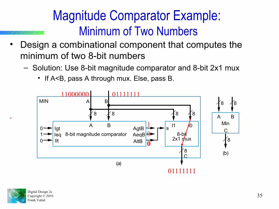
Magnitude Comparator Example: Minimum of Two Numbers
• Design a combinational component that computes the minimum of two 8-bit numbers– Solution: Use 8-bit magnitude comparator and 8-bit 2x1 mux
• If A<B, pass A through mux. Else, pass B.
MIN
IgtIeqIlt
AgtBAeqBAltB
010
A
A B
B
8-bit magnitude comparators I1 I0
2x1 mux8-bit
C
8
88 8 8
8
8
8
C
A BMin
(a)
(b)
11000000 01111111
0
01
01111111
a