Embed Size (px)
Citation preview


THIS PAGE ISBLANK

Copyright © 2007, New Age International (P) Ltd., PublishersPublished by New Age International (P) Ltd., Publishers
All rights reserved.No part of this ebook may be reproduced in any form, by photostat, microfilm,xerography, or any other means, or incorporated into any information retrievalsystem, electronic or mechanical, without the written permission of thepublisher. All inquiries should be emailed to [email protected]
ISBN (10) : 81-224-2323-XISBN (13) : 978-81-224-2323-5
PUBLISHING FOR ONE WORLD
NEW AGE INTERNATIONAL (P) LIMITED, PUBLISHERS4835/24, Ansari Road, Daryaganj, New Delhi - 110002Visit us at www.newagepublishers.com

DharmN-high/hg-tit.pm5

THIS PAGE ISBLANK
Preface to the Second Edition
“High Voltage Engineering” has been written for the undergraduate students in Electri-cal Engineering of Indian and foreign Universities as well as the practising electricalengineers.
The author developed interest in the field of High Voltage Engineering when he was astudent at the Govt. Engineering College, Jabalpur. It used to be thrilling to observe largemetal spheres flashing over, corona phenomenon on a wire placed along the axis of acylinder and then recording the corona loss, controlling the wave shapes of impulse voltagesetc.
The author has taught the subject at the Delhi College of Engineering for quite a numberof years and while preparing lecture notes he referred to some of the books and journalsand some literature from the internationally famed manufacturers of High Voltageequipments e.g. Haefely, Tettex etc. The lecture notes so prepared, thus, have a touch ofboth the class room requirements and a practising engineer’s requirements.
In this edition, zeroth chapter on Electric Stress estimation and c ontrol has been addedwhere in different methods viz. finite difference, finite element, charge simmulation methodand surface charge simulation methods have been discussed per estimation of metricstresses in complex dielectric media and electrode configuration. a brief view of optimisationof electrode configuration is also given in this chapter.
Chapter 1 deals with the breakdown of gases, liquids, and solid materials. Even though ithas not been possible to explain the physical phenomenon associated with breakdown ofthe materials, with accuracy and precisiveness, an attempt has been made to bring outsome of the theories advocated by researchers in this field in a simple lucid and organisedway.
Chapters 2 and 3 discuss the generation of high d.c. and a.c. voltages and high impulsevoltages and currents. Some of the latest circuits have been discussed and rigorous math-ematical treatment of the circuit has been given to make the subject more interesting andto make the student understand the subject better.
Measurement of transient voltage and currents and high voltage and current require dif-ferent skills and equipment as compared with common a.c. or d.c. voltages we normallycome across. Chapter 4 discusses various techniques and circuits for measurement of suchquantities.
Chapter 5 deals into high voltage testing of electrical equipments like insulators, cables,transformers, circuit breakers etc.
The measurements using high voltage Schering bridge, transformer ratio arm bridge andpartial discharges yield information regarding the life expectancy and the long term sta-bility or otherwise of the insulating materials. These techniques have been discussed elabo-rately in Chapter 6. These tests are very important both during design and operation ofthe equipments.
Electrical transients last for a very short duration but these play a very important role inthe insulation design of power system. Chapter 7 takes a view of various types of tran-sients in power system and suggests classical and more modern statistical methods ofcoordinating the insulation requirements of various equipments of the system and thedevices required for protection of these equipments.
In this edition of the book following articles have been added in chapter 1 of the book :
(i) Breakdown in SF6 gas and Vacuum.
(ii) Insulating materials used in power apparatus.
(iii) Application of gases, liquid and solid insulating materials in different power appara-tus.
A suitable number of problems have been solved to help understand the relevant theory.At the end, a large number of multiple choice questions have been added to help thereader to test himself. An extensive bibliography will help the reader to locate detailedinformation on various topics of his interest.
There are very few High Voltage Laboratories all over the world and the reader may nothave an opportunity to visit such a laboratory. Therefore, a few photoplates have beenadded at suitable locations in the book to give a physical feel of various equipments in awell equipped high voltage laboratory. The author feels that with the inclusion ofphotoplates of high voltage equipments the student as well the practising engineers wouldbe greatly benefited.
I wish to express my sincere thanks to M/s Emile Haefely & Co. Ltd., Switzerland forpermitting inclusion of photoplates in the book which has enhanced the utility of the book.
I also wish my express my gratitude to my wife Usha, daughter Meenu and son Sandeepfor their patience and encouragement during the preparation of the book.
Any constructive suggestion for the improvement of the book will be gratefully acknowl-edged.
New Delhi C.L. WADHWA
( viii )
DharmN-high/hg-tit.pm5
Contents
Preface (vii)
0 Electric Stress Estimation and Control (xiii)
0.1 Introduction xiii0.2 Finite Difference Method xiv0.3 Finite Element Method xv0.4 Charge Simulation Method xix0.5 Surface Charge Simulation Method xxi0.6 Comparison of Various Techniques xxiii0.7 Electrolytic Tank xxiii0.8 Control of Electric Field Intensity xxv0.9 Optimisation of Electrode Configuration xxvii
0.9.1 Droplacement of Contour Points xxviii0.9.2 Charging the Position of the Optimisation Charges and Contour Points xxix0.9.3 Modification of Contour Elements xxx
1 Breakdown Mechanism of Gases, Liquid and Solid Materials 1
1.0 Introduction 11.1 Mechanism of Breakdown of Gases 11.2 Townsend’s First Ionization Coefficient 21.3 Cathode Processes—Secondary Effects 31.4 Townsend’ Second Ionization Coefficient 51.5 Townsend Breakdown Mechanism 71.6 Streamer or Kanal Mechanism of Spark 71.7. The Sparking Potential—Paschen’s Law 101.8 Penning Effect 141.9 Corona Discharges 141.10 Time-lag 16
1.10.1 Breakdown in Electronegative Gases 171.10.2 Application of Gases in Power System 17
DharmN-high/hg-tit.pm5
1.11 Breakdown in Liquid Dielectrics 181.11.1 Suspended Solid Particle Mechanism 211.11.2 Cavity Breakdown 22
1.12 Treatment of Transformer Oil 241.13 Testing of Transformer Oil 28
1.13.1 Application of Oil in Power Apparatus 291.14 Breakdown in Solid Dielectrics 30
1.14.1 Intrinsic Breakdown 311.14.2 Electromechanical Breakdown 321.14.3 Breakdown due to Thrilling and Tracking 331.14.4 Thermal Breakdown 341.14.5 Electrochemical Breakdown 381.14.6 Solid Dielectrics used in Power Apparatus 391.14.7 Application of Insulating Materials 44
1.15 Breakdown in Vacuum 481.15.1 Non-metallic Electron Emission Mechanism 491.15.2 Clump Mechanison 501.15.3 Effect of Pressure Breakdown Voltage 51
2 Generation of High D.C. and A.C. Voltages 56
2.1 Half-wave Rectifier Circuit 562.2 Cockroft-Walton Voltage Multiplier Circuit 592.3 Electrostatic Generator 662.4 Generation of High A.C. Voltages 692.5 Series Resonant Circuit 73
3 Generation of Impulse Voltages and Currents 81
3.1 Definitions: Impulse Voltage 813.2 Impulse Generator Circuits 833.3 Analysis of Circuit ‘a’ 843.4 Analysis of Circuit ‘b’ 903.5 Multistage Impulse Generator Circuit 943.6 Construction of Impulse Generator 963.7 Triggering and Synchronisation of the Impulse Generator 983.8 Impulse Current Generation 100
4 Measurement of High Voltages and Currents 110
4.1 Introduction 1104.2 Sphere Gap 1104.3 Uniform Field Spark Gap 1184.4 Rod Gap 1194.5 Electrostatic Voltmeter 1214.6 Generating Voltmeter 124
( x )
DharmN-high/hg-tit.pm5
4.7 The Chubb-Fortescue Method 1274.8 Impulse Voltage Measurements Using Voltage Dividers 1314.9 Measurement of High D.C. and Impulse Currents 139
5 High Voltage Testing of Electrical Equipment 148
5.1 Testing of Overhead Line Insulators 1495.2 Testing of Cables 1515.3 Testing of Bushings 1535.4 Testing of Power Capacitors 1545.5 Testing of Power Transformers 1565.6 Testing of Circuit Breakers 1585.7 Test Voltage 164
6 Nondestructive Insulation Test Techniques 167
6.1 Loss in a Dielectric 1676.2 Measurement of Resistivity 1686.3 Measurement of Dielectric Constant and Loss Factor 1696.4 High Voltage Schering Bridge 1716.5 Measurement of Large Capacitance 1776.6 Schering Bridge Method for Grounded Test Specimen 1776.7 Schering Bridge for Measurement of High Loss Factor 1786.8 Transformer Ratio Arm Bridge 1796.9 Partial Discharges 1816.10 Bridge Circuit 1956.11 Oscilloscope as PD Measuring Device 1966.12 Recurrent Surge Generator 197
7 Transients in Power Systems and Insulation Coordination 204
7.1 Introduction 2047.2 Transients in Simple Circuits 2057.3 Travelling Waves on Transmission Lines 2117.4 Capacitance Switching 2297.5 Over Voltage due to Arcing Ground 2307.6 Lightning Phenomenon 2307.7 Line Design Based on Lightning 2347.8 Switching Surge Test Voltage Characteristics 2357.9 Insulation Co-ordination and Overvoltage Protection 2377.10 Overvoltage Protection 2437.11 Ground Wires 2507.12 Surge Protection of Rotating Machine 256
Multiple Choice Questions 258
Index 269
( xi )

THIS PAGE ISBLANK
Electric Stress Estimation andControl
xiii
0
0.1 INTRODUCTION
The potential at a point plays an important role in obtaining any information regarding the electrostaticfield at that point. The electric field intensity can be obtained from the potential by gradient operationon the potential
i.e. E = – ∇ V ...(1)
which is nothing but differentiation and the electric field intensity can be used to find electric fluxdensity using the relation
D = εE ...(2)
The divergence of this flux density which is again a differentiation results in volume chargedensity.
∇ . D = ρv ...(3)
Therefore, our objective should be to evaluate potential which of course can be found in termsof, charge configuration. However it is not a simple job as the exact distribution of charges for aparticular potential at a point is not readily available. Writing εE = D in equation (3) we have
∇. εE = ρv
or – ∇ . ε . ∇ V = ρv
or ε ∇2 V = – ρv
or ∇2 V = – ρεv ...(4)
This is known as Poisson’s equation. However, in most of the high voltage equipments, spacecharges are not present and hence ρv = 0 and hence equation (4) is written as
∇2 V = 0 ...(5)Equation (5) is known as Laplace’s equation
If ρv = 0, it indicates zero volume charge density but it allows point charges, line charge, ringcharge and surface charge density to exist at singular location as sources of the field.
Here ∇ is a vector operator and is termed as del operator and expressed mathematically incartesian coordinates as
∇ = ∂
∂∂∂
∂∂x
ay
az
ax y z+ + ...(6)
where a ax y, and az are unit vectors in the respective increasing directions.
DharmN-HIGH\HG0-1.PM5 XIV
xiv HIGH VOLTAGE ENGINEERING
Hence Laplace’s equation in cartesian coordinates is given as
∇2 V = ∂∂
∂∂
∂∂
2
2
2
2
2
2
V
x
V
y
V
z+ + = 0 ...(7)
Since ∇ . ∇ is a dot produce of two vectors, it is a scalar quantity. Following methods arenormally used for determination of the potential distribution
(i) Numerical methods(ii) Electrolytic tank method.Some of the numerical methods used are
(a) Finite difference method (FDM)(b) Finite element method (FEM)(c) Charge simulation method (CSM)(d) Surface charge simulation method (SCSM).
0.2 FINITE DIFFERENCE METHOD
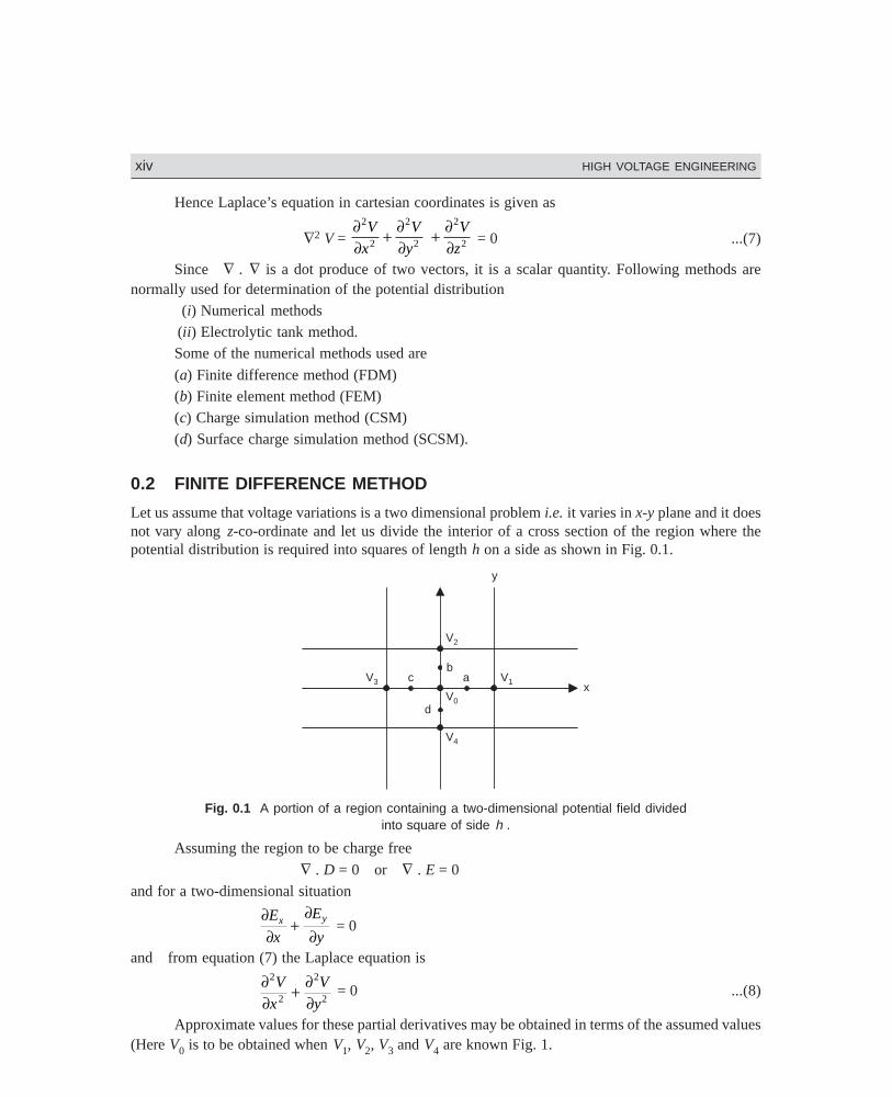
Let us assume that voltage variations is a two dimensional problem i.e. it varies in x-y plane and it doesnot vary along z-co-ordinate and let us divide the interior of a cross section of the region where thepotential distribution is required into squares of length h on a side as shown in Fig. 0.1.
y
V2
V1
V0
V3
V4
d
acb
x
Fig. 0.1 A portion of a region containing a two-dimensional potential field dividedinto square of side h .
Assuming the region to be charge free
∇ . D = 0 or ∇ . E = 0and for a two-dimensional situation
∂∂
∂∂
E
x
E
yx y+ = 0
and from equation (7) the Laplace equation is
∂∂
∂∂
2
2
2
2
V
x
V
y+ = 0 ...(8)
Approximate values for these partial derivatives may be obtained in terms of the assumed values(Here V0 is to be obtained when V1, V2, V3 and V4 are known Fig. 1.
DharmN-HIGH\HG0-1.PM5 XV
ELECTRIC STRESS ESTIMATION AND CONTROL xv
∂∂V
x
V V
ha
=−1 0 and ∂
∂V
x
V V
hc
=−0 3 ...(9)
From the gradients
∂∂
∂∂
∂∂2
20
1 0 0 32
V
x
V
x
V
x
h
V V V V
ha c=
−=
− − +...(10)
Similarly ∂∂
2
20
2 0 0 42
V
y
V V V V
h=
− − +
Substituting in equation (8) we have
∂∂
∂∂
2
2
2
21 2 3 4 0
2
4V
x
V
y
V V V V V
h+ =
+ + + − = 0
or V0 = 1
4 (V1 + V2 + V3 + V4) ...(11)
As mentioned earlier the potentials at four corners of the square are either known through com-putations or at start, these correspond to boundary potentials which are known a priori. From equation(11) it is clear that the potential at point O is the average of the potential at the four neighbouring points.The iterative method uses equation (11) to determine the potential at the corner of every square sub-division in turn and then the process is repeated over the entire region until the difference in values isless than a prespecified value.
The method is found suitable only for two dimensional symmetrical field where a direct solutionis possible. In order to work for irregular three dimensional field so that these nodes are fixed uponboundaries, becomes extremely difficult. Also to solve for such fields as very large number of V(x, y)values of potential are required which needs very large computer memory and computation time andhence this method is normally not recommended for a solution of such electrostatic problems.
0.3 FINITE ELEMENT METHOD
This method is not based on seeking the direct solution of Laplace equation as in case of FDM, insteadin Finite element method use is made of the fact that in an electrostatic field the total energy enclosed inthe whole field region acquires a minimum value. This means that this voltage distribution under givenconditions of electrode surface should make the enclosed energy function to be a minimum for a givendielectric volume v.
We know that electrostatic energy stored per unit volume is given as
W = 1
2 ∈ E2 ...(12)
For a situation where electric field is not uniform, and if it can be assumed uniform for a differ-ential volume δv, the electric energy over the complete volume is given as
W = 1
2
1
2VV dvz ∈ − ∇( ) ...(13)
DharmN-HIGH\HG0-1.PM5 XVI
xvi HIGH VOLTAGE ENGINEERING
To obtain voltage distribution, our performance index is to minimise W as given in equation(13).
Let us assume an isotropic dielectric medium and an electrostatic field without any space charge.The potential V would be determined by the boundaries formed by the metal electrode surfaces.
Equation (13) can be rewritten in cartesian co-ordinates as
W = 1
2 ∈ zzz F
HGIKJ +
FHG
IKJ + F
HGIKJ
LNMM
OQPP
∂∂
∂∂
∂∂
V
x
V
y
V
zdxdydz
2 2 2
...(14)
Assuming that potential distribution is only two-dimensional and there is no change in potential
along z-direction, then ∂∂V
z = 0 and hence equation (14) reduces to
WA = z zz ∈ FHG
IKJ +
FHG
IKJ
RS|T|
UV|W|
L
NMM
O
QPP
1
2
2 2∂∂
∂∂
V
x
V
ydxdy ...(15)
Here z is constant and WA represents the energy density per unit area and the quantity withinintegral sign represents differential energy per elementary area dA = dxdy.
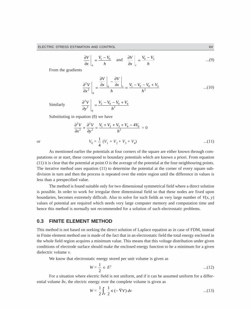
In this method also the field between electrodes is divided into discrete elements as in FDM.The shape of these elements is chosen to be triangular for two dimensional representation and tetrahe-dron for three dimensional field representation Fig. 0.2 (a) and (b).
Vi
Vk
Vj
Vj
Vi
Vk
Vh
Fig. 0.2 (a) Triangular finite element (b) Tetrahedron finite element.
The shape and size of these finite elements is suitably chosen and these are irregularly distrib-uted within the field. It is to be noted that wherever within the medium higher electric stresses areexpected e.g. corners and edges of electrodes, triangles of smaller size should be chosen.
Let us consider an element e1 as shown in Fig. 0.2(a) as part of the total field having nodes i, jand k in anti-clockwise direction. There will be a large no. of such elements e1, e2 .....eN . Havingobtained the potential of the nodes of these elements, the potential distribution within each elements isrequired to be obtained. For this normally a linear relations of V on x and y is assumed and hence thefirst order approximation gives
V(x, y) = a1 + a2x + a3 y ...(16)
DharmN-HIGH\HG0-1.PM5 XVII
ELECTRIC STRESS ESTIMATION AND CONTROL xvii
It is to be noted that for better accuracy of results higher order approximation e.g. square orcubic would be required. Equation (16) implies that electric field intensity within the element is con-stant and potentials at any point within the element are linearly distributed. The potentials at nodes i, jand k are given as
Vi = a1 + a2xi + a3yi
Vj = a1 + a2xj + a3yj
Vk = a1 + a2xk + a3yk ...(17)
Equation (17) can be rewritten in matrix form as
VVV
x yx yx y
aaa
i
j
k
i i
j j
k k
L
NMM
O
QPP =
L
NMM
O
QPPL
NMM
O
QPP
111
1
2
3
...(18)
By using Cramer’s rules, the coefficient a1, a2, a3 can be obtained as follows
a1 = 1
2∆ e
(αi Vi + αj Vj + αk Vk) ...(19)
a2 = 1
2∆e
(βi Vi + βj Vj + βk Vk)
and a3 = 1
2∆e
(γi Vi + γj Vj + γk Vk)
where αi = xj yk – xk yj, αj = xk yi – xi yk , αk = xi yj – xj yi
βi = yi – yk , βj = yk – yi, βk = yi – yj
γi = xk – xj, γj = xi – xk, γk = xj – xi
and 2∆e = αi + αj + αk = βiγj – βjγi
where ∆e represents the area of the triangular element under consideration. As mentioned earlier thenodes must be numbered anticlockwise, else ∆e may turn out to be negative.
From equation (16), the partial derivatives of V are
∂∂V
x = a2 = f(Vi, Vj , Vk) and
∂∂V
y = a3 = f(Vi , Vj, Vk) ...(20)
We know that for obtaining the voltage at various nodes we have to minimise the energy withinthe whole system for which derivatives of energies with respect to potential distribution in each ele-ment is required. For the element e under consideration, let We be the energy enclosed in the element,then energy per unit length in the z-direction We /z denoted by W∆e can be obtained by using equation(15) as follows
W∆e = W
ze =
1
2 ∈ ∆e
∂∂
∂∂
V
x
V
ye
FHG
IKJ +
FHG
IKJ
RS|T|
UV|W|
2 2
...(21)
Here ∆e = e
dxdyzzTo obtain condition for energy minimisation we differentiate partially equation (21) with respect
to Vi , Vj and Vk separately. Thus partially differentiating equation (21) with respect to Vi and makinguse of equations (19) and (20).
DharmN-HIGH\HG0-1.PM5 XVIII
xviii HIGH VOLTAGE ENGINEERING
We have ∂∂
∂∂
∂∂
W
Va
a
V
a
Ve
ie
i i
∆ ∆= ∈ +FHG
IKJ
1
22 2
2 3 =
1
2 2 3∈ +( )a ai iβ γ
= ε β γ β β γ γ β β γ γ
42 2
∆ei i i i j i j j i k i k kV V V[( ) ( ) ( ) ]+ + + + + ...(22)
Similarly, finding partial derivatives of equation (21) with respect to Vj and Vk and following theprocedure outlined above for partial derivative with respect to Vi and arranging all the three equation inmatrix from we have
∂∂
εβ γ β β γ γ β β γ γ
β β γ γ β γ β β γ γβ β γ γ β β γ γ β γ
W
V
VVV
e
e e
i i i j i j i k i k
j i j i j j j k j k
k i k i k j k j k k
i
j
k
∆
∆=
+ + ++ + ++ + +
L
N
MMM
O
Q
PPP
L
NMM
O
QPP4
2 2
2 2
2 2
( ) ( ) ( )
( ) ( ) ( )( ) ( ) ( )
...(22a)
= ε
4∆ e
ii ij ik
ji jj jk
ki kj kk e
i
j
k e
C C CC C CC C C
VVV
( ) ( )( )L
NMMM
O
QPPP
L
NMM
O
QPP = [C]e [V]e ...(23)
After considering a typical element e, the next step is to take into account all such elements inthe region under consideration and the energy associated with all the elements will then be
W =e
N
eW=
∑ =1
1
2 ∈ [V T] [C] [V] ...(24)
where [V] =
VV
Vn
1
2
L
N
MMM
O
Q
PPP
and n is the total number of nodes in the system and N is the no. of elements and [C] is called the globalstiffness matrix which is the sum of the individual matrices.
In general∂∂
W
Vh
leads to
i
n
i ikV C=∑
1
= 0 ...(25)
The solution of the above equations gives voltage distribution in the region. Of course whileseeking the final solution the boundary conditions must be satisfied and hence this would require someiterative method for the exact solution.
The second approach could be to formulate energy function in terms of the unknown nodalvoltage. This energy function is subjected to certain constraints in terms of boundary conditions. Theobjective then is to min. [W] subject to certain constraints. For this various mathematical programmingtechniques like, Fletcher Powell technique, Fletcher technique, direct search techniques, self scalingvariable metric techniques can be used. A computer program can be developed and accuracy of theresult can be obtained depending upon the convergence critsion fed into the computer. A suitable initialguess for the solution can always be made depending upon the system configuration and during everyiteration the voltage can be updated till all the boundary conditions are satisfied and the energy
DharmN-HIGH\HG0-1.PM5 XIX
ELECTRIC STRESS ESTIMATION AND CONTROL xix
function is minimised that is when the change in the energy function between two consecutive itera-tions is less than a prespecified value.
The finite element method is useful for estimating electric fields at highly curved and thin elec-trode surfaces with composite dielectric materials especially when the electric fields are uniform orweakly non-uniform and can be expressed in two dimensioned geometrics. The method is normally notrecommended for three dimensional non-uniform fields.
0.4 CHARGE SIMULATION METHOD
As suggested by the name itself, in this method, the distributed charges on the surface of a conductor/electrode or dielectric interfaces is simulated by replacing these charges by n discrete fictitious indi-vidual charges arranged suitably inside the conductor or outside the space in which the field is to becomputed. These charges could be in the form of point, line or ring, depending upon the shape of theelectrode under consideration. It could be a suitable combination of these fictitious charges. The posi-tion and type of simulation charges are to be determined first and then the field on the electrode surfaceis determined by the potential function of these individual charges. In order to determine the magnitudeof these charges n no. of points are chosen on the surface of the conductor. These points are known as“contour points’’. The sum of the potentials due to fictitious charge distribution at any contour pointsshould correspond to the conductor potential Vc which is known a priori.
Suppose qi, is one of the fictitious charges and Vi is the potential of any point Pi in space whichis independent of the coordinate system chosen, the total potential Vi due to all the charges is given as
Vi = j
n
ij jp q=
∑1
...(26)
where pij are known as ‘‘potential Co-efficient’’ which are to be determined for different types ofcharges by using Laplace’s equation. We know that potential at a point P at a distance ‘a’ from a pointcharge q is given as
V = q
a4π ∈...(27)
So here the potential co-efficient p is 1
4π ∈aSimilarly, these co-efficients for linear and ring or circular charges can also be obtained. It is
found these are also dependent upon various distance of these charges from the point under considera-tion where potential is to be obtained and the permittivity of the medium as in case of a point chargeand hence potential co-efficients are constant number and hence the potential due to various types ofcharges are a linear function of charges and this is how we get the potential at a point due to variouscharges as an algebraic sum of potential due to individual charges.
A few contour points must also be taken at the electrode boundaries also and the potential due tothe simulated charge system should be obtained at these points and this should correspond to theequipotentials or else, the type and location of charges should be changed to acquire the desired shapeand the given potential. Suppose we take ‘n’ number of contour points and n no. of charges, the follow-ing set of equations can be written
DharmN-HIGH\HG0-1.PM5 XX
xx HIGH VOLTAGE ENGINEERING
p p pp p p
p p p
q
VV
V
n
n
n n nn n n
11 12 1
21 22 2
1 2
1
2
1
2
...
...:
...: :
L
N
MMM
O
Q
PPP
L
N
MMM
O
Q
PPP
=
L
N
MMM
O
Q
PPP
...(28)
The solution of these equations gives the magnitude of the individual charges and which corre-sponds to electrode potential (V1 ....... Vn) at the given discrete points. Next, it is necessary to checkwhether the type and location of charges as obtained from the solution of equation (28) satisfies theactual boundary conditions every where on the electrode surfaces. It is just possible that at certaincheck points the charges may not satisfy the potential at those points. This check for individual point iscarried out using equation (26). If simulation does not meet the accuracy criterion, the procedure isrepeated by changing either the number or type or location or all, of the simulation charges till adequatecharge system (simulation) is obtained. Once, this is achieved, potential or electric field intensity at anypoint can be obtained.
The field intensity at a point due to various charges is obtained by vector addition of intensitydue to individual charges at that point. However, it is desirable to obtain the individual directionalcomponents of field intensity separately. In cartesion coordinate system, the component of electric fieldintensity along x-direction for n number of charges is given as
Ep
xq f qx
j
nij
jj
n
ij x j= == =
∑ ∑1 1
∂∂
( ) ...(29)
where (fij)x are known as field intensity co-efficients in x-direction.
In this method it is very important to select a suitable type of simulation charges and theirlocation for faster convergence of the solution e.g. for cylindrical electrodes finite line charges aresuitable, spherical electrodes have point charges or ring charges as suitable charges. However, forfields with axial symmetry having projected circular structures, ring charges are found better. Experi-ence of working on such problems certainly will play an important role for better and faster selection.The procedure for CSM is summarised as follows :
1. Choose a suitable type and location of simulation charges within the electride system.
2. Select some contour point on the surface of the electrodes. A relatively larger no. of contourpoints should be selected on the curved or corner points of the electrode.
3. Calculate the pij for different charges and locations (contour points) and assemble in theform of a matrix.
4. Obtain inverse of this matrix and calculate the magnitude of charges (simulation).
5. Test whether the solution so obtained is feasible or not by selecting some check points onthe conductor surface. If the solution is feasible stop and calculate the electric field intensityat requisite point. If not, repeat the procedure by either changing the type or location of thesimulation charges.
CSM has proved quite useful for estimation of electric field intensity for two and three dimen-sional fields both with or without axial symmetry. It is a simple method and is found computationallyefficient and provides accurate results.
DharmN-HIGH\HG0-1.PM5 XXI
ELECTRIC STRESS ESTIMATION AND CONTROL xxi
The simplicity with which CSM takes care of curved and rounded surfaces of electrodes orinterfaces of composite dielectric medium makes it a suitable method for field estimation. The compu-tation time is much less as compared to FDM and FEM.
However, it is difficult to apply this methods for thin electrodes e.g. foils, plates or coatings assome minimum gap distance between the location of a charge and electrode contours is required. Also,it is found difficult to apply this method for electrodes with highly irregular and complicated bounda-ries with sharp edges etc.
However, as mentioned earlier a good experience of selecting type and location of simulationcharge may solve some of these problem.
An improved version of CSM known as surface charge simulation method (SCSM) describedbelow is used to overcome the problem faced in CSM.
0.5 SURFACE CHARGE SIMULATION METHOD
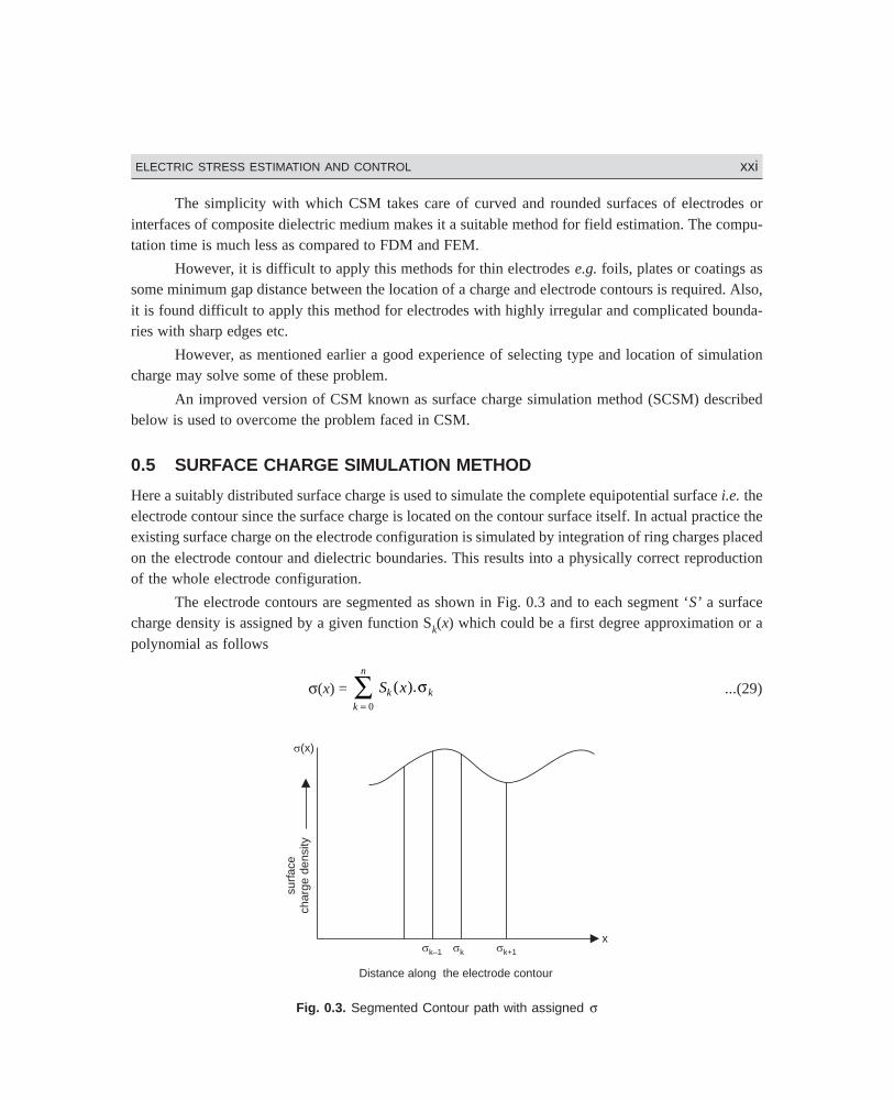
Here a suitably distributed surface charge is used to simulate the complete equipotential surface i.e. theelectrode contour since the surface charge is located on the contour surface itself. In actual practice theexisting surface charge on the electrode configuration is simulated by integration of ring charges placedon the electrode contour and dielectric boundaries. This results into a physically correct reproductionof the whole electrode configuration.
The electrode contours are segmented as shown in Fig. 0.3 and to each segment ‘S’ a surfacecharge density is assigned by a given function Sk(x) which could be a first degree approximation or apolynomial as follows
σ(x) = k
n
k kS x=
∑0
( ).σ ...(29)
(x)
surf
ace
char
gede
nsity
k–1 k k+1
Distance along the electrode contour
x
Fig. 0.3. Segmented Contour path with assigned σ
DharmN-HIGH\HG0-1.PM5 XXII
xxii HIGH VOLTAGE ENGINEERING
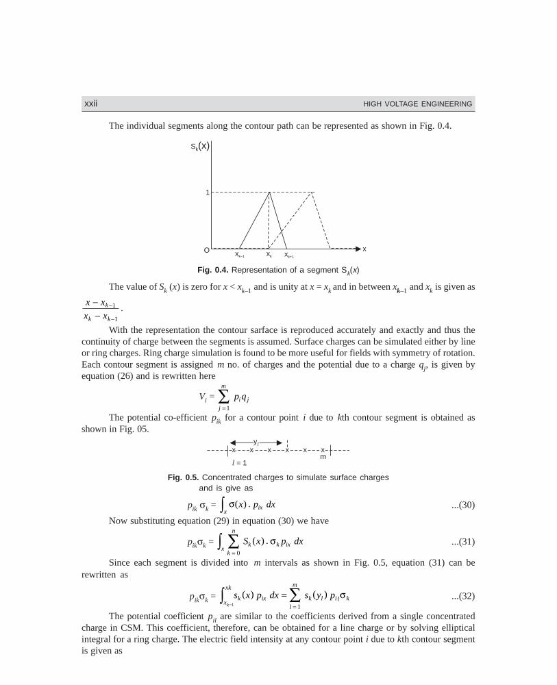
The individual segments along the contour path can be represented as shown in Fig. 0.4.
1
xk–1 xk xk+1
xO
Sk(x)
Fig. 0.4. Representation of a segment Sk(x)
The value of Sk (x) is zero for x < xk–1 and is unity at x = xk and in between xk–1 and xk is given as
x x
x xk
k k
−−
−
−
1
1
.
With the representation the contour sarface is reproduced accurately and exactly and thus thecontinuity of charge between the segments is assumed. Surface charges can be simulated either by lineor ring charges. Ring charge simulation is found to be more useful for fields with symmetry of rotation.Each contour segment is assigned m no. of charges and the potential due to a charge qj, is given byequation (26) and is rewritten here
Vi = j
m
i jp q=
∑1
The potential co-efficient pik for a contour point i due to kth contour segment is obtained asshown in Fig. 05.
l = 1
xx xx xx xx xx xxy
ly
l
mm
Fig. 0.5. Concentrated charges to simulate surface chargesand is give as
pik σk = x
ixx p dxz σ( ) . ...(30)
Now substituting equation (29) in equation (30) we have
pikσk = x
k
n
k k ixS x p dxz ∑= 0
( ) . σ ...(31)
Since each segment is divided into m intervals as shown in Fig. 0.5, equation (31) can berewritten as
pikσk = x
xk
k ixl
m
k l i l kk
s x p dx s y p−
z ∑==1 1
( ) ( ) σ ...(32)
The potential coefficient pil are similar to the coefficients derived from a single concentratedcharge in CSM. This coefficient, therefore, can be obtained for a line charge or by solving ellipticalintegral for a ring charge. The electric field intensity at any contour point i due to kth contour segmentis given as
DharmN-HIGH\HG0-1.PM5 XXIII
ELECTRIC STRESS ESTIMATION AND CONTROL xxiii
Ei = x
m
k ikf=
∑1
σ ...(33)
where fik are the field intensity co-efficients.
As discussed this method requires a large number of elements, normally more than 2500, inde-pendent of the surface shape and thus require large computational efforts. Also, due to certain practicaldifficulties this method is not used as frequently as other numerical methods for estimation of electricfields.
0.6 COMPARISON OF VARIOUS TECHNIQUES
Out of the various techniques FDM is the simplest to compute and understand but the computationeffort and computer memory requirements are the highest. Also, since all difference equations areapproximation to the actual field conditions, the final solution may have considerable error.
Finite element method is a general method and has been used for almost all fields of engineer-ing. The method is suitable for estimating fields at highly curved and thin electrode surfaces withdifferent dielectric materials. However, this method is more useful for uniform or weakly non-uniformfields and which can be represented by two dimensional geometries. This method is recommended forthree dimensional complicated field configurations.
Charge Simulation Method (CSM) is considered to be one of the most superior and acceptablemethod for two and three dimensional configuration with more than one dielectric and with electrodesystems of any desired shape since this method is based on minimization of the energy function whichcould be subjected to any operating constraints e.g. environmental condition, it has proved to be highlyaccurate method. Because of inherent features of the technique, this method also helps in optimisingelectrode configuration. In this electrode configuration optimisation problems the objective is to havefield intensity as low as possible subject to the condition that a constant field intensity exists on thecomplete electrode surface. With this optimisation, a higher life expectancy of high voltage equipmentscan be achieved.
However, as mentioned earlier this method can not be used for thin electrodes e.g. foils, platesor coatings due to the requirement of a minimum gap distance between the location of a charge andelectrode contour. Also, this method is not suitable for highly irregular electrode boundaries.
The surface charge simulation method even though takes into account the actual surface chargedistribution on the electrode surface, this method is not normally recommended for solution of fieldproblem due to some practical difficulties.
An important difference between the various method is that the FDM and FEM can be used onlyfor bounded field whereas CSM and SCMS can also be used for unbounded fields.
0.7 ELECTROLYTIC TANK
For assessing electric field distribution in complex three dimensional situations, analytical methods areunsuitable. Two other approaches in use are, experimental analog and numbrical techniques. Thenumerical techniques have already been discussed in the previous section. We now study analogtechniques especially the use of electrolytic tank.
DharmN-HIGH\HG0-1.PM5 XXIV
xxiv HIGH VOLTAGE ENGINEERING
The potential distribution in conductive media in current equilibrium condition satisfies Laplace’sequation the same as the electric fields in space-charge-free regions i.e. ρv = 0. This fact makes itpossible to obtain solutions to many difficult electrostatic field problems by constructing an analyogouspotential distribution in a conductive medium where the potential and field distributions can be meas-ured directly. The conductors and insulation arrangements can be represented using an electrolytictank. Due to its simplicity and accuracy this method has been used for decades.
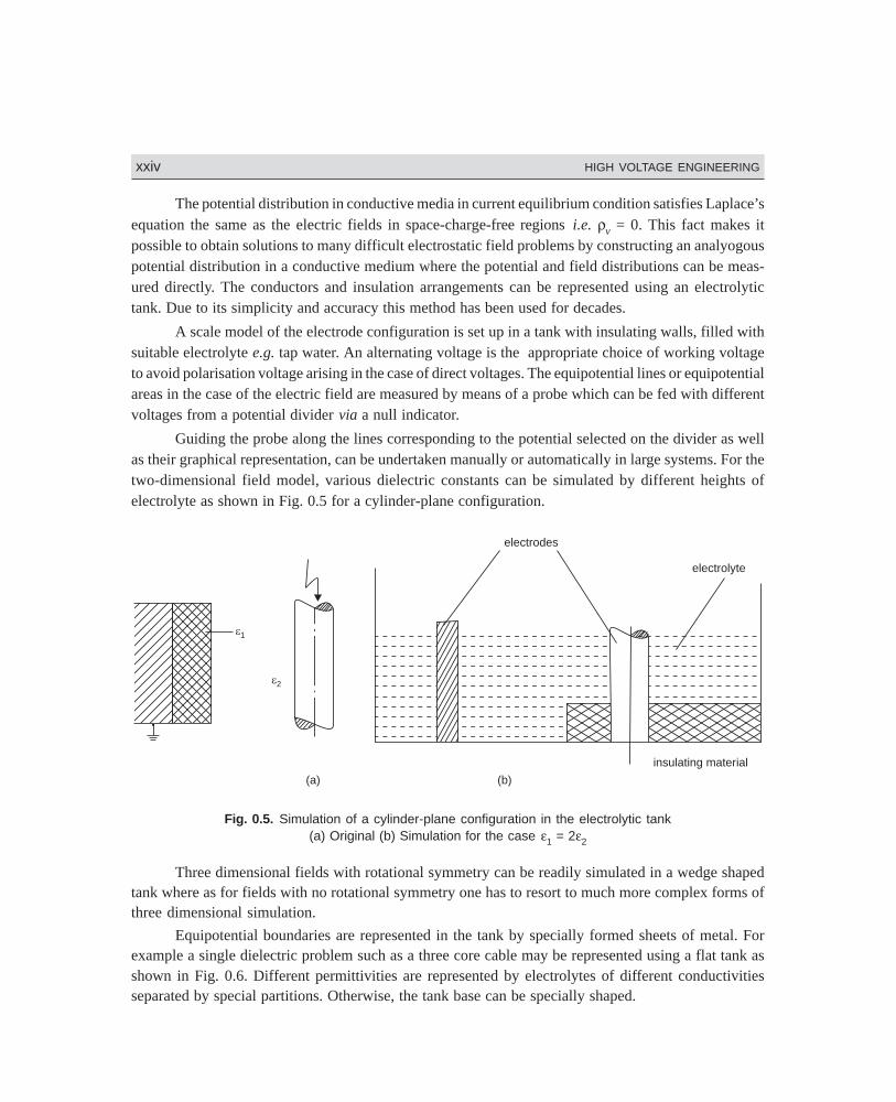
A scale model of the electrode configuration is set up in a tank with insulating walls, filled withsuitable electrolyte e.g. tap water. An alternating voltage is the appropriate choice of working voltageto avoid polarisation voltage arising in the case of direct voltages. The equipotential lines or equipotentialareas in the case of the electric field are measured by means of a probe which can be fed with differentvoltages from a potential divider via a null indicator.
Guiding the probe along the lines corresponding to the potential selected on the divider as wellas their graphical representation, can be undertaken manually or automatically in large systems. For thetwo-dimensional field model, various dielectric constants can be simulated by different heights ofelectrolyte as shown in Fig. 0.5 for a cylinder-plane configuration.
1
2
electrolyte
electrodes
insulating material
(b)(a)
Fig. 0.5. Simulation of a cylinder-plane configuration in the electrolytic tank(a) Original (b) Simulation for the case ε1 = 2ε2
Three dimensional fields with rotational symmetry can be readily simulated in a wedge shapedtank where as for fields with no rotational symmetry one has to resort to much more complex forms ofthree dimensional simulation.
Equipotential boundaries are represented in the tank by specially formed sheets of metal. Forexample a single dielectric problem such as a three core cable may be represented using a flat tank asshown in Fig. 0.6. Different permittivities are represented by electrolytes of different conductivitiesseparated by special partitions. Otherwise, the tank base can be specially shaped.
DharmN-HIGH\HG0-1.PM5 XXV
ELECTRIC STRESS ESTIMATION AND CONTROL xxv
V
to probe
L.F.-AC
source
Fig. 0.6. Electrolytic tank model of a three-core cable represented at the instantwhen one core is at zero voltage, the same as the sheath.
0.8 CONTROL OF ELECTRIC FIELD INTENSITY
It is a common knowledge that if the field in a dielectric material is uniform, the material is properlyutilised. If it is non-uniform the material is under-utilised. Under normal situation an electric field is notuniform due to imperfection in the dielectric material during manufacture or it could be due to undesir-able shapes and sizes of electrodes.
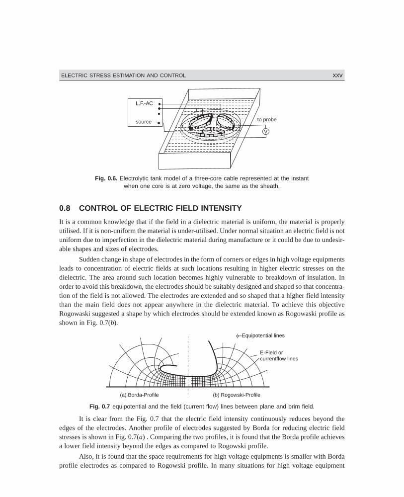
Sudden change in shape of electrodes in the form of corners or edges in high voltage equipmentsleads to concentration of electric fields at such locations resulting in higher electric stresses on thedielectric. The area around such location becomes highly vulnerable to breakdown of insulation. Inorder to avoid this breakdown, the electrodes should be suitably designed and shaped so that concentra-tion of the field is not allowed. The electrodes are extended and so shaped that a higher field intensitythan the main field does not appear anywhere in the dielectric material. To achieve this objectiveRogowaski suggested a shape by which electrodes should be extended known as Rogowaski profile asshown in Fig. 0.7(b).
(a) Borda-Profile (b) Rogowski-Profile
E-Fleld orcurrentflow lines
–Equipotential lines
Fig. 0.7 equipotential and the field (current flow) lines between plane and brim field.
It is clear from the Fig. 0.7 that the electric field intensity continuously reduces beyond theedges of the electrodes. Another profile of electrodes suggested by Borda for reducing electric fieldstresses is shown in Fig. 0.7(a) . Comparing the two profiles, it is found that the Borda profile achievesa lower field intensity beyond the edges as compared to Rogowski profile.
Also, it is found that the space requirements for high voltage equipments is smaller with Bordaprofile electrodes as compared to Rogowski profile. In many situations for high voltage equipment
DharmN-HIGH\HG0-1.PM5 XXVI
xxvi HIGH VOLTAGE ENGINEERING
space requirements become a serious problem and hence electric field optimisation techniques havereceived a great importance.
A visit to a high voltage laboratory shows that electrodes at high potential are given large,smooth shaped dome like shapes to bring down the electric field stress surrounding the area i.e. theatmospheric air. The modern trend is to design segmented electrodes in which a number of small,identical, smooth discs are given a desired continuous shapes as per requirement.
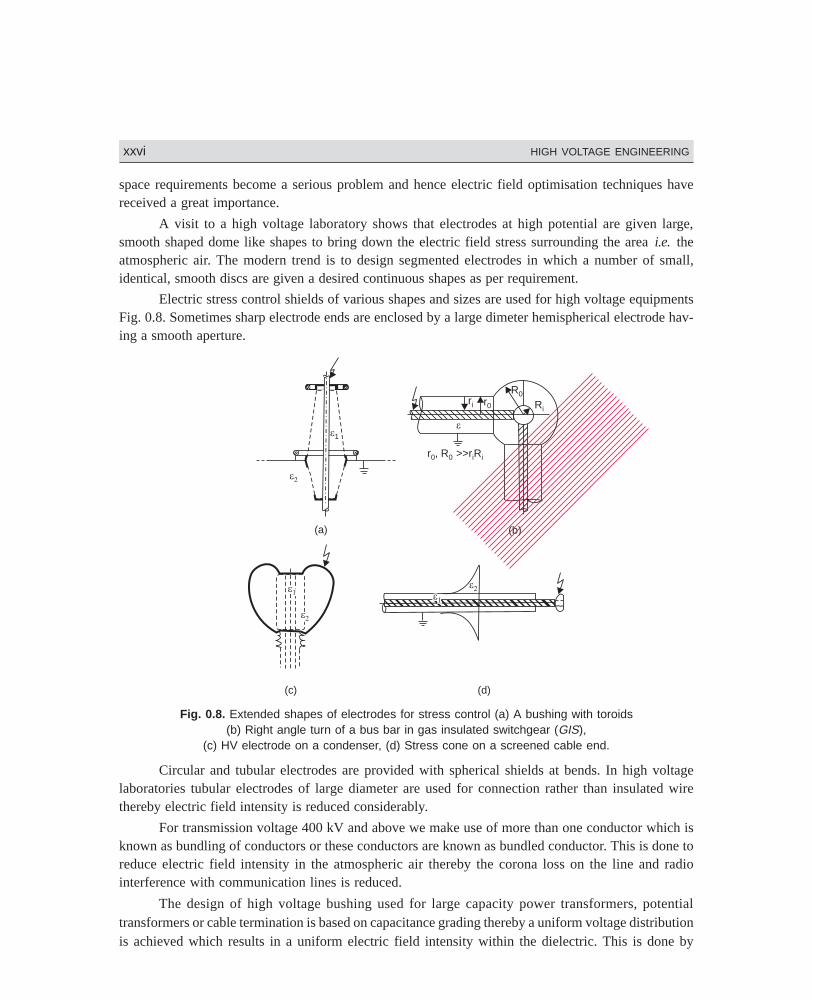
Electric stress control shields of various shapes and sizes are used for high voltage equipmentsFig. 0.8. Sometimes sharp electrode ends are enclosed by a large dimeter hemispherical electrode hav-ing a smooth aperture.
1
(a) (b)
(d)(c)
r , R >>r R0 0 i i
r0
R0ri Ri
Fig. 0.8. Extended shapes of electrodes for stress control (a) A bushing with toroids(b) Right angle turn of a bus bar in gas insulated switchgear (GIS),
(c) HV electrode on a condenser, (d) Stress cone on a screened cable end.
Circular and tubular electrodes are provided with spherical shields at bends. In high voltagelaboratories tubular electrodes of large diameter are used for connection rather than insulated wirethereby electric field intensity is reduced considerably.
For transmission voltage 400 kV and above we make use of more than one conductor which isknown as bundling of conductors or these conductors are known as bundled conductor. This is done toreduce electric field intensity in the atmospheric air thereby the corona loss on the line and radiointerference with communication lines is reduced.
The design of high voltage bushing used for large capacity power transformers, potentialtransformers or cable termination is based on capacitance grading thereby a uniform voltage distributionis achieved which results in a uniform electric field intensity within the dielectric. This is done by
DharmN-HIGH\HG0-1.PM5 XXVII
ELECTRIC STRESS ESTIMATION AND CONTROL xxvii
interposing concentric sheets of metals of suitable lengths and position. This is known as “inter-sheathgrading” to control electric field intensity. The inter-sheaths are held at suitable potential which enableseconomic utilisation of the insulating material by evenly distributing the equipotential surfaces.
A simple rule to control electric field intensity in high voltage equipments is to avoid sharppoints and edges in the electrodes. These electrodes should be large symmetrical and should havesmooth surface. The surface should not be rough as this would lead to higher stresses at high voltages.Micro protrusion on the surface of the electrode may penetrate deeper into the dielectric material whichmay result in high electric field intensity at those points and may lead to breakdown of the dielectricmaterial.
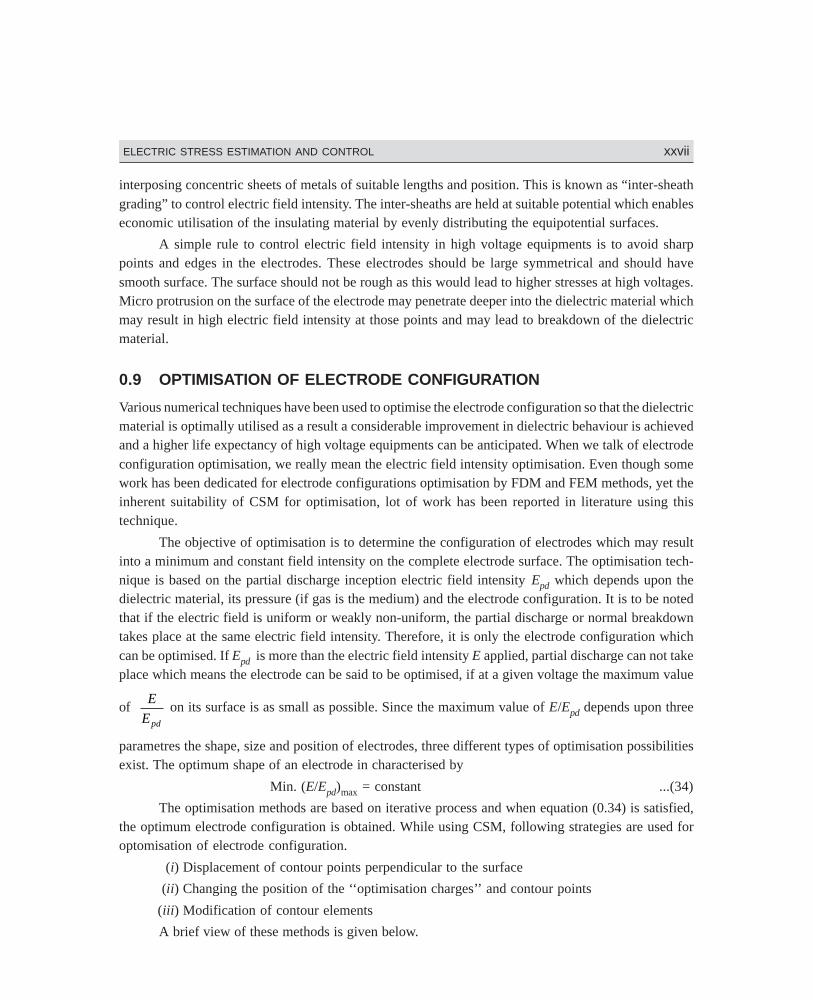
0.9 OPTIMISATION OF ELECTRODE CONFIGURATION
Various numerical techniques have been used to optimise the electrode configuration so that the dielectricmaterial is optimally utilised as a result a considerable improvement in dielectric behaviour is achievedand a higher life expectancy of high voltage equipments can be anticipated. When we talk of electrodeconfiguration optimisation, we really mean the electric field intensity optimisation. Even though somework has been dedicated for electrode configurations optimisation by FDM and FEM methods, yet theinherent suitability of CSM for optimisation, lot of work has been reported in literature using thistechnique.
The objective of optimisation is to determine the configuration of electrodes which may resultinto a minimum and constant field intensity on the complete electrode surface. The optimisation tech-nique is based on the partial discharge inception electric field intensity Epd which depends upon thedielectric material, its pressure (if gas is the medium) and the electrode configuration. It is to be notedthat if the electric field is uniform or weakly non-uniform, the partial discharge or normal breakdowntakes place at the same electric field intensity. Therefore, it is only the electrode configuration whichcan be optimised. If Epd is more than the electric field intensity E applied, partial discharge can not takeplace which means the electrode can be said to be optimised, if at a given voltage the maximum value
of E
Epd
on its surface is as small as possible. Since the maximum value of E/Epd depends upon three
parametres the shape, size and position of electrodes, three different types of optimisation possibilitiesexist. The optimum shape of an electrode in characterised by
Min. (E/Epd)max = constant ...(34)
The optimisation methods are based on iterative process and when equation (0.34) is satisfied,the optimum electrode configuration is obtained. While using CSM, following strategies are used foroptomisation of electrode configuration.
(i) Displacement of contour points perpendicular to the surface
(ii) Changing the position of the ‘‘optimisation charges’’ and contour points
(iii) Modification of contour elements
A brief view of these methods is given below.
DharmN-HIGH\HG0-1.PM5 XXVIII
xxviii HIGH VOLTAGE ENGINEERING
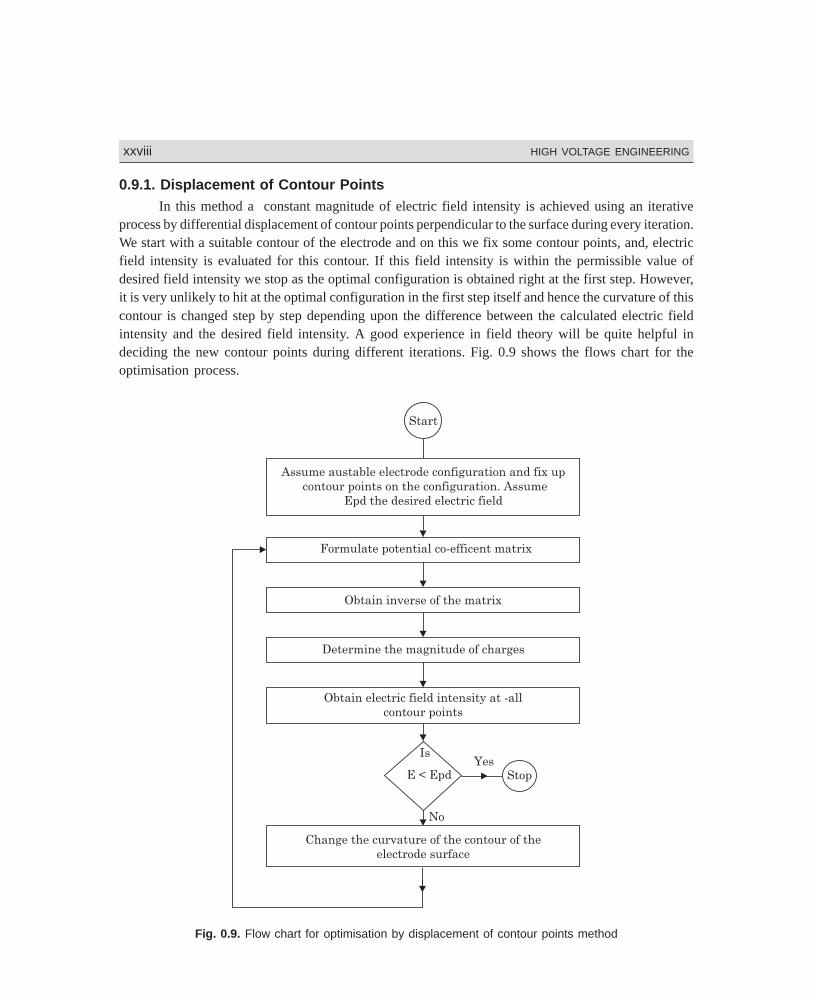
0.9.1. Displacement of Contour PointsIn this method a constant magnitude of electric field intensity is achieved using an iterative
process by differential displacement of contour points perpendicular to the surface during every iteration.We start with a suitable contour of the electrode and on this we fix some contour points, and, electricfield intensity is evaluated for this contour. If this field intensity is within the permissible value ofdesired field intensity we stop as the optimal configuration is obtained right at the first step. However,it is very unlikely to hit at the optimal configuration in the first step itself and hence the curvature of thiscontour is changed step by step depending upon the difference between the calculated electric fieldintensity and the desired field intensity. A good experience in field theory will be quite helpful indeciding the new contour points during different iterations. Fig. 0.9 shows the flows chart for theoptimisation process.
Start
Assume austable electrode configuration and fix up
contour points on the configuration. Assume
Epd the desired electric field
Formulate potential co-efficent matrix
Obtain inverse of the matrix
Determine the magnitude of charges
Obtain electric field intensity at -all
contour points
Is
E < EpdYes
No
Stop
Change the curvature of the contour of the
electrode surface
Fig. 0.9. Flow chart for optimisation by displacement of contour points method
DharmN-HIGH\HG0-1.PM5 XXIX
ELECTRIC STRESS ESTIMATION AND CONTROL xxix
It is to be noted that for electric field calculation on the electrode surface (assumed or updated)is caried out using CSM technique. Since during every iteration the complete CSM technique is to beused for calculation of electric field intensity, computer time requirement is high and this is its majordisadvantage.
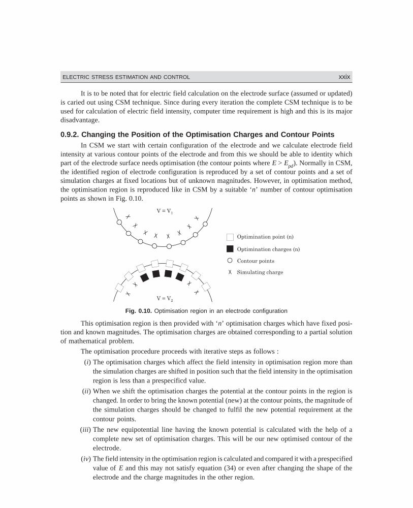
0.9.2. Changing the Position of the Optimisation Charges and Contour PointsIn CSM we start with certain configuration of the electrode and we calculate electrode field
intensity at various contour points of the electrode and from this we should be able to identity whichpart of the electrode surface needs optimisation (the contour points where E > Epd). Normally in CSM,the identified region of electrode configuration is reproduced by a set of contour points and a set ofsimulation charges at fixed locations but of unknown magnitudes. However, in optimisation method,the optimisation region is reproduced like in CSM by a suitable ‘n’ number of contour optimisationpoints as shown in Fig. 0.10.
V = V1
V = V2
Optimination point (n)
Optim tion charges (n)ina
Contour points
Simulating charge
Fig. 0.10. Optimisation region in an electrode configuration
This optimisation region is then provided with ‘n’ optimisation charges which have fixed posi-tion and known magnitudes. The optimisation charges are obtained corresponding to a partial solutionof mathematical problem.
The optimisation procedure proceeds with iterative steps as follows :
(i) The optimisation charges which affect the field intensity in optimisation region more thanthe simulation charges are shifted in position such that the field intensity in the optimisationregion is less than a prespecificd value.
(ii) When we shift the optimisation charges the potential at the contour points in the region ischanged. In order to bring the known potential (new) at the contour points, the magnitude ofthe simulation charges should be changed to fulfil the new potential requirement at thecontour points.
(iii) The new equipotential line having the known potential is calculated with the help of acomplete new set of optimisation charges. This will be our new optimised contour of theelectrode.
(iv) The field intensity in the optimisation region is calculated and compared it with a prespecifiedvalue of E and this may not satisfy equation (34) or even after changing the shape of theelectrode and the charge magnitudes in the other region.
DharmN-HIGH\HG0-1.PM5 XXX
xxx HIGH VOLTAGE ENGINEERING
(v) The optimisation points are now located at the newly obtained contour of the electrode. Thelocation of the respective optimisation charges should, therefore, be suitably corrected tostart the next iteration.
The iteration procedure is continued with lower magnitude of electric field intensity till it con-verges to a prespecified value or instruct to stop the computation process if it goes to a very low valuewhich is physically not feasible.
0.9.3. Modification of Contour ElementsThis method is based on the qualitative correlation between the curvature of an electrode sur-
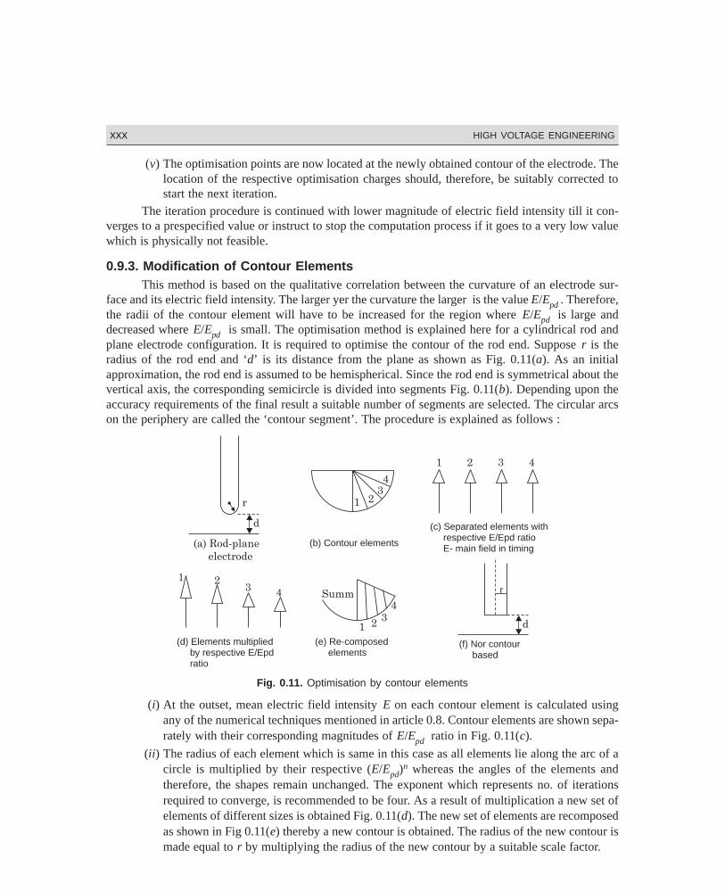
face and its electric field intensity. The larger yer the curvature the larger is the value E/Epd . Therefore,the radii of the contour element will have to be increased for the region where E/Epd is large anddecreased where E/Epd is small. The optimisation method is explained here for a cylindrical rod andplane electrode configuration. It is required to optimise the contour of the rod end. Suppose r is theradius of the rod end and ‘d’ is its distance from the plane as shown as Fig. 0.11(a). As an initialapproximation, the rod end is assumed to be hemispherical. Since the rod end is symmetrical about thevertical axis, the corresponding semicircle is divided into segments Fig. 0.11(b). Depending upon theaccuracy requirements of the final result a suitable number of segments are selected. The circular arcson the periphery are called the ‘contour segment’. The procedure is explained as follows :
d
(a) Rod-plane
electrode
1 234
(b) Contour elements
1 2 3 4
(c) Separated elements withrespective E/Epd ratioE- main field in timing
1 23
4
(d) Elements multipliedby respective E/Epdratio
1 23
4Summ
(e) Re-composedelements
d
r
(f) Nor contourbased
r
Fig. 0.11. Optimisation by contour elements
(i) At the outset, mean electric field intensity E on each contour element is calculated usingany of the numerical techniques mentioned in article 0.8. Contour elements are shown sepa-rately with their corresponding magnitudes of E/Epd ratio in Fig. 0.11(c).
(ii) The radius of each element which is same in this case as all elements lie along the arc of acircle is multiplied by their respective (E/Epd)
n whereas the angles of the elements andtherefore, the shapes remain unchanged. The exponent which represents no. of iterationsrequired to converge, is recommended to be four. As a result of multiplication a new set ofelements of different sizes is obtained Fig. 0.11(d). The new set of elements are recomposedas shown in Fig 0.11(e) thereby a new contour is obtained. The radius of the new contour ismade equal to r by multiplying the radius of the new contour by a suitable scale factor.
DharmN-HIGH\HG0-1.PM5 XXXI
ELECTRIC STRESS ESTIMATION AND CONTROL xxxi
(iii) The new contour is placed at the distance ‘d’ from the plane as shown in Fig. 0.11(f). Thesteps (i) and (ii) are repeated until the remaining differences in E/Epd ratio are sufficientlysmall. As seen in Fig. 0.11(e) during each iteration the surface region is flattened where E/Epd exceeds its mean value whereas the remaining region becomes more curved whichresults into a more uniform distribution of E/Epd . It is to be noted that in step (ii) if the Epd
depends upon the curvature of the electrode surface, then instead of the element radii, thereciprocal of the curvature is multiplied by (E/Epd)
n. It is to be noted with caution that theboundary conditions in terms of operating constraints if any must be included during theprocess of optimisation of electrode configuration otherwise it may turn out to an infeasiblesolution.
For further details a few references are given at the end of the chapter.
0.1. ‘‘The potential at a point plays an important role in obtaining any information regarding the electrostaticfield’’ Justify the statement.
0.2. Starting with Laplace’s equation in two dimension explain the Finite Differentce method for Evaluationof field distribution. Discuss its advantages and disadvantages.
0.3. What is Finite Element Method for evaluation of field distribution. Discuss the procedure associated withthis method and discuss its advantages and limitations.
0.4. What is a global stiffness matrix when referred to Finite Element Method used for evaluation of electricfield ?
0.5. Discuss the basic philosophy associated with charge simulation method for evaluation of electric fielddistribution.
0.6. Obtain expressions for potential coefficients p for a (i) point charge (ii) line charge (iii) ring charge distri-bution.
0.7. What are field intensity co-efficients when referred to charge simulation method.
0.8. Explain briefly in a few steps the procedure associated with charge simulation method. Discuss its advan-tages and limitations.
0.9. Explain briefly an improved version of charge simulation method and discuss its advantages and limita-tions.
0.10. Compare in brief various numerical techniques to study or evaluate the electric field distribution in dielec-tric medium.
0.11. Explain with neat diagrams the application of an Electrolytic tank for evaluating electric field distributionin dielectric medium or electrical equipments.
0.12. Explain with neat diagrams the procedure to control electric field intensity in high voltage equipments.
0.13. Explain clearly what you mean by optimisation of Electrode configuration. Mention various techniquesused for the purpose.
0.14. Discuss briefly the optimisation techniques listed here :
(i) Displacement of contour points with flow chart.
(ii) Changing the location of optimisation charges and contour points.
(iii) Modification of contour elements.
DharmN-HIGH\HG0-1.PM5 XXXII
xxxii HIGH VOLTAGE ENGINEERING
1. Alston High Voltage Technology Oxford University Press 1968.
2. E. Kuffel and W.S. Zaengl, High Voltage Engineering-Fundamentals, Pergamon Press, 1984.
3. Arora R. & Wolfgang Mosch, High Voltage Insulation Engg., New Age International.
4. Reister M. Weib P. “Computation of Electric fields by use of surface charge simulation method” Int. Sympon HV Engg. Athens (1983) Report 11.06.
5. Welly J. D. “Optimisation of electrode contours in high voltage equipment using circular contour elements”Int. Symp on HV Engg. Braunschweig (1987).
6. Singer H., computation of optimised electrode geometries Int. Symp. on HV Engg. Milano (1979) Report11.06.
Breakdown Mechanism of Gaseous,Liquid and Solid Materials
1
1
1.0 INTRODUCTION
With ever increasing demand of electrical energy, the power system is growing both in size and com-plexities. The generating capacities of power plants and transmission voltage are on the increase be-cause of their inherent advantages. If the transmission voltage is doubled, the power transfer capabilityof the system becomes four times and the line losses are also relatively reduced. As a result, it becomesa stronger and economical system. In India, we already have 400 kV lines in operation and 800 kV linesare being planned. In big cities, the conventional transmission voltages (110 kV–220 kV etc.) are beingused as distribution voltages because of increased demand. A system (transmission, switchgear, etc.)designed for 400 kV and above using conventional insulating materials is both bulky and expensiveand, therefore, newer and newer insulating materials are being investigated to bring down both the costand space requirements. The electrically live conductors are supported on insulating materials andsufficient air clearances are provided to avoid flashover or short circuits between the live parts of thesystem and the grounded structures. Sometimes, a live conductor is to be immersed in an insulatingliquid to bring down the size of the container and at the same time provide sufficient insulation betweenthe live conductor and the grounded container. In electrical engineering all the three media, viz. the gas,the liquid and the solid are being used and, therefore, we study here the mechanism of breakdown ofthese media.
1.1 MECHANISM OF BREAKDOWN OF GASES
At normal temperature and pressure, the gases are excellent insulators. The current conduction is of theorder of 10–10 A/cm2. This current conduction results from the ionisation of air by the cosmic radiationand the radioactive substances present in the atmosphere and the earth. At higher fields, charged parti-cles may gain sufficient energy between collision to cause ionisation on impact with neutral molecules.It is known that during an elastic collision, an electron loses little energy and rapidly builds up itskinetic energy which is supplied by an external electric field. On the other hand, during elastic colli-sion, a large part of the kinetic energy is transformed into potential energy by ionising the moleculestruck by the electron. Ionisation by electron impact under strong electric field is the most importantprocess leading to breakdown of gases.
This ionisation by radiation or photons involves the interaction of radiation with matter.Photoionisation occurs when the amount of radiation energy absorbed by an atom or molecule exceedsits ionisation energy and is represented as A + hν → A+ + e where A represents a neutral atom or
DharmN-HIGH\HG1-1.PM5 2
2 HIGH VOLTAGE ENGINEERING
molecule in the gas and hν the photon energy. Photoionization is a secondary ionization process and isessential in the streamer breakdown mechanism and in some corona discharges. If the photon energy isless than the ionization energy, it may still be absorbed thus raising the atom to a higher energy level.This is known as photoexcitation.
The life time of certain elements in some of the excited electronic states extends to seconds.These are known as metastable states and these atoms are known as metastables. Metastables have arelatively high potential energy and are, therefore, able to ionize neutral particles. Let A be the atom tobe ionized and Bm the metastable, when Bm collides with A, ionization may take place according to thereaction.
A + Bm → A+ + B + e
Ionization by metastable interactions comes into operation long after excitation and it has beenshown that these reactions are responsible for long-time lags observed in some gases.
Thermal Ionisation: The term thermal ionisation in general applies to the ionizing actions ofmolecular collisions, radiation and electron collisions occurring in gases at high temperatures. When agas is heated to high temperature, some of the gas molecules acquire high kinetic energy and theseparticles after collision with neutral particles ionize them and release electrons. These electrons andother high-velocity molecules in turn collide with other particles and release more electrons. Thus, thegas gets ionized. In this process, some of the electrons may recombine with positive ions resulting intoneutral molecule. Therefore, a situation is reached when under thermodynamic equilibrium conditionthe rate of new ion formation must be equal to the rate of recombination. Using this assumption, Sahaderived an expression for the degree of ionization β in terms of the gas pressure and absolute tempera-ture as follows:
ββ
π2
2
3 25 2
1
1 2
−= −
p
m
hKT ee W KT( )
( )/
/ /
orβ
β
2
2
45 2
1
2 4 10
−= × −
−. / /
pT e W KTi
where p is the pressure in Torr, Wi the ionization energy of the gas, K the Boltzmann’s constant, β theratio ni/n and ni the number of ionized particles of total n particles. Since β depends upon the tempera-ture it is clear that the degree of ionization is negligible at room temperature. Also, if we substitute thevalues of p, Wi, K and T, it can be shown that thermal ionization of gas becomes significant only iftemperature exceeds 1000° K.
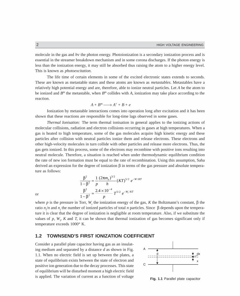
1.2 TOWNSEND’S FIRST IONIZATION COEFFICIENT
Consider a parallel plate capacitor having gas as an insulat-ing medium and separated by a distance d as shown in Fig.1.1. When no electric field is set up between the plates, astate of equilibrium exists between the state of electron andpositive ion generation due to the decay processes. This stateof equilibrium will be disturbed moment a high electric fieldis applied. The variation of current as a function of voltage
Fig. 1.1 Parallel plate capacitor
DharmN-HIGH\HG1-1.PM5 3
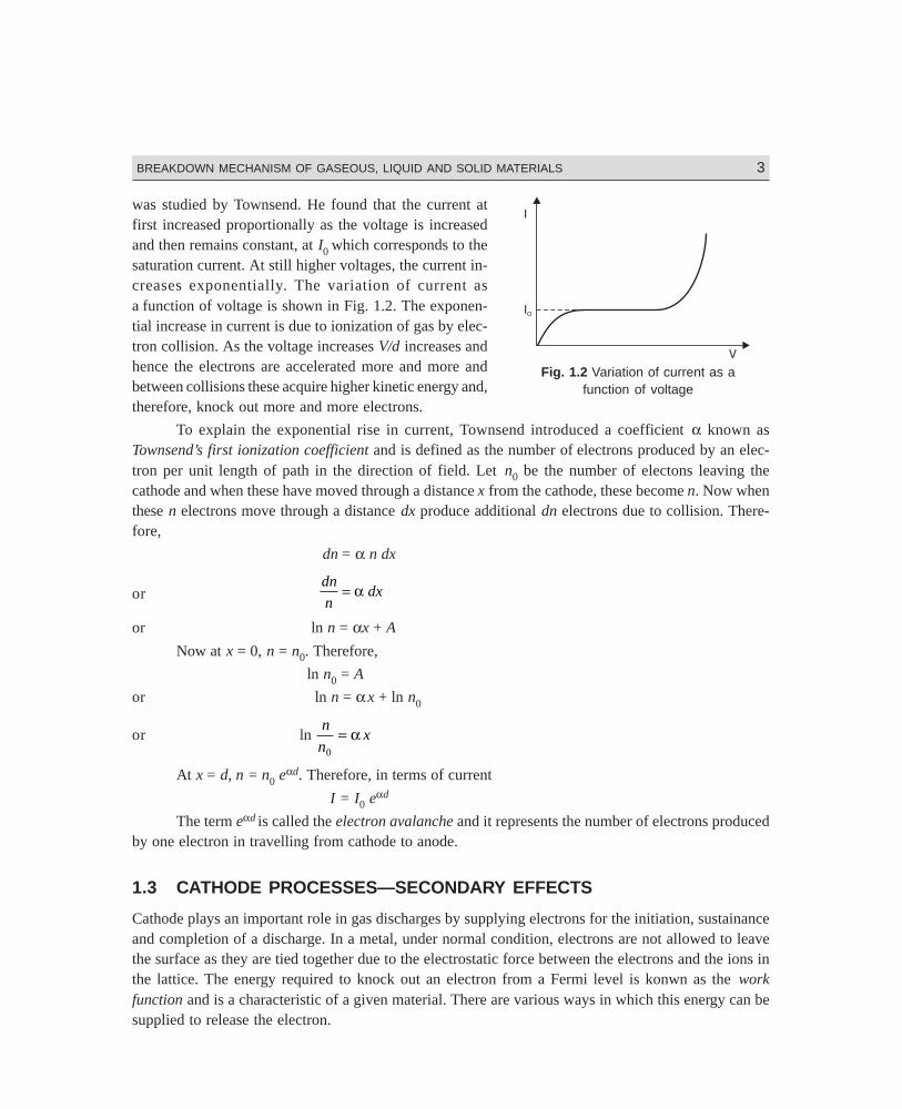
BREAKDOWN MECHANISM OF GASEOUS, LIQUID AND SOLID MATERIALS 3
was studied by Townsend. He found that the current atfirst increased proportionally as the voltage is increasedand then remains constant, at I0 which corresponds to thesaturation current. At still higher voltages, the current in-creases exponentially. The variation of current asa function of voltage is shown in Fig. 1.2. The exponen-tial increase in current is due to ionization of gas by elec-tron collision. As the voltage increases V/d increases andhence the electrons are accelerated more and more andbetween collisions these acquire higher kinetic energy and,therefore, knock out more and more electrons.
To explain the exponential rise in current, Townsend introduced a coefficient α known asTownsend’s first ionization coefficient and is defined as the number of electrons produced by an elec-tron per unit length of path in the direction of field. Let n0 be the number of electons leaving thecathode and when these have moved through a distance x from the cathode, these become n. Now whenthese n electrons move through a distance dx produce additional dn electrons due to collision. There-fore,
dn = α n dx
ordn
ndx= α
or ln n = αx + A
Now at x = 0, n = n0. Therefore,
ln n0 = A
or ln n = αx + ln n0
or ln n
nx
0
= α
At x = d, n = n0 eαd. Therefore, in terms of current
I = I0 eαd
The term eαd is called the electron avalanche and it represents the number of electrons producedby one electron in travelling from cathode to anode.
1.3 CATHODE PROCESSES—SECONDARY EFFECTS
Cathode plays an important role in gas discharges by supplying electrons for the initiation, sustainanceand completion of a discharge. In a metal, under normal condition, electrons are not allowed to leavethe surface as they are tied together due to the electrostatic force between the electrons and the ions inthe lattice. The energy required to knock out an electron from a Fermi level is konwn as the workfunction and is a characteristic of a given material. There are various ways in which this energy can besupplied to release the electron.
Fig. 1.2 Variation of current as afunction of voltage
DharmN-HIGH\HG1-1.PM5 4
4 HIGH VOLTAGE ENGINEERING
Thermionic Emission: At room temperature, the conduction electrons of the metal do not have suffi-cient thermal energy to leave the surface. However, if the metals are heated to temperature 1500°K andabove, the electrons will receive energy from the violent thermal lattice in vibration sufficient to crossthe surface barrier and leave the metal. After extensive investigation of electron emission from metalsat high temperature, Richardson developed an expression for the saturation current density Js as
Js = 4 2
32π αm K
hT ee W KT− / A/m2
where the various terms have their usual significance.
Let A = 4 2
3
πm K
he
the above expression becomes
Js = AT2e–W/KT
which shows that the saturation current density increases with decrease in work function and increasein temperature. Substituting the values of me, K and h, A is found to be 120 × 104 A/m2 K2. However, theexperimentally obtained value of A is lower than what is predicted by the equation above. The discrep-ancy is due to the surface imperfections and surface impurities of the metal. The gas present betweenthe electrode affects the thermionic emission as the gas may be absorbed by the metal and can alsodamage the electrode surface due to continuous impinging of ions. Also, the work function is observedto be lowered due to thermal expansion of crystal structure. Normally metals with low work functionare used as cathode for thermionic emission.
Field Emission: If a strong electric field is applied between the electrodes, the effective work functionof the cathode decreases and is given by
W′ = W – ε3/2 E1/2
and the saturation current density is then given by
Js = AT2 e–W′/KT
This is known as Schottky effect and holds good over a wide range of temperature and electricfields. Calculations have shown that at room temperature the total emission is still low even when fieldsof the order of 105 V/cm are applied. However, if the field is of the order of 107 V/cm, the emissioncurrent has been observed to be much larger than the calculated thermionic value. This can be ex-plained only through quantum mechanics at these high surface gradients, the cathode surface barrierbecomes very thin and quantum tunnelling of electrons occurs which leads to field emission even atroom temperature.
Electron Emission by Positive Ion and Excited Atom BombardmentElectrons may be emitted by the bombardment of positive ion on the cathode surface. This is known assecondary emission. In order to effect secondary emission, the positive ion must have energy more thantwice the work function of the metal since one electron will neutralize the bombarding positive ion andthe other electron will be released. If Wk and Wp are the kinetic and potential energies, respectively ofthe positive ion then for secondary emission to take place Wk + Wp ≥ 2W. The electron emission bypositive ion is the principal secondary process in the Townsend spark discharge mechanism. Neutral
DharmN-HIGH\HG1-1.PM5 5
BREAKDOWN MECHANISM OF GASEOUS, LIQUID AND SOLID MATERIALS 5
excited atoms or molecules (metastables) incident upon the cathode surface are also capable of releas-ing electron from the surface.
1.4 TOWNSEND SECOND IONISATION COEFFICIENT
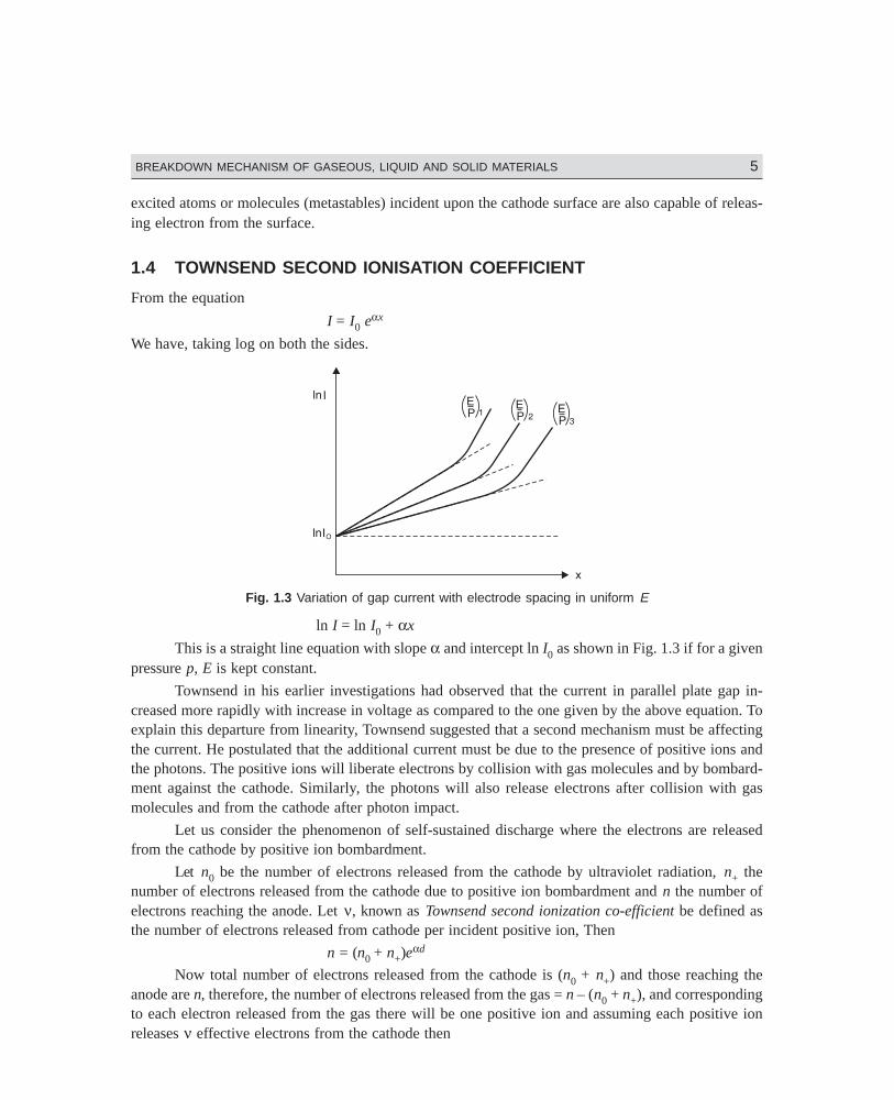
From the equation
I = I0 eαx
We have, taking log on both the sides.
Fig. 1.3 Variation of gap current with electrode spacing in uniform E
ln I = ln I0 + αx
This is a straight line equation with slope α and intercept ln I0 as shown in Fig. 1.3 if for a givenpressure p, E is kept constant.
Townsend in his earlier investigations had observed that the current in parallel plate gap in-creased more rapidly with increase in voltage as compared to the one given by the above equation. Toexplain this departure from linearity, Townsend suggested that a second mechanism must be affectingthe current. He postulated that the additional current must be due to the presence of positive ions andthe photons. The positive ions will liberate electrons by collision with gas molecules and by bombard-ment against the cathode. Similarly, the photons will also release electrons after collision with gasmolecules and from the cathode after photon impact.
Let us consider the phenomenon of self-sustained discharge where the electrons are releasedfrom the cathode by positive ion bombardment.
Let n0 be the number of electrons released from the cathode by ultraviolet radiation, n+ thenumber of electrons released from the cathode due to positive ion bombardment and n the number ofelectrons reaching the anode. Let ν, known as Townsend second ionization co-efficient be defined asthe number of electrons released from cathode per incident positive ion, Then
n = (n0 + n+)eαd
Now total number of electrons released from the cathode is (n0 + n+) and those reaching theanode are n, therefore, the number of electrons released from the gas = n – (n0 + n+), and correspondingto each electron released from the gas there will be one positive ion and assuming each positive ionreleases ν effective electrons from the cathode then
DharmN-HIGH\HG1-1.PM5 6
6 HIGH VOLTAGE ENGINEERING
n+ = ν [n – (n0 + n+)]
or n+ = νn – νn0 – νn+
or (1 + ν) n+ = ν(n – n0)
or n+ = ν
ν( )n n−
+0
1
Substituting n+ in the previous expression for n, we have
n = nn n
ve d
00
1+ −
+LNM
OQP
ν α( ) =
( )1
10 0+ + −
+ν ν ν
ναn n n
e d
= n n
e d0
1
++
νν
α
or (n + νn) = n0 eαd + νneαd
or n + νn – νneαd = n0eαd
or n[1+ ν – νeαd] = n0eαd
or n = n e
n e
d
d0
1 1
α
αν+ −( ) =
n e
e
d
d0
1 1
α
αν− −( )
In terms of current
I = I e
e
d
d0
1 1
α
αν− −( )
Earlier Townsend derived an expression for current as
I = Ie
e
d
d0( ) ( )
( )
α βα β
α β
α β−−
−
−
where β represents the number of ion pairs produced by positive ion travelling 1 cm path in the direc-tion of field. Townsend’s original suggestion that the positive ion after collision with gas moleculereleases electron does not hold good as ions rapidly lose energy in elastic collision and ordinarily areunable to gain sufficient energy from the electric field to cause ionization on collision with gas moleculesor atoms.
In practice positive ions, photons and metastable, all the three may participate in the process ofionization. It depends upon the experimental conditions. There may be more than one mechanismproducing secondary ionization in the discharge gap and, therefore, it is customary to express the netsecondary ionization effect by a single coefficient v and represent the current by the above equationkeeping in mind that ν may represent one or more of the several possible mechanism.
ν = ν1 + ν2 + ν3 + .....
It is to be noted that the value of ν depends upon the work function of the material. If the workfunction of the cathode surface is low, under the same experimental conditions will produce moreemission. Also, the value of ν is relatively small at low value of E/p and will increase with increase inE/p. This is because at higher values of E/p, there will be more number of positive ions and photons ofsufficiently large energy to cause ionization upon impact on the cathode surface. It is to be noted thatthe influence of ν on breakdown mechanism is restricted to Townsend breakdown mechanism i.e., tolow-pressure breakdown only.
DharmN-HIGH\HG1-1.PM5 7
BREAKDOWN MECHANISM OF GASEOUS, LIQUID AND SOLID MATERIALS 7
1.5 TOWNSEND BREAKDOWN MECHANISM
When voltage between the anode and cathode is increased, the current at the anode is given by
I = I e
e
d
d0
1 1
α
αν− −( )
The current becomes infinite if
1 – ν(eαd –1) = 0
or ν(eα d – 1) = 1
or νeα d ≈ 1
Since normally eα d >> 1
the current in the anode equals the current in the external cirrcuit. Theoretically the current becomesinfinitely large under the above mentioned condition but practically it is limited by the resistance of theexternal circuit and partially by the voltage drop in the arc. The condition νeαd = 1 defines the conditionfor beginning of spark and is known as the Townsend criterion for spark formation or Townsend break-down criterion. Using the above equations, the following three conditions are possible.
(1) νeαd =1
The number of ion pairs produced in the gap by the passage of arc electron avalanche is suffi-ciently large and the resulting positive ions on bombarding the cathode are able to relase onesecondary electron and so cause a repetition of the avalanche process. The discharge is then saidto be self-sustained as the discharge will sustain itself even if the source producing I0 is removed.
Therefore, the condition νeαd = 1 defines the threshold sparking condition.
(2) νeαd > 1
Here ionization produced by successive avalanche is cumulative. The spark discharge growsmore rapidly the more νeαd exceeds unity.
(3) νeαd < 1
Here the current I is not self-sustained i.e., on removal of the source the current I0 ceases to flow.
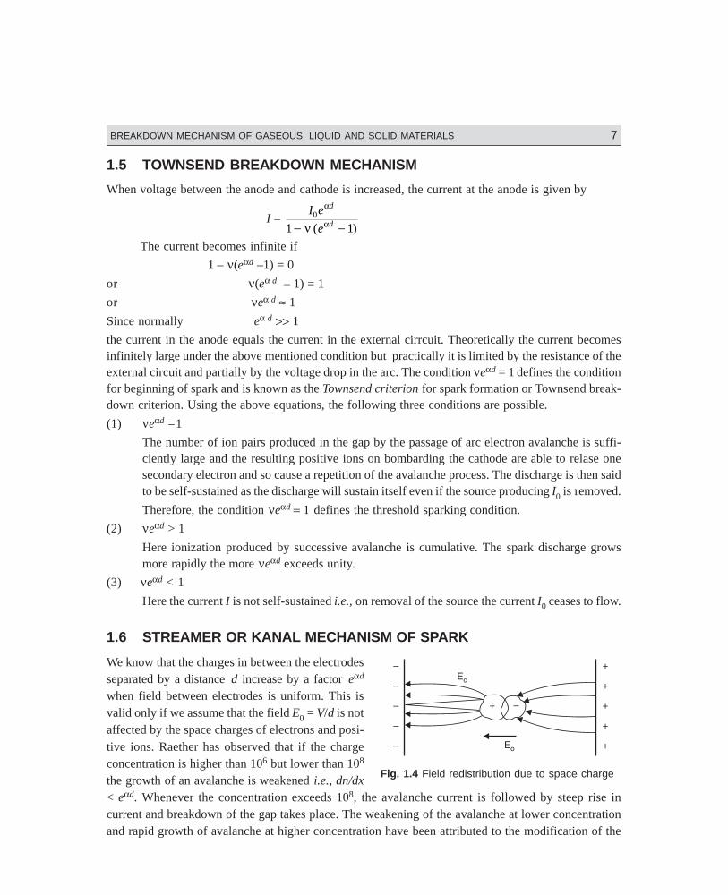
1.6 STREAMER OR KANAL MECHANISM OF SPARK
We know that the charges in between the electrodesseparated by a distance d increase by a factor eαd
when field between electrodes is uniform. This isvalid only if we assume that the field E0 = V/d is notaffected by the space charges of electrons and posi-tive ions. Raether has observed that if the chargeconcentration is higher than 106 but lower than 108
the growth of an avalanche is weakened i.e., dn/dx< eαd. Whenever the concentration exceeds 108, the avalanche current is followed by steep rise incurrent and breakdown of the gap takes place. The weakening of the avalanche at lower concentrationand rapid growth of avalanche at higher concentration have been attributed to the modification of the
Fig. 1.4 Field redistribution due to space charge
DharmN-HIGH\HG1-1.PM5 8
8 HIGH VOLTAGE ENGINEERING
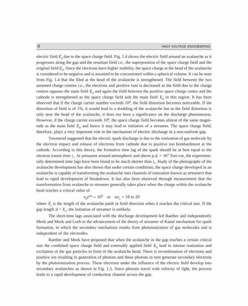
electric field E0 due to the space charge field. Fig. 1.4 shows the electric field around an avalanche as itprogresses along the gap and the resultant field i.e., the superposition of the space charge field and theoriginal field E0. Since the electrons have higher mobility, the space charge at the head of the avalancheis considered to be negative and is assumed to be concentrated within a spherical volume. It can be seenfrom Fig. 1.4 that the filed at the head of the avalanche is strengthened. The field between the twoassumed charge centres i.e., the electrons and positive ions is decreased as the field due to the chargecentres opposes the main field E0 and again the field between the positive space charge centre and thecathode is strengthened as the space charge field aids the main field E0 in this region. It has beenobserved that if the charge carrier number exceeds 106, the field distortion becomes noticeable. If thedistortion of field is of 1%, it would lead to a doubling of the avalanche but as the field distortion isonly near the head of the avalanche, it does not have a significance on the discharge phenomenon.However, if the charge carrier exceeds 108, the space charge field becomes almost of the same magni-tude as the main field E0 and hence it may lead to initiation of a streamer. The space charge field,therefore, plays a very important role in the mechanism of electric discharge in a non-uniform gap.
Townsend suggested that the electric spark discharge is due to the ionization of gas molecule bythe electron impact and release of electrons from cathode due to positive ion bombardment at thecathode. According to this theory, the formative time lag of the spark should be at best equal to theelectron transit time tr. At pressures around atmospheric and above p.d. > 103 Torr-cm, the experimen-tally determined time lags have been found to be much shorter than tr. Study of the photographs of theavalanche development has also shown that under certain conditions, the space charge developed in anavalanche is capable of transforming the avalanche into channels of ionization known as streamers thatlead to rapid development of breakdown. It has also been observed through measurement that thetransformation from avalanche to streamer generally takes place when the charge within the avalanchehead reaches a critical value of
n0eαx ≈ 108 or αxc ≈ 18 to 20
where Xc is the length of the avalanche parth in field direction when it reaches the critical size. If thegap length d < Xc, the initiation of streamer is unlikely.
The short-time lags associated with the discharge development led Raether and independentlyMeek and Meek and Loeb to the advancement of the theory of streamer of Kanal mechanism for sparkformation, in which the secondary mechanism results from photoionization of gas molecules and isindependent of the electrodes.
Raether and Meek have proposed that when the avalanche in the gap reaches a certain criticalsize the combined space charge field and externally applied field E0 lead to intense ionization andexcitation of the gas particles in front of the avalanche head. There is recombination of electrons andpositive ion resulting in generation of photons and these photons in turn generate secondary electronsby the photoionization process. These electrons under the influence of the electric field develop intosecondary avalanches as shown in Fig. 1.5. Since photons travel with velocity of light, the processleads to a rapid development of conduction channel across the gap.
DharmN-HIGH\HG1-1.PM5 9
BREAKDOWN MECHANISM OF GASEOUS, LIQUID AND SOLID MATERIALS 9
Fig. 1.5 Secondary avalanche formation by photoelectrons
Raether after thorough experimental investigation developed an empirical relation for the streamerspark criterion of the form
αxc = 17.7 + ln xc + ln E
Er
0
where Er is the radial field due to space charge and E0 is the externally applied field.
Now for transformation of avalanche into a streamer Er ≈ E
Therefore, αxc = 17.7 + ln xc
For a uniform field gap, breakdown voltage through streamer mechanism is obtained on theassumption that the transition from avalanche to streamer occurs when the avalanche has just crossedthe gap. The equation above, therefore, becomes
αd = 17.7 + ln d
When the critical length xc ≥ d minimum breakdown by streamer mechanism is brought about.The condition Xc = d gives the smallest value of α to produce streamer breakdown.
Meek suggested that the transition from avalanche to streamer takes place when the radial fieldabout the positive space charge in an electron avalanche attains a value of the order of the externallyapplied field. He showed that the value of the radial field can be otained by using the expression.
Er = 5.3 × 10⁻⁷ α αe
x P
x
( / ) /1 2 volts/cm.
where x is the distance in cm which the avalanche has progressed, p the gas pressure in Torr and α theTownsend coefficient of ionization by electrons corresponding to the applied field E. The minimumbreakdown voltage is assumed to correspond to the condition when the avalanche has crossed the gapof length d and the space charge field Er approaches the externally applied field i.e., at x = d, Er = E.Substituting these values in the above equation, we have
E = 5.3 × 10⁻⁷ α αe
d p
d
( / ) /1 2
Taking ln on both the sides, we have
ln E = – 14.5 + ln α – 1
2ln
d
p + αd
ln E – ln p = – 14.5 + ln α – ln p – 1
21n
d
p + αd
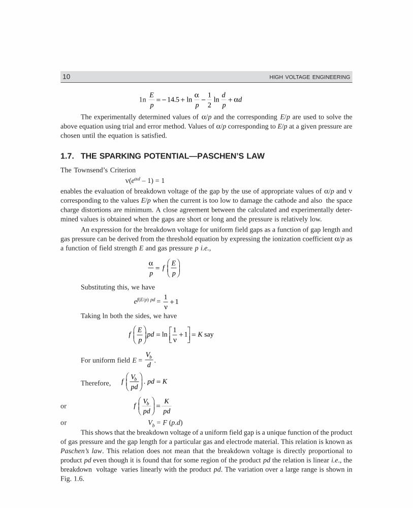
DharmN-HIGH\HG1-1.PM5 10
10 HIGH VOLTAGE ENGINEERING
1n E
p p
d
pd= − + − +14 5
1
2. lnln
α α
The experimentally determined values of α/p and the corresponding E/p are used to solve theabove equation using trial and error method. Values of α/p corresponding to E/p at a given pressure arechosen until the equation is satisfied.
1.7. THE SPARKING POTENTIAL—PASCHEN’S LAW
The Townsend’s Criterion
ν(eαd – 1) = 1
enables the evaluation of breakdown voltage of the gap by the use of appropriate values of α/p and νcorresponding to the values E/p when the current is too low to damage the cathode and also the spacecharge distortions are minimum. A close agreement between the calculated and experimentally deter-mined values is obtained when the gaps are short or long and the pressure is relatively low.
An expression for the breakdown voltage for uniform field gaps as a function of gap length andgas pressure can be derived from the threshold equation by expressing the ionization coefficient α/p asa function of field strength E and gas pressure p i.e.,
αp
fE
p=
FHG
IKJ
Substituting this, we have
ef(E/p) pd = 1
1ν
+
Taking ln both the sides, we have
fE
ppd K
FHG
IKJ = +L
NMOQP =ln say
11
ν
For uniform field E = V
db
.
Therefore, fV
pdpd KbF
HGIKJ =.
or fV
pd
K
pdbF
HGIKJ =
or Vb = F (p.d)This shows that the breakdown voltage of a uniform field gap is a unique function of the product
of gas pressure and the gap length for a particular gas and electrode material. This relation is known asPaschen’s law. This relation does not mean that the breakdown voltage is directly proportional toproduct pd even though it is found that for some region of the product pd the relation is linear i.e., thebreakdown voltage varies linearly with the product pd. The variation over a large range is shown inFig. 1.6.
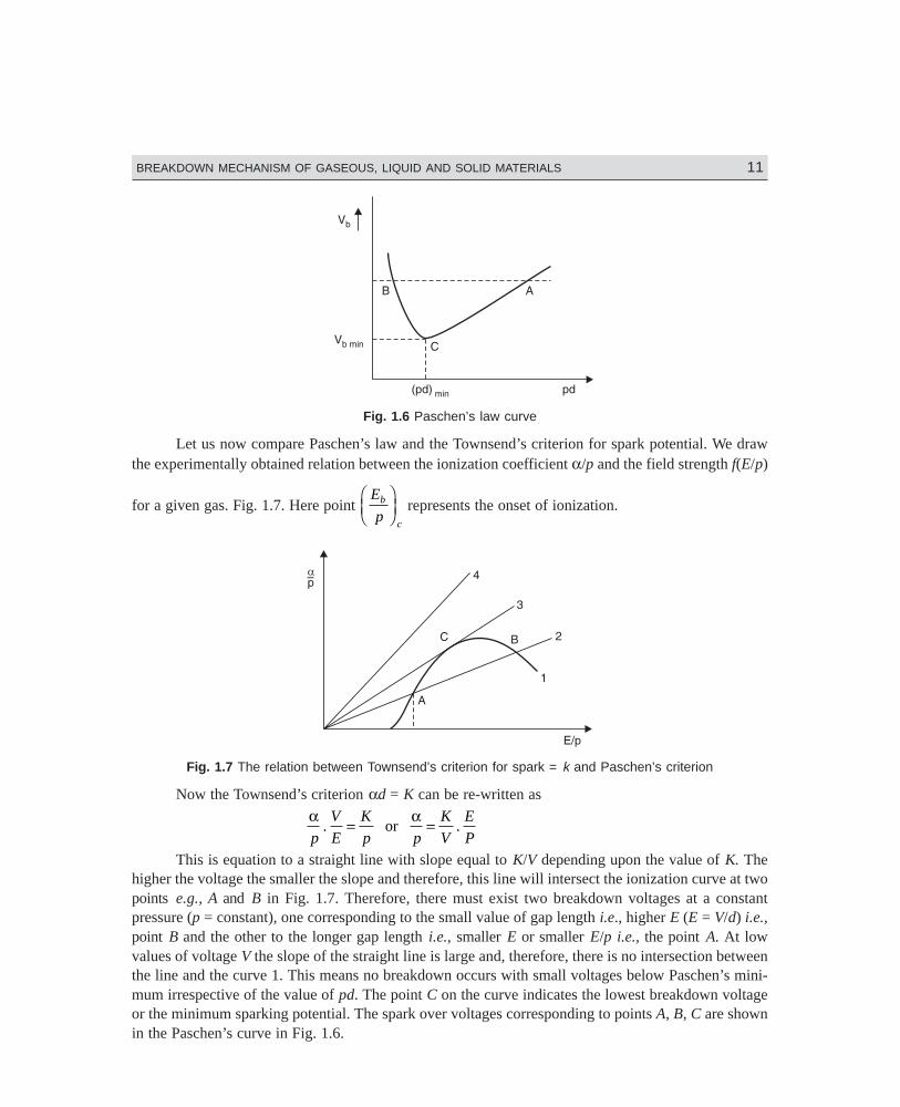
DharmN-HIGH\HG1-1.PM5 11
BREAKDOWN MECHANISM OF GASEOUS, LIQUID AND SOLID MATERIALS 11
Fig. 1.6 Paschen’s law curve
Let us now compare Paschen’s law and the Townsend’s criterion for spark potential. We drawthe experimentally obtained relation between the ionization coefficient α/p and the field strength f(E/p)
for a given gas. Fig. 1.7. Here point E
pb
c
FHG
IKJ represents the onset of ionization.
Fig. 1.7 The relation between Townsend’s criterion for spark = k and Paschen’s criterion
Now the Townsend’s criterion αd = K can be re-written as
α αp
V
E
K
p p
K
V
E
P. .= =or
This is equation to a straight line with slope equal to K/V depending upon the value of K. Thehigher the voltage the smaller the slope and therefore, this line will intersect the ionization curve at twopoints e.g., A and B in Fig. 1.7. Therefore, there must exist two breakdown voltages at a constantpressure (p = constant), one corresponding to the small value of gap length i.e., higher E (E = V/d) i.e.,point B and the other to the longer gap length i.e., smaller E or smaller E/p i.e., the point A. At lowvalues of voltage V the slope of the straight line is large and, therefore, there is no intersection betweenthe line and the curve 1. This means no breakdown occurs with small voltages below Paschen’s mini-mum irrespective of the value of pd. The point C on the curve indicates the lowest breakdown voltageor the minimum sparking potential. The spark over voltages corresponding to points A, B, C are shownin the Paschen’s curve in Fig. 1.6.
DharmN-HIGH\HG1-1.PM5 12
12 HIGH VOLTAGE ENGINEERING
The fact that there exists a minimum sparking potential in the relation between the sparkingpotential and the gap length assuming p to be constant can be explained quantitatively by consideringthe efficiency of ionization of electrons traversing the gap with different electron energies. Assumingthat the Townsend’s second ionization coefficient ν is small for values pd > (pd)min., electrons cross-ing the gap make more frequent collision with the gas molecules than at (pd)min. but the energy gainedbetween the successive collision is smaller than at (pd). Hence, the probability of ionization is lowerunless the voltage is increased. In case of (pd) < (pd) min., the electrons cross the gap without makingany collision and thus the sparking potential is higher. The point (pd)min., therefore, corresponds to thehighest ionization efficiency and hence minimum sparking potential.
An analytical expression for the minimum sparking potential can be obtained using the generalexpression for α/p.
αp
AeBp E= /or α = −pAe Bpd Vb/
or e Bpd Vb− / = pA
αor 1
α= e
pA
Bpd Vb/
or d . 1
αd
e
pA
B Vpd
=/ b
We know that αd = 1n 11+F
HIKν
Therefore, de
pA
Bpd Vb
= +FH
IK
/
1 11
nν
Assuming ν to be constant, let 1 11
n +FH
IK =
νk
Then de
pAK
Bpd Vb
=/
In order to obtain minimum sparking potential, we rearrange the above expression as
Vb = f(pd)
Taking 1n on both sides, we haveBpd
V
Apd
Kb
= ln
or Vb = Bpd
Apd kln /Differentiating Vb w.r. to pd and equating the derivative to zero
dV
d pd
Apd
KB Bpd
K
Apd
A
K
Apd
K
b
( )
. . .=
−
FH
IK
ln
n12 =
BApdK
Apd
K
B
Apd
K
ln
1n nFH
IK
−FH
IK
=2 2
1
0
or1 1
2ln ln
Apd
KApd
K
=FH
IK
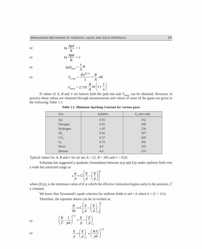
DharmN-HIGH\HG1-1.PM5 13
BREAKDOWN MECHANISM OF GASEOUS, LIQUID AND SOLID MATERIALS 13
or 1nApd
K = 1
or 1nApd
K = e
or (pd)min = e
AK
or Vb min = B e B
AeK
K A/
.1
=
Vbmin = 2.718 B
A1 1
1n +FH
IKν
If values of A, B and ν are known both the (pd) min and Vbmin can be obtained. However, inpractice these values are obtained through measurements and values of some of the gases are given inthe following Table 1.1.
Table 1.1. Minimum Sparking Constant for various gases
Gas (pd)min Vb min volts
Air 0.55 352
Nitrogen 0.65 240
Hydrogen 1.05 230SF6 0.26 507
CO2 0.57 420
O2 0.70 450
Neon 4.0 245
Helium 4.0 155
Typical values for A, B and ν for air are A = 12, B = 365 and ν = 0.02.
Schuman has suggested a quadratic formulation between α/p and E/p under uniform field overa wide but restricted range as
sαp
CE
p
E
p= −
FHG
IKJ
LNM
OQP
2
where (E/p)c is the minimum value of E at which the effective ionization begins and p is the pressure, Ca constant.
We know that Townsend’s spark criterion for uniform fields is αd = k where k = (1 + 1/ν).
Therefore, the equation above can be re-written as
K
dpC
E
p
E
p c
= −FHG
IKJ
LNMM
OQPP
2
or K
C pd
E
p
E
p c
./
11 2F
HGIKJ = −
FHG
IKJ
or E
p
E
p
K C
pdc
=FHG
IKJ +
FHG
IKJ
//1 2
DharmN-HIGH\HG1-1.PM5 14
14 HIGH VOLTAGE ENGINEERING
V
dp
E
p
K C
pdc
=FHG
IKJ +
FHG
IKJ
//1 2
or VE
ppd
K
cpdb
c
=FHG
IKJ + F
HIK
1 2/
.
Sohst and Schröder have suggested values for Ec = 24.36 kV/cm K/C = 45.16 (kV)2 /cm for airat p = 1 bar and temperature 20°C.
Substituting these values in the above equation, we have
Vb = 6.72 pd + 24.36 (pd) kV
The breakdown voltages suggested in tables or obtained through the use of empirical relationnormally correspond to ambient temperature and pressure conditions, whereas the atmospheric airprovides basic insulation between various electrical equipments. Since the atmospheric conditions (Tem-perature, pressure) vary widely from time to time and from location to location, to obtain the actualbreakdown voltage, the voltage obtained from the STP condition should be multiplied by the air den-sity correction factor. The air density correction factor is given as
δ = 3 92
273
. b
t+where b is the atmospheric pressure in cm of Hg and t the temperature in °C.
1.8 PENNING EFFECT
Paschen’s law does not hold good for many gaseous mixtures. A typical example is that of mixture ofArgon in Neon. A small percentage of Argon in Neon reduces substantially the dielectric strength ofpure Neon. In fact, the dielectric strength is smaller than the dielectric strengths of either pure Neon orArgon. The lowering of dielectric strength is due to the fact that the lowest excited stage of neon ismetastable and its excitation potential (16 ev) is about 0.9 ev greater than the ionization potential ofArgon. The metastable atoms have a long life in neon gas, and on hitting Argon atoms there is a veryhigh probability of ionizing them. This phenomenon is known as Penning Effect.
1.9 CORONA DISCHARGES
If the electric field is uniform and if the field is increased gradually, just when measurable ionizationbegins, the ionization leads to complete breakdown of the gap. However, in non-uniform fields, beforethe spark or breakdown of the medium takes place, there are many manifestations in the form of visualand audible discharges. These discharges are known as Corona discharges. In fact Corona is defined asa self-sustained electric discharge in which the field intensified ionization is localised only over aportion of the distance (non-uniform fields) between the electrodes. The phenomenon is of particularimportance in high voltage engineering where most of the fields encountered are non-uniform fieldsunless of course some design features are involved to make the filed almost uniform. Corona is respon-sible for power loss and interference of power lines with the communication lines as corona frequencylies between 20 Hz and 20 kHz. This also leads to deterioration of insulation by the combined action ofthe discharge ion bombarding the surface and the action of chemical compounds that are formed by thecorona discharge.
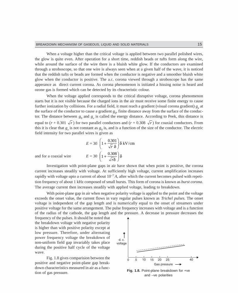
DharmN-HIGH\HG1-1.PM5 15
BREAKDOWN MECHANISM OF GASEOUS, LIQUID AND SOLID MATERIALS 15
When a voltage higher than the critical voltage is applied between two parallel polished wires,the glow is quite even. After operation for a short time, reddish beads or tufts form along the wire,while around the surface of the wire there is a bluish white glow. If the conductors are examinedthrough a stroboscope, so that one wire is always seen when at a given half of the wave, it is noticedthat the reddish tufts or beads are formed when the conductor is negative and a smoother bluish whiteglow when the conductor is positive. The a.c. corona viewed through a stroboscope has the sameapperance as direct current corona. As corona phenomenon is initiated a hissing noise is heard andozone gas is formed which can be detected by its chracteristic colour.
When the voltage applied corresponds to the critical disruptive voltage, corona phenomenonstarts but it is not visible because the charged ions in the air must receive some finite energy to causefurther ionization by collisions. For a radial field, it must reach a gradient (visual corona gradient) gu atthe surface of the conductor to cause a gradient g0, finite distance away from the surface of the conduc-tor. The distance between g0 and gv is called the energy distance. According to Peek, this distance is
equal to (r + 0.301 r ) for two parallel conductors and (r + 0.308 r ) for coaxial conductors. Fromthis it is clear that gv is not constant as g0 is, and is a function of the size of the conductor. The electricfield intensity for two parallel wires is given as
E = 30 10 301
+FHG
IKJ
./
r δδ kV cm
and for a coaxial wire E = 30 10 308+F
HGIKJ
.
rδδ
Investigation with point-plane gaps in air have shown that when point is positive, the coronacurrent increases steadily with voltage. At sufficiently high voltage, current amplification increasesrapidly with voltage upto a current of about 10–7 A, after which the current becomes pulsed with repeti-tion frequency of about 1 kHz composed of small bursts. This form of corona is known as burst corona.The average current then increases steadily with applied voltage, leading to breakdown.
With point-plane gap in air when negative polarity voltage is applied to the point and the voltageexceeds the onset value, the current flows in vary regular pulses known as Trichel pulses. The onsetvoltage is independent of the gap length and is numerically equal to the onset of streamers underpositive voltage for the same arrangement. The pulse frequency increases with voltage and is a functionof the radius of the cathode, the gap length and the pressure. A decrease in pressure decreases thefrequency of the pulses. It should be noted thatthe breakdown voltage with negative polarityis higher than with positive polarity except atlow pressure. Therefore, under alternatingpower frequency voltage the breakdown ofnon-uniform field gap invariably takes placeduring the positive half cycle of the voltagewave.
Fig. 1.8 gives comparision between thepositive and negative point-plane gap break-down characteristics measured in air as a func-tion of gas pressure. Fig. 1.8. Point-plane breakdown for +ve
and –ve polarities
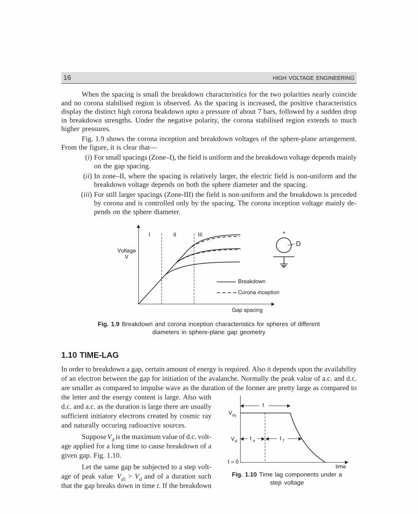
DharmN-HIGH\HG1-1.PM5 16
16 HIGH VOLTAGE ENGINEERING
When the spacing is small the breakdown characteristics for the two polarities nearly coincideand no corona stabilised region is observed. As the spacing is increased, the positive characteristicsdisplay the distinct high corona beakdown upto a pressure of about 7 bars, followed by a sudden dropin breakdown strengths. Under the negative polarity, the corona stabilised region extends to muchhigher pressures.
Fig. 1.9 shows the corona inception and breakdown voltages of the sphere-plane arrangement.From the figure, it is clear that—
(i) For small spacings (Zone–I), the field is uniform and the breakdown voltage depends mainlyon the gap spacing.
(ii) In zone–II, where the spacing is relatively larger, the electric field is non-uniform and thebreakdown voltage depends on both the sphere diameter and the spacing.
(iii) For still larger spacings (Zone-III) the field is non-uniform and the breakdown is precededby corona and is controlled only by the spacing. The corona inception voltage mainly de-pends on the sphere diameter.
Fig. 1.9 Breakdown and corona inception characteristics for spheres of differentdiameters in sphere-plane gap geometry
1.10 TIME-LAG
In order to breakdown a gap, certain amount of energy is required. Also it depends upon the availabilityof an electron between the gap for initiation of the avalanche. Normally the peak value of a.c. and d.c.are smaller as compared to impulse wave as the duration of the former are pretty large as compared tothe letter and the energy content is large. Also withd.c. and a.c. as the duration is large there are usuallysufficient initiatory electrons created by cosmic rayand naturally occuring radioactive sources.
Suppose Vd is the maximum value of d.c. volt-age applied for a long time to cause breakdown of agiven gap. Fig. 1.10.
Let the same gap be subjected to a step volt-age of peak value Vd1 > Vd and of a duration suchthat the gap breaks down in time t. If the breakdown
Fig. 1.10 Time lag components under astep voltage
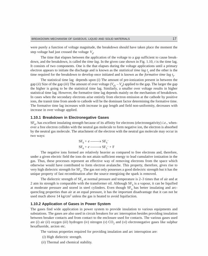
DharmN-HIGH\HG1-1.PM5 17
BREAKDOWN MECHANISM OF GASEOUS, LIQUID AND SOLID MATERIALS 17
were purely a function of voltage magnitude, the breakdown should have taken place the moment thestep voltage had just crossed the voltage Vd.
The time that elapses between the application of the voltage to a gap sufficient to cause break-down, and the breakdown, is called the time lag. In the given case shown in Fig. 1.10, t is the time lag.It consists of two components. One is the that elapses during the voltage applications until a primaryelectron appears to initiate the discharge and is known as the statistical time lag ts and the other is thetime required for the breakdown to develop once initiated and is known as the formative time lag tf.
The statistical time lag depends upon (i) The amount of pre-ionization present in between thegap (ii) Size of the gap (iii) The amount of over voltage (Vd1 – Vd) applied to the gap. The larger the gapthe higher is going to be the statistical time lag. Similarly, a smaller over voltage results in higherstatistical time lag. However, the formative time lag depends mainly on the mechanism of breakdown.In cases when the secondary electrons arise entirely from electron emission at the cathode by positiveions, the transit time from anode to cathode will be the dominant factor determining the formative time.The formative time lag increases with increase in gap length and field non-uniformity, decreases withincrease in over voltage applied.
1.10.1 Breakdown in Electronegative GasesSF6, has excellent insulating strength because of its affinity for electrons (electronegativity) i.e., when-ever a free electron collides with the neutral gas molecule to form negative ion, the electron is absorbedby the neutral gas molecule. The attachment of the electron with the neutral gas molecule may occur intwo ways:
SF6 + e → SF6–
SF6 + e → SF5– + F
The negative ions formed are relatively heavier as compared to free electrons and, therefore,under a given electric field the ions do not attain sufficient energy to lead cumulative ionization in thegas. Thus, these processes represent an effective way of removing electrons from the space whichotherwise would have contributed to form electron avalanche. This property, therefore, gives rise tovery high dielectric strength for SF6. The gas not only possesses a good dielectric strength but it has theunique property of fast recombination after the source energizing the spark is removed.
The dielectric strength of SF6 at normal pressure and temperature is 2–3 times that of air and at2 atm its strength is comparable with the transformer oil. Although SF6 is a vapour, it can be liquifiedat moderate pressure and stored in steel cylinders. Even though SF6 has better insulating and arc-quencling properties than air at an equal pressure, it has the important disadvantage that it can not beused much above 14 kg/cm2 unless the gas is heated to avoid liquifaction.
1.10.2 Application of Gases in Power SystemThe gases find wide application in power system to provide insulation to various equipments andsubstations. The gases are also used in circuit breakers for arc interruption besides providing insulationbetween breaker contacts and from contact to the enclosure used for contacts. The various gases usedare (i) air (ii) oxygen (iii) hydrogen (iv) nitrogen (v) CO2 and (vi) electronegative gases like sulphurhexafluoride, arcton etc.
The various properties required for providing insulation and arc interruption are:
(i) High dielectric strength.
(ii) Thermal and chemical stability.
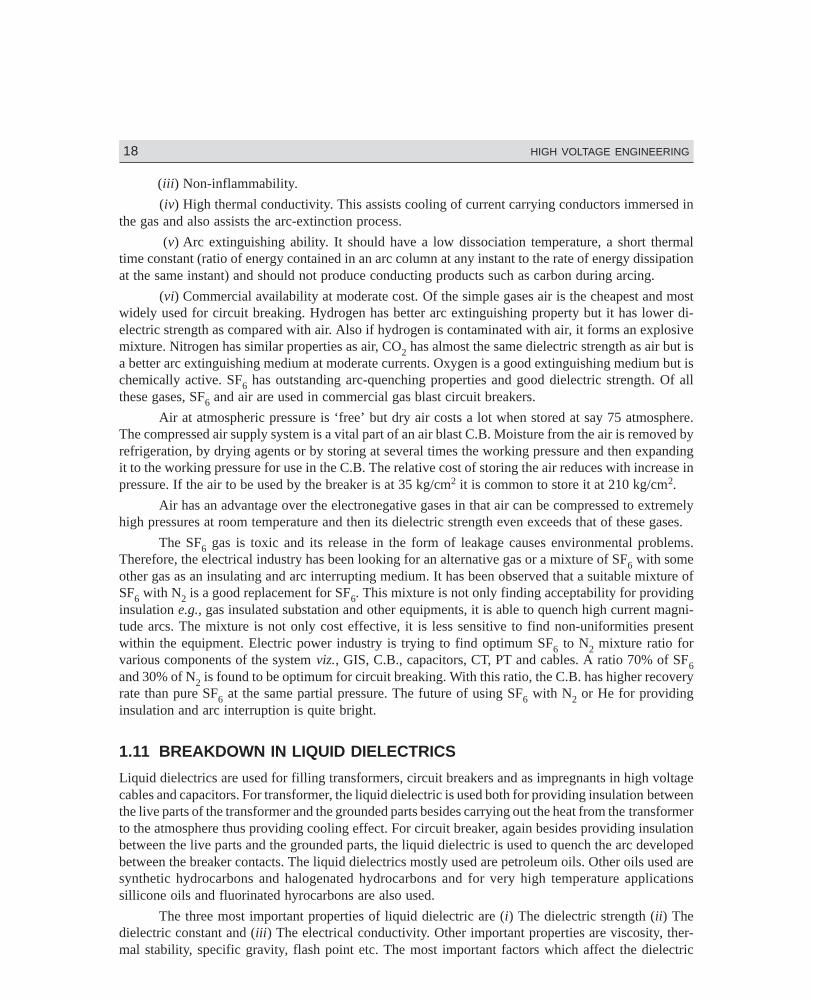
DharmN-HIGH\HG1-1.PM5 18
18 HIGH VOLTAGE ENGINEERING
(iii) Non-inflammability.
(iv) High thermal conductivity. This assists cooling of current carrying conductors immersed inthe gas and also assists the arc-extinction process.
(v) Arc extinguishing ability. It should have a low dissociation temperature, a short thermaltime constant (ratio of energy contained in an arc column at any instant to the rate of energy dissipationat the same instant) and should not produce conducting products such as carbon during arcing.
(vi) Commercial availability at moderate cost. Of the simple gases air is the cheapest and mostwidely used for circuit breaking. Hydrogen has better arc extinguishing property but it has lower di-electric strength as compared with air. Also if hydrogen is contaminated with air, it forms an explosivemixture. Nitrogen has similar properties as air, CO2 has almost the same dielectric strength as air but isa better arc extinguishing medium at moderate currents. Oxygen is a good extinguishing medium but ischemically active. SF6 has outstanding arc-quenching properties and good dielectric strength. Of allthese gases, SF6 and air are used in commercial gas blast circuit breakers.
Air at atmospheric pressure is ‘free’ but dry air costs a lot when stored at say 75 atmosphere.The compressed air supply system is a vital part of an air blast C.B. Moisture from the air is removed byrefrigeration, by drying agents or by storing at several times the working pressure and then expandingit to the working pressure for use in the C.B. The relative cost of storing the air reduces with increase inpressure. If the air to be used by the breaker is at 35 kg/cm2 it is common to store it at 210 kg/cm2.
Air has an advantage over the electronegative gases in that air can be compressed to extremelyhigh pressures at room temperature and then its dielectric strength even exceeds that of these gases.
The SF6 gas is toxic and its release in the form of leakage causes environmental problems.Therefore, the electrical industry has been looking for an alternative gas or a mixture of SF6 with someother gas as an insulating and arc interrupting medium. It has been observed that a suitable mixture ofSF6 with N2 is a good replacement for SF6. This mixture is not only finding acceptability for providinginsulation e.g., gas insulated substation and other equipments, it is able to quench high current magni-tude arcs. The mixture is not only cost effective, it is less sensitive to find non-uniformities presentwithin the equipment. Electric power industry is trying to find optimum SF6 to N2 mixture ratio forvarious components of the system viz., GIS, C.B., capacitors, CT, PT and cables. A ratio 70% of SF6and 30% of N2 is found to be optimum for circuit breaking. With this ratio, the C.B. has higher recoveryrate than pure SF6 at the same partial pressure. The future of using SF6 with N2 or He for providinginsulation and arc interruption is quite bright.
1.11 BREAKDOWN IN LIQUID DIELECTRICS
Liquid dielectrics are used for filling transformers, circuit breakers and as impregnants in high voltagecables and capacitors. For transformer, the liquid dielectric is used both for providing insulation betweenthe live parts of the transformer and the grounded parts besides carrying out the heat from the transformerto the atmosphere thus providing cooling effect. For circuit breaker, again besides providing insulationbetween the live parts and the grounded parts, the liquid dielectric is used to quench the arc developedbetween the breaker contacts. The liquid dielectrics mostly used are petroleum oils. Other oils used aresynthetic hydrocarbons and halogenated hydrocarbons and for very high temperature applicationssillicone oils and fluorinated hyrocarbons are also used.
The three most important properties of liquid dielectric are (i) The dielectric strength (ii) Thedielectric constant and (iii) The electrical conductivity. Other important properties are viscosity, ther-mal stability, specific gravity, flash point etc. The most important factors which affect the dielectric
DharmN-HIGH\HG1-1.PM5 19
BREAKDOWN MECHANISM OF GASEOUS, LIQUID AND SOLID MATERIALS 19
strength of oil are the, presence of fine water droplets and the fibrous impurities. The presence of even0.01% water in oil brings down the dielectric strength to 20% of the dry oil value and the presence offibrous impurities brings down the dielectric strength much sharply. Therefore, whenever these oils areused for providing electrical insulation, these should be free from moisture, products of oxidation andother contaminants.
The main consideration in the selection of a liquid dielectric is its chemical stability. The otherconsiderations are the cost, the saving in space, susceptibility to environmental influences etc. The useof liquid dielectric has brought down the size of equipment tremendously. In fact, it is practicallyimpossible to construct a 765 kV transformer with air as the insulating medium. Table 1.2. shows theproperties of some dielectrics commonly used in electrical equipments.
Table 1.2. Dielectric properties of some liquids
S.No. Property Transformer Capacitor Cable Silicone
Oil Oil Oil Oil
1. Relative permittivity 50 Hz 2.2 – 2.3 2.1 2.3 – 2.6 2.7 – 3.0
2. Breakdown strength at 12 kV/mm 18 kV/mm 25 kV/mm 35 kV/mm20°C 2.5 mm 1 min
3. (a) Tan δ 50 Hz 10–3 2.5 × 10⁻⁴ 2 × 10⁻³ 10–3
(b) 1 kHz 5 × 10⁻⁴ 10–4 10–4 10–4
4. Resistivity ohm-cm 1012 – 1013 1013 – 1014 1012 – 1013 2.5 × 10¹⁴
5. Maximum permissible watercontent (ppm) 50 50 50 < 40
6. Acid value mg/gm of KOH NIL NIL NIL NIL
7. Sponification mg of KOH/gm 0.01 0.01 0.01 < 0.01of oil
8. Specific gravity at 20°C 0.89 0.89 0.93 1.0–1.1
Liquids which are chemically pure, structurally simple and do not contain any impurity even intraces of 1 in 109, are known as pure liquids. In contrast, commercial liquids used as insulating liquidsare chemically impure and contain mixtures of complex organic molecules. In fact their behaviour isquite erratic. No two samples of oil taken out from the same container will behave identically.
The theory of liquid insulation breakdown is less understood as of today as compared to the gasor even solids. Many aspects of liquid breakdown have been investigated over the last decades but nogeneral theory has been evolved so far to explain the breakdown in liquids. Investigations carried outso far, however, can be classified into two schools of thought. The first one tries to explain the break-down in liquids on a model which is an extension of gaseous breakdown, based on the avalancheionization of the atoms caused by electon collisiron in the applied field. The electrons are assumed tobe ejected from the cathode into the liquid by either a field emission or by the field enhanced thermioniceffect (Shottky’s effect). This breakdown mechanism explains breakdown only of highly pure liquidand does not apply to explain the breakdown mechanism in commercially available liquids. It has beenobserved that conduction in pure liquids at low electric field (1 kV/cm) is largely ionic due to dissocia-tion of impurities and increases linearily with the field strength. At moderately high fields the conduc-tion saturates but at high field (electric), 100 kV/cm the conduction increases more rapidly and thusbreakdown takes place. Fig. 1.11 (a) shows the variation of current as a function of electric field for
DharmN-HIGH\HG1-1.PM5 20
20 HIGH VOLTAGE ENGINEERING
hexane. This is the condition nearer to breakdown. However, if the figure is redrawn starting with lowfields, a current-electric field characteristic as shown in Fig. 1.11 (b) will be obtained. This curve hasthree distinct regions as discussed above.
Line
ar
Saturation
High field
( )a ( )b
Con
duct
ion
curr
ent
Fig. 1.11 Variation of current as a function of electric field
(a) High fields (b) Low fields
The second school of thought recognises that the presence of foreign particles in liquid insulationshas a marked effect on the dielectric strength of liquid dielectrics. It has been suggested that the sus-pended particles are polarizable and are of higher permittivity than the liquid. These particles experi-ence an electrical force directed towards the place of maximum stress. With uniform field electrodesthe movement of particles is presumed to be initiated by surface irregularities on the electrodes, whichgive rise to local field gradients. The particles thus get accumulated and tend to form a bridge acrossthe gap which leads finally to initiation of breakdown. The impurities could also be in the form ofgaseous bubbles which obviously have lower dielectric strength than the liquid itself and hence onbreakdown of bubble the total breakdown of liquid may be triggered.
Electronic BreakdownOnce an electron is injected into the liquid, it gains energy from the electric field applied between theelectrodes. It is presumed that some electrons will gain more energy due to field than they would loseduring collision. These electrons are accelerated under the electric field and would gain sufficientenergy to knock out an electron and thus initiate the process of avalanche. The threshold condition forthe beginning of avalanche is achieved when the energy gained by the electron equals the energy lostduring ionization (electron emission) and is given by
e λ E = Chv
where λ is the mean free path, hv is the energy of ionization and C is a constant. Table 1.3 gives typicalvalues of dielectric strengths of some of the highly purified liquids.
Table 1.3. Dielectric strengths of pure liquids
Liquid Strength (MV/cm)
Benzene 1.1Goodoil 1.0–4.0Hexane 1.1–1.3Nitrogen 1.6–1.88Oxygen 2.4Silicon 1.0–1.2
DharmN-HIGH\HG1-2.PM5 21
BREAKDOWN MECHANISM OF GASEOUS, LIQUID AND SOLID MATERIALS 21
The electronic theory whereas predicts the relative values of dielectric strength satisfactorily,the formative time lags observed are much longer as compared to the ones predicted by the electronictheory.
1.11.1 Suspended Solid Particle MechanismCommercial liquids will always contain solid impurities either as fibers or as dispersed solid particles.The permittivity of these solids (E1) will always be different from that of the liquid (E2). Let us assumethese particles to be sphere of radisus r. These particles get polarized in an electric field E and experi-ence a force which is given as
F = r3 ε εε ε
1 2
1 22
–.
+E
dE
dx
and this force is directed towards a place of higher stress if ε1 > ε2 and towards a place of lower stressif ε1 < ε2 when ε1 is the permittivity of gas bubbles. The force given above increases as the permittivityof the suspended particles (ε1) increases. If ε1 → ∞
F = r3 1
1 22 1
2 1
−+
ε εε ε
/
/E
dE
dx
Let ε1 → ∞
F = r3E . dE
dxThus, the force will tend the particle to move towards the strongest region of the field. In a
uniform electric field which usually can be developed by a small sphere gap, the field is the strongest inthe uniform field region. Here dE/dx → 0 so that the force on the particle is zero and the particleremains in equilibrium. Therefore, the particles will be dragged into the uniform field region. Since thepermittivity of the particles is higher than that of the liquid, the presence of particle in the uniform fieldregion will cause flux concentration at its surface. Other particles if present will be attracted towardsthe higher flux concentration. If the particles present are large, they become aligned due to these forcesand form a bridge across the gap. The field in the liquid between the gap will increase and if it reachescritical value, brakdown will take place. If the number of particles is not sufficient to bridge the gap, theparticles will give rise to local field enhancement and if the field exceeds the dielectric strength ofliquid, local breakdown will occur near the particles and thus will result in the formation of gas bubbleswhich have much less dielectric strength and hence finally lead to the breakdown of the liquid.
The movement of the particle under the influence of electric field is oposed by the viscous forceposed by the liquid and since the particles are moving into the region of high stress, diffusion must alsobe taken into account. We know that the viscous force is given by (Stoke’s relation) FV = 6πnrν whereη is the viscosity of liquid, r the raidus of the particle and v the velocity of the particle.
Equating the electrical force with the viscous force we have
6πηrν = r3 E dE
dxor ν =
r E dE
dx
2
6πη
However, if the diffusion process is included, the drift velocity due to diffusion will be given by
νd = – D
N
dN
dx
KT
r
dN
Ndx= −
6πη
DharmN-HIGH\HG1-2.PM5 22
22 HIGH VOLTAGE ENGINEERING
where D = KT/6πηr a relation known as Stokes-Einstein relation. Here K is Boltzmann’s constant and
T the absolute temperature. At any instant of time, the particle should have one velocity and, therefore,equation v = vd
We have
– KT
r
dN
Ndx
r E dE
dx6 6
2
πη πη. .=
or KT
r
dN
Nr E dE= − 2
orKT
rN
r E1
2
2 2
n = −
It is clear that the breakdown strength E depends upon the concentration of particles N, radius rof particle, viscosity η of liquid and temperature T of the liquid.
It has been found that liquid with solid impurities has lower dielectric strength as compared toits pure form. Also, it has been observed that larger the size of the particles impurity the lower theoverall dielectric strength of the liquid containing the impurity.
1.11.2 Cavity BreakdownIt has been observed experimentally that the dielectric strength of liquid depnds upon the hydrostaticpressure above the gap length. The higher the hydrostatic pressure, the higher the electric strength,which suggests that a change in phase of the liquid is involved in the breakdown process. In fact,smaller the head of liquid, the more are the chances of partially ionized gases coming out of the gap andhigher the chances of breakdown. This means a kind of vapour bubble formed is responsible for thebreakdown. The following processes might lead to formation of bubbles in the liquids:
(i) Gas pockets on the surface of electrodes.
(ii) Due to irregular surface of electrodes, point charge concentration may lead to corona dis-charge, thus vapourizing the liquid.
(iii) Changes in temperature and pressure.
(iv) Dissociation of products by electron collisions giving rise to gaseous products.
It has been suggested that the electric field in a gas bubble which is immersed in a liquid ofpermittivity ε2 is given by
EE
b =+
3
20
2εWhere E0 is the field in the liquid in absence of the bubble. The bubble under the influence of
the electric field E0 elongates keeping its volume constant. When the field Eb equals the gaseous ioni-zation field, discharge takes place which will lead to decomposition of liquid and breakdown mayfollow.
A more accurate expression for the bubble breakdown strength is given as
Er
V
rEbb=
−+
−LNMM
OQPP
RS|T|
UV|W|
1 2 2
4 21
2 1
2 1
0
1 2
ε επσ ε ε π( )
/
DharmN-HIGH\HG1-2.PM5 23
BREAKDOWN MECHANISM OF GASEOUS, LIQUID AND SOLID MATERIALS 23
where σ is the surface tension of the liquid, ε2 and ε1 are the permittivities of the liquid and bubble,respectively, r the initial radius of the bubble and Vb the voltage drop in the bubble. From the expres-sion it can be seen that the breakdown strength depends on the initial size of the bubble which of coursedepends upon the hydrostatic pressure above the bubble and temperature of the liquid. Since the aboveformation does not take into account the production of the initial bubble, the experimental values ofbreakdown were found to be much less than the calculated values. Later on it was suggested that onlyincompressible bubbles like water bubbles can elongate at constant volume according to the simple gaslaw pV = RT. Such a bubble under the influence of electric field changes its shape to that of a prolatespheroid and reaches a condition of instability when β, the ratio of the longer to the shorter diameter ofthe spheroid is about 1.85 and the critical field producing the instability will be given by
Ec = 6002
2
2 1
π σε
εε εr
G H−
−LNM
OQP
where G = 1
1 112
1
2 1 2ββ ββ− −
−LNM
OQP
−cosh
( ) /
and H2 = 2β1/3 2 112β
β− −
FHG
IKJ
For transformer oil ε2 = 2.0 and water globule with r = 1 µm, σ = 43 dynes/cm, the aboveequation gives Ec = 226 KV/cm.
Electroconvection BreakdownIt has been recognized that the electroconvection plays an important role in breakdown of insulatingfluids subjected to high voltages. When a highly pure insulating liquid is subjected to high voltage,electrical conduction results from charge carriers injected into the liquid from the electrode surface.The resulting space charge gives rise to coulombic forces which under certain conditions causes hydro-dynamic instability, yielding convecting current. It has been shown that the onset of instability is asso-ciated with a critical voltage. As the applied voltage approaches the critical voltage, the motion at firstexhibits a structure of hexagonal cells and as the voltage is increased further the motion becomesturbulent. Thus, interaction between the space charge and the electric field gives rise to forces creatingan eddy motion of liquid. It has been shown that when the voltage applied is near to breakdown value,
the speed of the eddy motion is given by νe = ε ρ2 / where ρ is the density of liquid. In liquids, the
ionic drift velocity is given by
νd = KE
where K is the mobility of ions.
Let M KEe
d
νν
ερ
= 2 /
The ratio M is usually greater than unity and sometimes much greater than unity (Table 1.4).
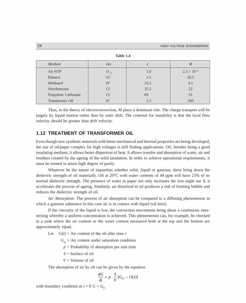
DharmN-HIGH\HG1-2.PM5 24
24 HIGH VOLTAGE ENGINEERING
Table 1.4
Medium Ion ε M
Air NTP O–2 1.0 2.3 × 10⁻²
Ethanol Cl– 2.5 26.5
Methanol H+ 33.5 4.1
Nitrobenzene Cl– 35.5 22
Propylene Carbonate Cl– 69 51
Transformer Oil H+ 2.3 200
Thus, in the theory of electroconvection, M plays a dominant role. The charge transport will belargely by liquid motion rather than by ionic drift. The criterion for instability is that the local flowvelocity should be greater than drift velocity.
1.12 TREATMENT OF TRANSFORMER OIL
Even though new synthetic materials with better mechanical and thermal properties are being developed,the use of oil/paper complex for high voltages is still finding applications. Oil, besides being a goodinsulating medium, it allows better dispersion of heat. It allows transfer and absorption of water, air andresidues created by the ageing of the solid insulation. In order to achieve operational requirements, itmust be treated to attain high degree of purity.
Whatever be the nature of impurities whether solid, liquid or gaseous, these bring down thedielectric strength of oil materially. Oil at 20°C with water contents of 44 ppm will have 25% of itsnormal dielectric strength. The presence of water in paper not only increases the loss angle tan δ, itaccelerates the process of ageing. Similarly, air dissolved in oil produces a risk of forming bubble andreduces the dielectric strength of oil.
Air Absorption: The process of air absorption can be compared to a diffusing phenomenon inwhich a gaseous substance in this case air is in contact with liquid (oil here).
If the viscosity of the liquid is low, the convection movements bring about a continuous inter-mixing whereby a uniform concentration is achieved. This phenomenon can, for example, be checkedin a tank where the air content or the water content measured both at the top and the bottom areapproximately equal.
Let G(t) = Air content of the oil after time t
Gm = Air content under saturation condition
p = Probability of absorption per unit time
S = Surface of oil
V = Volume of oil
The absorption of air by oil can be given by the equation
dG
dtp
S
VG G tm= −. [ ( )]
with boundary condition at t = 0 G = G0
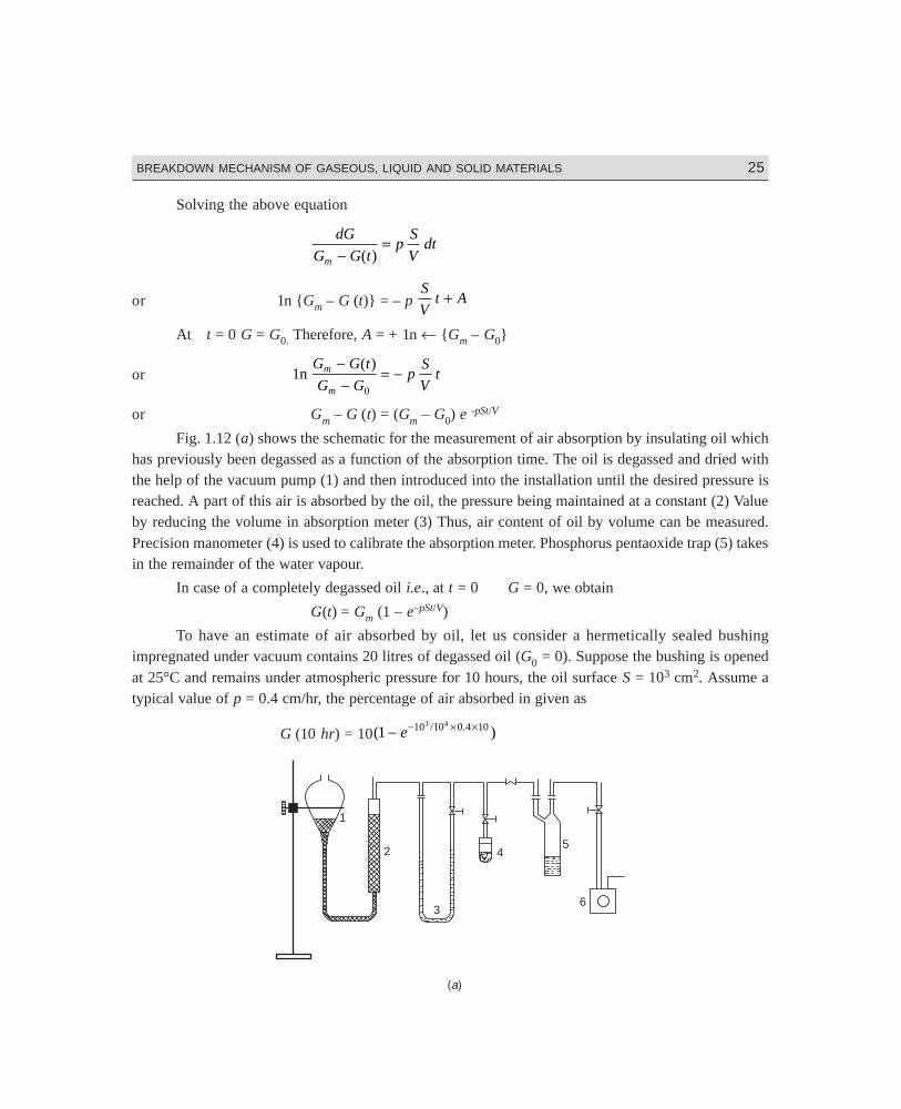
DharmN-HIGH\HG1-2.PM5 25
BREAKDOWN MECHANISM OF GASEOUS, LIQUID AND SOLID MATERIALS 25
Solving the above equation
dG
G G tp
S
Vdt
m −=
( )
or 1n Gm – G (t) = – p S
Vt A+
At t = 0 G = G0. Therefore, A = + 1n ← Gm – G0
or 10
nG G t
G Gp
S
Vtm
m
−−
= −( )
or Gm – G (t) = (Gm – G0) e -pSt/V
Fig. 1.12 (a) shows the schematic for the measurement of air absorption by insulating oil whichhas previously been degassed as a function of the absorption time. The oil is degassed and dried withthe help of the vacuum pump (1) and then introduced into the installation until the desired pressure isreached. A part of this air is absorbed by the oil, the pressure being maintained at a constant (2) Valueby reducing the volume in absorption meter (3) Thus, air content of oil by volume can be measured.Precision manometer (4) is used to calibrate the absorption meter. Phosphorus pentaoxide trap (5) takesin the remainder of the water vapour.
In case of a completely degassed oil i.e., at t = 0 G = 0, we obtain
G(t) = Gm (1 – e–pSt/V)
To have an estimate of air absorbed by oil, let us consider a hermetically sealed bushingimpregnated under vacuum contains 20 litres of degassed oil (G0 = 0). Suppose the bushing is openedat 25°C and remains under atmospheric pressure for 10 hours, the oil surface S = 103 cm2. Assume atypical value of p = 0.4 cm/hr, the percentage of air absorbed in given as
G (10 hr) = 10( )/ .1 10 10 0 4 103 4
− − × ×e
1
2
3
45
6
( )a
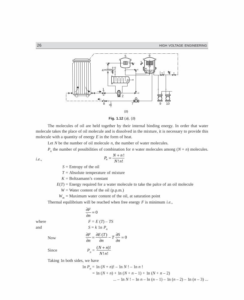
DharmN-HIGH\HG1-2.PM5 26
26 HIGH VOLTAGE ENGINEERING
2
1
78 9 10
5 6
3
4
( )b
Fig. 1.12 (a), (b)
The molecules of oil are held together by their internal binding energy. In order that watermolecule takes the place of oil molecule and is dissolved in the mixture, it is necessary to provide thismolecule with a quantity of energy E in the form of heat.
Let N be the number of oil molecule n, the number of water molecules.
Pn the number of possibilities of combination for n water molecules among (N + n) molecules.
i.e., PN n
N nn = + !
! !S = Entropy of the oilT = Absolute temperature of mixtureK = Boltzamann’s constant
E(T) = Energy required for a water molecule to take the palce of an oil moleculeW = Water content of the oil (p.p.m.)
Wm = Maximum water content of the oil, at saturation point
Thermal equilibrium will be reached when free energy F is minimum i.e.,
∂∂
=F
n0
where F = E (T) – TS
and S = k 1n Pn
Now ∂∂
= ∂∂
− ∂∂
=F
n
E T
nT
S
n
( )0
Since Pn = ( )!
! !
N n
N n
+
Taking 1n both sides, we have
1n Pn = 1n (N + n)! – 1n N ! – 1n n !
= 1n (N + n) + 1n (N + n – 1) + 1n (N + n – 2)
... – 1n N ! – 1n n – ln (n – 1) – 1n (n – 2) – 1n (n – 3) ...
DharmN-HIGH\HG1-2.PM5 27
BREAKDOWN MECHANISM OF GASEOUS, LIQUID AND SOLID MATERIALS 27
Differentiating both sides,
1 1 1
1
1 1
1
∂∂
=+
++ −
+ − −−
P
P n N n N n n nn
n
... ...
≈ 1 1
N n n+− = –
N
n N n( )+
Since ∂∂
= ∂∂
S
n
K
P
P
nn
n ≈ – KN
n N n( )+Substituting for ∂S/∂n in the equation
We have, ∂∂
− ∂∂
=E T
nT
S
n
( )0
∂∂
++
=E T
nT
TKN
n N n
( )
( )0
or∂∂
= −+
E
n
TKN
n N n( )
∂E = – TK N dn
n N n( )+Since N >> N + n ≈ N
Therefore, ∂E = – TK dn
nor E = – TK ln n + A
when E = 0, n = N. Therefore, 0 = – TK ln N + A or A = TK ln N
or E = TK ln N
n
or ln n
N
E
TK= − or n
Ne E TK≈ − /
or n = N e–E/TK ≈ Wm
Following impurities should be considered for purification of oil (i) solid impurities (ii) free anddissolved water particles (iii) dissolved air. Some of the methods used to remove these impurities havebeen described below.
Filtration and Treatment Under Vacuum: Different types of filters have been used. Filter press withsoft and hard filter papers is found to be more suitable for insulating oil. Due to hygroscopic propertiesof the paper, oil is predried before filtering. Therefore, this oil can not be used for high voltage insulation.The subsequent process of drying is carried out in a specially, designed tank under vacuum. The oil isdistributed over a large surface by a so-called ‘‘Rasching-ring’’ degassing column. Through this process,both the complete drying and degassing are achieved simultaneously. By suitable selection of the variouscomponents of the plant e.g., rate of flow of oil, degassing surface, vacuum pump etc., a desired degreeof purity can be obtained.
Fig. 1.12 (b) shows a typical plant for oil treatment. The oil from a transformer or a storage tankis prefiltered (1) so as to protect the feeder pump (2). In (3), the oil is heated up and is allowed to flow
DharmN-HIGH\HG1-2.PM5 28
28 HIGH VOLTAGE ENGINEERING
through filter press (4) into degassing tank (5). The degassing tank is evacuated by means of vacuumpump (6) whereas the second vacuum pump (7) is either connected with the degassing tank in parallelwith pump (6) or can be used for evacuating the transformer tank which is to be treated.
The operating temperature depends upon the quality and the vapour pressure of oil. In order toprevent an excessive evaporation of the aromatics, the pressure should be greater than 0.1 Torr. Thefilteration should be carried out at a suitable temperature as a higher temperature will cause certainproducts of the ageing process to be dissolved again in the oil.Centrifugal Method: This method is helpful in partially extracting solid impurities and free water. It istotally ineffective as far as removal of water and dissolved gases is concerned and oil treated in thismanner is even over-saturated with air as air, is thoroughly mixed into it during the process. However,if the centrifugal device is kept in a tank kept under vacuum, partial improvement can be obtained. Butthe slight increase in efficiency of oil achieved is out of proportion to the additional costs involved.Adsorption Columns: Here the oil is made to flow through one or several columns filled with an adsorbingagent either in the form of grains or powder. Following adsorbing agents have been used:
(i) Fuller earth(ii) Silica gel
(iii) Molecular sievesActivated Fuller earths absorb carbonyl and hydroxyl groups which from the principal ageing
products of oil and small amount of humidity. Best results of oil treatment are obtained by a combina-tion of Fuller earth and subsequent drying under vacuum.
Silica gel and in particular molecular sieves whose pore diameter measures 4 Å show a strongaffinity for water. Molecular sieves are capable of adsorbing water 20% of its original weight at 25°Cand water vapour pressure of 1 Torr whereas sillica gel and Fuller earth take up 6 and 4 per centrespectively.
Molecular sieves are synthetically produced Zeolites which are activated by removal of thecrystallisation water. Their adsorption capacity remains constant upto saturation point. The constructionof an oil drying plant using molecular sieves is, therefore, simple. The plant consists of an adsorptioncolumn containing the sieves and of an oil circulating pump.
The adsorption cycle is followed by a desorption cycle once the water content of the sieves hasexceeded 20 per cent. It has been found that the two processes adsorption and desorption are readilyreversible. In order to attain disorption of the sieves, it is sufficient to dry them in air stream of 200°C.
Electrostatic Filters: The oil to be treated is passed between the two electrodes placed in a container.The electrostatic field charges the impurities and traces of water which are then attracted and retainedby the foam coated electrodes. This method of drying oil is found to be economical if the water contentof the oil is less than 2 ppm. It is, therefore, essential that the oil is dried before hand if the water contentis large. Also, it is desirable that the oil flow should be slow if efficient filtering is required. Therefore,for industrial application where large quantity of oil is to be filtered, large number of filters will have tobe connected in parallel which may prove uneconomical.
1.13 TESTING OF TRANSFORMER OIL
The oil is poured in a container known as test-cell which has internal dimensions of 55 mm × 90 mm× 100 mm high. The electrodes are polished spheres of 12.7 to 13 mm diameter, preferably of brass,arranged horizontally with their axis not less than 40 mm above the bottom of the cell. For the test, the
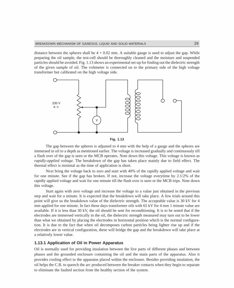
DharmN-HIGH\HG1-2.PM5 29
BREAKDOWN MECHANISM OF GASEOUS, LIQUID AND SOLID MATERIALS 29
distance between the spheres shall be 4 + 0.02 mm. A suitable gauge is used to adjust the gap. Whilepreparing the oil sample, the test-cell should be thoroughly cleaned and the moisture and suspendedparticles should be avoided. Fig. 1.13 shows an experimental set-up for finding out the dielectric strengthof the given sample of oil. The voltmeter is connected on to the primary side of the high voltagetransformer but calibrated on the high voltage side.
Fig. 1.13
The gap between the spheres is adjusted to 4 mm with the help of a gauge and the spheres areimmersed in oil to a depth as mentioned earlier. The voltage is increased gradually and continuously tilla flash over of the gap is seen or the MCB operates. Note down this voltage. This voltage is known asrapidly-applied voltage. The breakdown of the gap has taken place mainly due to field effect. Thethermal effect is minimal as the time of application is short.
Next bring the voltage back to zero and start with 40% of the rapidly applied voltage and waitfor one minute. See if the gap has broken. If not, increase the voltage everytime by 2.1/2% of therapidly applied voltage and wait for one minute till the flash over is seen or the MCB trips. Note downthis voltage.
Start again with zero voltage and increase the voltage to a value just obtained in the previousstep and wait for a minute. It is expected that the breakdown will take place. A few trials around thispoint will give us the breakdown value of the dielectric strength. The acceptable value is 30 kV for 4mm applied for one minute. In fact these days transformer oils with 65 kV for 4 mm 1 minute value areavailable. If it is less than 30 kV, the oil should be sent for reconditioning. It is to be noted that if theelectrodes are immersed vertically in the oil, the dielectric strength measured may turn out to be lowerthan what we obtained by placing the electrodes in horizontal position which is the normal configura-tion. It is due to the fact that when oil decomposes carbon particles being lighter rise up and if theelectrodes are in vertical configuration, these will bridge the gap and the breakdown will take place ata relatively lower value.
1.13.1 Application of Oil in Power ApparatusOil is normally used for providing insulation between the live parts of different phases and betweenphases and the grounded enclosure containing the oil and the main parts of the apparatus. Also itprovides cooling effect to the apparatus placed within the enclosure. Besides providing insulation, theoil helps the C.B. to quench the arc produced between the breaker contacts when they begin to separateto eliminate the faulted section from the healthy section of the system.
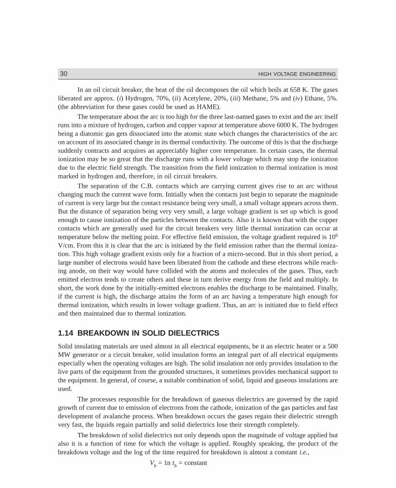
DharmN-HIGH\HG1-2.PM5 30
30 HIGH VOLTAGE ENGINEERING
In an oil circuit breaker, the heat of the oil decomposes the oil which boils at 658 K. The gasesliberated are approx. (i) Hydrogen, 70%, (ii) Acetylene, 20%, (iii) Methane, 5% and (iv) Ethane, 5%.(the abbreviation for these gases could be used as HAME).
The temperature about the arc is too high for the three last-named gases to exist and the arc itselfruns into a mixture of hydrogen, carbon and copper vapour at temperature above 6000 K. The hydrogenbeing a diatomic gas gets dissociated into the atomic state which changes the characteristics of the arcon account of its associated change in its thermal conductivity. The outcome of this is that the dischargesuddenly contracts and acquires an appreciably higher core temperature. In certain cases, the thermalionization may be so great that the discharge runs with a lower voltage which may stop the ionizationdue to the electric field strength. The transition from the field ionization to thermal ionization is mostmarked in hydrogen and, therefore, in oil circuit breakers.
The separation of the C.B. contacts which are carrying current gives rise to an arc withoutchanging much the current wave form. Initially when the contacts just begin to separate the magnitudeof current is very large but the contact resistance being very small, a small voltage appears across them.But the distance of separation being very very small, a large voltage gradient is set up which is goodenough to cause ionization of the particles between the contacts. Also it is known that with the coppercontacts which are generally used for the circuit breakers very little thermal ionization can occur attemperature below the melting point. For effective field emission, the voltage gradient required is 106
V/cm. From this it is clear that the arc is initiated by the field emission rather than the thermal ioniza-tion. This high voltage gradient exists only for a fraction of a micro-second. But in this short period, alarge number of electrons would have been liberated from the cathode and these electrons while reach-ing anode, on their way would have collided with the atoms and molecules of the gases. Thus, eachemitted electron tends to create others and these in turn derive energy from the field and multiply. Inshort, the work done by the initially-emitted electrons enables the discharge to be maintained. Finally,if the current is high, the discharge attains the form of an arc having a temperature high enough forthermal ionization, which results in lower voltage gradient. Thus, an arc is initiated due to field effectand then maintained due to thermal ionization.
1.14 BREAKDOWN IN SOLID DIELECTRICS
Solid insulating materials are used almost in all electrical equipments, be it an electric heater or a 500MW generator or a circuit breaker, solid insulation forms an integral part of all electrical equipmentsespecially when the operating voltages are high. The solid insulation not only provides insulation to thelive parts of the equipment from the grounded structures, it sometimes provides mechanical support tothe equipment. In general, of course, a suitable combination of solid, liquid and gaseous insulations areused.
The processes responsible for the breakdown of gaseous dielectrics are governed by the rapidgrowth of current due to emission of electrons from the cathode, ionization of the gas particles and fastdevelopment of avalanche process. When breakdown occurs the gases regain their dielectric strengthvery fast, the liquids regain partially and solid dielectrics lose their strength completely.
The breakdown of solid dielectrics not only depends upon the magnitude of voltage applied butalso it is a function of time for which the voltage is applied. Roughly speaking, the product of thebreakdown voltage and the log of the time required for breakdown is almost a constant i.e.,
Vb = 1n tb = constant
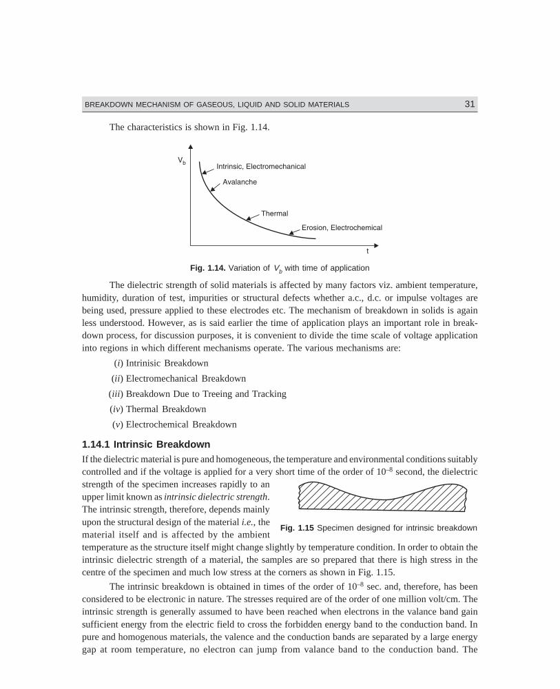
DharmN-HIGH\HG1-2.PM5 31
BREAKDOWN MECHANISM OF GASEOUS, LIQUID AND SOLID MATERIALS 31
The characteristics is shown in Fig. 1.14.
Fig. 1.14. Variation of Vb with time of application
The dielectric strength of solid materials is affected by many factors viz. ambient temperature,humidity, duration of test, impurities or structural defects whether a.c., d.c. or impulse voltages arebeing used, pressure applied to these electrodes etc. The mechanism of breakdown in solids is againless understood. However, as is said earlier the time of application plays an important role in break-down process, for discussion purposes, it is convenient to divide the time scale of voltage applicationinto regions in which different mechanisms operate. The various mechanisms are:
(i) Intrinisic Breakdown
(ii) Electromechanical Breakdown
(iii) Breakdown Due to Treeing and Tracking
(iv) Thermal Breakdown
(v) Electrochemical Breakdown
1.14.1 Intrinsic BreakdownIf the dielectric material is pure and homogeneous, the temperature and environmental conditions suitablycontrolled and if the voltage is applied for a very short time of the order of 10–8 second, the dielectricstrength of the specimen increases rapidly to anupper limit known as intrinsic dielectric strength.The intrinsic strength, therefore, depends mainlyupon the structural design of the material i.e., thematerial itself and is affected by the ambienttemperature as the structure itself might change slightly by temperature condition. In order to obtain theintrinsic dielectric strength of a material, the samples are so prepared that there is high stress in thecentre of the specimen and much low stress at the corners as shown in Fig. 1.15.
The intrinsic breakdown is obtained in times of the order of 10–8 sec. and, therefore, has beenconsidered to be electronic in nature. The stresses required are of the order of one million volt/cm. Theintrinsic strength is generally assumed to have been reached when electrons in the valance band gainsufficient energy from the electric field to cross the forbidden energy band to the conduction band. Inpure and homogenous materials, the valence and the conduction bands are separated by a large energygap at room temperature, no electron can jump from valance band to the conduction band. The
Fig. 1.15 Specimen designed for intrinsic breakdown
DharmN-HIGH\HG1-2.PM5 32
32 HIGH VOLTAGE ENGINEERING
conductivity of pure dielectrics at room temperature is, therfore, zero. However, in practice, no insulatingmaterial is pure and, therefore, has some impurities and/or imperfections in their structural designs.The impurity atoms may act as traps for free electrons in energy levels that lie just below the conductionband is small. An amorphous crystal will, therefore, always have some free electrons in the conductionband. At room temperature some of the trapped electrons will be excited thermally into the conductionband as the energy gap between the trapping band and the conduction band is small. An amorphouscrystal will, therefore, always have some free electrons in the conduction band. As an electric field isapplied, the electrons gain energy and due to collisions between them the energy is shared by all electrons.In an amorphous dielectric the energy gained by electrons from the electric field is much more thanthey can transfer it to the lattice. Therefore, the temperature of electrons will exceed the lattice temperatureand this will result into increase in the number of trapped electrons reaching the conduction band andfinally leading to complete breakdown.
When an electrode embeded in a solid specimen is subjected to a uniform electric field, breakdownmay occur. An electron entering the conduction band of the dielectric at the cathode will move towardsthe anode under the effect of the electric field. During its movement, it gains energy and on collision itloses a part of the energy. If the mean free path is long, the energy gained due to motion is more thanlost during collision. The process continues and finally may lead to formation of an electron avalanchesimilar to gases and will lead finally to breakdown if the avalanche exceeds a certain critical size.
1.14.2 Electromechanical BreakdownWhen a dielectric material is subjected to an electric field, charges of opposite nature are induced onthe two opposite surfaces of the material and hence a force of attraction is developed and the specimentis subjected to electrostatic compressive forces and when these forces exceed the mechanical withstandstrength of the material, the material collapses. If the initial thickness of the material is d0 and iscompressed to a thickness d under the applied voltage V then the compressive stress developed due toelectric field is
F = 12
ε ε0
2
2rV
dwhere εr is the relative permittivity of the specimen. If γ is the Young’s modulus, the mechanicalcompressive strength is
γ 1n d
d0
Equating the two under equilibrium condition, we have
12
10
2
20ε ε γr
V
d
d
d= n
or V2 = d2 . 2
10
0γε ε r
d
dn = Kd2 1n
d
d0
Differentiating with respect to d, we have
2V dV
ddK d
d
dd
d
d
d
d= −
LNM
OQP
2 1 0 2
0
02n . . = 0
DharmN-HIGH\HG1-2.PM5 33
BREAKDOWN MECHANISM OF GASEOUS, LIQUID AND SOLID MATERIALS 33
or 2d ln d
d0 = d
or ln d
d0 =
1
2
or d
d0
0 6= .
For any real value of voltage V, the reduction in thickness of the specimen can not be more than40%. If the ratio V/d at this value of V is less than the intrinsic strength of the specimen, a furtherincrease in V shall make the thickness unstable and the specimen collapses. The highest apparentstrength is then obtained by substituting d = 0.6 d0 in the above expressions.
V
d r
= 21 1 67
0
γε ε
n . orV
dEa
r0 0
1 2
0 6= =LNM
OQP
./
γε ε
The above equation is approximate only as γ depends upon the mechanical stress. The possibilityof instability occuring for lower average field is ignored i.e., the effect of stress concentration at irregu-larities is not taken into account.
1.14.3 Breakdown due to Treeing and TrackingWe know that the strength of a chain is given by the strength of the weakest link in the chain. Similarlywhenever a solid material has some impurities in terms of some gas pockets or liquid pockets in it thedielectric strength of the solid will be more or less equal to the strength of the weakest impurities.Suppose some gas pockets are trapped in a solid material during manufacture, the gas has a relativepermittivity of unity and the solid material εr, the electric field in the gas will be εr times the field in thesolid material. As a result, the gas breaks down at a relatively lower voltage. The charge concentrationhere in the void will make the field more non-uniform. The charge concentration in such voids is foundto be quite large to give fields of the order of 10 MV/cm which is higher than even the intrinsic breakdown.These charge concentrations at the voids within the dielectric lead to breakdown step by step andfinally lead to complete rupture of the dielectric. Since the breakdown is not caused by a single dischargechannel and assumes a tree like structure as shown in Fig. 1.6, it is known as breakdown due to treeing.The treeing phenomenon can be readily demonstrated in a laboratory by applying an impulse voltagebetween point plane electrodes with the point embedded in a transparent solid dielectric such as perspex.
The treeing phenomenon can be observed in all dielectric wherever non-uniform fields prevail.Suppose we have two electrodes separated by an insulating material and the assembly is placed
in an outdoor environment. Some contaminants in the form of moisture or dust particles will get depositedon the surface of the insulation and leakage current starts between the electrode through the contaminantssay moisture. The current heats the moisture and causes breaks in the moisture films. These small filmsthen act as electrodes and sparks are drawn between the films. The sparks cause carbonization andvolatilization of the insulation and lead to formation of permanent carbontracks on the surface ofinsulations. Therefore, tracking is the formation of a permanent conducting path usually carbon acrossthe surface of insulation. For tracking to occur, the insulating material must contain organic substances.For this reason, for outdoor equipment, tracking severely limits the use of insulation having organicsubstances. The rate of tracking can be slowed down by adding filters to the polymers which inhibitcarbonization.
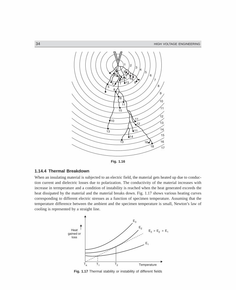
DharmN-HIGH\HG1-2.PM5 34
34 HIGH VOLTAGE ENGINEERING
Fig. 1.16
1.14.4 Thermal BreakdownWhen an insulating material is subjected to an electric field, the material gets heated up due to conduc-tion current and dielectric losses due to polarization. The conductivity of the material increases withincrease in termperature and a condition of instability is reached when the heat generated exceeds theheat dissipated by the material and the material breaks down. Fig. 1.17 shows various heating curvescorresponding to different electric stresses as a function of specimen temperature. Assuming that thetemperature difference between the ambient and the specimen temperature is small, Newton’s law ofcooling is represented by a straight line.
Fig. 1.17 Thermal stability or instability of different fields
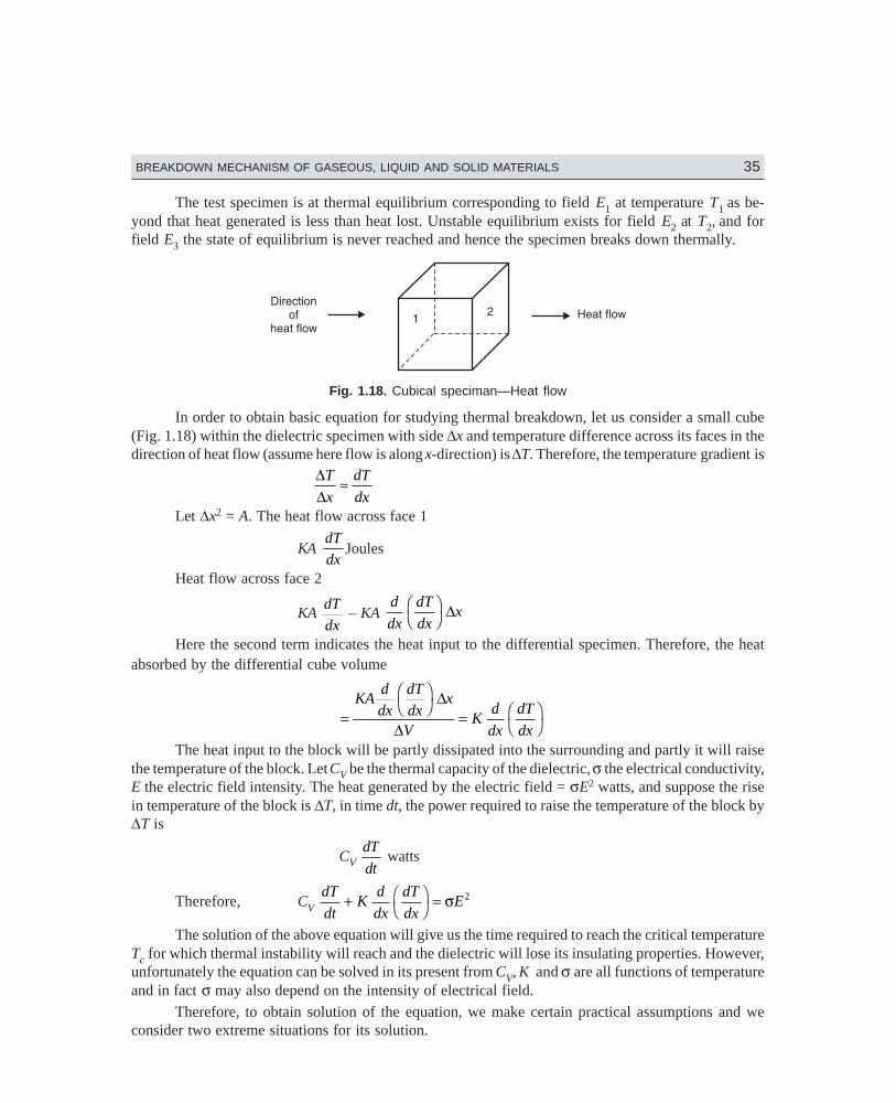
DharmN-HIGH\HG1-3.PM5 35
BREAKDOWN MECHANISM OF GASEOUS, LIQUID AND SOLID MATERIALS 35
The test specimen is at thermal equilibrium corresponding to field E1 at temperature T1 as be-yond that heat generated is less than heat lost. Unstable equilibrium exists for field E2 at T2,
and forfield E3 the state of equilibrium is never reached and hence the specimen breaks down thermally.
Fig. 1.18. Cubical speciman—Heat flow
In order to obtain basic equation for studying thermal breakdown, let us consider a small cube(Fig. 1.18) within the dielectric specimen with side ∆x and temperature difference across its faces in thedirection of heat flow (assume here flow is along x-direction) is ∆T. Therefore, the temperature gradient is
∆∆
T
x
dT
dx≈
Let ∆x2 = A. The heat flow across face 1
KA dT
dxJoules
Heat flow across face 2
KA dT
dx – KA
d
dx
dT
dxxF
HIK ∆
Here the second term indicates the heat input to the differential specimen. Therefore, the heatabsorbed by the differential cube volume
=
FH
IK
= FH
IK
KAd
dx
dT
dxx
VK
d
dx
dT
dx
∆
∆The heat input to the block will be partly dissipated into the surrounding and partly it will raise
the temperature of the block. Let CV be the thermal capacity of the dielectric, σ the electrical conductivity,E the electric field intensity. The heat generated by the electric field = σE2 watts, and suppose the risein temperature of the block is ∆T, in time dt, the power required to raise the temperature of the block by∆T is
CV dT
dt watts
Therefore, CV dT
dtK
d
dx
dT
dxE+ F
HIK = σ 2
The solution of the above equation will give us the time required to reach the critical temperatureTc for which thermal instability will reach and the dielectric will lose its insulating properties. However,unfortunately the equation can be solved in its present from CV, K and σ are all functions of temperatureand in fact σ may also depend on the intensity of electrical field.
Therefore, to obtain solution of the equation, we make certain practical assumptions and weconsider two extreme situations for its solution.
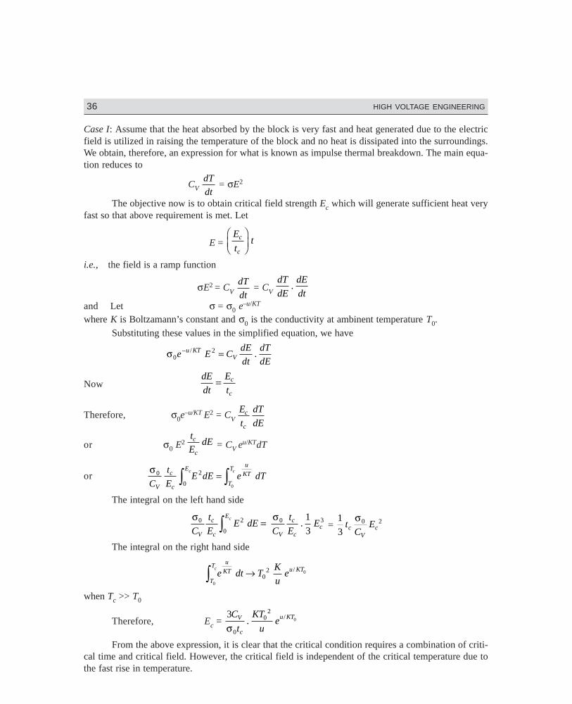
DharmN-HIGH\HG1-3.PM5 36
36 HIGH VOLTAGE ENGINEERING
Case I: Assume that the heat absorbed by the block is very fast and heat generated due to the electricfield is utilized in raising the temperature of the block and no heat is dissipated into the surroundings.We obtain, therefore, an expression for what is known as impulse thermal breakdown. The main equa-tion reduces to
CV dT
dt = σE2
The objective now is to obtain critical field strength Ec which will generate sufficient heat veryfast so that above requirement is met. Let
E = E
ttc
c
FHG
IKJ
i.e., the field is a ramp function
σE2 = CV dT
dt = CV
dT
dE
dE
dt.
and Let σ = σ0 e–u/KT
where K is Boltzamann’s constant and σ0 is the conductivity at ambinent temperature T0.Substituting these values in the simplified equation, we have
σ02e E C
dE
dt
dT
dEu KT
V− =/ .
NowdE
dt
E
tc
c
=
Therefore, σ0e–u/KT E2 = CV
E
t
dT
dEc
c
or σ0 E2
t
EdEc
c = CV e
u/KTdT
or σ0
0
2
0C
t
EE dE e dT
V
c
c
Eu
KT
T
Tc cz z=
The integral on the left hand side
σ σ0 2 0 3
0
1
3C
t
EE dE
C
t
EE
V
c
c V
c
cc
Ec
=z . = 1
30 2t
CEc
Vc
σ
The integral on the right hand side
e dt TK
ue
u
KT u KT
T
Tc
→z 02 0
0
/
when Tc >> T0
Therefore, Ec = 3
0
02
0C
t
KT
ueV
c
u KT
σ. /
From the above expression, it is clear that the critical condition requires a combination of criti-cal time and critical field. However, the critical field is independent of the critical temperature due tothe fast rise in temperature.
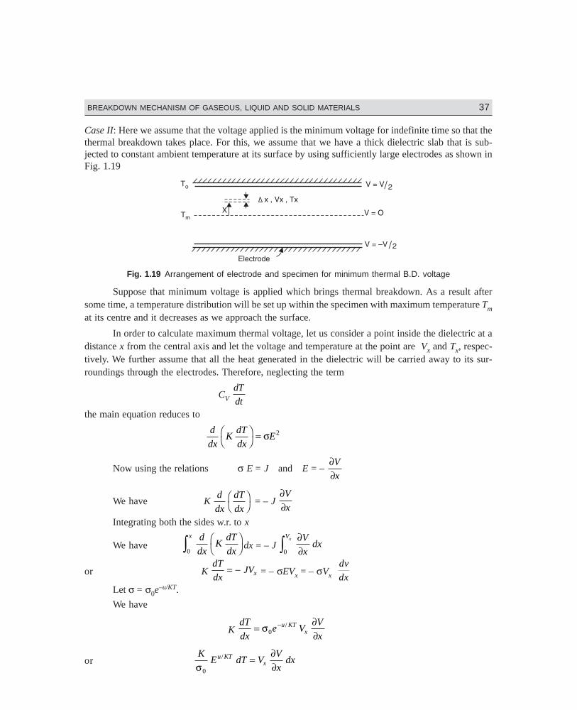
DharmN-HIGH\HG1-3.PM5 37
BREAKDOWN MECHANISM OF GASEOUS, LIQUID AND SOLID MATERIALS 37
Case II: Here we assume that the voltage applied is the minimum voltage for indefinite time so that thethermal breakdown takes place. For this, we assume that we have a thick dielectric slab that is sub-jected to constant ambient temperature at its surface by using sufficiently large electrodes as shown inFig. 1.19
Fig. 1.19 Arrangement of electrode and specimen for minimum thermal B.D. voltage
Suppose that minimum voltage is applied which brings thermal breakdown. As a result aftersome time, a temperature distribution will be set up within the specimen with maximum temperature Tmat its centre and it decreases as we approach the surface.
In order to calculate maximum thermal voltage, let us consider a point inside the dielectric at adistance x from the central axis and let the voltage and temperature at the point are Vx and Tx, respec-tively. We further assume that all the heat generated in the dielectric will be carried away to its sur-roundings through the electrodes. Therefore, neglecting the term
CV dT
dtthe main equation reduces to
d
dxK
dT
dxEF
HIK = σ 2
Now using the relations σ E = J and E = – ∂∂V
x
We have K d
dx
dT
dxFH
IK = – J
∂∂V
x
Integrating both the sides w.r. to x
We have d
dxK
dT
dx
x FH
IKz0 dx = – J
∂∂z V
xdx
Vx
0
or K dT
dxJVx= − = – σEVx = – σVx
dv
dxLet σ = σ0e
–u/KT.
We have
K dT
dxe V
V
xu KT
x= ∂∂
−σ0/
or K
E dT VV
xdxu KT
xσ0
/ = ∂∂
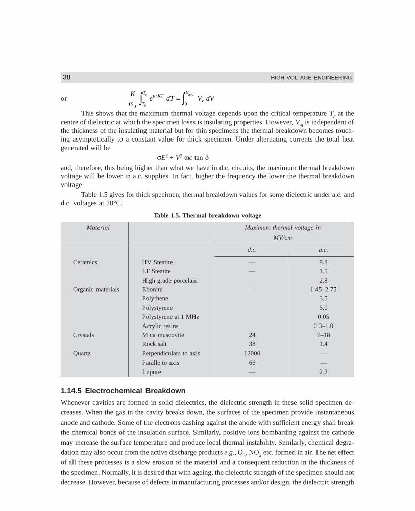
DharmN-HIGH\HG1-3.PM5 38
38 HIGH VOLTAGE ENGINEERING
or K
e dT V dVu KTx
V
T
T mc
σ0 0
2
0
/ /
= zzThis shows that the maximum thermal voltage depends upon the critical temperature Tc at the
centre of dielectric at which the specimen loses is insulating properties. However, Vm is independent ofthe thickness of the insulating material but for thin specimens the thermal breakdown becomes touch-ing asymptotically to a constant value for thick specimen. Under alternating currents the total heatgenerated will be
σE2 + V2 ωc tan δand, therefore, this being higher than what we have in d.c. circuits, the maximum thermal breakdownvoltage will be lower in a.c. supplies. In fact, higher the frequency the lower the thermal breakdownvoltage.
Table 1.5 gives for thick specimen, thermal breakdown values for some dielectric under a.c. andd.c. voltages at 20°C.
Table 1.5. Thermal breakdown voltage
Material Maximum thermal voltage in
MV/cm
d.c. a.c.
Ceramics HV Steatite — 9.8
LF Steatite — 1.5
High grade porcelain 2.8Organic materials Ebonite — 1.45–2.75
Polythene 3.5
Polystyrene 5.0
Polystyrene at 1 MHz 0.05
Acrylic resins 0.3–1.0Crystals Mica muscovite 24 7–18
Rock salt 38 1.4
Quartz Perpendiculars to axis 12000 —
Paralle to axis 66 —
Impure — 2.2
1.14.5 Electrochemical Breakdown
Whenever cavities are formed in solid dielectrics, the dielectric strength in these solid specimen de-creases. When the gas in the cavity breaks down, the surfaces of the specimen provide instantaneous
anode and cathode. Some of the electrons dashing against the anode with sufficient energy shall breakthe chemical bonds of the insulation surface. Similarly, positive ions bombarding against the cathodemay increase the surface temperature and produce local thermal instability. Similarly, chemical degra-dation may also occur from the active discharge products e.g., O3, NO2 etc. formed in air. The net effect
of all these processes is a slow erosion of the material and a consequent reduction in the thickness ofthe specimen. Normally, it is desired that with ageing, the dielectric strength of the specimen should notdecrease. However, because of defects in manufacturing processes and/or design, the dielectric strength
DharmN-HIGH\HG1-3.PM5 39
BREAKDOWN MECHANISM OF GASEOUS, LIQUID AND SOLID MATERIALS 39
decreases with time of voltage application or even without voltage application and in many cases; thedecrease in dielectric strength (Eb) with time follows the following empirical relation.
t Ebn = constant
where the exponent n depends upon the dielectric material, the ambient temperature humidity and thequality of manufacture. This is the main reason why high a.c. voltage testing is not recommended. Infact, these days very low frequency testing is being suggested (0.1 HZ) which simulates the effects of
both a.c. 50 HZ and d.c. voltages and yet the dielectric strength of the specimen is not affected muchwith VLF voltage application.
The breakdown of solid dielectric due to internal discharges or partial discharges has beenelaborately explained in section 6.9 of the book.
1.14.6 Solid Dielectrics Used in Power ApparatusThe main requirements of the insulating materials used for power apparatus are:
1. High insulation resistance
2. High dielectric strength
3. Good mechanical properties i.e., tenacity and elasticity
4. It should not be affected by chemicals around it
5. It should be non-hygroscopic because the dielectric strength of any material goes very muchdown with moisture content
Vulcanized rubber : Rubber in its natural form is highly insulating but it absorbs moisture readily andgets oxidized into a resinous material; thereby it loses insulating properties. When it is mixed withsulphur alongwith other carefully chosen ingredients and is subjected to a particular temperature itchanges into vulcanized rubber which does not absorb moisture and has better insulating propertiesthan even the pure rubber. It is elastic and resilient.
The electrical properties expected of rubber insulation are high breakdown strength and highinsulation resistance. In fact the insulation strength of the vulcanized rubber is so good that for lowervoltages the radial thickness is limited due to mechanical consideration.
The physical properties expected of rubber insulation are that the cable should withstand nor-mal hazards of installation and it should give trouble-free service.
Vulcanized rubber insulated cables are used for wiring of houses, buildings and factories forlow-power work.
There are two main groups of synthetic rubber material : (i) general purpose synthetics whichhave rubber-like properties and (ii) special purpose synthetics which have better properties than therubber e.g., fire resisting and oil resisting properties. The four main types are: (i) butyl rubber, (ii)silicon rubber, (iii) neoprene, and (iv) styrene rubber.
Butyl rubber: The processing of butyl rubber is similar to that of natural rubber but it is moredifficult and its properties are comparable to those of natural rubber. The continuous temperature towhich butyl rubber can be subjected is 85°C whereas for natural rubber it is 60°C. The current rating of

DharmN-HIGH\HG1-3.PM5 40
40 HIGH VOLTAGE ENGINEERING
butyl insulated cables is approximately same as those of paper or PVC insulated cables. Butyl rubbercompound can be so manufactured that it has low water absorption and offers interesting possibilitiesfor a non-metallic sheathed cable suitable for direct burial in the ground.
Silicone rubber: It is a mechanically weak material and needs external protection but it has highheat resistant properties. It can be operated at temperatures of the order of 150°C. The raw materialsused for the silicon rubber are sand, marsh gas, salt, coke and magnesium.
Neoprene: Neoprene is a polymerized chlorobutadiene. Chlorobutadiene is a colourless liquidwhich is polymerized into a solid varying from a pale yellow to a darkish brown colour. Neoprene doesnot have good insulating properties and is used upto 660 V a.c. but it has very good fire resistingproperties and therefore it is more useful as a sheathing material.
Styrene rubber: Styrene is used both for insulating and sheathing of cables. It has propertiesalmost equal to the natural rubber.
Polyvinyl Chloride (PVC)
It is a polymer derived generally from acetylene and it can be produced in different gradesdepending upon the polymerization process. For use in cable industry the polymer must be compoundedwith a plasticizer which makes it plastic over a wide range of temperature. The grade of PVC dependsupon the plasticizer. PVC is inferior to vulcanized in respect of elasticity and insulation resistance.PVC material has many grades.
General purpose type: It is used both for sheathing and as an insulating material. In this com-pound monomeric plasticizers are used. It is to be noted that a V.R. insulated PVC sheathed cable is notgood for use.
Hard grade PVC: These are manufactured with less amount of plasticizer as compared withgeneral purpose type. Hard grade PVC are used for higher temperatures for short duration of time likein soldering and are better than the general purpose type. Hard grade can not be used for low continu-ous temperatures.
Heat resisting PVC: Because of the use of monomeric plasticizer which volatilizes at tempera-ture 80°C–100°C, general purpose type compounds become stiff. By using polymeric plasticizers it ispossible to operate the material continuously around 100°C.
PVC compounds are normally costlier than the rubber compounds and the polymeric plasticizedcompounds are more expensive than the monomeric plasticized ones. PVC is inert to oxygen, oils,alkalis and acids and, therefore, if the environmental conditions are such that these things are present inthe atmosphere, PVC is more useful than rubber.
Polythene
This material can be used for high frequency cables. This has been used to a limited extent forpower cables also. The thermal dissipation properties are better than those of impregnated paper andthe impulse strength compares favourably with an impregnated paper-insulated device. The maximumoperating temperature of this material under short circuits is 100°C.
Cross-linked polythene: The use of polythene for cables has been limited by its low meltingpoint. By cross-linking the molecules, in roughly the same way as vulcanising rubber, a new material isproduced which does not melt but carbonizes at 250 to 300°C. By using chemical process it has been
DharmN-HIGH\HG1-3.PM5 41
BREAKDOWN MECHANISM OF GASEOUS, LIQUID AND SOLID MATERIALS 41
made technically possible to cross-link polythene in conventional equipment for the manufacture ofrubber. This is why the product is said to be “vulcanised” or “cross-linked” polythene.
The polythene is inert to chemical reactions as it does not have double bonds and polar groups.Therefore, it was thought that polythene could be cross-linked only through special condition, e.g., byirradiating polythene with electrons, thereby it could be given properties of cross-linking such as changeof tensile strength and better temperature stability. Many irradiation processes have been developed inthe cable making industry even though large amounts of high energy radiations are required and theprocedure is expensive.
Polythene can also be irradiated with ultraviolet light, after adding to it a smal quantity of ultra-violet sensitive material such as benzophenone. Under the influence of ultraviolet light on benzophenone,a radical is formed of the same type as in the decomposition of peroxide by the radical mechanism.Organic peroxides have also been used successfully to crosslink the polythene.
Impregnated paper
A suitable layer of the paper is lapped on the conductor depending upon the operating voltage.It is then dried by the combined application of heat and vacuum. This is carried out in a hermeticallysealed steam heated chamber. The temperature is 120°–130°C before vacuum is created. After thedevice is dried, an insulating compound having the same temperature as that of the chamber is forcedinto the chamber. All the pores of the paper are completely filled with this compound. After impregna-tion the device is allowed to cool under the compound so that the void formation due to compoundshrinkage is minimized.
In case of pre-impregnated type the papers are dried and impregnated before they are applied onthe conductor.
The compound used in case of impregnated paper is a semifluid and when the cables are laid ongradients the fluid tends to move from higher to lower gradient. This reduces the compound content athigher gradients and may result in void formation at higher gradients. This is very serious for cablesoperating at voltages higher than 3.3 kV. In many cases, the failures of the cables have been due to thevoid formation at the higher levels or due to the bursting of the sheath at the lower levels because of theexcessive internal pressure of the head of compound.
Insulating press boards. If the thickness of paper is 0.8 mm or more, it is called paper board.When many layers of paper are laminated with an adhesive to get desired thickness, these are known aspress boards and are used in bushings, transformers as insulating barriers or supporting materials. Theelectrical properties of press boards varies depending upon the resin content. The application of thesepress boards depends upon the thickness and density of paper used. For high frequency capacitors andcables usually low density paper (0.8 gm/cm3) is used where medium density paper is used for powercapacitors and high density papers are used in d.c. machines and energy storage capacitors. The electricstrength of press board is higher than that of resins or porcelain. However, it is adversely affected bytemperature above 20°C. The loss angle tan δ also decreases with increase in temperature. The mainadvantage of this material is that it provides good mechanical support even at higher temperatures upto120°C.
Mica. Mica consists of crystalline mineral silicates of alumina and potash. It has high dielectricstrength, low dielectric losses and good mechanical strength. All these properties make it useful for
DharmN-HIGH\HG1-3.PM5 42
42 HIGH VOLTAGE ENGINEERING
many electrical devices e.g., commutator segment separator, aremature windings, electrical heatingand cooling equipments and switchgear. Thin layers of mica are laminated with a suitable resin orvarnish to make thick sheets of mica. Mica can be mixed with the required type of resin to obtain itsapplication at different operating temperatures. Mica is used as a filler in insulating materials to im-prove their dielectric strength, reduce dielectric loss and improve heat resistance property.
Ceramics. Ceramics materials are produced from clay containing aluminium oxide and otherinorganic materials. The thick parts of these substances is given the desired shape and form at roomtemperature and then baked at high temperature about (1450°C) to provide a solid inelastic final struc-ture. Ceramics also known as porcelain in one of its forms have high mechanical strength and lowpermittivity (εr < 12) are widely used for insulators and bushings. These have 40% to 50% of clay, 30-20% of aluminium oxide and 30% of fieldspar. The ceramics with higher permittivity (εr > 12) are usedin capacitors and transducers.
The specific insulation resistance of ceramics is comparatively low. The tan δ of these materialsis high and increases with increase in temperature resulting in higher dielectric loss. The breakdownstrength of porecelain compared to other insulating material is low but it remains unaffected over awide range of temperature variation. Porcelain is chemically insert to alkalies and acids and, therefore,corrosion resistant and does not get contaminated. Alumina (Al2O3) has replaced quartz because of itsbetter thermal conductivity, insulating property and mechanical strength. It is used for the fabricationof high current vacuum circuit breakers.
Glass. Glass is a thermoplastic inorganic material consisting of silicondioxide (SiO2), which isavailable in nature in the form of quartz. Different types of metal oxides could be used for producingdifferent types of glasses but for use in electrical engineering only non-alkaline glasses are suitablehaving alkaline content less than 0.8%.
The dielectric constant of glass varies between 3.6 and 10.0 and the density varies between 2000kg/m3 and 6000 kg/m3. The loss angle tan δ is less than 10–3 and losses are higher for lower frequen-cies. Its dielectric strength varies between 300 and 500 kV/mm and it decreases with increase in tem-perature. Glass is used for X-ray equipments, electronic valves, electric bulbs etc.
Epoxy Resins. Epoxy resins are low molecular but soluble thermosetting plastics which exhibitsufficient hardening quality in their molecules. The chemical cross-linking of epoxy resins is normallycarried out at room temperatures either by a catalytic mechanism or by bridging across epoxy moleculethrough the epoxy or hydroxyl group.
Epoxy resins have high dielectric and mechanical strength. They can be cast into desired shapeseven at room temperature. They are highly elastic and it is found that when it is subjected to a pressureof 175000 psi, it returned to its original shape after the load is removed. The dielectric constant variesbetween 2.5 and 4.0. Epoxy resins basically being non-polar substances have high dc specific insula-tion resistance and low loss tan δ compared to polar materials like PVC. However, when the tempera-ture exceeds 100°C the specific insulation resistance begins to decrease considerably and tan δ in-creases. Compared to porcelain the breakdown strength of epoxy resin is almost double at temperaturesupto 100°C but decreases rapidly at higher temperatures.
As filler materials, the inorganic substances like quartz powder (SiO2) are used for castingapplications. In SF6 gas insulated systems having epoxy resin spacers, aluminium oxide and also dolo-
DharmN-HIGH\HG1-3.PM5 43
BREAKDOWN MECHANISM OF GASEOUS, LIQUID AND SOLID MATERIALS 43
mite are used as filler materials. These are found to be more compatible to the decomposed products ofSF6 by partial discharge and arcing discharges.
It is to be noted that the cast or encapsulation should not contain voids or humidity especially inhigh voltage applications and the material is desired to be homogeneous. It is, therefore, desirable todry and degas the individual components of the mixture and casting is preferably carried out in vacuum.
The epoxy resins casts are inert to ether, alcohol and benzol. However, most of them are solublein mineral oils at about 70°C. It is for this reason that they are not found suitable for applications infilled transformers.
There are certain application which require insulating materials to operate between a high rangeof temperature e.g., –270°C to 400°C. Some of the applications are space shuttle solar arrays, capaci-tors, transformers high speed locomotive, microprocessor chip carriers, cryogenic cables and otherapplications at cryogenic temperatures. For this some thermoplastic polymer films are used which haveunique combination of electrical, mechanical and physical quantities and these materials are able toretain these properties over a wide range of temperatures where other insulating materials may fail.Perfluoro carbon films have high dielectric strength very low dielectric constant of 2 and low dielectricloss of 2 × 10⁻⁴ at 100 Hz and 7.5 × 10⁻⁴ at 100 MHz. These films are used under extreme conditions oftemperature and environment. These films are used for insulation on high temperature wires, cables,motor coils phase and ground insulation and for capacitors. This is also used as a substrate for flexibleprinted circuits and flexible cables.
Another insulating film in which has the best thermal properties in this category of insulatingmaterials is polyimide film under the trade name of Kapton manufactured by DuPont of America.These films can be used between a very wide range of temperature variation varying between –270°Cand 350°C. Its continuous temperature rating is 240°C. It has high dielectric and tensile strength. Thedisadvantages of the film are
(i) high moisture absorption rate and (ii) it is affected by alkalies and strong inorganic acids.
Kepton films can be used capacitors, transformers formed coil insulation, motor state insulationand flexible printed circuits. The film is selectively costlier and is mainly used where its unique charac-teristics makes it the only suitable insulation. The use of this insulation for motors reduces the overalldimensions of the motors for the same ratings. It is, therefore, used in almost all situations whose spaceis a serious problem and the other nature insulation result in bigger dimension.
Another recently developed resins is poly carbonate (PC) which is good heat resistant; it isflexible and has good dielectric characteristic. It is not affected by oils, fats and dilute acids but isadversely affected by alkalies, esters and aromatic hydrocarbons. The film being cost effective and fastresistant, it is used for coil insulation, slot insulation for motors and for capacitor insulation. This isknown as the lexon polymer.
General Electric Co. of USA has developed a film under the trade name Ultem which is a polyetherimine (PEI) film which has dielectric strength comparable to that of polyimide film and has higherthermal conductivity and lower moisture absorption and is relatively less costlier. It is used as insula-tion for transformers and motors.
DharmN-HIGH\HG1-3.PM5 44
44 HIGH VOLTAGE ENGINEERING
1.14.7 Application of Insulating MaterialsInsulating fluids (gases and liquids) provide insulation between phases and between phase and groundedparts of electrical equipments. These also carry out heat from the windings of the electrical equipments.However, solid insulating materials are used only to provide insulation only.
International Electrotechincal Commission has categories various insulating materials depend-ing upon the temperature of operations of the equipments under the following categories.
Class Y 90°C Natural rubber, PVC, paper cotton, silk without impregnation.Class A 105°C Same as class Y but impregnatedClass E 120°C Polyethylene, terephthalate, cellulose tricetrate, polyvinyl acetate enamelClass B 130°C Bakelite, bituminised asbestos, fibre glass, mica, polyester enamelClass F 155°C As class B but with epoxy based resinClass H 180°C As class B with silicon resin binder silicone rubber, aromatic polyamide
(nomex paper and fibre), polyimide film (enamel, varnish and film) and estermideenamel
Class C Above 180°C, as class B but with suitable non-organic binders, teflon and otherhigh temperature polymers.
While describing the dielectric and other properties of various insulating materials, their appli-cation for various electrical apparatus has also been mentioned in the previous paragraphs. However, areverse process i.e., what insulating materials are used for a particular apparatus depending upon itsratings and environmental condition where the apparatus is required to operate, is also desirable and abrief review is given here.
Power Transformers. For small rating, the coils are made of super-enamelled copper wire. Forlayer to layer, coil to coil and coil to ground (iron core) craft paper is used.
However, for large size transformers paper or glass tape is rapped on the rectangular conductorswhereas for coil to coil or coil to ground, insulation is provided using thick radial spacers made of pressboard or glas fibre.
In oil-filled transformers, the transformer oil is the main insulation. However between variouslayers of low voltage and high voltage winding oil-impregnated press boards are placed.
SF6 gas insulated power transformers make use of sheet aluminium conductors for windingsand turn to turn insulation is provided by a polymer film. The transformer has annular cooling ductsthrough which SF6 gas circulates for cooling the winding. SF6 gas provides insulations to all majorgaps in the transformer. This transformer is used where oil filled transform is not suitable e.g., incinema halls, high rise buildings and some especial circumstances: The end turns of a large powertransformer are provided with extra insulation to avoid damage to coil when lighting or switchingsurges of high frequency are incident on the transformer winding.
The terminal bushings of large size power transformer are made of condenser type bushing. Theterminal itself consists of a brass rod or tube which is wound with alternate layers of treated paper andtin foil, so proportioned, as to length, that the series of condensers formed by the tin foil cylinders andthe intervening insulation have equal capacitances, thereby the dielectric stress is distributed uniformly.
Circuit Breakers. The basic construction of any circuit breaker requires the separation of con-tacts in an insulating fluid which serves two functions here:
(i) It extinguishes the arc drawn between the contacts when the CB, opens.(ii) It provides adequate insulation between the contacts and from each contact to earth.
DharmN-HIGH\HG1-3.PM5 45
BREAKDOWN MECHANISM OF GASEOUS, LIQUID AND SOLID MATERIALS 45
Many insulating fluids are used for arc extinction and the fluid chosen depends upon the ratingand type of C.B. The insulating fluids commonly used for circuit breakers are
(i) Air at atmospheric pressure: Air break circuit breaker upto 11 kV.(ii) Compressed air (Air blast circuit breaker between 220 kV and 400 kV)
(iii) Mineral oil which produces hydrogen for arc extrictrion (transformer oil)(a) Plain break oil, C.B. 11 kV–66 kV(b) Controlled break oil C.B. or bulk oil C.B. between 66 kV–220 kV(c) Minimum oil C.B. between 66 kV and 132 kV.
(iv) Ultra high vacuum C.B. upto 33 kV.(v) SF6 circuit breakers above 220 kV.
The controlled break and minimum oil circuit breakers enclose the breaker contacts in an arcingchamber made of insulating materials such as glassfibre reinforced synthetic resins etc.
Rotating Machines. For low voltage a.c. and d.c. machines, the winding wire are super enamelledwire and the other insulation used are vulcanised rubber and varnished cambric and paper. For highvoltage and large power capacity machines, the space limitations demand the use of insulating materialshaving substantially greater dielectric strength. Mica is considered to be a good choice not only due tospace requirements but because of its ability to withstand higher temperatures. However, the brittlenessof mica makes it necessary to build up the required thickness by using thin flakes cemented together byvarnish or bakelite generally with a backing of thin paper or cloth and then baking it under pressure.Epoxy resin bounded mica paper is widely used for both low and high voltage machines. Multilayerslot insulation is made of press board and polyester film. However, for machines with high operatingtemperatures kapton polymide is used for slot insulation. Mica has always been used for stator insulations.In addition to mica, conducting non-woven polyesters are used for corona protection both inside and atthe edges of the slots. Glass fibre reinforced epoxy wedge profiles are used to provide support betweenthe winding bars, slots and the core laminations.
Power Cables. The various insulating materials used are vulcanised rubber, PVC, Polyethyleneand impregnated papers.
Vulcanised rubber, insulated cables are used for wiring of houses, buildings and factories forlow power work.
PVC is inert to oxygen, oils, alkalies and acids and therefore, if the environmental conditionsare such that these things are present in the atmosphere, PVC is more useful than rubber.
Polyethylene is used for high frequency cables. This has been used to a limited extent for powercables also. The thermal dissipation properties are better than those of impregnated poper. The maxi-mum oprating temperature of this cable under short circuits is 100°C.
In case of impregnated paper, a suitable layer of the paper is lapped on the conductor dependingupon the operating voltage. It is then dried by the combined application of heat and vacuum. Thecompound used in case of impregnated paper is semifluid and when the cables are laid on gradients thefluid tends to move from higher to lower gradients which reduces the compound content at highergradients and may result in void formation at higher gradients. For this reason, impregnated papercables are used upto 3.3 kV.
Following methods are used for elimination of void formation in the cables:(i) The use of low viscosity mineral oil for the impregnation of the dielectric and the inclusion
of oil channels so that any tendency of void formation (due to cyclic heating and cooling ofimpregnate) is eliminated.
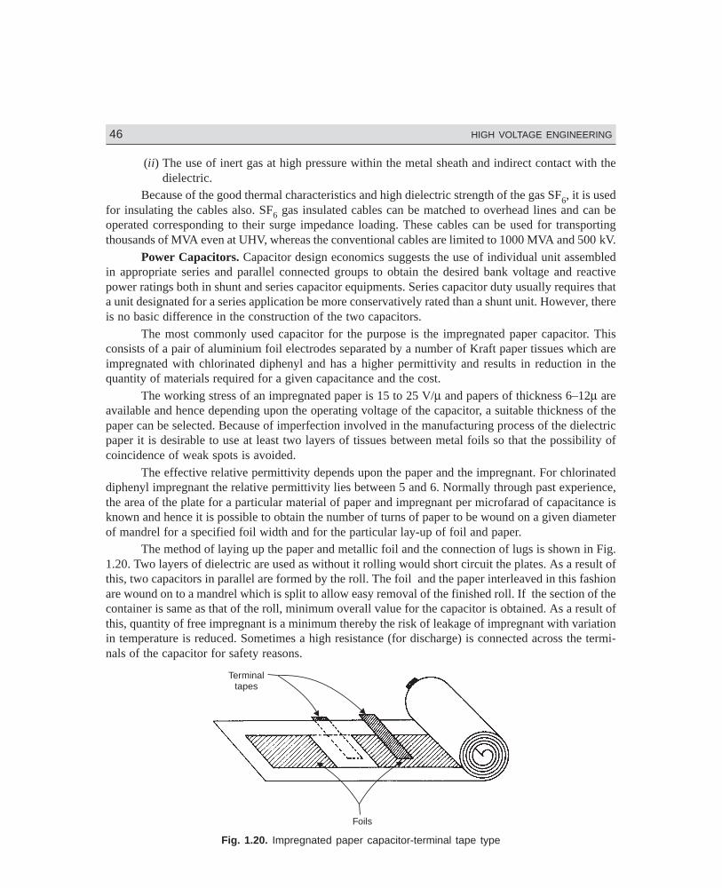
DharmN-HIGH\HG1-3.PM5 46
46 HIGH VOLTAGE ENGINEERING
(ii) The use of inert gas at high pressure within the metal sheath and indirect contact with thedielectric.
Because of the good thermal characteristics and high dielectric strength of the gas SF6, it is usedfor insulating the cables also. SF6 gas insulated cables can be matched to overhead lines and can beoperated corresponding to their surge impedance loading. These cables can be used for transportingthousands of MVA even at UHV, whereas the conventional cables are limited to 1000 MVA and 500 kV.
Power Capacitors. Capacitor design economics suggests the use of individual unit assembledin appropriate series and parallel connected groups to obtain the desired bank voltage and reactivepower ratings both in shunt and series capacitor equipments. Series capacitor duty usually requires thata unit designated for a series application be more conservatively rated than a shunt unit. However, thereis no basic difference in the construction of the two capacitors.
The most commonly used capacitor for the purpose is the impregnated paper capacitor. Thisconsists of a pair of aluminium foil electrodes separated by a number of Kraft paper tissues which areimpregnated with chlorinated diphenyl and has a higher permittivity and results in reduction in thequantity of materials required for a given capacitance and the cost.
The working stress of an impregnated paper is 15 to 25 V/µ and papers of thickness 6–12µ areavailable and hence depending upon the operating voltage of the capacitor, a suitable thickness of thepaper can be selected. Because of imperfection involved in the manufacturing process of the dielectricpaper it is desirable to use at least two layers of tissues between metal foils so that the possibility ofcoincidence of weak spots is avoided.
The effective relative permittivity depends upon the paper and the impregnant. For chlorinateddiphenyl impregnant the relative permittivity lies between 5 and 6. Normally through past experience,the area of the plate for a particular material of paper and impregnant per microfarad of capacitance isknown and hence it is possible to obtain the number of turns of paper to be wound on a given diameterof mandrel for a specified foil width and for the particular lay-up of foil and paper.
The method of laying up the paper and metallic foil and the connection of lugs is shown in Fig.1.20. Two layers of dielectric are used as without it rolling would short circuit the plates. As a result ofthis, two capacitors in parallel are formed by the roll. The foil and the paper interleaved in this fashionare wound on to a mandrel which is split to allow easy removal of the finished roll. If the section of thecontainer is same as that of the roll, minimum overall value for the capacitor is obtained. As a result ofthis, quantity of free impregnant is a minimum thereby the risk of leakage of impregnant with variationin temperature is reduced. Sometimes a high resistance (for discharge) is connected across the termi-nals of the capacitor for safety reasons.
Terminaltapes
Foils
Fig. 1.20. Impregnated paper capacitor-terminal tape type
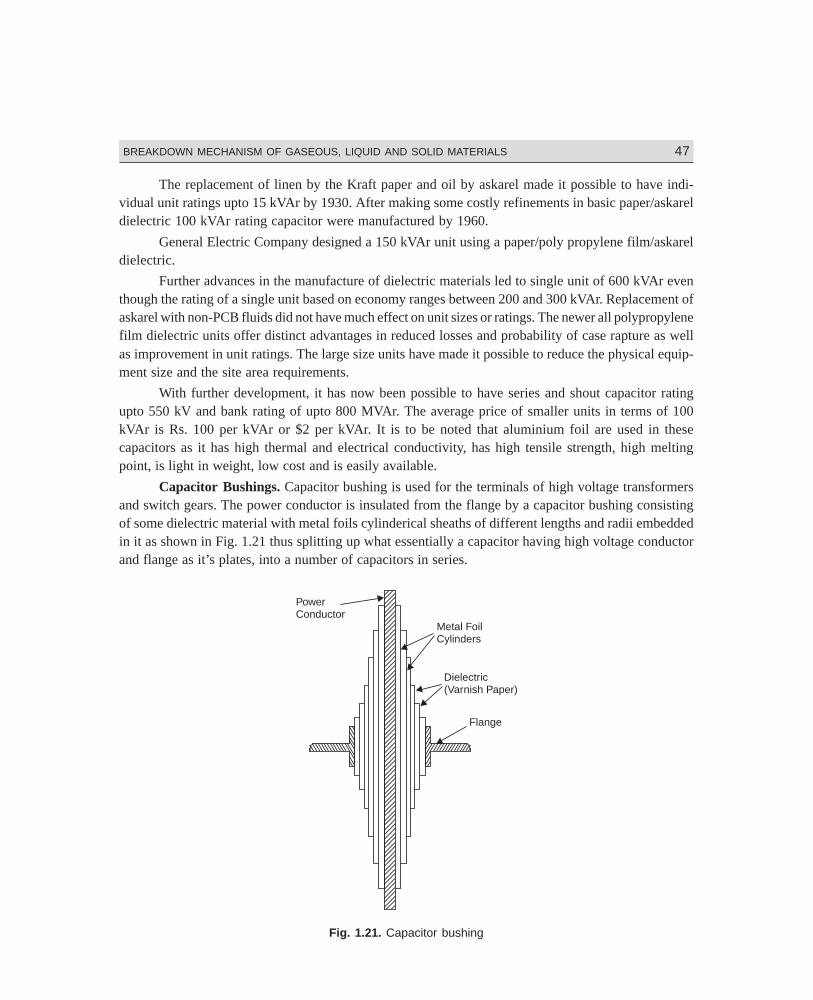
DharmN-HIGH\HG1-3.PM5 47
BREAKDOWN MECHANISM OF GASEOUS, LIQUID AND SOLID MATERIALS 47
The replacement of linen by the Kraft paper and oil by askarel made it possible to have indi-vidual unit ratings upto 15 kVAr by 1930. After making some costly refinements in basic paper/askareldielectric 100 kVAr rating capacitor were manufactured by 1960.
General Electric Company designed a 150 kVAr unit using a paper/poly propylene film/askareldielectric.
Further advances in the manufacture of dielectric materials led to single unit of 600 kVAr eventhough the rating of a single unit based on economy ranges between 200 and 300 kVAr. Replacement ofaskarel with non-PCB fluids did not have much effect on unit sizes or ratings. The newer all polypropylenefilm dielectric units offer distinct advantages in reduced losses and probability of case rapture as wellas improvement in unit ratings. The large size units have made it possible to reduce the physical equip-ment size and the site area requirements.
With further development, it has now been possible to have series and shout capacitor ratingupto 550 kV and bank rating of upto 800 MVAr. The average price of smaller units in terms of 100kVAr is Rs. 100 per kVAr or $2 per kVAr. It is to be noted that aluminium foil are used in thesecapacitors as it has high thermal and electrical conductivity, has high tensile strength, high meltingpoint, is light in weight, low cost and is easily available.
Capacitor Bushings. Capacitor bushing is used for the terminals of high voltage transformersand switch gears. The power conductor is insulated from the flange by a capacitor bushing consistingof some dielectric material with metal foils cylinderical sheaths of different lengths and radii embeddedin it as shown in Fig. 1.21 thus splitting up what essentially a capacitor having high voltage conductorand flange as it’s plates, into a number of capacitors in series.
Flange
Dielectric(Varnish Paper)
Metal FoilCylinders
PowerConductor
Fig. 1.21. Capacitor bushing
DharmN-HIGH\HG1-3.PM5 48
48 HIGH VOLTAGE ENGINEERING
The capacitance of the capacitors formed by the metal foil cylinders is given by
C = εl
R
R2 2
1
ln
where l is the axial length of the capacitor R1 and R2 are the radii of its cylinderical plates. If thesecapacitor have the same capacitance, the potential difference between their plates will be equal. Theequal capacitance between different layers is made possible by choosing suitable axial length together
with ratio R
R2
1
. With this strategy the potential gradient in the dielectric is uniform but the edges of the
foil sheets lie on a curve, thus giving unequal surfaces of dielectric between the edges of successivesheets. This is undesirable as this would result into flashovers by “Creeping” along the surface. How-ever, if the differences between the lengths of successive sheets are made equal, the radial stress is notuniform and hence a compromise between the two conditions is usually adopted.
There are three types of papers used as insulating materials for capacitor bushings; oil impreg-nated paper, resin bonded paper and resin impregnated paper. The oil impregnated paper bushing ismade by wrapping untreated paper after inserting foil sheets at the appropriate position and then im-pregnating with transformer oil after vacuum drying. Before impregnation, it is ensured that moistureand air voids are avoided. This bushing can work at a radial stress of 40 kV/cm.
In case of resin impregnated bushing creped paper tape is wrapped round the conductor andthen dried in an autoclave under controlled heat and vacuum. Epoxyresin is then sprayed to fill thewinding. The permissible radial stress in this case is 30 kV/cm.
In case of resin bonded paper bushing, the paper is first coated with epoxyresin and wrappedround a cylinderical form under heat and pressure after inserting foil sheets at appropriate position. Thepermissible radial stress in this case in 20 kV/cm.
1.15 BREAKDOWN IN VACUUM
A vacuum system is one in which the pressure maintained is at a value below the atmospheric pressureand is measured in terms of mm of mercury. One standard atmospheric pressure at 0°C is equal to 760mm of mercury. One mm of Hg pressure is also known as one torr after the name of Torricelli who wasthe first to obtain pressures below atmosphere, with the help of mercury barometer. Sometimes 10–3
torr is known as one micron. It is now possible to obtain pressures as low as 10–8 torr.
In a Townsend type of discharge, in a gas, the mean free path of the particles is small andelectrons get multiplied due to various ionization processes and an electron avalanche is formed. In avacuum of the order of 10–5 torr, the mean free path is of the order of few metres and thus when theelectrodes are separated by a few mm an electron crosses the gap without any collision. Therefore, in avacuum, the current growth prior to breakdown can not take place due to formation of electron ava-lanches. However, if it could be possible to liberate gas in the vacuum by some means, the dischargecould take place according to Townsend process. Thus, a vacuum arc is different from the general classof low and high pressure arcs. In the vacuum arc, the neutral atoms, ions and electrons do not comefrom the medium in which the arc is drawn but they are obtained from the electrodes themselves by
DharmN-HIGH\HG1-3.PM5 49
BREAKDOWN MECHANISM OF GASEOUS, LIQUID AND SOLID MATERIALS 49
evaporating its surface material. Because of the large mean free path for the electrons, the dielectricstrength of the vacuum is a thousand times more than when the gas is used as the interrupting medium.In this range of vacuum, the breakdown strength is independent of the gas density and depends only onthe gap length and upon the condition of electrode surface. Highly polished and thoroughly degassedelectrodes show higher breakdown strength. Electrodes get roughened after use and thus the dielectricstrength or breakdown strength decreases which can be improved by applying successive high voltageimpulses which of course does not change the roughened surface but removes the loosely adheringmetal particles from the electrodes which were deposited during arcing. It has been observed that for avacuum of 10–6 torr, some of the metals like silver, bismuth-copper etc. attain their maximum break-down strength when the gap is slightly less than 3 mm. This property of vacuum switches permits theuse of short gaps for fast operation.
Electric Discharge in VacuumThe electric discharge in vacuum results from the neutral atoms, ions and electrons emitted from
the electrodes themselves. Cathode spots are formed depending upon the current flowing. For lowcurrents a highly mobile cathode spot is formed and for large currents a multiple number of cathodespots are formed. These spots constitute the main source of vapour in the arc. The processes involvedin drawing the discharge will be due to high electric field between the contacts or resistive heatingproduced at the point of operation or a combination of the two. The cathode surfaces, normally, are notperfectly smooth but have many micro projections. Due to their small area of cross-section, the projec-tions will suffer explosive evaporation by resistive heating and supply sufficient quantity of vapour forthe arc formation. Since in case of vacuum, the emission occurs only at the cathode spots and not fromthe entire surface of the cathode, the vacuum discharge is also known as cold cathode discharge. Incold cathode the emission of electrons could be due to any of the combinations of the following mecha-nisms: (i) Field emission; (ii) Thermionic emission; (iii) Field and Thermionic emission; (iv) Second-ary emission by positive ion bombardment; (v) Secondary emission by photons; and (vi) Pinch effect.
The stability of discharge in vacuum depends upon: (i) the contact material and its vapour pres-sure, and (ii) circuit parameters such as voltage, current, inductance and capacitance. It has been ob-served that higher the vapour pressure at low temperature the better is the stability of the discharge.There are certain metals like Zn, Bi which show these characteristics and are better electrode materialsfor vacuum breakers. Besides the vapour pressure, the thermal conductivity of the metal also affects thecurrent chopping level. A good heat conducting metal will cool its surface faster and hence its elec-trode surface temperature will fall which will result into reduction in evaporation rate and arc will bechopped because of insufficient vapour. On the other hand, a bad heat conductor will maintain itstemperature and vaporization for a longer time and the arc will be more stable.
The process of multiplication of charged particles by the process of collision is very small in thespace between the electrode in vacuum, electron avalanche is not possible. If somehow a gas cloudcould be formed in vacuum, the usual kind of breakdown process can take place. This is the line ofaction adopted by the researchers to study mechanism of breakdown in vacuum. By finding the way,gas cloud could be created in a vacuum.
1.15.1 Non-metallic Electron Emission MechanismThe pre-breakdown conduction current in vacuum normally originates from a nonmetallic electrodesurface. These are present in the form of insulating/semiconducting oxide layer on the surfaces or asimpurities in the electrode material. These microinclusions present in the electrode surface can producestrong electron emission and significantly reduce the break down strength of the gap.
DharmN-HIGH\HG1-3.PM5 50
50 HIGH VOLTAGE ENGINEERING
Even when a vacuum system is completely sealed off, the electrode surfaces may still get con-taminated. It has been observed that when glass is heated to ‘its’ working temperature for sealing theelectrodes into a closed container, fluxes are vaporised from the glass which get deposited in the coolinner surfaces in the form of spherical particles upto a µm diameter . Therefore, the surface of a sealedelectrode may have on its surface contaminates e.g., sodium, potassium, boron aluminium and silicon.When an electric field is applied across such electrodes the oxides adsorbates and dust particles, thenundergo chemical changes e.g., oxides and adsorbates undergo chemical reactions which are initiatedby photons, electrons and ions and thus these contaminants limit the maximum field intensity for thefollowing reasons:
(i) The adsorbates and dust enhance the field emission of electrons.
(ii) The oxides adsorbates and dust particles enhance the secondary electron emission.
(iii) The oxides adsorbates and dust particles exhibit stimulated desorption of molecules andions under the impact of electrons, protons or ions.
Due to these mechanism, there is increase in electron emission process and therefore, moreelectric field energy is converted into kinetic energy of electron and ions which leads to an increase insurface energy of the metal. Thus, the electric strength of the gap may reduce to a level as low as 10 kV/cm as compared to 104 kV/cm which is required for the field emission process.
1.15.2 Clump MechanismThe vacuum breakdown mechanism based on this theory makes following assumption:
(i) A loosely bound particle known as clump exists on one of the electrode surfaces.
(ii) When a high voltage is applied between the two electrodes, this clump gets charged andsubsequently gets detached from the mother electrode and is attracted by the other electrode.
(iii) The breakdown occurs due to a discharge in the vapour or gas released by the impact to theparticle at the opposite electrode.
It has been observed that for a certain vacuum gap if frequent recurrent electric breakdowns arecarried out, the withstand voltage of the gap increases and after certain number of breakdown, it reachesan optimum maximum value. This is known as conditioning of electrodes and is of paramount importancefrom practical reasons. In this electrode conditioning, the microemission sites are supposed to havebeen destroyed.
Various methods for conditioning the electrodes have been suggested. Some of these are
(i) To treat the electrodes by means of hydrogen glow discharge. This method gives moreconsistent results.
(ii) Allowing the pre-breakdown currents in the gap to flow for some time or to heat the elec-trodes in vacuum to high temperature.
(iii) Treating the electrodes with repeated spark breakdown. This method is however quite timeconsuming.
The area of electrodes for breakdown of gases, liquids, solids or vacuum plays an importantrole. It has been observed that if the area of electrodes is increased for the same gap distance in uniformfield, the breakdown voltages are reduced.
DharmN-HIGH\HG1-3.PM5 51
BREAKDOWN MECHANISM OF GASEOUS, LIQUID AND SOLID MATERIALS 51
1.15.3 Effect of Pressure on Breakdown VoltageIt has been observed that in case of very small gaps of less than a mm and the gas pressure between thegap lies in the range 10–9 to 10–2 Torr, there is no change in the breakdown voltage i.e., if the gap lengthis small a variation of gas pressure in the range given above doesn’t affect the breakdown voltage.However, if the gap length is large say about 20 cm, the variation of gas pressure between the gapadversely affects the withstand voltage and the withstand voltage lowers drastically.
Example 1.1 A steady current of 600 µA flows through the plane electrode separated by a distance of
0.5 cm when a voltage of 10 kV is applied. Determine the Townsend’s first ionization coefficient if a
current of 60 µA flows when the distance of separation is reduced to 0.1 cm and the field is kept
constant at the previous value.
Solution: Since the field is kept constant (i.e., if distance of separation is reduced, the voltage is alsoreduced by the same ratio so that V/d is kept constant).
I = I0 eαx
Substituting two different sets of values,
we have 600 = I0 e0.5α and 60 = I0 e0.1α
or 10 = e0.4α or 0.4 α = 1n 10
0.4 α = 2.3026
α = 5.75 ionizing collisions/cm.
Example 1.2. The following table gives two sets of experimental results for studying Townsend’s mecha-
nism. The field is kept constant in each set:
I set 30 kV/cm II set kV/cm
Gap distance (mm) Observed current A
I set II set
0.5 1.5 × 10⁻¹³ 6.5 × 10⁻¹⁴
1.0 5 × 10–13 2.0 × 10⁻¹³
1.5 8.5 × 10⁻¹³ 4 × 10–13
2.0 1.5 × 10⁻¹² 8 × 10–13
2.5 5.6 × 10⁻¹² 1.2 × 10⁻¹²
3.0 1.4 × 10⁻¹⁰ 6.5 × 10⁻¹²
3.5 1.4 × 10⁻¹⁰ 6.5 × 10⁻¹¹
4.0 1.5 × 10⁻⁹ 4.0 × 10⁻¹⁰
5.0 7.0 × 10⁻⁷ 1.2 × 10⁻⁸
The manimum current observed is 6 × 10–14 A. Determine the values of Townsend’s first andsecond ionization coefficients.
DharmN-HIGH\HG1-3.PM5 52
52 HIGH VOLTAGE ENGINEERING
Solution: 1st Set. Since there is gradual increase in current upto gap distance of 3 mm, slope betweenany two points
1 0n I I
x
/FH
IK
will give us the value of α.
Let us take gap distances of 2 and 2.5 mm.
The respective 1n I/I0 are
1n 1 5 10
6 10
12
14
. ××
FHG
IKJ
−
− = 3.2188
and 1n 1 5 10
6 10
12
14
. ××
FHG
IKJ
−
− = 4.5362
∴ The slope = 4 5362 3 2188
0 0526 34
. .
..
− =
Since there is sudden rise in current at the last observation, this is used to evaluate γ .
We know that
or I = I e
e
x
x0
1 1
α
αγ− −( )
or I
I
e
e0
726 34 0 5
13 17
7
610
1 1= × =
− −
×. .
.( )γ
= 5 24 10
1 5 24 10
5
5
.
.
×− × γ
or7
610
1
5 24 10
1
1 5 24 107
5 5××
=− ×. . γ
or 0.0449 = 1 – 5.24 × 10⁵ γor 0.9551 = 5.24 × 10⁵ γor γ = 0.182 × 10⁻⁵ /cm.
Set-II. For the same gap distance the slope will be α = 1n (12/8)/0.05 = 8.1 collisions/cm andtherefore
I
I
e
e0
58 1 0 5
4 052 101 1
= × =− −
×. .
.( )γ
2 × 105 = 57 39
1 56 39
.
( . )− γ
or200 10
57 393 4849 10
1
1 56 39
33× = × =
−..
. γ
2.87 × 10–4 = 1 – 56.39 γ
DharmN-HIGH\HG1-3.PM5 53
BREAKDOWN MECHANISM OF GASEOUS, LIQUID AND SOLID MATERIALS 53
56.39γ = 1.0
or γ = 1.7 × 10⁻² collisions/cm
Example 1.3. The following observations were made in an experiment for determination of dielectricstrength of transformer oil. Determine the power law equation.
Gap spacing 4 6 8 10
Breakdown 88 135 165 212Voltage (kV)
Solution: Let us assume that the relation between gap spacing and breakdown voltage be given as
Vb = Kdn
Our objective is to find out values of K and n. Substituting values of two observations , we have
88 = K.4n
165 = K.8n
∴165
88
8
42= =
n
nn
1.875 = 2n
0.6286 = n × 0.693
or n = 0.9068
and K = 88
425 030 9068. .=
Similarly taking 2nd and 4th observation, we have
135 = K6n
212 = K10n
or212
1351 67= . n
1.57 = 1.67n
Taking 1n on both sides
0.4513 = 0.5128 nor n = 0.88
and K = 135
627 90 88. .=
Therefore, average value of n ≈ 0.89 and that of K ≈ 26.46 Ans.
Example 1.4. State and explain Paschen’s law. Derive expression for (pd)min and Vbmin. AssumeA = 12, B = 365 and γ = 0.02 for air. Determine (pd)min and Vbmin.
Solution: We know that
(pd)min = ek
Awhere K = ln (1 + 1/γ)
DharmN-HIGH\HG1-3.PM5 54
54 HIGH VOLTAGE ENGINEERING
Therefore, (pd)min = e
A ln (1 + 1/γ)
Substituting the values, we have
(pd)min = 2 718
121 1 1 0 02
.( / . )n + = 0.89 Ans.
Now Vbmin = B
Ae K =
365
122 718 1 51× . n = 325 Volts Ans.
1.1. Discuss various factors which affect breakdown of gases.
1.2. Define Townsend’s first and second ionisation coefficients. Explain the Townsends criterion for a spark.
1.3. State and explain Paschen’s law. How do you account for the minimum voltage for breakdown under agiven pd condition?
1.4. Explain the mechanism of development of anode and cathode streamers and explain how these lead tobreakdown.
1.5. What is time-lag? Discuss its components and the factors which affect these components.
1.6. Explain briefly various theories of breakdown in liquid dielectrics.
1.7. Explain clearly suspended particle mechanism of liquid breakdown.
1.8. State various process which lead to formation of bubbles in liquid dielectrics and explain clearly cavitybreakdown mechanism in liquid dielectrics.
1.9. What is electroconvection? Explain liquid breakdown based on electroconvection.
1.10. Discuss various criteria suggested by researchers for transition from avalanche to streamer.
1.11. Explain Penning Effect when referred to gaseous discharges.
1.12. What is corona discharge? Explain clearly Anode and Cathode coronas.
1.13. Describe briefly various mechanism of breakdown in solids.
1.14. What are ‘Treeing’ and ‘Tracking’? Explain clearly the two processes in solid dielectrics.
1.15. Derive an expression for maximum thermal voltage and show that the voltage is independent of thicknessof specimen. State clearly the assumptions made.
1.16. Derive an expression for critical electric field and show that the field is independent of the critical tem-perature of the dielectric. State the assumptions made.
1.17. What do you mean by ‘Intrinsic strength’ of a solid dielectric? Explain electric breakdown of soliddielectrics.
1.18. Explain Thermal breakdown in solid dielectrics. How this mechanism is more significant than the othermechanisms?
1.19. Explain the process of breakdown in electronegative gases.
1.20. Explain the application of oil in power apparatus and discuss clearly its function with reference to acircuit breaker.
1.21. Describe the main requirements of solid insulating materials used for power apparatus and describe thedielectric characteristics of the following material:
(i) vulcanized rubber (ii) PVC (iii) cross-link polyethylene (iv) insulating press board (v) mica (vi) ceram-ics (vii) glass (viii) epoxy resins.
DharmN-HIGH\HG1-3.PM5 55
BREAKDOWN MECHANISM OF GASEOUS, LIQUID AND SOLID MATERIALS 55
1.22. Describe the application of various insulating materials used in the following power apparatus:
(i) Power transformers (ii) Circuit breakers
(iii) Rotating machines (iv) Power cables
(v) Power capacitors (vi) Capacitor bushings
1.23. Explain clearly various processes which explain electric breakdown in vacuum.
1.24. What is ‘‘conditioning of elecrodes’’? How does it affect breakdown in vacuum?
1.25. Discuss the effect of ‘‘Area of electrode’’ and ‘‘Effect of pressure’’ on the breakdown of vacuum.
1.26. Discuss the application of gases in electric power apparatus.
Alston, High Voltage Technology, Oxford University Press, 1968.
E.W. Mc Daniel, Collision Phenomenon in Ionised Gases, John Wiley, New York, 1964.
L.D. Loeb, The kinetic Theory of Gases, Johm Wiley, New York, 1963.
E. Kuffel and W.S. Zaengl, High Voltage Engineering-Fundamentals, Pergamon Press, 1984.
M.S. Naidu and V. Kamaraju, High Voltage Engineering, Tata McGraw-Hill 1982.
Ravindra Arora & W. Mosch, High Voltage Insulation Engineering, New Age International, 2005.
Generation of High D.C. andA.C. Voltages
56
2
There are various applications of high d.c. voltages in industries, research medical sciences etc. HVDCtransmission over both overhead lines and underground cables is becoming more and more popular.HVDC is used for testing HVAC cables of long lengths as these have very large capacitance and wouldrequire very large values of currents if tested on HVAC voltages. Even though D.C. tests on A.C.cables is convenient and economical, these suffer from the fact that the stress distribution within theinsulating material is different from the normal operating condition. In industry it is being used forelectrostatic precipitation of ashing in thermal power plants, electrostatic painting, cement industry,communication systems etc. HVDC is also being used extensively in physics for particle accelerationand in medical equipments (X-Rays).
The most efficient method of generating high D.C. voltages is through the process of rectifica-tion employing voltage multiplier circuits. Electrostatic generators have also been used for generatinghigh D.C. voltages.
According to IEEE standards 4-1978, the value of a direct test voltage is defined by its arithematicmean value Vd and is expressed mathematically as
VT
t dtd
T= z1
0υa f (2.1)
where T is the time period of the voltage wave having a frequency f = 1/T. Test voltages generated usingrectifiers are never constant in magnitude. These deviate from the mean value periodically and thisdeviation is known as ripple. The magnitude of the ripple voltage denoted by δV is defined as half thedifference between the maximum and minimum values of voltage i.e.,
δV = 1
2[ ]V Vmax min− (2.2)
and ripple factor is defined as the ratio of ripple magnitude to the mean value Vd i.e., δV/Vd. The testvoltages should not have ripple factor more than 5% or as specified in a specific standard for a particu-lar equipment as the requirement on voltage shape may differ for different applications.
2.1 HALF-WAVE RECTIFIER CIRCUIT
The simplest circuit for generation of high direct voltage is the half wave rectifier shown in Fig. 2.1Here RL is the load resistance and C the capacitance to smoothen the d.c. output voltage.
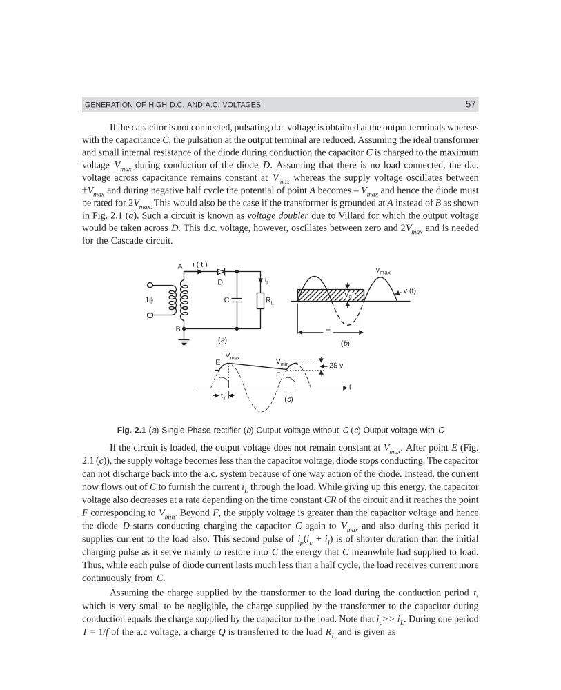
Dharm\N-HIGH\HG2-1.PM5 57
GENERATION OF HIGH D.C. AND A.C. VOLTAGES 57
If the capacitor is not connected, pulsating d.c. voltage is obtained at the output terminals whereaswith the capacitance C, the pulsation at the output terminal are reduced. Assuming the ideal transformerand small internal resistance of the diode during conduction the capacitor C is charged to the maximumvoltage Vmax during conduction of the diode D. Assuming that there is no load connected, the d.c.voltage across capacitance remains constant at Vmax whereas the supply voltage oscillates between±Vmax and during negative half cycle the potential of point A becomes – Vmax and hence the diode mustbe rated for 2Vmax. This would also be the case if the transformer is grounded at A instead of B as shownin Fig. 2.1 (a). Such a circuit is known as voltage doubler due to Villard for which the output voltagewould be taken across D. This d.c. voltage, however, oscillates between zero and 2Vmax and is neededfor the Cascade circuit.
1
vmax
v (t)
T
vd
( )b( )a
( )c
A
B
C
D iL
RL
i ( t )
E
t1
F
t
Vmax Vmin 2 v
Fig. 2.1 (a) Single Phase rectifier (b) Output voltage without C (c) Output voltage with C
If the circuit is loaded, the output voltage does not remain constant at Vmax. After point E (Fig.2.1 (c)), the supply voltage becomes less than the capacitor voltage, diode stops conducting. The capacitorcan not discharge back into the a.c. system because of one way action of the diode. Instead, the currentnow flows out of C to furnish the current iL through the load. While giving up this energy, the capacitorvoltage also decreases at a rate depending on the time constant CR of the circuit and it reaches the pointF corresponding to Vmin. Beyond F, the supply voltage is greater than the capacitor voltage and hencethe diode D starts conducting charging the capacitor C again to Vmax and also during this period itsupplies current to the load also. This second pulse of ip(ic + il) is of shorter duration than the initialcharging pulse as it serve mainly to restore into C the energy that C meanwhile had supplied to load.Thus, while each pulse of diode current lasts much less than a half cycle, the load receives current morecontinuously from C.
Assuming the charge supplied by the transformer to the load during the conduction period t,which is very small to be negligible, the charge supplied by the transformer to the capacitor duringconduction equals the charge supplied by the capacitor to the load. Note that ic>> iL. During one periodT = 1/f of the a.c voltage, a charge Q is transferred to the load RL and is given as
Dharm\N-HIGH\HG2-1.PM5 58
58 HIGH VOLTAGE ENGINEERING
Q = i t dtV t
RdtL
RL
LTTa f a f= zz = IT =
I
f
where I is the mean value of the d.c output iL(t) and VRL(t) the d.c. voltage which includes a ripple asshown in Fig. 2.1 (c).
This charge is supplied by the capacitor over the period T when the voltage changes from Vmax
to Vmin over approximately period T neglecting the conduction period of the diode.
Suppose at any time the voltage of the capacitor is V and it decreases by an amount of dV overthe time dt then charge delivered by the capacitor during this time is
dQ = CdV
Therefore, if voltage changes from Vmax to Vmin, the charge delivered by the capacitor
dQ CdV C V Vmax minV
V
max
= = − −zz b gmin
Or the magnitude of charge delivered by the capacitor
Q = C (Vmax– Vmin) (2.3)
Using equation (2.2)
Q = 2δVC (2.4)
Therefore, 2δVC = IT
or δV = IT
C
I
fC2 2= (2.5)
Equation (2.5) shows that the ripple in a rectifier output depends upon the load current and the circuitparameter like f and C. The product fC is, therefore, an important design factor for the rectifiers. Thehigher the frequency of supply and larger the value of filtering capacitor the smaller will be the ripplein the d.c. output.
The single phase half-wave rectifier circuits have the following disadvantages:
(i) The size of the circuits is very large if high and pure d.c. output voltages are desired.
(ii) The h.t. transformer may get saturated if the amplitude of direct current is comparable withthe nominal alternating current of the transformer.
It is to be noted that all the circuits considered here are able to supply relatively low currents andtherefore are not suitable for high current applications such as HVDC transmission.
When high d.c. voltages are to be generated, voltage doubler or cascaded voltage multipliercircuits are used. One of the most popular doubler circuit due to Greinacher is shown in Fig. 2.2.
Suppose B is more positive with respect to A and the diode D1 conducts thus charging thecapacitor C1 to Vmax with polarity as shown in Fig. 2.2. During the next half cycle terminal A of thecapacitor C1 rises to Vmax and hence terminal M attains a potential of 2 Vmax. Thus, the capacitor C2 ischarged to 2 Vmax through D2. Normally the voltage across the load will be less than 2 Vmax dependingupon the time constant of the circuit C2RL.
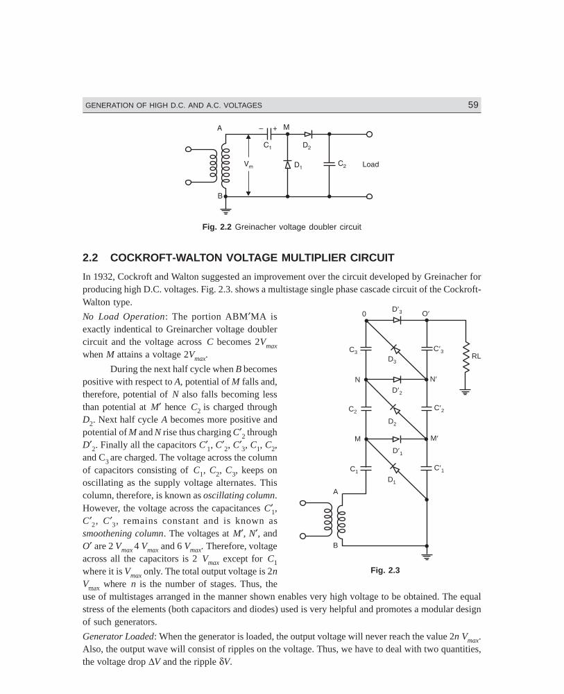
Dharm\N-HIGH\HG2-1.PM5 59
GENERATION OF HIGH D.C. AND A.C. VOLTAGES 59
Fig. 2.2 Greinacher voltage doubler circuit
2.2 COCKROFT-WALTON VOLTAGE MULTIPLIER CIRCUIT
In 1932, Cockroft and Walton suggested an improvement over the circuit developed by Greinacher forproducing high D.C. voltages. Fig. 2.3. shows a multistage single phase cascade circuit of the Cockroft-Walton type.
No Load Operation: The portion ABM′MA isexactly indentical to Greinarcher voltage doublercircuit and the voltage across C becomes 2Vmaxwhen M attains a voltage 2Vmax.
During the next half cycle when B becomespositive with respect to A, potential of M falls and,therefore, potential of N also falls becoming lessthan potential at M′ hence C2 is charged throughD2. Next half cycle A becomes more positive andpotential of M and N rise thus charging C′2 throughD′2. Finally all the capacitors C′1, C′2, C′3, C1, C2,and C3 are charged. The voltage across the columnof capacitors consisting of C1, C2, C3, keeps onoscillating as the supply voltage alternates. Thiscolumn, therefore, is known as oscillating column.However, the voltage across the capacitances C′1,C′2, C′3, remains constant and is known assmoothening column. The voltages at M′, N′, andO′ are 2 Vmax 4 Vmax and 6 Vmax. Therefore, voltageacross all the capacitors is 2 Vmax except for C1where it is Vmax only. The total output voltage is 2nVmax where n is the number of stages. Thus, theuse of multistages arranged in the manner shown enables very high voltage to be obtained. The equalstress of the elements (both capacitors and diodes) used is very helpful and promotes a modular designof such generators.
Generator Loaded: When the generator is loaded, the output voltage will never reach the value 2n Vmax.Also, the output wave will consist of ripples on the voltage. Thus, we have to deal with two quantities,the voltage drop ∆V and the ripple δV.
0 O
C3 C 3
N N
C2C 2
M M
C1C 1
A
D1
D 1
D2
D 2
D3
D3
RL
B
Fig. 2.3
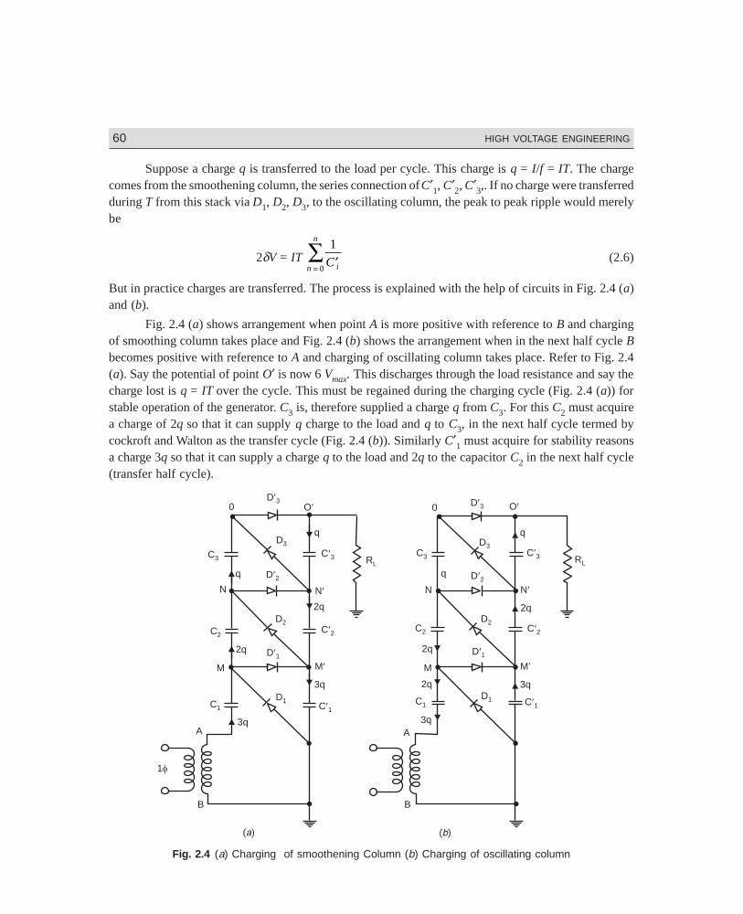
Dharm\N-HIGH\HG2-1.PM5 60
60 HIGH VOLTAGE ENGINEERING
Suppose a charge q is transferred to the load per cycle. This charge is q = I/f = IT. The chargecomes from the smoothening column, the series connection of C′1, C′2, C′3,. If no charge were transferredduring T from this stack via D1, D2, D3, to the oscillating column, the peak to peak ripple would merelybe
2δV = IT 1
0′=
∑ C in
n
(2.6)
But in practice charges are transferred. The process is explained with the help of circuits in Fig. 2.4 (a)and (b).
Fig. 2.4 (a) shows arrangement when point A is more positive with reference to B and chargingof smoothing column takes place and Fig. 2.4 (b) shows the arrangement when in the next half cycle Bbecomes positive with reference to A and charging of oscillating column takes place. Refer to Fig. 2.4(a). Say the potential of point O′ is now 6 Vmax. This discharges through the load resistance and say thecharge lost is q = IT over the cycle. This must be regained during the charging cycle (Fig. 2.4 (a)) forstable operation of the generator. C3 is, therefore supplied a charge q from C3. For this C2 must acquirea charge of 2q so that it can supply q charge to the load and q to C3, in the next half cycle termed bycockroft and Walton as the transfer cycle (Fig. 2.4 (b)). Similarly C′1 must acquire for stability reasonsa charge 3q so that it can supply a charge q to the load and 2q to the capacitor C2 in the next half cycle(transfer half cycle).
0 O
C3 C 3
N N
C2C 2
M M
C1 C 1D1
D 1
D2
D 2
D3
D 3
A
B
D 30 O
C3
D3C 3
D 2N N
C2
D2C 2
M
D 1M’
C 1D1C1
q
2q
3q
2q
3q
q q
2q
2q
q
2q
3q
3q
A
B
1
( )b( )a
RL RL
Fig. 2.4 (a) Charging of smoothening Column (b) Charging of oscillating column
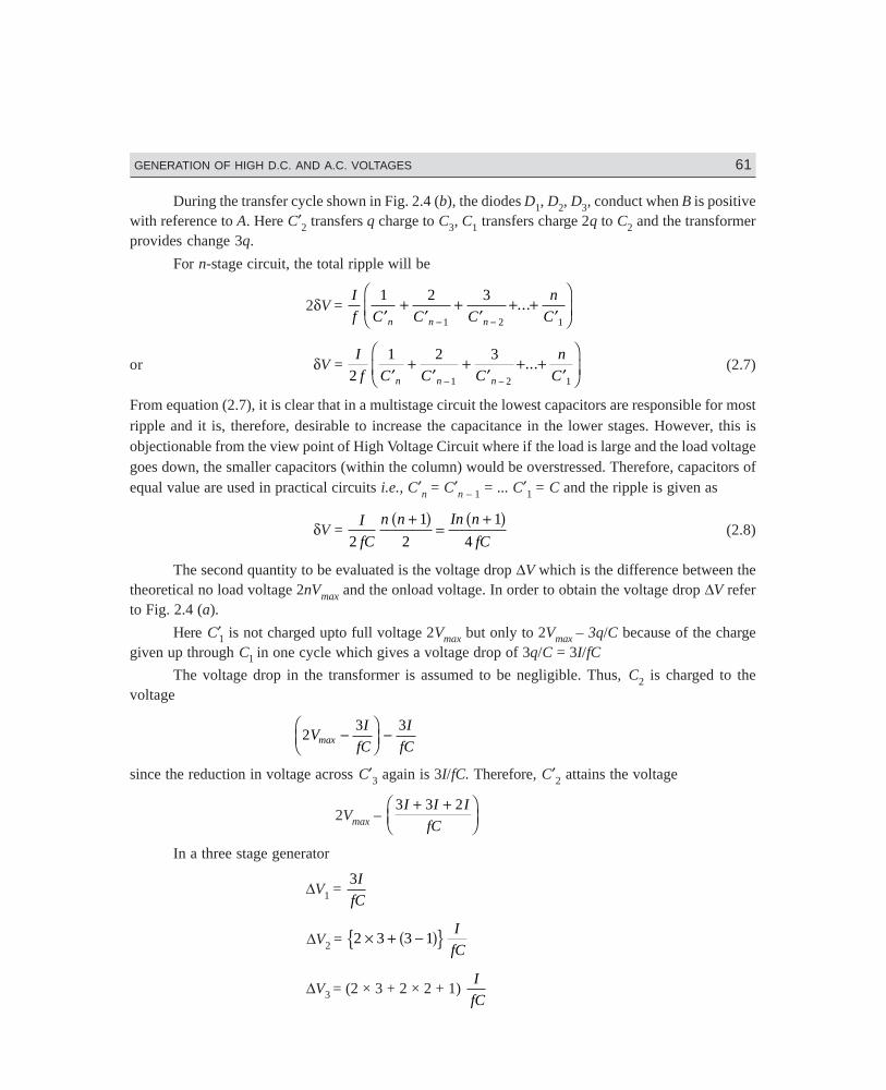
Dharm\N-HIGH\HG2-1.PM5 61
GENERATION OF HIGH D.C. AND A.C. VOLTAGES 61
During the transfer cycle shown in Fig. 2.4 (b), the diodes D1, D2, D3, conduct when B is positivewith reference to A. Here C′2 transfers q charge to C3, C1 transfers charge 2q to C2 and the transformerprovides change 3q.
For n-stage circuit, the total ripple will be
2δV = I
f C C C
n
Cn n n
1 2 3
1 2 1′+
′+
′+ +
′
FHG
IKJ− −
...
or δV = I
f C C C
n
Cn n n2
1 2 3
1 2 1′+
′+
′+ +
′
FHG
IKJ− −
... (2.7)
From equation (2.7), it is clear that in a multistage circuit the lowest capacitors are responsible for mostripple and it is, therefore, desirable to increase the capacitance in the lower stages. However, this isobjectionable from the view point of High Voltage Circuit where if the load is large and the load voltagegoes down, the smaller capacitors (within the column) would be overstressed. Therefore, capacitors ofequal value are used in practical circuits i.e., C′n = C′n – 1 = ... C′1 = C and the ripple is given as
δV = I
fC
n n In n
fC2
1
2
1
4
+=
+a f a f(2.8)
The second quantity to be evaluated is the voltage drop ∆V which is the difference between thetheoretical no load voltage 2nVmax and the onload voltage. In order to obtain the voltage drop ∆V referto Fig. 2.4 (a).
Here C′1 is not charged upto full voltage 2Vmax but only to 2Vmax – 3q/C because of the chargegiven up through C1 in one cycle which gives a voltage drop of 3q/C = 3I/fC
The voltage drop in the transformer is assumed to be negligible. Thus, C2 is charged to thevoltage
23 3
VI
fC
I
fCmax −
FHG
IKJ −
since the reduction in voltage across C′3 again is 3I/fC. Therefore, C′2 attains the voltage
2Vmax – 3 3 2I I I
fC
+ +FHG
IKJ
In a three stage generator
∆V1 = 3I
fC
∆V2 = 2 3 3 1× + −a fm r I
fC
∆V3 = (2 × 3 + 2 × 2 + 1) I
fC
Dharm\N-HIGH\HG2-1.PM5 62
62 HIGH VOLTAGE ENGINEERING
In general for a n-stage generator
∆Vn = nI
fC
∆Vn – 1 = I
fC 2n + (n – 1)
∆Vn – 2 = I
fC 2n + 2 (n – 1) + (n – 2)
.
.
.
∆V1 = I
fC 2n + 2 (n – 1) + 2 (n – 2) + ... 2 × 3 + 2 × 2 + 1
∆V = ∆Vn + ∆Vn – 1 + ... + ∆V1
After omitting I/fC, the series can be rewritten as:
Tn = nTn – 1 = 2n + (n – 1)
Tn – 2 = 2n + 2 (n – 1) + (n – 2) Tn – 3 = 2n + 2 (n – 1) + 2 (n – 2) + (n – 3)...
T1 = 2n + 2 (n – 1) + 2 (n – 2) + ... + 2 × 3 + 2 × 2 + 1
T = Tn + Tn – 1 + Tn – 2 + ... + T1
To sum up we add the last term of all the terms (Tn through T1) and again add the last term of theremaining term and so on, i.e.,
[n + (n – 1) + (n – 2)+ ... +2 + 1]
+ [2n + 2 (n – 1) + 2 (n – 2) + ... + 2 × 2]
+ [2n + 2 (n – 1) + ... + 2 × 4 + 2 × 3]
+ [2n + 2 (n – 1) + ... + 2 × 4]
+ [2n + 2 (n – 1) + 2 (n – 2) + ... + 2 × 5] + ... [2n]
Rearranging the above terms we have
n + (n – 1) + (n – 2) + ... + 2 + 1+ [2n + 2 (n – 1) + 2 (n – 2) + ... + 2 × 2 + 2 × 1] – 2 × 1+ [2n + 2 (n – 1) + 2 (n – 2) + ... + 2 × 3 + 2 × 2 + 2 × 1] – 2 × 2 – 2 × 1+ [2n + 2 (n – 1) + 2 (n – 2) + ... + 2 × 4 + 2 × 3 + 2 × 2 + 2 × 1]
– 2 × 3 – 2 × 2 – 2 × 1...
[2 × n + 2 (n – 1) + ... + 2 × 2 + 2 × 1] – [2 (n – 1)]
+ 2 (n – 2) + ... + 2 × 2 + 2 ×1]
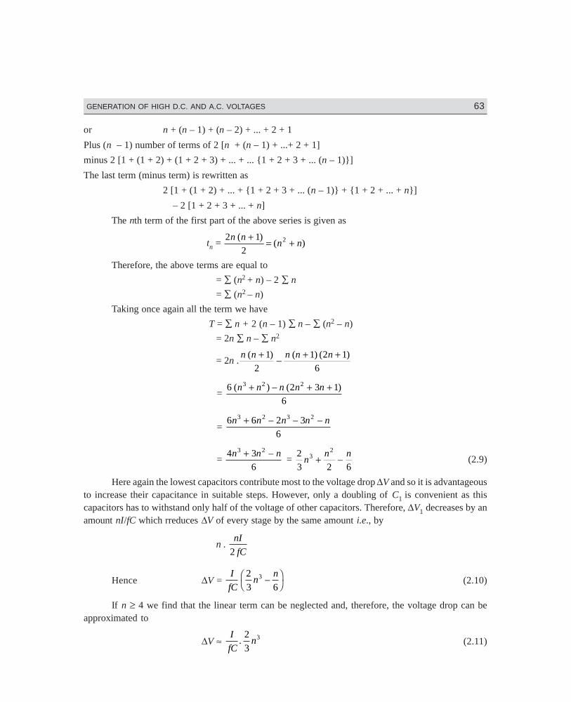
Dharm\N-HIGH\HG2-1.PM5 63
GENERATION OF HIGH D.C. AND A.C. VOLTAGES 63
or n + (n – 1) + (n – 2) + ... + 2 + 1
Plus (n – 1) number of terms of 2 [n + (n – 1) + ...+ 2 + 1]
minus 2 [1 + (1 + 2) + (1 + 2 + 3) + ... + ... 1 + 2 + 3 + ... (n – 1)]
The last term (minus term) is rewritten as
2 [1 + (1 + 2) + ... + 1 + 2 + 3 + ... (n – 1) + 1 + 2 + ... + n]
– 2 [1 + 2 + 3 + ... + n]
The nth term of the first part of the above series is given as
tn = 2 1
22n n
n n( )
( )+ = +
Therefore, the above terms are equal to
= ∑ (n2 + n) – 2 ∑ n= ∑ (n2 – n)
Taking once again all the term we have
T = ∑ n + 2 (n – 1) ∑ n – ∑ (n2 – n)
= 2n ∑ n – ∑ n2
= 2n .n n n n n( ) ( ) ( )+ − + +1
2
1 2 1
6
= 6 2 3 1
6
3 2 2( ) – ( )n n n n n+ + +
= 6 6 2 3
6
3 2 3 2n n n n n+ – – –
= 4 3
6
3n n n+ 2 – =
2
3 2 63
2
nn n+ – (2.9)
Here again the lowest capacitors contribute most to the voltage drop ∆V and so it is advantageousto increase their capacitance in suitable steps. However, only a doubling of C1 is convenient as thiscapacitors has to withstand only half of the voltage of other capacitors. Therefore, ∆V1 decreases by anamount nI/fC which rreduces ∆V of every stage by the same amount i.e., by
n . nI
fC2
Hence ∆V = I
fCn
n2
3 63 –F
HIK (2.10)
If n ≥ 4 we find that the linear term can be neglected and, therefore, the voltage drop can beapproximated to
∆V ≈ I
fCn.
2
33 (2.11)
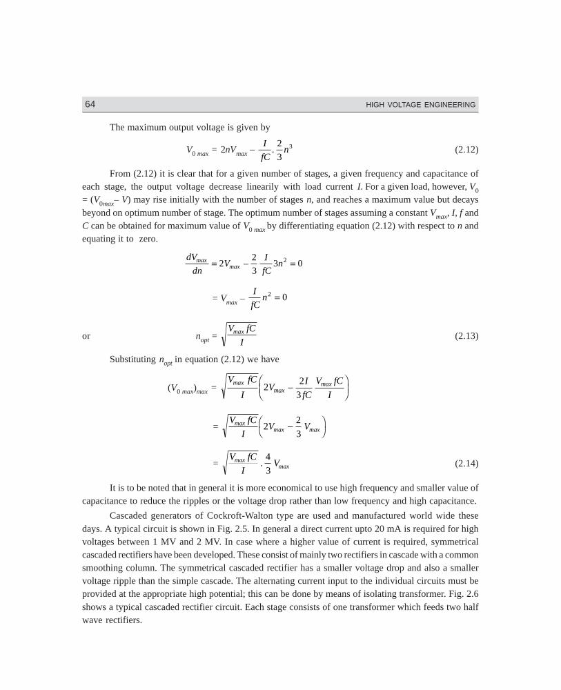
Dharm\N-HIGH\HG2-1.PM5 64
64 HIGH VOLTAGE ENGINEERING
The maximum output voltage is given by
V0 max = 2nVmax – I
fCn.
2
33 (2.12)
From (2.12) it is clear that for a given number of stages, a given frequency and capacitance ofeach stage, the output voltage decrease linearily with load current I. For a given load, however, V0
= (V0max– V) may rise initially with the number of stages n, and reaches a maximum value but decaysbeyond on optimum number of stage. The optimum number of stages assuming a constant Vmax, I, f andC can be obtained for maximum value of V0 max by differentiating equation (2.12) with respect to n andequating it to zero.
dV
dnV
I
fCnmax
max= =22
33 02–
= Vmax – I
fCn2 0=
or nopt = V fC
Imax (2.13)
Substituting nopt in equation (2.12) we have
(V0 max)max = V fC
IV
I
fC
V fC
Imax
maxmax2
2
3–
FHG
IKJ
= V fC
IV Vmax
max max22
3−F
HIK
= V fC
IVmax
max.4
3(2.14)
It is to be noted that in general it is more economical to use high frequency and smaller value ofcapacitance to reduce the ripples or the voltage drop rather than low frequency and high capacitance.
Cascaded generators of Cockroft-Walton type are used and manufactured world wide thesedays. A typical circuit is shown in Fig. 2.5. In general a direct current upto 20 mA is required for highvoltages between 1 MV and 2 MV. In case where a higher value of current is required, symmetricalcascaded rectifiers have been developed. These consist of mainly two rectifiers in cascade with a commonsmoothing column. The symmetrical cascaded rectifier has a smaller voltage drop and also a smallervoltage ripple than the simple cascade. The alternating current input to the individual circuits must beprovided at the appropriate high potential; this can be done by means of isolating transformer. Fig. 2.6shows a typical cascaded rectifier circuit. Each stage consists of one transformer which feeds two halfwave rectifiers.
Dharm\N-HIGH\HG2-1.PM5 65
GENERATION OF HIGH D.C. AND A.C. VOLTAGES 65
E M G
A V
W
V mA
3
Fig. 2.5 A typical Cockroft circuit
Fig. 2.6 Cascaded rectifier circuit
As the storage capacitors of these half wave rectifiers are series connected even the h.v. windingof T1 can not be grounded. This means that the main insulation between the primary and the secondarywinding of T1 has to be insulated for a d.c. voltage of magnitude Vmax, the peak voltage of T1. The sameis required for T2 also but this time the high voltage winding is at a voltage of 3Vmax. It would be
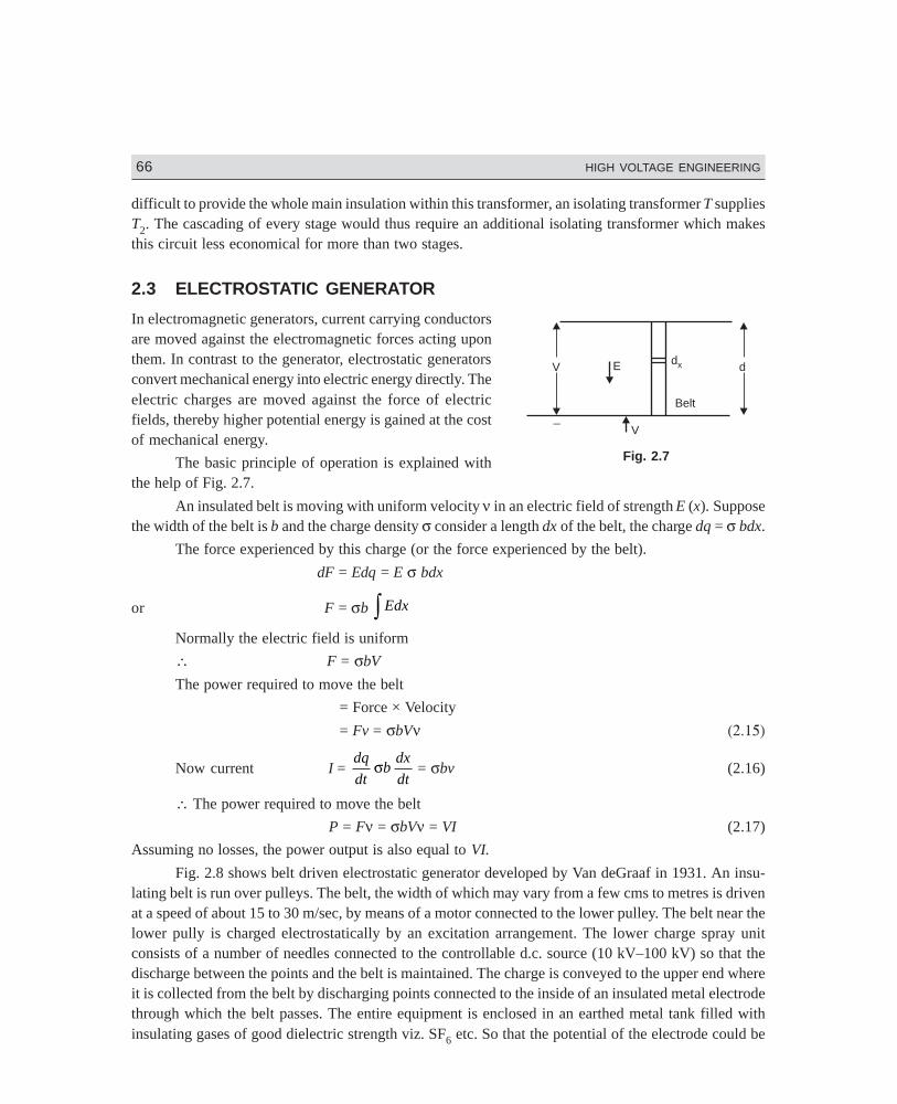
Dharm\N-HIGH\HG2-1.PM5 66
66 HIGH VOLTAGE ENGINEERING
difficult to provide the whole main insulation within this transformer, an isolating transformer T suppliesT2. The cascading of every stage would thus require an additional isolating transformer which makesthis circuit less economical for more than two stages.
2.3 ELECTROSTATIC GENERATOR
In electromagnetic generators, current carrying conductorsare moved against the electromagnetic forces acting uponthem. In contrast to the generator, electrostatic generatorsconvert mechanical energy into electric energy directly. Theelectric charges are moved against the force of electricfields, thereby higher potential energy is gained at the costof mechanical energy.
The basic principle of operation is explained withthe help of Fig. 2.7.
An insulated belt is moving with uniform velocity ν in an electric field of strength E (x). Supposethe width of the belt is b and the charge density σ consider a length dx of the belt, the charge dq = σ bdx.
The force experienced by this charge (or the force experienced by the belt).
dF = Edq = E σ bdx
or F = σb EdxzNormally the electric field is uniform
∴ F = σbV
The power required to move the belt
= Force × Velocity
= Fv = σbVν (2.15)
Now current I = dq
dtb
dx
dtσ = σbv (2.16)
∴ The power required to move the belt
P = Fν = σbVν = VI (2.17)
Assuming no losses, the power output is also equal to VI.
Fig. 2.8 shows belt driven electrostatic generator developed by Van deGraaf in 1931. An insu-lating belt is run over pulleys. The belt, the width of which may vary from a few cms to metres is drivenat a speed of about 15 to 30 m/sec, by means of a motor connected to the lower pulley. The belt near thelower pully is charged electrostatically by an excitation arrangement. The lower charge spray unitconsists of a number of needles connected to the controllable d.c. source (10 kV–100 kV) so that thedischarge between the points and the belt is maintained. The charge is conveyed to the upper end whereit is collected from the belt by discharging points connected to the inside of an insulated metal electrodethrough which the belt passes. The entire equipment is enclosed in an earthed metal tank filled withinsulating gases of good dielectric strength viz. SF6 etc. So that the potential of the electrode could be
Fig. 2.7
V E d
Belt
V
dx
_
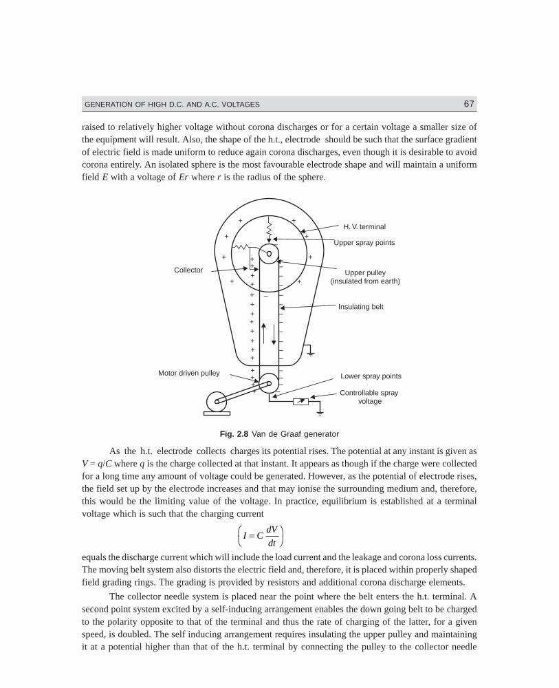
Dharm\N-HIGH\HG2-1.PM5 67
GENERATION OF HIGH D.C. AND A.C. VOLTAGES 67
raised to relatively higher voltage without corona discharges or for a certain voltage a smaller size ofthe equipment will result. Also, the shape of the h.t., electrode should be such that the surface gradientof electric field is made uniform to reduce again corona discharges, even though it is desirable to avoidcorona entirely. An isolated sphere is the most favourable electrode shape and will maintain a uniformfield E with a voltage of Er where r is the radius of the sphere.
+
+
+ +++
+ +
++++++++
++++
+
+
+
+
–
–––––––––––––
–––
–
H. V. terminal
Upper spray points
Upper pulley(insulated from earth)
Insulating belt
Lower spray points
Controllable sprayvoltage
Motor driven pulley
Collector
Fig. 2.8 Van de Graaf generator
As the h.t. electrode collects charges its potential rises. The potential at any instant is given asV = q/C where q is the charge collected at that instant. It appears as though if the charge were collectedfor a long time any amount of voltage could be generated. However, as the potential of electrode rises,the field set up by the electrode increases and that may ionise the surrounding medium and, therefore,this would be the limiting value of the voltage. In practice, equilibrium is established at a terminalvoltage which is such that the charging current
I CdV
dt=F
HIK
equals the discharge current which will include the load current and the leakage and corona loss currents.The moving belt system also distorts the electric field and, therefore, it is placed within properly shapedfield grading rings. The grading is provided by resistors and additional corona discharge elements.
The collector needle system is placed near the point where the belt enters the h.t. terminal. Asecond point system excited by a self-inducing arrangement enables the down going belt to be chargedto the polarity opposite to that of the terminal and thus the rate of charging of the latter, for a givenspeed, is doubled. The self inducing arrangement requires insulating the upper pulley and maintainingit at a potential higher than that of the h.t. terminal by connecting the pulley to the collector needle
Dharm\N-HIGH\HG2-1.PM5 68
68 HIGH VOLTAGE ENGINEERING
system. The arrangement also consists of a row of points (shown as upper spray points in Fig. 2.8)connected to the inside of the h.t. terminal and directed towards the pulley above its points of entry intothe terminal. As the pulley is at a higher potential (positive), the negative charges due to corona dischargeat the upper spray points are collected by the belt. This neutralises any remaining positive charge on thebelt and leaves an excess of negative charges on the down going belt to be neutralised by the lowerspray points. Since these negative charges leave the h.t. terminal, the potential of the h.t. terminal israised by the corresponding amount.
In order to have a rough estimate of the current supplied by the generator, let us assume that theelectric field E is normal to the belt and is homogeneous.
We know that D = ε0 E where D is the flux density and since the medium surrounding the h.t.terminal is say air εr = 1 and ε0 = 8.854 × 10⁻¹² F/metre.
According to Gauss law, D = σ the surface charge density.
Therefore, D = σ = ε0 E (2.18)
Assuming E = 30 kV/cm or 30,000 kV/m
σ = 8.854 × 10–12 × 3000 × 103
= 26.562 × 10⁻⁶ C/m2
Assuming for a typical system b = 1 metre and velocity of the belt ν = 10 m/sec, and usingequation (2.16), the current supplied by the generator is given as
I = σ bν= 26.562 × 10–6 × 1 × 10
= 26.562 × 10⁻⁵ Amp
= 265 µA
From equation (2.16) it is clear that current I depends upon σ, b and ν. The belt width (b) and velocityν being limited by mechanical reasons, the current can be increased by having higher value of σ. σ canbe increased by using gases of higher dielectric strength so that electric field intensity E could beincreased without the inception of ionisation of the medium surrounding the h.t. terminal. However,with all these arrangements, the actual short circuit currents are limited only to a few mA even for largegenerators.
The advantages of the generator are:
(i) Very high voltages can be easily generated
(ii) Ripple free output
(iii) Precision and flexibility of control
The disadvantages are:
(i) Low current output
(ii) Limitations on belt velocity due to its tendency for vibration. The vibrations may make itdifficult to have an accurate grading of electric fields
These generators are used in nuclear physics laboratories for particle acceleration and other processesin research work.
Dharm\N-HIGH\HG2-1.PM5 69
GENERATION OF HIGH D.C. AND A.C. VOLTAGES 69
2.4 GENERATION OF HIGH A.C. VOLTAGES
Most of the present day transmission and distribution networks are operating on a.c. voltages andhence most of the testing equipments relate to high a.c. voltages. Even though most of the equipmentson the system are 3-phase systems, a single phase transformer operating at power frequency is the mostcommon from of HVAC testing equipment.
Test transformers normally used for the purpose have low power rating but high voltage ratings.These transformers are mainly used for short time tests on high voltage equipments. The currentsrequired for these tests on various equipments are given below:
Insulators, C.B., bushings, Instrument
transformers = 0.1– 0.5 A
Power transformers, h.v. capacitors. = 0.5–1 A
Cables = 1 A and above
The design of a test transformer is similar to a potential transformer used for the measurement ofvoltage and power in transmission lines. The flux density chosen is low so that it does not draw largemagnetising current which would otherwise saturate the core and produce higher harmonics.
2.4.1 Cascaded TransformersFor voltages higher than 400 KV, it is desired to cascade two or more transformers depending upon thevoltage requirements. With this, the weight of the whole unit is subdivided into single units and, there-fore, transport and erection becomes easier. Also, with this, the transformer cost for a given voltagemay be reduced, since cascaded units need not individually possess the expensive and heavy insulationrequired in single stage transformers for high voltages exceeding 345 kV. It is found that the cost ofinsulation for such voltages for a single unit becomes proportional to square of operating voltage.
Fig. 2.9 shows a basic scheme for cascading three transformers. The primary of the first stagetransformer is connected to a low voltage supply. A voltage is available across the secondary of thistransformer. The tertiary winding (excitation winding) of first stage has the same number of turns as theprimary winding, and feeds the primary of the second stage transformer. The potential of the tertiary isfixed to the potential V of the secondary winding as shown in Fig. 2.9. The secondary winding of thesecond stage transformer is connected in series with the secondary winding of the first stage transformer,so that a voltage of 2V is available between the ground and the terminal of secondary of the secondstage transformer. Similarly, the stage-III transformer is connected in series with the second stagetransformer. With this the output voltage between ground and the third stage transformer, secondary is3V. it is to be noted that the individual stages except the upper most must have three-winding transformers.The upper most, however, will be a two winding transformer.
Fig. 2.9 shows metal tank construction of transformers and the secondary winding is notdivided. Here the low voltage terminal of the secondary winding is connected to the tank. The tank ofstage-I transformer is earthed. The tanks of stage-II and stage-III transformers have potentials of V and2V, respectively above earth and, therefore, these must be insulated from the earth with suitable solidinsulation. Through h.t. bushings, the leads from the tertiary winding and the h.v. winding are broughtout to be connected to the next stage transformer.
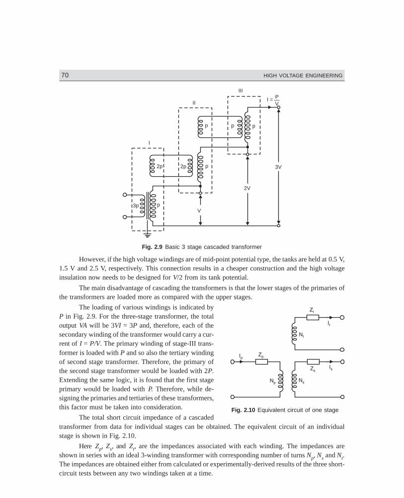
Dharm\N-HIGH\HG2-1.PM5 70
70 HIGH VOLTAGE ENGINEERING
3p p
2p p2p
p p p
I
II
III
3V
2V
V
I = P—V
Fig. 2.9 Basic 3 stage cascaded transformer
However, if the high voltage windings are of mid-point potential type, the tanks are held at 0.5 V,1.5 V and 2.5 V, respectively. This connection results in a cheaper construction and the high voltageinsulation now needs to be designed for V/2 from its tank potential.
The main disadvantage of cascading the transformers is that the lower stages of the primaries ofthe transformers are loaded more as compared with the upper stages.
The loading of various windings is indicated byP in Fig. 2.9. For the three-stage transformer, the totaloutput VA will be 3VI = 3P and, therefore, each of thesecondary winding of the transformer would carry a cur-rent of I = P/V. The primary winding of stage-III trans-former is loaded with P and so also the tertiary windingof second stage transformer. Therefore, the primary ofthe second stage transformer would be loaded with 2P.Extending the same logic, it is found that the first stageprimary would be loaded with P. Therefore, while de-signing the primaries and tertiaries of these transformers,this factor must be taken into consideration.
The total short circuit impedance of a cascadedtransformer from data for individual stages can be obtained. The equivalent circuit of an individualstage is shown in Fig. 2.10.
Here Zp, Zs, and Zt, are the impedances associated with each winding. The impedances areshown in series with an ideal 3-winding transformer with corresponding number of turns Np, Ns and Nt.The impedances are obtained either from calculated or experimentally-derived results of the three short-circuit tests between any two windings taken at a time.
Fig. 2.10 Equivalent circuit of one stage
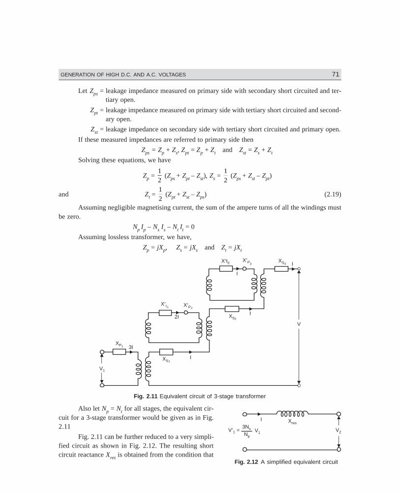
Dharm\N-HIGH\HG2-1.PM5 71
GENERATION OF HIGH D.C. AND A.C. VOLTAGES 71
Let Zps = leakage impedance measured on primary side with secondary short circuited and ter-tiary open.
Zpt = leakage impedance measured on primary side with tertiary short circuited and second-ary open.
Zst = leakage impedance on secondary side with tertiary short circuited and primary open.
If these measured impedances are referred to primary side then
Zps = Zp + Zs, Zpt = Zp + Zt and Zst = Zs + Zt
Solving these equations, we have
Zp = 1
2 (Zps + Zpt – Zst), Zs =
1
2 (Zps + Zst – Zpt)
and Zt = 1
2 (Zpt + Zst – Zps) (2.19)
Assuming negligible magnetising current, the sum of the ampere turns of all the windings mustbe zero.
Np Ip – Ns Is – Nt It = 0
Assuming lossless transformer, we have,
Zp = jXp, Zs = jXs and Zt = jXt
X t1
X t2
X P2
X P3
XS2
V1
I
I
I
2I
3I
XS1
XP1
XS3
V
I
Fig. 2.11 Equivalent circuit of 3-stage transformer
Also let Np = Nt for all stages, the equivalent cir-cuit for a 3-stage transformer would be given as in Fig.2.11
Fig. 2.11 can be further reduced to a very simpli-fied circuit as shown in Fig. 2.12. The resulting shortcircuit reactance Xres is obtained from the condition that
Fig. 2.12 A simplified equivalent circuit
V 1 =3Ns V1Np
I
V2
Xres
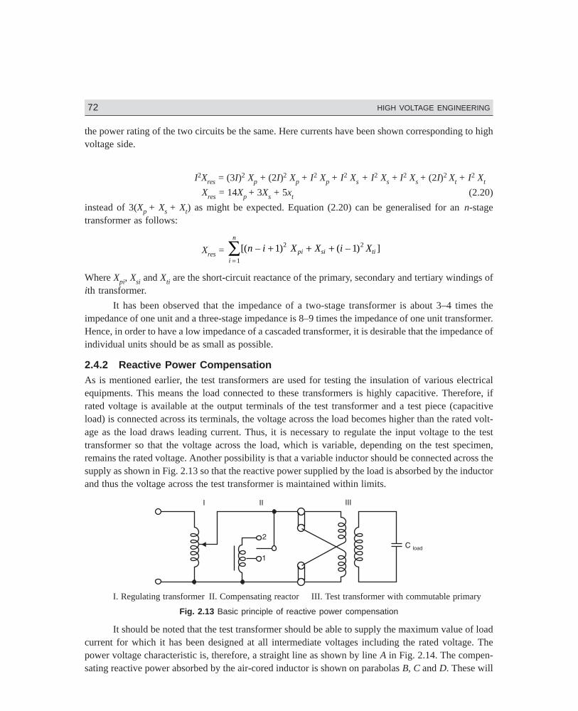
Dharm\N-HIGH\HG2-1.PM5 72
72 HIGH VOLTAGE ENGINEERING
the power rating of the two circuits be the same. Here currents have been shown corresponding to highvoltage side.
I2Xres = (3I)2 Xp + (2I)2 Xp + I2 Xp + I2 Xs + I2 Xs + I2 Xs + (2I)2 Xt + I2 Xt
Xres = 14Xp + 3Xs + 5xt (2.20)
instead of 3(Xp + Xs + Xt) as might be expected. Equation (2.20) can be generalised for an n-stagetransformer as follows:
Xres = [( – ) ( – ) ]n i X X i Xpi si tii
n
+ + +=∑ 1 12 2
1
Where Xpi, Xsi and Xti are the short-circuit reactance of the primary, secondary and tertiary windings ofith transformer.
It has been observed that the impedance of a two-stage transformer is about 3–4 times theimpedance of one unit and a three-stage impedance is 8–9 times the impedance of one unit transformer.Hence, in order to have a low impedance of a cascaded transformer, it is desirable that the impedance ofindividual units should be as small as possible.
2.4.2 Reactive Power CompensationAs is mentioned earlier, the test transformers are used for testing the insulation of various electricalequipments. This means the load connected to these transformers is highly capacitive. Therefore, ifrated voltage is available at the output terminals of the test transformer and a test piece (capacitiveload) is connected across its terminals, the voltage across the load becomes higher than the rated volt-age as the load draws leading current. Thus, it is necessary to regulate the input voltage to the testtransformer so that the voltage across the load, which is variable, depending on the test specimen,remains the rated voltage. Another possibility is that a variable inductor should be connected across thesupply as shown in Fig. 2.13 so that the reactive power supplied by the load is absorbed by the inductorand thus the voltage across the test transformer is maintained within limits.
I. Regulating transformer II. Compensating reactor III. Test transformer with commutable primary
Fig. 2.13 Basic principle of reactive power compensation
It should be noted that the test transformer should be able to supply the maximum value of loadcurrent for which it has been designed at all intermediate voltages including the rated voltage. Thepower voltage characteristic is, therefore, a straight line as shown by line A in Fig. 2.14. The compen-sating reactive power absorbed by the air-cored inductor is shown on parabolas B, C and D. These will
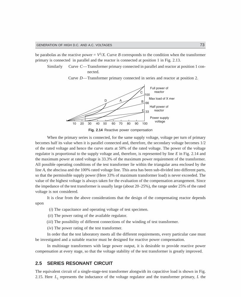
Dharm\N-HIGH\HG2-1.PM5 73
GENERATION OF HIGH D.C. AND A.C. VOLTAGES 73
be parabolas as the reactive power = V2/X. Curve B corresponds to the condition when the transformerprimary is connected in parallel and the reactor is connected at position 1 in Fig. 2.13.
Similarly Curve C—Transformer primary connected in parallel and reactor at position 1 con-nected.
Curve D—Transformer primary connected in series and reactor at position 2.
Fig. 2.14 Reactive power compensation
When the primary series is connected, for the same supply voltage, voltage per turn of primarybecomes half its value when it is parallel connected and, therefore, the secondary voltage becomes 1/2of the rated voltage and hence the curve starts at 50% of the rated voltage. The power of the voltageregulator is proportional to the supply voltage and, therefore, is represented by line E in Fig. 2.14 andthe maximum power at rated voltage is 33.3% of the maximum power requirement of the transformer.All possible operating conditions of the test transformer lie within the triangular area enclosed by theline A, the abscissa and the 100% rated voltage line. This area has been sub-divided into different parts,so that the permissible supply power (Here 33% of maximum transformer load) is never exceeded. Thevalue of the highest voltage is always taken for the evaluation of the compensation arrangement. Sincethe impedance of the test transformer is usually large (about 20–25%), the range under 25% of the ratedvoltage is not considered.
It is clear from the above considerations that the design of the compensating reactor dependsupon
(i) The capacitance and operating voltage of test specimen.
(ii) The power rating of the available regulator.
(iii) The possibility of different connections of the winding of test transformer.
(iv) The power rating of the test transformer.
In order that the test laboratory meets all the different requirements, every particular case mustbe investigated and a suitable reactor must be designed for reactive power compensation.
In multistage transformers with large power output, it is desirable to provide reactive powercompensation at every stage, so that the voltage stability of the test transformer is greatly improved.
2.5 SERIES RESONANT CIRCUIT
The equivalent circuit of a single-stage-test transformer alongwith its capacitive load is shown in Fig.2.15. Here L1 represents the inductance of the voltage regulator and the transformer primary, L the
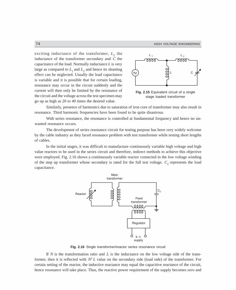
Dharm\N-HIGH\HG2-1.PM5 74
74 HIGH VOLTAGE ENGINEERING
exciting inductance of the transformer, L2 theinductance of the transformer secondary and C thecapacitance of the load. Normally inductance L is verylarge as compared to L1 and L2 and hence its shuntingeffect can be neglected. Usually the load capacitanceis variable and it is possible that for certain loading,resonance may occur in the circuit suddenly and thecurrent will then only be limited by the resistance ofthe circuit and the voltage across the test specimen maygo up as high as 20 to 40 times the desired value.
Similarly, presence of harmonics due to saturation of iron core of transformer may also result inresonance. Third harmonic frequencies have been found to be quite disastrous.
With series resonance, the resonance is controlled at fundamental frequency and hence no un-wanted resonance occurs.
The development of series resonance circuit for testing purpose has been very widely welcomeby the cable industry as they faced resonance problem with test transformer while testing short lengthsof cables.
In the initial stages, it was difficult to manufacture continuously variable high voltage and highvalue reactors to be used in the series circuit and therefore, indirect methods to achieve this objectivewere employed. Fig. 2.16 shows a continuously variable reactor connected in the low voltage windingof the step up transformer whose secondary is rated for the full test voltage. C2 represents the loadcapacitance.
Fig. 2.16 Single transformer/reactor series resonance circuit
If N is the transformation ratio and L is the inductance on the low voltage side of the trans-former, then it is reflected with N2 L value on the secondary side (load side) of the transformer. Forcertain setting of the reactor, the inductive reactance may equal the capacitive reactance of the circuit,hence resonance will take place. Thus, the reactive power requirement of the supply becomes zero and
Fig. 2.15 Equivalent circuit of a singlestage loaded transformer
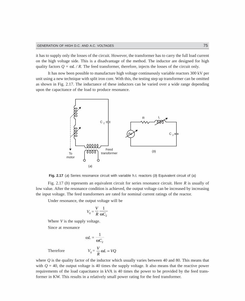
Dharm\N-HIGH\HG2-1.PM5 75
GENERATION OF HIGH D.C. AND A.C. VOLTAGES 75
it has to supply only the losses of the circuit. However, the transformer has to carry the full load currenton the high voltage side. This is a disadvantage of the method. The inductor are designed for highquality factors Q = ωL / R. The feed transformer, therefore, injects the losses of the circuit only.
It has now been possible to manufacture high voltage continuously variable reactors 300 kV perunit using a new technique with split iron core. With this, the testing step up transformer can be omittedas shown in Fig. 2.17. The inductance of these inductors can be varied over a wide range dependingupon the capacitance of the load to produce resonance.
C 2
C 2
R L
( )a
( )bTo
motor
Feedtransformer
Fig. 2.17 (a) Series resonance circuit with variable h.t. reactors (b) Equivalent circuit of (a)
Fig. 2.17 (b) represents an equivalent circuit for series resonance circuit. Here R is usually oflow value. After the resonance condition is achieved, the output voltage can be increased by increasingthe input voltage. The feed transformers are rated for nominal current ratings of the reactor.
Under resonance, the output voltage will be
V0 =
V
R C
1
2ω
Where V is the supply voltage.
Since at resonance
ωL = 1
2ωC
Therefore V0 = V
RL VQω =
where Q is the quality factor of the inductor which usually varies between 40 and 80. This means thatwith Q = 40, the output voltage is 40 times the supply voltage. It also means that the reactive powerrequirements of the load capacitance in kVA is 40 times the power to be provided by the feed trans-former in KW. This results in a relatively small power rating for the feed transformer.
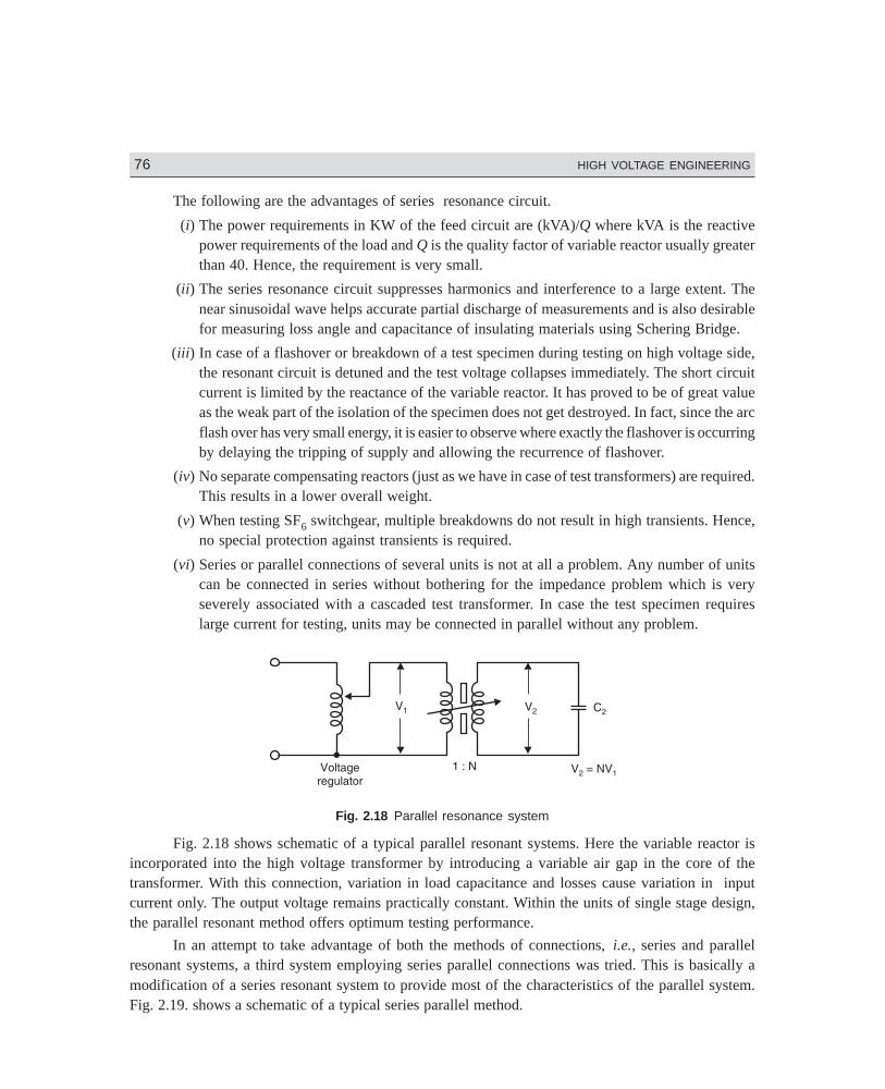
Dharm\N-HIGH\HG2-1.PM5 76
76 HIGH VOLTAGE ENGINEERING
The following are the advantages of series resonance circuit.
(i) The power requirements in KW of the feed circuit are (kVA)/Q where kVA is the reactivepower requirements of the load and Q is the quality factor of variable reactor usually greaterthan 40. Hence, the requirement is very small.
(ii) The series resonance circuit suppresses harmonics and interference to a large extent. Thenear sinusoidal wave helps accurate partial discharge of measurements and is also desirablefor measuring loss angle and capacitance of insulating materials using Schering Bridge.
(iii) In case of a flashover or breakdown of a test specimen during testing on high voltage side,the resonant circuit is detuned and the test voltage collapses immediately. The short circuitcurrent is limited by the reactance of the variable reactor. It has proved to be of great valueas the weak part of the isolation of the specimen does not get destroyed. In fact, since the arcflash over has very small energy, it is easier to observe where exactly the flashover is occurringby delaying the tripping of supply and allowing the recurrence of flashover.
(iv) No separate compensating reactors (just as we have in case of test transformers) are required.This results in a lower overall weight.
(v) When testing SF6 switchgear, multiple breakdowns do not result in high transients. Hence,no special protection against transients is required.
(vi) Series or parallel connections of several units is not at all a problem. Any number of unitscan be connected in series without bothering for the impedance problem which is veryseverely associated with a cascaded test transformer. In case the test specimen requireslarge current for testing, units may be connected in parallel without any problem.
Fig. 2.18 Parallel resonance system
Fig. 2.18 shows schematic of a typical parallel resonant systems. Here the variable reactor isincorporated into the high voltage transformer by introducing a variable air gap in the core of thetransformer. With this connection, variation in load capacitance and losses cause variation in inputcurrent only. The output voltage remains practically constant. Within the units of single stage design,the parallel resonant method offers optimum testing performance.
In an attempt to take advantage of both the methods of connections, i.e., series and parallelresonant systems, a third system employing series parallel connections was tried. This is basically amodification of a series resonant system to provide most of the characteristics of the parallel system.Fig. 2.19. shows a schematic of a typical series parallel method.
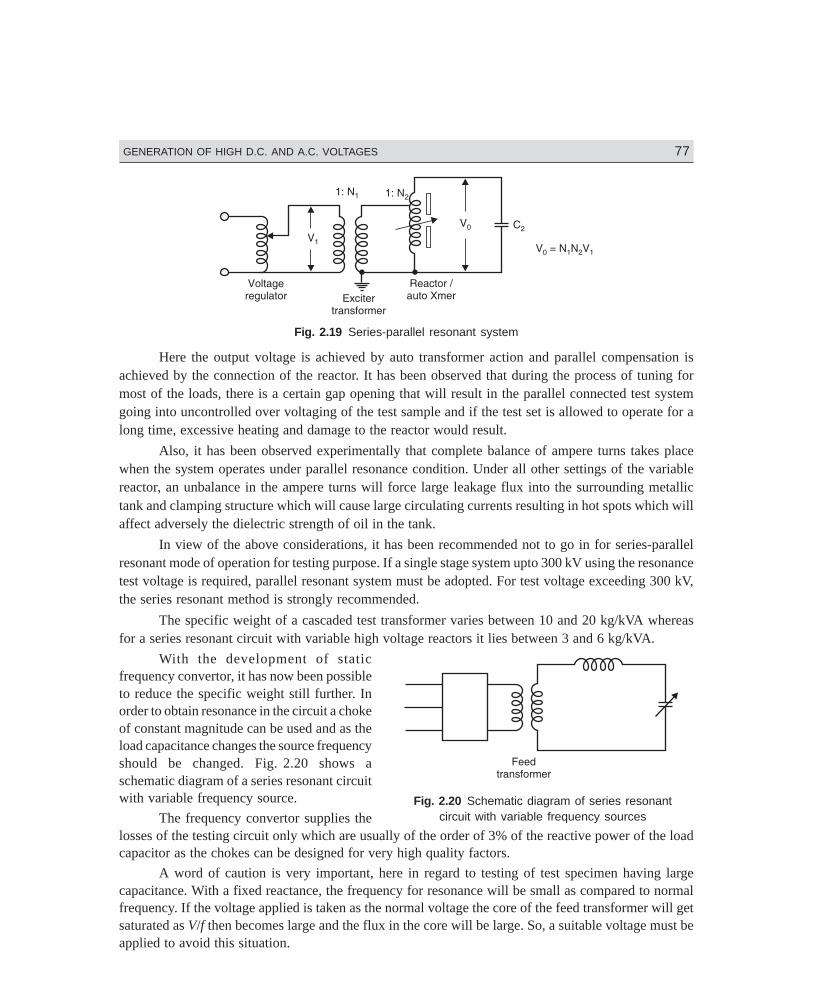
Dharm\N-HIGH\HG2-1.PM5 77
GENERATION OF HIGH D.C. AND A.C. VOLTAGES 77
Fig. 2.19 Series-parallel resonant system
Here the output voltage is achieved by auto transformer action and parallel compensation isachieved by the connection of the reactor. It has been observed that during the process of tuning formost of the loads, there is a certain gap opening that will result in the parallel connected test systemgoing into uncontrolled over voltaging of the test sample and if the test set is allowed to operate for along time, excessive heating and damage to the reactor would result.
Also, it has been observed experimentally that complete balance of ampere turns takes placewhen the system operates under parallel resonance condition. Under all other settings of the variablereactor, an unbalance in the ampere turns will force large leakage flux into the surrounding metallictank and clamping structure which will cause large circulating currents resulting in hot spots which willaffect adversely the dielectric strength of oil in the tank.
In view of the above considerations, it has been recommended not to go in for series-parallelresonant mode of operation for testing purpose. If a single stage system upto 300 kV using the resonancetest voltage is required, parallel resonant system must be adopted. For test voltage exceeding 300 kV,the series resonant method is strongly recommended.
The specific weight of a cascaded test transformer varies between 10 and 20 kg/kVA whereasfor a series resonant circuit with variable high voltage reactors it lies between 3 and 6 kg/kVA.
With the development of staticfrequency convertor, it has now been possibleto reduce the specific weight still further. Inorder to obtain resonance in the circuit a chokeof constant magnitude can be used and as theload capacitance changes the source frequencyshould be changed. Fig. 2.20 shows aschematic diagram of a series resonant circuitwith variable frequency source.
The frequency convertor supplies thelosses of the testing circuit only which are usually of the order of 3% of the reactive power of the loadcapacitor as the chokes can be designed for very high quality factors.
A word of caution is very important, here in regard to testing of test specimen having largecapacitance. With a fixed reactance, the frequency for resonance will be small as compared to normalfrequency. If the voltage applied is taken as the normal voltage the core of the feed transformer will getsaturated as V/f then becomes large and the flux in the core will be large. So, a suitable voltage must beapplied to avoid this situation.
Fig. 2.20 Schematic diagram of series resonantcircuit with variable frequency sources
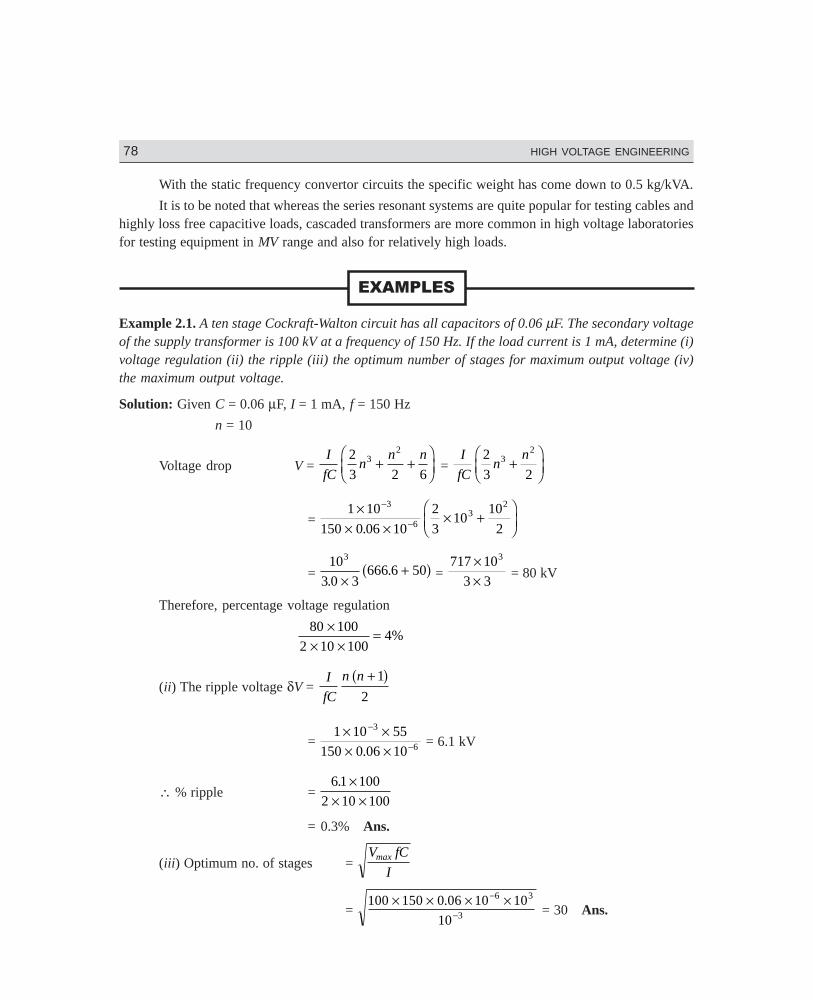
Dharm\N-HIGH\HG2-1.PM5 78
78 HIGH VOLTAGE ENGINEERING
With the static frequency convertor circuits the specific weight has come down to 0.5 kg/kVA.
It is to be noted that whereas the series resonant systems are quite popular for testing cables andhighly loss free capacitive loads, cascaded transformers are more common in high voltage laboratoriesfor testing equipment in MV range and also for relatively high loads.
Example 2.1. A ten stage Cockraft-Walton circuit has all capacitors of 0.06 µF. The secondary voltageof the supply transformer is 100 kV at a frequency of 150 Hz. If the load current is 1 mA, determine (i)voltage regulation (ii) the ripple (iii) the optimum number of stages for maximum output voltage (iv)the maximum output voltage.
Solution: Given C = 0.06 µF, I = 1 mA, f = 150 Hz
n = 10
Voltage drop V = I
fCn
n n2
3 2 63
2
+ +FHG
IKJ =
I
fCn
n2
3 23
2
+FHG
IKJ
= 1 10
150 0 06 10
2
310
10
2
3
63
2×× ×
× +FHG
IKJ
−
−.
= 10
3 0 3666 6 50
3
..
×+a f =
717 10
3 3
3×× = 80 kV
Therefore, percentage voltage regulation
80 100
2 10 1004%
×× ×
=
(ii) The ripple voltage δV = I
fC
n n + 1
2
a f
= 1 10 55
150 0 06 10
3
6
× ×× ×
−
−. = 6.1 kV
∴ % ripple = 6 1 100
2 10 100
. ×× ×
= 0.3% Ans.
(iii) Optimum no. of stages = V fC
Imax
= 100 150 0 06 10 10
10
6 3
3
× × × ×−
−.
= 30 Ans.
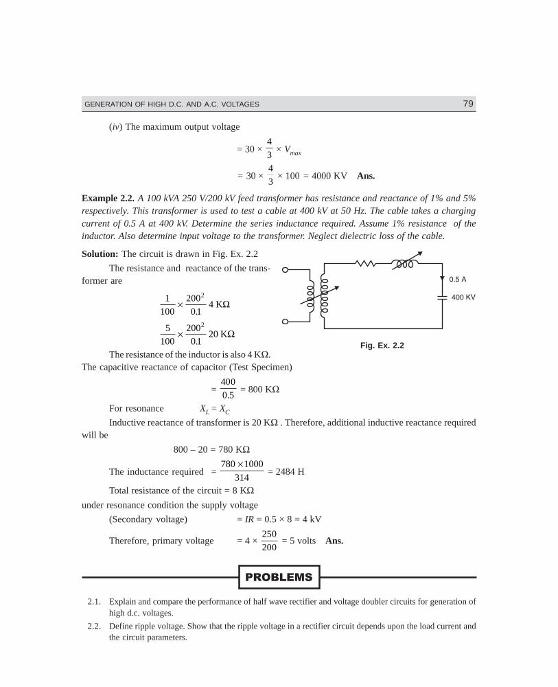
Dharm\N-HIGH\HG2-1.PM5 79
GENERATION OF HIGH D.C. AND A.C. VOLTAGES 79
(iv) The maximum output voltage
= 30 × 4
3 × Vmax
= 30 × 4
3 × 100 = 4000 KV Ans.
Example 2.2. A 100 kVA 250 V/200 kV feed transformer has resistance and reactance of 1% and 5%respectively. This transformer is used to test a cable at 400 kV at 50 Hz. The cable takes a chargingcurrent of 0.5 A at 400 kV. Determine the series inductance required. Assume 1% resistance of theinductor. Also determine input voltage to the transformer. Neglect dielectric loss of the cable.
Solution: The circuit is drawn in Fig. Ex. 2.2
The resistance and reactance of the trans-former are
1
100
200
0 14
2
×.
KΩ
5100
20001
202
×.
KΩ
The resistance of the inductor is also 4 KΩ.The capacitive reactance of capacitor (Test Specimen)
= 400
0 5. = 800 KΩ
For resonance XL = XC
Inductive reactance of transformer is 20 KΩ . Therefore, additional inductive reactance requiredwill be
800 – 20 = 780 KΩ
The inductance required = 780 1000
314
× = 2484 H
Total resistance of the circuit = 8 KΩunder resonance condition the supply voltage
(Secondary voltage) = IR = 0.5 × 8 = 4 kV
Therefore, primary voltage = 4 × 250
200 = 5 volts Ans.
2.1. Explain and compare the performance of half wave rectifier and voltage doubler circuits for generation ofhigh d.c. voltages.
2.2. Define ripple voltage. Show that the ripple voltage in a rectifier circuit depends upon the load current andthe circuit parameters.
Fig. Ex. 2.2
Dharm\N-HIGH\HG2-1.PM5 80
80 HIGH VOLTAGE ENGINEERING
2.3. Explain with neat sketches Cockroft-Walton voltage multiplier circuit. Explain clearly its operation whenthe circuit is (i) unloaded (ii) loaded.
2.4. Derive an expression for ripple voltage of a multistage Cockroft-Walton Circuit.
2.5. Derive an expression for the voltage output under load condition. Hence, deduce the condition for optimalnumber of stage if a maximum value of output voltage is desired.
2.6. Describe with neat diagram the principle of operation and application of a symmetrical cascaded rectifier.
2.7. Explain clearly the basic principle of operation of an electrostatic generator. Describe with neat diagramthe principle of operation, application and limitations of Van de Graf generator.
2.8. What is a cascaded transformer? Explain why cascading is done? Describe with neat diagram a three stagecascaded transformer. Label the power ratings of various stages of the transformer.
2.9. Draw equivalent circuit of a 3-stage cascaded transformer and determine the expression for short circuitimpedance of the transformer. Hence deduce an expression for the short-circuit impedance of an n-stagecascaded transformer.
2.10. Explain with neat diagram the basic principle of reactive power compensation is high voltage a.c. testingof insulating materials.
2.11. Explain with neat diagram the principle of operation of (i) series (ii) parallel resonant circuits for generat-ing high a.c. voltages. Compare their performance.
2.12. Explain the series-parallel resonant circuit and discuss its advantages and disadvantages.
Graggs J.D. and Meek J.M., High Voltage laboratory Technique, Buttrworth, London 1954.
Enge H.A., Cascade Transformer High Voltage Generator, US Patent No. 3596, 167 July, 1971.
Reid R., High Voltage Resonant Testing, IEEE PES Winter Meeting, 1974 Conf. Paper 74.
Kuffel E., Zaengl W.S., High Voltage Engineering Fundamentals, Pergamon Press, 1984.
Word Berry H. et al., A Comparative Analysis of Resonant Power Supply Design Technique for HighVoltage Testing, Fifth International Symposium on High Voltage Engineering, Branscheweig 24–28 Aug.1987. FRG.
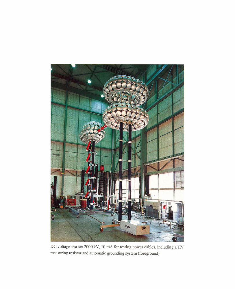
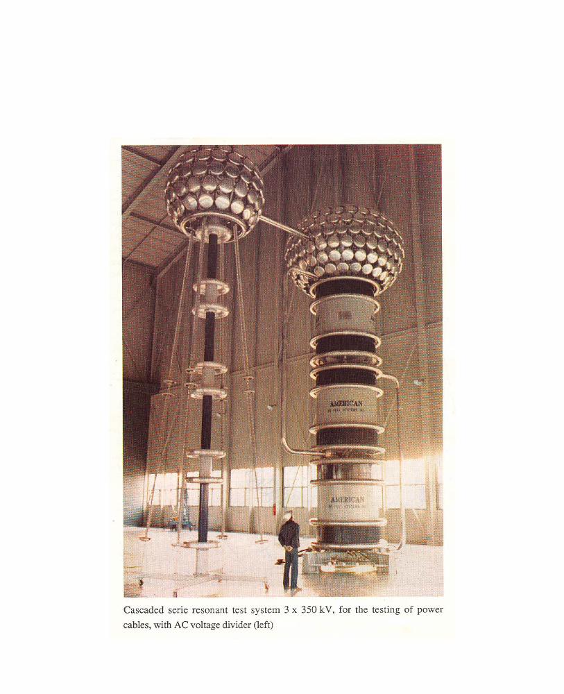
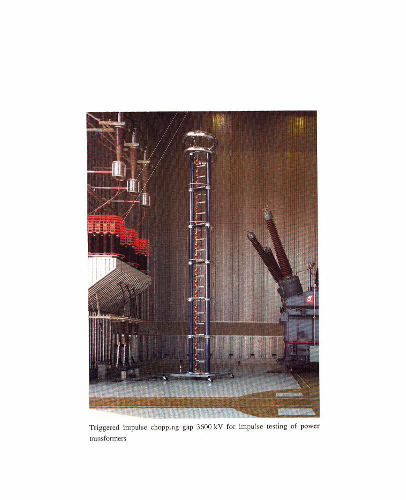
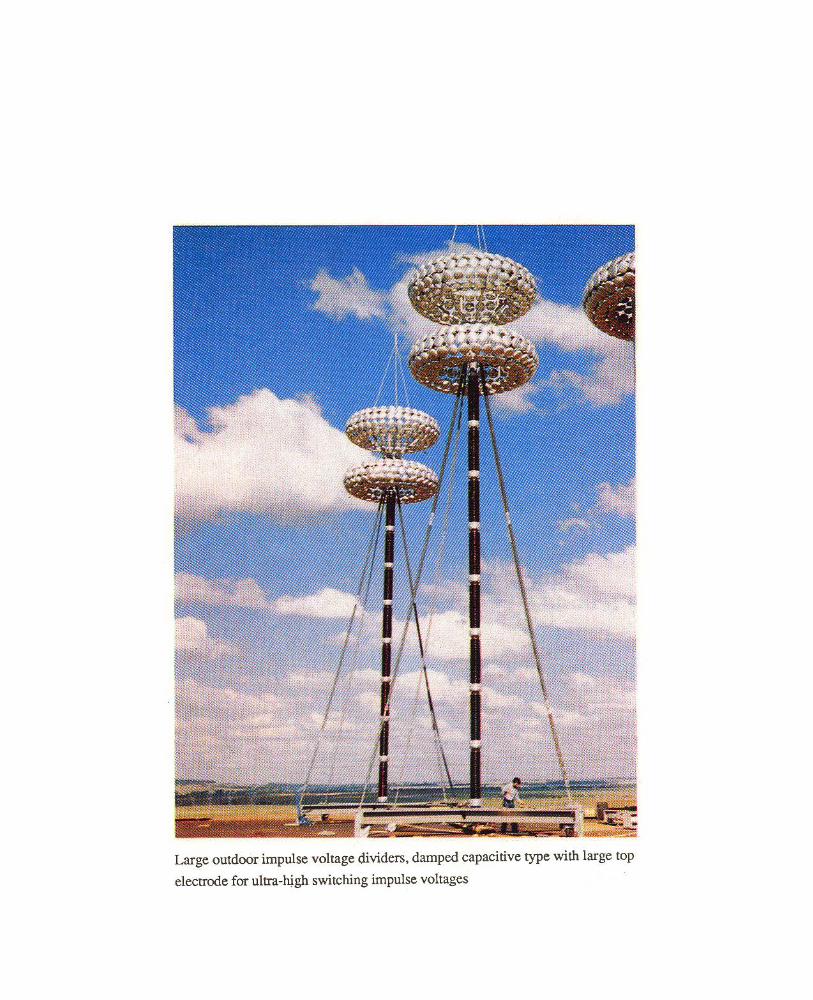
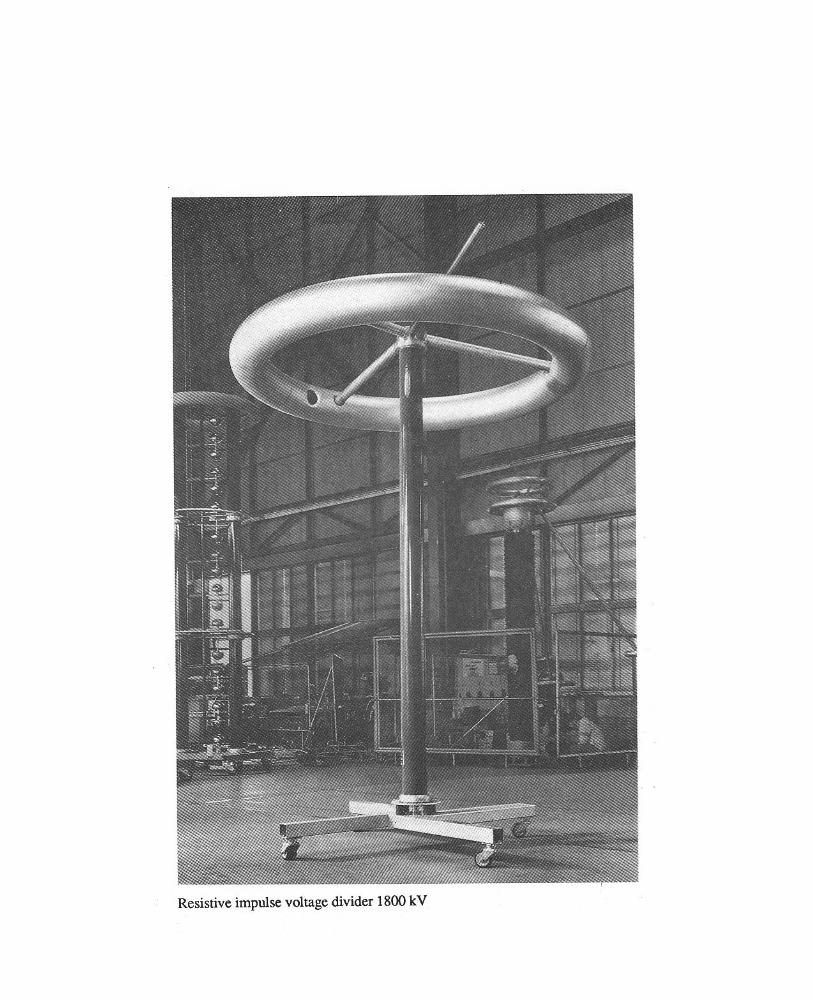
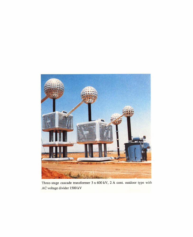
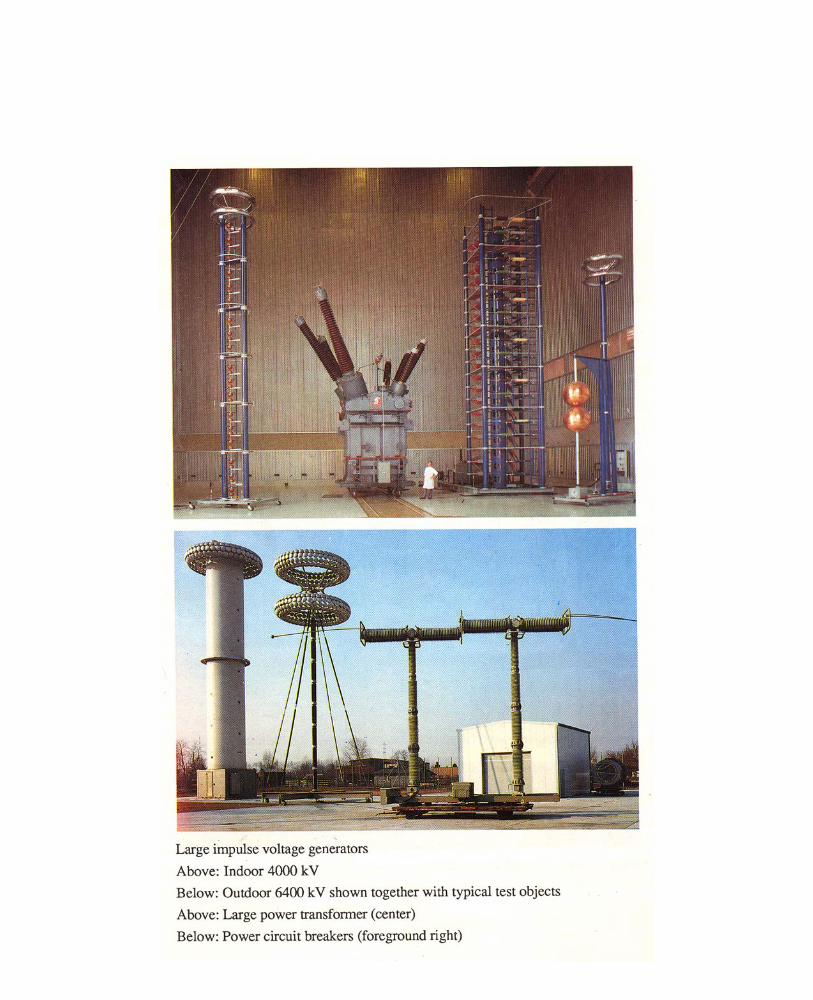
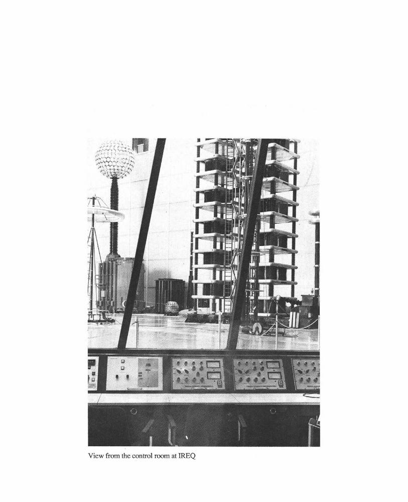
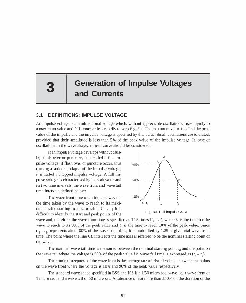
A
D
C90%
50%
10%
t0 t1 t2 t3
Generation of Impulse Voltagesand Currents
81
3
3.1 DEFINITIONS: IMPULSE VOLTAGE
An impulse voltage is a unidirectional voltage which, without appreciable oscillations, rises rapidly toa maximum value and falls more or less rapidly to zero Fig. 3.1. The maximum value is called the peakvalue of the impulse and the impulse voltage is specified by this value. Small oscillations are tolerated,provided that their amplitude is less than 5% of the peak value of the impulse voltage. In case ofoscillations in the wave shape, a mean curve should be considered.
If an impulse voltage develops without caus-ing flash over or puncture, it is called a full im-pulse voltage; if flash over or puncture occur, thuscausing a sudden collapse of the impulse voltage,it is called a chopped impulse voltage. A full im-pulse voltage is characterised by its peak value andits two time intervals, the wave front and wave tailtime intervals defined below:
The wave front time of an impulse wave isthe time taken by the wave to reach to its maxi-mum value starting from zero value. Usually it isdifficult to identify the start and peak points of thewave and, therefore, the wave front time is specified as 1.25 times (t2 – t1), where t2 is the time for thewave to reach to its 90% of the peak value and t1 is the time to reach 10% of the peak value. Since(t2 – t1) represents about 80% of the wave front time, it is multiplied by 1.25 to give total wave fronttime. The point where the line CB intersects the time axis is referred to be the nominal starting point ofthe wave.
The nominal wave tail time is measured between the nominal starting point t0 and the point onthe wave tail where the voltage is 50% of the peak value i.e. wave fail time is expressed as (t3 – t0).
The nominal steepness of the wave front is the average rate of rise of voltage between the pointson the wave front where the voltage is 10% and 90% of the peak value respectively.
The standard wave shape specified in BSS and ISS is a 1/50 micro sec. wave i.e. a wave front of1 micro sec. and a wave tail of 50 micro sec. A tolerance of not more than ±50% on the duration of the
Fig. 3.1 Full impulse wave
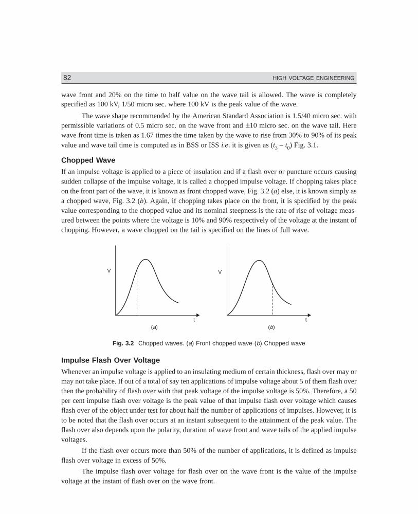
Dharm\N-HIGH\HG3-1PM5 82
82 HIGH VOLTAGE ENGINEERING
wave front and 20% on the time to half value on the wave tail is allowed. The wave is completelyspecified as 100 kV, 1/50 micro sec. where 100 kV is the peak value of the wave.
The wave shape recommended by the American Standard Association is 1.5/40 micro sec. withpermissible variations of 0.5 micro sec. on the wave front and ±10 micro sec. on the wave tail. Herewave front time is taken as 1.67 times the time taken by the wave to rise from 30% to 90% of its peakvalue and wave tail time is computed as in BSS or ISS i.e. it is given as (t3 – t0) Fig. 3.1.
Chopped WaveIf an impulse voltage is applied to a piece of insulation and if a flash over or puncture occurs causingsudden collapse of the impulse voltage, it is called a chopped impulse voltage. If chopping takes placeon the front part of the wave, it is known as front chopped wave, Fig. 3.2 (a) else, it is known simply asa chopped wave, Fig. 3.2 (b). Again, if chopping takes place on the front, it is specified by the peakvalue corresponding to the chopped value and its nominal steepness is the rate of rise of voltage meas-ured between the points where the voltage is 10% and 90% respectively of the voltage at the instant ofchopping. However, a wave chopped on the tail is specified on the lines of full wave.
V
t( )a
t( )b
V
Fig. 3.2 Chopped waves. (a) Front chopped wave (b) Chopped wave
Impulse Flash Over VoltageWhenever an impulse voltage is applied to an insulating medium of certain thickness, flash over may ormay not take place. If out of a total of say ten applications of impulse voltage about 5 of them flash overthen the probability of flash over with that peak voltage of the impulse voltage is 50%. Therefore, a 50per cent impulse flash over voltage is the peak value of that impulse flash over voltage which causesflash over of the object under test for about half the number of applications of impulses. However, it isto be noted that the flash over occurs at an instant subsequent to the attainment of the peak value. Theflash over also depends upon the polarity, duration of wave front and wave tails of the applied impulsevoltages.
If the flash over occurs more than 50% of the number of applications, it is defined as impulseflash over voltage in excess of 50%.
The impulse flash over voltage for flash over on the wave front is the value of the impulsevoltage at the instant of flash over on the wave front.
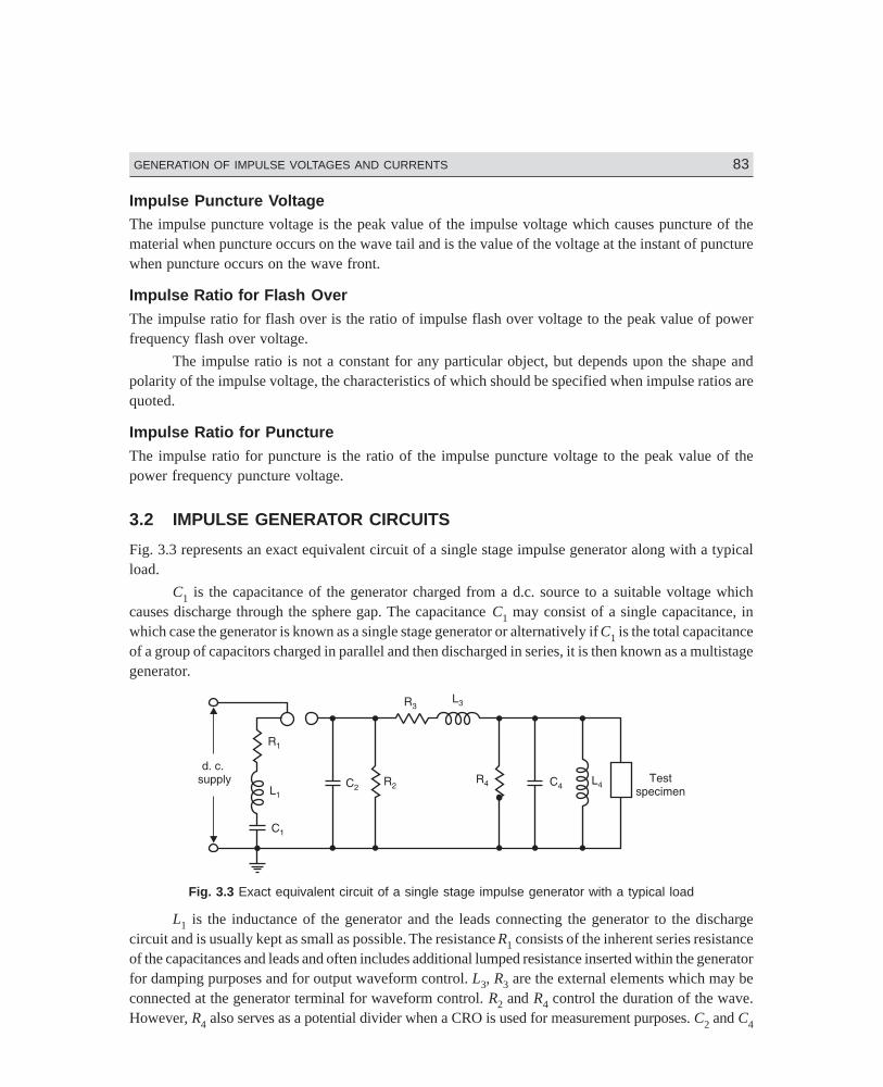
Dharm\N-HIGH\HG3-1PM5 83
GENERATION OF IMPULSE VOLTAGES AND CURRENTS 83
Impulse Puncture VoltageThe impulse puncture voltage is the peak value of the impulse voltage which causes puncture of thematerial when puncture occurs on the wave tail and is the value of the voltage at the instant of puncturewhen puncture occurs on the wave front.
Impulse Ratio for Flash OverThe impulse ratio for flash over is the ratio of impulse flash over voltage to the peak value of powerfrequency flash over voltage.
The impulse ratio is not a constant for any particular object, but depends upon the shape andpolarity of the impulse voltage, the characteristics of which should be specified when impulse ratios arequoted.
Impulse Ratio for PunctureThe impulse ratio for puncture is the ratio of the impulse puncture voltage to the peak value of thepower frequency puncture voltage.
3.2 IMPULSE GENERATOR CIRCUITS
Fig. 3.3 represents an exact equivalent circuit of a single stage impulse generator along with a typicalload.
C1 is the capacitance of the generator charged from a d.c. source to a suitable voltage whichcauses discharge through the sphere gap. The capacitance C1 may consist of a single capacitance, inwhich case the generator is known as a single stage generator or alternatively if C1 is the total capacitanceof a group of capacitors charged in parallel and then discharged in series, it is then known as a multistagegenerator.
Fig. 3.3 Exact equivalent circuit of a single stage impulse generator with a typical load
L1 is the inductance of the generator and the leads connecting the generator to the dischargecircuit and is usually kept as small as possible. The resistance R1 consists of the inherent series resistanceof the capacitances and leads and often includes additional lumped resistance inserted within the generatorfor damping purposes and for output waveform control. L3, R3 are the external elements which may beconnected at the generator terminal for waveform control. R2 and R4 control the duration of the wave.However, R4 also serves as a potential divider when a CRO is used for measurement purposes. C2 and C4
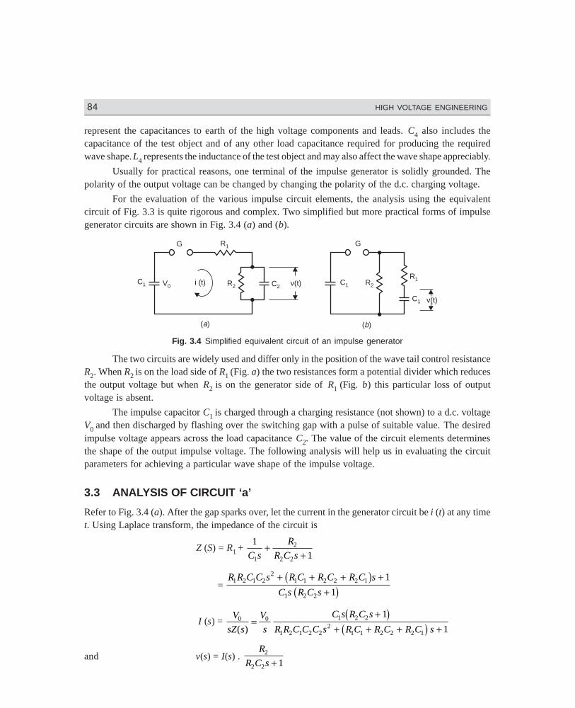
Dharm\N-HIGH\HG3-1PM5 84
84 HIGH VOLTAGE ENGINEERING
represent the capacitances to earth of the high voltage components and leads. C4 also includes thecapacitance of the test object and of any other load capacitance required for producing the requiredwave shape. L4 represents the inductance of the test object and may also affect the wave shape appreciably.
Usually for practical reasons, one terminal of the impulse generator is solidly grounded. Thepolarity of the output voltage can be changed by changing the polarity of the d.c. charging voltage.
For the evaluation of the various impulse circuit elements, the analysis using the equivalentcircuit of Fig. 3.3 is quite rigorous and complex. Two simplified but more practical forms of impulsegenerator circuits are shown in Fig. 3.4 (a) and (b).
G
V0 v(t)
( )a ( )b
G
v(t)
R1
R2 C2C1
C1
R1R2i (t)C1
Fig. 3.4 Simplified equivalent circuit of an impulse generator
The two circuits are widely used and differ only in the position of the wave tail control resistanceR2. When R2 is on the load side of R1 (Fig. a) the two resistances form a potential divider which reducesthe output voltage but when R2 is on the generator side of R1 (Fig. b) this particular loss of outputvoltage is absent.
The impulse capacitor C1 is charged through a charging resistance (not shown) to a d.c. voltageV0 and then discharged by flashing over the switching gap with a pulse of suitable value. The desiredimpulse voltage appears across the load capacitance C2. The value of the circuit elements determinesthe shape of the output impulse voltage. The following analysis will help us in evaluating the circuitparameters for achieving a particular wave shape of the impulse voltage.
3.3 ANALYSIS OF CIRCUIT ‘a’
Refer to Fig. 3.4 (a). After the gap sparks over, let the current in the generator circuit be i (t) at any timet. Using Laplace transform, the impedance of the circuit is
Z (S) = R1 + 1
11
2
2 2C s
R
R C s+
+
= R R C C s R C R C R C s
C s R C s1 2 1 2
21 1 2 2 2 1
1 2 2
1
1
+ + + ++
b gb g
I (s) = V
sZ s
V
s
C s R C s
R R C C C s R C R C R C s0 0 1 2 2
1 2 1 2 22
1 1 2 2 2 1
1
1( )=
++ + + +
b gb g
and v(s) = I(s) . R
R C s2
2 2 1+
Dharm\N-HIGH\HG3-1PM5 85
GENERATION OF IMPULSE VOLTAGES AND CURRENTS 85
= V0R2C1 1
11 2 1 22
1 1 2 2 2 1R R C C s R C R C R C s+ + + +b g
=
V R C
R R C C sR C R C R C
R R C Cs
R R C C
0 2 1
1 2 1 2 2 1 1 2 2 2 1
1 2 1 2 1 2 1 2
11
.+ + + +
The roots of the expression in the denominator are
1
2
41 1 2 2 2 1
1 2 1 2
1 1 2 2 2 1
1 2 1 2
2
1 2 1 2
––
R C R C R C
R R C C
R C R C R C
R R C C R R C C
+ +± + +F
HGIKJ
L
NMM
O
QPP
b g
Let α = R C R C R C
R R C C1 1 2 2 2 1
1 2 1 22
+ +
and β = 1
2
41 1 2 2 2 1
1 2 1 2
2
1 2 1 2
R C R C R C
R R C C R R C C
+ +FHG
IKJ −
Therefore, the roots are (– α + β) and (– α – β). The expression for voltage can be rewritten as
v(s) = 1 0
1 2s s
V
R C+ +α β α β–.a f a f+
Finding the partial fractions of the expression
1
s s
A
s
B
s+ + +=
++
+ +α β α β α β α β– – ( )a f a f
= As A A Bs B B
s s
+ + ++ + +α β α β
α β α β+ –
–a f a fComparing the coefficients A + B = 0 or A = – B and Aα + Aβ + Bα – Bβ = 1 or Aα + Aβ – Aα
+ Aβ = 1 or 2Aβ = 1 or
A = 1
2βand B = –
1
2βSubstituting these value of A and B, we have
v(s) = V
R C s s0
1 2
1
2
1 1.
( – )–
β α β α β+ + +LNM
OQPa f
Taking inverse Laplace transform of the voltage transform
v(s) = V
R Ce et t0
22βα β α β
1
[ ]– ( – ) – ( )− + (3.1)
Let Vn = V
R C0
22 β 1
∴ v(t) = Vn [e–(α – β)t – e– (α + β)t] (3.2)
Dharm\N-HIGH\HG3-1PM5 86
86 HIGH VOLTAGE ENGINEERING
Let t1 be the wave front time and t2 the wave tail time, then both α and β must have unique valuesirrespective of the particular circuit used.
At time t1, the shope of the wave is zero, therefore, t1 can be obtained from the relation dv(t)/dt = 0
i.e,dv t
dtV e en
t t a f = + + =+[– ( – ) ( ) ]– ( – ) – ( )α β α βα β α β 0
orα βα β
β+ =–
e t2 1
or 2βt1 = 1n α βα β
+–
or t1 = 1
2βα βα β
1n+–
(3.3)
and the peak value of the voltage is then given by
vm (t) = Vn [ – ]– ( ) – ( )e et tα β α β– 1 1+ (3.4)
To obtain t2, substitute t = t2 in equation (3.1) and the voltage is half of what it is when t = t1 inthe same equation i.e.
V e eV
e ent t n t t[ – ] [ – ]– ( – ) – ( ) – ( – ) – ( )α β α β α β α β2 2 1 1
2+ +=
Let t2 = Kt1 where K is a constant, then
V e eV
e enKt Kt n t t[ – ] [ – ]– ( – ) – ( ) – ( – ) – ( )α β α β α β α β1 1 1 1
2+ += (3.5)
From equations (3.3) and (3.5) it is possible to obtain desired values of α and β for a requiredwave shape i.e. values of t1 and K. Calculations can be simplified by the fact that in practice the secondterm on the left side of equation (3.5) is usually much smaller than the first term and can, therefore, beneglected.
Therefore, we have
e e eKt t t– ( – ) – ( – ) – ( )[ – ]α β α β α β1 1 11
2= +
or 2 1 1 1e e eKt t t– ( – ) – ( – ) – ( )–α β α β α β= +
Multiplying by e t( – )α β 1 both sides, we have
2 11 21e eK t t– ( – )( – ) ––α β β= 1
or α β β–( – )
. ln– –2
=FHG
IKJ
2
1
2
11t K e t1(3.6)
If 2βt1 > 4 equation (3.6) reduced to
α – β = 0 7
11
.
( – )t K(3.7)
With this assumption the results are found to be within 2% error.
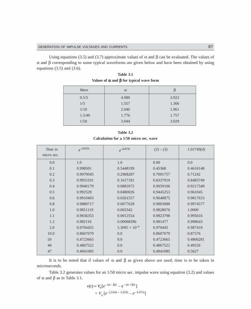
Dharm\N-HIGH\HG3-1PM5 87
GENERATION OF IMPULSE VOLTAGES AND CURRENTS 87
Using equations (3.5) and (3.7) approximate values of α and β can be evaluated. The values ofα and β corresponding to some typical waveforms are given below and have been obtained by usingequations (3.5) and (3.6).
Table 3.1
Values of α α α α α and β β β β β for typical wave form
Wave α β
0.5/5 4.080 3.922
1/5 1.557 1.366
1/10 2.040 1.961
1.5/40 1.776 1.757
1/50 3.044 3.029
Table 3.2
Calculation for a 1/50 micro sec. wave
Time in e–0.015te–6.073t (2) – (3) 1.01749(4)
micro sec.
0.0 1.0 1.0 0.00 0.0
0.1 0.998501 0.5448199 0.45368 0.4616148
0.2 0.9970045 0.2968287 0.7001757 0.71242
0.3 0.9955101 0.1617181 0.8337919 0.8483749
0.4 0.9940179 0.0881072 0.9059106 0.9217549
0.5 0.992528 0.0480026 0.9445253 0.961045
0.6 0.9910403 0.0261557 0.9648875 0.9817633
0.8 0.9880717 0.0077628 0.9803088 0.9974577
1.0 0.9851119 0.002342 0.9828076 1.0000
1.1 0.9836353 0.0012554 0.9823798 0.995616
1.2 0.982116 0.00068396 0.981477 0.998643
2.0 0.9704455 5.3095 × 10⁻⁶ 0.970445 0.987418
10.0 0.8607079 0.0 0.8607079 0.87576
50 0.4723665 0.0 0.4723665 0.4806281
48 0.4867522 0.0 0.4867522 0.49526
47 0.4941085 0.0 0.4941085 0.5627
It is to be noted that if values of α and β as given above are used, time is to be taken inmicroseconds.
Table 3.2 generates values for an 1/50 micro sec. impulse wave using equation (3.2) and valuesof α and β as in Table 3.1.
v t V e ent t( ) [ – ]– ( – ) – ( )= +α β α β
= Vn [e– (3.044 – 3.029) – e– 6.073t]
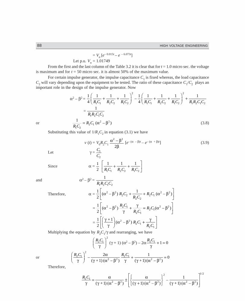
Dharm\N-HIGH\HG3-1PM5 88
88 HIGH VOLTAGE ENGINEERING
= Vn [e– 0.015t – e – 6.073t]
Let p.u. Vn = 1.01749From the first and the last column of the Table 3.2 it is clear that for t = 1.0 micro sec. the voltage
is maximum and for t = 50 micro sec. it is almost 50% of the maximum value.For certain impulse generator, the impulse capacitance C1 is fixed whereas, the load capacitance
C2 will vary depending upon the equipment to be tested. The ratio of these capacitance C1/C2 plays animportant role in the design of the impulse generator. Now
α2 – β2 = 1
4
1 1 1 1
4
1 1 1 1
1 1 2 2 1 2
2
1 1 2 2 1 2
2
1 2 1 2R C R C R C R C R C R C R R C C+ +
FHG
IKJ + +
FHG
IKJ +–
= 1
1 2 1 2R R C C
or 1
1 22 1R C
R C= ( – )α β2 2 (3.8)
Substituting this value of 1/R1C2 in equation (3.1) we have
v (t) = V0R2C1 α β
β
2 2–
2 [e
– (α – β)t – e– (α + β)t] (3.9)
Let γ = C
C1
2
Since α = 1
2
1 1 1
1 1 2 2 1 2R C R C R C+ +
LNM
OQP
and α2 – β2 = 1
1 2 1 2R R C C
Therefore, α = 1
2
12 2
2 22 1( – ) ( – )α β α β2 2 2 2R C
R CR C+ +
LNM
OQP
= 1
22 1
2 12 1( – ) ( – )α β
γγ α β2 2 2 2R C
R CR C+ =
LNM
OQP
= 1
2 2 12 1
γγ
α β γ+ 1 2 2FHG
IKJ +
LNM
OQP( – ) R C
R C
Multiplying the equation by R2C1/γ and rearranging, we have
R C2 1
2
γFHG
IKJ (γ + 1) (α2 – β2) – 2α
R C2 1 1 0γ
+ =
or R C R C2 1
2
2 12 10
γα
γ α β γ γ α βFHG
IKJ + =–
( ) ( – )( + 1) ( – ) + 12 2 2 2
Therefore,
R C2 1
2 1 2
1
1
γα
γ α βα
γ α β γ α β= ±
+RST
UVWLNMM
OQPP( ) ( – ) ( ) ( – )
–( ) ( – )
/
+ 1 + 12 2 2 2 2 2
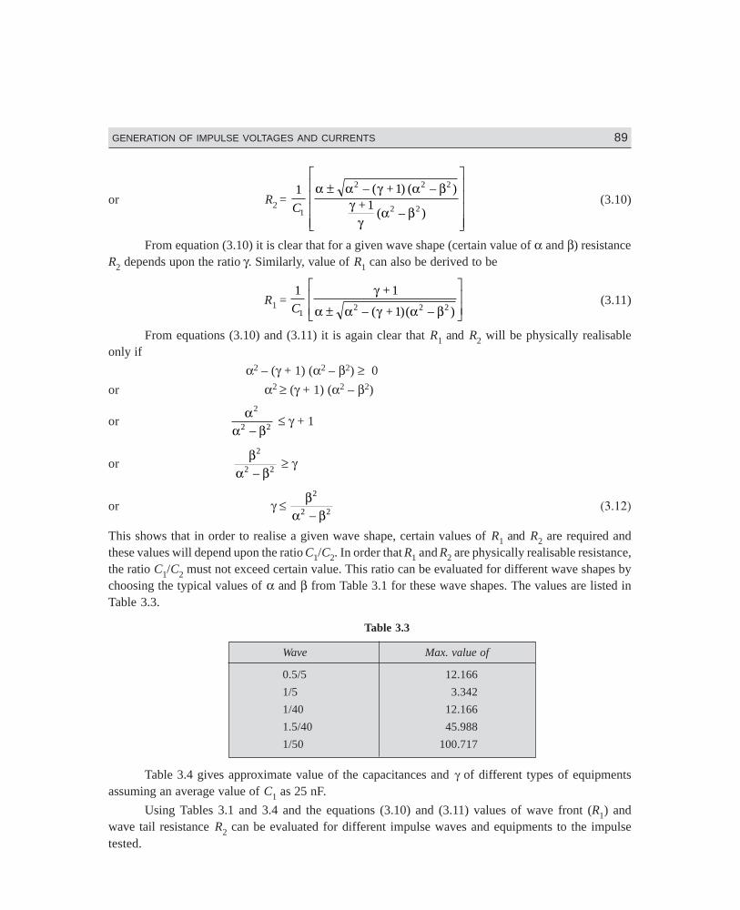
Dharm\N-HIGH\HG3-1PM5 89
GENERATION OF IMPULSE VOLTAGES AND CURRENTS 89
or R2 = 1
1C
α α γ α βγ
γα β
±L
N
MMMM
O
Q
PPPP
2 2 2
2 2
+ 1+ 1– ( ) ( – )
( – )(3.10)
From equation (3.10) it is clear that for a given wave shape (certain value of α and β) resistanceR2 depends upon the ratio γ. Similarly, value of R1 can also be derived to be
R1 =
1
1C
γ
α α γ α β
+ 1
+ 12 2 2±
L
NMM
O
QPP– ( )( – )
(3.11)
From equations (3.10) and (3.11) it is again clear that R1 and R2 will be physically realisableonly if
α2 – (γ + 1) (α2 – β2) ≥ 0or α2 ≥ (γ + 1) (α2 – β2)
orα
α β
2
2 2– ≤ γ + 1
or βα β
2
2 2– ≥ γ
or γ ≤ βα β
2
2 2–(3.12)
This shows that in order to realise a given wave shape, certain values of R1 and R2 are required andthese values will depend upon the ratio C1/C2. In order that R1 and R2 are physically realisable resistance,the ratio C1/C2 must not exceed certain value. This ratio can be evaluated for different wave shapes bychoosing the typical values of α and β from Table 3.1 for these wave shapes. The values are listed inTable 3.3.
Table 3.3
Wave Max. value of
0.5/5 12.166
1/5 3.342
1/40 12.166
1.5/40 45.988
1/50 100.717
Table 3.4 gives approximate value of the capacitances and γ of different types of equipmentsassuming an average value of C1 as 25 nF.
Using Tables 3.1 and 3.4 and the equations (3.10) and (3.11) values of wave front (R1) andwave tail resistance R2 can be evaluated for different impulse waves and equipments to the impulsetested.
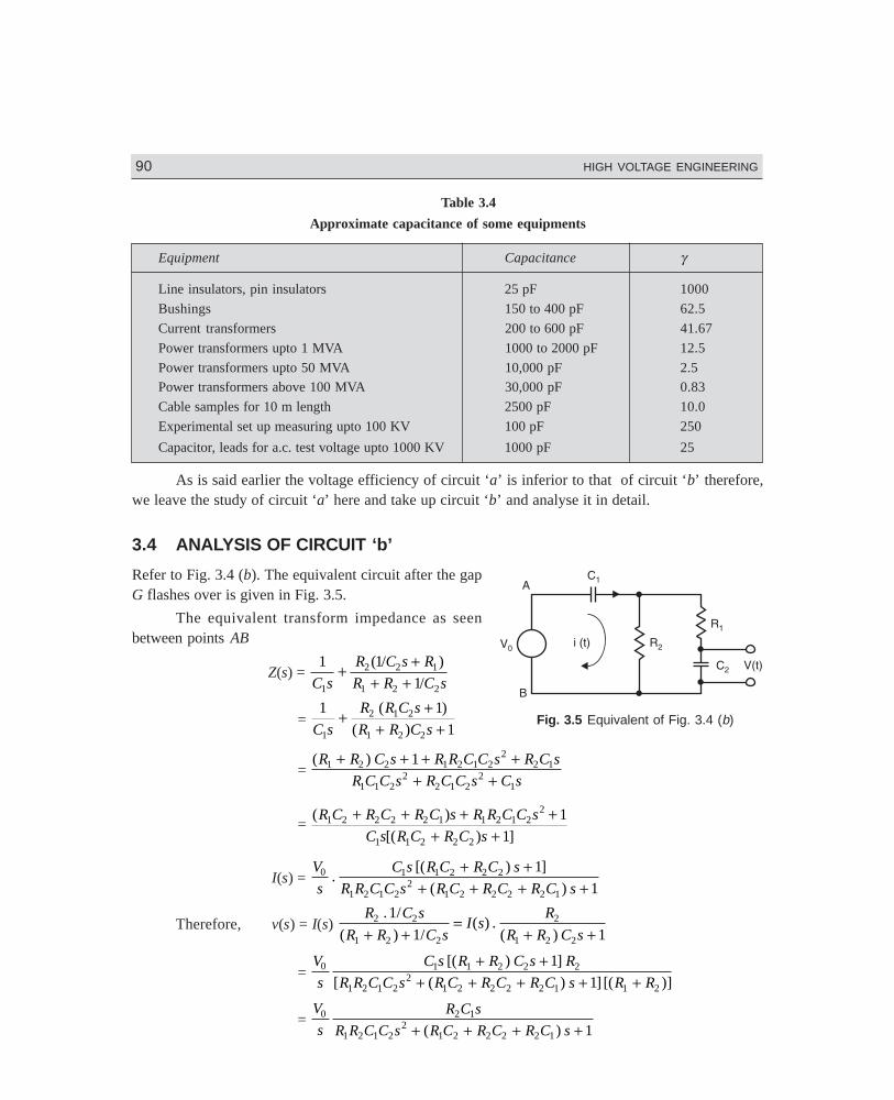
Dharm\N-HIGH\HG3-1PM5 90
90 HIGH VOLTAGE ENGINEERING
Table 3.4
Approximate capacitance of some equipments
Equipment Capacitance γ
Line insulators, pin insulators 25 pF 1000
Bushings 150 to 400 pF 62.5
Current transformers 200 to 600 pF 41.67
Power transformers upto 1 MVA 1000 to 2000 pF 12.5
Power transformers upto 50 MVA 10,000 pF 2.5Power transformers above 100 MVA 30,000 pF 0.83
Cable samples for 10 m length 2500 pF 10.0
Experimental set up measuring upto 100 KV 100 pF 250
Capacitor, leads for a.c. test voltage upto 1000 KV 1000 pF 25
As is said earlier the voltage efficiency of circuit ‘a’ is inferior to that of circuit ‘b’ therefore,we leave the study of circuit ‘a’ here and take up circuit ‘b’ and analyse it in detail.
3.4 ANALYSIS OF CIRCUIT ‘b’
Refer to Fig. 3.4 (b). The equivalent circuit after the gapG flashes over is given in Fig. 3.5.
The equivalent transform impedance as seenbetween points AB
Z(s) = 1 1
11
2 2 1
1 2 2C s
R C s R
R R C s+ +
+ +( / )
/
= 1 1
11
2 1 2
1 2 2C s
R R C s
R R C s+ +
+ +( )
( )
= ( )R R C s R R C C s R C s
R C C s R C C s C s1 2 2 1 2 1 2
22 1
1 1 22
2 1 22
1
1+ + + ++ +
= ( )
[( ) ]
R C R C R C s R R C C s
C s R C R C s1 2 2 2 2 1 1 2 1 2
2
1 1 2 2 2
1
1
+ + + ++ +
I(s) = V
s
C s R C R C s
R R C C s R C R C R C s0 1 1 2 2 2
1 2 1 22
1 2 2 2 2 1
1
1.
[( ) ]
( )
+ ++ + + +
Therefore, v(s) = I(s) R C s
R R C sI s
R
R R C s2 2
1 2 2
2
1 2 2
1
1 1
. /
( ) /( ) .
( )+ +=
+ +
= V
s
C s R R C s R
R R C C s R C R C R C s R R0 1 1 2 2 2
1 2 1 22
1 2 2 2 2 1 1 2
1
1
[( ) ]
[ ( ) ] [( )]
+ ++ + + + +
= V
s
R C s
R R C C s R C R C R C s0 2 1
1 2 1 22
1 2 2 2 2 1 1+ + + +( )
Fig. 3.5 Equivalent of Fig. 3.4 (b)
Dharm\N-HIGH\HG3-1PM5 91
GENERATION OF IMPULSE VOLTAGES AND CURRENTS 91
Dividing the numerator and denominator by R1R2C1C2, we have
v(s) = V
R C0
1 2
11 1 1 12
2 1 1 1 1 2 1 2 1 2
sR C R C R C
sR R C C
+ + +FHG
IKJ +
L
NMMM
O
QPPP
(3.13)
Let α = 1
2
1 1 1
2 1 1 1 1 2R C R C R C+ +
LNM
OQP
and β = 1
2
1 1 1 4
2 1 1 1 1 2
2
1 2 1 2
1 2
R C R C R C R R C C+ +
FHG
IKJ
LNMM
OQPP–
/
Equation (3.13) can be rewritten as
v(s) = V
R C s s0
1 2
1
( ) ( )+ +α β α β– +
v(t) = V
R C0
1 22 β[e– (α – β)t – e– (α + β)t] (3.14)
Let γ = C1/C2 and working on the similar lines as for the circuit ‘a’, we have
R2 = 1
1
11
2
C
α α γγ
α β
γγ
α β
± +
+
L
N
MMMM
O
Q
PPPP
– – ( – )
( – )
2 2
2 2(3.15)
and R1 = 1 1
11 2C
+
± +
L
N
MMMM
O
Q
PPPP
γ
α α γγ
α β2 2– ( – )
(3.16)
Again, in order that, R1 and R2 are physically realisable
α γγ
2 1 +– (α2 – β2) ≥ 0
or α2 ≥ 1 + γ
γ (α2 – β2)
or α
α β
2
2 2– ≥
1 + γγ
or α
α β
2
2 2– – 1 ≥ 1
γ
or γ ≥ α ββ
2 2
2
–(3.17)
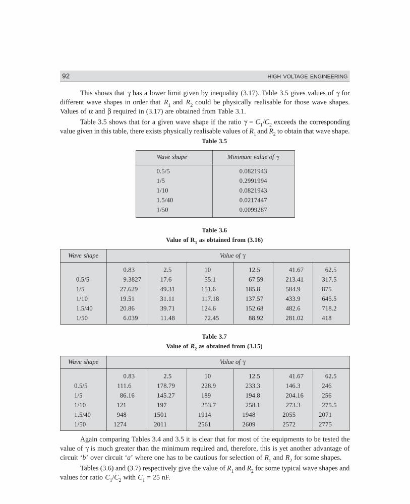
Dharm\N-HIGH\HG3-1PM5 92
92 HIGH VOLTAGE ENGINEERING
This shows that γ has a lower limit given by inequality (3.17). Table 3.5 gives values of γ fordifferent wave shapes in order that R1 and R2 could be physically realisable for those wave shapes.Values of α and β required in (3.17) are obtained from Table 3.1.
Table 3.5 shows that for a given wave shape if the ratio γ = C1/C2 exceeds the correspondingvalue given in this table, there exists physically realisable values of R1 and R2 to obtain that wave shape.
Table 3.5
Wave shape Minimum value of γ
0.5/5 0.0821943
1/5 0.2991994
1/10 0.0821943
1.5/40 0.0217447
1/50 0.0099287
Table 3.6
Value of R1 as obtained from (3.16)
Wave shape Value of γ
0.83 2.5 10 12.5 41.67 62.5
0.5/5 9.3827 17.6 55.1 67.59 213.41 317.5
1/5 27.629 49.31 151.6 185.8 584.9 875
1/10 19.51 31.11 117.18 137.57 433.9 645.5
1.5/40 20.86 39.71 124.6 152.68 482.6 718.2
1/50 6.039 11.48 72.45 88.92 281.02 418
Table 3.7
Value of R2 as obtained from (3.15)
Wave shape Value of γ
0.83 2.5 10 12.5 41.67 62.5
0.5/5 111.6 178.79 228.9 233.3 146.3 246
1/5 86.16 145.27 189 194.8 204.16 256
1/10 121 197 253.7 258.1 273.3 275.5
1.5/40 948 1501 1914 1948 2055 2071
1/50 1274 2011 2561 2609 2572 2775
Again comparing Tables 3.4 and 3.5 it is clear that for most of the equipments to be tested thevalue of γ is much greater than the minimum required and, therefore, this is yet another advantage ofcircuit ‘b’ over circuit ‘a’ where one has to be cautious for selection of R1 and R2 for some shapes.
Tables (3.6) and (3.7) respectively give the value of R1 and R2 for some typical wave shapes andvalues for ratio C1/C2 with C1 = 25 nF.
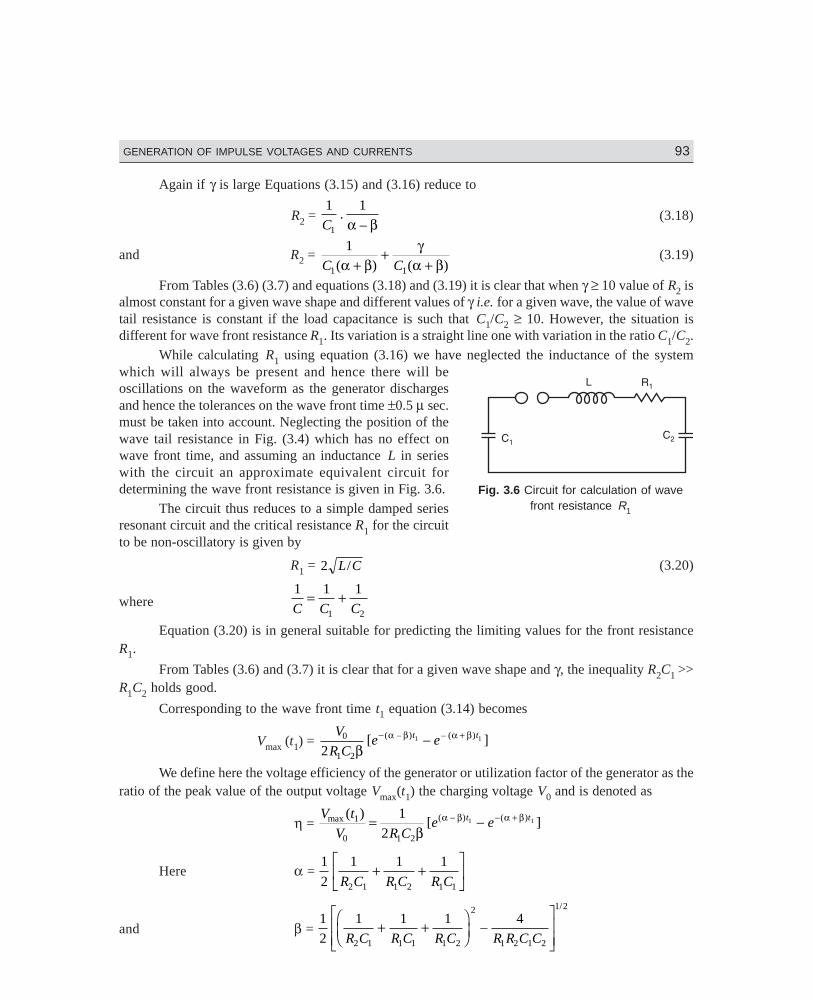
Dharm\N-HIGH\HG3-1PM5 93
GENERATION OF IMPULSE VOLTAGES AND CURRENTS 93
Again if γ is large Equations (3.15) and (3.16) reduce to
R2 = 1 1
1C.
–α β(3.18)
and R2 = 1
1C C( ) ( )α βγ
α β++
+1
(3.19)
From Tables (3.6) (3.7) and equations (3.18) and (3.19) it is clear that when γ ≥ 10 value of R2 isalmost constant for a given wave shape and different values of γ i.e. for a given wave, the value of wavetail resistance is constant if the load capacitance is such that C1/C2 ≥ 10. However, the situation isdifferent for wave front resistance R1. Its variation is a straight line one with variation in the ratio C1/C2.
While calculating R1 using equation (3.16) we have neglected the inductance of the systemwhich will always be present and hence there will beoscillations on the waveform as the generator dischargesand hence the tolerances on the wave front time ±0.5 µ sec.must be taken into account. Neglecting the position of thewave tail resistance in Fig. (3.4) which has no effect onwave front time, and assuming an inductance L in serieswith the circuit an approximate equivalent circuit fordetermining the wave front resistance is given in Fig. 3.6.
The circuit thus reduces to a simple damped seriesresonant circuit and the critical resistance R1 for the circuitto be non-oscillatory is given by
R1 = 2 L C/ (3.20)
where1 1 1
1 2C C C= +
Equation (3.20) is in general suitable for predicting the limiting values for the front resistanceR1.
From Tables (3.6) and (3.7) it is clear that for a given wave shape and γ, the inequality R2C1 >>R1C2 holds good.
Corresponding to the wave front time t1 equation (3.14) becomes
Vmax (t1) = V
R Ce et t0
1 221 1
βα β α β[ – ]( – ) – ( )− +
We define here the voltage efficiency of the generator or utilization factor of the generator as theratio of the peak value of the output voltage Vmax(t1) the charging voltage V0 and is denoted as
η = V t
V R Ce et tmax ( ) ( )( )
[ ]1
0 1 2
1
21 1= −− − +
βα β α β
Here α = 1
2
1 1 1
2 1 1 2 1 1R C R C R C+ +
LNM
OQP
and β = 1
2
1 1 1 4
2 1 1 1 1 2
2
1 2 1 2
1 2
R C R C R C R R C C+ +
FHG
IKJ
L
NMM
O
QPP–
/
Fig. 3.6 Circuit for calculation of wavefront resistance R1
Dharm\N-HIGH\HG3-1PM5 94
94 HIGH VOLTAGE ENGINEERING
When R2C1 >> R1C2, neglecting 1/R2C1
We have α = 1
2
1 1
21 2 1
1 2
1 2 1R C C
C C
C C R+
LNM
OQP
=+
≈ β
Neglecting the term1
2 1R C and
4
1 2 1 2R R C C.
Therefore, η = v t
V
C C R
R C C C
C
C Cmax ( )
( )1
0
1 2 1
1 2 1 2
1
1 2
2
2=
+≈
+
Here the term e t– ( )α β+ 1 is neglected as compared to e t– ( – )α β 1
η = 1
1 2
1
+ C
C
(3.21)
Therefore, higher the generator capacitance the higher is the voltage efficiency of the generator.The impulse energy transformed during a discharge is given by
W = 1
2 1 02C V (3.22)
With inductive loads the capacitance of generator must be large enough to prevent oscillationson the tail of the impulse wave. The minimum permissible capacitance is given by
C1 = 8 2
2t
L(3.23)
where t2 = Wave tail time in micro sec. L2 = Inductance of the test object in Henry and C1, the capacitancein pF.
In case of a 3-phase power transformer with MVA rating as M and V the rated voltage in kV, Zthe percentage impedance, the minimum value of generator capacitance should be
C1 = M
ZV
× 108
2 µF (3.24)
The impulse voltage is applied to one phase and the other two phases are grounded, the secondaryterminals are short-circuited.
3.5 MULTISTAGE IMPULSE GENERATOR CIRCUIT
In order to obtain higher and higher impulse voltage, a single stage circuit is inconvenient for thefollowing reasons:
(i) The physical size of the circuit elements becomes very large.(ii) High d.c. charging voltage is required.
(iii) Suppression of corona discharges from the structure and leads during the charging period isdifficult.
(iv) Switching of vary high voltages with spark gaps is difficult.In 1923 E. Marx suggested a multiplier circuit which is commonly used to obtain impulse voltages
with as high a peak value as possible for a given d.c. charging voltage.
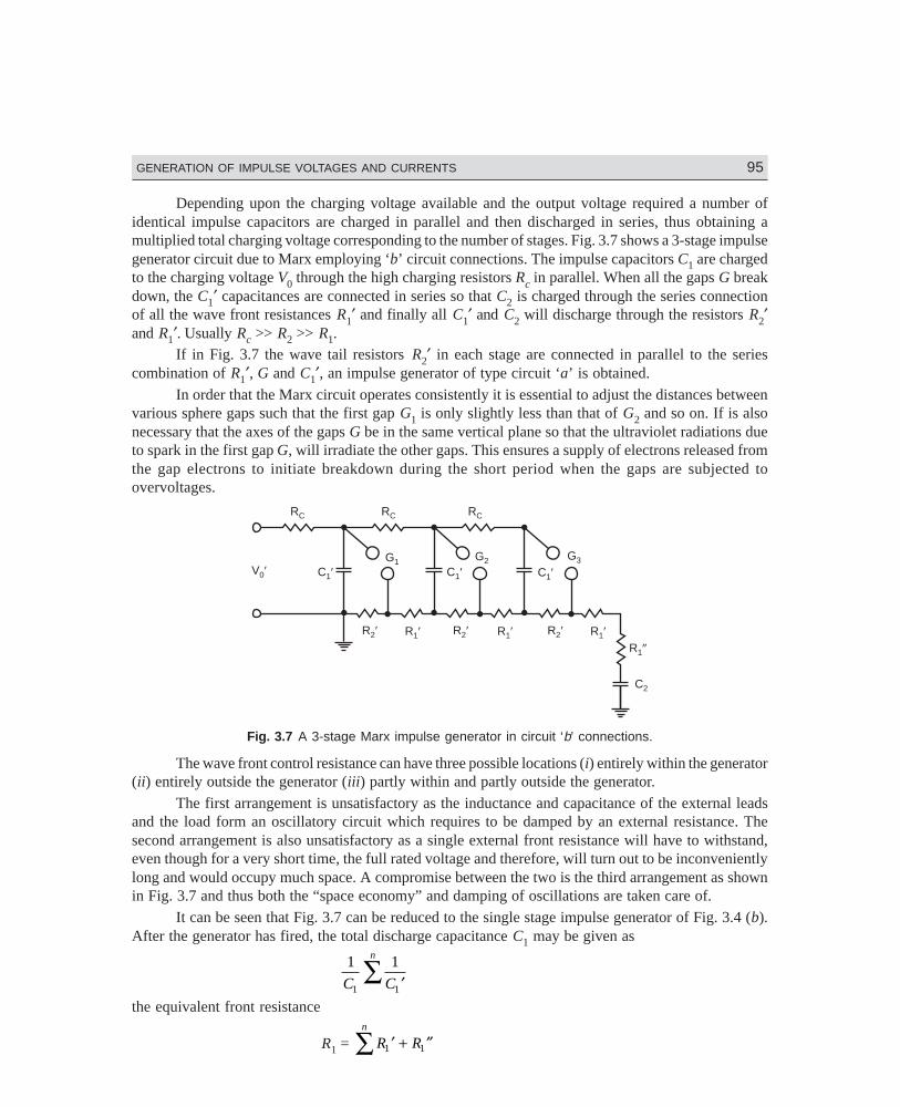
Dharm\N-HIGH\HG3-1PM5 95
GENERATION OF IMPULSE VOLTAGES AND CURRENTS 95
Depending upon the charging voltage available and the output voltage required a number ofidentical impulse capacitors are charged in parallel and then discharged in series, thus obtaining amultiplied total charging voltage corresponding to the number of stages. Fig. 3.7 shows a 3-stage impulsegenerator circuit due to Marx employing ‘b’ circuit connections. The impulse capacitors C1 are chargedto the charging voltage V0 through the high charging resistors Rc in parallel. When all the gaps G breakdown, the C1′ capacitances are connected in series so that C2 is charged through the series connectionof all the wave front resistances R1′ and finally all C1′ and C2 will discharge through the resistors R2′and R1′. Usually Rc >> R2 >> R1.
If in Fig. 3.7 the wave tail resistors R2′ in each stage are connected in parallel to the seriescombination of R1′, G and C1′, an impulse generator of type circuit ‘a’ is obtained.
In order that the Marx circuit operates consistently it is essential to adjust the distances betweenvarious sphere gaps such that the first gap G1 is only slightly less than that of G2 and so on. If is alsonecessary that the axes of the gaps G be in the same vertical plane so that the ultraviolet radiations dueto spark in the first gap G, will irradiate the other gaps. This ensures a supply of electrons released fromthe gap electrons to initiate breakdown during the short period when the gaps are subjected toovervoltages.
RC
V0 C1
C2
R1R2
G3G2G1
RCRC
R1 R1R1
R2 R2
C1 C1
Fig. 3.7 A 3-stage Marx impulse generator in circuit ‘b’ connections.
The wave front control resistance can have three possible locations (i) entirely within the generator(ii) entirely outside the generator (iii) partly within and partly outside the generator.
The first arrangement is unsatisfactory as the inductance and capacitance of the external leadsand the load form an oscillatory circuit which requires to be damped by an external resistance. Thesecond arrangement is also unsatisfactory as a single external front resistance will have to withstand,even though for a very short time, the full rated voltage and therefore, will turn out to be inconvenientlylong and would occupy much space. A compromise between the two is the third arrangement as shownin Fig. 3.7 and thus both the “space economy” and damping of oscillations are taken care of.
It can be seen that Fig. 3.7 can be reduced to the single stage impulse generator of Fig. 3.4 (b).After the generator has fired, the total discharge capacitance C1 may be given as
1 1
1C C
n
1 ′∑the equivalent front resistance
R1 = ∑ ′ + ″n
R R1 1
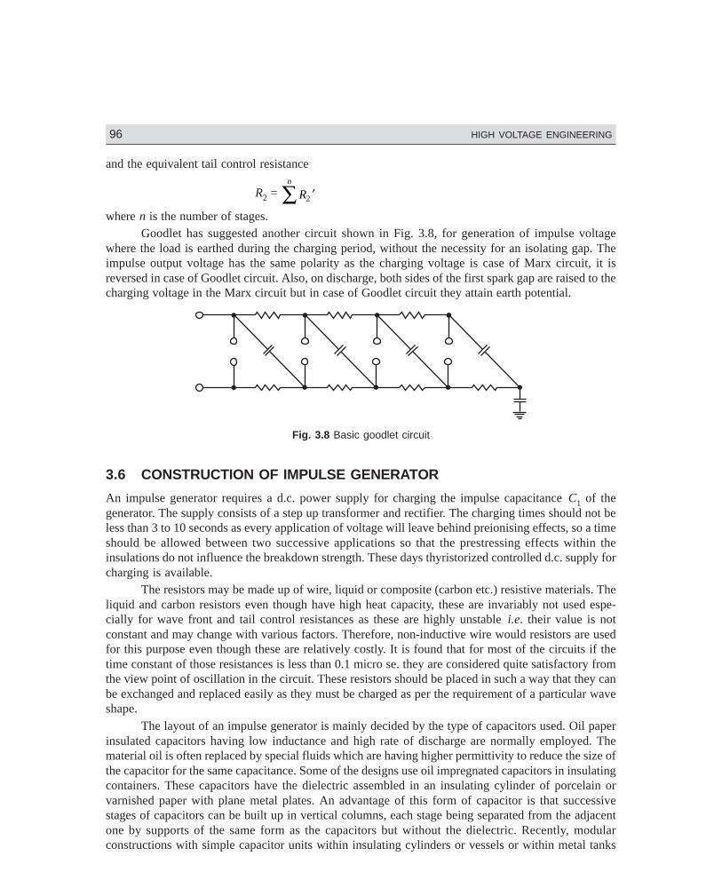
Dharm\N-HIGH\HG3-2.PM5 96
96 HIGH VOLTAGE ENGINEERING
and the equivalent tail control resistance
R2 = ∑ ′n
R2
where n is the number of stages.Goodlet has suggested another circuit shown in Fig. 3.8, for generation of impulse voltage
where the load is earthed during the charging period, without the necessity for an isolating gap. Theimpulse output voltage has the same polarity as the charging voltage is case of Marx circuit, it isreversed in case of Goodlet circuit. Also, on discharge, both sides of the first spark gap are raised to thecharging voltage in the Marx circuit but in case of Goodlet circuit they attain earth potential.
Fig. 3.8 Basic goodlet circuit
3.6 CONSTRUCTION OF IMPULSE GENERATOR
An impulse generator requires a d.c. power supply for charging the impulse capacitance C1 of thegenerator. The supply consists of a step up transformer and rectifier. The charging times should not beless than 3 to 10 seconds as every application of voltage will leave behind preionising effects, so a timeshould be allowed between two successive applications so that the prestressing effects within theinsulations do not influence the breakdown strength. These days thyristorized controlled d.c. supply forcharging is available.
The resistors may be made up of wire, liquid or composite (carbon etc.) resistive materials. Theliquid and carbon resistors even though have high heat capacity, these are invariably not used espe-cially for wave front and tail control resistances as these are highly unstable i.e. their value is notconstant and may change with various factors. Therefore, non-inductive wire would resistors are usedfor this purpose even though these are relatively costly. It is found that for most of the circuits if thetime constant of those resistances is less than 0.1 micro se. they are considered quite satisfactory fromthe view point of oscillation in the circuit. These resistors should be placed in such a way that they canbe exchanged and replaced easily as they must be charged as per the requirement of a particular waveshape.
The layout of an impulse generator is mainly decided by the type of capacitors used. Oil paperinsulated capacitors having low inductance and high rate of discharge are normally employed. Thematerial oil is often replaced by special fluids which are having higher permittivity to reduce the size ofthe capacitor for the same capacitance. Some of the designs use oil impregnated capacitors in insulatingcontainers. These capacitors have the dielectric assembled in an insulating cylinder of porcelain orvarnished paper with plane metal plates. An advantage of this form of capacitor is that successivestages of capacitors can be built up in vertical columns, each stage being separated from the adjacentone by supports of the same form as the capacitors but without the dielectric. Recently, modularconstructions with simple capacitor units within insulating cylinders or vessels or within metal tanks
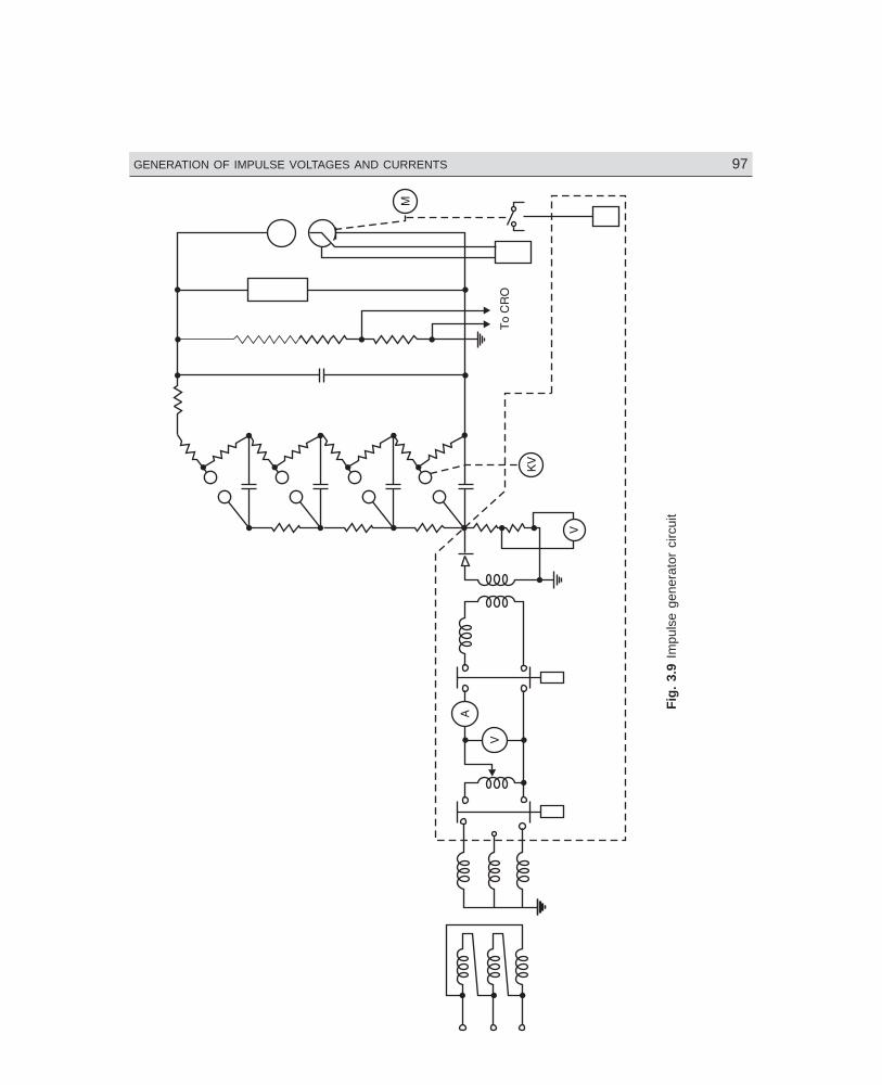
Dharm\N-HIGH\HG3-2.PM5 97
GENERATION OF IMPULSE VOLTAGES AND CURRENTS 97
Fig
. 3.
9 Im
puls
e ge
nera
tor
circ
uit
Dharm\N-HIGH\HG3-2.PM5 98
98 HIGH VOLTAGE ENGINEERING
and bushings have been recommended, are in use. These designs were made possible due to the use ofhigh dielectric fluids (e.g. SF6) which could reduce the size of the capacitors significantly.
The coupling sphere gaps are arranged one above the other on horizontal arms and the setting ofthe gaps is adjusted by a remotely controlled motor in conjunction with an indicator. This arrangementwith mutual irradiation ensures a perfect cascading of the spark gaps. They are normally incapsulatedin a chimney provided with dust free and dry air. The use of proper gas mixtures gives good switchingperformance.
The impulse generator should have a device to earth the capacitors when it is not in operation.The d.c. capacitors can build up high voltages after a short time of short circuit due to the relaxationphenomenon. A series protective resistance should be included in this earthing device to avoid too highdischarge currents.
The front and tail resistors are fixed to the generator frame by means of resistor carriers ofbakelised paper tubes. The charging resistors are fixed along the sphere gap column. All leads andelectrodes within the generator should be dimensioned properly to avoid too heavy corona dischargesduring the charging period.
A typical impulse generator circuit giving all details is shown in Fig. 3.9.
3.7 TRIGGERING AND SYNCHRONISATION OF THE IMPULSE GENERATOR
Impulse generators are normally operated in conjunction with cathode ray oscillographs for measurementand for studying the effect of impulse waves on the performance of the insulations of the equipments.Since the impulse waves are of shorter duration, it is necessary that the operation of the generator andthe oscillograph should be synchronised accurately and if the wave front of the wave is to be recordedaccurately, the time sweep circuit of the oscillograph should be initiated at a time slightly before theimpulse wave reaches the deflecting plates.
If the impulse generator itself initiates the sweep circuit of the oscillograph, it is then necessaryto connect a delay cable between the generator or the potential divider and the deflecting plates of theoscilloscope so that the impulse wave reaches the plates at a controlled time after the sweep has beentripped. However, the use of delay cable leads to inaccuracies in measurement. For this reason, sometripping circuits have been developed where the sweep circuit is operated first and then after a time ofabout 0.1 to 0.5 µ sec. the generator is triggered.
One of the methods involves the use of a three-sphere gap in the first stage of the generator asshown in Fig. 3.10. The spacing between the spheres is so adjusted that the two series gaps are able towithstand the charging voltage of the impulse generator. A high resistance is connected between theouter spheres and its centre point is connected to the control sphere so that the voltage between theouter spheres is equally divided between the two gaps. If the generator is now charged to a voltageslightly less than the breakdown voltage of the gaps, the breakdown can be achieved at any instant byapplying an impulse of either polarity and of a peak voltage not less than one fifth of the chargingvoltage to the control sphere.
The operation is explained as follows. The switch S is closed which initiates the sweep circuit ofthe oscillograph. The same impulse is applied to the grid of the thyratron tube. The inherent time delayof the thyratron ensures that the sweep circuit begins to operate before the start of the high voltage impulse.
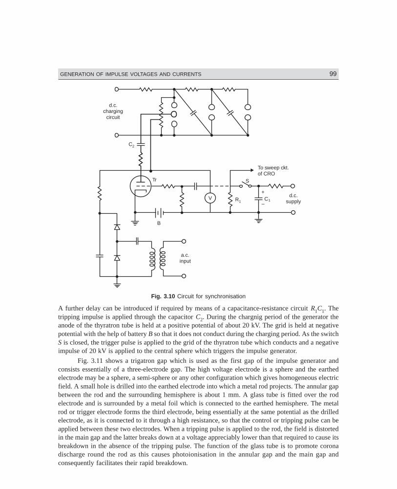
Dharm\N-HIGH\HG3-2.PM5 99
GENERATION OF IMPULSE VOLTAGES AND CURRENTS 99
d.c.charging
circuit
To sweep ckt.of CRO
d.c.supply
a.c.input
C2
R1C1
Tr S
+
B
–V
Fig. 3.10 Circuit for synchronisation
A further delay can be introduced if required by means of a capacitance-resistance circuit R1C1. Thetripping impulse is applied through the capacitor C2. During the chargnig period of the generator theanode of the thyratron tube is held at a positive potential of about 20 kV. The grid is held at negativepotential with the help of battery B so that it does not conduct during the charging period. As the switchS is closed, the trigger pulse is applied to the grid of the thyratron tube which conducts and a negativeimpulse of 20 kV is applied to the central sphere which triggers the impulse generator.
Fig. 3.11 shows a trigatron gap which is used as the first gap of the impulse generator andconsists essentially of a three-electrode gap. The high voltage electrode is a sphere and the earthedelectrode may be a sphere, a semi-sphere or any other configuration which gives homogeneous electricfield. A small hole is drilled into the earthed electrode into which a metal rod projects. The annular gapbetween the rod and the surrounding hemisphere is about 1 mm. A glass tube is fitted over the rodelectrode and is surrounded by a metal foil which is connected to the earthed hemisphere. The metalrod or trigger electrode forms the third electrode, being essentially at the same potential as the drilledelectrode, as it is connected to it through a high resistance, so that the control or tripping pulse can beapplied between these two electrodes. When a tripping pulse is applied to the rod, the field is distortedin the main gap and the latter breaks down at a voltage appreciably lower than that required to cause itsbreakdown in the absence of the tripping pulse. The function of the glass tube is to promote coronadischarge round the rod as this causes photoionisation in the annular gap and the main gap andconsequently facilitates their rapid breakdown.
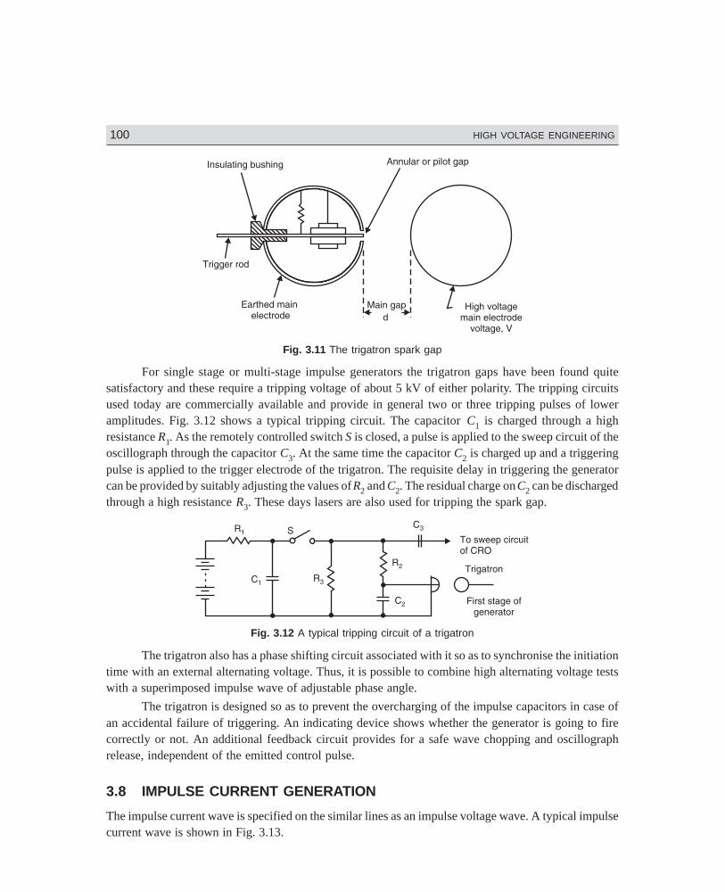
Dharm\N-HIGH\HG3-2.PM5 100
100 HIGH VOLTAGE ENGINEERING
Fig. 3.11 The trigatron spark gap
For single stage or multi-stage impulse generators the trigatron gaps have been found quitesatisfactory and these require a tripping voltage of about 5 kV of either polarity. The tripping circuitsused today are commercially available and provide in general two or three tripping pulses of loweramplitudes. Fig. 3.12 shows a typical tripping circuit. The capacitor C1 is charged through a highresistance R1. As the remotely controlled switch S is closed, a pulse is applied to the sweep circuit of theoscillograph through the capacitor C3. At the same time the capacitor C2 is charged up and a triggeringpulse is applied to the trigger electrode of the trigatron. The requisite delay in triggering the generatorcan be provided by suitably adjusting the values of R2 and C2. The residual charge on C2 can be dischargedthrough a high resistance R3. These days lasers are also used for tripping the spark gap.
Fig. 3.12 A typical tripping circuit of a trigatron
The trigatron also has a phase shifting circuit associated with it so as to synchronise the initiationtime with an external alternating voltage. Thus, it is possible to combine high alternating voltage testswith a superimposed impulse wave of adjustable phase angle.
The trigatron is designed so as to prevent the overcharging of the impulse capacitors in case ofan accidental failure of triggering. An indicating device shows whether the generator is going to firecorrectly or not. An additional feedback circuit provides for a safe wave chopping and oscillographrelease, independent of the emitted control pulse.
3.8 IMPULSE CURRENT GENERATION
The impulse current wave is specified on the similar lines as an impulse voltage wave. A typical impulsecurrent wave is shown in Fig. 3.13.
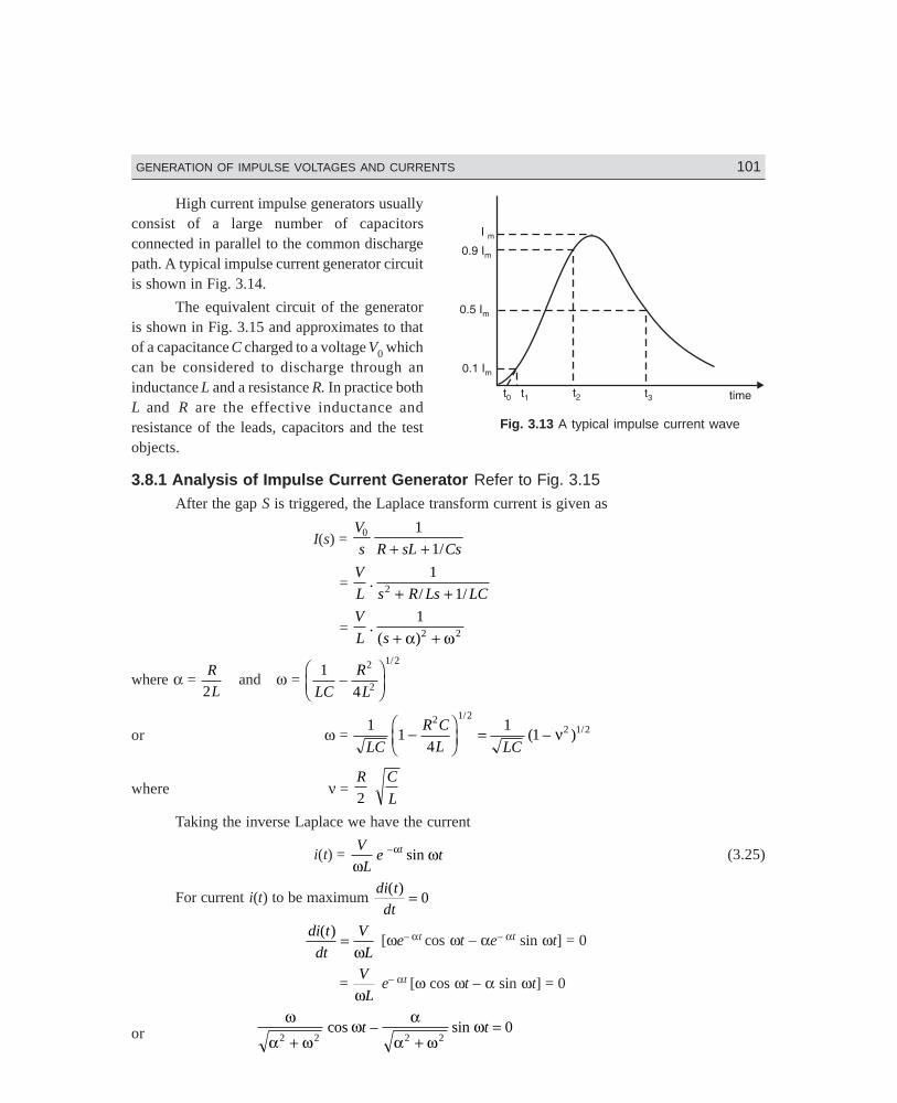
Dharm\N-HIGH\HG3-2.PM5 101
GENERATION OF IMPULSE VOLTAGES AND CURRENTS 101
High current impulse generators usuallyconsist of a large number of capacitorsconnected in parallel to the common dischargepath. A typical impulse current generator circuitis shown in Fig. 3.14.
The equivalent circuit of the generatoris shown in Fig. 3.15 and approximates to thatof a capacitance C charged to a voltage V0 whichcan be considered to discharge through aninductance L and a resistance R. In practice bothL and R are the effective inductance andresistance of the leads, capacitors and the testobjects.
3.8.1 Analysis of Impulse Current Generator Refer to Fig. 3.15After the gap S is triggered, the Laplace transform current is given as
I(s) = V
s R sL Cs0 1
1+ + /
= V
L s R Ls LC.
/ /
1
12 + +
= V
L s.
( )
12+ +α ω2
where α = R
L2and ω =
1
4
2
2
1 2
LC
R
L–
/FHG
IKJ
or ω = 1
14
11
2 1 22 1 2
LC
R C
L LC−
FHG
IKJ =
//( – )ν
where ν = R
2
C
L
Taking the inverse Laplace we have the current
i(t) = V
Le tt
ωωα– sin (3.25)
For current i(t) to be maximum di t
dt
( ) = 0
di t
dt
V
L
( ) =ω
[ωe– αt cos ωt – αe– αt sin ωt] = 0
= V
Lω e– αt [ω cos ωt – α sin ωt] = 0
orω
α ωω α
α ωω
2 2 2 2+ +=cos – sint t 0
Fig. 3.13 A typical impulse current wave
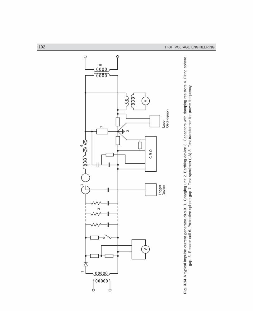
Dharm\N-HIGH\HG3-2.PM5 102
102 HIGH VOLTAGE ENGINEERING
Fig
. 3.
14 A
typ
ical
impu
lse
curr
ent
gene
rato
r ci
rcui
t. 1.
Cha
rgin
g un
it 2.
Ear
thin
g de
vice
3.
Cap
acito
rs w
ith d
ampi
ng r
esis
tors
4.
Firi
ng s
pher
ega
p. 5
. R
eact
or c
oil 6
. P
rote
ctiv
e sp
here
gap
7.
Test
spe
cim
en (
LA)
8. T
est
tran
sfor
mer
for
pow
er f
requ
ency
.
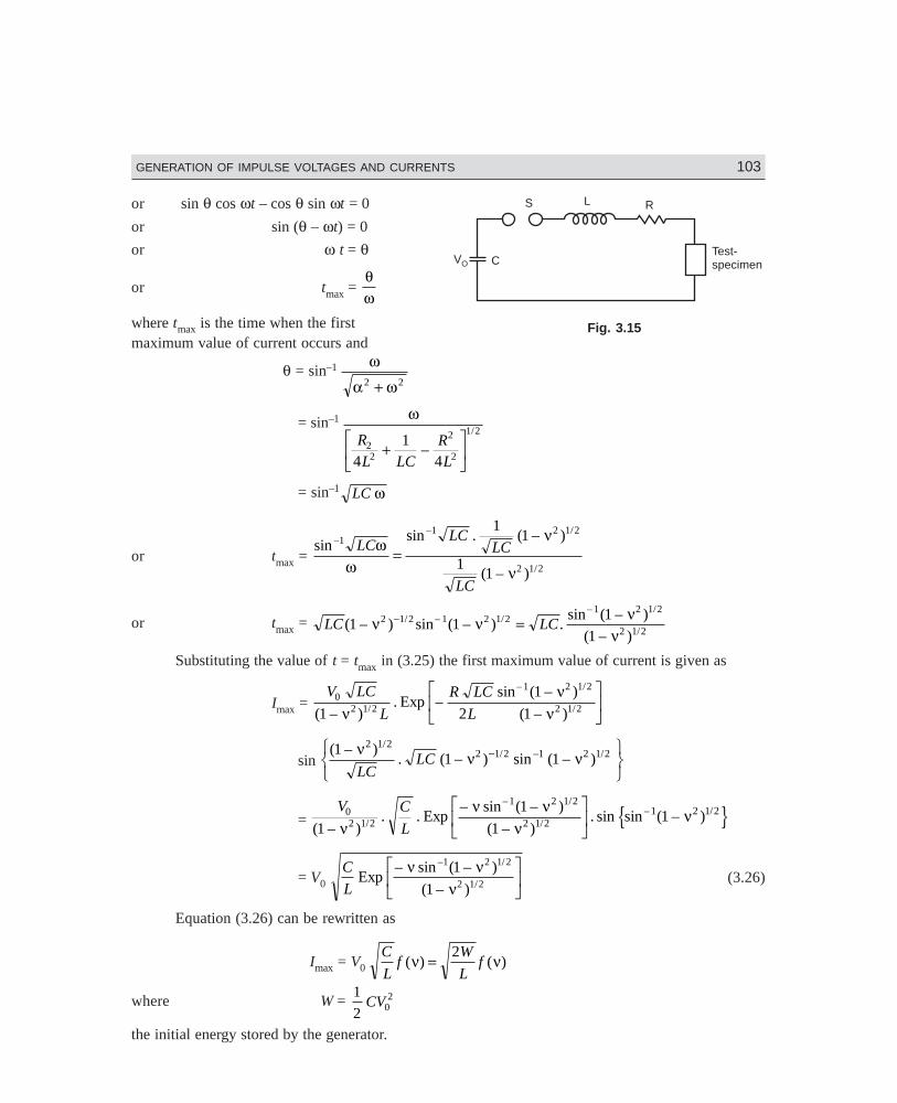
Dharm\N-HIGH\HG3-2.PM5 103
GENERATION OF IMPULSE VOLTAGES AND CURRENTS 103
VO C
S L R
Test-specimen
or sin θ cos ωt – cos θ sin ωt = 0
or sin (θ – ωt) = 0
or ω t = θ
or tmax = θω
where tmax is the time when the firstmaximum value of current occurs and
θ = sin–1 ω
α ω2 2+
= sin–1 ω
R
L LCRL
2
4 2
2
2
1 21
4+
LNM
OQP
–/
= sin–1 LC ω
or tmax = sin
sin–1–1 /
/
. ( – )
( – )
LCLC
LC
LC
ωω
ν
ν=
11
11
2 1 2
2 1 2
or tmax = LC LC( – ) ( – ) .( – )
( – )/ – /
– /
/1 11
12 1 2 1 2 1 2
1 2 1 2
2 1 2ν ν νν
− =sinsin
Substituting the value of t = tmax in (3.25) the first maximum value of current is given as
Imax = V LC
L
R LC
L0
2 1 2
1 2 1 2
2 1 21
1
2 1( – ).
( – )
( – )/
– /
/νν
νExp –
sinLNM
OQP
sin ( – )
. ( – ) ( – )/
/ –1 /11 1
2 1 22 1 2 2 1 2ν ν ν
LCLC −RST
UVWsin
= V C
L02 1 2
1 2 1 2
2 1 21 2 1 2
1
1
11
( – ). .
– ( – )
( – ). ( – )/
– /
/– /
νν ν
ννExp
sinsin sin
LNM
OQP n s
= V0 C
LExp
– sin –1ν νν( – )
( – )
/
/
1
1
2 1 2
2 1 2
LNM
OQP
(3.26)
Equation (3.26) can be rewritten as
Imax = V0 C
Lf
W
Lf( ) ( )ν ν=
2
where W = 1
2 02CV
the initial energy stored by the generator.
Fig. 3.15
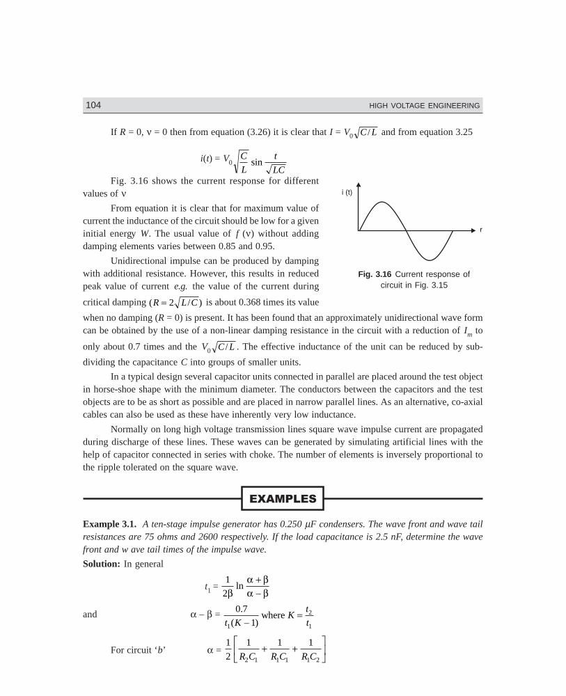
Dharm\N-HIGH\HG3-2.PM5 104
104 HIGH VOLTAGE ENGINEERING
If R = 0, ν = 0 then from equation (3.26) it is clear that I = V0 C L/ and from equation 3.25
i(t) = V0C
L
t
LCsin
Fig. 3.16 shows the current response for differentvalues of ν
From equation it is clear that for maximum value ofcurrent the inductance of the circuit should be low for a giveninitial energy W. The usual value of f (ν) without addingdamping elements varies between 0.85 and 0.95.
Unidirectional impulse can be produced by dampingwith additional resistance. However, this results in reducedpeak value of current e.g. the value of the current during
critical damping ( / )R L C= 2 is about 0.368 times its value
when no damping (R = 0) is present. It has been found that an approximately unidirectional wave formcan be obtained by the use of a non-linear damping resistance in the circuit with a reduction of Im to
only about 0.7 times and the V0 C L/ . The effective inductance of the unit can be reduced by sub-
dividing the capacitance C into groups of smaller units.
In a typical design several capacitor units connected in parallel are placed around the test objectin horse-shoe shape with the minimum diameter. The conductors between the capacitors and the testobjects are to be as short as possible and are placed in narrow parallel lines. As an alternative, co-axialcables can also be used as these have inherently very low inductance.
Normally on long high voltage transmission lines square wave impulse current are propagatedduring discharge of these lines. These waves can be generated by simulating artificial lines with thehelp of capacitor connected in series with choke. The number of elements is inversely proportional tothe ripple tolerated on the square wave.
Example 3.1. A ten-stage impulse generator has 0.250 µF condensers. The wave front and wave tailresistances are 75 ohms and 2600 respectively. If the load capacitance is 2.5 nF, determine the wavefront and w ave tail times of the impulse wave.
Solution: In general
t1 = 1
2βα βα β
ln+–
and α – β = 0 7
11
2
1
.
( – )t KK
t
twhere =
For circuit ‘b’ α = 1
2
1 1 1
2 1 1 1 1 2R C R C R C+ +
LNM
OQP
Fig. 3.16 Current response ofcircuit in Fig. 3.15
Dharm\N-HIGH\HG3-2.PM5 105
GENERATION OF IMPULSE VOLTAGES AND CURRENTS 105
and β = 1
24
4
1 2 1 2
1 2
α2 –/
R R C C
LNM
OQP
In the given problem
R1 = 75 ohms, R2 = 2600 ohms, C1 = 250
10 = 25 nF
and C2 = 2.5 nF
∴ α = 10
2
1
2600 25
1
75 25
1
75 2 5
9
×+
×+
×LNM
OQP.
≈ 10
2
1
75 25
9
×+
×LNM
OQP
1
75 2.5
≈ 10
2
9
[5.333 × 10⁻⁴ + 5.333 × 10⁻³]
≈ 10
2
9
× 5.8663 × 10–3
≈ 2.933 × 10⁶
Now4 10
75 2600 25 2 5
18×× × × .
= 3.282 × 10¹¹
∴ β = 2.9189 × 10⁶
t1 = 1
2 2 9189 2 933 2 9189× . . – .ln
2.933 + 2.9189
= 0.1713 ln 5 8519
0 0141
.
.= 1.03 µ sec.
0.0141 = 0 7
1 03 1
.
. ( – )K
K – 1 = 48.07
K = 49.07
or t2 = 50.5 µ sec. Ans.
Approximate values of wave front and wave tail times can be obtained as follows:
The approximate circuit during charging of loadcapacitance by the generator capacitance is a follows:
Here R2 is neglected and the time taken for chargingto peak value is approximately three times the time constantof the circuit. During charging C1 and C2 are in series.Therefore,
t1 = 3 C C
C CR1 2
1 21+
Dharm\N-HIGH\HG3-2.PM5 106
106 HIGH VOLTAGE ENGINEERING
During discharge C1 and C2 are in parallel and R1 and R2 in series. Hence the time for 50%discharge is approximately given as
t2 = 0.7 (R1 + R2) (C1 + C2)
Using these formulae, we have
t1 = 3 × 25 2 5 10
27 5 1075
× ××
×.
.
–18
–9
= 511 × 10–9 sec.
= 0.511 µ sec.
and t2 = 0.7 (2675) (27.5) × 10–9
= 51.5 µ sec.
On comparison with the values obtained through exact formulate it is found that whereas wavetail time is more or less same, the wave front time as calculated through approximate formula is quiteerroneous.
Example 3.2. A 12-stage impulse generator has capacitors each rated at 0.3 µF, 150 kV. The capacitanceof the test specimen is 400 pF. Determine the wave front and wave tail resistance to produce at 1.2/50µ sec. impulse wave. Also determine the maximum output voltage if the charging voltage is 125 kV.
Solution: Using the approximate formulae, we have
t1 = 1.2 × 10–6 = 3 R1 C C
C C1 2
1 2+
where C1 = 0 3
12
. = 0.025 µF = 25 nF
1.2 × 10–6 = 3 R1 25 0 4
25 4
× .
. × 10–9
R1 = 1016 Ω 50 × 10–6 = 0.7 (1016 + R2) (25.4) × 10–9
R2 + 1016 = 2812
R2 = 1796 ΩAlternative:
t1 = 1
2βα βα β
ln+–
α βα β
β+ =–
e t2 1
and α – β = 0 7
50 1
.
( – )t
α – β = 0 7
48 8
.
. = 0.014344
Since γ = C
C1
2
= 62.5 and is a large value
Dharm\N-HIGH\HG3-2.PM5 107
GENERATION OF IMPULSE VOLTAGES AND CURRENTS 107
R1 ≈ 1 1 1
25 10 0 0143441C.
– .–3α β=
× ×= 2788 Ω
Since α ≈ β
t1 = 2
2
2
0 014344αα
ln.
FH
IK
2.4 α = ln 139 αAfter a few trials say α = 2.43
LHS = 5.832 and RHS = 5.82
Therefore α ≈ 2.43
∴ β = 2.415656
R1 = 1 1 1 62 5
1 1C C. .
.
α β α β++
+
= 1
25 10
1
4 8456
62 5
4 84563×+L
NMOQP− .
.
.
R1 = 1
25 10
63 5
4 84565343×
FH
IK =−
.
.Ω
From the result it is clear that the approximate formulae are really approximate and, therefore,they give only some idea of the final exact results. The maximum output voltage is given by
V
R Ce et t0
1 221 1
βα β α β[ – ]–( – ) –( )+
where V0 = 125 × 12 = 1500 KV [e–0.014344 × 1.2 – e–4.8456 × 1.2]
∴ νmax (t) = 1500
2 524 0 4 10 2 41565× × × ×. .–3
= 1481 × 0.983
= 1455 kV Ans.
Example 3.3. An impulse current generator has total capacitance of 15 µF, the charging voltage 125KV, the circuit inductance 2 mH and the dynamic resistance 1 ohm. Determine the peak current andwave shape of the wave.
Solution: The maximum value of current is given as
Imax = V0 C
Le
– sin ( – )
( – )
–1 /
/
ν νν1
1
2 1 2
2 1 2
where ν = R C
L2
= 1
2
15 10
2 10
××
–6
–3
Dharm\N-HIGH\HG3-2.PM5 108
108 HIGH VOLTAGE ENGINEERING
= 4.33 × 10⁻²
Now e e– sin ( – )
( – )
–1 /
/–0. .ν ν
ν1
1
2 1 2
2 1 20433 1 526= ×
= 0.936
∴ Imax = 125 × 8.66 × 10–2 × 0.936
= 10.13 KA Ans.
Now t1 = LCsin ( – )
( – )
–1 /
/
1
1
2 1 2
2 1 2
νν
= 2 10 15 10 1 52676× × × ×−–3 .
= 2.6 × 10–4
= 260 µ sec.
The general expression for current
i (t) = V0 C
Le
t
LCt−α sin
i (t2) = 5.06 = 125 × 8.66 × 10–2 ett−
×2 2000 2
15 2000/ sin
or 0.46 = ett− 2 2000 2
173 2/ sin
.
After a few trials say t2 = 1275 µ sec.
RHS = 0.5286 sin 1275
173 2.
= 0.5286 × 0.883
= 0.466
Therefore, time to 50% value is 1275 µ sec. Ans.
3.1. Define the terms (i) Impulse voltages; (ii) Chopped wave; (iii) Impulse flash over voltage; (iv) Impulsepuncture voltage; (v) Impulse ratio for flash over; (vi) Impulse ratio for puncture.
3.2. Draw a neat exact equivalent circuit of an Impulse Generator and indicate the significance of each parameterbeing used.
3.3. Draw and compare the two simplified equivalent circuits of the impulse generator circuits (a) and (b).
3.4. Give complete analysis of circuit ‘a’ and show that the wave front and wave tail resistances are physicallyrealisable only under certain condition. Derive the condition.
3.5. Give complete analysis of circuit ‘b’ and derive the condition for physical realisation of wave front andwave tail resistances.
3.6. Derive an expression for voltage efficiency of a single stage impulse generator.

Dharm\N-HIGH\HG3-2.PM5 109
GENERATION OF IMPULSE VOLTAGES AND CURRENTS 109
3.7. Describe the construction, principle of operation and application of a multistage Marx's Surge Generator.
3.8. Explain the Goodlet circuit of impulse voltage generation and compare its performance with that of Marx’xCircuit.
3.9. Describe the construction of various components used in the development of an impulse generator.
3.10. Explain with neat diagram triggering and synchronisation of the impulse generator with the CRO.
3.11. Draw a typical impulse current generator circuit and explain its operation and application.
3.12. Draw a neat diagram of a high current generator circuit (equivalent circuit) and through analysis of thecircuit show how the wave form can be controlled.
Measurement of High Voltagesand Currents
110
4
4.1 INTRODUCTION
Transient measurements have much in common with measurements of steady state quantities but theshort-lived nature of the transients which we are trying to record introduces special problems. Frequentlythe transient quantity to be measured is not recorded directly because of its large magnitudes e.g. whena shunt is used to measure current, we really measure the voltage across the shunt and then we assumethat the voltage is proportional to the current, a fact which should not be taken for granted with transientcurrents. Often the voltage appearing across the shunt may be insufficient to drive the measuring device;it requires amplification. On the other hand, if the voltage to be measured is too large to be measuredwith the usual meters, it must be attenuated. This suggests an idea of a measuring system rather than ameasuring device.
Measurements of high voltages and currents involves much more complex problems which aspecialist, in common electrical measurement, does not have to face. The high voltage equipmentshave large stray capacitances with respect to the grounded structures and hence large voltage gradientsare set up. A person handling these equipments and the measuring devices must be protected againstthese over voltages. For this, large structures are required to control the electrical fields and to avoidflash over between the equipment and the grounded structures. Sometimes, these structures are re-quired to control heat dissipation within the circuits. Therefore, the location and layout of the equipmentsis very important to avoid these problems. Electromagnetic fields create problems in the measurementsof impulse voltages and currents and should be minimised.
The chapter is devoted to describing various devices and circuits for measurement of high voltagesand currents. The application of the device to the type of voltages and currents is also discussed.
4.2 SPHERE GAP
Sphere gap is by now considered as one of the standard methods for the measurement of peak value ofd.c., a.c. and impulse voltages and is used for checking the voltmeters and other voltage measuringdevices used in high voltage test circuits. Two identical metallic spheres separated by certain distanceform a sphere gap. The sphere gap can be used for measurement of impulse voltage of either polarityprovided that the impulse is of a standard wave form and has wave front time at least 1 micro sec. andwave tail time of 5 micro sec. Also, the gap length between the sphere should not exceed a sphereradius. If these conditions are satisfied and the specifications regarding the shape, mounting, clearances
Dharm\N-HIGH\HG4-1.PM5 111
MEASUREMENT OF HIGH VOLTAGES AND CURRENTS 111
of the spheres are met, the results obtained by the use of sphere gaps are reliable to within ±3%. It hasbeen suggested in standard specification that in places where the availability of ultraviolet radiation islow, irradiation of the gap by radioactive or other ionizing media should be used when voltages ofmagnitude less than 50 kV are being measured or where higher voltages with accurate results are to beobtained.
In order to understand the importance of irradiation of sphere gap for measurement of impulsevoltages especially which are of short duration, it is necessary to understand the time-lag involved inthe development of spark process. This time lag consists of two components—(i) The statistical time-lag caused by the need of an electron to appear in the gap during the application of the voltage. (ii) Theformative time lag which is the time required for the breakdown to develop once initiated.
The statistical time-lag depends on the irradiation level of the gap. If the gap is sufficientlyirradiated so that an electron exists in the gap to initiate the spark process and if the gap is subjected toan impulse voltage, the breakdown will take place when the peak voltage exceeds the d.c. breakdownvalue. However, if the irradiation level is low, the voltage must be maintained above the d.c. break-down value for a longer period before an electron appears. Various methods have been used for irradia-tion e.g. radioactive material, ultraviolet illumination as supplied by mercury arc lamp and coronadischarges.
It has been observed that large variation can occur in the statistical time-lag characteristic of agap when illuminated by a specified light source, unless the cathode conditions are also preciselyspecified.
Irradiation by radioactive materials has the advantage in that they can form a stable source ofirradiation and that they produce an amount of ionisation in the gap which is largely independent of thegap voltage and of the surface conditions of the electrode. The radioactive material may be placedinside high voltage electrode close behind the sparking surface or the radioactive material may formthe sparking surface.
The influence of the light from the impulse generator spark gap on the operation of the spheregaps has been studied. Here the illumination is intense and occurs at the exact instant when it is re-quired, namely, at the instant of application of the voltage wave to the sphere gap.
The formative time lag depends mainly upon the mechanism of spark growth. In case of second-ary electron emission, it is the transit time taken by the positive ion to travel from anode to cathode thatdecides that formative time lag. The formative time-lag decreases with the applied over voltage andincrease with gap length and field non-uniformity.
Specifications on Spheres and Associated AccessoriesThe spheres should be so made that their surfaces are smooth and their curvatures as uniform as possible.The curvature should be measured by a spherometer at various positions over an area enclosed by acircle of radius 0.3 D about the sparking point where D is the diameter of the sphere and sparkingpoints on the two spheres are those which are at minimum distances from each other.
For smaller size, the spheres are placed in horizontal configuration whereas large sizes (diameters),the spheres are mounted with the axis of the sphere gaps vertical and the lower sphere is grounded. Ineither case, it is important that the spheres should be so placed that the space between spheres is freefrom external electric fields and from bodies which may affect the field between the spheres (Figs. 4.1and 4.2).
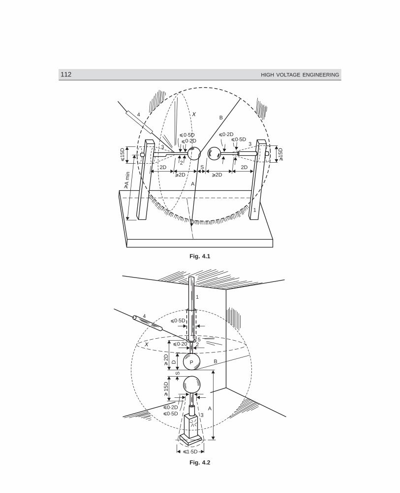
Dharm\N-HIGH\HG4-1.PM5 112
112 HIGH VOLTAGE ENGINEERING
0·2D0·5D
3
2DS
B
2D
1
15D
4
3
X
0·5D0·2D
22D
15D
2D
AAm
in
Fig. 4.1
B
A
0·5D
0·20X
4
52
1
P
SD
15D
2D
3
0·2D0·5D
1·5D
Fig. 4.2
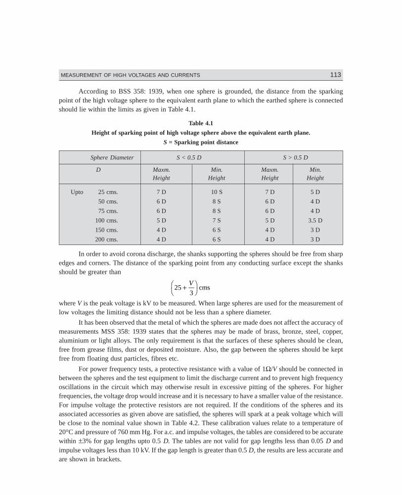
Dharm\N-HIGH\HG4-1.PM5 113
MEASUREMENT OF HIGH VOLTAGES AND CURRENTS 113
According to BSS 358: 1939, when one sphere is grounded, the distance from the sparkingpoint of the high voltage sphere to the equivalent earth plane to which the earthed sphere is connectedshould lie within the limits as given in Table 4.1.
Table 4.1
Height of sparking point of high voltage sphere above the equivalent earth plane.
S = Sparking point distance
Sphere Diameter S < 0.5 D S > 0.5 D
D Maxm. Min. Maxm. Min.Height Height Height Height
Upto 25 cms. 7 D 10 S 7 D 5 D
50 cms. 6 D 8 S 6 D 4 D
75 cms. 6 D 8 S 6 D 4 D
100 cms. 5 D 7 S 5 D 3.5 D
150 cms. 4 D 6 S 4 D 3 D
200 cms. 4 D 6 S 4 D 3 D
In order to avoid corona discharge, the shanks supporting the spheres should be free from sharpedges and corners. The distance of the sparking point from any conducting surface except the shanksshould be greater than
253
+FH
IK
Vcms
where V is the peak voltage is kV to be measured. When large spheres are used for the measurement oflow voltages the limiting distance should not be less than a sphere diameter.
It has been observed that the metal of which the spheres are made does not affect the accuracy ofmeasurements MSS 358: 1939 states that the spheres may be made of brass, bronze, steel, copper,aluminium or light alloys. The only requirement is that the surfaces of these spheres should be clean,free from grease films, dust or deposited moisture. Also, the gap between the spheres should be keptfree from floating dust particles, fibres etc.
For power frequency tests, a protective resistance with a value of 1Ω/V should be connected inbetween the spheres and the test equipment to limit the discharge current and to prevent high frequencyoscillations in the circuit which may otherwise result in excessive pitting of the spheres. For higherfrequencies, the voltage drop would increase and it is necessary to have a smaller value of the resistance.For impulse voltage the protective resistors are not required. If the conditions of the spheres and itsassociated accessories as given above are satisfied, the spheres will spark at a peak voltage which willbe close to the nominal value shown in Table 4.2. These calibration values relate to a temperature of20°C and pressure of 760 mm Hg. For a.c. and impulse voltages, the tables are considered to be accuratewithin ±3% for gap lengths upto 0.5 D. The tables are not valid for gap lengths less than 0.05 D andimpulse voltages less than 10 kV. If the gap length is greater than 0.5 D, the results are less accurate andare shown in brackets.
Dharm\N-HIGH\HG4-1.PM5 114
114 HIGH VOLTAGE ENGINEERING
Table 4.2
Sphere gap with one sphere earthed
Peak value of disruptive discharge voltages (50% for impulse tests) are valid for (i) alternating voltages(ii) d.c. voltage of either polarity (iii) negative lightning and switching impulse voltages
Sphere Gap Voltage KV PeakSpacing mm Sphere dia in cm.
12.5 25 50 75 100 150 200
10 31.7
20 59.0
30 85 86
40 108 112
50 129 137 138 138 138 138
75 167 195 202 203 203 203 203
100 (195) 244 263 265 266 266 266
125 (214) 282 320 327 330 330 330
150 (314) 373 387 390 390 390
175 (342) 420 443 443 450 450
200 (366) 460 492 510 510 510
250 (400) 530 585 615 630 630
300 (585) 665 710 745 750
350 (630) 735 800 850 855
400 (670) (800) 875 955 975
450 (700) (850) 945 1050 1080
500 (730) (895) 1010 1130 1180
600 (970) (1110) 1280 1340
700 (1025) (1200) 1390 1480
800 (1260) 1490 1600
900 (1320) 1580 1720
1000 (1360) 1660 1840
1100 1730 1940
1200 1800 2020
1300 1870 2100
1400 1920 2180
1500 1960 2250
1600 2320
1700 2370
1800 2410
1900 2460
2000 2490
Dharm\N-HIGH\HG4-1.PM5 115
MEASUREMENT OF HIGH VOLTAGES AND CURRENTS 115
Due to dust and fibre present in the air, the measurement of d.c. voltages is generally subject tolarger errors. Here the accuracy is within ±5% provided the spacing is less than 0.4 D and excessivedust is not present.
The procedure for high voltage measurement using sphere gaps depends upon the type of voltageto be measured.
Table 4.3
Sphere Gap with one sphere groundedPeak values of disruptive discharge voltages (50% values).
Positive lightning and switching impulse voltages
Peak Voltage kVSphere Gap Sphere dia in cms
Spacing mm 12.5 25 50 75 100 150 200
10 31.7
20 59 59
30 85.5 86
40 110 112
50 134 138 138 138 138 138 138
75 (181) 199 203 202 203 203 203
100 (215) 254 263 265 266 266 266
125 (239) 299 323 327 330 330 330
150 (337) 380 387 390 390 390
175 (368) 432 447 450 450 450
200 (395) 480 505 510 510 510
250 (433) 555 605 620 630 630
300 (620) 695 725 745 760
350 (670) 770 815 858 820
400 (715) (835) 900 965 980
450 (745) (890) 980 1060 1090
500 (775) (940) 1040 1150 1190
600 (1020) (1150) (1310) 1380
700 (1070) (1240) (1430) 1550
750 (1090) (1280) (1480) 1620
800 (1310) (1530) 1690
900 (1370) (1630) (1820)
1000 (1410) (1720) 1930
1100 (1790) (2030)
1200 (1860) (2120)
For the measurement of a.c. or d.c. voltage, a reduced voltage is applied to begin with so that theswitching transient does not flash over the sphere gap and then the voltage is increased gradually till thegap breaks down. Alternatively the voltage is applied across a relatively large gap and the spacing is
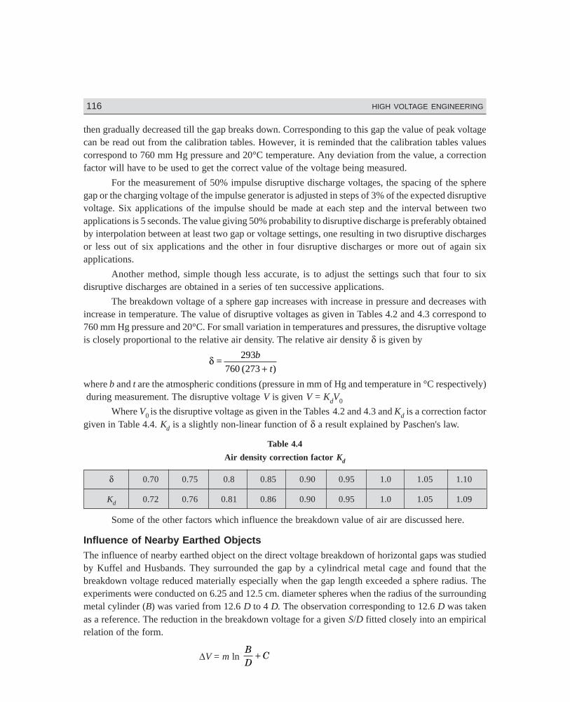
Dharm\N-HIGH\HG4-1.PM5 116
116 HIGH VOLTAGE ENGINEERING
then gradually decreased till the gap breaks down. Corresponding to this gap the value of peak voltagecan be read out from the calibration tables. However, it is reminded that the calibration tables valuescorrespond to 760 mm Hg pressure and 20°C temperature. Any deviation from the value, a correctionfactor will have to be used to get the correct value of the voltage being measured.
For the measurement of 50% impulse disruptive discharge voltages, the spacing of the spheregap or the charging voltage of the impulse generator is adjusted in steps of 3% of the expected disruptivevoltage. Six applications of the impulse should be made at each step and the interval between twoapplications is 5 seconds. The value giving 50% probability to disruptive discharge is preferably obtainedby interpolation between at least two gap or voltage settings, one resulting in two disruptive dischargesor less out of six applications and the other in four disruptive discharges or more out of again sixapplications.
Another method, simple though less accurate, is to adjust the settings such that four to sixdisruptive discharges are obtained in a series of ten successive applications.
The breakdown voltage of a sphere gap increases with increase in pressure and decreases withincrease in temperature. The value of disruptive voltages as given in Tables 4.2 and 4.3 correspond to760 mm Hg pressure and 20°C. For small variation in temperatures and pressures, the disruptive voltageis closely proportional to the relative air density. The relative air density δ is given by
δ =293b
t760 273( )+where b and t are the atmospheric conditions (pressure in mm of Hg and temperature in °C respectively) during measurement. The disruptive voltage V is given V = KdV0
Where V0 is the disruptive voltage as given in the Tables 4.2 and 4.3 and Kd is a correction factorgiven in Table 4.4. Kd is a slightly non-linear function of δ a result explained by Paschen's law.
Table 4.4
Air density correction factor Kd
δ 0.70 0.75 0.8 0.85 0.90 0.95 1.0 1.05 1.10
Kd 0.72 0.76 0.81 0.86 0.90 0.95 1.0 1.05 1.09
Some of the other factors which influence the breakdown value of air are discussed here.
Influence of Nearby Earthed ObjectsThe influence of nearby earthed object on the direct voltage breakdown of horizontal gaps was studiedby Kuffel and Husbands. They surrounded the gap by a cylindrical metal cage and found that thebreakdown voltage reduced materially especially when the gap length exceeded a sphere radius. Theexperiments were conducted on 6.25 and 12.5 cm. diameter spheres when the radius of the surroundingmetal cylinder (B) was varied from 12.6 D to 4 D. The observation corresponding to 12.6 D was takenas a reference. The reduction in the breakdown voltage for a given S/D fitted closely into an empiricalrelation of the form.
∆V = m ln BD
C+
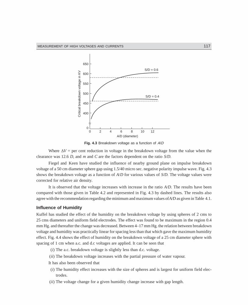
Dharm\N-HIGH\HG4-1.PM5 117
MEASUREMENT OF HIGH VOLTAGES AND CURRENTS 117
4 6 8 10 12A/D (diameter)
S/D = 0.6
S/D = 0.4
650
600
550
500
450
400
020
Crit
ical
brea
kdow
nvo
ltage
inK
V
Fig. 4.3 Breakdown voltage as a function of A/D
Where ∆V = per cent reduction in voltage in the breakdown voltage from the value when theclearance was 12.6 D, and m and C are the factors dependent on the ratio S/D.
Fiegel and Keen have studied the influence of nearby ground plane on impulse breakdownvoltage of a 50 cm diameter sphere gap using 1.5/40 micro sec. negative polarity impulse wave. Fig. 4.3shows the breakdown voltage as a function of A/D for various values of S/D. The voltage values werecorrected for relative air density.
It is observed that the voltage increases with increase in the ratio A/D. The results have beencompared with those given in Table 4.2 and represented in Fig. 4.3 by dashed lines. The results alsoagree with the recommendation regarding the minimum and maximum values of A/D as given in Table 4.1.
Influence of HumidityKuffel has studied the effect of the humidity on the breakdown voltage by using spheres of 2 cms to25 cms diameters and uniform field electrodes. The effect was found to be maximum in the region 0.4mm Hg. and thereafter the change was decreased. Between 4–17 mm Hg. the relation between breakdownvoltage and humidity was practically linear for spacing less than that which gave the maximum humidityeffect. Fig. 4.4 shows the effect of humidity on the breakdown voltage of a 25 cm diameter sphere withspacing of 1 cm when a.c. and d.c voltages are applied. It can be seen that
(i) The a.c. breakdown voltage is slightly less than d.c. voltage.
(ii) The breakdown voltage increases with the partial pressure of water vapour.
It has also been observed that
(i) The humidity effect increases with the size of spheres and is largest for uniform field elec-trodes.
(ii) The voltage change for a given humidity change increase with gap length.
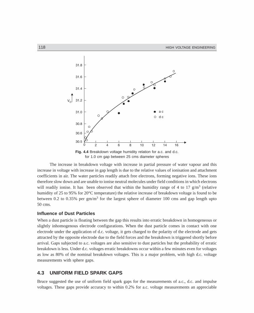
Dharm\N-HIGH\HG4-1.PM5 118
118 HIGH VOLTAGE ENGINEERING
Fig. 4.4 Breakdown voltage humidity relation for a.c. and d.c.for 1.0 cm gap between 25 cms diameter spheres
The increase in breakdown voltage with increase in partial pressure of water vapour and thisincrease in voltage with increase in gap length is due to the relative values of ionisation and attachmentcoefficients in air. The water particles readily attach free electrons, forming negative ions. These ionstherefore slow down and are unable to ionise neutral molecules under field conditions in which electronswill readily ionise. It has been observed that within the humidity range of 4 to 17 g/m3 (relativehumidity of 25 to 95% for 20°C temperature) the relative increase of breakdown voltage is found to bebetween 0.2 to 0.35% per gm/m3 for the largest sphere of diameter 100 cms and gap length upto50 cms.
Influence of Dust ParticlesWhen a dust particle is floating between the gap this results into erratic breakdown in homogeneous orslightly inhomogenous electrode configurations. When the dust particle comes in contact with oneelectrode under the application of d.c. voltage, it gets charged to the polarity of the electrode and getsattracted by the opposite electrode due to the field forces and the breakdown is triggered shortly beforearrival. Gaps subjected to a.c. voltages are also sensitive to dust particles but the probability of erraticbreakdown is less. Under d.c. voltages erratic breakdowns occur within a few minutes even for voltagesas low as 80% of the nominal breakdown voltages. This is a major problem, with high d.c. voltagemeasurements with sphere gaps.
4.3 UNIFORM FIELD SPARK GAPS
Bruce suggested the use of uniform field spark gaps for the measurements of a.c., d.c. and impulsevoltages. These gaps provide accuracy to within 0.2% for a.c. voltage measurements an appreciable
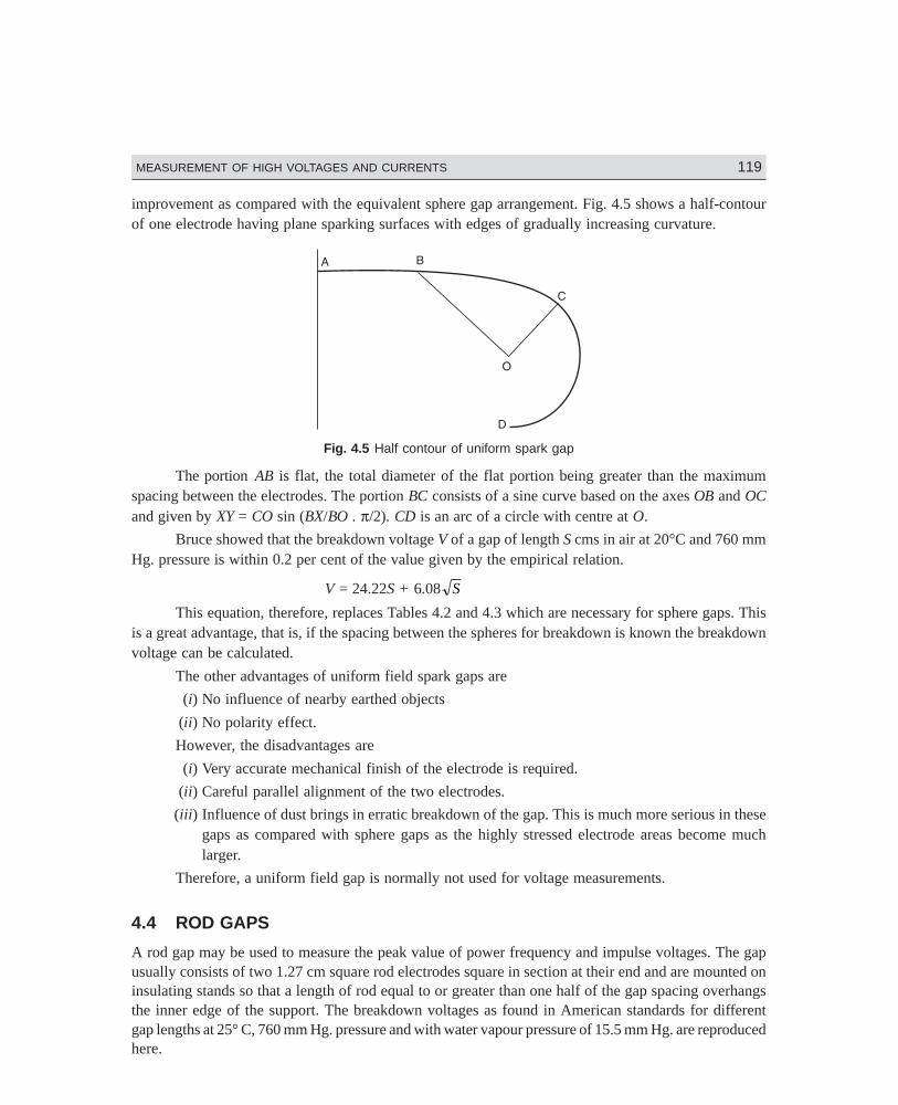
Dharm\N-HIGH\HG4-1.PM5 119
MEASUREMENT OF HIGH VOLTAGES AND CURRENTS 119
improvement as compared with the equivalent sphere gap arrangement. Fig. 4.5 shows a half-contourof one electrode having plane sparking surfaces with edges of gradually increasing curvature.
Fig. 4.5 Half contour of uniform spark gap
The portion AB is flat, the total diameter of the flat portion being greater than the maximumspacing between the electrodes. The portion BC consists of a sine curve based on the axes OB and OCand given by XY = CO sin (BX/BO . π/2). CD is an arc of a circle with centre at O.
Bruce showed that the breakdown voltage V of a gap of length S cms in air at 20°C and 760 mmHg. pressure is within 0.2 per cent of the value given by the empirical relation.
V = 24.22S + 6.08 S
This equation, therefore, replaces Tables 4.2 and 4.3 which are necessary for sphere gaps. Thisis a great advantage, that is, if the spacing between the spheres for breakdown is known the breakdownvoltage can be calculated.
The other advantages of uniform field spark gaps are
(i) No influence of nearby earthed objects
(ii) No polarity effect.
However, the disadvantages are
(i) Very accurate mechanical finish of the electrode is required.
(ii) Careful parallel alignment of the two electrodes.
(iii) Influence of dust brings in erratic breakdown of the gap. This is much more serious in thesegaps as compared with sphere gaps as the highly stressed electrode areas become muchlarger.
Therefore, a uniform field gap is normally not used for voltage measurements.
4.4 ROD GAPS
A rod gap may be used to measure the peak value of power frequency and impulse voltages. The gapusually consists of two 1.27 cm square rod electrodes square in section at their end and are mounted oninsulating stands so that a length of rod equal to or greater than one half of the gap spacing overhangsthe inner edge of the support. The breakdown voltages as found in American standards for differentgap lengths at 25° C, 760 mm Hg. pressure and with water vapour pressure of 15.5 mm Hg. are reproducedhere.
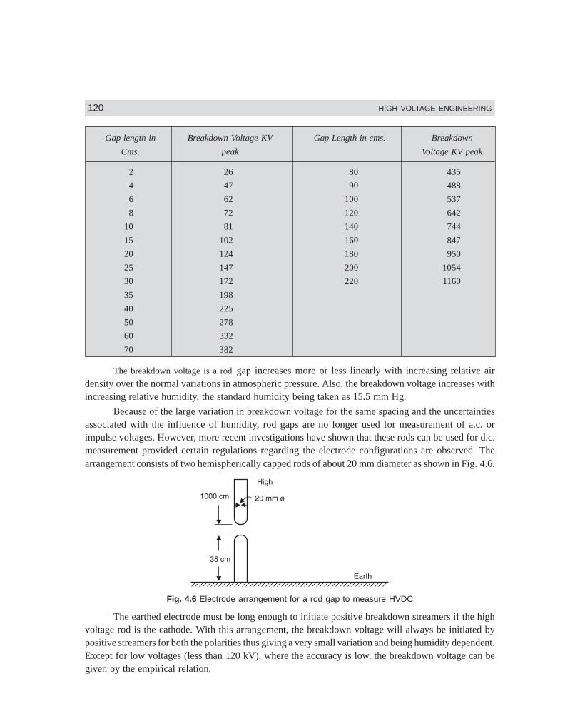
Dharm\N-HIGH\HG4-1.PM5 120
120 HIGH VOLTAGE ENGINEERING
Gap length in Breakdown Voltage KV Gap Length in cms. Breakdown
Cms. peak Voltage KV peak
2 26 80 435
4 47 90 488
6 62 100 537
8 72 120 642
10 81 140 744
15 102 160 847
20 124 180 950
25 147 200 1054
30 172 220 1160
35 198
40 225
50 278
60 332
70 382
The breakdown voltage is a rod gap increases more or less linearly with increasing relative airdensity over the normal variations in atmospheric pressure. Also, the breakdown voltage increases withincreasing relative humidity, the standard humidity being taken as 15.5 mm Hg.
Because of the large variation in breakdown voltage for the same spacing and the uncertaintiesassociated with the influence of humidity, rod gaps are no longer used for measurement of a.c. orimpulse voltages. However, more recent investigations have shown that these rods can be used for d.c.measurement provided certain regulations regarding the electrode configurations are observed. Thearrangement consists of two hemispherically capped rods of about 20 mm diameter as shown in Fig. 4.6.
Fig. 4.6 Electrode arrangement for a rod gap to measure HVDC
The earthed electrode must be long enough to initiate positive breakdown streamers if the highvoltage rod is the cathode. With this arrangement, the breakdown voltage will always be initiated bypositive streamers for both the polarities thus giving a very small variation and being humidity dependent.Except for low voltages (less than 120 kV), where the accuracy is low, the breakdown voltage can begiven by the empirical relation.
Dharm\N-HIGH\HG4-1.PM5 121
MEASUREMENT OF HIGH VOLTAGES AND CURRENTS 121
V = δ (A + BS) 4 51 10 8 65. ( . )–2× +h kV
where h is the absolute humidity in gm/m3 and varies between 4 and 20 gm/m3 in the above relation.The breakdown voltage is linearly related with the gap spacing and the slope of the relationB = 5.1 kV/cm and is found to be independent of the polarity of voltage. However constant A is polaritydependent and has the values
A = 20 kV for positive polarity
= 15 kV for negative polarity of the high voltage electrode.
The accuracy of the above relation is better than ±20% and, therefore, provides better accuracyeven as compared to a sphere gap.
4.5 ELECTROSTATIC VOLTMETER
The electric field according to Coulomb is the field of forces. The electric field is produced by voltageand, therefore, if the field force could be measured, the voltage can also be measured. Whenever avoltage is applied to a parallel plate electrode arrangement, an electric field is set up between the plates.It is possible to have uniform electric field between the plates with suitable arrangement of the plates.The field is uniform, normal to the two plates and directed towards the negative plate. If A is the area ofthe plate and E is the electric field intensity between the plates ε the permittivity of the medium betweenthe plates, we know that the energy density of the electric field between the plates is given as,
Wd = 1
2 ε E2
Consider a differential volume between the plates and parallel to the plates with area A andthickness dx, the energy content in this differential volume Adx is
dW = Wd Adx = 1
2εE Adx2
Now force F between the plates is defined as the derivative of stored electric energy along thefield direction i.e.,
F = dW
dxE A= 1
2ε 2
Now E = V/d where V is the voltage to be measured and d the distance of separation between theplates. Therefore, the expression for force
F = 1
2 2ε V A
d
2
Since the two plates are oppositely charged, there is always force of attraction between theplates. If the voltage is time dependant, the force developed is also time dependant. In such a case themean value of force is used to measure the voltage. Thus
F = 1 1 1
212
1 120
2
2 22
2
2TF t dt
T
V t
dA dt
A
d TV t dt A
V
d
Trms( )
( ). ( )= = =z z zε ε ε
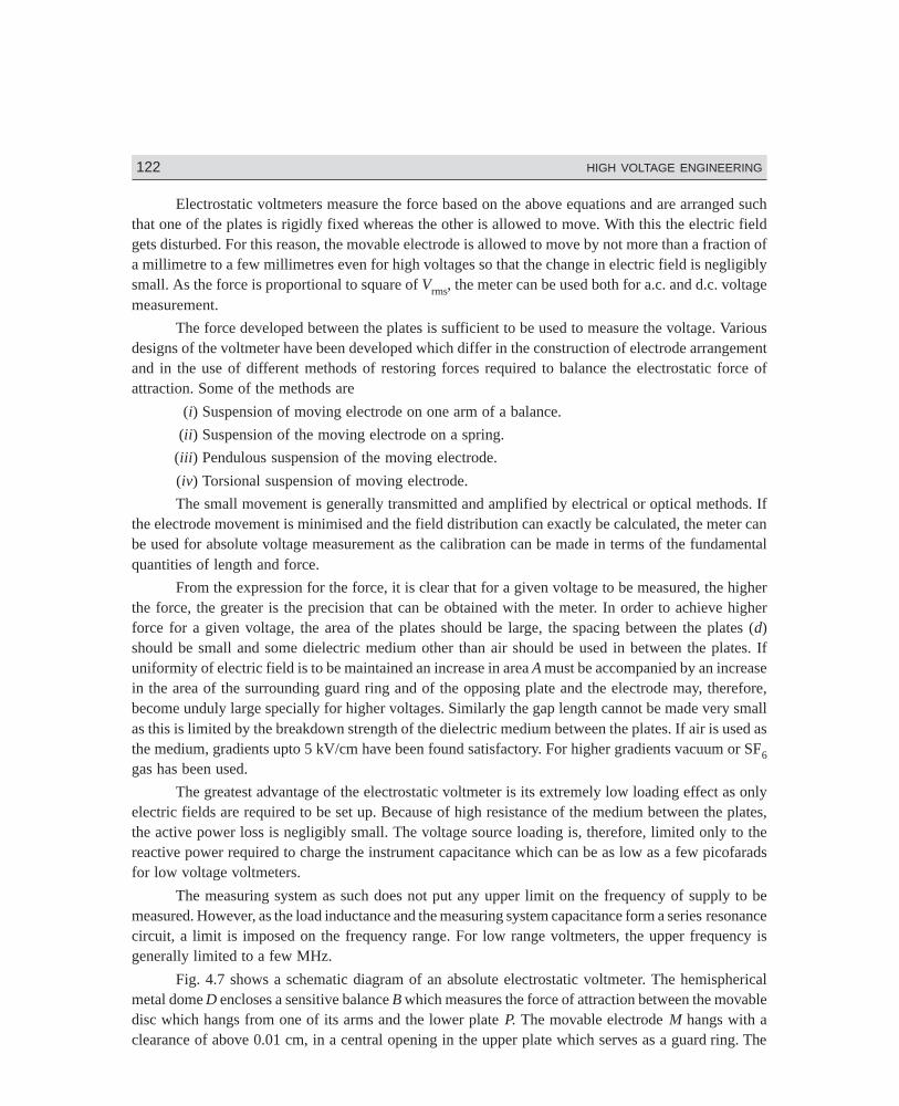
Dharm\N-HIGH\HG4-1.PM5 122
122 HIGH VOLTAGE ENGINEERING
Electrostatic voltmeters measure the force based on the above equations and are arranged suchthat one of the plates is rigidly fixed whereas the other is allowed to move. With this the electric fieldgets disturbed. For this reason, the movable electrode is allowed to move by not more than a fraction ofa millimetre to a few millimetres even for high voltages so that the change in electric field is negligiblysmall. As the force is proportional to square of Vrms, the meter can be used both for a.c. and d.c. voltagemeasurement.
The force developed between the plates is sufficient to be used to measure the voltage. Variousdesigns of the voltmeter have been developed which differ in the construction of electrode arrangementand in the use of different methods of restoring forces required to balance the electrostatic force ofattraction. Some of the methods are
(i) Suspension of moving electrode on one arm of a balance.
(ii) Suspension of the moving electrode on a spring.
(iii) Pendulous suspension of the moving electrode.
(iv) Torsional suspension of moving electrode.
The small movement is generally transmitted and amplified by electrical or optical methods. Ifthe electrode movement is minimised and the field distribution can exactly be calculated, the meter canbe used for absolute voltage measurement as the calibration can be made in terms of the fundamentalquantities of length and force.
From the expression for the force, it is clear that for a given voltage to be measured, the higherthe force, the greater is the precision that can be obtained with the meter. In order to achieve higherforce for a given voltage, the area of the plates should be large, the spacing between the plates (d)should be small and some dielectric medium other than air should be used in between the plates. Ifuniformity of electric field is to be maintained an increase in area A must be accompanied by an increasein the area of the surrounding guard ring and of the opposing plate and the electrode may, therefore,become unduly large specially for higher voltages. Similarly the gap length cannot be made very smallas this is limited by the breakdown strength of the dielectric medium between the plates. If air is used asthe medium, gradients upto 5 kV/cm have been found satisfactory. For higher gradients vacuum or SF6gas has been used.
The greatest advantage of the electrostatic voltmeter is its extremely low loading effect as onlyelectric fields are required to be set up. Because of high resistance of the medium between the plates,the active power loss is negligibly small. The voltage source loading is, therefore, limited only to thereactive power required to charge the instrument capacitance which can be as low as a few picofaradsfor low voltage voltmeters.
The measuring system as such does not put any upper limit on the frequency of supply to bemeasured. However, as the load inductance and the measuring system capacitance form a series resonancecircuit, a limit is imposed on the frequency range. For low range voltmeters, the upper frequency isgenerally limited to a few MHz.
Fig. 4.7 shows a schematic diagram of an absolute electrostatic voltmeter. The hemisphericalmetal dome D encloses a sensitive balance B which measures the force of attraction between the movabledisc which hangs from one of its arms and the lower plate P. The movable electrode M hangs with aclearance of above 0.01 cm, in a central opening in the upper plate which serves as a guard ring. The
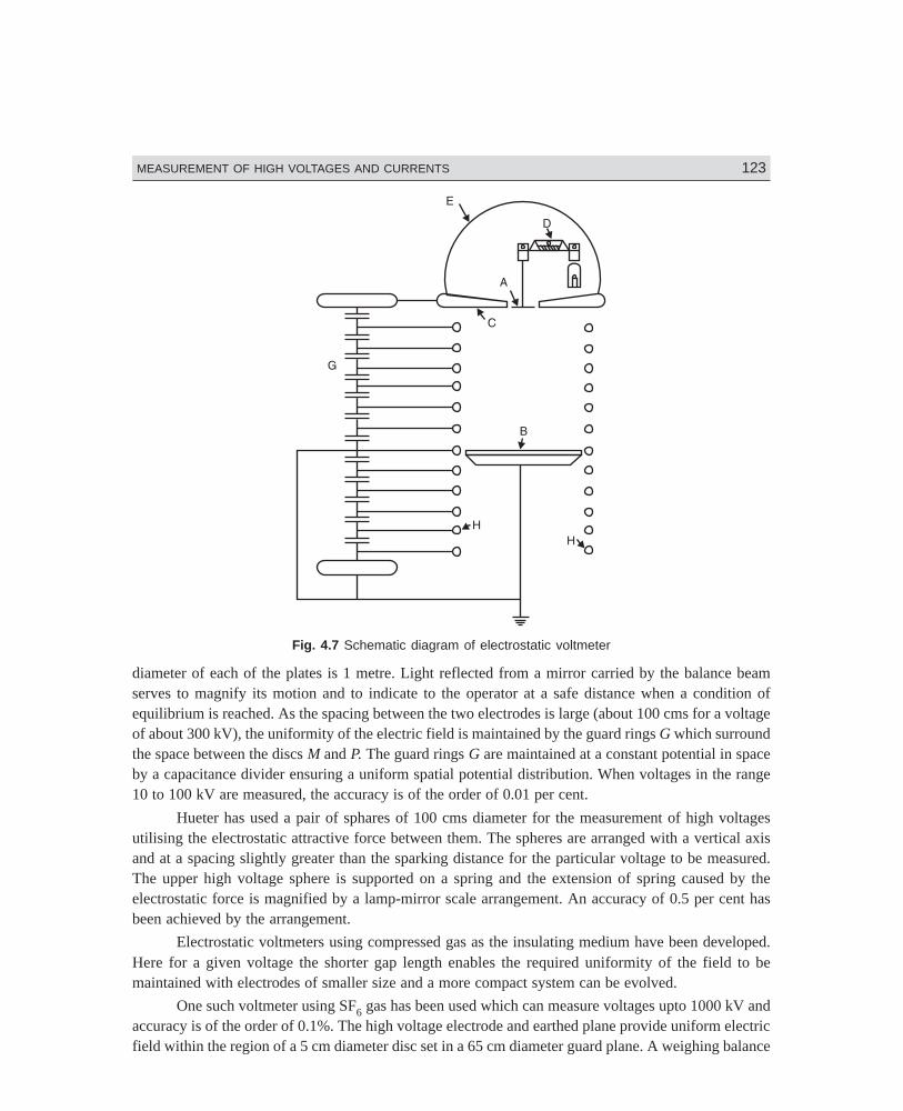
Dharm\N-HIGH\HG4-1.PM5 123
MEASUREMENT OF HIGH VOLTAGES AND CURRENTS 123
Fig. 4.7 Schematic diagram of electrostatic voltmeter
diameter of each of the plates is 1 metre. Light reflected from a mirror carried by the balance beamserves to magnify its motion and to indicate to the operator at a safe distance when a condition ofequilibrium is reached. As the spacing between the two electrodes is large (about 100 cms for a voltageof about 300 kV), the uniformity of the electric field is maintained by the guard rings G which surroundthe space between the discs M and P. The guard rings G are maintained at a constant potential in spaceby a capacitance divider ensuring a uniform spatial potential distribution. When voltages in the range10 to 100 kV are measured, the accuracy is of the order of 0.01 per cent.
Hueter has used a pair of sphares of 100 cms diameter for the measurement of high voltagesutilising the electrostatic attractive force between them. The spheres are arranged with a vertical axisand at a spacing slightly greater than the sparking distance for the particular voltage to be measured.The upper high voltage sphere is supported on a spring and the extension of spring caused by theelectrostatic force is magnified by a lamp-mirror scale arrangement. An accuracy of 0.5 per cent hasbeen achieved by the arrangement.
Electrostatic voltmeters using compressed gas as the insulating medium have been developed.Here for a given voltage the shorter gap length enables the required uniformity of the field to bemaintained with electrodes of smaller size and a more compact system can be evolved.
One such voltmeter using SF6 gas has been used which can measure voltages upto 1000 kV andaccuracy is of the order of 0.1%. The high voltage electrode and earthed plane provide uniform electricfield within the region of a 5 cm diameter disc set in a 65 cm diameter guard plane. A weighing balance
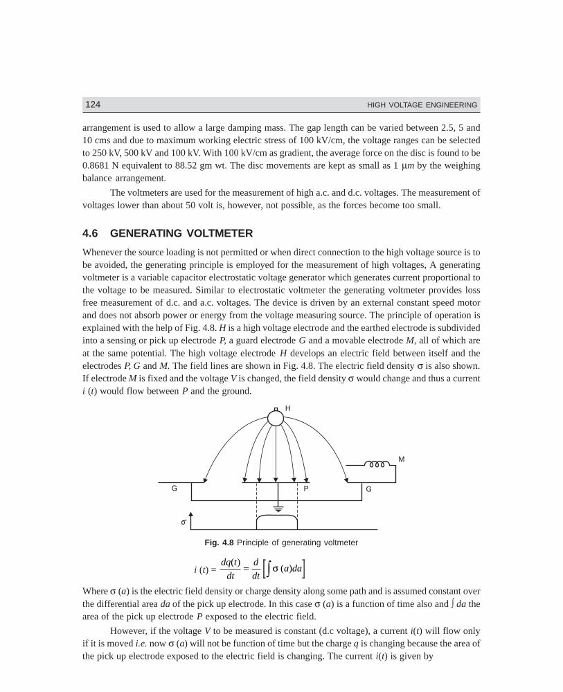
Dharm\N-HIGH\HG4-1.PM5 124
124 HIGH VOLTAGE ENGINEERING
arrangement is used to allow a large damping mass. The gap length can be varied between 2.5, 5 and10 cms and due to maximum working electric stress of 100 kV/cm, the voltage ranges can be selectedto 250 kV, 500 kV and 100 kV. With 100 kV/cm as gradient, the average force on the disc is found to be0.8681 N equivalent to 88.52 gm wt. The disc movements are kept as small as 1 µm by the weighingbalance arrangement.
The voltmeters are used for the measurement of high a.c. and d.c. voltages. The measurement ofvoltages lower than about 50 volt is, however, not possible, as the forces become too small.
4.6 GENERATING VOLTMETER
Whenever the source loading is not permitted or when direct connection to the high voltage source is tobe avoided, the generating principle is employed for the measurement of high voltages, A generatingvoltmeter is a variable capacitor electrostatic voltage generator which generates current proportional tothe voltage to be measured. Similar to electrostatic voltmeter the generating voltmeter provides lossfree measurement of d.c. and a.c. voltages. The device is driven by an external constant speed motorand does not absorb power or energy from the voltage measuring source. The principle of operation isexplained with the help of Fig. 4.8. H is a high voltage electrode and the earthed electrode is subdividedinto a sensing or pick up electrode P, a guard electrode G and a movable electrode M, all of which areat the same potential. The high voltage electrode H develops an electric field between itself and theelectrodes P, G and M. The field lines are shown in Fig. 4.8. The electric field density σ is also shown.If electrode M is fixed and the voltage V is changed, the field density σ would change and thus a currenti (t) would flow between P and the ground.
Fig. 4.8 Principle of generating voltmeter
i (t) = dq t
dt
d
dta da
( )( )= zσ
Where σ (a) is the electric field density or charge density along some path and is assumed constant overthe differential area da of the pick up electrode. In this case σ (a) is a function of time also and ∫ da thearea of the pick up electrode P exposed to the electric field.
However, if the voltage V to be measured is constant (d.c voltage), a current i(t) will flow onlyif it is moved i.e. now σ (a) will not be function of time but the charge q is changing because the area ofthe pick up electrode exposed to the electric field is changing. The current i(t) is given by
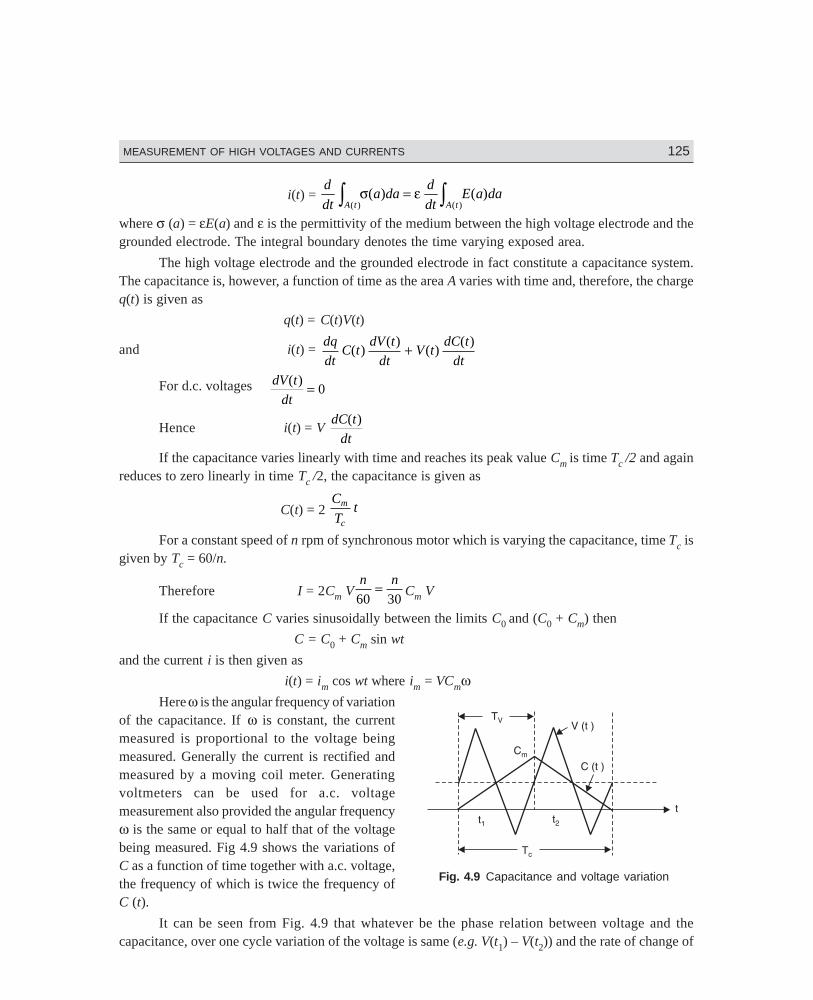
Dharm\N-HIGH\HG4-1.PM5 125
MEASUREMENT OF HIGH VOLTAGES AND CURRENTS 125
i(t) = d
dta da
d
dtE a da
A t A t( ) ( )( ) ( )z z=σ ε
where σ (a) = εE(a) and ε is the permittivity of the medium between the high voltage electrode and thegrounded electrode. The integral boundary denotes the time varying exposed area.
The high voltage electrode and the grounded electrode in fact constitute a capacitance system.The capacitance is, however, a function of time as the area A varies with time and, therefore, the chargeq(t) is given as
q(t) = C(t)V(t)
and i(t) = dq
dtC t
dV t
dtV t
dC t
dt( )
( )( )
( )+
For d.c. voltages dV t
dt
( ) = 0
Hence i(t) = V dC t
dt
( )
If the capacitance varies linearly with time and reaches its peak value Cm is time Tc /2 and againreduces to zero linearly in time Tc /2, the capacitance is given as
C(t) = 2 C
Ttm
c
For a constant speed of n rpm of synchronous motor which is varying the capacitance, time Tc isgiven by Tc = 60/n.
Therefore I = 2Cm Vn n
60 30= Cm V
If the capacitance C varies sinusoidally between the limits C0 and (C0 + Cm) then
C = C0 + Cm sin wt
and the current i is then given as
i(t) = im cos wt where im = VCmωHere ω is the angular frequency of variation
of the capacitance. If ω is constant, the currentmeasured is proportional to the voltage beingmeasured. Generally the current is rectified andmeasured by a moving coil meter. Generatingvoltmeters can be used for a.c. voltagemeasurement also provided the angular frequencyω is the same or equal to half that of the voltagebeing measured. Fig 4.9 shows the variations ofC as a function of time together with a.c. voltage,the frequency of which is twice the frequency ofC (t).
It can be seen from Fig. 4.9 that whatever be the phase relation between voltage and thecapacitance, over one cycle variation of the voltage is same (e.g. V(t1) – V(t2)) and the rate of change of
Fig. 4.9 Capacitance and voltage variation
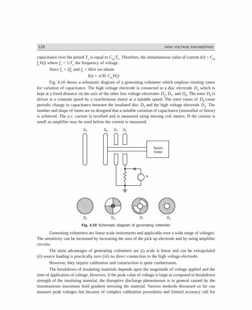
Dharm\N-HIGH\HG4-1.PM5 126
126 HIGH VOLTAGE ENGINEERING
capacitance over the period Tv is equal to Cm/Tv. Therefore, the instantaneous value of current i(t) = CmfvV(t) where fv = 1/Tv the frequency of voltage.
Since fv = 2fc and fc = 60/n we obtain
I(t) = n/30 CmV(t)
Fig. 4.10 shows a schematic diagram of a generating voltmeter which employs rotating vanesfor variation of capacitance. The high voltage electrode is connected to a disc electrode D3 which iskept at a fixed distance on the axis of the other low voltage electrodes D2, D1, and D0. The rotor D0 isdriven at a constant speed by a synchronous motor at a suitable speed. The rotor vanes of D0 causeperiodic change in capacitance between the insulated disc D2 and the high voltage electrode D3. Thenumber and shape of vanes are so designed that a suitable variation of capacitance (sinusodial or linear)is achieved. The a.c. current is rectified and is measured using moving coil meters. If the current issmall an amplifier may be used before the current is measured.
Fig. 4.10 Schematic diagram of generating voltmeter
Generating voltmeters are linear scale instruments and applicable over a wide range of voltages.The sensitivity can be increased by increasing the area of the pick up electrode and by using amplifiercircuits.
The main advantages of generating voltmeters are (i) scale is linear and can be extrapolated(ii) source loading is practically zero (iii) no direct connection to the high voltage electrode.
However, they require calibration and construction is quite cumbersome.
The breakdown of insulating materials depends upon the magnitude of voltage applied and thetime of application of voltage. However, if the peak value of voltage is large as compared to breakdownstrength of the insulating material, the disruptive discharge phenomenon is in general caused by theinstantaneous maximum field gradient stressing the material. Various methods discussed so far canmeasure peak voltages but because of complex calibration procedures and limited accuracy call for
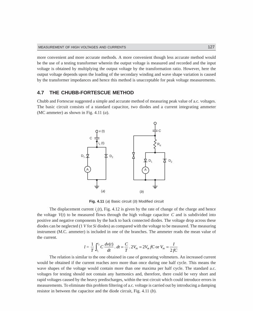
Dharm\N-HIGH\HG4-1.PM5 127
MEASUREMENT OF HIGH VOLTAGES AND CURRENTS 127
more convenient and more accurate methods. A more convenient though less accurate method wouldbe the use of a testing transformer wherein the output voltage is measured and recorded and the inputvoltage is obtained by multiplying the output voltage by the transformation ratio. However, here theoutput voltage depends upon the loading of the secondary winding and wave shape variation is causedby the transformer impedances and hence this method is unacceptable for peak voltage measurements.
4.7 THE CHUBB-FORTESCUE METHOD
Chubb and Fortescue suggested a simple and accurate method of measuring peak value of a.c. voltages.The basic circuit consists of a standard capacitor, two diodes and a current integrating ammeter(MC ammeter) as shown in Fig. 4.11 (a).
A
C
( )a ( )b
D1 D2
Rd
v (t)
i (t)c
A
C
D1 D2
Fig. 4.11 (a) Basic circuit (b) Modified circuit
The displacement current ic(t), Fig. 4.12 is given by the rate of change of the charge and hencethe voltage V(t) to be measured flows through the high voltage capacitor C and is subdivided intopositive and negative components by the back to back connected diodes. The voltage drop across thesediodes can be neglected (1 V for Si diodes) as compared with the voltage to be measured. The measuringinstrument (M.C. ammeter) is included in one of the branches. The ammeter reads the mean value ofthe current.
I = 1
2 221
2
TC
dv t
dtdt
C
TV V fC V
I
fCm m mt
t ( ). .= = =z or
The relation is similar to the one obtained in case of generating voltmeters. An increased currentwould be obtained if the current reaches zero more than once during one half cycle. This means thewave shapes of the voltage would contain more than one maxima per half cycle. The standard a.c.voltages for testing should not contain any harmonics and, therefore, there could be very short andrapid voltages caused by the heavy predischarges, within the test circuit which could introduce errors inmeasurements. To eliminate this problem filtering of a.c. voltage is carried out by introducing a dampingresistor in between the capacitor and the diode circuit, Fig. 4.11 (b).
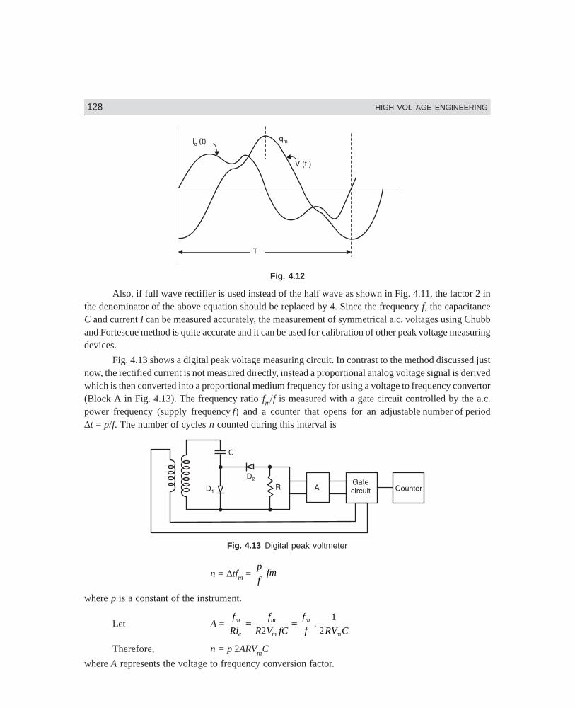
Dharm\N-HIGH\HG4-1.PM5 128
128 HIGH VOLTAGE ENGINEERING
Fig. 4.12
Also, if full wave rectifier is used instead of the half wave as shown in Fig. 4.11, the factor 2 inthe denominator of the above equation should be replaced by 4. Since the frequency f, the capacitanceC and current I can be measured accurately, the measurement of symmetrical a.c. voltages using Chubband Fortescue method is quite accurate and it can be used for calibration of other peak voltage measuringdevices.
Fig. 4.13 shows a digital peak voltage measuring circuit. In contrast to the method discussed justnow, the rectified current is not measured directly, instead a proportional analog voltage signal is derivedwhich is then converted into a proportional medium frequency for using a voltage to frequency convertor(Block A in Fig. 4.13). The frequency ratio fm/f is measured with a gate circuit controlled by the a.c.power frequency (supply frequency f) and a counter that opens for an adjustable number of period∆t = p/f. The number of cycles n counted during this interval is
Fig. 4.13 Digital peak voltmeter
n = ∆tfm = p
ffm
where p is a constant of the instrument.
Let A = f
Ri
f
R V fC
f
f RV Cm
c
m
m
m
m
= =2
1
2.
Therefore, n = p 2ARVmC
where A represents the voltage to frequency conversion factor.
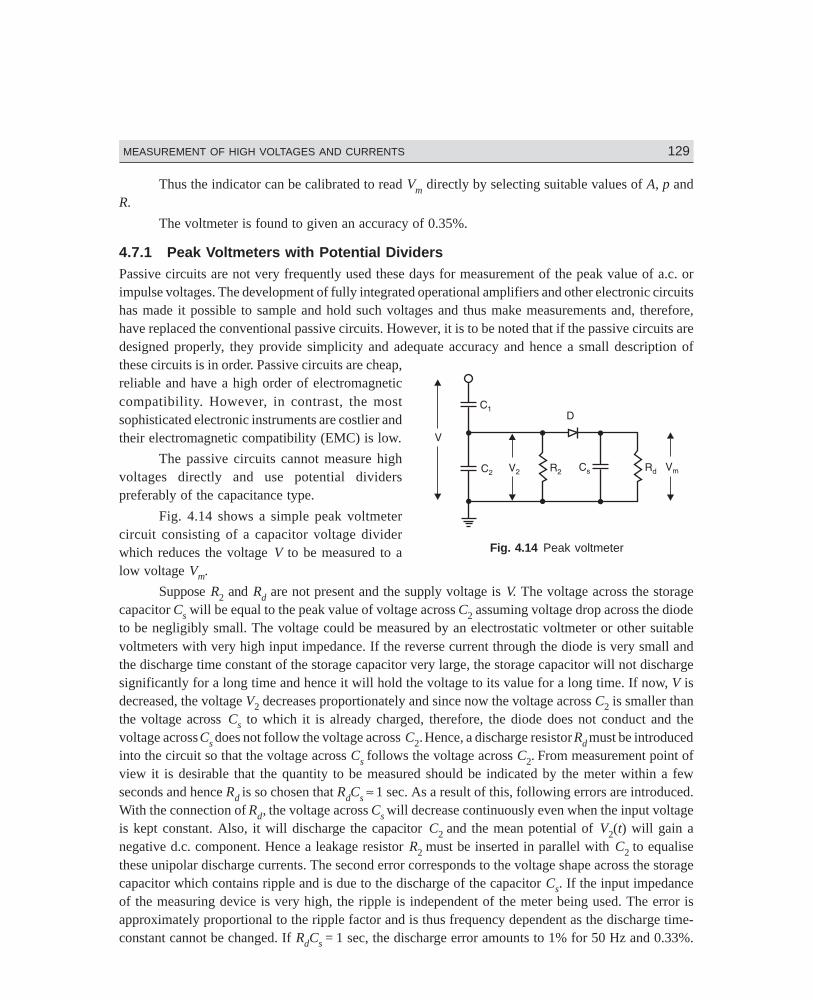
Dharm\N-HIGH\HG4-2.PM5 129
MEASUREMENT OF HIGH VOLTAGES AND CURRENTS 129
Thus the indicator can be calibrated to read Vm directly by selecting suitable values of A, p andR.
The voltmeter is found to given an accuracy of 0.35%.
4.7.1 Peak Voltmeters with Potential DividersPassive circuits are not very frequently used these days for measurement of the peak value of a.c. orimpulse voltages. The development of fully integrated operational amplifiers and other electronic circuitshas made it possible to sample and hold such voltages and thus make measurements and, therefore,have replaced the conventional passive circuits. However, it is to be noted that if the passive circuits aredesigned properly, they provide simplicity and adequate accuracy and hence a small description ofthese circuits is in order. Passive circuits are cheap,reliable and have a high order of electromagneticcompatibility. However, in contrast, the mostsophisticated electronic instruments are costlier andtheir electromagnetic compatibility (EMC) is low.
The passive circuits cannot measure highvoltages directly and use potential dividerspreferably of the capacitance type.
Fig. 4.14 shows a simple peak voltmetercircuit consisting of a capacitor voltage dividerwhich reduces the voltage V to be measured to alow voltage Vm.
Suppose R2 and Rd are not present and the supply voltage is V. The voltage across the storagecapacitor Cs will be equal to the peak value of voltage across C2 assuming voltage drop across the diodeto be negligibly small. The voltage could be measured by an electrostatic voltmeter or other suitablevoltmeters with very high input impedance. If the reverse current through the diode is very small andthe discharge time constant of the storage capacitor very large, the storage capacitor will not dischargesignificantly for a long time and hence it will hold the voltage to its value for a long time. If now, V isdecreased, the voltage V2 decreases proportionately and since now the voltage across C2 is smaller thanthe voltage across Cs to which it is already charged, therefore, the diode does not conduct and thevoltage across Cs does not follow the voltage across C2. Hence, a discharge resistor Rd must be introducedinto the circuit so that the voltage across Cs follows the voltage across C2. From measurement point ofview it is desirable that the quantity to be measured should be indicated by the meter within a fewseconds and hence Rd is so chosen that RdCs ≈ 1 sec. As a result of this, following errors are introduced.With the connection of Rd, the voltage across Cs will decrease continuously even when the input voltageis kept constant. Also, it will discharge the capacitor C2 and the mean potential of V2(t) will gain anegative d.c. component. Hence a leakage resistor R2 must be inserted in parallel with C2 to equalisethese unipolar discharge currents. The second error corresponds to the voltage shape across the storagecapacitor which contains ripple and is due to the discharge of the capacitor Cs. If the input impedanceof the measuring device is very high, the ripple is independent of the meter being used. The error isapproximately proportional to the ripple factor and is thus frequency dependent as the discharge time-constant cannot be changed. If RdCs = 1 sec, the discharge error amounts to 1% for 50 Hz and 0.33%.
Fig. 4.14 Peak voltmeter
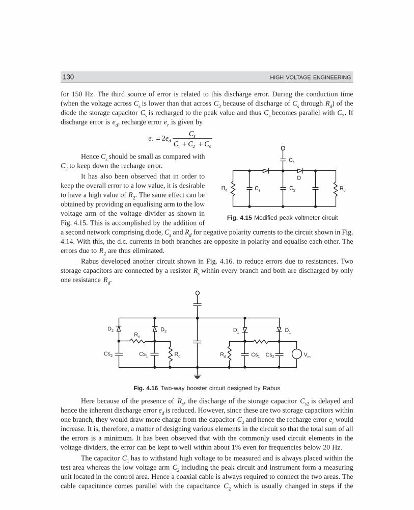
Dharm\N-HIGH\HG4-2.PM5 130
130 HIGH VOLTAGE ENGINEERING
for 150 Hz. The third source of error is related to this discharge error. During the conduction time(when the voltage across Cs is lower than that across C2 because of discharge of Cs through Rd) of thediode the storage capacitor Cs is recharged to the peak value and thus Cs becomes parallel with C2. Ifdischarge error is ed, recharge error er is given by
e eC
C C Cr ds
s
=+ +
21 2
Hence Cs should be small as compared withC2 to keep down the recharge error.
It has also been observed that in order tokeep the overall error to a low value, it is desirableto have a high value of R2. The same effect can beobtained by providing an equalising arm to the lowvoltage arm of the voltage divider as shown inFig. 4.15. This is accomplished by the addition ofa second network comprising diode, Cs and Rd for negative polarity currents to the circuit shown in Fig.4.14. With this, the d.c. currents in both branches are opposite in polarity and equalise each other. Theerrors due to R2 are thus eliminated.
Rabus developed another circuit shown in Fig. 4.16. to reduce errors due to resistances. Twostorage capacitors are connected by a resistor Rs within every branch and both are discharged by onlyone resistance Rd.
D2Rs
Rd
D1D2
RdCs2 Cs2
Cs1 Cs1
D1
Vm
Fig. 4.16 Two-way booster circuit designed by Rabus
Here because of the presence of Rs, the discharge of the storage capacitor Cs2 is delayed andhence the inherent discharge error ed is reduced. However, since these are two storage capacitors withinone branch, they would draw more charge from the capacitor C2 and hence the recharge error er wouldincrease. It is, therefore, a matter of designing various elements in the circuit so that the total sum of allthe errors is a minimum. It has been observed that with the commonly used circuit elements in thevoltage dividers, the error can be kept to well within about 1% even for frequencies below 20 Hz.
The capacitor C1 has to withstand high voltage to be measured and is always placed within thetest area whereas the low voltage arm C2 including the peak circuit and instrument form a measuringunit located in the control area. Hence a coaxial cable is always required to connect the two areas. Thecable capacitance comes parallel with the capacitance C2 which is usually changed in steps if the
Fig. 4.15 Modified peak voltmeter circuit
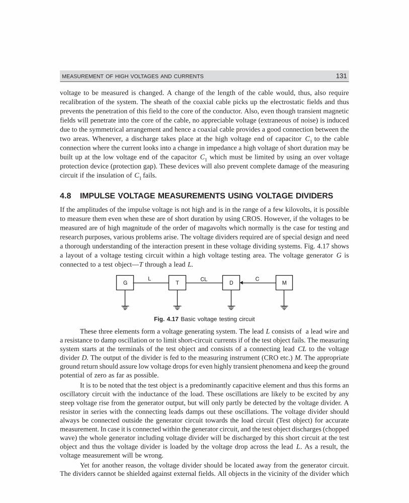
Dharm\N-HIGH\HG4-2.PM5 131
MEASUREMENT OF HIGH VOLTAGES AND CURRENTS 131
voltage to be measured is changed. A change of the length of the cable would, thus, also requirerecalibration of the system. The sheath of the coaxial cable picks up the electrostatic fields and thusprevents the penetration of this field to the core of the conductor. Also, even though transient magneticfields will penetrate into the core of the cable, no appreciable voltage (extraneous of noise) is induceddue to the symmetrical arrangement and hence a coaxial cable provides a good connection between thetwo areas. Whenever, a discharge takes place at the high voltage end of capacitor C1 to the cableconnection where the current looks into a change in impedance a high voltage of short duration may bebuilt up at the low voltage end of the capacitor C1 which must be limited by using an over voltageprotection device (protection gap). These devices will also prevent complete damage of the measuringcircuit if the insulation of C1 fails.
4.8 IMPULSE VOLTAGE MEASUREMENTS USING VOLTAGE DIVIDERS
If the amplitudes of the impulse voltage is not high and is in the range of a few kilovolts, it is possibleto measure them even when these are of short duration by using CROS. However, if the voltages to bemeasured are of high magnitude of the order of magavolts which normally is the case for testing andresearch purposes, various problems arise. The voltage dividers required are of special design and needa thorough understanding of the interaction present in these voltage dividing systems. Fig. 4.17 showsa layout of a voltage testing circuit within a high voltage testing area. The voltage generator G isconnected to a test object—T through a lead L.
Fig. 4.17 Basic voltage testing circuit
These three elements form a voltage generating system. The lead L consists of a lead wire anda resistance to damp oscillation or to limit short-circuit currents if of the test object fails. The measuringsystem starts at the terminals of the test object and consists of a connecting lead CL to the voltagedivider D. The output of the divider is fed to the measuring instrument (CRO etc.) M. The appropriateground return should assure low voltage drops for even highly transient phenomena and keep the groundpotential of zero as far as possible.
It is to be noted that the test object is a predominantly capacitive element and thus this forms anoscillatory circuit with the inductance of the load. These oscillations are likely to be excited by anysteep voltage rise from the generator output, but will only partly be detected by the voltage divider. Aresistor in series with the connecting leads damps out these oscillations. The voltage divider shouldalways be connected outside the generator circuit towards the load circuit (Test object) for accuratemeasurement. In case it is connected within the generator circuit, and the test object discharges (choppedwave) the whole generator including voltage divider will be discharged by this short circuit at the testobject and thus the voltage divider is loaded by the voltage drop across the lead L. As a result, thevoltage measurement will be wrong.
Yet for another reason, the voltage divider should be located away from the generator circuit.The dividers cannot be shielded against external fields. All objects in the vicinity of the divider which
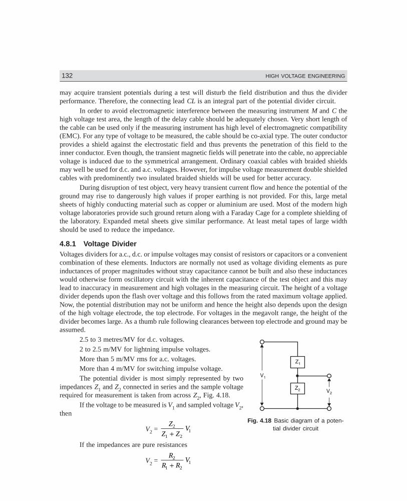
Dharm\N-HIGH\HG4-2.PM5 132
132 HIGH VOLTAGE ENGINEERING
may acquire transient potentials during a test will disturb the field distribution and thus the dividerperformance. Therefore, the connecting lead CL is an integral part of the potential divider circuit.
In order to avoid electromagnetic interference between the measuring instrument M and C thehigh voltage test area, the length of the delay cable should be adequately chosen. Very short length ofthe cable can be used only if the measuring instrument has high level of electromagnetic compatibility(EMC). For any type of voltage to be measured, the cable should be co-axial type. The outer conductorprovides a shield against the electrostatic field and thus prevents the penetration of this field to theinner conductor. Even though, the transient magnetic fields will penetrate into the cable, no appreciablevoltage is induced due to the symmetrical arrangement. Ordinary coaxial cables with braided shieldsmay well be used for d.c. and a.c. voltages. However, for impulse voltage measurement double shieldedcables with predominently two insulated braided shields will be used for better accuracy.
During disruption of test object, very heavy transient current flow and hence the potential of theground may rise to dangerously high values if proper earthing is not provided. For this, large metalsheets of highly conducting material such as copper or aluminium are used. Most of the modern highvoltage laboratories provide such ground return along with a Faraday Cage for a complete shielding ofthe laboratory. Expanded metal sheets give similar performance. At least metal tapes of large widthshould be used to reduce the impedance.
4.8.1 Voltage DividerVoltages dividers for a.c., d.c. or impulse voltages may consist of resistors or capacitors or a convenientcombination of these elements. Inductors are normally not used as voltage dividing elements as pureinductances of proper magnitudes without stray capacitance cannot be built and also these inductanceswould otherwise form oscillatory circuit with the inherent capacitance of the test object and this maylead to inaccuracy in measurement and high voltages in the measuring circuit. The height of a voltagedivider depends upon the flash over voltage and this follows from the rated maximum voltage applied.Now, the potential distribution may not be uniform and hence the height also depends upon the designof the high voltage electrode, the top electrode. For voltages in the megavolt range, the height of thedivider becomes large. As a thumb rule following clearances between top electrode and ground may beassumed.
2.5 to 3 metres/MV for d.c. voltages.2 to 2.5 m/MV for lightning impulse voltages.More than 5 m/MV rms for a.c. voltages.More than 4 m/MV for switching impulse voltage.The potential divider is most simply represented by two
impedances Z1 and Z2 connected in series and the sample voltagerequired for measurement is taken from across Z2, Fig. 4.18.
If the voltage to be measured is V1 and sampled voltage V2,then
V2 = Z
Z ZV2
1 21+
If the impedances are pure resistances
V2 = R
R RV2
1 21+
Fig. 4.18 Basic diagram of a poten-tial divider circuit
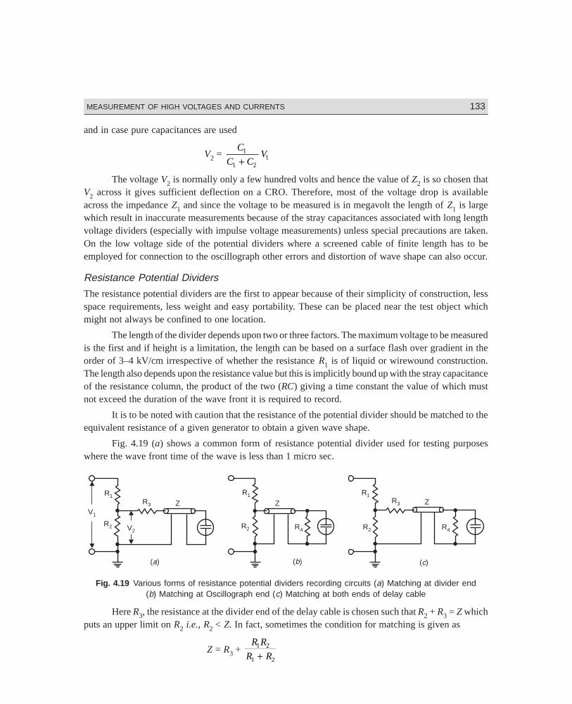
Dharm\N-HIGH\HG4-2.PM5 133
MEASUREMENT OF HIGH VOLTAGES AND CURRENTS 133
and in case pure capacitances are used
V2 = C
C CV1
1 21+
The voltage V2 is normally only a few hundred volts and hence the value of Z2 is so chosen thatV2 across it gives sufficient deflection on a CRO. Therefore, most of the voltage drop is availableacross the impedance Z1 and since the voltage to be measured is in megavolt the length of Z1 is largewhich result in inaccurate measurements because of the stray capacitances associated with long lengthvoltage dividers (especially with impulse voltage measurements) unless special precautions are taken.On the low voltage side of the potential dividers where a screened cable of finite length has to beemployed for connection to the oscillograph other errors and distortion of wave shape can also occur.
Resistance Potential Dividers
The resistance potential dividers are the first to appear because of their simplicity of construction, lessspace requirements, less weight and easy portability. These can be placed near the test object whichmight not always be confined to one location.
The length of the divider depends upon two or three factors. The maximum voltage to be measuredis the first and if height is a limitation, the length can be based on a surface flash over gradient in theorder of 3–4 kV/cm irrespective of whether the resistance R1 is of liquid or wirewound construction.The length also depends upon the resistance value but this is implicitly bound up with the stray capacitanceof the resistance column, the product of the two (RC) giving a time constant the value of which mustnot exceed the duration of the wave front it is required to record.
It is to be noted with caution that the resistance of the potential divider should be matched to theequivalent resistance of a given generator to obtain a given wave shape.
Fig. 4.19 (a) shows a common form of resistance potential divider used for testing purposeswhere the wave front time of the wave is less than 1 micro sec.
V1
R1
R2
R3
V2
Z
( )a
R1R1
R2 R2
Z ZR3
R4 R4
( )b ( )c
Fig. 4.19 Various forms of resistance potential dividers recording circuits (a) Matching at divider end(b) Matching at Oscillograph end (c) Matching at both ends of delay cable
Here R3, the resistance at the divider end of the delay cable is chosen such that R2 + R3 = Z whichputs an upper limit on R2 i.e., R2 < Z. In fact, sometimes the condition for matching is given as
Z = R3 + R R
R R1 2
1 2+
Dharm\N-HIGH\HG4-2.PM5 134
134 HIGH VOLTAGE ENGINEERING
But, since usually R1 > > R2, the above relation reduces to Z = R3 + R2. From Fig. 4.19 (a), thevoltage appearing across R2 is
V2 = Z
Z RV1
1 11+
where Z1 is the equivalent impedance of R2 in parallel with (Z + R3), the surge impedance of the cablebeing represented by an impedance Z to ground.
Now Z1 = ( ) ( )Z R R
R Z R
Z R R
Z
++ +
= +3 2
2 3
3 2
2
Therefore, V2 = ( )Z R R
Z
V
Z R
++
3 2 1
1 12
However, the voltage entering the delay cable is
V3 = V
Z RZ
Z
Z R
Z R R
Z
V
Z RV
R
Z R2
3 3
3 2 1
1 11
2
1 12 2+=
++
+=
+( )
.( )
As this voltage wave reaches the CRO end of the delay cable, it suffers reflections as theimpedance offered by the CRO is infinite and as a result the voltage wave transmitted into the CRO isdoubled. The CRO, therefore, records a voltage
V3′ = R
Z RV2
1 11+
The reflected wave, however, as it reaches the low voltage arm of the potential divider does notsuffer any reflection as Z = R2 + R3 and is totally absorbed by (R2 + R3).
Since R2 is smaller than Z and Z1 is a parallel combination of R2 and (R3 + Z), Z1 is going to besmaller than R2 and since R1 > > R2, R1 will be much greater than Z1 and, therefore to a first approximationZ1 + R1 ≈ R1.
Therefore, V3′ = R
RV
R
R RV2
11
2
1 21≈
+ as R2 < < R1
Fig. 4.19 (b) and (c) are the variants of the potential divider circuit of Fig. 4.19 (a). The cablematching is done by a pure ohmic resistance R4 = Z at the end of the delay cable and, therefore, thevoltage reflection coefficient is zero i.e. the voltage at the end of the cable is transmitted completelyinto R4 and hence appears across the CRO plates without being reflected. As the input impedance of thedelay cable is R4 = Z, this resistance is a parallel to R2 and forms an integral part of the divider’s lowvoltage arm. The voltage of such a divider is, therefore, calculated as follows:
Equivalent impedance
= R1 + R Z
R Z
R R Z R Z
R Z2
2
1 2 2
2+= + +
+( )
( )
Therefore, Current I = V R Z
R R Z R Z1 2
1 2 2
( )
( )
++ +
and voltage V2 = IR Z
R Z
V R Z
R R Z R Z
R Z
R Z2
2
1 2
1 2 2
2
2+=
++ + +
( )
( )
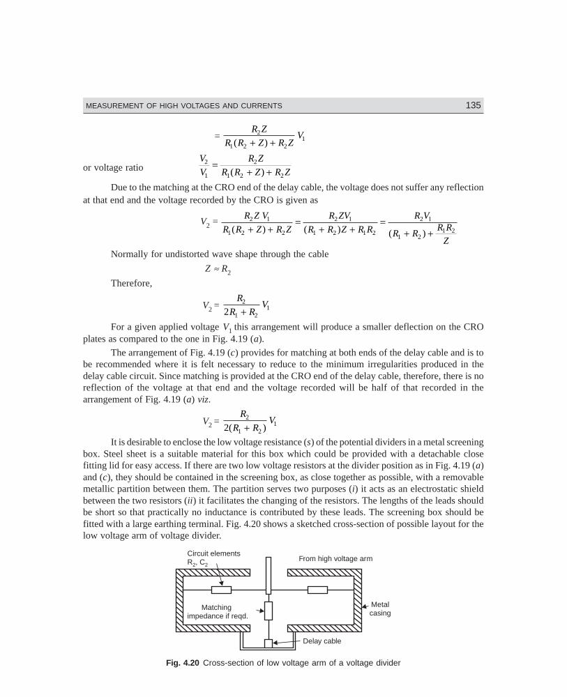
Dharm\N-HIGH\HG4-2.PM5 135
MEASUREMENT OF HIGH VOLTAGES AND CURRENTS 135
= R Z
R R Z R ZV2
1 2 21( )+ +
or voltage ratioV
V
R Z
R R Z R Z2
1
2
1 2 2
=+ +( )
Due to the matching at the CRO end of the delay cable, the voltage does not suffer any reflectionat that end and the voltage recorded by the CRO is given as
V2 = R Z V
R R Z R Z
R ZV
R R Z R R
R V
R RR R
Z
2 1
1 2 2
2 1
1 2 1 2
2 1
1 21 2( ) ( ) ( )+ +
=+ +
=+ +
Normally for undistorted wave shape through the cable
Z ≈ R2
Therefore,
V2 = R
R RV2
1 212 +
For a given applied voltage V1 this arrangement will produce a smaller deflection on the CROplates as compared to the one in Fig. 4.19 (a).
The arrangement of Fig. 4.19 (c) provides for matching at both ends of the delay cable and is tobe recommended where it is felt necessary to reduce to the minimum irregularities produced in thedelay cable circuit. Since matching is provided at the CRO end of the delay cable, therefore, there is noreflection of the voltage at that end and the voltage recorded will be half of that recorded in thearrangement of Fig. 4.19 (a) viz.
V2 = R
R RV2
1 212( )+
It is desirable to enclose the low voltage resistance (s) of the potential dividers in a metal screeningbox. Steel sheet is a suitable material for this box which could be provided with a detachable closefitting lid for easy access. If there are two low voltage resistors at the divider position as in Fig. 4.19 (a)and (c), they should be contained in the screening box, as close together as possible, with a removablemetallic partition between them. The partition serves two purposes (i) it acts as an electrostatic shieldbetween the two resistors (ii) it facilitates the changing of the resistors. The lengths of the leads shouldbe short so that practically no inductance is contributed by these leads. The screening box should befitted with a large earthing terminal. Fig. 4.20 shows a sketched cross-section of possible layout for thelow voltage arm of voltage divider.
Circuit elementsR , C2 2
From high voltage arm
Metalcasing
Matchingimpedance if reqd.
Delay cable
Fig. 4.20 Cross-section of low voltage arm of a voltage divider
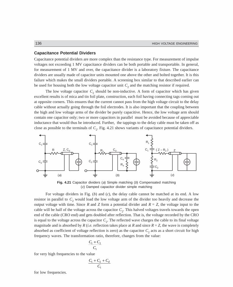
Dharm\N-HIGH\HG4-2.PM5 136
136 HIGH VOLTAGE ENGINEERING
Capacitance Potential DividersCapacitance potential dividers are more complex than the resistance type. For measurement of impulsevoltages not exceeding 1 MV capacitance dividers can be both portable and transportable. In general,for measurement of 1 MV and over, the capacitance divider is a laboratory fixture. The capacitancedividers are usually made of capacitor units mounted one above the other and bolted together. It is thisfailure which makes the small dividers portable. A screening box similar to that described earlier canbe used for housing both the low voltage capacitor unit C2 and the matching resistor if required.
The low voltage capacitor C2 should be non-inductive. A form of capacitor which has givenexcellent results is of mica and tin foil plate, construction, each foil having connecting tags coming outat opposite corners. This ensures that the current cannot pass from the high voltage circuit to the delaycable without actually going through the foil electrodes. It is also important that the coupling betweenthe high and low voltage arms of the divider be purely capacitive. Hence, the low voltage arm shouldcontain one capacitor only; two or more capacitors in parallel must be avoided because of appreciableinductance that would thus be introduced. Further, the tappings to the delay cable must be taken off asclose as possible to the terminals of C2. Fig. 4.21 shows variants of capacitance potential dividers.
C1
C2
R
( )a ( )b ( )c
R1
R2
R4
C4
R3CdZ, Cd ( Z – R )2C1 Z
C1
C2
C2
Fig. 4.21 Capacitor dividers (a) Simple matching (b) Compensated matching(c) Damped capacitor divider simple matching
For voltage dividers in Fig. (b) and (c), the delay cable cannot be matched at its end. A lowresistor in parallel to C2 would load the low voltage arm of the divider too heavily and decrease theoutput voltage with time. Since R and Z form a potential divider and R = Z, the voltage input to thecable will be half of the voltage across the capacitor C2. This halved voltages travels towards the openend of the cable (CRO end) and gets doubled after reflection. That is, the voltage recorded by the CROis equal to the voltage across the capacitor C2. The reflected wave charges the cable to its final voltagemagnitude and is absorbed by R (i.e. reflection takes place at R and since R = Z, the wave is completelyabsorbed as coefficient of voltage reflection is zero) as the capacitor C2 acts as a short circuit for highfrequency waves. The transformation ratio, therefore, changes from the value:
C C
C1 2
1
+
for very high frequencies to the value
C C C
Cd1 2
1
+ +
for low frequencies.
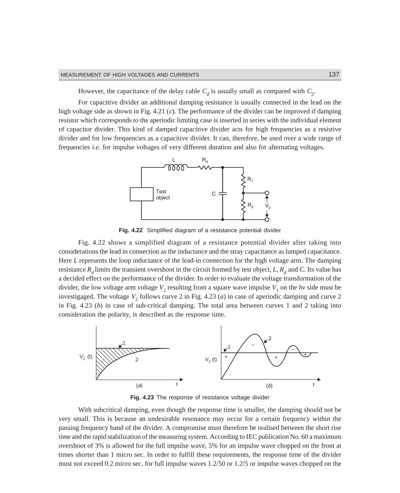
Dharm\N-HIGH\HG4-2.PM5 137
MEASUREMENT OF HIGH VOLTAGES AND CURRENTS 137
However, the capacitance of the delay cable Cd is usually small as compared with C2.
For capacitive divider an additional damping resistance is usually connected in the lead on thehigh voltage side as shown in Fig. 4.21 (c). The performance of the divider can be improved if dampingresistor which corresponds to the aperiodic limiting case is inserted in series with the individual elementof capacitor divider. This kind of damped capacitive divider acts for high frequencies as a resistivedivider and for low frequencies as a capacitive divider. It can, therefore, be used over a wide range offrequencies i.e. for impulse voltages of very different duration and also for alternating voltages.
Fig. 4.22 Simplified diagram of a resistance potential divider
Fig. 4.22 shows a simplified diagram of a resistance potential divider after taking intoconsiderations the lead in connection as the inductance and the stray capacitance as lumped capacitance.Here L represents the loop inductance of the lead-in connection for the high voltage arm. The dampingresistance Rd limits the transient overshoot in the circuit formed by test object, L, Rd and C. Its value hasa decided effect on the performance of the divider. In order to evaluate the voltage transformation of thedivider, the low voltage arm voltage V2 resulting from a square wave impulse V1 on the hv side must beinvestigaged. The voltage V2 follows curve 2 in Fig. 4.23 (a) in case of aperiodic damping and curve 2in Fig. 4.23 (b) in case of sub-critical damping. The total area between curves 1 and 2 taking intoconsideration the polarity, is described as the response time.
V2 (t)
1
2
( )a t
2
+
–
V (t)2
( )b t
+ +
1 –
Fig. 4.23 The response of resistance voltage divider
With subcritical damping, even though the response time is smaller, the damping should not bevery small. This is because an undesirable resonance may occur for a certain frequency within thepassing frequency band of the divider. A compromise must therefore be realised between the short risetime and the rapid stabilization of the measuring system. According to IEC publication No. 60 a maximumovershoot of 3% is allowed for the full impulse wave, 5% for an impulse wave chopped on the front attimes shorter than 1 micro sec. In order to fulfill these requirements, the response time of the dividermust not exceed 0.2 micro sec. for full impulse waves 1.2/50 or 1.2/5 or impulse waves chopped on the
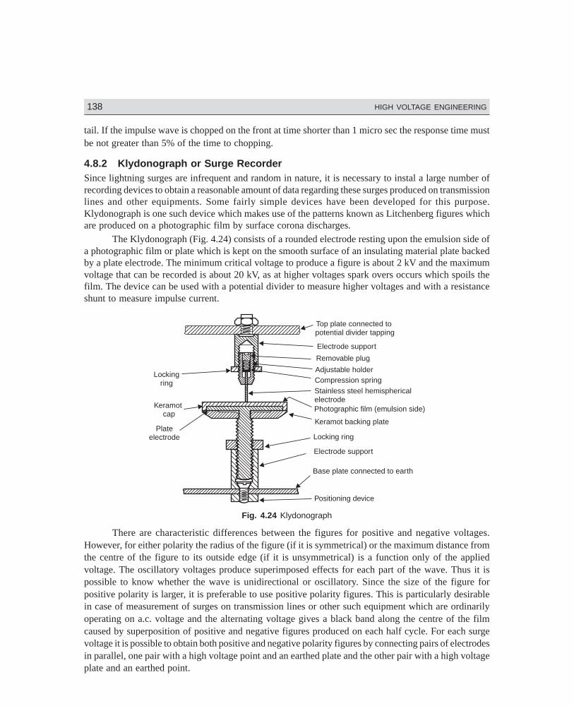
Dharm\N-HIGH\HG4-2.PM5 138
138 HIGH VOLTAGE ENGINEERING
tail. If the impulse wave is chopped on the front at time shorter than 1 micro sec the response time mustbe not greater than 5% of the time to chopping.
4.8.2 Klydonograph or Surge RecorderSince lightning surges are infrequent and random in nature, it is necessary to instal a large number ofrecording devices to obtain a reasonable amount of data regarding these surges produced on transmissionlines and other equipments. Some fairly simple devices have been developed for this purpose.Klydonograph is one such device which makes use of the patterns known as Litchenberg figures whichare produced on a photographic film by surface corona discharges.
The Klydonograph (Fig. 4.24) consists of a rounded electrode resting upon the emulsion side ofa photographic film or plate which is kept on the smooth surface of an insulating material plate backedby a plate electrode. The minimum critical voltage to produce a figure is about 2 kV and the maximumvoltage that can be recorded is about 20 kV, as at higher voltages spark overs occurs which spoils thefilm. The device can be used with a potential divider to measure higher voltages and with a resistanceshunt to measure impulse current.
Top plate connected topotential divider tapping
Electrode support
Removable plug
Adjustable holderCompression springStainless steel hemisphericalelectrodePhotographic film (emulsion side)
Keramot backing plate
Locking ring
Electrode support
Base plate connected to earth
Positioning device
Lockingring
Keramotcap
Plateelectrode
Fig. 4.24 Klydonograph
There are characteristic differences between the figures for positive and negative voltages.However, for either polarity the radius of the figure (if it is symmetrical) or the maximum distance fromthe centre of the figure to its outside edge (if it is unsymmetrical) is a function only of the appliedvoltage. The oscillatory voltages produce superimposed effects for each part of the wave. Thus it ispossible to know whether the wave is unidirectional or oscillatory. Since the size of the figure forpositive polarity is larger, it is preferable to use positive polarity figures. This is particularly desirablein case of measurement of surges on transmission lines or other such equipment which are ordinarilyoperating on a.c. voltage and the alternating voltage gives a black band along the centre of the filmcaused by superposition of positive and negative figures produced on each half cycle. For each surgevoltage it is possible to obtain both positive and negative polarity figures by connecting pairs of electrodesin parallel, one pair with a high voltage point and an earthed plate and the other pair with a high voltageplate and an earthed point.
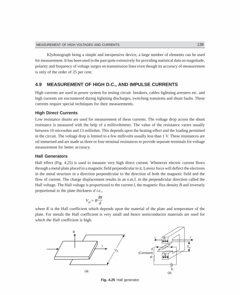
Dharm\N-HIGH\HG4-2.PM5 139
MEASUREMENT OF HIGH VOLTAGES AND CURRENTS 139
Klydonograph being a simple and inexpensive device, a large number of elements can be usedfor measurement. It has been used in the past quite extensively for providing statistical data on magnitude,polarity and frequency of voltage surges on transmission lines even though its accuracy of measurement
is only of the order of 25 per cent.
4.9 MEASUREMENT OF HIGH D.C., AND IMPULSE CURRENTS
High currents are used in power system for testing circuit breakers, cables lightning arresters etc. andhigh currents are encountered during lightning discharges, switching transients and shunt faults. Thesecurrents require special techniques for their measurements.
High Direct CurrentsLow resistance shunts are used for measurement of these currents. The voltage drop across the shuntresistance is measured with the help of a millivoltmeter. The value of the resistance varies usuallybetween 10 microohm and 13 milliohm. This depends upon the heating effect and the loading permittedin the circuit. The voltage drop is limited to a few millivolts usually less than 1 V. These resistances areoil immersed and are made as three or four terminal resistances to provide separate terminals for voltagemeasurement for better accuracy.
Hall GeneratorsHall effect (Fig. 4.25) is used to measure very high direct current. Whenever electric current flowsthrough a metal plate placed in a magnetic field perpendicular to it, Lorenz force will deflect the electronsin the metal structure in a direction perpendicular to the direction of both the magnetic field and theflow of current. The charge displacement results in an e.m.f. in the perpendicular direction called theHall voltage. The Hall voltage is proportional to the current I, the magnetic flux density B and inverselyproportional to the plate thickness d i.e.,
VH = RBI
d
where R is the Hall coefficient which depends upon the material of the plate and temperature of theplate. For metals the Hall coefficient is very small and hence semiconductor materials are used forwhich the Hall coefficient is high.
VH
I
B
( )a
(Constant)
I
d
RB
VH
E
BI
( )b
Fig. 4.25 Hall generator
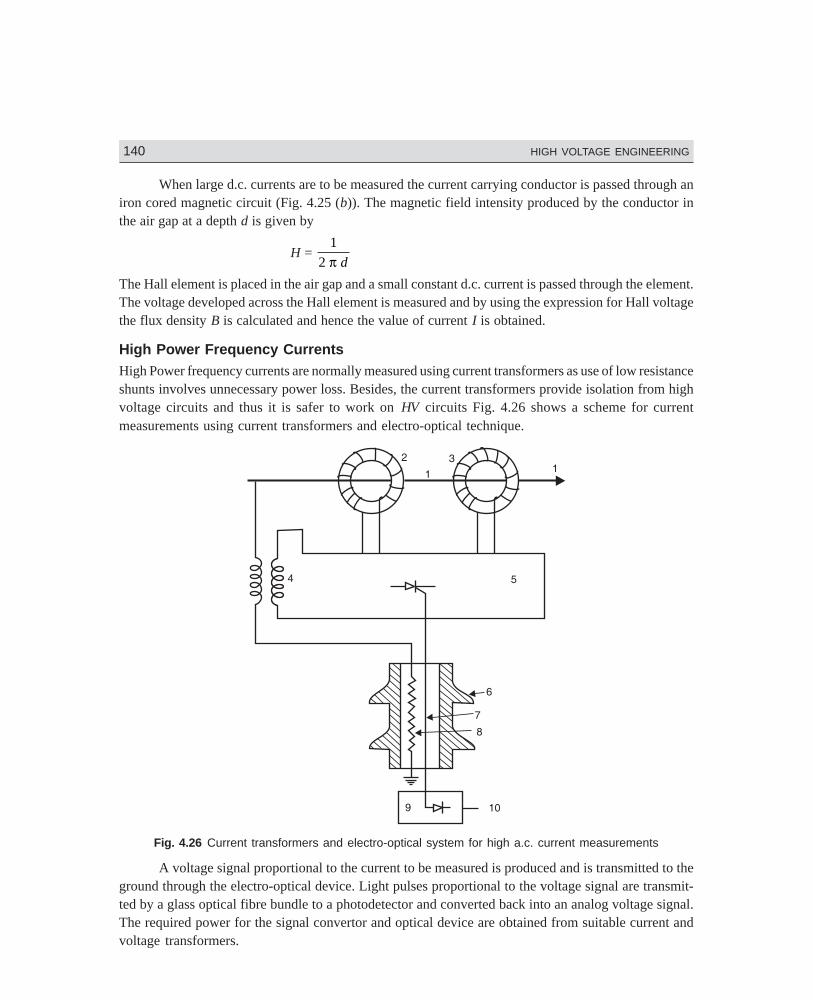
Dharm\N-HIGH\HG4-2.PM5 140
140 HIGH VOLTAGE ENGINEERING
When large d.c. currents are to be measured the current carrying conductor is passed through aniron cored magnetic circuit (Fig. 4.25 (b)). The magnetic field intensity produced by the conductor inthe air gap at a depth d is given by
H = 1
2 π d
The Hall element is placed in the air gap and a small constant d.c. current is passed through the element.The voltage developed across the Hall element is measured and by using the expression for Hall voltagethe flux density B is calculated and hence the value of current I is obtained.
High Power Frequency CurrentsHigh Power frequency currents are normally measured using current transformers as use of low resistanceshunts involves unnecessary power loss. Besides, the current transformers provide isolation from highvoltage circuits and thus it is safer to work on HV circuits Fig. 4.26 shows a scheme for currentmeasurements using current transformers and electro-optical technique.
Fig. 4.26 Current transformers and electro-optical system for high a.c. current measurements
A voltage signal proportional to the current to be measured is produced and is transmitted to theground through the electro-optical device. Light pulses proportional to the voltage signal are transmit-ted by a glass optical fibre bundle to a photodetector and converted back into an analog voltage signal.The required power for the signal convertor and optical device are obtained from suitable current andvoltage transformers.
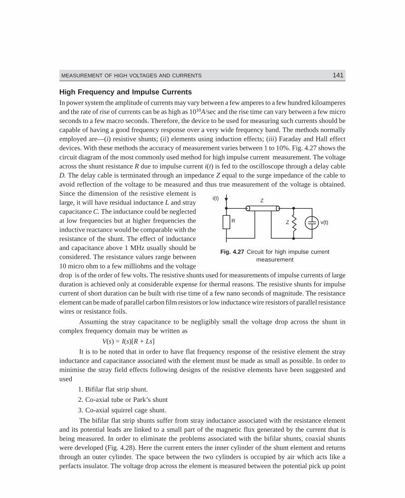
Dharm\N-HIGH\HG4-2.PM5 141
MEASUREMENT OF HIGH VOLTAGES AND CURRENTS 141
High Frequency and Impulse CurrentsIn power system the amplitude of currents may vary between a few amperes to a few hundred kiloamperesand the rate of rise of currents can be as high as 1010A/sec and the rise time can vary between a few microseconds to a few macro seconds. Therefore, the device to be used for measuring such currents should becapable of having a good frequency response over a very wide frequency band. The methods normallyemployed are—(i) resistive shunts; (ii) elements using induction effects; (iii) Faraday and Hall effectdevices. With these methods the accuracy of measurement varies between 1 to 10%. Fig. 4.27 shows thecircuit diagram of the most commonly used method for high impulse current measurement. The voltageacross the shunt resistance R due to impulse current i(t) is fed to the oscilloscope through a delay cableD. The delay cable is terminated through an impedance Z equal to the surge impedance of the cable toavoid reflection of the voltage to be measured and thus true measurement of the voltage is obtained.Since the dimension of the resistive element islarge, it will have residual inductance L and straycapacitance C. The inductance could be neglectedat low frequencies but at higher frequencies theinductive reactance would be comparable with theresistance of the shunt. The effect of inductanceand capacitance above 1 MHz usually should beconsidered. The resistance values range between10 micro ohm to a few milliohms and the voltagedrop is of the order of few volts. The resistive shunts used for measurements of impulse currents of largeduration is achieved only at considerable expense for thermal reasons. The resistive shunts for impulsecurrent of short duration can be built with rise time of a few nano seconds of magnitude. The resistanceelement can be made of parallel carbon film resistors or low inductance wire resistors of parallel resistancewires or resistance foils.
Assuming the stray capacitance to be negligibly small the voltage drop across the shunt incomplex frequency domain may be written as
V(s) = I(s)[R + Ls]
It is to be noted that in order to have flat frequency response of the resistive element the strayinductance and capacitance associated with the element must be made as small as possible. In order tominimise the stray field effects following designs of the resistive elements have been suggested andused
1. Bifilar flat strip shunt.
2. Co-axial tube or Park’s shunt
3. Co-axial squirrel cage shunt.
The bifilar flat strip shunts suffer from stray inductance associated with the resistance elementand its potential leads are linked to a small part of the magnetic flux generated by the current that isbeing measured. In order to eliminate the problems associated with the bifilar shunts, coaxial shuntswere developed (Fig. 4.28). Here the current enters the inner cylinder of the shunt element and returnsthrough an outer cylinder. The space between the two cylinders is occupied by air which acts like aperfacts insulator. The voltage drop across the element is measured between the potential pick up point
i(t) Z
R v(t)Z
Fig. 4.27 Circuit for high impulse currentmeasurement
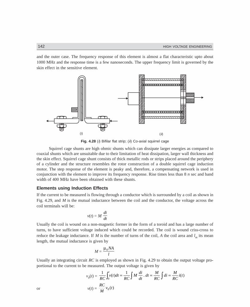
Dharm\N-HIGH\HG4-2.PM5 142
142 HIGH VOLTAGE ENGINEERING
and the outer case. The frequency response of this element is almost a flat characteristic upto about1000 MHz and the response time is a few nanoseconds. The upper frequency limit is governed by theskin effect in the sensitive element.
( )i ( )ii
Fig. 4.28 (i) Bifilar flat strip; (ii) Co-axial squirrel cage
Squirrel cage shunts are high ohmic shunts which can dissipate larger energies as compared tocoaxial shunts which are unsuitable due to their limitation of heat dissipation, larger wall thickness andthe skin effect. Squirrel cage shunt consists of thick metallic rods or strips placed around the peripheryof a cylinder and the structure resembles the rotor construction of a double squirrel cage inductionmotor. The step response of the element is peaky and, therefore, a compensating network is used inconjunction with the element to improve its frequency response. Rise times less than 8 n sec and bandwidth of 400 MHz have been obtained with these shunts.
Elements using Induction EffectsIf the current to be measured is flowing through a conductor which is surrounded by a coil as shown inFig. 4.29, and M is the mutual inductance between the coil and the conductor, the voltage across thecoil terminals will be:
v(t) = M di
dtUsually the coil is wound on a non-magnetic former in the form of a toroid and has a large number ofturns, to have sufficient voltage induced which could be recorded. The coil is wound criss-cross toreduce the leakage inductance. If M is the number of turns of the coil, A the coil area and lm its meanlength, the mutual inductance is given by
M = µ0 NA
lUsually an integrating circuit RC is employed as shown in Fig. 4.29 to obtain the output voltage pro-portional to the current to be measured. The output voltage is given by
v0(t) = 1 1
0RCv t dt
RCM
di
dtdt
M
RCdi
M
RCi t
t( ) . ( )z z z= = =
or v(t) = RC
Mv t0 ( )
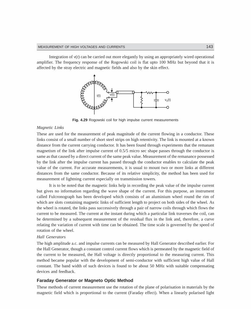
Dharm\N-HIGH\HG4-2.PM5 143
MEASUREMENT OF HIGH VOLTAGES AND CURRENTS 143
Integration of v(t) can be carried out more elegantly by using an appropriately wired operationalamplifier. The frequency response of the Rogowski coil is flat upto 100 MHz but beyond that it isaffected by the stray electric and magnetic fields and also by the skin effect.
i(t) v(t)
v (t)0
Fig. 4.29 Rogowski coil for high impulse current measurements
Magnetic Links
These are used for the measurement of peak magnitude of the current flowing in a conductor. Theselinks consist of a small number of short steel strips on high retentivity. The link is mounted at a knowndistance from the current carrying conductor. It has been found through experiments that the remanantmagnetism of the link after impulse current of 0.5/5 micro sec shape passes through the conductor issame as that caused by a direct current of the same peak value. Measurement of the remanance possessedby the link after the impulse current has passed through the conductor enables to calculate the peakvalue of the current. For accurate measurements, it is usual to mount two or more links at differentdistances from the same conductor. Because of its relative simplicity, the method has been used formeasurement of lightning current especially on transmission towers.
It is to be noted that the magnetic links help in recording the peak value of the impulse currentbut gives no information regarding the wave shape of the current. For this purpose, an instrumentcalled Fulcronograph has been developed which consists of an aluminium wheel round the rim ofwhich are slots containing magnetic links of sufficient length to project on both sides of the wheel. Asthe wheel is rotated, the links pass successively through a pair of narrow coils through which flows thecurrent to be measured. The current at the instant during which a particular link traverses the coil, canbe determined by a subsequent measurement of the residual flux in the link and, therefore, a curverelating the variation of current with time can be obtained. The time scale is governed by the speed ofrotation of the wheel.
Hall Generators
The high amplitude a.c. and impulse currents can be measured by Hall Generator described earlier. Forthe Hall Generator, though a constant control current flows which is permeated by the magnetic field ofthe current to be measured, the Hall voltage is directly proportional to the measuring current. Thismethod became popular with the development of semi-conductor with sufficient high value of Hallconstant. The band width of such devices is found to be about 50 MHz with suitable compensatingdevices and feedback.
Faraday Generator or Magneto Optic MethodThese methods of current measurement use the rotation of the plane of polarisation in materials by themagnetic field which is proportional to the current (Faraday effect). When a linearly polarised light
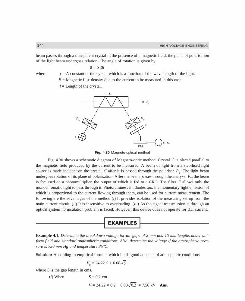
Dharm\N-HIGH\HG4-2.PM5 144
144 HIGH VOLTAGE ENGINEERING
beam passes through a transparent crystal in the presence of a magnetic field, the plane of polarisationof the light beam undergoes relation. The angle of rotation is given by
θ = α Bl
where α = A constant of the cyrstal which is a function of the wave length of the light.
B = Magnetic flux density due to the current to be measured in this case.
l = Length of the crystal.
C
P1
L
P2
F
PMCRO
i(t)
Fig. 4.30 Magneto-optical method
Fig. 4.30 shows a schematic diagram of Magneto-optic method. Crystal C is placed parallel tothe magnetic field produced by the current to be measured. A beam of light from a stabilised lightsource is made incident on the crystal C after it is passed through the polariser P1. The light beamundergoes rotation of its plane of polarisation. After the beam passes through the analyser P2, the beamis focussed on a photomultiplier, the output of which is fed to a CRO. The filter F allows only themonochromatic light to pass through it. Photoluminescent diodes too, the momentary light emission ofwhich is proportional to the current flowing through them, can be used for current measurement. Thefollowing are the advantages of the method (i) It provides isolation of the measuring set up from themain current circuit. (ii) It is insensitive to overloading. (iii) As the signal transmission is through anoptical system no insulation problem is faced. However, this device does not operate for d.c. current.
Example 4.1. Determine the breakdown voltage for air gaps of 2 mm and 15 mm lengths under uni-form field and standard atmospheric conditions. Also, determine the voltage if the atmospheric pres-sure is 750 mm Hg and temperature 35°C.
Solution: According to empirical formula which holds good at standard atmospheric conditions
Vb = 24.22 S + 6.08 S
where S is the gap length in cms.
(i) When S = 0.2 cm
V = 24.22 × 0.2 + 6.08 0 2. = 7.56 kV Ans.
Dharm\N-HIGH\HG4-2.PM5 145
MEASUREMENT OF HIGH VOLTAGES AND CURRENTS 145
(ii) When S = 1.5 cms
Vb = 24.22 × 1.5 + 6.08 1 5. = 36.33 + 7.446 = 43.776 kV Ans.
The air density correction factor
= 3 92
273
. b
t+ =
3 92 75
273 35
. ×+
= 0.9545 Ans.
Therefore, voltage for 2 mm gap will be 7.216 kV and for 15 mm gap it will be 41.78 kV.
Example 4.2. An absolute electrostatic voltmeter has a movable circular plate 8 cms in diameter. If thedistance between the plates during a measurement is 4 mm, determine the potential difference when theforce of attraction is 0.2 gm wt.
Solution: Area of plateπ π4
8 162× = sq. cm
Spacing between the plates d = 4 mm
Force of attraction = 12
2
2ε V
dA
0.2 × 10–3 × 9.8 = 1
2
1
3610
16 1016 109
2
64× ×
×× ×−
−−
ππV
1.96 × 10–3 = 1
7210 7 2× − V
of V = 1188 volts. Ans.
Example 4.3. An electrostatic voltmeter has two parallel plates. The movable plate is 10 cm in diam-eter. With 10 kV between the plates the pull is 5 × 10⁻³ N. Determine the change in capacitance for amovement of 1 mm of movable plate.
Solution: 5 × 10–3 = 1
2
1
3610
1825 109
8
24.
ππ× × ×− −
d
or d = 26.35 mm.
Therefore, change in capacitance
10
3610 25 10
1
26 35
1
27 35
39 4× × × −F
HIK
− −π. .
= 0.0959 pF Ans.
Example 4.4. A generating voltmeter is required to measure voltage between 15 kV to 250 kV. If theindicating meter reads a minimum current of 2 µA and maximum of 35 µA, determine the capacitanceof the generating voltmeter. Assume that the speed of driving synchronous motor is 1500 rpm.
Solution:
IVC w
rmsm=2
Dharm\N-HIGH\HG4-2.PM5 146
146 HIGH VOLTAGE ENGINEERING
2 × 10–6 = 15 1000
2
2 1500
60
× × × ×Cm π
Cm = 12 × 10–7 × 10–6 = 1.5 pF Ans.
At 250 kV, the current indicated will be
2 × 250
1533 3= . µA Ans.
Example 4.5. A peak reading voltmeter is required to measure voltage upto 150 kV. The peak voltmeteruses an RC circuit, a microammeter and a capacitance potential divider. The potential divider has aratio of 1200 : 1 and the micrometer can read upto 10 µA. Determine the value of R and C if the timeconstant of RC circuit is 8 secs.
Solution: The voltage across the low voltage arm of the potential divider,
= ×150 1000
1200 = 125 volts.
The same voltage appears across the resistance.
Therefore RV
I= =
×=−
125
10 1012.5 M6 Ω
Since the time constant of the RC circuit is 8 sec.
C = 8
12 5 100 646.
.×
= µF Ans.
Example 4.6. A Rogowski coil is required to measure impulse current of 8 kA having rate of change ofcurrent of 1010 A/sec. The voltmeter is connected across the integrating circuit which reads 8 volts forfull scale deflection. The input to the integrating circuit is from the Rogowski Coil. Determine themutual inductance of coil R and C of the integrating circuit.
Solution: i(t) = RC
MV t0 ( )
8 × 103 = RC
M × 8
or RC
M= 103
Time taken for the current wave to reach to maximum value
= 8 1000
1010
× = 8 × 10⁻⁷ sec.
This is for 1/4th of a cycle. Therefore for one cycle, the time is
T = 32 × 10–7
∴ fT
= =×
=−1 1
32 10
10
327
7
Hz
Dharm\N-HIGH\HG4-2.PM5 147
MEASUREMENT OF HIGH VOLTAGES AND CURRENTS 147
For proper integration
1
5
10
32 5
10
16
7 6
CR
f= =×
=
or CR = 16
106
Also since CR
M= 103
M = CR
10
16
10
1
1016 nH3 6 3= × = Ans.
Taking R = 8 × 10³ Ω Ans.
C = 16
10
1
8 102 nF6 3×
= Ans.
4.1. What are the requirements of a sphere gap for measurement of high voltages? Discuss the disadvantagesof sphere gap for measurements.
4.2. Explain clearly the procedure for measurement of (i) impulse; (ii) a.c. high voltages using sphere gap.4.3. Discuss the effect of (i) nearby earthed objects (ii) humidity and (iii) dust particles on the measurements
using sphere gaps.4.4. Describe the construction of a uniform field spark gap and discuss its advantages and disadvantages for
high voltage measurements.4.5. Explain with neat diagram how rod gaps can be used for measurement of high voltages. Compare its
performance with a sphere gap.4.6. Explain with neat diagram the principle of operation of an Electrostatic Voltmeter. Discuss its advantages
and limitations for high voltage measurements.4.7. Draw a neat schematic diagram of a generating voltmeter and explain its principle of operation. Discuss
its application and limitations.4.8. Draw Chubb-Fortescue Circuit for measurement of peak value of a.c. voltages discuss its advantages over
other methods.4.9. Discuss the problems associated with peak voltmeter circuits using passive elements. Draw circuit devel-
oped by Rabus and explain how this circuit overcomes these problems.4.10. What are the problems associated with measurement of very high impulse voltages? Explain how these
can be taken care of during measurements.4.11. Discuss and compare the performance of (i) resistance (ii) capacitance potential dividers for measurement
of impulse voltages.4.12. Discuss various resistance potential dividers and compare their performance of measurement of impulse
voltages.4.13. Discuss various capacitance, potential dividers and compare their performance for measurement of im-
pulse voltages.4.14. Draw a simplified equivalent circuit of a resistance potential divider and discuss its step response.4.15. Discuss various methods of measuring high d.c. and a.c. currents.4.16. Discuss various methods of measuring high impulse currents.4.17. What is Rogowski Coil? Explain with a neat diagram its principle of operation for measurement of high
impulse currents.
148
5
Man has been power hungry since time-immemorial. In modern times the world has seen phenomenalincrease in demand for energy, of which an important component is that of electrical energy. Theproduction of electrical energy in big plants under the most economic condition makes it necessary thatmore and more energy be transported over longer and longer distances. Therefore, transmission at extrahigh voltages and the erection of systems which may extend over whole continents has become themost urgent problems to be solved in the near future. The very fast development of systems is followedby studies of equipment and the service conditions they have to fulfill. These conditions will alsodetermine the values for testing at alternating, impulse and d.c. voltages under specific conditions.
As we go for higher and higher operating voltages (say above 1000 kV) certain problems areassociated with the testing techniques. Some of these are:
(i) Dimension of high voltage test laboratories.
(ii) Characteristics of equipment for such laboratories.
(iii) Some special aspects of the test techniques at extra high voltages.
The dimensions of laboratories for test equipments of 750 kV and above are fixed by the followingmain considerations:
(i) Figures (values) of test voltages under different conditions.
(ii) Sizes of the test of equipments in a.c., d.c. and impulse voltages.
(iii) Distances between the objects under high voltage during the test period and the earthedsurroundings such as floors, walls and roofs of the buildings. The problems associated withthe characteristics of the equipments used for testing are summarised here.
In alternating voltage system, a careful choice of the characteristics of the testing transformer isessential. It is known that the flash over voltage of the insulator in air or in any insulating fluid dependsupon the capacitance of the supply system. This is due to the fact that a voltage drop may not maintainpreliminary discharges or breakdown. It is, therefore, suggested that a capacitance of at least 1000 pFmust be connected across the insulator to obtain the correct flash over or puncture voltage and alsounder breakdown condition (a virtual short circuit) the supply system should be able to supply at least1 amp for clean and 5 amp for polluted insulators at the test voltage.
There are some difficult problems with impulse testing equipments also especially when testinglarge power transformers or large reactors or large cables operating at very high voltages. The equiva-lent capacitance of the impulse generator is usually about 40 nano farads independent of the operatingvoltage which gives a stored energy of about 1/2 × 40 10–9 × 36 × 109 = 720 KJ for 6 MV generators
High Voltage Testing of ElectricalEquipment
Dharm\N-HIGH\HG5-1.PM5 149
HIGH VOLTAGE TESTING OF ELECTRICAL EQUIPMENT 149
which is required for testing equipments operating at 150 kV. It is not at all difficult to pile up a largenumber of capacitances to charge them in parallel and then discharge in series to obtain a desiredimpulse wave. But the difficulty exists in reducing the internal reactance of the circuit so that a shortwave front with minimum oscillation can be obtained. For example for a 4 MV circuit the inductance ofthe circuit is about 140 µH and it is impossible to test an equipment with a capacitance of 5000 pF witha front time of 1.2 µ sec. and less than 5% overshoot on the wave front.
Cascaded rectifiers are used for high voltage d.c. testing. A careful consideration is necessarywhen test on polluted insulation is to be performed which requires currents of 50 to 200 mA but ex-tremely predischarge streamer of 0.5 to 1 amp during milliseconds occur. The generator must have aninternal reactance in order to maintain the test voltage without too high a voltage drop.
5.1 TESTING OF OVERHEAD LINE INSULATORS
Various types of overhead line insulators are (i) Pin type (ii) Post type (iii) String insulator unit(iv) Suspension insulator string (v) Tension insulator.
Arrangement of Insulators for TestString insulator unit should be hung by a suspension eye from an earthed metal cross arm. The testvoltage is applied between the cross arm and the conductor hung vertically down from the metal part onthe lower side of the insulator unit.
Suspension string with all its accessories as in service should be hung from an earthed metalcross arm. The length of the cross arm should be at least 1.5 times the length of the string being testedand should be at least equal to 0.9 m on either side of the axis of the string. No other earthed objectshould be nearer to the insulator string then 0.9 m or 1.5 times the length of the string whichever isgreater. A conductor of actual size to be used in service or of diameter not less than 1 cm and length 1.5times the length of the string is secured in the suspension clamp and should lie in a horizontal plane.The test voltage is applied between the conductor and the cross arm and connection from the impulsegenerator is made with a length of wire to one end of the conductor. For higher operating voltageswhere the length of the string is large, it is advisable to sacrifice the length of the conductor as stipu-lated above. Instead, it is desirable to bend the ends of the conductor over in a large radius.
For tension insulators the arrangement is more or less same as in suspension insulator exceptthat it should be held in an approximately horizontal position under a suitable tension (about 1000 Kg.).
For testing pin insulators or line post insulators, these should be mounted on the insulator pin orline post shank with which they are to be used in service. The pin or the shank should be fixed in avertical position to a horizontal earthed metal cross arm situated 0.9 m above the floor of the laboratory.A conductor of 1 cm diameter is to be laid horizontally in the top groove of the insulator and secured byat least one turn of tie-wire, not less than 0.3 cm diameter in the tie-wire groove. The length of the wireshould be at least 1.5 times the length of the insulator and should over hang the insulator at least 0.9 mon either side in a direction at right angles to the cross arm. The test voltage is applied to one end of theconductor.
High voltage testing of electrical equipment requires two types of tests: (i) Type tests, and (ii)Routine test. Type tests involves quality testing of equipment at the design and development level i.e.samples of the product are taken and are tested when a new product is being developed and designed or
Dharm\N-HIGH\HG5-1.PM5 150
150 HIGH VOLTAGE ENGINEERING
an old product is to be redesigned and developed whereas the routine tests are meant to check thequality of the individual test piece. This is carried out to ensure quality and reliability of individual testobjects.
High voltage tests include (i) Power frequency tests and (ii) Impulse tests. These tests are car-ried out on all insulators.
(i) 50% dry impulse flash over test.
(ii) Impulse withstand test.
(iii) Dry flash over and dry one minute test.
(iv) Wet flash over and one minute rain test.
(v) Temperature cycle test.
(vi) Electro-mechanical test.
(vii) Mechanical test.
(viii) Porosity test.
(ix) Puncture test.
(x) Mechanical routine test.
The tests mentioned above are briefly described here.
(i) The test is carried out on a clean insulator mounted as in a normal working condition. Animpulse voltage of 1/50 µ sec. wave shape and of an amplitude which can cause 50% flash over of theinsulator, is applied, i.e. of the impulses applied 50% of the impulses should cause flash over. Thepolarity of the impulse is then reversed and procedure repeated. There must be at least 20 applicationsof the impulse in each case and the insulator must not be damaged. The magnitude of the impulsevoltage should not be less than that specified in standard specifications.
(ii) The insulator is subjected to standard impulse of 1/50 µ sec. wave of specified value underdry conditions with both positive and negative polarities. If five consecutive applications do not causeany flash over or puncture, the insulator is deemed to have passed the impulse withstand test. If out offive, two applications cause flash over, the insulator is deemed to have filed the test.
(iii) Power frequency voltage is applied to the insulator and the voltage increased to the speci-fied value and maintained for one minute. The voltage is then increased gradually until flash overoccurs. The insulator is then flashed over at least four more times, the voltage is raised gradually toreach flash over in about 10 seconds. The mean of at least five consecutive flash over voltages must notbe less than the value specified in specifications.
(iv) If the test is carried out under artificial rain, it is called wet flash over test. The insulator issubjected to spray of water of following characteristics:
Precipitation rate 3 ± 10% mm/min.
Direction 45° to the vertical
Conductivity of water 100 micro siemens ± 10%
Temperature of water Ambient +15°C
The insulator with 50% of the one-min. rain test voltage applied to it, is then sprayed for twominutes, the voltage raised to the one minute test voltage in approximately 10 sec. and maintained therefor one minute. The voltage is then increased gradually till flash over occurs and the insulator is then
Dharm\N-HIGH\HG5-1.PM5 151
HIGH VOLTAGE TESTING OF ELECTRICAL EQUIPMENT 151
flashed at least four more times, the time taken to reach flash over voltage being in each case about10 sec. The flash over voltage must not be less than the value specified in specifications.
(v) The insulator is immersed in a hot water bath whose temperature is 70° higher than normalwater bath for T minutes. It is then taken out and immediately immersed in normal water bath for Tminutes. After T minutes the insulator is again immersed in hot water bath for T minutes. The cycle isrepeated three times and it is expected that the insulator should withstand the test without damage to theinsulator or glaze. Here T = (15 + W/1.36) where W is the weight of the insulator in kgs.
(vi) The test is carried out only on suspension or tension type of insulator. The insulator issubjected to a 2½ times the specified maximum working tension maintained for one minute. Also,simultaneously 75% of the dry flash over voltage is applied. The insulator should withstand this testwithout any damage.
(vii) This is a bending test applicable to pin type and line-post insulators. The insulator is sub-jected to a load three times the specified maximum breaking load for one minute. There should be nodamage to the insulator and in case of post insulator the permanent set must be less than 1%. However,in case of post insulator, the load is then raised to three times and there should not be any damage to theinsulator and its pin.
(viii) The insulator is broken and immersed in a 0.5% alcohol solution of fuchsin under a pres-sure of 13800 kN/m2 for 24 hours. The broken insulator is taken out and further broken. It should notshow any sign of impregnation.
(ix) An impulse over voltage is applied between the pin and the lead foil bound over the top andside grooves in case of pin type and post insulator and between the metal fittings in case of suspensiontype insulators. The voltage is 1/50 µ sec. wave with amplitude twice the 50% impulse flash overvoltage and negative polarity. Twenty such applications are applied. The procedure is repeated for 2.5,3, 3.5 times the 50% impulse flash over voltage and continued till the insulator is punctured. Theinsulator must not puncture if the voltage applied is equal to the one specified in the specification.
(x) The string in insulator is suspended vertically or horizontally and a tensile load 20% inexcess of the maximum specified working load is applied for one minute and no damage to the stringshould occur.
5.2 TESTING OF CABLES
High voltage power cables have proved quite useful especially in case of HV d.c. transmission. Under-ground distribution using cables not only adds to the aesthetic looks of a metropolitan city but it pro-vides better environments and more reliable supply to the consumers.
Preparation of Cable Sample
The cable sample has to be carefully prepared for performing various tests especially electrical tests.This is essential to avoid any excessive leakage or end flash overs which otherwise may occur duringtesting and hence may give wrong information regarding the quality of cables. The length of the samplecable varies between 50 cms to 10 m. The terminations are usually made by shielding the ends of thecable with stress shields so as to relieve the ends from excessive high electrical stresses.
A cable is subjected to following tests:
(i) Bending tests.
(ii) Loading cycle test.
Dharm\N-HIGH\HG5-1.PM5 152
152 HIGH VOLTAGE ENGINEERING
(iii) Thermal stability test.
(iv) Dielectric thermal resistance test.
(v) Life expectancy test.
(vi) Dielectric power factor test.
(vii) Power frequency withstand voltage test.
(viii) Impulse withstand voltage test.
(ix) Partial discharge test.
(i) It is to be noted that a voltage test should be made before and after a bending test. The cableis bent round a cylinder of specified diameter to make one complete turn. It is then unwound andrewound in the opposite direction. The cycle is to be repeated three times.
(ii) A test loop, consisting of cable and its accessories is subjected to 20 load cycles with aminimum conductor temperature 5°C in excess of the design value and the cable is energized to1.5 times the working voltage. The cable should not show any sign of damage.
(iii) After test as at (ii), the cable is energized with a voltage 1.5 times the working voltage for acable of 132 kV rating (the multiplying factor decreases with increases in operating voltage) and theloading current is so adjusted that the temperature of the core of the cable is 5°C higher than its speci-fied permissible temperature. The current should be maintained at this value for six hours.
(iv) The ratio of the temperature difference between the core and sheath of the cable and theheat flow from the cable gives the thermal resistance of the sample of the cable. It should be within thelimits specified in the specifications.
(v) In order to estimate life of a cable, an accelerated life test is carried out by subjecting thecable to a voltage stress higher than the normal working stress. It has been observed that the relationbetween the expected life of the cable in hours and the voltage stress is given by
gK
n t=
where K is a constant which depends on material and n is the life index depending again on the material.
(vi) High Voltage Schering Bridge is used to perform dielectric power factor test on the cablesample. The power factor is measured for different values of voltages e.g. 0.5, 1.0, 1.5 and 2.0 times therated operating voltages. The maximum value of power factor at normal working voltage does notexceed a specified value (usually 0.01) at a series of temperatures ranging from 15°C to 65°C. Thedifference in the power factor between rated voltage and 1.5 times the rated voltage and the ratedvoltage and twice the rated voltage does not exceed a specified value. Sometimes the source is not ableto supply charging current required by the test cable, a suitable choke in series with the test cable helpsin tiding over the situation.
(vii) Cables are tested for power frequency a.c. and d.c. voltages. During manufacture the entirecable is passed through a higher voltage test and the rated voltage to check the continuity of the cable.As a routine test the cable is subjected to a voltage 2.5 times the working voltage for 10 min withoutdamaging the insulation of the cable. HV d.c. of 1.8 times the rated d.c. voltage of negative polarity for30 min. is applied and the cable is said to have withstood the test if no insulation failure takes place.
(viii) The test cable is subjected to 10 positive and 10 negative impulse voltage of magnitude asspecified in specification, the cable should withstand 5 applications without any damage. Usually, after
Dharm\N-HIGH\HG5-1.PM5 153
HIGH VOLTAGE TESTING OF ELECTRICAL EQUIPMENT 153
the impulse test, the power frequency dielectric power factor test is carried out to ensure that no failureoccurred during the impulse test.
(ix) Partial discharge measurement of cables is very important as it gives an indication of ex-pected life of the cable and it gives location of fault, if any, in the cable.
When a cable is subjected to high voltage and if there is a void in the cable, the void breaksdown and a discharge takes place. As a result, there is a sudden dip in voltage in the form of an impulse.This impulse travels along the cable as explained in detail in Chapter VI. The duration between thenormal pulse and the discharge pulse is measured on the oscilloscope and this distance gives the loca-tion of the void from the test end of the cable. However, the shape of the pulse gives the nature andintensity of the discharge.
In order to scan the entire length of the cable against voids or other imperfections, it is passedthrough a tube of insulating material filled with distilled water. Four electrodes, two at the end and twoin the middle of the tube are arranged. The middle electrodes are located at a stipulated distance andthese are energized with high voltage. The two end electrodes and cable conductor are grounded. Asthe cable is passed between the middle electrode, if a discharge is seen on the oscilloscope, a defect inthis part of the cable is stipulated and hence this part of the cable is removed from the rest of the cable.
5.3 TESTING OF BUSHINGS
Bushings are an integral component of high voltage machines. A bushing is used to bring high voltageconductors through the grounded tank or body of the electrical equipment without excessive potentialgradients between the conductor and the edge of the hole in the body. The bushing extends into thesurface of the oil at one end and the other end is carried above the tank to a height sufficient to preventbreakdown due to surface leakage.
Following tests are carried out on bushings:
(i) Power Factor Test
The bushing is installed as in service or immersed in oil. The high voltage terminal of the bushing isconnected to high voltage terminal of the Schering Bridge and the tank or earth portion of the bushingis connected to the detector of the bridge. The capacitance and p.f. of the bushing is measured atdifferent voltages as specified in the relevant specification and the capacitance and p.f. should bewithin the range specified.
(ii) Impulse Withstand Test
The bushing is subjected to impulse waves of either polarity and magnitude as specified in the standardspecification. Five consecutive full waves of standard wave form (1/50 µ sec.) are applied and if two ofthem cause flash over, the bushing is said to be defective. If only one flash over occurs, ten additionalapplications are made. If no flash over occurs, bushing is said to have passed the test.
(iii) Chopped Wave and Switching Surge Test
Chopped wave and switching surge of appropriate duration tests are carried out on high voltage bush-ings. The procedure is identical to the one given in (ii) above.
(iv) Partial Discharge Test
In order to determine whether there is deterioration or not of the insulation used in the bushing, this testis carried out. The procedure is explained in detail in Chapter-VI. The shape of the discharge is an
Dharm\N-HIGH\HG5-1.PM5 154
154 HIGH VOLTAGE ENGINEERING
indication of nature and severity of the defect in the bushing. This is considered to be a routine test forhigh voltage bushings.
(v) Visible Discharge Test at Power Frequency
The test is carried out to ascertain whether the given bushing will give rise to ratio interference or notduring operation. The test is carried out in a dark room. The voltage as specified is applied to thebushing (IS 2099). No discharge other than that from the grading rings or arcing horns should bevisible.
(vi) Power Frequency Flash Over or Puncture Test
(Under Oil): The bushing is either immersed fully in oil or is installed as in service condition. This testis carried out to ascertain that the internal breakdown strength of the bushing is 15% more than thepower frequency momentary dry withstand test value.
5.4 TESTING OF POWER CAPACITORS
Power capacitors is an integral part of the modern power system. These are used to control the voltageprofile of the system. Following tests are carried out on shunt power capacitors (IS 2834):
(i) Routine Tests
Routine tests are carried out on all capacitors at the manufacturer’s premises. During testing, the ca-pacitor should not breakdown or behave abnormally or show any visible deterioration.
(ii) Test for Output
Ammeter and Voltmeter can be used to measure the kVAr and capacitance of the capacitor. The kVArcalculated should not differ by more than –5 to +10% of the specified value for capacitor units and 0 to10% for capacitors banks.
The a.c. supply used for testing capacitor should have frequency between 40 Hz to 60 Hz, preferably asnear as possible to the rated frequency and the harmonics should be minimum.
(iii) Test between Terminals
Every capacitor is subjected to one of the following two tests for 10 secs:
(a) D.C. test; the test voltage being Vt = 4.3 V0
(b) A.C. test Vt = 2.15 V0, where V0 is the rms value of the voltage between terminals which inthe test connection gives the same dielectric stress in the capacitor element as the rated voltage Vn givesin normal service.
(iv) Test between Line Terminals and Container (For capacitor units)
An a.c. voltage of value specified in column 2 of Table 5.1 is applied between the terminals (shortcircuited) of the capacitor unit and its container and is maintained for one minute, no damage to thecapacitor should be observed.
Figures with single star represent values corresponding to reduced insulation level (Effectivelygrounded system) and with double star full insulation level (non-effectively grounded system).
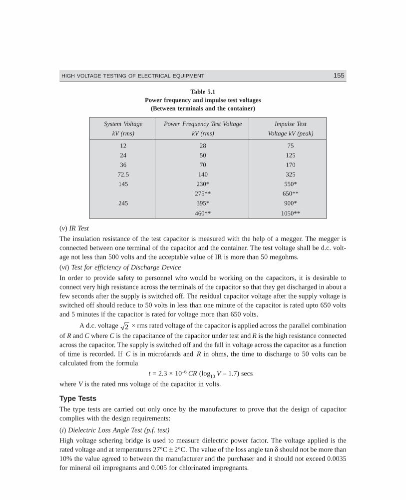
Dharm\N-HIGH\HG5-1.PM5 155
HIGH VOLTAGE TESTING OF ELECTRICAL EQUIPMENT 155
Table 5.1Power frequency and impulse test voltages
(Between terminals and the container)
System Voltage Power Frequency Test Voltage Impulse Test
kV (rms) kV (rms) Voltage kV (peak)
12 28 75
24 50 125
36 70 170
72.5 140 325
145 230* 550*
275** 650**
245 395* 900*
460** 1050**
(v) IR Test
The insulation resistance of the test capacitor is measured with the help of a megger. The megger isconnected between one terminal of the capacitor and the container. The test voltage shall be d.c. volt-age not less than 500 volts and the acceptable value of IR is more than 50 megohms.
(vi) Test for efficiency of Discharge Device
In order to provide safety to personnel who would be working on the capacitors, it is desirable toconnect very high resistance across the terminals of the capacitor so that they get discharged in about afew seconds after the supply is switched off. The residual capacitor voltage after the supply voltage isswitched off should reduce to 50 volts in less than one minute of the capacitor is rated upto 650 voltsand 5 minutes if the capacitor is rated for voltage more than 650 volts.
A d.c. voltage 2 × rms rated voltage of the capacitor is applied across the parallel combination
of R and C where C is the capacitance of the capacitor under test and R is the high resistance connectedacross the capacitor. The supply is switched off and the fall in voltage across the capacitor as a functionof time is recorded. If C is in microfarads and R in ohms, the time to discharge to 50 volts can becalculated from the formula
t = 2.3 × 10⁻⁶ CR (log10 V – 1.7) secs
where V is the rated rms voltage of the capacitor in volts.
Type TestsThe type tests are carried out only once by the manufacturer to prove that the design of capacitorcomplies with the design requirements:
(i) Dielectric Loss Angle Test (p.f. test)
High voltage schering bridge is used to measure dielectric power factor. The voltage applied is therated voltage and at temperatures 27°C ± 2°C. The value of the loss angle tan δ should not be more than10% the value agreed to between the manufacturer and the purchaser and it should not exceed 0.0035for mineral oil impregnants and 0.005 for chlorinated impregnants.
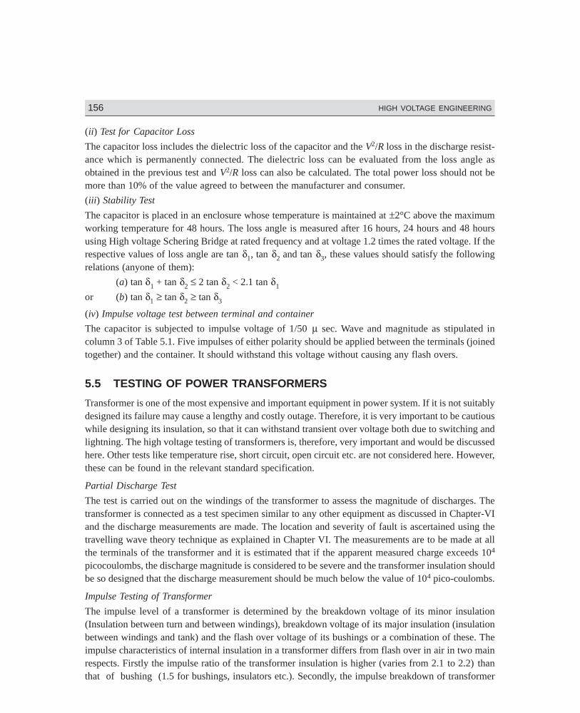
Dharm\N-HIGH\HG5-1.PM5 156
156 HIGH VOLTAGE ENGINEERING
(ii) Test for Capacitor Loss
The capacitor loss includes the dielectric loss of the capacitor and the V2/R loss in the discharge resist-ance which is permanently connected. The dielectric loss can be evaluated from the loss angle asobtained in the previous test and V2/R loss can also be calculated. The total power loss should not bemore than 10% of the value agreed to between the manufacturer and consumer.
(iii) Stability Test
The capacitor is placed in an enclosure whose temperature is maintained at ±2°C above the maximumworking temperature for 48 hours. The loss angle is measured after 16 hours, 24 hours and 48 hoursusing High voltage Schering Bridge at rated frequency and at voltage 1.2 times the rated voltage. If therespective values of loss angle are tan δ1, tan δ2 and tan δ3, these values should satisfy the followingrelations (anyone of them):
(a) tan δ1 + tan δ2 ≤ 2 tan δ2 < 2.1 tan δ1
or (b) tan δ1 ≥ tan δ2 ≥ tan δ3
(iv) Impulse voltage test between terminal and container
The capacitor is subjected to impulse voltage of 1/50 µ sec. Wave and magnitude as stipulated incolumn 3 of Table 5.1. Five impulses of either polarity should be applied between the terminals (joinedtogether) and the container. It should withstand this voltage without causing any flash overs.
5.5 TESTING OF POWER TRANSFORMERS
Transformer is one of the most expensive and important equipment in power system. If it is not suitablydesigned its failure may cause a lengthy and costly outage. Therefore, it is very important to be cautiouswhile designing its insulation, so that it can withstand transient over voltage both due to switching andlightning. The high voltage testing of transformers is, therefore, very important and would be discussedhere. Other tests like temperature rise, short circuit, open circuit etc. are not considered here. However,these can be found in the relevant standard specification.
Partial Discharge Test
The test is carried out on the windings of the transformer to assess the magnitude of discharges. Thetransformer is connected as a test specimen similar to any other equipment as discussed in Chapter-VIand the discharge measurements are made. The location and severity of fault is ascertained using thetravelling wave theory technique as explained in Chapter VI. The measurements are to be made at allthe terminals of the transformer and it is estimated that if the apparent measured charge exceeds 104
picocoulombs, the discharge magnitude is considered to be severe and the transformer insulation shouldbe so designed that the discharge measurement should be much below the value of 104 pico-coulombs.
Impulse Testing of Transformer
The impulse level of a transformer is determined by the breakdown voltage of its minor insulation(Insulation between turn and between windings), breakdown voltage of its major insulation (insulationbetween windings and tank) and the flash over voltage of its bushings or a combination of these. Theimpulse characteristics of internal insulation in a transformer differs from flash over in air in two mainrespects. Firstly the impulse ratio of the transformer insulation is higher (varies from 2.1 to 2.2) thanthat of bushing (1.5 for bushings, insulators etc.). Secondly, the impulse breakdown of transformer
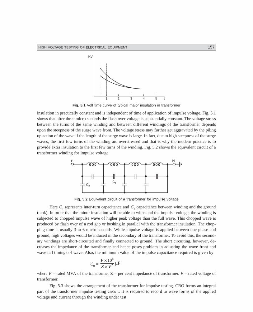
Dharm\N-HIGH\HG5-1.PM5 157
HIGH VOLTAGE TESTING OF ELECTRICAL EQUIPMENT 157
1 2 3 4 5 t
KV
Fig. 5.1 Volt time curve of typical major insulation in transformer
insulation in practically constant and is independent of time of application of impulse voltage. Fig. 5.1shows that after three micro seconds the flash over voltage is substantially constant. The voltage stressbetween the turns of the same winding and between different windings of the transformer dependsupon the steepness of the surge wave front. The voltage stress may further get aggravated by the pilingup action of the wave if the length of the surge wave is large. In fact, due to high steepness of the surgewaves, the first few turns of the winding are overstressed and that is why the modern practice is toprovide extra insulation to the first few turns of the winding. Fig. 5.2 shows the equivalent circuit of atransformer winding for impulse voltage.
Fig. 5.2 Equivalent circuit of a transformer for impulse voltage
Here C1 represents inter-turn capacitance and C2 capacitance between winding and the ground(tank). In order that the minor insulation will be able to withstand the impulse voltage, the winding issubjected to chopped impulse wave of higher peak voltage than the full wave. This chopped wave isproduced by flash over of a rod gap or bushing in parallel with the transformer insulation. The chop-ping time is usually 3 to 6 micro seconds. While impulse voltage is applied between one phase andground, high voltages would be induced in the secondary of the transformer. To avoid this, the second-ary windings are short-circuited and finally connected to ground. The short circuiting, however, de-creases the impedance of the transformer and hence poses problem in adjusting the wave front andwave tail timings of wave. Also, the minimum value of the impulse capacitance required is given by
C0 = P
Z V
××
108
2 µF
where P = rated MVA of the transformer Z = per cent impedance of transformer. V = rated voltage oftransformer.
Fig. 5.3 shows the arrangement of the transformer for impulse testing. CRO forms an integralpart of the transformer impulse testing circuit. It is required to record to wave forms of the appliedvoltage and current through the winding under test.
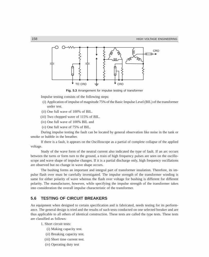
Dharm\N-HIGH\HG5-1.PM5 158
158 HIGH VOLTAGE ENGINEERING
Fig. 5.3 Arrangement for impulse testing of transformer
Impulse testing consists of the following steps:
(i) Application of impulse of magnitude 75% of the Basic Impulse Level (BIL) of the transformerunder test.
(ii) One full wave of 100% of BIL.
(iii) Two chopped wave of 115% of BIL.
(iv) One full wave of 100% BIL and
(v) One full wave of 75% of BIL.
During impulse testing the fault can be located by general observation like noise in the tank orsmoke or bubble in the breather.
If there is a fault, it appears on the Oscilloscope as a partial of complete collapse of the appliedvoltage.
Study of the wave form of the neutral current also indicated the type of fault. If an arc occursbetween the turns or form turn to the ground, a train of high frequency pulses are seen on the oscillo-scope and wave shape of impulse changes. If it is a partial discharge only, high frequency oscillationsare observed but no change in wave shape occurs.
The bushing forms an important and integral part of transformer insulation. Therefore, its im-pulse flash over must be carefully investigated. The impulse strength of the transformer winding issame for either polarity of wave whereas the flash over voltage for bushing is different for differentpolarity. The manufacturer, however, while specifying the impulse strength of the transformer takesinto consideration the overall impulse characteristic of the transformer.
5.6 TESTING OF CIRCUIT BREAKERS
An equipment when designed to certain specification and is fabricated, needs testing for its perform-ance. The general design is tried and the results of such tests conducted on one selected breaker and arethus applicable to all others of identical construction. These tests are called the type tests. These testsare classified as follows:
1. Short circuit tests:
(i) Making capacity test.
(ii) Breaking capacity test.
(iii) Short time current test.
(iv) Operating duty test
Dharm\N-HIGH\HG5-1.PM5 159
HIGH VOLTAGE TESTING OF ELECTRICAL EQUIPMENT 159
2. Dielectric tests:
(i) Power frequency test:
(a) One minute dry withstand test.
(b) One minute wet withstand test.
(ii) Impulse voltage dry withstand test.
3. Thermal test.
4. Mechanical test
Once a particular design is found satisfactory, a large number of similar C.Bs. are manufacturedfor marketing. Every piece of C.B. is then tested before putting into service. These tests are known asroutine tests. With these tests it is possible to find out if incorrect assembly or inferior quality materialhas been used for a proven design equipment. These tests are classified as (i) operation tests,(ii) millivoltdrop tests, (iii) power frequency voltage tests at manufacturer’s premises, and (iv) powerfrequency voltage tests after erection on site.
We will discuss first the type tests. In that also we will discuss the short circuit tests after theother three tests.
Dielectric TestsThe general dielectric characteristics of any circuit breaker or switchgear unit depend upon the basicdesign i.e. clearances, bushing materials, etc. upon correctness and accuracy in assembly and upon thequality of materials used. For a C.B. these factors are checked from the viewpoint of their ability towithstand over voltages at the normal service voltage and abnormal voltages during lightning or otherphenomenon.
The test voltage is applied for a period of one minute between (i) phases with the breaker closed,(ii) phases and earth with C.B. open, and (iii) across the terminals with breaker open. With this thebreaker must not flash over or puncture. These tests are normally made on indoor switchgear. For suchC.Bs the impulse tests generally are unnecessary because it is not exposed to impulse voltage of a veryhigh order. The high frequency switching surges do occur but the effect of these in cable systems usedfor indoor switchgear are found to be safely withstood by the switchgear if it has withstood the normalfrequency test.
Since the outdoor switchgear is electrically exposed, they will be subjected to over voltagescaused by lightning. The effect of these voltages is much more serious than the power frequency voltagesin service. Therefore, this class of switchgear is subjected in addition to power frequency tests, theimpulse voltage tests.
The test voltage should be a standard 1/50 µ sec wave, the peak value of which is specifiedaccording to the rated voltage of the breaker. A higher impulse voltage is specified for non-effectivelygrounded system than those for solidly grounded system. The test voltages are applied between (i) eachpole and earth in turn with the breaker closed and remaining phases earthed, and (ii) between all termi-nals on one side of the breaker and all the other terminals earthed, with the breaker open. The specifiedvoltages are withstand values i.e. the breaker should not flash over for 10 applications of the wave.Normally this test is carried out with waves of both the polarities.
The wet dielectric test is used for outdoor switchgear. In this, the external insulation is sprayedfor two minutes while the rated service voltage is applied; the test overvoltage is then maintained for30 seconds during which no flash over should occur. The effect of rain on external insulation is partlybeneficial, insofar as the surface is thereby cleaned, but is also harmful if the rain contains impurities.
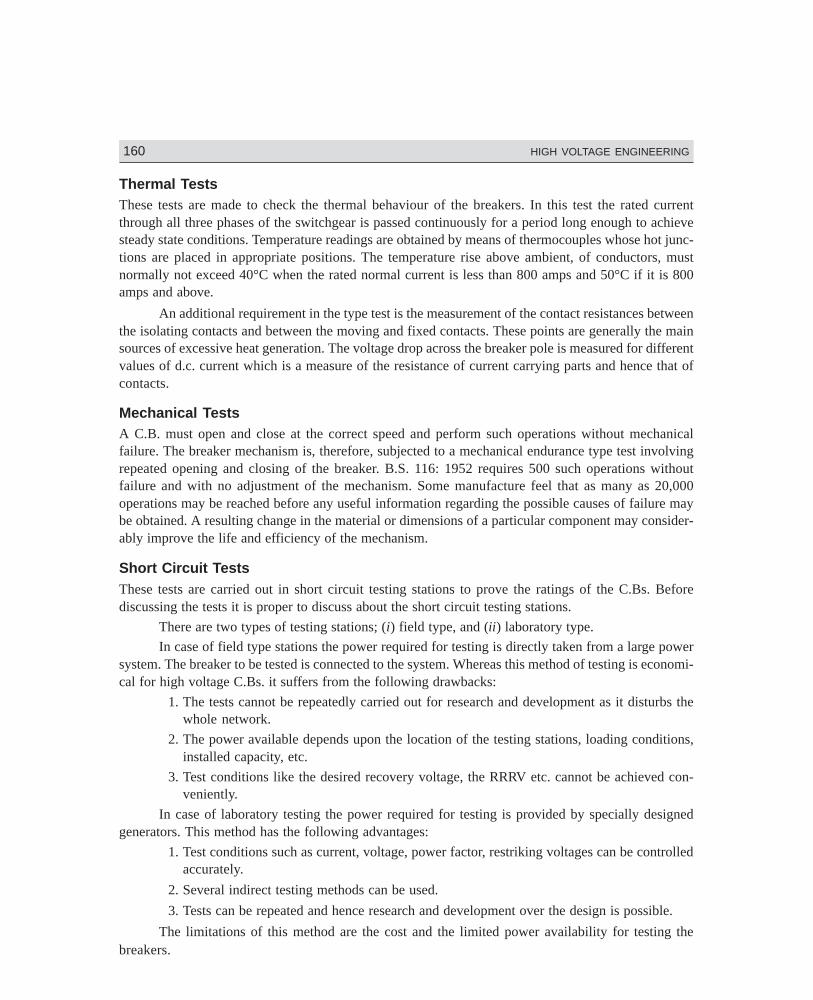
Dharm\N-HIGH\HG5-1.PM5 160
160 HIGH VOLTAGE ENGINEERING
Thermal TestsThese tests are made to check the thermal behaviour of the breakers. In this test the rated currentthrough all three phases of the switchgear is passed continuously for a period long enough to achievesteady state conditions. Temperature readings are obtained by means of thermocouples whose hot junc-tions are placed in appropriate positions. The temperature rise above ambient, of conductors, mustnormally not exceed 40°C when the rated normal current is less than 800 amps and 50°C if it is 800amps and above.
An additional requirement in the type test is the measurement of the contact resistances betweenthe isolating contacts and between the moving and fixed contacts. These points are generally the mainsources of excessive heat generation. The voltage drop across the breaker pole is measured for differentvalues of d.c. current which is a measure of the resistance of current carrying parts and hence that ofcontacts.
Mechanical TestsA C.B. must open and close at the correct speed and perform such operations without mechanicalfailure. The breaker mechanism is, therefore, subjected to a mechanical endurance type test involvingrepeated opening and closing of the breaker. B.S. 116: 1952 requires 500 such operations withoutfailure and with no adjustment of the mechanism. Some manufacture feel that as many as 20,000operations may be reached before any useful information regarding the possible causes of failure maybe obtained. A resulting change in the material or dimensions of a particular component may consider-ably improve the life and efficiency of the mechanism.
Short Circuit TestsThese tests are carried out in short circuit testing stations to prove the ratings of the C.Bs. Beforediscussing the tests it is proper to discuss about the short circuit testing stations.
There are two types of testing stations; (i) field type, and (ii) laboratory type.
In case of field type stations the power required for testing is directly taken from a large powersystem. The breaker to be tested is connected to the system. Whereas this method of testing is economi-cal for high voltage C.Bs. it suffers from the following drawbacks:
1. The tests cannot be repeatedly carried out for research and development as it disturbs thewhole network.
2. The power available depends upon the location of the testing stations, loading conditions,installed capacity, etc.
3. Test conditions like the desired recovery voltage, the RRRV etc. cannot be achieved con-veniently.
In case of laboratory testing the power required for testing is provided by specially designedgenerators. This method has the following advantages:
1. Test conditions such as current, voltage, power factor, restriking voltages can be controlledaccurately.
2. Several indirect testing methods can be used.
3. Tests can be repeated and hence research and development over the design is possible.
The limitations of this method are the cost and the limited power availability for testing thebreakers.
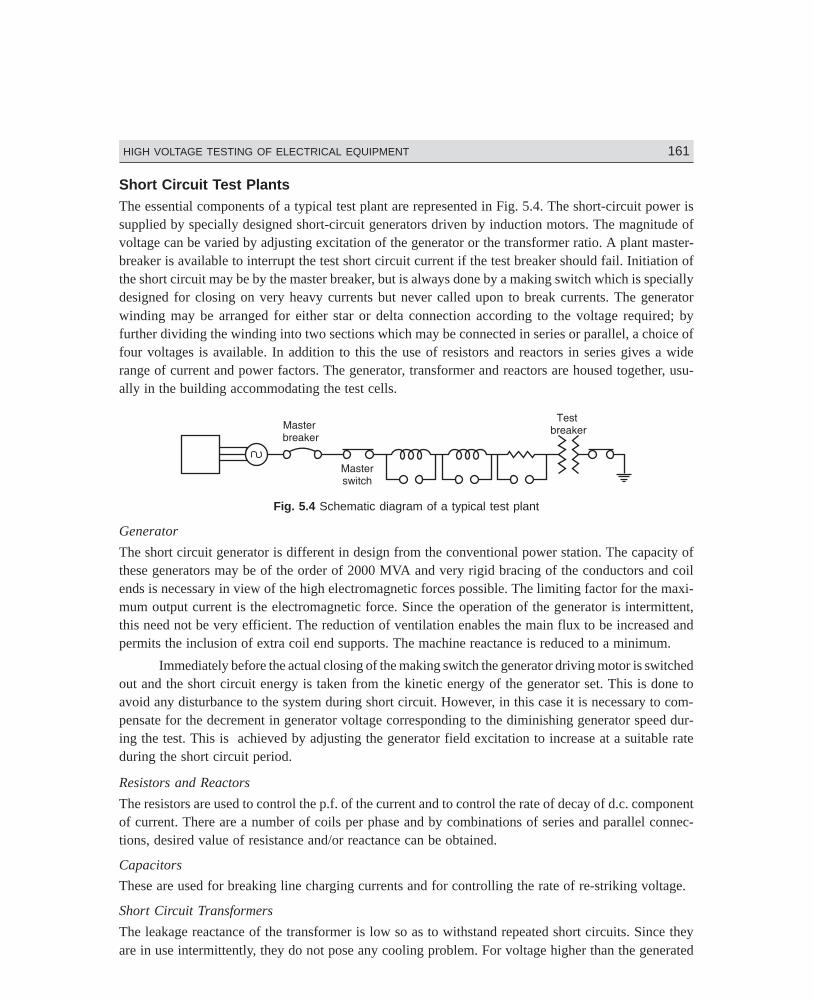
Dharm\N-HIGH\HG5-1.PM5 161
HIGH VOLTAGE TESTING OF ELECTRICAL EQUIPMENT 161
Short Circuit Test PlantsThe essential components of a typical test plant are represented in Fig. 5.4. The short-circuit power issupplied by specially designed short-circuit generators driven by induction motors. The magnitude ofvoltage can be varied by adjusting excitation of the generator or the transformer ratio. A plant master-breaker is available to interrupt the test short circuit current if the test breaker should fail. Initiation ofthe short circuit may be by the master breaker, but is always done by a making switch which is speciallydesigned for closing on very heavy currents but never called upon to break currents. The generatorwinding may be arranged for either star or delta connection according to the voltage required; byfurther dividing the winding into two sections which may be connected in series or parallel, a choice offour voltages is available. In addition to this the use of resistors and reactors in series gives a widerange of current and power factors. The generator, transformer and reactors are housed together, usu-ally in the building accommodating the test cells.
Fig. 5.4 Schematic diagram of a typical test plant
Generator
The short circuit generator is different in design from the conventional power station. The capacity ofthese generators may be of the order of 2000 MVA and very rigid bracing of the conductors and coilends is necessary in view of the high electromagnetic forces possible. The limiting factor for the maxi-mum output current is the electromagnetic force. Since the operation of the generator is intermittent,this need not be very efficient. The reduction of ventilation enables the main flux to be increased andpermits the inclusion of extra coil end supports. The machine reactance is reduced to a minimum.
Immediately before the actual closing of the making switch the generator driving motor is switchedout and the short circuit energy is taken from the kinetic energy of the generator set. This is done toavoid any disturbance to the system during short circuit. However, in this case it is necessary to com-pensate for the decrement in generator voltage corresponding to the diminishing generator speed dur-ing the test. This is achieved by adjusting the generator field excitation to increase at a suitable rateduring the short circuit period.
Resistors and Reactors
The resistors are used to control the p.f. of the current and to control the rate of decay of d.c. componentof current. There are a number of coils per phase and by combinations of series and parallel connec-tions, desired value of resistance and/or reactance can be obtained.
Capacitors
These are used for breaking line charging currents and for controlling the rate of re-striking voltage.
Short Circuit Transformers
The leakage reactance of the transformer is low so as to withstand repeated short circuits. Since theyare in use intermittently, they do not pose any cooling problem. For voltage higher than the generated
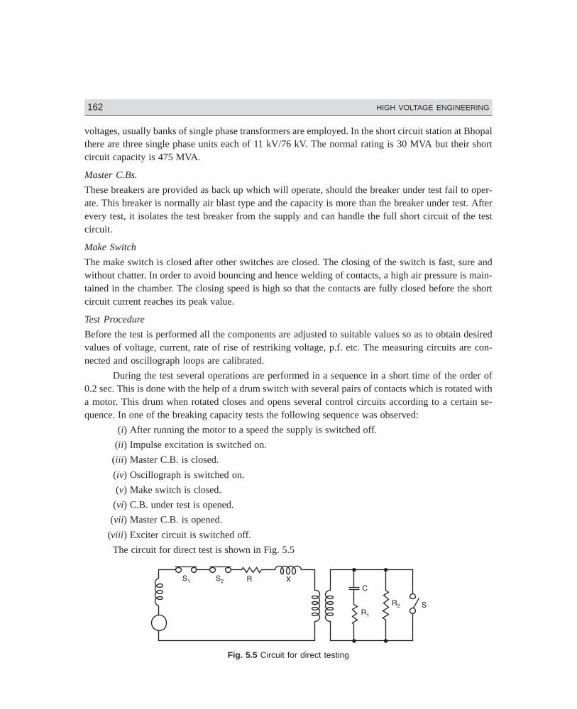
Dharm\N-HIGH\HG5-1.PM5 162
162 HIGH VOLTAGE ENGINEERING
voltages, usually banks of single phase transformers are employed. In the short circuit station at Bhopalthere are three single phase units each of 11 kV/76 kV. The normal rating is 30 MVA but their shortcircuit capacity is 475 MVA.
Master C.Bs.
These breakers are provided as back up which will operate, should the breaker under test fail to oper-ate. This breaker is normally air blast type and the capacity is more than the breaker under test. Afterevery test, it isolates the test breaker from the supply and can handle the full short circuit of the testcircuit.
Make Switch
The make switch is closed after other switches are closed. The closing of the switch is fast, sure andwithout chatter. In order to avoid bouncing and hence welding of contacts, a high air pressure is main-tained in the chamber. The closing speed is high so that the contacts are fully closed before the shortcircuit current reaches its peak value.
Test Procedure
Before the test is performed all the components are adjusted to suitable values so as to obtain desiredvalues of voltage, current, rate of rise of restriking voltage, p.f. etc. The measuring circuits are con-nected and oscillograph loops are calibrated.
During the test several operations are performed in a sequence in a short time of the order of0.2 sec. This is done with the help of a drum switch with several pairs of contacts which is rotated witha motor. This drum when rotated closes and opens several control circuits according to a certain se-quence. In one of the breaking capacity tests the following sequence was observed:
(i) After running the motor to a speed the supply is switched off.
(ii) Impulse excitation is switched on.
(iii) Master C.B. is closed.
(iv) Oscillograph is switched on.
(v) Make switch is closed.
(vi) C.B. under test is opened.
(vii) Master C.B. is opened.
(viii) Exciter circuit is switched off.
The circuit for direct test is shown in Fig. 5.5
Fig. 5.5 Circuit for direct testing
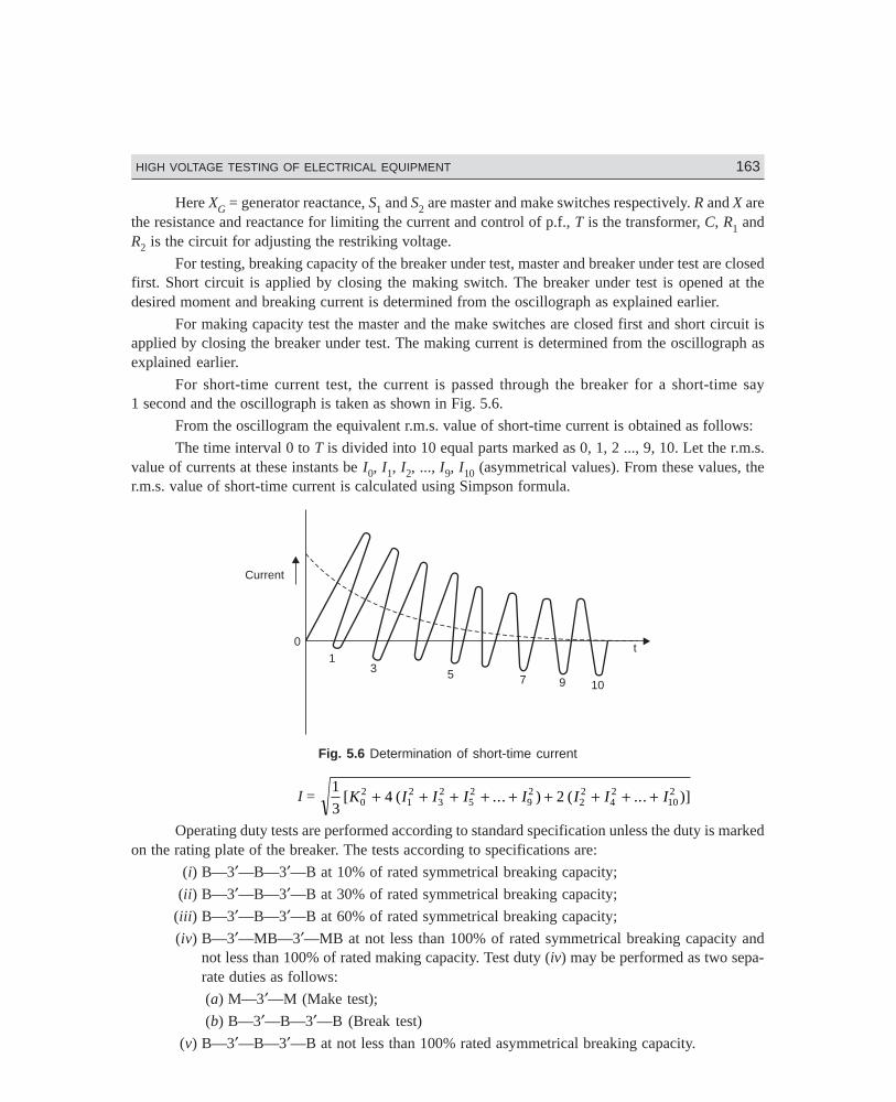
Dharm\N-HIGH\HG5-1.PM5 163
HIGH VOLTAGE TESTING OF ELECTRICAL EQUIPMENT 163
Here XG = generator reactance, S1 and S2 are master and make switches respectively. R and X arethe resistance and reactance for limiting the current and control of p.f., T is the transformer, C, R1 andR2 is the circuit for adjusting the restriking voltage.
For testing, breaking capacity of the breaker under test, master and breaker under test are closedfirst. Short circuit is applied by closing the making switch. The breaker under test is opened at thedesired moment and breaking current is determined from the oscillograph as explained earlier.
For making capacity test the master and the make switches are closed first and short circuit isapplied by closing the breaker under test. The making current is determined from the oscillograph asexplained earlier.
For short-time current test, the current is passed through the breaker for a short-time say1 second and the oscillograph is taken as shown in Fig. 5.6.
From the oscillogram the equivalent r.m.s. value of short-time current is obtained as follows:
The time interval 0 to T is divided into 10 equal parts marked as 0, 1, 2 ..., 9, 10. Let the r.m.s.value of currents at these instants be I0, I1, I2, ..., I9, I10 (asymmetrical values). From these values, ther.m.s. value of short-time current is calculated using Simpson formula.
Current
01
3 5 7 9 10
t
Fig. 5.6 Determination of short-time current
I = 1
34 20
212
32
52
92
22
42
102[ ( ... ) ( ... )]K I I I I I I I+ + + + + + + + +
Operating duty tests are performed according to standard specification unless the duty is markedon the rating plate of the breaker. The tests according to specifications are:
(i) B—3′—B—3′—B at 10% of rated symmetrical breaking capacity;
(ii) B—3′—B—3′—B at 30% of rated symmetrical breaking capacity;
(iii) B—3′—B—3′—B at 60% of rated symmetrical breaking capacity;
(iv) B—3′—MB—3′—MB at not less than 100% of rated symmetrical breaking capacity andnot less than 100% of rated making capacity. Test duty (iv) may be performed as two sepa-rate duties as follows:
(a) M—3′—M (Make test);
(b) B—3′—B—3′—B (Break test)
(v) B—3′—B—3′—B at not less than 100% rated asymmetrical breaking capacity.

Dharm\N-HIGH\HG5-1.PM5 164
164 HIGH VOLTAGE ENGINEERING
Here B and M represent breaking and making operations respectively. MB denotes the makingoperation followed by breaking operation without any international time-lag.3′ denotes the time inminutes between successive operations of an operating duty.
5.7 TEST VOLTAGE
For different transmission voltages, the test voltages required are given in the following Tables:
Table 5.2
Test voltages for a.c. equipments
System nominal Power frequency Impulse withstand Switching surgevoltage (rms) withstand voltage voltage withstand voltage
(rms)
400 520 1425 875
525 670 1800 1100
765 960 2300 1350
1100 1416 2800 1800
1500 1920 3500 2200
Table 5.3
Test voltages for d.c. equipments
Normal voltage D.C. withstand Impulse withstand Switching surgevoltage kV voltage kV withstand voltage kV
± 400 KV 800 1350 1000
± 600 KV 1200 1900 1500
± 800 KV 1600 2300 2000
Table 5.4
Test voltages required for different system voltage (a.c. system)
Nominal voltage KV Power frequency Impulse withstand Switching surge(rms) voltage kV (rms) voltage kV voltage kV
400 800 2400 1150
765 1000 3000 1750
1100 1400 3700 2300
1500 1900 4600 2800
If the insulation requirements for a particular operating voltage are required to be studied in aresearch and development laboratory, the voltage levels required in the laboratory are given inTables 5.4 and 5.5.

Dharm\N-HIGH\HG5-1.PM5 165
HIGH VOLTAGE TESTING OF ELECTRICAL EQUIPMENT 165
Table 5.5
Test voltages required for different d.c. system voltages
Nominal voltage kV D.C. voltage kV Impulse withstand Switching surgevoltage kV voltage kV
± 400 800 1750 1300
± 600 1200 2500 2000
± 800 1600 3000 2600
Table 5.6 shows approximate dimension of the testing equipment and the equipment to be tested.
Table 5.6
Approximate dimensions of the testing equipmentand the equipment to be tested
Nominal voltage of A.C. transformer Impulse generator Dimension of Test-the equipment kV height (m) height (m) object
(rms)
400 10 6 7 × 2 × 11
765 15 8 11 × 2 × 17
1100 18 12 17 × 2 × 24
1500 22 15 28 × 2 × 38
Table 5.7 shows some of the very important high voltage laboratories in the world.
Table 5.7
High voltage laboratories in the world
Location Dimension Power frequency Impulse Test SwitchingTest Voltage MV Voltage MV Surge Voltage
MV
Australia 1.5 8.0 –Bharat Heavy 67 × 35 × 35 1.5 3.6 2.0Elect. Bhopal, IndiaCESI-Milan, Italy 150 × 75 × 55 2.3 4.8 3.0
(200 KJ)College of 25 × 15 × 15 0.3 1.2 –Engineering,Guindy, Madras
College ofEngineering, 33 × 26 × 30 0.5 1.4 –Jabalpur (MP) (16 KJ)College of 20 × 12 × 8 0.5 1.4 –Engineering, (16 KJ)Kakinada, AP
Dharm\N-HIGH\HG5-1.PM5 166
166 HIGH VOLTAGE ENGINEERING
Electricity DC, 65 × 65 × 45 2.5 7.2 6.0France (1010 KJ)
Hydro-Quebec 82 × 68 × 50 2.5 6.4 6.0Montreal, Canada (400 KJ)
Indian Instt. 37.5 × 25 × 19 1.05 3.0 1.6of Science, (50 KJ)Bangalore
Indian Instt. of 28 × 10 × 9.7 0.80 1.5 –Technology, (36 KJ)Madras
Russia 115 × 80 × 60 3.0 8.0 –
Technical 32 × 25 × 21 1.2 3.2 –UniversityDarmstadt, W.Germany
Technical University 34 × 23 × 19 1.2 3.0 –
Munich, W. Germany
5.1. Explain the procedure for testing string insulator.
5.2. Describe the arrangement of insulators for performing various tests.
5.3. List out various tests to be carried out on insulator and give a brief account of each test.
5.4. Write a short note on the cable sample preparation before it is subjected to various tests.
5.5. List out various tests to be carried out on a cable and give a brief account of each test.
5.6. Explain briefly various tests to be carried out on a bushing.
5.7. Explain the function of discharge device used in a power capacitor and explain the test for efficacy of thisdevice.
5.8. Explain the procedure for performing (i) IR test (ii) Stability test and (iii) Partial discharge test.
5.9. Explain briefly impulse testing of power transformer.
5.10. Describe various tests to be carried out on C.B.
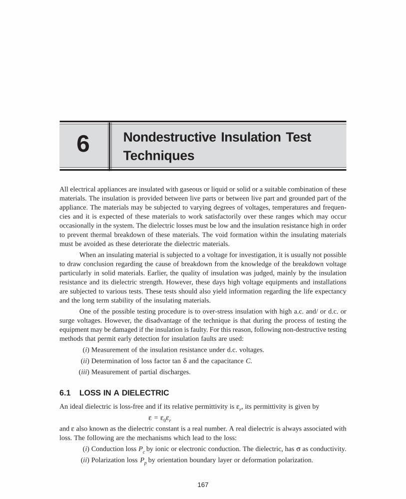
167
6
All electrical appliances are insulated with gaseous or liquid or solid or a suitable combination of thesematerials. The insulation is provided between live parts or between live part and grounded part of theappliance. The materials may be subjected to varying degrees of voltages, temperatures and frequen-cies and it is expected of these materials to work satisfactorily over these ranges which may occuroccasionally in the system. The dielectric losses must be low and the insulation resistance high in orderto prevent thermal breakdown of these materials. The void formation within the insulating materialsmust be avoided as these deteriorate the dielectric materials.
When an insulating material is subjected to a voltage for investigation, it is usually not possibleto draw conclusion regarding the cause of breakdown from the knowledge of the breakdown voltageparticularly in solid materials. Earlier, the quality of insulation was judged, mainly by the insulationresistance and its dielectric strength. However, these days high voltage equipments and installationsare subjected to various tests. These tests should also yield information regarding the life expectancyand the long term stability of the insulating materials.
One of the possible testing procedure is to over-stress insulation with high a.c. and/ or d.c. orsurge voltages. However, the disadvantage of the technique is that during the process of testing theequipment may be damaged if the insulation is faulty. For this reason, following non-destructive testingmethods that permit early detection for insulation faults are used:
(i) Measurement of the insulation resistance under d.c. voltages.
(ii) Determination of loss factor tan δ and the capacitance C.
(iii) Measurement of partial discharges.
6.1 LOSS IN A DIELECTRIC
An ideal dielectric is loss-free and if its relative permittivity is εr, its permittivity is given by
ε = ε0εr
and ε also known as the dielectric constant is a real number. A real dielectric is always associated withloss. The following are the mechanisms which lead to the loss:
(i) Conduction loss Pc by ionic or electronic conduction. The dielectric, has σ as conductivity.
(ii) Polarization loss Pp by orientation boundary layer or deformation polarization.
Nondestructive Insulation TestTechniques
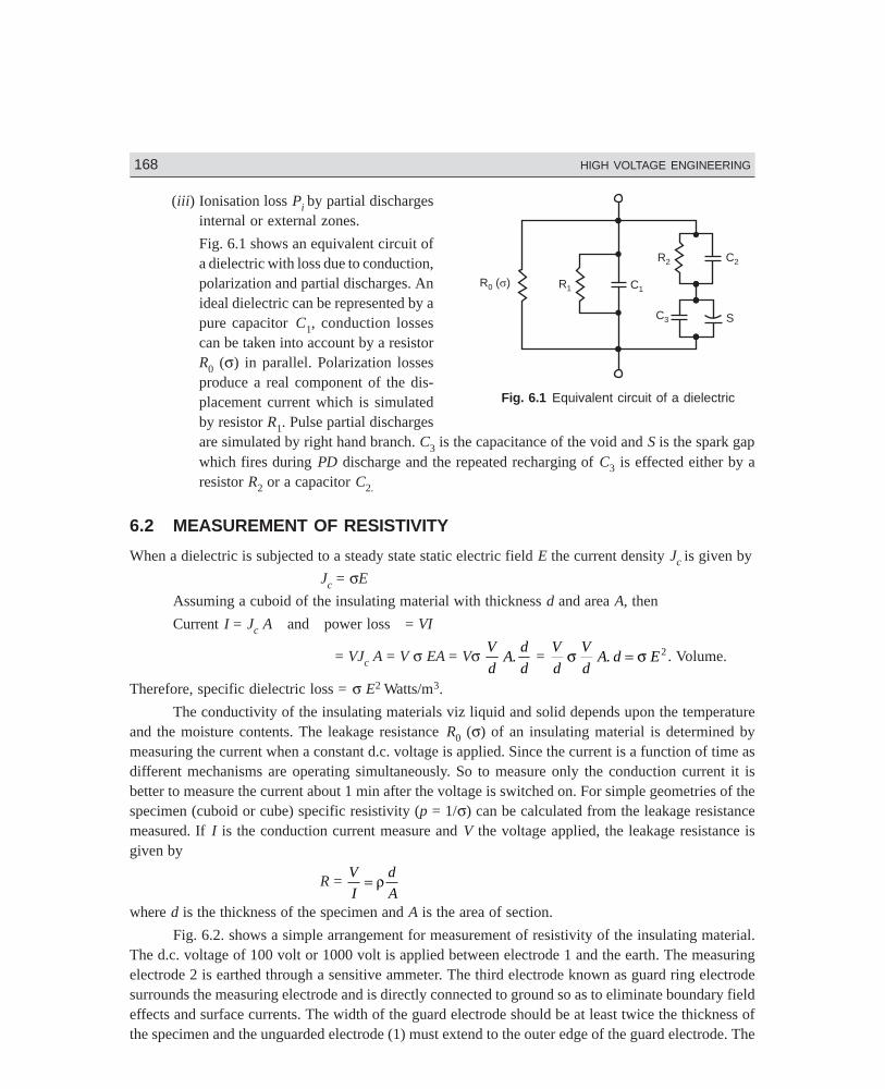
168 HIGH VOLTAGE ENGINEERING
Dharm\N-HIGH\HG6-1.PM5 168
(iii) Ionisation loss Pi by partial dischargesinternal or external zones.
Fig. 6.1 shows an equivalent circuit ofa dielectric with loss due to conduction,polarization and partial discharges. Anideal dielectric can be represented by apure capacitor C1, conduction lossescan be taken into account by a resistorR0 (σ) in parallel. Polarization lossesproduce a real component of the dis-placement current which is simulatedby resistor R1. Pulse partial dischargesare simulated by right hand branch. C3 is the capacitance of the void and S is the spark gapwhich fires during PD discharge and the repeated recharging of C3 is effected either by aresistor R2 or a capacitor C2.
6.2 MEASUREMENT OF RESISTIVITY
When a dielectric is subjected to a steady state static electric field E the current density Jc is given by
Jc = σE
Assuming a cuboid of the insulating material with thickness d and area A, then
Current I = Jc A and power loss = VI
= VJc A = V σ EA = Vσ V
dA
d
d. =
V
d
V
dA d Eσ σ. = 2 . Volume.
Therefore, specific dielectric loss = σ E2 Watts/m3.
The conductivity of the insulating materials viz liquid and solid depends upon the temperatureand the moisture contents. The leakage resistance R0 (σ) of an insulating material is determined bymeasuring the current when a constant d.c. voltage is applied. Since the current is a function of time asdifferent mechanisms are operating simultaneously. So to measure only the conduction current it isbetter to measure the current about 1 min after the voltage is switched on. For simple geometries of thespecimen (cuboid or cube) specific resistivity (p = 1/σ) can be calculated from the leakage resistancemeasured. If I is the conduction current measure and V the voltage applied, the leakage resistance isgiven by
R = V
I
d
A= ρ
where d is the thickness of the specimen and A is the area of section.
Fig. 6.2. shows a simple arrangement for measurement of resistivity of the insulating material.The d.c. voltage of 100 volt or 1000 volt is applied between electrode 1 and the earth. The measuringelectrode 2 is earthed through a sensitive ammeter. The third electrode known as guard ring electrodesurrounds the measuring electrode and is directly connected to ground so as to eliminate boundary fieldeffects and surface currents. The width of the guard electrode should be at least twice the thickness ofthe specimen and the unguarded electrode (1) must extend to the outer edge of the guard electrode. The
S
R1
R2 C2
C1
C3
R ( )0 s
Fig. 6.1 Equivalent circuit of a dielectric
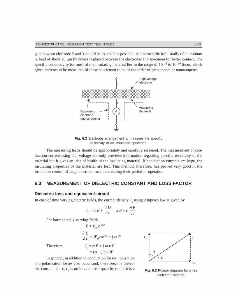
Dharm\N-HIGH\HG6-1.PM5 169
NONDESTRUCTIVE INSULATION TEST TECHNIQUES 169
Ir
I
I
w
fd
gap between electrode 2 and 3 should be as small as possible. A thin metallic foil usually of aluminiumor lead of about 20 µm thickness is placed between the electrodes and specimen for better contact. Thespecific conductivity for most of the insulating material lies in the range of 10–16 to 10–10 S/cm, whichgives currents to be measured of these speciemen to be of the order of picoampers or nanoamperes.
High-voltageelectrode
Guard-ringelectrodeand screening
MeasuringelectrodeA
1
2
Fig. 6.2 Electrode arrangement to measure the specificresistivity of an insulation specimen
The measuring leads should be appropriately and carefully screened. The measurement of con-duction current using d.c. voltage not only provides information regarding specific resistivity of thematerial but it gives an idea of health of the insulating material. If conduction currents are large, theinsulating properties of the material are lost. This method, therefore, has proved very good in theinsulation control of large electrical machines during their period of operation.
6.3 MEASUREMENT OF DIELECTRIC CONSTANT AND LOSS FACTOR
Dielectric loss and equivalent circuitIn case of time varying electric fields, the current density Jc using Amperes law is given by
Jc = σ E + ∂∂
D
t = σ E + ε
∂∂
E
t
For harmonically varying fields
E = Em e jωt
∂∂
E
t = jEmωejωt = j ω E
Therefore, Jc = σ E + j ω ε E
= (σ + j ω ε)E
In general, in addition to conduction losses, ionizationand polarization losses also occur and, therefore, the dielec-tric constant ε = ε0 εr is no longer a real quantity rather it is a Fig. 6.3 Phasor diagram for a real
dielectric material
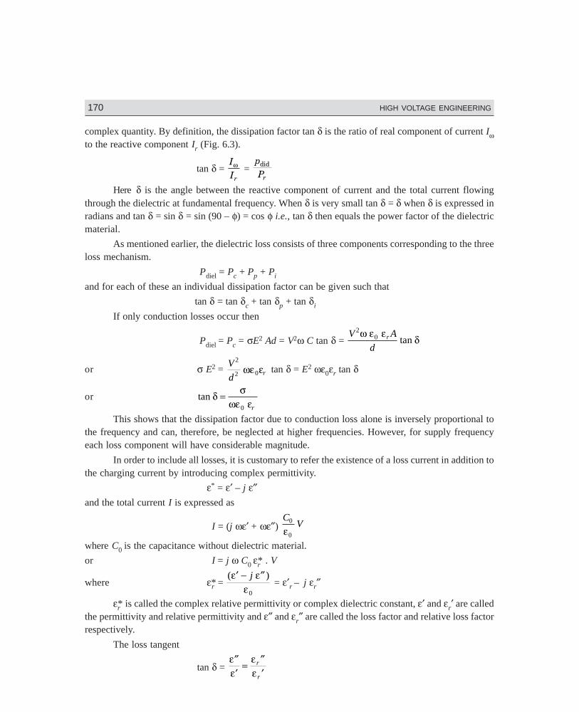
170 HIGH VOLTAGE ENGINEERING
Dharm\N-HIGH\HG6-1.PM5 170
complex quantity. By definition, the dissipation factor tan δ is the ratio of real component of current Iωto the reactive component Ir (Fig. 6.3).
tan δ = IIr
ω = pPr
did
Here δ is the angle between the reactive component of current and the total current flowingthrough the dielectric at fundamental frequency. When δ is very small tan δ = δ when δ is expressed inradians and tan δ = sin δ = sin (90 – φ) = cos φ i.e., tan δ then equals the power factor of the dielectricmaterial.
As mentioned earlier, the dielectric loss consists of three components corresponding to the threeloss mechanism.
Pdiel = Pc + Pp + Pi
and for each of these an individual dissipation factor can be given such that
tan δ = tan δc + tan δp + tan δi
If only conduction losses occur then
Pdiel = Pc = σE2 Ad = V2ω C tan δ = V A
dr
20ω ε ε
δtan
or σ E2 = V
dr
2
2 0ωε ε tan δ = E2 ωε0εr tan δ
or tan δ σωε ε
=0 r
This shows that the dissipation factor due to conduction loss alone is inversely proportional tothe frequency and can, therefore, be neglected at higher frequencies. However, for supply frequencyeach loss component will have considerable magnitude.
In order to include all losses, it is customary to refer the existence of a loss current in addition tothe charging current by introducing complex permittivity.
ε* = ε′ – j ε″and the total current I is expressed as
I = (j ωε′ + ωε″) C
V0
0εwhere C0 is the capacitance without dielectric material.
or I = j ω C0 εr* . V
where ε*r = ( )ε ε
ε′ − ″j
0
= ε′r – j εr″
εr* is called the complex relative permittivity or complex dielectric constant, ε′ and εr′ are calledthe permittivity and relative permittivity and ε″ and εr″ are called the loss factor and relative loss factorrespectively.
The loss tangent
tan δ = εε
εε
″′
= ″′
r
r
Dharm\N-HIGH\HG6-1.PM5 171
NONDESTRUCTIVE INSULATION TEST TECHNIQUES 171
The product of the angular frequency and ε″ is equivalent to the dielectric conductivity σ″ i.e., σ″ = ωε″.
The dielectric conductivity takes into account all the three power dissipative processes includ-ing the one which is frequency dependent. Fig. 6.4 shows two equivalent circuits representing theelectrical behaviour of insulating materials under a.c. voltages, losses have been simulated by resistances.
dd
I
I
RP CP
RS
CS
( )a ( )bVV/R
wV C wCS
I
I RS
Fig. 6.4 Equivalent circuits for an insulating material
Normally the angle between V and the total current in a pure capacitor is 90°. Due to losses, thisangle is less than 90°. Therefore, δ is the angle by which the voltage and charging current fall short ofthe 90° displacement.
For the parallel circuit the dissipation factor is given by
tan δ = 1
ωC Rp p
and for the series circuit
tan δ = ω CsRs
For a fixed frequency, both the equivalents hold good and one can be obtained from the other.However, the frequency dependence is just the opposite in the two cases and this shows the limitedvalidity of these equivalent circuits.
The information obtained from the measurement of tan δ and complex permittivity is an indica-tion of the quality of the insulating material.
(i) If tan δ varies and changes abruptly with the application of high voltage, it shows inceptionof internal partial discharge.
(ii) The effect to frequency on the dielectric properties can be studied and the band of frequen-cies where dispersion occurs i.e., where that permittivity reduces with rise in frequency canbe obtained.
6.4 HIGH VOLTAGE SCHERING BRIDGE
The bridge is widely used for capacity and dielectric loss measurement of all kinds of capacitances, forinstance cables, insulators and liquid insulating materials. We know that most of the high voltageequipments have low capacitance and low loss factor. Typical values of these equipments are given inChapter 3. This bridge is then more suitable for measurement of such small capacitance equipments asthe bridge uses either high voltage or high frequency supply. If measurements for such low capacityequipments is carried out at low voltage, the results so obtained are not accurate.
172 HIGH VOLTAGE ENGINEERING
Dharm\N-HIGH\HG6-1.PM5 172
Fig. 6.5 shows a high voltage schering bridge where the specimen has been represented by aparallel combination of Rp and Cp.
Fig. 6.5 Basic high voltage schering bridge
The special features of the bridge are:
1. High voltage supply, consists of a high voltage transformer with regulation, protective cir-cuitry and special screening. The input voltage is 220 volt and output continuously variablebetween 0 and 10 kV. The maximum current is 100 mA and it is of 1 kVA capacity.
2. Screened standard capacitor Cs of 100 pF ± 5%, 10 kV max and dissipation factor tan δ= 10–5. It is a gas-filled capacitor having negligible loss factor over a wide range of frequency.
3. The impedances of arms I and II are very large and, therefore, current drawn by these armsis small from the source and a sensitive detector is required for obtaining balance. Also,since the impedance of arm I and II are very large as compared to III and IV, the detector andthe impedances in arm III and IV are at a potential of only a few volts (10 to 20 volts) aboveearth even when the supply voltage is 10 kV, except of course, in case of breakdown of oneof the capacitors of arm I or II in which case the potential will be that of supply voltage.Spark gaps are, therefore, provided to spark over whenever the voltage across arm III or IVexceeds 100 volt so as to provide personnel safety and safety for the null detector.
4. Null Detector: An oscilloscope is used as a null detector. The γ–plates are supplied with thebridge voltage Vab and the x-plates with the supply voltage V. If Vab has phase differencewith respect to V, an ellipse will appear on the screen (Fig. 6.6). However, if magnitudebalance is not reached, an inclined straight line will be observed on the screen. Theinformation about the phase is obtained from the area of the eclipse and the one about themagnitude from the inclination angle. Fig. 6.6a shows that both magnitude and phase arebalanced and this represents the null point condition. Fig. (6.6c) and (d) shows that onlyphase and amplitude respectively are balanced.
( )a ( )b ( )c ( )d
Fig. 6.6 Indications on null detector
Dharm\N-HIGH\HG6-1.PM5 173
NONDESTRUCTIVE INSULATION TEST TECHNIQUES 173
The handling of bridge keys allows to meet directly both the phase and the magnitudeconditions in a single attempt. A time consuming iterative procedure being used earlier isthus avoided and also with this a very high order of accuracy in the measurement is achieved.The high accuracy is obtained as these null oscilloscopes are equipped with a γ – amplifierof automatically controlled gain. If the impedances are far away from the balance point, thewhole screen is used. For nearly obtained balance, it is still almost fully used. As Vab becomessmaller, by approaching the balance point, the gain increases automatically only for deviationsvery close to balance, the ellipse area shrinks to a horizontal line.
5. Automatic Guard Potential Regulator: While measuring capacitance and loss factors usinga.c. bridges, the detrimental stray capacitances between bridge junctions and the groundadversely affect the measurements and are the source of error. Therefore, arrangementsshould be made to shield the measuring system so that these stray capacitances are eitherneutralised, balanced or eliminated by precise and rigorous calculations. Fig. 6.7 showsvarious stray capacitance associated with High Voltage Schering Bridge.
Fig. 6.7 Schering bridge with stray capacitances
Ca, Cb, Cc and Cd are the stray capacitances at the junctions A, B, C and D of the bridge. If pointD is earthed during measurement capacitance Cd is thus eliminated. Since Cc comes across the powersupply for earthed bridge, has no influence on the measurement. The effect of other stray capacitancesCa and Cb can be eliminated by use of auxiliary arms, either guard potential regulator or auxiliarybranch as suggested by Wagner.
Fig. 6.8 shows the basic principle of Wagner earth to eliminate the effect of stray capacitancesCa and Cb. In this arrangement an additional arm Z is connected between the low voltage terminal of thefour arm bridge and earth. The stray capacitance C between the high voltage terminal of the bridge andthe grounded shield and the impedance Z together constitute a six arm bridge and a double balancingprocedure is required.
Switch S is first connected to the bridge point b and balance is obtained. At this point a and b areat the same potential but not necessarily at the ground potential. Switch S is now connected to point Cand by adjusting impedance Z balance is again obtained. Under this condition point ‘a’ must be at thesame potential as earth although it is not permanently at earth potential. Switch S is again connected topoint b and balance is obtained by adjusting bridge parameters. The procedure is repeated till all thethree points a, b and c are at the earth potential and thus Ca and Cb are eliminated.
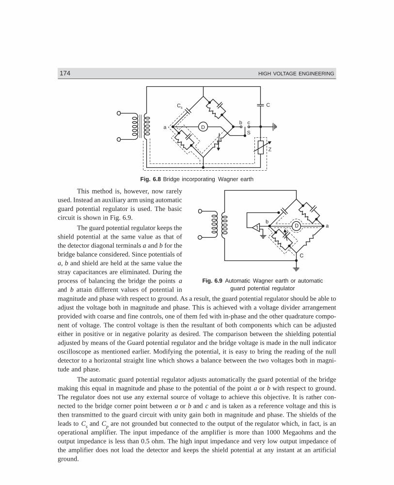
174 HIGH VOLTAGE ENGINEERING
Dharm\N-HIGH\HG6-1.PM5 174
Cs
ab c
SD
Z
C
Fig. 6.8 Bridge incorporating Wagner earth
This method is, however, now rarelyused. Instead an auxiliary arm using automaticguard potential regulator is used. The basiccircuit is shown in Fig. 6.9.
The guard potential regulator keeps theshield potential at the same value as that ofthe detector diagonal terminals a and b for thebridge balance considered. Since potentials ofa, b and shield are held at the same value thestray capacitances are eliminated. During theprocess of balancing the bridge the points aand b attain different values of potential inmagnitude and phase with respect to ground. As a result, the guard potential regulator should be able toadjust the voltage both in magnitude and phase. This is achieved with a voltage divider arrangementprovided with coarse and fine controls, one of them fed with in-phase and the other quadrature compo-nent of voltage. The control voltage is then the resultant of both components which can be adjustedeither in positive or in negative polarity as desired. The comparison between the shielding potentialadjusted by means of the Guard potential regulator and the bridge voltage is made in the null indicatoroscilloscope as mentioned earlier. Modifying the potential, it is easy to bring the reading of the nulldetector to a horizontal straight line which shows a balance between the two voltages both in magni-tude and phase.
The automatic guard potential regulator adjusts automatically the guard potential of the bridgemaking this equal in magnitude and phase to the potential of the point a or b with respect to ground.The regulator does not use any external source of voltage to achieve this objective. It is rather con-nected to the bridge corner point between a or b and c and is taken as a reference voltage and this isthen transmitted to the guard circuit with unity gain both in magnitude and phase. The shields of theleads to Cs and Cp are not grounded but connected to the output of the regulator which, in fact, is anoperational amplifier. The input impedance of the amplifier is more than 1000 Megaohms and theoutput impedance is less than 0.5 ohm. The high input impedance and very low output impedance ofthe amplifier does not load the detector and keeps the shield potential at any instant at an artificialground.
Fig. 6.9 Automatic Wagner earth or automaticguard potential regulator
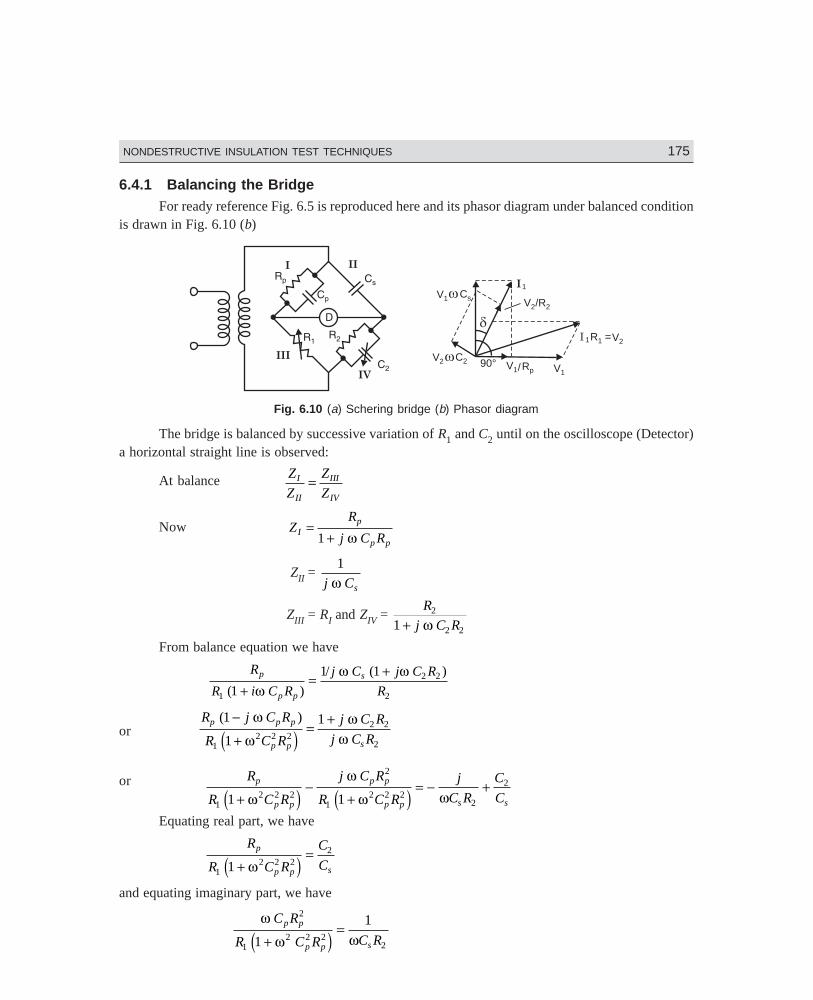
Dharm\N-HIGH\HG6-1.PM5 175
NONDESTRUCTIVE INSULATION TEST TECHNIQUES 175
6.4.1 Balancing the BridgeFor ready reference Fig. 6.5 is reproduced here and its phasor diagram under balanced condition
is drawn in Fig. 6.10 (b)
/R2
d
V1 Csw
V2 C2wV1
V2
I1
V2I 1R =1
RpV1/90°
Fig. 6.10 (a) Schering bridge (b) Phasor diagram
The bridge is balanced by successive variation of R1 and C2 until on the oscilloscope (Detector)a horizontal straight line is observed:
At balance Z
Z
Z
ZI
II
III
IV
=
Now ZR
j C RI
p
p p
=+1 ω
ZII = 1
j Csω
ZIII = RI and ZIV = R
j C R2
2 21 + ωFrom balance equation we have
R
R i C R
j C j C R
Rp
p p
s
1
2 2
21
1 1
( )
/ ( )
+= +
ωω ω
or R j C R
R C R
j C R
j C Rp p p
p p s
( )1
1
1
12 2 2
2 2
2
−
+=
+ω
ωω
ωd i
or R
R C R
j C R
R C R
j
C R
C
Cp
p p
p p
p p s s12 2 2
2
12 2 2
2
2
1 1+−
+= − +
ω
ω
ω ωd i d iEquating real part, we have
R
R C R
C
Cp
p p s12 2 2
2
1 +=
ωd iand equating imaginary part, we have
ω
ω ωC R
R C R C Rp p
p p s
2
12 2 2
21
1
+=
d i
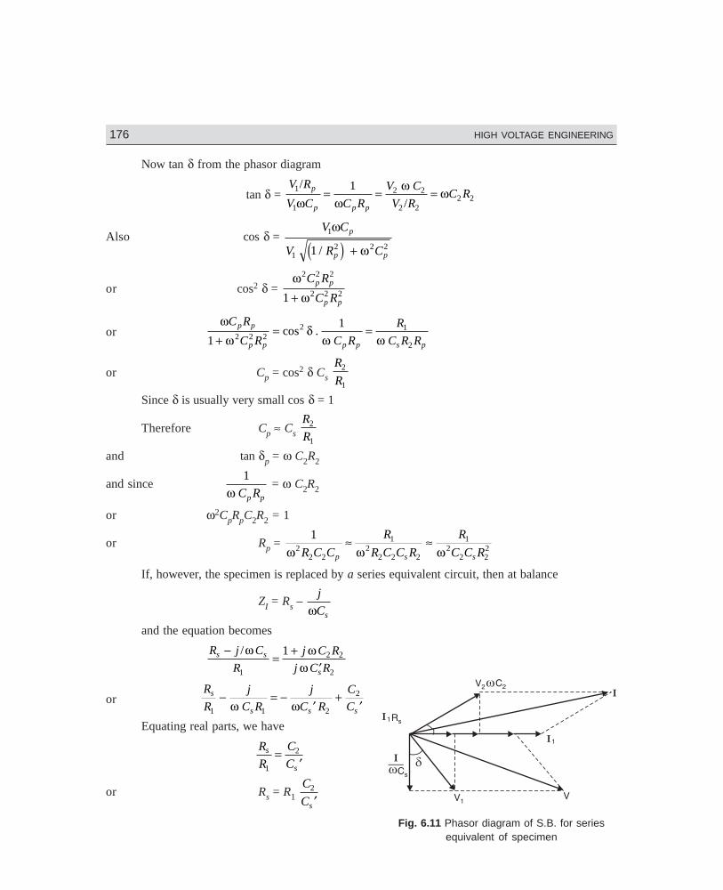
176 HIGH VOLTAGE ENGINEERING
Dharm\N-HIGH\HG6-1.PM5 176
Now tan δ from the phasor diagram
tan δ = V R
V C C R
V C
V RC R
p
p p p
1
1
2 2
2 22 2
1/
/ω ωω ω= = =
Also cos δ = V C
V R C
p
p p
1
12 2 21
ω
ω/d i +
or cos2 δ = ω
ω
2 2 2
2 2 21
C R
C Rp p
p p+
orωω
δω ω
C R
C R C R
R
C R Rp p
p p p p s p1
12 2 2
2 1
2+= =cos .
or Cp = cos2 δ Cs R
R2
1
Since δ is usually very small cos δ = 1
Therefore Cp ≈ Cs R
R2
1
and tan δp = ω C2R2
and since1
ω C Rp p
= ω C2R2
or ω2CpRpC2R2 = 1
or Rp = 1
22 2
12
2 2 2
12
2 22ω ω ωR C C
R
R C C R
R
C C Rp s s
≈ ≈
If, however, the specimen is replaced by a series equivalent circuit, then at balance
ZI = Rs – j
Csωand the equation becomes
R j C
R
j C R
j C Rs s
s
−= +
′/ω ω
ω1
2 2
2
1
orR
R
j
C R
j
C R
C
Cs
s s s1 1 2
2− = −′
+′ω ω
Equating real parts, we have
R
R
C
Cs
s1
2=′
or Rs = R1 C
Cs
2
′
Fig. 6.11 Phasor diagram of S.B. for seriesequivalent of specimen
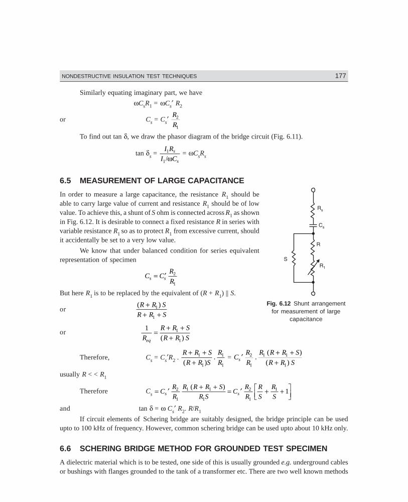
Dharm\N-HIGH\HG6-1.PM5 177
NONDESTRUCTIVE INSULATION TEST TECHNIQUES 177
Similarly equating imaginary part, we have
ωCsR1 = ωCs′ R2
or Cs = Cs′ R
R2
1
To find out tan δ, we draw the phasor diagram of the bridge circuit (Fig. 6.11).
tan δs = I R
I Cs
s
1
1/ω = ωCsRs
6.5 MEASUREMENT OF LARGE CAPACITANCE
In order to measure a large capacitance, the resistance R1 should beable to carry large value of current and resistance R1 should be of lowvalue. To achieve this, a shunt of S ohm is connected across R1 as shownin Fig. 6.12. It is desirable to connect a fixed resistance R in series withvariable resistance R1 so as to protect R1 from excessive current, shouldit accidentally be set to a very low value.
We know that under balanced condition for series equivalentrepresentation of specimen
C CR
Rs s= ′ 2
1
But here R1 is to be replaced by the equivalent of (R + R1) || S.
or( )R R S
R R S
++ +
1
1
or 1 1
1R
R R S
R R Seq
=+ ++( )
Therefore, Cs = Cs′R2 . R R S
R R S
R
R
+ ++
1
1
1
1( ). = C
R
R
R R R S
R R Ss ′+ ++
2
1
1 1
1
.( )
( )
usually R < < R1
Therefore Cs = ′ + + = ′ + +LNM
OQPC
R
R
R R R S
R SC
R
R
R
S
R
Ss s2
1
1 1
1
2
1
1 1( )
and tan δ = ω Cs′ R2. R/R1
If circuit elements of Schering bridge are suitably designed, the bridge principle can be usedupto to 100 kHz of frequency. However, common schering bridge can be used upto about 10 kHz only.
6.6 SCHERING BRIDGE METHOD FOR GROUNDED TEST SPECIMEN
A dielectric material which is to be tested, one side of this is usually grounded e.g. underground cablesor bushings with flanges grounded to the tank of a transformer etc. There are two well known methods
Fig. 6.12 Shunt arrangementfor measurement of large
capacitance
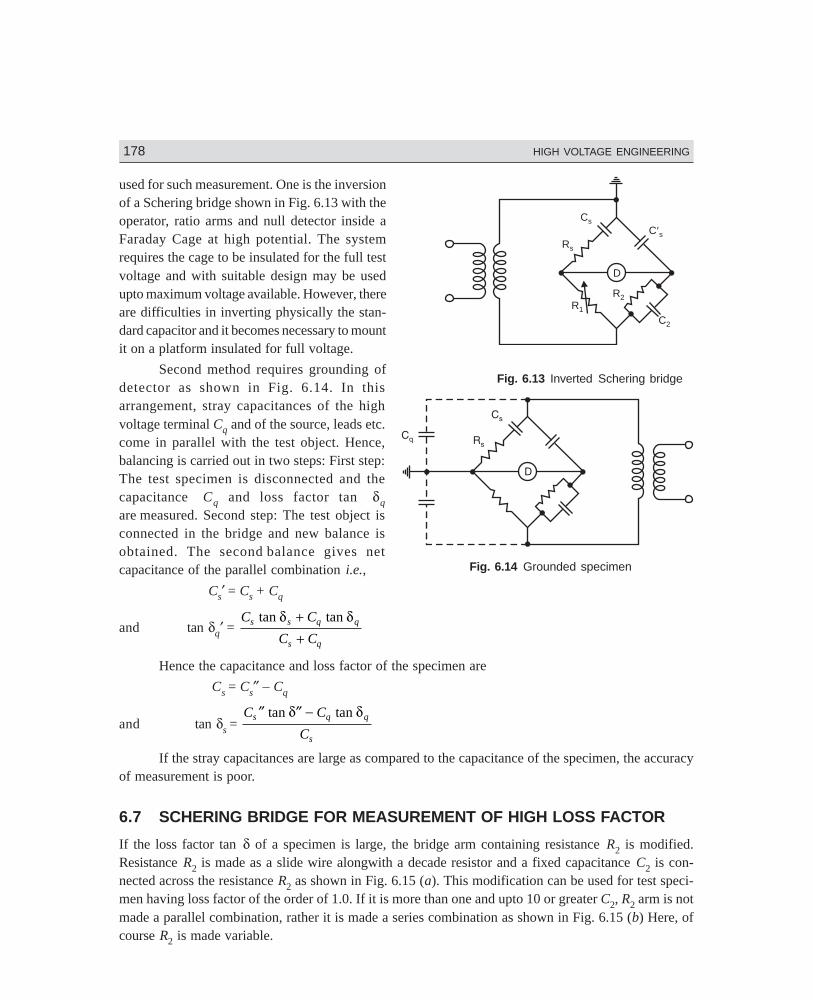
178 HIGH VOLTAGE ENGINEERING
Dharm\N-HIGH\HG6-1.PM5 178
C2
Cs
R2R1
Rs
C¢s
D
used for such measurement. One is the inversionof a Schering bridge shown in Fig. 6.13 with theoperator, ratio arms and null detector inside aFaraday Cage at high potential. The systemrequires the cage to be insulated for the full testvoltage and with suitable design may be usedupto maximum voltage available. However, thereare difficulties in inverting physically the stan-dard capacitor and it becomes necessary to mountit on a platform insulated for full voltage.
Second method requires grounding ofdetector as shown in Fig. 6.14. In thisarrangement, stray capacitances of the highvoltage terminal Cq and of the source, leads etc.come in parallel with the test object. Hence,balancing is carried out in two steps: First step:The test specimen is disconnected and thecapacitance Cq and loss factor tan δq
are measured. Second step: The test object isconnected in the bridge and new balance isobtained. The second balance gives netcapacitance of the parallel combination i.e.,
Cs′ = Cs + Cq
and tan δq′ = C C
C Cs s q q
s q
tan tanδ δ++
Hence the capacitance and loss factor of the specimen are
Cs = Cs″ – Cq
and tan δs =
C C
Cs q q
s
″ ″ −tan tanδ δ
If the stray capacitances are large as compared to the capacitance of the specimen, the accuracyof measurement is poor.
6.7 SCHERING BRIDGE FOR MEASUREMENT OF HIGH LOSS FACTOR
If the loss factor tan δ of a specimen is large, the bridge arm containing resistance R2 is modified.Resistance R2 is made as a slide wire alongwith a decade resistor and a fixed capacitance C2 is con-nected across the resistance R2 as shown in Fig. 6.15 (a). This modification can be used for test speci-men having loss factor of the order of 1.0. If it is more than one and upto 10 or greater C2, R2 arm is notmade a parallel combination, rather it is made a series combination as shown in Fig. 6.15 (b) Here, ofcourse R2 is made variable.
Fig. 6.13 Inverted Schering bridge
Fig. 6.14 Grounded specimen
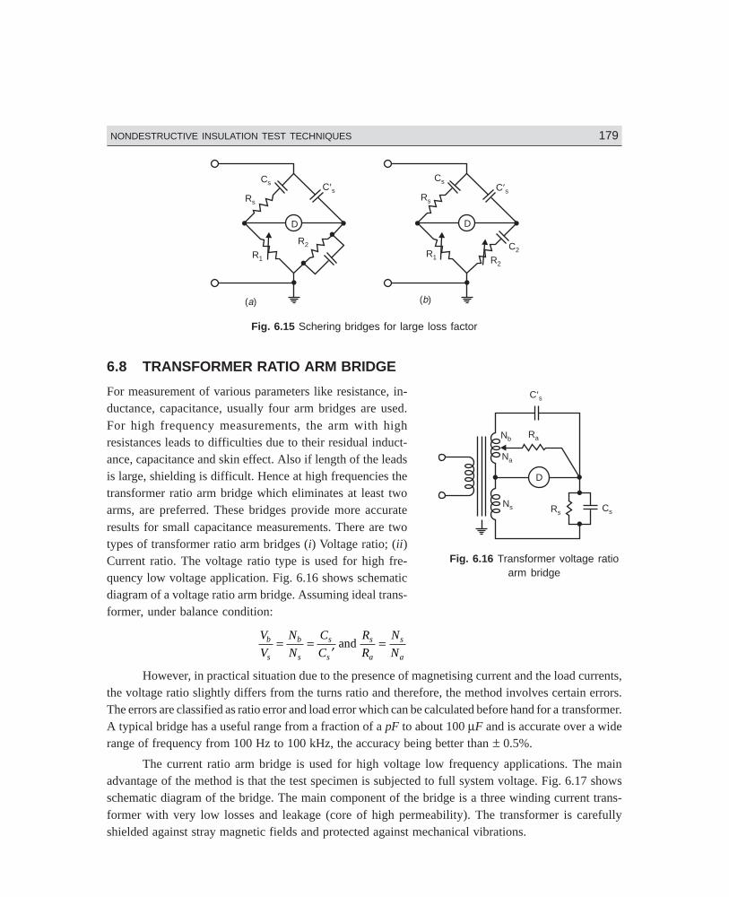
Dharm\N-HIGH\HG6-1.PM5 179
NONDESTRUCTIVE INSULATION TEST TECHNIQUES 179
Nb
Na
Ns
Ra
D
Rs Cs
C¢s
C2
Cs
R1 R2
Rs
C¢s
( )b
D
R2
R1
Rs
C¢s
D
( )a
Cs
Fig. 6.15 Schering bridges for large loss factor
6.8 TRANSFORMER RATIO ARM BRIDGE
For measurement of various parameters like resistance, in-ductance, capacitance, usually four arm bridges are used.For high frequency measurements, the arm with highresistances leads to difficulties due to their residual induct-ance, capacitance and skin effect. Also if length of the leadsis large, shielding is difficult. Hence at high frequencies thetransformer ratio arm bridge which eliminates at least twoarms, are preferred. These bridges provide more accurateresults for small capacitance measurements. There are twotypes of transformer ratio arm bridges (i) Voltage ratio; (ii)Current ratio. The voltage ratio type is used for high fre-quency low voltage application. Fig. 6.16 shows schematicdiagram of a voltage ratio arm bridge. Assuming ideal trans-former, under balance condition:
V
V
N
N
C
C
R
R
N
Nb
s
b
s
s
s
s
a
s
a
= =′
=and
However, in practical situation due to the presence of magnetising current and the load currents,the voltage ratio slightly differs from the turns ratio and therefore, the method involves certain errors.The errors are classified as ratio error and load error which can be calculated before hand for a transformer.A typical bridge has a useful range from a fraction of a pF to about 100 µF and is accurate over a widerange of frequency from 100 Hz to 100 kHz, the accuracy being better than ± 0.5%.
The current ratio arm bridge is used for high voltage low frequency applications. The mainadvantage of the method is that the test specimen is subjected to full system voltage. Fig. 6.17 showsschematic diagram of the bridge. The main component of the bridge is a three winding current trans-former with very low losses and leakage (core of high permeability). The transformer is carefullyshielded against stray magnetic fields and protected against mechanical vibrations.
Fig. 6.16 Transformer voltage ratioarm bridge
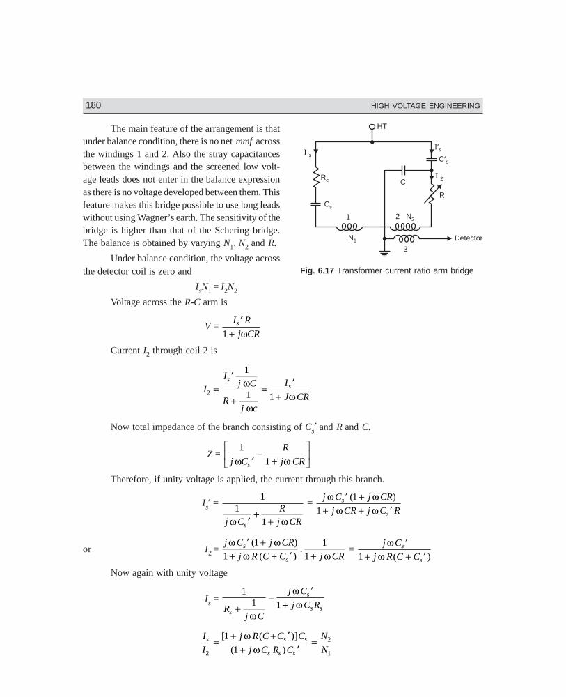
180 HIGH VOLTAGE ENGINEERING
Dharm\N-HIGH\HG6-1.PM5 180
HT
Rc
Cs
N2
R
1 2
3
C
N1
I¢sC¢s
I s
I 2
Detector
The main feature of the arrangement is thatunder balance condition, there is no net mmf acrossthe windings 1 and 2. Also the stray capacitancesbetween the windings and the screened low volt-age leads does not enter in the balance expressionas there is no voltage developed between them. Thisfeature makes this bridge possible to use long leadswithout using Wagner’s earth. The sensitivity of thebridge is higher than that of the Schering bridge.The balance is obtained by varying N1, N2 and R.
Under balance condition, the voltage acrossthe detector coil is zero and
IsN1 = I2N2
Voltage across the R-C arm is
V = I R
j CRs ′
+1 ω
Current I2 through coil 2 is
II
j C
Rj c
I
J CR
ss
2
1
1 1=
′
+=
′+
ω
ωω
Now total impedance of the branch consisting of Cs′ and R and C.
Z = 1
1j C
R
j CRsω ω′+
+LNM
OQP
Therefore, if unity voltage is applied, the current through this branch.
Is′ = 1
11j C
Rj CRsω ω′
++
= j C j CR
j CR j C Rs
s
ω ωω ω
′ ++ + ′
( )1
1
or I2 = j C j CR
j R C C j CRs
s
ω ωω ω′ +
+ + ′ +( )
( ).
1
1
1
1 =
j C
j R C Cs
s
ωω
′+ + ′1 ( )
Now again with unity voltage
Is = 1
1 1Rj C
j C
j C Rs
s
s s+=
′+
ω
ωω
I
I
j R C C C
j C R C
N
Ns s s
s s s2
2
1
1
1= + + ′
+ ′=[ ( )]
( )
ωω
Fig. 6.17 Transformer current ratio arm bridge
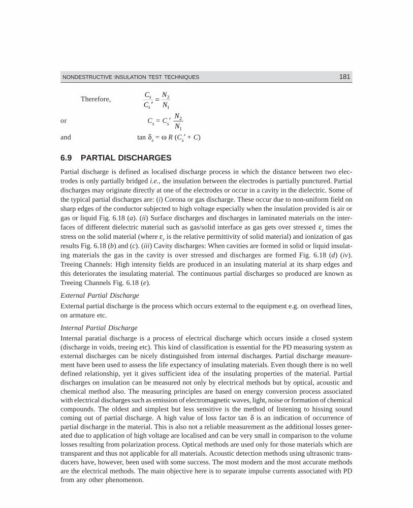
Dharm\N-HIGH\HG6-1.PM5 181
NONDESTRUCTIVE INSULATION TEST TECHNIQUES 181
Therefore, C
C
N
Ns
s ′= 2
1
or Cs = Cs′ N
N2
1
and tan δs = ω R (Cs′ + C)
6.9 PARTIAL DISCHARGES
Partial discharge is defined as localised discharge process in which the distance between two elec-trodes is only partially bridged i.e., the insulation between the electrodes is partially punctured. Partialdischarges may originate directly at one of the electrodes or occur in a cavity in the dielectric. Some ofthe typical partial discharges are: (i) Corona or gas discharge. These occur due to non-uniform field onsharp edges of the conductor subjected to high voltage especially when the insulation provided is air orgas or liquid Fig. 6.18 (a). (ii) Surface discharges and discharges in laminated materials on the inter-faces of different dielectric material such as gas/solid interface as gas gets over stressed εr times thestress on the solid material (where εr is the relative permittivity of solid material) and ionization of gasresults Fig. 6.18 (b) and (c). (iii) Cavity discharges: When cavities are formed in solid or liquid insulat-ing materials the gas in the cavity is over stressed and discharges are formed Fig. 6.18 (d) (iv).Treeing Channels: High intensity fields are produced in an insulating material at its sharp edges andthis deteriorates the insulating material. The continuous partial discharges so produced are known asTreeing Channels Fig. 6.18 (e).
External Partial Discharge
External partial discharge is the process which occurs external to the equipment e.g. on overhead lines,on armature etc.
Internal Partial Discharge
Internal paratial discharge is a process of electrical discharge which occurs inside a closed system(discharge in voids, treeing etc). This kind of classification is essential for the PD measuring system asexternal discharges can be nicely distinguished from internal discharges. Partial discharge measure-ment have been used to assess the life expectancy of insulating materials. Even though there is no welldefined relationship, yet it gives sufficient idea of the insulating properties of the material. Partialdischarges on insulation can be measured not only by electrical methods but by optical, acoustic andchemical method also. The measuring principles are based on energy conversion process associatedwith electrical discharges such as emission of electromagnetic waves, light, noise or formation of chemicalcompounds. The oldest and simplest but less sensitive is the method of listening to hissing soundcoming out of partial discharge. A high value of loss factor tan δ is an indication of occurrence ofpartial discharge in the material. This is also not a reliable measurement as the additional losses gener-ated due to application of high voltage are localised and can be very small in comparison to the volumelosses resulting from polarization process. Optical methods are used only for those materials which aretransparent and thus not applicable for all materials. Acoustic detection methods using ultrasonic trans-ducers have, however, been used with some success. The most modern and the most accurate methodsare the electrical methods. The main objective here is to separate impulse currents associated with PDfrom any other phenomenon.
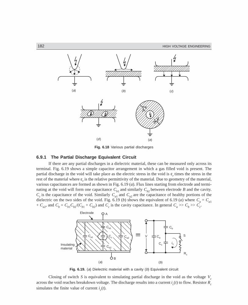
182 HIGH VOLTAGE ENGINEERING
Dharm\N-HIGH\HG6-1.PM5 182
( )a ( )b ( )c
( )d ( )e
Fig. 6.18 Various partial discharges
6.9.1 The Partial Discharge Equivalent CircuitIf there are any partial discharges in a dielectric material, these can be measured only across its
terminal. Fig. 6.19 shows a simple capacitor arrangement in which a gas filled void is present. Thepartial discharge in the void will take place as the electric stress in the void is εr times the stress in therest of the material where εr is the relative permittivity of the material. Due to geometry of the material,various capacitances are formed as shown in Fig. 6.19 (a). Flux lines starting from electrode and termi-nating at the void will form one capacitance Cb1 and similarly Cb2 between electrode B and the cavity.Cc is the capacitance of the void. Similarly Ca1 and Ca2 are the capacitance of healthy portions of thedielectric on the two sides of the void. Fig. 6.19 (b) shows the equivalent of 6.19 (a) where Ca = Ca1+ Ca2, and Cb = Cb1Cb2/(Cb1 + Cb2) and Cc is the cavity capacitance. In general Ca >> Cb >> Cc.
Electrode
Insulatingmaterial
A
( )a ( )b
B
SV
Cb
Ca
Cc
Cb1
Cb2
Ca1 Ca2
ic
Rc
Cc
Fig. 6.19. (a) Dielectric material with a cavity (b) Equivalent circuit
Closing of switch S is equivalent to simulating partial discharge in the void as the voltage Vcacross the void reaches breakdown voltage. The discharge results into a current ic(t) to flow. Resistor Rc
simulates the finite value of current ic(t).
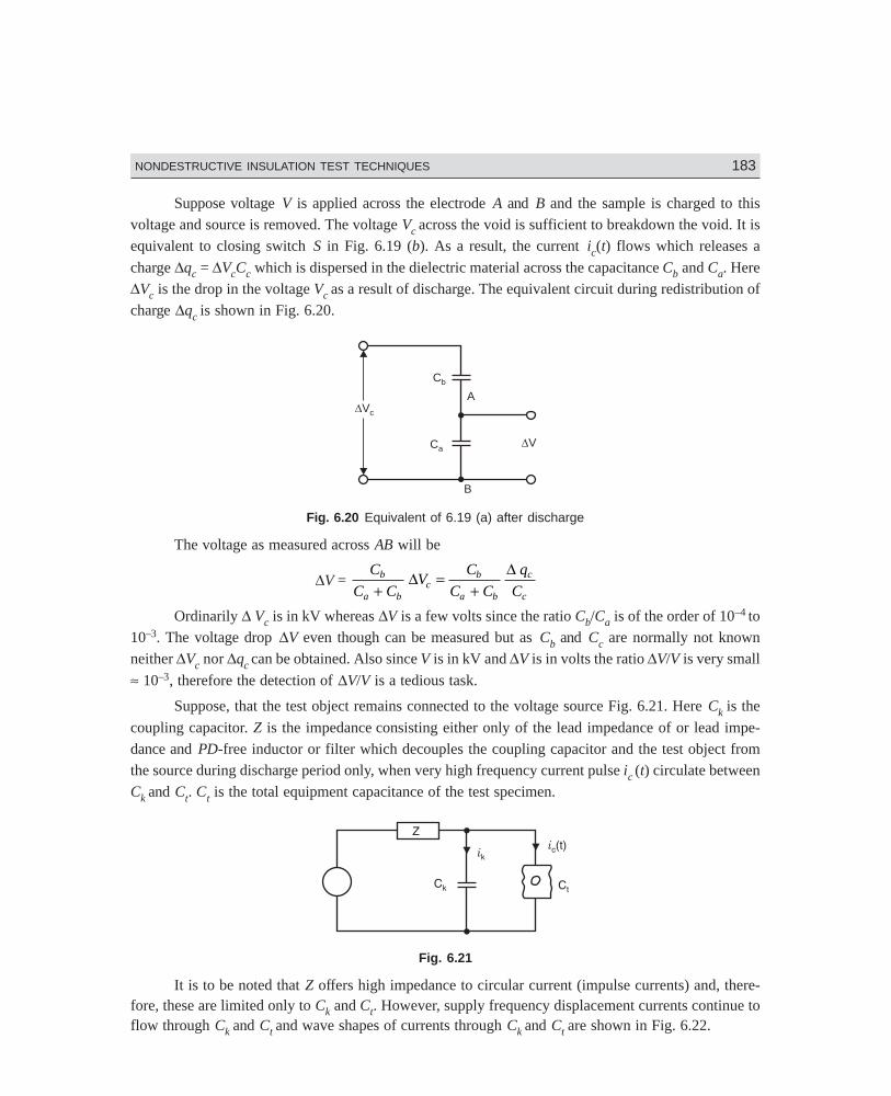
Dharm\N-HIGH\HG6-1.PM5 183
NONDESTRUCTIVE INSULATION TEST TECHNIQUES 183
Suppose voltage V is applied across the electrode A and B and the sample is charged to thisvoltage and source is removed. The voltage Vc across the void is sufficient to breakdown the void. It isequivalent to closing switch S in Fig. 6.19 (b). As a result, the current ic(t) flows which releases a
charge ∆qc = ∆VcCc which is dispersed in the dielectric material across the capacitance Cb and Ca. Here∆Vc is the drop in the voltage Vc as a result of discharge. The equivalent circuit during redistribution ofcharge ∆qc is shown in Fig. 6.20.
Cb
Ca
DVc
DV
A
B
Fig. 6.20 Equivalent of 6.19 (a) after discharge
The voltage as measured across AB will be
∆V = C
C CV
C
C C
q
Cb
a bc
b
a b
c
c+=
+∆ ∆
Ordinarily ∆ Vc is in kV whereas ∆V is a few volts since the ratio Cb/Ca is of the order of 10–4 to10–3. The voltage drop ∆V even though can be measured but as Cb and Cc are normally not knownneither ∆Vc nor ∆qc can be obtained. Also since V is in kV and ∆V is in volts the ratio ∆V/V is very small
≈ 10–3, therefore the detection of ∆V/V is a tedious task.
Suppose, that the test object remains connected to the voltage source Fig. 6.21. Here Ck is the
coupling capacitor. Z is the impedance consisting either only of the lead impedance of or lead impe-dance and PD-free inductor or filter which decouples the coupling capacitor and the test object fromthe source during discharge period only, when very high frequency current pulse ic (t) circulate betweenCk and Ct. Ct is the total equipment capacitance of the test specimen.
Fig. 6.21
It is to be noted that Z offers high impedance to circular current (impulse currents) and, there-fore, these are limited only to Ck and Ct. However, supply frequency displacement currents continue toflow through Ck and Ct and wave shapes of currents through Ck and Ct are shown in Fig. 6.22.
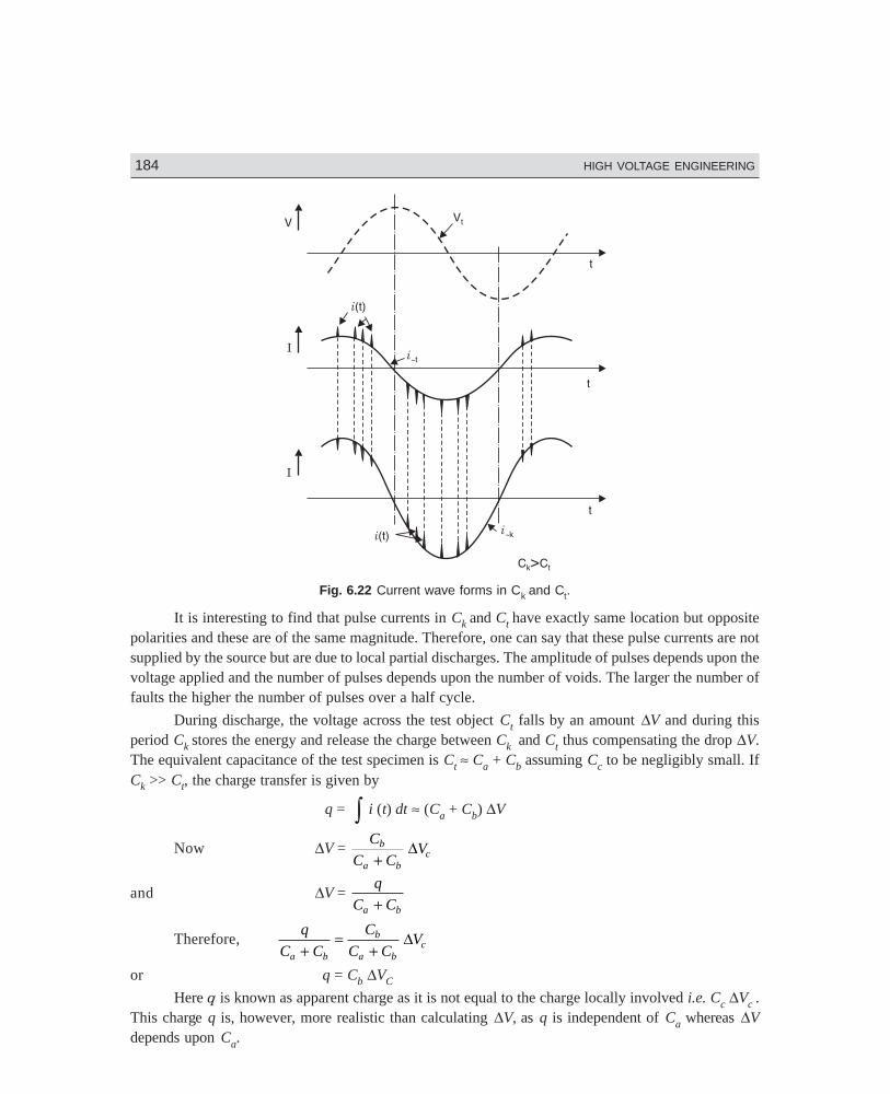
184 HIGH VOLTAGE ENGINEERING
Dharm\N-HIGH\HG6-1.PM5 184
Fig. 6.22 Current wave forms in Ck and Ct.
It is interesting to find that pulse currents in Ck and Ct have exactly same location but oppositepolarities and these are of the same magnitude. Therefore, one can say that these pulse currents are notsupplied by the source but are due to local partial discharges. The amplitude of pulses depends upon thevoltage applied and the number of pulses depends upon the number of voids. The larger the number offaults the higher the number of pulses over a half cycle.
During discharge, the voltage across the test object Ct falls by an amount ∆V and during thisperiod Ck stores the energy and release the charge between Ck and Ct thus compensating the drop ∆V.The equivalent capacitance of the test specimen is Ct ≈ Ca + Cb assuming Cc to be negligibly small. IfCk >> Ct, the charge transfer is given by
q = z i (t) dt ≈ (Ca + Cb) ∆V
Now ∆V = C
C CVb
a bc+
∆
and ∆V = q
C Ca b+
Therefore,q
C C
C
C CV
a b
b
a bc+
=+
∆
or q = Cb ∆VC
Here q is known as apparent charge as it is not equal to the charge locally involved i.e. Cc ∆Vc .This charge q is, however, more realistic than calculating ∆V, as q is independent of Ca whereas ∆Vdepends upon Ca.
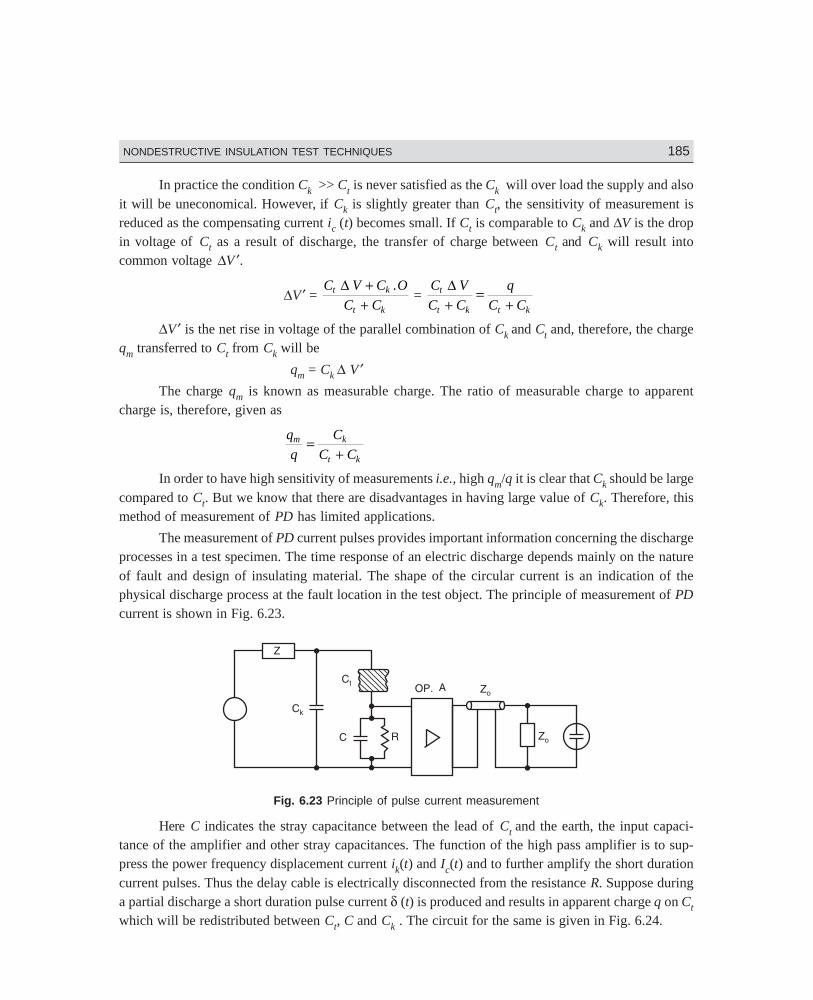
Dharm\N-HIGH\HG6-1.PM5 185
NONDESTRUCTIVE INSULATION TEST TECHNIQUES 185
In practice the condition Ck >> Ct is never satisfied as the Ck will over load the supply and alsoit will be uneconomical. However, if Ck is slightly greater than Ct, the sensitivity of measurement isreduced as the compensating current ic (t) becomes small. If Ct is comparable to Ck and ∆V is the dropin voltage of Ct as a result of discharge, the transfer of charge between Ct and Ck will result intocommon voltage ∆V ′.
∆V ′ = C V C O
C Ct k
t k
∆ ++
. =
C V
C C
q
C Ct
t k t k
∆+
=+
∆V ′ is the net rise in voltage of the parallel combination of Ck and Ct and, therefore, the chargeqm transferred to Ct from Ck will be
qm = Ck ∆ V ′The charge qm is known as measurable charge. The ratio of measurable charge to apparent
charge is, therefore, given as
q
q
C
C Cm k
t k
=+
In order to have high sensitivity of measurements i.e., high qm/q it is clear that Ck should be largecompared to Ct. But we know that there are disadvantages in having large value of Ck. Therefore, thismethod of measurement of PD has limited applications.
The measurement of PD current pulses provides important information concerning the dischargeprocesses in a test specimen. The time response of an electric discharge depends mainly on the natureof fault and design of insulating material. The shape of the circular current is an indication of thephysical discharge process at the fault location in the test object. The principle of measurement of PDcurrent is shown in Fig. 6.23.
Fig. 6.23 Principle of pulse current measurement
Here C indicates the stray capacitance between the lead of Ct and the earth, the input capaci-tance of the amplifier and other stray capacitances. The function of the high pass amplifier is to sup-press the power frequency displacement current ik(t) and Ic(t) and to further amplify the short durationcurrent pulses. Thus the delay cable is electrically disconnected from the resistance R. Suppose duringa partial discharge a short duration pulse current δ (t) is produced and results in apparent charge q on Ct
which will be redistributed between Ct, C and Ck . The circuit for the same is given in Fig. 6.24.
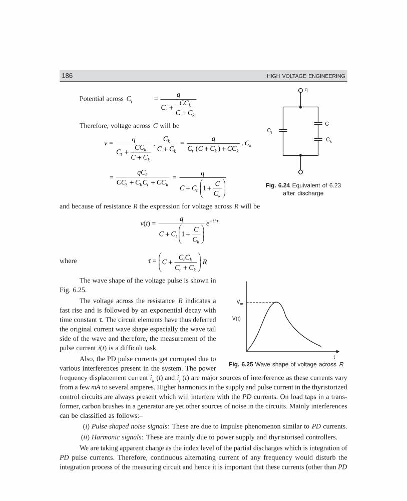
186 HIGH VOLTAGE ENGINEERING
Dharm\N-HIGH\HG6-1.PM5 186
Potential across Ct = q
CCC
C Ctk
k
++
Therefore, voltage across C will be
v = q
CCC
C C
C
C Ct
k
k
k
k++
+. =
q
C C C CCC
t k kk( )
.+ +
= qC
CC C C CCk
t k t k+ + =
q
C CC
Ctk
+ +FHG
IKJ1
and because of resistance R the expression for voltage across R will be
v(t) = q
C CC
C
e
tk
t
+ +FHG
IKJ
−
1
/ τ
where τ = CC C
C CRt k
t k
++
FHG
IKJ
The wave shape of the voltage pulse is shown inFig. 6.25.
The voltage across the resistance R indicates afast rise and is followed by an exponential decay withtime constant τ. The circuit elements have thus deferredthe original current wave shape especially the wave tailside of the wave and therefore, the measurement of thepulse current i(t) is a difficult task.
Also, the PD pulse currents get corrupted due tovarious interferences present in the system. The powerfrequency displacement current ik (t) and it (t) are major sources of interference as these currents varyfrom a few mA to several amperes. Higher harmonics in the supply and pulse current in the thyristorizedcontrol circuits are always present which will interfere with the PD currents. On load taps in a trans-former, carbon brushes in a generator are yet other sources of noise in the circuits. Mainly interferencescan be classified as follows:–
(i) Pulse shaped noise signals: These are due to impulse phenomenon similar to PD currents.
(ii) Harmonic signals: These are mainly due to power supply and thyristorised controllers.
We are taking apparent charge as the index level of the partial discharges which is integration ofPD pulse currents. Therefore, continuous alternating current of any frequency would disturb theintegration process of the measuring circuit and hence it is important that these currents (other than PD
Fig. 6.24 Equivalent of 6.23after discharge
Fig. 6.25 Wave shape of voltage across R
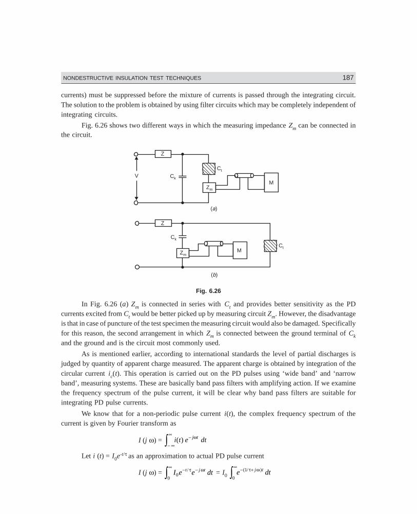
Dharm\N-HIGH\HG6-1.PM5 187
NONDESTRUCTIVE INSULATION TEST TECHNIQUES 187
currents) must be suppressed before the mixture of currents is passed through the integrating circuit.The solution to the problem is obtained by using filter circuits which may be completely independent ofintegrating circuits.
Fig. 6.26 shows two different ways in which the measuring impedance Zm can be connected inthe circuit.
( )a
( )b
Z
Ck
M
Ct
Z
Zm
MV
Ck
Ct
Zm
Fig. 6.26
In Fig. 6.26 (a) Zm is connected in series with Ct and provides better sensitivity as the PDcurrents excited from Ct would be better picked up by measuring circuit Zm. However, the disadvantageis that in case of puncture of the test specimen the measuring circuit would also be damaged. Specificallyfor this reason, the second arrangement in which Zm is connected between the ground terminal of Ck
and the ground and is the circuit most commonly used.
As is mentioned earlier, according to international standards the level of partial discharges isjudged by quantity of apparent charge measured. The apparent charge is obtained by integration of thecircular current ic(t). This operation is carried out on the PD pulses using ‘wide band’ and ‘narrowband’, measuring systems. These are basically band pass filters with amplifying action. If we examinethe frequency spectrum of the pulse current, it will be clear why band pass filters are suitable forintegrating PD pulse currents.
We know that for a non-periodic pulse current i(t), the complex frequency spectrum of thecurrent is given by Fourier transform as
I (j ω) = − ∞
∞ −z i t e dtj t( ) ω
Let i (t) = I0e-t/τ as an approximation to actual PD pulse current
I (j ω) = I e e dtt j t0
0
− −∞z / τ ω = I0 0
1∞ − +z e dtj t( / )τ ω
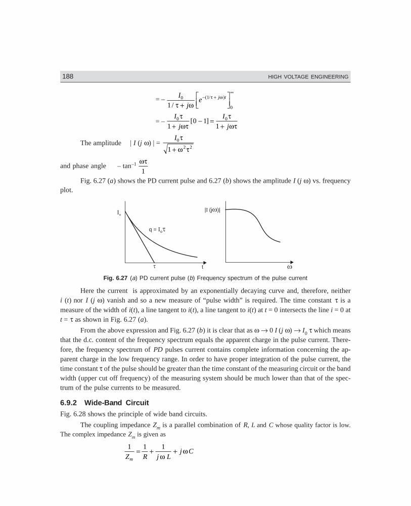
188 HIGH VOLTAGE ENGINEERING
Dharm\N-HIGH\HG6-2.PM5 188
= – I
je j t0 1
01 /( / )
τ ωτ ω
+LNM
OQP
− +∞
= – I
j
I
j0 0
10 1
1
τωτ
τωτ+
− =+
[ ]
The amplitude | I (j ω) | = I0
2 21
τ
ω τ+
and phase angle – tan–1 ωτ1
Fig. 6.27 (a) shows the PD current pulse and 6.27 (b) shows the amplitude I (j ω) vs. frequencyplot.
Io
q = Iot
t t w
| (j )|I w
Fig. 6.27 (a) PD current pulse (b) Frequency spectrum of the pulse current
Here the current is approximated by an exponentially decaying curve and, therefore, neitheri (t) nor I (j ω) vanish and so a new measure of “pulse width” is required. The time constant τ is ameasure of the width of i(t), a line tangent to i(t), a line tangent to i(t) at t = 0 intersects the line i = 0 att = τ as shown in Fig. 6.27 (a).
From the above expression and Fig. 6.27 (b) it is clear that as ω → 0 I (j ω) → I0 τ which meansthat the d.c. content of the frequency spectrum equals the apparent charge in the pulse current. There-fore, the frequency spectrum of PD pulses current contains complete information concerning the ap-parent charge in the low frequency range. In order to have proper integration of the pulse current, thetime constant τ of the pulse should be greater than the time constant of the measuring circuit or the bandwidth (upper cut off frequency) of the measuring system should be much lower than that of the spec-trum of the pulse currents to be measured.
6.9.2 Wide-Band CircuitFig. 6.28 shows the principle of wide band circuits.
The coupling impedance Zm is a parallel combination of R, L and C whose quality factor is low.The complex impedance Zm is given as
1 1 1
Z R j Lj C
m
= + +ω
ω
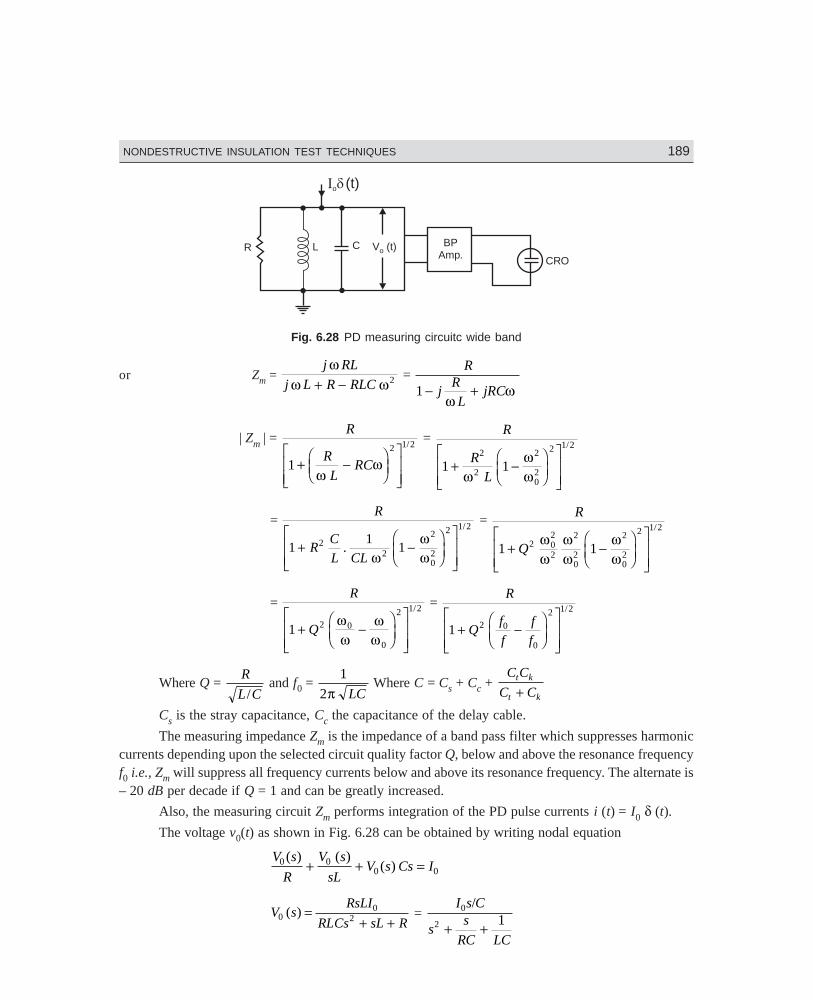
Dharm\N-HIGH\HG6-2.PM5 189
NONDESTRUCTIVE INSULATION TEST TECHNIQUES 189
R L C BPAmp. CRO
I do (t)
V (t)o
Fig. 6.28 PD measuring circuitc wide band
or Zm = j RL
j L R RLC
ωω ω+ − 2 =
R
jRL
jRC1 − +ω
ω
| Zm | = R
R
LRC1
2 1 2
+ −FHG
IKJ
LNMM
OQPPω
ω/ =
R
RL
1 12
2
2
02
2 1 2
+ −FHG
IKJ
LNMM
OQPPω
ωω
/
= R
RC
L CL1
112
2
2
02
2 1 2
+ −FHG
IKJ
LNMM
OQPP.
/
ωωω
= R
Q1 12 02
2
2
02
2
02
2 1 2
+ −FHG
IKJ
LNMM
OQPP
ωω
ωω
ωω
/
= R
Q1 2 0
0
2 1 2
+ −FHG
IKJ
LNMM
OQPP
ωω
ωω
/ = R
Qf
f
f
f1 2 0
0
2 1 2
+ −FHG
IKJ
LNMM
OQPP
/
Where Q = R
L C/ and f0 =
1
2π LC Where C = Cs + Cc +
C C
C Ct k
t k+
Cs is the stray capacitance, Cc the capacitance of the delay cable.
The measuring impedance Zm is the impedance of a band pass filter which suppresses harmoniccurrents depending upon the selected circuit quality factor Q, below and above the resonance frequencyf0 i.e., Zm will suppress all frequency currents below and above its resonance frequency. The alternate is– 20 dB per decade if Q = 1 and can be greatly increased.
Also, the measuring circuit Zm performs integration of the PD pulse currents i (t) = I0 δ (t).
The voltage v0(t) as shown in Fig. 6.28 can be obtained by writing nodal equation
V s
R
V s
sLV s Cs I0 0
0 0( ) ( )
( )+ + =
V sRsLI
RLCs sL R0
02( ) =
+ + =
I s C
ss
RC LC
0
2 1/
+ +
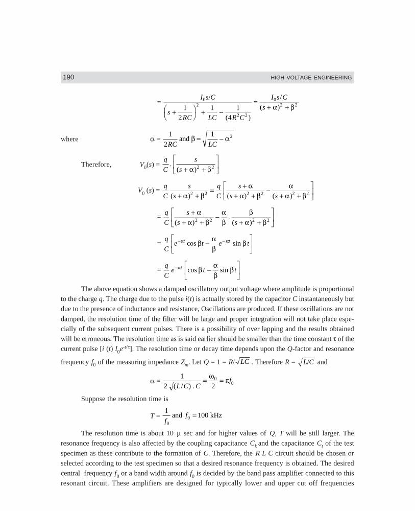
190 HIGH VOLTAGE ENGINEERING
Dharm\N-HIGH\HG6-2.PM5 190
= I s C
sRC LC R C
I s C
s0
2
2 2
02 21
2
1 1
4
/
( )
/
( )+F
HIK + −
=+ +α β
where α = 1
2
1 2
RC LCand β α= −
Therefore, V0(s) = q
C
s
s.
( )+ +LNM
OQPα β2 2
V0 (s) = q
C
s
s
q
C
s
s s( ) ( ) ( )+ += +
+ +−
+ +LNM
OQPα β
αα β
αα β2 2 2 2 2 2
= q
C
s
s s
++ +
−+ +
LNM
OQP
αα β
αβ
βα β( )
.( )2 2 2 2
= q
Ce t e tt t− −−LNM
OQP
α αβ αβ
βcos sin
= q
Ce t tt− −
LNM
OQP
α β αβ
βcos sin
The above equation shows a damped oscillatory output voltage where amplitude is proportionalto the charge q. The charge due to the pulse i(t) is actually stored by the capacitor C instantaneously butdue to the presence of inductance and resistance, Oscillations are produced. If these oscillations are not
damped, the resolution time of the filter will be large and proper integration will not take place espe-cially of the subsequent current pulses. There is a possibility of over lapping and the results obtainedwill be erroneous. The resolution time as is said earlier should be smaller than the time constant τ of thecurrent pulse [i (t) I0e-t/τ]. The resolution time or decay time depends upon the Q-factor and resonance
frequency f0 of the measuring impedance Zm. Let Q = 1 = R/ LC . Therefore R = L C/ and
α = 1
2 20
0( / ) .L C Cf= =ω π
Suppose the resolution time is
T = 1
1000
0ffand kHz=
The resolution time is about 10 µ sec and for higher values of Q, T will be still larger. Theresonance frequency is also affected by the coupling capacitance Ck and the capacitance Ct of the test
specimen as these contribute to the formation of C. Therefore, the R L C circuit should be chosen orselected according to the test specimen so that a desired resonance frequency is obtained. The desiredcentral frequency f0 or a band width around f0 is decided by the band pass amplifier connected to thisresonant circuit. These amplifiers are designed for typically lower and upper cut off frequencies
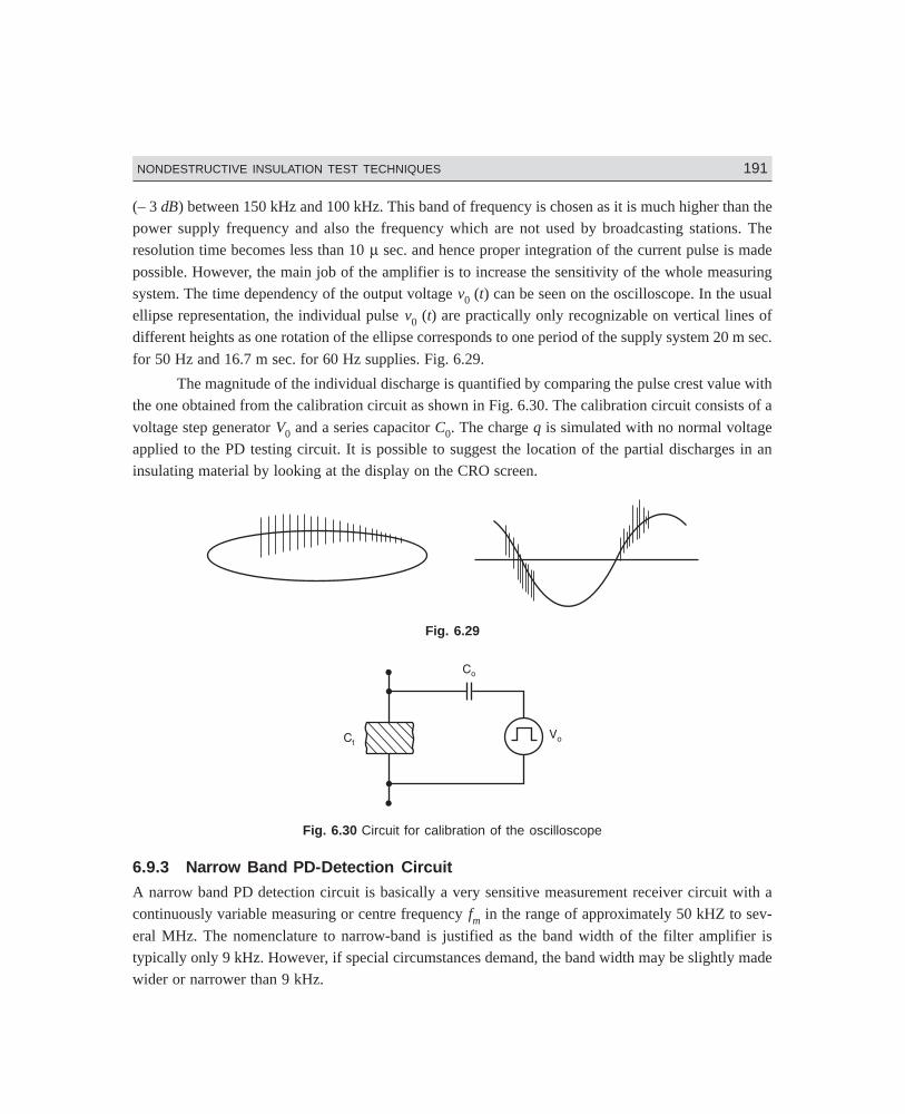
Dharm\N-HIGH\HG6-2.PM5 191
NONDESTRUCTIVE INSULATION TEST TECHNIQUES 191
(– 3 dB) between 150 kHz and 100 kHz. This band of frequency is chosen as it is much higher than thepower supply frequency and also the frequency which are not used by broadcasting stations. Theresolution time becomes less than 10 µ sec. and hence proper integration of the current pulse is made
possible. However, the main job of the amplifier is to increase the sensitivity of the whole measuringsystem. The time dependency of the output voltage v0 (t) can be seen on the oscilloscope. In the usualellipse representation, the individual pulse v0 (t) are practically only recognizable on vertical lines ofdifferent heights as one rotation of the ellipse corresponds to one period of the supply system 20 m sec.
for 50 Hz and 16.7 m sec. for 60 Hz supplies. Fig. 6.29.
The magnitude of the individual discharge is quantified by comparing the pulse crest value withthe one obtained from the calibration circuit as shown in Fig. 6.30. The calibration circuit consists of a
voltage step generator V0 and a series capacitor C0. The charge q is simulated with no normal voltageapplied to the PD testing circuit. It is possible to suggest the location of the partial discharges in aninsulating material by looking at the display on the CRO screen.
Fig. 6.29
Fig. 6.30 Circuit for calibration of the oscilloscope
6.9.3 Narrow Band PD-Detection Circuit
A narrow band PD detection circuit is basically a very sensitive measurement receiver circuit with acontinuously variable measuring or centre frequency fm in the range of approximately 50 kHZ to sev-
eral MHz. The nomenclature to narrow-band is justified as the band width of the filter amplifier istypically only 9 kHz. However, if special circumstances demand, the band width may be slightly madewider or narrower than 9 kHz.
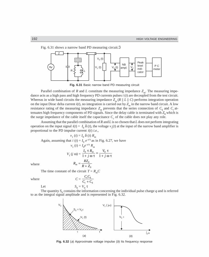
192 HIGH VOLTAGE ENGINEERING
Dharm\N-HIGH\HG6-2.PM5 192
Fig. 6.31 shows a narrow band PD measuring circuit.ℑZ
R LV (t)1
V (t)0
V (t)2
NBampl.
Peaklevelindi-cator
V2P C
meter
Fig. 6.31 Basic narrow band PD measuring circuit
Parallel combination of R and L constitute the measuring impedance Zm. The measuring impe-dance acts as a high pass and high frequency PD currents pulses i (t) are decoupled from the test circuit.Whereas in wide band circuits the measuring impedance Zm (R || L || C) performs integration operationon the input Dirac delta current i(t), no integration is carried out by Zm in the narrow band circuit. A lowresistance rating of the measuring impedance Zm prevents that the series connection of Ck and Ct at-tenuates high frequency components of PD signals. Since the delay cable is terminated with Z0 which isthe surge impedance of the cable itself the capacitance Cc of the cable does not play any role.
Assuming that the parallel combination of R and L is so chosen that L does not perform integratingoperation on the input signal i(t) = I0 δ (t), the voltage v1(t) at the input of the narrow band amplifier isproportional to the PD impulse current i(t) i.e.,
v1 (t) = I0 δ (t) Rm
Again, assuming that i (t) = I0 e–t/τ as in Fig. 6.27, we have
v1 (t) = I0e–t/τ Rm
V1 (j ω) = I R
j
V
jm0 0
1 1
τω τ
τω τ+
=+
where RRZ
R Zm =+
0
0
The time constant of the circuit T = RmC
where C = C C
C Ct k
t k+Let S0 = V0 τThe quantity S0 contains the information concerning the individual pulse charge q and is referred
to as the integral signal amplitude and is represented in Fig. 6.32.
V0
( )a
S = V0 0t
tt
V (t)1
( )b
V ( j )1 w
V0 t
ò wn
Fig. 6.32 (a) Approximate voltage impulse (b) Its frequency response
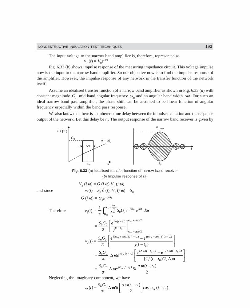
Dharm\N-HIGH\HG6-2.PM5 193
NONDESTRUCTIVE INSULATION TEST TECHNIQUES 193
The input voltage to the narrow band amplifier is, therefore, represented as v1 (t) = V0e–t/τ
Fig. 6.32 (b) shows impulse response of the measuring impedance circuit. This voltage impulsenow is the input to the narrow band amplifier. So our objective now is to find the impulse response ofthe amplifier. However, the impulse response of any network is the transfer function of the networkitself.
Assume an idealised transfer function of a narrow band amplifier as shown in Fig. 6.33 (a) withconstant magnitude G0, mid band angular frequency ωm and an angular band width ∆ω. For such anideal narrow band pass amplifier, the phase shift can be assumed to be linear function of angularfrequency especially within the band pass response.
We also know that there is an inherent time delay between the impulse excitation and the responseoutput of the network. Let this delay be t0. The output response of the narrow band receiver is given by
Dw
G0
G ( j )w
f w= t0
wm w
V2 max
t
t0
Fig. 6.33 (a) Idealised transfer function of narrow band receiver
(b) Impulse response of (a)
V2 (j ω) = G (j ω) V1 (j ω)
and since v1(t) = S0 δ (t); V1 (j ω) = S0
G (j ω) = G e j t0
0− ω
Therefore v2(t) = 1
0 0
2
2 0
πωω ω
ω ω
ω ω
S G e e dj t j t
m
m −
−
+z ∆
∆
= S G e
j
j t t
t t
m
m
0 0
2
20
0π
ω
ω
ω( )
( )/
/−
−−
+LNM
OQP ∆ω
∆ω
v2(t) = S G e e
j t t
j t t j t tm m0 0
2 2
0
0 0
π
ω ω ω ω( / ) ( ) ( / ) ( )
( )
+ − − −−−
LNM
OQP
∆ ∆
= S G
ee e
j t tj t t
j t t j t tm0 0
2 2
0
00 0
2 2πω
ωω
ω ω
.[ ( )/ ]
( )( )/ ( )/
∆∆
∆ ∆−
− − −−−
LNM
OQP
= S G
e Sit tj t tm0 0 00
2πω
ωω∆∆( ) ( )− −
Neglecting the imaginary component, we have
v tS G
Sit t
t tm20 0 0
02( )
( )cos ( )= −L
NMOQP −
πω ω ω∆ ∆
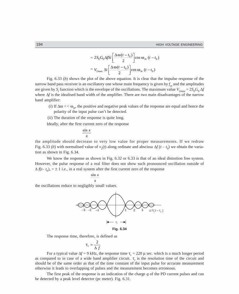
194 HIGH VOLTAGE ENGINEERING
Dharm\N-HIGH\HG6-2.PM5 194
= 220 0
00S G fSi
t tt tm∆ ∆ω ω( )
cos ( )−L
NMOQP −
= V Sit t
t tm20
02max( )
cos ( )∆ ω ω−LNM
OQP −
Fig. 6.33 (b) shows the plot of the above equation. It is clear that the impulse response of thenarrow band pass receiver is an oscillatory one whose main frequency is given by fm and the amplitudesare given by Si function which is the envelope of the oscillations. The maximum value V2max = 2S0G0 ∆fwhere ∆f is the idealised band width of the amplifier. There are two main disadvantages of the narrowband amplifier:
(i) If ∆ω << ωm, the positive and negative peak values of the response are equal and hence thepolarity of the input pulse can’t be detected.
(ii) The duration of the response is quite long.
Ideally, after the first current zero of the response
sin x
xthe amplitude should decrease to very low value for proper measurements. If we redrawFig. 6.33 (b) with normalised value of v2(t) along ordinate and abscissa ∆f (t – t0) we obtain the varia-tion as shown in Fig. 6.34.
We know the response as shown in Fig. 6.32 or 6.33 is that of an ideal distortion free system.However, the pulse response of a real filter does not show such pronounced oscillation outside of∆ f(t– t0), = ± 1 i.e., in a real system after the first current zero of the response
sin x
xthe oscillations reduce to negligibly small values.
1 2 3–1–2–3
tr
D f ( t t )o–
Fig. 6.34
The response time, therefore, is defined as
τr f= 2
∆For a typical value ∆f = 9 kHz, the response time τr = 220 µ sec. which is a much longer period
as compared to in case of a wide band amplifier circuit. τr is the resolution time of the circuit andshould be of the same order as that of the time constant of the input pulse for accurate measurementotherwise it leads to overlapping of pulses and the measurement becomes erroneous.
The first peak of the response is an indication of the charge q of the PD current pulses and canbe detected by a peak level detector (pc meter). Fig. 6.31.
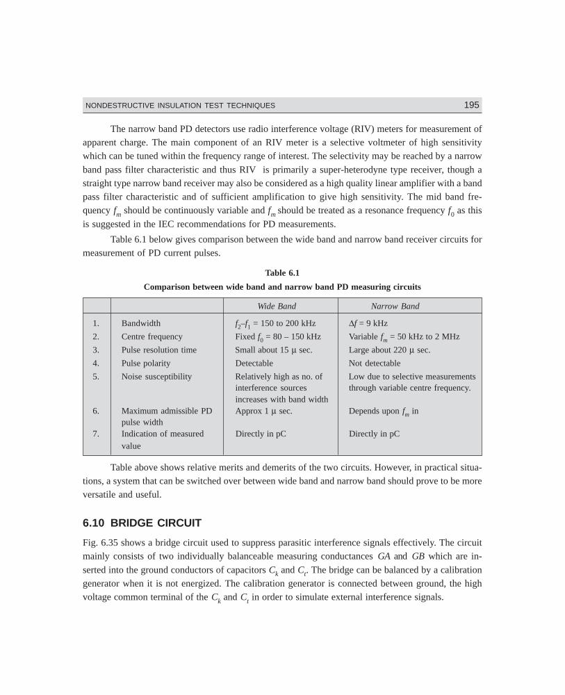
Dharm\N-HIGH\HG6-2.PM5 195
NONDESTRUCTIVE INSULATION TEST TECHNIQUES 195
The narrow band PD detectors use radio interference voltage (RIV) meters for measurement ofapparent charge. The main component of an RIV meter is a selective voltmeter of high sensitivitywhich can be tuned within the frequency range of interest. The selectivity may be reached by a narrow
band pass filter characteristic and thus RIV is primarily a super-heterodyne type receiver, though astraight type narrow band receiver may also be considered as a high quality linear amplifier with a bandpass filter characteristic and of sufficient amplification to give high sensitivity. The mid band fre-quency fm should be continuously variable and fm should be treated as a resonance frequency f0 as this
is suggested in the IEC recommendations for PD measurements.
Table 6.1 below gives comparison between the wide band and narrow band receiver circuits formeasurement of PD current pulses.
Table 6.1
Comparison between wide band and narrow band PD measuring circuits
Wide Band Narrow Band
1. Bandwidth f2–f1 = 150 to 200 kHz ∆f = 9 kHz
2. Centre frequency Fixed f0 = 80 – 150 kHz Variable fm = 50 kHz to 2 MHz
3. Pulse resolution time Small about 15 µ sec. Large about 220 µ sec.
4. Pulse polarity Detectable Not detectable
5. Noise susceptibility Relatively high as no. of Low due to selective measurementsinterference sources through variable centre frequency.increases with band width
6. Maximum admissible PD Approx 1 µ sec. Depends upon fm inpulse width
7. Indication of measured Directly in pC Directly in pCvalue
Table above shows relative merits and demerits of the two circuits. However, in practical situa-tions, a system that can be switched over between wide band and narrow band should prove to be moreversatile and useful.
6.10 BRIDGE CIRCUIT
Fig. 6.35 shows a bridge circuit used to suppress parasitic interference signals effectively. The circuitmainly consists of two individually balanceable measuring conductances GA and GB which are in-
serted into the ground conductors of capacitors Ck and Ct. The bridge can be balanced by a calibrationgenerator when it is not energized. The calibration generator is connected between ground, the highvoltage common terminal of the Ck and Ct in order to simulate external interference signals.
196 HIGH VOLTAGE ENGINEERING
Dharm\N-HIGH\HG6-2.PM5 196
Fig. 6.35 Basic principle of bridge circuit
The setting of the conductances GA and GB for balance depends upon the capacitances Ck andCt. However, in order to have high sensitivity of the bridge, the conductances should be as low aspossible. The practical limit is given by the current carrying capacity of the individual components inthe bridge arms GA and GB. If the conductances are not of proper value, the current pulses are so long(τ = Ck/GA = Ct/GB) that these would involve errors in measurements. Sometimes the instructionmanual suggests suitable values of GA and GB for the purpose.
If VA and VB are of the same magnitude and having the same polarity, the measuring instrumentshows zero deflection. When an external signal occurs, this will induce same current-I in both thecircuit branches which in turn would cause same voltage drops across GA and GB and hence themeasuring instruments would read zero. However, if there is partial discharge in Ct, circular current i(t)will flow and the polarity of VA and VB will now be opposed and the differential voltage VAB will beindicated by the meter. The measuring instrument can be of either wide band or narrow band type. Withthis circuit, it is possible to obtain interference suppression factors varying from 1:20 to 1:1000 dependingupon the construction of capacitances Ct and Ck and the type of source of interference. If the capacitancesCt and Ck are identical, interference suppression factors of 1:1000 can be achieved as the entirearrangement is then symmetrical. The test object should be placed close to each other so that theinterference effect is identical. Under highly unfavourable condition e.g. PD testing of outdoor switchgear where an ambient noise level exists because of corona discharges and radio interferences, theeffective interference suppression factors may be only around 1: 20. Also if the values of Ct and Ckdiffer materially, lower interference suppression factor is then expected as the bridge will have to bebalanced over a large frequency range and the bridge has then less accuracy of measurement. However,the narrow band measuring system makes it possible to measure with a variable centre frequency atwhich the bridge circuit achieves maximum interference suppression.
6.11 OSCILLOSCOPE AS PD MEASURING DEVICE
Oscilloscope is an integral and indispensable component of a PD measuring system. An indicatingmeter e.g. a pC meter and RIV meter can give quantity of charge, whether the charge is as a result ofpartial discharge or due to external interferences, cannot be estimated. This problem can be solved onlyif the output wave form is studied on the Oscilloscope. Whether the origin of the discharges is fromwithin the test object or not, can frequently be determined based on the typical patterns. If it is ascer-tained from the patterns that the discharge is from the test object, the magnitude of the apparent chargeshould be measured with pC meters or RIV meters. The peak value of the integrated pulse current is the
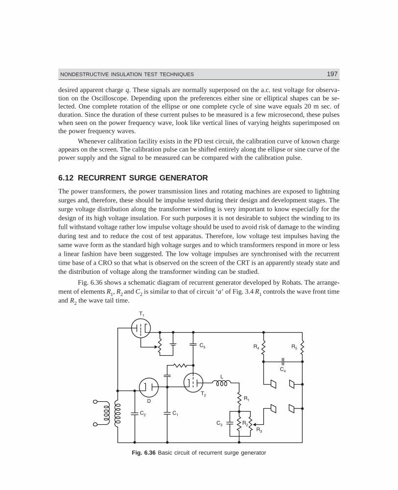
Dharm\N-HIGH\HG6-2.PM5 197
NONDESTRUCTIVE INSULATION TEST TECHNIQUES 197
desired apparent charge q. These signals are normally superposed on the a.c. test voltage for observa-tion on the Oscilloscope. Depending upon the preferences either sine or elliptical shapes can be se-lected. One complete rotation of the ellipse or one complete cycle of sine wave equals 20 m sec. ofduration. Since the duration of these current pulses to be measured is a few microsecond, these pulseswhen seen on the power frequency wave, look like vertical lines of varying heights superimposed onthe power frequency waves.
Whenever calibration facility exists in the PD test circuit, the calibration curve of known chargeappears on the screen. The calibration pulse can be shifted entirely along the ellipse or sine curve of thepower supply and the signal to be measured can be compared with the calibration pulse.
6.12 RECURRENT SURGE GENERATOR
The power transformers, the power transmission lines and rotating machines are exposed to lightningsurges and, therefore, these should be impulse tested during their design and development stages. Thesurge voltage distribution along the transformer winding is very important to know especially for thedesign of its high voltage insulation. For such purposes it is not desirable to subject the winding to itsfull withstand voltage rather low impulse voltage should be used to avoid risk of damage to the windingduring test and to reduce the cost of test apparatus. Therefore, low voltage test impulses having thesame wave form as the standard high voltage surges and to which transformers respond in more or lessa linear fashion have been suggested. The low voltage impulses are synchronised with the recurrenttime base of a CRO so that what is observed on the screen of the CRT is an apparently steady state andthe distribution of voltage along the transformer winding can be studied.
Fig. 6.36 shows a schematic diagram of recurrent generator developed by Rohats. The arrange-ment of elements R1, R2 and C2 is similar to that of circuit ‘a’ of Fig. 3.4 R1 controls the wave front timeand R2 the wave tail time.
Fig. 6.36 Basic circuit of recurrent surge generator
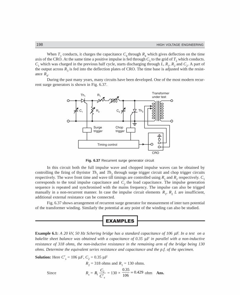
198 HIGH VOLTAGE ENGINEERING
Dharm\N-HIGH\HG6-2.PM5 198
When T1 conducts, it charges the capacitance C4 through R4 which gives deflection on the timeaxis of the CRO. At the same time a positive impulse is fed through C5 to the grid of T2 which conducts.C1 which was charged in the previous half cycle, starts discharging through L, R1, R2 and C2. A part ofthe output across R3 is fed into the deflection plates of CRO. The time base is adjusted with the resist-ance R4.
During the past many years, many circuits have been developed. One of the most modern recur-rent surge generators is shown in Fig. 6.37.
Fig. 6.37 Recurrent surge generator circuit
In this circuit both the full impulse wave and chopped impulse waves can be obtained bycontrolling the firing of thyristor Th1 and Th2 through surge trigger circuit and chop trigger circuitsrespectively. The wave front time and wave till timings are controlled using R1 and R2 respectively. C1corresponds to the total impulse capacitance and C2 the load capacitance. The impulse generationsequence is repeated and synchronised with the mains frequency. The impulse can also be triggedmanually in a non-recurrent manner. In case the impulse circuit elements R1, R2 L are insufficient,additional external resistance can be connected.
Fig. 6.37 shows arrangement of recurrent surge generator for measurement of inter turn potentialof the transformer winding. Similarly the potential at any point of the winding can also be studied.
Example 6.1: A 20 kV, 50 Hz Schering bridge has a standard capacitance of 106 µF. In a test on abakelite sheet balance was obtained with a capacitance of 0.35 µF in parallel with a non-inductiveresistance of 318 ohms, the non-inductive resistance in the remaining arm of the bridge being 130ohms. Determine the equivalent series resistance and capacitance and the p.f. of the specimen.
Solution: Here C′s = 106 µF, C2 = 0.35 µF
R2 = 318 ohms and R1 = 130 ohms.
Since Rs = RC
C s1
2
′ = 130 ×
0 35
1060 429
..= ohm Ans.
Dharm\N-HIGH\HG6-2.PM5 199
NONDESTRUCTIVE INSULATION TEST TECHNIQUES 199
and Cs = CR
Rs′ 2
1
= 106 × 318
130259= µF Ans.
tan δs = ωCs Rs = 314 × 259 × 10–6 × 0.429
= 3.5 × 104 × 10–6 = 0.035 Ans.
Since tan δ = sin δ = cos (90 – δ)
= cos φ = 0.035 Ans.
Example 6.2. Determine p.f. and the equivalent parallel resistance and capacitance of the rest speci-men of example 6.1
Solution: For parallel equivalent
Cp = Cs R
R2
1
Here Cs is the standard capacitance
Cp = 106 × 318
130259= µF Ans.
Rp = R
C C Rs
12
2 22ω
Rp = 130
314 0 35 106 10 3182 12 2× × × ×−.
= 351 ohms Ans.
tan δ = 1
314 351 259 10 6× × × −
= =1
28 540 035
.. Ans.
Example 6.3. A 33 kV, 50 Hz high voltage Schering bridge is used to test a sample of insulation. Thevarious arms have the following parameters on balance. The standard capacitance 500 pF, the resis-tive branch 800 ohm and branch with parallel combination of resistance and capacitance has values180 ohms and 0.15 µF. Determine the value of the capacitance of this sample its parallel equivalentloss resistance, the p.f. and the power loss under these test conditions.
Solution: Given Cs = 500 pF
R1 = 800 ohm
R2 = 180 ohm
C2 = 0.15 µF
Now C CR
Rp s= = × × =−2
1
12500 10180
800112 5. pF
Rp = R
C C Rs
12
2 22ω
= 800
314 500 10 0 15 10 1802 12 6 2× × × × ×− −.
200 HIGH VOLTAGE ENGINEERING
Dharm\N-HIGH\HG6-2.PM5 200
= 800
2 3958 10 1011 18. × × = 333.9 × 107 = 3339 MΩ
p.f. = tan δp = 1
ωC Rp p =
1
314 112 5 10 3339 1012 6× × × ×−.
= 1
117 95. 0.008478 Ans.
Power loss = V
R
2 2 6
6
33 10
3339 10= ×
×= 0.326 watts Ans.
Example 6.4. A length of cable is tested for insulation resistance by the loss of charge method. Anelectrostatic voltmeter of infinite resistance is connected between the cable conductor and earth form-ing therewith a joint capacitance of 600 pF. It is observed that after charging the voltage falls from 250volts to 92 V in one min. Determine the insulation resistance of the cable.
Solution: The voltage at any time t is given as
v = Ve–t/CR
where V is the initial voltage
or V
vet CR= /
or 1nV
v
t
CR=
or R = t
CV
v1n
= 60
600 10 1250
9212× − n
= 60
600 10 112× ×−
= 100,000 M ohms Ans.
Example 6.5. Following measurements are made to determine the dielectric constant and complexpermittivity of a test specimen:
The air capacitance of the electrode system = 50 pF
The capacitance and loss angle of the electrodes with specimen = 190 pF and 0.0085 respectively.
Solution: The dielectric constant εr = 190
503 8= .
Now complex permittivity ε = ε′ – jε″= ε0 (εr′ – jεr″)
εr′ = εr = 3.8
tan δ = εε
εr
r
r″′
= ″ =3 8
0 0085.
.
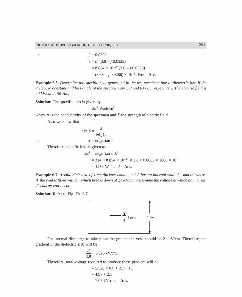
Dharm\N-HIGH\HG6-2.PM5 201
NONDESTRUCTIVE INSULATION TEST TECHNIQUES 201
or εr″ = 0.0323
ε = ε0 (3.8 – j 0.0323)
= 8.854 × 10⁻¹² (3.8 – j 0.0323)
= (3.36 – j 0.0286) × 10–11 F/m Ans.
Example 6.6. Determine the specific heat generated in the test specimen due to dielectric loss if thedielectric constant and loss angle of the specimen are 3.8 and 0.0085 respectively. The electric field is40 kV/cm at 50 Hz.]
Solution: The specific loss is given by
σE2 Watts/m3
where σ is the conductivity of the specimen and E the strength of electric field.
Also we know that
tan δ = σ
ωε ε0 r
or σ = ωε0εr tan δTherefore, specific loss is given as
σE2 = ωε0εr tan δ E2
= 314 × 8.854 × 10–12 × 3.8 × 0.0085 × 1600 × 1010
= 1436 Watts/m3 Ans.
Example 6.7. A solid dielectric of 1 cm thickness and εr = 3.8 has an internal void of 1 mm thickness.If the void is filled with air which breaks down at 21 KV/cm, determine the voltage at which an internaldischarge can occur.
Solution: Refer to Fig. Ex. 6.7
For internal discharge to take place the gradient in void should be 21 kV/cm. Therefore, thegradient in the dielectric slab will be
21
3 85 526
..= kV/cm.
Therefore, total voltage required to produce these gradient will be
= 5.526 × 0.9 + 21 × 0.1
= 4.97 + 2.1
= 7.07 kV rms Ans.
202 HIGH VOLTAGE ENGINEERING
Dharm\N-HIGH\HG6-2.PM5 202
6.1. What is non-destructive testing of insulating materials? Give very briefly the characteristics of thesemethods.
6.2. Starting from first principles, develop expression to evolve equivalent circuit of an insulating material.
6.3. Draw a neat diagram of a high voltage schering bridge and describe various features of the bridge.
6.4. Describe the functions of (i) Null detector (ii) Automatic guard potential regulator used in high voltageSchering bridge.
6.5. Draw a neat diagram of high voltage Schering bridge and analyse it for balanced condition. Draw itsphasor diagram. Assume (i) Series equivalent (ii) Parallel equivalent representation of the insulating ma-terial.
6.6. What modifications do you suggest in the basic Schering bridge while measuring large capacitances?Give its analysis. How the expressions for capacitance and loss angle get modified?
6.7. What is an inverted schering bridge? Give its application.
6.8. Explain the operation of high voltage Schering bridge when the test specimen (i) is grounded (ii) has highloss factor.
6.9. Discuss various types of transformer ratio arm bridges and give their application and advantages.
6.10. Describe with a neat diagram the principle of the operation of transformer current ratio arm bridge. Ex-plain how this is used for measurement of capacitance and loss factor of an insulating material.
6.11. What are partial discharges? Differentiate between internal and external discharges.
6.12. Develop and draw equivalent circuit of insulating material during partial discharge.
6.13. What is apparent charge in relation to partial discharges? Show that the calculation of apparent charge asa measure of partial discharges even though is more realistic than calculation of change in voltage acrossthe electrode, has limited application for partial discharge measurement.
6.14. Explain with neat diagram basic principle of pulse current measurement for estimation of partial dis-charges.
6.15. Write short note on the measuring impedance circuit for estimation of partial discharges.
6.16. Shows that the d.c. content of the frequency spectrum equals the apparent charge in the pulse current.
6.17. Explain with neat diagrams how wide band circuit can be used for measuring partial discharge.
6.18. “For proper measurement of partial discharge the resolution time of the circuit should be smaller than thetime-constant of the current pulse” Why? Explain.
6.19. Explain with neat diagram the Narrow-Band PD-detection circuit.
6.20. Show that the impulse response of narrow-bandpass receiver is an Oscilatory and with main frequency fmand the amplitude is given by signum function. Discuss the limitation of narrow bandpass detector.
6.21. Compare the performance of narrow band and wide band PD measuring circuits.
6.22. Explain with neat diagram a bridge circuit used for suppressing interference signals.
6.23. Write a short note on the use of an Oscilloscope as a PD measuring device.
6.24. Explain why the Schering bridge is particularly suitable for measurements at high voltages and outline theprecautions necessary to avoid errors.
A sample of insulation is placed in one arm CD of the Schering bridge. Under balanced condition theother three arms are as follows:
Dharm\N-HIGH\HG6-2.PM5 203
NONDESTRUCTIVE INSULATION TEST TECHNIQUES 203
AD = 109 pF, BC = 100 ohms and AB = 309 ohm in parallel with a loss free capacitance of 0.5 µF.Determine the capacitance equivalent series resistance and p.f. of the insulation in the arm CD. Derivebalanced conditions and draw phasor diagram. (340 pF, 460 K Ω, 0.05)
6.25. A sheet of bakelite 4.57 mm thick is tested at 50 Hz between electrodes 12.10 cms in diameter. TheSchering bridge employed has a standard compressed air capacitor of 106 pF a non-inductive resistor of1000/π ohm in parallel with a variable capacitance C, and a non-inductive variable resistor R. Balance isobtained with C = 0.5 µF and R = 260 ohm. Calculate the p.f. and the permittivity of the sheet.
(0.05, 5.88)
6.26. To determine the permittivity of a material following two measurements were made on the Scheringbridge.
Without the specimen between the electrodes.
Standard capacitor 150 pF in arm BC
Arm CD 120 pF in parallel with 5000 ΩArm DA 120 pF in parallel with 5000 ΩArm DA 120 pF in parallel with 5000 ΩArm AB Test electrodes
With specimen between the electrodes
AB BC 900 pF
Arm CD 1000 pF in parallel with 5000 ΩArm DA 1000 pF in parallel with 5000 ΩThe angular frequency of supply is 500 rad/sec.
Determine the relative permittivity and p.f. of the specimen. (6.0, 0.02)
Kuffel E., Zaengl W. High Voltage Engineering-Fundamentals, Pergamon Press 1984.
Boggs S.A., Electromagnetic techniques for fault and PD-location in gas-insulated cables and substa-tions, IEEE Tran PAS - 101 (1982), pp 1935–41.
Mole G. et al, Measurement of the magnitude of internal discharged in power capacitor, Proc. IEE Vol.116, No.5 (1969).
Papoulis A., The Fourier Integrais and its’ applications Mc Graw Hill 1962.
Schwab A.J., High Voltage Measurement Techniques, MIT Press 1972.
204
7.1 INTRODUCTION
Transient phenomenon is an aperiodic function of time and does not last longer. The duration for whichthey last is very insignificant as compared with the operating time of the system. Yet they are veryimportant because depending upon the severity of these transients, the system may result into black outin a city, shut down of a plant, fires in some buildings, etc.
The power system can be considered as made up of linear impedance elements of resistance,inductance and capacitance. The circuit is normally energized and carries load until a fault suddenlyoccurs. The fault, then, corresponds to the closing of a switch (or switches, depending upon the type offault) in the electrical circuit. The closing of this switch changes the circuit so that a new distribution ofcurrents and voltages is brought about. This redistribution is accompanied in general by a transientperiod during which the resultant currents and voltages may momentarily be relatively high. It is veryimportant to realize that this redistribution of currents and voltages cannot take place instantaneouslyfor the following reasons:
1. The electromagnetic energy stored by an inductance L is 12
2LI where I is the instantaneous
value of current. Assuming inductance to be constant the change in magnetic energy requires change in
current which an inductor is opposed by an emf of magnitude L dI
dt . In order to change the current
instantaneously dt = 0 and therefore L dI
0 is infinity, i.e., to bring about instantaneous change in current
the emf in the inductor should become infinity which is practically not possible and, therefore, it can besaid that the change of energy in an inductor is gradual.
2. The electrostatic energy stored by a capacitor C is given by 12
2CV where V is the instantane-
ous value of voltage. Assuming capacitance to be constant, the change in energy requires change involtage across the capacitor.
Since, for a capacitor, dV
dt
I
C= , to bring instantaneous change in voltage, i.e., for dt = 0 the
change in current required is infinite which again can not be achieved in practice and, therefore, it canbe said that change in energy in a capacitor is also gradual.
Transients in Power Systems andInsulation Coordination7
Dharm\N-HIGH\HG7-1.PM5 205
TRANSIENTS IN POWER SYSTEMS AND INSULATION COORDINATION 205
There are only two components L and C in an electrical circuit which store energy and we haveseen that the change in energy through these components is gradual and, therefore, the redistribution ofenergy following a circuit change takes a finite time. The third component, the resistance R, consumesenergy. At any time, the principle of conservation of energy in an electrical circuit applies, i.e. the rateof generation of energy is equal to the rate of storage of energy plus the rate of energy consumption.
It is clear that the three simple facts, namely,
1. The current cannot change instantaneously through an inductor,
2. The voltage across a capacitor cannot change instantaneously,
3. The law of conservation of energy must hold good, are fundamental to the phenomenon oftransients in electric power systems.
From the above it can be said that in order to have transients in an electrical system the follow-ing requirements should be met:
1. Either inductor or capacitor or both should be present.
2. A sudden change in the form of a fault or any switching operation should take place.
There are two components of voltages in a power system during transient period: (i) Fundamen-tal frequency voltages, and (ii) Natural frequency voltages usually of short duration which are superim-posed upon the fundamental frequency voltages. There is third component also known as harmonicvoltages resulting from unbalanced currents flowing in rotating machines in which the reactances inthe direct and quadrature axes are unequal.
Natural frequency voltages appear immediately after the sudden occurrence of a fault. Theysimply add to the fundamental frequency voltages. Since resultant voltages are of greater importancefrom a practical viewpoint it will be preferable to speak of the fundamental frequency and naturalfrequency components simply as a transient voltage. The transient voltages are affected by the numberof connections and the arrangements of the circuits.
Transients in which only one form of energy-storage, magnetic or electric is concerned, arecalled single energy transients, where both magnetic and electric energies are contained in or acceptedby the circuit, double energy transients are involved.
7.2 TRANSIENTS IN SIMPLE CIRCUITS
For analysing circuits for transients we will make use of Laplace transform technique which is morepowerful and easy to handle the transient problems than the differential equation technique. We willassume here lumped impedances only. The transients will depend upon the driving source also, i.e.,whether it is a d.c. source or an a.c. source. We will begin with simple problems and then go to somecomplicated problems.
1. D.C. Source(a) Resistance only (Fig. 7.1 (a))
As soon as the switch S is closed, the current in the circuit will be determined according to Ohm’s law.
I = V
RNow transients will be there in the circuit.
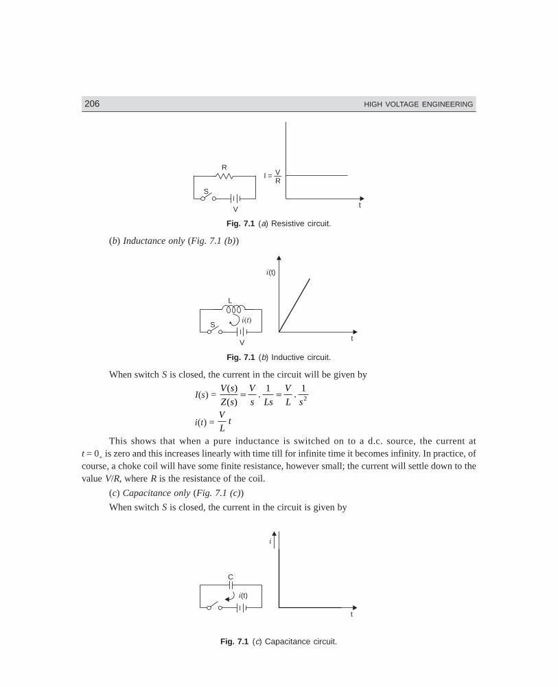
206 HIGH VOLTAGE ENGINEERING
Dharm\N-HIGH\HG7-1.PM5 206
V
S
R
t
I = —VR
Fig. 7.1 (a) Resistive circuit.
(b) Inductance only (Fig. 7.1 (b))
V
S
L
t
i(t)
i t( )
Fig. 7.1 (b) Inductive circuit.
When switch S is closed, the current in the circuit will be given by
I(s) = V s
Z s
V
s Ls
V
L s
( )
( ). .= =1 1
2
i(t) = V
Lt
This shows that when a pure inductance is switched on to a d.c. source, the current att = 0+ is zero and this increases linearly with time till for infinite time it becomes infinity. In practice, ofcourse, a choke coil will have some finite resistance, however small; the current will settle down to thevalue V/R, where R is the resistance of the coil.
(c) Capacitance only (Fig. 7.1 (c))
When switch S is closed, the current in the circuit is given by
C
t
(t)i
i
Fig. 7.1 (c) Capacitance circuit.
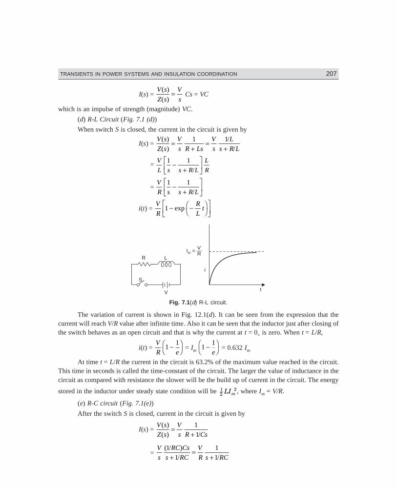
Dharm\N-HIGH\HG7-1.PM5 207
TRANSIENTS IN POWER SYSTEMS AND INSULATION COORDINATION 207
I(s) = V s
Z s
V
s
( )
( )= Cs = VC
which is an impulse of strength (magnitude) VC.
(d) R-L Circuit (Fig. 7.1 (d))
When switch S is closed, the current in the circuit is given by
I(s) = V s
Z s
V
s R Ls
V
s
L
s R L
( )
( )
/
/=
+=
+1 1
= V
L s s R L
L
R
1 1−+
LNM
OQP/
= V
R s s R L
1 1−+
LNM
OQP/
i(t) = V
R
R
Lt1 − −FHIK
LNM
OQPexp
V
S
L
t
i
R
VR
I = —m
Fig. 7.1(d) R-L circuit.
The variation of current is shown in Fig. 12.1(d). It can be seen from the expression that thecurrent will reach V/R value after infinite time. Also it can be seen that the inductor just after closing ofthe switch behaves as an open circuit and that is why the current at t = 0+ is zero. When t = L/R,
i(t) = V
R e1
1−FH
IK = Im 1
1−FH
IKe
= 0.632 Im
At time t = L/R the current in the circuit is 63.2% of the maximum value reached in the circuit.This time in seconds is called the time-constant of the circuit. The larger the value of inductance in thecircuit as compared with resistance the slower will be the build up of current in the circuit. The energy
stored in the inductor under steady state condition will be 12
2LIm , where Im = V/R.
(e) R-C circuit (Fig. 7.1(e))
After the switch S is closed, current in the circuit is given by
I(s) = V s
Z s
V
s R Cs
( )
( ) /=
+1
1
= V
s
RC Cs
s RC
V
R s RC
( / )
/ /
1
1
1
1+=
+
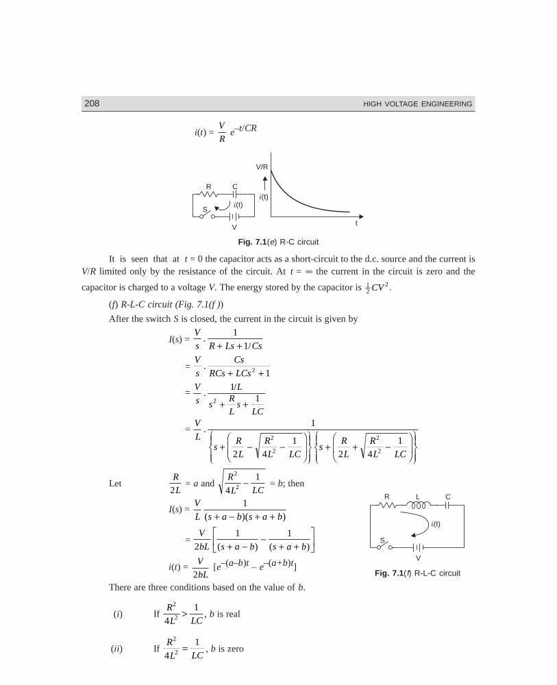
208 HIGH VOLTAGE ENGINEERING
Dharm\N-HIGH\HG7-1.PM5 208
i(t) = V
R e–t/CR
V
S
C
t
i(t)R
V/R
i(t)
Fig. 7.1(e) R-C circuit
It is seen that at t = 0 the capacitor acts as a short-circuit to the d.c. source and the current isV/R limited only by the resistance of the circuit. At t = ∞ the current in the circuit is zero and the
capacitor is charged to a voltage V. The energy stored by the capacitor is 12
2CV .
(f) R-L-C circuit (Fig. 7.1(f ))
After the switch S is closed, the current in the circuit is given by
I(s) = V
s R Ls Cs.
/
1
1+ +
= V
s
Cs
RCs LCs.
+ +2 1
= V
s
L
sR
Ls
LC
./1
12 + +
= V
Ls
R
L
R
L LCs
R
L
R
L LC
.1
2 41
2 412
2
2
2+ − −FHG
IKJ
RS|T|
UV|W|
+ + −FHG
IKJ
RS|T|
UV|W|
Let R
L2 = a and
R
L LC
2
24
1− = b; then
I(s) = V
L s a b s a b
1
( )( )+ − + +
= V
bL s a b s a b2
1 1
( ) ( )+ −−
+ +LNM
OQP
i(t) = V
bL2 [e–(a–b)t – e–(a+b)t]
There are three conditions based on the value of b.
(i) If R
L LC
2
24
1> , b is real
(ii) If R
L LC
2
24
1= , b is zero
V
S
L
i(t)
R C
Fig. 7.1(f) R-L-C circuit
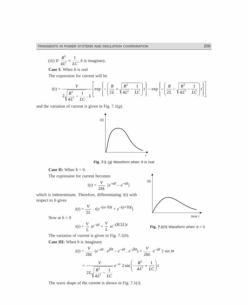
Dharm\N-HIGH\HG7-1.PM5 209
TRANSIENTS IN POWER SYSTEMS AND INSULATION COORDINATION 209
(iii) If R
L LC
2
24
1< , b is imaginary.
Case I: When b is real
The expression for current will be
i(t) = V
R
L LCL
R
L
R
L LCt
R
L
R
L LCt
24
1 2 4
1
2 4
12
2
2
2
2
2
−
− + −FHG
IKJ
RS|T|
UV|W|
− − − −FHG
IKJ
RS|T|
UV|W|
L
NMM
O
QPP
.
exp exp
and the variation of current is given in Fig. 7.1(g).
i(t)
t
Fig. 7.1 (g) Waveform when b is real
Case II: When b = 0.
The expression for current becomes
i(t) = V
bL2 [e–at – e–at]
which is indeterminate. Therefore, differentiating i(t) withrespect to b gives
i(t) = V
L2 . t[e–(a–b)t + e–(a+b)t]
Now at b = 0
i(t) = V
L te–at =
V
L te–(R/2L)t
The variation of current is given in Fig. 7.1(h).
Case III: When b is imaginary
i(t) = V
bL2 (e–at . ejbt – e–at . e–jbt) =
V
bL2 e–at 2 sin bt
= V
LR
L LC
eR
L LCtat
24
12
4
12
2
2
2
−
− +FHG
IKJ
− sin
The wave shape of the current is shown in Fig. 7.1(i).
i(t)
time t
Fig. 7.1(h) Waveform when b = 0
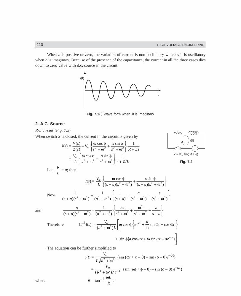
210 HIGH VOLTAGE ENGINEERING
Dharm\N-HIGH\HG7-1.PM5 210
v = V sin( t + )m
i(t)
When b is positive or zero, the variation of current is non-oscillatory whereas it is oscillatorywhen b is imaginary. Because of the presence of the capacitance, the current in all the three cases diesdown to zero value with d.c. source in the circuit.
i(t)
t
Fig. 7.1(i) Wave form when b is imaginary
2. A.C. SourceR-L circuit (Fig. 7.2)
When switch S is closed, the current in the circuit is given by
I(s) = V s
Z sV
s
s
s R Lsm( )
( )
cos sin=+
++
RSTUVW +
ω φω
φω2 2 2 2
1
= V
L s
s
s s R Lm ω φ
ωφ
ωcos sin
/2 2 2 2
1
++
+RST
UVW +
Let R
L = a; then
I(s) = V
L s a s
s
s a sm ω φ
ωφ
ωcos
( )( )
sin
( )( )+ ++
+ +RST
UVW2 2 2 2
Now 1 1 12 2 2 2 2 2 2 2( )( ) ( ) ( ) ( ) ( )s a s a s a
a
s
s
s+ +=
+ ++
+−
+RST
UVWω ω ω ω
and s
s a s a
as
s s
a
s a( )( ) ( )+ +=
+ ++
+−
+RST
UVW2 2 2 2 2 2
2
2 2
1
ω ω ωω
ω
Therefore L–1I(s) = V
a Le
at tm at
( )cos sin cos2 2+
+ −RSTUVW
LNM
−
ωω φ
ωω ω
+ sin cos sin φ ω ω ωa t t ae at+ −OQP
−
The equation can be further simplified to
i(t) = V
L a
m
2 2+ ω sin (ωt + φ – θ) – sin (φ – θ)e–at
= V
R Lm
( ) /2 2 2 1 2+ ω sin (ωt + φ – θ) – sin (φ – θ) e–at
where θ = tan–1 ωL
R .
Fig. 7.2
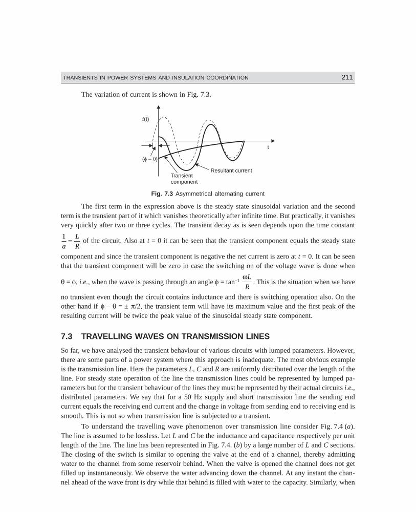
Dharm\N-HIGH\HG7-1.PM5 211
TRANSIENTS IN POWER SYSTEMS AND INSULATION COORDINATION 211
The variation of current is shown in Fig. 7.3.
t
( ) –
i(t)
Transientcomponent
Resultant current
Fig. 7.3 Asymmetrical alternating current
The first term in the expression above is the steady state sinusoidal variation and the secondterm is the transient part of it which vanishes theoretically after infinite time. But practically, it vanishesvery quickly after two or three cycles. The transient decay as is seen depends upon the time constant
1
a
L
R= of the circuit. Also at t = 0 it can be seen that the transient component equals the steady state
component and since the transient component is negative the net current is zero at t = 0. It can be seenthat the transient component will be zero in case the switching on of the voltage wave is done when
θ = φ, i.e., when the wave is passing through an angle φ = tan–1 ωL
R. This is the situation when we have
no transient even though the circuit contains inductance and there is switching operation also. On theother hand if φ – θ = ± π/2, the transient term will have its maximum value and the first peak of theresulting current will be twice the peak value of the sinusoidal steady state component.
7.3 TRAVELLING WAVES ON TRANSMISSION LINES
So far, we have analysed the transient behaviour of various circuits with lumped parameters. However,there are some parts of a power system where this approach is inadequate. The most obvious exampleis the transmission line. Here the parameters L, C and R are uniformly distributed over the length of theline. For steady state operation of the line the transmission lines could be represented by lumped pa-rameters but for the transient behaviour of the lines they must be represented by their actual circuits i.e.,distributed parameters. We say that for a 50 Hz supply and short transmission line the sending endcurrent equals the receiving end current and the change in voltage from sending end to receiving end issmooth. This is not so when transmission line is subjected to a transient.
To understand the travelling wave phenomenon over transmission line consider Fig. 7.4 (a).The line is assumed to be lossless. Let L and C be the inductance and capacitance respectively per unitlength of the line. The line has been represented in Fig. 7.4. (b) by a large number of L and C sections.The closing of the switch is similar to opening the valve at the end of a channel, thereby admittingwater to the channel from some reservoir behind. When the valve is opened the channel does not getfilled up instantaneously. We observe the water advancing down the channel. At any instant the chan-nel ahead of the wave front is dry while that behind is filled with water to the capacity. Similarly, when
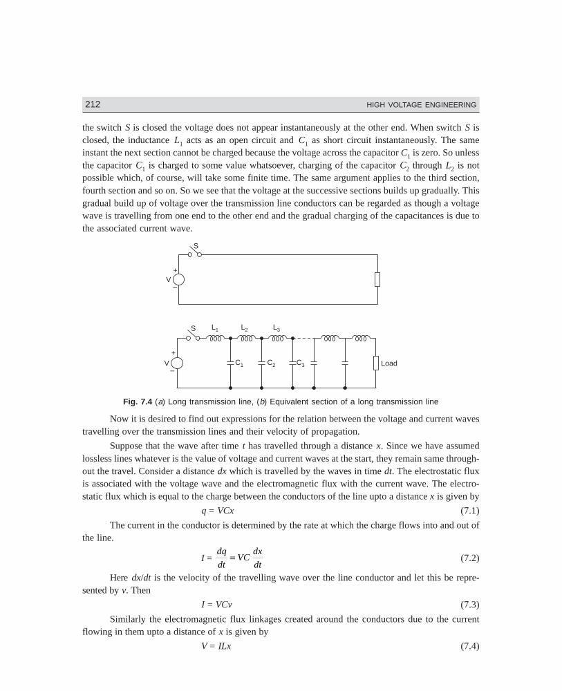
212 HIGH VOLTAGE ENGINEERING
Dharm\N-HIGH\HG7-1.PM5 212
the switch S is closed the voltage does not appear instantaneously at the other end. When switch S isclosed, the inductance L1 acts as an open circuit and C1 as short circuit instantaneously. The sameinstant the next section cannot be charged because the voltage across the capacitor C1 is zero. So unlessthe capacitor C1 is charged to some value whatsoever, charging of the capacitor C2 through L2 is notpossible which, of course, will take some finite time. The same argument applies to the third section,fourth section and so on. So we see that the voltage at the successive sections builds up gradually. Thisgradual build up of voltage over the transmission line conductors can be regarded as though a voltagewave is travelling from one end to the other end and the gradual charging of the capacitances is due tothe associated current wave.
L1
C1V C2 C3 Load
L2 L3S
+
V+
S
–
–
Fig. 7.4 (a) Long transmission line, (b) Equivalent section of a long transmission line
Now it is desired to find out expressions for the relation between the voltage and current wavestravelling over the transmission lines and their velocity of propagation.
Suppose that the wave after time t has travelled through a distance x. Since we have assumedlossless lines whatever is the value of voltage and current waves at the start, they remain same through-out the travel. Consider a distance dx which is travelled by the waves in time dt. The electrostatic fluxis associated with the voltage wave and the electromagnetic flux with the current wave. The electro-static flux which is equal to the charge between the conductors of the line upto a distance x is given by
q = VCx (7.1)
The current in the conductor is determined by the rate at which the charge flows into and out ofthe line.
I = dq
dtVC
dx
dt= (7.2)
Here dx/dt is the velocity of the travelling wave over the line conductor and let this be repre-sented by v. Then
I = VCv (7.3)
Similarly the electromagnetic flux linkages created around the conductors due to the currentflowing in them upto a distance of x is given by
V = ILx (7.4)
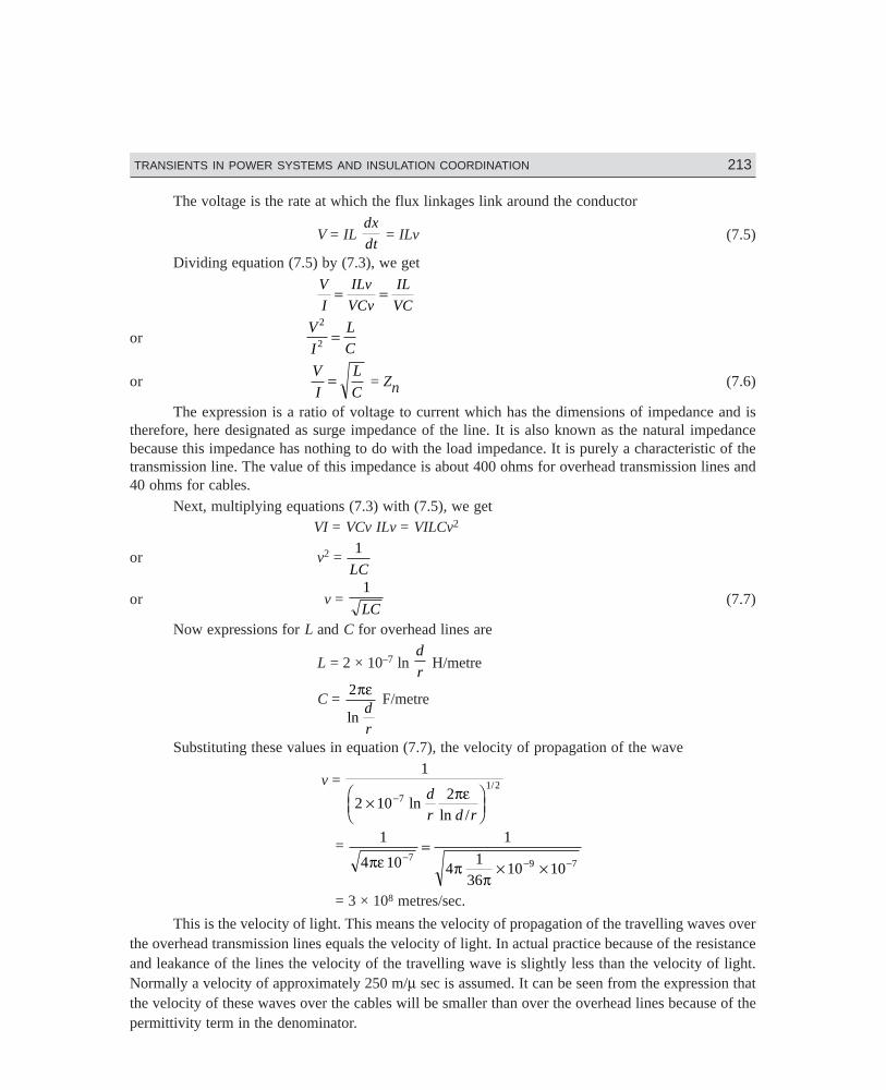
Dharm\N-HIGH\HG7-1.PM5 213
TRANSIENTS IN POWER SYSTEMS AND INSULATION COORDINATION 213
The voltage is the rate at which the flux linkages link around the conductor
V = IL dx
dt = ILv (7.5)
Dividing equation (7.5) by (7.3), we get
V
I
ILv
VCv
IL
VC= =
or V
I
L
C
2
2 =
or V
I
L
C= = Zn (7.6)
The expression is a ratio of voltage to current which has the dimensions of impedance and istherefore, here designated as surge impedance of the line. It is also known as the natural impedancebecause this impedance has nothing to do with the load impedance. It is purely a characteristic of thetransmission line. The value of this impedance is about 400 ohms for overhead transmission lines and40 ohms for cables.
Next, multiplying equations (7.3) with (7.5), we get VI = VCv ILv = VILCv2
or v2 = 1
LC
or v = 1
LC(7.7)
Now expressions for L and C for overhead lines are
L = 2 × 10⁻⁷ ln d
r H/metre
C = 2πε
lnd
r
F/metre
Substituting these values in equation (7.7), the velocity of propagation of the wave
v = 1
2 1027
1 2
×FHG
IKJ
− lnln /
/d
r d r
πε
= 1
4 10
1
41
3610 10
79 7πε π
π− − −
=× ×
= 3 × 10⁸ metres/sec.
This is the velocity of light. This means the velocity of propagation of the travelling waves overthe overhead transmission lines equals the velocity of light. In actual practice because of the resistanceand leakance of the lines the velocity of the travelling wave is slightly less than the velocity of light.Normally a velocity of approximately 250 m/µ sec is assumed. It can be seen from the expression thatthe velocity of these waves over the cables will be smaller than over the overhead lines because of thepermittivity term in the denominator.
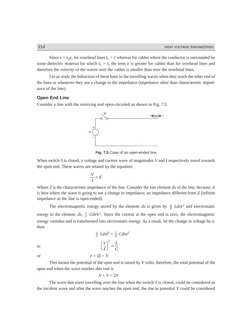
214 HIGH VOLTAGE ENGINEERING
Dharm\N-HIGH\HG7-1.PM5 214
Since ε = ε0εr for overhead lines εr = 1 whereas for cables where the conductor is surrounded bysome dielectric material for which εr > 1, the term ε is greater for cables than for overhead lines andtherefore the velocity of the waves over the cables is smaller than over the overhead lines.
Let us study the behaviour of these lines to the travelling waves when they reach the other end ofthe lines or whenever they see a change in the impedance (impedance other than characteristic imped-ance of the line).
Open End LineConsider a line with the receiving end open-circuited as shown in Fig. 7.5.
V+
S
–
dx
Fig. 7.5 Case of an open-ended line
When switch S is closed, a voltage and current wave of magnitudes V and I respectively travel towardsthe open end. These waves are related by the equation:
V
IZ=
Where Z is the characteristic impedance of the line. Consider the last element dx of the line, because, itis here where the wave is going to see a change in impedance, an impedance different from Z (infiniteimpedance as the line is open-ended).
The electromagnetic energy stored by the element dx is given by 12 LdxI 2 and electrostatic
energy in the element dx, 12 CdxV 2. Since the current at the open end is zero, the electromagnetic
energy vanishes and is transformed into electrostatic energy. As a result, let the change in voltage be e;then
12 LdxI2 = 1
2 Cdxe2
or e
I
L
CFHIK =
2
or e = IZ = V
This means the potential of the open end is raised by V volts; therefore, the total potential of the
open end when the wave reaches this end is
V + V = 2V
The wave that starts travelling over the line when the switch S is closed, could be considered asthe incident wave and after the wave reaches the open end, the rise in potential V could be considered
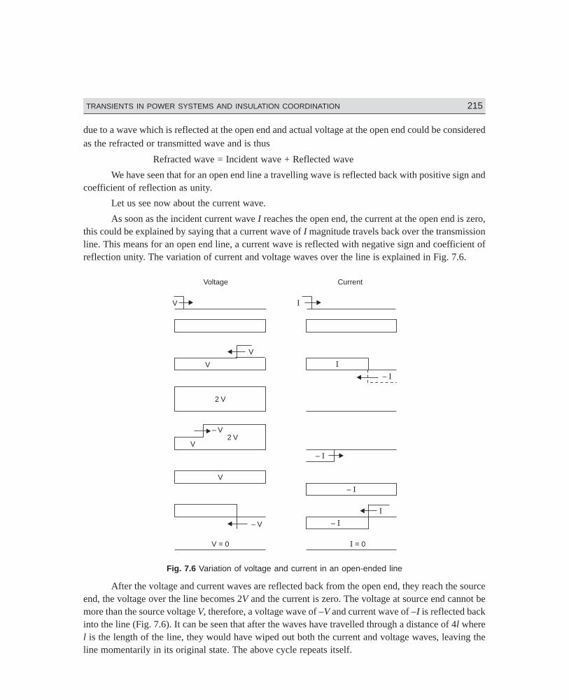
Dharm\N-HIGH\HG7-1.PM5 215
TRANSIENTS IN POWER SYSTEMS AND INSULATION COORDINATION 215
due to a wave which is reflected at the open end and actual voltage at the open end could be consideredas the refracted or transmitted wave and is thus
Refracted wave = Incident wave + Reflected wave
We have seen that for an open end line a travelling wave is reflected back with positive sign andcoefficient of reflection as unity.
Let us see now about the current wave.
As soon as the incident current wave I reaches the open end, the current at the open end is zero,this could be explained by saying that a current wave of I magnitude travels back over the transmissionline. This means for an open end line, a current wave is reflected with negative sign and coefficient ofreflection unity. The variation of current and voltage waves over the line is explained in Fig. 7.6.
V I
I
V
V
– I
2 V
2 V– V
V
V
I
– I
– I– V
I = 0V = 0
– I
Voltage Current
Fig. 7.6 Variation of voltage and current in an open-ended line
After the voltage and current waves are reflected back from the open end, they reach the sourceend, the voltage over the line becomes 2V and the current is zero. The voltage at source end cannot bemore than the source voltage V, therefore, a voltage wave of –V and current wave of –I is reflected backinto the line (Fig. 7.6). It can be seen that after the waves have travelled through a distance of 4l wherel is the length of the line, they would have wiped out both the current and voltage waves, leaving theline momentarily in its original state. The above cycle repeats itself.
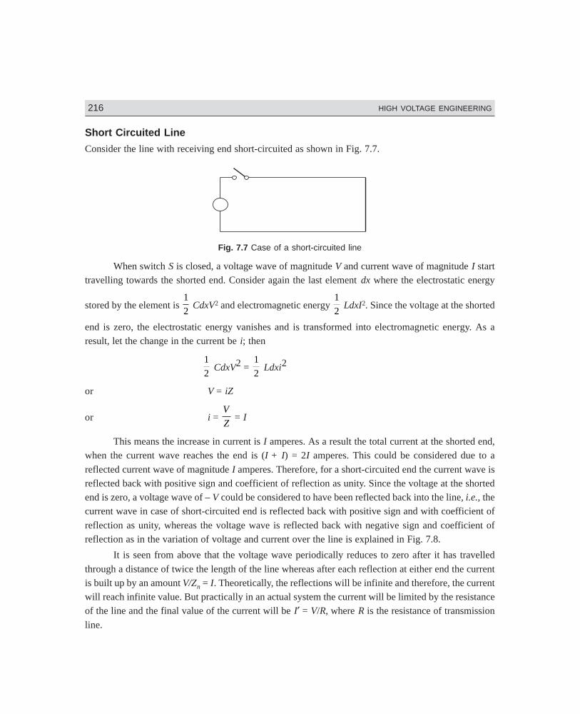
216 HIGH VOLTAGE ENGINEERING
Dharm\N-HIGH\HG7-1.PM5 216
Short Circuited Line
Consider the line with receiving end short-circuited as shown in Fig. 7.7.
Fig. 7.7 Case of a short-circuited line
When switch S is closed, a voltage wave of magnitude V and current wave of magnitude I starttravelling towards the shorted end. Consider again the last element dx where the electrostatic energy
stored by the element is 1
2 CdxV2 and electromagnetic energy
1
2 LdxI2. Since the voltage at the shorted
end is zero, the electrostatic energy vanishes and is transformed into electromagnetic energy. As aresult, let the change in the current be i; then
1
2 CdxV2 =
1
2 Ldxi2
or V = iZ
or i = V
Z = I
This means the increase in current is I amperes. As a result the total current at the shorted end,when the current wave reaches the end is (I + I) = 2I amperes. This could be considered due to a
reflected current wave of magnitude I amperes. Therefore, for a short-circuited end the current wave isreflected back with positive sign and coefficient of reflection as unity. Since the voltage at the shortedend is zero, a voltage wave of – V could be considered to have been reflected back into the line, i.e., thecurrent wave in case of short-circuited end is reflected back with positive sign and with coefficient of
reflection as unity, whereas the voltage wave is reflected back with negative sign and coefficient ofreflection as in the variation of voltage and current over the line is explained in Fig. 7.8.
It is seen from above that the voltage wave periodically reduces to zero after it has travelled
through a distance of twice the length of the line whereas after each reflection at either end the currentis built up by an amount V/Zn = I. Theoretically, the reflections will be infinite and therefore, the currentwill reach infinite value. But practically in an actual system the current will be limited by the resistanceof the line and the final value of the current will be I′ = V/R, where R is the resistance of transmission
line.
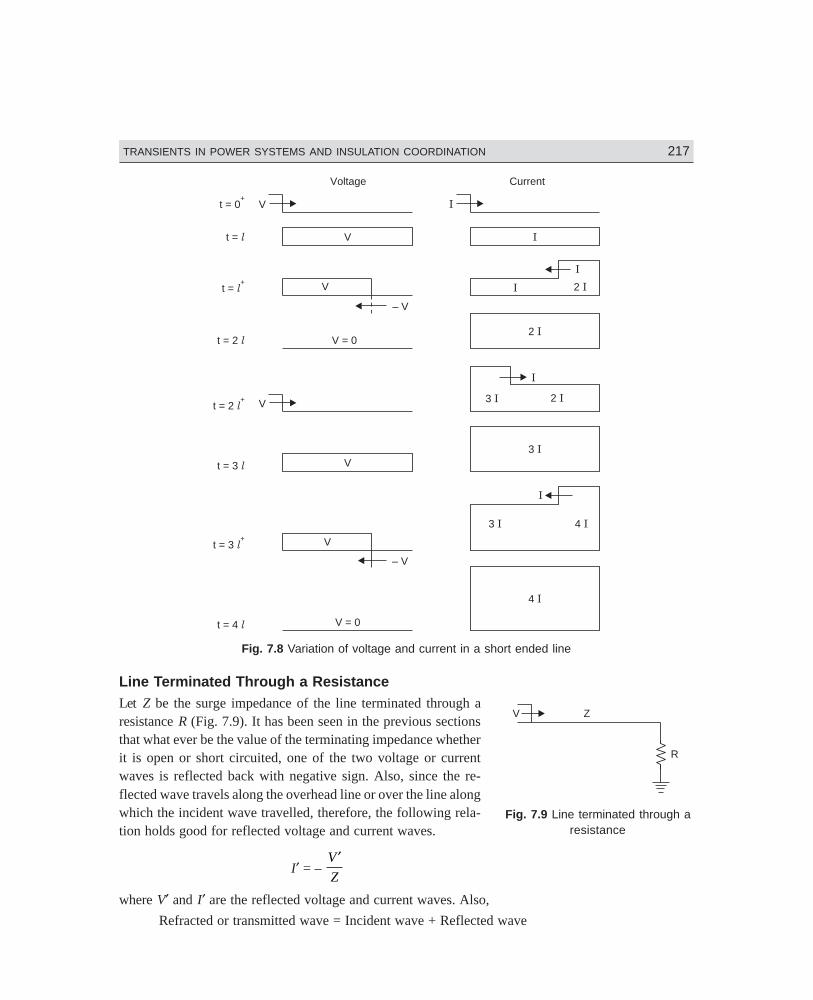
Dharm\N-HIGH\HG7-1.PM5 217
TRANSIENTS IN POWER SYSTEMS AND INSULATION COORDINATION 217
V
V
I
I
I
V = 0t = 2 l
t = 2 l+
V
V
t = 3 l
t = 3 l+
– V
V = 0t = 4 l
t = 0+
Voltage Current
t = l
– V
Vt = l+
2 I
I
V
I
3 I 2 I
3 I
3 I
4 I
I
2 I
4 I
Fig. 7.8 Variation of voltage and current in a short ended line
Line Terminated Through a ResistanceLet Z be the surge impedance of the line terminated through aresistance R (Fig. 7.9). It has been seen in the previous sectionsthat what ever be the value of the terminating impedance whetherit is open or short circuited, one of the two voltage or currentwaves is reflected back with negative sign. Also, since the re-flected wave travels along the overhead line or over the line alongwhich the incident wave travelled, therefore, the following rela-tion holds good for reflected voltage and current waves.
I′ = – V
Z
′
where V′ and I′ are the reflected voltage and current waves. Also,
Refracted or transmitted wave = Incident wave + Reflected wave
R
ZV
Fig. 7.9 Line terminated through aresistance
218 HIGH VOLTAGE ENGINEERING
Dharm\N-HIGH\HG7-1.PM5 218
Let V″ and I″ be the refracted voltage and current waves into the resistor R when the incidentwaves V and I reach the resistance R. The following relations hold good:
I = VZ
I′ = – V
Z
′
I″ = ′′V
ZSince I″ = I + I′ and V″ = V + V′, using these relations, we have
V
R
V
Z
V
Z
″ = − ′ =
V
Z
V V
Z− ″ −
= 2V
Z
V
Z− ″
(7.8)
or V″ = 2VR
Z R+(7.9)
and current I″ = 2 2V
R Z
V
Z
Z
R Z+=
+. = I .
2Z
R Z+(7.10)
Similarly substituting for V″ in terms of (V + V′), equation (7.8) becomes
V V
R
V
Z
V
Z
+ ′ = − ′
or V′ = V R Z
R Z
−+
(7.11)
and I′ = – V
Z
V
Z
R Z
R Z
′ = − −+
( )(7.12)
From the relations above, the coefficient of refraction for current waves
= 2Z
R Z+
and for voltage waves = 2R
R Z+Similarly, the coefficient of reflection for current waves
= – R Z
R Z
−+
and for voltage waves = + R Z
R Z
−+
Now the two extreme cases can be derived out of this general expression. For open circuit,
R → ∞and coefficient of refraction for current waves
20
Z
Z∞ +=
Dharm\N-HIGH\HG7-2.PM5 219
TRANSIENTS IN POWER SYSTEMS AND INSULATION COORDINATION 219
and coefficient of refraction for voltage waves
= 2 2
1
2
1
R
R Z Z R Z+=
+=
+ ∞/ / = 2
Similarly, coefficient of reflection for current waves
= – R Z
R Z
Z R
Z R
−+
= − −+
1
1
/
/ = – 1
and coefficient of reflection for voltage waves
= R Z
R Z
−+
= 1
Similarly, to find out the coefficients of reflection and refraction for current and voltage wavesfor the short circuit case, the value of R = 0 is to be substituted in the corresponding relations as derivedin this section.
It is, therefore, seen here that whenever a travelling wave looks into a change in impedance, itsuffers reflection and refraction. It is shown below that in case Z = R i.e., the line is terminated througha resistance whose value equals the surge impedance of the line (i.e., no change in the impedance) therewill be no reflection and the wave will enter fully into the resistance, i.e., the coefficient of refraction
will be unity whereas the coefficient of reflection will be zero.
When R = Z, substituting this, the coefficient of reflection for current wave
= – R Z
R Z
Z Z
Z Z
−+
= −+
= 0
and for voltage wave = R Z
R Z
−+
= 0
The coefficient of refraction for current wave
= 2 2
21
Z
R Z
Z
Z+= =
and for voltage wave = 2R
R Z+ = 1
It is seen that when a transmission line is terminated through a resistance equal to its surge
impedance the wave does not suffer reflection and, therefore, such lines could be said to be of infinitelength. Such lines are also called as matched lines and the load corresponding to this is known as surgeimpedance loading or natural impedance loading.
Line Connected to a CableA wave travels over the line and enters the cable (Fig. 7.10).Since the wave looks into a different impedance, it suffersreflection and refraction at the junction and the refracted volt-age wave is given by
Z1
Z2
Fig. 7.10 Line connected to a cable
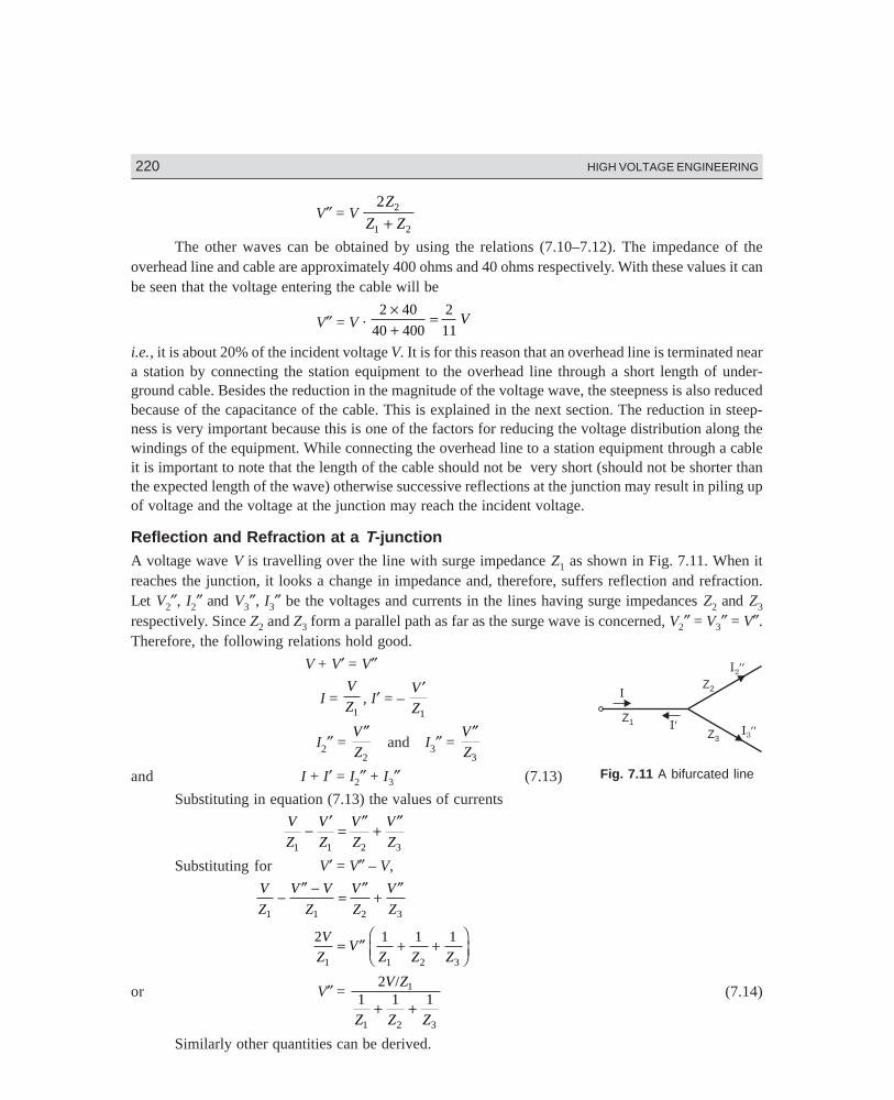
220 HIGH VOLTAGE ENGINEERING
Dharm\N-HIGH\HG7-2.PM5 220
V″ = V 2 2
1 2
Z
Z Z+The other waves can be obtained by using the relations (7.10–7.12). The impedance of the
overhead line and cable are approximately 400 ohms and 40 ohms respectively. With these values it canbe seen that the voltage entering the cable will be
V″ = V · 2 40
40 400
2
11
×+
= V
i.e., it is about 20% of the incident voltage V. It is for this reason that an overhead line is terminated neara station by connecting the station equipment to the overhead line through a short length of under-ground cable. Besides the reduction in the magnitude of the voltage wave, the steepness is also reducedbecause of the capacitance of the cable. This is explained in the next section. The reduction in steep-ness is very important because this is one of the factors for reducing the voltage distribution along thewindings of the equipment. While connecting the overhead line to a station equipment through a cableit is important to note that the length of the cable should not be very short (should not be shorter thanthe expected length of the wave) otherwise successive reflections at the junction may result in piling upof voltage and the voltage at the junction may reach the incident voltage.
Reflection and Refraction at a T-junctionA voltage wave V is travelling over the line with surge impedance Z1 as shown in Fig. 7.11. When itreaches the junction, it looks a change in impedance and, therefore, suffers reflection and refraction.Let V2″, I2″ and V3″, I3″ be the voltages and currents in the lines having surge impedances Z2 and Z3
respectively. Since Z2 and Z3 form a parallel path as far as the surge wave is concerned, V2″ = V3″ = V″.Therefore, the following relations hold good.
V + V′ = V″
I = V
Z1, I′ = –
V
Z
′
1
I2″ = V
Z
″
2and I3″ =
V
Z
″
3
and I + I′ = I2″ + I3″ (7.13)
Substituting in equation (7.13) the values of currents
V
Z
V
Z
V
Z
V
Z1 1 2 3
− ′ = ″ + ″
Substituting for V′ = V″ – V,
V
Z
V V
Z
V
Z
V
Z1 1 2 3
−″ −
=″
+″
2 1 1 1
1 1 2 3
V
ZV
Z Z Z= ″ + +
FHG
IKJ
or V″ = 2
1 1 11
1 2 3
V Z
Z Z Z
/
+ +(7.14)
Similarly other quantities can be derived.
Z1
Z2
Z3
I
I
I2
I3
Fig. 7.11 A bifurcated line
Dharm\N-HIGH\HG7-2.PM5 221
TRANSIENTS IN POWER SYSTEMS AND INSULATION COORDINATION 221
Example 7.1. A 3-phase transmission line has conductors 1.5 cms in diameter spaced 1 metre apart in
equilateral formation. The resistance and leakance are negligible. Calculate (i) the natural impedance
of the line, (ii) the line current if a voltage wave of 11 kV travels along the line, (iii) the rate of energy
absorption, the rate of reflection and the state and the form of reflection if the line is terminated through
a star connected load of 1000 ohm per phase, (iv) the value of the terminating resistance for no reflec-
tion and (v) the amount of reflected and transmitted power if the line is connected to a cable extension
with inductance and capacitance per phase per cm of 0.5 × 10⁻⁸ H and 1 × 10⁻⁶ F respectively.
Solution: The inductance per unit length
= 2 × 10⁻⁷ ln d
r H/metre
= 2 × 10⁻⁷ ln 100
0.75
= 2 × 10⁻⁷ ln 133.3
= 2 × 10–7 × 4.89
= 9.78 × 10⁻⁷ H/m
The capacitance per phase per unit length
= 2 0πεln /d r
F/metre
= 2 10
36
9× −
ln /d r = 1
18
10 9
×−
4.89 = 1.136 × 10⁻¹¹
∴ The natural impedance = L
C =
9.78 10
1.136 10
7
11
××
−
− = 294 ohms. Ans.
(ii) The line current = 11000
3 296× = 21.6 amps. Ans.
(iii) Since the terminating resistance is of higher value as compared to the value of the surgeimpedance of the line, the reflection is with a positive sign.
E″ = 2 2
1 2
Z E
Z Z+
where Z1 = line surge impedance, Z2 = terminating impedance and E = incident voltage.
E″ = 2 × 11000
3
1000
1294 = 9.8 kV
∴ The rate of power consumption = 3 2E
R
″MW
= 3 × ×9.8 9.8
1000 × 1000 kW
= 288 kW Ans.
222 HIGH VOLTAGE ENGINEERING
Dharm\N-HIGH\HG7-2.PM5 222
The reflected voltage E′ = Z Z
Z ZE2 1
2 1
1000 294
1294
11
3
−+
= − × kV
= 706
1294
11
3× = 3.465 kV
∴ The rate of reflected energy = 3
294
2× 3.465 × 1000 kW
= 121.8 kW Ans.
(iv) In order that the incident wave when reaches the terminating resistance, does not sufferreflection, the terminating resistance should be equal to the surge impedance of the line, i.e., 294 ohms.
(v) The surge impedance of the cable = L
C=
× −
−0.5 10
10
8
12
= 70.7 ohm
The refracted voltage = 2 70.7 11
3
×+
×294 70.7
= 2 70.7
3 364.7
× ××
11 = 2.46 kV
The reflected voltage = 70.7 294
364.7
11
3
− ×
= − ×
×223 3 11
3 364 7
.
. = – 3.9 kV
∴ The refracted and reflected powers are respectively.
3
70.7
2× 2.46 × 1000 = 256 kW and
3 2× 3.9
294 × 1000 = 155 kW. Ans.
Example 7.2. A surge of 15 kV magnitude travels along a cable towards its junction with an overheadline. The inductance and capacitance of the cable and overhead line are respectively 0.3 mH, 0.4 µFand 1.5 mH, 0.012 µF per km. Find the voltage rise at the junction due to the surge.
Solution: In this problem the surge travels from the cable towards the overhead line and hence therewill be positive voltage reflection at the junction.
The natural impedance of the cable = 0.3 10
0.4 10
3
6
××
−
− =
3 10
10
4
6
××
−
−0.4 = 27.38
The natural impedance of the line = 1.5
0.012 10 6
××
−
−10 3
= 1.5
0.12 10 7
××
−
−10 3
= 353 ohms.
Dharm\N-HIGH\HG7-2.PM5 223
TRANSIENTS IN POWER SYSTEMS AND INSULATION COORDINATION 223
The voltage rise at the junction is the voltage transmitted into the overhead line as the voltage iszero before the surge reaches the junction.
E″ = 2 353 15
353 27
2 353 15
380
× ×+
= × × = 27.87 kV Ans.
Example 7.3. A surge of 100 kV travelling in a line of natural impedance 600 ohms arrives at ajunction with two lines of impedances 800 ohms and 200 ohms respectively. Find the surge voltagesand currents transmitted into each branch line.
Solution: The problem deals with a reflection at a T-joint. The various natural impedances are: Z1= 600 ohms, Z2 = 800 ohms, Z3 = 200 ohms. The surge magnitude is 100 kV.
The surge as it reaches the joint suffers reflection and here the two lines are in parallel; there-fore, the transmitted voltage will have the same magnitude and is given by
E″ = 2
1 1 12 100 600
1600
1800
1200
1
1 2 3
E Z
Z Z Z
/ /
+ += ×
+ +
= 0.333
(1.67 1.25 5.0) 10
0.333
+ + ×= ×
−3
310
7 92.
= 33.3
7.92 × 10 = 42.04 kV Ans.
The transmitted current in line Z2 = 42.04 1000
800
× amps = 52.55 amps Ans.
The transmitted current in line Z3 = 42.04 1000
200
× amps = 210.2 amps. Ans.
Line Terminated through a CapacitanceWe consider here that a d.c. surge of infinite length travels over the line of surge impedance Z and isincident on the capacitor as shown in Fig. 7.12. We are interested in finding out the voltage across thecapacitor i.e., the refracted voltage. The refracted voltage, using equation (7.9),
V″(s) = 2 1×
+=
+/
/.
Cs
Z Cs
V
s
V
s ZCs1
2 1
1
= 2 1
12
1 1
1
V
s
ZC
s ZCV
s s ZC.
/
/ /+= −
+LNM
OQP
v″(t) = 2V[1 – e–t/ZC] (7.15)
The variation of voltage is shown in Fig. 7.13 (b).
It is to be noted that since terminating impedance is not a trans-mission line, therefore, V″(s) is not a travelling wave but it is thevoltage across the capacitor C.
C
Z
V
S
Fig. 7.12 Line terminatedthrough a capacitance
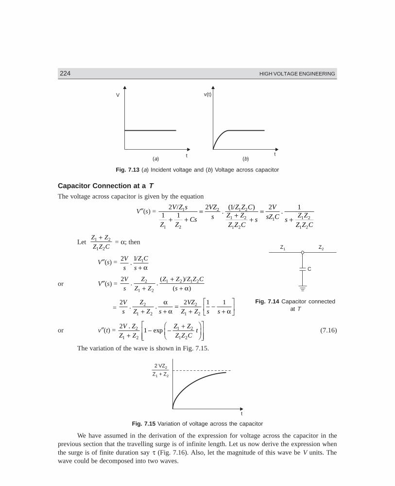
224 HIGH VOLTAGE ENGINEERING
Dharm\N-HIGH\HG7-2.PM5 224
t
V
t
v(t)
( )a ( )b
Fig. 7.13 (a) Incident voltage and (b) Voltage across capacitor
Capacitor Connection at a TThe voltage across capacitor is given by the equation
V″(s) = 2
1 12 1 2 11
1 2
2 1 2
1 2
1 2
1 1 2
1 2
V Z s
Z ZCs
VZ
s
Z Z CZ Z
Z Z Cs
V
sZ C sZ Z
Z Z C
/.
( / ).
+ += + +
=+
Let Z Z
Z Z C1 2
1 2
+ = α; then
V″(s) = 2 1 1V
s
Z C
s.
/
+ α
or V″(s) = 2 2
1 2
1 2 1 2V
s
Z
Z Z
Z Z Z Z C
s. .
( )/
( )++
+ α
= 2 2 1 12
1 2
2
1 2
V
s
Z
Z Z s
VZ
Z Z s s. .
+ +=
+−
+LNM
OQP
αα α
or v″(t) = 2
12
1 2
1 2
1 2
V Z
Z Z
Z Z
Z Z Ct
.exp
+− −
+FHG
IKJ
LNMM
OQPP
(7.16)
The variation of the wave is shown in Fig. 7.15.
t
2 VZ2
Z + Z1 2
Fig. 7.15 Variation of voltage across the capacitor
We have assumed in the derivation of the expression for voltage across the capacitor in theprevious section that the travelling surge is of infinite length. Let us now derive the expression whenthe surge is of finite duration say τ (Fig. 7.16). Also, let the magnitude of this wave be V units. Thewave could be decomposed into two waves.
C
Z1 Z2
Fig. 7.14 Capacitor connectedat T
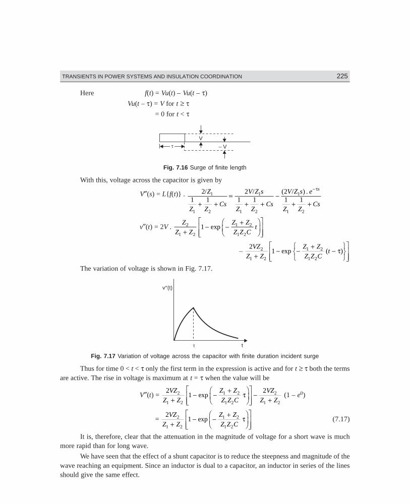
Dharm\N-HIGH\HG7-2.PM5 225
TRANSIENTS IN POWER SYSTEMS AND INSULATION COORDINATION 225
Here f(t) = Vu(t) – Vu(t – τ)
Vu(t – τ) = V for t ≥ τ= 0 for t < τ
V
– V
Fig. 7.16 Surge of finite length
With this, voltage across the capacitor is given by
V″(s) = Lf(t) . 21 1
21 1
21 1
1
1 2
1
1 2
1
1 2
/ / ( / ) .Z
Z ZCs
V Z s
Z ZCs
V Z s e
Z ZCs
s
+ +=
+ +−
+ +
−τ
v″(t) = 2V . Z
Z Z
Z Z
Z Z Ct2
1 2
1 2
1 2
1+
− −+F
HGIKJ
LNMM
OQPP
exp
– 2
12
1 2
1 2
1 2
VZ
Z Z
Z Z
Z Z Ct
+− −
+−
RSTUVW
LNMM
OQPP
exp ( )τ
The variation of voltage is shown in Fig. 7.17.
t
v (t)
Fig. 7.17 Variation of voltage across the capacitor with finite duration incident surge
Thus for time 0 < t < τ only the first term in the expression is active and for t ≥ τ both the termsare active. The rise in voltage is maximum at t = τ when the value will be
V″(t) = 2
122
1 2
1 2
1 2
2
1 2
VZ
Z Z
Z Z
Z Z C
VZ
Z Z+− −
+FHG
IKJ
LNMM
OQPP
−+
exp τ (1 – e0)
= 2
12
1 2
1 2
1 2
VZ
Z Z
Z Z
Z Z C+− −
+FHG
IKJ
LNMM
OQPP
exp τ (7.17)
It is, therefore, clear that the attenuation in the magnitude of voltage for a short wave is muchmore rapid than for long wave.
We have seen that the effect of a shunt capacitor is to reduce the steepness and magnitude of thewave reaching an equipment. Since an inductor is dual to a capacitor, an inductor in series of the linesshould give the same effect.
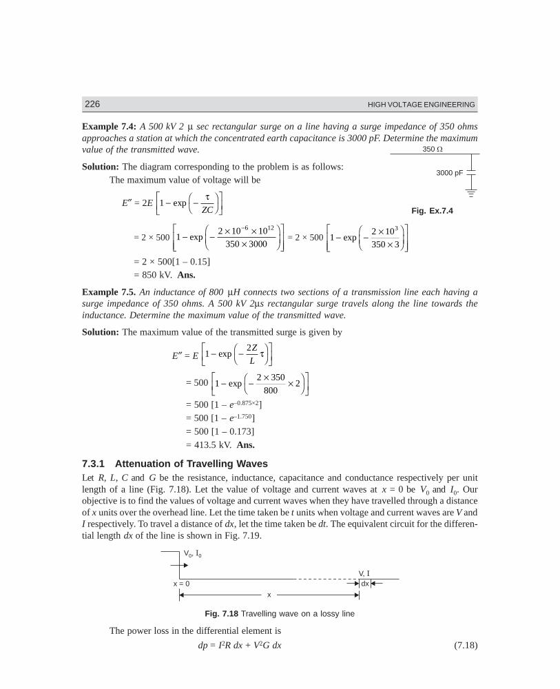
226 HIGH VOLTAGE ENGINEERING
Dharm\N-HIGH\HG7-2.PM5 226
Example 7.4: A 500 kV 2 µ sec rectangular surge on a line having a surge impedance of 350 ohmsapproaches a station at which the concentrated earth capacitance is 3000 pF. Determine the maximumvalue of the transmitted wave.
Solution: The diagram corresponding to the problem is as follows:The maximum value of voltage will be
E″ = 2E 1 − −FHIK
LNM
OQP
expτ
ZC
= 2 × 500 12 10 10
350 3000
6 12
− − × ××
FHG
IKJ
LNMM
OQPP
−exp = 2 × 500 1
2 10
350 3
3
− − ××
FHG
IKJ
LNMM
OQPP
exp
= 2 × 500[1 – 0.15]= 850 kV. Ans.
Example 7.5. An inductance of 800 µH connects two sections of a transmission line each having asurge impedance of 350 ohms. A 500 kV 2µs rectangular surge travels along the line towards theinductance. Determine the maximum value of the transmitted wave.
Solution: The maximum value of the transmitted surge is given by
E″ = E 12
− −FHIK
LNM
OQP
expZ
Lτ
= 500 12 350
8002− −
××F
HIK
LNM
OQP
exp
= 500 [1 – e–0.875×2]= 500 [1 – e–1.750]= 500 [1 – 0.173]= 413.5 kV. Ans.
7.3.1 Attenuation of Travelling WavesLet R, L, C and G be the resistance, inductance, capacitance and conductance respectively per unitlength of a line (Fig. 7.18). Let the value of voltage and current waves at x = 0 be V0 and I0. Ourobjective is to find the values of voltage and current waves when they have travelled through a distanceof x units over the overhead line. Let the time taken be t units when voltage and current waves are V andI respectively. To travel a distance of dx, let the time taken be dt. The equivalent circuit for the differen-tial length dx of the line is shown in Fig. 7.19.
dx
x
x = 0
V ,0 I0
V, I
Fig. 7.18 Travelling wave on a lossy line
The power loss in the differential element is
dp = I2R dx + V2G dx (7.18)
3000 pF
350
Fig. Ex.7.4
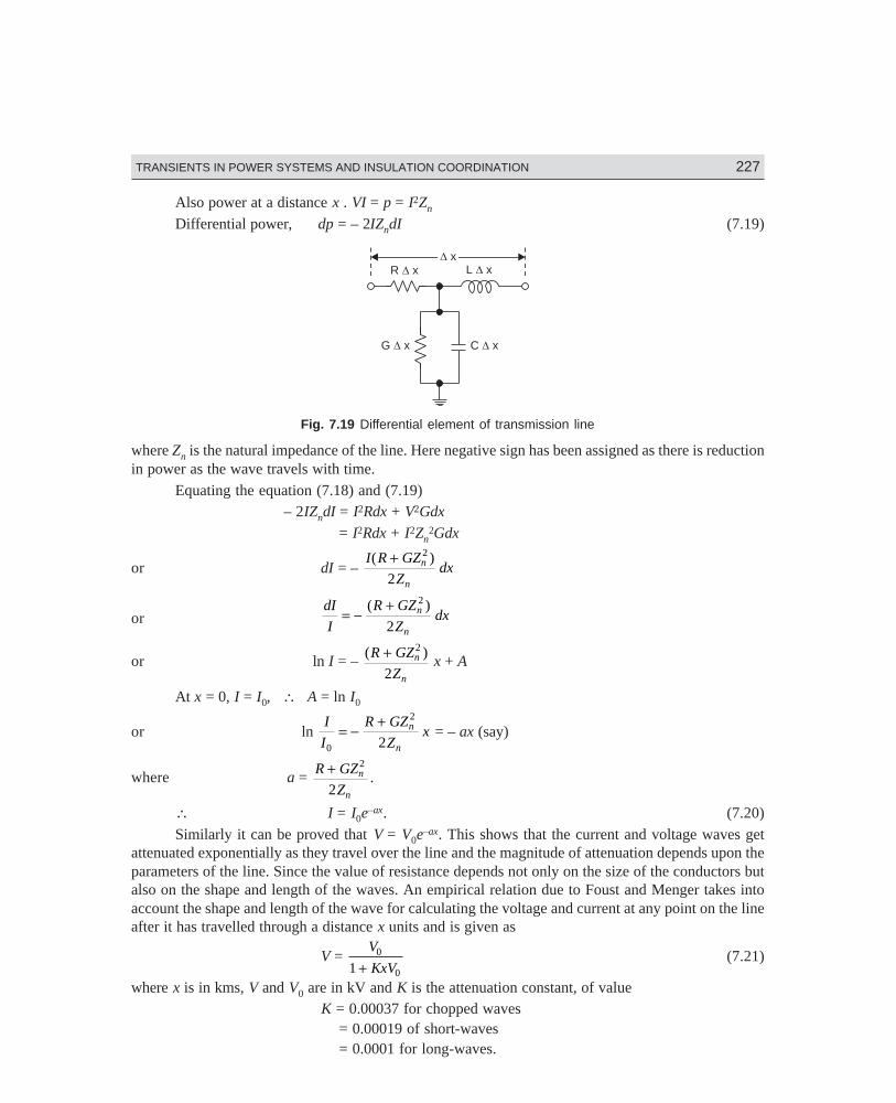
Dharm\N-HIGH\HG7-2.PM5 227
TRANSIENTS IN POWER SYSTEMS AND INSULATION COORDINATION 227
Also power at a distance x . VI = p = I2Zn
Differential power, dp = – 2IZndI (7.19)
R x L x
G x C x
x
Fig. 7.19 Differential element of transmission line
where Zn is the natural impedance of the line. Here negative sign has been assigned as there is reductionin power as the wave travels with time.
Equating the equation (7.18) and (7.19) – 2IZndI = I2Rdx + V2Gdx
= I2Rdx + I2Zn2Gdx
or dI = – I R GZ
Zdxn
n
( )+ 2
2
or dI
I
R GZ
Zdxn
n
= −+( )2
2
or ln I = – ( )R GZ
Zn
n
+ 2
2 x + A
At x = 0, I = I0, ∴ A = ln I0
or ln I
I
R GZ
Zxn
n0
2
2= −
+ = – ax (say)
where a = R GZ
Zn
n
+ 2
2.
∴ I = I0e–ax. (7.20)
Similarly it can be proved that V = V0e–ax. This shows that the current and voltage waves get
attenuated exponentially as they travel over the line and the magnitude of attenuation depends upon theparameters of the line. Since the value of resistance depends not only on the size of the conductors butalso on the shape and length of the waves. An empirical relation due to Foust and Menger takes intoaccount the shape and length of the wave for calculating the voltage and current at any point on the lineafter it has travelled through a distance x units and is given as
V = V
KxV0
01 +(7.21)
where x is in kms, V and V0 are in kV and K is the attenuation constant, of value K = 0.00037 for chopped waves
= 0.00019 of short-waves= 0.0001 for long-waves.
228 HIGH VOLTAGE ENGINEERING
Dharm\N-HIGH\HG7-2.PM5 228
Example 7.6. A travelling wave of 50 kV enters an overhead line of surge impedance 400 ohms andconductor resistance 6 ohm per km. Determine (i) the value of the voltage wave when it has travelledthrough a distance of 50 km, and (ii) the power loss and the heat loss of the wave during the timerequired to traverse this distance. Neglect the losses in the insulation and assume a wave velocity of3 × 105 km per second. Determine the corresponding values for a cable having surge impedance of 40ohms and relative permittivity 4.
Solution: (i) Since the line has some specific resistance, the wave as it travels gets attenuated in mag-nitude.
The magnitude of the wave is given by
e = e0ε–1/2(R/Z + GZ) x
where e = the value of voltage when travelled through a distance of x kilometres, R, G the resistanceand leakance per kilometre length of the line and Z is the surge impedance, e0 = initial magnitude of thesurge voltage, ε the Naperian base.
Here in this problem e0 = 50 kV, x = 50 km, R = 6 ohm and Z = 400 ohm and G = 0.0 mhos.
Substituting these values, e = 50ε–1/2(6/400)50 = 50 ×–0.375 = 50 × 0.69 = 34.5 kV.
(ii) The power loss is the instantaneous quantity and is required to be calculated when the wavetravels the distance of 50 km where the voltage magnitude is 34.5 kV.
The power loss = 34.5 34.5
400
× × 1000 kW = 2975 kW
The heat loss is the integrated value of power over the distance (or time) the wave has travelled.
Heat loss = z ei dt
Now e = e0ε–1/2 R/Z x and similarly, i = i0ε–1/2 R/Z x.
Now, x = vt
∴ e = e0 ε–1/2 RZ
vt and i = i0ε–1/2 RZ
vt
Substituting these values, we get
Heat loss = 0
0 0
tR Z vt dte iz −ε ( / )
where v = the velocity of the wave
t = x
v=
×50
3 105 = 16.67 × 10⁻⁵ sec
and i0 = e
Z0 50 1000
4000= ×
= 125 amps.
∴ Heat loss = – 0
16.67 10 5
50 125×
−−
z × ε ( / )R Z vt dt
= – 50 × 125 × 400
6 3 105× × [e–0.75 – 1]
= 0.736 kJ or 176 cal. Ans.
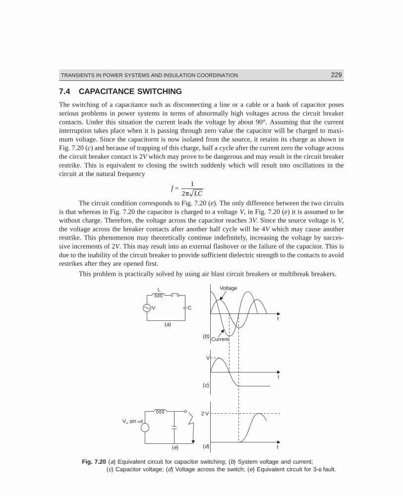
Dharm\N-HIGH\HG7-2.PM5 229
TRANSIENTS IN POWER SYSTEMS AND INSULATION COORDINATION 229
7.4 CAPACITANCE SWITCHING
The switching of a capacitance such as disconnecting a line or a cable or a bank of capacitor posesserious problems in power systems in terms of abnormally high voltages across the circuit breakercontacts. Under this situation the current leads the voltage by about 90°. Assuming that the currentinterruption takes place when it is passing through zero value the capacitor will be charged to maxi-mum voltage. Since the capacitorm is now isolated from the source, it retains its charge as shown inFig. 7.20 (c) and because of trapping of this charge, half a cycle after the current zero the voltage acrossthe circuit breaker contact is 2V which may prove to be dangerous and may result in the circuit breakerrestrike. This is equivalent to closing the switch suddenly which will result into oscillations in thecircuit at the natural frequency
f = 1
2π LC
The circuit condition corresponds to Fig. 7.20 (e). The only difference between the two circuitsis that whereas in Fig. 7.20 the capacitor is charged to a voltage V, in Fig. 7.20 (e) it is assumed to bewithout charge. Therefore, the voltage across the capacitor reaches 3V. Since the source voltage is V,the voltage across the breaker contacts after another half cycle will be 4V which may cause anotherrestrike. This phenomenon may theoretically continue indefinitely, increasing the voltage by succes-sive increments of 2V. This may result into an external flashover or the failure of the capacitor. This isdue to the inability of the circuit breaker to provide sufficient dielectric strength to the contacts to avoidrestrikes after they are opened first.
This problem is practically solved by using air blast circuit breakers or multibreak breakers.
V
L
C
Voltage
Current
t
t
t
2 V
( )d
( )c
( )b
V
( )a
V sin tm
( )e
Fig. 7.20 (a) Equivalent circuit for capacitor switching; (b) System voltage and current;(c) Capacitor voltage; (d) Voltage across the switch; (e) Equivalent circuit for 3-φ fault.
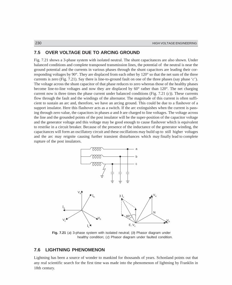
230 HIGH VOLTAGE ENGINEERING
Dharm\N-HIGH\HG7-2.PM5 230
7.5 OVER VOLTAGE DUE TO ARCING GROUND
Fig. 7.21 shows a 3-phase system with isolated neutral. The shunt capacitances are also shown. Underbalanced conditions and complete transposed transmission lines, the potential of the neutral is near theground potential and the currents in various phases through the shunt capacitors are leading their cor-responding voltages by 90°. They are displaced from each other by 120° so that the net sum of the threecurrents is zero (Fig. 7.21). Say there is line-to-ground fault on one of the three phases (say phase ‘c’).The voltage across the shunt capacitor of that phase reduces to zero whereas those of the healthy phasesbecome line-to-line voltages and now they are displaced by 60° rather than 120°. The net chargingcurrent now is three times the phase current under balanced conditions (Fig. 7.21 (c)). These currentsflow through the fault and the windings of the alternator. The magnitude of this current is often suffi-cient to sustain an arc and, therefore, we have an arcing ground. This could be due to a flashover of asupport insulator. Here this flashover acts as a switch. If the arc extinguishes when the current is pass-ing through zero value, the capacitors in phases a and b are charged to line voltages. The voltage acrossthe line and the grounded points of the post insulator will be the super-position of the capacitor voltageand the generator voltage and this voltage may be good enough to cause flashover which is equivalentto restrike in a circuit breaker. Because of the presence of the inductance of the generator winding, thecapacitances will form an oscillatory circuit and these oscillations may build up to still higher voltagesand the arc may reignite causing further transient disturbances which may finally lead to completerupture of the post insulators.
a
b
c
Ib
Va
Ia
Vc
Ic
Vb60°
Va
E, Vc
3 Ic
N
Vb
Fig. 7.21 (a) 3-phase system with isolated neutral; (b) Phasor diagram underhealthy condition; (c) Phasor diagram under faulted condition.
7.6 LIGHTNING PHENOMENON
Lightning has been a source of wonder to mankind for thousands of years. Schonland points out thatany real scientific search for the first time was made into the phenomenon of lightning by Franklin in18th century.
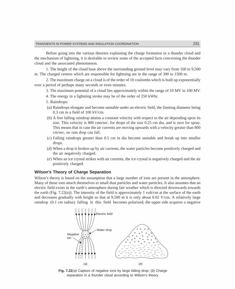
Dharm\N-HIGH\HG7-2.PM5 231
TRANSIENTS IN POWER SYSTEMS AND INSULATION COORDINATION 231
Before going into the various theories explaining the charge formation in a thunder cloud andthe mechanism of lightning, it is desirable to review some of the accepted facts concerning the thundercloud and the associated phenomenon.
1. The height of the cloud base above the surrounding ground level may vary from 160 to 9,500m. The charged centres which are responsible for lightning are in the range of 300 to 1500 m.
2. The maximum charge on a cloud is of the order of 10 coulombs which is built up exponentiallyover a period of perhaps many seconds or even minutes.
3. The maximum potential of a cloud lies approximately within the range of 10 MV to 100 MV.4. The energy in a lightning stroke may be of the order of 250 kWhr.5. Raindrops:(a) Raindrops elongate and become unstable under an electric field, the limiting diameter being
0.3 cm in a field of 100 kV/cm.(b) A free falling raindrop attains a constant velocity with respect to the air depending upon its
size. This velocity is 800 cms/sec. for drops of the size 0.25 cm dia. and is zero for spray.This means that in case the air currents are moving upwards with a velocity greater than 800cm/sec, no rain drop can fall.
(c) Falling raindrops greater than 0.5 cm in dia become unstable and break up into smallerdrops.
(d) When a drop is broken up by air currents, the water particles become positively charged andthe air negatively charged.
(e) When an ice crystal strikes with air currents, the ice crystal is negatively charged and the airpositively charged.
Wilson’s Theory of Charge SeparationWilson’s theory is based on the assumption that a large number of ions are present in the atmosphere.Many of these ions attach themselves to small dust particles and water particles. It also assumes that anelectric field exists in the earth’s atmosphere during fair weather which is directed downwards towardsthe earth (Fig. 7.22(a)). The intensity of the field is approximately 1 volt/cm at the surface of the earthand decreases gradually with height so that at 9,500 m it is only about 0.02 V/cm. A relatively largeraindrop (0.1 cm radius) falling in this field becomes polarized, the upper side acquires a negative
Electric field
Water dropNegativeion
+ + + ++ +++
+ + + ++
++++++ + +
++
++++++ + + + +
– – ––––
––
––––
––
––– –
–– ––
––
––
–– –
–
––
–––– –
–––
–––
––
––
–– –
– ––
– ––––
––
– ––
( )a ( )b
+ + +++
– ––
Fig. 7.22(a) Capture of negative ions by large falling drop; (b) Chargeseparation in a thunder cloud according to Wilson’s theory.
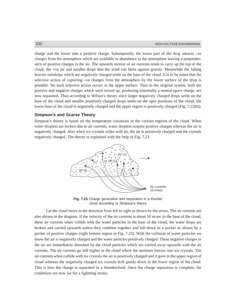
232 HIGH VOLTAGE ENGINEERING
Dharm\N-HIGH\HG7-2.PM5 232
charge and the lower side a positive charge. Subsequently, the lower part of the drop attracts –vecharges from the atmosphere which are available in abundance in the atmosphere leaving a preponder-ance of positive charges in the air. The upwards motion of air currents tends to carry up the top of thecloud, the +ve air and smaller drops that the wind can blow against gravity. Meanwhile the fallingheavier raindrops which are negatively charged settle on the base of the cloud. It is to be noted that theselective action of capturing –ve charges from the atmosphere by the lower surface of the drop ispossible. No such selective action occurs at the upper surface. Thus in the original system, both thepositive and negative charges which were mixed up, producing essentially a neutral space charge, arenow separated. Thus according to Wilson’s theory since larger negatively charged drops settle on thebase of the cloud and smaller positively charged drops settle on the uper positions of the cloud, thelower base of the cloud is negatively charged and the upper region is positively charged (Fig. 7.22(b)).
Simpson’s and Scarse TheorySimpson’s theory is based on the temperature variations in the various regions of the cloud. Whenwater droplets are broken due to air currents, water droplets acquire positive charges whereas the air isnegatively charged. Also when ice crystals strike with air, the air is positively charged and the crystalsnegatively charged. The theory is explained with the help of Fig. 7.23.
++ +
+++
+
++ +
+
++
+++
+ + ++ + +++
+
++
+ +
++ +
++– – – – – – – – – – ––––––––––––– –––
– – – – – – ––– ––– ––
–– – –
– ––
–––
––
–
–
–
–– – –
––– – –
–– –
+ +(– 20° C)
(– 10° C)
(0° C) + ++ ++
+++++
+
Air currents10 m/sec
+– – ––– – –
––
– – – –––––
Fig. 7.23 Charge generation and separation in a thundercloud according to Simpson’s theory
Let the cloud move in the direction from left to right as shown by the arrow. The air currents are
also shown in the diagram. If the velocity of the air currents is about 10 m/sec in the base of the cloud,these air currents when collide with the water particles in the base of the cloud, the water drops arebroken and carried upwards unless they combine together and fall down in a pocket as shown by apocket of positive charges (right bottom region in Fig. 7.23). With the collision of water particles we
know the air is negatively charged and the water particles positively charged. These negative charges inthe air are immediately absorbed by the cloud particles which are carried away upwards with the aircurrents. The air currents go still higher in the cloud where the moisture freezes into ice crystals. Theair currents when collide with ice crystals the air is positively charged and it goes in the upper region of
cloud whereas the negatively charged ice crystals drift gently down in the lower region of the cloud.This is how the charge is separated in a thundercloud. Once the charge separation is complete, theconditions are now set for a lightning stroke.
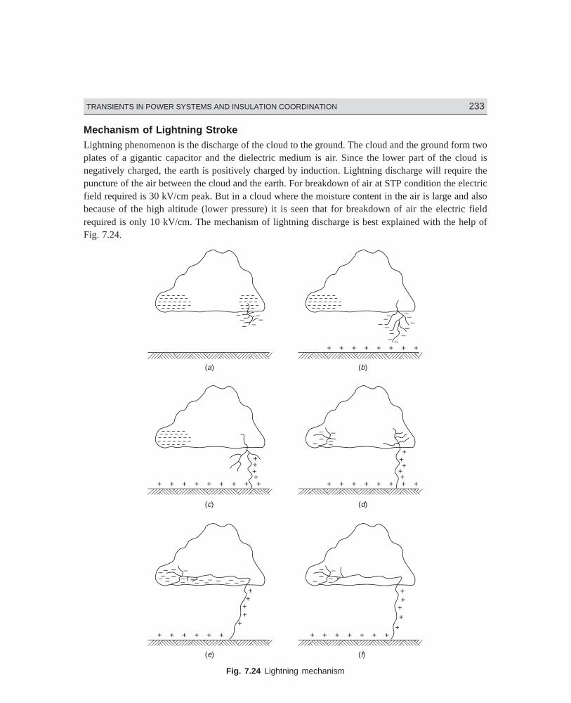
Dharm\N-HIGH\HG7-2.PM5 233
TRANSIENTS IN POWER SYSTEMS AND INSULATION COORDINATION 233
Mechanism of Lightning StrokeLightning phenomenon is the discharge of the cloud to the ground. The cloud and the ground form twoplates of a gigantic capacitor and the dielectric medium is air. Since the lower part of the cloud isnegatively charged, the earth is positively charged by induction. Lightning discharge will require thepuncture of the air between the cloud and the earth. For breakdown of air at STP condition the electricfield required is 30 kV/cm peak. But in a cloud where the moisture content in the air is large and alsobecause of the high altitude (lower pressure) it is seen that for breakdown of air the electric fieldrequired is only 10 kV/cm. The mechanism of lightning discharge is best explained with the help ofFig. 7.24.
––––
–– ––
––
–––
–––––
+ + + + + + + +
+ + + + + + + ++ + + + + + + + +++++
– –– –– –
+++
++
+ + + + + + +
– –– –– –
+++++
+ + + + + +
– –– –– –
+
–––––
– – –– – – –– – –
+++
+
( )a ( )b
( )c ( )d
( )e ( )f
Fig. 7.24 Lightning mechanism
234 HIGH VOLTAGE ENGINEERING
Dharm\N-HIGH\HG7-2.PM5 234
After a gradient of approximately 10 kV/cm is set up in the cloud, the air surrounding getsionized. At this a streamer (Fig. 7.24(a)) starts from the cloud towards the earth which cannot bedetected with the naked eye; only a spot travelling is detected. The current in the streamer is of theorder of 100 amperes and the speed of the streamer is 0.16 m/µ sec. This streamer is known as pilotstreamer because this leads to the lightning phenomenon. Depending upon the state of ionization of theair surrounding the streamer, it is branched to several paths and this is known as stepped leader (Fig.7.24(b)). The leader steps are of the order of 50 m in length and are accomplished in about a microsecond.The charge is brought from the cloud through the already ionized path to these pauses. The air sur-rounding these pauses is again ionized and the leader in this way reaches the earth (Fig. 7.24(c)).
Once the stepped leader has made contact with the earth it is believed that a power return stroke(Fig. 7.24(c)) moves very fast up towards the cloud through the already ionized path by the leader. Thisstreamer is very intense where the current varies between 1000 amps and 200,000 amps and the speedis about 10% that of light. It is here where the –ve charge of the cloud is being neutralized by thepositive induced charge on the earth (Fig. 7.24(d)). It is this instant which gives rise to lightning flashwhich we observe with our naked eye. There may be another cell of charges in the cloud near theneutralized charged cell. This charged cell will try to neutralize through this ionised path. This streameris known as dart leader (Fig. 7.24(e)). The velocity of the dart leader is about 3% of the velocity oflight. The effect of the dart leader is much more severe than that of the return stroke.
The discharge current in the return streamer is relatively very large but as it lasts only for a fewmicroseconds the energy contained in the streamer is small and hence this streamer is known as coldlightning stroke whereas the dart leader is known as hot lightning stroke because even though thecurrent in this leader is relatively smaller but it lasts for some milliseconds and therefore the energycontained in this leader is relatively larger.
It is found that each thunder cloud may contain as many as 40 charged cells and a heavy light-ning stroke may occur. This is known as multiple stroke.
7.7 LINE DESIGN BASED ON LIGHTNING
The severity of switching surges for voltage 400 kV and above is much more than that due to lightningvoltages. All the same it is desired to protect the transmission lines against direct lightning strokes. Theobject of good line design is to reduce the number of outages caused by lightning. To achieve this thefollowing actions are required.
(i) The incidence of stroke on to power conductor should be minimised.
(ii) The effect of those strokes which are incident on the system should be minimized.
To achieve (i) we know that lightning normally falls on tall objects; thus tall towers are morevulnerable to lightning than the smaller towers. In order to keep smaller tower height for a particularground clearance, the span lengths will decrease which requires more number of towers and hence theassociated accessories like insulators etc. The cost will go up very high. Therefore, a compromise hasto be made so that adequate clearance is provided, at the same time keeping longer span and hencelesser number of towers.
With a particular number of towers the chances of incidence of lightning on power conductorscan be minimized by placing a ground wire at the top of the tower structure. Refer to article 7.11 forground wires.
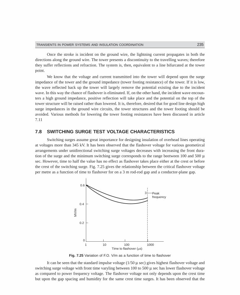
Dharm\N-HIGH\HG7-3.PM5 235
TRANSIENTS IN POWER SYSTEMS AND INSULATION COORDINATION 235
Once the stroke is incident on the ground wire, the lightning current propagates in both thedirections along the ground wire. The tower presents a discontinuity to the travelling waves; thereforethey suffer reflections and refraction. The system is, then, equivalent to a line bifurcated at the towerpoint.
We know that the voltage and current transmitted into the tower will depend upon the surgeimpedance of the tower and the ground impedance (tower footing resistance) of the tower. If it is low,the wave reflected back up the tower will largely remove the potential existing due to the incidentwave. In this way the chance of flashover is eliminated. If, on the other hand, the incident wave encoun-ters a high ground impedance, positive reflection will take place and the potential on the top of thetower structure will be raised rather than lowered. It is, therefore, desired that for good line design highsurge impedances in the ground wire circuits, the tower structures and the tower footing should beavoided. Various methods for lowering the tower footing resistances have been discussed in article7.11
7.8 SWITCHING SURGE TEST VOLTAGE CHARACTERISTICS
Switching surges assume great importance for designing insulation of overhead lines operatingat voltages more than 345 kV. It has been observed that the flashover voltage for various geometircalarrangements under unidirectional switching surge voltages decreases with increasing the front dura-tion of the surge and the minimum switching surge corresponds to the range beetween 100 and 500 µsec. However, time to half the value has no effect as flashover takes place either at the crest or beforethe crest of the switching surge. Fig. 7.25 gives the relationship between the critical flashover voltageper metre as a function of time to flashover for on a 3 m rod-rod gap and a conductor-plane gap.
0.6
0.4
0.2
010 100 1000
MV
/m
Time to flashover ( s)1
Peakfrequency
3
Fig. 7.25 Variation of F.O. V/m as a function of time to flashover
It can be seen that the standard impulse voltage (1/50 µ sec) gives highest flashover voltage andswitching surge voltage with front time varyling between 100 to 500 µ sec has lower flashover voltageas compared to power frequency voltage. The flashover voltage not only depends upon the crest timebut upon the gap spacing and humidity for the same crest time surges. It has been observed that the
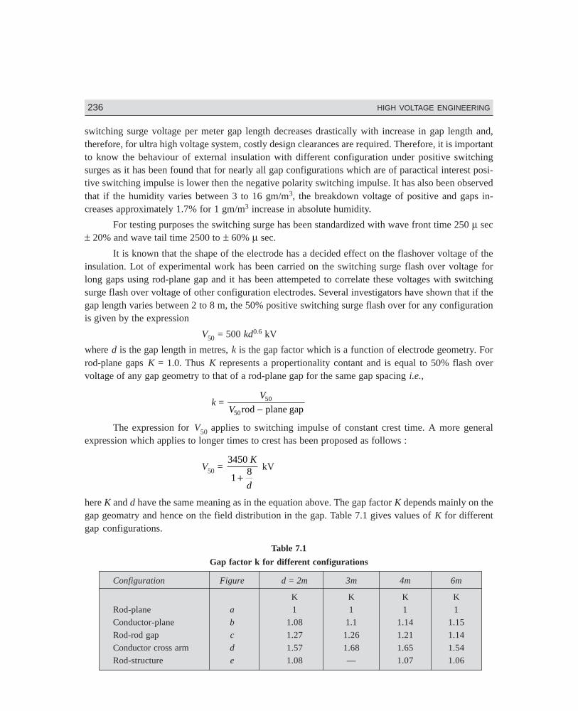
236 HIGH VOLTAGE ENGINEERING
Dharm\N-HIGH\HG7-3.PM5 236
switching surge voltage per meter gap length decreases drastically with increase in gap length and,therefore, for ultra high voltage system, costly design clearances are required. Therefore, it is importantto know the behaviour of external insulation with different configuration under positive switchingsurges as it has been found that for nearly all gap configurations which are of paractical interest posi-tive switching impulse is lower then the negative polarity switching impulse. It has also been observedthat if the humidity varies between 3 to 16 gm/m3, the breakdown voltage of positive and gaps in-creases approximately 1.7% for 1 gm/m3 increase in absolute humidity.
For testing purposes the switching surge has been standardized with wave front time 250 µ sec± 20% and wave tail time 2500 to ± 60% µ sec.
It is known that the shape of the electrode has a decided effect on the flashover voltage of theinsulation. Lot of experimental work has been carried on the switching surge flash over voltage forlong gaps using rod-plane gap and it has been attempeted to correlate these voltages with switchingsurge flash over voltage of other configuration electrodes. Several investigators have shown that if thegap length varies between 2 to 8 m, the 50% positive switching surge flash over for any configurationis given by the expression
V50 = 500 kd0.6 kV
where d is the gap length in metres, k is the gap factor which is a function of electrode geometry. Forrod-plane gaps K = 1.0. Thus K represents a propertionality contant and is equal to 50% flash overvoltage of any gap geometry to that of a rod-plane gap for the same gap spacing i.e.,
k = V
V50
50rod plane gap−
The expression for V50 applies to switching impulse of constant crest time. A more generalexpression which applies to longer times to crest has been proposed as follows :
V50 = 3450
18K
d+
kV
here K and d have the same meaning as in the equation above. The gap factor K depends mainly on thegap geomatry and hence on the field distribution in the gap. Table 7.1 gives values of K for differentgap configurations.
Table 7.1
Gap factor k for different configurations
Configuration Figure d = 2m 3m 4m 6m
K K K KRod-plane a 1 1 1 1
Conductor-plane b 1.08 1.1 1.14 1.15
Rod-rod gap c 1.27 1.26 1.21 1.14
Conductor cross arm d 1.57 1.68 1.65 1.54
Rod-structure e 1.08 — 1.07 1.06
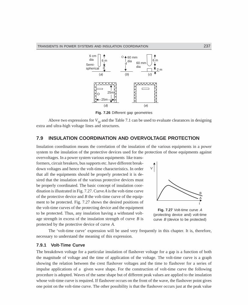
Dharm\N-HIGH\HG7-3.PM5 237
TRANSIENTS IN POWER SYSTEMS AND INSULATION COORDINATION 237
A
B
V
t
6 cmdia
Semi-spherical
6 m
dd
60 mmdia 60 mm
dia
6 m
2 m
( )a ( )b ( )c
( )d
25m
25m
( )e
O
Fig. 7.26 Different gap geometries
Above two expressions for V50 and the Table 7.1 can be used to evaluate clearances in designingextra and ultra-high voltage lines and structures.
7.9 INSULATION COORDINATION AND OVERVOLTAGE PROTECTION
Insulation coordination means the correlation of the insulation of the various equipments in a powersystem to the insulation of the protective devices used for the protection of those equipments againstovervoltages. In a power system various equipments like trans-formers, circuit breakers, bus supports etc. have different break-down voltages and hence the volt-time characteristics. In orderthat all the equipments should be properly protected it is de-sired that the insulation of the various protective devices mustbe properly coordinated. The basic concept of insulation coor-dination is illustrated in Fig. 7.27. Curve A is the volt-time curveof the protective device and B the volt-time curve of the equip-ment to be protected. Fig. 7.27 shows the desired positions ofthe volt-time curves of the protecting device and the equipmentto be protected. Thus, any insulation having a withstand volt-age strength in excess of the insulation strength of curve B isprotected by the protective device of curve A.
The ‘volt-time curve’ expression will be used very frequently in this chapter. It is, therefore,necessary to understand the meaning of this expression.
7.9.1 Volt-Time CurveThe breakdown voltage for a particular insulation of flashover voltage for a gap is a function of boththe magnitude of voltage and the time of application of the voltage. The volt-time curve is a graphshowing the relation between the crest flashover voltages and the time to flashover for a series ofimpulse applications of a given wave shape. For the construction of volt-time curve the followingprocedure is adopted. Waves of the same shape but of different peak values are applied to the insulationwhose volt-time curve is required. If flashover occurs on the front of the wave, the flashover point givesone point on the volt-time curve. The other possibility is that the flashover occurs just at the peak value
Fig. 7.27 Volt-time curve A(protecting device and) volt-timecurve B (device to be protected)
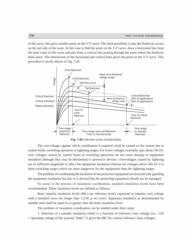
238 HIGH VOLTAGE ENGINEERING
Dharm\N-HIGH\HG7-3.PM5 238
of the wave; this gives another point on the V-T curve. The third possibility is that the flashover occurson the tail side of the wave. In this case to find the point on the V-T curve, draw a horizontal line fromthe peak value of this wave and also draw a vertical line passing through the point where the flashovertakes place. The intersection of the horizontal and vertical lines gives the point on the V-T curve. Thisprocedure is nicely shown in Fig. 7.28.
Crest flashover
Front flashover
Tail flashover
Wave front flashovervoltage range
Volt time curve
Wave tail flashovervoltage range
Critical flashover50% of applications50% of applications
Time ofcrestflashover Time of critical
flashover
Time rangewavefrontflashover
Time range wave tail flashoverTime in microseconds
Time rangeno impulseflashover
Vol
tage
Critical flashover
Critical withstand
Rated withstand
Fig. 7.28 Volt-time curve (construction)
The overvoltages against which coordination is required could be caused on the system due tosystem faults, switching operation or lightning surges. For lower voltages, normally upto about 345 kV,over voltages caused by system faults or switching operations do not cause damage to equipmentinsulation although they may be detrimental to protective devices. Overvoltages caused by lightning
are of sufficient magnitude to affect the equipment insulation whereas for voltages above 345 kV it isthese switching surges which are more dangerous for the equipments than the lightning surges.
The problem of coordinating the insulation of the protective equipment involves not only guardingthe equipment insulation but also it is desired that the protecting equipment should not be damaged.
To assist in the process of insulation coordination, standard insulation levels have been
recommended. These insulation levels are defined as follows.
Basic impulse insulation levels (BIL) are reference levels expressed in impulse crest voltagewith a standard wave not longer than 1.2/50 µ sec wave. Apparatus insulation as demonstrated by
suitable tests shall be equal to or greater than the basic insulation level.
The problem of insulation coordination can be studied under three steps:
1. Selection of a suitable insulation which is a function of reference class voltage (i.e., 1.05× operating voltage of the system). Table 7.2 gives the BIL for various reference class voltages.
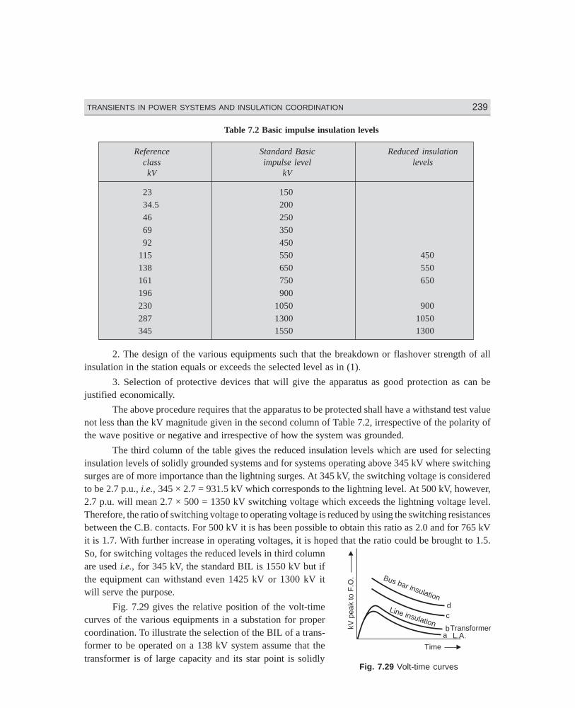
Dharm\N-HIGH\HG7-3.PM5 239
TRANSIENTS IN POWER SYSTEMS AND INSULATION COORDINATION 239
Table 7.2 Basic impulse insulation levels
Reference Standard Basic Reduced insulationclass impulse level levelskV kV
23 150
34.5 200
46 250
69 350
92 450115 550 450
138 650 550
161 750 650
196 900
230 1050 900
287 1300 1050345 1550 1300
2. The design of the various equipments such that the breakdown or flashover strength of allinsulation in the station equals or exceeds the selected level as in (1).
3. Selection of protective devices that will give the apparatus as good protection as can bejustified economically.
The above procedure requires that the apparatus to be protected shall have a withstand test valuenot less than the kV magnitude given in the second column of Table 7.2, irrespective of the polarity ofthe wave positive or negative and irrespective of how the system was grounded.
The third column of the table gives the reduced insulation levels which are used for selectinginsulation levels of solidly grounded systems and for systems operating above 345 kV where switchingsurges are of more importance than the lightning surges. At 345 kV, the switching voltage is consideredto be 2.7 p.u., i.e., 345 × 2.7 = 931.5 kV which corresponds to the lightning level. At 500 kV, however,2.7 p.u. will mean 2.7 × 500 = 1350 kV switching voltage which exceeds the lightning voltage level.Therefore, the ratio of switching voltage to operating voltage is reduced by using the switching resistancesbetween the C.B. contacts. For 500 kV it is has been possible to obtain this ratio as 2.0 and for 765 kVit is 1.7. With further increase in operating voltages, it is hoped that the ratio could be brought to 1.5.So, for switching voltages the reduced levels in third columnare used i.e., for 345 kV, the standard BIL is 1550 kV but ifthe equipment can withstand even 1425 kV or 1300 kV itwill serve the purpose.
Fig. 7.29 gives the relative position of the volt-timecurves of the various equipments in a substation for propercoordination. To illustrate the selection of the BIL of a trans-former to be operated on a 138 kV system assume that thetransformer is of large capacity and its star point is solidly
aTransformerkV
peak
toF
.O.
Time
b
cd
L.A.
Bus bar insulation
Line insulation
Fig. 7.29 Volt-time curves
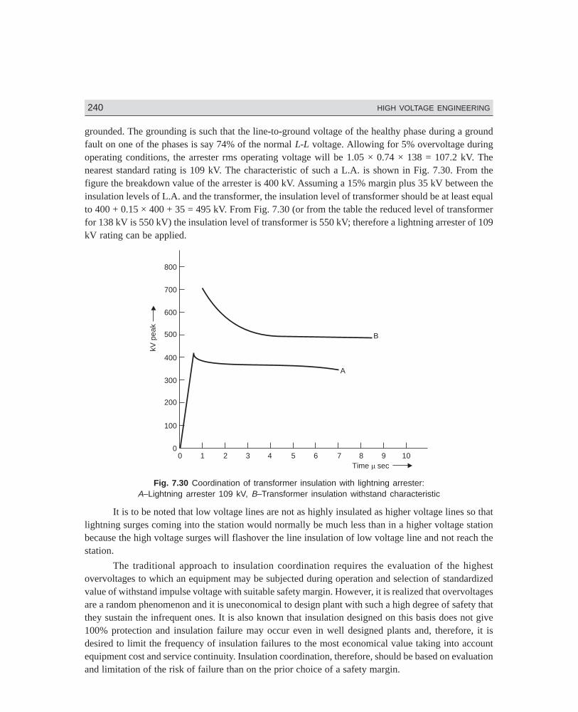
240 HIGH VOLTAGE ENGINEERING
Dharm\N-HIGH\HG7-3.PM5 240
grounded. The grounding is such that the line-to-ground voltage of the healthy phase during a groundfault on one of the phases is say 74% of the normal L-L voltage. Allowing for 5% overvoltage duringoperating conditions, the arrester rms operating voltage will be 1.05 × 0.74 × 138 = 107.2 kV. Thenearest standard rating is 109 kV. The characteristic of such a L.A. is shown in Fig. 7.30. From thefigure the breakdown value of the arrester is 400 kV. Assuming a 15% margin plus 35 kV between theinsulation levels of L.A. and the transformer, the insulation level of transformer should be at least equalto 400 + 0.15 × 400 + 35 = 495 kV. From Fig. 7.30 (or from the table the reduced level of transformerfor 138 kV is 550 kV) the insulation level of transformer is 550 kV; therefore a lightning arrester of 109kV rating can be applied.
800
700
600
500
400
300
200
100
00 1 2 3 4 5 6 7 8 9 10
kVpe
ak
A
B
Time sec
Fig. 7.30 Coordination of transformer insulation with lightning arrester:A–Lightning arrester 109 kV, B–Transformer insulation withstand characteristic
It is to be noted that low voltage lines are not as highly insulated as higher voltage lines so thatlightning surges coming into the station would normally be much less than in a higher voltage stationbecause the high voltage surges will flashover the line insulation of low voltage line and not reach thestation.
The traditional approach to insulation coordination requires the evaluation of the highestovervoltages to which an equipment may be subjected during operation and selection of standardizedvalue of withstand impulse voltage with suitable safety margin. However, it is realized that overvoltagesare a random phenomenon and it is uneconomical to design plant with such a high degree of safety thatthey sustain the infrequent ones. It is also known that insulation designed on this basis does not give100% protection and insulation failure may occur even in well designed plants and, therefore, it isdesired to limit the frequency of insulation failures to the most economical value taking into accountequipment cost and service continuity. Insulation coordination, therefore, should be based on evaluationand limitation of the risk of failure than on the prior choice of a safety margin.
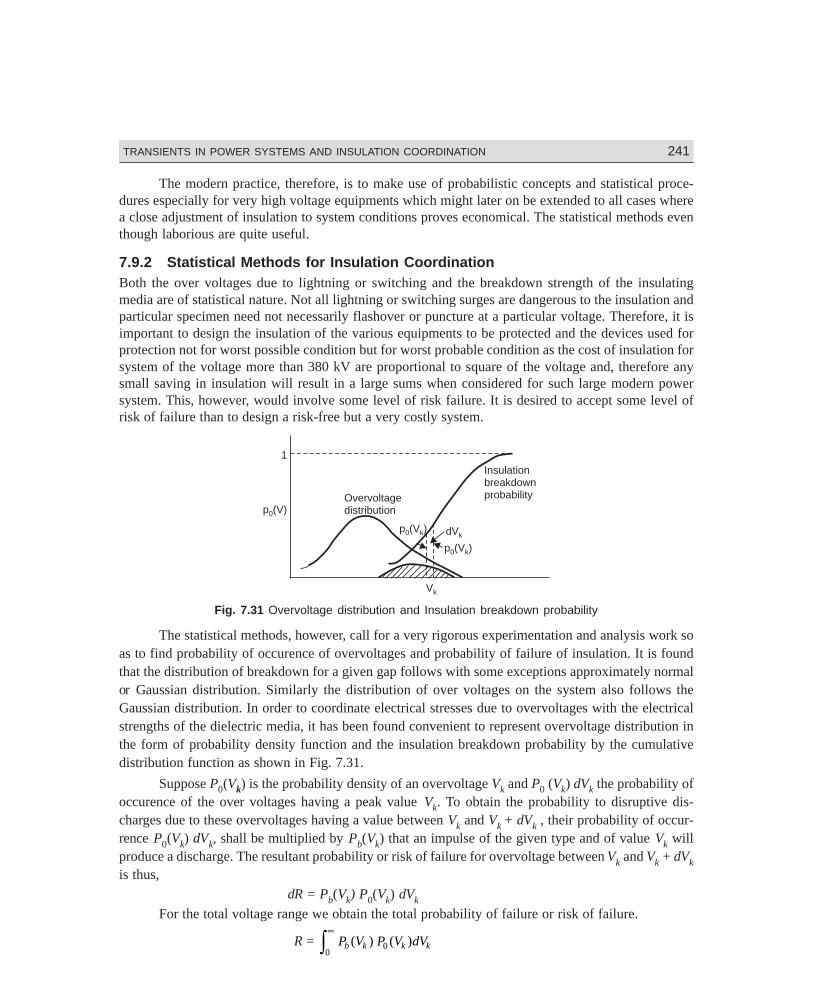
Dharm\N-HIGH\HG7-3.PM5 241
TRANSIENTS IN POWER SYSTEMS AND INSULATION COORDINATION 241
The modern practice, therefore, is to make use of probabilistic concepts and statistical proce-dures especially for very high voltage equipments which might later on be extended to all cases wherea close adjustment of insulation to system conditions proves economical. The statistical methods eventhough laborious are quite useful.
7.9.2 Statistical Methods for Insulation CoordinationBoth the over voltages due to lightning or switching and the breakdown strength of the insulatingmedia are of statistical nature. Not all lightning or switching surges are dangerous to the insulation andparticular specimen need not necessarily flashover or puncture at a particular voltage. Therefore, it isimportant to design the insulation of the various equipments to be protected and the devices used forprotection not for worst possible condition but for worst probable condition as the cost of insulation forsystem of the voltage more than 380 kV are proportional to square of the voltage and, therefore anysmall saving in insulation will result in a large sums when considered for such large modern powersystem. This, however, would involve some level of risk failure. It is desired to accept some level ofrisk of failure than to design a risk-free but a very costly system.
1
Overvoltagedistribution
Insulationbreakdownprobability
p (V)0
p (V )0 k dVk
p (V )0 k
Vk
Fig. 7.31 Overvoltage distribution and Insulation breakdown probability
The statistical methods, however, call for a very rigorous experimentation and analysis work soas to find probability of occurence of overvoltages and probability of failure of insulation. It is foundthat the distribution of breakdown for a given gap follows with some exceptions approximately normalor Gaussian distribution. Similarly the distribution of over voltages on the system also follows theGaussian distribution. In order to coordinate electrical stresses due to overvoltages with the electricalstrengths of the dielectric media, it has been found convenient to represent overvoltage distribution inthe form of probability density function and the insulation breakdown probability by the cumulativedistribution function as shown in Fig. 7.31.
Suppose P0(Vk) is the probability density of an overvoltage Vk and P0 (Vk) dVk the probability ofoccurence of the over voltages having a peak value Vk. To obtain the probability to disruptive dis-charges due to these overvoltages having a value between Vk and Vk + dVk , their probability of occur-rence P0(Vk) dVk, shall be multiplied by Pb(Vk) that an impulse of the given type and of value Vk willproduce a discharge. The resultant probability or risk of failure for overvoltage between Vk and Vk + dVkis thus,
dR = Pb(Vk) P0(Vk) dVk
For the total voltage range we obtain the total probability of failure or risk of failure.
R = 0
0
∞z P V P V dVb k k k( ) ( )
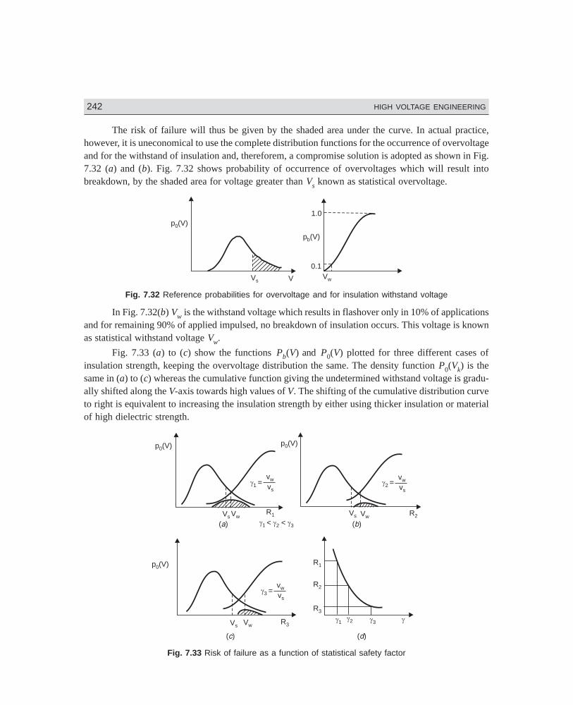
242 HIGH VOLTAGE ENGINEERING
Dharm\N-HIGH\HG7-3.PM5 242
The risk of failure will thus be given by the shaded area under the curve. In actual practice,however, it is uneconomical to use the complete distribution functions for the occurrence of overvoltageand for the withstand of insulation and, thereforem, a compromise solution is adopted as shown in Fig.7.32 (a) and (b). Fig. 7.32 shows probability of occurrence of overvoltages which will result intobreakdown, by the shaded area for voltage greater than Vs known as statistical overvoltage.
p (V)0
Vs V Vw
p (V)b
1.0
0.1
Fig. 7.32 Reference probabilities for overvoltage and for insulation withstand voltage
In Fig. 7.32(b) Vw is the withstand voltage which results in flashover only in 10% of applicationsand for remaining 90% of applied impulsed, no breakdown of insulation occurs. This voltage is knownas statistical withstand voltage Vw.
Fig. 7.33 (a) to (c) show the functions Pb(V) and P0(V) plotted for three different cases ofinsulation strength, keeping the overvoltage distribution the same. The density function P0(Vk) is thesame in (a) to (c) whereas the cumulative function giving the undetermined withstand voltage is gradu-ally shifted along the V-axis towards high values of V. The shifting of the cumulative distribution curveto right is equivalent to increasing the insulation strength by either using thicker insulation or materialof high dielectric strength.
p (V)0p (V)0
Vs VwR1
1 =vw
vs
< < 2 31( )a ( )b
Vs Vw
2 =vw
vs
R2
p (V)0
Vs Vw
3 =vw
vs
R3
R1
R2
R3
12 3
( )c ( )d
Fig. 7.33 Risk of failure as a function of statistical safety factor
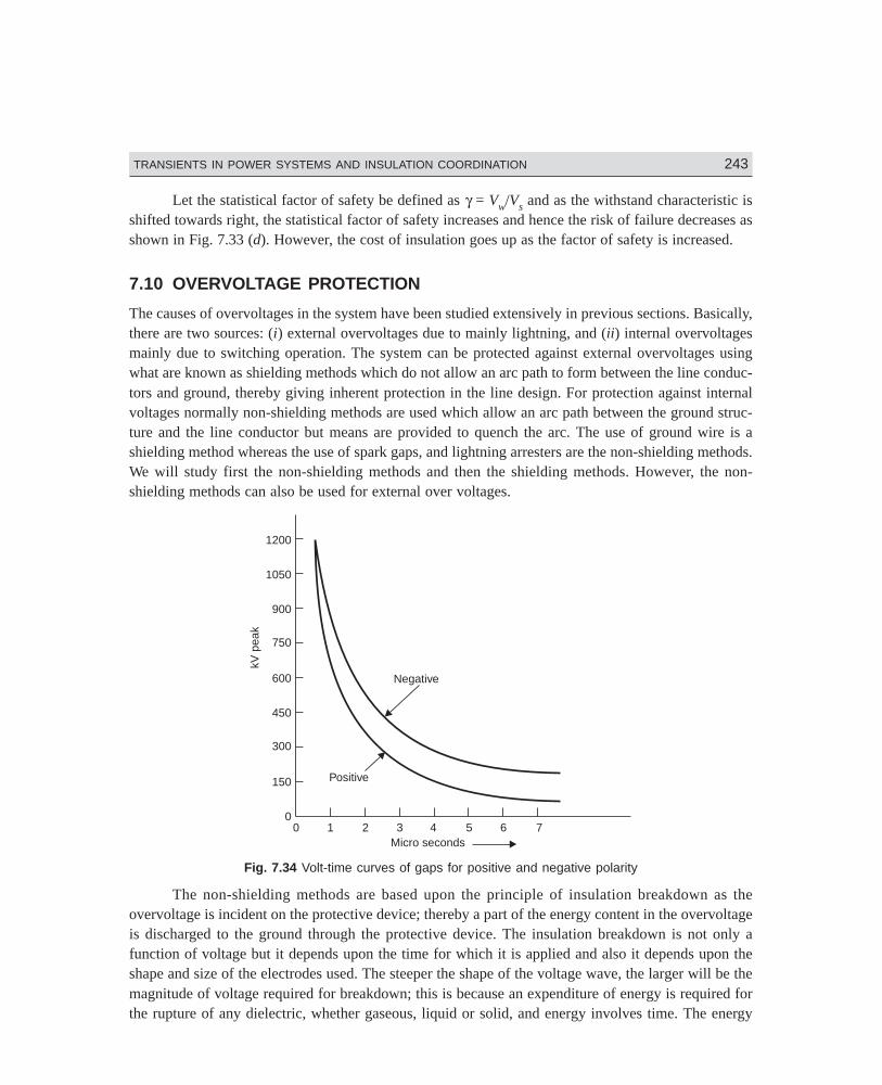
Dharm\N-HIGH\HG7-3.PM5 243
TRANSIENTS IN POWER SYSTEMS AND INSULATION COORDINATION 243
Let the statistical factor of safety be defined as γ = Vw/Vs and as the withstand characteristic isshifted towards right, the statistical factor of safety increases and hence the risk of failure decreases asshown in Fig. 7.33 (d). However, the cost of insulation goes up as the factor of safety is increased.
7.10 OVERVOLTAGE PROTECTION
The causes of overvoltages in the system have been studied extensively in previous sections. Basically,there are two sources: (i) external overvoltages due to mainly lightning, and (ii) internal overvoltagesmainly due to switching operation. The system can be protected against external overvoltages usingwhat are known as shielding methods which do not allow an arc path to form between the line conduc-tors and ground, thereby giving inherent protection in the line design. For protection against internalvoltages normally non-shielding methods are used which allow an arc path between the ground struc-ture and the line conductor but means are provided to quench the arc. The use of ground wire is ashielding method whereas the use of spark gaps, and lightning arresters are the non-shielding methods.We will study first the non-shielding methods and then the shielding methods. However, the non-shielding methods can also be used for external over voltages.
1200
1050
900
750
600
450
300
150
00 1 2 3 4 5 6 7
kVpe
ak
Negative
Positive
Micro seconds
Fig. 7.34 Volt-time curves of gaps for positive and negative polarity
The non-shielding methods are based upon the principle of insulation breakdown as theovervoltage is incident on the protective device; thereby a part of the energy content in the overvoltageis discharged to the ground through the protective device. The insulation breakdown is not only afunction of voltage but it depends upon the time for which it is applied and also it depends upon theshape and size of the electrodes used. The steeper the shape of the voltage wave, the larger will be themagnitude of voltage required for breakdown; this is because an expenditure of energy is required forthe rupture of any dielectric, whether gaseous, liquid or solid, and energy involves time. The energy
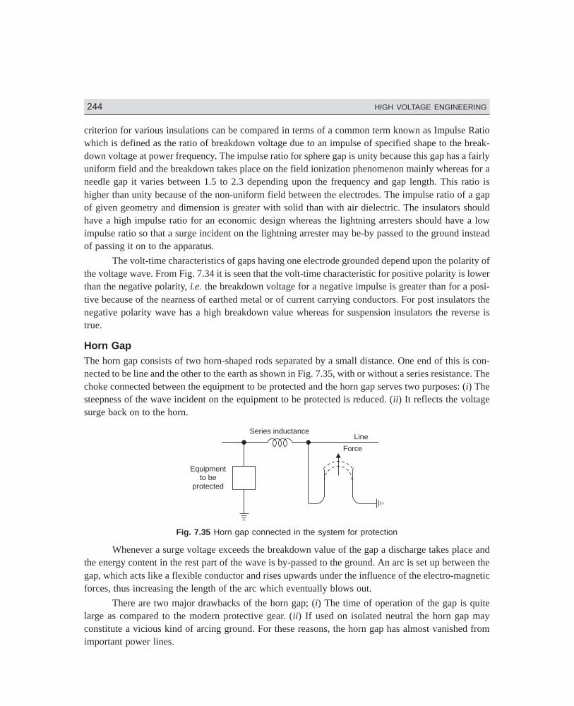
244 HIGH VOLTAGE ENGINEERING
Dharm\N-HIGH\HG7-3.PM5 244
criterion for various insulations can be compared in terms of a common term known as Impulse Ratiowhich is defined as the ratio of breakdown voltage due to an impulse of specified shape to the break-down voltage at power frequency. The impulse ratio for sphere gap is unity because this gap has a fairlyuniform field and the breakdown takes place on the field ionization phenomenon mainly whereas for aneedle gap it varies between 1.5 to 2.3 depending upon the frequency and gap length. This ratio ishigher than unity because of the non-uniform field between the electrodes. The impulse ratio of a gapof given geometry and dimension is greater with solid than with air dielectric. The insulators shouldhave a high impulse ratio for an economic design whereas the lightning arresters should have a lowimpulse ratio so that a surge incident on the lightning arrester may be-by passed to the ground insteadof passing it on to the apparatus.
The volt-time characteristics of gaps having one electrode grounded depend upon the polarity ofthe voltage wave. From Fig. 7.34 it is seen that the volt-time characteristic for positive polarity is lowerthan the negative polarity, i.e. the breakdown voltage for a negative impulse is greater than for a posi-tive because of the nearness of earthed metal or of current carrying conductors. For post insulators thenegative polarity wave has a high breakdown value whereas for suspension insulators the reverse istrue.
Horn GapThe horn gap consists of two horn-shaped rods separated by a small distance. One end of this is con-nected to be line and the other to the earth as shown in Fig. 7.35, with or without a series resistance. Thechoke connected between the equipment to be protected and the horn gap serves two purposes: (i) Thesteepness of the wave incident on the equipment to be protected is reduced. (ii) It reflects the voltagesurge back on to the horn.
Line
Force
Series inductance
Equipmentto be
protected
Fig. 7.35 Horn gap connected in the system for protection
Whenever a surge voltage exceeds the breakdown value of the gap a discharge takes place andthe energy content in the rest part of the wave is by-passed to the ground. An arc is set up between thegap, which acts like a flexible conductor and rises upwards under the influence of the electro-magneticforces, thus increasing the length of the arc which eventually blows out.
There are two major drawbacks of the horn gap; (i) The time of operation of the gap is quitelarge as compared to the modern protective gear. (ii) If used on isolated neutral the horn gap mayconstitute a vicious kind of arcing ground. For these reasons, the horn gap has almost vanished fromimportant power lines.
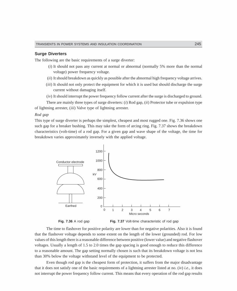
Dharm\N-HIGH\HG7-3.PM5 245
TRANSIENTS IN POWER SYSTEMS AND INSULATION COORDINATION 245
Surge DivertersThe following are the basic requirements of a surge diverter:
(i) It should not pass any current at normal or abnormal (normally 5% more than the normalvoltage) power frequency voltage.
(ii) It should breakdown as quickly as possible after the abnormal high frequency voltage arrives.
(iii) It should not only protect the equipment for which it is used but should discharge the surgecurrent without damaging itself.
(iv) It should interrupt the power frequency follow current after the surge is discharged to ground.
There are mainly three types of surge diverters: (i) Rod gap, (ii) Protector tube or expulsion typeof lightning arrester, (iii) Valve type of lightning arrester.
Rod gap
This type of surge diverter is perhaps the simplest, cheapest and most rugged one. Fig. 7.36 shows onesuch gap for a breaker bushing. This may take the form of arcing ring. Fig. 7.37 shows the breakdowncharacteristics (volt-time) of a rod gap. For a given gap and wave shape of the voltage, the time forbreakdown varies approximately inversely with the applied voltage.
Conductor electrode
Earthed
1200
1000
800
600
400
200
01 2 3 4 5 6 7
Micro seconds0
kV
Fig. 7.36 A rod gap Fig. 7.37 Volt-time characteristic of rod gap
The time to flashover for positive polarity are lower than for negative polarities. Also it is foundthat the flashover voltage depends to some extent on the length of the lower (grounded) rod. For lowvalues of this length there is a reasonable difference between positive (lower value) and negative flashovervoltages. Usually a length of 1.5 to 2.0 times the gap spacing is good enough to reduce this differenceto a reasonable amount. The gap setting normally chosen is such that its breakdown voltage is not lessthan 30% below the voltage withstand level of the equipment to be protected.
Even though rod gap is the cheapest form of protection, it suffers from the major disadvantagethat it does not satisfy one of the basic requirements of a lightning arrester listed at no. (iv) i.e., it doesnot interrupt the power frequency follow current. This means that every operation of the rod gap results
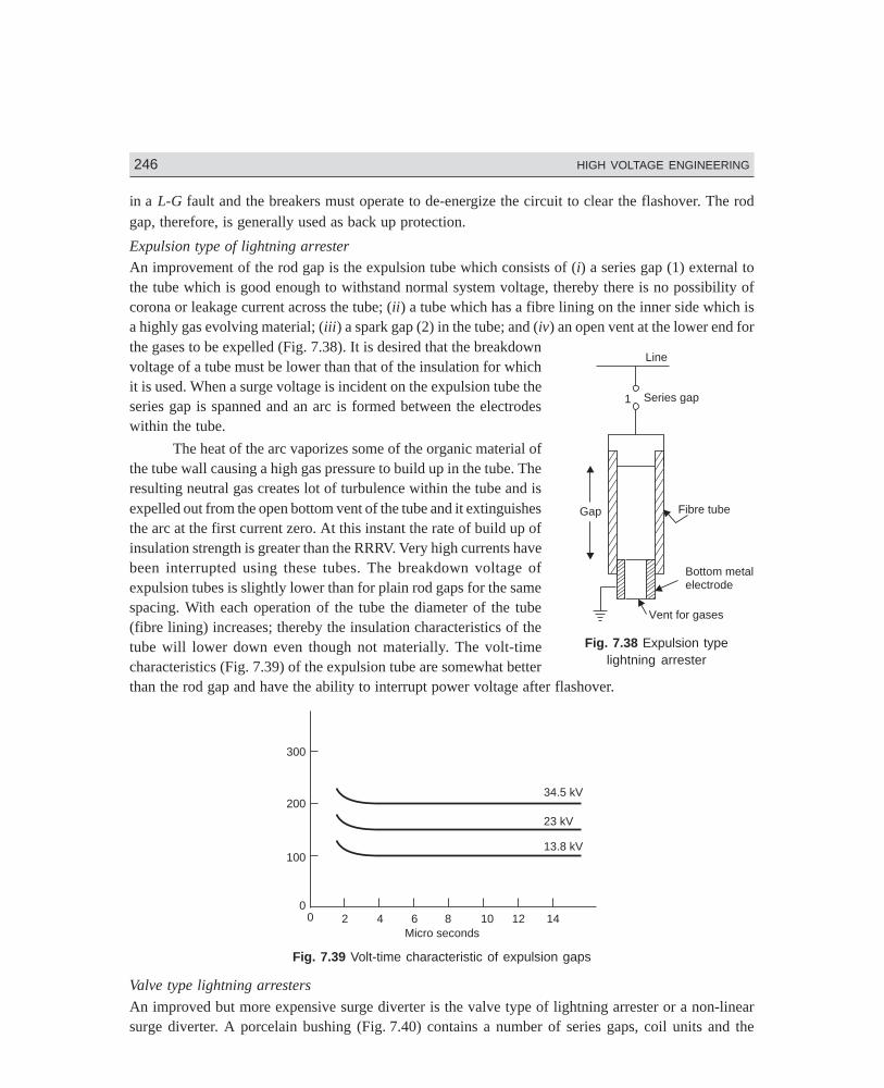
246 HIGH VOLTAGE ENGINEERING
Dharm\N-HIGH\HG7-3.PM5 246
in a L-G fault and the breakers must operate to de-energize the circuit to clear the flashover. The rodgap, therefore, is generally used as back up protection.
Expulsion type of lightning arrester
An improvement of the rod gap is the expulsion tube which consists of (i) a series gap (1) external tothe tube which is good enough to withstand normal system voltage, thereby there is no possibility ofcorona or leakage current across the tube; (ii) a tube which has a fibre lining on the inner side which isa highly gas evolving material; (iii) a spark gap (2) in the tube; and (iv) an open vent at the lower end forthe gases to be expelled (Fig. 7.38). It is desired that the breakdownvoltage of a tube must be lower than that of the insulation for whichit is used. When a surge voltage is incident on the expulsion tube theseries gap is spanned and an arc is formed between the electrodeswithin the tube.
The heat of the arc vaporizes some of the organic material ofthe tube wall causing a high gas pressure to build up in the tube. Theresulting neutral gas creates lot of turbulence within the tube and isexpelled out from the open bottom vent of the tube and it extinguishesthe arc at the first current zero. At this instant the rate of build up ofinsulation strength is greater than the RRRV. Very high currents havebeen interrupted using these tubes. The breakdown voltage ofexpulsion tubes is slightly lower than for plain rod gaps for the samespacing. With each operation of the tube the diameter of the tube(fibre lining) increases; thereby the insulation characteristics of thetube will lower down even though not materially. The volt-timecharacteristics (Fig. 7.39) of the expulsion tube are somewhat betterthan the rod gap and have the ability to interrupt power voltage after flashover.
100
0 2 4 6 8 10 12 14Micro seconds
0
200
300
34.5 kV
23 kV
13.8 kV
Fig. 7.39 Volt-time characteristic of expulsion gaps
Valve type lightning arresters
An improved but more expensive surge diverter is the valve type of lightning arrester or a non-linearsurge diverter. A porcelain bushing (Fig. 7.40) contains a number of series gaps, coil units and the
Gap Fibre tube
Bottom metalelectrode
Vent for gases
Line
Series gap1
Fig. 7.38 Expulsion typelightning arrester
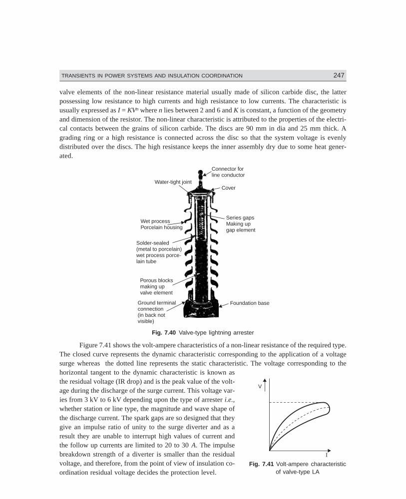
Dharm\N-HIGH\HG7-3.PM5 247
TRANSIENTS IN POWER SYSTEMS AND INSULATION COORDINATION 247
V
I
valve elements of the non-linear resistance material usually made of silicon carbide disc, the latterpossessing low resistance to high currents and high resistance to low currents. The characteristic isusually expressed as I = KVn where n lies between 2 and 6 and K is constant, a function of the geometryand dimension of the resistor. The non-linear characteristic is attributed to the properties of the electri-cal contacts between the grains of silicon carbide. The discs are 90 mm in dia and 25 mm thick. Agrading ring or a high resistance is connected across the disc so that the system voltage is evenlydistributed over the discs. The high resistance keeps the inner assembly dry due to some heat gener-ated.
Connector forline conductor
Cover
Series gapsMaking upgap element
Foundation base
Water-tight joint
Wet processPorcelain housing
Solder-sealed(metal to porcelain)wet process porce-lain tube
Porous blocksmaking upvalve element
Ground terminalconnection(in back notvisible)
Fig. 7.40 Valve-type lightning arrester
Figure 7.41 shows the volt-ampere characteristics of a non-linear resistance of the required type.The closed curve represents the dynamic characteristic corresponding to the application of a voltagesurge whereas the dotted line represents the static characteristic. The voltage corresponding to thehorizontal tangent to the dynamic characteristic is known asthe residual voltage (IR drop) and is the peak value of the volt-age during the discharge of the surge current. This voltage var-ies from 3 kV to 6 kV depending upon the type of arrester i.e.,whether station or line type, the magnitude and wave shape ofthe discharge current. The spark gaps are so designed that theygive an impulse ratio of unity to the surge diverter and as aresult they are unable to interrupt high values of current andthe follow up currents are limited to 20 to 30 A. The impulsebreakdown strength of a diverter is smaller than the residualvoltage, and therefore, from the point of view of insulation co-ordination residual voltage decides the protection level.
Fig. 7.41 Volt-ampere characteristicof valve-type LA
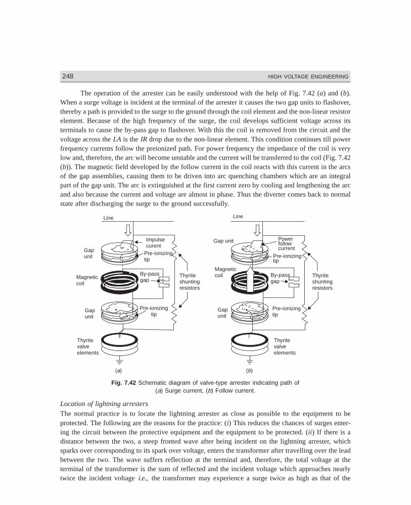
248 HIGH VOLTAGE ENGINEERING
Dharm\N-HIGH\HG7-3.PM5 248
The operation of the arrester can be easily understood with the help of Fig. 7.42 (a) and (b).When a surge voltage is incident at the terminal of the arrester it causes the two gap units to flashover,thereby a path is provided to the surge to the ground through the coil element and the non-linear resistorelement. Because of the high frequency of the surge, the coil develops sufficient voltage across itsterminals to cause the by-pass gap to flashover. With this the coil is removed from the circuit and thevoltage across the LA is the IR drop due to the non-linear element. This condition continues till powerfrequency currents follow the preionized path. For power frequency the impedance of the coil is verylow and, therefore, the arc will become unstable and the current will be transferred to the coil (Fig. 7.42(b)). The magnetic field developed by the follow current in the coil reacts with this current in the arcsof the gap assemblies, causing them to be driven into arc quenching chambers which are an integralpart of the gap unit. The arc is extinguished at the first current zero by cooling and lengthening the arcand also because the current and voltage are almost in phase. Thus the diverter comes back to normalstate after discharging the surge to the ground successfully.
Line
Impulsecurent
Pre-ionizingtip
Gapunit
Magneticcoil
By-passgap
Gapunit
Pre-ionizingtip
Thyriteshuntingresistors
Thyritevalveelements
Line
Powerfollowcurrent
Pre-ionizingtip
By-passgap
Magneticcoil
Gapunit
Pre-ionizingtip
Thyriteshuntingresistors
Thyritevalveelements
( )b( )a
Gap unit
Fig. 7.42 Schematic diagram of valve-type arrester indicating path of(a) Surge current, (b) Follow current.
Location of lightning arresters
The normal practice is to locate the lightning arrester as close as possible to the equipment to beprotected. The following are the reasons for the practice: (i) This reduces the chances of surges enter-ing the circuit between the protective equipment and the equipment to be protected. (ii) If there is adistance between the two, a steep fronted wave after being incident on the lightning arrester, whichsparks over corresponding to its spark over voltage, enters the transformer after travelling over the leadbetween the two. The wave suffers reflection at the terminal and, therefore, the total voltage at theterminal of the transformer is the sum of reflected and the incident voltage which approaches nearlytwice the incident voltage i.e., the transformer may experience a surge twice as high as that of the
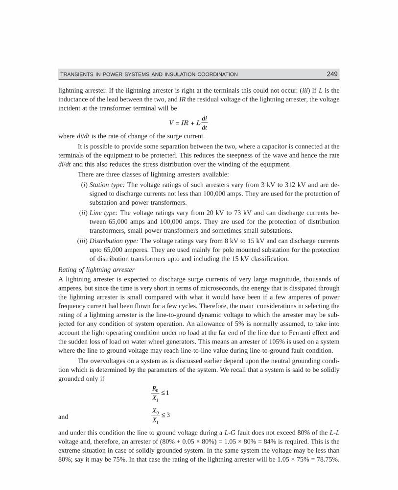
Dharm\N-HIGH\HG7-3.PM5 249
TRANSIENTS IN POWER SYSTEMS AND INSULATION COORDINATION 249
lightning arrester. If the lightning arrester is right at the terminals this could not occur. (iii) If L is theinductance of the lead between the two, and IR the residual voltage of the lightning arrester, the voltageincident at the transformer terminal will be
V = IR + Ldi
dtwhere di/dt is the rate of change of the surge current.
It is possible to provide some separation between the two, where a capacitor is connected at theterminals of the equipment to be protected. This reduces the steepness of the wave and hence the ratedi/dt and this also reduces the stress distribution over the winding of the equipment.
There are three classes of lightning arresters available:
(i) Station type: The voltage ratings of such arresters vary from 3 kV to 312 kV and are de-signed to discharge currents not less than 100,000 amps. They are used for the protection ofsubstation and power transformers.
(ii) Line type: The voltage ratings vary from 20 kV to 73 kV and can discharge currents be-tween 65,000 amps and 100,000 amps. They are used for the protection of distributiontransformers, small power transformers and sometimes small substations.
(iii) Distribution type: The voltage ratings vary from 8 kV to 15 kV and can discharge currentsupto 65,000 amperes. They are used mainly for pole mounted substation for the protectionof distribution transformers upto and including the 15 kV classification.
Rating of lightning arrester
A lightning arrester is expected to discharge surge currents of very large magnitude, thousands ofamperes, but since the time is very short in terms of microseconds, the energy that is dissipated throughthe lightning arrester is small compared with what it would have been if a few amperes of powerfrequency current had been flown for a few cycles. Therefore, the main considerations in selecting therating of a lightning arrester is the line-to-ground dynamic voltage to which the arrester may be sub-jected for any condition of system operation. An allowance of 5% is normally assumed, to take intoaccount the light operating condition under no load at the far end of the line due to Ferranti effect andthe sudden loss of load on water wheel generators. This means an arrester of 105% is used on a systemwhere the line to ground voltage may reach line-to-line value during line-to-ground fault condition.
The overvoltages on a system as is discussed earlier depend upon the neutral grounding condi-tion which is determined by the parameters of the system. We recall that a system is said to be solidlygrounded only if
R
X0
1
1≤
andX
X0
1
3≤
and under this condition the line to ground voltage during a L-G fault does not exceed 80% of the L-Lvoltage and, therefore, an arrester of (80% + 0.05 × 80%) = 1.05 × 80% = 84% is required. This is theextreme situation in case of solidly grounded system. In the same system the voltage may be less than80%; say it may be 75%. In that case the rating of the lightning arrester will be 1.05 × 75% = 78.75%.
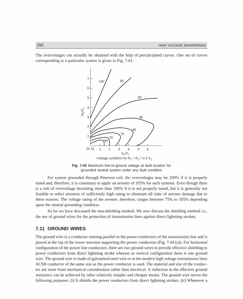
250 HIGH VOLTAGE ENGINEERING
Dharm\N-HIGH\HG7-3.PM5 250
The overvoltages can actually be obtained with the help of precalculated curves. One set of curvescorresponding to a particular system is given in Fig. 7.43.
7
6
5
4
3
2
1
100 95
90
85
8075
7065
R/X
01
(0, 0) 1 2 3 4 5 6X /X0 1
Voltage condition for R = R = 0.2 X1 2 1
Fig. 7.43 Maximum line-to-ground voltage at fault location forgrounded neutral system under any fault condition
For system grounded through Peterson coil, the overvoltages may be 100% if it is properlytuned and, therefore, it is customary to apply an arrester of 105% for such systems. Even though thereis a risk of overvoltage becoming more than 100% if it is not properly tuned, but it is generally notfeasible to select arresters of sufficiently high rating to eliminate all risks of arrester damage due tothese reasons. The voltage rating of the arrester, therefore, ranges between 75% to 105% dependingupon the neutral grounding condition.
So far we have discussed the non-shielding method. We now discuss the shielding method i.e.,the use of ground wires for the protection of transmission lines against direct lightning strokes.
7.11 GROUND WIRES
The ground wire is a conductor running parallel to the power conductors of the transmission line and isplaced at the top of the tower structure supporting the power conductors (Fig. 7.44 (a)). For horizontalconfiguration of the power line conductors, there are two ground wires to provide effective shielding topower conductors from direct lightning stroke whereas in vertical configuration there is one groundwire. The ground wire is made of galvanized steel wire or in the modern high voltage transmission linesACSR conductor of the same size as the power conductor is used. The material and size of the conduc-tor are more from mechanical consideration rather than electrical. A reduction in the effective groundresistance can be achieved by other relatively simpler and cheaper means. The ground wire serves thefollowing purposes: (i) It shields the power conductors from direct lightning strokes. (ii) Whenever a
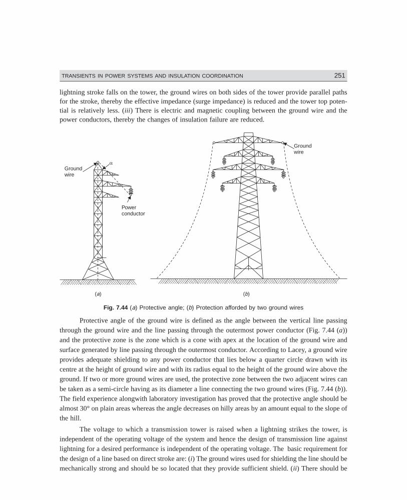
Dharm\N-HIGH\HG7-3.PM5 251
TRANSIENTS IN POWER SYSTEMS AND INSULATION COORDINATION 251
lightning stroke falls on the tower, the ground wires on both sides of the tower provide parallel pathsfor the stroke, thereby the effective impedance (surge impedance) is reduced and the tower top poten-tial is relatively less. (iii) There is electric and magnetic coupling between the ground wire and thepower conductors, thereby the changes of insulation failure are reduced.
Groundwire
Powerconductor
( )a
Groundwire
( )b
Fig. 7.44 (a) Protective angle; (b) Protection afforded by two ground wires
Protective angle of the ground wire is defined as the angle between the vertical line passingthrough the ground wire and the line passing through the outermost power conductor (Fig. 7.44 (a))and the protective zone is the zone which is a cone with apex at the location of the ground wire and
surface generated by line passing through the outermost conductor. According to Lacey, a ground wireprovides adequate shielding to any power conductor that lies below a quarter circle drawn with itscentre at the height of ground wire and with its radius equal to the height of the ground wire above theground. If two or more ground wires are used, the protective zone between the two adjacent wires can
be taken as a semi-circle having as its diameter a line connecting the two ground wires (Fig. 7.44 (b)).The field experience alongwith laboratory investigation has proved that the protective angle should bealmost 30° on plain areas whereas the angle decreases on hilly areas by an amount equal to the slope ofthe hill.
The voltage to which a transmission tower is raised when a lightning strikes the tower, isindependent of the operating voltage of the system and hence the design of transmission line againstlightning for a desired performance is independent of the operating voltage. The basic requirement for
the design of a line based on direct stroke are: (i) The ground wires used for shielding the line should bemechanically strong and should be so located that they provide sufficient shield. (ii) There should be
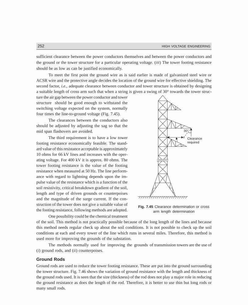
252 HIGH VOLTAGE ENGINEERING
Dharm\N-HIGH\HG7-3.PM5 252
sufficient clearance between the power conductors themselves and between the power conductors andthe ground or the tower structure for a particular operating voltage. (iii) The tower footing resistanceshould be as low as can be justified economically.
To meet the first point the ground wire as is said earlier is made of galvanized steel wire orACSR wire and the protective angle decides the location of the ground wire for effective shielding. Thesecond factor, i.e., adequate clearance between conductor and tower structure is obtained by designinga suitable length of cross arm such that when a string is given a swing of 30° towards the tower struc-ture the air gap between the power conductor and towerstructure should be good enough to withstand theswitching voltage expected on the system, normallyfour times the line-to-ground voltage (Fig. 7.45).
The clearances between the conductors alsoshould be adjusted by adjusting the sag so that themid span flashovers are avoided.
The third requirement is to have a low towerfooting resistance economically feasible. The stand-ard value of this resistance acceptable is approximately10 ohms for 66 kV lines and increases with the oper-ating voltage. For 400 kV it is approx. 80 ohms. Thetower footing resistance is the value of the footingresistance when measured at 50 Hz. The line perform-ance with regard to lightning depends upon the im-pulse value of the resistance which is a function of thesoil resistivity, critical breakdown gradient of the soil,length and type of driven grounds or counterpoisesand the magnitude of the surge current. If the con-struction of the tower does not give a suitable value ofthe footing resistance, following methods are adopted.
One possibility could be the chemical treatmentof the soil. This method is not practically possible because of the long length of the lines and becausethis method needs regular check up about the soil conditions. It is not possible to check up the soilconditions at each and every tower of the line which runs in several miles. Therefore, this method isused more for improving the grounds of the substation.
The methods normally used for improving the grounds of transmission towers are the use of(i) ground rods, and (ii) counterpoises.
Ground RodsGround rods are used to reduce the tower footing resistance. These are put into the ground surroundingthe tower structure. Fig. 7.46 shows the variation of ground resistance with the length and thickness ofthe ground rods used. It is seen that the size (thickness) of the rod does not play a major role in reducingthe ground resistance as does the length of the rod. Therefore, it is better to use thin but long rods ormany small rods.
30°
Clearancerequired
Fig. 7.45 Clearance determination or crossarm length determination
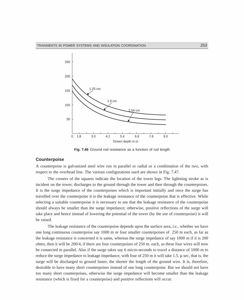
Dharm\N-HIGH\HG7-3.PM5 253
TRANSIENTS IN POWER SYSTEMS AND INSULATION COORDINATION 253
250
200
150
100
50
0 1.8 3.0 4.2 5.4 6.6 7.8 9.0
Driven depth in m
1.25 cm
1.9 cm
2.54 cm
Fig. 7.46 Ground rod resistance as a function of rod length
Counterpoise
A counterpoise is galvanized steel wire run in parallel or radial or a combination of the two, withrespect to the overhead line. The various configurations used are shown in Fig. 7.47.
The corners of the squares indicate the location of the tower legs. The lightning stroke as isincident on the tower, discharges to the ground through the tower and then through the counterpoises.It is the surge impedance of the counterpoises which is important initially and once the surge has
travelled over the counterpoise it is the leakage resistance of the counterpoise that is effective. Whileselecting a suitable counterpoise it is necessary to see that the leakage resistance of the counterpoiseshould always be smaller than the surge impedance; otherwise, positive reflections of the surge willtake place and hence instead of lowering the potential of the tower (by the use of counterpoise) is will
be raised.
The leakage resistance of the counterpoise depends upon the surface area, i.e., whether we haveone long continuous counterpoise say 1000 m or four smaller counterpoises of 250 m each, as far as
the leakage resistance is concerned it is same, whereas the surge impedance of say 1000 m if it is 200ohms, then it will be 200/4, if there are four counterpoises of 250 m. each, as these four wires will nowbe connected in parallel. Also if the surge takes say 6 micro-seconds to travel a distance of 1000 m toreduce the surge impedance to leakage impedance, with four of 250 m it will take 1.5. µ sec, that is, the
surge will be discharged to ground faster, the shorter the length of the ground wire. It is, therefore,desirable to have many short counterpoises instead of one long counterpoise. But we should not havetoo many short counterpoises, otherwise the surge impedance will become smaller than the leakageresistance (which is fixed for a counterpoise) and positive reflections will occur.
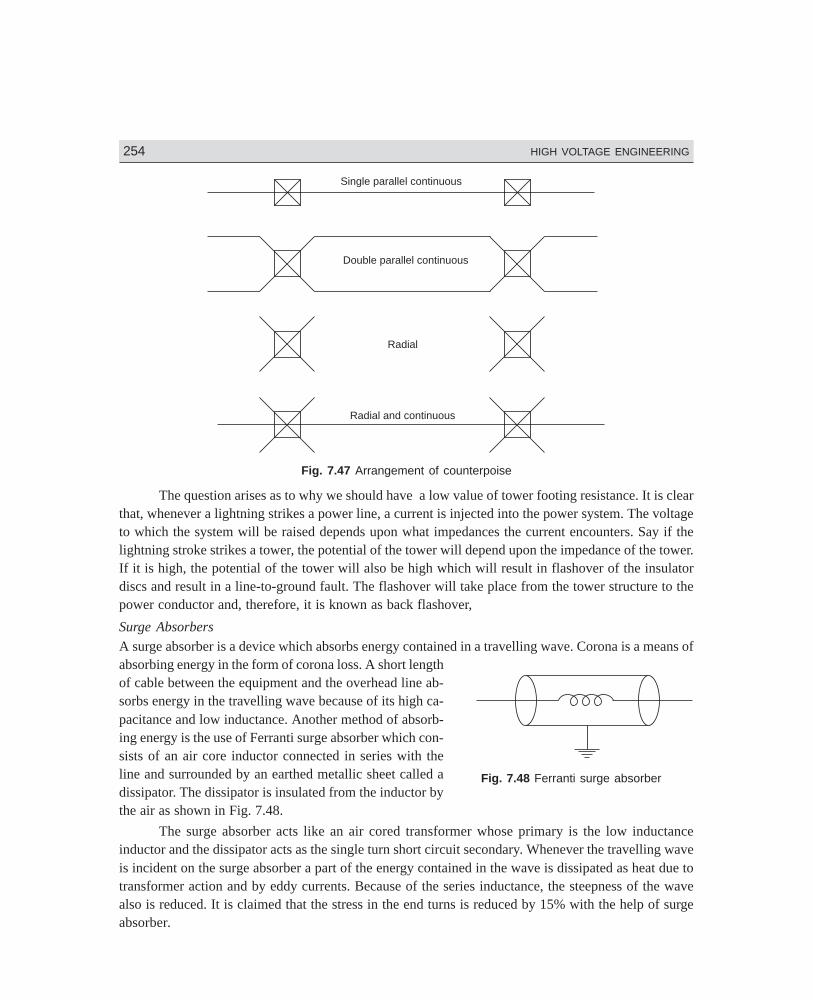
254 HIGH VOLTAGE ENGINEERING
Dharm\N-HIGH\HG7-3.PM5 254
Single parallel continuous
Double parallel continuous
Radial
Radial and continuous
Fig. 7.47 Arrangement of counterpoise
The question arises as to why we should have a low value of tower footing resistance. It is clearthat, whenever a lightning strikes a power line, a current is injected into the power system. The voltageto which the system will be raised depends upon what impedances the current encounters. Say if thelightning stroke strikes a tower, the potential of the tower will depend upon the impedance of the tower.If it is high, the potential of the tower will also be high which will result in flashover of the insulatordiscs and result in a line-to-ground fault. The flashover will take place from the tower structure to thepower conductor and, therefore, it is known as back flashover,
Surge Absorbers
A surge absorber is a device which absorbs energy contained in a travelling wave. Corona is a means ofabsorbing energy in the form of corona loss. A short lengthof cable between the equipment and the overhead line ab-sorbs energy in the travelling wave because of its high ca-pacitance and low inductance. Another method of absorb-ing energy is the use of Ferranti surge absorber which con-sists of an air core inductor connected in series with theline and surrounded by an earthed metallic sheet called adissipator. The dissipator is insulated from the inductor bythe air as shown in Fig. 7.48.
The surge absorber acts like an air cored transformer whose primary is the low inductanceinductor and the dissipator acts as the single turn short circuit secondary. Whenever the travelling waveis incident on the surge absorber a part of the energy contained in the wave is dissipated as heat due totransformer action and by eddy currents. Because of the series inductance, the steepness of the wavealso is reduced. It is claimed that the stress in the end turns is reduced by 15% with the help of surgeabsorber.
Fig. 7.48 Ferranti surge absorber
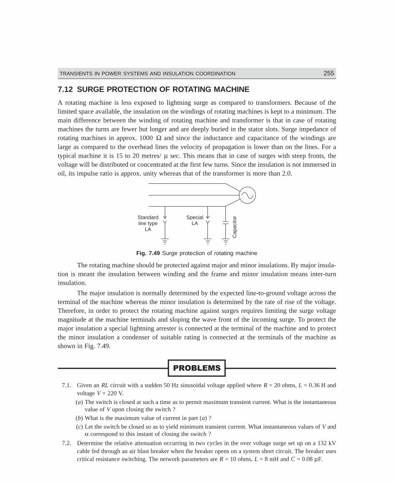
Dharm\N-HIGH\HG7-3.PM5 255
TRANSIENTS IN POWER SYSTEMS AND INSULATION COORDINATION 255
7.12 SURGE PROTECTION OF ROTATING MACHINE
A rotating machine is less exposed to lightning surge as compared to transformers. Because of thelimited space available, the insulation on the windings of rotating machines is kept to a minimum. Themain difference between the winding of rotating machine and transformer is that in case of rotatingmachines the turns are fewer but longer and are deeply buried in the stator slots. Surge impedance ofrotating machines in approx. 1000 Ω and since the inductance and capacitance of the windings arelarge as compared to the overhead lines the velocity of propagation is lower than on the lines. For atypical machine it is 15 to 20 metres/ µ sec. This means that in case of surges with steep fronts, thevoltage will be distributed or concentrated at the first few turns. Since the insulation is not immersed inoil, its impulse ratio is approx. unity whereas that of the transformer is more than 2.0.
Standardline type
LA
SpecialLA
Cap
acito
r
Fig. 7.49 Surge protection of rotating machine
The rotating machine should be protected against major and minor insulations. By major insula-tion is meant the insulation between winding and the frame and minor insulation means inter-turninsulation.
The major insulation is normally determined by the expected line-to-ground voltage across theterminal of the machine whereas the minor insulation is determined by the rate of rise of the voltage.Therefore, in order to protect the rotating machine against surges requires limiting the surge voltagemagnitude at the machine terminals and sloping the wave front of the incoming surge. To protect themajor insulation a special lightning arrester is connected at the terminal of the machine and to protectthe minor insulation a condenser of suitable rating is connected at the terminals of the machine asshown in Fig. 7.49.
7.1. Given an RL circuit with a sudden 50 Hz sinusoidal voltage applied where R = 20 ohms, L = 0.36 H andvoltage V = 220 V.
(a) The switch is closed at such a time as to permit maximum transient current. What is the instantaneousvalue of V upon closing the switch ?
(b) What is the maximum value of current in part (a) ?
(c) Let the switch be closed so as to yield minimum transient current. What instantaneous values of V andα correspond to this instant of closing the switch ?
7.2. Determine the relative attenuation occurring in two cycles in the over voltage surge set up on a 132 kVcable fed through an air blast breaker when the breaker opens on a system short circuit. The breaker usescritical resistance switching. The network parameters are R = 10 ohms, L = 8 mH and C = 0.08 µF.
256 HIGH VOLTAGE ENGINEERING
Dharm\N-HIGH\HG7-3.PM5 256
7.3. Explain with neat diagrams two different theories of charge generation and separation in a thunder cloud.
7.4. Explain with neat sketches the mechanism of lightning discharge.
7.5. Differentiate between a hot lightning stroke and a cold lightning stroke.
7.6. Show that a travelling wave moves with a velocity of light on the overhead line and its speed is propor-
tional to 1/ εr on a cable with dielectric material of permittivity εr.
7.7. Explain the variation of current and voltage on an overhead line when one end of the line is(i) short-circuited, and (ii) open-circuited and at the other end a source of constant e.m.f. V is switched in.
7.8. What is a travelling wave ? Explain the development of such a wave on an overhead line.
7.9. An overhead transmission line with surge impedance 400 ohms is 300 km long. One end of this line isshort-circuited and at the other end a source of 11 kV is suddenly switched in. Calculate the current at thesource end 0.005 sec after the voltage is applied.
7.10. Explain why a short length of cable is connected between the dead end tower and the terminal apparatusin a station. An over-head line with surge impedance 400 ohms is connected to a terminal apparatusthrough a short length of cable of surge impedance 40 ohms.
A travelling wave of constant magnitude 100 kV and infinite duration originates in the overhead line andtravels towards the junction with the cable. Calculate the energy transmitted into the cable during a periodof 5 µ sec after the arrival of the wave at the junction.
7.11. An overhead line with inductance and capacitance per km of 1.24 mH and 0.087 µF respectively is con-nected in series with an underground cable having inductance and capacitance of 0.185 mH/km and 0.285µF/km. Calculate the values of transmitted and reflected waves of voltage and current at the junction dueto a voltage surge of 110 kV travelling to the junction (i) along the line towards the cable, and (ii) alongthe cable towards the line.
7.12. An overhead line with surge impedance 400 ohms bifurcates into two lines of surge impedance 400 ohmsand 40 ohms respectively. If a surge of 20 kV is incident on the overhead line, determine the magnitudesof voltage and current which enter the bifurcated lines.
7.13. A long overhead line has a surge impedance of 500 ohms and an effective resistance of 6 ohms per km. Ifa surge of 400 kV enters the line at a certain point, calculate the magnitude of this surge after it hastraversed 100 km and calculate the power loss and heat loss of the wave over this distance. Assumevelocity of wave as 3 × 10⁸ m/sec.
7.14. A rectangular surge of 2 µ sec duration and magnitude 100 kV travels along a line of surge impedance500 ohms. The latter is connected to another line of equal impedance through an inductor of 500 µH.Calculate the maximum value of surge transmitted to the second line.
7.15. The effective inductance and capacitance of a faulted system as viewed from the contacts of a breaker are2.5 mH and 600 pF respectively. Determine the restriking voltage across the breaker contacts when a faultcurrent of 150 amps is chopped.
7.16. What is arcing ground? Explain its effect on the performance of a power system.
7.17. What is “capacitance switching”? Explain its effect on the performance of the circuit breaker.
7.18. What are volt-time curves ? What is their significance in power system studies?
7.19. What are BILS? Explain their significance in power system studies?
7.20. Describe the construction, principle of operation and application of (i) Rod gaps; (ii) Expulsion gap; and(iii) Valve type lightning arrester.
7.21. Compare the relative performances of the following: (i) Rod gap; (ii) Expulsion gap; and (iii) Valve typel.A.
Dharm\N-HIGH\HG7-3.PM5 257
TRANSIENTS IN POWER SYSTEMS AND INSULATION COORDINATION 257
7.22. Explain clearly how the rating of a lightning arrester is selected. What is the best location of a lightningarrester and why?
7.23. What is tower-footing resistance? What are the methods to reduce this resistance? Why is it required tohave this resistance as low as economically feasible?
7.24. What are ground rods and counterpoises? Explain clearly how these can be used to improve the groundingconditions. Give various arrangements of counterpoise.
7.25. “The leakage resistance of a counterpoise should be lower than its surge impedance.” Why?
7.26. What is a ground wire? Discuss its location with respect to power conductors.
7.27. What are the requirements of a ground wire for protecting power conductors against direct lightningstroke? Explain how they are achieved in practice.
7.28. Explain the principle of operation of Ferranti surge absorber.
7.29. What are the basic requirements of a lightning arrester? Differentiate between (i) a lightning arrester anda lightning conductor, and (ii) a surge diverter and a surge absorber.
7.30. Explain clearly how a lightning arrester is selected for protecting a power transformer.
7.31. Give a scheme of protecting a rotating machine against overvoltages. Explain clearly how the scheme isdifferent from protecting a power transformer.
H. A. Peterson, Power System Transients, Dover, 1966.
Travelling Waves on Transmission Systems, Dover, 1961.
Allan Greenwood, Electrical Transients in Power System, John Wiley & Sons, 1971.
IEEE Committee Report on Switching Surges, IEEE Trans. on PAS, pp. 912, 1948.
V.A. Venikov, Transients in Power System.
H. Cotton, The Transmission and Distribution of Electrical Energy.
The Transmission and Distribution Reference Book, Westinghouse Elect. Corp., Pennsylvania, 1964.
B. M. Weedy, Electric Power Systems, John Wiley & Sons, 1974.
F. S. Young et al., Shielding of Transmission Lines, IEEE Trans. on PAS, 83, 132, 1963.
Kuffel, E., Zaengl, W.S., High Voltage Engineering Fundamentals, Pergamen Press, 1984.

258
1. The process of ionisation is brought about by
(a) Positive ions only (b) Photons only
(c) metastables only (d) all of the above
2. The value of Townsends second ionization coefficient has
(a) high value for low E/p ratio (b) Low value for low E/p ratio
(c) no relation with E/p ratio (d) no application if the gas pressure is low
3. If α and v are the Townsends first and second ionisation coefficients, d the distance of separa-tion between the plates, the Townsends Criterion for Threshold sparking is given as
(a) eαd = 1 (b) γeαd = 1 (c) eαd/γ = 1 (d) γeαd = 2
4. When avalanche in the gap reaches a certain critical size, the electric spark discharge is duemainly to ionization of gas by
(a) electron impact (b) positive ion bombardment
(c) photoionization (d) all (a) (b) and (c)
5. If Er is the radial field due to space charge and E0 the externally applied field, the transformationof avalanche into a streamer takes place when
(a) Er < E0 (b) Er > E0 (c) Er ≈ E0
(d) (a) and (c) (e) (b) and (c)
6. If p is the pressure of gas and d the distance of separation between the electrodes, the dischargevoltage according to paschen’s low is directly proportional to
(a) p (b) d (c) pd (d) none of the above
7. Assuming p to be Constant and Townsend’s second ionization coefficure to be small during theapplicability of Paschen’s law. Then if (pd > (pd)min
(a) electrons crossing in the gap make more frequent collisions with gas molecules than at(pd)min
(b) energy gained between successive collisions is smaller than at (pd)min
(c) energy gained between successive collisions is larger than at (pd)min
(d) (a) and (b)
(e) (a) and (c)
8. The breakdown voltage of a specimen is 65 kV at STP. The breakdown voltage at 73 cm Hgpressure and 35° C is
(a) 69 kV (b) 63.25 kV (c) 64.33 kV (d) 60.39
Multiple Choice Questions

Dharm\N-HIGH\HG-OBJ.PM5 259
MULTIPLE CHOICE QUESTIONS 259
9. Penning effect explains
(a) increase in dielectric strength of all mixture of gases
(b) decrease in dielectric strength of many mixture of gases
(c) increase in dielectric strength of many mixture of gases
(d) none of the above
10. Trichel pulses are noticed in a point plane gap in air when
(a) point is positive
(b) point is negative
(c) These pulses are seen in plane-sphere gap
(d) These pulses are seen in point-sphere gap
11. The on-set voltage for Trichel pulses
(a) increases with increases in gap length
(b) increases with decrease in gap length
(c) independent of gap length
12. The frequency of Trichel pulses
(a) increases with voltage and gap pressure
(b) increases with voltage but decreases with increase in pressure
(c) decreases with increase in voltage and pressure
(d) decreases with increase in voltage and increases with increase in pressure.
13. All parameters remaining same, the breakdown voltage is
(a) higher with negative polarity at all pressures
(b) lower with negative polarity at all pressures
(c) higher with negative polarity at low pressures.
` (d) none of above
14. Liquids with solid impurities
(a) have higher dielectric strength
(b) of large size have higher dielectric strength
(c) has lower dielectric strength as compared to pure liquids
(d) none of the above
15. The electric field in a gas bubble which is immersed in a liquid of permittivity εz is
(a) higher than that of the field in the liquid
(b) lower than that of the field in the liquid
(c) same as that in the liquid
(d) none of the above is always true
16. Centrifugal methods of reconditioning transformer oil is effected for removal of
(a) water (b) dissolved gases
(c) solid impurities (d) all of the above
260 HIGH VOLTAGE ENGINEERING
Dharm\N-HIGH\HG-OBJ.PM5 260
17. In order to prevent an excessive evaporation of the aromatics during reconditioning of trans-former oil using filtrations under vacuum, the vapour pressure should be
(a) less than 10–4 torr (b) less than 10–2 torr
(c) less than 10–1 torr (d) none of the above
18 During reconditioning of transformer oil it is economical to use electrostatic filters if the watercontent of oil is
(a) greater than 4 ppm (b) greater than 2 ppm
(c) less than 2 ppm (d) electrostatic filters are never used
19. The accepted value of dielectric strength of transformer oil is
(a) 30 kV (b) 30 kV/cm
(c) 30 kV/cm for one min. (d) none of the above
20. While testing transformer oil for dielectric strength the spherical electrodes are placed in
(a) horizontal configuration (b) vertical configuration
(c) any configuration (d) spherical electrodes are not used
21. The breakdown of solid materials is roughly given by
(a) Vbtb = constant (b) Vb 1n tb = constant
(c) tb 1n Vb = constant (d) None of the above
22. While conducting intrinsic dielectric strength on a specimen, its shape should be so preparedthat
(a) the electric stress is high at its centre
(b) the electric stress is high at its corner
(c) the electric stress is same all along the sample
(d) No definite consideration
23. To determine intrinsic dielectric strength, the time of application of voltage is of the order of
(a) 10–8 sec (b) 10–6 sec
(c) 10–4 sec (d) No such consideration
24. In case of impulse thermal breakdown of solid insulating materials, the critical electric filed is
(a) proportional to critical absolute temperature
(b) proportional to square of critical absolute temperature
(c) proportional to square of T0
(d) None of the above is true
25. In case of impulse thermal breakdown of insulating materials, the critical time to breakdown is
(a) proportional to critical electric filed
(b) inversely proportional to critical electric field
(c) proportional to square of critical absolute temperature
(d) None of the above
Dharm\N-HIGH\HG-OBJ.PM5 261
MULTIPLE CHOICE QUESTIONS 261
26. The ripple voltage in the d.c. output is small if
(a) frequency of supply is small (b) the filtering capacitor is small
(c) the load current is large (d) none of the above is true
27. The voltage drop for a certain Cockroft and Walton circuit is small if
(a) the load current is small (b) the frequency of supply is small
(c) the capacitance of each stage is small (d) all of the above
28. All other parameters remaining identical, the ratio of voltage drop for an 8 stage to 4 stageCockroft Walton circuit approximately is
(a) 2 (b) 8 (c) 4 (d) 2.828
29. In Cockrofts-Walton circuit, the optimum number of stages for maximum output voltage (for afixed supply voltage magnitude) is directly proportional to
(a) frequency of supply (b) capacitance of each stage
(c) load current (d) none of the above
30. In a Cockroft-Walton circuit, input voltage 100 kV load current-100 mA, supply frequency 100Hz, each capacitor 10 nF. The optimum no. of stages for maximum output voltage is
(a) 1 (b) 10 (c) 15 (d) 35
31. The maximum output voltage is question 30 is
(a) 133 kV (b) 300 kV (c) 500 kV (d) 1000 kV
32. In order to reduce ripples and/or voltage drop, it is more economical to use
(a) high frequency and high capacitance (b) high frequency and small capacitance
(c) low frequency and small capacitance (d) low frequency and high capacitance
33. In a Van de Graaf generator, the width of the belt is 1 m, and surface charge density permissibleis 30 × 10–6 C/m2. To supply a current of 300 µA, the velocity of belt should be
(a) 1 m/sec (b) 10 m/sec (c) 3.16 m/sec (d) None of the above
34. The surface charge density permissible in a Van de Graaf generator is 30 × 10–6 c/m2. The radiusof the electrode to charge to 10 MV is
(a) 0.295 m (b) 0.532 m (c) 1.234 m (d) 1.535 m
35. The radius of the ht electrode is 1 metre in Van de Graaf generator. If the permissible electricfield is 21 kV/cm the maximum potential to which the electrode can be charged is
(a) 2.1 MV (b) 21 MV (c) 4.5 MV (d) None of the above
36. For a 3 stage Cascaded transformer if P1, P2, P3 are the loadings of I, II and III stages primaries,then
(a) P1 = P2 = P3 (b) P1 > P2 > P3 (c) P1 < P2 < P3 (d) P2 < P1 < P3
37. The short-circuit impedance of a three stage cascaded transformer as compared to a single unittransformer is
(a) 3 to 4 times (b) 8 to 9 times (c) 15 to16 times (d) 352 to 452 times
38. If the quality factor of the h.t. reactor in a.c. series resonant circuit is 49, and Q is the reactivepower requirement of the test specimen, then the kW rating of the Feed Transformer is
(a) 49 Q (b) 7 Q (c) Q/7 (d) Q/49
262 HIGH VOLTAGE ENGINEERING
Dharm\N-HIGH\HG-OBJ.PM5 262
39. If a single stage system using resonance test voltage is required, it is better to use
(a) series resonant circuit (b) parallel resonant circuit
(c) series-parallel resonant circuit (d) any one of the above
40. The impulse ratio for any particular object
(a) is a constant
(b) depends upon shape of wave
(c) depends upon the polarity of the impulse wave
(d) (b) and (c)
41. Impulse generator with circuit ‘a’ configuration as compared with circuit ‘b’ configuration
(a) has high voltage efficiency
(b) can be used for most of the equipments to be tested
(c) (a) and (b) (d) none of the above
42. The wave front and tail resistance and IG are 150 and 2000 Ω respectively. The impulse capaci-tance and load capacitances are 25 and 2 nF respectively. The approximate wave front time is
(a) 1 µ Sec. (b) 0.833 µ Sec. (c) 1.525 µ Sec. (d) 1.22 µ Sec.
43. The wave tail time for the above problem is
(a) 50.79 µ Sec. (b) 40.6 µ Sec. (c) 150 µ Sec. (d) 325.33 µ Sec.
44. For an impulse generator if C1/C2 > 10, for a given wave shape with different values of C1/C2
(a) wave front resistance is practically constant
(b) wave tail resistance is practically constant
(c) (a) and (b) (d) None of the above is true
45. The approximate voltage efficiency of IG for problem 42 is
(a) 99.45 % (b) 98.32 % (c) 92.60 % (d) 90.35 %
46. The minimum value of impulse capacitance to prevent oscillations on the tail of the impulsewave (1.5/40 µ Sec.) while testing inductive load with inductance of 10 H is
(a) 400 pF (b) 4 pF (c) 1628 pF (d) 1280 pF
47. The minimum value of impulse capacitance to impulse test a 3 φ, 200 kV, 5% impedance, powertransformer is
(a) 4.5 nF (b) 0.22 nF (c) 0.826 nF (d) 0.02 µF
48. While impulse testing a power transformer, the impulse voltage is applied to
(a) one phase and the other two phases are short circuited, the secondary terminals are shortcircuited.
(b) one phase, the other two phases grounded, the secondary short circuited
(c) one phase, two phases left open, secondary left open
(d) one phase, two phases left open, secondary short circuited
49. If Rc is the charging resistance, R2 wave tail resistance and R1 the wave front control resistancethen
(a) Rc > R2 < R1 (b) Rc < R2 < R1
(c) R1 > R2 > Rc (d) None of the above
Dharm\N-HIGH\HG-OBJ.PM5 263
MULTIPLE CHOICE QUESTIONS 263
50. In order that Impulse circuit operates consistently, it is essential that
(a) the first gap is slightly less than the second and so on
(b) the axes of the gaps should be in the same vertical plane
(c) (a) and (b)
(d) None of the above is necessary
51. It is desirable to have wavefront control resistance
(a) entirely within the impulse circuit
(b) entirely outside the impulse circuit
(c) partly inside and partly outside the impulse circuit
(d) any where
52. The magnitude of pulse currents depends upon
(a) voltage applied (b) no. of voids (c) (a) and (b)
53. The frequency spectrum of PD pulse current contains complete information concerning
(a) the measurable charge in low frequency range
(b) apparent charge in the low frequency range
(c) apparent charge in the high frequency range
(d) None of the above
54. In order to have proper integration of the pulse current it is desired that
(a) time constant of pulse τ should be greater than time constant of the measuring circuit (T)
(b) τ < T (c) τ = T
(d) time constant has nothing to do with integration of a pulse current
55. In narrow band PD detection circuit
(a) Parallel combination of RLC forms measuring impedance
(b) Parallel combination of RL forms measuring impedance
(c) integration is carried out on the pulse current
(d) (a) and (c)
56. Recurrent surge generator is used to generate
(a) current of large magnitude
(b) repetitive current surges
(c) impulse voltage of smaller magnitude
(d) (b) and (c)
57. For reducing tower footing resistance it is better to use
(a) chemical and ground rods only (b) chemical and counterpoise only
(c) ground rod and counterpoise only (d) chemical, ground rods and counter poise
58. The impulse ratio of a rod gap is:
(a) unity (b) between 1.2 and 1.5
(c) between 2.0 and 2.2 (d) between 1.6 and 1.8
264 HIGH VOLTAGE ENGINEERING
Dharm\N-HIGH\HG-OBJ.PM5 264
59. The insulation of the modern EHV lines is designed based on:
(a) The lightning voltage (b) The switching voltage
(c) Corona (d) RI
60. High voltage d.c. testing for HV machines is resorted because
(a) Certain conclusions regarding the continuous ageing of an insulation can be drawn
(b) The stress distribution is a representation of the service condition
(c) Standardisation on the magnitude of voltage to be applied is available
(d) The stresses do not damage the coil and insulation
61. Standard impulse testing of a power transformer requires :
(a) Two applications of chopped wave followed by one application of a full wave
(b) One application of chopped wave followed by one applications of a full wave
(c) One application of chopped wave followed by two applications of a full wave
(d) None of the above
62. The velocity of a travelling wave through a cable of relative permittivity 9 is :
(a) 9 × 10⁸ m/sec (b) 3 × 10⁸ m/sec
(c) 108 m/sec (d) 2 × 10⁸ m/sec
63. An overhead line with surge impedance 400 ohms is terminated through a resistance R. A surgetravelling over the line does not suffer any reflection at the junction if the value of R is
(a) 20 ohms (b) 200 ohms
(c) 800 ohms (d) None of the above
64. When Oscilloscope is used as a null detector
(a) an inclined straight line shows magnitude unbalance
(b) an inclined straight line shows phase unbalance
(c) the area of the ellipse shows amptitude unbalance
(d) (b) and (c)
65. Current ratio arm bridge is used for
(a) low voltage high frequency application
(b) low voltage low frequency application
(c) high voltage low frequency application
(d) high voltage high frequency appliacation
66. Partial discharge can be detected by
(a) listening to hissing sound (b) a high tan δ(c) optical methods (d) all of the above
67. During partial discharges if pulse currents through CK and Ct are observed simultaneously onthe oscilloscope, it is found that
(a) these occupy same location (b) these have same polarity
(c) these have same magnitude (d) (a) and (b)
(e) (a) and (c)
Dharm\N-HIGH\HG-OBJ.PM5 265
MULTIPLE CHOICE QUESTIONS 265
68. The pulse currents through CK and Ct are supplied by
(a) source mainly (b) partial discharge mainly
(c) partly by source and partly be partial discharge
(d) impedance Z
69. If the source is not able to supply charging current required by the test cable, it is desirable to use
(a) shunt capacitor (b) series capacitor
(c) series inductor (d) (a) and (c)
70. Partial discharge measurement on a cable gives
(a) p.f. of the cable (b) loss angle of the cable
(c) location of fault (d) (a) and (b)
71. If tan δ1, tan δ2, and tan δ3 are the loss angles of the test capacitors after 16, 24, and 48 hrs.respectively measured on HV schering bridge, it is desirable that
(a) tan δ1 ≤ tan δ2 ≤ tan δ3 (b) tan δ1 ≥ tan δ2 ≥ tan δ3
(c) tan δ1 ≤ tan δ2 + tan δ3 (d) None of the above
72. Non-destructive testing mehods require measurement of
(a) dielectric strength (b) Insulation resistance
(c) tan δ (d) (a) and (b)
(e) (b) and (c)
73. The mechanism responsible for dielectric loss in a dielectric are
(a) Conduction (b) Polarisation
(c) Ionisation (d) (a) and (b)
(e) (b) and (c)
74. The specific conductivity of a test specimen with εr = 3.8 and tan δ = 0.008 at 50 Hz is
(a) 0.27 × 10⁻¹² s/m (b) 84.51 × 10⁻¹²
(c) 10.56 × 10⁻⁹ (d) 22.24 × 10⁻¹²
75. The specific conductivity of a test specimen with εr = 4.0 at 50 Hz is 10–12 S/m. It’s loss angle is
(a) 9 × 10⁻⁵ (b) 5.65 × 10⁻⁴
(c) 9 × 10⁻⁴ (d) 5.65 × 10⁻³
76. A test specimen with specific conductivity 10–12 S/m is placed in an electric field of 100 kV/cm.The specific loss in the specimen is
(a) 10–5 W/m3 (b) 100 W/m3
(c) 109 W/m3 (d) None of the above
77. High voltage Schering bridge is used to measure
(a) Large capacitance without additional element
(b) small capacitance without additional element
(c) medium value capacitances
(d) all values capacitances
266 HIGH VOLTAGE ENGINEERING
Dharm\N-HIGH\HG-OBJ.PM5 266
78. Sphere gap is used for measurement of
(a) a.c. voltage only (b) d.c. voltage only(c) Impulse voltage of any wave shape (d) (a) and (b)(e) (a), (b), and (c)
79. Sphere gap when used for measurement of high voltage, the spheres are placed
(a) in horizontal configuration if spheres are small(b) in vertical configuration if spheres are small(c) in horizontal configuration if spheres are large
(d) (b) and (c)
80. Protective resistance to be connected between the sphere gap and the test equipment is requiredwhile measuring
(a) power frequency and higher frequency a.c. voltage
(b) power frequency and impulse voltage
(c) Higher frequency a.c. voltages and impulse voltage(d) all kinds of voltages
81. If D is the diameter of the sphere, for better measurements, the gaps ‘S’ should be such that,
(a) 0.05 D ≤ S ≤ 0.6 D (b) 0.04 D ≤ S ≤ 0.5 D(c) 0.05 D ≤ S ≤ 0.5 D (d) 0.03 D ≤ S ≤ 0.6 D
82. Tick out of the correct :
(a) The breakdown voltage in sphere gaps increases with increase in partial pressure of watervapour
(b) The increase in breakdown voltage as in (a) increases with increase in gap length(c) (a) and (b)
(d) The breakdown voltage in sphere gaps decreases with increase in partial pressure of watervapour
83. Using uniform field spark gap, the breakdown voltage for 10 mm gap length is
(a) 34.25 kV (b) 30.30 kV (c) 36.25 kV (d) 32.73 kV
84. The voltage measurements using uniform spark gap are
(a) affected by nearby earthed objects (b) affected by polarity of supply(c) affected by dust particles (d) all of (a) (b) and (c)
85. A generating voltmeter
(a) generates voltage (b) generates current(c) is a variable capacitor device (d) (b) and (c)
86. A generating voltmeter uses
(a) a constant speed motor
(b) a variable speed motor
(c) a variable speed motor with a capacitor
(d) none of the above
Dharm\N-HIGH\HG-OBJ.PM5 267
MULTIPLE CHOICE QUESTIONS 267
87. A generating voltmeter is used to measure a.c. voltages if the angular frequency of voltage is
(a) half the angular frequency of motor used(b) twice the angular frequency of motor used(c) thrice the angular frequency of the motor used(d) None of the above
88. A generating voltmeter has
(a) linear scale(b) non-linear scale(c) no contact with high voltage electrode(d) (a) and (c)
89. A potential divider is normally connected
(a) Outside the generator circuit towards the load circuit
(b) within the generator circuit
(c) at a distance V/100 metres from the generator where V is the voltage to be measured in kV
(d) None of the above
90. For capacitor dividers, if damping resister is inserted in series with individual element of capaci-tor divider, the damped capacitive divider acts as
(a) capacitance divider only (b) resistance divider only(c) resistance divider for high frequency (d) capacitance divider for high frequency
91. Klydonograph is used to record impulse voltages
(a) greater than 50 kV(b) greater than 50 kV but less than 100 kV(c) greater than 100 kV but less than 1000 kV(d) None of the above
92. Klydonograph when used for measurement of voltages provides information on
(a) magnitude and polarity (b) polarity and frequency
(c) magnitude and frequency (d) all the three quantities
93. High power-frequency currents are normally measured using
(a) low shunt resistance (b) Hall element
(c) Current transformer (d) all of the above methods
94. High frequency and impulse currents are measured using
(a) resistive shunts (b) inductive elements
(c) Hall and Faraday effect devices (d) all of the above
95. Which element has flat frequency response upto 1000 MHz
(a) Bifilar shunt (b) Co-axial shunt
(c) Squirrel cage shunt (d) Rogowski coil
96. The breakdown voltage for air gap of 3 mm in a uniform field under standard atmosphericcondition is
(a) 10.59 kV (b) 6.3 kV
(c) 9.2 kV (d) 7.25 kV.
268 HIGH VOLTAGE ENGINEERING
Dharm\N-HIGH\HG-OBJ.PM5 268
1 (d) 21 (b) 41 (d) 61 (a) 81 (c)2 (b) 22 (a) 42 (b) 62 (c) 82 (c)
3 (b) 23 (a) 43 (b) 63 (d) 83 (b)4 (d) 24 (c) 44 (b) 64 (a) 84 (c)5 (c) 25 (b) 45 (c) 65 (c) 85 (e)6 (d) 26 (d) 46 (d) 66 (d) 86 (a)
7 (d) 27 (a) 47 (c) 67 (e) 87 (b)8 (d) 28 (b) 48 (b) 68 (b) 88 (d)9 (b) 29 (d) 49 (d) 69 (c) 89 (a)
10 (b) 30 (a) 50 (c) 70 (c) 90 (c)
11 (c) 31 (a) 51 (c) 71 (b) 91 (d)12 (a) 32 (b) 52 (a) 72 (e) 92 (a)13 (d) 33 (a) 53 (b) 73 (e) 93 (c)14 (c) 34 (a) 54 (a) 74 (b) 94 (d)
15 (b) 35 (a) 55 (b) 75 (a) 95 (b)
16 (c) 36 (b) 56 (c) 76 (b) 96 (a)
17 (d) 37 (b) 57 (c) 77 (b)
18 (c) 38 (d) 58 (b) 78 (d)
19 (d) 39 (b) 59 (c) 79 (a)
20 (a) 40 (d) 60 (a) 80 (a)

269
Ageing, insulation, 167
Apparent charge, 185
Application of insulation
gases, 17
oil, 29solid, 44
Arcing ground, 230
Attenuation constant, 227
Attenuation of waves, 226
Automatic guard potential regulator, 172
Bandpass filter, 175
Basic impulse levels, 240
Breakdown of
electronegative gases, 17gases, 1
liquids, 18
solids, 30
vacuum, 48
Breakdown probability, 242
Bridge circuit, 198Bruce profile, 118
Bubble theory, 22
Capacitance switching, 229Cascaded transformer, 70
Cathode processes, 3
Cathode ray oscilloscope, 98, 196
Cavity breakdown, 22
Charge formation, 230
Charge simulation method, xixChubb-Fortescue method, 127
Circular currents, 184
Cockroft-Walton circuit, 59
Co-efficient of reflection, 218
Co-efficient of refraction, 218
Conduction loss, 167Contour elements, xxviii, xxx
Corona, 14
Counterpoise, 255
Coupling capacitor, 184
Cumulative distribution curve, 243
Dart leader, 234
Delay cable, 98, 136
Dielectric constant, 167
Dielectric loss, 167Digital peak voltmeter, 129
Displacement current, 128, 184
Electrochemical breakdown, 38Electromagnetic compatibility, 132
Electromechanical breakdown, 32
Electronic breakdown, 20
Electrostatic filters, 28
Electrostatic generator, 66
Electrostatic voltmeter, 121absolute, 123
Electric stress
control, xxv
estimates, xiii
Electrolytic tank, xxiii
Energy distance, 15
Index

DharmN-HIGH\HG-IDX.PM5 270
270 HIGH VOLTAGE ENGINEERING
Faraday cage, 132
Faraday generator, 144Field emission, 5
Field intensity co-efficient, xx
Finite difference method, xiv
Finite element method, xv
Fulchronograph 144
Fuller earth, 28
Gap factor, 237
Gaussian distribution, 242
Generating voltmeter, 124Greinarcher, 59
Ground rod, 253
Ground wire, 251
Hall generator, 139, 143
Horn gap, 245
Impulse current generation, 100analysis, 101
Impulse ratio, 248
for flashover, 83
for puncture, 83
Impulse voltage,chopped, 81, 82
definition, 81
flashover, 83
full, 81
puncture, 84
Impulse voltage generator,circuits, 83
circuit ‘a’ 84
circuit ‘b’ 90
construction, 96
Marx’s circuit, 95
synchronisation, 98triggering, 98
voltage efficiency, 94
Incident wave, 215
Infinite length line, 220
Insulation coordination, 238
statistical method, 242Intrinsic breakdown, 31
Kanal mechanism, 7
Klydonograph, 138
Laplaa’s equation, xiii
Lightning arrester, 246
expulsion type, 247location, 250
rating, 251
valve type, 248
Lightning phenomenon, 230
line design based on 233
Loss in a dielectric, 167
Magnetic links, 144
Magneto-optic, 144
Marx’s surge generator, 84Measurable charge, 185
Measurement of,
dielectric constant, 169
loss factor, 169
resistivity, 168
Measuring impedance, 188Mechanism of lightning, 232
Meek, 8
Metastables, 2
Minimum sparking constants, 13
Narrow band PD circuit, 191
Non-destructive testing, 167
Null-detector, 172
Optimisation of electrode, xxvii
Oscillating column, 60
Overvoltage, protection, 244
Partial discharges, 181
Paschen’s law, 10
Peak voltmeter, 129
modified, 131Penning effect, 14
Photoexcitation, 2
Pilot leader, 233
Polarisation loss, 167
Poisson’s equation, xiii
Potential co-efficient, xix

DharmN-HIGH\HG-IDX.PM5 271
INDEX 271
Power capacitors, 154
Protective angle, 252Protective zone, 252
Pulse, current, 190
Rabus, 130Raether, 8
Rasching ring, 27
Reactive power compensation, 72
Recurrent surge generator, 197
Rectifiers,
cascaded circuit, 66Half wave, 56
Reflected wave, 215
Refracted wave, 215
Relative air density, 115
Return streamer, 234
Richardson, 3Ripple voltage, 56
Risk of failure, 242
Rod gap, 119, 246
Rohats, 197
Rogowski coil, 143
Schering bridge, 171
Schottky effect, 5, 20
Schröder, 14Schuman, 14
Series, reasonant circuit, 73
Shunt, current, 137
Shunt co-axial tubulars, 142
Silicone oil, 19
Simpson theory, 231Smoothening column, 60
Sparking point distance, 113
Sparking potential, 10
Sphere gap, 110
Stepped leader, 232
Streamer mechanism, 7Surge absorber, 256
Surge diverter, 246
Surge impedance, 213
Switching surges, 236
Test voltages, 164Testing of,
bushing, 153cables, 151capacitors, 154circuit breakers, 158insulators, 149transformer, 156
Thermal breakdown, 34Thermal ionisation, 2Thunder cloud, 230Time lag, 16
formative, 18, 111statistical, 18, 111
Tower footing resistance, 252Townsend’s breakdown, 7Townsend’s first ionisation co-efficient, 2
second ionisation co-efficient, 5Townsend’s spark criterion, 7Tracking, 33Transfer cycle, 60Transformer oil,
reconditioning, 24testing, 28
Transformer ratio arm bridge, 179Travelling wave, 211Treeing, 33Trichel pulses, 15Trigatron gap, 99
tripping cicuit, 98
Uniform field gap, 118Vacuum breakdown, 48Van de Graaf generator, 66Voltage divider, 131
capacitance, 136clearances, 132resistance, 132
Volt-Time curve, 238
Wagner earth, 173Wave front-time, 81Wave tail time, 81Wide band circuit, 189Wilson’s theory, 230


![EVOLUTION OF VOLTAGE REGULATOR TO … · Low Drop out (CL-LDO) Voltage Regulator, since CL-LDO architecture is the ... portable, handheld battery operated devices [1]. Voltage regulators](https://img.dokumen.tips/doc/110x75/5b91ca6e09d3f26a278c8323/evolution-of-voltage-regulator-to-low-drop-out-cl-ldo-voltage-regulator-since.jpg)