Embed Size (px)
Citation preview

1
NANOSCALE MATERIALS IN NOVEL SOLAR CELL DESIGNS
By
POOJA WADHWA
A DISSERTATION PRESENTED TO THE GRADUATE SCHOOL OF THE UNIVERSITY OF FLORIDA IN PARTIAL FULFILLMENT
OF THE REQUIREMENTS FOR THE DEGREE OF DOCTOR OF PHILOSOPHY
UNIVERSITY OF FLORIDA
2011

2
© 2011 Pooja Wadhwa

3
To my mom and dad

4
ACKNOWLEDGMENTS
I would like to sincerely thank my academic advisor Prof. Andrew Rinzler for his
indispensable guidance, enriching discussions and invaluable time without which this
thesis would not have been completed. He has been a constant source of inspiration,
guidance and support. I want to thank him for all the great opportunities he has given
me to explore my potential.
I would like to thank Prof. Reynolds for his insightful discussions and his group for
their collaborative work. I would also like to thank Prof. Jing Guo and Jason Seol for
their collaboration. I would like to thank my committee members, Prof. Hebard, Prof.
Tanner, Prof. Hershfield and Prof. Hirschfeld for their guidance and encouragement. A
special thanks to Prof. David Reitze for showing his confidence in me and being so
wonderful to me. I would also like to thank Prof. Jiangeng Xue for being an inspirational
teacher to me.
I want to acknowledge all members of my lab for their help and support. I would
also like to thank National Science Foundation and Nanoholdings for funding these
research projects.
I would like to thank Bill Lewis and David Hays from Nanoscale Research Facility
for training me and allowing me to access the clean room facilities. I also want to thank
Brent Nelson for solving all my computer issues and salvaging my laptop time and
again. I want to thank Larry Phelps and Pete Axson from the Electronic shop and Marc
Link, Bill Malphurs and Edward Storch from the Machine shop for doing such incredible
work and helping me with the electronics, designing and machining for my projects.
I want to express my sincere gratitude to Darlene Latimer for her prompt help,
support and friendship, making my life smooth sailing as a graduate student in UF. I

5
also want to thank Pam Marlin for always answering my last minute questions. I want to
thank Jay Horton for having insightful discussions with me on life, goals and career and
for always greeting me with a smile.
Most importantly, I want to thank my mother, Kiran Wadhwa, my father, Mohan Lal
Wadhwa and my brother, Sachin Wadhwa for their unconditional love, immeasurable
affection and constant support and for having faith in me and for believing in me. I want
to thank them for preparing me for my future. Words cannot express how much their
love means to me and has motivated me to move forward in my life and to never give
up.
I am especially thankful and grateful to my uncle, Subhash Sangar and his family
for their good wishes, prayers and love.
I want to thank my friend Manoj Srivastava for being a great teacher of physics
and of life to me. I also want to thank Basak Selcuk, Sinan Selcuk, Mansi Bahl and
Ranie Bansal for their precious and beautiful friendships, for their understanding and
patience and for always being there for me.
I would like to dedicate this work to my late grandmother, Rampyaari Kapoor, she
would have been proud.
6
TABLE OF CONTENTS
page
ACKNOWLEDGMENTS .................................................................................................. 4
LIST OF TABLES ............................................................................................................ 9
LIST OF FIGURES ........................................................................................................ 10
LIST OF FIGURES ........................................................................................................ 10
LIST OF ABBREVIATIONS ........................................................................................... 13
ABSTRACT ................................................................................................................... 15
CHAPTER
1 INTRODUCTION .................................................................................................... 17
1.1 Carbon Nanotubes ............................................................................................ 17
1.2 Nanotube Films ................................................................................................. 19
1.2.1 Nanotube Suspension ........................................................................... 19
1.2.2 Filtration Process ................................................................................... 20
2 SOLAR CELLS ....................................................................................................... 24
2.1 Background ....................................................................................................... 24
2.2 Theory ............................................................................................................... 24
2.2.1 Solar Energy ......................................................................................... 24
2.2.2 Working of a Solar Cell .......................................................................... 25
2.2.2.1 Effect of series resistance ........................................................ 27
2.2.2.2 Performance characteristics of photovoltaics .......................... 28
2.3 Instrumentation ................................................................................................. 28
3 SILICON NANOWIRES IN A HYBRID SOLAR CELL ............................................. 36
3.1 Motivation ......................................................................................................... 36
3.2 Challenge .......................................................................................................... 37
3.3 Hybrid Solar Cell ............................................................................................... 37
3.3.1 Device Design and Fabrication .............................................................. 38
3.3.2 Synthesis of SiNWs ............................................................................... 39
3.3.3 Results .................................................................................................. 40
3.3.4 Simulated Effect of Series Resistance .................................................. 40
3.3.5 Discussion ............................................................................................. 41
3.4 Interpenetrating Heterojunction Solar Cell ........................................................ 42
3.4.1 Concept ................................................................................................. 42

7
3.4.2 Fabrication Details ................................................................................. 42
4 ELECTROLYTE GATED NANOTUBE/SILICON SOLAR CELL ............................. 52
4.1 Concept ............................................................................................................ 52
4.2 Background ....................................................................................................... 52
4.3 Experimental Details ......................................................................................... 54
4.3.1 Device Architecture ............................................................................... 54
4.3.2 Device Fabrication ................................................................................. 54
4.4 Results .............................................................................................................. 56
4.4.1 Conventional Solar Cell ......................................................................... 56
4.4.2 Electrolyte Gated Solar Cell .................................................................. 56
4.4.3 Equivalent Circuit .................................................................................. 58
4.5 Discussion ........................................................................................................ 59
4.5.1 Effect on Built-in Potential ..................................................................... 59
4.5.2 Nanotube Film Resistivity ...................................................................... 60
4.5.3 Energy Gap Feature .............................................................................. 61
4.5.3.1 Schottky-Mott model ................................................................ 61
4.5.3.2 Bardeen model ........................................................................ 62
4.5.3.3 Modern Schottky model ........................................................... 63
4.5.4 VOC Saturation ....................................................................................... 64
4.6 Concluding Remarks ......................................................................................... 65
4.7 Future Work ...................................................................................................... 66
5 ELECTROLYTE INDUCED INVERSION LAYER SCHOTTKY JUNCTION SOLAR CELL .......................................................................................................... 73
5.1 Background ....................................................................................................... 73
5.2 Device Design ................................................................................................... 73
5.2.1 Device Architecture ............................................................................... 73
5.2.2 Device Fabrication ................................................................................. 74
5.3 Results .............................................................................................................. 74
5.3.1 Conventional Grid Cell .......................................................................... 74
5.3.2 Electrolyte Gated Grid Cell .................................................................... 75
5.4 Inversion Layer ................................................................................................. 76
5.5 Electrostatic Simulations ................................................................................... 79
5.6 Quantitative Analysis ........................................................................................ 82
5.7 Discussion and Future Work ............................................................................. 84
6 CARBON NANOTUBE SPRAYED FILMS .............................................................. 93
6.1 Theory ............................................................................................................... 93
6.2 Ink preparation .................................................................................................. 95
6.3 SWNT Ink Based Films ..................................................................................... 96
6.4 Decomposing Pyrene-HPC ............................................................................... 96
6.5 Spray Casting ................................................................................................... 97
6.6 Pyrene-HPC/SWNTs Ethanol Ink ..................................................................... 98

8
6.7 Stability Measurement ...................................................................................... 99
6.8 Future Work .................................................................................................... 100
LIST OF REFERENCES ............................................................................................. 108
BIOGRAPHICAL SKETCH .......................................................................................... 113

9
LIST OF TABLES
Table page 3-1 Gives the output parameters for different junctions under light. ......................... 44
4-1 Solar cell characteristics extracted from the gated J-V curves. .......................... 67

10
LIST OF FIGURES
Figure page 1-1 The unrolled honeycomb lattice of a nanotube.. ................................................. 22
1-2 DOS of (10, 0) and (9, 0) nanotube. ................................................................... 23
2-1 Thirty years evolution in conversion efficiencies of different photovoltaic technologies. ...................................................................................................... 30
2-2 Shows the air mass ratio. ................................................................................... 31
2-3 Solar spectrum as a function of wavelength at different air mass ratios.. ........... 32
2-4 A p-n junction solar cell with resistive load. ........................................................ 33
2-5 Shows the effect of varying bias voltage on the net current and band bending of a p-n junction.. ................................................................................................ 33
2-6 I-V characteristics of a solar cell under illumination. ........................................... 34
2-7 Equivalent solar cell circuit. ................................................................................ 34
2-8 I-V characteristics of a solar cell depicting the effect of series resistance. ......... 35
2-9 The optical set up used to simulate AM1.5G solar spectrum. ............................. 35
3-1 Shows a heterogeneous blend of two organic materials. ................................... 44
3-2 Cross-section of an organic-inorganic hybrid device. ......................................... 44
3-3 Chemical structure of PEDOT:PSS.. .................................................................. 45
3-4 Top view. Shows a SEM images of the as-prepared SiNWs with Ag. ................ 45
3-5 SEM images of SiNWs after Ag etching. ............................................................ 46
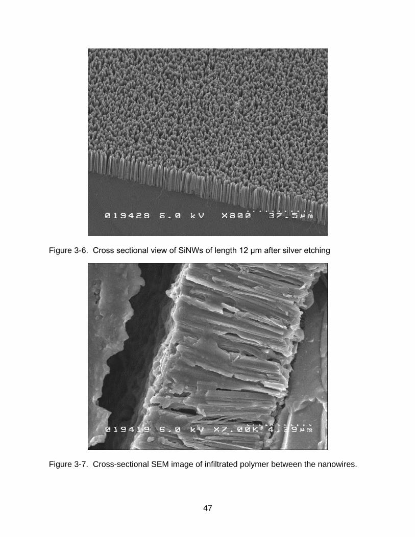
3-6 Cross sectional view of SiNWs of length 12 μm after silver etching ................... 47
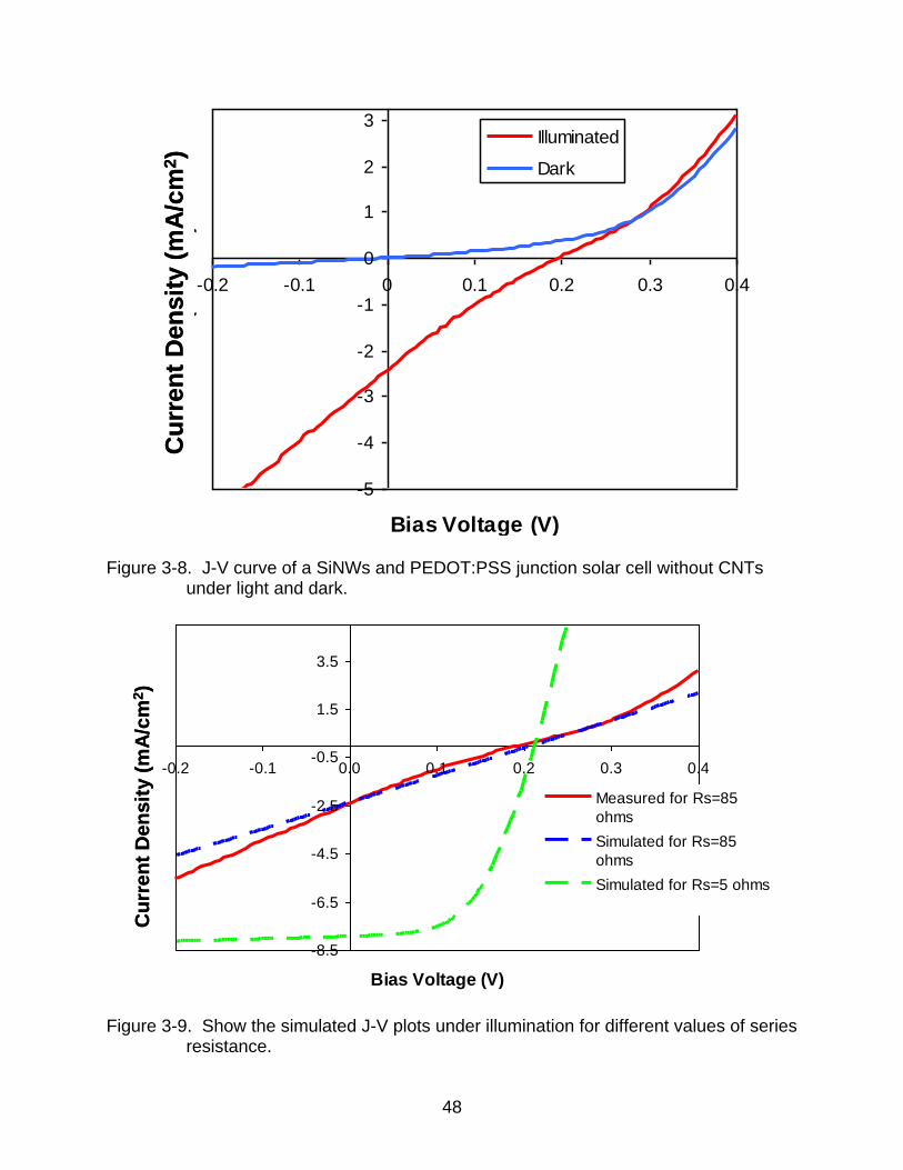
3-7 Cross-sectional SEM image of infiltrated polymer between the nanowires. ....... 47
3-8 J-V curve of a SiNWs and PEDOT:PSS junction solar cell without CNTs. ......... 48
3-9 Show the simulated J-V plots under illumination for different values of Rs . ....... 48
3-10 A schematic diagram of a heterogeneous mixture of CNTs and SiNWs. ............ 49
3-11 Schematic diagram of a solar cell with a mixed layer at the junction. ................. 49
11
3-12 Shows the SEM images of pure SiNWs on a mixed cellulose membrane. ......... 50
3-13 Shows the SEM images of a mixed SiNWs/CNTs film on a MCE membrane..... 51
4-1 Solar cell model J-V curves following Prince. ..................................................... 67
4-2 Device illustration. .............................................................................................. 68
4-3 Photograph of the sample in the measurement fixture. ...................................... 69
4-4 J-V plots: “conventional” SWNT-Si cell in the dark and under AM1.5G .............. 69
4-5 Gating effects. .................................................................................................... 70
4-6 Equivalent circuit of Figure 4-5B. ........................................................................ 71
4-7 Dark and light current J-V curves at the indicated gate voltages. ....................... 71
4-8 Trend of the VOC with gate voltage. .................................................................... 72
5-1 Schematic of the nanotube-grid/silicon device.................................................... 86
5-2 J-V curves for a continuous SWNT film covering the Si window and for an etched film.. ........................................................................................................ 87
5-3 Shows J-V curves of the grid SWNT film before and after addition of the electrolyte. .......................................................................................................... 88
5-4 Time measurements of short circuit current of the grid solar cell. ....................... 89
5-5 Experimental J-V curves under illumination at the specified gate voltages. ....... 90
5-6 Simulation geometry and parameters of a cross-sectional slice of the device . .. 90
5-7 Simulation results at Vg = -0.75, 0, +0.75 V and Vbias = 0, 0.3 V. ........................ 91
5-8 Simulation results at Vg = -0.75, 0, +0.75 V and Vbias = -0.4 V. ........................... 91
5-9 The reflectance and transmittance measurements as a function of wavelength of the NES solar cell. ....................................................................... 92
6-1 Shows the structure of pyrene-HPC. ................................................................ 101
6-2 A flowchart describing the steps of making SWNTs/polymer dispersant inks. .. 102
6-3 AFM image of a drop cast film of pyrene-HPC/SWNTs water based ink. ......... 102
6-4 Optical micrographs of the pyrene-HPC/SWNTs inks spray-cast onto glass . .. 103

12
6-5 AFM image of pyrene-HPC/SWNTs film sprayed from a water/ethanol. .......... 103
6-6 Optical Microscope image of a sprayed SWNT film after removal of p-HPC from ethanol based ink. .................................................................................... 104
6-7 AFM image of SWNT film sprayed from pyrene-HPC/SWNT ethanol based ink after removal of p-HPC. .............................................................................. 104
6-8 UV-vis spectra of sprayed pyrene-HPC/SWNT film after etching p-HPC. ........ 105
6-9 Optical micrograph image of sprayed SWNTs film after removal of p-HPC. ..... 105
6-10 Photograph of SWNT film sprayed from the p-HPC/SWNT ethanol based ink .106
6-11 UV-vis spectrum of the SWNT sprayed film after etching pyrene-HPC. ........... 106
6-12 Log plot of stability measurement of sheet resistance of a sprayed SWNTs film after removal of p-HPC. ............................................................................. 107

13
LIST OF ABBREVIATIONS
AFM Atomic force microscope
AM Air mass
BOE Buffered oxide etch
CMC Critical micelle concentration
CNT Carbon nanotube
DCMC Double critical micelle concentration
DI De-ionized
DOS Density of states
E-GaIn Gallium-Indium eutectic
EMI-BTI 1-Ethyl-3-methylimidazolium bis(trifluoromethylsulfonyl)imide
HF Hydrofluoric acid
HPC Hydroxypropyl cellulose
IL Ionic liquid
MCE Mixed cellulose ester
MS Metal semiconductor
NES Nanotube-electrolye/semiconductor
PC Propylene carbonate
PCE Power conversion efficiency
PEDOT:PSS Poly(3,4-ethylene dioxythiophene): poly(styrene sulfonate)
PTFE Polytetrafluoroethylene
PV Photovoltaic
SEM Scanning electron microscope
Si Silicon
SiNW Silicon nanowire

14
STC Standard test conditions
SWNT Single wall carbon nanotube
15
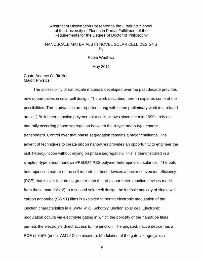
Abstract of Dissertation Presented to the Graduate School of the University of Florida in Partial Fulfillment of the Requirements for the Degree of Doctor of Philosophy
NANOSCALE MATERIALS IN NOVEL SOLAR CELL DESIGNS
By
Pooja Wadhwa
May 2011
Chair: Andrew G. Rinzler Major: Physics
The accessibility of nanoscale materials developed over the past decade provides
new opportunities in solar cell design. The work described here-in explores some of the
possibilities. Three advances are reported along with some preliminary work in a related
area: 1) Bulk heterojunction polymer solar cells, known since the mid-1990s, rely on
naturally occurring phase segregation between the n-type and p-type charge
transporters. Control over that phase segregation remains a major challenge. The
advent of techniques to create silicon nanowires provides an opportunity to engineer the
bulk heterojunction without relying on phase segregation. This is demonstrated in a
simple n-type silicon nanowire/PEDOT:PSS polymer heterojunction solar cell. The bulk
heterojunction nature of the cell imparts to these devices a power conversion efficiency
(PCE) that is over four times greater than that of planar heterojunction devices made
from these materials. 2) In a second solar cell design the intrinsic porosity of single wall
carbon nanotube (SWNT) films is exploited to permit electronic modulation of the
junction characteristics in a SWNT/n-Si Schottky junction solar cell. Electronic
modulation occurs via electrolyte gating in which the porosity of the nanotube films
permits the electrolyte direct access to the junction. The ungated, native device has a
PCE of 8.5% (under AM1.5G illumination). Modulation of the gate voltage (which
16
consumes negligible power in the steady state) of ±0.75 V yields a continuous,
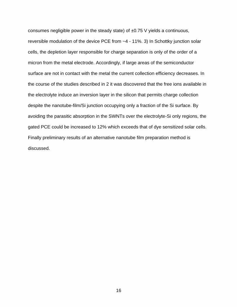
reversible modulation of the device PCE from ~4 - 11%. 3) In Schottky junction solar
cells, the depletion layer responsible for charge separation is only of the order of a
micron from the metal electrode. Accordingly, if large areas of the semiconductor
surface are not in contact with the metal the current collection efficiency decreases. In
the course of the studies described in 2 it was discovered that the free ions available in
the electrolyte induce an inversion layer in the silicon that permits charge collection
despite the nanotube-film/Si junction occupying only a fraction of the Si surface. By
avoiding the parasitic absorption in the SWNTs over the electrolyte-Si only regions, the
gated PCE could be increased to 12% which exceeds that of dye sensitized solar cells.
Finally preliminary results of an alternative nanotube film preparation method is
discussed.
17
CHAPTER 1 INTRODUCTION
1.1 Carbon Nanotubes
A single wall carbon nanotube is geometrically a graphene sheet rolled into a
seamless cylinder with diameter of about 0.7–10.0 nm. Most of the single wall carbon
nanotubes (SWNT or CNT) have diameters < 2 nm. Due to their large aspect ratio (i.e.
length/diameter which can be as large as 104), the nanotube are quasi-one-
dimensional. The structure of a SWNT can be specified or indexed by its circumferential
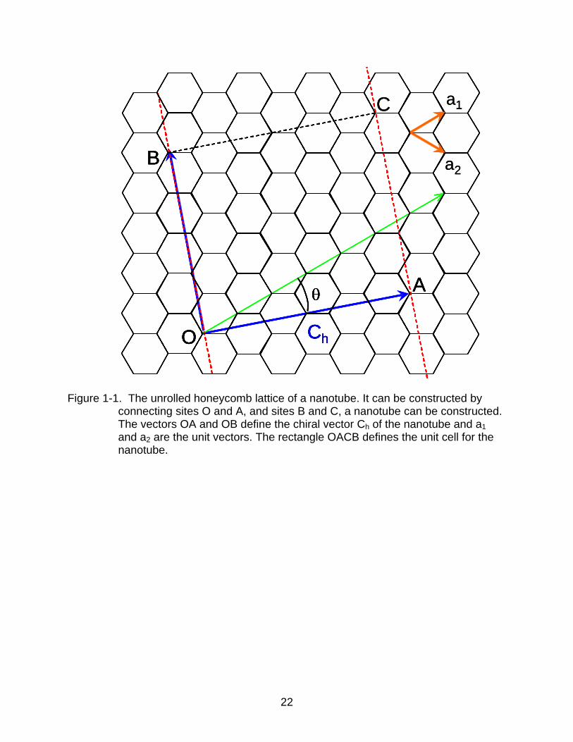
periodicity and its chiral vector (Ch) in terms of a pair of integers (n, m).1 The unwrapped
graphene sheet in Figure 1-1 shows a unit cell of a SWNT, where a1 and a2 are the real
space unit vectors of the hexagonal lattice that is related to the chiral vector as given by
Equation 1-1.
Ch = na1 + ma2 ≡ (n, m) (n, m are integers, 0 ≤ |m| ≤ n) (1-1)
It has been shown that the electronic properties of the carbon nanotubes are very
sensitive to their structure.2-4 Although graphene is a zero-gap semiconductor, theory
had predicted that carbon nanotubes can be either metals or semiconductors with
different size energy gaps, depending very sensitively on the diameter and helicity of
the tubes, i.e., on the indices (n, m).1 This has since been confirmed through a host of
experiments including scanning tunneling spectroscopy4 as well as optical absorption
and emission spectroscopies.
The physics behind this sensitivity of the electronic properties of carbon nanotubes
to their structure can be understood within a zone-folding picture. The density of states
(DOS) of SWNTs can be derived from the energy dispersion relationship of the
nanotubes. Due to the quasi-one dimensional characteristic of SWNTs, the DOS is

18
found to be limited in its capacity and can be easily filled or emptied upon injecting or
depleting electrons from it.
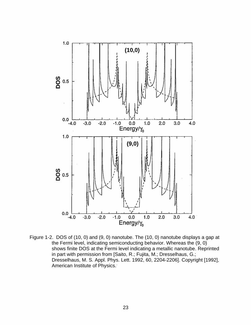
As shown in Figure 1-2, (10, 0) and (9, 0) nanotube density of states show that the
(10, 0) nanotube has a band gap at the Fermi level indicating a semiconducting
nanotube, while the (9, 0) nanotubes are metallic with low density of states at the Fermi
level. The sharp features in the DOS of the nanotubes are called von Hove singularities.
In this picture which ignores excitonic effects, the only allowed electronic transitions are
between symmetric valence and conduction band von Hove singularities, resulting in
absorption bands in the optical spectrum of the SWNTs. The band gap for the
semiconducting nanotubes is inversely proportional to the diameter of the SWNT.5 For
an (n, m) SWNT, if 2n+m is a multiple of 3, then the nanotube is metallic, otherwise its
semiconducting.
While the density of states of the nanotubes is low compared to typical metals,
their charge mobility is very high (near ballistic)6,7 making them good conductors. But,
because of their low density of states, the Fermi level of the nanotubes can be easily
tuned, which has motivated their application in photovoltaics in this dissertation. Chapter
2 presents the theory and working of a basic solar cell and Chapter 3 introduces the
application of nanotubes in a hybrid solar cell with silicon nanowires. Chapter 3 presents
two different models to maximize the junction area in a solar cell using carbon
nanotubes. Chapter 4 presents a nanotube/silicon photovoltaic where the Fermi-level of
the nanotubes is electrically modulated by electronic gating. Chapter 5 depicts and
discusses in detail the effect of the electrolyte gating on a nanotube-grid/silicon solar
cell. A new type of solar cell has been introduced and its performance is shown to be
19
increased via electrolytic gating. Finally, Chapter 6 discusses an alternative method to
prepare uniform thin films of nanotubes by spray coating. To comprehend this alternate
approach to nanotube film fabrication and understand the nanotube films used in
Chapters 3 to 5 it is useful to discuss the background and procedure of the conventional
nanotube film preparation scheme, which is discussed in Section 1.2.
1.2 Nanotube Films
1.2.1 Nanotube Suspension
The nanotubes are not soluble in any known solvents so the nanotubes when
placed in solvents, rather than being homogeneously dispersed, forms large
inhomogeneous clumps which are held together by van der Waals forces. To form
homogeneous nanotube suspensions, they are suspended in an aqueous solution with
the aid of surfactants.8 For example 1% (by weight) of Triton X-100 surfactant solution
stably suspends the nanotubes for extended periods of time.8, 9 The general surfactant
is a molecule with a hydrophobic side and a hydrophilic side. To suspend particles
which are hydrophobic (like carbon nanotubes), the surfactants assemble on the
particles with their hydrophobic side facing them while presenting their hydrophilic side
to the aqueous phase. The hydrophilic side of the surfactants meanwhile generates a
hydration shell that then prevents the suspended particles from coming into direct
contact with each other and flocking out of suspension. Because the hydrophobic
interaction of surfactants with the substances they are to suspend is generally weak,
surfactant molecules are continuously desorbed from the surfaces. To replace these
molecules and prevent flocculation the free surfactant concentration should be high
however surfactants that are placed into water self assemble into micellular structures,
often spherical, that face their hydrophobic sides toward each other. It is found that only

20
once the surfactant concentration in the aqueous solution is raised above a certain
concentration (specific to each surfactant) that the free surfactant concentration is
maintained at a level sufficient to suspend particles. This concentration is called “critical
micelle concentration” (CMC) which is 0.17 g/l for Triton X-100, above which there are
free surfactant molecules available to suspend the nanotubes.
The nanotube suspension in the surfactant solution is meta-stable and with time
the nanotubes in the solution begins to flock. The nanotubes can be re-dispersed in the
surfactant solution by supplying external energy via ultrasonication, which breaks the
aggregates apart. Upon ultrasonication, the nanotubes solution can be used to make
uniform films by the filtration method which is discussed in Section 1.2.2.
1.2.2 Filtration Process
A nanotube film is made by the filtration process10 by collecting the nanotubes on
a filtration membrane with pores that are too small in diameter for the nanotubes to
permeate through. A mixed cellulose ester (MCE) membrane with pore size of 0.1 μm is
used for filtration (as it can later be easily dissolved away by acetone during the
transferring of the nanotube film to a substrate). The filtration process is self-regulatory
and forms a uniform thickness film with fine control over the film thickness by the
nanotube concentration in the suspension and the volume of the suspension filtered.
The nanotube surfactant solution is filtered through the MCE membrane and the film so
formed on the membrane is then washed with sufficient de-ionized (DI) water to rinse off
the major fraction of the surfactant. The nanotube film so formed is dried on the filtration
membrane and is ready to be transferred to a substrate for use. The nanotube transfer
step generally proceeds as follows. The nanotube film (backed by the membrane) is cut
to the desired size and shape, wetted with DI water and pressed against the substrate

21
using modest pressure in a clamp assembly. The assembly is dried in an 80°C oven for
an hour leaving the nanotube film and backing membrane adhered to the substrate. The
membrane is then dissolved away starting with an acetone vapor bath followed by
transfer to multiple fresh acetone liquid baths to ensure removal of the major fraction of
the mixed cellulose ester membrane material.
22
ChO
A
B
C
ChO
A
B
a2
a1
ChO
A
B
C
ChO
A
B
a2
a1
Figure 1-1. The unrolled honeycomb lattice of a nanotube. It can be constructed by connecting sites O and A, and sites B and C, a nanotube can be constructed. The vectors OA and OB define the chiral vector Ch of the nanotube and a1 and a2 are the unit vectors. The rectangle OACB defines the unit cell for the nanotube.
23
DO
S
(10,0)
(9,0)
DO
SD
OS
(10,0)
DO
S
(10,0)
(9,0)
DO
S
Figure 1-2. DOS of (10, 0) and (9, 0) nanotube. The (10, 0) nanotube displays a gap at the Fermi level, indicating semiconducting behavior. Whereas the (9, 0) shows finite DOS at the Fermi level indicating a metallic nanotube. Reprinted in part with permission from [Saito, R.; Fujita, M.; Dresselhaus, G.; Dresselhaus, M. S. Appl. Phys. Lett. 1992, 60, 2204-2206]. Copyright [1992], American Institute of Physics..
24
CHAPTER 2 SOLAR CELLS
2.1 Background
Photovoltaic cells convert light energy into electricity. The photovoltaic effect was
first discovered by nineteen-year-old Edmund Becquerel, a French experimental
physicist in 1839 while he was experimenting with an electrolytic cell made up of two
metal electrodes. For over a century, there were on-going efforts to understand the
photovoltaic effect with significant contributions made by several imminent scientists
including Albert Einstein and Milikan. In 1954, the Bell Labs researchers Pearson,
Chapin, and Fuller reported their discovery of 4.5% efficient silicon solar cells; this was
raised to 6% a few months later by a work team including Mort Prince. The first
commercial solar cell was announced by Hoffman Electronics's Semiconductor Division
at 2% efficiency; priced at $25/cell and at 14 mW power each, making the cost of
energy from such cells $1500/W. Figure 2-1 shows the evolution of efficiencies of
different solar cell technologies (from National Renewable Energy Lab).11
2.2 Theory
2.2.1 Solar Energy
The total mass of the sun is now about 2×1030 kg, with a nearly constant radiative
energy output driven by nuclear fusion, and a stable life projected of over 10 billion
(1010) years. The sun light reaching the surface of earth is attenuated by various layers
of the atmosphere principally due to water vapor absorption in the infrared, ozone
absorption in the ultraviolet and scattering by airborne dust and aerosols. The degree to
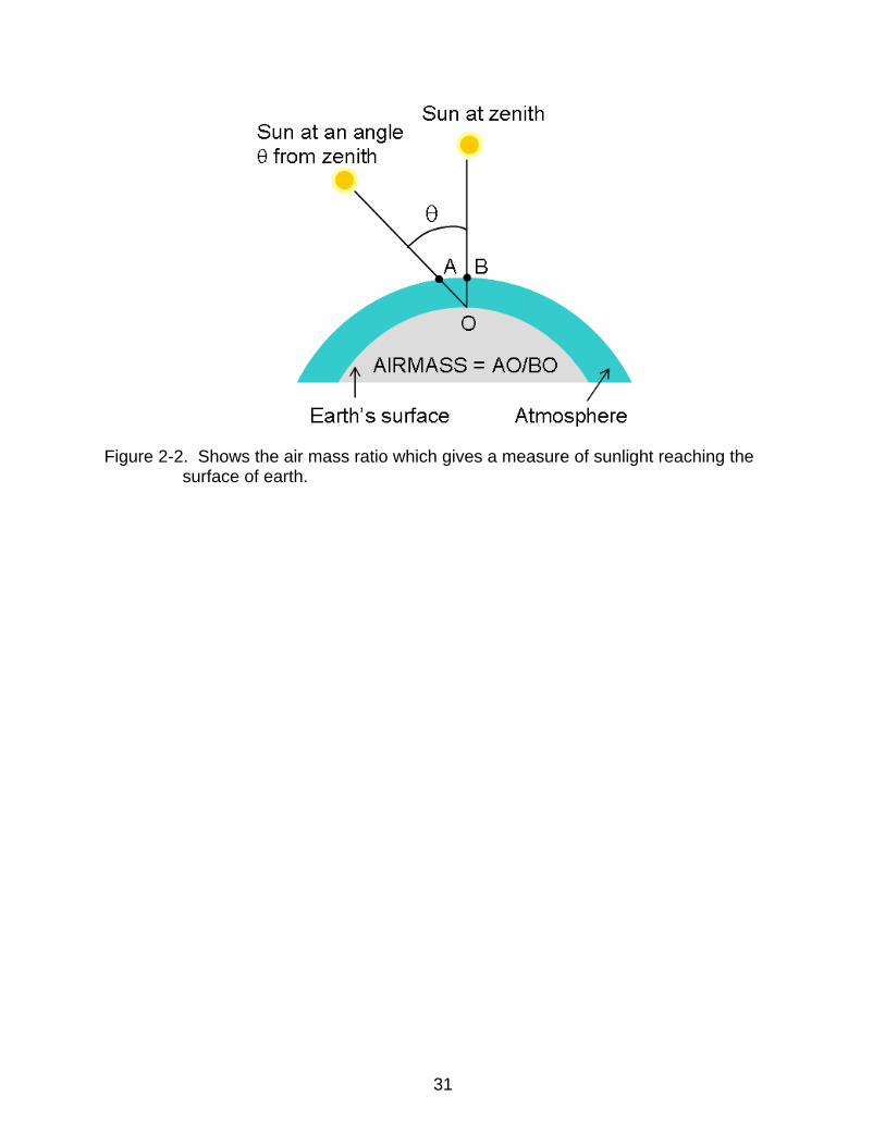
which the atmosphere affects the sunlight received at the surface of earth is defined as
the “air mass” ratio. It is defined as the secant of the angle (sec θ) between the sun and

25
the zenith and it measures the atmospheric path length relative to the minimum path
length when the sun is directly overhead as shown in Figure 2-2.
Air mass zero (AM0) corresponds to solar spectrum outside the earth’s
atmosphere and AM1.5 spectrum ( = 48.2°) corresponds to the spectrum at the
surface of the earth and is the standard by which different solar cells are compared. The
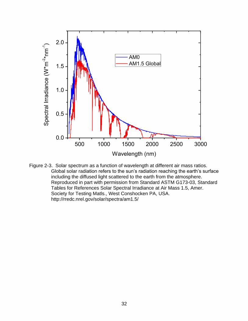
global clear sky spectrum corresponds to AM1.5G with a light intensity of 100
mW/cm2.12 Figure 2-3 shows the spectral irradiance (power per unit area per unit
wavelength) as a function of wavelength at different air mass ratios.
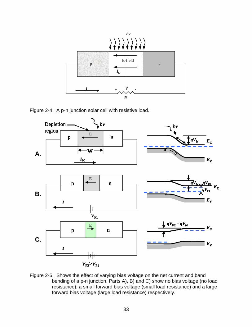
2.2.2 Working of a Solar Cell
A prototypical homojunction solar cell consists of a semiconducting material doped
to be p-type on one side and n-type on the other side of their junction with electrical
contacts on each end. When the two materials are brought in contact, charge transfer
takes place which develops a built-in potential at equilibrium. Once light shines on the
device, charge carriers (electron-hole pairs, also called excitons) are created and
dissociated by the internal electric field generated by the built-in potential in the
depletion region which are collected by the electrodes generating the photocurrent (IL)13
(Figure 2-4). When the external load is zero this photo-illuminated current is called the
short-circuit current (ISC). The voltage generated when the external impedance is infinite
is called the open-circuit voltage (VOC); providing two of the figures of merit for the
device.
When a junction between two materials is formed, thermalization of electrons
across the junction results in a built-in potential. This thermal equilibrium is represented
on an energy level diagram by a line-up of the Fermi levels across the junction, while
26
the built-in potential appears as a bending of the semiconductor valence and conduction
bands across the depletion region (Figure 2-5A). Photons absorbed within a
semiconductor generate excitons provided the photon is absorbed within the region of
the built-in potential near the junction; the electron and the hole are driven by the
potential in opposite directions to provide power from the cell.
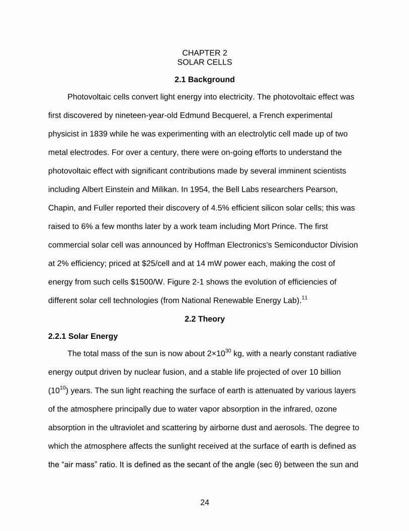
Given the open circuit potential, VOC and the short circuit current, ISC, the power of
an ideal solar cell can be defined as the product of these. The power extracted from real
cells however is found to depend on the load. This occurs because of the charge
accumulation on the terminals of the cell, which in turn shifts the energy levels of the
device. An experimental means for mapping out the load impedance-dependent power
from a cell is to have the load be a power supply that provides a forward bias to the cell
terminals (the forward bias here refers to the forward current (IF) direction for a diode,
opposite to the direction of the photo-current), thus mimicking the effect of the load
impedance. By mapping out the current from the illuminated cell as a function of the
forward bias voltage, the I-V curve for the device can be generated. Figure 2-5 shows
the graphical depiction of a solar cell demonstrating the effect of the voltage collected
across the load impedance on the depletion region, electric field and band bending at
the junction of the device. When a photon generates an exciton in the depletion region,
a photocurrent is produced in the device by virtue of exciton dissociation due to band
bending arising from the initial difference in the Fermi levels (qVbi, where Vbi is the built-
in potential) of the two materials. As mentioned above, when no load resistance is
connected to the device, the generated photocurrent is called the short-circuit current
(Figure 2-5A). This is also shown on the I-V curve of a solar cell in Figure 2-6A. In
27
Figure 2-5B, as a forward bias voltage (VF) is applied to the device (mimicking the effect
of a load), the net band bending is reduced by qVF thus reducing the net output current.
As the forward biased voltage is increased further (Figure 2-5C), the band bending is
further reduced, until beyond a point (VOC) it changes direction. At this point, the electric
field due to VF exceeds the electric field due to photo-generated carriers, flipping its
direction and reversing the direction of the current (Figure 2-6C).
The net current in the circuit of Figure 2-5 is given by,14
I = IF – IL = IS [exp(qV/kT) – 1] – IL (2-1)
where, IL results from the excitation of excess carriers by solar radiation and IS is the
diode saturation current. The output power is given by,
P = IV = IS V [exp(qV/kT) – 1] – IL V (2-2)
Figure 2-6 shows current-voltage characteristics of a solar cell under illumination.
The condition for maximum power (PM) can be obtained when dP/dV = 0 and is depicted
by the shaded rectangle in Figure 2-6.
2.2.2.1 Effect of series resistance
For a practical solar cell, Figure 2-4 is modified to include series resistance (RS) to
account for the ohmic losses within the device.15 The equivalent circuit is shown in
Figure 2-7. Thus the output current reduces to,
I = IS {exp[q(V– I RS)/k T] – 1}– IL (2-3)
The I-V characteristics of a solar cell for varying values of RS are shown in Figure
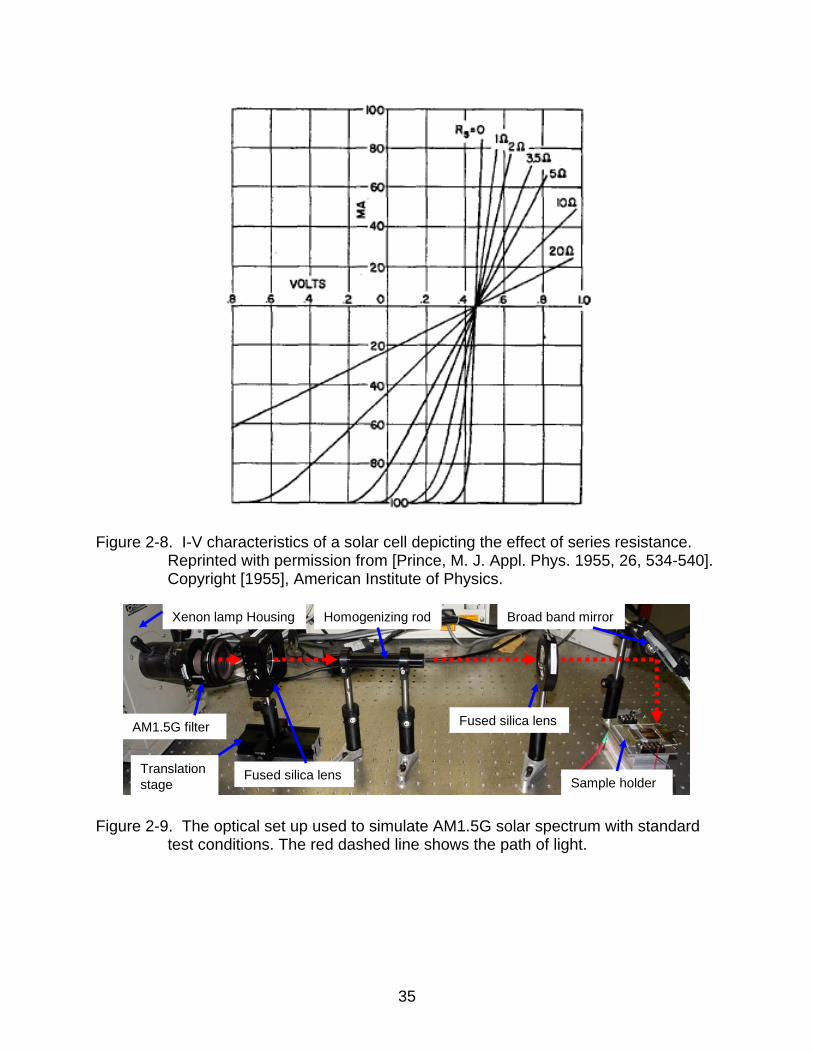
2-8.15 This data clearly shows that the series resistance plays a key role in determining
the output characteristics of a solar cell.
It has been observed15,16 that the series resistance of a given solar cell depends
on numerous factors including the bulk resistance of the organic and inorganic
28
materials, the contact resistance between the electrodes and the junction materials, the
bulk resistances of the electrodes, the junction depth and the doping concentrations of
the semiconductors. It is essential for all practical purposes to keep each of these
contributions to the series resistance as low as possible.
2.2.2.2 Performance characteristics of photovoltaics
The power conversion efficiency (PCE) of a solar cell is a primary performance
metric defined as the fraction of incident solar energy converted into electricity and is
given by the ratio of the output electrical power to the incident optical power, which is
given by
PCE = PM/Pinc × 100% = IMVM/Pinc × 100% (2-4)
where Pinc is the incident power, IM and VM are the current and voltage values at
maximum power. The maximum PCE achieved thus far is 30% using inorganic
semiconductors17 and that using polymer based organic semiconductors still remain
significantly lower at 5.7% efficiency.18
The ratio, IMVM/ISCVOC is called fill factor (FF) and is a measure of the realizable
power from a solar cell or in other words, it defines the deviation from an ideal solar cell
as a result of losses.
Therefore, the PCE in terms of FF can be re-written as
PCE = FF ISCVOC /Pinc × 100% (2-5)
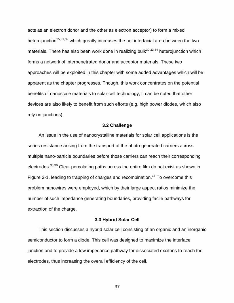
2.3 Instrumentation
Standard test conditions (STC) under which the I-V curve measurements of a solar
cell are made, specify a cell temperature of 25°C, an illumination intensity of 100
mW/cm2, and an AM1.5G spectrum.19 The setup used to simulate the STC is shown in
Figure 2-9. It involves a 150 W xenon lamp (Oriel 6255) in an Oriel 6136 housing

29
powered by a model 8500 power supply. Light approximating the solar spectral
distribution was obtained using an Oriel 81094 AM1.5G filter. Light from the
inhomogeneous source was focused into the acceptance aperture of a 150 mm long,
fused silica homogenizing rod (Edmund Optics P65-837) by a 50 mm diameter fused
silica lens with a 65 mm focal length. The output face of the homogenizing rod was
imaged in the horizontal focal plane of the sample by a 50 mm diameter, 100 mm focal
length fused silica lens after rotation by 90 degrees with a broad band mirror (Newport
66225). The intensity at the sample plane was adjusted to 100 mW/cm2 by translation of
the 65 mm focal length lens, cutting down on the fraction of the light entering the
homogenizing rod. The homogeneity of the light intensity over the ~1 cm2 central region
of the homogenized beam at the sample plane was measured to be within 5%.
Measurements were performed using a Keithley 2400 source meter controlled by
LabTracer 2.0 software. Gating was done using a potentiometer controlled voltage
divided 9 V battery (to provide a highly stable source of the voltages less than 1 V).

30
Figure 2-1. Thirty years evolution in conversion efficiencies of different photovoltaic technologies. Reprinted in part with permission from Don Gwinner. Data compiled by Dr. Lawrence Kazmerski, National Renewable Energy Laboratory, Golden, Colorado. www.nrel.gov/pv/thin_film/docs/kaz_best_research_cells.ppt
31
Figure 2-2. Shows the air mass ratio which gives a measure of sunlight reaching the surface of earth.
32
500 1000 1500 2000 2500 30000.0
0.5
1.0
1.5
2.0
Sp
ectr
al Ir
radia
nce
(W
*m-2*n
m-1)
Wavelength (nm)
AM0
AM1.5 Global
Figure 2-3. Solar spectrum as a function of wavelength at different air mass ratios. Global solar radiation refers to the sun’s radiation reaching the earth’s surface including the diffused light scattered to the earth from the atmosphere. Reproduced in part with permission from Standard ASTM G173-03, Standard Tables for References Solar Spectral Irradiance at Air Mass 1.5, Amer. Society for Testing Matls., West Conshocken PA, USA. http://rredc.nrel.gov/solar/spectra/am1.5/
33
E-field
IL
np
hν
+ -V
R
I
E-field
IL
np
hν
+ -V
R
I
Figure 2-4. A p-n junction solar cell with resistive load.
E
ISC
E
I
E
I
EV
ECqVbi
EV
EC
qVbi – qVF1
qVF1
EV
EC
qVF2 – qVbi
(a)
(b)
(c)
p n
p n
np
VF2>VF1
VF1
W
Depletion
region
hν hν
E
ISC
E
I
E
I
EV
ECqVbi
EV
EC
qVbi – qVF1
qVF1
EV
EC
qVF2 – qVbi
(a)
(b)
(c)
p n
p n
np
VF2>VF1
VF1
W
Depletion
region
hν hν
A.
B.
C.
E
ISC
E
I
E
I
EV
ECqVbi
EV
EC
qVbi – qVF1
qVF1
EV
EC
qVF2 – qVbi
(a)
(b)
(c)
p n
p n
np
VF2>VF1
VF1
W
Depletion
region
hν hν
E
ISC
E
I
E
I
EV
ECqVbi
EV
EC
qVbi – qVF1
qVF1
EV
EC
qVF2 – qVbi
(a)
(b)
(c)
p n
p n
np
VF2>VF1
VF1
W
Depletion
region
hν hν
A.
B.
C.
Figure 2-5. Shows the effect of varying bias voltage on the net current and band bending of a p-n junction. Parts A), B) and C) show no bias voltage (no load resistance), a small forward bias voltage (small load resistance) and a large forward bias voltage (large load resistance) respectively.
34
VVOC
PM
0
I
ISC (a)
(b)
(c)
VVOC
PM
0
I
ISC (a)
(b)
(c)
A.
B.
C.
VVOC
PM
0
I
ISC (a)
(b)
(c)
VVOC
PM
0
I
ISC (a)
(b)
(c)
A.
B.
C.
Figure 2-6. I-V characteristics of a solar cell under illumination.
Rs
IL
Rs
ILIL
Figure 2-7. Equivalent solar cell circuit.
35
Figure 2-8. I-V characteristics of a solar cell depicting the effect of series resistance.
Reprinted with permission from [Prince, M. J. Appl. Phys. 1955, 26, 534-540]. Copyright [1955], American Institute of Physics.
Xenon lamp Housing Homogenizing rod Broad band mirror
AM1.5G filter
Translation
stageFused silica lens
Fused silica lens
Sample holder
Xenon lamp Housing Homogenizing rod Broad band mirror
AM1.5G filter
Translation
stageFused silica lens
Fused silica lens
Sample holder
Figure 2-9. The optical set up used to simulate AM1.5G solar spectrum with standard test conditions. The red dashed line shows the path of light.

36
CHAPTER 3 SILICON NANOWIRES IN A HYBRID SOLAR CELL
3.1 Motivation
The key operational component of numerous electronic and opto-electronic
devices arises at the interface between dissimilar materials possessing distinct
workfunctions. This so called junction is critical to the operation of diodes,
photodetectors, photovoltaics and light emitting diodes. Common manufacturing
techniques for solar cell junctions that for example evaporate (or implant) one material
onto (into) another tend to produce planar junctions, who’s area is the geometric overlap
between the two materials. This is often less than ideal. For example, in a photovoltaic
of inorganic materials, the width of the built-in potential responsible for separation of the
photo-generated electron-hole pairs is of the order of 300 nm for highly doped silicon.
Relatively few photons can be absorbed within such a thin layer meaning that only a
small fraction of the incident light is converted directly to electrical power. Photons not
absorbed in that layer can still contribute to the power if the absorption occurs within a
diffusion length of the junction but that, depending on the material system, can be short.
One known approach to improving this circumstance is to roughen or texture the
surface at which the junction is formed to increase the effective surface area of the
junction20-24 however, even texturing by microlithography techniques can only go so far
in terms of the increased effective surface area. The advent of nanoscale materials
presents new opportunities for enormous increases in the effective junction area,25-30
which by increasing the net amount of incident light absorbed within or near the junction
can in principle increase the net amount of power produced by the device. For example,
attempts have been made to form a blend of two distinct types of nanoparticles (one
37
acts as an electron donor and the other as electron acceptor) to form a mixed
heterojunction25,31,32 which greatly increases the net interfacial area between the two
materials. There has also been work done in realizing bulk30,33,34 heterojunction which
forms a network of interpenetrated donor and acceptor materials. These two
approaches will be exploited in this chapter with some added advantages which will be
apparent as the chapter progresses. Though, this work concentrates on the potential
benefits of nanoscale materials to solar cell technology, it can be noted that other
devices are also likely to benefit from such efforts (e.g. high power diodes, which also
rely on junctions).
3.2 Challenge
An issue in the use of nanocrystalline materials for solar cell applications is the
series resistance arising from the transport of the photo-generated carriers across
multiple nano-particle boundaries before those carriers can reach their corresponding
electrodes.35,36 Clear percolating paths across the entire film do not exist as shown in
Figure 3-1, leading to trapping of charges and recombination.16 To overcome this
problem nanowires were employed, which by their large aspect ratios minimize the
number of such impedance generating boundaries, providing facile pathways for
extraction of the charge.
3.3 Hybrid Solar Cell
This section discusses a hybrid solar cell consisting of an organic and an inorganic
semiconductor to form a diode. This cell was designed to maximize the interface
junction and to provide a low impedance pathway for dissociated excitons to reach the
electrodes, thus increasing the overall efficiency of the cell.
38
3.3.1 Device Design and Fabrication
The approach was to form a heterojunction between vertically oriented inorganic
semiconducting nanowires and organic polymer layer infiltrated between them.
The schematic device design is shown in Figure 3-2. Silicon nanowires (SiNWs)
were etched to be vertically oriented to be 5 μm in length on an 8×8 mm2 n-Si sample.
These SiNWs were infiltrated with a polymer to form a junction. The chemical potential
of the polymer, on equilibrating with the Fermi level of the Si, induced a built-in potential
in Si, where exciton dissociation occured. Electrons propagated down the n-SiNWs
while holes were transported through the polymer to the electrode. The polymer used
was poly(3,4-ethylene dioxythiophene): poly(styrene sulfonate) (PEDOT:PSS) (Figure
3-3). It was selected for its high electrical conductivity (70 S/cm, as measured on thin
spin cast films), reasonable transparency and good thermal stability. Its water solubility
moreover permited convenient room temperature solution casting of uniform thin films.
Indeed it was found that spin coating of the PEDOT:PSS provided the desired polymer
layer infiltration between the SiNWs.
An additional hole extraction layer was used on top of the polymer, which helped
the holes to reach the anode. This layer was a conductive, transparent, single-walled
carbon nanotube (CNT) film which was transferred onto the polymer and aided the hole
extraction. It has previously been used as a transparent electrode in various solar cells
benefiting from low sheet resistance and high transmittance.37 The sheet resistance for
a 45 nm thick CNTs film used in this device was 82 Ω/. Aluminum (Al) and gold (Au)
were used as the bottom electrodes (cathode) with work functions of 4.08 eV and 5.1

39
eV respectively. Palladium (Pd) was used as the top electrode (anode) with a work
function of 5.12 eV.
The silicon nanowires were formed on a flat n-Si substrate by an etching process
described in Section 3.3.2. A protective layer was created on the back of the Si to
prevent its chemical etching and avoid having SiNWs etched on the back surface of the
device making it difficult to form electrical contacts. This protective layer was parylene
C, which is an electrical insulator and is a chemically inert compound with no organic
and inorganic solvents at room temperature. It has water absorption of less than 0.1%
(after 24 hrs of soaking in water).38 All these physical properties make parylene well
suited for this application. A layer of a parylene C (poly-para-xylene) was formed by
pyrolysis of an unreacted dimer charge, di-para-xylene into a monomer (p-xylene) which
was deposited on the back surface and on a small portion of the top surface of the Si
wafer in a chemical vapor deposition system.39
3.3.2 Fabrication of SiNWs
Vertically oriented SiNWs were synthesized by etching n-type single crystalline Si
<100> with a resistivity of 0.002-0.04 Ωcm in hydrofluoric acid/ferric nitrate
(HF/Fe(NO3)3) at 50°C preceded by an electroless deposition of silver from silver nitrate
(AgNO3), which deposited in a dendritic morphology as shown in Figure 3-4.40-48 SiNWs
with diameters 50 - 200 nm. The etching time can be controlled to vary the length of
SiNWs ranging from 1 to 12 μm. The nanowire fabrication technique is independent of
the Si dopant type or its crystallographic orientation. The silver etches down into the
wafer leaving the nanowires behind. Excess Ag ends up around the bottom of the
SiNWs and must be removed.49 This was done in an aqueous nitric acid solution
containing sodium nitrite (NaNO2) at 85°C. Representative SiNWs generated by this

40
method are shown in Figures 3-5 through 3-7. Figures 3-6 and 3-7 show cross-sectional
scanning electron microscope (SEM) image of the SiNWs after silver etching and after
polymer infiltration, respectively.
3.3.3 Results
Measurements in this early work were conducted in the lab using a 150 W halogen
light source which is by no means representative of the solar energy spectrum,
nevertheless the relative values are meaningful. Table 3-1 lists four types of devices
comparing SiNWs/PEDOT:PSS to planar-Si/PEDOT:PSS devices with two distinct
contacts to the PEDOT:PSS, with and without CNTs. Four to five of each device type
were fabricated and measured. The values shown in Table 3-1 are specific
representative devices. Surprisingly, the devices that included CNTs had substantially
smaller short circuit currents. The absorbance of a 45 nm thick SWNT film is much too
small to account for the difference so the conclusion is that a barrier develops between
the nanotubes and the PEDOT:PSS which reduces the currents. Comparison of the
SiNWs to planar devices shows that in one case (with the CNTs) the JSC is 2.7 times
greater and in the other (without the CNTs) 4.4 times greater for the SiNWs based
devices.
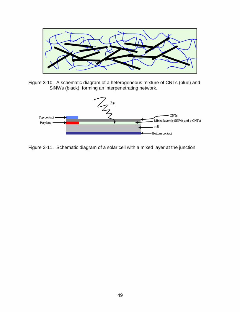
The J-V curve for a SiNW/PEDOT:PSS device is shown in Figure 3-8 under
standard test conditions of AM1.5G. The Voc and Jsc obtained from the plot are 194 mV
and 2.4 mA/cm2, respectively with a PCE of 0.104% and a FF of 0.22.
3.3.4 Simulated Effect of Series Resistance
The J-V curve of Figure 3-8 suggests a high series resistance. Accordingly, simple
simulations incorporating series resistance in the Shockley’s equation were performed.
The input parameters used in the diode Equation 2-3 from Chapter 2 are photocurrent IL
41
= 8 mA, the diode saturation current IS = 0.9 μA and series resistance RS = 85 Ω
(measured from Figure 3-8). The JSC and VOC obtained from this simulated curve are 2.4
mA/cm2 and 200 mV, respectively as shown in Figure 3-9. These values are in close
agreement with the measured values. Keeping the input parameters the same, and only
changing RS to 5 Ω (Figure 3-9), the JSC will increase to 7.95 mA/cm2, the VOC to 211
mV, the FF and PCE to 0.53 and 0.9% respectively. Hence lowering the series
resistance in these devices would result in a major improvement.
3.3.5 Discussion
The work function of the heavily doped n-Si under consideration is 4.1 eV while
that of PEDOT:PSS polymer is frequently quoted as 5.1 eV.50 Within the Schottky-Mott
model this should yield a built-in potential of the difference and the VOC should be close
to this value. A far lower VOC was observed. This is generally attributed to interface
states at the semiconductor surface and is likely the case here. Experience has shown
that passivation of the surface with a thin oxide layer (less than 25 A° to avoid creating a
tunneling barrier) can reduce this surface state density thus greatly improving
performance. In the present case, polymer is introduced into the devices immediately
after etching the wires in HF. Future work could explore introduction of a time delay
before polymer introduction to permit the formation of a thin native oxide layer.
As shown by the simulation, the devices clearly have a large series resistance that
should be reduced. Two sources of series resistance are likely. Ohmic contacts to n-
type Si are notoriously difficult to make without introducing n++ regions. One source of
series resistance in these devices is thus the Al/Au back contact. More recent work
(Chapter 4) has identified Gallium/Indium (GaIn) eutectic51 as forming much better
Ohmic contacts and can be tried. The other likely source of series resistance in the

42
devices built was the long path length for holes through the PEDOT:PSS polymer to the
metal contact along only one edge of the device. More closely spaced metal finger
electrodes can improve this.
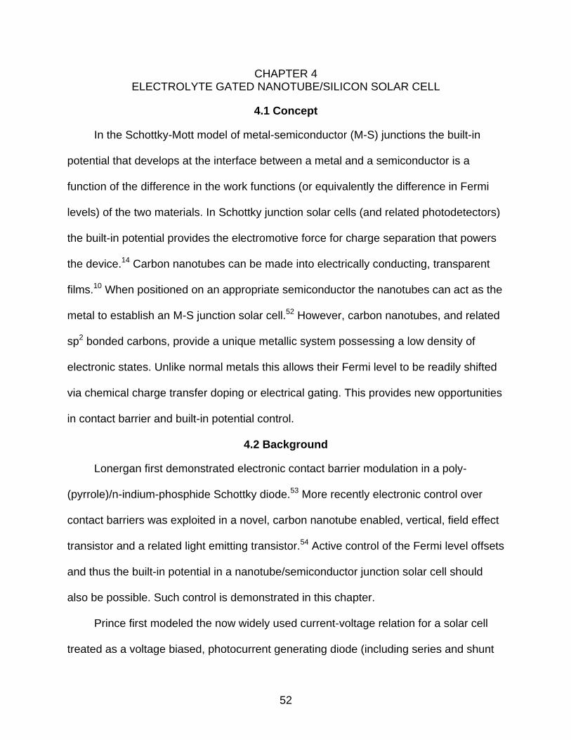
3.4 Interpenetrating Heterojunction Solar Cell
3.4.1 Concept
Some preliminary work to fabricate a mixed nanaotube/semiconducting nanowire
heterojunction solar cell was also performed. Silicon nanowires (of n-Si) and carbon
nanotubes were mixed together to form a heterogeneous blend. This layer was to be
deposited onto a pure n-Si wafer to collect the electrons while a pure CNT transparent
film was to be used as the transparent hole collection electrode. The mixed layer
consists of 12 μm long, 50-200 nm wide SiNWs and ~10 μm long, ~5 nm wide CNT
bundles. By the fabrication method employed, the nanowires and nanotubes in this
device were preferentially oriented to generally lie along a plane (Figure 3-10) as
opposed to the vertically oriented SiNWs in the first approach. A schematic of the
device design is shown in Figure 3-11.
Fabrication challenges did not get the work to the point of testing devices however
it may be useful to others to know what was done.
3.4.2 Fabrication Details
The mixed nanotube/nanowire layer was formed by dispersing the nanotubes
and/or nanowires in DI water aided by Triton X-100 surfactant and following Section
1.2.2 from Chapter 1 to make a uniform film having the SiNWs/CNTs lying parallel to the
membrane. The film was transferred onto a pure n-Si substrate. Figures 3-12 and 3-13
show the SEM images of pure SiNWs film and of a mixed SiNWs/CNTs film on a mixed
cellulose ester membrane, respectively. A second layer of pure CNTs was attempted to

43
transfer on the mixed layer but with no success. The first transfer step of the mixed
layer onto Si had a high success rate but the rigidity of SiNWs (present in the mixed
layer) prevented the successful transfer of the second layer. Future work can be done to
overcome this problem by filtering pure CNTs, followed by a mixed layer on the same
filter membrane and perform one transfer step on Si substrate to make the device.
Longer and more flexible SiNWs can also be fabricated using chemical vapor deposition
or laser-ablation to successfully fabricate such a device.

44
Table 3-1. Gives the output parameters for different junctions under light.
Device VOC (mV) JSC (mA/cm2)
SiNWs/PEDOT:PSS/CNT 182 0.625 Planar-Si/PEDOT:PSS/CNT 160 0.234 SiNWs/PEDOT:PSS 200 3.125 Planar-Si/PEDOT:PSS 200 0.703
Figure 3-1. Shows a heterogeneous blend of two organic materials which increase the net surface area in contact but leads to charge trapping.
Aluminum/Gold
contactn-Si
n-SiNWs PolymerPalladium
contact
SiO2/Parylene C
h
Aluminum/Gold
contactn-Si
n-SiNWs PolymerPalladium
contact
SiO2/Parylene C
h
Figure 3-2. Cross-section of an organic-inorganic hybrid device.

45
PEDOT
PSS
PEDOT
PSS
Figure 3-3. Chemical structure of PEDOT:PSS..
Figure 3-4. Top view. Shows a SEM images of the as-prepared SiNWs with Ag dendrites.

46
A.
B.
Figure 3-5. SEM images of SiNWs after Ag etching A) shows the top view and B) shows the side view.
47
Figure 3-6. Cross sectional view of SiNWs of length 12 μm after silver etching
Figure 3-7. Cross-sectional SEM image of infiltrated polymer between the nanowires.
48
Cu
rren
t D
en
sit
y (
mA
/cm
2)
-5
-4
-3
-2
-1
0
1
2
3
-0.2 -0.1 0 0.1 0.2 0.3 0.4
Bias Voltage (V)
Jsc (
mA
/cm
2)
Illuminated
DarkC
urr
en
t D
en
sit
y (
mA
/cm
2)
-5
-4
-3
-2
-1
0
1
2
3
-0.2 -0.1 0 0.1 0.2 0.3 0.4
Bias Voltage (V)
Jsc (
mA
/cm
2)
Illuminated
Dark
Figure 3-8. J-V curve of a SiNWs and PEDOT:PSS junction solar cell without CNTs under light and dark.
Cu
rren
t D
en
sit
y (
mA
/cm
2)
-8.5
-6.5
-4.5
-2.5
-0.5
1.5
3.5
-0.2 -0.1 0.0 0.1 0.2 0.3 0.4
Bias Voltage (V)
Js
c (
mA
/cm
2)
Measured for Rs=85
ohms
Simulated for Rs=85
ohms
Simulated for Rs=5 ohms
Cu
rren
t D
en
sit
y (
mA
/cm
2)
-8.5
-6.5
-4.5
-2.5
-0.5
1.5
3.5
-0.2 -0.1 0.0 0.1 0.2 0.3 0.4
Bias Voltage (V)
Js
c (
mA
/cm
2)
Measured for Rs=85
ohms
Simulated for Rs=85
ohms
Simulated for Rs=5 ohms
Figure 3-9. Show the simulated J-V plots under illumination for different values of series resistance.
49
Figure 3-10. A schematic diagram of a heterogeneous mixture of CNTs (blue) and SiNWs (black), forming an interpenetrating network.
Mixed layer (n-SiNWs and p-CNTs)
n-Si
Parylene
Top contactCNTs
Bottom contact
h
Mixed layer (n-SiNWs and p-CNTs)
n-Si
Parylene
Top contactCNTs
Bottom contact
h
Figure 3-11. Schematic diagram of a solar cell with a mixed layer at the junction.

50
A.
B.
Figure 3-12. A) and B) show the SEM images of pure SiNWs on a mixed cellulose membrane.

51
A.
B.
Figure 3-13. A) and B) show the SEM images of a mixed SiNWs/CNTs film on a mixed cellulose membrane.
52
CHAPTER 4 ELECTROLYTE GATED NANOTUBE/SILICON SOLAR CELL
4.1 Concept
In the Schottky-Mott model of metal-semiconductor (M-S) junctions the built-in
potential that develops at the interface between a metal and a semiconductor is a
function of the difference in the work functions (or equivalently the difference in Fermi
levels) of the two materials. In Schottky junction solar cells (and related photodetectors)
the built-in potential provides the electromotive force for charge separation that powers
the device.14 Carbon nanotubes can be made into electrically conducting, transparent
films.10 When positioned on an appropriate semiconductor the nanotubes can act as the
metal to establish an M-S junction solar cell.52 However, carbon nanotubes, and related
sp2 bonded carbons, provide a unique metallic system possessing a low density of
electronic states. Unlike normal metals this allows their Fermi level to be readily shifted
via chemical charge transfer doping or electrical gating. This provides new opportunities
in contact barrier and built-in potential control.
4.2 Background
Lonergan first demonstrated electronic contact barrier modulation in a poly-
(pyrrole)/n-indium-phosphide Schottky diode.53 More recently electronic control over
contact barriers was exploited in a novel, carbon nanotube enabled, vertical, field effect
transistor and a related light emitting transistor.54 Active control of the Fermi level offsets
and thus the built-in potential in a nanotube/semiconductor junction solar cell should
also be possible. Such control is demonstrated in this chapter.
Prince first modeled the now widely used current-voltage relation for a solar cell
treated as a voltage biased, photocurrent generating diode (including series and shunt

53
resistances)15 as described in Chapter 2. For typical values, the shunt resistance is
found to have a negligible effect on the current density-voltage (J-V) characteristic while
the series resistance (RS) in contrast has profound effects. Figure 4-1 shows the J-V
curves within this model (parameters adapted from Prince)15 for no series resistance,
and series resistances of 20 ∙cm2 and 40 ∙cm2 (RS=V/J). Power from the cell is
generated in the 4th quadrant where the area of the largest rectangular box (PM =
[JV]M) that can be fit between the curve and the axes gives the maximum power
density the cell can generate. The relative areas of the boxes associated with the zero
and 20 ∙cm2 curves illustrate the deleterious effect of series resistance on solar cell
performance.
For a diode in the dark (not shown, but essentially the curves of Figure 4-1 shifted
vertically so that they take off exponentially from the J = 0 axis) the forward bias current
becomes appreciable when the applied forward bias voltage counteracts the built-in
potential, so that on a band diagram (inset Figure 4-1) the bands on the semiconductor
side are raised and flattened sufficiently to permit forward tunneling and thermionic
currents. When the junction is exposed to light the J-V curve additionally includes a
counter propagating photocurrent (inset Figure 4-1). The voltage at which the net
current is zero now corresponds to the applied bias voltage at which the forward diode
current equals the photocurrent flowing in the opposite direction. Since the forward
current requires a flattening of the bands, while the electromotive force for photo-carrier
separation is provided by the bent bands, the voltage at which these currents are equal,
i.e. the open circuit voltage, VOC, (approaching the flat band condition) provides a
sensitive measure of the built-in potential. The value of the VOC in illuminated J-V curve
54
measurements can thus characterize the degree to which the built-in potential has been
modified, something that has previously required a change of material partners, which is
demonstrated here in a single device.
4.3 Experimental Details
4.3.1 Device Architecture
A schematic of the single wall carbon nanotube (SWNT)/Si photovoltaic (PV) cell
is shown in Figure 4-2. The cell substrate used was a moderately doped, n-Si wafer
(phosphorous, 4-20 Ω-cm resistivity) with a 1 μm thermal oxide. A gold metallization
layer deposited on the oxide frames a 2×4 mm2 window was etched through to the bare
Si. A thin, transparent SWNT film (~45 nm thick) was transferred to the wafer lying
across the window, in contact with the metal. The flexibility of the nanotubes lets the film
conform into the area of the window contacting the bare Si to form the SWNT/Si
junction. The gold provided electrical contact to the SWNTs and constituted the positive
terminal of the device when it was illuminated. Contact to the n-Si side of the cell was
made via a gallium-indium eutectic (E-GaIn) painted directly onto the n-Si on the
opposite side of the wafer underlying the junction in contact with a stainless steel
electrode.
4.3.2 Device Fabrication
Wafers were phosphorous doped n-Si, 4-20 ∙cm resistivity, with a 1 m thermal
oxide. These were diced into 2.52.5 cm2 substrates. The two contact pads were
thermally evaporated onto the oxide surface using a 5 nm Cr adhesion layer and 80 nm
of Au. The junction film contact pad surrounded a 24 mm2 window of exposed oxide.
The oxide within the window was etched to the bare Si with buffered oxide etch (BOE)

55
using the gold pad as the etch mask. Subsequently, the substrate backside underlying
the window was etched followed by a de-ionized (DI) water rinse and an N2 blow dry.
Two 68 mm2 45 nm thick SWNT films were transferred from mixed cellulose ester
membranes as described in Section 1.2.2 of Chapter 1, one film draped across the
window in the junction pad, forming the SWNT/Si junction, and the other across the gate
electrode pad.
Prior to making the backside contact the substrate backside was exposed to
several drops of BOE for 2 minutes, removing native oxide formed during the SWNT
film transfer steps. After a DI rinse and N2 blow dry GaIn eutectic was painted onto the
backside (underlying the junction) in an approximately 1 cm2 patch using a stainless
steel blunt tip needle. A similarly sized region was painted onto a 0.015” thick stainless
steel sheet that is larger than the substrate. The substrate was placed onto the steel
sheet overlapping the painted regions, forming the backside contact between the
substrate and the steel sheet and taped in place. An indium dot contact on the stainless
steel coupled to a silver wire completed the backside electrical contact. Indium dots
were used to couple the gold electrodes on the front side to silver wires providing the
junction film and gate electrode electrical contacts. A final HF etching step of the
junction was introduced with the SWNT film in place, immediately prior to device testing
to remove the oxide layer that developed at the interface during the SWNT film transfer
step (the etchant and subsequent aqueous rinse permeating through the porous SWNT
film before drying the device). Figure 4-3 shows an assembled device in the test fixture
for AM1.5G measurements before addition of ionic liquid.
56
4.4 Results
4.4.1 Conventional Solar Cell
To this point the construction forms a “conventional” Schottky diode PV cell
(additional structures in Figure 4-2 are discussed below). Within the Schottky-Mott
model thermodynamic equilibration of the Fermi level offset between the SWNTs and
the n-Si transfers carriers (electrons) from the Si to the SWNTs, producing the built-in
potential and corresponding depletion layer in the Si, adjacent to the junction. When
exposed to light, photons transmitted through the transparent SWNT film and absorbed
within the underlying Si depletion layer generate electron-hole pairs that are driven in
opposite directions by the field associated with the built-in potential, with holes extracted
on the SWNT film side and electrons on the n-Si side.
Figure 4-4 shows the J-V characteristic for such a device in the dark, and under
AM 1.5 illumination (instrumentation details are provided in Chapter 2). From the
illuminated curve, the conventional parameters were extracted that characterized the
cell performance: an open circuit voltage (VOC) of 0.52 V, a short circuit current density
(JSC) of 22.1 mA/cm2, a fill factor (FF) of 0.75, and a power conversion efficiency (PCE)
of 8.5%. This performance was somewhat better than similar such devices made by Jia
et al. (who used thin films of double walled carbon nanotubes rather than the SWNTs
used here and reported a maximum 7.4% PCE).52
4.4.2 Electrolyte Gated Solar Cell
To attain control over the Fermi-level offsets at the SWNT/Si junction, the natural
porosity of the SWNT film was exploited and an electrolyte gate was used to apply a
gate field at the junction. This gate was electrically addressed by a second gold contact
deposited as a strip on the oxide near the SWNT/Si junction and a second identical

57
SWNT film was transferred to contact this strip (Figure 4-2). The first (junction) and
second (gate electrode) SWNT films were not in electrical contact except through an
ionic liquid: 1-Ethyl-3-methylimidazolium bis(trifluoromethylsulfonyl)imide (EMI-BTI), that
was drawn between, and saturated both SWNT films (Figure 4-2B). A potential applied
between the junction and gate electrode films modifies the electronic population of the
SWNTs at the junction. The electrolyte boosts the capacitance of the nanotubes,
providing substantial change in their electronic populations for relatively small applied
voltages. A SWNT film was used as the gate electrode for its large surface area, which
avoids limiting the charge accumulation in the junction film by a limited series
capacitance of the gating electrode. By keeping the applied gate potentials well below
the redox potential of the ionic liquid, the gate drew effectively no current in the steady
state (once charge reorganization was complete). Importantly, this means that under
steady operation the applied gate potential neither consumes nor supplies power.
As mentioned in Section 4.3.2, the junction was exposed to a final etching step,
leaving the silicon surface hydrogen terminated which was stable against oxidation for
tens of minutes to hours in ambient atmosphere 55,56 giving plenty of time for
measurement before the ionic liquid was added (despite the porous nature of the
nanotube film). Since atmospheric water was complicit in silicon oxide formation the
EMI-BTI ionic liquid, which excludes water by its hydrophobicity, actually affords
protection against oxide formation at the junction.
Figure 4-5A shows the dramatic, reversible, effect of steady-state gate potentials
on the J-V characteristics of the AM1.5G illuminated device. Figure 4-5B represents a
SWNT at the junction and a gate SWNT on the oxide, both in cross-section (directed out
58
of the page) and their charge state in response to gate potentials (negative gate
shown). From the J-V curves of Figure 4-5A positive voltages applied to the gate
electrode (versus the junction film) are seen to depress the PV cell’s performance
characteristics and introduce a kink feature near the VOC. Negative voltages applied to
the gate electrode enhance the PV cell characteristics. Figure 4-5C shows a zoom of
the zero current crossing (the VOC) for the curves. Negligible gate current (< |30 nA|)
was drawn at the extreme gate voltages (|0.75 V|). The solar cell characteristics
extracted from each curve are listed in Table 4-1. At the largest negative gate potential
applied (-0.75 V) the PV cell achieves ~ 11% power conversion efficiency, nearly 30%
higher than its original value of 8.5%.
4.4.3 Equivalent Circuit
Figure 4-6 is the equivalent circuit for the device shown in Figure 4-5B. In the
equivalent circuit the cell power supply potential is explicitly labeled VC. The measured
currents that can flow in the cell loop, IC, and the gate loop IG are also shown. The ionic
liquid electrolyte is shown as a leaky capacitor allowing for current flow through the
parallel resistor. Because the maximum gate voltage was kept below the voltage where
appreciable redox reactions occur this is a very large resistor (with IG~30 nA at the
greatest gate voltages values used VG = |0.75 V| this resistance is 25 M).
From the equivalent circuit, Figure 4-6 (and Kirchoff’s circuit laws) it should be
clear that IC and VC are independent of IG and VG. It might be argued that equivalent
circuit does not capture the physical situation because the electrolyte also contacts the
bare silicon adjacent to the nanotubes. The argument against this is that what is
relevant is which side of the depletion layer is contacted (the same side as the
59
nanotubes). Nevertheless, to consider all possible objections even if the connection of
the electrolyte were to the other side of the diode or indeed to both sides, this
circumstance that the power dissipated in the gate loop cannot influence the power
measured in the cell loop remains. Moreover, the power dissipated in the gate loop is a
mere: IGVG = (30 nA) (0.75 V) = 22.5 nW.
If this were somehow incorrect, appreciable dark currents would be expected
when the cell is gated. Figure 4-7 shows the dark and light current J-V curves for the
device at gate voltages of zero volts and the extreme gate voltages ±0.75 V. As is
clearly seen there is no dark current with gate voltage.
4.5 Discussion
This gate voltage induced behavior can be explained on the basis of four
mechanisms that are inferred to be relevant in this system. These are the gate voltage
induced modulation of
1) the built-in potential
2) the nanotube film resistivity
3) an interface dipole at the SWNT/Si junction and
4) an electric field induced across the depletion layer in the n-Si.
Further work and detailed modeling will be needed to parse the quantitative
contributions of these mechanisms to the gated J-V curves of Figure 4-5A. Here the
evidence is framed that these processes are necessary and sufficient to explain the
data and observations.
4.5.1 Effect on Built-in Potential
The change in the VOC (0.22 V over the gate voltage range of ±0.75 V as seen in
Figure 4-5C) is consistent with a change in the built-in potential (Vbi) of the device as
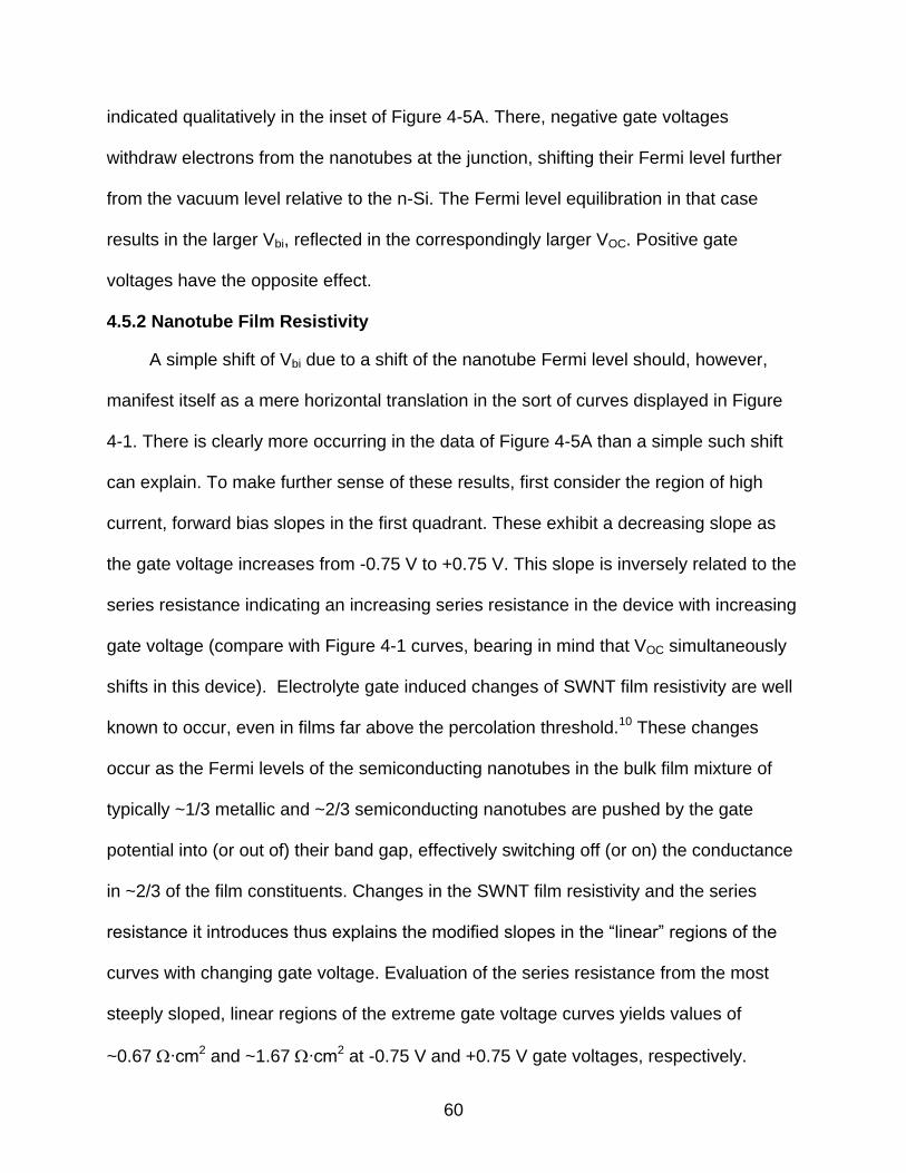
60
indicated qualitatively in the inset of Figure 4-5A. There, negative gate voltages
withdraw electrons from the nanotubes at the junction, shifting their Fermi level further
from the vacuum level relative to the n-Si. The Fermi level equilibration in that case
results in the larger Vbi, reflected in the correspondingly larger VOC. Positive gate
voltages have the opposite effect.
4.5.2 Nanotube Film Resistivity
A simple shift of Vbi due to a shift of the nanotube Fermi level should, however,
manifest itself as a mere horizontal translation in the sort of curves displayed in Figure
4-1. There is clearly more occurring in the data of Figure 4-5A than a simple such shift
can explain. To make further sense of these results, first consider the region of high
current, forward bias slopes in the first quadrant. These exhibit a decreasing slope as
the gate voltage increases from -0.75 V to +0.75 V. This slope is inversely related to the
series resistance indicating an increasing series resistance in the device with increasing
gate voltage (compare with Figure 4-1 curves, bearing in mind that VOC simultaneously
shifts in this device). Electrolyte gate induced changes of SWNT film resistivity are well
known to occur, even in films far above the percolation threshold.10 These changes
occur as the Fermi levels of the semiconducting nanotubes in the bulk film mixture of
typically ~1/3 metallic and ~2/3 semiconducting nanotubes are pushed by the gate
potential into (or out of) their band gap, effectively switching off (or on) the conductance
in ~2/3 of the film constituents. Changes in the SWNT film resistivity and the series
resistance it introduces thus explains the modified slopes in the “linear” regions of the
curves with changing gate voltage. Evaluation of the series resistance from the most
steeply sloped, linear regions of the extreme gate voltage curves yields values of
~0.67 ∙cm2 and ~1.67 ∙cm2 at -0.75 V and +0.75 V gate voltages, respectively.
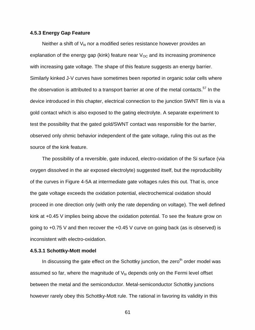
61
4.5.3 Energy Gap Feature
Neither a shift of Vbi nor a modified series resistance however provides an
explanation of the energy gap (kink) feature near VOC and its increasing prominence
with increasing gate voltage. The shape of this feature suggests an energy barrier.
Similarly kinked J-V curves have sometimes been reported in organic solar cells where
the observation is attributed to a transport barrier at one of the metal contacts.57 In the
device introduced in this chapter, electrical connection to the junction SWNT film is via a
gold contact which is also exposed to the gating electrolyte. A separate experiment to
test the possibility that the gated gold/SWNT contact was responsible for the barrier,
observed only ohmic behavior independent of the gate voltage, ruling this out as the
source of the kink feature.
The possibility of a reversible, gate induced, electro-oxidation of the Si surface (via
oxygen dissolved in the air exposed electrolyte) suggested itself, but the reproducibility
of the curves in Figure 4-5A at intermediate gate voltages rules this out. That is, once
the gate voltage exceeds the oxidation potential, electrochemical oxidation should
proceed in one direction only (with only the rate depending on voltage). The well defined
kink at +0.45 V implies being above the oxidation potential. To see the feature grow on
going to +0.75 V and then recover the +0.45 V curve on going back (as is observed) is
inconsistent with electro-oxidation.
4.5.3.1 Schottky-Mott model
In discussing the gate effect on the Schottky junction, the zeroth order model was
assumed so far, where the magnitude of Vbi depends only on the Fermi level offset
between the metal and the semiconductor. Metal-semiconductor Schottky junctions
however rarely obey this Schottky-Mott rule. The rational in favoring its validity in this
62
case was based on two properties of the nanotubes: 1) their lack of chemical reactivity
implies no chemical bonds across the junction thus avoiding chemical bond induced
interface states and 2) the compact nature of the carbon pz orbitals forming the
nanotube bands and the large van der Waals bond distance (relative to chemical
bonds) across the junction makes it improbable that the nanotubes would cause metal
induced gap states within the Si bandgap. Without these principle mechanisms for
generating in-gap states it seemed plausible that the Fermi level would be unpinned and
thus follow the Schottky-Mott rule. The inability to explain the origin of the gate
modulated kink feature along with other features of the data however compel a
reconsideration of this assumption.
4.5.3.2 Bardeen model
Bardeen’s original explanation of what would come to be called Fermi level pinning
had no need of extrinsically induced surface states.58 The simple termination of a bulk
semiconductor at its surface already leads to surface states. Treated as a continuum,
these states have their own energy dependent density of states and the energy
distribution of that density depends on the particular crystal face involved, surface
atomic reconstruction, defects and impurities. Because the bulk semiconductor must be
in thermodynamic equilibrium with its surface the equilibrium spatial distribution of
charge between the surface and the bulk can itself lead to an essentially intrinsic band
bending and associated depletion layer. If the surface states have a band of high
density around the highest occupied surface state (in thermodynamic equilibrium with its
bulk) then thermodynamic equilibration with the Fermi level of the contacting metal
occurs via electrons exchanged with this high density band of surface states. In that

63
case there is relatively little change in the band bending upon making the metal-
semiconductor contact and the Schottky barrier is independent of the workfunction of
the metal used, effectively pinning the barrier. The Schottky-Mott and the Bardeen
models comprise the extreme limits of the behaviors typically observed wherein the
Schottky barrier height does show dependence on the metal workfunction, with a
generally weaker (and often much weaker) dependence than predicted by the Schottky-
Mott rule.
4.5.3.3 Modern Schottky model
To allow for the degree of dependence on the metal workfunction (incomplete
pinning) generally seen, more modern Schottky barrier models incorporate the idea of
an additional interface dipole between the metal and the semiconductor. In recent years
this dipole has been associated with bond polarization across the chemical bonds
between the metal and the semiconductor,59 however earlier models recognized the
existence of an interface dipole, independent of chemical bonds (more relevant to the
case of carbon nanotubes), as the charge transferred by energy equilibration between
the semiconductor surface states on the one side and the corresponding image charge
in the metal on the other.60 Importantly, because this interface dipole is assumed thin, it
contributes as a tunneling barrier whose effect is folded into the Schottky barrier height.
Work in recent years has indeed evidenced systematic changes in the Schottky barrier
height in response to the dipole moments and orientations of polar molecules grafted to
the semiconductor surface (or the metal) before forming the contact with the metal.61-63
The modern view of Schottky contacts thus allows for modulation of the built-in potential
mediated by charge exchange with surface states, combined with an interface dipole
that contributes to the Schottky barrier height.

64
Within this context, the kink feature in Figure 4-5A can be explained. Concomitant
with the gate induced modulation of the nanotube Fermi level there is a gate modulated
enhancement or suppression of the interface dipole at the nanotube-Si junction which,
in turn, feeds back to the band bending and Vbi in the n-Si. Because the electrolyte gate
has direct access to the n-Si surface immediately adjacent to the nanotubes at the
junction (through the nanotube film porosity) its effect on the interface dipole can be
dramatic. In the case of more positive gate bias the enhanced dipole contributes to the
Schottky barrier height manifesting itself as a reduced forward current in the first
quadrant of Figure 4-5A. In the fourth quadrant the additional tunneling barrier due to
this enhanced interface dipole increases recombination losses, manifesting itself as the
reduced current kink feature. Further contributing to this barrier is an electric field
induced across the depletion layer due to the positive charges accumulated in the ionic
liquid at the Si surface, in the regions adjacent to the nanotubes (generating an electric
field in a direction opposing the field associated with the built-in potential). Going toward
negative gate bias reverses these trends.
4.5.4 VOC Saturation
A further feature stands out in the data. The changes in the VOC saturate in this
sample at 0.55 V with negative gate voltage and at most at 0.58 V in the numerous
other devices tested as shown in Figure 4-8. Within the described picture this finds
explanation as a region of high silicon surface state density that once reached prevents
further change in Vbi. Reported measurements of the surface state density as a function
of energy for partly oxidized hydrogen terminated Si indeed show a steep rise in the
density on approach of the valence band from the mid gap.64 As mentioned previously,

65
detailed modeling is needed to quantify the relative contributions of these effects to the
behaviors seen, which will be addressed to in Chapter 5.
4.6 Concluding Remarks
Finally, returning to the point made earlier that the steady state gate voltage draws
no power. This means that the ~11% power conversion efficiency obtained (with room
for further optimization in e.g. the nanotube film thickness) can be realized with
negligible loss of power to drive the gate. Indeed, two relatively small ungated solar
cells wired in series (to get the -0.75 V gate voltage) can be used to drive the gate of a
much larger device, giving up in the power conversion efficiency only the fractional
surface area dedicated to the small gating cells. Given the 30 nA current drawn by the
gate for our 8 mm2 area cell, two 1 cm2 ungated cells could power the gate of over 6 m2
of solar cell. Since the gating electrode need not be illuminated it need not occupy cell
surface real estate and while it requires a large capacitance, this can be achieved
compactly using activated carbon or a pseudo-capacitive electrode of a type common in
supercapacitors. Commercial devices would likely require sealing and while the fluid
state of the ionic liquid electrolyte is convenient in research, sealing may be complicated
by a fluid layer. Replacement with a solid state electrolyte could be useful in that case.
Finally, reiterating that the “soft contact” of the nanotube films with silicon means that
the Si surface is left chemically unperturbed. If modification of the Si surface can
change its surface state density to unpin the VOC from the observed saturation value,
the resulting gate induced increase in VOC should allow for substantial further
performance enhancement.

66
4.7 Future Work
Further experiments (e.g. gate modulated capacitance-voltage measurements)
should be useful in gaining a more detailed understanding. Particularly interesting would
be the results of similar electrolyte gated devices constructed with high quality single
layer graphene as the transparent junction electrode.65-66 Indeed graphene/n-Si
Schottky junction devices have recently been reported.67 Since a continuous graphene
layer can avoid direct contact of the electrolyte with the junction, and the graphene layer
should screen the gate field from a direct influence on the interface dipole, this could
separate out its direct effect on the dipole from the gate induced modification of the
(graphene) Fermi level. The electronically gated device platform reported here provides
a model system that may provide new insights into some long standing questions in the
physics of Schottky junctions.

67
Table 4-1. Solar cell characteristics extracted from the gated J-V curves of Figure 4-5A. Reproduced in part with permission from [Wadhwa, P.; Liu, B.; McCarthy, M. A.; Wu, Z.; Rinzler, A. G. Nano Lett. 2010, 10, 5001-5005]. Copyright [2010], American Chemical Society
Gate Bias (V) - 0.75 - 0.45 - 0.15 0.0 + 0.15 + 0.45 + 0.75
VOC(V) 0.55 0.54 0.51 0.49 0.47 0.41 0.33 JSC(mA/cm2) 25.0 25.3 25.2 25.0 25.0 24.9 24.8 FF 0.79 0.77 0.71 0.68 0.62 0.54 0.44 PCE(%) 10.9 10.5 9.2 8.4 7.4 5.5 3.6
Figure 4-1. Solar cell model J-V curves Inset: Band bending at a M-S junction and the flattening of the bent bands with increasing forward bias (VF). Reproduced in part with permission from [Wadhwa, P.; Liu, B.; McCarthy, M. A.; Wu, Z.; Rinzler, A. G. Nano Lett. 2010, 10, 5001-5005]. Copyright [2010], American Chemical Society

68
A.
B.
A.
B.
GateA.
B.
A.
B.
Gate
Figure 4-2. Device illustration. A) 3-D view, hash lines are merely aids for 3-D visualization (ionic liquid not shown). B) Cross-sectional view, ionic liquid (IL) shown. The larger gold contact on the SiO2 surface includes a 2×4 mm2 rectangular window in which the oxide was etched to the bare n-Si surface. A SWNT film contacts both the gold electrode and the n-Si within the window forming the SWNT/n-Si junction. E-GaIn provides the back side contact between the n-Si and a stainless steel sheet (not shown). The large gold contact and the steel sheet comprise the two terminals of the solar cell. The second smaller gold contact and its associated SWNT film lie entirely on the oxide. These provide the gate electrode for the IL electrolyte which lies as a puddle across both SWNT films. Reproduced in part with permission from [Wadhwa, P.; Liu, B.; McCarthy, M. A.; Wu, Z.; Rinzler, A. G. Nano Lett. 2010, 10, 5001-5005]. Copyright [2010], American Chemical Society.
69
Figure 4-3. Photograph of the sample in the measurement fixture recorded from above (the sample sits horizontally). IL is introduced within the region of the dotted oval line and once added, it saturates both SWNT films and bridges between them. Reproduced in part with permission from [Wadhwa, P.; Liu, B.; McCarthy, M. A.; Wu, Z.; Rinzler, A. G. Nano Lett. 2010, 10, 5001-5005]. Copyright [2010], American Chemical Society.
Figure 4-4. J-V plots: “conventional” SWNT-Si cell in the dark and under AM1.5G illumination. Reproduced in part with permission from [Wadhwa, P.; Liu, B.; McCarthy, M. A.; Wu, Z.; Rinzler, A. G. Nano Lett. 2010, 10, 5001-5005]. Copyright [2010], American Chemical Society.

70
A.
C.B.
A.
C.B.
Figure 4-5. Gating effects. A) J-V plots of the illuminated SWNT/n-Si cell under the indicated gate voltage applied to the gate electrode. B) Charge state of the junction SWNTs with negative voltage applied to the gate electrode. C) Zoom of the zero current crossings (VOC) region in A). Reproduced in part with permission from [Wadhwa, P.; Liu, B.; McCarthy, M. A.; Wu, Z.; Rinzler, A. G. Nano Lett. 2010, 10, 5001-5005]. Copyright [2010], American Chemical Society.

71
Figure 4-6. Equivalent circuit of Figure 4-5B. Reproduced in part with permission from [Wadhwa, P.; Liu, B.; McCarthy, M. A.; Wu, Z.; Rinzler, A. G. Nano Lett. 2010, 10, 5001-5005]. Copyright [2010], American Chemical Society.
-0.4 -0.2 0.0 0.2 0.4 0.6 0.8
-20
0
20
40
-0.75 V (light)
-0.75 V (dark)
0 V (light)
0 V (dark)
+0.75 V (light)
+0.75 V (dark)
Cu
rre
nt
de
nsity (
mA
/cm
2)
Voltage (V)
Figure 4-7. Dark and light current J-V curves at the indicated gate voltages. Reproduced in part with permission from [Wadhwa, P.; Liu, B.; McCarthy, M. A.; Wu, Z.; Rinzler, A. G. Nano Lett. 2010, 10, 5001-5005]. Copyright [2010], American Chemical Society.
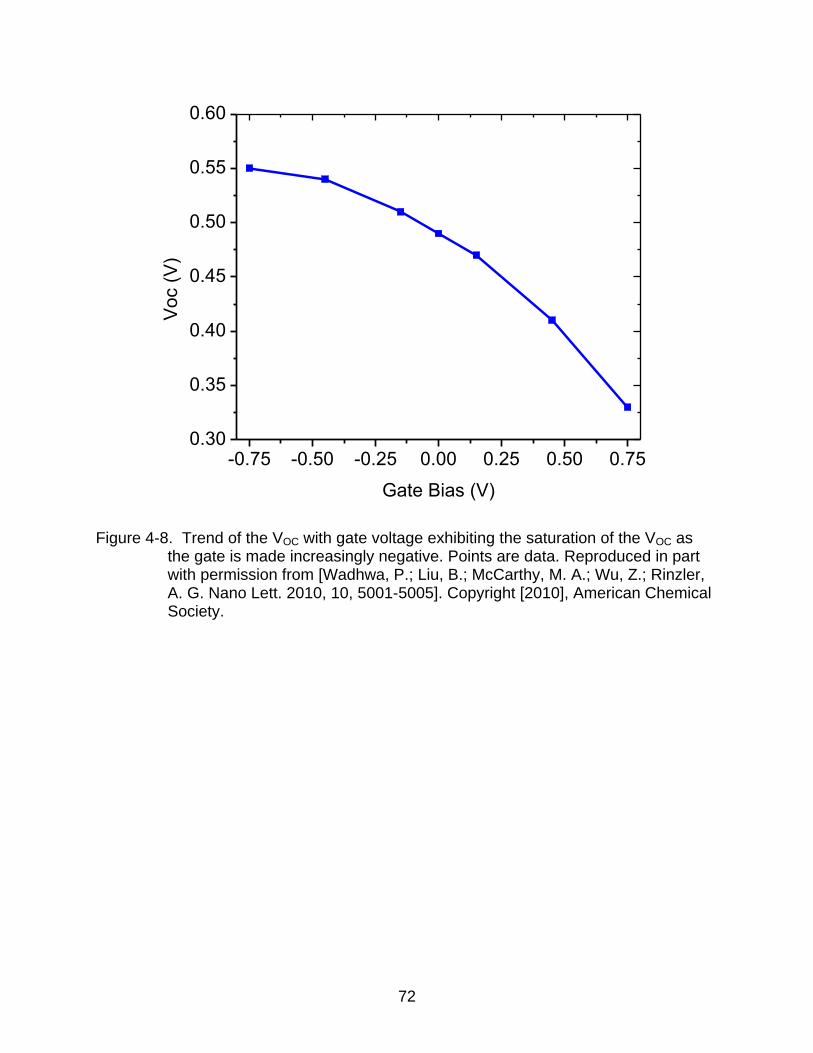
72
-0.75 -0.50 -0.25 0.00 0.25 0.50 0.750.30
0.35
0.40
0.45
0.50
0.55
0.60
Voc (
V)
Gate Bias (V)
Figure 4-8. Trend of the VOC with gate voltage exhibiting the saturation of the VOC as the gate is made increasingly negative. Points are data. Reproduced in part with permission from [Wadhwa, P.; Liu, B.; McCarthy, M. A.; Wu, Z.; Rinzler, A. G. Nano Lett. 2010, 10, 5001-5005]. Copyright [2010], American Chemical Society.

73
CHAPTER 5 ELECTROLYTE INDUCED INVERSION LAYER SCHOTTKY JUNCTION SOLAR CELL
5.1 Background
Chapter 4 described the electronic modulation of the fundamental characteristics
(open circuit voltage, fill factor, power conversion efficiency) of a nanotube/n-Si Schottky
junction solar cell.68 The native device exhibited PCE of 8.5%. By exploiting an
electrolyte gate, having access to the junction through the thin, porous SWNT film, a
continuous, reversible modulation of the PCE from ~4% to nearly 11% was
demonstrated (the gate circuit drawing negligible power in the steady state). The
presence of an electrolyte at the junction, presents the opportunity for a new type of
solar cell that is described in this chapter.
5.2 Device Design
5.2.1 Device Architecture
The device construction that demonstrates this new cell has much in common with
the gated nanotube/n-Si device discussed in Chapter 4, except that rather than use a
continuous nanotube film to form the junction the film was etched in a grid pattern to
cover only a fraction of the n-Si surface. Figure 5-1A shows the schematic of such a
device. A gold electrode with a 2×4 mm2 rectangular window was evaporated onto a
1 μm thick oxide layer on an n-Si wafer. The window in the gold electrode is used as an
etch mask to etch the oxide within the window down to the bare n-Si. A 45 nm thick, 6×8
mm2 rectangular area SWNT film was deposited across the window contacting the gold
electrode and forming the junction with the exposed n-Si. As was done in Chapter 4, a
second gold electrode and second SWNT film that is to act as the gate electrode once
the electrolyte was added, were deposited on the oxide layer near the junction. Figure

74
5-1B shows a photograph of the grid pattern in the junction SWNT film formed by
photolithography and etching in an oxygen barrel asher. The grid lines shown are 100
μm wide with a 300 μm spacing between the vertical lines.
5.2.2 Device Fabrication
To define the SWNT grid lines in the junction film photolithography was used. The
substrate was spin coated with Shipley S1813 photoresist and a patterned chrome
mask was used in Kurl Suss Mask Aligner 6.0 to expose 300 μm wide regions with 100
μm separation between them right above the n-Si window. On developing the
photoresist, 100 μm wide regions were covered with photoresist and the 300 μm
regions exposed the SWNT film underneath. Antech barrel plasma asher was used to
etch away the 300 μm wide SWNT strips under oxygen plasma, leaving the photoresist
covered areas of 100 μm width intact. The photoresist was completely stripped off the
substrate using propylene glycol monomethyl ether acetate, acetone and methanol.
This finally formed the required SWNTs-grid/Si junction with 100 μm wide SWNT strips
in contact with n-Si and 300 μm apart.
Procedure similar to that described in Chapter 4 was followed to make the back
contact with GaIn eutectic and a 0.015” stainless steel sheet. On making the electrical
contacts using indium dots and silver wires, a final BOE etching step of the grid/Si
junction was introduced and the device was ready for measurement.
5.3 Results
5.3.1 Conventional Grid Cell
Figure 5-2 shows the cell current density versus voltage (J-V) characteristic in the
dark and under illumination (AM1.5G, 100 mW/cm2) for two distinct devices in the
absence of electrolyte. One device with a continuous SWNT film across the entire

75
window and the other with the nanotube film etched into a grid pattern limiting the Si
coverage with the nanotubes to 27% of the window area. The nanotube film/n-Si contact
forms a “conventional” metal-semiconductor Schottky junction solar cell. Fermi level
equilibration of the n-Si with the nanotubes, transfers electrons from the n-Si to the
SWNTs generating a depletion layer and band bending in the Si. Photons absorbed in
the Si generate free electrons and holes that upon diffusing to the depletion layer are
separated by the built-in potential in the vicinity of the nanotubes, enabling power
generation from the device. For doping density of ~1015 donors/cm3 this depletion layer
extends ~1 μm into the Si from the contact with the nanotubes. Given the relatively
small extent of this depletion layer the reduced junction area of the grid device yielded a
reduced short circuit photocurrent. The reduction in the photocurrent did not scale in
direct proportion to the reduced junction area because high quality single crystal silicon
has long diffusion lengths, allowing photocarriers generated far from the junction to
diffuse there and contribute to the photocurrent. Nevertheless, the photocurrent in the
grid film is reduced by more than a factor of two over that of the continuous film, yielding
a corresponding decrease in the full window-area-normalized power conversion
efficiency.
5.3.2 Electrolyte Gated Grid Cell
The situation became substantially more interesting on the simple addition of the
EMI-BTI ionic liquid electrolyte. Figure 5-3 compares the illuminated J-V curves of the
grid SWNT film before and after addition of the electrolyte for the gate electrically
floating and with -0.75 V applied to the gate electrode. The simple addition of the
electrolyte, gate floating or not, more than recovers the short circuit photocurrent lost
due to the reduced areal coverage of the n-Si by the nanotubes. To explain this

76
behavior, it is concluded that the electrolyte induces its own depletion (or inversion)
layer in the Si across the large gaps between the nanotube grid lines.
5.4 Inversion Layer
Electrolyte induced depletion layers are well known from photoelectrochemistry
studies of electrolyte-semiconductor interfaces.69 By incorporating a counter-electrode
and a suitable regenerative redox couple in the supporting electrolyte such junctions
form the basis of the liquid-junction, regenerative solar cell, the best known example of
which is the Gratzel cell.70 In such cells the counter electrode forms one terminal of the
cell and the redox couple serves as a shuttle necessary to ferry charge between the
semiconductor surface and the counter electrode, effectively completing the internal
circuit of the cell.
The SWNT-grid-electrolyte/n-Si cell must be distinguished from
photoelectrochemical cells in that there is no redox couple and the EMI-BTI electrolyte
used here has a very broad electrochemical window ranging from -2.6 V to +2.0 V (vs.
Fc/Fc+ or -5.1 V relative to the vacuum level).71 Hence this electrolyte does not
participate in the charge transport. Instead photogenerated holes that make it to the
electrolyte induced inversion layer in the Si are trapped by the electric field within the
layer and are diffused along it until they encounter a nanotube grid line where they are
collected. Because the electric field, which accumulates holes at the surface also repels
electrons, deleterious surface recombination is largely avoided.
Consideration of how the depletion layer develops in photoelectrochemical cells
further demonstrates that the inversion layer appearing in the nanotube-
electrolyte/semiconductor (NES) solar cells must be of distinct origin. In the electrolyte
of a photoelectrochemical cell the electrochemical (Nernst) potential of the incorporated
77
redox couple sets the equilibrium distribution of the couple between its reduced and
oxidized states. When the electrolyte comes into contact with the semiconductor the two
exchange charge, simultaneously shifting the electrochemical potential of the redox
couple and the Fermi level of the semiconductor until they are in equilibrium (thus
establishing the depletion layer in the semiconductor). But in NES devices, the large
electrochemical window over which the EMI-BTI electrolyte undergoes no redox
precludes such charge exchange. Accordingly, the cause of the inversion layer required
by the NES J-V curves is different from that of photoelectrochemical cells.
The situation is reminiscent of so called “grating” metal-insulator-semiconductor
(MIS) cells first described by Godfrey and Green in the late 1970s.72 In those devices
narrow metal lines (Al or Mg) on the front surface of p-type silicon collected electrons
trapped by an inversion layer formed at the p-Si surface in the regions between the
widely spaced metal lines. The inversion layer in those devices was induced by positive
charge trapped in an SiO layer grown on the Si. In the present case the gate voltage is
certainly capable of inducing charge (of either sign depending on the polarity of the
gate) adjacent to the surface of the n-Si but interestingly the high short circuit current
(Vbias = 0 V) seen in the grid film of Figure 5-3 occurs immediately on introduction of the
ionic liquid. This implies that negative ions accumulate at the n-Si surface upon simple
introduction of the electrolyte.
An experiment was conducted to explore whether the depletion layer in the n-Si
induced by the ions in the electrolyte between nanotube grid lines existed prior to the
light exposure or if it was created by ion migration in the electrolyte initiated by light
exposure. The short circuit current generated by the cell was measured as a function of
78
time immediately after exposing the device to the light (AM1.5G) using a fast
electromechanical shutter. If the depletion layer did not exist prior to the light exposure,
the current should have built up relatively slowly as ions migrate to the surface inducing
the depletion layer over time. Realizing that the high ionic conductivity of the ionic liquid
EMI-BTI, which is 8 mS/cm may reorganize too quickly for the electronics to see the
current rise (the fastest sampling rate of Keithley 2400 is ~2.4 ms, also about the speed
of the electromechanical shutter used), a different electrolyte system was used: lithium
triflate (LiClO4) in propylene carbonate (PC). In this electrolyte system, the ionic
concentration could be reduced, thereby increasing the timescale for the build-up of a
depletion layer if it was somehow photo-initiated . Figure 5.4 shows the effect of the
different ionic conductivities of: 0 (no electrolyte), 2.2 μS/cm; 29 μS/cm (different
concentrations of LiClO4 in PC) and 8000 μS/cm (EMI-BTI) on the short circuit current
developed in the cell as a function of time (for multiple blocking and unblocking cycles of
the light by the shutter). For the non-electrolyte curve the short circuit current was
limited by the depletion layer existing only in the immediate vicinity of the nanotube
grids covering 25% of the Si window. Since the grid pattern limited this to only about a
quarter of the n-Si surface, the short circuit current density was only ~ 6 mA/cm2. With
the lowest ionic conductivity electrolyte (2.2 μS/cm), the short circuit current density was
already substantially greater than without the electrolyte showing that, as expected,
relatively little electrolyte conductivity was required to begin to establish a depletion
layer in the n-Si. The rapid increase of the current beyond the 6 mA/cm2 indicated that
the major fraction of the depletion layer pre-existed the light exposure on the electrolyte.
The small time dependence seen in the rounded corners of the curves near the opening
79
of the shutter (unblocking of light) indicated that there was some further enhancement of
the depletion layer likely due to image charges in the electrolyte migrating to the
interface in response to the photo generated hole build-up, but this is a small effect that
disappears as the electrolyte conductivity is increased. Increasing the electrolyte ionic
concentration increases the current density, which in turn indicates that the depletion
layer due to the electrolyte increases with electrolyte ionic concentration. Since
however the still quite low ionic concentration of the 29 μS/cm LiClO4 in PC shows a
saturation current density that is already 75% of that of the 8000 μS/cm ionic liquid this
dependence on the electrolyte conductivity clearly saturates at well below the highest
conductivity. The pre-existence of the electrolyte induced inversion layer for conducting
electrolytes was also supported by electrostatic simulations discussed in Section 5.5.
5.5 Electrostatic Simulations
To determine if the charge separation could be explained by the native
electrostatics, the system was modeled using the solar simulation design package:
Synopsys TCAD Sentaurus.73 This work was done in collaboration with Professor Jing
Guo (UF Dept. of Electrical and Computer Engineering) and the simulations were
performed in his group by Jason Seol. The electrolyte was simulated using a dielectric
coating with a very large dielectric constant (ε = 5000), i.e. the mobile free ions of the
electrolyte were replaced by a “dielectric” layer having a bound charge possessing an
extreme polarizablity (the free charge of electrolytes precludes definition of a real, DC
dielectric constant for them so that the AC dielectric constants available in the literature
were not relevant). The value of ε = 5000 comes from the ratio of the characteristic
dielectric layer dimension (~100 μm) relative to that of the characteristic Debye layer
dimension in the electrolyte (< 20 nm). The simulation confirmed the formation of an

80
inversion layer generating an electric field upon addition of the electrolyte. Figure 5-5
shows the experimental J-V curves for the grid device where the current density
remained normalized to the full window area. Figure 5-6 shows the simulation
parameters and geometry (not to scale) for a cross-sectional slice through a SWNT grid
line of 100 μm width, having its long axis perpendicular to the page. The SWNT line
was treated as a simple metal of constant work function CNT = 4.9 eV (consistent with
that of nitric acid purified nanotubes). The gate electrode was a gold line (Au = 5.1 eV)
situated on a 1 μm thick SiO2 dielectric ( = 3.9). Below the SWNT grid line lied the
junction with the n-Si (Si = 4.3 eV for the 11015 cm-3 phosphorous doping density),
which adjacent to the SWNT line was in direct contact with the “electrolyte” (dielectric
with ε = 5000) that coated the entire structure. The Neumann boundary conditions used
placed mirror planes at the left and right sides of the figure making the gold gate
electrode line (including its reflection on the left side) 100 μm wide (equal area to the
SWNT grid line) and the spacing to the next SWNT grid line (including the reflection on
the right side) 300 μm. Figures 5-7A, B, C show the electric field developed in the
depletion layer below the SWNT/n-Si junction and in the adjacent n-Si at a bias voltage
Vbias = 0 V for gate voltages: Vg= –0.75, 0, +0.75 V (left column 5-7A, C, E,
respectively). Figures 5-7B, D, F show this at a forward bias voltage Vbias = 0.3 V for the
same gate voltages: Vg= -0.75, 0, +0.75 V (right column 5-7B, D, F, respectively). The
simulation plots for the reverse bias case Vbias = -0.4 V at gate voltages Vg= -0.75, 0,
+0.75 V are shown in Figure 5-8.
This simulation is concerned only with the inversion layer generated by the
electrolyte. The other gate field dependent features of the J-V curves discussed in
81
Chapter 4 were not modeled here. Thus, the model did not for example include the gate
induced shift in the SWNT Fermi-level (nor the resistivity changes in the SWNT film,
irrelevant to the electrostatics). Nevertheless, the model captured the existence of an
inversion layer extending well beyond the direct depletion layer in the vicinity of the
SWNT/n-Si contact as required to explain the increased saturation currents upon
addition of the electrolyte.
This behavior can be understood as follows. When the nanotubes and the n-Si are
first placed in intimate contact the free energy of electrons in the n-Si (work function:
Si = 4.3 eV) is reduced by their transfer to the carbon nanotubes (work function:
CNT = 4.9 eV). Such transfer stops when the Coulombic restoring forces due to the
charge imbalance raise the local potential (the built-in potential) to prevent further
charge exchange, establishing equilibrium. In the presence of electrolyte ions, having
freedom to migrate, the ions compensate the transferred charge to permit the exchange
of substantially more charge before equilibrium is reached. Additional electrons are
transferred to the nanotubes from the n-Si regions between the nanotube grid lines
compensated by positive electrolyte ions surrounding the nanotubes, while the holes left
behind in the n-Si inversion layer are compensated by negative electrolyte ions
accumulated at the Si surface. The electrolyte here serves much as it does in an
electrolytic capacitor to raise the capacitance of the system with a self potential
provided internally by the original Fermi level offset between the nanotubes and the n-
Si, or externally by the gate field.

82
5.6 Quantitative Analysis
Photons in transit to the Si surface that are absorbed in the SWNT film do not
contribute to the power generation. This was confirmed by looking for photocurrent with
a filter in the light path that only transmits light energies below the silicon bandgap
(looking for photocurrent from absorption in the semiconducting nanotubes, having a
bandgap of ~0.6 eV). In fact light absorbed in the nanotube films is not transmitted to
the n-Si thus degrading the PCE. Thinner nanotube films would transmit more power to
the silicon, enhancing the PCE, but thinning the nanotube films increases their
resistance and cell series resistance degrades the fill factor and thus the PCE. The
ability to use a liquid junction and reduce the area of the Si that must be covered by the
nanotube film suggested that a grid pattern of optimized spacing could minimize the
overall absorptive losses while minimally increasing the series resistance, yielding a net
gain in the PCE. This turned out to be the case. The gated device discussed in Chapter
4 using a continuous SWNT film and -0.75 V applied to the gate achieved a best PCE of
10.9%. At this same gate voltage the grid film having 100 μm wide SWNT lines with 300
μm spaces between them has a PCE of 12%, an increase of 10% over the continuous
film (Figure 5-3). The increased photon flux arriving at the electrolyte/n-Si junction of the
gridded cell should manifest itself as a larger short circuit current density, as was
observed. The short circuit current density for the grid film was 229.8 mA/cmSCGJ while
that for the continuous film was 225.0 mA/cmSCFJ . The small increase in the JSC of the
full film device before and after the addition of the electrolyte (22 mA/cm2 to 25 mA/cm2)
was likely due a refractive index matching effect of the ionic liquid.
83
The principle difference between the short circuit current density in the case of a
grid and a full film device (both electrolyte coated) should be in the absorptive losses
due to the nanotubes. This was quantitatively corroborated as follows. The current
collected for the grid device is proportional to the photon flux reaching the silicon as
given by:
[1 ( ) ( )] ( ) (1 )(1 ( )] ( )G G nt nt G SiI A R B P d A R P d (5-1)
Where AG is the area occupied by the nanotube grid lines as a fraction of the total
window area, ( )ntR was the measured reflectance of an ionic liquid saturated nanotube
film (45 nm thick) on n-Si, ( ) 1 ( ) nt ntB T , where ( )ntT is the measured transmittance
of an ionic liquid saturated nanotube film (45 nm thick) on glass (making ( )ntB the
absorptive loss in the SWNT film), ( )P is the AM1.5G solar irradiance (mW/cm2/nm),
( )SiR is the reflectance of n-Si coated with a thin layer of the ionic liquid and the
integrals are over the region of the solar spectrum relevant to silicon (300 nm to 1107
nm). The current collected in the full film covered window device will similarly be
proportional to the photon flux reaching the silicon in that case and be given by:
[1 ( ) ( )] ( )F nt ntI R B P d (5-2)
Reflectance and transmittance measurements were performed using a Perkin
Elmer Lambda 900, dual beam spectrophotometer (plots shown in Figure 5-9). The
solar irradiance was derived from the ASTM G173-03 tables74 and the integrals were
performed numerically. The ratio of the currents in the two devices evaluated in this way
yields / 1.17G FI I which should yield the ratio of the grid to the film short circuit current

84
densities of / 29.8 mA / 25 mA 1.19SCG SCFJ J . These are in good agreement given no
adjustable parameters and errors to be expected from the neglect of the second transit
through the nanotube film that appears in the reflectance measurement, and the neglect
of the reflection from the front surface of the nanotube film/ionic liquid occurring in the
transmittance measurement. Reassuringly, correction for these effects would raise the
calculated value, further improving the agreement.
5.7 Discussion and Future Work
The grating MIS cell mentioned above was intensely studied in the late 1970s and
early 1980s. Although the PCE of the grating MIS cells could exceed 17% it was found
that they degraded rather drastically with time.75 The degradation was traced to
electrons that accumulated from the environment at the SiO layer surface. Because this
charge tended to neutralize the trapped positive charge in the SiO layer (responsible for
generating the inversion layer that permitted the wide electrode spacing) the magnitude
of the inversion layer decreased, degrading the cell performance. This should not be a
problem with electrolytes which are intrinsically neutral and induce the inversion layer
via a spontaneous charge separation. As is seen in the data of Figure 5-3 simple
addition of the electrolyte, even with the gate electrically floating, yields a short circuit
photocurrent equal to the saturation photocurrent implying existence of the inversion
layer even before any gate field is applied. In the case of the SWNTs the appearance of
the gap like feature on electrolyte addition reduces the fill factor so that the gate field is
necessary to achieve the maximum power conversion efficiency. Such gap like feature
is not anticipated in the case of conventional metal electrodes. In that case a grating
MIS Schottky junction cell with the SiO layer replaced by the ionic liquid electrolyte may
85
provide the solution to the previous degradation problem even without the need for
active gating (while gating incurs little energetic penalty it does add complexity). Finally
we note that such cells should also benefit from a texturing of the Si to trap more of the
light reflected from its surface. Recently arrays of nanoholes in a p-n junction Si solar
cell have been demonstrated to enhance the device performance.76 The large spacing
permitted between the grid lines in the electrolyte coated NES device indicates that by
filling the nanoholes with electrolyte, the device could benefit from both the inversion
layer and the additional light trapping. Substantial further improvements may be
possible for such electrolyte induced, inversion layer cells.
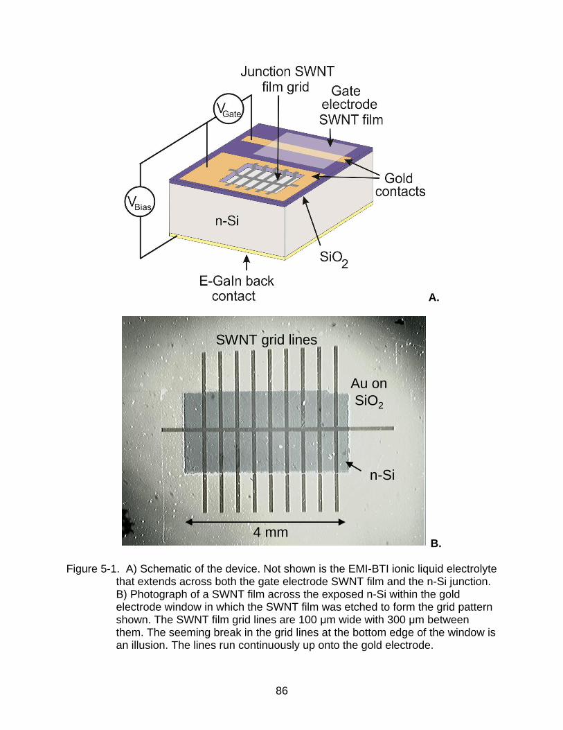
86
A.
Au on
SiO2
n-Si
SWNT grid lines
4 mm
Au on
SiO2
n-Si
SWNT grid lines
4 mm B.
Figure 5-1. A) Schematic of the device. Not shown is the EMI-BTI ionic liquid electrolyte that extends across both the gate electrode SWNT film and the n-Si junction. B) Photograph of a SWNT film across the exposed n-Si within the gold electrode window in which the SWNT film was etched to form the grid pattern shown. The SWNT film grid lines are 100 μm wide with 300 μm between them. The seeming break in the grid lines at the bottom edge of the window is an illusion. The lines run continuously up onto the gold electrode.

87
-0.8 -0.6 -0.4 -0.2 0.0 0.2 0.4 0.6 0.8
-20
0
20
40
60
SWNT Film-dark
SWNT Film-light
SWNT Grid-dark
SWNT Grid-light
Curr
ent
density (
mA
/cm
2)
Voltage (V)
Figure 5-2. J-V curves in both the light (AM 1.5G, 100 mW/cm2) and dark for a continuous SWNT film covering the n-Si window and for an etched film (as in Figure 5-1B). The etched film in this case covers 27% of the n-Si window.
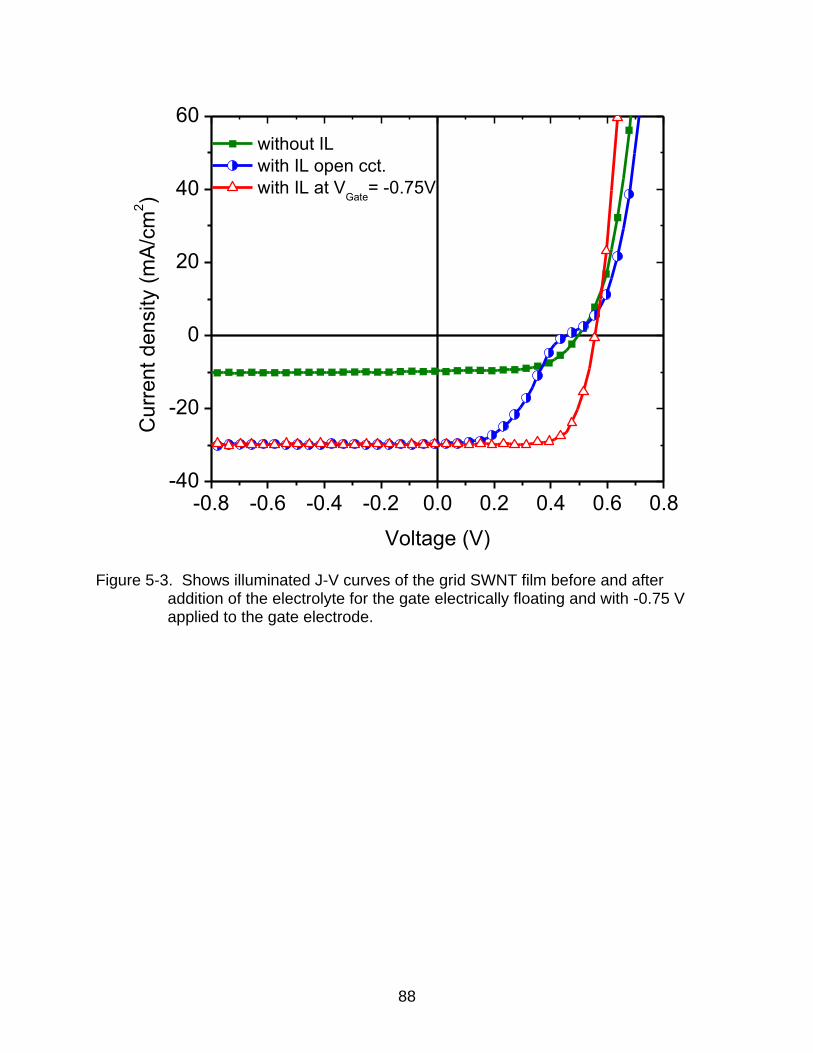
88
-0.8 -0.6 -0.4 -0.2 0.0 0.2 0.4 0.6 0.8-40
-20
0
20
40
60
without IL
with IL open cct.
with IL at VGate
= -0.75V
Cu
rre
nt
de
nsity (
mA
/cm
2)
Voltage (V)
Figure 5-3. Shows illuminated J-V curves of the grid SWNT film before and after addition of the electrolyte for the gate electrically floating and with -0.75 V applied to the gate electrode.

89
-20
-10
0
0 30 60 90 120
Time (s)
Sh
ort
cir
cu
it c
urr
ent
den
sity (
mA
/cm
2)
0 S/cm (no electrolyte)
2.2 S/cm
29 S/cm
8000 S/cm (EMI-BTI)
Figure 5-4. Time measurements of short circuit current of the grid solar cell with 25% of the silicon window covered with the nanotubes at different electrolyte concentrations (as indicated by the ionic conductivity).

90
-0.6 -0.3 0.0 0.3 0.6
-30
-20
-10
0
10
20
Curr
ent
density (
mA
/cm
2)
Bias Voltage (V)
-0.75 V
-0.45 V
0 V
+0.45 V
+0.75 V
VGate
Figure 5-5. Experimental J-V curves under illumination at the specified gate voltages.
Figure 5-6. Simulation geometry and parameters of a cross-sectional slice of the device through the nanotube grid line.

91
Figure 5-7. Simulation results at Vg = -0.75, 0, +0.75 V and Vbias = 0, 0.3 V.
Figure 5-8. Simulation results at Vg = -0.75, 0, +0.75 V and Vbias = -0.4 V.
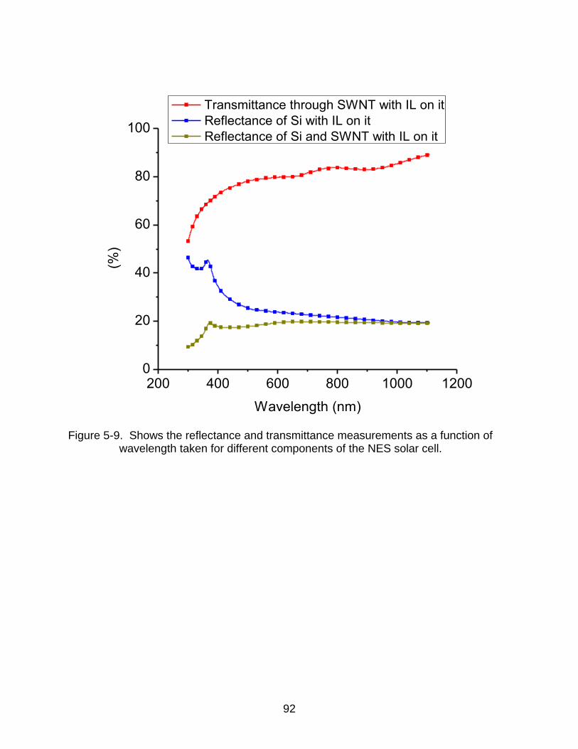
92
200 400 600 800 1000 12000
20
40
60
80
100(%
)
Wavelength (nm)
Transmittance through SWNT with IL on it
Reflectance of Si with IL on it
Reflectance of Si and SWNT with IL on it
Figure 5-9. Shows the reflectance and transmittance measurements as a function of wavelength taken for different components of the NES solar cell.
93
CHAPTER 6 CARBON NANOTUBE SPRAYED FILMS
6.1 Theory
This chapter discusses an alternate nanotube film preparation approach. The aim
is to develop a process capable of producing larger area nanotube films than can be
fabricated by the filtration method (discussed in Chapter 1) without sacrificing the
homogeneity, low sheet resistance and high transmittance achieved by that method.
The filtration process is limited by the size of the filtration apparatus and available
membrane sizes. A conventional means of producing thin solid films of particulates over
large areas is spray coating. This requires that the particles be homogeneously
dispersed in a solvent creating an “ink” that can be sprayed onto a surface in a uniform
layer leaving the solid particulates behind once the solvent evaporates.
As discussed in Chapter 1, surfactants can be used to suspend carbon nanotubes
in solvents to form a sprayable ink. Unfortunately, as also discussed in Chapter 1
nanotube suspension with surfactants requires at least the critical micelle concentration
of the surfactant. That turns out to be a far larger concentration than the nanotubes and
since the surfactants are non-volatile they are left behind along with the nanotubes once
the solvent evaporates. Because surfactants are not electrically conducting, they greatly
impede the film electrical transport and attempts to remove the surfactant without
disturbing the homogeneity of the film are problematic.
Much effort has gone into improving the dispersibility of carbon nanotubes by
surface functionalization involving the covalent attachment of chemical groups to
CNTs.77,78 While these methods can be effective at dispersing the nanotubes the
covalent attachment disrupts the sp2 structure and conjugation of the CNTs responsible

94
for their high electrical conductivity.79 Hence these methods are not useful in the
fabrication of conductive, transparent CNT films.
Alternative to covalent attachment carbon nanotube dispersants that bind non-
covalently to the nanotubes have also been explored. The non-covalently bound
dispersants fall into three broad categories, surfactants80 (already discussed),
polymers81 and others like DNA, proteins, starch etc.82 Polymer dispersants increase
the solubility of nanotubes in a broad range of solvents. This chapter describes the use
of one such polymer to disperse the nanotubes in a desired solvent. This project is part
of a collaborative effort between Rinzler group (UF Dept. of Physics) and the Polymer
Chemistry group of Professor John Reynolds (UF Dept. of Chemistry). The polymer
system used was synthesized by the Reynolds group based on a system described in
the literature to disperse mutiwalled carbon nanotubes well in water.83 This system is a
pyrene derivitized hydroxypropyl cellulose. Pyrene and its derivatives have been widely
used to functionalize the CNTs because of their ability to interact with the CNTs via π-π
stacking.84 Commercially available hydroxypropyl cellulose (HPC) is one of the most
commonly used cellulose derivatives with good solubility in most common solvents. So,
a pyrene-derivitized HPC, shown in Figure 6-1, can be used as a dispersant to suspend
carbon nanotubes. One advantage of this system is that unlike surfactants only the
pyrene-HPC associated with a nanotube need exist in the solvent, minimizing the
dispersant amount that must be used. Another advantage is that the HPC backbone is
readily decomposed under relatively mild conditions so that once the film is formed, the
major fraction of this material can be decomposed and washed away.
95
6.2 Ink preparation
Purified single wall carbon nanotube material suspended in 1% surfactant (Triton
X-100) was used as the starting material. This solution was filtered through a porous
filter membrane to collect the nanotubes on the membrane and without letting the
nanotubes dry a Triton X-100 solution at critical micelle concentration (CMC) was used
to rinse off the excess surfactant while leaving the nanotubes coated with their full
complement of surfactant. Without letting the film dry, the nanotubes were scrapped off
the membrane and re-dispersed in an aqueous solution of Triton X-100 at a
concentration of 2×CMC. After letting the nanotubes soak in the solution for 15 hr, 20
minutes of bath ultrasonication was used to re-suspend the SWNTs in 2×CMC solution.
Pyrene-HPC was dissolved in deionized water at a concentration of 0.33 mg/ml and
filtered through 45 μm polytetrafluoroethylene (PTFE) filter. Equal volumes of the
SWNTs in 2×CMC aqueous solution and the pyrene-HPC (p-HPC) solution were mixed
and left stirring on a magnetic stir plate for 4 days. The rationale behind this procedure
is to present the SWNTs with Triton X-100 at precisely the CMC simultaneously with
excess pyrene-HPC. During the long term stirring step it was anticipated that the
pyrene-HPC, with its high affinity for the nanotubes would replace the surfactant (as is
confirmed below). To eliminate the surfactant and excess pyrene-HPC the solution was
filtered with DI water washing collecting the SWNTs. Again without drying the filtered
product was scraped into the desired solvent and re-dispersed by bath ultrasonication.
The fact that this material could be stably suspended in pure solvents in which HPC is
soluble is clear evidence of the success of this association process. Two control
experiments following this protocol but using no HPC in one experiment and a second
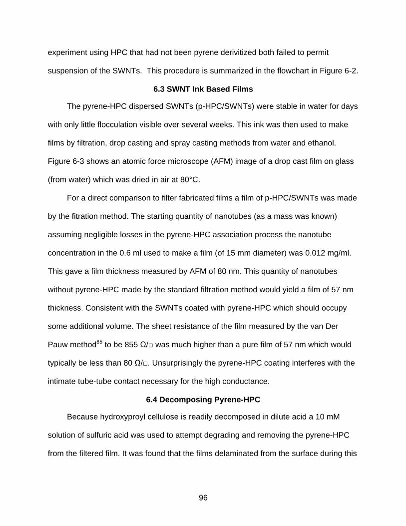
96
experiment using HPC that had not been pyrene derivitized both failed to permit
suspension of the SWNTs. This procedure is summarized in the flowchart in Figure 6-2.
6.3 SWNT Ink Based Films
The pyrene-HPC dispersed SWNTs (p-HPC/SWNTs) were stable in water for days
with only little flocculation visible over several weeks. This ink was then used to make
films by filtration, drop casting and spray casting methods from water and ethanol.
Figure 6-3 shows an atomic force microscope (AFM) image of a drop cast film on glass
(from water) which was dried in air at 80°C.
For a direct comparison to filter fabricated films a film of p-HPC/SWNTs was made
by the fitration method. The starting quantity of nanotubes (as a mass was known)
assuming negligible losses in the pyrene-HPC association process the nanotube
concentration in the 0.6 ml used to make a film (of 15 mm diameter) was 0.012 mg/ml.
This gave a film thickness measured by AFM of 80 nm. This quantity of nanotubes
without pyrene-HPC made by the standard filtration method would yield a film of 57 nm
thickness. Consistent with the SWNTs coated with pyrene-HPC which should occupy
some additional volume. The sheet resistance of the film measured by the van Der
Pauw method85 to be 855 Ω/□ was much higher than a pure film of 57 nm which would
typically be less than 80 Ω/□. Unsurprisingly the pyrene-HPC coating interferes with the
intimate tube-tube contact necessary for the high conductance.
6.4 Decomposing Pyrene-HPC
Because hydroxyproyl cellulose is readily decomposed in dilute acid a 10 mM
solution of sulfuric acid was used to attempt degrading and removing the pyrene-HPC
from the filtered film. It was found that the films delaminated from the surface during this
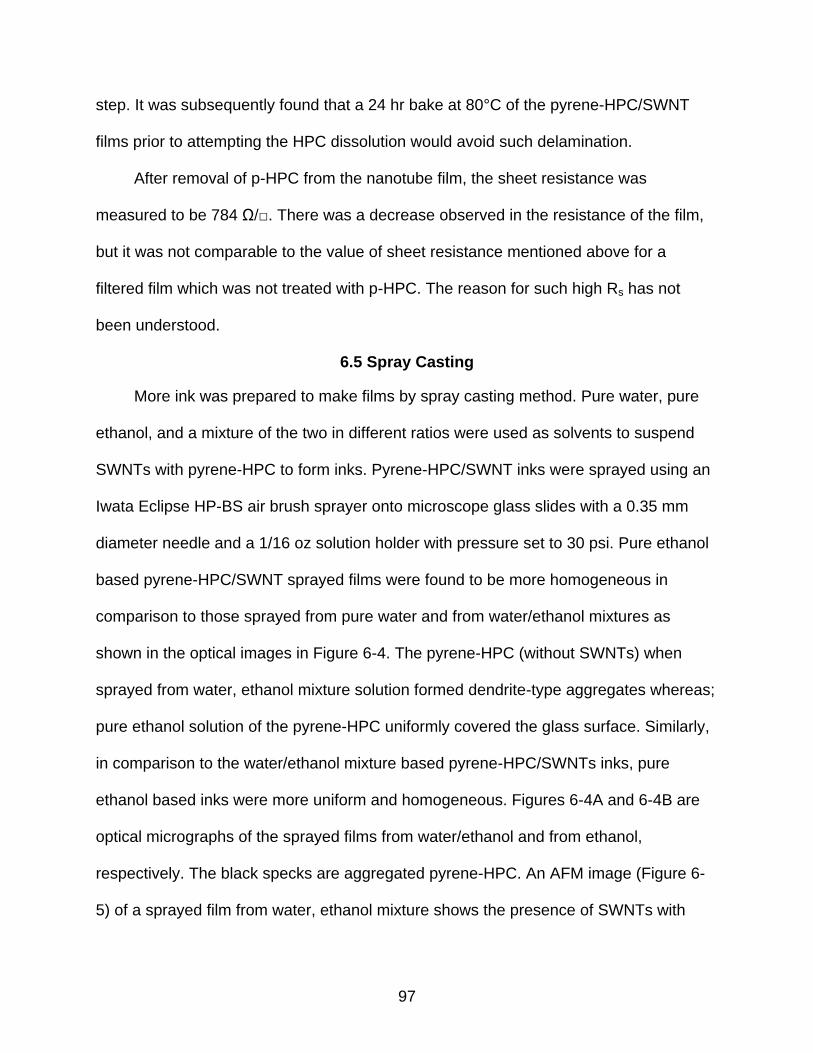
97
step. It was subsequently found that a 24 hr bake at 80°C of the pyrene-HPC/SWNT
films prior to attempting the HPC dissolution would avoid such delamination.
After removal of p-HPC from the nanotube film, the sheet resistance was
measured to be 784 Ω/□. There was a decrease observed in the resistance of the film,
but it was not comparable to the value of sheet resistance mentioned above for a
filtered film which was not treated with p-HPC. The reason for such high Rs has not
been understood.
6.5 Spray Casting
More ink was prepared to make films by spray casting method. Pure water, pure
ethanol, and a mixture of the two in different ratios were used as solvents to suspend
SWNTs with pyrene-HPC to form inks. Pyrene-HPC/SWNT inks were sprayed using an
Iwata Eclipse HP-BS air brush sprayer onto microscope glass slides with a 0.35 mm
diameter needle and a 1/16 oz solution holder with pressure set to 30 psi. Pure ethanol
based pyrene-HPC/SWNT sprayed films were found to be more homogeneous in
comparison to those sprayed from pure water and from water/ethanol mixtures as
shown in the optical images in Figure 6-4. The pyrene-HPC (without SWNTs) when
sprayed from water, ethanol mixture solution formed dendrite-type aggregates whereas;
pure ethanol solution of the pyrene-HPC uniformly covered the glass surface. Similarly,
in comparison to the water/ethanol mixture based pyrene-HPC/SWNTs inks, pure
ethanol based inks were more uniform and homogeneous. Figures 6-4A and 6-4B are
optical micrographs of the sprayed films from water/ethanol and from ethanol,
respectively. The black specks are aggregated pyrene-HPC. An AFM image (Figure 6-
5) of a sprayed film from water, ethanol mixture shows the presence of SWNTs with
98
pyrene-HPC. Ethanol was chosen to be the preferred solvent over water for spraying
pyrene-HPC/SWNTs based inks.
6.6 Pyrene-HPC/SWNTs Ethanol Ink
Pyrene-HPC/SWNTs ethanol ink was prepared with a concentration of 16 μg/ml
which was used to spray a 1×1 cm2 film on a glass substrate. The thickness of the film
was measured to be ~20 nm. Pyrene-HPC was removed from the film by the acid
treatment as mentioned above. Figures 6-6 and 6-7 show the optical image and the
AFM image of the sprayed film. The optical image shows inhomogeneity in the film with
varying concentration of nanotubes which was confirmed by varying intensities in
different regions as observed by Raman spectroscopy. The sheet resistance of this thin
inhomogeneous SWNTs film after removal of pyrene-HPC was measured to be Rs =
1070 Ω/□. The Rs of a standard film prepared by the filtration method at this thickness is
typically ~ 200 Ω/□ indicating that this film gave reasonable conductivity compared to
earlier samples.
To increase the conductance of sprayed films, it was necessary to spray thicker
films. It was challenging to do so because of persistent clogging of the air-brush nozzle
with pyrene-HPC coated nanotubes. To avoid clogging, dilute p-HPC/SWNT inks were
prepared and used. The air-brush nozzle was cleaned with ethanol and the sprayed film
was dried in the air at 80°C for 2 min between successive sprayed layers. This method
was successful in spraying thick films. The SWNT film that was made with a low ink
density of 1.6 μg/ml as opposed to 16 μg/ml used for previous film, resulted in a
successful spraying of a thick film. The thickness of the SWNT film was determined
from its UV-vis spectra (Figure 6-8) to be 65-70 nm. The AFM imaging was done and it
showed a high surface roughness of the film so the step height (thickness)
99
measurement was not performed. Figures 6-9 and 6-10 show the optical image and the
optical transparency of this thick film after removal of p-HPC respectively.
The sheet resistance of this sprayed pyrene-HPC/SWNT film before and after
removal of pyrene-HPC was measured to be Rs = 165 Ω/□ and Rs = 138 Ω/□
respectively. This not only showed an increase in conductance of the SWNT film after
the removal of p-HPC, but also showed a substantial increase in conductance of the film
sprayed using dilute inks when compared to the conductance of the film sprayed using
higher concentration ink. The Rs of a filtered film of the same thickness would typically
be 40 Ω/□, indicating reasonable success with thicker SWNT sprayed films.
6.7 Stability Measurement
To study the changes in the sheet resistance of the sprayed film as a function of
time, long term Rs measurements were conducted over a period of four months. A
pyrene-HPC/SWNTs film was sprayed from ethanol on a glass substrate with 40 nm
gold contacts pre-deposited on the four corners of the glass such that the film overlaps
the Au contacts when sprayed. The contacts were deposited to avoid tearing of the film
during frequent probe contacts for van Der Paw measurement. The sheet resistance of
the sprayed pyrene-HPC/SWNT film was measured before and after the removal of p-
HPC and was found to be Rs = 115 Ω/□ and Rs = 91 Ω/□ respectively. The thickness of
this film as determined from the UV-vis spectrum as shown in Figure 6-11 is 60-65 nm.
Figure 6-12 shows the change in Rs of the SWNTs film over time where the film was
stored in a petri dish in ambient air and the measurements were also conducted in air.
The stability curve indicates that the sheet resistance of the sprayed nanotube film only
doubles in a period of four months. The conductance and the stability of these sprayed

100
films can be useful in various applications of nanotubes. One such application is in the
electrochromic devices which can be explored in the future.
6.8 Future Work
This chapter demonstrated an alternative method of making SWNT films, spray
casting. Pyrene derivitized HPC was bound to SWNTs to disperse them in ethanol to
form inks which was used to successfully spray SWNT films. The sheet resistance
measurements indicate that the sprayed SWNT films can be used in different
applications. These experiments also motivate future work to be done on synthesizing
new polymer dispersants which can bind to the nanotubes to disperse them in desired
solvents for spraying.
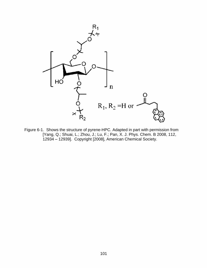
101
Figure 6-1. Shows the structure of pyrene-HPC. Adapted in part with permission from [Yang, Q.; Shuai, L.; Zhou, J.; Lu, F.; Pan, X. J. Phys. Chem. B 2008, 112, 12934 – 12939]. Copyright [2008], American Chemical Society.
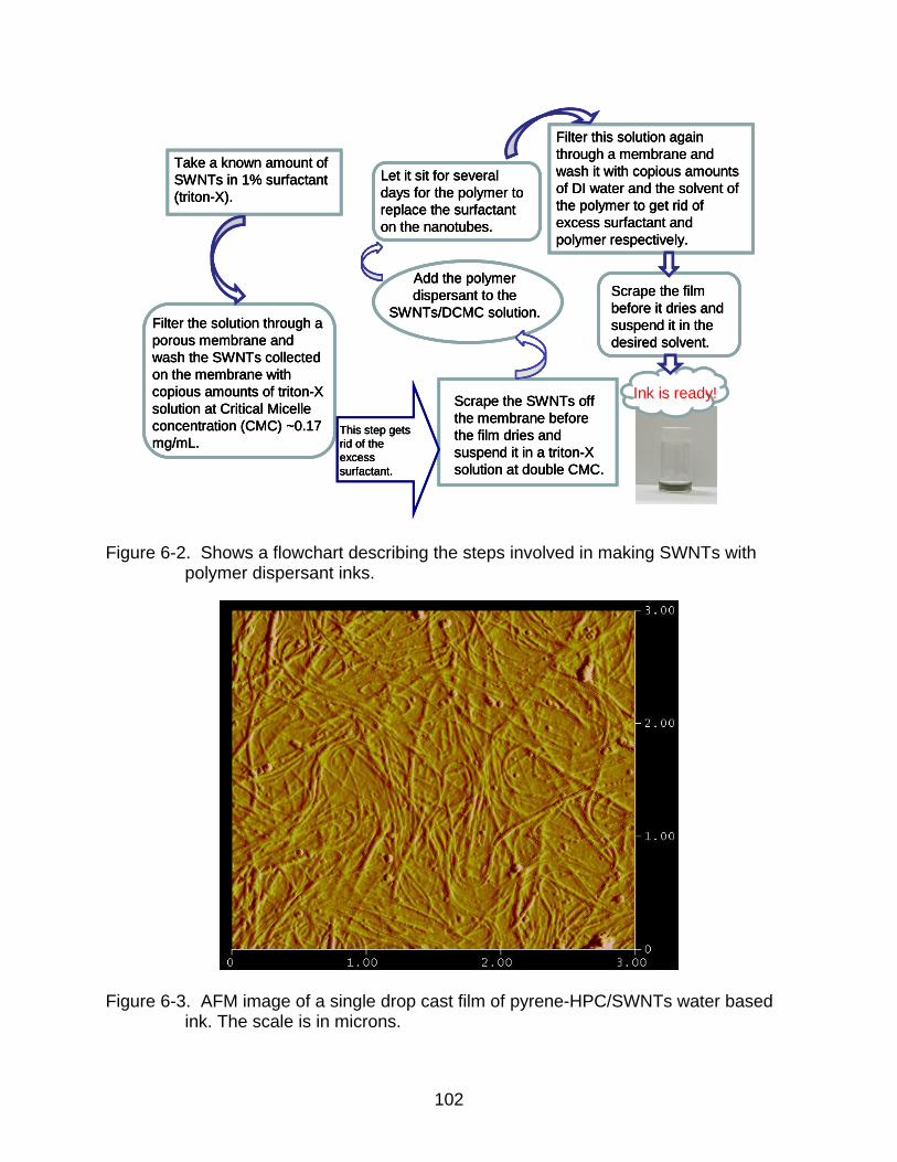
102
Take a known amount of
SWNTs in 1% surfactant
(triton-X).
Filter the solution through a
porous membrane and
wash the SWNTs collected
on the membrane with
copious amounts of triton-X
solution at Critical Micelle
concentration (CMC) ~0.17
mg/mL.
Add the polymer
dispersant to the
SWNTs/DCMC solution.
Let it sit for several
days for the polymer to
replace the surfactant
on the nanotubes.
Filter this solution again
through a membrane and
wash it with copious amounts
of DI water and the solvent of
the polymer to get rid of
excess surfactant and
polymer respectively.
Scrape the film
before it dries and
suspend it in the
desired solvent.
Scrape the SWNTs off
the membrane before
the film dries and
suspend it in a triton-X
solution at double CMC.
Ink is ready!
This step gets
rid of the
excess
surfactant.
Figure 6-2. Shows a flowchart describing the steps involved in making SWNTs with polymer dispersant inks.
Figure 6-3. AFM image of a single drop cast film of pyrene-HPC/SWNTs water based ink. The scale is in microns.
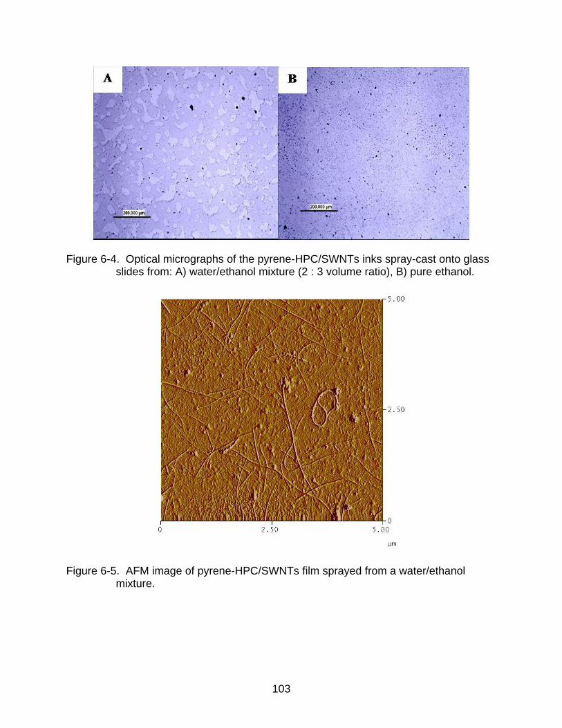
103
Figure 6-4. Optical micrographs of the pyrene-HPC/SWNTs inks spray-cast onto glass slides from: A) water/ethanol mixture (2 : 3 volume ratio), B) pure ethanol.
Figure 6-5. AFM image of pyrene-HPC/SWNTs film sprayed from a water/ethanol mixture.
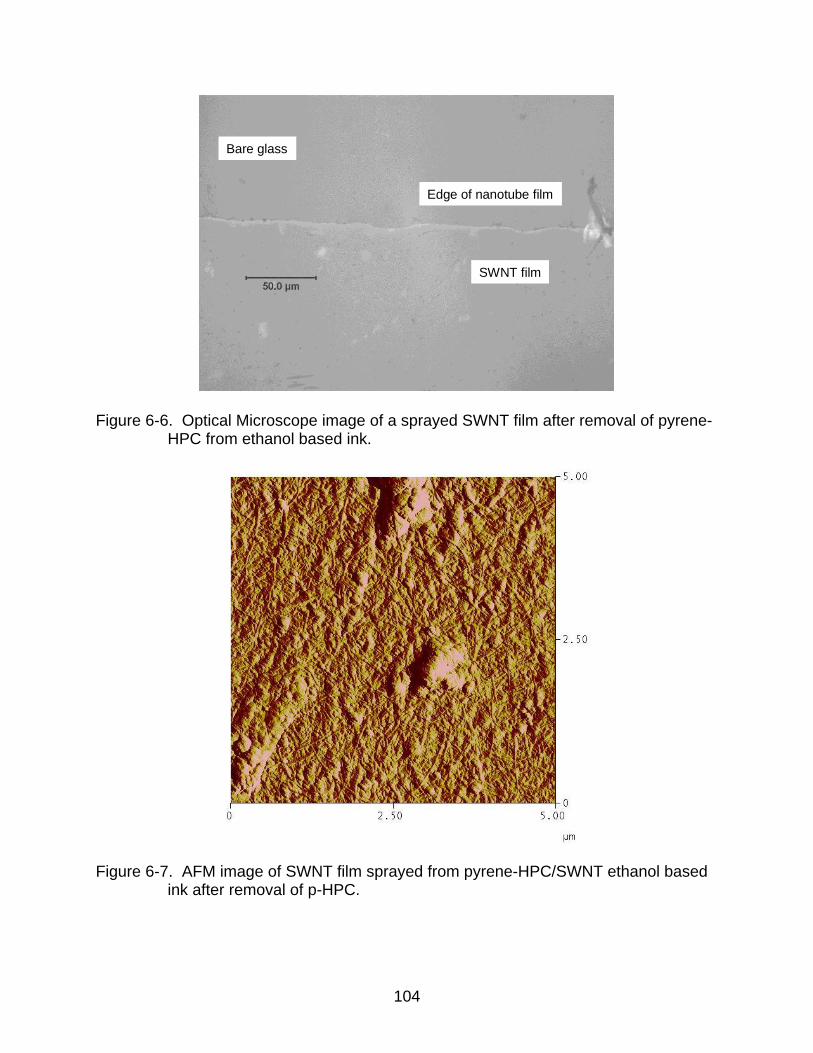
104
Bare glass
Edge of nanotube film
SWNT film
Bare glass
Edge of nanotube film
SWNT film
Figure 6-6. Optical Microscope image of a sprayed SWNT film after removal of pyrene-HPC from ethanol based ink.
Figure 6-7. AFM image of SWNT film sprayed from pyrene-HPC/SWNT ethanol based ink after removal of p-HPC.
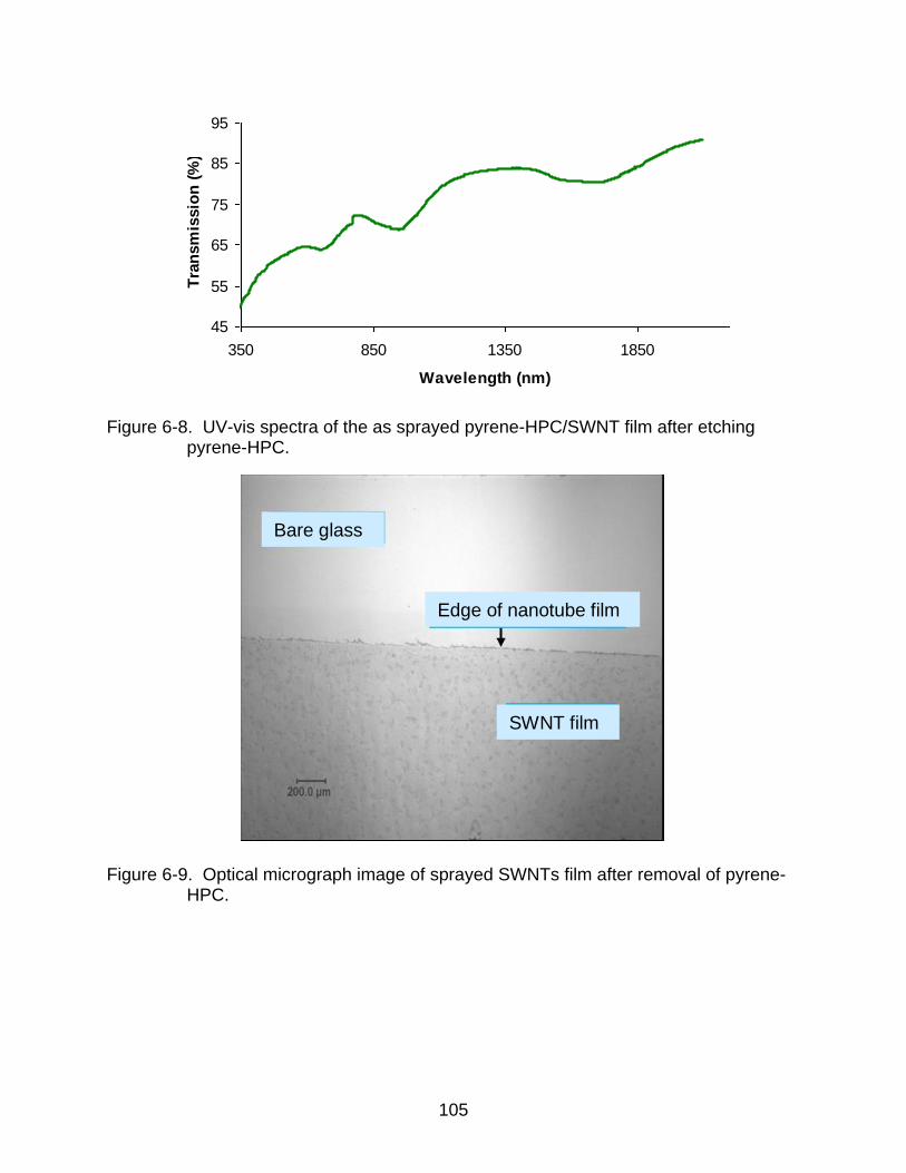
105
Sprayed SWNT film after removal of sticky cellulose
45
55
65
75
85
95
350 850 1350 1850
Wavelength (nm)
Tra
nsm
issio
n (
%)
Sprayed SWNT film after removal of sticky cellulose
45
55
65
75
85
95
350 850 1350 1850
Wavelength (nm)
Tra
nsm
issio
n (
%)
Figure 6-8. UV-vis spectra of the as sprayed pyrene-HPC/SWNT film after etching pyrene-HPC.
Bare glass
Edge of nanotube film
SWNT film
Bare glass
Edge of nanotube film
SWNT film
Figure 6-9. Optical micrograph image of sprayed SWNTs film after removal of pyrene-HPC.
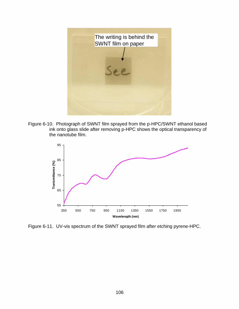
106
The writing is behind the
SWNT film on paper
The writing is behind the
SWNT film on paper
Figure 6-10. Photograph of SWNT film sprayed from the p-HPC/SWNT ethanol based ink onto glass slide after removing p-HPC shows the optical transparency of the nanotube film.
55
65
75
85
95
350 550 750 950 1150 1350 1550 1750 1950
Wavelength (nm)
Tra
ns
mit
tan
ce
(%
)
Figure 6-11. UV-vis spectrum of the SWNT sprayed film after etching pyrene-HPC.

107
1
10
100
1000
0 20 40 60 80 100 120
Number of days
Sh
eet
resis
tan
ce (
oh
ms/s
q)
Figure 6-12. Log plot of stability measurement of sheet resistance of a sprayed SWNTs film after removal of pyrene-HPC.
108
LIST OF REFERENCES
1. Dresselhaus, M. S.; Dresselhaus, G.; Jorio, A. Annu. Rev. Mater. Res. 2004, 34, 247-278.
2. Mintmire, J. W.; Dunlap, B. I.; White C. T. Phys. Rev. Lett. 1992, 68, 631-634.
3. Hamada, N.; Sawada, S.; Oshiyama, A. Phys. Rev. Lett. 1992, 68, 1579-1581.
4. Saito, R.; Fujita, M.; Dresselhaus, G.; Dresselhaus, M. S. Appl. Phys. Lett. 1992, 60, 2204-2206.
5. Saito, R.; Dresselhaus, G.; Dresselhaus, M. S. Physical properties of carbon nanotubes. London: World Scientific Publishing Company (Imperial College Press, 1998).
6. Javey, A.; Guo, J.; Wang, Q.; Lundstrom, M.; Dai, H. J. Nature 2003, 424, 654-657.
7. Avouris, P.; Chen, Z.; Perebeinos, V. Nature Nanotechnology 2007, 2, 605-615.
8. Moore, V. C.; Strano, M. S.; Haroz, E. H.; Hauge, R. H.; Smalley, R. E. Nano Lett. 2003, 3, 1379-1382.
9. Rinzler, A. G.; Liu, J.; Dai, H.; Nikolaev, P.; Huffman, C. B.; Rodriguez, F. J.; Boul, P. J.; Lu, A. H.; Heymann, D.; Colbert, D. T.; Lee, R. S.; Fischer, J. E.; Rao, A. M.; Eklund, P. C.; Smalley, R. E. Applied Physics A 1998, 67, 29-37.
10. Wu, Z. C.; Chen, Z.; Du, X.; Logan, J. M.; Sippel, J.; Nikolou, M.; Kamaras, K.; Reynolds, J. R.; Tanner, D. B.; Hebard, A. F.; Rinzler, A. G. Science 2004, 305, 1273-1276.
11. Data complied by Kazmerski, L. National Renewable Energy Laboratory, Golden, Colorado, www.nrel.gov/pv/thin_film/docs/kaz_best_research_cells.ppt
12. Bird, R. E.; Hulstrom, R. L. J. of Solar Energy Eng. 1981, 103, 182-192.
13. Neamen, D. A. Semiconductor physics and devices (McGraw Hill, 3rd edition).
14. Sze, S. M. Physics of Semiconductor Devices (Wiley, 1981).
15. Prince, M. J. Appl. Phys. 1955, 26, 534-540.
16. Xue, J.; Uchida, S.; Rand, B. P.; Forrest, S. R. App. Phys. Lett. 2004, 84, 3013-3015.
17. Green, M. A.; Emery, K.; King, D. L.; Igari, S.; Warta, W. Prog. Photovoltaics 2001, 9, 287-293.

109
18. Xue, J.; Uchida, S.; Rand, B. P.; Forrest, S. R. App. Phys. Lett. 2004, 85, 5757-5759.
19. Photovoltaic devices, Part 3; Measurement principles for terrestrial photovoltaic devices with reference spectral irradiance data, CEl/lEC 904-3, 1989.
20. Gangopadhyay, U.; Dhungel, S. K.; Kim, K.; Manna, U.; Basu, P. K.; Kim, H. J.; Karunagaran, B.; Lee, K. S.; Yoo, J. S.; Yi, J. Semicond. Sci. Technol. 2005, 20, 938-946.
21. Manea, E.; Budianu, E.; Purica, M.; Cristea, D.; Cernica, I.; Muller, R. Inter. Conf. on Phys., Chem. and Engg. Sol. Cells 2005, 87, 423-431.
22. Kumaravelu, G.; Alkaisi, M. M.; Bittar, A. IEEE 2002, 258- 261.
23. Inomata, Y.; Fukui, K.; Shirasawa, K. Sol. Energy Mater. Sol. Cells 1997, 48, 237-242.
24. Campbell, P.; Green, M. A. J. Appl. Phys. 1987, 62, 243–249.
25. Huynh, W. U.; Dittmer, J. J.; Alivisatos, A. P. Science 2002, 295, 2425-2427.
26. Yu, G.; Gao, J.; Hummelen, J. C.; Wudl, F.; Heeger, A. J. Science 1995, 270, 1789-1791.
27. Shaheen, S. E.; Brabec, C. J.; Padinger, F.; Fromherz, T.; Hummelen, J. C.; Sariciftci, N. S. Appl. Phys. Lett. 2001, 78, 841-843.
28. Peumans, P.; Yakimov, A.; Forrest, S. J. of Appl. Phys. 2003, 93, 3693-3723.
29. Shaheen, S. E.; Ginley, D. S.; Jabbour, G. E. MRS Bulletin 2005, 30, 10-15.
30. Coakley, K. M.; McGehee, M. D. Chem. Mater. 2004, 16, 4533-4542.
31. Huynh, W. U.; Dittmer, J. J.; Libby, W. C.; Whiting, G. L.; Alivisatos, A. P. Adv. Func. Mater. 2003, 13, 73-79.
32. Peumans, P.; Uchida, S.; Forrest, S. R. Nature 2003, 425, 158-162.
33. Yang, F.; Shtein, M.; Forrest, S. R. J. Appl. Phys. 2005, 98, 014906.
34. Yang, F.; Stein, M.; Forrest, S. R. Nat. Mater. 2005, 4, 37-41.
35. Huynh, W. U.; Dittmer, J. J.; Alivisatos, A. P. Science 2002, 295, 2425-2427.
36. Peumans, P.; Uchida, S.; Forrest, S. R. Nature 2003, 425, 158-162.
37. Rowell, M. W.; Topinka, M. A.; McGehee, M. App. Phys. Lett. 2006, 88, 233506.

110
38. Patil, A. PhD Dissertation presented to University of Florida 2004.
39. Gorham, W. F. J. Polym. Sci. 1966, 4 (Part A-1), 3027-3039.
40. Peng, K. Q.; Hu, J. J.; Yan, Y. J.; Wu, Y.; Fang, H.; Xu, Y.; Lee,. S. T.; Zhu, J. Adv. Funct. Mater. 2006, 16, 387-394.
41. Peng, K. Q.; Yan, Y. J.; Gao, S. P.; Zhu, J. Adv. Mater. 2002, 14, 1164-1167.
42. Peng, K. Q.; Yan, Y. J.; Gao, S. P.; Zhu, J. Adv. Funct. Mater. 2003, 13, 127-132.
43. Peng, K. Q.; Zhu, J. J. Electronal. Chem. 2003, 558, 35-39.
44. Peng, K. Q.; Huang, Z. P.; Zhu, J. Adv. Mater. 2004, 16, 73-76.
45. Peng, K. Q.; Zhu, J. Electrochim. Acta 2005, 49, 2563-2568.
46. Peng, K. Q.; Wu, Y.; Fang, H.; Zhong, X. Y.; Xu, Y.; Zhu, J. Angew. Chem. 2005, 117, 2797-2802.
47. Peng, K. Q.; Xu, Y.; Wu, Y.; Yan, Y.; Lee, S. T.; Zhu, J. Small 2005, 1, 1062-1067.
48. Peng, K. Q.; Fang, H.; Hu, J.; Wu, Y.; Zhu, J.; Yan, Y.; Lee, S. T. Chem. Eur. J. 2006, 12, 7942-7947.
49. Kurz, P. F. J. Chem. Edu. 1956, 33, 625-626.
50. Nardes, A. M.; Kemerink, M.; Kok, M. M.; Vinken, E.; Maturova, K.; Janssen, R. A. Orgn. Electr. 2008, 9, 727-734.
51. Scott, A.; Janes, D. B.; Risko, C.; Ratner, M. A. Appl. Phys. Lett. 2007, 91, 033508.
52. Jia, Y.; Wei, J.; Wang, K.; Cao, A.; Shu, Q.; Gui, X.; Zhu, Y.; Zhuang, D.; Zhang, G.; Ma, B.; Wang, L.; Liu, W.; Wang, Z.; Luo, J.; Wu, D. Adv. Mater. 2008, 20, 4594-4598.
53. Lonergan, M. C. Science 1997, 278, 2103-2106.
54. Liu, B.; McCarthy, M. A.; Yoon, Y.; Kim, D. Y.; Wu, Z.; So, F.; Holloway, P. H.; Reynolds, J. R.; Guo, J.; Rinzler, A. G. Adv. Mater. 2008, 20, 3605-3609.
55. Neuwald, U.; Hessel, H. E.; Feltz, A.; Memmert, U.; Behm, R. J. Appl. Phys. Lett. 1992, 60, 1307-1309.
56. Yokogawa, K.; Mizutani, T. Jpn. J. Appl. Phys 1993, 32, L635-L637.
57. Glatthaar, M.; Riede, M.; Keegan, N.; Sylvester-Hvid, K.; Zimmermann, B.; Niggemann, M.; Hinsch, A.; Gombert, A. Sol. Energy Mater. & Sol. Cells 2007, 91, 390-393.

111
58. Bardeen, J. Phys. Rev. 1947, 71, 717-727.
59. Tung, R. T. Phys. Rev. Lett. 2000, 84, 6078-6081.
60. Cowley, A. M.; Sze, S. M. J. Appl. Phys. 1965, 36, 3212-3220.
61. Selzer, Y.; Cahen D. Adv. Mater. 2001, 13, 508-511.
62. Haick, H.; Ambrico, M.; Ligonzo, T.; Tung, R. T.; Cahen, D. J. Am. Chem. Soc. 2006, 128, 6854-6869.
63. Hiremath, R. K.; Rabinal, M. K.; Mulimani, B. G.; Khazi, I. M. Langmuir 2008, 24, 11300-11306.
64. Henrion, W.; Rebien, M.; Angermann, H.; Roseler, A. Appl. Surf. Sci. 2002, 202, 199-205.
65. Kim, K. S.; Zhao, Y.; Jang, H.; Lee, S. Y.; Kim, J. M.; Kim, K. S.; Ahn, J. H.; Kim, P.; Choi, J. Y.; Hong, B. H. Nature 2009, 457, 706-710.
66. Li, X.; Cai, W.; An, J.; Kim, S.; Nah, J.; Yang, D.; Piner, R.; Velamakanni, A.; Jung, I.; Tutuc, E.; Banerjee, S. K.; Colombo, L.; Ruoff, R. S. Science 2009, 324, 1312-1314.
67. Li, X.; Zhu, H.; Wang, K.; Cao, A.; Wei, J.; Li, C.; Jia, Y.; Li, Z.; Li, X.; Wu, D. Adv. Mater. 2010, 22, 2743-2748.
68. Wadhwa, P.; Liu, B.; McCarthy, M. A.; Wu, Z.; Rinzler, A. G. Nano Lett. 2010, 10, 5001-5005.
69. Memming, R. Topics in Current Chemistry: Photoelectrochemical Solar Energy Conversion (Springer Verlag, Berlin Heidelberg, 1988).
70. Gratzel, M. Nature 2001, 414, 338-344.
71. Matsumoto, H.; Sakaebe, H.; Tatsumi, K. J. Power Sources 2005, 146, 45-50.
72. Godfrey, R. B.; Green, M. A. Appl. Phys. Lett. 1978, 33, 637-639.
73. Sentaurus TCAD, Synopsis Inc., Mountain View, CA, ver. D-2010.03
74. http://rredc.nrel.gov/solar/spectra/am1.5/, Standard ASTM G173-03, Standard Tables for References Solar Spectral Irradiance at Air Mass 1.5, Amer. Society for Testing Matls., West Conshocken PA, USA.
75. Lam, Y. W.; Green, M. A.; Davies, L. W. Appl. Phys. Lett. 1980, 37, 1087-1089.
76. Peng, K. Q.; Wang, X.; Li, L.; Wu, X. L.; Lee, S. T. J. Am. Chem. Soc. 2010, 132, 6872–6873.

112
77. Banerjee, S.; Hemraj-Benny, T.; Wong, S. S. Adv. Mater. 2005, 17, 17-29.
78. Tasis, D.; Tagmatarchis, N.; Bianco, A.; Prato, M. Chem. Rev. 2006, 106, 1105-1136.
79. Chen, R. J.; Zhang, Y. G.; Wang, D. W.; Dai, H. J. J. Am. Chem. Soc. 2001, 123, 3838-3839.
80. Hu, L.; Hecht, D. S.; Gruner, G. Chem Review 2010, 110, 5790-5844.
81. Shvartzman-Cohen, R.; Monje, I.; Florent, M.; Frydman, V.; Goldfarb, D.; Yerushalmi-Rozen, R. Macromolecules 2010, 43, 606-614.
82. Tu, X.; Manohar, S.; Jagota, A.; Zheng, M. Nature 2009, 460, 250-253.
83. Yang, Q.; Shuai, L.; Zhou, J.; Lu, F.; Pan, X. J. Phys. Chem. B 2008, 112, 12934-12939.
84. Ou, Y. Y.; Huang, M. H. J. Phys. Chem. B 2006, 110, 2031-2036.
85. Van der Pauw, L. J. Philips Research Reports 1958, 13, 1-9.
113
BIOGRAPHICAL SKETCH
Pooja Wadhwa was born in the year 1981 in New Delhi, India. She did her
undergraduate studies from University of Delhi in electronic science graduating with
honors in 2002. She went on a scholarship to Singapore to pursue her master’s in
electrical and computer engineering from National University of Singapore and
graduated in 2004. She continued to live in Singapore and worked in Data Storage
Institute as a research engineer and then she moved to United States of America in
2005 to purse her PhD in physics from University of Florida.