Embed Size (px)
Citation preview
Chapter 5: Introduction to Memory
Mrs. Sunita M Dol (Aher),Assistant Professor,
Computer Science and Engineering Department,Walchand Institute of Technology, Solapur, Maharashtra

05/02/2023 Mrs. Sunita M Dol, CSE Dept. 2
Chapter 6: Introduction to Memory• What is Computer?• Memory Operation and Organization• Expanding Memory Size• Memory Classification

05/02/2023 Mrs. Sunita M Dol, CSE Dept. 3
Chapter 6: Introduction to Memory• What is Computer?• Memory Operation and Organization• Expanding Memory Size• Memory Classification

05/02/2023 Mrs. Sunita M Dol, CSE Dept. 4
What is Computer?• A computer can be divided into three broad categories
or subsystem: the central processing unit (CPU), the main memory and the input/output subsystem.
05/02/2023 Mrs. Sunita M Dol, CSE Dept. 5
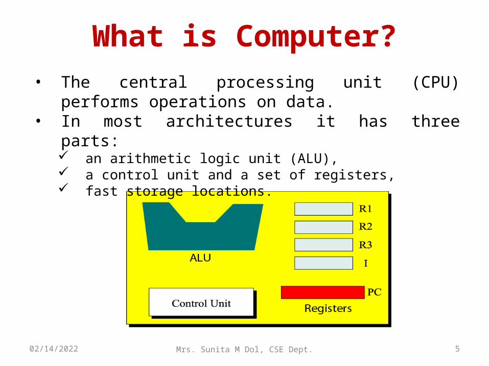
• The central processing unit (CPU) performs operations on data.
• In most architectures it has three parts: an arithmetic logic unit (ALU), a control unit and a set of registers, fast storage locations.
What is Computer?

05/02/2023 Mrs. Sunita M Dol, CSE Dept. 6
• CPU• The arithmetic logic unit (ALU) performs logic, shift,
and arithmetic operations on data. Logic operations: NOT, AND, OR, and XOR. Shift operations: logic shift operations and arithmetic shift
operations Arithmetic operations: arithmetic operations on integers
and reals.
What is Computer?

05/02/2023 Mrs. Sunita M Dol, CSE Dept. 7
• CPU• Registers
Registers are fast storage locations that hold data temporarily. Multiple registers are needed to facilitate the operation of the CPU.o Data registers: Input data and output datao Instruction registerso Program counter
• Control Unit The control unit controls the operation of each subsystem.
Controlling is achieved through signals sent from the control unit to other subsystems.
What is Computer?
05/02/2023 Mrs. Sunita M Dol, CSE Dept. 8
• Main memory consists of a collection of storage locations, each with a unique identifier, called an address.
• Data is transferred to and from memory in groups of bits called words.
What is Computer?
05/02/2023 9
• Data word: A word can be a group of 8 bits, 16 bits, 32 bits or 64 bits (and growing). If the word is 8 bits, it is referred to as a byte. A 16-bit word is referred to as a 2-byte word, or a 32-bit word is
referred to as a 4-byte word.
Mrs. Sunita M Dol, CSE Dept.
What is Computer?

05/02/2023 Mrs. Sunita M Dol, CSE Dept. 10
• Address space: To access a word in memory requires an identifier.
• Programmers use a name to identify a word (or a collection of words), at the hardware level each word is identified by an address.
• The total number of uniquely identifiable locations in memory is called the address space.
What is Computer?
05/02/2023 Mrs. Sunita M Dol, CSE Dept. 11
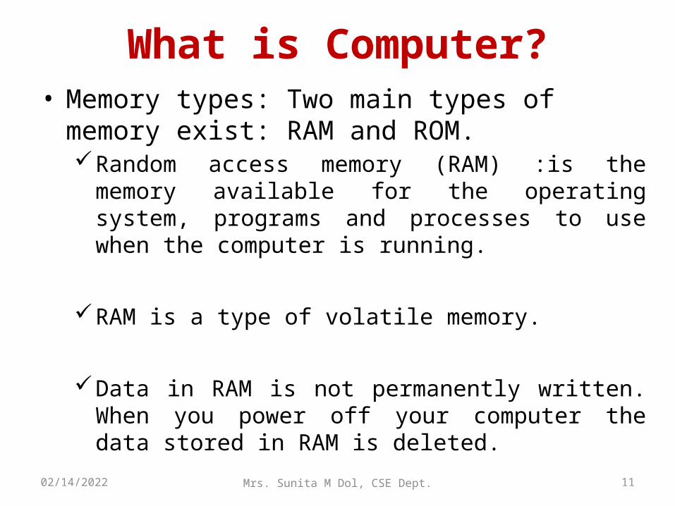
• Memory types: Two main types of memory exist: RAM and ROM. Random access memory (RAM) :is the memory
available for the operating system, programs and processes to use when the computer is running.
RAM is a type of volatile memory.
Data in RAM is not permanently written. When you power off your computer the data stored in RAM is deleted.
What is Computer?

05/02/2023 Mrs. Sunita M Dol, CSE Dept. 12
• Memory types:Types of RAM
Static RAM (SRAM) :Static random access memory uses multiple transistors, typically four to six, for each memory cell but doesn't have a capacitor in each cell. It is used primarily for cache.
Dynamic RAM (DRAM) – Dynamic random access memory has memory cells with a paired transistor and capacitor requiring constant refreshing.
What is Computer?

05/02/2023 Mrs. Sunita M Dol, CSE Dept. 13
• Memory types:Read-only memory (ROM) :is the memory that comes
with your computer that is pre-written to hold the instructions for booting-up the computer.
ROM is a type of non- volatile memory. Data in ROM is permanently written and is not erased when you power off your computer.
What is Computer?

05/02/2023 Mrs. Sunita M Dol, CSE Dept. 14
• Memory types:Type of Read-only memory (ROM)
Programmable read-only memory (PROM). Erasable programmable read-only memory (EPROM).Electrically erasable programmable read-only memory
(EEPROM).
What is Computer?
05/02/2023 Mrs. Sunita M Dol, CSE Dept. 15
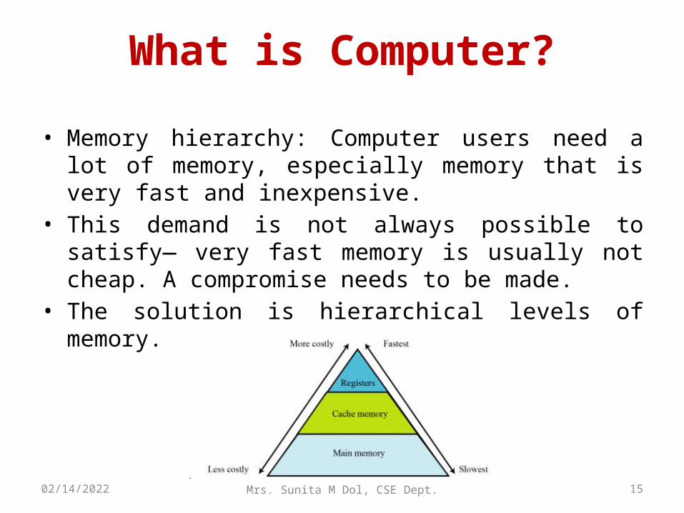
• Memory hierarchy: Computer users need a lot of memory, especially memory that is very fast and inexpensive.
• This demand is not always possible to satisfy— very fast memory is usually not cheap. A compromise needs to be made.
• The solution is hierarchical levels of memory.
What is Computer?

05/02/2023 16
• Cache memory: Cache memory is faster than main memory, but slower than the CPU and its registers.
• Cache memory, which is normally small in size, is placed between the CPU and main memory.
Mrs. Sunita M Dol, CSE Dept.
What is Computer?
05/02/2023 Mrs. Sunita M Dol, CSE Dept. 17
• The input/output (I/O) subsystem in a computer is the collection of devices.
• This subsystem allows a computer to communicate with the outside world and to store programs and data even when the power is off.
• Input/output devices can be divided into two broad categories: non-storage and storage devices.
What is Computer?
05/02/2023 Mrs. Sunita M Dol, CSE Dept. 18
• How these three subsystems (CPU, main memory, and I/O) are interconnected?The interconnection plays an important role because
information needs to be exchanged between the three subsystems.
Connecting CPU and memory: The CPU and memory are normally connected by three groups of connections, each called a bus: data bus, address bus and control bus.
What is Computer?
05/02/2023 Mrs. Sunita M Dol, CSE Dept. 19
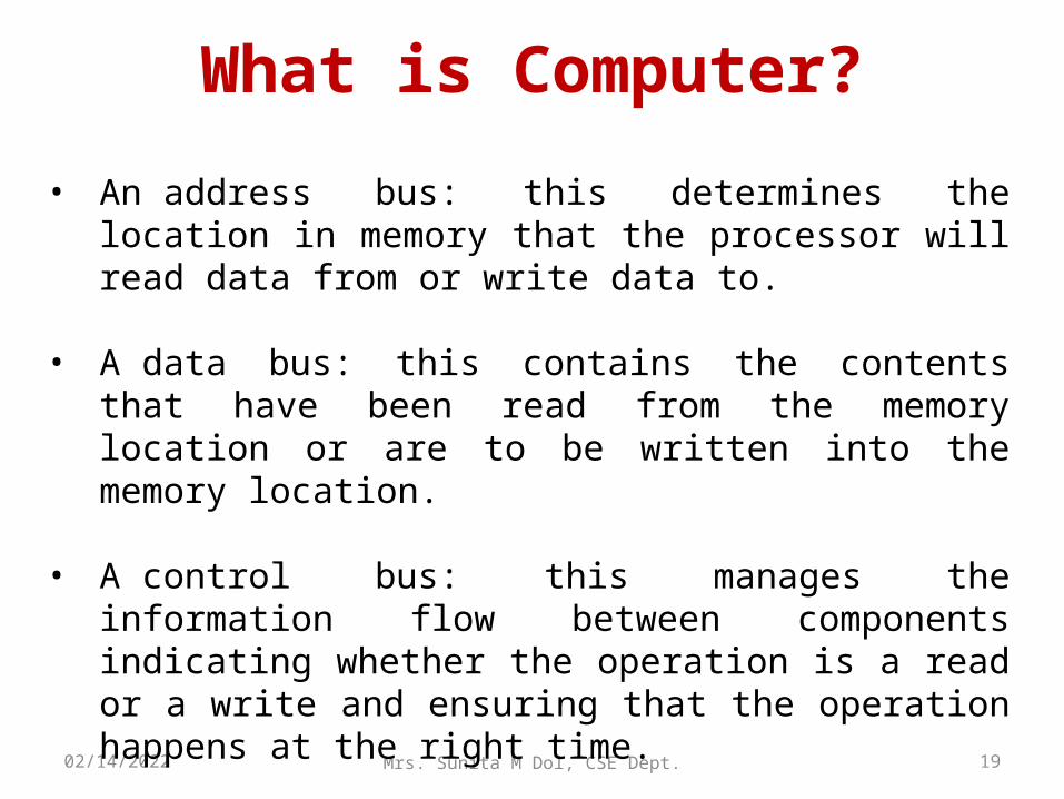
What is Computer?• An address bus: this determines the location in memory
that the processor will read data from or write data to.
• A data bus: this contains the contents that have been read from the memory location or are to be written into the memory location.
• A control bus: this manages the information flow between components indicating whether the operation is a read or a write and ensuring that the operation happens at the right time.

05/02/2023 Mrs. Sunita M Dol, CSE Dept. 20
What is Computer?

05/02/2023 Mrs. Sunita M Dol, CSE Dept. 21
Chapter 6: Introduction to Memory• What is Computer?• Memory Operation and Organization• Expanding Memory Size• Memory Classification

05/02/2023 Mrs. Sunita M Dol, CSE Dept. 22
Memory Operation and Organization• Basic Element of semiconductor memory is FF.
• There are number of locations in memory chip, each location being meant for one word of digital information.
• The size of the memory is specified by two numbers M and N as MxN bits
where M specifies the number of locations available in the memory and N is the number of bits at each location.
• The commonly used values of the number of words per chips are 64, 256, 512, 1024 etc.

05/02/2023 Mrs. Sunita M Dol, CSE Dept. 23
Memory Operation and Organization• Block diagram of a memory device:
Set of N-lines is required for storing
the data into the memory referred to
as data inputs
The address input is applied to P to M decoder circuit which activates one of its M outputs
depending on the address and the thus the desired
memory location is selected
control input is used for reading or writing
the data
set of N-lines is required for reading the data already stored in memory referred to as
data outputs

05/02/2023 Mrs. Sunita M Dol, CSE Dept. 24
Memory Operation and Organization• Each of the M location of the memory is defined by a
unique address.
• For accessing any one of the M locations, P inputs are required where 2p=M
• This set of lines is referred to as address input or address bus.
• The address input is applied to P to M decoder circuit which activates one of its M outputs depending on the address and the thus the desired memory location is selected.

05/02/2023 Mrs. Sunita M Dol, CSE Dept. 25
Memory Operation and Organization• The number of inputs required to store the data into
or read the data from any memory location is N.
• One set of N-lines is required for storing the data into the memory referred to as data inputs.
• Another set of N-lines is required for reading the data already stored in memory referred to as data outputs.
• Set of lines meant for data inputs is input data bus and for data outputs is output data bus.

05/02/2023 Mrs. Sunita M Dol, CSE Dept. 26
Memory Operation and Organization• Input and output data buses are unidirectional i.e. data
flow in one direction only.
• The same set of lines is used for data inputs as well as data output referred to as bidirectional bus.
• Read/Write (R/W) control input is used for reading or writing the data.
• When R/W is high the data bus will be used for reading the memory whereas R/W is low, the bus will be acting in the input direction and the data on the bus will go into the memory.

05/02/2023 Mrs. Sunita M Dol, CSE Dept. 27
Memory Operation and Organization• Block diagram of a memory with bidirectional data bus:
The same set of lines is used for data inputs as
well as data output referred to as
bidirectional bus
When R/W is high the data bus will be used for reading the memory
whereas R/W is low, the bus will be acting in the
input direction and the data on the bus will go into the
memory
05/02/2023 Mrs. Sunita M Dol, CSE Dept. 28
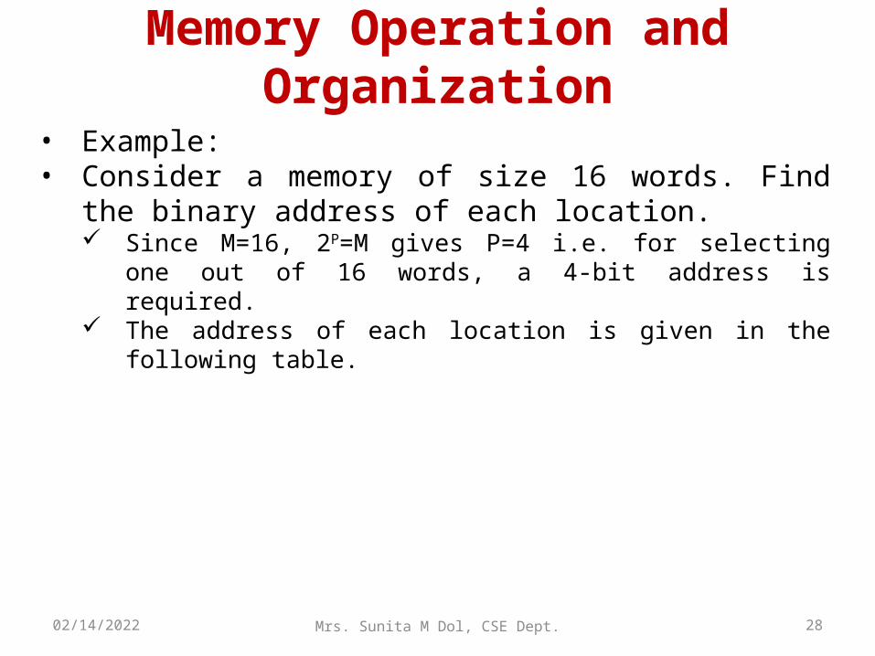
Memory Operation and Organization• Example:• Consider a memory of size 16 words. Find the binary
address of each location. Since M=16, 2P=M gives P=4 i.e. for selecting one out of 16
words, a 4-bit address is required. The address of each location is given in the following table.

05/02/2023 Mrs. Sunita M Dol, CSE Dept. 29
Memory Operation and Organization• Example Word No. Binary address
A3(MSB) A2 A1 A0 (LSB)
0 0 0 0 0
1 0 0 0 1
2 0 0 1 0
3 0 0 1 1
4 0 1 0 0
5 0 1 0 1
6 0 1 1 0
7 0 1 1 1
8 1 0 0 0
9 1 0 0 1
10 1 0 1 0
11 1 0 1 1
12 1 1 0 0
13 1 1 0 1
14 1 1 1 0
15 1 1 1 1

05/02/2023 Mrs. Sunita M Dol, CSE Dept. 30
Memory Operation and Organization• Example: Internal organization of a 16x4 memory chip is
illustrated in following figureTo write the word into the selected memory location requires logic 1 voltage to be applied to CS and
Write(WR) inputs and logic 0 voltage to Read (RD) input
A 1 at the output of A2 enables the output buffers so that the content of the selected memory location
will appear at the data output

05/02/2023 Mrs. Sunita M Dol, CSE Dept. 31
Memory Operation and Organization• Write Operation
• To write the word into the selected memory location requires logic 1 voltage to be applied to CS and Write(WR) inputs and logic 0 voltage to Read (RD) input.
• A 1 at the output of A1 enables the input buffers so that the 4-bit word applied to the data inputs will be loaded into the selected memory location.
• A 0 at the output of A2 disables the output buffers so that data output are not available.

05/02/2023 Mrs. Sunita M Dol, CSE Dept. 32
Memory Operation and Organization• Write Operation
• For writing a word into a particular memory location, following sequence of operation is to be performed:
1. The chip select signal is applied to the CS terminal.2. The word to be stored is applied to the data-input terminals.3. The address of the desired memory location is applied to the
address-input terminals.4. A write command signal is applied to the write-control input
terminal with RD = 0.
• The addressed memory location is cleared of any word that might have been stored in it earlier
05/02/2023 Mrs. Sunita M Dol, CSE Dept. 33
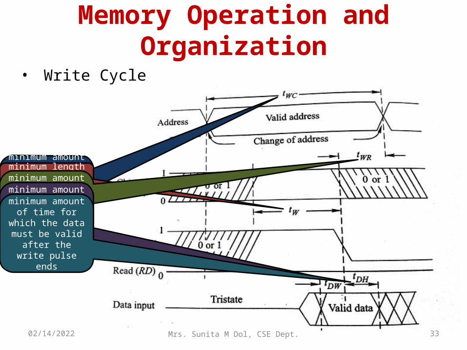
Memory Operation and Organization• Write Cycle
minimum amount of time for which the valid address must be present for writing a word
in the memory
minimum length of the write pulse
minimum amount of time for which the address must be valid after the write pulse ends
minimum amount of time for which the data must be valid before the write pulse ends
minimum amount of time for which the data must be
valid after the write pulse ends
05/02/2023 Mrs. Sunita M Dol, CSE Dept. 34
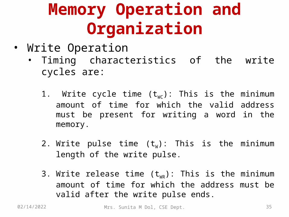
Memory Operation and Organization• Write Operation
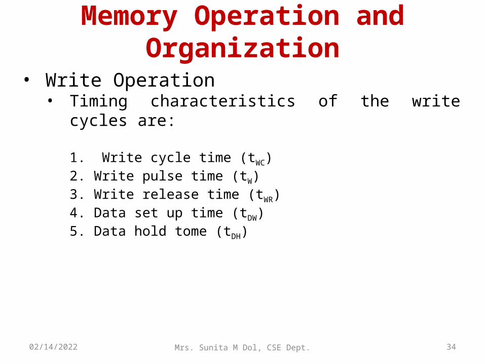
• Timing characteristics of the write cycles are:
1. Write cycle time (tWC)2. Write pulse time (tW)3. Write release time (tWR)4. Data set up time (tDW)5. Data hold tome (tDH)
05/02/2023 Mrs. Sunita M Dol, CSE Dept. 35
Memory Operation and Organization• Write Operation
• Timing characteristics of the write cycles are:
1. Write cycle time (tWC): This is the minimum amount of time for which the valid address must be present for writing a word in the memory.
2. Write pulse time (tW): This is the minimum length of the write pulse.
3. Write release time (tWR): This is the minimum amount of time for which the address must be valid after the write pulse ends.

05/02/2023 Mrs. Sunita M Dol, CSE Dept. 36
Memory Operation and Organization• Write Operation
• Timing characteristics of the write cycles are:
4. Data set up time (tDW): This is the minimum amount of time for which the data must be valid before the write pulse ends.
5. Data hold tome (tDH): This is the minimum amount of time for which the data must be valid after the write pulse ends.

05/02/2023 Mrs. Sunita M Dol, CSE Dept. 37
Memory Operation and Organization• Read Operation
• In order to read the contents of the selected memory location, the read (RD)and the chip select (CS) inputs must be at logic 1 level and WR at logic 0 level.
• A 1 at the output of A2 enables the output buffers so that the content of the selected memory location will appear at the data output.
• RD=1 tristates the input buffers so that the data inputs do not affect the memory during a read operation.

05/02/2023 Mrs. Sunita M Dol, CSE Dept. 38
Memory Operation and Organization• Read Operation
• For reading a data word to be stored at a particular address, following sequence of operation is to be performed:
1. The chip select signal is applied to the CS terminal.2. The address of the desired memory location is applied to the
address-input terminals.3. A read command signal is applied to the read-input terminal.
• In response to the above operation, the data word stored at the addressed location appears on the data output terminals.

05/02/2023 Mrs. Sunita M Dol, CSE Dept. 39
Memory Operation and Organization• Read cycle:
minimum amount of time for which the valid address must be present
for reading a word from memory
maximum time from the start of the valid address of the read
cycle to the time when the valid data is available at the
data outputs
maximum time delay between the beginning of the
read pulse and the availability of valid
data at the data output
minimum time delay between the beginning of the
read pulse and the output buffers
coming to active state
maximum time delay between the beginning of the chip select pulse and availability of valid data at the
outputs
minimum time delay between the beginning of the chip select pulse and the output
buffers coming to active state
maximum time delay between the
end of the read pulse and the output buffers going to high
impedance state
minimum time for which the valid
data is available at the data outputs after the address
ends.
05/02/2023 Mrs. Sunita M Dol, CSE Dept. 40
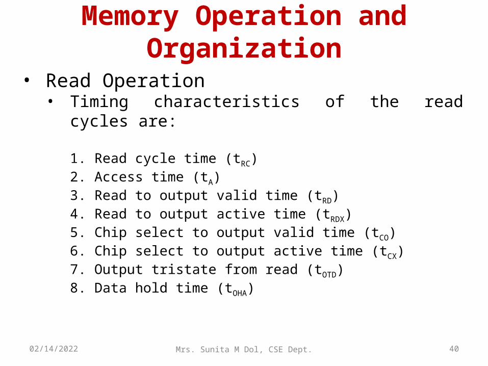
Memory Operation and Organization• Read Operation
• Timing characteristics of the read cycles are:
1. Read cycle time (tRC)2. Access time (tA)3. Read to output valid time (tRD)4. Read to output active time (tRDX)5. Chip select to output valid time (tCO)6. Chip select to output active time (tCX)7. Output tristate from read (tOTD)8. Data hold time (tOHA)

05/02/2023 Mrs. Sunita M Dol, CSE Dept. 41
Memory Operation and Organization• Read Operation
• Timing characteristics of the read cycles are:
1. Read cycle time (tRC) : This is the minimum amount of time for which the valid address must be present for reading a word from memory.
2. Access time (tA): This is the maximum time from the start of the valid address of the read cycle to the time when the valid data is available at the data outputs. tA<= tRC
3. Read to output valid time (tRD): This is the maximum time delay between the beginning of the read pulse and the availability of valid data at the data output.

05/02/2023 Mrs. Sunita M Dol, CSE Dept. 42
Memory Operation and Organization• Read Operation
• Timing characteristics of the read cycles are:
4. Read to output active time (tRDX): This is the minimum time delay between the beginning of the read pulse and the output buffers coming to active state (from high impedance state).
5. Chip select to output valid time (tCO): This is the maximum time delay between the beginning of the chip select pulse and availability of valid data at the outputs
6. Chip select to output active time (tCX): This is the minimum time delay between the beginning of the chip select pulse and the output buffers coming to active state.

05/02/2023 Mrs. Sunita M Dol, CSE Dept. 43
Memory Operation and Organization• Read Operation
• Timing characteristics of the read cycles are:
7. Output tristate from read (tOTD): This is the maximum time delay between the end of the read pulse and the output buffers going to high impedance state.
8. Data hold time (tOHA): This is the minimum time for which the valid data is available at the data outputs after the address ends.

05/02/2023 Mrs. Sunita M Dol, CSE Dept. 44
Chapter 6: Introduction to Memory• What is Computer?• Memory Operation and Organization• Expanding Memory Size• Memory Classification

05/02/2023 Mrs. Sunita M Dol, CSE Dept. 45
Expanding Memory Size• Expanding Word Size: If it is required to have a
memory of word size n and the word size of the availability memory ICs is N (n>N), then a number of similar ICs can be combined together to achieve the desired word size.
05/02/2023 Mrs. Sunita M Dol, CSE Dept. 46
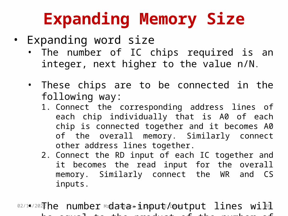
• Expanding word size • The number of IC chips required is an integer, next
higher to the value n/N.
• These chips are to be connected in the following way:1. Connect the corresponding address lines of each chip
individually that is A0 of each chip is connected together and it becomes A0 of the overall memory. Similarly connect other address lines together.
2. Connect the RD input of each IC together and it becomes the read input for the overall memory. Similarly connect the WR and CS inputs.
• The number data-input/output lines will be equal to the product of the number of chips used and the word size of each chip.
Expanding Memory Size

05/02/2023 Mrs. Sunita M Dol, CSE Dept. 47
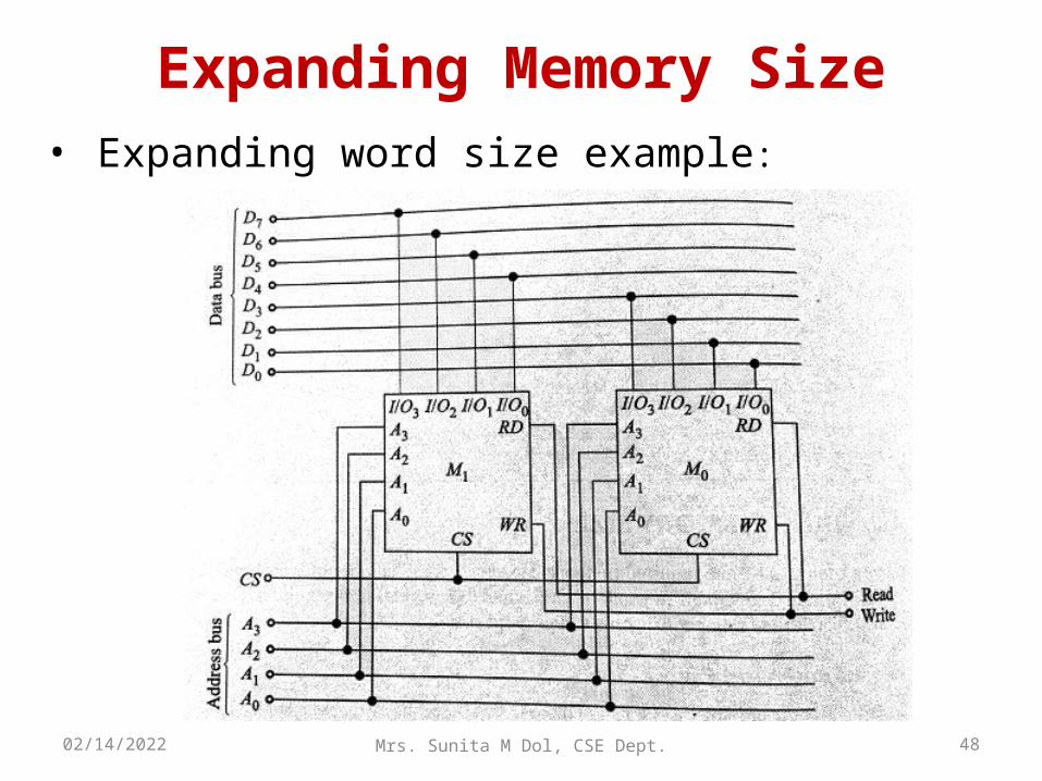
• Expanding word size example: • Obtain a 16x8 memory using 16x4 memory ICs.
Since the word size required is n=8 and the word size of the available IC is N=4, therefore n/N =2 chips are required to obtain the desired memory.
In this 16x8 memory, the higher order four bits (D7, D6, D5, D4) of each 8-bit word are located in memory M1 and the lower order four bits (D3, D2, D1, D0) are located in memory M0.
Expanding Memory Size
05/02/2023 Mrs. Sunita M Dol, CSE Dept. 48
• Expanding word size example:
Expanding Memory Size

05/02/2023 Mrs. Sunita M Dol, CSE Dept. 49
• Expanding word size example: • Obtain a 4x4 memory using 4x2 memory ICs.
Expanding Memory Size

05/02/2023 Mrs. Sunita M Dol, CSE Dept. 50
I/O 1 I/O 0 I/O 1 I/O 0
A1 A0
A1
A0
RD WR
RD WR
CS CS
M1 M0
CS RD ReadWR Write
D3D2D1D0
A1A2
Data bus
Address bus

05/02/2023 Mrs. Sunita M Dol, CSE Dept. 51
• Expanding word size example: • Obtain a 8x6 memory using 8x3 memory ICs.
Expanding Memory Size

05/02/2023 Mrs. Sunita M Dol, CSE Dept. 52
I/O2 I/O 1 I/O 0
A2
A1 A0
A2
A1
A0
RD WR
RD WR
CS CS
M1 M0
CS RD ReadWR Write
D5D4D3D2D1D0
A2A1
Data bus
Address bus
I/O2 I/O 1 I/O 0
A0

05/02/2023 Mrs. Sunita M Dol, CSE Dept. 53
• Expanding word size example: • Obtain a 16x8 memory using 16x4 memory ICs.
Expanding Memory Size
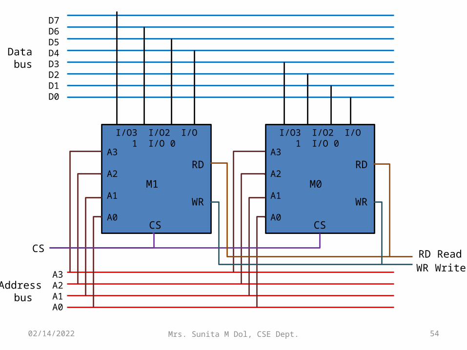
05/02/2023 Mrs. Sunita M Dol, CSE Dept. 54
I/O3 I/O2 I/O 1 I/O 0
A3
A2
A1 A0
RD
WR
M1
I/O3 I/O2 I/O 1 I/O 0
A3
A2
A1 A0
RD
WR
M0
CS RD ReadWR Write
D7D6D5D4D3D2D1D0
A3A2A1A0
Data bus
Address bus
CS CS

05/02/2023 Mrs. Sunita M Dol, CSE Dept. 55
• Expanding word size example: • Obtain a 16x12 memory using 16x4 memory ICs.
Expanding Memory Size
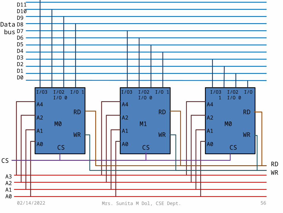
05/02/2023 Mrs. Sunita M Dol, CSE Dept. 56
I/O3 I/O2 I/O 1 I/O 0
A4
A2
A1 A0
RD
WR
M1
I/O3 I/O2 I/O 1 I/O 0
A4
A2
A1 A0
RD
WR
M0
I/O3 I/O2 I/O 1 I/O 0
A4
A2
A1 A0
RD
WR
M0
CS RDWR
D11D10D9D8D7D6D5D4D3D2D1D0
A3A2A1A0
Data bus
CS CS CS

05/02/2023 Mrs. Sunita M Dol, CSE Dept. 57
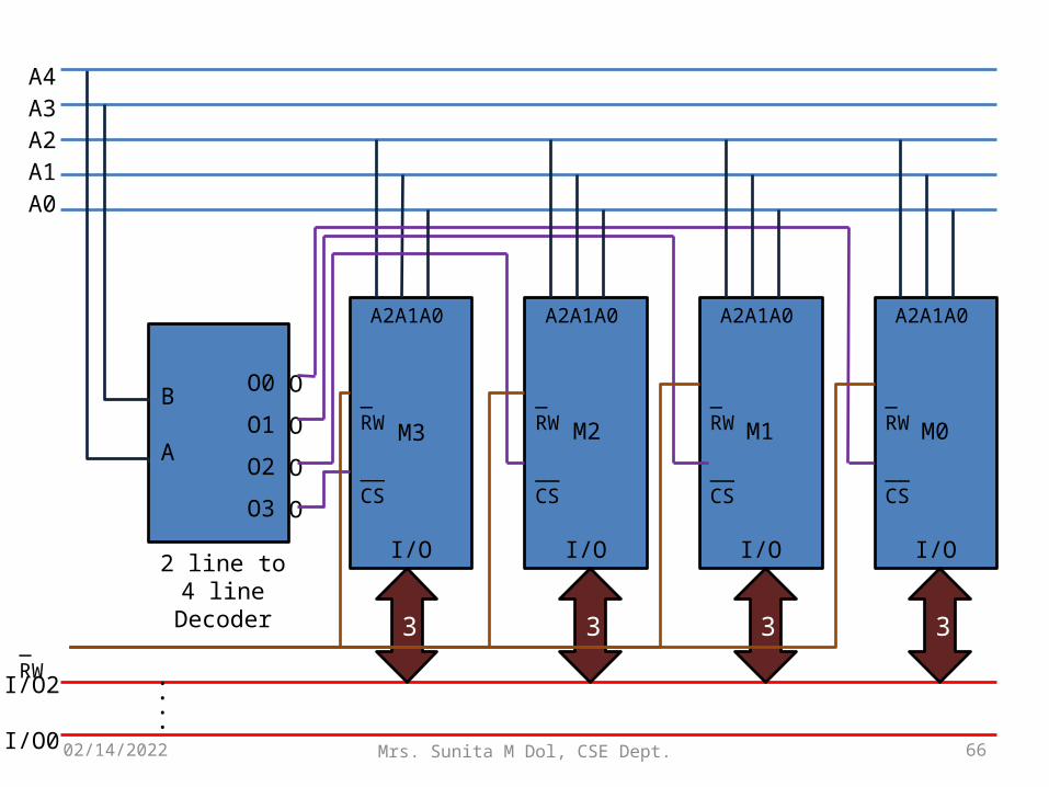
• Expanding word capacity: Memory chips can be combined together to produce a memory with the desired number of locations.
• To obtain a memory of capacity m words using the memory chips with M words each, the number of chips required is an integer next to the value m/M
Expanding Memory Size

05/02/2023 Mrs. Sunita M Dol, CSE Dept. 58
• Expanding word capacity :• These chips are to be connected in the following way:
1. Connect the corresponding address lines of each chip individually.
2. Connect the RD input of each chip together. Similarly, connect the WR inputs.
3. Use a decoder of proper size and connect each of its outputs to one of the CS terminal of memory chip. e.g. If eight chips are to be connected, a3-line-to-6-line decoder is required to select one out of eight chips at any one time
Expanding Memory Size

05/02/2023 Mrs. Sunita M Dol, CSE Dept. 59
• Expanding word capacity example:• Obtain a 2048x8 memory using 256x8 memory ICs.
The number of chips required in 2048/256=8. At any time, only one of the 2048 location is to be accessed
which will be in one of the eight chips. For selecting one out of 2048 locations, the number of address
lines required is 11 (211=2048). The lower order eight bits of the address A7-A0 will be same for
each chip and the higher order three bits of the address A10-A8 must select one out of the eight chips.
For this purpose, a 3-lint-to-8-line decoder is required.
Expanding Memory Size

05/02/2023 Mrs. Sunita M Dol, CSE Dept. 60
• Expanding word capacity example:
Expanding Memory Size

05/02/2023 Mrs. Sunita M Dol, CSE Dept. 61
• Expanding word size example: • Obtain a 64x4 memory using 16x4 memory ICs.
Expanding Memory Size

05/02/2023 Mrs. Sunita M Dol, CSE Dept. 62
A3A2A1A0
M3 M2 M1 M0
I/O I/O I/O I/O
B
A
O0
O1
O2
O3
O
O
O
O
_RW
__CS
_RW
__CS
_RW
__CS
_RW
__CS
A3A2A1A0 A3A2A1A0 A3A2A1A0
A5A4A3A2A1A0
2 line to 4 line Decoder
4 4 4 4
I/O 3
I/O0
....
_RW
05/02/2023 Mrs. Sunita M Dol, CSE Dept. 63
• Expanding word size example: • Obtain a 16x2 memory using 4x2 memory ICs.
Expanding Memory Size

05/02/2023 Mrs. Sunita M Dol, CSE Dept. 64
A1A0
M3 M2 M1 M0
I/O I/O I/O I/O
B
A
O
O
O
O
_RW
__CS
_RW
__CS
_RW
__CS
_RW
__CS
A1A0 A1A0 A1A0
A3A2A1A0
2 line to 4 line Decoder
2 2 2 2
I/O1
I/O0
_RW
O0
O1
O2
O3

05/02/2023 Mrs. Sunita M Dol, CSE Dept. 65
• Expanding word size example: • Obtain a 32x3 memory using 8x3 memory ICs.
Expanding Memory Size
05/02/2023 Mrs. Sunita M Dol, CSE Dept. 66
A2A1A0
M3 M2 M1 M0
I/O I/O I/O I/O
B
A
O
O
O
O
_RW
__CS
_RW
__CS
_RW
__CS
_RW
__CS
A2A1A0 A2A1A0 A2A1A0
A4A3A2A1A0
2 line to 4 line Decoder
3 3 3 3
I/O2
I/O0
_RW
....
O0
O1
O2
O3

05/02/2023 Mrs. Sunita M Dol, CSE Dept. 67
• Expanding word size example: • Obtain a 64x3 memory using 8x3 memory ICs.
Expanding Memory Size

05/02/2023 Mrs. Sunita M Dol, CSE Dept. 68
A2A1A0
M7 M6 M1 M0
I/O I/O I/O I/O
C
B
A
OOOOOOOO
_RW
__CS
_RW
__CS
_RW
__CS
_RW
__CS
A2A1A0 A2A1A0 A2A1A0
A5A4A3A2A1A0
2 line to 4 line Decoder
3 3 3 3
I/O2
I/O0
_RW
....
O0O1O2O3O4O5O6O7
…..

05/02/2023 Mrs. Sunita M Dol, CSE Dept. 69
Chapter 6: Introduction to Memory• What is Computer?• Memory Operation and Organization• Expanding Memory Size• Memory Classification
05/02/2023 Mrs. Sunita M Dol, CSE Dept. 70
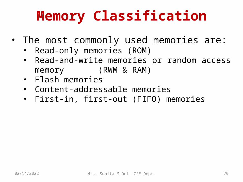
• The most commonly used memories are:• Read-only memories (ROM)• Read-and-write memories or random access memory
(RWM & RAM)• Flash memories• Content-addressable memories• First-in, first-out (FIFO) memories
Memory Classification

05/02/2023 71Mrs. Sunita M Dol, CSE Dept.
Memory Classification
Read-only memories
Read-and-write memories or
random access memory
(RWM & RAM)
Flash memories
Content-addressable
memories
First-in, first-out (FIFO) memories
Read-only memory
Programmable Read only
memory (PROM)
Erasable and programmable
ROM
Electrically erasable and
programmable ROM
Static RAM (SRAM)
Dynamic RAM
Asynchronous SRAM
Synchronous SRAM
Fat page mode DRAM (FPM DRAM)
Extended data out DRAM (EDO DRAM)
Burst EDO DRAM (BEDO DRAM)
Synchronous DRAM (SDRAM)

05/02/2023 Mrs. Sunita M Dol, CSE Dept. 72
• ROM:• It is type of internal memory.
• The data and instructions in ROM are stored by the manufacturer at the time of its manufacturing. This data and programs cannot be changed or deleted afterwards.
• The data or instructions stored in ROM can only be read but new data or instructions cannot be written into it.
Memory Classification
05/02/2023 Mrs. Sunita M Dol, CSE Dept. 73
• ROM:
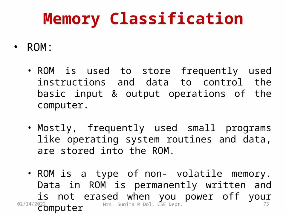
• ROM is used to store frequently used instructions and data to control the basic input & output operations of the computer.
• Mostly, frequently used small programs like operating system routines and data, are stored into the ROM.
• ROM is a type of non- volatile memory. Data in ROM is permanently written and is not erased when you power off your computer
Memory Classification

05/02/2023 Mrs. Sunita M Dol, CSE Dept. 74
• ROM:• Types of ROM
Read-only memory Programmable Read only memory (PROM) Erasable and programmable ROM (EPROM) Electrically erasable and programmable ROM (EEPROM)
Memory Classification

05/02/2023 Mrs. Sunita M Dol, CSE Dept. 75
• ROM:• Types of ROM
Read-only memory: It is programmed at the time of manufacturing as the last process of fabrication according to the information specified by the user. The data stored cannot be changed after fabrication.
Programmable Read only memory (PROM): This type of ROM is programmed by the user using a special circuit- a PROM programmer. A PROM can be programmed only once after which its content are permanently fixed. This form of ROM is initially blank. If there is an error in writing instructions or data in PROM, the error cannot be erased. PROM chip becomes unusable.
Memory Classification
05/02/2023 Mrs. Sunita M Dol, CSE Dept. 76
• ROM:• Types of ROM
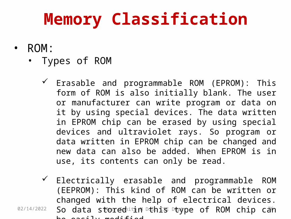
Erasable and programmable ROM (EPROM): This form of ROM is also initially blank. The user or manufacturer can write program or data on it by using special devices. The data written in EPROM chip can be erased by using special devices and ultraviolet rays. So program or data written in EPROM chip can be changed and new data can also be added. When EPROM is in use, its contents can only be read.
Electrically erasable and programmable ROM (EEPROM): This kind of ROM can be written or changed with the help of electrical devices. So data stored in this type of ROM chip can be easily modified.
Memory Classification

05/02/2023 Mrs. Sunita M Dol, CSE Dept. 77
• ROM Organization:• A ROM is an array of selectively open and closed
unidirectional contacts.• A 16-bit ROM array is shown in the figure.
Memory Classification

05/02/2023 Mrs. Sunita M Dol, CSE Dept. 78
• ROM Organization
Memory Classification

05/02/2023 Mrs. Sunita M Dol, CSE Dept. 79
• ROM Organization:• To select any one of the 16-bits, a 4-bit address (A3,
A2, A1, A0) is required.
• The lower order two bits (A1, A0) are decoded by the decoder DL which selects one of the four rows.
• The higher order two bits (A3, A2) are decoded by the decoder DH which activates four columns sense amplifier.
• The diode matrix is formed by connecting one diode along with the a switch between each row and column.
Memory Classification
05/02/2023 Mrs. Sunita M Dol, CSE Dept. 80
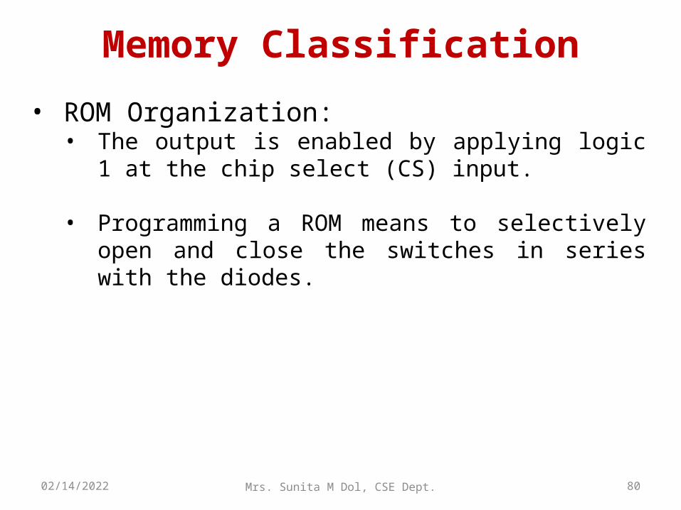
• ROM Organization:• The output is enabled by applying logic 1 at the chip
select (CS) input.
• Programming a ROM means to selectively open and close the switches in series with the diodes.
Memory Classification

05/02/2023 Mrs. Sunita M Dol, CSE Dept. 81
• RAM:• RAM is the memory available for the operating system,
programs and processes to use when the computer is running.
• In this type of memories, the memory locations are organized in such a way so that locations require equal time for writing and reading. This type of memory is also known as read-and-write memory.
• Data in RAM is not permanently written. When you power off your computer the data stored in RAM is deleted.
Memory Classification

05/02/2023 Mrs. Sunita M Dol, CSE Dept. 82
• RAM:
• RAMs can be static or dynamic and fabricated using bipolar and unipolar technologies.
Memory Classification
Read-and-write memories or random access memory (RWM & RAM)
Static RAM (SRAM) Dynamic RAM
uses bistable latches as storage element.
1.uses capacitor as a storage element which required periodic refreshing. 2.DRAMs can store much more data than SRAMs for a given physical size and cost.
05/02/2023 Mrs. Sunita M Dol, CSE Dept. 83
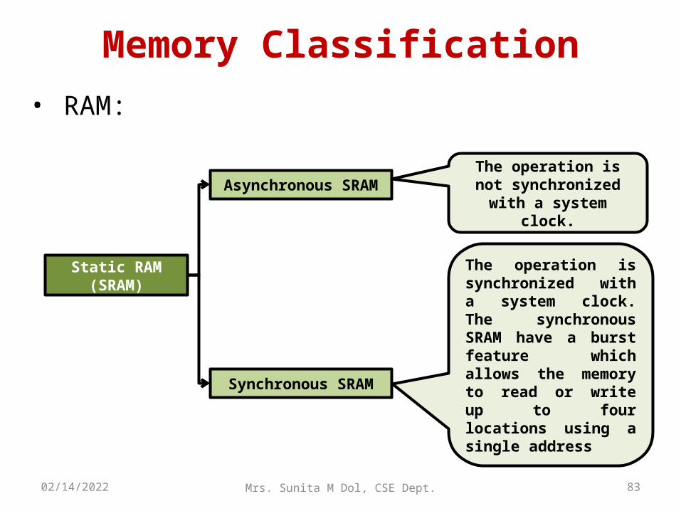
• RAM:
Memory Classification
Static RAM (SRAM)
Asynchronous SRAM
Synchronous SRAM
The operation is not synchronized with a
system clock.
The operation is synchronized with a system clock. The synchronous SRAM have a burst feature which allows the memory to read or write up to four locations using a single address
05/02/2023 Mrs. Sunita M Dol, CSE Dept. 84
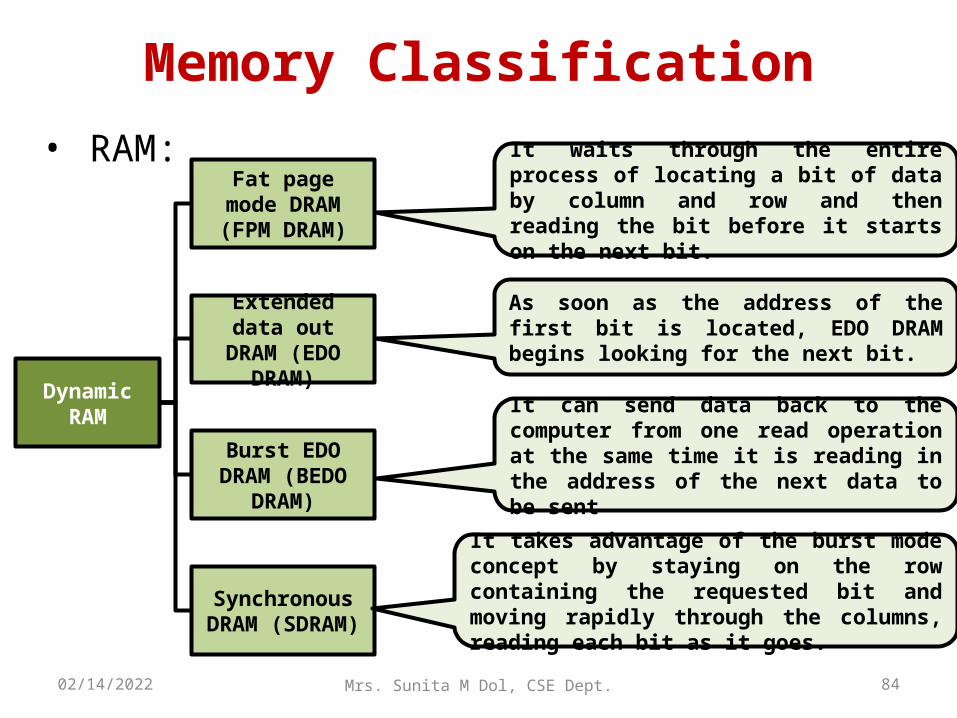
• RAM:
Memory Classification
Dynamic RAM
Fat page mode DRAM (FPM
DRAM)
Extended data out DRAM (EDO
DRAM)
Burst EDO DRAM (BEDO
DRAM)
Synchronous DRAM (SDRAM)
It waits through the entire process of locating a bit of data by column and row and then reading the bit before it starts on the next bit.
As soon as the address of the first bit is located, EDO DRAM begins looking for the next bit.
It takes advantage of the burst mode concept by staying on the row containing the requested bit and moving rapidly through the columns, reading each bit as it goes.
It can send data back to the computer from one read operation at the same time it is reading in the address of the next data to be sent

05/02/2023 Mrs. Sunita M Dol, CSE Dept. 85
• Flash Memories:• Flash memories are non-volatile, large bit storage
capacity, read and write memories.
• The storage cell in a flash memory consist of a single floating point-gate MOS transistors.
Memory Classification
05/02/2023 Mrs. Sunita M Dol, CSE Dept. 86
• Content Addressable Memories:• It is a special purpose RAM which performs association
operation in addition to read/write operation.
Memory Classification
05/02/2023 Mrs. Sunita M Dol, CSE Dept. 87
• First-in First-out memories(FIFO):• The data which is entered first is taken out first.
• The storage device used in is a SRAM array with two separate ports that allows the data to be written into and read from its array at independent data rates.
Memory Classification