Embed Size (px)
Citation preview

NANOTECHNOLOGY FOR ELECTRONICS
SMALLER
FASTER
MORE SENSITIVE
MORE EFFICIENT
Varun Bansal

WHAT IS NANOTECHNOLOGY ?Nanotechnology broadly includes all technologies that handle nano-scale
materials, and in a narrow sense, technologies that handle unique
phenomena that arise in the 10-to-100-nm size range. Carbon
Nanofibre(a single human hairis 1000 times thicker than any of the nanofibres in the image).


NEW PROPERTIES At the nanoscale, matter begins to demonstrate entirely new and unique
properties. It can become stronger, conduct heat better, and show
extraordinary electrical properties.

CREATING NANOSTRUCTURES
•The top – down method•The bottom – up method


WHY NANOTECHNOLOGY MATTERS ?
• The advances in nanotechnology have brought new tools to the field of electronics and sensors.
• For instance, at the nanoscale, the resistance dependence of a material on an external magnetic field is significantly amplified, which has led to the fabrication of hard disks with a data storage density in the gigabyte and terabyte ranges.

A few promising areas of nanoelectronics and
nanosensors.

CARBON BASED SENSORS AND ELECTRONICS
Carbon nanomaterials such as one-dimensional (1D) carbon nanotubes and two-dimensional (2D) graphene have:-
• Superior electrical properties which allow for fabrication of faster and more power-efficient electronics.
• High surface to volume ratio.• Excellent mechanical properties rendering
them as a robust and highly sensitive building block for nanosensors.
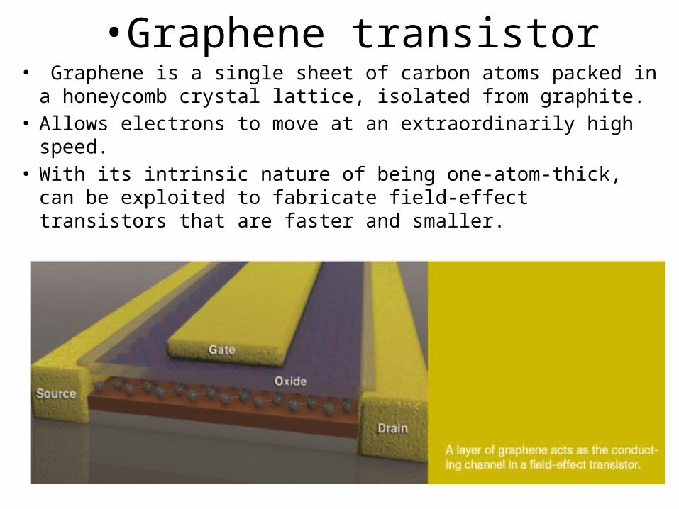
•Graphene transistor• Graphene is a single sheet of carbon atoms packed in a
honeycomb crystal lattice, isolated from graphite. • Allows electrons to move at an extraordinarily high speed. • With its intrinsic nature of being one-atom-thick, can be
exploited to fabricate field-effect transistors that are faster and smaller.

• Carbon nanotube electronicsWhen a layer of graphene is
rolled into a tube, a single-walled carbon nanotube (SWNT) is formed. The cylindrical structure and high electron mobility makes them a more readily available option for forming the channel in field-effect transistors. These have advanced to logic gates and radio-frequency components.

• Carbon-based nanosensors• Graphene and carbon nanotubes have excellent thermal
conductivity, high mechanical robustness, and very large surface to volume ratio making them superior materials for fabrication of electromechanical and electrochemical sensors with higher sensitivities, lower limits of detection, and faster response time.
Any additional gold atom that adsorbs on the surface of a vibrating carbon nanotube would change its resonance frequency which is further detected.

MOLECULAR ELECTRONICS
• Recent advances in nanofabrication techniques have provided the opportunity to use single molecules, or a tiny assembly of them, as the main building blocks of an electronic circuit.
• Enabling the realisation of novel functionalities beyond the scope of traditional solid state devices.

• Single Molecule Memory DeviceA modern memory device, stores each bit of data by
charging up a tiny capacitor. As memory device dimensions approach the nanometer range, the capacitor can be replaced by a single organic molecule such as Ferrocene, whose oxidation state can be altered by moving an electron into or out of the molecule.

• Organic transistor odour sensor
In an odour sensor, for instance, the nano-scale chemical reactions upon exposure of the device to a certain atmospheric condition modify the electronic properties of the organic semiconducting material which is further reflected by a change in the current flowing through the transistor.

QUANTUM COMPUTING
Quantum algorithms are implemented in a device that makes direct use of quantum mechanical phenomena such as entanglement and superposition. Nanotechnology uses the fact that the physical laws that govern the behaviour of a system at the atomic scale are inherently quantum mechanical in nature.

SINGLE ELECTRON TRANSISTOR• A single electron transistor
needs only one electron to change from the insulating to the conducting state.
• Deliver very high device density and power efficiency with remarkable operational speed.
• Quantum dots with sub-100 nm dimensions have to be fabricated.

SPINTRONICS Spintronics employs the spin of electrons to
encode and transfer information. It has the potential to deliver nanoscale memory and logic devices which process information faster, consume less power, and store more data in less space. The extension of the hard disk capacities to the gigabyte and the terabyte ranges was the main achievement of spintronics by taking advantage of Giant Magneto-Resistance (GMR) and Tunnel Magneto-Resistance (TMR) effects which are effective only at the nano scale.

NANO-ELECTRO-MECHANICAL SYSTEMS (NEMS)
• Nano-electro-mechanical systems have evolved during the last 10 years by creating sensors
(“eyes”) and actuators (“arms”). • Recent developments in synthesis of nanomaterials
with excellent electrical and mechanical properties have extended the boundaries of NEMS
applications to include more advanced devices such as the non-volatile nanoelectro-mechanical memory, where information is transferred and
stored through a series of electrical and mechanical actions at the nanoscale.


Hybrid Si NanoCones/Polymer Solar Cell • Si nanocones
fabricated by colloidal lithography were covered with a conductive polymer, which formed a Schottky junction between the Si and polymer.
• The power conversion efficiency of the hybrid Si/polymer device was more than 11 %.

Common applications of NANOTECHNOLOGY IN
ELECTRONICS

• Computer processing
Moore’s Law describes a trend of technology. It states that the number of transistors that can be put on a single chip will double every two years.

Because of nanotechnology, the speed of computers has increased while the price of computing has decreased.

• Memory and storage
2 GB in 1980s $80,000
2 GB in 1990s $200
2 GB in 2010 $5

• DisplaysCarbon nanotubes on a glass or plastic sheet allow
manufacturers to make clear conductive panels for displays that are extremely thin.

Restoring Sight to the Blind • Blindness due to loss of photoreceptors. • Sight can be restored by patterned electrical
stimulation of the surviving inner retinal neurons.
• Photovoltaic subretinal prosthesis directly converts pulsed light into pulsed electric current in each pixel, stimulating nearby neurons.
• Visual information is projected onto retina by video goggles using pulsed NIR (~900 nm) light. Photovoltaic arrays including 3 diodes in each pixels were fabricated in SNF.


Cancer Detection• Motivation – Earlier
cancer detection • Development of
nanomagnetic sensor chip
– Use same principles employed in magnetic storage industry
– Use magnetic nanoparticles to ‘tag’ proteins indicative of cancer

Nanostructures in Nature• A moth’s eye has very small bumps on its surface. These patterns are
smaller than the wavelength of visible light (350-800nm). The eye surface has a very low reflectance for the visible light. The moth can see much better than humans in dim or dark conditions because these nanostructures absorb light very efficiently.
• On the surface of a butterfly’s wings are multilayer nanoscale patterns. These structures filter light and reflect mostly one wavelength, so we see a single bright color. Due to multiple layers in these structures optical interferences are created (wings of male Morpho Rhetenor appear blue).
• The edelweiss (Leontopodium nivale) is an alpine flower found at high altitudes, where UV radiation is strong. The flowers are covered with thin hollow filaments that have nanoscale structures (100-200nm) on their periphery. They will absorb ultraviolet light, but reflect all visible light. This explains the white color of the flower. It also protects the flower’s cells from possible damage due to this high-energy radiation.


• Providing realistic, cost-effective methods for harnessing renewable energy sources and keeping the environment clean.
• Doctors detecting disease at its earliest stages and treating illnesses such as cancer, diabetes, heart disease with more effective and safer medicines.
• New technologies for protecting both military forces and civilians from conventional, chemical and biological weapons.