WP4: Radiation Hard Semiconductor Detectors- Status of activities -
Michael Moll (PH-DT), Michael Moll (PH-DT), Heinz PerneggerHeinz Pernegger (PH-ADE) (PH-ADE)
PH Theme 3 R&D meeting 4.6.2009
WP4 – Challenge and Aim WP4 – Work program, organization and participants Status:
Pixel sensor evaluation/development ( in collaboration with ATLAS) Strip sensor evaluation/development ( in collaboration with CMS) Generic R&D ( in collaboration with RD50) Build up of infrastructure ( common CERN infrastructure)
Work plan for 2009/2010
OUTLINE (Michael: 3-5 June 09: RD50 Workshop in Freiburg)

M.Moll, H.Pernegger – PH-WP Meeting – 4 June 2009 -2-
1013 5 1014 5 1015 5 1016
Φeq [cm-2]
5000
10000
15000
20000
25000
signal [electrons]
n-in-n (FZ), 285μm, 600V, 23 GeV p p-in-n (FZ), 300μm, 500V, 23GeV pp-in-n (FZ), 300μm, 500V, neutrons
p-in-n-FZ (500V)n-in-n FZ (600V)
M.Moll - 08/2008
References:
[1] p/n-FZ, 300μm, (-30oC, 25ns), strip [Casse 2008][2] n/n-FZ, 285μm, (-10oC, 40ns), pixel [Rohe et al. 2005]
FZ Silicon Strip and Pixel Sensors
strip sensorspixel sensors
Challenge: Sensors for the SLHC TrackersNote: Measured partly
under different conditions! Lines to guide the eye
(no modeling)!
Strip sensors: max. cumulated fluence for LHC and SLHC
Pixel sensors: max. cumulated fluence for LHC and SLHC
LHC detectors would fail in SLHC due to radiation damage
SLHC will need more radiation tolerant tracking detector concepts!

M.Moll, H.Pernegger – PH-WP Meeting – 4 June 2009 -3-
Work program and structure of WP 4
1. Development and evaluation of pixel sensor concepts in framework of ATLAS Pixel Upgrade projects (H.Pernegger, A. La Rosa)
Evaluation of rad. tolerant sensors for innermost pixel layers in view of IBL and SLHC pixel:Pixel technologies: Silicon planar sensors, Silicon 3D sensors, Diamond sensors
WP4-Fellow A.La Rosa has become a driving force for organization and running of testbeam and irradiation campaigns for the ATLAS pixel community.
2. Development and evaluation of sensor concepts for CMS upgrade in framework of CMS Tracker Upgrade projects (M.Mannelli)
Sensor R&D program with HPK (Hamamatsu) to evaluate sensors based on various silicon sensor materials: FZ, MCZ and EPI silicon of n- and p-type and different thickness
Part of prg. for preproduction, qualification and large scale production of CMS phase II upgrade
3. Generic R&D on radiation tolerance of silicon sensors in framework of RD50 project (M.Moll)
Generic R&D on understanding of radiation damage in silicon
4. Build up of test equipment & infrastructure for PH common use (M.Moll, M. Fahrer) Equipment: Probestations for CV/IV measurements of sensors TCT/ b-source test system in climate controlled container
WP4 is organized around 4 partly overlapping projects

M.Moll, H.Pernegger – PH-WP Meeting – 4 June 2009 -4-
WP4 – ParticipantsCoordinator: Michael Moll (PH-DT)
Project 1 (ATLAS): WP4-Fellow: Alessandro La Rosa
Start: 1.4.2008, PH-DT, Experiments: ATLAS / RD50 Supervisor: Heinz Pernegger (PH-ADE)
H.Pernegger, S.Roe, B. di Girolamo, D.Dobos
Project 2 (CMS): M. Mannelli
Project 3 & 4 (RD50 & Test equipment): WP4-Fellow: Manuel Fahrer
Start: 1.3.2008, PH-DT, Experiments: RD50 Supervisor: Michael Moll (PH-DT)
Michael Moll, K.Kaska (PhD student), N.Pacifico (MCPAD ESR) R.Fortin, A.Guipet (Technical support)
Observers (presently no active role)
LHCb : Paula Collins ALICE : Petra Riedler TOTEM: Gennaro Ruggiero
M.Moll, H.Pernegger – PH-WP Meeting – 4 June 2009 -5-
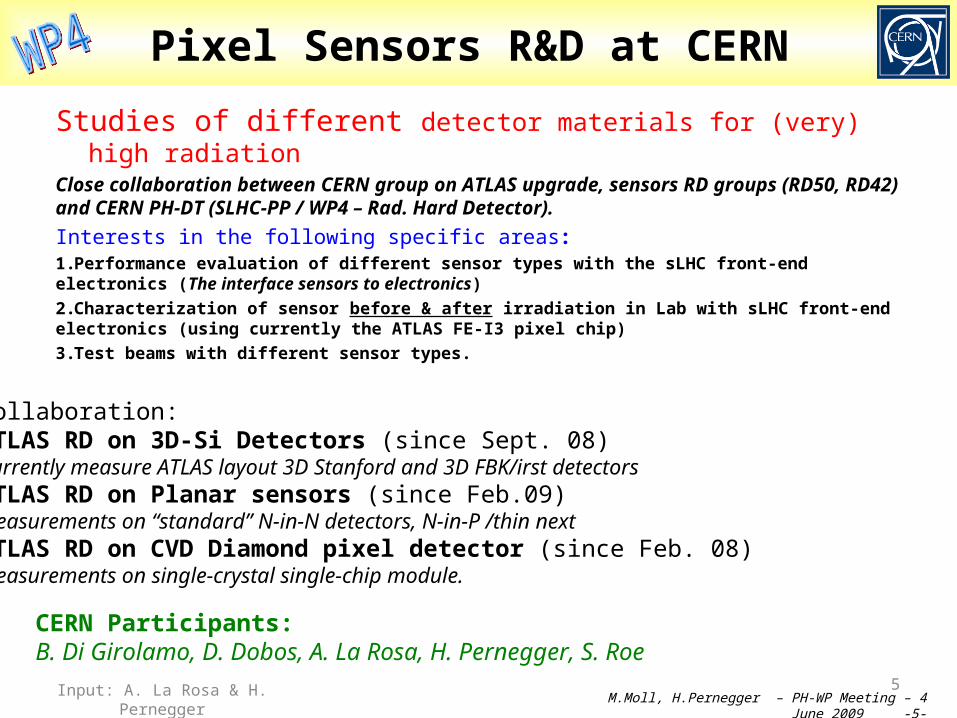
Pixel Sensors R&D at CERN
Studies of different detector materials for (very) high radiationClose collaboration between CERN group on ATLAS upgrade, sensors RD groups (RD50, RD42) and CERN PH-DT (SLHC-PP / WP4 – Rad. Hard Detector).
Interests in the following specific areas:1.Performance evaluation of different sensor types with the sLHC front-end electronics (The interface sensors to electronics)
2.Characterization of sensor before & after irradiation in Lab with sLHC front-end electronics (using currently the ATLAS FE-I3 pixel chip)
3.Test beams with different sensor types.
Input: A. La Rosa & H. Pernegger5
CERN Participants: B. Di Girolamo, D. Dobos, A. La Rosa, H. Pernegger, S. Roe
Collaboration:ATLAS RD on 3D-Si Detectors (since Sept. 08)Currently measure ATLAS layout 3D Stanford and 3D FBK/irst detectorsATLAS RD on Planar sensors (since Feb.09)Measurements on “standard” N-in-N detectors, N-in-P /thin nextATLAS RD on CVD Diamond pixel detector (since Feb. 08)Measurements on single-crystal single-chip module.

M.Moll, H.Pernegger – PH-WP Meeting – 4 June 2009 -6-
3D-Si sensors
6/4/09 A. La Rosa & H. Pernegger 6
Started to do measurements on different detectors (FBK/irst 2E, 3E and 4E-types): Leakage currents Threshold scan (threshold and noise measurements) Noise vs bias voltage Source test with Am-241, Cd-109 and Sr90
Am241
Sr90
MPV ~14k2 eThick. ~ 220um
M.Moll, H.Pernegger – PH-WP Meeting – 4 June 2009 -7-
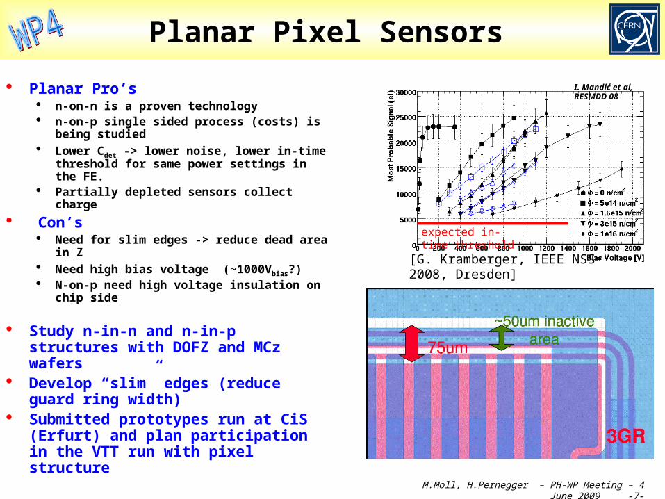
Planar Pixel Sensors
Planar Pro’s n-on-n is a proven technology n-on-p single sided process (costs) is being
studied Lower Cdet -> lower noise, lower in-time
threshold for same power settings in the FE. Partially depleted sensors collect charge
Con’s Need for slim edges -> reduce dead area in Z Need high bias voltage (~1000Vbias?) N-on-p need high voltage insulation on chip side
Study n-in-n and n-in-p structures with DOFZ and MCz wafers
Develop “slim” edges (reduce guard ring width)
Submitted prototypes run at CiS (Erfurt) and plan participation in the VTT run with pixel structure
T=-20 to -30oCG. Casse et al., IEEE TNS, Vol. 55, No. 3, 2008, p. 1695Liverpool data not annealed
I. Mandić et al, RESMDD 08
[G. Kramberger, IEEE NSS 2008, Dresden]
expected in-time threshold
M.Moll, H.Pernegger – PH-WP Meeting – 4 June 2009 -8-
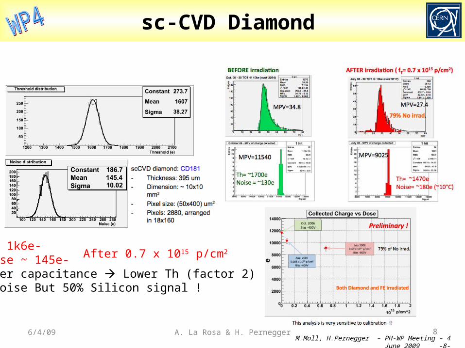
sc-CVD Diamond
6/4/09 A. La Rosa & H. Pernegger 8
Th@ 1k6e-Noise ~ 145e-Lower capacitance Lower Th (factor 2) & Noise But 50% Silicon signal !
After 0.7 x 10¹⁵ p/cm2

M.Moll, H.Pernegger – PH-WP Meeting – 4 June 2009 -9-
WP4 (2010) – Proposal for common R&D within ATLAS/RD42/RD50 community
Input: A. La Rosa & H. Pernegger9
In the framework of SLHC-PP /WP4 (Rad. Hard Detector) project we would like to propose a Common ATLAS Pixel Sensors RD activity for tracking detector environment at CERN for 2010.So we propose to organize a:- Common lab characterization of bonded sensors at CERN ATLAS Pixel Lab; - Common irradiation test (proton at CERN and neutron at Ljubljana facility) at a high fluences (FEI3 compatible and after FEI4);- Common test-beam with MIP at CERN, before and after irradiation test. The aim of the activity would be give out a comparative overview about the next pixel sensor generation for tracking detector environment to facilitate a decision regarding their implementation in the ATLAS-IBL project and in the ATLAS-SLHC Pixel Upgrade.
For 2010 we’d request a Doctoral Student (start date 1.1.2010) who could work full-time in the RD activity.
Status of proposal:
Distributed to potential partners

M.Moll, H.Pernegger – PH-WP Meeting – 4 June 2009 -10-
CMS SLHC Tracker - Thin Sensor R&D with HPK -
Phase I: Targeted R&D ~ 2008 - 2012 Establish required sensors characteristics & basic specifications Single Source R&D with HPK agreed with CERN, together with framework
for Market Survey & Procurements for Phase II & Phase III
Phase II: Preproduction and Qualification ~ 2012 - 2014 Finalize detailed specifications and QA protocols Qualify for large scale production
Phase III: Large Scale Production ~ 2014 - 2016Input: Marcello Mannelli
Project is integral part of CMS
Tracker upgrade
Outline plan:
WP4 participation in Phase I:
• coordination of project M .Mannelli (CMS & WP4)
• irradiation of sensors
• characterization of sensors (… requires still the set up of some specific equipment at CERN)
M.Moll, H.Pernegger – PH-WP Meeting – 4 June 2009 -11-
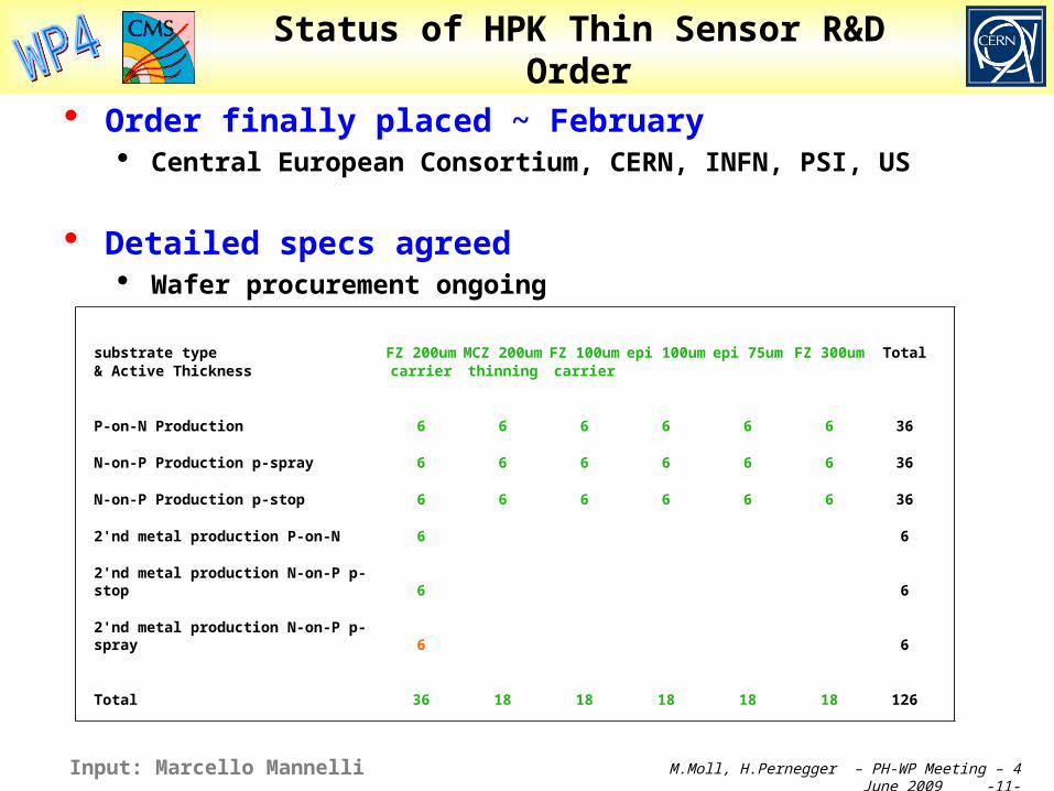
Status of HPK Thin Sensor R&D Order
Order finally placed ~ February Central European Consortium, CERN, INFN, PSI, US
Detailed specs agreed Wafer procurement ongoing
substrate typeFZ
200umMCZ
200umFZ
100umepi
100um epi 75umFZ
300um Total
& Active Thickness carrier thinning carrier
P-on-N Production 6 6 6 6 6 6 36
N-on-P Production p-spray 6 6 6 6 6 6 36
N-on-P Production p-stop 6 6 6 6 6 6 36
2'nd metal production P-on-N 6 6
2'nd metal production N-on-P p-stop 6 6
2'nd metal production N-on-P p-spray 6 6
Total 36 18 18 18 18 18 126
Input: Marcello Mannelli

M.Moll, H.Pernegger – PH-WP Meeting – 4 June 2009 -12-
Status of HPK Thin Sensor R&D Order
Wafer Layout being finalized
Input for full set of designs provided to HPK
Waiting response from HPK• Expect feed-back within
coming weeks
Input: Marcello Mannelli
M.Moll, H.Pernegger – PH-WP Meeting – 4 June 2009 -13-
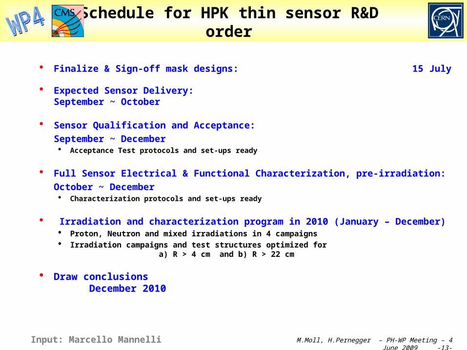
Schedule for HPK thin sensor R&D order
Finalize & Sign-off mask designs: 15 July
Expected Sensor Delivery: September ~ October
Sensor Qualification and Acceptance:
September ~ December Acceptance Test protocols and set-ups ready
Full Sensor Electrical & Functional Characterization, pre-irradiation:
October ~ December Characterization protocols and set-ups ready
Irradiation and characterization program in 2010 (January – December) Proton, Neutron and mixed irradiations in 4 campaigns Irradiation campaigns and test structures optimized for
a) R > 4 cm and b) R > 22 cm
Draw conclusions December 2010
Input: Marcello Mannelli

M.Moll, H.Pernegger – PH-WP Meeting – 4 June 2009 -14-
Status: Build up of test equipment
‘Refurbishment’ of characterization tools in 28-2-017 (done) (Laboratory for Departmental Silicon Facility & RD50 support)
Probe station for CV/IV measurements (4” chuck in dark box, CV/IV up to 1000V) Simple TCT (Transient Charge Technique) (one channel, limited space and cooling capacity) CCE with Sr90 source (one channel, μs shaping, limited size of samples and limited cooling)
Pixel test stations in Bat 161 for sensor+FE chip measurments fully operational since early 2008
With source and electronic calibration
For 2010 on Pixel Tests Stands Adaptation with new controller electronics for new FEI4 chip Installation for lower temperature cooling (T~ -20C) for tests of irradiated pixel sensors
New TCT/CCE setup in 28-2-017 (under commissioning, see next slide)
Two further installations planned: Probe station with cold chuck for CV/IV measurements
(status: designed, some parts machined, realization delayed due to high work load in PH-DT bonding lab & radiation facilities keeping technicians busy with ‘LHC relevant work’)
Probe station with characterization tools for measuring high number of CMS Tracker prototype sensors
• Detailed requirements to be specified by CMS• Installation in DSF (Departmental Silicon Facility)
Input M.Fahrer, M.Moll

M.Moll, H.Pernegger – PH-WP Meeting – 4 June 2009 -15-
TCT/CCE setup (28-2-017)Characterization methods TCT (Transient Charge Technique)
strip and pad sensors can be mounted lasers illumination on both sides of sample red + infrared laser (ps pulses)
CCE (Charge collection efficiency) Sr90 source Scintillator based trigger
CV / IV CV presently at 1, 10, 100 KHz
(to be extended to variable frequency up to 1 MHz)
Mechanics & Cooling Cooled with silicon oil
vacuum or dry atmosphere to avoid formation of ice
Temperatures down to below -30C (full range still to be tested)
Movable from outside laser and source
can be scanned over DUT Modular system with flanshes
allows for easy mounting of additional feedthroughts
Sample mounting & Electronics SMA connectors (HF)
Bandwidth limitations due to scope:3 GHz scope would be very useful
Sample boards (support PCB) detectors to be bonded good thermal & HF properties
Amplification commercial solutions for
single channels ALIBAVA system for strip sensor CCE
• based on LHCb Beetle Chip• 25ns shaping time, 128 channels

M.Moll, H.Pernegger – PH-WP Meeting – 4 June 2009 -16-
TCT/CCE Setup
Sr 90
Source
PCB support
PM
laser focusercooling plate
equipment movable against
support plate

M.Moll, H.Pernegger – PH-WP Meeting – 4 June 2009 -17-
Sensor Development within RD50
Strip sensors produced in framework of RD50 (~50 inst.) WP4 participation in ongoing RD50 sensor characterizations
sensors are partly already irradiated and ready for measurements at CERN WP4 participation in new RD50 processing runs
(next project: Sensor production with VTT in Finland / mask under design)
CIS Erfurt, Germany 2005/2006/2007 (RD50): Several runs with various epi 4” wafers only pad detectors
CNM Barcelona, Spain 2006 (RD50): 22 wafers (4”), (20 pad, 26 strip, 12 pixel),(p- and n-type),(MCZ, EPI, FZ) 2006 (RD50/RADMON): several wafers (4”), (100 pad), (p- and n-type),(MCZ, EPI, FZ)
HIP, Helsinki, Finland 2006 (RD50/RADMON): several wafers (4”), only pad devices, (n-type),(MCZ, EPI, FZ) 2006 (RD50) : pad devices, p-type MCz-Si wafers, 5 p-spray doses, Thermal Donor compensation 2006 (RD50) : full size strip detectors with 768 channels, n-type MCz-Si wafers
IRST, Trento, Italy 2004 (RD50/SMART): 20 wafers 4” (n-type), (MCZ, FZ, EPI), mini-strip, pad 200-500μm 2004 (RD50/SMART): 23 wafers 4” (p-type), (MCZ, FZ), two p-spray doses 3E12 amd 5E12 cm-2 2005 (RD50/SMART): 4” p-type EPI 2008 (RD50/SMART): new 4” run
Micron Semiconductor L.t.d (UK) 2006 (RD50): 4”, microstrip detectors on 140 and 300μm thick p-type FZ and DOFZ Si. 2006/2007 (RD50): 93 wafers, 6 inch wafers, (p- and n-type), (MCZ and FZ), (strip, pixel, pad)
Sintef, Oslo, Norway 2005 (RD50/US CMS Pixel) n-type MCZ and FZ Si Wafers
Recent productions of Silicon Strip, Pixel and Pad detectors within RD50(non exclusive list):
Details:
http://www.cern.ch/RD50/
M.Moll, H.Pernegger – PH-WP Meeting – 4 June 2009 -18-
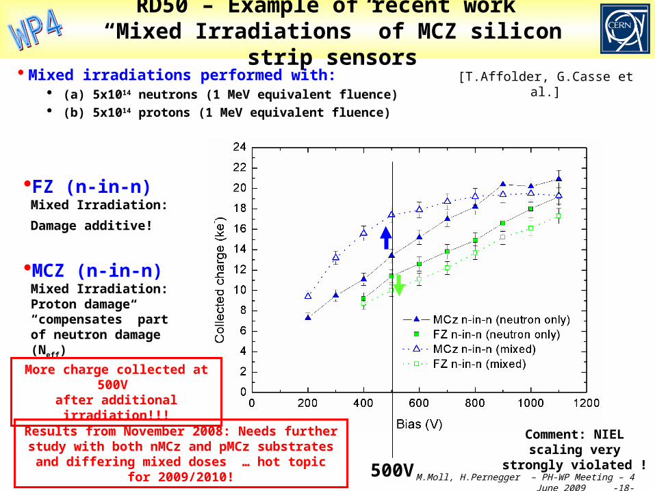
RD50 – Example of recent work “Mixed Irradiations” of MCZ silicon strip
sensors Mixed irradiations performed with:
(a) 5x10¹⁴ neutrons (1 MeV equivalent fluence) (b) 5x10¹⁴ protons (1 MeV equivalent fluence)
FZ (n-in-n)Mixed Irradiation:
Damage additive!
MCZ (n-in-n)Mixed Irradiation:Proton damage “compensates” part of neutron damage (Neff)
500V
Comment: NIEL scaling very strongly violated !
[T.Affolder, G.Casse et al.]
Results from November 2008: Needs further study with both nMCz and pMCz substrates and differing
mixed doses … hot topic for 2009/2010!
More charge collected at 500V after additional irradiation!!!

M.Moll, H.Pernegger – PH-WP Meeting – 4 June 2009 -19-
p-type FZ Silicon Sensors
Higher voltage helps!
Which voltage can be applied?
1014 5 1015 5 1016
Φeq [cm-2]
5000
10000
15000
20000
25000
signal [electrons] n-in-p (FZ), 300μm, 1700V, neutrons [2]
n-in-p-FZ (1700V)
n-in-p (FZ), 300μm, 500V, 23GeV p [1]n-in-p (FZ), 300μm, 500V, neutrons [1]n-in-p (FZ), 300μm, 500V, 26MeV p [1]n-in-p (FZ), 300μm, 800V, 23GeV p [1]n-in-p (FZ), 300μm, 800V, neutrons [1]n-in-p (FZ), 300μm, 800V, 26MeV p [1]
n-in-p-Fz (500V)
n-in-p-Fz (800V)
p-in-n (FZ), 300μm, 500V, 23GeV p [1]p-in-n (FZ), 300μm, 500V, neutrons [1]
p-in-n-FZ (500V)
M.Moll - 08/2008
References:
[1] p/n-FZ, 300μm, (-30oC, 25ns), strip [Casse 2008][2] p-FZ,300μm, (-40oC, 25ns), strip [Mandic 2008]
[3] n/n-FZ, 285μm, (-10oC, 40ns), pixel [Rohe et al. 2005][1] 3D, double sided, 250μm columns, 300μm substrate [Pennicard 2007][2] Diamond [RD42 Collaboration][3] p/n-FZ, 300μm, (-30oC, 25ns), strip [Casse 2008]Data from Gianluigi Casse et al. (Liverpool)
presented on VERTEX 2008
FZ Silicon Strip Sensors
500V
800V
1700V
Data: G.Casse et al. (Liverpool) [RD50 06/2008 & VERTEX 2008]and I.Mandic et al. (Ljubljana) [RD50 06/2008]

M.Moll, H.Pernegger – PH-WP Meeting – 4 June 2009 -20-
MCz-n – 8e14 n/cm^2 (front ill. – The only possible)
MCz-n – 8e14 neq /cm^2 (front ill. – The only possible)
neutrons
protons
Not ‘whole bulk’ type inversion, but still the junction on the back starts to prevail over the junction on the front – MCz-n irradiated with neutrons behaves in a similar way as FZ-n…
With protons the situation is radically different. The two junctions are there, but the one on the front remains higher than the one forming on the back.
Different kind of hadrons with different energies produce different development of the field profile in the detector.
WP4 generic research: MCZ siliconType inversion problem in MCz-Si with 24 GeV/c p+ (2/2)
under publication in NIMA
M.Moll, H.Pernegger – PH-WP Meeting – 4 June 2009 -21-
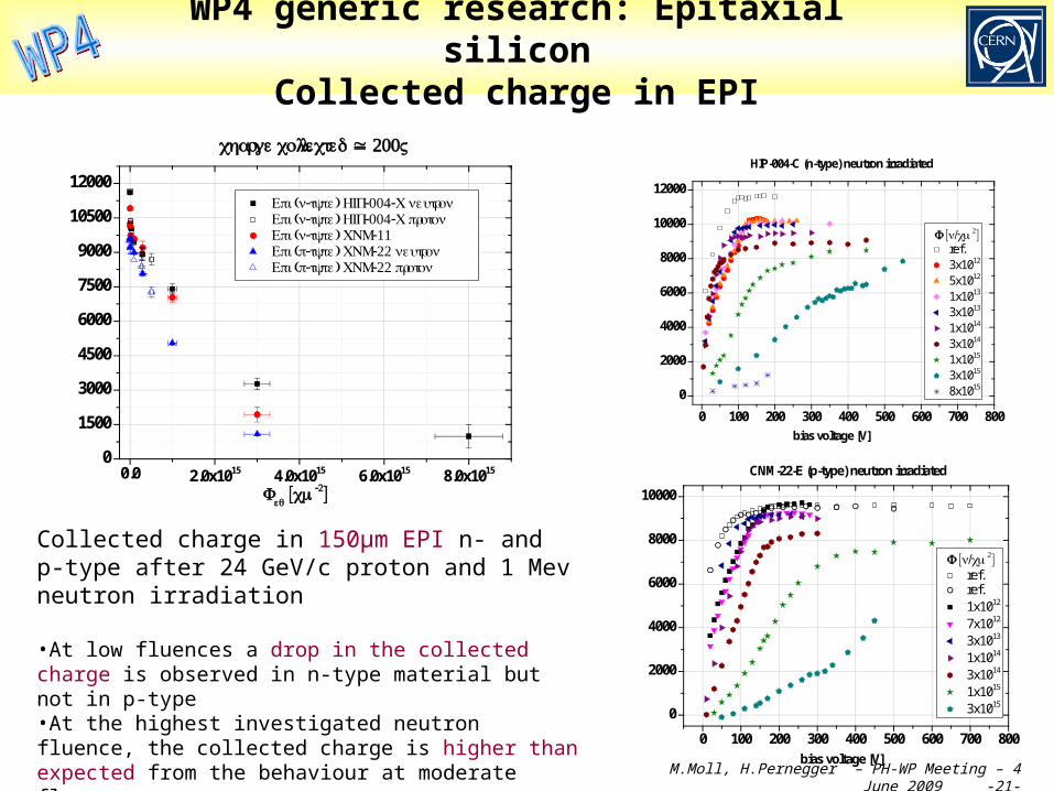
WP4 generic research: Epitaxial siliconCollected charge in EPI
0 100 200 300 400 500 600 700 800
0
2000
4000
6000
8000
10000
collected charge [e
-]
bias voltage [V]
ref. ref. 1x10¹²
7x10¹²
3x10¹³
1x10¹⁴
3x10¹⁴
1x10¹⁵
3x10¹⁵
CNM-22-E (p-type) neutron irradiated
Φ [n/cm2]
0 100 200 300 400 500 600 700 800
0
2000
4000
6000
8000
10000
12000
collected charge [e
-]
bias voltage [V]
ref.3x1012
5x10¹²
1x10¹³
3x10¹³
1x10¹⁴
3x10¹⁴
1x10¹⁵
3x10¹⁵
8x10¹⁵
HIP-004-C (n-type) neutron irradiated
Φ [n/cm2]
0.0 2.0x10¹⁵ 4.0x10¹⁵ 6.0x10¹⁵ 8.0x10150
1500
3000
4500
6000
7500
9000
10500
12000
collected charge [e
-]
Φeq [cm-2]
Epi (n-type) HIP-004-C neutron Epi (n-type) HIP-004-C proton Epi (n-type) CNM-11 Epi (p-type) CNM-22 neutron Epi (p-type) CNM-22 proton
charge collected @ 200V
Collected charge in 150μm EPI n- and p-type after 24 GeV/c proton and 1 Mev neutron irradiation
•At low fluences a drop in the collected charge is observed in n-type material but not in p-type•At the highest investigated neutron fluence, the collected charge is higher than expected from the behaviour at moderate fluences
M.Moll, H.Pernegger – PH-WP Meeting – 4 June 2009 -22-
Workplan 2009 & 2010 Workplan “ATLAS pixels”:
Extension of setup to include new chip controller + pulsed laser source (under study) (2009/10) Participation in ATLAS Pixel upgrade irradiations & testbeams (2009/2010) Active participation in the procurement and assembly of pixel test modules
(sensors bump bonded to ATLAS pixel chip) for lab and beam tests (2009/2010) Contribute measurements on different pixel sensor technologies to ATLAS IBL (2009/10)
Workplan “sensors for CMS” Participate in CMS work on sensor characterization before & after irradiation (2010)
Workplan on activities in framework of RD50 Submission of detector production run at VTT, Finland (2009) Detailed study on reverseannealing in p-type silicon strip sensors (2009/2010) Further studies on MCZ silicon in mixed irradiation fields (2009/2010) Participate in RD50 sensor evaluation program (MCZ vs. FZ, n-vs.p-type) 2009/2010
Workplan on common infrastructure at CERN Extension of TCT/CCE to use ALIBAVA system (LHCb Beetle chip) -- 2009 Probe station for CMS and common use in DSF – (2009/2010)

M.Moll, H.Pernegger – PH-WP Meeting – 4 June 2009 -23-
Manpower request 2010
2nd board 2009: Fellow ship extensions
• La Rosa +6mo from 1.4.2010
• Fahrer +6mo from 1.3.2010
New Fellow (RD50)• Starting 1.1.2010
New Doctoral Student (Pixel Irradation & Testbeam support)• Starting 1.1.2010
1st board 2010 New Fellow
• Starting 1.7.2010

M.Moll, H.Pernegger – PH-WP Meeting – 4 June 2009 -24-
Spares
Spares

M.Moll, H.Pernegger – PH-WP Meeting – 4 June 2009 -25-
CCE/TCT : Instrumentation
Optics ps-Laser from PicoQuant two heads: 661nm and 1055nm low energetic pulses around 10pJ at lasing
threshold most interesting attenuated by micro screw directly at
coupling full and closed fiber solution with splitters
and shutters no manual intervention to fiber
path during measurements allows for reliable and
reproducible measurements focusing spot ~ 12μm on DUT at working
distance of 23mm
Environmental control cooling down to -40°C vacuum down to 0.06 mbar multifunctional DAQ & control unit
T,H & other analog signals low voltage clock
Prototype PCB Not yet optimized for
HF external bias board
for filtering and line matching
thus allows CV measurements as well
Gold-nickel plated Roger’s PCB
material for HF and good thermal conductivity

M.Moll, H.Pernegger – PH-WP Meeting – 4 June 2009 -26-
WP4
Contact with “clients”
Pixel sensordevelopment
(H.Pernegger, A.La Rosa)
“ATLAS environment” + “RD42 environment” for diamond sensor tests
“Common CERN infrastructure”
CMS sensors
(M.Mannelli)
“CMS environment”
ATLAS and CMS colleagues are part of the WP Heinz (ATLAS) working in framework of approved ATLAS upgrade projects Marcello (CMS) working in framework of approved CMS upgrade project
ALICE, LHCb and TOTEM Contact persons for WP4 at CERN appointed, Invited to participate in WP4
meetings and in WP4 activities
RD50 sensor characterization
(M.Fahrer, M.Moll, K.Kaska, N.Pacifico)
“RD50 environment”
Strip and Pad sensor characterization tools
(M.Fahrer, M.Moll)

M.Moll, H.Pernegger – PH-WP Meeting – 4 June 2009 -27-
WP4 generic research: MCZ siliconType inversion problem in MCz-Si with 24 GeV/c p+ (1/2)
Naïf interpretation of Vdep CV annealing curves:
•MCz-n silicon does not type invert with irradiation•MCz-p silicon stays p-type at lowest fluences, but at higher ones show n-type annealing behavior ->Type inversion?•Type inversion with annealing (n->p)
Annealing curves still quite different from what we would expect by “standard” diode behavior (during type inversion Vdep should go to zero)
Irradiation with hadrons produces two different space charge regions… This effect seems more dramatic in oxygenated device -> MCz and EPI Silicon…
It’s *not* anymore about whether the bulk inverts or not, but of the two junctions which one will prevail… ?

M.Moll, H.Pernegger – PH-WP Meeting – 4 June 2009 -28-
WP4 generic research: Epitaxial siliconEffective space charge in EPI
0 2 4 6 8 10 12 14 16
0.00
0.02
0.04
0.06
0.08
0.10
0.12
20V
10V
70V
60V
50V
40V
30V
I [V/50
Ω]
t [ns]
0 2 4 6 8 10 12 14 16 18
0.00
0.01
0.02
0.03
0.04
0.05
0.06
0.07
0.08
0.09
190V
160V
130V
100V
70V
40V
I [V/50
Ω]
t [ns]
220V
10V
After neutron irradiation n-type inverts to p-type
After proton irradiation p-type inverts to n-type
0.0 8.0x10¹⁴ 1.6x10¹⁵ 2.4x10¹⁵ 3.2x10150
5
10
15
20
25
30
0
100
200
300
400
500
|Neff
| [10
12
cm-3
]
Φeq [cm-2]
neutron irradiatedn-type
HIP-004-C CNM-11-E
p-type CNM-22-E
proton irradiatedn-type
HIP-004-C CNM-11-E
p-type CNM-22-E
Vd [ ]V
In 150μm EPI the depletion voltage charge rises quicker with proton than with neutron irradiation. •After proton irradiation the space charge is positive •After neutron irradiation the space charge is negative
under publication in NIMA
M.Moll, H.Pernegger – PH-WP Meeting – 4 June 2009 -29-
Deliverables 2008 & 2009
Main deliverables for 2008 Pixel sensor test setup (Heinz/Alessandro) TCT/CCE test setup for strip sensors (Manuel/Michael) Submission of HPK Sensor Order
& Work plan for corresponding measurements at CERN in 2009 (Marcello / CMS project)
Main deliverables for 2009 Report on lab characterization (90Sr source/TCT) of irradiated sensors
• Performance before/after irradiation; evaluation of procurement, cost and integration issues for different sensor types
• Pixel: 3D, Diamond, Planar • Strip: RD50 and CMS sensors (p- and n- MCZ, FZ, EPI, thick vs. thin)
Test beam results • on pixel sensors (3D, Diamond, Planar sensors)
(to be produced in framework of ATLAS Pixel upgrade activities/test beams)
• on strip sensors (MCZ vs. FZ, thick vs. thin)(to be produced in framework of CMS and/or RD50 upgrade activities/test beams)
Probe station in DSF for sensor characterization (CV/IV) (CERN common infrastructure!)
Recommended


![Semberske novine [broj 701, 4.6.2009]](https://img.dokumen.tips/doc/110x75/577d29331a28ab4e1ea62d1b/semberske-novine-broj-701-462009.jpg)