Advanced Qualification of Additive Manufacturing Materials Workshop
Temperature Simulations and Measurements Manufacturing Materials Workshop
pfor Process Qualification in Powder-Bed Electron Beam Additive ManufacturingElectron Beam Additive Manufacturing
Kevin ChouKevin ChouProfessor
Mechanical Engineering DepartmentThe University of AlabamaThe University of Alabama
Assistant Director for TechnologyAdvanced Manufacturing National Program Officeg g
U.S. Department of Commerce
July 20, 2015
Disclaimer and Note• The materials presented and opinions expressed in this seminar were solely from
the presenter himself. They do not represent the viewpoints of The University of Alabama, nor the Advanced Manufacturing National Program Office.
• The materials presented in this seminar are mainly from the following articles.– Cheng, B., S. Price, J. Lydon, K. Cooper and K. Chou, "On Process Temperature in Powder‐Bed
El t B Additi M f t i M d l D l t d E i t l V lid ti ” J lElectron Beam Additive Manufacturing: Model Development and Experimental Validation,” Journal of Manufacturing Science and Engineering, Vol. 136, No. 6, pp. 061018 (1‐12), 2014.
– Price, S., B. Cheng, J. Lydon, K. Cooper and K. Chou, "On Process Temperature in Powder‐Bed Electron Beam Additive Manufacturing: Process Parameter Effects,” Journal of Manufacturing Science and Engineering, Vol. 136, No. 6, pp. 061019 (1‐10), 2014.Science and Engineering, Vol. 136, No. 6, pp. 061019 (1 10), 2014.
– Gong, X., J. Lydon, K. Cooper, and K. Chou, “Beam Speed Effects on Ti‐6Al‐4V Microstructures in Electron Beam Additive Manufacturing,” Journal of Materials Research, Vol. 29, No. 17, pp. 1951‐1959, 2014.
– Gong, X., J. Lydon, K. Cooper, and K. Chou, “Characterization of Ti‐6Al‐4V Powder in Electron‐Beam‐g, , y , p , ,Melting Additive Manufacturing,” International Journal of Powder Metallurgy, Vol. 51, No. 1, pp. 1‐10, 2015.
Contact information:Kevin Chou, [email protected], 205‐348‐0044
2

Quality Control in AM Material and ProcessMaterial and Process
Process ∆2 Part∆2
∆
∆f
EBAM Process Video∆1Feedstock
EBAM Process Video
GE Aviation
3∆f = Fn (∆1, ∆2, etc.)
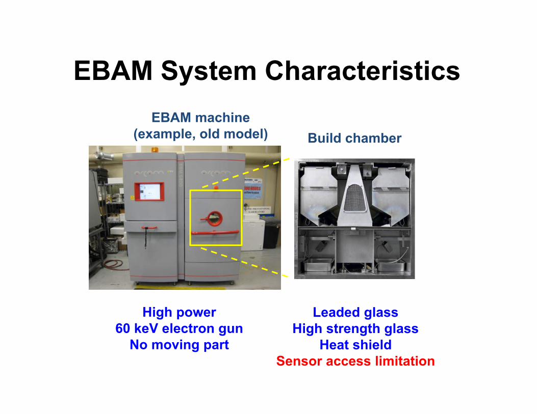
EBAM System CharacteristicsEBAM System CharacteristicsEBAM machine
( l ld d l)(example, old model) Build chamber
High power 60 keV electron gun
Leaded glassHigh strength glass
4
No moving part Heat shieldSensor access limitation

EBAM Viewport WindowEBAM Viewport WindowMetal
ShutterLeaded GlassBuildBuild
Area
Machine Outside
Sacrificial Glass
Vacuum Glass
Heat Shield
Machine Inside
5Metalized film deposit
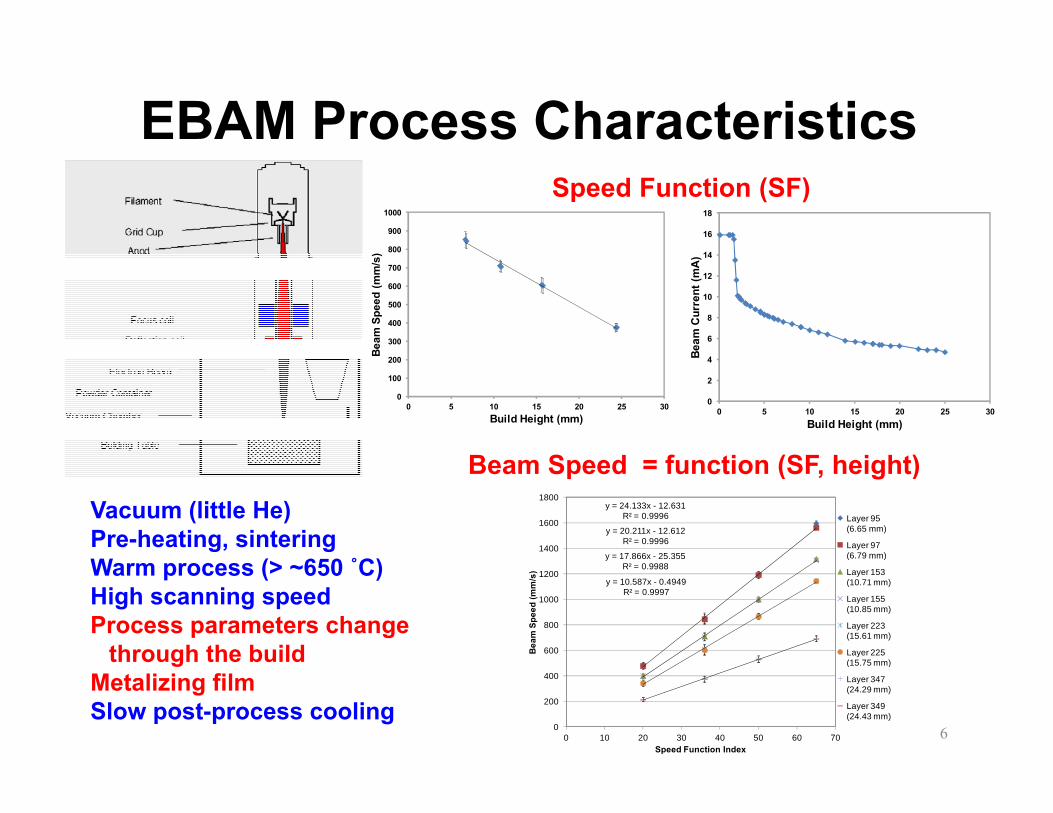
EBAM Process CharacteristicsSpeed Function (SF)
800
900
1000
14
16
18
300
400
500
600
700
Beam
Spe
ed (m
m/s
)
6
8
10
12
14
Beam
Cur
rent
(mA
)
B S d f ti (SF h i ht)
0
100
200
0 5 10 15 20 25 30
B
Build Height (mm)0
2
4
0 5 10 15 20 25 30
B
Build Height (mm)
Vacuum (little He)Pre-heating, sinteringW ( 650 ˚C)
Beam Speed = function (SF, height)y = 24.133x - 12.631
R² = 0.9996
y = 20.211x - 12.612R² = 0.9996
y = 17.866x - 25.3551400
1600
1800
Layer 95 (6.65 mm)
Layer 97 (6.79 mm)
Warm process (> ~650 ˚C)High scanning speedProcess parameters change
through the build
yR² = 0.9988
y = 10.587x - 0.4949R² = 0.9997
600
800
1000
1200
Bea
m S
peed
(mm
/s) Layer 153
(10.71 mm)
Layer 155 (10.85 mm)
Layer 223 (15.61 mm)
Layer 225 (15 75 mm)
6
gMetalizing filmSlow post-process cooling
0
200
400
0 10 20 30 40 50 60 70Speed Function Index
(15.75 mm)
Layer 347 (24.29 mm)
Layer 349 (24.43 mm)
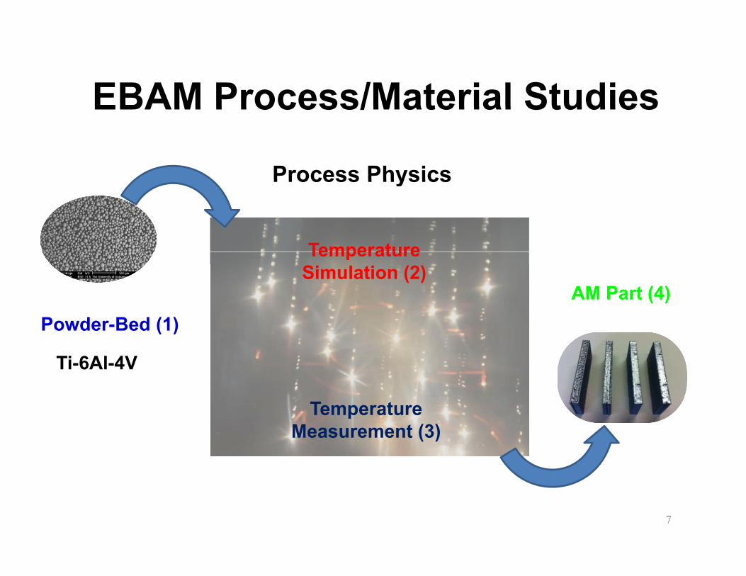
EBAM Process/Material StudiesEBAM Process/Material Studies
Process PhysicsProcess Physics
Temperature
AM Part (4)Powder-Bed (1)
TemperatureSimulation (2)
Powder-Bed (1)
Ti-6Al-4V
Temperature Measurement (3)
7

(1) Feedstock Characterization
(1) Feedstock Characterization
√ Powder-Bed Particles, Porosity- Metallography, Micro-CT
√
Thermal ConductivityHot Disk Thermal Analyzer
√
- Hot-Disk Thermal Analyzer
8

Preheated PowderZ-plane
X-plane9
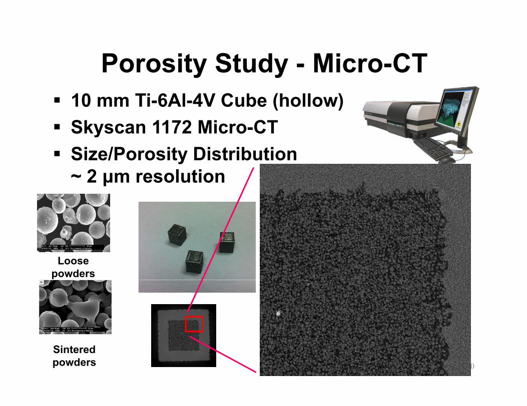
Porosity Study - Micro-CTy y 10 mm Ti-6Al-4V Cube (hollow) Skyscan 1172 Micro CT Skyscan 1172 Micro-CT Size/Porosity Distribution
~ 2 μm resolution~ 2 μm resolution
Loosepowders
10
Sinteredpowders
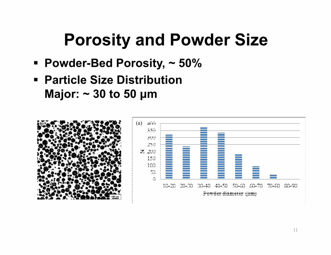
Porosity and Powder Sizey Powder-Bed Porosity, ~ 50% Particle Size Distribution Particle Size Distribution
Major: ~ 30 to 50 μm
(b) (a)
11
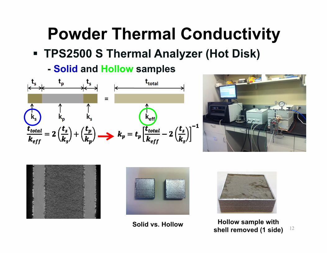
Powder Thermal Conductivity TPS2500 S Thermal Analyzer (Hot Disk)
- Solid and Hollow samples
12Solid vs. Hollow Hollow sample with shell removed (1 side)
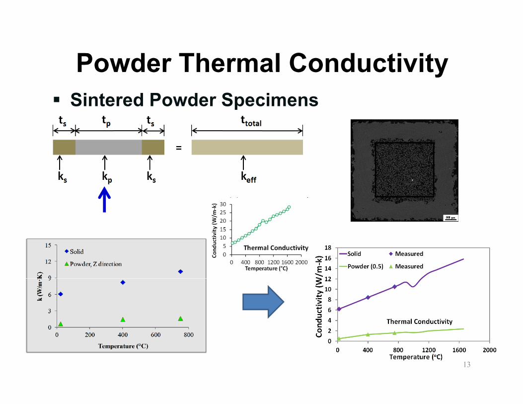
Powder Thermal Conductivityy Sintered Powder Specimens
13
(2) Temperature Simulation- Finite Element Modeling
Heat Transfer Heat Source
√√ Heat Source Material/Powder Properties√√
√ Latent Heat of Fusion√
14

Governing EquationsHeat Transfer
TcTc )()(
g q
T - Temperature
xTc
vt
TcQTk p
sp
)()()(
- Absorbed heat fluxc - Specific heat capacityρ - Densityλ - Thermal conductivity
C d f h
, ,x y zQ
Latent Heat of Fusion
d f
Assumptions:
vs - Constant speed of the moving heat source
fH T cdT L f 0
ST T f
,S
S L
T TT T T p
Heat Conduction Negligible molten flow within molten pool Radiation considered as boundary condition
1L ST T
f ,S L
L
T T TT T
ΔHf - latent heat of fusion Uniform temperature as the part initial temperature
15
Tl - liquidus temperatureTs - solidus temperaturefs - solid fraction

Heat Source Equations
Intensity distribution: a conical source: Horizontal – Gaussian distribution Vertical – Decaying with increasing of
penetration depth
η - electron beam efficiency coefficient
U - voltageU voltage
Ib - current
S - penetration depth
ΦE - beam diameterΦE beam diameter
xS, yS - horizontal position of heat source center
Hs - Gaussian heat source, Cline and Anthony
Iz - penetration function, Zäh and Lutzmannz p ,
16
Simulation Examplep
Process Simulation Animation
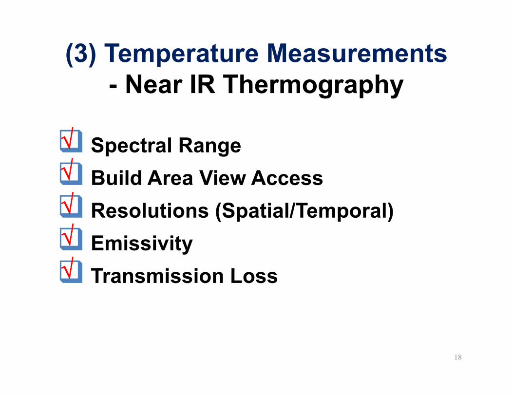
(3) Temperature Measurements- Near IR Thermography
Spectral Range B ild A Vi A
√√ Build Area View Access Resolutions (Spatial/Temporal)√√
Emissivity Transmission Loss
√√ Transmission Loss√
18
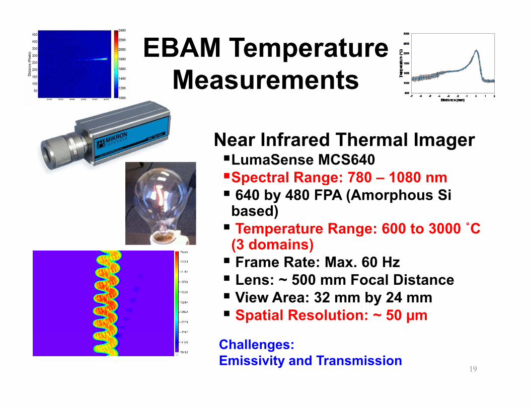
EBAM Temperature MeasurementsMeasurements
Near Infrared Thermal ImagerLumaSense MCS640 Spectral Range: 780 – 1080 nmSpectral Range: 780 – 1080 nm 640 by 480 FPA (Amorphous Si
based) Temperature Range: 600 to 3000 ˚CTemperature Range: 600 to 3000 C
(3 domains) Frame Rate: Max. 60 Hz Lens: ~ 500 mm Focal DistanceLens: 500 mm Focal Distance View Area: 32 mm by 24 mm Spatial Resolution: ~ 50 µm
19
Challenges:Emissivity and Transmission

Measurement Setupp
Emissivity (Single Setting, Estimated)Emissivity (Single Setting, Estimated)Transmission (Calibrated, 3 Ranges, with Glasses)
20Heat shield
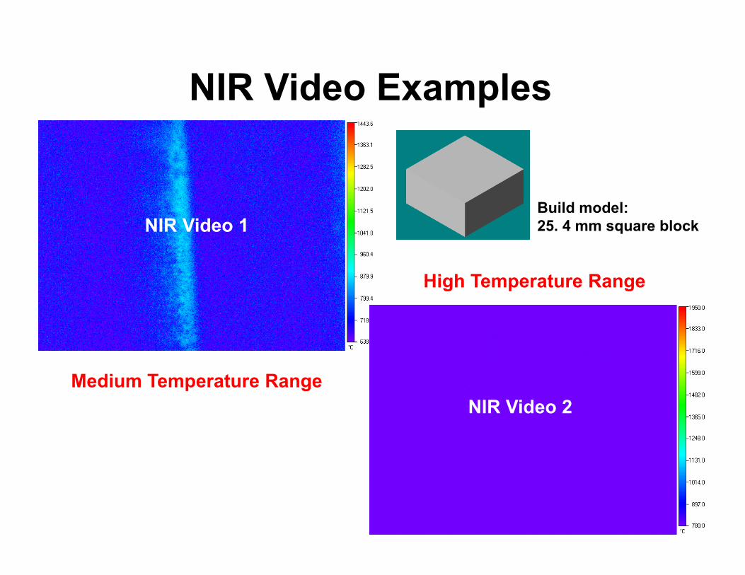
NIR Video Examplesp
Build model:25. 4 mm square blockNIR Video 1
High Temperature Range
Medium Temperature RangeNIR Video 2
21
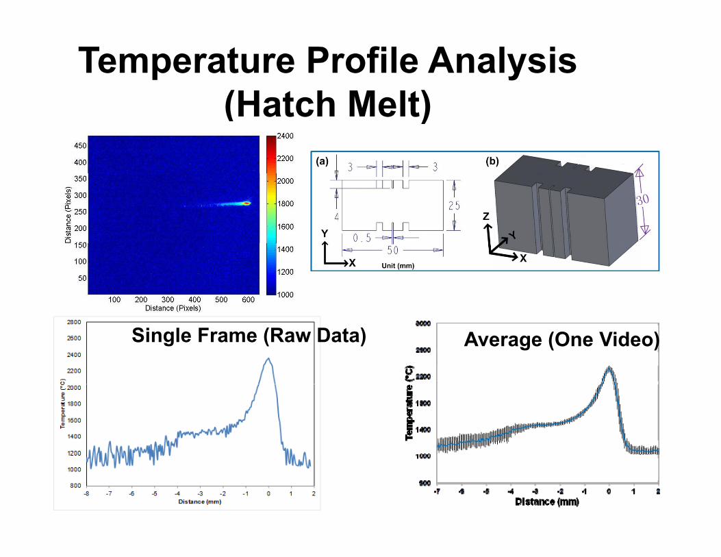
Temperature Profile Analysis (Hatch Melt)(Hatch Melt)
Single Frame (Raw Data) Average (One Video)
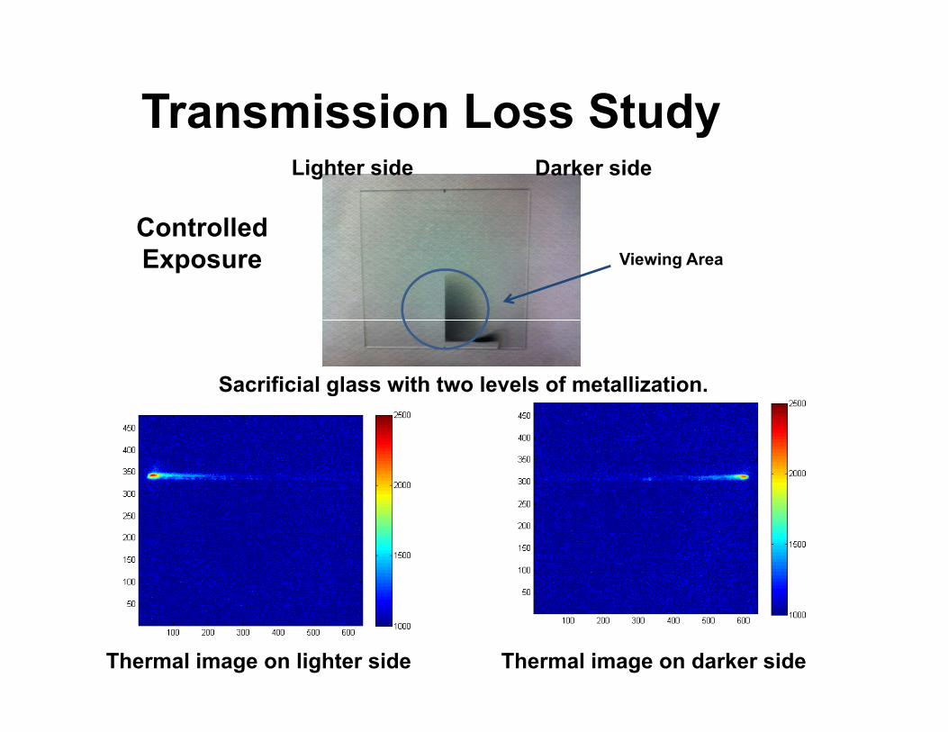
Transmission Loss Studyy
Controlled
Lighter side Darker side
Viewing AreaControlled Exposure
Sacrificial glass with two levels of metallization.
Thermal image on lighter side Thermal image on darker side

Controlled Exposure Experimentp pTemperature Profiles Observed Through Different
Levels of Metallization
y = 1 1602x 171 852250
2500
2200
2400
2600
y = 1.1602x - 171.85R² = 0.9822
1750
2000
de T
empe
ratu
re (C
)
1600
1800
2000
2200
mpe
ratu
re (C
)
Light SideD k Sid
1250
1500
Ligh
ter S
id1000
1200
1400
Tem Dark Side
10001000 1250 1500 1750 2000 2250 2500
Darker Side Temperature (C)
800-8 -6 -4 -2 0 2
Distance (mm)
Average Temperature Profiles Relationship Between
24
g p(6.37 mm Build Height)
pTemperatures Observed Through Different Levels of Metallization
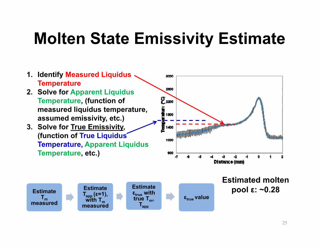
Molten State Emissivity Estimatey
1. Identify Measured Liquidus1. Identify Measured LiquidusTemperature
2. Solve for Apparent LiquidusTemperature, (function of
d li id t tmeasured liquidus temperature, assumed emissivity, etc.)
3. Solve for True Emissivity, (function of True Liquidus( qTemperature, Apparent LiquidusTemperature, etc.)
Estimated molten pool ε: ~0.28Estimate
Tmd
Estimate Tapp (ε=1), with Tm
Estimateεtrue with true Tm, εtrue value
25
measured with Tmmeasured
mTapp
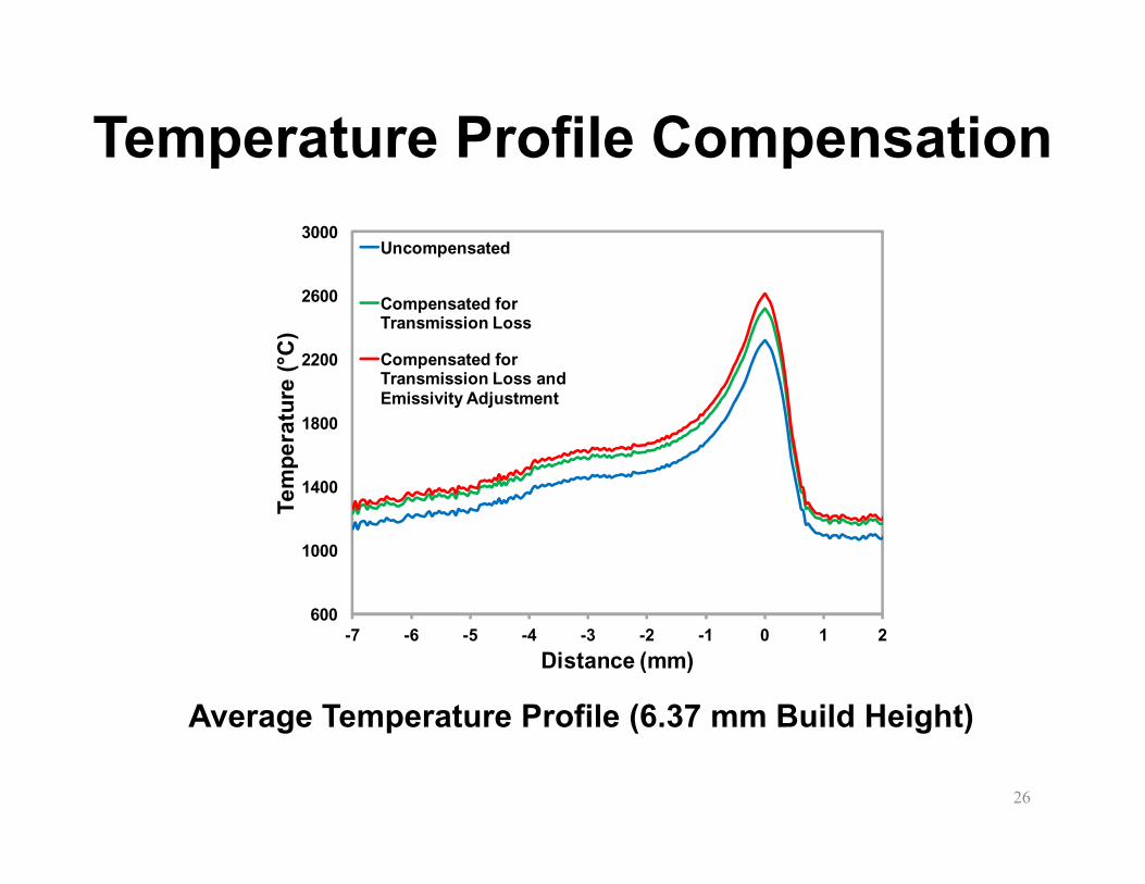
Temperature Profile Compensationp p3000
Uncompensated
2200
2600e
(°C
)Compensated for Transmission Loss
Compensated for Transmission Loss and
1400
1800
empe
ratu
re Emissivity Adjustment
600
1000
Te
Average Temperature Profile (6 37 mm Build Height)
600-7 -6 -5 -4 -3 -2 -1 0 1 2
Distance (mm)
26
Average Temperature Profile (6.37 mm Build Height)
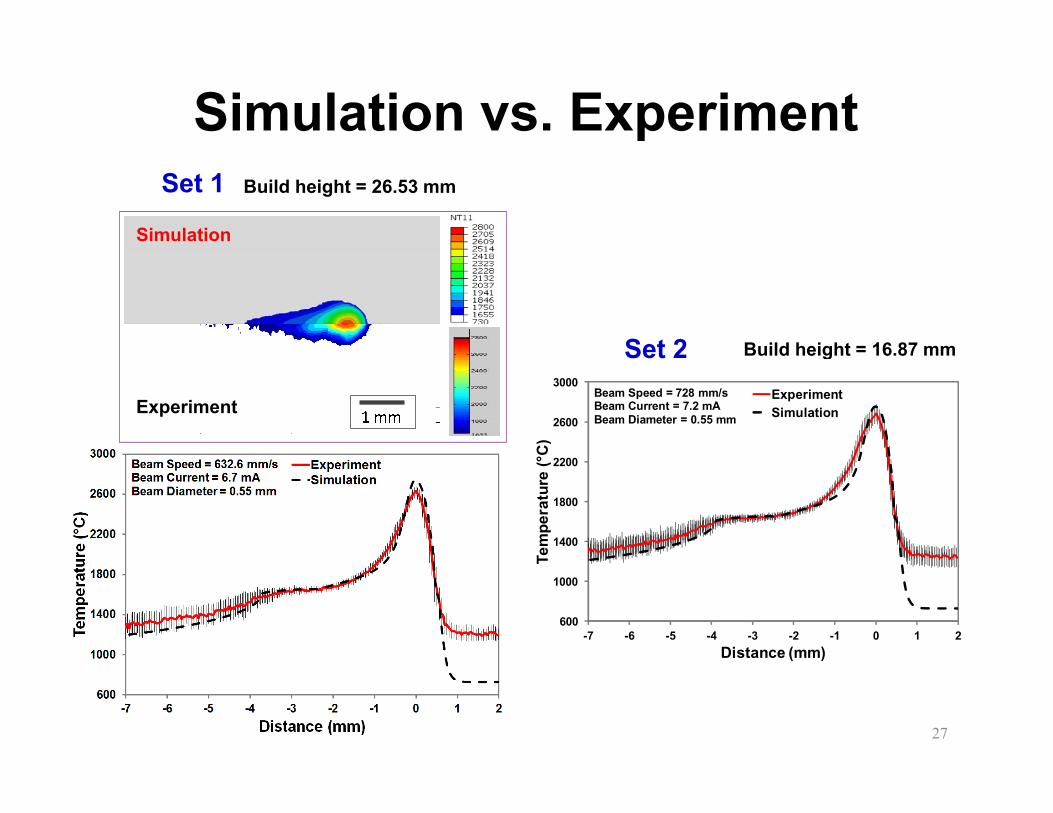
Simulation vs. Experiment
Simulation
Set 1 Build height = 26.53 mm
Set 2 Build height = 16.87 mm
2200
2600
3000
°C)
ExperimentSimulation
Beam Speed = 728 mm/sBeam Current = 7.2 mABeam Diameter = 0.55 mm
Experiment
Set 2 Build height 16.87 mm
1400
1800
2200
Tem
pera
ture
(°
600
1000
-7 -6 -5 -4 -3 -2 -1 0 1 2
T
Distance (mm)
27
Process Parameter Effect Speed Function (SF) Index
Process Parameter Effect1000p ( )
- System Setting Beam Speed, Current 500
600
700
800
900
peed
(mm
/s)
p , Tested Range
- SF20 – SF650
100
200
300
400
Beam
Sp
00 5 10 15 20 25 30
Build Height (mm)
14
16
18
A)
4
6
8
10
12
Beam
Cur
rent
(mA
280
2
4
0 5 10 15 20 25 30
B
Build Height (mm)
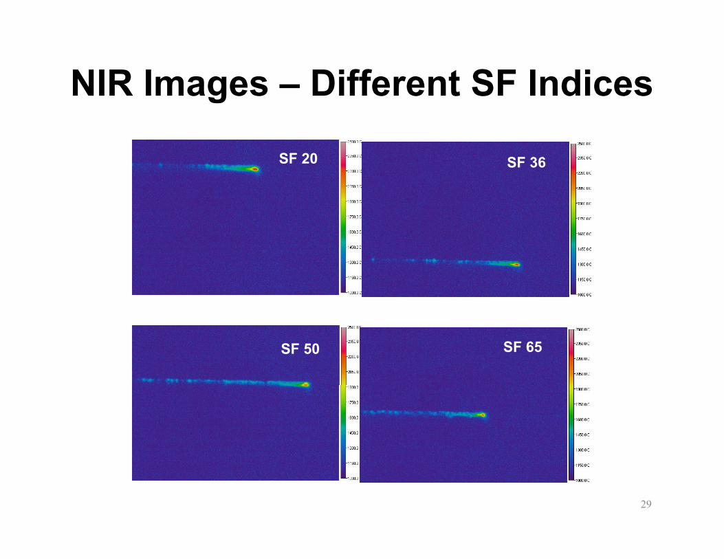
NIR Images – Different SF Indices
SF 20 SF 36
SF 50 SF 65
29
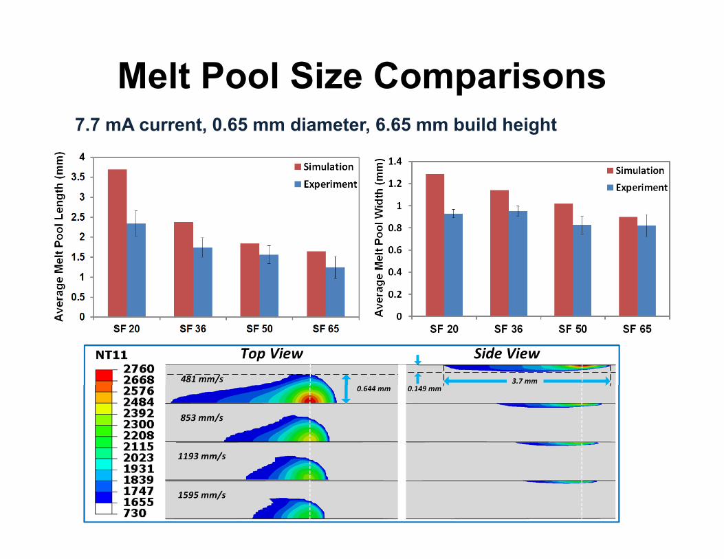
Melt Pool Size Comparisons7.7 mA current, 0.65 mm diameter, 6.65 mm build height

Temperature AnalysisBeam Speed EffectBeam Speed Effect
7.7 mA current, 0.65 mm diameter, 6.65 mm build height

(4) Part Characteri ation(4) Part Characterization
Microstructures (Phases, Grain Sizes) M h i l P ti (E H YS UTS)
√√ Mechanical Properties (E, H, YS, UTS)√
32
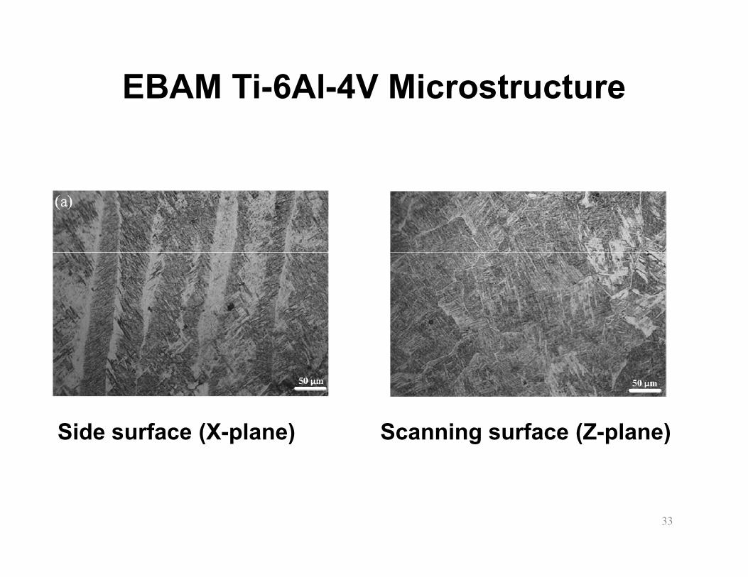
EBAM Ti-6Al-4V Microstructure
Side surface (X-plane) Scanning surface (Z-plane)
33
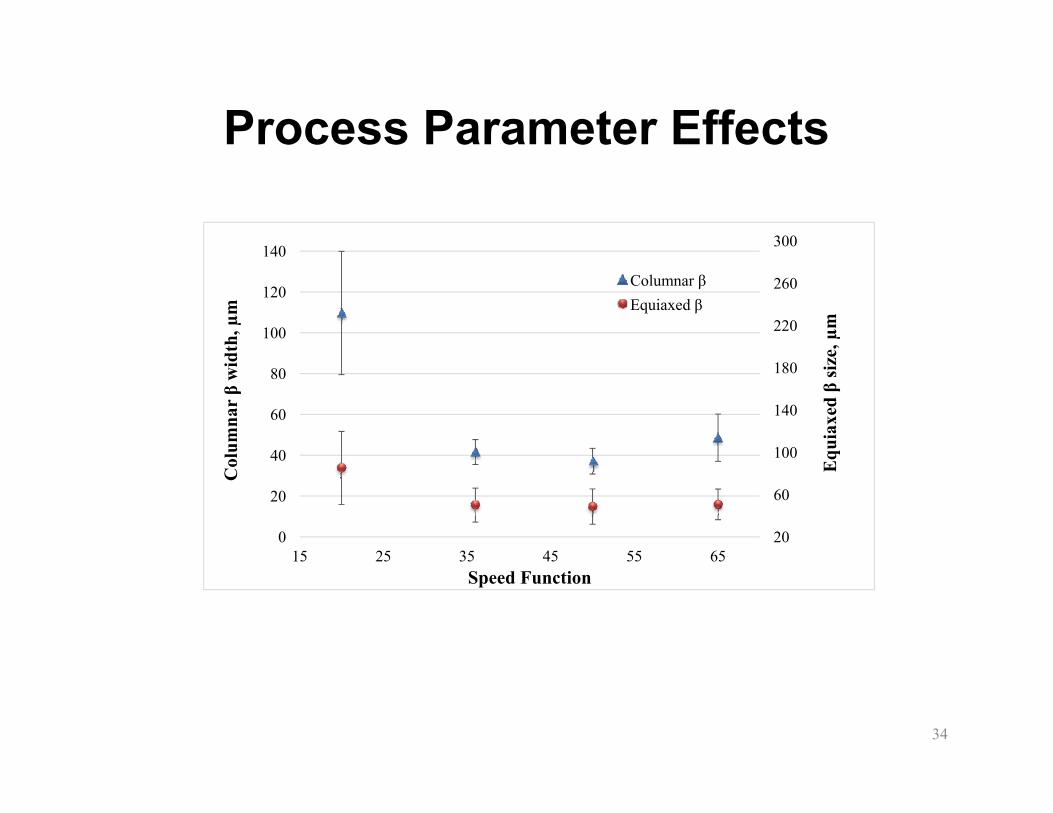
Process Parameter Effects
300140
220
260
100
120
140
e, µ
m
dth,
µm
Columnar β Equiaxed β
100
140
180
40
60
80
quia
xedβ
size
lum
nar β
wid
20
60
15 25 35 45 55 650
20
40 Eq
Co
15 25 35 45 55 65Speed Function
34

Mechanical Property (Nanoindentation)Z l X plane
120
130
120
130
Z-plane X-plane
100
110
E, G
Pa
100
110
E, G
Pa
Young’smodulus
80
90
20 36 50 65Speed Function
80
90
20 36 50 65Speed Function
6.0
6.5
7.0
6.0
6.5
7.0
H d
4.0
4.5
5.0
5.5
H, G
Pa
4.0
4.5
5.0
5.5H
, GPa Hardness
35
3.0
3.5
20 36 50 65Speed Function
3.0
3.5
20 36 50 65Speed Function
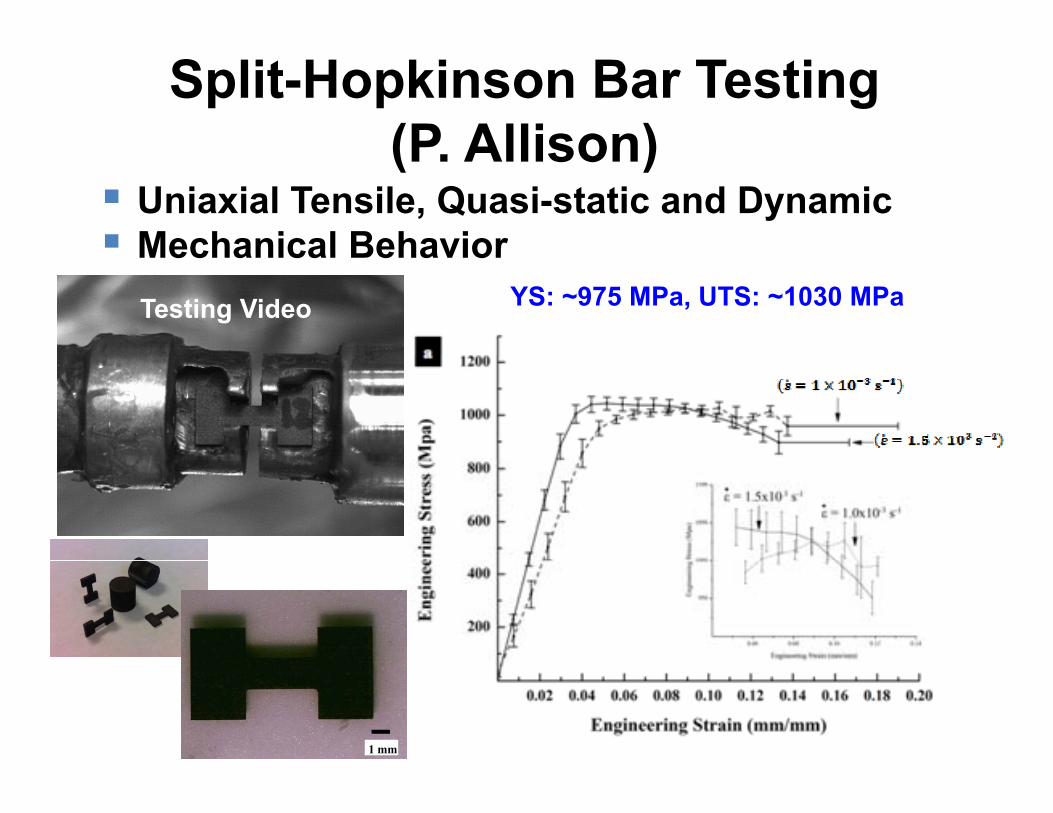
Split-Hopkinson Bar Testing(P Allison)(P. Allison)
Uniaxial Tensile, Quasi-static and Dynamic Mechanical BehaviorMechanical Behavior
YS: ~975 MPa, UTS: ~1030 MPaTesting Video
3636
1 mm
Recommended