TMC424 Datasheet – (V1.04 / 2015-JUL-01) 1/21
Copyright © 2011 TRINAMIC Motion Control GmbH & Co. KG
TMC424 – Datasheet Serial Triple Incremental
Encoder Interface
TRINAMIC Motion Control GmbH & Co. KG Waterloohain 5 D – 22769 Hamburg GERMANY WWW.TRINAMIC.COM
TMC424 Main Features The TMC424 is a triple incremental encoder input chip, which interfaces to any SPITM compatible controller. The TMC424 can especially be used in conjunction with the TMC429 triple stepper motor controller to provide position verification or stabilization using some additional software. It integrates 24 bit counters for each encoder to provide a high position resolution without CPU interaction. Further it allows dynamic resolution adaptation to allow direct comparison of encoder counters with motors using a different micro step resolution. All encoder counters can be latched synchronously, or whenever a null channel event occurs, providing a position on strobe holding function. The TMC424 also provides a step / direction output with programmable signal shaping for the TMC429 as an optional function. A multiplexer function is also integrated for the TMC429 reference switches. All functions can also be used in conjunction.
Applications Stepper Motor Position Verification Position Maintenance Incremental Encoder Interface Readout Step / Direction conversion for TMC429 systems
Features Supports 2 and 3 channel incremental encoders with a wide range of resolutions Allows step / direction signal extraction from TMC429 output data stream Programmable pulse shaping for step / direction interface 24 bit integrated position resolution Programmable prescaler for Incremental Encoder Interface 4-times evaluation of encoder signals Fast 32 bit SPITM interface Can share SPITM interface with TMC429 and supplies separate interrupt output Integrates Reference Switch Multiplexers Package: TQ100 Note: SPI is Trademark of Motorola, Inc.
SD
O
SC
K
SD
I
SD
O4
29
NS
CS
NIN
T
NS
CS
42
9
GN
D
EX
T_
RE
S
VC
OR
E
SD
I_D
SD
O_D
NS
CS
_D
SC
K_D
RE
F2
RE
F1
VC
CI
ST
OP
R0
GN
D
ST
OP
R2
RE
F0
ST
OP
R1
ST
OP
L0
ST
OP
L1
ST
OP
L2
TD
I
TMC424
TQFP-100 Package
GND
ENC1_A
ENC1_B
ENC1_N
ENC2_A
GND
ENC2_B
ENC2_N
ENC3_A
ENC3_B
ENC3_N
STEP1
DIR1
VCCI
STEP2
DIR2
STEP3
DIR3
VCORE
GND
GND
TC
K
TM
S
TDO
TRST
VCC
CLK
VCCI
VCC
GND
VCC
VC
CI
EN
C_
INV
VCC
GND
VCORE
VCORE
VC
OR
E
VC
C
1
25
75
51
26
50
100
76
GND

TMC424 Datasheet – (V1.04 / 2015-JUL-01) 2/21
Copyright © 2011 TRINAMIC Motion Control GmbH & Co. KG
Revision History
Version Comment Date Name
1.0 Derived from TMC423 rebirth datasheet V1.4 June 24, 2010 SL
1.01 Added Pin12 (GND) to Table 1 October 14, 2010 SL
1.02 Added internal Pull-Up/-Down
resistors to Table 1 February 1, 2011 SL
1.03 Updated to TMC429 and TMC26x June 30, 2011 SL
1.04 Warning hint for chamfered corner in IC package is not pin 1 reference 2015-JUN-01 BD

TMC424 Datasheet – (V1.04 / 2015-JUL-01) 3/21
Copyright © 2011 TRINAMIC Motion Control GmbH & Co. KG
Table of Contents 1 Pinout .............................................................................................................................................................................. 5
1.1 Pin Description ..................................................................................................................................................... 6 1.2 Recommended Operating Conditions ............................................................................................................ 7 1.3 Electrical Characteristics ..................................................................................................................................... 7
2 Block Diagram ............................................................................................................................................................... 8 3 Application Environment ............................................................................................................................................ 9
3.1 Application Description ...................................................................................................................................... 9 3.1.1 Application with TMC26x Stepper Motor Driver (SPI controlled) ..................................................... 9 3.1.2 Application with Step/Direction controlled TMC26x ............................................................................ 9
3.2 Application Examples........................................................................................................................................ 10 3.2.1 Application with TMC6x Stepper Motor Driver .................................................................................... 10 3.2.2 Application with Step/Direction Power Stage ..................................................................................... 10
4 Dynamic Resolution Adaptation ............................................................................................................................. 11 5 Serial Peripheral Interface (SPI) with 32-bit Register ...................................................................................... 12
5.1 Description and Specification......................................................................................................................... 12 5.2 32-bit SPI Datagram Structure ....................................................................................................................... 13 5.3 SPI 32-bit Datagram Specification ................................................................................................................ 13
5.3.1 Overview ........................................................................................................................................................ 13 6 Incremental Encoder ................................................................................................................................................. 14 7 Configuration Datagrams ......................................................................................................................................... 15
7.1 Encoder Interface Prescaler and Null Event Configuration .................................................................... 15 7.2 Encoder Interface Hold Register Operation................................................................................................ 16 7.3 Timer Logic Step Pulse Length and Delay ................................................................................................. 17 7.4 Control Register and Interrupt Control ....................................................................................................... 17 7.5 N-Channel Read Back ........................................................................................................................................ 17
8 SPI-Protocol for Interface with 6-bit Register .................................................................................................... 18 8.1 Step and Direction Pulse conversion ........................................................................................................... 18
9 Package dimensions .................................................................................................................................................. 19
TMC424 Datasheet – (V1.04 / 2015-JUL-01) 4/21
Copyright © 2011 TRINAMIC Motion Control GmbH & Co. KG
List of Figures Figure 1: Pinout TMC424 ..................................................................................................................................................... 5 Figure 2: Block diagram of the TMC424 .......................................................................................................................... 8 Figure 3: Application Environment................................................................................................................................... 9 Figure 4: Example for Application with SPI controlled TMC26x Stepper Motor Driver ................................... 10 Figure 5: Example for Application with Step/Direction Power Stage .................................................................. 10 Figure 6: TMC424 Application .......................................................................................................................................... 11 Figure 7: Timing diagram of the Serial Interface ...................................................................................................... 12 Figure 8: Structure 32-Bit Interface ................................................................................................................................ 13 Figure 9: Overview TMC424 Registers ........................................................................................................................... 13 Figure 10: Encoder Output and Evaluation .................................................................................................................. 14 Figure 11: Crosstalk on Encoder Wire ........................................................................................................................... 14 Figure 12: Step Direction conversion ............................................................................................................................ 18 Figure 13: 100-Pin TQFP Top View ................................................................................................................................. 19 Figure 14: 100-Pin TQFP Side View ................................................................................................................................ 19 Figure 15: 100-Pin TQFP Side View Detail A................................................................................................................ 19 List of Tables Table 1: TMC424 Pinout ....................................................................................................................................................... 6 Table 2: Operating Conditions ........................................................................................................................................... 7 Table 3: Operating Conditions ........................................................................................................................................... 7 Table 4: Prescaler factors for different motors and encoders ................................................................................ 11 Table 5: Interrupt Flags ..................................................................................................................................................... 13 Table 6: SPI Datagram Prescaler ..................................................................................................................................... 16 Table 7: SPI Datagram Hold Register ............................................................................................................................ 16 Table 8: SPI Datagram Step-/Dir logic ........................................................................................................................... 17 Table 9: SPI Datagram Control Register ....................................................................................................................... 17 Table 10: N-Channel Read Back Register ...................................................................................................................... 17 Table 11: SPI Datagram Step / Direction Converter .................................................................................................. 18 Table 12: Datagram example and RAM contents for three step-direction drivers ............................................ 18 Table 13: TQFP Dimensions .............................................................................................................................................. 20
TMC424 Datasheet – (V1.04 / 2015-JUL-01) 5/21
Copyright © 2011 TRINAMIC Motion Control GmbH & Co. KG
1 Pinout
SD
O
SC
K
SD
I
SD
O4
29
NS
CS
NIN
T
NS
CS
42
9
GN
D
EX
T_
RE
S
VC
OR
E
SD
I_D
SD
O_
D
NS
CS
_D
SC
K_
D
RE
F2
RE
F1
VC
CI
ST
OP
R0
GN
D
ST
OP
R2
RE
F0
ST
OP
R1
ST
OP
L0
ST
OP
L1
ST
OP
L2
TD
I
TMC424
TQFP-100 Package
GND
ENC1_A
ENC1_B
ENC1_N
ENC2_A
GND
ENC2_B
ENC2_N
ENC3_A
ENC3_B
ENC3_N
STEP1
DIR1
VCCI
STEP2
DIR2
STEP3
DIR3
VCORE
GND
GND
TC
K
TM
STDO
TRST
VCC
CLK
VCCI
VCC
GND
VCC
VC
CI
EN
C_IN
V
VCC
GND
VCORE
VCORE
VC
OR
E
VC
C
1
25
75
51
26
50
10
0
76
GND
Figure 1: Pinout TMC424
TMC424 Datasheet – (V1.04 / 2015-JUL-01) 6/21
Copyright © 2011 TRINAMIC Motion Control GmbH & Co. KG
1.1 Pin Description
Pin Location Dir Pull-Up / Pull-Down
Description
GND 1, 9, 12, 25, 38, 51, 67, 75, 88
Ground
ENC1_A 3 In Incremental Encoder Interface 1 Channel A ENC1_B 4 In Incremental Encoder Interface 1 Channel B ENC1_N 5 In Incremental Encoder Interface 1 Channel N ENC2_A 6 In Incremental Encoder Interface 2 Channel A ENC2_B 7 In Incremental Encoder Interface 2 Channel B ENC2_N 8 In Incremental Encoder Interface 2 Channel N ENC3_A 10 In Incremental Encoder Interface 3 Channel A ENC3_B 11 In Incremental Encoder Interface 3 Channel B ENC3_N 13 In Incremental Encoder Interface 3 Channel N ENC_INV 86 In Down Invert all ENCx_y inputs TDI 48 Connect to Ground TMS 49 Connect to 3.3 Volt via Pull-Up Resistor TRST 55 Connect to 3.3 Volt via Pull-Up Resistor TDO 54 To be left open TCK 47 Connect to Ground VCCI 18, 39, 66, 87 Positive Power Supply 3.3 Volt VCC 24, 50, 52, 56, 74 Positive Power Supply 3.3 Volt VCORE 14, 17, 37, 68, 89 Positive Power Supply 1.5 Volt CLK 64 In System Clock 16MHz EXT_RES 92 In Up External Reset Low Active Step 1 16 Out Step/Direction Interface – Step Output Motor 1 Dir 1 19 Out Step/Direction Interface – Direction Output Motor 1 Step 2 20 Out Step/Direction Interface – Step Output Motor 2 Dir 2 21 Out Step/Direction Interface – Direction Output Motor 2 Step 3 22 Out Step/Direction Interface – Step Output Motor 3 Dir 3 23 Out Step/Direction Interface – Direction Output Motor 3 SDO_D 26 Out Step / Direction SPI MISO SDI_D 27 In Up Step / Direction SPI MOSI SCK_D 28 In Up Step / Direction SPI SCK NSCS_D 29 In Up Step / Direction SPI NSCS REF0 34 Out Reference switch output 1 REF1 35 Out Reference switch output 2 REF2 36 Out Reference switch output 3 STOPR0 40 In Down Right Stop Switch Motor 1 STOPR1 41 In Down Right Stop Switch Motor 2 STOPR2 42 In Down Right Stop Switch Motor 3 STOPL0 43 In Down Left Stop Switch Motor 1 STOPL1 44 In Down Left Stop Switch Motor 2 STOPL2 45 In Down Left Stop Switch Motor 3 SDO 100 Out SPI MISO SDI 99 In Up SPI MOSI SCK 98 In Up SPI SCK NSCS 97 In Up SPI NSCS SDO429 96 In Up SPI MISO Pin of TMC429 (SDO_C) NSCS429 95 In Up SPI NSCS Pin of TMC429 (nSCS_C) NINT 94 Out Interrupt Output (low active)
Table 1: TMC424 Pinout
Note: Pins which are not marked in Figure 1: Pinout TMC424 on page 5 must be left open.

TMC424 Datasheet – (V1.04 / 2015-JUL-01) 7/21
Copyright © 2011 TRINAMIC Motion Control GmbH & Co. KG
1.2 Recommended Operating Conditions
Parameter Value Unit Clock Frequency (1) 16 MHz Temperature 0 … +70 °C 1.5 V Power Supply 1.425 ... 1.725 V 3.3 V Power Supply 3 ... 3.6 V
Table 2: Operating Conditions
1 – frequencies up to 60MHz are supported. Please take care about the timing information in this datasheet, since they are based on 16MHz Clock Frequency.
1.3 Electrical Characteristics
Parameter Min Max Unit Supply Current 1.5V 10.5 mA Supply Current 3.3V (Output current = 0)
1.5 mA
Input voltage level Low 0.8 V Input voltage level High 2 V Encoder input pulse length 2 tCLK Encoder count rate fCLK
Table 3: Operating Conditions

TMC424 Datasheet – (V1.04 / 2015-JUL-01) 8/21
Copyright © 2011 TRINAMIC Motion Control GmbH & Co. KG
2 Block Diagram
CLK
Power On
Reset
Encoder
signal
decoder
Flag register
Prescaler factor 10 bit
1/16, 2/16, ... 64
or 1/5, 2/5, ... 64
Encoder Counter
24+4 bit
+
Encoder Hold
24 bit
prescaler+1
SPI Interface
with 32 bit Reg
*Clear on N event
*Hold on N
*N polarity
Control register
*Common Hold
command
*Interrupt enable
SCK
SDI
SDO
NSCS
M
U
X
SDO
428
NSCS
428
INT
Logic+
Latch
NINT
3 x Encoder Interface
3 x Step / Direction converter
SCK
_D
SDI
_D
SDO
_D
NSCS
_D
SPI Interface
with 6 Bit reg
Step pulse
length
8 bit
Timer logic
Step pulse
delay after dir
change 10 bit
EXT
RES
REF
1
REF
2
REF
3
STOP
L1
STOP
L2
STOP
L3
STOP
R1
STOP
R2
STOP
R3
REF
MUX
VCC GND
ENC1
A
ENC1
B
ENC1
N
ENC3
A
ENC3
B
ENC3
N
ENC2
A
ENC2
B
ENC2
N
STEP
1
DIR
1
STEP
2
DIR
2
STEP
3
DIR
3
ENC_
INV
VCCI VCORE
Figure 2: Block diagram of the TMC424

TMC424 Datasheet – (V1.04 / 2015-JUL-01) 9/21
Copyright © 2011 TRINAMIC Motion Control GmbH & Co. KG
3 Application Environment
MotorIncremental
Encoder
TMC
429
TMC
424
TMC
26x
µC
SPI-Interface
SPI-Interface
Step / Direction Interface
for up to three power stages
MotorIncremental
Encoder
TMC
26x
MotorIncremental
Encoder
TMC
26x
MotorIncremental
Encoder
TMC
26x
TMC
429
TMC
424
TMC
26x
TMC
26x
µC
MotorIncremental
Encoder
MotorIncremental
Encoder
SPI-InterfaceSPI-Interface
TMC424 as Step / Direction converter
and Incremental Encoder Interface
TMC424 as Incremental Encoder Interface
Figure 3: Application Environment
3.1 Application Description
3.1.1 Application with TMC26x Stepper Motor Driver (SPI controlled) A complete close-loop motion control system consists of the TMC429 three-axis motion controller, a powerful stepper motor driver from the TMC26x family and the TMC424 Encoder Interface. The system is controlled by an inexpensive microcontroller. The main advantage of the system is that time critical communication to the TMC26x driver is performed by the TMC429. The main purpose of the inexpensive microcontroller is to parameterize the TMC429 and TMC424 and to send motion parameters like maximum speed or target position to the TMC429. Position validation is done by reading the actual position of the TMC429 and the TMC424. The older TMC236, TMC246, TMC239 and TMC249 are also compatible with the TMC424.
3.1.2 Application with Step/Direction controlled TMC26x Another possibility to build a close loop motion control system is to use the TMC424 as encoder interface and also as a step direction converter. Thereto the TMC424 converts the SPITM datagrams sent by the TMC429 into parameterizeable step and direction pulses. For parameterizing, both the TMC429 and TMC424 have to be connected via SPITM interface to an inexpensive microcontroller. Since the TMC429 already has the capability to output Step/Direction signals for at least two motors (depending on the package), the conversion in the TMC424 is not needed in most cases.

TMC424 Datasheet – (V1.04 / 2015-JUL-01) 10/21
Copyright © 2011 TRINAMIC Motion Control GmbH & Co. KG
3.2 Application Examples
3.2.1 Application with TMC6x Stepper Motor Driver This example illustrates the encoder connection and the use of reference switches with the TMC424 and additionally the SPI interface connections between TMC424, TMC429 and a microcontroller. The communication to the drivers (e.g. TMC260) is performed via SPI by the TMC429 motion control chip. On some package variants of the TMC429, the REFR pins are available. Those should be preferred to the STOPR/STOPL inputs of the TMC424's multiplexer.
TMC429
CLK
REF1
REF2
REF3
SDI_C
SCK_C
SDO_C
nSCS_C
V5
V33
Test
GND
SDI_S
SCK_S
SDO_S
nSCS_S
Notes:
1. If the NSCS429 pin is not in use it has to be tied to +3.3V
2. NSCS_D activates the reference switches (inputs
STOPRx/STOPLx and outputs REFx).
TMC424
CLK
RESET
ENC1_A
ENC1_B
ENC1_N
ENC2_A
ENC2_B
ENC2_N
ENC3_A
ENC3_B
ENC3_N
REF1
REF2
REF3
SDI
SCK
SDO
NSCS
SDO429
NSCS429
VCC
VCORE
SDI_D
SCK_D
NSCS_D
STOPR0 - STOPR2
STOPL0 - STOPL2
TRST
TMS
GND
TCK
TDI
GND
+1.5V
+3.3V
16MHz+3.3V
10k each
Co
nn
ect to
en
co
de
rs
16MHz
µCS
S4
24
SS
42
9
MIS
O
SC
K
MO
SI
+3.3V
GND
SPI
to
Drivers
470nF
+3.3V
10k
6x Reference Switch
Inputs (active high)
from nSCS_S
of TMC429
to nSCS_D
of TMC424
Figure 4: Example for Application with TMC26x Stepper Motor Driver
3.2.2 Application with Step/Direction Power Stage Additionally to the previous example the use of the TMC424 as step/direction converter is shown. This can be used with the TMC429 as a drop-in replacement for the TMC428. The reference switches can also be used as above.
TMC429
SCK_C
SDI_C
SDO_C
nSCS_C
SDO_S
SCK_S
SDI_S
nSCS_S
CLK
V5
V33
Test
GND
Note:
If the NSCS429 pin is not in use, it has to be tied to +3.3V
GND
+1.5V
+3.3V
+3.3V
10k
16MHz+3.3V
10k each
Co
nn
ect to
en
co
de
rs
16MHz
+3.3V
GND
GND
TMC424
CLK
RESET
ENC1_A
ENC1_B
ENC1_N
ENC2_A
ENC2_B
ENC2_N
ENC3_A
ENC3_B
ENC3_N
NSCS
SDO
SCK
SDI
SDO429
NSCS429
SDI_D
SCK_D
SDO_D
NSCS_D
STEP1
DIR1
STEP2
DIR2
STEP3
DIR3
VCC
VCORE
SDI_D
SCK_D
TRST
TMS
STOPR0 - STOPR2
STOPL0 - STOPL2
GND
TCK
TDI
µC
SS
42
4
MIS
O
SS
42
9
SC
K
MO
SI
Step/DIR
to
Drivers
470nF
Figure 5: Example for Application with Step/Direction

TMC424 Datasheet – (V1.04 / 2015-JUL-01) 11/21
Copyright © 2011 TRINAMIC Motion Control GmbH & Co. KG
4 Dynamic Resolution Adaptation The dynamic resolution adaptation is needed to link stepper motors and encoders with different resolutions. The characteristics of the connected hardware must be provided to the TMC424 by sending the corresponding SPI telegram. (See 5.3.1 Overview on page 13 in this issue). The TMC424 multiplies the encoder counter by a user selectable value in the range 1..1024, and then divides it by 16. When using incremental encoders with N channel it is also possible to select between different behaviors when the N channel is triggered.
Stepper
motorTMC424 SPI Interface
Stepper Motor:
Resolution: e.g.: 12800 steps / rotation
Encoder:
Resolution: e.g.: 1000 steps / rotation
TMC424:
Prescaler = 3.2 -> 1000* 4 * 3.2 = 12800
Figure 6: TMC424 Application
Table 4 shows a number of prescaler factors for possible combinations of micro step resolution and encoder resolution. Note: The given number of pulses have to be multiplied by four since 4-times
encoder signal evaluation is used. (See
Channel A
Channel B
Evaluation
Step
Channel N
Figure 10: Encoder Output and Evaluation on page 14).
Microsteps Encoder Resolution [Pulses / Rotation] 1024 1000 512 500 256 250 200 125 50 25
12800 3.125 3.2 6.25 6.4 12.5 12.8 16 25.6 64 ---- 6400 1.5625 1.6 3.125 3.2 6.25 6.4 8 12.8 32 64 3200 ---- ---- 1.5625 1.6 3.125 3.2 4 6.4 16 32 1600 ---- ---- ---- ---- 1.5625 1.6 2 3.2 8 16 800 ---- ---- ---- ---- ---- ---- 1 1.6 4 8 400 ---- ---- ---- ---- ---- ---- ---- ---- 2 4
Table 4: Prescaler factors for different motors and encoders

TMC424 Datasheet – (V1.04 / 2015-JUL-01) 12/21
Copyright © 2011 TRINAMIC Motion Control GmbH & Co. KG
5 Serial Peripheral Interface (SPI) with 32-bit Register
5.1 Description and Specification Four pins named nSCS, SCK, SDI and SDO form the serial peripheral interface from a microcontroller to the TMC424. The communication between the microcontroller and the TMC424 takes place via datagrams with a fixed length of 32 bit. The microcontroller always acts as master and the TMC424 as slave. The SPITM of the TMC424 behaves like a simple 32-bit shift register. Incoming serial data at pin SDI is shifted with the rising edge of the clock signal SCK into the 32-bit register. The content of this register is copied after 32-bits with the rising edge of the selection signal nSCS into a buffer register of 32-bit length. The SPITM of the TMC424 sends back data read from registers immediately via the SDO signal. It processes serial data synchronously to the clock signal CLK. Because of on-the-fly processing of the input data stream, the serial microcontroller interface of the TMC424 requires the serial data clock signal SCK to have a minimum low / high time of three clock cycles. The data signal SDI driven by the microcontroller has to be valid at the rising edge of the serial data clock input SCK. The maximum duration of the serial data clock period is unlimited. A complete serial datagram frame has a fixed length of 32 bit. While the data transmission from the microcontroller to the TMC424 is idle, the low active serial chip select input nSCS and also the serial data clock signal SCK are set to high. The serial data input SDI of the TMC429 has to be driven by the microcontroller. Like other SPI compatible devices, the SDO signal of the TMC424 is high impedance ‘Z’ as long as nSCS is high. The signal nSCS has to be high for at least three clock cycles before starting a datagram transmission. To initiate a transmission, the signal nSCS has to be set to low. Three clock cycles later the serial data clock may go low. The most significant bit (MSB) of a 32 bit wide datagram comes first and the least significant bit (LSB) is transmitted as the last one. A data transmission is finished by setting nSCS high for three or more CLK cycles after the last rising SCK slope. nSCS and SCK change in opposite order from low to high at the end of a transmission as these signals change from high to low at the beginning. The timing of the serial microcontroller interface is outlined here:
tSDtSD
CLK
sdi_bit#31
tSCKCL tSCKCHtSUCSC tHDCSC
1 x SDI_C sampled
one full 32 bit datagram
SDO
SDI
SCK
nSCS
sdi_bit#30 . . . sdi_bit#1
30 x sampled SDI_C
sdi_bit#0
1 x SDI_C sampled
tCLK
tDATAGRAMuC
sdo_bit#31 sdo_bit#30 ... sdo_bit#1 sdo_bit#0
tPD
tIS
tSD
tSI
tHDCSC tSUCSC
Figure 7: Timing diagram of the Serial Interface

TMC424 Datasheet – (V1.04 / 2015-JUL-01) 13/21
Copyright © 2011 TRINAMIC Motion Control GmbH & Co. KG
5.2 32-bit SPI Datagram Structure
2
7
1
7
1
8
1
9
2
0
2
1
2
2
2
3
2
4
2
5
2
6
1
66789
1
0
1
1
1
2
1
3
1
4
1
55
2
8
2
9
3
0
3
101234
0 DataINT 0 0 0
Datagram from TMC424 send to µC
Datagram from µC to TMC4242
7
1
7
1
8
1
9
2
0
2
1
2
2
2
3
2
4
2
5
2
6
1
66789
1
0
1
1
1
2
1
3
1
4
1
55
2
8
2
9
3
0
3
101234
R
WAddress Data
Figure 8: Structure 32-Bit Interface
Interrupt Flags [Bit] Name Description
31 INT_ext external Interrupt, e.g. TMC429 30 INT_enc1 N Signal of Encoder Interface 1 detected 29 INT_enc2 N Signal of Encoder Interface 2 detected 28 INT_enc3 N Signal of Encoder Interface 3 detected
Table 5: Interrupt Flags
5.3 SPI 32-bit Datagram Specification
5.3.1 Overview
Byte 0Byte 1Byte 2Byte 3
31 30 29 28 27 26 25 24 23 22 21 20 19 18 17 16 15 14 13 12 11 10 9 8 7 6 5 4 3 2 1 0
0 000 000 Encoder 1 Prescaler
0 000 100 Encoder 2 Prescaler
0 000 010 Encoder 3 Prescaler
0 000 110 Encoder 1, 2, 3 Prescaler - set all commonly
1
1
1
1
Control
0 000 001
0 000 101
0 000 011
Encoder 1 Position Register
Encoder 2 Position Register
Encoder 3 Position Register
R WAddress
0 0 0 0 1 1 1
1000 0 0 0
1 10 0 0 0 0N-Input
Data
Step /Dir
INT
Byte #
Bit #
ReservedStep Pulse DelayStep Pulse Length
Reserved
Reserved
Reserved
Reserved
Reserved
INT
EN
Cle
ar
Fla
gs
Re
g H
old
N P
ola
rity
N H
old
N C
lea
r
N T
rig
ge
r
Dire
ctio
n
0
1
1
N1N2N30 0 0 N1N2N30 0 0N1N2N30 0 0 N1N2N30 0 0
Figure 9: Overview TMC424 Registers
TMC424 Datasheet – (V1.04 / 2015-JUL-01) 14/21
Copyright © 2011 TRINAMIC Motion Control GmbH & Co. KG
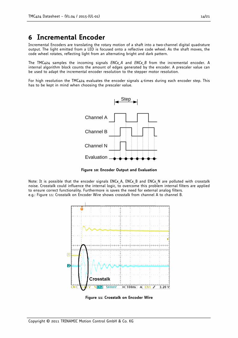
6 Incremental Encoder Incremental Encoders are translating the rotary motion of a shaft into a two-channel digital quadrature output. The light emitted from a LED is focused onto a reflective code wheel. As the shaft moves, the code wheel rotates, reflecting light from an alternating bright and dark pattern. The TMC424 samples the incoming signals ENCx_A and ENCx_B from the incremental encoder. A internal algorithm block counts the amount of edges generated by the encoder. A prescaler value can be used to adapt the incremental encoder resolution to the stepper motor resolution. For high resolution the TMC424 evaluates the encoder signals 4-times during each encoder step. This has to be kept in mind when choosing the prescaler value.
Channel A
Channel B
Evaluation
Step
Channel N
Figure 10: Encoder Output and Evaluation
Note: It is possible that the encoder signals ENCx_A, ENCx_B and ENCx_N are polluted with crosstalk noise. Crosstalk could influence the internal logic, to overcome this problem internal filters are applied to ensure correct functionality. Furthermore is saves the need for external analog filters. e.g.: Figure 11: Crosstalk on Encoder Wire shows crosstalk from channel A to channel B.
Figure 11: Crosstalk on Encoder Wire

TMC424 Datasheet – (V1.04 / 2015-JUL-01) 15/21
Copyright © 2011 TRINAMIC Motion Control GmbH & Co. KG
7 Configuration Datagrams
7.1 Encoder Interface Prescaler and Null Event Configuration The Encoder Interface Initialization datagram configures the parameterizeable encoder prescaler to adapt the TMC424 for different incremental encoders. Furthermore the TMC424 behavior concerning the N channel can be selected. Example: A 1000 steps per rotation encoder is to connect at a stepper motor with 12800 microsteps per rotation. When the next event at the high active N channel is found, the position register must set to zero. Only Encoder Interface 1 is connected. The following datagram performs this task: Bits 31 down to 24 have to be set to 01HEX to select encoder interface 1 The prescaler value has to set to 12800 / (1000*4) = 3.2. Therefore bits 23 down to 12 must set to 831HEX. The N channel is set up correctly when bits 11 down to 0 are set to A0HEX.
Bit Encoder Interface Initialization 31…28 “0000” Register Address 27…25 Interface Selection
000 = Interface 1 001 = Interface 2 010 = Interface 3 011 = Interface 1, 2 and 3
24 ‘1’ 23…12 External Encoder Resolution and Corresponding Prescaler Factor
Bits 15 … 12: Fractional part of Factor. Unit: 1/16 (when bit 23 = 0) resp. 1/5 (bit 23 = 1) Bits 22 … 16: Integer part of Factor Bit 23: Switches Fractional part between 1/5 resolution or 1/16 resolution Default: (010)h (prescaler 1) (default value after power on) Example settings: Encoder: 1024 lines (4096 steps per rotation) (032)h for 12800 micro steps per rotation (prescaler 3.125) (019)h for 6400 micro steps (prescaler 1.5625) Encoder: 1000 lines (831) h for 12800 micro steps (prescaler 3.2) (813)h for 6400 micro steps (prescaler 1.6) Encoder: 512 lines (064)h for 12800 micro steps (prescaler 6.25) (032)h for 6400 micro steps (prescaler 3.125) (019)h for 3200 micro steps (prescaler 1.5625) Encoder: 500 lines (862)h for 12800 micro steps (prescaler 6.4) (831)h for 6400 micro steps (prescaler 3.2) (813)h for 3200 micro steps (prescaler 1.6) Encoder: 256 lines (0C8)h for 12800 micro steps (prescaler 12.5) (064)h for 6400 micro steps (prescaler 6.25) (032)h for 3200 micro steps (prescaler 3.125) (019)h for 1600 micro steps (prescaler 1.5625) Encoder: 250 lines (8C4)h for 12800 micro steps (prescaler 12.8) (862)h for 6400 micro steps (prescaler 6.4) (831)h for 3200 micro steps (prescaler 3.2) (813)h for 1600 micro steps (prescaler 1.6) Encoder: 200 lines (100)h for 12800 micro steps (prescaler 16) (080)h for 6400 micro steps (prescaler 8) (040)h for 3200 micro steps (prescaler 4) (020)h for 1600 micro steps (prescaler 2) (010)h for 800 micro steps (prescaler 1)
TMC424 Datasheet – (V1.04 / 2015-JUL-01) 16/21
Copyright © 2011 TRINAMIC Motion Control GmbH & Co. KG
Encoder: 125 lines (993)h for 12800 micro steps (prescaler 25.6) (8C4)h for 6400 micro steps (prescaler 12.8) (862)h for 3200 micro steps (prescaler 6.4) (831)h for 1600 micro steps (prescaler 3.2) (813)h for 800 micro steps (prescaler 1.6) Encoder: 50 lines (200 steps per rotation) (400)h for 12800 micro steps (prescaler 64) (200)h for 6400 micro steps (prescaler 32) (100)h for 3200 micro steps (prescaler 16) (080)h for 1600 micro steps (prescaler 8) (040)h for 800 micro steps (prescaler 4) (020)h for 400 micro steps (prescaler 2) (010)h for 200 steps per rotation (prescaler 1)
11 N Polarity for Selected Interface 0 = active low (default) 1 = active high When changing the polarity, please be aware that a single clear on N Event might be triggered, and thus should not be initiated in the same write access.
10 Hold on N for Selected Interface 0 = no hold (default) 1 = active: Encoder counter freezes during 0 channel event.
9 Clear on N Event for Selected Interface 0 = no clear (default) 1 = active When switched to active, then it depends on bit 8, if a clear event is issued only once, or always when the N channel becomes active.
8 N Trigger Selection 0 = only at next N signal (default) 1 = always at N signal The clear event last until the N signal goes inactive again. If earlier termination is desired, i.e. to preset the encoder counter to a different value, disable “Clear on N” prior to changing the position register.
7 add or sub register for each step (CW = looking onto the axis) 0= add for CW, sub for CCW (default) 1= add for CCW, sub for CW
6…0 Reserved
Table 6: SPI Datagram Prescaler
7.2 Encoder Interface Hold Register Operation To read the actual contents of the position register or to preset the position register the following command is to be used:
Bit Encoder Interface Control (Read/Preload Encoder Hold Register) 31…28 “0000” Register Address 27…25 Select Encoder Hold Register
100 = Hold register in encoder interface 1 101 = Hold register in encoder interface 2 110 = Hold register in encoder interface 3
24 Read or Preload Selection 0 = Read encoder hold register 1 = Preload encoder hold register
23…0 Encoder Hold Register Data
Table 7: SPI Datagram Hold Register

TMC424 Datasheet – (V1.04 / 2015-JUL-01) 17/21
Copyright © 2011 TRINAMIC Motion Control GmbH & Co. KG
7.3 Timer Logic Step Pulse Length and Delay To parameterize the step length and delay the next datagram is to be used:
Bit Write Step Pulse Length / Delay 31…25 “0000111” Register Address 24 ‘1’ 23…16 Step Pulse Length (default value = 48(10) after PON) 15…6 Step Pulse Delay after Direction Change (default value = 160(10) after PON) 5…0 Reserved
Table 8: SPI Datagram Step-/Dir logic
7.4 Control Register and Interrupt Control This datagram configures the interrupt control of the TMC424. When enabled, the N channel pulse of all encoders is fed to the NINT pin.
Bit Control Register 31…25 “0001000” Register Address 24 ‘1’ 23 Set Common Hold for Encoder Hold Registers
0 = no hold (default) 1 = freeze encoder hold registers
22 Encoder Interrupt Enable, if Null signal 0 = interrupt disable (default) 1 = interrupt enable
21 Clear Interrupt Flags 0 = no clear (default) 1= clear flags
20…0 Reserved
Table 9: SPI Datagram Control Register
7.5 N-Channel Read Back This datagram returns the state of the three N-Channel inputs ENCx_N after the possible inverting controlled by ENC_INV. The three inputs are sampled after transmission of the R/W bit. The three bits are repeated in the datagram for compatibility reasons as if the N-signals were connected to the SW_ROW_PIN(0..2) inputs of a TMC423.
Bit Channel 31…25 “0001001” Register Address 24 ‘0’ 23…21, 17…15, 11…9, 5…3
“000”
20, 14, 8, 2 ENC3_N when ENC_INV = 0, not ENC3_N when ENC_INV = 1 19, 13, 7, 1 ENC2_N when ENC_INV = 0, not ENC2_N when ENC_INV = 1 18, 12, 6, 0 ENC1_N when ENC_INV = 0, not ENC1_N when ENC_INV = 1
Table 10: N-Channel Read Back Register

TMC424 Datasheet – (V1.04 / 2015-JUL-01) 18/21
Copyright © 2011 TRINAMIC Motion Control GmbH & Co. KG
8 SPI-Protocol for Interface with 6-bit Register The 6-bit SPI Interface is used to receive step / direction information from the TMC429. The TMC424 processes the data and issues the corresponding step / direction signals via the step / direction pins. Bit0 (Pulse 1) have to be sent first to the TMC424.
Bit Step / Direction Converter
0 Pulse 1 1 Direction 1 2 Pulse 2 3 Direction 2 4 Pulse 3 5 Direction 3
Table 11: SPI Datagram Step / Direction Converter
The order of the control signals serially sent from the TMC429 has to be defined. This can be done by writing so called primary signal codes into the stepper motor driver datagram configuration area of the on-chip configuration RAM of the TMC429. This signals codes are $13 (step first) and $12 (direction). To switch to the next motor the next motor bit (NxM) has to be set.
Position within datagram
Driver/motor NxM bit TMC429 signal code
RAM data TMC429 mnemonic of primary signal
0 1
0 $13 $13 Step 1 1 $12 $32 Direction 2
2 0 $13 $13 Step
3 1 $12 $32 Direction 4
3 0 $13 $13 Step
5 1 $12 $32 Direction
Table 12: Datagram example and RAM contents for three step-direction drivers
8.1 Step and Direction Pulse conversion Step pulses can be modified in their pulse width and delayed after an direction change was done. The corresponding datagram (See 7.3) on page 17) is used to parameterize the Step / Dir interface.
t
t
step_in
dir
step pulse length
step pulse delay
t
step_out
Figure 12: Step Direction conversion
TMC424 Datasheet – (V1.04 / 2015-JUL-01) 19/21
Copyright © 2011 TRINAMIC Motion Control GmbH & Co. KG
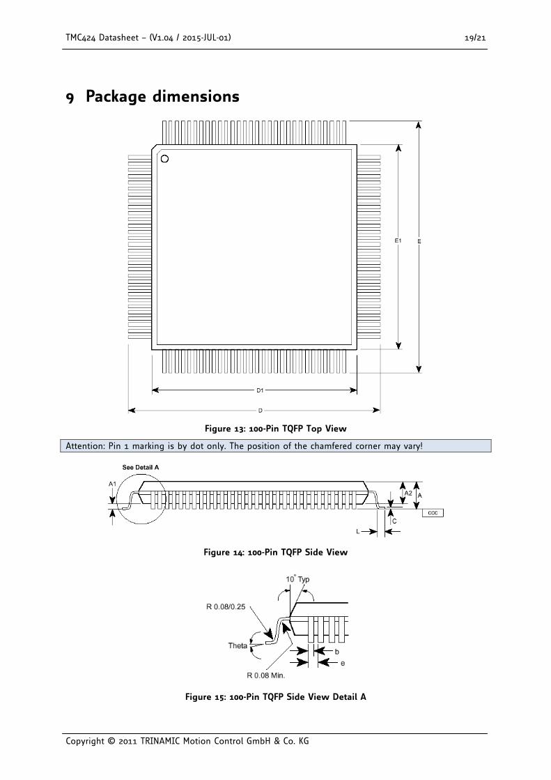
9 Package dimensions
Figure 13: 100-Pin TQFP Top View
Attention: Pin 1 marking is by dot only. The position of the chamfered corner may vary!
Figure 14: 100-Pin TQFP Side View
Figure 15: 100-Pin TQFP Side View Detail A
TMC424 Datasheet – (V1.04 / 2015-JUL-01) 20/21
Copyright © 2011 TRINAMIC Motion Control GmbH & Co. KG
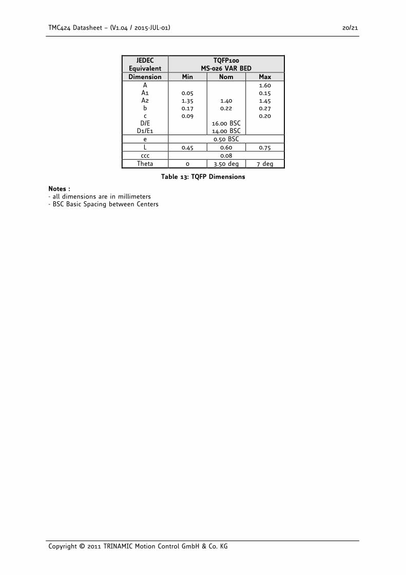
JEDEC Equivalent
TQFP100 MS-026 VAR BED
Dimension Min Nom Max A A1 A2 b c
D/E D1/E1
0.05 1.35 0.17 0.09
1.40 0.22
16.00 BSC 14.00 BSC
1.60 0.15 1.45 0.27 0.20
e 0.50 BSC L 0.45 0.60 0.75
ccc 0.08 Theta 0 3.50 deg 7 deg
Table 13: TQFP Dimensions
Notes : - all dimensions are in millimeters - BSC Basic Spacing between Centers
TMC424 Datasheet – (V1.04 / 2015-JUL-01) 21/21
Copyright © 2011 TRINAMIC Motion Control GmbH & Co. KG
Life support policy TRINAMIC Motion Control GmbH & Co. KG does not authorize or warrant any of its products for use in life support systems, without the specific written consent of TRINAMIC Motion Control GmbH & Co. KG. Life support systems are equipment intended to support or sustain life, and whose failure to perform, when properly used in accordance with instructions provided, can be reasonably expected to result in personal injury or death. © 2011 TRINAMIC Motion Control GmbH & Co. KG Information given in this data sheet is believed to be accurate and reliable. However no responsibility is assumed for the consequences of its use nor for any infringement of patents or other rights of third parties, which may result form its use. Specifications subject to change without notice.
Recommended